3-Channel Low Power SDTV Video Amp w/I2C Control 6dB ...
54
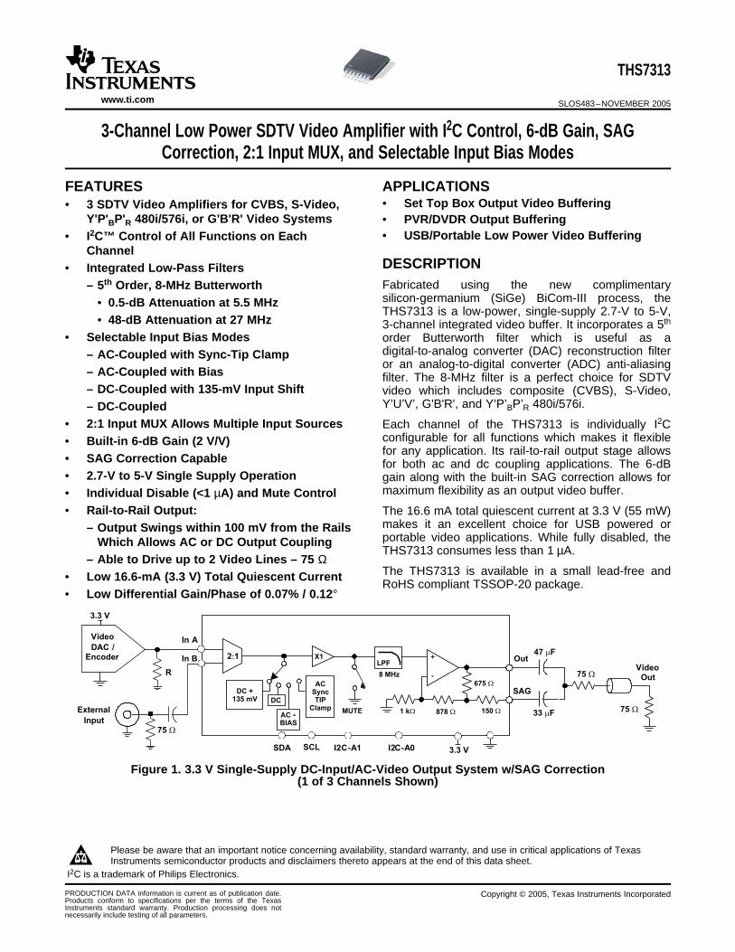
www.ti.com FEATURES APPLICATIONS DESCRIPTION In A Video DAC / Encoder 3.3 V 3.3 V LPF AC Sync TIP Clamp DC + - 1kW 878 W X1 DC + 135 mV MUTE 2:1 675 W 150 W AC - BIAS In B External Input SDA I2C-A1 SCL I2C-A0 8 MHz Out SAG 47 F m 33 F m 75 W 75 W Video Out 75 W R THS7313 SLOS483 – NOVEMBER 2005 3-Channel Low Power SDTV Video Amplifier with I 2 C Control, 6-dB Gain, SAG Correction, 2:1 Input MUX, and Selectable Input Bias Modes • Set Top Box Output Video Buffering • 3 SDTV Video Amplifiers for CVBS, S-Video, Y'P' B P' R 480i/576i, or G'B'R' Video Systems • PVR/DVDR Output Buffering • USB/Portable Low Power Video Buffering • I 2 C™ Control of All Functions on Each Channel • Integrated Low-Pass Filters Fabricated using the new complimentary –5 th Order, 8-MHz Butterworth silicon-germanium (SiGe) BiCom-III process, the • 0.5-dB Attenuation at 5.5 MHz THS7313 is a low-power, single-supply 2.7-V to 5-V, • 48-dB Attenuation at 27 MHz 3-channel integrated video buffer. It incorporates a 5 th • Selectable Input Bias Modes order Butterworth filter which is useful as a digital-to-analog converter (DAC) reconstruction filter – AC-Coupled with Sync-Tip Clamp or an analog-to-digital converter (ADC) anti-aliasing – AC-Coupled with Bias filter. The 8-MHz filter is a perfect choice for SDTV – DC-Coupled with 135-mV Input Shift video which includes composite (CVBS), S-Video, Y’U’V’, G'B'R', and Y’P’ B P’ R 480i/576i. – DC-Coupled • 2:1 Input MUX Allows Multiple Input Sources Each channel of the THS7313 is individually I 2 C configurable for all functions which makes it flexible • Built-in 6-dB Gain (2 V/V) for any application. Its rail-to-rail output stage allows • SAG Correction Capable for both ac and dc coupling applications. The 6-dB • 2.7-V to 5-V Single Supply Operation gain along with the built-in SAG correction allows for maximum flexibility as an output video buffer. • Individual Disable (<1 μA) and Mute Control • Rail-to-Rail Output: The 16.6 mA total quiescent current at 3.3 V (55 mW) makes it an excellent choice for USB powered or – Output Swings within 100 mV from the Rails portable video applications. While fully disabled, the Which Allows AC or DC Output Coupling THS7313 consumes less than 1 μA. – Able to Drive up to 2 Video Lines – 75 Ω The THS7313 is available in a small lead-free and • Low 16.6-mA (3.3 V) Total Quiescent Current RoHS compliant TSSOP-20 package. • Low Differential Gain/Phase of 0.07% / 0.12° Figure 1. 3.3 V Single-Supply DC-Input/AC-Video Output System w/SAG Correction (1 of 3 Channels Shown) Please be aware that an important notice concerning availability, standard warranty, and use in critical applications of Texas Instruments semiconductor products and disclaimers thereto appears at the end of this data sheet. I 2 C is a trademark of Philips Electronics. PRODUCTION DATA information is current as of publication date. Copyright © 2005, Texas Instruments Incorporated Products conform to specifications per the terms of the Texas Instruments standard warranty. Production processing does not necessarily include testing of all parameters.
-
Upload
khangminh22 -
Category
Documents
-
view
0 -
download
0
Transcript of 3-Channel Low Power SDTV Video Amp w/I2C Control 6dB ...
www.ti.com
FEATURES APPLICATIONS
DESCRIPTION
In AVideo
DAC /Encoder
3.3 V
3.3 V
LPF
ACSyncTIP
ClampDC
+
-
1 kW 878 W
X1
DC +135 mV
MUTE
2:1
675 W
150 WAC -BIAS
In B
External
Input
SDA I2C-A1SCL I2C-A0
8 MHz
Out
SAG
47 Fm
33 Fm
75 W
75 W
VideoOut
75 W
R
THS7313
SLOS483–NOVEMBER 2005
3-Channel Low Power SDTV Video Amplifier with I2C Control, 6-dB Gain, SAGCorrection, 2:1 Input MUX, and Selectable Input Bias Modes
• Set Top Box Output Video Buffering• 3 SDTV Video Amplifiers for CVBS, S-Video,Y'P'BP'R 480i/576i, or G'B'R' Video Systems • PVR/DVDR Output Buffering
• USB/Portable Low Power Video Buffering• I2C™ Control of All Functions on EachChannel
• Integrated Low-Pass FiltersFabricated using the new complimentary– 5th Order, 8-MHz Butterworthsilicon-germanium (SiGe) BiCom-III process, the• 0.5-dB Attenuation at 5.5 MHzTHS7313 is a low-power, single-supply 2.7-V to 5-V,
• 48-dB Attenuation at 27 MHz 3-channel integrated video buffer. It incorporates a 5th
• Selectable Input Bias Modes order Butterworth filter which is useful as adigital-to-analog converter (DAC) reconstruction filter– AC-Coupled with Sync-Tip Clampor an analog-to-digital converter (ADC) anti-aliasing
– AC-Coupled with Bias filter. The 8-MHz filter is a perfect choice for SDTV– DC-Coupled with 135-mV Input Shift video which includes composite (CVBS), S-Video,
Y’U’V’, G'B'R', and Y’P’BP’R 480i/576i.– DC-Coupled• 2:1 Input MUX Allows Multiple Input Sources Each channel of the THS7313 is individually I2C
configurable for all functions which makes it flexible• Built-in 6-dB Gain (2 V/V)for any application. Its rail-to-rail output stage allows• SAG Correction Capable for both ac and dc coupling applications. The 6-dB
• 2.7-V to 5-V Single Supply Operation gain along with the built-in SAG correction allows formaximum flexibility as an output video buffer.• Individual Disable (<1 µA) and Mute Control
• Rail-to-Rail Output: The 16.6 mA total quiescent current at 3.3 V (55 mW)makes it an excellent choice for USB powered or– Output Swings within 100 mV from the Railsportable video applications. While fully disabled, theWhich Allows AC or DC Output CouplingTHS7313 consumes less than 1 µA.
– Able to Drive up to 2 Video Lines – 75 ΩThe THS7313 is available in a small lead-free and• Low 16.6-mA (3.3 V) Total Quiescent CurrentRoHS compliant TSSOP-20 package.
• Low Differential Gain/Phase of 0.07% / 0.12°
Figure 1. 3.3 V Single-Supply DC-Input/AC-Video Output System w/SAG Correction(1 of 3 Channels Shown)
Please be aware that an important notice concerning availability, standard warranty, and use in critical applications of TexasInstruments semiconductor products and disclaimers thereto appears at the end of this data sheet.
I2C is a trademark of Philips Electronics.
PRODUCTION DATA information is current as of publication date. Copyright © 2005, Texas Instruments IncorporatedProducts conform to specifications per the terms of the TexasInstruments standard warranty. Production processing does notnecessarily include testing of all parameters.
www.ti.com
DESCRIPTION (CONTINUED)
ABSOLUTE MAXIMUM RATINGS
DISSIPATION RATINGS
THS7313
SLOS483–NOVEMBER 2005
This integrated circuit can be damaged by ESD. Texas Instruments recommends that all integratedcircuits be handled with appropriate precautions. Failure to observe proper handling and installationprocedures can cause damage.
ESD damage can range from subtle performance degradation to complete device failure. Precisionintegrated circuits may be more susceptible to damage because very small parametric changes couldcause the device not to meet its published specifications.
As part of the THS7313 flexibility, the 2:1 MUX input can be selected for ac or dc coupled inputs. The ac coupledmodes include a sync-tip clamp option for CVBS or Y' signals, or a fixed bias for the C/P'B/P'R channels. The dcinput options include a dc input or a dc + 135-mV input offset shift to allow for a full sync dynamic range at theoutput with 0-V input.
PACKAGING/ORDERING INFORMATION
TRANSPORT MEDIA,PACKAGED DEVICES (1) PACKAGE TYPE QUANTITY
THS7313PW Rails, 70TSSOP-20
THS7313PWR Tape and reel, 2000
(1) For the most current package and ordering information, see the Package Option Addendum at the end of this document, or see the TIWeb site at www.ti.com
over operating free-air temperature range (unless otherwise noted) (1)
UNIT
VSS Supply voltage, VS+ to GND 5.5 V
VI Input voltage –0.4V to VS+
IO Output current ±125 mA
Continuous power dissipation See Dissipation Rating Table
TJ Maximum junction temperature, any condition (2) 150°C
TJ Maximum junction temperature, continuous operation, long term reliability (3) 125°C
Tstg Storage temperature range –65°C to 150°C
Lead temperature 1,6 mm (1/16 inch) from case for 10 seconds 300°C
HBM 2000 V
ESD ratings CDM 750 V
MM 100 V
(1) Stresses above those listed under absolute maximum ratings may cause permanent damage to the device. These are stress ratingsonly and functional operation of the device at these or any other conditions beyond those indicated under recommended operatingconditions is not implied Exposure to absolute maximum rated conditions for extended periods may degrade device reliability.
(2) The absolute maximum junction temperature under any condition is limited by the constraints of the silicon process.(3) The absolute maximum junction temperature for continuous operation is limited by the package constraints. Operation above this
temperature may result in reduced reliability and/or lifetime of the device.
POWER RATING (1)
θJC θJA (TJ = 125°C)PACKAGE (°C/W) (°C/W)TA = 25°C TA = 85°C
TSSOP – 20 (PW) 32.3 83 (2) 1.2 W 0.48 W
(1) Power rating is determined with a junction temperature of 125°C. This is the point where distortion starts to substantially increase andlong-term reliability starts to be reduced. Thermal management of the final PCB strives to keep the junction temperature at or below125°C for best performance and reliability.
(2) This data was taken with the JEDEC High-K test PCB. For the JEDEC low-K test PCB, the θJA is 125.8°C.
2
www.ti.com
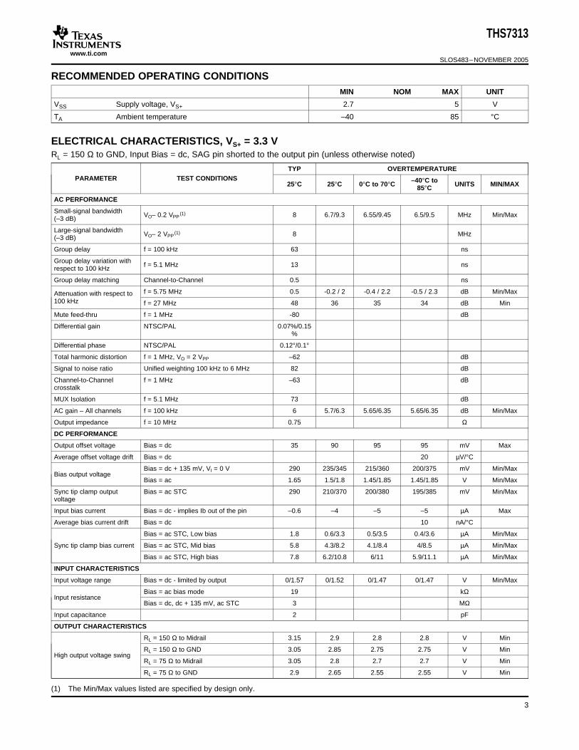
RECOMMENDED OPERATING CONDITIONS
ELECTRICAL CHARACTERISTICS, VS+ = 3.3 V
THS7313
SLOS483–NOVEMBER 2005
MIN NOM MAX UNIT
VSS Supply voltage, VS+ 2.7 5 V
TA Ambient temperature –40 85 °C
RL = 150 Ω to GND, Input Bias = dc, SAG pin shorted to the output pin (unless otherwise noted)
TYP OVERTEMPERATUREPARAMETER TEST CONDITIONS –40°C to25°C 25°C 0°C to 70°C UNITS MIN/MAX85°C
AC PERFORMANCE
Small-signal bandwidth VO– 0.2 VPP(1) 8 6.7/9.3 6.55/9.45 6.5/9.5 MHz Min/Max(–3 dB)
Large-signal bandwidth VO– 2 VPP(1) 8 MHz(–3 dB)
Group delay f = 100 kHz 63 ns
Group delay variation with f = 5.1 MHz 13 nsrespect to 100 kHz
Group delay matching Channel-to-Channel 0.5 ns
f = 5.75 MHz 0.5 -0.2 / 2 -0.4 / 2.2 -0.5 / 2.3 dB Min/MaxAttenuation with respect to100 kHz f = 27 MHz 48 36 35 34 dB Min
Mute feed-thru f = 1 MHz -80 dB
Differential gain NTSC/PAL 0.07%/0.15%
Differential phase NTSC/PAL 0.12°/0.1°
Total harmonic distortion f = 1 MHz, VO = 2 VPP –62 dB
Signal to noise ratio Unified weighting 100 kHz to 6 MHz 82 dB
Channel-to-Channel f = 1 MHz –63 dBcrosstalk
MUX Isolation f = 5.1 MHz 73 dB
AC gain – All channels f = 100 kHz 6 5.7/6.3 5.65/6.35 5.65/6.35 dB Min/Max
Output impedance f = 10 MHz 0.75 Ω
DC PERFORMANCE
Output offset voltage Bias = dc 35 90 95 95 mV Max
Average offset voltage drift Bias = dc 20 µV/°C
Bias = dc + 135 mV, VI = 0 V 290 235/345 215/360 200/375 mV Min/MaxBias output voltage
Bias = ac 1.65 1.5/1.8 1.45/1.85 1.45/1.85 V Min/Max
Sync tip clamp output Bias = ac STC 290 210/370 200/380 195/385 mV Min/Maxvoltage
Input bias current Bias = dc - implies Ib out of the pin –0.6 –4 –5 –5 µA Max
Average bias current drift Bias = dc 10 nA/°C
Bias = ac STC, Low bias 1.8 0.6/3.3 0.5/3.5 0.4/3.6 µA Min/Max
Sync tip clamp bias current Bias = ac STC, Mid bias 5.8 4.3/8.2 4.1/8.4 4/8.5 µA Min/Max
Bias = ac STC, High bias 7.8 6.2/10.8 6/11 5.9/11.1 µA Min/Max
INPUT CHARACTERISTICS
Input voltage range Bias = dc - limited by output 0/1.57 0/1.52 0/1.47 0/1.47 V Min/Max
Bias = ac bias mode 19 kΩInput resistance
Bias = dc, dc + 135 mV, ac STC 3 MΩ
Input capacitance 2 pF
OUTPUT CHARACTERISTICS
RL = 150 Ω to Midrail 3.15 2.9 2.8 2.8 V Min
RL = 150 Ω to GND 3.05 2.85 2.75 2.75 V MinHigh output voltage swing
RL = 75 Ω to Midrail 3.05 2.8 2.7 2.7 V Min
RL = 75 Ω to GND 2.9 2.65 2.55 2.55 V Min
(1) The Min/Max values listed are specified by design only.
3
www.ti.com
THS7313
SLOS483–NOVEMBER 2005
ELECTRICAL CHARACTERISTICS, VS+ = 3.3 V (continued)RL = 150 Ω to GND, Input Bias = dc, SAG pin shorted to the output pin (unless otherwise noted)
TYP OVERTEMPERATUREPARAMETER TEST CONDITIONS –40°C to25°C 25°C 0°C to 70°C UNITS MIN/MAX85°C
RL = 150 Ω to Midrail 0.14 0.24 0.27 0.28 V Max
RL = 150 Ω to GND 0.09 0.17 0.2 0.21 V MaxLow output voltage swing
RL = 75 Ω to Midrail 0.24 0.33 0.36 0.37 V Max
RL = 75 Ω to GND 0.09 0.17 0.2 0.21 V Max
RL = 10 Ω to Midrail, sourcing 70 45 42 40 mA MinOutput current
RL = 10 Ω to Midrail, sinking 70 45 42 40 mA Min
POWER SUPPLY
Maximum operating voltage 3.3 5.5 5.5 5.5 V Max
Minimum operating voltage 3.3 2.6 2.6 2.6 V Min
Maximum quiescent current Per channel VI = 200 mV 6 7.2 7.4 7.5 mA Max
Minimum quiescent current Per channel VI = 200 mV 6 4.8 4.6 4.5 mA Min
Total quiescent current All channels ON, VI = 200 mV (2) 16.6 mA
Power supply rejection VS+ = 3.5 V to 3.1 V 59 37 35 35 dB Min(+PSRR)
DISABLE CHARACTERISTICS
Quiescent current All 3 channels disabled (3) 0.1 µA
Turn-on time delay (tON) 5 µsTime reaches 50% of final value after I2Ccontrol is completedTurn-on time delay (tOFF) 2 µs
(2) Due to sharing of internal bias circuitry, the quiescent current, with all channels operating, is less than the single individual channelquiescent current channels added together.
(3) Note that the I2C circuitry is still active while in disable mode. The current shown has no activity with the THS7313 I2C circuitry.
4
www.ti.com
ELECTRICAL CHARACTERISTICS, VS+ = 5 V
THS7313
SLOS483–NOVEMBER 2005
RL = 150 Ω to GND, Input Bias = dc, SAG pin shorted to the output pin (unless otherwise noted)
TYP OVERTEMPERATUREPARAMETER TEST CONDITIONS –40°C to25°C 25°C 0°C to 70°C UNITS MIN/MAX85°C
AC PERFORMANCE
Small-signal bandwidth VO– 0.2 VPP(1) 8 6.7/9.3 6.55/9.45 6.5/9.5 MHz Min/Max(–3 dB)
Large-signal bandwidth VO– 2 VPP(1) 8 MHz(–3 dB)
Group delay f = 100 kHz 67 ns
Group delay variation with f = 5.1 MHz 13.5 nsrespect to 100 kHz
Channel-to-Channel group f = 5.1 MHz 0.5 nsdelay variation
f = 5.75 MHz 0.5 -0.2 / 2 -0.4 / 2.2 -0.5 / 2.3 dB Min/MaxAttenuation with respect to100 kHz f = 27 MHz 48 36 35 34 dB Min
Mute feed-thru f = 1 MHz -80 dB
Differential gain NTSC/PAL 0.08%/0.16%
Differential phase NTSC/PAL 0.18°/0.18°
Total harmonic distortion f = 1 MHz, VO = 2 VPP –67 dB
Signal to noise ratio Unified weighting 100 kHz to 6 MHz 82 dB
Channel-to-Channel f = 1 MHz –64 dBCrosstalk
MUX Isolation f = 5.1 MHz 73 dB
AC gain – All channels f = 100 kHz 6 5.7/6.3 5.65/6.35 5.65/6.35 dB Min/Max
Output impedance f = 10MHz 0.7 Ω
DC PERFORMANCE
Output offset voltage Bias = dc 30 90 95 95 mV Max
Average offset voltage drift Bias = dc 20 µV/°C
Bias = dc + 135 mV, VI = 0 V 290 235/345 215/360 200/375 mV Min/MaxBias output voltage
Bias = ac 2.5 2.3/2.7 2.25/2.75 2.25/2.75 V Min/Max
Sync tip clamp output Bias = ac STC 300 230/375 215/385 210/390 mV Min/Maxvoltage
Input bias current Bias = dc - implies Ib out of the pin –0.6 –4 –5 –5 µA Max
Average bias current drift Bias = dc 10 nA/°C
Bias = ac STC, low bias 1.9 0.6/3.3 0.5/3.5 0.4/3.6 µA Min/Max
Sync tip clamp bias current Bias = ac STC, mid bias 6 4.3/8.2 4.1/8.4 4/8.5 µA Min/Max
Bias = ac STC, high bias 8.2 6.2/10.8 6/11 5.9/11.1 µA Min/Max
INPUT CHARACTERISTICS
Input voltage range Bias = dc - limited by output 0/2.4 0/2.35 0/2.3 0/2.3 V Min/Max
Bias = ac bias mode 19 kΩInput resistance
Bias = dc, dc + 135 mV, ac STC 3 MΩ
Input capacitance 2 pF
OUTPUT CHARACTERISTICS
RL = 150 Ω to midrail 4.8 4.4 4.3 4.3 V Min
RL = 150 Ω to GND 4.65 4.2 4.1 4.1 V MinHigh output voltage swing
RL = 75 Ω to midrail 4.7 4.3 4.2 4.2 V Min
RL = 75 Ω to GND 4.4 4.1 4 4 V Min
RL = 150 Ω to midrail 0.2 0.34 0.37 0.37 V Max
RL = 150 Ω to GND 0.1 0.23 0.26 0.27 V MaxLow output voltage swing
RL = 75 Ω to Midrail 0.35 0.46 0.5 0.5 V Max
RL = 75 Ω to GND 0.1 0.23 0.26 0.27 V Max
(1) The Min/Max values listed are specified by design only.
5

www.ti.com
THS7313
SLOS483–NOVEMBER 2005
ELECTRICAL CHARACTERISTICS, VS+ = 5 V (continued)RL = 150 Ω to GND, Input Bias = dc, SAG pin shorted to the output pin (unless otherwise noted)
TYP OVERTEMPERATUREPARAMETER TEST CONDITIONS –40°C to25°C 25°C 0°C to 70°C UNITS MIN/MAX85°C
RL = 10 Ω to Midrail, sourcing 85 60 57 55 mA MinOutput current
RL = 10 Ω to Midrail, sinking 85 60 57 55 mA Min
POWER SUPPLY
Maximum operating voltage 5 5.5 5.5 5.5 V Max
Minimum operating voltage 5 2.6 2.6 2.6 V Min
Maximum quiescent current Per channel VI = 200 mV 6.6 7.9 8.1 8.2 mA Max
Minimum quiescent current Per channel VI = 200 mV 6.6 5.3 5.1 5 mA Min
Total quiescent current All channels ON, VI = 200 mV (2) 18.9 mA
Power supply rejection VS+ = 3.5 V to 3.1 V 59 38 36 36 dB Min(+PSRR)
DISABLE CHARACTERISTICS
Quiescent current All 3 channels disabled (3) 0.1 µA Max
Turn-on time delay (tON) 5 µsTime reaches 50% of final value after I2Ccontrol is completedTurn-on time delay (tOFF) 2 µs
(2) Due to sharing of internal bias circuitry, the quiescent current, with all channels operating, is less than the single individual channelquiescent current channels added together.
(3) Note that the I2C circuitry is still active while in disable mode. The current shown has no activity with the THS7313 I2C circuitry.
6
www.ti.com
TIMING REQUIREMENTS (1)
tw(H) tw(L) tr t f
tsu(1) th(1)
SCL
SDA
tsu(2) th(2) tsu(3) t(buf)
SCL
SDA
Start Condition Stop Condition
THS7313
SLOS483–NOVEMBER 2005
VS+ = 2.7 V to 5 V
STANDARD MODE FAST MODEPARAMETER UNIT
MIN MAX MIN MAX
fSCL Clock frequency, SCL 0 100 0 400 kHz
tw(H) Pulse duration, SCL high 4 0.6 µs
tw(L) Pulse duration, SCL low 4.7 1.3 µs
tr Rise time, SCL and SDA 1000 300 ns
tf Fall time, SCL and SDA 300 300 ns
tsu(1) Setup time, SDA to SCL 250 100 ns
th(1) Hold time, SCL to SDA 0 0 ns
t(buf) Bus free time between stop and start conditions 4.7 1.3 µs
tsu(2) Setup time, SCL to start condition 4.7 0.6 µs
th(2) Hold time, start condition to SCL 4 0.6 µs
tsu(3) Setup time, SCL to stop condition 4 0.6 µs
Cb Capacitive load for each bus line 400 400 pF
(1) The THS7313 I2C address = 01011(A1)(A0)(R/W). See the application information section for more information.
Figure 2. SCL and SDA Timing
Figure 3. Start and Stop Conditions
7
www.ti.com
FUNCTIONAL DIAGRAM
SDA
8 MHz
8 MHz
8 MHz
L P F
ACSyncTIP
Clamp
ACSyncTIP
Clamp
ACSyncTIP
Clamp
AC-BIAS
AC-BIAS
AC-BIAS
DC
I2C -
A1
+
-
1 kW
1 kW
1 kW
878 W
878 W
878 W
675 W
675 W
675 W
150 W
150 W
150 W
X1
DC +135 mV
DC +135 mV
DC +135 mV
Ch ann e l 1
Inp u t A
Ch ann e l 2
Inp u t A
Chan ne l 1
SA G
Ch ann e l 1
Ou tp u t
SCLI2C -
A0
MU T E
2 :1
Ch ann e l 3
Inp u t A
Ch ann e l 1
Inp u t B
Ch ann e l 2
Inp u t B
Ch ann e l 3
Inp u t B
LP F
DC
+
-
X1
Chan ne l 2
SA G
Ch ann e l 2
Ou tp u t
MU T E
2:1
LP F
DC
+
-
X1
Ch ann e l 3
SA G
Ch an n el 3
Ou tp u t
MU T E
2:1
Vs+
THS7313
SLOS483–NOVEMBER 2005
NOTE: The I2C Address of the THS7313 is 01011(A1)(A0)(R/W)
8
www.ti.com
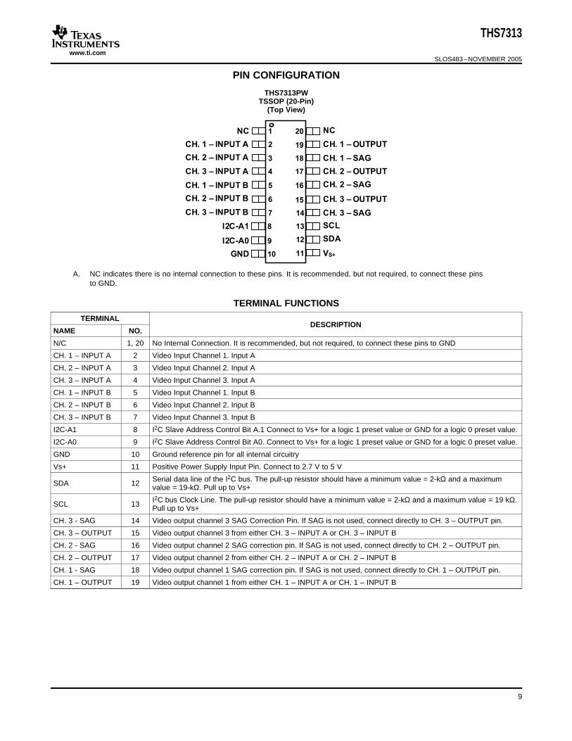
PIN CONFIGURATION
THS7313
SLOS483–NOVEMBER 2005
THS7313PWTSSOP (20-Pin)
(Top View)
A. NC indicates there is no internal connection to these pins. It is recommended, but not required, to connect these pinsto GND.
TERMINAL FUNCTIONS
TERMINALDESCRIPTION
NAME NO.
N/C 1, 20 No Internal Connection. It is recommended, but not required, to connect these pins to GND
CH. 1 – INPUT A 2 Video Input Channel 1. Input A
CH. 2 – INPUT A 3 Video Input Channel 2. Input A
CH. 3 – INPUT A 4 Video Input Channel 3. Input A
CH. 1 – INPUT B 5 Video Input Channel 1. Input B
CH. 2 – INPUT B 6 Video Input Channel 2. Input B
CH. 3 – INPUT B 7 Video Input Channel 3. Input B
I2C-A1 8 I2C Slave Address Control Bit A.1 Connect to Vs+ for a logic 1 preset value or GND for a logic 0 preset value.
I2C-A0 9 I2C Slave Address Control Bit A0. Connect to Vs+ for a logic 1 preset value or GND for a logic 0 preset value.
GND 10 Ground reference pin for all internal circuitry
Vs+ 11 Positive Power Supply Input Pin. Connect to 2.7 V to 5 V
Serial data line of the I2C bus. The pull-up resistor should have a minimum value = 2-kΩ and a maximumSDA 12 value = 19-kΩ. Pull up to Vs+
I2C bus Clock Line. The pull-up resistor should have a minimum value = 2-kΩ and a maximum value = 19 kΩ.SCL 13 Pull up to Vs+
CH. 3 - SAG 14 Video output channel 3 SAG Correction Pin. If SAG is not used, connect directly to CH. 3 – OUTPUT pin.
CH. 3 – OUTPUT 15 Video output channel 3 from either CH. 3 – INPUT A or CH. 3 – INPUT B
CH. 2 - SAG 16 Video output channel 2 SAG correction pin. If SAG is not used, connect directly to CH. 2 – OUTPUT pin.
CH. 2 – OUTPUT 17 Video output channel 2 from either CH. 2 – INPUT A or CH. 2 – INPUT B
CH. 1 - SAG 18 Video output channel 1 SAG correction pin. If SAG is not used, connect directly to CH. 1 – OUTPUT pin.
CH. 1 – OUTPUT 19 Video output channel 1 from either CH. 1 – INPUT A or CH. 1 – INPUT B
9

www.ti.com
TYPICAL CHARACTERISTICS
−40
−50
−35
−45
−30
−25
−20
−15
−10
−5
0
5
10
0.1 1 10 100 1000
Sig
na
l G
ain
−d
B
f − Frequency − MHz
V = 3.3 V
R = 150 || 13 pF
S
L W
Solid Line = 200 mV ,PP
Dashed Line = 2.6 VPP
3
4
3.5
4.5
5
5.5
6
6.5
0.1 1 10
Sig
na
l G
ain
−d
B
f − Frequency − MHz
V = 3.3 V
R = 150 || 13 pF
S
L W
Solid Line = 200 mV ,PP
Dashed Line = 2.6 VPP
35
40
45
50
55
60
65
70
75
80
90
0.1 1 10 100
Gro
up
De
lay
−n
s
f − Frequency − MHz
V = 3.3 V
V = 200 mVS
O PP
R = 150 || 13 pFL W
-360
-315
-270
-225
-180
-135
-90
-45
0
45
0.1 1 10 100
Ph
as
e−
o
f − Frequency − MHz
V = 3.3 V
V = 200 mVS
O PP
R = 150 || 13 pFL W
0
0.04
0.02
0.08
0.06
0.12
0.1
0.16
0.14
0.18
0.2
1st 2nd 3rd 4th 5th 6th
Dif
fere
nti
al
Ga
in−
%
NTSC
PAL
V = 3.3 V
R = 150 || 13 pF
S
L W
0
0.02
0.08
0.06
0.04
0.1
0.12
1st 2nd 3rd 4th 5th 6th
Dif
fere
nti
al
Ph
as
e−
o
NTSC
PAL
V = 3.3 V
R = 150 || 13 pF
S
L W
THS7313
SLOS483–NOVEMBER 2005
SMALL AND LARGE SIGNAL FREQUENCY RESPONSE SMALL AND LARGE SIGNAL FREQUENCY RESPONSE
Figure 4. Figure 5.
GROUP DELAY vs FREQUENCY PHASE RESPONSE vs FREQUENCY
Figure 6. Figure 7.
3.3 V DIFFERENTIAL GAIN 3.3 V DIFFERENTIAL PHASE
Figure 8. Figure 9.
10

www.ti.com
−80
−75
−70
−65
−60
−55
−45
−40
−50
0 0.5 1 1.5 2 2.5 3
2n
d O
rde
r H
arm
on
ic D
isto
rtio
n−
dB
V − Output VO oltage − VPP
V = 3.3 V,
fS
= 1 MHz,
R = 150 || 13 pFL W
−100
−90
−80
−70
−60
−50
−40
0 0.5 1 1.5 2 2.5 3
3rd
Ord
er
Ha
rmo
nic
dis
tort
ion
−d
B
V − Output Voltage − VO PP
V = 3.3 V,
fS
= 1 MHz,
R = 150 || 13 pFL W
−70
−60
−50
−40
−30
−20
−10
0
10
0.1 1 10 100 1000
Sig
na
l G
ain
−d
B
f − Frequency − MHz
V = 3.3 V,
V = 0.2 V ,S
O PP
R = 150 || CL LW
C = 35 pFL
C = 23 pFL
C = 13 pFL
0.25
0.5
0.75
1
1.25
1.5
1.75
2
2.25
2.5
2.75
3
3.25
−100 0 100 200 300 400 500 600 800700
V-
Ou
tpu
t V
olt
ag
e−
VO
t − Time − ns
V = 3.3 V,
R
S
L = 150 || 13 pFW
t - Time = 1000 ns/div
20
0 m
V/d
iv
CVBS
Chroma
Luma
V = 3.3 VS
t - Time = 100 ns/div
14
3 m
V/d
iv
V = 3.3 VS
R’
B’
G’
THS7313
SLOS483–NOVEMBER 2005
TYPICAL CHARACTERISTICS (continued)
HD2 vs OUTPUT VOLTAGE HD3 vs OUTPUT VOLTAGE
Figure 10. Figure 11.
SMALL SIGNAL FREQUENCY RESPONSE vs CAPACITIVE LARGE SIGNAL PULSE RESPONSELOAD
Figure 12. Figure 13.
NTSC NTC7 COMPOSITE RESPONSE 480i G'B'R' PULSE RESPONSE
Figure 14. Figure 15.
11

www.ti.com
t - Time = 100 ns/div
14
3 m
V/d
iv
G’
Input Source
R’
B’
t - Time = 2 s/divm
14
3 m
V/d
iv
V = 3.3 VS
P’R
P’B
Y’
0.01
0.1
1
10
100
0.1 1 10 100
Z−
Ou
tpu
t Im
pe
da
nc
e−
OW
f − Frequency − MHz
V = 3.3 VS
0
10
20
30
50
40
60
0.5 1 1.5 2 2.5 3
V − Output Voltage − VO PP
SR
Sle
w R
ate
−V
/s
m−
V = 3.3 V,S
R = 150 || 13 pFL W
0
10
20
30
40
50
60
70
80
0.01 0.1 1 10 100
PS
RR
−P
ow
er
Su
pp
ly R
eje
cti
on
Ra
tio
−d
B
f − Frequency − MHz
V = 5 VS
V = 3.3 VS
−85
−90
−80
−70
−75
−65
−55
−60
−50
0.1 1 10 100
f − Frequency − MHz
Mu
x F
ee
d T
hro
ug
h−
dB
V = 3.3 V,
R = 150 || 13 pF
S
L W
Applied Signal to Unselected MUXMeasured Output of ChannelReferred to Applied Signal Input
THS7313
SLOS483–NOVEMBER 2005
TYPICAL CHARACTERISTICS (continued)
480i G'B'R' INPUT SOURCE 576i PULSE RESPONSE
Figure 16. Figure 17.
OUTPUT IMPEDANCE vs FREQUENCY SLEW RATE vs OUTPUT VOLTAGE
Figure 18. Figure 19.
POWER SUPPLY REJECTION RATIO vs FREQUENCY MUX FEED THROUGH vs FREQUENCY
Figure 20. Figure 21.
12
www.ti.com
−85
−80
−75
−70
−65
−60
−55
−50
0.1 1 10 100
f − Frequency − MHz
Cro
ss
talk
−d
B
Worst CaseCrosstalkReferred to InputRL = 150 W || 13 pF
V = 5 VS
V = 3.3 VS
−90
−100
−80
−70
−60
−50
−40
0.1 1 10 100 1000
f − Frequency − MHz
Mu
te F
ee
d T
hro
ug
h−
dB
V = 3.3 V and 5 V
R = 150 || 13 pF
S
L W
0
1
2
3
4
5
6
7
8
9
-40 -20 0 4020 60 80 100
I−
AIB
m−
Inp
ut
Bia
s C
urr
en
t
T − Ambient Temperature − CAo
STC - High
STC - Mid
STC - Low
V = 3.3 VS
−1
0
1
2
3
4
5
6
7
8
9
2.6 3 3.4 3.8 4.2 4.6 5
I−
AIB
m−
Inp
ut
Bia
s C
urr
en
t
V − Supply Voltage − VS
STC - High
STC - Mid
STC - Low
T = 25 CAo
DC Input
−40
−50
−35
−45
−30
−25
−20
−15
−10
−5
0
5
10
0.1 1 10 100 1000
Sig
na
l G
ain
−d
B
f − Frequency − MHz
V = 5 V
R = 150 || 13 pF
S
L W
Solid Line = 200 mV ,PP
Dashed Line = 2.6 VPP
3
4
3.5
4.5
5
5.5
6
6.5
0.1 1 10
Sig
na
l G
ain
−d
B
f − Frequency − MHz
V = 5 V
R = 150 || 13 pF
S
L W
Solid Line = 200 mV ,PP
Dashed Line = 2.6 VPP
THS7313
SLOS483–NOVEMBER 2005
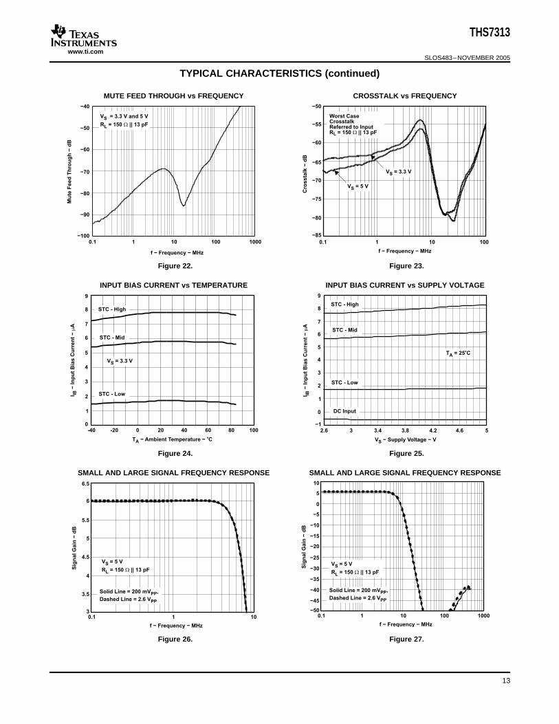
TYPICAL CHARACTERISTICS (continued)
MUTE FEED THROUGH vs FREQUENCY CROSSTALK vs FREQUENCY
Figure 22. Figure 23.
INPUT BIAS CURRENT vs TEMPERATURE INPUT BIAS CURRENT vs SUPPLY VOLTAGE
Figure 24. Figure 25.
SMALL AND LARGE SIGNAL FREQUENCY RESPONSE SMALL AND LARGE SIGNAL FREQUENCY RESPONSE
Figure 26. Figure 27.
13

www.ti.com
40
45
50
55
60
65
70
75
80
85
90
0.1 1 10 100
Gro
up
De
lay
−n
s
f − Frequency − MHz
V = 5 V
V = 200 mVS
O PP
R = 150 || 13 pFL W
−360
−315
−270
−225
−180
−135
−90
−45
0
45
0.1 1 10 100
VS = 5 V,VO = 200 mVPP,RL = 150 || 13 pFW
Ph
as
e−
°
f − Frequency − MHz
0
0.04
0.02
0.08
0.06
0.12
0.1
0.16
0.14
0.18
0.2
1st 2nd 3rd 4th 5th 6th
Dif
fere
nti
al
Ga
in−
%
NTSC
PAL
V = 5 V
R = 150 || 13 pF
S
L W
0
0.04
0.02
0.08
0.06
0.12
0.1
0.16
0.14
0.18
0.2
1st 2nd 3rd 4th 5th 6th
Dif
fere
nti
al
Ph
as
e−
o
NTSC
PAL
V = 5 V
R = 150 || 13 pF
S
L W
−80
−75
−70
−65
−60
−55
−50
0.1 1 10
2n
d O
rde
r H
arm
on
ic d
isto
rtio
n−
dB
f − Frequency − MHz
V = 5 V,
V = 2 V ,S
O PP
R = 150 || 13 pFL W
−100
−95
−90
−85
−80
−75
−70
0.1 1 10
3rd
Ord
er
Ha
rmo
nic
dis
tort
ion
−d
B
f − Frequency − MHz
V = 5 V,
V = 2 V ,S
O PP
R = 150 || 13 pFL W
THS7313
SLOS483–NOVEMBER 2005
TYPICAL CHARACTERISTICS (continued)
GROUP DELAY vs FREQUENCY PHASE vs FREQUENCY
Figure 28. Figure 29.
5 V DIFFERENTIAL GAIN 5 V DIFFERENTIAL PHASE
Figure 30. Figure 31.
HD2 vs FREQUENCY HD3 vs FREQUENCY
Figure 32. Figure 33.
14
www.ti.com
−90
−80
−70
−60
−40
−50
0 1 2 3 4 5
2n
d O
rde
r H
arm
on
ic D
isto
rtio
n−
dB
V − Output VO oltage − VPP
V = 5 V,
fS
= 1 MHz,
R = 150 || 13 pFL W
−110
−100
−70
−90
−60
−80
−40
−50
0 1 2 3 4 5
3rd
Ord
er
Ha
rmo
nic
Dis
tort
ion
−d
B
V − Output VO oltage − VPP
V = 5 V,
fS
= 1 MHz,
R = 150 || 13 pFL W
−70
−60
−50
−40
−30
−20
−10
0
10
0.1 1 10 100 1000
Sig
na
l G
ain
−d
B
f − Frequency − MHz
V = 5 V,
V = 0.2 V ,S
O PP
R = 150 || CL LW
C = 35 pFL
C = 23 pFL
C = 13 pFL
0.55
0.65
0.75
0.85
0.95
1.05
1.15
1.25
−100 0 100 200 300 400 500 600 800700
V-
Ou
tpu
t V
olt
ag
e−
VO
t − Time − ns
V = 5 V,
R
S
L = 150 || 13 pFW
0.5
0.75
1
1.25
1.5
1.75
2
2.25
2.5
2.75
3
−100 0 100 200 300 400 500 600 800700
V-
Ou
tpu
t V
olt
ag
e−
VO
t − Time − ns
V = 5 V,
R
S
L = 150 || 13 pFW
0
10
20
40
30
70
60
50
80
0.5 1 1.5 2 32.5 3.5 4
V − Output Voltage − VO PP
SR
Sle
w R
ate
−V
/s
m−
V = 5 V,S
R = 150 || 13 pFL W
THS7313
SLOS483–NOVEMBER 2005
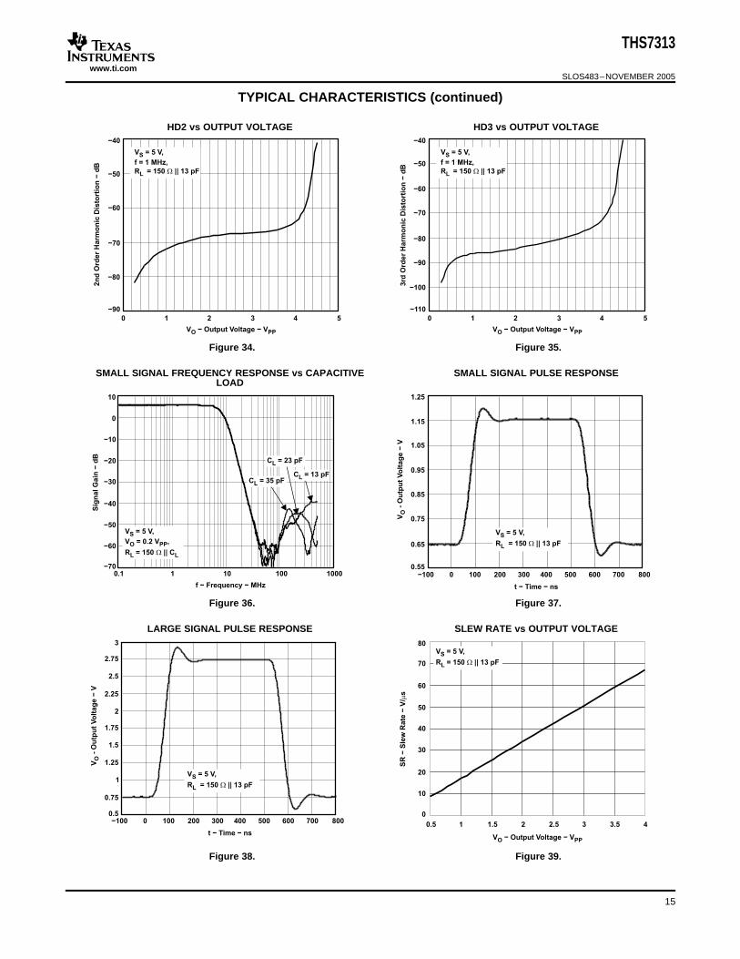
TYPICAL CHARACTERISTICS (continued)
HD2 vs OUTPUT VOLTAGE HD3 vs OUTPUT VOLTAGE
Figure 34. Figure 35.
SMALL SIGNAL FREQUENCY RESPONSE vs CAPACITIVE SMALL SIGNAL PULSE RESPONSELOAD
Figure 36. Figure 37.
LARGE SIGNAL PULSE RESPONSE SLEW RATE vs OUTPUT VOLTAGE
Figure 38. Figure 39.
15
www.ti.com
0.01
0.1
1
10
100
0.1 1 10 100
Z−
Ou
tpu
t Im
pe
da
nc
e−
OW
f − Frequency − MHz
V = 5 VS
−90
−80
−85
−70
−75
−60
−65
−55
−50
0.1 1 10 100
f − Frequency − MHz
Mu
x F
ee
d T
hro
ug
h−
dB
V = 5 V
R = 150 || 13 pF
S
L W
Applied Signal to Unselected MUXMeasured Output of ChannelReferred to Applied Signal Input
t - Time = 500 ns/div
25
0 m
V/d
iv
CVBS Input
CVBS Output
V = 5 VS
t - Time = 1000 ns/div
20
0 m
V/d
iv
CVBS
Chroma
Luma
V = 5 VS
t - Time = 100 ns/div
14
3 m
V/d
iv
V = 5 VS
R’
B’
G’
t - Time = 2 s/divm
14
3 m
V/d
iv
V = 5 VS
P’R
P’B
Y’
THS7313
SLOS483–NOVEMBER 2005
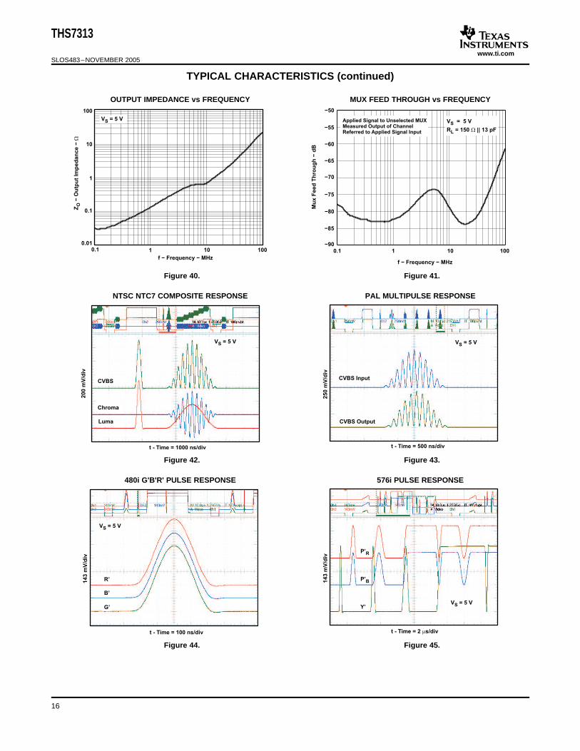
TYPICAL CHARACTERISTICS (continued)
OUTPUT IMPEDANCE vs FREQUENCY MUX FEED THROUGH vs FREQUENCY
Figure 40. Figure 41.
NTSC NTC7 COMPOSITE RESPONSE PAL MULTIPULSE RESPONSE
Figure 42. Figure 43.
480i G'B'R' PULSE RESPONSE 576i PULSE RESPONSE
Figure 44. Figure 45.
16
www.ti.com
APPLICATION INFORMATION
OPERATING VOLTAGE
INPUT VOLTAGE
INPUT OVERVOLTAGE PROTECTION
THS7313
SLOS483–NOVEMBER 2005
The THS7313 is targeted for video output buffer applications. Although it can be used for numerous otherapplications, the needs and requirements of the video signal are the most important design parameters of theTHS7313. Built on the complimentary silicon germanium (SiGe) BiCom-3 process, the THS7313 incorporatesmany features not typically found in integrated video parts while consuming low power. Each channelconfiguration is completely independent of the other channels. This allows for configurations for each channel tobe dictated by the end user and not device. The resulting highly flexible system contains the following features:• I2C Interface for easy interfacing to the system.• Single-supply 2.7-V to 5-V operation with low total quiescent current of 16.6 mA with 3.3-V supply and 18.9
mA with 5-V supply.• 2:1 input MUX.• Input configuration accepting dc, dc + 135 mV shift, ac bias, or ac sync-tip clamp selection.• 5th order low-pass filter for DAC reconstruction or ADC image rejection :
– 8-MHz for SDTV NTSC/PAL/SECAM, S-Video, component 480i/576i Y’P’BP’R, and G'B'R' (R'G'B') signals.• Internal fixed gain of 2 V/V (6 dB) buffer that can drive 2 video lines with dc coupling, traditional ac coupling,
or SAG corrected ac coupling.• Shutdown mode which reduces quiescent current to as low as 0.1-µA or a mute function that keeps the
THS7313 powered on, but does not allow a signal to pass through.• Signal flow-through configuration using a 20-pin TSSOP package that complies with the latest lead-free
(RoHS compatible) and green manufacturing requirements.
The THS7313 is designed to operate from 2.7 V to 5 V over a -40°C to 85°C temperature range. The impact onperformance over the entire temperature range is negligible due to the implementation of thin film resistors andlow-temperature coefficient capacitors.
The power supply pins should have a 0.1-µF to 0.01-µF capacitor placed as close as possible to these pins.Failure to do so may result in the THS7313 outputs ringing or oscillating. Additionally, a large capacitor, such as22 µF to 100 µF, should be placed on the power supply line to minimize issues with 50/60 Hz line frequencies.
The THS7313 input range allows for an input signal range from Ground to (VS+– 1.4 V). But, due to the internalfixed gain of 2 V/V (6 dB), the output is the limiting factor for the allowable linear input range. For example, with a5-V supply, the linear input range is from GND to 3.6 V. But due to the gain, the linear output range limits theallowable linear input range to be from GND to a maximum of 2.5 V.
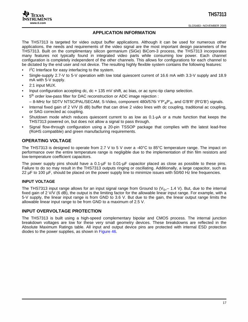
The THS7313 is built using a high-speed complementary bipolar and CMOS process. The internal junctionbreakdown voltages are low for these very small geometry devices. These breakdowns are reflected in theAbsolute Maximum Ratings table. All input and output device pins are protected with internal ESD protectiondiodes to the power supplies, as shown in Figure 46.
17
www.ti.com
ExternalInput/Output
Pin
InternalCircuitry
VS+
TYPICAL CONFIGURATION and VIDEO TERMINOLOGY
THS7313
SLOS483–NOVEMBER 2005
APPLICATION INFORMATION (continued)
Figure 46. Internal ESD Protection
These diodes provide moderate protection to input overdrive voltages above and below the supplies. Theprotection diodes can typically support 30-mA of continuous current when overdriven.
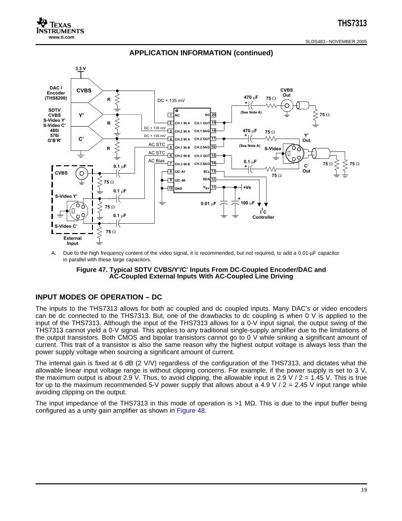
A typical application circuit using the THS7313 as a video buffer is shown in Figure 47. It shows a DAC (orencoder such as the THS8200) driving the three input channels of the THS7313. Although the S-Video Y' and C'channels and the composite video baseband signal (CVBS) channel of a standard definition video (SD) systemare shown, these channels can also be the Y’P’BP’R (sometimes labeled Y’U’V’ or incorrectly labeled Y’C’BC’R)signals of a 480i or 576i system. These signals could be G’B’R’ (R'G'B') signals or other variations. Note that forcomputer signals the sync should be embedded within the signal for a system with only 3-outputs. This issometimes labeled as R’G’sB’ (sync on green) or R’sG’sB’s (sync on all signals).
The second set of inputs (B-Channels) shown are being driven from an external input typically used as apass-through function. These are traditional SD or professional G’B’R’ video signals. The THS7313’s flexibilityallows for almost any input signal to be driven into the THS7313 regardless of the other set of inputs. Control ofthe I2C configures the THS7313. For example, the THS7313 can be configured to have Channel 1 Inputconnected to input A while Channels 2 and 3 are connected to input B. The various sections explaining the I2Cinterface later in this data sheet.
Note that the Y’ term is used for the luma channels throughout this document rather than the more commonluminance (Y) term. The reason is to account for the definition of luminance as stipulated by the CIE -International Commission on Illumination. Video departs from true luminance since a nonlinear term, gamma, isadded to the true GBR signals to form G’B’R’ signals. These G’B’R’ signals are then used to mathematicallycreate luma (Y’). Thus luminance (Y) is not maintained providing a difference in terminology.
This rationale is also used for the chroma (C’) term. Chroma is derived from the nonlinear G’B’R’ terms and thusit is nonlinear. Chominance (C) is derived from linear GBR giving the difference between chroma (C’) andchrominance (C). The color difference signals (P’B / P’R / U’ / V’) are also referenced this way to denote thenonlinear (gamma corrected) signals.
R’G’B’ (commonly mislabeled RGB) is also called G’B’R’ (again commonly mislabeled as GBR) in professionalvideo systems. The SMPTE component standard stipulates that the luma information is placed on the firstchannel, the blue color difference is placed on the second channel, and the red color difference signal is placedon the third channel. This is consistent with the Y'P'BP'R nomenclature. Because the luma channel (Y') carries thesync information and the green channel (G') also carries the sync information, it makes logical sense that G' beplaced first in the system. Since the blue color difference channel (P'B) is next and the red color differencechannel (P'R) is last, then it also makes logical sense to place the B' signal on the second channel and the R'signal on the third channel respectfully. Thus, hardware compatibility is better achieved when using G'B'R' ratherthan R'G'B'. Note that for many G'B'R' systems, sync is embeded on all three channels; however, this may not betrue in all systems.
18
www.ti.com
17
20
19
18
GND
16
CH.2 IN B
CH.3 IN B
15
I2C-A0 SDA
VS+ 11
14
13
12
SCL
CH.3 SAG
I2C-A1
CH.1 IN B
CH.2 IN A
CH.3 IN A
CH.1 IN A
NC
CH.3 OUT
CH.2 SAG
CH.2 OUT
CH.1 SAG
CH.1 OUT
NC
DAC /Encoder
(THS8200)
3.3 V
1
2
3
4
5
6
7
8
9
10
CVBS
Y’
C’
75 W
75 W
75 W
75 W
75 W
75 W
75 W
0.1 Fm
0.01 Fm 100 Fm
0.1 Fm
0.1 Fm
R
R
R
CVBSOut
470 Fm
470 Fm
0.1 Fm
(See Note A)
(See Note A)
+
+
+
+
+Vs
I CController
2
SDTVCVBS
S-Video Y’
S-Video C’
480i576i
G’B’R’AC STC
AC STC
AC Bias
DC + 135 mV
DC + 135 mV
DC + 135 mV
ExternalInput
CVBS
S-Video C’
S-Video Y’
75 W75 WC’
Out
Y’
Out
S-Video
INPUT MODES OF OPERATION – DC
THS7313
SLOS483–NOVEMBER 2005
APPLICATION INFORMATION (continued)
A. Due to the high frequency content of the video signal, it is recommended, but not required, to add a 0.01-µF capacitorin parallel with these large capacitors.
Figure 47. Typical SDTV CVBS/Y'/C' Inputs From DC-Coupled Encoder/DAC andAC-Coupled External Inputs With AC-Coupled Line Driving
The inputs to the THS7313 allows for both ac coupled and dc coupled inputs. Many DAC’s or video encoderscan be dc connected to the THS7313. But, one of the drawbacks to dc coupling is when 0 V is applied to theinput of the THS7313. Although the input of the THS7313 allows for a 0-V input signal, the output swing of theTHS7313 cannot yield a 0-V signal. This applies to any traditional single-supply amplifier due to the limitations ofthe output transistors. Both CMOS and bipolar transistors cannot go to 0 V while sinking a significant amount ofcurrent. This trait of a transistor is also the same reason why the highest output voltage is always less than thepower supply voltage when sourcing a significant amount of current.
The internal gain is fixed at 6 dB (2 V/V) regardless of the configuration of the THS7313, and dictates what theallowable linear input voltage range is without clipping concerns. For example, if the power supply is set to 3 V,the maximum output is about 2.9 V. Thus, to avoid clipping, the allowable input is 2.9 V / 2 = 1.45 V. This is truefor up to the maximum recommended 5-V power supply that allows about a 4.9 V / 2 = 2.45 V input range whileavoiding clipping on the output.
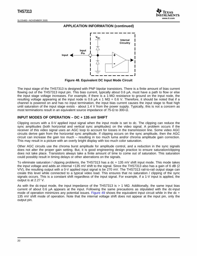
The input impedance of the THS7313 in this mode of operation is >1 MΩ. This is due to the input buffer beingconfigured as a unity gain amplifier as shown in Figure 48.
19
www.ti.com
InputPin
Input
InternalCircuitry
VS+
INPUT MODES OF OPERATION – DC + 135 mV SHIFT
THS7313
SLOS483–NOVEMBER 2005
APPLICATION INFORMATION (continued)
Figure 48. Equivalent DC Input Mode Circuit
The input stage of the THS7313 is designed with PNP bipolar transistors. There is a finite amount of bias currentflowing out of the THS7313 input pin. This bias current, typically about 0.6 µA, must have a path to flow or elsethe input stage voltage increases. For example, if there is a 1-MΩ resistance to ground on the input node, theresulting voltage appearing at the input node is 0.6 µA x 1 MΩ = 0.6 V. Therefore, it should be noted that if achannel is powered on and has no input termination, the input bias current causes the input stage to float highuntil saturation of the input stage exists - about 1.4 V from the power supply. Typically, this is not a concern asmost terminations result in an equivalent source impedance of 75-Ω to 300-Ω.
Clipping occurs with a 0-V applied input signal when the input mode is set to dc. The clipping can reduce thesync amplitudes (both horizontal and vertical sync amplitudes) on the video signal. A problem occurs if thereceiver of this video signal uses an AGC loop to account for losses in the transmission line. Some video AGCcircuits derive gain from the horizontal sync amplitude. If clipping occurs on the sync amplitude, then the AGCcircuit can increase the gain too much – resulting in too much luma and/or chroma amplitude gain correction.This may result in a picture with an overly bright display with too much color saturation.
Other AGC circuits use the chroma burst amplitude for amplitude control, and a reduction in the sync signalsdoes not alter the proper gain setting. But, it is good engineering design practice to ensure saturation/clippingdoes not take place. Transistors always take a finite amount of time to come out of saturation. This saturationcould possibly result in timing delays or other aberrations on the signals.
To eliminate saturation / clipping problems, the THS7313 has a dc + 135 mV shift input mode. This mode takesthe input voltage and adds an internal +135 mV shift to the signal. Since the THS7313 also has a gain of 6 dB (2V/V), the resulting output with a 0-V applied input signal is be 270 mV. The THS7313 rail-to-rail output stage cancreate this level while connected to a typical video load. This ensures that no saturation / clipping of the syncsignals occurs. This is a constant shift regardless of the input signal. For example, if a 1-V input is applied, theoutput is at 2.27 V.
As with the dc-input mode, the input impedance of the THS7313 is > 1 MΩ. Additionally, the same input biascurrent of about 0.6 µA appears at the input. Following the same precautions as stipulated with the dc-inputmode of operation minimizes any potential issues. Figure 49 shows the equivalent input circuit while in the dc +135 mV shift mode of operation. Note that the internal voltage shift does not appear at the input pin, only theoutput pin.
20

www.ti.com
InputPin
Input
InternalCircuitry
LevelShifter
VS+
INPUT MODES OF OPERATION – AC BIAS
Input PinInput
Rpd(See Note A)
Rpu(See Note A) 75 kW
25 kWCI
InternalCircuitry
VS+ VS+ VS+
THS7313
SLOS483–NOVEMBER 2005
APPLICATION INFORMATION (continued)
Figure 49. Equivalent DC + 135 mV Input Mode Circuit
Other applications require an ac-coupled input. The ac coupling ensures that a source dc-input level does notalter, or clip, the resulting output video signal. The first ac coupling mode is the AC Bias mode where a simpleinternal dc bias voltage is applied to the input signal on the THS7313 side of the external 1-µF couplingcapacitor.
The applied dc bias voltage is set internally by a resistor divider circuit as shown in Figure 50. The dc biasvoltage is set to VS+÷ 4. With a 3.3-V power supply, the input bias voltage is nominally 0.825 V, and with 5-Vsupply, the input bias voltage is nominally 1.25 V. The input impedance with this mode is approximately 19-kΩ.With a 1-µF input capacitor, it sets a high-pass corner frequency of about 9-Hz. If a lower frequency is desired,increasing the capacitor decreases the corner frequency proportionally. For example, using a 4.7-µF capacitorresults in a 1.8-Hz high pass corner frequency, and results in lower droop (tilt). Using any capacitor value isacceptable for this mode of operation.
It is sometimes desirable to adjust the bias voltage to another level other than the one dictated by the internalresistors. There are two ways this is accomplished:1. The first is to add an external resistor between the input pin and either the +Vs or GND. This creates a new
bias voltage equal to +Vs × [25 k / 25 k + (75 k || Rpu)] for raising the bias voltage, or +Vs × [(25 k || Rpd) /(25 k || Rpd) + 75 k] for reducing the bias voltage.
2. The second method to set the AC-Bias voltage is to use the Rpu and Rpd external resistors, but place theTHS7313 in dc input bias mode. Since the dc mode is very high impedance, the resulting bias voltage isequal to +Vs × (Rpd / Rpd + Rpu).
This mode of operation is recommended for use with chroma (C’), P’B, P’R, U’, V’, and nonsync B’ and R’ signals.
NOTE: Use external pull-up and/or pull-down resistors if changing the ac-bias input voltage is desired.
Figure 50. Equivalent AC Bias Input Mode Circuit
21
www.ti.com
INPUT MODES OF OPERATION – AC SYNC TIP CLAMP
InputPin
Input
InternalCircuitrySTC
LPF
STCBias
Select
1.8 A
5.8 A
7.8 A
m
m
m
135 mV
Comparator
0.1 Fm
VS+ VS+
THS7313
SLOS483–NOVEMBER 2005
APPLICATION INFORMATION (continued)
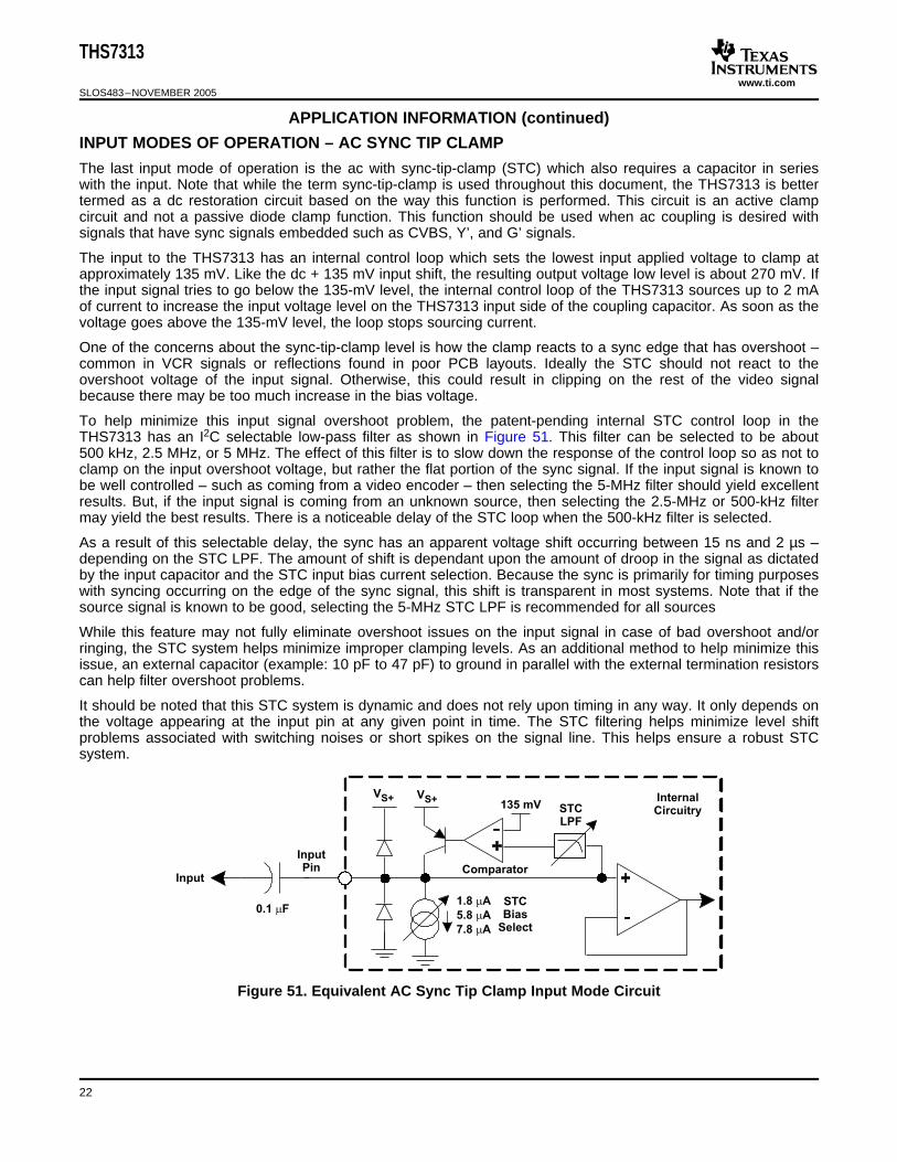
The last input mode of operation is the ac with sync-tip-clamp (STC) which also requires a capacitor in serieswith the input. Note that while the term sync-tip-clamp is used throughout this document, the THS7313 is bettertermed as a dc restoration circuit based on the way this function is performed. This circuit is an active clampcircuit and not a passive diode clamp function. This function should be used when ac coupling is desired withsignals that have sync signals embedded such as CVBS, Y’, and G’ signals.
The input to the THS7313 has an internal control loop which sets the lowest input applied voltage to clamp atapproximately 135 mV. Like the dc + 135 mV input shift, the resulting output voltage low level is about 270 mV. Ifthe input signal tries to go below the 135-mV level, the internal control loop of the THS7313 sources up to 2 mAof current to increase the input voltage level on the THS7313 input side of the coupling capacitor. As soon as thevoltage goes above the 135-mV level, the loop stops sourcing current.
One of the concerns about the sync-tip-clamp level is how the clamp reacts to a sync edge that has overshoot –common in VCR signals or reflections found in poor PCB layouts. Ideally the STC should not react to theovershoot voltage of the input signal. Otherwise, this could result in clipping on the rest of the video signalbecause there may be too much increase in the bias voltage.
To help minimize this input signal overshoot problem, the patent-pending internal STC control loop in theTHS7313 has an I2C selectable low-pass filter as shown in Figure 51. This filter can be selected to be about500 kHz, 2.5 MHz, or 5 MHz. The effect of this filter is to slow down the response of the control loop so as not toclamp on the input overshoot voltage, but rather the flat portion of the sync signal. If the input signal is known tobe well controlled – such as coming from a video encoder – then selecting the 5-MHz filter should yield excellentresults. But, if the input signal is coming from an unknown source, then selecting the 2.5-MHz or 500-kHz filtermay yield the best results. There is a noticeable delay of the STC loop when the 500-kHz filter is selected.
As a result of this selectable delay, the sync has an apparent voltage shift occurring between 15 ns and 2 µs –depending on the STC LPF. The amount of shift is dependant upon the amount of droop in the signal as dictatedby the input capacitor and the STC input bias current selection. Because the sync is primarily for timing purposeswith syncing occurring on the edge of the sync signal, this shift is transparent in most systems. Note that if thesource signal is known to be good, selecting the 5-MHz STC LPF is recommended for all sources
While this feature may not fully eliminate overshoot issues on the input signal in case of bad overshoot and/orringing, the STC system helps minimize improper clamping levels. As an additional method to help minimize thisissue, an external capacitor (example: 10 pF to 47 pF) to ground in parallel with the external termination resistorscan help filter overshoot problems.
It should be noted that this STC system is dynamic and does not rely upon timing in any way. It only depends onthe voltage appearing at the input pin at any given point in time. The STC filtering helps minimize level shiftproblems associated with switching noises or short spikes on the signal line. This helps ensure a robust STCsystem.
Figure 51. Equivalent AC Sync Tip Clamp Input Mode Circuit
22
www.ti.com
THS7313
SLOS483–NOVEMBER 2005
APPLICATION INFORMATION (continued)
When the ac sync-tip-clamp (STC) operation is used, there must also be some finite amount of discharge biascurrent. As previously described, if the input signal goes below the 135-mV clamp level, the internal loop of theTHS7313 sources current to increase the voltage appearing at the input pin. As the difference between the signallevel and the 135-mV reference level increases, the amount of source current increases proportionally –supplying up to 2-mA of current. Thus the time to re-establish the proper STC voltage can be fast. If thedifference is small, then the source current is also small to account for minor voltage droop.
But, what happens if the input signal goes above the 135-mV input level? The problem is the video signal isalways above this level and must not be altered in any way. But, if the Sync level of the input signal is above the135-mV level, then the internal discharge (sink) current reduces the ac-coupled bias signal to the proper 135-mVlevel.
This discharge current must not be large enough to alter the video signal appreciably or picture quality issuesmay arise. This is often seen by looking at the tilt (droop) of a constant luma signal being applied, and looking atthe resulting output level. The associated change in luma level from the beginning of the video line to the end ofthe video line is the amount of line tilt (droop). The amount of tilt can be seen by the general formula:
I = C dV/dt
where I is the discharge current and C is the external coupling capacitor which is typically 0.1 µF. If the current (I)and the capacitor (C) are constant, then the tilt is governed by:
i/C = dV/dt
If the discharge current is small the amount of tilt is low which is good. But, the amount of time for the system tocapture the sync signal could be too long. This is also termed hum rejection. Hum arises from the ac line voltagefrequency of 50 Hz or 60 Hz. The value of the discharge current and the ac-coupling capacitor combine to dictatethe hum rejection and the amount of line tilt.
Because many users have different thoughts as to the proper amount of hum rejection and line tilt, the THS7313has incorporated a variable sink bias current selectable through the I2C interface. The Low Bias mode selectsabout 1.8-µA of dc sink bias current for low line tilt. But, if more hum rejection is desired, then selecting the MidBias mode increases the dc sink bias current to about 5.8 µA. For severe environments, the high bias mode hasabout 7.8 µA of dc sink bias current. This drawback to these higher bias modes is an increase in line tilt, but withan increase in hum rejection. The other method to change the hum rejection and line tilt is to change the inputcapacitor used. An increase in the capacitor from 0.1 µF to 0.22 µF decreases the hum rejection and line tilt by afactor of 2.2. A decrease of this input capacitor accomplishes the opposite effect. Note that the amplifier inputbias current of nominally 0.6 µA has already been taken into account when stipulating the 1.8-µA/5.8-µA/7.8-µAcurrent sink values.
The input impedance of the THS7313 in ac STC mode is typically >1 MΩ. When the STC control loop needs tosource current to increase the bias voltage up to 135 mV, the impedance is altered. But, this typically happensquickly and only on the sync signals such that it does not alter the video signal impedance.
To ensure proper stability of the ac STC control loop, the source impedance must be less than 600-Ω with theinput capacitor in place. Otherwise, there is a possibility of the control loop ringing. The ringing appears on theoutput of the THS7313. Similar to the dc modes of operation, many DACs and Encoders use a resistor toestablish the output voltage. These resistors are typically less than 300 Ω. Thus, stability of the ac STC loop isensured. But, if the source impedance looking from the THS7313 input perspective is high or open, then addinga 300-Ω resistor to GND ensures proper operation of the THS7313.
If a MUX channel is not required in the system, then it is recommended to place a 75-Ω resistor to GND. This isnot required, but helps minimize any potential issues.
23
www.ti.com
OUTPUT MODES OF OPERATION – DC COUPLED
17
20
19
18
GND
16
CH.2 IN B
CH.3 IN B
15
I2C-A0 SDA
VS+ 11
14
13
12
SCL
CH.3 SAG
I2C-A1
CH.1 IN B
CH.2 IN A
CH.3 IN A
CH.1 IN A
NC
CH.3 OUT
CH.2 SAG
CH.2 OUT
CH.1 SAG
CH.1 OUT
NC
DAC /Encoder
(THS8200)
3.3 V
1
2
3
4
5
6
7
8
9
10
CVBS
Y’
C’
75 W
75 W
75 W
75 W
75 W
75 W
75 W
0.1 Fm
0.01 Fm 100 Fm
0.1 Fm
0.1 Fm
R
R
R
CVBSOut
+
+Vs
I CController
2
SDTVCVBS
S-Video Y’
S-Video C’
480i576i
G’B’R’AC STC
AC STC
AC Bias
DC + 135 mV
DC + 135 mV
DC + 135 mV
ExternalInput
CVBS
S-Video C’
S-Video Y’
75 W75 WC’
Out
Y’
Out
S-Video
THS7313
SLOS483–NOVEMBER 2005
APPLICATION INFORMATION (continued)
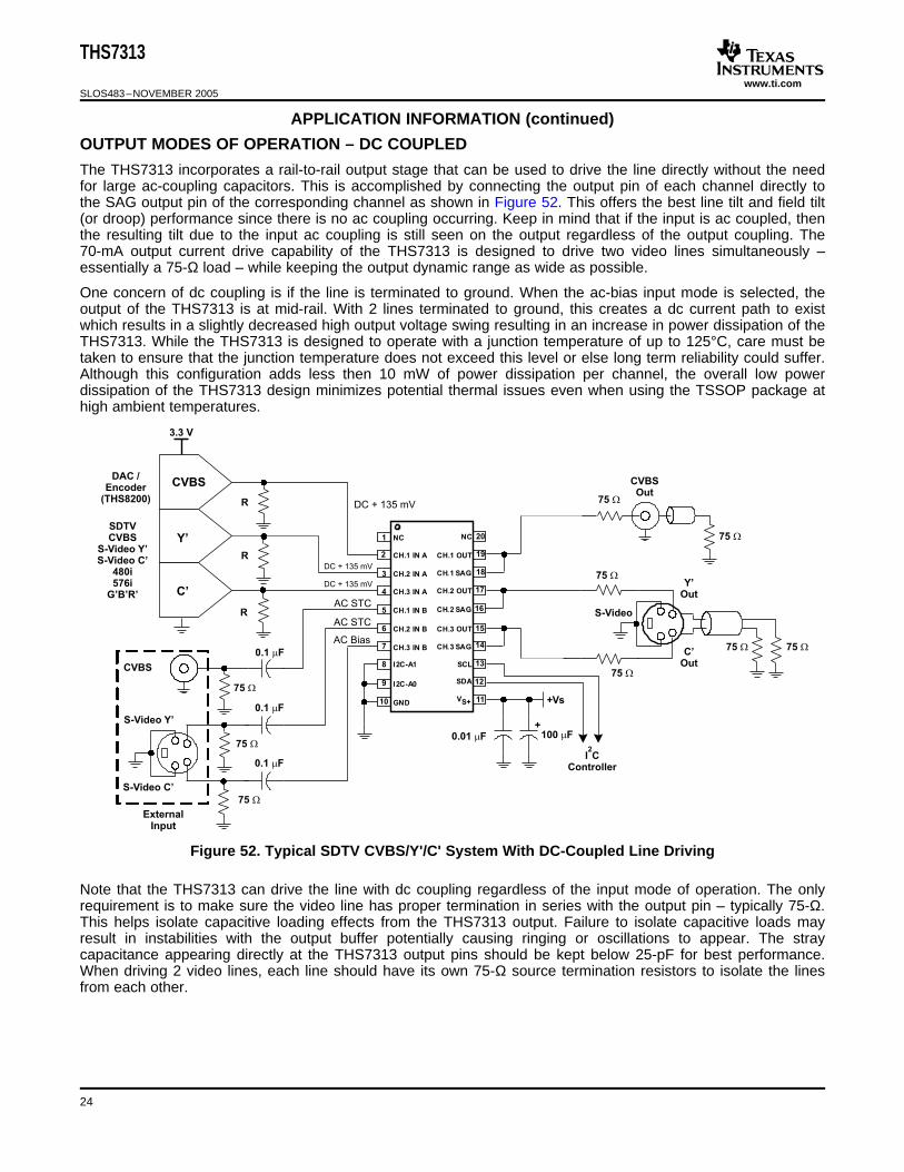
The THS7313 incorporates a rail-to-rail output stage that can be used to drive the line directly without the needfor large ac-coupling capacitors. This is accomplished by connecting the output pin of each channel directly tothe SAG output pin of the corresponding channel as shown in Figure 52. This offers the best line tilt and field tilt(or droop) performance since there is no ac coupling occurring. Keep in mind that if the input is ac coupled, thenthe resulting tilt due to the input ac coupling is still seen on the output regardless of the output coupling. The70-mA output current drive capability of the THS7313 is designed to drive two video lines simultaneously –essentially a 75-Ω load – while keeping the output dynamic range as wide as possible.
One concern of dc coupling is if the line is terminated to ground. When the ac-bias input mode is selected, theoutput of the THS7313 is at mid-rail. With 2 lines terminated to ground, this creates a dc current path to existwhich results in a slightly decreased high output voltage swing resulting in an increase in power dissipation of theTHS7313. While the THS7313 is designed to operate with a junction temperature of up to 125°C, care must betaken to ensure that the junction temperature does not exceed this level or else long term reliability could suffer.Although this configuration adds less then 10 mW of power dissipation per channel, the overall low powerdissipation of the THS7313 design minimizes potential thermal issues even when using the TSSOP package athigh ambient temperatures.
Figure 52. Typical SDTV CVBS/Y'/C' System With DC-Coupled Line Driving
Note that the THS7313 can drive the line with dc coupling regardless of the input mode of operation. The onlyrequirement is to make sure the video line has proper termination in series with the output pin – typically 75-Ω.This helps isolate capacitive loading effects from the THS7313 output. Failure to isolate capacitive loads mayresult in instabilities with the output buffer potentially causing ringing or oscillations to appear. The straycapacitance appearing directly at the THS7313 output pins should be kept below 25-pF for best performance.When driving 2 video lines, each line should have its own 75-Ω source termination resistors to isolate the linesfrom each other.
24
www.ti.com
OUTPUT MODES OF OPERATION – AC COUPLED
GND
CH.2 IN B
CH.3 IN B
I2C-A0 SDA
VS+ 11
12
13
14
15
16
17
18
19
20
SCL
CH.3 SAG
I2C-A1
CH.1 IN B
CH.2 IN A
CH.3 IN A
CH.1 IN A
NC
CH.3 OUT
CH.2 SAG
CH.2 OUT
CH.1 SAG
CH.1 OUT
NC1
2
3
4
5
6
7
8
9
10
+
CVBSOut 1
C’
Out 1
C’
Out 2Y’
Out 1
Y’
Out 2
CVBSOut 2
+
CBVS
Y’
C’
R
R
R
3.3 V
75 W
75 W
75 W
75 W 75 W75 W 75 W
75 W
75 W
75 W 75 W
75 W
75 W
75 W
0.1 Fm
0.01 Fm
470 F(See Note A)
m
470 F(See Note A)
m
470 F(Note A)
m 470 F(Note A)
m
100 Fm
0.1 Fm
0.1 Fm
0.1 Fm
0.1 Fm
0.1 Fm
3.3 V
I CController
2
ExternalInput
CVBS
S-Video C’
S-Video Y’
S-Video 1 S-Video 2
DAC /Encoder
(THS8200)
SDTVCVBS
S-Video Y’
S-Video C’
480i576i
G’B’R’
+ +
THS7313
SLOS483–NOVEMBER 2005
APPLICATION INFORMATION (continued)
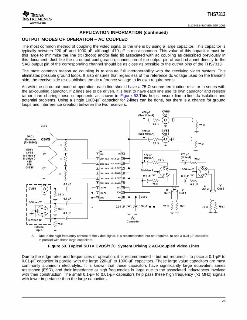
The most common method of coupling the video signal to the line is by using a large capacitor. This capacitor istypically between 220 µF and 1000 µF, although 470 µF is most common. This value of this capacitor must bethis large to minimize the line tilt (droop) and/or field tilt associated with ac coupling as described previously inthis document. Just like the dc output configuration, connection of the output pin of each channel directly to theSAG output pin of the corresponding channel should be as close as possible to the output pins of the THS7313.
The most common reason ac coupling is to ensure full interoperability with the receiving video system. Thiseliminates possible ground loops. It also ensures that regardless of the reference dc voltage used on the transmitside, the receive side re-establishes the dc reference voltage to its own requirements.
As with the dc output mode of operation, each line should have a 75-Ω source termination resistor in series withthe ac-coupling capacitor. If 2 lines are to be driven, it is best to have each line use its own capacitor and resistorrather than sharing these components as shown in Figure 53.This helps ensure line-to-line dc isolation andpotential problems. Using a single 1000-µF capacitor for 2-lines can be done, but there is a chance for groundloops and interference creation between the two receivers.
A. Due to the high frequency content of the video signal, it is recommended, but not required, to add a 0.01-µF capacitorin parallel with these large capacitors.
Figure 53. Typical SDTV CVBS/Y'/C' System Driving 2 AC-Coupled Video Lines
Due to the edge rates and frequencies of operation, it is recommended – but not required – to place a 0.1-µF to0.01-µF capacitor in parallel with the large 220-µF to 1000-µF capacitors. These large value capacitors are mostcommonly aluminum electrolytic. It is known that these capacitors have significantly large equivalent seriesresistance (ESR), and their impedance at high frequencies is large due to the associated inductances involvedwith their construction. The small 0.1-µF to 0.01-µF capacitors help pass these high frequency (>1 MHz) signalswith lower impedance than the large capacitors.
25
www.ti.com
OUTPUT MODES OF OPERATION – AC COUPLED WITH SAG CORRECTION
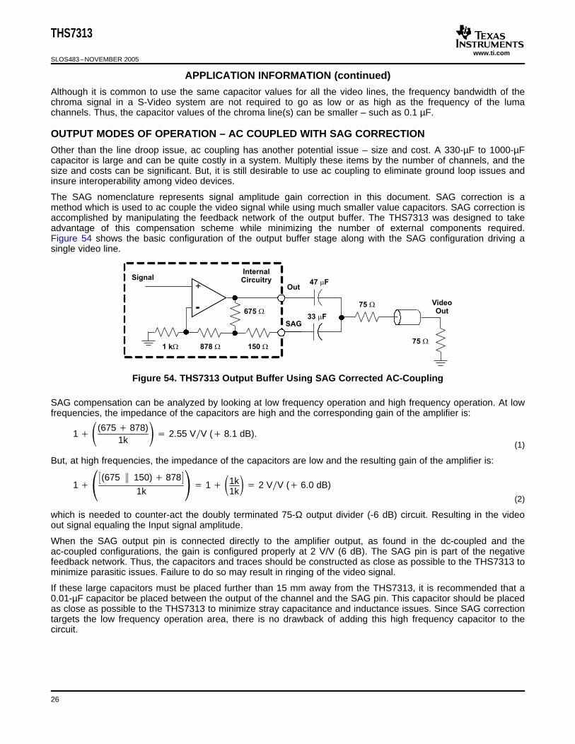
SignalInternalCircuitry
VideoOut
Out
SAG
675 W
1 kW 878 W 150 W
75 W
75 W
47 Fm
33 Fm
1 (675 878)1k
2.55 VV ( 8.1 dB).(1)
1 (675 150) 8781k
1 1k1k 2 VV ( 6.0 dB)
(2)
THS7313
SLOS483–NOVEMBER 2005
APPLICATION INFORMATION (continued)
Although it is common to use the same capacitor values for all the video lines, the frequency bandwidth of thechroma signal in a S-Video system are not required to go as low or as high as the frequency of the lumachannels. Thus, the capacitor values of the chroma line(s) can be smaller – such as 0.1 µF.
Other than the line droop issue, ac coupling has another potential issue – size and cost. A 330-µF to 1000-µFcapacitor is large and can be quite costly in a system. Multiply these items by the number of channels, and thesize and costs can be significant. But, it is still desirable to use ac coupling to eliminate ground loop issues andinsure interoperability among video devices.
The SAG nomenclature represents signal amplitude gain correction in this document. SAG correction is amethod which is used to ac couple the video signal while using much smaller value capacitors. SAG correction isaccomplished by manipulating the feedback network of the output buffer. The THS7313 was designed to takeadvantage of this compensation scheme while minimizing the number of external components required.Figure 54 shows the basic configuration of the output buffer stage along with the SAG configuration driving asingle video line.
Figure 54. THS7313 Output Buffer Using SAG Corrected AC-Coupling
SAG compensation can be analyzed by looking at low frequency operation and high frequency operation. At lowfrequencies, the impedance of the capacitors are high and the corresponding gain of the amplifier is:
But, at high frequencies, the impedance of the capacitors are low and the resulting gain of the amplifier is:
which is needed to counter-act the doubly terminated 75-Ω output divider (-6 dB) circuit. Resulting in the videoout signal equaling the Input signal amplitude.
When the SAG output pin is connected directly to the amplifier output, as found in the dc-coupled and theac-coupled configurations, the gain is configured properly at 2 V/V (6 dB). The SAG pin is part of the negativefeedback network. Thus, the capacitors and traces should be constructed as close as possible to the THS7313 tominimize parasitic issues. Failure to do so may result in ringing of the video signal.
If these large capacitors must be placed further than 15 mm away from the THS7313, it is recommended that a0.01-µF capacitor be placed between the output of the channel and the SAG pin. This capacitor should be placedas close as possible to the THS7313 to minimize stray capacitance and inductance issues. Since SAG correctiontargets the low frequency operation area, there is no drawback of adding this high frequency capacitor to thecircuit.
26

www.ti.com
17
20
19
18
GND
16
CH.2 IN B
CH.3 IN B
15
I2C-A0 SDA
VS+11
14
13
12
SCL
CH.3 SAG
I2C-A1
CH.1 IN B
CH.2 IN A
CH.3 IN A
CH.1 IN A
NC
CH.3 OUT
CH.2 SAG
CH.2 OUT
CH.1 SAG
CH.1 OUT
NC1
2
3
4
5
6
7
8
9
10
+
+
+
+
+
+
R
R
R
3.3 V
75 W
75 W
75 W
75 W
CVBSOut
75 W
75 W
75 W
0.1 Fm
0.01 Fm
+Vs
100 Fm
0.1 Fm
0.1 Fm
47 Fm
47 Fm
33 Fm
33 Fm
0.1 Fm
* (See Note A)
*
*
I CController
2
AC STC
AC STC
AC Bias
DC + 135 mV
DC + 135 mV
DC + 135 mV
DAC /Encoder
(THS8200)
CVBS
Y’
C’
SDTVCVBS
S-Video Y’
S-Video C’
480i576i
G’B’R’
ExternalInput
CVBS
S-Video C’
S-Video Y’
75 W75 WC’
Out
Y’
Out
S-Video
THS7313
SLOS483–NOVEMBER 2005
APPLICATION INFORMATION (continued)
When SAG correction is used, low frequency gain is higher than the high frequency gain (8.1 dB vs. 6 dB). Thisgain counter acts the attenuation of the signal due to the increase in the 47-µF capacitor impedance. Thisamplifier gain increase is determined by the 33-µF capacitor (and associated internal resistor values) and causesa Q enhancement to occur at low frequencies – typically at about 15-Hz. The ratio of these capacitorsdetermines the frequency and amplitude of this enhancement.
The internal resistor values were chosen to optimize the system while using the 47-µF and 33-µF capacitors andto approximate the performance of a single 330-µF capacitor. These capacitors can be a different value ifdesired, but the characteristics of the system are altered accordingly. For example, if 22-µF capacitors is used forboth sections, then there are increases in line tilt and field tilt. But, for some systems this may be consideredacceptable depending on the application. Using larger values, such as 68 µF and 47 µF respectively, decreasesfield time distortion even further approaching performance of a single 470-µF capacitor.
It is important to note that the dc gain is about 2.55 V/V. Thus, if the input has a dc bias, the output dc bias is2.55 times the input. For example, this results in an output bias point of 345 mV for the dc + 135 mV shift.Additionally, if the ac bias input mode is selected, the dc operating point is Vs/4 X 2.55, or 2.1 V with 3.3-Vsupply and 3.2 V with 5-V supply. This additional offset should not hinder the performance of the THS7313 asthere is still plenty of voltage headroom between the dc operating point and the rail-to-rail output capability.
One possible concern about this configuration is the low frequency gain enhancement may cause saturation ofthe signal when low power supply voltages - such as 3 V - are used. Thus, the internal resistors were chosen tominimize the low frequency gain such that saturation is minimized. Other SAG correction parts have much higherlow frequency gain (10 dB or higher), which when coupled with low power supply voltages, can easily createclipping on the output of the amplifier both dynamically and dc. Other SAG correction parts do not use a resistorin series with the SAG pin. Neglecting this resistor can result in a large Q enhancement causing possiblesaturation issues. These systems typically require much larger feedback capacitor values to minimize thisproblem which ultimately minimizes the benefits of SAG correction.
Figure 55 shows a SAG corrected configuration for the THS7313. If a s-video chroma channel is beingconfigured, there is no reason for SAG correction as the coupling capacitor is typically small at 0.1 µF. Thus,tying the output pin directly to the SAG output pin is recommended along with a 0.1-µF capacitor.
A. If the SAG correction capacitors are more than 15 mm from the THS7313, add a 0.01µF capacitor as shown.
Figure 55. Typical SDTV CVBS/Y'/C' System Driving SAG Corrected AC-Coupled Video Lines
27
www.ti.com
LOW PASS FILTER MODE
THS7313
SLOS483–NOVEMBER 2005
APPLICATION INFORMATION (continued)
Each channel of the THS7313 incorporates a 5th-Order Low Pass Filter. These video reconstruction filtersminimize DAC images from being passed onto the video receiver. Depending on the receiver design, failure toeliminate these DAC images can cause picture quality problems due to aliasing of the ADC. Another benefit ofthe filter is to smooth out aberrations in the signal which some DACs can have if their own internal filtering is notgood. This helps with picture quality and helps insure the signal meets video bandwidth requirements.
Each filter has a Butterworth characteristic associated with it. They have been modified with a slightly lower Qthan the traditional Q associated with the Butterworth response. The benefit of the Butterworth response is thefrequency response is flat with a relatively steep initial attenuation at the corner frequency. The problem is thatthe group delay rises near the corner frequency. Group delay is defined as the change in phase (radians/second)divided by a change in frequency. An increase in group delay corresponds to a time domain pulse response thathas overshoot and some possible ringing associated with the overshoot.
The use of other types of filters such as elliptic or chebyshev is not recommended for video applications due totheir large group delay variations near the corner frequency which results in overshoot and ringing. While theseelliptic or chebyshev filters may help meet the video standard specifications with respect to amplitudeattenuation, their group delay is beyond the standards specifications. Couple this with the fact that video can gofrom a white pixel to a black pixel over and over again, ringing occurs. Ringing typically causes a display to haveghosting or fuzziness appear on the edges of a sharp transition. However, a Bessel filter has an ideal groupdelay response, but the rate of attenuation is typically too low for acceptable image rejection. Thus, theButterworth filter is a respectable compromise for both attenuation and group delay.
The THS7313 filter has a slightly lower group delay variation near the corner frequency compared to an idealButterworth filter. This results in a time domain pulse response which still has some overshoot, but not as muchas a true Butterworth filter. Additionally, the initial rate of attenuation in the frequency response is not as fast asan ideal Butterworth response, but it is an acceptable initial rate of attenuation considering the pulse and groupdelay characteristic benefits.
One concern about an active filter in an integrated circuit is the variation of the filter characteristics when theambient temperature and the subsequent die temperature changes. To minimize temperature effects, theTHS7313 uses thin-film metal resistors and high quality - low temperature coefficient capacitors found in theBiCom-3 process. The filters have been specified by design to account for process variations and temperaturevariations to maintain proper filter characteristics. This maintains a low channel-to-channel time delay which isrequired for proper video signal performance.
The THS7313 filters have a nominal corner (-3 dB) frequency selectable at 8 MHz. The 8-MHz filter is ideal forstandard definition (SD) NTSC, PAL, and SECAM composite video (CVBS) signals. It is also useful for S-Videosignals (Y’/C’), 480i / 576i Y’P’BP’R , and Y’U’V’ video signals. The -3-dB corner frequency was designed to be 8MHz to allow a maximally flat video signal while achieving 48-dB of attenuation at 27 MHz – a commonfrequency between the ADC 2nd and 3rd Nyquist zones found in many video receivers. This is important becauseany signal appearing around this frequency can appear in the baseband due to aliasing effects of an analog todigital converter found in a receiver.
The 8-MHz filter frequency was chosen to account for process variations in the THS7313. To ensure the requiredvideo frequencies are the least affected, the filter corner frequency must be high enough to allow for componentvariations. The other consideration is the attenuation must be large enough to ensure the anti-aliasing /reconstruction filtering meets the system demands. Thus, the selection of the filter frequencies was not chosenarbitrarily.
The I2C interface of the THS7313 allows each channel to be configured totally independent of the otherchannels. One of the benefits is that a multiple output encoder (or DAC) can be routed through one THS7313with the proper input configuration regardless of the signal. This is useful for a portable system or in a low costsystem where only one set (or 2 sets in parallel) is desired on the output of the system. An update of the I2Ccommands changes the THS7313 channels. An example is shown in Figure 56 where the input MUX allows forone set of component video signals to be put into the THS7313, and then through an I2C update, aCVBS/S-Video set of signals is sent through the THS7313 with the proper input mode.
28
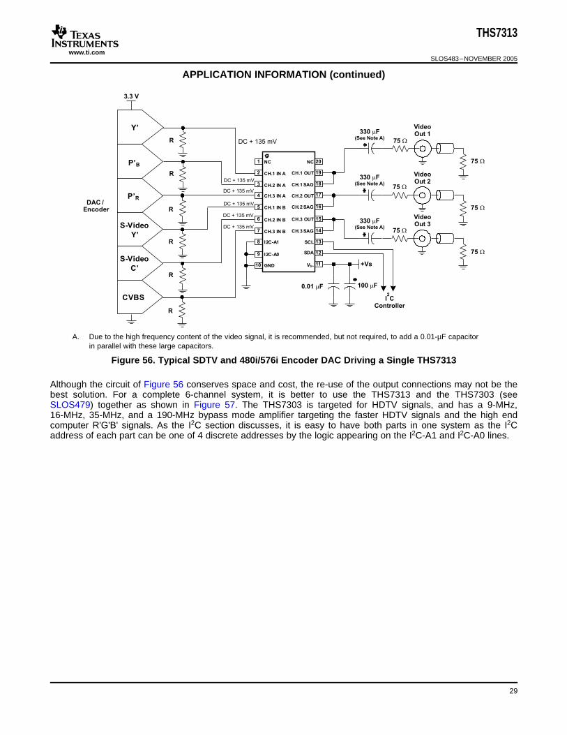
www.ti.com
17
20
19
18
GND
16
CH.2 IN B
CH.3 IN B
15
I2C-A0 SDA
VS+11
14
13
12
SCL
CH.3 SAG
I2C-A1
CH.1 IN B
CH.2 IN A
CH.3 IN A
CH.1 IN A
NC
CH.3 OUT
CH.2 SAG
CH.2 OUT
CH.1 SAG
CH.1 OUT
NC1
2
3
4
5
6
7
8
9
10
+
+
+
+
S-Video
Y’
S-Video
C’
CVBS
Y’
P’B
P’R
R
R
R
R
R
R
DAC /Encoder
3.3 V
75 W
75 W
75 W
75 W
75 W
75 W
VideoOut 1
VideoOut 2
VideoOut 3
0.01 Fm
+Vs
100 Fm
330 Fm(See Note A)
330 Fm(See Note A)
330 Fm(See Note A)
I CController
2
DC + 135 mV
DC + 135 mV
DC + 135 mV
DC + 135 mV
DC + 135 mV
DC + 135 mV
THS7313
SLOS483–NOVEMBER 2005
APPLICATION INFORMATION (continued)
A. Due to the high frequency content of the video signal, it is recommended, but not required, to add a 0.01-µF capacitorin parallel with these large capacitors.
Figure 56. Typical SDTV and 480i/576i Encoder DAC Driving a Single THS7313
Although the circuit of Figure 56 conserves space and cost, the re-use of the output connections may not be thebest solution. For a complete 6-channel system, it is better to use the THS7313 and the THS7303 (seeSLOS479) together as shown in Figure 57. The THS7303 is targeted for HDTV signals, and has a 9-MHz,16-MHz, 35-MHz, and a 190-MHz bypass mode amplifier targeting the faster HDTV signals and the high endcomputer R'G'B' signals. As the I2C section discusses, it is easy to have both parts in one system as the I2Caddress of each part can be one of 4 discrete addresses by the logic appearing on the I2C-A1 and I2C-A0 lines.
29
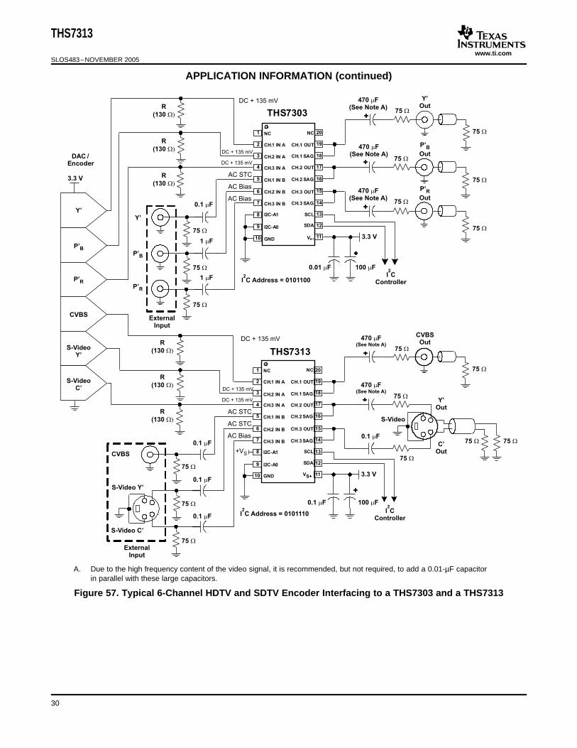
www.ti.com
17
20
19
18
GND
16
CH.2 IN B
CH.3 IN B
15
I2C-A0 SDA
VS+11
14
13
12
SCL
CH.3 SAG
I2C-A1
CH.1 IN B
CH.2 IN A
CH.3 IN A
CH.1 IN A
NC
CH.3 OUT
CH.2 SAG
CH.2 OUT
CH.1 SAG
CH.1 OUT
NC1
2
3
4
5
6
7
8
9
10
+
+
+
+
ExternalInput
ExternalInput
DAC /Encoder
CVBS
CVBS
17
20
19
18
GND
16
CH.2 IN B
CH.3 IN B
15
I2C-A0 SDA
VS+ 11
14
13
12
SCL
CH.3 SAG
I2C-A1
CH.1 IN B
CH.2 IN A
CH.3 IN A
CH.1 IN A
NC
CH.3 OUT
CH.2 SAG
CH.2 OUT
CH.1 SAG
CH.1 OUT
NC1
2
3
4
5
6
7
8
9
10
+
+
+
THS7303
THS7313
75 W
75 W
75 W
75 W
75 W
75 W
75 W75 W
75 W
75 W
75 W
75 W
75 W
75 W
75 W
75 W
75 W
75 W
R
(130 W)
R
(130 W)
R
(130 W)
R
(130 W)
R
(130 W)
R
(130 W)
Y’
Out
P’
OutB
P’
OutR
P’RP’R
P’BP’B
Y’
Y’
C’
Out
Y’
Out
S-Video
S-Video C’
S-VideoC’
S-VideoY’
S-Video Y’
CVBSOut
470 F(See Note A)
m
470 F(See Note A)
m
470 F(See Note A)
m
100 Fm0.01 Fm
1 Fm
0.1 Fm
1 Fm
0.1 Fm
0.1 Fm
0.1 Fm
3.3 V
3.3 V
470 Fm(See Note A)
470 Fm(See Note A)
0.1 Fm
0.1 Fm
3.3 V
100 Fm
I CController
2
I CController
2
I C Address = 01011002
I C Address = 01011102
AC STC
AC STC
AC STC
AC Bias
AC Bias
+VS
AC Bias
DC + 135 mV
DC + 135 mV
DC + 135 mV
DC + 135 mV
DC + 135 mV
DC + 135 mV
THS7313
SLOS483–NOVEMBER 2005
APPLICATION INFORMATION (continued)
A. Due to the high frequency content of the video signal, it is recommended, but not required, to add a 0.01-µF capacitorin parallel with these large capacitors.
Figure 57. Typical 6-Channel HDTV and SDTV Encoder Interfacing to a THS7303 and a THS7313
30

www.ti.com
I2C INTERFACE NOTES
StartCondition
StopCondition
SDA
SCL
S P
GENERAL I2C PROTOCOL
THS7313
SLOS483–NOVEMBER 2005
APPLICATION INFORMATION (continued)
The I2C interface is used to access the internal registers of the THS7313. I2C is a two-wire serial interfacedeveloped by Philips Semiconductor (see the I2C-Bus Specification, Version 2.1, January 2000). The busconsists of a data line (SDA) and a clock line (SCL) with pull-up structures. When the bus is idle, both SDA andSCL lines are pulled high. All the I2C compatible devices connect to the I2C bus through open drain I/O pins,SDA and SCL. A master device, usually a microcontroller or a digital signal processor, controls the bus. Themaster is responsible for generating the SCL signal and device addresses. The master also generates specificconditions that indicate the START and STOP of data transfer. A slave device receives and/or transmits data onthe bus under control of the master device. The THS7313 works as a slave and supports the standard modetransfer (100 kbps) and fast mode transfer (400 kbps) as defined in the I2C-Bus specification. The THS7313 hasbeen tested to be fully functional but not ensured with the high-speed mode (3.4 Mbps).
The basic I2C start and stop access cycles are shown in Figure 58.
The basic access cycle consists of the following:• A start condition• A slave address cycle• Any number of data cycles• A stop condition
Figure 58. I2C Start and Stop Conditions
• The master initiates data transfer by generating a start condition. The start condition exist when a high-to-lowtransition occurs on the SDA line while SCL is high, as shown in Figure 58. All I2C-compatible devices shouldrecognize a start condition.
• The master then generates the SCL pulses and transmits the 7-bit address and the read/write direction bitR/W on the SDA line. During all transmissions, the master ensures that data is valid. A valid data conditionrequires the SDA line to be stable during the entire high period of the clock pulse (see Figure 59). All devicesrecognize the address sent by the master and compare it to their internal fixed addresses. Only the slavedevice with a matching address generates an acknowledge (see Figure 60) by pulling the SDA line lowduring the entire high period of the ninth SCL cycle. On detecting this acknowledge, the master knows that acommunication link with a slave has been established.
• The master generates further SCL cycles to either transmit data to the slave (R/W bit 1) or receive data fromthe slave (R/W bit 0). In either case, the receiver needs to acknowledge the data sent by the transmitter. So,an acknowledge signal can either be generated by the master or by the slave, depending on which one is thereceiver. The 9-bit valid data sequences consisting of 8-bit data and 1-bit acknowledge can continue as longas necessary (See Figure 61).
• To signal the end of the data transfer, the master generates a stop condition by pulling the SDA line from lowto high while the SCL line is high (see Figure 58). This releases the bus and stops the communication linkwith the addressed slave. All I2C compatible devices must recognize the stop condition. Upon the receipt of astop condition, all devices know that the bus is released, and they wait for a start condition followed by amatching address.
31
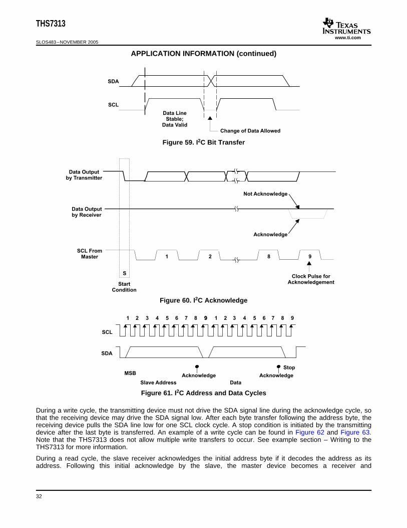
www.ti.com
SCL
SDA
Data LineStable;
Data ValidChange of Data Allowed
StartCondition
Clock Pulse forAcknowledgement
Acknowledge
Not Acknowledge
Data Outputby Receiver
Data Outputby Transmitter
SCL FromMaster
S
1 2 8 9
SCL
SDA
MSB
Slave Address Data
Stop
1 2 3 4 5 6 7 8 99 1 2 3 4 5 6 7 8 9
Acknowledge Acknowledge
THS7313
SLOS483–NOVEMBER 2005
APPLICATION INFORMATION (continued)
Figure 59. I2C Bit Transfer
Figure 60. I2C Acknowledge
Figure 61. I2C Address and Data Cycles
During a write cycle, the transmitting device must not drive the SDA signal line during the acknowledge cycle, sothat the receiving device may drive the SDA signal low. After each byte transfer following the address byte, thereceiving device pulls the SDA line low for one SCL clock cycle. A stop condition is initiated by the transmittingdevice after the last byte is transferred. An example of a write cycle can be found in Figure 62 and Figure 63.Note that the THS7313 does not allow multiple write transfers to occur. See example section – Writing to theTHS7313 for more information.
During a read cycle, the slave receiver acknowledges the initial address byte if it decodes the address as itsaddress. Following this initial acknowledge by the slave, the master device becomes a receiver and
32
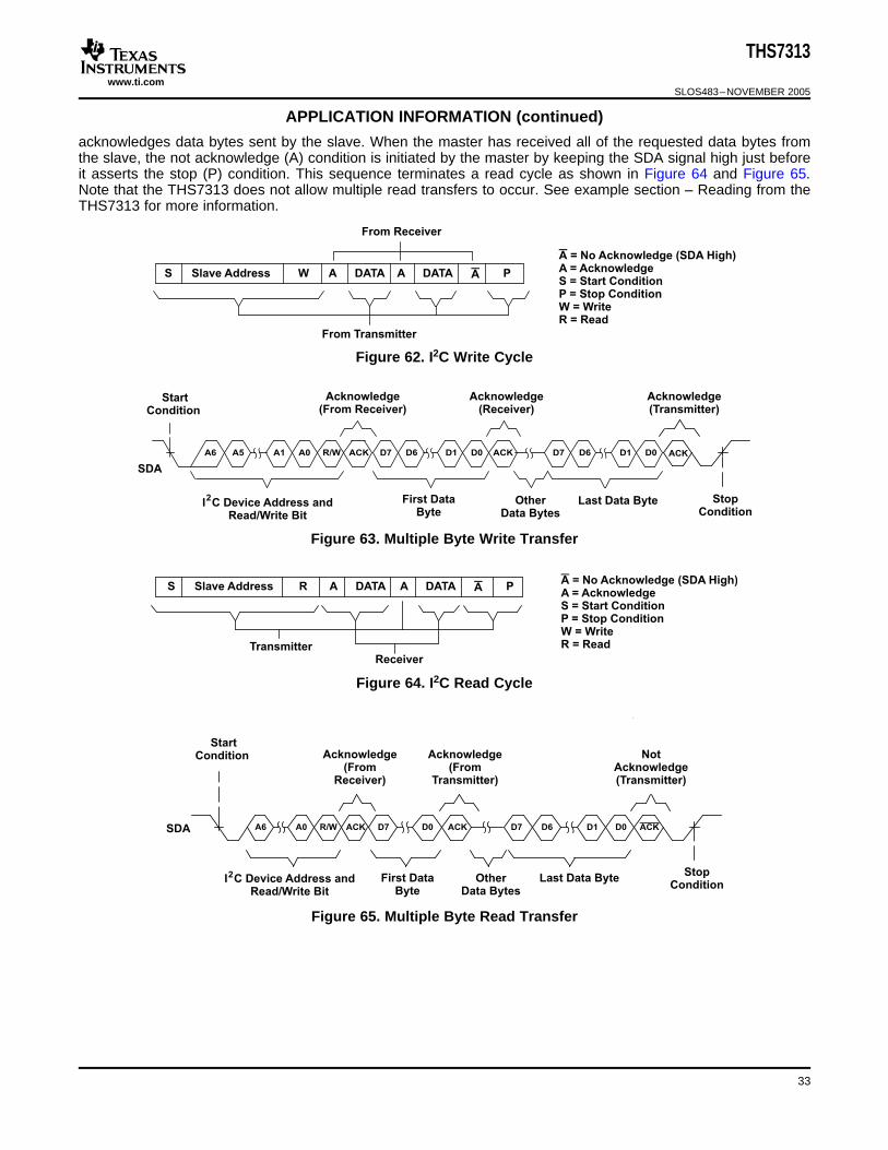
www.ti.com
A = No Acknowledge (SDA High)A = AcknowledgeS = Start ConditionP = Stop ConditionW = WriteR = Read
AA A PDATA DATAS Slave Address
From Transmitter
From Receiver
W
A6 A5
2
A0A1 ACK
Acknowledge(From Receiver)
I C Device Address andRead/Write Bit
R/W D7 D6 D0 D0ACK
StopCondition
Acknowledge(Receiver)
Last Data Byte
SDA
D7 D6D1 D1
First DataByte
StartCondition
Acknowledge(Transmitter)
ACK
OtherData Bytes
A = No Acknowledge (SDA High)A = AcknowledgeS = Start ConditionP = Stop ConditionW = WriteR = Read
AA A PDATA DATAS Slave Address
TransmitterReceiver
R
A6
2
A0 ACK
Acknowledge(From
Receiver)
I C Device Address andRead/Write Bit
R/W D7 D0 ACK
StopCondition
Acknowledge(From
Transmitter)
Last Data Byte
SDA D7 D6 D1 D0 ACK
First DataByte
StartCondition Not
Acknowledge(Transmitter)
OtherData Bytes
THS7313
SLOS483–NOVEMBER 2005
APPLICATION INFORMATION (continued)
acknowledges data bytes sent by the slave. When the master has received all of the requested data bytes fromthe slave, the not acknowledge (A) condition is initiated by the master by keeping the SDA signal high just beforeit asserts the stop (P) condition. This sequence terminates a read cycle as shown in Figure 64 and Figure 65.Note that the THS7313 does not allow multiple read transfers to occur. See example section – Reading from theTHS7313 for more information.
Figure 62. I2C Write Cycle
Figure 63. Multiple Byte Write Transfer
Figure 64. I2C Read Cycle
Figure 65. Multiple Byte Read Transfer
33
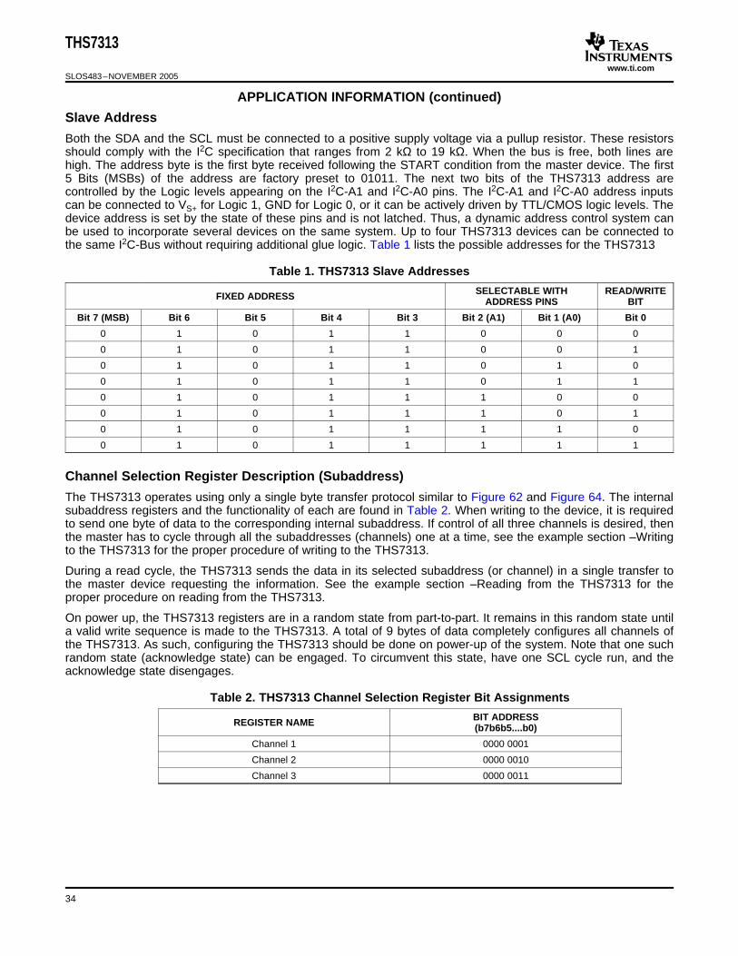
www.ti.com
Slave Address
Channel Selection Register Description (Subaddress)
THS7313
SLOS483–NOVEMBER 2005
APPLICATION INFORMATION (continued)
Both the SDA and the SCL must be connected to a positive supply voltage via a pullup resistor. These resistorsshould comply with the I2C specification that ranges from 2 kΩ to 19 kΩ. When the bus is free, both lines arehigh. The address byte is the first byte received following the START condition from the master device. The first5 Bits (MSBs) of the address are factory preset to 01011. The next two bits of the THS7313 address arecontrolled by the Logic levels appearing on the I2C-A1 and I2C-A0 pins. The I2C-A1 and I2C-A0 address inputscan be connected to VS+ for Logic 1, GND for Logic 0, or it can be actively driven by TTL/CMOS logic levels. Thedevice address is set by the state of these pins and is not latched. Thus, a dynamic address control system canbe used to incorporate several devices on the same system. Up to four THS7313 devices can be connected tothe same I2C-Bus without requiring additional glue logic. Table 1 lists the possible addresses for the THS7313
Table 1. THS7313 Slave Addresses
SELECTABLE WITH READ/WRITEFIXED ADDRESS ADDRESS PINS BIT
Bit 7 (MSB) Bit 6 Bit 5 Bit 4 Bit 3 Bit 2 (A1) Bit 1 (A0) Bit 0
0 1 0 1 1 0 0 0
0 1 0 1 1 0 0 1
0 1 0 1 1 0 1 0
0 1 0 1 1 0 1 1
0 1 0 1 1 1 0 0
0 1 0 1 1 1 0 1
0 1 0 1 1 1 1 0
0 1 0 1 1 1 1 1
The THS7313 operates using only a single byte transfer protocol similar to Figure 62 and Figure 64. The internalsubaddress registers and the functionality of each are found in Table 2. When writing to the device, it is requiredto send one byte of data to the corresponding internal subaddress. If control of all three channels is desired, thenthe master has to cycle through all the subaddresses (channels) one at a time, see the example section –Writingto the THS7313 for the proper procedure of writing to the THS7313.
During a read cycle, the THS7313 sends the data in its selected subaddress (or channel) in a single transfer tothe master device requesting the information. See the example section –Reading from the THS7313 for theproper procedure on reading from the THS7313.
On power up, the THS7313 registers are in a random state from part-to-part. It remains in this random state untila valid write sequence is made to the THS7313. A total of 9 bytes of data completely configures all channels ofthe THS7313. As such, configuring the THS7313 should be done on power-up of the system. Note that one suchrandom state (acknowledge state) can be engaged. To circumvent this state, have one SCL cycle run, and theacknowledge state disengages.
Table 2. THS7313 Channel Selection Register Bit Assignments
BIT ADDRESSREGISTER NAME (b7b6b5....b0)
Channel 1 0000 0001
Channel 2 0000 0010
Channel 3 0000 0011
34
www.ti.com
Channel Register Bit Descriptions
EXAMPLE – WRITING TO THE THS7313
THS7313
SLOS483–NOVEMBER 2005
Each bit of the sub-address (channel selection) control register as described above allows the user to individuallycontrol the functionality of the THS7313. The benefit of this process allows the user to control the functionality ofeach channel independent of the other channels. The bit description is decoded in Table 3.
Table 3. THS7313 Channel Register Bit Decoder Table
BIT FUNCTION BIT RESULTVALUE(S)
(MSB) STC Low Pass Filter Selection 0 0 500-kHz Filter – Useful for poor video sync signals7, 6 0 1 2.5-MHz Filter – Useful for reasonable sync signals
1 0 5-MHz Filter – Useful for good sync signals
1 1 5-MHz Filter – Useful for good sync signals
5 Input MUX Selection 0 Input A Select
1 Input B Select
4 , 3 Reserved X X Do Not Care
2, 1, 0 Input Bias Mode Selection and 0 0 0 Disable Channel – Conserves Power(LSB) Disable Control 0 0 1 Channel On – Mute Function – No Output
0 1 0 Channel On – DC Bias Select
0 1 1 Channel On – DC Bias + 135 mV Offset Select
1 0 0 Channel On – AC Bias Select
1 0 1 Channel On – Sync Tip Clamp with Low Bias
1 1 0 Channel On – Sync Tip Clamp with Mid Bias
1 1 1 Channel On – Sync Tip Clamp with High Bias
Bits 7 (MSB) and 6 – Controls the AC-Sync Tip Clamp Low Pass Filter function. If AC-STC mode is not used,this function is ignored.
Bit 5 – Controls the input MUX of the THS7313.
Bits 4 and 3 – Reserved for future functionality. The values of these bits do not affect the THS7313.
Bits 2, 1, and 0 (LSB) – Selects the input biasing of the THS7313 and the power-savings function. WhenSync-Tip Clamp is selected, the DC input sink bias current is also selectable.
The proper way to write to the THS7313 is illustrated as follows:An I2C master initiates a write operation to the THS7313 by generating a start condition (S) followed by theTHS7313 I2C address (as shown below), in MSB first bit order, followed by a 0 to indicate a write cycle. Afterreceiving an acknowledge from the THS7313, the master presents the subaddress (channel) it wants to writeconsisting of one byte of data, MSB first. The THS7313 acknowledges the byte after completion of thetransfer. Finally the master presents the data it wants to write to the register (channel) and the THS7313acknowledges the byte. The I2C master then terminates the write operation by generating a stop condition(P). Note that the THS7313 does not support multi-byte transfers. To write to all three channels – or registers– this procedure must be repeated for each register one series at a time (i.e., repeat steps 1 through 8 foreach channel).
Step 1 0
I2C Start (Master) S
Step 2 7 6 5 4 3 2 1 0
I2C General Address (Master) 0 1 0 1 1 X X 0
Where each X Logic state is defined by I2C-A1 and I2C-A0 pins being tied to either Vs+ or GND.
Step 3 9
I2C Acknowledge (Slave) A
35
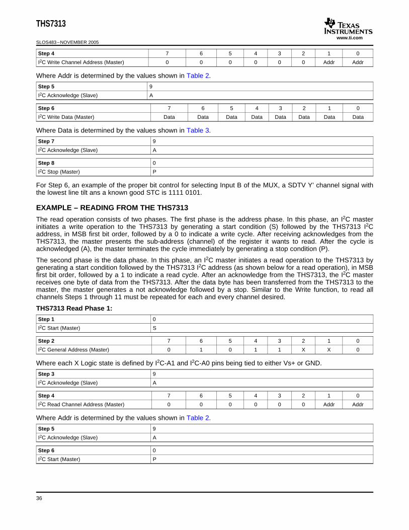
www.ti.com
EXAMPLE – READING FROM THE THS7313
THS7313
SLOS483–NOVEMBER 2005
Step 4 7 6 5 4 3 2 1 0
I2C Write Channel Address (Master) 0 0 0 0 0 0 Addr Addr
Where Addr is determined by the values shown in Table 2.
Step 5 9
I2C Acknowledge (Slave) A
Step 6 7 6 5 4 3 2 1 0
I2C Write Data (Master) Data Data Data Data Data Data Data Data
Where Data is determined by the values shown in Table 3.
Step 7 9
I2C Acknowledge (Slave) A
Step 8 0
I2C Stop (Master) P
For Step 6, an example of the proper bit control for selecting Input B of the MUX, a SDTV Y’ channel signal withthe lowest line tilt ans a known good STC is 1111 0101.
The read operation consists of two phases. The first phase is the address phase. In this phase, an I2C masterinitiates a write operation to the THS7313 by generating a start condition (S) followed by the THS7313 I2Caddress, in MSB first bit order, followed by a 0 to indicate a write cycle. After receiving acknowledges from theTHS7313, the master presents the sub-address (channel) of the register it wants to read. After the cycle isacknowledged (A), the master terminates the cycle immediately by generating a stop condition (P).
The second phase is the data phase. In this phase, an I2C master initiates a read operation to the THS7313 bygenerating a start condition followed by the THS7313 I2C address (as shown below for a read operation), in MSBfirst bit order, followed by a 1 to indicate a read cycle. After an acknowledge from the THS7313, the I2C masterreceives one byte of data from the THS7313. After the data byte has been transferred from the THS7313 to themaster, the master generates a not acknowledge followed by a stop. Similar to the Write function, to read allchannels Steps 1 through 11 must be repeated for each and every channel desired.
THS7313 Read Phase 1:
Step 1 0
I2C Start (Master) S
Step 2 7 6 5 4 3 2 1 0
I2C General Address (Master) 0 1 0 1 1 X X 0
Where each X Logic state is defined by I2C-A1 and I2C-A0 pins being tied to either Vs+ or GND.
Step 3 9
I2C Acknowledge (Slave) A
Step 4 7 6 5 4 3 2 1 0
I2C Read Channel Address (Master) 0 0 0 0 0 0 Addr Addr
Where Addr is determined by the values shown in Table 2.
Step 5 9
I2C Acknowledge (Slave) A
Step 6 0
I2C Start (Master) P
36
www.ti.com
THS7313
SLOS483–NOVEMBER 2005
THS7313 Read Phase 2:
Step 7 0
I2C Start (Master) S
Step 8 7 6 5 4 3 2 1 0
I2C General Address (Master) 0 1 0 1 1 X X 1
Where each X Logic state is defined by I2C-A1 and I2C-A0 pins being tied to either Vs+ or GND.
Step 9 9
I2C Acknowledge (Slave) A
Step 10 7 6 5 4 3 2 1 0
I2C Read Data (Slave) Data Data Data Data Data Data Data Data
Where Data is determined by the Logic values contained in the Channel Register.
Step 11 9
I2C Not-Acknowledge (Master) A
Step 12 0
I2C Stop (Master) P
37
www.ti.com
Evaluation Module
THS7313
SLOS483–NOVEMBER 2005
An evaluation module (EVM) is available for the TPS7313. Because the THS7313 is controlled by the I2C lines,additional control is required—rather than simple switches. To ease control, an USB-to-I2C interface wasdesigned onto the EVM. A computer running either Windows 2000 or XP is then connected to the EVM throughthe USB cable. A computer program interface allows graphical control of the THS7313 that allows both read andwrite functions to be performed. The EVM comes with a CD-ROM loaded with all the required software to installthe command software on to the computer.
To program the THS7313, the user selects the channel, the filter, and the mode of operation, and selects theExecute button. The Req Done light on the computer screen is lit to confirm that the command was executed bythe THS7313. The same procedure is done for each and every channel. To read the THS7313 registers, changethe switch to Read, select the channel, and then select the Execute button. The resulting register contentappears in hexadecimal code.
Note that the USB-to-I2C interface circuitry must be powered by a 3.3-V supply only. Additionally, the I2C circuitrysection must be powered on either at the same time as the THS7313 or before power is applied to the THS7313.This is due to the reading of the EEPROM, the TAS1020 device must complete to program its core. The yellowLED in the I2C section is lit if the TAS1020 was programmed properly. If this LED is not lit, then cyclng the powershould be done to reset the USB-to-I2C TAS1020 chip.
Table 4 is a bill of materials, the board layout is found in Figure 66 through Figure 69.
Table 4. Bill Of MaterialsSMD REFERENCE PCB MANUFACTURER'S DISTRIBUTER'SITEM DESCRIPTION SIZE DESIGNATOR QUANTITY PART NUMBER (1) PART NUMBER
1 BEAD, FERRITE, 2.5A, 80 OHM 0805 FB1, FB2, FB3 3 (TDK) MPZ2012S331A (DIGI-KEY) 445-1569-1-ND
CAP, 22uF, TAN, 6.3V, 10%, LO (AVX)2 A C30 1 (DIGI-KEY) 478-1754-1-NDESR TPSA226K006R0900
CAP, 100uF, TAN, 10V, 10%, LO (AVX)3 C C5 1 (DIGI-KEY) 478-1765-1-NDESR TPSC107K010R0100
C2, C3, C8, C11,4 OPEN 0805 C12, C14, C17, C21, 9
C23
CAP, 33pF, CERAMIC, 50V,5 0805 C31, C32 2 (AVX) 08055A330JAT2A (DIGI-KEY) 478-1310-1-NDNPO
CAP, 47pF, CERAMIC, 50V,6 0805 C27, C29 2 (AVX) 08055A470JAT2A (DIGI-KEY) 478-1312-1-NDNPO
CAP, 100pF, CERAMIC, 50V,7 0805 C34 1 (AVX) 08055A101JAT2A (DIGI-KEY) 478-1316-1-NDNPO
CAP, 1000pF, CERAMIC, 100V,8 0805 C33 1 (AVX) 08051A102JAT2A (DIGI-KEY) 478-1290-1-NDNPO
CAP, 0.01uF, CERAMIC, 100V,9 0805 C19, C28 2 (AVX) 08051C103KAT2A (DIGI-KEY) 478-1358-1-NDX7R
C4, C6, C9, C13,CAP, 0.1uF, CERAMIC, 50V,10 0805 C16, C22, C25, C26, 11 (AVX) 08055C104KAT2A (DIGI-KEY) 478-1395-1-NDX7R C43, C44, Z4
C18, C35, C36, C37,11 CAP, 1uF, CERAMIC, 16V, X7R 0805 C38, C39, C40, C41, 11 (TDK) C2012X7R1C105K (DIGI-KEY) 445-1358-1-ND
C42, Z5, Z6
(CORNELL)12 CAP, ALUM, 470uF, 10V, 20% F C1, C10, C20 3 (NEWARK) 97C7597AFK477M10F24B
(CORNELL)13 CAP, ALUM, 33uF, 25V, 20% C C7, C15, C24 3 (NEWARK) 97C7564AFK336M25C12B
14 OPEN 0603 R47, R48, R49, R51 4
R1, R2, R3, R4, R6,15 RESISTOR, 0 OHM 0603 9 (ROHM) MCR03EZPJ000 (DIGI-KEY) RHM0.0GCT-NDR7, R19, R20, R23
RESISTOR, 2.74K OHM, 1/8W, (ROHM)16 0603 R41, R61 2 (DIGI-KEY) RHM2.7KHCT-ND1% MCR03EZPFX2741
17 OPEN 0805 R15, R16, R28 3
R9, R13, R21, Z1, Z2,18 RESISTOR, 0 OHM 0805 6 (ROHM) MCR10EZHJ000 (DIGI-KEY) RHM0.0ACT-NDZ3
(1) Manufacturer's part numbers are used for test purposes only.
38
www.ti.com
THS7313
SLOS483–NOVEMBER 2005
Table 4. Bill Of Materials (continued)SMD REFERENCE PCB MANUFACTURER'S DISTRIBUTER'SITEM DESCRIPTION SIZE DESIGNATOR QUANTITY PART NUMBER (1) PART NUMBER
(ROHM)19 RESISTOR, 10 OHM, 1/8W, 1% 0805 R39, R44, R45, R52 4 (DIGI-KEY) RHM10.0CCT-NDMCR10EZHF10R0
RESISTOR, 27.4 OHM, 1/8W,20 0805 R30, R31 2 (ROHM) MCR10EZHF27.4 (DIGI-KEY) RHM27.4CCT-ND1%
R5, R8, R10, R11,21 RESISTOR, 75 OHM, 1/8W, 1% 0805 R12, R14, R17, R18, 9 (ROHM) MCR10EZHF75.0 (DIGI-KEY) RHM75.0CCT-ND
R22
(ROHM)22 RESISTOR, 100 OHM, 1/8W, 1% 0805 R50 1 (DIGI-KEY) RHM100CCT-NDMCR10EZHF1000
(ROHM)23 RESISTOR, 200 OHM, 1/8W, 1% 0805 R26, R27 2 (DIGI-KEY) RHM200CCT-NDMCR10EZHF2000
(ROHM)24 RESISTOR, 649 OHM, 1/8W, 1% 0805 R33, R60 2 (DIGI-KEY) RHM649CCT-NDMCR10EZHF0649
RESISTOR, 1.0K OHM, 1/8W, (ROHM) (DIGI-KEY)25 0805 R29 11% MCR10EZHF1001 RHM1.00KCCT-ND
RESISTOR, 1.5K OHM, 1/8W, (ROHM) (DIGI-KEY)26 0805 R32 11% MCR10EZHF1501 RHM1.50KCCT-ND
RESISTOR, 2.21K OHM, 1/8W, (ROHM) (DIGI-KEY)27 0805 R34, R35 21% MCR10EZHF2211 RHM2.21KCCT-ND
RESISTOR, 3.09K OHM, 1/8W, (ROHM) (DIGI-KEY)28 0805 R43 11% MCR10EZHF3091 RHM3.09KCCT-ND
RESISTOR, 10K OHM, 1/8W, (ROHM) (DIGI-KEY)29 0805 R24, R25, R40, R42 41% MCR10EZHF1002 RHM10.0KCCT-ND
RESISTOR, 20K OHM, 1/8W, (ROHM) (DIGI-KEY)30 0805 R46 11% MCR10EZHF2002 RHM20.0KCCT-ND
(LITE-ON)31 LED, GREEN 0805 D1 1 (DIGI-KEY) 160-1423-1-NDLTST-C171GKT
32 LED, YELLOW 0805 D2 1 (LITE-ON) LTST-C171YKT (DIGI-KEY) 160-1431-1-ND
33 IC, CONV, SERIAL TO USB U3 1 (TI) TAS1020BPFB (DIGI-KEY) TAS1020BPFB
(MICROCHIP)34 IC, SERIAL, EEPROM, 64K 8-SOIC U2 1 (DIGI-KEY) 24LC64-I/SN-ND24LC64-I/SN
(CITIZEN)35 CRYSTAL, 6.00MHz., SMT HCM49 X1 1 (DIGI-KEY) 300-6112-1-NDHCM49-6.000MABJT
36 OPEN SOT-23 U4, U5 2
JACK, BANANA RECEPTANCE,37 J4, J5, J16, J17 4 (SPC) 813 (NEWARK) 39N8670.25" DIA. HOLE
(DIGI-KEY)38 SWITCH, SMD GULL WING 4MM S1 1 (BOURNS) 7914G-1-000E 7914G-000ETR-ND
39 CONNECTOR, RCA, JACK, R/A J1, J2, J12 3 (CUI) RCJ-32265 (DIGI-KEY) CP-1446-ND
CONNECTOR, USB, RTANG,40 B J15 1 (ASSMANN) AU-Y1007 (DIGI-KEY) AE1085-NDFEMALE
CONNECTOR, BNC, JACK, 75 J3, J6, J7, J8, J9, (AMPHENOL)41 9 (NEWARK) 93F7554OHM J10, J11, J13, J14 31-5329-72RFX
HEADER, 0.1" CTRS, 0.025" SQ.42 2 POS. JP1, JP2, JP3 3 (SULLINS) PZC36SAAN (DIGI-KEY) S1011-36-NDPINS
43 SHUNTS JP1, JP2, JP3 3 (SULLINS) SSC02SYAN (DIGI-KEY) S9002-ND
TP1, TP2, TP5, TP6,44 TEST POINT, RED 5 (KEYSTONE) 5000 (DIGI-KEY) 5000K-NDTP7
45 TEST POINT, BLACK TP3, TP4 2 (KEYSTONE) 5001 (DIGI-KEY) 5001K-ND
46 IC, THS7313 U1 1 (TI) THS7313PW
STANDOFF, 4-40 HEX, 0.625"47 4 (KEYSTONE) 1808 (NEWARK) 89F1934LENGTH
48 SCREW, PHILLIPS, 4-40, .250" 4 (BF) PMS 440 0031 PH (DIGI-KEY) H343-ND
49 BOARD, PRINTED CIRCUIT 1 EDGE # 6469006 REV.B
39
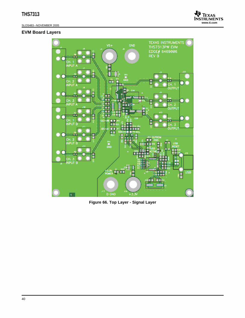
www.ti.com
EVM Board Layers
THS7313
SLOS483–NOVEMBER 2005
Figure 66. Top Layer - Signal Layer
40
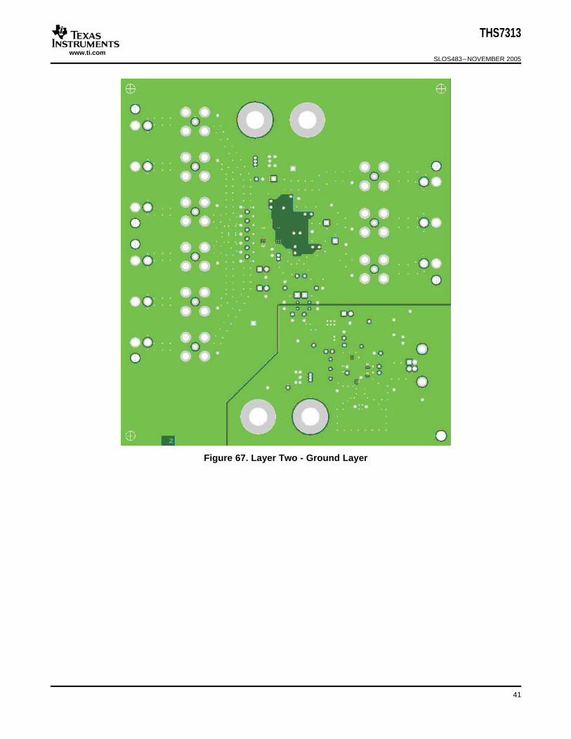
www.ti.com
THS7313
SLOS483–NOVEMBER 2005
Figure 67. Layer Two - Ground Layer
41
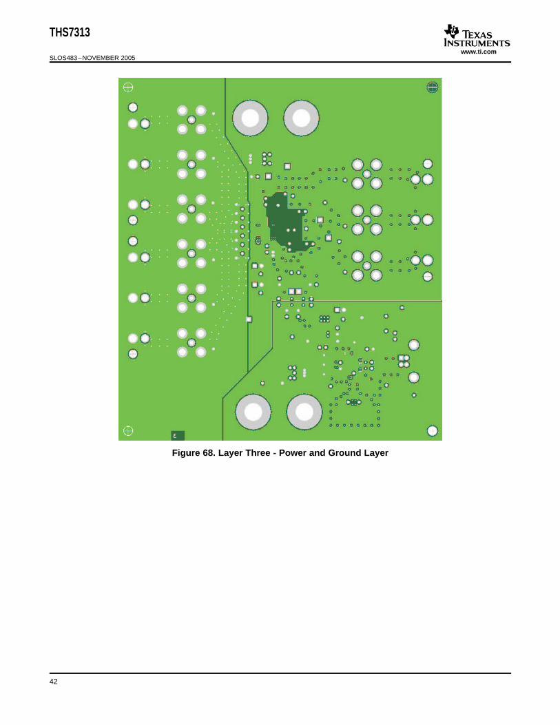
www.ti.com
THS7313
SLOS483–NOVEMBER 2005
Figure 68. Layer Three - Power and Ground Layer
42
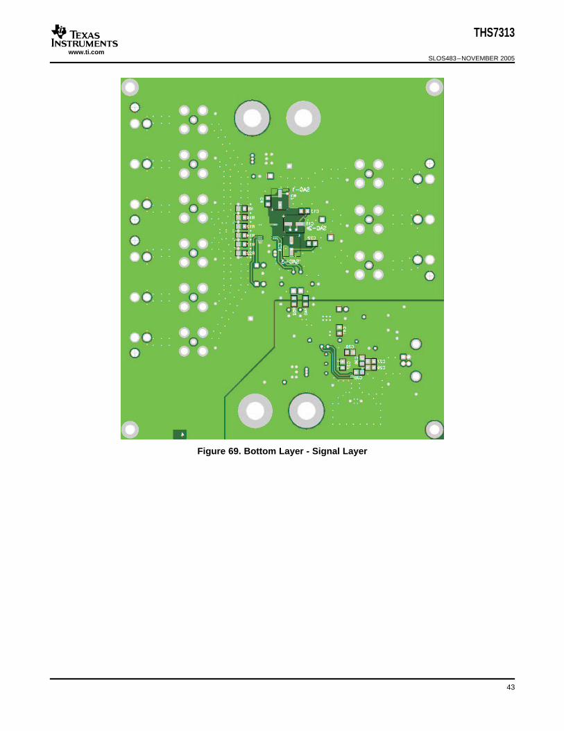
www.ti.com
THS7313
SLOS483–NOVEMBER 2005
Figure 69. Bottom Layer - Signal Layer
43
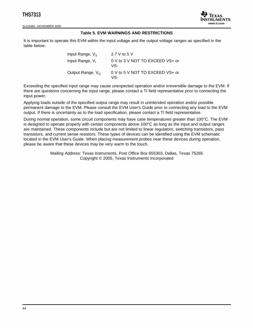
www.ti.com
THS7313
SLOS483–NOVEMBER 2005
Table 5. EVM WARNINGS AND RESTRICTIONS
It is important to operate this EVM within the input voltage and the output voltage ranges as specified in thetable below.
Input Range, VS 2.7 V to 5 V
Input Range, VI 0 V to 3 V NOT TO EXCEED VS+ orVS-
Output Range, VO 0 V to 5 V NOT TO EXCEED VS+ orVS-
Exceeding the specified input range may cause unexpected operation and/or irreversible damage to the EVM. Ifthere are questions concerning the input range, please contact a TI field representative prior to connecting theinput power.
Applying loads outside of the specified output range may result in unintended operation and/or possiblepermanent damage to the EVM. Please consult the EVM User's Guide prior to connecting any load to the EVMoutput. If there is uncertainty as to the load specification, please contact a TI field representative.
During normal operation, some circuit components may have case temperatures greater than 100°C. The EVMis designed to operate properly with certain components above 100°C as long as the input and output rangesare maintained. These components include but are not limited to linear regulators, switching transistors, passtransistors, and current sense resistors. These types of devices can be identified using the EVM schematiclocated in the EVM User's Guide. When placing measurement probes near these devices during operation,please be aware that these devices may be very warm to the touch.
Mailing Address: Texas Instruments, Post Office Box 655303, Dallas, Texas 75265Copyright © 2005, Texas Instruments Incorporated
44
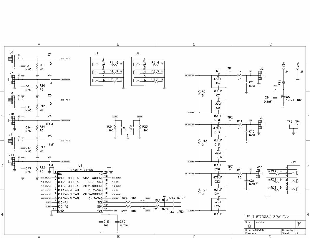
++
++
++
+
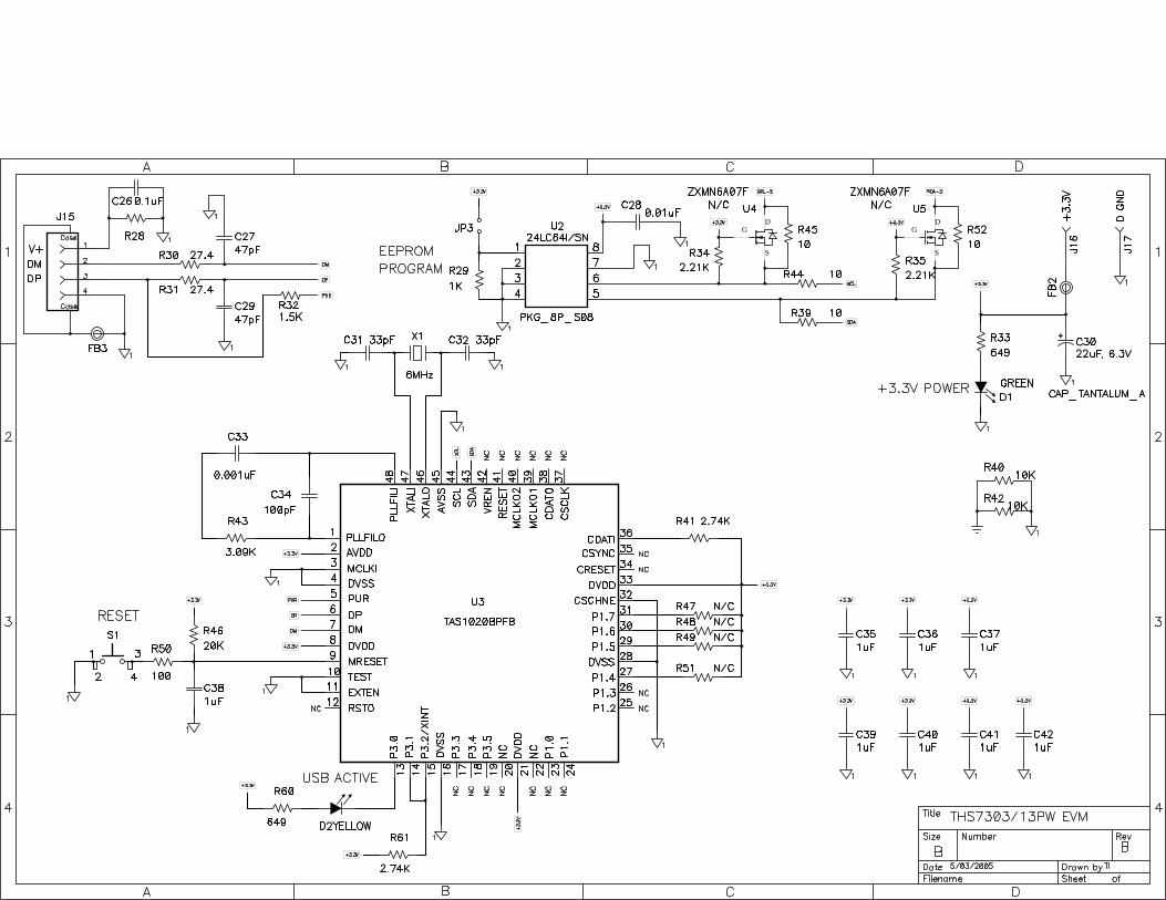
D
S
G
+
GD
S
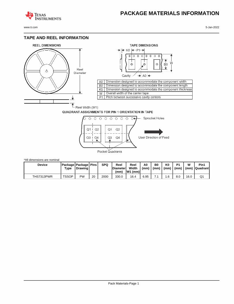
TAPE AND REEL INFORMATION
*All dimensions are nominal
Device PackageType
PackageDrawing
Pins SPQ ReelDiameter
(mm)
ReelWidth
W1 (mm)
A0(mm)
B0(mm)
K0(mm)
P1(mm)
W(mm)
Pin1Quadrant
THS7313PWR TSSOP PW 20 2000 330.0 16.4 6.95 7.1 1.6 8.0 16.0 Q1
PACKAGE MATERIALS INFORMATION
www.ti.com 5-Jan-2022
Pack Materials-Page 1
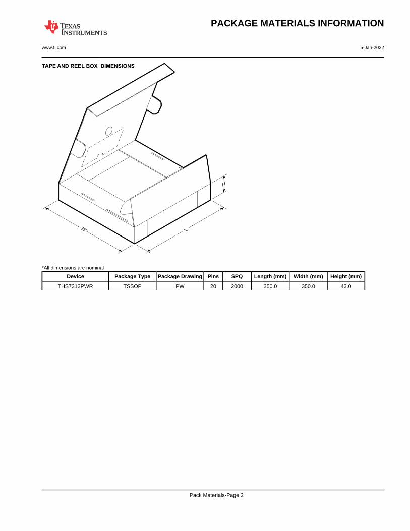
*All dimensions are nominal
Device Package Type Package Drawing Pins SPQ Length (mm) Width (mm) Height (mm)
THS7313PWR TSSOP PW 20 2000 350.0 350.0 43.0
PACKAGE MATERIALS INFORMATION
www.ti.com 5-Jan-2022
Pack Materials-Page 2
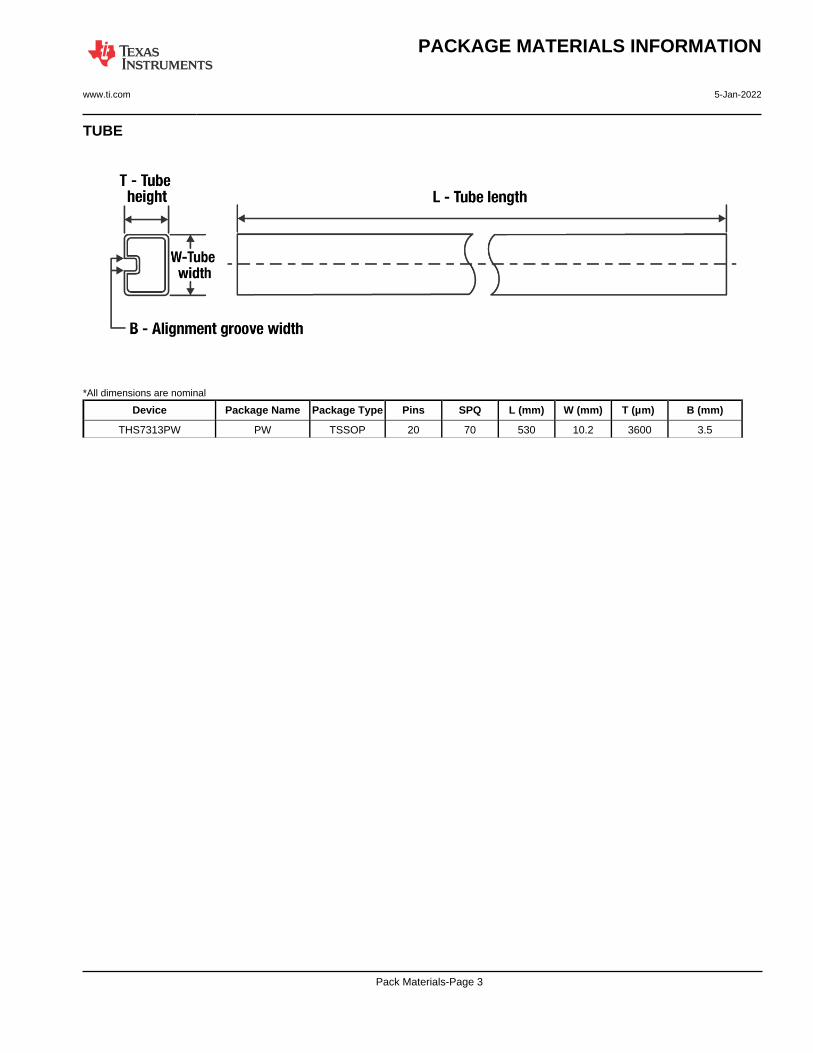
TUBE
*All dimensions are nominal
Device Package Name Package Type Pins SPQ L (mm) W (mm) T (µm) B (mm)
THS7313PW PW TSSOP 20 70 530 10.2 3600 3.5
PACKAGE MATERIALS INFORMATION
www.ti.com 5-Jan-2022
Pack Materials-Page 3

www.ti.com
PACKAGE OUTLINE
C
18X 0.65
2X5.85
20X 0.300.19
TYP6.66.2
1.2 MAX
0.150.05
0.25GAGE PLANE
-80
BNOTE 4
4.54.3
A
NOTE 3
6.66.4
0.750.50
(0.15) TYP
TSSOP - 1.2 mm max heightPW0020ASMALL OUTLINE PACKAGE
4220206/A 02/2017
1
1011
20
0.1 C A B
PIN 1 INDEX AREA
SEE DETAIL A
0.1 C
NOTES: 1. All linear dimensions are in millimeters. Any dimensions in parenthesis are for reference only. Dimensioning and tolerancing per ASME Y14.5M. 2. This drawing is subject to change without notice. 3. This dimension does not include mold flash, protrusions, or gate burrs. Mold flash, protrusions, or gate burrs shall not exceed 0.15 mm per side. 4. This dimension does not include interlead flash. Interlead flash shall not exceed 0.25 mm per side.5. Reference JEDEC registration MO-153.
SEATINGPLANE
A 20DETAIL ATYPICAL
SCALE 2.500
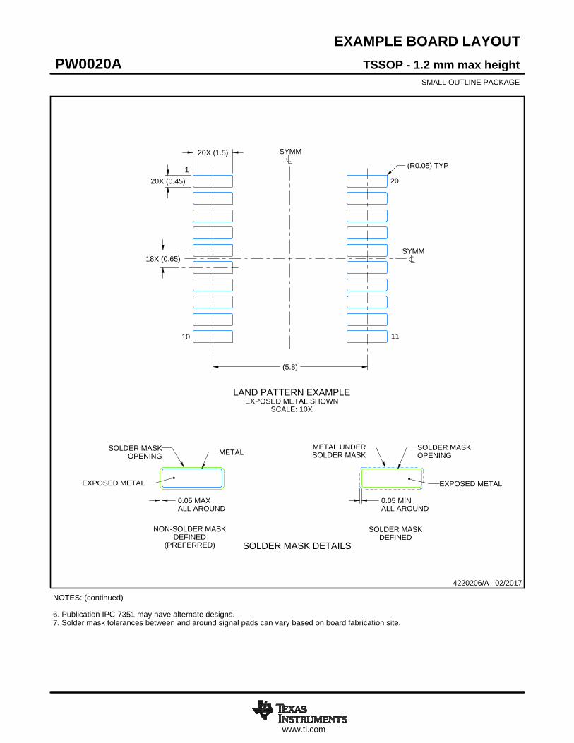
www.ti.com
EXAMPLE BOARD LAYOUT
0.05 MAXALL AROUND
0.05 MINALL AROUND
20X (1.5)
20X (0.45)
18X (0.65)
(5.8)
(R0.05) TYP
TSSOP - 1.2 mm max heightPW0020ASMALL OUTLINE PACKAGE
4220206/A 02/2017
NOTES: (continued) 6. Publication IPC-7351 may have alternate designs. 7. Solder mask tolerances between and around signal pads can vary based on board fabrication site.
LAND PATTERN EXAMPLEEXPOSED METAL SHOWN
SCALE: 10X
SYMM
SYMM
1
10 11
20
15.000
METALSOLDER MASKOPENING
METAL UNDERSOLDER MASK
SOLDER MASKOPENING
EXPOSED METALEXPOSED METAL
SOLDER MASK DETAILS
NON-SOLDER MASKDEFINED
(PREFERRED)
SOLDER MASKDEFINED
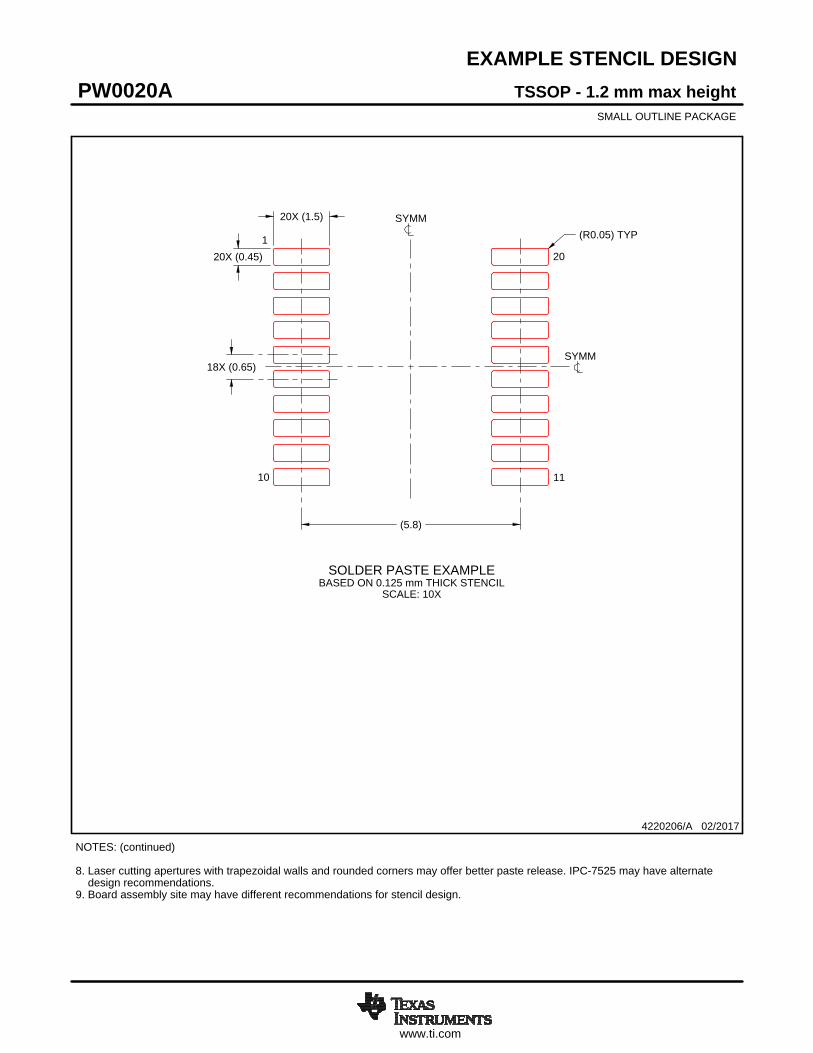
www.ti.com
EXAMPLE STENCIL DESIGN
20X (1.5)
20X (0.45)
18X (0.65)
(5.8)
(R0.05) TYP
TSSOP - 1.2 mm max heightPW0020ASMALL OUTLINE PACKAGE
4220206/A 02/2017
NOTES: (continued) 8. Laser cutting apertures with trapezoidal walls and rounded corners may offer better paste release. IPC-7525 may have alternate design recommendations. 9. Board assembly site may have different recommendations for stencil design.
SOLDER PASTE EXAMPLEBASED ON 0.125 mm THICK STENCIL
SCALE: 10X
SYMM
SYMM
1
10 11
20

IMPORTANT NOTICE AND DISCLAIMERTI PROVIDES TECHNICAL AND RELIABILITY DATA (INCLUDING DATA SHEETS), DESIGN RESOURCES (INCLUDING REFERENCE DESIGNS), APPLICATION OR OTHER DESIGN ADVICE, WEB TOOLS, SAFETY INFORMATION, AND OTHER RESOURCES “AS IS” AND WITH ALL FAULTS, AND DISCLAIMS ALL WARRANTIES, EXPRESS AND IMPLIED, INCLUDING WITHOUT LIMITATION ANY IMPLIED WARRANTIES OF MERCHANTABILITY, FITNESS FOR A PARTICULAR PURPOSE OR NON-INFRINGEMENT OF THIRD PARTY INTELLECTUAL PROPERTY RIGHTS.These resources are intended for skilled developers designing with TI products. You are solely responsible for (1) selecting the appropriate TI products for your application, (2) designing, validating and testing your application, and (3) ensuring your application meets applicable standards, and any other safety, security, regulatory or other requirements.These resources are subject to change without notice. TI grants you permission to use these resources only for development of an application that uses the TI products described in the resource. Other reproduction and display of these resources is prohibited. No license is granted to any other TI intellectual property right or to any third party intellectual property right. TI disclaims responsibility for, and you will fully indemnify TI and its representatives against, any claims, damages, costs, losses, and liabilities arising out of your use of these resources.TI’s products are provided subject to TI’s Terms of Sale or other applicable terms available either on ti.com or provided in conjunction with such TI products. TI’s provision of these resources does not expand or otherwise alter TI’s applicable warranties or warranty disclaimers for TI products.TI objects to and rejects any additional or different terms you may have proposed. IMPORTANT NOTICE
Mailing Address: Texas Instruments, Post Office Box 655303, Dallas, Texas 75265Copyright © 2022, Texas Instruments Incorporated