2 Laboratories Introduction
83
-
Upload
khangminh22 -
Category
Documents
-
view
0 -
download
0
Transcript of 2 Laboratories Introduction
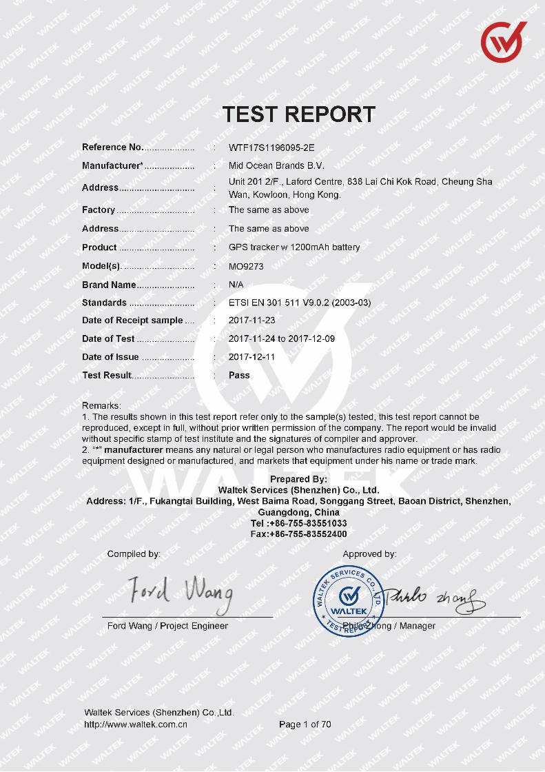
Reference No.: WTF17S1196095-2E Page 2 of 70
Waltek Services (Shenzhen) Co.,Ltd. http://www.waltek.com.cn
2 Laboratories Introduction Waltek Services Test Group Ltd. is one of the largest and the most comprehensive third party testing
organizations in China, our headquarter located in Shenzhen (CNAS Registration No. L3110, A2LA
Certificate Number: 4243.01) and have branches in Foshan (CNAS Registration No. L6478), Dongguan
(CNAS Registration No. L9950), Zhongshan, Suzhou (CNAS Registration No. L7754), Ningbo and Hong
Kong, Our test capability covered four large fields: safety test. Electronic Magnetic Compatibility(EMC),
reliability and energy performance, Chemical test. Meanwhile, Waltek has got recognition as registration and
accreditation laboratory from EMSD (Electrical and Mechanical Services Department), and American Energy
star, FCC(The Federal Communications Commission), CPSC(Consumer Product Safety Commission),
CEC(California energy efficiency), IC(Industry Canada) and ELI(Efficient Lighting Initiative). It’s the strategic
partner and data recognition laboratory of international authoritative organizations, such as UL, Intertek(ETL-
SEMKO), CSA, TÜV Rheinland, TÜV SÜD, etc. As a professional, comprehensive, justice international test
organization, we still keep the scientific and rigorous work attitude to help each client satisfy the international
standards and assist their product enter into globe market smoothly.
Waltek Services (Shenzhen) Co., Ltd.
A. Accreditations for Conformity Assessment (International)
Country/Region Accreditation Body Scope Note
USA
CNAS
(Registration No.: L3110)
A2LA
(Certificate No.: 4243.01)
FCC ID \ DOC \ VOC 1
Canada IC ID \ VOC 2
Japan MIC-T \ MIC-R -
Europe EMCD \ RED -
Taiwan NCC -
Hong Kong OFCA -
Australia RCM -
India
International Services
WPC -
Thailand NTC -
Singapore IDA -
Note:
1. FCC Designation No.: CN1201. Test Firm Registration No.: 523476.
2. IC Canada Registration No.: 7760A
B. TCBs and Notify Bodies Recognized Testing Laboratory.
Recognized Testing Laboratory of … Notify body number
TUV Rheinland Optional.

Reference No.: WTF17S1196095-2E Page 3 of 70
Waltek Services (Shenzhen) Co.,Ltd. http://www.waltek.com.cn
Intertek
TUV SUD
SGS
Phoenix Testlab GmbH 0700
Element Materials Technology Warwick Ltd 0891
Timco Engineering, Inc. 1177
Eurofins Product Service GmbH 0681
Reference No.: WTF17S1196095-2E Page 4 of 70
Waltek Services (Shenzhen) Co.,Ltd. http://www.waltek.com.cn
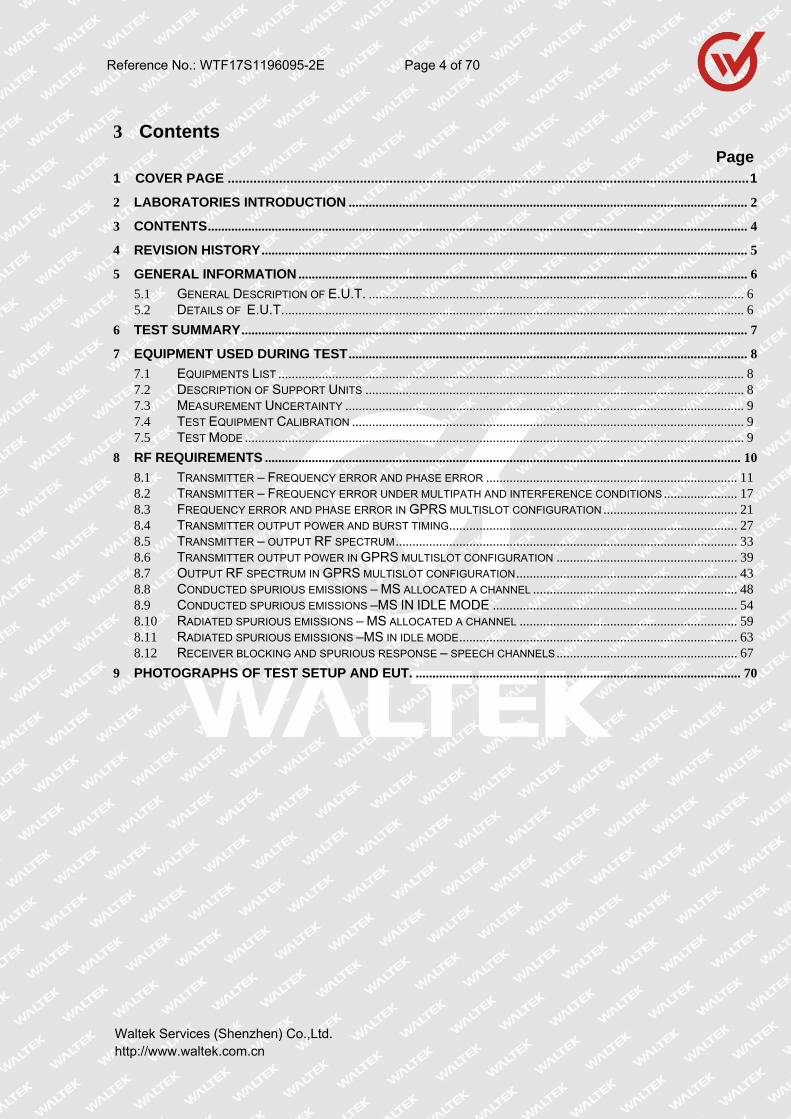
3 Contents Page
1 COVER PAGE .............................................................................................................................................. 1
2 LABORATORIES INTRODUCTION ....................................................................................................................... 2
3 CONTENTS ................................................................................................................................................................. 4
4 REVISION HISTORY ................................................................................................................................................. 5
5 GENERAL INFORMATION ...................................................................................................................................... 6
5.1 GENERAL DESCRIPTION OF E.U.T. ................................................................................................................ 6 5.2 DETAILS OF E.U.T. ......................................................................................................................................... 6
6 TEST SUMMARY ....................................................................................................................................................... 7
7 EQUIPMENT USED DURING TEST ....................................................................................................................... 8
7.1 EQUIPMENTS LIST ........................................................................................................................................... 8 7.2 DESCRIPTION OF SUPPORT UNITS ................................................................................................................. 8 7.3 MEASUREMENT UNCERTAINTY ....................................................................................................................... 9 7.4 TEST EQUIPMENT CALIBRATION ..................................................................................................................... 9 7.5 TEST MODE ..................................................................................................................................................... 9
8 RF REQUIREMENTS .............................................................................................................................................. 10
8.1 TRANSMITTER – FREQUENCY ERROR AND PHASE ERROR ........................................................................... 11 8.2 TRANSMITTER – FREQUENCY ERROR UNDER MULTIPATH AND INTERFERENCE CONDITIONS ...................... 17 8.3 FREQUENCY ERROR AND PHASE ERROR IN GPRS MULTISLOT CONFIGURATION ........................................ 21 8.4 TRANSMITTER OUTPUT POWER AND BURST TIMING ...................................................................................... 27 8.5 TRANSMITTER – OUTPUT RF SPECTRUM ...................................................................................................... 33 8.6 TRANSMITTER OUTPUT POWER IN GPRS MULTISLOT CONFIGURATION ...................................................... 39 8.7 OUTPUT RF SPECTRUM IN GPRS MULTISLOT CONFIGURATION .................................................................. 43 8.8 CONDUCTED SPURIOUS EMISSIONS – MS ALLOCATED A CHANNEL ............................................................. 48 8.9 CONDUCTED SPURIOUS EMISSIONS –MS IN IDLE MODE ......................................................................... 54 8.10 RADIATED SPURIOUS EMISSIONS – MS ALLOCATED A CHANNEL ................................................................. 59 8.11 RADIATED SPURIOUS EMISSIONS –MS IN IDLE MODE ................................................................................... 63 8.12 RECEIVER BLOCKING AND SPURIOUS RESPONSE – SPEECH CHANNELS ...................................................... 67
9 PHOTOGRAPHS OF TEST SETUP AND EUT. ................................................................................................. 70

Reference No.: WTF17S1196095-2E Page 5 of 70
Waltek Services (Shenzhen) Co.,Ltd. http://www.waltek.com.cn
4 Revision History
Test report No. Date of Receipt sample
Date of TestDate of Issue
Purpose Comment Approved
WTF17S11960
95-2E 2017-11-23
2017-11-24 to 2017-12-
09 2017-12-11 original - Valid

Reference No.: WTF17S1196095-2E Page 7 of 70
Waltek Services (Shenzhen) Co.,Ltd. http://www.waltek.com.cn
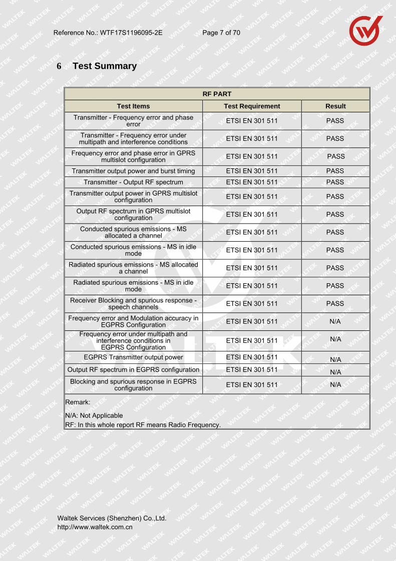
6 Test Summary
RF PART
Test Items Test Requirement Result
Transmitter - Frequency error and phase error ETSI EN 301 511 PASS
Transmitter - Frequency error under multipath and interference conditions ETSI EN 301 511 PASS
Frequency error and phase error in GPRS multislot configuration ETSI EN 301 511 PASS
Transmitter output power and burst timing ETSI EN 301 511 PASS
Transmitter - Output RF spectrum ETSI EN 301 511 PASS
Transmitter output power in GPRS multislot configuration ETSI EN 301 511 PASS
Output RF spectrum in GPRS multislot configuration ETSI EN 301 511 PASS
Conducted spurious emissions - MS allocated a channel ETSI EN 301 511 PASS
Conducted spurious emissions - MS in idle mode ETSI EN 301 511 PASS
Radiated spurious emissions - MS allocated a channel ETSI EN 301 511 PASS
Radiated spurious emissions - MS in idle mode ETSI EN 301 511 PASS
Receiver Blocking and spurious response - speech channels ETSI EN 301 511 PASS
Frequency error and Modulation accuracy in EGPRS Configuration ETSI EN 301 511 N/A
Frequency error under multipath and interference conditions in
EGPRS ConfigurationETSI EN 301 511 N/A
EGPRS Transmitter output power ETSI EN 301 511 N/A
Output RF spectrum in EGPRS configuration ETSI EN 301 511 N/ABlocking and spurious response in EGPRS
configuration ETSI EN 301 511 N/A
Remark:
N/A: Not Applicable RF: In this whole report RF means Radio Frequency.
Reference No.: WTF17S1196095-2E Page 8 of 70
Waltek Services (Shenzhen) Co.,Ltd. http://www.waltek.com.cn
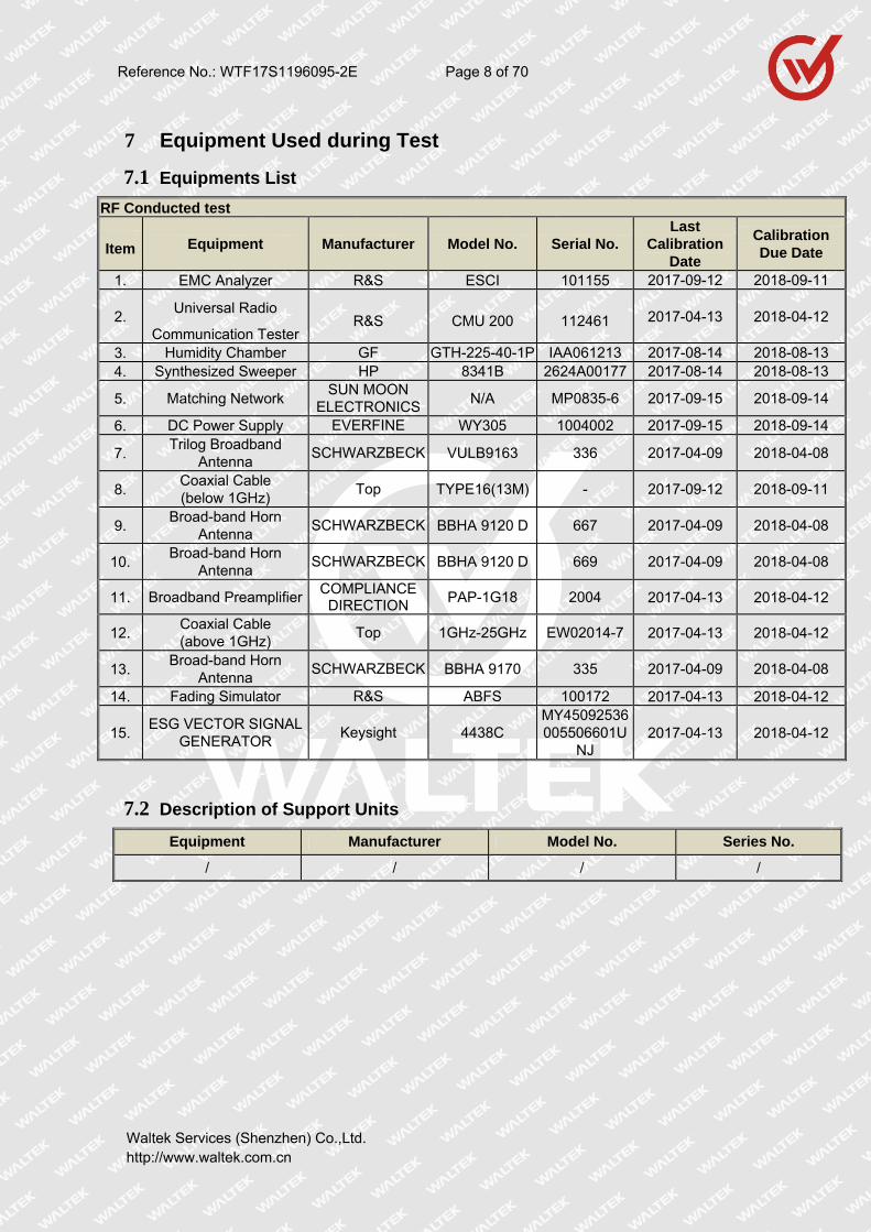
7 Equipment Used during Test
7.1 Equipments List
RF Conducted test
Item Equipment Manufacturer Model No. Serial No. Last
Calibration Date
Calibration Due Date
1. EMC Analyzer R&S ESCI 101155 2017-09-12 2018-09-11
2. Universal Radio
Communication Tester R&S CMU 200 112461 2017-04-13 2018-04-12
3. Humidity Chamber GF GTH-225-40-1P IAA061213 2017-08-14 2018-08-13 4. Synthesized Sweeper HP 8341B 2624A00177 2017-08-14 2018-08-13
5. Matching Network SUN MOON
ELECTRONICSN/A MP0835-6 2017-09-15 2018-09-14
6. DC Power Supply EVERFINE WY305 1004002 2017-09-15 2018-09-14
7. Trilog Broadband
Antenna SCHWARZBECK VULB9163 336 2017-04-09 2018-04-08
8. Coaxial Cable (below 1GHz)
Top TYPE16(13M) - 2017-09-12 2018-09-11
9. Broad-band Horn
Antenna SCHWARZBECK BBHA 9120 D 667 2017-04-09 2018-04-08
10. Broad-band Horn
Antenna SCHWARZBECK BBHA 9120 D 669 2017-04-09 2018-04-08
11. Broadband Preamplifier COMPLIANCE
DIRECTION PAP-1G18 2004 2017-04-13 2018-04-12
12. Coaxial Cable (above 1GHz)
Top 1GHz-25GHz EW02014-7 2017-04-13 2018-04-12
13. Broad-band Horn
Antenna SCHWARZBECK BBHA 9170 335 2017-04-09 2018-04-08
14. Fading Simulator R&S ABFS 100172 2017-04-13 2018-04-12
15. ESG VECTOR SIGNAL
GENERATOR Keysight 4438C
MY45092536005506601U
NJ 2017-04-13 2018-04-12
7.2 Description of Support Units
Equipment Manufacturer Model No. Series No.
/ / / /
Reference No.: WTF17S1196095-2E Page 9 of 70
Waltek Services (Shenzhen) Co.,Ltd. http://www.waltek.com.cn
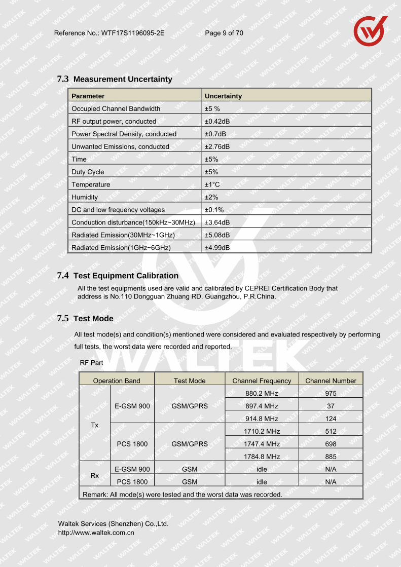
7.3 Measurement Uncertainty
Parameter Uncertainty
Occupied Channel Bandwidth ±5 %
RF output power, conducted ±0.42dB
Power Spectral Density, conducted ±0.7dB
Unwanted Emissions, conducted ±2.76dB
Time ±5%
Duty Cycle ±5%
Temperature ±1°C
Humidity ±2%
DC and low frequency voltages ±0.1%
Conduction disturbance(150kHz~30MHz) 3.64dB
Radiated Emission(30MHz~1GHz) 5.08dB
Radiated Emission(1GHz~6GHz) 4.99dB
7.4 Test Equipment Calibration
All the test equipments used are valid and calibrated by CEPREI Certification Body that address is No.110 Dongguan Zhuang RD. Guangzhou, P.R.China.
7.5 Test Mode
All test mode(s) and condition(s) mentioned were considered and evaluated respectively by performing
full tests, the worst data were recorded and reported.
RF Part
Operation Band Test Mode Channel Frequency Channel Number
Tx
E-GSM 900 GSM/GPRS
880.2 MHz 975
897.4 MHz 37
914.8 MHz 124
PCS 1800 GSM/GPRS
1710.2 MHz 512
1747.4 MHz 698
1784.8 MHz 885
Rx E-GSM 900 GSM idle N/A
PCS 1800 GSM idle N/A
Remark: All mode(s) were tested and the worst data was recorded.

Reference No.: WTF17S1196095-2E Page 10 of 70
Waltek Services (Shenzhen) Co.,Ltd. http://www.waltek.com.cn
8 RF Requirements
1. Normal Test Conditions:
Ambient Condition: 22 C to 55 %RH
2. Extreme Test Conditions:
Extreme Temperature:
Handheld device: -20°C to +40°C;
Vehicular or Portable: -20°C to +40°C;
Extreme Power Source Voltages:
Power source Lower extreme Higher extreme Normal condition
AC mains 0.9 1.1 1.0
Regulated lead acid battery 0.9 1.3 1.1
Leclanché battery 0.85 1.0 1.0
Lithium battery 0.95 1.10 1.10
Mercury/nickel cadmium battery 0.9 1.0 1.0
The follow condition is applicable:
Test Conditions Normal LTLV LTHV HTHV HTLV
Temperature ( ) 22 -20 -20 40 40
Voltage (V) 3.7 3.5 4.1 4.1 3.5
Reference No.: WTF17S1196095-2E Page 11 of 70
Waltek Services (Shenzhen) Co.,Ltd. http://www.waltek.com.cn
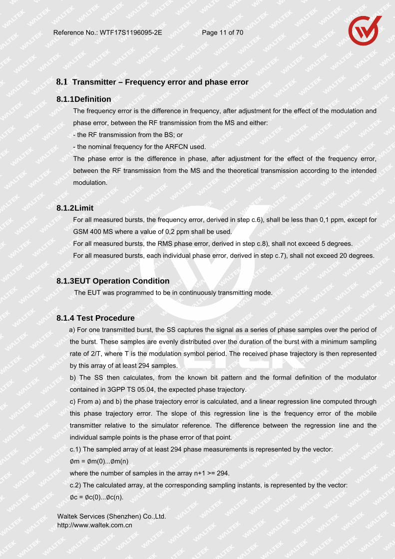
8.1 Transmitter – Frequency error and phase error
8.1.1 Definition
The frequency error is the difference in frequency, after adjustment for the effect of the modulation and
phase error, between the RF transmission from the MS and either:
- the RF transmission from the BS; or
- the nominal frequency for the ARFCN used.
The phase error is the difference in phase, after adjustment for the effect of the frequency error,
between the RF transmission from the MS and the theoretical transmission according to the intended
modulation.
8.1.2 Limit
For all measured bursts, the frequency error, derived in step c.6), shall be less than 0,1 ppm, except for
GSM 400 MS where a value of 0,2 ppm shall be used.
For all measured bursts, the RMS phase error, derived in step c.8), shall not exceed 5 degrees.
For all measured bursts, each individual phase error, derived in step c.7), shall not exceed 20 degrees.
8.1.3 EUT Operation Condition
The EUT was programmed to be in continuously transmitting mode.
8.1.4 Test Procedure
a) For one transmitted burst, the SS captures the signal as a series of phase samples over the period of
the burst. These samples are evenly distributed over the duration of the burst with a minimum sampling
rate of 2/T, where T is the modulation symbol period. The received phase trajectory is then represented
by this array of at least 294 samples.
b) The SS then calculates, from the known bit pattern and the formal definition of the modulator
contained in 3GPP TS 05.04, the expected phase trajectory.
c) From a) and b) the phase trajectory error is calculated, and a linear regression line computed through
this phase trajectory error. The slope of this regression line is the frequency error of the mobile
transmitter relative to the simulator reference. The difference between the regression line and the
individual sample points is the phase error of that point.
c.1) The sampled array of at least 294 phase measurements is represented by the vector:
∅m = ∅m(0)...∅m(n)
where the number of samples in the array n+1 >= 294.
c.2) The calculated array, at the corresponding sampling instants, is represented by the vector:
∅c = ∅c(0)...∅c(n).
Reference No.: WTF17S1196095-2E Page 12 of 70
Waltek Services (Shenzhen) Co.,Ltd. http://www.waltek.com.cn
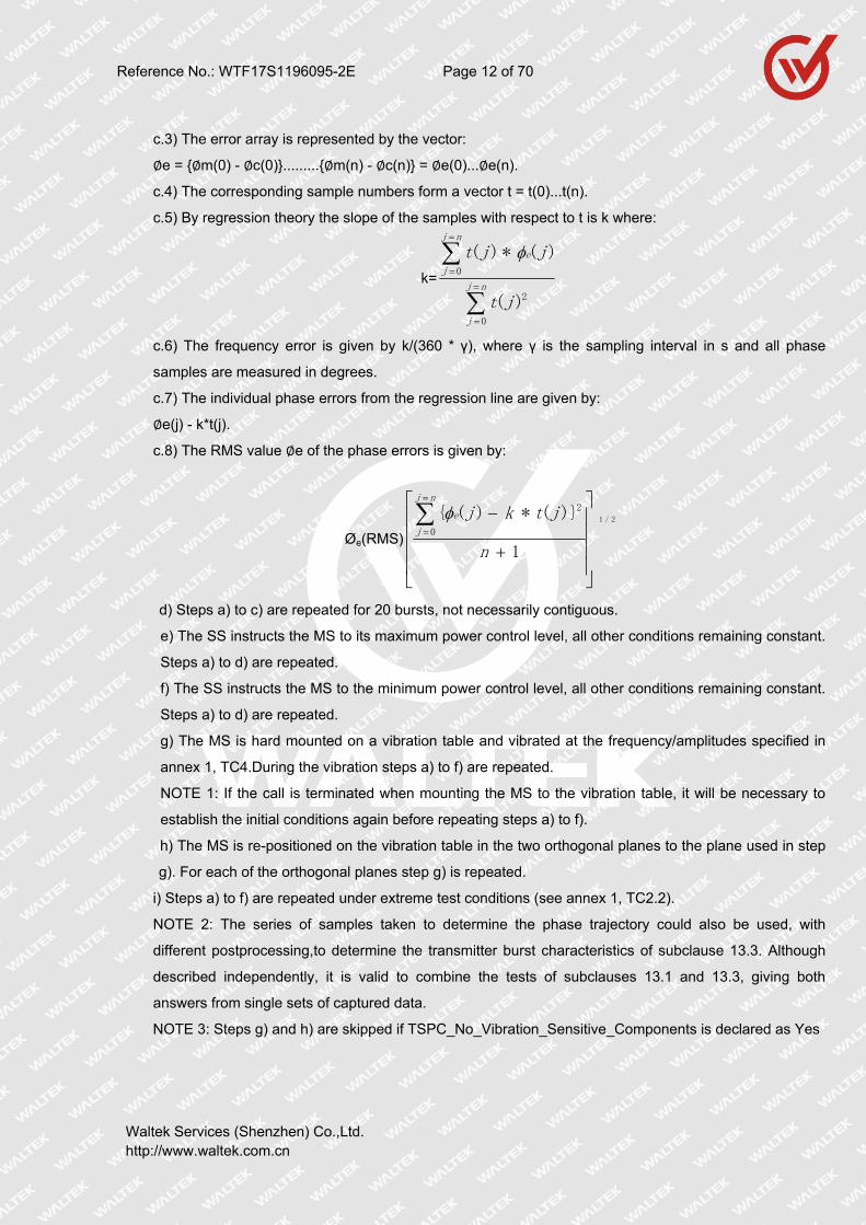
c.3) The error array is represented by the vector:
∅e = ∅m(0) - ∅c(0).........∅m(n) - ∅c(n) = ∅e(0)...∅e(n).
c.4) The corresponding sample numbers form a vector t = t(0)...t(n).
c.5) By regression theory the slope of the samples with respect to t is k where:
k=
nj
j
nj
j
e
jt
jjt
0
2
0
)(
)(*)(
c.6) The frequency error is given by k/(360 * γ), where γ is the sampling interval in s and all phase
samples are measured in degrees.
c.7) The individual phase errors from the regression line are given by:
∅e(j) - k*t(j).
c.8) The RMS value ∅e of the phase errors is given by:
Øe(RMS)
1
)(*)(0
2
n
jtkjnj
j
e 2/1
d) Steps a) to c) are repeated for 20 bursts, not necessarily contiguous.
e) The SS instructs the MS to its maximum power control level, all other conditions remaining constant.
Steps a) to d) are repeated.
f) The SS instructs the MS to the minimum power control level, all other conditions remaining constant.
Steps a) to d) are repeated.
g) The MS is hard mounted on a vibration table and vibrated at the frequency/amplitudes specified in
annex 1, TC4.During the vibration steps a) to f) are repeated.
NOTE 1: If the call is terminated when mounting the MS to the vibration table, it will be necessary to
establish the initial conditions again before repeating steps a) to f).
h) The MS is re-positioned on the vibration table in the two orthogonal planes to the plane used in step
g). For each of the orthogonal planes step g) is repeated.
i) Steps a) to f) are repeated under extreme test conditions (see annex 1, TC2.2).
NOTE 2: The series of samples taken to determine the phase trajectory could also be used, with
different postprocessing,to determine the transmitter burst characteristics of subclause 13.3. Although
described independently, it is valid to combine the tests of subclauses 13.1 and 13.3, giving both
answers from single sets of captured data.
NOTE 3: Steps g) and h) are skipped if TSPC_No_Vibration_Sensitive_Components is declared as Yes
Reference No.: WTF17S1196095-2E Page 13 of 70
Waltek Services (Shenzhen) Co.,Ltd. http://www.waltek.com.cn
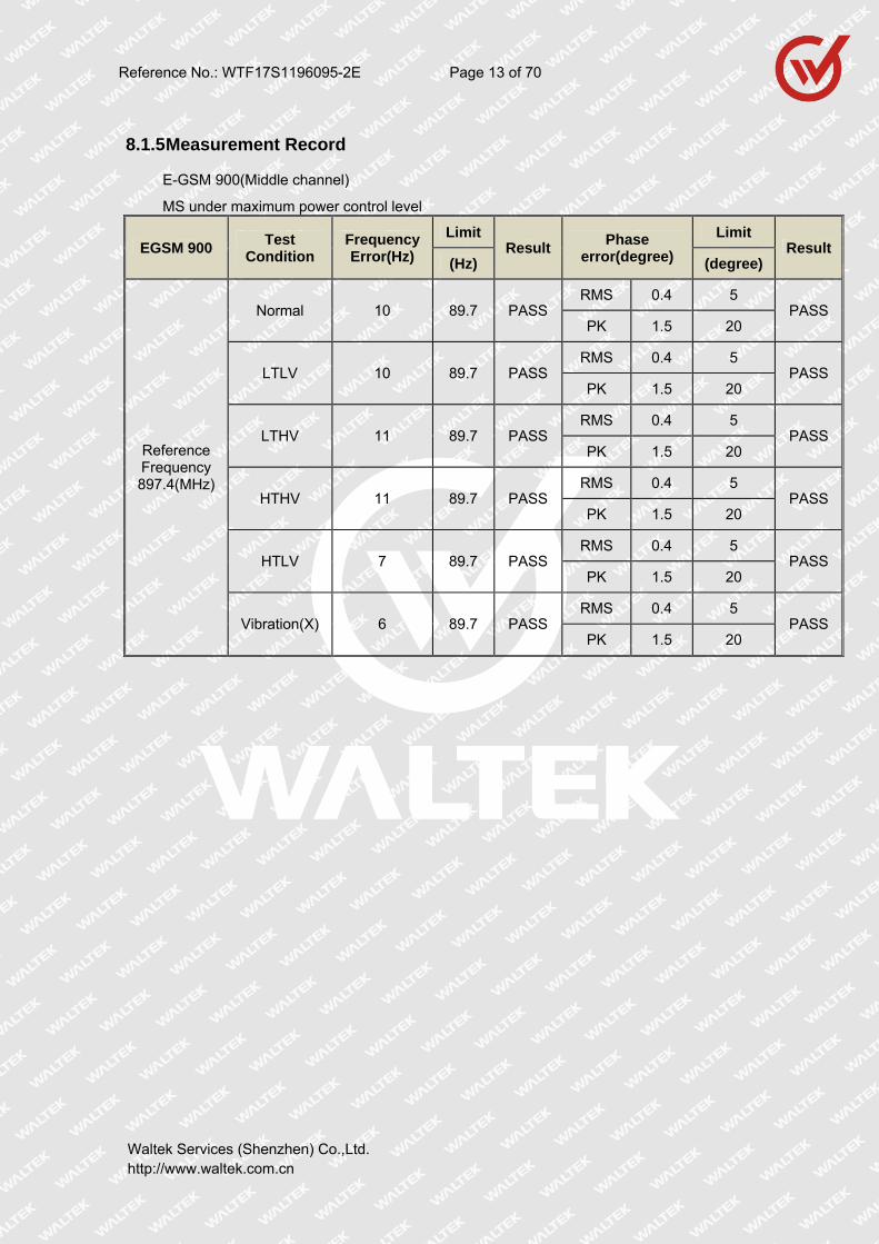
8.1.5 Measurement Record
E-GSM 900(Middle channel)
MS under maximum power control level
EGSM 900 Test
Condition Frequency Error(Hz)
LimitResult
Phase error(degree)
Limit Result
(Hz) (degree)
Reference Frequency 897.4(MHz)
Normal 10 89.7 PASS RMS 0.4 5
PASSPK 1.5 20
LTLV 10 89.7 PASS RMS 0.4 5
PASSPK 1.5 20
LTHV 11 89.7 PASS RMS 0.4 5
PASSPK 1.5 20
HTHV 11 89.7 PASS RMS 0.4 5
PASSPK 1.5 20
HTLV 7 89.7 PASS RMS 0.4 5
PASSPK 1.5 20
Vibration(X) 6 89.7 PASS RMS 0.4 5
PASSPK 1.5 20

Reference No.: WTF17S1196095-2E Page 14 of 70
Waltek Services (Shenzhen) Co.,Ltd. http://www.waltek.com.cn
DCS 1800(Middle channel)
MS under maximum power control level
DCS 1800 Test
Condition Frequency Error(Hz)
Limit Result
Phase error(degree)
Limit Result
(Hz) (degree)
Reference Frequency
1747.4 (MHz)
Normal 24 174.7 PASS RMS 0.6 5
PASSPK 3.4 20
LTLV 25 174.7 PASS RMS 0.6 5
PASSPK 3.4 20
LTHV 25 174.7 PASS RMS 0.6 5
PASSPK 3.4 20
HTHV 24 174.7 PASS RMS 0.6 5
PASSPK 3.4 20
HTLV 22 174.7 PASS RMS 0.6 5
PASSPK 3.4 20
Vibration(X) 22 174.7 PASS RMS 0.6 5
PASSPK 3.3 20
Reference No.: WTF17S1196095-2E Page 15 of 70
Waltek Services (Shenzhen) Co.,Ltd. http://www.waltek.com.cn
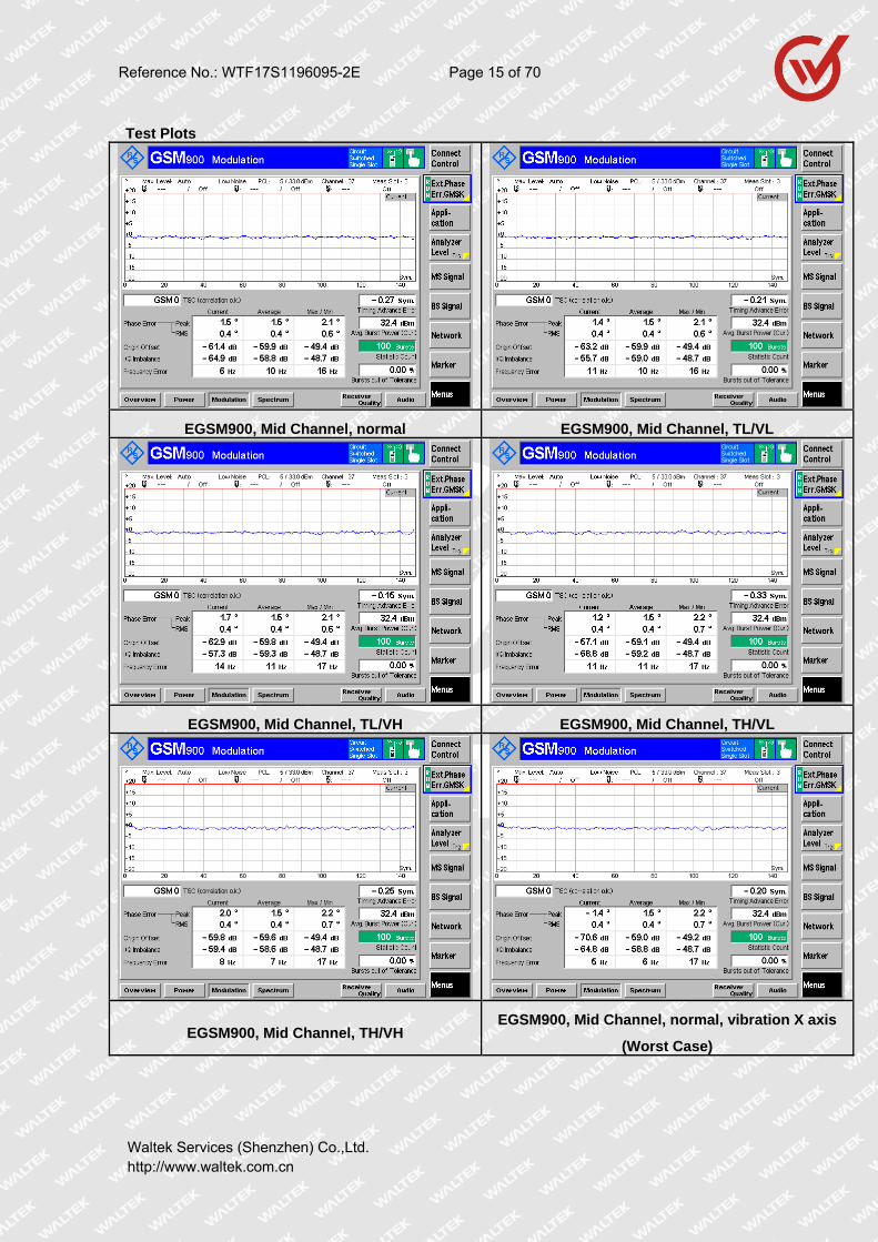
Test Plots
EGSM900, Mid Channel, normal EGSM900, Mid Channel, TL/VL
EGSM900, Mid Channel, TL/VH EGSM900, Mid Channel, TH/VL
EGSM900, Mid Channel, TH/VH EGSM900, Mid Channel, normal, vibration X axis
(Worst Case)

Reference No.: WTF17S1196095-2E Page 16 of 70
Waltek Services (Shenzhen) Co.,Ltd. http://www.waltek.com.cn
DCS1800, Mid Channel, normal DCS1800, Mid Channel, TL/VL
DCS1800, Mid Channel, TL/VH DCS1800, Mid Channel, TH/VL
DCS1800, Mid Channel, TH/VH DCS1800, Mid Channel, normal, vibration X axis
(Worst Case)

Reference No.: WTF17S1196095-2E Page 17 of 70
Waltek Services (Shenzhen) Co.,Ltd. http://www.waltek.com.cn
8.2 Transmitter – Frequency error under multipath and interference conditions
8.2.1 Definition
The frequency error under multipath and interference conditions is a measure of the ability of the MS
to maintain frequency synchronization with the received signal under conditions of Doppler shift,
multipath reception and interference.
8.2.2 Limit T-GSM 810, GSM 850 and
E-GSM 900 DCS 1 800 PCS 1 900
Propagation
condition
Permitted
frequency
error
Propagation
condition
Permitted
frequency
error
Propagation
condition
Permitted
frequency
error
RA250
HT100
TU50
TU3
±300 Hz
±180 Hz
±160 Hz
±230 Hz
RA130
HT100
TU50
TU1,5
±400 Hz
±350 Hz
±260 Hz
±320 Hz
RA130
HT100
TU50
TU1,5
±420 Hz
±370 Hz
±280 Hz
±330 Hz
8.2.3 EUT Operation Condition
The EUT was programmed to be in continuously transmitting mode.
8.2.4 Test Procedure
a) The level of the serving cell BCCH is set to 10 dB above the reference sensitivity level and the
Fading function set to RA. The SS waits 30 s for the MS to stabilize to these conditions. The SS is set
up to capture the first burst transmitted by the MS during call establishment. A call is initiated by the
SS on a channel in the mid ARFCN range as described for the generic call set up procedure but to a
TCH at level 10 dB above the reference sensitivity level and fading function set to RA.
b) The SS calculates the frequency accuracy of the captured burst as described in test 13.1.
c) The SS sets the serving cell BCCH and TCH to the reference sensitivity level applicable to the type
of MS, still with the fading function set to RA and then waits 30 s for the MS to stabilize to these
conditions.
d) The SS shall capture subsequent bursts from the traffic channel in the manner described in test
13.1.
NOTE: Due to the very low signal level at the MS receiver input the MS receiver is liable to error.
The "looped back" bits are therefore also liable to error, and hence the SS does not know the
expected bit sequence. The SS will have to demodulate the received signal to derive (error free) the
transmitter burst bit pattern. Using this bit pattern the SS can calculate the expected phase trajectory
according to the definition within 3GPP TS 05.04.

Reference No.: WTF17S1196095-2E Page 18 of 70
Waltek Services (Shenzhen) Co.,Ltd. http://www.waltek.com.cn
e) The SS calculates the frequency accuracy of the captured burst as described in test 13.1.
f) Steps d) and e) are repeated for 5 traffic channel bursts spaced over a period of not less than 20 s.
g) The initial conditions are established again and steps a) to f) are repeated but with the fading
function set to HT100 (HT200 for GSM 400, HT120 for GSM 700).
h) The initial conditions are established again and steps a) to f) are repeated but with the fading
function set toTU50 (TU100 for GSM 400, TU 60 for GSM 700).
i) The initial conditions are established again and steps a) and b) are repeated but with the following
differences:
- the levels of the BCCH and TCH are set to 18 dB above reference sensitivity level.
- two further independent interfering signals are sent on the same nominal carrier frequency as the
BCCH
- and TCH and at a level 10 dB below the level of the TCH and modulated with random data,
including the mid amble.
- the fading function for all channels is set to TUlow.
j) The SS waits 100 s for the MS to stabilize to these conditions.
k) Repeat steps d) to f), except that at step f) the measurement period must be extended to 200 s and
the number of measurements increased to 20.
l) The initial conditions are established again and steps a) to k) are repeated for ARFCN in the Low
ARFCN range.
m) The initial conditions are established again and steps a) to k) are repeated for ARFCN in the High
ARFCN range.
n) Repeat step h) under extreme test conditions
Reference No.: WTF17S1196095-2E Page 19 of 70
Waltek Services (Shenzhen) Co.,Ltd. http://www.waltek.com.cn
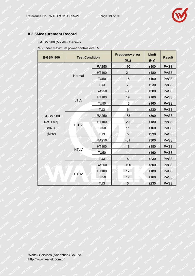
8.2.5 Measurement Record
E-GSM 900 (Middle Channel)
MS under maximum power control level: 5
E-GSM 900 Test Condition Frequency error
(Hz)
Limit
(Hz) Result
E-GSM 900
Ref. Freq.
897.4
(MHz)
Normal
RA250 -80 ±300 PASS
HT100 21 ±180 PASS
TU50 15 ±160 PASS
TU3 7 ±230 PASS
LTLV
RA250 -86 ±300 PASS
HT100 19 ±180 PASS
TU50 13 ±160 PASS
TU3 6 ±230 PASS
LTHV
RA250 -88 ±300 PASS
HT100 20 ±180 PASS
TU50 11 ±160 PASS
TU3 5 ±230 PASS
HTLV
RA250 -81 ±300 PASS
HT100 18 ±180 PASS
TU50 11 ±160 PASS
TU3 5 ±230 PASS
HTHV
RA250 -100 ±300 PASS
HT100 17 ±180 PASS
TU50 12 ±160 PASS
TU3 5 ±230 PASS
Reference No.: WTF17S1196095-2E Page 20 of 70
Waltek Services (Shenzhen) Co.,Ltd. http://www.waltek.com.cn
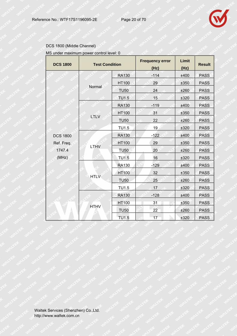
DCS 1800 (Middle Channel)
MS under maximum power control level: 0
DCS 1800 Test Condition Frequency error
(Hz)
Limit
(Hz) Result
DCS 1800
Ref. Freq.
1747.4
(MHz)
Normal
RA130 -114 ±400 PASS
HT100 29 ±350 PASS
TU50 24 ±260 PASS
TU1.5 15 ±320 PASS
LTLV
RA130 -119 ±400 PASS
HT100 31 ±350 PASS
TU50 22 ±260 PASS
TU1.5 19 ±320 PASS
LTHV
RA130 -122 ±400 PASS
HT100 29 ±350 PASS
TU50 20 ±260 PASS
TU1.5 16 ±320 PASS
HTLV
RA130 -129 ±400 PASS
HT100 32 ±350 PASS
TU50 25 ±260 PASS
TU1.5 17 ±320 PASS
HTHV
RA130 -128 ±400 PASS
HT100 31 ±350 PASS
TU50 22 ±260 PASS
TU1.5 17 ±320 PASS

Reference No.: WTF17S1196095-2E Page 21 of 70
Waltek Services (Shenzhen) Co.,Ltd. http://www.waltek.com.cn
8.3 Frequency error and phase error in GPRS multislot configuration
8.3.1 Definition: The frequency error is the difference in frequency, after adjustment for the effect of the modulation and
phase error, between the RF transmission from the MS and either: - the RF transmission from the BS; or
- the nominal frequency for the ARFCN used. The phase error is the difference in phase, after adjustment for the effect of the frequency error, between the RF transmission from the MS and the theoretical transmission according to the intended
modulation.
8.3.2 Limit: For all measured bursts, the frequency error, derived in step c.6), shall be less than 10E-7. For all measured bursts, the RMS phase error, derived in step c.8), shall not exceed 5 degrees.
For all measured bursts, each individual phase error, derived in step c.7), shall not exceed 20 degrees.
8.3.3 EUT Operation Condition:
The EUT was programmed to be in continuously transmitting mode.
8.3.4 Test Procedure: a) For one transmitted burst on the last slot of the multislot configuration, the SS captures the signal
as a series of phase samples over the period of the burst. These samples are evenly distributed over
the duration of the burst with a minimum sampling rate of 2/T, where T is the modulation symbol period. The received phase trajectory is then represented by this array of at least 294 samples. b) The SS then calculates, from the known bit pattern and the formal definition of the modulator
contained in 3GPP TS 05.04, the expected phase trajectory. c) From a) and b) the phase trajectory error is calculated, and a linear regression line computed through this phase trajectory error. The slope of this regression line is the frequency error of the
mobile transmitter relative to the simulator reference. The difference between the regression line and the individual sample points is the phase error of that point. c.1) The sampled array of at least 294 phase measurements is represented by the vector:
∅m = ∅m(0)...∅m(n) where the number of samples in the array n+1 ≥ 294. c.2) The calculated array, at the corresponding sampling instants, is represented by the vector:
∅c = ∅c(0)...∅c(n). c.3) The error array is represented by the vector: ∅e = ∅m(0) - ∅c(0).........∅m(n) - ∅c(n) = ∅e(0)...∅e(n).
c.4) The corresponding sample numbers form a vector t = t(0)...t(n). c.5) By regression theory the slope of the samples with respect to t is k where:
k=
nj
nj
nj
j
e
jt
jjt
2
0
)(
)(*)(

Reference No.: WTF17S1196095-2E Page 22 of 70
Waltek Services (Shenzhen) Co.,Ltd. http://www.waltek.com.cn
c.6) The frequency error is given by k/(360 * g), where g is the sampling interval in s and all phase samples are measured in degrees. c.7) The individual phase errors from the regression line are given by:
∅e(j) - k*t(j). c.8) The RMS value ∅e of the phase errors is given by:
Øe(RMS)
1
)(*)(0
2
n
jtkjnj
j
e 2/1
d) Steps a) to c) are repeated for 20 bursts, not necessarily contiguous.
e) The SS instructs the MS to its maximum power control level by setting the power control parameter ALPHA (α) to 0 and GAMMA_TN (ΓCH) for each timeslot to the desired power level in the Packet Uplink Assignment message (Closed Loop Control, see 3GPP TS 05.08, clause B.2), all other
conditions remaining constant. Steps a) to d) are repeated. f) The SS instructs the MS to the minimum power control level, all other conditions remaining constant.
Steps a) to
d) are repeated. g) The MS is hard mounted on a vibration table and vibrated at the frequency/amplitudes specified in
annex 1, TC4.
During the vibration steps a) to f) are repeated. NOTE 1: If the call is terminated when mounting the MS to the vibration table, it will be necessary to
establish the
initial conditions again before repeating steps a) to f). h) The MS is re-positioned on the vibration table in the two orthogonal planes to the plane used in step
g). For each
of the orthogonal planes step g) is repeated. i) Steps a) to f) are repeated under extreme test conditions (see annex 1, TC2.2). NOTE 2: Steps g) and h) are skipped if TSPC_No_Vibration_Sensitive_Components is declared as
Yes

Reference No.: WTF17S1196095-2E Page 23 of 70
Waltek Services (Shenzhen) Co.,Ltd. http://www.waltek.com.cn
8.3.5 Measurement Record
E-GSM 900(Middle channel)
MS under maximum level
EGSM 900 (GPRS)
Test Condition
Frequency Error(Hz)
LimitResult
Phase error(degree)
Limit Result
(Hz) (degree)
Reference Frequency 897.4(MHz)
Normal 2 89.7 PASS RMS 0.4 5
PASSPK 1.5 20
LTLV 2 89.7 PASS RMS 0.5 5
PASSPK 1.5 20
LTHV 5 89.7 PASS RMS 0.4 5
PASSPK 1.5 20
HTHV 7 89.7 PASS RMS 0.4 5
PASSPK 1.5 20
HTLV 8 89.7 PASS RMS 0.4 5
PASSPK 1.4 20
Vibration(X) 8 89.7 PASS RMS 0.4 5
PASSPK 1.5 20
Reference No.: WTF17S1196095-2E Page 24 of 70
Waltek Services (Shenzhen) Co.,Ltd. http://www.waltek.com.cn
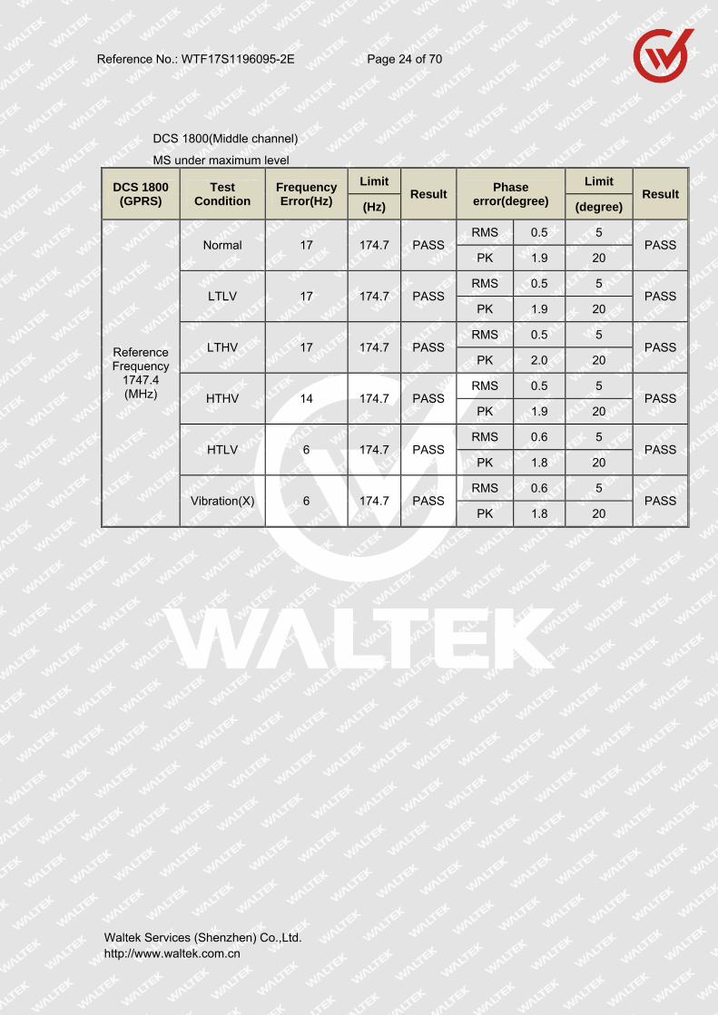
DCS 1800(Middle channel)
MS under maximum level
DCS 1800 (GPRS)
Test Condition
Frequency Error(Hz)
Limit Result
Phase error(degree)
Limit Result
(Hz) (degree)
Reference Frequency
1747.4 (MHz)
Normal 17 174.7 PASS RMS 0.5 5
PASSPK 1.9 20
LTLV 17 174.7 PASS RMS 0.5 5
PASSPK 1.9 20
LTHV 17 174.7 PASS RMS 0.5 5
PASSPK 2.0 20
HTHV 14 174.7 PASS RMS 0.5 5
PASSPK 1.9 20
HTLV 6 174.7 PASS RMS 0.6 5
PASSPK 1.8 20
Vibration(X) 6 174.7 PASS RMS 0.6 5
PASSPK 1.8 20

Reference No.: WTF17S1196095-2E Page 25 of 70
Waltek Services (Shenzhen) Co.,Ltd. http://www.waltek.com.cn
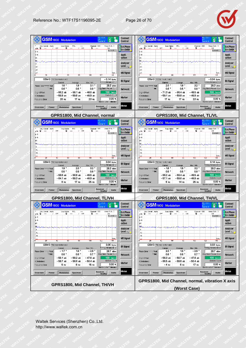
Test Plots
GPRS900, Mid Channel, normal GPRS900, Mid Channel, TL/VL
GPRS900, Mid Channel, TL/VH GPRS900, Mid Channel, TH/VL
GPRS900, Mid Channel, TH/VH GPRS900, Mid Channel, normal, vibration X axis
(Worst Case)
Reference No.: WTF17S1196095-2E Page 26 of 70
Waltek Services (Shenzhen) Co.,Ltd. http://www.waltek.com.cn
GPRS1800, Mid Channel, normal GPRS1800, Mid Channel, TL/VL
GPRS1800, Mid Channel, TL/VH GPRS1800, Mid Channel, TH/VL
GPRS1800, Mid Channel, TH/VH GPRS1800, Mid Channel, normal, vibration X axis
(Worst Case)
Reference No.: WTF17S1196095-2E Page 27 of 70
Waltek Services (Shenzhen) Co.,Ltd. http://www.waltek.com.cn
8.4 Transmitter output power and burst timing
8.4.1 Definition The transmitter output power is the average value of the power delivered to an artificial antenna or radiated by the MS and its integral antenna, over the time that the useful information bits of one burst are transmitted.
The transmit burst timing is the envelope of the RF power transmitted with respect to time. The timings are referenced to the transition from bit 13 to bit 14 of the Training Sequence ("midamble") before differential decoding. The timing of the modulation is referenced to the timing of the received signal
from the SS.
8.4.2 Limit 1. The MS maximum output power shall be as defined in 3GPP TS 05.05, sub clause 4.1.1, table for
GMSK modulation, according to its power class, with a tolerance of ±2 dB under normal conditions;
3GPP TS 05.05, sub clause 4.1.1, table for GMSK modulation. 2. The MS maximum output power shall be as defined in 3GPP TS 05.05, sub clause 4.1.1, table for
GMSK modulation, according to its power class, with a tolerance of ±2,5 dB under extreme
conditions; 3GPP TS 05.05, sub clause 4.1.1, table for GMSK modulation; 3GPP TS 05.05 annex D in subclasses D.2.1 and D.2.2.
3. The power control levels shall have the nominal output power levels as defined in 3GPP TS 05.05,
sub clause 4.1.1, from the lowest power control level up to the maximum output power corresponding to the class of the MS (for tolerance on maximum output power see conformance requirements 1), with a tolerance of ±3 dB, ±4 dB or ±5 dB under normal conditions; 3GPP TS
05.05, sub clause 4.1.1. 4. The power control levels shall have the nominal output power levels as defined in 3GPP TS 05.05,
4.1.1,from the lowest power control level up to the maximum output power corresponding to the
class of the MS(for tolerance on maximum output power see conformance requirements 2), with a tolerance of ±4 dB, ±5dB or ±6 dB under extreme conditions; 3GPP TS 05.05, sub clause 4.1.1; 3GPP TS 05.05 annex D subclasses D.2.1and D.2.2.
5. The output power actually transmitted by the MS at consecutive power control levels shall form a monotonic sequence and the interval between power control levels shall be 2 ± 1,5 dB (1 ± 1dB between power control level 30 and 31 for PCS 1 900); 3GPP TS 05.05, sub clause 4.1.1.
6. The transmitted power level relative to time for a normal burst shall be within the power/time template given in 3GPP TS 05.05, annex B in figure B.1:
6.1 Under normal conditions; 3GPP TS 05.05, sub clause 4.5.2.
6.2 Under extreme conditions; 3GPP TS 05.05, sub clause 4.5.2, 3GPP TS 05.05 annex D in sub clauses D.2.1 and D.2.2.
7. When accessing a cell on the RACH and before receiving the first power command during a
communication on a DCCH or TCH (after an IMMEDIATE ASSIGNMENT), all GSM, class 1 and class 2 DCS 1 800 and PCS 1 900 MS shall use the power control level defined by the MS_TXPWR_MAX_CCH parameter broadcast on the BCCH of the cell, or if
MS_TXPWR_MAX_CCH corresponds to a power control level not supported by the MS as defined by its power class, the MS shall act as though the closest supported power control level had been broadcast. A Class 3 DCS 1 800 MS shall use the POWER_OFFSET parameter.
8. The transmissions from the MS to the BS, measured at the MS antenna, shall be 468,75 - TA bit periods behind the transmissions received from the BS, where TA is the last timing advance received from the current serving BS. The tolerance on these timings shall be ±1 bit period:
8.1 Under normal conditions; 3GPP TS 05.10, sub clause 6.4.

Reference No.: WTF17S1196095-2E Page 28 of 70
Waltek Services (Shenzhen) Co.,Ltd. http://www.waltek.com.cn
8.2 Under extreme conditions; 3GPP TS 05.10, sub clause 6.4, 3GPP TS 05.05 annex D in sub clauses D.2.1 and D.2.2.
9. The transmitted power level relative to time for a random access burst shall be within the
power/time template given in 3GPP TS 05.05, annex B in figure B.3: 9.1 Under normal conditions; 3GPP TS 05.05, sub clause 4.5.2. 9.2 Under extreme conditions; 3GPP TS 05.05, sub clause 4.5.2, 3GPP TS 05.05 annex D in sub
clause D.2.1 and D.2.2. 10. The MS shall use a TA value of 0 for the Random Access burst sent:
10.1 Under normal conditions; 3GPP TS 05.10, sub clause 6.6.
10.2 Under extreme conditions; 3GPP TS 05.10, sub clause 6.6, 3GPP TS 05.05 annex D in sub clause D.2.1 and D.2.2.
8.4.3 EUT Operation Condition
The EUT was programmed to be in continuously transmitting mode.
8.4.4 Test Procedure
a) Measurement of normal burst transmitter output power.
-The SS takes power measurement samples evenly distributed over the duration of one burst with a
sampling rate of at least 2/T, where T is the bit duration. The samples are identified in time with
respect to the modulation on the burst. The SS identifies the centre of the useful 147 transmitted
bits, i.e. the transition from bit 13 to bit 14 of the mid amble, as the timing reference.
- The transmitter output power is calculated as the average of the samples over the 147 useful bits.
This is also used as the 0 dB reference for the power/time template.
b) Measurement of normal burst timing delay.
- The burst timing delay is the difference in time between the timing reference identified in a) and
the corresponding transition in the burst received by the MS immediately prior to the MS transmit
burst sampled.
c) Measurement of normal burst power/time relationship.
- The array of power samples measured in a) are referenced in time to the centre of the useful
transmitted bits and in power to the 0 dB reference, both identified in a).
d) Steps a) to c) are repeated with the MS commanded to operate on each of the power control levels
defined, even those not supported by the MS.
e) The SS commands the MS to the maximum power control level supported by the MS and steps a)
to c)are repeated for ARFCN in the Low and High ranges.
f) Measurement of access burst transmitter output power.
- The SS causes the MS to generate an Access Burst on an ARFCN in the Mid ARFCN range, this
could be either by a handover procedure or a new request for radio resource. In the case of a
handover procedure the Power Level indicated in the HANDOVER COMMAND message is the
maximum power control level supported by the MS. In the case of an Access Burst the MS shall
use the Power Level indicated in the MS_TXPWR_MAX_CCH parameter. If the power class of
Reference No.: WTF17S1196095-2E Page 29 of 70
Waltek Services (Shenzhen) Co.,Ltd. http://www.waltek.com.cn
the MS is DCS 1 800 Class 3, the MS shall also use the POWER_OFFSET parameter.
- The SS takes power measurement samples evenly distributed over the duration of the access
burst as described in a). However, in this case the SS identifies the centre of the useful bits of the
burst by identifying the transition from the last bit of the synch sequence. The centre of the burst is
then five data bits prior to this point and is used as the timing reference.
- The transmitter output power is calculated as the average of the samples over the 87 useful bits of
the burst. This is also used as the 0 dB reference for the power/time template.
g) Measurement of access burst timing delay.
- The burst timing delay is the difference in time between the timing reference identified in f) and
the MS received data on the common control channel.
h) Measurement of access burst power/time relationship.
- The array of power samples measured in f) are referenced in time to the centre of the useful
transmitted bits and in power to the 0 dB reference, both identified in f).
HANDOVER COMMAND with power control level set to 10 or it changes the System Information
elements MS_TXPWR_MAX_CCH and for DCS 1 800 the POWER_OFFSET on the serving cell
BCCH in order to limit the MS transmit power on the Access Burst to power control level 10 (+23 dBm
for GSM 400, GSM 700, GSM 850, and GSM 900 or +10 dBm for DCS 1 800 and PCS 1 900) and
then steps f) to h) are repeated.
j) Steps a) to i) are repeated under extreme test conditions (annex 1, TC2.2) except that the repeats at
step d) are only performed for power control level 10 and the minimum power control level of the MS.
Reference No.: WTF17S1196095-2E Page 30 of 70
Waltek Services (Shenzhen) Co.,Ltd. http://www.waltek.com.cn
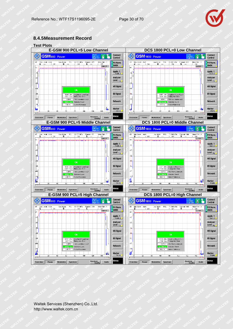
8.4.5 Measurement Record
Test Plots E-GSM 900 PCL=5 Low Channel DCS 1800 PCL=0 Low Channel
E-GSM 900 PCL=5 Middle Channel DCS 1800 PCL=0 Middle Channel
E-GSM 900 PCL=5 High Channel DCS 1800 PCL=0 High Channel
Reference No.: WTF17S1196095-2E Page 31 of 70
Waltek Services (Shenzhen) Co.,Ltd. http://www.waltek.com.cn
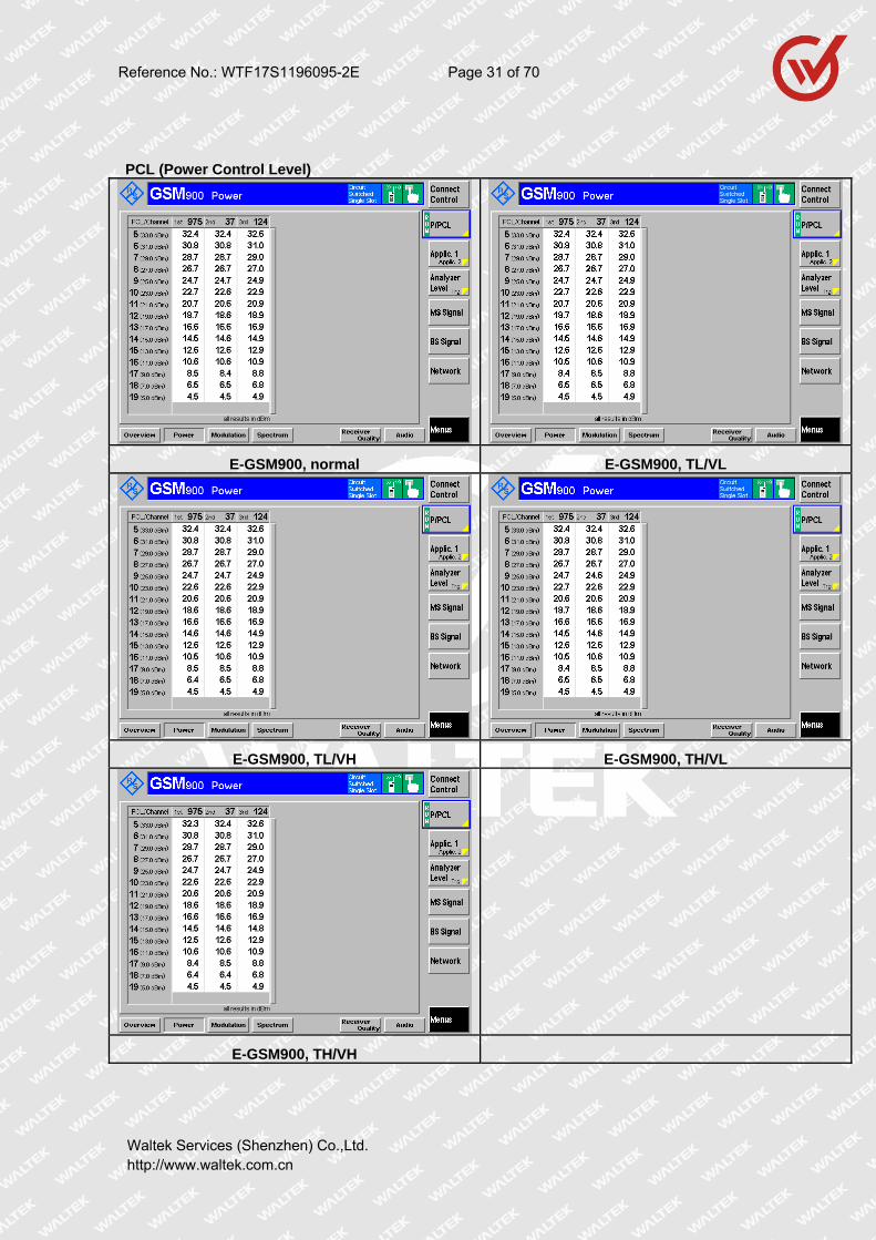
PCL (Power Control Level)
E-GSM900, normal E-GSM900, TL/VL
E-GSM900, TL/VH E-GSM900, TH/VL
E-GSM900, TH/VH
Reference No.: WTF17S1196095-2E Page 32 of 70
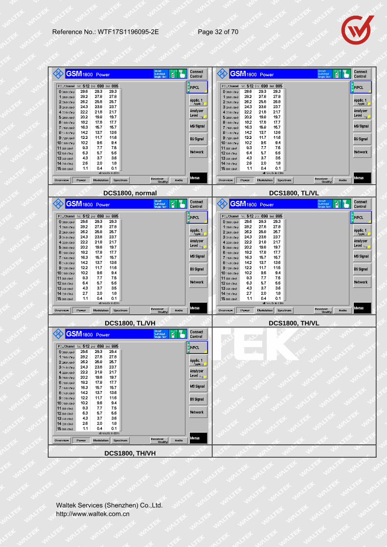
Waltek Services (Shenzhen) Co.,Ltd. http://www.waltek.com.cn
DCS1800, normal DCS1800, TL/VL
DCS1800, TL/VH DCS1800, TH/VL
DCS1800, TH/VH

Reference No.: WTF17S1196095-2E Page 33 of 70
Waltek Services (Shenzhen) Co.,Ltd. http://www.waltek.com.cn
8.5 Transmitter – output RF spectrum
8.5.1 Definition
The output RF spectrum is the relationship between the frequency offset from the carrier and the
power, measured in a specified bandwidth and time, produced by the MS due to the effects of
modulation and power ramping.
8.5.2 Limit The level of the output RF spectrum due to modulation shall be no more than that given in ETSI TS 151 010-1 V7.11.0 (2008-10),sub clause 13.4.5, table Table 13-6) GSM 400, GSM 700, T-GSM 810, GSM 850 and GSM 900 Spectrum due to modulation out to less than 1800 kHz offset, Table 13-7)
DCS 1800 Spectrum due to modulation out to less than 1800 kHz offset, Table 13-9) Spectrum due to modulation from 1800 kHz offset to the edge of the transmit band (wideband noise), Table 13-10) Spurious emissions in the MS receive bands.
For GSM 400, T-GSM 810, GSM 900 and DCS 1800 MS the spurious emissions in the bands 850 MHz to 866 MHz, 925 MHz to 935 MHz, 935 MHz to 960 MHz and 1805 MHz to 1880 MHz, measured in step d),shall not exceed the values shown in table 13-10 except in up to five measurements in the
band 925 MHz to 960 MHz and five measurements in the band 1805 MHz to 1880 MHz where a level up to -36 dBm is permitted. For GSM 400 MS, in addition, the MS spurious emissions in the bands 460, 4 MHz to 467,6MHz and 488,8 MHz to 496 MHz shall not exceed the value of -67 dBm, except in up to
three measurements in each of the bands 460,4 MHz to 467,6 MHz and 488,8 MHz to 496 MHz where a level up to -36 dBm is permitted. For GSM 700, GSM 850 and PCS 1 900 MS the spurious emissions in the bands 698 MHz to 716 MHz, 747 MHz to 762 MHz, 869 MHz to 894 MHz and 1930
MHz to 1990 MHz shall not exceed the values shown in table 13-10 except in up to five measurements in each of the bands 698 MHz to 716 MHz, 747 MHz to 762 MHz, 869 MHz to 894 MHz and 1930 MHz to 1990 MHz where a level up to -36 dBm is permitted.
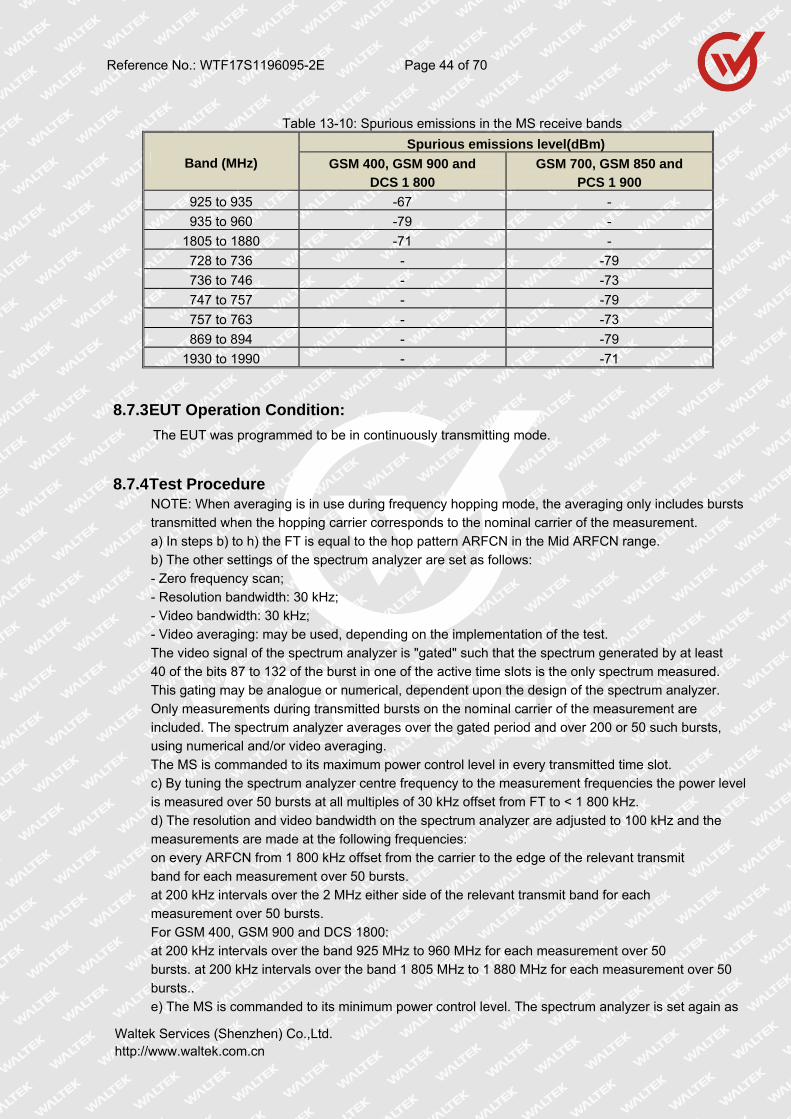
Table 13-10: Spurious emissions in the MS receive bands
Band (MHz) Spurious emissions level(dBm)
- GSM 400, T-GSM 810, GSM
900 and DCS 1 800
GSM 700, GSM 850 and PCS 1
900
460.4 – 467.6 (GSM 400 MS only)
-67 -
488.8 - 496 (GSM 400 MS only)
-67 -
850 to 866
(T-GSM 810 MS only) -79 -
925 to 935 -67 -
935 to 960 -79 -
1 805 to 1 880 -71 -
728 to 736 - -73
736 to 746 - -79
747 to 757 - -79
757 to 763 - -73
869 to 894 - --79
1 930 to 1 990 - -71
Reference No.: WTF17S1196095-2E Page 34 of 70
Waltek Services (Shenzhen) Co.,Ltd. http://www.waltek.com.cn
8.5.3 EUT Operation Condition:
The EUT was programmed to be in continuously transmitting mode.
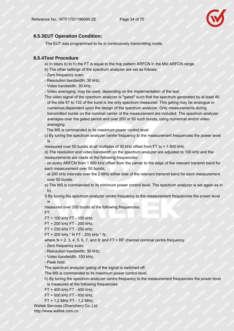
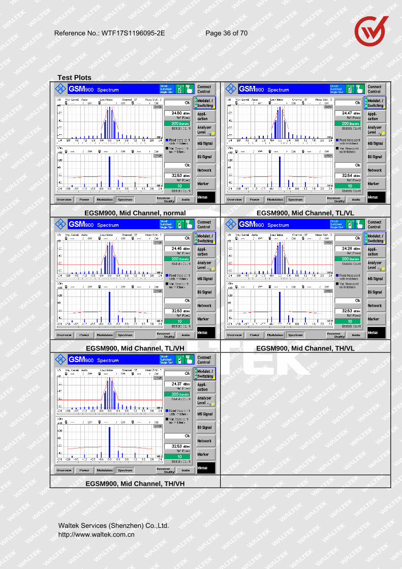
8.5.4 Test Procedure a) In steps b) to h) the FT is equal to the hop pattern ARFCN in the Mid ARFCN range. b) The other settings of the spectrum analyzer are set as follows: - Zero frequency scan;
- Resolution bandwidth: 30 kHz; - Video bandwidth: 30 kHz; - Video averaging: may be used, depending on the implementation of the test.
The video signal of the spectrum analyzer is "gated" such that the spectrum generated by at least 40 of the bits 87 to 132 of the burst is the only spectrum measured. This gating may be analogue or numerical,dependent upon the design of the spectrum analyzer. Only measurements during
transmitted bursts on the nominal carrier of the measurement are included. The spectrum analyzer averages over the gated period and over 200 or 50 such bursts, using numerical and/or video averaging.
The MS is commanded to its maximum power control level. c) By tuning the spectrum analyzer centre frequency to the measurement frequencies the power level
is
measured over 50 bursts at all multiples of 30 kHz offset from FT to < 1 800 kHz. d) The resolution and video bandwidth on the spectrum analyzer are adjusted to 100 kHz and the measurements are made at the following frequencies:
- on every ARFCN from 1 800 kHz offset from the carrier to the edge of the relevant transmit band for each measurement over 50 bursts; - at 200 kHz intervals over the 2 MHz either side of the relevant transmit band for each measurement
over 50 bursts. e) The MS is commanded to its minimum power control level. The spectrum analyzer is set again as in
b).
f) By tuning the spectrum analyzer centre frequency to the measurement frequencies the power level is
measured over 200 bursts at the following frequencies:
FT; FT + 100 kHz FT - 100 kHz; FT + 200 kHz FT - 200 kHz;
FT + 250 kHz FT - 250 kHz; FT + 200 kHz * N FT - 200 kHz * N; where N = 2, 3, 4, 5, 6, 7, and 8; and FT = RF channel nominal centre frequency.
- Zero frequency scan; - Resolution bandwidth: 30 kHz; - Video bandwidth: 100 kHz;
- Peak hold. The spectrum analyzer gating of the signal is switched off. The MS is commanded to its maximum power control level.
h) By tuning the spectrum analyzer centre frequency to the measurement frequencies the power level is measured at the following frequencies:
FT + 400 kHz FT - 400 kHz;
FT + 600 kHz FT - 600 kHz; FT + 1,2 MHz FT - 1,2 MHz;

Reference No.: WTF17S1196095-2E Page 35 of 70
Waltek Services (Shenzhen) Co.,Ltd. http://www.waltek.com.cn
FT + 1,8 MHz FT - 1,8 MHz; where FT = RF channel nominal centre frequency. The duration of each measurement (at each frequency) will be such as to cover at least 10 burst
transmissions at FT. i) Step h) is repeated for power control levels 7 and 11. j) Steps b), f), g) and h) are repeated with FT equal to the hop pattern ARFCN in the Low ARFCN
range except that in step g) the MS is commanded to power control level 11 rather than maximum power. k) Steps b), f), g) and h) are repeated with FT equal to the hop pattern ARFCN in the High ARFCN
range except that in step g) the MS is commanded to power control level 11 rather than maximum power.
l) Steps a) b) f) g) and h) are repeated under extreme test conditions (annex 1, TC2.2). except that at
step g) the MS is commanded to power control level 11.
8.5.5 Measurement Record
Mode Test Frequency(MHz) Test Condition Result
E-GSM900 880.2 Normal LTLV LTHV HTLV HTHV PASS
897.4 Normal LTLV LTHV HTLV HTHV PASS
914.8 Normal LTLV LTHV HTLV HTHV PASS
DCS 1800 1710.2 Normal LTLV LTHV HTLV HTHV PASS
1747.4 Normal LTLV LTHV HTLV HTHV PASS
1784.8 Normal LTLV LTHV HTLV HTHV PASS
Reference No.: WTF17S1196095-2E Page 36 of 70
Waltek Services (Shenzhen) Co.,Ltd. http://www.waltek.com.cn
Test Plots
EGSM900, Mid Channel, normal EGSM900, Mid Channel, TL/VL
EGSM900, Mid Channel, TL/VH EGSM900, Mid Channel, TH/VL
EGSM900, Mid Channel, TH/VH
Reference No.: WTF17S1196095-2E Page 37 of 70
Waltek Services (Shenzhen) Co.,Ltd. http://www.waltek.com.cn
DCS1800, Mid Channel, normal DCS1800, Mid Channel, TL/VL
DCS1800, Mid Channel, TL/VH DCS1800, Mid Channel, TH/VL
DCS1800, Mid Channel, TH/VH

Reference No.: WTF17S1196095-2E Page 38 of 70
Waltek Services (Shenzhen) Co.,Ltd. http://www.waltek.com.cn
Spurious Emissions in the MS receive bands:
For EGSM900 Band (Middle channel)
Frequency
range Level
(MHz)
Frequency
(MHz)
Level (dBm) Test
ResultNormal LTLV LTHV HTHV HTLV
925-935 927.54 -79.98 -80.95 -80.28 -79.84 -80.59 PASS
935-960 939.57 -80.63 -81.49 -80.21 -82.82 -83.52 PASS
945.13 -80.68 -81.05 -80.74 -81.90 -81.49 PASS
For DCS1800 Band (Middle channel)
Frequency
range Level
(MHz)
Frequency
(MHz)
Level (dBm) Test
ResultNormal LTLV LTHV HTHV HTLV
1805-1880
1806.47 -73.38 -73.13 -74.19 -73.71 -73.45 PASS
1810.47 -74.23 -73.55 -73.50 -73.04 -74.28 PASS
1855.24 -73.46 -74.80 -74.35 -74.72 -74.59 PASS
1871.49 -73.66 -73.70 -74.75 -73.27 -74.45 PASS
Reference No.: WTF17S1196095-2E Page 39 of 70
Waltek Services (Shenzhen) Co.,Ltd. http://www.waltek.com.cn
8.6 Transmitter output power in GPRS multislot configuration
8.6.1 Definition
The transmitter output power is the average value of the power delivered to an artificial antenna or
radiated by the MS and its integral antenna, over the time that the useful information bits of one burst
are transmitted.
8.6.2 Limit
1. The MS maximum output power shall be as defined in 3GPP TS 05.05, subclause 4.1.1, first table,
according to its power class, with a tolerance of ±2 dB under normal conditions; 3GPP TS 05.05,
subclause 4.1.1, first table.
2. The MS maximum output power shall be as defined in 3GPP TS 05.05, subclause 4.1.1, first table,
according to its power class, with a tolerance of ±2,5 dB under extreme conditions; 3GPP TS
05.05, subclause 4.1.1, first table; 3GPP TS 05.05 annex D subclauses D.2.1 and D.2.2.
3. The power control levels shall have the nominal output power levels as defined in 3GPP TS 05.05,
subclause 4.1.1, third table (for GSM 400, GSM 700, GSM 850 and GSM 900), fourth table (for
DCS 1 800) or fifth table (for PCS 1 900), from the lowest power control level up to the maximum
output power corresponding to the class of the MS (for tolerance on maximum output power see
conformance requirements 1), with a tolerance of ±3 dB, ±4 dB or ±5 dB under normal conditions;
3GPP TS 05.05, subclause 4.1.1, third, fourth or fifth table.
4. The power control levels shall have the nominal output power levels as defined in 3GPP TS 05.05,
Subclause 4.1.1, third table (for GSM 400, GSM 700, GSM 850 and GSM 900), fourth table (for
DCS 1 800) or fifth table (for PCS 1 900), from the lowest power control level up to the maximum
output power corresponding to the class of the MS (for tolerance on maximum output power see
conformance requirements 2), with a tolerance of ±4 dB, ±5 dB or ±6 dB under extreme
conditions; 3GPP TS 05.05, subclause 4.1.1, third, fourth or fifth table; 3GPP TS 05.05 annex D
subclauses D.2.1 and D.2.2.
5. The output power actually transmitted by the MS at consecutive power control levels shall form a
monotonic sequence and the interval between power control levels shall be 2 ± 1,5 dB (1 ± 1dB
between power control level 30 and 31 for PCS 1 900); 3GPP TS 05.05, subclause 4.1.1.
6. The transmitted power level relative to time for a normal burst shall be within the power/time
template given in 3GPP TS 05.05, annex B figure B1. In multislot configurations where the bursts
in two or more consecutive time slots are actually transmitted at the same frequency the template
of annex B shall respected during the useful part of each burst and at the beginning and the end of
the series of consecutive bursts. The output power during the guard period between every two
consecutive active timeslots shall not exceed the level allowed for the useful part of the first
timeslot or the level allowed for the useful part of the second timeslot plus 3 dB, whichever is the

Reference No.: WTF17S1196095-2E Page 40 of 70
Waltek Services (Shenzhen) Co.,Ltd. http://www.waltek.com.cn
highest:
6.1 Under normal conditions; 3GPP TS 05.05, subclause 4.5.2.
Under extreme conditions; 3GPP TS 05.05, subclause 4.5.2, 3GPP TS 05.05 annex D
subclauses D.2.1 and D.2.2.
7. When accessing a cell on the PRACH or RACH and before receiving the first power control
parameters during packet transfer on PDCH, all GSM and class 1 and class 2 DCS 1 800 and PCS
1 900 MS shall use the power control level defined by the GPRS_MS_TXPWR_MAX_CCH
parameter broadcast on the PBCCH or MS_TXPWR_MAX_CCH parameter broadcast on the
BCCH of the cell. When MS_TXPWR_MAX_CCH is received on the BCCH, a class 3 DCS 1800
MS shall add to it the value POWER_OFFSET broadcast on the BCCH. If
MS_XPWR_MAX_CCH or the sum defined by: MS_TXPWR_MAX_CCH plus
POWER_OFFSET corresponds to a power control level not supported by the MS as defined by its
power class, the MS shall act as though the closest supported power control level had been
broadcast.
8. The transmitted power level relative to time for a Random Access burst shall be within the
power/time template given in 3GPP TS 05.05, annex B figure B.3:
8.1 Under normal conditions; 3GPP TS 05.05, subclause 4.5.2.
8.2 Under extreme conditions; 3GPP TS 05.05, subclause 4.5.2, 3GPP TS 05.05 annex D
subclauses D.2.1 and D.2.2.
8.6.3 EUT Operation Condition
The EUT was programmed to be in continuously transmitting mode.
8.6.4 Test Procedure
a) Measurement of normal burst transmitter output power.
The SS takes power measurement samples evenly distributed over the duration of one burst with a
Sampling rate of at least 2/T, where T is the bit duration. The samples are identified in time with
respect to the modulation on the burst. The SS identifies the centre of the useful 147 transmitted
bits, i.e. the transition from bit 13 to bit 14 of the midamble, as the timing reference.
The transmitter output power is calculated as the average of the samples over the 147 useful bits.
This is also used as the 0 dB reference for the power/time template.
b) Measurement of normal burst power/time relationship
The array of power samples measured in a) are referenced in time to the centre of the useful
transmitted bits and in power to the 0 dB reference, both identified in a).
c) Steps a) to b) are repeated on each timeslot within the multislot configuration with the MS
commanded to operate on each of the power control levels defined, even those not supported by
the MS.

Reference No.: WTF17S1196095-2E Page 41 of 70
Waltek Services (Shenzhen) Co.,Ltd. http://www.waltek.com.cn
d) The SS commands the MS to the maximum power control level supported by the MS and steps a)
to b) are repeated on each timeslot within the multislot configuration for ARFCN in the Low and
High ranges.
e) The SS commands the MS to the maximum power control level in the first timeslot allocated
within the multislot configuration and to the minimum power control level in the second timeslot
allocated. Any further timeslots allocated are to be set to the maximum power control level. Steps
a) to b) and corresponding measurements on each timeslot within the multislot configuration are
repeated.
f) Measurement of access burst transmitter output power
The SS causes the MS to generate an Access Burst on an ARFCN in the Mid ARFCN range, this
could be either by a cell re-selection or a new request for radio resource. In the case of a cell
reselection
procedure the Power Level indicated in the PSI3 message is the maximum power control
level supported by the MS. In the case of an Access Burst the MS shall use the Power Level
indicated in the GPRS_MS_TXPWR_MAX_CCH parameter. If the power class of the MS is DCS
1 800 Class 3 and the Power Level is indicated by the MS_TXPWR_MAX_CCH parameter, the
MS shall also use the POWER_OFFSET parameter.
The SS takes power measurement samples evenly distributed over the duration of the access burst
as described in a). However, in this case the SS identifies the centre of the useful bits of the burst
by identifying the transition from the last bit of the synch sequence. The centre of the burst is then
five data bits prior to this point and is used as the timing reference.
The transmitter output power is calculated as the average of the samples over the 87 useful bits of
the burst. This is also used as the 0 dB reference for the power/time template.
g) Measurement of access burst power/time relationship
The array of power samples measured in f) are referenced in time to the centre of the useful
transmitted bits and in power to the 0 dB reference, both identified in f).
h) Depending on the method used in step f) to cause the MS to send an Access Burst, the SS sends
either a PACKET CELL CHANGE ORDER along with power control level set to 10 in PSI3
parameter GPRS_MS_TXPWR_MAX_CCH or it changes the (Packet) System Information
elements (GPRS_)MS_TXPWR_MAX_CCH and for DCS 1 800 the POWER_OFFSET on the
serving cell PBCCH/BCCH in order to limit the MS transmit power on the Access Burst to power
control level 10 (+23 dBm for GSM 400, GSM 700, GSM 850 and GSM 900 or +10 dBm for DCS
1 800 and PCS 1 900) and then steps f) to g) are repeated.
i) Steps a) to h) are repeated under extreme test conditions (annex 1, TC2.2) except that the repeats
at step d) are only performed for power control level 10 and the minimum power control level of
the MS.
Reference No.: WTF17S1196095-2E Page 42 of 70
Waltek Services (Shenzhen) Co.,Ltd. http://www.waltek.com.cn
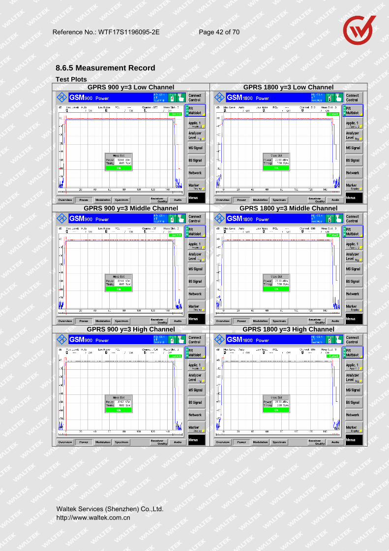
8.6.5 Measurement Record
Test Plots GPRS 900 y=3 Low Channel GPRS 1800 y=3 Low Channel
GPRS 900 y=3 Middle Channel GPRS 1800 y=3 Middle Channel
GPRS 900 y=3 High Channel GPRS 1800 y=3 High Channel

Reference No.: WTF17S1196095-2E Page 43 of 70
Waltek Services (Shenzhen) Co.,Ltd. http://www.waltek.com.cn
8.7 Output RF spectrum in GPRS multislot configuration
8.7.1 Definition The output RF spectrum is the relationship between the frequency offset from the carrier and the power, measured in a specified bandwidth and time, produced by the MS due to the effects of modulation and power ramping.
8.7.2 Limit 1. The level of the output RF spectrum due to modulation shall be no more than that given in 3GPP TS 05.05, subclause 4.2.1, table a) for GSM 400, GSM 700, GSM 850 and GSM 900, table b) for DCS 1800 or table c) for PCS 1900, with the following lowest measurement limits:
- 36 dBm below 600 kHz offset from the carrier; - -51 dBm for GSM 400, GSM 700, GSM 850 and GSM 900 or -56 dBm for DCS 1 800 and PCS 1 900 from 600 kHz out to less than 1 800 kHz offset from the carrier;
- -46 dBm for GSM 400, GSM 700, GSM 850 and GSM 900 or -51 dBm for DCS 1 800 and PCS 1 900 at and beyond 1 800 kHz offset from the carrier; but with the following exceptions at up to -36 dBm:
- up to three bands of 200 kHz width centred on a frequency which is an integer multiple of 200 kHz in the combined range 600 kHz to 6 000 kHz above and below the carrier; - up to 12 bands of 200 kHz width centred on a frequency which is an integer multiple of 200 kHz at
more than 6 000 kHz offset from the carrier. 1.1 Under normal conditions; 3GPP TS 05.05, subclause 4.2.1. 1.2 Under extreme conditions; 3GPP TS 05.05, subclause 4.2.1; 3GPP TS 05.05, annex D subclauses
D.2.1 and D.2.2. 2. The level of the output RF spectrum due to switching transients shall be no more than given in 3GPP TS 05.05, subclause 4.2.2, table "a) Mobile Station".
2.1 Under normal conditions; 3GPP TS 05.05, subclause 4.2.2. 2.2 Under extreme conditions; 3GPP TS 05.05, subclause 4.2.2; 3GPP TS 05.05 annex D subclause D.2.1 and D.2.2.
3. When allocated a channel, the power emitted by a GSM 400, GSM 900 and DCS 1 800 MS, in the band 935 MHz to 960 MHz shall be no more than -79 dBm, in the band 925 MHz to 935 MHz shall be no more than -67 dBm and in the band 1 805 MHz to 1 880 MHz shall be no more than -71 dBm
except in five measurements in each of the bands 925 MHz to 960 MHz and 1 805 MHz to 1 880 MHz where exceptions at up to -36 dBm are permitted. For GSM 400 MS, in addition, the power emitted by MS, in the bands of 460,4 MHz to 467,6 MHz and 488,8 MHz to 496 MHz shall be no
more than -67 dBm except in three measurements in each of the bands 460,4 MHz to 467,6 MHz and 488,8 MHz to 496 MHz where exceptions at up to -36 dBm are permitted. For GSM 700 and GSM 850, the power emitted by MS, in the band of 747 MHz to 757 MHz shall be no more than -79
dBm, in the band of 757 MHz to 762 MHz shall be no more than –73 dBm, in the band 869 MHz to 894 MHz shall be no more than -79 dBm, in the band 1 930 MHz to 1 990 MHz shall be no more than – 71 dBm except in five measurements in each of the bands 747 MHz to 762 MHz, 869 MHz to
894 MHz and 1 930 MHz to 1 990 MHz where exceptions at up to -36 dBm are permitted. For PCS 1 900 MS, the power emitted by MS, in the band 869 MHz to 894 MHz shall be no more than -79 dBm, in the band 1 930 MHz to 1 990 MHz shall be no more than -71 dBm except in five
measurements in each of the bands 869 MHz to 894 MHz and 1 930 MHz to 1 990 MHz where exceptions at up to -36 dBm are permitted. Under normal conditions; 3GPP TS 05.05, subclause 4.3.3.
Reference No.: WTF17S1196095-2E Page 44 of 70
Waltek Services (Shenzhen) Co.,Ltd. http://www.waltek.com.cn
Table 13-10: Spurious emissions in the MS receive bands
Band (MHz)
Spurious emissions level(dBm)
GSM 400, GSM 900 and
DCS 1 800
GSM 700, GSM 850 and
PCS 1 900
925 to 935 -67 -
935 to 960 -79 -
1805 to 1880 -71 -
728 to 736 - -79
736 to 746 - -73
747 to 757 - -79
757 to 763 - -73
869 to 894 - -79
1930 to 1990 - -71
8.7.3 EUT Operation Condition:
The EUT was programmed to be in continuously transmitting mode.
8.7.4 Test Procedure NOTE: When averaging is in use during frequency hopping mode, the averaging only includes bursts transmitted when the hopping carrier corresponds to the nominal carrier of the measurement.
a) In steps b) to h) the FT is equal to the hop pattern ARFCN in the Mid ARFCN range. b) The other settings of the spectrum analyzer are set as follows: - Zero frequency scan;
- Resolution bandwidth: 30 kHz; - Video bandwidth: 30 kHz; - Video averaging: may be used, depending on the implementation of the test.
The video signal of the spectrum analyzer is "gated" such that the spectrum generated by at least 40 of the bits 87 to 132 of the burst in one of the active time slots is the only spectrum measured. This gating may be analogue or numerical, dependent upon the design of the spectrum analyzer.
Only measurements during transmitted bursts on the nominal carrier of the measurement are included. The spectrum analyzer averages over the gated period and over 200 or 50 such bursts, using numerical and/or video averaging.
The MS is commanded to its maximum power control level in every transmitted time slot. c) By tuning the spectrum analyzer centre frequency to the measurement frequencies the power level is measured over 50 bursts at all multiples of 30 kHz offset from FT to < 1 800 kHz.
d) The resolution and video bandwidth on the spectrum analyzer are adjusted to 100 kHz and the measurements are made at the following frequencies: on every ARFCN from 1 800 kHz offset from the carrier to the edge of the relevant transmit
band for each measurement over 50 bursts. at 200 kHz intervals over the 2 MHz either side of the relevant transmit band for each measurement over 50 bursts.
For GSM 400, GSM 900 and DCS 1800: at 200 kHz intervals over the band 925 MHz to 960 MHz for each measurement over 50 bursts. at 200 kHz intervals over the band 1 805 MHz to 1 880 MHz for each measurement over 50
bursts.. e) The MS is commanded to its minimum power control level. The spectrum analyzer is set again as
Reference No.: WTF17S1196095-2E Page 45 of 70
Waltek Services (Shenzhen) Co.,Ltd. http://www.waltek.com.cn
in b). f) By tuning the spectrum analyzer centre frequency to the measurement frequencies the power level is measured over 200 bursts at the following frequencies:
FT; FT + 100 kHz FT - 100 kHz;FT + 200 kHz FT - 200 kHz; FT + 250 kHz FT - 250 kHz;FT + 200 kHz * N FT - 200 kHz * N;
where N = 2, 3, 4, 5, 6, 7, and 8; and FT = RF channel nominal centre frequency. g) Steps a) to f) is repeated except that in step a) the spectrum analyzer is gated so that the burst of
the next active time slot is measured. h) The spectrum analyzer settings are adjusted to: - Zero frequency scan;
- Resolution bandwidth: 30 kHz; - Video bandwidth: 100 kHz; - Peak hold.
The spectrum analyzer gating of the signal is switched off. The MS is commanded to its maximum power control level in every transmitted time slot. i) By tuning the spectrum analyzer centre frequency to the measurement frequencies the power level
is measured at the following frequencies: FT + 400 kHz FT - 400 kHz;FT + 600 kHz FT - 600 kHz; FT + 1,2 MHz FT - 1,2 MHz;FT + 1,8 MHz FT - 1,8 MHz;
where FT = RF channel nominal centre frequency. The duration of each measurement (at each frequency) will be such as to cover at least 10 burst transmissions at FT.
j) Step i) is repeated for power control levels 7 and 11. k) Steps b), f), h) and i) are repeated with FT equal to the hop pattern ARFCN in the Low ARFCN range except that in step h) the MS is commanded to power control level 11 rather than maximum
power. l) Steps b), f), h) and i) are repeated with FT equal to the hop pattern ARFCN in the High ARFCN range except that in step h) the MS is commanded to power control level 11 rather than maximum
power. m) Steps a) b) f) h), and i) are repeated under extreme test conditions (annex 1, TC2.2). except that at step h) the MS is commanded to power control level 11.
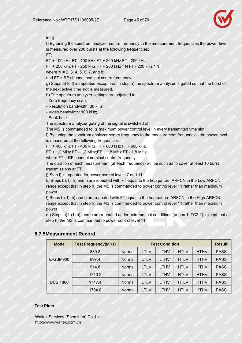
8.7.5 Measurement Record
Mode Test Frequency(MHz) Test Condition Result
E-GSM900
880.2 Normal LTLV LTHV HTLV HTHV PASS
897.4 Normal LTLV LTHV HTLV HTHV PASS
914.8 Normal LTLV LTHV HTLV HTHV PASS
DCS 1800
1710.2 Normal LTLV LTHV HTLV HTHV PASS
1747.4 Normal LTLV LTHV HTLV HTHV PASS
1784.8 Normal LTLV LTHV HTLV HTHV PASS
Test Plots
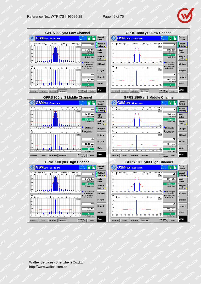
Reference No.: WTF17S1196095-2E Page 46 of 70
Waltek Services (Shenzhen) Co.,Ltd. http://www.waltek.com.cn
GPRS 900 y=3 Low Channel GPRS 1800 y=3 Low Channel
GPRS 900 y=3 Middle Channel GPRS 1800 y=3 Middle Channel
GPRS 900 y=3 High Channel GPRS 1800 y=3 High Channel
Reference No.: WTF17S1196095-2E Page 47 of 70
Waltek Services (Shenzhen) Co.,Ltd. http://www.waltek.com.cn
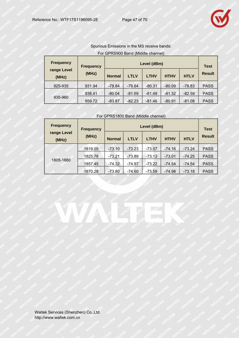
Spurious Emissions in the MS receive bands:
For GPRS900 Band (Middle channel)
Frequency
range Level
(MHz)
Frequency
(MHz)
Level (dBm) Test
ResultNormal LTLV LTHV HTHV HTLV
925-935 931.94 -78.84 -78.64 -80.31 -80.09 -78.83 PASS
935-960 938.41 -80.04 -81.69 -81.49 -81.32 -82.59 PASS
959.72 -83.87 -82.23 -81.46 -80.91 -81.08 PASS
For GPRS1800 Band (Middle channel)
Frequency
range Level
(MHz)
Frequency
(MHz)
Level (dBm) Test
ResultNormal LTLV LTHV HTHV HTLV
1805-1880
1819.05 -73.10 -73.23 -73.07 -74.16 -73.24 PASS
1825.78 -73.21 -73.89 -73.13 -73.01 -74.25 PASS
1857.45 -74.32 -74.97 -73.22 -74.54 -74.54 PASS
1870.28 -73.80 -74.60 -73.59 -74.98 -73.18 PASS

Reference No.: WTF17S1196095-2E Page 48 of 70
Waltek Services (Shenzhen) Co.,Ltd. http://www.waltek.com.cn
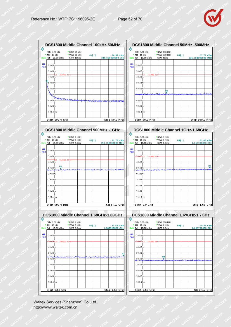
8.8 Conducted spurious emissions – MS allocated a channel
8.8.1 Definition
Conducted spurious emissions, when the MS has been allocated a channel, are emissions from the antenna connector at frequencies other than those of the carrier and sidebands associated with normal
modulation.
8.8.2 Limit
Frequency range Power level in dBm GSM 400, GSM 700, T-GSM 810 GSM 850, GSM 900
DCS 1 800 PCS 1 900
9 kHz to 1 GHz 1 GHz to 12,75 GHz 1 GHz to 1 710 MHz 1 710 MHz to 1 785 MHz 1 785 MHz to 12,75 GHz
-36 -30
-36 -30 -36 -30
-36 -30
8.8.3 EUT Operation Condition
The EUT was programmed to be in continuously transmitting mode.
8.8.4 Test Procedure
a) Measurements are made in the frequency range 100 kHz to 12,75 GHz. Spurious emissions are measured at the connector of the transceiver, as the power level of any discrete signal, higher than the requirement in table 1 minus 6 dB, delivered into a 50 Ω load.
The measurement bandwidth based on a 5 pole synchronously tuned filter is according to table 2. The power indication is the peak power detected by the measuring system. The measurement on any frequency shall be performed for at least one TDMA frame period with the
exception of the idle frame. NOTE: This ensures that both the active times (MS transmitting) and the quiet times are measured. b) The test is repeated under extreme voltage test conditions ([annex 1, TC2.2 and TC3]).
Reference No.: WTF17S1196095-2E Page 49 of 70
Waltek Services (Shenzhen) Co.,Ltd. http://www.waltek.com.cn
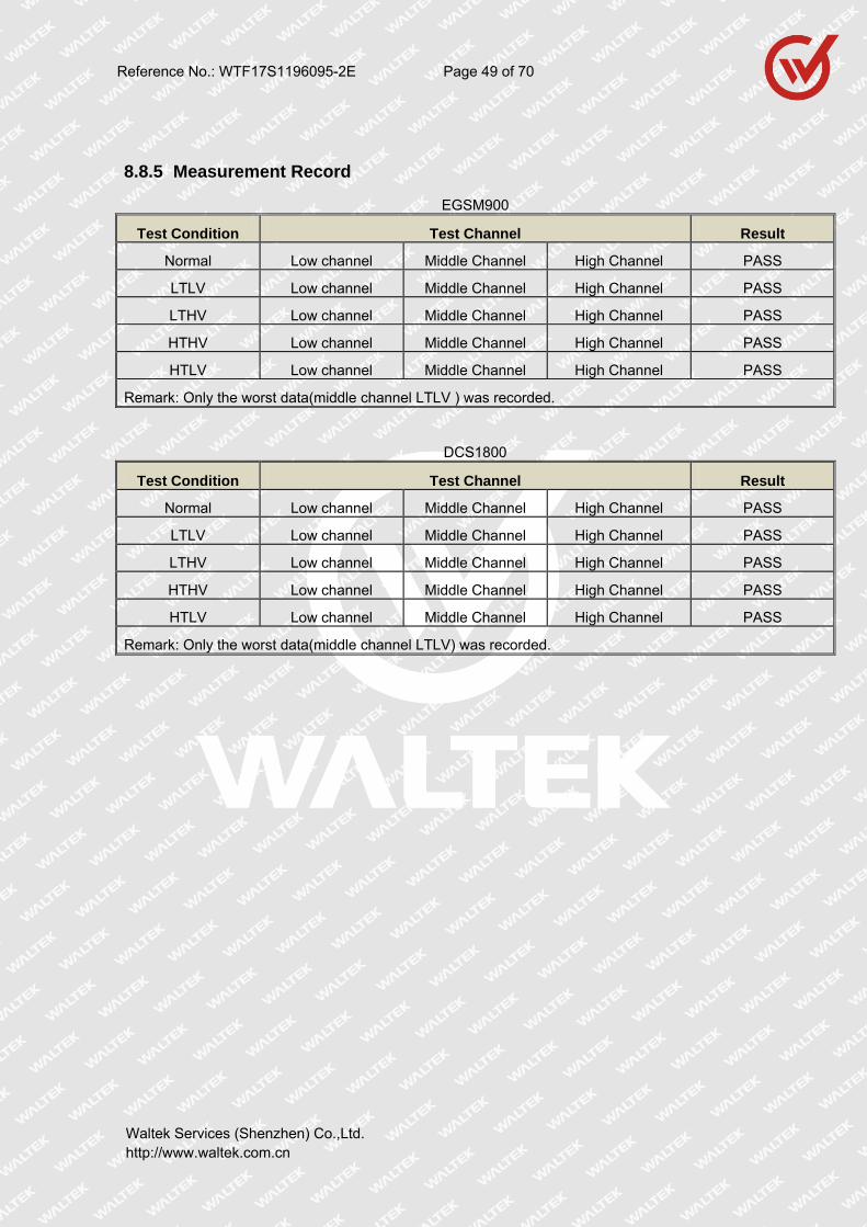
8.8.5 Measurement Record
EGSM900
Test Condition Test Channel Result
Normal Low channel Middle Channel High Channel PASS
LTLV Low channel Middle Channel High Channel PASS
LTHV Low channel Middle Channel High Channel PASS
HTHV Low channel Middle Channel High Channel PASS
HTLV Low channel Middle Channel High Channel PASS
Remark: Only the worst data(middle channel LTLV ) was recorded.
DCS1800
Test Condition Test Channel Result
Normal Low channel Middle Channel High Channel PASS
LTLV Low channel Middle Channel High Channel PASS
LTHV Low channel Middle Channel High Channel PASS
HTHV Low channel Middle Channel High Channel PASS
HTLV Low channel Middle Channel High Channel PASS
Remark: Only the worst data(middle channel LTLV) was recorded.
Reference No.: WTF17S1196095-2E Page 50 of 70
Waltek Services (Shenzhen) Co.,Ltd. http://www.waltek.com.cn
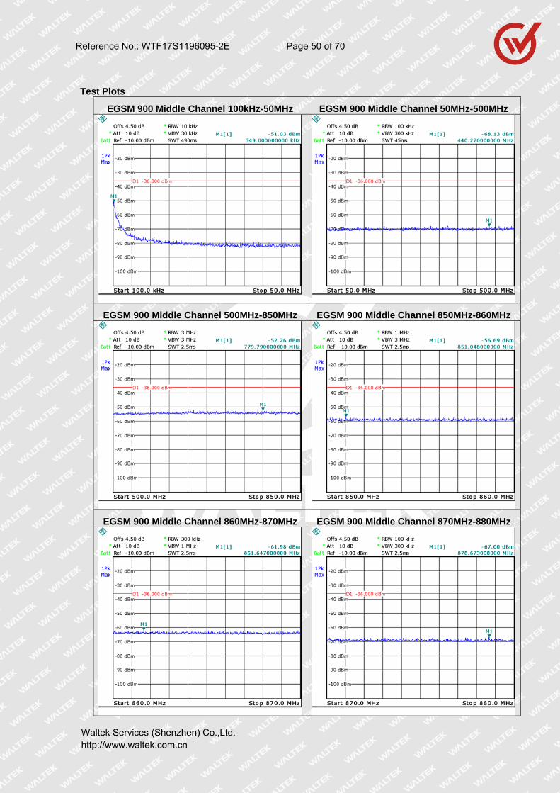
Test Plots
EGSM 900 Middle Channel 100kHz-50MHz EGSM 900 Middle Channel 50MHz-500MHz
EGSM 900 Middle Channel 500MHz-850MHz EGSM 900 Middle Channel 850MHz-860MHz
EGSM 900 Middle Channel 860MHz-870MHz EGSM 900 Middle Channel 870MHz-880MHz
Reference No.: WTF17S1196095-2E Page 51 of 70
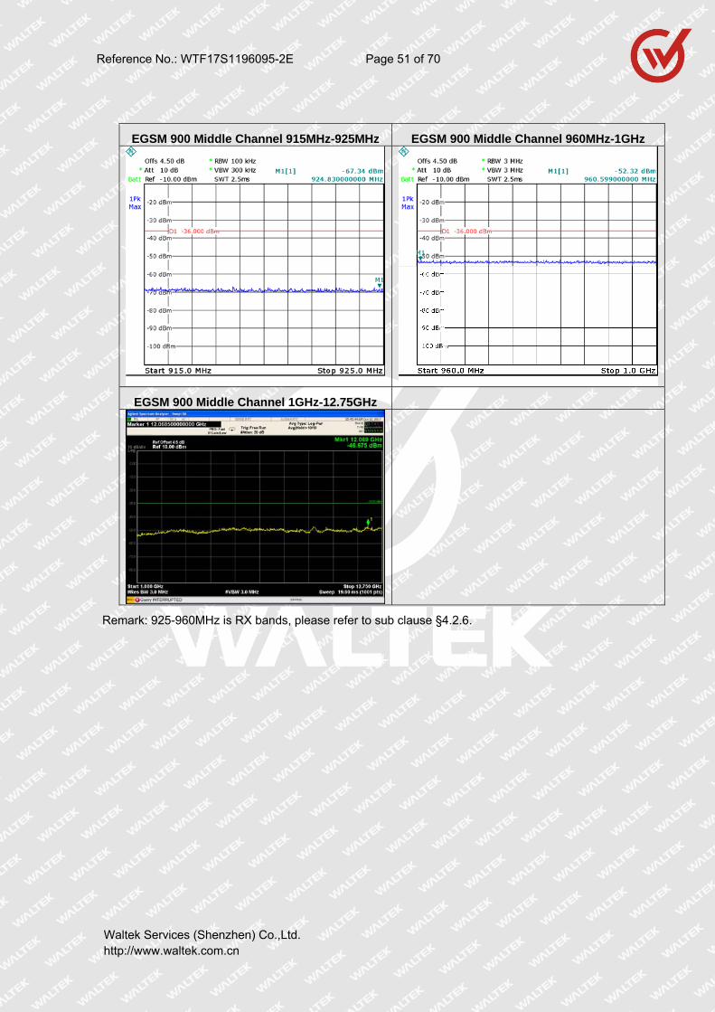
Waltek Services (Shenzhen) Co.,Ltd. http://www.waltek.com.cn
EGSM 900 Middle Channel 915MHz-925MHz EGSM 900 Middle Channel 960MHz-1GHz
EGSM 900 Middle Channel 1GHz-12.75GHz
Remark: 925-960MHz is RX bands, please refer to sub clause §4.2.6.
Reference No.: WTF17S1196095-2E Page 52 of 70
Waltek Services (Shenzhen) Co.,Ltd. http://www.waltek.com.cn
DCS1800 Middle Channel 100kHz-50MHz DCS1800 Middle Channel 50MHz -500MHz
DCS1800 Middle Channel 500MHz -1GHz DCS1800 Middle Channel 1GHz-1.68GHz
DCS1800 Middle Channel 1.68GHz-1.69GHz DCS1800 Middle Channel 1.69GHz-1.7GHz

Reference No.: WTF17S1196095-2E Page 53 of 70
Waltek Services (Shenzhen) Co.,Ltd. http://www.waltek.com.cn
DCS1800 Middle Channel 1.7GHz-1.71GHz DCS1800 Middle Channel 1.785GHz-1.795GHz
DCS1800 Middle Channel 1.795GHz-1.805GHz DCS1800 Middle Channel 1.88GHz-12.75GHz
Remark: 1805-1880MHz is RX bands, please refer to sub clause §4.2.6.
Reference No.: WTF17S1196095-2E Page 54 of 70
Waltek Services (Shenzhen) Co.,Ltd. http://www.waltek.com.cn
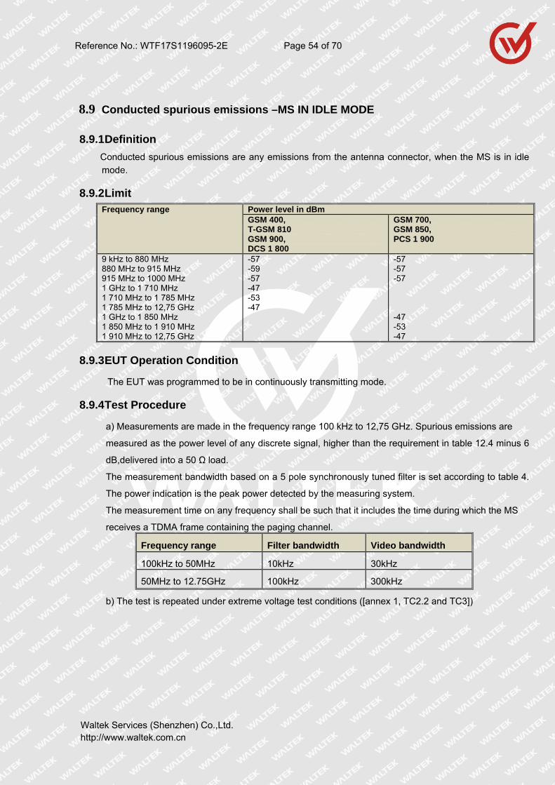
8.9 Conducted spurious emissions –MS IN IDLE MODE
8.9.1 Definition
Conducted spurious emissions are any emissions from the antenna connector, when the MS is in idle
mode.
8.9.2 Limit Frequency range Power level in dBm
GSM 400,T-GSM 810 GSM 900, DCS 1 800
GSM 700, GSM 850, PCS 1 900
9 kHz to 880 MHz 880 MHz to 915 MHz 915 MHz to 1000 MHz 1 GHz to 1 710 MHz 1 710 MHz to 1 785 MHz 1 785 MHz to 12,75 GHz 1 GHz to 1 850 MHz 1 850 MHz to 1 910 MHz 1 910 MHz to 12,75 GHz
-57 -59 -57 -47 -53 -47
-57 -57 -57 -47 -53 -47
8.9.3 EUT Operation Condition
The EUT was programmed to be in continuously transmitting mode.
8.9.4 Test Procedure
a) Measurements are made in the frequency range 100 kHz to 12,75 GHz. Spurious emissions are
measured as the power level of any discrete signal, higher than the requirement in table 12.4 minus 6
dB,delivered into a 50 Ω load.
The measurement bandwidth based on a 5 pole synchronously tuned filter is set according to table 4.
The power indication is the peak power detected by the measuring system.
The measurement time on any frequency shall be such that it includes the time during which the MS
receives a TDMA frame containing the paging channel.
Frequency range Filter bandwidth Video bandwidth
100kHz to 50MHz 10kHz 30kHz
50MHz to 12.75GHz 100kHz 300kHz
b) The test is repeated under extreme voltage test conditions ([annex 1, TC2.2 and TC3])

Reference No.: WTF17S1196095-2E Page 55 of 70
Waltek Services (Shenzhen) Co.,Ltd. http://www.waltek.com.cn
8.9.5 Measurement Record
EGSM900
Test Condition Test Channel Result
Normal Low channel Middle Channel High Channel PASS
LTLV Low channel Middle Channel High Channel PASS
LTHV Low channel Middle Channel High Channel PASS
HTHV Low channel Middle Channel High Channel PASS
HTLV Low channel Middle Channel High Channel PASS
Remark: Only the worst data(middle channel LTLV ) was recorded.
DCS1800
Test Condition Test Channel Result
Normal Low channel Middle Channel High Channel PASS
LTLV Low channel Middle Channel High Channel PASS
LTHV Low channel Middle Channel High Channel PASS
HTHV Low channel Middle Channel High Channel PASS
HTLV Low channel Middle Channel High Channel PASS
Remark: Only the worst data(middle channel LTLV) was recorded.

Reference No.: WTF17S1196095-2E Page 56 of 70
Waltek Services (Shenzhen) Co.,Ltd. http://www.waltek.com.cn
Test Plots
EGSM 900 Middle Channel 100kHz-50MHz EGSM 900 Middle Channel 50MHz -880MHz
EGSM 900 Middle Channel 880MHz -915MHz EGSM 900 Middle Channel 915MHz -1GHz
EGSM 900 Middle Channel 1GHz-1.71GHz EGSM 900 Middle Channel 1.71-1.785GHz
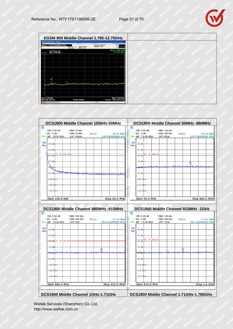
Reference No.: WTF17S1196095-2E Page 57 of 70
Waltek Services (Shenzhen) Co.,Ltd. http://www.waltek.com.cn
EGSM 900 Middle Channel 1.785-12.75GHz
DCS1800 Middle Channel 100kHz-50MHz DCS1800 Middle Channel 50MHz -880MHz
DCS1800 Middle Channel 880MHz -915MHz DCS1800 Middle Channel 915MHz -1GHz
DCS1800 Middle Channel 1GHz-1.71GHz DCS1800 Middle Channel 1.71GHz-1.785GHz
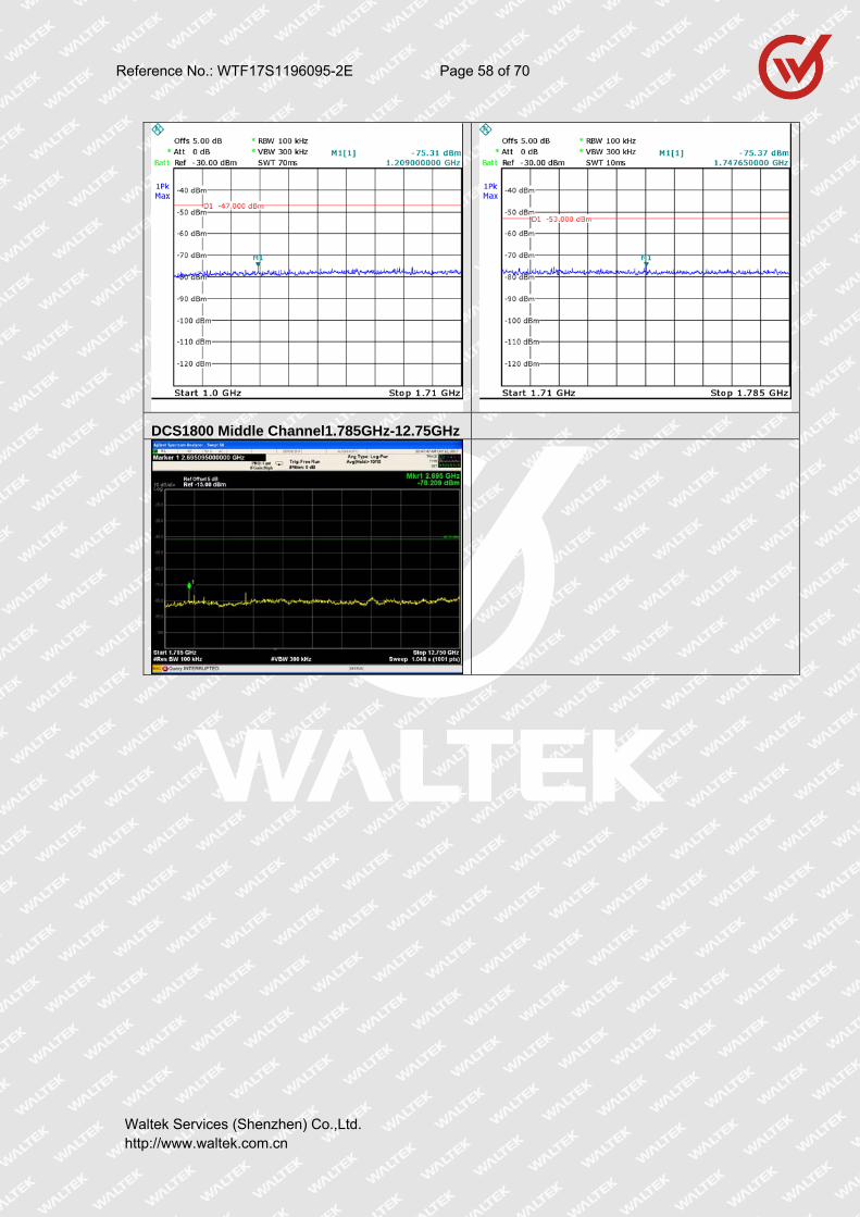
Reference No.: WTF17S1196095-2E Page 58 of 70
Waltek Services (Shenzhen) Co.,Ltd. http://www.waltek.com.cn
DCS1800 Middle Channel1.785GHz-12.75GHz

Reference No.: WTF17S1196095-2E Page 59 of 70
Waltek Services (Shenzhen) Co.,Ltd. http://www.waltek.com.cn
8.10 Radiated spurious emissions – MS allocated a channel
8.10.1 Definition
Radiated spurious emissions, when the MS has been allocated a channel, are any emissions
radiated by the cabinet and structure of the mobile station, including all interconnecting cables.
This is also known as "cabinet radiation".
The test applies to all types of MS with the exception of the test at extreme voltages for an MS where
a practical connection, to an external power supply, is not possible.
NOTE: A "practical connection" shall be interpreted to mean it is possible to connect extreme
voltages to the MS without interfering with the configuration of the MS in a way which could
invalidate the test.
8.10.2 Limit
Frequency range Power level in dBm GSM 400, GSM 700, T-GSM 810, GSM 850, GSM 900
DCS 1 800 PCS 1 900
30 MHz to 1 GHz 1 GHz to 4 GHz 1 GHz to 1 710 MHz 1 710 MHz to 1 785 MHz 1 785 MHz to 4 GHz
-36 -30
-36 -30 -36 -30
-36 -30
8.10.3 EUT Operation Condition
The EUT was programmed to be in continuously transmitting mode.
8.10.4 Test Procedure
a) Initially the test antenna is closely coupled to the MS and any spurious emission radiated by the MS is detected by the test antenna and receiver in the range 30 MHz to 4 GHz. NOTE 1: This is a qualitative step to identify the frequency and presence of spurious emissions
which are to be measured in subsequent steps. b) The test antenna separation is set to the appropriate measurement distance and at each frequency at which an emission has been detected, the MS shall be rotated to obtain maximum
response and the effective radiated power of the emission determined by a substitution measurement. In case of an anechoic shielded chamber pre-calibration may be used instead of a substitution measurement.
c) The measurement bandwidth, based on a 5 pole synchronously tuned filter, is set according to table 6.The power indication is the peak power detected by the measuring system. The measurement on any frequency shall be performed for at least one TDMA frame period, with
the exception of the idle frame. NOTE 2: This ensures that both the active times (MS transmitting) and the quiet times are measured.

Reference No.: WTF17S1196095-2E Page 60 of 70
Waltek Services (Shenzhen) Co.,Ltd. http://www.waltek.com.cn
NOTE 3: For these filter bandwidths some difficulties may be experienced with noise floor above required measurement limit. This will depend on the gain of the test antenna, and adjustment of the measuring system bandwidth is permissible. Alternatively, for test frequencies above 900 MHz, the
test antenna separation from the MS may be reduced to 1 meter. d) The measurements are repeated with the test antenna in the orthogonal polarization plane. e) The test is repeated under extreme voltage test conditions (see [annex 1, TC2.2]).
8.10.5 Measurement Record
E-GSM 900
Test Condition Test Channel Result
Normal Voltage Low Channel Middle Channel High Channel PASS
Low Voltage Low Channel Middle Channel High Channel PASS
High Voltage Low Channel Middle Channel High Channel PASS
Remark: Only the worst date(Low Voltage) is recorded.
DCS1800
Test Condition Test Channel Result
Normal Voltage Low Channel Middle Channel High Channel PASS
Low Voltage Low Channel Middle Channel High Channel PASS
High Voltage Low Channel Middle Channel High Channel PASS
Remark: Only the worst date(Low Voltage) is recorded.
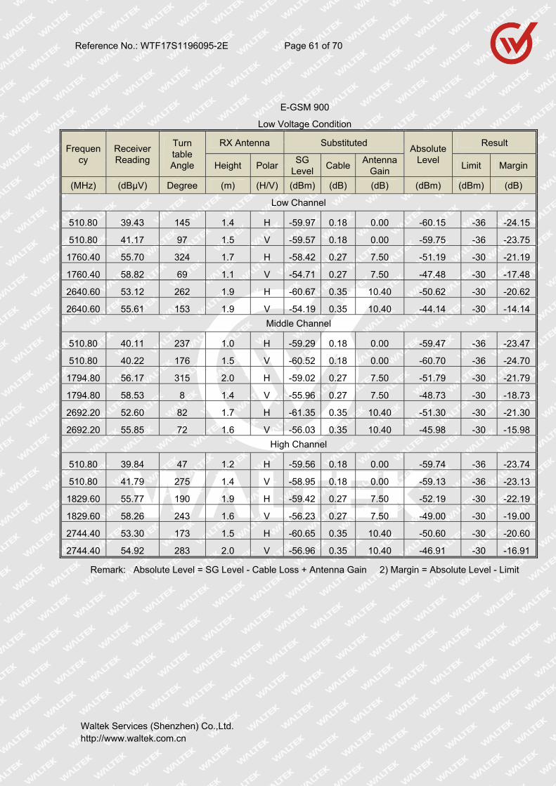
Reference No.: WTF17S1196095-2E Page 61 of 70
Waltek Services (Shenzhen) Co.,Ltd. http://www.waltek.com.cn
E-GSM 900
Low Voltage Condition
Frequency
Receiver Reading
Turn table Angle
RX Antenna Substituted Absolute
Level
Result
Height PolarSG
LevelCable
Antenna Gain
Limit Margin
(MHz) (dBμV) Degree (m) (H/V) (dBm) (dB) (dB) (dBm) (dBm) (dB)
Low Channel
510.80 39.43 145 1.4 H -59.97 0.18 0.00 -60.15 -36 -24.15
510.80 41.17 97 1.5 V -59.57 0.18 0.00 -59.75 -36 -23.75
1760.40 55.70 324 1.7 H -58.42 0.27 7.50 -51.19 -30 -21.19
1760.40 58.82 69 1.1 V -54.71 0.27 7.50 -47.48 -30 -17.48
2640.60 53.12 262 1.9 H -60.67 0.35 10.40 -50.62 -30 -20.62
2640.60 55.61 153 1.9 V -54.19 0.35 10.40 -44.14 -30 -14.14
Middle Channel
510.80 40.11 237 1.0 H -59.29 0.18 0.00 -59.47 -36 -23.47
510.80 40.22 176 1.5 V -60.52 0.18 0.00 -60.70 -36 -24.70
1794.80 56.17 315 2.0 H -59.02 0.27 7.50 -51.79 -30 -21.79
1794.80 58.53 8 1.4 V -55.96 0.27 7.50 -48.73 -30 -18.73
2692.20 52.60 82 1.7 H -61.35 0.35 10.40 -51.30 -30 -21.30
2692.20 55.85 72 1.6 V -56.03 0.35 10.40 -45.98 -30 -15.98
High Channel
510.80 39.84 47 1.2 H -59.56 0.18 0.00 -59.74 -36 -23.74
510.80 41.79 275 1.4 V -58.95 0.18 0.00 -59.13 -36 -23.13
1829.60 55.77 190 1.9 H -59.42 0.27 7.50 -52.19 -30 -22.19
1829.60 58.26 243 1.6 V -56.23 0.27 7.50 -49.00 -30 -19.00
2744.40 53.30 173 1.5 H -60.65 0.35 10.40 -50.60 -30 -20.60
2744.40 54.92 283 2.0 V -56.96 0.35 10.40 -46.91 -30 -16.91
Remark: Absolute Level = SG Level - Cable Loss + Antenna Gain 2) Margin = Absolute Level - Limit
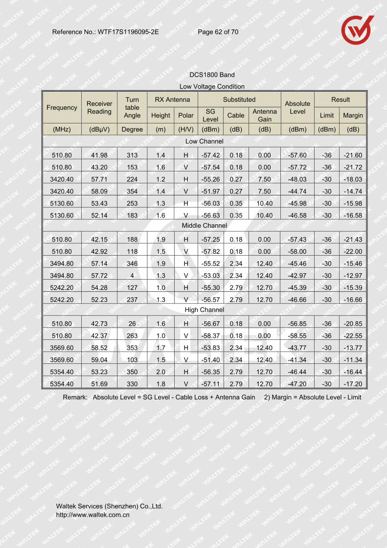
Reference No.: WTF17S1196095-2E Page 62 of 70
Waltek Services (Shenzhen) Co.,Ltd. http://www.waltek.com.cn
DCS1800 Band
Low Voltage Condition
Frequency Receiver Reading
Turn table Angle
RX Antenna Substituted Absolute
Level
Result
Height PolarSG
LevelCable
Antenna Gain
Limit Margin
(MHz) (dBμV) Degree (m) (H/V) (dBm) (dB) (dB) (dBm) (dBm) (dB)
Low Channel
510.80 41.98 313 1.4 H -57.42 0.18 0.00 -57.60 -36 -21.60
510.80 43.20 153 1.6 V -57.54 0.18 0.00 -57.72 -36 -21.72
3420.40 57.71 224 1.2 H -55.26 0.27 7.50 -48.03 -30 -18.03
3420.40 58.09 354 1.4 V -51.97 0.27 7.50 -44.74 -30 -14.74
5130.60 53.43 253 1.3 H -56.03 0.35 10.40 -45.98 -30 -15.98
5130.60 52.14 183 1.6 V -56.63 0.35 10.40 -46.58 -30 -16.58
Middle Channel
510.80 42.15 188 1.9 H -57.25 0.18 0.00 -57.43 -36 -21.43
510.80 42.92 118 1.5 V -57.82 0.18 0.00 -58.00 -36 -22.00
3494.80 57.14 346 1.9 H -55.52 2.34 12.40 -45.46 -30 -15.46
3494.80 57.72 4 1.3 V -53.03 2.34 12.40 -42.97 -30 -12.97
5242.20 54.28 127 1.0 H -55.30 2.79 12.70 -45.39 -30 -15.39
5242.20 52.23 237 1.3 V -56.57 2.79 12.70 -46.66 -30 -16.66
High Channel
510.80 42.73 26 1.6 H -56.67 0.18 0.00 -56.85 -36 -20.85
510.80 42.37 263 1.0 V -58.37 0.18 0.00 -58.55 -36 -22.55
3569.60 58.52 353 1.7 H -53.83 2.34 12.40 -43.77 -30 -13.77
3569.60 59.04 103 1.5 V -51.40 2.34 12.40 -41.34 -30 -11.34
5354.40 53.23 350 2.0 H -56.35 2.79 12.70 -46.44 -30 -16.44
5354.40 51.69 330 1.8 V -57.11 2.79 12.70 -47.20 -30 -17.20
Remark: Absolute Level = SG Level - Cable Loss + Antenna Gain 2) Margin = Absolute Level - Limit
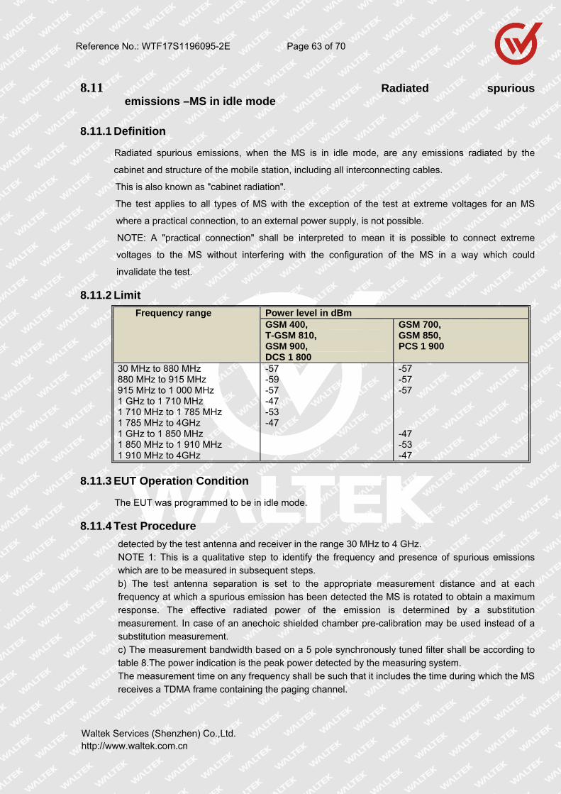
Reference No.: WTF17S1196095-2E Page 63 of 70
Waltek Services (Shenzhen) Co.,Ltd. http://www.waltek.com.cn
8.11 Radiated spurious emissions –MS in idle mode
8.11.1 Definition
Radiated spurious emissions, when the MS is in idle mode, are any emissions radiated by the
cabinet and structure of the mobile station, including all interconnecting cables.
This is also known as "cabinet radiation".
The test applies to all types of MS with the exception of the test at extreme voltages for an MS
where a practical connection, to an external power supply, is not possible.
NOTE: A "practical connection" shall be interpreted to mean it is possible to connect extreme
voltages to the MS without interfering with the configuration of the MS in a way which could
invalidate the test.
8.11.2 Limit
Frequency range Power level in dBm GSM 400, T-GSM 810, GSM 900, DCS 1 800
GSM 700, GSM 850, PCS 1 900
30 MHz to 880 MHz 880 MHz to 915 MHz 915 MHz to 1 000 MHz 1 GHz to 1 710 MHz 1 710 MHz to 1 785 MHz 1 785 MHz to 4GHz 1 GHz to 1 850 MHz 1 850 MHz to 1 910 MHz 1 910 MHz to 4GHz
-57 -59 -57 -47 -53 -47
-57 -57 -57 -47 -53 -47
8.11.3 EUT Operation Condition
The EUT was programmed to be in idle mode.
8.11.4 Test Procedure
detected by the test antenna and receiver in the range 30 MHz to 4 GHz. NOTE 1: This is a qualitative step to identify the frequency and presence of spurious emissions which are to be measured in subsequent steps.
b) The test antenna separation is set to the appropriate measurement distance and at each frequency at which a spurious emission has been detected the MS is rotated to obtain a maximum response. The effective radiated power of the emission is determined by a substitution
measurement. In case of an anechoic shielded chamber pre-calibration may be used instead of a substitution measurement. c) The measurement bandwidth based on a 5 pole synchronously tuned filter shall be according to
table 8.The power indication is the peak power detected by the measuring system. The measurement time on any frequency shall be such that it includes the time during which the MS receives a TDMA frame containing the paging channel.
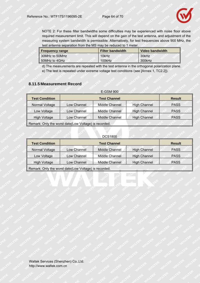
Reference No.: WTF17S1196095-2E Page 64 of 70
Waltek Services (Shenzhen) Co.,Ltd. http://www.waltek.com.cn
NOTE 2: For these filter bandwidths some difficulties may be experienced with noise floor above required measurement limit. This will depend on the gain of the test antenna, and adjustment of the measuring system bandwidth is permissible. Alternatively, for test frequencies above 900 MHz, the
test antenna separation from the MS may be reduced to 1 meter.
Frequency range Filter bandwidth Video bandwidth
30MHz to 50MHz 50MHz to 4GHz
10kHz 100kHz
30kHz 300kHz
d) The measurements are repeated with the test antenna in the orthogonal polarization plane. e) The test is repeated under extreme voltage test conditions (see [Annex 1, TC2.2]).
8.11.5 Measurement Record
E-GSM 900
Test Condition Test Channel Result
Normal Voltage Low Channel Middle Channel High Channel PASS
Low Voltage Low Channel Middle Channel High Channel PASS
High Voltage Low Channel Middle Channel High Channel PASS
Remark: Only the worst date(Low Voltage) is recorded.
DCS1800
Test Condition Test Channel Result
Normal Voltage Low Channel Middle Channel High Channel PASS
Low Voltage Low Channel Middle Channel High Channel PASS
High Voltage Low Channel Middle Channel High Channel PASS
Remark: Only the worst date(Low Voltage) is recorded.

Reference No.: WTF17S1196095-2E Page 65 of 70
Waltek Services (Shenzhen) Co.,Ltd. http://www.waltek.com.cn
E-GSM 900
Low Voltage Condition
Frequency Receiver Reading
Turn table Angle
RX Antenna Substituted Absolute
Level
Result
Height PolarSG
LevelCable
Antenna Gain
Limit Margin
(MHz) (dBμV) Degree (m) (H/V) (dBm) (dB) (dB) (dBm) (dBm) (dB)
Low Channel
227.70 39.85 320 1.1 H -69.86 0.15 0.00 -70.01 -57 -13.01
227.70 39.01 183 1.8 V -67.98 0.15 0.00 -68.13 -57 -11.13
2219.47 40.77 213 1.4 H -72.61 0.34 10.50 -62.45 -47 -15.45
2219.47 44.36 29 1.7 V -68.27 0.34 10.50 -58.11 -47 -11.11
Middle Channel
227.70 40.84 314 1.6 H -68.87 0.15 0.00 -69.02 -57 -12.02
227.70 39.51 355 1.2 V -67.48 0.15 0.00 -67.63 -57 -10.63
2219.47 41.00 286 1.9 H -72.38 0.34 10.50 -62.22 -47 -15.22
2219.47 44.57 231 1.4 V -68.06 0.34 10.50 -57.90 -47 -10.90
High Channel
227.70 40.23 276 2.0 H -69.48 0.15 0.00 -69.63 -57 -12.63
227.70 40.22 263 1.5 V -66.77 0.15 0.00 -66.92 -57 -9.92
2219.47 41.72 225 1.7 H -71.66 0.34 10.50 -61.50 -47 -14.50
2219.47 45.01 216 1.5 V -67.62 0.34 10.50 -57.46 -47 -10.46
Remark: Absolute Level = SG Level - Cable Loss + Antenna Gain 2) Margin = Absolute Level - Limit
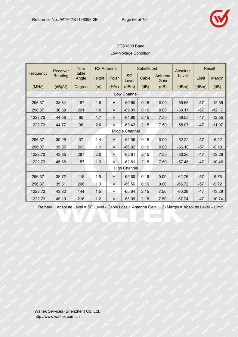
Reference No.: WTF17S1196095-2E Page 66 of 70
Waltek Services (Shenzhen) Co.,Ltd. http://www.waltek.com.cn
DCS1800 Band
Low Voltage Condition
Frequency Receiver Reading
Turn table Angle
RX Antenna Substituted Absolute
Level
Result
Height PolarSG
LevelCable
Antenna Gain
Limit Margin
(MHz) (dBμV) Degree (m) (H/V) (dBm) (dB) (dB) (dBm) (dBm) (dB)
Low Channel
296.37 38.34 167 1.9 H -69.50 0.16 0.00 -69.66 -57 -12.66
296.37 36.59 291 1.0 V -69.01 0.16 0.00 -69.17 -57 -12.17
1222.73 44.56 60 1.7 H -64.90 2.15 7.50 -59.55 -47 -12.55
1222.73 44.77 96 2.0 V -63.42 2.15 7.50 -58.07 -47 -11.07
Middle Channel
296.37 39.26 37 1.4 H -62.06 0.16 0.00 -62.22 -57 -5.22
296.37 35.85 263 1.1 V -66.02 0.16 0.00 -66.18 -57 -9.18
1222.73 43.85 287 2.0 H -65.61 2.15 7.50 -60.26 -47 -13.26
1222.73 45.38 157 1.3 V -62.81 2.15 7.50 -57.46 -47 -10.46
High Channel
296.37 38.72 115 1.5 H -62.60 0.16 0.00 -62.76 -57 -5.76
296.37 35.31 206 1.3 V -66.56 0.16 0.00 -66.72 -57 -9.72
1222.73 43.82 144 1.5 H -65.64 2.15 7.50 -60.29 -47 -13.29
1222.73 45.10 216 1.2 V -63.09 2.15 7.50 -57.74 -47 -10.74
Remark: Absolute Level = SG Level - Cable Loss + Antenna Gain 2) Margin = Absolute Level – Limit
Reference No.: WTF17S1196095-2E Page 67 of 70
Waltek Services (Shenzhen) Co.,Ltd. http://www.waltek.com.cn
8.12 Receiver blocking and spurious response – speech channels
8.12.1 Definition
Blocking is a measure of the ability of the receiver to receive a modulated wanted input signal in the
presence of an unwanted input signal, on frequencies other than those of the spurious responses or
the adjacent channels, without exceeding a given degradation.
8.12.2 Limit
The blocking characteristics of the receiver are specified separately for in-band and out-of-band performance as Identified in 3GPP TS 05.05 sub clause 5.1.
The reference sensitivity performance as specified in table 1 of 3GPP TS 05.05 shall be met when the following Signals are simultaneously input to the receiver: - a useful signal at frequency f0, 3 dB above the reference sensitivity level as specified in 3GPP TS
05.05 sub clause 6.2; - a continuous, static sine wave signal at a level as in the table of 3GPP TS 05.05 sub clause 5.1 and at a frequency(f) which is an integer multiple of 200 kHz;
- with the following exceptions, called spurious response frequencies: a) GSM 700, GSM 850 and GSM 900: in band, for a maximum of six occurrences (which if grouped shall not exceed three contiguous occurrences per group);
b) out of band, for a maximum of 24 occurrences (which if below f0 and grouped shall not exceed three contiguous occurrences per group).
where the above performance shall be met when the continuous sine wave signal (f) is set to a level
of 70dBμV(emf) (i.e. -43 dBm). 3GPP TS 05.05, sub clause 5.1
8.12.3 EUT Operation Condition
The EUT was programmed to be in continuously receiving mode.
8.12.4 Test Procedure
the wanted signal is set to 4 dB above the reference sensitivity level.
b) The unwanted signal is a C.W. signal (Standard test signal IO) of frequency FB. It is applied in turn on the subset of frequencies calculated in step c) in the overall range 100 kHz to 12,75 GHz, where FB is an integer multiple of 200 kHz.
However, frequencies in the range FR ±600 kHz are excluded. NOTE: Allowance must be made for possible spurious signals arising from the SS. These are particularly likely at sub harmonic frequencies nFB where n = 2, 3, 4, 5, etc.
c) The frequencies at which the test is performed (adjusted to an integer multiple of 200 kHz channels most closely approximating the absolute frequency of the calculated blocking signal frequency) are the combined frequencies from i), ii) and iii) below:
i) The total frequency range formed by: E-GSM 900 the frequencies between Flo + (IF1 + IF2 + ... + IFn + 17,5 MHz) and Flo - (IF1 + IF2 + ...+ IFn + 17,5 MHz).
And the frequencies +100 MHz and -100 MHz from the edge of the relevant receive band. Measurements are made at 200 kHz intervals. ii) The three frequencies IF1, IF1 + 200 kHz, IF1 - 200 kHz.

Reference No.: WTF17S1196095-2E Page 68 of 70
Waltek Services (Shenzhen) Co.,Ltd. http://www.waltek.com.cn
iii) The frequencies: mFlo + IF1; mFlo - IF1;
mFR; where m is all positive integers greater than or equal to 2 such that either sum lies in the range 100 kHz to 12,75 GHz.
The frequencies in step ii) and iii) lying in the range of frequencies defined by step i) above need not be repeated. Where:
Flo - local oscillator applied to first receiver mixer IF1 ... IFn - are the n intermediate frequencies Flo, IF1, IF2 ... IFn - shall be declared by the manufacturer in the PIXIT statement 3GPP TS
51.010-1 annex 3. d) The level of the unwanted signal is set according to table 14-28. NOTE 1: These values differ from 3GPP TS 05.05 because of practical generator limits in the SS.
NOTE 2: For an E-GSM 900 MS the level of the unwanted signal in the band 905 MHz to < 915 MHz is relaxed to 108 dBuVemf( ). NOTE 3: For a GSM 450 small MS the level of the unwanted signal in the band 450,4 MHz to <
457,6MHz is relaxed to 108 dBuVemf( ). For a GSM 480 small MS the level of the unwanted signal in the band 478,8 MHz to < 486 MHz is relaxed to 108 dBuVemf( ). e) The SS compares the data of the signal that it sends to the MS with the signal which is looped
back from the receiver after demodulation and decoding, and checks the frame erasure indication. The SS tests the RBER compliance for the bits of class II, by examining sequences of at least the Minimum number of samples of consecutive bits of class II, where bits are taken only from those
frames for which no bad frame indication was given. The number of error events is recorded. If a failure is indicated it is noted and counted towards the allowed exemption totals. In the case of failures discovered at the predicted frequencies at steps f ii), iii) or iv) the test is
repeated on the adjacent channels ±200 kHz away. If either of these two frequencies fail then the next channel 200 kHz beyond is also tested. This process is repeated until all channels constituting the group of failures is known.
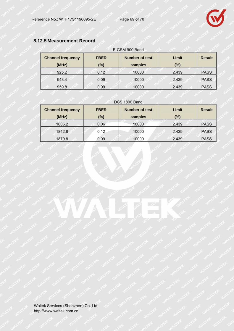
Reference No.: WTF17S1196095-2E Page 69 of 70
Waltek Services (Shenzhen) Co.,Ltd. http://www.waltek.com.cn
8.12.5 Measurement Record
E-GSM 900 Band
Channel frequency
(MHz)
FBER
(%)
Number of test
samples
Limit
(%)
Result
925.2 0.12 10000 2.439 PASS
943.4 0.09 10000 2.439 PASS
959.8 0.09 10000 2.439 PASS
DCS 1800 Band
Channel frequency
(MHz)
FBER
(%)
Number of test
samples
Limit
(%)
Result
1805.2 0.06 10000 2.439 PASS
1842.8 0.12 10000 2.439 PASS
1879.8 0.09 10000 2.439 PASS

Reference No.: WTF17S1196095-2E Page 70 of 70
Waltek Services (Shenzhen) Co.,Ltd. http://www.waltek.com.cn
9 Photographs of test setup and EUT.
Note: Please refer to appendix: WTF17S1196095E-Photo.
======End of Report======
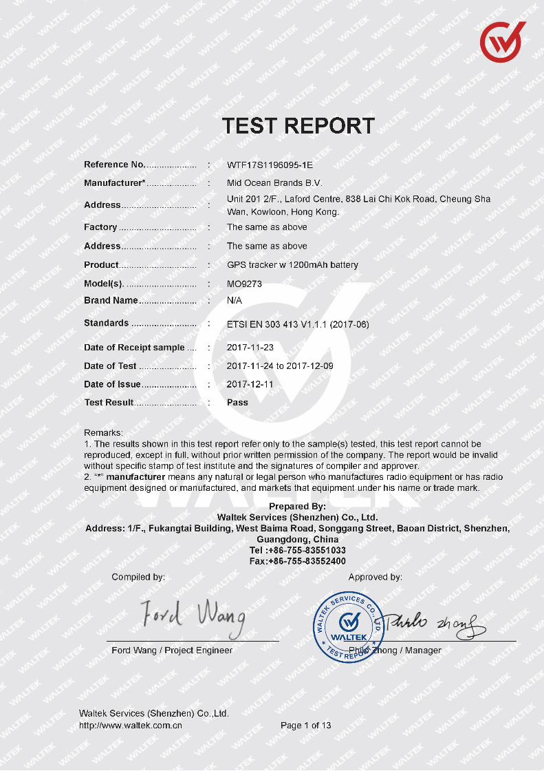

Reference No.: WTF17S1196095-1E Page 2 of 13
Waltek Services (Shenzhen) Co.,Ltd. http://www.waltek.com.cn
2 Laboratories Introduction
Waltek Services Test Group Ltd. is one of the largest and the most comprehensive third party testing
organizations in China, our headquarter located in Shenzhen (CNAS Registration No. L3110, A2LA
Certificate Number: 4243.01) and have branches in Foshan (CNAS Registration No. L6478), Dongguan
(CNAS Registration No. L9950), Zhongshan, Suzhou (CNAS Registration No. L7754), Ningbo and Hong
Kong, Our test capability covered four large fields: safety test. Electronic Magnetic Compatibility(EMC),
reliability and energy performance, Chemical test. Meanwhile, Waltek has got recognition as registration and
accreditation laboratory from EMSD (Electrical and Mechanical Services Department), and American Energy
star, FCC(The Federal Communications Commission), CPSC(Consumer Product Safety Commission),
CEC(California energy efficiency), IC(Industry Canada) and ELI(Efficient Lighting Initiative). It’s the strategic
partner and data recognition laboratory of international authoritative organizations, such as UL, Intertek(ETL-
SEMKO), CSA, TÜV Rheinland, TÜV SÜD, etc. As a professional, comprehensive, justice international test
organization, we still keep the scientific and rigorous work attitude to help each client satisfy the international
standards and assist their product enter into globe market smoothly.
Waltek Services (Shenzhen) Co., Ltd.
A. Accreditations for Conformity Assessment (International)
Country/Region Accreditation Body Scope Note
USA
CNAS
(Registration No.: L3110)
A2LA
(Certificate No.: 4243.01)
FCC ID \ DOC \ VOC 1
Canada IC ID \ VOC 2
Japan MIC-T \ MIC-R -
Europe EMCD \ RED -
Taiwan NCC -
Hong Kong OFCA -
Australia RCM -
India
International Services
WPC -
Thailand NTC -
Singapore IDA -
Note:
1. FCC Designation No.: CN1201. Test Firm Registration No.: 523476.
2. IC Canada Registration No.: 7760A
B. TCBs and Notify Bodies Recognized Testing Laboratory.
Recognized Testing Laboratory of … Notify body number
TUV Rheinland
Optional. Intertek
TUV SUD

Reference No.: WTF17S1196095-1E Page 3 of 13
Waltek Services (Shenzhen) Co.,Ltd. http://www.waltek.com.cn
SGS
Phoenix Testlab GmbH 0700
Element Materials Technology Warwick Ltd 0891
Timco Engineering, Inc. 1177
Eurofins Product Service GmbH 0681
Reference No.: WTF17S1196095-1E Page 4 of 13
Waltek Services (Shenzhen) Co.,Ltd. http://www.waltek.com.cn
3 Contents
Page
1 COVER PAGE ........................................................................................................................................... 1
2 LABORATORIES INTRODUCTION .................................................................................................................... 2
3 CONTENTS ............................................................................................................................................................. 4
4 REVISION HISTORY ............................................................................................................................................. 5
5 GENERAL INFORMATION ................................................................................................................................... 6
5.1 GENERAL DESCRIPTION OF E.U.T. ................................................................................................... 6 5.2 DETAILS OF E.U.T. ......................................................................................................................... 6
6 TEST SUMMARY ................................................................................................................................................... 7
7 EQUIPMENT USED DURING TEST ................................................................................................................... 8
7.1 EQUIPMENTS LIST ........................................................................................................................... 8 7.2 DESCRIPTION OF SUPPORT UNITS .................................................................................................... 8 7.3 MEASUREMENT UNCERTAINTY ......................................................................................................... 8 7.4 TEST EQUIPMENT CALIBRATION ....................................................................................................... 8
8 RF REQUIREMENTS ............................................................................................................................................. 9
8.1 GUE ADJACENT FREQUENCY BAND SELECTIVITY PERFORMANCE ........................................................ 9 8.2 RECEIVER SPURIOUS EMISSIONS ................................................................................................... 12
9 PHOTOGRAPHS OF TEST SETUP AND EUT. .............................................................................................. 13
Reference No.: WTF17S1196095-1E Page 5 of 13
Waltek Services (Shenzhen) Co.,Ltd. http://www.waltek.com.cn
4 Revision History
Test report No. Date of Receipt sample
Date of TestDate of Issue
Purpose Comment Approved
WTF17S11960
95-1E 2017-11-23
2017-11-24 to 2017-12-
09 2017-12-11 original - Valid
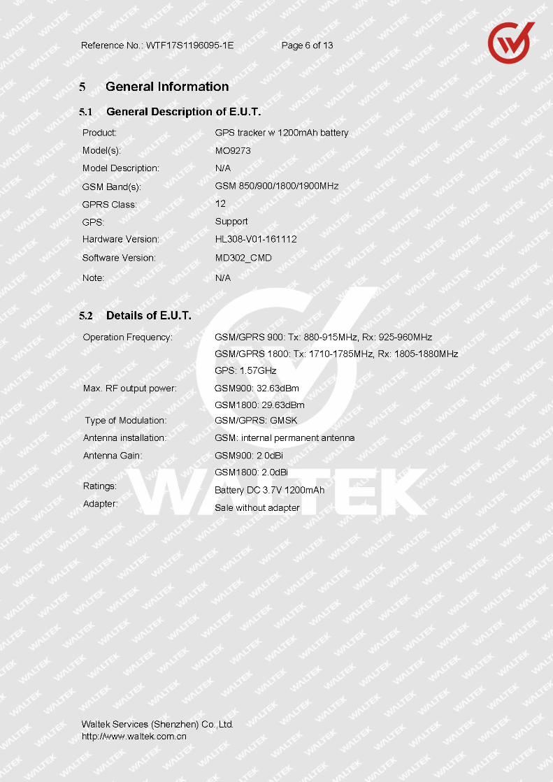
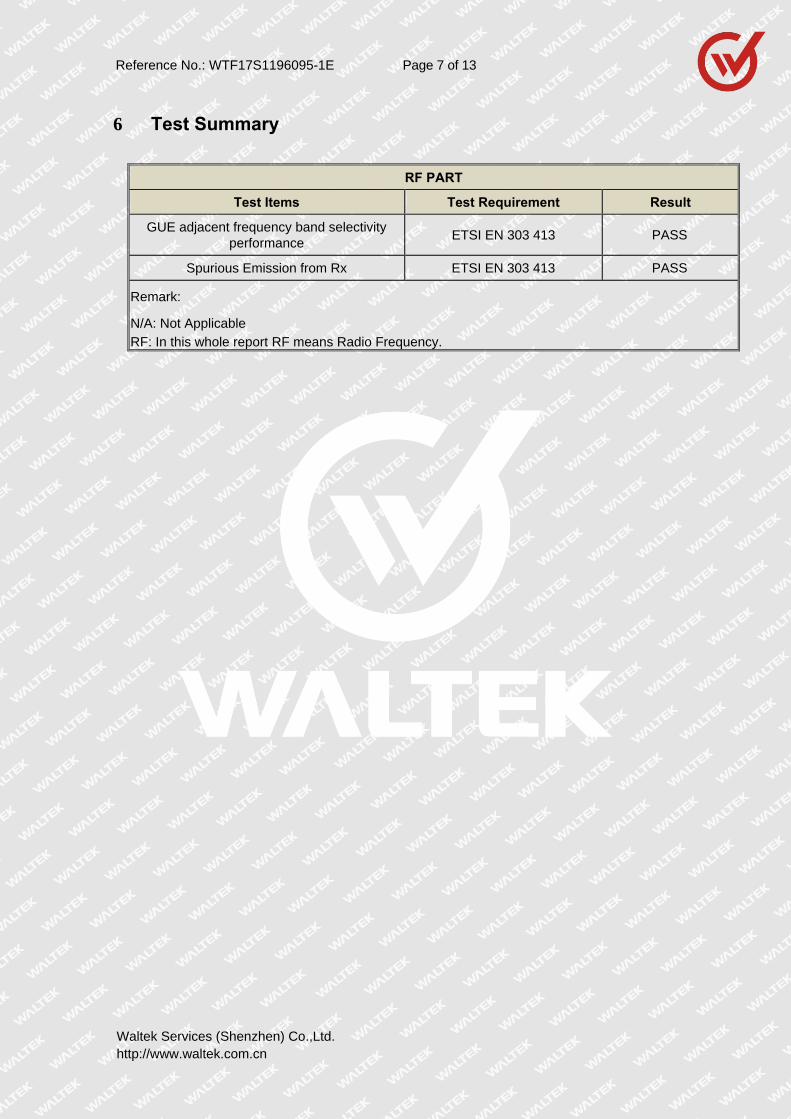
Reference No.: WTF17S1196095-1E Page 7 of 13
Waltek Services (Shenzhen) Co.,Ltd. http://www.waltek.com.cn
6 Test Summary
RF PART
Test Items Test Requirement Result
GUE adjacent frequency band selectivity performance
ETSI EN 303 413 PASS
Spurious Emission from Rx ETSI EN 303 413 PASS
Remark:
N/A: Not Applicable RF: In this whole report RF means Radio Frequency.

Reference No.: WTF17S1196095-1E Page 8 of 13
Waltek Services (Shenzhen) Co.,Ltd. http://www.waltek.com.cn
7 Equipment Used during Test
7.1 Equipments List
Item Equipment Manufacturer Model No. Serial No. Last
Calibration Date
Calibration Due Date
1. Spectrum Analyzer R&S FSP 100091 2017-04-29 2018-04-28
2. Trilog Broadband
Antenna SCHWARZBECK VULB9163 336 2017-04-09 2018-04-08
3. Coaxial Cable
(below 1GHz) Top TYPE16(13M) - 2017-09-12 2018-09-11
4. Broad-band Horn
Antenna SCHWARZBECK BBHA 9120 D 667 2017-04-09 2018-04-08
5. Broad-band Horn
Antenna SCHWARZBECK BBHA 9120 D 669 2017-04-09 2018-04-08
6. Broadband Preamplifier COMPLIANCE
DIRECTION PAP-1G18 2004 2017-04-13 2018-04-12
7. Coaxial Cable
(above 1GHz) Top
1000MHz-
25GHz EW02014-7 2017-04-13 2018-04-12
8. Broad-band Horn
Antenna SCHWARZBECK BBHA 9170 335 2017-04-09 2018-04-08
9 EXG Analog Signal
Generator Keysight N5171B
MY53050845503
2017-09-12 2018-09-11
10 USB Wideband Power
Sensor Keysight U2021XA SG5440003 2017-04-29 2018-04-28
11 Spectrum Analyzer Agilent N9020A MY49100060 2017-09-22 2018-09-21
7.2 Description of Support Units
Equipment Manufacturer Model No. Series No.
/ / / /
7.3 Measurement Uncertainty
Parameter Uncertainty
Radiated Spurious Emissions test ± 5.08 dB (Bilog antenna 30M~1000MHz)
± 4.99 dB (Horn antenna 1000M~25000MHz)
7.4 Test Equipment Calibration
All the test equipments used are valid and calibrated by CEPREI Certification Body that address is No.110 Dongguan Zhuang RD. Guangzhou, P.R.China.

Reference No.: WTF17S1196095-1E Page 9 of 13
Waltek Services (Shenzhen) Co.,Ltd. http://www.waltek.com.cn
8 RF Requirements
8.1 GUE adjacent frequency band selectivity performance
Normal Test Conditions:
Ambient Condition: 22 C to 55 %RH, AC 230V/50Hz
8.1.1 Limit The C/N0 metric reported by the GUE for all GNSS and GNSS signals given in table 4-1 and
supported by the GUE shall not degrade by more than the value given in equation 4-1 when an
adjacent frequency signal is applied. The adjacent frequency signal is defined in table 4-4, with the
frequencies and power levels defined in table 4-2 and/or in table 4-3 depending on the RNSS bands
supported by the GUE.
Equation 4-1: Maximum degradation in C/N0
C/N0 ≤ 1 dB.
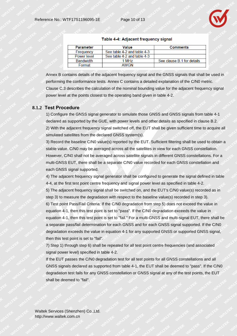
Reference No.: WTF17S1196095-1E Page 10 of 13
Waltek Services (Shenzhen) Co.,Ltd. http://www.waltek.com.cn
Annex B contains details of the adjacent frequency signal and the GNSS signals that shall be used in
performing the conformance tests. Annex C contains a detailed explanation of the C/N0 metric.
Clause C.3 describes the calculation of the nominal bounding value for the adjacent frequency signal
power level at the points closest to the operating band given in table 4-2.
8.1.2 Test Procedure 1) Configure the GNSS signal generator to simulate those GNSS and GNSS signals from table 4-1
declared as supported by the GUE, with power levels and other details as specified in clause B.2.
2) With the adjacent frequency signal switched off, the EUT shall be given sufficient time to acquire all
simulated satellites from the declared GNSS system(s).
3) Record the baseline C/N0 value(s) reported by the EUT. Sufficient filtering shall be used to obtain a
stable value. C/N0 may be averaged across all the satellites in view for each GNSS constellation.
However, C/N0 shall not be averaged across satellite signals in different GNSS constellations. For a
multi-GNSS EUT, there shall be a separate C/N0 value recorded for each GNSS constellation and
each GNSS signal supported.
4) The adjacent frequency signal generator shall be configured to generate the signal defined in table
4-4, at the first test point centre frequency and signal power level as specified in table 4-2.
5) The adjacent frequency signal shall be switched on, and the EUT's C/N0 value(s) recorded as in
step 3) to measure the degradation with respect to the baseline value(s) recorded in step 3).
6) Test point Pass/Fail Criteria: If the C/N0 degradation from step 5) does not exceed the value in
equation 4-1, then this test point is set to "pass". If the C/N0 degradation exceeds the value in
equation 4-1, then this test point is set to "fail." For a multi-GNSS and multi-signal EUT, there shall be
a separate pass/fail determination for each GNSS and for each GNSS signal supported. If the C/N0
degradation exceeds the value in equation 4-1 for any supported GNSS or supported GNSS signal,
then this test point is set to "fail".
7) Step 1) through step 6) shall be repeated for all test point centre frequencies (and associated
signal power level) specified in table 4-2.
If the EUT passes the C/N0 degradation test for all test points for all GNSS constellations and all
GNSS signals declared as supported from table 4-1, the EUT shall be deemed to "pass". If the C/N0
degradation test fails for any GNSS constellation or GNSS signal at any of the test points, the EUT
shall be deemed to "fail".
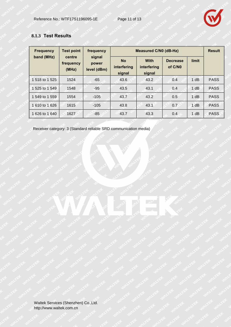
Reference No.: WTF17S1196095-1E Page 11 of 13
Waltek Services (Shenzhen) Co.,Ltd. http://www.waltek.com.cn
8.1.3 Test Results
Frequency
band (MHz)
Test point
centre
frequency
(MHz)
frequency
signal
power
level (dBm)
Measured C/N0 (dB-Hz) Result
No
interfering
signal
With
interfering
signal
Decrease
of C/N0
limit
1 518 to 1 525 1524 -65 43.6 43.2 0.4 1 dB PASS
1 525 to 1 549 1548 -95 43.5 43.1 0.4 1 dB PASS
1 549 to 1 559 1554 -105 43.7 43.2 0.5 1 dB PASS
1 610 to 1 626 1615 -105 43.8 43.1 0.7 1 dB PASS
1 626 to 1 640 1627 -85 43.7 43.3 0.4 1 dB PASS
Receiver category: 3 (Standard reliable SRD communication media)
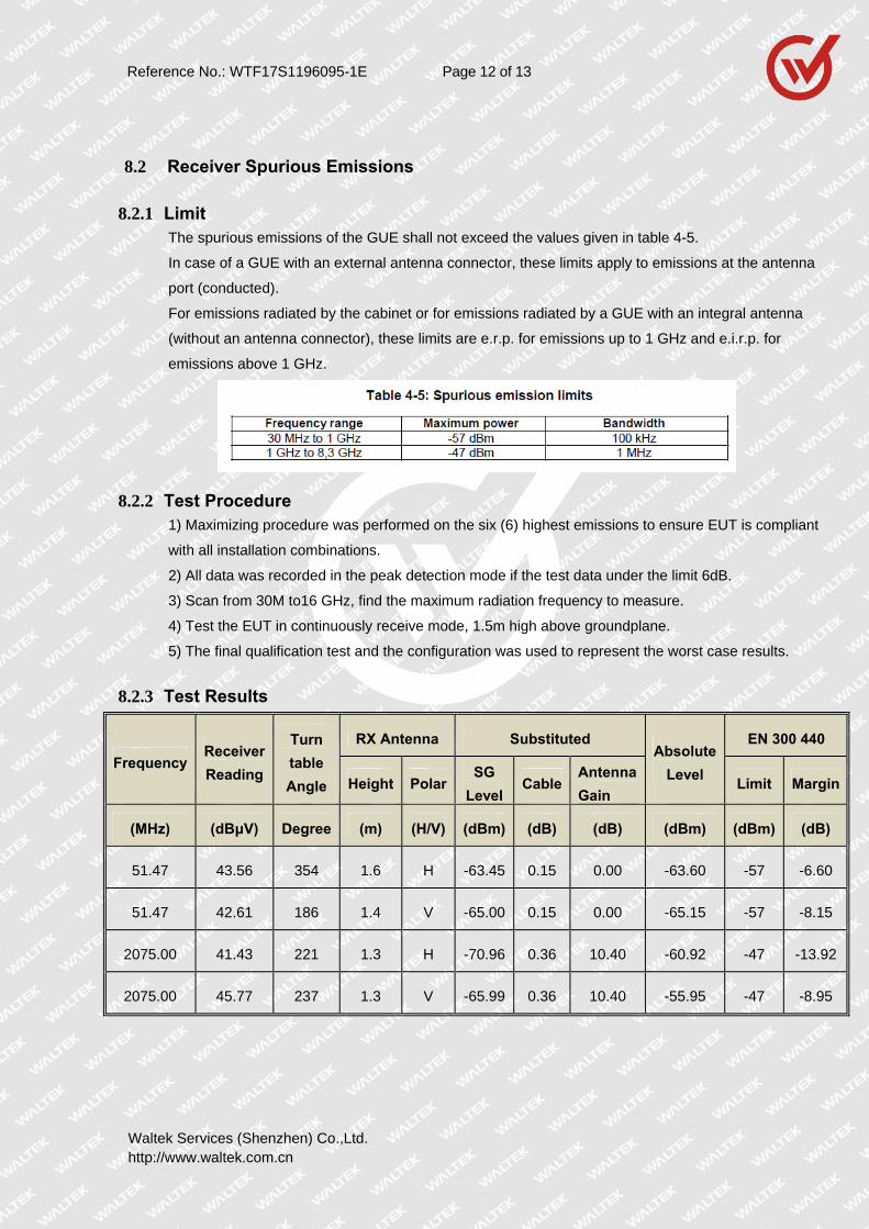
Reference No.: WTF17S1196095-1E Page 12 of 13
Waltek Services (Shenzhen) Co.,Ltd. http://www.waltek.com.cn
8.2 Receiver Spurious Emissions
8.2.1 Limit The spurious emissions of the GUE shall not exceed the values given in table 4-5.
In case of a GUE with an external antenna connector, these limits apply to emissions at the antenna
port (conducted).
For emissions radiated by the cabinet or for emissions radiated by a GUE with an integral antenna
(without an antenna connector), these limits are e.r.p. for emissions up to 1 GHz and e.i.r.p. for
emissions above 1 GHz.
8.2.2 Test Procedure 1) Maximizing procedure was performed on the six (6) highest emissions to ensure EUT is compliant
with all installation combinations.
2) All data was recorded in the peak detection mode if the test data under the limit 6dB.
3) Scan from 30M to16 GHz, find the maximum radiation frequency to measure.
4) Test the EUT in continuously receive mode, 1.5m high above groundplane.
5) The final qualification test and the configuration was used to represent the worst case results.
8.2.3 Test Results
Frequency Receiver
Reading
Turn
table
Angle
RX Antenna Substituted Absolute
Level
EN 300 440
Height PolarSG
LevelCable
Antenna
Gain Limit Margin
(MHz) (dBμV) Degree (m) (H/V) (dBm) (dB) (dB) (dBm) (dBm) (dB)
51.47 43.56 354 1.6 H -63.45 0.15 0.00 -63.60 -57 -6.60
51.47 42.61 186 1.4 V -65.00 0.15 0.00 -65.15 -57 -8.15
2075.00 41.43 221 1.3 H -70.96 0.36 10.40 -60.92 -47 -13.92
2075.00 45.77 237 1.3 V -65.99 0.36 10.40 -55.95 -47 -8.95

Reference No.: WTF17S1196095-1E Page 13 of 13
Waltek Services (Shenzhen) Co.,Ltd. http://www.waltek.com.cn
9 Photographs of test setup and EUT.
Note: Please refer to appendix: WTF17S1196095E-Photo.
======End of Report======