18eln24-basic electroncs - Sri Krishna Institute of Technology
19
BE-2-BS-SKIT-Ph5b1-F02-V2.2 COURSE PLAN - CAY 2019-20 Sri Krishna Institute of Technology, Bangalore COURSE PLAN Academic Year 2019-2020 Program: BE Semester : 2 Course Code: 18ELN24 Course Title: Basic Electronics Credit / L-T-P: 3 / 2-2-0 Total Contact Hours: 50 Course Plan Author: Shilpa Rani P/ Kiranmayi M Academic Evaluation and Monitoring Cell Sri Krishna Institute of Technology #29,Chimney hills,Hesaraghata Main road, Chikkabanavara Post Bangalore – 560090, Karnataka, INDIA Phone / Fax :08023721477/28392221/23721315 Web: www.skit.org.in , e-mail: [email protected] 18ELN24 Copyright ©2017. cAAS. All rights reserved. Page # 1 / 19 Ref No:
-
Upload
khangminh22 -
Category
Documents
-
view
0 -
download
0
Transcript of 18eln24-basic electroncs - Sri Krishna Institute of Technology
BE-2-BS-SKIT-Ph5b1-F02-V2.2COURSE PLAN - CAY 2019-20
Sri Krishna Institute of Technology,Bangalore
COURSE PLAN
Academic Year 2019-2020
Program: BE
Semester : 2
Course Code: 18ELN24
Course Title: Basic Electronics
Credit / L-T-P: 3 / 2-2-0
Total Contact Hours: 50
Course Plan Author: Shilpa Rani P/ Kiranmayi M
Academic Evaluation and Monitoring Cell
Sri Krishna Institute of Technology#29,Chimney hills,Hesaraghata Main road, Chikkabanavara Post
Bangalore – 560090, Karnataka, INDIA
Phone / Fax :08023721477/28392221/23721315Web: www.skit.org.in , e-mail: [email protected]
18ELN24 Copyright ©2017. cAAS. All rights reserved.Page # 1 / 19
Ref No:
BE-2-BS-SKIT-Ph5b1-F02-V2.2COURSE PLAN - CAY 2019-20
Table of ContentsA. COURSE INFORMATION.............................................................................................................31. Course Overview..............................................................................................................................32. Course Content.................................................................................................................................33. Course Material................................................................................................................................44. Course Prerequisites.........................................................................................................................45. Content for Placement, Profession, HE and GATE..........................................................................5B. OBE PARAMETERS......................................................................................................................51. Course Outcomes..............................................................................................................................52. Course Applications..........................................................................................................................53. Articulation Matrix...........................................................................................................................64. Curricular Gap and Content..............................................................................................................6C. COURSE ASSESSMENT...............................................................................................................61. Course Coverage..............................................................................................................................62. Continuous Internal Assessment (CIA)............................................................................................7D1. TEACHING PLAN - 1..................................................................................................................7Module - 1............................................................................................................................................7E1. CIA EXAM – 1..............................................................................................................................8a. Model Question Paper - 1.................................................................................................................8b. Assignment -1...................................................................................................................................9D2. TEACHING PLAN - 2................................................................................................................10Module – 2..........................................................................................................................................10Module – 3..........................................................................................................................................11E2. CIA EXAM – 2............................................................................................................................12a. Model Question Paper - 2...............................................................................................................12b. Assignment – 2...............................................................................................................................12D3. TEACHING PLAN - 3................................................................................................................14Module – 4..........................................................................................................................................14Module – 5..........................................................................................................................................15E3. CIA EXAM – 3............................................................................................................................16a. Model Question Paper - 3...............................................................................................................16b. Assignment – 3...............................................................................................................................16F. EXAM PREPARATION.................................................................................................................171. University Model Question Paper..................................................................................................172. SEE Important Questions...............................................................................................................18
18ELN24 Copyright ©2017. cAAS. All rights reserved.Page # 2 / 19

BE-2-BS-SKIT-Ph5b1-F02-V2.2COURSE PLAN - CAY 2019-20
A. COURSE INFORMATION1. Course OverviewDegree: BE Program: EC
Semester: 2 Academic Year: 2019-20
Course Title: Basic Electronics Course Code: 18ELN24
Credit / L-T-P: 3 / 2-2-0 SEE Duration: 180 Minutes
Total Contact Hours: 50 Hours SEE Marks: 60 Marks
CIA Marks: 40 Marks Assignment 1 / Module
Course Plan Author: Mrs. Shilpa Rani P/ Mrs. Kiranmayi M Sign .. Dt:21/02/2019
Checked By: Sign .. Dt:
CO Targets CIA Target : 80% SEE Target: 65 %
Note: Define CIA and SEE % targets based on previous performance.
2. Course ContentContent / Syllabus of the course as prescribed by University or designed by institute.Module
Content Teaching Hours Blooms LearningLevels
1 Semiconductor Diodes and Applications: P-N junction diode, Equivalent circuit of diode, Zener diode and zener diode as a regulator. Rectification-Half wave rectifier, full wave rectifier, bridge rectifier, capacitor filter circuit, Photo diode, LED, Photo coupler, 78XX series and 7805 fixed IC voltage regulator
12 L1,L2,L3
2 FET and SCR: Introduction to JFET, construction and operation, JFET drain characteristics and parameters, JFET transfer characteristics, Square law expression ID , Input resistance, MOSFET: Depletion and enhancement type construction, operation, characteristics and symbols. CMOS, Silicon Controlled Rectifier- two transistor model, Switching action characteristics and phase control application
8 L1,L2
3 Operational Amplifiers and Applications: Introduction to op-amp,Op-amp input modes, Op-amp parameters-CMRR, Input offset voltage and current, Input bias current, Input and output impedance , Slew rate. Applications of op-amp- Inverting amplifier, Non-inverting amplifier, Summer, voltage follower, integrator, differentiator, comparator
8 L1,L2,L3
4 BJT applications. Feedback amplifiers and oscillators: BJT as an amplifier, as a switch, Transistor switch circuit to switch ON/OFF an LED and a lamp in a power circuit using relay. Feedback amplifiers-Principle, properties and advantages of negative feedback, Types of feedback, Voltage series feedbackand gain stability with feedback, Oscillators- Barkhaunsen’s criteria for oscillation, RC phase shift oscillator, Wein bridge oscillator, IC 555 timer and astable oscillator using IC 555
12 L1,L2,L3
5 Digital Electronics Fundamentals: Difference between analog and digital signals, Number systems: Binary and hexadecimal, Conversion: Decimal to binary and hexadecimal to decimal and vice-versa, Boolean algebra, Basic and universal gates, Half and full adder, Multiplexer, decoder, SR and JK flip flops, Shift register, 3 bit Ripple counter. Basic communication system, Principle of operations of Mobile phone
13 L1,L2, L3
- Total 53 -
18ELN24 Copyright ©2017. cAAS. All rights reserved.Page # 3 / 19
BE-2-BS-SKIT-Ph5b1-F02-V2.2COURSE PLAN - CAY 2019-20
3. Course MaterialBooks & other material as recommended by university (A, B) and additional resources used by courseteacher (C).1. Understanding: Concept simulation / video ; one per concept ; to understand the concepts ; 15 – 30minutes2. Design: Simulation and design tools used – software tools used ; Free / open source3. Research: Recent developments on the concepts – publications in journals; conferences etc.Module
sDetails Chapters
in bookAvailability
A Text books (Title, Authors, Edition, Publisher, Year.) - -1, 2, 3,
4, 5D P Kothari, I J Nagarath, “Basic Electronics”, 2nd edn, Mc Graw Hill, 2018 2,3,6,7,8,
10,17,18In Lib
3 Thomas.L.Floyd, “Electronic Devices”, Pearson education, 9th edition, 2012 12 In Lib
B Reference books (Title, Authors, Edition, Publisher, Year.) - -1,
2,3,4,5D P Kothari, I J Nagarath, “Basic Electronics”, 1st edn, Mc Graw Hill, 2014 2,3,6,7,8,
10,17,18In Lib
1, 2,3,4Boylestad, Nashelskey,”Electronic Devices and Circuit theory”, PearsonEducation, 9th edition, 2007/11th edition, 2013
1,2 In Lib
1,2,3,4 David A Bell, “Electronic Devices And Circuits”, Oxford University Press, 5 th
Edition, 20083,4 In lib
C Concept Videos or Simulation for Understanding - -C1 https://www.youtube.com/watch?v=cOICDYuY-gAC2 https://www.youtube.com/watch?v=yaUMBKjkOjgC3 https://www.youtube.com/watch?v=9h7_vDUE908C4 https://www.youtube.com/watch?v=iJYm_BGqa1AC5 https://www.youtube.com/watch?v=3ORJa_Hu0SE
https://www.youtube.com/watch?v=THNNc7AYrQUC6 https://www.youtube.com/watch?v=_JMV4ywAJug
D Software Tools for Design - -
E Recent Developments for Research - -
F Others (Web, Video, Simulation, Notes etc.) - -1
4. Course PrerequisitesRefer to GL01. If prerequisites are not taught earlier, GAP in curriculum needs to be addressed. Include inRemarks and implement in B.5.Students must have learnt the following Courses / Topics with described Content . . .Modules
CourseCode
Course Name Topic / Description Sem Remarks BloomsLevel
18ELN24 Copyright ©2017. cAAS. All rights reserved.Page # 4 / 19

BE-2-BS-SKIT-Ph5b1-F02-V2.2COURSE PLAN - CAY 2019-20
5. Content for Placement, Profession, HE and GATEThe content is not included in this course, but required to meet industry & profession requirements and helpstudents for Placement, GATE, Higher Education, Entrepreneurship, etc. Identifying Area / Content requiresexperts consultation in the area.Topics included are like, a. Advanced Topics, b. Recent Developments, c. Certificate Courses, d. CourseProjects, e. New Software Tools, f. GATE Topics, g. NPTEL Videos, h. Swayam videos etc.Modules
Topic / Description Area Remarks BloomsLevel
B. OBE PARAMETERS1. Course OutcomesExpected learning outcomes of the course, which will be mapped to POs.Modules
CourseCode.#
Course OutcomeAt the end of the course, student
should be able to . . .
Teach. Hours Instr Method Assessment Method
Blooms’Level
1 18ELN24.1 Describe the operation of diodes, BJT, FET and Operational Amplifiers.
16 Lecture Test &Assignme
nt
L2
2 18ELN24.2 Design and explain the construction of rectifiers, regulators, amplifiers and oscillators.
14 Lecture Test &Assignme
nt
L3
3 18ELN24.3 Describe general operating principles of SCRs and its application.
5 Lecture Test &Assignme
nt
L2
4 18ELN24.4 Explain the working and design of Fixed voltage IC regulator using 7805 and astable oscillator using Timer IC 555.
5 Lecture Test &Assignme
nt
L3
5 18ELN24.5 Explain the different number system and their conversations and construct simple combinational and sequential logic circuits using Flip-Flops.
9 Lecture Test &Assignme
nt
L3
6 18ELN24.6 Describe the basic principle of operation of communication system and mobile phones.
4 Lecture Test &Assignme
nt
L2
- - Total 53 - - L2-L4
2. Course ApplicationsWrite 1 or 2 applications per CO.Students should be able to employ / apply the course learnings to . . .Modules
Application AreaCompiled from Module Applications.
CO Level
1 Diodes as Rectifiers , Transistors as amplifiers 1 L22 Regulators, oscillators 2 L33 Rectification, Regulation, Protection 3 L24 Fixed voltage regulator, Astable multi vibrator 4 L35 Digital encoding, Counters 5 L36 Internet access, millitary 6 L2
18ELN24 Copyright ©2017. cAAS. All rights reserved.Page # 5 / 19
BE-2-BS-SKIT-Ph5b1-F02-V2.2COURSE PLAN - CAY 2019-20
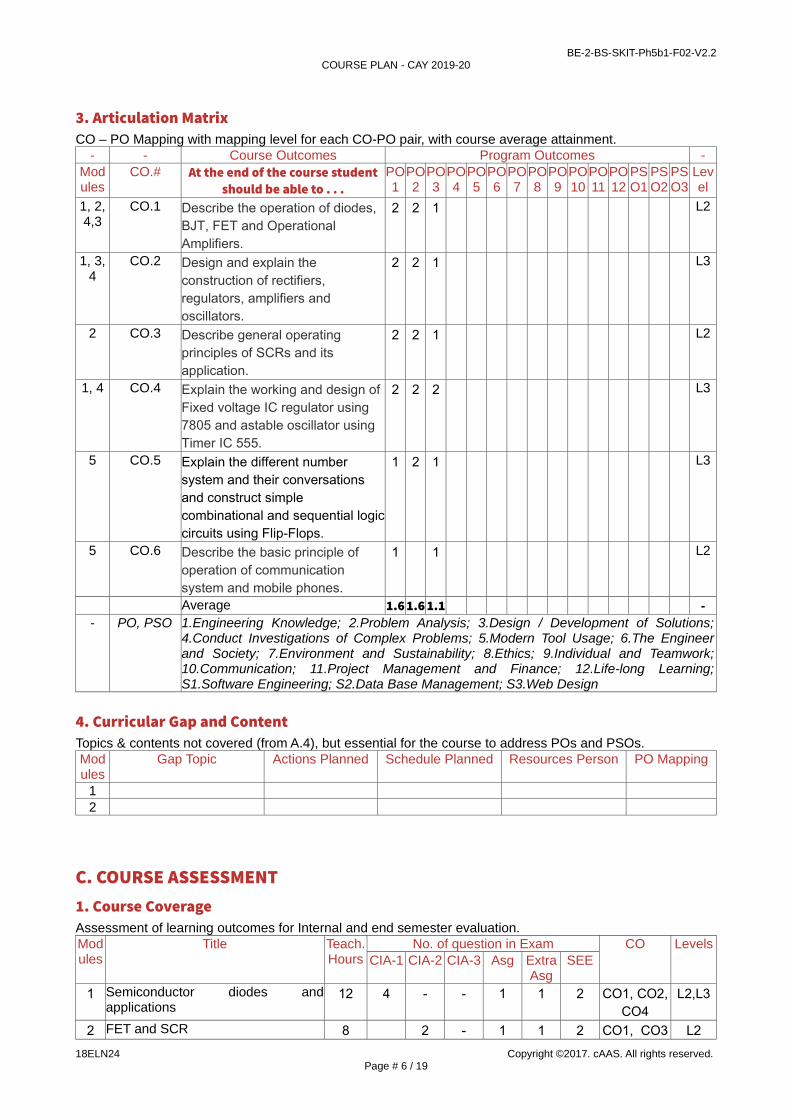
3. Articulation MatrixCO – PO Mapping with mapping level for each CO-PO pair, with course average attainment.
- - Course Outcomes Program Outcomes -Modules
CO.# At the end of the course studentshould be able to . . .
PO1
PO2
PO3
PO4
PO5
PO6
PO7
PO8
PO9
PO10
PO11
PO12
PSO1
PSO2
PSO3
Level
1, 2,4,3
CO.1 Describe the operation of diodes, BJT, FET and Operational Amplifiers.
2 2 1 L2
1, 3,4
CO.2 Design and explain the construction of rectifiers, regulators, amplifiers and oscillators.
2 2 1 L3
2 CO.3 Describe general operating principles of SCRs and its application.
2 2 1 L2
1, 4 CO.4 Explain the working and design of Fixed voltage IC regulator using 7805 and astable oscillator using Timer IC 555.
2 2 2 L3
5 CO.5 Explain the different number system and their conversations and construct simple combinational and sequential logiccircuits using Flip-Flops.
1 2 1 L3
5 CO.6 Describe the basic principle of operation of communication system and mobile phones.
1 1 L2
Average 1.6 1.6 1.1 -- PO, PSO 1.Engineering Knowledge; 2.Problem Analysis; 3.Design / Development of Solutions;
4.Conduct Investigations of Complex Problems; 5.Modern Tool Usage; 6.The Engineerand Society; 7.Environment and Sustainability; 8.Ethics; 9.Individual and Teamwork;10.Communication; 11.Project Management and Finance; 12.Life-long Learning;S1.Software Engineering; S2.Data Base Management; S3.Web Design
4. Curricular Gap and ContentTopics & contents not covered (from A.4), but essential for the course to address POs and PSOs.Modules
Gap Topic Actions Planned Schedule Planned Resources Person PO Mapping
12
C. COURSE ASSESSMENT1. Course CoverageAssessment of learning outcomes for Internal and end semester evaluation.Modules
Title Teach.Hours
No. of question in Exam CO LevelsCIA-1 CIA-2 CIA-3 Asg Extra
AsgSEE
1 Semiconductor diodes andapplications
12 4 - - 1 1 2 CO1, CO2,CO4
L2,L3
2 FET and SCR 8 2 - 1 1 2 CO1, CO3 L2
18ELN24 Copyright ©2017. cAAS. All rights reserved.Page # 6 / 19
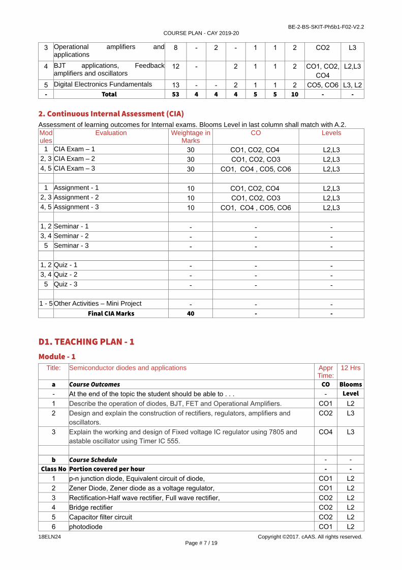
BE-2-BS-SKIT-Ph5b1-F02-V2.2COURSE PLAN - CAY 2019-20
3 Operational amplifiers andapplications
8 - 2 - 1 1 2 CO2 L3
4 BJT applications, Feedbackamplifiers and oscillators
12 - 2 1 1 2 CO1, CO2,CO4
L2,L3
5 Digital Electronics Fundamentals 13 - - 2 1 1 2 CO5, CO6 L3, L2- Total 53 4 4 4 5 5 10 - -
2. Continuous Internal Assessment (CIA)Assessment of learning outcomes for Internal exams. Blooms Level in last column shall match with A.2.Modules
Evaluation Weightage inMarks
CO Levels
1 CIA Exam – 1 30 CO1, CO2, CO4 L2,L32, 3 CIA Exam – 2 30 CO1, CO2, CO3 L2,L34, 5 CIA Exam – 3 30 CO1, CO4 , CO5, CO6 L2,L3
1 Assignment - 1 10 CO1, CO2, CO4 L2,L32, 3 Assignment - 2 10 CO1, CO2, CO3 L2,L34, 5 Assignment - 3 10 CO1, CO4 , CO5, CO6 L2,L3
1, 2 Seminar - 1 - - -3, 4 Seminar - 2 - - -
5 Seminar - 3 - - -
1, 2 Quiz - 1 - - -3, 4 Quiz - 2 - - -
5 Quiz - 3 - - -
1 - 5 Other Activities – Mini Project - - -Final CIA Marks 40 - -
D1. TEACHING PLAN - 1Module - 1
Title: Semiconductor diodes and applications ApprTime:
12 Hrs
a Course Outcomes CO Blooms- At the end of the topic the student should be able to . . . - Level1 Describe the operation of diodes, BJT, FET and Operational Amplifiers. CO1 L22 Design and explain the construction of rectifiers, regulators, amplifiers and
oscillators.CO2 L3
3 Explain the working and design of Fixed voltage IC regulator using 7805 and astable oscillator using Timer IC 555.
CO4 L3
b Course Schedule - -Class No Portion covered per hour - -
1 p-n junction diode, Equivalent circuit of diode, CO1 L22 Zener Diode, Zener diode as a voltage regulator, CO1 L23 Rectification-Half wave rectifier, Full wave rectifier, CO2 L24 Bridge rectifier CO2 L25 Capacitor filter circuit CO2 L26 photodiode CO1 L2
18ELN24 Copyright ©2017. cAAS. All rights reserved.Page # 7 / 19

BE-2-BS-SKIT-Ph5b1-F02-V2.2COURSE PLAN - CAY 2019-20
7 LED CO1 L28 Photocoupler CO1 L29 Numericals on diodes CO1 L3
10 Numericals on rectifiers CO2 L311 Numericals on rectifiers CO2 L312 78XX series and 7805 Fixed IC voltage regulator. CO4 L2
c Application Areas- Students should be able employ / apply the Module learnings to . . .1 Diodes as Rectifiers CO2 L32 Regulators CO4 L2
d Review Questions-1 Explain the working of PN junction diode under forward biased and reverse
biased condition.CO1 L2
2 With neat sketch explain the formation of depletion region in unbiased pn junction CO1 L23 Explain the working of photodiode with its VI characteristics. CO1 L24 Explain the different types of diode approximations CO1 L25 Draw and explain VI characteristics of PN junction diode CO1 L26 What is rectifier? Draw the circuit for HWR and explain its working? Derive the
expression for IDC efficiency η PIV, RMS value of voltageCO2 L3
7 Draw the circuit for FWR and explain its working? Derive the expression for IDC
efficiency η PIV, RMS value of voltageCO2 L3
8 Define ripple factor? Show that for HWR ripple factor is 1.21 CO2 L29 Explain the avalanche and zener break down with the help of VI characteristics? CO1 L2
10 Draw the bridge rectifier circuit and explain its operation with waveforms. Showthat ripple factor is 0.48?
CO2 L3
11 With relevant waveforms derive expression for IDC, IRMS and riipple factor of aFWR?
CO2 L3
12 Explain how a zener diode can be used as voltage regulator? Also explain itsperformance?
CO1 L2
13 What is 78XX series? Explain the 7805 fixed IC voltage regulator? CO4 L214 A full wave rectifier uses 2 diodes having internal resistance of 10 Ω each. The
transformer RMS secondary voltage from center to each end is 200 V. find Im,Idc, Irms and Vdc if the load is 800 Ω
CO2 L3
e Experiences - -12
E1. CIA EXAM – 1a. Model Question Paper - 1CrsCode:
18ELN24 Sem: II Marks: 50 Time: 1hr 45minutes
Course: Basic Electronics- - Note: Answer all questions, each carry equal marks. Module : 1 Marks CO Level1 a Explain the function of zener diode voltage regulator with neat circuit
diagram and relevant equations for zener current8 CO1 L2
b Explain the working of center tapped FWR and derive an expression for the following
8 CO2 L2
18ELN24 Copyright ©2017. cAAS. All rights reserved.Page # 8 / 19
BE-2-BS-SKIT-Ph5b1-F02-V2.2COURSE PLAN - CAY 2019-20
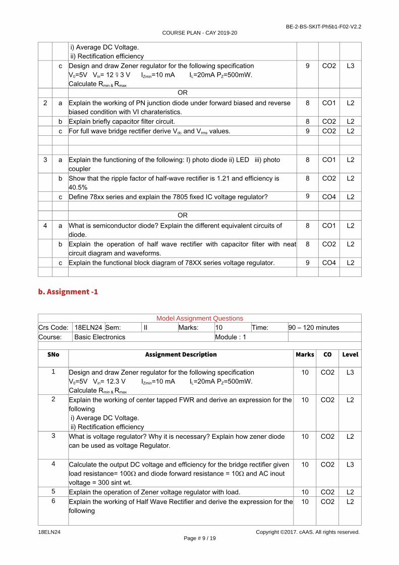
i) Average DC Voltage. ii) Rectification efficiency
c Design and draw Zener regulator for the following specificationV0=5V Vin= 123 V IZmin=10 mA IL=20mA PZ=500mW.Calculate Rmin & Rmax
9 CO2 L3
OR
2 a Explain the working of PN junction diode under forward biased and reverse biased condition with VI charateristics.
8 CO1 L2
b Explain briefly capacitor filter circuit. 8 CO2 L2c For full wave bridge rectifier derive Vdc and Vrms values. 9 CO2 L2
3 a Explain the functioning of the following: I) photo diode ii) LED iii) photo coupler
8 CO1 L2
b Show that the ripple factor of half-wave rectifier is 1.21 and efficiency is 40.5%
8 CO2 L2
c Define 78xx series and explain the 7805 fixed IC voltage regulator? 9 CO4 L2
OR
4 a What is semiconductor diode? Explain the different equivalent circuits of diode.
8 CO1 L2
b Explain the operation of half wave rectifier with capacitor filter with neatcircuit diagram and waveforms.
8 CO2 L2
c Explain the functional block diagram of 78XX series voltage regulator. 9 CO4 L2
b. Assignment -1
Model Assignment QuestionsCrs Code: 18ELN24 Sem: II Marks: 10 Time: 90 – 120 minutesCourse: Basic Electronics Module : 1
SNo Assignment Description Marks CO Level
1 Design and draw Zener regulator for the following specificationV0=5V Vin= 12.3 V IZmin=10 mA IL=20mA PZ=500mW.Calculate Rmin & Rmax
10 CO2 L3
2 Explain the working of center tapped FWR and derive an expression for thefollowing i) Average DC Voltage. ii) Rectification efficiency
10 CO2 L2
3 What is voltage regulator? Why it is necessary? Explain how zener diode can be used as voltage Regulator.
10 CO2 L2
4 Calculate the output DC voltage and efficiency for the bridge rectifier given load resistance= 100Ω and diode forward resistance = 10Ω and AC inout voltage = 300 sint wt.
10 CO2 L3
5 Explain the operation of Zener voltage regulator with load. 10 CO2 L26 Explain the working of Half Wave Rectifier and derive the expression for the
following10 CO2 L2
18ELN24 Copyright ©2017. cAAS. All rights reserved.Page # 9 / 19

BE-2-BS-SKIT-Ph5b1-F02-V2.2COURSE PLAN - CAY 2019-20
i) Average DC Voltage.ii) Rectification efficiency
7 Draw the circuit of FWR and show that ripple factor is equal to 0.48 and efficiency is 81%
10 CO2 L3
8 With neat circuit diagram and waveform explain the working of full wave bridge rectifier.
10 CO2 L2
9 Explain briefly capacitor filter circuit. 10 CO2 L210 With a neat circuit diagram and waveforms, explain the working of a half
wave rectifier.10 CO2 L2
11 Write a note on voltage regulator circuit. 10 CO2 L212 Explain the function of zener diode voltage regulator with neat circuit
diagram and relevant equations for zener current10 CO2 L2
13 Prove that ripple factor of HWR rectifier is 1.21 10 CO2 L314 Define line regulation and load regulator 10 CO2 L215 Discuss the performance of zener diode in terms of source and load effects 10 CO1 L216 Explain the functioning of the following: I) photo diode ii) LED iii) photo
coupler10 CO1 L2
17 Define 78xx series and explain the 7805 fixed IC voltage regu/lator? 10 CO2 L218 Explain the function of zener diode voltage regulator with neat circuit
diagram and relevant equations for zener current8 CO1 L2
19 Explain the working of PN junction diode under forward biased and reverse biased condition with VI charateristics.
8 CO1 L2
20 Explain the functioning of the following: I) photo diode ii) LED iii) photo coupler
8 CO1 L2
D2. TEACHING PLAN - 2Module – 2
Title: FET and SCR ApprTime:
8 Hrs
a Course Outcomes CO Blooms- At the end of the topic the student should be able to . . . - Level1 Describe the operation of diodes, BJT, FET and Operational Amplifiers. CO1 L22 Describe general operating principles of SCRs and its application. CO3 L2
b Course Schedule - -Class No Portion covered per hour - -
13 FET and SCR: Introduction to JFET CO1 L2
14 construction and operation, JFET drain characteristics and parameters CO1 L2
15 JFET transfer characteristics, Square law expression ID , Input resistance, CO1 L2
16 MOSFET: Depletion and enhancement type construction, operation, CO1 L2
17 characteristics and symbols, CMOS CO1 L2
18 Silicon Controlled Rectifier- two transistor model, CO3 L2
19 Switching action characteristics and phase control application CO3 L3
20 Numericals CO3 L3
c Application Areas - -- Students should be able employ / apply the Module learnings to . . . - -1 home appliances including lighting, temperature control, fan speed regulation,
heating and alarm activationCO1 L3
2 Used in devices where control of high power is demanded such as lamp dimming,power regulators and motor control and in
CO3 L3
18ELN24 Copyright ©2017. cAAS. All rights reserved.Page # 10 / 19

BE-2-BS-SKIT-Ph5b1-F02-V2.2COURSE PLAN - CAY 2019-20
d Review Questions - --1 Explain the construction and operation of junction field effect transistor? CO1 L22 Draw and explain the JFET drain characteristics and parameters CO1 L23 Draw and explain JFET transfer characteristics CO1 L24 Derive Square law expression ID, and also find the Input resistance? CO1 L25 Construct depletion and enhancement type MOSFET. CO1 L26 Explain the operation, characteristics and symbols of MOSFET CO1 L27 Write a short note on CMOS CO1 L28 Define Silicon Controlled Rectifier. Draw the two transistor equivalent model and
explain with its VI characteristics.CO3 L2
9 Explain the Switching action characteristics of SCR CO3 L210 Explain the Phase control application of SCR CO3 L2
e Experiences - -12
Module – 3Title: Operational Amplifiers and Applications Appr
Time:8 Hrs
a Course Outcomes CO Blooms- At the end of the topic the student should be able to . . . - Level1 Describe the operation of diodes, BJT, FET and Operational Amplifiers. CO1 L2
2 Design and explain the construction of rectifiers, regulators, amplifiers and oscillators.
CO2 L3
b Course ScheduleClass No Portion covered per hour - -
1 Introduction to op-amp, Op-amp input modes. CO1 L22 Op-amp parameters-CMRR, Input offset voltage and current. CO1 L2
3 Op-amp parameters- Input bias current, Input and output impedance , Slew rate CO1 L2
4 Inverting amplifier CO2 L3
5 Non-inverting amplifier CO2 L3
6 Summer, Voltage follower CO2 L3
7 Integrator, differentiator. CO2 L3
8 Comparator. CO2 L3
c Application Areas - -- Students should be able employ / apply the Module learnings to . . . - -
Used as voltage follower, selective inversion circuit, active rectifier, integrator,filter and comparator in medical cardiographs
CO2 L3
Analog computers, analog to digital converters and wave-shaping circuits CO2 L3
d Review Questions - -- The attainment of the module learning assessed through following questions - -
1 What is operational amplifier? Explain the equivalent circuite of op-amp. CO1 L22 List the ideal and practical characteristics of op-amp. CO1 L13 Explain inverting and Non-inverting mode of op-amp. CO2 L24 Distinguish between open loop and closed loop configuration of op-amp. CO2 L25 What is voltage follower w.r.t op-amp? Explain the circuit of voltage follower. CO2 L26 What is op-amp summer circuit? Explain the op-amp based summer circuit with CO2 L2
18ELN24 Copyright ©2017. cAAS. All rights reserved.Page # 11 / 19
BE-2-BS-SKIT-Ph5b1-F02-V2.2COURSE PLAN - CAY 2019-20
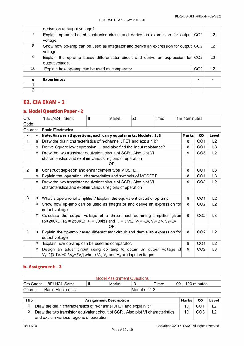
derivation to output voltage?7 Explain op-amp based subtractor circuit and derive an expression for output
voltage.CO2 L2
8 Show how op-amp can be used as integrator and derive an expression for outputvoltage.
CO2 L2
9 Explain the op-amp based differentiator circuit and derive an expression foroutput voltage.
CO2 L2
10 Explain how op-amp can be used as comparator. CO2 L2
e Experiences - -12
E2. CIA EXAM – 2a. Model Question Paper - 2CrsCode:
18ELN24 Sem: II Marks: 50 Time: 1hr 45minutes
Course: Basic Electronics- - Note: Answer all questions, each carry equal marks. Module : 2, 3 Marks CO Level1 a Draw the drain characteristics of n-channel JFET and explain it? 8 CO1 L2
b Derive Square law expression ID, and also find the Input resistance? 8 CO1 L3c Draw the two transistor equivalent circuit of SCR . Also plot VI
characteristics and explain various regions of operation9 CO3 L2
OR
2 a Construct depletion and enhancement type MOSFET. 8 CO1 L3b Explain the operation, characteristics and symbols of MOSFET 8 CO1 L3c Draw the two transistor equivalent circuit of SCR . Also plot VI
characteristics and explain various regions of operation9 CO3 L2
3 a What is operational amplifier? Explain the equivalent circuit of op-amp. 8 CO1 L2b Show how op-amp can be used as integrator and derive an expression for
output voltage.8 CO2 L2
c Calculate the output voltage of a three input summing amplifier givenR1=200kΩ, R2 = 250KΩ, R3 = 500kΩ and Rf = 1MΩ. V1= -2v, V2=2 v, V3=1v
9 CO2 L3
OR4 a Explain the op-amp based differentiator circuit and derive an expression for
output voltage. 8 CO2 L2
b Explain how op-amp can be used as comparator. 8 CO1 L2c Design an adder circuit using op amp to obtain an output voltage of
Vo=2[0.1V1+0.5V2+2V3] where V1, V2 and V3 are input voltages.9 CO2 L3
b. Assignment – 2
Model Assignment QuestionsCrs Code: 18ELN24 Sem: II Marks: 10 Time: 90 – 120 minutesCourse: Basic Electronics Module : 2, 3
SNo Assignment Description Marks CO Level1 Draw the drain characteristics of n-channel JFET and explain it? 10 CO1 L22 Draw the two transistor equivalent circuit of SCR . Also plot VI characteristics
and explain various regions of operation10 CO3 L2
18ELN24 Copyright ©2017. cAAS. All rights reserved.Page # 12 / 19
BE-2-BS-SKIT-Ph5b1-F02-V2.2COURSE PLAN - CAY 2019-20
3 What are the applications of SCR. Explain 10 CO3 L2
4 Draw the circuit diagram to show how an SCR can be triggered by application of a pulse to the gate terminal. Sketch the circuit waveforms and explain its operation?
10 CO3 L2
5 Sketch typical SCR forward and reverse characteristics. Identify all regions of characteristics and all important current and voltage level?
10 CO3 L2
6 Draw the drain characteristics of p-channel JFET and explain it? 10 CO1 L27 Explain the construction and operation of junction field effect transistor? 10 CO1 L38 Draw and explain the JFET drain characteristics and parameters 10 CO1 L39 Draw and explain JFET transfer characteristics 10 CO1 L310 Derive Square law expression ID, and also find the Input resistance? 10 CO1 L311 Construct depletion and enhancement type MOSFET. 10 CO1 L312 Explain the operation, characteristics and symbols of MOSFET 10 CO1 L313 Write a short note on CMOS 10 CO1 L314 Define Silicon Controlled Rectifier. Draw the two transistor equivalent model
and explain with its VI characteristics.10 CO3 L3
15 Explain the Switching action characteristics of SCR 10 CO3 L316 Explain the Phase control application of SCR 10 CO3 L317 What is operational amplifier? Explain the equivalent circuit of op-amp. 10 CO1 L218 List the ideal and practical characteristics of op-amp. 10 CO1 L219 Explain inverting and Non-inverting mode of op-amp. 10 CO2 L220 Distinguish between open loop and closed loop configuration of op-amp. 10 CO2 L221 What is voltage follower w.r.t op-amp? Explain the circuit of voltage follower. 10 CO2 L222 What is op-amp summer circuit? Explain the op-amp based summer circuit with
derivation to output voltage?10 CO2 L2
23 Explain op-amp based subtractor circuit and derive an expression for outputvoltage.
10 CO2 L2
24 Show how op-amp can be used as integrator and derive an expression foroutput voltage.
10 CO2 L2
25 Explain the op-amp based differentiator circuit and derive an expression foroutput voltage.
10 CO2 L2
26 Explain how op-amp can be used as comparator. 10 CO2 L227 Design an adder circuit using op amp to obtain an output voltage of
Vo=2[0.1V1+0.5V2+2V3] whwre V1, V2 and V3 are input voltages.10 CO2 L3
28 What is an op-amp. Explain the ideal characteristics of the op-amp? 10 CO1 L229 Define the following in case of a practical op-amp i) Slew rate ii) CMRR iii)
Off set voltages iv) PSRR10 CO2 L2
30 Calculate the output voltage of a three input summing amplifier givenR1=200kΩ, R2 = 250KΩ, R3 = 500kΩ and Rf = 1MΩ. V1= -2v, V2=2 v, V3=1v
10 CO2 L3
31 Write any four advantages of negative feedback amplifiers? 10 CO2 L232 What is operational amplifier? Explain the equivalent circuit of op-amp. 10 CO1 L238 Explain op-amp based subtractor circuit and derive an expression for output
voltage.10 CO2 L2
39 Show how op-amp can be used as integrator and derive an expression foroutput voltage.
10 CO2 L2
40 Explain the op-amp based differentiator circuit and derive an expression foroutput voltage.
10 CO2 L2
18ELN24 Copyright ©2017. cAAS. All rights reserved.Page # 13 / 19

BE-2-BS-SKIT-Ph5b1-F02-V2.2COURSE PLAN - CAY 2019-20
D3. TEACHING PLAN - 3Module – 4
Title: BJT Applications, Feedback Amplifiers and Oscillators ApprTime:
12 Hrs
a Course Outcomes CO Blooms- At the end of the topic the student should be able to . . . - Level1 Describe the operation of diodes, BJT, FET and Operational Amplifiers. CO1 L2
2 Design and explain the construction of rectifiers, regulators, amplifiers and oscillators.
CO2 L3
3 Explain the working and design of Fixed voltage IC regulator using 7805 and astable oscillator using Timer IC 555.
CO4 L2
b Course ScheduleClass No Portion covered per hour - -
1 BJT as an amplifier CO1 L22 BJT as a switch CO1 L23 Transistor switch circuit to switch ON/OFF an LED and a lamp in a power circuit
using relayCO1 L2
4 Feedback amplifiers-Principle, properties and advantages of negative feedback CO2 L25 Types of feedback, Voltage series feedback and gain stability with feedback CO2 L26 Oscillators- Barkhaunsen’s criteria for oscillation CO2 L27 RC phase shift oscillator CO2 L28 Wein bridge oscillator CO2 L29 IC 555 timer and astable oscillator using IC 555 CO4 L2
10 Numericals on transistors CO2 L311 Numericals on amplifiers CO2 L312 Numericals on oscillators CO2 L3
c Application Areas - -- Students should be able employ / apply the Module learnings to . . . - -1 Used as automatically controlled switches, TTL circuits, amplifiers, current drivers CO2 L32 Applied in Tunable radio transmitters and receivers, signal generators CO4 L3
d Review Questions - -- The attainment of the module learning assessed through following questions - -
1 Explain BJT as an amplifier? CO1 L22 Explain BJT as a switch? CO1 L23 Explain Transistor switch circuit to switch ON/OFF an LED CO2 L24 Describe the lamp in a power circuit using relay? CO2 L25 Explain the principle of feed back amplifiers? CO2 L26 List the types of feedback. Explain the properties and advantages of negative
feedback. CO2 L2
7 Explain the Voltage series feedback CO2 L28 Describe the gain stability with feedback CO2 L29 Explain the Barkhaunsen’s criteria for oscillation CO2 L2
10 Explain the working of RC phase shift oscillator CO2 L211 Explain the working of Wein bridge oscillator CO2 L212 Draw the pin diagram of the IC 555 timer and explain astable oscillator using IC
555CO4 L2
18ELN24 Copyright ©2017. cAAS. All rights reserved.Page # 14 / 19
BE-2-BS-SKIT-Ph5b1-F02-V2.2COURSE PLAN - CAY 2019-20
e Experiences - -1 CO7 L22
Module – 5Title: Appr
Time:13 Hrs
a Course Outcomes CO Blooms- At the end of the topic the student should be able to . . . - Level1 Explain the different number system and their conversations and construct simple
combinational and sequential logic circuits using Flip-Flops.CO5 L3
2 Describe the basic principle of operation of communication system and mobile phones.
CO6 L2
b Course Schedule - -Class No Portion covered per hour - -
1 Difference between analog and digital signals CO5 L22 Number systems: Binary and hexadecimal CO5 L23 Conversion: Decimal to binary and hexadecimal to decimal and vice-versa CO5 L34 Conversion: Decimal to binary and hexadecimal to decimal and vice-versa CO5 L35 Conversion: Decimal to binary and hexadecimal to decimal and vice-versa CO5 L36 Boolean algebra, Basic and universal gates CO5 L37 Half and full adder CO5 L38 Multiplexer, decoder, CO5 L29 SR and JK flip flops CO5 L210 Shift register, CO5 L211 3 bit Ripple counter. CO5 L212 Basic communication system, CO6 L213 Principle of operations of Mobile phone CO6 L2
c Application Areas - -- Students should be able employ / apply the Module learnings to . . . - -1 Temporary data storage, data transfer. Data manipulation, counters CO5 L32 Mobile phones CO6 L2
d Review Questions - -- The attainment of the module learning assessed through following questions - -
1 Differentiate between analog and digital signals CO5 L22 Explain the Binary and hexadecimal forms of numbers CO5 L23 Explain conversion process of Decimal to binary and hexadecimal to decimal and
vice-versaCO5 L2
4 State and prove De-Morgan’s Theorem CO5 L25 Explain the basic laws in boolean algebra CO5 L26 With truth table explain Basic and universal gates CO5 L27 Realize Half and full adder sing basic and universal gates CO5 L28 Explain the working of the following: I) Multiplexer ii) decoder iii) SR flip flop iv) JK
flip flop CO5 L2
9 Explain the following: I) Shift register ii) 3 bit Ripple counter. CO5 L210 With a neat block diagram explain the communication system? CO6 L2
18ELN24 Copyright ©2017. cAAS. All rights reserved.Page # 15 / 19

BE-2-BS-SKIT-Ph5b1-F02-V2.2COURSE PLAN - CAY 2019-20
11 Explain the Principle of operations of Mobile phone CO6 L2
e Experiences - -1 CO10 L22 CO9
E3. CIA EXAM – 3a. Model Question Paper - 3Crs Code 18ELN24 Sem: II Marks: 50 Time: 1hr 45 minutesCourse: Basic Electronics
- - Note: Answer all questions, each carry equal marks. Module : 4, 5 Marks CO Level1 a Explain BJT as an amplifier? 8 CO1 L2
b Explain Transistor switch circuit to switch ON/OFF an LED 8 CO2 L2c Explain the working of astable oscillator constructed using 555 timer 9 CO4 L2
OR2 a Explain BJT as a switch? 8 CO1 L2
b Explain the Barkhaunsen’s criteria for oscillation 8 CO2 L2c Draw the pin diagram of the IC 555 timer and explain astable oscillator
using IC 5559 CO4 L2
3 a Solve the following (i) (ABC)16=(?)2 (ii) (985.85)10=(?)8 8 CO5 L2
b Reduce the following Boolean expression and implement using basic gates.F=ABC+ABC+ABC+ABC
8 CO5 L2
c Explain the Principle of operations of Mobile phone 9 CO6 L2
4 a Write the decimal equivalent of (10AB)16 8 CO5 L2b Design a logic circuit using basic gates with three inputs A, B, C and output
Y that goes low only when A is high and B and C are different8 CO5 L2
c With a neat block diagram explain the communication system? 9 CO6 L2
b. Assignment – 3
Model Assignment QuestionsCrs Code: 18ELN24 Sem: II Marks: 10 Time: 90 – 120 minutesCourse: Basic Electronics Module : 4, 5
SNo Assignment Description Marks CO Level
1 Explain BJT as an amplifier? 8 CO1 L22 Explain BJT as a switch? 8 CO1 L23 Explain Transistor switch circuit to switch ON/OFF an LED 8 CO2 L24 Describe the lamp in a power circuit using relay? 8 CO2 L25 Explain the principle of feed back amplifiers? 8 CO2 L26 List the types of feedback. Explain the properties and advantages of
negative feedback. 8 CO2 L2
7 Explain the Voltage series feedback 8 CO2 L28 Describe the gain stability with feedback 8 CO2 L29 Explain the Barkhaunsen’s criteria for oscillation 8 CO2 L2
10 Explain the working of RC phase shift oscillator 8 CO2 L211 Explain the working of Wein bridge oscillator 8 CO2 L212 Draw the pin diagram of the IC 555 timer and explain astable oscillator 8 CO4 L2
18ELN24 Copyright ©2017. cAAS. All rights reserved.Page # 16 / 19
BE-2-BS-SKIT-Ph5b1-F02-V2.2COURSE PLAN - CAY 2019-20
using IC 55513 Differentiate between analog and digital signals 8 CO5 L214 Explain the Binary and hexadecimal forms of numbers 8 CO5 L215 Explain conversion process of Decimal to binary and hexadecimal to
decimal and vice-versa8 CO5 L2
16 State and prove De-Morgan’s Theorem 8 CO5 L217 Explain the basic laws in boolean algebra 8 CO5 L218 With truth table explain Basic and universal gates 8 CO5 L219 Realize Half and full adder sing basic and universal gates 8 CO5 L220 Explain the working of the following: I) Multiplexer ii) decoder iii) SR flip
flop iv) JK flip flop 8 CO5 L2
21 Explain the following: I) Shift register ii) 3 bit Ripple counter. 8 CO5 L222 With a neat block diagram explain the communication system? 8 CO6 L223 Explain the Principle of operations of Mobile phone 8 CO6 L224 Solve the following (i) (ABC)16=(?)2 (ii) (985.85)10=(?)8 8 CO5 L2
25 Reduce the following Boolean expression and implement using basicgates. F=ABC+ABC+ABC+ABC
8 CO5 L2
26 Write the decimal equivalent of (10AB)16 8 CO5 L2
F. EXAM PREPARATION1. University Model Question PaperCourse: Basic Electronics Month / Year May /2019Crs Code: 18ELN24 Sem: II Marks: 100 Time: 180 minutesModu
leNote Answer all FIVE full questions. All questions carry equal marks. Marks CO Level
1 a Explain the working of PN junction diode under forward biased and reversebiased condition.
7 CO1 L2
b With neat sketch explain the formation of depletion region in unbiased pnjunction
6 CO1 L2
c Explain the working of photodiode with its VI characteristics. 7 CO1 L2OR
1 a With relevant waveforms derive expression for IDC, IRMS and riipple factor of aFWR?
7 CO2 L3
b Explain how a zener diode can be used as voltage regulator? Also explainits performance?
6 CO1 L2
c What is 78XX series? Explain the 7805 fixed IC voltage regulator? 7 CO4 L2
2 a Draw and explain JFET transfer characteristics 5 CO1 L3b Derive Square law expression ID, and also find the Input resistance? 7 CO1 L3c Construct depletion and enhancement type MOSFET. 8 CO1 L3
OR2 a What are the applications of SCR. Explain. 5 CO3 L2
b Draw the circuit diagram to show how an SCR can be triggered by application of a pulse to the gate terminal. Sketch the circuit waveforms and explain its operation?
7 CO3 L2
c Sketch typical SCR forward and reverse characteristics. Identify all regions of characteristics and all important current and voltage level?
8 CO3 L2
3 a Distinguish between open loop and closed loop configuration of op-amp. 5 CO2 L218ELN24 Copyright ©2017. cAAS. All rights reserved.
Page # 17 / 19

BE-2-BS-SKIT-Ph5b1-F02-V2.2COURSE PLAN - CAY 2019-20
b What is voltage follower w.r.t op-amp? Explain the circuit of voltage follower. 7 CO2 L2c What is op-amp summer circuit? Explain the op-amp based summer circuit
with derivation to output voltage?8 CO2 L2
OR3 a Calculate the output voltage of a three input summing amplifier given
R1=200kΩ, R2 = 250KΩ, R3 = 500kΩ and Rf = 1MΩ. V1= -2v, V2=2 v, V3=1v7 CO2 L3
b Write any four advantages of negative feedback amplifiers? 5 CO2 L2c What is operational amplifier? Explain the equivalent circuit of op-amp. 8 CO1 L2
4 a Explain Transistor switch circuit to switch ON/OFF an LED 5 CO2 L2b Describe the lamp in a power circuit using relay? 7 CO2 L2c Explain the principle of feed back amplifiers? 8 CO2 L2
OR4 a Explain the working of RC phase shift oscillator 5 CO2 L2
b Explain the working of Wein bridge oscillator 7 CO2 L2c Draw the pin diagram of the IC 555 timer and explain astable oscillator
using IC 5558 CO4 L2
5 a State and prove De-Morgan’s Theorem 5 CO5 L2b Explain the working of the following: I) Multiplexer ii) decoder iii) SR flip flop
iv) JK flip flop 7 CO5 L2
c With a neat block diagram explain the communication system? 8 CO6 L2OR
5 a With truth table explain Basic and universal gates 5 CO5 L2b Realize Half and full adder sing basic and universal gates 7 CO5 L2c Explain the Principle of operations of Mobile phone 8 CO6 L2
2. SEE Important QuestionsCourse: Basic Electronics Month / Year May /2018Crs Code: 18ELN24 Sem: 2 Marks: 80 Time: 180 minutes
Note Answer all FIVE full questions. All questions carry equal marks. - -Module
Qno. Important Question Marks CO Year
1 a What is rectifier? Draw the circuit for HWR and explain its working? Derivethe expression for IDC efficiency η PIV, RMS value of voltage
10 CO2 2004
b Draw the circuit for FWR and explain its workintg? Derive the expression forIDC efficiency η PIV, RMS value of voltage
10 CO2 2013
c With neat circuit diagram explain working princirples of bridge wave rectifier? 10 CO2 2013d Explain the performance of zener diode in terms of souce and load effects. 10 CO1 2013e Explain photo diode with neat diagram? 10 CO1 2012
2 a Draw the drain characteristics of a n-channel JFET and explain it. 10 CO2 2012b Explain the construction and operation of MOSFET 8 CO2 2010c Sketch and explain the VI characteristics if SCR? 8 CO3 2010d Draw two transister equivalent model of SCR. 10 CO3 2012e Explain phase control application using SCR 10 CO3 2012
3 a Explain the ideal opamp characteristics. 8 CO1 2012b Explain the following i)CMRR II)Slew rate iii) PSRR 8 CO1 2012
18ELN24 Copyright ©2017. cAAS. All rights reserved.Page # 18 / 19
BE-2-BS-SKIT-Ph5b1-F02-V2.2COURSE PLAN - CAY 2019-20
c With a help of circuit diagram, derive the output voltage for integrator 8 CO2 2013d Show how an opamp can be used as differentiator. derive expression for
output voltage9 CO2 2010
e Draw the following circuit using opamp: i)adder ii) voltage follower. 9 CO2 2014
4 a Explain how BJT can be used as an amplifier. 10 CO2 2009b Give four advantages of negative feedback in amplifier. 10 CO2 2009c With circuit explain the working of RC phase shift oscillator. 10 CO2 2011d Explain barkhausen criterian for oscillation. 10 CO2 2009e Draw the pin diagram of the IC 555 timer and explain astable oscillator
using IC 5558 CO4 2011
5 a What are universal gates? Realize AND and OR gates using universal gates. 10 CO5 2011b Subtract (57)10 from (43)10 using 2’s complement form 10 CO5 2011c Realize two input EX-OR gate using only NAND gates. 10 CO5 2010d Explain with a neat diagram shift register 12 CO5 2012e With a neat diagram explain communication systems. 12 CO6 2009
18ELN24 Copyright ©2017. cAAS. All rights reserved.Page # 19 / 19