Solid State Lighting Annex: Quality and Performance ... - IEA 4E
Upload
khangminh22Category
view
0download
0
S Ti. FILE COYAEOSRTR. 90 0744, I-iLE COPY00N4e Optical Symbolic Processor forNN Expert System Execution
Final Technical Report I
Period of Performance: June 1, 1986 to December 31, 1989
Sponsored by:
Air Force Office of Scientific Research
and
Advanced Research Projects Agency (DoD)ARPA Order No. 5794
Contract #F49620-86-C-0082
Prepared by:
Julian BristowPrincipal Research Scientist
Honeywell Systems and Research CenterBloomington, Minnesota
A7.
The views and conclusions contained In this document are those of theauthors and should not be Interpreted as necessarily representing theofficial policies, either expressed or Implied, of the Defense AdvancedResearch Projects Agency or the U.S. Government.

REPORT DOCUMENTA, lON PAGE ofm ,a oz wpwtg4 i W, Morelq am ow "" I -,~ C "'mew. "' we q "W I w -mq w waq U WWm..9,jeemq m lm ma M~i a m es. o/wE 'a m e ,s weq ta toltatice" " of' 'lO' .bt m'.Me CO tfiA o w SR W if4m Mwq $OUmt s4e t 0. .-
c0Iai8m "011140 . aui qW4 am OVt.@1S . tO *1 o oA W rt6I o ft otaowtn r i eWWSA aw w" mm" of, daw n om of IF.Oa..Qiti. WI 'US. mova"U t 6a" p t wo " i t. fl@o Maq ot "we f S Wiqm. 'aestew' e iuiatle wat o e 0801M NAftwqte 1C Ifni
1. AGENCY US& ONLY (Leg,. bt"w) 2. REPORT oATE 3. REPORT TYPE AfNo DATH C3vE10I FINAL 01 J un 86 TO 31 Dec 89
TITLE ANO SUGTMm S. PUNOSG NUMBERS
Optical Symbolic Processor for Expert SystemExecution
' A'O")ARPA ORDER NO 5794L. AUTH4ORS)
Dr Anis Husain
7. PEFR0MNG ORGANIZATION NAME(S) AND AOORESS(ES) LP000 NUMB ER TO
Honeywell Inc 44Corporate Technology Center AFOSR ;Ji) .) I10701 Lyndale AveBloomington MN 55420
g. SSORINGMONITORING AGENCY NAME(S) AND A.MESS(ES) 16. ILSD INGIOORNGAGENC REPOR NUMME
AFOSR/NEBldg 410Bolling AFB Washington DC 20332-6448 F49620-86-C-0082Dr. Alan E. Craig -_,,
it. SUPPUMITANY NOTES
". O STlJRIITONIAVAILAUIUTY STATEMENT n 12b. OISTUSJW- Cool
APPROVED FOR PUBLIC RELEASE: DISTRIBUTION IS UNLIMITED
13. A8STRACt _(N4la4Mma200MW0*The goal of this program was to develop key concepts for optical symboliccomputing. During the course of the program, both a top-down and bottom-upapproach was taken to develop an architecture for symbolic computing. Theapproach was intended to result in an architecture suitable for the designgoals while being implementable with practical components.Key results of the program include the following:
- Design of a unique symbolic processing architecture,- Identification of lack of suitable addressable optical memory as amajor impediment in the implementation of existing paradigms,- Demonstration of a unique, critically needed polarization basedmodulator with 17 dB extinction ratio, and demonstration of the world'shighest extinction ratio (23 dB) of AIGaAs/GaAs modulator at I GHz, /I- Demonstration of high density modulator arrays with the world'ssmallest pitch (20 urn) and less than 20 dB crosstalk, ( (- -
14. SUBCT TERMS IS. NUM.R O PAGES
I&. PUICE coca
17. SECUITY CLASSNICATOU lIs. SECURITY CLASSiIOCATION 1t. SECURITY C.$slIcATOn 0f .tIITATION OF ABSTRACT
OF 4ER " OP THIS PAGE Of ABSTRACT
UNCLASSIFIED UNCLASSIFIED UNCLASSIFIED UNLIMITED
NtSN F" 029.U0 -00 Stand P g2 (ROV 2-89)
RINm i 71m0-20S0 0-m m aw AO n

GENERAL INSTRUCTIOP4S FOR .COMPLETING SF-296Th Reort Documentation Page (ROP) is used in announcing and cataloging reports. it is importantthat this information be consistent with the rest of the report, particulaly the cover and title page.Instuctions for filling in each block of the form follow, It is important to sty within ft lines to meetapdcal scaraxrng 1qWeoments.
Black 1. Agency Us Only (Leave blank). Block 12a. Distnbution/AvaiiabilitvStatementDenotes public availability or limitations. Cite-any
Block 2. Roo ae Full publication date availability to the public. Enter additionalincluding day, month, and year. if available (e.g. 1 limitations or special markcings in all capitals (e.g.Ian 88). Must cite at teast the year. NOFORN, REL, ITAR).
Slaock 3. Tyce of Report and Oates Covered. 000 - See DoOl) 5230.24, DOistributionState whether report is interim, final, etc. ifStemnsoTchiaapplicable, enter inclusive report dates (e.g. 10 Statements. onTchia
Jun 7 - 0 Ju 1111).001E - See authorities.Skack 4. Title ad Subtitle. A title is taken from NASA.- See Handbook NHS 2200.2.the part of the report that provides the most NTIS -Leave blank.meaningful and complete information. When areport is prepared in more than one volume, Bok1b itiuinCdrepeat the primary title, add volume number, and Bok1binclude subtitle for th* specific volume. On 00-Laebakdlassified documents enter the title classification 000 - Eae blEnk.btincaeore
iparer eses from the Standard Distribution forSlick S. Fundina Numbers. To include contract Unclassified Scientific and Technicaliind grant numbers; may include program Reports.element number(s), project number(s), task NASA - Lease blank.number(s), and work unit number(s). Use the NTIS - Leave blank.following labels:
C - Contract Pit - Project Block 13. A Include a brief (MaximumG -Grant TA -Task 200 worth) factual summary of the mostPtE - Program WUJ Work Unit significant information contained in the report.
Element Accession No.
Mack 6. Auhrs Name(s) of peirson(s) Slock 14. Suic To Il eywords or phrasesresponsible for writing the report, performing identfying major subjects in the report.the research, or credited with the content of thereprt if editor or complIer4, this should fol lowthe name(s). Slack 19S. Number of PAMe. Enter the total
number of pages.Slack 7. Performing Organization Name(s) andAdrolgflk Self-explanatory. Slack 16l. Pjrg,*ggj. Enter appropriate priceSlaock L. Perforiing Orcanizaton Rawn- code (NAiS onlfy).Nubr Enter the unique alphaniumeric report
numersaming ed bypo thBraetlacks 17..- 19. Security Cassificator Self.perfrmng~ rearLexplanatory. Enter U.S. Security Classification in
Blocki9. SponsorinalMonitorina Aaency Nam*(s) accordance with U.S. Security Regulations (i.e.,an drstd Self-expl anatory. U NCLASSIFIED). If farm contains clasified
information, stamp classification on the top andSlack 10. S osrinalMonitoring Aaenc bottom of the page.Report Nmber.L (if known)
Gkick I11. Suaalementrv Notes. Enter Slack 20. Umnitatiori of Absrf This block mustinformation not included elsewhere such as: be completed to assign a limitation to thePrepared in cooperation with ... ; Trans. of ... ; To be abstract. Enter either UL (unlimited) or SAR (samepublished in.... When a report is revised, include as report). An entry in tiws black is necessary ifa statement whether the new report supersedes the abstract is to be limited. if blank. the abstractor supplemeints the older report. is assumed to be unlimited.
stanewg Pgtf 1"6 Im8 (Re,. 2-49)

II
OPTICAL SYMBOLIC PROCESSOR FOR EXPERT SYSTEM EXECUTION
FINAL TECHNICAL REPORT
i Period of Performance: June 1, 1986 to December 31 1989
3 Sponsored by:
Air Force Office of Scientific Research
and
Advanced Research Projects Agency (DOD)ARPA Order No. 5794
Contract #F49620-86-C-0082IPrepared by:
Julian Bristow
Principal Research ScientistHoneywell Systems and Research Center, Bloomington, Minnesota
IPrepared by: V ' ,5 Date: _______TC
I Julian Bristow
I Approved by: Date: 5-J)1170
Anis HusainSection Head
Approved by: _______0_ Date:
. David LambDepartment Head
The views and conclusions contained in this document are those3cf the authors and should not be interpreted as necessarilyrepresenting the official policies, either expressed orimplied, of the Defense Advanced Research Projects Agency orthe U.S. Government.
I

Accession ForContents CPVTIS GRA
6 DTIC TABUnannounced
1. Summary Justification
3 2. Expert Systems in Optics
3. Languages for Artificial Intelligence Systems Distribution/
Availability Codes3.1 Imperative languages jAva-il ador3.2 Logic languages Dist Special
3.3 Functional languagesI4. Computational models for Symbolic Processing
4.1 Computational models for PARLOG4.2 Computational models for functional languages4.3 Requirements for supporting computational models
5. Primitives in Optical Computing
5.1 Data representation5.2 Memory5.3 Interconnections5.4 Processing
3 6. Optical Implementations of Symbolic Processing Languages
6.1 Issues in optical implementation of PARLOG6.2 Issues in optical implementation of functional
programming languages
7. SPARO - Symbolic Processing Architecture in Optics
7.1 Processor design outline7.2 Analysis ot the SPARO optical symbolic computing
i architecture
7.2.1 Computational theory background7.2.2 Combinator graph reduction7.2.3 Execution model of SPARO7.2.4 Instruction passing
7.2.5 Mapping combinator graphs onto SPARO7.2.6 Graph representation7.2.7 Combinator graph node types7.2.8 Single SPARO node execution7.2.9 Abstract finite state machine model of a
processor node7.2.10 SPARO computer architecture7.2.11 Control structures for CGR in SPARO7.2.12 Macroinstructions and messages7.2.13 Basic control instructions7.2.14 Control requirements in the network processor7.2.15 Memory management in SPARO
U

I
7.2.16 Functional units in SPARO i7.2.17 Complex control structures7.2.18 Recursion7.2.19 Iteration
8. Optical implementation of SPARO 38.1 Optical primitives8.2 Optical layout8.3 The architecture of the network8.4 Architecture of the processor
9. Sparo performance analysis 39.1 Serial reduction rate9.2 Cycle time of SPARO9.3 Parallel reduction rate9.4 SPARO conclusions
10. Interconnection Network Analysis
10.1 Introduction10.2 Performance of ring networks 5
10.2.1 Principle of operation10.2.2 Analytical model of the ring network10.2.3 Throughput of ring networks10.2.4 Conclusions
10.3 Performance of single stage and replicated shuffleexchange networks
10.3.1 The shuffle exchange network10.3.2 Operational model of the SEN I10.3.4 Replicated shuffle exchange networks
10.3.5 Performance of single stage and replicatedshutfle exchange networks
10.4 Comparison of RSENs with other networks
10.4.1 Comparisons with MINs n10.4.2 Comparisons with the hypercube
11. Optical Implementations of Shuffle Exchange Networks
11.1 Existing optical shuffle exchange designs
11.1.1 Perfect shuffle11.1.2 Exchange switch
11.2 Required functionalities of the exchange switch I11.2.1 Conflict resolution by the exchange switch11.2.2 Delivery of messages 5
I

I
1 11.2.3 Detection of a valid message
11.3 Possible approaches to an optical exchange switchdesign
11.3.1 Polarization encoding gate11.3.2 Acousto Optic Gate11.3.3 Photorefractive gate11.3.4 Waveguide or coupler11.3.5 Fredkin gate implementation
11.4 Design and analysis of an optical exchange switch
11.4.1 A passive optical exchange using polarizationas control
11.4.2 A passive optical message update11.4.3 Detection of age and collision decisions11.4.4 Conclusions in designing an optical smart
exchange switch
11.5 Hybrid SEN Implementations
11.5.1 SEN and processor array interface11.5.2 Shuffle exchange stage11.5.3 Electronic SEN implementations11.5.4 Off chip interconnection delays11.5.5 Backplane wiring11.5.6 High-speed electronic implementation11.5.7 Network delay for GaAs implementation11.5.8 Network delay for ECL implementation11.5.9 Network cycle time11.5.10 Parallel versus serial message transfers
j 11.6 Optical and electro-optic SENs
11.6.1 Processor complexity11.6.2 Processor granularity11.6.3 SEN schemes11.6.4 Serial optical shuffle1 11.6.5 Alternate partitioning of PEs
12. Optical vs Electrical Interconnection networks
i 12.1 Connectivity requirements of some network topologies
12.1.1 Hypercube interboard connectivity12.1.2 Crossbar interboard connectivity12.1.3 Shuffle exchange interboard connectivity
SiI

II
12.2 Board level interconnect technologies in optics
12.2.2 Optical interconnect comparisons I12.2.3 Fiber optics12.2.4 Polymer waveguides12.2.5 Planar holograms12.2.6 Bulk optics and microoptics
12.3 Summary of optical backplane approaches12.4 Sources and detectors for shuffle connectivity I12.5 Crossovers in waveguide interconnects
12.5.1 Shuffle connection12.5.2 Hypercube connection n
13. Hybrid Optoelectronic Implementations of Shuffle Exchange
13.1 Multilayer Polyimide Implementa.tions13.2 Board to backplane connector design13.3 Tolerances in Selfoc based connectors13.4 Fanout chip design
14. Waveguide Modulator Development I
14.1 Modulator design choices14.2 Waveguide design 3
14.2.1 Structures analyzed14.2.2 Compensated polarization-modulator
14.3 Mask design14.4 Materials growth14.5 Processing14.6 Waveguide and modulator testing
14.6.1 Waveguide performance14.6.2 Phase modulator performance S14.6.3 Mach-Zehnder performance
14.6.4 Polarization modulator performance14.6.5 Anomalous polarization behavior14.6.6 Polarization analyzer performance14.6.7 High frequency and array operation
15. Conclusions I16. References 3
III

I
i. Summary
I The goal of this program was to develop key concepts foroptical symbolic computing. During the course of the program, botha top-down and bottom-up approach was taken to develop anarchitecture for symbolic computing. The approach was intended toresult in an architecture suitable for the design goals while beingimplementable with practical components.
Key results of the program include the following:
- Design of a unique symbolic processing architecture
- Identification of lack of suitable addressable opticalmemory as a major impediment in the implementation ofexisting paradigms
- Identification of the interconnection network as themajor performance limitation for massively parallelsystems
- Demonstration of a unique, critically neededpolarization based modulator with 17 dB extinction ratio,and demonstration of the world's highest extinction ratio(23 dB) of AlGaAs/GaAs modulator at 1 GHz
- Demonstration of high density modulator arrays with theworld's smallest pitch (20 gm) and less than 20 dBcrosstalk
The approach initially taken was to examine computationalmodels of computer languages, determine primitive operationsrequired, and develop and evaluate a conceptual architecture. Itwas found that the computational requirements of logic languages
and functional languages are primitive operations which involvemanipulation of complex structures such as graphs and trees, andthat the execution of the languages can be described asmanipulations of those data structures. The representation of thecomplex data structures imply that the representations must beexact (digital), and that some means to denote connections betweenthe data items, such as pointers, is required. Since therepresentation between data items is more important than the actualitems stored, the most important functions are the manipulationsof the data structures.
Examinations of the optical architectures available torepresent and implement the identified functions showed that someway to perform location addressable memory was needed. Onetechnique, matrix representation, was identified and a techniqueto construct addressable optical memories was invented. Byexamination of a possible architecture however, it was found thatthese methods do not adequately perform the computationalprimitives. Moreover, it was found that while functional languages
!

I1
and logic languages require similar primitive operations,implementation of logic languages in parallel optical environmentsis more difficult.
A technique for digital optical computing, known as symbolicsubstitution and several variants on this technique were evaluated.It was found that symbolic substitution by itself cannot performthe required memory and data movement functions, but is well suitedto the control functions required in a computer. We examined thepossibility of combining other optical computing structures with Isymbolic substitution to perform the data movement and storage todevelop a viable computer architecture.
A novel architecture for an optical symbolic computer wasdeveloped. The architecture, Symbolic Processing Architecture inoptics, is designed for executing functional language programsusing combinator graph reduction. Sparo is designed with the goal Iof exploiting the available fine-grained parallelism of bothcombinator graph reduction and primitive optical operations. Aplanar array of processors communicating by messages over a network Iprovides the processing power of SPARO. The finite state machineof individual processors is expected to be implemented usingsymbolic substitution techniques, while gatable interconnects would gbe used for realizing data movements between the processor and thenetwork. We proposed a simple register based network that wouldenable multiple messages to be delivered concurrently. It is shownthat the architecture can easily be scaled to accommodate large Icombinator graphs. The detailed control sequence required forprocessing within the nodes and for messages are shown as macroinstructions that would be executed by each processor in SPARO.These macro instructions can be further translated into simplersymbolic substitution rules.
Our implementation effort began with a detailed performance Ievaluation of our optical architecture, SPARO, for combinator graphreduction. Since we had determined that the interconnection networkwas the bottleneck in the performance of the architecture, our Ifocus was on the message throughput of the simple register-basednetwork. We derived an accurate performance model for theequivalent bidirectional ring network and found, both by analysis Iand simulation, that the net parallelism in the architecture wasrestricted by the low message traffic in the network. When messagesexhibited no locality, the throughput for a 1024 processor networkwas limited to 8. With local messages, the maximum throughput forthe same network was 27.
The poor performance of the simple ring network motivated us !to examine other more elaborate but efficient interconnectionnetwork topologies. The alternatives considered were hypercubes,multistage interconnection networks (MINs), and single-stage Ishuffle-exchange networks (SENs) and replicated SENs. On the basisof analysis and extensive simulations, we found SENs, especiallyreplicated SENs, to be the most feasible and promising. Recentinvestigations have indicated that SENs could be implemented
I

II
efficiently in optics. Furthermore, we established that replicatedSENs can provide a high throughput competitive with any otherinterconnection network.
While the shuffle connection of the SEN is feasible in opticsusing passive devices, a full-scale exchange switch which handlesconflict resolution among competing messages is much moredifficult. The functionalities required for the exchange switchand its controls were therefore analyzed. These functionalitieswere then assessed for optical implementation. A reasonableapproach appeared to be to construct the basic exchange switch,and then incrementally add the necessary functionalities. We foundthat while the basic switch and the representation of the messagecan be done with relative ease in optics using differentinformation encoding techniques, the conflict resolution functionis far too complex to be implemented optically. Even usingbrute-force techniques such as holographic look-up tables toimplement combinational logic that underlies the exchange switch,a large network (1024 or more) would require exchange switches ofprohibitive sizes. We conclude that optically controlled networkexchange switches will be a reality only when optics technologypromises basic switching logic to be competitive in size and speed3 with electronics.
In conjunction with our work on the optical exchange switch,we also evaluated the advantages and the relative feasibility ofhybrid optical designs for the complete SEN. We evaluatedelectronic and hybrid SEN implementations in terms of complexityand performance. The hybrid design refers to the use of anelectronic exchange switch in conjunction with an optical shuffleconnection. The analysis of electronic SENs required designing theinterface between the processors and the SEN, the smart exchangeswitch, and means of laying out the perfect shuffle within theboard. We considered both GaAs and ECL technologies to determinethe highest performance of an electronic SEN. Our results showed
that when a large number (1024 or more) of specialized graphreduction SPARO processors, whose complexity and sizes wereestimated on paper, are packed on a board for high speed parallel
computing, there is a severe performance degradation due to thelimited parallelism in transferring messages. Our focus wastherefore directed to using optics for implementing ahigh-bandwidth and high-density SEN multiboard architectures.
IThe requirement of high density I/O for boards is not uniqueto SENs. This was based or our analysis of the general I/Orequirements of parallel architectures that are implemented asmultiboard systems using other interconnection networks such ascrossbars and hypercubes. A formal analysis of board I/Orequirements in transferring messages in parallel between PEs wasconducted to compare SENs, hypercubes, and crossbars. A particularexample, the Connection Machine, was also examined to obtain areal-world reference. It was clear that as larger levels ofparallelism are employed, existing electrical connection technologywould be hard pressed to provide the high degree of connectivity
I

!I
and parallelism necessary for high performance. Our resultsrevealed that if a large number of boards are used in implementingthe architecture, then a single-stage SEN is the best choice, Iprovided that the network load is not very high.
The exchange switch analysis as well as the earlierperformance analysis of SPARO motivated us to focus our energiesin determining the optical techniques and devices that would bethe most promising in providing the high bandwidth and high densityinterconnections. We therefore compared the properties of both Idemonstrated and emerging optical interconnection technologies.
Rather than merely examine the performance of the interconnectionmedium, we considered the entire interconnection problem, includingthe possible implementation of the optoelectronic transducersrequired to interface with the electronic processing elements.Specific approaches investigated were fibers, polymer waveguides,planar holograms, volume holograms, and bulk optics/microoptics.Our assessment reveals that polymer waveguides offer the mostpromise if electronic processing elements are to be used inconventional architectures. The choice was driven significantly by Ithe absence oL suitable transducers to operate with three-dimensional free-space interconnects, rather than by predictionsof attainable interconnection density based on diffraction limits.
A critical element in parallel optical interconnection is theoptical source. For systems employing parallel operation of 1024or more processors, considerations of lifetimes suggest thatexisting diode lasers will not provide adequate performance. Ourfavored approach involves employing a small number of high-powerlasers in remote locations where their operation may be bettercontrolled. These lasers are then fanned out to high-densitymodulator arrays. To be immune to the variations of temperatureand wavelength likely to encountered in practical; machines,devices relying on the electrooptic effect offer the most promise.
Perusal of the relevant literature reveals that a large numberof designs for electrooptic waveguide modulators have been Breported. However, the important issue of high-density operation
in arrays has not been addressed. This is a consequence of thedevelopment of such devices for telecommunications applications,where space is not at a premium. Our effort then focussed on thedevelopment of high-density arrays of electrooptic modulators.
A novel waveguide modulator was developed to meet the unique Irequirements of high density array uses. Constraints of arrayoperation suggest that some means of disposing of the unwantedlight should be sought, such that this light does not corrupt thesignal in adjacent channels. A possible approach involves the useof polarization rotation modulators and waveguide analyzers. Thisenables the unwanted light to be converted to heat. Previouslyreported polarization rotators in waveguide form have suffered frompoor conversion efficiency due to imperfect phase matching betweenthe orthogonally polarized eigenmodes. Our design overcomes these £
I

Ideficiencies by employing a separate tuning voltage. Extinction
i ratios of up to 17dB have been determined for this device.
Arrays of electrooptic waveguide modulators were developed.Both the novel polarization rotator and the more conventional Mach-Zehnder modulators were used to construct arrays with interdevicespacings as small as 20 microns. Arrays of eight working deviceswere demonstrated. The Mach-Zehnder devices used had the highestextinction ratio reported to date for any III-V modulator, 23dB.The bandwidths of both devices were determined and found to be atleast 1GHz. Higher frequency operation may be possible, but couldnot be verified using the test arrangement.
IU
I
IpISU£
II

2. Expert Systems in Optics
* One of the most significant advances in the field ofartificial intelligence (AI) has been the development of powerfulnew computer systems known as "expert" or "knowledge based"systems. Expert systems differ from other well-known computingsystems in that they use a body of domain-specific knowledge,obtained from experts and represented explicitly in a special form,I to solve problems in that domain. The practicality of these systemscan be seen in their increasing presence and proliferation insolving real-world problems in many diverse fields, fromagriculture to space technology [1,2]. With such increasing usageof expert systems to solve many hitherto intractable computingproblems, the need for a high-performance expert system platformhas become imminent. The problem of designing such high-performanceand special-purpose architectures is not restricted to expertsystems alone but also apply to traditional symbolic processing,
of which expert systems are a special class, since knowledge isusually represented using symbolic data. In this report, our useof the term symbolic processing will denote traditional symbolicprocessing which is distinct from other non-traditional computingparadigms such as neural networks.
While special-purpose electronic architectures have beendesigned and proposed, the potential for using optical techniquesfor expert system architectures and traditional symbolic processinghas received significant attention recently [3-10]. These proposalsinclude tree search engines [8-10], systems for propositionalcalculus [5,6] and systems for accelerating the execution of logicprograms [7]. It is well-known that optical computing techniquesand architectures seem well-matched to the tasks of searching andtemplate matching that is required in many expert systems. Anexample of optics addressing a basic requirement of symbolicprocessing, searching a large memory for an occurrence of apattern, is in the use of an optical correlator. In one paralleloperation, a correlator can find all instances of a pattern in animage. Unfortunately, as we will show, this example is difficultto exploit for symbolic processing. Although both advantageous anddisadvantageous properties of optics in computing have beendiscussed by several researchers before us, we reexamine them hereto uncover the complexities in designing an optical expert systemf or more generally an optical symbolic processor.
Optical techniques appear attractive for symbolic applicationsfor several reasons. Besides performing matching and correlationsover a whole image in parallel, optical systems have the promiseto provide very high space- and time-bandwidth systems. Opticalsystems can be three-dimensional and therefore provide inherentparallelism. Furthermore, unlike in electronics, free space opticalsignals can propagate through each other with essentially nointeraction and crosstalk. However, while these advantages ofoptics are significant, several limitations must be overcome beforeoptics can compete with electronic computers. These limitations
1

II
include materials and devices that have small nonlinearities, ascompared to electronic ones, and the need for large-scale opticalsystems to employ very structured interconnects [11-17] to keep athe system size tractable. An important limitation that surfaceswhen considering implementation of certain computing functions isthat no digital optical architecture has to date been developed toprovide random access or location-based addressable memory. This Vlimitation is found to be significant and is discussed at lengthin subsequent sections. 3
Logic and functional symbolic processing languages arerepresentative of those typically used to write expert systems andother AI applications. Among the logic languages our focus has beenon a parallel logic language, PARLOG [18], which is a derivativeof Prolog and Concurrent Prolog (19]. However, the essentialconclusions derived for PARLOG apply equally well to Prolog andmany other logic languages. We emphasize PARLOG because, unlike themore popular Prolog, the evaluation of PARLOG is inherently
parallel. We consider pure functional languages becausecomputational models for such languages also have the potential for Iparallel implementation. Languages that fall into this categoryinclude pure LISP and SASL [20].
Developing systems which can exploit the advantages of optics Ifor symbolic processing is very challenging for several reasons.Symbolic computing is a field in which no single primary paradigmhas emerged but which nonetheless has exhibited considerable Igrowth. We believe this means that, in general, very specialized
architectures are not likely to be accepted. rn our opinion onlyarchitectures which possess some degree of flexibility will beused. In addition to flexibility, there are several other goalswhich we believe are important for future symbolic processingsystems: The system should allow the programmer to exploit as muchparallelism as is present in the problem. Furthermore, as desired Iin the design of electronic parallel computers, the system shouldnot require extraordinary efforts to map a parallel algorithm ontothe architecture. Another goal would be to ensure that the serial pperformance of the system is acceptably high since some symbolicprocessing problems may inherently have a limited degree ofparallelism. Finally, the system should attempt to be similar to mpresent-day computer systems, in as much as there exists asignificant base of applications which could make use of expandedcapabilities. 3
In the light of these goals and constraints, our decision tolimit the discussion of approaches to traditional symboliccomputing is a natural one. This is not to say that theinvestigation of approaches such as neural networks are not withoutmerit, but rather that the class of problems for which neuralnetworks will be useful are usually outside those solvable byconventional symbolic processing. Our approach necessarilyminimizes the likelihood that we will develop a radically differentoptical architecture and that such an architecture will alter thedevelopment of symbolic computing practices. We have decided to
I

I
accept this limitation of our approach. We believe it unlikely thatcurrent symbolic processing theory can suggest a radicallystated and be uniquely suited to optical implementation.
We have imposed several other criteria. The first was thatthe architecture should scale to real applications which may haveover 105 simple facts and rules. This criterion implies thatcomponent subsystems that are impractical when scaled, or computingstrategies that only work problems of limited size (<100 simplerules), were not pursued.
Another criterion was to develop an architecture with optimum
overall performance. While the general aim was to design theoptical processing components of the architecture, the finaldetails were to be determined on the basis of theoretical andsimulated performance evaluations. This criterion implied the useof optics only where it provided the most benefit. (Unfortunately,these decisions cannot be fully resolved until adequate performanceevaluations are conducted.)
Yet another criterion was to attempt to exploit the massiveparallelism possible with optical systems and to employ parallelcomputational models.
Finally, all approaches to provide the primitive computationaloperations required must take into account the overall task. Thisglobal view is necessary so that undesirable interactions betweensubsystems can be avoided. An example of this would be the needfor a large amount of data formatting prior to insertion from onepart of the computer to a specialized processor. If this dataconversion requires a significant amount of time, then the speedof the subsystem will ultimately be limited by the data conversionoperation [21]. Thus, while subsystems can be developedindividually, the total system performance must be used to evaluatethe utility of the subsystem.
We shall now provide a brief outline of the languages forexpert systems. A description of computational models for theselanguages and the requirements to implement them is then presented.Basic building blocks which can be used to implement thesearchitectures are discussed, and two approaches to developing anoptical symbolic computer are expounded. A brief overview of ouroptical symbolic processing architecture, SPARO (SymbolicProcessing Architecture in Optics), is provided. The interestedreader will find a more complete description later in this report.
I
1

I
3. Languages for Artificial Intelligonce Systems
i Typical expert systems, as well as most symbolic processingapplications, are written in high-level programming languages. Themost popular programming languages for symbolic computing are LISPand Prolog. While it is well-known but not often stated, thesemantics of the programming language employed directly influencethe efficiency of implementation. There is currently significantresearch in the area of designing parallel architectures forfunctional and logic languages using parallel computational models(18,22,23]. It is for this reason that we investigate the languages5 and computational models underlying symbolic processing.
Languages for implementing expert systems can be divided intothree categories: imperative, functional, and logic. We examineeach of these in terms of their suitability for parallelimplementation.
I 3.1 Imperative Languages
I Imperative languages are characterized by sequences ofstatements or commands that make incremental changes to a globalprogram state contained in a set of variables. Examples ofimperative languages are the traditional programming languages suchas FORTRAN, Pascal, and C. Even LISP, in the form in which it isused today, is an imperative language. Because imperative languagesincrementally change the global state of the program throughvariable changes, such as through assignment (i.e., setting thevariable to a specific value), they permit uncontrolled sideeffects. Thus, when one procedure changes the values of variablesthrough assignment, another procedure cannot operate on thosevariables and thus cannot be scheduled at the same time. Thepresence of such side effects makes it very difficult to exploitparallelism in such languages by partitioning the problem forindependent subcomputations. This does not mean that parallelismis not possible with imperative languages. In certainobject-oriented type imperative languages, a current research area,side effects are limited and therefore can be used for parallelimplementations. In general, however, the semantics of imperativelanguages discourage parallelism, and it is difficult to achieveparallelism that is proportional to the amount of data present.
Unlike imperative languages, pure functional languages andlogic languages do not use assignment and therefore do not exhibitside effects. The parallelism is implicit in these language classes
making them suitable for parallel implementation.
II

I
3.2 Loaio Lanuaa" 4Programs in most logic languages are composed of Horn clauses
which have the form Ihead <- body 3
where head is zero or an atomic formula (a predicate or arelationship with arguments supplied), and body is a conjunctionof zero or more atomic formulae. The logical interpretation of aHorn clause is that the body implies the head. An empty Horn clausebody is considered true. Therefore, a Horn clause with an emptybody states the head is true. Such a Horn clause is called a fact. IAn empty Horn clause head is considered false. Therefore, a Hornclause with an empty head states that the conjunction of atomicformulas in the clause body is false. The refutation of the body gcan be used to initiate a resolution-based proof that the body isin fact true. In the course of this proof, all variablecombinations that make the body true can be discovered. A Hornclause with no head is therefore called a goal or query. Thus, the Iquery to find the grandfather, X, of Y can be expressed by the Hornclause <parent(X, Z), parent (Z, Y)>. 3
While the best known logic programming languages is Prolog,its sequential semantics render it inherently unsuitable forparallel processing. In Prolog, the order of the clauses issignificant; the "database" (a memory where all relations orformulae are stored) is scanned sequentially from top to bottomwhen attempting to satisfy a goal. Within a clause, the atomicformulae in the body are satisfied from left to right, in order. IFinally, when the search leads to satisfying queries that wouldnot contribute to a solution, the Prolog "cut" operator [24] isexecuted which prevents the search to be directed back up the chainof satisfied goals. The presence of mechanisms like cut, whichintroduces side effects, makes Prolog further unsuitable forparallel implementation.
Concurrent logic programming languages, e.g. Concurrent Prolog(19] and PARLOG (18], alleviate the problems posed by thesequential semantics of Prolog. While PARLOG and Concurrent Prolog Iare very similar, the semantics of PARLOG have been defined toeliminate the runtime management of multiple binding environments,in which the same logic variable is bound to different values when Iattempting to satisfy different goals (18]. Since these issuesamplify the problems with addressable memory to be detailed later,PARLOG was chosen as the logic language to investigate a parallelimplementation.
Ii

3.3 Functional Lanauages
Programs in functional languages are essentially definitionsand applications of functions, which are used to extract valuesand not updated variables. There is no notion of operations onnamed objects, and therefore there are no side effects. Examplesof functional languages include pure LISP, FP, and data flowlanguages such as Id (22]. All are ideal for parallel execution.
IIIIIUIIaI
I

II
4. Comoutational Models for Svubolio Prooessina Lanauages
I We now consider the computational models for the logic andfunctional languages. For reasons stated in the preceding section,3 we only consider the PARLOG logic language.
U 4.1 Computational Models for PARLOG
The operational semantics of PARLOG are best understood interms of the AND/OR process model (18,23]. In this model, a processis created for evaluating a formula and for searching for acandidate clause during the evaluation of a formula. The state ofa PARLOG evaluation is represented by a process structure calledthe AND/OR process tree. The nodes in this tree are processes. Theleaf processes are either executable or suspended while waitingfor some variable to be bound. The nonleaf processes are notexecutable. They await results from their child processes. Thereare two types of nonleaf processes: AND processes and OR processes.A process assumes a type AND if it is to evaluate a conjunction offormulae. A process assumes a type OR if it is to search for acandidate clause among the clauses defining a formula or relation.A PARLOG query is evaluated by first searching for any candidateclause and then evaluating it. During query evaluation, the AND/ORprocess tree grows and shrinks dynamically.
A parallel abstract machine has been designed for PARLOG (23].This machine is a multiprocessor consisting of processing elements(PEs) that are connected by an interconnection network. Each PE inturn consists of computing entities that are dedicated to handlemessage passing between the PEs and also handle the process treemanagement. The PARLOG data objects (or terms) are represented asDirected Acyclic Graphs (DAGs) in this machine. Data objects andthe AND/OR processes are distributed among the various PEs.However, the machine has a single virtual address space. This meansthat the DAGs and the process tree are linked across PEs. This
linkage has important consequences for the optical implementationof PARLOG.
£ 4.2 CoUutational Models for Functional Laniuages
In the case of functional languages, there are basically twocomputational models we need consider: dataflow and reduction. Ina dataflow model, the program is compiled into a graph representingthe data dependencies. The nodes of such a graph, referred to asoperators, represent function applications, while the edges reflectthe compositioi- of the functions. The dataflow graph is executed
directly; an operator "fires" whenever its input arguments are5 present, sending any output to its direct descendants.
U

II
In graph reduction, the program is viewed as a set of rewriterules. The left-hand side of each rule corresponds to a functionspecification, the right-hand side to the function definition. In Iorder to evaluate a function, first a directed graph that captures
the rewrite information is constructed. The nodes in this graphcorrespond to functions. The immediate descendants of a nodecorrespond to the definition of the function. The computation canproceed in either a demand-driven, that is, evaluation proceedsonly when requested, or in an eager manner, that is, evaluation maybe initiated in anticipatory fashion to increase parallelism in Iexecution. After a function is evaluated, it is replaced by itsvalue, hence the name reduction. Eventually, the whole graph isreplaced by one value.
Reduction comes in two varieties: string reduction and graphreduction. In string reduction, every occurrence of a variable istreated as a distinct copy, while in graph reduction, alloccurrences share the same copy. A technique called combinatorreduction is often used for efficiently executing functionallanguage programs. In this technique, variables occurring in a Ifunction definition are abstracted out to produce a functiondefinition consisting solely of operators called combinators.Combinators are higher order functions. That is, they can accept Ifunctions as arguments and return functions as results. Theso-called S, K, and I combinators [20] are sufficient to removeall variables from any function definition. Combinator graphreduction involves two steps. First, the program is transformedinto combinator expressions (containing no variables). Second,these expressions, applied to arguments, are reduced as dictatedby the definitions of the combinators.
4.3 Requirements for Subporting Computational Models
To summarize our examination of the different computationalmodels for both functional and logic languages, we outline here alist of capabilities that must be provided when consideringimplementation, optical or electronic. We find that the basicfunctions required for the execution of programs in PARLOG and ifunctional languages are quite similar [25]. The key capabilities
that must be provided for an efficient implementation of thecomputational models are as follows:
- Digital representation of data and data structures:Precise comparison of data is required in thesecomputational models.
- Random access or location-based addressable memory: forimplementing data structures such as lists and graphs |that are modified dynamically. Also, there must beprovision for accessing different components of the datastructure. 3
I

II
- Dynamic memory management: traditional symboliccomputing requires dynamic allocation and deallocationof memory locations since data structures are dynamicallycreated and disposed of.
3 - Primitive logical and arithmetic operations: somelogical, such as Boolean operations, and primitivearithmetic operations, such as addition and negation,must be supported. In symbolic computing logicaloperations are more prevalent.
- Comparison operation: comparison operation is requiredfor symbolic matching purposes. This matching should bedigital due to the level of precision required.
3 - Multiple tasks will be running, and issues such asmultitasking on the same processor need to be carefullyinvestigated and either eliminated or accommodated.
I - Recursion must be supported.
The fundamental difference between the support for thecomputational models for logic languages and functional languagesis that the data structures in logic languages may be partiallyinstantiated during execution, that is, their extent are not fullyknown at all times. This is not true for functional languages.
It is important to reiterate the conclusions on the need ofmemory. An important implication of the representation of data bygraphs and trees is that the representation of the connectionsbetween the data is as or more important than the actual dataitems. Traditional computer designs handle this problem throughthe use of pointers. Pointers are typically addresses of locationswhere other data items are stored. This approach to therepresentation of complex data structures is attractive because itallows complicated relationships to be efficiently stored withouthaving to be specified at the time the program was developed. Italso requires that the machine possess addressable memory. A moreimportant result of such a representation, especially in the caseof these computational models, is that the access of differentparts of the data structure is simplified. The access to differentcomponents in a data structure is important since individualcomponents can be modified. A simple example of such a requirementis in the merging of two linked lists, of arbitrary lengths, in aLISP program.
Another important issue that will have to be addressed in anoptical computer architecture based on a parallel computationalmodel is one common to multiprocessor architectures. Whenconsidering a parallel processing architecture with a finite numberof processors, each processor must have the capability of handlingmultiple concurrent processes. This is especially critical insymbolic processing applications where data structures do not havefixed extent and the number of executing processes can vary, unlikeI

I
in signal processing where a problem size does not change once inexecution. Handling more than one process is equivalent to handlingmore than one context and requires context switching. Managingcontext switching in turn requires some form of memory, typically,stacked memory structures. Memory structures such as stacks aredifficult to implement without location addressable memory.
Yet another issue that must be addressed in traditionalsymbolic processing is recursion. Recursive algorithms are oftenemployed by expert system programs and other symbolic processingapplications because of their ability to handle problems ofarbitrary size. In a typical recursive algorithm, such as therecursive copying of a tree of data, a function or subroutine iscalled from within itself to solve part of the problem presentedto the original calling routine. For this algorithm to executecorrectly, a new set of local arguments must be evaluated for eachcall to the function. Stacks are typically used for this process,and as with context switching, this means that some form oflocation addressable memory is required. i
IIiIII
III
I

I
5. Primitives in OVtical Comvutinq
An examination of the optical computing primitives and thefundamental and practical limitations of optics will provide uswith data as to how well various computational models can besupported, and what changes must be accommodated to make themamenable to optical computation.
From the optical device point of view, the primitiveoperations that are required by the target computational modelsare quite complicated since they must operate on data structures,not on isolated data items. Moreover, because of the dynamic natureof the data structure, the makeup of these data structures is notknown until the time of actual execution. This means that therequired operations cannot be performed by optical architecturessuch as simple correlators since the structure, as well as thevalues, of the data must be examined.
Operations like matching of digital data items could, perhaps,
still be performed using correlations. One approach would be touse the correlator to compare simple atomic values. This approach,however, cannot fully exploit the advantages of optical correlationsystems. Since the whole item cannot be compared at once, eachatomic value would have to be compared separately. This underminesthe advantages of parallelism inherent in the optical correlationoperation. Secondly, since all bits are individually significant,the correlator would have to be accurate enough to distinguishdifferences of one bit. This places severe accuracy constraints onthe correlator.
Another approach would be to maintain the data structure asa single entity. At present, this type of representation isdifficult to achieve in any computer because the data structureschange, requiring a means for selecting, adding, deleting,splitting and joining as well as managing the free space requiredand freed by these operations. We examine why these issues areimportant and why they might be difficult for an optical computer.
5.1 Data Representation
I Although optical computing as applied to signal processingand to neural networks traditionally uses analog datarepresentation, because of noise problems and the requirement ofprecise representation of data structures in expert systems,digital representation is preferred. A particularly difficult issuein an analog system is how pointers are implemented. Exactrepresentation of data structures can be most easily accomplishedwith digital representation. Analog representation could beemployed if the probability of error were sufficiently low (1 errorin 10 5 operations), but, in practice, digital systems are the onlychoice. This choice will then limit the types of optical computing
U

0
LO
uJL 0 5j LL -
cis

Istructures to those that represent the data in digital form. Thisdoes not, however, imply that all of the computation mustnecessarily be digital. Very low-level (node to node) matchingmight be able to use analog methods, but manipulation of the datastructures must use digital representation. This conclusion is apractical one rather than an physical one because it may bepossible to develop correlation strategies which have the requiredbit error rate. However, this seems likely only if the domain ofcomparison is extremely limited. One possible solution to matchingis to employ digital representations for the data items but use ananalog element to determine if items are identical. Nevertheless,the most important and time-consuming part of the task is the datastructure manipulation which does not benefit directly fromemploying analog elements.
The first item which must be investigated in developing waysto perform the functions for symbolic processing is therepresentation of the graphs and lists using optical architectures.As stated previously, this type of representation typicallyrequires the use of pointers and location addressable memory. Thisneed for addressable memory can be tackled in two ways: bydeveloping another type of memory structure or by developing a wayto implement addressable memory with optical devices. We discussthe issues in implementing addressable optical memory next..
3 5.2 Memory
Several methods can be employed to represent data structuresin digital form without resorting to location addressable memory.Adjacency matrices represent one possible approach. Graphstructures can be represented in a matrix structure by assigningnodes of the graph to rows and columns. When there is a connectionbetween nodes, an entry is made at the intersections of rows andcolumns of the two elements. A directed graph may be representedby using the rows to indicate the node the connection is from andthe columns to indicate the node it is connected to. No addressingis required to check interconnections between data items; it is allpresent in the matrix. To set up the connections, however, somemeans is required to address and set/reset the elements of thematrix. Figure 5.1 illustrates the representation of a simple3 directed graph.
While the adjacency matrix appears quite suitable forrepresenting arbitrary graphs, there are certain limitations tothis approach. The 8-node graph shown in figure 5.1 has only 9connections but requires a 64 element adjacency matrix. First,unless the graph is densely connected, the adjacency matrix isquite sparse and therefore inefficient in space to represent theoriginal graph. Second, the adjacency matrix represents onlyconnections, it has no descriptions of the values of the nodes inthe graph. Third, and most critical, is the difficulty of handling
I

Iadditions and deletions to the graph in the adjacency matrix. Thefollowing example will illustrate the difficulty.
A simple deletion of a node corresponds to removing the rowand the column for the graph. Zince the matrix is typically offixed size, after a number of additions and deletions, we wouldhave to squeeze in the graph to exploit the intermediate empty rows Iand columns or use some other strategy to keep track of the unusedrows and columns. In case of symbolic computing, where frequentchanges are made to data structures, one would have to have an iefficient approach to locate the deleted data locations. Inconventional systems this function is often performed by a linkedlist. However, linked lists require addressable memory so ourassumption about not requiring such memory is violated. Becausethe adjacency matrix has the same problems as location addressablememory and because it is so space inefficient we conclude that itis not a viable option for symbolic computing.
Another attractive method for implementing a different memoryand computing structure is the optical finite state machine (OFSM) I[13]. The feature of this architecture, unlike in conventional
electronic computers, is that the memory iF . separated from theprocessor. Computing systems have been proposed which are composedof parallel planes of 1000 x 10 0 optical gates performing thelogic operations of the finite state machine [3]. The conventionalway to design a finite state machine (for eventual electronicimplementation) is to enumerate all the potsible inputs, outputs Iand next states, and then develop some combinatorial logic toperform that function. Such an effort would' be tantamount tospecifying all of the possible data structures and all the possiblevalues of the data items at the time the machine is designed. Italso would require specifying the answers for each possible case.In other words, design of such a system would be identical toenumerating all answers for all of the possible computations the Imachine could ever make. This is achievable for small systems suchas sequencers in microprocessors and other simple controllers, butit is impractical for designing computers which solve traditionalsymbolic processing problems. In a symbolic processing computerthe number of possible states is enormous, perhaps as large as thenumber of states in the machine (for a 1000 x 1000 array of bits,this is 2106 - 10300000 different states).
The other approach to developing a finite state machine is tospecify the transition rules for the states in such a way as toavoid specifying all of them explicitly. Symbolic Substitution issuch a method [12, 13, 26]. However, it has the disadvantage thatthe machine is no longer highly interconnected. Only pixels within Ia certain neighborhood can communicate directly. This willeventually limit the speed at which a computation can occur, sincemany cycleb could be required to transfer data around the plane.The use of shuffle networks [29] improves performance by increasingthe connectivity. Symbolic substitution does have the advantage ofbeing easily implemented and may be able to employ high-speed(gigabit) optical components. However, symbolic substitution is
I

not a method to implement memory but a way of implementing"circuits."
One uniquely optical solution would be an all-optical storagein volume holographic media. Such systems have the potential tostore large amounts of data in small volumes, but have severalproblems which make them difficult to use for addressable memory
Page addressable holographic storage is one possibility.However, some means are necessary to generate the readoutwavefront. This would not be a trivial task since many independentwavefronts would be required to address many different pages. Atpresent, there are no methods for generating these read beams withthe speed required to use them as working storage. Page addressableholographic memories also have the problems with limited page size[16], and with the need to select the appropriate data in theoutput page.
Associative architectures solve the problem of generating thereading wavefronts. However, optical power considerations stilllimit the size of the page unless the input pattern is nearly thesame size as the output page [16]. As we have shown, it is unlikelythat large input patterns would be used to represent data. Thus,a large input pattern would either have to be generated as part ofthe addressing process, or the associative memory would be used tostore small patterns. The use of large pages has the same problemsas page addressable storage with regard to selecting theappropriate data in the output page. The use of small pages isproblematic since associative architectures cannot store data whichhave very similar input patterns. This means that with small inputpatterns, fewer sufficiently different patterns would be availableand fewer data items could be stored. This is the same as statingthat associative memories are inefficient (in terms of capacity)as compared to normal RAM.
The added functionality of the associative memory does notmake up for this reduced storage. This is because of the need forpointers. The representation of pointers is arbitrary and thereforeunaffected by the use of a memory which allows input patterns thatare different from binary addresses. In broad terms, this meansthat associative memories cannot be used because they areill-suited to represent the data structures used in traditionalsymbolic processing.
The other solution to location addressable memory is toactually construct memory that has binary addresses. The problemwith this approach has been the difficulty in generating thedecoding addresses. Two approaches have been developed to decodebinary addresses (29,31]. Both employ log 2n stages, for a memoryof size n, to decode the address and work much like the addressdecoders in common electronic memory chips.
The basic approach in both cases is to construct a decoderwhich converts n binary bits into a 1 of 2n bits. Then as in an

II
a) b) IData -- B
ADataABI
Select 3
!c) Address select lines
I
I
ia
Binary Address lines 5Floure 5.2 Memory decoders I
S

electronic memory, these lines address either the x or y lines ofan 2-D array of memory elements. Memory elements are located (butnot shown) at the intersection of the x and y address decode lines.When one X and one Y line are activated, the memory element at thevertex is addressed and can be read or written.
Figure 5.2 illustrates how a decoder can be constructed. Twogates, a select gate and a fanout gate, can be connected so thatwhen a binary address is used to set the select lines, a 1 passesto one and only one of the outputs. The select gate is analogousto a single pole double throw electrical switch. The input can bedirected to either of the outputs, depending on the state of theselect line. The fanout gate is nothing more than a gate with hasenough gain to allow it to power two gates.
An example of how a select gate could be implemented is shownin Figure 5.3. Optical logic gates with reflection and transmissioncharacteristics shown in Figure 5.3b are used. When optical poweris present only in the bias beam, most of the light is reflectedfrom OLGl and goes to OLG2. If data is present, it switches OLG2and causes the beam to be sent to output A. If the select beam ispresent, then OLGI is mostly transmitting and the power goes toOLG3. Data could then switch it to send power to the output B. Thesystem described here is designed to be illustrative of theoperation of such a memory, rather than be a serious attempt atdeveloping one. In a real system, arrays of devices would need tobe employed. The system performance could then be estimated fromthe time of flight, if the optical logic gates were very fast orfrom the gate speeds themselves.
The fastest speed for an optical memory would be determinedby the time of flight of the system. This is because, while suchdevices could operate in pipelined mode, the important time for amemory device is the time it takes to fully complete a read orwrite or the cycle time. For our approach we estimate that the timerequired to decode the address in a useful memory (>64K bits) wouldbe between 10 and 100 ns. We believe this is too large to be usefulin an application which is so dependent upon accessing memory. Thisspeed is not slow by today's standards, but electronic memories areexpected to be implemented with speeds of 1 ns by the end of thecentury. This speed advantage would not be of much import if theoptical memory had greater capabilities than the electronic one.However, in this situation the optical system is emulating anarchitecture which is very well matched to electronicimplementation. The optical memory is much more limited in its5 capabilities.
A final approach would be to employ electronic memory. Thishas the advantage of employing an efficient, mature technique forstoring data. However, it places the interface between theelectronic and the optical system in the middle of the mosttime-critical function, that of manipulating the data structures.The implication of using such a memory is that while a parallelarchitecture can be designed using basic processor-memory building
I

< 0
0
a.ICL,
d JOMOd PGlpeIl6u
cc..5cc
0
coo
~aJOMOd PZI!WSUBJIL

aI
blocks, each building block is a von Neumann architecture with anoptical CPU and an electronic memory. This means that, to be aviable option, the optical processor must have sufficientcomputational power to overcome the disadvantage of the interfaceand to also fit well with a traditional electronic locationaddressable memory. These requirements are not likely to be metwhen compared to an electronic CPU. The simpler RISC architecturesalready have a bottleneck with the memory access rather than with3 the processing. This state of affairs is likely to continue.
Another approach to employ electronic memory would be todevelop an architecture which has a limited amount of all-opticalmemory as a cache memory but uses electronics to store the majorityof the data. However, this means that the need for an all-opticaladdressable memory has not been eliminated, just reduced. It alsomeans that a complex system is required to manage the cache memory.This may or may not be a viable approach for optical symbolicprocessing, but the need to address very different parts of thememory, and the need to develop a system which can do so inparallel does not make this option very attractive.
3 5 .3 Interconnections
The complexity of the interconnections between parts of anarchitecture significantly affect how efficiently a problem can bemapped onto it. If an architecture has dynamic interconnectivity,then it becomes possible to represent the connections between dataitems by interconnects in the processor. In this section we examinethe physical limitations to optical interconnects which preclude
the use of such dynamic interconnects for symbolic processing, andwhich put limits on the complexity of the static interconnectswhich can be employed.
The interconnection schemes which we would like to considerare shown in Figure 5.4. We would like to develop a system whichcould interconnect any element of the input plane and connect itto any element in the output plane. This system has beenextensively investigated (11-17, 32, 34] and the two mainapproaches are to employ a thin array of deflecting elements justafter the input plane or to employ a volume holographic element.9 Both systems offer advantages and disadvantages.
The specific problem which we examine is the connection oflarge input and output planes (106 elements) in a way which is asgeneral as possible and would allow multiple simultaneous updatesof the interconnections at speeds which are comparable to thememory access speeds. In this system high speed memory access wouldnot be as important since the connections would be already in placeand fewer would be required. The implementations of such systemswith thin and volume interconnects are slightly different. We3 examine each independently starting with thin holograms.
I

a)
'P 1MF0
.0 0-000 . 0.I
b) 000 0000 0-0 00., ..0 I00 0 00 0 0 00 0 1.0.00000 00 0I
IP CI
Figgre 5.4 -Intercpnnection schans3

It is clear that a multifaceted hologram (11] would be ableto perform the operations required for the thin interconnect if amaterial could be found which responded fast enough. The number ofinterconnects which can be performed by the interconnect isproportional to the space bandwidth product (SBP) of the hologram.Another issue for this system is the total system volume or thetotal volume which the interconnect system from the input to theoutput plane would require. To determine this volume, we examinethe diffraction of light emanating from one element of the inputplane.
We assume that collimated light emanates from the input plane.This is equivalent to assuming that a plane wave is incident on atransparency which has elements transparent or opaque depending on
the data to be transmitted. We also assume that the first elementin the interconnect is a thin lens which without any interveningelements would focus the light from all input elements to thecenter of the output plane. By separating the functions offocussing and deflection, the problem is greatly simplified. Sincethe only function of the hologram is deflection, it can be modeledas a simple grating. For a phase grating, it is well known that alarge diffraction efficiency can be obtained. This means that inthe output plane, the output will essentially be the spot patternfrom the aperture of the input plane, or equivalently in thisanalysis the multifaceted hologram.
I Assuming square elements, the problem can be examined in oneplane. The amplitude of the light incident on the output plane is
5 just:
u(x) = A sinc(a(x-m sl)/lf) (1)
where s, is the center to center separation between input elements,a the size of an input element, m is the element number, f is thedistance between the planes, and A is a constant related to thelight intensity. The distance d between the first zeros of the spot
* in the output plane is
d = 2 f 1/a (2)
The distance f is limited by the maximum deflection obtainable fromthe thin lens-deflector combination. For a holographic situation,this is approximately 45" 111]. If s2 is the center to centerspacings between the elements on the output plane, then the minimum3 separation is given by
f = n(s, + s2 )/2 (3)
I

Solving (2) and (3) simultaneously we find that
kl/d + k 2 /a = I/nl (4)
where sI = kla and s2 = k2d.
For close packing (kI = k2 = 1) this equation gives the 3relationship for the smallest elements. It is easy to show thatthe smallest system volume and components results when a = d = nl.Since there are n x n elements in the deflector, the dimensions ofthe input plane, output plane, deflector and distance between themare all n21 and the required SBP is n4 . This means that with planesizes of 1000 x 1000 and light in the near infrared, the planeshave dimensions of almost lm x lm. Notice that in this 3configuration it is not possible to use the total theoretical SBPof the hologram. Moreover, the volume required per interconnectwould be I
Vol/interconnect= n6 13/n2 = n413 aFor a 1000 x 1000 plane, the system volume would be nearly
1m3 . Clearly, it is not possible to use direct deflection bymultifaceted elements to obtain arbitrary interconnects that willhave good operating performance (the transit time of such a deviceis over 3 ns, not including the skew associated with the ideflection). I
If a programmable interconnect were to be used, then it wouldhave to be totally general and would have to be the same size as man arbitrary fixed interconnect. One possible way to reduce thecomplexity of the interconnect would be to structure theinterconnects [14] so that only a few interconnect patterns would Ibe possible. In this way, it is possible to get some limited degreeof programmability at the cost of having only a few degrees offreedom. This, clearly, cannot be used to connect arbitrary data aitems together, our initial goal, and thin deflectors must be
eliminated.
It has been shown [15,17] that volume holograms have a much Ismaller volume requirement and that the input planes can be muchsmaller. However, it is difficult to use these holograms for thedynamic interconnects required. Current photorefractive materialshave problems meeting the speed requirements if good diffractiveefficiencies are to be maintained [33]. The creation ofintermodulation gratings will limit the ability of these systems Ito have the interconnects updated in parallel [16].
UI

I _ ___ __
5.4 ProcessingISeveral approaches have been previously described for
processing symbolic data [4-10], but most have used computationalmodels which are very different from those used in traditionalsymbolic processing. These approaches to optical architectures arenot applicable here since they put strict bounds on the types of3 problems which can be solved.
optical finite state machines would appear to offer thegreatest computational flexibility, but as we have already notedare impractical for large problems. Several other approaches whichemploy the basic structure of the FSM are optical sequential logic[34), symbolic substitution [27], and the optical clockedarchitecture [35]. All of these have the capability to performarbitrary operations and symbolic substitution has been shown tobe a general computer in the sense of a Turing Machine.
3 We have shown that the most basic required operations fortraditional symbolic processing applications are data movement andcomparison, with the understanding that these will be employed tomanipulate and compare data structures.
In summary, it is possible for optics to perform most of thememory functions needed for symbolic computing, but it is unclearthat optics has any clear advantage over electronics except forproviding a large degree of connectivity between the computingelements and thus providing a source for increased throughput. Fromthis analysis we believe that only a FSM-based processing schemesuch as symbolic substitution has the computational power requiredto implement the tasks required for symbolic computing. However,since memory is difficult to implement this way, in the nextsection we examine the issues involved in implementing logiclanguages and functional languages using optical primitives byexamining example optical computer architectures with the goal ofminimizing the amount of memory required.
ISI3IU

BU
6. Optical Implementations of Symbolic Processing3 Lanau~aes
We consider the issues in implementing the two categories of5 languages, functional and logic, in optics.
U 6.1 Issues in Optical IM2leMentatiou of PARLOG
Based on the AND/OR graph reduction computational model andthe abstract parallel architecture (23], which appears mostappropriate for PARLOG, a broad optical architecture for PARLOGwas attempted.
I As described earlier, each PE in the parallel abstract machinemust contain a number of computing functions or computing agents,such as handling variable bindings through matching, managing theAND/OR process tree, and handling message communications with otherPEs. The interconnection of the PEs could be handled very simplythough point-to-point optical connections. However, implementingthe PEs is much more complicated. Optically, the computing agentscould be realized in termn )f a cluster of OFSMs which execute thealgorithms comprising tne Zunction of the agent. The PEs, as wellas the agents, commurir ce via messages. Different message typescan be recognized by the use of an associative pattern matching onthe message type. Since OFSMs are limited in complexity, allcontrol operations, such as logic, matching and arithmeticoperations, arp done external to the basic finite state machine asin a traditional CPU. Another approach would be to use symbolicsubstitution to perform all of the logic, arithmetic and matching3functions.
The crucial design of the optical architecture, however, isthe data representation of the DAGs, as we saw earlier in thecontext of optical memory. Given the severe limitations of opticalmemory, linked list structures cannot be implemented as easily asin electronics. The simplest solution is to represent the DAG asan adjacency matrix despite space inefficiencies. The adjacencymatrix will only contain topology information of the DAG and willneed augmentation to represent information about the node values.More important than the necessity to represent values of the nodes-.n the DAG is the fact that a node in a DAG may be partiallynstantiated, that is, it possesses only a partial structure, and
daits to be fully instantiated, possibly through input matchingwith some other variable not yet evaluated. Such a situation mayrequire waiting in a demand list of another variable to avoid busywaiting on a variable by a PE. Moreover, when the node does becomecompletely instantiated, it may assume some structure alreadypresent in the memory. This would then require that the matrixmemory be modified to point to the data structure and theconnections to the demand list be removed. This removal would thenrequire either the rearrangement of the total memory or the
I

aU
addition of the free or deallocated space to some list. In anycase, efficient representation of partially instantiated variables,common to logic programming languages, implies extensive use of Ipointer structures and location addressable memory.
Because logic languages use coarse-grained control-levelparallelism, and because of the difficulty in feasibly implementingdata structures and required computing agents in the PEs of thearchitectures using OFSMs and separate memory structures, weeschewed the possibility of implementing optical processors for Iexecuting logic programming languages. Comparisons reveal thatfunctional languages provided a better alternative for opticalimplementation.
6.2 Issues in Optical lmplementation of FunctionalProgramming Languages
One of the major disadvantages of logic programming language 3execution in optics was the presence of partially instantiatedvariables since this caused an extra burden in data representation.Functional languages, on the other hand, do not present thisproblem since in their computational model, all variables are Ieither not at all or fully instantiated. To evaluate functionallanguages for optical implementations, both reduction and dataflowmodels were evaluated since both have been implemented in Ielectronics for high performance. The data flow computational modelis considered first followed by a discussion on graph reduction. I
A dataflow machine [22) requires multiple processors tooperate on different portions of the dataflow graph if and wheninput arguments for different operators become available. Thisrequires each PE to maintain the complete graph and possess thecapability of recognizing input arguments and their context withthe help of tags. Since an operation may require multiplearguments, a PE in the multiprocessor architecture has to maintain aa tag matching unit while waiting for all arguments of an
operation. A typical topology for such an architecture is an n xn routing network connecting the PEs [22]. 3
From the point of view of optical implementation, the dataflowcomputational model leads to a coarse-grained parallel architecturesince each PE has to be cognizant of the complete dataflow graph I(as in the case of PARLOG and its local memory for the compiledprogram). However, the overhead at the level of data objectmanagement is also substantial since tags must be generated, Imaintained and matched at runtime. In a broad sense, the complexityof the optical architecture for this computational mode will be ascomplex as that in a logic language except that the variables willnot be partially instantiated during evaluation.
The next computational model considered is that of reduction.While the complexity of graph reduction is typically similar to
I

that of data flow, one flavor of graph reduction that appears mostpromising for parallelism is combinator graph reduction (CGR) [20].In CGR, each step is an atomic step in which the graph is mutatedin a manner consistent with the reduction rule of the correspondingcombinator. In a distributed system where the graph is distributedin a network of PEs, a message-passing strategy will allow eachreduction to occur in piecemeal fashion. The graph reductionevaluation model therefore appears well suited for a fine tomedium-grained parallel architecture in which reducible expressions(redexes) are evaluated in parallel.
The critical design challenge in optics is how to realize thecombinator reduction process in parallel. Since the PE responsiblefor the combinator application is a simple combinational function,an OFSM implementation is not necessary; however, since theargument of the combinators can be a data structure (a list in thegeneral case) of any size, the transformations may be difficult tohandle if the data is moved every time into different nodes. Inthe electronic case, pointers can be used very conveniently withoutactual movement of data. Thus, unless the data is of simplestructure, using pointers becomes attractive.
Another instance where pointer structures are necessary is inthe evaluation of common subexpressions. To avoid wastedcomputation, common expressions are shared in graph reductionunlike in string reduction, which is similar in all other respectsto graph reduction. However, the use of shared expressions in CGRimplies using indirection to ensure that argument values are notlost before all expressions involving the subexpression have beenevaluated. Given these issues, it would therefore appear moreattractive to examine nondistributed architectures, where graphmutations are managed in a common large memory. Such architectureswould be designed to exploit low-level parallelism in optics. Ourdesign of a symbolic processing optical architecture, SPARO(Symbolic Processing Architecture in Optics), is based on thesemotivations. We provide a brief overview next. We have presentedthe results of our analysis in designing optical expert systems andtraditional symbolic processing architectures in this paper. Wehave attempted to examine the complete problem of symboliccomputing by systematically analyzing the computational modelsrequired for symbolic processing rather than attempting toconstruct smaller subsystems of symbolic processing in optics. Wehave reached some critical conclusions regarding the use of opticsto solve these problems. In particular, we have accomplished thefollowing goals:
We have employed a top-down and bottom-up approach to designan optical symbolic architecture. In the top-down analysis, we haveabstracted the requirements necessary to support the implementationof symbolic processing languages and their computational models.Special emphasis was placed on parallel computational models suchas graph reduction and data flow. We have then derived a list ofrequirements that must be met if these computational models are tobe implemented. In the associated bottom-up analysis of optical
I

IU
computing methods and techniques, we have looked at their strengthsand weaknesses to determine how optics can be used to meet thetop-down requirements.I
Based on our analysis, we find that no single opticalcomputing scheme matches the requirements for symbolic processing.This is because of the crucial need for a good representation andmanipulation of complex, dynamic, structured data. Such arequirement is best addressed by the use of location-based oraddressable memory, a feature that is not well-met by currentoptical technology. We conclude, however, that computational modelsfor fine-grained parallel execution of pure functional languagesappear more amenable to optical processing because the need tocommunicate and maintain several different types of data structuresis less severe when compared to other computational models andother programming languages. 3
In summary, we have shown that symbolic processing is acomplicated and difficult task which may or may not have an opticalprocessing solution. Only a critical performance evaluation of thefinal architecture will the determine the validity of this approachto optical processing.
III
IIIIIU

I
I
7. SPARO: Svmbolic Processing Architecture in Optics
a In the previous sections we have attempted to describe whyoptics can or cannot do operations required for symbolicprocessing. The purpose of this was, of course, to find what couldbe done to construct an optical symbolic processor. In this sectionwe draw the conclusions of the previous sections together to3 outline how such a processor could be constructed.
SPARO was developed to meet several criteria. These includescalability of the architecture, exploiting the parallelism ofoptics, and the ability to perform tasks required to solve realproblems. In the following short description of the proposedarchitecture, we only provide an overview of the processors that3 constitute SPARO and how CGR is executed in parallel.
7.1 Processor Design Outline
One of the major obstacles overcome by the SPARO architectureis the difficulty of implementing addressable memory with opticalcomponents. This is important since the design of the processorfor CGR is intimately tied to the design of local memory in a3 nondistributed architecture.
The conclusions that location-based addressable memory isdifficult with optics technology and that pointers are essentialar- at the heart of the architecture of SPARO. These constraintslead to an architecture that employs fine-grained processingelements or nodes (as called henceforth because of their analogyto nodes of the graph and to nodes of a network) in anondistributed architecture. The processing elements are verytightly coupled, and relatively simple communication, i.e., a fewdata words, are used. Also, the memory is not separated from theprocessing elements and thus can be considered to be a part of thenodes. This structure meets the requirements imposed by opticalimplementation by reducing the need for addressable memory whilestill offering pointer-like constructs. It does this while exposingthe parallelism present in CGR.
The combinator graph (CG) has a very special structure. Eachnode in the graph has an 'arity' or out-degree of two. The onlydifference between the CG and binary tree is that nodes in the CGmay be shared by more than one parent node (all nodes can only havetwo child nodes). This limited arity of nodes in the CG suggestsa direct mapping of the graph onto the processing elements. Theadvantage of this mapping is that each node as memory only needsa small amount of storage since it only has to maintain informationabout itself, its two children (more than two child nodes can beeasily accommodated in this scheme), and its current parents. Asa processing element it also contains information regarding itsstate and some very limited working storage.
I

Unlike other non-Von Neumann architectures, SPARO has noaddressable memory (in the traditional sense) anywhere. The onlymemory is the set of few registers in each node. These registersserve two critical functions in SPARO. First, they are used tobuild data structures. This is because the registers are designated 1as pointers to other nodes rather than for containing their actual
values. Data structures are constructed by linking togetherprocessor nodes through the use of pointers. Second, the registersare used to implement message-passing between processing elements. uThe values of the pointers, the register contents, provide theaddresses of messages that are sent between nodes of the CG.Addressable memory is thus emulated by sending messages to where Idata resides, rather than by fetching memory location.
To perform graph reduction in a distributed manner, the nodesperform primitive operations necessary for executing a reduction iand communicate by sending messages. Processing in a node isactivated when it receives a message while it despatches messagesto other nodes to initiate or complete graph reduction operations.By passing select messages about the types of operations, and bydesigning the processing elements or nodes to specifically performgraph reduction, short messages can be used to control the flow of Ithe reduction.
A separate interconnection network is used to pass thesemessages (with data) from node to node. The nature of the Iarchitecture requires that the external interconnection networktransfer data to and from nodes in the array. Locations ofinterconnected nodes cannot be guaranteed to exhibit locality in Ithe array, due to the nature of graph mutations. We have thereforepartitioned the processor and the communication into two separatefunctional parts to solve the connectivity and data movementproblem. The interconnection network could be implemented in anyfashion in so far as it allows the transfer of multiple parallelmessages.i5
If optical elements having 1000 x 1000 pixel elements areemployed, then an efficient representation is a linear array ofnodes. Each row of the optical element would store the informationfor one node, as shown in Figure 10. This fits well with the useof a limited number of registers as storage. The use of a linearrepresentation is important since both the connections between Inodes as well as the contents of the nodes can be easilyrepresented. The use of a linear array is also attractive sincethe complexity of the optical interconnects will be lower than fora structure that employs a 2-D array of nodes.
Each row of the array would correspond to one processing node.Each node would consist of several registers to store the Iinformation about the combinator graph, a set of bits which wouldbe used to denote the state of the node, and registers which wouldmake up an interconnection network to the rest of the processingnodes.
I

II
Examination of optical computing structures has revealed thatthe most promising concept for realizing the necessary functionsneeded for SPARO is symbolic substitution or another FSM typearchitecture. However, because of fanout considerations, it isdifficult to implement register to register transfers. Thislimitation is present because it is difficult for one bit tocontrol the state of many other bits without requiring many stages.To circumvent this weakness, SPARO uses another simple techniqueto move data between registers, while still employing FSM-likestructures for the control and logic operations.
The strategy for moving data between registers and nodes whichwe consider is a technique called gated interconnects. The approachuses limited, regular interconnects that have optical logic gatesat the inputs and that are controlled by pixels of the controllogic system. Thus, by enabling or disabling the logic gates,information can pass on tha interconnect from one point on theplane to another point on the next plane. These interconnects wouldlikely need to be implemented differently to solve problems withfanout of optical devices [17]. This sort of interconnect is reallya special case of interconnections required by all approaches toFSM type computers. Since it is so important, we consider it to bean additional architectural feature to emphasis its importance andto delineate that it may use a different implementation technologythan the logic functions. This is possible since at this stage ofdevelopment gross performance analysis can be done without exactlyspecifying the total system configuration.
Physically, the operations of SPARO would occur in threedimensions. Planes of optical logic gates and of interconnectsallow information to be transferred through the planes of thesystem. For simplicity, the architecture is shown as if there wereone main processor plane which makes use of the functions of theother planes. The other planes are considered to have interconnectsthat connect the outputs of the registers and gates in theprocessor plane and carry out the intermediate steps required forsymbolic substitution. In a more realistic implementation of SPARO,the functionality of the processor and interconnect planes wouldlikely be distributed throughout some volume so as to reduce thetotal system size.
I 7.2 Analysis of the SPARC Optical Symbolic CoulutingArchitecture
We now present a more comprehensive analysis of SPARO. Onlycertain computational models are feasible for opticalimplementation. Thus, functional languages executed usingfine-grained graph reduction, or combinator graph reduction (CGR),were found to be the most suitable. We also discovered a basicdisadvantage in using available optical computing techniques toimplement any computational model. This was due to the lack of an
I

optical addressable memory that could compete with electronics.Unlike numeric processing, addressable memory is cruciallyimportant in symbolic processing, which requires frequent Imanipulation of dynamic and structured data such as lists andtrees. The problem of handling large data structures as a wholewas alleviated if the data as well as the program was representedand executed in a fine-grained distributed fashion as in CGR.
We explore the results of pursuing that conclusion, presentthe resulting architecture, SPARO (for Symbolic Processing IArchitecture in Optics), and discuss the lessons we have learned.While SPARO has been designed to exploit the strength of optics,its detailed implementation has not been pursued. However, as our 5results and conclusions will show, the level of detail in thedesign is sufficient to perform a gross evaluation of thearchitecture and to make significant observations as to theadvantages and disadvantages of using optics. Most importantly,the design and critical evaluation of SPARO provides us guidelinesand recommendations as to where optics can best be used in parallelcomputing architectures.
We outline the computational theory behind CGR. We thenintroduce the control flow or execution model of SPARO. Next wedescribe the details of the computer architecture, that is, theorganization and operation of the processor array, the network andthe network processor in SPARO. The optical implementation of thedifferent components of SPARO is suggested, and the results of theperformance evaluation of SPARO are given.
7.2.1 COMPUTATIONAL THEORY BACKGROUND
From previoufanalysis [36], we had concluded that CGR should Ibe implemented in an optical computer since the distributedrepresentation alleviated the problem of manipulating large complexdata structures. In this section, we briefly describe combinator Ireduction so that its use in SPARO is more comprehensible. A moredetailed explanation can be found in [20) and [37]. CGR is aversion of the graph reduction computational model first proposedby Turner [20] for reducing purely functional languages (FP, SASL,pure LISP subset). The combinator graph (CG) or, equivalently, thecombinator expression of a given program is really the object codeof a program, typically written in a functional language. To usethe CGR computational model, the high-level language program mustbe compiled into the CG. 5
Implementation and operation of such a compiler is complicatedand presents many challenges such as the allocation of processorsto the combinator nodes and the identification of recursive code.We have not considered the design of the compiler. Instead, we havefocused on the design of the runtime system for CGR, since it isexpected that applications written for SPARO would require frequentexecution but infrequent compilation. In CGR, special operators or
I

Icombinators are introduced to allow the bound variables of afunction to be abstracted [20]. This leads to efficientrepresentation and execution of the program, especially in the caseof functional programming. The compiler, having removed all thevariables, passes a binary graph structure, the CG, to the runtimesystem, which subsequently reduces the program by applying thenecessary variables as arguments. During reduction, the combinatorsembedded in the CG specify the order in reducing the graph. Threebasic combinators are required, although often more are defined tosimplify the CG. These are S, the distribution combinator, K, thekill combinator, and I, the identity combinator. Optionalcombinators such as B and C, which can be expressed in terms of S,K and I, are introduced to reduce and optimize the size of thecompiled graph. In conventional notation, the combinators aredefined as follows:
S f g x = (f x) (g x)K f x = fI Ix=xB f g x = f (g x)C f g x = (f g) x
where f and g are some functions, either composite or primitive,and x is a subgraph to be evaluated. In this notation the functionsoperate on operands to the right, that is, they are leftassociative. Figure 7.1 graphically depicts theapplication of theS combinator. Notice that the apply nodes (shown as empty nodes)provide the required "glue" to hold the graph together. Figure 2shows an example combinator expression for the function, f(X,Y) =X2+y2 The corresponding combinator expression E, shown in the CGform, is:
SE = C (B S (B K (B + (S * I)))) (S * I)
The reduction is done by applying first X and then Y, that is, byevaluating the expression Exy. Some steps in the reduction areshown in Figure 7.1. Note that all variables, X and Y, are appliedat the top of the graph and do not have to be embedded within thegraph. This graph structure is possible due to the variableabstraction possible when deriving the combinator expression.
1 7.2.2 Cobinator Graph Reduction
The fundamental difference in the execution of CGR comparedto other compiled code is that there is no distinction made betweenthe program and data. The complete program is a combinatorexpression that is progressively reduced by applying the reduction
I

Sfgx ->fx(gx)
Combinator graph and reduction for S1
yU
C _IsI
B S _IB K~U
sI
Combinator graph for 2 2y
FiGufre 7.1 Combinator ara~hs1

IU
rules. Two kinds of reductions take place, that of the combinators,defined earlier, and those specified by the primitive functionssuch as PLUS or TIMES.
One of the most interesting properties of CGR (and graphreduction in general) is that many reducible expressions (whosearguments are available), or redexes, can be reduced in parallel.In fact, by the Church-Rosser property [37], the final result ofa combinator expression in the normal form is independent of theorder in which the redexes are reduced. However, simultaneousreduction of all redexes is most often computationally wastefulsince certain subgraphs of the CG are not required in the finalcomputation. An example of such a computation is the evaluation ofboth subgraphs of an if-then-else expression where only one isnecessary. To avoid computing all redexes, an ordering is thereforeimposed on the reduction process. Two common strategies in thereduction order are 'innermost first' and 'outermost first' or'normal order.' The outermost or innermost first refers to theposition in the CG where the reduction is initiated. It can beeasily shown that the 'innermost first' strategy is not safe (37];so 'outermost first' or normal order CGR is always used.
The parallelism in the execution of a CG is limited by theinherent parallelism available in the application as well as bythe ordering imposed by normal order evaluation. One way toincrease the possible parallelism without severe wastedcomputations is to employ eager evaluation in the case of 'strict'functions. An expression is defined to be strict in a givensubexpression if reducing the whole expression requires reducingthat subexpression. Examples of basic functions that are strict intheir arguments are PLUS and TIMES. However, the amount ofparallelism available from the strictness of primitive functionsis modest. The amount of parallelism in a program can be improvedthrough a compile-time analysis that identifies all strictfunctions and the arguments in which they are strict. To exploitthe parallelism, each processor node in SPARO is designed as afinite state machine that can execute a specific set ofinstructions in normal order as well as distinguish between strict
* and non-strict functions.
7.2.3 Execution Model of SPARO
To describe the SPARO optical architecture, we first presentthe method by which parallel execution or reduction is induced onthe CG, which is distributed among a large number of processors.This method, called "instruction passing", shifts the focus ofcontrol to the processor that contains the relevant data. In manyways it is like a data flow architecture, except that shortmessages, rather than the data, initiate computation.
II

IFirst reduction step In f = S K ((S +) I) (S * I) representing f(x) - x**2 + x**2
839N
N ew node 1New node 2
, Is-.. . -s "
.13. 17 6 ,'+ -I - ,. * .-/d
Message/instruction Passing sequence for S (node 9) reduction:
Message no. Source Destination Instr. Data Comment
1 8 1 Apply Send evaluation
2 1 2 Apply request down to
3Apply leftmost leaf node
4 9 2 Eva]-complete S Start S reduction
5 2 1 S1 3 Initiate Ist step: S16 1 8 S2 3, 6 Initiate 2nd step:S2
7a 8 free Allocate 3, 171 Request allocation7b 8 free Allocate 6, 17 of data fas childrende With
8a New node 1 8 Aliocreply 3
8b New node 2 8 Allocreply 6
9 8 New node 1 Apply
II

II
7.2.4 Instruction PassiD9
In instruction passing, an executing macro-function initiatesthe next macro-function by sending a message to the node with theappropriate data. Figure 7.2 shows an example of an actualinstruction-passing sequence for the first step in reducing asimple algebraic expression, x2 + x2 . Nine messages are requiredto implement the S reduction through instruction passing. The nodesof the graph constitute simple processors c an abstractmulti-processor system connected in a tree as shown in the figure.While this example illustrates the execution model of CGR employedin SPARO, actual implementation issues are considered in detail inthe next section. Here we explain how the reduction proceeds usinginstruction passing in normal order.
I To reduce the expression, the runtime system initiates theevaluation by passing an APPLY instruction to the root node 8.Since node 8 is not a leaf node, it sends an APPLY instruction toits left child (LC) node 1. This APPLY instruction sequence isgenerated until node 9 (S) receives the APPLY instruction. Sincenode 9 is a leaf node, the processor element of node 9 will then3 initiate the S reduction.
Two actions take place in node 9. A message is sent to theparent node 2 to collect the arguments of the S combinatorreduction. This is expressed as a Eval-complete instruction for anS combinator. The information that the combinator (or function, inthe general case) is an S is encoded in the data field of themessage. While the message is sent to the node 2, node 9 isdeallocated or freed. Node 2 continues the S reduction process bysending the instruction Si to its parent node 1 with the its rightchild (RC) address, node 3, as one of the arguments for the Sreduction. Node 1 then continues by sending instruction S2 to node8 with both arguments of the S reduction, namely, nodes 3 and 6.Note that 3 and 6 represent the composite nodes that areunevaluated as shown in the figure. To accomplish the reduced graphstructure shown on the right, node 8 allocates two new nodes, Newnode 1 and New node 2, in parallel. At the end of the S reductionstep, node 8 initiates the reduction of the reduced graph bysending an APPLY instruction to its LC node, New node 1.
The message passing approach in SPARO promotes the efficientimplementation of distributed control since it does not requirearty shared program or data storage. Each node processor in theevaluation process of the above reduction step acts independentlyand has its own control. It does not have to store or manage anydata besides its own. By designing each node processor as a finitestate machine with a minimal specified instruction set, the set ofInodes constituting the parallel processor, any general CG can bereduced. All parallelism in the application, exposed by the graph,is obtained by exploiting strictness of the functions evaluated.Thus, when new nodes are to be allocated by node 8, two messages,7a and 7b, are sent out in parallel. Similarly, any operation, such
I

I
as PLUS, would request the reduced values of its child nodes inparallel by sending out two messages in parallel. The evaluationof those arguments in turn may require further parallelevaluations. Thus as the graph reduction proceeds, the parallelismin the application unfolds.
Generally, the degree of parallelism in execution increaseswhen the instructions reach deeper into the mutating CG where morereductions can occur simultaneously. However, the price of this Iparallelism is that many instructions need to be passed betweenprocessors. In a system where the processors execute much fasterthan the communication network that delivers messages, this typeof computing would normally produce a serious bottleneck. However,the communication burden is alleviated by the fact thatfine-grained processors need very simple messages: addresses ofthe source and destination, an instruction, and at most two data Iitems.
It must be noted that the motivation for implementinginstruction passing is essentially to emulate addressable memory Ion a large number of fine-grained processors. This motivation isprovided from our conclusion that addressable memory is criticalin implementing well-known computational models.
To implement instruction passing, each processor performs abasic set of macrofunctions, comprising the instructions that are Upassed. These macrofunctions include instruction sequences for theS, K, I, B, and C combinators, arithmetic, logic and conditionaloperations, control instructions such as APPLY, ALLOCATE,DEALLOCATE, etc. Using a relatively small set of instructions foreach processor node, any relatively complex set of higher orderoperations can be performed using instruction passing. This is inkeeping with the properties of optics since the advantages of fast Iswitching and massive interconnects should lead toward complexcomputing structures from simple computing elements.
As evident from our design approach, the control and memory Ido not have separate loci of operation. This is inherent in thenature of the CG construction. An important feature of the SPAROarchitecture is the mapping of an arbitrary CG onto a fixed arrayof processors, which is examined next.
7,.2.5 MaDDinG Combinator Graphs onto SPARO UA number of assumptions regarding the representation of I
functional programs have to be made before the mapping is derived.We have assumed that the typical LISP CONS [38] operation, requiredin constructing lists, trees and other complex data structures in Ifunctional languages, is implemented as a primitive function ratherthan using the P combinator [20]. Use of the CONS construct greatlysimplifies the control of the processor nodes. An ,.xample of how
simliie te cntoloftheprceso noes A rxamleofhoI mli l~lmm g min N| RR mmI

I
A B Q 1 I2 32 -4
2 3 3 4 54
I Representing non-binary graphs 4 5 5 -
Figure 7.4 Graph representation in two dimensions
II
State Left Parent
AlcLC Type RC Type Right Parent
I Address Instruction LC RC
IFigure 7.5 SPARO processor node in one dimension
+ ............
igFiere 7.6 Ring network
I IL

the CONS operator is used to construct a list of three elements a,b and c is shown below in shorthand LISP notation: n
(a b c) will be written as (CONS a (CONS b (CONS c nil)))where nil represents an empty list U
Another assumption made in representing programs is the useof compiler annotations in the compiled graph to efficientlyrepresent recursive reentrant subgraphs in SPARe instead of usingthe fixed-point combinator Y [20). (A compiler annotated recursivesubgraph implies that the CG nodes constituting the recursive code Iwill be specially marked so that it will be distinguishable fromthe remainder of the graph.) Compiler annotations will also be usedto distinguish reentrant iterative code. More discussion onhandling recursion and iteration in SPARC is provided later.
The primitive functions considered will include the primitiveEQ for comparison and COND for conditional testing. The arithmetic Iprimitives will consist of the unary MINUS and the binary PLUSoperators. Only one Boolean primitive NOR (or NAND) will beconsidered. Separate input/output functions IN and OUT will beassumed to read and write data to and from SPARC. The input andoutput primitives are implemented as special messages sent orreceived on the network.
7.2.6 Gravh Representation i
The limited arity or out-degree of nodes in the CG makesdirect mapping of the graph onto an array of processor veryattractive. In such a representation, there are as many processors Ias there are nodes in the graph. Figure 7.4 shows how any arbitrarygraph can be converted into a binary graph, which in turn can berepresented with a two-dimensional (2-D) arrays of bits. Each CG Inode is represented by a fiYed-size register. If each node is nowprovided more information about its location in the CG and somecomputing power (converting it into a processor), then CGR can be Iaccomplished in a truly distributed fashion.
To describe the node in a binary graph such as the CG, threeessential fields are required: the label or address of the current Inode, and the addresses of the LC and RC. Nodes with arity higherthan two can also be represented as a binary graph. Since each nodeis of fixed size, any CG can be now represented by a 2-D array of Ibits. This is significant, since a 2-D plane of binary data can beoperated on in parallel in optics. By this representation format,any program can be compiled into a CG, mapped into a 2-D Irepresentation, and then reduced or evaluated optically in oneplane.i

The linear representation of a node in the CG described aboveis not sufficient for executing CGR. Other information is necessaryfor implementing instruction passing. Figure 7.5 depicts the otherinformation fields required in each processor node of SPARO.Besides the child node information, the node also has to containinformation on its state (evaluated or unevaluated, etc.), whetherit is free or allocated, and information on its parent nodes. Thisrepresentation of the CG makes graph traversal from the parent tochild nodes easy, since information on the child nodes is includedin data stored in each node. Graph traversal from a node to itsparents is more difficult since a node can have multiple parents.Information on the parent nodes is important since the result ofa subgraph reduction is always sent to its parent node. Duringreduction, the node representing the result of the reduction cannotbe freed or deallocated from the array unless one can ensure thatno other node is waiting on it, or the parent nodes. Since asubgraph can be shared by any number of nodes, a mechanism must becreated so that all parents can be accessed from the root node ofthe subgraph. This would allow the result of the evaluated subgraphto be communicated back to all its parents. We examine how multipleparents are represented.
While a CG node has more than two parent nodes, they areconnected by using a special '& node' that is used to create abinary tree of any number of parent nodes as shown in Figure 7.4.Two parent fields are chosen for the following reasons. First, wecannot allow a node to have an unbounded number of parents. Theuse of & nodes allows the effective number of parents to be verylarge without resorting to stacks or queues. Second, a singleparent field cannot save an evaluation request from a second parentif the node is evaluating upon the request of the first. Third, ifmore than two parents are possible, the &-node can be usedeffectively to store two parent fields at a time. When more thantwo evaluating requests arrive from the parent nodes, they can besaved in the & nodes. This means that a single node is neverburdened with sending messages to many parents about the resultsof its reduction. Another advantage is that messages can be passedfaster through the tree of & nodes than if one node passes themessage sequentially. On the other hand, some penalty is paidbecause one may end up with a structure resembling a linked listrather than an inverted tree, which would slow the delivery ofresults.
7.2.7 Coabinator Graph Node TM esISince details on other aspects of graph representation were
provided earlier, we list here only the possible data types thathave to be distinguished during CGR. The use of the different datatypes will become clear in the context of how combinator reductionis accomplished in SPARO.
i

For simplicity, we will discuss graphs with atomic nodevalues. Complex data structures, such as lists, will be representedas a combinator expression of list atoms and the CONS operator asdescribed earlier. The data fields in a node of a CG aredistinguished by the type of node it represents. Although it is notshown in the example CGs shown in Figures 2 and 3, t'e cicvalues of variables, combinators and primitive funcions arecontained in leaf nodes. A leaf node is a node whose LC containsa value and whose RC is empty. The & node described earlier is usedto string together multiple, more than two, parents of an argument. IA node that is neither a leaf node nor an &-nodi- is called aregular node. Thus, a node is of three possible types: regular, &,or leaf.
Each node of a CG thus has type information associated withit and its LC and RC fields as shown in Figure 7.5. The parentfields are always pointers and therefore do not require typing.
7.2.8 Single SPARO Node Execution 3We now consider how a processor node in SPARO would operate
as an abstract machine. This level of abstraction explains the Ibasic operations of a processor when performing a reduction. U
7.2.9 Abstract Finite State Machine Model of a ProcessorNode
Although each processor node is physically a finite statemachine (FSM) that executes the different control sequences forreducing combinators and functions, it can be considered as anabstract FSM at a higher level. This level of abstractioncorresponds to specifying the state of evaluation of the node.Specifically, a processor node can be viewed to be in one of three Iexternal states: not evaluated (nev), evaluating (evg), andevaluated (evd). Initially, all nodes are in the nev state. Whenthe graph embedded in SPARO is to be reduced, the root node is sentan evaluation request. This request is manifested as an APPLYinstruction from the root node and is sent to its leftmostdescendant as prescribed by normal order graph reduction. The statetransition of a node is determined by the external stateinformation (nev, evg, or evd), the type, (leaf or non-leaf) ofits LC, and the instruction it receives as input. Thus, the actualstate of a node is determined by its external state and the type Iof its LC, while the input to FSM is the instruction received.Below, we discuss some state transitions that can occur.
If a node does not specify a combinator or a function, then Ithe following actions are taken. A message is first sent to its LCto transmit the APPLY instruction. The current node is then placedinto the evg state. If the node is a combinator or function node,
int te vgstae.Ifth noe s cmbiatr r uncio nde
-- - -- m i mmmmmn in~nmi~lln ~ lI

then the associated macrolevel sequence is invoked. In the case ofa function evaluation, the collection of all required arguments isinitiated. This sequence of events was illustrated in the reductionexample of Figure 7.2.
A transition from the evg state to the evd state is made ifthe node is reduced to a value. A node can be reduced to a valueonly as a result of a K or I combinator reduction or by a primitivefunction evaluation. After the reduction completes, a node sendsI an Eval-complete message to its parent. An evaluated node can thenbe deallocated only if no other parent is waiting on its value.When multiple APPLY requests arrive at a node with multipleparents, the requests are saved in the parent & nodes. Each &-nodecan hold two evaluation requests. The parent and & nodes are setto the evg state. When the child node is finally evaluated, the3 Eval-complete message is sent to all waiting parent nodes.
Note that,since subgraphs are shared and not replicated as instring reduction, whenever an evaluation is requested of a sharedsubgraph, new nodes must be created to represent the mutatedsubgraph. (This was evident in the S-reduction of Figure 7.3.)Thus, nodes have to be allocated during a reduction. Our experiencein writing the macroalgorithms reveals that the complexity of SPAROis not in the actual reduction process but in the management of theshared subgraphs.
7.2.10 SPAPO Computer Architecture
The SPARO architecture was designed so that many simple nodescan store a small amount of information and use instruction passingto perform CGR. The key guideline in the design was to reduce thecomplexity of symbolic processing in an arcitecture comprising ofsimple processors. Functionally, SPARO consists of three parts: aprocessor array (PA), a set of control elements called the networkprocessor (NP), and the network. The PA, described in the previoussection, is responsible for executing the instructions that perform
CGR. The network is the intercommunication network required toprovide the means of transferring messages between processors inthe PA. The NP is the buffer and network access control mechanismthat is necessary for handling and transferring message packets
* between the PA and the network.
The network of SPARO is different from typical interconnectionnetworks only in that it has to transfer short messages with lowdelay times. It must, therefore, be of a sufficiently simplestructure to minimize the message passing overhead.
3 The NP arbitrates the transfer of messages between nodes andassures that two messages cannot iimultaneously reach a processor.The need for the NP can be demonstrated by examining what happenswhen a message arrives at an executing node. Since there is nostored program or program counter in the node, the instruction
I

IU
register and the working registers constitute its current state.If an instruction were to be passed to this node, it wouldoverwrite the currently executing instruction leading to the lossof any partial results (possibly irreversibly). By bufferingmessages and only sending them into the processor node when it isidle, the NP assures the safe evaluation in the PA.
Another function performed by the NP that greatly simplifiesthe operation of the PA is the network access by messages, whichis best explained by examining the network model assumed.
The fine-grained processing in SPARO necessitates a largenumber of processors in the PA. Since a message can be destined toany arbitrary node, due to the mutative nature of CGR, any nodecan communicate with any other node. This implies that the idealnetwork provides complete, preferably non-blocking connectivity.Thus, if there are N nodes in the PA, the complexity of the network Uis at worst of order N2, as in a crossbar. However, theimplementation and the control of large optical crossbars is notcurrently feasible. Thus, a network with limited connectivity mustbe -sed. The network chosen in the original design was one thatwas the most naturally compatible with the architecture and layoutof SPARO - a synchronous ring network constructed from shiftregisters. The ring network can be best described as a circularchain of shift registers (see Figure 7.6): each shift register isassociated with a node in PA. The size of each shift register isthe same as the size of a message. The ring network operates much Ilike an escalator between levels representing nodes. A message ina node can access the network if the corresponding slot in the NPis empty, otherwise the message has to wait. It is the function ofthe NP to continuously check the status of the network and off-loadthe message onto the network when an empty slot is available. Byshifting the burden of accessing the network onto the NP, the nodesin the PA are free to carry on their computation. In Figure 7.6, Ithe NP has not been shown explicitly but can be viewed as anextension of the PA, comprising special registers with separatecontrol.
We have examined two network configurations based on the ringnetwork for SPARO: simple rings and chordal rings, where the eachregister in the ring is connected to a distant node besides itsimmediate neighbor. Both of these are relatively simple, and havethe regular connectivity required to map them onto a 2-D opticalarray.
While we will cover the details on the optical implementationlater, the control structures in the PA and NP deserve more Iattention. These control mechanisms are described next.
III

I
7.2.11 Control Structures for CGR in SPAROIThe basic node structure explained earlier assumes that the
processor node executes some set of instructions using specificcontrol fields and flags. To expose the implementation details thatmust be considered, as well as illustrate the level of thecomplexity of each node, we list the key ones below.
I Our preliminary analysis of combinator reduction andfunctional evaluation algorithms reveal that five Boolean flagsare necessary for use by the macrofunctions or macroinstructionsin each node. These are:
- 2 parents present : This flag indicates that bothparent fields of the node are occupied, or that the nodehas two or more parents.
- 2nd apply received: This flag indicates whether thesecond parent of a node has requested an evaluation. Itapplies only to nodes for which 2_parentspresent istrue.
Irudoing S: This flag indicates that at the top level(root node of a combinator subgraph) an S rather than aB combinator is being executed.
- awaiting arity incr replies: This flag indicates thattwo new parents have been added to the parent list of ashared argument node (in the case of a S, B, and Ccombinator reduction).
- awaiting eval completes: This flag indicates that botharguments of a binary function have been evaluated; thebinary function can now be applied.
I Further, two other fields are used to describe a node type and
the level of the combinator subgraph. These are:
- node type: regular, &, and leaf
- combinator level: 1, 2, or 3, where the number refersto level in the combinator subgraph; 1 is the level ofa node whose LC is a combinator (S, B, or C) and RC isthe first argument, 2 is the level of a node whose RC isthe second argument, while 3 is the level of the root ofthe combinator subgraph.
We have assumed that leaf nodes for atomic values in the CG,i.e., atomic values are separate nodes. While this results ininefficient use of storage, it implies a more efficient control.
Maintaining separate identities for atomic values implies thatevery argument is a pointer to a value. Such a representationeliminates the need for checking whether every argument is a
I

II
pointer or value, and considerably simplifies the macroinstructions(macros) executed in each node.
In addition to the aforementioned flags, an annot flag is usedto indicate that a node is annotated and cannot be reduced on firstevaluation. Annot nodes are used to describe recursive anditerative code, and are dealt with later.
Memory management, such as node allocation and deallocation,is crucial in all symbolic processing, especially in the Ifine-grained computing in SPARO. This is because the node spacecan be quickly exhausted even by small recursive programs ifgarbage collection is not employed. In the case of SPARO, thememory management functions are directly built into the controlalgorithms to explicitly control deallocation and allocation ofnodes. A separate state bit dealloc is used to denote if the nodeis free or in use.
7.2.12 Macroinstructions and Nessages 3The communication between the PA nodes is handled by message
macros. Within a macro, a message (denoted by the instruction SEND) Uis specified by four fields: destination, instruction, datal, anddata2. The source field is not specified since a message initiatedin any node will always use the current node address as the source. IFunctional units that execute arithmetic or logic primitives, suchas PLUS and AND, are assumed to be located by 'a message with thedestination address set to the name of the function (denoted byfunctional-unit) . This assumption allows the implementation of thecontrol unit of SPARO to be independent of the implementation ofthe functional units.
To explain how messages are incorporated into themacroinstruction (macro) executed by a processor node, we describeas an example the macro that would be used to execute an APPLY Iinstruction when the node is in the nev (not evaluated) state. Asomewhat different and much simpler macro is executed if the APPLYis received when the node is in the evg or the evd state. In bufferand out-buffer refer to registers in the node that receive anddispatch messages from and to the network, respectively. P1 and P2refer to the addresses in the first and second parent fields of thenode. The instructions in the macro are explained in the nextsubsection.
APPLY MACRO FOR UNEVALUATED NODES iLOAD P1 <- in buffer.destination /* load the parent
address *7
CASE nodetype of: /* take different actions fordifferent types of nodes *
I

II
regular node: /* send a message down to theleft-child node */
SENDoutbuffer.destination <- LCoutbuffer.instruction <- APPLY
LOAD state <- evg&-node: /* send a message down to theright-child node */
SENDoutbuffer.destination <- RCout buffer.instruction <- APPLY
LOAD state <- evgleaf node: /* start evaluating by sending datato parent node */
I SENDout buffer.destination
<- P1outbuffer.instruction <- Eval completeoutbuffer.datal <- RC
IF NOT (2_parents_present) then /* only one parent -3 deallocate */
LOAD state <- dealloc
ELSE /* two parent nodes exist - wait for 2ndAPPLY */
IF 2ndapply received then
SENDout buffer.destination <- P2out~bu tar.instruction <- Evalcompleteoutbu.er datal<- RC
LOAD state <- dealloc
ELSELOAD state <- evd /* wait for 2nd APPLY */
7.2.13 Basic Control Instructions
Having described how messages are constructed, we provide asummary on the construction of macros executed in the nodes. Abasic set of control instructions or mini-instructions is used tocontrol the operations within a processor node, the sequencing ofinstructions, and the processor memory management, as the APPLY
I• . l l i i i

II
macro example above illustrates. These instructions are describedin an assembly language format. 3
Three basic mini-instructions are used to move data betweenregisters, initiate data transfers between processing nodes, andcontrol basic and macro and mini-instruction execution.
The data transfer instruction is LOAD, which moves data fromregister to register within a node. Condition flags are also setwith the LOAD instruction.
Conditional statements are represented by IF-THEN-ELSEstructures, while CASE instructions are used to represent multiple IIF-THEN-ELSE sequences.
The SEND instruction is used to construct messages in theprocessor node to be dispatched to the network by the NP. It setsup the data in the output buffer (in the NP). This buffer containsthe four message fields, destination instruction, datal, and data2.The network processor then sends a message containing these four Ifields and one indicating the current node (source).
7.2.15 Control Requirements in the Network Processor i
While the use of the network processor combined with the Ilimited number of parents and children solves the contentionproblem for high levels of parallel data movement, we have yet toaddress the lateral data moves required in SPARO. These data movesare critical when considering the implementation in optics.
We list here only the lateral data moves that must be realizedin SPARO. For implementation, one would select a minimal number ofpossible data field moves in each of these categories. These are:
- Network to NP to fields, i- NP to PA node fields,- PA node to NP fields, and- NP to network fields. INote that because the NP works in concert with the processor
and the network, it will require its own set of "instruction"registers which would keep track of its state relative to that ofthe processor and the network. These instructions will control andsequence the moves to the network and the PA nodes. As with thePA, SS will be employed to set up the sequencing and gatedinterconnects will provide the actual data movements.
7.2.15 Memory Nanageoment in SPiRO i
II

II
The memory management operations are of two types: allocateand deallocate. An allocate operation is used to create and assignnew nodes in the processor, while a deallocate instruction is usedto free nodes that are not required anymore. The deallocateinstruction is thus used to perform garbage collection. Since weare limited in the size of the array, memory management is animportant function in the processor.
I 7.2.15.1 Allocate
* This function uses the network to allocate a node in thegraph. A message to a free node is sent using an indefinite form
n of the SEND instruction as shown below:
SENDout buffer.destination ->?
outbuffer.instruction instroutIbuffer.datal -> datalout buffer.data2 -> data2ou!ufe aa-- aa
where ? indicates any available node in the PA, and instr, datal,and data2 refer to an instruction and data to be passed to thenewly allocated node. The network delivers this message to any nodethat does not have its alloc bit set.
7.2.15.2 Deallocate
The complement of the allocate operation is the deallocateoperation. It is more complicated than the allocate operation. Thisis because a node cannot be deallocated if it has any parent nodewaiting for its evaluated value. As previously described, a nodecan be deallocated only when no parents are waiting on it.
The basic operation of the deallocate operation is to checkif the node has two parents. This is done by examining the flag2_parents_present. If this flag is not set, then the node has onlyone parent and can be deallocated. Otherwise, the node checks ifit received an evaluation request from the other parent. If it did,then it sends its evaluated result and then deallocates itself. Ifthe evaluation request has not been received from the secondparent, the node cannot be deallocated and must wait. Checking formultiple parents is explicit within the macro that invokes thedeallocate operation. This is evident in the deallocation of theleaf node in the APPLY macro example described earlier.
7.2.16 Functional Units in SPAROII

One of the components currently missing from SPARO is the setof functional units. For SPARO to be complete it must be able toperform more than just the functions required for combinator graph Ireduction. It needs to have primitive arithmetic and logicfunctions included in it. Two approaches exist for completingSPARO. The first would be to add a functional unit to each node.The second would be to have special nodes attached to the networkfor the sole purpose of executing the primitive functions. Wedescribe the tradeoffs for each approanh.
Assigning a functional unit to each processor would providethe best performance since it avoids a large number of datamovements and message delay overheads. However, since most nodes Ido not, and may never, perform the primitive functions during theexecution of symbolic processing, the addition of functional unitsis very expensive in terms of unused computational power. (Thesituation would be different if SPARO is used purely for numericprocessing.) The addition of functional units to each node wouldalso require a larger optical system and a correspondingly longercycle time. This waste of computational power and longer cycle time Imay only be justified if it leads to substantially better systemperformance than the alternative.
The second choice for implementation of functional units wouldbe to use special nodes on the network for performing the primitivefunctions. This approach would greatly simplify the nodes and wouldnot add a large amount of seldom-used hardware to the system.However, such a design would increase the message traffic on thenetwork and thus the time required for function evaluation. Also,the many requests for a few resources would result in contention Iproblems, which would be addressed by buffering requests. Thebuffer location and mechanisms need to be defined with carefulregard to optics capabilities and limitations.
In summary, the design of incorporating functional units inSPARO is governed primarily by the physical and technologicallimitations, and can be decided only at the time of implementation.
7.2.17 CoUlex Control Structures: Recursion and Iteration i
A general-purpose symbolic processing computer must allow theexecution of high-level programming constructs such as recursion Iand iteration. While simple function evaluation is not difficultto define in SPARO, the implementation recursion handling needssome explanation. Here we show how a recursive and an iterativecombinator graph can be evaluated in the fine-grained SPAROarchitecture. With the inclusion of these facilities to executedifferent programming constructs, the SPARO architecture becomes 3a very versatile evaluation engine that can execute any programcompiled into a CG.
I

I
7.2.18 RecursioniThe typical method for executing recursive code is to expand
out the recursive call until closure is reached. The control flowsequence is usually maintained by using a stack. Since stacks andother explicit memory structures are difficult to implement inoptics, we have chosen an alternate route. Instead of executingshared code and saving different contexts on stack, we copy thesubgraph for the recursive structure and evaluate or reduce eachinstance separately. Each instance of the recursive code is
explicitly generated and reduced during CGR. There are twoimplications to this approach. First, the recursive subgraph hasto be copied each time. Second, the original subgraph cannot bereduced, and thereby destroyed, before closure is reached. These
* two issues are examined next.
Employing the first approach is very expensive since thecomplete subgraph is first copied at runtime and then executed.However, such a 'copy and reduce' technique may not be necessary.One possibility is to pipeline the copying and reductionoperations. Thus, while the original graph is being copied (innormal order), the apply instruction can be sent down theincomplete graph in normal order. Since copying requires allocatingfree nodes and sending data via messages, the speed of copying willdepend on the speed of the network. To prevent evaluation of anincompletely copied node, certain control constructs are requiredto suspend evaluation until its child nodes have been specified.
Normal CGR reduces and thus destroys the original CG. Thatis, the CG is not reentrant. Since we do not have separate memory,we must make other provisions for maintaining the recursivesubgraph. To avoid use of a separate special memory, we ensure thatthe original recursive graph is not destroyed until closure isreached. To distinguish the recursive portions of the code fromthe rest during execution, we use compiler annotations for allnodes that constitute the recursive subgraph. An annotated nodewill have its annot bit set. Note that another option to theannotated node technique would have been to distinguish betweencompile-time generated nodes and runtime generated nodes where thecompile-time generated nodes are never destroyed. Conceptually,there is no difference between the two options, and so we have
i decided to examine the annotated case.
When the root node of a recursive subgraph receives an APPLYinstruction, it initiates a copying algorithm. If an incrementalcopying algorithm is used, that is, copying and graph reductionare pipelined, it can be executed recursively. A COPY macro doesthe following: the present node is first copied in a newlyallocated node (the allocation is also initiated by the copyinstruction), and a copy instruction is sent to its LC and RC. Eachchild node then invokes the copying algorithm again. The copyingstops when leaf nodes are reached. After the first node has beencopied, an APPLY instruction is sent to the first copy of the
I

recursive subgraph. In this manner, the copying and evaluation ofthe subgraph can be accomplished in a pipelined fashion. i
The correct sequencing of the recursive evaluation isspecified by the linking of the copies of the subgraph. Let thehead or root node of the original recursive subgraph be called H. iThe node that specifies the recursive call, i.e., the node in thebody of the subgraph that points back to H, will be denoted by Tfor tail. These nodes in the copies will be called H1 , Tl, H2 , T2 , Ietc. The correct sequencing for evaluating the recursion proceedsas follows. The parent node P of (H,..,T) sends down a request forevaluation, an APPLY instruction, to H. Since H is the firstannotated node, it initiates the first copying sequence. The copyconsists of the sequence (HI,..,TI). The tail T1 is set to pointto the original head node H. H sends an evaluation request to H1with the address of its parent P. Since the subgraph (HI,..,TI) isnot annotated, it will be reduced. If the recursive condition (thecondition that determines the recursive call) is satisfied, T1 isevaluated. Since T, points to H, another copy of the original Isubgraph is made with the new tail T2 pointing to H. H2 is thensent an evaluation request from H with the address of T1, since T1is the new parent of H. The subgraph copies are thus linked toemulate a nested call structure.
The recursive spawning of new copies continues until closureis reached, when the recursive condition is false, say at the kth Icopy. At this stage Tk is sent a deallocate message since therecursive condition is false. Since Tk points to the originalsubgraph, (H,..,T) is recursively deallocated. In parallel, thekth copy reduces and sends back a completion message to Hk, whichin turn sends a completion to Tk.l, the tail of the (k - l)th copy.The (k - l)th copy of the subgraph is then reduced. The reductionproceeds until the first copy is reached. Since P is the originalrequesting nodes, the final completion message is sent from H1 to
It would appear that handling recursive calls is moreefficient if block copying, that is, copying a complete sequence(Hi,.. Ti), rather than incremental copying is used. This does notaffect the control sequence described above. In block copying, acomplete block of nodes that constitute the recursive subgraph canbe copied in a single step. This avoids the problems of floodingthe network with messages to allocate nodes and to check if child Inodes have been allocated. Block copying can only be feasible ifthe size of the recursive subgraph is relatively small.
7.2.19 Iteration
The problem of maintaining the ite-tive subgraph untiliteration is complete is similar to that i the recursive case.Therefore, a similar solution using compiler annotations is chosen.The only difference is that, unlike in recursion, the life of the I

IK
iterative structure is usually known at compile time. Furthermore,the different iterations do not exist at the same time. Only thecurrent iteration must be saved. The copying of the originalsubgraph is initiated if the termination condition is notsatisfied. A reduction can proceed as soon as the copying hascompleted or is in progress in the case of incremental copying.Each iteration is completely reduced before the next iteration isgenerated since no nesting of subgraphs occurs.
Having examined the detailed evaluation strategy for CGR inSPARO, we now examine the optical implementation of the different
* components of the architecture in the next section.
I
IiIIIiiIIi
I

II
8. Optical Impleuentation of Svaro
This section outlines possible implementations of each of the
component systems that make up SPARO. We first describe the basicoptical components assumed available and employed in SPARO.
3 8.1 O~tiCA Primitives
Only a few optical elements are required to implement thestructures necessary in SPARO. It is assumed that suitablenonlinear optical gates can be found to perform the logicoperations required. Interconnects between logic planes will likelyemploy classical optical components such as mirrors, beamsplitters, and lenses as well as holographic deflectors. Much work
is currently being done in these areas [40,41), and we believe that3they will ultimately provide the required components andsubsystems.
The two techniques that SPARO employs are SymbolicSubstitution (SS) [41] and gateable interconnects. SS is atechnique to perform complex logical operations by the manipulationof patterns. Its main attraction is that it is well-suited tooperation in parallel and it has a relatively straightforwardimplementation in optics. Gateable interconnects are nothing morethan masks that allow light to be transferred to-specific locationsin the next logic plane in the system. In their simplestimplementation, they might consist of optical gates which controllight through a subsequent classical interconnect. In SPARO, SS isemployed to perform the control operations within a node, andgateable interconnects are used to transfer information betweendata fields.
An optical system that performs one SS rule consists of twoportions: the recognition optics and the scribing optics. In therecognition optics, the fields where SS is to be performed areoptically split into several copies. These copies are then shiftedin varying directions and distance and imaged onto a plane ofoptical gates operated as thresholding elements. In this manner,specific patterns can be recognized. The light out of the opticalgates denotes locations where a pattern was recognized. In thescribing optics, this output light is optically split into severalportions, then shifted and recombined creating the desired outputpattern.
Each rule in a SS system requires a specific recognition andscribing optics for that rule. It may be possible, however, tocombine shifted images, or partial results of recognition andscribing to reduce the complexity of many-rule SS systems.
Gatable interconnects could be realized using a pixel from a
control field to control several optical gates configured as a!

0I
0 0)
as a
03
u CC

I|
Iprogrammable mask. If the light from the control pixel is presentthen light would be passed through the mask. Gateable interconnectscould be realized by using such programmable masks in the paths oflight connecting the output from data fields to the input of otherdata fields. Figure 8.1 shows how SS and gateable interconnectscould be used to move data around in an optical system. Specificpixels in the region where SS is performed are used to controlmasks that send information from one register A to other registersB and C. This use of large fanout is contrary to conventionalthinking about the use of optical logic gates, but it avoids theneed for complicated fanout circuitry. It is clear that the use ofgate level optical computing strategies (41] would allow thesefunctions to be implemented without the need for fanout. However,it is likely that less than regular interconnects will be requiredat the lowest levels of the system.
8.2 Optical LayoutIAs described earlier, the optical system is laid out as a
linear array of nodes (Figure 8.2). The elements of this plane areoptical gates that provide the nonlinear functions required for SS(Figure 8.3). Free-space optical interconnects provide theconnections between fields in the nodes and on the network as wellas for SS. Connections are provided for all processing elements inparallel to facilitate simultaneous operation of all of theprocessors. The linear layout is required to reduce the number ofpossible interconnects between pixels on the plane so thatdiffraction effects can be managed.
Figure 8.2 shows schematically how the plane is functionallysplit into three sections and how that plane makes up part of alarger system. The block in the lower portion of the figurerepresents the optics employed for the interconnects between planesof nonlinear elements. Logical operations are performed byinterconnecting the outputs of optical gates from one plane to theinputs of gates in the next plane. The blocks and planes correspondto the blocks and planes in Figure 8.3. A complete cycle of lightaround the loop shown in Figure 8.3 represents one machine cycle.The various stages are required to perform the operations necessaryfor SS and to set up the transfers between registers.
To explain the macro-architecture we will examine theinteraction between the processor portion of the optical plane withthe network portion. An intermediate stage is necessary to handlethe management of data transfer between the network and PA, theprocessor array. We have referred to this stage as the NP or the
i network processor.
II

,01
o) .c0 .
2c~onQcu 75-
~0
0
Vo 003:C
caa(DI

Fold FlIMirrors Itronc pia oi ae irr
Optics
Figure 8.3 Blocks and planes of the optical system
Network
0---Nde4-Up Rows
3 ::.~.Down Rows
I Figure 8.4 Network format for implementing bidirectional searches

I
I8.3 The Architecture of the Network
The network used by SPARO is best described as a micro-areanetwork. It has an extremely simple protocol, but it can passmessages in parallel between the many nodes of SPARO. As wasevident from the macro-level descriptions of the SKI combinators, ait is used by the processor by invoking send instructions. Here weexamine one possible configuration of the network. It was notdesigned for high performance, but rather to demonstrate that a Ucommunications channel could be developed that was in keeping withthe overall system requirements.
The requirements used to develop this network, and which mustbe met by any alternative, are:
- parallel or near-parallel transmission of many messages,I- simple (from the node processor point of view) contentionmanagement,- supports node allocation,- nonblocking (partially managed through processor design),
The functionality of the network is determined by the natureof operations required for CGR. The gross functions that arerequired as capabilities of the network are graph traversal anddata moves. These in turn require that the network must be able tolocate nodes in the array by their node numbers, and be able to Iread/write data in and out of the data fields.
Another required feature of the network is the parallel accessof nodes in the plane. This is critical since we want to exploitany parallelism available during CGR. When different subgraphs canbe reduced simultaneously, the network should be able toaccommodate the data moves and traversal in disjointed segments ofthe graph. Efficient parallel access of the nodes in the graphimplies that there should be no contention in the use of thenetwork. As we will see later, addressing contention will strongly Iinfluence the design of the architecture.
The basic operation of the network is to sequentially step amessage from node to node along the linear array. If thedestination matches the neighboring node, the data is transferredfrom the network to the network processor. 3
We will assume, in our implementation, that the networksearches for the node number sequentially in the proper direction(up or down) in the array. The sequential search means that at Severy node a comparison is made between the destination node numberand the current node number. While this is slow, the advantage isthat both the processor and the network (and also network processor Iwhich manages contention) can operate at the same speed and withthe same cycle time. Searches for nodes can be done in eitherdirection to allow for parallel searches crossing the same nodewithout contention. Such a bidirectional search is implemented by
I

tNO6 e PrOCeSSOt
eW
r-21ss o-oeoIr pticat ceiayT
Bloc NGext mife slice
I Figure 1i a
QtalAdvatnce TO
U 3~asS Block
Tf' lc
IC

Iproviding two sets of fields for each node in the network. Figure8.4 shows the format of the network for implementing bidirectionalsearches. I
The network can be viewed as a sequence of registers, one setof which transfers data up the array while the other set transfersdata down. In each register set, the basic operation is the Itransfer of one register to the next as in Figure 8.4. On eachprocessor cycle, register data is moved up (or down) one step. Datatransfer is initiated by placing a message on the network. To place 3a message on the network, the processor first determines therelative location (up or down) of the destination. It then checksto be sure that on the next machine cycle its network register willbe free by examining an 'occupy' pixel or bit. If it will be, theprocessor transfers the message to the network. If not, it checksagain for a freed register. 3
Connections to the edges of the processor plane could be madeto other processing elements (to increase the total number ofprocessing nodes in a system) or they could be refracted to the ielements on the other end of the array as shown in Figure 8.6.
On every cycle the network compares the message destinationto the current position of the message. This is accomplished by Icomparing the node number field to the destination number field ofthe message. If the message is at its destination, it is moved offthe network into the network processor. Otherwise, it is passed to Ithe next register in sequence.
As described, contention for the network is managed byrefusing to send a message if the network is busy. This method ofmanaging contention reduces the buffering requirements of thesystem since the node can be made to buffer the information whileit is waiting to send it out. Further, this method does not Iintroduce more inefficiencies in execution since a node, in mostcases, does no processing until its subgraphs have been reduced.This means that it can idle while waiting for access to the Inetwork.
Since multiple processes can be occurring on the same graph,a message may arrive at a node that is still processing. In such ia case, the message must be buffered until the current processingis complete. This buffering is provided by the network processor.The network processor needs to manage only two buffers for messagesfrom the network. Two buffers are sufficient since each node hasonly two parent or child nodes. Such limited connectivityconstrains the number of messages that can arrive simultaneously Iat a node, and thus limits the number of requests that may have tobe buffered.
An approach to increase the performance of the network would ibe to implement a chordal ring that was mentioned earlier. Theincreased connectivity of the chordal ring would reduce thedelivery time of a message by providing pathways that skip portions
I

FAUI0
11 I
4321A 0 800
I 86

SPARO processors. This is the performance available when theprogram executed is totally sequential. Second, we determined thetotal throughput when a parallel application is executed. Note that Iin theory, because of the nature of CGR, the parallelism in theapplication is limited mainly by the parallelism inherent in theapplication-and the ordering imposed when using normal order graphreduction with some eager evaluation (for strict and semi-strict Ifunctions). There are no limitations of trying to map a parallelalgorithm to a specific architecture.
The criterion used for measuring performance of graphreduction machines is reductions per second (rps). Special-purposeelectronic graph reductions have been designed to execute at100,000 rps to at most 300,000 rps (42,43]. Since different Icombinators and functions require different levels of computationaleffort, these figures represent an average behavior on applicationsused for benchmarking. Due to a lack of benchmarking tools for Igraph reduction machines, our approach to analyzing a theoreticalarchitecture is based on estimating the performance of SPARO onreducing an 'average' combinator which we define below.
We will assume, and later compute, the cycle time of the SPAROmachine. This corresponds to the time taken by the SS optics andthe gated interconnects to execute a single mini-instruction. Since [each combinator and primitive function is a sequence of macros thatcan be expressed in terms of mini-instructions, we can estimate theexecution times of each basic combinator and functions that form Ithe core oO the instruction set for SPARO. An average of thesecycle time-- for all functions (and combinators) will provide anestimate of the execution time of an 'average' reduction. Theassumption is reasonable if variances in the cycle times fordifferent Junctions are within one order of magnitude. This isindeed the case as our analysis of all macros revealed. The serialreduction Late, SRR, can then be defined simply as follows:
SRR = l/(Machine cycles for average reduction * Cycle time)
The rarallel reduction rate is difficult to estimate sincethis depe,.ds on the application. However, for a fine-grainedmessage-paqsing architecture, where each new reduction is initiatedby a message (APPLY), the peak parallelism in the architecture islimited by the peak throughput of the interconnection network used.In a first-order analysis, therefore, the parallel reduction ratecan be define as:
PRR = SRR*(Throughput of network)
In the following subsections we present the results of ouranalysis on the estimates for SRR and PRR.
U3

Iof the network. The interconnect pattern would no longer be local,but it would still remain regular and thus still potentially beimplemented in optics. The connections of the nodes at the end ofthe processor could still be handled by the use of bulk optic5 deflectors as in the simple linear case.
A chordal network would operate much like the simple network,except the message would be passed through the far connection ifthe message was destined for that part of the network and the slotprior to the destination was empty (not about to be moved into thefar slot). This would require a control system of greatercomplexity, but would still not require any extra buffering tomanage contention. The added complexity comes in detecting thedistance a message is going to travel. The simple compare forequality is no longer sufficient, but a subtract and detect signwill work and may be simple enough (relative to the complexity ofthe other operations) to warrant inclusion in the SPARO system.
3 8.4 Architecture of the Processor and Network Processor
3 Our discussion shows that the control operations arerelatively simple and few, especially at the macrolevel. The aimfor the development of an architecture for the processor is todetermine the minimal set of instructions that need to beimplemented.
The registers and functionality of the processor require thatthe processors store information and transfer it between fields;the same functionality is required of the network. However, in thecase of the processor, the control for data transfers is providedby the executing instructions.
Currently, we have not completed the design of the processorarchitecture, but have schematically developed how it will operate.Figure 8.7 shows, schematically, the basic functionality of ourconcept for the processor. Bit fields in the instruction registercontrol gateable interconnects between different lateral moves. Thebit fields in the instruction register, in turn, are controlled bySS rules. We envision that the SS rules would be developed fromthe mini-instructions in a two-step process (mini-instructions tomicrocode-like instructions to SS rules) so that the number of SSrules can be minimized.
9. SPARO Performance Analysis
I The feasibility of the SPARO architecture, however novel itmay be, depends on its potential performance. Since this is anexploratory architecture, the performance analysis also establishesbottlenecks in the design. The performance analysis was done intwo phases. First, we determined the serial performance of the
U

I
9.1 Serial Reduction Rate
A typical macro can be represented as a sequence of parallelloads (transfer from one register to another in the PA or NP) andparallel or serial sequence of messages. The machine cyclesrequired for executing an average reduction is thus the sum of the Icycle times taken to execute the loads and transfer the messages.It is expected that the delay in delivering messages is larger thanthe average time taken to transfer a message. This is because in Ia network of limited connectivity, multiple cycles are necessaryto transfer a message. Thus, the SRR can be approximated by thedelay of the average number of messages. A study of the combinatorand functions reveal that the average number of messages requiredis 8.1, assuming that all combinators and functions are equallylikely to appear in the CG. (This is not too unreasonable since anarbitrary CG can have almost any combination of combinators.) We Inote that the number 8.1 is an optimistic estimate, since in theworst case the arguments of a combinator or function can be sharedand may be located at the end of a chain of & nodes. Traversing a Isequence of & nodes will require more messages to reach thearguments. The SRR is therefore equal to the inverse of(8.1*Average Message Delay*Cycle Time). 3
In the case of the ring network of size N, the average messagedelay is N/2 for a unidirectional network and N/4 for bidirectionalnetwork. Clearly, the delay grows proportional to the size of the Inetwork or the size of the PA. If the cycle time is T, the averagemessage delay is NT/2. Thus, the serial performance is inverselyproportional to the size of the network. For a PA with 1K nodes,the serial performance will be three orders of magnitude slowerthan the cycle rate for the basic optical system. Clearly, the ringnetwork is the bottleneck. 3
One option considered was to use chordal networks where everynode in the ring is connected to its adjacent neighbors as well asto nodes that are a distance k (k > 1) away. The optimal Iperformance is obtained when k = N. However, with this increasedconnectivity, more contention checking operations are required. Ifthree cycles are assumed to be sufficient to accomplish contentionchecking, the average message delay is 3N cycles for aunidirectional chordal ring, and 3N/2 for a bidirectional chordalring. For a PA with 1K nodes, this yields a SRR that is two ordersof magnitude slower than the cycle rate of the basic optical 3system. Thus, the use of the chordal ring improves the serialperformance by an order of magnitude. i
9.2 C9cle Time of SPARO
To estimate the performance of SPARO, it is necessary todetermine how long a machine cycle will take. We define a machinecycle as the time required for light to traverse the length of the
I

I
processor and return to the starting point. Since many logicaloperations are required in each machine cycle and many opticalinterconnect paths are used, the cycle time is determined both bythe speed of light and by device speeds. However, to set an upperbound on the performance, we assume that the device response timesare infinitesimal; the devices are infinitely fast. Similarly, wedo not have any quantitative description of the complexity of theoptical interconnects to enable the exact calculation of cycletimes. However, we can estimate the performance based on anestimate of the number and complexity of SS rules required and thesize of the optical system required to implement that number ofrules. We will also, for the current analysis, ignore the power3 required for this system.
If we assume that the logic arrays are made up of 1000 x 1000arrays of logic gates, a likely total size of the device would be3 x 3 cm. This implies that the gates would be on 30 microncenters.
We define the time it takes to perform the primitive opticalfunction as one block time. The simplest function which isperformed on the whole array is a right angle turn by a mirror. Wedefine this to be the block time: tb = Lb/c, where Lb is the lineardimension of the array on nonlinear optical elements. With theassumption that devices would be 3 x 3 cm, we find the block time,tb = 100 ps. From this we see that the simplest opticalarchitecture would take four block times (Figure 9.1). In thissystem the output of the optical gate array is imaged on its input.The lens is assumed to be f/l. This system has a cycle time of 400
* ps.
The optics required to perform a SS rule is composed of twoparts: the recognizer optics and the scriber optics. The functionof the recognizer is to determine if the bits required for aspecific rule are present. The scriber uses the yes/no result fromthe recognizer to make a pattern to be substituted for therecognized pattern. We define the time (in block times) of the SSprocesses to be S. Examination of the operation of the scriber andrecognizer optics reveals that both take approximately the samenumber of block times. So we assume the process of recognizing andscribing take the same amount of time (S/2).
The number of block times required to recognize a SS rule isdependent upon its complexity. Examination of the optics in (41]reveals that S/2 PB where B is the number of bits that makes up a
symbol to be recognized and P is a constant related to the finitetime required for imaging. This is because the input image must besplit into B parts, and each split means that the optical path willbe increased. We have assumed that the relationship betweenprocessing time and complexity is linear. From the paper, we willassume P4. We make this assumption because each split and recombinerequires, as a minimum, two added beam splitters and someadditional path length for imaging.
U

It is generally accepted that some relationship exists betweenthe number and complexity of rules required and the time it takesto perform some operation. While it is easy to implement simplerules, more control bits are required. Further, more cycles arerequired. However, the execution of complex rules requires moretime than simple rules since the optical path is longer. Again, Isince little is known about the quantitative relationship betweenrule complexity and the number of cycles required we will assumethat it is linear. Furthermore, we will assume that, because ofthe longer cycle time required for complex rules, the exactimplementation is relatively unimportant.
Since the processor will have many rules that may fire m
simultaneously, optics must be provided to split the image to gointo the different SS optics. Figure 9.2 shows a modification ofa concept of [41] which would perform this function. It uses a Iseries of beam splitters to create multiple copies of the logicplane while maintaining a constant optical path through all therules. Since each beam splitter takes a block time, the totalnumber of block times to perform all the SS is:
T = S + 2R 3where R is the number of rules. 3To estimate the complexity of the problem, we begin by making
some assumptions about the difficulty in implementing functions. IWe have found that a set of about 25 different
macroinstructions is required to execute the major functions of ISPARO. We have assumed that an instruction will be represented bya symbol with 20 bits. Thus, to analyze the performance we canassume (quite arbitrarily, and perhaps optimistically) that about25 different SS rules will be employed and that, on the average, I5 bits in each symbol would have to be recognized (B = 5). Thismeans that 3
S = 2PB = 40
block times are required for one SS rule and that IT = 90 3
block times are required for one machine cycle. Thus, the totalcycle time of SPARO then becomes
I

I
I
L Cycle Time =4L/c
UI Figure 9.1 Calculation of cycle time
II
2LIJSI ,I
S6LI Total transit time- 6L + 2L
C
Ii Figure 9.2 Calculation of tr:ansit time

I
t = T Tb = 90 x 100 ps =9 ns
where we have assumed that the configuration of Figure 7.14 can befolded so that no additional time is required to connect the outputto the input. This means that simple operations such as moves from Iregister to register and movement of messages along the networktake nearly 10 ns.
We have ignored the complexity of the gated interconnects in Ithis analysis. This assumption is based on the contention that themovement of data required to recognize and set up a SS iscomparable to the effort required to set up a transfer from one Iregister to another. While this may or may not be the case, theinteraction between the SS rules that control the gatedinterconnects will certainly increase the complexity of the overall Uoptical system and consequently increase the cycle time. It wouldnot be unreasonable to expect that a 10 to 20% overhead wouldresult because of the need to increase path lengths to accommodatethe connection of the SS and interconnect systems. Thus we canassume a cycle time for SPARO greater than 10 ns.
We do not believe that such an implementation is necessarily 3practical or optimal, but rather that it gives an order ofmagnitude estimate of the time required to perform the requiredfunctions. 3
This cycle time also implies that the processor can employoptical logic elements that switch quickly but take much longer torecover, a property present in many proposed optical logic elements I[40]. This mode of operation is likely to be preferred in opticaldevices because it allows the use of materials that have largernonlinearities, but relatively long recovery times.
Ideally, the switch would take place quite rapidly (on theorder of picoseconds) so that no additional propagation time wouldbe added to the system. However, allowing switches that operate intimes comparable to the block time would only reduce theperformance by a factor of two. 3
Another possible approach is for the system to be parallel intime as well as space. By using the processors in the PA in apipeline mode, different graph reductions could be occurring at ionce. Thus, the implementation of each processor would be such thatit would keep on executing while having pipelined its messagerequests for delivery by the network. Pipelining could also beimplemented in the execution of the functional units as is commonlydone in commercial floating point processors available today.
If we assume that logic gates with a total switching and 3recovery time of 10 ps.are possible, and that the power dissipatedcould be removed, then the effective available performance goes upby a factor of 103. In SPARO this could instead translate to anincrease in the number of possible nodes in the graph.
I,

II
Unlike some parallel systems which cannot take advantage ofthe added processing power of a pipelined system, SPARO can usethis extra power to have more nodes available in the graph (i.e.,as memory) with the potential for more parallelism. This means thatinstead of being able to process graphs with only 103 nodes, SPAROwould be capable of working on realistic systems with 106 nodes.With a system such as this, the processor would not require outsideprogram or data memory and would be a complete computer.
Several problems present themselves in using this muchparallelism. Foremost are how do each of the time slices physicallycommunicate, and how do such a large number of processing nodescommunicate effectively.
3 A simple time delay would be all that is needed for SPARO tosend a message from one time slice to the next. It might even bepossible (given the close time packing) to arrange for messages tobe passed to the slice ahead by using a shorter route. All thatwould be required is to specify one location as the gateway to theother time slices and to include an optical delay (glass) equal tothe time delay in its path (Figure 7.11a). Alternatively, the arraycould be delayed except for one location (Figure 7.11b). Theseelements could be employed to make the array look like one long(106 nodes!) network. More realistically, some other method of
I network routing would have to be employed.
Since in SPARO the extra processing power is being used asmemory, it would be advantageous for the power consumption to beminimized. This could be accomplished by designing the system sothat nodes which are idle (doing no processing) would not requiremany switching operations. In this way, if the amount ofparallelism which can be exploited is not extreme, the increase inoperating power is not significantly more than the un-pipelinedmode, assuming switches with equal switch energies.
9.3 Parallel Reduction RateIBy using the results of our the SRR and the cycle time
analysis, we find that for a 1K SPARO network, and a 10 ns cycletime, the reduction rate is only about 50K rps. There is almostthree orders of performance loss due to the slow speed of theregister-based bidirectional ring. This is comparable to theperformance obtained in SKIM, the electronic graph reductionmachine (42] that was rated at 100K rps. The SRR of SPARO is slowerthan the performance of NORMA [43) that boasts a performance of250K rps (300K with more recent technology). The key factor thatwould set SPARO apart from electronic special-purpose machines isin the parallelism of the execution model. We therefore embarkedon an evaluation of the throughput of the synchronous ring networkthat was originally proposed for SPARO.
U

IBoth analytical modeling and simulation show that the
throughput of the ring network is severely limited. In the case ofrandom message distribution, the throughput of the unidirectional Iring and the bidirectional ring are bound asymptotically to 2 and8, respectively. If messages exhibit locality, the performanceimproves to-about 27 for a network of size 1K. Clearly, the simplering network is a bottleneck in terms of serial and parallel Uthroughput. This is because of the rather limited connectivity ofthe network. Only in cases where the processing is very local, asin image processing, can the performance of such a network be high. mThe conclusion is that while the ring network appears relativelyeasy in terms of implementation and complexity, it is poor inproviding a reasonable performance.
9.3.1 Alternative Network Performance 3Since the network appears to be the bottleneck, we have
analyzed the performance of alternate network architectures. A inetwork that is more sophisticated than the ring network butsimpler than a fully-connected network is the replicatedsingle-stage shuffle-exchange network. The shuffle-exchange network(SEN) appears attractive in terms of optics because of the relativeease with which the perfect shuffle can be implemented [44]. Purelyfrom an architectural considnration, the throughput of a replicatedSEN can be two orders higher than that of the ring network. ISimulations of a fully-replicated SEN yield throughputs of about385 for 1K network. Simulations of the SPARO architecture using areplicated shuffle-exchange network showed that the parallelism ina real CG for a parallel recursive factorial example yielded areduction rate of 7M rps if a cycle time of 10 ns is assumed. Themaximum parallelism in the application was only 10. Clearly, higherperformance could be achieved if the application deo.,nstrated ahigher degree of parallelism.
The performance analysis reveals, not surprisingly, that the i
fine-grained parallel processing of SPARO introduces a severebottleneck in the communications. Because of the lack ofaddressable optical memory and relatively limited power of opticalprocessing (in the traditional electronic sense), we had todistribute the data and computation to design an unique and novelarchitecture. However, the parallelism in fine-grained computingcalled for very high message throughputs between the nodes of thePA. Simple network architectures such as the ring architecturesproposed are unable to provide the desired throughput. While moresophisticated networks such as SENs can provide the high Ithroughput, they are much more difficult to implement purely inoptics.
II

I
9.4. 8PARO ConclusionsIOur approach to designing a symbolic optical computer based
on the functional requirements of symbolic processing and thecapabilities of optics have led to a unique architecture design.The architecture, SPARO, exploits parallelism at the lowest levelof the combinator graph reduction computational model, resultingin a very fine-grained processor design. More importantly, to makethe design feasible in optics, the architecture minimizes thestringent memory requirements that symbolic processing imposes. Wehave assumed that very fast cycle times of optical elements wouldallow the total computational throughput to be high because of theparallelism.
The general conclusions on evaluating SPARO are mixed in thesense that while an optical implementation appears possible, thefeasibility and performance of such a system is questionable. The3 reasons for our conclusions can be summarized as follows.
First, current state of the art optics lacks scalableaddressable memory devices that can compete with electronics.Addressable memory is central to symbolic processing, based ontraditional or existing computational models, and therefore mustbe either provided or emulated in an optical symbolic processor.
I Second, circumventing large addressable memories as done inour design of SPARO shifts the burden of computing to largeswitching systems. Based on our assumptions of implementing SPARO,the performance of the architecture is not clearly superior to anelectronic implementation. To provide high throughput in amasrively parallel architecture using optics, we require opticalswitching systems of complexities beyond the current state of theart.
Third, a fine-grained architecture resulting from a primitivememory technology demands high connectivity and high throughput ofdata or messages between processors. Current technology cannotsupport the large purely optical networks to provide the highthroughput possible with massively parallel architectures. Recentwork reveals that interconnection networks are also a seriousbottleneck for massively parallel electronic machines such as theconnection Machine [45]. On a more optimistic note, the assessmentof hybrid optical networks reveals that optics could potentiallyprovide the high connectivity required of high-bandwidthhigh-density interconnection networks in massively parallelarchitectures.
The results of this work thus provide two broad directions inoptical computing research. The long-term direction is in thedevelopment of conventional symbolic and numeric processors in
optics. We find that the realization of such processors requiresthe vigorous development of integratable optical switches andmemories. The near-term direction is in the area of massive
I

I
connectivity for board-level computers where electronics is
severely limited. 3I
Ii
II
IIII
I, I

I
10. Analysis of Interconnection Networks for SDaro
3 10.1 Introduction
After the SPARO (Symbolic Processing Architecture in Optics)design had been completed, we embarked on a rigourous performanceevaluation of both the serial and the parallel throughput possible.Our analyses revealed that while SPARO was novel in mapping thecombinator graph reduction model onto a two-dimensional opticalplane (where the evaluation could be done optically), theperformance of the architecture was poor due to the inordinatesizes of the present-day devices required for solving non-trivialproblems A more significant discovery was that the relativelysimple shift register based ring network employed in SPARO was asevere bottleneck in achieving high throughput. Since fine-grainedprocessing, as employed in the architecture of SPARO, dependscritically on the performance of the interconnection network, thisdiscovery motivated us to examine optical interconnection moreclosely. The emphasis of the program thus shifted from opticalprocessing to optical interconnection networks.
3 The search for the ideal optical interconnection networks hasled to the examination of different known networks such ashypercubes, shuffle-exchanges and the crossbar. Rigorous studiesof the requirements of large parallel processing systems revealthat parallelism of connectivity is the key problem in implementinginterconnection networks both in electronics and optics. Based onour analysis of the computing requirements and feasibility inoptics, the single stage shuffle-exchange network (SEN) appears tobe the interconnection network of choice.
3 Our discussion of interconnection networks is organized asfollows. The next section presents the detailed analysis ofinterconnection networks for SPARO. Following this we examine thekey issues in implementing purely optical SENs. The design ofhybrid SENs, those implemented in a mix of optics and electronics,is then examined. For comparison, an electronic SEN design isdiscussed. The interconnection requirements of highly parallelsystems are then summarized, and specific optical techniquesevaluated with the goal of meeting those requirements.
3 Our initial analysis focuses on the performance of the ringnetwork proposed earlier. The performance metrics, both throughputand waiting time of messages are derived analytically, and comparedwith simulated results. The other candidate interconnectionnetwork, the shuffle exchange network, which has been foundsuitable for optical implementation, was also analyzed. The resultspresented for the candidate networks are mostly from simulations.We show how shuffle-exchange networks, especially replicatedshuffle exchange networks, can provide significant improvement inthe message throughput and thus guarantee a greatly improvedperformance for SPARO.
I

II
The performance of the proposed optical architecture, SPARO(Symbolic Processing Architecture in Optics), was shown to be idominated by the performance of the interconnection network. Inorder to determine the expected throughput of the messages in theSPARO network, and thus the rate of reductions, it is necessary toanalyze the network used. A shift register based ring network wasproposed in the original architecture. It was expected that thesystolic nature of the ring network would accomplish a highthroughput of messages, and therefore provide fast execution of Icombinator graphs by using a high degree of parallelism. Ouranalytical model reveals, however, that even a bidirectional ringnetwork of large sizes cannot provide significant parallelism. iThus, while the simple ring network is amenable for opticalimplementation, its performance is not acceptable. This motivatedus to examine alternative candidates for the network. Among thenetworks found suitable for packet switching, the single-stage SENand the binary hypercube are promising candidates. We havetherefore examined and analyzed the SEN, and compared itsperformance against that of the hypercube and also the popular Imultistage interconnection network (MIN), the delta network. The
reason for using the delta network is that it is considered astandard high-performance interconnection topology. Unfortunately,the implementation of a MIN is much more complex than the SEN. Ourintent in the comparisons was to show that despite the simplerimplementation of the SEN in optics, (or in optoelectronics) theperformance of the SEN is quite competitive with a MIN.
We have provided the detailed analytical modeling for thebidirectional ring network. We derive the expressions for both the Ithroughput and the waiting time. Two cases are considered in our
analysis of the ring network performance: i) the case wheremessages for any processor node are equally probable, i.e., nolocality is assumed, and ii) locality of messages are assumedwhereby the probability of the message to a destination node variesinversely as the distance from the source.
Our analysis is based on the work presented earlier by Lawrieand Padua [46]. It is assumed that the conflicts in the SEN areresolved by giving priority to the message closest to its 1destination. We show, from the results of our simulations, thatfor a packet switching network, even a modest message generationcan throttle the network. This underscores the inappropriatenessof the loading factor used by Lawrie and Padua to characterize thenetworks. To alleviate the problem of increased waiting times andlow throughput, we studied buffered SENs. Contrary to naiveexpectations, the introduction of buffers does not improve Uperformance. We present arguments as to why such behavior isobserved, since analytical modeling of buffered SENs with prioritystrategy for resolving conflicts is extremely difficult.
We also present our simulation results on replicated SENs. Weshow how replication of SENs can dramatically improve throughput.Based on our results, we show what order replication would be
I

I
U recommended, given performance and cost constraints. The otheralternative to replication is to use an enlarged network or anetwork that is about four times as large as the number ofprocessors to be connected. The choice of replication or enlargingthe network would be determined by the relative difficulty ofmerging multiple networks (in the case of replication) and themaximum size of the network that can be implemented (in the caseof enlarging the network).
Finally, we present a summary on the performance analyses ofhypercubes and delta networks for comparison with the SENs. Thecomparison is based on our simulated network results as well as3 the theoretical work done by other researchers.
3 10.2 Performance of ring networks
Before presenting the model used to represent the ringnetwork, we state the assumptions made in our analysis. We alsopreface our assumptions with a brief description of the network.
1 10.2.1 Principle of operation
The register-based network originally designed for SPARO,
purely by serendipity, looks quite similar to that proposed earlierfor the ZMOB parallel processor (39) intended for image processingapplications. The SPARO network is composed of at least 1024registers (the size being determined by the size of problems forwhich the architecture is targeted) connected in a conveyor beltfashion. Each stage or register is associated at any time with asingle processor node. There are thus 1024 processor nodes. Eachprocessor node can receive or send a message by accepting a messagefrom or loading into its associated register in the network.Messages are delivered by the network by shifting the registers ina conveyor belt fashion. Since each message has a destinationaddress, the message reaches its destination when the processornode address matches that of the message. Unlike the ZMOB network,the SPARO network is bidirectional. The network is assumed torecognize the direction which results in a shorter delivery pathfor a message. The analysis of unidirectional and bidirectionalnetwork is only trivially different.
In terms of operation, the following three-phase sequence is3 followed in SPARO:
i) Each processor in the network examines if its message outputbuffer is empty, that is, if the previous message has beendelivered. If the output buffer is full, the processor cannot3 load its new message into the buffer and therefore enters a
I

Iwait state. Otherwise, the processor will load the outputbuffer with its message and continue processing. I
ii) The ring network shifts and the ring register associated witheach processor examines if it has a message to deliver to theprocessor. This is done by comparing the destination addressof the message to that of the processor. If the addresses Imatch, the message is delivered to the input buffer of theprocessor.
iii) The processor checks if the associated ring register is full,that is, the message in the register is meant for anotherprocessor. If the register is empty, then the message in theoutput buffer is loaded into the ring register. Otherwise, theprocessor waits to offload its message in the next networkcycle.
Since in phase (iii) the processor buffer cannot be emptied,the processor cannot generate more messages. This allows the ringto proceed uninterrupted at its full speed, and also ensures thatno messages are lost. This assumption also implies that the messagegeneration rate is influenced by the loading of the network. (Theassumption reflects, especially in the case of fine-graineaprocessing, that a processor operates on simple sequential tasks Iand cannot proceed until the previously sent message has beendelivered and a response message has been received.) We now examinethe analytical model of the ring network in brief. I
10.2.2 Analytical model of the ring network
Figure 10.1 shows the representation of an individual stageof the network and its communication with the processors. We definebelow the following parameters that are used to define and computethe throughput of the network. i
N = 2n: total number of nodes in the network
p(i): probability that the destination of a message is ishifts away from source
mgO: rate of message generation at each node under no loading
restrictions i
mg: effective rate of message generation at each node
m: total rate at which messages arrive at a node via thenetwork
Pt: probability of termination of a message arriving at a node 3
I

In the first part of our analysis, we consider the case thatmessages in the network are equally likely to be delivered to anynode in the network. This contrasts with the case that the messagesexhibit locality, or that the probability of accessing remotedestinations is lower than those nearer to the source node. In theequiprobable case, the probability of generating a message withdestination that is i shifts away is independent of i. Thisprobability is 2/N for a bidirectional ring (1/N for a3 unidirectional ring) where N = 2n is the ring size.
We can calculate the rate m at which messages are traversingthe network. If mg be the effective probability of messagegeneration in each processor, and Pt the probability that a messagehas terminated or reached its destination, then in the steadystate, the rate of generation of messages, mg, will be equal to therate of consumption m Pt. Then, in a bidirectional ring,
3 m = mg / 2 Pt
In the case of the unidirectional ring, m is twice that of thebidirectional ring.
Note that the above expression involves the effective messagegeneration rate mg and not the actual message generation rate whichwe denote by mgO. This modification reflects the fact that theeffective message generation rate depends on the load on thenetwork. As traffic on the network, indicated by m, increases, themessage generation rate will decrease. Thus, mg < mgO. Theeffective message generation rate can be computed by knowing whenthe buffer in the processor is full. If ql and qO be theprobability that the buffer is full and empty, respectively, thenwe can find ql using the relation
I ql = aOl q + all ql -
3 where aOl and all are the probabilities of transition from qO toql and vice versa. a0l is thus the message generation rate whenthe network register is occupied, or
aOl = mgO m(l - Pt ).Iall is the probability that a non-terminating message arrives at
* the processor node or
all = m (1 - Pt).
I

IU
_ g_ _ _ Register i+I
-pu,,,Buf.f r i ,
IntBuffer ]4p
Processor Register i-1
Ring etwork 3I
Figure 10.1 Processor/ Ring network interface 3I
sProcessor A
(-mo2nProcessor(A-iA~imod 2nso
Processrsr
(A:ln)mod 2n
IFigul'e 10.2 Mesage sources for bidirectional rngs I
III

I
qO = [1 - m(l - Pt )]/ [1 - m(l - Pt )( 1 - mgO )]
ql = m mgO (1 - pt)/[1 - m(1 - Pt)(1 -migO)]
I Using the expression for m previously derived, we find that m isthe solution to the following equation.
im2 [2 Pt (1 - Pt )(1 - mgO )] - m[ 2 Pt - mgO (1 - Pt )] + mgO1 =0
In the case of the unidirectional ring, the corresponding equationfor m can be obtained by removing all occurrences of 2 from theabove equation.
It can be shown that one of the roots of the above quadraticequation for m is not viable. The legitimate value of m is foundto be
I m = a - (b/c)1/2
I where a, b and c are defined to be:
3 a = 2Pt + mgO(l - Pt)
b = [2Pt - mgO(l - Pt)] 2 + 8Pt(l - Pt)mgo 2
3 c = 4Pt(l - Pt) (I- mgO)
To calculate the throughput, we need to determine Pt, theprobability of termination of any message. Pt in turn can hecomputed if the distribution of messages in steady state is known.By steady state distribution we mean the distribution probabilityof messages with different destination distances, from 1 to n (Nfor the unidirectional case).
To find the termination probability Pt, we first derive thedistribution probability for messages with random destinations. Themethod used for deriving the message probabilities is similar tothe one used by Abraham and Padmanabhan [47]. Note from Figure 10.2that there are two possible message sources (processor nodes) ina bidirectional ring that are i shifts away when i < n, but only
I

I
one when i = n. Suppose two shifts have taken place in the network.The distribution of messages can be derived as follows. The numberof messages that require (i - 1), i _ n, shifts to reach itsdestination is 2 + 2. (The first term corresponds to the number ofmessages generated in the second shift that require i -1 shifts,while the second term ccrresponds to those that need the same Inumber of shifts but were generated in the first shift.) Note thatthe 2 appearing in each term, except for the destination n awayfrom the source, is due to the fact that we are consideringbidirectional networks. Since the maximum number of shifts requiredfor the ring network is n, the distribution of messages withdifferent required shifts reaches steady state after n shifts. Thenumber of messages requiring i - 1 shifts is 2 (n - i) + 1.
To derive the normalized probability, we need to find A where
A = S [2(n - i) + 1] = n 2 where i varies from 1 to n UThus, the probability that a message requires i - 1 shifts to reachits destination: 1
p(i -1) = (2(n - i) + 1) / n 2
The termination probability Pt is the probability that thedestination of the message is 0 shifts away. This can be found bysimply setting i = 1 in the expression for p(i - 1), which gives IPt = (2n - 1) / n2 . The termination probability for theunidirectional case can be shown to be 1/n.
When messages exhibit locality, the same analysis can r.-carried out, except that the probability of messages requiring ishifts decreases as i increases. In case of a harmonic distributionof messages, the probability of a message requiring i shifts isinversely proportional to i .
The procedure to derive the expression for p(i - 1) is exactly 3similar to that used in the earlier case, except that messagesrequiring different number of shifts are assigned differentprobabilities. Thus, p(i - 1) can be written as: I
p(i - 1) = S (2/j - 1/n) / A where j varies from i to n. 5where A can be shown to be: 3
A = S S (1/j - 1) where j varies from i to n while i variesfrom 1 to n I

II
Setting i = 1 in p(i - 1), we obtain Pt
Pt = S (2/j - 1/n) / A where j varies from I to n
I Neither the numerator and denominator can be expressed in closedform.
10.2.3 Throughput of ring networks
I The throughput is defined as the average number of messag.delivered at the end of each cycle or shift of the ring. Since mis the rate at which messages arrive at a node via the network,the number of messages delivered at a node is m Pt. Since thereare N nodes in the network, the total throughput, denoted by T,can be expressed as follows.For a bidirectional ring T = 2 m Pt N = 8 m (N - 1)/NFor a unidirectional ring T = m N Pt 2 m
U In the case of locality, the throughput expression for thebidirectional ring cannot be expressed in closed form. It can beseen that the throughput for no locality asymptotically levels offto 2 and 8 for the unidirectional and bidirectional rings,respectively. Thus, the throughput of unidirectional rings can bequadrupled at only twice the cost.
Figures 10.3 and 10.4 graphically depict the throughput forbidirectional rings when messages have random and localdestinations. Figure 10.3 shows the near-exponential increase inthe total delay time (theoretical derivations are not includedhere) which is composed of the waiting time in the buffer and thetransit time over the network. As can be seen, the analyticalresults agree closely with the simulated results. It is of interestto note that when messages exhibit locality, the throughput reachesas much as 27. This is more than three times the throughput of
* rings with no local messages.
10.2.4 Conclusions
We have presented an analytical model to evaluate thethroughput of ring interconnection networks in message-passingenvironments. Although the model is relatively simple, iteffectively shows the serious limitations of the register-basedring networks. Clearly, from Figures 10.3. and 10.4, for processorsusing message passing for communications, the ring network cannotprovide an acceptable throughput for more than about 16 processors.I
U

IU
We next evaluate other network topologies as possiblecandidates interconnecting the processors in SPARO.
10.3 Performance of single-stage and replicatedshuffle-exchange networks 5
The first alternative topology that we examined in detail isthe shuffle-exchange network. We also examined the potential ofemploying replicated shuffle-exchange networks which have been usedin electronic network designs to improve the performance of thesingle-stage network. Although analytical models for predictingthe performance of these networks have been studied, the questionof what the desired level of replication should be, has been leftunanswered. We therefore examine, from an architecturalperspective, which of the following possible networks is desirable:
i) a single shuffle-exchange network (SEN),ii) a full multistage interconnection network consisting of log 2N
stages when N processor nodes are to be interconnected, or
iii) replicated SENs where the degree of replication is between 1 Iand log2N.
10.3.1 The shuffle-exchanQe network 1
We will initially consider the single stage SEN. The operationIof the SEN that we are considering is described in detail by Langin (4,8. A one-stage SEN contains N = 2n registers or buffers,indexed from 0 to N - 1, when N processors are connected to thenetwork. Figure 10.5 shows the SEN for connecting 8 processors ornetwork xodules. To deliver messages from the processors, thenetwork operates by cycles. In each cycle, a message and its Udestination tag (binary address of the destination processor)passes through an exchange element and then undergoes a shufflepermutation. If the destination processor is reached, the messageis delivered to the processor, or else it is injected back into thenetwork. It takes at most n periods for a message to reach itsdestination. 1
The shuffle stage of the SEN is used to realize a perfectshuffle among the N elements. The perfect shuffle can be describedby the following relation: I
S(i) = (2i +2i/N) mod N
where S(i) denotes the destination of the message from the ithprocessor due the shuffle permutation and represent the lower
I

3 Figure 10.3 Ring network throughput for random message distribution
0**
Id
% %% %
I II%
I %d3 % %3 %% %3
I % % % %
* L3 - % 1A %3 %JVS~

Figure 10.4 Rine network throughput for harmonic messoe ditribution
%% %%
%
. % % %
= -% %
.4%4 Li..
C)~~. % 4-
Nx
.4 .
% % %-
4 %. -
Ln%%% 0 1\J \ %*..
% % % I.4~ .4%
%4 %. % % %
%4 . 'd
.4.4 .4.4 %
' . 4 .4 0.4% .C/2 ~.4% ~. 4 9 . %
'. '* ' %
3104 83d4 MYS

integer ceiling of the enclosed expression. Figure 10.5 can be usedto verify the shuffle stage for N = 8. The second part of the SENconsists of N/2 exchange elements. The purpose of the exchangeelement is to exchange the destinations of messages arriving fromtwo adjacent processors. The exchange is done based on the valueof a control bit. Depending on the control bit, the exchangeelement will either exchange the position of the input messages orleave them unchanged. Instead of using separate control bits forrouting a message through the SEN, one can conveniently use thedestination tag method [49] for setting the control of the exchangeelements. In this method, if bn bn_1 ...b, be the binaryrepresentation of the destination processor, then during the (i -1)th period, bit bi is used to set the exchange element. Dependingon the controlling bit, the switch will either exchange, i.e.,cross-connect the input and the output message packets or let thempass through undisturbed. Clearly, since each input message canprovide the switch setting independently, there is a fifty-fiftychance of conflict when two messages arrive at an exchange element.I
10.3.2 Operational model of the SEN and its analysis
A good operational model and its analysis has been presentedin [46]. Here we will give a brief description of the model tomotivate the study of replicated SENs.
In the normal operational mode, several messages will becirculating in the network. Both from an analysis as well as froman implementation viewpoint, it is easier to consider thesynchronous operation of the network. Synchronous operation of thenetwork implies that the exchange elements and the registers (thathold the messages to be injected to the network) are latchedsimultaneously. On the average, messages in a SEN can be deliveredwithin 2n cycles. There is no upper bound on the number of cyclesrequired since in each pass through the network a message may getblocked, due to possible conflicts arising at the exchange elementsof the network. The exchange element resolves this conflict byallowing one message to go through to the proper destination. Ifmessages cannot be dropped, then the message that loses in theconflict resolution is routed via a longer path, thus increasingthe 'delay time' or the number of cycles required to deliver it.Two schemes for resolving conflicts are often used:
i) random selection, and
I ii) closest first selection.
In the random selection scheme, as the name implies, themessage chosen for routing to the proper destination is chosenrandomly. The message that loses in the random selection startsafresh in the routing cycle. To represent the status of a messagein the routing, a counter is associated with the message. Thecounter is initially set to one. If the message is successfully
I

NetorkBuf es Echage erectShufl
NewIi >kfr xhag efc Shulxane Ioar
Fioure 10.6 SiRestaa SENfr8Ps

II
routed in one pass or period of the SEN, its counter isincremented. However, if the message loses during a conflictresolution, its counter is reset. Thus, a message reaches itsdestination when the counter value is n+l. In the prioritized caseof the closest first selection, the conflict is resolved byselecting the message with the larger counter value (randomly, ifthere is tie). Results from [46] show that, as expected, themessage delay is smaller and the throughput is higher (for smallloads) in the second case. Therefore, we have focussed ourattention on SEN utilizing the prioritized conflict resolutionscheme.
I Previous analysis of the SEN considered the state transitionof the counter to determine the probability that a message has beendelivered (i.e., the probability that the message has a countervalue of n+l). This would then yield both the throughput and theexpected number of periods (delay) that a message stays in thenetwork. Unfortunately, the authors could not find a closed formexpressions for these metrics for the prioritized selection case.Instead, numerical solutions have been provided for different'loads', where the load is defined as the fraction of activemessages to the total number (N) of processors. Note that the loadis distinct from the rate of message generation by the processors.The results showed that for loads below 0.25, the expected delayis 1.5log2N periods. For larger loads, the expected delay riseswhile the throughput falls off, especially for large N.
Previous researchers [46] have mentioned briefly the use ofreplicated SENs for improved throughput when the load is high. Adetailed study of the effectiveness of replicated netwcrks has notbeen undertaken. We have chosen to examine the advantages ofreplicated SENs, in the operational mode described above, ingreater detail.
10.3.4 Replicated Shuffle-Exchange Networks
Figure 10.6 illustrates a replicated SEN (RSEN). If ak-replicated network is used, then k networks are connected inparallel. A message to be delivered can be routed to any availablenetwork. Similarly, at most k routed messages can arrive at theinput of a processor. For each of the k networks, the effectivenumber of processors generating messages is at most N/k. Thus, theexpected load in each SEN in the k-replicated network is at most1/k. In our study of RSENs, we have limited k to be less than orequal to n since any message takes at most n passes to be routedif no conflict occurs.
I Our focus in the study of replicated networks was on theperformance of k-replicated SENs for different values of k and fordifferent message generation rates. The advantage in using RSENs,besides the increased throughputs, is the flexibility of varyingthe amount of replication. As Figure 10.8 shows the level of
I

II
replication can be increased from 1 to 10 for a 1024 network forincreased throughput. The cost and the desired performance willdecide what level of replication is most suitable.
We next present the results on the performance of single SENwith different network sizes, and the performance of k-replicatednetworks for different k.
10,3.5 Performance of single and renlicated SUNs I
Two different sets of results have been obtained by 5simulation. First, we have examined the effect of the size of thenetwork on the throughput for a fixed message generation rate. Thishas been done for a single SEN for the purposes of studying theeffect of size on performance. Second, we have considered theeffect of the degree of replication on the both the throughput andthe delay time.
The performance of the single-stage SEN and the RSEN is givengraphically in Figures 10.7 and 10.8. Figure 10.7 depicts thothroughput and delay times for delivery of messages in asingle-stage SEN of various sizes up to 1024. The messagegeneration rate considered is only 0.25 since rates higher thanthis lead to a fully loaded network. A fully loaded networkexhibits a very large number of conflicts resulting in very fewdeliveries per cycle. According to our simulations, a 1024 networkhas a throughput of only 40 when 256 processors can generate amessage on average (message generation rate of 0.25). The RSEN Iperformance (Figure 10.8) shows the throughput can be increasedusing replication. Note that the throughput shown in Figure 10.8is the throughput per individual network. Thus, the totalthroughput for a 10-replicated network is greater than 380 when themessage generation rate is 1.0. The dramatic increase in throughputin RSENs is due to the decreased loading in each network whichresults in fewer conflicts than in the single-stage SEN.
Another result obtained from simulations which influences theimplementation is the effect of the delivery schedule of messages. IIn the normal delivery scheme, a message is deLivered to its
destination when the counter associated with the message readslog2N. We had expected that delivering messages on the basis of thecomparison of the destination address with the address of the nodeat the end of each cycle would be more efficient. However,simulations show there is no perceptible difference in the totaldelay time of messages or the throughput when the second deliveryscheme is adopted. The lack of difference can be attributed to theeffect of conflicts that erode any advantages expected in thescheme using address comparisons. I
We have also examined the use of buffers in single stage SENsto improve performance. We examined the effect offirst-in-first-out buffers to queue arriving messages being
!

* 23
Figure 10.7 Performance of single stage SENs
C
mE
I 6
I%%CI%I%
~a - ~%
%S
%UW =
% %% C
Cd%%%
%ICI cI%I%*%
III
I II Ik'C3G 40O S310,k3 / 3ABOU3 S3YSS3M1

24
Figure 10.8 Performance of RSEN
I I I 0]II
- C o ,,i C 4 I
E ~'E~eEIIS I I I I
" / II lI I
/ II
I
a. . I I
;' -'* / I
1 ' 1I<-'
a Iad
SII I 1.,, C-
I I i/ IIIII 11
=
AnJ1 CD
IgI ,"1,
C-3I
/ In
~i" I/I :I
-I~ I : I /U I
CD/
I g I"
I#// /f-
I I
0
s / //I'
I
Ita , ' " /
a..t!I ,./
/ C4
Y 3 J O ,I' I I I i .I I= .,,'/// /I
,i,. IQ
.i" o
A V 3 O S-3 k Q A J a S|S ~

II
injected in the network. Interestingly, the performance of bufferedSENs, even for modest loads, degrades drastically as the number ofbuffers increases. This is because message delays increase almostexponentially while the throughput remains almost constant once thenetwork is fully loaded. While the results may not be obvious atfirst, the results can be explained as follows. When buffers areused, processors can generate messages while buffers are not fulleven when the network routes messages through them. At some point,when all buffers are non-empty, the network essentially has a loadof 1. From earlier results [46], we know that the performancedegrades as the load on the network is increased above 0.25.
A further problem in buffered single stage SENs is the problemof routing messages into a processor whose buffer is full. Oneapproach is to provide handshaking capability between source anddestination processors. However, in a single-stage SEN, a chain ofup to n handshakes maybe required (as in the multistage SEN). Whena buffer is full and a message has to be accommodated in the inputqueue, some message in the buffer has to be removed to some otherprocessor. Such a scheme will require more complex control andtherefore a buffered SEN does appear attractive.
To examine the performance of SENs and RSENs more objectively,we examined other candidate networks under similar conditions ofsize and load.
10.4 Comparison of RSENs with other networksIThe strength of RSENs can be judged best on the basis of their
performance relative to other well-known networks. We havetherefore examined a number of interconnection networks that arecommonly used in electronic parallel processing architectures.
I 10.4.1 Comparisons with multistage interconnection networks
Multistage interconnection networks (MINs) are very popularin implementing large parallel processors. An example of such anetwork in a commercial machine is the BBN Butterfly. Figure 10.9shows the topology for an 8 X 8 MIN. To compare the RSEN with theMIN, we have relied on the results on unbuffered delta networks(one class of MINs) given by Patel [51] and on the results onbuffered delta networks by Dias and Jump [50]. Although both setsof figures are obtained from analytical models, Dias and Jump haveverified their results by simulation.
The results for a MIN show that for a 1024 10-stage MIN, thenormalized throughput (that is, the ratio of the absolutethroughput to the total number of processors) is about 0.2 for anunbuffered network and 0.39 for a network with a single buffer.These figures translate to a throughput of 205 in case of the
I

I I III I I I • II
II
I
IFilure 10.9 8x8 Multistage interconnection network 3
II"IIIUIII

Iunbuffered network and a throughput of approximately 400 for anetwork with a single buffer. This is comparable to the throughputof a RSEN (380) composed of 10 networks. The normalized delay timeto deliver a message in the MIN is about 1.5 or 15 cycles for a10-stage network. This also compares well with the 15 - 20 cyclerange observed in the RSEN.
In comparing the RSEN with the MIN, note that while the MINhas multiple (log2N) switching stages, the processors in ak-replicated RSEN must be able to accept up to k messages on itsinput port. However, in the case of a RSEN there is an addedflexibility of using less than log2N shuffle-exchange networks ifless than maximum throughput is acceptable.
10.4.2 Comparisons vith the hvercube
To compare the performance of RSENs with another popularinterconnection network of comparable size, we have examined thehypercube topology. The hypercube has recently become popular bymaking its appearance in two commercial machines the ConnectiopMachine (CM) (52] and the Intel Hypercube. Figure 10.10 shows thetopology of a hypercube of 4 dimensions. In our analyses, we haveconsidered a 10-dimensional hypercube.
I As in the CM, each node in the hypercube is assumed to possessa routing buffer of length k (0 _ k _ log2 N = n). The routing inthe hypercube is determined by forming the bit-by-bit EXOR of thesource and destination addresses. The bit positions of the resultindicate the dimensions along which routing takes place. Thenetwork operates synchronously with one dimension being active ata time. There is no set transfer sequence amongst the dimensionsfor a message to be routed.
When two processors are connected during some dimension cycle,each processor examines its own buffer to check for messages thatneed to be transferred. If none are found, a processor checks todetermine if its buffer is full. If both processors have messagesto transfer, a two-way transfer takes place. If only a singlemessage packet needs to be transferred, the transfer is possibleonly if the buffer of the destination processor is not full. Twomodes of operation are possible when considering the delivery ofmessages. In the first, both message generation and delivery areallowed in every dimension cycle. In the second, there is an upperbound on the number of messages that can be generated and deliveredin every n dimension cycles or one network cycle. The second modeof operation is followed in the CM.
In the first mode of operation, since messages can bedelivered in each dimension cycle, one expects a smaller waitingand therefore a smaller delay time. While this should result inbetter performance, the control is expected to be more complex andthe dimension cycle would be longer than in the CM mode. The
I
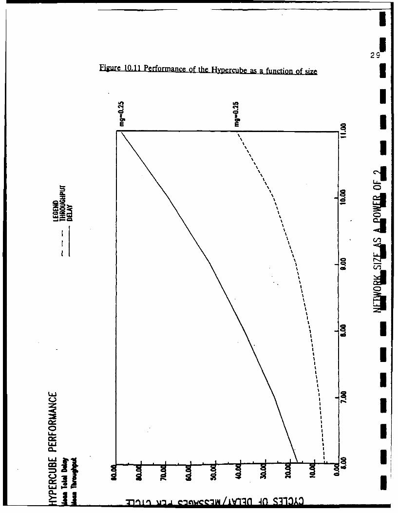
29Figure 10.11 Performance of the Hypercube as a function of size
IIIUC*4 Ci
I I I
E E
ItII I• C
\I
I-
M l
I
. [ . ..- ,, ,., ,,-T ,",O,,," l , ! ' -J I

Ii
network cycles in the two modes of operation of the hypercubetherefore have different meanings. In the first mode wheredeliveries are allowed in each dimension cycle, an individualdimension cycle is longer to allow for message deliveries. In theCM mode of operation, the network cycle is composed of simpler
dimension cycles during which messages can only be transferred. Alldeliveries take place at the end of the network cycle. While wefocussed our attention on the first method, we simulated both modes
*of operation for comparison.
Figure 10.11 shows how the throughput varies with the size ofthe hypercube when a single buffer is used at a message generationrate of 0.25 per cycle. We have assumed the CM mode of operation.With a message generation rate of 0.25, the throughput is onlyabout 25 for a hypercube of 10 dimensions. The poor throughputresults from the overflow of the input buffer in each dimensioncycle when more than one message have to be transferred acrosspairs of processors. Figure 10.12 examines the throughput for a1024 hypercube as a function of the buffer size. The maximumthroughput for such a network is about 190 when a buffer of size10 is used.
In the CM mode of operation, where 1 message generation and1 message delivery was allowed (that is, we allow 1 message to begenerated, if the buffer is not full, and 1 delivery, if anymessage was generated, at the end of each network cycle), thethroughput reaches a maximum value of about 1000 per network cycle.In either mode of operation of the hypercube (a maximum of 200 perdimension cycle), we believe that the RSEN is very competitive (385per single cycle). It must be noted that it is difficult to makean exact quantitative comparison between the two networks since theRSEN cycle of operation is different from the dimension cycle inthe hypercube. As pointed out earlier, the dimension cycle in theCM mode of operation is shorter since no message deliveries occuruntil a network cycle is completed. Actual implementation issues
* must be considered before accurate comparisons can be made.
In terms of optical implementation, the SEN appears moreattractive than the hypercube which must use large buffers for eachnode in the processor. on such simple first order analysis, the SENcycle would be expected to be shorter than that of the hypercube.Thus, given that the two networks are competitive on the basis of3 throughputs, the RSEN would appear to be a better candidate.
IIII

31Figure 10.12 Hvercube performance as a function of buffer size 3
" Io ii
0 dd-oo,,I
a
- I, \III
I
I I %40 V4
I "--...-'.-...,
I-0 II
.. ... . , , iII I I I II II II I I>--%,

U11. Implementation Issues in Optical Shuffle-ExchangeINetworks
Our analysis of interconnection networks, based mostly onperformance, reveals the SEN to be competitive with other commonlyused networks with low loads (<0.25). For larger loads, replicatedSENs or RSENs are very competitive with other commonly usedtopologies. The SEY also appears more attractive than othernetworks because of recent work on the optical implementation ofthe perfect shuffle. A number of different optical shuffleimplementations have been proposed. Lohmann [45] and Midwinter [53]initially showed how the perfect shuffle can be implemented veryeffectively using passive optical elements such as lens and prismcombinations or holograms. Eichmann and Li [54] have later shownan even more compact implementation in optics which reduces thetotal optical path length from Lohmann's approach by a factor of6. Their results indicate that the channel spacing d and the spotsize a are the limiting factors.I
d = D / (N - 1), a < D / (2(N - 1))
where D is the aperture of the lens used.
I With a 50 X 50 sq. mm aperture lens, the optical perfectshuffle can handle as many as 40,000 light channels. The channelspacing and spot size is assumed to be 0.25 and 0.1 mm,respectively. While using bulk optics, as proposed in [54] may leadto larger-sized SENs, alternative holographic approaches and guidedapproaches may be used to accomplish the same shuffle permutation.We will examine these alternative approaches in the next section.
To make the design process of the optical SEN more tractable,we examined the proposed optical designs and also extracted thekey requirements for the critical portion of the SEN, the exchangeswitch.I
11.1 Existina optical shuffle-exchange designs
There has been increasing interest recently in theimplementation of the optical perfect shuffle for sorting networksbut very few efforts on the exchange switch implementation. Herewe outline the work that has been reported thus far.
III

I
11 .1.1 Perfect shuffle ULohmann [44] appears to have been the first to present an
optical perfect shuffle design. He proposes a setup using prismsand lenses. The input elements are divided into two halves, upperand lower, which are stretched in one direction to match the sizeof the original inputs. The stretched halves are then recombinedby interlacing to achieve the perfect shuffle of the inputs. Theoutputs on recombination appear in reverse shuffle order but can Ieasily be 'unreversed' by standard optical means. The total opticalpath length is two times the sum of the focal lengths, fl and f2,of the lenses required to separate and recombine the two halves of Ithe input set. To maintain the same output channel spacing as thatof the input, f2 must be twice fl. The total length is therefore6fl.
Another implementation that has been proposed is one byMidwinter [53] which is suitable for one-sided operation, that is,the input and output elements are on the same side of the system. iThe advantage in this design is that the exchange switch logicarray, which if not purely optical, can be on one side separateofrom the purely optical shuffle. The approach here is also, as inthe previous scheme, to stretch-mask (shear)-add the inputs toobtain the perfect shuffle. However, the same optical system isfolded in such a way as to incorporate a return path to the inputside. The bottom half of the system only does a one-to-one imaging mof the exchanged elements to the output port. Having the I/O onthe same side is an advantage from the point of view ofimplementation. Figure 11.2 shows the folded perfect-shuffle Ischeme.
The third scheme by Eichmann [54], mentioned previously, is Imore compact than the previous two methods. Two versions have beenproposed: one in which two identical negative cylindrical lens areused side by side, and another where only one negative cylindricallens can be used with two prism wedges. In either case collimated Iinput beams are required. The total path length for the scheme is2f (for the first implementation).
11.1.2 Exchange switch
IThe focus by most researchers has been on the realization of
the perfect shuffle connection. Since the shuffle connection canbe done using passive elements, the system can operate essentially Iat optical bandwidths. The exchange switch for the SEN cannot berealized with simple passive devices since some form of control isrequired to either pass uninterrupted or deflect the input beams ito the output of the switch. Unfortunately, scant work is evidenton designing the exchange switch. We examine some alternatives inimplementing a special case of the exchange switch as described byone reported work.
I

III
33
101 7MI "~ 171I
Figure 11.1 Lohmann's scheme for perfect shuffles
loi
I
U%
-autput
1/0"(f~f erment anid
I3 Figure 11.2 Reflected pefect shuffle
II

II1
d LL W
o .3
La~.6-"-'" 6
(b)
I
Figure 11.3 Compact perfect shuffle 1I
. D ,- OwUs.A7O MSMO Y IPC' AMNG I1AMSPLoa i:1
&L I
Figure 11.4 Compare and exchange switch!
UII

Stirk, et al, (55] examine means of constructing a compare andexchange module which is assumed to always receive two inputs. Theexchange is based on comparison and not on any prioritized schemeas in the case of the message passing network of SPARO. However,some bulk optical techniques are discussed for realizing the basicexchange function, that is, the cross or bar (pass) configuration.Among the passive routing techniques suggested is polarizationencoded switching using Wollaston prisms and controllable half-waveplates. The retardance of the half-wave plate is controlledelectrooptically by some photoconductor. When the photoconductoris activated by the comparison signal, the dynamic half-wave platerotates the polarization of the orthogonally polarized inputsignals through 90 degrees (see Figure 11.4). A polarizablebeamsplitter or Wollaston prism can then spatially separate the twoinput signals. The performance of this scheme is bound by thebandwidth of the half-wave plate. These devices, due to theirlimited switching power dissipation, can respond at millisecondspeeds. With newer ferroelectric liquid crystals, one can expectto push this response time to the microsecond range.
An electrooptic approach has also been suggested using asystem of detectors and modulators. It uses nonlinear modulatorswhich are normally transmitting unless a signal from thecorresponding detectors converts them to be opaque. The schemerequires an electrical reset for the system to be operable onsubsequent messages. Use of the electrical control thus requiresusing electrooptic devices such as PLZTs or ferroelectric liquidcrystals, the performance of which would limit the messagebandwidth.
In the above proposals, the response time of the control ofthe switch is always the limiting factor and offsets much of thespeed advantages of the purely optical shuffle. (However, it isimportant to note that there are other advantages an opticalshuffle can conceivably provide over an electronic one besidesspeed such as increased simplicity and physical compactness. Wewill visit these advantages later.) It is important to point out,that the above designs ignore many of the key functions that areessential to the exchange switch. A simple compare and exchangemodule will not be useful in the case of parallel processing thatuses message passing. The next subsection summarily outlines theimportant functionalities required in the exchange switch as wellas in the complete network implementation.
I 11.2 Reauired functionalities of the exchange switch
The survey of current attempts in designing optical SENsreveals that while the basic exchange switch has been examined,some important requirements of the exchange switch have beentotally ignored. These requirements are necessary when the networkis employed in a parallel processing environment as in SPARO.
U

I
11.2.1 Conflict resolution by the exohanUe svitch
The most important problem that has to be considered in amessage passing environment is that of the resolution of possibleconflicts among messages that arrive simultaneously at an exchangeswitch. Conflicts between messages occur since the correct routingof both messages may require different settings of the exchangeswitch. i
There are a number of approaches to address this conflictdepending on the desired complexity of the switch. Since onemessage is going to lose the conflict, these approaches differ in Ihow to treat the losing message. One approach is to drop the losingmessage and let the sender processor (the source of the message)wait for a response. If a response is not received within aspecified time, the sender processor will retransmit the message.The processor thus follows a specific message protocol sequence.In the case of fine-grained processing, implementing a protocol orhandshake with each message is too high an overhead and thereforenot acceptable. In the second approach, the losing message isrerouted, that is, the message is deliberately passed through thewrong output but certain modifications are made so that it reaches Iits destination. In case of the single-stage SEN, the rerouting,consists of simply resetting the counter field that indicates thenumber of passes the message had made. Because of the way thecounter is typically implemented in electronics, it will be ireferred to as the mask. The mask denotes the age of the message:in a network connecting N processors, a message is delivered in
log2N passes when no conflicts occur. Thus to route a message, this Imask is reset to 1 when the delivery is on mask value log2N,usually represented modulo 1. No other modifications are necessarysince the destination address does not change. The resolution ofthe conflict or the switch setting, as mentioned earlier, is doneby selecting the message which has a higher mask (counter) value(prioritized selection).
11.2.2 Delivery of messages 3
A message is delivered when it has successfully cycled lg 2Ntimes around the network. The delivery of the messages thusrequires examining the mask or counter value. When the mask valuehas reaches log2N, then it must be extracted from the network anddelivered to the processor. This is envisioned to be simpler thancomparing the destination address with the address of the processor Iassociated with the output of each shuffle. Such a mask checkingscheme would be especially attractive if the processors areoperating electronically while the messages are optical signals. IIn this scheme, the mask of a message (or some optical equivalent)could be checked optically or elect-uoptically at every cyclewithout removing the message from the network system. When themessage has indeed reached its destination, it can be sent out of
I

the network, converted into an electronic signal and queued at the3 input message buffer of the processor.
11.2.3 Detection of a valid messaae
Because of the possibility of noise in an optical system, itis important that the network can distinguish a noisy null messagefrom a valid message. Accepting noise as a real message can ruinthe network performance by causing unnecessary conflicts at theexchange switches as well as send spurious data to the processors.The traditional electronic approach recommends providing a messageheader with each message. In the case of an optical implementation,one may either provide a header bit or stream or a separate signal
n which indicates if a valid message is present.
We assume a synchronous operation of the network so that itcan work efficiently with electronic processors. A synchronousdesign will also be easier to design and implement. The networkcycle will be synchronized with the processor array clock whoserate is determined by the speed of operation of the completeshuffle-exchange. At the beginning of each network cycle, theprocessors will be polled for messages generated for routing duringthe previous network cycle. The message present signal for everyprocessor will therefore be examined during the beginning of everynetwork cycle. Figure 11.5 shows the simplified schematic of thenetwork and processor array interface. The message register in thenetwork is required to hold a new message from the processor or arecirculating message from the network.
3 11.3 Possible aproaches to an optical exchange svitch design
The most difficult part of an optical SEN is the exchangeswitch design. Besides implementing the conflict resolution, theexchange switch design also governs the delivery of messages (sincethis depends on the way masks are represented and updated).Similarly, the optical technique used for implementing the basicexchange switch, that is, the simple cross or pass switch, also
determines how the controls for conflict resolution will berealized. Our initial investigation indicates that the method ofrepresenting the mask information is critical to the nature of theswitch design.
I Here we discuss briefly the different candidate opticaltechniques that could be used for implementing the basic exchangeswitch. These are: acoustooptic gates, polarization encoding gates,waveguide or coupler, and photorefractive gates based on four-wavemixing. The goal is to pick the technique that results in the mostspeed---fficient basic exchange switch and then add the requiredfunctionalities of the network. We also provide one exchange switchdesign that we have investigated using Fredkin gates which haa
I

II
been proposed as an optical computing devices [56,57]. While nooptical implementation of Fredkin gates are known, they can beviewed as a useful computing primitive from which complex computing Ustructures can be built. The Fredkin gate design will be viable ifthe basic Fredkin gate can be implemented optically in a compactfashion. I
11.3.1 Polarization encodina gate 3The polarization encoding gate concept requires input message
signals to encode the switching information as polarization. Thus,each message can have one of two polarization levels indicatingwhether the switch has to be in a pass or a cross configuration.The data in each message is assumed to be intensity-encoded. Theoptical switch is essentially a birefringent plate with a storedgrating. The grating is visible to a message beam only if themessage has the 'cross' polarization, in which case the input beamis diffracted across the plate. The situations when no conflictsoccur, that is both messages require a cross or pass configurationof the switch, is relatively easy to implement. The crossconfiguration can be realized by allowing a negative diffraction Nfor the upper beam and a positive diffraction for the lower beam.More details on this method are described in the next subsectionon the final switch design. I
Note that this approach differs significantly from thepolarization switching gate discussed by Shamir et al [56]. In thatgate, signals passing through a electrooptic modulator are rotated Iby 90' when the gate is activated electrically. The approachpresented here is purely optical and appears to hold the mostpromise. However, the critical issue of conflict resolution can beincorporated in this encoding technique is not clear.
11.3.2 AOousto-Optio gate I
The acoustooptic gate is not very different from the 3polarization switching gate of (56], except that the switchinginformation of the exchange gate is encoded in an acoustic signal.The gate is essentially an acoustooptic deflector that can be Iimplemented in bulk or as an integrated SAW device. If the thereis no acoustic signal on the gate control line, the input messagespass undeflected, otherwise they are deflected across. The problemwith this approach is that the bandwidth of messages is in acousticrange which is lower than electronic bandwidths. While this isacceptable for transfer of large messages which arriveinfrequently, it is too slow for messaging in a fine-grainedcomputing environment where the rate of computing depends on therate at which messages can be delivered.
I

I
11.3.3 Photorefractive gate
I A photorefractive gate based on four-wave mixing is anall-optical approach mentioned by the authors in [56]. Besides thetwo incident input message beams, the control consists of two pumpbeams. The inputs are transmitted if the control is absent,otherwise they are phase-conjugated resulting in switching betweenthe outputs. Given the state of art in four-wave mixing, thisapproach appears the least feasible for implementation.
11.3.4 Wave auide or coupler
A modulated waveguide coupler is used for the switch. Byelectrooptically changing the guided mode effective index, one canchange the coupling between the two coupled waveguides. A numberof techniques for implementing this function have been describedin the last decade. More detail will be given in connection withthe analysis of optical interconnection networks to be given laterin the report.
11.3.5 Fredkin gate implementation
Fredkin gates have been proposed recently as building blocksfor optical computing. As Figure 11.6 shows, the Fredkin gate isa controlled crossover device that can be used for constructingcircuit primitives (such as crossover, fanout, and delay) andcomputing primitives (such as AND, OR, and NOT). A Fredkin gate isalso a conservative logic gate [58], that is, it is reversible(information lossless) and bit-conservative (conserves the numberof is and Os that are present at the input). A control-specificFredkin gate (57] is one in which the control and data lines arefundamentally different and cannot be interchanged.
We have investigated the use of Fredkin gate for realizing theexchange switch and its controls. Our approach has been to map aBoolean functional description into a circuit using Fredkin gates.We completed, as an example, a minimal Fredkin gate design (57] forthe switch control. (At this stage we have ignored the mask updatecontrol.) We describe below the functional specification and thecorresponding realization. The minimal circuit realization derivedis control-specific with respect to the mask comparison information
Ionly.We define five inputs to the exchange switch. These are:
I P1: Presence signal for the upper input of the switch,indicating whether a message has arrived. A 1 indicates the
* presence of a message while a 0 indicates no message.
U

II
Processing Element 3~TO/from
Output Suffer Handahcke Controls Shufflo Exchcmge jMessage Data
or DaaNetwork Interface
II
Figure 11.5 Schematic of network and processor array interface
Xcx + Cy 0 ab 1 a'+b 1a'
Y-t -- cx + c'y b-ab b 0a+ba
I
III

3 46
__ _ 2 M A1 A C R R
No Packets 0 0 - - - 0 0
1 1 0 - 0 - 0 0 0One packet 1 0 - 1 - 1 0 0
0 0 1 . 00 1 - - 0 0 0o 1 -. 1 0 0 0
No conflict1 1 - 0 1 0 0 0
m Two packetr- 1 1 1 0 0 0 0 11 1 0 0 0 1 1 0
Message Conflict a ---
Comparisons 1 1 1 1 1 1 0 1
required ____o
r~lix k, 1 0 1 1 0 "0
I3 Table 11.1 Lookup table for smart exchange switch
I "o* 0 CkI °- P 2
a2I0al
Figure 11.7 Excmhange swjitch implementation from Fredicin gates
I
I

P2: Presence signal for the lower input of the switch.
M: Mask comparison signal, or the outcome of the comparison iM1 <= M2 where M1 and M2 are mask values of the upper andlower input messages, respectively. IAl: The destination address bit under the mask M. This bitdecides the switch configuration required for the message inthe current network cycle. 3A2: The destination address bit under the mask M2.
C: The output of the Fredkin gate circuit which represents the 3control input to the last Fredkin gate that acts as the basicexchange switch. A C value of 0 implies a straight or passconfiguration while a value of 1 represents an exchange orcross configuration.
The truth table for setting the control C is shown in Table11.1. Note that R1 and R2 in the truth table represent the maskreset controls that are necessary to handle conflicts. A logicminimization of the combinational function for C yields thefollowing sum of products form expression. A _ before a variable iname denotes the complement of that variable.
C = Pl-P2 Al + -P1 P2 -A2 + PI Al -A2 + P2 -A2 -M + P1 Al M i
The expressions for the reset signals are: 3R1 = P1 P2 -M (-AI -A2 + Al A2) 3R2 = Pl P2 M (-Al -A2 + Al A2)
Figure 11.7 shows a six gate implementation for the exchangeswitch in terms of the five input variables. The total delay in ithis switch is three Fredkin gate delays.
As indicated earlier, the feasibility of the aboveimplementation depends on the feasibility of the Fredkin gate iimplemeitation. As yet a feasible optical Fredkin gate has not beendemonstrated. There have been some discussions (19) of cascadingPriese gates or interaction gates to construct a single Fredkin Igate but they have not been explored in detail. The speed andcomplexity issues of the our design will determine whether such animplementation is viable. I
We now present a conceptual optical switch design based on thestudy of the methods described here. The results of this effortindicates that while parts of the exchange function for the switch
I

IU
can be implemented very elegantly using optical computingtechniques, the optical implementation of the entire exchangefunction and its control is beyond the feasibility for currentdemonstrati .n.
1 11.4 Design and analysis of an optical exchange switch
I The basic exchange switch is based on the polarization codingmethod described previously.I
11.4.1. A passive optical exchange using polarization ascontrol.
As described earlier, passive exchange of signals in a SEN ispossible by forming a grating structure in a birefringent materialso that light propagating with one polarization is affected by thegrating and deflected to the appropriate path, while light of thecrossed polarization is unaffected by the grating and passesthrough the material essentially undeflected.
To operate such a polarization-based switch, the polarizationof the light beams (messages) must be switched or set based on theswitch setting control logic that is a function of the address bitsand the mask values or the message ages. (Notethat in case of anoptical implementation, we will use message ages to denote maskvalues since the latter has an electronic implementation.) Whilemany devices are available which can switch polarization quicklybased on electrical control [59,60], all-optical devices tend toperform this operation either slowly or over a relatively longinteraction distance. While the actual routing is passive andoptical, the control for this polarization setting operation mustbe electronic if it is to be implemented with components andmaterials existing at this time.
One advantage of this approach is that the information carriedalong with the message regarding whether an exchange should occuror not does not have to be actively decoded at the routing device.Instead, when this information is calculated, it can be representedin such a way that the decoding is a passive beam propagationphenomenon. Since the calculation of whether a particular messageshould be exchanged or not must be performed at each step throughthe network anyway, the overall switching time can be reduced.
11.4.2. A R asive optical message age update.
In the SEN, in addition to address information which conveysto a switching node whether it should exchange inputs or not, amessage also carries its age information. Again, the large number
I

II
of information representation formats for optical computing can beused to reduce the overall speed of updating this information.Since the propagation of information through the network can bethought of as routing in a plane (yz in Figure 11.8), in realspatial dimensions, an optical routing implementation might beperformed with planar geometry, using mirrors, prisms or gratings Ito deflect the paths of the beams carrying the messages through thenetwork. This leaves another dimension (x) orthogonal to this planeto use as information encoding. One simple method of representingand updating the number of passes a particular message has takenthrough the network is to represent the number of passes as aspatial position in this orthogonal direction. With each passthrough the network, the position of the message beam is shifted Ione unit in the perfect shuffle plane by means of a prism or agrating. Because this information is represented spatially in adimension (x) orthogonal to the interconnection plane, shifts inthis dimension can be independent of the routing pattern in theinterconnection plane. Since there is no decision on whether toshift or not because propagation of any message for another passrepresents a shift, this can be performed with a permanently Iconfigured passive optical system of gratings or prisms.
11.4.3. Detection of age and collision decisions
Perhaps the biggest shortcoming of the all-optical Iexchange-switch is the lack of a method or devices to perform thedecision on which of the two messages gets priority of the exchangecontrol when a collision occurs at a node in the network. This Idecision is based on the ages of the two messages, usually with theolder message getting priority and the younger message startingrouting afresh in the network.
Optical computing strategies have traditionally had seriousproblems implementing integer comparisons. One method that couldaccomplish this with light-speed throughput is a look-up table Ihologram in which all combinations of age comparisons are stored,and the appropriate combination is recalled through Braggreconstruction of the correct output. However, the number of Icombinations which the hologram would need to store for a largesystem would be prohibitive. Referring to the last four rows oftruth table shown in Table 11.1, one can verify that the number of Ientries in the truth table is equal to the order of the number ofmessage comparisons or O((log 2N)2) for a SEN connecting Nprocessors (PEs). The actual number of entries required is4(log2N)2+5. Thus for a SEN connecting 1K or 1024 PEs the look-uptable required for every exchange switch control must have storedin it 405 entries. The number of inputs is 24, while the number ofoutputs (control of switch configuration, reset controls for the nage of each message) is 3. A single hologram of this size is nota problem. But since N/2 exchange switches are required, the 1Knetwork must be able to physically accommodate 512 such holograms. I
I

Processor Si)
anamorphic' prisms,and mirrors
FigUre 11.8 Representation of message ane by satial encoding

IOther possible approaches would require either the
representation of the ages or the number of passes as analog levelsand a threshold comparison of the two intensities or a Boolean Ialgebra calculation of the comparison. While fast analog thresholddetection might be possible with multiple quantum-well devices, thefabrication technology of these devices is not yet advanced enoughfor them to be used reliably in large-scale networkimplementations. Boolean operations for optical computing are alsonot feasible for large systems at this time. Devices which performfast Boolean logic operations in optics tend to be multiplequantum-well devices, which are difficult to use for large systems.Spatial light modulators, which can be easily expanded to performBoolean operations for large systems, unfortunately operate at very ilow speeds.
11.4.4 Conclusions in designing an optical smart exchange Iswitch
In summary, there are two aspects of the exchange operationin which optical implementation can be applied to decrease routingdelay time for messages passing through a SEN. These are thepassive exchange of polarization coded messages, and the passiveupdate of the number of passes that a message has taken throughthe network on the way to its destination. Unfortunately, this isnot enough to justify an all-optical implementation of exchangeoperation, because the control of polarization changes and thedecisions for handling collisions cannot be implemented easily inhigh-speed devices with optical control using components which are iavailable at this time, or which are even in developmental stagesin any laboratory.
11.5. Hybrid SEN Implementations UTo quantitatively evaluate the relative advantages of an
optical SEN, specifically the optical shuffle, we examined twodifferent SEN implementations. The first implementation is a purely Uelectronic design of both the exchange switch and the shuffleconnection. A logic design and analysis was conducted to determinethe complexity of the design in terms of silicon area and wirelengths required for connections. The same analyses also yieldsthe first-order estimate of the speed of operation of the SEN whenthe fastest semiconductor technology is used. The secondimplementation is a hybrid one that uses an optical shuffle in Iconjunction with an electronic exchange switch. The optical shufflesection is expected to be slightly faster and much more compactthan a hardwired electronic implementation. A similar analysis as Iin the case of the first was undertaken to assess the seconddesign. An optical SEN implementation can then be compared to boththese implementations on the basis of their speed-complexityproduct.
l

I
11.5.1 BEN and processor array interface
U The single-stage SEN was shown in Figure 10.5 showing theProcessor Array, consisting of 1024 processing elements (PEs) forfine-grained computing, communicating with the network through theNetwork Interface (NI), or the control portion of the network thathandles the transfer of messages between the PEs and the network.Here we will focus on the complexity and the cycle time, the delayexperienced by a message to pass once through the shuffle-exchangestage, of the network.
To isolate the performance of the SEN from that of theimplementation of the PEs, we will define the network cycle to bethe difference of the time when a message is accepted into the NIand the time when it is loaded back into NI for delivery or forrecirculation.
Each PE, as Figure 10.5 shows, contains two buffers forstoring outgoing and ingoing messages. A message to be sent toanother PE is queued at the output buffer (OB). At the beginning
of a network cycle (defined as the time taken by a message to cycleonce through the shuffle-exchange network), if there is a messagein the OB, the PE requests access into the network through thehandshake line Processor Request. The network can receive a messageif there is no circulating message at the PE. The NI correspondingto the PE communicates this information to the PE via the ProcessorAccess line. When access is granted to the PE, the message isloaded from the OB into the NI through the message data line/lines.Similarly, when the NI at the end of a network cycle has a messageto be delivered to the PE, it uses the handshake signal NetworkRequest to check if the Input Buffer (IB) of the PE is not full.If IB is not full, the PE uses the Network Access line to signalthe NI to transfer the message over the data lines. Note in Figure3.5 we have assumed that the data lines between the PEs and the NIare bidirectional ports. This has been done to reduce the numberof I/O connections.
The mechanism for delivering messages from the SEN to the PEsproceeds as follows. When a circulating message is received in theNI, it is checked to see if it has completed 10g2N passessuccessfully. If it has, then it is transferred to the PE,otherwise it reenters the SEN. This checking can be done withinthe NI module or inside the SE stage.
We now focus on the Shuffle-Exchange (SE) part of the networkindependent of the network interface portion.
11.5.2. Shuffle Exchange Stage
The basic exchange switch, shown in figure 11.9, is one thatis controlled by one input that produces a cross or bar connection
I

between the input and the output. An useful exchange switch mustsatisfy all functional requirements listed earlier. We will callsuch a switch the smart exchange switch (SES) described by the mBoolean equation. The Boolean expression for the switch controlassumes that both the deciding address bit extraction as well asthe mask comparison has already been completed. There are a number Iof possible hardware schemes, serial and parallel, for realizingboth operations. We now consider some electronic implementations.
11.5.3. Electronic SEN Imvlementations IIn order to uncover the critical architectural issues in
designing optical SENs, we first consider a purely electronicdesign. A number of issues determine the nature of the electronic uimplementation in terms of the size and complexity as well asperformance. These include pin constraints of a chip, the numberof backplane interconnects between printed circuit boards or thebackplane wiring constraints, and the off-chip and off-boardinterconnect delay as compared to the gate delays within a chip.We examine these issues briefly as inputs to our designmethodology, and then present the possible performance and size of Ielectronic implementations.
11.5.3.1 Pin Constraints i
The design approach most affected by the limits on pin counts iis the issue of parallel versus serial message data transfer.Consider the pprameters of the SPARO (Symbolic ProcessingArchitecture in Optics) architecture. There are nominally 1024 PEs icommunicating via messages composed of five essential fields: thedestination PE address, the source PE address, two data/addressoperands, and the instruction. For a 1024 processor architecture, Ithe address is 10 bits wide. Although the specific application willdecide the size of the data used, we assume that a 32-bit wide datawould suffice. The instruction word was assumed earlier to beencoded as 1 bit per macro-instruction to simplify the instruction Idecoding in optics. We expect that more than 30 macroinstructions,each of which requires 2 to 3 machine cycles. In the case of anelectronic design where binary decoding can be done relatively Isimply in the PE, we will assume 6 bits are required to encode allmacro-instructions.
The total width of the message is thus 90 bits (2(32) + 2(10) i+ 6). A message of this length presupposes that the mask for eachmessage is generated in the network. However, to avoid increasingthe complexity of network, it is preferable that the mask be Igenerated by the processor and sent as part of the message forpurposes of routing in the SEN. The total message length would thenbe 100 bits. Larger or smaller sizes of the messages are possible Idepending on the size of the data necessary. As we shall see later,
I

a'a3 a' - NOT(c)a + c
t- b- -ca +NOT(C)b
U Figure 11.9 Basic exchange switch

Ithe length of the message has a profound effect on the performanceand implementation of the SEN. 3
The control lines required between each PE and thecorresponding row of the SE were discussed earlier. Four handshakelines are required: Processor Request by the PE to transfer amessage from the OB of PE into the NI, Processor Grant to grant theprocessor request, Network Request by the network for messagedelivery from the NI into IB of PE, and Network Access to grant thenetwork request. Since messages are all of fixed length, we do notrequire acknowledge signals after message transfers have beencompleted.
The problem of pin limitations arises when considering how themessage has to be transferred between the PEs and the SEN: 104 bitsof control and message information if the messages are transferredin parallel between the NI and the PE, or 5 bits for control and Userial data lines. Note that in our initial electronic designs allmessage lines are considered to be bidirectional to reduce thespace overhead. In the first case, all messages (at the beginning Ior at the end of the network cycle) can be transferred in one clockcycle after handshaking. In the second case, 100 clock cycles arprequired to transfer the message serially. While the serial optionis 100 times slower, it requires 1/21th the number of pins at theoutput of the PE. There is thus a space-time trade of f to beconsidered. The real question to be answered is the totalspace-time complexity. If 1024 PEs are placed on one board toreduce off-board delays, then the board has to accommodate 1024*104or 106496 lines between the PE array and the SEN. By comparison,the serial transfer scheme only requires 5120 lines. How many PEs Ican be put on a chip or package and then on a board thereforedepends on the pin limitations on the chip as well as the numberof interconnection lines that can be squeezed on a single board.These issues in turn depend on the technology used to design the Iboard.
11.5.4. Off-ChL Interconnection Delays
Since the complete network, that is, the exchange circuitry mas well as the shuffle connection, requires a multi-chip (possiblymulti-board) implementation, off-chip delays will be a designconcern. The problem of interconnection delay becomes severe fora large perfect shuffle where exchange stages are switched at highspeeds. The network delay, or the time taken by a message bit topass around the complete SEN, depends partially on the actual Iinterconnection length between the output of the exchange stageand the register that delivers the message to the input of theexchange stage. Since the shuffle connection is not modular, this Ilength increases with the size of the network. We will examine therelative importance of the interconnection delay when examiningSENs implemented in different electronic technologies. 3
I

I11.5.5 Backolane Wirina
I The problem of backplane wiring arises if a multiboardimplementation is necessary when all PEs and the correspondinginterconnects cannot fit on one board. The number of boards andthe total delay would then be determined by the number of backplaneinterconnects possible. The maximum number of board-levelinterconnects depends on the technology used to construct theboard. Thus, using thin film multilayer (TFML) boards allow formuch faster and more dense interconnects than do standard PVC PCBswith edge connectors.
Both pin count and packaging constraints and limits onbackplane wiring will therefore determine the nature of transferof the message, that is, how serial or how parallel. The otherfactors are the complexity of each SE stage. The larger the areaof a single SE stage, the fewer PEs can be fitted on a chip andthus fewer chips on a single board. We will consider these factorsin more detail in the next section.
11.5.6 Hiah-Spoed Electronic Implementation
We have examined the complexity of the circuitry required toimplement the complete shuffle-exchange network in electronics.Both GaAs and Si ECL technologies were considered for high-speedimplementations. Given the large size (1024) of the network, weinitially considered bit serial transfer of messages. We examinethe design implications for a parallel message transfer scheme
later. As we will show, the nature of the message transfer in thenetwork is critical in determining the complexity and performanceof the network implementation.
The size of each exchange stage and its controls is estimatedfirst to determine the layout complexity and thus the total area,size, and speed of the network. The circuitry in the exchangeincludes the NI and its controls, the combinational logic togenerate the exchange switch settings, and registers to hold themessage during recirculation. Figure 11.10 shows a schematic ofthe electronic SEN. The operation of the network is now explained
* in more detail.
A message is accepted into the network with the destinationaddress field entering first. The address and mask fields of themessage are successively loaded into their respective registers,so that the deciding address bit can be extracted. The decidingaddress bit extraction is achieved by serially shifting the maskand address register contents and ANDing the output bits. While themask register is being cyclically shifted, the mask comparisonbetween masks of two messages can be done in parallel. The maskcomparison result and the deciding address bits are fed to theswitch and mask control logic. While the presence bits of messages
I

755
IDI

have not been shown they can be derived in the NI by examining theprocessor request and grant lines. When the exchange switch is set,the registers are alternately emptied to serially pass theirmessage to the shuffle stage. The message buffer holds the initialportion of the message while the remaining message portion passesthrough the exchange switch.
We now examine implementation of the above SE circuit in3 different technologies.
11.5.7 Network delay for GaAs implementation
In the case of GaAs, the total number of gates (the averagegate is a two-input NOR or NAND) required for each exchange stagefor every pair of PEs is expected to be less than 1300. (The majorproportion of these gates are consumed by registers and buffers.)If the fastest usable GaAs technology were employed, gates withdelays of the order of 100 ps (10 GHz) could be used. Since thenumber levels of logic between switchable gates will be 3 to 4 onan average, the clock speed for operating the network would beabout 2 GHz. At that speed, the current and near-future level ofintegration allows between 3000 and 4000 gates on one chip. Thisallows us to realistically fit in 2 exchange stages (for 4 PES) ona single chip. Using state-of-the-art multichip carriers, we couldfit close to 25 chips or 50 exchange stages on a rectangularmultichip carrier package (MCP) measuring 3.7 by 2.4 inches. Thecurrent limit on the number of pins in a pin grid array is about575. Since each stage requires one output message line and fiveinput lines, a single package can be used to pack about 100 PEs.We are assuming that the data line is bidirectional. Ifunidirectional data lines are used, six lines are required toconnect each PE to the network.
For a 1024 SEN, we would have to place at least 10 or 11 suchMCPs on a PWB (printed wire board). Since standard PWBs have lowdielectric constants, off-package delays will be higher than those
inside the package unless polyimide substrate is used for theboard. Interconnection lines would be done in copper on thepolyimide. The shuffle stage would have to interconnect these 10packages on the board. Each package would have 100 serial outputlines for messages leaving the exchange stage for the shuffleconnection.
Because of the non-local nature of the shuffle connection andthe limit in integration, we cannot integrate the shuffleconnections on the package. The off-package delays for the
connections are directly proportional to the wire length. Ifmultilayer (TFML) connections are used (currently 5 layers with 3for ground and power), the longest vertical length between packagesis 5 MCP heights, that is, 5" x 3.7" or 18.5". Since this line islarge in length, there is considerable loss in the lines. It wouldbe difficult to run GaAs at 2 GHz over long interconnection lines
I

unless impedance matched input and output buffers are used at theinput and output pins of the exchange stages. (The bigger problemis that of timing, or the distribution of clock to all parts of the ISEN which is to operate synchronously.) Since the delay on copperon polyimide is 62 ps/cm, the longest interconnect delay in theshuffle stage is 2913.4 ps or nearly 3 ns. Note that the processorto exchange stage connections are not as much of a bottleneck sincethey are direct local connections between PEs and the MCPs for theexchange. We assumed, in our preliminary analysis, that all PEscan be connected by the SEN on one board. As it turns out, this is Inot possible since packing 1024 PEs alone will consume a completeboard-see note on processor complexity in the next subsection. Thusthe PE array and SEN connection will be across boards and not on Ia single board. For purposes of determining the upper limit on theSEN performance, however, we assume that the PE and SEN connectionproblem can be solved, and therefore focus on the one-board SENperformance. We have assumed that load impedances will be matchedat the MCP pin boundaries. Thus the delay between connections ofsuccessive stages of the network is over 3 ns given that some gatedelays have be accounted for within the package. We can assume the Iworst case total network delay time to be about 4 ns.
In our delay computation, we have assumed that the clock canbe distributed such that no clock skews occur. At Honeywell we usea star configuration in distributing the clock within a package toensure that the clock propagation delay is the same for allmodules. If clock synchronization is a problem at the board level,and we believe it will be, we could conceivably employ aholographic optical element (HOE) to distribute the clock.
11.5.8 Network Delay for ECL Implementation
Because of the relative severity of off-chip delays in theGaAs implementation, we considered a more mature technology, ECL,as another choice for implementing the control and exchange stage Iof the network. The advantages of ECL over GaAs despite its slowerspeed is the higher level of integration as well as a relativelysmaller penalty for off-chip connections. Today, we can integrate I10000 gates on an off-shelf ECL gate-array chip with relative ease.With the state-of-the-art ECL technology, maybe even 20000 gatescould be put on one chip. (This would be possible since theconnections in the SE stages are regular and simple with lowfanouts.) We are assuming of course that the high heat dissipationproblem for the on-board ECL circuitry can be solved. With such alevel of integration, one could account for SE stages for 20 PEs. ITo completely fit all 1024 PE connections, we would need about 50chips on a board. Each chip would have 200 pins for seriallytransferring data in and out of the network. This number of pins Iis quite feasible today. By pushing technology to its limits, thedata could be clocked through at 200 MHz if delays across the boardare not significant. It would be reasonable to assume that theinterconnection length would be close to that of the GaAs SEN. Thus
I

UU
the network delay will also be close to 4 ns. We assume as beforethat an optical clock distribution is possible using a HOEI(holographic optical interconnect) scheme. Since the ECL clock isrun as much as 50 times slower than that for GaAs, theinterconnection delay in the ECL SEN is a very small fraction ofthe cycle time.
We now examine the total cycle time of the network for each* technology.
11.5.9 Network Cycle Time
The network cycle time is the sum of the propagation delaysfor the control and the exchange switch, the shuffle path delay,and the total time to transfer the message. Since the number ofgates is expected to be less than 5 between clocked stages, andsince the shuffle connections are compact, these delays do not slowthe clock down. The message transfer is therefore dominated by thetime taken to transfer 100 bits. Since the delay across the boardis not significant, the head of the message will arrive through thoshuffle connection to the next exchange stage before the tail ofthe message has passed completely through the exchange switch. Evenif the two 10-bit registers are used to alternately hold 10-bitchunks of the message, a message buffer is required to save aportion of the message before the exchange switches can be set forthe next pass.
In the case of GaAs, the message bits are pipelined out of thesource PEs at 2 GHz. The network cycle time is 54 (100*500 ps + 4ns) ns or effectively the network operates at 18.52 MHz. Thenetwork delay time is thus 108 times slower than the GaAs gatedelay (500 ps) because of the serial transmission of the message.Since two 10-bit registers are used to hold portions of themessage, a 80-bit message register is required. In case of ECL,the message transfer time is 504 (5 * 100 + 4 ns) ns. This impliesthat the network effectively operates at 2 MHz.
For either technology, the serial message transfer causes thenetwork to be a bottleneck. This bottleneck is especially seriouswhen the PEs operate on the same clock as the SEN. An averagemessage requires 1.5*log 2N network clock (46) or 150*log 2N clockcycles to be delivered (100 bits per message), when the networkload is not more than 0.25. Therefore for a 1024 SEN, a messagerequires 1500 clock cycles to be delivered. If a specializedreduced instruction set (for combinator graph reduction)architecture is used to implement the PE, a message can begenerated at best in 3 to 5 cycles, assuming some parallel loadsare allowed within the PE. Thus, the message generation rate (all100 bits generated in parallel) is about 300 to 500 times higherthan the message delivery rate if the message is transferredserially, and 3 to 5 times higher if transferred in parallel. Inan ideal situation, where no bottlenecks exist, the network should
I

II
deliver messages at approximately the same rate at which the PEsgenerate them. Thus, the message bandwidth in the network mustequal the message generation bandwidth in the PE. This implies that Ithe SEN operates on a clock that is either operating at aridiculous 300 to 500 times faster than the PE clock whentransferring messages serially, or accepts and transfers messagestotally in parallel with a clock that is less than an order ofmagnitude faster.
11.5.10 Parallel versus Serial message transfers
The previous discussion showed that the message bandwidth in Ithe network is inversely proportional to the message length. Theincreased bandwidth required in the SEN motivates us examine thecomplexity of a parallel implementation where messages aretransferred in a parallel or quasi-parallel fashion.
For the same level of integration as described earlier, an ECL 3chip built with 20000 gates can accommodate exchange stages for 20PEs. However, instead of 20*6 (5 between PE and exchange and 1between output of the shuffle stage and exchange) or 120 I/O pins,now 20 * 204 (104 between PEs and exchange and 100 between outputof the shuffle stage and exchange) or 4080 I/O pins are required,ignoring ground, power and clock connection pins. Since this is notpossible, a single chip cannot be deemed to contain more than one iexchange stage for 2 PEs since about 250 is the limit to the numberof pins to a chip. In such a case, 500 such chips would have to beinterconnected in a shuffle connection where each channel of theshuffle now has to connect 100 wires per channel or a total of102400 wires for a 1024 shuffle. If board-level interconnects areused, then many boards are required in the implementation of theshuffle connection since typically only 250 to 300 backplaneconnections are possible with standard edge connectors. Clearly,the pin limitations and size complexity makes a largeshuffle-exchange for parallel message transfer impractical in Ielectronics.
In summary, one notes that an electronic implementation, GaAsor ECL, for a large shuffle-exchange could be operated at highspeeds, over 200 MHz for ECL and over 1 GHz for GaAs. However,severe limitations of the packaging technology and the level ofintegration of high-speed semiconductor technology forces a serialtransfer of messages when a large SEN is desired. Unfortunately,when messages are transferred serially, the message throughputvaries inversely as its length. For a modest message length of 100 Ibits, suitable for the level of fine-grained computing, the messagethroughput is less than 1/100th the data rate. Table 11.2summarizes the electronic SE network cycle times and thecorresponding message latencies. The message latency is defined,for our purposes, to be the average time required to deliver amessage. We have assumed, using Lawrie and Padua's results [46]that a message requires an average of 1.510g2N cycles to deliver
tha a esagereuirs n aerge f l5lg 2Ncylestodelve
| | p lI

iiII |
Technology Gate delay Network latency Message latencySGaAs 500 ps (2 GHz). 54 ns (18.52 N[Hz) 810 ns (1.24 MHz)
ECL 5 ns (200 MHz) 504 ns (2.0 MHz) 7.56 us (132.3 KHz)
Table 11.2 Performance of electronic SENs.
II
iIIII
II"I

IB
if the network is not loaded much beyond 0.25 (that is, about 25%of all stages have messages in transit).
For comparison with the above performance, we examined thesame issues for electrooptic and optical implementations.
11.6 Optical and electro-optical SENs IAs in the electronic implementation both parallel and serial
message transfers can be considered. As before a parallel messagetransfer scheme in optics requires that each channel be 104 (100message lines and 4 control lines) signals wide. A total of 100Ksignals in a single optical system appears difficult in the nearfuture if guided optics is used. Thus, the optical system may haveto be quasi-parallel since the worst case serial transfer cannot Uprovide acceptable throughput unless the switching speeds in theoptical SEN is hundreds of times faster than the PEs. i
Since an all-optical implementation has not yet been designed,we will focus on the architecture of electrooptic and hybridimplementations. One thing is clear: if the optical network has toprovide an advantage over an electronic one, using an opticalserial shuffle together with an electronic exchange and contralwill not be an advantage. This is because the serial delay of themessage in electronics is a serious bottleneck, and using anoptical shuffle will only add further electron-photon conversiondelays. We will therefore examine optical methods to improve thebandwidth of message transfers. Another issue that requires Iconsideration in designing the SEN is the nature of its interfaceto the PE array. The network interface depends on the size of thePE and therefore on its complexity. The next subsection examinesthe complexity of a special-purpose graph reduction processor.
11.6.1 Processor ComDlexitv
The nature of optical implementation depends on the level ofconnectivity, that is, whether the connections between the PEs are iwithin the board or off-board. Since we are building a fine-grainedparallel system, the size of each PE dictates the nature ofconnection. For this purpose, we examined the functionalrequirements and the architecture of a specialized combinator graphreduction (CGR) PE.
Our initial estimates show that a reduced instruction CGR PEwill have about 3u to 35 hardwired instructions, each of whichexecutes 2 to 3 steps. The typical sequence of operations are asfollows. The PE receives a message, decodes it, operates on it,and sends out a message in response. If a simple ALU (nomultiplier) is used, the PE could be implemented with about 1600gates in Honeywell's high-speed (50 MHz), high density CMOS
l

process. To give more power to the PEs, a larger ALU equipped witha multiplier could be shared by a pair or more PEs on the samechip. As many as 11,000 gates can be put on 1 CMOS gate array chip(400 mils X 400 mils). Thus, 6 to 7 PEs can fit on 1 chip. As manyas 20 gate array chips could be squeezed on a package 3.25 " X2.6". Thus one package would account for 120 to 140 PEs. The limitin the packaging is not in the total gates available but in thenumber of I/O pins. The maximum number of pins possible in such apackage is 575 in a pin grid array. Thus if 100 PEs were dedicatedto a package, each would have only 5 or 6 (depending on abidirectional or unidirectional data line) I/O pins allocated toit, ignoring common clock, power, and ground lines. This limitedpin allocation per PE forces a serial message transfer schemewherein all messages in and out of the PE have to be serial.
At the level of integration discussed, at most 10 packages canbe fit on a large board. The limit at the board level would be inthe number of board connections as well. If 1024 PEs wereaccommodated on 1 board, the number of I/O lines in the board atI5 or 6 I/O pins/PE will be over 5000. Thus, connecting a SEN tothis board is not possible using standard electronic wiringconnections. More importantly, it is clear that to build a scalablemachine, consisting of 10,000 PEs or more (necessary forfine-grained computing), a multiboard solution is desired.Therefore, the SEN must be operational across multiple boards andnot just within the board. The number of boards required for allPEs is dependent on the functionality and granularity of a PE. Wenow examine this important issue in more detail.
11.6.2 Processor Granularity
The PE granularity influences the SEN design in two ways.First, the coarser the granularity, the fewer the PEs required tosolve the problem. This implies that a small number of boards willsuffice to accommodate all PEs. The architecture of theprocessor/memory subsystem for coarse-grained processors will ofcourse be quite different from the one chosen here. Second,coarser-grained PEs will operate on a larger problem (that is, onsubgraphs rather than on individual nodes in CGR) and thereforewill have less frequent communication with other PEs. The messagegeneration frequency will therefore be considerably lower. However,the size of messages may be considerably larger. For example, themessages may contain subgraphs rather than single node information.The increased size of messages will tend to keep the bandwidth ofmessages high even if the message generation rate is decreased. Oneway to keep the message size down to the lengths that we areconsidering here (100 bits) is to use a radically differentarchitecture such as shared memory and PE clusters. Using such adifferent architecture implies solving a different sort of PEcommunication problem which we will not consider here. We willinstead focus on the general tradeoff of PE granularity and messagebandwidth.
3

I IU
In the SPARO architecture that has been developed forfine-grained CGR, each PE contains and operates on a single graph Inode. There is no concept of memory since the registers in the PEspecify a graph node completely. While this approach seemedsuitable for optics where a complex processor could not bedesigned, when considering an electronic implementation other Uproblems surface. First, the number of PEs required in thearchitecture is not defined by the size, in terms of the number ofnodes, of the original combinator graph, but by the maximum number 5of nodes required during reduction. As recursive expansion offunctions is common in CGR, we expect that the maximum number ofPEs/graph nodes required for a real application may be as high as100K to 500K, even when concurrent distributed garbage collectionis employed as in SPARO. The maximum size of the PE array thus canbe very large. For this reason, we may consider a couple of optionswhen implementing SPARO realistically in electronics. As suggestedabove, we can increase the granularity of the PEs to handlesubgraphs instead of single nodes, so that 1K PEs would suffice inhandling reductions. However, this would reduce the maximum iparallelism that can be expressed in the graph. It would alsoincrease the memory requirements in each processor. As mentionedearlier, the message bandwidth is not expected to change much fromthat in SPARO since the messages will be of greater length but theymay be generated less frequently.
For purposes of solving the PE interconnection problem, we can iistill derive a major benefit by solving the general message passingproblem that features the same bandwidth as that of the messagesin SPARO. We will therefore isolate the exact processing nature in Ithe architecture used from the specification and requirements ofthe network, and focus on achieving a high throughput of messagesbetween PEs in a generic parallel processing environment that usesmessage passing.
11.6.3 SEN Schemes
Since the design and analysis precludes the possibility ofefficiently implementing optical exchange switches for a large SEN, 1we focus on SEN designs that use optical shuffles and electronicprocessors and network control. The implementation options in sucha case is either a serial optical or a parallel optical shuffle. iWe use the term parallel to include both fully parallel andquasi-parallel data transfers. This broader definition is employedsince it is not certain that fully parallel (100 bits) optical data Itransfers (at the board level) may be possible for a large numberof processors. The actual physical size and partitioning of the PEswill dictate the level of parallelism in the message transfer. An aexample of such (quasi-) parallelism would be to use 25 signallines (encoded in fewer lines or non-coded data in 25 channels) totransfer the message in four periods. Note that if the messages aresent serially on the shuffle network, it has to be operated at
I

least 100 times or faster (for a 100 bit message) than the speedat which the PEs operate. This makes the problem of interfacing thenetwork and the processor or processor control difficult.
We examine the serial and parallel optical shuffleimplementations to note the merits and demerits in both.
f 11.6.4 Serial Optical Shuffle
The messages are assumed to be generated within the PE andstored in the output buffer (OB) (Figure 11.5). Each processor hasaccess to two clocks: the first for the electronic processor andexchange circuitry and the second faster one to clock the OB, IB,and the diode array. It is assumed that both clocks are distributedoptically on the chip as well as on the board. The faster clock isassumed to be almost 100 times faster than the slower one. In sucha case, the network cycle time is as long as that of the processor.Effectively, the processor and network operate at the same speedto maximize throughput. Note that since the PE can be assumed toload the OB in parallel, there is no delay in moving the messagewithin the PE. Thus, if the PEs are high performance processorisdesigned to run on a clock of 50 MHz (100 MHz), the network clockmust operate at 5 GHz (10 GHz). The complete network cycle is thenabout 20 ns (10 ns), although all switching within the networkoccurs with a delay of 200 ps (100 ps). To avoid synchronizingproblems, the slower clock would be derived from the faster clock.
There are some obvious technical obstacles to the proposal.First, the PE chip has to integrate the high-speed buffers and thelaser diode array. We require, at the least, one high-speed buffer,instead of separate OB and IB, which communicates with the opticalnetwork. While the laser diode array and the buffers are requiredto be implemented in GaAs, the rest of the circuitry, the processorand its interface to the external world, would be in Si (ECL). Thisis essential since ECL and bipolar have much higher levels ofintegration for a full-scale processor design than GaAs. Usingtoday's integration capabilities, separate (Si and GaAs) dies canbe separately optimized and integrated on a single package. WhileIplacing a single laser diode on the package is not a problem,integrating a large number of such diodes at high speeds on asingle package introduces severe problems of power dissipation,thermal coupling, and electrical and optical crosstalk. The limitednumber of lasers that can be integrated in a package has moreimpact on the number of message lines (and the number of PEs) thatcan be put on a chip. If lower speed are used to transmit data outof the PEs, a higher degree of parallelism is possible.
While the density of lasers on the package as well as on thePWB is a problem, significant advances in laser technology,specifically in reliability, process yield, threshold current andthermal degradation, will alleviate this problem. The more seriousproblem, however, is one of scalability of the serial approach. As
I

the processor technology increases its basic clock speed, forexample 50 MHz to 200 MHz (in GaAs), or the messages are increasedin size, the synchronous loading of messages into and out of nbuffers would require clock speeds of hundreds of GHzs. Suchswitching speeds are not possible with current or near-futuretechnology even with GaAs. Therefore, parallel transfer of messagesmust be employed if good message throughput is desired. Henceforth,we will only consider the parallel transfer of messages.
11.6.5 Parallel Ovtical Shuffle
Because messages are to be transferred in parallel, the speedrequirement of the optical logic is much less severe. Figure 11.5shows the schematic layout for this SEN scheme. The PE array, mostlikely on multiple boards, may be connected to the shuffle networkby guided or free space methods. For illustration, we considerfiber connections. If wavelength division multiplexing (WDM) isused to improve the parallelism in message transfer, the limit on Ithe amount of parallelism is specified by the number laser diodes
(of the required frequency) that can be integrated on-chip, thespace occupied by the multiplexing and demultiplexing optics, andthe required wavelength separation between adjacent channels.
Figure 11.13 shows an array of PEs connected to an array ofexchange switches. In this scheme, each exchange switch contains 1electrooptic detectors that detect specific frequencies andpolarizations of the incoming message lines. The output of theexchange modules are shuffled and fed back to the network and the IPEs.
11.6.6 Alternative Partitioning of PEs for Parallel Shuffle UThe scheme presented in Figure 11.13 appears to partition !
naturally in vertical slices, that is, a set of PEs on one board,a set of exchange and control logic on the same or another board,and the shuffle connection at the edge of the exchange and logic Iboard. An alternate means of partitioning the PE array and the SENmight be more attractive in terms of implementation. Considerpartitioning the complete architecture into horizontal slices,which are placed on separate boards. Each board is a slice of thearchitecture consisting of an even number of PEs and theircorresponding exchange and control stages. A number of boards,depending on the total number of PEs in the architecture and thenumber of PEs that fit on a board, are connected by the shuffleconnection. The advantage in this scheme is that it avoids routingthe message wires between the PEs and the exchange switches across !boards. The problem of. designing the optical SEN is then redefinedas one of distributing the shuffle across multiple boards. We willconsider only this configuration in all future optical SEN designs.
!

IK
3 48P rNetwork Exchange ShuffleProcessor Array Interface Switch Connection
N-1<I ---
II N 7j -
I , Figure 11.11 S.EN and processor arra
1Destination Mask Source Instruction Operand I Operand 2
)0 10 10 6 32 32
I
I

Frequency codedoptical signals ,
~~Smart .....E~~xchE.angs ::"\I \ |I
Backplane 5PE Array Electronic Exchange Shuffle
and Control Connection
!I
Figure 11.13 Scheme for an electronic SEN and PE array gI
I
NIU
- - ... .i I I I I II

Ii
The interboard shuffle will be specified by the number ofchannels on each board. This is determined by the off-boardconnection or wire density. The actual off-board wire densityrequired is dictated by the number of PEs placed on a board. Thenumber of PEs placed on each board in turn is determined by thetechnology used to construct the board as well as the nature ofboard connectors used. We examine these limits in the next section.
UIiIII5UIIIIUIf

12. Optical and Electrical interconnections for Fine GQrained3 Com utina
The requirements of interconnection densities depend on theinterconnection network topology used. How well these densityrequirements can be satisfied depends on the nature of materialsand devices used for implementing the interconnections. In thissection we study the requirements for different topologies and howsome interconnect techniques, primarily electronic, can meet them.Following this we describe in greater deta'il the different opticaltechniques that can be used to support multiboard interconnectionnetworks.
Table 12.1 shows the possible interconnect densities fordifferent materials and technologies. The technologies illustratedare standard board edge connector, optical fibers, Button Boardelectrical connectors, and multimode polyimide waveguides. Of thefour technologies mentioned, only the standard edge connectors areavailable off-shelf. The new button board technology (using 4 milbuttons), developed by TRW and commercialized by Cinch, whichconnects boards on the surface is the most promising high-densityelectronic interconnect technology possible. At present the limiton the number of I/O points on a board that can be connected usingthis technology is not known, the density shown representingdevices currently in development. In any case, the realizableinterconnection density will be limited by wiring density withinthe planes to access the connectors and by electrical crosstalkbetween leads. The two off-board optical interconnects techniquesare based on optical fibers and waveguides. Of these, the fiberoptics technology is more mature. Standard fibers are usually 125um thick. Custom fibers could be implemented with smallerdiameters, several tens of microns (20 um. without significantcrosstalk). However, the yield in fabricating such fibers would belower than for standard fibers because of the non-standardtechniques required. Waveguides of dimensions less than 10 um and10 um spacing provide the highest density in optical connectivityon or off-board (if alignment problems are solved). The use ofwaveguides, grown on polyimide substrates at Honeywell, as boardlevel connectons is still experimental. However, technology ofoptical waveguides is rapidly advancing. Integrated optical devicesusing similar technologies are now commercially available.
The different interconnect technologies can be evaluated notonly on the basis of density of interconnects but also on theirbandwidths. We have therefore listed the limiting speed ofoperations of each interconnect in Table 5.1. Complete informationon the button board operation is not available yet and is beingcurrently compiled. The advantage in the optical techniques wouldbe their higher available bandwidth.
The exact capabilities of the various technologies will bediscussed later having defined the requirements of the variousnetworks which may be used with fine-grained systems.
I

IIp
Table 12.1 Interconnection capabilities of various technologies
iType of board Density/inch Speed Comments SPVC/Edge connector 40 200 MHz Standard/custom
Button Board 170 150 MIHz (?) 4 mil buttons
Optical fibers 2000 Source limited Custom
Polyimide wavegides 12000 Source limited Experimental
IIii[
- I
III
I

III
I
12.1 Connectivity Requirements of Some Network Topo1o0ies
The motivation for implementing the perfect shuffle in opticsis driven -by the needs of parallel computing. These needs werederived by a detailed examination of the 1/0 requirements at theI/board level for fine-grained processing using large scaleparallelism, as evidenced in commercial machines such as theConnection Machine, a SIMD computer from Thinking MachinesCorporation, and NCube, an MIMD machine from NCube Computers Inc..We find that, not surprisingly, computer architects and systemdesigners have made major tradeoffs in the I/O design toaccommodate the limitations of electrical I/O and packagingtechnology. Typically, multiple (as many as 512 in case of the CM)PEs are restricted to a serial I/O line, as in the NCube, or share
i a serial I/O line, as in the CM. Since the communication infine-grained processing involves packet switching, the serialcommunication of messages between PEs imposes a severe performancerestriction. Because I/O is such a severe bottleneck, the PEperformance is normally degraded and state of the art technologycannot be used. The overall effect is that the throughput of theparallel computer is limited by the I/O bandwidth at the board5 level.
In this section we examine the connectivity requirements fordifferent network topologies. We can show that the wiringcomplexity across boards, for a multiboard system, of theshuffle-exchange is no worse than that of other interconnectionarchitectures such as the hypercube and the crossbar when parallelmessage transfers are considered. In fact, the board-levelconnection density for SENs is less severe.
Consider, for example, a large-scale parallel architectureconsisting of NM PEs distributed across M boards (or clusters, inthe general case) communicating via messages. Thus each board hasN PEs that need to communicate to other PEs on its board as wellas others. Since we are concerned with interconnection requirementsacross board boundaries for different interconnectionarchitectures, we will not consider the on-board connections thatcan be done by.board-level routing. We will examine the total I/Ochannels required per board for the same density of PEs on a boardfor different interconnections.
12.1.1 HyDercube interboard ConnectivityILet us first examine the hypercube. Since there are a total
of NM (N and M are necessarily powers of 2) PEs, the dimension ofthe hypercube is D = iog2NM. Thus each PE has both input and outputconnections to D other PEs.
If each PE communicates a B-bit data packet or message, theneach PE requires DB bits for each input or output connection. To
I

estimate how many of the D PEs are on the same board as the sourcePE, we have to consider the how the PEs are partitioned. 3
The best case, that is, when the least number of connectionsare required outside the board, partition occurs when each boardof the N PEs form their own smaller hypercube and D is minimum or2. In such a case, each PE on a board is connected to log 2N PEs onthe board and to only 1 PE on the second board. In the general casewhen there are M boards (M >= 2), each board contains N PEs in ahypercube and the number off-board unidirectional PE connectionsper PE in the best case is 2(log2D - log2N) or 21og2M.
Thus, the number channels required per PE in the board is 52Blog 2M.
The total number of channels for each board is 2NBlog2M. 312.1.2 Crossbar Interboard Connectivity
The cross-bar connection for connecting a massively parallelPE array does not really make practical sense since all PEs arepermitted to address any other PE in one cycle. However, forpurposes of comparison and completeness, we will examine thisinterconnection topology. Each PE has to be connected all others.In the multiboard case, each PE has to be connected to all 2N(M-1) off-board PEs, besides the N - 1 on-board PEs.
Thus, the number (unidirectional) channels required per PE inthe board is 2BN(M - 1).
The total number of channels for each board is 2BN2 (M - 1). 312.1.3 Shuffle-Exchange Interboard Connectivity
The computation of the I/O channels required for theshuffle-exchange is relatively simple since each PE has a fixed Ifanin and fanout of 1. However, in a multiboard situation thepartitioning of the processors determines the number of interboardconnections.
In the best case, M=2 and the 2N processors can be split upsuch that only N/2 PEs on each board require off-board connectionsto the other board. The rest of the PEs can be connected by the Ishuffle-exchange on-board. This is because the shuffle connectionis bisymmetric (that is, the shuffle connections for the lowergroup of N PEs are mirror image of the connections of the upper mgroup of N PEs) and half of each group, that is, N/2 PEs, isconnected to half of the other group. This can be verified byexamining the relation that describes the shuffle permutationS(i)-(2i+12i/N) mod N of the ith PE where 0 < i <= N-1.
-- m ~ mmmn l lm~n I m ww..... 3

The total board I/O required for M=2 is therefore 2BN/2 or BNsince there are two connections (input and output) for each of theN/2 PEs connected to offboard PEs.
However, the SEN is not modular, so when M is increased beyond2, each PE in the worst case partitioning may require a shuffleconnection to a PE off-board. In such a case, each PE has I/Oconnections to two other PEs off-board, one for input and the otherfor output.
Thus, the worst case number channels required per PE in theboard is 2B.
The total number of channels for each board in the worst caseis 2BN. Table 12.2 summarizes the I/O channel requirements foran N PE board where M boards contain a total of NM PEs. In the sametable we also show the board I/O requirements for NM = 1024, M =8 (assuming 128 PEs per board), and B = 100. Note that the columnsmarked as I/O per PE or I/O per board do not reflect physicalfanout but rather the required connectivity. This is because, asin the hypercube operation, the PEs do not operate in a broadcast3 mode but rather selectively talk to individual PEs at any one time.
Figure 12.1 shows how the board-level I/O increases as -Afunction of the number of boards for conservative values of N andB (N = 16 and B = 32). Figure 12.2 and 12.3 show graphically thetotal I/O requirements as a function of the number of processorsfor two different sets of values of message width B and the numberof boards M. In each graph we have also provided two referencelines representing the total board I/O possible in two differenttechnologies, button boards and optical fiber interconnects,assuming that a large 18" X 15" board is used. Note that sincebutton boards have been designed for a maximum of 2000 buttons a8" X 6" board only, we have extrapolated that figure and assumedthat 5000 buttons can be placed on the larger board. In case ofoptical fibers, we have assumed that they are used only on one edgeof the board, and not on the complete periphery like the buttonson the button board. From size and spacing considerations, 36,000optical fibers can be fitted on the 18" side of the board. Thefigure is even better (216,000) if waveguide connections can beused on the edge of the board. Thus for a large number of PEs,optical interconnects appear to hold more promise than availableelectronic techniques.
For reference, we have provided three (connected) points inFigure 12.3 that reflect the current and projected board I/Orequirements of one 8K card rack (containing 16 cards with 512 PEseach) of the 64K CM. The lowest point (768) represents the currentoffboard I/O required in each board, where every 16 PEs share oneserial link. The second point represents the 4K offboardconnections required if each PE were allowed its own serial link.5 The third point represents 184K connections required if each PE
U

III
Table 12.2 Crossovers for several interconnection networks i
Interconnection 1/0 1/0 Normalized 1/0 Board 1/0 1Topology per PE per Board per Board (N,M,B=128,8,100)
Hypercube 2B log2M 2NB log2M log2M 76.8 K 3Crossbar 2BN(M - 1) 2BN2(M - 1) N(M - 1) 22.4 M
SEN (M=2) B BN 3(M > 2, worst) 2B 2BN 1 25 K
%
' I
IIII
I3

UNumber of PEs/board =16, Message Width -323 6.0-
5.5-
1 5.0-
43 a -W Hypercube4, Crossarm
4 4.0 Button Board3 t -~j .Optical Fiber3.5- Waveguides
3.5
2.5I0 200 400 600 S00 1000
Figure 12.1 Board level 1/0 as a function of the number of boards for B =32. N= 16
.5 Number of boards =2, Message width =10
1 5.4-
I4.3 -W Crossbar
3.2- -a- Optical Fiber
3 2.1
0 200 400 600 S00 10005 Total Numbeir of P&.
1 Figure 12.2 Board level 110 as a function of the number of PEs per board for B = 10, M = 2

6- -*- Hypercub.
5 -40-Button sca-0 Opd" ibo
v -W Waveguides4 -O 64K CM5
3I
0 2000 4000 6000 8000
TOW~ Number of PU
Figure 12.3 Board level 1/10 as a function of the number of PEs on a board for B =100.M 16K

I
were allowed 46-bit (for 4 bytes of data in a packet) parallelmessages.
When comparing the three networks, we find that the crossbar,because of the quadratic increase in the number of I/O channels isbeyond practical consideration for large networks. The SEN faresbetter than the hypercube-an optical fiber approach can supportless than 1000 PEs in a hypercube as opposed to 3000 PEs in a SEN.The higher I/O density in the hypercube is due to the largerfanout, by a factor of log2M over the SEN, of each PE. Further, incase of a SEN, these limits on the number of PEs per board scaleonly with the total number of PEs, unlike in the hypercube wherethe connectivity requirement of the board increases with the numberof PEs as well as the number of boards. We note, in fairness, thatthe limited connectivity of the SEN, implies handling a smallerload, i.e., usually around 25%. Larger loads would slow downmessage deliveries since more conflicts would occur. Forsignificantly higher message traffic, replicated networks arerecommended.
Having examined the board I/O densities of different networksfrom a topological and computational perspective, and havingpreviously concluded that electrical interconnection networks arbinadequate in meeting the requirements, we examine how differentguided and free-space optical interconnect technologies can meet
those requirements, and which appears most promising.
12.2 Board-Level Interconnect Technologies in OvticsITo address the demand of high I/O density at the board level
that we established in the previous section, we embarked onanalyzing different optical interconnect technologies as possiblecandidates. The key optical technologies that we investigated arefibers, polymer waveguides, volume holograms, planar holograms andmicrooptics and bulk optics
To assess the relative capabilities of these technologies withthe existing electrical means, we have also examined two electricalboard-level iSterconnect approaches considered in the previoussection. These are high-density conventional connectors and TRW'sbutton boards. before discussing the merits and demerits of thedifferent optical approaches, we have first listed a number ofissues that were used as criteria for comparing and assessing theoptical approaches against the existing electrical interconnecttechnologies.
3 12.2.1 Issues in using optical interconnection
The following issues are of concern when opticalinterconnections are used. These considerations are important if
U

l I I
I
optics is to provide a competitive edge over electronic boardinterconnect technologies. An evaluation of these issues providethe fundamental physical and technological limits in using opticalinterconnects for boards.
i) Power: Power considerations are necessary primarily for 3transmitters, detectors and receivers; the power consumed bythe interconnect circuitry directly determines, at least inpart, the density of optical interconnects on the board. Thepower budget is a function of the optical losses in the systemand the power required by the drive circuitry for the sources(lasers and /or modulators) and the receivers. 5
ii) Size and volume of optical components: This refers to the sizeof optic devices (lenslets, mirrors, receivers, etc.) and thevolume of the hologram, if holograms are used for connectingsignals at the edges of boards. The size of the opticalsubsystem is important since it determines the optical pathlength and therefore the delay in the system. In addition, insituations in which individual optical elements determine the Ipath of a given channel or set of channels, the size of thecomponents determines the intra board connection densityattainable.
iii) Density of receivers and transmitters: The physical size anddensity, in case of integrated devices, determines the densityof I/O connections possible. The fabrication technology also mdetermines what densities are practically achievable. Thermalconsiderations and optical and electrical crosstalk also limitthe density of connections.
iv) Speed and Bandwidth: The speed and bandwidth of the receiverand transmitter determine the I/O bandwidth of the system. Theusabel data rate of the optical interconnection is alsoaffected by the dispersion of the interconnection medium,where paths other than those defined in free space are used. 3
v) Crosstalk: Crosstalk is important in determiningsignal-to-noise ratios and bit error rates in opticalcommunications. Because of lower efficiencies in transmitting Iinformation, crosstalk is much more severe in degrading noisemargins in optics than in electronics.
vi) Tolerance: The tolerance in the physical dimensions of devicesand components is crucial if boards can be pulled out andreinserted into the racks. Since optical interconnects forparallel systems offer the possibility of near-term Iincorporation into machines, their use should not requireabandoning establishes concepts for multiboard systems. Thetolerance of change in the wavelength of the signal as well Ias the temperature of the source is also important whenensuring correct connectivity.
U

II
vi) Reliability: The lifetime of all devices used is especiallyimportant when competing with mature electronic technologies.The large number of independent channels for a massivelyparallel system communicating with parallel bits placesstringent requirements on the performance of individualdevices.
vii) Cost: For practical considerations, the cost ofinterconnecting processors distributed across two or moreboards must be close to that of electronics unless the densityof optical interconnects far exceeds that possible in5 electronics.
12.2.2 Optical interconnect comparisons
To implement the perfect shuffle connection between PE boardsoptically, a variety of approaches are possible. These includevolume holograms, planar holograms, waveguides, optical fibers,and microoptics. Each of the interconnect formats will beconsidered in turn together with their relative advantages.
Volume holograms would appear to offer the possibility ofboard to board connection with high density. To most effectivelyuse the hologram, a vertical connectivity would be employed. Anarray of vertically emitting sources would be mounted on the lowersurface of the upper board. Immediately below it would be a volumehologram, which would serve firstly to collimate the output fromeach source, and to direct the signals from the sources associatedwith a particular exchange switch output to the relevant set ofdetectors. Thus the hologram is divided into a set of facets, onefor each set of sources associated with an exchange switch output,and within each of these facets an array of smaller structuresserving to collimate the output of each source.
1 Several design requirements conflict. In order to achieve highresolution of the image y 'ne, a large hologram is required. Highdensity in the holograz plane requires small holograms. Highdensity in the source plane requires that the hologram plane beclose, to prevent the diverging output from the source (laser ormodulator) reaching the hologram associated with the adjacentchannel. A study of literature evaluating volume holograms forinter-board distribution indicates that for geometries likely to
be encountered in intra-board connection, densities of 100 persquare cm may be attainable.
Configurations involving multiboard connections with hologramslocated between boards are cumbersome, and subject to even lowerdensities of connectivity. Even in the two-board case, the hologrammust be located accurately with respect to the source array, bothpositionally and with respect to angle. Although the deflectionassociated with each hologram facet is locally space invariant,each smaller facet also serves the purpose of collimating a source,
I

3I
behaving in a manner similar to a lens. Thus significant spatialmisalignment of the hologram will result in angular misalignmentof the beam. Smaller misalignments will result in unacceptable icrosstalk.
Holograms used in this application impose stringentrequirements on source wavelength. If the hologram is fabricated Ito operate at a given wavelength, the source wavelength used mustbe sufficiently close to this value. Acceptable tolerances areapproximately Inm. This implies a stabilization of the source laser Itemperature to approximately 1 degree for a simple Fabry-Perotlaser and perhaps 20 degrees for a DFB laser. The DFB lasers aremore complicated, and therefore more expensive to manufacture. LEDS Iare obviously unsuitable. Fabrication of vertically emitting laserswith such close tolerance has neither been demonstrated norreported in the literature. In addition, control of individuallaser wavelength within an array of uncoupled lasers is likely tobe difficult, and require space-consuming circuits.
Use of matched pairs of holograms can offset misalignment due 3to temperature changes. However, more fundamental problems exist.As will be shown later, reliability considerations suggest thatindividual lasers will not be used for each channel. Thusapproaches involving fanning out of a remote laser to a number ofmodulators are likely to be employed. While the fanout is easy toimplement using holograms, the spatial light modulators employedfor such modulation have to date demonstrated inadequate speed andextinction ratios, or have required high drive voltages. Effron[62] presents a comparison of available spatial light modulatortypes.
Having eliminated holograms between boards on the grounds ofscalability and tolerance, one is tempted to consider the use ofholograms in the backplane. Here, edge emitting structures arepermissible. However, the achievable density is now only 10 perlinear cm, since only one of the two orthogonal dimensions of thehologram is used.
12.2.3 Fiber optics 3
An extremely simple means of providing the optical shufflewithin the interconnect medium between boards is by the use ofoptical fibers. Here an array of optical outputs are connected toa ribbon of optical fibers. Each ribbon corresponds to the outputsfrom each channel of the exchange switch, assuming no multiplexing. IThus for a total of 128 PEs on two boards, 32 ribbons would berequired. High density fiber connectors are available commercially[63] with 18 fibers per connector, and the techniques used in theirconstruction are readily scalable. However the approach isinelegant, and requires increasingly cumbersome assembly as thenumber of PEs increases. Acceptable bend radii are typically 3
I

II
several centimetres, hardly attractive for the systems underconsideration.
The technology for fiber optics is however one of the mostmature of -those considered here. Fibers are low in cost, andconnector technology is mature for low densities of connections,and has been demonstrated for high densities. For higher densitiesthan are implied by the 125 um outside diameter of most fibers,modified manufacturing technologies would be required, resultingin a higher cost. Other technologies may therefore offer lowercosts per channel. A state of the art demonstration might have adensity of 80 per cm. Etching of existing fibers might yield adensity of 500 per cm, while alternative fibers could be developedwith very high relative refractive index differences to yield amaximum density of 103 per cm. These limitations for our highdensity application reflect the development of fiber optics forlong distance point-to-point links, where space is rarely aconsideration.
1 12.2.4 Polymer vaveguides
I These waveguides, developed earlier at Honeywell, have theadvantage over fiber waveguides in that the processing involvesplanar techniques, and the waveguides could be fabricated directlyon printed circuit boards. Waveguides have been demonstrated withdimensions of approximately 10 mm in width and 4 mm in thickness,and on a range of materials, including other polymers, glass,silicon, and Aluminum. These are multimode. Adjustments to theguide dimensions are easily incorporated to increase the waveguidepitch. With such adjustments, a theoretical density of the orderof 1,000/cm is predicted. A state of the art demonstration wouldtoday have a density of 250 per linear cm.
The crosstalk between parallel waveguides is negligibly smallfor waveguides with spacings comparable to the waveguide widthsinvolved, and with the high relative refractive index differencesinvolved when the adjacent guides are surrounded by air. Of moreconcern is the.crosstalk associated with the intersecting waveguidejunctions which will be required in the perfect shuffleimplementation with waveguides on one layer. For N PEs on each oftwo boards, each with 100 channels, depending on the particularconfiguration used, on the order of 10ON crossovers will berequired in the worst case. (This is proved later. Again using avalue of 128 for N, and assuming worst case number of crossovers,we find that to preserve a crosstalk of -20dB at the output, eachcrossover must on average have a crosstalk of -60dB. To date,crosstalk figures have been -51dB per intersection. This suggeststhat multlayer waveguides should be employed. It would not benecessary to fabricate all layers simultaneously, merely toassemble the complete waveguide assembly from several singlelayers. This problem becomes more critical for systems using more
a

II
than 1000 PEs, as would be the case for a massively parallelsystem. 3
Figure 12.4 shows the shuffle connection across two boards fora network of size 8. Without making any attempt to optimize theconnection layout, it is seen that two of the crossovers areassociated with outgoing lines crossing lines associated with eachboard, while the two remaining crossovers are associated with linesbetween boards. Light in these intersecting junctions propagatesin opposite directions. An important distinction should be madebetween the two types of crosstalk. In coupler terminology, a4-port coupler illustrated in Figure 12.5 connects inputs 1 and 2to outputs 3 and 4. In our case the ratio of the powers of the Isignals, P1 to P4 and P2 to P3 should be unity, while all othercoefficients should be zero. Crosstalk, defined specifically asP3/P4, may arise from non-optimal designs, while a finitedirectivity P3/P2 may arise from a different set of imperfections. IIn many couplers the directivity is significantly better than thecrosstalk. While sufficiently accurate data are not available forpolymer waveguides, surveys of results obtained from other Iwaveguide technologies such as high-index silica, ion-exchangedglass, or LiNbO3 indicate that values of 40 or 50dB may reasonablybe expected.
Thus, the implementation of the perfect shuffle using polymerwaveguides is possible, but various forms of crosstalk will limitthe ultimate scalability. It should be pointed out that"engineering" techniques may result in lowering the total numberof crossovers, but that no rule exists for determining the optimallayout. The situation is analogous to the CAD layout of printed Icircuit boards, and therefore layout and routing algorithms fromthe CAD world could be profitably adapted to reduce the number oftotal crossovers. A simple solution is currently underconsideration for the case of N PEs on each of 2 boards.
Figure 12.6 shows micrographs of polyimide waveguidesexhibiting certain features, including 45 degree and ninety degree Iwaveguide bends. The sizes of the waveguides illustrated areapproximately 25 microns by 10 microns (height). These waveguideswere not developed under this program, rather on a DARPA/NOSC Uprogram. The data are merely included here to indicate thefeasibility of the solution, and to enable us to justify ourassumption that the required interconnection medium will exist.
12.2.5 Planar holograms 5An alternative approach involves the use of planar holograms.
These are equivalent to modified planar waveguides, either single Umode or multimode. Predicted densities are 102 per square cm forthe multimode planar holograms, and 104 per cm for the single modeversion. The geometry here differs from that of the volumeholograms since planar holograms control the propagation of light
t

I
IDO D4
LO A
Li L5
3 D1 D5
Board A Board BD2 D6
L2 L6
D3 D7-I
I Figure 12.4 Waveguide shuffle connectivity across two PWBs.
I3
IdeaL P4/Pi - P3/p2 I
Crosstalk* P3/p4 for input into 1
P4/P3 for input into 2
_ Directivity: P2/P4 for input into i
PI/P3 for input into 2
I
IIUI

II
from one edge of the hologram to the other. Crosstalk is predictedto be approximately -20dB at these densities. Thus, the planarholograms offer an advantage if the number of crossovers is greater Ithan 100.
The problems associated with mechanical alignment of theholograms are not as severe as for the volume holograms sinceplanar alignment techniques may be employed in this two-dimensionalcase. However, the concerns of source wavelength and its stabilityare still relevant.
Although an N-point to N-point distribution has not beendemonstrated with this technology, reported results of a fanout Idemonstration indicate that a state-of-the-art demonstration might
involve 10 connections. The state of the art demonstration appearsto be about three orders of magnitude less than the theoreticallimit. Further evaluation of this technology is necessary. Issues Isuch as the scaling of crosstalk with the number of point-to-pointconnections have yet to be resolved. At present this technology isnot sufficiently mature to enable a cost to be associated with it.
12.2.6 Bulk Optics and Nicroobtics
Lohman has reported a perfect shuffle mapping in optics usingbulk components. Provided all sources and all destinationprocessors lie neatly in a line on opposite sides of the lens, themapping is easily implemented. Folded versions have been reportedwhich increase further the attainable interconnection density. For Uparallel operation, anamorphic optics would be required to ensure
that a number of parallel channels were subjected to the samemappings. '3
For PEs distributed across a number of boards, the mappingbecomes insufficiently regular for a single lens to perform therouting. Instead, a single lens would be associated with the outputfrom each processor. Use of such a large number of lenses, and theaccurate tolerances involved, render this approach unattractive.In addition, -the arguments relating to speed of spatial light Imodulators further reinforce our decision not to use thistechnology. Since bulk optical implementations of the perfectshuffle have been demonstrated, one would expect microopticversions to be possible.
Using miniature prisms and gradient index lenses ,the requiredmapping could be performed. Issues not yet resolved concern theeffect of aberrations present in real lenses, and the input/outputdensity attainable with this format. The negative commentsconcerning discrete bulk optical components and the labour involved Iin their assembly and alignment also apply here. Microoptics doeshowever offer significant advantages for use in connectors betweenboards and backplane when used "h polymer waveguides, for I

5 a
Ib
IC
Ioymd aeud opnns a w 5 ed n n 0 ed(bIw 5 ed n 0 nescin n c 2slte

Ila 2 Ica
I.'am
& 7 £

I
I12.3 Summary of optical backplane aproachesU
On grounds of loss, bandwidth, board fabrication compatibilityand ultimate low-cost per channel, we infer that the most favoredapproach is that of the polymer waveguides. The ultimatescalability will depend upon the performance of individualcrossovers and other components. Most high-quality sources underconsideration are edge-emitters, while most detectors are in aplanar form. The polymer waveguide approach is compatible withboth, given that vertical reflecting surfaces have been reportedin the literature [64].
Figure 12.7 shows the likely format of both free-space andguide-wave implementations of the optical hybrid interconnection3 scheme.
Planar holograms deserve further investigation as thetechnology matures. Their use for the shuffle exchange, inconjunction with polymer waveguides, to transfer signals acrossrelatively large distances may extend the scalability. However,this technology is significantly further behind in development that3 competing approaches.
In order to demonstrate a connection scheme using suchwaveguides, a connector would be required between the backplaneand each board. Expanded beam connectors appear to be suitablecandidates, but further work would be required to design a suitable3 connector.
12.4 Sources and detectors for the optical shuffle connection
The high input/output densities described here imply theintegration of many sources and detectors on one chip, rather thanthe assembly of discrete components. We consider first the sourceissue. Choices for the transmitter section of the networkinclude LEDs, lasers, and optical modulators driven by externalsources. Issues Involved in choosing the best approach includepower dissipation of the source and drive circuitry, reliability,sensitivity to change in operating environment, yield infabrication, and cost. We consider each possible solution in turnto determine the most appropriate for our needs. Our comparison iscentered on short-wavelength (say 780-830nm) sources, since thedistances involved are such that modal dispersion will not becomea problem unless data rates per channel exceed lOGBits/sec. Sourcesand detectors at the shorter wavelengths generally have lower costand higher performance. The bandwidth of the polyimide waveguidemay be expected to be lOOGHz.cm, so that increasing throughputwould best be accomplished by increasing the message width. Thishighlights another potential advantage of non-serialized
I interconnection approaches, other attractive features including the
I

avoidance of latency in multiplexing which would otherwise beincurred.
LEDs typically have low output power, and such power as isemitted is- distributed across a large area, resulting in littletransfer of power into a coupled waveguide. Also, efficiencies of Ionly one or two percent result in large amounts of power beingrequired to drive the device for a given optical output level. Thelarge amount of drive power therefore required to obtain bit errorrates of 10-15 required in such systems would make this approach Iunattractive. In addition, their speed is low, perhaps 100MHz.
Typical semiconductor lasers operate at currents of the order 3of a few tens of milliamps drive current. Typical thresholdcurrents are a perhaps 10 milliamps, while ultra low thresholddevices are currently being developed, having attained severalmilliamps to date. Modulation of diode lasers requires switchingperhaps 10 milliamps for each laser in the transmitter array.Significant efforts have been expended in the enhancement of laserreliability. However, at the short wavelengths, dark line defectsgenerally limit the device lifetime. Reliability data of Fabry-Perot AlGaAs lasers indicate that the failure rate of these diodelasers increases with operating time. We have extrapolated the Iavailable data to describe the reliability of the 128,000 sourceslikely to be employed in a system with one source per channel. rtwas found that even at room temperature, a hard failure of one linkwould occur within hours, on average. It was assumed that the timeand ensemble average failure rates were identical.
Given such a large number of sources, incorporation of full 3redundancy is infeasible. On grounds of reliability and easeof incorporation of redundancy, an approach involving a smallnumber of discrete lasers driving a number of arrays of modulatorsis preferable to one involving a large, high-density array ofuncoupled lasers. Issues involved in such a design are the fanoutbetween lasers and modulators, the available power of the lasers,the effects of high power densities on the input to the waveguidefanout, loss in the fanout and the modulators, and the optical andelectrical characteristics of the modulators. In eitherarrangement, eareful design would be required to reduce electrical Icrosstalk and therefore optical crosstalk. Some circuitry isrequired to drive the modulators -heat dissipation in such acircuit and the size of the circuit will dictate the usable densityof the transmitters.
Waveguide modulators are voltage controlled devices, thecurrent required for switching beine small, and being determined Iby the switching speed and the device capacitance. For example,suppose a given laser requires 30mA operating current, with abandgap corresponding to 1.5 Volts. Typical CW power dissipations Iwill be approximately 40mA. Since the shuffle exchange networkworks particularly well with low network traffic, we assume a dutycycle of 10%. Thus each laser must dissipate 2mW on average, butmust still be able to tolerate 40mW. The drive electronics must be
I

able to supply and switch 30mA at whatever rate is required by the3 system. We assume a value of 500MHz.
To compare the power dissipation and drive power requirementsof a laser with those of a modulator, we consider a modulator witha drive voltage of 5 volts, and a capacitance of 0.5pF. Each chargeor discharge of the device requires a charge of 2.5pC, or supplyingan energy of 12.5pJ. At a target data rate of lGbit/sec with a NRZformat, the modulation frequency would be 500 MHz. Thus the powerto be supplied must be 6mW. This has considered the modulator tobe a lumped electrode device. At higher frequencies, traveling waveconfigurations would be required, necessitating termination of thedevice in its characteristic impedance or its complex conjugate.For an impedance of 25 ohms, the power dissipated in eachterminating resistor would oe lWatt. The excessive total powerdissipation of terminated structures suggests that lumped andunterminated structures should be used provided severe penaltiesare not incurred in the drive requirements.
3 For the modulator, the driver must be capable of supplying anaverage current of at least imA. In addition, the driver must beable to provide sufficient current to overcome the loss of powerin the series resistance. For a series resistance of 10 Ohms, thiswould be approximately 10mW. The laser driver however requires thatperhaps 10mA be supplied in the on state, with less in the offstate. Let us assume that 2mA corresponds to threshold, then theaverage power dissipation for a 50% duty cycle would beapproximately 10mW.
3 Modulators then do not necessarily have any advantage in termsof drive power compared to lasers, and indeed as the frequencyincreases show a pronounced disadvantage in cases where the drive3 requirements are limited by the modulator capacitance.
Disadvantages of the modulator approach are the loss sustainedby light propagating through the modulator, and the lossesassociated with interfacing the modulator into the optical network.In addition, two extra interfaces are introduced compared to thelaser, thus an extra critical alignment step is introduced.I-
To realize the potential benefits of modulators over lasers,and to minimize the overhead of packaging, it is proposed that aremotely mounted laser be used to provide optical power to a numberof modulators. The optimum fan-out of the source will be determinedby considering the loss for the complete system, and the properties
of the modulators and receivers. To enable the system to beinserted into a system, it is envisaged that the modulator array andfan-out chip would be assembled into a hybrid package.
3 For logic-compatible modulators in III-V materials, devicesof a few millimetres in length are required. At speeds of I GHz orless, traveling wave configurations are not required, and theelectronics drives a mainly capacitive load. The modulator designcan therefore be relatively simple in comparison to modulators for
I

IU
telecommunication applications, since frequency chirp is not anissue in the low-dispersion short length waveguide connections.
Similarly, in the receiver array, the design of the amplifiercircuits rather than the photodetector will be the limiting factor.For example in reference [80], a monolithic receiver circuit isdescribed with a cell dimension of 75 um x 175 um, although thedetector only occupies an area of 10 um x 10 um. Somereconfiguration of the layout of this circuit would enable hightransverse packing densities to be achieved, up to 10um pitch. The Icrosstalk which would result has not been considered.Approximately, 75 mW were dissipated in this circuit. Allowing amore conservative packing density of 200 per cm arising from areceiver pitch of 50 um, 15W would be dissipated per linear cm, orapproximately 160W per square cm. This is at the limit of what canbe tolerated with the most advanced heat sinking technology. In anycase, the lifetime of the devices at the resulting elevatedtemperatures is questionable. Tradeoffs between receiver complexityand performance may be performed. Such an optimization wouldinclude the optical performance of the backplane connection and the Iperformance of the sources or modulators.
Our initial analysis of state of the art detectors andreceivers, such as the one above, reveals three problem areas thatmust addressed before board-level optical interconnects can becomecompetitive with electronic connections. These are: Ui) size of the receiver circuit,
ii) crosstalk - both optical and electrical, and 3iii) power budget for the receiver
Each of the size, crosstalk, and power is currently too large 3for implementing high-density and high bandwidth board-levelinterconnects. This is again a consequence of the bulk ofdevelopmental effort being focussed of telecommunications type Ireceivers, where space is not at a premium, and large amounts ofelectrical power may be consumed to compensate (within certainlimits) for ly received optical powers. 3
In summary, a demonstration of a high-density interconnectioncannot be performed unless high-density transmitters and receiverscan be demonstrated with the required performance. We note thatthe problem of designing such transmitters and receivers isorthogonal to the actual approach used for accomplishing thebackplane connection in optics, and that any optical approach 3employed must provide adequate solutions to this problem.
I
I

I
12.5 Crossovers in Waveguide Interconnection
U In considering optical interconnections for different networktopologies, two different approaches to realize the connectivitybetween boards of PEs were considered: a free-space connectionapproach using either holograms or bulk optics, and a guidedapproach using waveguides in the third level interconnect. Whilethe free-space approach is limited primarily by density ofresolvable points on the board, the guided approach is limited bythe amount of crosstalk that can be tolerated by the waveguide. Thecrosstalk results from an unavoidable number of crossovers awaveguide channel experiences in realizing the planar layout forthe network connection. Here we will examine the limitations indesigning a guided optical approach for the SEN and hypercube3 interconnection networks using polymer waveguides.
It can be seen easily that the number of crossovers in layingout any network topology varies significantly with the number ofboards and the total number of PEs. Furthermore, as experience formCAD layout and routing has shown, there are many ways of minimizingthe number of crossovers, but the optimal layout problem isprovably NP-hard. We will therefore focus on deriving the worstcase number of crossovers that can arise for an arbitrary numberof PEs, N, distributed over an M boards, communicating by message"of width B bits.
12.5.1 Shuffle ConnectionIThe connectivity requirements of the shuffle connection is3 given by the mapping S,
S(i) = (2i +12i/Nl) mod N where 12i/Nl represent the lowerfloor of the value 2i/N, and i (0 < i <= N-l) is the index ofthe PE.
3 While there may be some heuristic techniques in partitioningthe N PEs into P (=N/M) PEs in each of the M boards, we will notfocus on that research problem. We will assume that contiguouspairs of PEs are placed on each board. Thus, the first board willcontain the PEs 0 to (P-l), the second will contain P to (2P-1),and so on. Note that an even number of PEs is required to be placed
I on a board (even in case of a different partitioning) since theexchange switch required for every pair of PEs must be resident onthe board.
I To determine the crossovers we have to topologically representthe board on which the third level interconnects are placed. Figure12.8 represents the placement of PEs from the M boards on 1 plane.Each row corresponds to the PE I/O connections in each board. There
I

Board # 0
20 1~ 2P-1
_____I___-__T__I
M/2 IN/2 -P ... N/2-1M/2 +1 L N1 2 N/ 2+P-11
M-1 * _ _ __ _ _ __ _
M IN-P ... N-2N-1
Figure 12.8 Tooloica1 layout for the Shuffle connection3

Iare thus M rows containing P PEs each. The numbering of the PEs isshown within the row: row 1 contains PEs 0 through P-i, . ., rowM/2 contains PEs N/2 -P through N/2 -1, row M/2 +1 contains PEs N/2through N/2 +P-l,. . ., and row M contains PEs N-P through N-i. Theconnection- of the output signals of any PE is determined by itsshuffle connection.
Using Figure 12.8 as a guide, we examine the nature ofconnections between different boards. Note that the output of allPEs on the first board are connected to PEs in the second board.As we go down the row to the board labeled M/2, we will notice thatthe output connections are to boards that are further away. Thus,PEs of board 1 connect to PEs of board 2, PEs of board 2 connectPEs of board 3 and 4, . . , and PEs of the board M/2 connect to PEsof the Mth (the last) board.
I Using the symmetry of the shuffle connections we find that theoutput connections of the lower half boards are mirror image of theconnections of the upper half boards. Thus, the output of PEs ofthe Mth board are connected to the M-1 th board, and the PEs of theM/2 +1 th board are connected to the first board.
The distance between connecting boards, as can be shown usingthe shuffle permutation, depends on the relative values of P andN. The number of crossovers of any line or channel is determinedby the nature of the planar layout. To decrease the number ofcrossovers, we will use both sides of each row for routing theconnecting channels as shown in Figure 12.8. To determine thenumber of crossovers, note that any outgoing channel from a PE(interchangeably, any incoming channel to a PE) has to possiblycross the outgoing channels of the PEs in the same row as thesource, cross channels of other connections outside the rows ofPEs (left or right), and the again the channels in the row of thedestination PE. The worst case occurs, evident from Figure 12.8,when the source or destination PE is in row M/2 or M/2 +1. This isbecause PEs from these boards have to be connected to PEs furthestfrom the board.
To calculate the worst case number of crossovers, we considerthe individuaL components:
3 Worst case number of crossovers in the source row = PB/2
Worst case number of crossovers external to the rows = (M/2-l)PB/2 (in the lower half) + (M/2 -I)PB/2 (in the upper half)= (1/2 -1)PB
Worst case number of crossovers in the destination row = PB/2
Thus, the total number of crossovers SSEN = NB/2
I

I
I12.5.2 Hiperoub. Connection
We will use a similar approach to derive the worst casecrossovers for the hypercube connection. However, we note thefollowing differences. Each board of the hypercube connected systemis its own hypercube of dimension log 2P. A PE on each board willbe connected to log2M PEs, each on a different board.
Using the same components of crossovers as before, we Udetermine the worst case by considering the maximum number ofcrossovers internal and external to a row. We obtain the followingbounds.I
Worst case internal crossovers in a row in the source board= (P/2)(21og2M)B (the factor 2 appears since unidirectionalchannels are assumed)
Worst case number of crossovers external to the rows = 3(M -i)P/2(21og 2 M)B
Worst case internal crossovers in a row in the destinationboard = (P/2)(21og2M)B
Thus, the total number of crossovers SHYP - Iog 2M(N+P)B UFigure 12.9 shows the total number of crossovers as a function
of N for both the SEN and the hypercube.
Thus, the number of the crossovers for the SEN and hypercubeare O(N) and O(Nlog 2M), respectively.
IIIIII
lllll~I

IIIII
i Number of boards 8, Message width =32I/200000-
150000I2100000 -0- HypercubeI
Z 50000-
I3 0 500 1000 1500 2000
Total Number of PEx
Fiure 12.9 Worst case number of crossovers for third level Panarinterconnects (M-8 B-32)
IIIII

I
13. Hybrid Optoelectronic 1m=lementations of Multiboard Shuffle3 Connected Circuits
Based on our preliminary examination of the optical shuffle,we find that the most attractive implementation for the near terminvolves the use of polyimide waveguides on both the boards and thebackplanes, and high density arrays of optoelectronic sources andreceivers. The densities likely to be encountered in parallelinterconnection within massively parallel systems would suggestthat large scales of optical integration would be employed. Theintegration need not encompass the associated drive and controlelectronics, but would merely be of a scale sufficient to allow therequired interconnection density at the board edge. We emphasizethat our choice of implementation was strongly influenced byconsiderations of practicality. Further developments in technologymay ultimately render the free space approach feasible. Also, wewere motivated by the need to interface with electronic processors,since optical processing elements are unlikely to offer improvedperformance over their electronic counterparts for the foreseeablefuture.
Several key components were identified as requiringdevelopment before an optical network could be implemented forhighly parallel computing. These were: high density opticalsources, high density optical receivers, and optical connectorsbetween the boards and backplane which would be present in apractical system.
Considerations of power dissipation, environmental stability,compatibility with electronics, and reliability led to the choiceof electro-optic waveguide modulators for the optical source. Toachieve the required densities, modulator arrays rather thandiscrete devices are required. These would be fed by a remotelaser, either within or outside the physical boundaries of the3 system.
1 3.1 Multilaver Polyimide Implementations
Consider a shuffle-exchange interconnected network containing1024 PEs on a total of 16 boards, each communicating with messagewidths of 128 bits. Half the total number of channels will be onthe backplane in the region of the central boards. While notingthat some optimised routing may reduce the number of crossoversencountered by a signal in a given waveguide, in the worst case,a waveguide may encounter perhaps 104 other waveguides in its path.Assuming that in the worst case all other channels are "on"(although this would load the shuffle exchange networkunacceptably), the signal arriving in the unilluminated channelunder consideration would be -10dB down on that of the otherchannels. This corresponds to the limit of tolerable extinction
i

IU
ratio and signal to noise ratio to maintain a bit error rate of10-9 . Some enhancement of this margin would be preferable.
As will be shown shortly, gradient index lenses may beemployed to transfer the signals from board to backplane and back.Efficient use of the lenses would suggest that multilayer polyimidewaveguides should be employed. At present, such guides are notavailable with the high relative refractive index demonstrated atHoneywell to perform the abrupt, complex routing which will berequired. I
Optical receiver arrays are also key components for parallelcomputing. For eventual compatibility with electronics, GaAs Ireceivers are being investigated. Before a design can be prepared,a detailed analysis of the error budget for the system, the opticallosses, and power levels must be performed. This will commenceshortly.
High-density optical board-to-backplane connectors arerequired for the implementation of a practical system. The iconnector must transfer light from the waveguides on a board to
those on a backplane. The connector must fulfil this function afterrepeated removals and insertions of the board, while maintaininglow crosstalk for individual guides.
The use of gradient index lenses, an established technology,was investigated for these connectors. it was found that a Icommercially available lens would be able to handle all thechannels associated with one processor. The properties of such aconnector are compatible with existing electrical connectors. ILongitudinal alignment is not critical, however angular alignmentsrequire careful attention. A design for a practical connector willbe prepared shortly.
13.2 Board-to-Backnlane Connector Desian 3If high density interconnection networks are to be implemented
in practical astems involving several boards and a backplane, some Imeans of transferring light between the components is required. Ina practical connector, issues of alignment and its repeatabilitymust be addressed. Given our previous choice of polymer waveguidesfor the interconnection network medium a connector must bedeveloped to transfer light between waveguides mounted onsubstrates mounted at right angles to each. i
Several methods were considered using polymer waveguides ofvarying indices to transfer light unidirectionally when the twowaveguides were brought into contact. However, most of these Irequire maintaining high optical quality of the surface throughoutsuccessive reinsertion of the connector. To meet our stated goalof general compatibility with present day multiboard architectures,we felt this approach to be unattractive.
U

II
Our favored scheme is to use Selfoc connectors in conjunctionwith prisms. Reasons for using this technology are that attractivetradeoffs between alignment parameters may be made, and that thetechnology is already relatively mature. At the start of theinvestigation, it was hoped that available hardware may be used.In contrast to other applications of selfoc connectors in expandedbeam configurations, where a point-to-point configuration is used,we are concerned with an N-point to N-point mapping. The studypresented in this section is then concerned with the density ofwaveguide connections attainable with the technology, the alignmenttolerances of the system, and its loss and crosstalk.
The connectors allow us to tolerate poor lateral andlongitudinal alignment, but force accurate angular alignment to bemaintained. This tradeoff, wile not perfect, is more amenable toboard removal and insertion than other approaches.
An envisaged implementation of a board-to-backplane connectoris shown in figure 13.1. The waveguides in the vicinity of theconnector are aligned in a plane orthogonal to both the substrates.
Redirection of the waveguides to implement the perfect shuffle maybe performed on the backplane.
Data from manufacturers (Nippon Sheet Glass) suggest that anindividual lens may be able to image the outputs from all 100waveguides associated with one processor. The density attainablefrom an ideally aligned connector is affected by the resolution ofthe lens, and by the field of view. The Iatter affects theintensity of the image associated with each guide. An optimum sizeexists for the waveguides to be used with a specific connector. Ifthe waveguide is smaller than optimum, the divergence angle oflight emerging from the guide will be large and a smaller area ofthe lens may be used before vignetting occurs. If the waveguidesize is larger than the optimum value, the divergence angle willbe smaller, but the density of waveguides must necessarily belower. The optimum size and hence density of waveguides may beevaluated for single-mode guides. As the width of the guideincreases, the number of modes supported will also increase. Whilethe resulting. connection density will be less than optimum,considerations of alignment and scattering loss may dictate thatmulti-mode rather than single-mode waveguides are used. Since themodulator is a single-mode device, and the expansion to a lowerloss multimode guide is performed in the polyimide, it would bepossible to perform the mode expansion in the backplane, keepingthe waveguides single mode at the transmitter connector. This wouldincrease the density of interconnections attainable at thetransmitter end of the interconnection network.I
II

..... .....
Optial rocesorSelfoc
Waveguide Array aeud
Array 81095
Figure 13-1. Board to Backplane Connector Concept3

IFor a single-mode waveguide width of W, at a wavelength of 1
micron, the divergence angle of the assumed Gaussian fundamental* mode is given by
0 = = Xe
; W_ W
I We may define the limit to the field of view by the conditionthat the outer ray associated with the outermost guide barely touchthe lens surface. If X, is half the field of view, then the numberof waveguides in the field of view will be:
N = 2X1
W
Maximizing the resulting expression for the number of waveguidesyields for the optimum waveguide width:
Wop t =fl e
And that the maximum number of waveguides which may be imagedis:
Nmax = r0 2
-e
The maximum number of allowable waveguides, expressed as a fractionof the optimum number versus the ratio of the guide Gaussian widthto its optimum value, is shown in figure 13.2. This clearlyillustrates the nature of the optimization to be performed.
As an example, for the NSG ILW lens family (65), with f/ro -
2.623, the optimum value for the full width of the Gaussian is2.77m and the divergence angle is 0.36 radians. For a diameter of2.7 mm, the maximum resolvable number of spots would be 487.Allowing a separation of two spot sizes between adjacent waveguideimages results in approximately 160 waveguides being used with thislens. As the waveguide dimension is increased above its optimumvalue, the divergence angle will at first decrease, then, as thenumber of modes supported increases, the maximum divergence anglefor the highest order mode will remain at a value determined by the
i relative refractive index difference between the core and cladding.
l

IUII
1.02
m a x : "- .' .- 3
0.8-
wopt X
0.6
0.4 -
0.2 -
0.01 1 8 91063
0.0 1.0 2.0 3.0
w
Wopt I
IFiqure 13.2 Resolution of optical system I
- IIIIII

II
Assuming that this angle is close to the optimum value for thesingle-mode case, a 10um guide would result in 240 resolvaliewaveguide spots, and perhaps 100 waveguides being usable withsufficiently low crosstalk.
m 13.3 Tolerances in Oelfoc-based Connectors
The polyimide interconnection medium itself is insensitive tosmall changes in wavelength. Since propagating light is containedwithin the waveguide, the direction taken by the light isdetermined by the defined waveguides. However, alignment errors inthe connector may serve to image the light from one waveguide ontoan incorrect location, and in severe cases onto the locationassociated with a different waveguide. It is therefore importantto determine the tolerances for the complete system.
Two types of tolerance are important in the describedconnector. One set of tolerances refers to the alignment of thewaveguides with respect to their intended positions in relation tothe two parts of the connector. An example in this category wouldbe a separation between the ends of the polyimide waveguides andthe focal plane of the Selfoc lens. The second relates to errorsin the alignment of the two connector halves. An example of amisalignment in this category would be the introduction of a gapbetween the two connector parts.
The alignment is insensitive to longitudinal misplacementbetween the two halves. If sufficiently severe of course,vignetting for the waveguides furthest from the center will occur.The greatest depth of field occurs where the beams are parallel,thus the 90 degree fold in the optical system should occur betweenthe two lenses.
Of more concern are lateral misalignment and angulardeviations. Deviations in angular placement of the two halvesresults in a shift of the imaged spot position. Lateral
misalignment of the same parts results in a reduction in intensityfor the outermost waveguides, but has little effect on crosstalkor resolution.
For a displacement of the receiving waveguide with respect tothe imaged source waveguides, the crosstalk and optical loss whichresult are given by the appropriate overlap integrals [79). The twoare interdependent. Errors in placing the receiving waveguideswithin the connectors image plane are almost the same as the errorsallowable for butt-coupling the waveguides. For multimode guidesof 10 microns width, the lateral tolerances are of the order of afew microns. The longitudinal tolerances are calculated as follows.If the receiving guides are not placed at the focal plane of thesecond lens, the width of the beam will be larger then the value
m which would ensure optimum power transfer.
I

II
From [66), the fractional increase in beam size for a Gaussianof waist width 4 microns, and a wavelength of 1 micron, thetolerance is approximately 100um. i
For an angular misalignment due to errors in mounting theprisms, the resulting misalignment is given the angularmisalignment and the focal length. Thus allowing a 1 micron Imisalignment (single mode case) for the ILW lens discussedpreviously, the allowable angular misaiinment would beapproximately 2 seconds. As the ratio of the actual width to the Iideal width (non-ideality factor) increases, so will the angulartolerance become less severe. Thus for the 10 micron guide, onemight require angular tolerances of 10 seconds.
This trade-off of angular misalignment for longitudinaltolerance is beneficial in a system where boards are to berepeatedly mounted and demounted. A practical connector wouldmaintain accurate angular alignment, while not requiring that theboards be inserted to a predetermined depth. The connector wouldthen be compatible with electrical connector technology.
Figure 13.3 shows the concept of the board to backplaneconnector, including the mounting arrangement necessary to ensurerepeatable, accurate angular alignment.
13.4 Fan-out ChiR Design 3The fan-out chip distributes the source power to a number of
modulators. The length occupied by such a chip is of concern. For Ismall fan-outs Y-junction splitters may be used [67]. The spaceoccupied by the splitter depends on the minimum bend radius whichmay be sustained by the waveguides. The branch angle is typicallylimited to one or two degrees to avoid excessive transmission loss.
For high degrees of fan-out, the space occupied by the chipwould become prohibitively large. A drastic reduction in length ofthe chip can be brought about be the use of waveguidesincorporating-ight-angle bends. Associated with each such bend isa loss. Results reported to date for InGaAsP are 1.5dB per mirror[68]. For a fanout of 2n,(n=2,4,6...) n such bends would berequired.
Several options exist for the fan-out chip substrate. If theresidual loss of the AlGaAs Waveguides is sufficiently low, it ispossible that the chip could be fabricated from the same material. IIn this case, the fan-out chip and modulator could be fabricatedon the same substrate, eliminating the optical loss and alignmentdifficulty associated with the interface between two chips.Alternatively, the fanout chip could be fabricated on a differentmaterial, enabling the waveguide design to be optimized for the twocomponents independently. Constraints placed on the choice are thatthe single mode waveguides should match closely those of the
th inl|md waeuie shudmthcoeytoeo h

PrcsorBad
I PocesorBordseso
Blc
I Fiarure 13.1TMulti~le waveguide array board to backplane connector

IU
modulator, and that the input sections of the fanout chip shouldbe able to handle the undivided incident power. Chips based oncommercially available ion-exchanged glass waveguides (69] wouldbe suitable for hybrid integration with the modulators.
Since multimode polyimide waveguides have been identified as Ia suitable material for the interconnection medium, it would beadvantageous to use the same materials and processes for the fan-out chip. Since efficient waveguide modulators will be single-modein operation, the waveguides of the fan-out chip must be also.Results have not been reported on single mode implementations ofthis technology, and considerable development would be required to
evaluate their potential.I
IIIIIII
- IIIII

I
14. Waveguide Modulator DevelopmentITo interface with our chosen polyimide waveguide
interconnection network, in which the perfect shuffle mapping wouldbe performed on the backplane, the modulators must be in waveguideform. To be immune to the variations in temperature likely to beencountered in such a system, and the variations in wavelengthSlikely to be encountered if random source selection is to beemployed, non band-edge type effects are to be avoided. Thegreatest immunity to these effects is likely to result from the useof devices which rely for their operation on the linearelectrooptic effect. Several devices relying on such a principlehave been reported, and are shown in figure 14.1.
Since most work on modulators to date has been on discretedevices, some effort was expended on selecting the device mostappropriate for incorporation into high-density arrays. The devicesillustrated in figure 14.1 may be divided into three broadcategories on the basis of the fate of the unwanted light.Switches, both the directional coupler and the mode interferencemodulator, divert the unwanted light to a second output port. Thofunctionality sought is that of a single channel whose transmissionmay be modified. Use of switches requires dummy waveguides tocollect the unwanted light, thus placing further demands on the
* already stretched interconnection density.
Mode extinction modulators and Mach-Zehnder amplitudemodulators force the unwanted light to become a radiation mode.While adequate for discrete device applications, the radiation maypossibly re-couple to adjacent channels, or to other waveguideswithin the optical routing scheme. The usefulness of this class of3 modulators for array applications is not known.
The device which appeared to haver the greatest promise wasan amplitude modulator based on polarization rotation andsubsequent differential modal attenuation. Polarization rotatorsin AlGaAs/GaAs have previously been reported, but have had poorperformance. The reasons for this inadequate operation, and oursolution enabling the limitations to be overcome, will bedescribed. A novel modulator configuration was developed, and shownto exhibit behaviour predicted by theory. The device was designedusing a semi-vectorial finite-difference analysis technique,enabling the range of experimental parameters to be investigatedto be kept to a minimum.
I The two designs implemented were the polarization rotationbased device and interferometric (Mach-Zehnder) modulator. Severaltechniques for isolating adjacent devices against undesiredcrosstalk were also investigated in order to determine the maximumpossible density attainable with this technique.
II

I
14.1 Modulator Design Choices
To render the modulator insensitive to variations in sourcewavelength or temperature of the system, devices based on theelectro-optic effect rather than electroabsorption are preferable.In fact, several mechanisms may contribute to the modification ofthe transmission properties on waveguides. These are summarized in[70]. Our discussion is henceforth limited to a class of modulatorwhich is minimally sensitive to changes in source wavelength andoperating temperature. Five choices of electro-optic modulator areshown in figure 1. The designs are (a) a Mach-Zehnderinterferometric modulator, (b) a mode extinction (cut-off) imodulator, (c) a polarization based modulator, (c) an X-junction(two-mode interference) device and (e) a directional coupler.Further variations on these designs are made possible sincedifferent field orientations may be used with many of the devices.The following discussion is restricted to structures fabricated on(100) substrates. Electric fields along the <110> type directionsresult in a polarization type of modulation with twice the Imagnitude of devices based on <100> type fields. This is discussedby Wang in (78]. The <100> based devices may be operated in a phasemodulation type of configuration, or also in a polarization typescheme. However, for (100) substrates the last option requireslaunching polarized light at 45 degrees to the horizontal andvertical axes of the waveguide. The difference between TE and TMpropagation constants which exists in practical waveguides would mseverely degrade the modulator performance.
The Mach-Zehnder is an interferometric device. When used with 5electric fields in the <100> type directions phase modulation forthe TE modes results. Most efficient use is made of the device ina push-pull configuration. The output of the single mode waveguidedepends cosinusoidally on the induced phase difference between thetwo arms of the interferometer. Light arriving out of phase at theoutput waveguide junction is radiated into the substrate. Thisradiation is not of concern for discrete devices, however in high Udensity arrays, the resulting crosstalk may degrade systemperformance. For n+ doped substrates, attenuation of the modesradiated intothe substrate may limit the crosstalk sufficiently:further analysis is necessary to determine the magnitude of theeffect. The device occupies approximately three "waveguide widths".The drive voltage is determined by the overlap of the electricfield with the optical field, the refractive index of the material,and the electro-optic coefficient.
The mode extinction modulator or cut-off modulator is not an Iinterferometric device. In this device, application of an electricfield serves to modify the properties of the waveguide such thatlight is no longer guided within the structure [71]. Thetransmission therefore steadily increases or decreases with appliedvoltage reaching either a maximum or minimum value. Thetransmission function is not periodic with applied voltage. Thedevice occupies only one "waveguide width". The unwanted light is
I

l)II cl
0
.02
xU
0
I 4)
4)
4))VC
4))
cc0
0CI0
Ic Iacc
N7

radiated into the substrate: further analysis is necessary todetermine the resulting crosstalk in a high-density array. Thismodulator design with a <100> field configuration has the importantadvantage that the design is uncritical of fabrication parameters.The device may also be operated in the <110> electric fieldconfiguration. To gain an advantage over the previousconfiguration, the TE and TM propagation constants must be closelymatched. A further benefit of this arrangement is that the modeorthogonal to the launched mode may be designed to be leaky. Thusthe device would operate as a polarization converter between a Iguided and a radiated mode. The fabrication conditions for thisdevice are more critical, in that control over the differencebetween TE and TM propagation constants is required.
The polarization based modulator operates in a similar manner,using <110> fields. Here the incident TM mode passes through thedevice unperturbed in the absence of an applied electric field to 5be attenuated by the polarizer at the waveguide output. Thepolarizer is a thin film device which relies for its operation onthe selective coupling of the TM guided modes to a lossy surfaceplasma wave which may propagate at the boundary between a
dielectric and a metal. Upon application of a suitable electricfield, the incident TM mode is converted to a TE mode, which thenpasses unhindered through the polarizer section and onto theoptical network.
The device requires horizontal fields if (100) substrates areto be used, and thus occupies rather more width than the modeextinction modulator with vertical field. However, crosstalk isexpected to be lower since the unwanted light is attenuated rather Ithan radiated into the substrate.
The two mode interference device, also known as a zero-gapdirectional coupler [72) relies on the excitation of the lowestorder symmetric and asymmetric modes at the interface between asingle-mode and a two-mode waveguide. The output of the device isdetermined by the relative phases of the two modes. Application of Ian appropriate electric field results in a modification of the
phase delay, and hence results in switching at the waveguideoutputs. The 4evice may be operated in a normally on or normallyoff state, depending on which output from the device is selectedas the output channel. The device occupies a width of approximatelythree "waveguide widths", and has a length dependent upon thedifference in propagation constants of the two modes, and therequired drive voltage. The device requires <100> type fields foroperation in the manner described.
The directional coupler operates on a similar principle [73].Two waveguides are brought into close proximity so that interactionoccurs between the modes of the two waveguides. In fact the modesare strongly coupled, and device operation can be thought of asinterference between the lowest order symmetric and antisymmetricsupermodes of the complex waveguide. The device however requiresthat in the simple configuration illustrated, the interaction

length is exactly one coupling length. Failure to arrange for thisto occur results in reduced extinction ratio. The fabricationtolerances are relaxed if the device is operated in a more complexelectrode structure, where the sign of the phase mismatch is
reversed for half the length of the modulator. The requirement forinteraction length of the modulator is now that it be between oneand three coupling lengths for the waveguides, the coupling lengthsimply being defined by the length required to transfer all theenergy from one waveguide into the other.
The unwanted light for the two-mode interference device andthe directional coupler is diverted to a "dummy" port. In both:3 cases, provision must be made for the attenuation or diversion ofthe light to a "safe" location of the light. Thus these two designsare not favored due to their larger transverse size (three"waveguide widths" plus the space occupied by the optics requiredto dispose of the unwanted light.
The mode extinction modulator and the polarization modulatorwith polarizer both offer the possibility of operation in thenormally off state, thus potentially eliminating the need forinverting circuits at the receivers.
Paramount in the design of the modulator array is the mini-mization of crosstalk between modulators. Intuitively, one wouldexpect the polarization based device to have lower crosstalk in anarray than the mode extinction device. In the latter, the light isforced away from the guide, and radiates into the substrate. In thepolarization based device, the unwanted light is absorbed andconverted to heat in the metal overlay. Isolation between devicesmay be accomplished in several ways. Constructing an "isolationtrench" between devices may be effective, but requires the trench
IA to be at least as deep as the gap between devices. Usingconventional microfabricational techniques, this would not bepractical. The approach investigated was to use isolation groundsbetween devices. This is effective, but may increase capacitancedue to the proximity of a ground electrode to the drive electrode.
Modulation depth in the mode extinction device depends uponthe voltage applied, and the induced conversion to radiated modes.The modulation depth of the polarization based device however isa periodic function of applied voltage, and is finite, limited bythe difference in propagation constants of the two orthogonalwaveguide modes. Evaluation of the feasibility of the polarizationbased modulator therefore requires an analysis of the opticalwaveguide to determine the propagation constants of the fundamentalTE and TM like modes. Determination of the bandwidth in lumpedelectrode configuration requires detailed evaluation of theelectric field resulting from application of a voltage to thedevice, and hence a determination of the capacitance.
Dissipation of heat in the metal overlay is of interest.Suppose a film of Aluminum 5 mm in length overlaid the outputsection of the waveguide, and that 1mW of optical power is to be
I

I
absorbed with 100% efficiency with an average duty cycle of 0.9(ie. almost always absorbing). With a waveguide pitch of 20um, apower density of 9W/cm2 would need to be dissipated. This isattainable with present day packaging technology.
The modulation depth of the polarization based modulator isaffected by the polarization conversion efficiency, in addition to Uthe extinction ratio (differential modal attenuation) for thepolarizer located beyond the polarization modulator. Many choicesare possible for the latter: the most compatible with planar ntechnology would rely on the surface plasma wave excited at theboundary between a metal and a dielectric deposited above thewaveguide upper surface (74]. Operation of the device isillustrated in figure 14.2. In the absence of an applied field,light launched in the TM mode propagates unperturbed through themodulator, and is incident upon the polarizer section of thedevice. Due to the selective TM attenuation of the device, theIlight is attenuated. If on the other hand an appropriate voltage
is applied to the electrodes, polarization rotation is induced suchthat the TE mode is incident upon the polarizing section. Sincelittle attenuation is induced for this mode, the light istransmitted. The extinction ratio of the device is determined bythe conversion efficiency of the polarization converter, and by theextinction ratio of the polarizer.
14.2 Waveguide Design- Semivectorial Finite Difference Analysis
In order to design efficient waveguide modulators, someanalytical "ramework is required. Modelling of the opticalproperties of such a device must address several issues. First, thepropagation constants of the TE and TM -like modes must bedetermined. In the last few years, many analytical techniques have 'Abeen proposed. Many models have been described in publications inthe last two decades. Many of these are scalar techniques, in thata value of the propagation constants associated with a particular Iwaveguide is determined with no regard for polarizationsensitivity. This is a result of ignoring a term describing thegradient of Ihe logarithm of the refractive index. Since thepolarization properties of the guide are central to the operation Iof polarization based modulators, such techniques are notappropriate here. 1
Most versatile of the available techniques is the vectorfinite element technique. When applied to optical waveguides,realization of suitable resolution requires extremely long computer Iruns, so that simpler solutions should be sought whenever possible.The technique described by Stern [75] is a finite difference schemefor evaluating propagation constants and mode profiles of opticalwaveguides. It is semi-vectorial in that solutions to the 1eigenvalue equation are sought which rely on horizontal componentsof the electric field for TE modes being continuous acrosshorizontal boundaries, with vertical components being continuous
I

I1 00>
401>Al 1 Ga (1xAs
I ---- Electrodes
m ! Substrate ao
T Input
g Figure 14.2 Polarization based intensity modulator
£IIU
I

across vertical boundaries for TM modes. Justification for thistechnique is provided by the experimental observation that in thelaboratory, waveguides typically maintain launched linearpolarization over several millimeters. Indeed, waveguides which did
not have this property would not be suitable for use in the systemsunder consideration here, since depolarization between themodulator section and the passive mode filter would result in bothhigh excess loss in the off-state, and poor extinction ratio.
The structure analyzed is considered to be ideal in that no 1variation in parameters along the length of the guide is permitted.the model could however be applied to account for such phenomenaif applied in a piecewise manner. The model deals readily withstructures in which the boundaries are either vertical orhorizontal. Structures incorporating interfaces at other angles mayhowever be analyzed, providing the boundary may be represented bya series of horizontal and vertical boundaries. This limitation isalso common to other techniques, including the finite sleientmethod, in which triangular elements are used to assemble thewaveguide under investigation.
The method consists of solving the equation:
V2E + k2E = B2E 5to produce two sets of eigenvalues and eigenvectors, onecorresponding to quasi-TE modes, the other to quasi TM modes. The Iinitial N x N array of index values is represented as a 1 x N2vector. The finite difference matrix has dimensions N2 x N2
Using an appropriate algorithm, the eigenvalues of the matrix £are returned as a 1 x N2 vector. Further analysis of thR resultsis then required to determine which of the eigenvalues correspondsto a valid solution of the field equation for the prc,,lem. For Isingle mode guides, one solution only should be valid for each ofthe returned TE and TM eigenvalue vectors. For each eigenvaluethere exists a set of N2 data points constituting the associated Ieigenvector. For valid solutions, the eigenvector may betransformed into the N x N array of field values.
In the scalar case, an analysis of the waveguide is performed ifor real-valued refractive indices. The resulting finite differencematrix is both real and symmetric. A number of techniques yieldsolutions to the eigenvalue equation and return the associatedeigenvectors.
Routines for finding eigenvalues of non-symmetric matrices 3are significantly slower that those for symmetric matrices. The runtime would be further increased by the determination of theeigenvalues. Since the modeling is aimed at developing waveguidesto have as little variation between polarization eigenmodes as
!

IS
possible, is was assumed that the eigenvectors for both TE and TMmodes would depart little from the eigenvalues of the scalarproblem. Thus the technique adopted was to determine theeigenvalues and eigenvectors of the scalar problem, then simply theeigenvalues for both TE and TM modes of the vector problem.
It should be noted that all results contained in this report,and obtained using the semi-vectorial finite difference techniquewere obtained assuming all indices were real. Further modificationsof the program are in progress to incorporate imaginary refractiveindices. This program takes 12 hours to run with the same
* resolution as the real version.
The scalar Helmholtz equation is solved using a finitedifference technique. The physical N x N optical field values arewritten as a 1 x N2 vector. The finite difference matrix hasdimensions N2 x N2 . The analysis proceeds by establishing the arrayof refractive index values, and using standard eigenvaluetechniques to find N eigenvalues with their associated eigenvectors(the optical field values). Of the returned eigenvalues, only a few(two in the case of a single mode guide with non-degenerate
effective indices) are meaningful solutions to the problem. Mosteigenvalue routines take a time proportional to M2 , where M is theorder of the matrix. Thus the finite difference method scalesrather poorly as N6 . It should be noted that finite elementf itechniques typically would scale as N8 .
314.2.1 Structures analyzed
Many semiconductor structures are possible candidates for theelectrooptic modulator, and are illustrated in figure 14.3.Considerable work had been performed at Honeywell on high delta-nstructures. This results in small mode profiles and smalldimensions for single-mode operation. While these are notnecessarily desirable properties, a further advantage is conferredon the waveguides by this structure, specifically that abrupt bendsmay be tolerated. Thus highly complex routing may be performed.This would be.of use if the fan-out from the single laser source
* to a number of modulators were performed in the same waveguidesystem as the modulator. If however the fan-out is to be performedin a different system, the constraint of high relative refractiveindex difference may be relaxed. As will be seen when results ofthe modelling are described, the high relative refractive indexstructure possesses strong anisotropy in TE and TM propagationconstants. Other structures with smaller relative refractive indexdifferences are therefore also reported.
We shall show that the simple polarization rotator structureis predicted to suffer from poor extinction ratio due to imperfectphase matching between TE and TM propagation constants. Thesedifferences arise from geometrical effects, since the indexmaterial itself does not depend on polarization. Further modeling
I

I
has enabled a modification to the structure to be designed.Specifically, a third electrode placed on the surface of the rib,and covering the entire width of the rib, has been added. The Idevice now operates using two fields. A lateral field serves tocouple TE to TM modes, while the residual asynchronism is removed,within limits imposed by device breakdown and acceptability of Napplied voltage, by virtue of a vertical field. The interaction ofthe applied electric field with the optical field is shown infigure 14.2. We note that similar principles, although withdifferent field orientations, have been used in lithium niobatebased devices .
It will be observed that the electrode configuration for thisdevice is essentially the same as for the phase-modulator typestructures incorporated in the Mach-Zehnders. The differencebetween the two lies primarily in the etch depth of the structure. I
14.2.2 Simulation Results 3We present the graphical output from the numerical analysis
of both the fully etches structure and the partially etchedstructure. It is important that the structures used for thefabrication of modulators support only a single spatial mode forboth polarizations. For the strongly guided structures analyzed,the cutoff properties of the two eigenmodes are sufficiently closeto each other, and to the scalar solution, that, examination of thecutoff properties of the scalar guide will be sufficient. Thesemivectorial properties of our analytical tool are only employed Iwhen analyzing the polarization based structure, since then themodal asyncronism affects critically the extinction ratio and drivevoltage.
Figures 14.4-14.7 show the lines of equal intensity of thescalar fields supported by a structure consisting of 1.05 micronsof the 35% material, the same thickness of the 30% material, andapproximately 3 microns of 35%AlAs concentration AlGaAs. The plotsshow the solutions for waveguide widths of 1.3 microns, 1.85microns and 2-736 microns. The last guide supports two modes, thehigher order mode exhibiting poorer confinement than thefundamental.
In figures 14.8 and 14.9 we show both the absolute value ofthe scalar eigenvalues, and the difference between thesemivectorial eigenvalues of the two vector eigenmodescorresponding to each scalar solution. The onset of the second modeis clearly seen. Single mode behavior would be exhibited by guideswith widths between 1.2 and 2.3 microns, with stronger confinementand hence less absorption by the substrate for the wider guides.The difference between the constants decreases with increasingwidth, as expected.
a

I
I
I
IA BAIGaAs 1RAJGaAs 22
I AI~aAm
GaAs
(a) Phase Modulator (b) Polarization ModulatorStructure Structure
Ficgre 14.3 Wavecuide structures analyzed
lII
NI m mlmi

ua
I
0 'ih
Vi44 ., 1 1 I I Il I I I I I T I I I I
CNJ
( IuU
cv -00 "i
4J
ini
j-8
N P0c3n 0z *
W i C4 N 4 N w- d- 0 0 !

IiI
LoN C4
I',
ain in
N
4-
IIn
I1
004NIh i - 8 IA :flui 0i r 4 4

N 1 N
4i A0 0 4.V4 (
EN C4
4-4.
60 4 q N 05cN l mI f)O
pi C4 C 4

3 o 0 1 C4 04
14 I rid
N 00
I~ ~~~ - _ _ _ _
I(o
E4c4
UN W) W - I A- x V0 84 p5Ci ri d c4 c- as d 0

0 0E E
Cr)i
'2)
-u 31
0 2
oG
r- 3cNnrnr
I ~i
CO CO CO * N C

'3C
fn NN
L-QUX))I~ (~~lg

~~0 090*
V) > 03(c
0
o 11
-4-- 0
Q-o
-CNC3
0~
E
LOv
0)
0 N
4-'lOIq UA)

II
In figure 14.10, we show the voltage required for a phasemodulator structure to achieve synchronism. This was obtained usingthe electric field calculation routine, and determining the inducedindex change for a given mode as a function of applied voltage. Theseparation between rib and ground electrodes was assumed to be onemicron. It was assumed that all charge had already been swept outfrom the guide. Note that the voltage required to achievesynchronism is typically several hundred volts. Both practicalbreakdown voltages, and the difficulty in obtaining high drivevoltages experimentally from logic level drivers, dictate anotherapproach. Figure NEW shows the variation in synchronism voltage3 with spacing between the rib and electrode.
Figures 14.11 to 14.21 show the mode solutions for guides inwhich the guide layer has been only partially etched. Poorerconfinement is apparent in the mode profiles, particularly for thesecond and third modes, denoting by the first mode that with nozeroes in the guide. Figure 14.22 shows the dispersion of thisguide as a function of width. Comparing with the results of thepreceding analysis, it is seen that a narrower range of widths ispermitted for single mode operation.
I To operate a polarization modulator with either TE or TM inputpolarizations, phase matching is required. Figure 14.23 shows thedegradation in attainable extinction which will result from a givendifference in guided mode effective indices for the orthogonaleigenmodes. Since practical devices will only be able to sustaina certain voltage applied to a Schottky contact before breakdownoccurs, it is important that the structure to be fabricated havean acceptably low breakdown voltage.
Figure 14.24 shows the voltage required to achieve synchronismfor the partially etched structure. It is seen that for widthscorresponding to single mode waveguides, the voltage required toachieve synchronism is approximately 20 volts.
14.5 Mask Design
The mask set designed incorporates the facility for thefabrication of several different devices. Specifically, we wishedto fabricate Mach-Zehnder interferometric modulators, polarizationrotators, and lastly a polarizer, or polarization analyzer. Thisis required for the polarization modulator, in which a polarizationconversion device must ultimately be integrated with a polarizerto obtain amplitude modulation. In addition, however, we wished tomaximize the number of measurements and hence obtain the mostinformation possible from a given processing run.
Two sets of masks were fabricated. The first was designed tooptimise the fabrication process and to evaluate and understand the3 performance of discrete devices. The second was intended to develop
I

:33LOI
CU
E'
-C ci I
wi ri C40-C40 c

I4CIE
.4 C4 -
,a cs8 18
a 6 1 3 A
4 A 094 A d a

II
I
N so0 4 8Pii p c;I. I I I-I I I II
C4
-C
II
NN
C4 0

A 10Iv a l, Wli P 4 N 0 4c
Iyo
It44
)
N C4
Qci
(NoI- C4-)4-44-''-

WN N
rig~ Pev4 4 c4c

m~ co r- (D 0 IV .- 0 0
W 01 o0 4 G
C,4
ur)
4m
to N o0sIi pi -4 C C
0-ps
| €' _
' .
o
| .- 4 _ 4._._i u j4..
N
m m mm m m ie

4 P" ri I4 I4 I I4
III
I
I
E Go
a0,
-C9
L
IA a)
N |4Lai,
C44
I ,I1m a% go N to 00 0 D N, w 4. " 9
w; w; N .- El 4 ~ 0s (s Cj Es

10 00 !r- co IA 4 q'-CD do qt4 0 c 0 0 4 0
'4 P'4 N N d 6
3 L4
ain
NN
-CC
-0I-Ny c n 00 N f f
to N 00 V
Lr)-.. 4 4 4

CY£V A 40I4) "i C4 C4 C4 dI41I
I4
000
.4janWC4 c4
C4 CS
1 1 I I
E Ci4 C C

I
IIII
! * ' c.., -d a-
C4 N
,,,I
I • I II
N d
LrB

IIU
I
(0 CA~~
c go cc
C-i N
-4-J
LC) 0j-
do 0o
"i C4 C4iidc;
J:- 4 1 0
!nwu,
I*
. . .. 0I I I II I

o0 0I E
.c
*jQ
*oN00ccI r
3oc
(JDIDS); O

80
60
20 Volts3
15 Volts3
t 10 Volts
5 Volts
20
0.0-7.5 -7.0 -6.5 -6.0 -5.5 -5.0 -4.5 -4.0
Log 10 of difference between TE and TM B00731 Ieffective induces I
Figure 14.23. Maximum attainable extinction ratio for GaAs polarization modulators as afunction of the asymmetry of the fundamental orthogonal eigenmodes.5
I!ISS
I
I

SCScU
-I-
ICi03
'1 2 4
aF 0
> 0 )
* 0
- cD-N0
Ecc
ELONo
4-,4
0
1n 040I (WSOIuoiyOuIAs)A

C0 3
-44
4-4
oc 0
0 -
C)
o 00N-N V
(wsolO-J4u~sI

(iI
high density arrays of a select few modulators, based on the* results of the discrete devices.
The mask set for single devices encompasses waveguide widthsof 1.4 to 3.0 microns in 0.2 micron increments for the single modesections of the device, and double these values for the two modedsections (for example, at the splitting and recombining junctionsof the Mach-Zehnder). While simply doubling the width does notuniversally guarantee two-moded operation, modeling indicates thatthe correct operation will be obtained for the structuresincorporated in the mask set. The mask set makes provision for theuse of both semi-insulating GaAs substrates and also n+ material.While initial calculations indicate that the semi-insulatingmaterial will enable lower crosstalk to be obtained for modulatorarrays compared to devices grown on n+ material and using backsidecontacts, the techniques proposed by Walker (77) may enablecomparable crosstalk to be obtained with higher drive frequency.Thus it was considered beneficial to incorporate the facility for3 the use of n+ substrates.
The function of the various levels of the mask set and theprocess steps in the fabrication of the modulators are shown infigure 14.25. We describe the function of the mask levels byreference to a phase modulator structure. However, the process isvery similar for more complex electrode configurations needed for3 the Mach-Zehnder.
A reactive ion-etch process is used to define the waveguideribs, in conjunction with the first level of the mask set.Different etch times will be used for the fabrication of lateralcontact polarization modulators. All other devices will use acommon process.
The second level of the mask set is used to define, via lift-off, the contacts which will reside on the planar etched surface5 of the substrate.
In the third step, the substrate is spin coated with polyimideto planarize the surface. The need to obtain a uniform rather thana conformal tayer results in a thicker film than desired foralignment. Thus a uniform oxygen reactive ion etch is used toreduce the thickness in the fourth step.
A third mask level is used to define both the polarizer topsurface area to be exposed, and to reduce the polyimide thicknessin areas where contacts to the metals previously defined on thesubstrate are to be made. In step 6, an oxygen reactive ion etchis used to reduce the polyimide thickness in the defined areas,resulting in the top layer of the polyimide being exposed. In theseventh step, a wet chemical etch is used to reduce the thicknessof the AlGaAs top cladding.I
I

Polarization Ve1ical Zefo-9ap Zeramodulator- contact potwztion PoLzev directiona coupler. dr.SctaJ
STEP lateral contact modulaor Latlai tod oouple 50 Waveguide P=I 9 F .
reactive ton etch
[Mask level 11]
) Lateral contact . . :) P imetalizationlift-offI I i ) I(Mask level 21 LE~ EU L] [
O Polyimode spinplanarization.
02 RIE Polyimdeetch
( Define waveguidetop for polarizer - _,_ _ _ _
etch and contactexposure
(Mask level 31 ol
02 RIE to reveal mpolarizer surface. _ _
0 Wet chemical0
etch polarizer Itop layer 0
ODefine Potyimidfor contact areas _________
0 Etch Polyimide
(Mask level 4 g(j Deposit top metal !1i Son;= _ __ __
and perform I,
lift-o__
(Mask level 5JE1
B890Q2
Figure 14.25 Steps in the fabrication of AIGaAs waveguide modulators.

IS
The contact areas are opened up by means of a further oxygenreactive ion etch, a fourth mask level being used to providedefinition.
Next, the top contact metal is deposited and patterned usinglift-off. The fifth and final mask level is used for this stage.The process as described will result in the same metal being usedfor the modulator contacts and the polarizer metal overlay. A3 further level would be required to enable different metals to beused.
In the case of array devices, yet another polyimide depositionstep is used, in conjunction with a further mask. The purpose ofthis additional procedure is to add bridges between the lowerpolyimide and the bridging metal wherever metal lines are to passover a device to provide contact to another. This reduces theprobability of short circuits, which may occur if the thin (0.2microns) of polyimide over the waveguide were used without3 enhancement.
The Mach Zehnder modulator is not shown in the figures, buthas a structure essentially the same as the vertical contact phasemodulator. In plan view however, the device is seen to incorporatewaveguide junctions at the input and outputs. Critical to the low-loss operation of both the two-mode interference based devices, andthe Mach-Zehnder interferometer, are sharp waveguide intersections.The design of the Mach-Zehnder interferometer was described in thelast quarterly report. The designs incorporated into this mask sethave gradual waveguide bend, consisting of straight segmentsintersecting at 0.1 degrees, with the exception of the initialwaveguide split, which has a total angle of 0.5 degrees. Thestraight waveguide sections have a length of approximately 100um.No attempt has been made to optimize the section length with regardto minimisation of bend loss: careful engineering may later beemployed to reduce the total insertion loss via the use of coherent5 bends (76).
Critical to the realization of low-loss devices will be therealization of highly sharp apexes to the waveguide splitters.Extinction ratrio in Mach-Zehnders depends largely on symmetry, andtherefore on careful processing. Excess loss however depends ofobtaining sharp splitters. Process development is aimed partiallyat the definition of such a sharp apex and its maintenancethroughout the process.
Provision was also incorporated into the mask set forfabrication of guided wave polarizers. In order to be integrablewith the polarization rotators, selective areas of the waveguideare reduced in thickness, after which they are coated withdielectric and metal, or just metal. This involves an additionallevel of masks incorporating the etch windows. This relies on amodified growth procedure being used, specifically theincorporation of a thin layer of AlAs at a predetermined point inthe upper cladding layer.
3

I
14.4 Materials Growth IOur aim in growirg the materials for the modulators is to
produce low carrier concentration material. High carrierconcentrAtion will have two adverse effects. First, free-carrier Uabsorption will contribute to the total optical insertion loss ofthe device. Second, as the carrier concentration increases, agreater voltage will be required to fully deplete the waveguideregion, hence a greater voltage must be applied to the device toachieve a given field within the waveguide region. Since thebreakdown voltage of a practical device is of the order of tens ofvolts, effective operation of the device may not be possible. Note Ithat breakdown will only result in damage to the device if theassociated current is not limited.
The loss contributed by free carrier absorption may be Icalculated from [78]. At a concentzation of 1016 the attenuationwould be .03dB/cm, while at a concentration of 1017/cm3 theattenuation would be .3dB/cm. These attenuations represent the loss Iwith no applied voltage. As the cp-'iers are depleted, theabsorption will decrease, until for iui1!l aepleted guides no freecarrier absorption will be Drc~ent.
The structure grown for all experiments with the exception ofthe polarization analyzers, :nn3istod of an AlAs superlatticebuffer on semi-insulating GaAs. On the superlattice buffer aregrown 3 microns of 35% AlAs composition AlGaAs, followed by onemicron of 30% AlAs concentration, and a further micron of 35% AlAsconcentration. This structure was common to all the experiments in Uthe discrete device development phase.
Some of the materials for the modulators were grown n threeinch wafers. Uniformity over such an area with our existing reactor Idesign is approximately 15%. This deviation arises from a desireto keep the thickness controlled in the center of the wafer, whilerelaxing the constraints away from the center. Carrier Iconcentrations ranged from 7 x 10¹⁴ to 1.5 x 10¹⁶/cm3 . Themeasurements were obtained using both C-V and Hall effectprocedures. Growth was performed on both semi-insulating and on n
+
substrates, while maintaining good surface morphology.
14.5 Processing I
During early processing experiments, it was apparent that Iseveral defects were present in the fabricated waveguides. Thesewere (1) striations in the waveguide walls, and (2) a step, orseries of steps, in the waveguide walls (ie a non-verticalboundary). The first defect would result in increased waveguidewall scattering, and hence a reduction in throughput, while thesecond will contribute to loss via variation in the height of thestep with propagation distance. This would result in lower
I

performance than ultimately possible, and in variations betweenprocess runs, precluding the refinement of the modulatorprocessing.
Striations in the waveguide wall are caused by transfer ofimperfections in the contact mask used into the resist employed topattern the waveguide. The imperfections arise from the etching ofthe chrome, and are essentially identical to those encountered inthe lox masks used for projection lithography. In the case ofprojection lithography however, the imperfections are smeared outin the reduction process, ultimately resulting in the smoothersidewalls typically obtained for this process.
The steps in the sidewalls were believed to be caused by anon-vertical wall in the photoresist mask used to define thewaveguide, and by lateral etching of the mask during processing.The step is common to both contact printing and projectionlithography, thus no improvement would be obtained by the use ofthe three inch process. As the resist is etched down during thewaveguide etch process, the non-vertical wall manifests itself asa change in the masked area above the rib. The presence of the stepis not as significant as the variation in its height along thelength of the device. This potentially results in a variation inthe waveguide cross-section with propagation distance, and hencesome loss due to scattering. The desire to eliminate variablesbetween runs suggests that the step should be eliminated, even ifits contribution to device loss should be determined to benegligible.
Initial efforts were directed at either reducing the widthreduction associated with the ridge via the use of a siliconnitride layer between the resist and the upper surface of the topAlGaAs layer, or in displacing it to the cap layer above thewaveguide. It was hoped that the use of silicon nitride wouldeither prevent or eliminate the reduction in width of the maskinglayer. Unfortunately, the etch parameters required to fabricate theAlGaAs rib waveguides at an acceptable rate appear also causeetching of the silicon nitride. The nitride served merely to reducethe magnitude of the defect, rather than to eliminate it, thus thisapproach was at adopted.
The solution found to be most effective involves the use ofan Sio 2 mask layer directly above the grown AlGaAs layers.
In order to reduce the magnitude of the striations, and hencethe scattering loss of the waveguide several experiments wereperformed. During the spinning of photoresist onto the sample, abead is formed around the edge of the substrate. An experiment wasperformed to determine whether the presence of this bead, withconsequent physical separation of the mask from the resist, wascontributing to the striations. In order to investigate thishypothesis, two samples were prepared. In one, the resist was spunas usual, while in the second the bead was removed from the edges.Processing for the waveguide delineation then proceeded as usual.

The results of this experiment were inconclusive, with only a smalldifference being observed between the devices with and without thebead removal. This led us to believe that the defects on the mask Iwould always be transferred onto the resist. We therefore soughta solution which allowed the defects present to be reduced.
The process finally used is not susceptible to these defects,and involves depositing 7000A of SiO2 on the AlGaAs surface, on thesurface of which is spun photoresist in the normal manner.Reflowing of the resist at elevated temperature is performed to Ismooth out the local perturbations in the patterned edge of the
waveguide. Reactive ion etching then proceeds as normal. The SiO 2has been shown to resist erosion in the etch, and thus maintain ivertical sidewalls. We note that the imperfections are originallycaused by the contact process. Some reduction in their magnitudewould be expected from the use of projection lithography. Theexperiments were however designed to use smaller pieces than thethree inch wafers required by a projection process, in order tomaximize the amount of information obtained from the experiments.
Figure 14.26 shows the waveguides at various stages of theprocessing. Slight rounding of the lower corners of the structurpwill be observed. This was not intentional, but a result of theprocess once optimised to reduce sidewall scattering.
Figure 14.27 illustrates the active structures by showing partof an array of 10 polarization rotation devices. The linear arrayof bond pads can clearly be seen, as can the bridges across thewaveguides to access the more distant modulators.
14.6 Waveguide and modulator testing
In order to characterize the device performance, several keyparameters must be determined. These are 31) Device insertion loss and propagation loss
2) Drive vQtage required to effect a certain chanqe in the Iproperties of the light propagating through the device, forexample the voltage required to achieve a minimum intransmission of a device with a periodic transfer function,and
3) The maximum achievable extinction ratio, or other suchparameter.
Modeling had earlier established that synchronism of the twoorthogonally polarized eigenmodes of the polarization rotator would Ilimit the attainable extinction ratio. The three-electrode
modulator is, in principle able to overcome some of thesedeficiencies, however for a given applied voltage, compensation mayonly be provided for a finite synchronism. The maximum tolerable
I

ISIISII3 B00729
Figure 14.26. Illustrating wavegu ides after RIE using ref lowed resist.
I Waveguide width is approximately 1.8 microns
IUIIIIIUII

a- II
UIIIIIIUIIU3
B00730
Figure 14.27. Array of 10 polarization rotation modulators, and the polyimide bridges
used to interconnect devices and bond pads. II3

I
3 asynchronism is thus determined by compatibility with controlelectronics, or ultimately by the breakdown voltage of thefabricated device. Thus an important part of the experimentsinvolved determining the variation in maximum attainable extinctionratio with control voltage.
I 14.6.1 Wavegide performance
I The ratio of TE to TM attenuations (ie. the differential loss)was determined as shown in figure 14.28 by rotating the incidentplane of polarization using a Soleil-Babinet Compensator set up tofunction as a half-wave plate. The adjustment of the compensatoris performed between crossed polarizers in the absence of andlenses, thus ensuring that lens depolarization does not corrupt theaccuracy of the initial adjustment. Figure 14.29 shows the ratioof TE to TM outputs for equal excitations in the case of a basicwaveguide with no metal overlay, and the case where Ti/Au isdeposited on top of the one micron buffer layer. As bad beenexpected, the ratio of the transmissions was almost unity for theunclad guide. The addition of the metal to the upper claddinginduced a factor of two difference in transmissions for the twomodes. Also, the differential loss appeared to increase abruptlyaround 2.5 microns, this corresponding to the onset of the secondorder mode, with presumably less confinement than the corresponding3 fundamental mode.
Figure 14.30 shows the ratio of transmitted power for uncladand metal clad guides, the measurements being performed for bothTE and TM excitations for a range of waveguide widths. The devicelength in this experiment, as in the last, was 9.3mm. Theadditional loss of approximately 1dB/cm associated with the TMmodes is clearly seen.
314.6.2 Phase modulator performance
Before evaluating the performance of the more sophisticatedmodulators, abasic phase modulator was investigated. Figure 14.28shows the experimental arrangement used to test the basic phasemodulator performance of the active structures. Rather than set upan external interferometer to determine the phase modulation, theinput plane of polarization was oriented at 45 degrees to the
surface of the device. The phase modulation properties weredetermined on the assumption that only the TE component of theelectric field was affected by the applied field. An analyzeroriented at 90 degrees to the input polarizer converts the
I polarization rotation to an amplitude modulation.
The best extinction ratio determined for this category ofdevice was 20dB, this being for sample 1390B, which was fabricatedon semi insulating material. The carrier concentration was 1.4 x
I

I
IDetectorvI
CrystalPolarizer
Y(Axis at 900 to A))Lens
IDevice under test 3
-' Objective
Soleil-Babinet
Compensator-Output islinear polarization at 450to surface '
CrystalPolarizer4 I
B00740Laser
IFigure 14.28 Test arrangement for phase modulators I
III

ISU 3.0
I Sample 1404 (SI)2.5 1.9 p.m etch depth
I "2.0
31 Metal
Io. 1.5
No Metal
1.0
I3 0.5
0.5 1.0 1.5 2.0 2.5 3.0
3 Channel Width (um)
3 Figure 14.29 TE/TM transmission ratio for 9.3mm sampie length
*I
IUI
3a •I I I i

II
1.0 TEI
II0.8
TM£
E 0.6 10
I*6 0.4
0.2 1.
0.0 B9138I
0.5 1.0 1.5 2.0 2.5 3.0I
Channel Width (urn) 3
Figre 14.30 Ratio of transmissions for metal clad and unclad guides of 9.3mm length. I
IIII

IU
1016 (p-type). The etch depth on this sample was 1.9 microns,slightly less than the value od 2.0 microns which would correspondto complete etching of the guide layer. The nominal waveguide widthwas 2.2 microns. The maximum extinction ratio was obtained for atotal applied vcltage of 12 volts, for a device length ofapproximately 8mm. While the transition from undepleted to fullydepleted operation is not a step function, no interaction betweenthe applied field and the optical transmission was observed until5 volts had been applied. Also, due to the desire to save thedevice for further experiments, Is was not deemed desirabale toincrease the voltage by the further 14 volts to obtain a secondmaximum with fully depleted operation. The propagation loss ofthese waveguides was typically 1dB/cm, somewhat higher than thevalues of 0.2dB which had previously been obtained from thisstructure. The addition of the metal to the basic waveguide resultsin an additional loss of approximately IdB/cm for this width.Figures 14.29 and 14.30 shows the differential transmission of cladand unclad guides as a function of width. The wavelength at whichthese experiments, and all others reported here, were undertaken,was 820nm.
5 14.6.3 Mach-Zehnder Performance
Figure 14.31 shows the experimental arrangement used to testthe Mach-Zehnder interferometric modulators. For convenience, andbecause the breakdown voltage of the modulators was typically inexcess of 30 volts, the modulator was used in a single-sidedconfiguration. This may affect the ultimately attainable extinctionratio, since the other waveguide will contain some carriers, while
the modulated guide will have them swept out. Thus the absorption5 loss due to free carriers will be asymmetric.
The input and output polarizers shown in the figure were usedto ensure that only TE inputs were used, and that depolarizationthrough the length of the waveguide modulator did not degrade theextinction ratio measurements.
3 The active electrode length for the Mach Zehnders was 5mm,while the total length was just under 1cm. This allowed for asignificant portion of input and output single mode guides ateither end of the device to avoid the corrupting influence of thepropagation of the higher order modes in a leaky manner, whichwould occur if shorter lengths were used.
I Figure 14.32 shows a graph of transmission versus appliedvoltage for device 1399A, this having a carrier concentration of7 x 1014. For a pure TE input, outputs in both TE and TM states areshown. Interestingly, the finite TM output shows a lower voltagerequired for extinction than the TE output. The latter is of coursethe mode of interest for this device. Full extinction was measured5 to be 23dB for a width of 2.2 microns (nominal). The voltage
U

required to obtain this value was 22.4 volts. It is seen thatlittle effect on the transmission is observed until the appliedvoltage has exceeded 13 volts. Presumably after this, the edge ofthe depleted region begins to intrude into the waveguide, and somemodification of the index results. The departure of the curve froma perfect cosine function would confirm this behavior. Assuming Ithen that 11.5 volts corresponds to a pi phase change for the 5mmactive part of the structure, we find that V i would beapproximately 55 volt.mm. This rather high value can be consideredto be a result of the thick upper cladding, designed to minimisethe absorption of the TE mode due to the metal overlay. The excessloss for the complete Mach-Zehnder, over and above the loss of asimilar straight waveguide, was approximately 2dB.
We note that this extinction ratio represents the highest yetobtained for a Mach-Zehnder fabricated on AlGaAs/GaAs and operatingat 820nm wavelength.
14.6.4 Polarization modulator performance IEarlier, the r esign of a polarization based modulator was i
described. In r to achieve phase-matching of two orthogonaleigenmodes, a r -dification to the conventionally encountered twoelectrode puU.rization modulator was introduced. The device isillustratri in figure 14.32. The material from which the device wasfabricated, 1449, had a carrier concentration of 3.6x 10¹⁵ . Threeelectrodes are employed with the aim of providing two independentfields, one horizontal and the other vertical. This will result in Iphase-matching for the modes corresponding to polarization statesat 45 degrees to the waveguide wall and top surface.
It will be observed that the electrode configuration for thisdevice is essentially the same as for the phase-modulator typestructures incorporated in the Mach-Zehnders. The differencesbetween the two lie in the etch depth of the structure and in theability to separate the potentials of the two lower electrodes. Thedevice functions by applying a vertical field to the waveguideregion, with the effect of inducing a change in the effective index 3for the TE mode. A lateral field is also imposed, which results innew principal axes being defined at 45 degrees to the waveguideupper surface. Thus a TE or TM input signal is resolved into twomutually orthogonal components. The sign of the index changeassociated with each axis is opposite, so that a polarizationrotation results. Thus with increasing application of voltage, aTE input would be converted to first TM, then TE again. Should any Iasynchronism be present in the waveguide, the efficiency of theconversion will decrease in a sin(x)/x manner. 3
The device was tested by applying a fixed potential to theupper electrode, and then recording the voltage required tominimize the polarization component parallel to the original. Boththe required voltage and minimum transmission between crossed
I

Detector
IPolarizer
X Bridge
3 Not connected
UTE Input
(from Polarizer) B0739
Figure 14.31 Experimental arrangement for testing Mach-Zehnders
IIIII:II

•I,,inputI TE input
'I
0 5 10 15 20 25 30 35
Bias Voltage (V) B
Figure 14.32 Mach-Zehnder Transmission.
UIIIU
I ...... .... . ,

Ipolarizers were recorded. Figure 14.33 shows the variation of thetransmission as a function of lateral field for several differentvalues of the applied vertical field. It will be noted that thevoltage required to minimize the extinction actually increases withincreasing bias. These results can be explained as follows. A givenapplied vertical field results in either an increase or a decreasein the effective refractive index of the TE mode in this structure.When fabricated, some birefringence will be built into the guide.In other words, the TE effective index may be smaller than orlarger than the TM index by some amount. If the carrierconcentration in the active region of the device were negligible,it would be a simple matter to select the appropriate polarity ofthe field to offset the birefringence. Unfortunately, appreciablecarrier concentration in this p-type material results in depletionbeing localized in the region of the negatively biased electrode.If this electrode happens to be that above the rib, most of theapplied field will appear in the waveguide region. If however thebirefringence requires that this electrode be positively biased,so that the negative bias is applied to the more distant surfaceelectrode, a much greater voltage will be required to offset thebirefringence, and may in fact cause breakdown before phasematching is achieved.
I In figure 14.34 we show corresponding results for thedirection of propagation orthogonal to that of the previous device..Now the correct mode of operation can be seen, wherin increasingthe vertical potential acheives better synchronism of theorthogonally polarized eigenmodes. The vertical and horizontalfields are obviously not completely decoupled, since the voltagerequired to achieve rotation increases with applied vertical field,contrary to the theory predicted by decoupled fields.
I 14.6.5 Anoualous polarization behavior
5 During the evaluation of the fabricated samples, it was notedthat even in the absence of an applied field, a linear inputpolarization parallel with the waveguide axes resulted in anelliptical output state. This implies that some depolarization andIIpolarization rotation mechanism exists within the device. Possiblecauses include stress in the waveguide region. Great care was takento ensure that the input and output microscope objectives did notcontribute to the depolarization. In particular, strain-freeobjectives were employed. These maintained a linear state ofpolarization with a depolarization better than -40dB. Thedepolarization and polarization rotation are thus attributable tothe waveguide device, even though the exact mechanism responsiblefor the effe act is not known.
iI

I
14.6.6 Polarization Analyzer Behavior m
The polarizers fabricatea by the selective etch process 1detailed in the fabrication description were tested fordifferential transmission as described earlier. During testing, itbecame apparent that the cladding parameters were not optimised.The maximum extinction ratio obtained was 22dB, but this was at theexpense of a 10dB excess loss. These results suggest that use ofthe index change due to the fiffering AlAs concentrations in a Imultilayer structure will not result in a high performance device.Further experiments would use a separately deposited dielectric oflower index to couple the guided TM mode to the surface plasmawave.
14.6.7 HiQh Frequency and Array operation I
Arrays of devices were incorporated in the second mask set.Groups of 5 Mach-Zehnders and four polarization rotators with Idifferent waveguide widths. Widths of 2.2 microns were used toconstruct arrays of 10 of each type of device. The spacings of thtpolarization rotators were 25 microns and 100 microns. Thepolarization rotators were equipped with isolation grounds betweenadjacent pairs of devices, as shown in figure 14.35. Since themach-Zehnders have all lower metal at ground, introducing Uadditional grounds would serve no purpose.
The array performance was evaluated by testing each device inturn. The highest yield was obtained for the array of polarization Irotators, eight of which were determined to operate correctly. Theremaining two in the array of 10 were found to suffer from shorts. 3
The high frequency performance was evaluated using thearrangement shown in figure 14.36. A 50 ohm termination is providedfor the RF source, via a bias tee to enable the depletion voltageto be applied. The value selected for this was half that needed forcomplete extinction, to maximize the small scale sensitivity of themodulator. Figure 14.37 illustrates the non symmetric nature of thetransfer function of the device, due to incomplete sweeping out ofthe carriers within the waveguide.
The frequency response of the device was determined up to 31GHz, beyond which the response of the probes was so poor thataccurate deconvolution was not possible. The devices had not rolledoff by 3dB when this upper frequency limit was reached.
Crosstalk between adjacent devices was measured for the Mach-Zehnders. In order to simulate as accurately as possible apractical case, the adjacent device was biased to an identicaloperating point. The modulation of light travelling through thisadjacent device was then determined, with a signal applied to theoriginal device. The crosstalk was found to depend on frequency.
I

I
IiII \
,,V =15
'I,
o - SV 0
,, V B= 10
V B = 5
0 5 10 15 20 25
V LateralB00733
5 Figure 14. 33 Measured throughput of polarization rotator as a function oflateral voltage for several different bias voltages.
IIIII

I
4.0 VB =5 3v 0 I
V B= 10
3.0
0U ~I ,In I
2.0
1.0 V B 15
cI
0.0- I0 10 15 20 25 30 35 3
V Lateral B00732 I
Figuze 14. 34 Measured throughput of polarization rotator as a function of lateral voltagefor several different bias voltages, but oriented at 900 degrees. 5
III

5 BB00728
Figure 1435. Grounding arrangements for polarization rotation arrays. B02

D.C. UAmpiier t50
0 Terminitation
1 GHz Source_. I
D.C. BNC Tee Light Wave
Probe Analyzer" 3
i I
Optical UInput
Figure 14.36"Experemental arrangement for determining crosstalk Iand high frequency performance (DC bias and the two tees are notused for crosstalk determination)
80078
III
. ... .......... ....-- . m m l m I I t i ~ a I

I
I,
II
iTime (nS) 8 00734
3 Figure 16.37. Asymetric transmission junction of Mach-Zehnders for Sinusoidal drive voltage.
I
I
IIIIIIII

IU
At a frequency of 290 MHz, the (electrical) crosstalk was -22dB.While insufficient data are available to determine accurately thevariation in crosstalk with frequency, it was noted that the valuewas significantly worse at approximately 60MHz, and 130MHz. Thefrequency difference between these values corresponds to awavelength of some 5 metres. This is unlikely to be associated withany property of the modulator array, rather the long leads used toconnect the probes to the sources and bias power supplies.Similarly, little improvement in crosstalk was observed when thesecond, third and fourth most remote devices were accessed with theRF probe, indicating that lead pickup may be the dominant crosstalkmechanism. The quoted vales of -22dB are perhaps therefore c
I3
IiIiUiiiIU

mI
15. ConclusionsIThe goal of this program was to develop key concepts for
optical symbolic computing. The goal was accomplished using botha top-down and bottom-up approach.
The approach initially taken was to examine computationalmodels of computer languages, determine primitive operationsrequired, and develop and evaluate a conceptual architecture. Itwas found that the computational requirements of logic languagesand functional languages are primitive operations which involvemanipulation of complex structures such as graphs and trees, andthat the execution of the languages can be described asmanipulations of those data structures. The representation of thecomplex data structures imply that the representations must beexact, and therefore for all practical purposes digital, and thatsome means to denote connections between the data items, such aspointers, is required. Since the representation between data itemsis more important that the actual items stored, the most importantfunctions are the manipulations of the data structures.
Examinations of the optical architectures available torepresent and implement the identified functions showed that Elmeway to perform locztion addressable memory was needed. Onetechnique, matrix representation, was identified and a techniqueto construct addressable optical memories was invented. Byexamination of a possible architecture however, it was found thatthese methods do not adequately perform the computationalprimitives. Moreover, it was found that while functional languagesand logic languages require similar primitive operations,implementation of logic languages in parallel optical environments
m is more difficult.
Symbolic substitution was evaluated for optical computing. Itwas found that symbolic substitution by itself cannot perform therequired memory and data movement functions, but is well suited tothe control functions required in a computer. We examined thepossibility of combining other optical computing structures withsymbolic substitution to perform the data movement and storage todevelop a viable computer architecture.
A novel architecture for an optical symbolic computer wasdeveloped. The architecture, Symbolic Processing Architecture inOptics, is designed for executing functional language programsusing combinator graph reduction. Sparo was designed with the goalof exploiting the available fine-grained parallelism of bothcombinator graph reduction and primitive optical operations. Aplanar array of processors communicating by messages over a networkprovides the processing power of SPARO. The finite state machineof individual processors is expected to be implemented usingsymbolic substitution techniques, while gatable interconnects wouldbe used for realizing data movements between the processor and thenetwork. we proposed a simple register based network that would
I

II
enable multiple messages to be delivered concurrently. It is shownthat the architecture can easily be scaled to accommodate largecombinator graphs. The detailed control sequence required for Uprocessing within the nodes and for messages are shown in as macroinstructions that would be executed by each processor in SPARO.These macro instructions can be further translated into simplersymbolic substitution rules.
The optical implementation of the developed arhitecture wasinvestigated. Since we had determined that the interconnection inetwork was the bottleneck in the performance of the architecture,our focus was on the message throughput of the simpleregister-based network. We derived an accurate performance modelfor the equivalent bidirectional ring network and found, both byanalysis and simulation, that the net parallelism in thearchitecture was restricted by the low message traffic in thenetwork. When messages exhibited no locality, the throughput for Ia 1024 processor network was limited to 8. With local messages,the maximum throughput for the same network was 27.
The poor performance of the simple ring network motivated usto examine other more elaborate but efficient interconnectionnetwork topologies. The alternatives considered were hypercubes,multistage interconnection networks (MINs), and single-stage Ishuffle-exchange networks (SENs) and replicated SENs. On the basisof analysis and extensive simulations, we found SENs, especiallyreplicated SENs, to be the most feasible and promising. Recent Iinvestigations have indicated that SENs could be implementedefficiently in optics. Furthermore, we established that replicatedSENs can provide a high throughput competitive with any otherinterconnection network.
While the shuffle connection of the SEN is feasible in opticsusing passive devices, a full-scale exchange switch is not |possible, due to the need to resolve conflicts in even lightlyloaded networks. A reasonable alternative appeared to be toconstruct the basic exchange switch, and then incrementally add the Inecessary functionalities. We found that while the basic switchand the representation of the message can be done with relativeease in optics using different information encoding techniques,the conflict resolution function is far too complex to beimplemented optically. Even using brute-force techniques such asholographic look-up tables to implement combinational logic thatunderlies the exchange switch, a large network (1024 or more) would Irequire exchange switches of prohibitive sizes. We conclude thatoptically controlled network exchange switches will be a realityonly when optics technology promises basic switching logic to be Icompetitive in size and speed with electronics.
In conjunction with our work on the optical exchange switch,we also evaluated the advantages and the relative feasibility of Uhybrid optical designs for the complete SEN. We evaluatedelectronic and hybrid SEN implementations in terms of complexityand performance. The hybrid design refers to the use of an
andpeforane. hehyriddeignreer toth us o a. . . . . m l ~ l |I

III
Ielectronic exchange switch in conjunction with an optical shuffleconnection. The analysis of electronic SENs required designing theinterface between the processors and the SEN, the smart exchangeswitch, and means of laying out the perfect shuffle within theboard. We considered both GaAs and ECL technologies to determinethe highest performance of an electronic SEN. Our results showedthat when a large number (1024 or more) of specialized graphreduction SPARO processors, whose complexity and sizes wereestimated on paper, are packed on a board for high speed parallelcomputing, there is a severe performance degradation due to thelimited parallelism in transferring messages. Our focus wastherefore directed to using optics for implementing ahigh-bandwidth and high-density SEN multiboard architectures.
The requirement of high density I/O for boards is not uniqueto SENs. This was based on our analysis of the general I/Orequirements of parallel architectures that are implemented asmultiboard systems using other interconnection networks such ascrossbars and hypercubes. A formal analysis of board I/Orequirements in transferring messages in parallel between PEs wasconducted to compare SENs, hypercubes, and crossbars. A particularexample, the Connection Machine, was also examined to obtain areal-world reference. It was clear that as larger levels ofparallelism are employed, existing electrical connection technologywould be hard pressed to provide the high degree of connectivityand parallelism necessary for high performance. Our resultsrevealed that if a large number of boards are used in implementingthe architecture, then a single-stage SEN is the best choice,provided that the network load is not very high.
Electrical interconnections were found to be inadequate inmeeting the interconnection requirements of many parallelarchitectures. We therefore examined the properties of bothdemonstrated and emerging optical interconnection technologies.Rather than merely examine the performance of the interconnectionmedium, we considered the entire interconnection problem, includingthe possible implementation of the optoelectronic transducersrequired to interface with the electronic processing elements.Specific approaches investigated were fibers, polymer waveguides,planar hologr~ms, volume holograms, and bulk optics/microoptics.Our assessment reveals that polymer waveguides offer the mostpromise if electronic processing elements are to be used inconventional architectures. The choice was driven significantly bythe absence of suitable transducers to operate with three-dimensional free-space interconnects, rather than by predictions
*of attainable interconnection density based on diffraction limits.
A critical element in parallel optical interconnection is theoptical source. For systems employing parallel operation of 1024or more processors, considerations of lifetimes suggest thatexisting diode lasers will not provide adequate performance. Ourfavored approach involves employing a small number of high-powerlasers in remote locations where their operation may be bettercontrolled. These lasers are then fanned out to high-density
I

II
modulator arrays. To be immune to the variations of temperature andwavelength likely to encountered in practical; machines, devicesrelying on the electrooptic effect offer the most promise.
A novel waveguide modulator was developed to meet the uniquerequirements of high density array uses. The device relies onpolarization rotation and subsequent differential modalattenuation. This enables the unwanted light to be converted toheat. Problems associated with previously reported versions havebeen overcome by our novel design. Extinction ratios of up to 17dBhave been determined for this device.
Arrays of electrooptic waveguide modulators were developed.Both the novel polarization rotator and the more conventional Mach- iZehnder modulators were used to construct arrays with interdevicespacings as small as 20 microns. Arrays of eight working deviceswere demonstrated. The Mach-Zehnder devices used had the highestextinction ratio reported to date for any III-V modulator, 23dB.The bandwidths of both devices were determined and found to be atleast 1GHz. Higher frequency operation may be possible, but could inot be verified using the test arrangement.
The optical components and the concepts developed here willenable optical interconnections to implement fully parallelconnections within massively parallel, multi-board systems. Whileseveral key problems remain unsolved, particularly the need forcustom receivers, parallel optical interconnects certainly appearto be a feasible solution to a serious impediment to parallelsystem design.
IU
IIIII

I
16. References
[1] D. A. Waterman, A Guide to Expert Systems, Addison-Wesley,1985.
[2] F. Hayes-Roth, D. Waterman, and D. Lenat, Expert Systems,Addison-Wesley, 1983.
I [3] J. Neff, "Optics and symbolic computing", Proc. SPIE 634,24(1987).
[4] C. Warde and J. Kottas, "Hybrid optical inference machines:architectural considerations", Appl. Opt. 25, (15 March 1986)940.
r5' R.A. Schmidt, W.T. Cathey, "Optical representations forartificial intelligence problems", Proc. SPIE 62.Z, (1986) 226.
I [6] R.A. Schmidt and W.T. Cathey, "Optical representations forsymbolic logic", Opt. Eng. 27(6), 475 (1988).
[7] A. McAulay, "Real-time optical expert systems", Appl. Opt. 26,(May 1987) 1927; A. D. McAulay, "Optical Prolog computer usingsymbolic substitution", Proc. SPIE 881, 223 (1988).
1 [8] H.J. Caulfield, "Optical inference machines", Opt. Commun. 55,259 (15 Sept 1985).
[9] G. Eichmann and H.J. Caulfield, "Optical learning (inference)
machines", Appl. Opt. 24, 2051 (15 July 1985).
[10] D.P. Casasent and E.C. Botha, "Knowledge in optical symbolicpattern recognition processors", Opt. Eng. 26, 034(1987).
[11] H. Bartelt, S.K. Case, "Coordinate transformations viamultifacet hologram optical elements", Opt. Eng. 22, 497(1983).
[12] A. Huang, "Impact of new technological advances andarchitectural insights on the design of optical computers",Proc. SPIE, 456, (1984) 25.
[13] A. Huang, "Architectural considerations involved in the designof an optical digital computer", Proc. IEEE 72, 780 (1984).
I [14] B.K. Jenkins, P. Chavel, R. Forcheimer, A.A. Sawchuk, T.C.Strand, "Architectural implications of an optical computer",App. Opt. 23, 3465 (1984).
[15] D. Psaltis and J. Hong, "Storage capacity of holographicassociative memories", Opt. Lett. 11, 812 (1986).I
I

I
[16] D. Psaltis, Proceedings of the 34th Scottish University SummerSchool in Physics: Optical Computing, 14-26 August 1988,Heriot-Watt University, Edinburgh, U.K.
(17] M.E. Prise, N. Streibl, and M.M. Downs, "Opticalconsiderations in the design of digital optical computers",Opt. and Quant. Electron. 20, 49 (1988).
[18] S. Gregory, Design, ARlication and ImDlementation of aParallel Logic Programming Language, Doctoral Dissertation,Department of Computing, Imperial College of Science andTechnology, (September, 1985).
[19] E.Y. Shapiro, "Systems Programming in Concurrent Prolog",Proceedings of the 11th ACM Symposium of on Principles ofProgramming Languages, (January 1984).
£20] D. Turner, "A New Implementation Technique for ApplicativeLanguages", Software-Practice and Experience, Vol. 9, (1979).
[21] D. Psaltis and R.A. Athale, "High accuracy computation withlinear analog optical systems: a critical study", Appl. Opt.25, 3071 (15 Sept. 1986). 3
[22] Arvind and V. Kathail, "A Multiple Processor Data Flow Machinethat supports Generalized Procedures", Proceedings of the 8thAnnual International Symposium on Computer Architecture, (May I1981).
[23] R. Ramnarayan, et al, "Very Large Parallel Data Flow", RADCFinal Technical Report, RADC-TR-88-42, Rome Air DevelopmentCenter, Air Force Systems Command, Griffiss Air Force Base,NY (March 1988).
[24] B.W. Arden and H. Lee, "Analysis of chordal ring network",IEEETransaction on Computers, Vol. C-30, 1981, pp. 291-295.
[25] W.F. Clocksin, and C.S. Mellish, Programming in Proloa,Springer-Verlag, New York, (1981).
[26] A. Huang, "Optical digital computers?" Digest of PapersCOMPCON Spring 1985. Thirtieth IEEE Computer SocietyInternational Conference (25-28 Feb 1985), 290. 3
[27] Y. J. Hsu, et al, "A Gate-Array Design of a Shuffle-ExchangeNetwork Switching Element", 6th BiennialUniversity/Government/Industry Microelectronics Symposium, I1985.
[28] R. Kostuk, Doctoral Dissertation, Stanford University, 1986.
[29] M. Murdocca and N. Streibl, "A Digital Design Technique forOptical Computing", Proc. of the Topical Meeting on OpticalComputing (1987), Lake Tahoe, NV, Paper MB2.
I

II
[30] D.H. Hartman, "Digital high speed interconnects: a study ofthe optical alternative", Optical Engineering, October 1986,Vol. 25, No. 10, pp. 1086 - 1102.
[31] K.H. Bohle, Lectures given at 34th Scottish TT7i±ves7 ty SummerSchool in Physics, 14-26 August 1988, Heriot-watt University,Edinburgh, Scotland.
I [32] K. Wagner and D. Psaltis, "Multilayer optical learningnetworks", Appl. Opt. 26, 5061(1988).
[33] H. Rajbenbach, Proceedings of the 34th Scottish University
Summer School in Physics: Optical Computing, 14-26 August1988, Heriot-Watt University, Edinburgh, Scotland, to be
I published.
[34] A.A. Sawchuk, and T.C. Strand, "Digital Optical Computing",3 Proc. IEEE 72, (1984) 758.
[35] S.D. Smith, A.C. Walker, B.S. Wherrett, F.A.P. Tooley, J.G.H.Matthew, M.R. Taghizadeh, and I. Janossy, "Cascadeable digitaloptical logic circuit elements in the visible and infrared:Demonstration of some first all-optical circuits", App. Opt.25, 1586 (1986).
I [36] M. Derstine and A. Guha, "Design Considerations for an OpticalSymbolic Processing Architecture",Optical Engineering, SpecialIssue on Optical Computing, April 1988.
[37] D. Turner, "Combinator Reduction Machines", Proceedings of theInternational Workshop on High-Level Computer Architectures,University of Maryland, May 1984.
[38] R. Wilensky, LISPcraft, W.W. Norton & Company, New York, 1984.
I [39] T. Kushner, et al, "Image Processing on the ZMOB", IEEETransactions on Computers, October 1982, pp. 943 - 951.
[40] B. Wherratt, "Optical Computing", Proceedings of the 4thEuropean Conference on Integrated Optics, Glasgow, Scotland,May 11-13, 1987.
I [41] K.-H. Brenner, A. Huang, N. Streibl, "Digital opticalcomputing with symbolic substitution", Appl. Opt. 25, (15Sept. 1986), 8054.
[42] T.J.W. Clark, et al, "SKIM - the S, K, I Reduction Machine",Proceedings of the 1980 ACM LISP Conference, 1980, pp. 128 -135.
[43] M. Scheevel, "NORMA: A Graph Reduction Processor", 1986 ACMConference on LISP and Functional Programming Languages,August 1986.
I

I[44] A.W. Lohmann, "What Classical Optics can do for the Digital
Optical Computer", and "Optical Perfect Shuffle", AppliedOptics, 15 May 1986, Vol. 25, No. 10.
[45] W.D. Hillis, "The Connection Machine", MIT Press, 1985.
[46] D.H. Lawrie and D.A. Padua, "Analysis of Message Switchingwith Shuffle- Exchanges in Multiprocessors", Proc. of theWorkshop on Interconnection Networks for Parallel andDistributed Processing, 1980, pp. 116 - 123.
[47] S. Abraham and K. Padmanabhan, "Performance of the Direct iBinary n-Cube Network for Multiprocessors", Proc.International Conference on Parallel Processing, 1986, pp. 636- 639.
[48] T. Lang, "Interconnections Between Processors and MemoryModules Using the Shuffle-Exchange Network", IEEE Transactionson Computers, May 1976, pp. 496 - 503.
[49] D.H. Lawrie, "Access and Alignment of Data in an ArrayProcessor", IEEE Transactions on Computers, December 1975, pp.1145 - 1155.
[501 D.M. Dias and J.R. Jump, "Analysis and Simulation of BufferedDelta Networks", IEEE Transactions on Computers, April 1981,pp. 273 - 282,
[51] J.H. Patel, "Performance of Processor-Memory Interconnectionsfor Multiprocessors", IEEE Transactions on Computers, October1981, pp. 771 - 780.
[52] W.D. Hillis, "The Connection Machine", MIT Press, 1985. I[53] J.E. Midwinter, "Novel Approach to the Design of Optically
Activated Wideband Switching Mitrices", IEE Proceedings, Vol.134, Pt. J, No. 5, October 1987; "'Light' Electronics, mythor reality", IEE Proceedings, Vol. 132, Pt. J, No. 6, December1985. - 1
[54] G. Eichmann and Yao Li, "Compact Optical Generalized PerfectShuffle", Applied Optics, 1 April 1987, Vol. 26, No. 7.
[55] R.Jin et al. "All Optical Compare and Exchange Switches",I.E.E.E. Selected Areas in Communications, Vol 6, No 7, 1988,pp 1273-1279.
[56] J. Shamir, H. J. Caulfield, W. Micelli, and R. J. Seymour,"Optical Computing and the Fredkin Gates", Applied Optics, 15 IMay 1986.
[57] R. Cuykendal] and D. McMillin, "Control-specific OpticalFredkin Circuits", Applied Optics, 15 May 198" i
I

III
I[58] E. Fredkin and T. Toffoli, "Conservative Logic", International
Journal of Theoretical Physics, Vol. 21, Nos 3/4, 1982, pp.219 - 253.
[59] Clark,N. A., M. R. Meadows, M. A. Handschy and K. M. Johnson,
"Optical Interconnections Using Ferroelectric LiquidCrystals", OSA Annual Meeting, Technical Digest, Rochester,NY, p. 119, Oct. 1987.
[60] McManus, J. B., R. S. Putnam and H. J. Caulfield,"Demonstration of Switched Holograms for OpticalInterconnection", OSA Annual Meeting, Technical Digest,Rochester, NY, p. 120, Oct. 1987.
[61] A. Guha, R. Ramnarayan, and M. Derstine, "Architectural Issuesin Designing Symbolic Processors in Optics", Proceedings ofthe 14th Annual International Symposium on Computer3 Architecture, (June 1987).
L62] Effron, U, "Spatial Light Modulators and their Applications",Proc SPIE, Vol 700, 1986, pp1 32-145
[63] AT&T, commercial literature for multifiber array connector(MAC), Spring 1988.
1 [64] R. Selvaraj, et al, "Integrated Optical Waveguides inPolyimide for Wafer Scale Integration", Journal of LightwaveTechnology, Vol. 6, No. 6, July 1988.
[65] "General Aspects of the Selfoc Lens Technology", and otherliterature available from the Nippon Sheet Glass Co. throughNSG America, Inc., 28 World's Fair Drive, Somerset, NJ 08873.
[66] J.D. Zook, T.C. Lee, "Geometrical Interpretation of GaussianBeam Optics", Applied Optics, Vol. 11, page 2140, 1972.
[67] M. Izutsu et al. "Operation Mechanism of the Single-ModeOptical Waveguide Y-Junction", Applied Optics, Vol. 21, page136, 1982.
[68] U. Niggebrugge et al. "Self-Aligned Low-Loss TotallyReflecting Waveguide Mirrors in InGaAsP/InP", Proceedings ofthe Fourth European Conference on Integrated Optics,C.Wilkinson and J. Lamb editors, Glasgow, U.K, May 11-13,
I 1987, pp. 90-93.
[69] K.W. Murphy "An Integrated Optics Technology for theProduction of Photocor Fiber-Optic Components", Corning GlassWorks Technical Report, 1987.
[70] J. Mendoza Alvarez et al. "Analysis of Depletion EdgeTranslation Lightwave Modulators", I.E.E.E. Journal ofLightwave Technology, Vol LT-6, No. 6, 1988, pp793-808
I

(71] M. Belanger et al. "Fabrication and Characterization of aLinear Mode Confinement Modulator on GaAs", I.E.E.E. Journal ion Selected Areas in Communications, Vol. 6, No. 7, August1988, pp. 1205-1208.
[72] F. Rottmann et al. "Integrated-Optic Wavelength Multiplexerson Lithium Niobate Based on Two-Mode Interference", I.E.E.E.Journal of Lightwave Technology, Vol. 6, No. 6, June 1988, pp.946-952.
[73] L. Thylen, "Integrated Optics in Lithium Niobate: RecentDevelopments in Devices for Telecommunications", ibid, pp. I847-861.
(74] See for example: A. Otto, "Excitation of Nonradiative SurfacePlasma Waves in Silver by the Method of Frustrated TotalReflection", Zeitschrift fur Physik, Vol. 216, pp. 398-410,1968.
(75] M. S. Stern, "Semivectorial Polarized Finite Difference Methodfor Optical Waveguides with Arbitrary Index Profiles", I.E.E,.Proceedings Part J, Vol. 135, No. 1, February 1988, pp. 56-63.
[76] L.M Johnson and F.J.Leonberger "Low Loss LiNbO3 WaveguideBends with Coherent Coupling"
[77] R. Walker and A. Carter, presented at the S.P.I.E. Conferenceon Integrated Optical Circuit Engineering, Boston, September1988.
[78] S. Wang and H. Lin "High-Speed III-V Electro-optic WaveguideModulators at 1=1.3 I.E.E.E. Journal of Lightwave Technology,Vol. 6, No. 6, June 1988, pp. 758-771.
[79] See for example: E. J. Murphy, "Fiber Attachment for GuidedWave Devices", I.E.E.E. Journal of Lightwave Technology, Vol.6, No. 6, June 1988, pp. 862-871. i
[80] C. Harder, et al, "5.2 GHz Bandwidth Monolithic GaAsOptoelectronic Receiver", IEEE Electron Devices Letters, Vol.9, No. 8, April 1988.
III
I I i l i l l |
Copyright © 2022 FDOKUMEN