具有 FSK 调制功能的 LMX2572LP 2GHz 低功耗宽带射频合成 ...
81
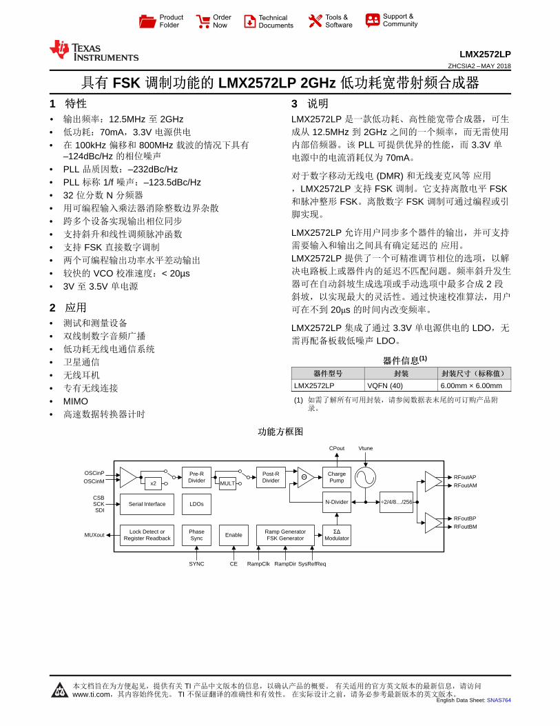
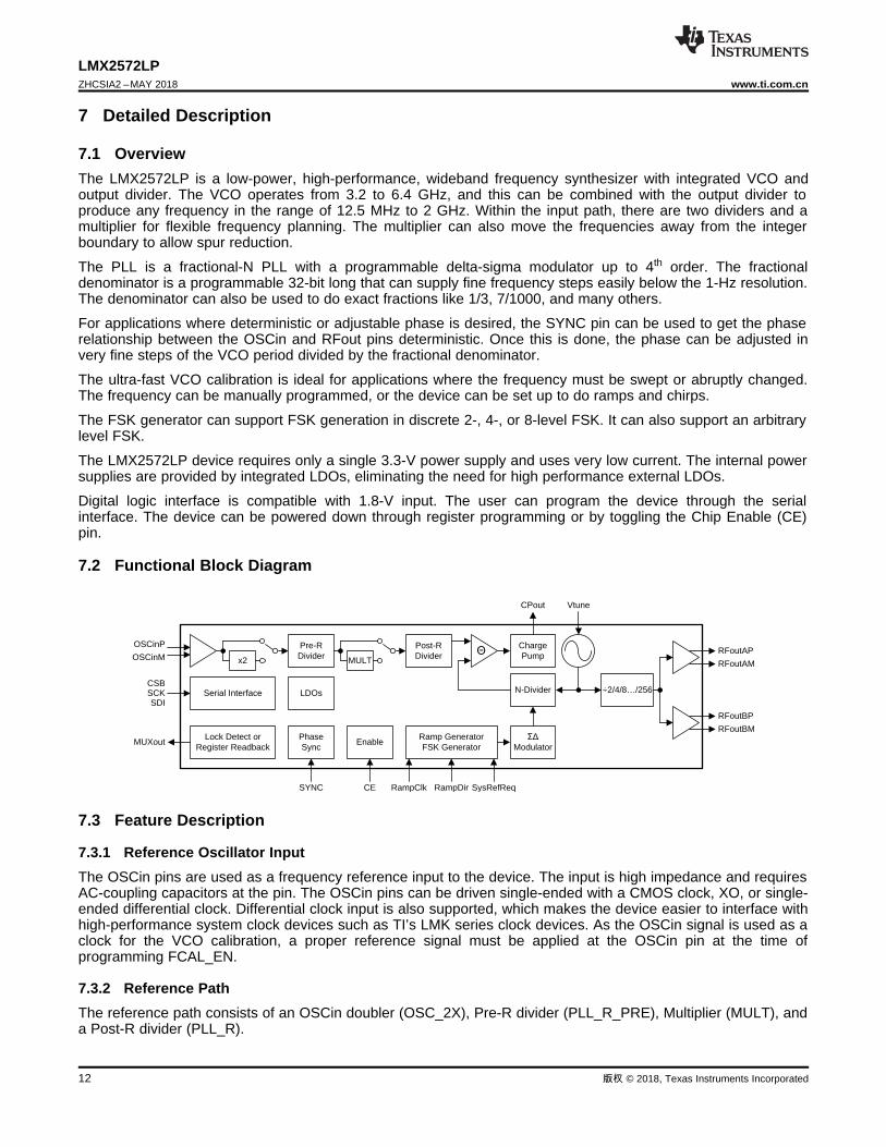
Charge Pump Serial Interface CPout Vtune CSB SCK SDI Lock Detect or Register Readback x2 Ramp Generator FSK Generator OSCinP OSCinM RFoutBP RFoutBM RFoutAP RFoutAM MUXout SYNC SysRefReq MULT , ÷2/4/8«/256 RampClk RampDir CE Pre-R Divider Post-R Divider Enable Phase Sync ß Modulator N-Divider LDOs Product Folder Order Now Technical Documents Tools & Software Support & Community 本文档旨在为方便起见,提供有关 TI 产品中文版本的信息,以确认产品的概要。 有关适用的官方英文版本的最新信息,请访问 www.ti.com,其内容始终优先。 TI 不保证翻译的准确性和有效性。 在实际设计之前,请务必参考最新版本的英文版本。 English Data Sheet: SNAS764 LMX2572LP ZHCSIA2 – MAY 2018 具有 FSK 调制功能的 LMX2572LP 2GHz 低功耗宽带射频合成器 1 1 特性 1• 输出频率:12.5MHz 至 2GHz • 低功耗:70mA,3.3V 电源供电 • 在 100kHz 偏移和 800MHz 载波的情况下具有 –124dBc/Hz 的相位噪声 • PLL 品质因数:–232dBc/Hz • PLL 标称 1/f 噪声:–123.5dBc/Hz • 32 位分数 N 分频器 • 用可编程输入乘法器消除整数边界杂散 • 跨多个设备实现输出相位同步 • 支持斜升和线性调频脉冲函数 • 支持 FSK 直接数字调制 • 两个可编程输出功率水平差动输出 • 较快的 VCO 校准速度:< 20μs • 3V 至 3.5V 单电源 2 应用 • 测试和测量设备 • 双线制数字音频广播 • 低功耗无线电通信系统 • 卫星通信 • 无线耳机 • 专有无线连接 • MIMO • 高速数据转换器计时 3 说明 LMX2572LP 是一款低功耗、高性能宽带合成器,可生 成从 12.5MHz 到 2GHz 之间的一个频率,而无需使用 内部倍频器。该 PLL 可提供优异的性能,而 3.3V 单 电源中的电流消耗仅为 70mA。 对于数字移动无线电 (DMR) 和无线麦克风等 应用 ,LMX2572LP 支持 FSK 调制。它支持离散电平 FSK 和脉冲整形 FSK。离散数字 FSK 调制可通过编程或引 脚实现。 LMX2572LP 允许用户同步多个器件的输出,并可支持 需要输入和输出之间具有确定延迟的 应用。 LMX2572LP 提供了一个可精准调节相位的选项,以解 决电路板上或器件内的延迟不匹配问题。频率斜升发生 器可在自动斜坡生成选项或手动选项中最多合成 2 段 斜坡,以实现最大的灵活性。通过快速校准算法,用户 可在不到 20μs 的时间内改变频率。 LMX2572LP 集成了通过 3.3V 单电源供电的 LDO,无 需再配备板载低噪声 LDO。 器件信息 (1) 器件型号 封装 封装尺寸(标称值) LMX2572LP VQFN (40) 6.00mm × 6.00mm (1) 如需了解所有可用封装,请参阅数据表末尾的可订购产品附 录。 功能方框图
-
Upload
khangminh22 -
Category
Documents
-
view
0 -
download
0
Transcript of 具有 FSK 调制功能的 LMX2572LP 2GHz 低功耗宽带射频合成 ...
Charge Pump
Serial Interface
CPout Vtune
CSBSCKSDI
Lock Detect or Register Readback
x2
Ramp Generator FSK Generator
OSCinP
OSCinM
RFoutBP
RFoutBM
RFoutAP
RFoutAM
MUXout
SYNC SysRefReq
MULT,
÷2/4/8«/256
RampClk RampDirCE
Pre-R Divider
Post-R Divider
EnablePhase Sync
�û�
Modulator
N-DividerLDOs
Product
Folder
Order
Now
Technical
Documents
Tools &
Software
Support &Community
本文档旨在为方便起见,提供有关 TI 产品中文版本的信息,以确认产品的概要。 有关适用的官方英文版本的最新信息,请访问www.ti.com,其内容始终优先。 TI 不保证翻译的准确性和有效性。 在实际设计之前,请务必参考最新版本的英文版本。
English Data Sheet: SNAS764
LMX2572LPZHCSIA2 –MAY 2018
具具有有 FSK 调调制制功功能能的的 LMX2572LP 2GHz 低低功功耗耗宽宽带带射射频频合合成成器器
1
1 特特性性
1• 输出频率:12.5MHz 至 2GHz• 低功耗:70mA,3.3V 电源供电
• 在 100kHz 偏移和 800MHz 载波的情况下具有–124dBc/Hz 的相位噪声
• PLL 品质因数:–232dBc/Hz• PLL 标称 1/f 噪声:–123.5dBc/Hz• 32 位分数 N 分频器
• 用可编程输入乘法器消除整数边界杂散
• 跨多个设备实现输出相位同步
• 支持斜升和线性调频脉冲函数
• 支持 FSK 直接数字调制
• 两个可编程输出功率水平差动输出
• 较快的 VCO 校准速度:< 20µs• 3V 至 3.5V 单电源
2 应应用用
• 测试和测量设备
• 双线制数字音频广播
• 低功耗无线电通信系统
• 卫星通信
• 无线耳机
• 专有无线连接
• MIMO• 高速数据转换器计时
3 说说明明
LMX2572LP 是一款低功耗、高性能宽带合成器,可生
成从 12.5MHz 到 2GHz 之间的一个频率,而无需使用
内部倍频器。该 PLL 可提供优异的性能,而 3.3V 单
电源中的电流消耗仅为 70mA。
对于数字移动无线电 (DMR) 和无线麦克风等 应用
,LMX2572LP 支持 FSK 调制。它支持离散电平 FSK和脉冲整形 FSK。离散数字 FSK 调制可通过编程或引
脚实现。
LMX2572LP 允许用户同步多个器件的输出,并可支持
需要输入和输出之间具有确定延迟的 应用。
LMX2572LP 提供了一个可精准调节相位的选项,以解
决电路板上或器件内的延迟不匹配问题。频率斜升发生
器可在自动斜坡生成选项或手动选项中最多合成 2 段
斜坡,以实现最大的灵活性。通过快速校准算法,用户
可在不到 20μs 的时间内改变频率。
LMX2572LP 集成了通过 3.3V 单电源供电的 LDO,无
需再配备板载低噪声 LDO。
器器件件信信息息(1)
器器件件型型号号 封封装装 封封装装尺尺寸寸((标标称称值值))
LMX2572LP VQFN (40) 6.00mm × 6.00mm
(1) 如需了解所有可用封装,请参阅数据表末尾的可订购产品附录。
功功能能方方框框图图
2
LMX2572LPZHCSIA2 –MAY 2018 www.ti.com.cn
Copyright © 2018, Texas Instruments Incorporated
目目录录
1 特特性性.......................................................................... 12 应应用用.......................................................................... 13 说说明明.......................................................................... 14 修修订订历历史史记记录录 ........................................................... 25 Pin Configuration and Functions ......................... 36 Specifications......................................................... 4
6.1 Absolute Maximum Ratings ...................................... 46.2 ESD Ratings.............................................................. 46.3 Recommended Operating Conditions....................... 46.4 Thermal Information .................................................. 56.5 Electrical Characteristics........................................... 56.6 Timing Requirements ................................................ 76.7 Timing Diagrams....................................................... 86.8 Typical Characteristics .............................................. 9
7 Detailed Description ............................................ 127.1 Overview ................................................................. 127.2 Functional Block Diagram ....................................... 127.3 Feature Description................................................. 127.4 Device Functional Modes........................................ 17
7.5 Programming........................................................... 177.6 Register Maps ......................................................... 20
8 Application and Implementation ........................ 598.1 Application Information............................................ 598.2 Typical Application .................................................. 698.3 Do's and Don'ts....................................................... 70
9 Power Supply Recommendations ...................... 7210 Layout................................................................... 73
10.1 Layout Guidelines ................................................. 7310.2 Layout Example .................................................... 73
11 器器件件和和文文档档支支持持 ..................................................... 7411.1 器件支持 ................................................................ 7411.2 文档支持 ................................................................ 7411.3 接收文档更新通知 ................................................. 7411.4 社区资源 ................................................................ 7411.5 商标 ....................................................................... 7411.6 静电放电警告......................................................... 7411.7 术语表 ................................................................... 74
12 机机械械、、封封装装和和可可订订购购信信息息....................................... 74
4 修修订订历历史史记记录录注:之前版本的页码可能与当前版本有所不同。
日日期期 版版本本 注注释释
2018 年 5 月 * 初始发行版
40G
ND
11V
ccC
P
1CE 30 RampClk
39G
ND
12C
Pou
t
2GND 29 VrefVCO2
38V
regV
CO
13G
ND
3VbiasVCO 28 SysRefReq
37V
ccV
CO
14G
ND
4GND 27 VbiasVCO2
36V
refV
CO
15V
ccM
AS
H
5SYNC 26 VccVCO2
35V
tune
16S
CK
6GND 25 GND
34G
ND
17S
DI
7VccDIG 24 CSB
33V
bias
VA
RA
C18
RF
outB
M
8OSCinP 23 RFoutAP
32R
ampD
ir19
RF
outB
P
9OSCinM 22 RFoutAM
31G
ND
20M
UX
out
10VregIN 21 VccBUF
Not to scale
DAP
3
LMX2572LPwww.ti.com.cn ZHCSIA2 –MAY 2018
Copyright © 2018, Texas Instruments Incorporated
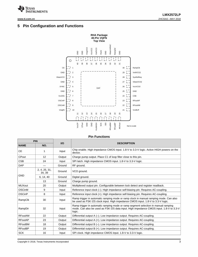
5 Pin Configuration and Functions
RHA Package40-Pin VQFN
Top View
Pin FunctionsPIN
I/O DESCRIPTIONNAME NO.
CE 1 Input Chip enable. High impedance CMOS input. 1.8-V to 3.3-V logic. Active HIGH powers on thedevice.
CPout 12 Output Charge pump output. Place C1 of loop filter close to this pin.CSB 24 Input SPI latch. High impedance CMOS input. 1.8-V to 3.3-V logic.DAP — Ground RF ground.
GND
2, 4, 25, 31,34, 39 Ground VCO ground.
6, 14, 40 Ground Digital ground.13 Ground Charge pump ground.
MUXout 20 Output Multiplexed output pin. Configurable between lock detect and register readback.OSCinM 9 Input Reference input clock (–). High impedance self-biasing pin. Requires AC-coupling.OSCinP 8 Input Reference input clock (+). High impedance self-biasing pin. Requires AC-coupling.
RampClk 30 Input Ramp trigger in automatic ramping mode or ramp clock in manual ramping mode. Can alsobe used as FSK I2S clock input. High impedance CMOS input. 1.8-V to 3.3-V logic.
RampDir 32 InputRamp trigger in automatic ramping mode or ramp segment selection in manual rampingmode. Can also be used as FSK I2S data input. High impedance CMOS input. 1.8-V to 3.3-Vlogic.
RFoutAM 22 Output Differential output A (–). Low impedance output. Requires AC-coupling.RFoutAP 23 Output Differential output A (+). Low impedance output. Requires AC-coupling.RFoutBM 18 Output Differential output B (–). Low impedance output. Requires AC-coupling.RFoutBP 19 Output Differential output B (+). Low impedance output. Requires AC-coupling.SCK 16 Input SPI clock. High impedance CMOS input. 1.8-V to 3.3-V logic.
4
LMX2572LPZHCSIA2 –MAY 2018 www.ti.com.cn
Copyright © 2018, Texas Instruments Incorporated
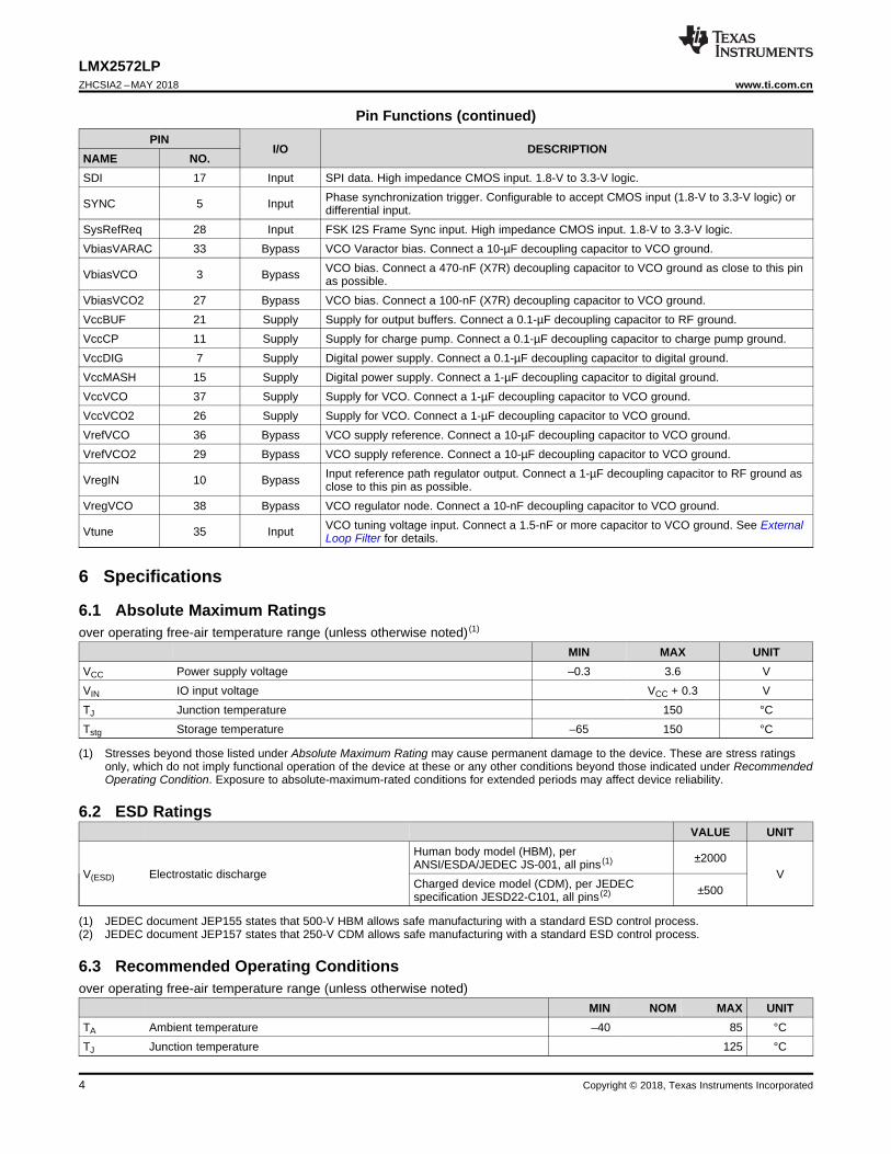
Pin Functions (continued)PIN
I/O DESCRIPTIONNAME NO.SDI 17 Input SPI data. High impedance CMOS input. 1.8-V to 3.3-V logic.
SYNC 5 Input Phase synchronization trigger. Configurable to accept CMOS input (1.8-V to 3.3-V logic) ordifferential input.
SysRefReq 28 Input FSK I2S Frame Sync input. High impedance CMOS input. 1.8-V to 3.3-V logic.VbiasVARAC 33 Bypass VCO Varactor bias. Connect a 10-µF decoupling capacitor to VCO ground.
VbiasVCO 3 Bypass VCO bias. Connect a 470-nF (X7R) decoupling capacitor to VCO ground as close to this pinas possible.
VbiasVCO2 27 Bypass VCO bias. Connect a 100-nF (X7R) decoupling capacitor to VCO ground.VccBUF 21 Supply Supply for output buffers. Connect a 0.1-µF decoupling capacitor to RF ground.VccCP 11 Supply Supply for charge pump. Connect a 0.1-µF decoupling capacitor to charge pump ground.VccDIG 7 Supply Digital power supply. Connect a 0.1-µF decoupling capacitor to digital ground.VccMASH 15 Supply Digital power supply. Connect a 1-µF decoupling capacitor to digital ground.VccVCO 37 Supply Supply for VCO. Connect a 1-µF decoupling capacitor to VCO ground.VccVCO2 26 Supply Supply for VCO. Connect a 1-µF decoupling capacitor to VCO ground.VrefVCO 36 Bypass VCO supply reference. Connect a 10-µF decoupling capacitor to VCO ground.VrefVCO2 29 Bypass VCO supply reference. Connect a 10-µF decoupling capacitor to VCO ground.
VregIN 10 Bypass Input reference path regulator output. Connect a 1-µF decoupling capacitor to RF ground asclose to this pin as possible.
VregVCO 38 Bypass VCO regulator node. Connect a 10-nF decoupling capacitor to VCO ground.
Vtune 35 Input VCO tuning voltage input. Connect a 1.5-nF or more capacitor to VCO ground. See ExternalLoop Filter for details.
(1) Stresses beyond those listed under Absolute Maximum Rating may cause permanent damage to the device. These are stress ratingsonly, which do not imply functional operation of the device at these or any other conditions beyond those indicated under RecommendedOperating Condition. Exposure to absolute-maximum-rated conditions for extended periods may affect device reliability.
6 Specifications
6.1 Absolute Maximum Ratingsover operating free-air temperature range (unless otherwise noted) (1)
MIN MAX UNITVCC Power supply voltage –0.3 3.6 VVIN IO input voltage VCC + 0.3 VTJ Junction temperature 150 °CTstg Storage temperature –65 150 °C
(1) JEDEC document JEP155 states that 500-V HBM allows safe manufacturing with a standard ESD control process.(2) JEDEC document JEP157 states that 250-V CDM allows safe manufacturing with a standard ESD control process.
6.2 ESD RatingsVALUE UNIT
V(ESD) Electrostatic discharge
Human body model (HBM), perANSI/ESDA/JEDEC JS-001, all pins (1) ±2000
VCharged device model (CDM), per JEDECspecification JESD22-C101, all pins (2) ±500
6.3 Recommended Operating Conditionsover operating free-air temperature range (unless otherwise noted)
MIN NOM MAX UNITTA Ambient temperature –40 85 °CTJ Junction temperature 125 °C

5
LMX2572LPwww.ti.com.cn ZHCSIA2 –MAY 2018
Copyright © 2018, Texas Instruments Incorporated
(1) For more information about traditional and new thermal metrics, see the Semiconductor and IC Package Thermal Metrics applicationreport.
6.4 Thermal Information
THERMAL METRIC (1)LMX2572LP
UNITRHA (VQFN)40 PINS
RθJA Junction-to-ambient thermal resistance 25.5 °C/WRθJC(top) Junction-to-case (top) thermal resistance 14.4 °C/WRθJB Junction-to-board thermal resistance 8 °C/WΨJT Junction-to-top characterization parameter 0.2 °C/WΨJB Junction-to-board characterization parameter 7.9 °C/WRθJC(bot) Junction-to-case (bottom) thermal resistance 1.2 °C/W
(1) ICP = 2.5 mA; fVCO = 3.2 GHz; fOUT = 400 MHz; POUT = −3 dBm; OSC_2X = 1; MULT = 1; one RF output.(2) ICP = 2.5 mA; fVCO = 3.2 GHz; fOUT = 400 MHz; POUT = −3 dBm; OSC_2X = 0; MULT = 1; one RF output.(3) See OSCin Configuration for definition of OSCin input voltage.(4) For lower VCO frequencies, the N-divider minimum value can limit the phase detector frequency.(5) Measured with a clean OSCin signal with a high slew rate using a wide loop bandwidth. The noise metrics model the PLL noise for an
infinite loop bandwidth as: PLL_Total = 10*log[10(PLL_Flat/10)+10(PLL_Flicker/10)]; PLL_Flat = PN1 Hz + 20*log(N) + 10*log(fPD); PLL_Flicker= PN10 kHz - 10*log(Offset/10 kHz) + 20*log(fOUT/1 GHz)
(6) fOSCin = 200 MHz; fPD = 100 MHz; fVCO = 6 GHz(7) fOSCin = 200 MHz; fPD = 100 MHz; fVCO = 6.001 GHz; Fractional denominator = 1000.
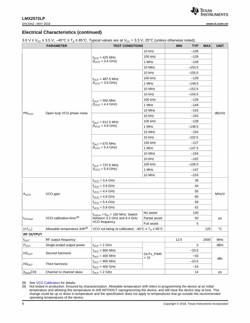
6.5 Electrical Characteristics3.0 V ≤ VCC ≤ 3.5 V, –40°C ≤ TA ≤ 85°C. Typical values are at VCC = 3.3 V, 25°C (unless otherwise noted).
PARAMETER TEST CONDITIONS MIN TYP MAX UNITPOWER SUPPLYVCC Supply voltage 3 3.3 3.5 V
ICC Supply currentfOSCin = 20 MHz; fPD = 40 MHz (1) 70
mAfOSCin = 100 MHz; fPD = 100 MHz (2) 74.5ICCPD Power down current 2.5INPUT SIGNAL PATH
fOSCin OSCin input frequencyOSC_2X = 0 (Doubler bypassed) 5 250
MHzOSC_2X = 1 (Doubler enabled) 5 125
VOSCin OSCin input voltage (3) Single-ended input buffer 0.3 3.6V
Differential input buffer 0.15 1fMULTin Multiplier input frequency
MULT ≥ 310 40
MHzfMULTout Multiplier output frequency 60 150PLL
fPD Phase detector frequency (4)
Integer channel 0.25 250
MHz1st and 2nd order modulator 5 2003rd order modulator 5 1604th order modulator 5 120
ICPout Charge pump current
CPG = 1 625
µACPG = 2 1250CPG = 3 1875··· …CPG = 15 6875
PNPLL_1/f Normalized PLL 1/f noise (5) –123.5dBc/Hz
PNPLL_Flat Normalized PLL noise floor (5) Integer channel (6) –232Fractional channel (7) –232
VCOfVCO VCO frequency 3200 6400 MHz
6
LMX2572LPZHCSIA2 –MAY 2018 www.ti.com.cn
Copyright © 2018, Texas Instruments Incorporated
Electrical Characteristics (continued)3.0 V ≤ VCC ≤ 3.5 V, –40°C ≤ TA ≤ 85°C. Typical values are at VCC = 3.3 V, 25°C (unless otherwise noted).
PARAMETER TEST CONDITIONS MIN TYP MAX UNIT
(8) See VCO Calibration for details.(9) Not tested in production. Ensured by characterization. Allowable temperature drift refers to programming the device at an initial
temperature and allowing this temperature to drift WITHOUT reprogramming the device, and still have the device stay at lock. Thischange could be up or down in temperature and the specification does not apply to temperatures that go outside the recommendedoperating temperatures of the device.
PNVCO Open loop VCO phase noise
fOUT = 425 MHz(fVCO = 3.4 GHz)
10 kHz –106
dBc/Hz
100 kHz –1291 MHz –14910 MHz –153.5
fOUT = 487.5 MHz(fVCO = 3.9 GHz)
10 kHz –105.5100 kHz –1291 MHz –149.510 MHz –152.5
fOUT = 550 MHz(fVCO = 4.4 GHz)
10 kHz –104.5100 kHz –1291 MHz –14910 MHz –153
fOUT = 612.5 MHz(fVCO = 4.9 GHz)
10 kHz –103100 kHz –1281 MHz –148.510 MHz –154
fOUT = 675 MHz(fVCO = 5.4 GHz)
10 kHz –102.5100 kHz –1271 MHz –147.510 MHz –154
fOUT = 737.5 MHz(fVCO = 5.9 GHz)
10 kHz –102100 kHz –126.51 MHz –14710 MHz –153
KVCO VCO gain
fVCO = 3.4 GHz 39
MHz/V
fVCO = 3.9 GHz 44fVCO = 4.4 GHz 55fVCO = 4.9 GHz 60fVCO = 5.4 GHz 69fVCO = 5.9 GHz 62
tVCOcal VCO calibration-time (8)fOSCin = fPD = 100 MHz; Switchbetween 3.2 GHz and 6.4 GHzVCO frequency
No assist 130µsPartial assist 50
Full assist 5|ΔTCL| Allowable temperature drift (9) VCO not being re-calibrated, –40°C ≤ TA ≤ 85°C 125 °CRF OUTPUTfOUT RF output frequency 12.5 2000 MHzPOUT Single-ended output power fOUT = 2 GHz
OUTx_PWR= 15
5 dBm
H2OUT Second harmonicfOUT = 800 MHz −33.5
dBcfOUT = 400 MHz −43
H3OUT Third harmonicfOUT = 800 MHz –10.5fOUT = 400 GHz −10
|tskewCH| Channel to channel skew fOUT = 2 GHz 14 ps
7
LMX2572LPwww.ti.com.cn ZHCSIA2 –MAY 2018
版权 © 2018, Texas Instruments Incorporated
Electrical Characteristics (continued)3.0 V ≤ VCC ≤ 3.5 V, –40°C ≤ TA ≤ 85°C. Typical values are at VCC = 3.3 V, 25°C (unless otherwise noted).
PARAMETER TEST CONDITIONS MIN TYP MAX UNITPHASE SYNCHRONIZATION
fOSCinSYNC OSCin input frequency withSYNC
Category 3 5 100MHz
Categories 1 and 2 5 200
|tskewSYNC| OSCin to RFout skew After phase synchronization;fOSCinSYNC = fOUT = 100 MHz 2 ns
DIGITAL INTERFACEVIH High-level input voltage 1.4 VCC VVIL Low-level input voltage 0.4IIH High-level input current –25 25
µAIIL Low-level input current –25 25VOH High-level output voltage Load current = –5 mA
MUXout pinVCC – 0.5
VVOL Low-level output voltage Load current = 5 mA 0.5
6.6 Timing Requirements3.0 V ≤ VCC ≤ 3.5 V, –40°C ≤ TA ≤ 85°C. Typical values are at VCC = 3.3 V, 25°C (unless otherwise noted).
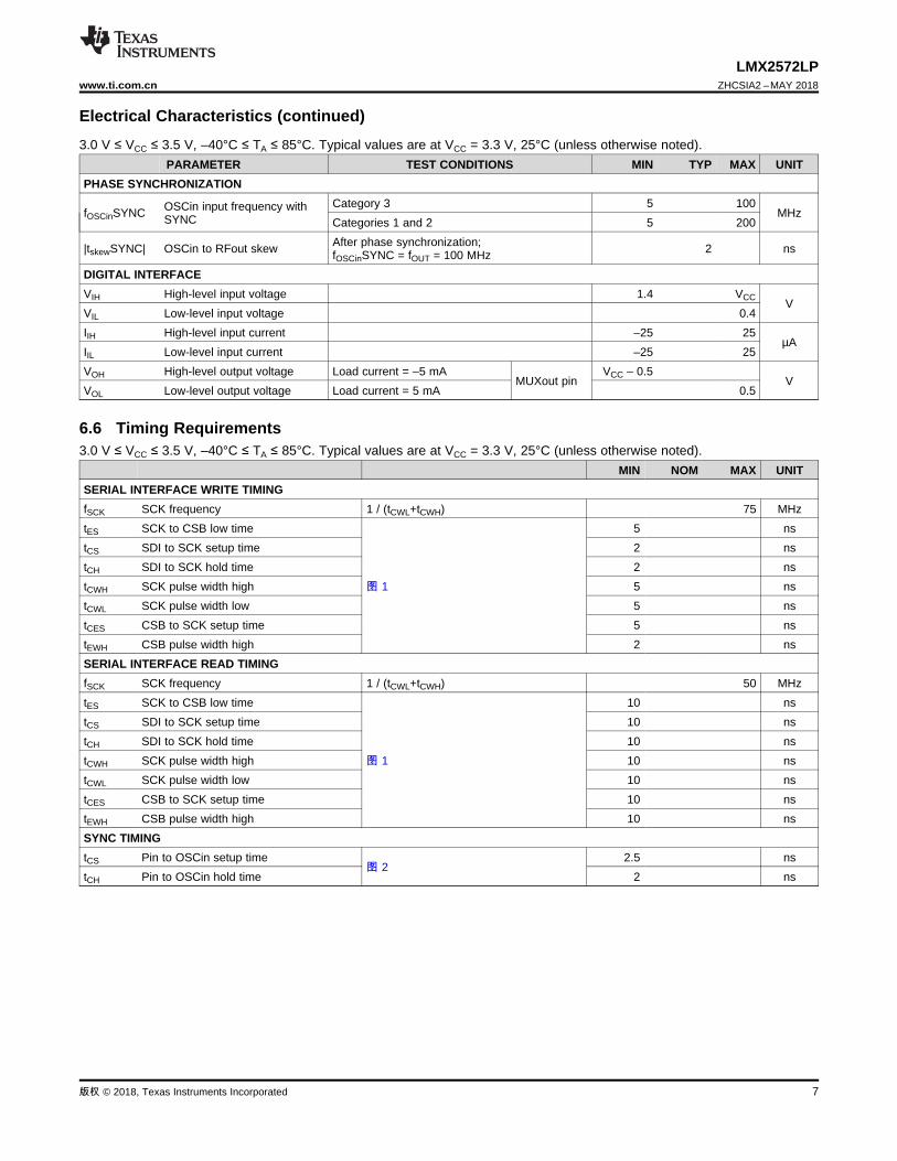
MIN NOM MAX UNITSERIAL INTERFACE WRITE TIMINGfSCK SCK frequency 1 / (tCWL+tCWH) 75 MHztES SCK to CSB low time
图 1
5 nstCS SDI to SCK setup time 2 nstCH SDI to SCK hold time 2 nstCWH SCK pulse width high 5 nstCWL SCK pulse width low 5 nstCES CSB to SCK setup time 5 nstEWH CSB pulse width high 2 nsSERIAL INTERFACE READ TIMINGfSCK SCK frequency 1 / (tCWL+tCWH) 50 MHztES SCK to CSB low time
图 1
10 nstCS SDI to SCK setup time 10 nstCH SDI to SCK hold time 10 nstCWH SCK pulse width high 10 nstCWL SCK pulse width low 10 nstCES CSB to SCK setup time 10 nstEWH CSB pulse width high 10 nsSYNC TIMINGtCS Pin to OSCin setup time
图 22.5 ns
tCH Pin to OSCin hold time 2 ns
tCHtCS
SYNC
OSCin
MSB(R/W)
LSB(D0)
tCHtCS
tCES
tCWL
tCWH tEWHtCE
SDI
SCK
CSB
1st 2nd 3rd ± 7th 8th 9th ± 23rd 24th
Read back register value16-bit
MUXout
Address(7-bit) (D15 ± D1)
8
LMX2572LPZHCSIA2 –MAY 2018 www.ti.com.cn
版权 © 2018, Texas Instruments Incorporated
6.7 Timing Diagrams
图图 1. Serial Interface Timing Diagram
图图 2. SYNC Timing Diagram

Offset (kHz)
Ph
ase
no
ise
(dB
c/H
z)
1 2 3 45 710 20 50 100200 1000 10000 5000050000-160
-140
-120
-100
-80
-60
D037
675 MHz
Offset (kHz)
Ph
ase
no
ise
(dB
c/H
z)
1 2 3 45 710 20 50 100200 1000 10000 5000050000-160
-140
-120
-100
-80
-60
D038
737.5 MHz
Offset (kHz)
Ph
ase
no
ise
(dB
c/H
z)
1 2 3 45 710 20 50 100200 1000 10000 5000050000-160
-140
-120
-100
-80
-60
D035
550 MHz
Offset (kHz)
Ph
ase
no
ise
(dB
c/H
z)
1 2 3 45 710 20 50 100200 1000 10000 5000050000-160
-140
-120
-100
-80
-60
D036
612.5 MHz
Offset (kHz)
Ph
ase
no
ise
(dB
c/H
z)
1 2 3 45 710 20 50 100200 1000 10000 5000050000-160
-140
-120
-100
-80
-60
D033
425 MHz
Offset (kHz)
Ph
ase
no
ise
(dB
c/H
z)
1 2 3 45 710 20 50 100200 1000 10000 5000050000-160
-140
-120
-100
-80
-60
D034
487.5 MHz
9
LMX2572LPwww.ti.com.cn ZHCSIA2 –MAY 2018
版权 © 2018, Texas Instruments Incorporated
6.8 Typical CharacteristicsAt TA = 25°C, unless otherwise noted
图图 3. Open-Loop VCO Phase Noise at 425 MHz 图图 4. Open-Loop VCO Phase Noise at 487.5 MHz
图图 5. Open-Loop VCO Phase Noise at 550 MHz 图图 6. Open-Loop VCO Phase Noise at 612.5 MHz
图图 7. Open-Loop VCO Phase Noise at 675 MHz 图图 8. Open-Loop VCO Phase Noise at 737.5 MHz
Offset (kHz)
Ph
ase
no
ise
(dB
c/H
z)
1 2 3 5 710 20 50 100 1000 10000 100000-160
-150
-140
-130
-120
-110
-100
D043
675 MHz
Offset (kHz)
Ph
ase
no
ise
(dB
c/H
z)
1 2 3 5 710 20 50 100 1000 10000 100000-160
-150
-140
-130
-120
-110
-100
D044
737.5 MHz
Offset (kHz)
Ph
ase
no
ise
(dB
c/H
z)
1 2 3 5 710 20 50 100 1000 10000 100000-160
-150
-140
-130
-120
-110
-100
D041
550 MHz
Offset (kHz)
Ph
ase
no
ise
(dB
c/H
z)
1 2 3 5 710 20 50 100 1000 10000 100000-160
-150
-140
-130
-120
-110
-100
D042
612.5 MHz
Offset (kHz)
Ph
ase
no
ise
(dB
c/H
z)
1 2 3 5 710 20 50 100 1000 10000 100000-160
-150
-140
-130
-120
-110
-100
D039
425 MHz
Offset (kHz)
Ph
ase
no
ise
(dB
c/H
z)
1 2 3 5 710 20 50 100 1000 10000 100000-160
-150
-140
-130
-120
-110
-100
D040
487.5 MHz
10
LMX2572LPZHCSIA2 –MAY 2018 www.ti.com.cn
版权 © 2018, Texas Instruments Incorporated
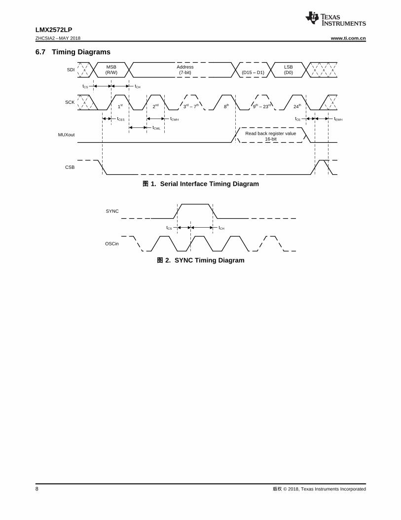
Typical Characteristics (接接下下页页)At TA = 25°C, unless otherwise noted
图图 9. Wide Band Phase Noise at 425 MHz 图图 10. Wide Band Phase Noise at 487.5 MHz
图图 11. Wide Band Phase Noise at 550 MHz 图图 12. Wide Band Phase Noise at 612.5 MHz
图图 13. Wide Band Phase Noise at 675 MHz 图图 14. Wide Band Phase Noise at 737.5 MHz

Time (µs)
f OU
T (
MH
z)
-250 -200 -150 -100 -50 0 50 100 150 200 250424.915
424.932
424.949
424.966
424.983
425
425.017
425.034
425.051
425.068
425.085
D007 Time (µs)
f OU
T (
MH
z)
-500 -300 -100 100 300 500487.4968
487.4974
487.4981
487.4987
487.4994
487.5
487.5006
487.5013
487.5019
487.5026
487.5032
D008
fOUT (MHz)
PO
UT (
dB
m)
0 200 400 600 800 1000 1200 1400 1600 1800 2000-6
-4
-2
0
2
4
6
8
10
D047
OUTx_PWR51218
OUTx_PWR
PO
UT (
dB
m)
2 4 6 8 10 12 14 16 18-12
-9
-6
-3
0
3
6
9
D048
fOUT250 MHz500 MHz1000 MHz2000 MHz
Time (µs)
f OU
T (
MH
z)
-20 0 20 40 60 80 100 120 140 160 180600
800
1000
1200
1400
1600
1800
D045
VCO frequency jump from 3200 MHz to 6400 MHz
Time (µs)
f OU
T (
MH
z)
-20 0 20 40 60 80 100 120 140 160 180600
800
1000
1200
1400
1600
1800
D046
VCO frequency jump from 6400 MHz to 3200 MHz
11
LMX2572LPwww.ti.com.cn ZHCSIA2 –MAY 2018
版权 © 2018, Texas Instruments Incorporated
Typical Characteristics (接接下下页页)At TA = 25°C, unless otherwise noted
图图 15. VCO Calibration Time 图图 16. VCO Calibration Time
图图 17. Output Power vs Frequency 图图 18. Configurable Output Power
图图 19. 4-Level GFSK Modulation 图图 20. Discrete-Level FSK Modulation
Charge Pump
Serial Interface
CPout Vtune
CSBSCKSDI
Lock Detect or Register Readback
x2
Ramp Generator FSK Generator
OSCinP
OSCinM
RFoutBP
RFoutBM
RFoutAP
RFoutAM
MUXout
SYNC SysRefReq
MULT,
÷2/4/8«/256
RampClk RampDirCE
Pre-R Divider
Post-R Divider
EnablePhase Sync
�û�
Modulator
N-DividerLDOs
12
LMX2572LPZHCSIA2 –MAY 2018 www.ti.com.cn
版权 © 2018, Texas Instruments Incorporated
7 Detailed Description
7.1 OverviewThe LMX2572LP is a low-power, high-performance, wideband frequency synthesizer with integrated VCO andoutput divider. The VCO operates from 3.2 to 6.4 GHz, and this can be combined with the output divider toproduce any frequency in the range of 12.5 MHz to 2 GHz. Within the input path, there are two dividers and amultiplier for flexible frequency planning. The multiplier can also move the frequencies away from the integerboundary to allow spur reduction.
The PLL is a fractional-N PLL with a programmable delta-sigma modulator up to 4th order. The fractionaldenominator is a programmable 32-bit long that can supply fine frequency steps easily below the 1-Hz resolution.The denominator can also be used to do exact fractions like 1/3, 7/1000, and many others.
For applications where deterministic or adjustable phase is desired, the SYNC pin can be used to get the phaserelationship between the OSCin and RFout pins deterministic. Once this is done, the phase can be adjusted invery fine steps of the VCO period divided by the fractional denominator.
The ultra-fast VCO calibration is ideal for applications where the frequency must be swept or abruptly changed.The frequency can be manually programmed, or the device can be set up to do ramps and chirps.
The FSK generator can support FSK generation in discrete 2-, 4-, or 8-level FSK. It can also support an arbitrarylevel FSK.
The LMX2572LP device requires only a single 3.3-V power supply and uses very low current. The internal powersupplies are provided by integrated LDOs, eliminating the need for high performance external LDOs.
Digital logic interface is compatible with 1.8-V input. The user can program the device through the serialinterface. The device can be powered down through register programming or by toggling the Chip Enable (CE)pin.
7.2 Functional Block Diagram
7.3 Feature Description
7.3.1 Reference Oscillator InputThe OSCin pins are used as a frequency reference input to the device. The input is high impedance and requiresAC-coupling capacitors at the pin. The OSCin pins can be driven single-ended with a CMOS clock, XO, or single-ended differential clock. Differential clock input is also supported, which makes the device easier to interface withhigh-performance system clock devices such as TI’s LMK series clock devices. As the OSCin signal is used as aclock for the VCO calibration, a proper reference signal must be applied at the OSCin pin at the time ofprogramming FCAL_EN.
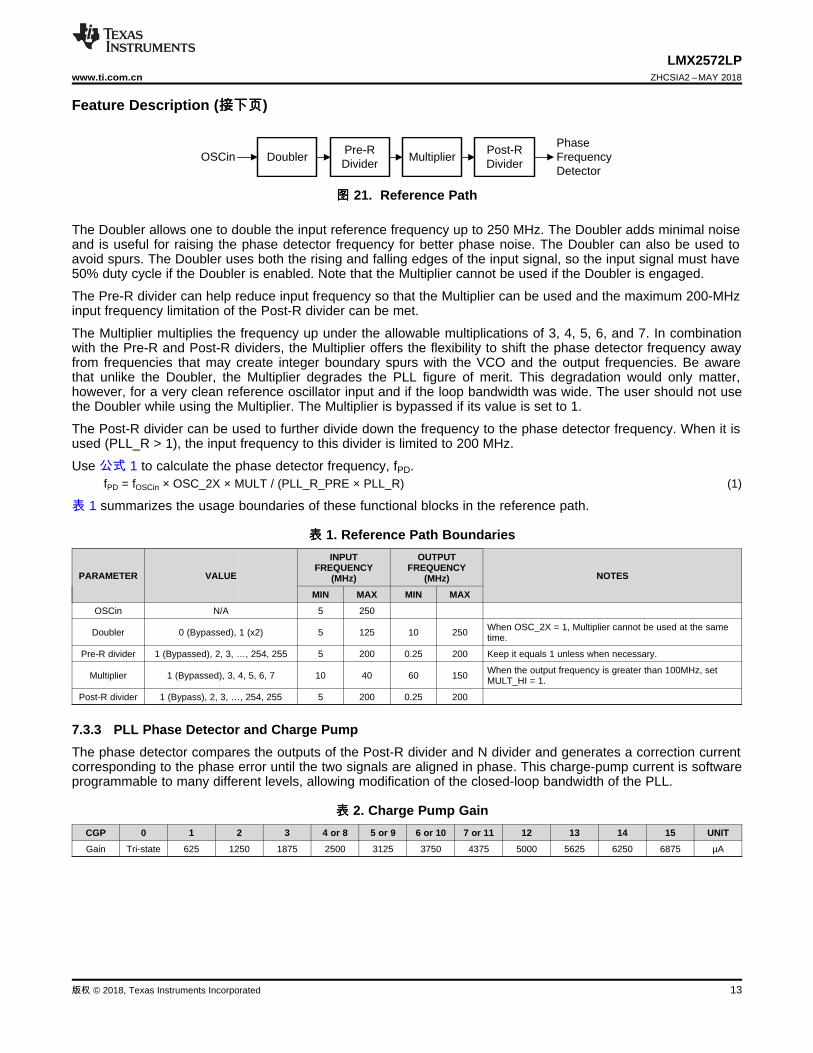
7.3.2 Reference PathThe reference path consists of an OSCin doubler (OSC_2X), Pre-R divider (PLL_R_PRE), Multiplier (MULT), anda Post-R divider (PLL_R).
Pre-R Divider
MultiplierPost-R Divider
OSCinPhase Frequency Detector
Doubler
13
LMX2572LPwww.ti.com.cn ZHCSIA2 –MAY 2018
版权 © 2018, Texas Instruments Incorporated
Feature Description (接接下下页页)
图图 21. Reference Path
The Doubler allows one to double the input reference frequency up to 250 MHz. The Doubler adds minimal noiseand is useful for raising the phase detector frequency for better phase noise. The Doubler can also be used toavoid spurs. The Doubler uses both the rising and falling edges of the input signal, so the input signal must have50% duty cycle if the Doubler is enabled. Note that the Multiplier cannot be used if the Doubler is engaged.
The Pre-R divider can help reduce input frequency so that the Multiplier can be used and the maximum 200-MHzinput frequency limitation of the Post-R divider can be met.
The Multiplier multiplies the frequency up under the allowable multiplications of 3, 4, 5, 6, and 7. In combinationwith the Pre-R and Post-R dividers, the Multiplier offers the flexibility to shift the phase detector frequency awayfrom frequencies that may create integer boundary spurs with the VCO and the output frequencies. Be awarethat unlike the Doubler, the Multiplier degrades the PLL figure of merit. This degradation would only matter,however, for a very clean reference oscillator input and if the loop bandwidth was wide. The user should not usethe Doubler while using the Multiplier. The Multiplier is bypassed if its value is set to 1.
The Post-R divider can be used to further divide down the frequency to the phase detector frequency. When it isused (PLL_R > 1), the input frequency to this divider is limited to 200 MHz.
Use 公式 1 to calculate the phase detector frequency, fPD.fPD = fOSCin × OSC_2X × MULT / (PLL_R_PRE × PLL_R) (1)
表 1 summarizes the usage boundaries of these functional blocks in the reference path.
表表 1. Reference Path Boundaries
PARAMETER VALUE
INPUTFREQUENCY
(MHz)
OUTPUTFREQUENCY
(MHz) NOTES
MIN MAX MIN MAX
OSCin N/A 5 250
Doubler 0 (Bypassed), 1 (x2) 5 125 10 250 When OSC_2X = 1, Multiplier cannot be used at the sametime.
Pre-R divider 1 (Bypassed), 2, 3, …, 254, 255 5 200 0.25 200 Keep it equals 1 unless when necessary.
Multiplier 1 (Bypassed), 3, 4, 5, 6, 7 10 40 60 150 When the output frequency is greater than 100MHz, setMULT_HI = 1.
Post-R divider 1 (Bypass), 2, 3, …, 254, 255 5 200 0.25 200
7.3.3 PLL Phase Detector and Charge PumpThe phase detector compares the outputs of the Post-R divider and N divider and generates a correction currentcorresponding to the phase error until the two signals are aligned in phase. This charge-pump current is softwareprogrammable to many different levels, allowing modification of the closed-loop bandwidth of the PLL.
表表 2. Charge Pump GainCGP 0 1 2 3 4 or 8 5 or 9 6 or 10 7 or 11 12 13 14 15 UNIT
Gain Tri-state 625 1250 1875 2500 3125 3750 4375 5000 5625 6250 6875 µA
VCO RFoutA÷2,4,8,16, 32,64,128,
256RFoutB
14
LMX2572LPZHCSIA2 –MAY 2018 www.ti.com.cn
版权 © 2018, Texas Instruments Incorporated
7.3.4 PLL N Divider and Fractional CircuitryThe N divider includes fractional compensation and can achieve any fractional denominator (PLL_DEN) from 1 to(232 – 1). The integer portion of N (PLL_N) is the whole part of the N divider value, and the fractional portion,Nfrac = PLL_NUM / PLL_DEN, is the remaining fraction. PLL_N, PLL_NUM and PLL_DEN are softwareprogrammable. The higher the denominator, the finer the resolution step of the output. For example, even whenusing fPD = 200 MHz, the output can increment in steps of 200 MHz / (232 – 1) = 0.0466 Hz. 公式 2 shows therelationship between the phase detector and VCO frequencies. Note that in SYNC mode, there is an extra dividerthat is not shown in 公式 2.
fVCO = fPD × [PLL_N + (PLL_NUM / PLL_DEN)] (2)
The multi-stage noise-shaping (MASH) sigma-delta modulator that controls the fractional division is alsoprogrammable from integer mode to fourth order. All of these settings work for integer channel where PLL_NUM= 0. To make the fractional spurs consistent, the modulator is reset any time that the R0 register is programmed.
The N divider has minimum value restrictions based on the modulator order. Furthermore, the PFD_DLY_SEL bitmust be programmed in accordance to 表 3.
表表 3. Minimum N Divider Restrictions
VCOFREQUENCY
(GHz)
MASH ORDER
INTEGER FIRST ORDER SECOND ORDER THIRD ORDER FOURTH ORDER
N PFD_DLY_SEL N PFD_DLY_SEL N PFD_DLY_SEL N PFD_DLY_SEL N PFD_DLY_SEL
fVCO < 4 20 0 25 1 26 1 32 2 44 4
4 ≤ fVCO < 4.9 24 1 29 2 30 2 32 2 44 4
4.9 ≤ fVCO ≤ 6.4 24 1 29 2 30 2 36 3 48 5
7.3.5 Voltage-Controlled OscillatorThe LMX2572LP includes a fully integrated VCO. The VCO generates a frequency which varies with the tuningvoltage from the loop filter. The entire VCO frequency range, 3.2 to 6.4 GHz, covers an octave that allows thechannel divider to take care of frequencies below the lower bound.
To reduce the VCO tuning gain, thus improving the VCO phase noise performance, the VCO frequency range isdivided into 6 different frequency bands. This creates the need for frequency calibration to determine the correctfrequency band given in a desired output frequency. The VCO is also calibrated for amplitude to optimize phasenoise. These calibration routines are activated any time that the R0 register is programmed with the FCAL_EN bitequals one. It is important that a valid OSCin signal must present before VCO calibration begins. This device willsupport a full sweep of the valid temperature range of 125°C (–40°C to 85°C) without having to re-calibrate theVCO. This is important for continuous operation of the synthesizer under the most extreme temperature variation.
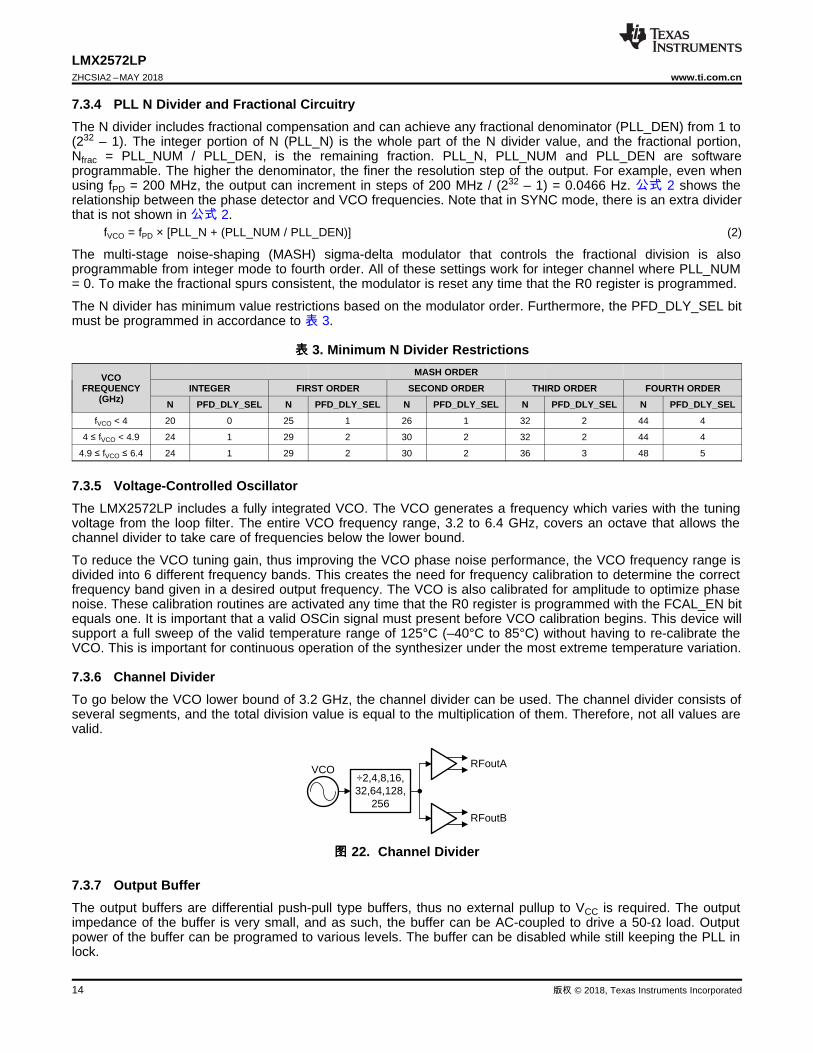
7.3.6 Channel DividerTo go below the VCO lower bound of 3.2 GHz, the channel divider can be used. The channel divider consists ofseveral segments, and the total division value is equal to the multiplication of them. Therefore, not all values arevalid.
图图 22. Channel Divider
7.3.7 Output BufferThe output buffers are differential push-pull type buffers, thus no external pullup to VCC is required. The outputimpedance of the buffer is very small, and as such, the buffer can be AC-coupled to drive a 50-Ω load. Outputpower of the buffer can be programed to various levels. The buffer can be disabled while still keeping the PLL inlock.
Device 1
Device 2
fOUT1
fOUT2
fOSCin
SYNC
SYNC
fOSCin
t1
fOUT1
fOUT2t2
15
LMX2572LPwww.ti.com.cn ZHCSIA2 –MAY 2018
版权 © 2018, Texas Instruments Incorporated
7.3.8 Lock DetectThe MUXout pin can be configured to output a signal that gives an indication for the PLL being locked. If theMUXout pin is configured as a lock detect output (MUXOUT_LD_SEL = 1), the MUXout pin output is a logicHIGH voltage when the device is locked. When the device is unlocked, the MUXout pin output is a logic LOWvoltage.
There are options to select the definition of PLL being locked. If LD_TYPE = 0, lock detect asserts a HIGH outputafter the VCO has finished calibration and the LD_DLY timeout counter is finished. If LD_TYPE = 1, in addition tothe VCO calibration and counter check, lock detect will assert a HIGH output if the VCO tuning voltage is alsowithin an acceptable limits.
7.3.9 Register ReadbackThe MUXout pin can also be configured to read back useful information from the device. Common uses forreadback are:• Read back registers to ensure that they have been programmed to the correct value. LMX2572LP allows any
of its registers to be read back.• Read back the lock detect status to determine if the PLL is in lock.• Read back VCO calibration information so that it can be used to improve the lock time.
7.3.10 PowerdownThe user can use the CE pin or the POWERDOWN bit to power the LMX2572LP up or down. All registers arepreserved in memory while the device is powered down.
The wake-up time for the device to come out of the powered state is adjustable. See Power-Up, Wake-Up Timefor details.
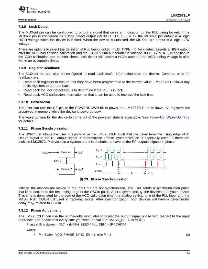
7.3.11 Phase SynchronizationThe SYNC pin allows the user to synchronize the LMX2572LP such that the delay from the rising edge of thOSCin signal to the RF output signal is deterministic. Phase synchronization is especially useful if there aremultiple LMX2572LP devices in a system and it is desirable to have all the RF outputs aligned in phase.
图图 23. Phase Synchronization
Initially, the devices are locked to the input but are not synchronized. The user sends a synchronization pulsethat is re-clocked to the next rising edge of the OSCin pulse. After a given time, t1, the devices are synchronized.This time is dominated by the sum of the VCO calibration time, the analog settling time of the PLL loop, and theMASH_RST_COUNT, if used in fractional mode. After synchronization, both devices will have a deterministicdelay of t2, related to OSCin.
7.3.12 Phase AdjustmentThe LMX2572LP can use the sigma-delta modulator to adjust the output signal phase with respect to the inputreference. The phase shift every time you write the value of MASH_SEED is 公式 3:
Phase shift in degree = 360° × (MASH_SEED / PLL_DEN) × (P / CHDIV)
where• P = 2 when VCO_PHASE_SYNC_EN = 1, else P = 1 (3)
Time
Out
put f
requ
ency
Time
Out
put f
requ
ency
Manual Ramping Mode Automatic Ramping Mode
16
LMX2572LPZHCSIA2 –MAY 2018 www.ti.com.cn
版权 © 2018, Texas Instruments Incorporated
For example, if• MASH_SEED = 800• PLL_DEN = 1000• CHDIV = 32• VCO_PHASE_SYNC_EN = 0
Phase shift = 360° × (800 / 1000) × (1 / 32) = 9°. If we write 800 to MASH_SEED 40 times, then we will shift thephase by 360°.
There are a couple of restrictions when using phase adjustment:• Phase adjustment does not work with MASH_ORDER equals 0 (Integer mode) or 1 (First order).• Phase adjustment is possible with integer channels (PLL_NUM = 0) as long as MASH_ORDER is greater
than 1.• PLL_DEN must be greater than PLL_NUM + MASH_SEED.
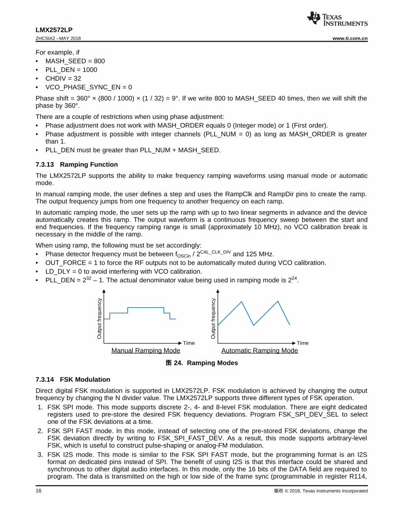
7.3.13 Ramping FunctionThe LMX2572LP supports the ability to make frequency ramping waveforms using manual mode or automaticmode.
In manual ramping mode, the user defines a step and uses the RampClk and RampDir pins to create the ramp.The output frequency jumps from one frequency to another frequency on each ramp.
In automatic ramping mode, the user sets up the ramp with up to two linear segments in advance and the deviceautomatically creates this ramp. The output waveform is a continuous frequency sweep between the start andend frequencies. If the frequency ramping range is small (approximately 10 MHz), no VCO calibration break isnecessary in the middle of the ramp.
When using ramp, the following must be set accordingly:• Phase detector frequency must be between fOSCin / 2CAL_CLK_DIV and 125 MHz.• OUT_FORCE = 1 to force the RF outputs not to be automatically muted during VCO calibration.• LD_DLY = 0 to avoid interfering with VCO calibration.• PLL_DEN = 232 – 1. The actual denominator value being used in ramping mode is 224.
图图 24. Ramping Modes
7.3.14 FSK ModulationDirect digital FSK modulation is supported in LMX2572LP. FSK modulation is achieved by changing the outputfrequency by changing the N divider value. The LMX2572LP supports three different types of FSK operation.1. FSK SPI mode. This mode supports discrete 2-, 4- and 8-level FSK modulation. There are eight dedicated
registers used to pre-store the desired FSK frequency deviations. Program FSK_SPI_DEV_SEL to selectone of the FSK deviations at a time.
2. FSK SPI FAST mode. In this mode, instead of selecting one of the pre-stored FSK deviations, change theFSK deviation directly by writing to FSK_SPI_FAST_DEV. As a result, this mode supports arbitrary-levelFSK, which is useful to construct pulse-shaping or analog-FM modulation.
3. FSK I2S mode. This mode is similar to the FSK SPI FAST mode, but the programming format is an I2Sformat on dedicated pins instead of SPI. The benefit of using I2S is that this interface could be shared andsynchronous to other digital audio interfaces. In this mode, only the 16 bits of the DATA field are required toprogram. The data is transmitted on the high or low side of the frame sync (programmable in register R114,
MSB LSB
tCHtCS
tCES
tCWL
tCWH tEWHtCE
I2S DATA(RampDir)
I2S CLK(RampClk)
I2S FS(SysRefReq)
MSB
Frame (n)th Frame (n+1)th
Time
Out
put f
requ
ency
17
LMX2572LPwww.ti.com.cn ZHCSIA2 –MAY 2018
版权 © 2018, Texas Instruments Incorporated
FSK_I2S_FS_POL). The unused side of the frame sync needs to be at least one clock cycle. In other words,17 (16 + 1) CLK cycles are required at a minimum for one I2S frame. Maximum I2S clock rate is 75 MHz.Timing diagram is shown in 图 26 while the timing specification is same as SPI write timing as shown in theTiming Requirements section.
图图 25. FSK Modulation
图图 26. FSK I2S Timing Diagram
7.4 Device Functional Modes表 4 lists the device functional modes of the LMX2572LP.
表表 4. Device Functional ModesMODE DESCRIPTION
Normal operation mode The device is used as a high frequency signal source without any addition features.FSK mode Generates discrete-level FSK or arbitrary-level pulse-shaped FSK modulation.
SYNC mode This mode is used to ensure deterministic phase between OSCin and RFout.Ramping mode Automatic frequency sweeping without the need of continuous SPI programming.
7.5 ProgrammingThe LMX2572LP is programmed using several 24-bit shift registers. The shift register consists of a data field, anaddress field, and a R/W bit. The MSB is the R/W bit. 0 means register write while 1 means register read. Thefollowing seven bits, ADDR[6:0], form the address field which is used to decode the internal register address.The remaining 16 bits form the data field DATA[15:0]. Serial data is shifted MSB first into the shift register. See图 1 for timing diagram details.
To write registers:• The R/W bit must be set to 0.• The data on SDI pin is clocked into the shift register upon the rising edge of the clocks on SCK pin. On the
rising edge of the 24th clock cycle, the data is transferred from the data field into the selected register bank.• The CSB pin may be held high after programming, which causes the LMX2572LP to ignore clock pulses.• If the SCK and SDI lines are toggled while the VCO is in lock, as is sometimes the case when these lines are
shared between devices, the phase noise may be degraded during the time of this programming.
18
LMX2572LPZHCSIA2 –MAY 2018 www.ti.com.cn
版权 © 2018, Texas Instruments Incorporated
Programming (接接下下页页)To read back registers:• The R/W bit must be set to 1.• The data field contents on the SDI line are ignored.• The read back data on MUXout pin is clocked out starting from the falling edge of the 8th clock cycle.
7.5.1 Recommended Initial Power-On Programming
7.5.1.1 Programming SequenceWhen the device is first powered up, it must be initialized, and the ordering of this programming is important. Thesequence is listed below. After this sequence is completed, the device should be running and locked to theproper frequency.1. Apply power to the device and ensure all the supply pins are at the proper levels.2. If CE is low, pull it high.3. Wait 500 µs for the internal LDOs to become stable.4. Ensure that a valid reference clock is applied to the OSCin pins.5. Program register R0 with RESET = 1. This will ensure all the registers are reset to their default values. This
bit is self-clearing.6. Program in sequence registers R125, R124, R123, ..., R1 and then R0.
7.5.1.2 Programming RegisterThere are altogether 126 programmable registers. However, not every register is required to be programmed atinitial power-on.
For example, most of the registers have fixed field value which is also equal to their silicon default value. Afterprogramming R0 with RESET = 1, these register fields have returned to their silicon default values. As such, it isnot necessary to program these registers again. Similarly, for those registers having configurable fields, if thedesired field values are equal to the silicon default values, again it is not necessary to program these registersagain after programming R0 with RESET = 1.
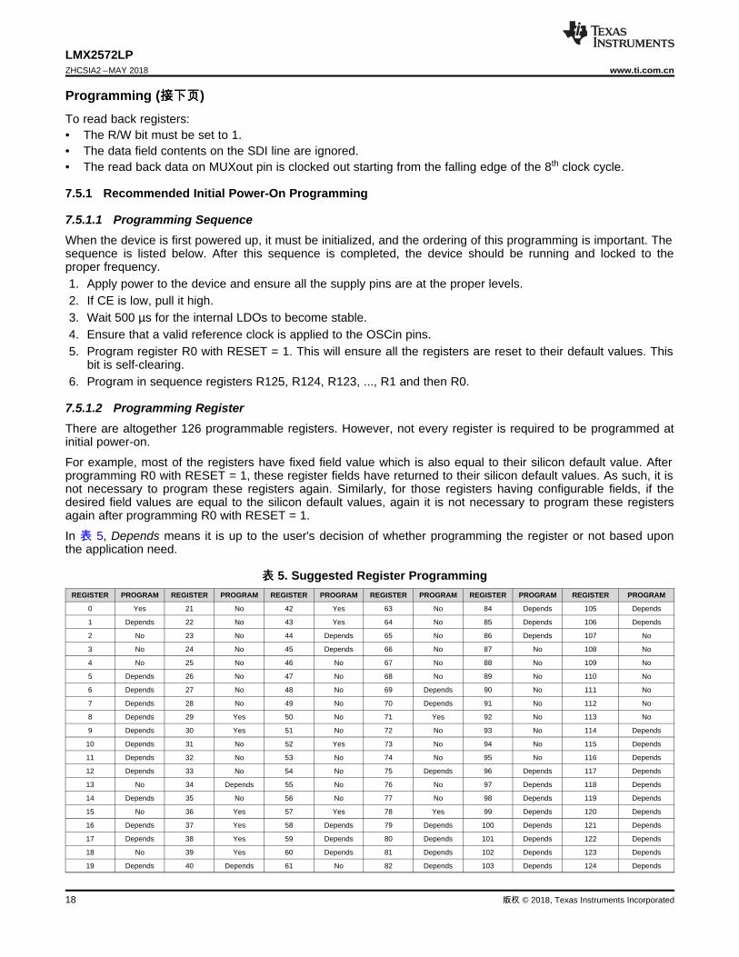
In 表 5, Depends means it is up to the user's decision of whether programming the register or not based uponthe application need.
表表 5. Suggested Register ProgrammingREGISTER PROGRAM REGISTER PROGRAM REGISTER PROGRAM REGISTER PROGRAM REGISTER PROGRAM REGISTER PROGRAM
0 Yes 21 No 42 Yes 63 No 84 Depends 105 Depends
1 Depends 22 No 43 Yes 64 No 85 Depends 106 Depends
2 No 23 No 44 Depends 65 No 86 Depends 107 No
3 No 24 No 45 Depends 66 No 87 No 108 No
4 No 25 No 46 No 67 No 88 No 109 No
5 Depends 26 No 47 No 68 No 89 No 110 No
6 Depends 27 No 48 No 69 Depends 90 No 111 No
7 Depends 28 No 49 No 70 Depends 91 No 112 No
8 Depends 29 Yes 50 No 71 Yes 92 No 113 No
9 Depends 30 Yes 51 No 72 No 93 No 114 Depends
10 Depends 31 No 52 Yes 73 No 94 No 115 Depends
11 Depends 32 No 53 No 74 No 95 No 116 Depends
12 Depends 33 No 54 No 75 Depends 96 Depends 117 Depends
13 No 34 Depends 55 No 76 No 97 Depends 118 Depends
14 Depends 35 No 56 No 77 No 98 Depends 119 Depends
15 No 36 Yes 57 Yes 78 Yes 99 Depends 120 Depends
16 Depends 37 Yes 58 Depends 79 Depends 100 Depends 121 Depends
17 Depends 38 Yes 59 Depends 80 Depends 101 Depends 122 Depends
18 No 39 Yes 60 Depends 81 Depends 102 Depends 123 Depends
19 Depends 40 Depends 61 No 82 Depends 103 Depends 124 Depends
MSB(R/W)
Data(R18)
SDI
SCK
CSB
1st 2nd±8th 41th
±56th
Address(7-bit)
Data(R19)
Data(R20)
9th±24th 25th
±40th
19
LMX2572LPwww.ti.com.cn ZHCSIA2 –MAY 2018
版权 © 2018, Texas Instruments Incorporated
Programming (接接下下页页)表表 5. Suggested Register Programming (接接下下页页)
REGISTER PROGRAM REGISTER PROGRAM REGISTER PROGRAM REGISTER PROGRAM REGISTER PROGRAM REGISTER PROGRAM
20 Depends 41 Depends 62 Depends 83 Depends 104 Depends 125 No
7.5.2 Recommended Sequence for Changing FrequenciesThe recommended sequence for changing frequencies in different scenarios is as follows:1. If the N divider is changing, program the relevant registers and then program R0 with FCAL_EN = 1.2. In FSK and Ramp mode, the fractional numerator is changing; program the relevant registers only.
7.5.3 Double BufferingSome register fields support double buffering. That is, the change to these fields would not be effectiveimmediately. To latch the new values into the device requires programming R0 again with FCAL_EN = 1. Thefollowing register fields support double buffering, see 表 69 for details.• MASH order (MASH_ORDER)• Fractional numerator (PLL_NUM)• N divider (PLL_N)• Doubler (OSC_2X); Pre-R divider (PLL_R_PRE); Multiplier (MULT); Post-R divider (PLL_R)
For example,1. Program PLL_R and PLL_N to new values. If double buffering for these fields is enabled, the PLL will remain
unchanged.2. Program R0 with FCAL_EN = 1. The PLL will calibrate and lock using the new PLL_R and PLL_N values.
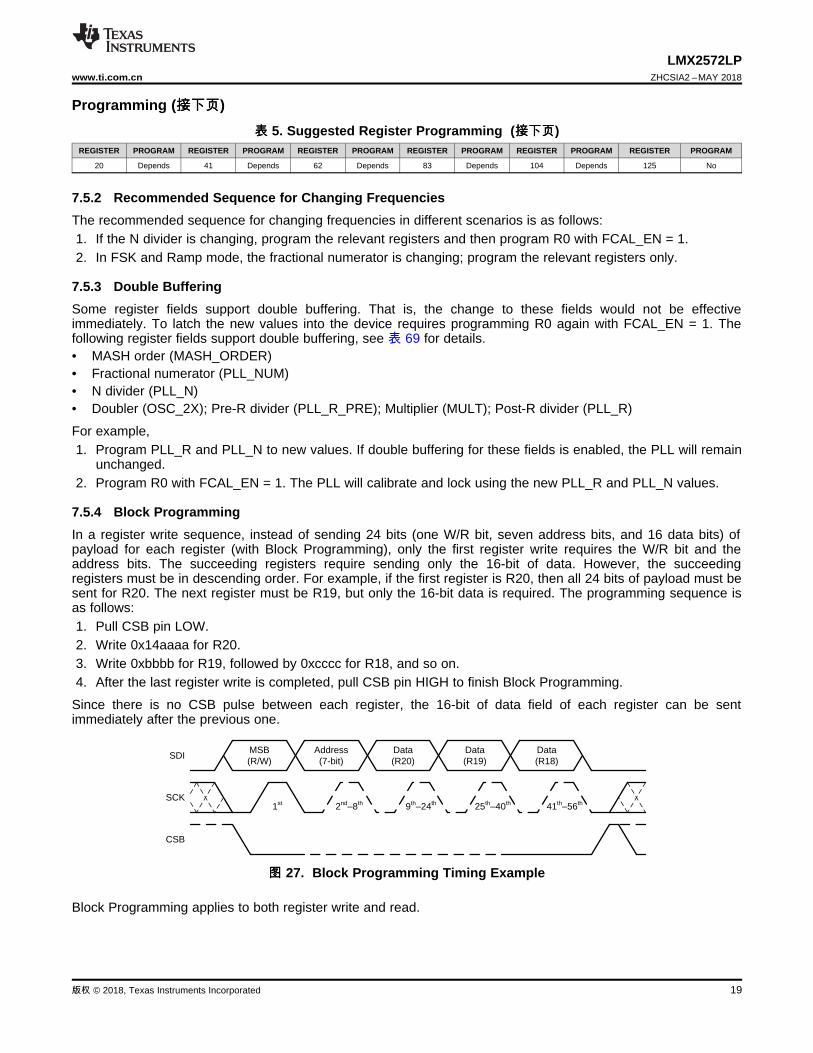
7.5.4 Block ProgrammingIn a register write sequence, instead of sending 24 bits (one W/R bit, seven address bits, and 16 data bits) ofpayload for each register (with Block Programming), only the first register write requires the W/R bit and theaddress bits. The succeeding registers require sending only the 16-bit of data. However, the succeedingregisters must be in descending order. For example, if the first register is R20, then all 24 bits of payload must besent for R20. The next register must be R19, but only the 16-bit data is required. The programming sequence isas follows:1. Pull CSB pin LOW.2. Write 0x14aaaa for R20.3. Write 0xbbbb for R19, followed by 0xcccc for R18, and so on.4. After the last register write is completed, pull CSB pin HIGH to finish Block Programming.
Since there is no CSB pulse between each register, the 16-bit of data field of each register can be sentimmediately after the previous one.
图图 27. Block Programming Timing Example
Block Programming applies to both register write and read.
LMX2572LPZHCSIA2 –MAY 2018 www.ti.com.cn
20 Copyright © 2018, Texas Instruments Incorporated
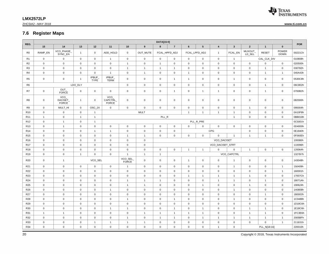
7.6 Register Maps
REG.DATA[15:0]
POR15 14 13 12 11 10 9 8 7 6 5 4 3 2 1 0
R0 RAMP_EN VCO_PHASE_SYNC_EN 1 0 ADD_HOLD 0 OUT_MUTE FCAL_HPFD_ADJ FCAL_LPFD_ADJ 1 FCAL_EN MUXOUT_
LD_SEL RESET POWERDOWN 00221Ch
R1 0 0 0 0 1 0 0 0 0 0 0 0 1 CAL_CLK_DIV 010808h
R2 0 0 0 0 0 1 0 1 0 0 0 0 0 0 0 0 020500h
R3 0 0 0 0 0 1 1 1 1 0 0 0 0 0 1 0 030782h
R4 0 0 0 0 1 0 1 0 0 1 0 0 0 0 1 1 040A43h
R5 0 0 1 IPBUF_TYPE
IPBUF_TERM 0 0 0 1 1 0 0 1 0 0 0 0530C8h
R6 LDO_DLY 0 0 0 0 0 0 0 0 0 1 0 06C802h
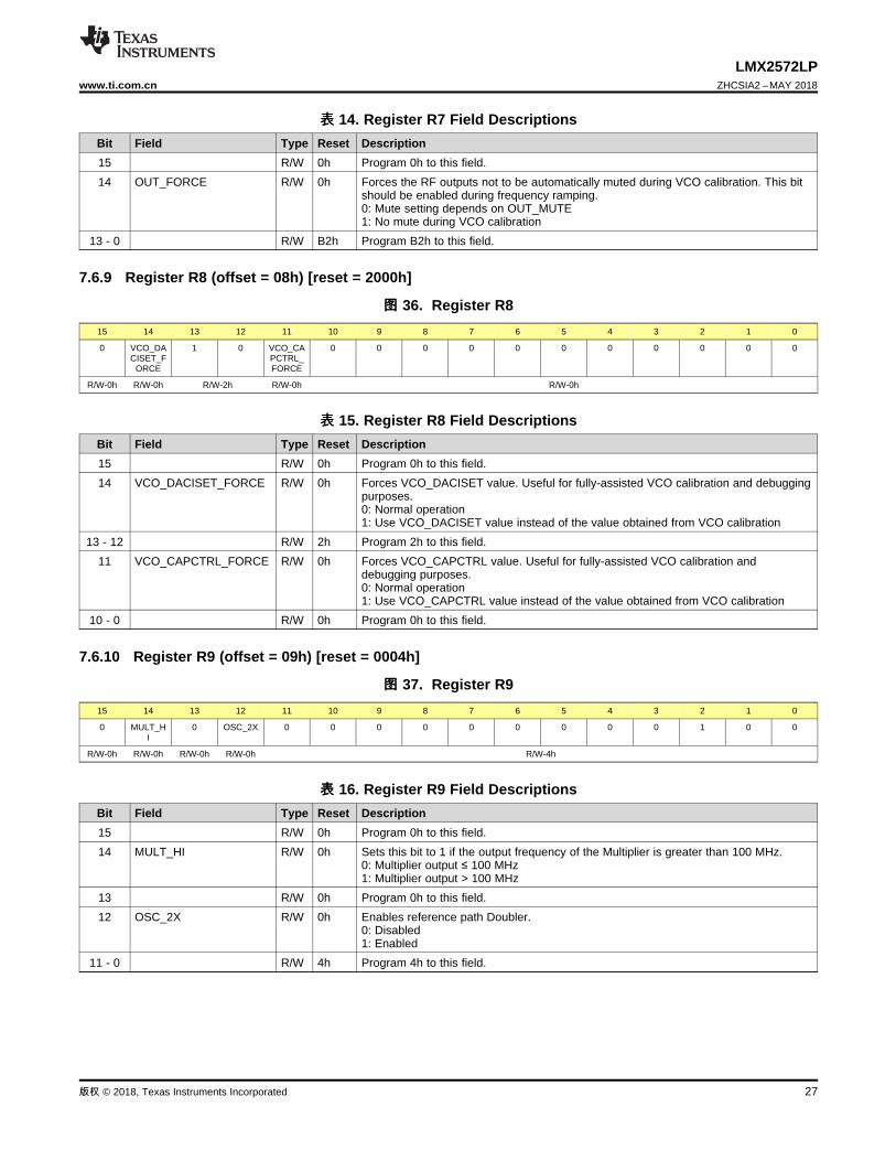
R7 0 OUT_FORCE 0 0 0 0 0 0 1 0 1 1 0 0 1 0 0700B2h
R8 0VCO_
DACISET_FORCE
1 0VCO_
CAPCTRL_FORCE
0 0 0 0 0 0 0 0 0 0 0 082000h
R9 0 MULT_HI 0 OSC_2X 0 0 0 0 0 0 0 0 0 1 0 0 090004h
R10 0 0 0 1 MULT 1 1 1 1 0 0 0 0A10F8h
R11 1 0 1 1 PLL_R 1 0 0 0 0BB018h
R12 0 1 0 1 PLL_R_PRE 0C5001h
R13 0 1 0 0 0 0 0 0 0 0 0 0 0 0 0 0 0D4000h
R14 0 0 0 1 1 0 0 0 0 CPG 0 0 0 0E1840h
R15 0 0 0 0 0 1 1 0 0 0 0 0 1 1 1 0 0F060Eh
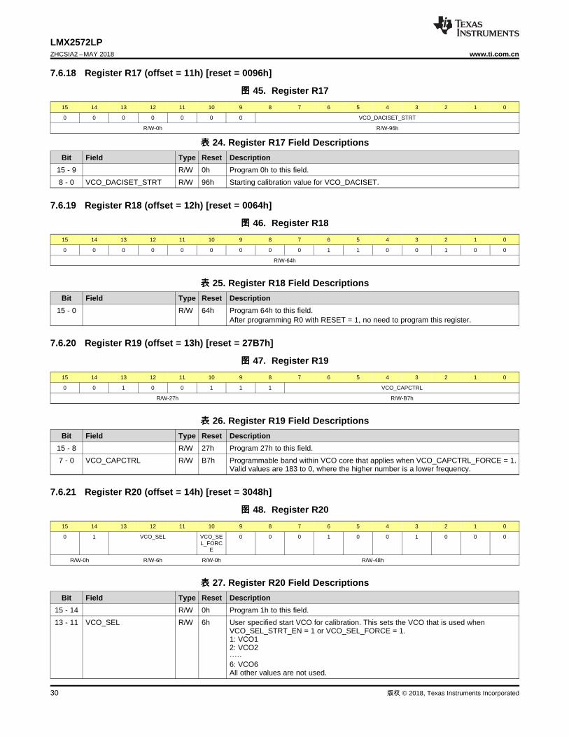
R16 0 0 0 0 0 0 0 VCO_DACISET 100080h
R17 0 0 0 0 0 0 0 VCO_DACISET_STRT 110096h
R18 0 0 0 0 0 0 0 0 0 1 1 0 0 1 0 0 120064h
R19 0 0 1 0 0 1 1 1 VCO_CAPCTRL 1327B7h
R20 0 1 VCO_SEL VCO_SEL_FORCE 0 0 0 1 0 0 1 0 0 0 143048h
R21 0 0 0 0 0 1 0 0 0 0 0 0 1 0 0 1 150409h
R22 0 0 0 0 0 0 0 0 0 0 0 0 0 0 0 1 160001h
R23 0 0 0 0 0 0 0 0 0 1 1 1 1 1 0 0 17007Ch
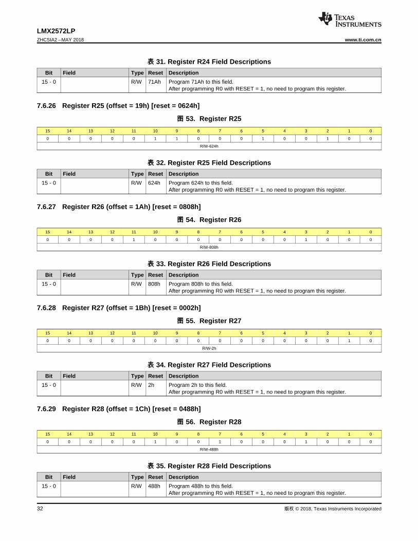
R24 0 0 0 0 0 1 1 1 0 0 0 1 1 0 1 0 18071Ah
R25 0 0 0 0 0 1 1 0 0 0 1 0 0 1 0 0 190624h
R26 0 0 0 0 1 0 0 0 0 0 0 0 1 0 0 0 1A0808h
R27 0 0 0 0 0 0 0 0 0 0 0 0 0 0 1 0 1B0002h
R28 0 0 0 0 0 1 0 0 1 0 0 0 1 0 0 0 1C0488h
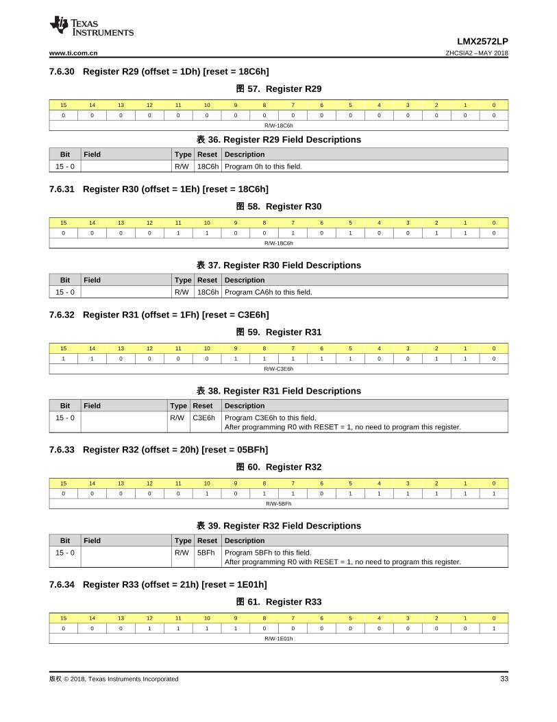
R29 0 0 0 0 0 0 0 0 0 0 0 0 0 0 0 0 1D18C6h
R30 0 0 0 0 1 1 0 0 1 0 1 0 0 1 1 0 1E18C6h
R31 1 1 0 0 0 0 1 1 1 1 1 0 0 1 1 0 1FC3E6h
R32 0 0 0 0 0 1 0 1 1 0 1 1 1 1 1 1 2005BFh
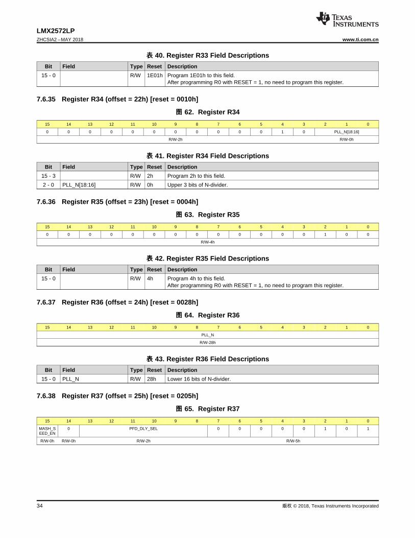
R33 0 0 0 1 1 1 1 0 0 0 0 0 0 0 0 1 211E01h
R34 0 0 0 0 0 0 0 0 0 0 0 1 0 PLL_N[18:16] 220010h
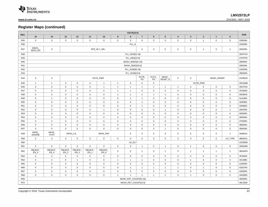
LMX2572LPwww.ti.com.cn ZHCSIA2 –MAY 2018
21Copyright © 2018, Texas Instruments Incorporated
Register Maps (continued)
REG.DATA[15:0]
POR15 14 13 12 11 10 9 8 7 6 5 4 3 2 1 0
R35 0 0 0 0 0 0 0 0 0 0 0 0 0 1 0 0 230004h
R36 PLL_N 240028h
R37 MASH_SEED_EN 0 PFD_DLY_SEL 0 0 0 0 0 1 0 1 250205h
R38 PLL_DEN[31:16] 26FFFFh
R39 PLL_DEN[15:0] 27FFFFh
R40 MASH_SEED[31:16] 280000h
R41 MASH_SEED[15:0] 290000h
R42 PLL_NUM[31:16] 2A0000h
R43 PLL_NUM[15:0] 2B0000h
R44 0 0 OUTA_PWR OUTB_PD
OUTA_PD
MASH_RESET_N 0 0 MASH_ORDER 2C08A2h
R45 1 1 0 0 0 1 1 0 0 0 OUTB_PWR 2DC608h
R46 0 0 0 0 0 1 1 1 1 1 1 1 0 0 0 0 2E07F0h
R47 0 0 0 0 0 0 1 1 0 0 0 0 0 0 0 0 2F0300h
R48 0 0 0 0 0 0 1 1 1 1 1 0 0 0 0 0 3003E0h
R49 0 1 0 0 0 0 0 1 1 0 0 0 0 0 0 0 314180h
R50 0 0 0 0 0 0 0 0 1 0 0 0 0 0 0 0 320080h
R51 0 0 0 0 0 0 0 0 1 0 0 0 0 0 0 0 330080h
R52 0 0 0 0 0 1 0 0 0 0 1 0 0 0 0 1 340420h
R53 0 0 0 0 0 0 0 0 0 0 0 0 0 0 0 0 350000h
R54 0 0 0 0 0 0 0 0 0 0 0 0 0 0 0 0 360000h
R55 0 0 0 0 0 0 0 0 0 0 0 0 0 0 0 0 370000h
R56 0 0 0 0 0 0 0 0 0 0 0 0 0 0 0 0 380000h
R57 0 0 0 0 0 0 0 0 0 0 1 0 0 0 0 0 390000h
R58 INPIN_IGNORE
INPIN_HYST INPIN_LVL INPIN_FMT 0 0 0 0 0 0 0 0 1 3A8001h
R59 0 0 0 0 0 0 0 0 0 0 0 0 0 0 0 LD_TYPE 3B0001h
R60 LD_DLY 3C03E8h
R61 0 0 0 0 0 0 0 0 1 0 1 0 1 0 0 0 3D00A8h
R62 DBLBUF_EN_5
DBLBUF_EN_4
DBLBUF_EN_3
DBLBUF_EN_2
DBLBUF_EN_1
DBLBUF_EN_0 0 0 1 0 1 0 1 1 1 1 3E00AFh
R63 0 0 0 0 0 0 0 0 0 0 0 0 0 0 0 0 3F0000h
R64 0 0 0 1 0 0 1 1 1 0 0 0 1 0 0 0 401388h
R65 0 0 0 0 0 0 0 0 0 0 0 0 0 0 0 0 410000h
R66 0 0 0 0 0 0 0 1 1 1 1 1 0 1 0 0 4201F4h
R67 0 0 0 0 0 0 0 0 0 0 0 0 0 0 0 0 430000h
R68 0 0 0 0 0 0 1 1 1 1 1 0 1 0 0 0 4403E8h
R69 MASH_RST_COUNT[31:16] 450000h
R70 MASH_RST_COUNT[15:0] 46C350h

LMX2572LPZHCSIA2 –MAY 2018 www.ti.com.cn
22 Copyright © 2018, Texas Instruments Incorporated
Register Maps (continued)
REG.DATA[15:0]
POR15 14 13 12 11 10 9 8 7 6 5 4 3 2 1 0
R71 0 0 0 0 0 0 0 0 1 0 0 0 0 0 0 1 470080h
R72 0 0 0 0 0 0 0 0 0 0 0 0 0 0 0 1 480001h
R73 0 0 0 0 0 0 0 0 0 0 1 1 1 1 1 1 49003Fh
R74 0 0 0 0 0 0 0 0 0 0 0 0 0 0 0 0 4A0000h
R75 0 0 0 0 1 CHDIV 0 0 0 0 0 0 4B0800h
R76 0 0 0 0 0 0 0 0 0 0 0 0 1 1 0 0 4C000Ch
R77 0 0 0 0 0 0 0 0 0 0 0 0 0 0 0 0 4D0000h
R78 0 0 0 0 RAMP_THRESH[32] 0 QUICK_
RECAL_EN VCO_CAPCTRL_STRT 1 4E0064h
R79 RAMP_THRESH[31:16] 4F0000h
R80 RAMP_THRESH[15:0] 500000h
R81 0 0 0 0 0 0 0 0 0 0 0 0 0 0 0 RAMP_LIMIT_HIGH[32] 510000h
R82 RAMP_LIMIT_HIGH[31:16] 520000h
R83 RAMP_LIMIT_HIGH[15:0] 530000h
R84 0 0 0 0 0 0 0 0 0 0 0 0 0 0 0 RAMP_LIMIT_LOW[32] 540000h
R85 RAMP_LIMIT_LOW[31:16] 550000h
R86 RAMP_LIMIT_LOW[15:0] 560000h
R87 0 0 0 0 0 0 0 0 0 0 0 0 0 0 0 0 570000h
R88 0 0 0 0 0 0 0 0 0 0 0 0 0 0 0 0 580000h
R89 0 0 0 0 0 0 0 0 0 0 0 0 0 0 0 0 590000h
R90 0 0 0 0 0 0 0 0 0 0 0 0 0 0 0 0 5A0000h
R91 0 0 0 0 0 0 0 0 0 0 0 0 0 0 0 0 5B0000h
R92 0 0 0 0 0 0 0 0 0 0 0 0 0 0 0 0 5C0000h
R93 0 0 0 0 0 0 0 0 0 0 0 0 0 0 0 0 5D0000h
R94 0 0 0 0 0 0 0 0 0 0 0 0 0 0 0 0 5E0000h
R95 0 0 0 0 0 0 0 0 0 0 0 0 0 0 0 0 5F0000h
R96 RAMP_BURST_EN RAMP_BURST_COUNT 0 0 600000h
R97 RAMP0_RST 0 0 0 0 RAMP_TRIGB RAMP_TRIGA 0 RAMP_BURST_TRIG 610000h
R98 RAMP0_INC[29:16] 0 RAMP0_DLY 620000h
R99 RAMP0_INC[15:0] 630000h
R100 RAMP0_LEN 640000h
R101 0 0 0 0 0 0 0 0 0 RAMP1_DLY
RAMP1_RST
RAMP0_NEXT 0 0 RAMP0_NEXT_TRIG 650000h
R102 0 0 RAMP1_INC[29:16] 660000h
R103 RAMP1_INC[15:0] 670000h
R104 RAMP1_LEN 680000h
R105 RAMP_DLY_CNT RAMP_MANUAL
RAMP1_NEXT 0 0 RAMP1_NEXT_TRIG 694440h
LMX2572LPwww.ti.com.cn ZHCSIA2 –MAY 2018
23Copyright © 2018, Texas Instruments Incorporated
Register Maps (continued)
REG.DATA[15:0]
POR15 14 13 12 11 10 9 8 7 6 5 4 3 2 1 0
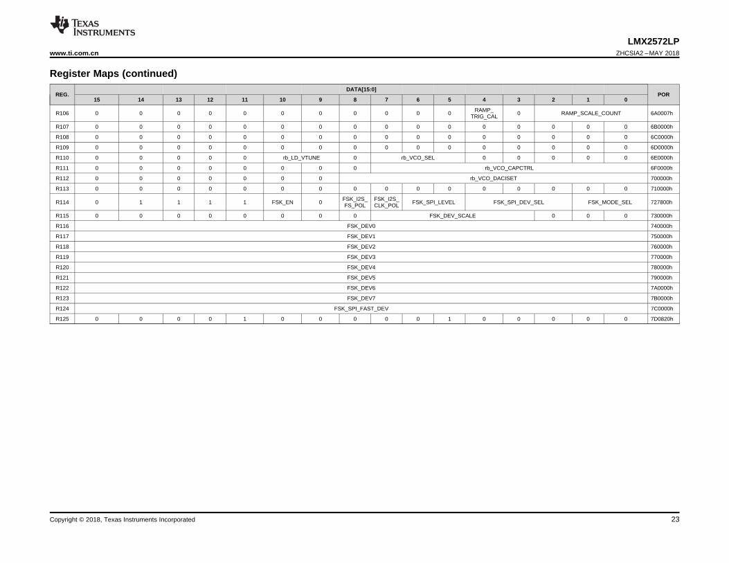
R106 0 0 0 0 0 0 0 0 0 0 0 RAMP_TRIG_CAL 0 RAMP_SCALE_COUNT 6A0007h
R107 0 0 0 0 0 0 0 0 0 0 0 0 0 0 0 0 6B0000h
R108 0 0 0 0 0 0 0 0 0 0 0 0 0 0 0 0 6C0000h
R109 0 0 0 0 0 0 0 0 0 0 0 0 0 0 0 0 6D0000h
R110 0 0 0 0 0 rb_LD_VTUNE 0 rb_VCO_SEL 0 0 0 0 0 6E0000h
R111 0 0 0 0 0 0 0 0 rb_VCO_CAPCTRL 6F0000h
R112 0 0 0 0 0 0 0 rb_VCO_DACISET 700000h
R113 0 0 0 0 0 0 0 0 0 0 0 0 0 0 0 0 710000h
R114 0 1 1 1 1 FSK_EN 0 FSK_I2S_FS_POL
FSK_I2S_CLK_POL FSK_SPI_LEVEL FSK_SPI_DEV_SEL FSK_MODE_SEL 727800h
R115 0 0 0 0 0 0 0 0 FSK_DEV_SCALE 0 0 0 730000h
R116 FSK_DEV0 740000h
R117 FSK_DEV1 750000h
R118 FSK_DEV2 760000h
R119 FSK_DEV3 770000h
R120 FSK_DEV4 780000h
R121 FSK_DEV5 790000h
R122 FSK_DEV6 7A0000h
R123 FSK_DEV7 7B0000h
R124 FSK_SPI_FAST_DEV 7C0000h
R125 0 0 0 0 1 0 0 0 0 0 1 0 0 0 0 0 7D0820h
24
LMX2572LPZHCSIA2 –MAY 2018 www.ti.com.cn
版权 © 2018, Texas Instruments Incorporated
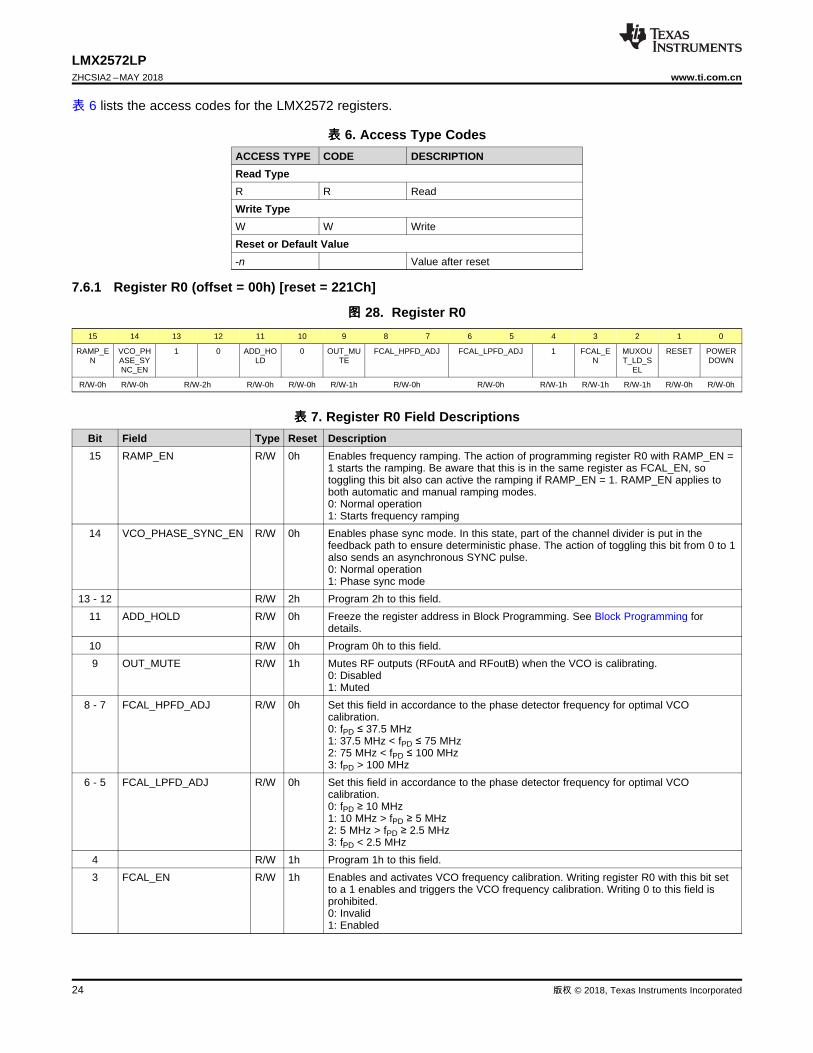
表 6 lists the access codes for the LMX2572 registers.
表表 6. Access Type CodesACCESS TYPE CODE DESCRIPTIONRead TypeR R ReadWrite TypeW W WriteReset or Default Value-n Value after reset
7.6.1 Register R0 (offset = 00h) [reset = 221Ch]
图图 28. Register R015 14 13 12 11 10 9 8 7 6 5 4 3 2 1 0
RAMP_EN
VCO_PHASE_SYNC_EN
1 0 ADD_HOLD
0 OUT_MUTE
FCAL_HPFD_ADJ FCAL_LPFD_ADJ 1 FCAL_EN
MUXOUT_LD_S
EL
RESET POWERDOWN
R/W-0h R/W-0h R/W-2h R/W-0h R/W-0h R/W-1h R/W-0h R/W-0h R/W-1h R/W-1h R/W-1h R/W-0h R/W-0h
表表 7. Register R0 Field DescriptionsBit Field Type Reset Description15 RAMP_EN R/W 0h Enables frequency ramping. The action of programming register R0 with RAMP_EN =
1 starts the ramping. Be aware that this is in the same register as FCAL_EN, sotoggling this bit also can active the ramping if RAMP_EN = 1. RAMP_EN applies toboth automatic and manual ramping modes.0: Normal operation1: Starts frequency ramping
14 VCO_PHASE_SYNC_EN R/W 0h Enables phase sync mode. In this state, part of the channel divider is put in thefeedback path to ensure deterministic phase. The action of toggling this bit from 0 to 1also sends an asynchronous SYNC pulse.0: Normal operation1: Phase sync mode
13 - 12 R/W 2h Program 2h to this field.11 ADD_HOLD R/W 0h Freeze the register address in Block Programming. See Block Programming for
details.10 R/W 0h Program 0h to this field.9 OUT_MUTE R/W 1h Mutes RF outputs (RFoutA and RFoutB) when the VCO is calibrating.
0: Disabled1: Muted
8 - 7 FCAL_HPFD_ADJ R/W 0h Set this field in accordance to the phase detector frequency for optimal VCOcalibration.0: fPD ≤ 37.5 MHz1: 37.5 MHz < fPD ≤ 75 MHz2: 75 MHz < fPD ≤ 100 MHz3: fPD > 100 MHz
6 - 5 FCAL_LPFD_ADJ R/W 0h Set this field in accordance to the phase detector frequency for optimal VCOcalibration.0: fPD ≥ 10 MHz1: 10 MHz > fPD ≥ 5 MHz2: 5 MHz > fPD ≥ 2.5 MHz3: fPD < 2.5 MHz
4 R/W 1h Program 1h to this field.3 FCAL_EN R/W 1h Enables and activates VCO frequency calibration. Writing register R0 with this bit set
to a 1 enables and triggers the VCO frequency calibration. Writing 0 to this field isprohibited.0: Invalid1: Enabled

25
LMX2572LPwww.ti.com.cn ZHCSIA2 –MAY 2018
版权 © 2018, Texas Instruments Incorporated
表表 7. Register R0 Field Descriptions (接接下下页页)Bit Field Type Reset Description2 MUXOUT_LD_SEL R/W 1h Selects the functionality of the MUXout pin.
0: Register readback1: Lock detect
1 RESET R/W 0h Resets all registers to silicon default values. This bit is self-clearing.0: Normal operation1: Reset
0 POWERDOWN R/W 0h Powers down the device.0: Normal operation1: Power down
7.6.2 Register R1 (offset = 01h) [reset = 0808h]
图图 29. Register R115 14 13 12 11 10 9 8 7 6 5 4 3 2 1 0
0 0 0 0 1 0 0 0 0 0 0 0 1 CAL_CLK_DIV
R/W-101h R/W-0h
表表 8. Register R1 Field DescriptionsBit Field Type Reset Description
15 - 3 R/W 101h Program 101h to this field.2 - 0 CAL_CLK_DIV R/W 0h Divides down the state machine clock during VCO calibration. Maximum state
machine clock frequency is 200 MHz.State machine clock frequency = fOSCin / (2CAL_CLK_DIV).0: fOSCin ≤ 200 MHz1: 200 MHz < fOSCin ≤ 250 MHzAll other values are not used.
7.6.3 Register R2 (offset = 02h) [reset = 0500h]
图图 30. Register R215 14 13 12 11 10 9 8 7 6 5 4 3 2 1 0
0 0 0 0 0 1 0 1 0 0 0 0 0 0 0 0
R/W-500h
表表 9. Register R2 Field DescriptionsBit Field Type Reset Description
15 - 0 R/W 500h Program 500h to this field.After programming R0 with RESET = 1, no need to program this register.
7.6.4 Register R3 (offset = 03h) [reset = 0782h]
图图 31. Register R315 14 13 12 11 10 9 8 7 6 5 4 3 2 1 0
0 0 0 0 0 1 1 1 1 0 0 0 0 0 1 0
R/W-782h
表表 10. Register R3 Field DescriptionsBit Field Type Reset Description
15 - 0 R/W 782h Program 782h to this field.After programming R0 with RESET = 1, no need to program this register.
26
LMX2572LPZHCSIA2 –MAY 2018 www.ti.com.cn
版权 © 2018, Texas Instruments Incorporated
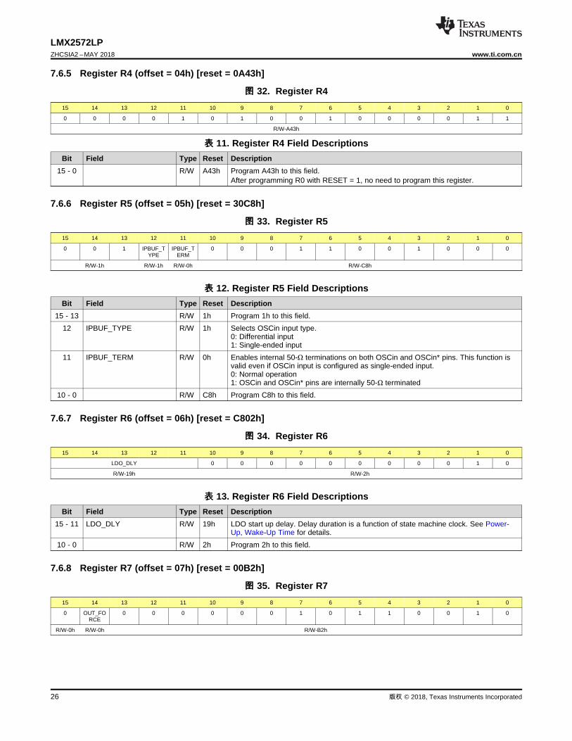
7.6.5 Register R4 (offset = 04h) [reset = 0A43h]
图图 32. Register R415 14 13 12 11 10 9 8 7 6 5 4 3 2 1 0
0 0 0 0 1 0 1 0 0 1 0 0 0 0 1 1
R/W-A43h
表表 11. Register R4 Field DescriptionsBit Field Type Reset Description
15 - 0 R/W A43h Program A43h to this field.After programming R0 with RESET = 1, no need to program this register.
7.6.6 Register R5 (offset = 05h) [reset = 30C8h]
图图 33. Register R515 14 13 12 11 10 9 8 7 6 5 4 3 2 1 0
0 0 1 IPBUF_TYPE
IPBUF_TERM
0 0 0 1 1 0 0 1 0 0 0
R/W-1h R/W-1h R/W-0h R/W-C8h
表表 12. Register R5 Field DescriptionsBit Field Type Reset Description
15 - 13 R/W 1h Program 1h to this field.12 IPBUF_TYPE R/W 1h Selects OSCin input type.
0: Differential input1: Single-ended input
11 IPBUF_TERM R/W 0h Enables internal 50-Ω terminations on both OSCin and OSCin* pins. This function isvalid even if OSCin input is configured as single-ended input.0: Normal operation1: OSCin and OSCin* pins are internally 50-Ω terminated
10 - 0 R/W C8h Program C8h to this field.
7.6.7 Register R6 (offset = 06h) [reset = C802h]
图图 34. Register R615 14 13 12 11 10 9 8 7 6 5 4 3 2 1 0
LDO_DLY 0 0 0 0 0 0 0 0 0 1 0
R/W-19h R/W-2h
表表 13. Register R6 Field DescriptionsBit Field Type Reset Description
15 - 11 LDO_DLY R/W 19h LDO start up delay. Delay duration is a function of state machine clock. See Power-Up, Wake-Up Time for details.
10 - 0 R/W 2h Program 2h to this field.
7.6.8 Register R7 (offset = 07h) [reset = 00B2h]
图图 35. Register R715 14 13 12 11 10 9 8 7 6 5 4 3 2 1 0
0 OUT_FORCE
0 0 0 0 0 0 1 0 1 1 0 0 1 0
R/W-0h R/W-0h R/W-B2h
27
LMX2572LPwww.ti.com.cn ZHCSIA2 –MAY 2018
版权 © 2018, Texas Instruments Incorporated
表表 14. Register R7 Field DescriptionsBit Field Type Reset Description15 R/W 0h Program 0h to this field.14 OUT_FORCE R/W 0h Forces the RF outputs not to be automatically muted during VCO calibration. This bit
should be enabled during frequency ramping.0: Mute setting depends on OUT_MUTE1: No mute during VCO calibration
13 - 0 R/W B2h Program B2h to this field.
7.6.9 Register R8 (offset = 08h) [reset = 2000h]
图图 36. Register R815 14 13 12 11 10 9 8 7 6 5 4 3 2 1 0
0 VCO_DACISET_F
ORCE
1 0 VCO_CAPCTRL_FORCE
0 0 0 0 0 0 0 0 0 0 0
R/W-0h R/W-0h R/W-2h R/W-0h R/W-0h
表表 15. Register R8 Field DescriptionsBit Field Type Reset Description15 R/W 0h Program 0h to this field.14 VCO_DACISET_FORCE R/W 0h Forces VCO_DACISET value. Useful for fully-assisted VCO calibration and debugging
purposes.0: Normal operation1: Use VCO_DACISET value instead of the value obtained from VCO calibration
13 - 12 R/W 2h Program 2h to this field.11 VCO_CAPCTRL_FORCE R/W 0h Forces VCO_CAPCTRL value. Useful for fully-assisted VCO calibration and
debugging purposes.0: Normal operation1: Use VCO_CAPCTRL value instead of the value obtained from VCO calibration
10 - 0 R/W 0h Program 0h to this field.
7.6.10 Register R9 (offset = 09h) [reset = 0004h]
图图 37. Register R915 14 13 12 11 10 9 8 7 6 5 4 3 2 1 0
0 MULT_HI
0 OSC_2X 0 0 0 0 0 0 0 0 0 1 0 0
R/W-0h R/W-0h R/W-0h R/W-0h R/W-4h
表表 16. Register R9 Field DescriptionsBit Field Type Reset Description15 R/W 0h Program 0h to this field.14 MULT_HI R/W 0h Sets this bit to 1 if the output frequency of the Multiplier is greater than 100 MHz.
0: Multiplier output ≤ 100 MHz1: Multiplier output > 100 MHz
13 R/W 0h Program 0h to this field.12 OSC_2X R/W 0h Enables reference path Doubler.
0: Disabled1: Enabled
11 - 0 R/W 4h Program 4h to this field.

28
LMX2572LPZHCSIA2 –MAY 2018 www.ti.com.cn
版权 © 2018, Texas Instruments Incorporated
7.6.11 Register R10 (offset = 0Ah) [reset = 10F8h]
图图 38. Register R1015 14 13 12 11 10 9 8 7 6 5 4 3 2 1 0
0 0 0 1 MULT 1 1 1 1 0 0 0
R/W-1h R/W-1h R/W-78h
表表 17. Register R10 Field DescriptionsBit Field Type Reset Description
15 - 12 R/W 1h Program 1h to this field.11 - 7 MULT R/W 1h Reference path frequency Multiplier. Input frequency to the Multiplier: 10 to 40 MHz.
Multiplier output frequency: 60 to 150 MHz.0: Not used1: Bypassed2: Not recommended. Use OSC_2X instead of MULT3: 3X·····7: 7X8 - 31: Not recommended
6 - 0 R/W 78h Program 78h to this field.
7.6.12 Register R11 (offset = 0Bh) [reset = B018h]
图图 39. Register R1115 14 13 12 11 10 9 8 7 6 5 4 3 2 1 0
1 0 1 1 PLL_R 1 0 0 0
R/W-Bh R/W-1h R/W-8h
表表 18. Register R11 Field DescriptionsBit Field Type Reset Description
15 - 12 R/W Bh Program Bh to this field.11 - 4 PLL_R R/W 1h Reference path Post-R divider. It is the divider after the frequency Multiplier.3 - 0 R/W 8h Program 8h to this field.
7.6.13 Register R12 (offset = 0Ch) [reset = 5001h]
图图 40. Register R1215 14 13 12 11 10 9 8 7 6 5 4 3 2 1 0
0 1 0 1 PLL_R_PRE
R/W-5h R/W-1h
表表 19. Register R12 Field DescriptionsBit Field Type Reset Description
15 - 12 R/W 5h Program 5h to this field.11 - 0 PLL_R_PRE R/W 1h Reference path Pre-R divider. It is the divider before the frequency Multiplier.
7.6.14 Register R13 (offset = 0Dh) [reset = 4000h]
图图 41. Register R1315 14 13 12 11 10 9 8 7 6 5 4 3 2 1 0
0 1 0 0 0 0 0 0 0 0 0 0 0 0 0 0
R/W-4000h

29
LMX2572LPwww.ti.com.cn ZHCSIA2 –MAY 2018
版权 © 2018, Texas Instruments Incorporated
表表 20. Register R13 Field DescriptionsBit Field Type Reset Description
15 - 0 R/W 4000h Program 4000h to this field.After programming R0 with RESET = 1, no need to program this register.
7.6.15 Register R14 (offset = 0Eh) [reset = 1840h]
图图 42. Register R1415 14 13 12 11 10 9 8 7 6 5 4 3 2 1 0
0 0 0 1 1 0 0 0 0 CPG 0 0 0
R/W-30h R/W-8h R/W-0h
表表 21. Register R14 Field DescriptionsBit Field Type Reset Description
15 - 7 R/W 30h Program 30h to this field.6 - 3 CPG R/W 8h Effective charge pump gain. This is the sum of the up and down currents. Each
increment represents 625 µA.0: Tri-state1: 625 µA2: 1250 µA3: 1875 µA·····15: 6875 µA
2 - 0 R/W 0h Program 0h to this field.
7.6.16 Register R15 (offset = 0Fh) [reset = 060Eh]
图图 43. Register R1515 14 13 12 11 10 9 8 7 6 5 4 3 2 1 0
0 0 0 0 0 1 1 0 0 0 0 0 1 1 1 0
R/W-60Eh
表表 22. Register R15 Field DescriptionsBit Field Type Reset Description
15 - 0 R/W 60Eh Program 60Eh to this field.After programming R0 with RESET = 1, no need to program this register.
7.6.17 Register R16 (offset = 10h) [reset = 0080h]
图图 44. Register R1615 14 13 12 11 10 9 8 7 6 5 4 3 2 1 0
0 0 0 0 0 0 0 VCO_DACISET
R/W-0h R/W-80h
表表 23. Register R16 Field DescriptionsBit Field Type Reset Description
15 - 9 R/W 0h Program 0h to this field.8 - 0 VCO_DACISET R/W 80h Programmable current setting for the VCO that is applied when
VCO_DACISET_FORCE = 1. Useful for fully-assisted VCO calibration.
30
LMX2572LPZHCSIA2 –MAY 2018 www.ti.com.cn
版权 © 2018, Texas Instruments Incorporated
7.6.18 Register R17 (offset = 11h) [reset = 0096h]
图图 45. Register R1715 14 13 12 11 10 9 8 7 6 5 4 3 2 1 0
0 0 0 0 0 0 0 VCO_DACISET_STRT
R/W-0h R/W-96h
表表 24. Register R17 Field DescriptionsBit Field Type Reset Description
15 - 9 R/W 0h Program 0h to this field.8 - 0 VCO_DACISET_STRT R/W 96h Starting calibration value for VCO_DACISET.
7.6.19 Register R18 (offset = 12h) [reset = 0064h]
图图 46. Register R1815 14 13 12 11 10 9 8 7 6 5 4 3 2 1 0
0 0 0 0 0 0 0 0 0 1 1 0 0 1 0 0
R/W-64h
表表 25. Register R18 Field DescriptionsBit Field Type Reset Description
15 - 0 R/W 64h Program 64h to this field.After programming R0 with RESET = 1, no need to program this register.
7.6.20 Register R19 (offset = 13h) [reset = 27B7h]
图图 47. Register R1915 14 13 12 11 10 9 8 7 6 5 4 3 2 1 0
0 0 1 0 0 1 1 1 VCO_CAPCTRL
R/W-27h R/W-B7h
表表 26. Register R19 Field DescriptionsBit Field Type Reset Description
15 - 8 R/W 27h Program 27h to this field.7 - 0 VCO_CAPCTRL R/W B7h Programmable band within VCO core that applies when VCO_CAPCTRL_FORCE = 1.
Valid values are 183 to 0, where the higher number is a lower frequency.
7.6.21 Register R20 (offset = 14h) [reset = 3048h]
图图 48. Register R2015 14 13 12 11 10 9 8 7 6 5 4 3 2 1 0
0 1 VCO_SEL VCO_SEL_FORC
E
0 0 0 1 0 0 1 0 0 0
R/W-0h R/W-6h R/W-0h R/W-48h
表表 27. Register R20 Field DescriptionsBit Field Type Reset Description
15 - 14 R/W 0h Program 1h to this field.13 - 11 VCO_SEL R/W 6h User specified start VCO for calibration. This sets the VCO that is used when
VCO_SEL_STRT_EN = 1 or VCO_SEL_FORCE = 1.1: VCO12: VCO2·····6: VCO6All other values are not used.

31
LMX2572LPwww.ti.com.cn ZHCSIA2 –MAY 2018
版权 © 2018, Texas Instruments Incorporated
表表 27. Register R20 Field Descriptions (接接下下页页)Bit Field Type Reset Description10 VCO_SEL_FORCE R/W 0h Forces the VCO to use the core specified by VCO_SEL.
0: Disabled1: Enabled
9 - 0 R/W 48h Program 48h to this field.
7.6.22 Register R21 (offset = 15h) [reset = 0409h]
图图 49. Register R2115 14 13 12 11 10 9 8 7 6 5 4 3 2 1 0
0 0 0 0 0 1 0 0 0 0 0 0 1 0 0 1
R/W-409h
表表 28. Register R21 Field DescriptionsBit Field Type Reset Description
15 - 0 R/W 409h Program 409h to this field.After programming R0 with RESET = 1, no need to program this register.
7.6.23 Register R22 (offset = 16h) [reset = 0001h]
图图 50. Register R2215 14 13 12 11 10 9 8 7 6 5 4 3 2 1 0
0 0 0 0 0 0 0 0 0 0 0 0 0 0 0 1
R/W-1h
表表 29. Register R22 Field DescriptionsBit Field Type Reset Description
15 - 0 R/W 1h Program 1h to this field.After programming R0 with RESET = 1, no need to program this register.
7.6.24 Register R23 (offset = 17h) [reset = 007Ch]
图图 51. Register R2315 14 13 12 11 10 9 8 7 6 5 4 3 2 1 0
0 0 0 0 0 0 0 0 0 1 1 1 1 1 0 0
R/W-7Ch
表表 30. Register R23 Field DescriptionsBit Field Type Reset Description
15 - 0 R/W 7Ch Program 7Ch to this field.After programming R0 with RESET = 1, no need to program this register.
7.6.25 Register R24 (offset = 18h) [reset = 071Ah]
图图 52. Register R2415 14 13 12 11 10 9 8 7 6 5 4 3 2 1 0
0 0 0 0 0 1 1 1 0 0 0 1 1 0 1 0
R/W-71Ah
32
LMX2572LPZHCSIA2 –MAY 2018 www.ti.com.cn
版权 © 2018, Texas Instruments Incorporated
表表 31. Register R24 Field DescriptionsBit Field Type Reset Description
15 - 0 R/W 71Ah Program 71Ah to this field.After programming R0 with RESET = 1, no need to program this register.
7.6.26 Register R25 (offset = 19h) [reset = 0624h]
图图 53. Register R2515 14 13 12 11 10 9 8 7 6 5 4 3 2 1 0
0 0 0 0 0 1 1 0 0 0 1 0 0 1 0 0
R/W-624h
表表 32. Register R25 Field DescriptionsBit Field Type Reset Description
15 - 0 R/W 624h Program 624h to this field.After programming R0 with RESET = 1, no need to program this register.
7.6.27 Register R26 (offset = 1Ah) [reset = 0808h]
图图 54. Register R2615 14 13 12 11 10 9 8 7 6 5 4 3 2 1 0
0 0 0 0 1 0 0 0 0 0 0 0 1 0 0 0
R/W-808h
表表 33. Register R26 Field DescriptionsBit Field Type Reset Description
15 - 0 R/W 808h Program 808h to this field.After programming R0 with RESET = 1, no need to program this register.
7.6.28 Register R27 (offset = 1Bh) [reset = 0002h]
图图 55. Register R2715 14 13 12 11 10 9 8 7 6 5 4 3 2 1 0
0 0 0 0 0 0 0 0 0 0 0 0 0 0 1 0
R/W-2h
表表 34. Register R27 Field DescriptionsBit Field Type Reset Description
15 - 0 R/W 2h Program 2h to this field.After programming R0 with RESET = 1, no need to program this register.
7.6.29 Register R28 (offset = 1Ch) [reset = 0488h]
图图 56. Register R2815 14 13 12 11 10 9 8 7 6 5 4 3 2 1 0
0 0 0 0 0 1 0 0 1 0 0 0 1 0 0 0
R/W-488h
表表 35. Register R28 Field DescriptionsBit Field Type Reset Description
15 - 0 R/W 488h Program 488h to this field.After programming R0 with RESET = 1, no need to program this register.
33
LMX2572LPwww.ti.com.cn ZHCSIA2 –MAY 2018
版权 © 2018, Texas Instruments Incorporated
7.6.30 Register R29 (offset = 1Dh) [reset = 18C6h]
图图 57. Register R2915 14 13 12 11 10 9 8 7 6 5 4 3 2 1 0
0 0 0 0 0 0 0 0 0 0 0 0 0 0 0 0
R/W-18C6h
表表 36. Register R29 Field DescriptionsBit Field Type Reset Description
15 - 0 R/W 18C6h Program 0h to this field.
7.6.31 Register R30 (offset = 1Eh) [reset = 18C6h]
图图 58. Register R3015 14 13 12 11 10 9 8 7 6 5 4 3 2 1 0
0 0 0 0 1 1 0 0 1 0 1 0 0 1 1 0
R/W-18C6h
表表 37. Register R30 Field DescriptionsBit Field Type Reset Description
15 - 0 R/W 18C6h Program CA6h to this field.
7.6.32 Register R31 (offset = 1Fh) [reset = C3E6h]
图图 59. Register R3115 14 13 12 11 10 9 8 7 6 5 4 3 2 1 0
1 1 0 0 0 0 1 1 1 1 1 0 0 1 1 0
R/W-C3E6h
表表 38. Register R31 Field DescriptionsBit Field Type Reset Description
15 - 0 R/W C3E6h Program C3E6h to this field.After programming R0 with RESET = 1, no need to program this register.
7.6.33 Register R32 (offset = 20h) [reset = 05BFh]
图图 60. Register R3215 14 13 12 11 10 9 8 7 6 5 4 3 2 1 0
0 0 0 0 0 1 0 1 1 0 1 1 1 1 1 1
R/W-5BFh
表表 39. Register R32 Field DescriptionsBit Field Type Reset Description
15 - 0 R/W 5BFh Program 5BFh to this field.After programming R0 with RESET = 1, no need to program this register.
7.6.34 Register R33 (offset = 21h) [reset = 1E01h]
图图 61. Register R3315 14 13 12 11 10 9 8 7 6 5 4 3 2 1 0
0 0 0 1 1 1 1 0 0 0 0 0 0 0 0 1
R/W-1E01h
34
LMX2572LPZHCSIA2 –MAY 2018 www.ti.com.cn
版权 © 2018, Texas Instruments Incorporated
表表 40. Register R33 Field DescriptionsBit Field Type Reset Description
15 - 0 R/W 1E01h Program 1E01h to this field.After programming R0 with RESET = 1, no need to program this register.
7.6.35 Register R34 (offset = 22h) [reset = 0010h]
图图 62. Register R3415 14 13 12 11 10 9 8 7 6 5 4 3 2 1 0
0 0 0 0 0 0 0 0 0 0 0 1 0 PLL_N[18:16]
R/W-2h R/W-0h
表表 41. Register R34 Field DescriptionsBit Field Type Reset Description
15 - 3 R/W 2h Program 2h to this field.2 - 0 PLL_N[18:16] R/W 0h Upper 3 bits of N-divider.
7.6.36 Register R35 (offset = 23h) [reset = 0004h]
图图 63. Register R3515 14 13 12 11 10 9 8 7 6 5 4 3 2 1 0
0 0 0 0 0 0 0 0 0 0 0 0 0 1 0 0
R/W-4h
表表 42. Register R35 Field DescriptionsBit Field Type Reset Description
15 - 0 R/W 4h Program 4h to this field.After programming R0 with RESET = 1, no need to program this register.
7.6.37 Register R36 (offset = 24h) [reset = 0028h]
图图 64. Register R3615 14 13 12 11 10 9 8 7 6 5 4 3 2 1 0
PLL_N
R/W-28h
表表 43. Register R36 Field DescriptionsBit Field Type Reset Description
15 - 0 PLL_N R/W 28h Lower 16 bits of N-divider.
7.6.38 Register R37 (offset = 25h) [reset = 0205h]
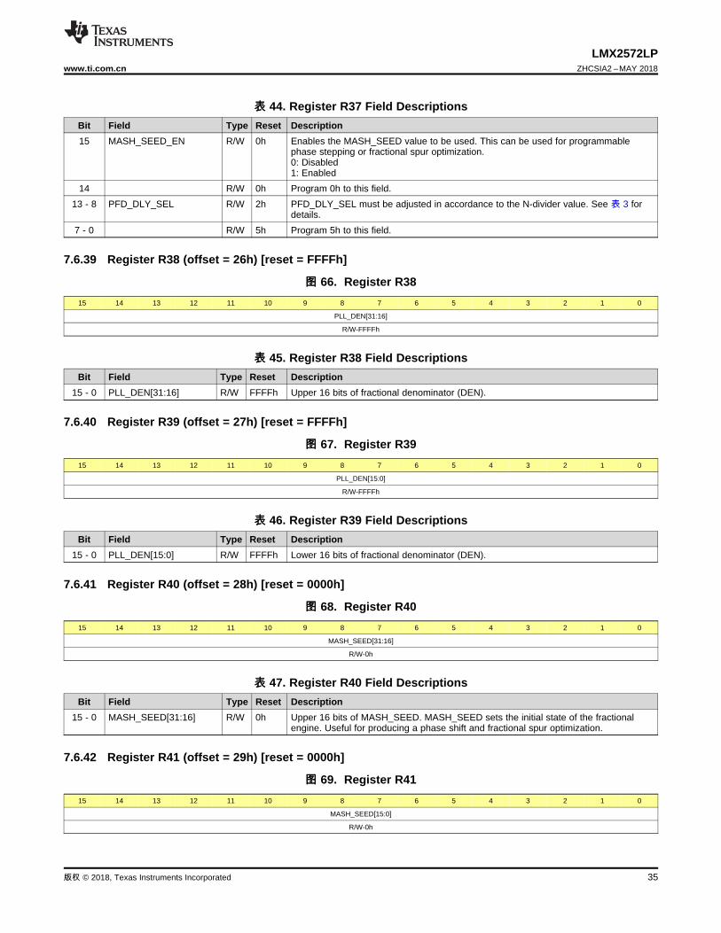
图图 65. Register R3715 14 13 12 11 10 9 8 7 6 5 4 3 2 1 0
MASH_SEED_EN
0 PFD_DLY_SEL 0 0 0 0 0 1 0 1
R/W-0h R/W-0h R/W-2h R/W-5h
35
LMX2572LPwww.ti.com.cn ZHCSIA2 –MAY 2018
版权 © 2018, Texas Instruments Incorporated
表表 44. Register R37 Field DescriptionsBit Field Type Reset Description15 MASH_SEED_EN R/W 0h Enables the MASH_SEED value to be used. This can be used for programmable
phase stepping or fractional spur optimization.0: Disabled1: Enabled
14 R/W 0h Program 0h to this field.13 - 8 PFD_DLY_SEL R/W 2h PFD_DLY_SEL must be adjusted in accordance to the N-divider value. See 表 3 for
details.7 - 0 R/W 5h Program 5h to this field.
7.6.39 Register R38 (offset = 26h) [reset = FFFFh]
图图 66. Register R3815 14 13 12 11 10 9 8 7 6 5 4 3 2 1 0
PLL_DEN[31:16]
R/W-FFFFh
表表 45. Register R38 Field DescriptionsBit Field Type Reset Description
15 - 0 PLL_DEN[31:16] R/W FFFFh Upper 16 bits of fractional denominator (DEN).
7.6.40 Register R39 (offset = 27h) [reset = FFFFh]
图图 67. Register R3915 14 13 12 11 10 9 8 7 6 5 4 3 2 1 0
PLL_DEN[15:0]
R/W-FFFFh
表表 46. Register R39 Field DescriptionsBit Field Type Reset Description
15 - 0 PLL_DEN[15:0] R/W FFFFh Lower 16 bits of fractional denominator (DEN).
7.6.41 Register R40 (offset = 28h) [reset = 0000h]
图图 68. Register R4015 14 13 12 11 10 9 8 7 6 5 4 3 2 1 0
MASH_SEED[31:16]
R/W-0h
表表 47. Register R40 Field DescriptionsBit Field Type Reset Description
15 - 0 MASH_SEED[31:16] R/W 0h Upper 16 bits of MASH_SEED. MASH_SEED sets the initial state of the fractionalengine. Useful for producing a phase shift and fractional spur optimization.
7.6.42 Register R41 (offset = 29h) [reset = 0000h]
图图 69. Register R4115 14 13 12 11 10 9 8 7 6 5 4 3 2 1 0
MASH_SEED[15:0]
R/W-0h
36
LMX2572LPZHCSIA2 –MAY 2018 www.ti.com.cn
版权 © 2018, Texas Instruments Incorporated
表表 48. Register R41 Field DescriptionsBit Field Type Reset Description
15 - 0 MASH_SEED[15:0] R/W 0h Lower 16 bits of MASH_SEED. MASH_SEED sets the initial state of the fractionalengine. Useful for producing a phase shift and fractional spur optimization.
7.6.43 Register R42 (offset = 2Ah) [reset = 0000h]
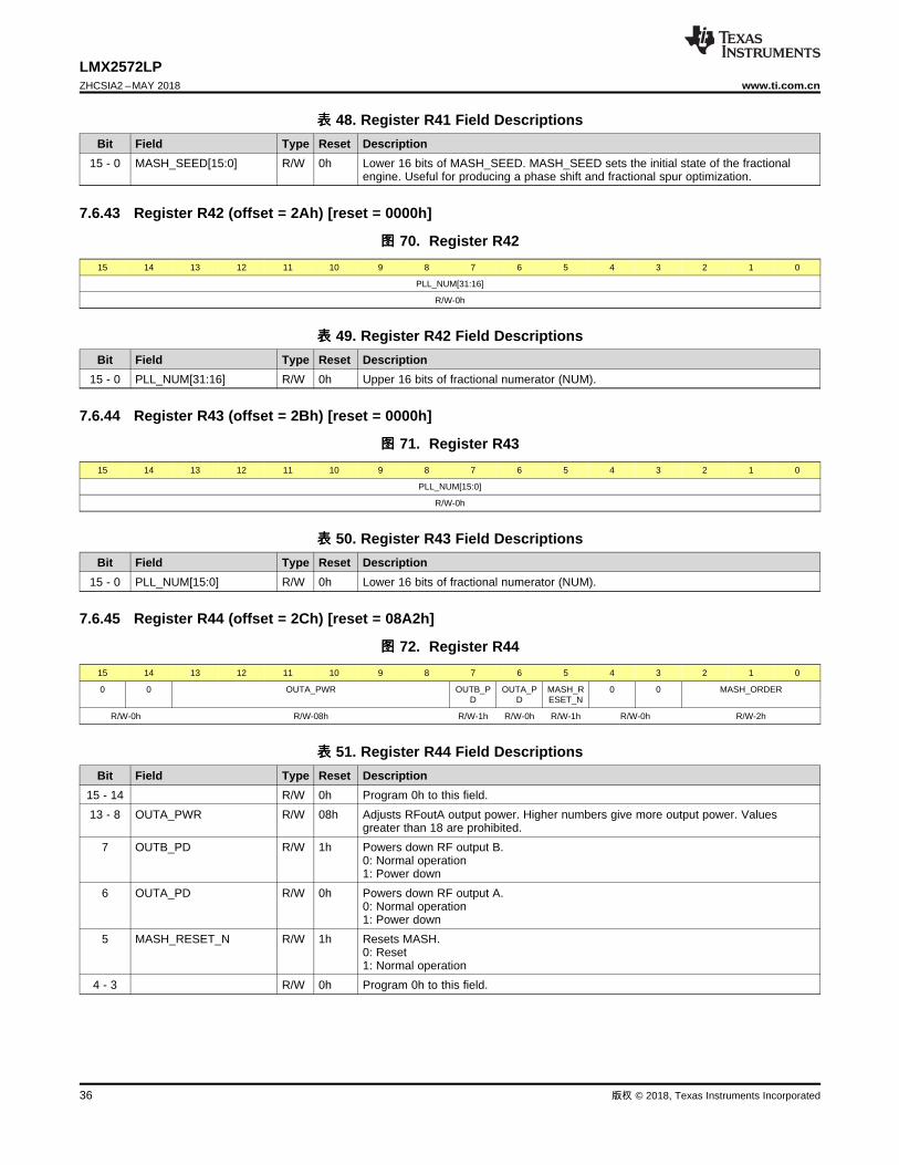
图图 70. Register R4215 14 13 12 11 10 9 8 7 6 5 4 3 2 1 0
PLL_NUM[31:16]
R/W-0h
表表 49. Register R42 Field DescriptionsBit Field Type Reset Description
15 - 0 PLL_NUM[31:16] R/W 0h Upper 16 bits of fractional numerator (NUM).
7.6.44 Register R43 (offset = 2Bh) [reset = 0000h]
图图 71. Register R4315 14 13 12 11 10 9 8 7 6 5 4 3 2 1 0
PLL_NUM[15:0]
R/W-0h
表表 50. Register R43 Field DescriptionsBit Field Type Reset Description
15 - 0 PLL_NUM[15:0] R/W 0h Lower 16 bits of fractional numerator (NUM).
7.6.45 Register R44 (offset = 2Ch) [reset = 08A2h]
图图 72. Register R4415 14 13 12 11 10 9 8 7 6 5 4 3 2 1 0
0 0 OUTA_PWR OUTB_PD
OUTA_PD
MASH_RESET_N
0 0 MASH_ORDER
R/W-0h R/W-08h R/W-1h R/W-0h R/W-1h R/W-0h R/W-2h
表表 51. Register R44 Field DescriptionsBit Field Type Reset Description
15 - 14 R/W 0h Program 0h to this field.13 - 8 OUTA_PWR R/W 08h Adjusts RFoutA output power. Higher numbers give more output power. Values
greater than 18 are prohibited.7 OUTB_PD R/W 1h Powers down RF output B.
0: Normal operation1: Power down
6 OUTA_PD R/W 0h Powers down RF output A.0: Normal operation1: Power down
5 MASH_RESET_N R/W 1h Resets MASH.0: Reset1: Normal operation
4 - 3 R/W 0h Program 0h to this field.

37
LMX2572LPwww.ti.com.cn ZHCSIA2 –MAY 2018
版权 © 2018, Texas Instruments Incorporated
表表 51. Register R44 Field Descriptions (接接下下页页)Bit Field Type Reset Description
2 - 0 MASH_ORDER R/W 2h Sets the MASH order.0: Integer mode1: First order modulator2: Second order modulator3: Third order modulator4: Fourth order modulator5 - 7: Not used
7.6.46 Register R45 (offset = 2Dh) [reset = C608h]
图图 73. Register R4515 14 13 12 11 10 9 8 7 6 5 4 3 2 1 0
1 1 0 0 0 1 1 0 0 0 OUTB_PWR
R/W-318h R/W-08h
表表 52. Register R45 Field DescriptionsBit Field Type Reset Description
15 - 6 R/W 318h Program 318h to this field.5 - 0 OUTB_PWR R/W 08h Adjusts RFoutB output power. Higher numbers give more output power. Values
greater than 18 are prohibited.
7.6.47 Register R46 (offset = 2Eh) [reset = 07F0h]
图图 74. Register R4615 14 13 12 11 10 9 8 7 6 5 4 3 2 1 0
0 0 0 0 0 1 1 1 1 1 1 1 0 0 0 0
R/W-7F0h
表表 53. Register R46 Field DescriptionsBit Field Type Reset Description
15 - 0 R/W 7F0h Program 7F0h to this field.After programming R0 with RESET = 1, no need to program this register.
7.6.48 Register R47 (offset = 2Fh) [reset = 0300h]
图图 75. Register R4715 14 13 12 11 10 9 8 7 6 5 4 3 2 1 0
0 0 0 0 0 0 1 1 0 0 0 0 0 0 0 0
R/W-300h
表表 54. Register R47 Field DescriptionsBit Field Type Reset Description
15 - 0 R/W 300h Program 300h to this field.After programming R0 with RESET = 1, no need to program this register.
7.6.49 Register R48 (offset = 30h) [reset = 03E0h]
图图 76. Register R4815 14 13 12 11 10 9 8 7 6 5 4 3 2 1 0
0 0 0 0 0 0 1 1 1 1 1 0 0 0 0 0
R/W-3E0h

38
LMX2572LPZHCSIA2 –MAY 2018 www.ti.com.cn
版权 © 2018, Texas Instruments Incorporated
表表 55. Register R48 Field DescriptionsBit Field Type Reset Description
15 - 0 R/W 3E0h Program 3E0h to this field.After programming R0 with RESET = 1, no need to program this register.
7.6.50 Register R49 (offset = 31h) [reset = 4180h]
图图 77. Register R4915 14 13 12 11 10 9 8 7 6 5 4 3 2 1 0
0 1 0 0 0 0 0 1 1 0 0 0 0 0 0 0
R/W-4180h
表表 56. Register R49 Field DescriptionsBit Field Type Reset Description
15 - 0 R/W 4180h Program 4180h to this field.After programming R0 with RESET = 1, no need to program this register.
7.6.51 Register R50 (offset = 32h) [reset = 0080h]
图图 78. Register R5015 14 13 12 11 10 9 8 7 6 5 4 3 2 1 0
0 0 0 0 0 0 0 0 1 0 0 0 0 0 0 0
R/W-80h
表表 57. Register R50 Field DescriptionsBit Field Type Reset Description
15 - 0 R/W 80h Program 80h to this field.After programming R0 with RESET = 1, no need to program this register.
7.6.52 Register R51 (offset = 33h) [reset = 0080h]
图图 79. Register R5115 14 13 12 11 10 9 8 7 6 5 4 3 2 1 0
0 0 0 0 0 0 0 0 1 0 0 0 0 0 0 0
R/W-80h
表表 58. Register R51 Field DescriptionsBit Field Type Reset Description
15 - 0 R/W 80h Program 80h to this field.After programming R0 with RESET = 1, no need to program this register.
7.6.53 Register R52 (offset = 34h) [reset = 0420h]
图图 80. Register R5215 14 13 12 11 10 9 8 7 6 5 4 3 2 1 0
0 0 0 0 0 1 0 0 0 0 1 0 0 0 0 1
R/W-420h
表表 59. Register R52 Field DescriptionsBit Field Type Reset Description
15 - 0 R/W 420h Program 421h to this field.
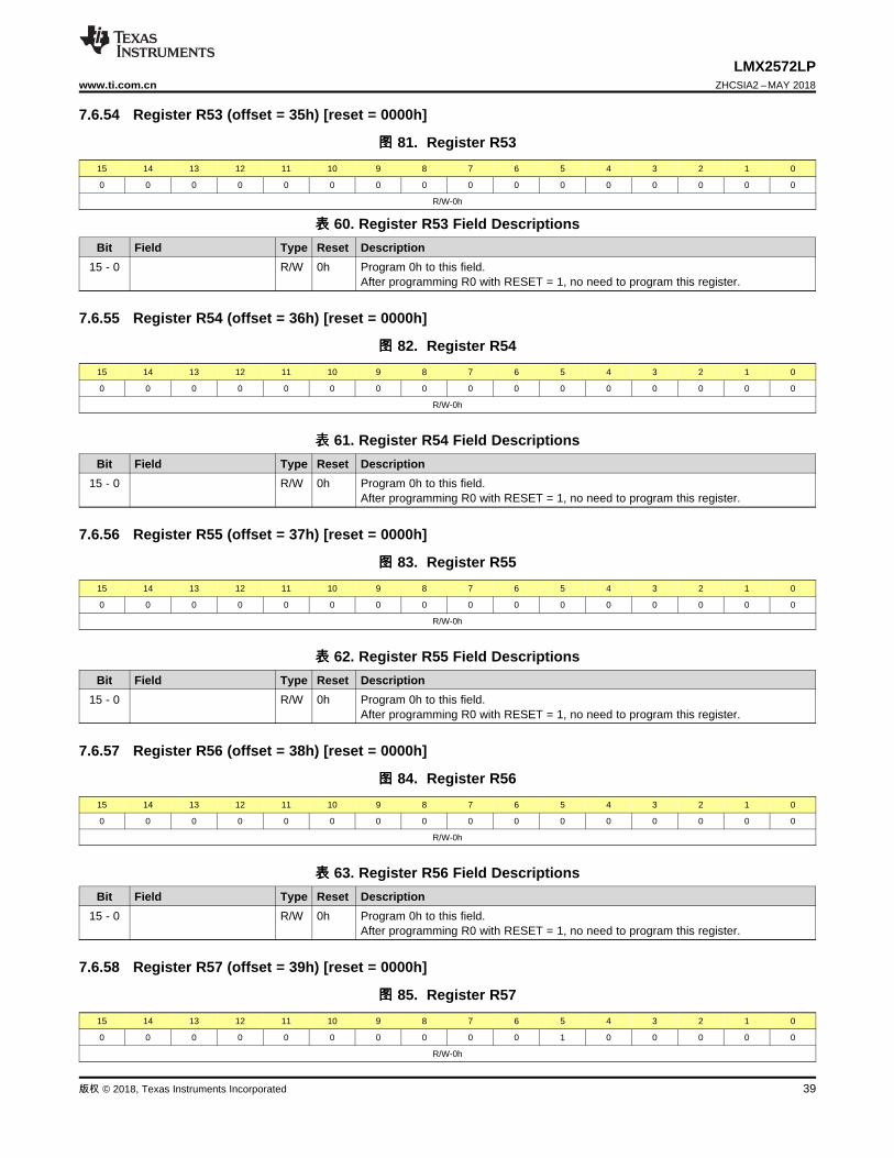
39
LMX2572LPwww.ti.com.cn ZHCSIA2 –MAY 2018
版权 © 2018, Texas Instruments Incorporated
7.6.54 Register R53 (offset = 35h) [reset = 0000h]
图图 81. Register R5315 14 13 12 11 10 9 8 7 6 5 4 3 2 1 0
0 0 0 0 0 0 0 0 0 0 0 0 0 0 0 0
R/W-0h
表表 60. Register R53 Field DescriptionsBit Field Type Reset Description
15 - 0 R/W 0h Program 0h to this field.After programming R0 with RESET = 1, no need to program this register.
7.6.55 Register R54 (offset = 36h) [reset = 0000h]
图图 82. Register R5415 14 13 12 11 10 9 8 7 6 5 4 3 2 1 0
0 0 0 0 0 0 0 0 0 0 0 0 0 0 0 0
R/W-0h
表表 61. Register R54 Field DescriptionsBit Field Type Reset Description
15 - 0 R/W 0h Program 0h to this field.After programming R0 with RESET = 1, no need to program this register.
7.6.56 Register R55 (offset = 37h) [reset = 0000h]
图图 83. Register R5515 14 13 12 11 10 9 8 7 6 5 4 3 2 1 0
0 0 0 0 0 0 0 0 0 0 0 0 0 0 0 0
R/W-0h
表表 62. Register R55 Field DescriptionsBit Field Type Reset Description
15 - 0 R/W 0h Program 0h to this field.After programming R0 with RESET = 1, no need to program this register.
7.6.57 Register R56 (offset = 38h) [reset = 0000h]
图图 84. Register R5615 14 13 12 11 10 9 8 7 6 5 4 3 2 1 0
0 0 0 0 0 0 0 0 0 0 0 0 0 0 0 0
R/W-0h
表表 63. Register R56 Field DescriptionsBit Field Type Reset Description
15 - 0 R/W 0h Program 0h to this field.After programming R0 with RESET = 1, no need to program this register.
7.6.58 Register R57 (offset = 39h) [reset = 0000h]
图图 85. Register R5715 14 13 12 11 10 9 8 7 6 5 4 3 2 1 0
0 0 0 0 0 0 0 0 0 0 1 0 0 0 0 0
R/W-0h

40
LMX2572LPZHCSIA2 –MAY 2018 www.ti.com.cn
版权 © 2018, Texas Instruments Incorporated
表表 64. Register R57 Field DescriptionsBit Field Type Reset Description
15 - 0 R/W 0h Program 20h to this field.
7.6.59 Register R58 (offset = 3Ah) [reset = 8001h]
图图 86. Register R5815 14 13 12 11 10 9 8 7 6 5 4 3 2 1 0
INPIN_IGNORE
INPIN_HYST
INPIN_LVL INPIN_FMT 0 0 0 0 0 0 0 0 1
R/W-1h R/W-0h R/W-0h R/W-0h R/W-1h
表表 65. Register R58 Field DescriptionsBit Field Type Reset Description15 INPIN_IGNORE R/W 1h Ignore SYNC and SysRefReq pins when VCO_PHASE_SYNC = 0. This bit should be
set to 1 unless VCO_PHASE_SYNC = 1.14 INPIN_HYST R/W 0h Enables high hysteresis for LVDS input to SysRefReq and SYNC pin.
0: Disabled1: Enabled
13 - 12 INPIN_LVL R/W 0h Sets bias level for LVDS input to SysRefReq and SYNC pin.0: Vin / 41: Vin2: Vin / 23: Invalid
11 - 9 INPIN_FMT R/W 0h Defines the input format of SysRefReq and SYNC pin.0: SYNC = SysRefReq = CMOS1: SYNC = LVDS; SysRefReq = CMOS2: SYNC = CMOS; SysRefReq = LVDS3: SYNC = SysRefReq = LVDS4: SYNC = SysRefReq = CMOS5: SYNC = LVDS (filtered); SysRefReq = CMOS6: SYNC = CMOS; SysRefReq = LVDS (filtered)7: SYNC = SysRefReq = LVDS (filtered)
8 - 0 R/W 1h Program 1h to this field.
7.6.60 Register R59 (offset = 3Bh) [reset = 0001h]
图图 87. Register R5915 14 13 12 11 10 9 8 7 6 5 4 3 2 1 0
0 0 0 0 0 0 0 0 0 0 0 0 0 0 0 LD_TYPE
R/W-0h R/W-1h
表表 66. Register R59 Field DescriptionsBit Field Type Reset Description
15 - 1 R/W 0h Program 0h to this field.0 LD_TYPE R/W 1h Defines lock detect type.
0: VCOCal. Lock detect asserts a HIGH output after the VCO has finished calibrationand the LD_DLY timeout counter is finished.1: Vtune and VCOCal. Lock detect asserts a HIGH output when VCOCal lock detectwould assert a HIGH signal and the tuning voltage to the VCO is within acceptablelimits.
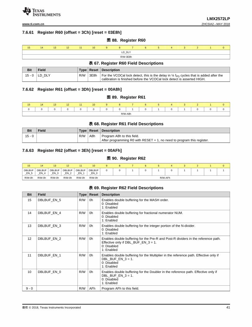
41
LMX2572LPwww.ti.com.cn ZHCSIA2 –MAY 2018
版权 © 2018, Texas Instruments Incorporated
7.6.61 Register R60 (offset = 3Ch) [reset = 03E8h]
图图 88. Register R6015 14 13 12 11 10 9 8 7 6 5 4 3 2 1 0
LD_DLY
R/W-3E8h
表表 67. Register R60 Field DescriptionsBit Field Type Reset Description
15 - 0 LD_DLY R/W 3E8h For the VCOCal lock detect, this is the delay in ¼ fPD cycles that is added after thecalibration is finished before the VCOCal lock detect is asserted HIGH.
7.6.62 Register R61 (offset = 3Dh) [reset = 00A8h]
图图 89. Register R6115 14 13 12 11 10 9 8 7 6 5 4 3 2 1 0
0 0 0 0 0 0 0 0 1 0 1 0 1 0 0 0
R/W-A8h
表表 68. Register R61 Field DescriptionsBit Field Type Reset Description
15 - 0 R/W A8h Program A8h to this field.After programming R0 with RESET = 1, no need to program this register.
7.6.63 Register R62 (offset = 3Eh) [reset = 00AFh]
图图 90. Register R6215 14 13 12 11 10 9 8 7 6 5 4 3 2 1 0
DBLBUF_EN_5
DBLBUF_EN_4
DBLBUF_EN_3
DBLBUF_EN_2
DBLBUF_EN_1
DBLBUF_EN_0
0 0 1 0 1 0 1 1 1 1
R/W-0h R/W-0h R/W-0h R/W-0h R/W-0h R/W-0h R/W-AFh
表表 69. Register R62 Field DescriptionsBit Field Type Reset Description15 DBLBUF_EN_5 R/W 0h Enables double buffering for the MASH order.
0: Disabled1: Enabled
14 DBLBUF_EN_4 R/W 0h Enables double buffering for fractional numerator NUM.0: Disabled1: Enabled
13 DBLBUF_EN_3 R/W 0h Enables double buffering for the integer portion of the N-divider.0: Disabled1: Enabled
12 DBLBUF_EN_2 R/W 0h Enables double buffering for the Pre-R and Post-R dividers in the reference path.Effective only if DBL_BUF_EN_3 = 1.0: Disabled1: Enabled
11 DBLBUF_EN_1 R/W 0h Enables double buffering for the Multiplier in the reference path. Effective only ifDBL_BUF_EN_3 = 1.0: Disabled1: Enabled
10 DBLBUF_EN_0 R/W 0h Enables double buffering for the Doubler in the reference path. Effective only ifDBL_BUF_EN_3 = 1.0: Disabled1: Enabled
9 - 0 R/W AFh Program AFh to this field.
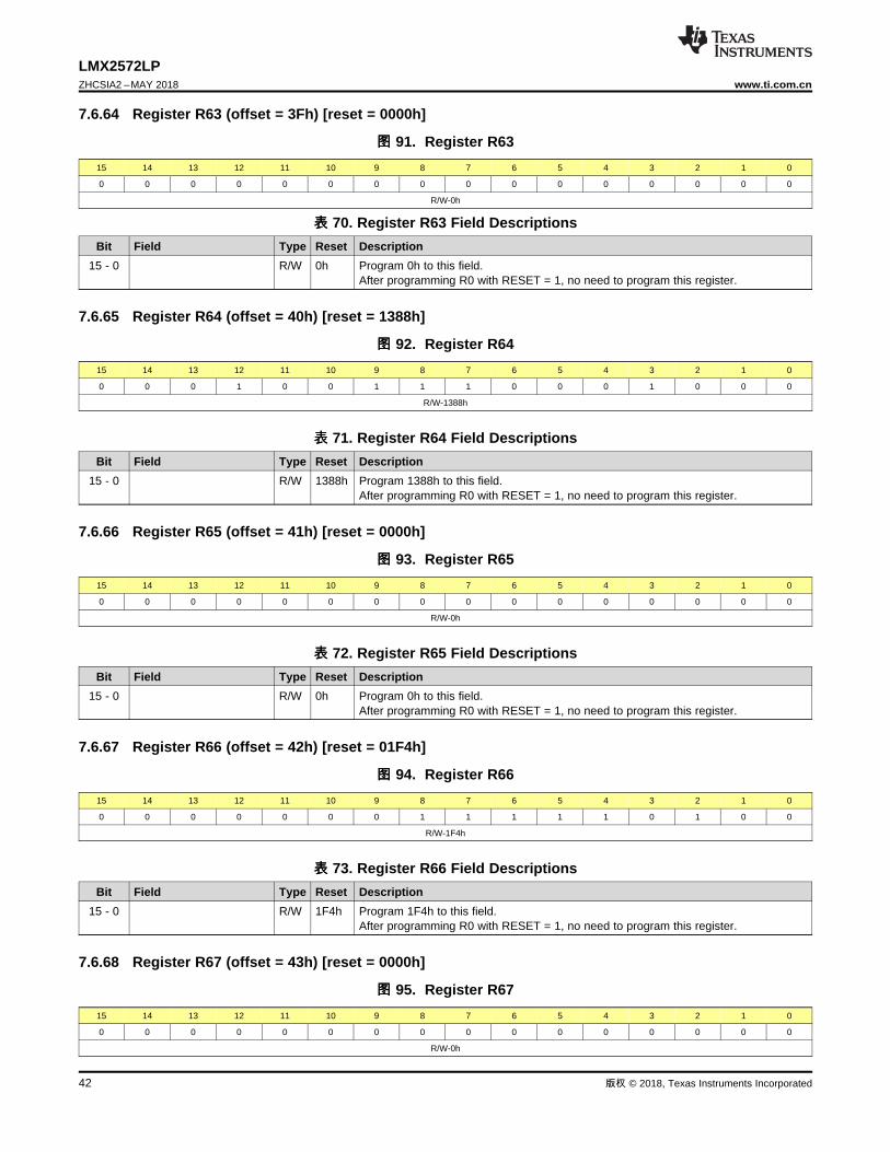
42
LMX2572LPZHCSIA2 –MAY 2018 www.ti.com.cn
版权 © 2018, Texas Instruments Incorporated
7.6.64 Register R63 (offset = 3Fh) [reset = 0000h]
图图 91. Register R6315 14 13 12 11 10 9 8 7 6 5 4 3 2 1 0
0 0 0 0 0 0 0 0 0 0 0 0 0 0 0 0
R/W-0h
表表 70. Register R63 Field DescriptionsBit Field Type Reset Description
15 - 0 R/W 0h Program 0h to this field.After programming R0 with RESET = 1, no need to program this register.
7.6.65 Register R64 (offset = 40h) [reset = 1388h]
图图 92. Register R6415 14 13 12 11 10 9 8 7 6 5 4 3 2 1 0
0 0 0 1 0 0 1 1 1 0 0 0 1 0 0 0
R/W-1388h
表表 71. Register R64 Field DescriptionsBit Field Type Reset Description
15 - 0 R/W 1388h Program 1388h to this field.After programming R0 with RESET = 1, no need to program this register.
7.6.66 Register R65 (offset = 41h) [reset = 0000h]
图图 93. Register R6515 14 13 12 11 10 9 8 7 6 5 4 3 2 1 0
0 0 0 0 0 0 0 0 0 0 0 0 0 0 0 0
R/W-0h
表表 72. Register R65 Field DescriptionsBit Field Type Reset Description
15 - 0 R/W 0h Program 0h to this field.After programming R0 with RESET = 1, no need to program this register.
7.6.67 Register R66 (offset = 42h) [reset = 01F4h]
图图 94. Register R6615 14 13 12 11 10 9 8 7 6 5 4 3 2 1 0
0 0 0 0 0 0 0 1 1 1 1 1 0 1 0 0
R/W-1F4h
表表 73. Register R66 Field DescriptionsBit Field Type Reset Description
15 - 0 R/W 1F4h Program 1F4h to this field.After programming R0 with RESET = 1, no need to program this register.
7.6.68 Register R67 (offset = 43h) [reset = 0000h]
图图 95. Register R6715 14 13 12 11 10 9 8 7 6 5 4 3 2 1 0
0 0 0 0 0 0 0 0 0 0 0 0 0 0 0 0
R/W-0h
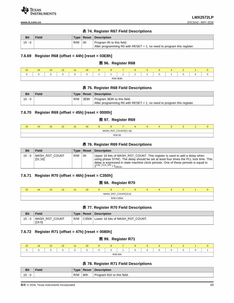
43
LMX2572LPwww.ti.com.cn ZHCSIA2 –MAY 2018
版权 © 2018, Texas Instruments Incorporated
表表 74. Register R67 Field DescriptionsBit Field Type Reset Description
15 - 0 R/W 0h Program 0h to this field.After programming R0 with RESET = 1, no need to program this register.
7.6.69 Register R68 (offset = 44h) [reset = 03E8h]
图图 96. Register R6815 14 13 12 11 10 9 8 7 6 5 4 3 2 1 0
0 0 0 0 0 0 1 1 1 1 1 0 1 0 0 0
R/W-3E8h
表表 75. Register R68 Field DescriptionsBit Field Type Reset Description
15 - 0 R/W 3E8h Program 3E8h to this field.After programming R0 with RESET = 1, no need to program this register.
7.6.70 Register R69 (offset = 45h) [reset = 0000h]
图图 97. Register R6915 14 13 12 11 10 9 8 7 6 5 4 3 2 1 0
MASH_RST_COUNT[31:16]
R/W-0h
表表 76. Register R69 Field DescriptionsBit Field Type Reset Description
15 - 0 MASH_RST_COUNT[31:16]
R/W 0h Upper 16 bits of MASH_RST_COUNT. This register is used to add a delay whenusing phase SYNC. The delay should be set at least four times the PLL lock time. Thisdelay is expressed in state machine clock periods. One of these periods is equal to2CAL_CLK_DIV / fOSCin.
7.6.71 Register R70 (offset = 46h) [reset = C350h]
图图 98. Register R7015 14 13 12 11 10 9 8 7 6 5 4 3 2 1 0
MASH_RST_COUNT[15:0]
R/W-C350h
表表 77. Register R70 Field DescriptionsBit Field Type Reset Description
15 - 0 MASH_RST_COUNT[15:0]
R/W C350h Lower 16 bits of MASH_RST_COUNT.
7.6.72 Register R71 (offset = 47h) [reset = 0080h]
图图 99. Register R7115 14 13 12 11 10 9 8 7 6 5 4 3 2 1 0
0 0 0 0 0 0 0 0 1 0 0 0 0 0 0 1
R/W-80h
表表 78. Register R71 Field DescriptionsBit Field Type Reset Description
15 - 0 R/W 80h Program 81h to this field.
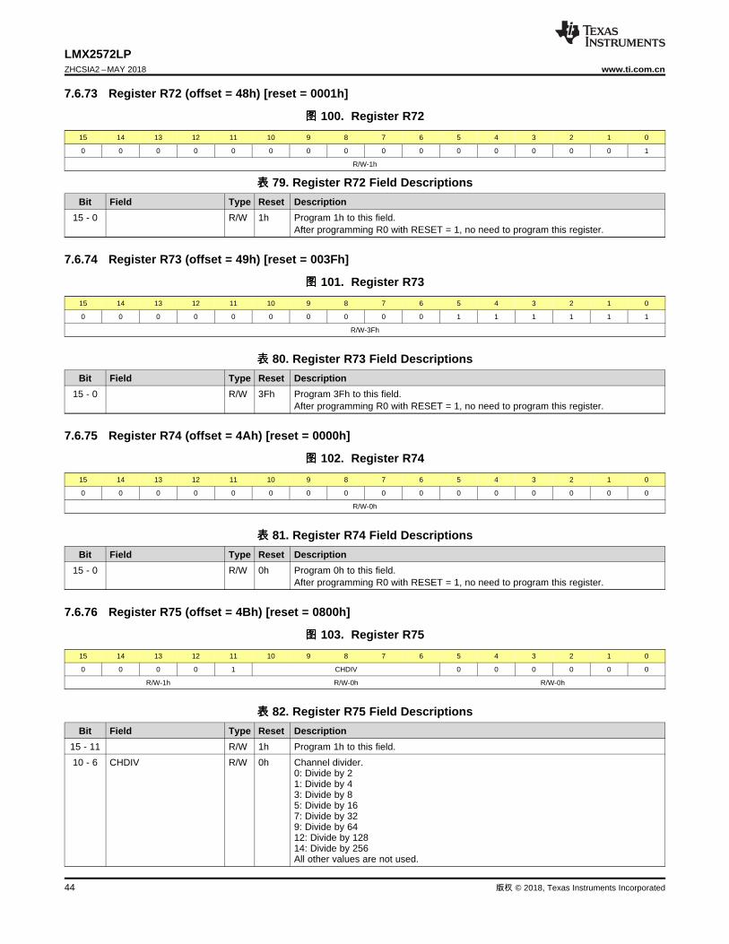
44
LMX2572LPZHCSIA2 –MAY 2018 www.ti.com.cn
版权 © 2018, Texas Instruments Incorporated
7.6.73 Register R72 (offset = 48h) [reset = 0001h]
图图 100. Register R7215 14 13 12 11 10 9 8 7 6 5 4 3 2 1 0
0 0 0 0 0 0 0 0 0 0 0 0 0 0 0 1
R/W-1h
表表 79. Register R72 Field DescriptionsBit Field Type Reset Description
15 - 0 R/W 1h Program 1h to this field.After programming R0 with RESET = 1, no need to program this register.
7.6.74 Register R73 (offset = 49h) [reset = 003Fh]
图图 101. Register R7315 14 13 12 11 10 9 8 7 6 5 4 3 2 1 0
0 0 0 0 0 0 0 0 0 0 1 1 1 1 1 1
R/W-3Fh
表表 80. Register R73 Field DescriptionsBit Field Type Reset Description
15 - 0 R/W 3Fh Program 3Fh to this field.After programming R0 with RESET = 1, no need to program this register.
7.6.75 Register R74 (offset = 4Ah) [reset = 0000h]
图图 102. Register R7415 14 13 12 11 10 9 8 7 6 5 4 3 2 1 0
0 0 0 0 0 0 0 0 0 0 0 0 0 0 0 0
R/W-0h
表表 81. Register R74 Field DescriptionsBit Field Type Reset Description
15 - 0 R/W 0h Program 0h to this field.After programming R0 with RESET = 1, no need to program this register.
7.6.76 Register R75 (offset = 4Bh) [reset = 0800h]
图图 103. Register R7515 14 13 12 11 10 9 8 7 6 5 4 3 2 1 0
0 0 0 0 1 CHDIV 0 0 0 0 0 0
R/W-1h R/W-0h R/W-0h
表表 82. Register R75 Field DescriptionsBit Field Type Reset Description
15 - 11 R/W 1h Program 1h to this field.10 - 6 CHDIV R/W 0h Channel divider.
0: Divide by 21: Divide by 43: Divide by 85: Divide by 167: Divide by 329: Divide by 6412: Divide by 12814: Divide by 256All other values are not used.

45
LMX2572LPwww.ti.com.cn ZHCSIA2 –MAY 2018
版权 © 2018, Texas Instruments Incorporated
表表 82. Register R75 Field Descriptions (接接下下页页)Bit Field Type Reset Description
5 - 0 R/W 0h Program 0h to this field.
7.6.77 Register R76 (offset = 4Ch) [reset = 000Ch]
图图 104. Register R7615 14 13 12 11 10 9 8 7 6 5 4 3 2 1 0
0 0 0 0 0 0 0 0 0 0 0 0 1 1 0 0
R/W-Ch
表表 83. Register R76 Field DescriptionsBit Field Type Reset Description
15 - 0 R/W Ch Program Ch to this field.After programming R0 with RESET = 1, no need to program this register.
7.6.78 Register R77 (offset = 4Dh) [reset = 0000h]
图图 105. Register R7715 14 13 12 11 10 9 8 7 6 5 4 3 2 1 0
0 0 0 0 0 0 0 0 0 0 0 0 0 0 0 0
R/W-0h
表表 84. Register R77 Field DescriptionsBit Field Type Reset Description
15 - 0 R/W 0h Program 0h to this field.After programming R0 with RESET = 1, no need to program this register.
7.6.79 Register R78 (offset = 4Eh) [reset = 0064h]
图图 106. Register R7815 14 13 12 11 10 9 8 7 6 5 4 3 2 1 0
0 0 0 0 RAMP_THRESH[
32]
0 QUICK_RECAL_
EN
VCO_CAPCTRL_STRT 1
R/W-0h R/W-0h R/W-0h R/W-0h R/W-32h R/W-0h
表表 85. Register R78 Field DescriptionsBit Field Type Reset Description
15 - 12 R/W 0h Program 0h to this field.11 RAMP_THRESH[32] R/W 0h The 33rd bit of RAMP_THRESH.
RAMP_THRESH sets how much the ramp can change the VCO frequency before aVCO calibration is required. If the frequency is chosen to be Δf, then RAMP_THRESH= (Δf / fPD) × 224.
10 R/W 0h Program 0h to this field.9 QUICK_RECAL_EN R/W 0h This sets the initial VCO starting calibration values. Especially useful if the frequency
change is smaller, say < 50 MHz or so.0: Calibration starts with VCO_SEL, VCO_CAPCTRL_START,VCO_DACISET_START1: Calibration starts with the current value
8 - 1 VCO_CAPCTRL_STRT R/W 32h This sets the starting VCO_CAPCTRL value that is used for VCO frequencycalibration. Smaller values yield a higher frequency band within a VCO core. Validnumber range is 0 to 183.
0 R/W 0h Program 1h to this field.
46
LMX2572LPZHCSIA2 –MAY 2018 www.ti.com.cn
版权 © 2018, Texas Instruments Incorporated
7.6.80 Register R79 (offset = 4Fh) [reset = 0000h]
图图 107. Register R7915 14 13 12 11 10 9 8 7 6 5 4 3 2 1 0
RAMP_THRESH[31:16]
R/W-0h
表表 86. Register R79 Field DescriptionsBit Field Type Reset Description
15 - 0 RAMP_THRESH[31:16] R/W 0h Upper 16 bits of RAMP_THRESH. See 表 85 for description.
7.6.81 Register R80 (offset = 50h) [reset = 0000h]
图图 108. Register R8015 14 13 12 11 10 9 8 7 6 5 4 3 2 1 0
RAMP_THRESH[15:0]
R/W-0h
表表 87. Register R80 Field DescriptionsBit Field Type Reset Description
15 - 0 RAMP_THRESH[15:0] R/W 0h Lower 16 bits of RAMP_THRESH. See 表 85 for description.
7.6.82 Register R81 (offset = 51h) [reset = 0000h]
图图 109. Register R8115 14 13 12 11 10 9 8 7 6 5 4 3 2 1 0
0 0 0 0 0 0 0 0 0 0 0 0 0 0 0 RAMP_LIMIT_HIGH[32]
R/W-0h R/W-0h
表表 88. Register R81 Field DescriptionsBit Field Type Reset Description
15 - 1 R/W 0h Program 0h to this field.0 RAMP_LIMIT_HIGH[32] R/W 0h The 33rd bit of RAMP_LIMIT_HIGH.
RAMP_LIMIT_HIGH sets a maximum frequency that the ramp cannot exceed so thatthe VCO does not get set beyond a valid frequency range.Suppose fHIGH is this frequency and fVCO is the starting VCO frequency, then:fHIGH ≥ fVCO;RAMP_LIMIT_HIGH = 224 × (fHIGH – fVCO) / fPD
7.6.83 Register R82 (offset = 52h) [reset = 0000h]
图图 110. Register R8215 14 13 12 11 10 9 8 7 6 5 4 3 2 1 0
RAMP_LIMIT_HIGH[31:16]
R/W-0h
表表 89. Register R82 Field DescriptionsBit Field Type Reset Description
15 - 0 RAMP_LIMIT_HIGH[31:16]
R/W 0h Upper 16 bits of RAMP_LIMIT_HIGH. See 表 88 for description.
47
LMX2572LPwww.ti.com.cn ZHCSIA2 –MAY 2018
版权 © 2018, Texas Instruments Incorporated
7.6.84 Register R83 (offset = 53h) [reset = 0000h]
图图 111. Register R8315 14 13 12 11 10 9 8 7 6 5 4 3 2 1 0
RAMP_LIMIT_HIGH[15:0]
R/W-0h
表表 90. Register R83 Field DescriptionsBit Field Type Reset Description
15 - 0 RAMP_LIMIT_HIGH[15:0] R/W 0h Lower 16 bits of RAMP_LIMIT_HIGH. See 表 88 for description.
7.6.85 Register R84 (offset = 54h) [reset = 0000h]
图图 112. Register R8415 14 13 12 11 10 9 8 7 6 5 4 3 2 1 0
0 0 0 0 0 0 0 0 0 0 0 0 0 0 0 RAMP_LIMIT_LO
W[32]
R/W-0h R/W-0h
表表 91. Register R84 Field DescriptionsBit Field Type Reset Description
15 - 1 R/W 0h Program 0h to this field.0 RAMP_LIMIT_LOW[32] R/W 0h The 33rd bit of RAMP_LIMIT_LOW.
RAMP_LIMIT_LOW sets a minimum frequency that the ramp cannot exceed so thatthe VCO does not get set beyond a valid frequency range.Suppose fLOW is this frequency and fVCO is the starting VCO frequency, then:fLOW ≤ fVCO;RAMP_LIMIT_LOW = 233 – 224 × (fVCO – fLOW) / fPD
7.6.86 Register R85 (offset = 55h) [reset = 0000h]
图图 113. Register R8515 14 13 12 11 10 9 8 7 6 5 4 3 2 1 0
RAMP_LIMIT_LOW[31:16]
R/W-0h
表表 92. Register R85 Field DescriptionsBit Field Type Reset Description
15 - 0 RAMP_LIMIT_LOW[31:16]
R/W 0h Upper 16 bits of RAMP_LIMIT_LOW. See 表 91 for description.
7.6.87 Register R86 (offset = 56h) [reset = 0000h]
图图 114. Register R8615 14 13 12 11 10 9 8 7 6 5 4 3 2 1 0
RAMP_LIMIT_LOW[15:0]
R/W-0h
表表 93. Register R86 Field DescriptionsBit Field Type Reset Description
15 - 0 RAMP_LIMIT_LOW[15:0] R/W 0h Lower 16 bits of RAMP_LIMIT_LOW. See 表 91 for description.

48
LMX2572LPZHCSIA2 –MAY 2018 www.ti.com.cn
版权 © 2018, Texas Instruments Incorporated
7.6.88 Register R87 (offset = 57h) [reset = 0000h]
图图 115. Register R8715 14 13 12 11 10 9 8 7 6 5 4 3 2 1 0
0 0 0 0 0 0 0 0 0 0 0 0 0 0 0 0
R/W-0h
表表 94. Register R87 Field DescriptionsBit Field Type Reset Description
15 - 0 R/W 0h Program 0h to this field.After programming R0 with RESET = 1, no need to program this register.
7.6.89 Register R88 (offset = 58h) [reset = 0000h]
图图 116. Register R8815 14 13 12 11 10 9 8 7 6 5 4 3 2 1 0
0 0 0 0 0 0 0 0 0 0 0 0 0 0 0 0
R/W-0h
表表 95. Register R88 Field DescriptionsBit Field Type Reset Description
15 - 0 R/W 0h Program 0h to this field.After programming R0 with RESET = 1, no need to program this register.
7.6.90 Register R89 (offset = 59h) [reset = 0000h]
图图 117. Register R8915 14 13 12 11 10 9 8 7 6 5 4 3 2 1 0
0 0 0 0 0 0 0 0 0 0 0 0 0 0 0 0
R/W-0h
表表 96. Register R89 Field DescriptionsBit Field Type Reset Description
15 - 0 R/W 0h Program 0h to this field.After programming R0 with RESET = 1, no need to program this register.
7.6.91 Register R90 (offset = 5Ah) [reset = 0000h]
图图 118. Register R9015 14 13 12 11 10 9 8 7 6 5 4 3 2 1 0
0 0 0 0 0 0 0 0 0 0 0 0 0 0 0 0
R/W-0h
表表 97. Register R90 Field DescriptionsBit Field Type Reset Description
15 - 0 R/W 0h Program 0h to this field.After programming R0 with RESET = 1, no need to program this register.
7.6.92 Register R91 (offset = 5Bh) [reset = 0000h]
图图 119. Register R9115 14 13 12 11 10 9 8 7 6 5 4 3 2 1 0
0 0 0 0 0 0 0 0 0 0 0 0 0 0 0 0
R/W-0h
49
LMX2572LPwww.ti.com.cn ZHCSIA2 –MAY 2018
版权 © 2018, Texas Instruments Incorporated
表表 98. Register R91 Field DescriptionsBit Field Type Reset Description
15 - 0 R/W 0h Program 0h to this field.After programming R0 with RESET = 1, no need to program this register.
7.6.93 Register R92 (offset = 5Ch) [reset = 0000h]
图图 120. Register R9215 14 13 12 11 10 9 8 7 6 5 4 3 2 1 0
0 0 0 0 0 0 0 0 0 0 0 0 0 0 0 0
R/W-0h
表表 99. Register R92 Field DescriptionsBit Field Type Reset Description
15 - 0 R/W 0h Program 0h to this field.After programming R0 with RESET = 1, no need to program this register.
7.6.94 Register R93 (offset = 5Dh) [reset = 0000h]
图图 121. Register R9315 14 13 12 11 10 9 8 7 6 5 4 3 2 1 0
0 0 0 0 0 0 0 0 0 0 0 0 0 0 0 0
R/W-0h
表表 100. Register R93 Field DescriptionsBit Field Type Reset Description
15 - 0 R/W 0h Program 0h to this field.After programming R0 with RESET = 1, no need to program this register.
7.6.95 Register R94 (offset = 5Eh) [reset = 0000h]
图图 122. Register R9415 14 13 12 11 10 9 8 7 6 5 4 3 2 1 0
0 0 0 0 0 0 0 0 0 0 0 0 0 0 0 0
R/W-0h
表表 101. Register R94 Field DescriptionsBit Field Type Reset Description
15 - 0 R/W 0h Program 0h to this field.After programming R0 with RESET = 1, no need to program this register.
7.6.96 Register R95 (offset = 5Fh) [reset = 0000h]
图图 123. Register R9515 14 13 12 11 10 9 8 7 6 5 4 3 2 1 0
0 0 0 0 0 0 0 0 0 0 0 0 0 0 0 0
R/W-0h
表表 102. Register R95 Field DescriptionsBit Field Type Reset Description
15 - 0 R/W 0h Program 0h to this field.After programming R0 with RESET = 1, no need to program this register.

50
LMX2572LPZHCSIA2 –MAY 2018 www.ti.com.cn
版权 © 2018, Texas Instruments Incorporated
7.6.97 Register R96 (offset = 60h) [reset = 0000h]
图图 124. Register R9615 14 13 12 11 10 9 8 7 6 5 4 3 2 1 0
RAMP_BURST_E
N
RAMP_BURST_COUNT 0 0
R/W-0h R/W-0h R/W-0h
表表 103. Register R96 Field DescriptionsBit Field Type Reset Description15 RAMP_BURST_EN R/W 0h This enables ramp burst mode. In this mode, a number of ramps equal to
RAMP_BURST_COUNT is sent out whenever RAMP_EN is set to 1. This is intendedto produce a finite pattern of ramps, instead of a continuous pattern.0: Disabled1: Enabled
14 - 2 RAMP_BURST_COUNT R/W 0h When RAMP_BURST_EN = 1, this sets the number of ramps that is sent out.1 - 0 R/W 0h Program 0h to this field.
7.6.98 Register R97 (offset = 61h) [reset = 0000h]
图图 125. Register R9715 14 13 12 11 10 9 8 7 6 5 4 3 2 1 0
RAMP0_RST
0 0 0 0 RAMP_TRIGB RAMP_TRIGA 0 RAMP_BURST_TRIG
R/W-0h R/W-0h R/W-0h R/W-0h R/W-0h R/W-0h
表表 104. Register R97 Field DescriptionsBit Field Type Reset Description15 RAMP0_RST R/W 0h Resets RAMP0 at start of ramp to eliminate round-off errors. Applies to automatic
ramping mode only.0: Disabled1: Reset
14 - 11 R/W 0h Program 0h to this field.10 - 7 RAMP_TRIGB R/W 0h Definition of ramp trigger B.
0: Disabled1: RampClk pin rising edge2: RampDir pin rising edge4: Always triggered9: RampClk pin falling edge10: RampDir pin falling edgeAll other values are not used.
6 - 3 RAMP_TRIGA R/W 0h Definition of ramp trigger A. Options are same as RAMP_TRIGB.2 R/W 0h Program 0h to this field.
1 - 0 RAMP_BURST_TRIG R/W 0h Sets what triggers the next ramp in burst mode.0: Ramp transition1: Trigger A2: Trigger B3: Not used
7.6.99 Register R98 (offset = 62h) [reset = 0000h]
图图 126. Register R9815 14 13 12 11 10 9 8 7 6 5 4 3 2 1 0
RAMP0_INC[29:16] 0 RAMP0_DLY
R/W-0h R/W-0h R/W-0h
51
LMX2572LPwww.ti.com.cn ZHCSIA2 –MAY 2018
版权 © 2018, Texas Instruments Incorporated
表表 105. Register R98 Field DescriptionsBit Field Type Reset Description
15 - 2 RAMP0_INC[29:16] R/W 0h Upper 14 bits of RAMP0_INC.RAMP0_INC sets the 2's compliment of the number added to the fractional numeratoron every ramp cycle.
1 R/W 0h Program 0h to this field.0 RAMP0_DLY R/W 0h When enabled, increases RAMP0 length by basing the ramp clock on two phase
detector cycles instead of one.0: Ramp clock = 1 fPD cycle1: Ramp clock = 2 fPD cycles
7.6.100 Register R99 (offset = 63h) [reset = 0000h]
图图 127. Register R9915 14 13 12 11 10 9 8 7 6 5 4 3 2 1 0
RAMP0_INC[15:0]
R/W-0h
表表 106. Register R99 Field DescriptionsBit Field Type Reset Description
15 - 0 RAMP0_INC[15:0] R/W 0h Lower 16 bits of RAMP0_INC. See 表 105 for description.
7.6.101 Register R100 (offset = 64h) [reset = 0000h]
图图 128. Register R10015 14 13 12 11 10 9 8 7 6 5 4 3 2 1 0
RAMP0_LEN
R/W-0h
表表 107. Register R100 Field DescriptionsBit Field Type Reset Description
15 - 0 RAMP0_LEN R/W 0h Length of the ramp in phase detector cycles.
7.6.102 Register R101 (offset = 65h) [reset = 0000h]
图图 129. Register R10115 14 13 12 11 10 9 8 7 6 5 4 3 2 1 0
0 0 0 0 0 0 0 0 0 RAMP1_DLY
RAMP1_RST
RAMP0_NEXT
0 0 RAMP0_NEXT_TRIG
R/W-0h R/W-0h R/W-0h R/W-0h R/W-0h R/W-0h
表表 108. Register R101 Field DescriptionsBit Field Type Reset Description
15 - 7 R/W 0h Program 0h to this field.6 RAMP1_DLY R/W 0h When enabled, increases RAMP1 length by basing the ramp clock on two phase
detector cycles instead of one.0: Ramp clock = 1 fPD cycle1: Ramp clock = 2 fPD cycles
5 RAMP1_RST R/W 0h Resets RAMP1 at start of ramp to eliminate round-off errors. Applies to automaticramping mode only.0: Disabled1: Reset
4 RAMP0_NEXT R/W 0h Defines what ramp comes after RAMP0.0: RAMP01: RAMP1
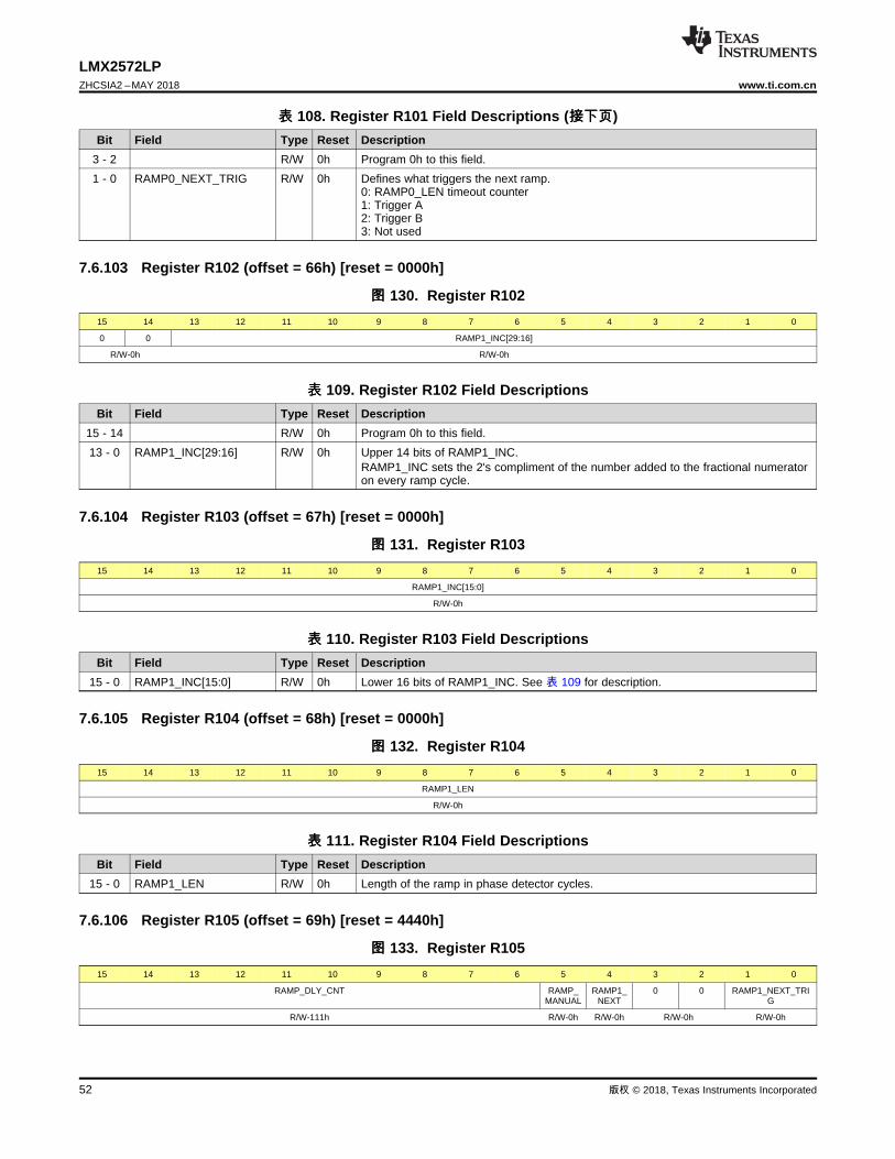
52
LMX2572LPZHCSIA2 –MAY 2018 www.ti.com.cn
版权 © 2018, Texas Instruments Incorporated
表表 108. Register R101 Field Descriptions (接接下下页页)Bit Field Type Reset Description
3 - 2 R/W 0h Program 0h to this field.1 - 0 RAMP0_NEXT_TRIG R/W 0h Defines what triggers the next ramp.
0: RAMP0_LEN timeout counter1: Trigger A2: Trigger B3: Not used
7.6.103 Register R102 (offset = 66h) [reset = 0000h]
图图 130. Register R10215 14 13 12 11 10 9 8 7 6 5 4 3 2 1 0
0 0 RAMP1_INC[29:16]
R/W-0h R/W-0h
表表 109. Register R102 Field DescriptionsBit Field Type Reset Description
15 - 14 R/W 0h Program 0h to this field.13 - 0 RAMP1_INC[29:16] R/W 0h Upper 14 bits of RAMP1_INC.
RAMP1_INC sets the 2's compliment of the number added to the fractional numeratoron every ramp cycle.
7.6.104 Register R103 (offset = 67h) [reset = 0000h]
图图 131. Register R10315 14 13 12 11 10 9 8 7 6 5 4 3 2 1 0
RAMP1_INC[15:0]
R/W-0h
表表 110. Register R103 Field DescriptionsBit Field Type Reset Description
15 - 0 RAMP1_INC[15:0] R/W 0h Lower 16 bits of RAMP1_INC. See 表 109 for description.
7.6.105 Register R104 (offset = 68h) [reset = 0000h]
图图 132. Register R10415 14 13 12 11 10 9 8 7 6 5 4 3 2 1 0
RAMP1_LEN
R/W-0h
表表 111. Register R104 Field DescriptionsBit Field Type Reset Description
15 - 0 RAMP1_LEN R/W 0h Length of the ramp in phase detector cycles.
7.6.106 Register R105 (offset = 69h) [reset = 4440h]
图图 133. Register R10515 14 13 12 11 10 9 8 7 6 5 4 3 2 1 0
RAMP_DLY_CNT RAMP_MANUAL
RAMP1_NEXT
0 0 RAMP1_NEXT_TRIG
R/W-111h R/W-0h R/W-0h R/W-0h R/W-0h
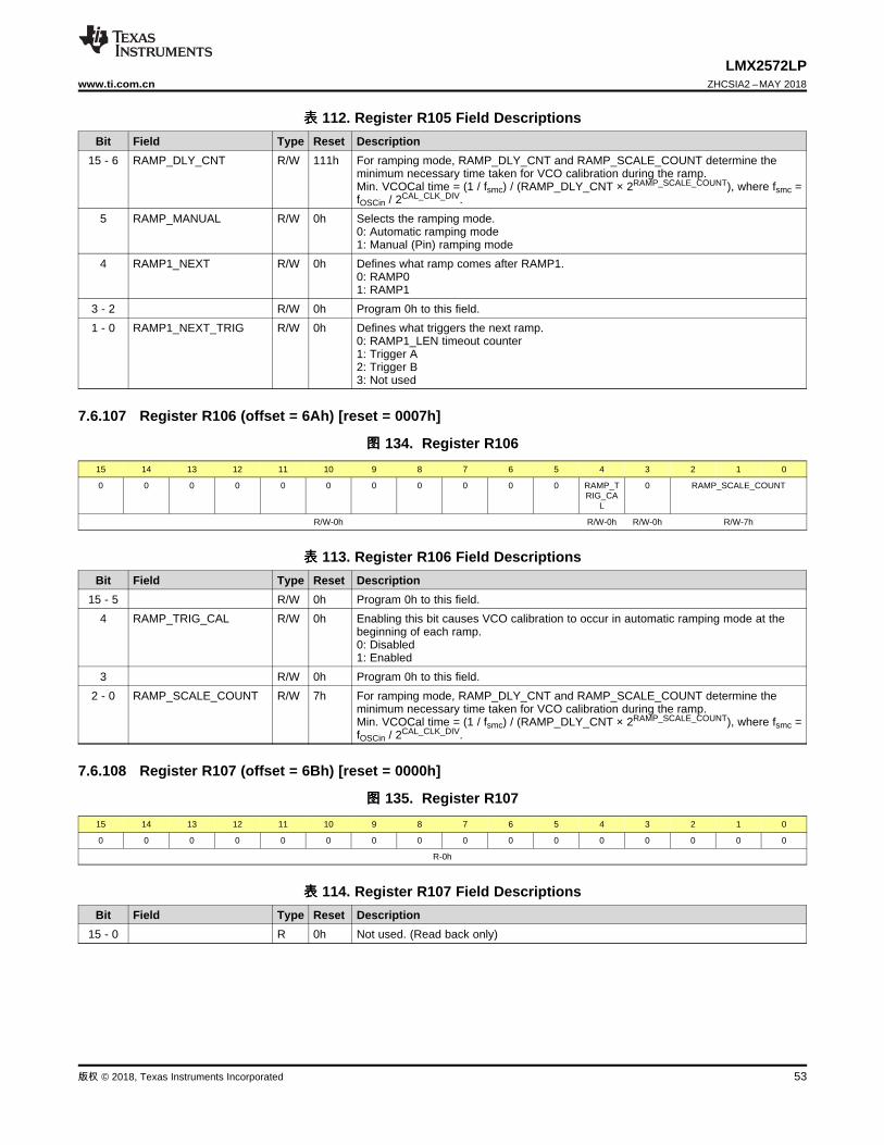
53
LMX2572LPwww.ti.com.cn ZHCSIA2 –MAY 2018
版权 © 2018, Texas Instruments Incorporated
表表 112. Register R105 Field DescriptionsBit Field Type Reset Description
15 - 6 RAMP_DLY_CNT R/W 111h For ramping mode, RAMP_DLY_CNT and RAMP_SCALE_COUNT determine theminimum necessary time taken for VCO calibration during the ramp.Min. VCOCal time = (1 / fsmc) / (RAMP_DLY_CNT × 2RAMP_SCALE_COUNT), where fsmc =fOSCin / 2CAL_CLK_DIV.
5 RAMP_MANUAL R/W 0h Selects the ramping mode.0: Automatic ramping mode1: Manual (Pin) ramping mode
4 RAMP1_NEXT R/W 0h Defines what ramp comes after RAMP1.0: RAMP01: RAMP1
3 - 2 R/W 0h Program 0h to this field.1 - 0 RAMP1_NEXT_TRIG R/W 0h Defines what triggers the next ramp.
0: RAMP1_LEN timeout counter1: Trigger A2: Trigger B3: Not used
7.6.107 Register R106 (offset = 6Ah) [reset = 0007h]
图图 134. Register R10615 14 13 12 11 10 9 8 7 6 5 4 3 2 1 0
0 0 0 0 0 0 0 0 0 0 0 RAMP_TRIG_CA
L
0 RAMP_SCALE_COUNT
R/W-0h R/W-0h R/W-0h R/W-7h
表表 113. Register R106 Field DescriptionsBit Field Type Reset Description
15 - 5 R/W 0h Program 0h to this field.4 RAMP_TRIG_CAL R/W 0h Enabling this bit causes VCO calibration to occur in automatic ramping mode at the
beginning of each ramp.0: Disabled1: Enabled
3 R/W 0h Program 0h to this field.2 - 0 RAMP_SCALE_COUNT R/W 7h For ramping mode, RAMP_DLY_CNT and RAMP_SCALE_COUNT determine the
minimum necessary time taken for VCO calibration during the ramp.Min. VCOCal time = (1 / fsmc) / (RAMP_DLY_CNT × 2RAMP_SCALE_COUNT), where fsmc =fOSCin / 2CAL_CLK_DIV.
7.6.108 Register R107 (offset = 6Bh) [reset = 0000h]
图图 135. Register R10715 14 13 12 11 10 9 8 7 6 5 4 3 2 1 0
0 0 0 0 0 0 0 0 0 0 0 0 0 0 0 0
R-0h
表表 114. Register R107 Field DescriptionsBit Field Type Reset Description
15 - 0 R 0h Not used. (Read back only)
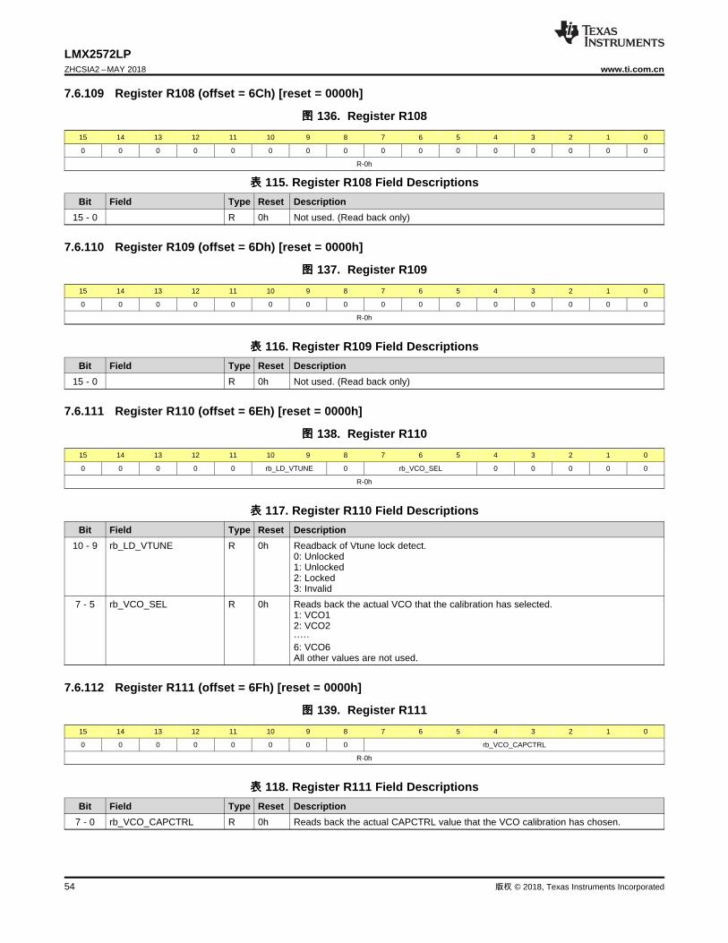
54
LMX2572LPZHCSIA2 –MAY 2018 www.ti.com.cn
版权 © 2018, Texas Instruments Incorporated
7.6.109 Register R108 (offset = 6Ch) [reset = 0000h]
图图 136. Register R10815 14 13 12 11 10 9 8 7 6 5 4 3 2 1 0
0 0 0 0 0 0 0 0 0 0 0 0 0 0 0 0
R-0h
表表 115. Register R108 Field DescriptionsBit Field Type Reset Description
15 - 0 R 0h Not used. (Read back only)
7.6.110 Register R109 (offset = 6Dh) [reset = 0000h]
图图 137. Register R10915 14 13 12 11 10 9 8 7 6 5 4 3 2 1 0
0 0 0 0 0 0 0 0 0 0 0 0 0 0 0 0
R-0h
表表 116. Register R109 Field DescriptionsBit Field Type Reset Description
15 - 0 R 0h Not used. (Read back only)
7.6.111 Register R110 (offset = 6Eh) [reset = 0000h]
图图 138. Register R11015 14 13 12 11 10 9 8 7 6 5 4 3 2 1 0
0 0 0 0 0 rb_LD_VTUNE 0 rb_VCO_SEL 0 0 0 0 0
R-0h
表表 117. Register R110 Field DescriptionsBit Field Type Reset Description
10 - 9 rb_LD_VTUNE R 0h Readback of Vtune lock detect.0: Unlocked1: Unlocked2: Locked3: Invalid
7 - 5 rb_VCO_SEL R 0h Reads back the actual VCO that the calibration has selected.1: VCO12: VCO2·····6: VCO6All other values are not used.
7.6.112 Register R111 (offset = 6Fh) [reset = 0000h]
图图 139. Register R11115 14 13 12 11 10 9 8 7 6 5 4 3 2 1 0
0 0 0 0 0 0 0 0 rb_VCO_CAPCTRL
R-0h
表表 118. Register R111 Field DescriptionsBit Field Type Reset Description
7 - 0 rb_VCO_CAPCTRL R 0h Reads back the actual CAPCTRL value that the VCO calibration has chosen.
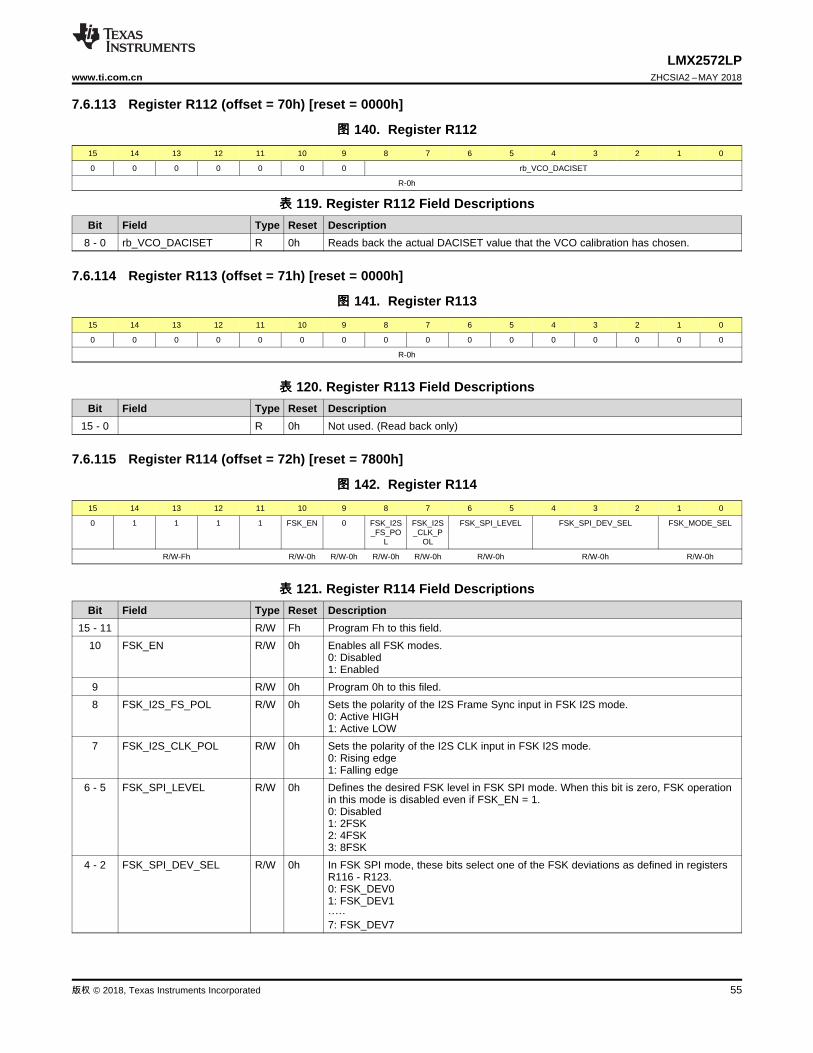
55
LMX2572LPwww.ti.com.cn ZHCSIA2 –MAY 2018
版权 © 2018, Texas Instruments Incorporated
7.6.113 Register R112 (offset = 70h) [reset = 0000h]
图图 140. Register R11215 14 13 12 11 10 9 8 7 6 5 4 3 2 1 0
0 0 0 0 0 0 0 rb_VCO_DACISET
R-0h
表表 119. Register R112 Field DescriptionsBit Field Type Reset Description
8 - 0 rb_VCO_DACISET R 0h Reads back the actual DACISET value that the VCO calibration has chosen.
7.6.114 Register R113 (offset = 71h) [reset = 0000h]
图图 141. Register R11315 14 13 12 11 10 9 8 7 6 5 4 3 2 1 0
0 0 0 0 0 0 0 0 0 0 0 0 0 0 0 0
R-0h
表表 120. Register R113 Field DescriptionsBit Field Type Reset Description
15 - 0 R 0h Not used. (Read back only)
7.6.115 Register R114 (offset = 72h) [reset = 7800h]
图图 142. Register R11415 14 13 12 11 10 9 8 7 6 5 4 3 2 1 0
0 1 1 1 1 FSK_EN 0 FSK_I2S_FS_PO
L
FSK_I2S_CLK_P
OL
FSK_SPI_LEVEL FSK_SPI_DEV_SEL FSK_MODE_SEL
R/W-Fh R/W-0h R/W-0h R/W-0h R/W-0h R/W-0h R/W-0h R/W-0h
表表 121. Register R114 Field DescriptionsBit Field Type Reset Description
15 - 11 R/W Fh Program Fh to this field.10 FSK_EN R/W 0h Enables all FSK modes.
0: Disabled1: Enabled
9 R/W 0h Program 0h to this filed.8 FSK_I2S_FS_POL R/W 0h Sets the polarity of the I2S Frame Sync input in FSK I2S mode.
0: Active HIGH1: Active LOW
7 FSK_I2S_CLK_POL R/W 0h Sets the polarity of the I2S CLK input in FSK I2S mode.0: Rising edge1: Falling edge
6 - 5 FSK_SPI_LEVEL R/W 0h Defines the desired FSK level in FSK SPI mode. When this bit is zero, FSK operationin this mode is disabled even if FSK_EN = 1.0: Disabled1: 2FSK2: 4FSK3: 8FSK
4 - 2 FSK_SPI_DEV_SEL R/W 0h In FSK SPI mode, these bits select one of the FSK deviations as defined in registersR116 - R123.0: FSK_DEV01: FSK_DEV1·····7: FSK_DEV7
56
LMX2572LPZHCSIA2 –MAY 2018 www.ti.com.cn
版权 © 2018, Texas Instruments Incorporated
表表 121. Register R114 Field Descriptions (接接下下页页)Bit Field Type Reset Description
1 - 0 FSK_MODE_SEL R/W 0h Defines FSK mode.0: Not used1: FSK I2S2: FSK SPI3: FSK SPI FAST
7.6.116 Register R115 (offset = 73h) [reset = 0000h]
图图 143. Register R11515 14 13 12 11 10 9 8 7 6 5 4 3 2 1 0
0 0 0 0 0 0 0 0 FSK_DEV_SCALE 0 0 0
R/W-0h R/W-0h R/W-0h
表表 122. Register R115 Field DescriptionsBit Field Type Reset Description
15 - 8 R/W 0h Program 0h to this field.7 - 3 FSK_DEV_SCALE R/W 0h The FSK deviation will be scaled by 2FSK_DEV_SCALE.2 - 0 R/W 0h Program 0h to this field.
7.6.117 Register R116 (offset = 74h) [reset = 0000h]
图图 144. Register R11615 14 13 12 11 10 9 8 7 6 5 4 3 2 1 0
FSK_DEV0
R/W-0h
表表 123. Register R116 Field DescriptionsBit Field Type Reset Description
15 - 0 FSK_DEV0 R/W 0h Defines the desired frequency deviation in FSK SPI mode.
7.6.118 Register R117 (offset = 75h) [reset = 0000h]
图图 145. Register R11715 14 13 12 11 10 9 8 7 6 5 4 3 2 1 0
FSK_DEV1
R/W-0h
表表 124. Register R117 Field DescriptionsBit Field Type Reset Description
15 - 0 FSK_DEV1 R/W 0h Defines the desired frequency deviation in FSK SPI mode.
7.6.119 Register R118 (offset = 76h) [reset = 0000h]
图图 146. Register R11815 14 13 12 11 10 9 8 7 6 5 4 3 2 1 0
FSK_DEV2
R/W-0h

57
LMX2572LPwww.ti.com.cn ZHCSIA2 –MAY 2018
版权 © 2018, Texas Instruments Incorporated
表表 125. Register R118 Field DescriptionsBit Field Type Reset Description
15 - 0 FSK_DEV2 R/W 0h Defines the desired frequency deviation in FSK SPI mode.
7.6.120 Register R119 (offset = 77h) [reset = 0000h]
图图 147. Register R11915 14 13 12 11 10 9 8 7 6 5 4 3 2 1 0
FSK_DEV3
R/W-0h
表表 126. Register R119 Field DescriptionsBit Field Type Reset Description
15 - 0 FSK_DEV3 R/W 0h Defines the desired frequency deviation in FSK SPI mode.
7.6.121 Register R120 (offset = 78h) [reset = 0000h]
图图 148. Register R12015 14 13 12 11 10 9 8 7 6 5 4 3 2 1 0
FSK_DEV4
R/W-0h
表表 127. Register R120 Field DescriptionsBit Field Type Reset Description
15 - 0 FSK_DEV4 R/W 0h Defines the desired frequency deviation in FSK SPI mode.
7.6.122 Register R121 (offset = 79h) [reset = 0000h]
图图 149. Register R12115 14 13 12 11 10 9 8 7 6 5 4 3 2 1 0
FSK_DEV5
R/W-0h
表表 128. Register R121 Field DescriptionsBit Field Type Reset Description
15 - 0 FSK_DEV5 R/W 0h Defines the desired frequency deviation in FSK SPI mode.
7.6.123 Register R122 (offset = 7Ah) [reset = 0000h]
图图 150. Register R12215 14 13 12 11 10 9 8 7 6 5 4 3 2 1 0
FSK_DEV6
R/W-0h
表表 129. Register R122 Field DescriptionsBit Field Type Reset Description
15 - 0 FSK_DEV6 R/W 0h Defines the desired frequency deviation in FSK SPI mode.

58
LMX2572LPZHCSIA2 –MAY 2018 www.ti.com.cn
版权 © 2018, Texas Instruments Incorporated
7.6.124 Register R123 (offset = 7Bh) [reset = 0000h]
图图 151. Register R12315 14 13 12 11 10 9 8 7 6 5 4 3 2 1 0
FSK_DEV7
R/W-0h
表表 130. Register R123 Field DescriptionsBit Field Type Reset Description
15 - 0 FSK_DEV7 R/W 0h Defines the desired frequency deviation in FSK SPI mode.
7.6.125 Register R124 (offset = 7Ch) [reset = 0000h]
图图 152. Register R12415 14 13 12 11 10 9 8 7 6 5 4 3 2 1 0
FSK_SPI_FAST_DEV
R/W-0h
表表 131. Register R124 Field DescriptionsBit Field Type Reset Description
15 - 0 FSK_SPI_FAST_DEV R/W 0h Defines the desired frequency deviation in FSK SPI FAST mode.
7.6.126 Register R125 (offset = 7Dh) [reset = 0820h]
图图 153. Register R12515 14 13 12 11 10 9 8 7 6 5 4 3 2 1 0
0 0 0 0 1 0 0 0 0 0 1 0 0 0 0 0
R/W-0820h
表表 132. Register R125 Field DescriptionsBit Field Type Reset Description
15 - 0 R/W 820h Program 820h to this field.After programming R0 with RESET = 1, no need to program this register.
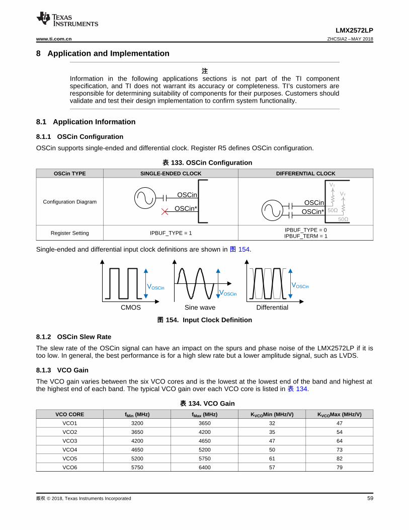
VOSCin
CMOS
VOSCin
Sine wave Differential
VOSCin
OSCin
OSCin*OSCin
OSCin*
VT
50��
50��
VT
59
LMX2572LPwww.ti.com.cn ZHCSIA2 –MAY 2018
版权 © 2018, Texas Instruments Incorporated
8 Application and Implementation
注注Information in the following applications sections is not part of the TI componentspecification, and TI does not warrant its accuracy or completeness. TI’s customers areresponsible for determining suitability of components for their purposes. Customers shouldvalidate and test their design implementation to confirm system functionality.
8.1 Application Information
8.1.1 OSCin ConfigurationOSCin supports single-ended and differential clock. Register R5 defines OSCin configuration.
表表 133. OSCin ConfigurationOSCin TYPE SINGLE-ENDED CLOCK DIFFERENTIAL CLOCK
Configuration Diagram
Register Setting IPBUF_TYPE = 1 IPBUF_TYPE = 0IPBUF_TERM = 1
Single-ended and differential input clock definitions are shown in 图 154.
图图 154. Input Clock Definition
8.1.2 OSCin Slew RateThe slew rate of the OSCin signal can have an impact on the spurs and phase noise of the LMX2572LP if it istoo low. In general, the best performance is for a high slew rate but a lower amplitude signal, such as LVDS.
8.1.3 VCO GainThe VCO gain varies between the six VCO cores and is the lowest at the lowest end of the band and highest atthe highest end of each band. The typical VCO gain over each VCO core is listed in 表 134.
表表 134. VCO GainVCO CORE fMin (MHz) fMax (MHz) KVCOMin (MHz/V) KVCOMax (MHz/V)
VCO1 3200 3650 32 47VCO2 3650 4200 35 54VCO3 4200 4650 47 64VCO4 4650 5200 50 73VCO5 5200 5750 61 82VCO6 5750 6400 57 79
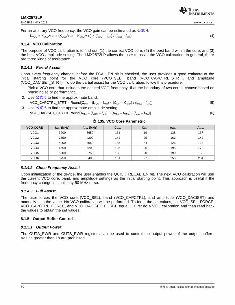
60
LMX2572LPZHCSIA2 –MAY 2018 www.ti.com.cn
版权 © 2018, Texas Instruments Incorporated
For an arbitrary VCO frequency, the VCO gain can be estimated as 公式 4:KVCO = KVCOMin + (KVCOMax – KVCOMin) × (fVCO – fMin) / (fMax – fMin) (4)
8.1.4 VCO CalibrationThe purpose of VCO calibration is to find out: (1) the correct VCO core, (2) the best band within the core, and (3)the best VCO amplitude setting. The LMX2572LP allows the user to assist the VCO calibration. In general, thereare three kinds of assistance.
8.1.4.1 Partial AssistUpon every frequency change, before the FCAL_EN bit is checked, the user provides a good estimate of theinitial starting point for the VCO core (VCO_SEL), band (VCO_CAPCTRL_STRT), and amplitude(VCO_DACISET_STRT). To do the partial assist for the VCO calibration, follow this procedure:1. Pick a VCO core that includes the desired VCO frequency. If at the boundary of two cores, choose based on
phase noise or performance.2. Use 公式 5 to find the approximate band:
VCO_CAPCTRL_STRT = Round[CMin – (fVCO – fMin) × (CMin – CMax) / (fMax – fMin)] (5)3. Use 公式 6 to find the approximate amplitude setting.
VCO_DACISET_STRT = Round[AMin – (fVCO – fMin) × (AMin – AMax) / (fMax – fMin)] (6)
表表 135. VCO Core ParametricVCO CORE fMin (MHz) fMax (MHz) CMin CMax AMin AMax
VCO1 3200 3650 131 19 138 137VCO2 3650 4200 143 25 162 142VCO3 4200 4650 135 34 126 114VCO4 4650 5200 136 25 195 172VCO5 5200 5750 133 20 190 163VCO6 5750 6400 151 27 256 204
8.1.4.2 Close Frequency AssistUpon initialization of the device, the user enables the QUICK_RECAL_EN bit. The next VCO calibration will usethe current VCO core, band, and amplitude settings as the initial starting point. This approach is useful if thefrequency change is small, say 50 MHz or so.
8.1.4.3 Full AssistThe user forces the VCO core (VCO_SEL), band (VCO_CAPCTRL), and amplitude (VCO_DACISET) andmanually sets the value. No VCO calibration will be performed. To force the set values, set VCO_SEL_FORCE,VCO_CAPCTRL_FORCE, and VCO_DACISET_FORCE equal 1. First do a VCO calibration and then read backthe values to obtain the set values.
8.1.5 Output Buffer Control
8.1.5.1 Output PowerThe OUTA_PWR and OUTB_PWR registers can be used to control the output power of the output buffers.Values greater than 18 are prohibited.

RFout
System device
fOUT (MHz)
PO
UT (
dB
m)
0 200 400 600 800 1000 1200 1400 1600 1800 2000-6
-4
-2
0
2
4
6
8
10
D047
OUTx_PWR51218
OUTx_PWR
PO
UT (
dB
m)
2 4 6 8 10 12 14 16 18-12
-9
-6
-3
0
3
6
9
D048
fOUT250 MHz500 MHz1000 MHz2000 MHz
61
LMX2572LPwww.ti.com.cn ZHCSIA2 –MAY 2018
版权 © 2018, Texas Instruments Incorporated
图图 155. Output Power vs Frequency 图图 156. Output Power vs Power Control Bits
8.1.5.2 Power-Up ResponseUse the OUTx_PD bits to power up or power down the output buffers. The RF output will vanish immediatelywhen the buffer is powered down. However, it takes some tiny amount of time for it to power up.
图图 157. Buffer Power Up at 400-MHz Output
8.1.5.3 Unused Output PinEach output buffer has two differential pair pins. The buffer can be used as a single differential output or twosingle-ended outputs. If only one single-ended output is necessary, the unused pin cannot be left open. The pinshould be terminated properly as shown in 图 158.
图图 158. Unused Output Buffer Differential Pin
8.1.6 Application for SYNCThe requirements for SYNC depend on certain setup conditions. In cases where the SYNC is not timing critical,the setup can be done through software by toggling the VCO_PHASE_SYNC_EN bit from 0 to 1. When theSYNC is timing critical, then setup must be done through the SYNC pin and the setup and hold times for theOSCin pin are critical.
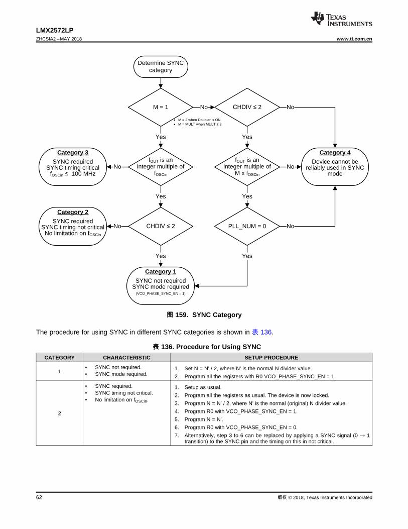
M = 1 &+',9���2
No
Category 4
Yes
fOUT is aninteger multiple of
M x fOSCin
x� M = 2 when Doubler is ONx� M = 08/7�ZKHQ�08/7���3
No
Yes
PLL_NUM = 0
Yes
fOUT is aninteger multiple of
fOSCin
Category 3
No
Yes
&+',9���2
Category 2
No
Determine SYNC category
Category 1
Yes Yes
SYNC requiredSYNC timing not critical
No limitation on fOSCin
SYNC requiredSYNC timing critical
fOSCin ���100 MHz
Device cannot be reliably used in SYNC
mode
NoNo
SYNC not requiredSYNC mode required
(VCO_PHASE_SYNC_EN = 1)
62
LMX2572LPZHCSIA2 –MAY 2018 www.ti.com.cn
版权 © 2018, Texas Instruments Incorporated
图图 159. SYNC Category
The procedure for using SYNC in different SYNC categories is shown in 表 136.
表表 136. Procedure for Using SYNCCATEGORY CHARACTERISTIC SETUP PROCEDURE
1• SYNC not required.• SYNC mode required.
1. Set N = N' / 2, where N' is the normal N divider value.2. Program all the registers with R0 VCO_PHASE_SYNC_EN = 1.
2
• SYNC required.• SYNC timing not critical.• No limitation on fOSCin.
1. Setup as usual.2. Program all the registers as usual. The device is now locked.3. Program N = N' / 2, where N' is the normal (original) N divider value.4. Program R0 with VCO_PHASE_SYNC_EN = 1.5. Program N = N'.6. Program R0 with VCO_PHASE_SYNC_EN = 0.7. Alternatively, step 3 to 6 can be replaced by applying a SYNC signal (0 → 1
transition) to the SYNC pin and the timing on this in not critical.

SYNC100
LMX2572LP
63
LMX2572LPwww.ti.com.cn ZHCSIA2 –MAY 2018
版权 © 2018, Texas Instruments Incorporated
表表 136. Procedure for Using SYNC (接接下下页页)CATEGORY CHARACTERISTIC SETUP PROCEDURE
3
• SYNC required.• SYNC timing critical.• fOSCin ≤ 100 MHz
1. Ensure that the maximum fOSCin for SYNC is not violated and there arehardware accommodations to use the SYNC pin.
2. Set N = N' / 2, where N' is the normal N divider (integer + fraction) value.3. Program all the registers with R0 VCO_PHASE_SYNC_EN = 1.4. Apply a SYNC signal (0 → 1 transition) to the SYNC pin. The timing of the
SYNC signal as shown in Timing Requirements must be obey.
Set these bits to drive the SYNC pin with a LVDS signal:• Set INPIN_FMT to 1 or 3 to enable LVDS input• Set INPIN_LVL to one of the options• Set INPIN_HYST, if necessary
The LVDS driver that is driving the SYNC pin should be configured as shown in 图 160:
图图 160. Driving SYNC Pin With Differential Signal
8.1.7 Application for Ramp
8.1.7.1 Manual Ramping ModeManual ramping is enabled when the user sets RAMP_EN = 1 and RAMP_MANUAL = 1. In this mode, the rampis clocked by the rising edges applied to the RampClk pin. The size of the frequency change is defined byRAMP0_INC and RAMP1_INC. If a LOW is seen at the RampDir pin on the rising edge of RampClk, the outputfrequency will be incremented by RAMP0_INC. On the contrary, the output frequency will be incremented byRAMP1_INC if a HIGH is captured. If a rising edge is seen on the RampClk pin while the VCO is calibrating, thenthis rising edge is ignored. The frequency for the RampClk must be limited to a frequency of 250 kHz or less, andthe rising edge of the RampDir signal must be targeted to the falling edge of the RampClk pin. The necessaryregister fields for use in manual ramping mode are shown in 表 137.
表表 137. Manual Ramping Mode ProgrammingREGISTER FIELD VALUE DESCRIPTION
RAMP_EN 1 = Enable ramp Set this bit to 1 to enable frequency ramping.
RAMP_MANUAL 1 = Manual rampingmode To select manual ramping mode, set this bit to 1.
RAMP_LIMIT_HIGHGreater than thehighest VCO rampfrequency
This sets the upper ramp limit that the ramp cannot go above. Suppose fHigh is thisfrequency and fStart is the starting VCO ramp frequency, then, for fHigh > fStart,RAMP_LIMIT_HIGH = 224 × (fHigh – fStart) / fPD
RAMP_LIMIT_LOWSmaller than thelowest VCO rampfrequency
This sets the lower ramp limit that the ramp cannot go below. Suppose fLow is this frequencyand fStart is the starting VCO ramp frequency, then, for fStart > fLow,RAMP_LIMIT_LOW = 233 – 224 × (fStart – fLow) / fPD
RAMP0_INCRAMP1_INC
Equal to the rampsize
Suppose the ramp size is Δf, thenRAMPx_INC = (Δf / fPD) × 224 or = 230 – (Δf / fPD) × 224 if Δf is a negative number.
RAMP_THRESH Suggest less than 50MHz
If the amount of frequency ramp exceeds this threshold, a VCO calibration will be initiated.For example, if the ramp size is 50 MHz while this threshold is 30 MHz, then VCOcalibration will be executed every time it ramps. Suppose the threshold frequency is fTH,thenRAMP_THRESH = (fTH / fPD) × 224
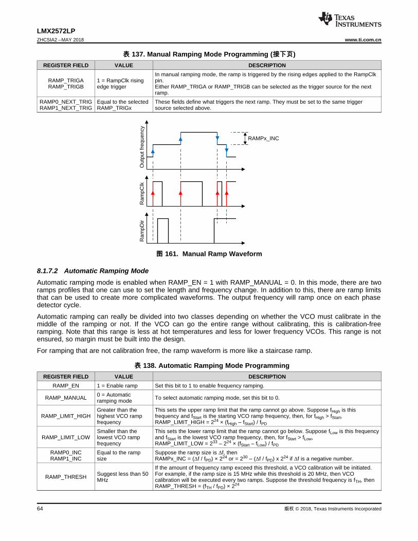
RAMPx_INCO
utpu
t fre
quen
cyR
ampC
lkR
ampD
ir
64
LMX2572LPZHCSIA2 –MAY 2018 www.ti.com.cn
版权 © 2018, Texas Instruments Incorporated
表表 137. Manual Ramping Mode Programming (接接下下页页)REGISTER FIELD VALUE DESCRIPTION
RAMP_TRIGARAMP_TRIGB
1 = RampClk risingedge trigger
In manual ramping mode, the ramp is triggered by the rising edges applied to the RampClkpin.Either RAMP_TRIGA or RAMP_TRIGB can be selected as the trigger source for the nextramp.
RAMP0_NEXT_TRIGRAMP1_NEXT_TRIG
Equal to the selectedRAMP_TRIGx
These fields define what triggers the next ramp. They must be set to the same triggersource selected above.
图图 161. Manual Ramp Waveform
8.1.7.2 Automatic Ramping ModeAutomatic ramping mode is enabled when RAMP_EN = 1 with RAMP_MANUAL = 0. In this mode, there are tworamps profiles that one can use to set the length and frequency change. In addition to this, there are ramp limitsthat can be used to create more complicated waveforms. The output frequency will ramp once on each phasedetector cycle.
Automatic ramping can really be divided into two classes depending on whether the VCO must calibrate in themiddle of the ramping or not. If the VCO can go the entire range without calibrating, this is calibration-freeramping. Note that this range is less at hot temperatures and less for lower frequency VCOs. This range is notensured, so margin must be built into the design.
For ramping that are not calibration free, the ramp waveform is more like a staircase ramp.
表表 138. Automatic Ramping Mode ProgrammingREGISTER FIELD VALUE DESCRIPTION
RAMP_EN 1 = Enable ramp Set this bit to 1 to enable frequency ramping.
RAMP_MANUAL 0 = Automaticramping mode To select automatic ramping mode, set this bit to 0.
RAMP_LIMIT_HIGHGreater than thehighest VCO rampfrequency
This sets the upper ramp limit that the ramp cannot go above. Suppose fHigh is thisfrequency and fStart is the starting VCO ramp frequency, then, for fHigh > fStart,RAMP_LIMIT_HIGH = 224 × (fHigh – fStart) / fPD
RAMP_LIMIT_LOWSmaller than thelowest VCO rampfrequency
This sets the lower ramp limit that the ramp cannot go below. Suppose fLow is this frequencyand fStart is the lowest VCO ramp frequency, then, for fStart > fLow,RAMP_LIMIT_LOW = 233 – 224 × (fStart – fLow) / fPD
RAMP0_INCRAMP1_INC
Equal to the rampsize
Suppose the ramp size is Δf, thenRAMPx_INC = (Δf / fPD) × 224 or = 230 – (Δf / fPD) x 224 if Δf is a negative number.
RAMP_THRESH Suggest less than 50MHz
If the amount of frequency ramp exceed this threshold, a VCO calibration will be initiated.For example, if the ramp size is 15 MHz while this threshold is 20 MHz, then VCOcalibration will be executed every two ramps. Suppose the threshold frequency is fTH, thenRAMP_THRESH = (fTH / fPD) × 224
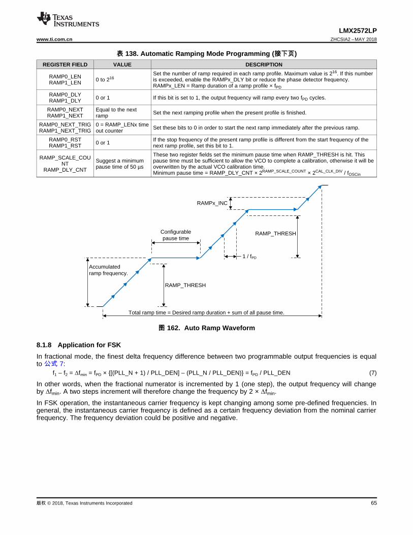
1 / fPD
Configurable pause time
Accumulated ramp frequency.
RAMP_THRESH
Total ramp time = Desired ramp duration + sum of all pause time.
RAMP_THRESH
RAMPx_INC
65
LMX2572LPwww.ti.com.cn ZHCSIA2 –MAY 2018
版权 © 2018, Texas Instruments Incorporated
表表 138. Automatic Ramping Mode Programming (接接下下页页)REGISTER FIELD VALUE DESCRIPTION
RAMP0_LENRAMP1_LEN 0 to 216
Set the number of ramp required in each ramp profile. Maximum value is 216. If this numberis exceeded, enable the RAMPx_DLY bit or reduce the phase detector frequency.RAMPx_LEN = Ramp duration of a ramp profile × fPD
RAMP0_DLYRAMP1_DLY 0 or 1 If this bit is set to 1, the output frequency will ramp every two fPD cycles.
RAMP0_NEXTRAMP1_NEXT
Equal to the nextramp Set the next ramping profile when the present profile is finished.
RAMP0_NEXT_TRIGRAMP1_NEXT_TRIG
0 = RAMP_LENx timeout counter Set these bits to 0 in order to start the next ramp immediately after the previous ramp.
RAMP0_RSTRAMP1_RST 0 or 1 If the stop frequency of the present ramp profile is different from the start frequency of the
next ramp profile, set this bit to 1.
RAMP_SCALE_COUNT
RAMP_DLY_CNT
Suggest a minimumpause time of 50 µs
These two register fields set the minimum pause time when RAMP_THRESH is hit. Thispause time must be sufficient to allow the VCO to complete a calibration, otherwise it will beoverwritten by the actual VCO calibration time.Minimum pause time = RAMP_DLY_CNT × 2RAMP_SCALE_COUNT × 2CAL_CLK_DIV / fOSCin
图图 162. Auto Ramp Waveform
8.1.8 Application for FSKIn fractional mode, the finest delta frequency difference between two programmable output frequencies is equalto 公式 7:
f1 – f2 = Δfmin = fPD × {[(PLL_N + 1) / PLL_DEN] – (PLL_N / PLL_DEN)} = fPD / PLL_DEN (7)
In other words, when the fractional numerator is incremented by 1 (one step), the output frequency will changeby Δfmin. A two steps increment will therefore change the frequency by 2 × Δfmin.
In FSK operation, the instantaneous carrier frequency is kept changing among some pre-defined frequencies. Ingeneral, the instantaneous carrier frequency is defined as a certain frequency deviation from the nominal carrierfrequency. The frequency deviation could be positive and negative.
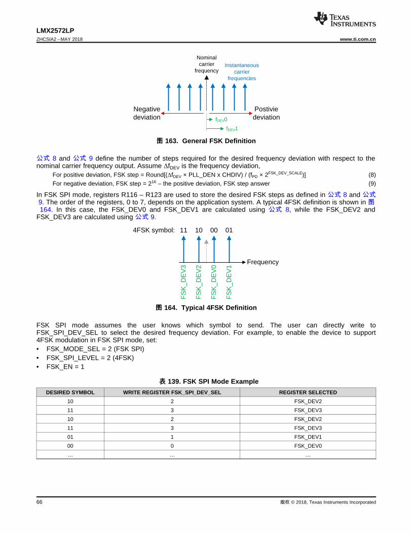
Frequency
FS
K_D
EV
3
00 01
FS
K_D
EV
2
FS
K_D
EV
0
FS
K_D
EV
14FSK symbol: 1011
fDEV0
fDEV1
Negative deviation
Postivie deviation
Nominal carrier
frequencyInstantaneous
carrier frequencies
66
LMX2572LPZHCSIA2 –MAY 2018 www.ti.com.cn
版权 © 2018, Texas Instruments Incorporated
图图 163. General FSK Definition
公式 8 and 公式 9 define the number of steps required for the desired frequency deviation with respect to thenominal carrier frequency output. Assume ΔfDEV is the frequency deviation,
For positive deviation, FSK step = Round[(ΔfDEV × PLL_DEN x CHDIV) / (fPD × 2FSK_DEV_SCALE)] (8)For negative deviation, FSK step = 216 – the positive deviation, FSK step answer (9)
In FSK SPI mode, registers R116 – R123 are used to store the desired FSK steps as defined in 公式 8 and 公式9. The order of the registers, 0 to 7, depends on the application system. A typical 4FSK definition is shown in 图164. In this case, the FSK_DEV0 and FSK_DEV1 are calculated using 公式 8, while the FSK_DEV2 and
FSK_DEV3 are calculated using 公式 9.
图图 164. Typical 4FSK Definition
FSK SPI mode assumes the user knows which symbol to send. The user can directly write toFSK_SPI_DEV_SEL to select the desired frequency deviation. For example, to enable the device to support4FSK modulation in FSK SPI mode, set:• FSK_MODE_SEL = 2 (FSK SPI)• FSK_SPI_LEVEL = 2 (4FSK)• FSK_EN = 1
表表 139. FSK SPI Mode ExampleDESIRED SYMBOL WRITE REGISTER FSK_SPI_DEV_SEL REGISTER SELECTED
10 2 FSK_DEV211 3 FSK_DEV310 2 FSK_DEV211 3 FSK_DEV301 1 FSK_DEV100 0 FSK_DEV0… … …
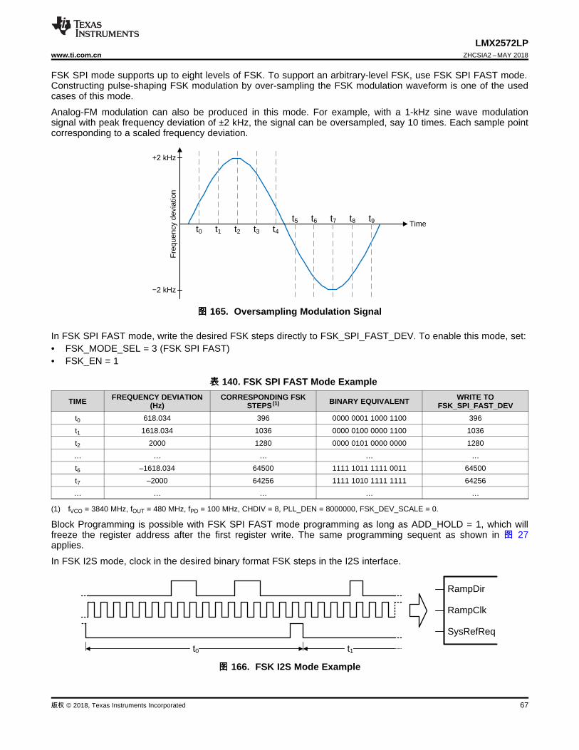
RampDir
t0 t1
RampClk
SysRefReq
Time
Fre
quen
cy d
evia
tion
t0 t1 t2 t3 t4t5 t6 t7 t8 t9
+2 kHz
í2 kHz
67
LMX2572LPwww.ti.com.cn ZHCSIA2 –MAY 2018
版权 © 2018, Texas Instruments Incorporated
(1) fVCO = 3840 MHz, fOUT = 480 MHz, fPD = 100 MHz, CHDIV = 8, PLL_DEN = 8000000, FSK_DEV_SCALE = 0.
FSK SPI mode supports up to eight levels of FSK. To support an arbitrary-level FSK, use FSK SPI FAST mode.Constructing pulse-shaping FSK modulation by over-sampling the FSK modulation waveform is one of the usedcases of this mode.
Analog-FM modulation can also be produced in this mode. For example, with a 1-kHz sine wave modulationsignal with peak frequency deviation of ±2 kHz, the signal can be oversampled, say 10 times. Each sample pointcorresponding to a scaled frequency deviation.
图图 165. Oversampling Modulation Signal
In FSK SPI FAST mode, write the desired FSK steps directly to FSK_SPI_FAST_DEV. To enable this mode, set:• FSK_MODE_SEL = 3 (FSK SPI FAST)• FSK_EN = 1
表表 140. FSK SPI FAST Mode Example
TIME FREQUENCY DEVIATION(Hz)
CORRESPONDING FSKSTEPS (1) BINARY EQUIVALENT WRITE TO
FSK_SPI_FAST_DEVt0 618.034 396 0000 0001 1000 1100 396t1 1618.034 1036 0000 0100 0000 1100 1036t2 2000 1280 0000 0101 0000 0000 1280… … … … …t6 –1618.034 64500 1111 1011 1111 0011 64500t7 –2000 64256 1111 1010 1111 1111 64256… … … … …
Block Programming is possible with FSK SPI FAST mode programming as long as ADD_HOLD = 1, which willfreeze the register address after the first register write. The same programming sequent as shown in 图 27applies.
In FSK I2S mode, clock in the desired binary format FSK steps in the I2S interface.
图图 166. FSK I2S Mode Example

CP
out V
tune
1
2
3
4
5
6
7
8
9
10
1 1 1 2 1 3 1 4 1 5 1 6 1 7 1 8
3 6 3 5 3 4 3 3 3 2 3 1
30
29
28
27
26
25
24
23
22
21
2 01 9
3 73 83 94 0
C1
C2
R2
R3
C3
68
LMX2572LPZHCSIA2 –MAY 2018 www.ti.com.cn
版权 © 2018, Texas Instruments Incorporated
To enable FSK I2S mode, set• INPIN_IGNORE = 0• FSK_MODE_SEL = 1 (FSK I2S)• FSK_EN = 1
8.1.9 Unused PinsTI recommends to pull these pins low if they are not used:• Pin 5, SYNC• Pin 28, SysRefReq• Pin 30, RampClk• Pin 32, RampDir
8.1.10 External Loop FilterThe LMX2572LP requires an external loop filter that is application-specific and can be configured by PLLatinumSim. For the LMX2572LP, it matters what impedance is seen from the Vtune pin looking outwards. Thisimpedance is dominated by the component C3 for a third order filter or C1 for a second order filter. If there is atleast 1.5 nF for the capacitance that is shunt with this pin, the VCO phase noise will be close to the best it canbe. If there is less, the VCO phase noise in the 100-kHz to 1-MHz region will degrade. This capacitor should beplaced close to the Vtune pin.
图图 167. External Loop Filter
8.1.11 Power-Up, Wake-Up TimeWhen the device comes out of the powered-down state, either by resuming the POWERDOWN bit to zero or bypulling back CE pin HIGH (if it was powered down by CE pin), it takes time for the device to acquire lock again.This wake-up time depends on LDO_DLY setting, loop bandwidth, and the state machine clock frequency (=fOSCin / 2CAL_CLK_DIV). If the loop bandwidth is greater than 20 kHz, the wake-up time could be adjusted to lessthan 1.5 ms with the LDO_DLY setting listed in 表 141.
表表 141. LDO_DLY SettingSTATE MACHINE CLOCK
FREQUENCY LDO_DLY
130 MHz ≤ f ≤ 200MHz 880 MHz ≤ f < 130 MHz 550 MHz ≤ f < 80 MHz 330 MHz ≤ f < 50 MHz 2
f < 30 MHz 1
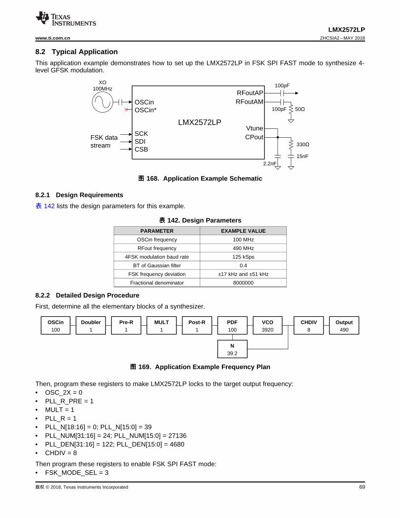
OSCin100
Doubler1
Pre-R1
MULT1
Post-R1
PDF100
VCO3920
CHDIV8
Output490
N39.2
OSCinOSCin*
RFoutAPRFoutAM
SCKSDICSB
CPout
100pF
XO 100MHz
15nF2.2nF
330�
100pF
50
VtuneFSK data stream
LMX2572LP
69
LMX2572LPwww.ti.com.cn ZHCSIA2 –MAY 2018
版权 © 2018, Texas Instruments Incorporated
8.2 Typical ApplicationThis application example demonstrates how to set up the LMX2572LP in FSK SPI FAST mode to synthesize 4-level GFSK modulation.
图图 168. Application Example Schematic
8.2.1 Design Requirements表 142 lists the design parameters for this example.
表表 142. Design ParametersPARAMETER EXAMPLE VALUE
OSCin frequency 100 MHzRFout frequency 490 MHz
4FSK modulation baud rate 125 kSpsBT of Gaussian filter 0.4
FSK frequency deviation ±17 kHz and ±51 kHzFractional denominator 8000000
8.2.2 Detailed Design ProcedureFirst, determine all the elementary blocks of a synthesizer.
图图 169. Application Example Frequency Plan
Then, program these registers to make LMX2572LP locks to the target output frequency:• OSC_2X = 0• PLL_R_PRE = 1• MULT = 1• PLL_R = 1• PLL_N[18:16] = 0; PLL_N[15:0] = 39• PLL_NUM[31:16] = 24; PLL_NUM[15:0] = 27136• PLL_DEN[31:16] = 122; PLL_DEN[15:0] = 4680• CHDIV = 8
Then program these registers to enable FSK SPI FAST mode:• FSK_MODE_SEL = 3

Mathlab
Creates and generates
codes
DG2020
Generates the electrical
signals
LMX2572LP
SCKSDICSB
CLK
DATA
LE
Signal Analyzer
70
LMX2572LPZHCSIA2 –MAY 2018 www.ti.com.cn
版权 © 2018, Texas Instruments Incorporated
• FSK_DEV_SCALE = 1• FSK_EN = 1
A Mathlab script is then developed to generate the necessary codes that will be used to continuously bit-streamthe LMX2572LP. These codes are uploaded to the data generator DG2020, which will generate the SPI data tomodulate the LMX2572LP.
图图 170. Application Example Test Setup
8.2.3 Application Curves
图图 171. Gaussian 4FSK Modulated Spectrum 图图 172. Gaussian 4FSK Modulation Quality
8.3 Do's and Don'ts• RFout output buffers do not need an external pullup. An AC-couple to the load is good enough.• The last shunt capacitor of the loop filter should be placed close to the Vtune pin.

CP
out V
tune
1
2
3
4
5
6
7
8
9
10
1 1 1 2 1 3 1 4 1 5 1 6 1 7 1 8
3 6 3 5 3 4 3 3 3 2 3 1
30
29
28
27
26
25
24
23
22
21
2 01 9
3 73 83 94 0
CP
out V
tune
1
2
3
4
5
6
7
8
9
10
1 1 1 2 1 3 1 4 1 5 1 6 1 7 1 8
3 6 3 5 3 4 3 3 3 2 3 1
30
29
28
27
26
25
24
23
22
21
2 01 9
3 73 83 94 0
RFout RFout
VCC
X
X
71
LMX2572LPwww.ti.com.cn ZHCSIA2 –MAY 2018
版权 © 2018, Texas Instruments Incorporated
Do's and Don'ts (接接下下页页)
图图 173. Do's and Don'ts
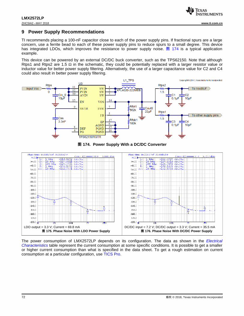
72
LMX2572LPZHCSIA2 –MAY 2018 www.ti.com.cn
版权 © 2018, Texas Instruments Incorporated
9 Power Supply RecommendationsTI recommends placing a 100-nF capacitor close to each of the power supply pins. If fractional spurs are a largeconcern, use a ferrite bead to each of these power supply pins to reduce spurs to a small degree. This devicehas integrated LDOs, which improves the resistance to power supply noise. 图 174 is a typical applicationexample.
This device can be powered by an external DC/DC buck converter, such as the TPS62150. Note that althoughRtps1 and Rtps2 are 1.5 Ω in the schematic, they could be potentially replaced with a larger resistor value orinductor value for better power supply filtering. Alternatively, the use of a larger capacitance value for C2 and C4could also result in better power supply filtering.
图图 174. Power Supply With a DC/DC Converter
LDO output = 3.3 V; Current = 69.8 mA图图 175. Phase Noise With LDO Power Supply
DC/DC input = 7.2 V; DC/DC output = 3.3 V; Current = 35.5 mA图图 176. Phase Noise With DC/DC Power Supply
The power consumption of LMX2572LP depends on its configuration. The data as shown in the ElectricalCharacteristics table represent the current consumption at some specific conditions. It is possible to get a smalleror higher current consumption than what is specified in the data sheet. To get a rough estimation on currentconsumption at a particular configuration, use TICS Pro.

73
LMX2572LPwww.ti.com.cn ZHCSIA2 –MAY 2018
版权 © 2018, Texas Instruments Incorporated
10 Layout
10.1 Layout GuidelinesIn general, the layout guidelines are similar to most other PLL devices. Here are some specific guidelines:• GND pins may be routed on the package back to the DAP.• The OSCin pins are internally biased and must be AC-coupled.• The RampClk, RampDir, and SysRefReq can be grounded to the DAP if not used.• Get a loop filter capacitor as close to the Vtune pin as possible to this. This may mean separating it from the
rest of the loop filter.• If a single-ended output is necessary, the other side must have the same loading. However, the routing for
the used side can be optimized by routing the complementary side through a via to the other side of theboard. On this side, make the load look equivalent to the side that is used.
• Ensure the DAP on the device is well-grounded with many vias, preferably copper filled.• Have a thermal pad that is as large as the exposed pad. Add vias to the thermal pad to maximize thermal
performance.
10.2 Layout Example
图图 177. Layout Example
74
LMX2572LPZHCSIA2 –MAY 2018 www.ti.com.cn
版权 © 2018, Texas Instruments Incorporated
11 器器件件和和文文档档支支持持
11.1 器器件件支支持持
11.1.1 开开发发支支持持
德州仪器 (TI) 在 www.ti.com.cn 提供了多种辅助开发的软件工具。其中包括:
• PLLatinum Sim 程序,用于设计回路滤波器以及对相位噪声和杂散进行仿真。
• TICS Pro 软件,用于了解如何对器件和 EVM 板进行编程。
11.2 文文档档支支持持
11.2.1 相相关关文文档档
请参阅如下相关文档:
• 《带有 DCS-Control 的 TPS62150 3V 至 17V 1A 降压转换器》(SLVSAL5)• 《AN-1879 分数 N 频率合成》(SNAA062)• 《通过 LMX2571 实现移频键控》(SNAA309)• 《PLL 性能、仿真和设计手册》(SNAA106)• 《LMX2572LPEVM 用户指南》(SNAU235)
11.3 接接收收文文档档更更新新通通知知
要接收文档更新通知,请导航至 TI.com.cn 上的器件产品文件夹。单击右上角的通知我 进行注册,即可每周接收产品信息更改摘要。有关更改的详细信息,请查看任何已修订文档中包含的修订历史记录。
11.4 社社区区资资源源
下列链接提供到 TI 社区资源的连接。链接的内容由各个分销商“按照原样”提供。这些内容并不构成 TI 技术规范,并且不一定反映 TI 的观点;请参阅 TI 的 《使用条款》。TI E2E™ 在在线线社社区区 TI 的的工工程程师师对对工工程程师师 (E2E) 社社区区。。此社区的创建目的在于促进工程师之间的协作。在
e2e.ti.com 中,您可以咨询问题、分享知识、拓展思路并与同行工程师一道帮助解决问题。设设计计支支持持 TI 参参考考设设计计支支持持可帮助您快速查找有帮助的 E2E 论坛、设计支持工具以及技术支持的联系信息。
11.5 商商标标
E2E is a trademark of Texas Instruments.All other trademarks are the property of their respective owners.
11.6 静静电电放放电电警警告告ESD 可能会损坏该集成电路。德州仪器 (TI) 建议通过适当的预防措施处理所有集成电路。如果不遵守正确的处理措施和安装程序 , 可能会损坏集成电路。
ESD 的损坏小至导致微小的性能降级 , 大至整个器件故障。 精密的集成电路可能更容易受到损坏 , 这是因为非常细微的参数更改都可能会导致器件与其发布的规格不相符。
11.7 术术语语表表
SLYZ022 — TI 术语表。
这份术语表列出并解释术语、缩写和定义。
12 机机械械、、封封装装和和可可订订购购信信息息
以下页面包含机械、封装和可订购信息。这些信息是指定器件的最新可用数据。数据如有变更,恕不另行通知,且不会对此文档进行修订。如需获取此数据表的浏览器版本,请查阅左侧的导航栏。
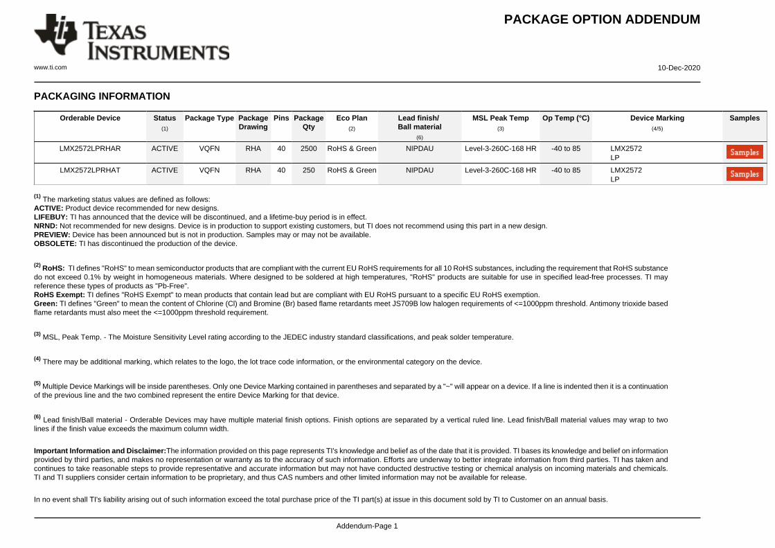
PACKAGE OPTION ADDENDUM
www.ti.com 10-Dec-2020
Addendum-Page 1
PACKAGING INFORMATION
Orderable Device Status(1)
Package Type PackageDrawing
Pins PackageQty
Eco Plan(2)
Lead finish/Ball material
(6)
MSL Peak Temp(3)
Op Temp (°C) Device Marking(4/5)
Samples
LMX2572LPRHAR ACTIVE VQFN RHA 40 2500 RoHS & Green NIPDAU Level-3-260C-168 HR -40 to 85 LMX2572LP
LMX2572LPRHAT ACTIVE VQFN RHA 40 250 RoHS & Green NIPDAU Level-3-260C-168 HR -40 to 85 LMX2572LP
(1) The marketing status values are defined as follows:ACTIVE: Product device recommended for new designs.LIFEBUY: TI has announced that the device will be discontinued, and a lifetime-buy period is in effect.NRND: Not recommended for new designs. Device is in production to support existing customers, but TI does not recommend using this part in a new design.PREVIEW: Device has been announced but is not in production. Samples may or may not be available.OBSOLETE: TI has discontinued the production of the device.
(2) RoHS: TI defines "RoHS" to mean semiconductor products that are compliant with the current EU RoHS requirements for all 10 RoHS substances, including the requirement that RoHS substancedo not exceed 0.1% by weight in homogeneous materials. Where designed to be soldered at high temperatures, "RoHS" products are suitable for use in specified lead-free processes. TI mayreference these types of products as "Pb-Free".RoHS Exempt: TI defines "RoHS Exempt" to mean products that contain lead but are compliant with EU RoHS pursuant to a specific EU RoHS exemption.Green: TI defines "Green" to mean the content of Chlorine (Cl) and Bromine (Br) based flame retardants meet JS709B low halogen requirements of <=1000ppm threshold. Antimony trioxide basedflame retardants must also meet the <=1000ppm threshold requirement.
(3) MSL, Peak Temp. - The Moisture Sensitivity Level rating according to the JEDEC industry standard classifications, and peak solder temperature.
(4) There may be additional marking, which relates to the logo, the lot trace code information, or the environmental category on the device.
(5) Multiple Device Markings will be inside parentheses. Only one Device Marking contained in parentheses and separated by a "~" will appear on a device. If a line is indented then it is a continuationof the previous line and the two combined represent the entire Device Marking for that device.
(6) Lead finish/Ball material - Orderable Devices may have multiple material finish options. Finish options are separated by a vertical ruled line. Lead finish/Ball material values may wrap to twolines if the finish value exceeds the maximum column width.
Important Information and Disclaimer:The information provided on this page represents TI's knowledge and belief as of the date that it is provided. TI bases its knowledge and belief on informationprovided by third parties, and makes no representation or warranty as to the accuracy of such information. Efforts are underway to better integrate information from third parties. TI has taken andcontinues to take reasonable steps to provide representative and accurate information but may not have conducted destructive testing or chemical analysis on incoming materials and chemicals.TI and TI suppliers consider certain information to be proprietary, and thus CAS numbers and other limited information may not be available for release.
In no event shall TI's liability arising out of such information exceed the total purchase price of the TI part(s) at issue in this document sold by TI to Customer on an annual basis.
PACKAGE OPTION ADDENDUM
www.ti.com 10-Dec-2020
Addendum-Page 2
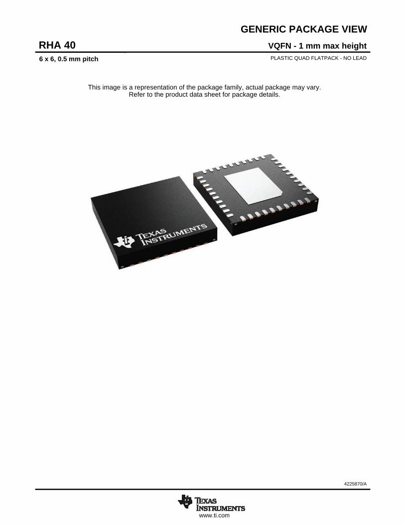
www.ti.com
GENERIC PACKAGE VIEW
This image is a representation of the package family, actual package may vary.Refer to the product data sheet for package details.
VQFN - 1 mm max heightRHA 40PLASTIC QUAD FLATPACK - NO LEAD6 x 6, 0.5 mm pitch
4225870/A

www.ti.com
PACKAGE OUTLINE
C
40X 0.30.2
4.5 0.1
40X 0.50.3
1 MAX
(0.2) TYP
0.050.00
36X 0.5
2X4.5
2X 4.5
A 6.15.9
B
6.15.9
0.30.2
0.50.3
(0.1)
VQFN - 1 mm max heightRHA0040HPLASTIC QUAD FLATPACK - NO LEAD
4219055/B 08/22/2019
PIN 1 INDEX AREA
0.08 C
SEATING PLANE
1
10 21
30
11 20
40 31
(OPTIONAL)PIN 1 ID 0.1 C A B
0.05
EXPOSEDTHERMAL PAD
DETAILSEE TERMINAL
SYMM
SYMM
NOTES: 1. All linear dimensions are in millimeters. Any dimensions in parenthesis are for reference only. Dimensioning and tolerancing per ASME Y14.5M. 2. This drawing is subject to change without notice. 3. The package thermal pad must be soldered to the printed circuit board for thermal and mechanical performance.
41
SEE SIDE WALLDETAIL
SCALE 2.200
DETAILOPTIONAL TERMINAL
TYPICAL
SIDE WALL DETAILOPTIONAL METAL THICKNESS
www.ti.com
EXAMPLE BOARD LAYOUT
0.07 MINALL AROUND
0.07 MAXALL AROUND
40X (0.25)
40X (0.6)
( 0.2) TYPVIA
36X (0.5)
(5.8)
(5.8)
( 4.5)
(R0.05)TYP
4X(1.46)
4X(1.27)
(0.73) TYP
4X (1.27)
(0.73)TYP
4X (1.46)
VQFN - 1 mm max heightRHA0040HPLASTIC QUAD FLATPACK - NO LEAD
4219055/B 08/22/2019
SYMM
1
10
11 20
21
30
3140
SYMM
LAND PATTERN EXAMPLEEXPOSED METAL SHOWN
SCALE:12X
41
NOTES: (continued) 4. This package is designed to be soldered to a thermal pad on the board. For more information, see Texas Instruments literature number SLUA271 (www.ti.com/lit/slua271).5. Vias are optional depending on application, refer to device data sheet. If any vias are implemented, refer to their locations shown on this view. It is recommended that vias under paste be filled, plugged or tented.
SOLDER MASKOPENING
METAL UNDERSOLDER MASK
SOLDER MASKDEFINED
EXPOSED METALMETAL
SOLDER MASKOPENING
SOLDER MASK DETAILS
NON SOLDER MASKDEFINED
(PREFERRED)
EXPOSED METAL
www.ti.com
EXAMPLE STENCIL DESIGN
40X (0.6)
40X (0.25)
36X (0.5)
(5.8)
(5.8)
9X ( 1.26)
(1.46)TYP
(1.46) TYP
(R0.05) TYP
VQFN - 1 mm max heightRHA0040HPLASTIC QUAD FLATPACK - NO LEAD
4219055/B 08/22/2019
NOTES: (continued) 6. Laser cutting apertures with trapezoidal walls and rounded corners may offer better paste release. IPC-7525 may have alternate design recommendations.
SYMM
METALTYP
SOLDER PASTE EXAMPLEBASED ON 0.125 mm THICK STENCIL
EXPOSED PAD 41:
70% PRINTED SOLDER COVERAGE BY AREASCALE:15X
SYMM
1
10
11 20
21
30
3140
41
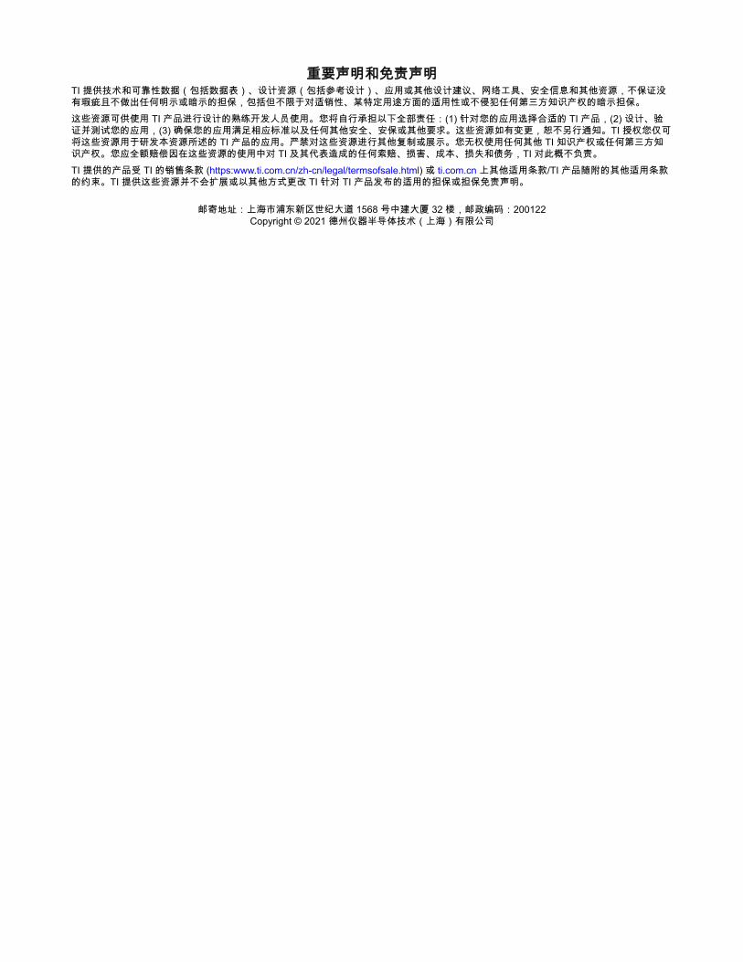
重要声明和免责声明TI 提供技术和可靠性数据(包括数据表)、设计资源(包括参考设计)、应用或其他设计建议、网络工具、安全信息和其他资源,不保证没有瑕疵且不做出任何明示或暗示的担保,包括但不限于对适销性、某特定用途方面的适用性或不侵犯任何第三方知识产权的暗示担保。这些资源可供使用 TI 产品进行设计的熟练开发人员使用。您将自行承担以下全部责任:(1) 针对您的应用选择合适的 TI 产品,(2) 设计、验证并测试您的应用,(3) 确保您的应用满足相应标准以及任何其他安全、安保或其他要求。这些资源如有变更,恕不另行通知。TI 授权您仅可将这些资源用于研发本资源所述的 TI 产品的应用。严禁对这些资源进行其他复制或展示。您无权使用任何其他 TI 知识产权或任何第三方知识产权。您应全额赔偿因在这些资源的使用中对 TI 及其代表造成的任何索赔、损害、成本、损失和债务,TI 对此概不负责。TI 提供的产品受 TI 的销售条款 (https:www.ti.com.cn/zh-cn/legal/termsofsale.html) 或 ti.com.cn 上其他适用条款/TI 产品随附的其他适用条款的约束。TI 提供这些资源并不会扩展或以其他方式更改 TI 针对 TI 产品发布的适用的担保或担保免责声明。IMPORTANT NOTICE
邮寄地址:上海市浦东新区世纪大道 1568 号中建大厦 32 楼,邮政编码:200122Copyright © 2021 德州仪器半导体技术(上海)有限公司