- 1 - November 6, 2009 Dr. John S. Bird School of Engineering ...
25
Copyright ©, 2009 Prospect1 Inc. - 1 - November 6, 2009 Dr. John S. Bird School of Engineering Science, Simon Fraser University, Burnaby, BC, V5A 1S6 Re: ENSC 440 Design Specifications for Auto-Splice Conductivity Analyzer Dear Dr. Bird: The attached document from Prospect1 Inc. outlines design specifications for the Auto- Splice Conductivity Analyzer (ASCA). ASCA is a device that can be used to analyze the imbalance of current flow in splices of an ACSR (Aluminum Conductor Steel Reinforced) overhead wire joint. By investigating current flow patterns, the user can identify the extent of damage present in the splice connecting the wires. The ‘Design Specifications’ outlines necessary design considerations that need to be taken care of in order for the ASCA device to perform its desired tasks. This document also lists test plans to ensure proper operation of our product. Design improvements for future iterations of the device are also discussed here, but, will not be implemented at this stage of development. Prospect1 Inc. consists of four enthusiastic and hard working fourth year Engineering Science students: Sam Hoque, Amir Najafzadeh, Milad Moezzie and Zhouhao Cui. We are very excited about the opportunity this project may hold in lessening the failure rates of automatic splices in overhead distribution systems. Please feel welcome to contact us if you have any questions or concerns by phone at (778) 229-9190 or by e-mail at [email protected] Sincerely yours, Amir NajafZadeh CEO Prospect1 Inc. Enclosure: Design Specifications for Auto-Splice Conductivity Analyzer
-
Upload
khangminh22 -
Category
Documents
-
view
1 -
download
0
Transcript of - 1 - November 6, 2009 Dr. John S. Bird School of Engineering ...

Copyright ©, 2009 Prospect1 Inc. - 1 -
November 6, 2009
Dr. John S. Bird
School of Engineering Science,
Simon Fraser University,
Burnaby, BC, V5A 1S6
Re: ENSC 440 Design Specifications for Auto-Splice Conductivity Analyzer
Dear Dr. Bird:
The attached document from Prospect1 Inc. outlines design specifications for the Auto-
Splice Conductivity Analyzer (ASCA). ASCA is a device that can be used to analyze the
imbalance of current flow in splices of an ACSR (Aluminum Conductor Steel
Reinforced) overhead wire joint. By investigating current flow patterns, the user can
identify the extent of damage present in the splice connecting the wires.
The ‘Design Specifications’ outlines necessary design considerations that need to be
taken care of in order for the ASCA device to perform its desired tasks. This document
also lists test plans to ensure proper operation of our product. Design improvements for
future iterations of the device are also discussed here, but, will not be implemented at this
stage of development.
Prospect1 Inc. consists of four enthusiastic and hard working fourth year Engineering
Science students: Sam Hoque, Amir Najafzadeh, Milad Moezzie and Zhouhao Cui. We
are very excited about the opportunity this project may hold in lessening the failure rates
of automatic splices in overhead distribution systems. Please feel welcome to contact us
if you have any questions or concerns by phone at (778) 229-9190 or by e-mail at
Sincerely yours,
Amir NajafZadeh
CEO Prospect1 Inc.
Enclosure: Design Specifications for Auto-Splice Conductivity Analyzer
Copyright ©, 2009 Prospect1 Inc. - 2 -
Design Specifications for
Auto-Splice Conductivity Analyzer
Project Team: Sam Hoque
Amir Najafzadeh
Zhouhao Cui
Mlad Moezzie
Contact Person: Sam Hoque
Submitted to: Dr. John Bird
Steve Whitmore
Jason Lee
School of Engineering Science
Simon Fraser University
Issued date: November 6, 2009
Revision: 1.5
Copyright ©, 2009 Prospect1 Inc. - 3 -
Executive Summary This list of design specifications mentioned here is suited for the proof-of-concept model
and will detail our proposed implementation of phases I and II of the Functional
Specifications for Auto-Splice Conductivity Analyzer (ASCA) [1]. This document outlines
the design of the ASCA device as well as theoretical and practical justifications for these
design choices.
This document contains an overview of system specifications for the ASCA Device. It
includes high level system design, graphics, comparison and evaluation for chosen
components, as well as low level descriptions of major functional units as the user
interface unit and control unit. This document also details the choice of hardware
components as the MCU, Hall Effect Sensors utilized herein and the choice of software
environment and the reasoning behind it. General software program process flow is also
included here. Moreover, the functional, performance, and user acceptance test plans
have been detailed here as well.
Development of the ASCA device is divided in to two phases. Upon completion of the
first phase, the device will be able to obtain data regarding magnetic field intensity
around live wire utilizing the Hall Effect Sensors and store them in a microcontroller.
The microcontroller will read inputs from the Hall Effect Sensors, apply a differentiating
algorithm, and save the data on the built-in memory.
In the second phase, this data will be sent to the output and displayed on the user
interface unit. The user interface unit consists of a few LEDs and an LCD. During this
phase, the casing of the device will also be prepared and the product will reach
completion. The first prototype is expected to conform to these design specifications by
the scheduled completion date of December 15, 2009.
Copyright ©, 2009 Prospect1 Inc. - 4 -
Table of Contents
List of Figures ..................................................................................................................... 5
List of Tables ...................................................................................................................... 5
Glossary .............................................................................................................................. 6
1. Introduction..................................................................................................................... 7
1.1 Scope......................................................................................................................... 7
1.2 Intended Audience .................................................................................................... 7
2 System Specifications ...................................................................................................... 8
3 Overall System Design .................................................................................................... 8
3.1 High Level System Design ....................................................................................... 8
3.2 Control Unit .............................................................................................................. 9
3.3 User Interface Unit.................................................................................................... 9
4 Control Unit ..................................................................................................................... 9
4.1 DN6847 Hall Effect Sensors..................................................................................... 9
4.2 Arduino Duemilanove Micro Controller ................................................................ 11
4.3 Software Environment ............................................................................................ 13
5 User Interface Unit......................................................................................................... 14
5.1 Input ........................................................................................................................ 14
5.1.1 On/Off Switch.................................................................................................. 14
5.2 Output ..................................................................................................................... 15
5.2.1 LCD Display .................................................................................................... 15
5.2.2 3mm Type 01 553-xxxx-300 LEDs ................................................................. 16
5.2.3 Tyco FSM Series tact pushbutton .................................................................... 17
6 Mechanical Design......................................................................................................... 17
7 Environmental Considerations....................................................................................... 20
8 System Test Plan............................................................................................................ 20
9 Future upgrades.............................................................................................................. 24
9.1 Hall Effect Sensor Noise Reducing Circuit ............................................................ 24

Copyright ©, 2009 Prospect1 Inc. - 5 -
9.2 Integrating Hot Stick and separating the user interface unit................................... 24
10 Conclusion ................................................................................................................... 24
11 References.................................................................................................................... 25
List of Figures Figure 3.1: High-Level Functional Block Diagram.....................................................................8
Figure 4.1.1: Pin diagram and Positioning Instructions for DN6847 Hall Effect Sensors.....10
Figure 4.2.1: The Arduino Duemilanove PIC board which uses the Atmel ATmega328
chip.................................................................................................................................................11
Figure 4.2.2: Pin diagram and CPU Architecture of the Atmel ATmega328 chip………….13
Figure 5.1.1: Push Button……………………………………………………………………….14
Figure 5.2.1: TS1620-1 LCD……………………………………………………………………15
Figure 5.2.2: 3mm Type 01 553-xxxx-300 LEDs………………………………………………16
Figure 6.1: Mechanical Design of the ASCA device…………………………………………..18
Figure 6.2: Flowchart of functionality for the ASCA device…………………………………19
Figure 8.1: High-Level Block Diagram for System Test Plan………………………………..21
List of Tables Table 4.1.1: Properties of DN6847 Hall Effect Sensors.............................................................10
Table 4.2.1: Properties of the Atmel ATmega328 chip………………………………………..12
Table 5.1.1: Properties of Tyco FSM Series tact pushbutton………………………………...14
Table 5.2.1: Properties of the TS1620-1 LCD……………………………………………........15
Table 5.2.2: Properties of 3mm Type 01 553-xxxx-300 LEDs………………………………..17
Table 8.1: Unit test description……………………………………………………………........21
Table 8.2: Constituent test description………………………………………………………...22
Copyright ©, 2009 Prospect1 Inc. - 6 -
Glossary
ASCA Auto-Splice Conductivity Analyzer
ACSR Aluminum Conductor Steel Reinforced (overhead wire)
LCD Liquid Crystal Display
LED Light Emitting Diode
MCU Arduino Duemilanove Micro Controller
Splice An electrical splice is the joining of two or more electrical
conductors by mechanically twisting them together or by
using a special splicing device [2]
Hot Stick An insulated rod usually made of fiber glass. It can be of
extendable length [3]
User Certified Technicians/Electricians who are authorized to
perform maintenance and testing on overhead transmission
lines
PIC Programmable Intelligent Computer
CPU Central Processing Unit
PVC Polyvinyl Cholride (A durable, easy to use polymer)
RoHS Restriction of the Use of Certain Hazardous Substances in
Electrical and Electronic Equipment Regulations
Copyright ©, 2009 Prospect1 Inc. - 7 -
1. Introduction Auto-Splice Conductivity Analyzer (ASCA) is designed to determine current imbalance
in overhead transmission line cable splices [2]. As splices age, Aluminum components
oxidize to form an insulating barrier, thereby increasing their resistance and causing a
current imbalance in cables’ strands [4]. From the resulting magnetic field around the
cables’ strands, this imbalance can be found, and used to verify if the splice is faulty. The
device has an LCD on it, which shows the intensity of the magnetic field around the
splice. There are also a couple of LEDs on the device, which lets the user know if the
intensity of the magnetic field is within range or out of range. ASCA can be attached to
the overhead wire as a slide-on device to obtain data using a hot stick [3]. The design
requirements for the ASCA device, as well as the reasoning behind it are described in this
document.
1.1 Scope
The design specification shall meet all requirements for a proof-of-concept system and a
partial set of requirements for a production model mentioned in the document: Functional
Specifications for Auto-Splice Conductivity Analyzer [1]. As we are focusing on the
proof-of-concept system for now, design considerations pertaining to the functional
requirements marked Type I will be primarily discussed here. Simplified algorithms and
design schematics will be used to explain various concepts. More detailed diagrams will
be included as appendices for referencing purposes.
1.2 Intended Audience
- Project managers shall use it to evaluate progress throughout different
development phases. It will also assist them in complying with necessary
manufacturing and usability standards.
- Design engineers shall follow this document to meet overall design requirements
from production to implementation of device.
- Test engineers shall use this document to assess the match in functionality
between the actual device and the guidelines outlined here.
- Marketing department may also use this document to develop marketing
materials and identify similarities in features (if any) with competitor’s products.
Copyright ©, 2009 Prospect1 Inc. - 8 -
2 System Specifications The ASCA device will assist in locating faulty splices on overhead transmission lines.
Once the user uses a hot stick to mount and slide the ASCA device along the length of a
splice on overhead transmission lines,
- The device will measure the intensity of magnetic field along the length of a
splice which connects two live wires.
- The device then compares this measurement with an ‘ideal scenario’ measurement
(which has been taken earlier) where all the strands in a splice were intact.
- The MCU built in the device then sends this measurement as output to the user
interface unit. The user interface unit consists of a LCD and a few LEDs.
3 Overall System Design This section provides a general, high-level explanation of the ASCA device, as well as a
short summary of the design characteristics of each component. More detail information
about individual components will be furnished in a well fashioned manner later.
3.1 High Level System Design
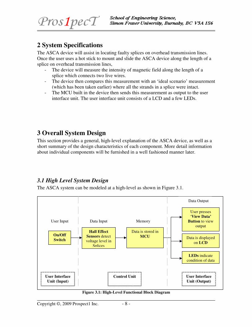
The ASCA system can be modeled at a high-level as shown in Figure 3.1.
Figure 3.1: High-Level Functional Block Diagram
Data Input User Input
On/Off
Switch
LEDs indicate
condition of data
User Interface
Unit (Input)
User Interface
Unit (Output)
Control Unit
Data is displayed
on LCD
Memory
Hall Effect
Sensors detect
voltage level in
Splices
Data is stored in
MCU
User presses
‘View Data’
Button to view
output
Data Output

Copyright ©, 2009 Prospect1 Inc. - 9 -
3.2 Control Unit
It is made up of an Arduino Duemilanove Micro Controller (MCU) and a couple of
DN6847 Hall Effect Sensors. This is the heart of the device and takes care of most of the
functionality of the device. Primary functions of the control unit include:
- To obtain data through the Hall Effect Sensors.
- To store data in MCU.
- To convert the information received from analog to digital.
- To send the output display to the LCD.
- To send output information to appropriate LEDs.
3.3 User Interface Unit
The user interface unit can be subdivided in to two components, the input and the output.
The input is an ‘On/Off’ switch while the output consists of a push button, LCD and three
LEDs. The device is turned on by pushing the ‘On/Off’ switch by the user. After
obtaining data, the user presses the ‘View Data’ button to observe captured data. This is
when stored data is displayed on the LCD along with an LED indicator. There are three
LEDs on the device and they represent the following:
- Green LED: Data is within optimal range.
- Red LED: Data is out of range.
- Blue LED: Data is irrelevant or there is insufficient data.
4 Control Unit The control unit consists of two primary components: two DN6847 Hall Effect Sensors
and an Arduino Duemilanove Micro Controller (MCU). The software and the
environment used to integrate the control unit with the user interface unit are also
discussed here.
4.1 DN6847 Hall Effect Sensors
DN6847 Hall Effect Sensors are chosen to measure the magnetic field intensity around
live wire splices. An alternating current carrying conductor produces a magnetic field
around it. The functionality of these chips is very simple in nature as they are able to
measure this magnetic field intensity directly, once placed near (within mechanical
tolerance) a current conducting splice. Two sensors are used instead of one for precision
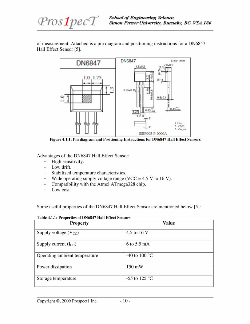
Copyright ©, 2009 Prospect1 Inc. - 10 -
of measurement. Attached is a pin diagram and positioning instructions for a DN6847
Hall Effect Sensor [5].
Figure 4.1.1: Pin diagram and Positioning Instructions for DN6847 Hall Effect Sensors
Advantages of the DN6847 Hall Effect Sensor:
- High sensitivity.
- Low drift.
- Stabilized temperature characteristics.
- Wide operating supply voltage range (VCC = 4.5 V to 16 V).
- Compatibility with the Atmel ATmega328 chip.
- Low cost.
Some useful properties of the DN6847 Hall Effect Sensor are mentioned below [5]:
Table 4.1.1: Properties of DN6847 Hall Effect Sensors
Property Value
Supply voltage (VCC) 4.5 to 16 V
Supply current (ICC) 6 to 5.5 mA
Operating ambient temperature -40 to 100 °C
Power dissipation 150 mW
Storage temperature -55 to 125 °C
Copyright ©, 2009 Prospect1 Inc. - 11 -
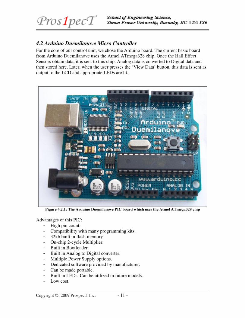
4.2 Arduino Duemilanove Micro Controller
For the core of our control unit, we chose the Arduino board. The current basic board
from Arduino Duemilanove uses the Atmel ATmega328 chip. Once the Hall Effect
Sensors obtain data, it is sent to this chip. Analog data is converted to Digital data and
then stored here. Later, when the user presses the ‘View Data’ button, this data is sent as
output to the LCD and appropriate LEDs are lit.
Figure 4.2.1: The Arduino Duemilanove PIC board which uses the Atmel ATmega328 chip
Advantages of this PIC:
- High pin count.
- Compatibility with many programming kits.
- 32kb built in flash memory.
- On-chip 2-cycle Multiplier.
- Built in Bootloader.
- Built in Analog to Digital converter.
- Multiple Power Supply options.
- Dedicated software provided by manufacturer.
- Can be made portable.
- Built in LEDs. Can be utilized in future models.
- Low cost.

Copyright ©, 2009 Prospect1 Inc. - 12 -
Some useful properties of the Atmel ATmega328 chip are mentioned below [6]:
Table 4.2.1: Properties of the Atmel ATmega328 chip
Property Value
Operating Temp –40°C to 85°C
Power Consumption At 1 MHz, 1.8V, 25°C
– Active Mode: 0.2 mA
– Power-down Mode: 0.1 µA
– Power-save Mode: 0.75 µA
Operating Voltage 1.8 - 5.5V
Memory 32KB
Registers 32 x 8
Speed Grade: 0 - 20 MHz @ 1.8 - 5.5V
Timer/Counters Two 8-bit or One 16-bit
I/O and Packages 23 Programmable I/O Lines
Write/Erase Cycles 10,000 Flash/100,000 EEPROM
Single Clock Cycle Execution 131
PWM Channels 6
Data retention 20 years at 85°C/100 years at 25°C
Copyright ©, 2009 Prospect1 Inc. - 13 -
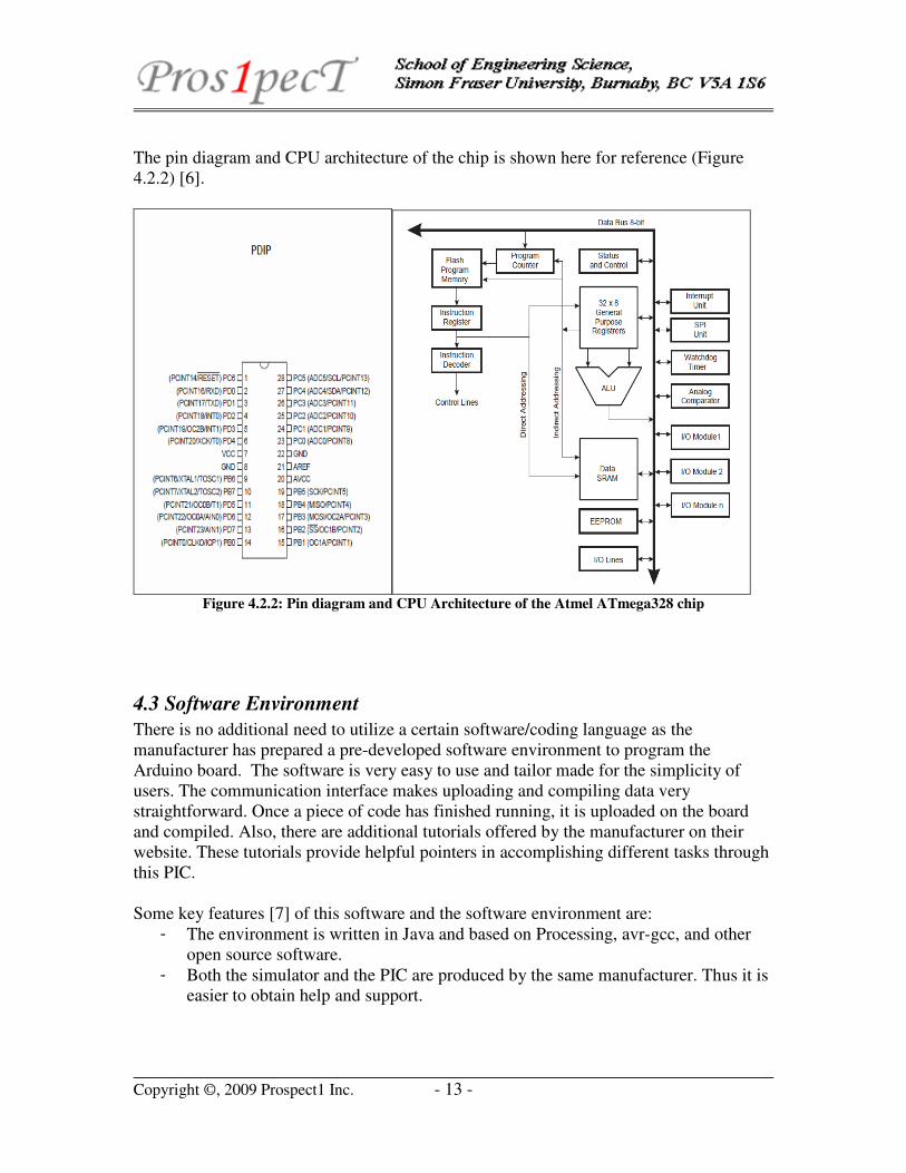
The pin diagram and CPU architecture of the chip is shown here for reference (Figure
4.2.2) [6].
Figure 4.2.2: Pin diagram and CPU Architecture of the Atmel ATmega328 chip
4.3 Software Environment
There is no additional need to utilize a certain software/coding language as the
manufacturer has prepared a pre-developed software environment to program the
Arduino board. The software is very easy to use and tailor made for the simplicity of
users. The communication interface makes uploading and compiling data very
straightforward. Once a piece of code has finished running, it is uploaded on the board
and compiled. Also, there are additional tutorials offered by the manufacturer on their
website. These tutorials provide helpful pointers in accomplishing different tasks through
this PIC.
Some key features [7] of this software and the software environment are:
- The environment is written in Java and based on Processing, avr-gcc, and other
open source software.
- Both the simulator and the PIC are produced by the same manufacturer. Thus it is
easier to obtain help and support.
Copyright ©, 2009 Prospect1 Inc. - 14 -
5 User Interface Unit The user interface unit is divided in to two parts, the input and the output. The input
consists of an ‘On/Off’ switch. And the output comprises of a push button, a LCD and
three LEDs.
5.1 Input
A momentary-on pushbutton is used as the ‘On/Off’ switch for this device. The user
presses this switch to turn on the device. Once turned on, it is mounted on a hot stick to
slide along a splice’s length.
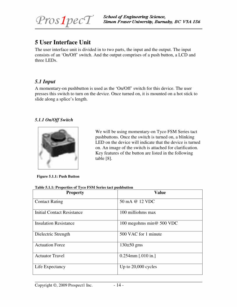
5.1.1 On/Off Switch
Figure 5.1.1: Push Button
We will be using momentary-on Tyco FSM Series tact
pushbuttons. Once the switch is turned on, a blinking
LED on the device will indicate that the device is turned
on. An image of the switch is attached for clarification.
Key features of the button are listed in the following
table [8].
Table 5.1.1: Properties of Tyco FSM Series tact pushbutton
Property Value
Contact Rating 50 mA @ 12 VDC
Initial Contact Resistance 100 milliohms max
Insulation Resistance 100 megohms min@ 500 VDC
Dielectric Strength 500 VAC for 1 minute
Actuation Force 130±50 gms
Actuator Travel 0.254mm [.010 in.]
Life Expectancy Up to 20,000 cycles
Copyright ©, 2009 Prospect1 Inc. - 15 -
Advantages of the Tyco FSM Series tact pushbutton:
- Low cost.
- Durability.
- Long Lasting.
- Easy to use.
5.2 Output
The output has three components: a TS1620-1 LCD, three 3mm Type 01 553-xxxx-300
LEDs and a Tyco FSM Series tact pushbutton.
5.2.1 LCD Display
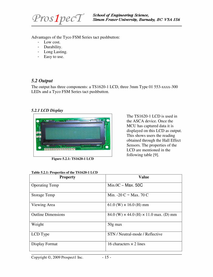
Figure 5.2.1: TS1620-1 LCD
The TS1620-1 LCD is used in
the ASCA device. Once the
MCU has captured data it is
displayed on this LCD as output.
This shows users the reading
obtained through the Hall Effect
Sensors. The properties of the
LCD are mentioned in the
following table [9].
Table 5.2.1: Properties of the TS1620-1 LCD
Property Value
Operating Temp Min.0C ~ Max. 50C
Storage Temp Min. -20 C ~ Max. 70 C
Viewing Area 61.0 (W) × 16.0 (H) mm
Outline Dimensions 84.0 (W) × 44.0 (H) × 11.0 max. (D) mm
Weight 50g max
LCD Type STN / Neutral-mode / Reflective
Display Format 16 characters × 2 lines
Copyright ©, 2009 Prospect1 Inc. - 16 -
Display Fonts 5 × 8 dots ( 1 character)
Viewing Angle 6:00
Backlight None
Advantages of the TS1620-1 LCD:
- Can display two lines of characters and numbers. This feature can be utilized for
future upgrades on the model.
- Low cost and durable.
- Light weight.
- Long Lasting and easy to use.
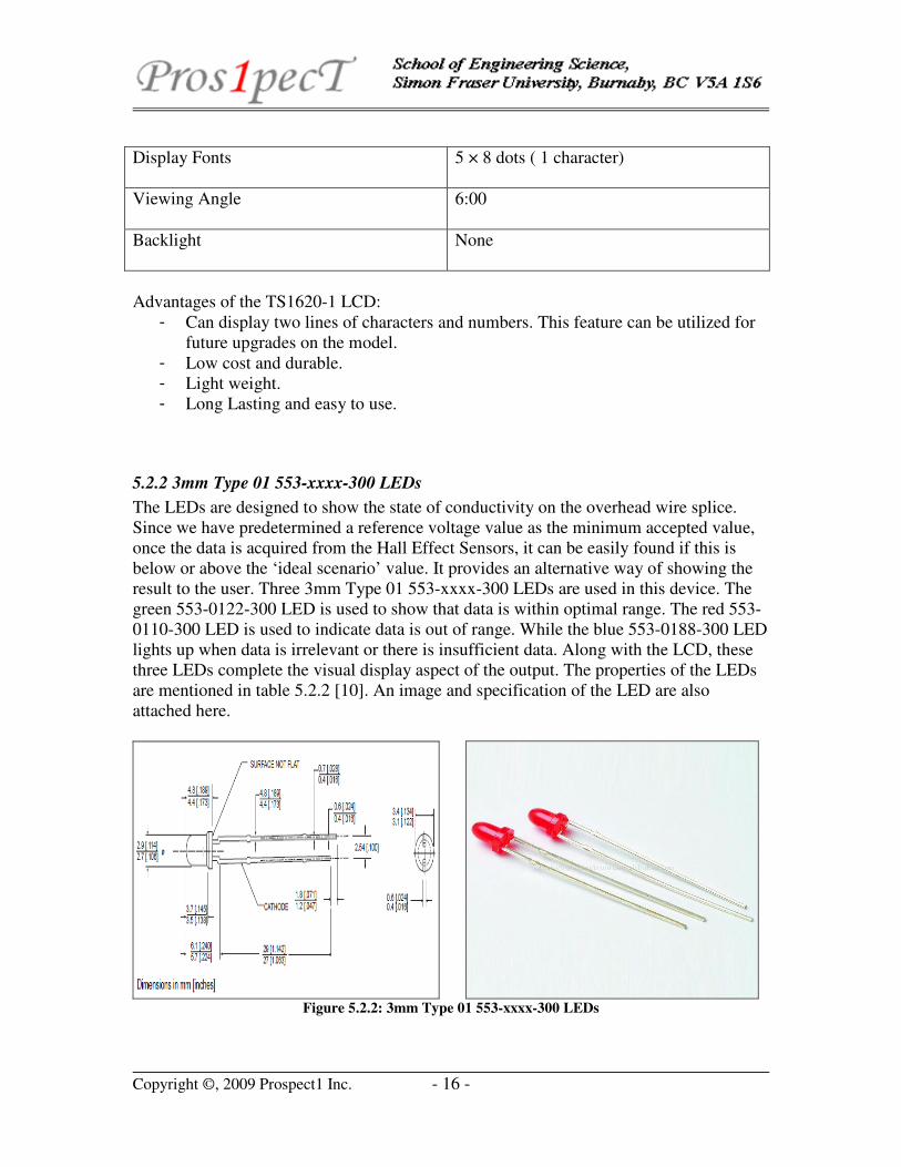
5.2.2 3mm Type 01 553-xxxx-300 LEDs
The LEDs are designed to show the state of conductivity on the overhead wire splice.
Since we have predetermined a reference voltage value as the minimum accepted value,
once the data is acquired from the Hall Effect Sensors, it can be easily found if this is
below or above the ‘ideal scenario’ value. It provides an alternative way of showing the
result to the user. Three 3mm Type 01 553-xxxx-300 LEDs are used in this device. The
green 553-0122-300 LED is used to show that data is within optimal range. The red 553-
0110-300 LED is used to indicate data is out of range. While the blue 553-0188-300 LED
lights up when data is irrelevant or there is insufficient data. Along with the LCD, these
three LEDs complete the visual display aspect of the output. The properties of the LEDs
are mentioned in table 5.2.2 [10]. An image and specification of the LED are also
attached here.
Figure 5.2.2: 3mm Type 01 553-xxxx-300 LEDs
Copyright ©, 2009 Prospect1 Inc. - 17 -
Table 5.2.2: Properties of 3mm Type 01 553-xxxx-300 LEDs
Property Red Green Blue Unit
Peak Wavelength 635 565 428 Nm
LV 10 16 12 mCd
VF 2 2.1 3.5 V
Test Current 10 10 10 mA
Viewing Angle 45 45 70 °
Operating Temperature Range -40~85 °C
Storage Temperature Range -25~85 °C
Advantages of 3mm Type 01 553-xxxx-300 LEDs:
- Low cost and performance.
- Optimal operating range of temperature.
- Durability.
- Long Lasting and easy to use.
5.2.3 Tyco FSM Series tact pushbutton
Another Tyco FSM Series tact pushbutton is used to View Data. This is the same
pushbutton switch used to turn on the device. Due to its similarity, lightweight and ease
of functionality this switch is used. Specifications and advantages of this switch can be
found in section 5.1.1.
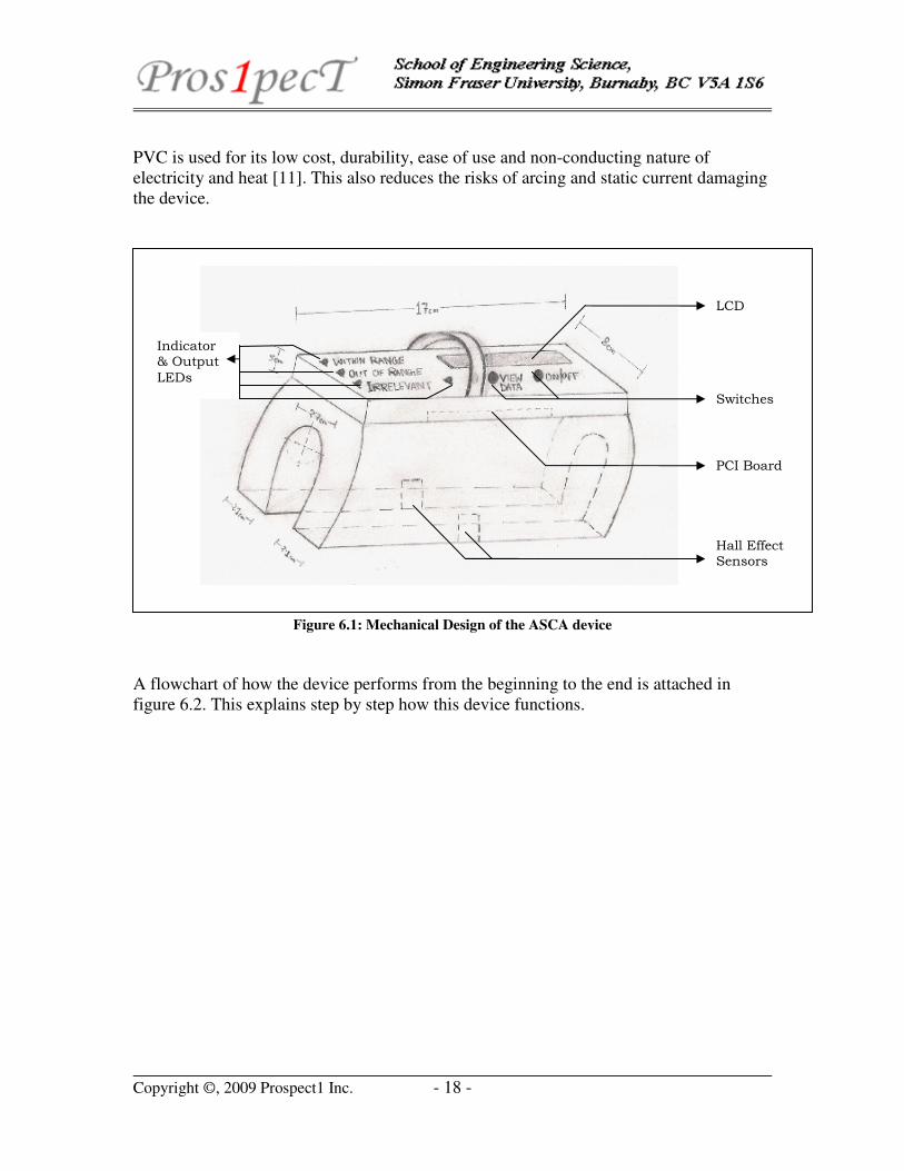
6 Mechanical Design Casing for the ASCA device and its dimensions are shown in figure 6.1. The device is
mostly made of PVC material. The LCD, switches and LEDs are mounted on the user
interface unit, which is made of PVC cuboids. Underneath the user interface unit lays the
Arduino Duemilanove PIC. All the wire connections and soldering are hidden by this
case. There is also a PVC hook in the middle of its top surface. This is used to mount the
device on a splice using a hot stick.
The cylindrical shaped component, also made of PVC material, holds the Hall Effect
Sensors. Wire connections are etched along its walls and connect to the PIC.
Copyright ©, 2009 Prospect1 Inc. - 18 -
PVC is used for its low cost, durability, ease of use and non-conducting nature of
electricity and heat [11]. This also reduces the risks of arcing and static current damaging
the device.
Figure 6.1: Mechanical Design of the ASCA device
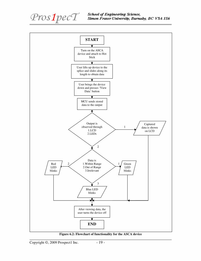
A flowchart of how the device performs from the beginning to the end is attached in
figure 6.2. This explains step by step how this device functions.
Indicator
& Output
LEDs
LCD
Switches
PCI Board
Hall Effect
Sensors
Copyright ©, 2009 Prospect1 Inc. - 19 -
Figure 6.2: Flowchart of functionality for the ASCA device
2
3
2
START
User brings the device
down and presses ‘View
Data’ button
User lifts up device to the
splice and slides along its
length to obtain data
Turn on the ASCA
device and attach to Hot
Stick
MCU sends stored
data to the output
Output is
observed through
1.LCD
2.LEDs
1
1
After viewing data, the
user turns the device off
END
Captured
data is shown
on LCD
Green
LED
blinks
Red
LED
blinks
Blue LED
blinks
Data is
1.Within Range
2.Out of Range
3.Irrelevant

Copyright ©, 2009 Prospect1 Inc. - 20 -
7 Environmental Considerations
• Prospect1 Inc. has paid utmost attention and degree of care to the environmental
aspect of the design during the device’s production and distribution. The
components chosen for the device adhere to RoHS directives [12]. It limits the
release of dangerous chemicals such as lead, cadmium and mercury into the
environment. It also protects the user from emissions of these dangerous
components. The device is ‘lead’ free; both in its components and during
soldering.
• The device is able to run and operate with minimal power consumption. The
ASCA device does not need a lot of power to function.
• In case the device reaches the end of its useful life, the user is provided with
complete information on proper disposal and recycling of the electronic device
and battery.
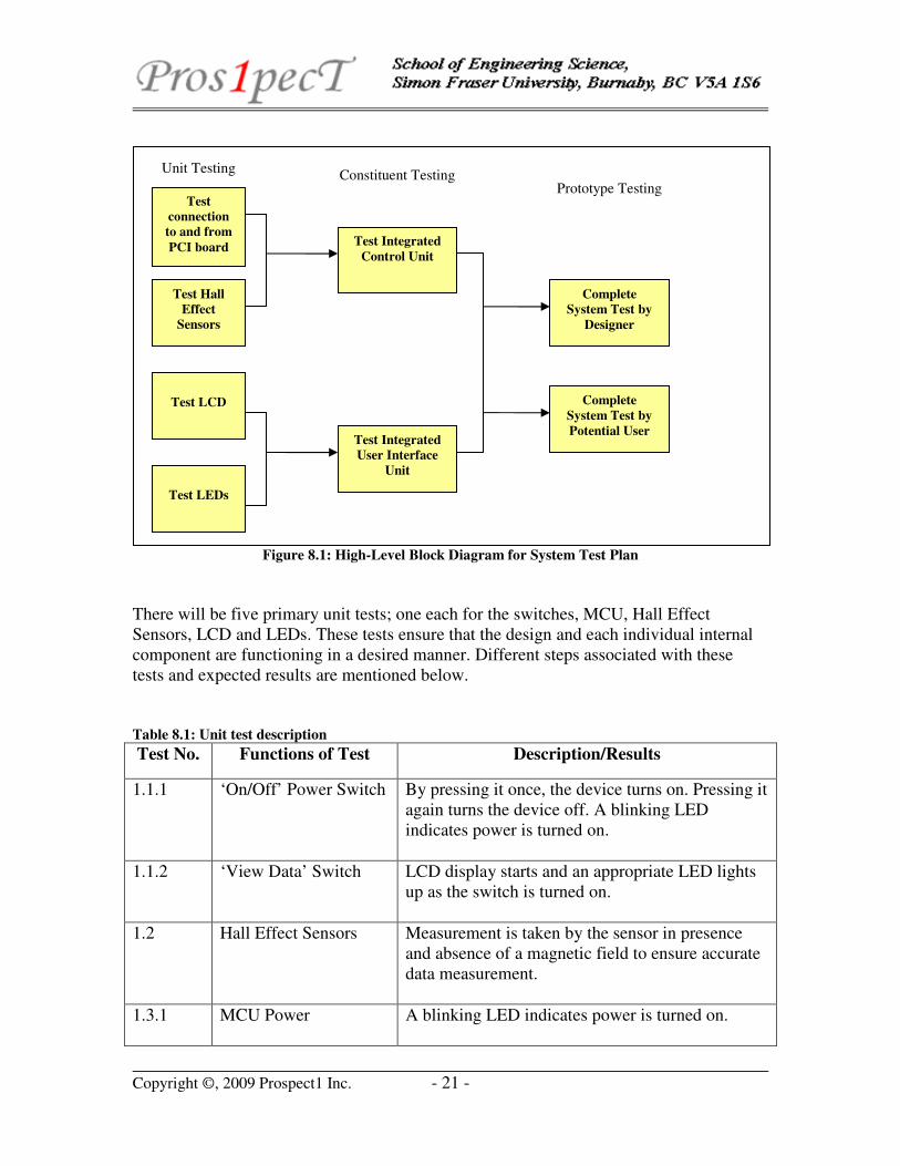
8 System Test Plan In order for the system to function in a reliable manner, it is necessary to test it during
different stages of design and implementation, prototype building and manufacturing. To
avoid errors, the general test plan is to test each module as it is built, and to retest the
modules upon integration into a complete unit. Device specifications mentioned in
functional specifications [1] emphasize on boundary conditions that should be taken care
of throughout the design. From designing this device to building a prototype, the tests
associated with various stages can be divided in to three main categories. For this project,
they will be named as unit testing, constituent testing and prototype testing.
Copyright ©, 2009 Prospect1 Inc. - 21 -
Figure 8.1: High-Level Block Diagram for System Test Plan
There will be five primary unit tests; one each for the switches, MCU, Hall Effect
Sensors, LCD and LEDs. These tests ensure that the design and each individual internal
component are functioning in a desired manner. Different steps associated with these
tests and expected results are mentioned below.
Table 8.1: Unit test description
Test No. Functions of Test Description/Results
1.1.1 ‘On/Off’ Power Switch By pressing it once, the device turns on. Pressing it
again turns the device off. A blinking LED
indicates power is turned on.
1.1.2 ‘View Data’ Switch LCD display starts and an appropriate LED lights
up as the switch is turned on.
1.2 Hall Effect Sensors Measurement is taken by the sensor in presence
and absence of a magnetic field to ensure accurate
data measurement.
1.3.1 MCU Power A blinking LED indicates power is turned on.
Test Integrated
Control Unit
Test Hall
Effect
Sensors
Test LCD
Test LEDs
Unit Testing
Test
connection
to and from
PCI board
Test Integrated
User Interface
Unit
Constituent Testing
Complete
System Test by
Designer
Complete
System Test by
Potential User
Prototype Testing
Copyright ©, 2009 Prospect1 Inc. - 22 -
1.3.2 MCU Data Storage A stack register can be used to note if the MCU
memory is getting filled as the sensors keep on
capturing data.
1.3.3 MCU Output LCD display shows measurement and an LED
lights up accordingly.
1.4.1 LCD Display (idle
state)
No data is displayed before the ‘View Data’
Switch is pressed.
1.4.2 LCD Display (active
state)
Measured data is displayed after the ‘View Data’
Switch is pressed.
1.5.1 LED (idle state) None of the LEDs are lit before the ‘View Data’
Switch is pressed.
1.5.2 LED (active state) According to range of data, suitable LED lights up
after the ‘View Data’ Switch is pressed.
Once satisfactory results are obtained through unit tests, next step is to perform
constituent testing. At this stage, the design gets divided into smaller building blocks. For
example, the user interface unit and the control unit.
Table 8.2: Constituent test description
Test No. Description of Tests
2.1 Hall Effect Sensors and MCU
- When the sensors are placed close to an alternating current conductor,
they measure the magnetic field intensity and this data is then sent to
the MCU to convert from analog to digital and store in its memory.
Once again a stack register can be used to notice if the memory is
getting filled. As the sensors are connected to the MCU here, if the
memory starts getting full, this test will confirm that the connection
between the sensors and the MCU are as desired.
- This would also ensure that the sensors are placed within threshold
distance form the conducting wire/splice to measure magnetic field
intensity.
2.2 LED, LCD and the MCU
- The following three tests determine if the connection from the MCU
Copyright ©, 2009 Prospect1 Inc. - 23 -
to the output (LED, LCD) is intact and if the device is providing its
output as desired.
2.2.1 LED and the MCU
- The MCU sends output to the LEDs when ‘View Data’ button is
pressed. According to the range of data the corresponding LED lights
up. The LED display should also be in sync with the LCD.
2.2.2 LCD and the MCU
- The MCU sends output data to the LCD when ‘View Data’ button is
pressed. Measured magnetic field intensity is displayed on the LCD.
The LCD display should also be in sync with the LEDs.
2.2.3 LCD and LEDs
- According to the measured reading on the LCD a corresponding LED
should light up. For example, if the data is out of range, the red LED
lights up. Thus the display on the LCD should match the LED light to
confirm the device’s accurate functionality.
The last step in the system test plan is prototype testing. After the smaller blocks pass
constituent testing, they are ready for integration. Once integrated, prototype testing can
make sure that the smaller blocks put together are functioning well and are in cohesion.
At this stage, boundary conditions shall be tested in greater details again. This may give
the designers an idea on how well the functionality of the device in different conditions
matches its functional specifications. It may also be a good idea to have potential users
try the prototype before commercialization or mass production of this device is done.
Their feedback may point to any negativity in the device or lead to possible upgrades and
improvements for future.
At this stage of testing, the ASCA device is tested by the user as a complete unit. Detail
functionalities described in functional specifications [1] are tested and made sure the
device is working as it is supposed to.
If at any point of the building process, a change in either design or raw material was
found necessary, the system shall be tested again from the stage where changes were
needed.
Copyright ©, 2009 Prospect1 Inc. - 24 -
9 Future upgrades
9.1 Hall Effect Sensor Noise Reducing Circuit
This is a very simple circuitry that might be used to reduce introduced noise. Although
the effect of this circuit can be minimal, this can be particularly useful where the data is
irrelevant. In such cases, some data signals exceed the maximum or minimum allowable
range. This circuit can then be useful in distinguishing between useful and distorted data.
9.2 Integrating Hot Stick and separating the user interface unit
The ASCA device has multiple power sources. This of course gives the device added
portability as well as a chance to power/operate the device from a laptop or an alternating
power source. In future models, for instantaneous observations, the user interface unit can
be separated and held in hand while the rest of the device is mounted on overhead wire.
For this model to be produced, wiring needs to be incorporated with the hot stick.
10 Conclusion The ‘Design Specifications for an Auto Splice Conductivity Analyzer’ provides a clear
and concise overview of our projected design. This is very much in correlation with the
functional specification [1]. There is a comparative analysis outlined here for each
component, which explains why they were chosen for the ASCA device. Extensive test
plans ensure the device meets its goals during the manufacturing and production phases.
This is not a rigid design as there is room for future improvement.
Copyright ©, 2009 Prospect1 Inc. - 25 -
11 References
[1] Functional Specifications for the Auto-Splice Conductivity Analyzer,
http://www.ensc.sfu.ca/~whitmore/courses/ensc305/projects/current/efunc.pdf
[2] Splices, Integrated Publishing,
http://www.tpub.com/content/construction/14027/css/14027_121.htm
[3] TEL-O-POLE II Parts List, Hastings,
http://www.westernsafety.com/Hastings/hastingspg1.html
[4] Transmission & Distribution World, “Forensic Analysis of Automatic Splices Leads
to Change”, http://tdworld.com/mag/power_forensic_analysis_automatic
[5] Hall Effect Sensors,
http://www.datasheetcatalog.org/datasheet/panasonic/SPC00002CEB.pdf
[6] Pin diagram & CPU Architecture, Atmel ATmega328 chip,
http://www.atmel.com/dyn/resources/prod_documents/doc8161.pdf
[7] Arduino Duemilanove software support, http://arduino.cc/en/Main/Hardware
[8] Properties of Tyco FSM Series tact pushbutton,
http://www.e-sonic.com/aboutus/cat/S/switches%2029.pdf
[9] Properties of the TS1620-1 LCD,
http://displaybras.com.br/pdf/DAN%20201602B-2.pdf
[10] Properties of 3mm Type 01 553-xxxx-300 LEDs,
http://www.digchip.com/datasheets/download_datasheet.php?id=67832&part-
number=553-0188-310
[11] PVC in Use, http://www.asf.com.au/PDFS/PVC.pdf
[12] RoHS, http://www.rohs.gov.uk/
[13] Engineering Science 305/440, http://www.ensc.sfu.ca/~whitmore/courses/ensc305