


Bahasa
Halaman
Hukum


ZigBee Intelligent Monitoring & Controlling
1. INTRODUCTION
1.1. EMBEDDED SYSTEMS:
Embedded systems are designed to dosome specific task, rather than be a general-purpose
computer for multiple tasks. Some also have real time
performance constraints that must be met, for reason such
as safety and usability; others may have low or no
performance requirements, allowing the system hardware to
be simplified to reduce costs.
An embedded system is not always a
separate block - very often it is physically built-in to
the device it is controlling. The software written for
embedded systems is often called firmware, and is stored
in read-only memory or flash convector chips rather than a
disk drive. It often runs with limited computer hardware
resources: small or no keyboard, screen, and little
memory.
Wireless communication has become an
important feature for commercial products and a popular
research topic within the last ten years. There are now
more mobile phone subscriptions than wired-line
subscriptions. Lately, one area of commercial interest has
been low-cost, low-power, and short-distance wireless
communication used for “personal wireless networks."
SRTIST (ECE) 1

ZigBee Intelligent Monitoring & Controlling
Technology advancements are providing smaller and more
cost effective devices for integrating computational
processing, wireless communication, and a host of other
functionalities. These embedded communications devices
will be integrated into applications ranging from homeland
security to industry automation and monitoring. They willalso enable custom tailored engineering solutions,
creating a revolutionary way of disseminating and
processing information. With new technologies and devices
come new business activities, and the need for employees
in these technological areas. Engineers who have knowledge
of embedded systems and wireless communications will be in
high demand. Unfortunately, there are few adorable
environments available for development and classroom use,
so students often do not learn about these technologies
during hands-on lab exercises. The communication mediums
were twisted pair, optical fiber, infrared, and generally
wireless radio.
2. ZigBee
ZigBee is the name of a specification for a suite of
high level communication protocols using small, low-power,
low data rate digital radios based on the IEEE 802.15.4
standard for wireless personal area networks (WPANs), such
as wireless headphones connecting with cell phones via
SRTIST (ECE) 2

ZigBee Intelligent Monitoring & Controlling
short-range radio. The technology is intended to be
simpler and cheaper than other WPANs, such as Bluetooth.
ZigBee is targeted at radio-frequency (RF) applications
which require a low data rate, long battery life, and
secure networking.
ZigBee is a low data rate, two-way standard for home
automation and data networks. The standard specification
for up to 254 nodes including one master, managed from a
single remote control. Real usage examples of ZigBee
includes home automation tasks such as turning lights on,
setting the home security system, or starting the VCR.
With ZigBee all these tasks can be done from anywhere in
the home at the touch of a button. ZigBee also allows for
dial-in access via the Internet for automation control.
The ZigBee standard uses small very low-power devices
to connect together to form a wireless control web. A
ZigBee network is capable of supporting up to 254 client
nodes plus one full functional device (master). ZigBee
protocol is optimized for very long battery life measured
in months to years from inexpensive, off-the-shelf non-
rechargeable batteries, and can control lighting, air
conditioning and heating, smoke and fire alarms, and other
security devices. The standard supports 2.4 GHz
(worldwide), 868 MHz (Europe) and 915 MHz (Americas)
unlicensed radio bands with range up to 75 meters.
SRTIST (ECE) 3

ZigBee Intelligent Monitoring & Controlling
2.1. IEEE 802.15.4:
IEEE 802.15.4 is a standard which specifies the
physical layer and medium access control for low-rate
wireless personal area networks (LR-WPAN's).This standard
was chartered to investigate a low data rate solution with
multi-month to multi-year battery life and very low
complexity. It is operating in an unlicensed,
international frequency band. Potential applications are
sensors, interactive toys, smart badges, remote controls,
and home automation.
802.15.4 Is part of the 802.15 wireless personal-area
network effort at the IEEE? It is a simple packet-based
radio protocol aimed at very low-cost, battery-operated
widgets and sensors (whose batteries last years, not
hours) that can intercommunicate and send low-bandwidth
data to a centralized device.
As of 2007, the current version of the standard is
the 2006 revision. It is maintained by the IEEE 802.15
working group.
It is the basis for the ZigBee specification, which
further attempts to offer a complete networking solution
by developing the upper layers which are not covered by
the standard
SRTIST (ECE) 4

ZigBee Intelligent Monitoring & Controlling
2.2. 802.15.4 Protocol Features:
Data rates of 250 kbps with 10-100 meter range.
Two addressing modes; 16-bit short and 64-bit IEEE
addressing.
Support for critical latency devices, such as
joysticks.
CSMA-CA channel access.
Automatic network establishment by the coordinator.
Fully handshaked protocol for transfer reliability.
Power management to ensure low power consumption.
16 channels in the 2.4GHz ISM band
Low duty cycle - Provides long battery life
Low latency
Support for multiple network topologies: Static,
dynamic, star and mesh
Direct Sequence Spread Spectrum (DSSS)
Up to 65,000 nodes on a network
128-bit AES encryption – Provides secure connections
between devices
2.3. ZigBee Applications:
SRTIST (ECE) 5

ZigBee Intelligent Monitoring & Controlling
ZigBee enables broad-based deployment of wireless
networks with low-cost, low-power solutions. It provides
the ability to run for years on inexpensive batteries for
a host of monitoring applications: Lighting controls, AMR
(Automatic Meter Reading), smoke and CO detectors,
wireless telemetry, HVAC control, heating control, home
security, Environmental controls and shade controls, etc.
Table-2.1: Zigbee vs other wireless technologies
StandardZigBee® 802.15.4
Wi-Fi™802.11b
Bluetooth™802.15.1
Transmission Range (meters)1 – 100* 1 - 100 1 – 10
Battery Life (days)100 – 1,000 0.5 – 5.0 1 - 7
Network Size (# of nodes) > 64,000 32 7
ApplicationMonitoring &
ControlWeb, Email,
VideoCable
Replacement
Stack Size (KB)4 – 32 1,000 250
Throughput kb/s)20 – 250 11,000 720
2.4. Use Case Scenario:
It is 4:00 a.m. on a farm in Iowa. Sensors
distributed throughout the fields report the moisture
content in the soil and humidity of the air. The staff onSRTIST (ECE) 6

ZigBee Intelligent Monitoring & Controlling
the farm uses this data to decide where and when to water
for optimum effect. The information also serves as an
early warning system for environmental issues such as
frost. Precious resources are used more efficiently and
productivity increases.
The sensors distributed in the field are
interconnected in a “mesh” network. If a sensor node goes
down, the network is self-healing; the nodes are able to
connect with one another dynamically, finding another
route to stay connected within the network.
2.5. Zigbee stack architecture:
Fig 2.1: ZigBee Stack Architecture
SRTIST (ECE) 7

ZigBee Intelligent Monitoring & Controlling
It may be helpful to think of IEEE 802.15.4 as the
physical radio and ZigBee as the logical network and
application software, as Figure 1 illustrates. Following
the standard Open Systems Interconnection (OSI) reference
model, ZigBee's protocol stack is structured in layers.
The first two layers, physical (PHY) and media access
(MAC), are defined by the IEEE 802.15.4 standard. The
layers above them are defined by the ZigBee Alliance. The
IEEE working group passed the first draft of PHY and MAC
in 2003. A final version of the network (NWK) layer is
expected sometime this year.
ZigBee-compliant products operate in unlicensed bands
worldwide, including 2.4GHz (global), 902 to 928MHz
(Americas), and 868MHz (Europe). Raw data throughput rates
of 250Kbps can be achieved at 2.4GHz (16 channels), 40Kbps
at 915MHz (10 channels), and 20Kbps at 868MHz (1 channel).
The transmission distance is expected to range from 10 to
75m, depending on power output and environmental
characteristics. Like Wi-Fi, Zigbee uses direct-sequence
spread spectrum in the 2.4GHz band, with offset-quadrature
phase-shift keying modulation. Channel width is 2MHz with
5MHz channel spacing. The 868 and 900MHz bands also use
direct-sequence spread spectrum but with binary-phase-
shift keying modulation.
SRTIST (ECE) 8

ZigBee Intelligent Monitoring & Controlling
2.6. Frame structure:
Figure 2 illustrates the four basic frame types
defined in 802.15.4: data, ACK, MAC command, and beacon.
Fig 2.2: Frame Structure
The data frame provides a payload of up to 104 bytes.
The frame is numbered to ensure that all packets are
tracked. A frame-check sequence ensures that packets are
received without error. This frame structure improves
reliability in difficult conditions.
SRTIST (ECE) 9
ZigBee Intelligent Monitoring & Controlling
Another important structure for 802.15.4 is the
acknowledgment (ACK) frame. It provides feedback from the
receiver to the sender confirming that the packet was
received without error. The device takes advantage of
specified "quiet time" between frames to send a short
packet immediately after the data-packet transmission.
A MAC command frame provides the mechanism for remote
control and configuration of client nodes. A centralized
network manager uses MAC to configure individual clients'
command frames no matter how large the network.
Finally, the beacon frame wakes up client devices,
which listen for their address and go back to sleep if
they don't receive it. Beacons are important for mesh and
cluster-tree networks to keep all the nodes synchronized
without requiring those nodes to consume precious battery
energy by listening for long periods of time.
2.7. Channel access, addressing:
Two channel-access mechanisms are implemented in
802.15.4. For a none”beacon network, a standard CSMA-CA
(carrier-sense medium-access with collision avoidance)
communicates with positive acknowledgement for
successfully received packets. In a beacon-enabled
network, a super frame structure is used to control
SRTIST (ECE) 10

ZigBee Intelligent Monitoring & Controlling
channel access. The super frame is set up by the network
coordinator to transmit beacons at predetermined intervals
(multiples of 15.38ms, up to 252s) and provides 16 equal-
width time slots between beacons for contention-free
channel access in each time slot. The structure guarantees
dedicated bandwidth and low latency. Channel access in
each time slot is contention-based. However, the network
coordinator can dedicate up to seven guaranteed time slots
per beacon interval for quality of service.
Device addresses employ 64-bit IEEE and optional 16-
bit short addressing. The address field within the MAC can
contain both source and destination address information
(needed for peer-to-peer operation). This dual address
information is used in mesh networks to prevent a single
point of failure within the network.
2.8. Networks:
A key component of the ZigBee protocol is the ability
to support mesh networks. In a mesh network, nodes are
interconnected with other nodes so that at least two
pathways connect each node. Connections between nodes are
dynamically updated and optimized in difficult conditions.
In some cases, a partial mesh network is established with
some of the nodes only connected to one other node.
SRTIST (ECE) 11

ZigBee Intelligent Monitoring & Controlling
Mesh networks are decentralized in nature; each node
is self-routing, self healing and able to connect to other
nodes as needed. The characteristics of mesh topology and
ad-hoc routing provide greater stability in changing
conditions or failure at single nodes.
The ZigBee specification identifies three kinds of
devices that incorporate ZigBee radios, with all three
found in a typical ZigBee network.
A coordinator, which organizes the network and
maintains routing tables.
Routers, which can talk to the coordinator, to other
routers and to reduced-function end devices.
Reduced-function end devices, which can talk to
routers and the coordinator, but not to each other.
Fig: 2.3 network model
SRTIST (ECE) 12

ZigBee Intelligent Monitoring & Controlling
2.9. ZigBee network model :
In a star topology, one of the FFD/RFD-type devices
assumes the role of network coordinator and is responsible
for initiating and maintaining the devices on the network.
All other devices, known as end devices, directly
communicate with the coordinator.
In a mesh topology, the ZigBee coordinator is
responsible for starting the network and for choosing key
network parameters, but the network may be extended
through the use of ZigBee routers. The routing algorithm
uses a request-response protocol to eliminate sub-optimal
routing. Ultimate network size can reach 264 nodes (more
than we'll probably need). Using local addressing, you can
configure simple networks of more than 65,000 (216) nodes,
thereby reducing address overhead.
The General Operation Framework (GOF) is a glue layer
between applications and rest of the protocol stack. The
GOF currently covers various elements that are common for
all devices. It includes sub addressing and addressing
modes and device descriptions, such as type of device,
power source, sleep modes, and coordinators. Using an
object model, the GOF specifies methods, events, and data
formats that are used by application profiles to construct
set/get commands and their responses.
SRTIST (ECE) 13

ZigBee Intelligent Monitoring & Controlling
Actual application profiles are defined in the
individual profiles of the IEEE's working groups. Each
ZigBee device can support up to 30 different profiles.
Currently, only one profile, Commercial and Residential
Lighting, is defined. It includes switching and dimming
load controllers, corresponding remote-control devices,
and occupancy and light sensors.
The ZigBee stack is small in comparison to other
wireless standards. For network-edge devices with limited
capabilities, the stack requires about 4Kb of the memory.
Full implementation of the protocol stack takes less than
32Kb of memory. The network coordinator may require extra
RAM for a node devices database and for transaction and
pairing tables. The 802.15.4 standard defines 26
primitives for the PHY and MAC layers; probably another
dozen will be added after finalizing the NWK layer
specification. Those numbers are still modest compared to
131 primitives defined for Bluetooth. Such a compact
footprint enables you to run Zigbee on a simple 8-bit
microcontroller such as an HC08- or 8051-based processor
core.
2.10. Secure Connections:
SRTIST (ECE) 14

ZigBee Intelligent Monitoring & Controlling
ZigBee leverages the security model of the IEEE
802.15.4 MAC sub layer which specifies four security
services:
access control—the device maintains a list of trusted
devices within the network.
Data encryption, which uses symmetric key 128-bit
advanced encryption standard (AES).
frame integrity to protect data from being modified
by parties without cryptographic keys.
sequential freshness to reject data frames that have
been replayed—the network controller compares the
freshness value with the last known value from the
device and rejects it if the freshness value has not
been updated to a new value.
The actual security implementation is specified by
the implementer using a standardized toolbox of ZigBee
security software.
2.11. Power consumption:
Ultra-low power consumption is how ZigBee technology
promotes a long lifetime for devices with non rechargeable
batteries. ZigBee networks are designed to conserve the
power of the slave nodes. For most of the time, a slave
device is in deep-sleep mode and wakes up only for a
SRTIST (ECE) 15

ZigBee Intelligent Monitoring & Controlling
fraction of a second to confirm its presence in the
network. For example, the transition from sleep mode to
data transition is around 15ms and new slave enumeration
typically takes just 30ms.
To minimize power consumption and promote long
battery life in battery-powered devices, end devices can
spend most of their time asleep, waking up only when they
need to communicate and then going immediately back to
sleep. ZigBee envisions that routers and the coordinator
will be mains-powered and will not go to sleep.
2.12. Zigbee benefits:
In all of its uses, ZigBee offers four inherent,
beneficial characteristics:
Low cost
Range and obstruction issues avoidance
Multi-source products
Low power consumption
SRTIST (ECE) 16

ZigBee Intelligent Monitoring & Controlling
3. OBJECTIVE OF THIS PROJECT
The objective of the project is to develop a system,
which demonstrate intelligent monitoring and control
system which uses ZigBee technology for communication. A
temperature effect on devices and heavy machines is a
major concern for many in the industrial and domestic
applications. In such applications monitoring temperature
and controlling it through some external solutions like
coolants and heaters is done. In order to overcome these
SRTIST (ECE) 17

ZigBee Intelligent Monitoring & Controlling
problems many industries and domestic users have been
implementing many solutions. By our project we are
demonstrating a cost effective and user friendly using
ZIG-BEE modules.
ZigBee offers many advantages like Low cost, Range
and obstruction issues avoidance, Multi-source products,
Low power consumption and a huge network of more than
64,000 devices can be connected. It offers secured
environment for communication.
SRTIST (ECE) 18

ZigBee Intelligent Monitoring & Controlling
4. DESCRIPTION OF THE PROJECT
The 230V/50HZ AC supply is given to the micro
controller to supply 5v or 12v to the controller to
operate the devices through the voltage regulators. In
this project we are designing a monitoring and controlling
unit which consists three sections for specific purposes.
The first section of the unit is designed using ADC0804
single channel Analog to Digital converter. A LM 35 Analog
SRTIST (ECE) 19
Zigbee
Fig 4.1: ZigBee intelligent monitoring ^&78888888&controlling
PC
ZigBeeMicrocontroller
LM 35
ADC
Relays
ULN 2803
LCD

ZigBee Intelligent Monitoring & Controlling
temperature is used for temperature detection, which is
connected to the input pin of the ADC 0804. The output
pins of the ADC are connected to the P0 of the
microcontroller. The control pin CS (chip select) of the
ADC 0804 is connected to the ground for selecting the
device. The control pins RD (Read), WR (Write), and INTRB
(interrupt) are connected to the P3.5, P3.6, P3.7 pins of
the microcontroller respectively.
The second section of the unit is designed using ULN
2803 high current drivers and SPDT relays for controlling
the devices connected across them. The input pins of the
ULN 2803 IC are connected to the P1.5 and P1.6 pins of the
microcontroller. The output pins of the ULN 2803 are
connected to the Relays for controlling the AC devices
connected to the Relays. The phase wire is connected to
the common pin of the SPDT Relay and the Neutral wire
directly to the AC device. The phase of the AC device is
connected to the normally open pin of the Relay.
The third section is the microcontroller section
with ZIG-BEE module interface. The ZigBee module is
connected to the RX, TX pins of the microcontroller
through Max 232. Here the temperature reading is
continuously transmitted to server through the ZigBee
module. The unit can generate alert messages for different
temperature values which are pre-determined low and high
cut-off values. The server will transmit control commandsSRTIST (ECE) 20

ZigBee Intelligent Monitoring & Controlling
to the unit depending on the temperature values
transmitted by the unit. Before executing the commands
received our system can verifies temperature for the low
and high cut-off values. If the temperature value does not
fall in the ranges of low and high cut-off values the
commands will not be executed, thus avoids any
irregularities associated with the transmission of control
commands.
4.1. The Port Pin connections:
This schematic explanation gives you in detail the
pin connections of the various IC’s and components used in
the project.
In this diagram the ADC data pins (pin11-pin18) are
connected to the port P0 of the micro controller. The
control pin RD (pin2) is connected to the port pinP3.5.
The control pin WR (pin3) of the ADC is connected to the
port pin P3.6 and the control pin INTR (pin5) is connected
to the port pin P3.7.
The output pin of LM 35 is connected to the input pin
(pin6) of ADC 0804. The input pin is connected to 5v and
the ground pin to the ground
ULN 2803 is a High Voltage, High Current Darlington
pair IC comprising 8 Darlington pairs. The inputs of ULN
SRTIST (ECE) 21

ZigBee Intelligent Monitoring & Controlling
2803 are connected to the pins P0.0, P0.1 and P0.2. SPDT
Relays are connected at the output end of the IC. Devices
are connected to the Relays.
Finally the power supply is given to the concerned
IC’s from the Bridge Rectifier circuit specified.
Here the Modem is used to receive the
messages; this is connected to the RS 232 pin to the modem
pin. This RS 232 pin is connected to the Max 232 and then
to the controller. The 3rd pin is connected to the 13th pin
of the max 232. The 2nd pin is connected to the 14th pin of
the max 232. The power supply is connected to the VCC pin
of max 232.
4.2. CIRCUIT DESCRIPTION:
In this project we are going to control general home
appliances based on the mobile communication. The idea
behind this particular work is to give user the full
flexibility to control the appliances from remote
distances when there is a busy schedule concerned to his
daily routine.
The main parts of this schematic diagram are:
1. POWER SUPPLY.
2. (P89V51RD2) MICROCONTROLLER.
3. LM 35
SRTIST (ECE) 22

ZigBee Intelligent Monitoring & Controlling
4. ADC 0804
5. ULN 2803
6. RELAYS
7. ZIG-BEE MODULE
8. PRINTED CIRCUIT BOARDS
4.3. POWER SUPPLY In this power supply, a step down
transformer is used to step down the current from 230V to
5V AC, next step is to convert this AC to DC which is done
by using a Bridge Rectifier and additional Filter Circuits
are used where the ripples or noised in the DC voltage are
removed and at last a 7805 Regulator is used to makeup
regulated a 5V DC, from the output of the 7805 IC we
connect a 2 pin connector to make a connection with the
corresponding Vcc(40) and Gnd(20) pins of the AT89C51
microcontroller. Now the microcontroller is powered up to
do the specified controlling action given by the user.
4.4. MICROCONTROLLER
Microprocessor has following instructions to perform:
1. Reading instructions or data from program memory ROM.
2. Interpreting the instruction and executing it.
SRTIST (ECE) 23

ZigBee Intelligent Monitoring & Controlling
3. Microprocessor Program is a collection of
instructions stored in a
4. Nonvolatile memory.
5. Read Data from I/O device
6. Process the input read, as per the instructions read
in program memory.
7. Read or write data to Data memory.
8. Write data to I/O device and output the result of
processing to O/P device.
4.4.1. NECESSITY OF MICROCONTROLLERS:
Microprocessors brought the
concept of programmable devices and made many applications
of intelligent equipment. Most applications, which do not
need large amount of data and program memory, tended to be
costly.
The microprocessor system had to
satisfy the data and program requirements so; sufficient
RAM and ROM are used to satisfy most applications .The
peripheral control equipment also had to be satisfied.
Therefore, almost all-peripheral chips were used in the
design. Because of these additional peripherals cost will
be comparatively high.
SRTIST (ECE) 24

ZigBee Intelligent Monitoring & Controlling
An example:
8085 chip needs:
An Address latch for separating address
from multiplex address and data.32-KB RAM and 32-KB ROM to
be able to satisfy most applications. As also Timer /
Counter, Parallel programmable port, Serial port, and
Interrupt controller are needed for its efficient
applications.
In comparison a typical Micro controller 8051
chip has all that the 8051 board has except a reduced
memory as follows.
4K bytes of ROM as compared to 32-KB, 128 Bytes of
RAM as compared to 32-KB.
Bulky:
On comparing a board full of chips
(Microprocessors) with one chip with all components in it
(Micro controller).
Debugging:
Lots of Microprocessor circuitry and program to
debug. In Micro controller there is no Microprocessor
circuitry to debug.
Slower Development time: As we have observed
Microprocessors need a lot of debugging at board level and
at program level, where as, Micro controller do not haveSRTIST (ECE) 25

ZigBee Intelligent Monitoring & Controlling
the excessive circuitry and the built-in peripheral chips
are easier to program for operation.
So peripheral devices like Timer/Counter,
Parallel programmable port, Serial Communication Port,
Interrupt controller and so on, which were most often used
were integrated with the Microprocessor to present the
Micro controller .RAM and ROM also were integrated in the
same chip. The ROM size was anything from 256 bytes to
32Kb or more. RAM was optimized to minimum of 64 bytes to
256 bytes or more.
4.4.2. Typical Micro controller has all the
following features:
1. 8/16/32 CPU.
2. Instruction set rich in I/O & bit operations.
3. One or more I/O ports.
4. One or more timer/counters.
SRTIST (ECE) 26

ZigBee Intelligent Monitoring & Controlling
5. One or more interrupt inputs and an interrupt
controller.
6. One or more serial communication ports.
7. Analog to Digital /Digital to Analog converter .
8. One or more PWM output.
9. Network controlled interface.
4.4.3. About AT 89C51? :
The system requirements and control specifications
clearly rule out the use of 16, 32 or 64 bit micro
controllers or microprocessors. Systems using these may be
earlier to implement due to large number of internal
features. They are also faster and more reliable but, the
above application is satisfactorily served by 8-bit micro
controller. Using an inexpensive 8-bit Microcontroller
will doom the 32-bit product failure in any competitive
market place.
Coming to the question of why to use P89V51RD2 of all
the 8-bit Microcontroller available in the market the main
answer would be because it has 64 kB Flash and 1024 bytes
of data RAM. . The Flash program memory supports both
parallel programming and in serial In-System Programming
(ISP). The P89V51RD2 is also In-Application Programmable
SRTIST (ECE) 27
ZigBee Intelligent Monitoring & Controlling
(IAP), allowing the Flash program memory to be
reconfigured even while the application is running.
4.4.4. 8051 micro controller architecture:
The 8051 architecture consists of these specific
features:
Eight –bit CPU with registers A (the accumulator) and B
Sixteen-bit program counter (PC) and data pointer (DPTR)
Eight- bit stack pointer (PSW)
Eight-bit stack pointer (Sp)
Internal ROM or EPROM (8751) of 0(8031) to 4K (8051)
Internal RAM of 128 bytes:
1. Four register banks, each containing eight registers
2. Sixteen bytes, which maybe addressed at the bit level
3. Eighty bytes of general- purpose data memory
Thirty –two input/output pins arranged as four 8-bit
ports:p0-p3
Two 16-bit timer/counters: T0 and T1
Full duplex serial data receiver/transmitter: SBUF
Control registers: TCON, TMOD, SCON, PCON, IP, and IESRTIST (ECE) 28

ZigBee Intelligent Monitoring & Controlling
Two external and three internal interrupts sources.
Oscillator and clock circuits.
4.4.5. 8051 PIN DIAGRAM:
SRTIST (ECE) 29

ZigBee Intelligent Monitoring & Controlling
Fig 4.2: PIN DIAGRAM OF 89C51 IC
.
4.4.6. FUNCTIONAL BLOCK DIAGRAM OF
MICROCONTROLLER
SRTIST (ECE) 30

ZigBee Intelligent Monitoring & Controlling
Fig4.3: Functional block diagram of micro controller
4.4.7. The 8051 Oscillator and Clock:
The heart of the 8051 circuitry that generates the
clock pulses by which all the internal all internal
operations are synchronized. Pins XTAL1 And XTAL2 is
provided for connecting a resonant network to form an
oscillator. Typically a quartz crystal and capacitors are
employed. The crystal frequency is the basic internal
clock frequency of the microcontroller. The manufacturers
SRTIST (ECE) 31

ZigBee Intelligent Monitoring & Controlling
make 8051 designs that run at specific minimum and maximum
frequencies typically 1 to 16 MHz.
Fig 4.4: Oscillator and timing circuit
4.4.8. Types of memory:
The 8051 have three general types of memory. They are
on-chip memory, external Code memory and external Ram. On-
Chip memory refers to physically existing memory on the
micro controller itself. External code memory is the code
SRTIST (ECE) 32

ZigBee Intelligent Monitoring & Controlling
memory that resides off chip. This is often in the form of
an external EPROM. External RAM is the Ram that resides
off chip. This often is in the form of standard static RAM
or flash RAM.
4.4.8.1. Program memory: Code memory is the memory that holds the actual 8051
programs that is to be run. This memory is limited to 64K.
Code memory may be found on-chip or off-chip. It is
possible to have 4K of code memory on-chip and 60K off
chip memory simultaneously. If only off-chip memory is
available then there can be 64K of off chip ROM. This is
controlled by pin provided as EA.
4.4.8.2. Data memory RAM:The 8051 have a bank of 128 bytes of internal
RAM. The internal RAM is found on-chip. So it is the
fastest Ram available. And also it is most flexible in
terms of reading and writing. Internal Ram is volatile, so
when 8051 is reset, this memory is cleared. 128 bytes of
internal memory are subdivided. The first 32 bytes are
divided into 4 register banks. Each bank contains 8
registers. Internal RAM also contains 128 bits, which are
addressed from 20h to 2Fh. These bits are bit addressed
i.e. each individual bit of a byte can be addressed by the
SRTIST (ECE) 33

ZigBee Intelligent Monitoring & Controlling
user. They are numbered 00h to 7Fh. The user may make use
of these variables with commands such as SETB and CLR.
4.4.8.3. Special Function registers:Special function registers are the areas of
memory that control specific functionality of the 8051
micro controller.
a) Accumulator (0E0h)As its name suggests, it is used to accumulate the
results of large no of instructions. It can hold 8 bit
values.
b) B register (0F0h)The B register is very similar to accumulator. It may
hold 8-bit value. The b register is only used by MUL AB
and DIV AB instructions. In MUL AB the higher byte of the
product gets stored in B register. In div AB the quotient
gets stored in B with the remainder in A.
c) Stack pointer (81h) The stack pointer holds 8-bit value. This is used to
indicate where the next value to be removed from the stack
should be taken from.When a value is to be pushed onto the
stack, the 8051 first store the value of SP and then store
the value at the resulting memory location. When a value
is to be popped from the stack, the 8051 returns the value
SRTIST (ECE) 34

ZigBee Intelligent Monitoring & Controlling
from the memory location indicated by SP and then
decrements the value of SP.
d) Data pointer The SFRs DPL and DPH work together work together to
represent a 16-bit value called the data pointer. The data
pointer is used in operations regarding external RAM and
some instructions code memory. It is a 16-bit SFR and also
an addressable SFR.
e) Program counter The program counter is a 16 bit register, which
contains the 2 byte address, which tells the 8051 where
the next instruction to execute to be found in memory.
When the 8051 is initialized PC starts at 0000h. And is
incremented each time an instruction is executes. It is
not addressable SFR.
f) PCON (power control, 87h)The power control SFR is used to control the
8051’s power control modes. Certain operation modes of the
8051 allow the 8051 to go into a type of “sleep mode ”
which consume much lee power.
Table 4.1:PCON Register
g) TCON (timer control, 88h)
SRTIST (ECE) 35

ZigBee Intelligent Monitoring & Controlling
The timer control SFR is used to configure and modify
the way in which the 8051’s two timers operate. This SFR
controls whether each of the two timers is running or
stopped and contains a flag to indicate that each timer
has overflowed. Additionally, some non-timer related bits
are located in TCON SFR. These bits are used to configure
the way in which the external interrupt flags are
activated, which are set when an external interrupt
occurs.
Table 4.2:PCON Register
h) TMOD (Timer Mode, 89h)The timer mode SFR is used to configure the mode of
operation of each of the two timers. Using this SFR your
program may configure each timer to be a 16-bit timer, or
13 bit timer, 8-bit auto reload timer, or two separate
timers. Additionally you may configure the timers to only
count when an external pin is activated or to count
“events ” that are indicated on an external pin.
Table 4.3:TMOD Register
SRTIST (ECE) 36

ZigBee Intelligent Monitoring & Controlling
i) TO (Timer 0 low/high, address 8A/8C h) These two SFRs taken together represent timer 0.
Their exact behavior depends on how the timer is
configured in the TMOD SFR; however, these timers always
count up. What is configurable is how and when they
increment in value.
j) T1 (Timer 1 Low/High, address 8B/ 8D h)These two SFRs, taken together, represent timer 1.
Their exact behavior depends on how the timer is
configured in the TMOD SFR; however, these timers always
count up..
k) P0 (Port 0, address 90h, bit addressable)This is port 0 latch. Each bit of this SFR
corresponds to one of the pins on a micro controller. Any
data to be outputted to port 0 is first written on P0
register. For e.g., bit 0 of port 0 is pin P0.0, bit 7 is
pin p0.7. Writing a value of 1 to a bit of this SFR will
send a high level on the corresponding I/O pin whereas a
value of 0 will bring it to low level.
l) P1 (port 1, address 90h, bit addressable)
SRTIST (ECE) 37

ZigBee Intelligent Monitoring & Controlling
This is port latch1. Each bit of this SFR
corresponds to one of the pins on a micro controller. Any
data to be outputted to port 0 is first written on P0
register. For e.g., bit 0 of port 0 is pin P1.0, bit 7 is
pin P1.7. Writing a value of 1 to a bit of this SFR will
send a high level on the corresponding I/O pin whereas a
value of 0 will bring it to low level
m) P2 (port 2, address 0A0h, bit addressable) : This is a port latch2. Each bit of this SFR
corresponds to one of the pins on a micro controller. Any
data to be outputted to port 0 is first written on P0
register. For e.g., bit 0 of port 0 is pin P2.0, bit 7 is
pin P2.7. Writing a value of 1 to a bit of this SFR will
send a high level on the corresponding I/O pin whereas a
value of 0 will bring it to low level.
n) P3(port 3,address B0h, bit addressable) : This is a port latch3. Each bit of
this SFR corresponds to one of the pins on a micro
controller. Any data to be outputted to port 0 is first
written on P0 register. For e.g., bit 0 of port 0 is pin
P3.0, bit 7 is pin P3.7. Writing a value of 1 to a bit of
this SFR will send a high level on the corresponding I/O
pin whereas a value of 0 will bring it to low level
o) IE (interrupt enable, 0A8h):
SRTIST (ECE) 38

ZigBee Intelligent Monitoring & Controlling
The Interrupt Enable SFR is used to
enable and disable specific interrupts. The low 7 bits of
the SFR are used to enable/disable the specific
interrupts, where the MSB bit is used to enable or disable
all the interrupts. Thus, if the high bit of IE is 0 all
interrupts are disabled regardless of whether an
individual interrupt is enabled by setting a lower bit.
Table 4.4 :IE Register
p) IP (Interrupt Priority, 0B8h) The interrupt priority SFR is used tospecify the relative priority of each interrupt. On 8051,
an interrupt maybe either low or high priority. An
interrupt may interrupt interrupts. For e.g., if we
configure all interrupts as low priority other than serial
interrupt. The serial interrupt always interrupts the
system, even if another interrupt is currently executing.
However, if a serial interrupt is executing no other
interrupt will be able to interrupt the serial interrupt
routine since the serial interrupt routine has the highest
priority.
Table 4.5: IP Register
SRTIST (ECE) 39

ZigBee Intelligent Monitoring & Controlling
q) PSW (Program Status Word, 0D0h) The program Status Word is used to
store a number of important bits that are set and cleared
by 8051 instructions. The PSW SFR contains the carry flag,
the auxiliary carry flag, the parity flag and the overflow
flag. Additionally, it also contains the register bank
select flags, which are used to select, which of the “R”
register banks currently in use.
Table4.6: PSW Register
r) SBUF (Serial Buffer, 99h)
SBUF is used to hold data in serial
communication. It is physically two registers. One is
writing only and is used to hold data to be transmitted
out of 8051 via TXD. The other is read only and holds
received data from external sources via RXD. Both mutually
exclusive registers use address 99h.
SRTIST (ECE) 40
ZigBee Intelligent Monitoring & Controlling
4.4.9. I/O ports:
One major feature of a microcontroller is
the versatility built into the input/output (I/O) circuits
that connect the 8051 to the outside world. The main
constraint that limits numerous functions is the number of
pins available in the 8051 circuit. The DIP had 40 pins
and the success of the design depends on the flexibility
incorporated into use of these pins. For this reason, 24
of the pins may each used for one of the two entirely
different functions which depend, first, on what is
physically connected to it and, then, on what software
programs are used to “program” the pins.
4.4.9.1. PORT 0:
Port 0 pins may serve as inputs, outputs,
or, when used together, as a bi directional low-order
address and data bus for external memory. To configure a
pin as input, 1 must be written into the corresponding
port 0 latch by the program. When used for interfacing
with the external memory, the lower byte of address is
first sent via PORT0, latched using Address latch enable
(ALE) pulse and then the bus is turned around to become
the data bus for external memory.
SRTIST (ECE) 41

ZigBee Intelligent Monitoring & Controlling
4.4.9.2. PORT 1:
Port 1 is exclusively used forinput/output operations. PORT 1 pins have no dual
function. When a pin is to be configured as input, 1 is to
be written into the corresponding Port 1 latch.
4.4.9.3. PORT 2:
Port 2 maybe used as an input/outputport. It may also be used to supply a high –order address
byte in conjunction with Port 0 low-order byte to address
external memory. Port 2 pins are momentarily changed by
the address control signals when supplying the high byte a
16-bit address. Port 2 latches remain stable when external
memory is addressed, as they do not have to be turned
around (set to 1) for data input as in the case for Port
0.
4.4.9.4. PORT 3:
Port 3 may be used to input /output port.
The input and output functions can be programmed under the
control of the P3 latches or under the control of variousSRTIST (ECE) 42

ZigBee Intelligent Monitoring & Controlling
special function registers. Unlike Port 0 and Port 2,
which can have external addressing functions and change
all eight-port b se, each pin of port 3 maybe individually
programmed to be used as I/O or as one of the alternate
functions. The Port 3 alternate uses are:
Table-4.7: Port 3 Alternate Uses
Pin (SFR) Alternate UseP3.0-RXD (SBUF) Serial data inputP3.1-TXD (SBUF) Serial data outputP3.2-INTO 0
(TCON.1)
External interrupt 0
P3.3 - INTO 1
(TCON.3)
External interrupt 1
P3.4 - T0 (TMOD) External Timer 0 inputP3.5 – T1 (TMOD) External timer 1 input
P3.6 - WR External memory write pulse
P3.7 - RD External memory read pulse
4.4.10. INTERRUPTS:SRTIST (ECE) 43

ZigBee Intelligent Monitoring & Controlling
Interrupts are hardware signals that are
used to determine conditions that exist in external and
internal circuits. Any interrupt can cause the 8051 to
perform a hardware call to an interrupt –handling
subroutine that is located at a predetermined absolute
address in the program memory.
Five interrupts are provided in the 8051.
Three of these are generated automatically by the internal
operations: Timer flag 0, Timer Flag 1, and the serial
port interrupt (RI or TI) Two interrupts are triggered by
external signals provided by the circuitry that is
connected to the pins INTO 0 and INTO1. The interrupts
maybe enable or disabled, given priority or otherwise
controlled by altering the bits in the Interrupt Enabled
(IE) register, Interrupt Priority (IP) register, and the
Timer Control (TCON) register. . These interrupts are mask
able i.e. they can be disabled. Reset is a non maskable
interrupt which has the highest priority. It is generated
when a high is applied to the reset pin. Upon reset, the
registers are loaded with the default values.
Each interrupt source causes the program
to do store the address in PC onto the stack and causes a
hardware call to one of the dedicated addresses in the
program memory. The appropriate memory locations for each
for each interrupt are as follows:SRTIST (ECE) 44

ZigBee Intelligent Monitoring & Controlling
Table-4.8: Interrupts
Interrupt AddressRESET 0000IE0 (External
interrupt 0)
0003
TF0 (Timer 0
interrupt)
000B
IE1 (External
interrupt 1)
0013
TF1 (Timer 1
interrupt)
001B
SERIAL 0023
5. HARDWARE COMPONENTS-I
5.1. TEMPERATURE SENSOR LM 35:
The LM35 series are precision integrated-circuit
temperature sensors, whose output voltage is linearly
proportional to the Celsius (Centigrade) temperature. The
LM35 thus has an advantage over linear temperature sensors
calibrated in ° Kelvin, as the user is not required to
subtract a large constant voltage from its output toSRTIST (ECE) 45

ZigBee Intelligent Monitoring & Controlling
obtain convenient Centigrade scaling. The LM35 does not
require any external calibration or trimming to provide
typical accuracies of ±¼°C at room temperature and ±¾°C
over a full -55 to +150°C temperature range. Low cost is
assured by trimming and calibration at the wafer level.
The LM35's low output impedance, linear output, and
precise inherent calibration make interfacing to readout
or control circuitry especially easy. It can be used with
single power supplies, or with plus and minus supplies. As
it draws only 60 µA from its supply, it has very low self-
heating, less than 0.1°C in still air. The LM35 is rated
to operate over a -55° to +150°C temperature range, while
the LM35C is rated for a -40° to +110°C range (-10° with
improved accuracy). The LM35 series is available packaged
in hermetic TO-46 transistor packages, while the LM35C,
LM35CA, and LM35D are also available in the plastic TO-92
transistor package. The LM35D is also available in an 8-
lead surface mount small outline package and a plastic TO-
220 package.
5.1.1. FEATURES:1. Calibrated directly in ° Celsius (Centigrade).
2. Linear + 10.0 mV/°C scale factor.
3. 0.5°C accuracy guarantee able (at +25°C).
4. Rated for full -55° to +150°C range.
SRTIST (ECE) 46

ZigBee Intelligent Monitoring & Controlling
5. Suitable for remote applications.
6. Low cost due to wafer-level trimming.
7. Operates from 4 to 30 volts.
8. Less than 60 µA current drain.
9. Low self-heating, 0.08°C in still air.
10. Non-linearity only ±¼°C typical.
11. Low impedance output, 0.1 Ohm for 1 mA load.
Use of LM35s to Measure Temperature:
You can measure temperature more accurately than a
using a thermistor. The sensor circuitry is sealed
and not subject to oxidation, etc.
The LM35 generates a higher output voltage than
thermocouples and may not require that the output voltage
be amplified.
Fig 5.1: LM35
SRTIST (ECE) 47

ZigBee Intelligent Monitoring & Controlling
Working of LM35:
1. It has an output voltage that is proportional to the
Celsius temperature.
2. The scale factor is .01V/oC
3. The LM35 does not require any external calibration or
trimming and maintains an accuracy of +/-0.4 oC at
room temperature and +/- 0.8 oC over a range of 0 oC to
+100 oC.
4. Another important characteristic of the LM35DZ is that
it draws only 60 micro amps from its supply and
possesses a low self-heating capability. The sensor
self-heating causes less than 0.1 oC temperature rise in
still air.
The LM35 comes in many different packages, including the
following.
1. TO-92 plastic transistor-like package,
2. T0-46 metal can transistor-like package
3. 8-lead surface mount SO-8 small outline package
Outputs from LM35:
You will need to use a voltmeter to sense Vout.
SRTIST (ECE) 48

ZigBee Intelligent Monitoring & Controlling
1. The output voltage is converted to temperature by a
simple conversion factor.
2. The sensor has a sensitivity of 10mV / oC.
3. Use a conversion factor that is the reciprocal that is
100V / oC.
The general equation used to convert output
voltage to temperature is:
1. Temperature ( oC) = Vout * (100 oC/V)
2. So if Vout is 1V , then, Temperature = 100 oC
3. The output voltage varies linearly with temperature.
Electrical Connections of a LM 35:
Here is a commonly used circuit. For connections refer to
the picture above.
In this circuit, parameter values commonly used are:
1. Vc = 4 to 30v.
2. 5v or 12v are typical values used.
3. Ra = Vc /10-6.
4. Actually, it can range from 80 KW to 600 KW , but most
just use 8 KW.
SRTIST (ECE) 49

ZigBee Intelligent Monitoring & Controlling
Fig 5.2: LM 35 wired on a circuit board.
Here is a the LM 35 wired on a circuit board.
1. The white wire in to the power supply.
2. Both the resistor and the black wire go to ground.
3. The output voltage is measured from the middle pin to
ground 1.
5.2. ADC DEVICE (0804):
Analog-to-digital converters are among the most
widely used devices for data acquisition. Digital
Computers use binary (discrete) values, but in the
physical world everything is analog (continuous).
Temperature, pressure, humidity, and velocity are a few
examples of physical quantities that we deal with every
SRTIST (ECE) 50
ZigBee Intelligent Monitoring & Controlling
day. Physical quantity is converted to electrical
(voltage, current) signals using a device called a
transducer. Transducers are also referred to as sensors.
Although there are sensors for temperature, velocity,
pressure, light, and many other natural quantities, they
produce an output that is voltage (or current). Therefore,
we need an analog-to-digital converter to translate the
analog signals to digital numbers so that the micro
controller can read them.
5.2.1. FEATURES:
1. Compatible with 8080 μP derivatives no interfacing logic
needed - access time 135 ns.
2. Easy interface to all microprocessors, or operates
“stand alone”.
3. Differential analog voltage inputs.
4. Logic inputs and outputs meet both MOS and TTL.
5. Voltage level specifications.
6. Works with 2.5V (LM336) voltage reference.
7. On-chip clock generator.
0V to 5V analog input voltage range with single 5V
supply
No zero adjust required
0.3 standard width 20-pin DIP package
SRTIST (ECE) 51

ZigBee Intelligent Monitoring & Controlling
20-pin molded chip carrier or small outline package
5.2.2. FUNCTIONAL DESCREPTION:
The ADC0804 IC is an analog-to-digital converter in
the family of the ADC800 series from National
Semiconductors. It works with 5V and as a resolution of 8
bits in addition to resolution; conversion time is another
major factor in judging an ADC. Conversion time is defined
as the time it takes the ADC to convert the analog input
to a digital (binary) number. In the ADC 0804, the
conversion time varies depending on the clocking signals
apply to the CLK R and CLK IN pins, but it cannot be
faster than 110 micro seconds.
SRTIST (ECE) 52

ZigBee Intelligent Monitoring & Controlling
Fig 5.3: ADC0804
5.2.3. PIN DESCRIPTION:
CS: Chip select is an active low input used to
activate the ADC 0804 chip. To accesses the ADC 0804, this
pin must be low.
RD: This is an input signal and is active low.
The ADC converts the analog input to its binary equivalent
and holds it in an internal register. RD is used to get
the converted data out of the ADC 0804 chip. When CS=0, if
a high to low pulse is applied to RD pin, the 8 bit
SRTIST (ECE) 53

ZigBee Intelligent Monitoring & Controlling
digital output shows up at the D0-D7 data pins. The RD pin
is also referred to as output enable.
WR: This is an active low input used to
inform the ADC 0804 to start the conversion process. If
CS=0 when WR makes a low to high transition, the ADC 0804
starts converting the analog input value of Van to an 8
bit digital number the amount of time it takes to convert
it varies depending on the CLK IN and CLK R values. When
the data conversion is complete, the ADC 0804 forces the
INTR pin low.
CLK IN and CLK R: CLK IN is an input pin connected to an external
clock source when an external clock is used for timing.
However the 0804 have an internal clock generator. To use
the internal clock generator of the ADC 0804, the CLK IN
and CLK R pins are connected to a capacitor and resistor;
in that case the clock frequency is determined by the
equation
F=
1/1.1 R
INTR:
SRTIST (ECE) 54

ZigBee Intelligent Monitoring & Controlling
This is an output pin and is active low. It is
a normally high pin and when the conversion is finished,
it goes low to signal the CPU that the converted data is
ready t be picked up. After INTR goes low, we make CS=0
and send a high to low pulse to the RD pin t get the data
out of the ADC 0804 chip.
Vin (+) and Vin (-): This are the differential
analog inputs where Vin= Vin (+)- Vin(-). Often the Vin
(–) connected to ground and the Vin (+) pin used as the
analog input to the converted to digital.
VCC: This is the +5V power supply. It is also used
as a reference voltage when the Vref/2 Vcc: input is open
(not connected).
D0-D7: D0-D7 (whereD7is the MSB, D0 the LSB) is
the digital data output pins. These are tri state buffered
and the converted data is accessed only CS=0 and RD is
forced low. To calculate the output voltage, use the
following formula.
SRTIST (ECE) 55

ZigBee Intelligent Monitoring & Controlling
Dout
=Vin/step size
5.2.4. ANALOG AND DIGITAL GROUND:
These are the input pins providing theground for both analog signal and digital signal and the
digital signal. Analog ground is connected to the ground
and of the analog Vin while digital ground is connected to
the ground of Vcc pin. The reason that we have two ground
pins is to isolate the analog vin signal from transient
voltages caused by digital switching of the digital data
output. D0-D7. Such isolation contributes to the accuracy
of digital data output
1. Make CS=0 and send a low to high pulse to pin WR to
start the conversion.
2. Keep monitoring the INTR pin. If INTR is low, the
conversion is finished and we can go the next step. If
INTR is high, keep polling until goes low.
3. After the INTR has become low, we make CS=0 and send a
high to low pulse to the RD pin to get the data out of
the ADC 0804 IC chip.
SRTIST (ECE) 56

ZigBee Intelligent Monitoring & Controlling
6. HARDWARE COMPONENTS-II
6.1. REGULATED POWER SUPPLY:
A variable regulated power supply, also called a
variable bench power supply, is one where you can
continuously adjust the output voltage to your
requirements. Varying the output of the power supply is
the recommended way to test a project after having double
checked parts placement against circuit drawings and the
parts placement guide. This type of regulation is ideal
for having a simple variable bench power supply. Actually
this is quite important because one of the first projects
a hobbyist should undertake is the construction of a
variable regulated power supply. While a dedicated supply
is quite handy e.g. 5V or 12V, it's much handier to have a
variable supply on hand, especially for testing. Most
SRTIST (ECE) 57

ZigBee Intelligent Monitoring & Controlling
digital logic circuits and processors need a 5 volt power
supply. To use these parts we need to build a regulated 5
volt source. Usually you start with an unregulated power
supply ranging from 9 volts to 24 volts DC (A 12 volt
power supply is included with the Beginner Kit and the
Microcontroller Beginner Kit.). To make a 5 volt power
supply, we use a LM7805 voltage regulator IC .
Fig 6.1: Voltage Regulator-LM7805
The LM7805 is simple to use. You simply connect the
positive lead of your unregulated DC power supply
(anything from 9VDC to 24VDC) to the Input pin, connect
the negative lead to the Common pin and then when you turn
on the power, you get a 5 volt supply from the Output pin.
6.1.1. CIRCUIT FEATURES:
SRTIST (ECE) 58

ZigBee Intelligent Monitoring & Controlling
Brief description of operation:
Gives out well regulated +5V output, output current
capability of 100 mA
Circuit protection:
Built-in overheating protection shuts down output
when regulator IC gets too hot
Circuit complexity:
Very simple and easy to build
Circuit performance:
Very stable +5V output voltage, reliable operation
Availability of components:
Easy to get, uses only very common basic components
Design testing:
Based on datasheet example circuit, I have used this
circuit successfully as part of many electronics projects
Applications:
Part of electronics devices, small laboratory power
supply
Power supply voltage:
Unregulated DC 8-18V power supply
Power supply current:
Needed output current + 5 mA
Component costs:
Few dollars for the electronics components + the
input transformer cost .
SRTIST (ECE) 59

ZigBee Intelligent Monitoring & Controlling
6.1.2.BLOCK DIAGRAM
Fig 6.2: Block Diagram of Power Supply
SRTIST (ECE) 60

ZigBee Intelligent Monitoring & Controlling
6.1.3CIRCUIT DIAGRAM
Fig 6.3: Circuit Diagram of Power Supply
SRTIST (ECE) 61

ZigBee Intelligent Monitoring & Controlling
6.1.4. BASIC POWER SUPPLY CIRCUIT:
Above is the circuit of a basic unregulated dc power
supply. A bridge rectifier D1 to D4 rectifies the ac from
the transformer secondary, which may also be a block
rectifier such as WO4 or even four individual diodes such
as 1N4004 types. (See later re rectifier ratings).
The principal advantage of a bridge rectifier is you
do not need a centre tap on the secondary of the
transformer. A further but significant advantage is that
the ripple frequency at the output is twice the line
frequency (i.e. 50 Hz or 60 Hz) and makes filtering
somewhat easier.
As a design example consider we wanted a small
unregulated bench supply for our projects. Here we will go
for a voltage of about 12 - 13V at a maximum output
SRTIST (ECE) 62

ZigBee Intelligent Monitoring & Controlling
current (IL) of 500ma (0.5A). Maximum ripple will be 2.5%
and load regulation is 5%.
Now the RMS secondary voltage (primary is whatever
is consistent with your area) for our power transformer T1
must be our desired output Vo PLUS the voltage drops
across D2 and D4 ( 2 * 0.7V) divided by 1.414.
This means that Vsec = [13V + 1.4V] / 1.414 which
equals about 10.2V. Depending on the VA rating of your
transformer, the secondary voltage will vary considerably
in accordance with the applied load. The secondary voltage
on a transformer advertised as say 20VA will be much
greater if the secondary is only lightly loaded.
If we accept the 2.5% ripple as adequate for our
purposes then at 13V this becomes 13 * 0.025 = 0.325 Vrms.
The peak to peak value is 2.828 times this value. Vrip =
0.325V X 2.828 = 0.92 V and this value is required to
calculate the value of C1. Also required for this
calculation is the time interval for charging pulses. If
you are on a 60Hz system it it 1/ (2 * 60 ) = 0.008333
which is 8.33 milliseconds. For a 50Hz system it is 0.01
sec or 10 milliseconds.
Remember the tolerance of the type of capacitor used
here is very loose. The important thing to be aware of is
the voltage rating should be at least 13V X 1.414 or
18.33. Here you would use at least the standard 25V or
higher (absolutely not 16V).With our rectifier diodes orSRTIST (ECE) 63

ZigBee Intelligent Monitoring & Controlling
bridge they should have a PIV rating of 2.828 times the
Vsec or at least 29V. Don't search for this rating because
it doesn't exist. Use the next highest standard or even
higher. The current rating should be at least twice the
load current maximum i.e. 2 X 0.5A or 1A. A good type to
use would be 1N4004, 1N4006 or 1N4008 types.
These are rated 1 Amp at 400PIV, 600PIV and 1000PIV
respectively. Always be on the lookout for the higher
voltage ones when they are on special.
6.1.5. TRANSFORMER RATING:
In our example above we were taking 0.5A out of the
Vsec of 10V. The VA required is 10 X 0.5A = 5VA. This is a
small PCB mount transformer available in Australia and
probably elsewhere.
This would be an absolute minimum and if you
anticipated drawing the maximum current all the time then
go to a higher VA rating.
The two capacitors in the primary side are small
value types and if you don't know precisely and I mean
precisely what you are doing then OMIT them. Their loss
won't cause you heartache or terrible problems.
The fuse F1 must be able to carry theprimary current but blow under excessive current, in this
SRTIST (ECE) 64

ZigBee Intelligent Monitoring & Controlling
case we use the formula from the diagram. Here N = 240V /
10V or perhaps 120V / 10V. The fuse calculates in the
first instance to [ 2 X 0.5A ] / [240 / 10] or .04A or 40
ma. In the second case .08A or 80 ma. The difficulty here
is to find suitable fuses of that low a current and
voltage rating. In practice you use the closest you can
get (often 100 ma ). Don't take that too literal and use
1A or 5A fuses.
6.2. ULN2803: ULN is mainly suited for
interfacing between low-level circuits and multiple
peripheral power loads, the series ULN20XX high voltage,
high current darlington arrays feature continuous load
current ratings. The driving circuitry in- turn decodes
the coding and conveys the necessary data to the stepper
motor, this module aids in the movement of the arm through
steppers.
SRTIST (ECE) 65

ZigBee Intelligent Monitoring & Controlling
Fig 6.4: ULN Block & Pin Diagram
The driver makes use of the ULN2003 driver IC, which
contains an array of 7 power Darlington arrays, each
capable of driving 500mA of current. At an approximate
duty cycle, depending on ambient temperature and number of
drivers turned on, simultaneously typical power loads
totaling over 230w can be controlled.
The device has base resistors, allowing
direct connection to any common logic family. All the
emitters are tied together and brought out to a separate
SRTIST (ECE) 66

ZigBee Intelligent Monitoring & Controlling
terminal. Output protection diodes are included; hence the
device can drive inductive loads with minimum extra
components. Typical loads include relays, solenoids,
stepper motors, magnetic print hammers, multiplexed LED,
incandescent displays and heaters.
6.2.1. Darlington Pair:
A Darlington pair is two transistors that act as a
single transistor but with a much higher current gain.
Current gain:
Transistors have a characteristic called current
gain. This is referred to as its hFE. The amount of
current that can pass through the load when connected to a
transistor that is turned on equals the input current x
the gain of the transistor (hFE) The current gain varies
for different transistor and can be looked up in the data
sheet for the device. Typically it may be 100. This would
mean that the current available to drive the load would be
100 times larger than the input to the transistor.
SRTIST (ECE) 67

ZigBee Intelligent Monitoring & Controlling
Fig 6.5: Darlington Pair
Use of Darlington Pair:
In some application the amount of input current
available to switch on a transistor is very low. This may
mean that a single transistor may not be able to pass
sufficient current required by the load.
As stated earlier this equals the input current x the
gain of the transistor (hFE). If it is not be possible to
increase the input current then we need to increase the
SRTIST (ECE) 68

ZigBee Intelligent Monitoring & Controlling
gain of the transistor. This can be achieved by using a
Darlington Pair.
A Darlington Pair acts as one transistor but with a
current gain that equals:
Total current gain (hFE total) = current gain of
transistor 1 (hFE t1) x current gain of transistor 2 (hFE
t2)
So for example if you had two transistors with a
current gain (hFE) = 100:
(hFE total) = 100 x 100
(hFE total) = 10,000
You can see that this gives a vastly increased
current gain when compared to a single transistor.
Therefore this will allow a very low input current to
switch a much bigger load current.
6.2.2. Base Activation Voltage:
Normally to turn on a transistor the base input
voltage of the transistor will need to be greater that
0.7V. As two transistors are used in a Darlington Pair
this value is doubled. Therefore the base voltage will
need to be greater than 0.7V x 2 = 1.4V.
It is also worth noting that the voltage drop across
collector and emitter pins of the Darlington Pair when the
turn on will be around 0.9V Therefore if the supply
SRTIST (ECE) 69

ZigBee Intelligent Monitoring & Controlling
voltage is 5V (as above) the voltage across the load will
be will be around 4.1V (5V – 0.9V)
6.3. RELAY
6.3.1. Overview:
A relay is an electrically operated switch. Current
flowing through the coil of the relay creates a magnetic
field which attracts a lever and changes the switch
contacts. The coil current can be ON or OFF so relays have
two switch position and they are double throw (changeover)
switches.
Relays allow one circuit to switch a second circuit
which can be completely separate from the first. For
example a low voltage battery circuit can use a relay to
switch a 230V AC mains circuit. There is no electrical
connection inside the relay between the two circuits; the
link is magnetic and mechanical.
The coil of a relay passes a relatively large
current, typically 30mA for a 12V relay, but it can be as
much as 100mA for relays designed to operate from lower
voltages. Most ICs (chips) can not provide this currentSRTIST (ECE) 70

ZigBee Intelligent Monitoring & Controlling
and a transistor is usually used to amplify the small IC
current to the larger value required for the relay coil.
The maximum output current for the popular 555 timer IC is
200mA so these devices can supply relay coils directly
without amplification.
Relays are usually SPDT or DPDT but they can have
many more sets of switch contacts, for example relay with
4 sets of changeover contacts are readily available. Most
relays are designed for PCB mounting but you can solder
wires directly to the pins providing you take care to
avoid melting the plastic case of the relay.
The supplier's catalogue should show you the relay's
connection. The coil will be obvious and it may be
connected either way round. Relay coils produce brief high
voltage 'spikes' when they are switched off and this can
destroy transistors and ICs in the circuit. To prevent
damage you must connect a protection diode across the
relay coil.
The relay’s switch connections are usually contains
COM, NC and NO.
COM = Common, always connect to this; it is the
moving part of the switch.
NC = Normally Closed, COM is connected to this when
the relay coil is off.
NO = Normally Open, COM is connected to this when the
relay coil is on.
SRTIST (ECE) 71

ZigBee Intelligent Monitoring & Controlling
Connect to COM and NO if you want the switched
circuit to be on when the relay coil is on.
Connect to COM and NC if you want the switched
circuit to be on when the relay coil is off.
Most relays are SPDT or DPDT which are often
described as "single pole changeover" (SPCO)
Or "double pole changeover"(DPCO).
Fig 6.5: SPDT
This is a Single Pole Double Throw relay. Current
will flow between the movable contact and one fixed
contact when the coil is energized and between the movable
contact and the alternate fixed contact when the relay
coil is energized. The most commonly used relay in car
audio, the Bosch relay, is a SPDT relay..
Fig 6.5: DPDT
SRTIST (ECE) 72

ZigBee Intelligent Monitoring & Controlling
This relay is a Double Pole Double Throw relay. It
operates like the SPDT relay but has twice as many
contacts. There are two completely isolated sets of
contacts.
6.3.2. Relay Construction:
Relays are amazingly simple devices. There are
four parts in every relay:
1. Electromagnet
2. Armature that can be attracted by the electromagnet
3. Spring
4. Set of electrical contacts
A relay consists of two separate
and completely independent circuits. The first is at the
bottom and drives the electromagnet. In this circuit, a
switch is controlling power to the electromagnet. When the
switch is on, the electromagnet is on, and it attracts the
armature. The armature is acting as a switch in the second
circuit. When the electromagnet is energized, the armature
completes the second circuit and the light is on. When the
electromagnet is not energized, the spring pulls the
armature away and the circuit is not complete. In that
case, the light is dark.
SRTIST (ECE) 73

ZigBee Intelligent Monitoring & Controlling
When you purchase relays, you generally have control
over several variables:
1. The voltage and current that is needed to activate the
armature.
2. The maximum voltage and current that can run through the
armature and the armature contacts.
3. The number of armatures (generally one or two).
4. The number of contacts for the armature (generally one
or two -- the relay shown here has two, one of which is
unused).
5.Whether the contact (if only one contact is provided) isnormally open (NO) or normally closed (NC).
6.3.3. Relay Applications:
In general, the point of a relay is to use
a small amount of power in the electromagnet coming, say,
from a small dashboard switch or a low-power electronic
circuit -- to move an armature that is able to switch a
much larger amount of power. For example, you might want
the electromagnet to energize using 5 volts and 50
milliamps (250 mill watts), while the armature can support
120V AC at 2 amps (240 watts). Relays are quite common
in home appliances where there is an electronic control
turning on something like a motor or a light. They are
also common in cars, where the 12V supply voltage means
SRTIST (ECE) 74

ZigBee Intelligent Monitoring & Controlling
that just about everything needs a large amount of
current. In later model cars, manufacturers have started
combining relay panels into the fuse box to make
maintenance easier.
In places where a large amount of power needs to be
switched, relays are often cascaded. In this case, a small
relay switches the power needed to drive a much larger
relay, and that second relay switches the power to drive
the load. Relays can also be used to implement Boolean
logic.
6.3.4. Advantages of Relay:
1.Relays can switch AC and DC, transistors can only switchDC.
2.Relays can switch high voltages, transistors cannot.
3.Relays are a better choice for switching large currents(> 5A).
4.Relays can switch many contacts at once.
SRTIST (ECE) 75

ZigBee Intelligent Monitoring & Controlling
7.SOFTWARE
7.1. Software’s used are:1. Keil software for c programming.
2. Express PCB for lay out design.
3. Express SCH for schematic design.
7.2. PRINTED CIRCUIT BOARD:Printed circuit boards may be covered in two topics
namely
1) Technology
2) Design
7.2.1. Introduction to printed circuit boards:
It is called PCB in short printed circuit consists
of conductive circuit pattern.
SRTIST (ECE) 76

ZigBee Intelligent Monitoring & Controlling
Applied to one or both sides of an insulating base,
depending upon that, it is called single sided PCB or
double-sided PCB.(SSB and DSB).
Conductor materials available are silver, brass,
aluminum and copper. Copper is most widely used. The
thickness of conducting material depends upon the current
carrying capacity of circuit. Thus a thicker copper layer
will have more current carrying capacity.
The printed circuit boards usually serves three
distinct functions.
1. It provides mechanical support for the components
mounted on it.
2. It provides necessary electrical interconnections.
3. It acts as heat sink that is provides a conduction path
leading to removal of the heat generated in the circuit.
7.2.2. Advantages of PCB:
1. When a number of identical assemblies are required.
PCB’s provide cost saving because once a layout is
approved there is no need to check the circuit every
time.
SRTIST (ECE) 77

ZigBee Intelligent Monitoring & Controlling
2. For large equipments such as computers, the saving on
checking connections or wires is substantial.
3. PCB’s have controllable and predictable electrical
and mechanical properties.
4. A more uniform product is produced because wiring
errors are eliminated.
5. The distributed capacitances are constant from one
production to another.
6. Soldering is done in one operation instead of
connecting discrete components by wires.
7. The PCB construction lands itself for automatic
assembly.
8. Spiral type of inductors may be printed.
9. Weight is less.
10. It has miniaturization potential.
11. It has reproducible performance.
12. All the signals are accessible for testing at
any point along conductor track.
7.3. µVISION:
New in µVision3:
µVision3 adds many new features to the Editor like
Text Templates, Quick Function Navigation, and Syntax
Coloring with brace high lighting Configuration Wizard for
dialog based startup and debugger setup. µVision3 is fullySRTIST (ECE) 78

ZigBee Intelligent Monitoring & Controlling
compatible to µVision2 and can be used in parallel with
µVision2.
µVision3:
µVision3 is an IDE (Integrated Development
Environment) that helps you write, compile, and debug
embedded programs. It encapsulates the following
components:
1. A project manager.
2. A make facility.
3. Tool configuration.
4. Editor.
5. A powerful debugger.
To help you get started, several example programs
(located in the \C51\Examples, \C251\Examples, \C166\
Examples, and \ARM\...\Examples) are provided.
HELLO is a simple program that prints the string
"Hello World" using the Serial Interface.
MEASURE is a data acquisition system for analog
and digital systems.
TRAFFIC is a traffic light controller with the
RTX Tiny operating system.
SIEVE is the SIEVE Benchmark.
DHRY is the Dhrystone Benchmark.
WHETS is the Single-Precision Whetstone
Benchmark.SRTIST (ECE) 79

ZigBee Intelligent Monitoring & Controlling
Additional example programs not listed here are
provided for each device architecture.
7.3.1. BUILDING AN APPLICATION IN µVISION:
To build (compile, assemble, and link) an application
in µVision2, you must:
1. Select Project -(forexample,166\EXAMPLES\HELLO\
HELLO.UV2).
2. Select Project - Rebuild all target files or Build
target.
a. µVision2 compiles, assembles, and links the
files in your project.
Creating Your Own Application in µVision2
To create a new project in µVision2, you must:
1. Select Project - New Project.
2. Select a directory and enter the name of the project
file.
3. Select Project - Select Device and select an 8051,
251, or C16x/ST10 device from the Device Database™.
4. Create source files to add to the project.
5. Select Project - Targets, Groups, Files. Add/Files,
select Source Group1, and add the source files to the
project.
6. Select Project - Options and set the tool options.
Note when you select the target device from theSRTIST (ECE) 80

ZigBee Intelligent Monitoring & Controlling
Device Database™ all special options are set
automatically. You typically only need to configure
the memory map of your target hardware. Default
memory model settings are optimal for most
applications.
7. Select Project - Rebuild all target files or Build
target.
Debugging an Application in µVision2
To debug an application created using µVision2, you
must:
1. Select Debug - Start/Stop Debug Session.
2. Use the Step toolbar buttons to single-step through
your program. You may enter G, main in the Output
Window to execute to the main C function.
3. Open the Serial Window using the Serial #1 button on
the toolbar.
4. Debug your program using standard options like Step,
Go, Break, and so on.
Starting µVision2 and Creating a Project
1. µVision2 is a standard Windows application and
started by clicking on the program icon.
2. To create a new project file select from the µVision2
menu Project – New Project…. This opens a standard
SRTIST (ECE) 81

ZigBee Intelligent Monitoring & Controlling
Windows dialog that asks you for the new project file
name.
3. We suggest that you use a separate folder for each
project. You can simply use the icon Create New
Folder in this dialog to get a new empty folder.
4. Then select this folder and enter the file name for
the new project, i.e. Project1.
5. µVision2 creates a new project file with the name
PROJECT1.UV2 which contains a default target and file
group name. You can see these names in the Project.
7.3.2. Window – Files:
1. Now use from the menu Project – Select Device for
Target and select a CPU for your project.
2. The Select Device dialog box shows the µVision2
device database.
3. Just select the microcontroller you use.
4. We are using for our examples the Philips 80C51RD+
CPU.
5. This selection sets necessary tool options for the
80C51RD+ device and simplifies in this way the tool
Configuration
SRTIST (ECE) 82

ZigBee Intelligent Monitoring & Controlling
7.3.3. Building Projects and Creating a HEX Files:
Typical, the tool settings under Options – Target are all
you need to start a new application.
1. You may translate all source files and line the
application with a click on the Build Target toolbar
icon.
2. When you build an application with syntax errors,
µVision2 will display errors and warning messages in
the Output Window – Build page.
3. A double click on a message line opens the source
file on the correct location in a µVision2 editor
window.
4. Once you have successfully generated your application
you can start debugging.
5. After you have tested your application, it is
required to create an Intel HEX file to download the
software into an EPROM programmer or simulator.
6. µVision2 creates HEX files with each build process
when Create HEX files under Options for Target –
Output is enabled.
7. You may start your PROM programming utility after the
make process when you specify the program under the
option Run User Program #1.
SRTIST (ECE) 83

ZigBee Intelligent Monitoring & Controlling
7.3.4. CPU Simulation:
1. µVision2 simulates up to 16 Mbytes of memory from
which areas can be mapped for read, write, or code
execution access.
2. The µVision2 simulator traps and reports illegal
memory accesses.
3. In addition to memory mapping, the simulator also
provides support for the integrated peripherals of
the various 8051 derivatives.
4. The on-chip peripherals of the CPU you have selected
are configured from the Device.
7.3.5. Database selection:
You have made when you create your project target.
You may select and display the on-chip peripheral
components using the Debug menu. You can also change the
aspects of each peripheral using the controls in the
dialog boxes.
7.3.6. Start Debugging:
SRTIST (ECE) 84
ZigBee Intelligent Monitoring & Controlling
You start the debug mode of µVision2 with the Debug –
Start/Stop Debug Session command.
1. Depending on the Options for Target – Debug
Configuration, µVision2 will load the application
program and run the startup code µVision2 saves the
editor screen layout and restores the screen layout
of the last debug session.
2. If the program execution stops, µVision2 opens an
editor window with the source text or shows CPU
instructions in the disassembly window.
3. The next executable statement is marked with a yellow
arrow. During debugging, most editor features are
still available.
For example, you can use the find command or correct
program errors. Program source text of your application is
shown in the same windows. The µVision2 debug mode differs
from the edit mode in the following aspects:
The “Debug Menu and Debug Commands” described below
are available. The additional debug windows are
discussed in the following.
The project structure or tool parameters cannot be
modified. All build Commands are disabled.
SRTIST (ECE) 85

ZigBee Intelligent Monitoring & Controlling
7.3.7. Disassembly Window:
The Disassembly window shows your target program as
mixed source and assembly program or just assembly code. A
trace history of previously executed instructions may be
displayed with Debug – View Trace Records. To enable the
trace history, set Debug – Enable/Disable Trace Recording.
If you select the Disassembly Window as the active
window all program step commands work on CPU instruction
level rather than program source lines. You can select a
text line and set or modify code breakpoints using toolbar
buttons or the context menu commands.
You may use the dialog Debug – Inline Assembly… to
modify the CPU instructions. That allows you to correct
mistakes or to make temporary changes to the target
program you are debugging.
SRTIST (ECE) 86

ZigBee Intelligent Monitoring & Controlling
8. SOURCE CODE
1. Click on the Keil uVision Icon on Desktop
2. The following fig will appear
Fig 8.1: Keil uVison Window
3. Click on the Project menu from the title bar
4. Then Click on New Project
SRTIST (ECE) 87

ZigBee Intelligent Monitoring & Controlling
Fig 8.2: Opening New Project
5. Save the Project by typing suitable project namewith no extension in u r own folder sited in eitherC:\ or D:\
Fig 8.3: Creating New Project
SRTIST (ECE) 88
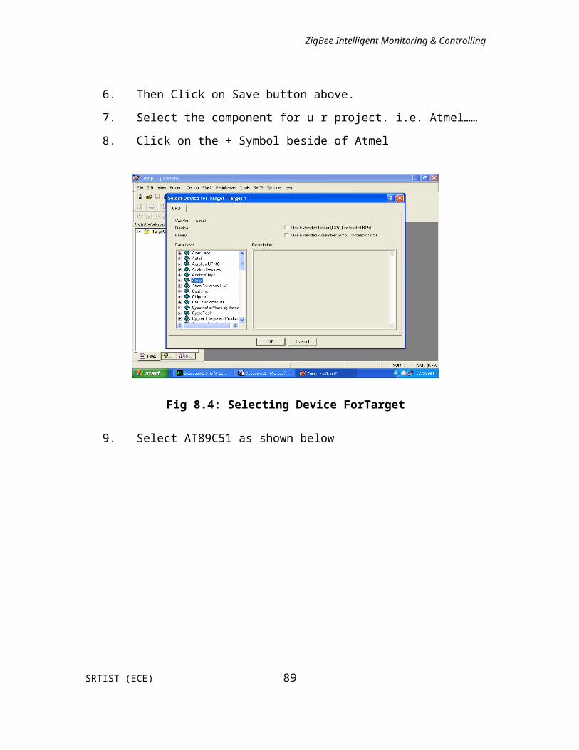
ZigBee Intelligent Monitoring & Controlling
6. Then Click on Save button above.
7. Select the component for u r project. i.e. Atmel……
8. Click on the + Symbol beside of Atmel
Fig 8.4: Selecting Device ForTarget
9. Select AT89C51 as shown below
SRTIST (ECE) 89

ZigBee Intelligent Monitoring & Controlling
Fig 8.5: Selecting AT89C51
10. Then Click on “OK”
11. The Following fig will appear
SRTIST (ECE) 90

ZigBee Intelligent Monitoring & Controlling
Fig 8.6: Adding FILE to project
12. Then Click either YES or NO………mostly “NO”
13. Now your project is ready to USE
14. Now double click on the Target1, you would get
another option “Source group 1” as shown in next
page.
Fig 8.7: Source Group 1
15. Click on the file option from menu bar and select“new”
SRTIST (ECE) 91

ZigBee Intelligent Monitoring & Controlling
Fig 8.8:Opening New FolderIn project
16. The next screen will be as shown in next page, and
just maximize it by double clicking on its blue
boarder.
Fig 8.9:Start Writing Program
SRTIST (ECE) 92

ZigBee Intelligent Monitoring & Controlling
17. Now start writing program in either in “C” or
“ASM”
18. For a program written in Assembly, then save it
with extension “. asm” and for “C” based program
save it with extension “ .C”
Fig 8.10: Add files to Group Source
19. Now right click on Source group 1 and click on “Addfiles to Group Source”
SRTIST (ECE) 93

ZigBee Intelligent Monitoring & Controlling
Fig 8.11: Add files to Group Source
20. Now you will get another window, on which bydefault “C” files will appear.
Fig 8.12: “C” files Window
SRTIST (ECE) 94

ZigBee Intelligent Monitoring & Controlling
21. Now select as per your file extension given while
saving the file
22. Click only one time on option “ADD”
23. Now Press function key F7 to compile. Any error
will appear if so happen.
Fig 8.13: “C” files Window
24. If the file contains no error, then press
Control+F5 simultaneously.
25. The new window is as follows
SRTIST (ECE) 95

ZigBee Intelligent Monitoring & Controlling
Fig 8.14: Option If Error
26. Then Click “OK”
27. Now Click on the Peripherals from menu bar, and
check your required port as shown in fig below
Fig 8.15: Selecting port
28. Drag the port a side and click in the program file.
SRTIST (ECE) 96
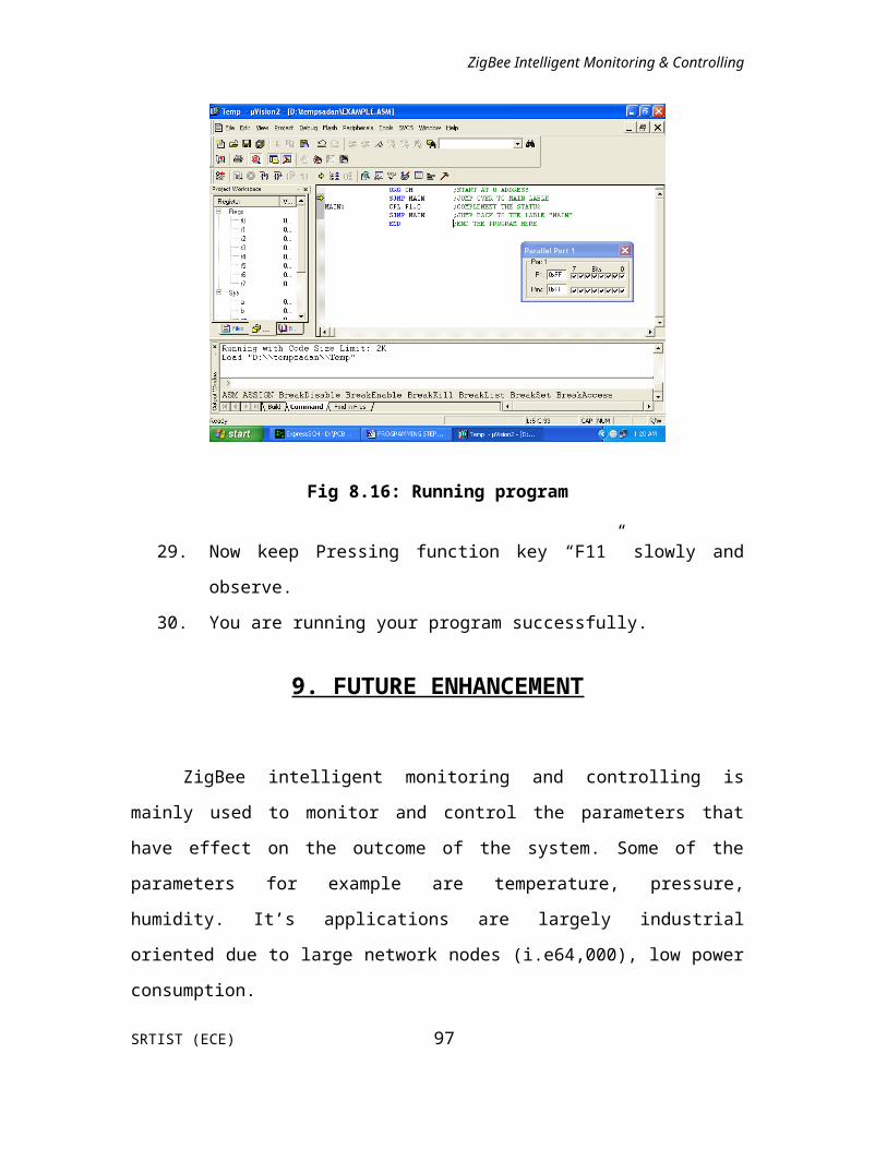
ZigBee Intelligent Monitoring & Controlling
Fig 8.16: Running program
29. Now keep Pressing function key “F11” slowly and
observe.
30. You are running your program successfully.
9. FUTURE ENHANCEMENT
ZigBee intelligent monitoring and controlling is
mainly used to monitor and control the parameters that
have effect on the outcome of the system. Some of the
parameters for example are temperature, pressure,
humidity. It’s applications are largely industrial
oriented due to large network nodes (i.e64,000), low power
consumption.
SRTIST (ECE) 97

ZigBee Intelligent Monitoring & Controlling
In our project the control commands from “pc side”
operate over the “work site” only when parameter (here
temperature) exceeds its limits in this way some
intelligence is imparted to the system.
Network building: In real time applications more
number of nodes are part of the network.
Security: Security can be further increased by giving
passwords to different users who operate over the
controlling end.
Dynamic: The temperature can be varied in dynamic
manner by designing a function to accept different
temperature limits from user.
Stop: command for stopping heater or cooler should
operate irrespective of the limits.
Further intelligence: Element (heater or cooler) can
be made to operate according to the limits.
SRTIST (ECE) 98

ZigBee Intelligent Monitoring & Controlling
10. CONCLUSION
The project ZIG-BEE INTELLIGENT MONITORING &
CONTROL has been successfully designed and tested.
Integrating features of all the hardware components used
have developed it. Presence of every module has been
reasoned out and placed carefully thus contributing to the
best working of the unit. Secondly, using highly advanced
IC’s and with the help of growing technology the project
has been successfully implemented.
SRTIST (ECE) 99

ZigBee Intelligent Monitoring & Controlling
11. APPENDIX A
PROGRAM:
// Including of the Header Filer
#include "c52.h"
#include "adc.h"
#define RL0 P1_5
#define RL1 P1_6
// Function Prototype Declaration
void SConfig();
void Send_Char(uc ch); //CHARECTER TRANSMITION FROM
SLAVE
void Send(uc *str); //COMPLETE STRING
SRTIST (ECE) 100

ZigBee Intelligent Monitoring & Controlling
void Set_Load(void);
uc chk_val(uc*);
uc chk_tmp(uc*,uc*);
void tmpmntr();
uc tmp;
// Main Function
void main()
{
P1_5=0; // set the devices to default
state
P1_6=0; // (poweroff)
SConfig(); // set baud rate
LCD_Init(); // initialize LCD
Delay(25);
lprintf("S R T I S T",1,1);
lprintf("ZIGBEE I M & C",2,1);
Delay(100);
ClrLCD(); // clear the LCD
P2=0xff;
bc=0;
EA=1; // enable all interrupts
ES=1; // enable serial interrupt
Send("start");
while(1)
SRTIST (ECE) 101

ZigBee Intelligent Monitoring & Controlling
{
while(!Rx) // if no commmands are received
{
tmpmntr(); // to monitor temperautre values
& transmit them as per cut-offs
Delay(500);
}
if(Rx) // if commands are received
{
EA=0;
Send(RData);
if(tmp=='L' || tmp=='H')// check for cut-off staus
Set_Load(); // if cut-off limits exceeded
perform the operation
Delay(200);
Rx=0;
}
}
}
// function to read ADC and check the cut-off limits and
trasmit respective messages
void tmpmntr()
{
EA=0;
bc=0;
SRTIST (ECE) 102

ZigBee Intelligent Monitoring & Controlling
Read_ADC(); // read the temperature
values
ClrLCD();
Send(str); //str holds the ADC output
value
lprintf(str,1,1);
Delay(25); // Delay of 50 Secs.
EA=1;
tmp=chk_val(str); // check for cut-off limit
flags
Delay(25);
if(tmp=='L')
{
Send("too cold! want to ON the Heater");
lprintf("too cold!",2,1);
Delay(50);
} // if flag L is set
else if(tmp=='H')
{
Send("too hot! wnat to ON the cooler");
lprintf("too hot!",2,1);
Delay(50);
} // if flag H is set
}
// function to set loads ie., heater, cooler ON,OFF
void Set_Load(void)SRTIST (ECE) 103

ZigBee Intelligent Monitoring & Controlling
{
if(RData[0]=='H' && RData[1]=='t' &&
RData[2]=='r') // to turn ON heater
{
RL0=1;
Delay(25);
RL1=0;
Delay(10);
}
else if(RData[0]=='C' && RData[1]=='l' &&
RData[2]=='r') // to turn ON cooler
{
RL1=1;
Delay(25);
RL0=0;
Delay(10);
}
else // to turn OFF
{
RL0=0;
Delay(10);
RL1=0;
Delay(25);
} //commands -- Htr! Clr!
STP!
}SRTIST (ECE) 104

ZigBee Intelligent Monitoring & Controlling
// to verify the measured temperature values and generate
corresponding alerts
uc chk_val(uc *str)
{
uc tmplmt[2][5]={"18.5","40.5"};
if(chk_tmp(str,tmplmt[0])=='L')
{
Send("warning! temperature below limit");
return ' L';
}
else if(chk_tmp(str,tmplmt[1])=='H')
{
Send("warning! temperature above limit");
return 'H';
}
else return 0;
}
// to compare the measured temperature value with the cut-
off value
uc chk_tmp(uc *str1,uc *str2)
{
uc flag=0;
while(*str1 && *str2)
{
if(*str1<*str2)
{ SRTIST (ECE) 105

ZigBee Intelligent Monitoring & Controlling
flag='L';
break;
}
else if(*str1>*str2)
{
flag='H';
break;
}
else flag=0;
str1++;
str2++;
}
if(flag)
return flag;
else
return 0;
}
BIBLIOGRAPHY
REFERENCES:
SRTIST (ECE) 106

ZigBee Intelligent Monitoring & Controlling
1 Mohd. Mazidi 8051-MICROCONTROLLER AND EMBEDDED
SYSTEM.
2 David .E. Simon EMBEDDED SOFTWARE PRIMER.
NAME OF THE SITES:
WWW.MITEL.DATABOOK.COM
WWW.ATMEL.DATABOOK.COM
WWW.FRANKLIN.COM
WWW.KEIL.COM
SRTIST (ECE) 107
Copyright © 2022 FDOKUMEN

