


Bahasa
Halaman
Hukum

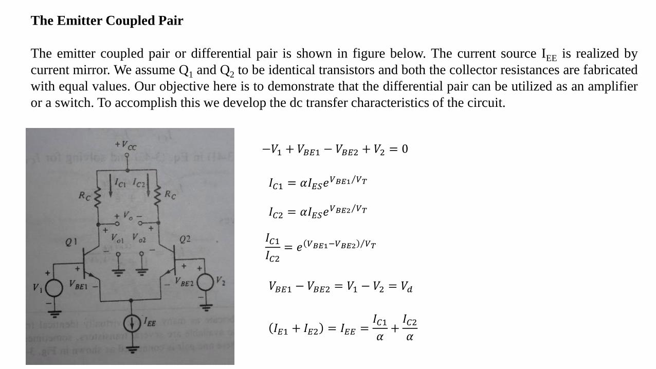
The Emitter Coupled Pair
The emitter coupled pair or differential pair is shown in figure below. The current source IEE is realized by
current mirror. We assume Q1 and Q2 to be identical transistors and both the collector resistances are fabricated
with equal values. Our objective here is to demonstrate that the differential pair can be utilized as an amplifier
or a switch. To accomplish this we develop the dc transfer characteristics of the circuit.
−𝑉1 + 𝑉𝐵𝐸1 − 𝑉𝐵𝐸2 + 𝑉2 = 0
𝐼𝐶1 = 𝛼𝐼𝐸𝑆𝑒 𝑉𝐵𝐸1 𝑉𝑇
𝐼𝐶2 = 𝛼𝐼𝐸𝑆𝑒 𝑉𝐵𝐸2 𝑉𝑇
𝐼𝐶1𝐼𝐶2
= 𝑒 𝑉𝐵𝐸1−𝑉𝐵𝐸2 𝑉𝑇
𝑉𝐵𝐸1 − 𝑉𝐵𝐸2 = 𝑉1 − 𝑉2 = 𝑉𝑑
𝐼𝐸1 + 𝐼𝐸2 = 𝐼𝐸𝐸 =𝐼𝐶1𝛼
+𝐼𝐶2𝛼

𝛼𝐼𝐸𝐸𝐼𝐶2
=𝐼𝐶1𝐼𝐶2
+ 1 = 1 + 𝑒 𝑣𝑑 𝑉𝑇
𝐼𝐶2 =𝛼𝐼𝐸𝐸
1 + 𝑒 +𝑉𝑑 𝑉𝑇
A similar analysis gives
𝐼𝐶1 =𝛼𝐼𝐸𝐸
1 + 𝑒 −𝑉𝑑 𝑉𝑇
𝑉𝑜1 ≡ 𝑉𝐶𝐶 − 𝐼𝐶1𝑅𝐶
𝑉𝑜2 ≡ 𝑉𝐶𝐶 − 𝐼𝐶2𝑅𝐶
𝑉𝑜 = 𝑉𝑜1 − 𝑉𝑜2
Thus it acts as a switch and as an amplifier. When 𝐼𝐶2 ≈ 0 at 𝑉𝑑 ≥ 4𝑉𝑇,
𝑉𝑜2 = 𝑉𝐶𝐶 𝑎𝑛𝑑 𝑉𝑜1 = 𝑉𝐶𝐶 − 𝛼𝐼𝐸𝐸𝑅𝐶 can be made small by taking large 𝑅𝐶 .
Thus the output of Q1 acts as a closed switch and Q2 as an open switch. By
applying 𝑉𝑑 ≤ −4𝑉𝑇, Q1 is open and Q2 is closed. Between −2𝑉𝑇𝑎𝑛𝑑 2𝑉𝑇 the
circuit is linear and acts as an amplifier.
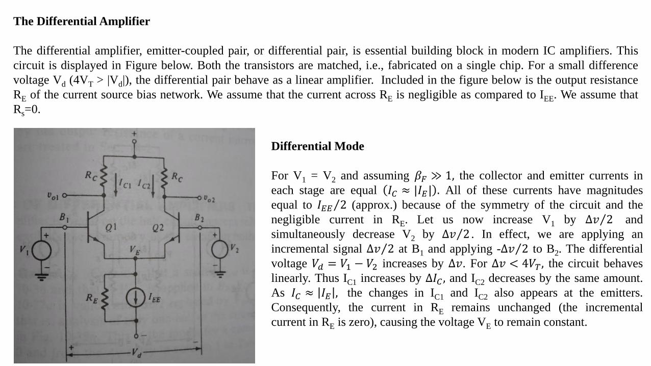
The Differential Amplifier
The differential amplifier, emitter-coupled pair, or differential pair, is essential building block in modern IC amplifiers. This
circuit is displayed in Figure below. Both the transistors are matched, i.e., fabricated on a single chip. For a small difference
voltage Vd (4VT > |Vd|), the differential pair behave as a linear amplifier. Included in the figure below is the output resistance
RE of the current source bias network. We assume that the current across RE is negligible as compared to IEE. We assume that
Rs=0.
Differential Mode
For V1 = V2 and assuming 𝛽𝐹 ≫ 1, the collector and emitter currents in
each stage are equal 𝐼𝐶 ≈ |𝐼𝐸| . All of these currents have magnitudes
equal to 𝐼𝐸𝐸 2 (approx.) because of the symmetry of the circuit and the
negligible current in RE. Let us now increase V1 by ∆𝑣 2 and
simultaneously decrease V2 by ∆𝑣 2 . In effect, we are applying an
incremental signal ∆𝑣 2 at B1 and applying - ∆𝑣 2 to B2. The differential
voltage 𝑉𝑑 = 𝑉1 − 𝑉2 increases by ∆𝑣. For ∆𝑣 < 4𝑉𝑇 , the circuit behaves
linearly. Thus IC1 increases by ∆𝐼𝐶 , and IC2 decreases by the same amount.
As 𝐼𝐶 ≈ 𝐼𝐸 , the changes in IC1 and IC2 also appears at the emitters.
Consequently, the current in RE remains unchanged (the incremental
current in RE is zero), causing the voltage VE to remain constant.
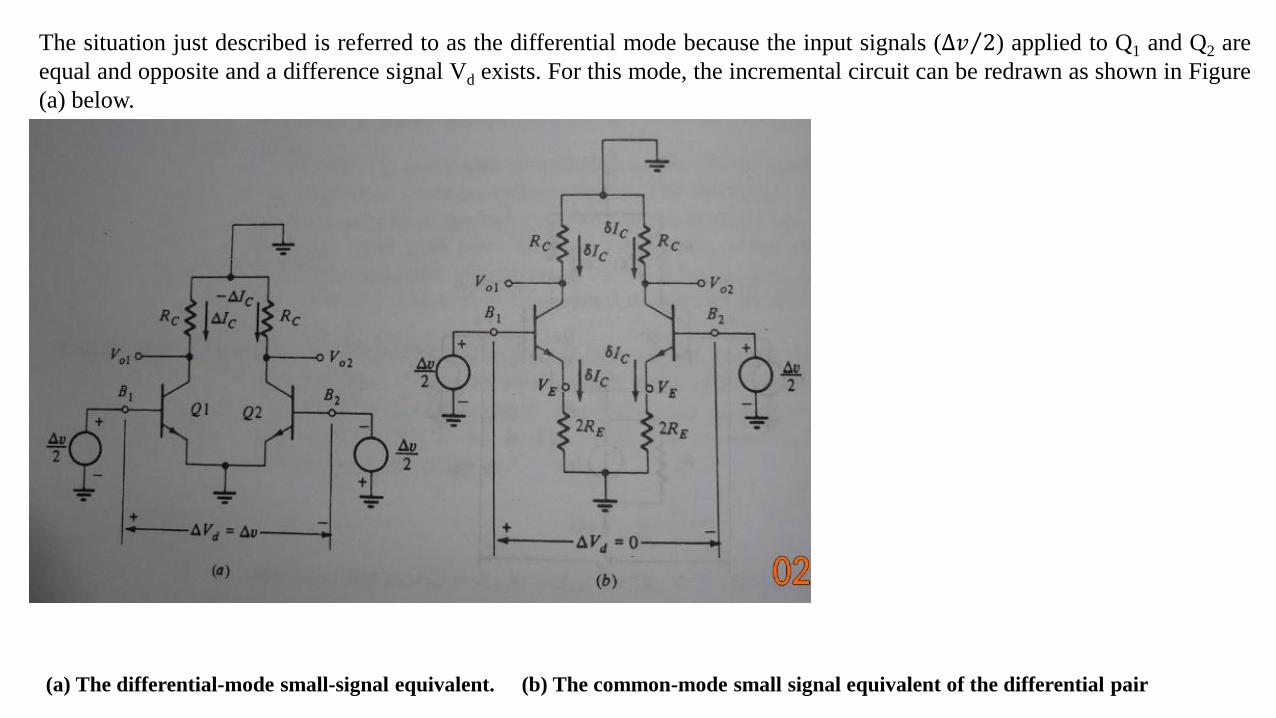
The situation just described is referred to as the differential mode because the input signals ( ∆𝑣 2) applied to Q1 and Q2 are
equal and opposite and a difference signal Vd exists. For this mode, the incremental circuit can be redrawn as shown in Figure
(a) below.
(a) The differential-mode small-signal equivalent. (b) The common-mode small signal equivalent of the differential pair

The Common Mode
Now let us consider that both V1 and V2 increase by ∆𝑣 2. The difference voltage Vd remains zero, and IC1 and
IC2 remain equal. However, because RE is present, both IC1 and IC2 exhibit a small increase 𝛿𝐼𝐶 . Again changes in
IC appear at the emitter, and hence the current in RE increases by 2𝛿𝐼𝐶 . The voltage VE is no longer constant but
must increase by 2𝛿𝐼𝐶𝑅𝐸. This situation, where equal signals are applied to Q1 and Q2 is called common mode.
The incremental equivalent circuit is displayed in Figure (b) above, in which it is implied that Q1 and Q2 are
represented by their small signal models. We can write 2𝛿𝐼𝐶𝑅𝐸 as 𝛿𝐼𝐶2𝑅𝐸 which is shown in the Figure (b)
above showing 2RE. The voltage across each is 2𝛿𝐼𝐶𝑅𝐸 and equals the incremental change in VE; thus the two
resistances are in parallel and 2𝑅𝐸||2𝑅𝐸 = 𝑅𝐸 .
It is evident in the Figures (a) and (b) above that depending on the input signal, the differential amplifier behaves
as either common-emitter stage or a common-emitter stage with emitter resistance. Therefore, the gain of this
stage is significantly higher for differential mode operation than for the common mode operation. Usually,
differential amplifiers are designed so that, for practical purposes, only difference signals are amplified.
As shown in the Figure (a) above, the emitter is at ground for small signal for small signal analysis. Thus it
appears that RE is bypassed. Similarly, the voltage between the two collectors Vo1 – Vo2 is zero in common mode
and is twice the change in Vo1 (Vo2) for the differential mode. Since the applied signal ∆𝑣 can be made positive or
negative, the voltage Vo1 – Vo2 can be positive or negative.
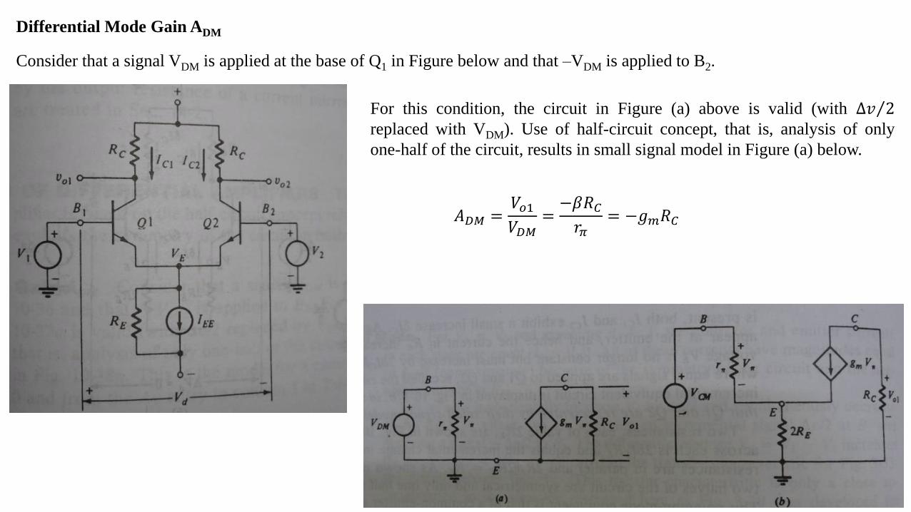
Differential Mode Gain ADM
Consider that a signal VDM is applied at the base of Q1 in Figure below and that –VDM is applied to B2.
For this condition, the circuit in Figure (a) above is valid (with ∆𝑣 2replaced with VDM). Use of half-circuit concept, that is, analysis of only
one-half of the circuit, results in small signal model in Figure (a) below.
𝐴𝐷𝑀 =𝑉𝑜1𝑉𝐷𝑀
=−𝛽𝑅𝐶𝑟𝜋
= −𝑔𝑚𝑅𝐶

For VDM positive, Vo1 = ADMVDM and as seen in the Equation above, ADM is negative, so that Vo1 is 180o out of phase with VDM
(Vo1 is inverted). Because Q2 is driven by –VDM, Vo2 = -ADMVDM and Vo2 is in phase with VDM (Vo2 is noninverting).
Common-Mode Gain ACM
When the signal VCM is applied to both bases in Figure on the left above, consider the Circuit in Figure (b) to the right above.
For this circuit, the gain ACM is
𝐴𝐶𝑀 =𝑉𝑜1𝑉𝐶𝑀
=−𝛽𝑅𝐶
2 𝛽 + 1 𝑅𝐸 + 𝑟𝜋
With 𝛽 ≫ 1 and the division by 𝑟𝜋, reduces to
𝐴𝐶𝑀 =−𝑔𝑚𝑅𝐶
1+2𝑔𝑚𝑅𝐸≈ −
𝑅𝐶
2𝑅𝐸For 2𝑔𝑚𝑅𝐸 ≫ 1.
Because the same signal is applied to Q1 and Q2, both Vo1 and Vo2 are 180o out of phase with VCM.
The Common-Mode Rejection Ratio
The differential amplifier is primarily designed to amplify differential signals; hence we
require 𝐴𝐷𝑀 ≫ 𝐴𝐶𝑀. A convenient measure of the differential amplifier performance is the
common-mode rejection ratio or CMRR, defined as
𝐶𝑀𝑅𝑅 ≡𝐴𝐷𝑀
𝐴𝐶𝑀
Combination of equation for ADM and ACM above and substituting in this equation yields
𝐶𝑀𝑅𝑅 = 1 + 2𝑔𝑚𝑅𝐸 ≈ 2𝑔𝑚𝑅𝐸
As seen in this equation, large values of CMRR require large values of RE and often
necessitates the use of current sources having high output resistances. Note that if 𝑅𝐸 → ∞,
𝐶𝑀𝑅𝑅 → ∞, ACM = 0 and no common-mode component appears at the output.
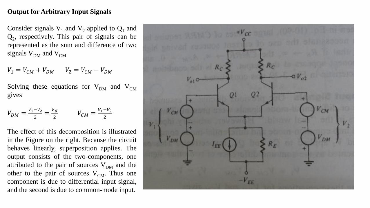
Output for Arbitrary Input Signals
Consider signals V1 and V2 applied to Q1 and
Q2, respectively. This pair of signals can be
represented as the sum and difference of two
signals VDM and VCM
𝑉1 = 𝑉𝐶𝑀 + 𝑉𝐷𝑀 𝑉2 = 𝑉𝐶𝑀 − 𝑉𝐷𝑀
Solving these equations for VDM and VCM
gives
𝑉𝐷𝑀 =𝑉1−𝑉2
2=
𝑉𝑑
2𝑉𝐶𝑀 =
𝑉1+𝑉2
2
The effect of this decomposition is illustrated
in the Figure on the right. Because the circuit
behaves linearly, superposition applies. The
output consists of the two-components, one
attributed to the pair of sources VDM and the
other to the pair of sources VCM. Thus one
component is due to differential input signal,
and the second is due to common-mode input.

The output voltage Vo1 is given as
𝑉𝑜1 = 𝐴𝐷𝑀𝑉𝐷𝑀 + 𝐴𝐶𝑀𝑉𝐶𝑀 = 𝐴𝐷𝑀 𝑉𝐷𝑀 +𝑉𝐶𝑀
𝐶𝑀𝑅𝑅
Equation above demonstrate the importance of CMRR if we are to amplify only the difference signals. As the
CMRR is increased, the common-mode output component has diminished significance. The out put voltage Vo2 is
expressed as
𝑉𝑜2 = −𝐴𝐷𝑀𝑉𝐷𝑀 + 𝐴𝐶𝑀𝑉𝐶𝑀 = −𝐴𝐷𝑀 𝑉𝐷𝑀 −𝑉𝐶𝑀
𝐶𝑀𝑅𝑅
Further simplifying we get
𝑉𝑜1 =𝐴𝐷𝑀
2𝑉𝑑 +
𝑉1+𝑉2
𝐶𝑀𝑅𝑅
𝑉𝑜2 =−𝐴𝐷𝑀
2𝑉𝑑 −
𝑉1+𝑉2
𝐶𝑀𝑅𝑅
These equations are an alternative form for the output voltages that appear in the literature. The difference signal
Vd appears explicitly.
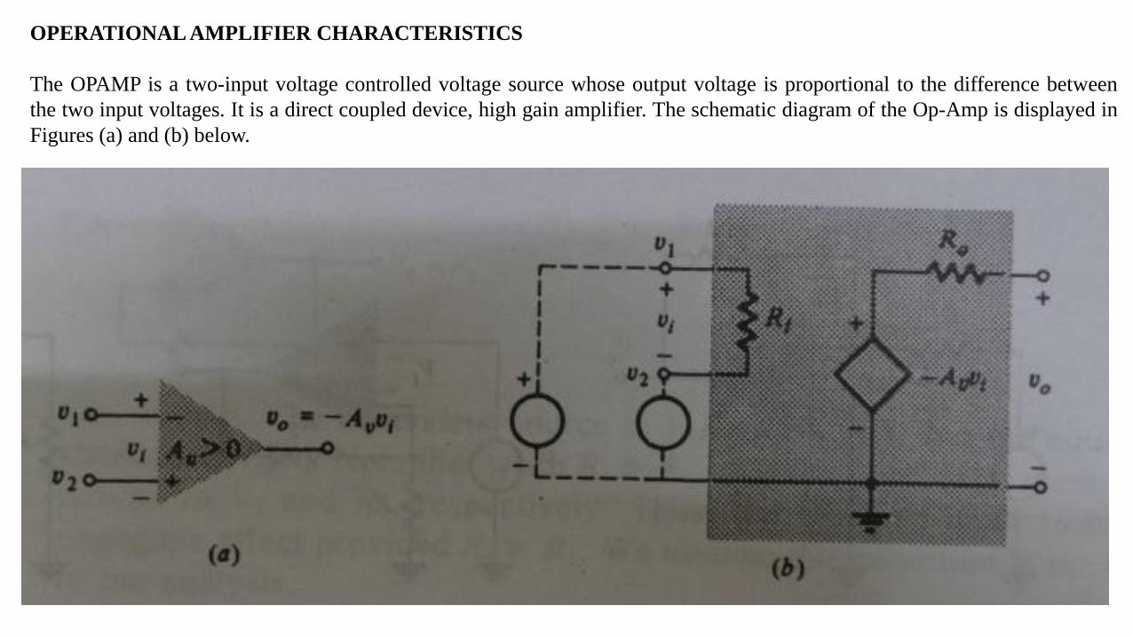
OPERATIONAL AMPLIFIER CHARACTERISTICS
The OPAMP is a two-input voltage controlled voltage source whose output voltage is proportional to the difference between
the two input voltages. It is a direct coupled device, high gain amplifier. The schematic diagram of the Op-Amp is displayed in
Figures (a) and (b) below.

The schematic diagram of the OPAMP is displayed in Figure (a) above and its equivalent
circuit in Figure (b) above. As seen in the Figure (b), the OPAMP is a voltage controlled
voltage source. The output voltage vo is the amplified difference signal vi = v1 – v2. The – and
+ symbols at the input of the OPAMP refer to the inverting and noninverting input terminals.
That is, if v2 = 0, vo is 180o out of phased with respect to the input signal vi. When v1 = 0, the
output vo is in phase with vi.
The Ideal OPAMP
The ideal OPAMP has the following characteristics:
1. The input resistance 𝑅𝑖 → ∞ (open circuited). Consequently, no current enters either input
terminal.
2. The output resistance Ro = 0.
3. The voltage gain 𝐴𝑣 → ∞. The output voltage 𝑣𝑜 = −𝐴𝑣𝑣𝑖 is finite ( 𝑣𝑜 < ∞); thus as
𝐴𝑣 → ∞, it is required that 𝑣𝑖 = 0.4. The amplifier responds equally at all frequencies. (i.e. the bandwidth is infinite).
5. When 𝑣1 = 𝑣2, 𝑣𝑜 = 0 and is independent of 𝑣1 . The converse is also true.
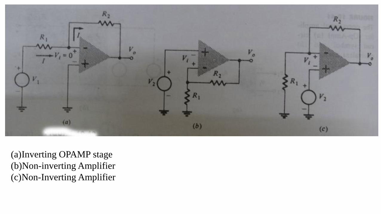
(a)Inverting OPAMP stage
(b)Non-inverting Amplifier
(c)Non-Inverting Amplifier
The same symbol is used for ideal and practical OPAMP. To distinguish them, we indicate the
finite gain Av in the triangle for practical OPAMPS and omit it in ideal case. This is illustrated in
Figures (a) (b) & (c) above. The circuit in Figure (a) above is an inverting amplifier stage
utilizing an ideal OPAMP. Because the input current is zero, the current I exists in both R1 and
R2. Furthermore, since Vi = 0, it follows that
𝐼 =𝑉𝑠
𝑅1= −
𝑉𝑜
𝑅2𝑓𝑟𝑜𝑚 𝑤ℎ𝑖𝑐ℎ 𝑤𝑒 𝑔𝑒𝑡 𝐴𝑣 =
𝑉0
𝑉𝑠= −
𝑅2
𝑅1
The OPAMP is used as noninverting amplifier stage in the circuit shown in Figures (b) & (c)
above. Making 𝑉𝑖 = 0 requires that
𝑉𝑖 = 𝑉1 − 𝑉2 =𝑅1
𝑅1+𝑅2𝑉𝑜 − 𝑉𝑠 = 0 𝑆𝑜𝑙𝑣𝑖𝑛𝑔 𝑓𝑜𝑟 𝐴𝑣 = 𝑉𝑜 𝑉𝑠 yields 𝐴𝑣 =
𝑅1+𝑅2
𝑅1= 1 +
𝑅2
𝑅1
The above equations indicates that the feedback provided by R2 causes Av to depend only on the
resistance ratio R2/R1.

The Voltage Follower
The property of high impedance is very desirable feature of the noninverting configuration. It enables using this
circuit as a buffer amplifier to connect a source with a high impedance to a low-impedance load. In such cases we
make R2 = 0 and R1 = ∞ to obtain the unity gain amplifier shown in the Figure (a) below. This circuit is commonly
referred to as a voltage follower, since the output follows the input. Figure (b) is its equivalent circuit model.

Difference Amplifiers
A difference amplifier is one that responds to difference between the two signals applied at its input and ideally
rejects signals that are common to the two inputs. The representation of signals in terms of their differential and
common mode components are given in the Figure below.
For practical cases voltage Vo is given by
𝑣𝑜 = 𝐴𝑑𝑣𝐼𝑑 + 𝐴𝑐𝑚𝑣𝐼𝑐𝑚
Where Ad denotes the amplifier differential gain and Acm
denotes the common-mode gain. The efficacy of the
differential amplifier is measured by the degree of its
rejection of common-mode signals in preference to
differential signals. This is usually quantified by a
measure known as Common-Mode Rejection Ratio
(CMRR) defined as
𝐶𝑀𝑅𝑅 = 20𝑙𝑜𝑔𝐴𝑑𝐴𝑐𝑚

A Single Op-Amp Difference Amplifier
Our first attempt at designing a difference amplifier is motivated by the observation that the gain of the noninverting amplifier
configuration is positive, 1 + 𝑅2 𝑅1 , while that of the inverting configuration is negative − 𝑅2 𝑅1 . Combining the two
configurations together is then a step in the right direction – namely, getting the difference between two input signals. We have
to make the two gain magnitudes equal in order to reject common-mode signals. This, however, can be easily achieved by
attenuating the positive input signal to reduce the gain of the positive path from 1 + 𝑅2 𝑅1 to 𝑅2 𝑅1 . The resulting
circuit would like as shown in Figure below.
Hence from this Figure
𝑅4
𝑅3+𝑅41 +
𝑅2
𝑅1=
𝑅2
𝑅1
Or𝑅4
𝑅3+𝑅4=
𝑅2
𝑅1+𝑅2
This condition is satisfied by selecting
𝑅4
𝑅3=
𝑅2
𝑅1
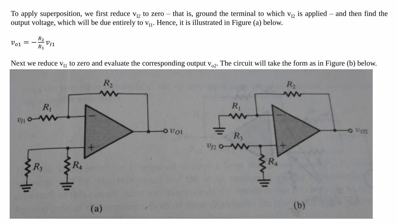
To apply superposition, we first reduce vI2 to zero – that is, ground the terminal to which vI2 is applied – and then find the
output voltage, which will be due entirely to vI1. Hence, it is illustrated in Figure (a) below.
𝑣𝑜1 = −𝑅2
𝑅1𝑣𝐼1
Next we reduce vI1 to zero and evaluate the corresponding output vo2. The circuit will take the form as in Figure (b) below.
The output voltage vo2 is given by
𝑣𝑜2 = 𝑣𝐼2𝑅4
𝑅3+𝑅41 +
𝑅2
𝑅1=
𝑅2
𝑅1𝑣𝐼2
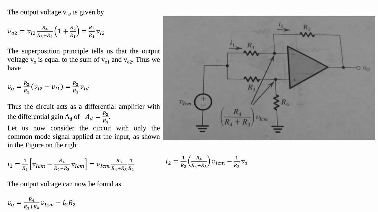
The superposition principle tells us that the output
voltage vo is equal to the sum of vo1 and vo2. Thus we
have
𝑣𝑜 =𝑅2
𝑅1𝑣𝐼2 − 𝑣𝐼1 =
𝑅2
𝑅1𝑣𝐼𝑑
Thus the circuit acts as a differential amplifier with
the differential gain Ad of 𝐴𝑑 =𝑅2
𝑅1.
Let us now consider the circuit with only the
common mode signal applied at the input, as shown
in the Figure on the right.
𝑖1 =1
𝑅1𝑣𝐼𝑐𝑚 −
𝑅4
𝑅4+𝑅3𝑣𝐼𝑐𝑚 = 𝑣𝐼𝑐𝑚
𝑅3
𝑅4+𝑅3
1
𝑅1
The output voltage can now be found as
𝑣𝑜 =𝑅4
𝑅3+𝑅4𝑣𝐼𝑐𝑚 − 𝑖2𝑅2
𝑖2 =1
𝑅2
𝑅4
𝑅4+𝑅3𝑣𝐼𝑐𝑚 −
1
𝑅2𝑣𝑜
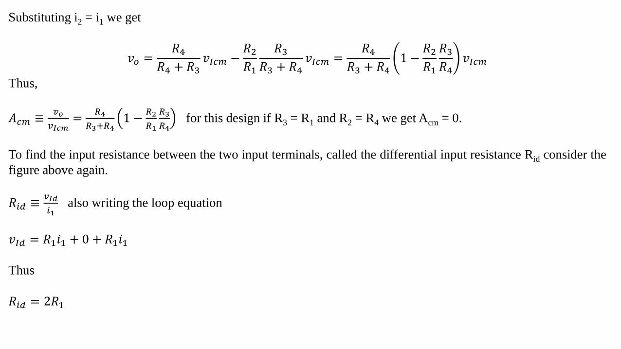
Substituting i2 = i1 we get
𝑣𝑜 =𝑅4
𝑅4 + 𝑅3𝑣𝐼𝑐𝑚 −
𝑅2𝑅1
𝑅3𝑅3 + 𝑅4
𝑣𝐼𝑐𝑚 =𝑅4
𝑅3 + 𝑅41 −
𝑅2𝑅1
𝑅3𝑅4
𝑣𝐼𝑐𝑚
Thus,
𝐴𝑐𝑚 ≡𝑣𝑜
𝑣𝐼𝑐𝑚=
𝑅4
𝑅3+𝑅41 −
𝑅2
𝑅1
𝑅3
𝑅4for this design if R3 = R1 and R2 = R4 we get Acm = 0.
To find the input resistance between the two input terminals, called the differential input resistance Rid consider the
figure above again.
𝑅𝑖𝑑 ≡𝑣𝐼𝑑
𝑖1also writing the loop equation
𝑣𝐼𝑑 = 𝑅1𝑖1 + 0 + 𝑅1𝑖1
Thus
𝑅𝑖𝑑 = 2𝑅1
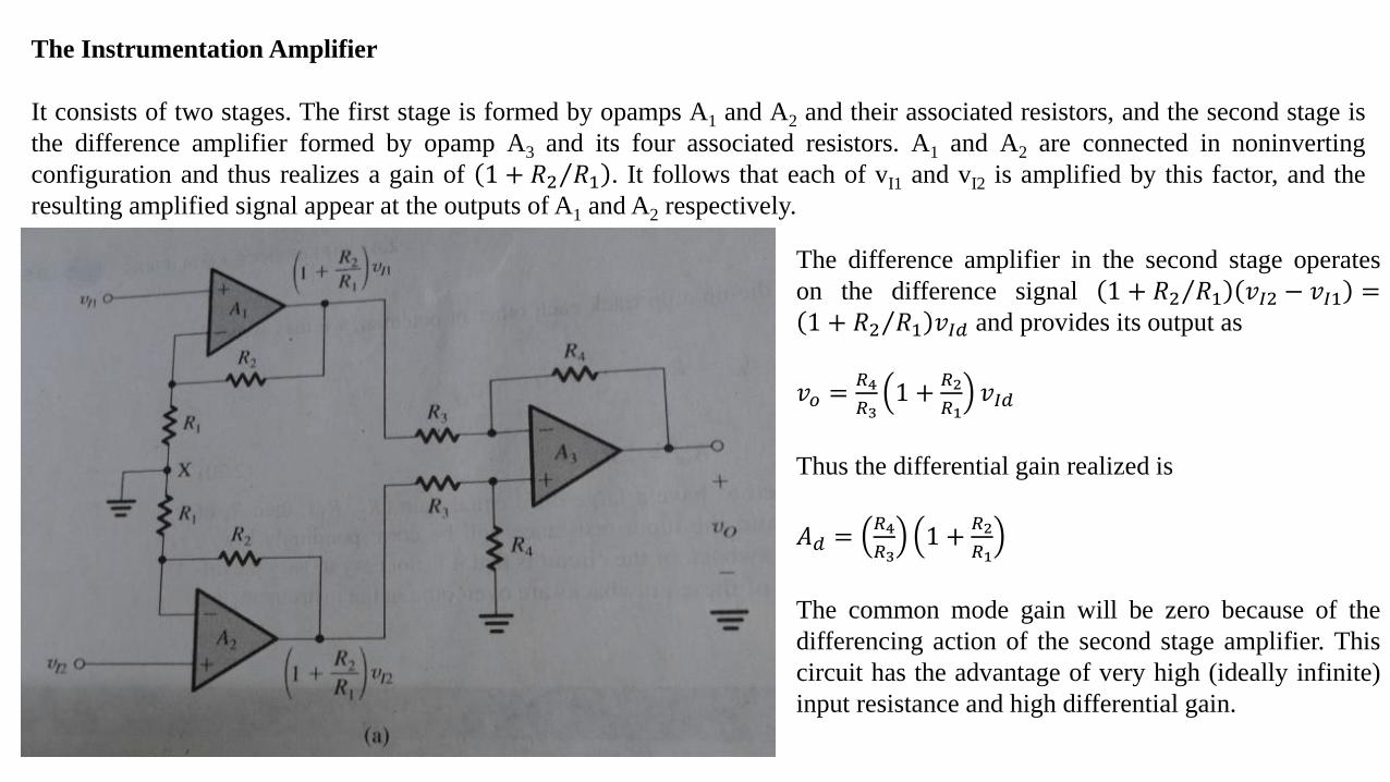
The Instrumentation Amplifier
It consists of two stages. The first stage is formed by opamps A1 and A2 and their associated resistors, and the second stage is
the difference amplifier formed by opamp A3 and its four associated resistors. A1 and A2 are connected in noninverting
configuration and thus realizes a gain of 1 + 𝑅2 𝑅1 . It follows that each of vI1 and vI2 is amplified by this factor, and the
resulting amplified signal appear at the outputs of A1 and A2 respectively.
The difference amplifier in the second stage operates
on the difference signal 1 + 𝑅2 𝑅1 𝑣𝐼2 − 𝑣𝐼1 =1 + 𝑅2 𝑅1 𝑣𝐼𝑑 and provides its output as
𝑣𝑜 =𝑅4
𝑅31 +
𝑅2
𝑅1𝑣𝐼𝑑
Thus the differential gain realized is
𝐴𝑑 =𝑅4
𝑅31 +
𝑅2
𝑅1
The common mode gain will be zero because of the
differencing action of the second stage amplifier. This
circuit has the advantage of very high (ideally infinite)
input resistance and high differential gain.

Voltage-to-Current Converter (Transconductance Amplifier)
The circuit for this configuration is given in Figure below. Thus we get the following equation. Note that iL is
independent of load ZL.
𝑖𝐿 𝑡 =𝑣𝑠(𝑡)
𝑅
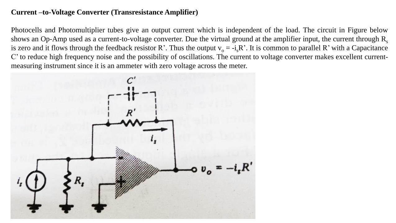
Current –to-Voltage Converter (Transresistance Amplifier)
Photocells and Photomultiplier tubes give an output current which is independent of the load. The circuit in Figure below
shows an Op-Amp used as a current-to-voltage converter. Due the virtual ground at the amplifier input, the current through Rs
is zero and it flows through the feedback resistor R’. Thus the output vo = -isR’. It is common to parallel R’with a Capacitance
C’ to reduce high frequency noise and the possibility of oscillations. The current to voltage converter makes excellent current-
measuring instrument since it is an ammeter with zero voltage across the meter.
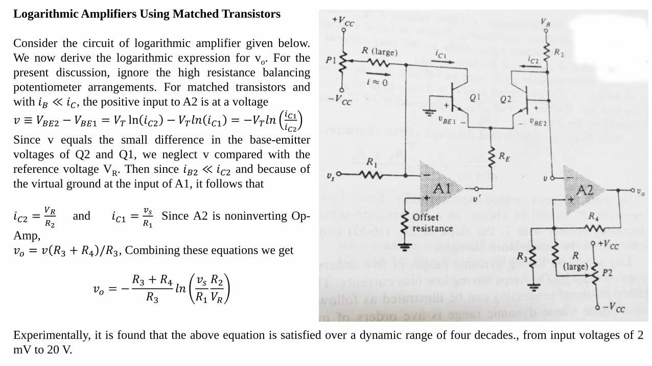
Logarithmic Amplifiers Using Matched Transistors
Consider the circuit of logarithmic amplifier given below.
We now derive the logarithmic expression for vo. For the
present discussion, ignore the high resistance balancing
potentiometer arrangements. For matched transistors and
with 𝑖𝐵 ≪ 𝑖𝐶, the positive input to A2 is at a voltage
𝑣 ≡ 𝑉𝐵𝐸2 − 𝑉𝐵𝐸1 = 𝑉𝑇 ln 𝑖𝐶2 − 𝑉𝑇𝑙𝑛 𝑖𝐶1 = −𝑉𝑇𝑙𝑛𝑖𝐶1
𝑖𝐶2
Since v equals the small difference in the base-emitter
voltages of Q2 and Q1, we neglect v compared with the
reference voltage VR. Then since 𝑖𝐵2 ≪ 𝑖𝐶2 and because of
the virtual ground at the input of A1, it follows that
𝑖𝐶2 =𝑉𝑅
𝑅2and 𝑖𝐶1 =
𝑣𝑠
𝑅1Since A2 is noninverting Op-
Amp,
𝑣𝑜 = 𝑣 𝑅3 + 𝑅4 /𝑅3, Combining these equations we get
𝑣𝑜 = −𝑅3 + 𝑅4
𝑅3𝑙𝑛
𝑣𝑠𝑅1
𝑅2𝑉𝑅
Experimentally, it is found that the above equation is satisfied over a dynamic range of four decades., from input voltages of 2
mV to 20 V.

Exponential (Antilog) Amplifier
This amplifier is depicted in the given Figure. In the exponential amplifier the feedback current iC1 is constant and is derived
from the reference voltage VR, whereas iC2 depends upon the input signal. In logarithmic amplifier the converse of this is true.
Because of the virtual ground at the inputs to A1 and A2, the collector and base of Q1 are at the same potential −𝑣 = 𝑉𝐵𝐸1 −𝑉𝐵𝐸2. Neglecting v relative to VR, we obtain
𝑖𝐶1 =𝑉𝑅
𝑅2and 𝑖𝐶2 =
𝑣𝑜
𝑅1From the input attenuator it is clear that −𝑣 =
𝑅3𝑣𝑠
𝑅3+𝑅4= 𝑉𝑇𝑙𝑛
𝑖𝐶1
𝑖𝐶2. Substituting the currents iC1
and iC2 from the above equations we obtain
𝑣𝑠 = −𝑉𝑇𝑅3+𝑅4
𝑅3𝑙𝑛
𝑣𝑜
𝑅1
𝑅2
𝑉𝑅
Hence,
𝑣0 =𝑅1𝑉𝑅
𝑅2𝑒𝑥𝑝 −
𝑣𝑠
𝑉𝑇
𝑅3
𝑅3+𝑅4
The system is calibrated for mismatch and
offset voltages by setting vs = 0 and then
adjusting the potentiometer P until
𝑣𝑜 = 𝑅1𝑉𝑅 𝑅2.
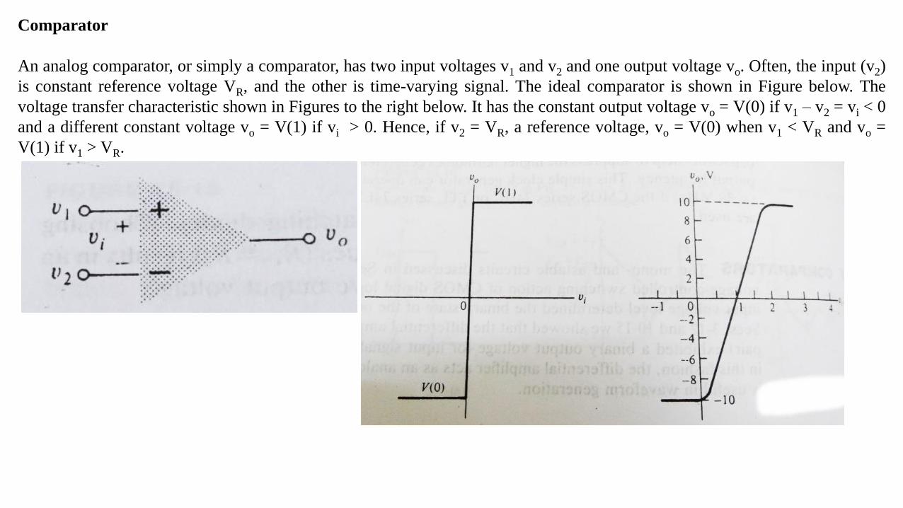
Comparator
An analog comparator, or simply a comparator, has two input voltages v1 and v2 and one output voltage vo. Often, the input (v2)
is constant reference voltage VR, and the other is time-varying signal. The ideal comparator is shown in Figure below. The
voltage transfer characteristic shown in Figures to the right below. It has the constant output voltage vo = V(0) if v1 – v2 = vi < 0
and a different constant voltage vo = V(1) if vi > 0. Hence, if v2 = VR, a reference voltage, vo = V(0) when v1 < VR and vo =
V(1) if v1 > VR.

Square Wave Generator From a Sinusoid
The comparator performs highly nonlinear wave shaping because the output bears no resemblance to the input waveform. It is
often used to transform a signal which varies slowly with time to another which exhibits an abrupt change. One such
application is the generation of square wave from sinusoidal signal. If VR is set to zero, the output will change from one stage
to the other very rapidly (limited by slew rate) every time the input passes through zero. Such a configuration is called zero-
crossing detector. If the input to a comparator is a sine wave, the output is square wave. If a zero crossing detector is used, a
symmetrical square wave results, as shown in the Figures below.

Regenerative Comparator (Schmitt Trigger)
The regenerative comparator of Figure (a) below is commonly referred to as a Schmitt trigger. The input voltage is applied to
the inverting terminal 2 and the feedback voltage to the noninverting terminal 1. Assuming that the output resistance of the
comparator is negligible compared with R1 + R, we obtain 𝑣1 =𝑅2
𝑅1+𝑅2𝑣𝑜

Since v1 = vi with v2 = 0, vo = Avvi and use of small signal analysis gives the return ratio as
𝑇 =−𝑅2𝐴𝑣
𝑅1+𝑅2Clearly, with Av > 0, T < 0 and the feedback is positive (Regenerative). Let Vo = VZ + VD and assume
that v2 < v1 so that vo = +Vo. From the Figures above we find that the voltage at the noninverting terminal is given
by
𝑣1 = 𝑉𝐴 +𝑅2
𝑅1+𝑅2𝑉𝑜 − 𝑉𝐴 ≡ 𝑉1
If v2 is now increased, vo remains constant at Vo, and v1 = V1 = constant until v2 = V1. At this threshold, critical, or
triggering voltage, the output regeneratively switches to vo = -Vo and remains at this value as long as v2 > V1. The
transfer characteristics is indicated in Figure (b) above. The voltage at the noninverting terminal for v2 > V1 is
𝑣1 = 𝑉𝐴 −𝑅2
𝑅1+𝑅2𝑉𝑜 + 𝑉𝐴 ≡ 𝑉2
Note that V2 < V1, and the difference between theses two values is called the hysteresis VH
𝑉𝐻 = 𝑉1 − 𝑉2 =2𝑅2𝑉𝑜
𝑅1+𝑅2

Square Wave Generator
The inverting Schmitt trigger can be used to obtain a free-running square wave generator by connecting an RC feedback
network between the output and the inverting input. The circuit is displayed in Figure below.
In Figure (a) above the differential input voltage vi is given by
𝑣𝑖 = 𝑣𝑐 − 𝑣1 = 𝑣𝑐 −𝑅2
𝑅1+𝑅2𝑣𝑜 = 𝑣𝑐 − 𝛽𝑣𝑜
From the ideal-comparator characteristics 𝑣𝑜 = 𝑉𝐷 + 𝑉𝑍 = 𝑉𝑜 if vi < 0 and vo = - Vo if vi > 0. Consider an instance
of time when vi < 0 or vc < βvo = βVo. The capacitor C charges exponentially toward Vo, through the RC
combination. The output remains at Vo until vc equals +βVo at which time the comparator output reverses to –Vo.
Now vc charges exponentially toward –Vo. The output voltage vo and the capacitor voltage vc waveforms are shown
in Figure (b) above. If we let t = 0 when vc = -βVo for the first half cycle, we have
𝑣𝑐 𝑡 = 𝑉𝑜 1 − (1 + 𝛽)𝑒− 𝑡 𝑅𝐶
Since at t = T/2 vc(t) = +βVo, we find T solving equation above is given by
𝑇 = 2𝑅𝐶𝑙𝑛1+𝛽
1−𝛽= 2𝑅𝐶𝑙𝑛 1 +
2𝑅1
𝑅2Note that T is independent of Vo
This square wave generator is particularly useful in the frequency range of 10 Hz to 10 KHz. At higher frequencies
the slew rate of the OPAMP limits the slope of the output square wave.
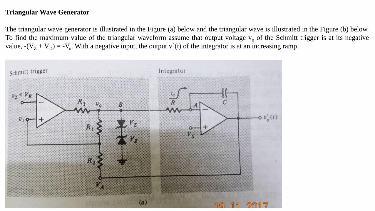
Triangular Wave Generator
The triangular wave generator is illustrated in the Figure (a) below and the triangular wave is illustrated in the Figure (b) below.
To find the maximum value of the triangular waveform assume that output voltage vo of the Schmitt trigger is at its negative
value, -(VZ + VD) = -Vo. With a negative input, the output v’(t) of the integrator is at an increasing ramp.
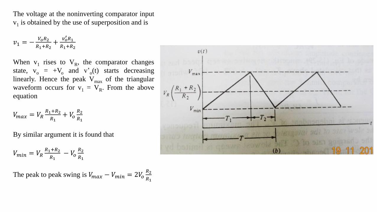
The voltage at the noninverting comparator input
v1 is obtained by the use of superposition and is
𝑣1 = −𝑉𝑜𝑅2
𝑅1+𝑅2+
𝑣𝑜′𝑅1
𝑅1+𝑅2
When v1 rises to VR, the comparator changes
state, vo = +Vo and v’o(t) starts decreasing
linearly. Hence the peak Vmax of the triangular
waveform occurs for v1 = VR. From the above
equation
𝑉𝑚𝑎𝑥 = 𝑉𝑅𝑅1+𝑅2
𝑅1+ 𝑉𝑜
𝑅2
𝑅1
By similar argument it is found that
𝑉𝑚𝑖𝑛 = 𝑉𝑅𝑅1+𝑅2
𝑅1− 𝑉𝑜
𝑅2
𝑅1
The peak to peak swing is 𝑉𝑚𝑎𝑥 − 𝑉𝑚𝑖𝑛 = 2𝑉𝑜𝑅2
𝑅1

We now calculate the sweep time T1 and T2 for Vs = 0. The capacitor charging current is given
as
𝑖𝑐 = 𝐶𝑑𝑣𝑐
𝑑𝑡= −𝐶
𝑑𝑣𝑜′
𝑑𝑡
Where vc = 𝑣𝑜′ is the capacitor voltage. For vo = -Vo, i = -Vo/R, and the positive sweep speed is
𝑑𝑣𝑜′ 𝑑𝑡 = 𝑉𝑜 𝑅𝐶 . Hence
𝑇1 =𝑉𝑚𝑎𝑥−𝑉𝑚𝑖𝑛
𝑉𝑜 𝑅𝐶=
2𝑅2𝑅𝐶
𝑅1
Since the negative sweep speed has the same magnitude as calculated above, T2 = T1 = T/2 =
1/2f, where the frequency f is given by
𝑓 =𝑅1
4𝑅2𝑅𝐶
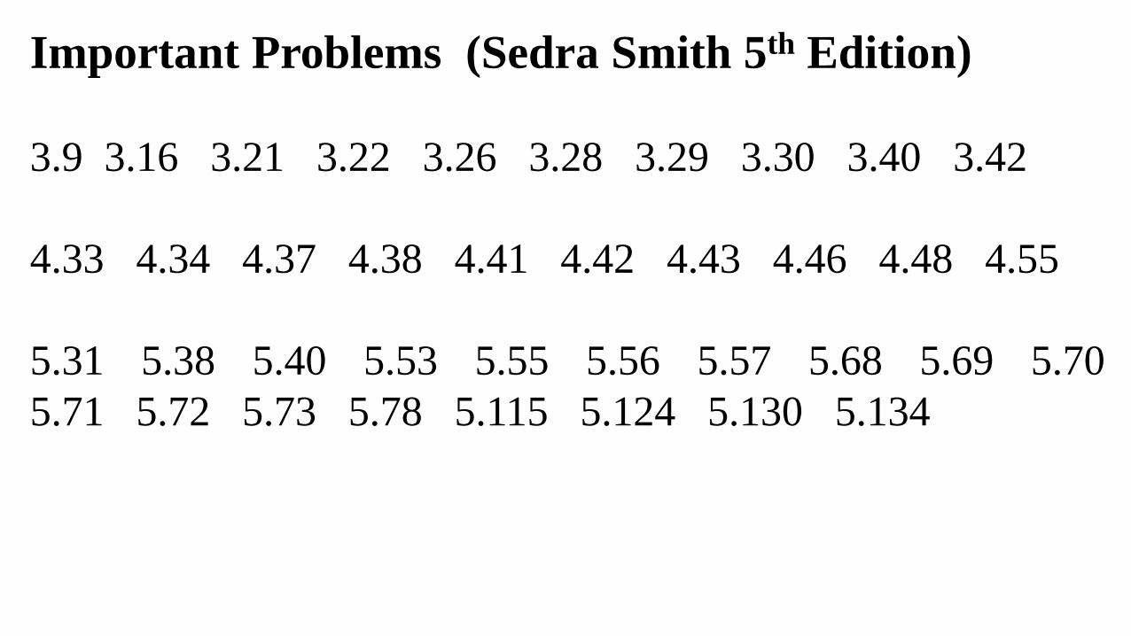
Important Problems (Sedra Smith 5th Edition)
3.9 3.16 3.21 3.22 3.26 3.28 3.29 3.30 3.40 3.42
4.33 4.34 4.37 4.38 4.41 4.42 4.43 4.46 4.48 4.55
5.31 5.38 5.40 5.53 5.55 5.56 5.57 5.68 5.69 5.70
5.71 5.72 5.73 5.78 5.115 5.124 5.130 5.134
Top Related
Copyright © 2022 FDOKUMEN

