


Bahasa
Halaman
Hukum

626 IEEE TRANSACTIONS ON ANTENNAS AND PROPAGATION, VOL. 58, NO. 3, MARCH 2010
RF MEMS Integrated Frequency ReconfigurableAnnular Slot Antenna
Bedri A. Cetiner, Member, IEEE, Gemma Roqueta Crusats, Student Member, IEEE, Lluís Jofre, Senior Member, IEEE,and Necmi Bıyıklı, Member, IEEE
Abstract—A new kind of double- and single-arm cantilevertype DC-contact RF MEMS actuators has been monolithicallyintegrated with an antenna architecture to develop a frequencyreconfigurable antenna. The design, microfabrication, and char-acterization of this “reconfigurable antenna (RA) annular slot”which was built on a microwave laminate TMM10i ( = 9.8, ���= 0.002), are presented in this paper. By activating/deactivatingthe RF MEMS actuators, which are strategically located withinthe antenna geometry and microstrip feed line, the operatingfrequency band is changed. The RA annular slot has two reconfig-urable frequencies of operation with center frequencies ��� =2.4GHz and ���� = 5.2 GHz, compatible with IEEE 802.11 WLANstandards. The radiation and impedance characteristics of theantenna along with the RF performance of individual actuatorsare presented and discussed.
Index Terms—Full-wave analyses, microfabrication, reconfig-urable antenna, RF MEMS actuators.
I. INTRODUCTION
THE reconfigurable antenna (RA) concept [1], [2] has
gained significant interest as a result of two main factors.
First, a single RA can perform multiple functions by dynami-
cally changing its properties (operating frequency, polarization,
and radiation pattern). This can result in a significant reduction
in the overall size of multi-mode multi-band wireless commu-
nication systems and replace multiple single-function legacy
antennas. Second, the reconfigurable antenna properties of a
RA can be used as important additional degrees of freedom in
an adaptive system (first proposed in [3] and later in [4]–[7]).
In particular it was shown that a RA equipped adaptive mul-
tiple-input multiple-output (MIMO) wireless communication
system can provide gains up to 30 dB as compared to conven-
tional fixed antenna MIMO systems [7]. These additional gains
result from the joint optimization of dynamically reconfig-
urable antenna properties with adaptive space-time modulation
techniques [8] in response to the changes in the propagation
environment.
Manuscript received January 29, 2009; revised April 28, 2009. First publishedDecember 28, 2009; current version published March 03, 2010. This work wassupported in part by Army Research Office under Grant W911 NF-07-1-0208and in part by the National Institute of Justice, Office of Justice Programs, USDepartment of Justice under Grant 2007-IJ-CX-K025.
B. A. Cetiner and N. Bıyıklı are with the Electrical and Computer EngineeringDepartment, Utah State University, Logan, UT 84322 USA (e-mail: [email protected]).
L. Jofre and G. Roqueta Crusats are with the Department of Signal Theory andCommunications, Technical University of Catalonia, 08034 Barcelona, Spain.
Color versions of one or more of the figures in this paper are available onlineat http://ieeexplore.ieee.org.
Digital Object Identifier 10.1109/TAP.2009.2039300
In order to dynamically change the properties of a RA, the
current distribution over the volume of the antenna needs to
be changed, where each distribution corresponds to a different
mode of operation. To this end, one can change the geometry and
feed line of the antenna by switching on and off various geomet-
rical segments that make up the RA and the feed circuitry. For
switching, either MEMS or solid-state switching devices can be
employed. In this work, we prefer using RF MEMS actuators
due to monolithic integration capability with antenna segments
along with their low loss and power characteristics. Also, the
potential of MEMS in avoiding nonlinearity and intermodula-
tion effects is an important advantage over solid-state switching
devices [9].
To cover multiple frequency bands by a single antenna
element, various design approaches such as a multi-frequency
antenna covering each individual band, a broadband antenna
covering the whole frequency bandwidth, or a RA with a
narrow instantaneous operating bandwidth that can be tuned
over the whole bandwidth can be used. The design of slot-ring
antennas for mobile communications was previously studied
in [10], [11]. Multi-frequency operation was also presented in
several research papers. In [12], [13], the multi-band operation
is achieved by using multiple concentric annular-ring slots,
which are fed by either a microstrip or coplanar waveguide.
Microstrip-fed slot-ring antennas, which consist of a single
slot-ring of various geometries, that achieve multi-frequency
operation were also investigated [14]. Although these antennas
support multiple frequencies, the radiation patterns and gain
values corresponding to each frequency can be significantly
different. The same problem applies to a broadband antenna,
where the degradation in gain can be significant over a broad
frequency band. This might be a problem for multi-mode
multi-band wireless communications applications where the
radiation characteristics and gain performance are required to
be similar over multiple frequencies. Recent efforts have been
focusing on the tunable slot-ring antennas [15], [16]. The RA
annular slot presented in this paper maintains the same radiation
characteristics for both modes of operation (
and ) due to a similar tunable highly efficient
operating bandwidth over which the radiation behavior remains
almost constant. This is accomplished by MEMS reconfigura-
tion which provides a circular one-wavelength-perimeter for
both the external longer slot of the lower frequency and the
internal shorter one of the higher frequency band. Additionally
the use of an annular geometry compared to the conventional
linear slot reduces the dimension of the antenna by a factor
(perimeter of for the annular slot instead of a length of
for the linear slot).
0018-926X/$26.00 © 2010 IEEE
Authorized licensed use limited to: IEEE Xplore. Downloaded on May 13,2010 at 11:49:50 UTC from IEEE Xplore. Restrictions apply.
CETINER et al.: RF MEMS INTEGRATED FREQUENCY RECONFIGURABLE ANNULAR SLOT ANTENNA 627
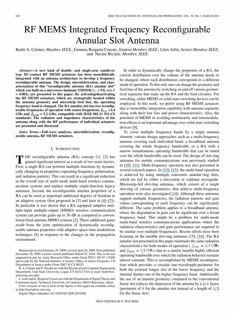
Fig. 1. Architecture of the microstrip-fed RA annular slot. (a) Top view andmagnified A-A’ cross section view. (b) Bottom view and magnified B-B’ crosssection view. (MEMS actuator width is 350 �� and length is 650 ��).
II. RECONFIGURABLE ANNULAR SLOT: ARCHITECTURE,
DESIGN, CHARACTERIZATION
A. Architecture and Working Mechanism
The architecture and a photograph of the microstrip-fed RA
annular slot are shown in Figs. 1 and 2, respectively.
The antenna is built on two separate layers of TMM10i (
, ) microwave laminate each with 0.635 mm
thickness. The microstrip feed line is placed on one layer and
the annular slot is placed on the other layer, which are bonded
together having a total thickness of 1.27 mm. This RA has two
concentric circular slots, each of which can be excited indi-
vidually in order to achieve frequency reconfigurability. The
microstrip feed line is broken into two segments, which are
spanned by a single-arm cantilever type MEMS actuator, (see
Fig. 1(b) and the inset of Fig. 2(a) for a magnified view), which
is similar to the MEMS switch presented in [17]. The actuator
enables either the outer or the inner slot to be excited by
changing the length of the microstrip. When is not activated
(actuator up-state), the microstrip segments are disconnected,
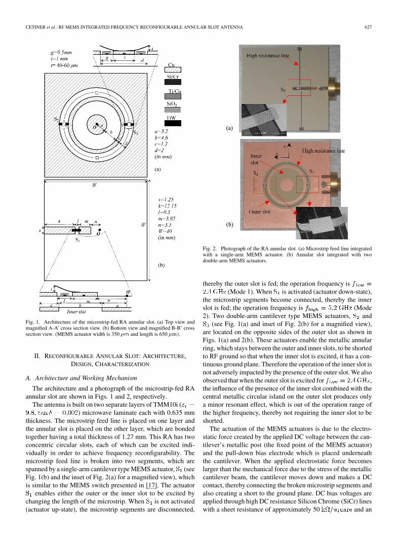
Fig. 2. Photograph of the RA annular slot. (a) Microstrip feed line integratedwith a single-arm MEMS actuator. (b) Annular slot integrated with twodouble-arm MEMS actuators.
thereby the outer slot is fed; the operation frequency is
(Mode 1). When is activated (actuator down-state),
the microstrip segments become connected, thereby the inner
slot is fed; the operation frequency is (Mode
2). Two double-arm cantilever type MEMS actuators, and
(see Fig. 1(a) and inset of Fig. 2(b) for a magnified view),
are located on the opposite sides of the outer slot as shown in
Figs. 1(a) and 2(b). These actuators enable the metallic annular
ring, which stays between the outer and inner slots, to be shorted
to RF ground so that when the inner slot is excited, it has a con-
tinuous ground plane. Therefore the operation of the inner slot is
not adversely impacted by the presence of the outer slot. We also
observed that when the outer slot is excited for ,
the influence of the presence of the inner slot combined with the
central metallic circular island on the outer slot produces only
a minor resonant effect, which is out of the operation range of
the higher frequency, thereby not requiring the inner slot to be
shorted.
The actuation of the MEMS actuators is due to the electro-
static force created by the applied DC voltage between the can-
tilever’s metallic post (the fixed point of the MEMS actuator)
and the pull-down bias electrode which is placed underneath
the cantilever. When the applied electrostatic force becomes
larger than the mechanical force due to the stress of the metallic
cantilever beam, the cantilever moves down and makes a DC
contact, thereby connecting the broken microstrip segments and
also creating a short to the ground plane. DC bias voltages are
applied through high DC resistance Silicon Chrome (SiCr) lines
with a sheet resistance of approximately 50 and an
Authorized licensed use limited to: IEEE Xplore. Downloaded on May 13,2010 at 11:49:50 UTC from IEEE Xplore. Restrictions apply.
628 IEEE TRANSACTIONS ON ANTENNAS AND PROPAGATION, VOL. 58, NO. 3, MARCH 2010
absolute resistance of 500 . Please note that the bias line used
to activate and is placed into the outer slot for the com-
pactness of the design. Due to high resistivity of the bias line,
this placement has no detrimental effect to the operation of RA
annular slot as demonstrated by the measurements and simula-
tions given in the following sections.
An annular slot etched in a large conducting plane can be
viewed as an annular distribution of a magnetic current given by
the actual mode excited into the circumferential slot. To obtain
maximum bandwidth with minimum dimensions, the
mode, normally called fundamental mode, tends to be the basic
choice [18]. Considering the annular slot as a transmission
line, the fundamental resonance appears around the frequency
at which the circumference of the annular slot becomes one
guided wavelength of the slot ( ). The slot guided wavelength
for the frequency and dielectric permittivity ranges of interest
can be expressed [19] as
(1)
where is the slot-line width, the free-space wavelength,
and and are the permittivity and thickness of the substrate,
respectively. While (1) provides a good first order approxima-
tion for the resonance frequency, the actual frequency for the
microstrip-fed MRA annular slot will be in close vicinity of that
of given by (1) as the penetration distance of the projection of
the microstrip onto the slot plays a second order role on the res-
onance frequency. As seen in Fig. 1(b), this penetration distance
for the inner slot is . The bandwidth may be adjusted
by selecting the appropriate internal and external radii of the
slots as
(2)
where , , are the central, upper and lower frequen-
cies for the or and ,
, are the central, external and internal radius for the
(outer slot) or (inner slot) frequency bands.
Please note that these definitions indicate that ,
where is the guided wavelength corresponding to
(outer slot) or (inner slot) frequency bands.
B. Microfabrication
The microfabrication process of the RA annular slot was
performed based on the microwave laminate compatible RF
MEMS technology [1], [20], [22] that enables the monolithic
integration of MEMS actuators with antenna segments. The
layout of MEMS actuators and antenna segments including
microstrip feed lines and high resistance DC control lines are
part of the same lithographic process. Thus, the process flow
for a single double-arm MEMS actuator interconnecting two
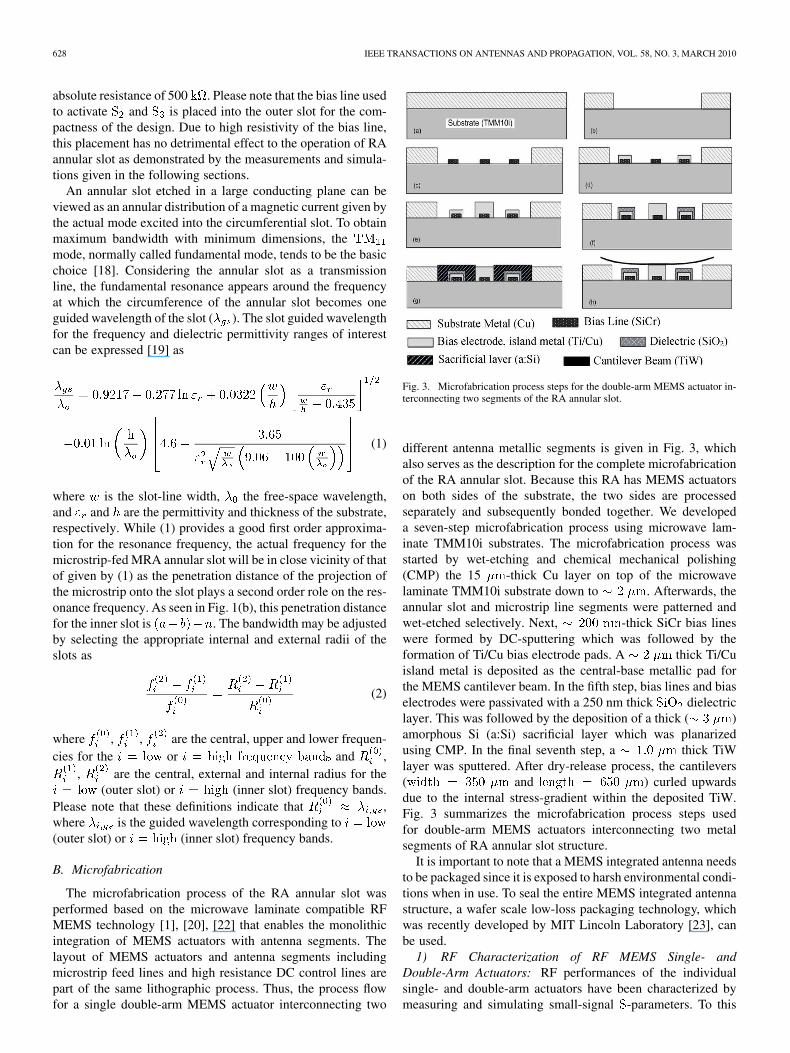
Fig. 3. Microfabrication process steps for the double-arm MEMS actuator in-terconnecting two segments of the RA annular slot.
different antenna metallic segments is given in Fig. 3, which
also serves as the description for the complete microfabrication
of the RA annular slot. Because this RA has MEMS actuators
on both sides of the substrate, the two sides are processed
separately and subsequently bonded together. We developed
a seven-step microfabrication process using microwave lam-
inate TMM10i substrates. The microfabrication process was
started by wet-etching and chemical mechanical polishing
(CMP) the 15 -thick Cu layer on top of the microwave
laminate TMM10i substrate down to . Afterwards, the
annular slot and microstrip line segments were patterned and
wet-etched selectively. Next, -thick SiCr bias lines
were formed by DC-sputtering which was followed by the
formation of Ti/Cu bias electrode pads. A thick Ti/Cu
island metal is deposited as the central-base metallic pad for
the MEMS cantilever beam. In the fifth step, bias lines and bias
electrodes were passivated with a 250 nm thick dielectric
layer. This was followed by the deposition of a thick ( )
amorphous Si (a:Si) sacrificial layer which was planarized
using CMP. In the final seventh step, a thick TiW
layer was sputtered. After dry-release process, the cantilevers
( and ) curled upwards
due to the internal stress-gradient within the deposited TiW.
Fig. 3 summarizes the microfabrication process steps used
for double-arm MEMS actuators interconnecting two metal
segments of RA annular slot structure.
It is important to note that a MEMS integrated antenna needs
to be packaged since it is exposed to harsh environmental condi-
tions when in use. To seal the entire MEMS integrated antenna
structure, a wafer scale low-loss packaging technology, which
was recently developed by MIT Lincoln Laboratory [23], can
be used.
1) RF Characterization of RF MEMS Single- and
Double-Arm Actuators: RF performances of the individual
single- and double-arm actuators have been characterized by
measuring and simulating small-signal -parameters. To this
Authorized licensed use limited to: IEEE Xplore. Downloaded on May 13,2010 at 11:49:50 UTC from IEEE Xplore. Restrictions apply.
CETINER et al.: RF MEMS INTEGRATED FREQUENCY RECONFIGURABLE ANNULAR SLOT ANTENNA 629
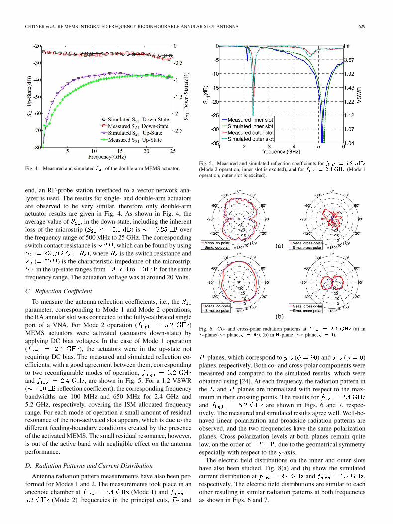
Fig. 4. Measured and simulated � of the double-arm MEMS actuator.
end, an RF-probe station interfaced to a vector network ana-
lyzer is used. The results for single- and double-arm actuators
are observed to be very similar, therefore only double-arm
actuator results are given in Fig. 4. As shown in Fig. 4, the
average value of , in the down-state, including the inherent
loss of the microstrip ( ) is over
the frequency range of 500 MHz to 25 GHz. The corresponding
switch contact resistance is , which can be found by using
, where is the switch resistance and
( ) is the characteristic impedance of the microstrip.
in the up-state ranges from to for the same
frequency range. The actuation voltage was at around 20 Volts.
C. Reflection Coefficient
To measure the antenna reflection coefficients, i.e., the
parameter, corresponding to Mode 1 and Mode 2 operations,
the RA annular slot was connected to the fully-calibrated single
port of a VNA. For Mode 2 operation ( )
MEMS actuators were activated (actuators down-state) by
applying DC bias voltages. In the case of Mode 1 operation
( ), the actuators were in the up-state not
requiring DC bias. The measured and simulated reflection co-
efficients, with a good agreement between them, corresponding
to two reconfigurable modes of operation,
and , are shown in Fig. 5. For a 1:2 VSWR
( reflection coefficient), the corresponding frequency
bandwidths are 100 MHz and 650 MHz for 2.4 GHz and
5.2 GHz, respectively, covering the ISM allocated frequency
range. For each mode of operation a small amount of residual
resonance of the non-activated slot appears, which is due to the
different feeding-boundary conditions created by the presence
of the activated MEMS. The small residual resonance, however,
is out of the active band with negligible effect on the antenna
performance.
D. Radiation Patterns and Current Distribution
Antenna radiation pattern measurements have also been per-
formed for Modes 1 and 2. The measurements took place in an
anechoic chamber at (Mode 1) and
(Mode 2) frequencies in the principal cuts, - and
Fig. 5. Measured and simulated reflection coefficients for � � ��� ���(Mode 2 operation, inner slot is excited), and for � � ��� ��� (Mode 1operation, outer slot is excited).
Fig. 6. Co- and cross-polar radiation patterns at � � ��� ��� (a) in�-plane(�-� plane, � � ), (b) in �-plane (�-� plane, � � ).
-planes, which correspond to - ( ) and - ( )
planes, respectively. Both co- and cross-polar components were
measured and compared to the simulated results, which were
obtained using [24]. At each frequency, the radiation pattern in
the and planes are normalized with respect to the max-
imum in their crossing points. The results for
and are shown in Figs. 6 and 7, respec-
tively. The measured and simulated results agree well. Well-be-
haved linear polarization and broadside radiation patterns are
observed, and the two frequencies have the same polarization
planes. Cross-polarization levels at both planes remain quite
low, on the order of , due to the geometrical symmetry
especially with respect to the -axis.
The electric field distributions on the inner and outer slots
have also been studied. Fig. 8(a) and (b) show the simulated
current distribution at and ,
respectively. The electric field distributions are similar to each
other resulting in similar radiation patterns at both frequencies
as shown in Figs. 6 and 7.
Authorized licensed use limited to: IEEE Xplore. Downloaded on May 13,2010 at 11:49:50 UTC from IEEE Xplore. Restrictions apply.
630 IEEE TRANSACTIONS ON ANTENNAS AND PROPAGATION, VOL. 58, NO. 3, MARCH 2010
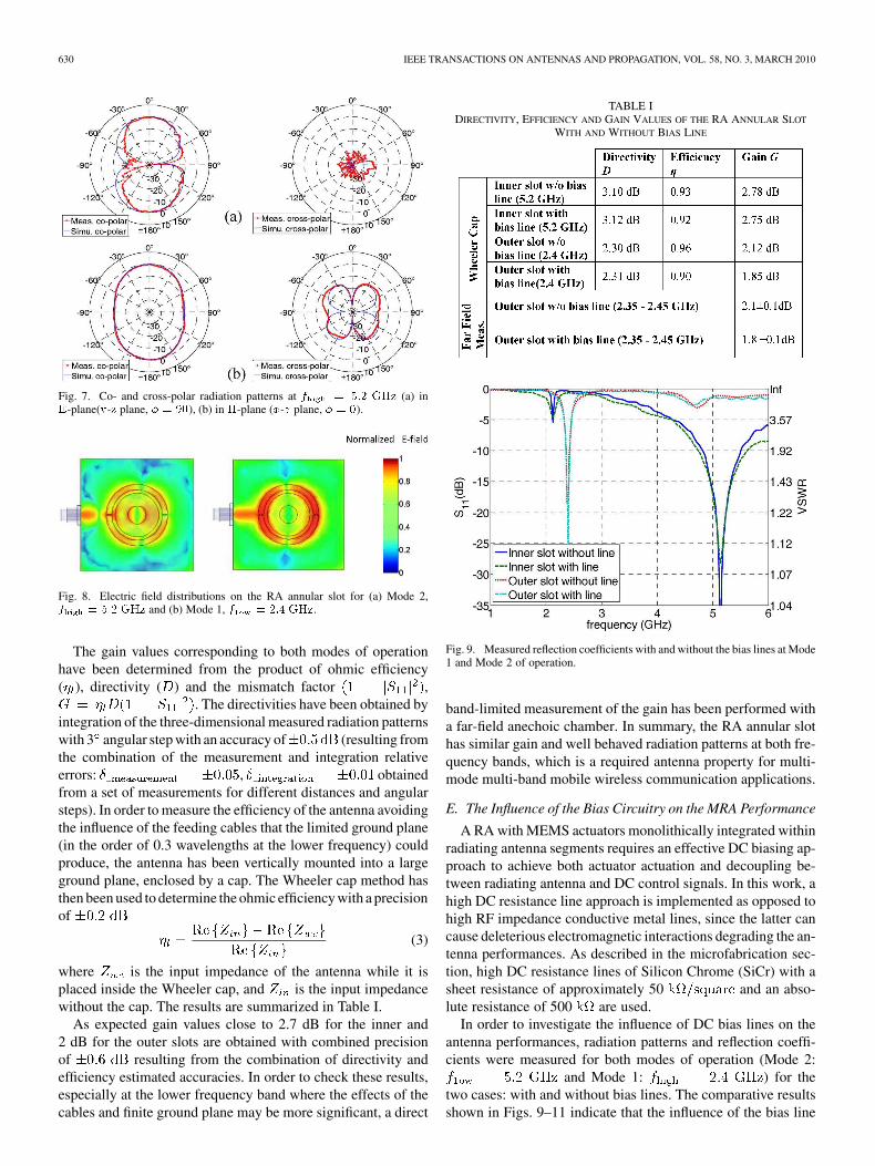
Fig. 7. Co- and cross-polar radiation patterns at � � ��� ��� (a) in�-plane(�-� plane, � � ), (b) in �-plane (�-� plane, � � ).
Fig. 8. Electric field distributions on the RA annular slot for (a) Mode 2,� � ��� ��� and (b) Mode 1, � � ��� ���.
The gain values corresponding to both modes of operation
have been determined from the product of ohmic efficiency
( ), directivity ( ) and the mismatch factor ,
. The directivities have been obtained by
integration of the three-dimensional measured radiation patterns
with 3 angular step with an accuracy of (resulting from
the combination of the measurement and integration relative
errors: , obtained
from a set of measurements for different distances and angular
steps). In order to measure the efficiency of the antenna avoiding
the influence of the feeding cables that the limited ground plane
(in the order of 0.3 wavelengths at the lower frequency) could
produce, the antenna has been vertically mounted into a large
ground plane, enclosed by a cap. The Wheeler cap method has
then been used to determine the ohmic efficiency with a precision
of
(3)
where is the input impedance of the antenna while it is
placed inside the Wheeler cap, and is the input impedance
without the cap. The results are summarized in Table I.
As expected gain values close to 2.7 dB for the inner and
2 dB for the outer slots are obtained with combined precision
of resulting from the combination of directivity and
efficiency estimated accuracies. In order to check these results,
especially at the lower frequency band where the effects of the
cables and finite ground plane may be more significant, a direct
TABLE IDIRECTIVITY, EFFICIENCY AND GAIN VALUES OF THE RA ANNULAR SLOT
WITH AND WITHOUT BIAS LINE
Fig. 9. Measured reflection coefficients with and without the bias lines at Mode1 and Mode 2 of operation.
band-limited measurement of the gain has been performed with
a far-field anechoic chamber. In summary, the RA annular slot
has similar gain and well behaved radiation patterns at both fre-
quency bands, which is a required antenna property for multi-
mode multi-band mobile wireless communication applications.
E. The Influence of the Bias Circuitry on the MRA Performance
A RA with MEMS actuators monolithically integrated within
radiating antenna segments requires an effective DC biasing ap-
proach to achieve both actuator actuation and decoupling be-
tween radiating antenna and DC control signals. In this work, a
high DC resistance line approach is implemented as opposed to
high RF impedance conductive metal lines, since the latter can
cause deleterious electromagnetic interactions degrading the an-
tenna performances. As described in the microfabrication sec-
tion, high DC resistance lines of Silicon Chrome (SiCr) with a
sheet resistance of approximately 50 and an abso-
lute resistance of 500 are used.
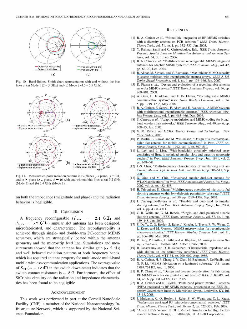
In order to investigate the influence of DC bias lines on the
antenna performances, radiation patterns and reflection coeffi-
cients were measured for both modes of operation (Mode 2:
and Mode 1: ) for the
two cases: with and without bias lines. The comparative results
shown in Figs. 9–11 indicate that the influence of the bias line
Authorized licensed use limited to: IEEE Xplore. Downloaded on May 13,2010 at 11:49:50 UTC from IEEE Xplore. Restrictions apply.
CETINER et al.: RF MEMS INTEGRATED FREQUENCY RECONFIGURABLE ANNULAR SLOT ANTENNA 631
Fig. 10. Band-limited Smith chart representation with and without the biaslines at (a) Mode 1 (2 – 3 GHz) and (b) Mode 2 (4.5 – 5.5 GHz).
Fig. 11. Measured co-polar radiation patterns in �- plane (�-� plane, � � ��)and in �-plane (�-� plane, � � �) with and without bias lines at (a) 5.2 GHz(Mode 2) and (b) 2.4 GHz (Mode 1).
on both the impedance (magnitude and phase) and the radiation
behavior is negligible.
III. CONCLUSION
A frequency reconfigurable ( and
) annular slot antenna has been designed,
microfabricated, and characterized. The reconfigurability is
achieved through single- and double-arm DC-contact MEMS
actuators, which are strategically located within the antenna
geometry and the microstrip feed line. Simulations and mea-
surements showed that the antenna has similar gain ( )
and well behaved radiation patterns at both frequency bands,
which is a required antenna property for multi-mode multi-band
mobile wireless communication applications. The average value
of ( in the switch down-state) indicates that the
switch contact resistance is . Furthermore, the effect of
SiCr bias circuitry on the radiation and impedance characteris-
tics has been found to be negligible.
ACKNOWLEDGMENT
This work was performed in part at the Cornell NanoScale
Facility (CNF), a member of the National Nanotechnology In-
frastructure Network, which is supported by the National Sci-
ence Foundation.
REFERENCES
[1] B. A. Cetiner et al., “Monolithic integration of RF MEMS switcheswith a diversity antenna on PCB substrate,” IEEE Trans. Microw.
Theory Tech., vol. 51, no. 1, pp. 332–335, Jan. 2003.[2] Y. Rahmat-Samii and C. Christodoulou, Eds., IEEE Trans. Antennas
Propag., Special Issue on Multifunction Antennas and Antenna Sys-
tems, vol. 54, pt. 1, Feb. 2006.[3] B. A. Cetiner et al., “Multifunctional reconfigurable MEMS integrated
antennas for adaptive MIMO systems,” IEEE Commun. Mag., vol. 42,pp. 62–70, Dec. 2004.
[4] B. Akbar, M. Sayeed, and V. Raghavan, “Maximizing MIMO capacityin sparse multipath with reconfigurable antenna arrays,” IEEE J. Sel.
Topics Signal Processing, vol. 1, no. 1, pp. 156–166, Jun. 2007.[5] D. Piazza et al., “Design and evaluation of a reconfigurable antenna
array for MIMO systems,” IEEE Trans. Antennas Propag., vol. 56, pp.869–881, 2008.
[6] A. Grau, H. Jafarkhani, and F. De Flaviis, “Reconfigurable MIMOcommunication system,” IEEE Trans. Wireless Commun., vol. 7, no.5, pp. 1719–1733, May 2008.
[7] B. A. Cetiner, E. Sengul, E. Akay, and E. Ayanoglu, “A MIMO systemwith multifunctional reconfigurable antennas,” IEEE Antennas Wire-
less Propag. Lett., vol. 5, pp. 463–466, Dec. 2006.[8] S. Catreux et al., “Adaptive modulation and MIMO coding for broad-
band wireless data networks,” IEEE Commun. Mag., vol. 40, no. 6, pp.
108–15, Jun. 2002.[9] G. M. Rebeiz, RF MEMS: Theory, Design and Technology. New
York: Wiley, 2003.[10] P. Mastin, B. Rawat, and M. Williamson, “Design of a microstrip an-
nular slot antenna for mobile communications,” in Proc. IEEE An-
tennas Propag. Symp., Jul. 1992, vol. 1, pp. 507–510.[11] L. Lavi and J. Liva, “Wide-bandwidth circularly polarized array
consisting of linearly polarized annular slots and parasitic microstrippatches,” in Proc. IEEE Antennas Propag. Symp., Jun. 1991, vol. 2,pp. 638–641.
[12] J.-S. Chen, “Multi-frequency characteristics of annular-ring slot an-tennas,” Microw. Opt. Technol. Lett., vol. 38, no. 6, pp. 506–511, Sep.2003.
[13] X. Qing and M. Chin, “Broadband annular dual-slot antenna forWLAN applications,” in Proc. IEEE Antennas and Propag. Int. Symp.,2002, vol. 2, pp. 452–455.
[14] H. Tehrani and K. Chang, “Multifrequency operation of microstrip-fedslot-ring antennas on thin low-dielectric permittivity substrates,” IEEE
Trans. Antennas Propag., vol. 50, pp. 1299–1308, Sep. 2002.[15] I. Carrasquillo-Rivera et al., “Tunable and dual-band rectangular
slotring antenna,” in Proc. IEEE Antennas Propag. Symp., Jun. 2004,vol. 4, pp. 4308–4311.
[16] C. R. White and G. M. Rebeiz, “Single- and dual-polarized tunableslot-ring antenna,” IEEE Trans. Antennas Propag., vol. 57, no. 1, pp.439–448, Jan. 2009.
[17] S. Duffy, C. O. Bozler, S. Rabe, J. Knecht, L. Travis, P. W. Wyatt, C.L. Keast, and M. Gouker, “MEMS microswitches for reconfigurablemicrowave circuitry,” IEEE Microw. Wireless Compon. Lett., vol. 11,pp. 106–108, Mar. 2001.
[18] R. Garg, P. Barthia, I. Bathl, and A. Ittipibon, Microstrip Antenna De-
sign Handbook. Boston, MA: Artech House, 2001.[19] R. Janaswamy and D. H. Schaubert, “Characteristic impedance of a
wide slotline on low permittivity substrates,” IEEE Trans. Microw.
Theory Tech., vol. MTT-34, pp. 900–902, Aug. 1986.[20] B. A. Cetiner, H. P. Chang, J. Y. Qian, M. Bachman, F. De Flaviis, and
G. P. Li, “MEMS fabrication on a laminated substrate,” U.S. patent7,084,724 B2, Aug. 1, 2006.
[21] H. P. Chang et al., “Design and process consideration for fabricatingRF MEMS switches on printed circuit boards,” IEEE J. MEMS, vol.14, no. 6, pp. 1311–1322, Dec. 2005.
[22] B. A. Cetiner and N. Biyikli, “Penta-band planar inverted F-antenna(PIFA) integrated by RF NEMS switches,” presented at the IEEE Uni-versity Government Industry Micro/Nano Symp., Louisville, KY, Jul.13–18, 2008.
[23] J. Muldavin, C. O. Bozler, S. Rabe, P. W. Wyatt, and C. L. Keast,“Wafer-scale packaged RF microelectromechanical switches,” IEEE
Trans. Microw. Theory Tech., vol. 56, no. 2, pp. 522–529, Feb. 2008.[24] “Ansoft HFSS Version 11, 3D EM-Field Simulation for High Perfor-
mance Electronic Design,”. Pittsburgh, PA, Ansoft Corporation.
Authorized licensed use limited to: IEEE Xplore. Downloaded on May 13,2010 at 11:49:50 UTC from IEEE Xplore. Restrictions apply.
632 IEEE TRANSACTIONS ON ANTENNAS AND PROPAGATION, VOL. 58, NO. 3, MARCH 2010
Bedri A. Cetiner (M’00) received the Ph.D. degreein electronics and communications engineering fromthe Yildiz Technical University, Istanbul, in 1999.
From November 1999 to June 2000, he was withthe University of California, Los Angeles, as a NATOScience Fellow. He then joined the Department ofElectrical Engineering and Computer Science, Uni-versity of California, Irvine, where he worked as aResearch Specialist from June 2000 to June 2004.From July 2004 until July of 2007, he worked as anAssistant Professor in the Department of Space Sci-
ence and Engineering, Morehead State University. In August 2007, he joinedUtah State University, Logan, where he is an Assistant Professor of electricalengineering. His research focuses on the applications of micro-nano technolo-gies to a new class of micro-/millimeter-wave circuits and systems, and intelli-gent wireless communications systems with an emphasis on the multifunctionalreconfigurable antennas (MRA) for use in cognitive multi-input multi-output(MIMO) systems. He is the Principal Inventor of three technologies includingmicrowave laminate compatible RF MEMS technology and MRA equippedMIMO systems.
Prof. Cetiner is a member of the IEEE Antennas and Propagation, MicrowaveTheory and Techniques, and Communication societies.
Gemma Roqueta Crusats (S’08) was born inGirona, Spain, in 1983. She received the Telecom-munication Engineer degree from the TechnicalUniversity of Catalonia (UPC), Barcelona, Spain, in2007, where she is working toward the Ph.D. degree.
In 2006, she was involved in body area net-works research as foreign student in the CatholicUniversity of Louvain, Louvain, Belgium. SinceSeptember 2007, she has been with the UPC whereshe is involved in developing wideband microwaveimaging applications for non-destructive quality
testing methods for civil structures with fiber reinforcement. Her research in-terests include indoor and outdoor propagation, wideband microwave imaging,spiralometric discrimination and ultra wide band antennas.
Lluís Jofre (S’79–M’83–SM’07) was born inMataró, Spain, in 1956. He received the M.Sc.(Ing) and Ph.D. (Doctor Ing.) degrees in electricalengineering (telecommunications eng.), from theTechnical University of Catalonia (UPC), Barcelona,Spain, in 1978 and 1982, respectively.
From 1979 to 1980, he was a Research Assistant inthe Electrophysics Group,UPC, where he worked onthe analysis and near field measurement of antennaand scatterers. From 1981 to 1982, he joined theEcole Superieure d’Electricite, Paris, France, where
he was involved in microwave antenna design and imaging techniques for med-ical and industrial applications. In 1982, he was appointed Associate Professorat the Communications Department, Telecommunication Engineering School,UPC, where he became Full Professor in 1989. From 1986 to 1987, he wasa Visiting Fulbright Scholar at the Georgia Institute of Technology, Atlanta,working on antennas, and electromagnetic imaging and visualization. From1989 to 1994, he served as Director of the Telecommunication EngineeringSchool (UPC), and from 1994–2000, as UPC Vice-Rector for AcademicPlanning. From 2000 to 2001, he was a Visiting Professor at the Electrical andComputer Engineering Department, Henry Samueli School of Engineering,University of California. From 2002 to 2004, he served as Director of theCatalan Research Foundation and since 2003 as Director of the UPC-TelefonicaChair. His research interests include antennas, electromagnetic scattering andimaging, and system miniaturization for wireless and sensing industrial and bioapplications. He has published more than 100 scientific and technical papers,reports and three books and chapters in specialized volumes.
Necmi Bıyıklı (M’04) was born in Utrecht, TheNetherlands, in 1974. He received the B.S., M.S.,and Ph.D. degrees in electrical and electronics en-gineering from Bilkent University, Ankara, Turkey,in 1996, 1998, and 2004, respectively. His M.S.and Ph.D. thesis work concentrated on the design,fabrication and characterization of high-performancephotodetectors.
During his Postdoctoral research at the VirginiaCommonwealth University, he worked on the growth,fabrication, and characterization of AlGaN/GaN het-
erostructures for various applications including high-performance GaN/AlGaNtransistors. He also worked as a Research Scientist at Utah State University.His research at Utah State University focused on RF-MEMS/NEMS integratedmultifunctional reconfigurable antennas. Currently he is with the UNAM– Materials Science and Nanotechnology Institute, Bilkent University. Hisresearch interests include RF-MEMS/NEMS integrated reconfigurable an-tennas, III-Nitride materials and devices for optoelectronic and photovoltaicapplications, nanofabrication for novel sensor technologies. He is the author ofover 70 citation-index journal papers and refereed conference proceedings.
Dr. Bıyıklı serves as a reviewer for several scientific journals including Ap-
plied Physics Letters, IEEE Photonics Technology Letters, and IEEE Journal of
Quantum Electronics.
Authorized licensed use limited to: IEEE Xplore. Downloaded on May 13,2010 at 11:49:50 UTC from IEEE Xplore. Restrictions apply.
Top Related
Copyright © 2022 FDOKUMEN

