


Bahasa
Halaman
Hukum

New resistorless and electronically tunable realizationof dual-output VM all-pass filter using VDIBA
Norbert Herencsar • Shahram Minaei •
Jaroslav Koton • Erkan Yuce • Kamil Vrba
Received: 25 February 2012 / Revised: 6 June 2012 / Accepted: 21 July 2012 / Published online: 31 August 2012
� Springer Science+Business Media, LLC 2012
Abstract In this paper, a new active element called
voltage differencing inverting buffered amplifier (VDIBA)
is presented. Using single VDIBA and a capacitor, a new
resistorless voltage-mode (VM) first-order all-pass filter
(APF) is proposed, which provides both inverting and non-
inverting outputs at the same configuration simultaneously.
The pole frequency of the filter can be electronically
controlled by means of bias current of the internal trans-
conductance. No component-matching conditions are
required and it has low sensitivity. In addition, the parasitic
and loading effects are also investigated. By connecting
two newly introduced APFs in open loop a novel second-
order APF is proposed. As another application, the pro-
posed VM APF is connected in cascade to a lossy inte-
grator in a closed loop to design a four-phase quadrature
oscillator. The theoretical results are verified by SPICE
simulations using TSMC 0.18 lm level-7 CMOS process
parameters with ±0.9 V supply voltages. Moreover, the
behavior of the proposed VM APF was also experimentally
measured using commercially available integrated circuit
OPA860 by Texas Instruments.
Keywords Analog signal processing � All-pass filter �Electronically tunable circuit � Four-phase quadrature
oscillator � Loading effect � Resistorless filter �Voltage-mode � Voltage differencing inverting buffered
amplifier (VDIBA)
1 Introduction
All-pass filters are used to correct the phase shifts caused
by analog filtering operations without changing the
amplitude of the applied signal. In the literature, although
many first-order voltage-mode (VM) all-pass filters (APFs)
were proposed (e.g. [1–23] and references cited therein),
only circuits in [3–23] are resistorless i.e. no external
resistor is required and electronically tunable simulta-
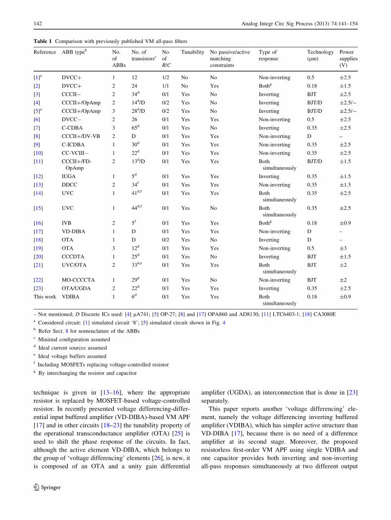
neously. Table 1 summarizes the advantages and disad-
vantages of previously reported VM APFs in [1–23]. It is
important to mention that we do not rule out the impor-
tance of the discussion on all the given criterions in the
Table 1, however, in this part we concentrate on compar-
ison of each circuit only regarding their tunability feature.
In general, the tunability feature of circuits is solved in four
different ways. After the current-controlled conveyor
(CCCII) was introduced [24], a new period has been
opened with respect to electronic tunability in the analog
filter design. Here the intrinsic input resistance of the
CCCII and other versatile analog building blocks (ABBs) is
controlled via an external current or voltage, as shown in
[3–11]. Similarly, the output resistance control of the
CMOS inverting amplifier is demonstrated in [12]. Another
N. Herencsar (&) � J. Koton � K. Vrba
Department of Telecommunications, Brno University
of Technology, Purkynova 118, 61200 Brno, Czech Republic
e-mail: [email protected]
J. Koton
e-mail: [email protected]
K. Vrba
e-mail: [email protected]
S. Minaei
Department of Electronics and Communications Engineering,
Dogus University, 34722 Kadikoy-Istanbul, Turkey
e-mail: [email protected]
E. Yuce
Department of Electrical and Electronics Engineering,
Pamukkale University, 20070 Kinikli-Denizli, Turkey
e-mail: [email protected]
123
Analog Integr Circ Sig Process (2013) 74:141–154
DOI 10.1007/s10470-012-9936-2
technique is given in [13–16], where the appropriate
resistor is replaced by MOSFET-based voltage-controlled
resistor. In recently presented voltage differencing-differ-
ential input buffered amplifier (VD-DIBA)-based VM APF
[17] and in other circuits [18–23] the tunability property of
the operational transconductance amplifier (OTA) [25] is
used to shift the phase response of the circuits. In fact,
although the active element VD-DIBA, which belongs to
the group of ‘voltage differencing’ elements [26], is new, it
is composed of an OTA and a unity gain differential
amplifier (UGDA), an interconnection that is done in [23]
separately.
This paper reports another ‘voltage differencing’ ele-
ment, namely the voltage differencing inverting buffered
amplifier (VDIBA), which has simpler active structure than
VD-DIBA [17], because there is no need of a difference
amplifier at its second stage. Moreover, the proposed
resistorless first-order VM APF using single VDIBA and
one capacitor provides both inverting and non-inverting
all-pass responses simultaneously at two different output
Table 1 Comparison with previously published VM all-pass filters
Reference ABB typeb No.
of
ABBs
No. of
transistorscNo.
of
R/C
Tunability No passive/active
matching
constraints
Type of
response
Technology
(lm)
Power
supplies
(V)
[1]a DVCC? 1 12 1/2 No No Non-inverting 0.5 ±2.5
[2] DVCC? 2 24 1/1 No Yes Bothg 0.18 ±1.5
[3] CCCII- 2 34d 0/1 Yes No Inverting BJT ±2.5
[4] CCCII?/OpAmp 2 14d/D 0/2 Yes No Inverting BJT/D ±2.5/-
[5]a CCCII?/OpAmp 3 28d/D 0/2 Yes No Inverting BJT/D ±2.5/-
[6] DVCC- 2 26 0/1 Yes Yes Non-inverting 0.5 ±2.5
[7] C-CDBA 3 65d 0/1 Yes No Inverting 0.35 ±2.5
[8] CCCII?/DV-VB 2 D 0/1 Yes Yes Non-inverting D –
[9] C-ICDBA 1 30d 0/1 Yes Yes Non-inverting 0.35 ±2.5
[10] CC-VCIII- 1 22d 0/1 Yes Yes Non-inverting 0.35 ±2.5
[11] CCCII?/FD-
OpAmp
2 13d/D 0/1 Yes Yes Both
simultaneously
BJT/D ±1.5
[12] IUGA 1 5d 0/1 Yes Yes Inverting 0.35 ±1.5
[13] DDCC 2 34f 0/1 Yes Yes Non-inverting 0.35 ±1.5
[14] UVC 1 41d,f 0/1 Yes Yes Both
simultaneously
0.35 ±2.5
[15] UVC 1 44d,f 0/1 Yes No Both
simultaneously
0.35 ±2.5
[16] IVB 2 5f 0/1 Yes Yes Bothg 0.18 ±0.9
[17] VD-DIBA 1 D 0/1 Yes Yes Non-inverting D –
[18] OTA 1 D 0/2 Yes No Inverting D –
[19] OTA 3 12d 0/1 Yes Yes Non-inverting 0.5 ±3
[20] CCCDTA 1 25d 0/1 Yes No Inverting BJT ±1.5
[21] UVC/OTA 2 33d,e 0/1 Yes Yes Both
simultaneously
BJT ±2
[22] MO-CCCCTA 1 29d 0/1 Yes No Non-inverting BJT ±2
[23] OTA/UGDA 2 22d 0/1 Yes Yes Inverting 0.35 ±2.5
This work VDIBA 1 6d 0/1 Yes Yes Both
simultaneously
0.18 ±0.9
– Not mentioned; D Discrete ICs used: [4] lA741; [5] OP-27; [8] and [17] OPA860 and AD8130; [11] LTC6403-1; [18] CA3080Ea Considered circuit: [1] simulated circuit ‘8’; [5] simulated circuit shown in Fig. 4b Refer Sect. 8 for nomenclature of the ABBsc Minimal configuration assumedd Ideal current sources assumede Ideal voltage buffers assumedf Including MOSFETs replacing voltage-controlled resistorg By interchanging the resistor and capacitor
142 Analog Integr Circ Sig Process (2013) 74:141–154
123
nodes. It is worth mention that only circuits in [11, 14, 15],
and [21] have such exclusive advantage. To validate the
applicability of the new APF, a second-order APF and
four-phase quadrature oscillator circuits are presented.
SPICE simulation and experimental measurement results
are included to support the theory.
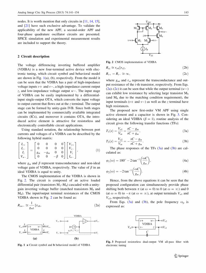
2 Circuit description
The voltage differencing inverting buffered amplifier
(VDIBA) is a new four-terminal active device with elec-
tronic tuning, which circuit symbol and behavioral model
are shown in Fig. 1(a), (b), respectively. From the model it
can be seen that the VDIBA has a pair of high-impedance
voltage inputs v? and v-, a high-impedance current output
z, and low-impedance voltage output w-. The input stage
of VDIBA can be easily implemented by a differential-
input single-output OTA, which converts the input voltage
to output current that flows out at the z terminal. The output
stage can be formed by unity-gain IVB. Since both stages
can be implemented by commercially available integrated
circuits (ICs), and moreover it contains OTA, the intro-
duced active element is attractive for resistorless and
electronically controllable circuit applications.
Using standard notation, the relationship between port
currents and voltages of a VDIBA can be described by the
following hybrid matrix:
IvþIv�Iz
Vw�
2664
3775 ¼
0 0 0 0
0 0 0 0
gm �gm 0 0
0 0 �b 0
2664
3775
VvþVv�Vz
Iw�
2664
3775; ð1Þ
where gm and b represent transconductance and non-ideal
voltage gain of VDIBA, respectively. The value of b in an
ideal VDIBA is equal to unity.
The CMOS implementation of the VDIBA is shown in
Fig. 2. The circuit is composed of an active loaded
differential pair (transistors M1–M4) cascaded with a unity-
gain inverting voltage buffer (matched transistors M5 and
M6). The input/output terminal resistances of the CMOS
VDIBA shown in Fig. 2 can be found as:
Row� ffi1
gm5
ro6k ; ð2aÞ
Roz ffi ro4 ro2k ; ð2bÞRvþ ¼ Rv� ffi 1; ð2cÞ
where gmi and roi represent the transconductance and out-
put resistance of the i-th transistor, respectively. From Eqs.
(2a)–(2c) it can be seen that while the output terminal (w-)
can exhibit low resistance by selecting large transistor M5
(and M6 due to the matching condition requirement), the
input terminals (v? and v-) as well as the z terminal have
high resistances.
The proposed new first-order VM APF using single
active element and a capacitor is shown in Fig. 3. Con-
sidering an ideal VDIBA (b = 1), routine analysis of the
circuit gives the following transfer functions (TFs):
T1 sð Þ ¼ Vo1
Vin¼ sC � gm
sC þ gm; ð3aÞ
T2 sð Þ ¼ Vo2
Vin¼ � sC � gm
sC þ gm: ð3bÞ
The phase responses of the TFs (3a) and (3b) are cal-
culated as:
u1 xð Þ ¼ 180� � 2 tan�1 xC
gm
� �; ð4aÞ
u2 xð Þ ¼ �2 tan�1 xC
gm
� �: ð4bÞ
Hence, from the above equations it can be seen that the
proposed configuration can simultaneously provide phase
shifting both between p (at x = 0) to 0 (at x = ?) and 0
(at x = 0) to -p (at x = ?), at output terminals Vo1 and
Vo2, respectively.
From Eqs. (3a) and (3b), the pole frequency xp is
expressed as:
v+
v– z
w–VDIBA Iz
Iw–
Iv–
Iv+
Vv–
Vv+
Vz
Vw–
gm(Vv+–Vv–)
VDIBA
–1
Vv–
Vv+
Vz
Vw–
(a) (b)
Fig. 1 a Circuit symbol and b behavioral model of VDIBA
IB
VSS
M3
M1 M2
M4 M5
M6
VDD
w–
v–v+
z
Fig. 2 CMOS implementation of VDIBA
v+
v– z
w–VDIBA
Vin Vo1
Vo2
C
Fig. 3 Proposed resistorless dual-output VM all-pass filter with
electronic tuning
Analog Integr Circ Sig Process (2013) 74:141–154 143
123
xp ¼gm
C: ð5Þ
Note that the xp can be easily tuned by adjusting the
transconductance of VDIBA. The pole sensitivities of the
proposed circuit are given as:
Sxpgm¼ �S
xp
C ¼ 1; ð6Þ
which are not higher than unity in magnitude.
3 Non-ideal and parasitic effects analysis
Taking into account the non-ideal voltage gain b of the
VDIBA, TFs in Eqs. (3a) and (3b) convert to:
T1 sð Þ ¼ Vo1
Vin¼ sC � gm
sC þ bgm; ð7aÞ
T2 sð Þ ¼ Vo2
Vin¼ �bT1 sð Þ; ð7bÞ
and non-ideal phase responses from TFs (7a) and (7b) are
given as:
u1 xð Þ ¼ 180� � tan�1 xC
gm
� �� tan�1 xC
bgm
� �; ð8aÞ
u2 xð Þ ¼ � tan�1 xC
gm
� �� tan�1 xC
bgm
� �: ð8bÞ
Consequently, the pole frequency of the presented filter
is found as:
xp ¼bgm
C: ð9Þ
From Eq. (9) it can be realized that the single non-
ideality of the VDIBA slightly affects the filter parameters,
however, this influence can be easily compensated by the
transconductance of the VDIBA.
For a complete analysis of the circuit in Fig. 3, it is also
important to take into account parasitic effects of the VDI-
BA. Detailed numerical simulation of the filter indicated that
the main source of non-idealities is due to the finite output
admittance Yz of the involved OTA stage of the VDIBA.
Considering that this admittance is modeled by a parallel RC
circuit consisting of a non-ideal output resistance Rz and a
non-ideal output capacitance Cz and assuming the non-zero
output resistance Rw- of the w- terminal, the matrix rela-
tionship of (1) changes as follows:
IvþIv�Iz
Vw�
2664
3775 ¼
0 0 0 0
0 0 0 0
gm �gm sCz þ 1Rz
0
0 0 �b Rw�
2664
3775
VvþVv�Vz
Iw�
2664
3775: ð10Þ
Re-analysis of the proposed filter in Fig. 3, the ideal TFs
(3a) and (3b) turns to be:
T1 sð Þ ¼ Vo1
Vin¼ C
C þ Cz� s� gm=C
sþ bgm þ 1Rz
� �.C þ Czð Þ
;
ð11aÞ
T2 sð Þ ¼ Vo2
Vin¼ �bT1 sð Þ: ð11bÞ
From Eq. (11a) it is noted that the filter has a con-
stant magnitude slightly lower than unity, which is equal
to C/(C ? Cz) provided that the following condition is
met:
b ¼ 1þ Cz
C� 1
gmRz: ð12Þ
Therefore, by replacing the involved unity gain IVB
stage with an adjustable amplifier with the prescribed gain
in Eq. (12), the above discussed non-ideal effects can be
fully compensated, at the cost of having a constant
magnitude slightly lower than unity.
At this point, we want to note an interesting and useful
property of the proposed filter. The filter has a very accu-
rate unit magnitude at very low and very high frequencies.
To be specific, owing to the fact that there is a capacitor
connected between the filter’s input and output terminals
and the capacitor behaves as a short-circuit element at the
very high frequencies, the filter has very accurate unit
magnitude in this frequency region, inherently. It is also
worth mention that the circuit in [12] has an identical
feature.
On the other hand, at very low frequencies, the filter
magnitude approximates to:
Vo1
Vin s ¼ 0
���� ¼ �gmRz
1þ bgmRz; ð13Þ
which is the gain of the feedback loop in Fig. 3. This gain
also is very close to unity since typical value of Rz is much
larger than 1/gm.
From Eqs. (11a) and (11b) the non-ideal zero xz and
pole xp frequencies including parasitics can be calculated
as:
xz ¼gm
C; ð14aÞ
xp ¼bgm þ 1
Rz
C þ Cz: ð14bÞ
From Eq. (14b) it is clear that pole xp frequency is
affected by the parasitics and non-idealities of the active
element used, however, they can be minimized by:
(i) making the b very close to unity and/or,
(ii) choosing C � Cz and/or,
(iii) choosing gm � 1/Rz.
144 Analog Integr Circ Sig Process (2013) 74:141–154
123
4 Loading effect analysis
In addition, the loading effects at both output terminals are
also worth to be investigated. Assuming equal load
RL1 = RL2 = RL and considering the non-idealities and
parasitics of the VDIBA in Eq. (10), straightforward
analysis gives the following voltage transfer functions:
T2 sð Þ ¼ Vo2
Vin¼ �bT1 sð Þ: ð15bÞ
Assuming RL � Rw-, TFs in Eqs. (15a) and (15b) turn
to:
T1 sð Þ ¼ Vo1
Vin¼ sC � gm
s C þ Czð Þ þ bgm þ 1Rzþ 1
RL
; ð16aÞ
T2 sð Þ ¼ Vo2
Vin¼ �bT1 sð Þ: ð16bÞ
Finally, considering Rz � RL, TFs in Eqs. (16a) and
(16b) change to:
T1 sð Þ ¼ Vo1
Vin¼ sC � gm
s C þ Czð Þ þ bgm þ 1RL
; ð17aÞ
T2 sð Þ ¼ Vo2
Vin¼ �bT1 sð Þ; ð17bÞ
and hence, the pole x0p frequency in Eq. (14b) turns to be:
x0p ¼bgm þ 1
RL
C þ Cz: ð18Þ
The active and passive sensitivities of the x0p can be
calculated as:
Sx0pC ¼ �
1
1þ Cz
C
; Sx0pCz¼ � 1
1þ CCz
;
Sx0pb ¼ S
x0pgm ¼
1
1þ 1bgmRL
; Sx0pRL¼ � 1
1þ bgmRL:
ð19Þ
Additionally, using (9) in (18), between x0p and xp the
following relationship can be calculated:
x0p ¼1
RL C þ Czð Þ þC
C þ Czxp: ð20Þ
To illustrate the effect of the load, Eq. (20) was further
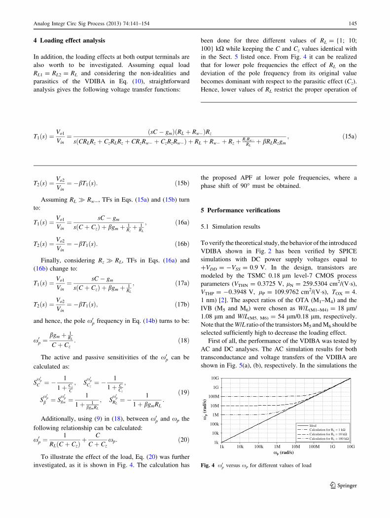
investigated, as it is shown in Fig. 4. The calculation has
been done for three different values of RL = {1; 10;
100} kX while keeping the C and Cz values identical with
in the Sect. 5 listed once. From Fig. 4 it can be realized
that for lower pole frequencies the effect of RL on the
deviation of the pole frequency from its original value
becomes dominant with respect to the parasitic effect (Cz).
Hence, lower values of RL restrict the proper operation of
the proposed APF at lower pole frequencies, where a
phase shift of 90� must be obtained.
5 Performance verifications
5.1 Simulation results
To verify the theoretical study, the behavior of the introduced
VDIBA shown in Fig. 2 has been verified by SPICE
simulations with DC power supply voltages equal to
?VDD = -VSS = 0.9 V. In the design, transistors are
modeled by the TSMC 0.18 lm level-7 CMOS process
parameters (VTHN = 0.3725 V, lN = 259.5304 cm2/(V�s),
VTHP = -0.3948 V, lP = 109.9762 cm2/(V�s), TOX = 4.
1 nm) [2]. The aspect ratios of the OTA (M1–M4) and the
IVB (M5 and M6) were chosen as W/L(M1–M4) = 18 lm/
1.08 lm and W/L(M5, M6) = 54 lm/0.18 lm, respectively.
Note that the W/L ratio of the transistors M5 and M6 should be
selected sufficiently high to decrease the loading effect.
First of all, the performance of the VDIBA was tested by
AC and DC analyses. The AC simulation results for both
transconductance and voltage transfers of the VDIBA are
shown in Fig. 5(a), (b), respectively. In the simulations the
1k 10k 100k 1M 10M 100M 1G 10G 1k
10k
100k
1M
10M
100M
1G
10G
ω' p
(rad
/s)
ωp (rad/s)
IdealCalculation for RL = 1 kΩCalculation for RL = 10 kΩCalculation for RL = 100 kΩ
Fig. 4 x0p versus xp for different values of load
T1 sð Þ ¼ Vo1
Vin¼ sC � gmð Þ RL þ Rw�ð ÞRz
s CRLRz þ CzRLRz þ CRzRw� þ CzRzRw�ð Þ þ RL þ Rw� þ Rz þ RzRw�RLþ bRLRzgm
; ð15aÞ
Analog Integr Circ Sig Process (2013) 74:141–154 145
123
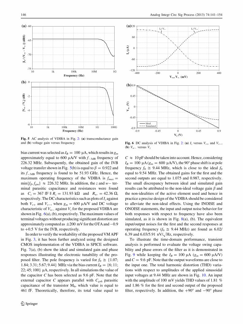
bias current was selected as IB = 100 lA, which results in gm
approximately equal to 600 lA/V with f-3dB frequency of
226.32 MHz. Subsequently, the obtained gain of the IVB
voltage transfer shown in Fig. 5(b) is equal to b = 0.922 and
its f-3dB frequency is found to be 51.93 GHz. Hence, the
maximum operating frequency of the VDIBA is fmax =
min{fb, fgm} & 226.32 MHz. In addition, the z and w- ter-
minal parasitic capacitance and resistances were found
as Cz = 367 fF || Rz = 131.93 kX and Rw- = 42.36 X,
respectively. The DC characteristics such as plots of Iz against
both Vv? and Vv-, when gm = 600 lA/V and DC voltage
characteristic of Vw- against Vz for the proposed VDIBA are
shown in Fig. 6(a), (b), respectively. The maximum values of
terminal voltages without producing significant distortion are
approximately computed as ±200 mV for the OTA and -0.9
to ?0.5 V for the IVB, respectively.
In order to verify the workability of the proposed VM APF
in Fig. 3, it has been further analyzed using the designed
CMOS implementation of the VDIBA in SPICE software.
Fig. 7(a), (b) show the ideal and simulated gain and phase
responses illustrating the electronic tunability of the pro-
posed filter. The pole frequency is varied for f0 % {1.07;
1.84; 3.31; 5.67; 9.44} MHz via the bias current IB = {6; 11;
22; 45; 100} lA, respectively. In all simulations the value of
the capacitor C has been selected as 9.6 pF. Note that the
external capacitor C appears parallel with Cgs6 parasitic
capacitance of the transistor M6, which value is equal to
461 fF. Theoretically, therefore, its total value equal to
C & 10 pF should be taken into account. Hence, considering
IB = 100 lA (gm = 600 lA/V), the 90� phase shift is at pole
frequency f0 % 9.44 MHz, which is close to the ideal f0equal to 9.54 MHz. The obtained gains for the first and the
second outputs are equal to 1.075 and 0.987, respectively.
The small discrepancy between ideal and simulated gain
results can be attributed to the non-ideal voltage gain b and
the non-idealities of the active element used and hence in
practice a precise design of the VDIBA should be considered
to alleviate the non-ideal effects. Using the INOISE and
ONOISE statements, the input and output noise behavior for
both responses with respect to frequency have also been
simulated, as it is shown in Fig. 8(a), (b). The equivalent
input/output noises for the first and the second responses at
operating frequency (f0 % 9.44 MHz) are found as 6.02/
6.39 and 6.03/5.91 nV/HHz, respectively.
To illustrate the time-domain performance, transient
analysis is performed to evaluate the voltage swing capa-
bility and phase errors of the filter as it is demonstrated in
Fig. 9 while keeping the IB = 100 lA (gm = 600 lA/V)
and C = 9.6 pF. Note that the output waveforms are close to
the input one. The total harmonic distortion (THD) varia-
tions with respect to amplitudes of the applied sinusoidal
input voltages at 9.44 MHz are shown in Fig. 10. An input
with the amplitude of 100 mV yields THD values of 1.81 %
and 1.86 % for the first and second output of the proposed
filter, respectively. In addition, the ?90� and -90� phase
Frequency (Hz) 1k 100k 10M 1G 10
-75
-70
-65
-60 |I z
/ (V
v+−
Vv−
)| (d
BS)
(a)
Frequency (Hz) 1k 100k 10M 1G 100G 10
-6
-4
-2
0
|Vw
− / V
z| (d
B)
(b)
Fig. 5 AC analysis of VDIBA in Fig. 2: (a) transconductance gain
and (b) voltage gain versus frequency
Vv+, Vv− (mV) -400 -200 0 200 400
-120
-60
0
60
120
I z (
μA)
Iz / Vv– Iz / Vv+
(a)
Vz (V)-0.9 -0.45 0 0.45 0.9
-0.9
-0.45
0
0.45
0.9
Vw
– (V
) Ideal Simulated
(b)
Fig. 6 DC analysis of VDIBA in Fig. 2: (a) Iz versus Vv? and Vv-,
(b) Vw- versus Vz
146 Analog Integr Circ Sig Process (2013) 74:141–154
123
shifts in the first and the second outputs against the input at
pole frequency 9.44 MHz are also illustrated in the Lissajous
patterns shown in Fig. 11(a), (b), respectively. The total
power dissipation of the circuit is found to be 10.5 mW.
5.2 Measurement results
In order to confirm the theoretical results, the behavior of the
proposed APF has also been verified by experimental mea-
surements using network-spectrum analyzer Agilent 4395A,
function generator Agilent 33521A, and four-channel
oscilloscope Agilent DSOX2014A. In measurements the
VDIBA was implemented based on the structure illustrated
in Fig. 12 using readily available ICs OPA860 [27] by Texas
Instruments. The DC power supply voltages were equal
to ± 5 V and the resistor RADJ (see [27]) was chosen as
270 X. The OPA860 contains the so-called ‘diamond’
transistor (DT) and fast voltage buffer (VB). In the input
stage, in order to increase the linearity of collector current
versus input voltage Vd, the DT1 is complemented with
degeneration resistor RG � 1/gmT, added in series to the
emitter, where the gmT is the DT transconductance. Then the
total transconductance decreases to the approximate value 1/
RG [17]. The DT2 together with RE and RC represent the IVB
-4
0
4
0
90
180
Frequency (Hz) 1k 10k 100k 1M 10M 100M 1G 10G
IdealIB = 6 μAIB = 11 μAIB = 22 μAIB = 45 μAIB = 100 μA
Pha
se (
deg.
)
Gai
n (d
B)
(a)
Frequency (Hz) 1k 10k 100k 1M 10M 100M 1G 10G
-4
0
4
-180
-90
0
Ideal IB = 6 μAIB = 11 μAIB = 22 μAIB = 45 μAIB = 100 μA
Pha
se (
deg.
)
Gai
n (d
B)
(b)
Fig. 7 Electronical tunability of the pole frequency by the bias
current IB: (a) inverting, (b) non-inverting VM first-order all-pass
filter responses
Equivalent input noiseOutput noise
Vol
tag e
noi
se (
nV/√
Hz)
Frequency (Hz) 1k 10k 100k 1M 10M 100M 1G 10G
0
2.5
5
7.5
10 (a)
Frequency (Hz)1k 10k 100k 1M 10M 100M 1G 10G
0
2.5
5
7.5
10
Equivalent input noiseOutput noise
Vol
tage
noi
se (
nV/√
Hz)
(b)
Fig. 8 Input and output noise variations for (a) Vo1 and (b) Vo2
versus frequency
Time (ns) 400 500 600 700
-100
0
100
Vol
tage
(m
V)
Vo2Vo1 Vin
Fig. 9 Time-domain responses of the proposed all-pass filter at
9.44 MHz
Input voltage (mV) 0 40 80 120 160 200
0
2.5
5
7.5
TH
D (
%)
Vo1Vo2
Fig. 10 THD variation of the proposed all-pass filter for both
responses against applied input voltage at 9.44 MHz
Analog Integr Circ Sig Process (2013) 74:141–154 147
123
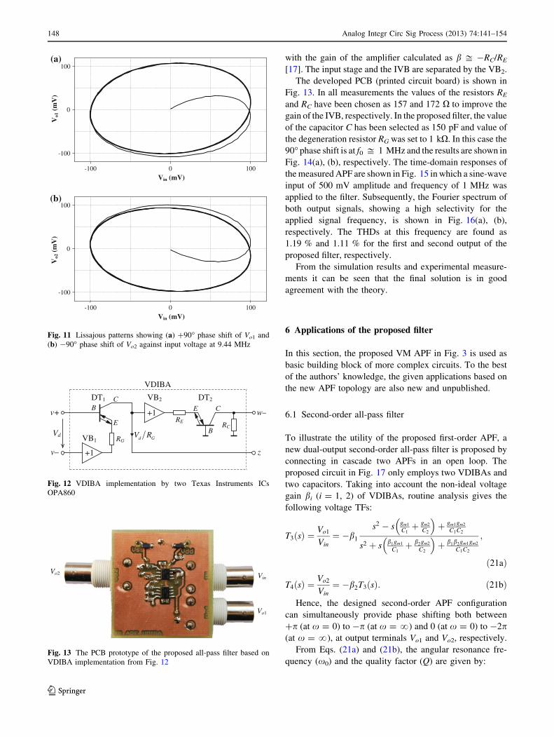
with the gain of the amplifier calculated as b % -RC/RE
[17]. The input stage and the IVB are separated by the VB2.
The developed PCB (printed circuit board) is shown in
Fig. 13. In all measurements the values of the resistors RE
and RC have been chosen as 157 and 172 X to improve the
gain of the IVB, respectively. In the proposed filter, the value
of the capacitor C has been selected as 150 pF and value of
the degeneration resistor RG was set to 1 kX. In this case the
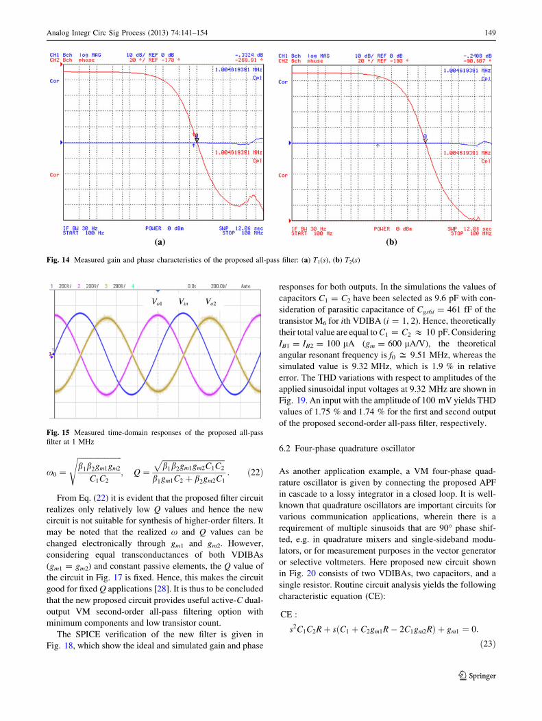
90� phase shift is at f0 % 1 MHz and the results are shown in
Fig. 14(a), (b), respectively. The time-domain responses of
the measured APF are shown in Fig. 15 in which a sine-wave
input of 500 mV amplitude and frequency of 1 MHz was
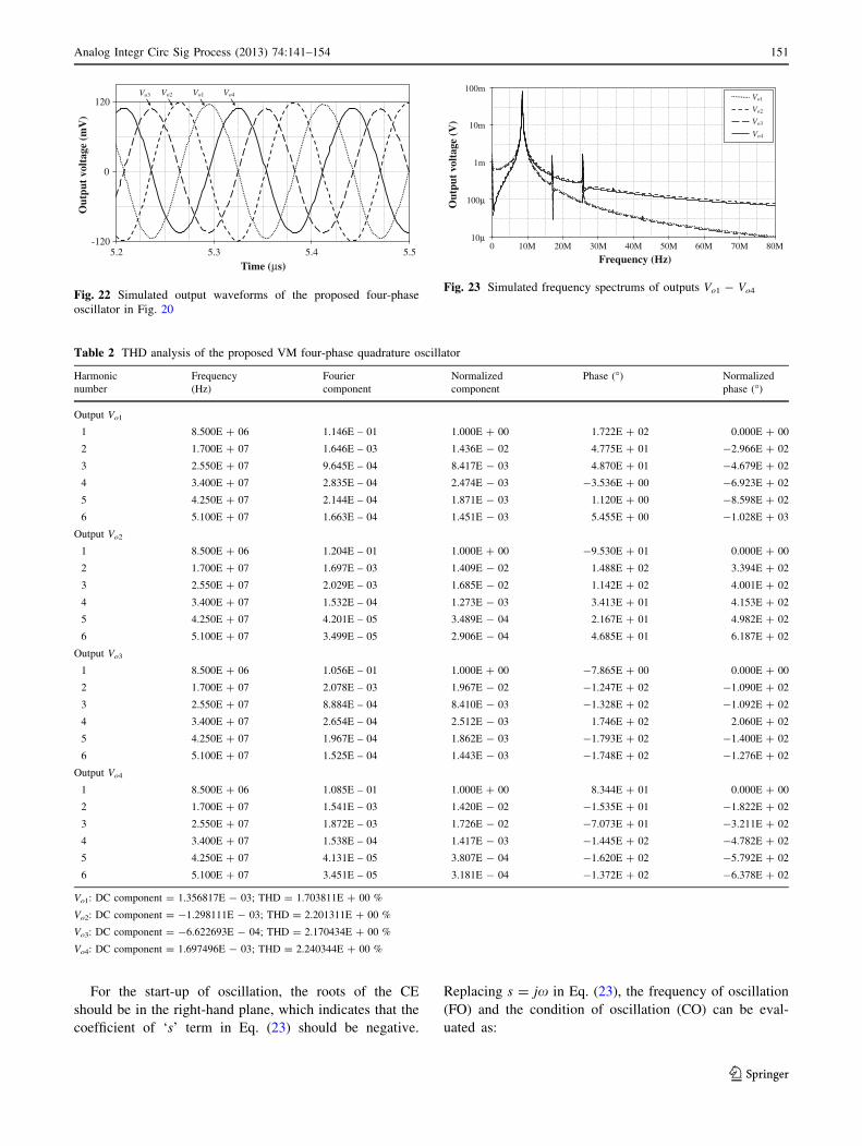
applied to the filter. Subsequently, the Fourier spectrum of
both output signals, showing a high selectivity for the
applied signal frequency, is shown in Fig. 16(a), (b),
respectively. The THDs at this frequency are found as
1.19 % and 1.11 % for the first and second output of the
proposed filter, respectively.
From the simulation results and experimental measure-
ments it can be seen that the final solution is in good
agreement with the theory.
6 Applications of the proposed filter
In this section, the proposed VM APF in Fig. 3 is used as
basic building block of more complex circuits. To the best
of the authors’ knowledge, the given applications based on
the new APF topology are also new and unpublished.
6.1 Second-order all-pass filter
To illustrate the utility of the proposed first-order APF, a
new dual-output second-order all-pass filter is proposed by
connecting in cascade two APFs in an open loop. The
proposed circuit in Fig. 17 only employs two VDIBAs and
two capacitors. Taking into account the non-ideal voltage
gain bi (i = 1, 2) of VDIBAs, routine analysis gives the
following voltage TFs:
T3 sð Þ ¼ Vo1
Vin¼ �b1
s2 � s gm1
C1þ gm2
C2
� �þ gm1gm2
C1C2
s2 þ s b1gm1
C1þ b2gm2
C2
� �þ b1b2gm1gm2
C1C2
;
ð21aÞ
T4 sð Þ ¼ Vo2
Vin¼ �b2T3 sð Þ: ð21bÞ
Hence, the designed second-order APF configuration
can simultaneously provide phase shifting both between
?p (at x = 0) to -p (at x = ?) and 0 (at x = 0) to -2p(at x = ?), at output terminals Vo1 and Vo2, respectively.
From Eqs. (21a) and (21b), the angular resonance fre-
quency (x0) and the quality factor (Q) are given by:
0
100
-100
Vo1
(m
V)
Vin (mV) -100 0 100
(a)
Vin (mV) -100 0 100
-100
0
100
Vo2
(m
V)
(b)
Fig. 11 Lissajous patterns showing (a) ?90� phase shift of Vo1 and
(b) -90� phase shift of Vo2 against input voltage at 9.44 MHz
+1 w–
z
VDIBA
v+
v–
RERC
E C
BRG
E
CB
+1
Vdd GV RVB1
VB2DT1 DT2
Fig. 12 VDIBA implementation by two Texas Instruments ICs
OPA860
Vin
Vo1
Vo2
Fig. 13 The PCB prototype of the proposed all-pass filter based on
VDIBA implementation from Fig. 12
148 Analog Integr Circ Sig Process (2013) 74:141–154
123
x0 ¼
ffiffiffiffiffiffiffiffiffiffiffiffiffiffiffiffiffiffiffiffiffiffiffib1b2gm1gm2
C1C2
s; Q ¼
ffiffiffiffiffiffiffiffiffiffiffiffiffiffiffiffiffiffiffiffiffiffiffiffiffiffiffiffiffiffiffiffiffib1b2gm1gm2C1C2
pb1gm1C2 þ b2gm2C1
: ð22Þ
From Eq. (22) it is evident that the proposed filter circuit
realizes only relatively low Q values and hence the new
circuit is not suitable for synthesis of higher-order filters. It
may be noted that the realized x and Q values can be
changed electronically through gm1 and gm2. However,
considering equal transconductances of both VDIBAs
(gm1 = gm2) and constant passive elements, the Q value of
the circuit in Fig. 17 is fixed. Hence, this makes the circuit
good for fixed Q applications [28]. It is thus to be concluded
that the new proposed circuit provides useful active-C dual-
output VM second-order all-pass filtering option with
minimum components and low transistor count.
The SPICE verification of the new filter is given in
Fig. 18, which show the ideal and simulated gain and phase
responses for both outputs. In the simulations the values of
capacitors C1 = C2 have been selected as 9.6 pF with con-
sideration of parasitic capacitance of Cgs6i = 461 fF of the
transistor M6 for ith VDIBA (i = 1, 2). Hence, theoretically
their total value are equal to C1 = C2 & 10 pF. Considering
IB1 = IB2 = 100 lA (gm = 600 lA/V), the theoretical
angular resonant frequency is f0 % 9.51 MHz, whereas the
simulated value is 9.32 MHz, which is 1.9 % in relative
error. The THD variations with respect to amplitudes of the
applied sinusoidal input voltages at 9.32 MHz are shown in
Fig. 19. An input with the amplitude of 100 mV yields THD
values of 1.75 % and 1.74 % for the first and second output
of the proposed second-order all-pass filter, respectively.
6.2 Four-phase quadrature oscillator
As another application example, a VM four-phase quad-
rature oscillator is given by connecting the proposed APF
in cascade to a lossy integrator in a closed loop. It is well-
known that quadrature oscillators are important circuits for
various communication applications, wherein there is a
requirement of multiple sinusoids that are 90� phase shif-
ted, e.g. in quadrature mixers and single-sideband modu-
lators, or for measurement purposes in the vector generator
or selective voltmeters. Here proposed new circuit shown
in Fig. 20 consists of two VDIBAs, two capacitors, and a
single resistor. Routine circuit analysis yields the following
characteristic equation (CE):
CE :
s2C1C2Rþ s C1 þ C2gm1R� 2C1gm2Rð Þ þ gm1 ¼ 0:
ð23Þ
Fig. 14 Measured gain and phase characteristics of the proposed all-pass filter: (a) T1(s), (b) T2(s)
Fig. 15 Measured time-domain responses of the proposed all-pass
filter at 1 MHz
Analog Integr Circ Sig Process (2013) 74:141–154 149
123
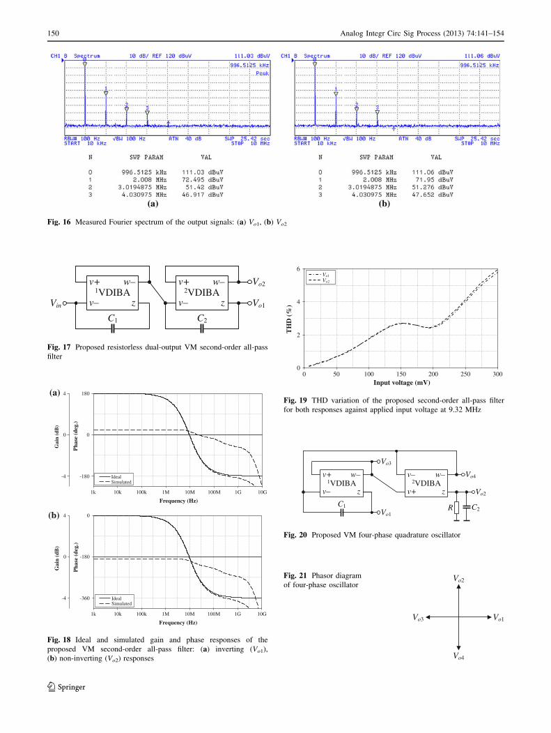
Fig. 16 Measured Fourier spectrum of the output signals: (a) Vo1, (b) Vo2
-4
0
4
-180
0
180
Pha
se (
deg.
)
Gai
n (d
B)
Frequency (Hz)
1k 10k 100k 1M 10M 100M 1G 10G
IdealSimulated
(a)
Frequency (Hz)
1k 10k 100k 1M 10M 100M 1G 10G
-4
0
4
-360
-180
0
Pha
se (
deg.
)
Gai
n ( d
B)
IdealSimulated
(b)
Fig. 18 Ideal and simulated gain and phase responses of the
proposed VM second-order all-pass filter: (a) inverting (Vo1),
(b) non-inverting (Vo2) responses
Input voltage (mV) 0 50 100 150 200 250 300
0
2
4
6 Vo1Vo2
TH
D (
%)
Fig. 19 THD variation of the proposed second-order all-pass filter
for both responses against applied input voltage at 9.32 MHz
v+
v– z
w–1VDIBA
C1
v–
v+ z
w–2VDIBA
Vo4
R C2Vo1
Vo3
Vo2
Fig. 20 Proposed VM four-phase quadrature oscillator
Vo1Vo3
Vo2
Vo4
Fig. 21 Phasor diagram
of four-phase oscillator
v+
v– z
w–1VDIBA
Vin
C1
v+
v– z
w–2VDIBA
Vo1
Vo2
C2
Fig. 17 Proposed resistorless dual-output VM second-order all-pass
filter
150 Analog Integr Circ Sig Process (2013) 74:141–154
123
For the start-up of oscillation, the roots of the CE
should be in the right-hand plane, which indicates that the
coefficient of ‘s’ term in Eq. (23) should be negative.
Replacing s = jx in Eq. (23), the frequency of oscillation
(FO) and the condition of oscillation (CO) can be eval-
uated as:
Time (μs)5.2 5.3 5.4 5.5
-120
0
120 Vo1Vo2Vo3 Vo4
Out
put
volt
age
(mV
)
Fig. 22 Simulated output waveforms of the proposed four-phase
oscillator in Fig. 20
Frequency (Hz) 0 10M 20M 30M 40M 50M 60M 70M 80M
10μ
100μ
1m
10m
100mVo1
Vo2
Vo3
Vo4
Out
put
volt
age
(V)
Fig. 23 Simulated frequency spectrums of outputs Vo1 - Vo4
Table 2 THD analysis of the proposed VM four-phase quadrature oscillator
Harmonic
number
Frequency
(Hz)
Fourier
component
Normalized
component
Phase (�) Normalized
phase (�)
Output Vo1
1 8.500E ? 06 1.146E – 01 1.000E ? 00 1.722E ? 02 0.000E ? 00
2 1.700E ? 07 1.646E – 03 1.436E - 02 4.775E ? 01 -2.966E ? 02
3 2.550E ? 07 9.645E – 04 8.417E - 03 4.870E ? 01 -4.679E ? 02
4 3.400E ? 07 2.835E – 04 2.474E - 03 -3.536E ? 00 -6.923E ? 02
5 4.250E ? 07 2.144E – 04 1.871E - 03 1.120E ? 00 -8.598E ? 02
6 5.100E ? 07 1.663E – 04 1.451E - 03 5.455E ? 00 -1.028E ? 03
Output Vo2
1 8.500E ? 06 1.204E – 01 1.000E ? 00 -9.530E ? 01 0.000E ? 00
2 1.700E ? 07 1.697E – 03 1.409E - 02 1.488E ? 02 3.394E ? 02
3 2.550E ? 07 2.029E – 03 1.685E - 02 1.142E ? 02 4.001E ? 02
4 3.400E ? 07 1.532E – 04 1.273E - 03 3.413E ? 01 4.153E ? 02
5 4.250E ? 07 4.201E – 05 3.489E - 04 2.167E ? 01 4.982E ? 02
6 5.100E ? 07 3.499E – 05 2.906E - 04 4.685E ? 01 6.187E ? 02
Output Vo3
1 8.500E ? 06 1.056E – 01 1.000E ? 00 -7.865E ? 00 0.000E ? 00
2 1.700E ? 07 2.078E – 03 1.967E - 02 -1.247E ? 02 -1.090E ? 02
3 2.550E ? 07 8.884E – 04 8.410E - 03 -1.328E ? 02 -1.092E ? 02
4 3.400E ? 07 2.654E – 04 2.512E - 03 1.746E ? 02 2.060E ? 02
5 4.250E ? 07 1.967E – 04 1.862E - 03 -1.793E ? 02 -1.400E ? 02
6 5.100E ? 07 1.525E – 04 1.443E - 03 -1.748E ? 02 -1.276E ? 02
Output Vo4
1 8.500E ? 06 1.085E – 01 1.000E ? 00 8.344E ? 01 0.000E ? 00
2 1.700E ? 07 1.541E – 03 1.420E - 02 -1.535E ? 01 -1.822E ? 02
3 2.550E ? 07 1.872E – 03 1.726E - 02 -7.073E ? 01 -3.211E ? 02
4 3.400E ? 07 1.538E – 04 1.417E - 03 -1.445E ? 02 -4.782E ? 02
5 4.250E ? 07 4.131E – 05 3.807E - 04 -1.620E ? 02 -5.792E ? 02
6 5.100E ? 07 3.451E – 05 3.181E - 04 -1.372E ? 02 -6.378E ? 02
Vo1: DC component = 1.356817E - 03; THD = 1.703811E ? 00 %
Vo2: DC component = -1.298111E - 03; THD = 2.201311E ? 00 %
Vo3: DC component = -6.622693E - 04; THD = 2.170434E ? 00 %
Vo4: DC component = 1.697496E - 03; THD = 2.240344E ? 00 %
Analog Integr Circ Sig Process (2013) 74:141–154 151
123
FO : x0 ¼ffiffiffiffiffiffiffiffiffiffiffiffiffiffi
gm1
C1C2R
r; ð24aÞ
CO : gm2�1
2
1
Rþ gm1
C2
C1
� �: ð24bÞ
From Eqs. (24a) and (24b), it is clear that the FO can be
controlled by adjusting the value of the resistor R and/or by
varying the control current IB1 of gm1.
Assuming that the used external capacitors and the
transconductance of both VDIBAs are equal, i.e. C1 = C2
and gm1 = gm2, the relationship between four quadrature
output voltages Vo1, Vo2, Vo3, and Vo4 can be expressed as:
Vo1
Vo2
¼ �j;Vo2
Vo3
¼ �j;Vo1
Vo4
¼ j; ð25Þ
ensuring the output voltages Vo2–Vo1, Vo3–Vo2, Vo4–Vo3,
and Vo1–Vo4 to be quadrature (in Fig. 21 the phase differ-
ences are / = 90�) and have equal amplitudes.
Assuming the non-ideal behavior of the active elements
(bi), the CE, FO, and the CO in Eqs. (23), (24a), and (24b)
change to:
CE : s2C1C2Rþ s C1 þ b1C2gm1R� b2C1gm2R b1 þ 1ð Þ½ �þ b1gm1 ¼ 0; ð26aÞ
FO : x0 ¼
ffiffiffiffiffiffiffiffiffiffiffiffiffiffib1gm1
C1C2R
s; ð26bÞ
CO : gm2�1
b2 b1 þ 1ð Þ1
Rþ b1gm1
C2
C1
� �: ð26cÞ
From Eqs. (26b) and (26c) it can be seen that the non-ideal
behavior of the active elements affects both the frequency of
oscillation and the condition of oscillation, however, CO can
be satisfied by adjusting gm2 without affecting FO.
The proposed oscillator was designed with the following
active parameters and the passive element values
IB1 = 100 lA, R = 1650 X, and C1 = C2 = 9.6 pF,
respectively, to obtain the sinusoidal output waveforms
with the oscillation frequency of f0 = x0/2p % 8.5 MHz.
In practice, to ensure the startup (build-up) of oscillations
and subsequently to satisfy the CO in Eq. (24b) the value of
IB2 is chosen as 131 lA. The waveforms of the quadrature
voltages are shown in Fig. 22. In addition, Fig. 23 shows
the frequency spectrum of the output waveforms and the
value of total harmonic distortion (THD) at all outputs are
less than 2.25 %. The results are summarised in Table 2.
7 Conclusions
This paper presents a new active element from the group of
‘voltage differencing’ devices, namely voltage differencing
inverting buffered amplifier (VDIBA). The input part of the
VDIBA is formed by the OTA, which is followed by the
IVB with a gain of -1 that makes the introduced element
attractive for resistorless and electronically controllable
linear circuit design. As an application examples a new
resistorless dual-output VM first-order all-pass filter, dual-
output second-order all-pass filter, and four-phase quadra-
ture oscillator circuits are proposed. SPICE simulation and
experimental results confirm the feasibility of the proposed
circuits.
8 Appendix
This section provides full nomenclature of the mentioned
ABBs in Table 1 in alphabetical order.
C-(I)CDBA Current-controlled (inverting) current dif-
ferencing buffered amplifier
CCCDTA Current controlled current differencing
transconductance amplifier
CCCII?(-) Plus-type (minus-type) second-generation
current-controlled current conveyor
CC-VCIII- Minus-type current-controlled third-gen-
eration voltage conveyor
DDCC Differential difference current conveyor
DVCC?(-) Plus-type (minus-type) differential voltage
current conveyor
DV-VB Differential-voltage voltage buffer
FD-OpAmp Fully-differential operational amplifier
IUGA Inverting unity gain amplifier
IVB Inverting voltage buffer
MO-CCCCTA Multiple-output current controlled
current conveyor transconductance
amplifier
OTA Operational transconductance amplifier
UGDA Unity gain differential amplifier
UVC Universal voltage conveyor
VD-DIBA Voltage differencing-differential input
buffered amplifier
VDIBA Voltage differencing inverting buffered
amplifier
Acknowledgments The research described in the paper was sup-
ported by the following projects: P102/11/P489, P102/10/P561, P102/
09/1681, FEKT-S-11-15, and project SIX CZ.1.05/2.1.00/03.0072
from the operational program Research and Development for Inno-
vation. Authors also wish to thank Prof. Dr. Serdar Ozoguz from the
Istanbul Technical University, Turkey, for his discussions made on
the proposed circuit and the anonymous reviewers for their useful and
constructive comments that helped to improve the paper. A pre-
liminary version of this paper has been presented at the 7th Interna-
tional Conference on Electrical and Electronics Engineering—
ELECO 2011 [29].
152 Analog Integr Circ Sig Process (2013) 74:141–154
123
References
1. Maheshwari, S. (2009). Analogue signal processing applications
using a new circuit topology. IET Circuits, Devices Systems, 3(3),
106–115.
2. Minaei, S., & Yuce, E. (2010). Novel voltage-mode all-pass filter
based on using DVCCs. Circuits, Systems, and Signal Processing,29(3), 391–402.
3. Maheshwari, S. (2004). New voltage and current-mode APS
using current controlled conveyor. International Journal ofElectronics, 91(12), 735–743.
4. Minaei, S., & Cicekoglu, O. (2006). A resistorless realization of
the first-order all-pass filter. International Journal of Electronics,93(3), 177–183.
5. Kumar, P., Keskin, A. U., & Pal, K. (2007). Wide-band resist-
orless allpass sections with single element tuning. InternationalJournal of Electronics, 94(6), 597–604.
6. Maheshwari, S. (2008). A canonical voltage-controlled VM-APS
with a grounded capacitor. Circuits Systems and Signal Pro-cessing, 27(1), 123–132.
7. Metin, B., & Pal, K. (2010). New all-pass filter circuit compen-
sating for C-CDBA non-idealities. Journal of Circuits Systemsand Computers, 19(2), 381–391.
8. Bajer, J., & Biolek, D. (2010). Voltage-mode electronically
tunable all-pass filter employing CCCII?, one capacitor and
differential-input voltage buffer. In Proceedings of the 2010IEEE 26-th convention of electrical and electronics engineers inIsrael, Eilat, Israel, pp. 934–937.
9. Metin, B., Pal, K., & Cicekoglu, O. (2011). CMOS controlled
inverting CDBA with a new all-pass filter application. Interna-tional Journal of Circuit Theory and Applications, 39(4), 417–425.
10. Herencsar, N., Koton, J., Vrba, K., & Metin, B. (2011). Novel
voltage conveyor with electronic tuning and its application to
resistorless all-pass filter. In Proceedings of the 2011 34thinternational conference on telecommunications and signal pro-cessing (TSP), Budapest, Hungary, pp. 265–268.
11. Biolkova, V., Kolka, Z., & Biolek, D. (2011). Dual-output all-
pass filter employing fully-differential operational amplifier and
current-controlled current conveyor. In Proceedings of the 7thinternational conference on electrical and electronics engineer-ing—ELECO 2011, Bursa, Turkey, pp. 319–323.
12. Toker, A., & Ozoguz, S. (2003). Tunable allpass filter for low
voltage operation. Electronics Letters, 39(2), 175–176.
13. Metin, B., Pal, K., & Cicekoglu, O. (2011). All-pass filters using
DDCC- and MOSFET-based electronic resistor. InternationalJournal of Circuit Theory and Applications, 39(8), 881–891.
14. Herencsar, N., Koton, J., Vrba, K., & Minaei, S. (2011). Elec-
tronically tunable MOSFET-C voltage-mode all-pass filter based
on universal voltage conveyor. In Proceedings of the interna-tional conference on computer and communication device—
ICCCD 2011, Bali Island, Indonesia, Vol. 1, pp. 53–56.
15. Herencsar, N., Koton, J., Jerabek, J., Vrba, K., & Cicekoglu, O.
(2011). Voltage-mode all-pass filters using universal voltage
conveyor and MOSFET-based electronic resistors. Radioengi-neering, 20(1), 10–18.
16. Minaei, S., & Yuce, E. (2012). High input impedance NMOS-
based phase shifter with minimum number of passive elements.
Circuits, Systems, and Signal Processing, 31(1), 51–60.
17. Biolek, D., & Biolkova, V. (2010). First-order voltage-mode all-
pass filter employing one active element and one grounded
capacitor. Analog Integrated Circuits and Signal Processing,65(1), 123–129.
18. Khan, I. A., & Ahmed, M. T. (1986). Electronically tunable first-
order OTA-capacitor filter sections. International Journal ofElectronics, 61(2), 233–237.
19. Kumngern, M., Chanwutitum, J., & Dejhan, K. (2008). Elec-
tronically tunable voltage-mode all-pass filter using simple
CMOS OTAs. In Proceedings of the 2008 international sympo-sium on communications and information technologies—ISCIT2008, Vientiane, Laos, pp. 1–5.
20. Tanaphatsiri, C., Jaikla, W., & Siripruchyanun, M. (2008). An
electronically controllable voltage-mode first-order all-pass filter
using only single CCCDTA. In Proceedings of the 2008 inter-national symposium on communications and information tech-nologies—ISCIT 2008, Vientiane, Laos, pp. 305–309.
21. Herencsar, N., Koton, J., & Vrba, K. (2009). A new electronically
tunable voltage-mode active-C phase shifter using UVC and
OTA. IEICE Electronics Express, 6(17), 1212–1218.
22. Pandey, N., Arora, P., Kapur, S., & Malhotra, S. (2011). First
order voltage mode MO-CCCCTA based all pass filter. In Pro-ceedings of the 2011 international conference on communicationsand signal processing—ICCSP 2011, Kerala, India, pp. 535–537.
23. Keskin, A. U., Pal, K., & Hancioglu, E. (2008). Resistorless first
order all-pass filter with electronic tuning. AEU—InternationalJournal of Electronics and Communications, 62(4), 304–306.
24. Fabre, A., Saaid, O., Wiest, F., & Boucheron, C. (1996). High
frequency applications based on a new current controlled con-
veyor. IEEE Transactions on Circuits Systems-I, 43(2), 82–91.
25. Geiger, R. L., & Sanchez-Sinencio, E. (1985). Active filter design
using operational transconductance amplifiers: a tutorial. IEEECircuits Devices Magazine, 1, 20–32.
26. Biolek, D., Senani, R., Biolkova, V., & Kolka, Z. (2008). Active
elements for analog signal processing: classification, review, and
new proposals. Radioengineering, 17(4), 15–32.
27. OPA860—Wide bandwidth operational transconductance ampli-
fier (OTA) and buffer, Texas Instruments, SBOS331C–June
2005–Revised August 2008, www.ti.com.
28. Maheshwari, S., Mohan, J., & Chauhan, D. S. (2011). Novel
cascadable all-pass/notch filters using a single FDCCII and
grounded capacitors. Circuits, Systems, and Signal Processing,30(3), 643–654.
29. Herencsar, N., Koton, J., Minaei, S., Yuce, E., & Vrba, K. (2011).
Novel resistorless dual-output VM all-pass filter employing
VDIBA. In Proceedings of the 7th international conference onelectrical and electronics engineering—ELECO 2011, Bursa,
Turkey, pp. 72–74.
Norbert Herencsar was born in
the Slovak Republic in 1982. He
received the M.Sc. and Ph.D.
degrees in Electronics & Com-
munication and Teleinformatics
from Brno University of Tech-
nology, Czech Republic, in
2006 and 2010, respectively.
Currently, he is an Assistant
Professor at the Department of
Telecommunications, Faculty of
Electrical Engineering and
Communication, Brno Univer-
sity of Technology, Brno, Czech
Republic. From September 2009
through February 2010 he was an Erasmus Exchange Student with the
Department of Electrical and Electronic Engineering, Bogazici Uni-
versity, Istanbul, Turkey. His research interests include analog filters,
current-, voltage- and mixed-mode circuits, electronic circuit & sys-
tem design, new active elements and their circuit applications, and
oscillators. He is an author or co-author of 23 research articles pub-
lished in SCI-E international journals, 20 articles published in other
journals, and 55 papers published in proceedings of international
Analog Integr Circ Sig Process (2013) 74:141–154 153
123
conferences. In 2011, he received Rector Award in the University
competition ‘‘Top 10 Excelence VUT 2010’’ for the 9th most pro-
ductive scientist at the Brno University of Technology, category
‘‘Publications’’. His paper ‘‘Novel resistorless dual-output VM all-
pass filter employing VDIBA’’, presented and published at the 7th
International Conference on Electrical Electronics Engineering—
ELECO 2011, Bursa, Turkey, received ‘‘The best paper award in
memory of Prof. Dr. Mustafa Bayram’’. Since 2008, Dr. Herencsar
serves in the organizing and technical committee of the International
Conference on Telecommunications and Signal Processing (TSP). In
2011, he is guest co-editor of TSP 2010 Special Issue on Telecom-
munications, published in the Telecommunication Systems journal of
Springer. In 2011–2013, he is guest co-editor of TSP 2010, TSP 2011,
and TSP 2012 Special Issues on Signal Processing, published in the
Radioengineering journal. Dr. Herencsar is Senior Member of the
IACSIT and Member of the IEEE, IAENG, and ACEEE. He is also
Committee Member of the IACSIT Electronics and Electrical Society
(EES).
Shahram Minaei received the
B.Sc. degree in Electrical and
Electronics Engineering from
Iran University of Science and
Technology, Tehran, Iran, in
1993 and the M.Sc. and Ph.D.
degrees in electronics and com-
munication engineering from
Istanbul Technical University,
Istanbul, Turkey, in 1997 and
2001, respectively. He is currently
a Professor in the Department of
Electronics and Communication
Engineering, Dogus University,
Istanbul, Turkey. He has more
than 100 publications in scientific journals or conference proceedings.
His current field of research concerns current-mode circuits and analog
signal processing. Dr. Minaei is a senior member of the IEEE, an
associate editor of the Journal of Circuits, Systems and Computers
(JCSC), and an area editor of the International Journal of Electronics
and Communications (AEU).
Jaroslav Koton received the
M.Sc. an Ph.D. degree in elec-
trical engineering from the Brno
University of Technology
(BUT), Brno, Czech Republic,
in 2006 and 2009, respectively.
He is currently an Assistant
Professor at the Department of
Telecommunications of BUT.
His current research is focused
on linear- and non-linear circuit
designing methods with current
or voltage conveyors, and cur-
rent active elements. He is an
author or co-author of about 85
research articles published in international journals or conference
proceedings. Dr. Koton is a Member of IEEE and IACSIT.
Erkan Yuce was born in 1969 in
Nigde, Turkey. He received the
B.Sc. degree from Middle East
Technical University, the M.Sc.
degree from Pamukkale Univer-
sity and the Ph.D. degree from
Bogazici University all in Elec-
trical and Electronics Engineer-
ing in 1994, 1998 and 2006,
respectively. He is currently an
Associative Professor at the
Electrical and Electronics Engi-
neering Department of Pamukk-
ale University. His current
research interests include analog
circuits, active filters, synthetic inductors and CMOS based circuits. He
is the author or co-author of about 90 papers published in scientific
journals or conference proceedings.
Kamil Vrba received the Ph.D.
degree in Electrical Engineering
in 1976, and the Prof. degree in
1997, both from the Technical
University of Brno. Since 1990
he has been Head of the
Department of Telecommunica-
tions, Faculty of Electrical
Engineering and Computer Sci-
ence, Brno University of Tech-
nology, Brno, Czech Republic.
His research work is concen-
trated on problems concerned
with accuracy of analog circuits
and mutual conversion of ana-
log and digital signals. In cooperation with AMI Semiconductor
Czech, Ltd. (now ON Semiconductor Czech Republic, Ltd.) he has
developed number of novel active function blocks for analog signal
processing such as universal current conveyor (UCC), universal
voltage conveyor (UVC), programmable current amplifier (PCA), and
others. He is an author or co-author of more than 650 research articles
published in international journals or conference proceedings. Pro-
fessor Vrba is a Member of IEEE, IEICE, and Associate Member of
IET.
154 Analog Integr Circ Sig Process (2013) 74:141–154
123
Top Related
Copyright © 2022 FDOKUMEN

