


Bahasa
Halaman
Hukum


SHO6262
Diploma Thesis
Master of Science in Electrical Engineering
General purpose process control unit
Ivan Mokrushev
June, 2017
Department of Electrical Engineering
The Arctic University of Norway
Title: Date:
General purpose process 6th of June 2017
control unit Classification:
Open
Author: Pages:
Ivan Mokrushev 55
Attachments:
7
Department: Department of Electrical Engineering
Field of Study: Electrical Engineering
Supervisor: Trond Østrem
Principal: Norges Arktiske Universitet
Principal
contact:
Trond Østrem
Keywords: Simulink, OrCAD, PSpice, triangle wave, H-bridge, PWM, op
amp, MOSFET, duty cycle, PCB Editor, motor driver
Department of Electrical Engineering
The Arctic University of Norway

I
Abstract
The main purpose of the thesis is to make a control unit where different models can be
tested with a number of motors, sensors, indicators, control devices which are used by
Fischertechnik in training models. This work observes different types of speed motor control
and investigates most useful method that could be implemented at the PLC Lab. It would be
very useful to simulate separated parts of the unit by using different software and compare
actual results with theoretically expected results. All the results must be realistic and simply
implemented in a real lab.
Obtained circuit should be implemented in board layout after succeed simulations and
checked for safety using in future. Measured signal, voltage level on each node and behavior
of motors should be similar to the theoretical results.
II
Table of contents
Abstract ....................................................................................................................................... i
Table of contents ........................................................................................................................ ii
List of figures ............................................................................................................................ iv
List of tables .............................................................................................................................. vi
Nomenclature list ..................................................................................................................... vii
1 Introduction ............................................................................................................................. 1
2 Motor control ........................................................................................................................... 2
2.1 Type of used motors ......................................................................................................... 2
2.2 Method of control ............................................................................................................. 3
2.3. Control loop ..................................................................................................................... 4
2.4 Motor driver ...................................................................................................................... 5
2.4.1 H-bridge control ......................................................................................................... 5
2.4.2 Transistors .................................................................................................................. 8
2.4.3 Gate driver ................................................................................................................. 9
2.5 Motor control simulation ................................................................................................ 10
2.5.1 H-bridge ................................................................................................................... 10
3. PWM signal .......................................................................................................................... 15
3.1 Triangle wave ................................................................................................................. 15
3.1.1. 555 timer ................................................................................................................. 15
3.1.2 Using op amps .......................................................................................................... 18
4 Simulation model .................................................................................................................. 24
4.1 Triangle wave simulation ............................................................................................... 24
4.2 Voltage divider ............................................................................................................... 26
4.3 PWM signal .................................................................................................................... 27
4.4 Corrected PWM signal ................................................................................................... 28
4.5 Galvanic isolation ........................................................................................................... 29
4.6 Motor driver .................................................................................................................... 30
5 Power supply ......................................................................................................................... 35
5.1 Voltage regulators ........................................................................................................... 35
5.2 Rectifier .......................................................................................................................... 36
5.3 Transformer .................................................................................................................... 37
6 Implementation ...................................................................................................................... 39
6.1 Power supply .................................................................................................................. 39

III
6.2 Triangle wave circuit ...................................................................................................... 41
6.3 PWM signal .................................................................................................................... 44
6.4 Motor driver .................................................................................................................... 45
6.5 Optocoupler and inverter ............................................................................................ 49
Conclusion ................................................................................................................................ 53
References ................................................................................................................................ 54
Appendix A. Motor control model in MATLAB ................................................................... 1
Appendix B. Circuit of 555 timer in OrCAD ......................................................................... 2
Appendix C. Triangle wave generator in OrCAD .................................................................. 2
Appendix D. PWM signal circuit with bipolar supplying ...................................................... 3
Appendix E. PWM signal circuit with unipolar supplying .................................................... 4
Appendix F. Motor control unit .............................................................................................. 5
Appendix G. Power supply circuit ......................................................................................... 6
Appendix H. Motor control unit with inverted PWM signal and DRV8872 ......................... 7

IV
List of figures
Figure 1: Brushed DC machine [2] ............................................................................................ 3
Figure 2:Block diagram of a system with feedback (closed loop) [5] ....................................... 4
Figure 3:H-bridge [7] ................................................................................................................. 5
Figure 4: H-bridge with MOSFETs [9] ...................................................................................... 6
Figure 5: Duty cycle [10] ........................................................................................................... 6
Figure 6: PWM with bipolar switching [8] ................................................................................ 7
Figure 7: Types of transistors ..................................................................................................... 8
Figure 8: Types of MOSFETs .................................................................................................... 9
Figure 9: Types of MOSFET [11] .............................................................................................. 9
Figure 10:Subsystem H-bridge ................................................................................................. 10
Figure 11: Parameter block for triangle signal ........................................................................ 11
Figure 12: Outputs ( 20% duty cycle) ...................................................................................... 11
Figure 13: Outputs ( 50% duty cycle) ...................................................................................... 12
Figure 14: Outputs ( 80% duty cycle) ...................................................................................... 12
Figure 15: Output voltage at duty cycle 20% ........................................................................... 13
Figure 16: Output voltage at duty cycle 50% ........................................................................... 13
Figure 17: Output voltage at duty cycle 80% ........................................................................... 14
Figure 18: Form PWM signal with comparator [12] ................................................................ 15
Figure 19: 555 timer [14] ......................................................................................................... 16
Figure 20: Monostable mode of 555 timer [15] ....................................................................... 17
Figure 21: Astable mode of 555 timer ..................................................................................... 17
Figure 22: Type of wave of 555 timer ...................................................................................... 18
Figure 23: Operational amplifier on the circuits ...................................................................... 18
Figure 24: Schmitt trigger ........................................................................................................ 19
Figure 25: Integrator (op amp) ................................................................................................. 20
Figure 26: Integrated step signal .............................................................................................. 21
Figure 27: Integrated rectangular signal ................................................................................... 21
Figure 28: Triangle wave generator ......................................................................................... 22
Figure 29: Result of op amps filter [21] ................................................................................... 25
Figure 30: Simulated triangle wave ......................................................................................... 26
Figure 31: Voltage divider ....................................................................................................... 27
Figure 32: LM393 connection .................................................................................................. 28
Figure 33: PWM signal with bipolar supplying op amps (DC voltage is minimum) .............. 28
Figure 34: PWM signal with unipolar supplying op amps( DC voltage is minimum) ............ 29
Figure 35:Functional block diagram for LM5045 [25] ............................................................ 31
Figure 36: Functional block diagram for SA50CE .................................................................. 32
Figure 37: Diagram of a typical application of the SA50CE .................................................. 33
Figure 38: Output voltage (blue) at control voltage level 6.667 volts ..................................... 34
Figure 39: Output voltage (blue) at control voltage level 1.177 volts ..................................... 34
Figure 40: Application LM78xx .............................................................................................. 36
Figure 41: Half-wave rectifier .................................................................................................. 36
Figure 42: Full-wave rectifier .................................................................................................. 37
Figure 43: Simulation LM7812 and LM7805 .......................................................................... 38
Figure 44:Measured voltage of transformer 230/25 ................................................................. 39
Figure 45: Measured voltage of transformer 230/18 ................................................................ 40
Figure 46:Implemented power supply circuit .......................................................................... 41

V
Figure 47: Triangle wave circuit for board layout ................................................................... 42
Figure 48: Model of triangle wave generator in PCB Editor ................................................... 42
Figure 49: Triangle wave generator (board layout) ................................................................. 43
Figure 50: Scope of triangular signal ....................................................................................... 43
Figure 51: Pin configuration of LM393 [31] ........................................................................... 44
Figure 52: Scope of PWM signal at 6.13 V ............................................................................. 45
Figure 53: Suitable motor drivers ............................................................................................. 46
Figure 54: Typical application of DRV8872 ............................................................................ 47
Figure 55: Separate motor driver circuit .................................................................................. 48
Figure 56: Board model of DRV8872 ...................................................................................... 48
Figure 57: Board layout of motor driver DRV8872 ................................................................. 49
Figure 58: Application of OPI110A ......................................................................................... 49
Figure 59: Inverter SN74S04 [36] ............................................................................................ 50
Figure 60: PWM signal after optocoupler ................................................................................ 50
Figure 61: Inverted PWM signal after optocoupler ................................................................. 51
Figure 62: The implemented circuit ......................................................................................... 51
Figure 63: Output voltage of motor driver with different PWM signal ................................... 52

VI
List of tables
Table 1: States of bridge ............................................................................................................. 5
Table 2: Optocoupler 3N244 .................................................................................................... 29
Table 3: SA50CE ..................................................................................................................... 32
Table 4: Voltage regulators parameters ................................................................................... 35
Table 5: Parameters of used transformers ................................................................................ 39

VII
Nomenclature list
𝜔𝑚 Motor speed
𝐼𝑎 Armature current Ra Armature resistance
Φ Magnetic flux.
PWM Pulse - Width Modulation
𝑉𝑎𝑁 Output voltage of H-bridge when high side (left) and low side (right) are open
𝑉𝑏𝑁 Output voltage of H-bridge when high side (right) and low side (left) are open
MOSFET Metal–oxide–semiconductor field-effect transistor
FET Field-effect transistor
IGBT Insulated-gate bipolar transistor
IC Integarted circuit
V+ Non-inverting input of op amp
V- Inverting input of op amp
VS+, VS- Positive and negative power supply
1
1 Introduction
Faculty of engineering science and technology of UiT uses products of Fischertechnik for
studying and demonstration purposes. Fischertechnik is a company [1] that produces
prefabricated models for schools and universities. It uses many types of electrical DC
machines with various voltage supplying.
The PLC technical lab needs a general purpose control unit where different models can be
tested with a number of motors, sensors, indicators, control devices etc. Currently the
laboratory lacks a universal device for controlling various models that are created by
university students. Each model has its own control with unchanged quantities of motors or
their types. The device that must be created on the basis of this work should help students and
university staff make models more flexible and changeable in the process of modifying or
demonstrating the capabilities of the PLC or the motors themselves.
The most important questions of this work are the determination of the best way to control
motor and its physical implementation in the laboratory. The best way means that the device
should consist of the fewest components and be easy to operate and configure, while having a
safety margin that will prevent the failure of various parts of the device or its power supply.
Each decision and step should be dictated by the criteria of simplicity, reliability and safety
implementation.
This work will consist of the two main parts: 1) theoretical description, 2) choosing and
implementing the best optimal solution. The theoretical part should consist of the theory of
control of electric motors and a brief description of the functioning of individual parts of the
device, also it should be shown electrical circuits and their simulations. The practical part will
show the result obtained using the developed circuits.

2
2 Motor control
Different types of motors have different methods of speed control according to differences
in their design or purpose, thus aim of the investigation is to identify:
1. Types of motor;
2. Purpose;
3. Limitation;
4. Most simple and reliable way to implement it in board layout.
Based on this, it should be determined what types of motors are used by this company in
their products. After that it should be considered
2.1 Type of used motors
Fischertechnik uses brushed DC machines [1], with a voltage of 3-24 volts, such a big
difference in the power supply of different motors is one of the problems that must be solved
in this paper. Brushed DC motors or BDC are the most common on the market with so low
voltage and there is many equipment that could work together with them.
The BDC with permanent magnets is the most common among the BDC [2]. The inductor
of this engine includes permanent magnets that create a stator magnetic field. BDC motors
with permanent magnets are commonly used in tasks that do not require large powers. A BDC
motor with permanent magnets responds very quickly to a voltage change. Due to the constant
stator field, it is easy to control the motor speed. The disadvantage of the constant-current
motor with permanent magnets is that over time, the magnets lose their magnetic properties,
as a result of which the stator field decreases and the characteristics of the motor decrease.

3
Figure 1: Brushed DC machine [2]
Commutator
Brush
Stator
housing
Stator (permanent magnets)
2.2 Method of control
From the equation of the electromechanical characteristic of a DC motor [4]:
𝜔𝑚 =𝑈−𝐼𝑎∗𝑅𝑎
𝑘∗Φ (1.1)
Where: U – supply voltage, 𝐼𝑎 − armature current, Ra − armature resistance, k - the
coefficient characterizing the magnetic system, Φ – magnetic flux.
It follows that three ways of regulating its angular velocity are possible:
1. Regulation by changing the resistance value of the resistance in the armature circuit
2. Regulation by changing the excitation flux of the motor Ф,
3. Regulation by changing the voltage U applied to the winding of the motor armature.

4
The first and second methods are not available in the project, since there is a motor with a
permanent magnet.
The third way to regulate speed is to change the voltage applied to the winding of the
motor armature. The speed of the DC motor irrespective of the load varies in direct proportion
to the voltage applied to the armature. Since all control characteristics are rigid and the degree
of their rigidity remains unchanged for all characteristics, the operation of the motor is stable
at all speeds and, therefore, a wide range of speed control is provided, regardless of the load.
If the power source provides the possibility of a continuous change in the voltage applied to
the motor, the speed control of the motor will be smooth.
This method will be used in the project.
2.3. Control loop
There are two control system principles that could be used in the project: open or closed
loop system.
Closed systems have feedback, which is an undoubted advantage. After the system
requests parameters, it becomes immune to changes and keep the required level of the output
signal, comparing it with the parameter. Control by human in such systems is not required [5].
Figure 2:Block diagram of a system with feedback (closed loop) [5]
Open loop systems are controlled manually by the operator.
However, in this case, an open loop system is the most suitable, since the manual speed
control mode is suitable for the purposes of the project (training and demonstration). Also, in
an open loop system, the position of the shaft position or speed is not required. These sensors
are quite expensive and do not guarantee that they are sufficiently standardized for all types of
motors that can be used in the laboratory.
5
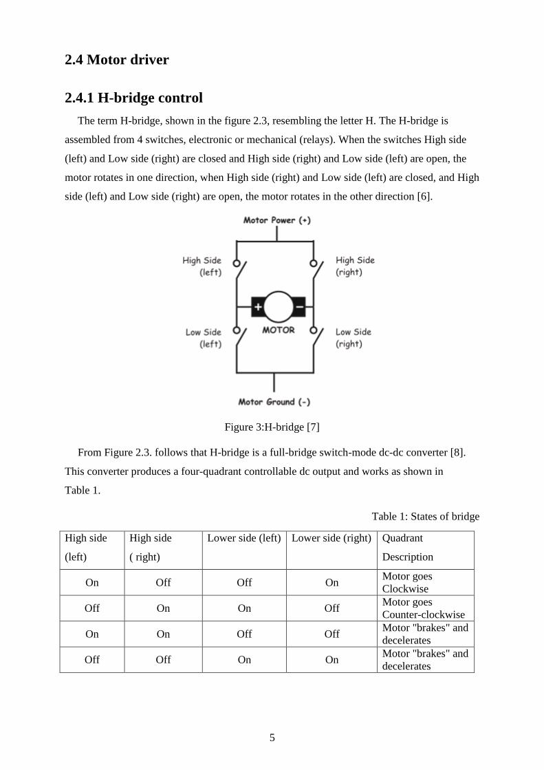
2.4 Motor driver
2.4.1 H-bridge control
The term H-bridge, shown in the figure 2.3, resembling the letter H. The H-bridge is
assembled from 4 switches, electronic or mechanical (relays). When the switches High side
(left) and Low side (right) are closed and High side (right) and Low side (left) are open, the
motor rotates in one direction, when High side (right) and Low side (left) are closed, and High
side (left) and Low side (right) are open, the motor rotates in the other direction [6].
Figure 3:H-bridge [7]
From Figure 2.3. follows that H-bridge is a full-bridge switch-mode dc-dc converter [8].
This converter produces a four-quadrant controllable dc output and works as shown in
Table 1.
Table 1: States of bridge
High side
(left)
High side
( right)
Lower side (left) Lower side (right) Quadrant
Description
On Off Off On Motor goes
Clockwise
Off On On Off Motor goes
Counter-clockwise
On On Off Off Motor "brakes" and
decelerates
Off Off On On Motor "brakes" and
decelerates
6
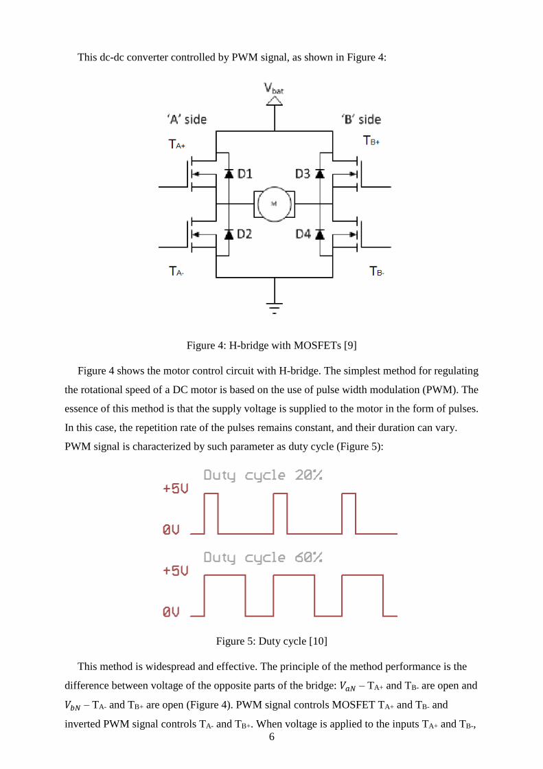
This dc-dc converter controlled by PWM signal, as shown in Figure 4:
Figure 4: H-bridge with MOSFETs [9]
Figure 4 shows the motor control circuit with H-bridge. The simplest method for regulating
the rotational speed of a DC motor is based on the use of pulse width modulation (PWM). The
essence of this method is that the supply voltage is supplied to the motor in the form of pulses.
In this case, the repetition rate of the pulses remains constant, and their duration can vary.
PWM signal is characterized by such parameter as duty cycle (Figure 5):
Figure 5: Duty cycle [10]
This method is widespread and effective. The principle of the method performance is the
difference between voltage of the opposite parts of the bridge: 𝑉𝑎𝑁 – TA+ and TB- are open and
𝑉𝑏𝑁 – TA- and TB+ are open (Figure 4). PWM signal controls MOSFET TA+ and TB- and
inverted PWM signal controls TA- and TB+. When voltage is applied to the inputs TA+ and TB-,

7
they are opened and the motor starts to rotate in the forward direction and opposite: TA- and
TB+. are opened if voltage of inverted PWM applied to them, in that case motor rotates in
backward direction. Figure 6 shows the relationship between the duty cycle and the output
voltage of the bridge.
Figure 6: PWM with bipolar switching [8]
Where Vd is input voltage, VO – output voltage. It is shown that Vo depends on ratio
between open time opposite pairs of transistors in the bridge.
From figure 6 follows, that output voltage is maximum when duty cycle is 100%, output
voltage is minimum when duty cycle of PWM is 0% (or 100% of inverted PWM). Output
voltage equals 0 when duty cycle is 50%.
8
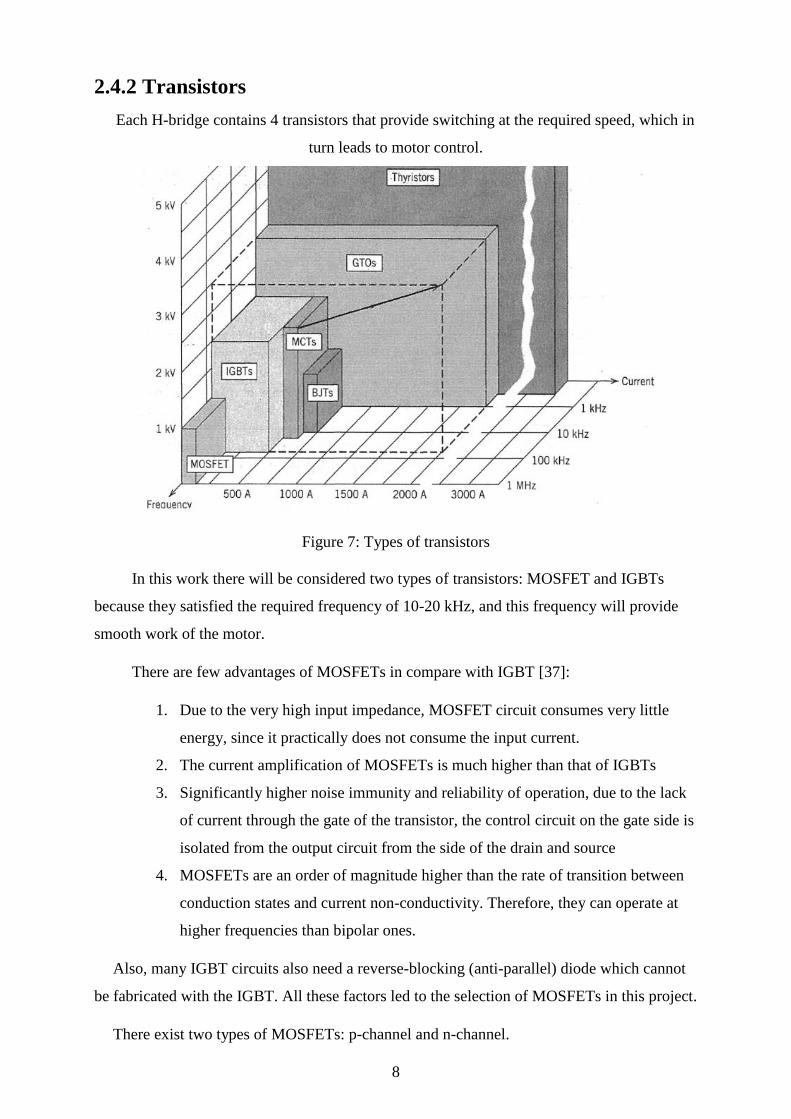
2.4.2 Transistors
Each H-bridge contains 4 transistors that provide switching at the required speed, which in
turn leads to motor control.
Figure 7: Types of transistors
In this work there will be considered two types of transistors: MOSFET and IGBTs
because they satisfied the required frequency of 10-20 kHz, and this frequency will provide
smooth work of the motor.
There are few advantages of MOSFETs in compare with IGBT [37]:
1. Due to the very high input impedance, MOSFET circuit consumes very little
energy, since it practically does not consume the input current.
2. The current amplification of MOSFETs is much higher than that of IGBTs
3. Significantly higher noise immunity and reliability of operation, due to the lack
of current through the gate of the transistor, the control circuit on the gate side is
isolated from the output circuit from the side of the drain and source
4. MOSFETs are an order of magnitude higher than the rate of transition between
conduction states and current non-conductivity. Therefore, they can operate at
higher frequencies than bipolar ones.
Also, many IGBT circuits also need a reverse-blocking (anti-parallel) diode which cannot
be fabricated with the IGBT. All these factors led to the selection of MOSFETs in this project.
There exist two types of MOSFETs: p-channel and n-channel.
9
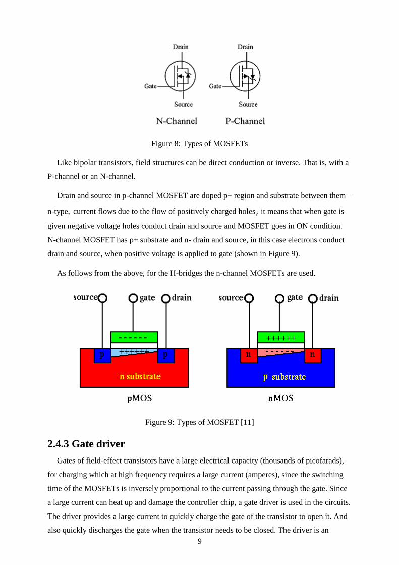
Figure 8: Types of MOSFETs
Like bipolar transistors, field structures can be direct conduction or inverse. That is, with a
P-channel or an N-channel.
Drain and source in p-channel MOSFET are doped p+ region and substrate between them –
n-type, current flows due to the flow of positively charged holes, it means that when gate is
given negative voltage holes conduct drain and source and MOSFET goes in ON condition.
N-channel MOSFET has p+ substrate and n- drain and source, in this case electrons conduct
drain and source, when positive voltage is applied to gate (shown in Figure 9).
As follows from the above, for the H-bridges the n-channel MOSFETs are used.
Figure 9: Types of MOSFET [11]
2.4.3 Gate driver
Gates of field-effect transistors have a large electrical capacity (thousands of picofarads),
for charging which at high frequency requires a large current (amperes), since the switching
time of the MOSFETs is inversely proportional to the current passing through the gate. Since
a large current can heat up and damage the controller chip, a gate driver is used in the circuits.
The driver provides a large current to quickly charge the gate of the transistor to open it. And
also quickly discharges the gate when the transistor needs to be closed. The driver is an

10
amplifier that receives a signal with a weak current from the controller and outputs a high
current signal.
2.5 Motor control simulation
2.5.1 H-bridge
It was decided to create simulation of H-bridge with PWM control. MATLAB was chosen
as useful software for this purpose. MATLAB is universal and effective software for
simulation of logic or electronic function.
Firstly, H-bridge was built up as a subsystem of motor control system with PWM.
As discussed above, the use of MOSFETs is the most convenient and effective.
Figure 10:Subsystem H-bridge
The whole model is available in the Appendix A.
According to theory, it is known that PWM with duty cycle 50% gives bridge equilibrium
and 0 voltage to the motor.
11
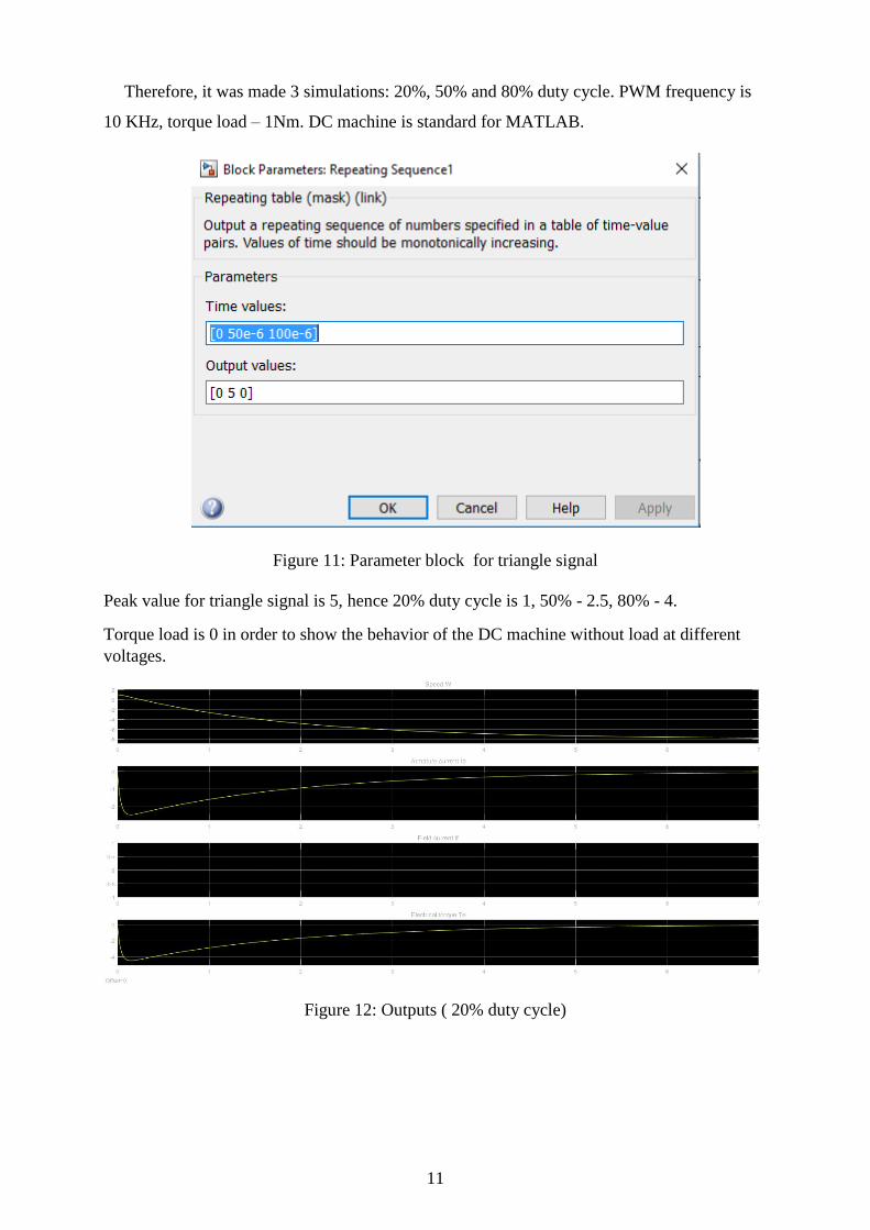
Therefore, it was made 3 simulations: 20%, 50% and 80% duty cycle. PWM frequency is
10 KHz, torque load – 1Nm. DC machine is standard for MATLAB.
Figure 11: Parameter block for triangle signal
Peak value for triangle signal is 5, hence 20% duty cycle is 1, 50% - 2.5, 80% - 4.
Torque load is 0 in order to show the behavior of the DC machine without load at different
voltages.
Figure 12: Outputs ( 20% duty cycle)
12
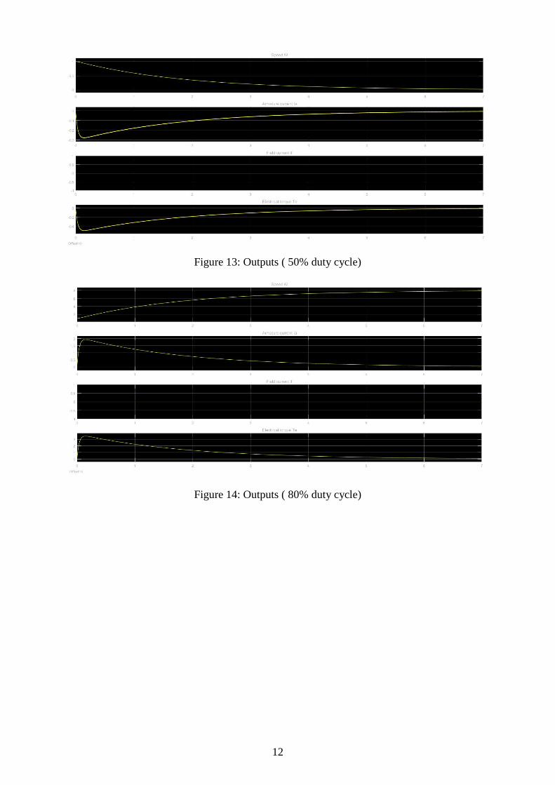
Figure 13: Outputs ( 50% duty cycle)
Figure 14: Outputs ( 80% duty cycle)
13
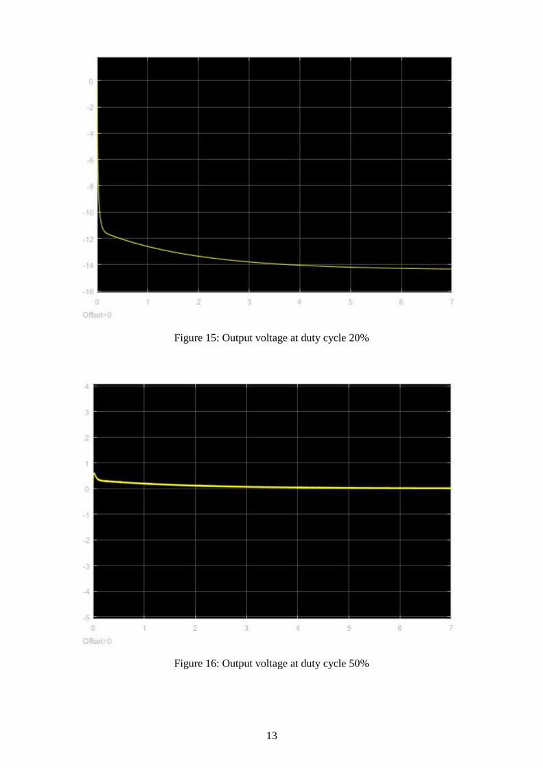
Figure 15: Output voltage at duty cycle 20%
Figure 16: Output voltage at duty cycle 50%
14
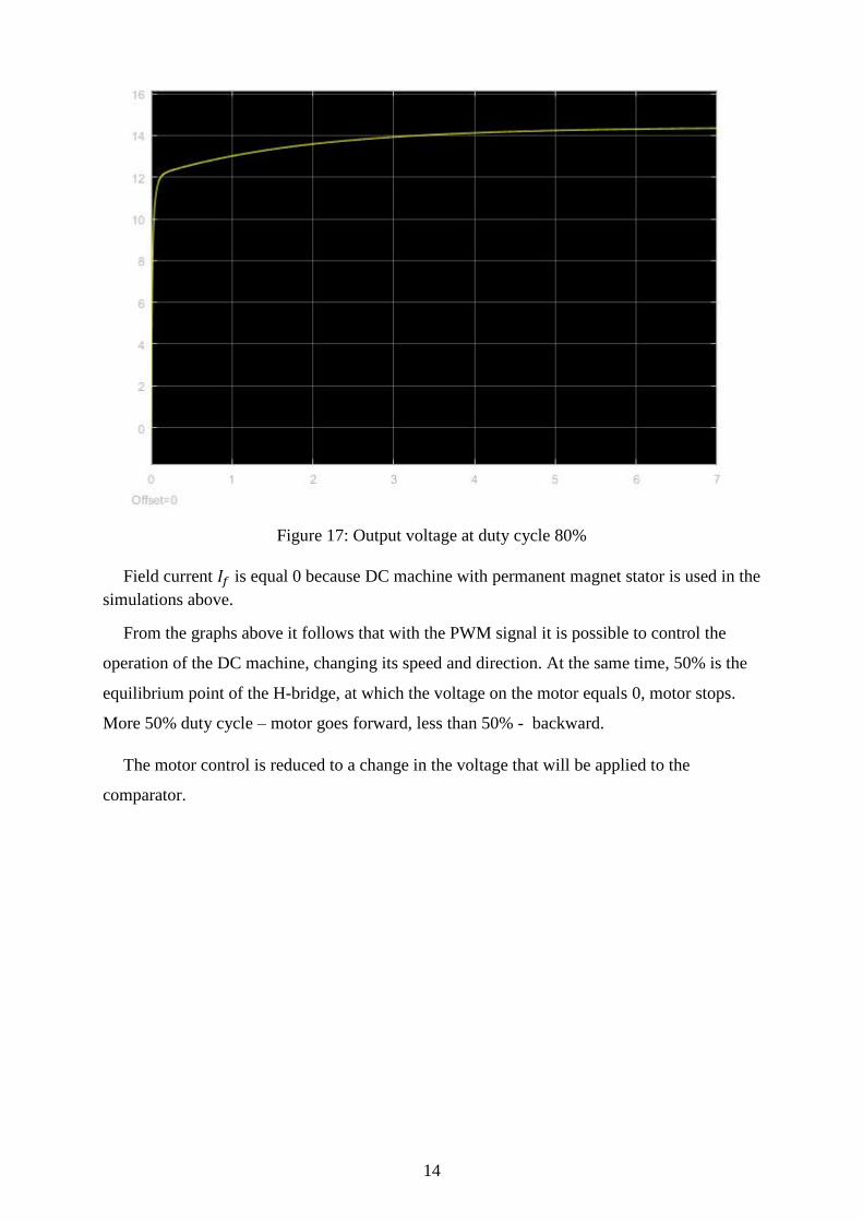
Figure 17: Output voltage at duty cycle 80%
Field current 𝐼𝑓 is equal 0 because DC machine with permanent magnet stator is used in the
simulations above.
From the graphs above it follows that with the PWM signal it is possible to control the
operation of the DC machine, changing its speed and direction. At the same time, 50% is the
equilibrium point of the H-bridge, at which the voltage on the motor equals 0, motor stops.
More 50% duty cycle – motor goes forward, less than 50% - backward.
The motor control is reduced to a change in the voltage that will be applied to the
comparator.

15
3. PWM signal
MATLAB does not allow creating an electronic circuit using real-world equipment and
simulating it. Therefore, it was decided to find another software that would allow to create
circuits and make simulations. After considering different options among the programs
licensed by UIT, the OrCAD software was chosen, which allows not only to create a circuit
using components from the built-in library, but also in the future, based on this circuit, to
develop a board layout that can be created on special equipment located on Campus. The
main challenge when working with OrCAD is the limitations of the library that does not allow
the use of components that are not included in it. Consequently, it was necessary to select
components on the manufacturers' websites again and again, since most of the new
microchips are missing in the OrCAD library.
One of the tasks of this work is the manual speed control of the motor. That is, as follows
from the data described in the previous chapters, the change of PWM duty cycle. The simplest
way to form PWM signal with manual control of duty cycle – using comparator.
Figure 18: Form PWM signal with comparator [12]
As shown above, user can change DC level to control PWM duty cycle.
Thus, the main challenge of the project was the generation of a triangle wave.
3.1 Triangle wave
3.1.1. 555 timer
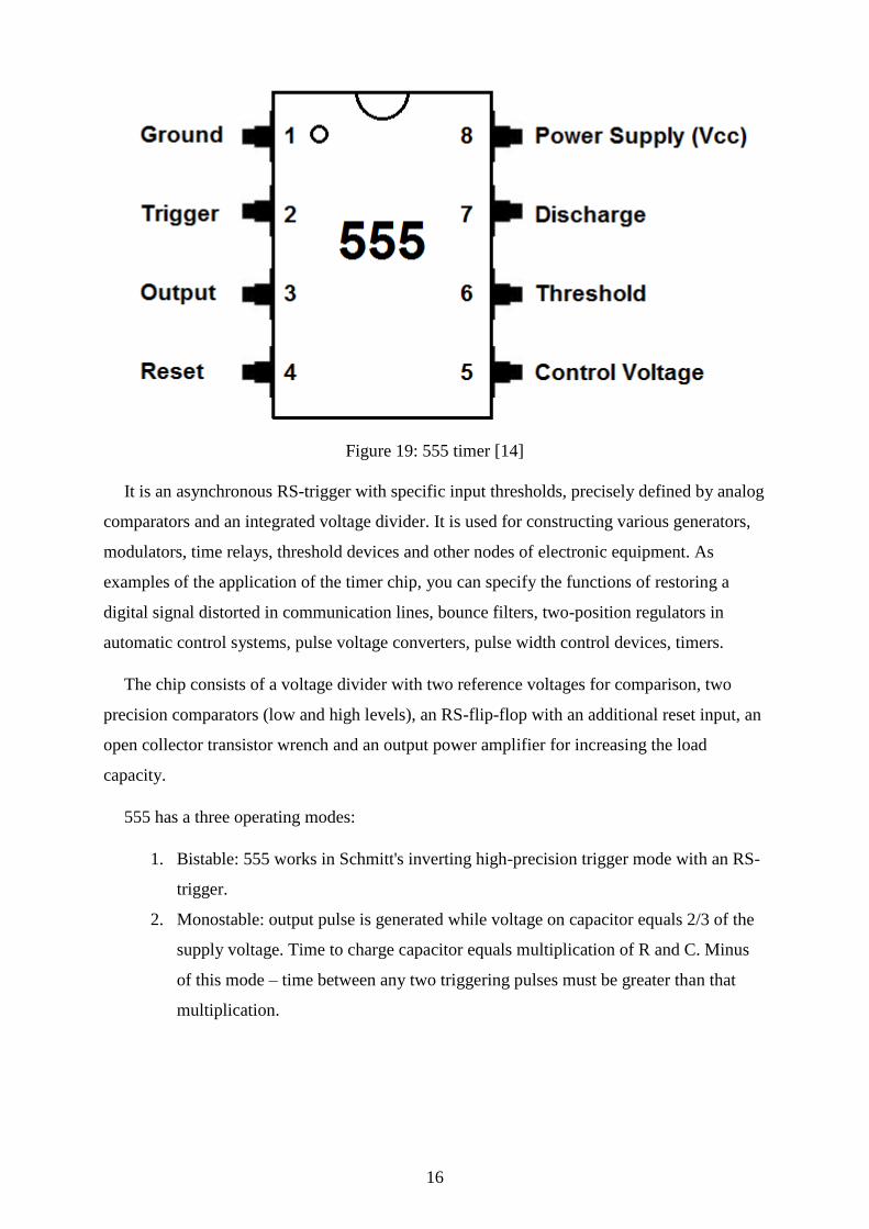
555 - integrated circuit, universal timer - a device for generating single and repetitive
pulses with stable time characteristics.
16
Figure 19: 555 timer [14]
It is an asynchronous RS-trigger with specific input thresholds, precisely defined by analog
comparators and an integrated voltage divider. It is used for constructing various generators,
modulators, time relays, threshold devices and other nodes of electronic equipment. As
examples of the application of the timer chip, you can specify the functions of restoring a
digital signal distorted in communication lines, bounce filters, two-position regulators in
automatic control systems, pulse voltage converters, pulse width control devices, timers.
The chip consists of a voltage divider with two reference voltages for comparison, two
precision comparators (low and high levels), an RS-flip-flop with an additional reset input, an
open collector transistor wrench and an output power amplifier for increasing the load
capacity.
555 has a three operating modes:
1. Bistable: 555 works in Schmitt's inverting high-precision trigger mode with an RS-
trigger.
2. Monostable: output pulse is generated while voltage on capacitor equals 2/3 of the
supply voltage. Time to charge capacitor equals multiplication of R and C. Minus
of this mode – time between any two triggering pulses must be greater than that
multiplication.

17
Figure 20: Monostable mode of 555 timer [15]
3. Astable: in this mode 555 timer generates continuous rectangular pulses on the
output and triangle wave in the point between C and R2
Figure 21: Astable mode of 555 timer
Frequency of pulses can be tuned according to this formula:
𝑓 =1
𝑙𝑛2∗(𝑅1+2∗𝑅2)∗𝐶 (3.1)
Frequency depends on three components in the circuit: two resistors and one capacitor.
Low level in this case equals 1/3 supply voltage and high level – 2/3 supply voltage. This
mode satisfies requirements of the project – triangle pulses generate in node between R2 and C
[13]. The model IC555 that was simulated is shown in Appendix B.
18
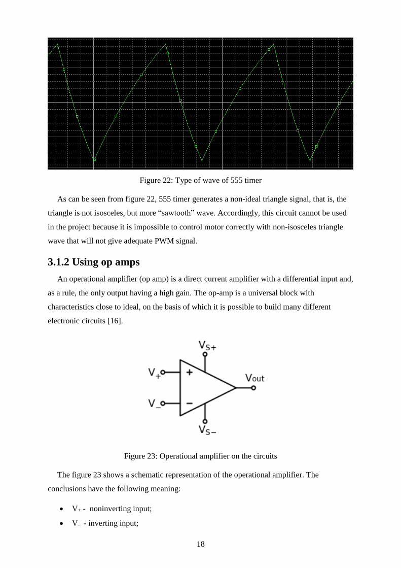
Figure 22: Type of wave of 555 timer
As can be seen from figure 22, 555 timer generates a non-ideal triangle signal, that is, the
triangle is not isosceles, but more “sawtooth” wave. Accordingly, this circuit cannot be used
in the project because it is impossible to control motor correctly with non-isosceles triangle
wave that will not give adequate PWM signal.
3.1.2 Using op amps
An operational amplifier (op amp) is a direct current amplifier with a differential input and,
as a rule, the only output having a high gain. The op-amp is a universal block with
characteristics close to ideal, on the basis of which it is possible to build many different
electronic circuits [16].
Figure 23: Operational amplifier on the circuits
The figure 23 shows a schematic representation of the operational amplifier. The
conclusions have the following meaning:
V+ - noninverting input;
V- - inverting input;

19
Vout – output;
VS+ - positive power supply (also can be referred as VDD, VCC or VCC+)
VS- - negative power supply (also can be referred as VSS, VEE or VCC-)
These five outputs are present in any op amp and are necessary for its operation.
There are many ways of constructing multivibrators and generators of pulse sequences that
are different from the rectangular form. Wide-spreading generators of linearly varying voltage
and various types of triangular pulses are used, which are used in oscilloscope sweeps,
shapers of a given time shift and other applications. Pulses of the required shape are obtained
by appropriate choice of positive and negative feedback circuits. A triangle waveform
generator can be obtained using a Schmitt trigger and an integrator [17].
3.1.2.1 Schmitt trigger
The Schmitt trigger is an electronic two-position relay element whose static characteristic
has hysteresis loop. Schematically, the Schmitt trigger is a two-threshold comparator with an
RS-flip-flop.
Figure 24: Schmitt trigger
The voltage levels at which the Schmitt trigger are triggered are called the upper level
(threshold) of the triggering of the trigger and the lower level (threshold) of the triggering. To
implement the Schmitt trigger, op amp covered by positive feedback are used, which is
implemented by feeding a part of the output voltage to the non-inverting input. Schmitt
trigger uses to compare two noisy or slowly changing signals, which allows excluding the
multiple operation of the comparator at close values of input voltage.
3.1.2.2 Integrator
Integration circuits are designed to integrate in time electrical input signals. Different
varieties of integrators are used in many schemes, for example, in active filters or in automatic
control systems to integrate an error signal.

20
Figure 25: Integrator (op amp)
The integrator's work is based on the fact that the inverting input is grounded, according to
the principle of virtual closure. The input current flows through the resistor R, at the same
time to counterbalance the zero potential point, the capacitor will be charged with the current
of the same value, but with the opposite sign. As a result, the voltage at which the capacitor is
charged by this current will form on the integrator output. The input resistance of the
integrator will be equal to the resistance of the resistor R, and the output resistance will be
determined by the parameters of the op-amp [18].
The magnitude of the input signal is generally described by equation:
𝑈𝑜𝑢𝑡(𝑡) = −1
𝑅𝐶∫ 𝑈𝑖𝑛(𝜏)𝑑𝜏
𝑡
0+ 𝑈𝑖𝑛𝑖𝑡𝑖𝑎𝑙 (3.2)
Where 𝑈𝑜𝑢𝑡 and 𝑈𝑖𝑛 are functions of time, 𝑈𝑖𝑛𝑖𝑡𝑖𝑎𝑙 – output voltage at time t = 0.
When a rectangular pulse with ideal fronts is fed to the RC integrating circuit, the output
voltage grows exponentially:

21
Figure 26: Integrated step signal
𝑈𝑜𝑢𝑡 = −1
𝑅𝐶∫ 𝑈 𝑑𝑡 = −
1
𝑅𝐶∗ 𝑈 ∗ 𝑡 (3.3)
The change in the output voltage in time is an inclined straight line with the polarity of the
input signal.
Figure 27: Integrated rectangular signal
Since the signal is periodic, it is sufficient to consider one full period to describe the output
voltage. After integration, we obtain an oblique line at each half-period. For any signal at the
input, the change in the output signal should start from the value that the output signal had at
the time the input signal.
22
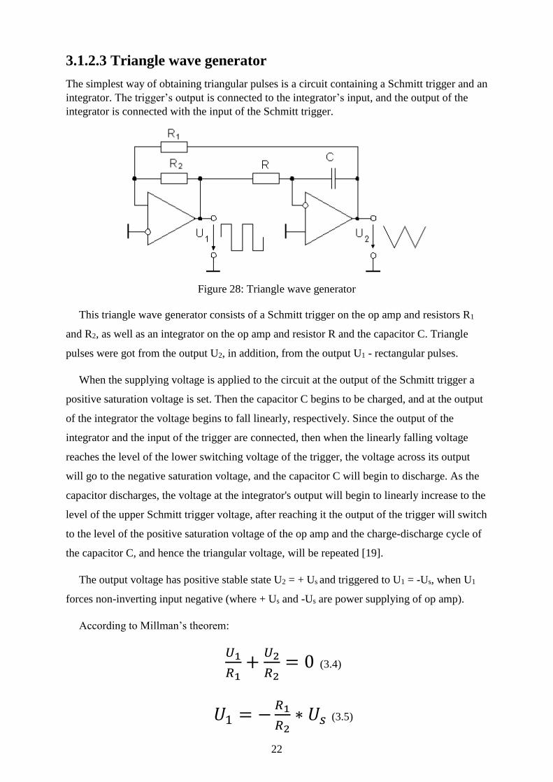
3.1.2.3 Triangle wave generator
The simplest way of obtaining triangular pulses is a circuit containing a Schmitt trigger and an
integrator. The trigger’s output is connected to the integrator’s input, and the output of the
integrator is connected with the input of the Schmitt trigger.
Figure 28: Triangle wave generator
This triangle wave generator consists of a Schmitt trigger on the op amp and resistors R1
and R2, as well as an integrator on the op amp and resistor R and the capacitor C. Triangle
pulses were got from the output U2, in addition, from the output U1 - rectangular pulses.
When the supplying voltage is applied to the circuit at the output of the Schmitt trigger a
positive saturation voltage is set. Then the capacitor C begins to be charged, and at the output
of the integrator the voltage begins to fall linearly, respectively. Since the output of the
integrator and the input of the trigger are connected, then when the linearly falling voltage
reaches the level of the lower switching voltage of the trigger, the voltage across its output
will go to the negative saturation voltage, and the capacitor C will begin to discharge. As the
capacitor discharges, the voltage at the integrator's output will begin to linearly increase to the
level of the upper Schmitt trigger voltage, after reaching it the output of the trigger will switch
to the level of the positive saturation voltage of the op amp and the charge-discharge cycle of
the capacitor C, and hence the triangular voltage, will be repeated [19].
The output voltage has positive stable state U2 = + Us and triggered to U1 = -Us, when U1
forces non-inverting input negative (where + Us and -Us are power supplying of op amp).
According to Millman’s theorem:
𝑈1
𝑅1+
𝑈2
𝑅2= 0 (3.4)
𝑈1 = −𝑅1
𝑅2∗ 𝑈𝑠 (3.5)
23
Assume that output voltage at Schmitt trigger has to trigger twice (from positive to
negative state) and then goes back. In this case:
∆𝑈2 = 2𝑅1
𝑅2𝑈𝑠 (3.6)
The second stage is integrator, where current flow through resistor R and capacitor C.
𝐼𝑐 =𝑈𝑆
𝑅 (3.7)
Since this current can change output voltage ∆𝑈 :
∆𝑈 =∆𝑄
𝐶=
𝐼𝐶∗∆𝑡
𝐶 (3.8)
rearranging
∆𝑡 =𝐶∗∆𝑈
𝐼𝐶 (3.9)
From 3.6 and 3.7 follows:
∆𝑡 = 2𝑅1
𝑅2𝑈𝑠 ∗
𝑅
𝑈𝑠∗ 𝐶 = 2
𝑅1𝑅
𝑅2𝐶 (3.10)
Since ∆𝑡 is half period, hence it follows that:
𝑇 =2*∆𝑡 = 4𝑅1𝑅
𝑅2𝐶 (3.11)
Thus, frequency of the triangle wave equals:
𝑓 =1
𝑇=
𝑅2
4𝑅1𝑅𝐶 (3.12)

24
4 Simulation model
4.1 Triangle wave simulation
First challenge in design circuit is the choice of components for circuit. Following the
circuit that was presented above, it is clear that the main in triangle wave generator is op
amps.
I decided to choose op amp that was produced by Texas Instruments, because this
company has huge components list and convenient search on website.
First of all, I chose type of op amps. On the website [21] it exists few types:
Precision op amps
High-Speed op amps
General-Purpose op amps
Ultra-Low-Power op amps
Audio op amps
Fully differential amplifiers
Power op amps
The most appropriate choice is general-purpose op amps.
I decided to choose op amp according to 3 parameters: minimum supply voltage, number
of channels and maximum quiescent current per channel:
25
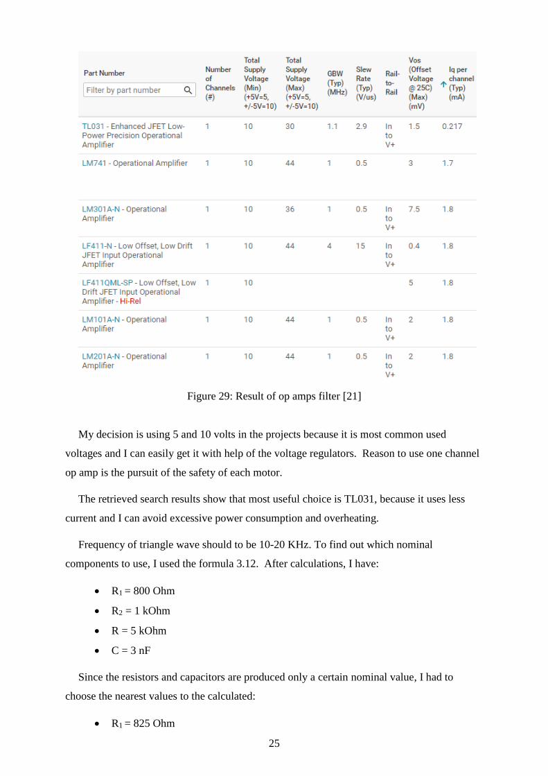
Figure 29: Result of op amps filter [21]
My decision is using 5 and 10 volts in the projects because it is most common used
voltages and I can easily get it with help of the voltage regulators. Reason to use one channel
op amp is the pursuit of the safety of each motor.
The retrieved search results show that most useful choice is TL031, because it uses less
current and I can avoid excessive power consumption and overheating.
Frequency of triangle wave should to be 10-20 KHz. To find out which nominal
components to use, I used the formula 3.12. After calculations, I have:
R1 = 800 Ohm
R2 = 1 kOhm
R = 5 kOhm
C = 3 nF
Since the resistors and capacitors are produced only a certain nominal value, I had to
choose the nearest values to the calculated:
R1 = 825 Ohm

26
R2 = 1 kOhm
R = 5.1 kOhm
C = 3.3 nF
The designed circuit, that is shown in Appendix C., consists triangle wave generator with
frequency ~14.3 kHz.
Whereas calculated frequency:
𝑓 =1
𝑇=
𝑅2
4𝑅1𝑅𝐶=
1000
4∗825∗5.1∗103∗3.3∗10−9 ~18 𝑘𝐻𝑧 (4.1)
Figure 30: Simulated triangle wave
This difference is due to the fact that maximum peak output voltage (if voltage supply is
±5 𝑉 ) of TL031 are VOM+ = 4.3 V and VOM- = 4.2 V.
In this case maximum amplitude achieves with 𝑅2
𝑅1~0.825. Also this are real op amps and
Schmitt trigger cannot change states instantaneously.
I can check my calculations later on a real board layout.
4.2 Voltage divider
The second component in obtaining the PWM signal is a constant voltage, which must be
compared with a triangular wave in the comparator. In this project, the PWM signal is
manually controlled. For this purpose, it was decided to use a voltage divider as the simplest
and cheapest method.
A voltage divider is a device in which the input and output voltages are connected by a
transmission coefficient. The voltage divider can be represented as two consecutive sections
of a chain (Figure 31), the sum of the voltages at which is equal to the input voltage. The

27
simplest resistive voltage divider consists of two series-connected resistors connected to a
voltage source. Since the resistors are connected in series, the current through them will be the
same in accordance with the first Kirchhoff`s law. The voltage drops across each resistor
according to Ohm's law will be proportional to the resistance [22]:
Figure 31: Voltage divider
𝑉𝑜𝑢𝑡 = 𝑉𝑖𝑛𝑅2
𝑅1+𝑅2 (4.2)
As you can see from the formula, the voltage will never be zero, you can only make it
minimum acceptable.
I decided to use 𝑅1 = 5 𝑘𝑂ℎ𝑚 and 𝑅2 = 200 𝑂ℎ𝑚. This will give me a low minimum
voltage level; however, the disadvantage is a very uneven voltage increase when changing 𝑅1.
4.3 PWM signal
PWM signal is the basis of the H-bridge operation, and hence the basis for the operation of
the entire circuit. As described above, the PWM signal is obtained by comparing the
triangular wave and the DC voltage. For this, there is a special chip, called a comparator.
There are exist a lot types of comparator, but I decided to use comparator that I could find
on the university’s storage and in OrCAD library at the same time.
The most commonly used and simple comparator is LM393. It is a dual differential
comparator that can supply voltage up to 36 V.
28
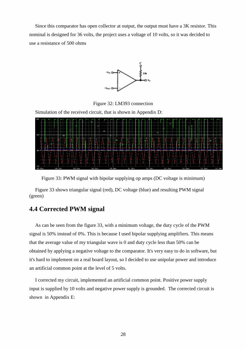
Since this comparator has open collector at output, the output must have a 3K resistor. This
nominal is designed for 36 volts, the project uses a voltage of 10 volts, so it was decided to
use a resistance of 500 ohms
Figure 32: LM393 connection
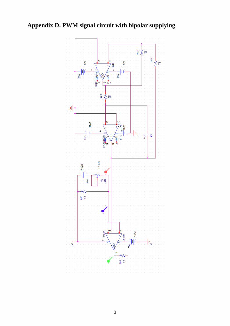
Simulation of the received circuit, that is shown in Appendix D:
Figure 33: PWM signal with bipolar supplying op amps (DC voltage is minimum)
Figure 33 shows triangular signal (red), DC voltage (blue) and resulting PWM signal
(green)
4.4 Corrected PWM signal
As can be seen from the figure 33, with a minimum voltage, the duty cycle of the PWM
signal is 50% instead of 0%. This is because I used bipolar supplying amplifiers. This means
that the average value of my triangular wave is 0 and duty cycle less than 50% can be
obtained by applying a negative voltage to the comparator. It's very easy to do in software, but
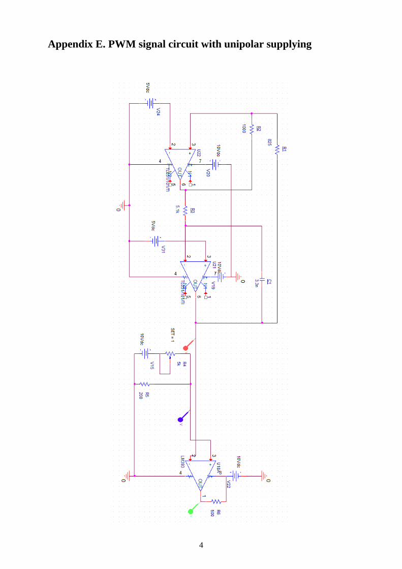
it's hard to implement on a real board layout, so I decided to use unipolar power and introduce
an artificial common point at the level of 5 volts.
I corrected my circuit, implemented an artificial common point. Positive power supply
input is supplied by 10 volts and negative power supply is grounded. The corrected circuit is
shown in Appendix E:

29
Figure 34: PWM signal with unipolar supplying op amps( DC voltage is minimum)
This circuit allows to control the duty cycle of PWM in the entire range from 0% to 100%.
4.5 Galvanic isolation
Galvanic isolation is a transfer of energy or signal between electrical circuits without
electrical contact between them. Galvanic isolation is used for signal transmission, for
contactless control and for protecting equipment and people from electric shock.
In my project I needed galvanic isolation, because I had to protect and separate my control
loop from power supply loop, that supplies motor and could damage control loop through
common chip – motor driver.
There are just a few models of optocouplers in OrCAD library.
I needed an optocoupler with a transistor as an output, minimum collector-emitter voltage
is 10 volts and time rise and fall is minimum:
𝑡 =𝑇
2=
1
2 ∗ 𝑓=
1
2 ∗ 14.3 ∗ 103~35 𝜇𝑠
Optocoupler with these requirements, which is in the OrCAD library is 3N244 [23]:
Table 2: Optocoupler 3N244
Forward DC Current 40 mA
Reverse Voltage 2 V
Continuous Collector Current 30 mA
Collector- Emitter Voltage 30 V
Output Rise Time 10 𝜇𝑠
Output Fall Time 10 𝜇𝑠

30
This optocoupler satisfies the stated requirements and is completely suitable for
simulations.
4.6 Motor driver
One of the main challenges of this project was the motor driver selection. First of all, I
decided to use in the project motor driver instead of gate driver.
Using the motor driver is simpler and more reliable since I decided to not use the
additional elements (MOSFETs, diodes) that can be damaged while using. In addition, the
market has much more motor drivers with included H-bridge than the gate drivers. This
makes it easy to find the item I need.
In the process of searching, I faced the problem of the OrCAD library. There are just few
motor driver models [24].
As a result, I found two motor drivers in OrCAD library that are controlled by a PWM
signal and have a suitable output voltage (24 volts):
LM5045
SA50CE
LM5045 produced by Texas Instruments, this is full-bridge PWM controller with
integrated MOSFET drivers.
31
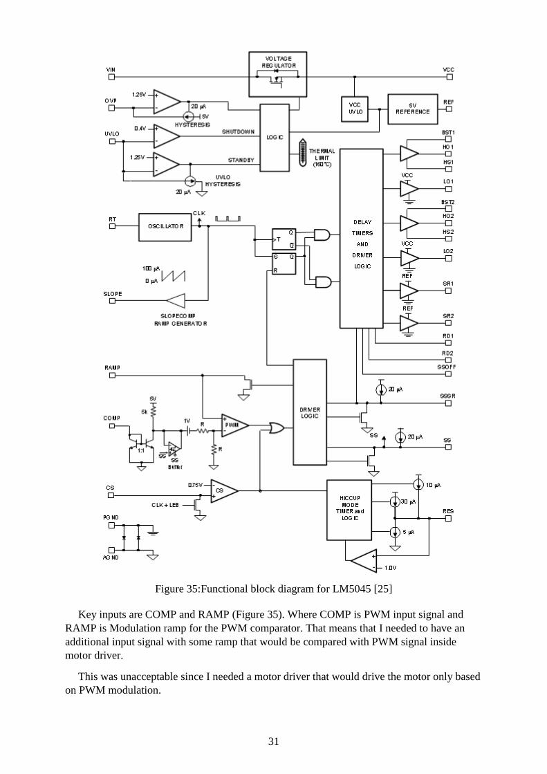
Figure 35:Functional block diagram for LM5045 [25]
Key inputs are COMP and RAMP (Figure 35). Where COMP is PWM input signal and
RAMP is Modulation ramp for the PWM comparator. That means that I needed to have an
additional input signal with some ramp that would be compared with PWM signal inside
motor driver.
This was unacceptable since I needed a motor driver that would drive the motor only based
on PWM modulation.
32
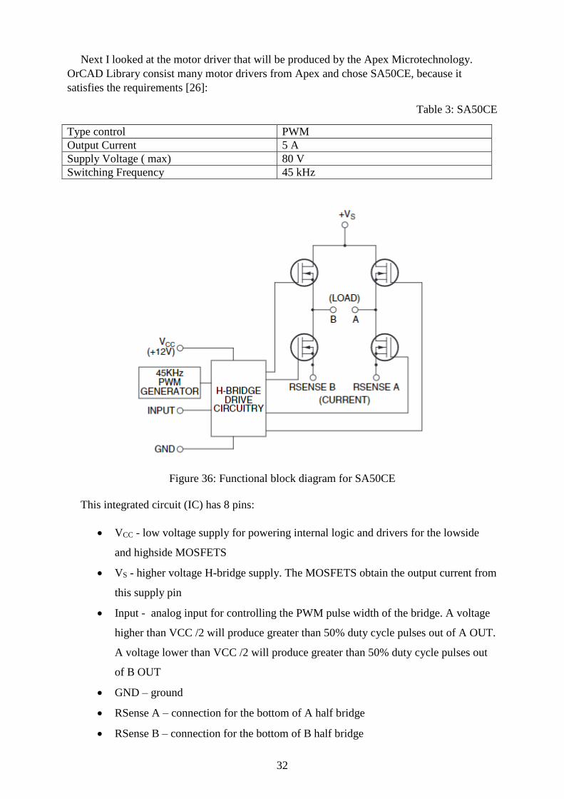
Next I looked at the motor driver that will be produced by the Apex Microtechnology.
OrCAD Library consist many motor drivers from Apex and chose SA50CE, because it
satisfies the requirements [26]:
Table 3: SA50CE
Type control PWM
Output Current 5 A
Supply Voltage ( max) 80 V
Switching Frequency 45 kHz
Figure 36: Functional block diagram for SA50CE
This integrated circuit (IC) has 8 pins:
VCC - low voltage supply for powering internal logic and drivers for the lowside
and highside MOSFETS
VS - higher voltage H-bridge supply. The MOSFETS obtain the output current from
this supply pin
Input - analog input for controlling the PWM pulse width of the bridge. A voltage
higher than VCC /2 will produce greater than 50% duty cycle pulses out of A OUT.
A voltage lower than VCC /2 will produce greater than 50% duty cycle pulses out
of B OUT
GND – ground
RSense A – connection for the bottom of A half bridge
RSense B – connection for the bottom of B half bridge
33
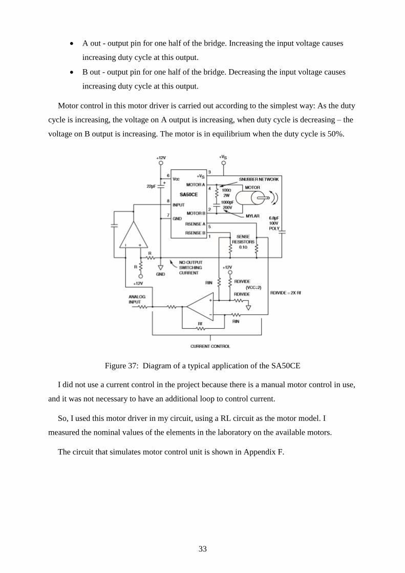
A out - output pin for one half of the bridge. Increasing the input voltage causes
increasing duty cycle at this output.
B out - output pin for one half of the bridge. Decreasing the input voltage causes
increasing duty cycle at this output.
Motor control in this motor driver is carried out according to the simplest way: As the duty
cycle is increasing, the voltage on A output is increasing, when duty cycle is decreasing – the
voltage on B output is increasing. The motor is in equilibrium when the duty cycle is 50%.
Figure 37: Diagram of a typical application of the SA50CE
I did not use a current control in the project because there is a manual motor control in use,
and it was not necessary to have an additional loop to control current.
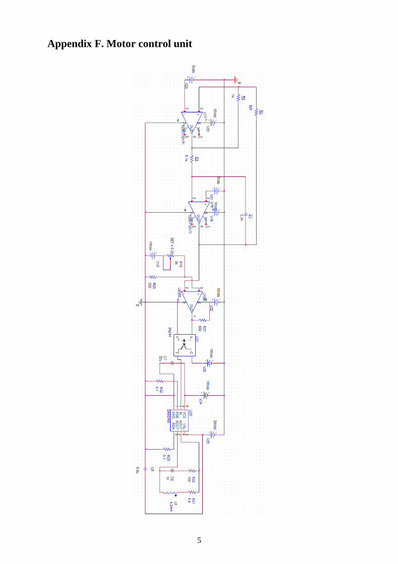
So, I used this motor driver in my circuit, using a RL circuit as the motor model. I
measured the nominal values of the elements in the laboratory on the available motors.
The circuit that simulates motor control unit is shown in Appendix F.
34
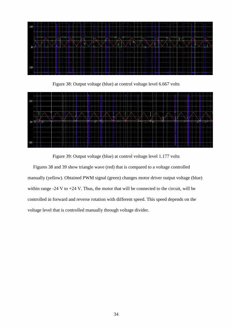
Figure 38: Output voltage (blue) at control voltage level 6.667 volts
Figure 39: Output voltage (blue) at control voltage level 1.177 volts
Figures 38 and 39 show triangle wave (red) that is compared to a voltage controlled
manually (yellow). Obtained PWM signal (green) changes motor driver output voltage (blue)
within range -24 V to +24 V. Thus, the motor that will be connected to the circuit, will be
controlled in forward and reverse rotation with different speed. This speed depends on the
voltage level that is controlled manually through voltage divider.
35
5 Power supply
This project requires a stable DC voltage for the circuit and motors power supply. As
shown above, the circuit uses a voltage is 5 volts, 10 volts and 24 volts.
Thus, the following problem arose: it was necessary to construct DC voltage source of
three different values: 5,10 and 24 V. For this purpose, the AC 220 V from the grid must be
lowered and rectified to the required values.
5.1 Voltage regulators
The simplest way to get stable voltage in the circuit is using voltage regulators.
The voltage regulator is a device that allows to change the value of the electrical voltage at
the output when it acts on the control elements, or when a control signal is received.
Since in the project was used standard voltage, it is easy to use voltage regulator 5, 10 and
24 volts, that could be found on market easily.
I chose voltage regulators that were produced by Texas Instruments:
LM7805 – 5 volts
LM7810 – 10 volts
LM7824 – 24 volts
All these three types of voltage regulators have different parameters [27]:
Table 4: Voltage regulators parameters
LM7805 LM7810 LM7824 Unit
Input voltage
min max min max min max
V
7 25 12.5 28 27 38
Output voltage min typ max min typ max min typ max
V 4.8 5 5.2 9.6 10 10.4 23 24 25
Output current 1.5 1.5 1.5 A
It was decided to use output voltage of LM7810 as input voltage LM7805, because these
two regulators are used in the same control loop and part of circuit. Another thing is LM7824:
this is another part of circuit that responsible for motor power supplying. These two loops
should to be separated, because of safety.
36
From the table 4 follows that that at least two input voltages are required, for LM7810 and
LM7824. Thus It requires two rectifiers and two transformers.
Figure 40: Application LM78xx
Figure 40 shows connection LM7805 (LM7810, LM7824) to circuit.
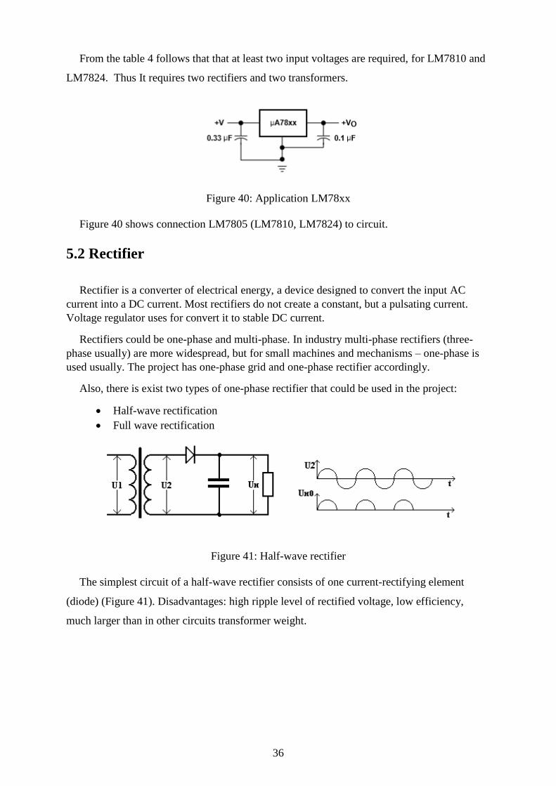
5.2 Rectifier
Rectifier is a converter of electrical energy, a device designed to convert the input AC
current into a DC current. Most rectifiers do not create a constant, but a pulsating current.
Voltage regulator uses for convert it to stable DC current.
Rectifiers could be one-phase and multi-phase. In industry multi-phase rectifiers (three-
phase usually) are more widespread, but for small machines and mechanisms – one-phase is
used usually. The project has one-phase grid and one-phase rectifier accordingly.
Also, there is exist two types of one-phase rectifier that could be used in the project:
Half-wave rectification
Full wave rectification
Figure 41: Half-wave rectifier
The simplest circuit of a half-wave rectifier consists of one current-rectifying element
(diode) (Figure 41). Disadvantages: high ripple level of rectified voltage, low efficiency,
much larger than in other circuits transformer weight.
37
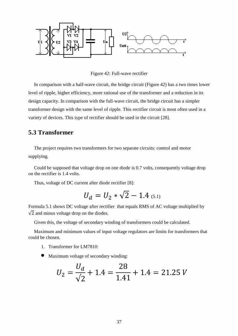
Figure 42: Full-wave rectifier
In comparison with a half-wave circuit, the bridge circuit (Figure 42) has a two times lower
level of ripple, higher efficiency, more rational use of the transformer and a reduction in its
design capacity. In comparison with the full-wave circuit, the bridge circuit has a simpler
transformer design with the same level of ripple. This rectifier circuit is most often used in a
variety of devices. This type of rectifier should be used in the circuit [28].
5.3 Transformer
The project requires two transformers for two separate circuits: control and motor
supplying.
Could be supposed that voltage drop on one diode is 0.7 volts, consequently voltage drop
on the rectifier is 1.4 volts.
Thus, voltage of DC current after diode rectifier [8]:
𝑈𝑑 = 𝑈2 ∗ √2 − 1.4 (5.1)
Formula 5.1 shows DC voltage after rectifier that equals RMS of AC voltage multiplied by
√2 and minus voltage drop on the diodes.
Given this, the voltage of secondary winding of transformers could be calculated.
Maximum and minimum values of input voltage regulators are limits for transformers that
could be chosen.
1. Transformer for LM7810:
Maximum voltage of secondary winding:
𝑈2 =𝑈𝑑
√2+ 1.4 =
28
1.41+ 1.4 = 21.25 𝑉
38
Minimum voltage of secondary winding:
𝑈2 =𝑈𝑑
√2+ 1.4 =
12.5
1.41+ 1.4 = 10.26 𝑉
2. Transformer for LM7824:
Maximum voltage of secondary winding:
𝑈2 =𝑈𝑑
√2+ 1.4 =
38
1.41+ 1.4 = 28.35 𝑉
Minimum voltage of secondary winding:
𝑈2 =𝑈𝑑
√2+ 1.4 =
27
1.41+ 1.4 = 20.55 𝑉
According to Fischertechnik [1], the largest motor they use has 24 volts supplying and 0.3
amperes current. Supposed starting current – 0.5 amperes. Thus, supposed power that will be
consumed by one largest motor:
𝑃 = 𝑈 ∗ 𝐼 = 24 ∗ 0.5 = 12 𝑉𝐴 (5.2)
At the request of the laboratory engineer, the model will use 4 motors at the same time.
Thus, total power consumption, that should to supply transformers, will be 60 VA.
Unfortunately, OrCAD doesn’t consist model of LM7824 and LM7810. Therefore, I
designed and simulated LM7812 and LM7810. This circuit is shown in Appendix G.
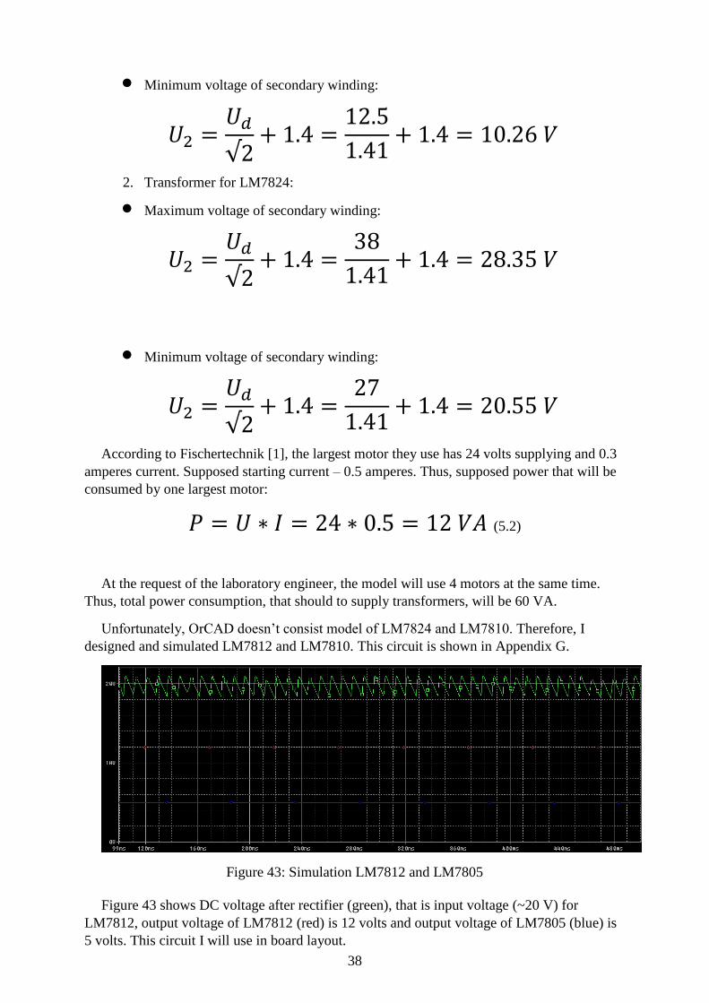
Figure 43: Simulation LM7812 and LM7805
Figure 43 shows DC voltage after rectifier (green), that is input voltage (~20 V) for
LM7812, output voltage of LM7812 (red) is 12 volts and output voltage of LM7805 (blue) is
5 volts. This circuit I will use in board layout.

39
6 Implementation
6.1 Power supply
The first stage of implementation of my circuit is power supplying as the basis of the
whole project. As I said in chapter 5, in this project I should to use two transformers 18 V and
25 V. I calculated in previous part that I need transformer for 25 V with power rating 60 VA
at least.
Before ordering in the web store, I had to use the components from the storage in the
university. There I found two transformers with secondary voltage rating 18 V and 25 V.
Power ratings were much more that I needed, but it is not necessary because higher power
rating is even better for the project: model could work with numbers of motors more than
four. Transformers that was used in the project [29]:
Table 5: Parameters of used transformers
Primary winding 230 V 230 V
Secondary winding 25 V 18 V
Power rating 80 VA 80 VA
Measured voltage 27.5 20.9
Figure 44:Measured voltage of transformer 230/25

40
Figure 45: Measured voltage of transformer 230/18
Measured voltage (figure 44 and 45) is higher than it is in datasheet. There are two points
to explain it:
1. Measured grid voltage is 237 volts, instead of 230 volts
2. It is indicated in the datasheet that no load secondary voltages are 28.3 volts and
20.4 volts respectively.
The second stage in power supplying is rectifier that consists of diodes. I chose diodes that
I found in the storage. I had two requirements for diodes: maximum average forward rectified
current is minimum 1 A and maximum reverse recovery time 𝑇 =1
𝑓=
1
60= 17 𝑚𝑠.
The diode that satisfied my requirements – BA197 [30]. This is fast recovery diode with
low forward voltage drop and low leakage current. According to Appendix G, I made two
rectifiers, with 3 voltage regulators.
Output voltage of the first rectifier (27,5 AC volts) is 37 DC volts. The output voltage of
the second rectifier (20.9 AC volts) is 27.1 DC volts. This result correlates with formula 5.1
and satisfied the voltage regulators requirements.

41
Figure 46:Implemented power supply circuit
Figure 46 shows two rectifiers: black square outlines 27.5 V rectifier and red square – 20.9.
As shown, second rectifier has two voltage regulators: LM7810 and LM7805. Outputs from
regulators are 24, 10 and 5 volts.
6.2 Triangle wave circuit
It is impossible to construct triangle wave circuit on the trainer, because op amp TL031 is
surface mount device. It means that I had to make separated board layout.
I made a circuit with inputs and outputs in OrCAD as shown in figure 47:
42
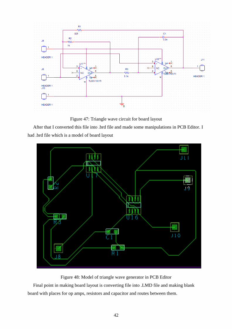
Figure 47: Triangle wave circuit for board layout
After that I converted this file into .brd file and made some manipulations in PCB Editor. I
had .brd file which is a model of board layout
Figure 48: Model of triangle wave generator in PCB Editor
Final point in making board layout is converting file into .LMD file and making blank
board with places for op amps, resistors and capacitor and routes between them.
43
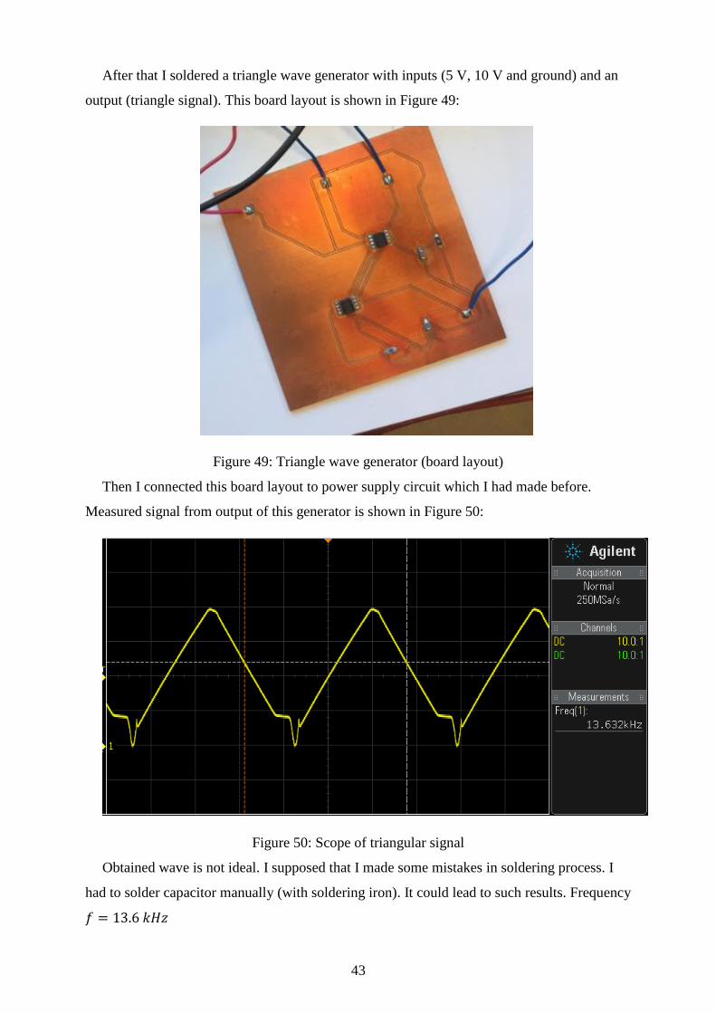
After that I soldered a triangle wave generator with inputs (5 V, 10 V and ground) and an
output (triangle signal). This board layout is shown in Figure 49:
Figure 49: Triangle wave generator (board layout)
Then I connected this board layout to power supply circuit which I had made before.
Measured signal from output of this generator is shown in Figure 50:
Figure 50: Scope of triangular signal
Obtained wave is not ideal. I supposed that I made some mistakes in soldering process. I
had to solder capacitor manually (with soldering iron). It could lead to such results. Frequency
𝑓 = 13.6 𝑘𝐻𝑧
44
Frequency has a difference with calculated (chapter 4), which was 14.3 kHz. The relative
error is as follows:
𝛿 =𝑈1 − 𝑈2
𝑈1∗ 100% =
14.3 − 13.6
14.3∗ 100% = 4.9%
It can be explained by the difference between simulation model op amp in OrCAD and real
op amp.
6.3 PWM signal
As was shown in chapter 4, I used voltage divider with two resistors 5 kOhm and 200
Ohm. This voltage is compared to a triangle signal received from the output of the triangle
wave generator (6.2).
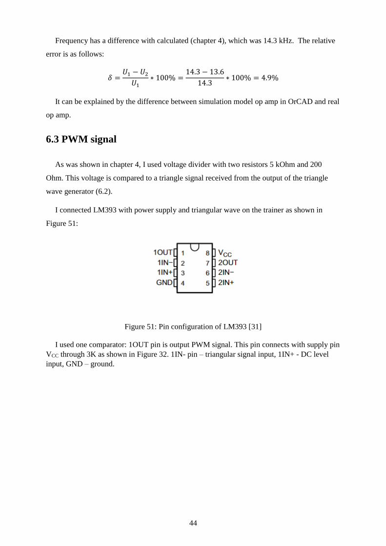
I connected LM393 with power supply and triangular wave on the trainer as shown in
Figure 51:
Figure 51: Pin configuration of LM393 [31]
I used one comparator: 1OUT pin is output PWM signal. This pin connects with supply pin
VCC through 3K as shown in Figure 32. 1IN- pin – triangular signal input, 1IN+ - DC level
input, GND – ground.
45
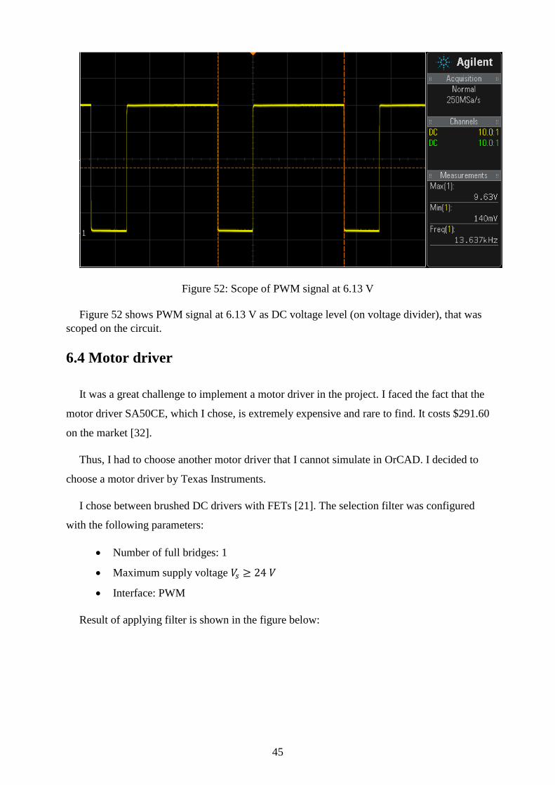
Figure 52: Scope of PWM signal at 6.13 V
Figure 52 shows PWM signal at 6.13 V as DC voltage level (on voltage divider), that was
scoped on the circuit.
6.4 Motor driver
It was a great challenge to implement a motor driver in the project. I faced the fact that the
motor driver SA50CE, which I chose, is extremely expensive and rare to find. It costs $291.60
on the market [32].
Thus, I had to choose another motor driver that I cannot simulate in OrCAD. I decided to
choose a motor driver by Texas Instruments.
I chose between brushed DC drivers with FETs [21]. The selection filter was configured
with the following parameters:
Number of full bridges: 1
Maximum supply voltage 𝑉𝑠 ≥ 24 𝑉
Interface: PWM
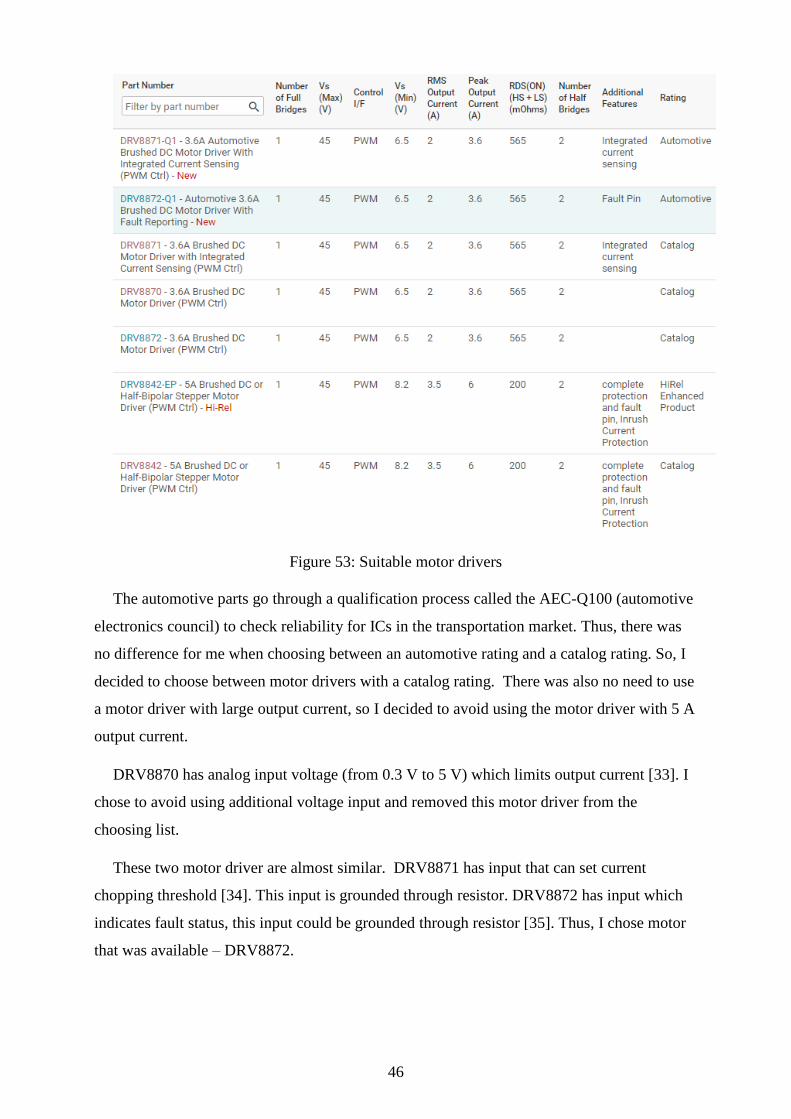
Result of applying filter is shown in the figure below:
46
Figure 53: Suitable motor drivers
The automotive parts go through a qualification process called the AEC-Q100 (automotive
electronics council) to check reliability for ICs in the transportation market. Thus, there was
no difference for me when choosing between an automotive rating and a catalog rating. So, I
decided to choose between motor drivers with a catalog rating. There was also no need to use
a motor driver with large output current, so I decided to avoid using the motor driver with 5 A
output current.
DRV8870 has analog input voltage (from 0.3 V to 5 V) which limits output current [33]. I
chose to avoid using additional voltage input and removed this motor driver from the
choosing list.
These two motor driver are almost similar. DRV8871 has input that can set current
chopping threshold [34]. This input is grounded through resistor. DRV8872 has input which
indicates fault status, this input could be grounded through resistor [35]. Thus, I chose motor
that was available – DRV8872.
47
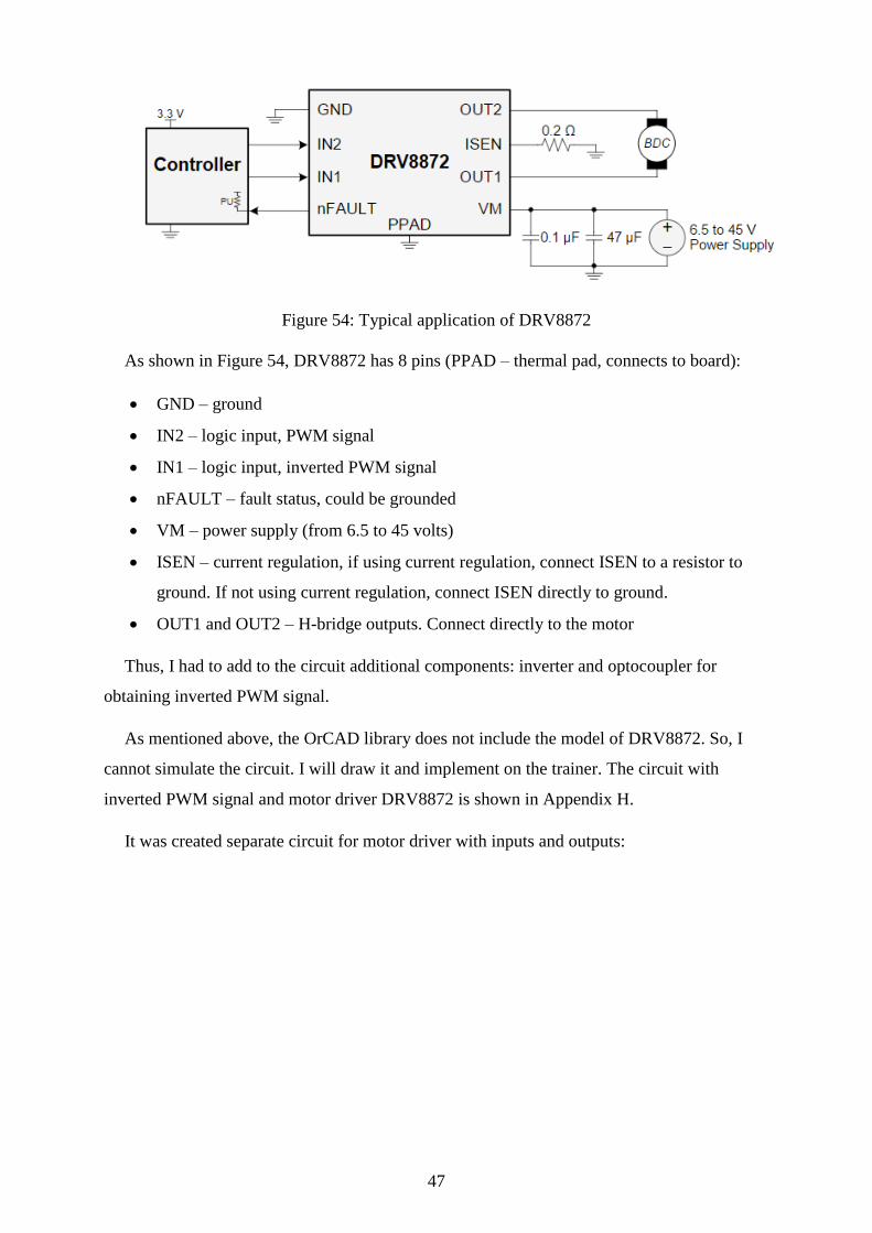
Figure 54: Typical application of DRV8872
As shown in Figure 54, DRV8872 has 8 pins (PPAD – thermal pad, connects to board):
GND – ground
IN2 – logic input, PWM signal
IN1 – logic input, inverted PWM signal
nFAULT – fault status, could be grounded
VM – power supply (from 6.5 to 45 volts)
ISEN – current regulation, if using current regulation, connect ISEN to a resistor to
ground. If not using current regulation, connect ISEN directly to ground.
OUT1 and OUT2 – H-bridge outputs. Connect directly to the motor
Thus, I had to add to the circuit additional components: inverter and optocoupler for
obtaining inverted PWM signal.
As mentioned above, the OrCAD library does not include the model of DRV8872. So, I
cannot simulate the circuit. I will draw it and implement on the trainer. The circuit with
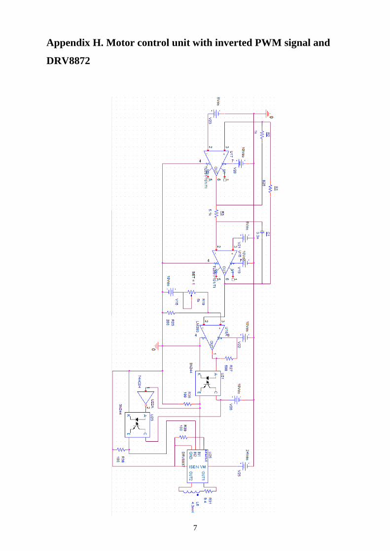
inverted PWM signal and motor driver DRV8872 is shown in Appendix H.
It was created separate circuit for motor driver with inputs and outputs:
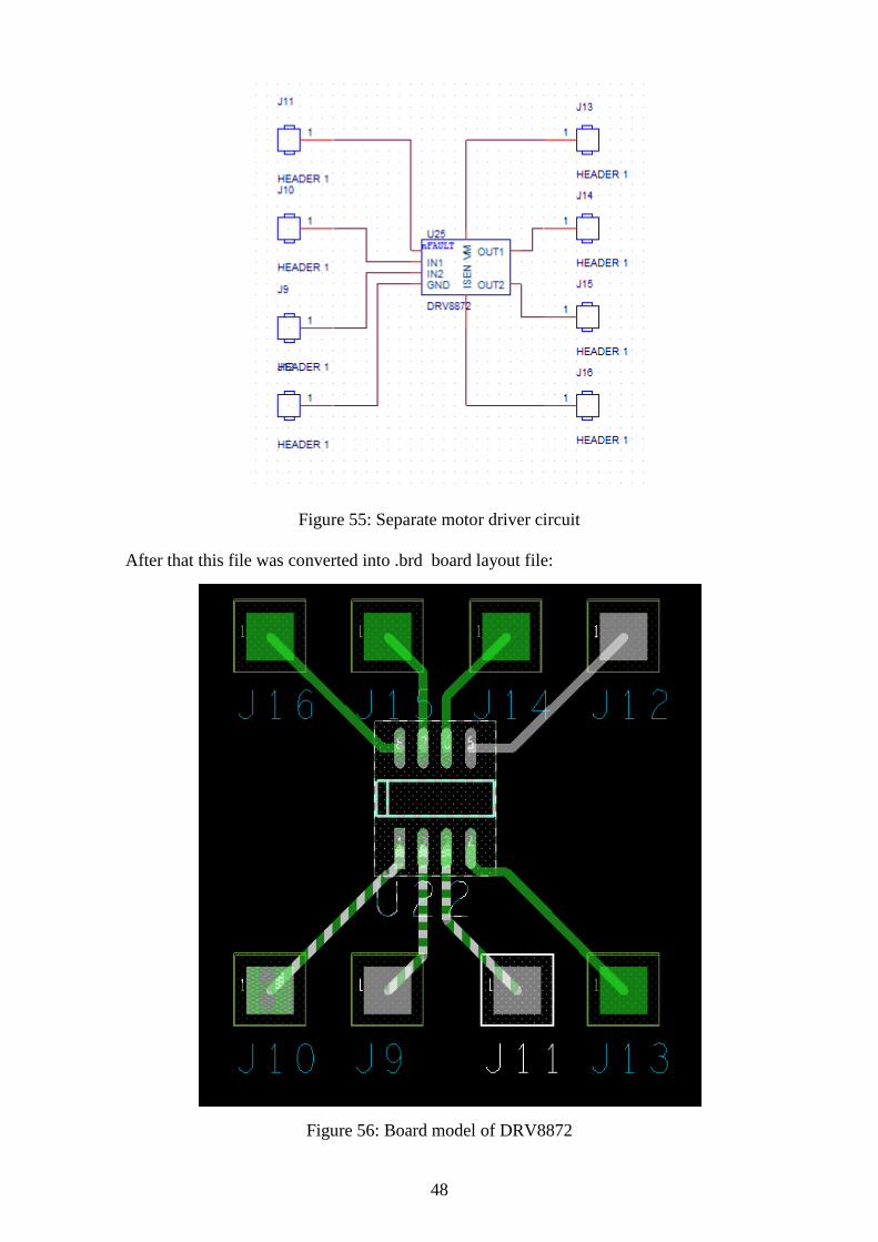
48
Figure 55: Separate motor driver circuit
After that this file was converted into .brd board layout file:
Figure 56: Board model of DRV8872

49
Board model from Figure 56 was printed in one of the labs. Motor driver and wiring
connections was soldered.
Figure 57: Board layout of motor driver DRV8872
Board layout of DRV8872 that was soldered is shown in Figure 57.
6.5 Optocoupler and inverter
Optocoupler 3N244 is used in the simulation in Appendix F, but it does not exist in the
university’s storage or on web stores. I chose an optocoupler with similar parameters, which
is marked in Table 2. There is one equivalent of 3N244 on the market – OPI110A [35].
Figure 58: Application of OPI110A
I used the application from Figure 58 for connection OPI110A, as shown in Appendix H.
According to Appendix H, I used inverter SN74S04.
50
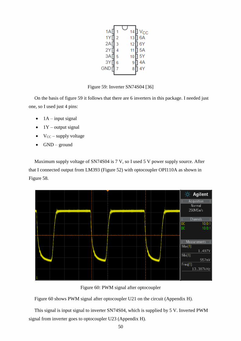
Figure 59: Inverter SN74S04 [36]
On the basis of figure 59 it follows that there are 6 inverters in this package. I needed just
one, so I used just 4 pins:
1A – input signal
1Y – output signal
VCC – supply voltage
GND – ground
Maximum supply voltage of SN74S04 is 7 V, so I used 5 V power supply source. After
that I connected output from LM393 (Figure 52) with optocoupler OPI110A as shown in
Figure 58.
Figure 60: PWM signal after optocoupler
Figure 60 shows PWM signal after optocoupler U21 on the circuit (Appendix H).
This signal is input signal to inverter SN74S04, which is supplied by 5 V. Inverted PWM
signal from inverter goes to optocoupler U23 (Appendix H).

51
Figure 61: Inverted PWM signal after optocoupler
PWM signal from optocoupler U21 and inverted PWM signal from optocoupler U23 are
input signals IN1 and IN2 for motor driver DRV8872. I implemented motor driver
connection which is shown in Figure 54.
Figure 62: The implemented circuit

52
The whole implemented circuit is shown in Figure 62. Output voltage of H-bridge is
controlled by potentiometer manually in range from -24 V to +24 V.
Figure 63: Output voltage of motor driver with different PWM signal
Figure 64 shows two extreme values of the output voltage and two intermediate values.
Connected motor rotates in both directions with different speed.
53
Conclusion
For this work two ways to control the motor were considered, and an open loop control
was selected. It was decided to use the H-bridge to control the motor. The H-bridge consists
of MOSFETs which are controlled by a PWM signal.
It was decided to use a comparator to obtain the PWM signal by comparing the triangular
wave and the DC level voltage. Various methods of obtaining a triangular signal were studied
and a method based on the use of the Schmitt trigger and integrator with implementation of an
artificial midpoint and unipolar feeding of amplifiers was selected.
Components and IC of the circuit were selected, simulations were made in MATLAB-
Simulink and OrCAD-PSpice. The results obtained fully satisfy the requirements.
The implementation of the circuit was carried out on a special training simulator. Some
parts of the circuit were drawn in the PCB Editor and created during the soldering process. As
the implementation of the circuit was changed, additional elements were implemented and
some components and IC were replaced due to their unavailability on the market.
Scopes were obtained using an oscilloscope. The results obtained coincide with the
simulations and completely satisfy the requirements. Rotor of the motor connected to the
circuit changes the direction and speed of its rotation with manual control of the circuit.
In the process of this project such programs as OrCAD-PSpice and PCB Editor were
studied, and the MATLAB-Simulink knowledge was deepened. The knowledge and
experience of choosing the components of the circuits is obtained. The experience of micro-
soldering has been obtained.
This work is an example of the summation of theoretical knowledge of the electrical
sciences obtained during the master's program and practical implementation, which was
studied independently on the basis of theory.
Future students can use this project as a basis for development of a multi-purpose model
that can control objects using:
1. Programmable logic controller (PLC)
2. Microprocessor
3. LabVIEW input/output interface
By combining measurement and control instruments with the described circuit, it is
possible to obtain an autonomous unit for control of any object in laboratory.

54
References
[1] http://www.fischertechnik.de/en/Home.aspx
[2] Mohan: Electric Machines and Drives, Wiley 2012
[3] Жесткова Ю.Е., Савоськин В.С., Электромеханика. Методическое пособие для
студентов вузов, Пенз. гос. ун-т, Пенза, 2002. - 253 с.
[4] http://electricalschool.info/main/drugoe/387-jelektrodvigateli-postojannogo-toka.html
[5] http://www.mpoweruk.com/motorcontrols.htm
[6] http://www.8051projects.net/wiki/DC_Motor_Interfacing
[7] http://www.mcmanis.com/chuck/robotics/tutorial/h-bridge
[8] Mohan, Undeland, Robbins: Power Electronics, 3. Edition, Wiley 2003
[9] http://www.talkingelectronics.com/projects/H-Bridge/H-Bridge-1.html
[10] http://chipenable.ru/index.php/how-connection/item/155-pwm-regulator-dc-
dvigatelya.html
[11] http://fourier.eng.hmc.edu/e84/lectures/ch4/node13.html
[12] http://homepages.which.net/~paul.hills/Circuits/PwmGenerators/PwmGenerators.html
[13] Интегральные микросхемы и их зарубежные аналоги: Справочник. Том 7./А.
В.Нефедов. - М.:ИПРадиоСофт, 1999г. - 640с.:ил.
[14] http://www.learningaboutelectronics.com/Articles/555-timer-pinout.php
[15] https://en.wikipedia.org/wiki/555_timer_IC
[16] Хоровиц П., Хилл У. Искусство схемотехники: В 3-х томах: Т. 1. Пер. с англ.— 4-е
изд., перераб. и доп.— М.: Мир, 1993.—413 с
[17] Sergio Franco. Design with Operational Amplifiers and Analog Integrated Circuits, 3rd
Ed., McGraw-Hill, New York, 2002
[18] http://de.ifmo.ru/bk_netra/page.php?tutindex=36&index=4
[19] http://studall.org/all-83490.html
[20]
http://www.sgu.ru/sites/default/files/textdocsfiles/2015/02/16/03_operacionnyy_usilitel_chast
2.pdf
[21] www.ti.com
[22] http://www.learningaboutelectronics.com/Articles/Voltage-divider-calculator.php
[23] http://www.ttelectronics.com/sites/default/files/download-files/3C91-3N263_A_TX-
TXV_RevA.4.pdf
[24] http://www.pspice.com/models/cadence
[25] http://www.ti.com/lit/ds/symlink/lm5045.pdf
[26] https://www.apexanalog.com/resources/products/sa50ceu.pdf

55
[27] http://www.farnell.com/datasheets/2287645.pdf
[28] http://www.cqham.ru/pow2_15.htm
[29] http://no.rs-online.com/web/
[30] http://www.vishay.com/diodes/list/product-88536/
[31] http://www.ti.com/lit/ds/symlink/lm393.pdf
[32] http://www.findchips.com/search/sa50ce
[33] http://www.ti.com/lit/ds/symlink/drv8870.pdf
[34] http://www.ti.com/lit/ds/symlink/drv8871.pdf
[35] http://www.farnell.com/datasheets/99092.pdf
[36] http://www.ti.com/lit/ds/symlink/sn74ls04.pdf
[37] И. П. Жеребцов. Основы электроники. Изд. 5-е, — Л., 1989. — С. 120—121

1
Appendix A. Motor control model in MATLAB

2
Appendix B. Circuit of 555 timer in OrCAD
Appendix C. Triangle wave generator in OrCAD
3
Appendix D. PWM signal circuit with bipolar supplying
4
Appendix E. PWM signal circuit with unipolar supplying
5
Appendix F. Motor control unit

6
Appendix G. Power supply circuit
7
Appendix H. Motor control unit with inverted PWM signal and
DRV8872
Top Related
Copyright © 2022 FDOKUMEN

