


Bahasa
Halaman
Hukum

Int. J. Electrochem. Sci., 8 (2013)
International Journal of ELECTROCHEMICAL
SCIENCE www.electrochemsci.org
Electrochromism in Self-Assembled Porous Thin Films of Hexagonal Tungsten Trioxide Microspheres Prepared by Aqueous Chemical Growth B.T. Sone1,2,*, S.N. Mailu2, T. Malwela4, E. Coetsee5, H. Swartz5, E. Iwuoha2 and M. Maaza1,3
1Nanosciences African Network (NANOAFNET), Materials Research Department, iThemba LABS-NRF, P.O. Box 722, Somerset West, 7129, South Africa 2SensorLab, Chemistry Department, University of the Western Cape, Private Bag X17, Bellville, South Africa 3UNESCO-UNISA Africa Chair in Nanosciences-Nanotechnology, College of Graduate Studies, University of South Africa, Muckleneuk Ridge, P.O. Box 392, Pretoria, South Africa 4DST/CSIR National Centre for Nano-Structured Materials, 1-Meiring Naude Road, Brummeria, Pretoria 0001, South Africa 5Physics Department, University of the Free State, P.O. Box 339, Bloemfontein, 9300, South Africa *E-mail: [email protected], [email protected] .
Received: 1 October 2013 / Published: 2013 WO3 thin films were grown by self-assembly, at 80-90 ˚C, on un-seeded conductive SnO2:F-glass through the method of Aqueous Chemical Growth (ACG). The thin films produced contained urchin-like microspheres of WO3, 1-2 µm thick. Scanning Electron Microscopy (SEM) and Transmission Electron Microscopy showed these microspheres to consist of a thick central core on which grew hair-like protrusions 200 - 400 nm long and 50-100 nm wide. X-ray Diffraction analysis, post annealing at 500 ˚C, revealed WO3 to be in the hexagonal phase. Focused Ion Beam-SEM showed a porous thin film grown for 18-24 h (~ 3 µm thick), that offers a wide surface area and shorter diffusion path-ways for H+ insertion in a 0.1M H2SO4 electrolyte. The fairly fast optical switching times (15-25s) observed at a scan rate of 50 mV/s for such highly crystalline thin films can be attributed to the porous nature of the films. A diffusion coefficient for H+ of 1.66 x 10⁻¹¹ cm2/s and 1.33 x 10⁻¹¹ cm2/s at 50 mV/s was observed during H+ insertion/de-insertion. We propose that by reducing film growth time, film thickness can be reduced rendering the method a viable one for producing WO3 thin films amenable to electrochromic devices. Keywords: Thin solid films; X-ray photoelectron spectroscopy; cyclic voltammetry; colouration efficiency.
Int. J. Electrochem. Sci., Vol. 8, 2013
2
1. INTRODUCTION
Tungsten trioxide (WO3) is an n-type, wide band gap (2.7 eV) semiconductor metal oxide whose I-V characteristics, electrochromic and gasochromic properties have been widely investigated for use as thin films and powders (bulk) in electrochromic windows, panels, rear view mirrors, photocatalysts, and gas sensors [1,2,3]. Electrochromism is a reversible and visible change in optical properties a material undergoes when an applied voltage of a few millivolts/volts is reversibly applied to the material [2]. The phenomenon in WO3 arises when WO3 electrode material (pale yellow/transparent) is cathodically reduced through intercalation of its interstitials with a metal cation M (M = H+, Li+ or Na+ ions). Simultaneous insertion of an electron (e-) helps in maintaining electrical neutrality in the WO3 electrochrome while forming a blue colored bronze MxWO3 [4,5].
WO3 (pale yellow/white) + xM+ + xe- MxWO3 (blue) (1) This entirely reversible process represented in equation (1) above, takes place primarily at the
surface of the electrochromic material [6]. Being a phenomenon that occurs primarily at the surface of materials with electrochromic potential it is therefore likely to be influenced by processes that result in the increase of the effective surface area available for H+/e- insertion/intercalation. Increase in surface area such as is observed in nanostructured/porous thin films can enhance the process of intercalation in tungsten trioxide thin films [7, 8].
As thin films, several methods have been used to prepare WO3 among which are thermal evaporation [9], chemical vapour deposition [4,9], electrodeposition [4,9], spray pyrolysis [9] electron beam evaporation [1], magnetron sputtering [9], sol-gel methods [2,4], etc. In recent times [7] emphasis has been on the preparation and use of nanostructured materials in investigating different chemical and physical phenomena such as electrochromism and gas sensing, this because reduction of particle size in such materials gives rise to quantum confinement effects; increase in surface active sites, grain boundaries, electronic band gaps, etc, all of which give rise to new or enhanced properties for these materials. Soft chemistry methods such as Aqueous Chemical Growth (ACG) [10] give the opportunity of designing metal oxide thin films containing micro/nanostructures whose size, shape and orientation can be rationally influenced by varying parameters such as the concentration, pH and the temperature of metal-oxide precursor solutions. The method as described here has not been previously used to prepare WO3 thin films on FTO substrates. We report here, the use of this soft chemistry method of Aqueous Chemical Growth for self-assembly of porous WO3 microsphere-containing thin films on unseeded FTO-coated glass, this at low-temperatures (80-90 ˚C) using as precursor solution peroxotungstic acid prepared by the action of H2O2 on W powder. To the best of our knowledge synthesis of WO3 thin films on un-seeded FTO substrates at such low temperatures using this method has not been previously reported. The method has as advantage the fact that: (i) substrates used did not require seeding or surface modification; (ii) it does not require the use of metal salts; (iii) there is no use of structure directing agents or surfactants rendering the process environmentally friendly, with produced films suffering from little or no contamination; and (iv) the equipment required for the deposition – a simple drying oven, a glass bottle with a screwable cap, a furnace, are easily obtainable at low cost.
Int. J. Electrochem. Sci., Vol. 8, 2013
3
2. EXPERIMENTAL
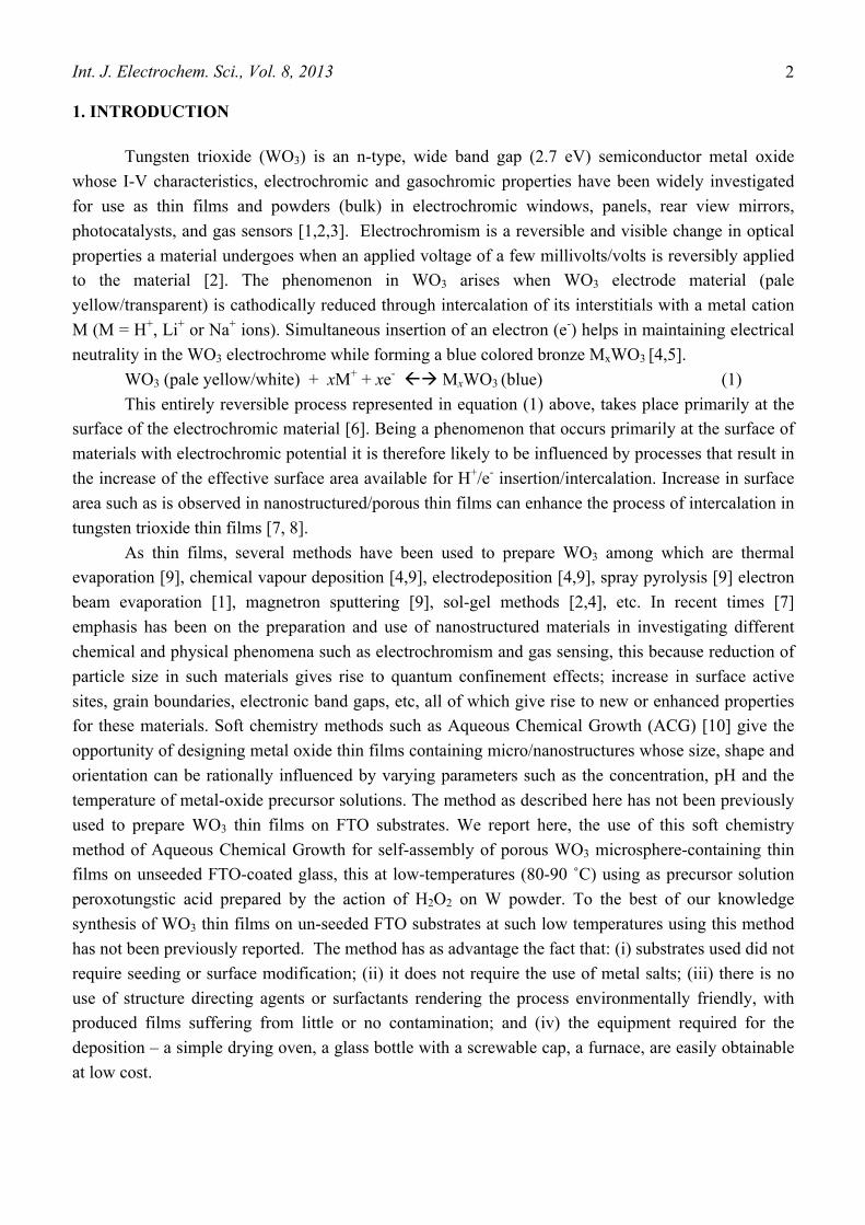
Pale yellow solutions of aged Peroxotungstic acid (PTA) with pH = 2.21 were prepared through the action of 30% H2O2 (80 mL) on W powder (3g) in a cool water bath (5-15 ˚C), after which was added to it iso-propanol and de-ionised water in the 1:1 v/v ratio.
Scheme 1. Schematic representation of the synthesis of WO3 thin films on F:SnO2 and plain glass substrates.
Aging was carried out for a period of 7-10 days giving time for the decomposition of residual H2O2. F-doped SnO2 (FTO) substrates (1 mm thick, 10 mm x 20 mm), cleaned by sequential ultrasonication in solutions of MeOH, acetone and de-ionised water for periods of 5 min each then dried with N2, were placed in a tightly clamped Teflon holder designed to hold tightly, four FTO substrates with their non-conductive sides back-back. This was placed at an angle 70˚ to the horizontal in Schott® bottles containing the aged PTA solution and was then tightly sealed and placed in a pre-heated (80-90 ˚C) laboratory oven for 6-24 h. Thin films, greenish-yellow in color (see Scheme 1 above), were seen to grow on the FTO-glass substrates. Upon removal these were washed gently with distilled water and dried in air after which annealing was carried out in air at temperatures of 500 ˚C, for 1-2 h so as to improve adhesion of the as-synthesized films to the FTO substrates.
SEM images of the thin films’ surface morphologies were obtained using a LEO-Stereo Scan 440 Scanning Electron Microscope (SEM) to which was coupled an Electron Dispersive X-ray
Int. J. Electrochem. Sci., Vol. 8, 2013
4
Spectrometer used for elemental analysis. Film thickness was determined using an Auriga Cobra Focused Ion Beam – Field Emission SEM. X-ray Diffraction Analysis (XRD) was obtained with the Bruker AXS D8 ADVANCE X-Ray diffractometer, using Cu Kα radiation, λ =1.5418 Å. X-ray tube current and voltage were set at 40 mA and 40 kV respectively. X-Ray Photoelectron Spectroscopy (XPS) for surface elemental analysis was carried out using PHI 5000 Versaprobe – Scanning ESCA Microprobe. The XPS survey scans and high resolution core level spectra were obtained with a 100 µm 25W 15 kV Al monochromatic x-ray beam.
Optical characterization of the WO3-FTO substrates before and after annealing and post-H+ intercalation was carried out in air, at room temperature, this within the 200-1100 nm spectral range (UV-Vis-NIR region), using a CECIL 2021 series spectrophotometer. H+ intercalation (via electrochemical redox reactions) on a calcined sample of WO3-FTO was carried out in a degassed (10-15 mins, using N2) 0.1M H2SO4 liquid electrolyte using a three electrode electrochemical cell powered by a BAS100W electrochemical workstation from BioAnalytical Systems Incorporated (Lafayette, USA), with WO3-x-FTO as the working electrode, Pt wire as the counter electrode and Ag/AgCl (sat’d KCl) as the reference electrode. 3. RESULTS AND DISCUSSION
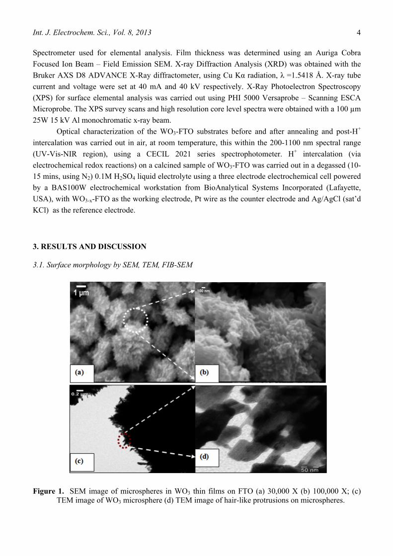
3.1. Surface morphology by SEM, TEM, FIB-SEM
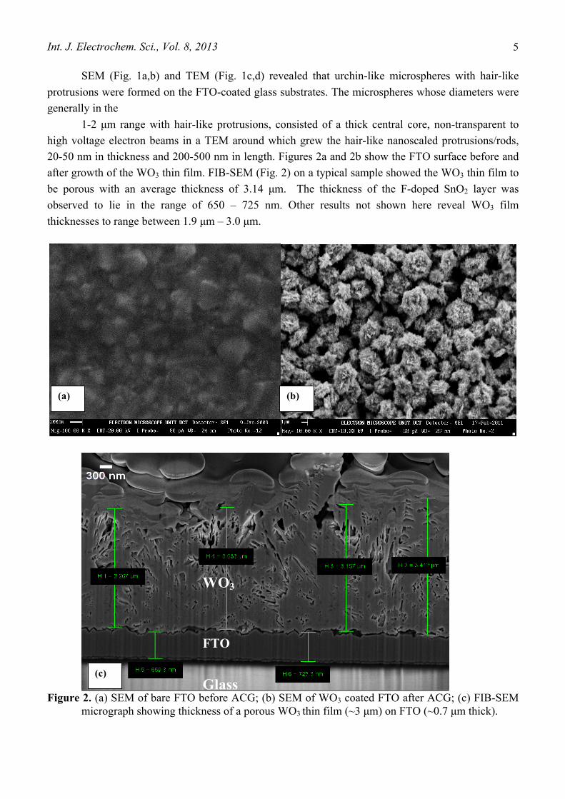
Figure 1. SEM image of microspheres in WO3 thin films on FTO (a) 30,000 X (b) 100,000 X; (c)
TEM image of WO3 microsphere (d) TEM image of hair-like protrusions on microspheres.
(c)
Int. J. Electrochem. Sci., Vol. 8, 2013
5
SEM (Fig. 1a,b) and TEM (Fig. 1c,d) revealed that urchin-like microspheres with hair-like protrusions were formed on the FTO-coated glass substrates. The microspheres whose diameters were generally in the
1-2 µm range with hair-like protrusions, consisted of a thick central core, non-transparent to high voltage electron beams in a TEM around which grew the hair-like nanoscaled protrusions/rods, 20-50 nm in thickness and 200-500 nm in length. Figures 2a and 2b show the FTO surface before and after growth of the WO3 thin film. FIB-SEM (Fig. 2) on a typical sample showed the WO3 thin film to be porous with an average thickness of 3.14 µm. The thickness of the F-doped SnO2 layer was observed to lie in the range of 650 – 725 nm. Other results not shown here reveal WO3 film thicknesses to range between 1.9 µm – 3.0 µm.
Figure 2. (a) SEM of bare FTO before ACG; (b) SEM of WO3 coated FTO after ACG; (c) FIB-SEM
micrograph showing thickness of a porous WO3 thin film (~3 µm) on FTO (~0.7 µm thick).
FTO
Glass
WO3
(c)
(b) (a)
Int. J. Electrochem. Sci., Vol. 8, 2013
6
3.2. Crystal structure determination using XRD, HRTEM and SAED
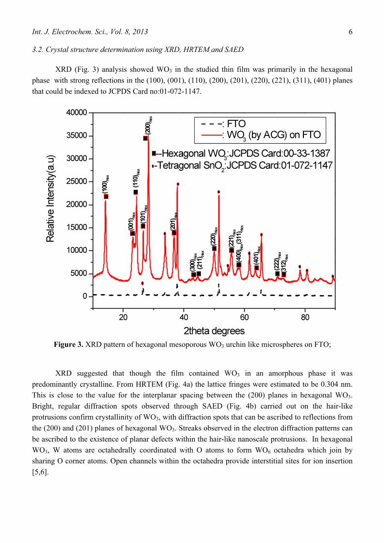
XRD (Fig. 3) analysis showed WO3 in the studied thin film was primarily in the hexagonal phase with strong reflections in the (100), (001), (110), (200), (201), (220), (221), (311), (401) planes that could be indexed to JCPDS Card no:01-072-1147.
Figure 3. XRD pattern of hexagonal mesoporous WO3 urchin like microspheres on FTO;
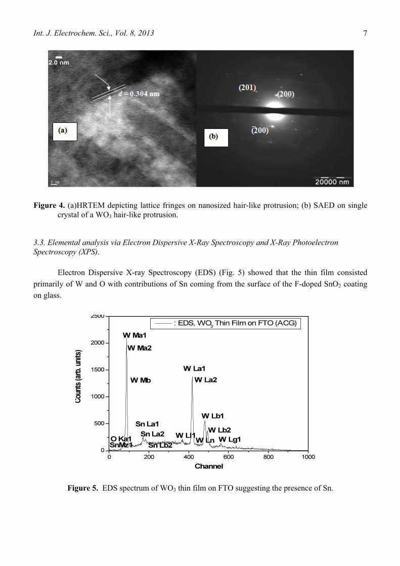
XRD suggested that though the film contained WO3 in an amorphous phase it was predominantly crystalline. From HRTEM (Fig. 4a) the lattice fringes were estimated to be 0.304 nm. This is close to the value for the interplanar spacing between the (200) planes in hexagonal WO3. Bright, regular diffraction spots observed through SAED (Fig. 4b) carried out on the hair-like protrusions confirm crystallinity of WO3, with diffraction spots that can be ascribed to reflections from the (200) and (201) planes of hexagonal WO3. Streaks observed in the electron diffraction patterns can be ascribed to the existence of planar defects within the hair-like nanoscale protrusions. In hexagonal WO3, W atoms are octahedrally coordinated with O atoms to form WO6 octahedra which join by sharing O corner atoms. Open channels within the octahedra provide interstitial sites for ion insertion [5,6].
Int. J. Electrochem. Sci., Vol. 8, 2013
7
Figure 4. (a)HRTEM depicting lattice fringes on nanosized hair-like protrusion; (b) SAED on single crystal of a WO3 hair-like protrusion.
3.3. Elemental analysis via Electron Dispersive X-Ray Spectroscopy and X-Ray Photoelectron Spectroscopy (XPS).
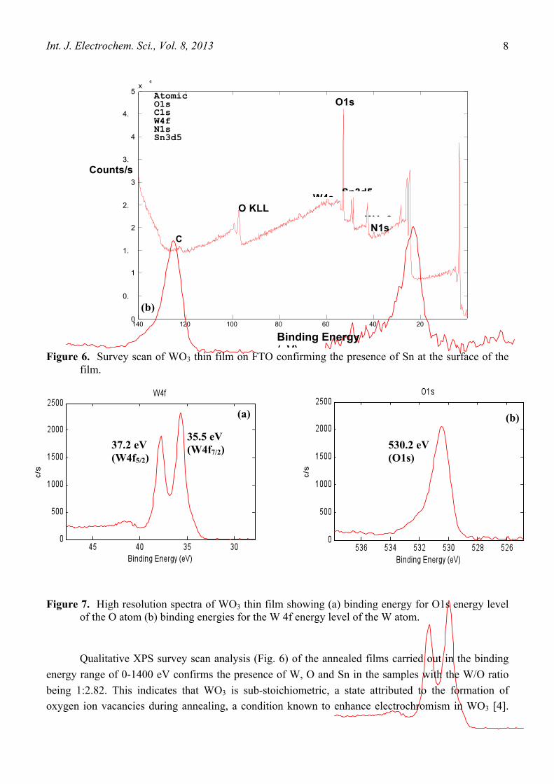
Electron Dispersive X-ray Spectroscopy (EDS) (Fig. 5) showed that the thin film consisted primarily of W and O with contributions of Sn coming from the surface of the F-doped SnO2 coating on glass.
Figure 5. EDS spectrum of WO3 thin film on FTO suggesting the presence of Sn.
Int. J. Electrochem. Sci., Vol. 8, 2013
8
Figure 6. Survey scan of WO3 thin film on FTO confirming the presence of Sn at the surface of the film.
Figure 7. High resolution spectra of WO3 thin film showing (a) binding energy for O1s energy level of the O atom (b) binding energies for the W 4f energy level of the W atom.
Qualitative XPS survey scan analysis (Fig. 6) of the annealed films carried out in the binding energy range of 0-1400 eV confirms the presence of W, O and Sn in the samples with the W/O ratio being 1:2.82. This indicates that WO3 is sub-stoichiometric, a state attributed to the formation of oxygen ion vacancies during annealing, a condition known to enhance electrochromism in WO3 [4].
200
400
600
800
1000
1200
1400 0
0.5
1
1.5
2
2.5
3
3.5
4
4.5
5 x 10
4
Sn3d5
W4p1
Atomic % O1s 48 C1s 26 W4f 17 N1s 5 Sn3d5 4
C KLL
O KLL Sn3p3
O1s
Sn3d3
N1s
C1s
W4s W4p3
W4f
W4d5
W4d3
W4d
(b)
Binding Energy (eV)
Counts/s
35.5 eV (W4f7/2) 37.2 eV
(W4f5/2) 530.2 eV (O1s)
(a) (b)
Int. J. Electrochem. Sci., Vol. 8, 2013
9
High resolution core level spectra (Fig 7a) showed doublet peaks at binding energies of 35.5 eV and 37.6 eV for W 4f7/2 and W 4f5/2 configurations that confirm the existence of W metal in W6+ state.
The core level spectrum for oxygen in the O1s configuration ascribes for the broad peak observed at 530.3 eV (Fig. 7b). The occurrence of Sn in both EDS and XPS spectra could be ascribed to initial dissolution of SnO2 due to acid attack prior to and during the nucleation of WO3 particles or the possible migration of Sn2+ during heat treatment, from the FTO layer into the WO3 layers. We believe that the formation of microspheres instead of nanoplatelets as was often observed when we prepared tungsten trioxide thin films on Corning glass at low pH [11], may be due to a seeding effect that the rough surface of FTO has on the growth of WO3 particles.
3.4. Optical Characterization using UV-VIS-NIR Spectrophotometry
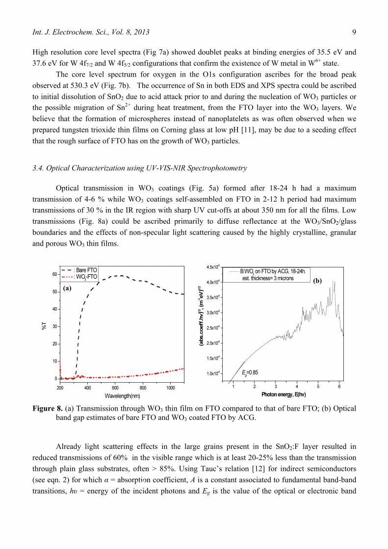
Optical transmission in WO3 coatings (Fig. 5a) formed after 18-24 h had a maximum transmission of 4-6 % while WO3 coatings self-assembled on FTO in 2-12 h period had maximum transmissions of 30 % in the IR region with sharp UV cut-offs at about 350 nm for all the films. Low transmissions (Fig. 8a) could be ascribed primarily to diffuse reflectance at the WO3/SnO2/glass boundaries and the effects of non-specular light scattering caused by the highly crystalline, granular and porous WO3 thin films.
Figure 8. (a) Transmission through WO3 thin film on FTO compared to that of bare FTO; (b) Optical
band gap estimates of bare FTO and WO3 coated FTO by ACG.
Already light scattering effects in the large grains present in the SnO2:F layer resulted in reduced transmissions of 60% in the visible range which is at least 20-25% less than the transmission through plain glass substrates, often > 85%. Using Tauc’s relation [12] for indirect semiconductors (see eqn. 2) for which α = absorption coefficient, A is a constant associated to fundamental band-band transitions, hυ = energy of the incident photons and Eg is the value of the optical or electronic band
(a) (b)
(e)
Int. J. Electrochem. Sci., Vol. 8, 2013
10
gap, Eg for FTO substrates was calculated to be 3.52 which is in agreement with the optical band gap value of pure glass [13] and close to the optical band gap value of SnO2 (3.6 eV).
(αhυ) = A(hυ-Eg)1/2 (2) The optical band gap for the FTO-glass coated with WO3 thin film by ACG (Fig. 8b) was
estimated following the same treatment to be 0.85 eV in a thin film of 3 µm. This value is close to the computational value for the optical band gap of tetragonal WO3 [14] suggesting that WO3 in the thin film investigated was both in the tetragonal and hexagonal phase. We however believe that anomalous band gap observed for the film investigated in Fig.8b is a primarily due to reduced transmittance resulting from the scattering effects of large grains in the sample and only secondarily due to high film thickness.
3.5. Electrochromism via cyclic voltammetry
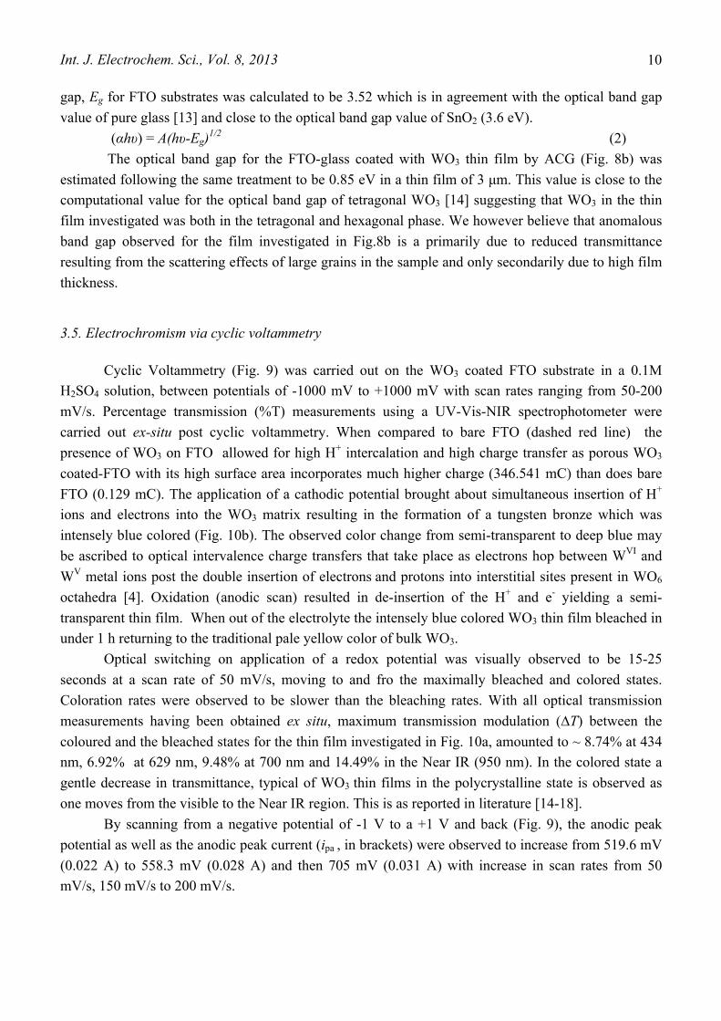
Cyclic Voltammetry (Fig. 9) was carried out on the WO3 coated FTO substrate in a 0.1M H2SO4 solution, between potentials of -1000 mV to +1000 mV with scan rates ranging from 50-200 mV/s. Percentage transmission (%T) measurements using a UV-Vis-NIR spectrophotometer were carried out ex-situ post cyclic voltammetry. When compared to bare FTO (dashed red line) the presence of WO3 on FTO allowed for high H+ intercalation and high charge transfer as porous WO3 coated-FTO with its high surface area incorporates much higher charge (346.541 mC) than does bare FTO (0.129 mC). The application of a cathodic potential brought about simultaneous insertion of H+ ions and electrons into the WO3 matrix resulting in the formation of a tungsten bronze which was intensely blue colored (Fig. 10b). The observed color change from semi-transparent to deep blue may be ascribed to optical intervalence charge transfers that take place as electrons hop between WVI and WV metal ions post the double insertion of electrons and protons into interstitial sites present in WO6 octahedra [4]. Oxidation (anodic scan) resulted in de-insertion of the H+ and e- yielding a semi-transparent thin film. When out of the electrolyte the intensely blue colored WO3 thin film bleached in under 1 h returning to the traditional pale yellow color of bulk WO3.
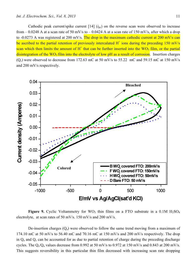
Optical switching on application of a redox potential was visually observed to be 15-25 seconds at a scan rate of 50 mV/s, moving to and fro the maximally bleached and colored states. Coloration rates were observed to be slower than the bleaching rates. With all optical transmission measurements having been obtained ex situ, maximum transmission modulation (∆T) between the coloured and the bleached states for the thin film investigated in Fig. 10a, amounted to ~ 8.74% at 434 nm, 6.92% at 629 nm, 9.48% at 700 nm and 14.49% in the Near IR (950 nm). In the colored state a gentle decrease in transmittance, typical of WO3 thin films in the polycrystalline state is observed as one moves from the visible to the Near IR region. This is as reported in literature [14-18].
By scanning from a negative potential of -1 V to a +1 V and back (Fig. 9), the anodic peak potential as well as the anodic peak current (ipa , in brackets) were observed to increase from 519.6 mV (0.022 A) to 558.3 mV (0.028 A) and then 705 mV (0.031 A) with increase in scan rates from 50 mV/s, 150 mV/s to 200 mV/s.
Int. J. Electrochem. Sci., Vol. 8, 2013
11
Cathodic peak current/spike current [14] (ipc) on the reverse scan were observed to increase from – 0.0248 A at a scan rate of 50 mV/s to – 0.0424 A at a scan rate of 150 mV/s, after which a drop to -0.0273 A was registered at 200 mV/s. The drop in the maximum cathodic current at 200 mV/s can be ascribed to the partial retention of previously intercalated H+ ions during the preceding 150 mV/s scan which then limits the amount of H+ that can be further inserted into the WO3 film, or the partial disintegration of the WO3 film into the electrolyte of low pH as a result of corrosion. Insertion charges (Qc) were observed to decrease from 172.63 mC at 50 mV/s to 55.22 mC and 59.15 mC at 150 mV/s and 200 mV/s respectively.
Figure 9. Cyclic Voltammetry for WO3 thin films on a FTO substrate in a 0.1M H2SO4
electrolyte, at scan rates of 50 mV/s. 150 mV/s and 200 mV/s. De-insertion charges (Qa) were observed to follow the same trend moving from a maximum of
174.10 mC at 50 mV/s to 56.40 mC and 70.16 mC at 150 mV/s and 200 mV/s respectively. The drop in Qa and Qc can be accounted for as due to partial retention of charge during the preceding discharge cycles. The Qc/Qa values decrease from 0.992 at 50 mV/s to 0.972 at 150 mV/s and 0.843 at 200 mV/s. This suggests reversibility in this particular thin film decreased with increasing scan rate dropping
Colored
Bleached
Int. J. Electrochem. Sci., Vol. 8, 2013
12
from 99.2% to 97.2% then 84.3% as the scan rate increased from 50 mV/s to 200 mV/s. Despite this charge imbalance optical switching between the bleached and colored states remains clear.
Based on the Randles-Sevcik equation [15], eqn.3, ip = 2.72 x 10⁵ x n3/2 x D1/2 x C0 x ʋ1/2 (3) in which D is the diffusion constant, C0 is the concentration of active ions (H+, Li+ ions in this
case) in the electrolyte, ʋ is the scan rate, ip is the peak current (whether ipc or ipa) and n is the number of electrons taking part in the electrochemical process, the diffusion coefficient of de-insertion of H+ ions was calculated to be 1.33 x 10⁻¹¹ cm2/s at 50 mV/s, 7.34 x 10⁻¹² cm2/s at 150 mV/s and 6.46 x 10⁻¹² cm2/s at 200 mV/s. That for insertion of H+ into the WO3 thin film at 50, 150 and 200 mV/s was respectively 1.66 x 10⁻¹¹ cm2/s, 1.62 x 10⁻¹¹ cm2/s, 5.04 x 10⁻¹² cm2/s.
Figure 10. (a) Optical transmission in colored and bleached state, obtained ex situ; (b) Digital photograph of WO3-FTO substrates (inset) showing WO3 in the bleached (pale yellow, left) and colored state (blue, right).
These values fall within the range of values for H+ diffusivity reported by Patil et al and Sivakumar et al [15, 16] but are averagely 2 orders of magnitude less than the 4.36 x 10⁻¹⁰ cm2/s and 6.08 x 10⁻¹⁰ cm2/s values Sivakumar et al [16] report for films (1.7 µm) they treated at 300 ˚C. This drop in D values at all scan rates should be expected and can be explained by the fact that the H+
(a)
(b)
Int. J. Electrochem. Sci., Vol. 8, 2013
13
diffusion to and from WO3 films is reduced because of the diffusion-limiting effect of crystallization at 500 ˚C, an effect caused by increase in density of the WO3 matrix, formation of grain boundaries and increase in grain size as annealing temperatures rise [15]. Despite the highly crystalline nature and thickness of the films (averagely 2-3 µm) their high porosity however allows for fairly fast coloration and bleaching rates. This fairly fast electro-optic response can be ascribed to the use of an electrolyte containing highly mobile H+, the open structure of perovskite-like hexagonal WO3 and the presence of semi-amorphous WO3 which promotes fast diffusion of H+ [4,8]. The cyclic voltammograms (Fig. 9) show that the ion insertion/de-insertion process was not entirely reversible especially as the anodic peak potential is observed to increase with the increase in scan rate, an indication of slow insertion kinetics which leads to irreversibility [17].
The inset in Fig. 10b shows that the film adhered poorly to the surface. This generally occurred after 10-15 cycles and can be ascribed to corrosion effects on WO3 in the electrolyte of low pH, as well as semi-compactness due to the partially amorphous and porous nature of the films. The thin films produced should have greater stability in Li+ based electrolytes resulting in longer life cycles [4].
An important parameter for the evaluation of a thin film with respect to electrochromism is that of Coloration Efficiency. Coloration efficiency (CE) which is a measure of the optical contrast per unit charge inserted into the film was calculated using eqn. 4 [19],
CE (λ) = ∆OD(λ)/Q/A = ln(Tb(λ)/Tc (λ))/Q/A (4) in which ∆OD(λ) is the change in optical density at a given wavelength, λ; Tb(λ), Tc(λ), are
respectively transmittance in the bleached and colored states at the given wavelength, and Q/A the charge inserted per unit area of the electrode.
Based on this, CE at a scan rate of 150 mV/s for the film investigated in Fig. 9b is estimated to be 18.91 cm2/C at 435 nm, 9.85 cm2/C at 629 nm, 13.78 cm2/C at 700 nm, 23.38 cm2/C at 950 nm and 23.99 cm2/C at 1000 nm. The values presented here at an inserted charge of 55.22 mC are in the range of values obtained by Sivakumar et al [16] for WO3 thin films prepared by e-beam evaporation and annealed at 300 ˚C. The results obtained are however smaller in magnitude and are a confirmation of the fact that highly crystalline WO3 thin films obtained after annealing at high temperatures show reduced electrochromic performance when compared to amorphous unannealed samples. This is due to the densification of the WO3 layer which makes ion insertion much more difficult [15,16,18].
The results also suggest that the change in optical density per unit charge inserted was comparatively smaller than that reported in literature [15,16]. It is also possible that the while the charge inserted into the dense crystalline WO3 matrix was high the optical response was comparatively small. This may be explained by the fact that measurements of transmission for bleaching and coloring were carried out ex situ. In situ measurements of transmission during bleaching and coloring should result in increased, more accurate values for CE. Hopefully, investigating the electrochromic effect in amorphous thin films produced by Aqueous Chemical Growth should also show improved results. Investigations on this will be performed and reported subsequently.
Int. J. Electrochem. Sci., Vol. 8, 2013
14
4. CONCLUSIONS
We have successfully grown through self-assembly, using the method of Aqueous Chemical Growth at 80 - 90 ˚C, thin films of WO3 on un-seeded FTO substrates. These were made up of urchin-like microspheres (1-2 µm wide) covered with nanoscale hair/rod-like protrusions. XRD, HRTEM and SAED showed WO3 in the calcined films to be in the hexagonal phase. Cyclic voltammetry in 0.1M H2SO4 suggests fast diffusion kinetics of H+ to and from the WO3-coated electrode. Reversible optical modulation during H+ insertion/de-insertion at 50 mV/s was seen to occur in under 25 seconds. But for problems encountered with stability in aqueous electrolytes the method of Aqueous Chemical Growth demonstrates that at low temperatures (80-90 ˚C), solution-based wet chemistry can be used to produce large arrays of WO3 thin films that may find application in flexible and rigid electrochromic devices, as well as dye-sensitized solar cells, photoelectrochemical devices and also supercapacitors. ACKNOWLEDGEMENTS The financial support of iThemba LABS-NRF, and the Abdus Salam ICTP (Trieste-Italy) via Nanosciences African Network (NANOAFNET) is hereby acknowledged. For assistance in SEM and TEM, we thank the staff of the Electron Microscopy Unit at the University of Cape Town. References 1. A.A. Joraid, Current Applied, Physics 9, (2009) 73-79. 2. Satyan K. Deb, Solar Energy Materials & Solar Cells 92, (2008) 245–258. 3. J. Wang, P.S. Lee, and J. Ma, Crystal Growth & Design 9, (2009) 2293-2299. 4. P.M.S. Monk, Critic. Rev. Solid State 24, (1999) 193-226. 5. P.R. Somani, S. Radhakrishnan, Mater. Chem. Phys. 77, (2002) 117-133. 6. C.G. Granqvist, G.A. Niklasson, A. Azens, Appl. Phys. A: Mater. 89 (2007) 29-35. 7. J. Zhang, X.L. Wang, X.H. Xia, C.D. Gu, J.P. Tu, Sol. Energy Mater. Sol. Cells 95, (2011) 2107-
2112. 8. B. Baloukas, J-M. Lamarre, L. Martinu, Sol. Energy Mater. Sol. Cells 95, (2011) 807-815. 9. C.G. Granqvist, Sol. Energy Mater. Sol. Cells 60, (2000) 201-262. 10. L. Vayssieres, Int. J. of Nanotechnology, Vol. 1, (2004) Nos. 1/2. 11. B.T. Sone, J. Sithole, R. Bucher, S.N. Mlondo, J. Ramontja, S. Sinha Ray, E. Iwuoha, M. Maaza,
Thin Solid Films (2012), http://dx.doi.org/10.1016/j.tsf.2012.08.032. 12. J. Tauc, R. Grigorovici , A . Vancu, Phys. Status Solidi (b) 15, (1966) 627-637. A.I. 13. Mart´ınez, L. Huerta, J.M. O-Rueda de Le´on, D. Acosta, O. Malik and M. Aguilar, J. Phys. D:
Appl. Phys. 39, (2006) 5091–5096. 14. S.K. Deb, Opportunities and challenges in science and technology of WO3 for electrochromic and
related applications, Solar Energy Materials & Solar Cells 92, (2008) 245–258. 15. P.S Patil, P.R. Patil, S.S. Kamble, S.H. Pawar, Sol. Energy Mater. Sol. Cells 60, (2000) 143-153. 16. R. Sivakumar, R. Gopalakrishnan, M. Jayachandran, C. Sanjeeviraja, Smart Materials and
Structures 15, (2006) 877-888. 17. E. Ozkan, S-H. Lee, P. Liu, C.E. Tracy, F.Z. Tepehan, J.R. Pitts, S.K. Deb, Solid State Ionics 149,
(2002) 139-146. 18. M. Deepa, A.K. Srivastava, S.A. Agnihotry, Acta Materialia 54 (2006) 4583-4595. © 2013 by ESG (www.electrochemsci.org)
Top Related
Copyright © 2022 FDOKUMEN

