


Bahasa
Halaman
Hukum

Carbon nanotubes coated with diamondnanocrystals and silicon carbide by hot-filamentchemical vapor deposition below 200 !C substratetemperature
F. Piazza a,*, G. Morell b,c, J. Beltran-Huarac b,c, G. Paredes a, M. Ahmadi b, M. Guinel b,c,d
a Nanoscience Research Laboratory, Pontificia Universidad Catolica Madre y Maestra, Autopista Duarte km 1 1/2, Apartado Postal 822,Santiago, Dominican Republicb Department of Physics, University of Puerto Rico, San Juan, PR 00936, USAc Institute for Functional Nanomaterials, University of Puerto Rico, San Juan, PR 00931, USAd Department of Chemistry, University of Puerto Rico, San Juan, PR 00936, USA
A R T I C L E I N F O
Article history:
Received 8 January 2014
Accepted 24 March 2014
Available online 28 March 2014
A B S T R A C T
Multi-walled carbon nanotubes (MWCNTs) dispersed onto a silicon substrate have been
coated with diamond nanocrystals (DNC) and silicon carbide (SiC) from solid carbon and
silicon sources exposed to H2 activated by hot filament chemical vapor deposition (HFCVD)
at around 190 !C substrate temperature. MWCNT coating by DNC initiates during filament
carburization process at 80 !C substrate temperature under conventional HFCVD condi-
tions. The hybrid nanocarbon material was analyzed by scanning electron microscopy,
transmission electron microscopy, energy dispersive X-ray spectroscopy, electron energy
loss spectroscopy, selected area electron diffraction, X-ray diffraction and Raman spectros-
copy. The structure of the MWCNTs is preserved during coating and the smooth DNC/SiC
coating is highly conformal. The average grain size is below 10 nm. The growth mechanism
of DNC and SiC onto MWCNT surface is discussed.
" 2014 Elsevier Ltd. All rights reserved.
1. Introduction
Hybrid nano-structured carbon materials such as carbonnanotubes (CNTs) coated by diamond nano-crystals (DNC)in a conformal manner or CNTs network connecting DNC
agglomerates are scientifically and technologically attractivebecause of the potential possibility of combining the excellentstructural, thermal, mechanical, chemical, optical and elec-tronic properties of both carbon allotropes [1–5]. Particularcombinations of CNT and diamond surfaces have been ex-pected to form chemically and mechanically stable interfaces
[2]. CNTs exhibit high tensile strength, radial elastic deforma-
bility, toughness together with unique electronic transportproperties [6]. Nanocrystalline diamond (NCD) films displayhigh hardness and stiffness, low coefficient of friction, excep-tional chemical inertness, biocompatibility, high thermal con-ductivity, negative electron affinity with proper surfacetreatment and high transparency in a wide range of wave-length [7]. It has been speculated that the combination ofCNT and DNC could give rise to materials with novel proper-ties that could be used in a wide range of applications suchas functional composite materials, field emission and other
http://dx.doi.org/10.1016/j.carbon.2014.03.0430008-6223/" 2014 Elsevier Ltd. All rights reserved.
* Corresponding author: Fax: +1 8097343400.E-mail address: [email protected] (F. Piazza).
C A R B O N 7 5 ( 2 0 1 4 ) 1 1 3 – 1 2 3
Avai lab le a t www.sc ienced i rec t .com
ScienceDirect
journal homepage: www.elsevier .com/ locate /carbon
electronic devices, biodevices, wear-resistant coatings, ther-mal management of integrated circuits, electrical field shield-ing and micro- and nano-electromechanical systems (MEMS/NEMS) [1–5, 8–11].
There are several methods for the synthesis of hybridnano-structured carbon material consisting of DNC agglomer-ates connecting CNTs [8,10, 12] but none of them have shown
the conformal coating of CNTs by DNC. Sun et al. obtainedDNC from multi-walled CNTs (MWCNTs) which were exposedduring 10 h to hydrogen plasma at a substrate temperature,TS, of 727 !C [13]. CNTs were partially converted into amor-phous carbon (a-C) onto which diamond nano-particlesnucleated. DNC diameter ranged from 5 to 30 nm and corre-sponding nucleation density was of !1011/cm2. No conformalcoating was observed. If MWCNT plasma exposure durationwas increased to 20 h, DNC grew into diamond nanowiresbut diamond nucleation density was not increased signifi-cantly [14–16]. Shankar et al. used hot-filament chemical va-
por deposition (HFCVD) to synthesize nanometer-sizeddiamond particles (2–20 nm) nucleating and growing radiallyoutward on the surface of MWCNTs which were previouslypre-dispersed onto a silicon substrate. They identified a smallparametric window in the diamond growth space-phase(2–5% CH4 in H2) wherein the CNTs were not destroyed andwherein their structure was partially preserved. Conformalcoating was not achieved neither. In order to enhance nucle-ation density of diamond on CNTs, Shankar studied theeffects of substrate temperature, precursor concentration,CNT film thickness and pressure on nucleation density of dia-
mond on CNTs. The conditions for maximum diamond nucle-ation density were found to correspond to cases where theCNTs were almost completely etched away by atomic hydro-gen, which would indicate a limitation to achieve higher dia-mond nucleation density by this method and thereforeconformal coating [17]. Besides, CNTs have been used to en-hance diamond nucleation on various substrate, in particularon substrates which neither dissolve carbon nor form carbide,such as copper [18]. However, to the knowledge of theauthors, there is no report hitherto on any survival of CNTsupon subsequent diamond film growth.
Terranova et al. reported on the growth of single-walledCNTs (SWCNTs) bundles coated by DNCs in a conformal man-ner, at a high substrate temperature (TS = 900 !C), in one step,by a modified HFCVD process [9]. SWCNTs bundles (diameter<120 nm) were formed first, followed by NCD coating. The sizeof the diamond grains with well-defined crystalline facetswas of 20–100 nm. However this method suffers from signifi-cant drawbacks. In particular, the substrate temperature istoo high for the integration of the hybrid CNT/nano-diamondmaterial with temperature sensitive substrate materials. It isprohibitive for low-cost mass production. Also, the size of the
diamond grains may result in insufficient conformal coatingof CNT bundles. Sub-10 nm diamond grains are desirable toachieve higher conformal degree. Later, Terranova et al., whileexploring other preparation routes which would be suitable tobe scaled up and adapted to the requirements of electronicindustries, reported the coating by standard HFCVD processof SWCNTs bundles [11]. The SWCNTs layers were depositedon silicon substrate by drop casting of dispersions composedof purified materials and methanol. The coating of the
SWCNT bundles by diamond was carried out by HFCVD expo-sure using a mixture of 1% of CH4 diluted in H2 as feeding gas.TS was estimated to be 630 !C. The SWCNTs bundles appeareduniformly coated by nano-grains, typically of the order of10 nm according to author’s statement. Low-magnificationscanning electron microscopy (SEM) images published donot allow estimating average grain size. No transmission elec-
tron microscopy image was provided. Reflection high energyelectron diffraction analysis revealed rings characteristic ofdiamond phase. No comment was done on possible presenceof SiC, which may form under those conditions, onto the CNTand substrate surface. Therefore, it is not clear whether dia-mond was obtained on the silicon substrate or on the SWCNTbundles surface. In any case, substrate temperature remainsprohibitive for various applications whereby CNTs must beintegrated with temperature sensitive substrate materials.
Similarly, conformal silicon carbide (SiC) coating ontoCNTs is of great interest for improving chemical and physical
properties of CNTs. For instance, for improving the thermo-oxidative stability of CNTs used as nano-reinforcements formetal, ceramic or polymer matrixes or for improving the elec-tron emission stability of CNTs used in field emission devices[19–20]. Nanocrystalline SiC exhibits high elasticity, strength,chemical inertness, wide bang gap, high electron mobility andthermal conductivity. However, up to now, conformal coatingof SiC onto CNTs is performed at too high CNT temperature.MWCNTs (40–1000 nm outer diameter) were coated with ananometer-sized SiC layer (!50 nm grains) by the reactionof SiO(g) and CO(g) at temperatures of 1150–1550 !C in vac-
uum. [19]. More recently, the result was achieved withMWCNTs of 15 nm external diameter, using polycarbosilaneas precursor, heated at !1300 !C under an inert atmosphere[20]. The temperature used in both processes is too high. Itis highly desired to coat CNTs by SiC at lower CNT tempera-ture. Also, the processes developed so far do not allow coatingCNTs located on a substrate, which would be highly desirablefor various applications such as electronic ones.
In conclusion, no method providing CNTs coated by DNCand/or SiC in a conformal manner at low temperature (below200 !C), which is suitable to be scaled up and adapted to the
requirements of various industries such as the electronicindustries, has been reported to date.
Our research team has been investigating NCD growth atlow substrate temperature by HFCVD for its integration withtemperature sensitive materials, such as polymers, in emerg-ing nanotechnologies [21–23]. For this purpose and in anattempt to reach high growth rate at low substrate tempera-ture, we have recently focused on the use of a solid carbonsource etched by atomic H, instead of a conventional hydro-carbon gas precursor activated by HFCVD or microwave CVD(MWCVD). Such carbon solid source method was previously
employed by various groups to grow CVD diamond films withhigher conversion efficiency and growth rate in comparisonto conventional conditions; usually at TS P 750 !C [24–39].Yang et al. reported diamond synthesis at 310 < TS < 410 !Cby MWCVD [35], but they did not provide any informationon the film deposited on polytetrafluoroethylene (PTFE) whichwas used as substrate temperature indicator. A patent dis-closed the synthesis of diamond by HFCVD on polyethyleneterephthalate (PET) at TS = 125 !C but there was no details
114 C A R B O N 7 5 ( 2 0 1 4 ) 1 1 3 – 1 2 3
on diamond structure, morphology and properties. The dis-closure is based on a single Raman spectrum showing a sharpmicrocrystalline diamond peak [37]. Also, the set-up used inRef. [37] is prone to graphite coating on filament which elim-inates its catalytic effect and degrades film quality. Besides,solid carbon and silicon sources were used to grow nanocrys-talline SiC films on Si substrate at TS = 750 !C by HFCVD [40]. A
solid graphite plate was used as the carbon source, and thesilicon source came from the substrate itself. The only feed-ing gas into the system was H2. This method is simple ascompared to other CVD methods to produce SiC whichinvolve a variety of gases; some of them being toxic and flam-mable such as silane and methyl silane. Recently we obtainedNCD films composed of small grains (!10 nm and below), onvarious substrates, including copper, at TS ! 190 !C and highgrowth rate (>3 lm/h), by using a graphite substrate holderexposed to H2 activated by hot-filaments and without anysubstrate pre-treatment to enhance nucleation density as
conventionally required, in particular for the substrateswhich neither dissolve carbon nor form carbide [41]. Weshowed that this method provides short induction time, highnucleation density, and high conversion efficiency andgrowth rate, even at such low substrate temperature [41].We employed the method to successfully grow diamond onpolyimide substrate with glass transition temperature of360 !C [41]. Also, by adding a silicon solid source, we elabo-rated nanocomposite films, containing diamond and SiCnanocrystals at TS ! 190 !C [41, 42]. From those results andstate of the art on CNTs coating, we hypothesized that this so-
lid source method might be used to achieve high diamondand SiC nucleation density and highly conformal coating ontoMWCNTs at low CNT and substrate temperature, before thoseones get completely etched away by atomic hydrogen.
In this study, we present results on the investigation ofMWCNTs conformally coated with DNC and SiC at low sub-strate temperature (below !190 !C) using solid carbon and sil-icon sources exposed to H2 activated by HFCVD. Coatingmechanism is discussed. The method is attractive for largescale production.
2. Experimental
(100) silicon (500–550 lm thickness, 14 mm · 14 mm N/As type;from Nova Electronics Materials) and copper foils (99.9% purity,0.5 mm thickness, 14 mm diameter; from Goodfellow) wereused as substrates. They were cleaned in acetone, rinsed indeionized water and dried in nitrogen at room temperature.Then, they were immersed in a solution of isopropanol con-taining MWCNTs, which wereprovided by Prof. Mauricio Terro-nes (Advanced Materials Department, IPICYT, Mexico). After30 min of sonication under mild conditions (ultrasonic power
of 60 W; frequency of 40 kHz), they were removed from thesolution and dried under chemical hood atmospheric condi-tions. No effort was made to achieve high MWCNTs dispersion.The MWCNTs were obtained from the spray catalytic pyrolysisof toluene (C7H8) and ferrocene (FeCp2) solutions at 800 !Cusing argon as carrier gas, as previously described in details[43]. 1 wt.% of EtOH in a FeCp2–C7H8 solution containing
2.5 wt.% of FeCp2 was employed. High magnification SEMimages were used to measure the dimensions of the tubes froman average of 80–100 measurements. Average diameter andlength were estimated to be of around 55 nm and 300–400 lm, respectively [43]. Iron content in MWCNT sample wasestimated from thermogravimetric analysis to be below6 wt.%. The ratio of the D band intensity on the G band intensity
in Raman spectra taken at 514.5 nm was estimated to be ofaround 0.34016 and corresponded to the highest degree of crys-tallinity obtained for a series of MWCNT sample synthesizedfrom different concentrations of EtOH and FeCp2 [43]. This con-clusion was also confirmed by X-ray diffraction analysis [43].
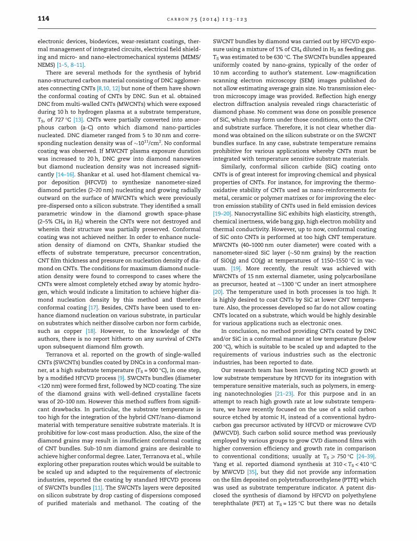
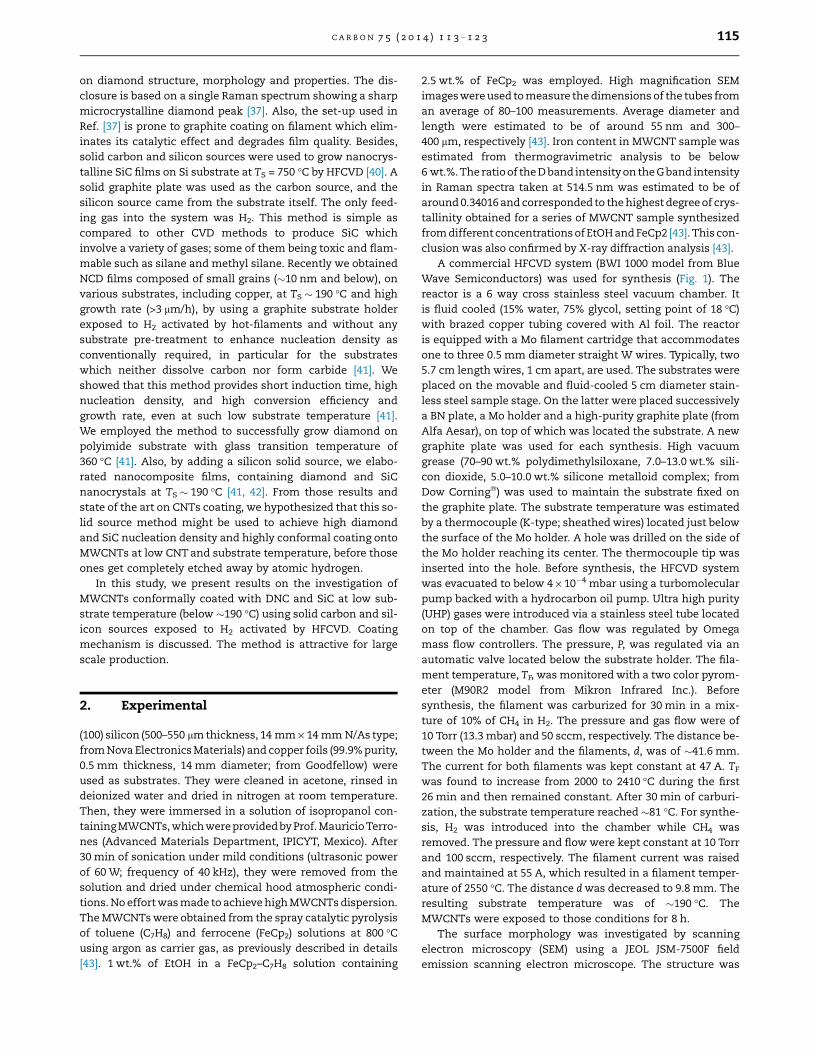
A commercial HFCVD system (BWI 1000 model from BlueWave Semiconductors) was used for synthesis (Fig. 1). Thereactor is a 6 way cross stainless steel vacuum chamber. Itis fluid cooled (15% water, 75% glycol, setting point of 18 !C)with brazed copper tubing covered with Al foil. The reactoris equipped with a Mo filament cartridge that accommodates
one to three 0.5 mm diameter straight W wires. Typically, two5.7 cm length wires, 1 cm apart, are used. The substrates wereplaced on the movable and fluid-cooled 5 cm diameter stain-less steel sample stage. On the latter were placed successivelya BN plate, a Mo holder and a high-purity graphite plate (fromAlfa Aesar), on top of which was located the substrate. A newgraphite plate was used for each synthesis. High vacuumgrease (70–90 wt.% polydimethylsiloxane, 7.0–13.0 wt.% sili-con dioxide, 5.0–10.0 wt.% silicone metalloid complex; fromDow Corning#) was used to maintain the substrate fixed onthe graphite plate. The substrate temperature was estimated
by a thermocouple (K-type; sheathed wires) located just belowthe surface of the Mo holder. A hole was drilled on the side ofthe Mo holder reaching its center. The thermocouple tip wasinserted into the hole. Before synthesis, the HFCVD systemwas evacuated to below 4 · 10"4 mbar using a turbomolecularpump backed with a hydrocarbon oil pump. Ultra high purity(UHP) gases were introduced via a stainless steel tube locatedon top of the chamber. Gas flow was regulated by Omegamass flow controllers. The pressure, P, was regulated via anautomatic valve located below the substrate holder. The fila-ment temperature, TF, was monitored with a two color pyrom-
eter (M90R2 model from Mikron Infrared Inc.). Beforesynthesis, the filament was carburized for 30 min in a mix-ture of 10% of CH4 in H2. The pressure and gas flow were of10 Torr (13.3 mbar) and 50 sccm, respectively. The distance be-tween the Mo holder and the filaments, d, was of !41.6 mm.The current for both filaments was kept constant at 47 A. TF
was found to increase from 2000 to 2410 !C during the first26 min and then remained constant. After 30 min of carburi-zation, the substrate temperature reached !81 !C. For synthe-sis, H2 was introduced into the chamber while CH4 wasremoved. The pressure and flow were kept constant at 10 Torr
and 100 sccm, respectively. The filament current was raisedand maintained at 55 A, which resulted in a filament temper-ature of 2550 !C. The distance d was decreased to 9.8 mm. Theresulting substrate temperature was of !190 !C. TheMWCNTs were exposed to those conditions for 8 h.
The surface morphology was investigated by scanningelectron microscopy (SEM) using a JEOL JSM-7500F fieldemission scanning electron microscope. The structure was
C A R B O N 7 5 ( 2 0 1 4 ) 1 1 3 – 1 2 3 115
analyzed by transmission electron microscopy (TEM), energydispersive X-ray analysis (EDX), electron energy loss spec-troscopy (EELS) and selected area electron diffraction (SAED)
using an energy filtered LEO-922 OMEGA microscopeequipped with an Omega filter and EDAX Genesis 2000microanalysis system (accelerating voltage of 200 kV). Forthis purpose, 3 nm thick holly carbon coated Cu grids wereprepared by scratching the samples with a commercial dia-mond tip. X-ray diffraction (XRD) and Raman spectroscopy(RS) were also employed to examine the structure. TheXRD measurements were taken on a Siemens D5000 diffrac-tometer using a Cu Ka line source (k = 1.5405 A) in a h"2hconfiguration. The Raman spectra were recorded with a tri-ple monochromator (ISA J-Y Model T64000) using the
514.5 nm line of Ar laser and a 80· objective. The probedarea was of !2 lm2. A Renishaw InVia Reflex SpectrometerSystem with a stigmatic single pass spectrograph was alsoused for Raman analysis. In this case, the 488 nm line ofan Ar ion laser and a 50· objective were used. The laserpower on the sample, and acquisition time were adjustedto obtain optimum signal without any sample modification.No visible damage and no change of the spectral shape
during measurements have been observed. Silicon was usedfor peak position calibration.
3. Results and discussion
3.1. Diamond coating
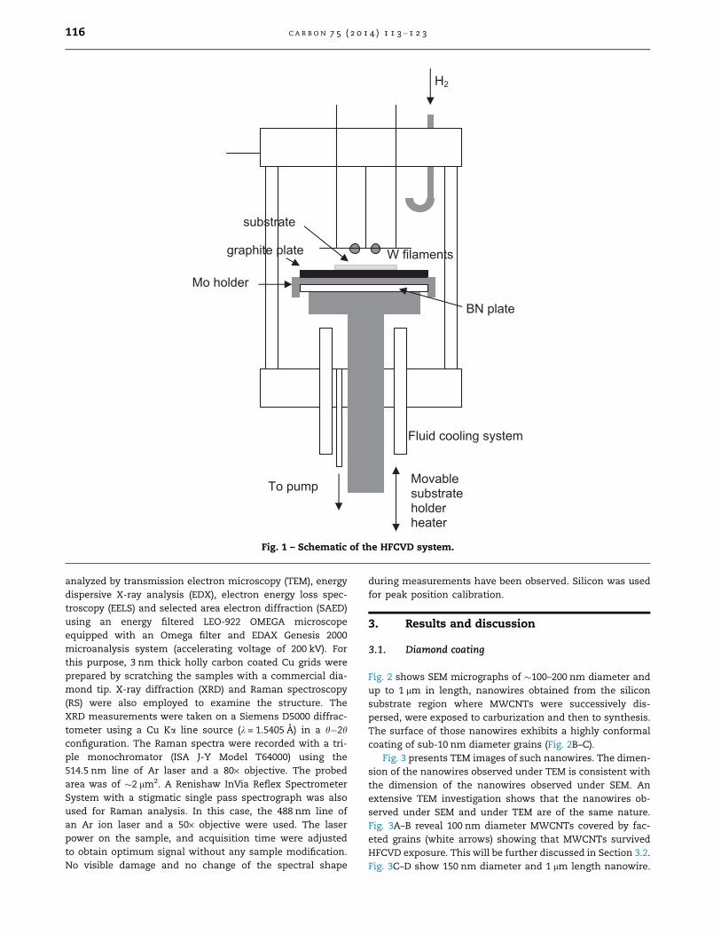
Fig. 2 shows SEM micrographs of !100–200 nm diameter andup to 1 lm in length, nanowires obtained from the siliconsubstrate region where MWCNTs were successively dis-persed, were exposed to carburization and then to synthesis.The surface of those nanowires exhibits a highly conformalcoating of sub-10 nm diameter grains (Fig. 2B–C).
Fig. 3 presents TEM images of such nanowires. The dimen-
sion of the nanowires observed under TEM is consistent withthe dimension of the nanowires observed under SEM. Anextensive TEM investigation shows that the nanowires ob-served under SEM and under TEM are of the same nature.Fig. 3A–B reveal 100 nm diameter MWCNTs covered by fac-eted grains (white arrows) showing that MWCNTs survivedHFCVD exposure. This will be further discussed in Section 3.2.Fig. 3C–D show 150 nm diameter and 1 lm length nanowire.
H2
Movablesubstrateholderheater
To pump
Fluid cooling system
W filaments
substrate
graphite plate
Mo holder
BN plate
Fig. 1 – Schematic of the HFCVD system.
116 C A R B O N 7 5 ( 2 0 1 4 ) 1 1 3 – 1 2 3
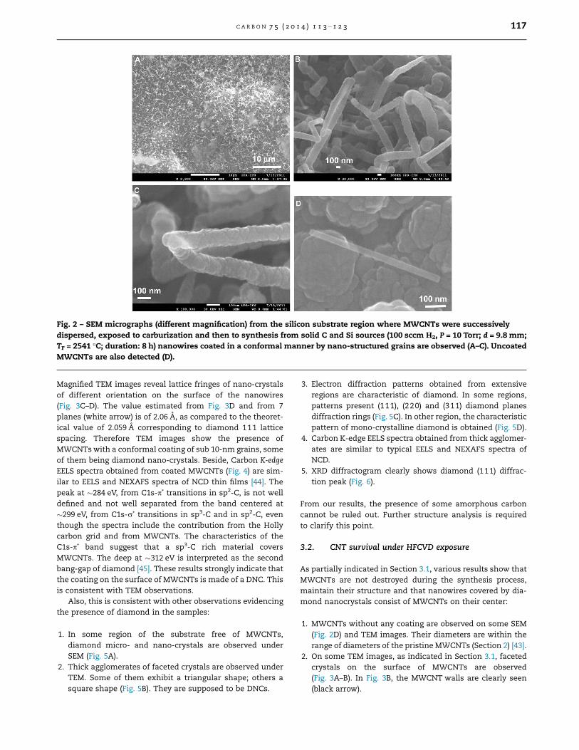
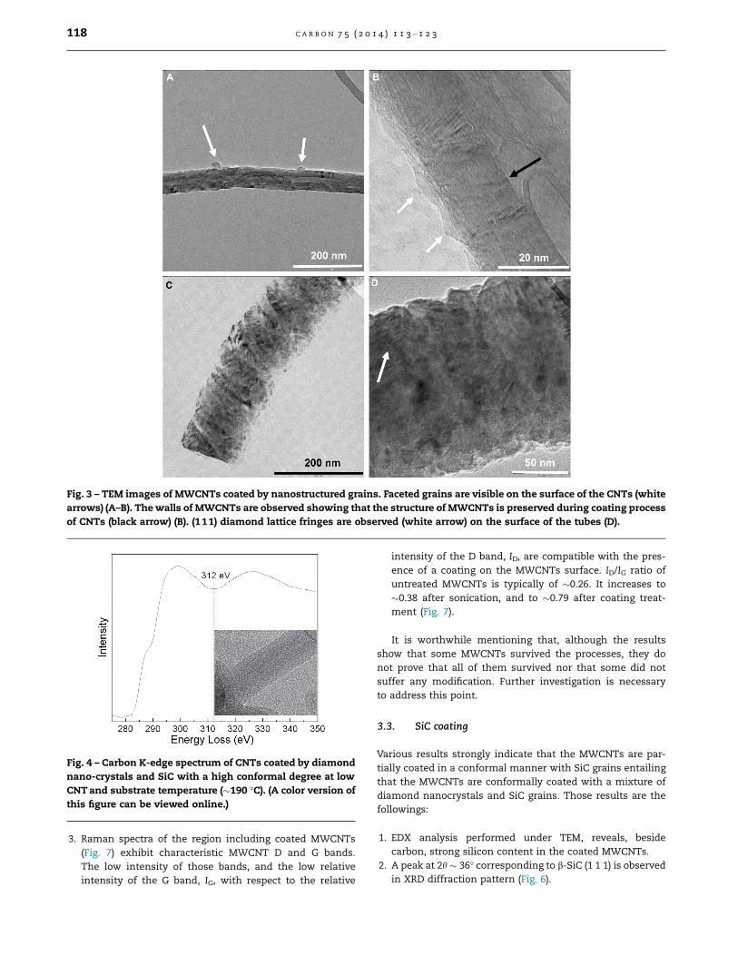
Magnified TEM images reveal lattice fringes of nano-crystalsof different orientation on the surface of the nanowires(Fig. 3C–D). The value estimated from Fig. 3D and from 7planes (white arrow) is of 2.06 A, as compared to the theoret-ical value of 2.059 A corresponding to diamond 111 latticespacing. Therefore TEM images show the presence ofMWCNTs with a conformal coating of sub 10-nm grains, someof them being diamond nano-crystals. Beside, Carbon K-edgeEELS spectra obtained from coated MWCNTs (Fig. 4) are sim-ilar to EELS and NEXAFS spectra of NCD thin films [44]. The
peak at !284 eV, from C1s-p* transitions in sp2-C, is not welldefined and not well separated from the band centered at!299 eV, from C1s-r* transitions in sp3-C and in sp2-C, eventhough the spectra include the contribution from the Hollycarbon grid and from MWCNTs. The characteristics of theC1s-p* band suggest that a sp3-C rich material coversMWCNTs. The deep at !312 eV is interpreted as the secondbang-gap of diamond [45]. These results strongly indicate thatthe coating on the surface of MWCNTs is made of a DNC. Thisis consistent with TEM observations.
Also, this is consistent with other observations evidencing
the presence of diamond in the samples:
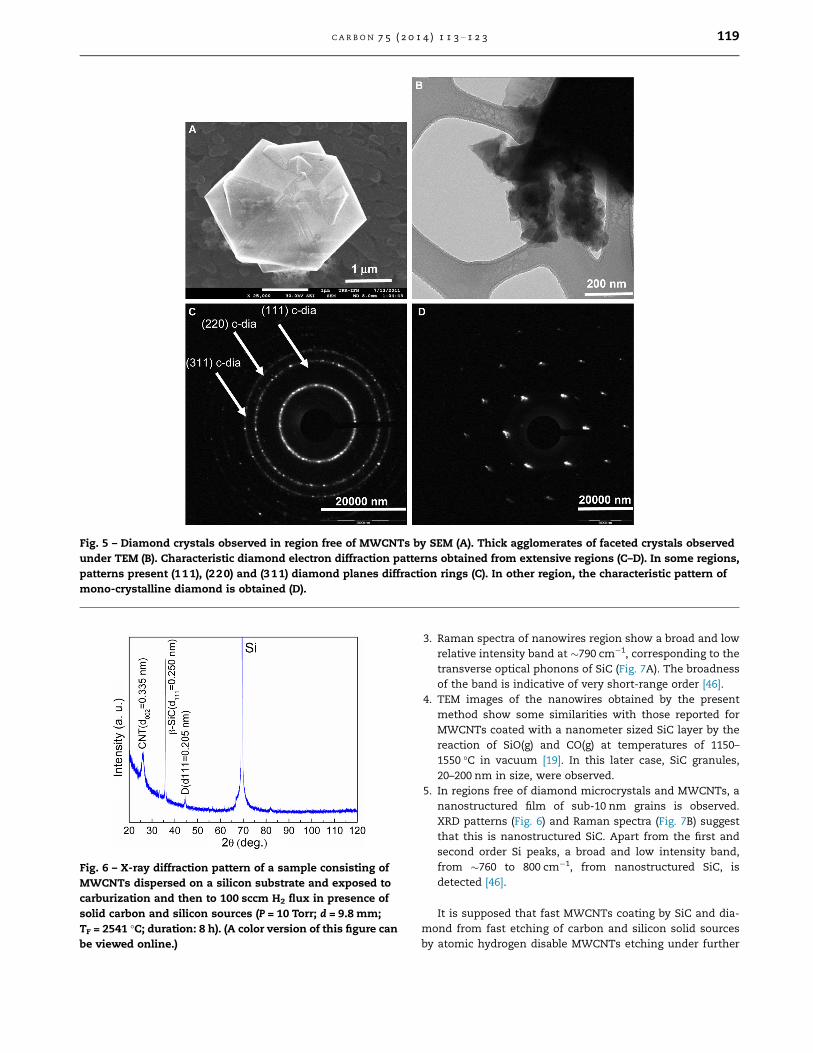
1. In some region of the substrate free of MWCNTs,diamond micro- and nano-crystals are observed underSEM (Fig. 5A).
2. Thick agglomerates of faceted crystals are observed underTEM. Some of them exhibit a triangular shape; others asquare shape (Fig. 5B). They are supposed to be DNCs.
3. Electron diffraction patterns obtained from extensiveregions are characteristic of diamond. In some regions,patterns present (111), (220) and (311) diamond planesdiffraction rings (Fig. 5C). In other region, the characteristicpattern of mono-crystalline diamond is obtained (Fig. 5D).
4. Carbon K-edge EELS spectra obtained from thick agglomer-ates are similar to typical EELS and NEXAFS spectra ofNCD.
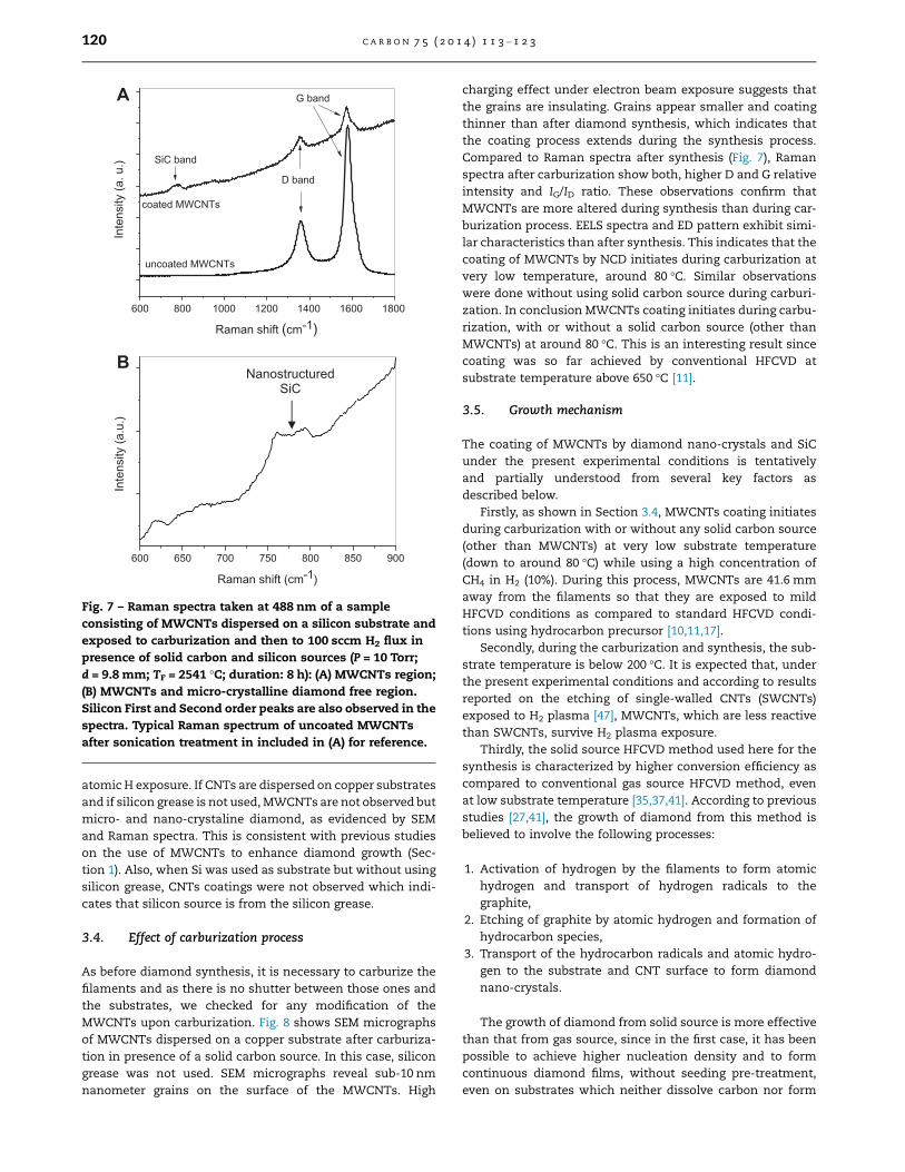
5. XRD diffractogram clearly shows diamond (111) diffrac-tion peak (Fig. 6).
From our results, the presence of some amorphous carboncannot be ruled out. Further structure analysis is requiredto clarify this point.
3.2. CNT survival under HFCVD exposure
As partially indicated in Section 3.1, various results show thatMWCNTs are not destroyed during the synthesis process,maintain their structure and that nanowires covered by dia-mond nanocrystals consist of MWCNTs on their center:
1. MWCNTs without any coating are observed on some SEM(Fig. 2D) and TEM images. Their diameters are within the
range of diameters of the pristine MWCNTs (Section 2) [43].2. On some TEM images, as indicated in Section 3.1, faceted
crystals on the surface of MWCNTs are observed(Fig. 3A–B). In Fig. 3B, the MWCNT walls are clearly seen(black arrow).
Fig. 2 – SEM micrographs (different magnification) from the silicon substrate region where MWCNTs were successivelydispersed, exposed to carburization and then to synthesis from solid C and Si sources (100 sccm H2, P = 10 Torr; d = 9.8 mm;TF = 2541 !C; duration: 8 h) nanowires coated in a conformal manner by nano-structured grains are observed (A–C). UncoatedMWCNTs are also detected (D).
C A R B O N 7 5 ( 2 0 1 4 ) 1 1 3 – 1 2 3 117
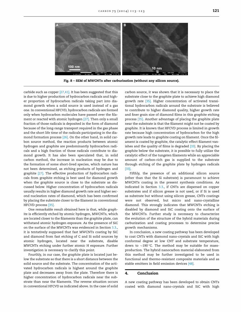
3. Raman spectra of the region including coated MWCNTs(Fig. 7) exhibit characteristic MWCNT D and G bands.
The low intensity of those bands, and the low relativeintensity of the G band, IG, with respect to the relative
intensity of the D band, ID, are compatible with the pres-
ence of a coating on the MWCNTs surface. ID/IG ratio ofuntreated MWCNTs is typically of !0.26. It increases to!0.38 after sonication, and to !0.79 after coating treat-ment (Fig. 7).
It is worthwhile mentioning that, although the resultsshow that some MWCNTs survived the processes, they donot prove that all of them survived nor that some did notsuffer any modification. Further investigation is necessaryto address this point.
3.3. SiC coating
Various results strongly indicate that the MWCNTs are par-
tially coated in a conformal manner with SiC grains entailingthat the MWCNTs are conformally coated with a mixture ofdiamond nanocrystals and SiC grains. Those results are thefollowings:
1. EDX analysis performed under TEM, reveals, besidecarbon, strong silicon content in the coated MWCNTs.
2. A peak at 2h ! 36! corresponding to b-SiC (1 1 1) is observedin XRD diffraction pattern (Fig. 6).
Fig. 3 – TEM images of MWCNTs coated by nanostructured grains. Faceted grains are visible on the surface of the CNTs (whitearrows) (A–B). The walls of MWCNTs are observed showing that the structure of MWCNTs is preserved during coating processof CNTs (black arrow) (B). (111) diamond lattice fringes are observed (white arrow) on the surface of the tubes (D).
Fig. 4 – Carbon K-edge spectrum of CNTs coated by diamondnano-crystals and SiC with a high conformal degree at lowCNT and substrate temperature (!190 !C). (A color version ofthis figure can be viewed online.)
118 C A R B O N 7 5 ( 2 0 1 4 ) 1 1 3 – 1 2 3
3. Raman spectra of nanowires region show a broad and lowrelative intensity band at !790 cm"1, corresponding to thetransverse optical phonons of SiC (Fig. 7A). The broadnessof the band is indicative of very short-range order [46].
4. TEM images of the nanowires obtained by the presentmethod show some similarities with those reported forMWCNTs coated with a nanometer sized SiC layer by thereaction of SiO(g) and CO(g) at temperatures of 1150–1550 !C in vacuum [19]. In this later case, SiC granules,
20–200 nm in size, were observed.5. In regions free of diamond microcrystals and MWCNTs, a
nanostructured film of sub-10 nm grains is observed.XRD patterns (Fig. 6) and Raman spectra (Fig. 7B) suggestthat this is nanostructured SiC. Apart from the first andsecond order Si peaks, a broad and low intensity band,from !760 to 800 cm"1, from nanostructured SiC, isdetected [46].
It is supposed that fast MWCNTs coating by SiC and dia-mond from fast etching of carbon and silicon solid sourcesby atomic hydrogen disable MWCNTs etching under further
Fig. 5 – Diamond crystals observed in region free of MWCNTs by SEM (A). Thick agglomerates of faceted crystals observedunder TEM (B). Characteristic diamond electron diffraction patterns obtained from extensive regions (C–D). In some regions,patterns present (111), (220) and (311) diamond planes diffraction rings (C). In other region, the characteristic pattern ofmono-crystalline diamond is obtained (D).
Fig. 6 – X-ray diffraction pattern of a sample consisting ofMWCNTs dispersed on a silicon substrate and exposed tocarburization and then to 100 sccm H2 flux in presence ofsolid carbon and silicon sources (P = 10 Torr; d = 9.8 mm;TF = 2541 !C; duration: 8 h). (A color version of this figure canbe viewed online.)
C A R B O N 7 5 ( 2 0 1 4 ) 1 1 3 – 1 2 3 119
atomic H exposure. If CNTs are dispersed on copper substratesand if silicon grease is not used, MWCNTs are not observed butmicro- and nano-crystaline diamond, as evidenced by SEMand Raman spectra. This is consistent with previous studieson the use of MWCNTs to enhance diamond growth (Sec-tion 1). Also, when Si was used as substrate but without usingsilicon grease, CNTs coatings were not observed which indi-cates that silicon source is from the silicon grease.
3.4. Effect of carburization process
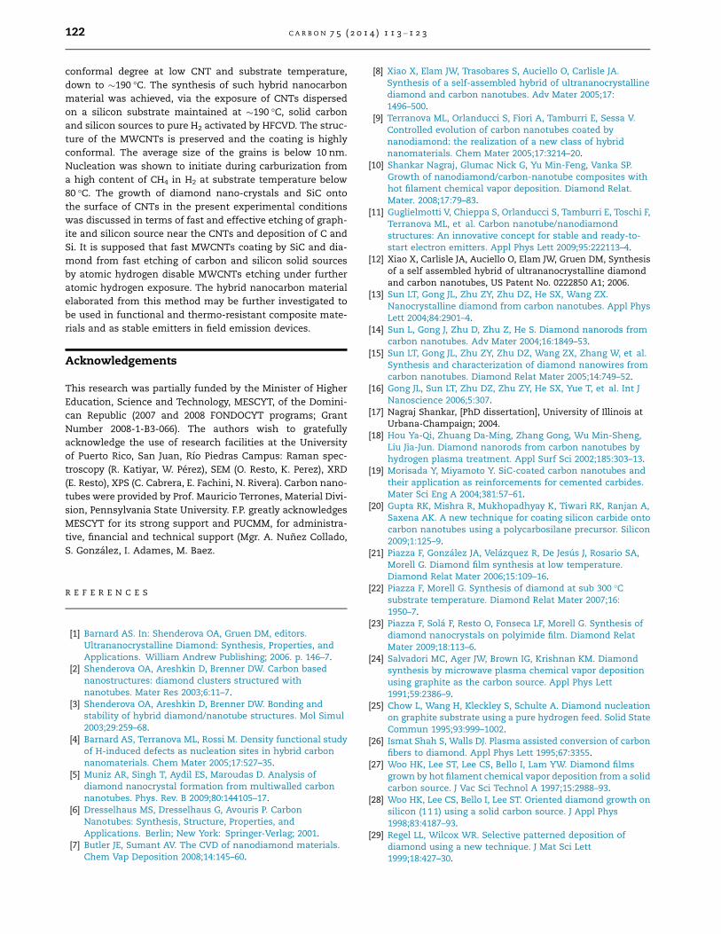
As before diamond synthesis, it is necessary to carburize thefilaments and as there is no shutter between those ones andthe substrates, we checked for any modification of theMWCNTs upon carburization. Fig. 8 shows SEM micrographsof MWCNTs dispersed on a copper substrate after carburiza-tion in presence of a solid carbon source. In this case, silicongrease was not used. SEM micrographs reveal sub-10 nmnanometer grains on the surface of the MWCNTs. High
charging effect under electron beam exposure suggests thatthe grains are insulating. Grains appear smaller and coatingthinner than after diamond synthesis, which indicates thatthe coating process extends during the synthesis process.Compared to Raman spectra after synthesis (Fig. 7), Ramanspectra after carburization show both, higher D and G relativeintensity and IG/ID ratio. These observations confirm that
MWCNTs are more altered during synthesis than during car-burization process. EELS spectra and ED pattern exhibit simi-lar characteristics than after synthesis. This indicates that thecoating of MWCNTs by NCD initiates during carburization atvery low temperature, around 80 !C. Similar observationswere done without using solid carbon source during carburi-zation. In conclusion MWCNTs coating initiates during carbu-rization, with or without a solid carbon source (other thanMWCNTs) at around 80 !C. This is an interesting result sincecoating was so far achieved by conventional HFCVD atsubstrate temperature above 650 !C [11].
3.5. Growth mechanism
The coating of MWCNTs by diamond nano-crystals and SiCunder the present experimental conditions is tentativelyand partially understood from several key factors asdescribed below.
Firstly, as shown in Section 3.4, MWCNTs coating initiatesduring carburization with or without any solid carbon source(other than MWCNTs) at very low substrate temperature(down to around 80 !C) while using a high concentration of
CH4 in H2 (10%). During this process, MWCNTs are 41.6 mmaway from the filaments so that they are exposed to mildHFCVD conditions as compared to standard HFCVD condi-tions using hydrocarbon precursor [10,11,17].
Secondly, during the carburization and synthesis, the sub-strate temperature is below 200 !C. It is expected that, underthe present experimental conditions and according to resultsreported on the etching of single-walled CNTs (SWCNTs)exposed to H2 plasma [47], MWCNTs, which are less reactivethan SWCNTs, survive H2 plasma exposure.
Thirdly, the solid source HFCVD method used here for the
synthesis is characterized by higher conversion efficiency ascompared to conventional gas source HFCVD method, evenat low substrate temperature [35,37,41]. According to previousstudies [27,41], the growth of diamond from this method isbelieved to involve the following processes:
1. Activation of hydrogen by the filaments to form atomichydrogen and transport of hydrogen radicals to thegraphite,
2. Etching of graphite by atomic hydrogen and formation ofhydrocarbon species,
3. Transport of the hydrocarbon radicals and atomic hydro-gen to the substrate and CNT surface to form diamondnano-crystals.
The growth of diamond from solid source is more effective
than that from gas source, since in the first case, it has beenpossible to achieve higher nucleation density and to formcontinuous diamond films, without seeding pre-treatment,even on substrates which neither dissolve carbon nor form
600 800 1000 1200 1400 1600 1800
coated MWCNTs
SiC band
G band
Inte
nsity
(a. u
.)
Raman shift (cm-1)
D band
uncoated MWCNTs
600 650 700 750 800 850 900
Inte
nsity
(a.u
.)
Raman shift (cm-1)
NanostructuredSiC
A
B
Fig. 7 – Raman spectra taken at 488 nm of a sampleconsisting of MWCNTs dispersed on a silicon substrate andexposed to carburization and then to 100 sccm H2 flux inpresence of solid carbon and silicon sources (P = 10 Torr;d = 9.8 mm; TF = 2541 !C; duration: 8 h): (A) MWCNTs region;(B) MWCNTs and micro-crystalline diamond free region.Silicon First and Second order peaks are also observed in thespectra. Typical Raman spectrum of uncoated MWCNTsafter sonication treatment in included in (A) for reference.
120 C A R B O N 7 5 ( 2 0 1 4 ) 1 1 3 – 1 2 3
carbide such as copper [27,41]. It has been suggested that thisis due to higher production of hydrocarbon radicals and high-er proportion of hydrocarbon radicals taking part into dia-mond growth when a solid source is used instead of a gasone. In conventional HFCVD, hydrocarbon radicals are formedonly when hydrocarbon molecules have passed over the fila-ment or reacted with atomic hydrogen [27]. Then only a smallfraction of those radicals is deposited in the form of diamond
because of the long-range transport required in the gas phaseand the short life time of the radicals participating in the dia-mond formation process [26]. On the other hand, in solid car-bon source method, the reaction products between atomichydrogen and graphite are predominantly hydrocarbon radi-cals and a high fraction of those radicals contribute to dia-mond growth. It has also been speculated that, in solidcarbon method, the increase in nucleation may be due tothe formation of some short-lived species, which nature hasnot been determined, as etching products of hydrogen andgraphite [27]. The effective production of hydrocarbon radi-
cals from graphite etching is best used for diamond growthwhen the graphite source is close to the substrate as dis-cussed below. Higher concentration of hydrocarbon radicalsusually results in higher diamond growth rate and higher sec-ond nucleation rates of diamond, which has been confirmedby placing the substrate closer to the filament in conventionalHFCVD process [35].
One remarkable result obtained here is that, while graph-ite is efficiently etched by atomic hydrogen, MWCNTs, whichare located closer to the filaments than the graphite plate, canwithstand atomic hydrogen exposure. As the presence of SiC
on the surface of the MWCNTs was evidenced in Section 3.3.,it is tentatively supposed that fast MWCNTs coating by SiCand diamond from fast etching of C and Si solid sources byatomic hydrogen, located near the substrate, disableMWCNTs etching under further atomic H exposure. Furtherinvestigation is necessary to clarify this point.
Fourthly, in our case, the graphite plate is located just be-low the substrate so that there is a short distance between thesolid source and the substrate. The concentration of the acti-vated hydrocarbon radicals is highest around the graphiteplate and decreases away from the plate. Therefore there ishigher concentration of hydrocarbon radicals near the sub-
strate than near the filaments. The reverse situation occursin conventional HFCVD as indicated above. In the case of solid
carbon source, it was shown that it is necessary to place thesubstrate close to the graphite plate to achieve high diamondgrowth rate [35]. Higher concentration of activated transi-tional hydrocarbon radicals around the substrate is believedto contribute to higher diamond quality, higher growth rateand finer grain size of diamond films in this graphite etchingprocess [35]. Another advantage of placing the graphite platenear the substrate is that the filament might not be coated by
graphite. It is known that HFCVD process is limited in growthrate because high concentration of hydrocarbon for the highgrowth rate leads to graphite coating on filament. Once the fil-ament is coated by graphite, the catalytic effect filament van-ishes and the quality of films is degraded [33]. By placing thegraphite below the substrate, it is possible to fully utilize thecatalytic effect of the tungsten filaments while an appreciableamount of carbon-rich gas is supplied to the substratethrough etching of the graphite plate by hydrogen radicals[33].
Fifthly, the presence of an additional silicon source
(other than that the Si substrate) is paramount to achieveMWCNTs coating in the present synthesis conditions. Asindicated in Section 3.3., if CNTs are dispersed on coppersubstrates and if silicon grease is not used, or if Si is usedas substrate but without using silicon grease, CNTs coatingswere not observed, but micro and nano-crystallinediamond. This strongly indicates that MWCNTs etching isdisabled by diamond and SiC coating onto the surface ofthe MWCNTs. Further study is necessary to characterizethe evolution of the structure of the hybrid materials duringcarburization and coating processes to determine precise
growth mechanisms.In conclusion, a new coating pathway has been developed
to coat CNTs with diamond nano-crystals and SiC with highconformal degree at low CNT and substrate temperature,down to !190 !C. The method may be suitable for mass-production. The hybrid nanocarbon material elaborated fromthis method may be further investigated to be used infunctional and thermo-resistant composite materials and asstable emitters in field emission devices [48].
4. Conclusion
A new coating pathway has been developed to obtain CNTscoated with diamond nano-crystals and SiC with high
Fig. 8 – SEM of MWCNTs after carburisation (without any silicon source).
C A R B O N 7 5 ( 2 0 1 4 ) 1 1 3 – 1 2 3 121
conformal degree at low CNT and substrate temperature,down to !190 !C. The synthesis of such hybrid nanocarbonmaterial was achieved, via the exposure of CNTs dispersedon a silicon substrate maintained at !190 !C, solid carbonand silicon sources to pure H2 activated by HFCVD. The struc-ture of the MWCNTs is preserved and the coating is highlyconformal. The average size of the grains is below 10 nm.
Nucleation was shown to initiate during carburization froma high content of CH4 in H2 at substrate temperature below80 !C. The growth of diamond nano-crystals and SiC ontothe surface of CNTs in the present experimental conditionswas discussed in terms of fast and effective etching of graph-ite and silicon source near the CNTs and deposition of C andSi. It is supposed that fast MWCNTs coating by SiC and dia-mond from fast etching of carbon and silicon solid sourcesby atomic hydrogen disable MWCNTs etching under furtheratomic hydrogen exposure. The hybrid nanocarbon materialelaborated from this method may be further investigated to
be used in functional and thermo-resistant composite mate-rials and as stable emitters in field emission devices.
Acknowledgements
This research was partially funded by the Minister of Higher
Education, Science and Technology, MESCYT, of the Domini-can Republic (2007 and 2008 FONDOCYT programs; GrantNumber 2008-1-B3-066). The authors wish to gratefullyacknowledge the use of research facilities at the Universityof Puerto Rico, San Juan, Rıo Piedras Campus: Raman spec-troscopy (R. Katiyar, W. Perez), SEM (O. Resto, K. Perez), XRD(E. Resto), XPS (C. Cabrera, E. Fachini, N. Rivera). Carbon nano-tubes were provided by Prof. Mauricio Terrones, Material Divi-sion, Pennsylvania State University. F.P. greatly acknowledgesMESCYT for its strong support and PUCMM, for administra-tive, financial and technical support (Mgr. A. Nunez Collado,
S. Gonzalez, I. Adames, M. Baez.
R E F E R E N C E S
[1] Barnard AS. In: Shenderova OA, Gruen DM, editors.Ultrananocrystalline Diamond: Synthesis, Properties, andApplications. William Andrew Publishing; 2006. p. 146–7.
[2] Shenderova OA, Areshkin D, Brenner DW. Carbon basednanostructures: diamond clusters structured withnanotubes. Mater Res 2003;6:11–7.
[3] Shenderova OA, Areshkin D, Brenner DW. Bonding andstability of hybrid diamond/nanotube structures. Mol Simul2003;29:259–68.
[4] Barnard AS, Terranova ML, Rossi M. Density functional studyof H-induced defects as nucleation sites in hybrid carbonnanomaterials. Chem Mater 2005;17:527–35.
[5] Muniz AR, Singh T, Aydil ES, Maroudas D. Analysis ofdiamond nanocrystal formation from multiwalled carbonnanotubes. Phys. Rev. B 2009;80:144105–17.
[6] Dresselhaus MS, Dresselhaus G, Avouris P. CarbonNanotubes: Synthesis, Structure, Properties, andApplications. Berlin; New York: Springer-Verlag; 2001.
[7] Butler JE, Sumant AV. The CVD of nanodiamond materials.Chem Vap Deposition 2008;14:145–60.
[8] Xiao X, Elam JW, Trasobares S, Auciello O, Carlisle JA.Synthesis of a self-assembled hybrid of ultrananocrystallinediamond and carbon nanotubes. Adv Mater 2005;17:1496–500.
[9] Terranova ML, Orlanducci S, Fiori A, Tamburri E, Sessa V.Controlled evolution of carbon nanotubes coated bynanodiamond: the realization of a new class of hybridnanomaterials. Chem Mater 2005;17:3214–20.
[10] Shankar Nagraj, Glumac Nick G, Yu Min-Feng, Vanka SP.Growth of nanodiamond/carbon-nanotube composites withhot filament chemical vapor deposition. Diamond Relat.Mater. 2008;17:79–83.
[11] Guglielmotti V, Chieppa S, Orlanducci S, Tamburri E, Toschi F,Terranova ML, et al. Carbon nanotube/nanodiamondstructures: An innovative concept for stable and ready-to-start electron emitters. Appl Phys Lett 2009;95:222113–4.
[12] Xiao X, Carlisle JA, Auciello O, Elam JW, Gruen DM, Synthesisof a self assembled hybrid of ultrananocrystalline diamondand carbon nanotubes, US Patent No. 0222850 A1; 2006.
[13] Sun LT, Gong JL, Zhu ZY, Zhu DZ, He SX, Wang ZX.Nanocrystalline diamond from carbon nanotubes. Appl PhysLett 2004;84:2901–4.
[14] Sun L, Gong J, Zhu D, Zhu Z, He S. Diamond nanorods fromcarbon nanotubes. Adv Mater 2004;16:1849–53.
[15] Sun LT, Gong JL, Zhu ZY, Zhu DZ, Wang ZX, Zhang W, et al.Synthesis and characterization of diamond nanowires fromcarbon nanotubes. Diamond Relat Mater 2005;14:749–52.
[16] Gong JL, Sun LT, Zhu DZ, Zhu ZY, He SX, Yue T, et al. Int JNanoscience 2006;5:307.
[17] Nagraj Shankar, [PhD dissertation], University of Illinois atUrbana-Champaign; 2004.
[18] Hou Ya-Qi, Zhuang Da-Ming, Zhang Gong, Wu Min-Sheng,Liu Jia-Jun. Diamond nanorods from carbon nanotubes byhydrogen plasma treatment. Appl Surf Sci 2002;185:303–13.
[19] Morisada Y, Miyamoto Y. SiC-coated carbon nanotubes andtheir application as reinforcements for cemented carbides.Mater Sci Eng A 2004;381:57–61.
[20] Gupta RK, Mishra R, Mukhopadhyay K, Tiwari RK, Ranjan A,Saxena AK. A new technique for coating silicon carbide ontocarbon nanotubes using a polycarbosilane precursor. Silicon2009;1:125–9.
[21] Piazza F, Gonzalez JA, Velazquez R, De Jesus J, Rosario SA,Morell G. Diamond film synthesis at low temperature.Diamond Relat Mater 2006;15:109–16.
[22] Piazza F, Morell G. Synthesis of diamond at sub 300 !Csubstrate temperature. Diamond Relat Mater 2007;16:1950–7.
[23] Piazza F, Sola F, Resto O, Fonseca LF, Morell G. Synthesis ofdiamond nanocrystals on polyimide film. Diamond RelatMater 2009;18:113–6.
[24] Salvadori MC, Ager JW, Brown IG, Krishnan KM. Diamondsynthesis by microwave plasma chemical vapor depositionusing graphite as the carbon source. Appl Phys Lett1991;59:2386–9.
[25] Chow L, Wang H, Kleckley S, Schulte A. Diamond nucleationon graphite substrate using a pure hydrogen feed. Solid StateCommun 1995;93:999–1002.
[26] Ismat Shah S, Walls DJ. Plasma assisted conversion of carbonfibers to diamond. Appl Phys Lett 1995;67:3355.
[27] Woo HK, Lee ST, Lee CS, Bello I, Lam YW. Diamond filmsgrown by hot filament chemical vapor deposition from a solidcarbon source. J Vac Sci Technol A 1997;15:2988–93.
[28] Woo HK, Lee CS, Bello I, Lee ST. Oriented diamond growth onsilicon (111) using a solid carbon source. J Appl Phys1998;83:4187–93.
[29] Regel LL, Wilcox WR. Selective patterned deposition ofdiamond using a new technique. J Mat Sci Lett1999;18:427–30.
122 C A R B O N 7 5 ( 2 0 1 4 ) 1 1 3 – 1 2 3
[30] Regel LL, Wilcox WR. Deposition of diamond on graphite andcarbon felt from graphite heated in hydrogen at low pressure.J Mat Sci Lett 2000;19:455–7.
[31] Regel LL, Wilcox WR. Diamond film deposition by chemicalvapor transport. Acta Astronaut 2001;48:129–44.
[32] Liu H, Wang C, Gao C, Han Y, Luo J, Zou G, et al. Diamondfilms grown on seeded substrates by hot-filament chemicalvapour deposition with H2 as the only feeding gas. J PhysCondens Matter 2002;14:10969–72.
[33] Shin SD, Hwang NM, Kim DY. High rate of diamonddeposition through graphite etching in a hot filament CVDreactor. Diamond Relat Mater 2002;11:1337–43.
[34] Yang Q, Chen W, Xiao C, Hirose A, Bradley M. Elongation ofarrays of amorphous carbon tubes. Carbon 2005;43:2618–21.
[35] Yang Q, Chen W, Xiao C, Sammynaiken R, Hirose A. Synthesisof diamond films and nanotips through graphite etching.Carbon 2005;43:748–54.
[36] Yang Q, Chen W, Xiao C, Hirose A, Sammynaiken R.Simultaneous growth of well-aligned diamond and graphiticcarbon nanostructures through graphite etching. DiamondRelat Mater 2005;14:1683–7.
[37] Regel L, Cropper AD, A method for manufacturing lowtemperature diamond coatings, US Patent No. 7,118,782 B2;2006.
[38] Yang Q, Yang S, Xiao C, Hirose A. Transformation of carbonnanotubes to diamond in microwave hydrogen plasma.Mater Lett 2007;61:2208–11.
[39] Lu X, Yang Q, Xiao C, Hirose A. Effects of hydrogen flow rateon the growth and field electron emission characteristics ofdiamond thin films synthesized through graphite etching.Diamond Relat Mater 2007;16:1623–7.
[40] Woo HK, Lee CS, Bello I, Lee ST. Growth of epitaxial b-SiCfilms on silicon using solid graphite and silicon sources.Diamond Relat Mater 1999;8:1737–40.
[41] Piazza F, Beltran-Huarac J, Paredes G, Morell G, Diamond RelatMater, submitted for publication.
[42] Piazza F, Beltran-Huarac J, Paredes G, Ahmadi M, Morell G,Guinel M, in preparation.
[43] Botello-Mendez A, Campos-Delgado J, Morelos-Gomez A,Romero-Herrera JM, Rodrıguez AG, Vavarro H, et al.Controlling the dimensions, reactivity and crystallinity ofmultiwalled carbon nanotubes using low ethanolconcentrations. Chem Phys Lett 2008;453:55–61.
[44] Xiao X, Birell J, Jerbi JE, Auciello O, Carlisle JA. Lowtemperature growth of ultrananocrystalline diamond. J ApplPhys 2004;96:2232–40.
[45] Laikhtman A, Gouzman I, Hoffman A, Comtet G, Hellner L,Dujardin G. Sensitivity of near-edge X-ray absorption finestructure spectroscopy to ion beam damage in diamondfilms. J Appl Phys 1999;86:4192–9.
[46] Klein S, Carius R, Finger F, Houben L. Low substratetemperature deposition of crystalline SiC using HWCVD.Thin Solid Films 2006;501:169–72.
[47] Zhang G, Qi P, Wang X, Lu Y, Mann D, Li X, et al.Hydrogenation and hydrocarbonation and etching of single-walled carbon nanotubes. J Am Chem Soc 2006;128:6026–7.
[48] Piazza F, Carbon nanotubes conformally coated withdiamond nanocrystals or silicon carbide, methods of makingthe same and their use, US Utility Patent Application No. 14/079,546; International Patent Application No. PCT/US2013/069934; Taiwanese Patent Application No.102141512.
C A R B O N 7 5 ( 2 0 1 4 ) 1 1 3 – 1 2 3 123
Top Related
Copyright © 2022 FDOKUMEN

