Xerox SIGMA 9 Computers - X-Files
206
Xerox SIGMA 9 Computers Reference Manual 90 17 33C
-
Upload
khangminh22 -
Category
Documents
-
view
0 -
download
0
Transcript of Xerox SIGMA 9 Computers - X-Files
Xerox SIGMA 9 Computers
Reference Manual
90 17 33C
SIGMA 9 INSTRUCTION LIST (MNEMONICS]
Mnemonic Code Instruction Nome Page Mnemonic Code Instruction Nome Page
AD 10 Add Doubleword 59 LCF 70 Load Conditions and Floating Control 53 AH 50 Add Halfword 58 LCFI 02 Load Conditions and Floating Control Immediate 52 AI 20 Add Immediate 58 LCH SA Load Complement Halfword 49 AIO 6E Acknowledge Input/Output Interrupt (privileged) 127 LCW 3A Load Complement Word 49 AND 4B AND Word 67 LD 12 Load Doubleword 49 ANLZ 44 Analyze 55 LH 52 Load Hal fword 48 AW 30 Add Word 58 LI 22 Load Immediate 48 AWM 66 Add Word to Memory 62 LM 2A Load Multiple 52
LMS 20 Load Memory Status (privileged) 108 BAL 6A Branch and Link 99 LPSD OE Load Program Status Doubleward (privileged) 101 BCR 68 Branch on Conditions Reset 99 LRA 2C Load Real Address (privileged) 107 8CS 69 Branch on Conditions Set 98 LRP 2F Load Register Pointer (privileged) 104 8DR 64 8ranch on Decrementing Register 99 LS 4A Load Selective , 51 BIR 65 Branch on Incrementing Register 99 LW 32 Load Ward 48
CAll 04 Call 1 100 MBS 61 ' Move Byte String 84
CAL2 05 Call 2 100 CAL3 06 Call 3 100
MH 57 Multiply Halfword 61
CAL4 07 Call 4 100 MI 23 Multiply Immediate 60
C8 71 Compare Byte 64 MMC 6F Move to Memory Control (privileged) 104
CBS. 60 Compare Byte Stri ng 85 MSP 13 Modify Stock Pointer 96
CD 11 Compare Doubleword 65 MTB 73 Modify ond Test Byte 62
CH 51 Compore Halfword 65 MTH 53 Modify and Test Halfword 63
CI 21 Compare Immediate 64 MTW 33 Modify and Test Word 63
CLM 19 Compare with Limits in Memory 66 MW 37 Multiply Word 61
CLR 39 Compare with Limits in Register 66 OR 49 OR Word 66
CS 45 Compare Selective 66 CVA 29 Convert by Addition 71
PACK 76 Pack Decimal Digits 81 CVS 28 Convert by Subtroction 71 CW 31 Compare Word 65
PLM OA Pull Multiple 95 PLW 08 Pull Word 94
DA 79 Decimal Add 79 POLP 4F Poll Processor (privileged) 127
DC 70 Decimal Compare 81 POLR 4F Pall and Reset Processor (privileged) 127
DO 7A Decimal Divide 80 PSM OB Push Multiple 94
DH 56 Divide Holfword 61 PSW 09 Push Word 94
DL 7E Decimal Load 79 RD 6C Read Direct (privileged)
OM 78 Decimal Multiply 80 110
OS 78 Decimal Subtract 79 RIO 4F Reset Input/Output (pri v i I eged) 126
DSA 7C Decimal Shift Arithmetic 81 S 25 Shift
DST 7F Decimal Store 79 67
OW 36 Divide Word 62 SO 18 Subtract Doubleword 60 SF 24 Shift Floating 69
E8S 63 Edit 8yte String 88 SH 58 Subtract Holfword 59
EOR 48 Exclusive OR Word 67 SIO 4C Stort Input/Output (privileged) 123
EXU 67 Execute 98 STB 75 Store Byte 53 STCF 74 Stare Conditions and Floating Control 54
FAL 10 Floating Add Long 75 STD IS Store Doubleword 54 STH 55 Store Halfword 53 FAS 3D Floating Add Short 74 STM 28 Store Multiple
FDL IE Floating Divide Long 76 54
FDS 3E Floating Divide Short 76 STS 47 Store Selective 54
FML IF Floating Mult:ply Long 76 STW 35 Store Word 53
FMS 3F Floating Multiply Short 76 SW 38 Subtract Word 59
FSL lC Floating Subtract Long 76 FSS 3C Floating Subtract Short 75 TBS 41 Translate Byte String 86
TDV 4E Test Device (privileged) 125 HIO 4F Holt Input/Output (privileged) 126 TlO 4D Test Input/Output (privileged) 124
HBS 40 Translate and Test Byte String 87 INT 6B Interpret 57
UNPK 77 Unpack Decimal Digits 82 LAD lB Load Absolute Doubleword 51 LAH 5B Load Absolute Halfward 49 WAIT 2E Wait (privileged) 110 LAS 26 Load and Set 51 WD 6D Write Direct (privileged) 112 LAW 38 Load Absolute Word 50 L8 72 Load Byte 48 XPSD OF Exchange Program Status Doubleword (privileged) 102 LCD 1A Load Complement Doubleword 50 XW 46 Exchange Word 53
701 South Aviation Boulevard EI Segundo, California 90245 213679-4511
Xerox SIGMA 9 Computers
Reference Manual
90 17 33C
June 1972
Price: $7.00
XEROX
Printed in U.S.A.
ii
REVISION
The major change made in this revision to the Xerox SIGMA 9 Computer/Reference Manual, Publ ication Number 901733 B (October 1971), is the inclusion of the previously published Revision Package, 9017 33B-1(4/72}. Technical changes from that of the previous manual are indicated by a vertical line in the margin of the page.
RELATED PUBLICATIONS
Publ ication No.
Xerox Sigma Glossary of Computer Terminology 900957
Xerox Meta-Symbol/LN, OPS Reference Manual 900952
Xerox Symbol/LN,OPS Reference Manual 90 1790
Manual Content Code: BP - batch processing, LN - language, OPS - operations, RBP - remote batch processing, RT - real-time, SM - system management, TS - time-sharing, UT - utilities.
ALL SPECIFICATIONS SUBJECT TO CHANGE WITHOUT NOTICE
CONTENTS
l. SIGMA 9 COMPUTER SYSTEMS Trap Condition Code 34 T rap Addressing 34
Introduction 1 Nonallowed Operation Trap 36
The Basi c Systems 1 Unimplemented Instruction Trap 37
Central Processing Unit 2 Push-Down Stack Limit Trap 38
Main Memory 3 Fixed-Point Overflow Trap 38
Multiplexor Input/Output Processor 4 Floating-Point Arithmetic Fault Trap 39
Motor Generator Set 4 Decimal Arithmetic Fault Trap 40
Optional Equipment 4 Call Instruction Trap 40
Additional Register Blocks 4 Processor Detected Fau I ts 40
Additiona I Real-Time Clocks 4 Trap Conditions During "Anticipate"
Priority Interrupt System 4 Operations 43
Alternate Buses 4 Register Altered Bit 43
Memory Reconfiguration Control Unit 4 Memory Expansion 4 Memory Access Port Expansion 5 Memory-to-Memory Move 5 3. INSTRUCTION REPERTOIRE 45 MIOP Channel A Expansion 5 MIOP Channel B Addition 5 Load/Store Instructions 47 High-Speed RAD Input/Output Processor __ 5 Ana Iyze/Interpret Instructions 55 Four-Byte Interface Feature 5 Fixed-Point Arithmetic Instructions 57
Genera I Characteristi cs 5 Comparison Instructions 64 Genera I Purpose Features 8 Logical Instructions 66 Mu Itiprocessing Features 8 Shift Instructions 67 Time-Sharing Features 8-1 Floating-Point Shift 69 Real-Time Features 8-2 Conversion Instructions 70 Multiusage Features 8-3 Floating-Point Arithmeti c Instructions 72
Floating-Point Numbers 72 Floating-Point Add and Subtract 73 Floating-Point Multiply and Divide 74
2. SIGMA 9 SYSTEM ORGANIZATION 9 Condition Codes for Floating-Point Instructions 74
Central Processing Unit 9 Decima I Instructions 77 General Register 9 Packed Decimal Numbers 77 Memory Control Storage 9 Zoned Decimal Numbers 77 Computer Modes 12 Decimal Accumulator 77 Information Format 12 Decimal Instruction Format 77 Information Boundaries 13 Illegal Digit and Sign Detection 77 Inst·ruction Register 13 Overflow Detection 78
Main Memory 14 Decimal Instruction Nomenclature 78 Memory Unit 14 Condition Code Settings 78 Virtual and Real Memory 15 Byte-String Instructions 83 Homespace 15 Push-Down Instructions 92 Memory Reference Address 15 Stack Pointer Doubleword (SPD) 92 Types of Addressi ng 18 Push-Down Condition Code Settings 93 Address Modification Examples 21 Execute/Branch Instructions 97 Memory Address Contro I 23 Branches in Real Extended Addressing Mode_ 97 Program Status Doubleword 27 Nonallowed Operation Trap During
Interrupt System 29 Execution of Branch Instruction 97 Interna I Interrupts 30 CALL Instructions 100 External Interrupts 31 Control Instructions 100 States of an Interrupt Level 31 Program Status Doubleword 101 Con tro I of the In terrupt System 33 Loading the Memory Map 105 Time of Interrupt Occurrences 33 Loading the Access Protection Controls 106 Single-Instruction Interrupts 33 Loadi ng the Memory Write Protection Locks_ 106
Trap System 34 In terrupti on of MMC 106 Trap 34 Memory Access Traps by MMC Instruction __ 107 Trap Entry Sequence 34 Read Direct, Internal Computer Control Trap Masks 34 (Mode 0) 111
90 17 33C-l (4/74) iii
4.
5.
iv
Read Direct, Interrupt Control (Mode 1)-- 112 Write Direct, Internal Computer Control
(Mode 0) 112 Write Direct, Interrupt Control (Mode 1) _ 114
Input/Output Instructions 114 Overa" Characteristics 114 I/o Status Information 118
INPUT/OUTPUT OPERATIONS 129
Operational Command Doublewords 130 Order 130 Memory Byte Address 130 Flags 130 Byte Count 132
Control Command Doublewords 132
OPERA TOR CONTROLS 134
Processor Control Panel 134 Control Mode 134 POWER 135 MEMORY CLEAR 135 SYS RESET 135 I/O RESET 135 LOAD 135 UNIT ADDRESS 135 SENSE 135 NOT NORMAL 135 HALT 135 WAIT 136 RUN 136 Program Status Doubleword Indicators ___ 136 INSERT 137 CPU RESET 137 INTERRUPT 137 ADDRESS STOP 137 SELECT ADDRESS 138 STORE 138 INSTR ADDR 138 DISPLAY (Indicators) 139 DISPLA Y FORMAT 139 FORMAT SEL 139 DATA 139 DISPLA Y (Switch) 139 COMPUTE 140
Maintenance Controls 140 ALARM 140 PDF 140 CLOCK MARGINS 140 PHASES 140 CLOCK MODE 141 SNAP 141 MEMORY MODE 141 OVERRIDE MODE 141 SCAN 141 EXT DIO 142
Operating Procedures _________ _ Loading Operation _________ _ Fetching and Storing Data ______ _
INDEX
APPENDIXES
A. REFERENCE TABLES
Standard Symbols and Codes Standard Character Sets Control Codes Specia I Code Properties Standard 8-Bit Computer Codes (EBCDIC) Standard 7-Bit Communication Codes (ANSCII)_ Standard Symbol-Code Correspondences Hexadecimal Arithmetic
Addition Table Multiplication Table Table of Powers of Si xteen 10 Table of Powers of Ten16
Hexadecimal-Decimal Integer Conversion Table
Hexadecimal-Decimal Fraction Conversion Table
Table of Powers of Two Mathematical Constants
B. SIGMA 9 INSTRUCTION LIST
c. INSTRUCTION TIMING
Timing Considerations Effects of Memory Interference Effects of Indexing Effects of Indirect Addressing Effects of Register-to-Register Operations __ Other SIGMA 9 Performance Factors
D. SYSTEM RELIABILITY AND MAINTAINABILITY
System Maintainabi lity Features CPU Features Main Memory Features MJJltiplexor Input/Output Processor (MIOP)
Features High-Speed RAD I/O Processor (HSRIOP)
Features
E. GLOSSARY OF SYMBOLIC TERMS
143 143 144
183
145
145 145 145 145 146 146 147 151 151 151 152 152
153
159 163 163
164
165
165 165 165 165 166 166
175
175 176 178
178
179
180
AGURES 6. SIGMA 9 Interrupt Locations 29
Frontispiece - SIGMA 9 Computer System __ vi 7. Summary of SIGMA 9 Trap Locations 35
l. A Typical SIGMA 9 System 10 8. TeC Setting for Instruction Exception Trap X'4D ' 42
2. Central Processing Unit 11 9. Registers Changed at Time of a Trap Due to
3. Information Boundaries 13 an Operand Access 43
4. Addressing Logic 17 10. ANALYZE Table for SIGMA 9 Operation Codes 56
5. Index Displacement Alignment (Real and Virutal Addressing Mode) 22 1l. Floating-Point Number Representation 73
6. Index Displacement Alignment (Real Extended 12. Condition Code Settings for Floating-Point Addressing) 23 Instructi ons 75
7. General of Actual Memory Addresses, Virtual 13. Status Word 0 109 Addressing (SIGMA 9 Mode) 24
14. Sta tus Word 1 109 8. Generation of Effective Virtua I Address, Real
Extended Addressing 25 15. Status Word 2 110
9. Typica I Interrupt Priority Chain 30 16. Description of I/O Instructions 115
10. Operational States of an Interrupt Level 32 17. I/o Status Information (Register R) 118
11. Formats of I/O Instructions 117 18. Devi ce Status Byte (Register R or Ru 1) (SIO, TIO, and HIO On Iy) 118
12. Processor Control Panel 134 19. Operationa I Status Byte (Regi ster Ru 1) 120
20. Status Response Bits for I/O Instructions ___ 121
TABLES 21. Processor Fault Status 122
l. Basic SIGMA 9 System 22. lOP Status Byte 122
2. Basic SIGMA 9 Model 2 System 23. Status Response Bits for AIO Instruction ___ 123
3. Basic SIGMA 9 Model 3 System 24. I/O Address (AIO Response) 123
4. Homespace Layout 16 25. Program Status Doubleword (PSD) Indicators_ 136
5. Computer Operating and Addressing Modes __ 29 C-l. Basic Instruction Timing 167
90 17 33C-1 (4/74) v

1. SIGMA 9 COMPUTER SYSTEMS
. INTRODUCTION
SIGMA 9, SIGMA 9 Model 2, and SIGMA 9 Model 3 are high-speed, general-purpose, digital computer systems designed for multiuse environments. SIGMA 9, the most powerful of the three systems, is universally applicable to all data processing applications. SIGMA 9 Model 2 provides for effi cient processing in mul tiprogrammed batch mode, remote batch mode, conversational time-sharing mode, real-time mode, and transaction processing mode. SIGMA 9 Model 3 is designed specifically for the multiuse environment of the scientific real-time community. Each computer system is complete, its design based on proven architecture and field-proven operating systems. The architectures allow independent memory access by the central processing unit (CPU) and peripherals for maximum throughput and minimum response time. The CPU, main memory subsystem, and independent I/O system perform asynchronously with respect to each other. The operating systems complement the hardware by providing a wide variety of subsystems, task management, virtual memory management, resource allocation, and installation accounting. SIGMA 9 Model 2 and SIGMA 9 Model 3 derive from extremely sophisticated trimodal operational concepts; the SIGMA 9 derives from the most sophisticated trimodal operational concept in the industry. AI I three systems additionally have advanced design characterictics and features that provide reliable operation and efficient ma i ntenan ce.
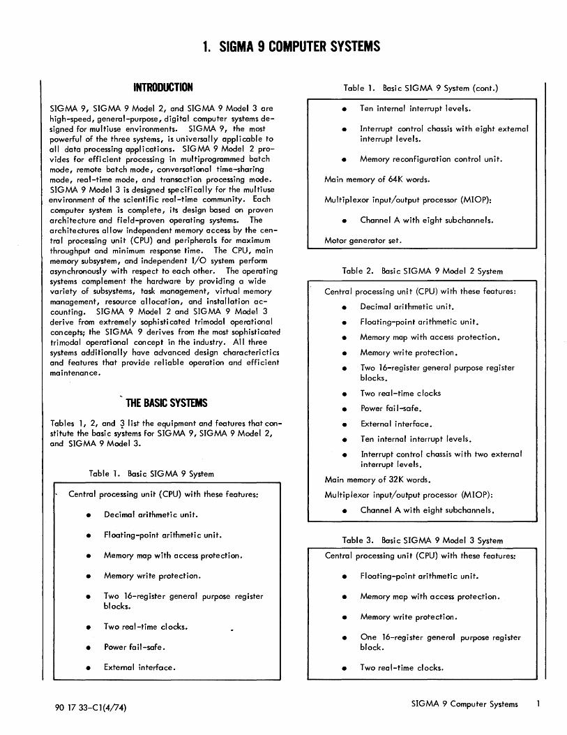
THE BASIC SYSTEMS
Tables 1, 2, and ~ list the equipment and features that constitute the basic systems for SIGMA 9, SIGMA 9 Model 2, and SIGMA 9 Model 3.
Table 1. Basic SIGMA 9 System
Central processing unit (CPU) with these features:
• Decimal arithmetic unit.
• Floating-point arithmetic unit.
• Memory map with access protection.
• Memory write protection.
• Two 16-register general purpose register blocks.
• Two real-time clocks.
• Powe r fa i I -safe.
• External interface.
Table 1. Basic SIGMA 9 System (cont.)
• Ten internal interrupt levels.
• Interrupt control chassis with eight external interrupt levels.
• Memory reconfiguration control unit.
Main memory of 64K words.
Multiplexor input/output processor (MIOP):
• Channel A with eight subchannels.
Motor generator set.
Table 2. Basic SIGMA 9 Model 2 System
Central processing unit (CPU) with these features:
• Decimal arit\'metic unit.
• Floating-point arit\'metic unit.
• Memory map with access protection.
• Memory write protection.
• Two 16-register general purpose register blocks.
• Two real-time clocks
• Power fai I-safe.
• External interface.
• Ten internal interrupt levels.
• Interrupt control chassis wit\' two external interrupt levels.
Main memory of 32K words.
Multiplexor input/output processor (MIOP):
• Channel A with eight subchannels.
Table 3. Basic SIGMA 9 Model 3 System
Central processing unit (CPU) with these features:
• Floating-point arithmetic unit.
• Memory map with access protection.
• Memory write protection.
• One 16-register general purpose register block.
• Two real-time clocks.
90 17 33-C1(4/74) SIGMA 9 Computer Systems
Table 3. Basic SIGMA 9 Model 3 System (cant.)
• Power fail-safe.
• Extemal interface.
• Ten internal interrupt levels.
• Interrupt control chassis with two external interrupt levels.
Main memory of 32K words.
Multiplexor input/output processor (MIOP):
• Channel A with eight subchannels.
CENTRAL PROCESSING UNIT
The CPU includes a 32-bit, binary, word-parallel, arithmetic and logic unit. The CPU has the ability to operate on data in various formats including doublewords (64 bits), words (32 bits), halfwords (16 bits) and bytes (8 bits). Data may be represented as binary, floating-point, or logi cal; in SIGMA 9 systems and SIGMA 9 Model 2 systems, data may also be represented as decimal. The CPU can perform double precision as well as single precision arithmetic. The interleaving and overlapping of memory cycles speeds computation and reduces I/O interference.
Each CPU has a large instruction set that includes floatingpoint, decimal and byte-string instructions. (SIGMA 9 Model 3, designed primarily for scientific applications, has the same instruction set less the decimal arithmeti c and byte-string capabil ities.) A special feature called "Iookahead II enables the CPUs to overlap instruction execution with memory access, thereby reducing program execution time.
SIGMA 9 Model 3 has an instruction execution rate performance level equal to that of the more powerful SIGMA 9. The SIGMA 9 Model 2 instruction execution rate performance level is equivalent to that of SIGMA 6/7 computers.
DECIMAL ARITHMETIC UNIT
(This unit is available only on the SIG MA 9 system and the SIGMA 9 Model 2 system.) This unit performs high-speed arithmetic and logical operations on binary coded decimal (4-bit) data and editing operations on byte-sized (8-bit) data.
The decimal arithmetic unit implements the following decimal ~nstructions: decimal add, subtract, multiply, divide, compare, and shift arithmetic instructions; and decimal load, store, pack, and unpack logical instructions. Storage is highly efficient - decimal digits and signs are packed two per 8-bit byte. The unit can process decimal fields
2 The Basic Systems
as long as 31 digits plus sign. Because of the variance in decimal field length, instruction execution time is reduced to the minimum for any operation. The decimal arithmetic unit eliminates the rounding and conversion problems of business-type arithmetic that occur when binary coding is used.
The decimal arithmetic unit also performs editing operations on a field or group of fields as long as 256 bytes. The instruction set includes these byte string instructions implemented by the decimal arithmetic unit: move byte string, compare byte string, translate byte string, translate and test byte string, and a comprehensive edit byte string instruction.
FLOATING-POINT ARITHMETIC UNIT
This unit performs high-speed floating-point arithmetic, provides automatic scaling, and permits a wide dynamic range of individual problem parameters. It uses both long and short floating-point formats. Short precision is useful for intermediate calculations and for the arithmetic manipulation of low precision data (real-time data generally fit in this category). long precision is useful for matrix inversion, integration, and for problems in which sums and differences of large numbers are key problem variables. Programs can select normalized or unnormalized modes for floating-point addition and subtraction. The unit detects imminent loss of significance and can optionally cause an arithmetic fault. When the unit detects a floating exponent underflow, it can alternatively cause a trap or produce a zero result, depending on the state of the program status doubleword.
MEMORY MAP WITH ACCESS PROTECTION
This feature eliminates the possibility of memoryfragmentation by allowing economi c relocation of programs. Regardless of which addresses the executing program uses (virtual addresses), the memory map permits the program to reside anywhere in main memory in noncontiguous areas. User memory is logically divided into 256 pages of 512 words each (2048 bytes per page). Thus several user programs with identical virtual addressing can be resident at the same time, scattered over the full 512K words(two million bytes) of memory available. The memory map feature automatically translates all virtual addresses of the program into actual addresses in memory when the CPU is operating in the mapping mode.
The memory map facilitates the sharing of software processors by several user programs, each with its own virtual memory; only one copy of each software processor is required in core. The result is increased efficiency in the use of rea I memory.
As part of the memory map feature is another level of protection - memory access protection. The memory access
90 17 33C-1(4/74)
protection feature subjects virtual addresses to an access validity check. Any page of 512 words can be specified as being available for
• No access for any purpose.
• Read access for operands only - no write.
• Read access for operands and instructions - no write.
• All access for any read, write, or execution.
MEMORY WRITE PROTECTION
This feature provides individual memory write protection for each page of the first 128K words (256 pages) of real memory. Three classes of programs can be simultaneously resident in memory, and all can be guaranteed that their data cannot be destroyed by any other class of program.
REGISTER BLOCKS
The CPUs in the basic SIGMA 9 and SIGMA 9 Model 2 systems include two, 16-register, general purpose register blocks (SIGMA 9 Model 3 has one register block standard). Any register can be used as an arithmetic or high-speed scratchpad. Seven registers in each 16-register block are available for use as index registers. A registerpointerfield in the current program status doubleword selects the current register block. All register references made by an ongoing program are then directed to the single block designated by the register pointer.
Use of multiple register blocks facilitates high-speed context switching by el iminating the overhead time and space associated with saving, loading, and restoring CPU registers.
REAL-TIME CLOCKS
Each basic system includes two real-time clocks (called counters 3 and 4). Multiple real-time clocks permit several programs to be timed out and initiated independently of each other, and eliminate the overhead processing associated with a scheduling program. Time-critical operations can be easily monitored on an elapsed time basis - the program is automatically notified by a priority interrupt as needed.
Counter 4 has a constant frequen~y of 500 Hz. Counter 3 can be individually set to one of four manually switchable frequencies: the commercial line frequency, 500 Hz, 2000 Hz, or a user-suppl ied external system.
POWER FAIL-SAFE
This feature detects an imminent failure of primary power and diverts the computer to a special interrupt routine that preserves the state of all volatile registers and brings the computer system to an orderly halt before power drops
90 17 33C-1(4/74)
below acceptable, safe limits. Thus, no vital data are lost, and operations can later resume at the point of interruption without the further loss of data and time associated with having to reinitiate a possibly lengthy computation. Similarly after a shutdown, this feature automatically senses when power has returned to a normal level and causes the machine to resume computation at the point of prior interruption. All volatile registers are saved in nonvolatile magneti c core before shutdown occurs; they are restored as part of the startup routine.
EXTERNAL INTERFACE
This feature provides an external interface for the attachment of external equipment to the computer via the direct input/output (DIO) system. External equipment may be Xerox external interrupts, Xerox system interface units, or nonstandard special equipment.
The external interface allows the transfer of a 32-bit data word between an affected register and an external devi ce and the transfer of a 16-bit address for selection and control purposes. Each transfer is underdirectprogram control.
INTERNAL INTERRUPT LEVELS
Each basic system provides 10 internal interrupt levels, expandable to 14, associated with signals generated as a result of these conditions: power on, power off, pulsing and monitoring of the two real-time clocks, processor fault, memory fault, input/output operation, and operator interrupt from the control panel. The four optional internal interrupts are associated with the pulsing and monitoring of two additional real-time clocks.
INTERRUPT CONTROL CHASSIS
Each basi c system includes an interrupt control chasis that provides control and mounting space for as many as 16 external priority interrupt levels. Eight of these interrupt levels are supplied with the basic SIGMA 9 (2 levels each are supplied with the basic SIGMA 9 Model 2 and SIGMA 9 Model 3). The external priority interrupt levels allow the CPU to immediately recognize special external conditions on a priority basis, thereby providing a means for scheduling real-time processes as well as a means for efficient I/O control.
MAIN MEMORY
The main memory for each basic system comprises a group of memory units. A memory unit is the smallest, logically complete part of the memory subsystem that can be logically isolated from the rest of the memory subsystem. Each memory unit consists of two physical memory banks. The memory banks in a memory unit operate independently and asynchronously with respect to each other. Each memory unit has a set of memory access ports that is common to both banks
The Basi c Systems 3
within the unit; that is, all ports in a giyen memory unit give access to the banks within that unit. A basic system is provided with two ports per memory unit, expandable to 12.
The memory subsystem has 2-way interleaving capabil ity within a unit and 4-way interleaving capability between two adjacent units. Interleaving increases the probabil ity that successive memory accesses wi II be overlapped. In combination, these two features provide the system with effective cycle times of a fraction of the individual bank cycle times. Each individual bank has a cycle time of 900 nan ose conds.
The basic SIGMA 9 system includes a memory size of 64K words. The basic SIGMA 9 Model 2 and SIGMA 9 Model 3 systems include a memory size of32K words. Memory is word, halfword, and byte addressable for both reading and writing. All of memory can be directlyaddressed (real extended mode).
MULTIPLEXOR INPUT/OUTPUT PROCESSOR
The Multiplexor Input/Output Processor (MIOP) provides the control necessary to simultaneously operate many lowto-medium-speed peripheral devices, and offers both command chaining and data chaining. The MIOP in each basic system includes channel A with eight subchannels; one subchannel is required for each device controller.
Transfers between memory and the MIOP are 33 bits wide including a parity bit • Transfers between the MIOP and the peripheral device are on a byte-wide path, oroptionally on a four-byte-wide path if the optional Four-Byte Interface Feature is installed on the system.
MOTOR GENERATOR SET
A motor generator set is standard with a basic SIGMA 9 system and available where necessary for SIGMA 9 Model 2 and SIGMA 9 Model 3 systems.
OPTIONAL EQUIPMENT
Each basi c system can be readily expanded to accommodate the user's requirements. The main memories have addressing space for four million words. Memory access paths can be increased from the basic two ports to a maximum of 12 ports. Input/output capability can be increased by adding more input/output processors (lOPs), device controllers, and peripheral I/O devices. The aggregate of lOPs and CPUs is restri cted by the maximum memory access port I imitati on of 12 ports.
ADDITIONAL REGISTER BLOCKS
One or more additional blocks of 16 general purpose registers may be added to a basic system: two additional blocks for SIGMA 9 and SIGMA 9 Model 2, and three
4 Optional Equipment
additional blocks for SIGMA 9 Model 3, for a total of four register blocks per system.
ADDITIONAL REAL-TIME CLOCKS
Two additional real-time clocks (called counters 1 and 2) can be added to any basi c system giving a total of four, independent, real-time clocks. Counters 1 and 2 can be individually set to one of four manually switchable frequencies: the commercial line frequency, 500 Hz, 2000 Hz, or a user-supplied extemal system that may be different for each counter.
PRIORITY INTERRUPT SYSTEM
When fully expanded by the addition of one or more interrupt control chassis, this system provides 224 external priority interrupt levels. Each level can be individually armed or disarmed and enabled or disabled under program control.
ALTERNATE BUS
In a given system, the CPU and Input/Output Processors (lOPs) are linked by one trunk-tail control bus (processor bus). See Figure 1 in Chapter 2. The alternate bus provides a duplication of that processor bus for multi-CPU configurations, and allows all system resources to be divided among the CPUs. Moreover, the alternate bus allows the system to be manually partitioned so that a faulty unit can be diagnosed and repaired while the rest of the system continues normal operation or a separate operation.
MEMORY RECONFIGURATION CONTROL UNIT
This option (standard on SIGMA 9) provides the capability of remotely controlling memory unit starting addresses, interleave modes, and port inhibit for each of the ports in any memory unit. These actions are accomplished via toggle switches on a memory reconfiguration control panel mounted in the CPU cabinet.
MEMORY EXPANSION
SIGMA 9 memory size is expandable in a specific manner to a maximum of 512K words. Expansion proceeds in 16K word increments from 64K words to 128-1< words, in 32K word increments from 128K words to 256K words, and in 64K word increments from 256K words to 512K words (where K = 1024).
SIGMA 9 Model 2 and SIGMA 9 Model 3 memories are expandable in increments of 32K words (one memory unit) to a maximum of 256K words for SIGMA 9 Model 2 and 512K words for SIGMA 9 Model 3. Each added memory unit includes two memory access ports.
90 17 33C-1 (4/74)
MEMORY ACCESS PORT EXPANSION
This option provides additional access paths to each memory unit in the system. Each processor (CPU, MIOP, HSRIOP, or other) requires its own bus to memory, and each memory unit requires a unique access path for each bus. One to 10 memory access ports can be added to each memory unit to enable the multiple-access memory to accept additional memory buses.
MEMORY-TO-MEMORY MOVE
This option permits information in main memory to be relocated to another area in main memory at high data rates. The move operation is initiated by the CPU and then proceeds independently. Data chaining may be used; thus the informati on involved in the move need not be in contiguous areas. The move operation proceedsautomaticallyata priority lower than that of any peripheral device attached to the MIOP (channel A). The move operation is controlled on the basis of a word count, that when reduced to zero, can by program decision cause an interrupt signal to be sent to the CPU.
This option uses dedicated subchannels 8 and 9. Thus channel A must haveat least 16 subchannels as a prerequisite.
MIOP CHANNEL A EXPANSION
MIOP Channel A can be expanded in increments of eight subchannels to comprise a maximum of 24 subchannels.
MIOP CHANNEL B ADDITION
Channel B is an optional addition to an MIOP. Channel B is intended for use in applications where the peripheral devices to be attached to a system exceed 100 percent of the available data transfer capabil ity of the MIOP with channel A only. Channel B includes conflict-resolving circuitry that allows it to share both the basic control circuitry of the MIOP as well as the memory bus.
Channel B provides the control necessary to operate eight peripheral devices simultaneously; that is, Channel B includes eightsubchannels and is notexpandable. Multipledevice controllers may be attached to these subchannels. Channel B provides full capability for data and command chaining.
HIGH-SPEED RAD INPUT/OUTPUT PROCESSOR
This option combines the functions of an IOPand controller to provide sequencing control and I/O data transmissions for as many as four Model 7212 High-Speed Rapid Access Data (RAD) units. I/O transmissions are fully buffered and checked for parity. All I/O operations proceed independently of the CPU once initiated by the CPU. The HSRIOP can handle very high data rates. Transmission at the rate of one 32-bit (plus one parity bit) word per microsecond is obtainable.
90 17 33C-l{4/74)
When more than one Model 7212 high-speed RAD is attached to a HSRIOP, they are treated as distinct units and are not considered contiguous in the programming sense. Xerox standard software assumes all lOPs go to all of memory.
Dedicated space in a basic system is available for one HSRIOP. Additional HSRIOPs can be provided in cabinets adjacent to memory.
FOUR-BYTE INTERFACE FEATURE
This option expands the bandwidth capability of the MIOP channels (A and B); one Four-Byte Interface Feature is required for each channel. This option also reduces the bandwidth consumed by some high-speed peripherals. It can also be used in systems applications where high-speed, word-oriented data are to be handled, and CPU performance and economy are important.
External peripheral devices capable of transferring four bytes at a time can, by program decision, sense that this feature is installed in the channels and request that data be transmitted four bytes in parallel. The operation of byteoriented devices is not affected by the installation of this feature.
GENERAL CHARACTERISTICS
(In the remainder of this manual, "SIGMA 9" refers to all three systems: SIGMA 9, SIGMA 9 Model 2, and SIGMA 9 Model 3. When the three systems differ in respect to a particular feature or capability, the discrepancy is noted.)
A SIGMA 9 computer system has features and operating characteristics that permit efficient functioning in generalpurpose, multiprocessing, time-sharing, real-time, and multiusage environments:
• Word-oriented memory (32-bit word plus parity bit) that can be addressed and altered as byte (a-bit), halfword (2-byte), word (4-byte), and doubleword (a-byte) quantities.
• Memory expandable to 512K words for SIGMA 9 and SIGMA 9 Model 3, and to 256K words for SIGMA 9 Model 2 (where K = 1024).
• Direct addressing capabi/ ity (real extended mode) of entire memory.
• Indirect addressing with or without postindexing.
• Displacement index registers, automatically selfadjusting for all data sizes.
• Immediate operand instructions for greater storage effi ci en cy and increased speed.
General Characteristics 5
• General-purpose registers, expandable to 64 (in blocks of 16) for addressing, indexing, and accumulating. Multiple registers permit effective use of small, high-speed memories.
• Hardware memory mapping that virtually eliminates memory fragmentation and provides dynami c program relocation.
• Four modes of memory access protection for system and information security and protection.
• Memory write protection to prevent inadvertent destruction of critical areas of memory.
• Watchdog timer to assure nonstop operation.
• Rea I-time priority interrupt system with automati c identifi cation and priority assignment, fast response time, and as many as 224 extemal interrupt levels that can be individually armed, enabled, and triggered by program control.
• Instructions with long execution times can be interrupted to guarantee response to interrupts.
• Automatic traps for error or fault conditions, with masking capability and maximum recoverabil ity, under program control.
• Power fail-safe for automatic shutdown and resumption of processing in event of power failure.
•
•
•
6
Multiple interval timers with a choice of resolutions for independent time bases.
Privileged instruction logic for program integrity in mul tiusage environments.
Complete instruction set that includes:
• Byte, halfword, word, and doubleword operations.
• Use of all memory-referencing instructions for register-to-register operations, with or without indirect addressing and postindexing, and within normal instruction format.
• Multiple register operations.
• Fixed-point integer arithmetic operations in halfword, word, and doubleword modes.
• Floating-point hardware operations in short and long formats with signifi cance, zero, and normalization control and checking, all under full program control.
• Full complement of logical operations (AND, OR, exclusive OR).
• Comparison operations, including compare between limits (with limits in memory or in registers).
General Characteristics
• Call instructions that permit up to 64 dynamically variable, user-defined instructions, and allow a program access to operating system functions without operating system intervention.
• Decimal hardware operations, including arithmetic, edit, and pack/unpack (not available on SIGMA 9 Model 3).
• Push-down stack operations (hardware implemented) of single or multiple words, with automatic limit checking, for dynamic space allocation, subroutine communication, and recursive routine capability.
• Automatic conversion operations, including binary/ BCD and any other we ighted-number systems.
• Analyze instruction that facilitates effective address computation.
• Interpret instruction that increases speed of interpretive programs.
• Shift operations (left and right) of word or doubleword, including logical, circular, arithmetic, searching shift, and floating-point modes.
• Built-in reliability and maintainability features (see Appendix D) that include:
• Extensive error logging. When a fault is detected, system status and fault information are available for program retrieval and logging for subsequent analysis.
• Full- parity checking on all data and addresses communicated in either direction on buses between memory units and processors, providing fault detection and location capabil ity to permit the operating system or diagnostic program to quickly determine a faulty unit.
• Address stop feature that permits operator or maintenance personne I to:
Stop on any instruction address.
Stop on any memory reference address.
Stop when any word in a selected page of memory is referenced.
• Programmable "snapshot" registers that enable diagnostic routines to compare contents of a snap- \ shot register with known correct information, thus accurately determining system fault conditions.
• CPU traps that provide for detection of a variety of CPU and system fault conditions and are designed to enable a high degree of system recoverability.
90 17 33C-1 (4/74)
• Partitioning features that enable system reconfiguration. SIGMA 9 units can be partitioned from the system by selectively disabling them from buses. Thus, faulty units or an entire subsystem, consisting of a CPU, memory unit, input/ output processor(IOP), and attached peripherals, can be isolated from the operational system to enable diagnosis and repair of a faulty unit while the primary system continues operation.
• Independently operating I/O system with the following features:
• Direct input/output (READ DIRECT, WRITE DIRECT) for transfer of 32-bit words between the specified general register and an external device; a 16-bit address is transferred for selection and control purposes; and each transfer is under direct program control.
• Up to eleven I/O processors (restricted only by memory access port I imitations).
• Multiplexor I/O processors (MIOP) with dual channel capabil ity, providing for simultaneous operation of up to 24 devices on one channel, and concurrently, simultaneous operation of eight devices on the other channel.
• High-speed Rapid Access Data I/O Processor (HSRIOP) for use with high-speed RAD storage units, allowing data transfer rates of up to three mill ion bytes per second.
• Both data and command chaining, for gather-read and scatter-write operations.
• Comprehensive arrayof modular software that is upward program compatible with SIGMA 5-9 computers:
• Expands in capability and speed as system grows.
• Operating systems: Control Program Five (CP-V) -available only on SIGMA 9 and SIGMA 9 Model 2, and Control Program Real-Time (CP-R). The Batch Processing Monitor (BPM), and Batch TimeSharing Monitor (8TM) are available upon user request.
• Language processors on CP-V that include: Extended FORTRAN IV, ANS COBOL, BASIC, FLAG, APL, and Meta-Symbol; also, utilities and applications software for both commercial and scientific users, e.g., Transaction Processing (TP), Extended Data Management system (EDMS), Generalized Sort and Merge, Manage, Simulation Language (SL-l), General Purpose Discrete Simulation package (GPDS), Circuit Analysis Systems (CIRC-AC and CIRC-DC), and Document Creation and Editing System (TEXT).
90 1733C-1(4/74)
• Language translators on CP-R that include: Symbol, Ma cro-Symbol, Xerox Assembl y Program (A P), Extended FORTRAN IV-H, Extended FORTRAN IV, and Simulation Language (SL-l).
• Standard and special-purpose peripheral equipment including:
• Rapid Access Data (RAD) files: Capacities to 6.2 million bytes per unit; transfer rates of three million bytes per second; average access time of 17 milliseconds.
• Magnetic tape units: 7-track and 9-track systems, IBM-compatible; high-speed units operating at 150 inches per second with transfer rates up to 240,000 bytes per second; and other units operating at 75 inches per second with transfer rates up to 120,000 bytes per second andat 37.5 inches per second with transfer rates up to 20,800 bytes per second.
• Displays: Graphic display has standard character generator, vector generator, and closeups, as well as light pen, and alphanumeric/function keyboard.
• Card equipment: Reading speeds up to 1500 cards per minute; punching speeds up to 300 cards per minute; intermixed binary and EBCDIC card codes.
• Line printers: Fully buffered with speeds up to 1500 I ines per minute; 132 print positions with 64 characters.
• Keyboard/printers: 10 characters per second; also available with paper tape reader (20 characters per second) and punch (10 characters per second).
• Paper tape equipment: Readers, punches, and spoolers.
• Graph plotters: Digital incremental, providing driftfree plotting in two axes in up to 300 steps per second at speeds from 30 mi II imeters to 3 inches per second.
• Data communications equipment: Complete line of character-oriented and message-oriented equipment to connect remote user terminals (including remote batch) to the computer system via common carrier lines and local terminals directly.
• Removable disk units: Capacities to 1290 million bytes of storage; transfer rates of 806K bytes per second; average seek access time of 30 microseconds; average rotational latency time of 8.6 microseconds.
• Cartridge disk units: Capacities to 18.4 million bytes; effective bit transfer rates of 2,500,000 bits per second; average seek access time of 38 microseconds; average rotational latency of 12.5 microseconds.
General Characteristics 7
GENERAL -PURPOSE FEATURES
General-purpose computing applications are characterized by emphasis on computation and intemal data handling. Many operations are performed in floating-point format and on strings of characters. Other typical characteristics include decimal arithmetic operations, binary to decimal number conversion (for printing or display), and high system input/output transfer rates. The SIGMA 9 computer systems include the following general-purpose features.
Floating-Point Hardware. Floating-point instructions are available in both short (32-bit) and long (64-bits) formats. Under program control, the user may select optional zero checking, normalization, and significance checking (which causes a trap when a post-operation shift of more than two hexadecimal places occurs in the fraction of a floatingpoint number). Significance checking permits use of the short floating-point format for high processing speed and storage economy and of the long format when loss of significance is detected.
Decimal Arithmetic Hardware. (Not available on SIGMA 9 Model 3.) Decimal arithmeti c instructions operate on up to 31 digits plus sign. This instruction set includes pack/ unpack instructions for converting to/from the packed format of two digits per byte, and a general ized edit instruction for zero suppression, check protection, and formatting, with punctuation to display or print it.
Indirect Addressing. Indirect addressing facilitates table linkages and permits keeping data sections of a program separate from procedure sections for ease of maintenance.
Displacement Indexing. Indexing by means of a flfloatingfl displacement permits accessing a desired unit of data without considering its size. The index registers automatically align themselves appropriately; thus, the same index register may be used on arrays with different data sizes. For example, in a matrix multiplication of any array of full word, single-precision, fixed-point numbers, the results may be stored in a second array as double-precision numbers, using the same index quantity for both arrays. If an index register contains the value of k, then the user always accesses the kth element, whether it is a byte, halfword, word, or doubleword. Incrementing by various quantities according to data size is not required; instead, incrementing is always by units in a continuous array table regardless of the size of data element used.
Instruction Set. More than 100 major instructions permit short, highly optimized programs to be written, which are rapidly assembled and minimize both program space and execution time.
Translate Instruction. (Not available on SIGMA 9 Model 3. ) The translate instruction permits rapid translation between
a General-Purpose Features/Mu I tiprocessing Featu res
any two a-bit codes; thus data from a variety of input sources can be handled and reconverted easily for output.
Conversion Instructions. Two generalized conversion instructions provide for bidirectional conversions between internal binary and any other weighted number system, including BCD.
Call Instructions. These four instructions permit handling up to 64 user-defined subroutines, as if they were built-in machine instructions, and gaining access to specified operating system services without requiring its intervention.
Interpret Instruction. The Interpret instruction simplifies and speeds interpretive operations such as compilation, thus reducing space and time requirements for compilers and other interpretive systems.
Four-Bit Condition Code. This simplifies the checking of results by automatically providing information on almost every instruction execution, including indicators for overflow, underflow, zero, minus, and plus, as appropriate, without requiring an extra instruction execution.
Multi lexor In ut/Out ut Processor (MIOP). Once initialized, I 0 processors operate independently of the CPU, leaving it free to provide faster response to system needs. The MIOP requires minimal interaction with the CPU by using I/O command doublewords that permit both command chaining and data chaining without intervening CPU control. I/O equipment speeds range from slow rates involving human interaction (teletypewriter, for example) to transfer rates of rotatingmemorydevices of up to one miflion bytes per second. Manydevices can be operated simultaneously.
High-Speed RAD Input/Output Processor (HSRIOP). The HSRIOP is similar to the MIOP in regard to interaction with the CPU. Once initiated, I/O operations proceed independently of the CPU. This I/O processor sustains data transfer rates of up to three million bytes per second. As many as four Model 7212 high-speed RAD units may be connected to an HSRIOP, with one unit operating at a time.
Direct Input/Output (DIO). DIO facilitates in-line program control of asynchronous or special-purpose devices. This feature permits information to be transmitted directly to or from general-purpose registers so that an I/O channel need not be used for relatively infrequent transmissions.
MULTIPROCESSING FEATURES
SIGMA 9 is designed to function as a shared-memory multiprocessor system. It can contain as many as four central processing units and as many as 11 input/output processors
90 17 33C-1 (4/74)
(the sum of both types of processors is restri cted by the maximum memory access port limitation of 12). All processors in a SIGMA 9 system address memory uniformly.
This section describes the major features of SIGMA 9 that allow expansion from a monoprocessor to a multiprocessor system.
Multiprocessor Interlock. In a multiprocessor system, the central processing units (CPUs) often need exclusive control of a system resource. This resource may be a region of memory, a particular peripheral device or, in some cases, a specific software process. SIGMA 9 has a special instruction to provide this required multiprocessor interlock. The special instruction, LOAD AND SET, unconditionally sets a "1" bit in the sign position of the referenced memory location during the restore cycle of the memory operation. If this bit had been previously set by another processor, the interlock is said to be "set" and the testing program proceeds to another task. On the other hand, if the sign bit of the tested location is a zero, the resource is allocated to the testing processor, and simultaneously the interlock is set for any other processor.
Homespace. Since all processors in a multiprocessor system address memory in a uniform manner, it is necessary to retain a private memory that is unique to each processor for its trap and interrupt locations, I/O communication locations, and other dedicated locations. This private memory is called Homespace and consists of 1,024 words for each CPU. Each Homespace region begins with real address zero. The implicitly assigned trap locations, interrupt locations, and lOP communication locations, plus the 16 locations that are reserved for the registers, occupy the first 320 locations of Homespace. The remaining words in the Homespace region can be used as private, independent storage by the CPU.
Multiport Memory System. SIGMA 9has growth capability of up to 12 ports per memory unit. A basic memory unit consists of two banks of 16K words each, in which each bank can be concurrently operating when addressed by two of the possible 12 ports.
The system architecture allows flexibil ity in growth pattems and provides large amounts of memory bandwidth, essential to multiprocessor systems.
Manual Partitioning Capability. SIGMA 9 has manual partitioning capability for all system units. Thus, besides its primary advantage of increased throughput capability, a secondary advantage of a multiprocessor system is its fail-soft ability. Any SIGMA 9 unit can be partitioned by selectively disabling it from the system buses. Faulty units are thus isolated from the operational system. Reenabling the connection altows repaired units to be retumed to service.
90 17 33C-l(4/74)
Multiprocessor Control Function. A multiprocessor control function is provided on all multiprocessor systems. This function provides three basi c features:
1. Control of the External Direct Input/Output bus (external DIO), used for controlling system maintenance and special purpose units such as A/D converters.
2. Central control of system partitioning.
3. Interprocessor interrupt connection, allowing one processor to directly signal anotherprocessor that an action is to be taken.
Shared Input/Output. Provisions have been made in a SIGMA 9 multiprocessor system for any CPU to direct I/O actions to any I/O processor. That is, any CPU can issue an SIO, no, TDV, or HIO instruction to begin, stop, or test any I/O process. The end-action sequence of the I/O process however is directed to one of the possible four CPUs. That feature (accomplished by setting a pair of configuration control switches) allows dedicating I/O end-action tasks to a single processor and avoids conflict resolution problems.
TIME -SHARING FEATURES
Time-sharing is the ability of a system to share its total resources among many users at the same time. Each user may be performing a different task (requiring a different share of the available resources). Some users maybe on-line in an interactive, "conversational" mode with the computer while other users may be entering work to be processed that requires only final output.
SIGMA 9 computer systems provide the time-sharing features described below.
Rapid Context Saving. When changing from one user to another, the operating environment can be switched quickly and easily. Stack-manipulating instructions permit storing in a push-down stack of 1 to 16 general-purpose registers by a single instruction. Stack status is updated automatically and information in the stack can be retrieved when needed (also, by a single instruction). The current program status doubleword (PSD), which contains the entire description of the current user's environment and mode of operation, can be stored anywhere in memory and a new PSD loaded, all with a single instruction.
Multiple Register Blocks. The optional availability of as many as four blocks of 16 general-purpose registers improves response time by reducing the need to store and load register blocks. A distinct block can be assigned for different functions as needed; the program status doubleword automatically selects the applicable reg ister block.
Time-Sharing Features 8-1
User Protection. The slave mode feature restricts each user to his own set of instructions while reserving for the operating system certain "privi leged" (master mode) instructions that could destroy another user's program if used incorrectly. Also, a memory access-protection system prevents a user from accessing any storage areas other than those assigned to him. It permits him to access certain areas for reading only, such as those containing public subroutines, while preventing him from reading, writing, or accessing instructions in areas set aside for other users.
Storage Management. SIGMA 9 memory is available in sizes from 64K (65,536) words to 512K (524,288) words, SIGMA 9 Model 2 from 32K (32,768) words to 256K (262,144) words, and SIGMA 9 Model 3 from 32K words to 512K words to provide the capacity needed while assuring the potential for expansion. To make effi cient use of available memory, the memory map hardware permits storing a user's program in fragments as small as a page of 512 words wherever space is available; yet all fragments appear as a single, contiguous block of storage at execution time. The memory map also automatically handles dynamic program relocation so that the program appears to be stored in a standard wayat execution time, even though it mayactually be stored in a different set of locations each time it is brought into memory. The memory map for SIGMA 9 can operate in a compatible SIGMA 6 or 7 mode in addition to providing the abil ity to locate any 128K-word (131 ,072) virtual program in the SIGMA 9's logical addressing space of four million words. Thus, the system can always address a virtual memory of 128K words regardless of physical memory size.
Input/Output Capability. Time-sharing input/output requirements are handled by the same general-purpose input/ output capabilities described under "General-Purpose Features" .
Nonstop Operation. A "watchdog" timer assures that the system continues to operate even in case of halts or delays due to failure of special I/O devices. Multiple real-time clocks with varying resolutions permit independent time bases for flexible allocation of time sl ices to each user.
REAL-TIME FEATURES
Real-time applications are characterized by a need for (1) hardware that provides quick response to an external environment, (2) speed great enough to keep up with the real-time process itself, and (3) sufficient input/output flexibility to handle a wide variety of data types at varying speeds. The SIGMA 9 systems include provisions for the following real-time computing features.
Multilevel, Priority Interrupt System. The real-timeoriented SIGMA 9 system provides quick response to interrupts by means of as many as 224 external interrupt levels.
8-2 Real-Time Features
The source of each interrupt is automatically identified and responded to according to its priority. For further flexibil ity, each I evel can be individually disarmed (to discontinue input acceptance) and disabled (to defer responses). Use of the disarm/disable feature makes programmed dynami c reassignment of priorities quick and easy, even while a real-time process is in progress. In estabI ishing a configuration for the system, each group of as many as 16 interrupt levels can have its priority assigned in different ways to meet the specific needs of a problem; the way interrupt levels are programmed is not affected by the pri ori ty assignment.
Programs that deal with interrupts from specially designed equipment often require checkout before the equipment is actually available. To permit simulating this special equipment, any extemal SIGMA 9 interrupt level can be "triggered" by the CPU through execution of a single instruction. This capability is also useful in establishing a modified hierarchy of responses. For example, in responding to a high-priority interrupt, after the urgent processing is completed, it may be desirable to assign a lower priority to the remaining portion so that the interrupt routine is free to respond to other critical stimuli. The interrupt routine can accomplish this by triggering a lower-priority level, which processes the remaining data only after other interrupts have been handled.
READ DIRECT and WRITE DIRECT instructions {described in Chapter 3) allow the program to completely interrogate the condition of the interrupt system at any time and to restore that system at a later time.
Nonstop Operation. When connected to special devices (on a ready/resume basis), the computer may be excessively delayed If the specific device does not respond quickly. A built-in watchdog timer assures that a SIGMA 9 computer cannot be delayed for an excessive length of time.
Real-Time Clocks. Many real-time functions must be timed to occur at specific instants. Other timing information is also needed - for example, elapsed time since a given event, or the current time of day. SIGMA 9 can contain as many as four real-time clocks with varying degrees of resolution to meet these needs. These clocks also al low easy handl ing of separate time bases and relative time priorities.
Rapid Context Switching. When responding to a new set of interrupt-initiated circumstances, a computer system must preserve the current operating environment for continuance later while setting up the new environment. This changing of environments must be done quickly with a minimum of "overhead" time costs. In the SIGMA 9 system, each one of as many as four blocks of generalpurpose arithmetic registers can be assigned to a specific environment. All relevant information about the current environment (instruction address, current general register
90 17 33C-l{4/74)
block, memory-protection key, etc.) is kept in a 64-bit program status doubleword (PSD). A single instruction stores the current PSD anywhere in memory and loads a new one from memory to establish a new environment, which includes information identifying a new block of generalpurpose registers. A SIGMA 9 system can thus preserve and change its operating environment completely through the execution of a single instruction.
Memory Protection. Both foreground (real-time) and background programs can be run concurrently in a SIGMA 9 system because.a foreground program is protected against destruction by an unchecked background program. Under operating system control, the memory access-protection feature prevents memory access for specified combinations of reading, writing, and instruction acquisition.
Variallie Precision Arithmetic. Much of the data encountered in real-time systems are 16 bits or less in size. To process that data effi ciently, SIGMA 9 provides halfword arithmeti c operations in addition to fullword operations. Doubleword arithmetic operations (for extended precision) are also included.
Direct Data Input/Output. For handling asynchronous I/O, a 32-bit word can be transferred directly to or from a general-purpose register so that an I/O channel need not be occupied with relatively infrequent andnonperiodic transmissions.
MULTIUSAGE FEATURES
As implemented in the SIGMA 9 system, "multiusage" combines two or more computer application areas. The most difficult general cornpu.ting problem is the real-time application because of its severe requirements. Similarly, the
. most difficult multiusage problem isa time-sharing applicationthat includes one or more real-time processes. Because
90 17 33C"; 1(4/74)
the SIGMA 9 systems have been designed on a real-time base, they are uniquely qualified for a mixture of applications in a multiusage environment. Many hardware features that prove valuable for certain application areas are equally useful in others, although in different ways. This multiple capability mokes SIGMA 9 systems particularly effective in multiusage applications. The major SIGMA 9 multiusage computer features are described below.
Priority Interrupt. In a multiusage environment, many elements operate simultaneously and asynchronously. Thus, an efficie~t priority interrupt system is essential. The priority interrupt system allows the computer system to respond quickly and in proper order to the many demands made on it, with attendant savings in improved resource effi ci ency.
Quick Response. The many features that combine to produce a quick-response system (multiple register blocks, rapid context saving, multiple push-pull operations) benefit all users because more of the system1s resources are available at any instant for useful work.
Memory Protection. The memory protection features that protect each user from every other user also guarantee the integrity of programs essential to critical real-time applications.
Input/Output. Because of the wide range of capacities and speeds,the SIGMA 9 I/O system simultaneously satisfies the needs of many different application areas economi cally, both in terms of equipment and programming.
Instruction Set. The large SIGMA 9 instruction set provides the computational and data-handling capabilities required for widely differing application areas; therefore, each user1s program length and running time is decreased, and the speed of obto i n i ng resu Its is in creased.
Multiusage Features 8-3
2. SIGMA 9 SYSTEM ORGANIZATION
The primary elements of a typical SIGMA 9 computer system, as illustrated in Fi gure 1, are central processor units, memory units, and input/output processors. These elements permit the total computer system to be viewed as a group of program-control I eel subsystems communicating with a common memory. Each subsystem operates asynchronously and semi-independently, automatically overlapping the operation of the other subsystems for greater speed (when circumstances permit). A CPU subsystem primarily performs overall control and data reduction tasks while each lOP (MIOP or HSRIOP) subsystem performs the tasks associated with the exchange of digital information between the main memory and selected peripheral devices. A basic system may be expanded by increasing the number of memory units (up to 16), increasing the number of lOPs (up to 11, including MIOPs and HSRIOPs), or by increasing the number of central processors (up to 4) ..
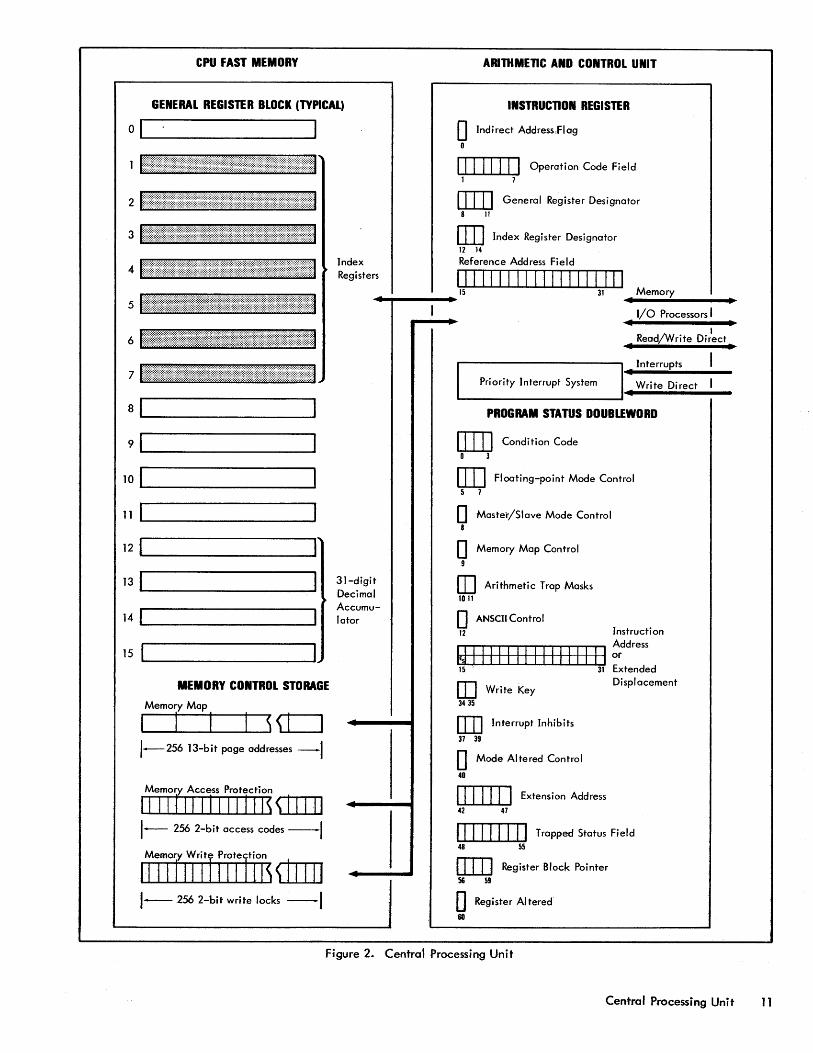
CENTRAL PROCESSING UNIT
This section describes the organization and operation of the SIGMA 9 central processing unit in terms of instruction and data formats, information processing, and program control. Basically, a SIGMA 9 CPU consists of two or more fast memories and an arithmetic and control unit as illustrated in Figure 2.
GENERAL REGISTERS
An integrated-circuit memory, consisting of sixteen 32-bit general-purpose registers, is used within the SIGMA 9 CPU. These 16 registers of fast memory are referred to as a register block. A SIGMA 9 system may contain up to 4 register blocks. A 4-bit control field (called the register block pointer) in the Program Status Doubleword (PSD) selects the block currently available to a program. The 16 general registers selected by the register block pointer are referred to as the current register block. The register block pointer can be changed when the computer is in the master or· master-protected mode.
Each general register in the current register block is identified by a 4-bit code in the range 0000 through 1111 (0 through 15 in decimal, or X'D' through X'F' in hexadecimal notation). Any general register may be used as a fixed-point accumulator, floating-point accumulator, temporary data storage location, or to contain control information such as a data address, count, pointer, etc. General registers 1 through 7 may be used as index registers, and regi sters 12 through 15 may be used as a dec imal accumulator capable of containing a decimal number of 31 digits plus sign. Registers 12 through 15 are always used when a decimal instruction is executed.
MEMORY CONTROL STORAGE
The CPU has three high-speed integrated-circuit memories for storage of a memory map, memory access protection codes associated with the memory map, and memory writeprotection codes. The contents of these memories can only be changed when the computer is in the master or masterprotected mode.
Memory Map. Two terms are essential to a proper understanding of the memory mapping concept: virtual address and actual address.
A virtual address is a value pertaining to the logical space used by a machine-level program, and which designates the location of an instruction, the location of an element of data, or the location of a data address (indirect address). It may also be an explicit quantity. Normally, virtual addresses are derived from programmer-supplied labels through an assembly (or compilation) process followed by a loading process. Virtual addresses may also be computed during a program's execution. Thus, virtual addresses include all instruction addresses, data addresses, indirect addresses, and addresses used as counts within a stored program, as well as those addresses computed by the program.
An actual address is the address a processor sends to the memory unit (memory address register) to access a specific memory location for storage or retrievQI of information. Thus, actual addresses are fixed and dependent on the wired-in hardware. (See "Main Memory" for furtherdetails.)
The memory map feature provides for dynamic program relocation into discontinuous segments of memory. When the memory map is in effect, any program may be segmented .into an integral number of 512-word pages and distributed throughout memory in whatever pages of space are avai lable. Thus the memory map transforms virtual addresses, as seen by the individual program, into actual addresses, as seen by the memory system.
When the memory map is not in effect, as determined by the memory map control bit in the program status doubleword, all virtual address values above 15 are used by the memory as actual addresses. Virtual addresses in the range o through 15 are always used by the CPU as general register addresses rather than as memory addresses. Thus, for example, if an instruction uses a virtual address of 5 as the address where a result is to be stored, the result is stored in general register 5 in the current register block instead of in memory location 5.
When the computer is operating with memory map, virtual addresses in the range 0 through 15 are still used as general register addre~ses. However, all virtual addresses above 15 are transformed into actual addresses, by replacing the highorder eight bits of the virtual address with a value obtained from the memory map. (The memory map replacement process is described in the section "Memory Address Control". )
SIGMA 9 System Organization 9
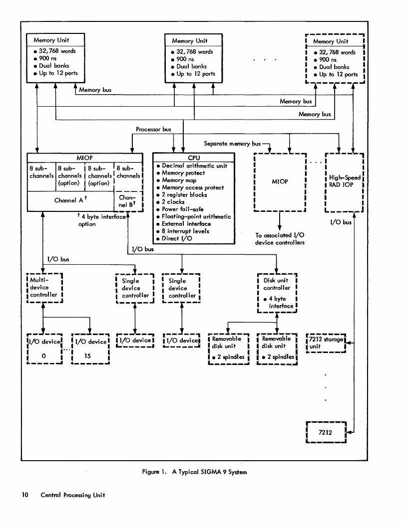
Memory Unit
• 32,768 words .900 ns • Dual banks • Up to 12 ports
t Memory bus
Memory Unit
• 32,768 words • 900 ns • Dual banks • Up to 12 ports
Processor bus
r---------, I Memory Unit I
: • 32, 768 words ~ 1.900ns I : • Dual banks : I • Up to 12 ports • L ____ I"- __ "..~
I~ j ~
Memory bus
Memory bus
Separate memory bus 3. ,~ ,
~-""''''''-C-PU----'''' .- -~- ... ~-, r--- -----, MIOP
8 sub- 8 sub- ~ 8 sub- I 8 subchannels channels channels I channels
(option) (option) ~ ~ ____ ~ ______ -L ______ ~I-_~ __
Channel At Channel BIt
-t4 byte interfacej~
I/O bus r
.-- i.---l I Multi- I ~ device I i controller I i __ ... __ J
I~
option
'. l
r'- --""'! ~....-J~-.
1./0 device; i I/O device I •...• I __ ~_J ! __ 1:. __ ..
I/O bus
__ ,--1 __ , : Single I I device I
l~:'Itr:I:J
..-- ---. • I/O devi ce I L..: _____ "
• Decimal arithmetic unit • Memory protect • Memory map • Memory access protect • 2 register blocks • 2 clocks • Power fa ii-safe • Floating-point arithmetic • External interface • 8 interrupt levels • Direct I/O
, .--------. I, Single I
d • I I eVlce I
1. ~C:ltro~:!
1-- --.,
!Y3_d=.v:j .. __ .i .. _ ....
I Removable • disk unit I
. • 2 spindles L ___ -=---:.1
Figure 1. A Typical SIGMA 9 System
10 Central Processing Unit
I ... I I • I I
• I ! • I High-Speed I I RAD lOP
•• • i I • I I •
MIOP
... ---r---- J L __ --:_J + I/O bus
To associated I/O device controllers
•• r--- - --=---, I Disk unit I • control I er I I I • • 4 byte I I interface. L_-X-_.J .. ----- ---J • Removable
disk unit
l~~
7212 14-
CPU FAST MEMORY
GENERAL REGISTER BLOCK (TYPICAL)
o~I ______________ ~ 1 ItI1flI1Il1IltII1Il1l1lll~~ll:1:l~lfIl1l1l1ll1~\lMII1lll\Ill\~\llIIItItl~lll~~1
2 IIII1l\ll~\~lIItJJIl\tl1l1~lllIl1l1JIlI1lII1IllIl1lI11I1Il1IIIlIIli
3 [llllI!I1JIIljlIjJ~jItJlj!j!lIlI1l:lfjIIIIl:Il:l:IIl:IIl\l\i\:lI:\:\:I] Index Registers
ARITHMETIC AND CONTROL UNIT
INSTRUCTION REGISTER
o Indirect Address,Flag o
III 1111 I Operation Code Field 1 7
OJ]] General Register Designator 8 11
[IIJ Index Register Designator 12 14
Reference Address Field
I1111111111I11111111 15 31
4 [111~111\\1\1~111\::1!11:11111I1IIfl::l:::::\11\11111:11!111\I:I11l1111IiI1l11I1l1ll\111111\lI1\11\\11Il:I1\i1i11
5 Ij11l1I\lliljjj\~jjilllj\jjjjjljjjjjjjj!j1\\\\j\\jl~11\~\~11111111~1111ijlljjl1jjjl1Ijlll111j\11\111\jlilIj11:11I\11\\1\1\i\111il1il
6 Ij1jllll11\\11Hl1~j~11\jl1\\i1i11I1!!ll!I\ljl\~ll1illIjllll111I1Irrl\!lrrljll\iI\!1!1~1!lIIljr:1
7 l!ljl~l~lll~l~lllII1!lIll1l~l\rlI1l1Jtl1l1l~llllIl1l1lllll~ll!llIll1lI~IIJl1ll1IIllIllI~L
~.,..---~ Memory
•
8~1 ______________ ~ 91~ ______________ ~ 10~1 ______________ ~ 11 ~I ________________ ~
121~ ________________ __
131~ ________________ ~ 14LI __________________ ~
15 ~------------________ IJ
MEMORY CONTROL STORAGE
Memory Map
J-256 13-bit page addresses -J
Memory Access Protection
II I I J II I I I 1/ 111 $ ~"'-+-I""""II""""'II 1-- 256 2-bit access codes --I Memory Write Protection
111111111 fIll I IS illIIJ 1- 256 2-bit write locks --I
31-digit Decimal Accumulator
II 0 Processors I • I
I Read/Write Direct
• I
I~----------------tl Interrupts •
Priority Interrupt System I Write Direct I
PROGRAM STATUS DOUBLEWORD
[ill Condition Code o 3
ITO Floating-point Mode Control 5 7
o Master/Slave Mode Control 8
o Memory Map Control 9
OJ Arithmetic Trap Masks 1011 o ANSell Control 12 Instruction
................ .,.............-................. ..,....,...,.....,-.-.,....., Address
Id 1111 I II II 1111 I I I or 15 . 31 Extended
OJ Write Key 3435
ITJJ Interrupt Inhibits 37 39 o Mode Altered Control
40
III III I Extension Address 42 47
Displacement
IIIII1III Trapped Status Field 48 55
o:IIJ Register Block Pointer 56 59 o Register AI tered GO
I
Figure 2. Central Processing Unit
Central Processing Unit 11
Memory Access Protection. When the computer is operating in the slave or master-protected mode with the memory map, the access-protection codes determine whether or not the program may access instructions from, read from, or write .into specific pages of the virtual address continuum (virtual memory). If the slave or master-protected mode program attempts to access a page of virtual memory that is so protected, a trap occurs. (The access-protection codes are described in the section" Memory Address Control". )
Memory Write Protection. The memory write-protection feature operates independently of the memory map and access protection. The memory write-protection feature includes the necessary integrated-circuit memory to provide 256 2-bit memory write locks. These locks operate in conjunction with a 2-bit field, called the write key, in the program status doubleword. The locks and the keydetermine whether any program may alter any word located within the first 128K words (256 pages) of main memory. The write key can be changed when the computer is in the master or masterprotected mode. (The functions of the locks and key are described in the section" Memory Address Control". )
COMPUTER MODES
A SIGMA 9 computer operates in either master, slave, or master-protected mode. The mode of operation is deter-' mined by three control bits in the program status doubleword. (See "Program Status Doubleword".)
MASTER MODE
In this mode, the CPU can perform all of its control func'tions and can modify any part of the system. The only restrictions placed upon the CPUls operation in this mode is that imposed by the wri te locks on protected pages of memory. The Mode Altered control bit (PSD bit position 40) must also be zero for the computer to operate in a SIGMA 7-compatible master mode. It is assumed that there is a resident operating system (operating in the master mode) that controls and supports the operation of other programs (which may be in the master, slave, or masterprotected mode).
'SLAVE MODE
The slave mode of operation is the problem-solving mode of the computer. In this mode, access protection codes applt to the slave mode program if mapping is in effect, and all IIprivileged li operations are prohibited. Privileged opera-
. tions are those relating to input/output and to changes in the basic control state of the computer. AII:privileged operations are performed in the master or master-protected mode by a group of privileged instructions. Any attempt by a program to execute a privileged instruction while the computer is in the slave mode results in a trap. The mcister/ ·slave mode control bit can be changed when the computer is in the master or master-protected mode. However, a
'slave mode program can gain direct access to certain executive program operations by means of call instructions
12 Central·Processing Unit
without requi ring executive program intervention. The operations avai lable through call instructions are estabI ished by the resident operating system.
MASTER-PROTECTED MODE
The master-protected mode of operation is a modification of the master mode designed to provide additional protection for programs that operate in the master mode. The masterprotected mode can only occur when the CPU is operating in the master mode with the memory mop in effect. In this mode, a trap will occur to the memory protection violation trap (Homespace location X1401
, with CC4 = 1), as it does in all mapped slave programs, if a program makes a reference to a virtual page to which access is prohibited by the current setting of the access protection codes.
INFORMAnON FORMAT
Nomenclature associated with digital information within the SIGMA 9 computer system is based on functional and/or physical attributes. A "word" of digital· information may be either an instruction word or a data word.
The basic element of SIGMA 9 information is a 32-bit word, in which the bit positions are numbered from 0 through 31, as follows:
I : w~rd : I 0.1 2 314 5 6 78 9 10 1111213141516171819120 2122232425262)'12829 3031
A SIGMA 9 word can be divided into two halfwords (16 bits each) in which the bit positions are numbered from 0 through 15, as follows:
A SIGMA 9 word can also be divided into four bytes (8 bits each) in which the bit positions are numbered from 0 through 7, as follows:
Byte 1 Byte 2 2 3 4 5 2 3 4 5
Two S'IGMA 9 words can be combined to form a doubleword (64 bits) in whi ch the bit positions are numbered from 0 through 63, as follows:
: Most Signif~~ant word: I 1 2 3 14 5 6 7 8 9 10 11 h2 13 14 15 16 17 18 19120 21 22 23 24 25 26 27128 29 30 31
I .: Least Significant word: I 3233 3435136 37 38 39 40 41 4243144 45 46 47 48 49 50 5ti52 53 54 55 56 57 58 59160 61 62 63
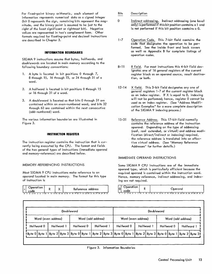
For fixed-point binary arithmetic, each element of information represents numerical data as a signed integer (bit 0 represents the sign, remaining bits represent the magnitude, and the'binary point is assumed to be just to the right of the I east significant or rightmost bit). Negative values are represented in two's complement form. Other formats required for floating-point and decimal instructions are described in Chapter 3.
INfORMATION BOUNDARIES
SIGMA 9 instructions assume that bytes, halfwords, and doublewords are located in main memory according to the following boundary conventions:
1. A byte is located in bit positions 0 through 7, 8 through 15, 16 through 23, or 24 through 31 of a word.
2. A halfword is located in bit positions 0 through 15 or 16 through 31 of a word.
3. A doubleword is located so that bits 0 through 31 are' contained within an even-numbered word, and bits 32 through 63 are contained within the next consecutive (odd-numbered) word.
The various information boundaries are ill ustrated in Figure 3.
INSTRUCTION REGISTER
The instruction register contains the instruction that is currently being executed by the CPU. The format and fields of the two general types of instructions (immediate operand and memory-reference) are described below.
MEMORY-REFERENCING INSTRUCTIONS
Most SIGMA 9 CPU instructions make reference to an operand located in main memory. The format for this type of instruction i-s
i Doubleword I
I
I Word {even address} Word (odd address) ! i Halfword 0 Halfword 1 Halfword 0 Halfword 1 I
: Byte 0 I Byte 1 Byte 21 Byte 3 Byte 0 I Byte 1 Byte 21 Byte 3
Bits
o
1-7
8-11
Description
Indirect addressing. Indirect addressing (one level only) is performed if this bit position contains a 1 and is not performed if this bit position contains a O.
Operation Code. This 7-bit field contains the code that designates the operation to be performed. See the inside front and back covers as well as Appendix B for complete listings of operation codes.
R field. For most instructions this 4-bit field designates one of 16 general registers of the current register block as an operand source, result destination, or both.
12-14 X field. This 3-bit field designates anyone of general registers 1-7 of the current register block as an index register. If X is equal to 0, indexing will"not be performed; hence, register 0 cannot be used as an index register. (See II Address Modification Examples" for a more complete description of the SIGMA 9 indexing process.)
15-31 Reference Address. This 17-bit field normally contains the reference address of the instruction operand. Depending on the type of addressing (real, real extended, or virtual) and address mod ification (direct/indirect or indexing) required, the reference address is translated into an effective virtual address. (See "Memory Reference Addresses" for further details.)
IMMEDIATE OPERAND INSTRUCTIONS
Some SIGMA 9 CPU instructions are of the immediate operand type, which is particularly efficient because the required operand is contained within the instruction word. Hence, memory reference, indirect addressing, and indexing are not required.
Doubleword i I • .
Word {even address} Word (odd address) I I
Halfword 0 Halfword 1 Halfword 0 Halfword 1 i I
Byte oj Byte 1 Byte 2 J Byte 3 Byte 01 Byte 1 Byte 21 Byte 3 j
Figure 3. Information Boundaries
Central Processing Unit 13
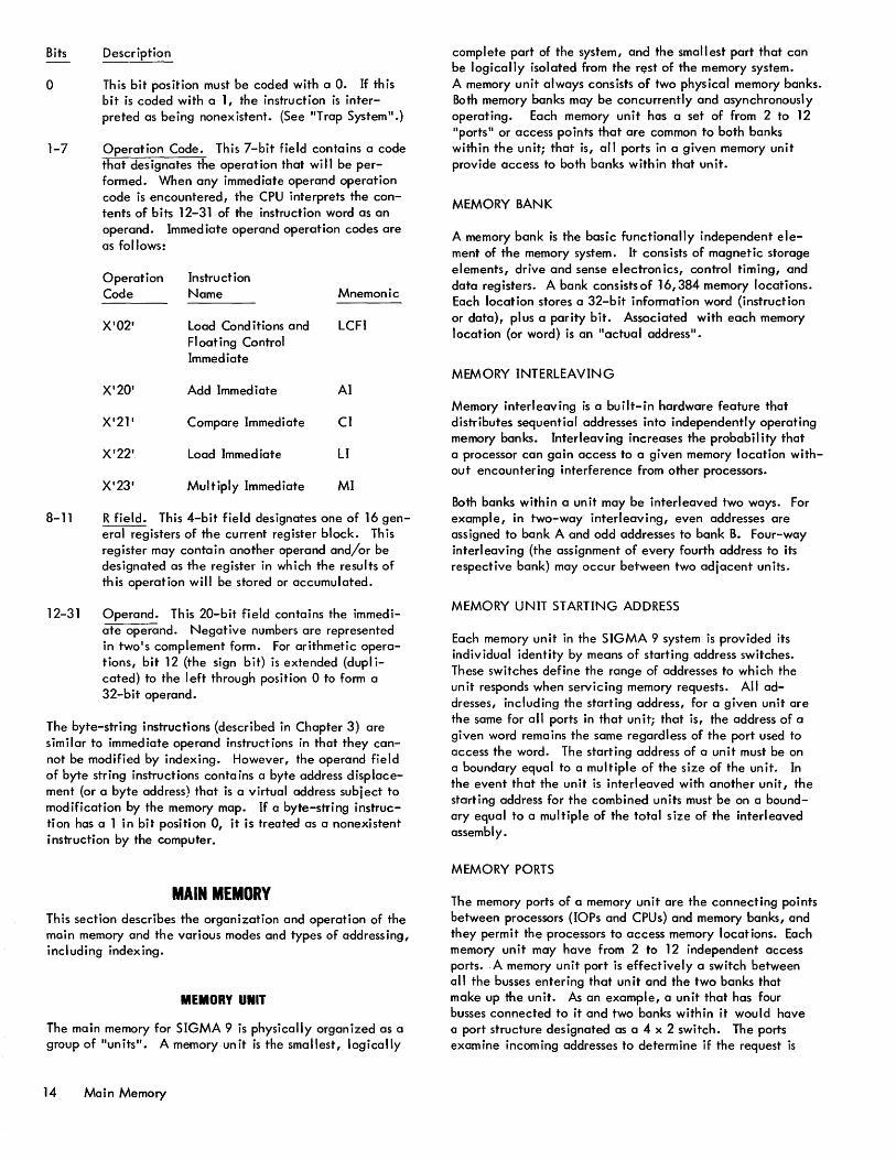
Bits
o
1-7
8-11
12-31
Description
This bit position must be coded with a O. If this bit is coded with a 1, the instruction is interpreted as be ing nonex istent. (See "Trap System".)
Operation Code. This 7-bit field contains a code that designates the operation that will be performed. When any immediate operand operation code is encountered, the CPU interprets the contents of bits 12-31 of the instruction word as an operand. Immediate operand operation codes are as follows:
Operation Code
X'02'
X'20'
X'21'
X'22'
X'23'
Instruction Name
Load Cond itions and Floating Control Immediate
Add Immediate
Compare Immediate
Load Immed iate
Multiply Immediate
Mnemonic
LCFI
AI
CI
LI
MI
R field. This 4-bit field designates one of 16 general registers of the current register block. This register may contain another operand and/or be designated as the register in which the results of th is operation will be stored or accumulated.
Operand. This 20-bit field contains the immediate operand. Negative numbers are represented in two's complement form. For arithmetic operations, bit 12 (the sign bit) is extended (dupl icated) to the left through position 0 to form a 32-bit operand.
The byte-string instructions (described in Chapter 3) are similar to immediate operand instructions in that they cannot be modified by indexing. However, the operand field of byte string instructions contains a byte address displacement {or a byte address} that is a virtual address subject to modification by the memory map. If a byte-string instruction has a 1 in bit position 0, it is treated as a nonexistent instruction by the computer.
MAIN MEMORY This section describes the organization and operation of the main memory and the various modes and types of addressing, including indexing.
MEMORY UNIT
The main memory for SIGMA 9 is physically organized as a group of "units". A memory un it is the smallest, logically
14 Main Memory
complete part of the system, and the smallest part that can be logically isolated from the r~st of the memory system. A memory unit always consists of two physical memory banks. Both memory banks may be concurrently and asynchronously operating. Each memory unit has a set of from 2 to 12 "ports" or access points that are common to both banks within the unit; that is, all ports in a given memory unit provide access to both banks within that unit.
MEMORY BANK
A memory bank is the basic functionally independent element of the memory system. It consists of magnetic storage elements, drive and sense electron ics, control timing, and data registers. A bank consistsof 16,384 memory locations. Each location stores a 32-bit information word (instruction or data), plus a parity bit. Associated with each memory location (or word) is an "actual address".
MEMORY INTERLEAVING
Memory interleaving is a built-in hardware feature that distributes sequential addresses into independently operating memory banks. Interleaving increases the probability that a processor can gain access to a given memory location without encountering interference from other processors.
Both banks within a unit may be interleaved two ways. For example, in two-way interleaving, even addresses are ass igned to bank A and odd addresses to bank B. Four-way interleaving (the assignment of every fourth address to its respective bank) may occur between two adjacent units.
MEMORY UNIT STARTING ADDRESS
Each memory unit in the SIGMA 9 system is provided its individual identity by means of starting address switches. These switches define the range of addresses to which the unit responds when servicing memory requests. All addresses, including the starting address, for a given unit are the same for all ports in that un it; that is, the address of a given word remains the same regardless of the port used to access the word. The starting address of a unit must be on a boundary equal to a multiple of the size of the unit. In the event that the unit is interleaved with another unit, the starting address for the combined units must be on a boundary equal to a multiple of the total size of the interleaved assembly.
MEMORY PORTS
The memory ports of a memory unit are the connecting points between processors (lOPs and CPUs) and memory banks, and they permit the processors to access memory locations. Each memory un it may have from 2 to 12 independent access ports .. A memory unit port is effectively a switch between all the busses entering that un it and the two banks that make up the unit. As an example, a unit that has four busses connected to it and two banks within it would have a port structure designated as a 4 x 2 switch. The ports examine incoming addresses to determine if the request is
for a bank within the memory unit. They also determine the priority of memory requests received simultaneously.
The minimum number of ports for a SIGMA 9 system is two, one for the CPU and one for an lOP. The number of ports may be expanded, in increments of one, to a maximum of 12.
PORT PRIORITY
The multiport structure and the dual-bank memory (within each unit) allow two simultaneous requests for memory to be processed immed iately, providing that the requests are rece ived on different ports, for different banks, and ne ither bank is busy. If a requested bank i s busy, or if simultaneous requests are received for the same bank, the memory port logic selects the highest priority request first.
Normally, all ports in a memory unit operate on a priority basis, with port numb.er 0 having the highest priority and port number IIn ll having the lowest. In general, CPUs are connected to the higher priority ports and lOPs are connected to the lower priority ports. If simultaneous requests are rece ived for a single bank on port 2 and port 4, port 2 has access to the memory bank first.
In addition to the normal priority that prevails among the ports, as described above, each port has a high priority level. A processor usually requests the normal priority level; however, under certain conditions a processor may request high priority access to a given port (e. g., an lOP wi II wait wi th a low priority memory request unti I ha If of its avai lable buffering has been fi lied on input or emptied on output; it then requests a high priority memory reference). If one port receives a high priority request, that portis priority is then higher than the normal priority of all other ports. If more than one port is on a high priority at the same time, the normal sequence of priority wi II prevai I among those ports on high priority.
CPU PORT
When the memory is quiescent, the port selection logic is set to a condition that automatically selects port o. The el imination- of switching time (to select a port) results in a timing preferential for the processor connected to port O. This is particularly advantageous for a monoprocessing system where the CPU is normally connected to port 0 of each memory u~it.
VIRTUAL AND REAL MEMORY
Virtual memory is logical memory as seen by an individual program. The maximum size of virtual memory is 128K (131,072) words. A virtual memory for a given program may consist of up to 256 pages of 512 words each distributed throughout the available pages of real memory.
Real memory corresponds to the physical memory, and its size is equal to the total number of words contained within
90 17 33C-1(4/74)
all memory units. The size of real memory ranges from a minimum of 128K words to 512K words. The 512K maximum size limitation is' physical (i. e. , based on maximum cable length considerations) rather than lo~cal. Real memory addressing space is over 4 million (22 ) words.
HOMESPACE
In a SIGMA 9 mul tiprocessing system, all processors address memory in the same manner. However, since, the CPUs do not share the same interrupt or trap systems, it is necessary to provide private storage for each CPU to contain its trap and interrupt locations, I/O communication locations, and general registers. Th is private storage is called Homespace.
Determining the location of Homespace for a CPU is I ike second-level mapping. Each CPU contains a Homespace bias. The Homespace bias is the actual address of a 16K region of the first 1 million words of main memory, of which the first 1,024 words is Homespace. After an effective real address is generated by a CPU by whatever method, and just before it is sent to memory, the most significant 12 bits are tested. If these bits are all equal to zero, then a 6-bit Homespace bias plus two leading zeros are inserted in place of the most significant eight of these bits. This means that any time a CPU makes a reference to the first 1,024 words of real memory that reference may be relocated by means of the Homespace bias.
The 6-bit Homespace bias is supplied by a set of six switches in a SIGMA 9 CPU. They can be changed manually to move the Homespace region from one area to another within the 64 possible areas.
When multiprocessors are used, a given CPU may reference the Homespace region of other processors by using the normal memory addresses for that region. The only exception to th is is that the Homespace of a CPU that is set at real memory location zero, cannot be referenced by any other CPU. However, the CPU that has its Homespace at real location zero may reference the Homespace of all other CPUs.
Each Homespace region contains all the trap locations, interrupt locations, and lOP communication locations for a given CPU (see Table 4). These implicitly assigned memory locations plus the 16 locations that are reserved for the general registers, occupy the first 320 locations of Homespace. The remaining words in the Homespace region can be used as private, independent storage by the CPU.
MEMORY REFERENCE ADDRESS
Homespace memory locationsO through 15 are not normally accessible to the programmer because their memory addresses are reserved as register designators for II reg ister-to-register ll
operations. However, an instruction can treat any register of the current register block as if it were a location in main memory. Furthermore, the register block can be used to hold an instruction (or a series of up to 16 instructions) for execution just as if the instruction (or instructions) were
Main Memory 15
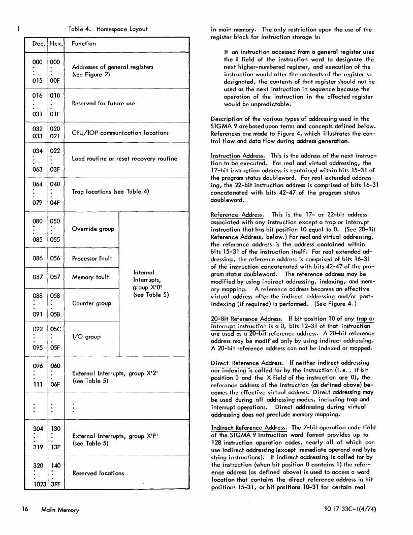
Table 4. Homespace Layout
Dec. Hex. Function
000 000 Addresses of general.registers (see Figure 2)
015 OOF
016 010 Reserved for future use
· 031 01F
032 020 CPU/lOP communication locations
033 021
034 022 · load routi ne or reset recovery routi ne ·
063 03F
064 040 · Trap locations (see Table 4)
079 04F
080 050 · Override group · 085 055
086 056 Processor fau I t
087 057 Memory fau I t Internal Interrupts, group X'O'
088 058 (see Table 5) · Counter group ·
091 05B
092 05C · I/O group ·
095 05F
096 060
· · Externa I Interrupts, group X'2' · · (see Table 5) 111 06F
· · · · ·
304 130 External Interrupts, group X'P
· (see Tab Ie 5) 319 13F
320 140 · · Reserved locations · · · 1023 3FF
16 Mai n Memory
in main memory. The only restriction upon the use of the register block for instruction storage is:
If an instruction accessed from a general register uses the R field of the instruction word to designate the next higher-numbered register, and execution of the instruction would alter the contents of the register so designated, the contents of that register should not be used as the next instruction in sequence because the operation of the instruction in the affected register would be unpredictable.
Description of the various types of addressing used in the SIGMA 9 are based upon terms and concepts defined below. References are made to Figure 4, which illustrates the control flow and data flow during address generation.
Instruction Address. This is the address of the next instruction to be executed., For real and virtual addressing, the 17-bit instruction address is contained within bits 15-31 of the program status doubleword. For real extended addressing, the 22-bit instruction address is comprised of bits 16-31 concatenated with bits 42-47 of the program status doubleword.
Reference Address. This is the 17- or 22-bit address associated with any instruction except a trap or interrupt instruction that has bit position 10 equal to O. (See 20-Bit Reference Address, below.) For real and virtual addressing, the reference address is the address contained within bits 15-31 of the instruction itself. For real extended addressing, the reference address is comprised of bits 16-31 of the instruction concatenated with bits 42-47 of the program status doubleword. The reference address may be modified by using indirect addressing, indexing, and memory mapping. A reference address becomes an effective virtual address after the indirect addressing and/or postindexing (if required) is performed. (See Figure 4. )
20-Bit Reference Address. If bit position 10 of any trap or interrupt instruction is a 0, bits 12-31 of that instruction are used as a 20-bit reference address. A 20-bit reference address may be modified only by using indirect addressing. A 20-bit reference address can not be indexed or mapped.
Direct Reference Address. If neither indirect addressing nor indexing is called for by the instruction (i. e., if bit position 0 and the X field of the instruction are 0), the reference address of the instruction (as defined above) becomes the effective virtual address. Direct addressing may be used during all addressing modes, including trap and interrupt operations. Direct addressing during virtual addressing does not preclude memory mapping.
Indirect Reference Address. The 7-bit operation code field of the SIGMA 9 instruction word format provides up to 128 instruction operation codes, nearly all of which can use indirect addressing {except immediate operand and byte string instructions}. If indirect addressing is called for by the instruction (when bit position 0 contains 1) the reference address (as defined above) is used to access a word location that contains the direct reference address in bit positions 15-31, or bit positions 10-31 for certain real
90 17 33C-1(4/74)
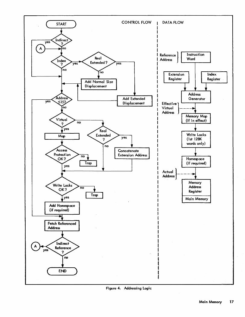
Add Homespace (if required)
CONTROL FLOW
Displacement
yes
no
Figure 4. Addressing logic
I
J i I i I I
!
DATA FLOW
Reference} Address
Instruction Word
Address
Write Locks {lst 128K words only}
Index Register
Actual },_"'-__ Address, ...-_.-...1 __ ---,
Memory Address Register
Main Memory
Main Memory 17
extended addressing operations. The indirect addressing operation is limited to one level. Indirect addressing does not proceed to further levels, regardless of the contents of the word location pointed to by the reference address field of the instruction. Indirect addressing occurs before indexing; that is, the 17-bit reference address field of the instruction is used to obtain a word, and the 17 or 22 loworder bits of the word thus obtained effectively replace the initial reference address field; then, indexing is carried out according to the operation code of the instruction. (See JI Address Modification Examples".)
Index Reference Address. If indexing is oalled for by the instruction '(0 nonzero value in bit positions 12-14 of the instruction), the direct or indirect reference address is modified by addition of the displacement value in the general register (index) called for by the instruction (after scaling the displacement according to the instruction type). This final reference address value (after indirect addressing, indexing, or both) is defined as the effective virtual address of the instruction. Indexing afterindirecf addressing is called postindexing. (See "Address Modification Examples" for further details.)
Displacements. Displacements are the 16- to 24-bit values used in index registers and by byte string instructions to generate effective addresses of the appropriate size (byte, halfword, word, or doubleword).
Register Address. If any instruction produces a virtual address that is a memory reference (i.e., a direct, indirect, or indexed reference .address) in the range 0 through 15, the CPU does not attempt to read from or write into main memory. Instead, the four low-order bits of the reference address are used as a general register address, and the general register (of the current register block) corresponding to this address is used as the operand location or result destination. Thus, the instruction can use any register in the current register block as the source of an operand, the location of a direct address, or the destination of a result. Such usage is referred to' as a "register-to-register" operation.
Actual Address. An actual address is the address value actually used by the CPU to access main memory via the memory address register (see Figure 4). If the effective virtual address is X10I - X1P, one of the general registers is addressed. If the computer is operating in virtual addressing mode, all virtual addresses above 15 are transformed (usually into addresses in a different memory page) by the memory map, and these then become actual addresses. However, if the computer is operating in either real or real extended mode, no transformation via the memory map takes place. All actual addresses are 21, 22, 23, or 24 bits, as required to address a doubleword, word, halfword, or byte.
effective Address. The effective address is defined as the final virtual address computed for an instruction (output ffom the address generator in Figure 4). The effective address is usually used as the virtual address of on operand location or result destination. However, some instructions
18 Main Memory
do not use the effective address as a location reference; instead, the effective address is used to control the operation of the instruction (as in a shift instruction), to designate the address of an input/output device (as in an input/ output instruction), or to designate a specific element of the system (as in a READ DIRECT or WRITE DIRECT instruction).
Effective Location. An effective location is defined as the actual location (in main memory or in the current register block) that is to receive the result of a memoryreferenci ng instruction, and is referenced by means of an effective address. Because an effective address may be either an actual address or a virtual address, this definition of an effective location assumes, where applicable, the transformation of a virtual address into an actual address.
Effective Operand. An effective operand is defined as the contents of an actual location (in main memory or in the current register block) that is to be used as an operand by a memory-referencing instruction, and is referred to by means of an effective address. This definition of an effective operand also presupposes the transformation of a virtual address into an actual address.
TYPES OF ADDRESSING
Except for the special type 9faddressing that is performed only by.some interrupt and trap instructions, all addressing within the computer system is real, ~eal extended, or virtual.
REAL ADDRESSING
Real addressing is a type of addressing where a one-to-one relationship prevails between the effective virtual address of each instruction and the actual address used to access' main memory. Characteristics of real ad~ressing are:
1. Each reference address is a 17-bit word address.
2. The reference address may be direct or indirect, with or wi thout posti ndexi ng.
3. Displacements associated with index,ing are automatically al igned, as required, for doubleword, word, halfword, or byte operations; and' the effective virtual address is either a 16-bit doubleword address, 17-bit word address, 18-bit halfword address, or a 19-bit byte address.
4. Memory mapping and memory access protection are never invoked.
5. Memory write protection is automatically invoked be- : cause the reference word will ol:Ways be located within the first 128K words of real memory. Memory locations outside the first 128K words of real memory are not ac"; cessible with real addressing.
6. Leading zeros are automatically appended to the effective address to generate an actual word address as required by the main memory.
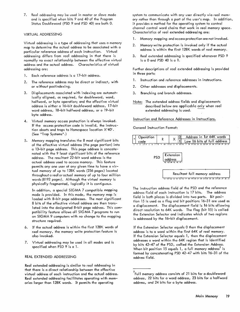
7. Real addressing may be used in master or slave mode and is specified when bits 9 and 40 of the Program Status Doubl eword (PSD 9 and PSD 40) are both O.
VIRTUAL ADDRESSING
Virtual addressing is a type of addressing that uses a memory map to determine the actual address to be associated with a particular reference address of each instruction. Virtual addressing differs from real addressing in that there is normally no exact relationship between the effective virtual address and the actual address. Characteristics of virtual addressing are:
1. Each reference address is a 17-bit address.
2. The reference address may be direct or indirect, with or without postindexing.
3. Displacements associated with indexing are automatically aligned, as required, for doubleword, word, halfword, or byte operation; and the effective virtual address is either a 16-bit doubleword address, 17-bit word address, 18-bit halfword address, or a 19-bit byte address.
4. Virtual memory access protection is always invoked. If the access protection code is invalid, the instruction aborts and traps to Homespace location X'40'. (See "Trap Systems".)
5. Memory mapping translates the 8 most significant bits of the effective virtual address (the page portion) into a 13-bit page address. This page address is concatenated with the 9 least significant bits of the reference address. The resultant 22-bit word address is the actual address used to access memory. This feature permits anyone user at any given time to have a virtual memory of up to 128K words (256 pages) located throughout a real oractual memory of up to four million words (8192 pages). AI though the virtual memory is physically fragmented, logically it is contiguous.
In addition, a special SIGMA 7 compatible mapping mode is provided. In this mode, the memory map is loaded with 8-bit page addresses. The most significant 8 bits of the effective virtual address are then translated into the designated 8-bit page address. This compatibility feature allows all SIGMA 7 programs to run on SIGMA 9 computers with no change to the mapping structure required.
6. If the actual address is within the first 128K words of real memory, the memory write protection feature is also invoked.
7. Virtual addressing may be used in all modes and is specified when PSD 9 is a 1.
REAL EXTENDED ADDRESSING
Real extended addressing is similar to real addressing in that there is a direct relationship between the effective virtual address of each instruction and the actual address. Real extended addressing facilitates operating with memories larger than 128K words. It permits the operating
system to communicate with any user directly via real memory rather than through a part of the user's map. In addition, it provides a method for the operating system to control channel control word chains that work in real memory space. Characteristics of real extended addressing are:
1. Memory mapping and access protection are not invoked.
2. Memory write protection is invoked only if the actual address is within the first 128K words of real memory.
3. Real extended addressing is specified whenever PSD 9 is a 0 and PSD 40 is a 1.
Further descriptions of real extended addressing is provided in three parts:
1. Instruction and reference addresses in instructions.
2. Other addresses and displacements.
3. Branching and branch addresses.
Note: The extended address fields and displacements described below are applicable only when real extended addressing is used. --
Instruction and Reference Addresses in Instructions.
General Instruction Format:
PSD
The instruction address field of the PSD and the reference address field of each instruction is 17 bits. The address field in both places is divided into two parts. Bit position 15 is used as a flag and bit positions 16-31 are used as a displacement. The displacement field is 16 bits allowing direct resolution to 64K words. The flag (bit 15) is call ed the Extension Selector and indicates which of two regions is addressed by the 16-bit displacement.
If the Extension Selector equals 0 then the displacement address is to a word within the first 64K of real memory. If the Extension Selector equals 1, then the displacement addresses a word within the 64K region that is identified by bits 42-47 of the PSD, called the Extension Address. When bit position 15 equals 1, a full memory addresst is formed by concatenating PSD 42-47 with bits 16-31 of the address field.
tFull memory address consists of 21 bits for a doubleword address, 22 bits for a word address, 23 bits for a halfword address, and 24 bits for a byte address.
Main Memory 19
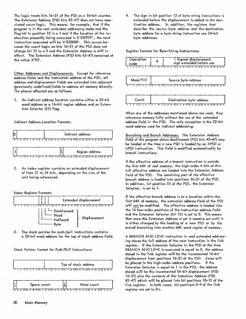
The logic treats bits 16-31 of the PSD as a 16-bit counter. The Extension Address (PSD bits 42-47) does not have asso·· ciated count logic. This means, for example, that if the program is in the real extended addressing mode and the flag bit in position 15 is a 1 and if the location of the instruction presently being executed is X'02FFFF' I the next instruction executed will be X'020000'. This occurs because the count logic on bits 16-31 of the PSD does not change bit 15 to a 0 and the Extension Address is still in effect. The Extension Address (PSD bits 42-47) remained at the value X'021.
Other Addresses and Displacements. Except for reference address fields and the instruction address of the PSD, all address and displacement fields are extended into adjacent (previously undefined) fields to address all memory directly. The places affected are as follows:
1. An indirect address location contains either a 22-bit word address or a 16-bit region address and an Extension Selector (ES) flag.
Indirect Address Location Formats:
\0 I : I : Indirect addre~S I o 1 2 3 14 5 6 7 8 9 10 11 112 13 14 15 16 17 18 19120 21 22 23 24 25 26 27128 29 30 31
2. An index register contains an extended displacement of from 21 to 24 bits, depending on the size of the unit being referenced.
Index Register Formats:
E~ Doubleword }
VVord • Halfword DIsplacement
Byte
3. The stack pointer for push/pull instructions contains a 22-bit word address for the top of stack address field.
Stack Pointer Format for Push/purr Instructions:
20 Main Memory
4. The sign in bit position 12 of byte string instructions is extended before the displacement is added to the destination address. In addition, the registers that describe the source byte address and the destination byte address for a byte string instruction are 24-bit byte addresses.
Register Formats for Byte-String Instructions:
When any of the addresses mentioned above are used, they reference memory fully without the use of the extended address field in the PSD. The only exception is the 22-bit word address used for indirect addressing.
Branch i ng and Branch Addresses. The Extension Address field of the program status doubleword (PSD bits 42-47) may be loaded at the time a new PSD is loaded by an XPSD or LPSD instruction. This field is modified automatically by branch instructions.
If the effective address of a branch instruction is outside the first 64K of real memory, the high-order 6 bits of this full effective address are loaded into the Extension Address field of the PSD. The remaining part of the effective branch address is loaded into positions 16-31 of the PSD. In addition, bit position 15 of the PSD, the Extension Sel ector, is set to 1.
If the effective branch address is to a location within the first 64K of memory, the extension address field of the PSD will not be modified. The effective address is loaded into the 16 low-order positions of the instruction address field and the Extension Selector (bit 15) is set to O. This means that once the Extension Address is set it remains set until it is either changed by the loading of a new PSD or by the actual branching into another 64K word region of memory.
A BRANCH AND LINK instruction in real extended addressing stores the full address of the next instruction in the link register. If the Extension Selector in the PSD at the time BRANCH AND LINK is executed is equal to 0, the address stored in the link register will be the incremented 16-bit displacement from positions 16-31 of the PSD. Zeros will be placed in the high-order address positions. If the Extension Selector is equal to 1 in the PSD, the address stored will be the incremented 16-bit displacement (PSD 16-31) plus the contents of the Extension Address (PSD 42-47) which will be placed into bit positions 10-15 of the I ink register. In both cases, bit positions 0-9 of the I ink register are set to O's.
INTERRUPT AND TRAP ENTRY ADDRESSING
An interrupt instruction is defined as one that is in an interrupt location and is executed as the direct result of an interrupt. Both elements of the definition must be satisfied simultaneously for it to be an interrupt instruction. An instruction is not an interrupt instruction even though it may be in an interrupt location if, for example, it is executed as the result of the program branching to the interrupt location under normal program control. Similarly, a trap instruction is defined as one. that is in a trap location and is executed as the direct result of a trap. The only valid interrupt instructions are XPSD, MTW, MTH, and MTB. The only valid trap instruction is XPSD.
Interrupt and Trap Instructi on Format:
The address of the instruction executed as a result of an interrupt or trap depends on bit 10 of the XPSD
If bit 10 of the XPSD in an interrupt or trap location is a 0, a real address is generated independently of the addressing mode specified by the current PSD. If bit 0 (the indirect bit) of the XPSD instruction is a 0, bits 12-31 of the XPSD instruction are used as a 20-bit reference address, which permits direct addressing of the first one mi II ion words of memory. If bit 0 of the XPSD instruction is a 1, indirect addressing is invoked, and bits 12-31 of the XPSD instruction point to a word in memory that contains the reference address in bit positions 10-31. Note that the indirect word must be programmed with bit 0 containing a 0 and bits 10-31 containing the reference address (so called long form). This 22-bit reference address allows addressing a 4 million word memory.
If bit 10 of the XPSD in a trap or interrupt location is a 1, the address will be generated as prescribed by the current PSD (i. e., real, real extended, or virtual addressing).
Any modify and test instruction encountered in an interrupt location uses the 20-bit reference address in the same manner as described above for the XPSD.
Any XPSD, MTW, MTH, orMTB instruction that is executed as a normal instruction, not an interrupt or trap inst~uction, uses the 17-bit reference address in the same manner as any other memory reference instruction. Bit 10 has no effect on the execution of an XPSD instruction that is executed as a normal instruction.
ADDRESS MODlflCAnON EXAMPLES
INDEXING (REAL AND VIRTUAL ADDRESSING)
Figure 5 shows how the indexing operation takes place during real and virtual addressing operations. As the instruction is brought from memory, it is loaded into a 34-bi t instruction register that initia11y contains O's in the two
low-order bit positions (32 and 33). The displacement value from the index register is then aligned with the instruction register (as an integer) according to the addressing type of the instruction; that is, if it is a byte operation, the displacement is I ined up so that its low-order bit is 01 igned with the least significant bit of the 34-bit instruction register. The displacement is shifted one bit to the left of this positi on for a halfword operation, two bits to the left for a word operation, and three bits to the left for a doubleword operation. An addition process then takes place to develop a 19-bit address, which is referred to as the effective address of the instruction. High-order bits of the 32-bit displacement field are ignored in the development of this effective address (i. e., the 15 high-order bits are ignored for word operations, the 25 high-order bits are ignored for shift operations, and the 16 high-order bits are ignored for doubleword operations). However, the displacement value can cause the effective address to be less than the initial reference address within the instruction if the displacement value contains a sufficient number of highorder lis {i. e., if the displacement is a negative integer in twols complement form.
The effective virtual address of an instruction is always a 19-bit byte address value. However, this value is automatically adjusted to the SIGMA 9 information boundary conventions. Thus, for halfword operations, the low-order bit of the effective halfword address is 0; for word operations, the two low-order bits of the effective word address are OIS; and for doubfeword operations, the 3 low-order bits of the effective doubleword address are O's.
If no indexing is used with a byte operation, the effective byte is the first byte (bit positions 0-7) of a word location; if no indexing is used with a haffword operation, the effective halfword is the first halfword (bit positions 0-15) of a word location. A doubleword operation always involves a word at an even-numbered word address and the word at the next sequentia I (odd-numbered) word address. If an oddnumbered word location is specified for a doubleword operation, the low-order bit of the effecti ve address fi e I d (hi t posi ti on 31 ) isautomaticallyforced toO. Thus, an odd-numbered word address desi gnates the same doubl eword as an even-numbered word address, when used for a doubleword operation.
If the addressing mode is real, the 19-bit effective virtual address is concatentated with 5 leading zeros to form a 24-bit actual address. If the addressing mode is virtual, the 8 most significant bits of the 19-bit effective virtual address (SIGMA 7 page address) are transformed into a 13-bit SIGMA 9 page address. The new page address and the 11 least significant bits of the 19-bit effective virtual address are combined to form a 24-bit actual address.
INDEXING (REAL EXTENDED ADDRESSING)
Fi gure 6 ill ustrates that the index ing process for real extended addressing is similar to that performed for real and virtual addressing. The differences are:
1. Bit 15 of the instruction word is not a part of the reference address. It is used as a control flag. If bit 15 is a 1" the contents of the Extension Register(bits 42-47 of the PSD) are concatenated to bits 16-31 of the instruction register to form a 22"'bit reference address.
Main Memory 21
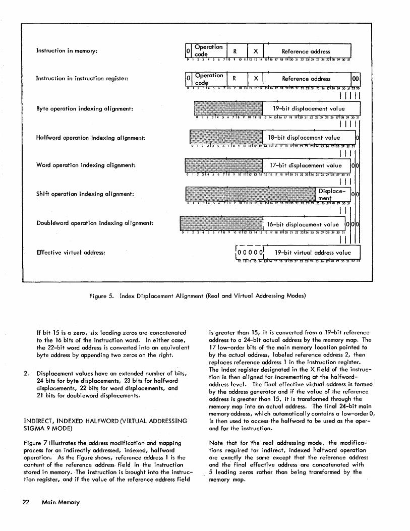
Instruction in memory:
Instruction in instruction register:
IIIII Byte operation indexing alignment:
Halfword operation indexing alignment:
Word operation indexing alignment:
Shift operation indexing alignment:
Doubleword operation indexing alignment:
Effective virtual address:
Figure 5. Index Displacement Alignment (Real and Virtual Addressing Modes)
If bit 15 is a zero, six leading zeros are concatenated to the 16 bits of the instruction word. In either case, the 22-bit word address is converted into an equivalent byte address by appending two zeros on the right.
2. Displacement values have an extended number of bits, 24 bits for byte displacements, 23 bits for halfword displacements, 22 bits for word displacements, and 21 bits for doubleword displacements.
INDIRECT, INDEXED HALFWORD (VIRTUAL ADDRESSING SIGMA 9 MODE)
Figure 7 illustrates the address modification and mapping process for an indirectly addressed, indexed, halfword operation.' As ·the figure shows, reference- address 1 is the content of the reference address field in the instruction stored in memory. The instruction is brought j'nto-the instruction register, and if the value of the reference address field
22 Main Memory
is greater than 15, it is converted from a 19-bit reference address to a 24-bit actual address by the memory map. The 17 low-order bits of the main memory location pointed to by the actual address, labeled reference address 2, then replaces reference address 1 in the instruction register. The Index register designated in the X field of the instruction is then aligned for incrementing at the halfwordaddress level. The final effective vir.tual address is formed by the address generator and if the value of the reference address is greater than 15, it is transformed through the memory map into an actual address. The final 24-bit main memory address, which automatically contains a low-order 0, is then used to access the haHword to be used as the operand for the instruction.
Note that for 'the real addressing mode, the modifications requ ired for i ndi rect, indexed hal fword operation are exactly the same except that the reference address and th~ final effective address are concatenated with 5 leading ze~os rather than being transformed by the memory map.
Instruction in memory:
Informati on used by address generator:
Byte operation indexing alignment:
Halfword operation indexing alignment:
Word operation indexing alignment:
Shift operation indexing alignment:
Bit 15 = 1 Bit 15 = 0
Doubleword operation indexing alignment:
24-bit effective address:
I IIII I 24-bi~ displacement ~alue
I I
Figure 6. Index Displacement Alignment (Real Extended Addressing)
INDIRECT, INDEX HALFWORD (REAL EXTENDED ADDRESSING)
Figure 8 ill ustrates the address modification process for real extended, indirect, indexed addressing.
Bit 15 of the instruction word is used as a control flag. When bit 15 equals 1, the 16-bit reference address of the instruction is concatenated with the 6 bits contained within the Extension Register (PSD 42.:..47). When bit 15 equals 0, the 16-bit reference address of the instruction is concatenated with 6 leading zeros and the contents of the Extension Register are not used nor changed.
The word in memory pointed to by the indirect reference address may be one of three types, differentiated by bit 0 and bi t 15 of the di rect address.
If bit 0 is a 0, bits 10 to 31 are used as the 22-bit direct address. If bit 0 is a 1 and bit 15 is a 0, then bits 16-31 are concatenated with 6 leading zeros to form a 22-bit
direct address. When bit 0 is a 1 and bit 15 is a 1, bits 16-31 are concatenated with the contents of the Extension Register to form a 22-bit direct address.
In either case, the 22-bit direct address is then modified by 23-bit displacement value (halfword alignment of index) to produce a 24-bit effective virtual address that has a 0 in the feast significant position. Since real extended addresses are not subjected to mapping, the final effective address is equivalent to the actual address.
MEMORY ADDRESS CONTROL
In a SIGMA 9 computer, two methods are avaitable for controlling the use of main memory by a program; they are the memory map and the memory lock. The memory map provides for dynamic relocatability of programs and for access protection through inhibitions imposed on slave or master-protected mode programs. The memory lock provides memory write protection for all modes of programs within the first 131,072 words of memory.
Main Memory 23
Instruction in memory:
Instruction in instruction registers:
The 8 high-order bits of the reference address are replaced with 13-bit page address Z from memory map:
Actual address of memory location that contains the di rect address:
,17-bit direct address in memory:
Indirect addressing replaces reference address with direct address:
Halfword operation indexing alignment:
Effective virtual address:
The 8 high-order bits of the effective address are replaced with 13-bit page address N from memory map:
Final memory address, which is the actual address of halfword location containing the effective halfword:
Figure 7. Generation of Actual Memory Addresses, Virtual Addressing (SIGMA 9 Mode)
24 Main Memory
III
til
1111

Initial conditions:
Instruction in instruction register:
Indi rect reference addresses:
PSD
Ie e e e e ei 42 43 4" 4S 46 47
Contents of indirect reference address:
Address used if bit 0 = 0:
Address used if bit 0 = 1 and bit 15 = 0:
Address used if bit 0 = 1 and bit 15 = 1:
Displacement aligned for halfword indexing!
Final effective address:
0123145
If bit 15 = 1 If bit 15 = 0
Figure 8. Generation of Effective Virtual Address, Real Extended Addressing
Main Memory 25
MEMORY MAP AND ACCESS PROTECTION
The SIGMA 9 memory map is physically an array of 256 . registers, each containing 13 bits. The array is stored in the CPU's fast memory. Each register has an 8-bit address and contains a 13-bit actual memory page address code for a specific 512-word page of virtual addresses.
The memory page address codes are ass igned to pages of virtual addresses as follows:
Memory page X Memory page K Memory page N (13 bits) (13 bits) (13 bits)
Virtual 8-bit Virtual a-bit Virtual 8-bit addresses addresses addresses X'10'-X'1FF' X'200'-X'3FF' X'lFEOO'-X'lFFFF' (virtual page 0) (virtual page 1) (virtual page 255)
The most significant a bits of a 17-bit virtual address is considered to be the virtual page number. Just prior to a memory reference, the virtual page num,ber is used as an address of an element of the map. The 13 bits contained within that element are then used in conjunction with the loworder 9 bits of the 17-bit virtual address.
When SIGMA 9 is operating in the SIGMA 7-compatible mode, the map appears identi'col to the SIGMA 7 map. This is occomplished by retaining the SIGMA 7 version of the MOVE TO MEMORY CONTROL (MMC) instruction to
. load the map in a compatible manner. In this form of the instruction, 8-bit quantities from memory are transmitted
. into the map. The a bits are stored in the low-order a bits : of each map element and the upper 5 bit positions are set to zero. This means that the map wi II always relocate to some address in the first 12aK of real memory, which is compatibl e for SIGMA 7 programs.
Associated with the memory map feature is another series of 256 2,...bit registers, also located in CPU fast memory. Each of these registers contains a 2-bit access control code for a specific 512-word page of virtual addresses. The access protection code indicates the allowed use or availability of the corresponding page of virtual memory.
The access control codes are assigned as follows:
Virtual addresses X'600'-X'7FF'
Virtual addresses X'400'-X· 5FF'
Virtual addresses X'200'-X'3FF'
Virtual addresses X'10'-X'1FF' (Virtual page O)
Virtual addresses X'1FEOO'X'1FFFF' (virtual page 255)
Virtual addresses X'lFCOO'X'lFDFF'
, The memory page address and access control codes can be changed only by means of the privileged instruction MOVE TO MEMORY CONTROL (see. "Control Instructions").
26 Main Memory
Access protection is in effect whenever the memory map is in effect (PSD 9 = 1) and the computer is operating in the slave mode (PSD a = 1) or in the master-protected mode (PSD 40 = 1). Access protection is not in effect when the computer is operating in the master mode.
When the memory map is in effect, all memory references used by the program (including instruction addresses) whether direct, indirect, or indexed, are referred to as vir ... tual addresses. Virtual addresses in the range 0 through 15 are not used to address main memory; instead, the 410worder bits of the virtual address comprise a general register address. However, if an instruction produces a virtual address greater than 15, the 8 high-order bits of the virtual ,address are used to obtai n the appropriate memory page address and access control codes. For example, if the 8 highorder bits of the virtual address are 0000 0000, the first page address code and the first access control code are used; if the 8 high-order bits of the virtual address are 0000 0001, the second page address and access control codes are used, etc., through the 256th page address and control codes. Thus, each 512-word page of virtual addresses is associated with its own memory page address and access control codes.
When the memory mop is accessed, the CPU performs a test to determine whether there are any inhibitions on using the virtual address by a slave or master-protected mode program. (If the CPU isinthemastermode, this test is not performed.)
The four types of access protection are as follows:
00 A slave or master-protected program can write into, read from, or access instructions from this page of virtual addresses.
01 A slave or master-protected program cannot write into, but can read from or access instructions from th is page of virtual addresses.
lOA slave or moster-protected program cannot write into or access instructions from, but can read from this page of virtual addresses.
11 A slave or moster-protected program is denied any access to this page of virtual addresses.
If the instruction being executed by the slave or masterprotected mode program fails this test, the instruction execution is aborted and the computer traps toHomespace location X'40', the "nonallowed operation" trap (see "Trap System ").
If the instruction being executed by the slave or masterprotected mode program passes this test (or the CPU is in the master mode), the page address bits in the accessed element of the memory mop replace the 8 high-order bits ' of the virtual address to produce the actual address of the main memory location to be used by the instruction (22-bit word address which is automatically adjusted as required for doubleword, word, halfword, or byte operation).
If the page address bits in the accessed element of the memory map are all O's, and on actual address is produced that corre~ponds to a word address in the range 0 through 15, when the page address is combined with 9 low-order bits of the virtual address, the corresponding general register in the
current register block is not accessed. In thi s one particular instance, a word address in the range o through 15 corresponds to actual main memory locations rather than general registers.
REAL MEMORY WRITE LOCKS
An additional memory protection feature, independent of the access protection, is provided by a lock and key technique. A 2-bit write protect lock (WL) is provided for each 512-word page of the first 128K words of actual memory addresses. The write-protect locks consist of 256 2-bit write locks, each assigned to a 512-word page of actual addresses as follows:
Actual addresses X 1600 I_X 1 7F F'
Actual addresses X'400'-X'5FF'
Actua I addresses X'200'-X '3FF'
Actual addresses O-X'l FF' (memory page 0)
Actual addresses X1l FEOO'X'l FFFF' (memory page 255)
Actual addresses XllFCOO'X'l FDFF'
The write-protect locks can be changed only by executing the privileged instruction MOVE TO MEMORY CONTROL (see "Control Instruction").
The write key (a 2-bit field in PSD for any operating program) works in conjunction with the lock storage to determine whether any program (sl ave, master-protected, or master mode) can write into a specific page of main memory locations. The keys and locks control access for writing, according to the following rules:
1. A lock value of 00 means that the corresponding memory page is "unlocked"; write access to that page is permitted independent of the key value.
2. A key value of 00 is a "skeleton" key that will open any lock; thus, write access to any memory page is permitted independent of its lock value.
3. A lock value other than 00 for a memory page permits write access to that page only if the key value is identical to the lock value.
Thus, a program can write into a given memory page if the lock value is 00, if the key value is 00, or if the key value matches the lock value.
Note that the memory access protection feature is used during virtual addressing modes and operates on virtual addresses, whereas the memory write protection feature operates a Iways on the fi rst 128 K words of actua I memory addresses. Thus, if the access protection feature is invoked (that is, the CPU is in the master-protected or slave mode and is using the memory map), the access protection codes are examined at the time the virtual address is converted into an actual address. Then, the locks and keys are examined to determine whether the program (master,
master-protected or slave mode) is allowed to alter the contents of the main memory location corresponding to the fi nal actua I address. If an instruction attempts to write into a write-protected memory page, the computer aborts the instruction, and traps to Homespace location X'40 ', which is the "nonallowed operation" trap (see "Trap System").
All pages of main memory beyond address 128K are considered to have a lock of 00, and are open for writing by any program. Adding Homespace bias to the address does not affect the write lock selection; write locks for page 0 or 1 continue to be used.
PROGRAM STATUS DOUBLEWORD
The criti cal control conditions of a SIGMA 9 CPU are defined within 64 bits of information. These 64 bits are collectively referred to as the current program status doubl eword (PSD). The current PSD may be considered as a 64-bit internal CPU register, although it actually exists as a collection of separate registers and fl ip-flops. When stored in memory, the PSD has the following format:
Designation
CC
FS
FZ
Function
Condition code. This generalized 4-bit code indicates the nature of the results of an instruction. The significance of the condition code bits depends on the particular instruction just executed. After an instruction is executed, the instructions BRANCH ON CONDITIONS SET (BCS) and BRANCH ON CON DITIONS RESET (BCR) can be used singly or in combination, to test for a particular condition code setting (these instructions are described in Chapter 3, "Execute/ Branch Instructions").
In some operations, only a portion of the condition code is involved; thus, the term CCl refers to the first bit of the condition code, CC2 to the second bit, CC3 to the third bit, and CC4 to the fourth bit. Any program can change the current value of the condition code by executing either the instruction LOAD CONDITIONS AND FLOATING CONTROL IMMEDIATE (LCFI) or the instruction LOAD CONDITIONS AND FLOATING CONTROL (LCF). Any program can store the current condition code by executing STORE CONDITIONS AND FLOATING CONTROL (STCF). These instructions are described in Chapter 3, II Load/Store Instructions ".
Floating significance mode control.
Floating zero mode control.
Main Memory 27
Designation
FN
MS
MM
DM
AM
AS
28
Function
Floating normal ize mode control. The three floating-point mode bits (FS, FZ, and FN) control the operation of the computer with respect to floating-point significance checking, the generation of zero results, and the normalization of the results of floating-point additions and subtractions, respectively. (The floating-point mode controls are described in Chapter 3, IIFloating-point Instruction ".) Any program can change the state of the current floating-point mode controls by executing either the instruction LCFI or the instruction. LCF. Any program can store the current state of the current floatingpoint mode controls by executing the instruction STCF.
Master/slave mode control. The computer is in the master mode when this bit and the Mode Altered bit are both 0; it is in the slave mode when this bit is a 1. (See description of MA for master-protected mode.) A master or masterprotected mode program can change the mode control by executing either the instruction LOAD PROGRAM STATUS DOUBLEWORP (LPSD) or the instruction EXCHANGE PROGRAM STATUS DOUBLEWORD (XPSD). These two privi leged instructions are described in Chapter 3, "Control Instructions".
Memory map control. The memory map is in effect when this bit is a 1. A master or masterprotected mode program can change the memory map control, by executing either the instruction LPSD or the instruction XPSD.
Decimal mask. The decimal arithmetic trap (see "Trap System ") is in effect when this bit is a l. The conditions that cause a decimal arithmetic trap are described in Chapter 3, II Decimal Instructions ll
• The decimal trap mask can be changed by a master or a master-protected mode program executing either the instruction LPSD or the instruction XPSD.
Arithmetic mask. The fixed-point arithmetic overflow trap is in effect when this bit is a 1. The instructions that can cause fixed-point overflow are described in the section IITrap System ll
•
The arithmetic trap mask can be changed by a master or master-protected mode program executing either the instruction LPSD or the instruction XPSD.
ANSCII Control. This bit controls a feature that faci Iitates the generation of ANSCII character codes. When this bit is a 1, ANSCIl codes are generated. When this bit is a 0, EBCDIC codes are genera ted.
Main Memory
Designation
IA
ES
ED
WK
CI
II
EI
MA
EA
TSF
RP
Function
Instruction address. This 17-bit field contains the virtual address of the next instruction to be executed.
Extension selector. In real extended type of addressing this bit indicates whether the region that is addressed by bits 16-31 of the instruction address field is the zero region or another 64K word region, as defined by the Extension Address (bits 42-47 of the PSD).
Extended displacement. Bits 16-31 of the instruction address specify the displacement within the region defined by EA (extension address bits 42-47) and ES (bit 15).
Write key. This field contains the 2-bit key used in conjunction with the memory protection feature. A master or master-protected mode program can change the write key by executing either the instruction LPSD or the instruction XPSD.
Counter interrupt group inhibit.
Input/output interrupt group inhibit.
External interrupt group inhibit. The three inhibit bits (CI, II, and EI) determine whether certain interrupts may occur. The functions of the interrupt inhibits are described in the section 1\ Interrupt System II. A master or master-protected mode program can change the interrupt inhibits by executing LPSD, XPSD, or the instruction WRITE DIRECT 0ND). The WD instruction is described in Chapter 3, "Control Instructions ll
•
Mode altered. This bit is used to invoke both the master-protected mode of operation and the real extended type of addressing. Table 5 indicates the function of this bit used in conjunction with MS (bit 8) and MM (bit 9).
Extension address. This field is used in real extended addressing to define the alternate region of 64K words that can be referenced by a given 16-bit address field (ED). It is used when ES (bit 15) is equal to l.
Trapped status field. This field is reserved for fault tracing during trap conditions. It is used for an access protection or write lock violation that results in a nonallowed operation trap to Homespace location X'40', condition code setti ng CC4 equa I to 1. Th i s trap occurs due to violating memory protection as a result of an instruction, indirect address access, or operand access. (See IIMemory Protection Violation ll
,
IITrap Condition Code ll, and. Table 5.)
Register pointer. This 4-bit field selects one of the four possible blocks of general-purpose registers as the current register block. Unused codes within this field are reserved for future use. A master or master-protected mode program can
90 17 33C-1(4/74)
Designation Function
INTERRUPT SYSTEM
When a condition that will result in an interrupt is sensed, RP (cont. )
change the register pointer by executing LPSD, XPSD, or the instruction LOAD REGISTER POINTER (LRP). The LRP instruction is described in Chapter 3, "Control Instructions".
a signal is sent to an interrupt level. If that level is "armed ", it advances to the waiting state. When all the conditions for its acknowledgment have been achieved, the interrupt level advances to the active state, where it causes the computer to take an instruction from a specific location in memory. The computer may execute many instructions between the time that the interrupt-requesting condition is sensed and the time that the actual interrupt acknowledgment occurs.
RA Register altered bit. In the event of a trap entry, this bit is set to 1 when any general register or location in memory has been altered in the execution or partial execution of the instruction that caused the trap.
Table 5. Computer Operating and Addressing Modes
Up to 238 interrupt levels are normally available, each
MS MM MA State
with a unique location (see Table 6) assigned in main memory, with a unique priority, and capable of being selectively armed and/or enabled by the CPU. Also, any interrupt level can be "triggered" by the CPU (suppl ied with a signal
0
0
0
0
1
1
1
0 0
0 1
1 0
1 1
0 0
0 1
1 -
location Dec. Hex.
80 50 81 51
82 52 83 53
84 54 85 55 86 56 87 57
88 58 89 59
90 5A 91 58
Master, real addressing (l28K words, maximum).
Master, real extended addressing.
Master, virtual addressing.
Mas te r-protected, virtual addressing.
Slave, real addressing (128K words, maximum).
Slave, real extended addressing.
Slave, virtual addressing (MA may be 1 or 0).
at the same physical point where the signal from the external source would enter the interrupt leve!). The triggering of an interrupt permits the testing of special systems programs before the special systems equipment is actually attached to the computer, and also permits an interrupt-servicing routine to defer a portion of the processing associated with an interrupt level by processing the urgent portion of an interrupt-servicing routine, triggering a lower-priority level (for a routine that handles the less-urgent part), then clearing the high-priority interrupt level so that other interrupts may occur before the deferred interrupt response is processed.
SIGMA 9 interrupts are arranged in groups that are connected in a predetermined priority chain by groups of levels. The priority of each level within a group is fixed; the first level has the highest priority and the last level has the lowest. The user has the option of ordering a machine with a priority chain starting with the override group and connecting all remaining groups in any sequence. This allows the user
Table 6. SIGMA 9 Interrupt Locations
WRITE DIRECT PSD WRITE DIRECT Register bitt Function Availabil ity Inhibit Group codett
none Power onttt standard none Power ofP'tt
16 Counter 1 count pulse optional 17 Counter 2 count pul se (as a set) none
18 Counter 3 count pulse 19 Counter 4 count pul se standard 20 Processor faul t X·O· 21 Memory fault
22 Counter 1 zero optional 23 Counter 2 zero (as a set)
CI 24 Counter 3 zero standard 25 Counter 4 zero
tWhen the privileged instruction WRITE DIRECT is used in the interrupt control mode to operate on interrupt levels, the interrupt levels are selected by specific bit positions in register R. The numbers in this column indicate the bit position in register R that corresponds to the various interrupt levels.
ttThe numbers in this column indicate the group codes (for use with WRITE DIRECT) of the various interrupt levels.
tttThese interrupts cannot be disarmed, disabled, or inhibited.
90 17 33C-1(4/74) Interrupt System 29
Table 6. SIGMA 9 Interrupt locations (cont.)
location WRITE DIRECT PSD WRITE DIRECT Dec. Hex. Register bitt Function Availability Inhibit Group codett
92 5C 26 " Input/Output 93 5D 27 Control Panel
standard II
X'O' 94 5E Reserved for future use 95 5F Reserved for future use
96 60 16 · · External Group 2 X'2'
· 111 6F 31
112 70 16
· . External Group 3 X'3' · 127 7F 31
· · optional EI · · 288 120 16
· External Group 14 X'E'
303 12F 31
304 130 16 . External Group 15 X'F' · ·
319 13F 31
tWhen the privileged instruction WRITE DIRECT is used in the interrupt control mode to operate on interrupt levels, the interrupt levels are selected by specific bit positions in register R. The numbers in this column indicate the bit position in register R that corresponds to the various interrupt levels.
ttThe numbers in this column indicate.the group codes (for use with WRITE DIRECT) of the various interrupt levels.
to establ ish external interrupts above, between, or below the counter and input/output groups of internal interrupts. Figure 9 illustrates this with a configuration that a user might establ ish, where (after the override group) the counter group of internal interrupts is given the second-highest priority, followed by the first group of external interrupts, then the input/output group of internal interrupts, and finally all succeeding groups of external interrupts.
INTE~L INTERRUPTS
Internal interrupts include those standard interrupts that are normally suppl ied with a SIGMA 9 system, as well as the additional counter interrupts.
OVERRIDE GROUP (lOCATIONS X'50' TO X'57')
The eight interrupt levels of this group always have the highest priority in a SIGMA 9 system. The power fail-safe feature includes the power on and power off interrupt levels. A system can contain 2 or 4 count-pulse interrupt levels that are triggered by pulses from clock sources. Counter 4 has a constant frequency of 500 Hz. Counters 1, 2, and 3 can be individually set to any of fOlJr manually switchable
30 Interrupt System
1 st Priority 2nd Priority
Override Counter ~
Interrupts Interrupts
3rd Priority
y External Interrupts Group 2 ~
4th Priority
Input/Output Interrupts
5th Priority
--1 External Interrupts Group 3
Figure 9. Typical Interrupt Priority Chain
90 17 33C-l(4/74)
frequencies - the commercial line frequency, 500 Hz, 2 kHz, or a user-suppl ied external signal - that may be different for each counter. (All counter frequencies are synchronous except for the line frequency and the signal supplied by the user.) Each of the count-pulse interrupt locations must contain one of the modify and test instructions (MTB, MTH, or MTW) or an XPSD instruction. When the modification (of the effective byte, halfword, or word) causes a zero result, the appropriate counter-equals-zero interrupt (see "Counter-Equals-Zero Group") is triggered.
The override group also includes a processor fault and a memory fault interrupt location. Both of these locations normally contain an XPSD instruction. The processor fault interrupt level is triggered by a signal from an input/output processor (lOP) or another CPU when these devices detect certain fault conditions. A POlR instruction must be used to reset the fault. The memory fault interrupt level is triggered by a signal that the memory generates when it detects certain fault conditions. An lMS instruction must be used to reset the fault (see" Trap System" for further detai Is on processor and memory faults).
COUNTER-EQUALS-ZERO GROUP (lOCATIONS X'581
TO X'5B')
Each interrupt I eve lin the counter-equa I s-zero group (called a counter-equals-zero interrupt) is associated with a count-pulse interrupt in the override group. When the execution of a modify and test instruction in the countpulse interrupt location causes a zero result in the effective byte, halfowrd, or word location, the corresponding counterequals-zero interrupt is triggered. The counter-equals-zero interrupt locations normally contain an XPSD instruction and they can be inhibited or permitted asa.group. If bit position 37 (CI) of the current program status doub I eword conta i ns a 0, the counter-equa Is-zero interrupts are a I lowed to interrupt the program being executed. However, if the CI bit is a 1, the counter-equals-zero interrupts are not allowed to interrupt the program. These interrupts wait until the CI bit is reset to 0 and then interrupt the program according to priority.
INPUT/OUTPUT GROUP (lOCA nONS X'5C AND X '5D')
This interrupt group includes two standard interrupts: the I/O interrupt and the control panel interrupt. The I/O interrupt level accepts interrupt signals from the standard I/O system. The I/O interrupt location is assumed to contain an EXCHANGE PROGRAM STATUS DOUBlEWORD (XPSD) instruction that transfers program control to a routine for servicing all I/O interrupts. The I/O routine then contains an ACKNOWLEDGE I/O INTERRUPT (AIO) instruction that identifies the source and reason for the interrupt.
The control panel interrupt level is connected to the INTERRUPT button on the processor control panel. The control panel interrupt location normally contains an XPSD instruction and can thus be triggered by the computer operator, allowing him to initiate a specific routine.
The interrupts in the input/output group can be inhibited or permitted by means of bit position 38 (II) of the program status doubieword. If II is a 0, the interrupts in the I/O
group are allowed to interrupt the program being executed. However, if the II bit is a 1, the interrupts are inhibited from interrupting the program.
EXTERNAL INTERRUPTS
A SIGMA 9 system can contain up to 14 groups of optional interrupt levels, with 16 levels in each group. As shown in Figure 9, the groups can be connected in any priority sequence.
All external interrupt locations normally contain XPSD instructions and can be inhibited or permitted by means of bit position 39 (EI) of the program status doubleword. If EI is a 0, external interrupts are allowed to interrupt the program. However, if EI is a 1, all external interrupts are inhibited from interrupting the program.
STATES OF AN INTERRUPT LEVEL
A SIGMA 9 interrupt level is mechanized by means of three fl ip-flops. Two of the fl ip-flops are used to define any of four mutually exclusive states: disarmed, armed, waiting, and active. The third flip-flop is used as a level-enable. The various states and the conditions causing them to change state are described in the following paragraphs. A conceptual diagram of the operational states of the interrupt system is shown in Figure 10.
DISARMED
When an interrupt level is in the disarmed state, no signal to that interrupt level is admitted; that is, no record is retained of the existence of the signal, nor is any program interrupt caused by it at any time.
ARMED
When an interrupt level is in the armed state, it caQ accept and remember an interrupt signal. The receipt of such a signal advances the interrupt level to the waiting state. (If the level is already in a waiting or active state, the signal has no effect. )
WAITING
When an interrupt level in the armed state receives an interrupt signal, it advances to the waiting state, and remains in the waiting state until it is allowed to advance to the active state. If the level-enable flip-flop is off, the interrupt level can undergo all state changes except that of moving from the waiting to the active state. Furthermore, if this flip-flop is off, the interrupt level is completely removed from the chain that determines the priority of access to the CPU. Thus, an interrupt level in the waiting state with its level-enable in the off condition does not prevent an enabled, waiting interrupt of lower priority from moving to the active state. Any signals received by an interrupt level in the waiting state are ignored.
Interrupt System 31
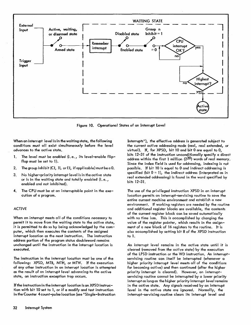
WAITING STATE External I --Input Active, waiting,
or disarmed state I
Disabled state I
I I I I Trigger
Input
Anned state
I I I I L
Remember interrupt Enabled state = 0
I I ~
Figure 10. Operational States of an Interrupt level
When an interrupt level is in the waiting state, the fortowing conditions must a" exist simultaneously before the level advances to the active state.
1. The level must be enabled (i. e., its level-enable flipflop must be set to 1).
2. The group inhibit (CI, II, or EI, if applicable) must be a O.
3. No higher-priority interrupt level is in the active state or is in the waiting state and totally enabled (i. e. , enabled and not inhibited).
4. The CPU must be at an interruptable point in the execution of a program.
ACTIVE
When an interrupt meets all of the conditions necessary to permit it to move from the waiting state to the active state, it is permitted to do so by being acknowledged by the computer, which then executes the contents of the assigned interrupt location as the next instruction. The instruction address portion of the program status doubleword remains unchanged unti I the i nstructi on in the interrupt I ocati on is executed.
The instruction in the interrupt location must be one of the following: XPSD, MTB, MTH, or MTW. If the execution of any other instruction in an interrupt location is attempted as the result of an interrupt level advancing to the active state, an instruction exception trap occurs.
If the instruction in the interrupt location is an XPSD instruction with bit 10 set to 1, or if a modify and test instruction in the Counter 4 count-pu fse location (see II Si ngle-Instructi on
32 Interrupt System
Interrupts"), the effective address is generated subject to the current active addressing mode (real, real extended, or virtual). If, for XPSD, bit 10 and bit Oare equal to 0, bits 12-31 of the instruction unconditionally specify a direct address within the first 1 mi Ilion (220) words of real memory. Since the index field is used for addressing, indexing is not possible. If bit 10 is equal to 0 and indirect addressing is specified (bit 0 = 1), the indirect address (interpreted as in real extended addressing) is found in the word specified by bits 12-31.
The use of the privileged instruction XPSD in an interrupt location permits an interrupt-servicing routine to save the entire current machine environment and establish a new envi ronment. If worki ng regi sters are needed by the routi ne and additional register blocks are avai lable, the contents of the current register block can be saved automatically with no time loss. This is accomplished by changing the value of the register pointer, which results in the assignment of a new block of 16 registers to the routine. It is also accomplished by setting bit 8 of the XPSD instruction to 1.
An interrupt level remains in the active state unti I it is cleared (removed from the active state) by the execution of the LPSD instruction or the WD instruction. An interruptservicing routine can itself be interrupted (whenever a higher priority interrupt level meets all of the conditions for becoming active) and then continued (after the higher priority interrupt is cleared). However, an interruptservicing routine cannot be interrupted by a lower priority interrupt as longas the higher priority interrupt level remains in the active state. Any signals received by an interrupt level in the active state are ignored. Normally, the interrupt-servicing routine clears its interrupt level and

transfers program control back to the point of interrupt by means of an LPSD instruction with the same effective address as the XPSD instruction in the interrupt location.
CONTROL OF THE INTERRUPT SYSTEM
The SIGMA 9 system has two points of interrupt control. One point of interrupt control is at the individual interrupt level. The WD instruction can be used to individually arm, disarm, enable, disable, or trigger any interrupt level except for the power fail-safe interrupts (which are always armed, always enabled, and cannot be triggered).
The second point of interrupt control is achieved by means of the interrupt inhibits (CI, II, and EI) in the program status doubleword. If an interrupt inhibit is set to 1, all interrupt levels in the corresponding group are effectively disabled, i. e., no interrupt in the group may advance from the waiting state to the active state and the group is removed from the interrupt recognition priority chain. Thus, a waiting, enabled interrupt level (in a group that is not inhibited) is not prevented from interrupting the program by a higher priority, waiting, enabled interrupt level in a group that is inhibited. However, if an interrupt group is inhibited while a level in that group is in the active state, no lower priority interrupt level may advance to the active state.
The RD instruction may be used to determine which interrupt levels in a selected group are in the armed orwaiting state, in the waiting or active state, or enabled. Chapter 3 contains a description of the RD instruction.
TIME OF INTERRUPT OCCURRENCES
The SIGMA 9 CPU permits an interrupt to occur during the following time intervals (related to the execution cycle of an instruction) provided that the control panel COMPUTE switch is in the RUN position and no "halt" condition exists:
L Between instructions: an interrupt is permitted between the completion of any instruction and the initiation of the next instruction.
.2. Between instruction it.erations: an interrupt is also permitted to <;>ccur during the execution of the following multi pie-operand instructions:
Move Byte String (MBS)
Compare Byte String (CBS)
Translate Byte String (TBS)
Translate and Test Byte String (TTBS)
Edit Byte String (EBS)
Decimal Multiply (DM)
Decimal Divide (DD)
Move to Memory Control (MMC)
The control and intermediate results of these instructions reside in registers and memory; thus, the instruction can be interrupted between the completion of one iteration (operand execution cycle) and the point in time (during the next iteration) when a memory location or register is modified. If an interrupt occurs during this time, the current iteration is aborted and the instruction address portion of the program status doubleword remains pointing to the interrupted instruction. After the interrupt-servicing routine is completed, the instruction continues from the point at which it was interrupted and does not begi n anew.
SINGLE-INSTRUCTION INTERRUPTS
A single-instruction interrupt occurs in a situation where an interrupt level is activated, the current program is interrupted~ the single instruction in the interrupt location is executed, the interrupt level is automatically cleared and armed, and the interrupted program continues without being disturbed or delayed (except for the time required for the single instruction).
If any of the following instructions is executed in any interrupt location, then that interrupt automatically becomes a single-instruction interrupt:
Modify and Test Byte (MTB)
Modify and Test Halfword (MTH)
Modify and Test Word (MTW)
A modify and test instruction modifies the effective byte, halfword, or word (as described in the section "Fixed-point Arithmeti c Instructions") but the current condition code remains unchanged (even if overflow occurs). The effective address of a modify and test instruction in an interrupt location (except counter 4) is always treated as an actual address, regard·less of whether or not the memory map is currently being used. Counter 4 uses the mapped location ifmapping is currently invoked in the PSD. The execution of a modify and test instruction in an interrupt location, rncl uding mapped and unmapped counter 4, is independent of the memory access protection codes and the writeprotection locks; thus, a memory protection violation trap cannot occur (a nonexistent memory address wi II cause an instruction exception trap). Also, the fixed-point overflow trap cannot occur as. the result of overflow caused by executing MTH or MTW in an interrupt location.
The execution of a modify and test instruction in an interrupt location automatically clears and arms the corresponding interrupt level, allowing the interrupted program to continue.
When a modify and test instruction is executed in a countpulse interrupt location, all of the above conditions apply, in addItion to the following: if the resultant value in the effective location is zero, the corresponding counterequals-zero interrupt is triggered.
Interrupt System 33
TRAP SYSTEM
TRAP
A trap is similar to an interrupt in that program execution automatically branches to a predesignated location when a trap condition occurs. A trap differs from an interrupt in that a trap location must contain an XPSD instruction. Depending on the type of trap, the trap instruction is either executed immediately (i. e., current instruction is aborted) or upon completion of the current instruction. The trap instruction is not held in abeyance by higher priority traps. Interrupts on the other hand may have an entire sequence of instructions executed before actual interupt action occurs.
TRAP ENTRY SE~UENCE
A trap entry sequence begins when the CPU detects the trap condition and ends when the new PSD has successfully replaced the old PSD. Detection of any condition listed in Table 7, which summarizes the trap system, results in a trap to a unique location in memory. When a trap condition occurs, the CPU sets the trap state. The operation currently being performed by the CPU mayor may not be carried to completion, depending on the type of trap. In any event, the instruction is terminated with a trap sequence. In this sequence, the program counter is not advanced; instead, the XPSD instruction in the location associated with the trap is executed. If any interrupt level is ready to enter the active state at the same time that an XPSD trap instruction is in process, the interrupt acknowl edgement will not occur until the XPSD trap instruction is completed. If the trap location does not contain an XPSD instruction, a second trap sequence is immediately invoked. (See "Instructi on Excepti on Trap II .) The operati on of the XPSD instruction is described in Chapter 3, under "Control Instructions ".
TRAP MASKS
The programmer may mask the four trap conditions described below. Other traps can not be masked.
1. The push-down stack limit trap is masked within the stack pointer doubleword for each individual stack.
2. The fixed-point overflow trap is masked in bit position 11 (AM) of the PSD. If bit position 11 (AM) of the PSD contains a 1, the trap is allowed to occur. If bit position 11 contains a 0, the trap is not allowed to occur. AM can be masked by operator intervention or by execution of either of the privileged instructions XPSD or LPSD.
3. The floating-point significance check trap is masked by a combination of the floating significance (FS), floating zero (FZ), and floating normalize (FN) mode control bits (see "Floating-Point Arithmetic FaultTrap").
34 T rap System
FS, FZ, and FN can be set or cI eared by the execution of any of the following instructions:
LOAD CONDITIONS AND FLOATING CONTROL (LCF)
LOAD CONDITIONS AND FLOATING CONTROL IMMEDIATE (LCFI)
EXCHANGE PROGRAM STATUS DOUBLEWORD (XPSD)
LOAD PROG RAM STATUS DOUBLEWORD (LPSD)
4. The decimal arithmetic fault trap is masked by bit position 10 (OM) of the PSD. If bit position 10 (OM) of the PSD contains a 1, the trap is allowed. If OM is a 0, the trap is not allowed. OM can be masked by execution of either of the privileged XPSD or LPSD instructions.
TRAP CONDITION CODE
For the traps push-down stack limit, fixed-point overflow, floating-point fault, and decimal fault, the normal condition code register, CC1-CC4, is loaded with more detailed information about the trap condition just before the trap occurs. This condition code is saved as part of the old PSD when the XPSD instruction is executed in response to the trap.
For the traps nona II owed operation, watchdog ti mer runout, memory parity error, instruction exception, and calls, a special register, the trap condition code TCC1-TCC4, is loaded just before the trap occurs. When the XPSD instruction is executed in response to the trap, this register is added to the new program address if bit 9 of the XPSD is set to 1; TCC1-TCC4 is also logically ORed with the condition code bits of the new PSD when loading CC1-CC4.
TRAP ADDRESSING
During the trap entry sequence, the XPSD instruction in the trap location is accessed without mapping, regardless of the current addressing mode.
If bit 10 of the XPSD is a 1, the effective address is generated subject to the current active addressing mode (real, real extended, or virtual). If, however, bit 10 and bit 0 are equal to a zero, bits 12-31 of the instruction unconditionally specify a direct address within the first 220 words of real memory. Since the index field is used for addressing, indexing is not possible. If bit 10 is equal to a zero and indirect addressing is specified (bit 0 = 1), the indirect address (interpreted as in real extended addressing) is found in the word specified by bits 12-31. Bit 10 of the XPSD has no effect when the XPSD is executed as a nontrap instruction.
90 17 33C-1(4/74)
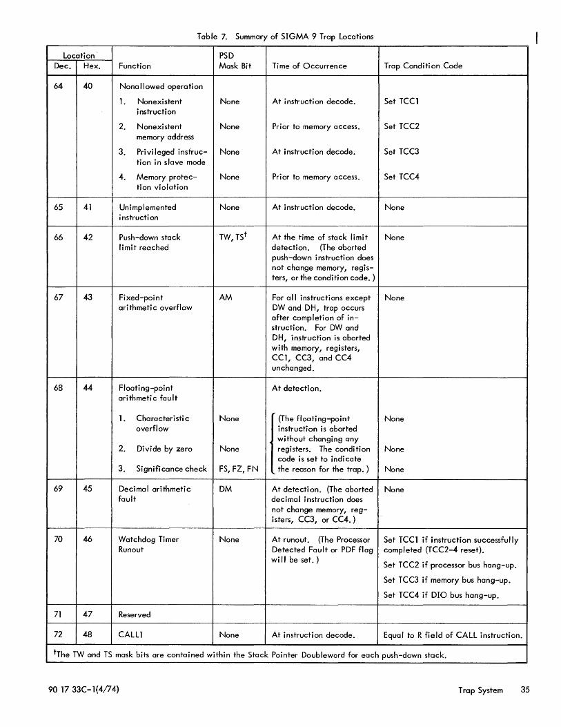
Table 7. Summary of SIGMA 9 Trap locations
location- PSD Dec. Hex. Function Mask Bit Ti me of Dccurren ce Trap Condi ti on Code
64 40 Nonallowed operation
1. Nonexi stent None At instruction decode. Set TCCl instruction
2. Nonexi stent None Prior to memory access. Set TCC2 memory address
3. Privileged instruc- None At instruction decode. Set TCC3 tion in slave mode
4. Memory protec- None Prior to memory access. Set TCC4 tion violation
65 41 Unimplemented None At instruction decode. None i nstructi on
66 42 Push-down stack TW, TSt At the time of stack limit None limit reached detection. (The aborted
push-down instruction does not change memory, regis-ters, or the condition code. )
67 43 Fixed-point AM For all instructions except None ari thmeti c overflow DW and DH, trap occurs
after completion of in-struction. For DWand DH, instruction is aborted with memory, registers, CC1, CC3, and CC4 unchanged.
68 44 Floating-point At detection. arithmetic fault
1. Characteristi c None (The floating-point None overflow instruction is aborted
without changing any 2. Divide by zero None registers. The condi ti on None
code is set to indicate 3. Significance check FS, FZ, FN the reason for the trap. ) None
69 45 Decimal arithmetic DM At detection. (The aborted None fault decimal instruction does
not change memory, reg-isters, CC3, or CC4. )
70 46 Watchdog Timer None At runout. (The Processor Set TCCl if instruction successfully Runout Detected Fault or PDF flag completed (TCC2-4 reset).
wi II be set. ) Set TCC2 if processor bus hang-up.
Set TCC3 if memory bus hang-up.
Set TCC4 if DID bus hang-up.
71 47 Reserved
72 48 CAlll None At instruction decode. Equal to R field of CAll instruction.
tThe TW and TS mask bits are contained within the Stack Pointer Doubleword for each push-down stack.
90 17 33C-l(4/74) Trap System 35
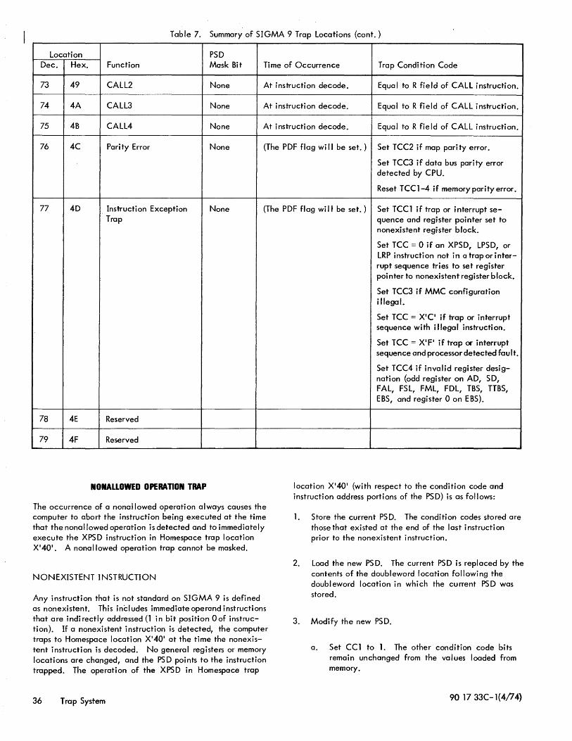
Table 7. Summary of SIGMA 9 Trap Locations (cont.)
Location PSD Dec. Hex. Function Mask Bit Time of Occurrence Trap Condition Code
73 49 CALL2 None At instruction decode. Equal to R field of CALL instruction.
74 4A CALL3 None At instruction decode. Equal to R field of CALL instruction.
75 4B CALL4 None At instruction decode. Equal to R field of CALL instruction.
76 4C Parity Error None (The PDF flag wi II be set. ) Set TCC2 if map parity error.
Set TCC3 if data bus parity error detected by CPU.
Reset TCCl-4 if memory parity error.
77 4D . Instruction Exception None (The PDF flag wi" be set. ) Set TCCl if trap or interrupt se-Trap
78 4E Reserved
79 4F Reserved
NONALLOWED OPERATION TRAP
The occurrence of a nona"owed operation always causes the computer to abort the instruction being executed at the time that the nonallowed operation is detected and to immediately execute the XPSD instruction in Homespace trap location X'40'. A nonallowed operation trap cannot be masked.
NONEXISTENT INSTRUCTION
Any instruction that is not standard on SIGMA 9 is defined as nonexistent. This inC! udes immediate operand instructions that are indirectly addressed (l in bit position Oof instruction). If a nonexistent instruction is detected, the computer traps to Homespace location X'40' at the time the nonexistent instruction is decoded. No general registers or memory locations are changed, and the PSD points to the instruction trapped. The operation of the XPSD in Homespace trap
36 Trap System
quence and register pointer set to nonexistent register block.
Set TCC = 0 if an XPSD, LPSD, or LRP instruction not in a trap or inter-rupt sequence tries to set register pointer to nonexistent register block.
Set TCC3 if MMC configuration i liege I.
Set TeC = X'C if trap or interrupt sequence with illegal instruction.
Set TCC = X'F' if trap or interrupt sequence and processor detected fault.
Set TCC4 if invalid register desig-nation (odd register on AD, SD, FAL, FSL, FML, FDL, TBS, TTBS, EBS, and register 0 on EBS).
location X'40' (with respect to the condition code and instruction address portions of the PSD) is as follows:
1. Store the current PSD. The condition codes stored are those that existed at the end of the last instruction prior to the nonexistent instruction.
2. Load the new PSD. The current PSD is replaced by the contents of the doubleword location following the doubleword location in which the current PSD was stored.
3. Modify the new PSD.
a. Set CCl to 1. The other condition code bits remain unchanged from the values loaded from memory.
90 17 33C-1(4/14)
b. If bitposition90f XPSDcontainsa 1, theprogram counter is incremented by B. If bit position 9 of XPSD contains a 0, the program counter remains unchanged from the value loaded from memory.
NONEXISTENT MEMORY ADDRESS
Any attempt to access a nonexistent memory address causes a trap to Homespace location X'40' at the time of the request for memory service. A nonexistent memory address condition is detected when an actual address is presented to the memory system. If the CPU is in the map mode, the program address will already have been modified by the memory map to generate an actual (but nonexistent) address. (Refer to Table 6 for possible changes to registers and memory locations.) The operation of the XPSD in Homespace trop location X'40' is as follows:
1. Store the current PSD.
2. Load the new PSD.
3. Modify the new PSD.
a. Set CC2 to 1. The other condition code bits remain unchanged from the values loaded from memory.
b. If bit position 9 of XPSD contains a 1, the program counter is incremented by 4. If bit position 9 of XPSD contains a 0, the program counter remains unchanged from the value loaded from memory.
PRIVILEGED INSTRUCTION IN SLAVE MODE
An attempt to execute a privi leged instruction whi Je the CPU is in the slave mode causes a trap to Homespace location X'40' before the privileged operation is performed. No general registers or memory locations are changed, and the PSD points to the instruction trapped. The operation of the XPSD in Homespace trap location X'40' is as follows:
1. Store the current PSD.
2. Load the new PS D.
3. Modify the new PSD.
a. Set CC3 to 1. The other condition code bits remain unchanged from the values loaded from memory.
b. If bit position 9 of XPSD contains a 1, the program counter is incremented by 2. If bit position 9 of XPSD contains a 0, the program counter remains unchanged from the values loaded from memory.
The operation codes OC and OD, and their indirectlyaddressed forms, BC and 8D, are both nonexistent and privileged. If anyone of these operation codes is used while the CPU is in the slave mode, both CCl and CC3 are set to lis after the current PSD is modified, and if bit position 9 of XPSD contains a 1, the program counter is incremented by 10. All other nonexistent operation codes are treated as nonprivi leged and, if used, wi II trap with CC1 set to 1.
MEMORY PROTECTION VIOLATION
A memory protection violation occurs either because of a memory map access control bit violation {by a program executed in the slave or master-protected mode using the memory map), or because of a memory write-lock violation (by any program) within the first 12BK words of real memory. When either type of memory protection violation occurs, the CPU aborts execution of the current instruction without changing protected memory and traps to Homespace location X'40'. (Refer to Table 6 for possible changes to registers and memory locations.) The operation of the XPSD in Homespace trap location X'40' is as follows:
1. Store the current PSD. Set trapped status field to virtual page address of protected page.
2. Load the new PSD.
3. Modify the new PS D.
a. Set CC4to 1. The other condition code bHs remain unchanged from the values loaded from memory.
b. If bit position 9 of XPSD contains a-1, the program counter is incremented by 1. If bit position 9 of XPSD contains a 0, the program counter remains unchanged from the value loaded from memory.
An attempt to access a memory location that is both protected and nonexistent causes both CC2 and CC4 to be set
- to lis after the current PSD has been modified, and -if bit position 9 of XPSD contains a 1, the program counter is incremented by 5.
When the memory protection violation trap occurs, an XPSD instruction is executed that stores the current PSD in the doubleword pointed to by the effective address of the instruction. If this trap condition (CC4 = 1) occurs, the particular virtual page address that caused the trap wi" be stored in the trapped status field, bit positions 4B-55, of the same doubleword. This information only appears in memory and only at the time of the trap. Subsequent XPSD instructions that are not executed as a result of this trap wi II not store information in bit positions 4B-55.
UNIMPLEMENTED IISTRUCnOI TRAP
When the DECIMAL switch on the processor control panel is in the OVERRIDE position, the decimal unit is disabled. The decimal unit includes the following instructions.
Operation Instruction Name Mnemonic Code
Decimal Load DL X'7E'
Decimal Store DST X'7F'
Decimal Add DA X'79'
Decimal Subtract DS X'7B'
Decimal MultipJy DM X'7B'
Decimal Divide DD X'7A'
Trap System 37
Operation Instruction Mnemonic Code
Decimal Compare DC X'7D'
Decimal Shift Arithmetic DSA X'7C'
Pack Decimal Digits PACK X'76'
Unpack Decimal Digits UNPK X'77'
Edit Byte String EBS X'63'
If an attempt is made to execute a decimal instruction (directly or indirectly addressed) when the DECIMAL switch is in the OVERRIDE position, the computer traps to Homespace location X'41 " the unimplemented instruction trap~ An indirectly addressed EBS instruction is always treated as a nonexistent instructi on rather than as an unimpl emented instruction.
The operation of the XPSD in trap Homespace location X'41' is as follows:
1. Store the current PSD. The condition code stored is that which existed at the end of the instruction immediately prior to the unimplemented instruction.
2. Load the new PSD. The condition code and the instruction address portions of the PSD remain at the values loaded from memory.
PUSH-DOWN STACK UMIT TRAP
Push-down stack overflow or underflow can occur during execution of any of the following instructions:
Operation Instruction Mnemonic Code
Push Word PSW X'09'
Pull Word PLW X'08'
Push Multiple PSM X'OB'
Pull Multiple PLM X'OA'
Modify Stack Pointer MSP X'13'
During the execution of any stack-manipulating instruction (see II Push':'down Instructions"), the stack is either pushed (words added to stack) or pul led (words removed from stack). In either case, the space (S) and words (W) fields of the stack pointer doubleword are tested prior to moving any words. If execution of the instruction would cause the space (S) field to become less than 0 or greater than 215_1, the instruction is aborted with memory and registers unchanged. If TS (bit 32) of the stack pointer doubleword is set to 0, the CPU traps to Homespace location X'42'. If TS is set to 1, the trap is inhibited and the CPU processes
38 T rap System
the next instruction. If execution of the instruction would cause the words (W) field to become less than 0 or greater than 215-1, the instruction is aborted with memory and registers unchanged. If TW (bit 48) of the stack pointer doubleword is set to 0, the CPU traps to Homespace location X'42'. If TW is set to 1, the trap is inhibited and the CPU processes the next instruction. If trapping is inhibited, CCl or CC3 is set to 1 to indicate the reason for aborting the instruction. The stack pointer doubleword, memory, and registers are modified only if the instruction is successfully executed.
If a push-down instruction traps, the execution of XPSD in Homespace trap location X'42' is as follows:
1. Store the current PSD. The condition codes that are stored are those that existed prior to execution of the aborted push-down instruction.
2. Load the new PSD. The condition code and instruction address portions of the PSD remain at the varues loaded from memory.
FIXED-POIITOVERFLOW TRAP
Overflow can occur for any of the fol lowing instructions:
Operation Instruction Mnemonic Code
Load Absol ute Word LAW X'3B'
Load Absolute Doubleword LAD X'1B'
Load Complement Word LCW X'3A'
Load Complement Doubleword LCD X'1A'
Add Ha I fword AH X'50'
Subtract Halfword SH X t 5S'
Divide Haffword DH X'56'
Add Immediate AI X'20'
Add Word AW X'30'
Subtract Word SW X'3S'
Divide Word DW X'36'
Add Doubl eword AD X'lO'
Subtract Doubl eword SD X'lS'
Modify and Test Halfword MTH X'53 1
Modify and Test Word MTW X'33'
Add Word to Memory AWM X'66'
Except for the instructions DIVIDE HALFWORD (DH) and DIVIDE WORD (DW), the instruction execution is allowed to proceed to completion. CC2 is set to 1 and CC3 and CC4 represent the actual result (0, -, or +) after overflow.
If the fixed-point arithmetic trap mask (bit 11 of PSD) is a 1, the CPU traps to Homespace location X'43 1 instead of executing the next instruction in sequence.
For DW and DH, the instruction execution is Qoorted without changing any register, and CC2 is set to 1; but CC1, CC3, and CC4 remain unchanged from their values at the end of the instruction immediately prior to the DW or DH. If the fixed-point arithmetic trap mask is a 1, the CPU traps to location X'43 1 instead of executing the next instruction in sequence.
The execution of XPSD in Homespace trap location X'43 1
is as follows:
1. Store the current PSD. If the instruction trapped was any instruction other than DW or DH, the stored condition code is interpreted as follows:
CC1 t CC2 CC3
tt o
o
o
CC4 Meaning
o Result after overflow is zero.
Resu I t after overflow is negative.
o Result after overflow is positive.
No carry out of bit 0 of the adder (add and subtract instructions only).
Carry out of bit 0 of the adder {add and subtract instructions only}.
If the instruction trapped was a DW or DH, the stored condition code is interpreted as follows:
CC1 CC2 CC3 CC4 Meaning
tt Overflow
tCCl remains unchanged for instructions LCW~ LAW, LCD, and LAD.
ttAhyphen indicates that the condition code bitsarenot affected by the condition given under the "Meaning" heading.
2. Load the new PS D. The conditi on code and instruction address portions of the PSD remain at the value loaded from memory.
FlOATING-POINT ARITHMETIC FAULT TRAP
Floating-point fault detection is performed after the operation called for by the instruction code is performed, but before any results are loaded into the general registers. Thus, the floating-point operation that causes an arithmetic fault is not carried to completion in that the original contents of the general registers are unchanged.
Instead, the computer traps to Homespace location X'441
with the current condition code indicating the reason for the trap. A characteristic overflow or an attempt to divide by zero always results in a trap condition. A significance check or a characteristic underflow results in a trap condition only if the floating-point mode controls {FS, FZ, and FN} in the current program status doubleword are set to the appropriate state.
If a floating-point instruction traps, the execution of XPSD in Homespace trap location X'441 is as follows:
1. Store the current PSD. If division is attempted with a zero divisor or if characteristic overflow occurs, the stored condition code is interpreted as follows:
CCl CC2 CC3 CC4 Meaning
0 0 0 Zero divisor.
0 0 Characteristic overflow, negative result.
0 0 Characteristic overflow, positive result.
If none of the above conditions occurred but characteristic underflow occurs with floating zero mode bit (FZ) = 1, the stored condition code is interpreted as follows:
CCl CC2 CC3 CC4 Meaning
o Characteri sti c underflow, negative result.
o Characteristic underffow, positive result.
If none of the above conditions occurred but an addition or subtraction results in either a zero result (with FS = 1 and FN = 0), or a postnormalization shift of more than two hexadecimal places {with FS = 1 and FN = O}, the stored condition code is interpreted as follows:
CCl CC2 CC3 CC4 Meaning
o o o Zero result of addition or subtraction.
T rap System 39
CCl ee2 CC3 CC4 Meaning
1 o o
o
1
o
More than two postnormal i zing shifts, negative result.
More than two postnormatizing. shifts, positive result.
2. load the new PSD. The condition code and instruction address portions of the PSD remain at the values loaded from memory.
DECIMAL ARITHMEnc FAUll TRAP
When either of two decimal fault conditions occurs (see II Decimal Instructions ll
), the normal sequencing of instruction execution is hafted, ec land CC2 are set according to the reason for the fault condition, and CeJ, CC4, memory, and the decimal accumulator remain unchanged by the instruction. If the decimal arithmetic trap mask (bit position 10 of PSWl) -is a 0, the instruction execution sequence continues with the next instruction in sequence at the time of fault detection; however, if the decimal arithmetic trap mask contains a 1, the computer traps to Homespace location Xf45f at the time of fault detection. The following are the fault conditions for decimal instructions:
Instruction Name Mnemonic Fault
Decimal load Dl Illegal digit
Decimal Store OS Illegal digit
Decimal Add DA Overflow, illegal digit
Decimal Subtract DS Overflow, Hlegal digit
Decimal Multiply OM IHegal digit
Decimal Divide DO Overflow, illegal digit
Decimal Compare DC fUegal digit
Dec imol Shift DSA II legal digit Arithmetic
Pock Decimal PACK Illegal digit Digits
Unpack Decimal UNPK IUegal digit Digits
Edit Byte String EBS Illegal digit
40 Trap System
The execution of XPSD in Homespace trap location X'451
is as follows:
1. Store the current PSD. The stored condition code is interpreted as follows:
CCI Ce2 CC3 CC4 Meaning
0 t
AU digits legal and overflow.
1" 0 Illegal digit detected.
2. Load the new PSD. The condition code and instruction address portions of the PSD remain at the values loaded from memory.
CALL IISTRUCllOl TRAP
The four CAll instructions (CAll, CAl2, CAl3, and CAL4) cause the computer to trap to Homespace location X'48' (for CAll), X'491 (for CAl2), Xf4Af (for CAl3), or X'4Bf (for CAl4). Execution of XPSD in the trap location is as foJ lows:
1. Store the current PSD. The stored condition code bits are those that existed prior to the CAll instruction.
2. Load the new PSD.
3. Modify the new PSD.
a. The R Field of the CAll instruction is logically ORed with the condition code register as loaded from memory.
b. If bit 9 of XPSD contains a 1, the R field of the CALL instruction is added to the program counter. If bit 9 of XPSD contains a 0, the program counter remains unchanged from the value loaded from memory.
Note: Return from a CAll trap will be to the trapping instruction + 1.
PROCESSOR DmClED fAULlS
The Processor Detected Fault (PDF) flag is ahardware flog used in the SIGMA 9 system to aid in solving the multiple error problem. Most traps occur because of some dynamic programming consideration (i. e., overflow, attempted division by zero, incorrect use of an instruction or address, etc.) and recovery is easify handled by another software subroutine. However, with certain classes of errors, if a second error occurs white the computer is
t A hyphen indicates that the condition code bit is not affected by the condition given under the "Meaning" heading.
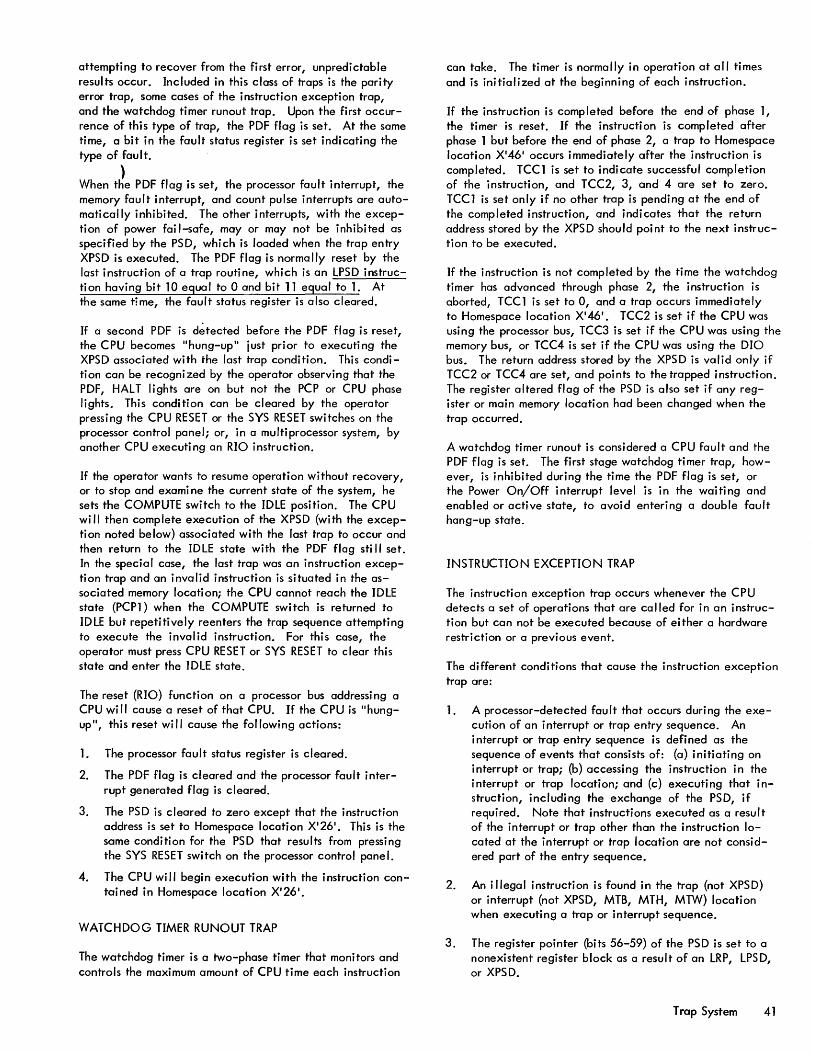
attempting to recover from the first error, unpredictable results occur. Included in this class of traps is the parity error trap, some cases of the instruction exception trap, and the watchdog timer runout trap. Upon the first occurrence of this type of trap, the PDF flag is set. At the same time, a bit in the fault status register is set indicating the type of fault.
) When the PDF flag is set, the processor fault interrupt, the memory fault interrupt, and count pulse interrupts are automatically inhibited. The other interrupts, with the exception of power fai I-safe, mayor may not be inhibited as specified by the PSD, which is loaded when the trap entry XPSD is executed. The PDF flag is normally reset by the last instruction of a trap routine, which is an LPSD instruction having bit 10 equal to 0 and bit 11 equal to 1. At the same time, the fault status register is also cleared.
If a second PDF is d~tected before the PDF flag is reset, the CPU becomes "hung-up" just prior to executing the XPSD associated with the last trap condition. This condition can be recognized by the operator observing that the PDF, HALT lights are on but not the PCP or CPU phase lights. This condition can be cleared by the operator pressing the CPU RESET or the SYS RESET switches on the processor control panel; or, in a multiprocessor system, by another CPU executing an RIO instruction.
If the operator wants to resume operation without recovery, or to stop and exami ne the current state of the system, he sets the COMPUTE switch to the IDLE position. The CPU will then complete execution of the XPSD (with the exception noted below) associated with the last trap to occur and then return to the IDLE state with the PDF flag sti II set. In the special case, the last trap was an instruction exception trap and an invalid instruction is situated in the associated memory location; the CPU cannot reach the IDLE state (PCP1) when the COMPUTE switch is returned to IDLE but repetitively reenters the trap sequence attempting to execute the invalid instruction. For this case, the operator must press CPU RESET or SYS RESET to clear this state and enter the IDLE state.
The reset (RIO) function on a processor bus addressing a CPU wi II cause a reset of that CPU. If the CPU is "hungUp", this reset will cause the following actions:
1. The processor fault status register is cleared.
2. The PDF flag is cleared and the processor fault interrupt generated flag is cleared.
3. The PSD is cleared to zero except that the instruction address is set to Homespace location X'26 1
• This is the same condition for the PSD that results from pressing the SYS RESET switch on the processor control panel.
4. The CPU wi" begin execution with the instruction contained in Homespace location X'26 1
•
WATCHDOG TIMER RUNOUT TRAP
The watchdog timer is a two-phase timer that monitors and controls the maximum amount of CPU time each instruction
can take. The timer is normally in operation at all times and is initialized at the beginning of each instruction.
If the instruction is completed before the end of phase I, the timer is reset. If the instruction is completed after phase 1 but before the end of phase 2, a trap to Homespace location X'46 1 occurs immediately after the instruction is completed. TCC1 is set to indicate successful completion of the instruction, and TCC2, 3, and 4 are set to zero. TCC1 is set only if no other trap is pending at the end of the completed instruction, and indicates that the return address stored by the XPSD should point to the next instruction to be executed.
If the instruction is not completed by the time the watchdog timer has advanced through phase 2, the instruction is aborted, TCC1 is set to 0, and a trap occurs immediately to Homespace location X'46 1
• TCC2 is set if the CPU was using the processor bus, TCC3 is set if the CPU was using the memory bus, or TCC4 is set if the CPU was using the DIO bus. The return address stored by the XPSD is valid only if TCC2 or TCC4 are set, and points to the trapped instruction. The register altered flag of the PSD is also set if any register or main memory location had been changed when the trap occurred.
A watchdog timer runout is considered a CPU fault and the PDF flag is set. The first stage watchdog timer trap, however, is inhibited during the time the PDF flag is set, or the Power On/Off interrupt level is in the waiting and enabled or active state, to avoid entering a double fault hang-up state.
INSTRUCTION EXCEPTION TRAP
The instruction exception trap occurs whenever the CPU detects a set of operations that are co lied for in an i nstruction but can not be executed because of either a hardware restriction or a previous event.
The different conditions that cause the instruction exception trap are:
1. A processor-detected fault that occurs during the execution of an interrupt or trap entry sequence. An interrupt or trap entry sequence is defined as the sequence of events that consists of: (a) initiating on interrupt or trap; (b) accessing the instruction in the interrupt or trap location; and (c) executing that instruction, including the exchange of the PSD, if required. Note that instructions executed as a result of the interrupt or trap other than the instruction located at the interrupt or trap location are not considered part of the entry sequence.
2. An illegal instruction is found in the trap (not XPSD) or interrupt (not XPSD, MTB, MTH, MTW) location when executing a trap or interrupt sequence.
3. The register pointer (bits 56-59) of the PSD is set to a nonexistent register block as a result of an LRP, LPSD, or XPSD.
Trap System 41
4. Bit positions 12-14 of the MOVE TO MEMORY CONTROL (MMC) instruction are interpreted as an illegal configuration. That is, any configuration other than 100, 010, 001, or 101.
5. The set of operations, primari Iy doubleword and bytestring instructions, that yield an unpredictable result when an incorrect register is specified; this type of fault is called lIinvalid register designation ll and includes the following instructions: t
Register 0 Specified
Edit Byte String (EBS)
Odd Register Specified
Add Doubleword (AD)
Subtract Doubleword (SD)
Floating Add Long (FAL)
Floating Subtract Long (FSL)
Floating Multiply Long (FMl)
Floating Divide Long (FDL)
Translate Byte String (TBS)
Translate and Test Byte String (TTBS)
Edit Byte String (EBS)
Move to Memory Control (MMC)
Trap Condition Code. The Trap Condition Code (TCC) differentiates between the different fault types. Some of the fault conditions (as listed in Table 8) may occur and/or be detected during a trap or interrupt entry sequence. In this case, the trapped status field, bits 48-55 of the PSD, are set to equal the least significant eight bits of the address of the trap or interrupt instruction in whi ch the trap occurred; that is, the trapped status field wi" point to the trap or interrupt location that was in effect when the fault occurred. In the event that the fault occurs in a normal program instruction, the trapped status field has no meaning.
Table 5 shows the settings of the TCC and trapped status field for the various fault types.
PARITY ERROR TRAP
Three types of parity errors may be detected in the addressing and memory logic.
1. Map Check. When the CPU is operating with the memory map, a parity check is made on the page
t"lnvalid register designation" faults do not set the PDF Hag.
42 Trap System
Table 8. TCC Setting for Instruction Exception Trap X'4D' I
T rapped Status TCC Field (PSD bits
Fault Type 1 234 48-55)
XPSD in trap or 1 000 8 least significant interrupt location tries bits of trap or to set register pointer interrupt address. to nonexistent register block.
XPSD, LPSD, or LRP 0000 No meaning. not in a trap or inter-rupt sequence tries to set register pointer to nonexistent register block.
Trap or interrupt 1 1 1 1 8 least significant sequence and pro- b its of trap or cessor detected fault. interrupt address.
Trap or interrupt 1 1 00 8 least significant sequence with bits of trap or inval id instruction. interrupt address.
MMC configuration 001 a No meaning. invalid.
Invalid register 0001 No meaning. designation.
addresses retrieved from the map. If an error is found, this fault occurs. The CPU aborts the memory request, traps to Homespace location X'4C' and sets TCC2 to 1.
2. Data Bus Check. If the CPU detects t a parity error on data received from memory and the memory does not also indicate a parity error on the information sent, a data bus check occurs. The data bus check causes the CPU to trap to Homespace location X'4C', and sets TCC3 to 1.
3. Memory Parity Error. When a CPU receivest a signal from the memory indicating memory parity error, this fault occurs. The CPU traps to Homespace location X'4C'. In addition, on a memory-detected parity error trap, the memory bank wi II "snapshot II the address causing the trap.
The memory parity error signal is generated:
1. When the memory is performing a read operation and a parity error is detected in the data as read from the memory elements.
t Note exceptions in IITrap Conditions During 'Anticipate' Operations ll
•
90 17 33C-1(4/74)
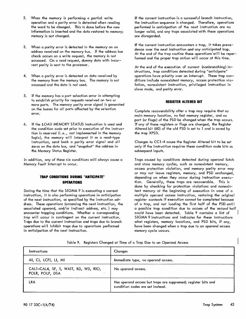
2. When the memory is performing a partial write operation and a parity error is detected when reading the word to be changed. This is done before the new information is inserted and the data restored to memory; memory is not changed.
3. When a parity error is detected in the memory on an address received on the memory bus. If the address bus check occurs on a write request, the memory is not accessed. On a read request, dummy data with incorrect parity is sent to the processor.
4. When a parity error is detected on data received by the memory from the memory bus. The memory is not accessed and the data is not used.
5. If the memory has a port selection error in attempting to establish priority for requests received on two or more ports. The memory parity error signal is generated on the busses for a II ports affected by the se I ecti on error.
6. If the LOAD MEMORY STATUS instruction is used and the condition code set prior to execution of the instruction is reserved (i. e., not implemented in the memory logic), the memory will interpret it as a read-type instruction, send back a parity error signal and all zeros on the data bus, and "snapshot" the address in the Memory Status Register.
In addition, any of these six conditions will always cause a Memory Fault Interrupt to occur.
TRAP CONDITIONS DURING "ANnCIPATE" OPERAnONS
During the time that the SIGMA 9 is executing a current instruction, it is also performing operations in anticipation of the next instruction, as specified by the instruction address. These operations (accessing the next instruction, the associated operand, and/or indirect address, etc.) may encounter trapping conditions. Whether a corresponding trap wi II occur is contingent on the current instruction. Traps due to the current instruction and traps due to branch operations wi II inhibit traps due to operations performed in anticipation of the next instruction.
If the current instruction is a successful branch instruction, the instruction sequence is changed. Therefore, operations performed in anticipation of the next instruction are no longer valid, and any traps associated with these operations are disregarded.
If the current instruction encounters a trap, it takes precedence over the next instruction and any anticipated trap. At the end of the trap routine these operations 'wi II be reperformed and the proper trap action wi II occur at this time.
At the end of the execution of current (nonbranching) instructions, trap conditions detected during "anticipate" operations have priority over an interrupt. These trap conditions include nonexistent memory, access protection violation, nonexistent instruction, privi leged instruction in slave mode, and parity error.
REGISTER ALTERED BIT
Complete recoverability after a trap may require that no main memory location, no fast memory register, and no part (or flags) of the PSD be changed when the trap occurs. If any of these registers or flags are changed, the Register Altered bit (60) of the old PSD is set to 1 and is saved by the trap XPSD.
Changes to CCl-4 cause the Register Altered bit to be set only if the instruction requires these condition code bits as subsequent inputs.
T raps caused by condi ti ons detected duri ng operand fetch and store memory cycles, such as nonexistent memory, access protection violation, and memory parity error may or may not leave registers, memory, and PSD unchanged, depending on when they occur during instruction execution. Generally, these traps are recoverable. This is done by checking for protection violations and nonexistent memory at the beginning of execution in case of a multiple operand access instruction, restoring the original register contents if execution cannot be completed because of a trap, and not loading the first half of the PSD unti I a possible trap condition due to access of the second half could have been detected. Table 9 contains a list of I SIGMA 9 instructions and indicates for these instructions what registers, memory locations, and PSD bits, if any, have been changed when a trap due to an operand access memory cycl e occurs.
Table 9. Registers Changed at Time of a Trap Due to an Operand Access
Instructions Changes
AI, CI, LCFI, LI, MI Immedi ate type, no operand access.
CALl-CAL4, SF, S, WAIT, RD, WD, RIO, No operand access. POLR, POLP, DSA
LRA Has operand access but traps are suppressed; register bits and condition codes are set instead.
90 17 33C-1(4;74) Trap System 43
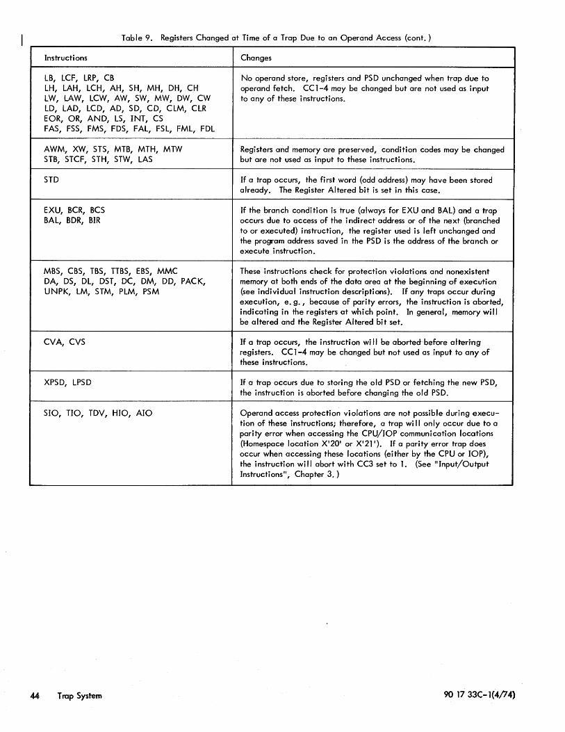
44
Table 9. Registers Changed at Time of a Trap Due to an Operand Access (cont.)
Instructions
LB, LCF, LRP, CB LH, LAH, LCH, AH, SH, MH, DH, CH LW, LAW, LCW, AW, SW, MW, DW, CW LD, LAD, LCD, AD, SD, CD, CLM, CLR EOR, OR, AND, LS, INT, CS FAS, FSS, FMS, FDS, FAL, FSL, FML, FDL
AWM, XW, STS, MTB, MTH, MTW STB, STCF, STH, STW, LAS
STD
EXU, BCR, BCS BAL, BDR, BIR
MBS, CBS, TBS, TTBS, ESS, MMC DA, DS, DL, DST, DC, DM, DD, PACK, UNPK, LM, STM, PLM, PSM
CYA, CYS
XPSD, LPSD
SIO, no, TDY, HIO, AIO
Trap System
Changes
No operand store, registers and PSD unchanged when trap due to operand fetch. CC 1-4 may be changed but are not used as input to any of these instructions.
Registers and memory are preserved, condition codes may be changed but are not used as input to these instructions.
If a trap occurs, the first word (odd address) may have been stored already. The Register Altered bit is set in this case.
If the branch condition is true (always for EXU and SAL) and a trap occurs due to access of the indirect address or of the next (branched to or executed) instruction, the register used is left unchanged and the program address saved in the PSD is the address of the branch or execute instruction.
These instructions check for protection violations and nonexistent memory at both ends of the data area at the beginning of execution (see individual instruction descriptions). If any traps occur during execution, e. g., because of parity errors, the instruction is aborted, indicating in the registers at which point. In general, memory will be altered and the Register Altered bit set.
If a trap occurs, the instruction wHI be aborted before altering registers. CC1-4 may be changed but not used as input to any of these instructions.
If a trap occurs due to storing the old PSD or fetching the new PSD, the instruction is aborted before changing the old PSD.
Operand access protection violations are not possible during execution of these instructions; therefore, a trap wi II only occur due to a parity error when accessing the CPU/lOP communication locations (Homespace location X'20' or X'211). If a parity error trap does occur when accessing these locations (either by the CPU or lOP), the i nstructi on wi II abort wi th CC3 set to 1. (See" Input/Output Instructions", Chapter 3.)
90 1733C-1(4/74)
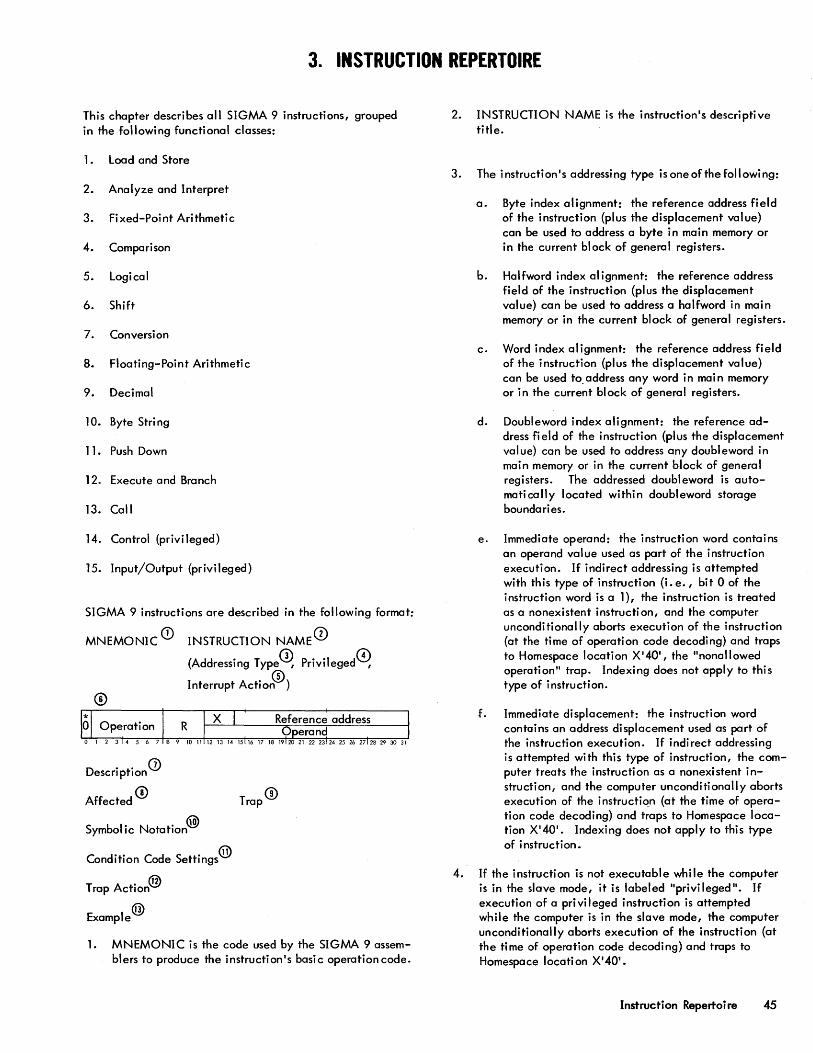
3. INSTRUCTION REPERTOIRE
This chapter describes all SIGMA 9 instructions, grouped in the following functional classes:
1. Load and Store
2. Analyze and Interpret
3. Fi xed-Poi nt Ari thmeti c
4. Comparison
5. Logical
6. Shift
7. Conversion
8. Floating-Point Arithmetic
9. Decimal
10. Byte String
1l. Push Down
12. Execute and Branch
13. Call
14. Control (privileged)
15. Input/Output (privileged)
SIGMA 9 instructions are described in the following format:
MNEMONIC CD INSTRUCTION NAMEQ)
(Addressing Type~ Privileged~ CD Interrupt Action )
D •. Q)
escrlptlon
Affected (!)
Symbolic Notation@
Condition Code Settings@
Trap Action@
Example @
Trap®
1. MNEMONIC is the code used by the SIGMA 9 assemblers to produce the instruction's basi c operation code.
2. INSTRUCTION NAME is the instruction's descriptive title.
3. The instruction's addressing type isoneofthefollowing:
a. Byte index alignment: the reference address field of the instruction (plus the displacement value) can be used to address a byte in main memory or in the current block of general registers.
b. Halfword index alignment: the reference address field of the instruction (plus the displacement value) can be used to address a halfword in main memory or in the current block of general registers.
c. Word index alignment: the reference address field of the instruction (plus the displacement value) can be used to. address any word in main memory or in the current block of general registers.
d. Doubleword index alignment: the reference address fi eld of the instruction {p1us the displacement value} can be used to address any doubleword in main memory or in the current hlock of general registers. The addressed doubleword is automatically located within doubleword storage boundaries.
e. Immediate operand: the instruction word contains an operand value used as part of the instruction execution. If indirect addressing is attempted with this type of instruction (i. e., bit 0 of the instruction word is a 1), the instruction is treated as a nonexistent instructi on, and the computer unconditionally aborts execution of the instruction (at the time of operation code decoding) and traps to Homespace location X'40' , the "nona II owed operation" trap. Indexing does not apply to this type of instruction.
f. Immediate displacement: the instruction word contains an address displacement used as part of the instruction execution. If indirect addressing is attempted with this type of instruction, the computer treats the i nstructi on as a nonexi stent i nstruction, and the computer unconditionally aborts execution of the instruction (at the time of operation code decoding) and traps to Homespace location X'40'. Indexing does not apply to this type of instrudion.
4. If the instruction is not executable while the computer is in the slave mode, it is labeled "privileged". If execution of a privileged instruction is attempted while the computer is in the slave mode, the computer unconditionally aborts execution of the instruction (at the time of operation code decoding) and traps to Homespa ce I ocati on X '40' •
Instruction Repertoire 45
5. If the instruction can be successfully resumed after its execution sequence has been interrupted by an interrupt acknowledgment, the instruction is labeled "continue after interrupt". In the case of the "continue after interruptll instructions, certain general registers contain intermediate results or control information that alfows the instruction to continue properly.
6. Instruction format:
o. Indirect addressing - If bit position 0 of the instruction format contains an asterisk (*), the instruction can use indi rect addressing; however, if bit position 0 of the instruction format contains a 0, the instruction is of the immediate operand type, which is treated as a nonexistent instruction if indirect addressing is attempted (resulting in a trap to Homespace location X'40 J
).
b. Operation code - The operation code field (bit positions 1-7) of the instruction is shown in hexadecimal notation.
c. R field - If the register address field (bit positions 8-11) of the instruction format contains the character "R", the instruction can specify any register in the current block of general registers as an operand source, result destination, or both; otherwise, the function of this field is determined hy the instruction.
d. X field - If the index register address field (bit positions 12-14) of the instruction format contains the character "X", the instruction specifies indexing withony one of registers 1 through 7 in the current block of general registers; otherwise, the function of this field is determined by the instruction.
e. Reference address field - Normally, the address field (bit positions 15-31) of the instruction format is used as the reference address va I ue for rea I, real extended, and virtual addresses (see Chapter 2). This reference address field is also used to address I/O systems (see I/O instructions later in this chapter and also Chapter 4). For immediate operand instructions, this field is augmented with the contents of the X field, as illustrated, to form a 20-bit operand.
f. Value field - In some fixed-point arithmetic instructions, bit positions 12-31 of the instruction format contain the word "value ll . This field is treated as a 20-bit integer, with negative integers represented in two's complement form.
g. Displacement field - In the byte string instructions, bit positions 12-31 of the instruction format contain the word "displacement"". In the execution of the instruction, this field is used to modify the source address of an operand, the destination address of a result, or both.
46 Instruction Repertoire
h. Reserved fields - In any format diagram that depicts system inputs (i .e., instruction, data word), a shaded area represents a field that is ignored by the computer (i .e., the content of the shaded field has no effect on instruction execution). It should not be used or must be coded with O's to preclude conflict with possible future modifications.
In any format diagram that depicts system outputs (i.e., general register, memory word modified by an instruction, or I/O status word), a shaded area represents a field whose content is indeterminate and must not be used (i .e., masked).
7. The description of the instruction defines the operations performed by the computer in response to the instruction configuration depicted by the instruction format diagram. Any instruction configuration that causes an unpredictable result is so specified in the description.
8. All programmable registers and storage areas that can be affected by the instruction are listed (symbolically) after the word "Affected". The instruction .address portion of the program status doubleword is considered to be affected only if a branch condition can occur as a result of the instruction execution, since the instruction address is incremented by 1 as part of every instruction execution.
9. All trap conditions that may be invoked by the execution of the instruction are listed after the word "Trap". SIGMA 9 trap locations are summarized in the section "T rap System" in Chapter 2.
10. The symboli c notation presents the instruction operation as a series of generalized symbolic statements. The symbolic terms used in the notation are defined in Appendix E, "Glossary of Symbol ic Terms".
11. Condition Code settings are given for each instruction that affects the condition code. A 0 or a 1 under any of columns 1, 2, 3, or 4 indicates that the instruction causes a 0 or 1 to be placed in CC1, CC2, CC3, or CC4, respectively I for the reasons given. If a hyphen (-) appears in columns 1, 2, 3, or 4, that .portion of the condition code is not affected by the reason given for the condition code bites) containing a 0 or 1. For example, the following condition code settings are given for a comparison instruction:
2 3 4 Result of comparison
o 0 Equal.
o
o
Register operand is arithmetically less than effective operand.
o Register operand is arithmetically greater than effective operand.
The logical product of the two operands is nonzero.
The logical product (AND) of the two operands is zero.
CCl is unchanged by the instruction. CC2 indicates whether or not the two operands have 11 sin corresponding bit positions, regardless of their arithmetic relationship. CC3 and CC4 are set according to the arithmetic relationship of the two operands, regardless of whether or not the two operands have 1's in corresponding bit positions. For example, if the register operand is arithmetically less than the effective operand and the two operands both have lis in at least one corresponding bit position, the condition code setting for the comparison instruction is:
234
o
The above statements about the condi tion code are valid only if no trap occurs before the successful completion of the instruction execution cycle. If a trap does occur during the instruction execution, the condition code is normally reset to the value it contained before the instruction was started and the register altered bit (PSD 60) is set to 1 if a register has been altered. Then the appropriate trap location is activated.
12. Actions taken by the computer for those trap conditions that may be invoked by the execution of the instruction are described. The description includes the criteria for the trap condition, any controlling trap mask or inhibit bits, and the action taken by the computer. In order to avoid unnecessary repetiti on, the three trap conditions that apply to all instructions (i. e., nonallowed operations, parity error, and watchdog timer runout) are not described for each instruction.
13. Some instruction descriptions provide one or more examples to illustrate the results of the instruction. These examples are intended onl y to show how the instructi ons operate, and not to demonstrate thei r fu II capability. Within the examples, hexadecimal notation is used to represent the contents of general registers and storage locations. Condition code settings are shown in binary notation. Th~ character "X" is used to indicate irrelevant or ignored information.
LOAD /STORE INSTRUCTIONS
The following load/store instructions are implemented in SIGMA 9 computers:
Instruction Name Mnemonic
Load Immediate LI
Load Byte LB
load Ha Ifword LH
Load Word LW
Load Doubl eword LD
Instruction Name Mnemonic
Load Complement Halfword LCH
Load Absolute Halfword LAH
Load Complement Word LCW
Load Absol ute Word LAW
Load Compl ement Doubl eword LCD
Load Absolute Doubleword LAD
Load Real Address (see "Control Instructions") LRA
Load and Set LAS
Load Memory Status (see "Control Instructions") LMS
Load Sel ective LS
Load Multiple LM
Load Conditions and Floating Control Immediate LCFI
Load Conditions and Floating Control LCF
Exchange Word XW
Store Byte STB
Store Hal fword STH
Store Word STW
Store Doubleword STD
Store Selective STS
Store Multiple STM
Store Conditions and Floating Control STCF
SIGMA 9 load and store instructions operate with information fields of byte, halfword, word, and doubleword lengths. Load instructions load the information indicated into one or more of the general registers in the current register block. Load instructions do not affect the source of information; however, nearly all load instructions provide a condition code setting that indicates the following information about the contents of the affected general register(s) after the instruction is successfully completed:
Condition code settings:
2 3 4 Result
- 0 0 Zero - the result in the affected register(s) is all O's.
- 0 Negative - register R contains a 1 in bit position O.
Load/Store Instructions 47
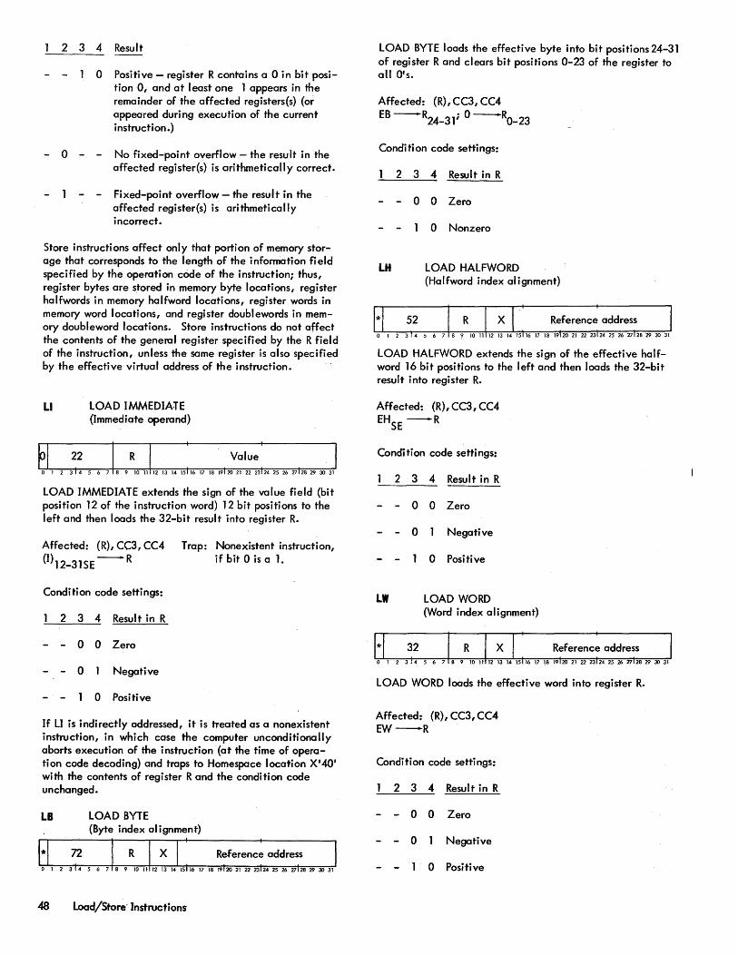
2 3 4 Result
o Positive - register R contains a 0 in bit position 0, and at least one 1 appears in the remainder of the affected registers(s} (or appeared during execution of the current instruction.)
o - - No fixed-point overflow - the result in the affected register(s} is arithmetically correct.
Fixed-point overflow - the result in the affected register(s) is arithmetically incorrect.
Store instructions affect only that portion of memory storage that corresponds to the length of the information field specified by the operation cOde of the instruction; thus, register bytes are stored in memory byte locations, register halfwords in memory halfword locations, register words in memory word locations, and register doublewords in memory doubleword locations. Store instructions do not affect the contents of the general register specified by the R field of the instruction, unless the same register is also specified by the effective virtual address of the instruction.
LI lOAD IMMEDIA:rE (Immediate operand)
LOAD IMMEDIATE extends the sign of the value field (bit position 12 of the instruction word) 12 bit positions to the left and then loads the 32-bit result into register R.
Affected: (R), CC3, CC4
(I}12-31SE -R
Condition code settings:
2 3 4 Resul tin R
- 0 0 Zero
- 0 Negative
o Positive
Trap: Nonexistent instruction, if bit 0 is a 1.
If LI is indirectly addressed, it is treated as a nonexistent instruction, in which case the computer unconditionally aborts execution of the instruction (at the time of operation code decoding) and traps to Homespace location X'40' with the contents of register R and the condition code unchanged.
LB LOAD BYTE (Byte index alignment)
48 Load/Store" Instructions
LOAD BYTE loads the effective byte into bit positions 24-31 of register R and clears bit positions 0-23 of the register to all O's.
Affected: (R),CC3,CC4 EB-R24_31; 0-RO"';23
Condi ti on code setti ngs:
2 3 4 Result in R
o 0 Zero
o Nonzero
LH LOAD HALFWORD (Halfword index alignment)
LOAD HALFWORD extends the sign of the effective halfword 16 bit positions to the left and then loads the 32-bit result into register R.
Affected: (R), CC3, CC4 EHSE -R
Condition code settings:
2 3 4 Result in R
o 0 Zero
o Negative
o Positive
LW LOAD WORD (Word index alignment)
LOAD WORD loads the effective word into register R.
Affected: (R), CC3, CC4 EW-R
Condition code settings:
2 3 4 Result in R
- 0 0 Zero
- 0 Negative
0 Positive
LO LOAD DOUBLEWORD (Doubleword index alignment)
LOAD DOUBLEWORD loads the 32 low-order bits of the effective doubleword into register Ru 1 and then loads the 32 hi gh-order bits of the effective doubleword into register R.
If R is an odd value, the result in register R is the 32 highorder bits of the effective doubleword. The condition code settings are based on the effective doubleword, rather than the final result in register R (see example 3, below).
Affected: (R), (Rul), CC3,CC4 ED
32_
63 -Ru1; ED
O_
31-R
Condition code settings:
2 3 4 Effective doubleword
o 0 Zero
o Negative
o Positive
Example 1, even R field value:
Before execution
ED X·0123456789ABCDEP
(R)
(Ru1)
CC
xxxxxxxx
xxxxxxxx
xxxx
Example 2, odd R field value:
ED
(R)
CC
Before execution
X·0123456789ABCDEP
xxxxxxxx
xxxx
Example 3, odd R field value:
ED
(R)
CC
Before execution
X·0000000012345678·
xxxxxxxx
xxxx
After execution
X·0123456789ABCDEF·
X·01234567·
X·89ABCDEP
xx10
After execution
X· 0 123456789A BCD EF·
X·01234567·
xxl0
After executi on
X·OOOOOO0012345678·
X·OOOOOOOO·
xxlO
LCH LOAD COMPLEMENT HALFWORD (Halfword index alignment)
LOAD COMPLEMENT HALFWORD extends the sign of the effective halfword 16 bit positions to the left and then loads the 32-bit two·s complement of the result into register R. (Overflow cannot occur.)
Affected: (R),CC3, CC4
-[EHSE] -R
Condition code settings:
2 3 4 Result in R
0 0 Zero
0 Negative
0 Positive
LAH LOAD ABSOLUTE HALFWORD (Halfword index alignment)
If the effective halfword is positive, LOAD ABSOLUTE HALFWORD extends the sign of the effective halfword 16 bit positions to the left and then loads the 32-bit result in register R. If the effective halfword. is negative, LAH extends the sign of the effective halfword 16 bit positions to the left and then loads the 32-bit two·s complement of the result into register R. (Overflow cannot occur.)
Affected: (R), CC3, CC4
IEHSE\-R
Condition code settings:
2 3 4 Resu It in R
- 0 0 Zero
o Nonzero
LCW LOAD COMPLEMENT WORD (Word index alignment)
LOAD COMPLEMENT WORD loads the 32-bit two·s complement of the effective word jnto register R. Fixed-point overflow occurs if the effective word is -231 (X·80000000·), in which case the result in register R is _231 and CC2 is set to 1; otherwise, CC2 is reset to O.
Affected: (R),CC2,CC3,CC4 Trap: Fixed-point overflow. -EW-R
Load/Store Instructions 49
Condition code settings:
2 3 4 Result in R
0 0 0 Zero
0 Negative
0 0 Positive
o - No fixed-point overflow
o Fixed-point overflow
If CC2 is set to 1 and the fixed-point arithmetic trap mask (AM) is a 1, the computer traps to Homespace location X'43' after execution of LOAD COMPLEMENT WORD; otherwise, the computer executes the next instruction in sequence.
LAW LOAD ABSOLUTE WORD (Word index alignment)
If the effective word is positive, LOAD ABSOLUTE WORD loads the effective word into register R. If the effective word is negative, LAW loads the 32-bit two's compiement of the effective word into register R. Fixed-point overflow occurs if the effective word'is -231~X'800()()OOO')' in which case the result in register R is -23 and CC2 is set to 1; otherwise, CC2 is reset to O.
Affected: (R), CC2, CC3, CC4 Trap: Fixed-point overflow IEWI-R
Condition code settings:
2 3 4 Result in R
o 0 0 Zero
o Nonzero
o No fixed-point overflow
o Fixed-point overflow {sign bit on}
If CC2 is set to 1 and the fixed-point arithmetic trap mask (AM) is a 1, the computer traps to Homespace location X'43' after execution of LOAD ABSOLUTE WORD; otherwise, the computer executes the next instruction in sequence.
LCD LOAD COMPLEMENT DOUBLEWORD (Doubleword index alignment)
LOAD COMPLEMENT DOUBLEWORD forms the 64-bit two's complement of the effective doubleword, loads the
50 Load/Store Instructions
32 low-order bits of the result into register Ru 1, and then loads the 32 high-order bits of the result into register R.
If R is an odd value, the result in register R is the 32 hi ghorder bits of the two's complemented doubleword. The condition code settings are based on the two's complement of the effective doubleword, rather than the final result in register R.
Fixed-point overflow occurs if the effective doubleword is _~3 (X'8000000000000000'), in which case the result in registers Rand Rul is _263 and CC2 is set to 1; otherwise, CC2 is reset to O.
Affected: (R), (Ru 1), CC2, Trap: Fixed-point overflow CC3, CC4
[-ED]32_63 -Rul; [-ED]0_31- R
Condition code settings:
2 3 4 Two's complement of effective doubleword
- 0 0 0 Zero
o Negative
o 0 Positive
- 0 - No fixed-point overflow
o Fixed-point overflow
If CC2 is set to 1 and the fixed-point arithmetic trap mask (AM) is a 1, the computer traps to Homespace location X'43' after execution of LOAD COMPLEMENT DOUBLEWORD; otherwise, the computer executes the next instruction in sequence.
Example 1, even R field value:
Before execution After execution
ED X'O 123456789ABCD EP X'0123456789ABCDEP
(R) xxxxxxxx X'FEDCBA98'
(Ru 1) xxxxxxxx X'76543211,
CC xxxx xOO1
Example 2, odd R field value:
Before execution After execution
ED X'0123456789ABCDEP X'0123456789ABCDEP
(R) xxxxxxxx X'FEDCBA98'
CC xxxx x 001
LAD LOAD ABSOLUTE DOU BLEWORD (Doubleword index al ignment)
If the effective doubleword is positive, LOAD ABSOLUTE DOUBLEWORD loads the 32 low-order bits of the effective doubleword into register Ru 1, and then loads the 32 highorder bits of the effective doubleword into register R. If R is an odd value, the result in register R is the 32 high-order bits of the effective doubleword. The condition code settings are based on the effective doubleword, rather than the final result in register R.
If the effective doubleword is negative, LAD forms the 64-bit twols complement of the effective doubleword, loads the 32 low-order bits of the twol s complemented doubleword into register Ru 1, and then loads the 32 high-order bits of the twols complemented doubleword into register R. If R is an odd value, the result in register R is the 32 highorder bits of the twols complementeddoubleword. The condition code settings are based on the twols complement of the effective doubleword, rather than the final result in register R.
Fixed-point overflow occurs if the effective doubleword is -263 (X'8000000000000000' ), in which case the result in registers Rand Ru1 is _263 and CC2 is set to 1; otherwise, CC2 is reset to O.
Affected: (R), (Ru 1), CC2, T rap: Fixed-point overflow CC3,CC4
I ED 132- 63 - Ru1; 1ED10_31 --R
Condition code settings:
2 3 4 Absolute value of effective doubleword
- 0 0 0 Zero
o Nonzero
- 0 - No fixed-point overflow
o Fixed-poi nt overflow (sign bit on)
If CC2 is set to 1 and the fixed-point arithmetic trap mask (AM) is a 1, the computer traps to Homespace location X'431 after execution of LOAD ABSOLUTE DOUBLEWORD; otherwise, the computer executes the next instruction in sequence.
Example 1, even R field value:
ED
(R)
(Ru 1)
CC
Before execution
X'0123456789ABCDEF'
xxxxxxxx
xxxxxxxx
xxxx
After execution
X 10123456789 A BCD EF I
X'012345671
XI 89ABCDEF'
x010
Example 2, even R field value:
Before execution After execution
ED XI FEDCBA98765432101 XI FEDCBA987654321 o'
(R) xxxxxxxx X'012345671
(Ru 1) xxxxxxxx X'89ABCDFO'
CC xxxx x010
Example 3, odd R field value:
Before execution After execution
ED X'0123456789ABCDEF' X'0123456789ABCDEF'
(R) xxxxxxxx X'012345671
CC xxx x x010
LAS LOAD AND SET (Word index al ignment)
o 1 2
LOAD AND SET loads the effective word into R and unconditionally sets bit 0 of the effective word location in memory to 1. Register R contains the previous contents of the effective word location (i.e., before being modified, if required). The effective address always references memoryeven if it is less than 16.
Affected: (R) CC3, CC4 EW-R l-EWO
Condition code settings:
2 3 4 Result in R
0 0 Zero
0 Negative
0 Positive
Note: Write locks protect memory and traps are not inhibited during the execution of LAS.
LS LOAD SELECTIVE (Word index al ignment)
o 1 2
Register Ru1 contains a 32-bit mask. If R is an even value, LOAD SELECTIVE loads the effective word into_ register R in those bit positions selected by a 1 in corresponding bit positions of register Ru 1. The contents of register R are not affected in those bit positions selected by a 0 in corresponding bit positions of register Ru 1.
Load/Store Instructions 51
If R is an odd value, LS logically ANDs the contents of register R with the effective word and loads the result into register R. If corresponding bit positions of register Rand the effective word both contain 1 IS, a 1 remains in register R; otherwise, a 0 is placed in the corresponding bit position of register R.
Affected: (R), CC3, CC4
If R is even, [EWn(Ru1)]u[(R)n(Ru1)] -R]
If R is odd, EWn(R)-R
. Condition code settings:
2 3 4 Resu I tin R
o 0 Zero.
OBit 0 of register R is a 1.
OBit 0 of register R is a 0 and bit positions 1-31 of register R contain at least one 1.
Example 1, even R field value:
Before execution
EW X'01234567'
(Ru 1) X'FFOOFFOO'
(R) xxxxxxxx
CC xxxx
Example 2, odd R field value:
Before execution
EW X'89ABCDEF'
(R)
CC
LM
X' FOFOFOFO'
xxxx
LOAD MULTIPLE (Word index alignment)
After execution
X'01234567'
X'FFOOFFOO'
X'01xx45xx'
xx10
After execution
X'89ABCDEF'
X' 80AOCOEO'
xx01
LOAD MULTIPLE loads a sequential set of words into a sequential set of registers, The set of words to be loaded begins with the word pointed to by the effective address of LM, and the set of registers begins with register R. The set of registers is treated modulo 16 (i.e., the next register loaded after register 15 is register 0 in the current register block).
The number of words to be loaded into the general registers is determined by the setting of the condition code
52 Load/Store Instructions
immediately before the execution of LM. (The desired value of the condition code can be set with LCF or LCFI.) An initial value of 0000 for the condition code causes 16 consecutive words to be loaded into the register block.
Affected: (R) to (R+CC-l)
(EWL - R;(EWL + 1) - R+ 1), ... ,(EWL +CC- 1) - R+CC-1
The lM instruction may cause a trap if its operation extends into a page of memory that is protedted by the access protection codes. A trap may also occur if the operation extends into a nonexistent memory region. In either case, it will be detected before the actual operation begins and the trap will occur immediately .
If the effective virtual address of the LM instruction is in the range 0 through 15, then the words to be loaded are taken from the genera I reg isters rather than from core memory. In this case the results will be unpredictable if any of the source registers are also used as destination registers.
LCFI LOAD CONDITIONS AND FLOATING CONTROL IMMEDIATE (Immediate operand)
If bit position 10 of the instruction word contains a 1, LOAD CONDITIONS AND FLOATING CONTROL IMMEDIATE loads the contents of bit positions 24 through 27 of the instruction word into the condition code; however, if bit 10 is 0, the condition code is not affected.
If bit position 11 of the instruction word contains a 1, LCFI loads the contents of bit positions 29 through 31 of the instruction word into the floating significance (FS), floating zero (FZ), and floating normal ize (FN) mode control bits, respectively (in the program status doubfeword); however, if bit 11 is 0, the FS, FZ, and FN control bits are not affected. The functions of the floating-point control bits are described in the section "Floating-Point Arithmetic Instructions".
Affected: CC, FS, FZ,FN Trap: Nonexistent instruction, if bit 0 is a 1.
If (1)10 = 1, {I)24_27- CC
If (1)10 = 0, CC is not affected.
If (1)11 = 1, (1)29-31- FS, FZ, FN
If (1)11 = 0, FS, FZ, and FN not affected.
Condition code settings,
2 3
if (1)10 = 1:
4
If LCFI is indirectly addressed, it is treated as a nonexistent instruction, in which case the computer unconditionally aborts execution of the instruction {at the time of operation
code decoding) and traps to Homespace location X'40' with the condition code unchanged.
LCF LOAD CONDITIONS AND FLOATING CONTROL (Byte index al ignment)
If bit position 10 of the instruction word contains a 1, LOAD CONDITIONS AND FLOATING CONTROL loads bits 0 through 3 of the effective byte into the location code; however, if bit 10 is 0, the condition code is not affected.
If bit position 11 of the instruction word contains a 1, LCF loads bits 5 through 7 of the effective byte into the floating significance (FS), floating zero (FZ), and floating normalize (FN)mode control bits, respectively; however, if bit 11 is 0, the FS, FZ, and FN control bits are not affected. The functions of the floating- point mode control bits are described in the section "Floating-Point Arithmetic Instructi ons ".
Affected: CC, FS, FZ, FN
If (1)10 = 1, EBO
_3 -CC
If (I) 10 = 0, CC not affected
If (I) 11 =1, EB5
_7
-FS,FZ,FN
If (I) 11 = 0, FS, FZ, FN not affected
Condition code settings, if (1)10 = 1:
2 3 4
(EB)l
XW EXCHANGE WORD (Word index al ignment)
EXCHANGE WORD exchanges the contents of register R with the contents of the effective word location.
Affected: (R), (EWL) , CC3, CC4 (R) --- (EWL)
Condition code settings:
2 3 4 Result in R
0 0 Zero
0 Negative
0 Positive
\ST8 STORE BYTE (Byte index al ignment)
STORE BYTE stores the contents of bit positions 24-31 of register R into the effective byte location.
Affected: (EBL)
(R)24-31 - EBL
STH STORE HALFWORD (Halfword index alignment)
STORE HALFWORD stores the contents of bit positions 16-31 of register R into the effective halfword location. If the information in register R exceeds halfword data limits, CC2 is set to 1; otherwise, CC2 is reset to o.
Affected: (EHL), CC2
(R)16-31 -EHL
Condition code settings:
2 3 4 Information in R
o (R)0-16 = all OIS or all lis.
(R)0-16 I all OIS or all lis.
STW STORE WORD (Word index al ignment)
o I 2
STORE WORD stores the contents of register R into the effective word location.
Affected: (EWL) (R) -EWL
Load/Store Instructions 53
STO STORE DOUBLEWORD (Doubleword index alignment)
STORE DOUBLEWORD stores the contents of register R into the 32 high-order bit positions of the effective doubleword location and then stores the contents of register Ru 1 into the 32 low-order bit positions of the effective doubleword location.
Affected: (EDL) (R)- EDL
O_
31; (Ru1) -EDL
32_63
Example 1, even R field value:
Before execution
(R) X'01234567'
(Rul) = X'89ABCDEF'
(EDL) = xxxxxxxxxxxxxxxx
Example 2, odd R field value:
Before execution
(R) X'89ABCDEF'
(EDL) = xxxxxxxxxxxxxxxx
STS STORE SELECTIVE (Word index al ignment)
After execution
X'01234567'
X'89ABCDEF'
X' 0123456789ABCDEF'
After execution
X'89ABCDEF'
X'89ABCDEF89ABCDEF'
Register Ru 1 contains a 32-bit mask. If R is an even value, STORE SELECTIVE stores the contents of register R into the effective word location in those bit positions selected by a 1 in corresponding bit positions of register Ru 1; the effective word remains unchanged in those bit positions selected by a 0 in corresponding bit positions of register Ru 1.
If R is an odd value, STS logically inclusive ORs the contents of register R with the effective word and stores the result into the effective word location. The contents of register R are not affected.
Affected: (EWL)
If R is even, [(R)n(Ru1)1 u [EW (Ru1)1-EWL
If R is odd, (R) u EW-EWL
54 Load/Store Instructions
Example 1, even R field value:
Before execution
(R) X' 12345678'
(Ru 1) X'FOFOFOFO'
EW xxxxxxxx
Example 2, odd R field va lue:
(R)
EW
STM
Before execution
X'OOFFOOFF'
X' 12345678'
STORE MULTIPLE (Word index alignment)
After execution
X'12345678'
X' FOFOFOFO'
X'1x3x5x7x'
After execution
X'OOFFOOFF'
C'12FF56FF'
I: I, , ;~. , , J . Roo ..I,,: ..I.,:" " " ~~e;,e~~~"a::::t~ u "I STORE MULTIPLE stores the contents of a sequential set of registers into a sequential set of word locations. The set of locations begins with the location pointed to by the effective word address ofSTM, and the set of registers begins with register R. The set of registers is treated modulo 16 (i .e., the next sequential register after register 15 is register 0). The number of registers to be stored is determined by the value of the condition code immediately before execution of STM. (The condition code can be set to the desired value before execution of STM with LCF or LCFI.) An initial value of 0000 for the condition code causes 16 general registers to be stored.
Affected: (EWL) to (EWL+CC-l) (R) -EWL,(R+ 1 )-EWL + 1 , ... ,(R+CC-1) - EWL +CC-1
The STM instruction may cause a trap if its operation extends into a page of memory that is protected by the access protection codes or the write locks. A trap may also occur if the operation extends into a nonexistent memory region. Jf any of these cases, the trap wi" be detected before the actual operation begins and it will occur immediately.
If the effective virtual address of the STM instruction is in the range 0 through 15, then the registers indicated by the R field of the STM instruction are stored in the general registers rather than in core memory. In this case, the results will be unpredictable if any of the source registers are also used as destination registers.
STCF STORE CONDITIONS AND FLOATING CONTROL (Byte index alignment)
STORE CONDITIONS,AND FLOATING CONTROL stores the current condition code and the current values of the floating significance (FS), floating zero (FZ), and floating
normalize (FN) mode control bits of the program status doubleword into the effective byte location as follows:
Affected: (EBL) (PSD)O_7 -EBL
ANAL VZE/INTERPRET INSTRUCTIONS
ANLZ ANALYZE (Word index al ignment)
The ANALYZE instruction evaluates the effective word as a SIGMA 9 instruction. The ANALYZE instruction always sets the condition codes to indicate the addressing type of the analyzed instruction {see condition code settings and Table 7, below}. Except when the analyzed instruction is an immediate operand instruction, an effective virtual address for the analyzed instruction is also calculated and loaded into register R.
The nonexistent instruction, the privileged instruction violation, and the unimplemented instruction trap conditions can never occur during execution of the ANLZ instruction. However, either the nonexistent memory address condition or the memory protection violation trap condition (or both) can occur as a result of any memory access initiated by the ANLZ instruction. If either of these trap conditions occurs, the instruction address stored by an XPSD in trap Homespace location X'40' is always the virtual address of the ANLZ instruct ion.
The detailed operation of ANALYZE is as follows:
1. The contents of the location pointed to by the effective virtual address of the ANLZ instruction is obtained. This effective word is the instruction to be analyzed. From a memory-protection viewpoint, the instruction (to be analyzed) is treated as an operand of the ANLZ instruction; that is, the analyzed instruction may be obtained from any memory area to which the program has read access.
2. If the operation code portion of the effective word spec ifies an immediate-addressing instruction type, the condition code is set to indicate the addressing type, and instruction execution proceeds to the next instruction in sequence after ANLZ. The original contents of reg ister R are not changed when the analyzed instruction is of the immediate-addressing type.
If the operation code portion of the effective word specifies a reference-addressing instruction type, the condition code is set to indicate the addressing type of the ana Iyzed instruction and the effective
Byte
address of the analyzed instruction is computed {using all of the normal address computation rules}. If bit 0 of the effective word is a 1, the contents of the memory location specified by bits 15-31 of the effective word are obta ined and then used as a direct address. The nonallowed operation trap (memory protection violation or nonexistent memory address) can occur as a result of the memory access. Indexing is always performed {with an index register in the current register block} if bits 12-14 of the analyzed instruction are nonzero. During real extended addressing, the effective virtual address of the analyzed instruction is al igned as an integer displacement value and loaded into register R, according to the instruction addressing type, as foil ows:
Halfword
Word
Doubleword
When the ANALYZE instruction is executed in the masterprotected mode and a trap condition occurs, it never traps. Instead of trapping it completes its execution by storing in reg ister R the address that would have caused the instruction to trap. Since the mode is master-protected, the access protection codes will apply to the interpretation of addresses. If a slave mode program is trapped because an instruction has referenced protected memory, the ANALYZE instruction in the master-protected mode can determine which address actually caused the trap.
To aid the interpreting program, when operating in the master-protected mode, the ANLZ instruction uses bits 5, 6, and 7 of register R to indicate which memory access
t Note that for real or virtual addressing, byte displacement is 19 bits, halfword displacement is 18 bits, word displacement is 17 bits, and doubleword displacement is 16 bits.
Analyze/Interpret Instructions 55
initiated by the ANLZ would have trapped. The meaning of the possible codes in R5-R7 is as follows:
R5 R6
o o
o o
o
R7
o
Meaning
Successful generation of the effective virtual address of the analyzed instruction. The CCs are set to the addressing type of the analyzed instruction and R8-R31 contain the effective virtual address of the analyzed instruction aligned as an integer displacement value according to the instruction addressing type.
The indirect reference of the analyzed instruction would have trapped because it was either nonexistent, memory protected, or had a parity error. The CCs are set to the addressing type of the analyzed instruction and R8-R31 contain the virtual address of the indirect reference of the ana Iyzed instruction aligned as a word displacement.
The effective virtual address of the ANlZ instruction would have trapped because it was either nonexistent, memory protected, or had a parity error. The CCs are indeterminate since the instruction to be analyzed may not have been fetched {nonexistent memory}. R8-R31 contain the effective virtual address of the ANLZ instruction aligned as a word displacement.
An indirect ANLZ instruction where the indirect reference would have trapped because it was either nonexistent, memory protected, or had a parity error. The CCs are indeterminate since the instruction to be analyzed may not be fetched (nonexistent memory). R8-R31 contain the virtual address of the indirect reference of the ANLZ instruction aligned as a word displacement.
If no trap condition occurs, ANLZ wi II execute norma IIy and return the effective address of the instruction analyzed'.
T obi e 10 shows the SIGMA 9 instruction set as a 4 by 32 matrix {arranged as a function of the operation code}. This table also shows how the instruction set is divided into six groups as a function of the addressing type {delineated by heavy I ines}. For example, if the operation code of the analyzed instruction is either X'02', X'20', X'21', X'22', or X'23', then CC1 is set to 1, CC2 is set to 0, CC3 is set to 0 (when analyzed instruction specifies direct addressing), and CC4 is set to 1. The decimal equiva lent of the condition code setting
56 Analyze/Interpret Instructions
X'n'
00 01 02 03
04 05 06 07
08 09 OA OB
OC OD OE OF
10 11 12 13
14 15 16 17
18 19 1A 1B
1C 1D lE 1F
Table 10. ANALYZE Table for SIGMA 9 Operation Codes
X'OO'+n X'20'+n X'40'+n X'60'+n
- AI TTBS TSS - tt CI
LCFI CD LI - MI
CAll CAL2 CAL3 CAL4
PLW PSW PLM PSM
tt
~PSDt ® XPSDt
AD CD LD MSP
srD
SD ClM LCD LAD
FSL FAL FDL FML
SF S LAS
ANLZ CS XW STS
CVS EaR CVA tt OR LM CD LS STM AND
LRAt SlOt LMSt TIot WAITt TDVt LRPt HIOt
AW CW LW MTW
STW DW MW
SW CLR LCW LAW
FSS FAS FDS FMS
AH CH LH MTH
STH DH MH
SH
LCH LAH
CBS tt MBS
(D-EBS
BDR BIR AWM EXU
BCR BCS BAL INT
LCF CB LB MTB
STCF tt STB tt
CD PACK CD UNPK
DS DA DD DM
DSA DC DL DST
tp ··1 d· . rivi ege instructions.
ttDecimal value of condition code settings when analyzed instruction calls for direct addressing. If analyzed instruction calls for indirect addressing, add 2 to the value shown.
for this group of immediate, word addressing type of instructions is shown as a 9 within a circle. The decimal equivalents of the condition code settings for the other five groups are shown in the same manner. If the analyzed instruction calls for indirect addressing, CC3 is always set to a 1 and the decimal value of the condition code setting shown in Table 7 should be increased by 2.
Affected: (R), CC
90 17 33C-1 (4/74)
Condition code settings:
2 3 4 Instruction addressing type
0 0 0 Byte
0 0 Immediate, byte
0 0 Halfword
0 0 Word
0 Immediate, word
0 Doubleword
0 Direct addressing (EW 0 = 0)
Indirect addressing (EWO = 1)
INT INTERPRET (Word index alignment)
INTERPRET loads bits 0-3 of the effective word into the condition code, loads bits 16-31 of the effective word into bit positions 16-31 of register Ru 1 (and loads OIS into bit positions 0-15 of register Ru1, loads bits 4-15 of the effective word into bit positions 20-31 of register R (and clears the remaining bits of register R). If R is an odd value, INT loads bits 0-3 of the effective word into the condition code, loads bits 16-31 of the effective word into bit positions 16-31 of register R, and loads OIS into bit positions 0-15 of register R (bits 4 ... 15 of the effective word are ignored in this case).
Affected: (R), (Ru1), CC
EWO
_3 -CC
EW4_15 -R20- 31 ; 0 -RO- 19
EW16
_31
-Rul16
_31
; 0 -Ru10
_15
Condition code settings:
2 3 4
Example 1, even R field value:
Before execution After execution
EW XI 123456781 XI 123456781
(R) xxxxxxxx X 1000002341
(Ru 1) xxxxxxxx X 1000056781
CC xxxx 0001
FIXED-POINT ARITHMETIC INSTRUCTIONS
The following fixed-point arithmetic instructions are included as a standard feature of the SIGMA 9 computer.
Instruction Name Mnemonic
Add Immediate AI
Add Ha I fword AH
Add Word AW
Add Doubl eword AD
Subtract Halfword SH
Subtract Word SW
Subtract Doubleword SD
Multiply Immediate MI
Multiply Halfword MH
Multiply Word MW
Divide Halfword DH
Divide Word DW
Add Word to Memory AWM
Modify and Test Byte MTB
Modify and Test Halfword MTH
Modify and Test Word MTW
The fixed-point arithmetic instruction set performs binary addition, subtraction, multiplication, and division with integer operands that may be data, addresses, index values, or counts. One operand may be either in the instruction word itself or may be in one or two of the current general registers; the second operand may be either in main memory or in one or two of the current general registers. For most of these instructions, both operands may be in the same general register, thus permitting the doubling, squaring, or clearing the contents of a register by using a reference address value equal to the R field value.
All fixed-point arithmetic instructions provide a condition code setting that indicates the following information about the result of the operation called for by the instruction:
Condition code settings:
2 3 4 Result
o 0 Zero - the result in the specified general register{s) is all zeros.
Fixed-Point Arithmetic Instructions 57
2 3 4 Result
o Negative - the instruction has produced a fixed-point negative result.
o Positive - the instruction has produced a fixed-point positive result.
o - Fixed-point overflow has not occurred during execution of an add, subtract, or divide instruction, and the result is correct.
o -
Fixed-point overflow has occurred during execution of an add, subtract, or divide instruction. For addition and subtraction, the incorrect result is loaded into the designated register(s). For a divide instruction, the designated register(s), and CC 1, CC3, and CC4 are not affected.
No carry - for an add or subtract instruction, there was no carry of a I-b it out of the hi ghorder (sign) bit position of the result.
Carry - for an add or subtract instruction, there was a 1-bit carry out of the sign bit position of the result. (Subtracting zero will a I ways produce carry. )
AI ADD IMMEDIATE {Immediate operand)
The value field (bit positions 12-31 of the instruction word) is treated as a 20-bit, two's complement integer. ADD IMMEDIATE extends the sign of the value field (bit position 12 of the instruction word) 12 bit positions to the left, adds the resulting 32-bit value to the contents of register R, and loads the sum into register R.
Affected: (R), cc (R) + (I)12-31SE-R
Condition code settings:
2 3 4 Result in R
0 0 Zero
- 0 Negative
0 Positive
Trap: Fixed-point overflow; or nonexistent instruction if bit 0 is a 1.
- 0 - No fixed-point overflow
- - Fixed-point overflow
o - No carry from bit position 0
- - Carry from bit position 0
58 Fixed-Point Arithmetic Instructions
If AI is indirectly addressed, it is treated as a nonexistent instruction, in which case the computer unconditionally aborts execution of the instruction (at the time of operation code decoding) and traps to Homespoce location X'40' with the contents of register R and the condition code unchanged.
If CC2 is set to 1 and the fixed-point arithmetic trap mask (AM). is a 1, the computer traps to Homespace location X'43' after loading the sum into register R; otherwise, the computer executes the next instruction in sequence.
AH ADD HALFWORD (Halfword index alignment)
ADD HALFWORD extends the sign of the effective halfword 16 bit positions to the left (to form a 32-bit word in which bit positions 0-15 contain the sign of the effective halfword), adds the 32-bit result to the contents of register R, and loads the sum into register R.
Affected: (R), cc (R) +EH -R
SE
Condition code settings:
2 3 4 Result in R
0 0 Zero
0 Negative
0 Positive
Trap: Fixed-point overflow
- 0 No fixed-point overflow
Fixed-point overflow
o - No carry from bit position 0
Carry from bit position 0
If CC2 is set to 1 and the fixed-point arithmetic trap mask is 1, the computer traps to Homespace location X'43' after loading the sum into register R; otherwise, the computer executes the next instruction in sequence.
AW ADD WORD 0I/ord index alignment)
ADD WORD adds the effective word to the contents of regsiter R and loads the sum into register R.
Affected: (R), CC (R)+EW -R
Trap: Fixed-point overflow
Condition code settings:
2 3 4 Resu It in R
o 0 Zero
- 0 Negative
o Positive
o - No fixed-point overflow
- Fixed-point overflow
o - No carry from bit position 0
Carry from bit position 0
If CC2 is set to 1 and the fixed-point arithmetic trap mask (AM) is a 1, the computer traps to Homespace location X'43' after loading the sum into register R; otherwise, the computer executes the next instruction in sequence.
AD ADD DOUBLEWORD (Doubleword index alignment)
ADD DOU BLEWORD adds the effective doubleword to the contents of registers Rand Rul (treated as a single, 64-bit register); loads the 32 low-order bits of the sum into register Ru 1 and then loads the 32 high-order bits of the sum into register R. R must be an even value; if R is an odd value, the computer traps with the contents in register R unchanged.
Affected: (R), (Ru 1), CC (R, Rul) + ED -R, Rul
Condition code settings:
2 3 4 Result in R, Rul
- 0 0 Zero
- 0 Negative
o Positive
Trap: Fixed-point overflow, instruction exception
o No fixed-point overflow
Fixed-point overflow
o - No carry from bit position 0
Carry from bit position 0
If CC2 is set to 1 and the fixed-point arithmetic trap mask (AM) is a 1, the computer traps to Homespace location X'43' after loading the sum into registers Rand Ru 1; otherwise, the computer executes the next instruction in sequence.
The R field of the AD instruction must be an even value for proper operation of the instruction; if the R field of AD is an odd value, the instruction traps .. to Homespace location X'4D', instruction exception trap.
Example 1, even R field value:
ED
(R)
(Ru 1)
CC
SH
Before execution After execution
X'33333333EEEEEEEE' X'33333333EEEEEEEE'
X'l1111111' X'44444445,
X '33333333' X'22222221'
xxxx 0010
SUBTRACT HALFWORD (Halfword index alignment)
SUBTRACT HALFWORD extends the sign of the effective halfword-16 bit positions to the left (to form a 32-bit word in which bit positions 0-15 contain the sign of the effective halfword), forms the two's complement of the resulting word, adds the complemented word to the contents of register R, and loads the sum into register R.
Affected: (R), CC -EH + (R)-R
SE
Trap: Fixed-point overflow
Condition code settings:
2 3 4 Result in R
- 0 0 Zero
- 0 Negative
0 Positive
- 0 - No fixed-point overflow
Fixed-point overflow
0-- No carry from bit position 0
Carry from bit position 0
If CC2 is set to 1 and the' fixed-point arithmetic trap mask (AM) is a 1, the computer traps to Homespace location X'43'after loading the sum into register R; otherwise, the computer executes the next instruction in sequence.
SW SUBTRACT WORD (Word index alignment)
Fixed-Point Arithmetic Instructions 59
SUBTRACT WORD forms the two's complement of the effeetive word, adds that complement to the contents of register R, and loads the sum into register R.
Affected: (R), CC -EW + (R) -R
Condition code settings:
2 3 4 Result in R
- 0 0 Zero
o Negative
o Positive
Trap: Fixed-point overflow
- 0 - No fixed-point overflow
Fixed-point overflow
o - No carry from bit position 0
Carry from bit position 0
If CC2 is set to 1 and the fixed-point arithmetic trap mask (AM) is a 1, the computer traps to Homespace location X'43' after loading the sum into register R; otherwise, the computer executes the next instruction in sequence.
SO SUBTRACT DOUBLEWORD (D~ubleword index alignment)
SUBTRACT DOUBLEWORD forms the 64-bit two's complement of the effective doubleword, adds the complemented doubleword to the contents of registers Rand Ru 1 (treated as a single, 64-bit register), loads the 32 low-order bits of the-sum into register Ru 1 and loads the 32 high-order bits of the sum into register R. R must be an even value; if R is an odd value, the computer traps with the contents in register R unchanged.
Affected: (R),(Ru1),CC -ED + (R, Ru1) -R, Rul
Trap: Fixed-point overflow, instruction exception
Condition code settings:
1· 2 3 4 Result in R, Ru1
0
- 0
0 -
0 -
0
1
0
Zero
Negative
Positive
No fixed-point overflow
Fixed-point overflow
No carry from bit position 0
Carry from bit position 0
60 - Fixed-Point Arithmetic Instructions
If CC2 is set to 1 and the fixed-point arithmetic trap mask (AM) is a 1, the computer traps to Homespace location X'43' after the result is loaded into registers Rand Ru 1; otherwise, the computer executes the next instruction in sequence.
The R field of the SO instruction must be an even value for proper operation of the instruction; if the R field of SO is an odd value, the instruction traps to Homespace location X'4D', instruction exception trap.
MI MULTIPLY IMMED.JA TE (Immediate operand)
The value field (bit positions 12-31 of the instruction word) is treated as a 20-bit, two's complement integer. MULTIPLY IMMEDIATE extends the sign of the value field (bit position 12) of the instruction word 12 bit positions to the left and multiplies the resulting 32-bit value by the contents of register Ru 1, then loads the 32 high-order bits of the product into register R, and then loads the 32 loworder bits of the product into register Ru 1.
If R is an odd value, the result in register R is the 32 loworder bits of the product. Thus, in order to generate a 64-bit product, the R field of the instruction must be even and the multiplicand must be in register R+1. The condition code settings are based on the 64-bit product formed during instruction execution, rather than on the final contents of register R. Overflow cannot occur.
Affected: (R),(Ru1),CC2,CC3,CC4 (Ru1) x (I)12_31SE-R,Rul
Trap: Nonexistent instruction if bit 0 is a 1.
Condition code settings:
2 3 4
0 0
0
0
o -
64-bit product
Zero.
Negative.
Positive.
Resul t is correct, as represented in register Rul.
Result is not correctly representable in register Ru 1 alone.
If MI is indirectly addressed, it is treated as a nonexistent instruction,_ in which case the computer unconditionally aborts execution of the instruction (at the time of operation code decoding) and traps to Homespace location X'40' with the contents of register R, register Ru 1, and the conditi.on code unchanged; otherwise, the computer executes the next instruction in sequence.
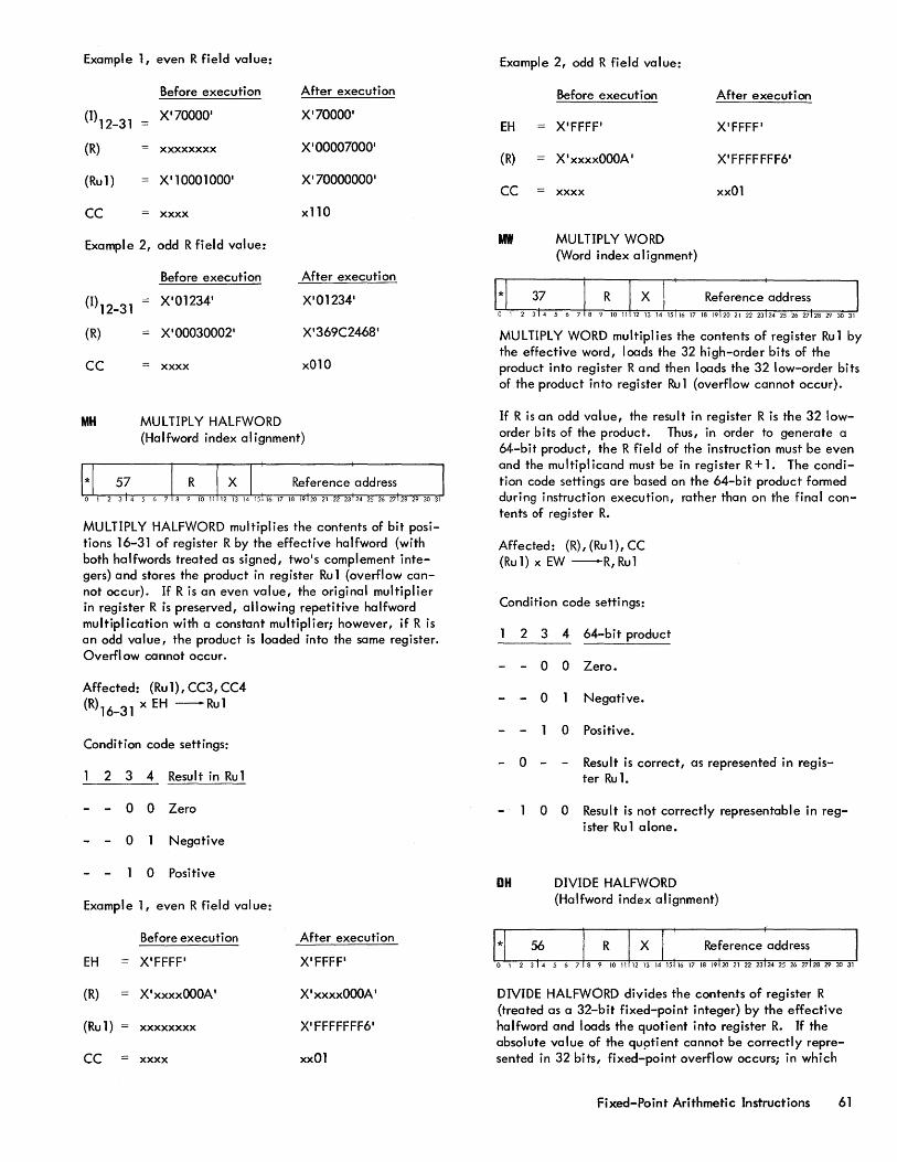
Example 1, even R field va1ue:
(1)12-31
(R)
(Ru 1)
CC
Before execution
X'700001
xxxxxxxx
X'10001000'
xxxx
Example 2, odd R field value:
(I) 12-31
(R)
CC
Before execution
X'012341
X'00030002'
xxxx
After execution
X'70000'
X' 00007000'
X'70000oo0'
x110
After executi on
X'01234'
X'369C2468'
x010
MH MULTIPLY HAlFWORD (Halfword index al ignment)
MULTIPLY HAlFWORD multiplies the contents of bit positions 16-31 of register R by the effective halfword (with both halfwords treated as signed, two's complement integers) and stores the product in register Ru 1 (overflow cannot occur). If R is an even value, the original multiplier in register R is preserved, allowing repetitive halfword multipl ication with a constant multipl ier; however, if R is an odd value, the product is loaded into the same register. Overflow cannot occur.
Affected: (Ru 1), CC3, CC4 (R)16-31 x EH --Ru1
Condition code settings:
2 3 4 Result in Ru 1
0 0 Zero
0 Negative
0 Positive
Example 1, even R field value:
Before execution
EH X'FFFF'
(R) X' xxxxOOOA'
(Ru 1) xxx xxx xx
CC xxxx
After execution
X'FFFF'
X' xxxxOooA'
X' FFFFFFF6'
xx01
Example 2, odd R field value:
Before execution After execution
EH X'FFFF' X'FFFfi
(R) X' xxxxOOOA' X'FFFFFFF6'
CC xxxx xx01
MW MUl TIPl Y WORD (Word index alignment)
MULTIPLY WORD multipl ies the contents of register Ru 1 by the effective word, loads the 32 high-order bits of the product into register R and then loads the 32 low-order bits of the product into register Ru 1 (overflow cannot occur).
If R is an odd value, the result in register R is the 32 loworder bits of the product. Thus, in order to generate a 64-bit product, the R field of the instruction must be even and the multiplicand must be in register R + 1. The condition code settings are based on the 64-bit product formed during instruction execution, rather than on the final contents of register R.
Affected: (R), (Ru 1), CC (Ru 1) x EW -R, Ru1
Condition code settings:
DH
2 3 4 64-bit product
- 0 0 Zero.
- 0 Negative.
0 Positive.
o - Result is correct, as represented in register Ru 1.
o 0 Result is not correctly representable in register Ru 1 alone.
DIVIDE HAlFWORD (Halfword index alignment)
DIVIDE HAlFWORD divides the contents of register R (treated as a 32-bit fixed-point integer) by the effective halfword and loads the quotient into register R. If the absolute value of the quptient cannot be correctly represented in 32 bits, fixed-point overflow occurs; in which
Fixed-Point Arithmetic Instructions 61
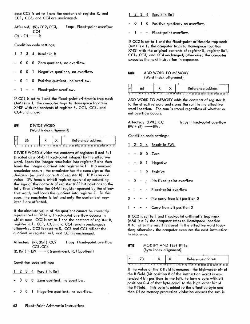
case CC2 is set to 1 and the contents of register R, and CCl, CC3, and CC4 are unchanged.
Affected: (R), CC2, CC3, CC4
Trap: Fixed-point overflow
(R)';' EH - R
Condition code settings:
2 3 4 Resu It in R
o 0 0 Zero quotient, no overflow.
o 0 Negative quotient, no overflow.
o 0 Positive quotient, no overflow.
- Fixed-point overflow.
If CC2 is set to 1 and the fixed-point arithmetic trap mask (AM) is a 1, the computer traps to Homespace location X'43' with the contents of register R, CC1, CC3, and CC4 unchanged.
ow DIVIDE WORD (Word index alignment)
DIVIDE WORD divides the contents of registers Rand Ru 1 (treated as a 64-bit fixed-point integer) by the effective word, loads the integer remainder into register R and then loads the integer quotient into register Ru 1. If a nonzero remainder occurs, the remainder has the same sign as the dividend (original contents of register R). If R is an odd value, DW forms a 64-bit register operand by extending the sign of the contents of register R 32 bit positions to the left, then divides the 64-bit register operand by the effective word, and loads the quotient into register R. In this case, the remainder is lost and only the contents of register R are affected.
If the absolute value of the quotient cannot be correctly represented in 32 bits, fixed-point overflow occurs; in which case CC2 is set to 1 and the contents of register R, regrster Rul, CC1, CC3, and CC4 remain unchanged; otherwise, CC2 is reset to 0, CC3 and CC4 reflect the quotient in register Ru 1, and CC 1 is unchanged.
Affected: (R),(Rul),CC2 Trap: Fixed-point overflow CC3,CC4
(R, Ru 1) .;. EW -R (remainder), Ru 1 (quotient)
Condition code settings:
2 3 4 Resu It in Ru 1
o 0 0 Zero quotient, no overflow.
o 0 Negative quotient, no overflow.
62 Fixed-Point Arithmetic Instructions
2 3 4 Resu It in Ru 1
- 0 o Positive quotient, no overflow.
Fixed-point overflow.
If CC2 is set to 1 and the fixed-point arithmetic trap mask (AM) is a l, the computer traps to Homespace location X'43' with the original contents of registerR, register Rul, CCl, CC3, and CC4 unchanged; otherwise, the computer executes the next instruction in sequence.
AWM ADD WORD TO MEMORY (Word index al ignment)
ADD WORD TO MEMORY adds the contents of register R to the effective word and stores the sum in the effective word location. The sum is stored regardless of whether or not overflow occurs.
Affected: (EWL), CC EW+ (R) -EWL
Condition code settings:
2 3 4 Result in EWl
o 0 Zero
o Negative
o Positive
Trap: Fixed-point overflow
- 0 No fixed-point overflow
Fixed-point overflow
o - No carry from bit position 0
Carry from bit position 0
If CC2 is set to 1 and fixed-point arithmetic trap mask (AM) is a 1, the computer traps to Homespace location X'43' after the result is stored in the effective word location; otherwise, the computer executes the next instruction in sequence.
MTS MODIFY AND TEST BYTE (Byte index al ignment)
If the value of the R field is nonzero, the high-order bit of the R field (bit position 8 of the instruction word) is extended 4 bit positions to the left, to form a byte with bit positions 0-4 of that byte equal to the high-order bit of the R field. This byte is added to the effective byte and then (if no memory. protection violation occurs) the sum is
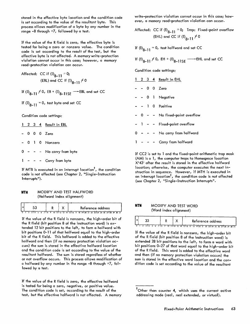
stored in the effective byte location and the condition code is set according to the value of the resultant byte. This process allows modification of a byte by any number in the range -8 through +7, followed by a test.
If the value of the R field is zero, the effective byte is tested for being a zero or nonzero value. The condition code is set according to the result of the test, but the effective byte is not affected. A memory write-protection violation cannot occur in this case; however, a memory read-protection violation can occur.
Affected: CC if (1)8-11 = 0;
(EBL) and CC if (1)8_ 11 f 0
If (1)8-11 f 0, EB + (1)8-11 SE -EBL and set CC
If {I)8-11 = 0, test byte and set CC
Condition code settings:
2 3 4 Result in EBL
o 0 0 Zero
o o Nonzero
o - No carry from byte
Carry from byte
If MTB is executed in an interrupt locationt , the condition code is not affected (see Chapter 2, "Single-Instruction Interrupts ll
).
MTH MODIFY AND TEST HALFWORD (Halfword index alignment)
If the value of the R field is nonzero, the high-order bit of the R field (bit position 8 of the instruction word) is extended 12 bit positions to the left, to form a halfword with bit positions 0-11 of that halfword equal to the high-order bit of the R field. This halfword is added to the effective halfword and then (if no memory protection violation occurs) the sum is stored in the effective halfword location and the condition code is set according to the value of the resultant halfword. The sum is stored regardless of whether or not overflow occurs. This process allows modification of a halfword by any number in "the range -8 through +7, followed by a test.
If the value of the R field is zero, the effective halfword is tested for being a zero, negative, or positive value. The condition code is set, according to the result of the test, but the effective halfword is not affected. A memory
write-protection violation cannot occur in this case; however, a memory read-protection violation can occur.
Affected: CC if (1)8-11 = 0; Trap: Fixed-point overflow
(EHL) and CC if (1)8-11 f 0
If {I)8-11 = 0, test halfword and set CC
If (1)8_11 to, EH + (1)8-11 SE -EHL and set CC
Condition code settings:
2 3 4 Result in EHL
- 0 0 Zero
- 0 Negative
o Positive
o - No fixed-point overflow
Fixed-point overflow
o - No carry from halfword
Carry from halfword
If CC2 is set to 1 and the fixed-point arithmetic trap mask (AM) is a 1, the computer traps to Homespace location X'43 1 after the result is stored in the effective halfword location; otherwise, the computer executes the next instruction in sequence. However, if MTH is executed in an interrupt locationt , the condition code is not affected (see Chapter 2, IISingle-Instruction Interrupts".
MTW MODIFY AND TEST WORD (Word index alignment)
If the value of the R field is nonzero, the high-order bit of the R field (bit position 8 of the instruction word) is extended 28 bit positions to the left, to form a word with bit positions 0-27 of that word equal to the high-order bit of the R field. This word is added to the effective word and then (if no memory protection violation occurs) the sum is stored in the effective word location and the condition code is set according to the value of the resultant
t Other than counter 4, which uses the current active addressing mode (real, real extended, or virtual).
Fixed~Point Arithmetic Instructions 63

word. The sum is stored regardless of whether or not overflow occurs. This process allows modification of a word by any number in the range -8 through +7, followed by a test.
If the value of the R field is zero, the effective word is tested for being a zero, negative, or positive value. The condition code is set according to the result of the test, but the effective word is not affected. A memory writeprotection violation cannot occur in this case; however, a memory read-protection violation can occur.
Affected: CC if (1)8-11 = 0; Trap: Fixed-point overflow
(EWL) and CC if (1)8_11 /0
If (1)8-11 = 0, test word and set CC
If (1)8-11 1 0, EW + IS-llSE -EWL and set CC
Condition code settings:
2 3 4 Resu It in EWl
0 0 Zero
- 0 Negative
0 Positive
o No fixed-point overflow
- Fixed-point overflow
o - No carry from word
Carry from word
If CC2 is set to 1 and the fixed-point arithmetic trap mask (AM) is a 1, the computer traps to Homespace location X'43' after the result is stored in the effective word location; otherwise, the computer executes the next instruction in sequence. However, if MTW is executed in an interrupt locationt , the condition code is not affected (see Chap-ter 2, "Single-Instruction Interrupts".
COMPARISON INSTRUCTIONS
The following comparison instructions are available to SIGMA 9 computer.s:
Instruction Name Mnemonic
Compare Immediate CI
Compare Byte CB
Compare Halfword CH
Compare Word cw
64 Comparison Instructions
Instruction Name Mnemonic
Compare Doubleword CD
Compare Selective CS
Compare With Limits in Register CLR
Compare With Limits in Memory ClM
All SIGMA 9 comparison instructions produce a condition code setting which is indicative of the results of the comparison, without affecting the effective operand in memory and without affecting the contents of the designated register.
CI COMPARE IMMEDIATE (Immediate operand)
COMPARE IMMEDIATE extends the sign of the value field (bit position 12) of the instruction word 12 bit positions to the Jeft, compares the 32-bit result with the contents of register R (with both operands treated as signed fixed-point quantities), and then sets the condition code according to the results of the comparison.
Affected: CC2, CC3,CC4
(R) : (1)12-31SE
Condition code settings:
2 3 4 Result of Comparison
o 0 Equal.
- 0 Register value less than immediate value.
o Register value greater than immediate value.
o - No 1-bits compare, (R) n (I)12-32SE = O.
- One or more l-bits compare,
(R) n (I) 12-32SE 10.
If CI is indirectly addressed, it is treated as a nonexistent instruction, in which case the computer unconditionally aborts execution of the instruction (at the time of operation code decoding) and then traps to Homespace location X'40' with the condition code unchanged.
CB COMPARE BYTE (Byte index alignment)
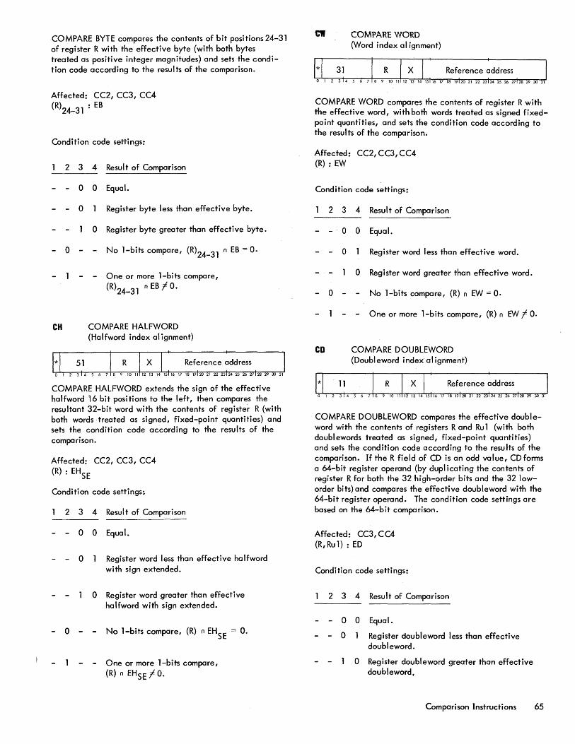
COMPARE BYTE compares the contents of bit positions 24-31 of register R with the effective byte (with both bytes treated as positive integer magnitudes) and sets the condition code according to the results of the comparison.
Affected: CC2, CC3, CC4
(R)24-31 : EB
Condition code settings:
2 3 4 Resul t of Comparison
- 0 0 Equal.
- 0
- 0 -
Register byte less than effective byte.
o Register byte greater than effective byte.
No 1-bits compare, (R)24-31 n EB = O.
One or more 1-bits compare,
(R)24-31 nEB I O.
CH COMPARE HALFWORD (Halfword index al ignment)
COMPARE HALFWORD extends the sign of the effective halfword 16 bit positions to the left, then compares the resultant 32-bit word with the contents of register R (with both words treated as signed, fixed-point quantities) and sets the condition code according to the results of the comparison.
Affected: CC2, CC3, CC4 (R) : EHSE
Condition code settings:
2 3 4 Result of Comparison
o 0 Equal.
o Register word less than effective halfword with sign extended.
o -
o Register word greater than effective halfword with sign extended.
No l-bits compare, (R) n EHSE = O.
One or more 1-bits compare, (R) n EHSE I O.
COMPARE WORD (Word index al ignment)
COMPARE WORD compares the contents of register R with the effective word, with both words treated as signed fixedpoint quc;mtities, and sets the condition code according to the results of the comparison.
Affected: CC2,CC3,CC4 (R) : EW
Condition code settings:
2 3 4 Result of Comparison
o 0 Equal.
o Register word less than effective word.
o Register word greater than effective word.
o - No 1-bits compare, (R) n EW = O.
One or more 1-bits compare, (R) n EW I o.
CD COMPARE DOUBLEWORD (Doubleword index al ignment)
COMPARE DOUBLEWORD compares the effective doubleword with the contents of registers Rand Ru 1 (with both doubl ewords treated as signed, fixed-point quantities) and sets the condition code according to the results of the comparison. If the R field of CD is an odd value, CD forms a 64-bit register operand (by dupl icating the contents of register R for both the 32 high-order bits and the 32 loworder bits) and compares the effective doubleword with the 64-bit register operand. The condition code settings are based on the 64-bit comparison.
Affected: CC3, CC4 (R, Ru 1) : ED
Condition code settings:
2 3 4 Result of Comparison
- 0 0 Equal.
- 0 Register doubleword less than effective doubl eword.
o Register doubleword greater than effective doubleword,
Comparison Instructions 65
cs COMPARE SELECTIVE (Word index alignment)
COMPARE SELECTIVE compares the contents of register R with the effective word in only those bit positions selected by a 1 in corresponding bit positions of register Ru 1 (mask). The contents of register R and the effective word are ignored in those bit positiofls designated by a 0 in corresponding bit positions of register Ru L The seJected contents of register R and the effective word are treated as positive integer magnitudes, and the condition code is set according to the result of the comparison. If the R field of CS is an odd value; CS compares the contents of register R with the logical product (AND) of the effective word and the contents of register R.
Affected: CC3, C C4 If R is even: (R) n (Rul) : EW n (Rul) If R is odd: (R): EW n (R)
Condition code settings:
2 3 4 Results of Comparison under Mask in Ru 1
- 0 0 Equal.
o Register word less than effective word.
o Register word greater than effective word. (if R is even)
elK COMPARE WITH LIMITS IN REGISTERS (Word index al ignment)
COMPARE WITH LIMITS IN REGISTERS simultaneously compares the effective word with the contents of register R and with the contents of register Ru 1 (with all three words treated as signed fixed-point quantities), and sets the condition code according to the results of the comparisons.
Affected: CC (R) : EW, (Ru 1) : EW
Condition code settings:
2 3 4 Result of Comparison
- 0 0 Contents of R equal to effective word.
- 0 Contents of R less than effective word.
o Contents of Rgreater than effective word.
o 0 Contents of Ru 1 equal to effective word.
o - Contents of Ru 1 less than effective word.
o - - Contents of Ru 1 greater than effective word.
66 Logical Instructions
ClM COMPARE WITH LIMITS IN MEMORY (Doubleword index alignment)
COMPARE-WITH LIMITS IN MEMORY simultaneously compares the contents of register R with the 32 high-order bits of the effective doubleword and with the 32 low-order bits of the effective doubleword, with all three words treated as 32-bit signed quantities, and sets the condition code accordi-ng to the results of the comparisons.
Affected: CC (R) : E00-31; (R): E032_63
Condition code settings:
1 . 2 3 4 Result of Comparison
- 0 0 Contents of R equal to most significant word, (R) = EO
O_3
1"
- 0 Contents of R less than most significant word, (R) < EO
O_
31'
o Contents of R greater than most signficant word, (R) > EOO_31"
o 0 - - Contents of R equal to least significant word, (R) = ID32- 63•
o - Contents of R less than least significant word, (R) < E0
32_63
•
o - Contents ·of R greater than least significant word, (R) > E032_63•
LOGICAL INSTRUCTIONS
All logical operations are performed bit by corresponding bit between two operands; one operand is in register Rand the other operand is the effective word. The result of the logical operation is loaded into register R.
OR OR WORD N/ord index aJ ignment)
OR WORD logically ORs the effective word into register R. If corresponding bits of register R and the effective word are both 0, a 0 remains in reg.ister R; otherwise, a 1 is placed in the corresponding bit position of register R. The effective word is not affected.
Affected: (R), CC3, CC4 (R) u EW - R, where 0 u 0 = 0, 0 u 1 = 1, 1 u 0 = 1,
1 u 1 = 1
Condition code settings:
2 3 4 Resu It in R
- 0 0 Zero.
- 0 Bit 0 of register R is a 1.
OBit 0 of register R is a 0 and bit positions 1-31 of register R contain at least one 1.
EOR EXCLUSIVE OR WORD (Word index al ignment)
EXCLUSIVE OR WORD logically exclusive ORs the effective word into register R. If corresponding bits of register R and the effective word are different, a 1 is placed in the corresponding bit position of register R; if the contents of the corresponding bit positions are alike, a 0 is placed in the corresponding bit position of register R. The effective word is not affected.
Affected: (R), CC3, CC4 (R)@ EW -R, where O@O = 0, O@ 1 = 1,
1 @ 0 = 1, 1 @ 1 = 0
Condition code settings:
2 3 4 Result in R
- 0 0 Zero.
- 0 Bit 0 of register R is a 1.
OBit 0 of register R is a 0 and bit positions 1-31 of register R contain at least one 1.
AND AND WORD (Word index alignment)
AND WORD logically ANDs the effective word into register R. If corresponding bits of register R and the effective word are both 1, a 1 remains in register R; otherwise, a 0 is placed in the corresponding bit position of register R. The effective word is not affected.
Affected: (R), CC3, CC4 (R) n EW - R, where 0 n 0 = 0, 0 n 1 = 0,
1 n 0 = 0, 1 () 1 = 1
Condition code settings:
2 3 4 Result in R
o 0 Zero.
o Bit 0 of register R is a 1.
o Bit 0 of registerR is a 0 and bit positions 1-31 of register R contain at least one 1.
SHIFT INSTRUCTIONS
The instruction format for logical, circular, arithmetic, and searching shift operations is:
S SHIFT (Word index al ignment)
If neither indirect addressing nor indexing is called for in the instruction SHIFT, bit positions 21-23 of the reference address field determine the type, and bit positions 25-31 determine the direction and amount of the shift.
If only indirect addressing is called for in the instruction, bits 15-31 of the instruction are used to access the indirect word and then bits 21-23 and 25-31 of the indirect word determine the type, direction, and amount of the shift.
If only inde)(ing is called for in the instruction, bits21-230f the instruction word determine the type of shift; the direction and amount of shift are determined by bits 25-31 of the instruction plus bits 25-31 of the specified index register.
If both indirect addressing and indexing are called for in the instruction, bits 15-31 of the instruction are used to access the indirect word and then bits 21-23 of the indirect word determine the type of shift; the direction and amount of the shift are determined by bits 25-31 of the indirect word plus bits 25-31 of the specified index register.
The effective address does not reference memory. Bit positions 15-20 and 24 of the effective virtual address are ignored. Bit positions 21, 22, and 23 of the effective virtual address determine the type of shift, as follows:
21 22 23 Shift Type
0 0 0 Logical, single register
0 0 Logical, double register
0 0 Circular, single register
0 Circular, double register
0 0 Arithmetic, single register
0 Arithmetic, double register
0 Searching, single register
Searching, double register
Shift Instructions 67
Bit positions 25 through 31 of the effective virtual address are a shift count that-determines the direction and amount of the shift. The shift count (C) is treated as a 7-bit signed binary integer, with the high-order bit (bit position 25) as the sign (negative integers are represented in two's complement form). A positive shift count causes a left shift of C bit positions. A negative shift count causes a right shift of Ici bit positions. The value of C is within the range: -64 ~ C ~ +63.
All double-register shift operations require an even value for the R field of the instruction, and treat registers Rand Ru 1 as a 64-b.it register with the high-order bit (bit position 0 of register R) as the sign for the entire register. If the R field of SHIFT is an odd value and a double-register shift operation is specified, a register doubleword is f.armed by dupl icating the contents of register R for both the 32 high-order bits and the 32 low-order bits of the doubleword. The shift operation is then performed and the 32 highorder bits of the result are loaded into register R.
Overflow occurs (on left shifts only) whenever the value of the sign bit (bit position 0 of register R) changes. At the completion of logical left, circular Jeft, arithmetic left, and searching left shifts, the condition code ;s set as follows:
2 3 4 Result of Shift
o - Even number of l's shifted off left end of register R.
- Odd number of l' s sh if ted off I eft end of register Rt.
- 0 - No overflow on left shift.
Overflow on left shift.
Searching shift terminated with RO equal 1.
At the completion of right shifts, the condition code is set as follows:
234
00- -
Logical Shift, Single Register
If the shift count, C, is positive, the contents of register R are shifted left C places, with O's copied into vacated bit
t Not -Oppl i cabl e for searching shift.
68 Shift InstruCtions
positions on the right. (Bits shifted past Ro are lost.) If C is negative, the contents of register R are shifted right Ici places, with.O's copied into vacatedbit positions on the left. (Bits shifted past ~1 are lost.)
Affected: (R), CC1, CC2
Logical Shift, Double Register
If the shift count, C, is positive, the contents of registers Rand Ru 1 are shifted left C places, with -o's copied into vacated bit positions on the right. Bits shifted past bit position 0 of register Ru 1 are copied into bit position 31 of register R. (Bits shifted past RO are tost.) If C is negative, the contents of registers Rand Ru 1 are shifted right lei places with O's copied into vacated bit positions on the left. Bits shifted past bit position 31 of register Rare copied into bit position 0 of register Rul. (Bits shifted past Ru1
31 are lost.)
Affected: (R), (Rul), CC1,CC2
Circufar Shift, Single Register
If the shift count, C, is positive, the contents of regis-ter R are shifted left C pfaces. Bits shifted past bit position 0 are copied into bi t position 31. (No bi ts are lost.) If C is negative, the contents of register R are shifted right rCI places. Bits shifted past bit position 31 are copied into bit position O. (No bits are lost.)
Affected: (R), eCl ,eC2
Circular Shift, Double Register
If the shift count, C, is positive, the contents of registers Rand Ru lore shifted left C places. Bits shifted past bit position 0 of register R are copied into bit position 31 of register Ru1. (No bits are lost.) If C is negative, the contents of registers Rand Ru 1 are shifted right Ici places. ~its shifted past bit position 31 of register Ru 1 are copied into bit position 0 of register R. (No bits are lost.)
Affected: (R), (Ru 1), Cel, Ce2
Arithmetic Shift, Single Register
If the shift count, C, is positive, the contents of register R are shifted left C places, with O's copied into
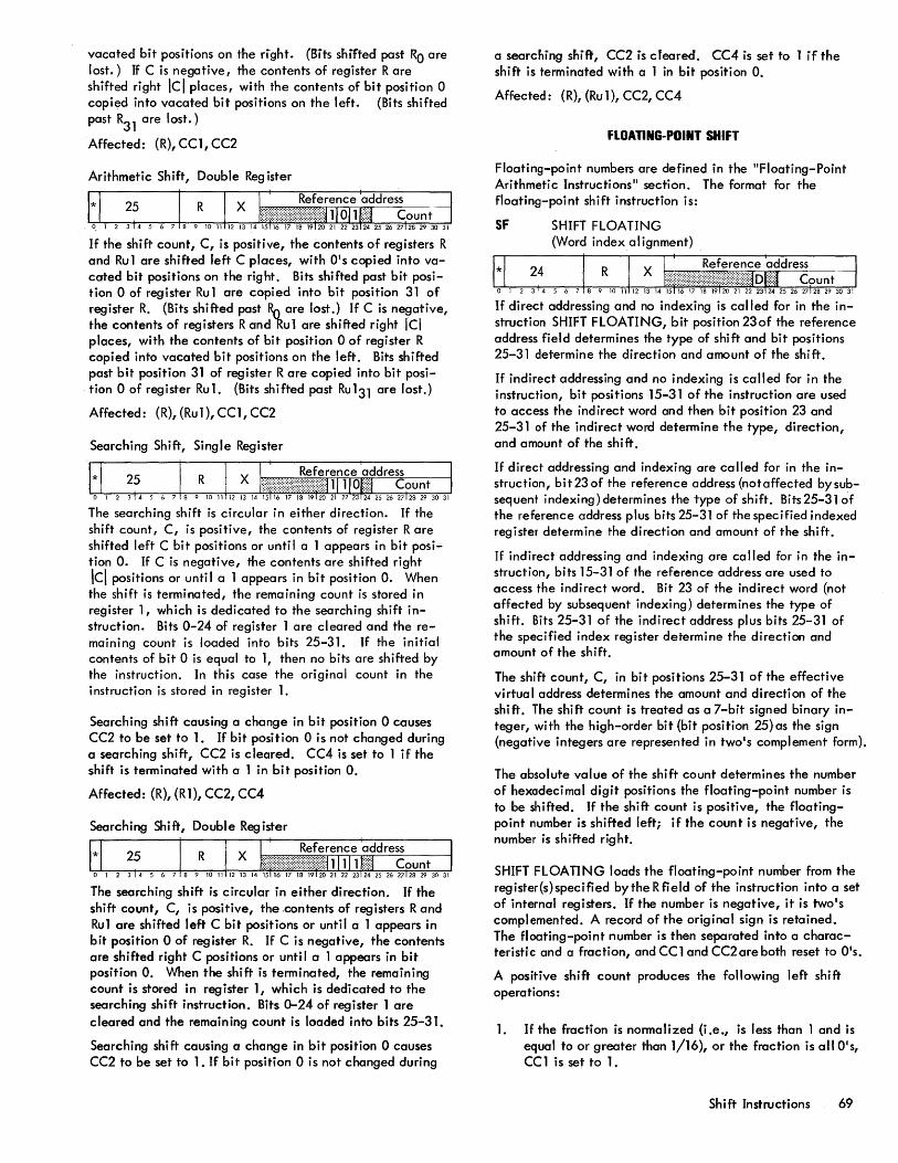
vacated bit positions on the right. (Bits shifted past RO are lost.) If C is negative, the contents of register Rare shifted right Ic I places, with the contents of bit position 0 copied into vacated bit positions on the left. (Bits shifted past R31 are lost.)
Affected: (R),CC1,CC2
Arithmetic Shift, Double Register
If the shift count, C, is positive, the contents of registers R and Ru 1 are shifted left C places, with O's copied into vacated bit positions on the right. Bits shifted past bit position 0 of register Ru1 are copied into bit position 31 of register R. (Bits shifted past Rn are lost.) If C is negative, the contents of registers Rand 'Ru1 are shifted right Ici places, with the contents of bit position 0 of register R copied into vacated bit positions on the left. Bits shifted past bit position 31 of register R are copied into bit position 0 of register Ru 1. (Bits shifted past Ru 131 are lost.)
Affected: (R), (Rul), CC1, CC2
Searching Shift, Single Register
The searching shift is circular in either direction. If the shift count, C, is positive, the contents of register Rare shifted left C bit positions or unti I a 1 appears in bit position O. If C is negative, the contents are shifted right \C\ positions or unti I a 1 appears in bit position O. When the shift is terminated, the remaining count is stored in register 1, which is dedicated to the searching shift instruction. Bits 0-24 of register 1 are cleared and the remaining count is loaded into bits 25-31. If the initial contents of bit 0 is equal to 1, then no bits are shifted by the instruction. In this case the original count in the instruction is stored in register 1.
Searching shift causing a change in bit position 0 causes CC2 to be set to 1. If bit position 0 is not changed during a searching shift, CC2 is cleared. CC4 is set to 1 if the shift is terminated with a 1 in bit position O.
Affected: (R), (Rl), CC2, CC4
Searching Shift, Double Register
The searching shift is circular in either direction. If the shift count, C, is positive, the .contents of registers Rand Rul are shifted left C bit positions or until a 1 appears in bit position 0 of register R. If C is negative, the contents are shifted right C positions or until a 1 appears in bit position O. When the shift is terminated, the remaining count is stored in register 1, which is dedicated to the searching shift instruction. Bits 0-24 of register 1 are cleared and the remaining count is loaded into bits 25-31.
Searching shift causing a change in bit position 0 causes CC2 to be set to 1. If bit position 0 is not changed during
a searching shift, CC2 is cfeared. CC4 is set to 1 if the shift is terminated with a 1 in bit position O.
Affected: (R), (Rul), CC2, CC4
flOATING·POINT SHIFT
Floating-point numbers are defined in the IIFloating-Point Arithmetic Instructions ll section. The format for the floating-point shift instruction is:
SF SHIFT FLOA lING (Word index alignment)
If direct addressing and no indexing is called for in the instruction SHIFT FLOATING, bit position 230f the reference address field determines the type of shift and bit positions 25-31 determine the direction and amount of the shift.
If indirect addressing and no indexing is called for in the instruction, bit positions 15-31 of the instruction are used to access the ind irect word and then bit position 23 and 25-31 of the indirect word determine the type, direction, and amount of the shift.
If direct addressing and indexing are called for in the instruction, bi t 23 of the reference address {not affected by subsequent indexing) determines the type of shift. Bits25-31 of the reference address plus bits 25-31 of the specified indexed register determine the direction and amount of the shift.
If indirect addressing and indexing are called for in the instruction, bits 15-31 of the reference address are used to access the indirect word. Bit 23 of the indirect word (not affected by subsequent indexing) determines the type of shift. Bits 25-31 of the indirect address plus bits 25-31 of the specified index register determine the direction and amount of the shift.
The shift count, C, in bit positions 25-31 of the effective virtual address determines the amount and direction of the shift. The shift count is treated as a7-bit signed binary integer, with the high-order bit {bit position 25)as the sign (negative integers are represented in two's complement form).
The absolute value of the shift count determines the number of hexadecimal digit positions the floating-point number is to be shifted. If the shift count is positive, the floatingpoint number is shifted left; if the count is negative, the number is shifted right.
SHIFT FLOATING loads the floating-point number from the register{s)specified by the R field of the instruction into a set of internal registers. If the number is negative, it is two's complemented. A record of the original sign is retained. The floating-point number is then separated into a characteristic and a fraction, and CCl and CC2areboth reset to O's.
A positive shift count produces the following left shift operations:
1. If the fraction is normalized (i.e., is less than 1 and is equal to or greater than 1/16), or the fraction is all O's, CC1 is set to 1.
Shi ft Instructions 69
2. If the fraction field is all OIS, the entire floating-point number is set to all OIS (true zero), regardless of the sign and the characteristic of the original number.
3. If the fraction is not nonnalized, the fraction field is shifted 1 hexadecimal digit position (4 bit positions) to the left and the characteristic field is decremented by 1. Vacated digit positions at the right of the fraction are filled with hexadecimal O's.
If the characteristic field underflows (i. e., is all l's as the result of being decremented), CC2 is set to 1. However, if the characteristic field does not underflow, the shift process (shift fraction, and decrement characteristic) continues until the fraction is normalized, until the characteristic field underflows, or until the fraction is shifted left C hexadecimal digit positions, whichever occurs first. (Any two, or all three, of the terminating conditions can occur simultaneously.)
4. At the completion of the left shift operation, the floating-point result is loaded back into the general register{s). If the number was originally negative, the twols complement of the resultant number is loaded into the general registers(s).
5. The condition code settings following a floating-point left shift are as follows:
2 3 4 Result
o 0 True zero (all OIS).
o Negative.
00-
o Positive.
C digits shifted (fraction unnormal ized, no characteristic underflow).
Fract ion norma I i zed (i ncl udes true zero).
Characteristic underflow.
A negative shift count produces the following right shift operations (again assuming that negative numbers are twols complemented before and after the shift operation):
1. The fraction field is shifted 1 hexadecimal digit position to the right and the characteristic field is incremented by 1. Vacated digit positions at the left are filled with hexadecimal OIS.
2. If the characteristic field overflows {i. e., is all OIS as the result of being incremented}, CC2 is set to 1. However, if the characteristic field does not overflow, the shift process (shift fraction, and increment characteristic) continues until the characteristic field overflows or until the fraction is shifted right IC/ hexadecimal digit positions, whichever occurs first. (Both terminating conditions can occur simultaneously. )
3. If the resultant fraction field is all OIS, the entire floating-point number is set to all OIS (true zero), regardless of the sign and the characteristic of the original number.
70 Conversion Instructions
4. At the completion of the right shift operation, the floating-point result is loaded back into the general register(s}. If the number was originally negative, the twols complement of the resultant number is loaded into the general register{s).
5. The condition code settings following a floating-point right shift are as follows:
2 3 4 Result
- 0 0 T rue zero {all zeros}.
- 0 Negative.
o Positive.
00- lei digits shifted (no characteristic overflow).
o Characteristic overflow.
Floating Shift, Single Register
The short-format floating-point number in register R is shifted according to the rules established above for floatingpoint shift operations.
Affected: (R), CC
Floating Shift, Double Register
The long-format floating-point number in registers Rand Ru 1 is shifted according to the rules established above for floating-point shift operations. (If the R field of the instruction word is an odd value, a long-fonnat floatingpoint number is generated by duplicating the contents of register R, and the 32 high-order bits of the result are loaded into register R.)
Affected: (R), {Ru1),CC
CONVERSION INSTRUCTIONS
The following two conversion instructions are provided by the SIGMA 9 computer:
Instructi on Name Mnemonic
Convert by Addition CVA
Convert by Subtraction CVS
These two conversion instructions can be used to accomplish bidirectional translation between binary code and any other weighted binary code, such as BCD.
The effective addresses of the instructions CONVERT BY ADDITION and CONVERT BY SUBTRACTION each point to the starting location of a conversion table of 32 words, containing weighted values for each bit position of register Ru 1. The 32 words of the conversion table are considered to be 32-bit positive quantities, and are referred to as conversion values. The intermediate results of these instructions are accumulated in internal CPU registers until the instruction is completed; the result is then loaded into the appropriate general register. Both instructions use a counter {n} that is set to 0 at the beginning of the instruction execution and is incremented by 1 with each iteration, until a total of 32 iterations have been performed.
If a memory parity or protection violation trap occurs during the execution of either instruction, the instruction sequence is aborted {without having changed the contents of register R or Ru 1} and may be restarted {at the beginning of the instruction sequence} after the trap routine is processed.
eVA CONVERT BY ADDITION (Word index alignment)
CONVERT BY ADDITION initially clears the internal A register and sets an internal counter {n} to o. If bit position n of register Ru1 contains a 1, CVA adds the nth conversion value {contents of the word location pointed to by the effective address plus n} to the contents of the A register, accumulates the sum in the A register, and increments n by 1. If bit position n of register Ru 1 contains a 0, CVA only increments n. If n is less than 32 after being incremented, the next bit position of register Ru 1 is examined, and the addition process continues through n equal to 31; the result is then loaded into register R. If, on any iteration, the sum has exceeded the value 232- 1, CC1 is set to 1; otherwise, eel is reset to O.
Affected: (R), CC1, eC3, CC4 O-A,O-n
If {Ru1} = 1, then {EWL + n} + {A} -A, n + 1 -n n
If {Ru1} = 0, then n + 1-- n n
If n < 32, repeat; otherwise, {A} -R and continue to next instruction.
Condition code settings:
2 3 4 Resu It in R
o 0 Zero.
o Bit 0 of register R is a 1.
o
evs
2 3 4 Result in R
OBit 0 of register R is a 0 and bit positions 1-31 of register R contain at least one 1.
Sum is correct {I ess than 232
}.
Sum is greater than 232
_1.
CONVERT BY SUBTRACTION {Word index alignment}
CONVERT BY SUBTRACTION loads the internal A register with the contents of register R, clears the internal B register, and sets an interna I counter {n} to O. All conversion values are considered to be 32-bit positive quantities. If the nth conversion value {the contents of the word location pointed to by the effective address plus n} is equal to or less than the current contents of the A register, CVS increments n by 1, adds the two's complement of the nth conversion value to the contents of the A register, stores the sum in the A register, and stores a 1 in bit position n of the B register. If the nth conversion value is greater than the current contents of the A register, CVS onl y increments n by 1. If n is less than 32 after being incremented, the next conversion value is compared and the process continues through n equal to 31; the remainder in the A register is loaded into register R, and the converted quantity in the B register is loaded into register Ru 1.
Affected: {R}, {Ru 1}, CC3, CC4
{R} -A, 0 -B, 0 -n
If {EWL + n} $ (A) then A - (EWL + n) -A, 1-B n+1-n
n'
If {EWL + n} > (A) then n + 1 -n
If n < 32, repeat; otherwise, (A) - R, {B} - Ru 1 and continue to the next instruction.
Condition code settings:
2 3 4 Resu I tin Ru 1
o 0 Zer~.
o Bit 0 of register Ru1 is a 1.
OBit 0 of register Ru1 is a 0 and bit positions 1-31 of register Ru1 contain at least one 1.
Conversion Instructions 71
FLOATING-POINT ARITHMETIC INSTRUCTIONS
The following floating-point arithmetic instructions are available to SIGMA 9 computers:
Instruction Name Mnemonic
Floating Add Short FAS
Floating Add Long FAL
Floating Subtract Short FSS
Floating Subtract Long FSL
Floating Multiply Short FMS
Floating Multiply Long FML
Floating Divide Short FDS
Floating Divide Long FDL
flOATING-POINT NUMBERS
SIGMA 9 accommodates two number formats for floatingpoint arithmetic: short and long. A short-formatfloatingpoint number consists of a sign (bit 0), a biasedt , base 16 exponent, which is called a characteristic (bits 1-7), and a six-digit hexadecimal fraction (bits 8-31). A long-format floating-point number followed by an additional eight hexadecimal digits of fractional significance and occupies a doubleword memory location or an even-odd pair of general registers.
A SIGMA 9 floating-point number (N) has the following format:
I~ I ~~i:(~r I : Fraction (F) : I o 1 2 3 14 5 6 7 8 9 10 11112 13 14 15 16 17 18 19120 21 22 23 24 25 26 27128 29 30 31
A floating-point number (N) has the following formal definition:
1. N = F x 16 C-64 where F = 0 or
16 -6 :s I FI:s l{short format) or
16-14
:s IFI:s 1 (long format)
and O:s C :5 127.
tThe bias value of 4016 is added to the exponent for the purpose of making it possible to compare the absolute magnitude of two numbers, i. e., without reference to a sign bit. This manipu~ation effectively removes the sign bit, making each characteristic a 7-bit positive number.
72 Floating-Point Arithmetic Instructions
2. A positive floating-point number with a fraction of zero and a characteristic of zero is a Jltrue Jl zero. A positive floating-point number with a fraction of zero and a nonzero characteristic is an Jlabnormal" zero. For floating-point multiplication and division, an abnormal zero is treated as a true zero. However, for addition and subtraction, an abnormal zero is treated the same as any nonzero operand.
3. A positive floating-point number is normalized if and only if the fraction is contained in the interval
1/16:5 F < 1
4. A negative floating-point number is the two's complement of its positive representation.
5. A negative floating-point number is normalized if and only if its two's complement is a normal ized positive number.
By this definition, a floating-point number of the form
1 xxx xxxx 1111 0000 . .. 0000
is normalized, and a floating-point number of the form
1 xxx xxxx 0000 0000 . .. 0000
is illegal and, whenever generated by floating-point instructions, is converted to the form
1 yyy yyyy 1111 0000 • .. 0000
where yy .•. y is 1 less than xx ... x. Table 11 contains examples of floating-point numbers.
Modes of Operation
SIGMA 9 contains three mode control bits that are used to qualify floating-point operations. These mode control bits
are identified as FS (floating significance), FZ (floating zero), and FN (floating normalize), and are contained in bit positions 5, 6, and 7, respectively, of the program status doubleword (PSD 5-7)'
The floating-point mode is establ ished by setting the three floating-point mode control bits. This can be performed by any of the following instructions:
Instruction Name
Load Conditions and Floating Control
Load Conditions and Floating Control Immediate
Load Program Status Doubl eword
Exchange Program Status Doubleword
Mnemonic
LCF
LCFI
LPSD
XPSD
90 17 33C-1(4/74)
Table 11. Floating-Point Number Representation
Short Floating-Point Format
Decimal Number ± C
+(16 +63)(1_2-24) a 111 1111 1111 1111
+(16+3)(5/16) a 100 0011 0101 0000
+( 16 -3) (209/256) 0 011 1101 1101 0001
+(16-63
)(2047/4096) a 000 0001 0111 1111
+(16-64)(1/16) a 000 0000 0001 0000
a (cai led true zero) a 000 0000 0000 0000
_(16-64)(1/16) 1 111 1111 1111 0000
-(16-63)(2047/4096) 1 111 1110 1000 0000
-(16-3)(209/256) 1 100 0010 0010 1111
-(16+3)(5/16) 1 011 1100 1011 0000
-(16 +63)(1_224) 1 000 0000 0000 0000
Speci a I Case
-(16e )(l) 1 -e 0000 0000
is cha nged to
-(16e+1)(1/16) 1 e + 1 1111 0000
whenever generated as the result of a floating-point instruction.
The floating-point mode control bits are stored by executing either of the following instructions:
Instruction Name
Store Cond i ti ons and Float i ng Contro I
Exchange Program Status Doubleword
FLOATING-POINT ADD AND SUBTRACT
Mnemonic
STCF
XPSD
The floating normalize (FN), floating zero (FZ), and floating significance (FS) mode control bits determine the operation of floating-point addition and subtraction (if characteristic overflow does not occur) as follows:
FN Floating normalize:
F N = a The results of additions and subtractions are to be postnormalized. If characteristic
90 17 33C-l(4/74)
F
1111
0000
0000
1111
0000
0000
0000
0001
0000
0000
0000
0000
0000
Hexadecimal Value
1111 1111 1111 7F FFFFFF
0000 0000 0000 43 500000
0000 0000 0000 3D Dl0000
0000 0000 0000 01 7FFOOO
0000 0000 0000 00 100000
0000 0000 0000 00 000000
0000 0000 0000 FF FOOOOO
0000 0000 0000 FE 801000
0000 0000 0000 C2 2FOOOO
0000 0000 0000 BC BOOOOO
0000 0000 0001 80 000001
0000 0000 0000
0000 0000 0000
underflow occurs, if the result is zero, or if more than two postnormalization hexadecimal shifts are required, the settings for FZ and FS determine the resultant action. If none of the above conditions occurs, the condition code is set to 0010 if the result is positive or to 0001 if the result is negative.
FN = 1 Inhibit postnormalization of the result of additions and subtractions. The settings of FZ and FS have no effect on the instruction operation. If the result is zero, the result is set to true zero and the condition code is set to 0000. If the result is positive, the condition code is set to 0010. If the result is negative, the condition code is set to 0001.
Floating -Point Arithmetic Instructions 73
FZ Floating zero: (appl ies only if FN :::: 0)
FZ = 0 If the final result of an addition or subtraction operation cannot be expressed in normalized form because of the characteristic being reduced below zero, underflow has occurred, in wh ich case the result is set equal to true zero and the condition cooe is set to 1100. (Exception: if a trap results from significance checking with FS = 1 and FZ = 0, an underflow generated in the process of postnormalizing is ignored.)
FZ = 1 Characteristic underflow causes the computer to trap to Homespace location X'44' with the contents of the genera I registers unchanged. If the result is positive, the condition code is set to 1110. If the result is negative, the condition code is set to 1101.
FS Floating sign ificance: (appl ies only if FN = 0)
FS = 0 Inhibit significance trap. If the result of an addition or subtraction is zero, the result is set equal to true zero, the condition code is set to 1000, and the computer executes the next instruction in sequence. If more than two hexadecimal places of postnormalization shifting are required and characteristic underftow does not occur, the condition code is set to 1010 if the result is positive, or to 1001 if the result is negative; then, the computer executes the next instruction in sequence. (Exception: if characteristic underflow occurs with FS = 0, FZ determines the resul tant action. )
FS = 1 The computer traps to Homespace location X'44' if more than two hexadecimal places of postnormal ization shifting are required or if the result is zero. The condition code is set to 1000 if the result is zero, to 1010 if the result is positive, or to 1001 if the result is negative; however, the contents of the general registers are not changed. (Exception: if a trap results from characteristic underflow with FZ = I, the results of significance testing are ignored.)
If characteristic overflow occurs, the CPU always traps to Homespace location X'44' with the general registers unchanged and the condition code set to 0110 if the result is positive, or to 0101 if the result is negative.
FlOAnNG-POINT MULTIPLY AND DIVIDE
The floating zero (FZ) mode control bit alone determines the operation of floating-point multiplication and division
74 Floating-Point Arithmetic Instructions
(if characteristic overflow does not occur and division by zero is not attempted) as follows:
FZ Floating zero:
FZ = 0 If the final result of a multiplication or division operation cannot be expressed in normalized form because of the characteristic being reduced below zero, underflow has occurred. If underflow occurs, the result is set equal to true zero and the condition code is set to 1100. If underflow does not occur, the condition code is set to 0010 if the result is positive, to 0001 if the result is negative, or to 0000 if the result is zero.
FZ = 1 Underflow causes the computer to trap to Homespace location X'44' with the contents of the general registers unchanged. The condition code is set to 1110 if the result is positive, or to 1101 if the result is negative. If underflow does not occur, the resultant action is the same as that for FZ = O.
If the divisor is zero in a floating-point division, the computer always traps to Homespace location X'44' with the general registers unchanged and the condition code set to 0100. If characteristic overflow occurs, the computer always traps to Homespace location X'44' with the general registers unchanged and the condition code set to 0110 if the result is positive, or to 0101 if the result is negative.
CONDlnON CODES III_R 'FLOATING-POINT INSTRUCnONS
The condition code settings for floating-point instructions are summarized in Table 12. The following provisions apply to all floating-point instructions:
1. Underflow and overflow detection apply to the final cl,aracteristic, not to any "intermediate" value.
2. If a floating-point operation results in a trap, the original contents of all general registers remain unchanged.
3. All shifting and truncation are performed on absolute magnitudes. If the fraction is negative, then the two's complement is formed after shifting or truncation.
FAS FLOATING ADD SHORT (Word index a Ii gnment)
The effective word and the contents of register Rare loaded into a set of internal registers and a low-order hexadecimal zero (guard digit) is appended to both fractions,
90 17 33C-l(4/74}
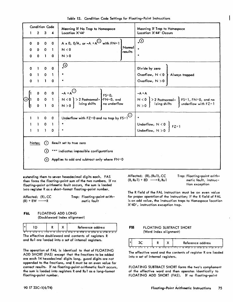
Table 12. Condition Code Settings for Floating-Point Instructions
Condition Code Meaning If No Trap to Homespace Meaning If Trap to Homespace
1 2 3 4 Location X'441 Location X'441 Occurs
0 0 0 0 A x 0, *0
0 0 0 1 N <0
O/A, or -A+A0 wi~ FN;l}
Nonnal * . results
0 0 1 0 N >0
0 1 0 0 0 *
0 1 0 1 * 0 1 1 0 *
1 0 0 0 o } -A +A FS=O,
01 0 0 1 N < 0 > 2 Postnormal- FN=O, and
J 0 1 0 N > o} izing shifts no underflow
1 1 0 0 Ut:lderflow with FZ=O and no trap by FS= 1
1 1 0 1 * 1 1 1 0 *
Notes: 0) Result set to true zero
0 ..... indicates impossible configurations
0) Appl ies to add and subtract only where FN=O
extending them to seven hexadecimal digits each. FAS then forms the floating-point sum of the two numbers. If no floating-point arithmetic fault occurs, the sum is loaded into register R as a short-format floating-point number.
Affected: (R), CC (R) + EW-R
Trap: Floating-point arithmetic fault
FAL FLOATING ADD LONG (Doubleword index alignment)
The effective doubleword and contents of registers R and Ru 1 are loaded into a set of internal registers.
The operation of FAL is identical to that of FLOATING ADD SHORT (FAS) except that the fractions to be added are each 14 hexadeCimal digits long, guard digits are not appended to the fractions, and R must be an even value for correct results. If no floating-point arithmetic fault occurs, the sum is loaded into registers Rand Ru 1 as a long-format floating-point number.
90 17 33C-1(4/74)
*
Divide by zero }
Overflow, N < 0 Always trapped
Overflow, N > 0
-A+A
N < 0 } > 2 Postnormol-N > 0 izing shifts
} FS= 1, FN=O, and no underflow with FZ= 1
0 • Underflow, N <0
} FZ;l Underflow, N >0
Affected: (R), (Ru 1), CC (R, Rul) + ED -R, Ru1
Trap: Floating-point arithmetic fault, instruction exception
The R field of the FAL instruction must be an even value for proper operation of the instruction; if the R field of FAL is an odd value, the instruction traps to Homespace location X' 4D ' , instruction exception trap.
FSS FLOATING SUBTRACT SHORT (Word index a Ii gnment)
The effective word and the contents of register R are loaded into a set of internal registers.
FLOATING SUBTRACT SHORT forms the two's complement of the effective word and then operates identically to FLOATING ADD SHORT (FAS). If no floating-point
Floating-Point Arithmetic Instructions 75
arithmetic faul t occurs, the difference is loaded into register R as a short-format floating-point number ..
Affected: (R), CC (R)-EW-R
Trap: Floating-point arithmetic fault
FSL FLOATING SUBTRACT LONG (Doubleword index al ignment)
The effective doubl eword and the contents of registers R and Ru1 are loaded into a set of internal registers.
FLOATING SU BTRACT LONG forms the two1s complement of the effective doubleword and then operates identically to FLOATING ADD LONG (FAL). If no floatingpoint arithmetic fault occurs, the difference is loaded into registers Rand Ru 1 as a long-format floating-point number.
Affected: (R), (Ry 1), CC (R, Ru 1) - ED -R, Ru 1
Trap: Floating-point arithmetic fault, instruction exception
The R field of the FSL instruction must be an even value for proper operation of the instruction; if the R field of FSL is an odd value, the instruction traps to Homespace location X'4D', instruction exception trap.
FMS FLOATING MULTIPLY SHORT (Word index al ignment)
The effective word (multiplier) and the contents of register R (multiplicand) are loaded into a set of internal registers, and both numbers are then prenormalized (if necessary). The product of the fractions contains 12 hexadecimal digits. If no floating-point arithmetic fault occurs, the product is loaded into register R as a properly truncated short-format floating-point number.
The result of floating-multiply is always postnormalized. At most, one place of postnormal izing shift may be required. Truncation takes place after postnormal ization.
Affected: (R), CC (R) x EW -R
Trap: Floating-point arithmetic fault
FML FLOA TIN G MULTIPLY LONG (Doubleword index al ignment)
The effective doubleword (multiplier) and the contents of registers Rand Ru 1 (multipl icand) are loaded into a set of internal registers. FLOATING MULTIPLY LONG then
76 . Floating-Point Arithmetic Instructions
operates identically to FLOATING MULTIPLY SHORT (FMS), except that the multiplier and the multiplicand fractions are each 14 hexadecimal digits long, the product fraction is 28 hexadecimal digits long, and R must be an even value for correct results. If no floating-point arithmetic fault occors, the postnormalized product is truncated to a long-format floating-point number and loaded into registers Rand Ru 1.
Affected: (R), (Ru 1), CC (R, Ru1) x ED -R, Ru 1
Trap: Floating-point arithmetic fault, instruction exception
The R field of the FML instruction must be an even value for proper operation of the instruction; if the R field of FML is an odd value, the instruction traps to Homespace location X'4D ' , instruction exception trap.
FDS FLOATING DIVIDE SHORT (Word index al ignment)
o 1 2
3E I R I X I: Reference: address I 3145 6 78 9 10 111213141516171819120212223;>4252627128293031
The effective word (divisor) and the contents of register R (dividend) are loaded into a set of internal registers and both numbers are then prenormalized (if necessary). FLOATING DIVIDE SHORT then forms a floating-point quotient with a 6-digit, normal ized hexadecimal fraction. If no floating-point arithmetic faul t occurs, the quotient is loaded into register R as a short-format floating-point number.
Affected: (R), CC (R)';' EW -R
Trap: Floating-point arithmetic fault
FDL FLOATING DIVIDE LONG (Doubleword index alignment)
The effective doubleword (divisor) and the contents of registers Rand Ru 1 (dividend) are loaded into a set of internal registers. FLOATING DIVIDE LONG then operates identically to FLOATING DIVIDE SHORT (FDS), except that the ·divisor, dividend, and quotient fractions are each 14 hexadecimal digits long, and R must be an even value for correct results. If no floating-point arithmetic fault occurs, the quotient is loaded into registers Rand Ru1 as a long-format floating-point number.
Affected: (R),(Ru1),CC (R, Ru1).;. ED -R, Rul
Trap: Floating-point arithmetic fault, instruction exception
The R field of the FDL instruction must be an even value for proper operation of the instruction; if the R field of FDL is an odd value, the instruction traps to Homespace location X'4D', instruction exception trap.
DECIMAL INSTRUCTIONS
The following instructions comprise the decimal instruction sett: -
Instruction Name
Decimal Load
Decimal Store
Decimal Add
Decimal Subtract
Decimal Mul~iply
Decimal Divide
Decimal Compare
Decimal Shift Arithmetic
Pack Decimal Digits
Unpack Decimal Digits
Edit Byte String (described under "Byte- Stri ng Instructions")
PACKED DECIMAL NUMBERS
Mnemonic
DL
DST
DA
DS
DM
DD
DC
DSA
PACK
UNPK
EBS
All SIGMA 9 decimal arithmetic instructions operate on packed decima I numbers, each consisting of from 1 to 31 decima~ digitstt (in absolute form) plus a decimal ~ign. A decimal digit is a 4-bit code in the range 0000 through 1001, where 0000 = 0, 0001 = 1, 0010 = 2, 0011 = 3, 0100 = 4, 0101 = 5, 0110 = 6, 0111 = 7; 1000 = 8, and 1001 = 9. A positive decimal sign is a 4-bit code of the form: 1010(X'A'), 1l00(X'C), 1110(X'E'), or 1111(X'F'). A negative decimal sign is a 4-bit code of the form: 1011(X'B') or 1l01(X'D'). However, the decimal sign codes generated for the result of a decimal instruction are: 1100 (EBCDIC) and 1010 (ANSCII) for positive results, and 1101 (EBCDIC) and 1011 (ANSCII) for negative results. The format of packed decimal numbers is:
For the decimal arithmetic instructions, a packed decimal number must occupy an integral number (1 through 16) of consecutive bytes. Thus, a decimal number must contain an odd number of decimal digits, the high-order digit (zero or nonzero) of the number must be in bit positions 0-3 of the first byte, the decimal sign must be in bit positions 4-7 of the last byte, and all decimal digits and the decimal sign. must be 4-bit codes of the form described above.
tFor disabling of decimal instructions, see "Unimplemented Instruction Trap", Chapter 2.
ttExcept EDIT BYTE STRING (EBS), which has no limit on the si ze of numbers.
ZONED DECIMAL NUMBERS
In zoned decimal format, a single decimal digit is contained within bit positions 4-7 of a byte, and bit positions 0-3 of the byte are referred to as the "zone" of the decimal digit. A zoned decimal number consists of from 1 to 31 bytes, with the decimal sign appearing as the zone for the last byte, as follows:
I zone I digit I zone I digit I ::: I sign I digit I 0123456701234567 01134567
The sign and zones are determined by bit 12 of the PSD. If bit 12 is zero, the sign format is EBCDIC and the zones are 1111. If it is one, the sign format is ASCII and zones are 0011.
A decimal number can be converted from zoned to packed format by means of the instruction PACK DECIMAL DIGITS. A dec ima I number can be converted from packed to zoned format by means of the instruction UNPACK DECIMAL DIGITS.
DECIMAL ACCUMULATOR
All decimal arithmetic instructions imply the use of registers 12 through 15 of the current register block as the decimal accumulator, and registers 12 through 15 are treated as a single 16-byte register. The entire decimal accumulator is used in every decimal arithmetic instruction.
DECIMAL INSTRUCTION fORMAT
The general format of a decimal instruction is as follows:
The indirect address bit (position 0), the operation code (positions 1-7), the index field (12-14), and the reference address field (15-31) all have the same functions for the decimal instructions as they do for any other SIGMA 9 byte addressing instruction . However, bit positions 8-11 of the instruction word do not refer to a general register; instead, the contents of this field (designated by the character "L ") designate the length, in bytes, of a packed decimal number. (If L = 0, a length of 16 bytes is assumed.)
ILLEGAL DIGIT AND SIGN DETECTION
Prior to executing any decimal instruction, the computer checks all decimal operands for the presence of illegal decimal digits or illegal decimal signs. For all decimal arithmetic instructions except DECIMAL MULTIPLY and DECIMAL DIVIDE, an illegal decimal digit is a sign code (i. e., in the range X'A I through X'F') that appears anywhere except in bit positions 4-7 of the least significant byte (the sign position) of the packed dec imal number; an illegal decimal sign is a digit code (i. e., in the range X101
Decimal Instructions 77
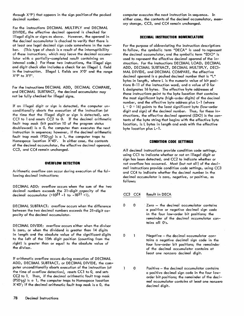
through X'9') that appears in the sign position of the packed decimal number.
For the instructions DECIMAL MULTIPLY and DECIMAL DIVIDE, the effective decimal operand is checked for illegal digits or signs as above. However, the operand in the decimal accumulator is checked to verify that there is at least one legal decimal sign code somewhere in the number. (This type of check is a result of the interruptibility of these instructions, which may leave the decimal accumulator with a partially-completed result containing an intemal code.) For these two instructions, the illegal sign and digit check also includes a check for an illegal L field in the instruction. Illegal L fields are X'O' and the range X'9' to X'F'.
For the instructions DECIMAL ADD, DECIMAL COMPARE, and DECIMAL SUBTRACT, the decima I accumulator may not be fully checked for illegal signs.
If an illegal digit or sign is detected, the computer unconditionally aborts the execution of the instruction (at the time that the illegal digit or sign is detected), sets CCl to 1 and resets CC2 to O. If the decimal arithmetic fault trap mask (bit position 10 of the program status doubleword) is a 0, the computer then executes the next instruction in sequence; however, if the decimal arithmetic fault trap mask (PSDI0) is a 1, the computer traps to Homespace location X'45'. In either case, the contents of the decimal accumulator, the effective decimal operand, CC3, and CC4 remain unchanged.
OVERFLOW DETECnON
Arithmetic overflow can occur during execution of the following decimal instructions:
DECIMAL ADD: overflow occurs when the sum of the two decimal numbers exceeds the 31-digit capacity of the decimal accumulator (+103 1 -1 to -1031 +1).
DECIMAL SUBTRACT: overflow occurs when the difference between the two decimal numbers exceeds the 31-digit capacity of the decimal accumulator.
DECIMAL DIVIDE: overflow occurs either when the divisor is zero, or when the dividend is greater than 14 digits in length and the absolute value of the significant digits to the left of the 15th digit position (counting from the right) is greater than or equal to the absolute value of the divisor.
If arithmetic overflow occurs during execution of DECIMAL ADD, DECIMAL SUBTRACT, or DECIMAL DIVIDE, the computer unconditionally aborts execution of the ,instruction (at the time of overflow detection), resets CCl to 0, and sets CC2 to 1. Then, if the decimal arithmetic fault trap mask (PSD10) is a 1, the computer traps to Homespoce location X'45'; if the decimal arithmetic fault trap mask is a 0, the
78 Decimal Instructions
computer executes the next instruction in sequence. In either case, the contents of the decimal accumulator, memory storage, CC3, and eC4 remain unchanged.
DECIMAL INSTRUCnON NOMENCLATURE
For the purpose of abbreviating the instruction descriptions to follow, the symbolic term "DECA" is used to represent the decimal accumulator, and the symbolic term "EDO" is used to represent the effective decimal operand of the instruction. For the instructions DECIMAL LOAD, DECIMAL ADD, DECIMAL SUBTRACT, DECIMAL MULTIPLY, DECIMAL DIVIDE, and DECIMAL COMPARE, the effective decimal operand is a packed decimal number that is "l" bytes in length, where L is the numeric value of bit positions 8-11 of the instruction word, and a value of 0 for L designates 16 bytes. The effective byte addresses of these instructions point to the byte location that contains the most significant byte (high-order -digits) of the decimal number, and the effective byte address plus L-l (where L = 0 = 16) points to the least significant byte (low-order digit and sign) of the decimal number. Thus, for these instructions, the effective decimal operand (EDO) is the contents of the byte string that begins with the effective byte location, is L bytes in length and ends with the effective byte location plus l-l.
CONDlnON CODE SEmNGS
All decimal instructions provide condition code settings, using eel to indicate whether or not an illegal digit or sign has been detected, and CC2 to indicate whether or not overfl ow has occurred. Most (bu t not a \I) of the decimol-instructions provide condition code settings, using CC3 and CC4 to indicate whether the decimal number in th~ decimal accumulator is zero, negative, or positive, as follows:
CC3 CC4 Result in DECA
o o
o
o
Zero - the decimal accumulator contains a positive or negative decimal sign code in the four low-order bit positions; the remainder of the decimal accumulator contains all O's.
Negative - the decimal accumulator contains a negative decimal sign code in the four low-order bit positions; the remainder of the decimal accumulator conta ins at least one nonzero decimal digit.
Positive - the decimal accumulator contains a positive decimal sign code in the four loworder bit positions; the remainder of the decimal accumulator contains at least one nonzero decimal digit.
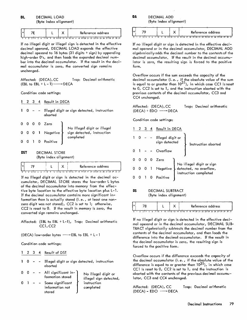
OL DECIMAL LOAD (Byte index alignment)
If no illegal digit or illegal sign is detected in the effective decimal operand, DECIMAL LOAD expands the effective decimal operand to 16 bytes (31 digits + sign) by appending high-order O·s, and then loads the expanded decimal number into the de<;:imal accumulator. If the result in the decimal accumulator is zero, the converted sign remains unchanged.
Affected: (DECA), CC Trap: Decimal arithmetic (EBL to EBL + L -l)-DECA
Condition code settings:
2 3 4 Result in DECA
o -
000
000
o 0
o
Illegal digit or sign detected, instruction aborted
No illegal digit or illegal sign detected, instruction completed
:::ative} o Positive
OST DECIMAL STORE (Byte index alignment)
If no illegal digit or sign is detected in the decimal accumulator, DECIMAL STORE stores the low-order L bytes of the decimal accumulator into memory from the effective byte location to the effective byte location plus L-1. If the decimal accumulator contains more significant information than is actually stored (i. e. , at least one nonzero digit was not stored), CC2 is set to 1; otherwise, CC2 is reset to O. If the result in memory is zero, the converted sign remains unchanged.
Affected: (EBL to EBL + L-1), Trap: Decimal arithmetic CC1, CC2
(DECA) low-order bytes --EBL to EBL + L - 1
Condition code settings:
2 3 4 Result of DST
o
o 0
o
Illegal digit or sign detected, instruction aborted
All significant in_} formation stored
Some significant information not stored
No illegal digit or illegal sign detected, instruction completed
OA DECIMAL ADD (Byte index alignment)
If no illegal digit or sign is detected in the effective decimal operand or in the decimal accumulator, DECIMAL ADD algebraically adds the decimal number to the contents of the decimal accumulator. If the result in the decimal accumulator is zero, the resulting sign is forced to the positive form.
Overflow occurs if the sum exceeds the capacity of the decimal accumulator (i. e., if the absolute value of the sum is equa I to or greater than 1031 ), in wh i ch case CC 1 is reset to 0, CC2 is set to 1, and the instruction aborted with the previous contents of the decimal accumulator, CC3 and CC4 unchanged.
Affected: (DECA), CC (DECA) + EDO --DECA
Trap: Decimal arithmetic
Condition code settings:
o
2 3 4 Result in DECA
o Illegal digit or } sign detected
Overflow
Instruction aborted
o 0 o 0
o 0 o
o 0 o
Zero } No illegal digit or sign Negati ve detected, no overflow,
instruction completed Positive
OS DECIMAL SUBTRACT (Byte index al ignment)
o I 2
If no illegal digit or sign is detected in the effective decimal operand or in the decimal accumulator, DECIMAL SUBTRACT algebraically subtracts the decimal number from the contents of the decimal accumulator, and then loads the difference into the decimal accumulator. If the result in the decimal accumulator is zero, the resulting sign is forced to the positive form.
Overflow occurs if the difference exceeds the capacity of the decimal accumulator (i. e., if the absolute value of the difference is equal to or greater then 1031 ), in which case CC 1 is reset to 0, CC2 is set to 1, and the instruction is aborted with the contents of the previous decimal accumulator, CC3 and CC4 unchanged.
Affected: (DECA), CC Trap: Decimal arithmetic (DECA) - EDO -DECA
Dec ima I Instructions 79
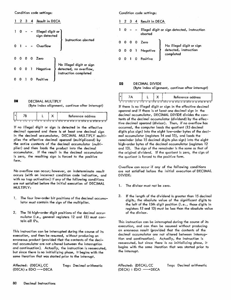
Condition code settings:
o
2 3 4- Result in OECA
o - Illegal digit or} sign detected
Overflow
o 0 0 0 Zero
Instruction aborted
No illegal digit or sign 0 0 0 Negative detected, no overflow,
instruction completed
0 0 1 0 Positive
OM DECIMAL MULTIPLY (Byte index alignment, continue after interrupt)
If no illegal digit or sign is detected in the effective decimal operand and there is at least one decimal sign in the decimal accumulator, DECIMAL MULTIPLY multiplies the effective decimal operand (multiplicand) by the entire contents of the decimal accumulator (multiplier) and then loads the product into the decimal accumulator. If the result in the decimal accumulator is zero, the resulting sign is forced to the positive form.
No overflow can occur; however, an indeterminate result occurs (with an incorrect condition code indication, and with no trap activation) if any of the following conditions are not satisfied before the initial execution of DECIMAL MUlTIPl Y:
1. The four low-order bit positions of the decimal accumulator must contain the sign of the multiplier.
2. The 16 high-order digit positions of the decimal accumulator (i.e., general registers 12 and 13) must contain aft O's.
This instruction can be interrupted during the course of its execution, and then be resumed, without producing an erroneous product (provided that the contents of the decimal accumulator are not a Itered between the interruption and continuation). Actually, the instruction is reexecuted, but since there is no initializing phase, it begins with the same iteration that was started prior to the interrupt.
Affected: (DECA), CC (DECA) x EDO -DECA
80 Decimal Instructions
Trap: Decimal arithmetic
Condition code settings:
2 3 4 Result in OECA
0 - Illegal digit or sign detected, instruction aborted
0 0 0 0 Zero
} No illegal digit or sign
0 0 0 Negative detected, instruction completed
0 0 0 Positive
DO DECIMAL DIVIDE (Byte index alignment, continue after interrupt)
If there is no illegal digit or sign in the effective decimal operand and if there is at least one decimal sign in the decimal accumulator, DECIMAL DIVIDE divides the contents of the decimal accumulator (dividend) by the effective decimal operand (divisor). Then, if no overflow has occurred, the computer loads the quotient (15 decimal digits plus sign) into the eight low-order bytes of the decimal accumulator (registers 14 and 15), and loads the remainder (also 15 decimal digits plus sign) into the eight high-order bytes of the decimal accumulator (registers 12 and 13). The sign of the remainder is the same as that of the original dividend. If the quotient is zero, the sign of -the quotient is forced to the positive form.
Overflow can occur if any of the following conditions are not satisfied before the initial execution of DECIMAL DIVIDE:
1. The divisor must not be zero.
2. If the length of the dividend is greater than 15 decimal digits, the absolute value of the significant digits to the left of the 15th digit position (i. e., those digits in registers 12 and 13) must be less than the absolute value of the divisor.
This instruction can be interrupted during the course of its execution, and can then be resumed without producing an erroneous result (provided that the contents of the decimal accumulator are not altered between interruption and continuation). Actually, the instruction is reexecuted, but since there' is no initializing phase, it begins with the same iteration that was started prior to the interrupt.
Affected: (DECA), CC (DECA) -;. EDO -DECA
Trap: Decimal arithmetic
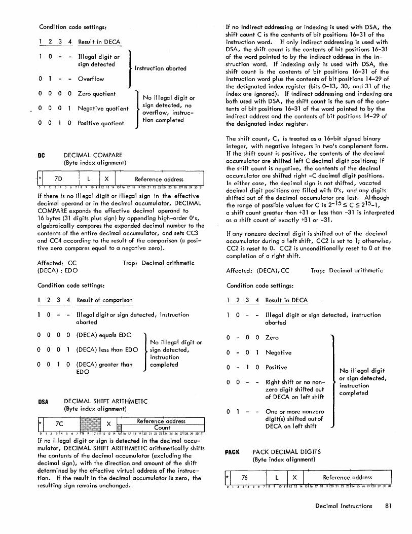
Condition code settings:
2 3 4 Result in DECA
0 Illegal digit or
} Instruction aborted sign detected
0 Overflow
0 0 0 0 Zero quotient } No illegal digit or
0 0 0 Negative quotient sign detected, no overflow, instruc-
0 0 0 Positive quotient tion completed
'DC DECIMAL COMPARE (Byte index alignment)
If there is no illegal digit or illegal sign in the effective decimal operand or in the decimal accumulator, DECIMAL COMPARE expands the effective decimal operand to 16 bytes (31 digits plus sign) by appending high-order OIS, algebraically compares the expanded decimal number to the contents of the entire decimal accumulator, and sets CC3 and CC4 according to the result of the comparison (a positive zero compares equal to a negative zero).
Affected: CC Trap: Decimal arithmetic (DECA) : EDO
Condition code settings:
2 3
0
0 0 0
0 0 0
0 0
DSA
4 Result of comparison
Illegal digit or sign detected, i nstruc t ion aborted
0 (DECA) equals EDO
} No illegal digit or (DECA) less than EDO sign detected,
instruction 0 (DECA) greater than completed
EDO
DECIMAL SHIFT ARITHMETIC (Byte index alignment)
If no illegal digit or sign is detected in the decimal accumulator, DECIMAL SHIFT ARITHMETIC arithmetically shifts the contents of the decimal accumulator (excluding the decimal sign), with the direction and amount of the shift determined by the effective virtual address of the instruction. If the result in the decimal accumulator is zero, the resulting sign remains unchanged.
If no indirect addressing or indexing is used with DSA, the shift count C is the contents of bit positions 16-31 of the instruction word. If only indirect addressing is used with DSA, the shift count is the contents of bit positions 16-31 of the word pointed to by the indirect address in the instruction word. If indexing only is used with DSA, the shift count is the contents of bit positions 16-31 of the instruction word plus the contents of bit positions 14-29 of the designated index register (bits 0-13, 30, and 31 of the index are ignored). If indirect addressing and indexing are both used with DSA, the shift count is the sum of the contents of bit positions 16-31 of the word pointed to by the indirect address and the contents of bit positions 14-29 of the designated index register.
The shift count, C, is treated as a 16-bit signed binary integer, with negative integers in twols complement form. If the shift count is positive, the contents of the decimal accumulator are shifted left C decimal digit positions; if the shift count is negative, the contents of the decimal accumulator are shifted right -C decimal digit positions. In either case, the decimal sign is not shifted, vacated decimal digit positions are filled with OIS, and any digits shifted out of the decimal accumulator are lost. Although the range of possible values for C is 2-15 $ C ~ 215_1, a shift count greater than +31 or less than -31 is interpreted as a shift count of exactly +31 or -31.
If any nonzero decimal digit is shifted out of the decimal accumulator during a left shift, CC2 is set to 1; otherwise, CC2 is reset to O. CC2 is unconditionally reset to 0 at the completion of a right shift.
Affected: (DECA), CC Trap: Decimal arithmetic
Condition code settings:
2 3 4 Result in DECA
o - Illegal digit or sign detected, instruction aborted
o - 0 0 Zero
o - 0 Negative
o 0 Positive
o 0 - Right shift or no nonzero digit shifted out of DECA on left shift
o
PACK
One or more nonzero digit(s) shifted outof DECA on left shift
PACK DECIMAL DIGITS (Byte index al ignment)
No illegal digit or sign detected, instruction completed
Decimal Instructions 81
PACK DECIMAL DIGITS converts the effective decimal operand (assumed to be in zoned format) into a packed decimal number and, if necessary, appends sufficient highorder O's to produce a decimal number that is 16 bytes (31 decimal digits plus sign) in length. The zone (bits 0-3) of the low-order digit of the effective decimal operand is used to select the sign code for the packed decimal number; all other zones are ignored in forming the packed decimal number. If no illegal digit or sign appears in the packed decimal number, it is then loaded into the decimal accumulator. If tbe result in the decimal accumulator is zero, the resulting sign remains unchanged.
The L field of this instruction specifies the length, in bytes, of the resultant packed decimal number in the decimal ac ... cumulator; therefore, the length of the effective decimal operand is 2L-1 bytes (¥lhere L = 0 implies a length of 31 bytes for the effective decimal operand).
Affected: (DECA), CC Trap: Decimal arithmetic
packed (EBL to EBL + 2L - 2) --DECA
Condition code settings:
2 3 4 Result in DECA
0 - - Illegal digit or sign detected, instruction aborted
0 0 0 0 Zero } No illegal digit or sign
0 0 0 Negative detected, instruction
0 0 0 Positive completed
Example 1, L = 6:
Before execution After execution
EDO X'FOF1F2F3 X'FOF1F2F3 F4F5F6F7 F4F5F6F7 F8F9FO' F8F9FO'
(DECA) xxxxxxxx X'ooOOOOOO xxx xxx xx 00000000 xxxxxxxx 00000123 xxxxxxxx 4567890C'
CC xxxx 0010
Example 2, L = 6:
Before execution After execution
EDO X'OOO938F7 X'000938F7 E655B483 E655B483 02F1 BO' 02F1BO'
(DECA) xxxxxxxx X '00000000 xxxxxxxx 00000000 xxxxxxxx 00000987 xxxxxxxx 65432100'
CC xxxx 0001
82 Decimal Instructions
UNPK UNPACK DECIMAL DIGITS (Byte index alignment, continue after interrupt)
If no illegal digit or sign is detected in the decimal accumulator (assumed to be in packed decimal format), UNPACK DECIMAL DIGITS converts the contents of the low-order L bytes of the decimal accumulator to zoned decimal format and stores the result, as a byte string, from the effective byte location to the effective byte location plus 2L-2. The contents of the four low-order bit positions of the decimal accumulator are used to select the sign code for the last digit of the string; for all other digits, if bit 12 of the PSD is zero, the zones are 1111 (EBCDIC), and if bit 12 is one, the zones are 0011 (ASCII). The contents of the decimal accumulator remain unchanged, and only 2L-l bytes of memory are altered. If the decimal accumulator contains more significant information than is actually unpacked and stored, CC2 is set to 1; otherwise, CC2 is reset to O. If the result in memory is zero, the resulting sign remains unchanged.
Affected: (EBL to EBL + 2L -2), Trap: Decimal arithmetic CC1, CC2
zoned (DECA) -EBL to EBL + 2L - 2
Condition code settings:
2 3 4 Result of UNPK
o Illegal digit or sign detected, instruction aborted
o 0 - - All significant information zoned and stored
o Some significant information not zoned and stored
Example 1, L = 10:
Before executi on
(DECA) X'ooOOOOOO 00000001 23456789 01234560'
EDO xxxxxxxx xxxxxxxx xxxxxxxx xxxxxxxx xxxxxx
CC xxxx
No illegal digit or sign detected, instruction completed
After execution
X'OooOOOOO 00000001 23456789 01234560'
X'FOFOFOFl F2F3F4F5 F6F7F8F9 FOF1F2F3 F4F5D6 1
OOxx
Example 2, L = 8:
(DECA)
EDO
Before execution
XI 00000000 23000000 10001234 0012345C'
xxxxxxxx xxxxxxxx xxxxxxxx xxxxxx
CC xxxx
Example 3, L = 4:
(DECA)
EDO
CC
Before execution
X'00001001 00001002 00001003 0001004F'
xxxxxxxx xxxxxxxx
xxxx
After execution
XI 00000000 23000000 10001234 0012345(1
X'F1FOFOFO F1F2F3F4 FOFOF1F2 F3F4C5 1
01xx
After execution
X' 00001001 00001002 00001003 00001004 1
X'"FOFOFOF 1 FOFOC4 1
01xx
BYTE-STRING INSTRUCTIONS
Five instructions provide for the manipulation of strings of consecutive bytes". The byte-string instructions and their mnemonic codes are as follows:
Instruction Name Mnemonic
Move Byte String MBS
Compare Byte String CBS
Translate Byte String TBS
Translate and Test Byte String TTBS
Edit Byte String EBS
These instructions are in the immediate displacement class and are memory-to-memory operations. These operations are under the control of information that must be loaded into certain general registers before the instruction is executed. These instructions may be interrupted at various stages of their execution; upon return, execution continues from the point of interruption.
The general format for the information in the instruction word and in the general registers is as follows:
Instruction word:
101 ~~:ation I I: : I o 1 2 314 5 6 7 8 9 RIO 1112 13 14 1516 17 18 ~9il::~~:~~:~: 262712829 30 31
Contents of reg ister R:
Contents of register Ru 1:
Designation
Operation
R
Displacement
Mask/Fill
Source Address
Count
Destination Address
Function
The 7-bit operation code of the instruction. (If any byte-string instruction is indirectly addressed, the computer traps to Homespace location X' 40' at the time of operation code decoding.)
The 4-bit field that identifies register R of the current general register block.
A 20-bit field that contains a signed byte displacement value, used to form an effective byte address. The displacement value is right-justified in the 20-bit field, and negative values are in twols comp I ement form.
An 8-bit field used only with TRANSLATE AND TEST BYTE STRING and EDIT BYTE STRING. The purpose of this field is explained in the detailed discussion of the TTBS and EBS instructions.
A 19- or 24-bit fieldt that normally contains the byte address of the first (most significant) byte of the source byte string operand. The effective source address is the source address in register R plus the displacement value in the instruction word.
An 8-bit field that contains the true count (from 0 to 255) of the number of bytes involved in the operation. This field is decremented by 1 as each byte in the destination byte string is processed. A 0 count means "no operation II with respect to the registers and main memory.
A 19- or 24-bit fieldt that contains the byte address of the fi rst (most sign i ficant) byte of the destination byte-string operand. This field is incremented by 1 as each byte in. the destination byte string is processed.
tFor real extended addressing mode, this is a 24-bit field (bits 8-31); for real and virtual addressing modes it is a 19-bit field (13-31).
Byte-String Instructions 83

In any byte-string instruction, any portion of register R or .Ru1 that is not explicitly defined (i.e., bit positions 8-12), should be coded with zeros for real and virtual addressing.
Since the value Ru 1 is obtained by performing a logical inclusive OR with the value 0001 and the value of the R field of the instruction word, the two control registers are Rand R+ 1 if R is even. However, if R is an odd value, register R contains an address value that functions both as a source operand address and as a destination operand address. Also, if register 0 is designated in any byte-string instruction (except for TRANSLATE AND TEST BYTE STRING and EDIT BYTE STRING), its contents are ignored and a zero source address value is obtained. Thus, the following three cases exist for most byte string instructions, depending on whether the value of the R field of the instruction word is even and nonzero, odd, or zero:
Case I: R is even and nonzero
The effective source address is the address in register R plus the displacement in the instruction word; the destination address is the address in register R + 1, but without the displacement added.
Case II: R is odd
The effective source address is the address in register R plus the displacement in the instruction word; the destination address is also the address in register R, but without the displacement added.
Case III: R is zero
The effective source address is the displacement value in the instruction word; the destination address is the address in register 1. In this case, the source byte-string operand is always a single byte.
In the descriptions of the ,byte-string instructions, the following abbreviations and terms are used:
D Displacement, (1)12-31'
SA Source address, (R)13-3l'
ESA
C
DA
t Effective source address, ~R) 13-31 + (1)12-31]13-31.
The contents of bit posifions 13-31 t of register R are added (right al igned) to the contents of bit positions 12-31 of the instruction word; the 19 or 24 low order bitst of the result are used as the effective source address.
Count, (Ru 1 )0-T
Destination address, {Ru 1)13-31 t.
84 Byte-String Instru.ctions
SBS Source byte string, the byte string that begins with the byte location pointed to by the 19- or 24-bjtt effective source address and is C bytes in length (if R is nonzero) or is 1 byte in length if R is 0).
DBS Destination byte string, the byte string that begins with the byte location pointed to by the destination address and is always C bytes in length.
TRAPS BY BYTE-STRING INSTRUCTIONS
Byte-string instructions cause a trap if either of the byte strings addressed come from pages of memory that are protected either through access protection or through write locks. A trap also occurs if either byte string is fully or partly contained with in pages of memory that are physically not present. A check for these access trap conditions are made prior to initiation of any byte relocation or general register change. These tests are performed for MOVE BYTE STRING and COMPARE BYTE STRING. These tests are performed only for the source byte string for TRANSLATE BYTE STRING, TRANSLATE AND TEST BYTE STRING, and EDIT BYTE STRING, since there is no assurance that the translate table or decimal digit bytes will be accessed in their entirety in the course of execution. If an access protection violation were to occur in trying to reach a byte in the translate table or decimal digit strings during the course of execution, then the instruction would trap and result in a partially executed condition. The registers would be restored, however, in such a manner that the instruction could be resumed after the protection violation had been corrected. When a trap occurs resulting. in a partially executed instruction, the Register Altered indicator will be set.
MBS MOVE BYTE STRING (Immediate displacement, continue after interrupt)
MOVE BYTE STRING copies the contents of the source byte string (left to right) into the destination byte string. The previous contents of the destination byte string are destroyed, but the contents of the source byte string are not affected unless the destination byte string overlaps the source byte string.
When the destination byte string overlaps the source byte string, the resulting destination byte string contains one or more r«;:petitions of bytes from the source byte string. Thus, if a destination byte string of C bytes begins with the kth byte of a source byte string (numbering from 1), the first
tFor real extended addressing mOde, this is a 24-bit field (bits 8-31); for real and virtual addressing modes it is a 19-bit field (13-31).
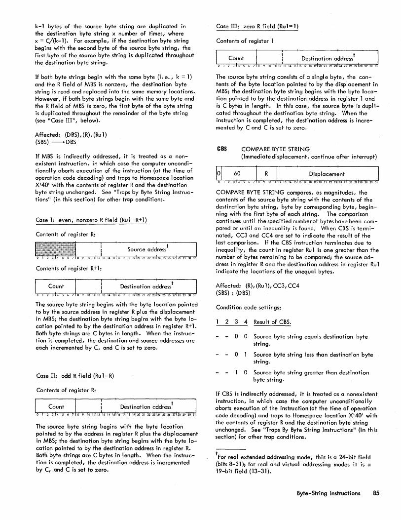
k-1 bytes of the source byte string are dupt icated in the destination byte string x number of times, where x = C/(k-1). For example, if the destination byte string begins with the second byte of the source byte string, the first byte of the source byte string is duplicated throughout the destination byte string.
If both byte strings begin with the same byte (i. e., k = 1) and the R field of MBS is nonzero, the destination byte string is read and replaced into the same memory locations. However, if both byte strings begin with the same byte and the R field of MBS is zero, the first byte of the byte string is duplicated throughout the remainder of the byte string (see "Case III", below).
Affected: (DBS),(R),(Ru1) (SBS) -DBS
If MBS is indirectly addressed, it is treated as a nonexistent instruction, in which case the computer unconditionall y aborts executi on of the instruction (at the time of operation code decoding) and traps to Homespace location X'40' with the contents of register R and the destination byte string unchanged. See "Traps by Byte String Instructions" (in this section) for other trap conditions.
Case I: even, nonzero R field (Ru 1 = R+ 1)
Contents of register R:
Contents of register R+1:
The source byte string begins with the byte location pointed to by the source address in register R plus the displacement in MBS; the destination byte string begins with the byte location pointed to by the destination address in register R+1. Both byte strings are C bytes in length. When the instruction is completed, the destination and source addresses are each incremented by C, and C is set to zero.
Case II: odd R field (Ru 1 = R)
Conten ts of reg ister R:
The source byte string begins with the byte location pointed to by the address in register R plus the displacement in MBS; the destination byte string begins with the byte location pointed to by the destination address in register R. Both byte strings are C bytes in length. When the instruction is completed, the destination address is incremented by C, and C is set to zero.
Case III: zero R field (Ru1=1)
Contents of register 1
The source byte string consists of a single byte, the contents of the byte location pointed to by the displacement in MBS; the destination byte string begins with the byte location pointed to by the destination address in register 1 and is C bytes in length. In this case, the source byte is dupl icated throughout the destination byte string. When the instruction is completed, the destination address is incremented by C and C is set to zero.
CBS COMPARE BYTE STRING (Immediate displacement, continue after interrupt)
COMPARE BYTE STRING compares, as magnitudes, the contents of the source byte stri ng with the contents of the destination byte string, byte by corresponding byte, beginning with the first byte of each string. The comparison continues until the specified numberof bytes have been compared or until an inequality is found. When CBS is terminated, CC3 and CC4 are set to indicate the result of the last comparison. If the CBS instruction terminates due to inequal ity, the count in register Ru 1 is one greater than the number of bytes remaining to be compared; the source address in register R and the destination address in register Ru 1 indicate the locations of the unequal bytes.
Affected: (R), (Ru 1), CC3, CC4 (SBS) : (DBS)
Condition code settings:
2 3 4 Result of CBS.
o 0 Source byte string equals destination byte string.
o Source byte string less than destination byte string.
o Source byte string greater than destination byte string.
If CBS is indirectly addressed, it is treated as a nonexistent instruction, in which case the computer unconditionally aborts execution of the instruction (at the time of operation code decoding) and traps to Homespace location X'40' with the contents of register R and the destination byte string unchanged. See "Traps By Byte String Instructions" (in this section) for other trap conditions.
tFor real extended addressing mode, this is a 24-bit field (b i ts 8-31); for rea I and vi rtua I addressing modes it is a 19-bit field (13-31).
Byte-String Instructions 85
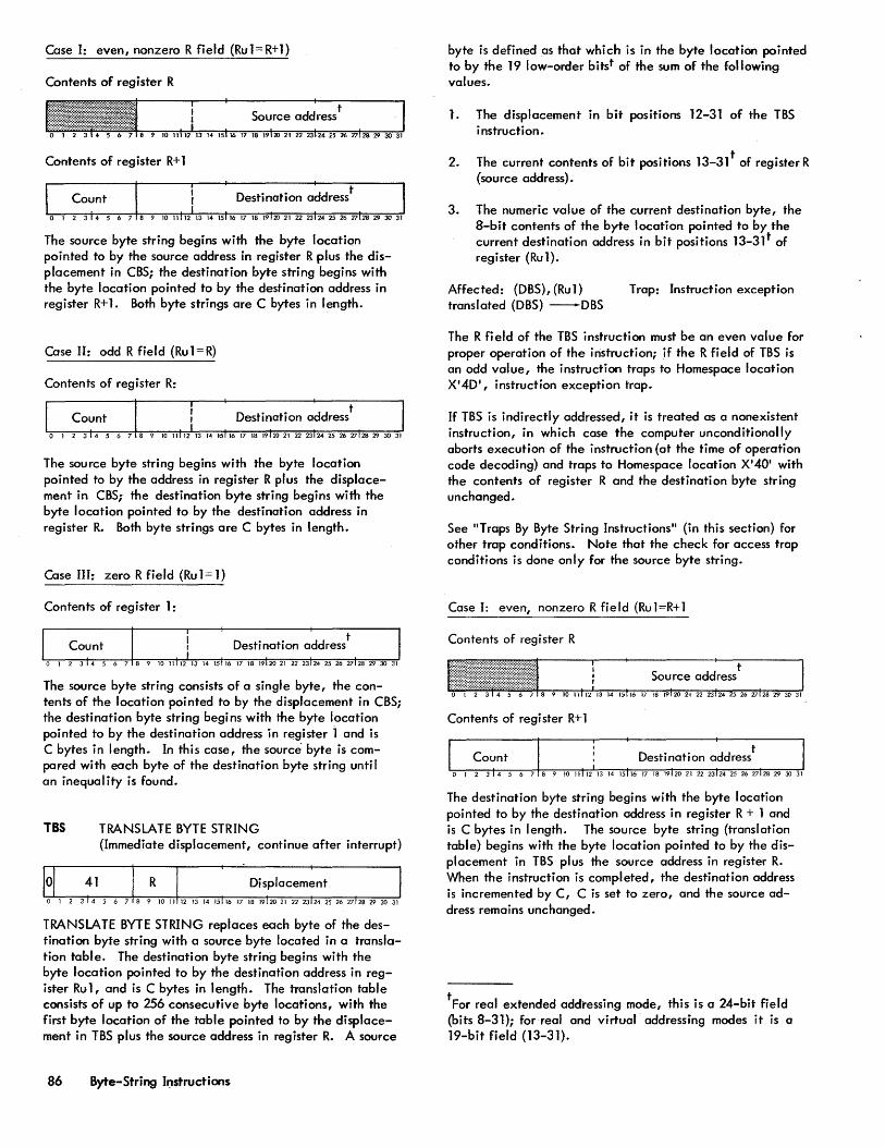
Case J: even, nonzero R field (Ru 1= R+1)
Contents of reg ister R
Contents of reg ister R+ 1
The source byte string begins with the byte location pointed to by the source address in register R plus the displacement in CBS; the destination byte string begins with the byte location pointed to by the destination address in register R+1. Both byte strings are C bytes in length.
Case II: odd R field (Ru1=R)
Contents of register R:
The source byte string begins with the byte location pointed to by the address in register R plus the displacement in CBS; the destination byte string begins with the byte location pointed to by the destination address in register R. Both byte strings are C bytes in length.
Case III: zero R field (Rul=l)
Contents of register 1:
The source byte string consists of a single byte, the contents of the location pointed to by the displacement in CBS; the destination byte string begins with the byte location pointed to by the destination address in register 1 and is C bytes in length. In this case, the source byte is compared with each byte of the destination byte string until an inequality is found.
lBS TRANSLATE BYTE STRING (Immediate displacement, continue after interrupt)
TRANSLA TE BYTE STRING replaces each byte of the destination byte string with a source byte located in a translation table. The destination byte string begins with the byte location pointed to by the destination address in register Ru 1, and is C bytes in length. The translation table consists of up to 256 consecutive byte locations, with the first byte location of the table pointed to by the displacement in TBS plus the source address in register R. A source
86 Byte-String Instructions
byte is defined as that which is in the byte location pointed to by the 19 low-order bitst of the sum of the following values.
1. The displacement in bit positions 12-31 of the TSS instruction.
2. The current contents of bit positions 13-31 t of register R (source address).
3. The numeric value of the current destination byte, the 8-bit contents of the byte location pointed to by the current destination address in bit positions 13-31 t of register (Ru 1).
Affected: (DBS),(Rul) translated (DBS) -DSS
T rap: Instruction exception
The R field of the TSS instruction must be an even value for proper operation of the instruction; if the R field of TSS is an odd value, the instruction traps to Homespace location X'4D', instruction exception trap.
If TSS is indirectly addressed, it is treated as a nonexistent instruction, in which case the computer unconditionally aborts execution of the instruction (at the time of operation code decoding) and traps to Homespace location X'40' with the contents of register R and the destination byte string unchanged.
See "Traps By Byte String Instructions" (in this section) for other trap conditions. Note that the check for access trap conditions is done only for the source byte string.
Case I: even, nonzero R field (Ru l=R+ 1
Contents of register R
Contents of register R+ 1
The destination byte string begins with the byte location pointed to by the destination address in register R + 1 and is C bytes in length. The source byte string (translation table) begins with the byte location pointed to by the displacement in TBS plus the source address in register R. When the instruction is completed, the destination address is incremented by C, C is set to zero, and the source address remains unchanged.
t For real extended addressing mode, this is a 24-bit field (bits 8-31); for real and virtual addressing modes it is a 19-bit field (13-31).
Case II: odd R HeM (Rul=R)
Because of the interruptible nature of TRANSLATE BYTE STRING, the instruction traps with the contents of register R unchanged when an odd-numbered general register is specified by the R field of the instruction word.
Case III: zero R field (Ru 1= 1)
Contents of register 1
The destination byte string begins with the byte location pointed to by the destination address in register 1 and is C bytes in length. The source byte string (translation table) begins with the location pointed to by the displacement in TBS. When the instruction is completed, the destination address is incremented by C and C is set to zero.
TTBS TRANSLATE AND TEST BYTE STRING (Immediate displacement, continue after interrupt)
TRANSLATE AND TEST BYTE STRING compares the mask in bit positions 0-7 of register R with source bytes in a byte translation table. The destination byte string begins with the byte location pointed to by the destination address in register Ru 1, and is C bytes in length. The byte translation table and the translation bytes themselves are identical to that described for the instruction TRANSLATE BYTE STRING. The destination byte string is examined (without being changed) until a translation byte (source byte) is found that contains a 1 in any of the bit positions selected by a 1 in the mask. When such a translation byte is found, TTBS replaces the mask with the logical product (AND) of the translation byte and the mask, and terminates with CC4 set to 1. If the TTBS instruction terminates due to the above condition, the count (C) in register Ru1 is one greater than the number of bytes remaining to be compared and the destination address in register Ru 1 indicates the location of the destination byte that caused the instruction to terminate. If no translation byte is found that satisfies the above condition after the specified number of destination bytes have been compared, TTBS terminates with CC4 reset to O. In no case does the TTB5 instruction change the source byte string.
Affected: (R), (Rul), CC4 Trap: Instruction exception
If translated (SBS) n mask "I 0, translated (SBS) n mask -mask and stop
If translated (SBS) n mask = 0, continue
Condition code settings:
2 3 4 Result of TTBS
o Translation bytes and the mask do not compare ones any place.
The last translation byte compared with the mask contained at least one 1 corresponding to a 1 in the mask.
The R field of the TTBS instruction must be an even value for proper operation of the instruction; if the R field of TTBS is an odd value, the instruction traps to Homespace location X'4D', instruction exception trap.
If TTBS is indirectly addressed, it is treated as a nonexistent instruction, in which case the computer unconditionally aborts execution of the instruction (at the time of operation code decoding) and traps to Homespace location X'40' with the contents of register R and the destination byte string unchanged.
See liT raps By Byte String Instructions" (in th is section) for other trap conditions. Note that the check for access trap 'conditions is done only for the source byte string.
Case I: even, nonzero R field (Ru1=R+1)
Contents of register R
Contents of regi ster R+ 1
The destination byte string begins with the byte location pointed to by the destination address in register R + 1 and is C bytes in length. The source byte string (translation table) begins with the byte location pointed to by the displacement in TTBS plus the source address in register R.
Case II: odd R field
Because of the interruptable nature of TRANSLATE AND TEST BYTE STRING the instruction traps with the contents of register R unchanged when an odd-numbered general register is specified by the R field of the instruction word.
tFor real extended addressing mode, this is a 24-bit field (bits 8-31); for real and virtual addressing modes it is a 19-bit field (13-31).
Byte-String Instructions 87
Case III. zero R field (Ru 1= 1)
Contents of register 1
The destination byte string begins with the byte location pointed to by the destination address in register 1 and is C bytes in length. The source byte string (translation table) begins with the location pointed to by the displacement in TTBS. In this case, the instruction automatically provides a mask of eight lIs. (This is an exception to the general rule, used in the other byte-string instructions, that register 0 provides all OIS as its contents.)
EBS EDIT BYTE STRING {Immediate displacement, continue after interrupt)
EDIT BYTE STRING converts a decimaJ information field from packed decimal format to zoned decimal format, under control of the editing pattern in the destination byte string, and replaces the destination byte string with the edited, zoned result. The decimal formats on which EBS operates are governed by bit 12 of the PSD (ANSCII/EBCDIC) mask bit). If PSD 12 is zero, EBCDIC codes are used; if it is one, ANSCII codes are used. (See IIDecimal Instructions", "Pac.ked Decimal Numbers ll
, and "Zoned Decimal Numbers ll
for a description of packed and zoned decimal formats.) EBS proceeds one byte at a time, starting with the first (most significant) byte of the editing pattern, and continues until all bytes in the editing pattern have been processed. The fill character, contained in bit position 0-7 of register R, replaces the pattern byte under specified conditions. More than one decimal number field can be edited by a single EBS instruction if the pattern in memory is, in fact, a series of patterns corresponding to a series of number fields. In such cases, however, after the EBS instruction is completed, the condition code indicates the result of the last decimal number field processed and register 1 contains the byte address (or the byte address plus 1) of the last significance indicator in the edited destination byte string. (This aJlows the insertion of a floating dollar sign, etc., with a subsequent instruction.)
R must ~e an even value (excluding 0) for proper operation of the instruction; if R is an odd value or equal to zero, the computer traps to Homespace location XI4D', instruction exception trap, with the contents in register R unchanged.
Contents of register R
t For real extended addressing mode, this is a 24-bit field (bits 8-31); for real and virtual addressing modes it is a 19-bit field (13-31).
88 Byte-String InstructiOns
Contents of register R+ 1
The destination byte string is an editing pattern that begins in the byte location pointed to by the destination address in register R+ 1, and is C bytes in length. The decimal information field, which must be in packed decimal format, begins with the byte location pointed to by the displacement in EBS plus the source address in register R. The decimal information field must contain I egal decimal digit and sign codes (packed format) and must begin with a decimal digit.
The destination byte string (the editing pattern) may contain any 8-bit codes desired. However, four byte codes in the editing pattern have special meanings. These codes are as follows:
Binary value Function Abbreviation
00)00000 (X'20') Digit selector ds
00100001 (X121') Significance start ss
00100010 (X'22') Field separation fs
0010 0011 (X'231) Immediate signifi- si
cance start
Before executing EBS, the condition code should be set to 0000 if the high-order digit of the decimal number is in the left half of a byte, and should be set to 0100 if the high-order digit is in the right half of a byte.
The editing operation performed on each pattern byte of the destination byte string is determined by the following conditions:
1. The pattern byte obtained from the destination byte string.
2. The decimal digit obtained from the decimal number field.
3. The current state of the condition code.
Depending upon various combinations of these conditions, the instruction EDIT BYTE STRING performs one (and only one) of the following actions with the pattern byte and the decimal dfgit:
1. The fill character (coatents of bit positions 0-7 of register R) or a blank character replac~ the byte in the destination byte string.
2. The decimal digit is expanded" to zoned decimal format and replaces the pattern byte in the destination byte string.
3. The pattern byte remains unchanged.
In general, the normal editing process is as follows:
1. Each byte of the destination byte string is replaced by a fill character until significance is present, either in the destination byte string or in the decimal information field. Significance is indicated by any of the following:
a. The pattern byte is X' 231 {jmmediate significance start), which begins significance with the current decimal digit.
b. The pattern byte is X' 21 1 (significance start), which begins significance with the following pattern byte.
c. The current decimal digit is nonzero, which begins significance with the current pattern byte.
2. After significance is encountered, each pattern byte that is X'20' (digit selector), X' 21 1 (significance start), X' 221 (field separator), or X' 231 (immediate significance start) is replaced by a zoned decimal number from the decimal field and all other pattern bytes are unchanged. This process continues until any of the following conditions occur:
a. A positive sign is encountered in the decimal field, in which case subsequent pattern bytes are replaced by blank characters until significance is again present, until a field separator is encountered, or until the destination byte string is entirely processed, whichever occurs first.
b. A negative sign is encountered in the decimal field, in which case subsequent pattern bytes are unchanged until significance is again present, until a field separator is encountered, or until the destination byte string is entirely processed, whichever occurs first.
c. A pattern byte of X' 221 (field separator) is encountered, in which case the field separator is replaced by a fi II character; subsequent pattern bytes are replaced by the fill character u~til significance is again present, until a positive or negative sign is encountered, or until the destination byte string is entirely processed, whichever occurs first.
d. The destination byte string is entirely processed, in which case the computer executes the next instruction in sequence.
The detailed operation of EDIT BYTE STRING is as given below.
The explanation is necessarily quite detailed due to the high degree of flexibility inherent in EBS. Condition code settings are made continuously during the editing process and these settings help determine how each subsequent pattern byte will be edited. The summarY'of condition code settings given on the next page will help clarify the discussion below.
1. If the count in bit position 0-7 of register R+1 is a nonzero, a pattern byte is obtained from the destination byte string; if the count in register R+1 is 0, the computer executes the next instruction in sequence.
2. If the pattern byte is a digit selector (X' 20' ), a significance start (X'211), or immediate significance start (X' 231), a digit is accessed from the decimal information field as follows:
a. Adecimal byte is obtained from the byte location pointed to by the displacement in EBS plus the source address in register R.
b. If bits 0-3 of the decimal byte are a sign code, the computer automatically aborts execution of EBS and traps to Homespace location X'451, with the contents of register R, register R+ 1, the condition code, and the destination byte string unchanged from thei r current contents.
c. If CC2 is currently set to 0, the digit to be used for editing is the left digit (bits 0-3) of the decimal byte; however, if CC2 is currently set to 1, the digit to be used is the right digit (bits 4-7) of the dec imal byte. In either case, CC3 is set to 1 if the digit is nonzero. If CC2 is set to 1 and the right digit (bits 4-7) of the decimal byte is a sign code, the computer automatically aborts execution of EBS and traps to Homespace location X' 451, as described above.
d. One of the following editing actions is performed.
Conditions
Pattern byte= SI{X 1231)
Pattern byte=SS(X'211) CC4=1
Pattern byte = SS CC4=0 non:?:ero digit
Pattern byte = SS CC4=0 digit =0
Action
Expand digit to zoned fo rmat, store in pattern byte location, and set CC4 to 1 (start significance).
Expand digit to zoned format and store in pattern byte location (because CC4= 1 means significance already encountered) .
Expand digit to zoned format, store in pattern byte location (because nonzero digit begi ns si gn i fi cance), and set CC4 to 1.
Store fill character in pattern byte location (because significance starts wi th next pattern byte) and set CO' "-to 1 .
Mode 1
None
Mode 1
Mode 2
Byte-String Instructions 89
Conditions Action
Pattern byte=DS(X'20') Expand digit to zoned None CC4 = 1 format, and store digit
in pattem byte location.
Pattern byte = DS CC4=0
Expand digit to zoned format, store digit in pattern byte location, and set CC4 to 1 to. signal significance
Mode 1
nonzero digit
Pattern byte= OS CC4=0
Store fi II character in pattern byte location (because significance not encountered yet).
None
digit=O
e. If CC2 is currently reset to 0 and if bits 4-7 of the decimal byte are a positive decimal sign code, CCl is set to 1, CC4 is reset to 0, and the source address in register R is incremented by 1. If CC2 is currently reset to 0 and if bits 4-7 of the decimal byte are a negative decimal sign code, CC 1 and CC4 are both set to 1, and the sou ree address is incremented by 1. Otherwise, CC2 is added to the source address and then CC2 is inverted.
f. If marking is invoked at set d, above, one of the two fol lowing marking operations are performed:
Mode 1: Load bits 13-31 of register R+1 into bit positions 13-31 of register 1; bit positions 0-12 of register are unpredictable.
Mode 2: Load bits 13-31 of register R+l into bit positions 13-31 of register 1 and then increment the contents of register 1 by 1; bit positions 0-12 of register 1 are unpredictable.
If marking is not appl icable (i. e., significance has not been encountered), the contents of reg ister 1 are not affected.
3. If the pattern byte is a field separator (X'22I), the fill character is stored in the pattern byte location. CC1, CC3, and CC4 are all reset to OIS, and CC2 remains unchanged.
4. If the pattern byte is not a digit selector, significance start, immediate significance start, or field separator, one of the following actions are performed:
Conditions Action
CC1-=0} CC4=0
CCl = 1 } CC4=0
CC4=1
Store fiJI character in pattern byte location.
Store blank character (X'40 ' if EBCD IC or X'20 ' if ANSCII) in pattern byte location.
None (pattern byte remains unchanged).
90 Byte-String Instructions
5. Increment the destination address in register Ru 1 and decrement the count in register Ru 1. If the count is sti If nonzero, process the next pattern byte as above; otherwise, execute the next instruction in sequence.
Affected: (R), (Ru 1)
(register 1), (OBS), CC
edited (SBS) -OBS
Traps: Nonexistent instruction, decimal arithmetic, instruction exception
Condition code settings:
2 3 4 Result of EBS
o 0 Significance is not present, no sign digit
o
o
o
has been encountered.
Significance is present, no sign digit has been encountered.
o A positive sign has been encountered.
A negative sign has been encountered.
Next digit to be processed is left digit of byte.
Next digit to be processed is right digit of byte.
No nonzero digit has been encountered.
A nonzero digit has been encountered.
If EBS is indirectly addressed, it is treated as a nonexistent instruction, in which case the computer unconditionally aborts execution of the instruction (at the time of operation code decoding) and traps to Homespace location X' 40' with the contents of register R, register Ru 1, register 1, the destination byte string, and the condition code unchanged.
The R field of the EBS instruction must be an even value (excluding 0) for proper operation of the instruction; if the R field of EBS is an odd value or equal to zero, the instruction traps to Homespace location X'4D', instruction exception trap.
If an illegal digit or sign is detected in the decimal information field, the computer unconditionally aborts execution of the instruction (at the time the illegal digit or sign is encountered) and traps to Homespace location X'451 with the contents of register R, register Ru 1, register 1, the destination byte string, and the condition code containing the results of the last editing operation performed before the illegal digit or sign was encountered.
See" Traps By Byte-String Instructions" (in this section) for other trap conditions. Note that the check for access trap conditions is done only for the source byte string.
In the following examples, the hexadecimal codes for the digit selector (X'20'), the significance start (X'211), the field separation (X'221), and the immediate significance
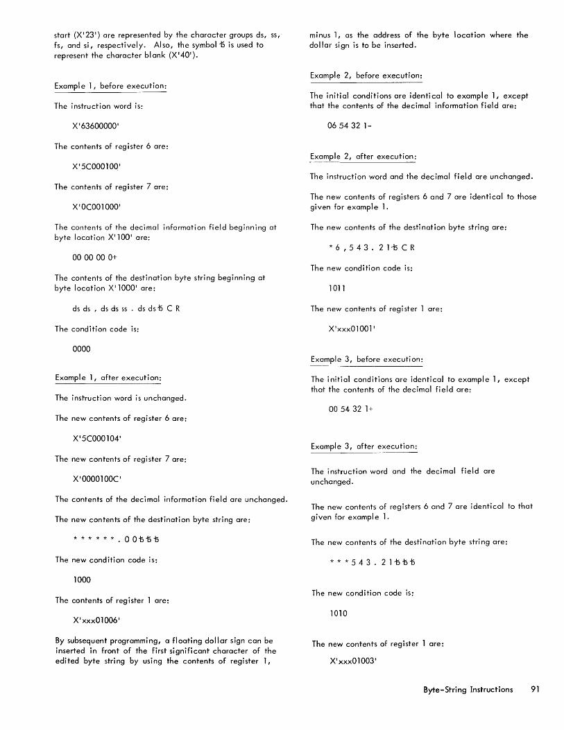
start (X'23 1) are represented by the character groups ds, ss,
fs, and si, respectively. Also, the symbol 15 is used to represent the character blank (X'40').
Exampl e 1, before execution:
The instruction word is:
X 163600000 I
The contents of reg i ster 6 are:
X'5C000100 '
The contents of register 7 are:
X'OC001000'
The contents of the decimal information field beginning at byte location X' l00 ' are:
000000 0+
The contents of the destination byte string beginning at byte location XI 10001 are:
ds ds , ds ds ss . ds ds 15 C R
The condition code is:
0000
Example 1, after execution:
The instruction word is unchanged.
The new contents of register 6 are:
X'5C0001041
The new contents of regi ster 7 are:
X 100001 DOC'
The contents of the decimal information field are unchanged.
The new contents of the destination byte string are:
* * * * * *.001'>151'>
The new condition code is:
1000
The contents of register 1 are:
X' xxxOl0061
By subsequent programming, a floating dollar sign can be inserted in front of the first significant character of the edited byte stri ng by usi ng the contents of regi ster 1,
minus 1, as the address of the byte location where the dollar sign is to be inserted.
Example 2, before execution:
The initial conditions are identi cal to example 1, except that the contents of the decimal information field are:
065432 1-
Example 2, after execution:
The instruction word and the decimal field are unchanged.
The new contents of registers 6 and 7 are identical to those given for example 1.
The new contents of the destination byte string are:
*6,543.211SCR
The new condition code is:
1011
The new contents of regi ster 1 are:
X' xxx01001 1
Example 3, before execution:
The initial conditions are identical to example 1, except that the contents of the decimal field are:
00 54 32 1+
Example 3, after execution:
The instruction word and the decimal field are unchanged.
The new contents of registers 6 and 7 are identical to that given for example 1.
The new contents of the desti nati on byte stri ng are:
***543.21151'>1'>
The new condition code is:
1010
The new contents of register 1 are:
X' xxx010031
Byte-String Instructions 91

Example 4, before execution:
The instruction word is:
X'63400100'
The contents of register 4 are:
X'7B001000'
The contents of register 5 are:
X' 19002000'
The contents of the decimal information field beginning at byte location X'1100' are:
06 12 50 0+ 01 23 4+ 03 5-
The contents of the destination byte string beginning at byte location X'2000' are:
A ds ds s i . ds ds ds fs B ds ds ss . ds ds C fs D
si ds ds END
The condition code is:
0100
Example 4, after execution:
The instruction word is unchanged.
The new contents of register 4 are:
X' 7B001 009'
The new contents of register 5 are:
X'00OO2019'
The decimal information field is unchanged.
The new contents of the destination byte string are:
# 6 1 2 . 5 0 0 # # # 1 2 . 3 415 # # 035 END
The new condition code is:
1011
The new contents of register 1 are:
X'xxx02013'
PUSH-DOWN INSTRUCTIONS
The term "push-down processing" refers to the programming technique (used extensively in recursive routines) of storing the context of a calculation in memory, proceeding with a new set of information, and then activating the previously
92 Push-Down Instructions
stored i nformati on. T yp i call y, th is process i nvo I ves a reserved area of memory (stack) into which operands are pushed (stored) and from which operands are pulled (loaded) on a last-in, first-out basis. The SIGMA 9 computer provides for simpl ified and efficient programming of push-down processing by means of the following instructions:
Instruction Name Mnemonic
Push Word PSW
Pull Word PLW
Push Multiple PSM
Pull Multiple PLM
Modify Stack Pointer MSP
STACK POINTER DOUBLEWORO (SPO)
Each of these instructions operates with respect to a memory stack that is defined by a doubleword located at the effective address of the instruction. This doubleword, referred to as a stack pointer doubleword (SPD), has the following structure:
Bit positions 15 through 31 t of the SPD contain a 17-bit address fieldt that points to the location of the word currently at the top (highest-numbered address) of the operand stack. In a push operation, the top-of-stack address is incremented by 1 and then an operand in a general register is pushed (stored) into that location, thus becoming the contents of the new top of the stack; the contents of the previous top of the stack remain unchanged. In a pull operation, the contents of the current top of the stack are pulled (loaded) into a general register and then the top-ofstack address is decremented by 1; the contents of the stack remain unchanged.
Bit positions 33 through 47 of the SPD, referred to as the space count, contain a 15-bit count (0 to 32,767) of the number of word locations currently available in the region of memory allocated to the stack. Bit positions 49 through 63 of the SPD, referred to as the word count, contain a 15-bit count (0 to 32,767) of the number of words currently in the stack. In a push operation, the space count is decremented by 1 and the word count is incremented by 1; in a
tFor real extended mode of addressing this is a 22-bit field (10-31); for real and virtual addressing modes it is a 17-bit field (15-31).
pull operation, the space count is incremented by 1 and the word count is decremented by 1. At the beginning of all push-down instructions, the space count and the word count are each tested to determine whether the instruction would cause either count field to be incremented above the upper I imit of 215- 1 (32,767), or to be decremented below the lower I imi t of O. If execution of the push-down instruction would cause either count I imit to be exceeded, the computer unconditionally aborts execution of the instruction, with the stack, the stack pointer doubleword, and the contents of general registers unchanged. Ordinarily, the computer traps to Homespace location X'421 after aborting a push-down instruction because of impending stack limit overflow or underflow, and with the condition code unchanged from the value it contained before execution of the instruction.
However, this trap action can be selectively inhibited by setting either (or both) of the trap inhibit bits in the SPD to 1.
Bit position 32 of the SPD, referred to as the trap-on-space (TS) inhibit bit, determines whether the computer will trap to Homespace location X'421 as a result of impending overflow or underflow of the space count (SPD33-47)' as follows:
TS Space count overflow/underflow action
o If the execution of a pull instruction would cause the space count to exceed 215- 1, or if the execution of a push instruction would cause the space count to be less than 0, the computer traps to Homespace location X' 421 with the condition code unchanged.
Instead of trapping to Homespace location X'421, the computer sets CC1 to 1 and then executes the next instruction in sequence.
Bit position 48 of the SPD, referred to as the trap-on-word (TW) inhibit bit, determines whether the computer will trap to Homespace location X'42' as a result of impending overflow or underflow of the word count (SPD 49-63)' as follows:
TW Word count overflow/underflow action
o If the execution of a push instruction would cause the word count to exceed 215- 1, or if the executi on of a pull instruction would cause the word count to be less than 0, the computer traps to Homespace location X'421 with the condition code unchanged.
Instead of trapping to Homespace location X'421, the computer sets CC3 to 1 and then executes the next instruction in sequence.
PUSH-DOWN CONDITION CODE SEtnNGS
If the execution of a push-down instruction is attempted and the computer traps to Homespace location X'42', the condition code remains unchanged from the value it contained immediately before the instruction was executed.
If the execution of a push-down instruction is attempted and the instruction is aborted because of impending stack I imit overflow or underflow (or both) but the push-down stack limit trap is inhibited by one (or both) of the inhibits (TS and TW), then, CC1 or CC3 is set to 1 (or both are set to lis) to indicate the reason for aborting the pushdown instruction, as follows:
o
2 3 4 Reason for abort
o
Impending overflow of word count on a push operation or impending underflow of word count on a pull operation. The push-down stack I imit trap was inhibited by the TW bit (SPD 48).
Impending overflow of space count on a pull operation or impending underflow of space count on a push operation. The push-down stack I imit trap was inhibited by the TS bit (SPD
32)·
Impending overflow of word count and underflow of space count on a push operation or impending overflow of space count and underflow of word count on a pull operation. The push-down stack limit trap was inhibited by both the TW and the TS bits.
If a push-down instruction is successfully executed, CCl and CC3 are reset to 0 at the completion of the instruction. Also, CC2 and CC4 are independently set to indicate the current status of the space count and the word count, respectively, as follows:
2 3 4 Status of space and word counts
o 0 The current space count and the current word count are both greater than zero.
o The current space count is greater than zero, but the current word count is zero, indicating that the stack is now empty. If the next operation on the stack is a pull instruction,_ the instruction will be aborted.
o The current word count is greater than zero, but the current space count is zero, indicating that the stack is now full. If the next operation on the stack is a push instruction, the instruction will be aborted.
If the computer does not trap to Homespace location X'421 as a result of impending stack limit overflow/ underflow, CC2 and CC4 indicate the status of the space and word counts at the termination of the push-down instruction, regardless of whether the space and word counts were actually modified by the instruction. In the following descriptions of the push-down instructions, only those condition code configurations are given that can actually be produced by the instruction, provided that the computer does not trap to Homespace location X'421.
Push-Down Instructions 93
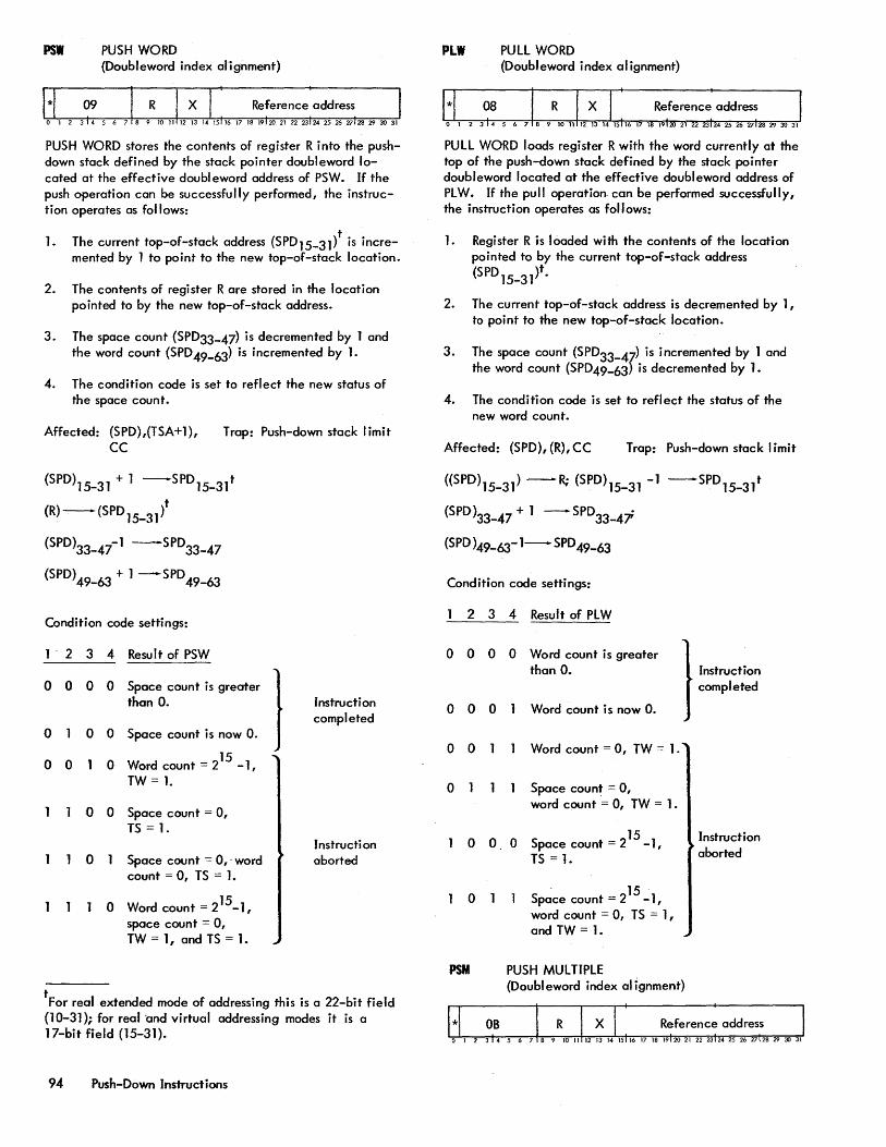
PSW PUSH WORD (Doubleword index alignment)
PUSH WORD stores the contents of register R into the pushdown stack defined by the stack pointer doubleword located at the effective doubl eword address of PSW. If the push operation can be successfully performed, the instruction operates as fol lows:
1. The current top-of-stack address (SPD15_31)t is incremented by 1 to point to the new top-of-stack location.
2. The contents of register R are stored in the location pointed to by the new top-of-stack address.
3. The space count (SPD33-47) is decremented by 1 and the word count (SPD 49-63) is incremented by 1.
4. The condition code is set to reflect the new status of the space count.
Affected: (SPD),(TSA+l), CC
Trap: Push-down stack limit
(SPD)I5-31 + 1 ~SPDI5_31t
(R) - (SPD15
_31
) t
(SPD)33_47-1 -SPD33_47
(SPD) 49-63 + 1 ---SPD 49-63
Condition code settings:
2
0 0
0
0 0
3 4
0 0
0 0
0
0 0
o 1
Resu I t of PSW
Space count is greater thon O.
Space count is now O.
15 Word count = 2 - I, TW= 1.
Space count = 0, TS = 1.
Space count = 0,· word count = 0, TS = 1.
1 0 Word count = 215_1, space count = 0, TW = 1, and TS = 1.
} Instruction completed
Instructi on aborted
tFor real extended mode of addressing this is a 22-bit field (10-31); for real 'and virtual addressing modes it is a 17-bit field (15-31).
94 Push-Down Instructions
PLW PUll WORD (Doubleword index alignment)
PUll WORD loads register R with the word currently at the top of the push-down stack defined by the stack pointer doubfeword located at the effective doubleword address of PlW. If the pull operation can be performed successfully, the instruction operates as follows:
1.
2.
3.
Register R is loaded with the contents of the location pointed to by the current top-of-stack address (SPD 15_31)t.
The current top-of-stack address is decremented by 1, to point to the new top-of-stack location.
The space count (SPD33- 47) is incremented by 1 and the word count (SPD49-63) is decremented by 1.
4. The condition code is set to reflect the status of the new word count.
Affected: (SPD), (R), CC Trap: Push-down stack limit
«SPD)15_31) -R; (SPD)15_31 -1 -SPDI5_31 t
(SPD)33_47 + 1 -SPD33_47
(SPD )49-63- 1- SPD 49-63
Condition code settings:
0
0
0
o
2 3 4 Result of PlW
0 0 0
0 0
0
000
o 1
Word count is greater than o.
Word count is now O.
Word count = 0, TW = 1.
Space count = 0, word count = 0, TW = 1.
15 Space count = 2 -1, TS = 1.
15 Space count = 2 - 1 , word count = 0, TS = 1, and TW = 1.
PSM PUSH MULTIPLE
} Instruction completed
Instruction aborted
(Doubleword index alignment)
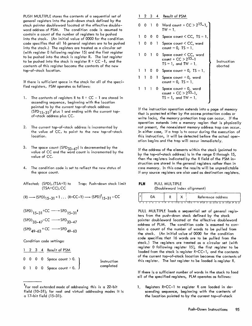
PUSH MULTIPLE stores the contents of a sequential set of general registers into the push-down stack defined by the stack pointer doubleword located at the effective doubleword address of PSM. The condition code is assumed to contain a count of the number of registers to be pushed into the stack. (An initial value of 0000 for the condition code specifies that all 16 general registers are to be pushed into the stack.) The registers are treated as a circular set (with register 0 following register 15) and the first register to be pushed into the stack is register R. The last register to be pushed into the stack is register R + CC -1, and the contents of this register become the contents of the new top-of-stack location.
if there is sufficient space in the stack for all of the specified registers, PSM operates as follows:
1. The contents of registers R to R + CC - 1 are stored in ascending sequence, beginning with the location pointed to by the current top-of-stack address (SPD15_31)t plus 1 and ending with the current topof-stack address plus CC.
2. The current top-of-stack address is incremented by the value of CC, to point to the new top-of-stack location.
3. The space count (sPD33-47) is decremented by the value of CC and the word count is incremented by the value of Cc.
4. The condition code is set to reflect the new status of the space count.
Affected: (sPD), (TSA+1) to (TSA+CC), CC
Trap: Push-down stack limit
(R) - (SPD)15-31 + 1 ... (R+CC-l) - (sPD)t15_31 + CC
(SPD) 15-31 +CC ---.--sPD 15_31 t
(sPD)33_47- CC --SPD33_47
(sPD 49-63 + CC -sPD 49-63
Condition code settings:
2 3 4 Resul t of PsM
0 0 0 0 Space count> O.
0 0 0 Space count = O. J Instruction completed
tFor real extended mode of addressing this is a 22-bit field (10-31); for real and virtual addressing modes it is a 17-bit field (15-31).
2 3 4 Result of PsM
00 0 Word count +CC>215_1, TW = 1.
o 0 0 Space count < CC, TS = 1.
o 0 Space count < CC, word count = 0, TS = 1.
o 0 Space count < CC, word count + CC > 2 15_1 TS= 1, and TW = 1.
o 0 Space count = 0, TS = 1.
o Space count = 0, word count = 0, TS = l.
o Space count = 0, word count + CC > 2 15-1, Ts = 1, and TW = 1.
Instructi on aborted
If the instruction operation extends into a page of memory that is protected either by the access protection codes or write locks, the memory protection trap can occur. If the operation extends into a memory region that is physically not present, the nonexistent memory address trap can occur. .In either case, if a trap is to occur during the execution of this instruction, it will be detected before the actual operation beg ins and the trap will occur immediately.
If the address of the elements within the stack (pointed to by the top-of-stack address) is in the range 0 through 15, then the reg isters indicated by the R field of the PSM instruction are stored in the general registers rather than in core memory. In this case the results will be unpredictable if any source registers are also used as destination registers.
PLM PULL MULTIPLE (Doubleword index al ignment)
PULL MULTIPLE loads a sequential set of general registers from the push-down stack defined by the stack pointer doubleword located at the effective doubleword address of PLM. The condition code is assumed to con.;. tain a count of the number of words to be pulled from the stack. (An initial value of 0000 for the condition code specifies that 16 words are to be pulled from the stack.) The registers are treated as a circular set (with register 0 following register 15), the first register to be loaded from the stack is register R+CC-l, and the contents of the current top-of-stack location becomes the contents of this register. The last register to be loaded is register R.
If there is a sufficient number of words in the stack to load all of the specified registers, PLM operates as follows:
1. Registers R+CC-l to register R are loaded in descending sequence, beg inn ing with the contents of the location pointed to by the current top-oF-stack
Push-Down Instructions 95
address (SPD15-31)t and ending with the contents of the location pointed to by the current top-of-stack address minus CC-l.
2. The current top-of-stack address is decremented by the votue of CC, to point to the new top-of-stack location.
3. The space count (SPD33-47) is incremented by the value of CC and the word count is decremented by the value of Cc.
4. The condition code is set to reflect the new status of the word count.
Affected: (SPD), (R+ee-l) Trap: Push-down stack limit to (R), ce
t «SPD)15_31) - R + CC -1, ... ,
«SPD)15_31 - Ice - 11) - Rt
(SPD)15_31 - ee - SPD15_31 t
(SPD)33_47 + ce - SPD33_47
(SPD) 49-63 - ec -S.PD 49-63
Condition code settings:
2 3 4 Result of PLM
0 0 0 a Word count > 0 ] 0 0 0 1 Word count = 0
0 0 0 Word count < ce, TW= 1
0 0 Word count = 0, TW= 1
a 0 Space count = 0, word count < ee, TW= 1
0 Space count = 0, word count = 0, TW = 1
a 0 0 15
Space count + CC > 2 -1, TS = 1
0 a 15 Space count + ce > 2 -1 , word count < CC, IS = 1, and TW = 1
0 Space count + CC > 215_1, word count = 0, TS = 1, and TW = 1
Instruction completed
Instruction aborted
t For real extended mode of addressing th is is a 22-bit field (10-3l); for real and virtual addressing modes it is a 17-bit field (15-31).
96 Push-Down InstrUctions
If the instruction operation extends into a poge of memory that is protected either by the access protection codes or write rocks, the memory protection can occur. If the operation extends into a memory region that is physically not present, the nonexistent memory address trap can occur. In either case, if a trap is to occur during the execution of this instruction, it will be detected before the actuat operation begins and the trap will occur immediately.
If the address of the elements within the stack (pointed to by the top-of-stack address) is in the range 0 through 15, then the words to be loaded are taken from the general registers rather thon from core memory. In this case, the resurts will be unpredictable if any of the source registers are also used as destination registers.
MSP MODIFY STACK POINTER (Doubleword index alignment)
MODIFY STACK POINTER modifies the stack pointer doubI eword, located at the effective doubleword address of MSP by the contents of register .R. Register R is assumed to have the following format:
Bit positions 16 through 31 of register R are treated as a signed integer, with negative integers in two's complement form (i.e., a fixed-point halfword). The modifier is algebraically added to the top-of-stack address, subtracted from the space count, and added to the word count in the stack pointer doubleword. If, as a result of MSP, either the space count or the word count would be decreased below 0 or increased above 2 15_1, the instruction is aborted. Then, the computer either traps to Homespoce location X'421 or sets the condition code to reflect the reason for aborting, depending on the stack limit trap inhibits.
If the modification of the stack pointer doubleword can be successfully performed, MSP operates as follows:
1. The modifier in register R is algebraically added to the current top-of-stack address (SPDI5-30t, to point to a new top-of-stack location. (If the modifier is negative, it is extended to 17 bits by appending a highorder 1.)
2. The modifier is algebmically subtracted from the current space count (SPD33- 47) and the result becomes the new space count.
3. The modifier is algebraically added to the current word count (SPD49-63) and the result becomes the new word count.
4. The condition code is set to reflect the new status of the new space count and new word count.
Affected: (SPD), CC T rap: Push-down stack limit
(SPD)15_31 + (R)16-31SE- SPD 15_31 t
(SPD)33_47 - (R)16-31- SPD33_47
(SPD) 49-63 + (R) 16-31- SPD 49-63
Condition code settings:
2 3 4 Result of MSP
o 0 0 0
000
000
o 0
Space count> 0, word count > O.
Space count> 0, word count = O.
Space count = 0, word count> O.
Space count = 0, word count = 0, modifier = O.
Instruction completed
If CC1, or CC3, or both CCl and CC3 are lis after execution of MSP, the instruction was aborted but the pushdown stack I imit trap was inhibited by the trap-on-space inhibit (SPD32), by the trap-on-word inhibit (SPD4S)' or both. The condition code is set to reflect the reason for aborting as follows:
2 3 4 Status of space and word counts
o Word count :> O.
Word count = O.
- - 0 - o ~ word count + modifier ~ 215_1.
- Word count + modifier < 0, and TW = 1 or word count + modifi er > 215_1, and TW = 1.
- 0 - - Space count> O.
Space count = O.
o - - - 0 ~ space count - modifier:S 215_1.
- - Space count - modifier < 0, and TS = 1 or space count - modifier> 215 -1, and TS = 1.
EXECUTE/BRANCH INSTRUCTIONS The EXECUTE instruction can be used to insert another instruction into the program sequence, and the branch instructions can be used to al ter the program sequence, either
tFor real extended mode of addressing this is a 22-bit field (10-31); for real and virtual addressing modes it is a 17-bit field (15-31).
unconditionally or conditionally. If a branch is unconditional (or conditiona I and the branch condition is satisfied), the instruction pointed to by the effective address of the branch instruction is normally the next instruction to be executed. If a branch is conditional and the condition for the branch is not satisfied, the next instruction is normally taken from the next location, in ascending sequence, after the branch instruction.
BRANCHES IN REAL EXTENDED ADDRESSING MODE
The extension address field of the PSD wiil be modified automatically by branch instructions. If the effective address of a branch instruction is outside the first 64K of real memory (region 0 is defined as the first 64K of real memory), the high-order bits of this full effective address will automatically be loaded into the Extension Address field of the PSD if the branch is taken. The remaining part of the effective branch address will, of course, be loaded into bit positions 16-31 of the PSD. In addition, bit position 15 of the PSD, the Extension Selector, will be set to 1.
If the effective branch address is to a location within the first 64K of memory, then the Extension Address field of the'PSD will not be modified. The effective address will be loaded into the 16 low-order positions of the instruction address field and the Extension Selector (bit 15) will be cleared (set equal to zero). This means that once the Extension Address field has been set, it will remain set until it is either changed by the loading of a new PSD or by actually branching into another 64K region of memory (excluding region 0).
A BRANCH AND LINK instruction in real extended addressing wi II store the full address of the next instruction in the link register. If the Extension Selector in the PSD at the time BRANCH AND LINK is executed is zero, then the address stored in the link register will be the incremented 16-bit displacement from positions 16-31 of the PSD and zeros in the high-order address positions. If the Extension Selector in the PSD is one, then the address stored will be the incremented 16-bit displacement (PSD 16-31) concatenated with the contents of the Extension Address field (PSD 42-47), which are loaded into bit positions 10-15 of the link register. In both cases, posi-tions 0-9 of the I ink register will be cleared.
NONALLOWED OPERATION TRAP DURING EXECUTION -OF BRANCH INSTRUCTION
A branch instruction has two possible places from which the next instruction may be taken: the location following the branch instruction or the location that may be branched to. It is possible that either of these two locations may be in a protected memory region or in a region that is physi cally nonexistent. The execution of the branch does not cause a trap unless the instruction that is actually to follow the branch instruction is in a protected or nonexistent memory region. Traps do not occur because of any anticipation on the part of the hardware.
Execute/Branch Instructions 97
A nonaUowed operation trap condition during execution of a branch instruction will occur for the following reasons:
1. The branch instruction is indirectly addressed and the branch conditions are satisfied, but the address of the location containing the direct address is either nonexistent or unava i lable for read access to the program in the slave mode.
2. The branch instruction is unconditional (or the branch is conditionar and the condition for the branch is satisfied), but the effective address of the branch instruction is either nonexistent or unavailable for instruction or read access to the program (in slave or masterprotected mode).
If either of the above situations occurs, the computer aborts execution of the branch instruction and executes a nonaHowed operation trap.
Prior to the time that an instruction is accessed from memory for execution, bit positions 15-31 of the program status doubleword contain the virtual address of the instruction, referred to as the instruction address. At this time, the computer traps to Homespace location X'40' if the actual address of the instruction is nonexistent or instructionaccess protected. If the instruction address is existent and is not instruction-access protected, the instruction is accessed and the instruction address portion of the program status doubleword is incremented by 1, so that it now contains the virtual address of the next instruction in sequence (referred to as the updated instruction address).
If a trap condition occurs during the execution sequence of any instruction, the computer decrements the updated instruction address by 1 and then traps to the location assigned to the trap condition. If neither a trap condition nor a satisfied branch condition occurs during the execution of an instruction, the next instruction' is accessed from the location pointed to by the updated instruction address. If a satisfied branch condition occurs during the execution of a branch instruction (and no trap condition occurs), the next instruction is accessed from the location pointed to by the effective address of the branch instruction.
EXU EXECUTE (Word index alignment)
EXECUTE causes the computer to access the instruction in the location pointed to by the effective address of EXU and execute the subject instruction. The execution of the subject instruction, including the processing of trap and interrupt conditions, is performed exactly as if the subject instruction were initially accessed instead of the EXU instruction. If the subject instruction is another EXU, the computer executes the subject instruction pointed to by the effective address of the second EXU as described above. Such "chains" of EXECUTE instructions may be of any length, and are processed (without affecting the updated instruction address) until an instruction other than EXU is
98 Execute/Branch Instructions
encountered. After the final subject instruction is executed, instruction execution proceeds with the next instruct:on in sequence after the initial EXU (unless the subject instruction is an LPSD or XPSD instruction, or is a branch instruction and the branch condition is satisfied).
If an interrupt activation occurs between the beginning of an EXU instruction (or chain of EXU instructions) and the last interruptible point in the subject instruction, the computer processes the interrupt-servicing routine for the active interrupt level and then returns program control to the EXU instruction (or the initial instruction of a chain of EXU instructions), which is started anew. Note that a program is interruptible after every instruction access, including accesses made with the EXU instruction, and the interruptibility of the subject instruction is the same as the normal interruptibility for that instruction.
If a trap condition occurs betwe~n the beginning of an EXU instruction (or chain of EXU instructions) and the completion of the subject instructi on, the computer traps to the appropriate trap location. The instruction address stored by the XPSD instruction in the trap location is the address of the EXU instruction (or the initial instruction of a chain of EXU instructions).
Affected: Determ i ned by subject instruction
Traps: Determined by subject instruction
Condition code settings: Determined by subject instruction
BCS BRANCH ON CONDITIONS SET (Word index alignment)
o 1 2
BRANCH ON CONDITIONS SET forms the logical product (AND) of the R field of the instruction word and the current condition code. If the logical product is nonzero, the branch condition is satisfied and instruction execution proceeds with the instruction pointed to by the effective addresst of the BCS instruction. However, if the logical product is zero, the branch condition is unsatisfied and instruction execution then proceeds with the next instruction in normal sequence.
Affected: (IA) if CC n R f 0
If CC n (1)8-11 f 0, EVA15_31-IA
If CC n (1)8-11 = 0, IA not affected
If the R field of BCS is 0, the next instruction to be executed after BCS is always the next instruction in ascending sequence, thus effectively producing a IIno operation" instruction.
t See" Branches in Rea I Extended Addressing Mode" in the introductory description under "Execute/Branch Instructions ll
•
8eR BRANCH ON CONDITIONS RESET (Word index alignment)
BRANCH ON CONDITIONS RESET forms the logical product (AND) of the R field of the instruction word and the current condition code. If the logi cal product is zero, the branch condition is satisfied and instruction execution then proceeds with the instruction pointed to by the effective addresst of the BCR instruction. However, if the logical product is non:z:ero, the branch condition is unsatisfied and instruction execution then proceeds with the next instruction in normal sequence.
Affected: (lA) if CC n R = ° If CC n (1)8-11 = 0, EVA15_31 - IA
If CC n (1)8-11 10, IA not affected
If the R field of BCR is 0, the next instruction to be executed after BCR is always the instruction located at the effective address of BeR, thus effectively producing a "branch unconditional Iii instruction.
BIR BRANCH ON INCREMENTING REGISTER (Word index al ignment)
BRANCH ON INCREMENTING REGISTER computes the effective virtual address and then increments the contents of general register R by 1. If the result is a negative value, the branch condition is satisfied and instruction execution then proceeds with the instruction pointed to by the effective addresst of the BIR instruction. However, if the result is zero or a positive value, the branch condition is not satisfied and instruction execution proceeds with the next instruction in normal sequence.
Affected: (R), (IA)
(R) + 1 - R
If (R)O = 1, EVA15
_31-- IA
If (R)O --, 0, I~ not affected
If the branch condition is satisfied and if the effective address of BIR is either unavailable to the program (slave or master-protected mode) for instruct i on access or is nonexistent, the computer aborts execution of the BIR instruction and traps to Homespace location X'40 ' . In this case, the instruction address stored by the XPSD instruction in location X'40 ' is the virtual address of the aborted BIR instruction. If the computer traps because of instruction access protection, register R will contain the value that existed just before the BIR execution (i .e., updated instruction address).
If a memory parity error occurs due to the accessing of the instruction to which the program is branching, the computer aborts execution of the SIR and traps to Homespace location X' 4C with reg ister R unchanged.
BDR BRANCH ON DECREMENTING REGISTER (Word index al ignment)
o 1 2
BRANCH ON DECREMENTING REGISTER computes the effective virtual address and then decrements the contents of general register R by 1. If the result is a positive value, the branch condition is satisfied and instruction execution then proceeds with the instruction pointed to by the effective addresst of the BDR instruction. - However, if the result is zero or a negotive va I ue, the branch condition is unsatisfied and instruction execution proceeds with the next instruction in norma I sequence.
Affected: (R), (IA)
(R) - 1 -R
If (R)O =0 and (R)1-31 10, EVA 15_31 --IA
If (R)O = 1 or (R) = 0, IA not affected
If the effective address of BDR is unavai lable to the program (sl ave or master-protected mode) for i nstructi on access and the branch condition is satisfied, or if the effective address of BDR is nonexistent, the computer aborts execution of the BDR instruction and traps to Homespace location X'40 ' . In this case, the instruction address stored by the XPSD instruction in location X'40 ' is the virtual address of the aborted BDR instruction. If the computer traps because of instruction access protection, register R will contain the value that existed just before the BDR instruction. If a memory parity error occurs due to the accessing of the instruction to which the program is branching, the computer aborts execution of the BDR and traps to Homespace location X'4C with register R unchanged.
BAL
o 1 2
BRANCH AND LINK (Word index alignment)
BRANCH AND LINK determines the effective virtual address, loads the updated instruction address (the virtual address of the next instruction in normal sequence after the BAL instruction) into bit positions 15-31 of general register R, clears bit positions 0-14 of register R to OIS and then replaces the updated instruction address with the effective virtual address. Instruction execution proceeds with the instruction pointed to by the effective address of the BAL instruction.
t See II Branches in Real Extended Addressing Mode" in the introductory description under "Execute/Branch Instructions ll
•
Execute/Branch Instructions 99
The SAL instruction in real extended addressing wi" store the full address of the next instruction in the specified R register. If the Extension Selector in the PSD at the time SAL is executed is equal to zero, then the address stored in the specified R register will be the incremented 16-bit displacement from positions 16-31 of the PSD, and zeros in the high-order address positions. If the Extension Selector in the PSD is equal to one, then the address stored wi II be the incremented 16-bit displacement (PSD 16-31) concatenated with the contents of the Extension Address (PSD 42-47). In both cases, positions 0-9 of the specified R register will be set equal to zero.
Affected: (R), (IA)
IA - R15- 31 ; 0 -- RO- 14; EVA15_31 -IA
If the effective address of SAL is unavai labre to the program (slave or master-protected mode) for instruction access and the branch condition is satisfied, or if the effective address of BAL is nonexistent, the computer aborts execution of the SAL instruction and traps to Homespace location X'40' (nonallowed operation trap). In this case, the instruction address stored by the XPSD instruction in location X'40' is the virtual address of the aborted SAL instruction. If the computer traps because of instruction access protection, register R will contain the updated instruction address. If a memory parity error occurs due to the accessing of the instruction to which the program is branching, the computer aborts execution of the BAL and traps to Homespace location X'4C' with register R changed to the updated instruction address.
CALL INSTRUCTIONS Each of the four CALL instructions causes the computer to trap to a specific location for the next instruction in sequence. The four CALL instructions, their mnemonics, and the locations to which the computer traps are:
Instruction Trap Home-Name Mnemonic space Location
CALL 1 CAll X'48'
CALL 2 CAL2 X' 49'
CALL 3 CAL3 X'4A'
CALL 4 CAL4 X'4B'
Each of these four trap locations must conta in an EXCHANGE PROGRAM STATUS DOUBLEWORD (XPSD) instruction. Execution of XPSD in the trap location for a CALL instruction is described under "Control Instructions, XPSD Exchange Program Status Doubleword". If the XPSD instruction is coded with bit position 9 set to 1, the next instruction (executed after the XPSD) is taken from one of 16 possible locations, as designated by the value in the Rfield of the CALL instruction. Each of the 16 locations may contain an instruction that causes the computer to branch to a specific routine; thus, the four CALL instructions can be used to enter any of as many as 64 unique routines.
100 CAll Instructions/ Control Instructions
If an indirect address in nonexistent memory is specified, the computer traps to Homespoce location X'40'. The effective address of a CALL instruction is not used for a memory reference and, therefore, can not cause a trap.
CAU CALL 1 (Word index alignment)
CALL 1 causes the computer to trap to Homespace location X'48'.
CAU CALL 2 (Word index alignment)
CALL 2 causes the computer to trap to Homespace location X'49 1
•
CAL3 CALL 3 (Word index al ignment)
CALL 3 causes the computer to trap to Homespace location X'4A'.
CAL4 CALL 4 (Word index alignment)
CALL 4 causes the computer to trap to Homespace location X'4B'.
CONTROL INSTRUCTIONS The following privileged instructions are used to control the basic operating conditions of the SIGMA 9 computer:
Instruct ion Name
load Program Status Doubleword
Exchange Program Status Doubleword
Load Register Pointer
Move to Memory Control
Load Rea I Address
Load Memory Status
Wait
Read Direct
Write Direct
Mnemonic
LPSD
XPSD
lRP
MMC
lRA
LMS
WAIT
RD
WD
If execution of any control instruction is attempted while the computer is in the slave mode (i .e., while bit S of the current program status doubleword is a 1), the computer unconditionally traps to Homespace location XI 401 prior to executing the instruction.
PROGRAM STATUS DOUBLEWORD
The SIGMA 9 program status doubleword has the following structure when stored in memory:
i l I
Bit Desig-Position nation Function
0-3 CC Condition code
5 FS Floating significance mask
6 FZ Floating zero mask
7 FN Floating normalize mask
8 MS Master/slave mode control
9 MM Memory map mQde control
10 DM Decima I arithmetic trap mask
11 AM Fixed-point arithmetic overflow trap mask
12 AS ANSCII mask
15 ES Extension selector
16-31 IA Instruction address
34,35 WK Write key
37 CI Counter interrupt group inhibit
38 II I/O interrupt group inhibit
39 EI External interrupt inhibit
40 MA Mode _a Itered
42-47 EA Extension address
48-55 TSF Trap status field
56-59· RP Register pointer
60 RA Reg i ster a I tered
The detailed functions of the various portions of the SIGMA 9 program status doubleword are described in Chapter 2, IIProgram Status Doubleword ll
•
LPSD LOAD PROGRAM STATUS DOUBLEWORD (Doubleword index alignment, privileged)
LOAD PROGRAM STATUS DOUBLEWORD replaces bits 0 through 39 of the current program status doubleword with bits 0 through 39 of the effective doubleword.
Control bits used in the LPSD instruction are:
Bit Desig- Control Position nation Function
S LP load pointer control
10 CL Clearing of interrupt level
11 AD Armed/disarmed state
The following conditional operations are performed:
1. If bit position S (LP)of LPSD contains a 1, bits56 through 59 of the current program status doubleword (register pointer) are replaced by bits 56 through 59 of the effective doubleword; if bit S of LPSD is a 0, the current register pointer val ue remains unchanged.
2. If bit position 10 (CL)of LPSD contains a 1, the highest priority interrupt level currently in the active state is cleared (i .e., reset to either the armed state or the disarmed state); the interrupt level is armed if bit 11 (AD) of LPSD is a 1.., or is disarmed if bit 11 of LPSD is a O. If bit 100f LPSD is a 0, no interrupt level is affected in any way, regardless of whether bit 11 of LPSD is 1 or O. If bit 10 of the LPSD is a Oand bit 11 of LPSD is 1, the PDF flog is cleared. (Interrupt levels are described in detail in Chapter 2, IIInterrupt System ll
.)
Bit position 10 (CL) 11 (AD) Function
o o
o Clear and disarm interrupt level.
Clear and .arm interrupt level.
Clear PDF flog.
o No control action. /
3. The PDF flag is normally reset by the last instruction of a trap routine, which is an LPSD instruction having bit 10 equal to 0 and bit 11 equal to 1.
Those portions of the effective doubleword that correspond to undefined fields in the program status doubleword are ignored.
Affected: (PSD), interrupt system if (1)10 = 1
EDO
_3 -CC; ED
5_
7-FS,FZ,FN
EDS -MS; ED9 - MM
ED10
-DM; ED11
-AM
ED15
-ES
ED16
_31-IA; ED
34_35
-WK
ED37_39 - CI, II, Eli if (I)S = i, ED 56-59 -RP
If (1)10 = 1 and (1)11 = 1, clear and arm interrupt
If (1)10 = 1 and {I)l1 = 0, clear and disarm interrupt
Control Instructions 101
XPSO EXCHANGE PROGRAM STATUS DOUBlEWORD (Doubleword index alignment, privileged)
EXCHANGE PROGRAM STATUS DOUBlEWORD stores the currently active PSD in the doubleword location addressed by the effective address of the XPSD instruction. The following doubfeword is then accessed from memory and loaded into the active PSD registers.
The XPSD instruction is used for three distinct types of operations: as a normal instruction in an ongoing program; as an interrupt instruction; and as a trap instruction.
Control bits used in the XPSD instructions are:
Bit Desig- Control Position notion Function Where Used
8 lP load poi nter All XPSDs control
9 AI Address increment Trap XPSD
10 AT Addressing type Trap XPSD or interrupt XPSD
The effective address of an XPSD instruction is generated in one of the following ways:
XPSD (normal instruction)
When on XPSD instruction is encountered in the course of execution of normal programs, the effective address is generated according to the rules for addressing then in effect as described by the currently active PSD; that is, the CPU is operating in real, reaf extended, or virtual addressing mode. The flags in bit positions 9 and 10 have no effect and must be coded as zeros.
XPSD (interrupt instruction)
An XPSD instruction (in an interrupt location) executed as a result of an interrupt is called an interrupt instruction. Bit position 10 determines the type of addressing to be used by the XPSD. If bit positions 10 and 0 are equal to zero, bit positions 12-31 of the instruction unconditionally specify a direct address within the first 1,048,576 words of real memory. Since the index field is used for addressing, indexing is not possible. If bit 10 is equal to zero an? indirect addressing is specified (bit 0 = 1), the indirect address, interpreted as in real extended addressing, is found in the word specified by bits 12-31. (In brief, the current type of addressing has no bearing on the execution of this instruction.) Bit position 9 is not effective during an interrupt instruct i on and must be a zero.
If bit 10 is a 1, the effective address of the XPSD is generated subject to the current active addressing mode (reaf, real extended, or virtual), and indexing is permitted.
102 Control Instructions
XPSD (trap instruction)
An XPSD instruction (in a trap location) executed asa result of a trap entry operation is caJleda trap instruction. Bit positions 9 and 10 are both effective in this instruction. Bit position 10 determines the type of addressing to be used by the XPSD. If bit positions 10 and 0 are equal to zero, bits 12-31 of the instruction unconditional ry specify a direct address within the first 1,048,576 words of real memory. Since the index field is used for addressingt
indexing is not possible. If bit 10 is equal to zero and indirect addressing is specified (bit 0 = 1), the indirect address, interpreted as in real extended addressing, is found in the word specified by bits 12-31. (In brief, the effective address is generated independently of the type of addressing being used by the program that was trapped.)
If bit position 10 is aI, the effective address ;s generated subject to the same current active addressing mode (real, real extended, or vi rtual) as the program that was trapped, and indexing is permitted.
The following additional operations are performed on the new program status doubleword if, and only if, the XPSD is being executed as the result of a nonalJowed operation (trap to Homespace location X'40')or a CAll instruction (trap to Homespace location X'48', X'49', X'4A', or X'4B'):
1. Nonallowed operations - the following additional functions are performed when XPSD is being executed as a result of a trap to Homespace location X'40':
a. Nonexistent instruction - if the reason for the trap condition is an attempt to execute a nonexistent instruction, bit position Oof the new program status doubleword (CCI) is set to 1. Then, if bit 9 {AI)of XPSD is a 1, bit positions 15-31 of the new program status doubleword (next instruction address) are incremented by 8. t
b. Nonexistent memory address - if the reason for the trap condition is an attempt to access 'or write into a nonexistent memory region, bit position 1 of the new program status doubfeword (CC2) is set to 1. Then, if bit 9 of XPSD is a 1, the instruction address portion of the new program status doubleword is incremented by 4.t
c. Privileged instruction violation - if the reason for the trap condition is an attempt to execute a privileged instruction while the computer is in the slave mode, bit position 2 of the new program status doubleword (CC3) is set to I. Then, if bit posiHon 9 of XPSD is 1, the instruction address portion of the new program status doubleword is incremented by2.t
tIf the CPU is in a reaf extended addressing mode and the effective address of the trap XPSD instruction is generated subject to that current mode, 'the addition of the condition code is restricted to bits 16to 31 of the Instruction Address. The Extension Selector (bit 15) and Extension Address {bits 42-47) will not be affected if a corry should result.
d. Memory protection violation - if the reason for the trap condition is an attempt to read from or write into a memory region to which the program does not have proper access, bit position 3 of the new program status doubleword (CC4) is set to 1. Then, if bit 9 of XPSD is a 1, the instruction address portion of the new program status doubleword is incremented by 1.t
There are certain circumstances under which two of the above nonallowed operations can occur simultaneously. The following operation codes (including their counterparts) are considered to be both nonexistent and privileged: X'OC' and X'OD'. If either of these operation codes is used as an instruction while the computer is in the slave or master-protected mode, CCl and CC3 are both set to l's; if bit 90f XPSD is a 1, the instruction address portion of the new program status doubleword is incremented by 10. If an attempt is made to access or write into a memory region that is both nonexistent and prohibited to the program by means of the memory control feature, CC2 and CC4are both set to l's; if bit 9 of XPSD is a 1, the instruction address of the new program status doubleword is incremented by 5.
2. CALL instructions-the following additional functions are performed when XPSD is being executed as a result of a trap to Homespace location X'48', X'49', X'4N, or X'4B'.
a. The R field of the CALL instruction causing the trap is logically inclusively ORed into bit positions 0-3 (CC) of the new PSD.
b. If bit position 9 of XPSD conta ins a 1, the R field of the CALL instruction causing the trap is added to the instruction address portion of the new PSD.
3. Watchdog timer, parity error, or instruction exception trap - the following additional functions are performed when XPSD is being executed as a result of a trap to Homespace location X'46', X'4C', or X'4D', respectively.
a. The contents of TCC 1-4 are logically inclusively ORed into bit positionsO-3 (CC) of the new PSD.
b. If bit position 9 of XPSD contains a 1, the contents of TCC 1-4 are added to the instruction address portion of the new PSD.
If bit position90fXPSDcontains aO, the instruction address portion of the newPSDalways remains at the value established by the second effective doubleword. Bit position 9 of XPSD is effective only if the instruction is being executed as the result of a nonallowed operation, CALL instruction, watchdog timer, parity error, or instruction exception trap. Bit position 9 of XPSD must be coded with a ° in all other cases; otherwise, the results of the XPSD instruction are undefined.
tIf theCPUis in a real extended addressing mode and the effective address of the trap XPSD instruction is generated subject to that current mode, the addition of the condition code is restricted to bits 16 to 31 of the Instruction Address. The Extension Selector (bit 15) and Extension Address (bits 42-47) will not be affected if a carry should result.
The current program status doubleword is stored in the doubleword location pointed to by the effective address of XPSD in the following form:
Program status doubleword
The current program status doubleword (as illustrated above) is replaced by a new program status doubleword as described below.
1. The effective address of XPSD is incremented by 2 so that it points to the next doubleword location. The contents of the next doubleword location are referred to as the second effective doubleword, or ED2.
2. Bits 0-35, 40, and 42-47 of the current program status doubleword are unconditionally replaced by bitsO-35,40, and 42-470f the second effective doubleword. The affected portions of the program status doubleword are:
Bit Desig-Position nation Function
0-3 CC Condition code
5-7 FS, FZ, Floating control FN
.:,8 MS Master/slave mode control
9 MM Mapping mode control
10 DM Decimal arithmetic trap mask
11 AM Fixed-point arithmetic trap mask
15 ES Extension selector} (real extended)
16-31 IA x Instruction address
or
15-31 IA Instruction address (real or virtual)
34-35 WK Write key
40 MA Mode altered
42-47 EA Extension address
3. A logical inclusive OR is performed between bits 37 through 39 of the current program status doubleword and bits 37 through 39 of the second effective doubleword.
Bit Desig-Position nation Function
37 CI Counter interrupt inhibit
38 II I/O interrupt inhibit
39 EI External interrupt inhibit
Control Instructions 103
If any (or all) of bits 37, 38, or 39 of the second effeCtive doubleword are O's, the corresponding bits in the current program status doubleword remain unchanged; if any (or all) of bits 37, 38, or 39 of the second effective doubleword are lis, the corresponding bits in the current program status doubleword are set to lis. See IIInterrupt System", Chapter 2, for a detailed discussion of the interrupt inhibits.
4. If bit position 8 (LP) of XPSD contains a 1, bits 56 through 59 of the current program status doubleword (register pointer) are replaced by bits 56 through 59 of the second effective doubleword; if bit 8 of XPSD is a 0, the current register pointer value remains unchanged.
Affected: (EDL), (PSD)
If (1)10 = 1, trap or interrupt instructions only, effective address is subject to current active addressing mode.
If (Iho = 0, trap or interrupt instructions only, effective address is independent of current active addressing mode.
PSD -EDL
ED20
_3
- CC; ED25
_7
- FS, FZ, FN
ED2 - MS· ED2 - MM 8 ' 9·
ED210
- DM; ED211 -AM; ED15
_31 - IA
or
ED215
-ES
ED216
_31 -I~ ED2
34_35
-WK
E D237 -39 u CI, II, EI -- CI, II, EI; ED240 --MA
If (1)8 = 1, ED256
_59
- RP
If (1)8 = 0, RP not affected
If nonexistent instruction, 1 --CC1 then, if (1)9 = 1, IA+8-IA
If nonexistent memory address, 1 --CC2 then, if (1)9 = 1, IA + 4 -IA
If privileged instruction violation, 1 -- CC3 then, if (1)9 = 1, IA + 2 --IA
104 Control Instructions
If memory protection violation, 1-CC4 then, if (I~ = 1, IA + l-IA
If CALL instruction, CC u CALL8_11- CC then, if (1)9 = 1, IA + CALL8_11 -IA
If (1)9 = 0, IA not affected
If watchdog timer, parity error, or instruction exception trap, ED20-3 u TCCl-4 -CCl-4 then, if (1)9 = 1, IA + TCCl-4 - IA
LRP LOAD REGISTER POINTER 0t/ord index alignment, privileged)
LOAD REGISTER POINTER loads bits 26 and 27 of the effective word into the register pointer (RP) portion of the current program status doubleword. Bit positions 0 through 25 and 28 through 31 of the effective word are ignored, and no other portion of the program status doubleword is affected. If the LOAD REGISTER POINTER instruction attempts to load the register pointer with a value that points to a nonexistent block of general registers, the computer traps to Homespace location XI4DI.
Affected: RP Trap: Instructi on exception
EW26
_27
-RP
MMe MOVE TO MEMORY CONTROL (Word index alignment, privileged, continue after interrupt)
MOVE TO MEMORY CONTROL loads a string of one or more words into one of the three blocks of memory control registers {memory control registers are described in Chapter 2, under II Memory Address Control" • Bi t posi ti ons 12- 14 of MMC are not used as an index register address; instead, they are used to specify which block of memory control registers is to be loaded, as follows:
Bit Position
12 13 14 Function
0 0 Load memory write protection locks.
0 0 Load access protection.
0 0 Load memory map (8-bit format).
0 load memory map (13-bit format).
An attempt to execute an MMC instruction wi th any code other than the four above causes the instruction to trap to Homespace location X'4DI, instruction exception trap.
Bit positions 15-31 of MMC are ignored insofar as the operation of the instruction is concerned, and the results of the instruction are the same whether MMC is indirectly addressed or not.
The R field of MMC designates an even-odd pair of general registers (R and Rul) that are used to control the loading of the specified bank of memory control registers. Registers R and Ru 1 are assumed to contain the following information:
Register R:
Register Ru 1:
Register R contains the address of the first word of the control image to be loaded into the specified block of memory control registers. Bit positions 0 through 7 of register Ru 1 contain a count of the number of words to be loaded. (If bits 0-7 of register Rul are initially all OIS, a word count of 256 is implied.)
Bit positions 15 through 22 of register Ru 1 point to the beginning of the memory region controlled by the registers to be loaded. The significance of this field is different for the four modes of MMC.
The R field of the MMC instruction must be an even value for proper operation of the instruction; if the R field of MMC is an odd value, the instruction traps to Homespace location XI4DI, instruction exception trap.
If MMC is indirectly addressed and the indirect reference address is nonexistent, the nonallowed operation trap (Homespace locationXl 401
) is not activated. The effective virtual address of the MMC instruction, however, is not used as a memory reference (thus does not affect the normal operation of the instruction).
Affected: (R),(Ru1), memory control storage
T rap: Instruction exception
LOADING THE MEMORY MAP
The following diagrams represent the configuration of MMC, register R, and register Ru 1 that are required to load the memory map in either the 8-bit or 13-bit format:
The 8-bit instruction format is:
lne 13-bit instruction format is:
In the following description, the top of the diagram depicts the 8-bit format and the bottom the 13-bit format.
The contents of register Rare:
The contents of register Ru 1 are:
MEMORY MAP CONTROL IMAG E
The initial address value in bit positions 15-31t
of register R is the virtual address of the first word of the memory map control image. The word length of the control image to be loaded is specified by the initial count in bit positions 0-7 of register Ru 1. A word count of 64 is suffi cient to load the entire block of memory map control registers. The memory map control registers are treated as a circular set, with the first register following the last; thus, a word count greater than 64 causes the first registers loaded to be overwritten.
Each word of the memory map control image is assumed to be in the following 8- or 13-bit format:
MEMORY MAP LOADING PROCESS
Bit positions 15-22 of register Ru1 initially point to the first 512-word page of virtual addresses that is to be controlled by the map image being loaded. MMC moves the map image into the memory map control registers one word at a time, thus loading the page address for four (two if 13-bit format selected) consecutive memory map registers with each image word. As each word is loaded into the memory map, the virtual address of the image area is incremented by 1, the word count is decremented by 1, and the value in bit positions lS-22 of register Ru 1 is incremented by 4 (by 2 if 13-bit format selected); this process continu~s until the word count is reduced to O.
When the loading process is completed, bit positions lS-31t
of register R contain a value equal to the sum of the initial map image address plus the initial word count. Also, bit positions 0-7 of register Ru 1 contain all OIS, and bit positions 15-22 of register Rul contain a value equal to the sum of the initial contents plus four times the initial word count (two tim~s the initial' word count if 13-bit format selected).
tFor real extended mode, bits 10-31.
Control Instructions lOS
LOADING THE ACCESS PROTECTION CONTROLS
The following diagrams represent the configurations of MMC, register R, and register Ru 1 that are required to load the access protection controls:
The instruction format" is:
The contents of register Rare:
The contents of register Ru 1 are:
i!!i~: ACCESS PROTECTION CONTROL IMAGE
The initial address value in register R is the virtual address of the first word of the access control image, and the word length of the first control image is specified by the initial count in register Ru 1. A word count of 16 is sufficient to load the entire block of access protection control registers. The access protection control registers are treated as a circular set, with the first register following the last; thus, a word count greater than 16 causes the first registers loaded to be overwritten. Each word of the access control image is assumed to be in the following format:
ACCESS CONTROL LOADING PROCESS
Bit positions 15-20 of register Ru1 initially point to the first 512-word page of virtual addresses that is to be controlled by the access control image. MMC moves the access control image into the access control registers one word at a time, thus loading the controls for 16 consecutive 512-word pages with each image word. As each word is loaded, the virtual address of the control image is incremented by 1, the word count is decremented by 1, and the value in bit positions 15-20 of register Ru 1 is incremented by 4; this process continues until the word count is reduced to O. When the loading process is completed, register R contains a value equal to the sum of the initial control image address plus the initial word count. Also, the final word count is 0, and bit positions 15-20 of register Ru 1 contain a value equal to the sum of the initial contents plus four times the initial word count.
LOADING THE MEMORY WRITE PROTECnON LOCKS
The following diagrams represent the configurations of MMC, register R, and register Ru 1 that are required to load the memory write protection locks:
106 Control Instructions
The contents of register Rare:
The contents of register Ru 1 are:
MEMORY LOCK CONTROL IMAGE
The initial address value in register R is the virtual address of the first word of the memory lock control image, and word length of the image is specified by the initial count in register Ru 1. A word count of 16 is sufficient to load the entire block of memory locks. The memory lock registers are treated as a circular set, with the register for memory addresses 0 through X'lFF' immediately following the register for memory addresses X'l FEOO' through Xi 1FFFF'; thus, a word count greater than 16 causes the first registers loaded to be overwritten. Each word of the lock image is assumed to be in the following format:
MEMORY LOCK LOADING PROCESS
Bit positions 15-20 of register Ru 1 initially point to the fi rst 512-word page of actual memory addresses that wi II be controlled by the memory lock image. MMC moves the lock image into the lock registers one word at a time, thus loading the locks for 16 consecutive 512-word pages with each image word. As each word is loaded, the virtual address of the lock image is incremented by 1, the word count is decremented by 1, and the value in bit posi-tions 15-20 of register Ru 1 is incremented by 4; this process continues until the word count is reduced to o. When the loading process is completed, register R contains a value equal to the sum of the initial lock image address plus the initial word count. -Also, the final word count is 0, and bit positions 15-20 of register Ru 1 contain a value equal to the sum of the initial contents plus four times the initial word count.
INTERRUPTION OF MMC
The execution of MMC can be interruptedafter each word of the control image has been moved into the specified control register. Immediately prior to the time that the instruction in the interrupt location is executed, the instruction address portion of the program status doubleword contains the virtual address of the MMC instruction, register Rcontains the vi rtual address of the next word of the control image tobe loaded, and register Ru1 containsacount of the number of control image words remaining tobe moved and avalue pointing to the next memory control reg ister to be loaded. After interrupt, the MMC instruction maybe resumed from the point itwas interrupted.
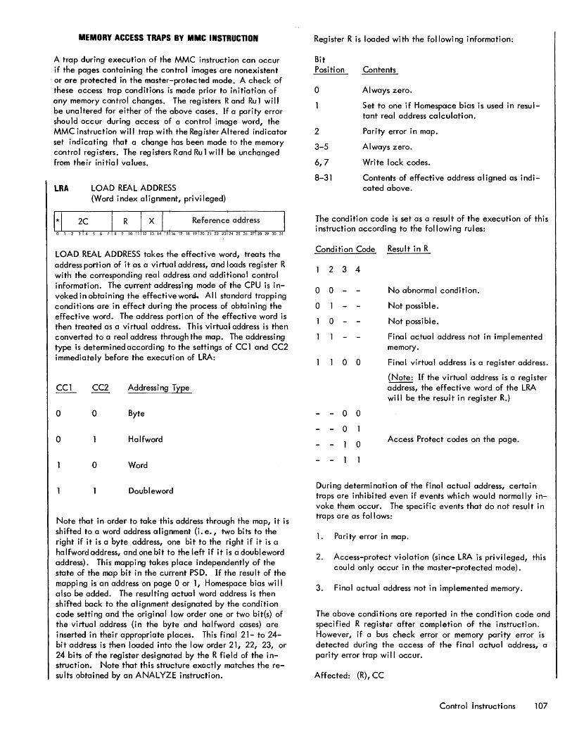
MEMORY ACCESS TRAPS BY MMC INSTRUCTION
A trap during execution of the MMC instruction can occur if the pages containing the control images are nonexistent
: or are protected in the master-protected mode. A check of these access trap conditions is made prior to initiation of any memory control changes. The reg isters Rand Ru 1 wi II be unaltered for either of the above cases. If a parity error shou Id occur during access of a control image word, the MMC instruction will trap with the Reg ister Altered indicator set indicating that a change has been made to the memory control registers. The reg isters Rand Ru 1 will be unchanged from their initial values.
LRA LOAD REAL ADDRESS (Word index alignment, privileged)
o 1 2 314 5 6 18 9 1011 12 13 14 15 16 17 181912021222324252627128293031
LOAD REAL ADDRESS takes the effective word, treats the address portion of it as a virtual address, and loads register R with the corresponding real address and additional control information. The current addressing mode of the CPU is invoked in obtaining the effective word.. All standard trappi ng conditions are in effect during the process of obtaining the effective word. The address portion of the effective word is then treated as a virtual address. This virtual address is then converted to a real address through the map. The addressing type is determined according to the settings of CCl and CC2 immediately before the execution of LRA:
CCl CC2 Addressing Type
o o Byte
o Halfword
o Word
Doubleword
Note that in order to take this address through the map, it is shifted to a word address alignment (i. e., two bits to the right if it is a byte address, one bit to the right if it is a halfwordaddress, and one bit to the left if it is a doubleword address). This mapping takes place independently of the state of the map bit in the current PSD. If the result of the mappi ng is an address on page 0 or 1, Homespace bias wi II also be added. The resulting actual word address is then shifted back to the alignment designated by the condition code setting and the original low order one or two bit(s} of the virtual address (in the byte and halfword cases) are inserted in their appropriate places. This final 21- to 24-bit address is then loaded into the low order 21, 22, 23, or 24 bits of the register designated by the R field of the instruction. Note that this structure exactly matches the results obtained by an ANALYZE instruction.
Register R is loaded with the following information:
Bit Position Contents
o
2
3-5
Always zero.
Set to one if Homespace bias is used in resultant real address calculation.
Parity error in map.
Always zero.
6,7
8-31
Write lock codes.
Contents of effective address aligned as indicated above.
The condition code is set as a result of the execution of this instruction according to the following rules:
Condition Code Result in R
234
o 0 - No abnormal condition.
o Not possible.
o Not possible.
Final actual address not in implemented memory.
o 0 Final virtual address is a register address.
(Note: If the virtual address is a register address, the effective word of the LRA will be the result in register R.)
- 0 0
- 0
o Access Protect codes on the page.
During determination of the final actual address, certain traps are inhibited even if events which would normally invoke them occur. The specific events that do not result in traps are as follows:
1. Parity error in map.
2. Access-protect violation (since LRA is privi leged, this could only occur in the master-protected mode).
3. Final actual address not in implemented memory.
The above conditions are reported in the condition code and specified R register after completion of the instruction. However, if a bus check error or memory parity error is detected during the access of the final actual address, a parity error trap wi II occur.
Affected: (R), CC
Control Instructions 107
LMS LOAD MEMORY STATUS (Word index alignment, privileged)
LOAD MEMORY STATUS is used to determine memory bank status and/or to perform diagnostic action on a memory bank The effective address is used to determine the memory bank. The condition code setting immediately before execution determines the diagnostic action to be performed. The effective address always references memory even if it is less than 16. The condition code can be set to the desired value before execution of LMS with the LCF or LCFI instructions. Register R is loaded with the result of the action. The condition code is set at the concl usion of execution to reflect the status of the word loaded (if any).
Affected: (R), CC Trap: See "Trap System", Chapter 2.
Initial condition code settings:
234
o 0 0 0
000
000
o 0
o 1
o 0
LMS Action
Load and set - causes the same action as the LOAD AND SET (LAS) instruction, except for condition code settings. Normal traps are allowed including write protect.
Read and inhibit parity -loads the effective word into R. If a memory parity error is detected, the memory does not take a "snap-shot" or generate a Memory Fault Interrupt (MFI). It does, however, generate the Memory Parity Error signal. The CPU inhibits the trap that would ordinarily occur for the memory parity error.
Read and set bad parity - loads the effective word into R. The memory reads the location and unconditionally restores the word with the inval id parity bit. The parity bit transmitted to the processor is the original parity bit. Parity error traps and memory fault interrupts are not inhibited by this instruction.
Reserved.
Reserved.
o o 1 Reserved.
o o
108
o Reserved.
Set memory clock margin - transfers the effective word from R to memory. The memory bank will interpret the word and change its own timing as follows:
Word Bits
8 9 10 11 12 Interpretati on
o 0 0 0 Set clock margin 0, early write half cycle.
Control Instructions
000
o 0
Word Bits
8 9 10 11
0 0 0
0 0 0
000
o 0 0 0
12 Interpretat i on
0 Set clock margin 1, late write half cycle.
0 Set clock margin 2, early strobe.
o Set clock margin 3, late strobe.
Set clock margin 4, early data release parity error, parity o.k. (read cycle).
Read status word ot - loads status word 0 into R (see Table 13).
Read stat.us word 1 t - loads status word into R (see Table 14).
o 0 Read status word 2t - loads status word 2 into R (see Table 15).
o Reserved.
o 0 Read status word 0 and clear status bits of words 0, 1, and 2. tt
o Reserved.
o Read status word 2t and clear all status bits.tt
Clear memory - clears the effective word. All traps are allowed including write protect violation.
Condition code settings after execution:
For "read and inhibit parity II operations, the status of the word loaded (if any) is stored in the condition code bits at the conclusion of execution as follows:
CC1: Memory Par i ty Error (from memory)
CC2: Data Bus Check (from CPU)
CC3: Parity Bit (from memory)
CC4: 0
tp " '1 f d" " rlmar! y 0 lagnostlc concern. tt Memory Fault Interrupt signal is also cleared implicitly.
90 17 33C-1(4/74)
Table 13. Status Word 0 Table 13. Status Word 0 (cont.) .
Field Bits Comments Field Bits Comments .,
Memory fault 0 Reserved. Port number 24 Port 5 types
1 Data parity error detected on read.
(cont.) 25 Port 6
Group 2 2 Data parity error detected 26 Port 7
on partial write.
3 Address bus parity error. 27 Port 8
~
4 Data bus parity error on 28 Port 9 full or partial write.
5 Loop check data par ity 29 Port 10
Group 3 error. 30 Port 11
6 Port selection error.
7 Basic memory unit over-31 Port 12 ...
temperature or power supply failures.
Note: Ports are installed in groups as shown.
8 A prior LMS instruction with a IIreserved II initial condition code setting was detected.
9-11 Reserved.
Table 14. Status Word 1
Subsequent 12 After a snapshot is taken, Field Bits Comments faults this bit is a 1 if one or
more subsequent memory faults occur before status
Interleave 0,1 0 1 mode
--register is cleared. 0 0 No interleave
Last parity 13 When initial snapshot was 0 1 Two-way interleave
bit written taken, the value of the last parity bit written into main memory is stored in
1 0 Four-way interleave
th is position. 1 1 Reserved
Bank number 14 Bit 14is the most signifi-cant bit of bank number in the unit. Bank size 2,3 2 3
--
15 Bit 15 is the least signifi- 0 0 8K cant bit of bank number in the unit. 0 1 16K -'1..--
16-19 Reserved. 1 0 Reserved
... 1 1 Reserved Port number 20 Port 1
21 Port 2 Memory unit 4-7 This field specifies the Group 1 number memory unit number, as
22 Port 3 follows: bit 4 is the most significant bit;
23 Port 4 bit 7 is the least sig-~ nificant bit.
90 17 33C-1(4/74) Control Instructions 109
Table 14. Status Word 1 (cont.)
Field Bits Comments
Unit size 8,9 .L:l.
0 0 8K
0 1 16K
1 0 24K
1 1 32K ...
10-12 Reserved
13 Power norma I
Clock margin 14 Clock margin 0, early write half cycle.
15 Clock margin 1, late write half cycle.
16 Clock margin 2, early strobe.
17 Clock margin 3, late strobe.
18 Clock margin 4, earfy data release, parity error, parity o.k. (read cycle).
19-31 Reserved
Table 15. Status Word 2
Field Bits Comments
0-9 Reserved
Interl eaved 10-31 address of fault
WAIT WAIT (Word index alignment, privileged)
WAIT causes the CPU to cease all operations until an interrupt activation occurs, or unti I the computer operator manually moves the COMPUTE switch on the processor control panel from the RUN position to IDLE and then back to RUN. The instruction address portion of the PSD is updated before the computer begins waiting; therefore, while the CPU is
110 Control Instruc tions
waiting, the INSTRUCTION ADDRESS indicators contain the virtual address of the next location in ascending sequence after WAIT and the contents of the next location are displayed in the DISPLAY indicators on the processor control panel. If any input/output operations are being performed when WAIT is executed, the operations proceed to their normal termination.
When an interrupt activation occurs while the CPU is waiting, the computer processes the interrupt-servicing routine. Normally, the interrupt-servicing routine begins with an XPSD instruction in the interrupt location, and ends with an LPSD instruction at the end of the routine. After the LPSD instruction is executed, the next instruction to be executed in the interrupted program is the next instruction in sequence after the WAIT instruction. If the interrupt is to a single-instruction interrupt location, the instruction in the interrupt location is executed and then instruction execution proceeds with the next instruction in sequence after the WAIT instruction. When the COMPUTE switch is moved from RUN to IDLE and back to RUN while the CPU is waiting, instruction execution proceeds with the next instruction in sequence after the WAIT instruction.
Affected: PC
If WAIT is indirectly addressed and the indirect reference address is nonexistent, the nona II owed operation trap to Homespace location X'40' will not occur. The effective virtual address of the WAIT instruction, however, is not used as a memory reference (thus does not affect the normal operation of the instruction).
RD READ DIRECT (Word index alignment, privileged)
The CPU is capable of directly communicating with other elements of the SIGMA 9 system, as well as performing internal control operations, by means of the READ DIRECT/ WRITE DIRECT (RD/vVD) lines. The RD/WD lines consist of 16 address lines, 32 data lines, two condition code lines, and various control lines that are connected to various CPU circuits and to special systems equipment.
READ DIRECT causes the CPU to present bits 16 through 31 of the effective virtual address to other elements of the SIGMA 9 system on the RD/WD address lines. Bits 16-31 of the effective virtual address identify a specific element of the SIGMA 9 system that is expected to return information (two condition code bits plus a maximum of 32 data bits) to the CPU. The significance and number of data bits returned to the CPU depend on the selected element. If the R field of RD is nonzero, up to 32 bits of the returned data are loaded into general register R; however, if the R field of RD is 0, the returned data is ignored and general register 0 is not changed. The specified element may return information to set the condition code.
90 17 33C-1(4/74)
Bits 16-19 of the effective virtual address of RD determine the mode of the RD instruction, as follows:
Bit Position
16 17 18 19 ~ode
0 0 0 0 Internal computer control. '
0 0 0 Interrupt control.
0 0 0 XDS testers.
0 0
1 Assigned to various groups of standard XD S products
0
Special systems control (for customer use with specially designed equipment).
If bits 16-19select mode 2 through mode F, CC1 and CC2 are set to zero and CC3and CC4are set according to the state of the two condition code lines from the external device.
READ DIRECT. INTERNAL COMPUTER CONTROL (MODE 0)
In this mode, the computer is able to read the sense switches, the CPU clock margin controls, the interrupt inhibit bits of the PSD, and the IIsnapshot ll register, as follows:
READ SENSE SWITCHES
The following configuration of RD can be used to read the four SENSE switches on the control panel.
If a particular SE NSE switch is set, the corresponding bit of the condition code is set to 1; if a SENSE switch is zero, the corresponding bit of the condition code is set to 0 (see "SENSE" in Chapter 5).
In this case, only the condition code is affected.
READ INTERNAL CONTROLS
Each CPU in a system is provided with local switch modules that are set at system installation time. The setting of these modules can be read with this internal READ DIRECT. Also, this instruction provides the system with information pertaining to the clock margin controls and power supply status.
The following RD configuration is used to read the CPU internal controls:
Bits 6 and 7 of the specified R register are a 2-bit number representing the CPU number.
90 17 33C-1(4/74)
The internal CPU margin controls are read into bits 8 and 9 of the specified R register, as follows:
Bit 8 Bit 9 Clock ~argins
o o Norm
o Hi
o Lo
Unused
Bit 10 of the specified R register is always zero.
The power supply status is read into bit 11 of the specified R register as follows:
Bit 11 Status
o Power not normal
Power normal
Bits 12-17 of the specified R register represent the Homespace bias for this CPU.
Bits 18, 19 Status
00 SIGMA 9
01 SIGMA 9 Model 2
10 SIGMA 9 Model 3
All other bits of the specified R register are zero.
Affected: (R)
CPU number-~, R7
Clock margins - R8
, R9
Power supply status - R11
Homespace bias - R12
-17
~odel identifier- R18
, R19
Control Instructions 111
READ INTERRUPT INHIBITS
The following configuration of RD can be used to read the contents of the interrupt inhibit field:
If the R field of RD is nonzero, the contents of the interrupt inhibit field (bits 37, 38, 39) of the program status doubleword are transferred to the least significant 3 bits of the specified R register (bits 29, 30, 31). The remainder of the R register bits (0-28) is cleared to zeros.
111-1 Control Instructions
Affected: (R)
(PSD)37_39 - R29- 31
O-RO
_28
READ SNAPSHOT SAMPLE REGISTER
Each CPU will contain an internal snapshot sample register to aid in diagnostic programming. The following configuration of RD is used to record the snapshot sample
90 17 33C-1(4/74)
register and disarm the snapshot feature if a snapshot has not yet occurred:
If the R field of RD is nonzero, the contents of the snapshot sample reg ister are transferred to the specified R register.
Affected: (R), CC
(Sample Register) - R
Condition code settings:
2 3 4 Result
0 0 Clock Counter = 0, end of instruction not reached.
0 Clock Counter = 0, end of instruction.
0 Armed but not "snapped".
READ DIRECT. INTERRUPT CONTROL (MODE 1)
The following configuration of RD is used to control the sensing of the various states of the individual interrupt levels within the CPU interrupt system:
Bits 28 through 31 of the effective address specify the identification number of the group of interrupt levels to be controlled by the READ DIRECT instruction.
The R field of the RD instruction specifies a general register that will contain the bits sensed from the individual interrupt levels within a specified group. For external interrupt groups, bit position 16 of register R contains the appropriate indicator bit for the highest priority (lowest number) interrupt level within the group and bit position 31 of reg ister R contains the indicator bit for the lowest priority interrupt level within the group. For assignments in Group X'O', see Table 3. Each interrupt level in the designated group is sensed according to the function code specified by bits 21 through 23 of the effective address of RD. The codes and their associated functions are as follows:
Code Function
001
010
100
Read Armed or Waiting State. Set to 1 the bits in the selected register which correspond to interrupt levels in this group that are in either the armed or the waiting state. Reset all other bits to zero.
Read Waiting or Active State. Set to 1 the bits in the selected register which correspond to each interrupt level in this group that is in either the waiting or the active state. All other bits are reset to zero.
Read Enabled. Set to 1 the bits in the selected register which correspond to each interrupt level in this group which is enabled. Reset all other bits to zero.
112 Control Instructions
WD WRITE DIRECT (Word index al ignment, privileged)
WRJTE DIRECT causes the CPU to present bits 16-31 of the effective virtual address to other elements of the SIGMA 9 system on the RD/'ND address I ines (see READ DIRECT). Bits 16-31 of the effective virtual address identify a specific element of the SIGMA 9 system that is to receive control information from the CPU. If the R field of WD is nonzero, the 32-bit contents of register R are transmitted to the specified element on the RD/'ND data lines. If the R field of WD is 0, 32 O's are transmitted to the specified element (instead of the contents of register 0). The spec ified element may return information to set the condition code.
Bits 16-19 of the effective virtual address determine the mode of the WD instruction, as follows:
Bit Position
16 17 18 19 Mode
0 0 0 0 Internal computer control.
0 0 0 Interrupt control.
0 0 0 Xerox computer testers.
0 0
} Assigned to various groups of Xerox computer products.
0
Special systems control (for customer use with specially designed equipment).
If bits 16-19 sel ect mode 2 through mode F, CC 1 and CC2 are set to zero and CC3and CC4are set according to the state of the two condition code lines from the external device.
WRITE DIRECT. INTERNAL COMPUTER CONTROL (MODE 0)
SET INTERRUPT INHIBITS
The following configuration of WD can be used to set the interrupt inhibits (bit positions 37-39 of the PSD):
A logical inclusive OR is performed between bits 29-31 of the effective virtual address and bits 37-39 of the PSD. If any (or all )of bits29-31 of the effective virtual address are l's, the corresponding inhibit bits in the PSD are set to l's; the current state of an inhibit bit is not affected if a corresponding bit position of the effective virtual address contains a O.
RESET INTERRUPT INHIBITS
The following configuration of WD can be used to reset the interrupt inhibits:
If any (or all) of bits 29-31 of the effective virtua I address are lis, the corresponding inhibit bits in the PSD are reset to O's; the current state of an inhibit bit is not affected if a corresponding bit position of the effective virtual address contains a O.
SET ALARM INDICATOR
The following configuration of WD is used to set the ALARM indicator on the maintenance section of the processor control panel:
If the COMPUTE switch on the processor control panel is in the RUN position and the AUDIO switch on the maintenance section of the processor control panel is in the ON position, a 1000-Hz signal is transmitted to the computer speaker. The signal maybe interrupted by moving the COMPUTE switch to the IDLE position, by moving the AUDIO switch to the OFF position, or by resetting the ALARM indicator.
RESET ALARM INDICATOR
The following configuration of WD is used to reset the ALARM indicator:
The ALARM indicator is also reset by means of either the CPU RESET/CLEAR switch or the SYS RESET/CLEAR switch on the processor control panel.
TOGGLE PROGRAM-CONTROLLED-FREQUENCY FLIP-FLOP
The following configuration of WD is used to set and reset the CPU program-control led-frequency (PCF) fl ip-flop:
The output of the PCF flip-flop is transmitted to the computer speaker through the AUDIO switch on the maintenance section of the processor control panel. if the PCF flip-flop is reset when the above configuration ofWD is executed, the WD instruction sets the PCF flip-flop; if the PCF flip-flop was previously set, the WD instruction resets it. A program can thus generate a desired frequency by setting and resetting the PCF flip-flop at the appropriate rate. Execution of the above configuration of WD also resets the ALARM indicator.
LOAD INTERRUPT INHIBITS
The following configuration of WD can be used to transfer the contents of the specified R register (R29- 31 ) to the Interrupt Inhibit field (PSD37- 39).
Affected: (PSD37- 39 )
(R29-31) - PSD37-39
LOAD SNAPSHOT CONTROL REGISTER
The following configuration of WD is used to arm the snapshot feature:
The contents of the specified R register are transferred to the snapshot control register with the following format:
Bit Desig-Position nation Function
0-7 CC
8 IF
10-14 CS
15-31 IA
Clock Counter. Contains the number of clock pulses, which determine the time the snapshot sample register is strobed after instruction address recognition.
Interrupt Flag. If this bit is a 1, the PCP interrupt is triggered at the time the snapshot occurs.
Condition Select. Determines which of several possible interna I states of the hardware to record. t
Instruction Address. The address used by the snapshot feature is the 17-bit address in positions 15-31 of the PSD, regardless of the mode of operation.
Affected: (Snapshot Control Register)
(R) - Snapshot Control Register
TURN ON MODE ALTERED FLAG
The following configuration of WD is used to set the Mode AI tered Flag (PSD 40) to 1:
TURN OFF MODE ALTERED FLAG
The following configuration of WD is used to reset the Mode Altered Flag (PSD '40) to 0:
SET INTERNAL CONTROLS
The following configuration of WD is used to set the CPU clock margin controls:
tA separate document, Xerox SIGMA 9 Engineering Support Manual wi II contain this information.
Control Instructions 113
The contents of the specified R register, bits 8 and 9, are used to set the internal CPU margin controls as follows:
Bit 8 Bit 9 Clock Margins
o o
o
o
Norm
Hi
Lo
Unused
All unused bits of the specified R register are disregarded.
WRITE DIRECT. INTERRUPT CONTROL (MODE 1)
The following configuration of WD is used to set and reset the various states of the individual interrupt levels within the CPU interrupt system:
INPUT /OUTPUT INSTRUCTIONS
The I/O instruction set for the SIGMA 9 CPU is comprised of eight instructions, as listed below.
Instruction Name Mnemonic
Start Input/Output SIO
Test Input/Output TIO
Test Device TDY
Halt Input/Output HIO
Reset Input/Output RIO
J () 1Il()/~ Poll Processor POLP
h--~:y...:.;..~=-'-::=~T---V 'l t~L"';-\o -D" •
Bits 28-31 of the effective address specify the identification number (see Tab I e 3) of the g roup of interrupt I eve I s to be controlled by the WD instruction.
The R field of the WD instruction specifies a general register that contains the selection bits for the individual interrupt levels within the specified group. For extemal interrupt groups, bit 16 of register R contains the selection bit for the highest-priority (Iowest-n~mbered) interrupt level within the group, and bit 31 of register R contains the selection bit for the lowest-priority (highest-numbered) interrupt level within the group. For assignments in Group X'O., see Table ~.;
Except for Power on/Power off interrupt levels, which can not be disabled, disarmed, or inhibited, each level in the designated group is operated on according to the function code specified bybits21-230f the effective address of WD. The codes and their associated functions are as follows:
Code
000 --
,100
101
110
111
Function
Set active all selected levels currently in the armed or waiting states.
Disarm all levels selected by a 1; all levels selected by a 0 are not affected.
Arm and enable all levels sel ected by a 1; all levels selected by a 0 are not affected.
Arm and disable all levels selected by a 1; all leve Is selected by a 0 are not affected.
Enable all levels selected by a 1; all levels serected by a 0 are not affected.
Disable all levels selected by a 1; all levels selected by a 0 are not affected.
Enable all levels selected by a 1 and disable all levels selected by a O.
Trigger all levels selected by a 1. All such levels that are currently armed advance to waiting state.
tThese codes clear the current interrupts, i.e., remove from the active or waiting state all levels selected by a 1 (see Figure 10).
114 Input/Output Instructions
Poll Processor and Reset POlR
Acknowledge Input/Output Interrupt AIO
OVERALL CHARACTERISTICS
All I/O instructions are privi leged and can be performed only when the CPU is in either the master or master-protected mode. If the CPU attempts to execute an I/O instruction when it is in the slave mode (bit 8 of the current PSD is a 1), the instruction is aborted at the time the operation code is
decoded and the CPU traps to Homespace location X'40 ' . Programs operating in the slave mode must request I/O services from the System Monitor.
At the end of every I/O instruction, the condition code bits (CC1-CC3) represent a summary description of the I/O operation and conditions within the addressed I/O subsystem. Specific condition code settings and meanings (unique for each I/O instruction) are contained in the detailed description for each I/O instruction.
All I/O instructions, except RIO, may request detai led I/O status information. The type and amount of I/O status information that may be requested is determined by the operation code and the R field of the I/O instruction. The R field also designates which general register{s) is to be loaded with the requested information. (Refer to I/O Status Information for further detai Is.) The presence (or absence) and validi ty of the requested I/O status information is indicated by condition code bits CCl and CC3, respectively.
I/O instructions are similar to other word-addressing instructions in that bits 15-31 may be modified by indirect addressing and/or indexing. However, the final value of these bits is not used as an effective virtual address for memory reference. Instead, depending upon the I/O instruction, these bits are used as an extension to the operation code field, as an I/O address to select a particular I/O subsystem, or they may be reserved. Further detai Is of I/O instructions are described in Table 16 and illustrated in Figure 11.
90 17 33C-l(4/74)
Bit Applicable Instructions Position (Mnemonics)
o All I/O instructions
1-7 SIO, TIO, TDV, and AIO
HIO, RIO, POLP, and POLR
8-11 SIO, TIO, TDV, and HIO
12-14
15~17
18
RIO
POLP and POLR
Ala
All I/O instructions
SIO, TIO, TDV, and AIO
HIO , RIO, PQLP, and POLR
All I/O instructions
90 1733C-1(4/74)
Table 16. Description of I/O Instructions
Function and/or Description
If this bit is a 1, bits 15-31 of the initial I/O instruction are modified by indirect addressing.
Fo~""these four instructions, the operation code uniquely defines the I/O operation that is t()'-h.~erformed.
'\ Within bit positi'o.,rs 1-7, these four instructions all have the same operation code (XI4FI). The inst;bctions are differentiated by using bits 15, 16, and 17 as an extension of the operation code field.
The value of the R field specifies how much status information is requested from the addressed I/O subsystem (lOP, device controller, and device) and into which general register(s) the status information is to be loaded. If the value of the R field is 0, no status information is requested. If the value of the R field is even and not 0, two words of status information are requested to be loaded into registers Rand Rul. If the value of the R field is odd, one word of status information is requested to be loaded into register R.
AI though the R field is not used by the RIO instruction, the R field may be coded with any value as required by the program. For example: by indirect addressing and/or indexing, the RIO instruction may be changed into an HIO, POLP, or POLR instruction. Thus, the R field of the RIO instruction must be coded with a value as required by the subsequent H 10, POLP, or POLR instruction.
This field specifies which general register (including register 0) is to receive processor (MIOP, HSRIOP, or CPU) fault information.
If the R field is 0, no status information is requested. If the R field is not 0, the ctesignated general register is to be loaded with the requested status information.
The X field may be used to specify indexing.
After the I/O address is generated, these bits are reserved and must be coded with zeros.
These bits are an extension to the operation code field (bits 1-7) and permit each of these instructions to be uniquely defi ned.
Note that these bits are subject to modifications due to indirect addressing or indexing. The final configuration of these bits must be as shown below:
HIO = 000
RIO = 001
POLP = 010
POLR = 011
After the I/O address is generated, this bit is reserved and must be coded with a zero.
Input/Output Instructions 115
Bit Applicable Instructions Position (Mnemonics)
19-31 All I/O instructions (except AIO)
f-- - -- - - - - -
19-23 All I/O instructions (except AIO)
Table 16. Description of I/O Instructions (cont.)
Function and/or Description
The I/O address (after any indirect addressing and/or indexing) is contained within these bits. Depending upon the I/O instruction, the required I/O address may be comprised of (1) a processor address only; (2) a processor address and a device controller address; or (3) a processor address, a device controller address, and a device address.
Subfields of the final I/O address field are described below.
These bits constitute the processor address (PA) field of an I/O instruction. The 32 processor addresses may be assigned in the following manner:
--
1. The assignment of addresses is mutually exclusive, that is, no two processors may have the same address.
2. The four highest addresses (X' 1C - X' 1F') are reserved for addressing CPUs in a multiprocessor system.
3. The remaining 28 addresses may be assigned to MIOPs, HSRIOPs, or to any other lOP that is compatible with the SIGMA 9 computer system.
a. SIGMA 9 MIOPs require an even-odd pair of addresses. The even address (bit 23 is a 0) selects Channel A and the next odd address (bit 23 is a 1) selects Channel B. If the MIOP only has Channel A, the next odd address is preempted and reserved. An RIO instruction resets both Channel A and Channel B of an MIOP regardless of bit 23.
b. A SIGMA 9 HSRIOP must be assigned an even address. f-- - - - - - -- - .- - - - - - - - - - - - - - - - - - - -
--24
AIO 1"------
510, TIO, TOY, and HIO
After the I/O address is generated, these bits are reserved and must be coded with zeros. -----------
If the I/O instruction is addressed to a single-unit device controller, this bit must be coded as a O. If the I/O instruction is addressed to a multiunit device controller, this bit must be coded as a 1. Note that bit 24 is not considered as part of the device controller address.
f---- - - -- - ------ -------------RIO, POLP, POLR, and AIO
After the I/O address is generated, this bit is reserved and must be coded with a zero.
!-- - -I-- - - - - -- -- -- -- -- -- -- -- -- -- -- - - - - -
25-31 510, TIO, TOY, and HIO
If the I/O instruction is addressed to a single-unit device controller (bit 24 is a 0), bits 25-31 represent one of 24 possible device controller addresses (X'OO' - X'17'). There is no need to specify a device address.
If the I/O instruction is addressed to a multiunit (e. g., magnetic tape) device controller (bit 24 is a 1), bits 25-27 represent one of eight possible device controller addresses (X'O' - X'7') and bits 28-31 represent one of 16 possible device addresses (X'O' - X'F').
Device controller addresses assigned to controllers within the same I/O channel (e. g., Channel A of MIOP), must be mutually exclusive. Note that bit 24, which must be a 0 when addressing a single-unit device controller and a 1 when addressing a multiunit device controller is not considered a part of the device controller address. Thus, for example, if the device controller address X'O' is assigned to a multiunit device controller within Channel A of an MIOP, no other device controller (single or multiunit) within Channel A may have an address of X'O'. This does not preclude using X'O' as a device controller address for either a single or multiunit device controller within Channel B or any other I/O channel.
r- - - - - -I- - - - - - - - - - - - - - - - - - -- - - - -
116
RIO, POlP, POLR, and AIO
Input/Output Instructions
After the I/O address is generated, these bits are reserved and must be coded with zeros.
90 17 33C-l{4/14)
5" ." C
"-0 c .... -0 S. 5" III .... .., c &. 0 :J III
""-I
0 1 2 3 4 5 6 7 8 9 10 11 12 13 14 15 16 17 18 19 20 21 22 23 24 25 26 27 28 29 30 31
I * I Operation Code I R I X I Reference Address I Initial I/O Instruct Ion
8 Iln,truction after
I * I Operation Code R X I:::/::gg::::/!:::::::::I I/O Address indirect addressing
0 and/or indexing
Operation Code
SIO * 4 C R X
TIO
TDV
HIO
RIO
POLP
POLR
AIO
8
G)
0)
8 0)
* 4 D R X 0
* 4 E R X
* 4 F R X
* 4 F R X
* 4 F R X
* 4 F R X
* 6 E R X
Portions of a word format that are shaded represent bits that are reserved (after the I/O address is generated) and must be coded with zeros to ensure program compatibility with possible enhancements to software and/or hardware.
OCE = operation code field extension; PA = processor address; DCA = device controller address; DA = device address.
To address Channel A of an MIOP, bit 23 must be a 0; to address Channel B of an MIOP, bit 23 must be a 1.
To address a single unit device controller, bit 24 must be a 0; to address a multiunit device controller, bit 24 must be a 1.
When RIO instruction is addressed to an MIOP, both Channels A and B are reset (regardless of bit 23).
Figure 11. Formats of I/O Instructions
1/0 STATUS INFORMATION
SIO, TIO, TDY, AND HIO INSTRUCTIONS
If the R field is coded with a 0, no status information is requested nor loaded. If the R field is odd, one word of status information is requested to be loaded into register R as specified by the R field. If the R field is even (not zero), two words of status information are requested to be loaded into registers Rand Ru1.
The following I/O status information may be loaded into register R only when the R field is coded with an even (nonzero) value.
The significance of each bit within register R is described in Table 17.
Table 17. I/O Status Information (Register R)
Bit Position Significance
o
3-10
11-31
Reserved t
Bus Check Fault. This bit is set to 1 if a discrepancy exists between the parity error status in the memory unit and the lOP when an lOP is performing a main memory read cycle. If the erroroccurswhile accessing data then the device halt is controlled by the Halt-onTransmission-Error flag (bit position 36 of an I/O command doubleword). If the error occurs while fetching a command, the operation is terminated immediately withan II unusual end ll
•
Control Check Fault. This bit is set to 1 when a parity error occurs during a subchannel read operation within the MIOP. The operation termi nates immediately wi th an II unusua I end ll
•
For HSRIOP operations, this bit is always set to O.
Reservedt
Current Command Doubleword Address. The 21 high-order bits of the main memory address from which the command doubleword for the I/O operation currently being processed by the addressed I/O subsystem is fetched.
tTo ensure program compatibility with possible software and/or hardware enhancements, it is recommended that reserved bits be treated as indeterminate and not used 0. e., masked).
tt The lOP unconditionally sets the Processor Fault Indicator{PFI) whenever a Bus Check or Control Check fault occurs. The lOP fault status register is set with status information as listed under the POLPor POLR instructions.
118 Input/Output Instructions
The following I/O status information may be loaded into register R if the R field is odd or into register Rul if the R field is even and not zero.
The format of information within the specified general register (R or Rul) is shown below.
Device Status Byte. These eight bits (0-7) when loaded into the specified general register provide status information pertaining to the addressed device and device controller or lOP. The significance of each bit when requested by an SIO, TIO, and HIO instruction is described in Table 18. The significance of these bits when requested by a TDY instruction is different and is described in the applicable, peripheral device reference manual.
Bit
Table 18. Device Status Byte (Register R or Rul) (SIO, TIO, and HIO only)
Position Significance
o Interrupt Pending. This bit is set to a 1 if the addressed device has requested an interrupt that has not been acknowledged by the CPU with an AIO instruction. Ifthisbitisa 1, the current SIO instruction is not accepted. Condition code bits are set to reflect this action and any requested status information is loaded into the designated general register(s). SIO instructions will not be accepted until the interrupt pending condition is cleared.
Normally, before a device can request an interrupt, the following conditions must prevail:
1. Appropriate flag{s) (IZC, ICE, and/or IUEi bit positions 33, 35, and 37, respectively) within the lOP command doubleword must be set to 1.
2. The flagged event (byte count reduced to zero for the IZC flag, channel end condition for the ICE flag, or unusual end condition for the IUE flag) must occur.
An I/O interrupt mayalsobe requested by certain devices via M modifier bits within the basic order for that device (see Operational Command Doublewords).
A CPU wi II respond to an interrupt request from a particular I/O subsystem if (1) the I/O interrupt level (X '5C') is armed, enabled, and not inhibited; and (2) that there is no higher priority interrupt level in the active or waiting state.
90 17 33C-l(4/74}
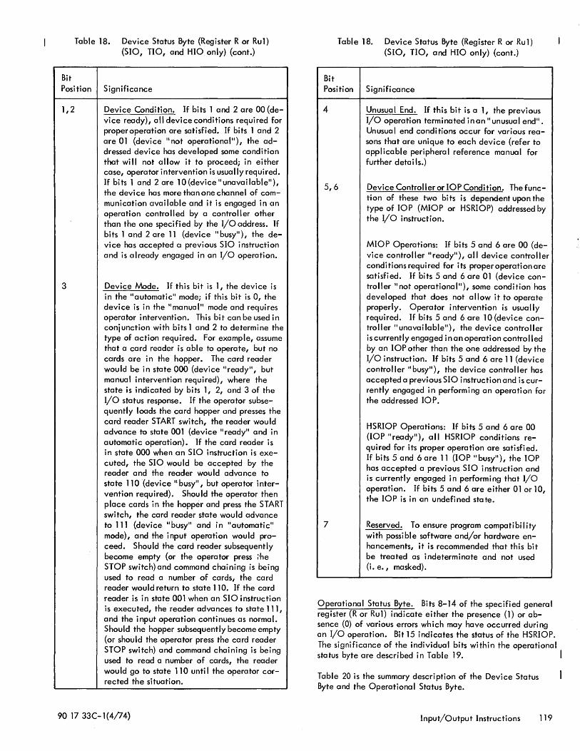
Bit
Table 18. Device Status Byte (Register R or Ru1) (SIO, TIO, and HIO only) (cont.)
Position Significance
1,2 Device Condition. If bits 1 and 2 are 00 (device ready), all device conditions required for proper operation are satisfied. If bits 1 and 2 are 01 (devi ce II not operationa I"), the addressed device has developed some condition that wi II not allow it to proceed; in either case, operator intervention is usually required. If bits 1 and 2 are 10(device l unavailable"), the device has more than one channel of communication available and it is engaged in an operation controlled by a controller other than the one specified by the I/O address. If bits 1 and 2 are 11 (device II busyll), the device has accepted a previous SIO instruction and is already engaged in an I/O operation.
3 Device Mode. If this bit is 1, the device is in the "automatic ll mode; if this bit is 0, the device is in the IImanual" mode and requires operator intervention. This bit can be used in conjunction with bits 1 and 2 to determine the type of action required. For example, assume that a card reader is able to operate, but no cards are in the hopper. The card reader would be in state 000 (device IIready", but manual intervention required), where the state is indicated by bits 1, 2, and 3 of the I/O status response. If the operator subsequently loads the card hopper and presses the card reader START switch, the reader would advance to state 001 (device" ready" and in automatic operation). If the card reader is in state 000 when an SIO instruction is executed, the SIO wou Id be accepted by the reader and the reader would advance to state 110 (device II busy", but operator intervention required). Should the operator then place cards in the hopper and press the START switch, the card reader state would advance to 111 (device "busi' and in lIautomatic li
mode), and the input operation would proceed. Should the card reader subsequently become empty (or the operator press ;·he STOP switch) and command chaining is being used to read a number of cards, the card reader would return to state 110. If the card reader is in state 001 when an SIO instruction is executed, the reader advances to state 111, and the input operation continues as normal. Should the hopper subsequently become empty (or should the operator press the card reader STOP switch) and command chaining is being used to read a number of cards, the reader would go to state 110 until the operator corrected the situation.
90 17 33C-1(4/74)
Bit
Table 18. Device Status Byte (Register R or Rul) (SIO, TIO, and HIO only) (cont.)
Position Significance
4 Unusual End. If this bit is a 1, the previous I/O operation terminated inan II unusual end ll . Unusua I end condi tions occur for various reasons that are unique to each device (refer to applicable peripheral reference manual for further detai Is.)
5,6 Device Controlleror lOP Condition. The function of these two bits is dependent upon the type of lOP (MIOP or HSRIOP) addressed by the I/O instruction.
MIOP Operations: If bits 5 and 6 are 00 (device controller IIreadyll), all device controller conditions required for its properoperationare satisfied. If bits 5 and 6 are 01 (device controller II not operational ll ), some condition has developed that does not allow it to operate properly. Operator intervention is usually required. If bits 5 and 6 are 10 (device controller lIunavailable"), the device controller is currently engaged inan operation controlled by an lOP other than the one addressed by the I/O instruction. If bits 5 and 6 are 11 (device controller IIbusyll), the device controller has accepted a previousSIO instruction and iscurrently engaged in performing an operation for the addressed lOP.
HSRIOP Operations: If bits 5 and 6 are 00 (lOP IIready"), all HSRIOP conditions required for its proper operation are satisfied. If bits 5 and 6 are 11 (lOP IIbusy"), the lOP has accepted a previous SIO instruction and is currently engaged in performing that I/O operation. If bits 5 and 6 are either 01 or 10, the lOP is in an undefined state.
7 Reserved. To ensure program compatibility with possible software and/or hardware enhancements, it is recommended that this bit be treated as indeterminate and not used 0. e., masked}.
Operational Status Byte. Bits 8-14 of the specified general register (R or Rul) indicate either the presence (1) or absence (0) of various errors wh ich may have occurred duri ng an I/O operation. Bit 15 indicates the status of the HSRIOP. The significance of the individual bits within the operational status byte are described in Table 19. I
Table 20 is the summary description of the Device Status Byte and the Operational Status Byte.
Input/Output Instructions 119
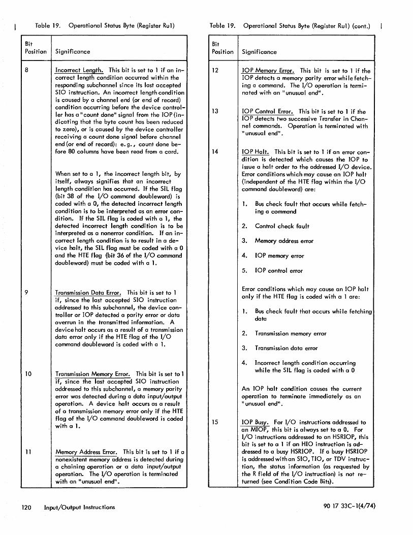
Table 19. Operational Status Byte {Register Rul}
Bit Position Significance
8 Incorrect Length. This bit is set to 1 if an incorrect length condition occurred within the responding subchannel since its last accepted SIO instruction. An incorrect length condition is caused by a channel end (or end of record) condition occurring before the device controller has a II count done" signal from the lOP (indicating that the byte count has been reduced to zero), or is caused by the device controller receiving a count done signal before channel end {or end of record}: e. g., count done before 80 columns have been read from a card.
9
10
11
120
When set to a 1, the incorrect length bit, by itself, always signifies that an incorrect length condition has occurred. If the SIL flag {bit 38 of the I/O command doubleword} is coded with a 0, the detected incorrect length condition is to be interpreted as an error condition. If the SIL flag is coded with a 1, the detected incorrect length condition is to be interpreted as a nonerror condition. If an incorrect length condition is to result in a device halt, the SIL flag must be coded with a 0 and the HTE flag (bit 36 of the I/O command doubleword) must be coded with a 1.
Transmission Data Error. This bit is set to 1 if, since the last accepted SIO instruction addressed to this subchannel, the device controller or lOP detected a parity error or data overrun in the transmitted information. A device halt occurs as a result of a transmission data error only if the HTE flag of the I/O command doubleword is coded with a 1.
Transmission Memory Error. This bit is set to 1 if, since the last accepted SIO instruction addressed to this subchannel, a memory parity error was detected during a data input/output operation. A device halt occurs as a result of a transmission memory error only if the HTE flag of the I/O command doubleword is coded with a 1.
Memory Address Error. This bit is set to 1 if a nonexistent memory address is detected during a chaining operation or a data input/output operation. The I/O operation is terminated with an "unusual end".
Input/Output Instructions
Table 19. Operational Status Byte (Register Rul) {cont.}
Bit Position Significance
12 lOP Memory Error. This bit is set to 1 if the lOP detects a memory parity error whi Ie fetching a command. The I/O operation is terminated with an II unusual end".
13 lOP Control Error. This bit is set to 1 if the lOP detects two successive Transfer in Channel commands. Operation is terminated with II unusua I end".
14 lOP Halt. This bit is set to 1 if an error condition is detected which causes the lOP to issue a halt order to the addressed I/O device. Error conditions which may cause an lOP halt (independent of the HTE flag within the I/O command doubleword) are:
15
1. Bus check fault that occurs while fetching a command
2. Control check fault
3. Memory address error
4. lOP memory error
5. lOP control error
Error conditions which may cause an lOP halt only if the HTE flag is coded with a 1 are:
1. Bus check fault that occurs while fetching data
2. Transmission memory error
3. Transmission data error
4. Incorrect length condition occurring while the SIL flag is coded with a 0
An lOP halt condition causes the current operation to terminate immediately as an II unusual end".
lOP Busy. For I/O instructions addressed to an MIOP, this bit is always set to a O. For I/O instructions addressed to an HSRIOP, this bit is set to a 1 if an HIO instruction is addressed to a busy HSRIOP. If a busy HSRIOP is addressedwithan SIO, TIO, or TDY instruction, the status information {as requested by the R field of the I/O instruction} is not returned (see Condition Code Bits).
90 17 33C-1(4/74)
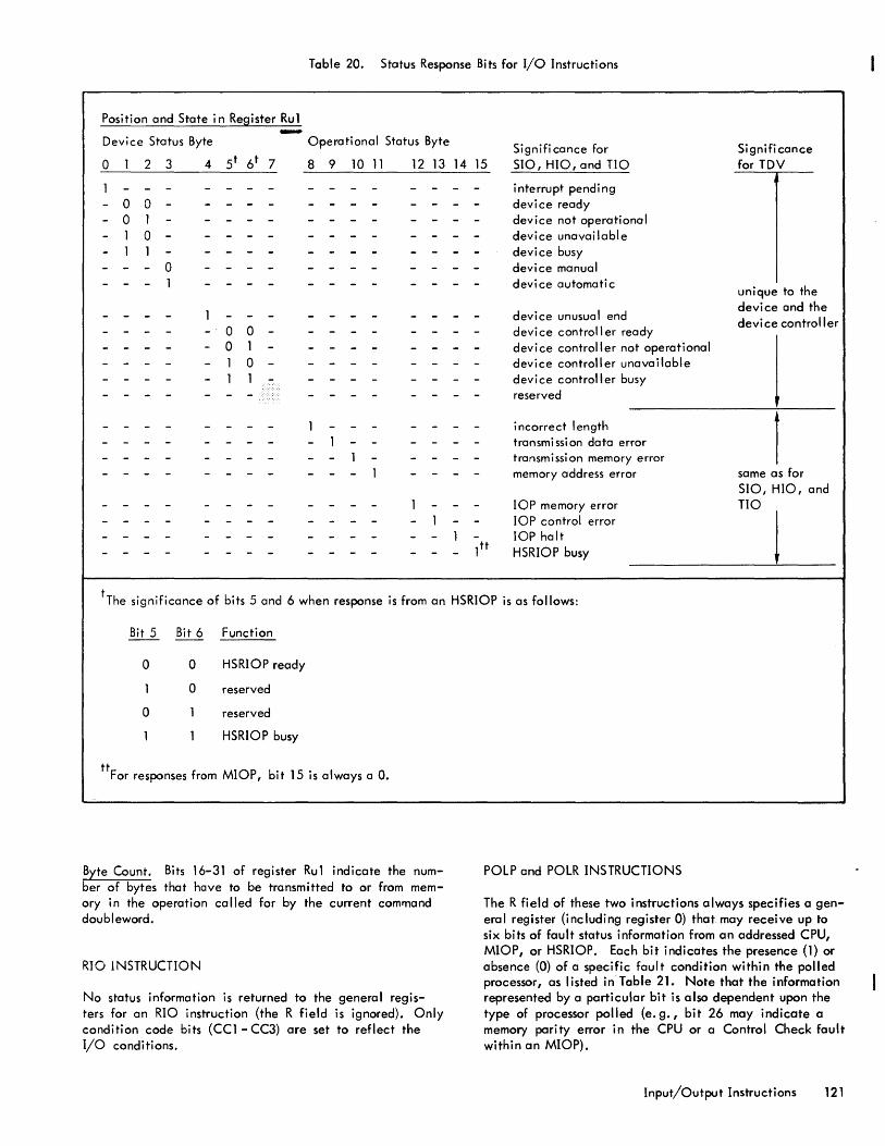
Table 20. Status Response Bits for I/O Instructions
Position and State in Register Ru1 -Devi ce Status Byte Operational Status Byte Signifi cance for Significance
0 1 2 3 4 5 t 6 t 7 8 9 10 11 12 13 14 15 SIO, HIO, and TIO for TDV
1 - - - - - - - - - - - - - - - interrupt pending - 0 0 - - - - - - - - - - - - - devi ce ready - 0 1 - - - - - - - - - - - - - device not operational - 1 0 - - - - - - - - - - - - - device unavailable - 1 1 - - - - - - - - - - - - - device busy - - - 0 - - - - - - - - - - - - device manual - - - 1 - - - - - - - - - - - - device automatic
unique to the
1 device unusual end device and the - - - - - - - - - - - - - - - device controller
- - - - - 0 0 - - - - - - - - - devi ce control I er ready - - - - - 0 1 - - - - - - - - - device controller not operational - - - - - 1 0 - - - - - - - - - device controller unavailable - - - - - 1 1 - - - - - - - - device controller busy - - - - - - - - - - - - - - - reserved
- - - - - - - - 1 - - - - - - - incorrect length
1 - - - - - - - - - 1 - - - - - - transmi ssi on data error - - - - - - - - - - 1 - - - - - transmission memory error - - - - - - - - - - - 1 - - - - memory address error same as for
SIO, HIO, and - - - - - - - - - - - - 1 - - - lOP memory error TIO - - - - - - - - - - - - - 1 - - lOP control error
j - - - - - - - - - - - - - - 1 - lOP halt - - - - - - - - - - - - - - - 1tt HSRIOP busy
t The significance of bits 5 and 6 when response is from an HSRIOP is as follows:
Bit 5 Bit 6 Function
0 0 HSRIOP ready
1 0 reserved
0 1 reserved
1 1 HSRIOP busy
tt For responses from MIOP, bit 15 is always a O.
Byte Count. Bits 16-31 of register Rul indicate the number of bytes that have to be transmitted to or from memory in the operation called for by the current command doubleword.
RIO lNSTRUCTION
No status information is returned to the general registers for an RIO instruction (the R field is ignored). Only condition code bits (CCl - CC3) are set to reflect the I/O conditions.
POLP and POLR INSTRUCTIONS
The R field of these two instructions always specifies a general register (including register 0) that may receive up to six bits of fault status information from an addressed CPU, MIOP, or HSRIOP. Each bit indicates the presence (1) or absence (0) of a specific faul t condition within the polled processor, as I isted in'Table 21. Note that the information represented by a particular bit is also dependent upon the type of processor polled (e. g., bit 26 may indicate a memory parity error in the CPU or a Control Check fault within an MIOP).
Input/Output Instructions 121
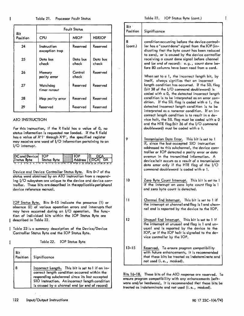
Table 21. Processor Fault Status
Fault Status Bit Position CPU MIOP HSRIOP
24 Instruction Reserved Reserved exception trap
25 Data bus Data bus Data bus check check check
26 Memory Control Reserved pari ty error check
27 Watchdog Reserved Reserved timer runout
28 Map pari ty error Reserved Reserved
29 Reserved Reserved Reserved
AIO INSTRUCTION
For this instruction, if the R field has a value of 0, no status information is requested nor loaded. If the R field has a value of Xl l 1 through X'F', the specified register may receive one word of I/O information pertaining to an I/O interrupt.
Device and Device Controller Status Byte. Bits 0-7 of the status word obtained by an AIO instruction from a responding I/O subsystem are unique to the device and device controller. These bits are described in theapplicableperipheral device reference manual.
lOP Status Byte. Bits 8-15 indicate the presence (1) or absence (0) of various operation errors and interrupts that may have occurred during an I/O operation. The function of individual bits within the lOP Status Byte are described in Table 22.
Table 23 is a summary description of the Device/Device Controller Status Byte and the lOP Status Byte.
Table 22. lOP Status Byte
Bit Position Significance
8 Incorrect Lenath. This bit is set to 1 if an in-correct length condition occurred within the responding subchannel since its last accepted SIO instruction. An incorrect length condition is caused by a channel end (or end of record)
122 Input/Output Instructions
Bit -Position
8 (cont.)
9
10
11
12
13-15
Table 22. lOP Status Byte (cont.)
Significance
condition occurring before the device controller has a "countdone" signal from the lOP (indicating that the byte count has been reduced to zero), or is caused by the device controller receiving a count done signal before channel end (or end of record): e. g., count done before 80 columns have been read from a card.
When set to a 1, the incorrect length bit, by itself, always signifies that an incorrect length condition has occurred. If the SIL flag (bit 38 of the I/O command doubleword) is coded with a 0, the detected incorrect length condition is to be interpreted as an error condition. If the SIL flag is coded with a 1, the detected incorrect length condition is to be interpreted as a nonerror condition. If an incorrect length condition is to result in a device halt, the SIL flag must be coded with a 0 and the HTE flag (bit 36 of the I/O command doubl eword) must be coded wi th a 1.
Transmission Data Error. This bit is set to 1 if, since the last accepted SIO instruction addressed to this subchannel, the device controller or lOP detected a parity error or data overrun in the transmitted information. A device halt occurs as a result of a transmission data error only if the HTE flag of the I/O command doubleword is coded with a 1.
Zero Byte Count Interrupt. This bit is set to 1 if the interrupt on zero byte count flag is 1 and zero byte count is detected.
Channel End Interrupt. This bit is set to 1 if the interrupt at channel end flag is 1 and channel end is reported by the device to the lOP.
Unusual End Interrupt. This bit is set to 1 if the interrupt at unusual end flag is 1 and unusual end is reported by the device to the lOP, or if the lOP halt is signaled to the device controller by the lOP.
Reserved. To ensure program compatibility with future enhancements, it is recommended that these bits be treated as indeterminate and not used (i. e., masked).
Bits 16-18. These bits of the AIO response are reserved. To ensure program compatibility with any enhancements (software and/or hardware), it is recommended that these bits be treated as indeterminate and not used 0. e., masked).
90 17 33C-1 (4/74)
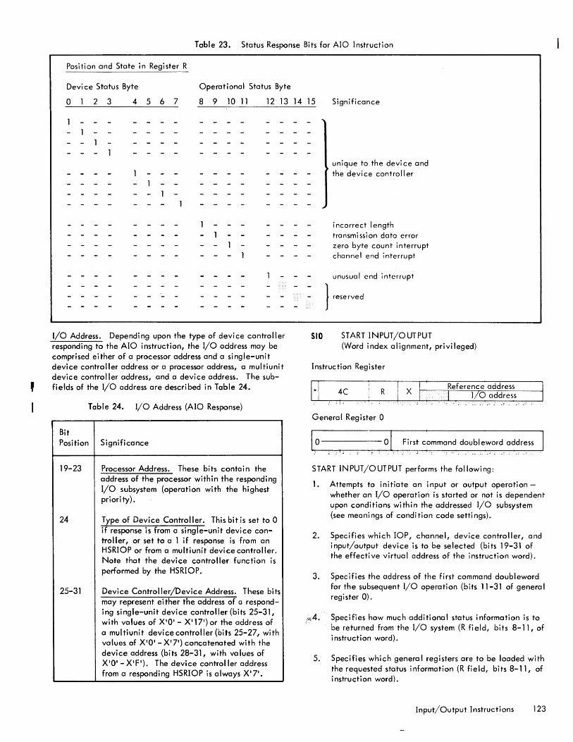
, I
Table 23. Status Response Bits for Ala Instruction
Position and State in Register R
Devi ce Status Byte Operational Status Byte
o 2 3 4 5 6 7 8 9 10 11 12 13 14 15 Significance
I/O Address. Depending upon the type of device controller responding to the Ala instruction, the I/O address may be comprised either of a processor address and a single-unit device controller address or a processor address, a multiunit device controller address, and a device address. The subfields of the I/O address are described in Table 24.
Table 24. I/O Address (Ala Response)
Bit Position
19-23
24
25-31
Significance
Processor Address. These bits contai n the address of the processor within the responding I/O subsystem (operation with the highest priority).
Type of Device Controller. This bit is set to 0 if response is from a single-unit device controller, or set to a 1 if response is from an HSRIOP or from a multiunit device controller. Note that the device controller function is performed by the HSRIOP.
Device Controller/Device Address. These bits may represent either the address of a responding single-unit device controller (bits 25-31, with values of XIOI- X'171)or the address of a multiunit device controller (bits 25-27, with values of XIOI - X'71) concatenated with the device address (bits 28-31, with va lues of XIOI - XIF'). The device controller address from a responding HSRIOP is always X'71.
unique to the devi ce and the device controller
incorrect length transmission data error zero byte count interrupt channel end interrupt
unusual end interrupt
} reserved
SID START INPUT/OUTPUT (Word index alignment, privileged)
Instruction Register
1*1 4C _, I,
General Register 0
10 --,-,---, s-ol F;rs~ c~mm~n.~dOU.bl.e~~rd. od~r~ss
START INPUT/OUTPUT performs the following:
1.
2.
3.
!~A.
5.
Attempts to initiate an input or output operationwhether an I/O operation is started or not is dependent upon condi tions wi th in the addressed I/O subsystem (see meani ngs of condi tion code setti ngs).
Specifies which lOP, channel, device controller, and input/output device is to be selected (bits 19-31 of the effective virtual address of the instruction word).
Specifies the addre.ss of the first command doubleword for the subsequent I/O operation (bits 11-31 of genera I register 0).
Speci fies how much additiona I status information is to be returned from the I/O system (R fi eld, bits 8-11, of instruction word).
Specifies which general registers are to be loaded with the requested status information (R field, bits 8-11, of instruction word).
Input/Output Instructions 123
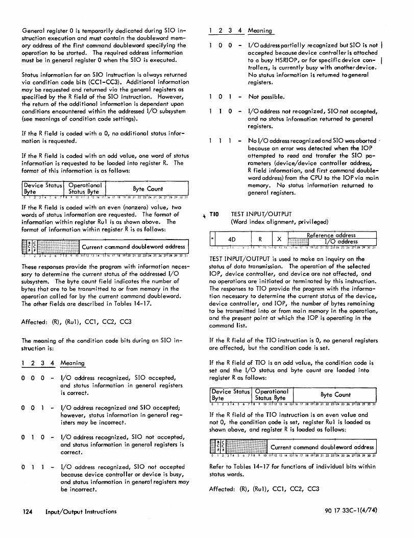
General register 0 is temporari Iy dedicated during SIO instruction execution and must contain the doubleword memory address of the first command doubleword specifying the operation to be started. The required address information must be in genera I register 0 when the SIO is executed.
Status information for an SIO instruction is always returned via condition code bits (CC1-CC3). Additional information may be requested and returned via the general registers as specified by the R field of the SIO instruction. However, the return of the additional information is dependent upon conditions encountered within the addressed I/O subsystem (see meanings of condition code settings).
If the R field is coded with a 0, no additional status information is requested.
If the R field is coded with an odd value, one word of status information is requested to be loaded into register R. The format of this information is as follows:
Byte Count
If the R field is coded with an even (nonzero) value, two words of status information are requested. The format of information within register Ru 1 is as shown above. The format of information within register R is as follows:
These responses provide the program with information necessary to determine the current status of the addressed I/O subsystem. The byte count field indicates the number of bytes that are to be transmitted to or from memory in the operation called for by the current command doubleword. The other fields are described in Tables 14-17.
Affected: (R), (Ru1), CC1, CC2, CC3
The meaning of the condition code bits during an SIO instruction is:
2 3 4 Meaning
o 0 0 - I/O address recognized, SIO accepted, and status information in general registers is correct.
o 0 I/O address recognized and SIO accepted; however, status information in general regi sters may be incorrect.
o 0 - I/O address recognized, SIO not accepted,
124
and status information in general registers is correct.
I/O address recognized, SIO not accepted because device controller or device is busy, and status information in general registers may be incorrect.
Input/Output Instructions
\- TIO
2 3 4 Meaning
o 0 - I/Oaddresspartially recognized but SIO is not I accepted because device controller is attached to a busy HSRIOP, or for specific device controllers, is currently busy with anotherdevice. No status information is returned to general registers.
o Not possible.
o - I/O address not recognized, SIO not accepted, and no status information returned to general registers.
No I/O address recognized and SIO was aborted ' because an error was detected when the lOP attempted to read and transfer the SIO parameters (device/device controller address, R field information, and first command doubleword address) from the CPU to the lOP via main memory. No status information returned to general registers.
TEST INPUT/OUTPUT (Word index alignment, privileged)
TEST INPUT/OUTPUT is used to make an inquiry on the status of data transmission. The operation of the selected lOP, device controller, and device are not affected, and no operations are initiated or terminated by this instruction. The responses to no provide the program with the information necessary to determi ne the current status of the device, device controller, and lOP, the number of bytes remaining to be transmitted into or from main memory in the operation, and the present point at which the lOP is operating in the command list.
If the R field of the TIO instruction is 0, no general registers are affected, but the condition code is set.
If the R field of no is an odd value, the condition code is set and the I/O status and byte count are loaded into register R as follows:
If the R field of the TIO instruction is an even value and not 0, the condition code is set, register Ru1 is loaded as shown above, and register R is loaded as follows:
Refer to Tables 14-17 for functions of individual bits within status words.
Affected: (R), (Rul), CC1, CC2, CC3
90 17 33C-l(4;74)
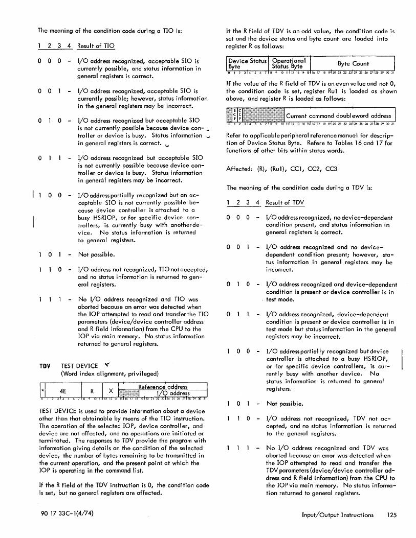
The meaning of the condition code during a TIO is:
2 3 4 Result of TIO
000
o 0
o 0
o
I 1 0 0
o
o
I/O address recognized, acceptable SIO is currently possible, and status information in general registers is correct.
I/O address recognized, acceptable SIO is currently possible; however, status information in the general registers may be incorrect.
I/O address recognized but acceptable SIO is not currently possible because device con- .., troller or device is busy. Status information in general registers is correct. II
I/O address recognized but acceptable SIO is not currently possible because device controller or device is busy. Status information in general registers may be incorrect.
I/O address partially recognized but an acceptable SIO is not currently possible because device controller is attached to a busy HSRIOP, or for specific device controllers, is currently busy with another device. No status information is returned to genera I registers.
Not possible.
I/O address not recognized, TIO not accepted, and no status information is returned to general registers.
No I/O address recognized and TIO was aborted because an error was detected when the lOP attempted to read and transfer the TIO parameters (device/device controller address and R field information) from the CPU to the lOP via main memory. No status information returned to general registers.
TOV TEST DEYICE ~ (Word index alignment, privileged)
TEST DEYICE is used to provide information about a device other than that obtainable by means of the TIO instruction. The operation of the selected lOP, device controller, and device are not affected, and no operations are initiated or terminated. The responses to TDY provide the program with information giving detai Is on the condition of the selected device, the number of bytes remaining to be transmitted in the current operation, and the present point at which the lOP is operating in the command list.
If the R field of the TDY instruction is 0, the condition code is set, but no general registers are affected.
90 17 33C-l{4/74)
It the R field of TDY is an odd value, the condition code is set and the device status and byte count are loaded into register R as follows:
If the value of the R field of TDY is an even value and not 0, the condition code is set, register Rul is loaded as shown above, and register R is loaded as follows:
Refer to applicable peripheral reference manual for description of Device Status Byte. Refere to Tables 16 and 17 for functions of other bits within status words.
Affected: (R), (Rul), CC1, CC2, CC3
The meaning of the condition code during a TDY is:
2 3 4 Result of TDY
o 0 0 I/O address recognized, no device-dependent condition present, and status information in general registers is correct.
o 0
o 0
o
o 0
I/O address recognized and no devicedependent condition present; however, status information in general registers may be incorrect.
I/O address recognized and device-dependent condition is present or device controller is in test mode.
I/O address recognized, device-dependent condition is present or device controller is in test mode but status information in the general registers may be incorrect.
I/O address partially recognized butdevice controller is attached to a busy HSRIOP, or for specific device controllers, is currently busy with another device. No status information is retumed to general registers.
o Not possible.
o I/O address not recognized, TOY not accepted, and no status information is returned to the general registers.
No I/O address recognized and TOY was aborted because an error was detected when the lOP attempted to read and transfer the TOY parameters (device/device controller address and R fi eld information) from the CPU to the lOP via main memory. No status information returned to general registers.
Input/Output Instructions 125
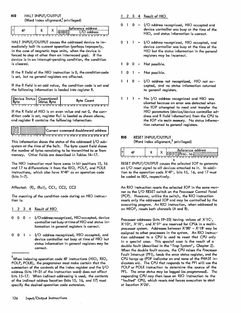
HID HALT INPUT/OUTPUT (Word index alignment! privileged)
HAL T INPUT/OUTPUT cquses the addressed device to immediately halt its current operation (perhaps improperly, in the case of magnetic tape units, when the device is forced to stop at other than an interrecord gap). If the device is in an interrupt-pending condition, the condition is cleared.
If the R field of the HIO instruction is 0, the condition code is set, but no general registers are affected.
If the R field is an odd value, the condition code is set and the following information is loaded into register R.
If the R field of HIO is an even value and not 0, the condition code is set, register Rulis loaded as shown above, and register R contains the following information:
This information shows the status of the addressed I/O subsystem at the time of the halt. The byte count field shows the number of bytes remaining to be transmitted to or from memory. Other fields are described in Tables 14-17.
The HIO instruction must have zeros in bit positions 15, 16 and 17 to differentiate it from the RIO, POLP, and POLR instructions, which also have XI4FI as an operation code (bits 1-7).
Affected: (R), (Ru1), CCl, CC2, CC3
The meaning of the condition code during an HIO instruction is:
2 3 4 Result of HIO
o 0 0 - I/Oaddressrecognized, HIOaccepted, device controller not busy attimeof HIO and status information in general registers is correct.
o 0 I/O address recognized, HIO accepted~ and device controller not busy at time of HIO but status information in general registers may be correct.
tWhen indexing operation code 4F instructions (HIO, RIO, POLP, POLR), the programmer must make certain that the summation of the contents of the index register and the I/O address (bi ts 19-31 of the instruction word) does not affect bits 15-17. When indirect addressing is used, the contents of the indirect address location (bits 15, 16, and 17) must specify the desired operation code extension.
126 Input/Output Instructions
2 3 4 Result of HIO
o 0 - I/O address recognized, HIO accepted and device controller was busy at the time of the HIO, and status information is correct.
o - I/O address recognized, HIO accepted, and
RIO
device controller was busy at the time of the HIO but the status information in the general registers may be incorrect.
o 0 - Not possible.
o Not possible.
o - I/O address not recognized, HIO not accepted, and no status information returned to general registers.
No I/O address recognized and HIO was aborted because an error was detected when the lOP attempted to read and transfer the HIO parameters (device/device controller address and R field information) from the CPU to the lOP via main memory. No status information returned to general registers.
RESET INPUT/OUTPUT {Word index alignment} privileged)
An RIO instruction resets the selected lOP in the some manner as the I/O RESET switch on the Processor Control Panel (PCP). However, unlike the switch, the RIO instruction resets only the addressed lOP and may be controlled by the executing program. An RIO instruction, when addressed to an MIOP, resets both channels (A and B).
Processor addresses (bits 19-23) having values of XI1 C, XII 0 1, XII EI, and XII FI are reserved for CPUs in a multiprocessor system. Addresses between XIOOI - XII BI may be assigned to other processors in the system. An RIO instruction addressed to a CPU is used to reset that CPU only in a special case. This special case is the result of a double fault (described in the "Trap System", Chapter 2). When the double fault occurs, the CPU raises the Processor Fault Interrupt (PFI), loads the error status register, and the CPU hangs up (PDF indicator on and none of the PHASE indicators on). The CPU that responds to the PFI will use the POLP or POLR instruction to determine the source of the PFI. The error status may be logged (as programmed). The responding CPU may then issue an RIO instruction to the "faulted" CPU, which resets and forces execution to start at location X1261•
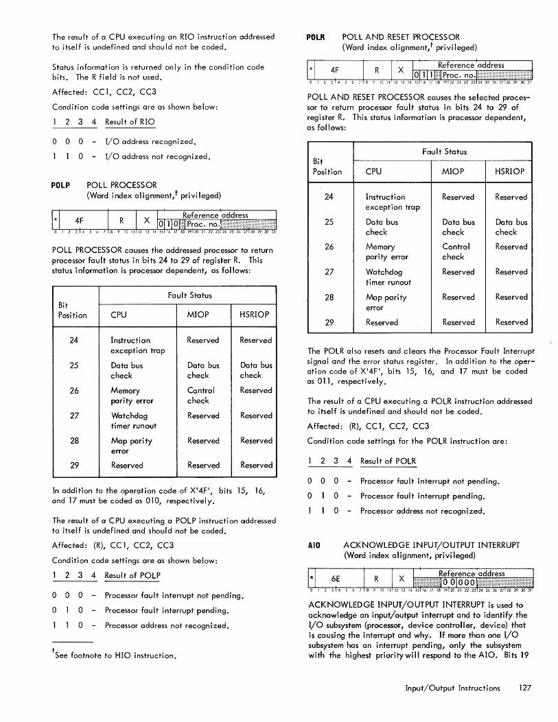
The result of a CPU executing an RIO instruction addressed to itself is undefined and should not be coded.
Status information is returned only in the condition code bits. The R field is not used.
Affected: CC1, CC2, CC3
Condition code settings are as shown below:
2 3 4 Result of RIO
000 I/O address recognized.
o I/O address not recognized.
POLP POLL PROCESSOR (Word index alignment,t privileged)
POLL PROCESSOR causes the addressed processor to return processor fault status in bits 24 to 29 of register R. This status information is processor dependent, as follows:
Fault Status Bit Position CPU MIOP HSRIOP
24 Instruction Reserved Reserved exception trap
25 Data bus Data bus Data bus check check check
26 Memory Control Reserved pari ty error check
27 Watchdog Reserved Reserved timer runout
28 Map parity Reserved Reserved error
29 Reserved Reserved Reserved
In addition to the operation code of X'4F ', bits 15, 16, and 17 must be coded as 010, respectively.
The result of a CPU executing a POLP instruction addressed to itself is undefined and should not be coded.
Affected: (R), CC 1, CC2, CC3
Condition code settings are as shown below:
2 3 4 Result of POLP
o 0 0 Processor fault interrupt not pending.
o o Processor fault interrupt pending.
o - Processor address not recognized.
t See footnote to HIO instruction.
POLR POLL AND RESET PROCESSOR (Word index alignment,t privileged)
POLL AND RESET PROCESSOR causes the selected processor to return processor fault status in bits 24 to 29 of register R. This status information is processor dependent, as follows:
Fault Status Bit Position CPU MIOP HSRIOP
24 Instruction Reserved Reserved exception trap
25 Data bus Data bus Data bus check check check
26 Memory Control Reserved parity error check
27 Watchdog Reserved Reserved timer runout
28 Map parity Reserved Reserved error
29 Reserved Reserved Reserved
The POLR also resets and clears the Processor Fault Interrupt signal and the error status register. In addition to the operation code of X'4F ', bits 15, 16, and 17 must be coded as 011, respectively.
The result of a CPU executing a POLR instruction addressed to itself is undefined and should not be coded.
Affected: (R), CC 1, CC2, CC3
Condition code settings for the POLR instruction are:
2 3 4 Result of POLR
000
o 0
Processor fault interrupt not pending.
Processor fault interrupt pending.
o Processor address not recognized.
AIO ACKNOWLEDGE INPUT/OUTPUT INTERRUPT (Word index alignment, privileged)
ACKNOWLEDGE INPUT/OUTPUT INTERRUPT is used to acknowledge an input/output interrupt and to identify the I/O subsystem (processor, device controller, device) that is causing the interrupt and why. If more than one I/O subsystem has an interrupt pending, only the subsystem with the highest priority wi II respond to the AIO. Bits 19
Input/Output Instructions 127
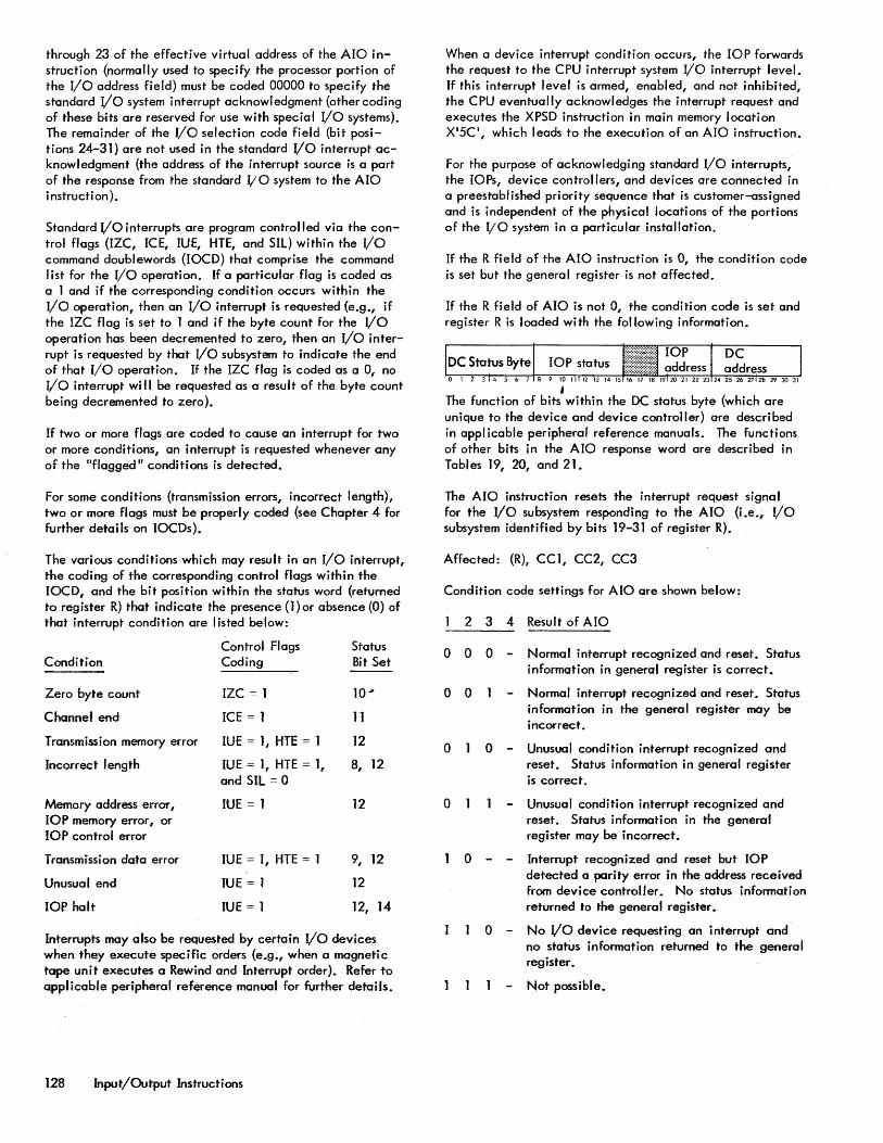
through 23 of the effective virtual address of the Ala instruction (normally used to specify the processor portion of the I/o address field) must be coded 00000 to specify the standard Va system interrupt acknowledgment {other coding of these bits are reserved for use with special I/o systems}. The remainder of the I/O selection code field (bit positions 24-31) are not used in the standard I/o interrupt acknowledgment (the address of the interrupt source is a part of the response from the standard I/O system to the Ala i nstructi on).
Standard I/o interrupts are program controlled via the control flags (IZC, ICE, IUE, HTE, and SIL) within the Va command doublewords (lOCO) that comprise the command list for the I/O operation. If a particular flag is coded as a 1 and if the corresponding condition occurs within the I/O operation, then an I/o interrupt is requested (e.g., if the IZC flag is set to 1 and if the byte count for the I/O operation has been decremented to zero, then an I/o interrupt is requested by that I/o subsystem to indicate the end of that I/O operation. If the IZC flag is coded as a 0, no I/o interrupt will be requested as a result of the byte count being decremented to zero).
If two or more flags are coded to cause an interrupt for two or more conditions, an interrupt is requested whenever any of the tlflagged" conditions is detected.
For some conditions (transmission errors, incorrect length), two or more flags must be properly coded (see Chapter 4 for further details on lOCOs).
The various conditions which may result in an I/O interrupt, the coding of the corresponding control flags within the lOCO, and the bit position within the status word (returned to register R) that indicate the presence (1) or absence (0) of that interrupt condition are I isted below:
Condition
Zero byte count
Channel end
Transmission memory error
Incorrect length
Memory address error, lOP memory error, or lOP control error
T ransmissi on data error
Unusual. end
lOP halt
Control Flags Coding
IZC = 1
ICE = 1
IUE = 1, HTE = 1
IUE = 1, HTE = 1, and SIL = 0
IUE = 1
rUE = 1, HTE = 1
IUE = 1
IUE = 1
Status Bit Set
10"-
11
12
8, 12
12
9, 12
12
12, 14
Interrupts may also be requested by certain I/o devices when they execute specific orders (e.g., when a magnetic tape unit executes a Rewind and Interrupt order). Refer to applicable peripheral reference manual for further details.
128 Input/Output Instructions
When a device interrupt condition occurs, the lOP forwards the request to the CPU interrupt system Va interrupt level. If this interrupt level is armed, enabled, and not inhibited, the CPU eventually acknowledges the interrupt request and executes the XPSO instruction in main memory location X'5C', which leads to the execution of an Ala instruction.
For the purpose of acknowledging standard I/O interrupts, the lOPs, device controllers, and devices are connected in a preestablished priority sequence that is customer-assigned and is independent of the physical locations of the portions of the I/O system in a particular installation.
If the R field of the Ala instruction is 0, the condition code is set but the general register is not affected.
If the R field of Ala is not 0, the condition code is set and register R is loaded with the following information.
; The function of bits within the DC status byte (which are unique to the device and device controller) are described in applicable peripheral reference manuals. The functions of other bits in the Ala response word are described in Tables 19, 20, and 21.
The Ala instruction resets the interrupt request signal for the I/O subsystem responding to the AIO (i.e., I/O subsystem identified by bits 19-31 of register R).
Affected: (R), CCl, CC2, CC3
Condition code settings for AIO are shown below:
2 3 4 Result of Ala
o 0 0 - Normal interrupt recognized and reset. Status information in general register is correct.
o 0 - Normal interrupt recognized and reset. Status information in the general register may be incorrect.
o
o
o - Unusual condition interrupt recognized and reset. Status information in general register is correct.
- Unusual condition interrupt recognized and reset. Status information in the general register may be incorrect.
o - - Interrupt recognized and reset but lOP detected a parity error in the address received from device controller. No status information returned to the general register.
o - No VO device requesting an interrupt and no status information returned to the general register.
Not possible.
4. INPUT jOUTPUT OPERATIONS
Ina SIGMA9 system, input/outputoperationsareprimarily under control of one or more input/output processors (lOPs). This allows the CPU to concentrate on program execution, free from the time-consuming details of I/O operations. Any I/O event that requires CPU intervention is brought to its attention by means of the interrupt system (see Chapter 2). For a detai I ed description of SIGMA 9 I/O instructions, see Chapter 3.
In the following discussion, the terminology conventions used are: The CPU executes instructions, the lOP executes commands, and the device controllers and I/O devi ces execute orders. To illustrate, the CPU wi" execute the START INPUT/OUTPUT (SIO) instruction to initiate an I/O operation. During the course of an I/O operation, the lOP might issue a command called Control, to transmit a byte to a device controller or I/O device that interprets the byte as an order, such as Rewind.
Each SIGMA 9 lOP operates independently after being started by a CPU. An lOP automatically picks up a chain of one or more commands from memory and executes these commands until the chain is completed or truncated as the result of an "unusual end" condition.
A multiplexor lOP can simultaneously operate up to 32 device controllers using both Channels A and B. Each device controller is assigned its own subchannel and chain of I/O commands. A high-speed RAD lOP (HSRIOP) can communicate with up to four Model 7212 RAD storage units. However, due to its high transfer rate capability, the HSRIOP remains connected until termination of the data in/data out sequence.
The flexible SIGMA 9 I/O structure permits both command chaining (making possible multiple-record operations) and data chain ing (making possible scatter-read and gatherwrite operations) without intervening CPU control. Command chaining refers to the execution of a sequence of I/O commands, under control of an lOP, on more than one physical record. Thus, a new command must be issued for each physical record even if the operation to be performed for a record is the same as that performed for the previous record. Data chaining refers to the execution of a sequence of I/O commands, under control of an lOP, that gather (or scatter) information within one physical record from (or to) more than one region of memory. Thus, a new command must be issued for each portion of a physical record when the data associated with that physical record appears (or is to appear) in noncontiguous locations in memory. For example, if information in specific columns of two cards in a file are to be stored in specific regions of memory, the I/O command I ist might appear as follows:
1. Read ca rd, store col umns 1-10, data chai n.
2. Store columns 11-60, data chain.
3. Store columns 61-80, command chain.
4. Read card, store columns 1-40, data chain.
5. Store col umns 41-80.
The SIGMA 9 CPU plays a minor role in the execution of an I/O operation. The CPU-executed program is responsible for creating and storing the command I ist (prepared prior to the initiation of any I/O operation) and for supplying the lOP with a pointer to the fi rst command in the I/O command list. Most of the communication between the CPU and the I/O system is carried out through memory.
The foil owi ng is an exampl e of the sequence of events that occurs during an I/O operation:
1. A CPU-executed program writes a sequence of I/O commands (doublewords) in memory.
2. The CPU executes the START IN PUT/OUTPUT (SIO) instruction and furnishes the lOP with a 13-bit I/o address (designating the device to be started) and a 21-bit first command address (designating the actual memory doubleword location where the first command for this device is located). At this point, either the device is started (if in the "read/' condition with no device interrupt pending) or an instruction reject occurs. The CPU is informed by condition code settings which of the two alternatives has occurred. If the SIO instruction is accepted, the command counter portion of the lOP register associated with the designated device controller is loaded with the first command address. From this time unti I the full sequence of I/O commands has been executed, the main program of the CPU need play no role in the I/O operation. At any time, however, the CPU may obtain status information on the progress of the I/O operation without interfering with it.
3. The device is now in the "busy" condition. When the device determines that it has the highest priority for access to the lOP, it requests service from the lOP with a service call. The lOP obtains the address of the first command doubleword of the I/O sequence (from the command counter associated with this device). The lOP then fetches the I/O command doubleword from memory, loads the doubleword into another register associated with the device, and transmits the first order (extracted from the command doubleword) to it.
4. Each command counter contains the memory address of the current I/O command in the sequence for its device. When the device requires further servicing, it makes a request to the lOP, which then repeats a process simi lar to that of step 3.
5. If a data transmission order has been sent to a device, control of the transmission resides in it. As each character is obtained by the I/Odevice, the lOP issignaled
Input/Output Operations 129
that data is available. The lOP uses the information stored in its own registers to control the information interchange between the I/O device and the memory, on either a word-by-word or character-by-character basis, depending on the nature of the device.
6. When all information exchanges called for by a single I/O command doubleword have been completed, the lOP uses the command counter to obtain the next command doubleword for execution. This process continues until all such command doublewords associated with the I/O sequence have been executed.
OPERATIONAL COMMAND DOUBLEWORDS Operational command doublewords have the following format:
ORDER
Bit positions 0 through 7 of the command doubleword contain the I/O order for the device controller or device. The I/O orders are shown belowt. Bits represented by the letter "M" specify orders or special conditions to the device and are unique for each type of device.
Bit posi tions 0 1 2 3 4 5 6 7 Order
M M M M M M 0 1 Write
M M M M M M 1 0 Read
M M M M M M Control
M M M M 0 0 0 Sense
M M M M 0 0 Read Backward
Write. The Write order causes certain device controllers to initiate on output operation. Bytes are read in ascending sequence from the memory location specified by. the memory byte address field of the command doubleword. The output operation continues until the device signals "channel end ll
,
Of until the byte count is reduced to 0 and no further data chaining is specified. Channel end occurs when the device has received a) I information associated with the output operation, completed all checks, and no longer requires the use of lOP facilities for the operation. Data chaining is described later in this chapter.
tNot all I/O devices recognize all the orders shown. See the particular Xerox SIGMA peripheral reference manual for orders applicable to that device.
130 Operational Command Doublewords
Read. The Read order causes certain device controllers to initiate an input operation. Bytes are stored in memory in ascending sequence, beginning at theJocation specified by the memory byte address field of the command doubleword. The input operation continues until the device signals channel end, or until the byte count is reduced to 0 and no data chaining is specified. Channel end occurs when the device has transmitted all information associated with the input operation and no longer requires the use of lOP facilities for the operation.
Control. The Control order is used to initiate special operations by certain devices. For magnetic tape, it is used to issue orders such as Rewind, Backspace Record, Backspace File, etc. Most orders can be specified by the M bits of the Control order; however, if additional information is required for a particular operation (e. g., the starting address of a disk seek), the memory byte address field of the command doubleword specifies the starting address of the bytes that are to be transmitted to the device controller for the additional information. When all bytes necessary for the operation have been transmitted, the device controller signals channel end.
Sense. The Sense order causes certain devices to transmit ~ more bytes of information, describing its current state. The bytes are stored in memory in ascending sequence, beginning with the address specified by the memory byte address field of the command doubleword. The number of bytes transmitted is a function of the device and the condition it describes. The Sense order can be used to obtain the current sector address from a disk or RAD storage unit.
Read Backward. The Read Backward order causes certain devices (at present, 9-track magnetic tape units) to be started in reverse, and bytes to be transmitted to the lOP for storage into memory in descending sequence, beginning at the location specified by the memory byte address field of the command doubleword. In all other respects, Read Backward is identical to Read, inc! uding reducing the byte count with each byte transmitted.
MEMORY am ADDRESS
For all operational I/O command doublewords, bit positions 8-31 of the doubleword provide a 24-bit memory byte address, designating the memory location for the next byte of data. For all orders other than Read Backward, this field (as stored in an lOP register) is incremented by 1 for each byte transmitted in the I/O operation; for the Read Backward order, the field is decremented by 1 for each byte transmitted.
flAGS
For all operational I/O command doublewords, bit positions 32-39 of the doubleword provide the lOP with eight flogs that specify how to handle chaining, error, and interrupt situations.

T11e three flogs (lZC, ICE, and fU£) pertaining to lOP interrupt action control whether the lOP will request an I/O interrupt to be triggered when a specified condition occurs during an I/O operation. These flags do not affect the I/O interrupt levels. Furthermore, in order for the flags to be effective, the I/O interrupt level (X I 5C') must first be placed in the desired state (i. e. , armed and enabled) via interrupt write control instructions (mode 1).
The functions of the eight flags are explained below.
Bit Position Function
32 (DC) Data chain. If this flag is 1, data chaining is called for when the current byte count is reduced to O. The next command doubleword is fetched and loaded into the lOP register associated with the device controller, but the new order code is not passed out to the device controller; thus, the operation called for by the previous order is continued. (Except for Transfer in Channel command doublewords, which are explained later in this chapter, the new command doubleword is used only to supply a new memory address, a new count, and new flags.) If the data chain flag is 0, no further data chaining is called for. Channel end is initiated either by the device running out of information, or by the byte count being reduced to O. At channel end, the device may accept a new 510 instruction, provided that a devi ce interrupt is not pending and no "unusual end" condition exists.
33 (lZC) Interrupt at zero byte count. If this flag is ], the lOP requests the I/O interrupt (location X I 5C') to be triggered when the byte count of this command doubleword (as stored in the lOP register) is reduced to O. An AIO instruction executed after the interrupt is acknowledged results in a 1 in bit position 10 of register R (status information) to indicate the reason for the interrupt.
34 (CC) Command chain. If this flag is 1, command chaining is called for when channel end occurs. If the previous operation did not terminate with an "unusual end" condition, the next command doubleword is fetched and loaded into the lOP register associated with the device controller, and the new order code is passed out to the device controller. If the CC flag is 0, no further command chaining is called for. If both data and command chaining are called for in the same command doubl eword, data chaining occurs if the byte count is reduced to 0 before channel end, and command chaining occurs if channel end occurs before the byte count is reduced to O.
Bit Position Function
35 (ICE) Interrupt at channel end. If this flag is 1, the lOP requests the I/O interrupt (location X I 5C') to be triggered when channel end occurs for the operation being controlled by this command doubl eword. An AIO instruction executed after the interrupt is acknowledged results in a 1 in bit position 11 of register R (status information) to indicate the reason for the interrupt. If the ICE flag is 0, no interrupt is requested.
36 (HTE) Halt on transmission error. If this flag is 1, any error condition associated with data transmission (transmission data error, transmission memory error, incorrect length error) detected in the device controller or lOP results in halting the I/O operation being controlled by this command doubleword. If the HTE flag is 0, an error condition does not cause the I/O operation to halt, although the error conditions are recorded in the lOP register and returned as part of the status information for the instructions 510, HIO, and TIO.
The HTE flag must be coded identically in every command doubleword associated with the same physical record. This means that when data chaining occurs, the HTE flag in the new lOP command doubl eword must be the same as the HTE flag in the previous lOP command doubleword. This restriction applies to data chaining only, and not to command chaining.
37 (IUE) Interrupt on unusual end. If this flag is 1, the device controller requests the I/O interrupt (location X I 5C') to be triggered when an "unusual end" condition is encountered. When an "unusual end" condition is detected, further servicing of the commands for that device is suspended. An Ala instruction executed after the interrupt is acknowledged results in a 1 in bit position 12 of register R (status information) to indicate the reason for the interrupt. If the IUE flag is 0, no interrupt is requested.
38 (SIL) lrSuppress incorrect length. If this flag is 1, an incorrect length indication by the device controller is not to be classified as an error by the lOP, although the lOP retains the incorrect length indication and provides an indicator (bit 8 of register Rul, the status response for 510, HIO, Ala, and TIO) to the program. If the Sll flag is 0, an incorrect length is considered an error and the lOP performs as specified by the HTE and IUE flags. Incorrect length is caused by a "channel end" condition occurring before the device controller has received a "count done"
Operational Command Doublewords 131
Bit Position
38 (Sll) (coot. )
39 (S)
Function
signal from the lOP, Of" is caused by the device controller receiving a count done signal before end of record, e. g., count done before 80 columns have been read frama card. Normally, a count done signal is sent to the device controJler by the lOP to indicate that aU data tronsfer a'ssociated with the current operation has been compjeted. The lOP is capable.of suppressing an error condition on incorrect length, since there are situations in which incorrect length is not on error.
Skip.. If this flog is ., the input operation (Read or Read Bockward) controlled by this command doubJeworo continues normaUy,except that no information is stored in memory. When used in conjunction with data chaining, the skip operation provides the capability for selective reQding of portions of a record.
If the S ftag is 1 for an output {Write) operation, the lOP does not access memory, but transmits zeros os data instead (L e., the lOP transmits the number of X100I bytes specified in the byte count of the command doubleword). This allows Q program to punch a blank card (by using the S bit 'OOd 0 Punch Binary order with Q byte count of 120) without requiring memory access for data. Jfthe SAag is '0, the I/O operation proceeds normally.
1m C8UIIT
Foran operotionaJ I/O command doublewonh, bit positions <48-63 ·of the doublewom provide for (] 16 ... bit count of the number of bytes to be transmitted in :the va operation; thus, 1 to 65,536 bytes (16,384 words) con be specified for tronsfer before command Of' data chaining is required. This field (as stored in an lOP register) is decremented by 1 for each byte tronsmitted; thus, it always contains a count of the number of bytes yet to be transmitted 10 or ·from memG'Y, and this count is returned as part of the response information for the instructions, 510, HIO, no, and TOV. An initial byte count of 0 is interpreted as 65,536 bytes.
In addition to the operational command doubJeword, there (Ire two control command doublewords with different formats that provlde control information for the lOP.
132 c.o.moJ Command Doublewonts
The Transfer in Channel command doubfeword has the following fonnat:
T fander in Channel. The Transfer in Channel command is executed within the lOP cnd has no direct effect on any of the I/O system elements external to the addressed lOP. The primary purpose of this command is to permit branching within the command I ist so that the lOP can, for exampJe, repeatedly transmit the same s·et of info.rmofiona number of times. When the lOP executes the Transfer 1n Channel command, it loads the command counter for the device controller it is currently servicing with the next command address fiefdof the Transfer in Channel command, loads the new command doubleword specified by this address into the lOP registers associated with the device controller, and then executes the new command. (Bit positions 0-3, 8-10, and 32-63 of the command doubleword for Transfer in Channel are ignored.) Transfer in Channel thus allows a command Jist to be broken into noncontiguous groups of commands. When used in conjunction with command chaining, Transfer in Channel fad lita tes thecontroJ of devices such as unbuffered card punches or unbuffered line printers. )he current flags are not altered during this command; thus, the type of chaining caHed for in the previous command doubJeword is retained until changed by a command doubfeword following Transfer in Channel.
For exompfe, assume that it is desired to present the same cord image twelve times to an unbuffered card punch. The punch counts the number of times that a record is presented to it and, when twel ve rows have been punched, causes the lOP to skip the -command it wouJd be e~ecuting next~ Thus, a command Hst for punching two cards might look like the following example:
l.ocation
A
8
Command
Punch row for card 1, command chain.
Transfer in Channel to A.
Punch row for card 2, command chain.
T mnsfer in Diannel to B.
Stop.
The Tronsfer in Channel command abo cao be used in conlunction with data chaining. As one example, consider a situation often encountered in data acquisition appl ications, where data is hunsmitted in extremely long, continuous streams. In this case, the data can be stored altemately in two or more buffer stora'geareas so that computer processing
can be carried out on the data in one bufferwhileadditional data is being input into the other buffer. The command list for such an application might look like the following example:
Location
A
Command
Read data, store into buffer 1, data chai n.
Store into buffer 2, data chain.
Transfer in Channel to A.
If the lOP encounters two successive Transfer in Channel commands, this is considered an lOP control error, resulting in the lOP setting the lOP control error status bit (bit 13 of register Rul) and issuing an 1I10P Halt" signal to the device controller. The lOP then halts further servicing of this command list.
The Stop command doubl eword has the following formats:
Stop. The Stop command causes certain devi ces to stop, generate a IIchannel end" condition, and also request the I/O interrupt (location X'5C') to be triggered if bit 0 in the Stop command is a 1. An Ala instruction executed aftedhe interrupt is acknowledged results ina 1 in bit position 7 of register R (status information) to indicate the reason for the interrupt. (Bit positions 32-39 of the command doubleword for Stop must be zero; bit positions 8-31 and 40-63 are ignored). The Stop command is primarily used to terminate a command chain for an unbuffered device, as illustrated in the first example given for the Transfer in Channel command.
Control Command Doublewords 133
5. OPERATOR CONTROLS·
PROCESSOR CONTROL PANEL
The SIGMA 9 processo r control panel (PC P) is shown in Figure 12 . The controls and indicators are divided into two sections. The upper section, which is labeled MAINTENANCE SECTION, contains most of the controls and indica tors used by maintenance personnel. The DISPLAY FORMAT indicator and FORMAT SEL switch located in. the lower secti on are a lso prima ril y used by maintenance personnel. All other controls and indicators located in the lower section of the PCP are normally used by operating personnel to load, e xe cute, and t roubleshoot programs.
A three -positi on rotary sw itch, located in the upper leftha nd corner and labeled EXT CONT/ LOCAL NORM/ LOCAL MAINT, is a control mode selector for the PCP. It is set
Xerox Data Systems
either to the LOCAL NORM position for normal operations or to the LOCAL MAJNT position for ma'intenance operations. The EXT CONT position is reserved for future use. Hereafter, this switch will be referred to as the Control' Mode switch.
CONTROL MODE
When the Control Mode switch is in the LOCAL MAINT position, all switches on the control panel are enabl ed. When the Control Mode switch is in the LOCAL NORM position, all switches are enabled except the following:
1. The FORMAT SEL switch is disabled and forced to appear in the NORMAL pos ition, regardless of the position of that switch.
________________ >.,t .$ f1 ~!· .. Jl:kl'>H':{'''i----------------. ,,) v ...• U (IXXXXX"»XIX»"'X)
\) ... -'.
•• •••• ••••••• •• ( X I fa I Xx i'l {i IIIIIXXXIXIXIXIX)
i I
I I I I I v I I·· I .. '"
li lt I IX lUll XX I II IIX II XX II ~XI nx II ~ ''''' ... .. , I I ' I
J I ' . '. .. • I . . : .~.:-
. . -f.c(~~~ .. . 't~~" ~. • .. " • ,.. • ..... :. •
Figure 12. Processor Control Panel
134 Operator Controls
2. The SNAP switches are disabled.
3. The EXT DIO switch is disabled.
4. The CLOCK MARGINS switch is disabled and forced to appear in the NORM position.
5. The CLOCK MODE switch is disabled and forced to appear in the CONT position.
6. The SCAN switches are disabled.
POWER
The POWER switch controls ac power to the central processor and to units under its direct control. The POWER indicator is I ighted when ac power is on.
MEMORY CLEAR
The MEMORY CLEAR switch clears all CPU memory. When this switch is pressed, the SCAN light illuminates and remains on until all memory is cleared. The contents of the general registers remain unaltered during the operation. It is recommended that CPU RESET be pressed before using the MEMORY CLEAR switch. Homespace bias is automatically suppressed during the clear operation.
SYS RESET
The SYS RESET (system reset) switch performs the combined functions of the CPU RESET switch and the I/O RESET switch. The SYS RESET switch also initial izes all memories connected to the system. The initialization of memories does not change the contents of any memory locations; onl y memory port logic is reset.
UNIT ADDRESS
Four UNIT ADDRESS switches select the peripheral unit to be used in the loading process. The two switches on the left designate an input/output processor (lOP). The leftmost switch has two positions, numbered 0 and 1. The next switch has 16 positions, numbered hexadecimally 0 through F. The two rightmost switches each have 16 positions, numbered hexadecimally 0 through F, which designate the device controller/device that is under control of the selected lOP.
SENSE
The four SENSE switches and indi cators are monitored under program control to set the condition code portion of the program status doubl eword (PSD). When a READ DIRECT instruction is executed in the internal control mode, the condition code is set according to the state of the four SENSE switches. If a SENSE switch is in the set (1) position (indicator lighted), the corresponding bit of the condition code is set to 1; if a SENSE switch is in the reset (0) position (indicator unl ighted), the corresponding bit of the condition code is reset to O.
NOT NORMAL
The NOT NORMAL indicator informs the user that normal program execution may be inhibited by the PCP. The NOT NORMAL indicator is lighted when any of the following occurs:
1. The Control Mode switch is in the LOCAL MAINT position.
2. The DECIMAL OVERRIDE switch is in the OVERRIDE position.
3. The INTERLEAVE SE L switch is in the DISABLE 1/0 RESET position.
The I/O RESET switch initial izes the standard input/output system. When the switch is pressed, all peripheral devices under control of the centra I processor are reset to the "ready" condition, and all status, interrupt, and control indicators in the input/output system are reset. The I/O RESET switch does not affect the central processor.
LOAD
The LOAD switch is active only when the COMPUTE switch is in the IDLE position. When this momentary action switch is pressed, a load program is written into memory locations X'22 1 through X' 2B ' for an input operation that uses the peripheral unit selected by the UNIT ADDRESS switches. CPU RESET or SYSTEM RESET must be performed before using this switch.
Detailed loading operation is described in the section "Loading Operation".
4. The W.D. TIMER switch is in the OVERRIDE posi tion.
5. The MEMORY FAULT switch is in the HALT position.
6. The CPU power supply voltage is not normal.
When the NOT NORMAL momentary action switch is depressed, a control panel lamp test is performed. This test turns on all indicators in the MAINTENANCE section, the DISPLAY lights, and the STOP and NOT HERE lights, without affecting machine operation.
HALT
The HALT indicator is lighted when the CPU is in the IDLE state.
Processor Control Panel 135
WAIT
The WAIT indicator is lighted when any of the following halt conditions exists:
1. The computer has executed a WAIT instruction.
2. The CPU RESET or SYS RESET switch is pressed when the COMPUTE switch is in the IDLE position.
3. The COMPUTE switch is in the IDLE position and the SYSTEM POWER switch turns power on or power is applied to the CPU. •
RUN
The RUN indicator is lighted when the COMPUTE switch is in the RUN position.
PROGRAM STATUS DOUBLEWORD INDICATORS
Two rows of binary indicators display the current PSD. For convenience, the second portion of the PSD, labeled PSW2, is arranged above the first portion, labeled PSW1. The PSD display consists of the indicators shown in Table 25.
Table 25. Program Status Doubleword (PSD) Indicators
PSD PSD Bit PSD Portion Indicator Function Position Designation
PSW2 WRITE KEY Write key status 34,35 WK
INTRPT INHIB Interrupt inhibits status
CI Counter interrupt group inhibit 37 CI
II Input/output interrupt group inhibit 38 II
EI External interrupt inhibit 39 EI
MA Mode altered 40 MA
EXT ADDR Extension address 42-47 EA
POINTER Register block pointer 58-59 RP
PSW1 COND CODE Condition code
1 Condition code 1 0 CC1
2 Condition code 2 1 CC2
3 Condition code 3 2 CC3
4 Condition code 4 3 CC4
FLOAT MODE Floating-point mode controls
SIG Significance trap mask 5 FS
ZERO Zero trap mask 6 FZ
NRMZ No rma Ii ze mask 7 FN
MODE Computer mode and memory map controls (
SLY Master/slave mode control 8 MS
MAP Memory map control 9 MM
136 Processor Control Panel 90 17 33C- T{4/74)
T~ble25. Program Status Doubleword (PSD) Indicators (cont.)
PSD PSD Bit PSD Portion Indicator Function Position Designation
PSW1 TRAP Arithmetic trap mask (cont. )
DEC Decimal arithmetic fault trap mask ·10 DM
AR Fixed-point arithmetic overflow trap mask 11 AM
ASCI ANSCII mask 12 AS
INSTRUCTION Instruction address or extension selector/displacement 15-31 IA ADDRESS
Extension selector
Displacement
INSERT
The INSERT switch permits manual changes to the PSD. The switch is stationary and inactive in the center (normal) position and momentary in the upper (PSW2) and lower (PSWl) positions. When the INSERT switch is moved to the PSW1 or PSW2 position, the corresponding half of the PSD is changed, as necessary, and the corresponding indicators display the information that has been entered from the 32 DATA switches located at the bottom of the control panel. The INSERT switch is active only when the COMPUTE switch is in the IDLE position.
CPU RESET
The CPU RESET switch initializes the central processor. When this switch is pressed, the following operations are performed:
1. All interrupt levels are reset to the disarmed and disabled state.
2. The ALARM indicators (visual and audio) are reset.
3. All PSD bits are reset except for the INSTRUCTION ADDRESS.
4. The INSTRUCTION ADDRESS indicators are set to X'26 1
•
5. The WAIT indicator is set, indicating the CPU is in the WAIT state.
The CPU RESET switch does not affect any operation that may be in process in the standard input/output system and is active only if the COMPUTE switch is in the IDLE position.
90 17 33C-1(4/74)
15 ES
16-31 D
INTERRUPT
The operator uses the INTERRUPT switch to activate the control panel interrupt. If the control panel interrupt (level X'5D') is armed when the INTERRUPT switch is pressed, a single pulse is transmitted to the interrupt level, advancing it to the waiting state. The INTERRUPT indicator is lighted when the control panel interrupt level is in the waiting or active state. If the control panel interrupt level is disarmed (or already in the active state) when the INTERRUPT switch is pressed, no computer or control panel action occurs. The INTERRUPT indicator goes off only when the level leaves these states and the switch is released. Thus, the light indicates that pushing the switch triggered the interrupt and that no new interrupt can be triggered unti I the switch is released and the level is cleared. The INTERRUPT switch is always operative.
ADDRESS STOP
The ADDRESS STOP section of the control panel consists of two switches, a STOP indicator, and a NOT HERE indicator.
The two ADDRESS STOP switches latch in all positions and are labeled INSTR/NORM/MEM REF and PAGE/WORD/WD/ WRT. They are used in conjunction with the SE LECT ADDRESS switches and the COMPUTE switch to cause the CPU to establish a halt condition and turn on the ADDRESS STOP indicator whenever the CPU accesses a selected instruction or a rea I memory address.
PAGEjWORD/WD/WRT
When the PAGE/WORD/WD/WRT switch is in the PAGE position, it causes the address stop feature to ignore the nine least significant SELECT ADDRESS switches. In effect, this enables the address stop feature when any word in a selected page is addressed.
Processor Control Panel 137
When the PAGE/WORD/WD/WRT switch is in the WORD position, 22 SELECT ADDRESS switches specify an address. Note that although there are 24 SE LEeT ADDRESS switches, the two leftmost switches are not used during address stop operations.
When the PAGE/WORD/WD/WRT switch is in the WD/WRT position (word write), al I actions of the WORD positions of the switch apply. However, memory reference address stops are enabled only for memory write cycles.
INSTR/NORM/MEM REF
When the INSTR/NORM/MEM REF (instruction/normal/ memory reference) switch is in the NORM position, it is inactive and the address stop feature is inhibited.
When this switch is in the MEM REF position and the COMPUTE switch is in the RUN position, a halt condition occurs when the CPU accesses a real memory reference address equal to the address contained by the 22 SELECT ADDRESS switches, subject to the constraints of the PAGE/WORD/ WD/WRT switch, as described above. The value of the INSTRUCTION ADDRESS indicators at the time of the halt is determined by the sequence of instructions being executed at the time of memory reference.
When the INSTR/NORM/MEM REF switch is in the INSTR position and the COMPUTE switch is in the RUN position, a halt condition occurs when the CPU accesses an instruction whose virtual address is equal to that contained in the 17 least significant SE LECT ADDRESS switches, subject to the constraints of the PAGE/WORD/WD/WRT switch. The INSTRUCTION ADDRESS indicators at the time of the halt normally will equal the SE LECT ADDRESS value, and the instruction pointed to by the INSTRUCTION ADDRESS will appear on the DISPLAY indicators.
The ADDRESS STOP halt condition is reset when the COMPUTE switch is moved from RUN to IDLE; if the COMPUTE switch is then moved back to RUN (or to STEP), the instruction shown in the DISPLAY indicators is the next instruction executed. No interrupt is allowed to proceed from the waiting to the active state whi Ie the ADDRESS STOP halt condition exists.
The ADDRESS STOP function is disabled during the time that the S NAP is armed.
STOP
The STOP indicator lights to indicate that the machine has halted due to either an INSTR-ADDRESS STOP or MEM REFADDRESS STOP. The STOP indicator is turned off when the COMPUTE switch is moved from RUN to IDLE.
NOT HERE
The NOT HERE indicator is lighted whenever a nonexistent memory location is referenced. It is automatically reset at the end of each memory cycle, or when the RESET switch is depressed.
138 Processor Control Panel
SELECT ADDRESS
The SE LECT ADDRESS switches are used in conjunction with
1. The ADDRESS STOP switches (INSTR/NORM/MEM REF and PAGE/WORD/WD/WRT) to select the virtual or real address at which a program wi" be halted.
2. The STORE switch to select the location to be altered.
3. The DISPLAY switch to select the word to be displayed.
4. The SCAN MODE switches to establish an upper boundary of the memory scan operation.
5. The SCAN-START ADDR switch to enter a starting address of the memory scan operation.
6. The EXT DIO switch to determine the DIO address lines.
Each SE LECT ADDRESS switch represents a 1 in the upper position or a 0 in the lower position.
STORE
The STORE switch alters the contents of a general register or a memory location. The switch is stationary and inactive in the center (unmarked) position and momentary in the INSTR ADDR and SE LECT ADDR positions. When the switch is moved to the INSTR ADDR position, the current value of the DATA switches is stored in the location pointed to by the INSTRUCTION ADDRESS indicators; when the switch is moved to the SELECT ADDR position, the current value of the DATA switches is stored in the location pointed to by the SE LEeT ADDRESS switches. The address is modified by the computer mode bits of the PSD. The contents of the addressed location are altered regardless of write protection. The STORE switch is active only when the COMPUTE switch is in the IDLE position.
INSTR ADDR
The INSTR ADDR (instruction address) switch is latching and inactive in the NORM position, latching in the HOLD position, and momentary in the INCRM position.
When the INSTR ADDR switch is in the HOLD position, the normal process of incrementing the INSTRUCTION ADDRESS portion of the PSD with each instruction execution is inhibited. With the INSTR ADDR switch in the HOLD position and the COMPUTE switch in the RUN position, the instruction in the location pointed to by the value of the INSTRUCTION ADDRESS indicators is executed repeatedly, with the INSTRUCTION ADDRESS indicators remaining unchanged. Moving the COMPUTE switch to the momentary STEP position whi Ie the INSTR ADDR switch is in the HOLD position causes the instruction in the location pointed to by the value of the INSTRUCTION ADDRESS indicators to be executed once each time the COMPUTE switch is moved to the STEP position. The INSTRUCTION ADDRESS indicators normally
remain unchanged. During HOLD operations, the INSTRUCTION ADDRESS may be altered as a result of a trap, interrupt, LPSD, XPSD, or branch instruction.
Each time the INSTR ADDR switch is moved from the NORM position to the INCRM position, the following operations are performed:
1. The current value of the INSTRUCTION ADDRESS indicators is incremented by 1.
2. Using the new value of the INSTRUCTION ADDRESS indicators as a virtual address value (i. e., subject to the current memory map if the MAP mode indicator is lighted), the contents of the location pointed to by the INSTRUCTION ADDRESS are displayed in the DISPLAY indicators.
If the final memory address is nonexistent, the CPU does not trap and the DISPLAY indicators are indeterminate. The access protection status of the virtual address does not affect the operation of the INSTR ADDR switch.
DISPLAY (INDICATORS)
The 32 DISPLAY indicators may display an instruction, data word, or maintenance data. When the Control Mode switch is in the LOCAL NORM position, the FORMAT SEL switch is forced into the NORMAL mode and the DISPLAY switch, COMPUTE switch, and INSTR ADDR switch can be used to display the contents of a memory location or the current contents of the internal CPU instruction register.
When the DISPLAY switch is placed in the INSTR ADDR position, the contents of the location indicated by the INSTRUCTION ADDRESS indicators are displayed in the DISPLAY indicators. When the DISPLAY switch is placed in the SE LECT ADDR position, the contents of the location selected by the SE LECT ADDRESS switches is displayed in the DISPLAY indicators. When the INSTR ADDR switch is placed in the INCRM position, the INSTRUCTION ADDRESS is incremented by one and the contents of the location is displayed in the DISPLAY indicators.
When the COMPUTE switch is placed in the STEP position, the contents of the location displayed in the INSTRUCTION ADD'RESS will be executed and the next instruction in the sequence in the internal CPU instruction register will be displayed in the DISPLAY indicators.
To display maintenance data, the Control Mode switch must be in the LOCAL MAINT position, and the FORMAT SEL switch may be placed in either the CONTROL position or the RE GISTER position to have control words or internal register contents displayed in the DISPLAY indicators. The specific control word or internal register selected is controlled by the thumbwhee I adjacent to the roll chart on the DISPLAY FORMAT.
DISPLAY FORMAT
The DISPLAY FORMAT feature, which is used by maintenance personnel, is inactive whenever the Control Mode switch is in the LOCAL NORM position. A chart comprised of 16 lines of printed information is mounted on a roller located directly behind the slot in the panel labeled DISPLAY FORMAT. Associated with the chart is a 16-position switch (thumbwheel-actuated) and a 3-position FORMAT SEL switch, which selects various internal registers of the CPU for display.
FORMAT SEt
The 3-position FORMAT SEL (format select) switch is labeled CONTROL/NORMAL/REGISTER. In the NORMAL position, the DISPLAY I ights show the CPU internal instruction register, and the DISPLAY FORMAT and FORMAT SEL features are inactive. When the Control Mode switch is not in the LOCAL MAINT position, the FORMAT SE L switch is overridden and the DISPLAY indicators always show the CPU internal instruction register (NORMAL position). When the FORMAT SE L switch is in either the RE GISTER position or the CONTROL position, and the Control Mode switch is in the LOCAL MAINT position, the DISPLAY indicators are used primarily for maintenance and/or diagnostic operations. In the RE GISTER position, the contents of the selected internal register (indicated by the line on the panel that is drawn from the legend "REGISTER" to the display window) will appear in the DISPLAY indicators. In the CONTROL position, specific control information (indicated by the line on the panel that is drawn from the legend "CONTROL" to the display window), as indicated by the display format labels, appears in the DISPLAY indicators. The definitions of the individual labels on the display format chart are found in the glossary for the appropriate SIGMA 9 Engineering Support Manual (CPU, Publication 90 24 35; Decimal, Publication 90 2436).
DATA
The 32 DATA switches alter the contents of the PSD when used in conjunction with the INSERT switch, or alter the contents of memory or a general register when used in conjunction with the STORE switch. Each DATA switch is latching in both the upper and center positions. In the center position, a DATA switch represents a 0; in the upper position, a 1.
DISPLAY (SWITCH)
The DISPLAY switch displays the contents of a general register or a memory location. The DISPLAY switch is stationary and inactive in the center (unmarked) position and momentary in the INSTR ADDR and SELECT ADDR positions. When the switch is moved to the INSTR ADDR or SELECT ADDR position, the contents of the location pointed to by the INSTRUCTION ADDRESS indicators or the SELECT ADDRESS switches, respectively, are shown in the DISPLAY indicators.
Processor Control Panel 139
The real memory address is modified according to the CPU mode bits of the PSD.
If the final memory address is nonexistent, the CPU does not trap and the DISPLAY indicators are indeterminate. The access protection status of the virtual memory does not affect the operation of the DISPLA Yswitch. The DISPLAY switch is active only when the COMPUTE switch is in the IDLE posi tion.
COMPUlE
The COMPUTE switch controls the execution of instructions. The IDLE and RUN positions are both latching; the STEP position is momentary. When the COMPUTE switch is in the IDLE position, all other control panel switches are operative and the ADDRESS STOP halt and the WAIT instruction halt conditions are reset (cleared). No interrupts are allowed in this mode.
When the COMPUTE switch is moved from IDLE to RUN, the RUN indicator is lighted and the current setting of the INSTRUCTION ADDRESS indicators is taken as the address of the next instruction to be executed, regardless of the contents of the DISPLAY indicators.
When the COMPUTE switch is in the RUN position, the only operative switches are POWER, INTERRUPT, ADDRESS STOP, INSTR ADDR (in the HOLD position), and the switches in the maintenance section except SCAN, EXT DIO, and SNAP ENTER.
Each time the COMPUTE switch is moved from IDLE to STEP, the following operations occur:
1. The instruction pointed to by the current value of the INSTRUCTION ADDRESS indicators is executed.
2. The current value of the INSTRUCTION ADDRESS indicators is incremented by 1. If the "stepped ll instruction (executed by moving the COMPUTE switch from IDLE to STEP) is a branch instruction and the branch should occur, the INSTRUCTION ADDRESS indicators are set to the value of the effective address of the branch instruction.
3. The instruction in the location pointed to by the new value of the INSTRUCTION ADDRESS indicators is displayed in the DISPLAY indicators.
If an instruction is being stepped, all interrupt levels are temporarily inhibited while the instruction is being executed; however, a trap condition can occur while the instruction is being executed. In this case, the XPSD instruction in the appropriate trap location is executed as if the COMPUTE switch were in the RUN position. Thus, if a trap condition occurs during a stepped instruction, the PSD display automatically reflects the effects of the XPSD instruction, and the DISPLAY indicators then contain the first instruction of the trap routine.
140 Maintenance Controls
MAINTENANCE CONTROLS
The controls and indicators located in the MAINTENANCE SECTION of the PCP, as well as the DISPLAY FORMAT and FORMAT SE L switches (described previously), are used primari Iy duri n9 computer maintenance and diagnosfi c operations.
AlARM
Audio and visual alarms mey be used toattract the computer operator1s attention. The alarms are turned on and off (under program control) by executing a properly coded WRITE DIRECT instruction. When the visual ALARM indicator is lighted and the AUDIO switch is ON, a lOOO-Hz signal is sent to the computer speaker; when the AUDIO switch is not in the ON position, the speaker is disconnected. (The AUDIO switch does not affect the state of the visual ALARM indicator.) The ALARM indicator is reset (turned off) whenever either the CPU RESET or the SYS RESET switch is pressed or a properly coded WRITE DIRECT instruction is executed.
The AUDIO switch controls all signals to the computer speaker, whether from the lOOO-Hz signal or programcontrolled frequency fl ip-flop.
The PDF (processor detected fault) indicator is on when the PDF flag is set (see Chapter 2, Trap System, Processor Detected Faults).
CLOCK MARGINS
The CPU clock frequency may be changed to values above and below the normal operating values by manually setting the CLOCK MARGIN switch or by programming via an appropriate internal WRITE DIRECT instruction. The CLOCK MARGIN switch overrides program control when set to the FAST or SLOW position. When set to the NORMAL position, clock margins are under program control. The NOT NORM clock indicator will be lighted whenever the clock frequency is not normal due to programming or switch settings of FAST or SLOW.
PHASES
The PHASES indicators disp1ay certain internal operating phases of the computer. The PREPARATION indicators display computer phases during preparation sequences. The PCP indicators display computer phases during processor control panel operations. The EXECUTION indicators display computer phases during the execution portlon of an instruction cycle. The INT/TRAP {interrupt/trap} indicators are individually lighted when an interrupt or a trap condition occurs. When the COMPUTE switch is in the IDLE position, all PHASES indicators are normally off except for the rightmost PCP indicator (indicating the idle phase for processor control panel functions).
CLOCK MOOt
The CLOCK MODE switch controls the internal computer clock. When the switch is in the CONT (continuous) position, the clock operates at normal speed. However, when the CLOCK MODE switch is in the inactive {center} position, the c lock enters an idle state and can be made to generate one clock pulse each time the switch is moved to the SINGLE- STEP position. When the clock is pulsed by the CLOCK MODE switch, the PHASES indicators reflect the computer phase during each pulse of the clock.
SNAP
All logic that is displayable on the PCP can be monitored with the snapshot control logic. Snapshot control logic is preset {armed} by executing a WRITE DIRECT (Load Snapshot Control Register) instruction or, when the COM PUTE switch is in the IDLE position, by moving the SNAP ENTER switch to the ENTER position. Moving the ENTER switch from the latching and inactive center position selects the following conditions {duplicates the function performed by the appropriate internal WRITE DIRECT instruction}:
loA c lock count number{obtained from DATA switches 0-7).
2. An interrupt flag (obtained from DATA switch 8). If this bit is equal to 1, the PCP interrupt is triggered at the time the snapshot occurs.
3. DAT A swi tch 9 must be set to 0 {down position}.
4. A register or group of control elements to be recorded (obtained from DATA switches 10-14).
5. A virtual instruction address (obtained from DATA switches 15-31).
When the COMPUTE switch is in the RUN position and the selected virtual address matches the instruction address of the PSD, the clock counter is decremented by each CPU clock pulse, starting with the first phase of execution. When the clock counter reaches a value of one, the selected logic is clocked by the current selected CPU clock into a 32-bit "snap" register and the snap condition is reset. The contents of the "snap" register can then be recorded by a READ DIRECT instruction under program control or visually displayed with the use of FORMAT SEL and DISPLAY FORMAT switches. The SNAP STOP switch can be used to stop the clock at time of the snap condition by setting it to the ON position. This switch is inactive in the NORM position. The halt condition, resulting from the SNAP STOP switch stoppi ng clock at snap time, can be reset by placing the STOP switch to the NORM position, which disables the STOP switch, or by placing the CLOCK MODE switch to center (unmarked) position, which keeps the clock stopped, then moving the 'SNAP STOP switch to the NORM position and SINGLE STEP the CLOCK MODE switch to reset the stop on snap condition, and then set the CLOCK MODE switch to CONT position.
SNAP MODE
The SNAP MODE indicator shows that the snap feature is armed and waiting to "snap", and is reset only if the snap has occurred or CPU RESET, SYS RESET, or a READ DIRECT for the SNAP register has been performed.
MEMORY MODE
MEMORY MODE switches and indicator are comprised of an INTERLEAVE SE L switch, a MEMORY FAULT switch, and a MEMORY FAULT indicator.
INTERLEAVE SE L
When the INTERLEAVE SE L (interleave select) switch is in the NORM position, memory address interleaving occurs normally depending on the interleave switches of the memory; however, when the switch is in the DISABLE position, memory addresses are not interleaved between memory banks.
MEMORY FAULT
The MEMORY FAULT switch in the CONT position has no effect on the CPU operation, but enables the MEMORY FAULT light to display the state of the Memory Fault Interrupt I ine in addition to momentari Iy displaying a CPUdetected bus or core parity error condition. When it is set to the HALT position, a CPU-detected parity error {core or bus} resulting from a memory operation wi II establish a CPU halt condition by stopping the CPU clock at the time of detection. At this time the MEMORY FAULT light is on, but the sta te of the Memory Fau rt In terrupt line is not displayed. The halt condition is cleared by CPU RESET, SYS RESET, or by setting the MEMORY FAULT switch to the CONT position.
OVERRIDE MODE
The OVERRIDE MODE portion of the control panel consists of the W. D. TIMER switch and the DECIMAL switch.
W. D. TIMER
When the W. D. TIMER (watchdog timer) switch is in the NORM position, the watchdog timer is operative; when the switch is in the OVERRIDE position, the watchdog timer is inactive.
DECIMAL
When the DECIMAL switch is in the OVERRIDE position, the decimal unit appears nonexistent to the CPU. When the DECIMAL switch is in the NORM position, the switch is inactive. The switch is latching in both positions.
SCAN
The SCAN portion of the control panel consists of the MODE switch, SCAN light, MEMORY MODE switch, and START AD DR switch. These controls enable the operator to continuously cycle memory between selected lower and upper addresses at a rate s'imutating the faster CPU operation with memory. Only memory is affected. All the switches
Maintenance Controls 141
are active only when the COMPUTE switch is in the IDLE position. Homespace bias is suppressed during the scan operation.
Prior to using this feature, the MAP mode bit of the PSD must be reset.
The starting address (first address read or modified by the scan operation) is entered by using the START ADDR switch in conjunction with the SELECT ADDRESS switches, which are active only when the COMPUTE switch is in the IDLE position.. Placing the START ADDR switch in the ENTER position enters the contents of the SELECT ADDRESS switches into an internal CPU register (P), which designates a starti ng address.
The upper address (the last address read or modified by the scan operation) is then set into the SELECT ADDRESS switches, and the ADDRESS STOP switch set to the MEM REF position.
The memory scan operation can be initiated by first placing the MEMORY MODE switch to DATA (for a store or display) or CLEAR (only for a store operation), then the MODE switch to STORE or DISPLAY. When this is performed, the scan operation starts continuously reading from or storing into consecutive memory locations, as a function of whether the MODE switch was set to DISPLAY or STORE, respectively. The scan operation begins with the starting address (set into P), and continues until the real memory address equals the value of the SELECT ADDRESS switches. Then, if the ADDRESS STOP switch is set to MEM REF, the scan continues again from the starting address. If the ADDRESS STOP switch is in the NORM position, all memory will be scanned. The scan operation continues indefinitely in this manner until the MEMORY MODE switch is set to the NORM position, which forces the CPU to the IDLE state. The SCAN light is on during the memory scan operation.
During a store scan, if the MEMORY MODE switch is set to DATA, the contents of the DATA swi tches are wri tten into memory. If the MEMORY MODE switch is set to CLEAR, the memory is cleared in the "operational" mode.
During a display scan, the MEMORY MODE switch must be in the DATA position. Data from memory is displayed on the DISPLAY lights when the display is selecting the CPU bus.
The MEMORY FAULT switch can be used during the scan to halt the operation on a memory parity error. At the time of the haft, the memory parity error light is on and the DISPLAY lights indicate the failing data when the display is selecting the CPU bus. CPU RESET will reset this condition.
MODE
The MODE switch is effective only when the COMPUTE switch is in the IDLE position and the Control Mode switch is in the LOCAL MAINT position. This is a three-position
142 Maintenance Controls
switch, latching in the inactive center position and momentary in the DISPLAY and STORE positions where it initiates a memory scan operation in conjunction with the MEMORY MODE switch.
MEMORY MODE
The MEMORY MODE switch isa three-position (all latching) switch, which must be set to either the DATA or CLEAR position, prior to setting the MODE switch to STORE or DISPLAY to start a scan operation. The memory scan operation is terminated when the MEMORY MODE switch is returned to NORM.
START ADDR - LMS
The START AD DR switch is effective only when the COMPUTE switch is in the IDLE position and the Control Mode switch is in the LOCAL MAINT position. This is a threeposition switch, latching in the center position where it is inactive. In the momentary ENTER position, it enters the state of the SE LECT ADDRESS switches into an internal CPU register (P), which designates the starting address of the scan. In the momentary STAT 0 position, the contents of the SE LECT ADDRESS switches determi ne the memory address of an LMS operation that performs a read status word zero without changing the memory status bits. The status word is returned to the DISPLAY indicators.
SCAN
The SCAN indicator is on during memory scan operations initiated by the MODE switch or the MEMORY CLEAR switch.
EXT DID
The EXT 010 {external direct input/output) switch controls the DIO interface directly from the PCP switches. This switch isactive onlywhen the COMPUTE switch is in the IDLE position.
When the EXT 010 switch is in the momentary RD (read direct) position, the least significant 16 switches of the SELECT ADDRESS switches directly control the DIO address lines. The read/write direct line on the DIO interface is set to indicate a read direct operation. The read direct operation is completed with the data response returned to the SNAP register.
The WD (write direct) position is also momentary. Operations in the WD position are the same as described above for the RD position, except that the contents of the DATA switches are .sent on the DIO data lines, and the read/write direct line indicates a write direct operation.
The EXT 010 switch is inactive in the center position (latching).
OPERATING PROCEDURES
LOADING OPERATION
This section describes the procedures for initially loading programs into memory from certain peripheral units attached to an input/output processor (lOP) in the SIGMA 9 system. The computer operator may initiate a loading program from the processor control panel (with the Control Mode switch in the LOCAL MAINT or LOCAL NORM position).
BOOTSTRAP LOADIN G PROGRAM
The LOAD switch and the UNIT ADDRESS switches prepare a SIGMA 9 computer for a load operation. When the LOAD switch is pressed, the following bootstrap program is stored in memory locations Xl221 through XI2BI:
Location (Hex. ) (Dec. )
22 34
23 35
24 36
25 37
> 26 38
27 39
28 40
29 41
2A 42
2B 43
Contents (Hexadeci ma I)
221 J0029
64100023
68000028
OOOOxxxx.
22Oyy01Stt
CCOOOO25
CDOOOO25
69COO022
02yyOOA8tt
OEOOO058
Symbolic Form of Instructi on
LI, 1
BDR, 1
BCR, 0 40
LI,O
SIO, 0 *37
TIO,O *37
BCS, 12 34
When the LOAD switch is pressed, the selected peripheral device is not activated and no other indicators or controls are affected; only memory is altered.
tThe XiS in location XI251 represent the value of the UNIT ADDRESS switches at the time the LOAD switch is pressed. The values can range from XI 0000 I to Xl1 FFP.
ttThe yls in locations XI261 and XI2AI represent the value of the Homespace bias at the time the LOAD switch is pressed. Homespace bias is loaded automatically (from Hoinespace bias switches) into bit positions 13 through 18 in Xl261 and bit posi'tions 10 through 15 in XI2AI.
LOAD PROCE DURE
To ensure correct loading operation, the following sequence should always be used to initiate the loading process:
1. Place the COMPUTE switch in the IDLE position.
2. Press the SYS RESET switch.
3. Set the UNIT ADDRESS switches to the address of the desired peripheral unit.
4. Press the LOAD switch.
5. Place the COMPUTE swi'tch in the RUN position.
After the COMPUTE switch is placed in the RUN position, in step 5, the following actions occur:
1. The first record on the selected peripheral device is read into memory locations XI2N through XI3P. (The previous contents of general register 0 are destroyed as a result of executing the bootstrap program in locations XI261 through XI291.)
2. After the record has been read, the next instruction is taken from location XI2AI (provided that no error condition has been detected by the device or the lOP).
3.
4.
When the instruction in location XI2AI is executed, the unit device and device controller selected for loading can accept a new SIO instruction.
Further I/O operations from the load unit may be accomplished by coding subsequent I/O instructions to indirectly address location X1251.
LOAD OPERATION DETAILS
The first executed instruction of the bootstrap program (in location X1261) loads general register 0 with the doubleword address of the first I/O command doubleword. The I/O address for the SIO instruction in location XI271 is the 13 low-order bits of location XI251 (which have been set equal to the load unit address as a result of pressing the LOAD switch). During execution of the SIO instruction, general register 0 points to locations XI2AI and XI2BI as the first I/O command doubleword for the" selected device. This command doubleword contains an order that instructs the selected peripheral devic~ to read 88 (XI581) bytes into consecutive memory locations starting at word location XI2AI (byte location .XIA81). At the completion of the read operation, neither data chaining .nor command chaining is called for in the I/O command doubleword. Also, the Suppress Incorrect Length flag is set to 1 so that an incorrect length indication will not be consfdered an error. (This means that no transmission error halt will result if the first record is either less than or greater than 88 bytes. If the record is greater than 88 bytes, only the first 88 bytes will be stored in memory. )
Operati ng Procedures 143
After the SIO instruction has been executed, the computer executes a TlO instruction with the same effective address as the SID instruction. The no instruction is coded to accept only condition code data from the lOP. The BCS instruction in location X'29' will cause a branch to X'22' (a LOAD IMMEDIATE instruction), if either CCI or CC2 (or both) is set to 1. Execution of the 1I instruction at X'22' foods a count of X'l0029' into register 1. The following BDR instruction at X'23' uses this as a "delay" count before execution of the BCR instruction in X'24', which unconditionally branches to the no in X'28'. Sufficient defay is introduced between execution of consecutive TlO instructions when testing the lOP so that excessive interference with the lOP cannot occur. In normal operation, CCl is reset to 0 and CC2 remains set to 1 until the device can accept another SIO instruction, at which time the next instruction will be taken from location X'2A'.
If a transmission error or equipment malfunction is detected by either the device or the lOP, the lOP instructs the device to halt and initiate an "unusual end" interrupt signal (as specified by the appropriate flags in the I/O command doubleword). The "unusual end ll interrupt will be ignored, however, since all interrupt levels have been disarmed by pressing the SYS RESET/CLEAR switch prior to loading. Thedevicewill notacceptanotherSIOwhilethe device interrupt is pending and, therefore, the BCS instruction in location X'29' will continue to branch to location X'22'. The correct operator action at this point is to repeat the load procedure. If there is no I/O address recognition of the toad unit, the SIO instruction will not cause any I/O action and CCl will continue to be set to 1 by the SIOand TID instructions thus causing the BCS instruction to branch.
FETCHING AND STORING DATA
Note: In the following operations, it is assumed that control bits PSD 9 and PSD 40 are both O. This ensures that the address designated by the SELECT ADDRESS
144 Operating Procedures
switches will be the actual address of a memory location and not a virtual address
To fetch data from a memory location and display it:
1. Set COMPUTE switch to IDLE.
2. Set SE LECT ADDRESS switches to desired address.
3. Depress DISPLAY switch to SELECT ADDR.
Contents of designated memory location will be displayed in the DISPLAY indicators.
To fetch and display data from successive memory locations:
1. Set COMPUTE switch to IDLE.
2. Set DATA switches to desired address.
3. Depress INSERT switch to PSW1.
4. Depress DISPLAY switch to INSTR ADDR.
Contents of first memory location wi II be displayed in the DISPLAY indicators.
5. Depress INSTR ADDR switch to INCRM.
Contents of successive memory locations will be displayed in the DISPLAY indicators for each depression of the INSTR ADDR switch.
To store data in a designated memory location:
1. Set COMPUTE switch to IDLE.
2. Set SE LECT ADDRESS switches to desired address.
3. Set DATA switches to desired storage value.
4. Depress STORE switch to SE LECT ADDR.
APPENDIX A. REFERENCE TABLES
This appendix contains the following reference material:
Title
Standard Symbols and Codes
Standard 8-Bit Computer Codes (EBCDIC)
Standard 7-Bit Communication Codes (ANSCII)
Standard Symbol-Code Correspondences
Hexadecimal Arithmetic
Addition Table Multiplication Table Table of Powers of Sixteenl0 Table of Powers of Ten16
Hexadecimal-Decimal Integer Conversion Table
Hexadecimal-Decimal Fraction Conversion Table
Table of Powers of Two
Mathematica I Constants
STANDARD SYMBOLS AND CODES The symbol and code standards described in this publication are applicable to all Xerox computer products, both hardware and software. They may be expanded or altered from time to time to meet changing requirements.
The symbols listed here include two types: graphic symbols and control characters. Graphic symbols are displayable and printable; control characters are not. Hybrids are SP, the symbol for a blank space; and DEL, the delete code, which is not considered a control command.
Three types of code are shown: (1) the 8-bit Xerox Standard Computer Code, i.e., the Extended Binary-Coded-Decimal Interchange Code (EBCDIC); (2) the 7-bit American National Standard Code for Information Interchange (ANSCII); and (3) the Xerox standard card code.
STANDARD CHARACTER SETS
1. EBCDIC
57-character set: uppercase letters, numerals, space, and & / < > ( ) + I $ *
% # @
63-character set: same as above plus i --,
89-character set: same as 63-character set plus lowercase letters
2. ANSCII
?
64-character set: uppercase letters, numerals, space, and! " $ % & I ( ) * + ,
/ \ < >? @ [J /\ #
95-character set: same as above plus lowercase letters and t }
CONTROL CODES In addition to the standard character sets I isted above, the symbol repertoire includes 37 control codes and the hybrid code DEL (hybrid code SP is considered part of all character sets). These are listed in the table titled Standard Symbo I-Code Correspondences.
SPECIAL CODE PROPERTIES The following two properties of all standard codes wi II be retained for future standard code extensions:
1. All control codes, and only the control codes, have their two high-order bits equal to 1100 11 . DEL is not considered a control code.
2. No two graphic EBCDIC codes have their seven loworder bi ts equa I.
Appendix A 145
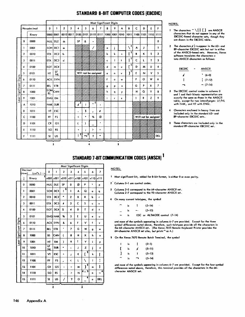
Hexadec imal a 1
Binary 10000 0001
0 0000 NUL OLE
1 0001 SOH DCl
2 0010 SIX DC2
3 0011 iETX De3
4 0100 IEOT DC4
5 0101 HT IF
.-; Nl
It 6 0110 ACK SYN
3 7 0111 BEL ETB
~ 8 1000 !E~ leAN I"~
] 9 1001 IENQ EM
A 1010 INAK SUB
B 1011 VT ESC
C 1100 FF FS
0 1101 CR GS
E 1110 SO RS
F 1111 SI US . ,
Decimal rows) (col's.)- 0 1 , Binary
I xooo xOOl
0 0000 NUL OLE
1 0001 SOH DCI
2 0010 STX De2
3 0011 ETX De3
4 0100 EOT DC4
5 0101 ENQ NAK
m 0 6 0110 ACK SYN
C 0 7 0111 BEL ETB ~ 'c 8 1000 BS CAN (J)
Vi
C; 9 1001 HT EM ta -' IF
10 1010 SUB NL
11 1011 VT ESC
12 1100 FF FS
13 1101 CR GS
14 1110 SO RS
15 1111 SI US .
"
146 Appendix A
STANDARD 8-BIT COMPUTER CODES (EBCDIC)
Most" -,. Digits
2 3 4 5 6 7 8 9 A B C 0 E F
0010 0011 0100 101 0110 :01 1000 1001 1010 1011 1100 1101 1110 1111
cis SP & - ~ a
55 ~ ~ / ~ a j -.
A J I
fs ~ ~ ~ ~ ~ b k s t I B K S 2
si ~ ~ ~ ~ c I t ~ I C l T 3
~ ~ ~ ~ d m u [ I 0 M U 4
/'." "'"' '~i'~;/ ] 1 E N V 5 e n v , , " ;,
~ ~ ~ ~ f a w F 0 W 6
~ ~ ~ ~ g p x G P X 7
~ ~ ~ ~ h q Y H Q Y 8
~ ~ ~ ~ i r z I R Z 9
,2 ~l ~ ~ ~ ~ ! :
$ , , ~ ~ ~ ~ < * % @
~/"/ '/// ."'" "'.''. ~", ''', be" ~.ii I~e;t/~
( ) , ~ ~ ~ ~ -
+ ; > = ~ ~ ~ ~ I 2 2
? ~ ~ ~ DEL
4
STANDARD 7-81T COMMUNICATION CODES (ANSCII) 1
NOTES:
The characters ~ \ t ~ [] are ANSCII characters that do nat appear in ony of the EBCDIC -based character sets, though they are shown in the EBCDIC table.
The characters t 1-, appear in the 63- and 89-character EBCDIC sets but not in either of the ANSCII-bosed sets. However, Xerox software translates the characters c into ANSClr characters as follows:
EBCDIC
I 1
..,
ANSCII
, (6-0)
: (7-12)
- (7-14)
The EBCDIC control codes in columns a and 1 and their binary representation are exactly the same as those in the' ANSCII table, except for two interchanges: LF/NL with NAK, and HT with ENQ.
Characters enclosed in heavy lines are included only in the standard 63- and 89-character EBCDIC sets.
These characters are included only in the standard 89-character EBCDIC set.
Most Significant Digits
2 3 4 5
xOlO xOll xl00 x101
SP a @ P
! 5
1 A Q
" 2 B R
, 3 C S
$ 4 0 T
% 5 E U
& 6 F Y
, 7 G W
( 8 H X
) 9 I Y
* : J Z
+ ; K [ 5
, < L \
- = M )5
> N 4 ..... 5
/ ? 0 4
-3
6 7
xlJO xlll
\ P
a q
b r
c s
d t
e u
f v
g w
h x
i Y
j z
k t I I
I
m l 4
n -0 DEL
,
1 Most significant bit, odded for 8-bit format, is either 0 or even parity.
Columns 0- I are control codes.
Columns 2-5 correspond to the 64-.character ANSCII set. Columns 2-7 correspond to the 95-character ANSCII set.
On many current teletypes, the symbol
is (5-14)
is (5-15)
is ESC or ALTMODE control (7-14)
and none of the symbols appearing in columns 6-7 are provided. Except for the three symbol differences noted above, therefore, such teletypes provide all the characters in the 64-charocter ANSCII set. (The Xerox 7015 Remote Keyboard Printer provides the 64-character ANSCII set also, but prints A as 1\.)
On the Xerox 7670 Remote Batch Terminal, the symbol
[ )
is
is
is
is
I I
-,
(2-1)
(5-11)
(5-13)
(5-14)
and none of the symbols appearing in columns 6-7 are provided. Except for the four symbol differences noted above, therefore, this terminal provides all the characters in the 64-character ANSCII set.
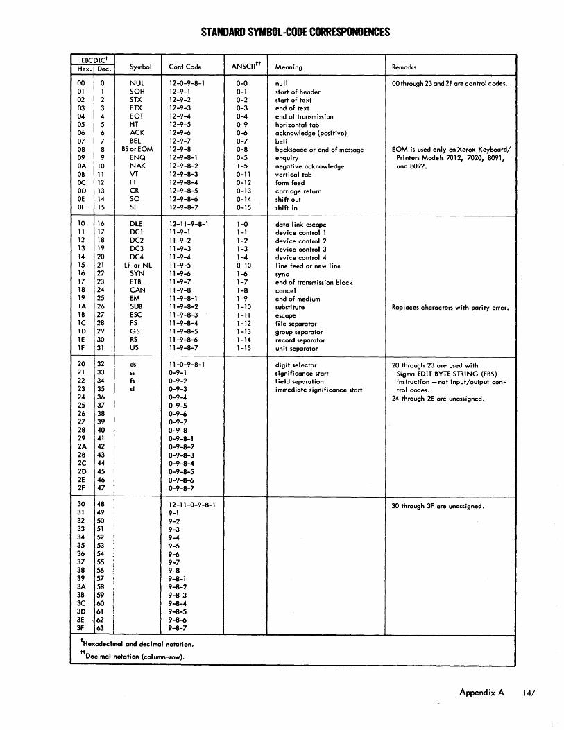
STANDARD SYMBOL-CODE CORRESPONDENCES
EacDICt ANScntt
Hex. Dec. Symbol Card Code Meaning Remarks
00 0 NUL 12-0-9-8-1 0-0 null 00 through 23 and 2F are control codes. 01 1 SOH 12-9-1 0-1 start of header 02 2 STX 12-9-2 0-2 start of text 03 3 ETX 12-9-3 0-3 end of text 04 4 EOT 12-9-4 0-4 end of transmission 05 5 HT 12-9-5 0-9 horizontal tab 06 6 ACK 12-9-6 0-6 acknowledge (positive) 07 7 BEL 12-9-7 0-7 bell 08 8 BSorEOM 12-9-8 0-8 backspace or end of message EOM is used only on Xerox Keyboard/ 09 9 ENQ 12-9-8-1 0-5 enquiry Printers Models 7012, 7020, 8091, OA 10 NAK 12-9-8-2 1-5 negative acknowledge and 8092. OB 11 VT 12-9-8-3 0-11 vertical tab OC 12 FF 12-9-8-4 0-12 form feed 00 13 CR 12-9-8-5 0-13 carriage return OE 14 SO 12-9-8-6 0-14 shift out OF 15 51 12-9-8-7 0-15 shift in
10 16 DLE 12-11-9-8-1 1-0 data Ii nk escape 11 17 DCl 11-9-1 1-1 device control 1 12 18 DC2 11-9-2 1-2 device control 2 13 19 DC3 11-9-3 1-3 device control 3 14 20 DC4 11-9-4 1-4 device control 4 15 21 LF or NL 11-9-5 0-10 line feed or new line 16 22 SYN 11-9-6 1-6 sync 17 23 ETB 11-9-7 1-7 end of transmission block 18 24 CAN 11-9-8 1-8 cancel 19 25 EM 11-9-8-1 1-9 end of medium lA 26 SUB 11-9-8-2 1-10 substitute Replaces characters with parity error. lB 27 ESC 11-9-8-3 1-1\ escape 1C 28 FS 11-9-8-4 1-12 fj Ie separator 10 29 GS 11-9-8-5 1-13 group separator lE 30 RS 11-9-8-6 1-14 record separator IF 31 US 11-9-8-7 1-15 unit separator
20 32 ds 11-0-9-8-1 digit selector 20 through 23 are used with 21 33 ss 0-9-1 significance start Sigma EDIT BYTE STRING (EBS) 22 34 fs 0-9-2 field separation instruction - not input/output con-23 35 si 0-9-3 immediate significance start trol codes. 24 36 0-9-4 24 through 2E are unassigned. 25 37 0-9-5 26 38 0-9-6 2] 39 0-9-7 28 40 0-9-8 29 41 0-9-8-1 2A 42 0-9-8-2 28 43 0-9-8-3 2C 44 0-9-8-4 20 45 0-9-8-5 2£ 46 0-9-8-6 2F 47 0-9-8-7
30 48 12-11-0-9-8-1 30 through 3F are unassigned. 31 49 9-1 32 50 9-2 33 51 9-3 34 52 9-4 35 53 9-5 36 54 9-6 37 55 9-7 38 56 9-8 39 57 9-8-1 3A 58 9-8-2 38 59 9-8-3 3C 60 9-8-4 30 61 9-8-5 3£ ·62 9-8-6 3F 63 9-8-7
tHexodecimol and decimal notation.
ttOecimal notation (column-row).
Append ix A 147
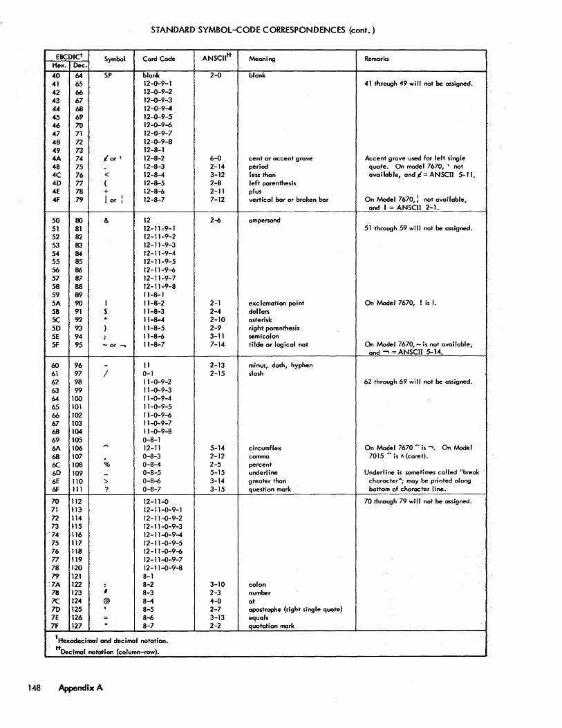
STANDARD SYMBOL-CODE CORRESPONDENCES (cont.)
EBCDICt Symbol Card Code ANSClltt Meaning Remarks Hex. Dec.
40 64 SP blank 2-0 b'ank 41 65 12-0-9-1 41 through 49 will not be assigned. 42 66 12-0-9-2 43 67 12-0-9-3 44 68 12...,0-9-4 45 69 12-0-9-5 46 70 12-0-9-6 4.7 71 12-0-9-7 48 n 12-0-9-8 49 73 12-8-1 4A 74 lor' 12-8-2 6"'() cent or accent grove Accent grave used for left single 4B 75 12-8-3 2-14 period quote. On model 7670, \ nat 4C 76 < 12-8-4 3-12 less thon available, and 1= ANSCII 5-11. 40 n ( 12-8-5 2-8 left parenthesis 4E 78 + 12-8-6 2-11 plus 4F 79 I or I 12-8-7 7-12 vertical bar or broken bar On Model 7670, : not available, I
and I = ANSal 2-1.
50 80 & 12 2-6 ampersand 51 81 12-11-9-1 51 through 59 will not be assigned. 52 B2 12-11-9-2 53 83 12-11-9-3 54 84 12-11-9-4 55 85 12-11-9-5 56 86 12-11-9-6 57 87 12-11-9-7 58 88 12-11-9-8 59 89 11-8-1 5A 90 ! 11-8-2 2-1 exclamation point On Model 7670, ! is I. 58 91 $ 11-8-3 2-4 dollars 5C 92 * 11-8-4 2-10 asterisk 50 93 ) 11-8-5 2-9 right parenthesis 5E 94 ; 11-8-6 3-11 semicolon Sf 95 - or .., 11-8-7 .7-14 tilde or logical not On Model 7670,-i5 not available,
and"" = ANSCII 5-14.
60 96 - 11 2-13 minus, dash, hyphen 61 97 / 0-1 2-15 slash 62 98 1T-0-9-2 62 through 69 wi II not be assigned. 63 99 11-0-9-3 64 100 11-0-9-4 65 101 11-0-9-5 66 102 11-0-9-6 67 103 11-0-9-7 68 104- 11-0-9-8 69 lOS 0-8-1 6A 106
.... 12-11 5-14 circumflex On Model 7670 ~ is '. On Model 68 107 . 0-8-3 2-12 comma 7015 ~ is 1\ (caret).
t£ 108 % 0-8-4 2-5 percent 60 109 - 0-8-5 5-15 underline Underline is sometimes called "break
, 6E 110 > 0-8-6 3-14 greater than character"; may be printed along 6F 111 ? 0-8-7 3-15 question mark bottom of character line.
70 112 12-H-O 70 through 79 will not be assigned. 71 113 12-11-0-9-1 n 114 12-11-0-9-2 73 115 12-11-0-9-3
'74 116 12-11-0-9-4 ·75 117 12-11-0-9-5 .76 118 12-11-0-9-6 n 119 12-11-0-9-7 78 120 12-11-0-9-8 79 121 8-1
'lA 122 8-2 3-10 colon 7B 123 I 8-3 2-3 number 7C 124 @ 8-4 4-0 at 7D 125 . 8-5 2-7 apostrophe (right single quote) 7£ 126 = 8-6 3-13 equals 7F 127 II 8-7 2-2 quotation mark
tHexodecimal and decimal notation.
tfOecimot notation {column-row}.
148 Appendix A
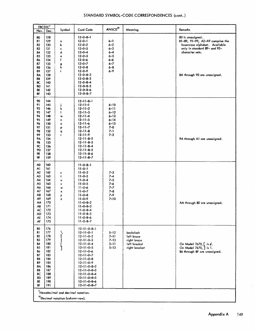
STANDARD SYMBOL-CODE CORRESPONDENCES (cont.)
EBCDIC t
ANSClItt Remarks Hex. Dec. Symbol Card Code Meaning
80 128 12-0-8-1 80 is unassigned. 81 129 a 12-0-1 6-1 81-89, 91-99, A2-A9 comprise the 82 130 b 12-0-2 6-2 lowercase alphabet. Available 83 131 c 12-0-3 6-3 only in standard 89- and 95-84 132 d 12-0-4 6-4 character sets. 85 133 e 12-0-5 6-5 86 134 f 12-0-6 6-6 87 135 I
g 12-0-7 6-7 88 136 h 12-0-8 6-8 89 137 i 12-0-9 6-9 8A 138 12-0-8-2 8A through 90 are unassigned. 88 139 12-0-8-3 Be 140 12-0-8-4 80 141 12-0-8-5 8E 142 12-0-8-6 8F 143 12-0-8-7
90 144 12-11-8-1 91 145 j 12-11-1 6-10 92 146 k 12-11-2 6-11 93 147 I 12-11-3 6-12 94 148 !1"1 12-11-4 6-13 95 149 n 12-11-5 6-14 96 150 0 12-11-6 6-15 97 151 p 12-11-7 7-0 98 152 q 12-11-8 7-1 99 153 r 12-11-9 7-2 9A 154 12-11-8-2 9A through Al are unassigned. 9B 155 12-11-8-3 9C 156 12-11-8-4 90 157 12-11-8-5 9E 158 12-11-8-6 9F 159 12-11-8-7
AO 160 11-0-8-1 Al 161 11-0-1 A2 162 s 11-0-2 7-3 A3 163 t 11-0-3 7-4 A4 164 u 11-0-4 7-5 A5 165 v 11-0-5 7-6 A6 166 w 11-0-6 7-7 A7 167 x 11-0-7 7-8 A8 168 y 11-0-8 7-9 A9 169 z 11-0-9 7-10 AA 170 11-0-8-2 AA through 80 are unassigned. AB 171 11-0-8-3 AC 172 11-0-8-4 AD 173 11-0-8-5 AE 174 11-0-8-6 AF 175 11-0-8-7
BO 176 12-11-0-8-1 81 177 \ 12-11-0-1 5-12 backs lash 82 178 { 12-11-0-2 7-11 left brace 83 179 J 12-11-0-3 7-13 right brace B4 180 [ 12-11-0-4 5-11 left bracket On Model 7670, ~ is i. 85 181 ] 12-11-0-5 5-13 right bracket On Model 7670, is!. 86 182 12-11-0-6 B6 through 8F are unassigned. 87 183 12-11-0-7 88 184 12-11-0-8 89 185 12-11-0-9 BA 186 12-11-0-8-2 88 187 12-11-0-8-3 8C 188 12-11-0-8-4 80 189 12-11-0-8-5 8E 190 12-11-0-8-6 SF 191 12-11-0-8-7
tHexadecimal and decimal notation.
ttOecimal notation (column-row).
Appendix A 149
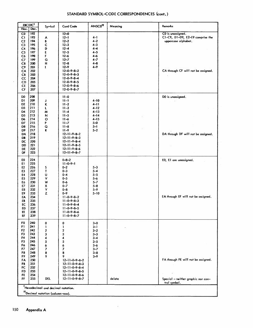
STANDARD SYMBOl-CODE CORRESPONDENCES (cont.)
ESCorC t Syl'!'bol Card Code ANSCntt Meaning Remarks
Hex. Dec.
CO 192 12-0 CO is unassigned. CI 193 A 12-1 4-1 CI-C9, 01-09, E2-E9 comprise the C2 194 B 12-2 4-2 uppercase alphabet. C3 195 C 12-3 4-3 C4 196 D 12-4 4-4 C5 197 E 12-5 4-5 C6 198 F 12-6 4-6 C7 199 G 12-7 4-7 C8 200 H 12-8 4-8
'C9 201 I 12-9 4-9 CA 202 12-0-9-8-2 CA through CF will not be assigned. CB 203 12-0-9-8-3 CC 204 12-0-9-8-4 CO 205 12-0-9-8-5 CE 206 12-0-9-8-6 CF 207 12-0-9-8-7
DO 208 11-0 DO is unassigned. 01 209 J 11-1 4-10 02 210 K 11-2 4-11 03 211 L 11-3 4-12 04 212 M 11-4 4-13 05 213 N 11-5 4-14 D6 214 0 11-6 4-15 07 215 P 11-7 5-0 08 216 Q 11-8 5-1 09 217 R 11-9 5-2 OA 218 12-11-9-8-2 OA through OF wi" nat be assigned. DB 219 12-11-9-8-3 DC 220 12-11-9-8-4 DO 221 12-11-9-8-5 DE 222 12-11-9-8-6 Of 223 12-11-9-8-7
EO 224 0-8-2 EO, E 1 are unassigned. El 225 11-0-9-1 E2 226 S 0-2 5-3 E3 227 T 0-3 5-4 E4 228 U 0-4 5-5 E5 229 V 0-5 5-6 E6 230 W 0-6 5-7 E7 231 X 0-7 5-8 E8 232 y 0-8 5-9 E9 233 Z 0-9 5-10 EA 234 11-0-9-8-2 EA through EF will not be assigned. f8 .235 11-0-9-8-3 EC 236 11-0-9-8-4 ED 2.37 11-0-9-8-5 EE 238 11-0-9-8-6 EF 239 11-0-9-8-7
FO 240 0 0 3-0 Fl 241 1 1 3-1 F2 242 2 2 3-2 F3 243 3 3 3-3 F4 244 4 4 3-4 F5 245 5 5 3-5 F6 246 6 6 3-6 F7 247 7 7 3-7 F8 248 8 8 3-8 F9 249 9 9 3-9 FA 250 12-11-0-9-8-2 FA through FE will not be assigned. FB 251 12-11-0-9-8-3 FC 252 12-11-0-9-8-4 FO 253 12-11-0-9-8-5 Ff 254 12-11-0-9-8-6 f.F 255 DEL 12-11-0-9-8-7 delete Special - neither graphic nor con-
trol symbol.
tHexadecimal and decimal notation.
ttOecimal notation (column-row).
150 Appendix A
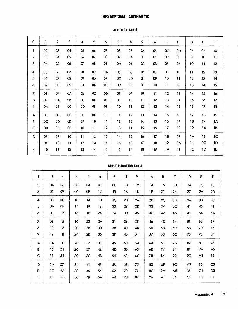
HEXADECIMAL ARITHMETIC
ADDITION TABLE
0 1 2 3 4 5 6 7 8 9 A B C D E F
1 02 03 04 05 06 07 08 09 OA DB OC OD OE OF 10
2 03 04 05 06 07 08 09 OA OB OC OD OE OF 10 11
3 04 05 06 07 08 09 OA OB DC 00 OE OF 10 11 12
4 05 06 07 08 09 OA OB OC OD OE OF 10 11 12 13
5 06 07 08 09 OA OB OC OD OE OF 10 11 12 13 14
6 07 08 09 OA OB OC OD OE OF 10 11 12 13 14 15
7 08 09 OA OB OC OD OE OF 10 11 12 13 14 15 16
8 09 OA OB DC OD OE OF 10 11 12 13 14 15 16 17
9 OA OB OC 00 OE OF 10 11 12 ; 13 14 15 16 17 18
A OB OC OD DE OF 10 11 12 13 14 15 16 17 18 19
B OC OD OE OF 10 11 12 13 14 15 16 17 18 19 1A
C OD OE OF 10 11 12 13 14 15 16 17 18 19 1A 1B
D OE OF 10 11 12 13 14 15 16 17 18 19 1A 1B 1C
E OF 10 11 12 13 14 15 16 17 18 19 1A 1B 1C 10
F 10 11 12 13 14 15 16 17 18 19 1A 1B 1C 10 1E
MULTIPLICATION TABLE
1 2 3 4 5 6 7 8 9 A B C D E F
2 04 06 08 OA OC OE 10 12 14 16 18 1A 1C 1E
3 06 09 OC OF 12 15 18 1B 1E 21 24 27 2A 2D
4 08 OC 10 14 18 1C 20 24 28 2C 30 34 38 3C
5 OA OF 14 19 1E 23 28 20 32 37 3C 41 46 4B
6 OC 12 18 1E 24 2A 30 36 3C 42 48 4E 54 5A
7 OE 15 1C 23 2A 31 38 3F 46 4D 54 58 62 69
8 10 18 20 28 30 38 40 48 50 58 60 68 70 78
9 12 1B 24 2D 36 3F 48 51 5A 63 6C 75 7E 87
A 14 lE 28 32 3C 46 50 5A 64 6E 78 82 Be 96
B 16 21 2C 37 42 4D 58 63 6E 79 84 8F 9A A5
C 18 24 30 3C 48 54 60 6C 78 84 90 9C A8 B4
D 1A 27 34 41 4E 5B 68 75 82 8F 9C A9 B6 C3
E 1C 2A 38 46 54 62 70 7E 8C 9A A8 B6 C4 D2
F 1E 2D 3C 4B 5A 69 78 87 96 A5 B4 C3 02 E1
Appendix A 151
16
256
4 096
65 536
048 576
16 777 216
268 435 456
4 294 967 296
68 719 476 736
1 099 511 627 776
17 592 186 044 416
281 474 976 710 656
4 503 599 627 370 496
72 057 594 037 927 936
1 152 921 504 606 846 976
3
23
163
OEO
8AC7
152 Appendix A
2
17
E8
918
5AF3
807E
86F2
4578
B6B3
2304
A
64
3E8
2710
86AO
F 4240
98 9680
5F5 El00
3B9A CAOO
540B E400
4876 E800
04A5 1000
4E72 AOOO
l07A 4000
A4C6 8000
6FC1 0000
508A 0000
A764 0000
89E8 0000
TABLE OF POWERS OF SIXTEEN 11
n
o
2
3
4
5
6
7
8
9
10
11
12
13
14
15
0.10000 00000 00000 00000 x 10
0.62500 00000 00000 00000 x 10- 1
0.39062 50000 00000 00000 x 10-2
0.24414 06250 00000 00000 x 10-3
0.15258 78906 25000 00000 x 10-4
0.95367 43164 06250 00000 x 10-6
0.59604 64477 53906 25000 x 10-7
0.37252 90298 46191 40625 x 10-8
0.23283 06436 53869 62891 x 10-9
0.14551 91522 83668 51807 x 10- 10
0.90949 47017 72928 23792 x 10- 12
0.56843 41886 08080 14870 x 10- 13
0.35527 13678 80050 09294 x 10- 14
0.22204 46049 25031 30808 x 10- 15
0.13877 78780 78144 56755 x 10- 16
0.86736 17379 88403 54721 x 10- 18
. TABLE OF POWERS OF TEN 1&
o
2
3
4
5
6
7
8
9
10
11
12
13
14
15
16
17
18
19
1.0000 0000 0000 0000
0.1999 9999 9999 999A
0.28F 5 C28F
0.4189 374B
0.680B 8BAC
0.A7C5 AC47
0.10C6 F7AO
0.1 AD7 F 29 A
0.2AF 3 10C4
0.44B8 2FAO
0.6 OF 3 7F67
O.AFE B F FOB
0.1197 9981
0.lC25 C268
0.2 D09 3700
0.480E BE7B
0.734A CA5 F
0.B877 AA32
0.1272 5DDl
0.1 D83 C94F
5C28
C6A7
710C
1B47
B5E D
BCAF
6118
9B5A
5EF6
CB24
20EA
4976
4257
9D58
6226
36A4
0243
B6D2
F5C3
EF9E
B296
8423
8D37
4858
73BF
52CC
EAOF
AAFF
1 1 19
81C2
3604
566D
FOAE
B449
ABAl
AC35
x
x
x
x
x
x
x
x
x
x
x
x
x
x
x
x
x
x
16-1
16-2
16-3
16-4
16-4
16-5
16-6
16-7
16-8
16-9
16-9
16- 10
16 -11
16- 12
16- 13
16- 14
16- 14
16- 15
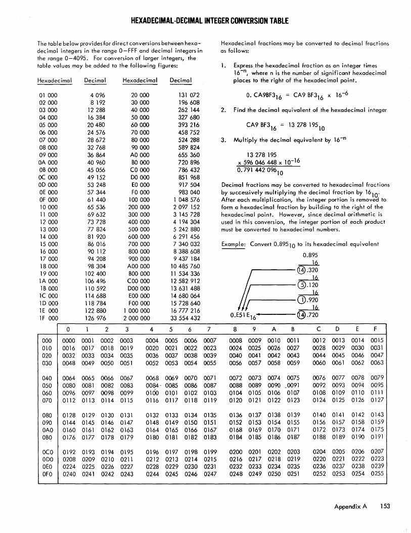
HEXADECIMAL-DECIMAL INTEGER CONVERSION TABLE
The table below provides for direct conversions between hexadecimal integers in the range O-FFF and decimal integers in the range 0-4095. For conversion of larger integers, the table values may be added to the following figures:
Hexadecimal
01 000 02000 03000 04000 05000 06 000 07000 08000 09000 OA 000 OB 000 DC 000 00000 OE 000 OF 000 10000 11000 12 000 13000 14000 15000 16000 17 000 18000 19000 lA 000 lB 000 lC 000 10000 lE 000 lF 000
000 010 020 030
040 050 060 070
080 090 OAO OBO
OCO 000 OED OFO
0
0000 0016 0032 0048
0064 0080 0096 0112
0128 0144 0160 0176
0192 0208 0224 0240
Decimal
4096 8 192
12 288 16384 20480 24576 28672 32768 36 864 40960 45056 49 152 53 248 57344 61440 65536 69632 73728 77 824 81 920 86 016 90 112 94208 98304
102400 106496 110592 114688 118784 122 880 126 976
1 2
0001 0002 0017 0018 0033 0034 0049 0050
0065 0066 0081 0082 0097 0098 0113 0114
0129 0130 0145 0146 0161 0162 0177 0178
0193 0194 0209 0210 0225 0226 0241 0242
Hexadecimal
20000 30000 40000 50000 60000 70000 80000 90000
AO 000 BO 000
CO 000 DO 000 EO 000 FO 000
100000 200000 300000 400000 500000 600000 700000 800000 900000
AOO 000 BOO 000
COO 000 000000 EOO 000 FOO 000
1 000000 2000000
3 4
0003 0004 0019 0020 0035 0036 0051 0052
0067 0068
Decimal
131 072 196608 262 144 327680 393 216 458752 524 288 589824 655 360 720896 786 432 851 968 917 504 983 040
1 048576 2 097 152 3 145 728 4 194304 5 242 880 6 291 456 7 340 032 8 388 608 9437 184
10485 760 11 534336 12582 912 13 631 488 14680064 15 728640 16 777 216 33554432
5 6
0005 0006 0021 0022 0037 0038 0053 0054
0069 0070 0083 0084- 0085 0086 0099 0100 0101 0102 0115 0116 0117 0118
0131 0132 0133 0134 0147 0148 0149 0150 0163 0164 0165 0166 0179 0180 0181 0182
0195 0196 0197 0198 0211 0212 0213 0214 0227 0228 0229 0230 0243 0244 0245 0246
7
0007 0023 ·0039 0055
0071 0087 0103 0119
0135 0151 0167 0183
0199 0215 0231 0247
Hexadecimal fractions may be converted to decimal fractions as follows:
1. Express the hexadecimal fraction as an integer times 16 -n, where n is the number of significant hexadecimal places to the right of the hexadecimal point.
O. CA9SF3 16 = CA9 BF3 16 x 16-6
2. Find the decimal equivalent of the hexadecimal integer
CA 9 SF 316
= 13 278 19510
3. Multiply the decimal equivalent by 16-n
13 278 195 x 596046 448 x 10-16
0.791 442 09610
Decimal fractions may be converted to hexadecimal fractions by successively multiplying the decimal fraction by 16 10. After each multiplication, the integer portion is removea to form a hexadecimal fraction by building to the right of the hexadecimal point. However, since decimal arithmetic is used in this conversion, the integer portion of each product must be converted to hexadecimal numbers.
Example: Convert 0.89510 to its hexadecimal equivalent
0.895 16
,------ Q3) .320 -.-l.Q.
,.----- @.120
/1/ ~ 'If 16 0.E51 E16------!&) .720
8 9 A B C
0008 0009 0010 0011 0012 0024 0025 0026 0027 0028 0040 0041 0042 0043 0044 0056 0057 0058 0059 0060
0072 0073 0074 0075 0076 0088 0089 0090 .0091 0092 0104 0105 0106 0107 0108 0120 0121 0122 0123 0124
0136 0137 0138 0139 0140 0152 0153 0154 0155 0156 0168 0169 0170 0171 0172 0184 0185 0186 0187 0188
0200 0201 0202 0203 0204 0216 0217 0218 0219 0220 0232 0233 0234 0235 0236 0248 0249 0250 0251 0252
0 E F
0013 0014 0015 0029 0030 0031 0045 0046 0047 0061 0062 0063
0077 0078 0079 0093 0094 0095 0109 0110 0111 0125 0126 0127
0141 0142 0143 0157 0158 0159 0173 0174 0175 0189 0190 0191
0205 0206 0207 0221 0222 0223 0237 0238 0239 0253 0254 0255
Appendix A 153
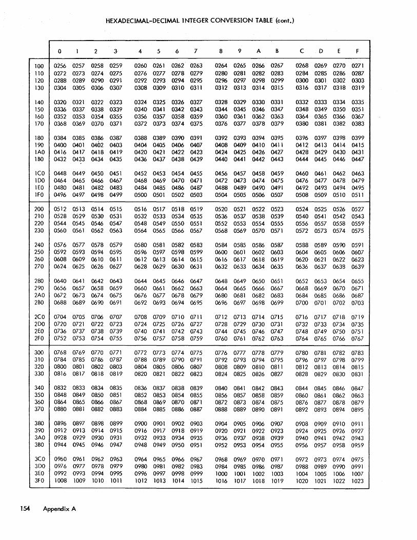
HEXADECIMAL-DECIMAL INTEGER CONVERSION TABLE (cont.)
0 1 2 3- 4 5 6 7 8 9 A B C 0 E F
100 0256 0257 0258 0259 0260 0261 0262 0263 0264 0265 0266 0267 0268 0269 0270 0271 110 0272 0273 0274 0275 0276 0277 0278 0279 0280 0281 0282 0283 0284 0285 0286 0287 120 0288 0289 0290 0291 0292 0293 0294 0295 0296 02W 0298 0299 0300 0301 0302 0303 130 0304 0305 0306 0307 0308 0309 0310 0311 0312 0313 0314 0315 0316 0317 0318 0319
140 0320 0321 0322 0323 0324 0325 0326 0327 0328 0329 0330 0331 0332 0333 0334 0335 150 0336 0337 0338 0339 0340 0341 0342 0343 0344 0345 0346 0347 0348 0349 0350 0351 160 0352 0353 0354 0355 0356 0357 0358 0359 0360 0361 0362 0363 0364 0365 0366 0367 170 0368 0369 0370 0371 0372 0373 0374 0375 0376 03n 0378 0379 0380 0381 0382 0383
180 0384 0385 0386 0387 0388 0389 0390 0391 0392 0393 0394 0395 0396 0397 0398 0399 190 0400 0401 0402 0403 0404 0405 0406 0407 0408 0409 0410 0411 0412 0413 0414 0415 lAO 0416 0417 0418 0419 0420 0421 0422 0423 0424 0425 0426 0427 0428 0429 0430 0431 ISO 0432 0433 0434 0435 0436 0437 0438 0439 0440 0441 0442 0443 0444 0445 0446 0447
lCO 0448 0449 0450 0451 0452 0453 0454 0455 0456 0457 0458 0459 0460 0461 0462 0463 IDO 0464 0465 0466 0467 0468 0469 0470 0471 0472 0473 0474 0475 0476 0477 0478 0479 lEO 0480 0481 0482 0483 0484 0485 0486 0487 0488 0489 0490 0491 0492 0493 0494 0495 1FO 0496 0497 0498 0499 0500 0501 0502 0503 0504 0505 0506 0507 0508 0509 0510 0511
200 0512 0513 0514 0515 0516 0517 0518 0519 0520 0521 0522 0523 0524 0525 0526 0527 210 0528 0529 0530 0531 0532 0533 0534 0535 0536 0537 0538 0539 0540 0541 0542 0543 220 0544 0545 0546 0547 0548 0549 0550 0551 0552 0553 0554 0555 0556 0557 0558 0559 230 0560 0561 0562 0563 0564 0565 0566 0567 0568 0569 0570 0571 0572 0573 0574 0575
240 0576 0577 0578 0579 0580 0581 0582 0583 0584 0585 0586 0587 0588 0589 0590 0591 250 0592 0593 0594 0595 0596 0597 0598 0599 0600 0601 0602 0603 0604 0605 0606 0607 260 0608 0609 0610 0611 0612 0613 0614 0615 0616 0617 0618 0619 0620 0621 0622 0623 270 0624 0625 0626 0627 0628 0629 0630 0631 0632 0633 0634 0635 0636 0637 0638 0639
280 0640 0641 0642 0643 0644 0645 0646 0647 0648 0649 0650 0651 0652 0653 0654 0655 290 0656 0657 0658 0659 0660 0661 0662 0663 0664 0665 0666 0667 0668 0669 0670 0671 2AO 0672 0673 0674 0675 0676 0677 0678 0679 0680 0681 0682 0683 0684 0685 0686 0687 2BO 0688 0689 0690 0691 0692 0693 0694 0695 0696 0697 0698 0699 0700 0701 0702 0703
2CO 0704 0705 0706 0707 0708 0709 0710 0711 0712 0713 0714 0715 0716 0717 0718 0719 2DO 0720 0721 0722 0723 0724 0725 0726 0727 0728 0729 0730 0731 0732 0733 0734 0735 2EO 0736 0737 0738 0739 0740 0741 0742 0743 0744 0745 0746 0747 0748 0749 0750 0751 2FO 0752 0753 0754 0755 0756 0757 0758 0759 0760 0761 0762 0763 0764 0765 0766 0767
300 0768 0769 0770 0771 0772 0773 0774 0775 0776 0777 0778 0779 0780 0781 0782 0783 310 0784 0785 0786 0787 0788 0789 0790 0791 0792 0793 0794 0795 0796 0797 0798 0799 320 0800 0801 0802 0803 0804 0805 0806 0807 0808 0809 0810 0811 0812 0813 0814 0815 330 0816 0817 0818 0819 0820 0821 0822 0823 0824 0825 0826 0827 0828 0829 0830 0831
340 0832 0833 0834 0835 0836 0837 0838 0839 0840 0841 0842 0843 0844 0845 0846 0847 350 0848 0849 0850 0851 0852 0853 0854 0855 0856 0857 0858 0859 0860 0861 0862 0863 360 0864 0865 0866 0867 0868 0869 0870 0871 0872 0873 0874 0875 0876 0877 0878 0879 370 0880 0881 0882 0883 0884 0885 0886 0887 0888 0889 0890 0891 0892 0893 0894 0895
380 0896 0897 0898 0899 0900 0901 0902 0903 0904 0905 0906 0907 0908 0909 0910 0911 390 0912 0913 0914 0915 0916 0917 0918 0919 0920 0921 0922 0923 0924 0925 0926 0927 3AO 0928 0929 0930 0931 0932 0933 0934 0935 0936 0937 0938 0939 0940 0941 0942 0943 3BO 0944 0945 0946 0947 0948 0949 0950 0951 0952 0953 0954 0955 0956 0957 0958 0959
3CO 0960 0961 0962 0963 0964 0965 0966 0967 0968 0969 0970 0971 0972 0973 0974 0975 3DO 0976 0977 0978 0979 0980 0981 0982 0983 0984 0985 0986 0987 0988 0989 0990 0991 3EO 0992 0993 0994 0995 0996 0997 0998 0999 1000 1001 1002 1003 1004 1005 1006 1007 3FO 1008 1009 1010 1011 1012 1013 1014 1015 1016 1017 1018 1019 1020 1021 1022 1023
154 Appendix A
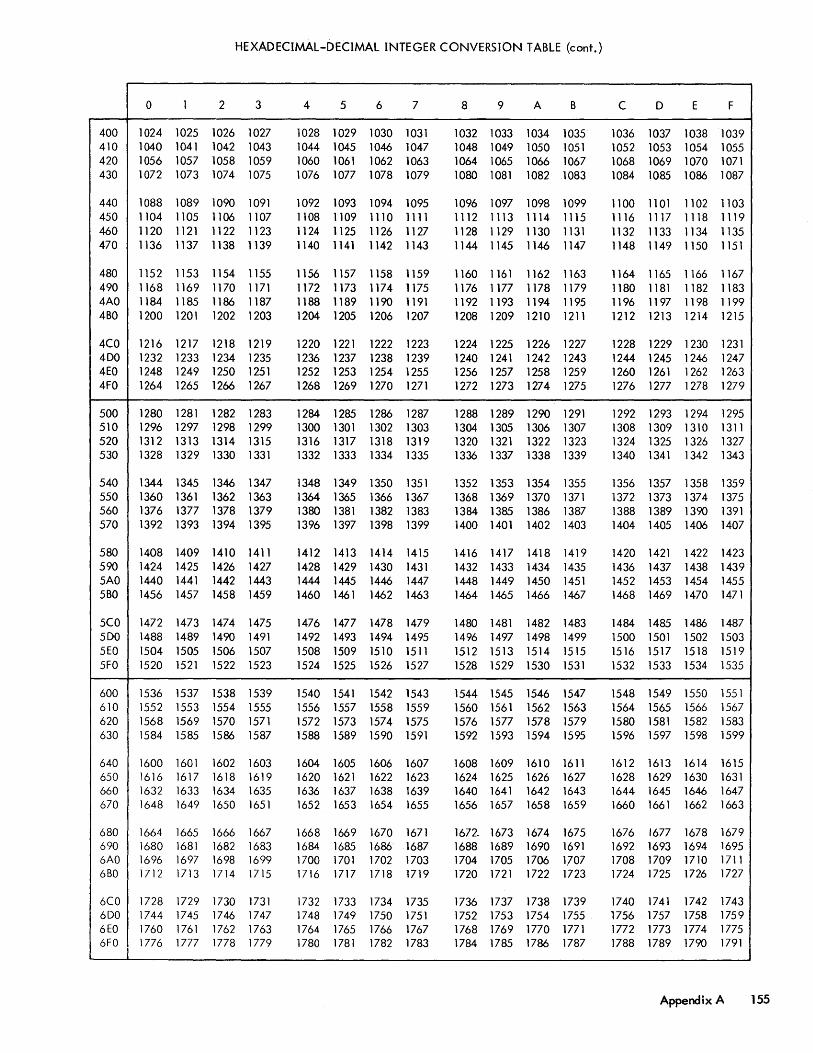
HEXADECIMAL-DECIMAL INTEGER CONVERSION TABLE (cont.)
0 1 2 3 4 5 6 7 8 9 A B C D E F
400 1024 1025 1026 1027 1028 1029 1030 1031 1032 1033 1034 1035 1036 1037 1038 1039 410 1040 1041 1042 1043 1044 1045 1046 1047 1048 1049 1050 1051 1052 1053 1054 1055 420 1056 1057 1058 1059 1060 1061 1062 1063 1064 1065 1066 1067 1068 1069 1070 1071 430 1072 1073 1074 1075 1076 1077 1078 1079 1080 1081 1082 1083 1084 1085 1086 1087
440 1088 1089 1090 1091 1092 1093 1094 1095 1096 1097 1098 1099 1100 1101 1102 1103 450 1104 1105 1106 1107 1108 1109 1110 1111 1112 1113 1114 1115 1116 1117 1118 1119 460 1120 1121 1122 1123 1124 1125 1126 1127 1128 1129 1130 1131 1132 1133 1134 1135 470 1136 1137 1138 1139 1140 1141 1142 1143 1144 1145 1146 1147 1148 1149 1150 1151
480 1152 1153 1154 1155 1156 1157 1158 1159 1160 1161 1162 1163 1164 1165 1166 1167 490 1168 1169 1170 1171 1172 1173 1174 1175 1176 1177 1178 1179 1180 1181 1182 1183 4AO 1184 1185 1186 1187 1188 1189 1190 1191 1192 1193 1194 1195 1196 1197 1198 1199 4BO 1200 1201 1202 1203 1204 1205 1206 1207 1208 1209 1210 1211 1212 1213 1214 1215
4CO 1216 1217 1218 1219 1220 1221 1222 1223 1224 1225 1226 1227 1228 1229 1230 1231 4DO 1232 1233 1234 1235 1236 1237 1238 1239 1240 1241 1242 1243 1244 1245 1246 1247 4EO 1248 1249 1250 1251 1252 1253 1254 1255 1256 1257 1258 1259 1260 1261 1262 1263 4FO 1264 1265 1266 1267 1268 1269 1270 1271 1272 1273 1274 1275 1276 1277 1278 1279
500 1280 1281 1282 1283 1284 1285 1286 1287 1288 1289 1290 1291 1292 1293 1294 1295 510 1296 1297 1298 1299 1300 1301 1302 1303 1304 1305 1306 1307 1308 1309 1310 1311 520 1312 1313 1314 1315 1316 1317 1318 1319 1320 1321 1322 1323 1324 1325 1326 1327 530 1328 1329 1330 1331 1332 1333 1334 1335 1336 1337 1338 1339 1340 1341 1342 1343
540 1344 1345 1346 1347 1348 1349 1350 1351 1352 1353 1354 1355 1356 1357 1358 1359 550 1360 1361 1362 1363 1364 1365 1366 1367 1368 1369 1370 1371 1372 1373 1374 1375 560 1376 1377 1378 1379 1380 1381 1382 1383 1384 1385 1386 1387 1388 1389 1390 1391 570 1392 1393 1394 1395 1396 1397 1398 1399 1400 1401 1402 1403 1404 1405 1406 1407
580 1408 1409 1410 1411 1412 1413 1414 1415 1416 1417 1418 1419 1420 1421 1422 1423 590 1424 1425 1426 1427 1428 1429 1430 1431 1432 1433 1434 1435 1436 1437 1438 1439 5AO 1440 1441 1442 1443 1444 1445 1446 1447 1448 1449 1450 1451 1452 1453 1454 1455 5BO 1456 1457 1458 1459 1460 1461 1462 1463 1464 1465 1466 1467 1468 1469 1470 1471
5CO 1472 1473 1474 1475 1476 1477 1478 1479 1480 1481 1482 1483 1484 1485 1486 1487 5DO 1488 1489 1490 1491 1492 1493 1494 1495 1496 1497 1498 1499 1500 1501 1502 1503 5EO 1504 1505 1506 1507 1508 1509 1510 1511 1512 1513 1514 1515 1516 1517 1518 1519 5FO 1520 1521 1522 1523 1524 1525 1526 1527 1528 1529 1530 1531 1532 1533 1534 1535
600 1536 1537 1538 1539 1540 1541 1542 1543 1544 1545 1546 1547 1548 1549 1550 1551 610 1552 1553 1554 1555 1556 1557 1558 1559 1560 1561 1562 1563 1564 1565 1566 1567 620 1568 1569 1570 1571 1572 1573 1574 1575 1576 1577 1578 1579 1580 1581 1582 1583 630 1584 1585 1586 1587 1588 1589 1590 1591 1592 1593 1594 1595 1596 1597 1598 1599
640 1600 1601 1602 1603 1604 1605 1606 1607 1608 1609 1610 1611 1612 1613 1614 1615 650 1616 1617 1618 1619 1620 1621 1622 1623 1624 1625 1626 1627 1628 1629 1630 1631 660 1632 1633 1634 1635 1636 1637 1638 1639 1640 1641 1642 1643 1644 1645 1646 1647 670 1648 1649 1650 1651 1652 1653 1654 1655 1656 1657 1658 1659 1660 1661 1662 1663
680 1664 1665 1666 1667 1668 1669 1670 1671 1672. 1673 1674 1675 1676 1677 1678 1679 690 1680 1681 1682 1683 1684 1685 1686 1687 1688 1689 1690 1691 1692 1693 1694 1695 6AO 1696 1697 1698 1699 1700 1701 1702 1703 1704 1705 1706 1707 1708 1709 1710 1711 6BO 1712 1713 1714 1715 1716 1717 1718 1719 1720 1721 1722 1723 1724 1725 1726 1727
6CO 1728 1729 1730 1731 1732 1733 1734 1735 1736 1737 1738 1739 1740 1741 1742 1743 6DO 1744 1745 1746 1747 1748 1749 1750 1751 1752 1753 1754 1755 1756 1757 1758 1759 6EO 1760 1761 1762 1763 1764 1765 1766 1767 1768 1769 1770 1771 1772 1773 1774 1775 6FO 1776 1777 1778 1779 1780 1781 1782 1783 1784 1785 1786 1787 1788 1789 1790 1791
Appendix A 155

HEXADECIMAL-DECIMAL INTEGER CONVERSION TABlE (corlf.)
0 I 2 3 4 5 6 7 8 9 A B C 0 E F
700 1792 1793 1794 1795 1796 1797 1798 1799 1800 I SOl 1802 1803 J804 1805 1806 1807 710 1808 1809 1810 1811 1812 1813 1814 18J5 1816 1817 1818 1819 1820 1821 1822 1823 720 1824 1825 1826 1827 1828 1829 1830 1831 1832 1833 1834 1835 1836 1837 1838 1839 730 1840 1841 1842 1843 1844 1845 1846 1847 1848 1849 )850 J851 1852 1853 1854 1855
740 1856 1857 1858 1859 1860 1861 1862 1863 1864 1865 1866 1867 1868 1869 1870 1871 750 1872 1873 )874 1875 1876 1877 1878 1879 1880 1881 1882 1883 1884 1885 1886 1887 760 1888 1889 1890 1891 1892 1893 )894 1895 1896 . 1897 1898 1899 1900 1901 1902 1903 770 1904 1905 1906 1907 )908 1909 1910 1911 1912 1913 1914 1915 1916 1917 1918 1919
780 1920 1921 1922 1923 1924 1925 1926 1927 1928 1929 1930 1931 1932 1933 1934 1935 790 1936 1937 1938 1939 1940 1941 1942 1943 1944 1945 1946 1947 1948 1949 1950 1951 7AO 1952 1953 1954 1955 1956 1957 1958 1959 1960 1961 1962 1963 J964 1965 1966 1967 780 1968 1969 1970 1971 1972 1973 1974 1975 1976 1977 1978 1979 1980 1981 1982 1983
7eo 1984 1985 1986 1987 1988 1989 1990 1991 1992 1993 1994 1995 1996 1997 1998 1999 700 2000 2001 2002 2003 2004 2005 2006 2007 2008 2009 2010 2011 2012 2013 2014 2015 7EO 2016 2017 2018 2019 2020 2021 2022 2023 2024 2025 2026 2027 2028 2029 2030 2031 ]f0 2032 2033 2034 2035 2036 2037 2038 2039 2040 2041 2042 2043 2044 2045 2046 2047
800 2048 2049 2050 2051 2052 2053 2054 2055 2056 2057 2058 2059 2060 2061 2062 2063 810 2064 2065 2066 2067 2068 2069 2070 2071 2072 2073 2074 2075 2076 2077 2078 2079 820 2080 2081 2082 2083 2084 2085 2086 2087 2088 2089 2090 2091 2092 2093 2094 2095 830 2096 2097 2098 2099 2100 2101 2102 2103 2104 2105 2106 2107 2108 2109 2110 2111
840 2112 2113 2114 2115 2116 2117 2118 2119 2120 2121 2122 2123 2124 2125 2126 2127 850 2128 2129 2130 2131 2132 2133 2134 2135 2136 2137 2138 2139 2140 2141 2142 2143 860 2144 2145 2146 2147 2148 2149 2150 2151 2152 2153 2154 2155 2156 2157 2158 2J59 870 2160 2161 2162 2163 2164 2165 2166 2167 2168 2169 2170 2171 2172 2173 2174 2175
880 2176 2177 2178 2179 2180 2181 2182 2183 2184 2185 2186 2187 2188 2189 2190 2191 890 2192 2193 2194 2195 2196 2197 2198 2199 2200 2201 2202 2203 2204 2205 2206 2207 8A0 2208 2209 2210 2211 2212 2213 2214 2215 2216 2217 2218 2219 2220 2221 2222 2223 8BO 2224 2225 2226 2227 2228 2229 2230 2231 2232 2233 2234 2235 2236 2237 2238 2239
aco . 2240 2241 2242 2243 2244 2245 2246 2247 2248 2249 2250 2251 2252 2253 2254 2255 800 2256 2257 2258 2259 2260 2261 2262 2263 2264 2265 2266 2267 2268 2269 2270 2271 8EO 2272 2273 2274 2275 2276 2277 2278 2279 2280 2281 2282 2283 2284 2285 2286 2287 BfO 2288 2289 2290 2291 2292 2293 2294 2295 2296 2297 2298 2299 2300 2301 2302 2303
900 2304 2305 2306 2307 2308 2309 2310 2311 2312 2313 2314 2315 2316 2317 2318 2319 910 2320 2321 2322 2323 2324 2325 2326 2327 2328 2329 2330 2331 2332 2333 2334 2335 920 2336 2337 2338 2339 2340 2341 2342 2343 2344 2345 2346 2347 2348 2349 2350 2351 930 2352 2353 2354 2355 2356 2357 2358 2359 2360 2361 2362 2363 2364 2365 2366 2367
940 2368 2369 2370 2371 2372 2373 2374 2375 2376 2377 2378 2379 2380 2381 2382 2383 950 2384 2385 2386 2387 2388 2389 2390 2391 2392 2393 2394 2395. 2396 2397 2398 2399 960 2400 2401 2402 2403 2404 2405 2406 2407 2408 2409 2410 2411 2412 2413 2414 2415 970 24)6 2417 2418 2419 2420 2421 2422 2423 2424 2425 2426 2427 2428 2429 2430 2431
980 2432 2433 2434 2435 2436 2437 2438 2439 2440 2441 2442 2443 2444 2445 2446 2447 990 2448 2449 2450 2451 2452 2453 2454 2455 2459 2457 2458 2459 2460 2461 2462 2463 9AO 2464 2465 2466 2467 2468 2469 2470 2471 2472 2473 2474 2475 2476 2477 2478 2479 980 2480 2481 2482 2483 2484 2485 2486 2487 2488 2489 2490 2491 2492 2493 2494 2495
9CO 2496 2497 2498 2499 2500 2501 2502 2503 2504 2505 2506 2507 2508 2509 2510 2511 900 2512 25t3 2514 2515 2516 2517 2518 2519 2520 2521 2522 2523 2524 2525 2526 2527 9EO ' 2528 2529 2530 2531 2532 2533 2534 2535 2536 2537 2538 2539 "2540 2541 2542 2543 9fO 2544 2545 2546 2547 2548 2549 2550 2551 2552 2553 2554 2555 2556 2557 2558 2559
J56 Appendix A
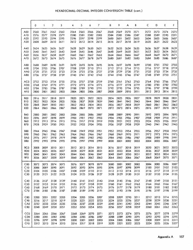
HEXADECIMAL-DECIMAL INTEGER CONVERSION TABLE (cont.)
0 1 2 3 4 5 6 7 8 9 A B C 0 E F
AOO 2560 2561 2562 2563 2564 2565 2566 2567 2568 2569 2570 2571 2572 2573 2574 2575 A10 2576 2577 2578 2579 2580 2581 2582 2583 2584 2585 2586 2587 2588 2589 2590 2591 A20 2592 2593 2594 2595 2596 2597 2598 2599 2600 2601 2602 2603 2604 2605 2606 2607 A30 2608 2609 2610 2611 2612 2613 2614 2615 2616 2617 2618 2619 2620 2621 2622 2623
A40 2624 2625 2626 2627 2628 2629 2630 2631 2632 2633 2634 2635 2636 2637 2638 2639 A50 2640 2641 2642 2643 2644 2645 2646 2647 2648 2649 2650 2651 2652 2653 2654 2655 A60 2656 2657 2658 2659 2660 2661 2662 2663 2664 2665 2666 2667 2668 2669 2670 2671 A70 2672 2673 2674 2675 2676 2677 2678 2679 2680 2681 2682 2683 2684 2685 2686 2687
A80 2688 2689 2690 2691 2692 2693 2694 2695 2696 2697 2698 2699 2700 2701 2702 2703 A90 2704 2705 2706 2707 2708 2709 2710 2711 2712 2713 2714 2715 2716 2717 2718 2719 AAO 2720 2721 2722 2723 2724 2725 2726 2727 2728 2729 2730 2731 2732 2733 2734 2735 ABO 2736 2737 2738 2739 2740 2741 2742 2743 2744 2745 2746 2747 2748 2749 2750 2751
ACO 2752 2753 2754 2755 2756 2757 2758 2759 2760 2761 2762 2763 2764 2765 2766 2767 ADO 2768 2769 2770 2771 2772 2773 2774 2775 2776 2777 2778 2779 2780 2781 2782 2783 AEO 2784 2785 2786 2787 2788 2789 2790 2791 2792 2793 2794 2795 2796 2797 2798 2799 AFO 2800 2801 2802 2803 2804 2805 2806 2807 2808 2809 2810 2811 2812 2813 2814 2815
BOO 2816 2817 2818 2819 2820 2821 2822 2823 2824 2825 2826 2827 2828 2829 2830 2831 BI0 2832 2833 2834 2835 2836 2837 2838 2839 2840 2841 2842 2843 2844 2845 2846 2847 B20 2848 2849 2850 2851 2852 2853 2854 2855 2856 2857 2858 2859 2860 2861 2862 2863 B30 2864 2865 2866 2867 2868 2869 2870 2871 2872 2873 2874 2875 2876 2877 2878 2879
B40 2880 2881 2882 2883 2884 2885 2886 2887 2888 2889 2890 2891 2892 2893 2894 2895 B50 2896 2897 2898 2899 2900 2901 2902 2903 2904 2905 2906 2907 2908 2909 2910 2911 B60 2912 2913 2914 2915 2916 2917 2918 2919 2920 2921 2922 2923 2924 2925 2926 2927 B70 2928 2929 2930 2931 2932 2933 2934 2935 2936 2937 2938 2939 2940 2941 2942 2943
B80 2944 2945 2946 2947 2948 2949 2950 2951 2952 2953 2954 2955 2956 2957 2958 2959 B90 2960 2961 2962 2963 2964 2965 2966 2967 2968 2969 2970 2971 2972 2973 2974 2975 BAO 2976 2977 2978 2979 2980 2981 2982 2983 2984 2985 2986 2987 2988 2989 2990 2991 BSO 2992 2993 2994 2995 2996 2997 2998 2999 3000 3001 3002 3003 3004 3005 3006 3007
BCO 3008 3009 3010 3011 3012 3013 3014 3015 3016 3017 3018 3019 3020 3021 3022 3023 BOO 3024 3025 3026 3027 3028 3029 3030 3031 3032 3033 3034 3035 3036 3037 3038 3039 BEO 3040 3041 3042 3043 3044 3045 3046 3047 3048 3049 3050 3051 3052 3053 3054 3055 BFO 3056 3057 3058 3059 3060 3061 3062 3063 3064 3065 3066 3067 3068 3069 3070 3071
COO 3072 3073 3074 3075 3076 3077 3078 3079 3080 3081 3082 3083 3084 3085 3086 3087 CI0 3088 3089 3090 3091 3092 3093 3094 3095 3096 3097 3098 3099 3100 3101 3102 3103 C20 3104 3105 3106 3107 3108 3109 3110 3111 3112 3113 3114 3115 3116 3117 3118 3119 C30 3120 3121 3122 3123 3124 3125 3126 3127 3128 3129 3130 3131 3132 3133 3134 3135
C40 3136 3137 3138 3139 3140 3141 3142 3143 3144 3145 3146 3147 3148 3149 3150 3151 C50 3152 3153 3154 3155 3156 3t57 3158 3159 3160 3161 3162 3163 3164 3165 3166 3167 C60 3168 3169 3170 3171 3172 3173 3174 3175 3176 3177 3178 3179 3180 3181 3182 3183 C70 3184 3185 3186 3187 3188 3189 3190 3191 3192 3193 3194 3195 3196 3197 3198 3199
C80 3200 3201 3202 3203 3204 3205 3206 3207 3208 3209 3210 3211 3212 3213 3214 3215 C90 3216 3217 3218 3219 3220 3221 3222 3223 3224 3225 3226 3227 3228 3229 3230 3231 CAO 3232 3233 3234 3235 3236 3237 3238 3239 3240 3241 3242 3243 3244 3245 3246 3247 CBO 3248 3249 3250 3251 3252 3253 3254 3255 3256 3257 3258 3259 3260 3261 3262 3263
CCO 3264 3265 3266 3267 3268 3269 3270 3271 3272 3273 3274 3275 3276 3277 3278 3279 COO 3280 3281 3282 3283 3284 3285 3286 3287 3288 3289 3290 3291 3292 3293 3294 3295 CEO 3296 3297 3298 3299 3300 3301 3302 3303 3304 3305 3306 3307 3308 3309 3310 3311 CFO 3312 3313 3314 3315 3316 3317 3318 3319 3320 3321 3322 3323 3324 3325 3326 3327
Appendi x A 157
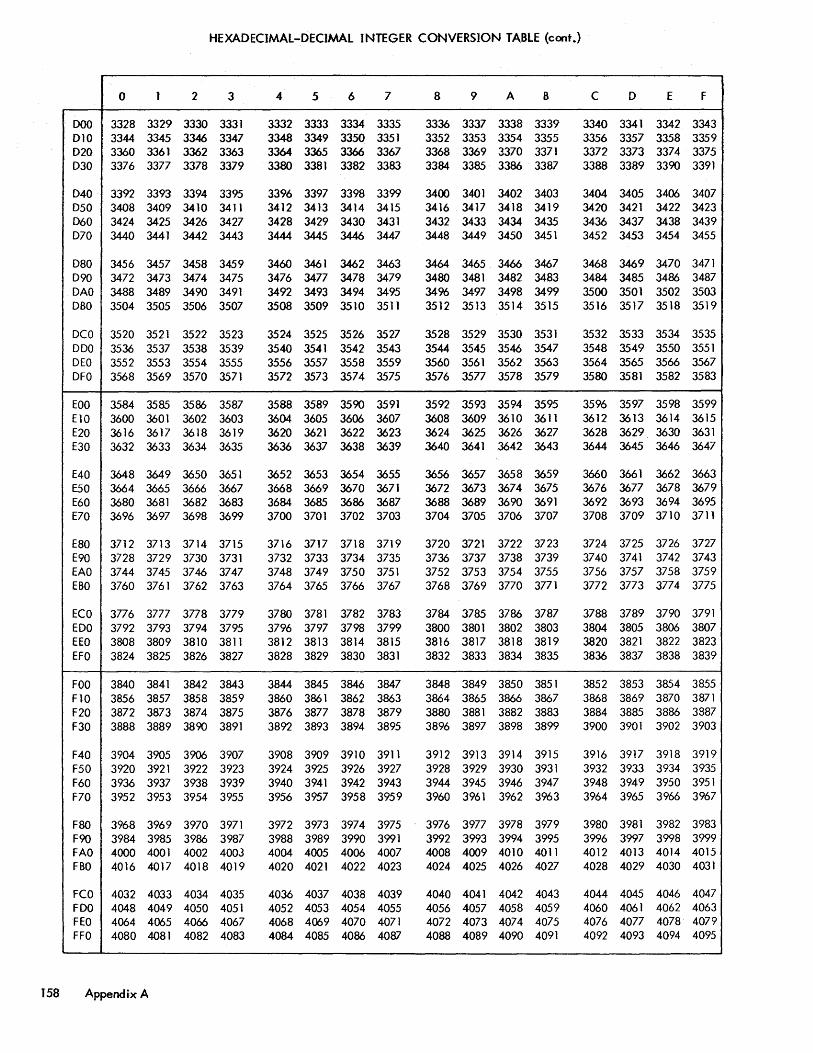
HEXADECIMAL-DECIMAL INTEGER CONVERSION TABLE (cont.)
0 1 2 3 4 5 6 7 8 9 A 8 C D E F
DOO 3328 3329 3330 3331 3332 3333 3334 3335 3336 3337 3338 3339 3340 3341 3342 3343 D10 3344 3345 3346 3347 3348 3349 3350 3351 3352 3353 3354 3355 3356 3357 3358 3359 D2Q 3360 3361 3362 3363 3364 3365 3366 3367 3368 3369 3370 3371 3372 3373 3374 3375 D30 3376 3377 3378 3379 3380 3381 3382 3383 3384 3385 3386 3387 3388 3389 3390 3391
D40 3392 3393 3394 3395 3396 3397 3398 3399 3400 3401 3402 3403 3404 3405 3406 3407 D50 3408 3409 34.10 3411 3412 3413 3414 3415 3416 3417 3418 3419 3420 3421 3422 3423 D60 3424 3425 3426 3427 3428 3429 3430 3431 3432 3433 3434 3435 3436 3437 3438 3439 D70 3440 3441 3442 3443 3444 3445 3446 3447 3448 3449 3450 3451 3452 3453 3454 3455
D80 3456 3457 3458 3459 3460 3461 3462 3463 3464 3465 3466 3467 3468 3469 3470 3471 D90 3472 3473 3474 3475 3476 3477 3478 3479 3480 3481 3482 3483 3484 3485 3486 3487 DAO 3488 3489 3490 3491 3492 3493 3494 3495 3496 3497 3498 3499 3500 3501 3502 3503 D80 3504 3505 3506 3507 3508 3509 3510 3511 3512 3513 3514 3515 3516 3517 3518 3519
DCO 3520 3521 3522 3523 3524 3525 3526 3527 3528 3529 3530 3531 3532 3533 3534 3535 000 3536 3537 3538 3539 3540 3541 3542 3543 3544 3545 3546 3547 3548 3549 3550 3551 DEO 3552 3553 3554 3555 3556 3557 3558 3559 3560 3561 3562 3563 3564 3565 3566 3567 DFO 3568 3569 3570 3571 3572 3573 3574 3575 3576 3577 3578 3579 3580 3581 3582 3583
EOO 3584 3585 3586 3587 3588 3589 3590 3591 3592 3593 3594 3595 3596 3597 3598 3599 ElO 3600 3601 3602 3603 3604 3605 3606 3607 3608 3609 3610 3611 3612 3613 3614 3615 E20 3616 3617 3618 3619 3620 3621 3622 3623 3624 3625 3626 3627 3628 3629 3630 3631 E30 3632 3633 3634 3635 3636 3637 3638 3639 3640 3641 3642 3643 3644 3645 3646 3647
E40 3648 3649 3650 3651 3652 3653 3654 3655 3656 3657 3658 3659 3660 3661 3662 3663 E50 3664 3665 3666 3667 3668 3669 3670 3671 3672 3673 3674 3675 3676 3677 3678 3679 E60 3680 3681 3682 3683 3684 3685 3686 3687 3688 3689 3690 3691 3692 3693 3694 3695 f70 3696 3697 3698 3699 3700 3701 3702 3703 3704 3705 3706 3707 3708 3709 3710 3711
E80 3712 3713 3714 3715 3716 3717 3718 3719 3720 3721 3722 3723 3724 3725 3726 3727 E90 3728 3729 3730 3731 3732 3733 3734 3735 3736 3737 3738 3739 3740 3741 3742 3743 EAO 3744 3745 3746 3747 3748 3749 3750 3751 3752 3753 3754 3755 3756 3757 3758 3759 EBO 3760 3761 3762 3763 3764 3765 3766 3767 3768 3769 3770 3771 3772 3773 3774 3775
ECO 3776 3777 3778 3779 3780 3781 3782 3783 3784 3785 3786 3787 3788 3789 3790 3791 EDO 3792 3793 3794 3795 3796 3797 3798 3799 3800 3801 3802 3803 3804 3805 3806 3807 EEO 3808 3809 3810 3811 3812 3813 3814 3815 3816 3817 3818 3819 3820 3821 3822 3823 EFO 3824 3825 3826 3827 3828 3829 3830 3831 3832 3833 3834 3835 3836 3837 3838 3839
FOO 3840 3841 3842 3843 3844 3845 3846 3847 3848 3849 3850 3851 3852 3853 3854 3855 FlO 3856 3857 3858 3859 3860 3861 3862 3863 3864 3865 3866 3867 3868 3869 3870 3871 F20 3872 3873 3874 3875 3876 3877 3878 3879 3880 3881 3882 3883 3884 3885 3886 3887 F30 3888 3889 3890 3891 3892 3893 3894 3895 3896 3897 3898 3899 3900 3901 3902 3903
F40 3904 3905 3906 3907 3908 3909 3910 3911 3912 3913 3914 3915 3916 3917 3918 3919 F50 3920 3921 3922 3923 3924 3925 3926 3927 3928 3929 3930 3931 3932 3933 3934 3935 F60 3936 3937 3938 3939 3940 3941 3942 3943 3944 3945 3946 3947 3948 3949 3950 3951 F70 3952 3953 3954 3955 3956 3957 3958 3959 3960 3961 3962 3963 3964 3965 3966 3967
F80 3968 3969 3970 3971 3972 3973 3974 3975 3976 3977 3978 3979 3980 3981 3982 3983 F90 3984 3985 3986 3987 3988 3989 3990 3991 3992 3993 3994 3995 3996 3997 3998 3999 FAO 4000 4001 4002 4003 4004 4005 4006 4007 4008 4009 4010 4011 4012 4013 4014 4015 FBO 4016 4017 4018 4019 4020 4021 4022 4023 4024 4025 4026 4027 4028 4029 4030 4031
FCO 4032 4033 4034 4035 4036 4037 4038 4039 4040 4041 4042 4043 4044 4045 4046 4047 FDO 4048 4049 4050 4051 4052 4053 4054 4055 4056 4057 4058 4059 4060 4061 4062 4063 FEO 4064 4065 4066 4067 4068 4069 4070 4071 4072 4073 4074 4075 4076 4077 4078 4079 FFO 4080 4081 4082 4083 4084 4085 4086 4087 4088 4089 4090 4091 4092 4093 4094 4095
158 Appendix A
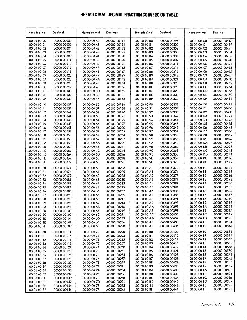
HEXADECIMAL ·DECIMAL FRACTION CONVERSION TABLE
Hexadec imal Decimal Hexadecimal Decimal Hexadecimal Decimal Hexadecimal Decimal
.00000000 .00000 00000 .00000040 .0000000149 .00000080 .00000 00298 .000000 CO .0000000447
.00000001 .00000 00002 .00000041 .0000000151 .00000081 .00000 00300 .000000 C1 .00000 0044 9
.00000002 .00000 00004 .00000042 .0000000153 .00000082 .0000000302 .000000 C2 .00000 0045 1
.00000003 .00000 00006 .00000043 .00000 00155 .00000083 .00000 00305 .000000 C3 .0000000454
.00000004 .0000000009 .00000044 .0000000158 .00000084 .00000 00307 .0000 00 C4 .00000 00456
.00000005 .0000000011 .00000045 .00000 00160 .00000085 .00000 00309 .000000 C5 .00000 00458
.00000006 .00000 0001 3 .00000046 .0000000162 .00000086 .0000000311 .000000 C6 .00000 0046 1
.00000007 .00000 00016 .00000047 .0000000165 .00000087 .00000 00314 .000000 C7 .00000 00463
.00000008 .00000 00018 .00000048 .0000000167 .00000088 .00000 00316 .000000 C8 .00000 00465
.00000009 .00000 00020 .00000049 .0000000169 .00000089 .00000 00318 .000000 C9 .00000 00467
.00 0000 OA .00000 00023 .0000004A .00000 001 72 .0000008A .00000 00321 .000000 CA .00000 00470
.OOOOOOOB .00000 00025 .0000004B .00000 00174 .00 00 0o-8B .00000 00323 .000000 CB .00000 00472
.0000 00 OC .0000000027 .00 00 004C .0000000176 .0000008C .00000 00325 .000000 CC .00000 00474
.OOOOOOOD .00000 00030 .0000004D .00000 00179 .0000008D .00000 00328 .000000 CD .00000 00477
.OOOOOOOE .00000 00032 .00 00 004E .0000000181 .0000008E .00000 00330 .000000 CE .00000 00479
.000000 OF .00000 00034 .0000004F .00000 00183 .0000008F .00000 00332 .000000 CF .00000 00481
.00000010 .00000 00037 .00000050 .00000 00186 .00000090 .00000 00335 .000000 DO .00000 00484
.000000 11 .0000000039 .00000051 .00000 00188 .00000091 .00000 00337 .000000 D1 .00000 00486
.000000 12 .00000 00041 .00000052 .00000 001 90 .00000092 .00000 00339 .000000 D2 .0000000488
.000000 13 .0000000044 .00000053 .00000 001 93 .00000093 .0000000342 .000000 D3 .00000 00491
.000000 14 .00000 00046 .00000054 .00000 00195 .00000094 .00000 00344 .000000 D4 .00000 00493
.000000 15 .00000 00048 .00000055 .0000000197 .00000095 .00000 00346 .000000 D5 .00000 00495
.000000 16 .00000 00051 .00000056 .00000 00200 .00000096 .00000 00349 .000000 D6 .00000 00498
.000000 17 .00000 00053 .00000057 .0000000202 .00000097 .00000 00351 .000000 D7 .00000 00500
.000000 18 .0000000055 .00000058 .00000 00204 .00000098 .00000 00353 .000000 D8 .00000 00502
.000000 19 .00000 00058 .00000059 .00000 00207 .00000099 .00000 00356 .000000 D9 .00000 00505
.000000 lA .00000 00060 .0000005A .00000 00209 .0000009A .0000000358 .000000 DA .00000 00507
.000000 1 B .00000 0006 2 .0000005B .00000 00211 .00 00 009B .00000 00360 .000000 DB .00000 00509
.0000001C .00000 00065 .0000005C .00000 00214 .0000 00 9C .00000 00363 .000000 DC .00000 0051 2
.000000 1 D .00000 00067 .0000005D .00000 00216 .00 00 00 9D .0000000365 .000000 DD .00000 00514
.000000 1 E .00000 0006 9 .0000005E .00000 00218 .0000 00 9E .00000 00367 .000000 DE .00000 00516
.000000 1 F .00000 00072 .00 00 00 5F .00000 00221 .0000009F .00000 00370 .000000 DF .00000 0051 9
.000000 20 .00000 00074 .00000060 .00000 00223 .000000 AO .00000 00372 .000000 EO .00000 00521
.000000 21 .00000 00076 .00000061 .00000 00225 .000000 A1 .00000 00374 .000000 El .00000 00523
.00000022 .00000 00079 .00000062 .00000 00228 .000000 A2 .00000 00377 .000000 E2 .0000000526
.00000023 .00000 00081 .00000063 .00000 00230 .000000 A3 .00000 00379 .000000 E3 .00000 00528
.00000024 .0000000083 .00000064 .00000 00232 .000000 A4 .00000 00381 .000000 E4 .00000 00530
.000000 25 .00000 00086 .00000065 .00000 00235 .000000 A5 .00000 00384 .000000 E5 .00000 00533
.000000 26 .00000 00088 .00000066 .00000 00237 .000000 A6 .00000 00386 .000000 E6 .0000000535
.00000027 .00000 00090 .00000067 .00000 00239 .000000 A7 .00000 00388 .000000 E7 .00000 00537
.00000028 .00000 00093 .00000068 .00000 00242 .000000 A8 .00000 00391 .000000 E8 .00000 00540
.00000029 .00000 00095 .00000069 .00000 00244 .000000 A9 .0000000393 .000000 E9 .00000 00542
.0000002A .00000 00097 .0000006A .00000 00246 .000000 AA .00000 00395 .000000 EA .00000 00544
.0000002B .00000 00100 .0000006B .00000 00249 .00 00 00 AB .00000 00398 .000000 EB .0000000547
.0000002C .0000000102 .0000006C .00000 00251 .000000 AC .00000 00400 .000000 EC .0000000549
.0000002D .00000 00104 .0000006D .00000 00253 .000000 AD .00000 00402 .000000 ED .00000 00551
.0000002E .00000 00107 .0000006E .0000000256 .000000 AE .00000 00405 .000000 EE .00000 00554
.0000002F .0000000109 .0000006F .00000 00258 .000000 AF .0000000407 .000000 EF .00000 00556
.000000 30 .00000 00111 .00000070 .00000 00260 .000000 BO .00000 00409 .000000 FO .00000 00558
.000000 31 .00000 00114 .00000071 .00000 00263 .000000 B1 .00000 0041 2 .000000 Fl .00000 00561
.00000032 .0000000116 .00000072 .0000000265 .000000 B2 .00000 00414 .000000 F2 .00000 00563
.00000033 .00000 00118 .00000073 .00000 00267 .000000 B3 .00000 00416 .000000 F3 .00000 00565
.00000034 .00000 00121 .00000074 .00000 00270 .000000 B4 .00000 0041 9 .000000 F4 .00000 00568
.00000035 .00000 001 23 .00000075 .00000 00272 .000000 B5 .00000 00421 .000000 F5 .00000 00570
.00000036 .00000 001 25 .00000076 .00000 00274 .000000 B6 .00000 00423 .000000 F6 .00000 00572
.00000037 .00000 00 128 .00000077 .00000 00277 .000000 B7 .00000 00426 .000000 F7 .00000 00575
.00000038 .00000 00130 .00000078 .00000 00279 .0000 00 B8 .0000000428 .00 0000 F8 .00000 00577
.00000039 .0000000132 .00000079 .00000 00281 .000000 B9 .00000 00430 .000000 F9 .00000 00579
.0000 00 3A .00000 00135 .00 00 00 7A .00000 00284 .000000 BA .00000 00433 .000000 FA .00000 00582
.0000003B . 00000 001 37 .00 00 00 7B .00000 00286 .000000 BB .00000 00435 .00 00 00 FB .00000 00584
.0000003C .00000 00139 .00 00 00 7C .00000 00288 .000000 BC .00000 00437 .000000 Fe .00000 00586
.00 00 00 3D .0000000142 .00 00 00 7D .00000 00 291 .000000 BD .00000 00440 .000000 FD .00000 00589
.0000003E .00000 00144 .00 00 00 7E .0000000293 .00 00 00 BE .00000 0044 2 .000000 FE .00000 00591
.0000003F .00000 00146 .00 00 00 7F .00000 00295 .000000 BF .00000 00444 .000000 FF .00000 00593
Appendix A 159
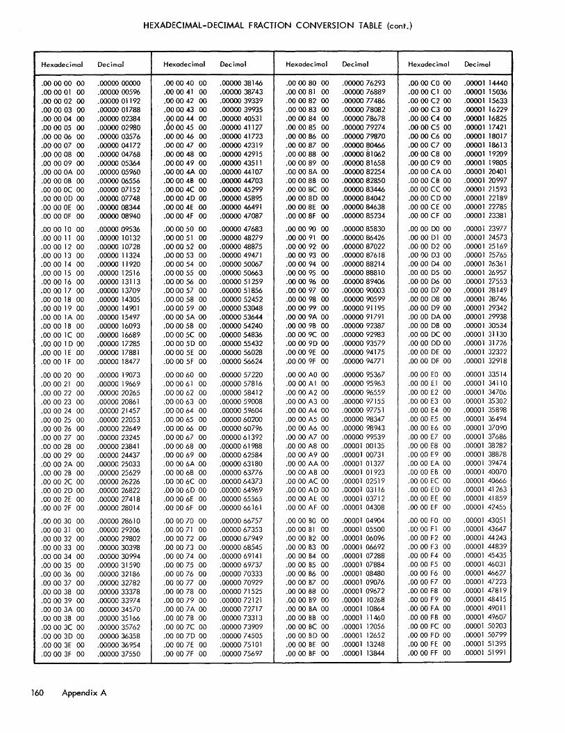
HEXADECIMAL-DECIMAL FRACTION CONVERSION TABLE (cont.)
Hexadecimal Decimal Hexadecimal Decimal Hexadecimal Decimal Hexadecimal Decimal
.00 00 00 00 .00000 00000 .00 00 40 00 .00000 38146 .000080 00 .00000 76293 .00 00 CO 00 .00001 14440
.00 00 01 00 .00000 00596 .00 00 41 00 .00000 38743 .00 00 81 00 .00000 76889 .0000 C1 00 .00001 15036
.000002 00 .00000 01192 .00 0042 00 .00000 39339 .000082 00 .00000 77486 .0000 C2 00 .00001 15633
.000003 00 .00000 01788 .000043 00 .00000 39935 .00 0083 00 .00000 78082 .0000 C3 00 .00001 16229
.00 00 04 00 .00000 02384 .000044 00 .00000 40531 .00 00 84 00 .00000 78678 .0000 C4 00 .00001 16825
.000005 00 .00000 02980 .000045 00 .00000 41127 .00 00 85 00 .00000 79274 .00 00 C5 00 .00001 17421
.00 00 06 00 .00000 03576 .000046 00 .00000 41723 .000086 00 .00000 79870 .00 00 C6 00 .00001 18017
.000007 00 .00000 04172 .000047 00 .00000 42319 .00 0087 00 .00000 80466 .00 00 C7 00 .00001 18613
.000008 00 .00000 04768 .00 0048 00 .00000 42915 .000088 00 .00000 81062 .00 00 C8 00 .00001 19209
.00 00 09 00 .00000 05364 .000049 00 .00000 43511 .00 00 89 00 .00000 81658 .0000 C9 00 .00001 19805
.0000 OA 00 · 00000 05960 .00004A 00 .00000 44107 .00008A 00 .00000 82254 .0000 CA 00 .00001 20401
.0000 DB 00 · 00000 06556 .00 00 4B 00 .00000 44703 .00008B 00 .00000 82850 .00 00 CB 00 .00001 20997
.00 00 DC 00 .00000 07152 .0000 4C 00 .00000 45299 .00008C 00 .00000 83446 .0000 CC 00 .00001 21593
.OOOOOD 00 .00000 07748 .00004D 00 .00000 45895 .00008D 00 .00000 84042 .0000 CD 00 .00001 22189
.0000 DE 00 .00000 08344 .0000 4E 00 .00000 46491 .00 00 8E 00 .00000 84638 .0000 CE 00 .00001 22785
.0000 OF 00 .00000 08940 .00 00 4F 00 .00000 47087 .00008F 00 .00000 85234 .0000 CF 00 .00001 23381
.000010 00 .00000 09536 .00 0050 00 .00000 47683 .000090 00 .00000 85830 .0000 DO 00 .0000i 23977
.000011 00 .00000 10132 .00 0051 00 .00000 48279 .00 0091 00 .00000 86426 .0000 DIDO .00001 24573
.00 00 12 00 .00000 10728 .00 0052 00 .00000 48875 .00 00 92 00 .00000 87022 .0000 D2 00 .00001 25169
.0000 13 00 .00000 11324 .000053 00 .0000049471 .00 0093 00 .0000087618 .0000 D3 00 .00001 25765
.0000 14 00 .00000 1 1920 .00 0054 00 .00000 50067 .00 0094 00 .00000 88214 .0000 D4 00 .00001 26361
.0000 15 00 .00000 12516 .000055 00 .00000 50663 .000095 00 .00000 88810 .0000 D5 00 .00001 26957
.000016 00 .00000 13113 .000056 00 .00000 51259 .00 00 96 00 .00000 89406 .0000 D6 00 .00001 27553
.000017 00 .00000 13709 .000057 00 .00000 51856 .00 0097 00 .00000 90003 .00 00 D7 00 .00001 28149
.000018 00 · 00000 14305 .000058 00 .00000 52452 .000098 00 .00000 90599 .00 00 D8 00 .00001 28746
.00 00 19 00 .00000 14901 .00 0059 00 .00000 53048 .000099 00 .00000 91195 .0000 D9 00 .00001 29342
.0000 1A 00 .00000 15497 .00 00 5A 00 .00000 53644 .00 009A 00 .00000 91791 .00 00 DA 00 .00001 29938
.0000 1 B 00 .00000 16093 .00005B 00 .00000 54240 .00 00 98 00 .00000 92387 .0000 DB 00 .00001 30534
.0000 lC 00 .00000 16689 .00005C 00 .00000 54836 .00 00 9C 00 .00000 92983 .0000 DC 00 .00001 31130
.0000 1 D 00 .00000 17285 .00005D 00 .00000 55432 .00 00 9D 00 .00000 93579 .0000 DD 00 .00001 31726
.00 00 1 E 00 .00000 17881 .00 00 5E 00 .00000 56028 .0000 9E 00 .00000 94175 .00 00 DE 00 .00001 32322
.0000 1 F 00 .00000 18477 .00005F 00 .00000 56624 .00009F 00 .00000 94771 .0000 DF 00 .00001 32918
.000020 00 .00000 19073 .00 00 60 00 .00000 57220 .0000 AD 00 .00000 95367 .0000 EO 00 .00001 33514
.000021 00 .00000 19669 .000061 00 .00000 57816 .0000 Al 00 .00000 95963 .OOOOEI 00 .0000 1 34110
.00 0022 00 .00000 20265 .00 0062 00 .00000 58412 .0000 A2 00 .00000 96559 .0000 E2 00 .00001 34706
.000023 00 .00000 20861 .000063 00 .00000 59008 .00 00 A3 00 .00000 97155 .0000 E3 00 .00001 35302
.000024 00 .00000 21457 .000064 00 .00000 59604 .0000 A4 00 .00000 97751 .0000 E4 00 .00001 35898
.000025 00 .00000 22053 .00 00 65 00 .0000060200 .0000 A5 00 .00000 98347 .0000 E5 00 .00001 36494
.000026 00 .00000 22649 .000066 00 .00000 60796 .0000 A6 00 .00000 98943 .0000 E6 00 .00001 37090
.0000 27 00 .00000 23245 .00 00 67 00 .00000 61392 .0000 A7 00 .00000 99539 .0000 E7 00 .00001 37686
.0000 28 00 .0000023841 .000068 00 .00000 61 988 .0000 A8 00 .00001 00135 .0000 E8 00 .00001 38282
.000029 00 .00000 24437 .000069 00 .0000062584 .0000 A9 00 .00001 00731 .0000 E9 00 .00001 38878
.00 00 2A 00 .00000 25033 .00 00 6A 00 .00000 63180 .0000 AA 00 .00001 01327 .0000 EA 00 .00001 39474
.00 00 2B 00 .00000 25629 .00006B 00 .0000063776 .0000 AB 00 .00001 01923 .0000 EB 00 .00001 40070
.00002C 00 .00000 26226 .00006C 00 .00000 64373 .0000 AC 00 .00001 02519 .00 00 EC 00 .00001 40666
.0000 2D 00 .00000 26822 .00006D 00 .00000 64969 .0000 AD 00 .00001 03116 .0000 ED 00 .00001 41263
.0000 2E 00 .00000 27418 .00006E 00 .00000 65565 .0000 AE 00 .00001 03712 .00 00 EE 00 .00001 41859
.00 00 2F 00 .00000 28014 .0000 6F 00 .00000 66161 .00 00 AF 00 .00001 04308 .00 00 Ef 00 .00001 42455
.000030 00 .00000 2861 a .000070 00 .00000 66757 .0000 BO 00 .00001 04904 .0000 FO 00 .00001 43051
.000031 00 .00000 29206 .000071 00 .00000 67353 .OOOOBI 00 .00001 05500 .00 00 Fl 00 .00001 43647
.000032 00 .00000 29802 .0000 72 00 .00000 67949 .0000 B2 00 .00001 06096 .0000 F2 00 .00001 44243
.000033 00 .00000 30398 .000073 00 .00000 68545 .0000 B3 00 .0000 1 06692 .0000 F3 00 .00001 44839
.000034 00 .0000030994 .00 00 74 00 .00000 69141 .0000 B4 00 .00001 07288 .00 00 F4 00 .0000 1 45435
.000035 00 .0000031590 .000075 00 .00000 69737 .0000 B5 00 .00001 07884 .0000 F5 00 .0000 I 46031
.000036 00 .0000032186 .00 00 76 00 .0000070333 .0000 B6 00 .00001 08480 .00 00 F6 00 .00001 46627
.00 0037 00 .00000 32782 .00 00 77 00 .00000 70929 .0000 B7 00 .00001 09076 .00 00 F7 00 .00001 47223
.000038 00 .0000033378 .000078 00 .0000071525 .0000 B8 00 .0000 1 09672 .00 00 F8 00 .00001 47819
.00 00 39 00 .0000033974 .000079 00 .0000072121 .00 00 B9 00 .00001 10268 .0000 F9 00 .00001 48415
.00003A 00 .00000 34570 .00007A 00 .00000 72717 .0000 BA 00 .0000 1 10864 .0000 FA 00 .00001 49011
.00003B 00 .00000 35166 .00007B 00 .00000 73313 .00 00 BB 00 .0000 1 11460 .0000 FB 00 .00001 49607
.00003C 00 .00000 35762 .00 00 7C 00 .00000 73909 .00 00 BC 00 .00001 12056 .0000 FC 00 .00001 50203
.0000 3D 00 .00000 36358 .00 00 7D 00 .00000 74505 .0000 BD 00 .00001 12652 .00 00 FD 00 .00001 50799
.00 00 3E 00 .0000036954 .00007E 00 .00000 75101 .00 00 BE 00 .00001 13248 .00 00 FE 00 .00001 51395
.00003F 00 .00000 37550 .00 00 7F 00 .00000 75697 .00 00 BF 00 .00001 13844 .00 00 FF 00 .00001 51991
160 Appendix A
HEXADECIMAL-DECIMAL FRACTION CONVERSION TABLE (cont.)
Hexadecimal Decimal Hexadecimal Decimal Hexadecimal Decimal Hexadecimal Decimal
.0000 0000 .00000 00000 .0040 0000 .00097 65625 .0080 0000 .00195 31250 .00 CO 0000 .00292 96875
.0001 0000 .00001 52587 .0041 0001) .00099 18212 .0081 0000 .00196 83837 .00 C1 0000 .00294 49462
.0002 0000 .00003 05175 .0042 0000 .00100 70800 .0082 0000 .00198 36425 .00 C2 0000 .00296 02050
.0003 0000 .00004 57763 .0043 0000 .00102 23388 .0083 0000 .0019989013 .00 C3 0000 .00297 54638
.0004 0000 .00006 10351 .0044 0000 .00103 75976 .0084 0000 .00201 41601 .00 C4 0000 .00299 07226
.0005 0000 .00007 62939 .0045 0000 .00105 28564 .0085 0000 .00202 94189 .00 C5 0000 .0030059814
.0006 0000 .00009 15527 .0046 0000 .00106 81152 .0086 0000 .00204 46777 .00 C6 0000 .00302 12402
.0007 0000 .0001068115 .0047 0000 .00108 33740 .0087 0000 .00205 99365 .00 C7 0000 .00303 64990
.00 08 0000 .00012 20703 .0048 0000 .0010986328 .0088 0000 .0020751953 .00 C8 0000 .00305 17578
.0009 0000 .0001373291 .0049 0000 .00111 38916 .0089 00 00 .00209 04541 .00 C9 0000 .00306 70166
.OOOA 0000 .00015 25878 .004A 0000 .0011291503 .008A 0000 .0021057128 .00 CA 0000 .00308 22753
.OOOB 0000 .00016 78466 .004B 0000 .00114 44091 .008B 0000 .0021209716 .00 CB 0000 .00309 75341
.OOOC 0000 .0001831054 .004C 0000 .00115 96679 .008C 0000 .00213 62304 .00 CC 0000 .00311 27929
.00 OD 0000 .0001983642 .004D 0000 .0011749267 .008D 00 00 .00215 14892 .00 CD 0000 .0031280517
.OOOE 0000 .00021 36230 .004E 0000 .0011901855 .008E 00 00 .0021667480 .00 CE 0000 .0031433105
.00 OF 0000 .00022 88818 .004F 0000 .0012054443 .008F 0000 .00218 20068 .00 CF 0000 .00315 85693
.00 10 0000 .0002441406 .0050 0000 .00122 07031 .0090 0000 .0021972656 .00 DO 0000 .00317 38281
.00 11 0000 .00025 93994 .0051 0000 .00123 59619 .0091 0000 .00221 25244 .00 D1 0000 .00318 90869
.00 12 0000 .00027 46582 .0052 0000 .00125 12207 .0092 0000 .00222 77832 .00 D2 0000 .0032043457
.00 13 0000 .00028 99169 .0053 0000 .00126 64794 .0093 0000 .0022430419 .00 D3 0000 .00321 96044
.00 14 0000 .00030 51757 .0054 0000 .001 28 17382 .0094 0000 .00225 83007 .00 D4 0000 .00323 48632
.00 15 0000 .00032 04345 .0055 0000 .0012969970 .0095 0000 .00227 35595 .00 D5 0000 .00325 01220
.00 16 0000 .00033 56933 .0056 0000 .00131 22558 .0096 0000 .00228 88183 .00 D6 0000 .00326 53808
.00 17 0000 .00035 09521 .0057 0000 .0013275146 .0097 0000 .00230 40771 .00 D7 0000 .00328 06396
.00 18 0000 .00036 62109 .0058 0000 .00134 27734 .0098 0000 .00231 93359 .00 D8 0000 .00329 58984
.00 19 0000 .00038 14697 .0059 0000 .00135 80322 .0099 0000 .00233 45947 .00 D9 0000 .00331 11572
.00 lA 0000 .00039 67285 .005A 0000 .00137 32910 .009A 00 00 .00234 98535 .00 DA 00 00 .00332 64160
.00 1 B 0000 .00041 19873 .005B 0000 .0013885498 .009B 00 00 .00236 51123 .00 DB 0000 .00334 16748
.00 1C 0000 .00042 72460 .005C 0000 .00140 38085 .009C 0000 .00238 03710 .00 DC 0000 .00335 69335
.00 1 D 0000 .00044 25048 .00 5D 0000 .00141 90673 .00 9D 0000 .0023956298 .00 DD 00 00 .00337 21923
.00 1 E 0000 .00045 77636 .005E 0000 .00143 43261 .009E 0000 .00241 08886 .00 DE 0000 .00338 74511
.00 1 F 0000 .00047 30224 .005F 0000 .00144 95849 .009F 0000 .0024261474 .00 DF 0000 .00340 27099
.0020 0000 .0004a 82812 .0060 0000 .00146 48437 .00 AO 0000 .00244 14062 .00 EO 0000 .00341 79687
.0021 0000 .00050 35400 .0061 0000 .00148 01025 .00 A1 0000 .00245 66650 .00 El 0000 .00343 32275
.0022 0000 .00051 87988 .0062 0000 .0014953613 .00 A2 0000 .00247 19238 .00 E2 0000 .00344 84863
.0023 0000 .00053 40576 .0063 0000 .00151 06201 .00 A3 0000 .00248 71826 .00 E3 0000 .00346 37451
.00 24 0000 .00054 93164 .0064 0000 .00152 58789 .00 A4 0000 .00250 24414 .00 E4 0000 .00347 90039
.0025 0000 .00056 45751 .0065 0000 .00154 11376 .00 A5 0000 .00251 77001 .00 E5 0000 .00349 42626
.0026 0000 .00057 98339 .0066 0000 .00155 63964 .00 A6 00 00 .00253 29589 .00 E6 0000 .00350 95214
.00 27 0000 .00059 50927 .0067 0000 .00157 16552 .00 A7 0000 .0025482177 .00 E7 0000 .00352 47802
.00 28 00 00 .00061 03515 .0068 0000 .0015869140 .00 A8 0000 .00256 34765 .00 E8 0000 .00354 00390
.00 29 0000 .00062 56103 .0069 0000 .00160 21728 .00 A9 00 00 .00257 87353 .00 E9 0000 .00355 52978
.00 2A 0000 .00064 08691 .006A 0000 .00161 74316 .00 AA 00 00 .00259 39941 .00 EA 0000 .00357 05566
.002B 0000 .00065 61279 .006B 0000 .00163 26904 .00 AB 0000 .00260 92529 .00 EB 0000 .00358 58154
.002C 0000 .00067 13867 .006C 0000 .0016479492 .00 AC 0000 .00262 45117 .00 EC 0000 .00360 10742
.00 2D 0000 .00068 66455 .006D 0000 .00166 32080 .00 AD 00 00 .00263 97705 .00 ED 0000 .00361 63330
.002E 0000 .00070 19042 .006E 0000 .00167 84667 .00 AE 00 00 .00265 50292 .00 EE 0000 .00363 15917
.002F 0000 .00071 71630 .006F 0000 .00169 37255 .00 AF 0000 .00267 02880 .00 EF 0000 .00364 68505
.0030 0000 .00073 24218 .0070 0000 .00170 89843 .00 BO 0000 .00268 55468 .00 FO 0000 .00366 21093
.0031 0000 .00074 76806 .0071 0000 .00172 42431 .00 B1 0000 .00270 08056 .00 Fl 0000 .00367 73681
.0032 0000 .00076 29394 .0072 0000 .00173 95019 .00 B2 0000 .00271 60644 .00 F2 0000 .00369 26269
.0033 0000 .0007781982 .0073 0000 .00175 47607 .00 B3 0000 .00273 13232 .00 F3 0000 .00370 78857
.0034 0000 .00079 34570 .0074 0000 .00177 00195 .00 B4 0000 .0027465820 .00 F4 0000 .00372 31445
.0035 0000 .00080 87158 .0075 0000 .00178 52783 .00 B5 0000 .00276 18408 .00 F5 0000 .00373 84033
.0036 0000 .00082 39746 .0076 0000 .00180 05371 .00 B6 0000 .00277 70996 .00 F6 0000 .00375 36621
.0037 0000 .00083 92333 .0077 0000 .00181 57958 .00 B7 0000 .00279 23583 .00 F7 0000 .00376 89208
.0038 0000 .00085 44921 .001'8 0000 .00183 10546 .00 B8 0000 .00280 76171 .00 F8 0000 .00378 41796
.0039 0000 .00086 97509 .0079 0000 .0018463134 .00 B9 0000 .00282 28759 .00 F9 0000 .00379 94384
.003A 0000 .00088 50097 .007A 0000 .00186 15722 .00 BA 0000 .00283 81347 .00 FA 0000 .00381 46972
.003B 0000 .0009002685 .007B 0000 .00187 68310 .00 BB 0000 .00285 33935 .00 FB 0000 .00382 99560
.003C 0000 .00091 55273 .007C 0000 .00189 20898 .00 BC 0000 .00286 86523 .00 FC 0000 .0038452148
.00 3D 0000 .00093 07861 .007D 0000 .001 90 73486 .00 BD 0000 .00288 39111 .00 FD 0000 .00386 04736
.003E 0000 .00094 60449 .007E 0000 .00192 26074 .00 BE 00 00 .00289 91699 .00 FE 0000 .00387 57324
.003F 0000 .00096 13037 .007F 0000 .001 93 78662 .00 BF 0000 .00291 44287 .00 FF 0000 .00389 09912
Appendix A 161
HEXADECIMAL-DECIMAL FRACTION CONVERSION TABLE (cont.)
Hexodecimal Decimal Hexadecimal Decimal Hexadecimal Decimal Hexodecimal Decimal
.00 00 00 00 .00000 00000 .40 000000 .25000 00000 .80 00 00 00 .50000 00000 .CO 000000 .75000 00000
.01 000000 .00390 62500 .41 000000 .25390 62500 .81 00 00 00 .50390 62500 .Cl 00 00 00 .75390 62500
.02 000000 .00781 25000 .42 00 00 00 .25781 25000 .82 000000 .50781 25000 .C2 000000 .75781 25000
.03 000000 .01171 87500 .43 000000 .26171 87500 .83 00 00 00 .51171 87500 .C3 00 00 00 .76171 87500
.04 00 0000 .0156250000 .44 000000 .26562 50000 .84 00 00 00 .5156250000 .C4 00 00 00 .7656250000
.05 00 00 00 .01953 12500 .45 000000 .26953 12500 .85 00 00 00 .51953 12500 .C5 000000 .76953 12500
.06 000000 .02343 75000 .46 000000 .27343 75000 .86 00 00 00 .52343 75000 .C6 000000 .77343 75000
.07 000000 .02734 37500 .47 000000 .27734 37500 .87 000000 .52734 37500 .C7 00 00 00 .77734 37500
.08 000000 .03125 00000 .48 000000 .281 25 00000 .88 000000 .53125 00000 .C8 00 00 00 .78125 00000
.09 000000 .0351562500 049 000000 .28515 62500 .89 000000 .53515 62500 .C9 000000 .78515 62500
.OA 000000 .03906 25000 AA 000000 .28906 25000 .8A 00 00 00 .53906 25000 .CA 00 00 00 .78906 25000
.OB 000000 .04296 87500 AB 000000 .29296 87500 .8B 000000 .5429687500 .CB 000000 .79296 87500
.OC 000000 .04687 50000 .4C 000000 .29687 50000 .8C 000000 .54687 50000 .CC 00 00 00 .79687 50000
.00 000000 .05078 12500 .40 00 00 00 .30078 12500 .80 000000 .55078 12500 .CD 00 00 00 .80078 1 2500
.OE 000000 .05468 75000 .4E 000000 .30468 75000 :8E 00 00 00 .55468 75000 .CE 000000 .80468 75000
.OF 000000 .05859 37500 .4F 000000 .30859 37500 .8F 00 00 00 .5585937500 .CF 000000 .80859 37500
.10 000000 .0625000000 .50 000000 .3125000000 .90 000000 .56250 00000 .00 000000 .8125000000
.11 000000 .06640 62500 .51 000000 .31640 62500 .91 000000 .56640 62500 .01 000000 .81640 62500
.12 000000 .07031 25000 .52 000000 .32031 25000 .92 000000 .57031 25000 .02 000000 .82031 25000
.13 000000 .07421 87500 .53 000000 .32421 87500 .93 000000 .57421 87500 .03 000000 .82421 87500
.14 000000 .07812 50000 .54 000000 .3281250000 .94 000000 .57812 50000 .04 000000 .8281 2 50000
.15 000000 .08203 12500 .55 000000 .33203 12500 .95 000000 .58203 12500 .05 000000 .83203 12500
.16 000000 .08593 75000 .56 000000 .33593 75000 .96 000000 .58593 75000 .06 000000 .8359375000
.17 000000 .08984 37500 .57 000000 .33984 37500 .97 000000 .58984 37500 .07 000000 .83984 37500
.18 000000 .09375 00000 .58 000000 .34375 00000 .98 000000 .59375 00000 .08 00 00 00 .84375 00000
.19 00 00 00 .09765 62500 .59 000000 .34765 62500 .99 00 00 00 .59765 62500 .09 000000 .84765 62500
.IA 000000 · 10 156 25000 .5A 000000 .35156 25000 .9A 000000 .60156 25000 .DA 00 00 00 .85156 25000
.IB 000000 .10546 87500 .5B 000000 .35546 87500 .9B 000000 .60546 87500 .DB 000000 .85546 87500
.1C 000000 · 10937 50000 .5C 000000 .35937 50000 .9C 00 00 00 .60937 50000 .DC 000000 .85937 50000
.ID 000000 .11328 12500 .50 000000 .36328 12500 .90 000000 .61 328 12500 .DD 000000 .86328 12500
.1 E 000000 .11718 75000 .5E 000000 .36718 75000 .9E 000000 .6171875000 .DE 000000 .8671875000
.IF 000000 · 1 21 09 37500 .5F 00 00 00 .3710937500 .9F 000000 .6210937500 .DF 000000 .8710937500
.20 000000 · 1 2500 00000 .60 000000 .3750000000 .AO 000000 .62500 00000 .EO 000000 .87500 00000
.21 000000 · I 2890 62500 .61 000000 .37890 62500 .Al 000000 .62890 62500 .El 000000 .87890 62500
.22 000000 .1328125000 .62 000000 .38281 25000 .A2 000000 .63281 25000 .E2 000000 .88281 25000
.23 000000 .13671 87500 .63 000000 .38671 87500 .A3 000000 .63671 87500 .E3 000000 :88671 87500
.24 000000 .1406250000 .64 000000 .39062 50000 .A4 000000 .64062 50000 .E4 000000 .89062 50000
.25 000000 · 14453 I 2500 .65 000000 .39453 12500 .A5 00 00 00 .64453 1 2500 .E5 000000 .89453 12500
.26 000000 .1484375000 .66 000000 .3984375000 .A6 000000 .6484375000 .E6 000000 .89843 75000
.27 00 00 00 .15234 37500 .67 000000 .40234 37500 .A7 000000 .65234 37500 .E7 000000 .9023437500
.28 000000 .15625 00000 .68 000000 .406 25 00000 .A8 000000 .65625 00000 .E8 000000 .90625 00000
.29 000000 .16015 62500 .69 000000 .410 15 62500 .A9 000000 .66015 62500 .E9 000000 .9101562500
.2A 000000 .16406 25000 .6A 000000 .41406 25000 .AA 00 00 00 .66406 25000 .EA 000000 .91406 25000
.2B 000000 .167-1687500 .6B 000000 .41796 87500 .AB 000000 .66796 87500 .EB 000000 .9179687500
.2C 000000 .17187 50000 .6C 000000 .42187 50000 .AC 000000 .67 I 87 50000 .EC 000000 .92187 50000
.20 000000 .17578 12500 .60 000000 .42578 12500 .AO 00 0000 .67578 12500 .ED 00 00 00 .92578 1 2500
.2E 000000 · 17968 75000 .6E 000000 .42968 75000 .AE 000000 .67968 75000 .EE 00 00 00 .92968 75000
.2F 000000 · I 8359 37500 .6F 0000 00 .43359 37500 .AF 000000 .68359 37500 .EF 000000 .93359 37500
.30 000000 .18750 00000 .70 000000 .43750 00000 .BO 000000 .68750 00000 .FO 000000 .93750 00000
.31 00 00 00 .1914062500 .71 000000 .44140 62500 .Bl 00 0000 .6914062500 .FI 000000 .9414062500
.32 000000 .19531 25000 .72 000000 .44531 25000 .B2 000000 .69531 25000 .F2 000000 .9453 I 25000
.33 000000 .19921 87500 .73 0000 00 .44921 87500 .B3 00 00 00 .69921 87500 .F3 00 0000 .94921 87500
.34 000000 .2031 2 50000 .74 000000 .453 I 2 50000 .84 000000 .7031 2 50000 .F4 000000 .95312 50000
.35 000000 .20703 12500 .75 00 00 00 .45703 12500 .B5 000000 .70703 12500 .F5 000000 .95703 I 2500
.36 000000 .21093 75000 .76 000000 .46093 75000 .86 000000 .7 1093 75000 .F6 000000 .96093 75000
.37 000000 .21484 37500 .77 000000 .46484 37500 .B7 000000 .71484 37500 .F7 000000 .96484 37500
.38 000000 .21875 00000 .78 000000 .46875 00000 .B8 000000 .71875 00000 .F8 000000 .96875 00000
.39 000000 .22265 62500 .79 000000 .47265 62500 .B9 000000 .72265 62500 .F9 000000 .97265 62500
.3A 000000 .22656 25000 .7A 00 0000 .47656 25000 .BA 00 00 00 .72656 25000 .FA 000000 .97656 25000
.3B 000000 .23046 87500 .7B 000000 .48046 87500 .BB 00 00 00 .73046 87500 .FB 000000 .98046 87500
.3C 000000 .23437 50000 .7C 000000 .48437 50000 .BC 000000 .73437 50000 .FC 000000 .98437 50000
.30 000000 .23828 12500 .70 0000 00 .48828 12500 .BD 000000 .73828 12500 .FD 000000 .98828 I 2500
.3E 000000 .24218 75000 .7E 000000 .49218 75000 .BE 000000 .74218 75000 .FE 000000 .99218 75000
.3F 000000 .2460937500 .7F 000000 .49609 37500 .BF 000000 .74609 37500 .FF 000000 .9960937500
162 Appendix A
TABLE OF POWERS OF TWO MATHEMATICAL CONSTANTS
L.!!.i:. 1 0 1.0 2 1 0.5 4 2 0.25 8 3 0.125
16 4 0.062 5 32 5 0.031 25 64 6 0.015 625
128 7 0.007 812 5
256 8 0.003 906 25 512 9 0.001 953 125
1 024 10 0.000 976 562 5 2 048 11 0.000 488 281 25
4096 12 0.000 244 140 625 8 192 13 0.000 122 070 312 5
16 384 14 0.000 061 035 156 25 32 768 15 0.000 030 517 578 125
65 536 16 0.000 015 258 789 062 5 131 072 17 0.000 007 629 394 531 25 262 144 18 0.000 003 814 697 265 625 524 288 19 0.000 001 907 348 632 812 5
1 048 576 20 0.000 000 953 674 316 406 25 2 097 152 21 0.000 000 476 837 158 203 125 4 194 304 22 0.000 000 238 418 579 101 562 5 8 388 608 23 0.000 000 119 209 289 550 781 25
16 777 216 24 0.000 000 059 604 644 775 390 625 33 554 432 25 0.000 000 029 802 322 387 695 312 5 67 108 864 26 0.000 000 014 901 161 193 847 656 25
134 217 728 27 0.000 000 007 450 580 596 923 828 125
268 435 456 28 0.000 000 003 725 290 298 461 914 062 5 536 870 912 29 0.000 000 001 862 645 149 230 957 031 25
1 073 741 824 30 0.000 000 000 931 322 574 615 478 515 625 2 147 483 648 31 0.000 000 000 465 661 287 307 739 257 812 5
4 294 967 296 32 0.000 000 000 232 830 643 653 869 628 906 25 8 589 934 592 33 0.000 000 000 116 415 321 826 934 814 453 125
17 179 869 184 34 0.000 000 000 058 207 660 913 467 407 226 562 5 34 359 738 368 35 0.000 000 000 029 103 830 456 733 703 613 281 25
68 719 476 736 36 0.000 000 000 014 551 915 228 366 851 806 640 625 137 438 953 472 37 0.000 000 000 007 275 957 614 183 425 903 320 312 5 274 877 906 944 38 0.000 000 000 003 637 978 807 091 712 951 660 156 25 549 755 813 888 39 0.000 000 000 001 818 989 403 545 856 475 830 078 125
1 099 511 627 776 40 0.000 000 000 000 909 494 701 772 928 237 915 039 062 5 2 199 023 255 552 41 0.000 000 000 000 454 747 350 886 464 118 957 519 531 25 4 398 046 511 104 42 0.000 000 000 000 227 373 675 443 232 059 478 759 765 625 8 796 093 022 208 43 0.000 000 000 000 113 686 837 721 616 029 739 379 882 812 5
17 592 186 044 416 44 0.000 000 000 000 056 843 418 860 808 014 869 689 941 406 25 35 184 372 088 832 45 0.000 000 000 000 028 421 709 430 404 007 434 844 970 703 125 70 368 744 177 664 46 0.000 000 000 000 014 210 854 715 202 003 717 422 485 351 562 5
140 737 488 355 328 47 0.000 000 000 000 007 105 427 357 601 001 858 711 242 675 781 25
281 474 976 710 656 48 0.000 000 000 000 003 552 713 678 800 500 929 355 621 337 890 625 562 949 953 421 312 49 0.000 000 000 000 001 776 356 839 400 250 464 677 810 668945 312 5
1 125 899 906 842 624 50 0.000 000 000 000 000 888 178 419 700 125 232 338 905 334 472 656 25 2 251 799 813 685 248 51 0.000 000 000 000 000 444 089 209 850 062 616 169 452 667236 328 125
Constant
11'-1
oJ;
Inn
e -1
e
..Je loglOe
log2 e
'i
In'i
.J2
In2
log10 2
.JTO In 10
4 503 599 627 370 496 52 0.000 000 000 000 000 222 044 604 925 031 308 084 726 333 618 164 062 5 9 007 199 254 740 992 53 0.000 000 000 000 000 111 022 302 462 515 654 042 363 166 809 082 031 25
18 014 398 509 481 984 54 0.000 000 000 000 000 055 511 151 231 257 827 021 181 583404 541 015 625 36 028 797 018 963 968 55 0.000 000 000 000 000 027 755 575 615 628 913 510 590 791 702 270 507 812 5
72 057 594 037 927 936 56 0.000 000 000 000 000 013 877 787 807 814 456 755 295 395851 135 253 906 25
Decimal Value
3.14159 26535 89793
0.31830 98861 83790
1.77245 38509 05516
I .14472 98858 49400
2.71828 18284 59045
0.36787 94411 71442
1.64872 12707 00128
0.43429 44819 03252
1 .44269 50408 88963
0.57721 56649 01533
-0.54953 93129 81645
1.41421 35623 73095
0.69314 71805 59945
0.30102 99956 63981
3.16227 76601 68379
2.30258 40929 94046
144 115 188 075 855 872 57 0.000 000 000 000 000 006 938 893 903 907 228 377 647 697 925 567 626 953 125 288 230 376 151 711 744 58 0.000 000 000 000 000 003 469 446 951 953 614 188 823 848 962 783 813 476 562 5 576 460 752 303 423 488 59 0.000 000 000 000 000 001 734 723 475 976 807 094 411 924481 391 906 738 281 25
1 152 921 504 606 846 976 60 0.000 000 000 000 000 000 867 361 737 988 403 547 205 962 240 695 953 369 140 625 2 305 843 009 213 693 952 61 0.000 000 000 000 000 000 433 680 868 994 201 773 602 981 120 347 976 684 570 312 5 4 611 686 018 427 387 904 62 0.000 000 000 000 000 000 216 840 434 497 100 886 801 490 560 173 988 342 285 156 25 9 223 372 036 854 775 808 63 0.000 000 000 000 000 000 108 420 217 248 550 443 400 745 280 086 994 171 142 578 125
Hexadecimal Value
3.243F 6A89
0.517C C187
I.C58F 891C
1.2500 048F
2.87El 5163
0.5E20 5809
1.A612 98E2
0.6F20 EC55
1.7154 7653
0.93C4 67E4
-0.8CAE 98Cl
1.6A09 E668
0.8172 17F8
0.4010 4042
3.2988 075C
2.4076 3777
Appendix A 163
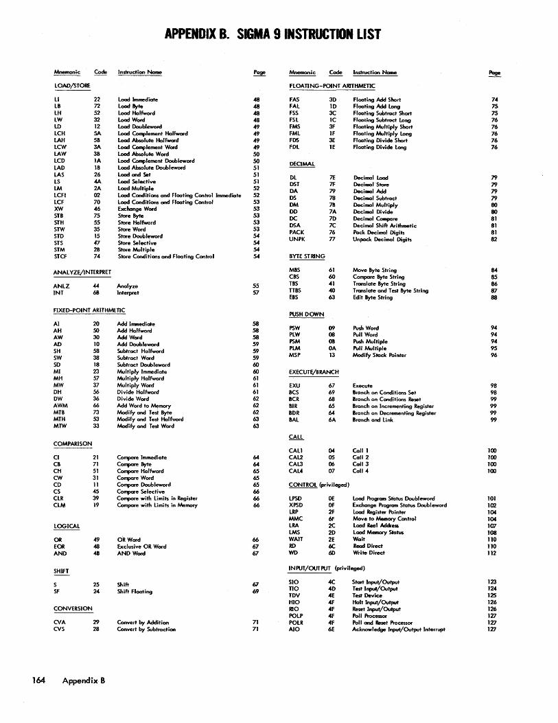
APPENDIX B. SIGMA 9 INSTRUCTION LIST
Mnemonic Code Instruction Name Page Mnemonic Code Instruction Nome Page
LOAD/STORE flOATING-POINT ARITHMETIC
1I 22 load 1mmediate 48 FAS 3D Floating Add Short 7-4 LB n Load Byte 48 FAL ID Floating Add long 75 LH 52 load Halfword 48 FSS 3C Floating Subtract Short 75 LW 32 Load Word 48 FSl lC Floating Subtract Long 76 to 12 load Doubleword 49 fMS 3F Floating Multiply Short 76 lCH SA Load Complement Halfword 49 FMl IF floating Multiply Long 76 LAM 58 load Absolute Hal fword 49 FDS 3E Floating Divide Short 76 lCW 3A load Complement Word 49 FDL IE Floating Divide long 76 LAW 3B Load Absolute Word 50 LCD lA Load Complement Doubleword 50 DEQMAl LAD lB load Absolute Doubleword 51 LAS 26 Load ond Set 51 Dl 7E Decimal Load 79 lS .fA Load Selective 51 05T 7F Decimal" Store 79 LM 2A load Multiple 52 DA 79 Decimal Add 79 LCFI 02 load Conditions and Floating Control Immediote 52 DS 78 Decimal Subtract 79 lCF 70 Load Conditions ond Floating Control 53 OM 7B Decimal Multiply 80 XW 46 Exchange Word 53 DD 7A Decimal Divide 80 STB 75 Store Byte 53 DC 7D Decimal Compare 81 SfH 55 Store Halfword 53 DSA 7C Decimal Shift Arithmetic 81 STW 35 Store Word 53 PACK 76 Pack Decimal Digits 81 STD 15 Store Doubleword 54 STS 47 Store Selective 54
UNPK 77 Unpack Decimal Digits 82
STM 2B Store Multiple 54 STCF 74 Store Conditions and Floating Control 54 BYTE STRING
ANAL YZE/INTERPRET MBS 61 Move Byte String 84 CBS 60 Compare Byte String 85
ANLZ « Analyze 55 TBS 41 Translate Byte String 86
INT 6B Interpret 57 TTBS 40 Translate and Test Byte String 87 EBS 63 Edit Byte StrilJg 88
FIXED-POINT ARITHMETIC PUSH DOWN
Al 20 Add Immediate 58 PSW 09 Push Word 94 AH 50 Add Halfward 58
AW 30 Add Word 58 PLW 08 Pull Word 94
AD TO Add Doubleword 59 PSM 08 Push Multiple 94
SH 58 Subtract Halfword 59 PLM OA Pull Mul.tiple 9S
SW 38 Subtract Word S9 MSP 13 Modify Stock Pointer 96
SD 18 Subtract Doubleword 60 MI 23 Multiply Immediate 60 EXECUTE/BRANCH MH 57 Multiply Halfward 61 MW 37 Multiply Word 61 EXU 67 Execute 98 DH 56 Divide Halfword 61 BCS 69 Branch on Conditions Set 98 OW 36 Divide Word 62 BCR 68 Branch on Conditions Reset 99 AWM 66 Add Word to Memory 62 BIR 65 Branch on Incrementing Register 99 MTB 73 Modify and Test Byte 62 BDR 64 Branch on Decrementing Register 99 MTH 53 Modify and Test Halfword 63 BAL 6A Branch and li nk 99 MTW 33 Modify and Test Word 63
CALL COMPARISON
CAll 04 Call 1 100 a 21 Compare Immediate 64 CAL2 05 Call 2 100 CB 71 Compare Byte 64 CAL3 06 Call 3 100 CH 51 Compare Halfword 65 CAL. 07 Call. 100 CN 31 Compare Word 65 CD 11 Compare Doubleword 65 CONTROL (privileged) CS 4S Compare Selective 66 elR 39 Compare with limits in Register 66 lPSD Of Lood Program Status Doubleword 101 ClM 19 Compare with limits in Memory 66 XPSD OF Exchange Program Status Doubleword 102
LRP 2F load Register Pointer 104 MMC 6F Move to Memory Control 104
LOGICAL LRA 2C load Reol Addres 107 lMS 20 load Memory Status 108
OR 49 OR Word 66 WAIT 2£ Wait 110 EOR 48 Exclusive OR Word 61 RD 6C Read Direct 110 AND 4B AND Word 67 WD 6D Write Direct 112
SHIFT INPUT/OUTPUT (privileged)
S 25 Shift 67 SIO 4C Start Input/Output 123
SF 24 Shift floating 69 TIO 40 Test Input/Output 124 TDV 4E Test Device 125 HIO 4f Halt Input/Output 126
CONVERSION RIO 4F Reset Input/Output 126 POlP .F Poll Processor 127
OIA 29 Convert by Addition 71 POlR 4F Poll and Reset Processor 127 OIS 28 Convert by Subtraction 71 AIO 6E Acknowledge Input/Output Interrupt 127
164 Appendix 8

APPENDIX C. INSTRUCTION TIMING
TIMING CONSIDERATIONS
In less complex computers it was quite simple to express the exact times or timing formulas for the execution of each operation. To determine the total time to execute a program it was necessary only to add the times required for each instruction. Simple timing formulas cannot exactly express SIGMA 9 central processor operations because the timing of each operation is dependent in varying degrees upon the previous instruction, the amount of address modification required, and the configuration of the memory system. The degree of overlap depends on the type of problem (i. e. , the instruction mix); it varies widely among problems that require predominantly floating-point, decimal, or byte string arithmetic, and is also affected by the number of instructions between branches and by input/output activity. To be accurate, it. is necessary to examine the exact timing relationships of the instructions inconsiderable detail. Even then, the effect of system configurations on performance is not included in that examination. The best method is to program a problem and time its execution under actual system operating environments.
Timings and formulas in Table C-l are based on the assumption that, whenever the CPU requests a service cycle from a particular memory bank, it never waits for such service due to other devices (such as lOPs), which are connected to that memory bank.
Execution times depend not only on the nature of the specific instructions and the configuration of memory banks in the system but also on the placement of instructions and operands in memory. These basic execution times must be increased to account for the effects of memory interference, indexing, indirect addressing, and register-to-register operations, These effects are discussed below.
Note that formulas given in Table C-l for long instructions such as shift, decimal, floating, byte string, and multiples are linearaverages of nonlinearfunctions. Programsheavily dependent on the times of these instructions should be benchmarked.
EFFECTS OF MEMORY INTERFERENCE
Memory interference wi II affect centra I processor speed, which varies with the memory cycle time, the number of memory banks capable of running in parallel, and the function being executed. Interference is minimized by interleaving memory banks to allow maximum memory overlap.
90 17 33C-1{4/74)
In a typical instruction mix used in scientific/engineering applications, the percentages of the instructions executed might be as follows:
Type of Instructi on
Floating-point
Fixed-point (including loads and stores)
Branch
Miscellaneous
Percent
8.5
53.0
27.5
11. 0
The effect of memory interference on the above instruction mix in an 8-bank system for 100 instructions is an increase of approximately 7. 4 microseconds or an average of 74 nanos.econds per instruction. Changing the mix to a commercial application that uses decimal and byte-string instructions does not signifrcantly change the effect of memory interference on the average instruction. Over a wide range of mixes, the effect of memory interference in an 8-bank system changed by less than 10 percent.
EFFECTS OF INDEXING
Indexing causes a maximum increase of .260 microsecond (.440 microsecond for SIGMA 9, Model 2) in the execution time of an instruction. Many instructions are I imited in speed due to memory access time. Indexing is often performed in conjunction with memory accesses. This overlapping of indexing with memory time allows the effective time due to indexing to be .260 microsecond (.440 microsecond for SIGMA 9, Model 2) less the memory overlap time. For a typical scientific mix of instructions, the average memory overlap is .120 microsecond. The typical indexing time would then be .140 microsecond (.320 microsecond for SIGMA 9, Model 2).
EFFECTS OF INDIRECT ADDRESSING
Indirect addressing requires a memory access. This access may be from the general registers or the main memory.
1. Indirect addressing from general registers requires a maximum time of .960 microsecond (1. 98 microseconds for SIGMA 9 Model 2).
2. Indirect addressing from main memory requires a maximum time of 1. 050 microseconds (1. 32 microseconds for SIGMA 9 Model 2).
The maximum time required for indirect addressing is reduced when the indirect memory request is overlapped with instruction execution. This effect is instruction dependent.
Appendix C 165
EFFECTS OF REGISTER-TO-REGISTER OPERATIONS
If the reference address is X'OI through XIP, the operand is accessed from the appropriate general register rather than from main memory. The additional time required for this operation varies from 155 to 445 nanoseconds, depending on the sequence of instructions being executed.
The major factors determining the additional time required for register-to-register operations are the type of instruction (multiple operands versus single-operand instructions) being executed and the type of instruction preceding the instruction in question.
For multiple operand type of instructions (load and store multiples, push/pul Is, byte strings, etc.), the average delay for operands other than the first of the string is approximately 260 nanoseconds for load-type instructions and 155 nanoseconds for store-type instructions.
For all initial operands pointed to by the effective address of the instruction, the delay due to register-to-register operations is dependent on the preceding instruction as follows:
1. If the preceding instruction is generally greater than 1 microsecond, then the typical delay is 445 na noseconds.
2. If the preceding instruction isgenerally less than 1 microsecond, then the typical delay is 235 nanoseconds.
OTHER SIGMA 9 PERFORMANCE FACTORS
"To achieve improved system performance, SIGMA 9 uses "anticipation logic". By anticipating the access of the next few memory words (i. e., guessi ng the location of the next words to be obtained from memory) certain machine functions can be overlapped. Factors that affect this capability, and thus machine performance, are outlined below.
1. If instruction n + 1 is altered by instruction n, the machine's anticipation logic is cleared (aborted), causing an extra delay of approximately 1. 3 microseconds.
2. If instruction n + 1 or n + 2 is located in main memory, and if either is modified by instruction n, the anticipation logi c is cleared (aborted). Due to hardware considerations this abort occurs if instruction n stores not only into location n + ] or n + 2 but also into locations 128 + (n +"1 or n + 2), 256 + (n + 1 or n + 2), and 384 + (n + 1 or n + 2). The delay caused by this abort is approximately 1.6 microseconds.
166 Appendix C
A special case is excluded from this type of abort. This case occurs when the location being modified is the one following the location of an unconditional bronch, as in the following example:
Instruction Location:
n STORE WORD INTO n + 2 n + 1 UNCONDITIONAL BRANCH n+2 X
Note: The special case occurs only when the unconditional branch branches to the next location. This case works normally (i. e., without an abort) due to n + 2 being accessed with operand timing.
3. If the index register being used for operand n+ 1 is modified by instruction n, then a preparation abort occurs. The indexing for instruction n+ 1 is performed at the start of execution of n. This is to allow time to overlap the n+ 1 operand memory access with the execution of instruction n. The delay caused by this type of abort is approximately .89 microsecond.
4. Instructions that cause a change in sequentia I accessing of instructions cause partial aborts of the anticipation logic. These instructions are branches, calls, XPSD, and LPSD.
5. Instructions that change the state of the machine cause a complete abort. This is necessary due to the fact that any anticipate operation may have been invalidated. The instructions causing this are: MMC, LRP, XPSD, and LPSD. The times shown in this appendix for these instructions include the extra time due to the anticipation restart.
6. Faults that cause traps, if detected for an instruction access (Memory Not Present, Access Protect, Map Parity Error, Memory Parity Error, and Bus Check Fault), cause the anticipation to be aborted. If the fault occurs during restart of the anticipation, the appropriate trap action will then occur.
7. Interrupts cause a change in the address from normal sequencing and therefore cause the anticipation to be aborted.
8. Instructions accessed from scratchpad cause a delay of from 0 to .355 microsecond.
9. SIGMA 9 performance is affected by the amount of memory overlap between instructions and operands. A performance gain will be realized if operands and instructions are located indifferent memory uni ts. Interleaving will allow overlap between instructions with instructions and operands with operands.
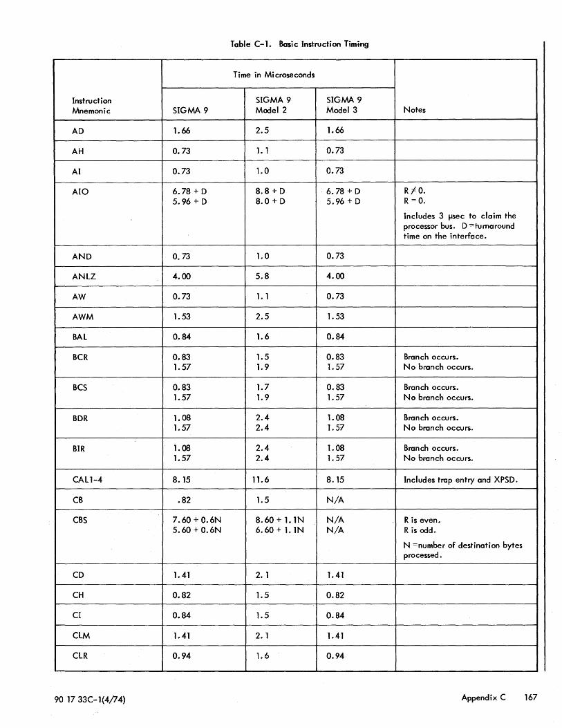
Table C-1. Basic Instruction Timing
Time in Microseconds
Instruction SIGMA 9 SIGMA 9 Mnemonic SIGMA 9 Model 2 Model 3 Notes
AD 1.66 2.5 1.66
AH 0.73 1.1 0.73
AI 0.73 1.0 0.73
AIO 6.78 + D 8.8 + D 6.78 + D Rj O. 5.96 + D 8.0 + D 5.96 + D R = O.
Includes 3 tJSec to claim the processor bus. D = tu rna round time on the interface.
AND 0.73 1.0 0.73
ANlZ 4.00 5.8 4.00
AW 0.73 1.1 0.73
AWM 1.53 2.5 1.53
BAl 0.84- 1.6 0.84
BCR 0.83 1.5 0.83 Branch occurs. 1.57 1.9 1.57 No branch occurs.
BCS 0.83 1.7 0.83 Branch occurs. 1.57 1.9 1.57 No branch occurs.
BDR 1.08 2.4 1.08 Branch occurs. 1.57 2.4 1. 57 No branch occurs.
BIR 1.08 2.4 1.08 Branch occurs. 1.57 2.4 1.57 No branch occurs.
CALl...;4 8. 15 11.6 8.15 Includes trap entry and XPSD.
CB .82 1.5 N/A
CBS 7.60 + 0.6N 8.60+1.1N N/A R is even. 5.60 + 0.6N 6.60 + 1.1N N/A R is odd.
N =number of destination bytes processed.
CD 1. 41 2. 1 1. 41
CH 0.82 1.5 0.82
CI 0.84- 1.5 0.84
ClM 1.41 2. 1 1.41
ClR 0.94 1.6 0.94
90 17 33C-l(4/74) Appendix C 167
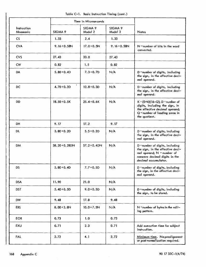
Table C-1. Basic Instruction Timing (cont.)
Time in Microseconds
Instruction SIGMA 9 SIGMA 9 Mnemonic SIGMA 9 Model 2 Model 3 Notes
CS 1.33 2.4 1.33
OIA 9.16+0.58N 17.0+0.5N 9.16+0.58N N =number of bits in the word converted.
OIS 27.43 33.0 27.43
CW 0.82 1.5 0.82
DA 5.80+0.4D 7.3 +0. 7D N/A D =number of digits, including the sign, in the effective deci-rna I operand.
DC 4.70+0.3D 12.8+0.3D N/A D =number of digits, including the sign, in the effective deci-mal operand.
DD 18.50+0.5K 25.4+0.6K N/A K = (D+6)(16-Q); D =number of digits, including the sign, in the effective decimal operand; Q =number of leading zeros in the quotient.
DH 9. 17 17.2 9.17
DL 3.80+0.2D 5.5+0.30 N/A D =number of digits, including the sign, in the effective deci-mal operand.
DM 38.20+0.28DN 57.2+0.4DN N/A D =number of digits, including the sign, in the effective deci-rna I operand; N = number of nonzero decimal digits in the decimal accumulator.
DS 5.80+0.4D 7.7+0.5D N/A D =number of digits, including the sign, in the effective deci-mal operand.
DSA 11.90 21.0 N/A
DST 5.40+0.5D 9.0+0.5D N/A D =number of digits, including the sign, to be stored.
DW 9.48 17.8 9.48
EBS 8.00+3.8N 10.0+ 7.5N N/A N =number of bytes in the edit-ing pattern.
EOR 0.73 1.0 0.73
EXU 0.71 2.3 0.71 Add execution time for subiect instruction.
FAL 2.72 4. 1 2.72 Minimum time. No preal ignment or post normalization required.
168 Appendix C 90 17 33C-l(4/74)
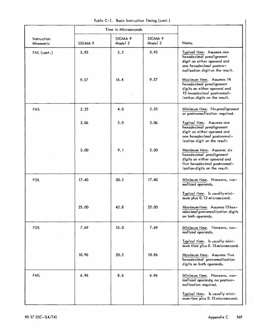
Table C-1. Basic Instruction Timing (cont.)
Time in Microseconds
Instruction SIGMA 9 SIGMA 9 Mnemonic SIGMA 9 Model 2 Model 3 Notes
FAL{cont.) 3.93 5.2 3.93 T l~i cal time. Assumes one hexadecimal prealignment digit on either operand and one hexadecimal postnor-malization digiton the result.
9.57 16.4 9.57 Maximum time. Assumes 14 hexadecimal preal ignment digits on either operand and 13 hexadecimal postnormal-ization digits on the result.
FAS 2.25 4.0 2.25 Minimum time. No preal ignment or postnormalization required.
3.06 5.0 3.06 T~~ical time. Assumes one hexadecimal prealignment digit on either operand and one hexadecimal postnormal-ization digit on the result.
5.00 9. 1 5.00 Maximum time. Assumes six hexadecimal prealignment digits on either operand and five hexadecimal postnormal-ization digits on the result.
FDL 17.40 30.5 17.40 Minimum time. Nonzero, nor-malized operands.
Tl~ical time. Is usuallymini-mum plus O. 13 microsecond.
25.00 42.8 25.00 Maximum time. Assumes 13 hex-adecimal prenormal ization digits on both operands.
FDS 7.69 15.0 7.69 Minimum time. Nonzero, nor-malized operands.
Typical time. Is usually mini-mum time plus O. 13 microsecond.
10.96 20.5 10.96 Maximum time. Assumes five hexadecimal prenormal ization digits on both operands.
FML 6.96 8.6 6.96 Minimum time. Nonzero, nor-malized operands; no postnor-malization required.
T~~ical time. Is usually mini-mum time plus O. 13 microsecond.
90 17 33C-1(4/74) Appendix C 169
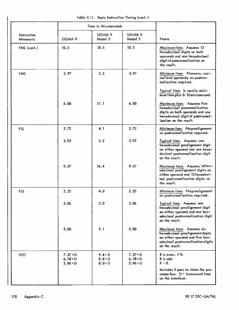
Table C-1. Basic Instruction Timing (cont.)
Time in Mi croseconds
Instruction SIGMA 9 SIGMA 9 Mnemonic SIGMA 9 Model 2 Model 3 Notes -,
FML (cont.) 10.5 18.5 10.5 Maximum time. Assumes 13 hexadecimal digits on both operands and one hexadecimal digit of postnormalization on the result.
FMS 3.97 5.5 3.97 Minimum time. Nonzero, nor-mal ized operands; no postnor-malization required.
Typical time. Is usually mini-mum time plus O. 13 microsecond.
6.00 11. 1 6.00 Maximum time. Assumes five hexadecimal prenormalization dig i ts on both operands and one hexadecimal digitof postnormal-ization on the result.
FSL 2.72 4. 1 2.72 Minimum time. No prea I i gnment on postnormalization required.
3.93 5.2 3.93 T~ical time. Assumes one hexadecimal prealignment digit on either operand and one hexa-decimal postnormalization digit on the result.
9.57 16.4 9.57 Maximum time. Assumes 14 hex-adecimal prealignment digits on either operand and 13 hexadeci-mal postnormalization digits on the result.
FSS 2.25 4.0 2.25 Minimum time. Noprealignment on postnorma I i zat i on requ ired.
3.06 5.0 3.06 T~eical time. Assumes one hexadecimal prealignment digit on either operand and one hex-adecimal postnormalization digit on the result.
5.00 9. 1 5.00 Maximum time. Assumes six hexadecimal prealignmentdigits on either operand and five hex-adecimal postnormalization digits on the result.
HIO 7.37+D 9.4+D 7.37+D R is even, I- o. 6.78+D 8.8+D 6.78+D R is odd. 5.96+D 8.0+D 5.96+D R = O.
Includes 3 tJSec to claim the pro-cessor bus. D = turnaround time on the interface.
170 Appendix C 90 1733C-l{4/74)
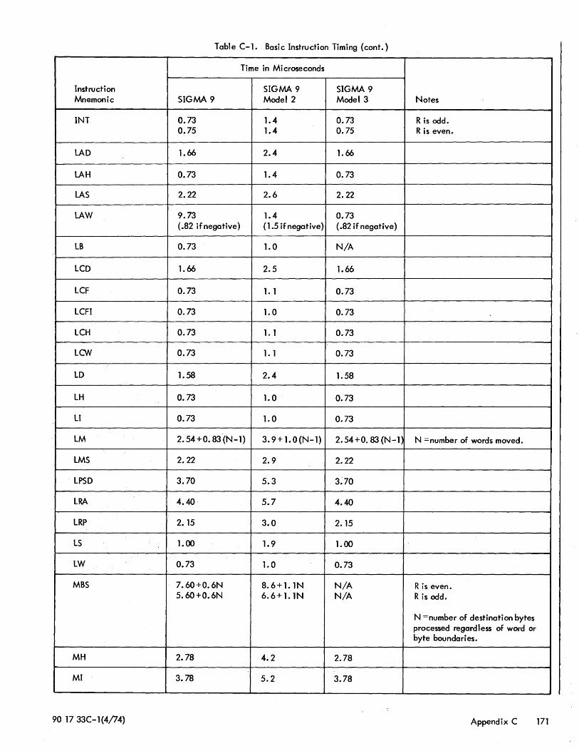
Table C-1. Basic Instruction Timing (cont.)
Time in Mi croseconds
Instruction SIGMA 9 SIGMA 9 Mnemonic SIGMA 9 Model 2 Model 3 Notes
INT 0.73 1.4 0.73 R is odd. 0.75 1.4 0.75 R is even.
LAD 1.66 2.4 1.66
LAH 0.73 1.4 0.73
LAS 2.22 2.6 2.22
LAW 9.73 1.4 0.73 (.82 ifnegative) (1.5 if negative) (.82 if negative)
LB 0.73 1.0 N/A
LCD 1.66 2.5 1.66
LCF 0.73 1.1 0.73
LCFI 0.73 1.0 0.73
LCH 0.73 1.1 0.73
LCW 0.73 1.1 0.73
LD 1.58 2.4 1.58
LH 0.73 1.0 0.73
LI 0.73 1.0 0.73
LM 2.54 +0.83 (N-l) 3. 9 + 1. 0 (N - 1) 2.54+0.83 (N-l, N =number of words moved.
LMS 2.22 2.9 2.22
LPSD 3.70 5.3 3.70
LRA 4.40 5.7 4.40
LRP 2.15 3.0 2.15
LS 1.00 1.9 1.00
LW 0.73 1.0 0.73
MBS 7.60+0.6N 8.6+1.1N N/A R is even. 5.60+0.6N 6.6+1.1N N/A R is odd.
N =number of destination bytes processed regardless of word or byte boundaries.
MH 2.78 4.2 2.78
MI 3.78 5.2 3.78
90 17 33C-l(4/74) Appendix C 171
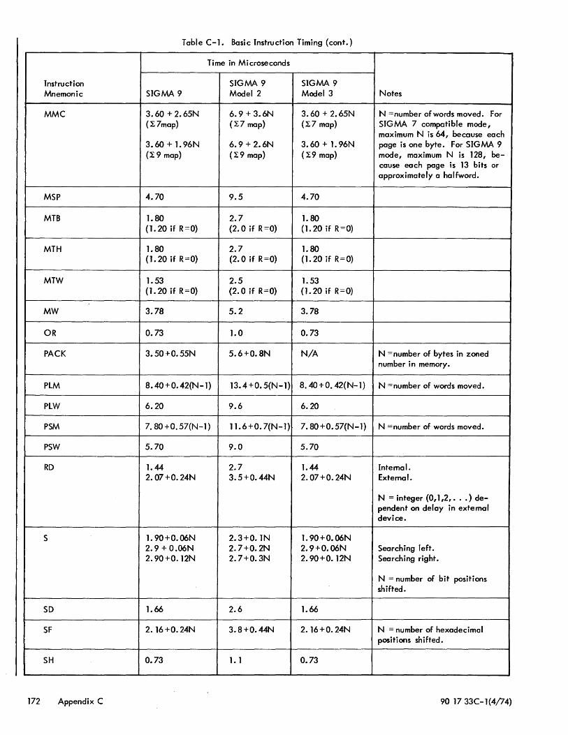
Table C-1. Basic Instruction Timing (cont.)
Time in Microseconds
Instruction SIGMA 9 SIGMA 9 Mnemonic SIGMA 9 Model 2 Model 3 Notes
MMC 3.60 + 2.65N 6.9 + 3.6N 3.60 + 2.65N N =number of words moved. For (l: 7map) (l:7 map) (l: 7 map) SIGMA 7 compatible mode,
maximum N is 64, because each 3.60 + 1. 96N 6.9 + 2.6N 3.60 + 1.96N page is one byte. For SIGMA 9 (l: 9 map) (l:9 map) (l:9 map) mode, maximum N is 128, be-
cause each page is 13 bits or approximately a halfword.
MSP 4.70 9.5 4.70
MTB 1.80 2.7 1. 80 (1. 20 if R =0) (2.0 if R=O) (1. 20 if R =0)
MTH 1.80 2.7 1.80 (1. 20 if R =0) (2.0 if R=O) (1. 20 if R = 0)
MTW 1.53 2.5 1.53 (1. 20 if R =0) (2.0 if R=O) (1.20 if R=O)
MW 3.78 5.2 3.78
OR 0.73 J.O 0.73
PACK 3.50+0.55N 5.6+0.8N N/A N =number of bytes in zoned number in memory.
PLM S. 40 + O. 42(N-1) 13.4 +0. 5(N-1) 8.4O+0.42(N-1) I N =number of words moved.
PLW 6.20 9.6 6.20
PSM 7.80 +0. 57(N-l) 11.6 +0. 7(N-l) 7. SO +0. 57(N-1) N =number of words moved.
PSW 5.70 9.0 5.70
RD 1.44 2.7 1.44 Internal. 2.07+0.24N 3.5+0.44N 2.07+0.24N External.
N = integer (0,1,2, •.. ) de-pendent on delay in external device.
S 1. 90+0.06N 2.3+0.1N 1. 90+0.06N 2.9 + O.06N 2.7+0.2N 2.9+0.06N Searching left. 2.90+0.12N 2.7+0.3N 2.90+0.12N Searching right.
N = number of bit positions shifted.
SO 1.66 2.6 1.66
SF 2. 16+0.24N 3.S+0.44N 2. 16+0.24N N = number of hexadecimal positions shifted.
SH 0.73 1.1 0.73
172 Appendix C 90 1733C-1(4/74)
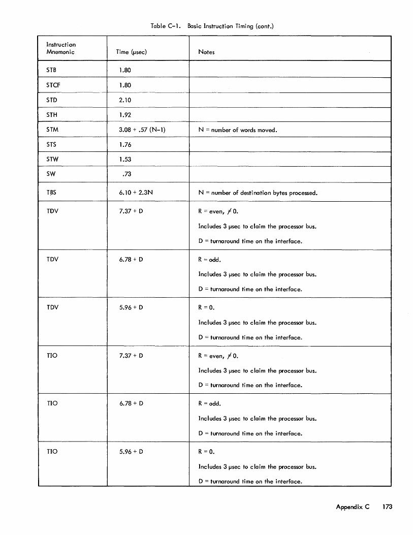
Table C-1. Basic Instruction Timing (cont.)
Instruction Mnemonic Time (fJsec) Notes
STB 1.80
STCF 1.80
STD 2.10
STH 1.92
STM 3.08 + .57 (N-1) N = number of words moved.
STS 1.76
STW 1.53
SW .73
T~S 6.10 + 2.3N N = number of destination bytes processed.
TDV 7.37 + D R = even, I- O.
Includes 3 fJsec to claim the processor bus.
D = turnaround time on the interface.
TDV 6.78 + D R = odd.
Includes 3 fJsec to claim the processor bus.
D = turnaround time on the interface.
TDV 5.96 + D R = O.
Includes 3 fJsec to claim the processor bus.
D = turnaround time on the interface.
no 7.37 + D R = even, I- O.
Includes 3 fJsec to claim the processor bus.
D = turnaround time on the interface.
no 6.78 + D R = odd.
Includes 3 fJsec to claim the processor bus.
D = turnaround time on the interface.
no 5.96 + D R = O.
Includes 3 fJsec to claim the processor bus.
D = turnaround time on the interface.
Appendix C 173
Table C-l. Basic Instruction Timing (cont.)
Time in Microseconds
Instruction SIGMA 9 SIGMA 9 Mnemonic SIGMA 9 Model 2 Model 3 Notes
SIO 7.37 + D 9.4 = D 7.37 + D R is even, f O. 6.78 + D 8.8 + D 6.78 + D R is odd. 5.96 + D 8.0 + D 5.96 + D R = O.
Includes 3 lJSec to claim the processor bus. D = turnaround on the interface.
STB 1. 80 2.5 N/A
STCF 1. 80 2.5 1. 80
STD 2. 10 4.9 2. 10
STH 1. 92 2.6 1. 92
STM 3.08 +0. 57(N-1) 6.3+0.7(N-l) 3.08 +0. 57(N-1) N = number of words moved.
STS 1. 76 3.3 1. 76
STW 1.53 2.3 1. 53
SW 0.73 1.1 0.73
TBS 6.10+2.3N 10.5 +3. 6N N/A N = number of destination bytes processed.
TDV 7.37 + D 9.4 + D 7.37 + D R is even, f O. 6.78 + D 8.8 + D 6.78 + D R is odd. 5.96 + D 8.0 + D 5.96 + D R = O.
Includes 3 J.lsec to claim the processor bus. D = turnaround time on the interface.
TIO 7.37 + D 9.4 + D 7.37 + D R is even, f O. 6.78 + D 8.8 + D 6.78 + D R is odd. 5.96 + D 8.0 + D 5.96 + D R =0.
Includes 3 lJSec to claim the processor bus. D = turnaround time on the interface.
TTBS 6.10+2.4N 10.5 +3. 6N N/A N = number of destination bytes processed.
UNPK 7.40+ LON 11.6+ LON N/A N = number of bytes to be stored in memory.
WAIT 0.73 1.0 0.73 Minimum time.
WD 1.44 2.7 1.44 Internal. 2. 07+0. 24N 3.5+0.44N 2.07+0.24N External.
N = integer (0, 1, 2, ... ) de-pendent on delay in external device.
90 17 33C-1 (4/74) Appendix C 173
Table C-l. Basic Instruction Timing (cont.)
Instruction Mnemonic Time {J.asec) Notes
rrBS 6.10 + 2.4N N = number of destination bytes processed.
UNPK 7.40 + l.ON N = number of bytes to be stored in memory.
WAIT .73 Minimum time.
WD 1.44 Internal
'NO 2.07 + .24N External
N = integer (0, 1, 2, ••• ), dependent on delay in external device.
XPSD 5.43
XW 1.53
174 Appendix C
Table C-1. Basic Instruction Timing (cont.)
Time in Microseconds
Instruction SIGMA 9 SIGMA 9 Mnemonic SIGMA 9 Model 2 Model 3 Notes
XPSD 5.43 7. 1 5.43
XW 1. 53 2.4 1.53
174 Appendix C 90 17 33C-l(4/74)
APPENDIX D. SYSTEM RELIABILITY AND MAINTAINABILITY
The SIGMA 9 computer system has many new design features that provide the user with reliable operation and efficient maintenance. For example, the extent to which a system can be partitioned into separate un its for either checkout or maintenance is a "fail-soft" feature (i. e., ability to keep remainder of a system operational in case of failure of any given unit), which was a major design goal for SIGMA 9 development.
The new design features are outl ined in the following sections:
System t-ilaintainabi I ity Features
CPU Features
Main Memory Features
Multiplexor Input/Output Processor Features
High-Speed RAD I/O Processor Features
SYSTEM MAINTAINABILITY FEATURES SIGMA 9 computer systems are maintained by means of the following:
1. Diagnostic Programs
Diagnostic programs for centralized SIGMA 9 units (CPUs, memory units, and lOPs) use special hardware to detect and isolate system faults. Interface with maintenance personnel is provided through a local keyboard-printer or a remote keyboard-printer connected via a telephone line. Diagnostic programs are designed with a multilevel structure consisting of the following capabilities.
a. System verification and testing to determine which unit is faulty.
b. Unit functional testing to determine the specific function that is faulty.
c. Fault location diagnosis to analyze which component is malfunctioning.
2. Snapshot Log i c
Snapshot logic enables diagnostic programs to retrieve control fl i p-fl ops and i nterna I reg i ster contents that are not otherwise "visible" to a program. This feature makes it possible to determine system status at the time a fault occurs and to locate the source of a fault condition down to the level of a small set of replaceable elements. (See "CPU Features".)
3. Status and Fault Retrieval
When a fault is detected, system status and fault information is available for program retrieval and error logging for subsequent analysis.
4. Partitioning Feature
A SIGMA 9 system can be reconfigured through the use of reconfiguration controls. SIGMA 9 units can be partitioned out of the system by selectively disabling them from the busses. Thus, faultyunitscanbe isolated from the system, or an entire subsystem (including a CPU in a multiprocessing environment) can be partitioned from the primary system to permit diagnosis and repair of a faulty unit. Repaired units can be returned to service by reenabl ing the connections.
5. RESET I/O (RIO) Instruction
This instruction provides programmed I/O Reset that operates exactly as though the I/O Reset had been initiated with the switch on the processor control panel (PCP). The addressed lOP and all peripheral devices connected to it are initialized. Special coding of RIO will reset a CPU (see RIO instruction, Chapter 3.)
6. Parity Checking
Parity on all data and addresses communicated in either direction on busses between memory units and processors (CPUs, MIOPs, and HSRIOPs) is checked. This feature provides fault detection and location capabilities that enhance the ability of an operating system or diagnostic program to quickly determine which unit is faulty.
7. Clock and Voltage Margins
Centralized units are provided with clock and voltage margin capabil ities that assist maintenance personnel or diagnostic programs to quickly Locate the source of an intermittent fault. Programmable clock margin control is provided and status is avai lable for program retrieval. NOT NORMAL conditions are indicated on the PCP.
8. Alternate Processor Bus (optional)
This feature provides a redundant connection of the lOPs and CPUs in a system. It is used in partitioning centralized units for diagnostic or reconfiguration purposes.
Appendix 0 175
9. Unique Processor Numbers
All processors have unique numbers so that they can be identified in communications on the processor bus.
10. Processor Fau I t Interrupt
A processor fault interrupt (PFI) signal is generated by processors (CPUs, MIOPs, and HSRIOPs) when certain fault conditions are detected. The interrupt signal is transmitted via the processor bus to all CPUs in the system (except to the CPU generating the PFI) for special fault handl ing.
11.. Status Instructions
The two instructions, POLL PROCESSOR (POLP) and POLL AND RESET PROCESSOR (POLR), are used to determine status. All processors in a SIGMA 9 system retain the status of faults, internal conditions, and processor identification. When a Processor Fault Interrupt (PFI) occurs, the CPU(s) that receives the interrupt must determine which processor caused the PFI and the nature of the fault.
The POLP instruction causes the addressed processor to return the contents of its fault status register and, in the condition code bits, indicate whether the processor had detected a fault and generated PFI. (See POLP instruction, Chapter 3.)
The POLR instruction performs the same functions as POLP but, in addition, causes the addressed processor to reset the contents of the processor fault register and resetthe PFI signal. (See POLR instruction, Chapter 3.)
CPU FEATURES
1. Processor Control Panel (PCP)
The PCP (see Chapter 5) is divided into two sections. The upper portion (MAINTENANCE SECTION) contains controls and indicators used exclusively by maintenance personneL The lower portion is used primarily by operating personnel to load, execute, and troubleshoot progf"Oms. A Control Mode switch disables certain maintenance functions during normal operation.
2. Maintenance Display
Various phases, control flip-flops, and registers of the CPU and decimal unit can be displayed on the PCP. A 16-position thumbwheel switch identifies and selects display information during maintenance activities.
3. Snapshot Log i c
All CPU logic that can be displayed on the PCP can be monitored by a program with the snapshot logic. At a
176 Appendix 0
preselected dock time of a given instruction execution, selected logic is stored into a 3~-bit snapshot register. The contents of the snapshot register are then retrieved by a specially coded READ DIRECT instruction. By comparing the "snapped" information with known correct information, the diagnostic program can accurately determine a specific fault. The failing component can then be identified. Snapshot action can also be initiated at the PCP, and the contents of the snapshot register displayed.
4. Clock and Voltage Margins
Clock margin control is accomplished manually at the PCPwith the CLOCK MARGIN switch or under program control with a properly coded WRITE DIRECT instruction. Three c lock rates are provided:
• NORMAL
• FAST
• SLOW
Voltage margin controls are also provided at each local d. c. power supply within a unit.
5. Memory Clear and Scan
Manual memory clear and scan capabilities are provided to enable operators or maintenance personnel to rapidly clear or read selected data from, or store selected data into, any or all consecutive CPU main memory locations. During the read scan operation, the CPU can be made to halt on a memory parity error, at which time the address and data of the indicated memory location can be displayed.
6. Address Stop Feature
This feature (see Chapter 5) allows the operator or maintenance personnel to:
a. Stop on any instruction whose virtual address equals the SELECT ADDRESS switch value. At the time of the halt, the instruction pointed to by the SELECT ADDRESS appears in the DISPLAY indicators.
b. Stop on any rea I memory (read or wri te) reference indicated by the SELECT ADDRESS switches.
c. Stop on any real memory write reference indicated by the SELECT ADDRESS switches.
d. Stop when any word ina selected page is referenced.
7. PCP M.anual Instruction Execution
The PCP allows manual execution of READ/WRITE DIRECT instructions while the CPU is in the IDLE mode. This feature is in addition to the programmable interrogation provided via the READ/WRITE DIRECT instructions (see Chapter 3). Thus, all devices connected to the direct I/O or maintenance interface may be examined manually by maintenance personnel.
Memory status word zero can be manually displayed on the PCP without clearing memory fault status while the CPU is in the IDLE mode. This action is similar to the
programmed LMS instruction with initial condition code setting 1000 (see Chapter 5).
8. Single Clock Mode
The CPU has a single clock mode of operation that enables maintenance personnel to execute an instruction from the PCP, one internal phase at a time.
9. Timer and Decimal Override
The operation of the watchdog timer and decimal unit can be selectively overridden to aid maintenance personnel in diagnosing related machine faults (see Chapter 5).
10. CPU Traps
CPU traps are provided for a variety of detected CPU and system fault conditions. The trap system (see Chapter 2) provides a high degree of system recoverabi lity. Indicators and audit trails enable the system programmer to accurately determine the status of the machine at the time of the trap. CPU fault conditions are:
a. Memory Parity Error - When a CPU receives a signal from the memory indicating a memory parity error, the CPU traps. The condition code identifies the memory parity error trap condition.
b. Data Bus Check - If the CPU detects a parity error on data received from memory, and the memory does not also indicate a parity error on the information sent, then a data bus check occurs. Occurrence of the data bus check condition causes the CPU to trap.
c. Map Check - When the CPU is operating with the memory map, a parity check is made on the page address retrieved from the map. If an error is found, the CPU aborts the memory request and traps.
d. Watch Dog Timer - The watch dog timer prevents the CPU from being "hung Up" due to internal faults or faults in other units. When the timer times out, the CPU traps and sets the condition code indicating which fault .has occurred.
e. Instruction Exceptions - If a CPU encounters an illegal condition in certain CPU operations, an instruction exception fault is detected and causes a trap. Included as instruction exceptions are:
• A processor-detected fault occurring during the execution of an interrupt or trap entry sequence.
• An illegal instruction in a trap (not XPSD) or interrupt (not XPSD, MTB, MTH, MTW) location when operating a trap or interrupt sequence.
• The setting of the register pointer of the PSD to a nonexistent register block as a result of an LRP, LPSD, or XPSD instruction.
• An illegal MMC instruction.
• An invalid register (odd) for an instruction (doubleword and byte string) that would yield an unpredictable result.
11. Processor Fault Interrupt
Whenever a CPU fault is detected, a Processor Detected Fault (PDF) flag is set in that CPU. If a second fault is detected (with PDF set), the CPU will generate and transmit the Processor Fault Interrupt (PFI) to any other CPUs in the system and enter a WAIT state that requires a Reset function to clear. Another CPU (in a multiprocessor system) may issue an RIO instruction to the malfunctioning CPU, which will clear the machine {in the same way as a CPU RESET or SYS RESET and cause it to resume execution at a predetermined instruction location. For a monoprocessor, operator action is required.
12. Automatic Instruction Fetch Retry
When fault conditions are detected on overlapped instruction fetch operations, the fetch is aborted and an automatic instruction fetch retry is attempted. If the fau I t recurs on the second attempt, the CPU traps in the normal manner.
13. Partitioning Feature
Various partitioning features in the SIGMA 9 CPU enable system reconfiguration. These features are locally controlled by switches and are readable by specially coded READ DIRECT instructions (see Chapter 3).
a. Homespace bias switches enable placing the Homespace for each CPU in different physical locations of memory (see "Homespace", Chapter 2).
b. CPU-lOP control bus selection is provided for the purpose of switching the CPU from primary to alternate processor busses. Thus, a failed CPU may be effectively partitioned out of the system; also, an entire subsystem consisting of an lOP, including attached peripherals, CPU, and memory unit can be partitioned from the primary system via this switch and the memory port disable switches, to allow diagnosis of any unit in the subsystem while the primary system continues operation.
Appendix D 177
c. The direct VO bus and the maintenance interface bus may be sel ectively disabled from the CPU.
MAIN MEMORY FEATURES
1 • Snapshot Logic
Each memory bank contains snapshot logic that is automatically activated when a memory fault occurs to record the nature and environment of the fault. The contents of the memory snapshot words (each 32 bits in size) can be retrieved by the use of the instruction, LOAD MEMORY STATUS (see Chapter 3). This feature may be used by the operating system for error logging, or by a diagnostic program to assist in fault locating. Notification of a fault occurrence is via the Memory Fault Interrupt.
2. Memory Fault Detection
Memory fault detection covers the following types of faults:
a. Parity errors detected on information read out of the memory bank.
b. Parity errors detected on addresses received from processors.
c. Parity errors detected on data received from processors.
d. Port selection errors detected if more than one port is simultaneously selected for one bank. Under this condition, the memory aborts the requested operation without modifying the contents of any memory locot i on.
e. Memory bank operational status, e. g., overtemperature, d. c. voltages out of tolerance, etc.
f. Data loop checks that provide additional fault detection on read operations. As data is gated onto the memorybusfortransmission to a processor, itis also gated from the bus back through the input path, clocked into a register, and checked for parity. Thus, the integrity of the I inedrivers/receivers at the memory is tested on every read cycle.
3. Memory Interleave Switch
The interleaved mode of memory operation may be disabled for certain diagnostic purposes with a switch located on the PCP (see Chapter 5).
4. ctock Mlrgin Switches
Clock margins are controlled manually by means of switches or by use of the LOAD MEMORY STATUS instruction. Voltage margin control is also provided at each local d.c. power supply within a unit.
l78 Appendix 0
5. Partitioning of Iv\emory
Partitioning of memory units is allowed on a memory port basis where each memory bus connection may selectively be disabled. Starting address switches allow the memory system to remain a contiguous unit after partitioning. A centrally located reconfiguration control panel for each memory I:Jnit is provided for this purpose.
6. Memory M:>de Feature
Two additional memory modes of operation are provided for testing memory units. These modes are called Read and Inhibit Parity and Read and Change Parity (see Chapter 3).
a. During the Read and Inhibit Parity operation, a word is read from memory and transmitted to the requesting processor. If a parity error is detected in the memory bank, the memory is prohibited from taking any snapshot and does not generate the Memory Fault Interrupt. It does transmit the Parity Error signal, however. The CPU recognizes this mode of operation and inhibits the trap that might occur for memory parity error and data bus check and, instead, records these attributes in the condition code at the conclusion of the instruction. If there is no parity error, the instruction is treated as a normal LOAD WORD instruction, except for the setting of the condition code.
b. During the Read and Change Parity operation, a word is read from memory and transmitted to the requesting processor. In the write half cycle, the word is restored to memory, and the word with an invalid parity bit is unconditionally restored. This allows the parity generation and checking logic of the memory to be tested.
MUL nPLEXOR INPUT/OUTPUT PROCESSOR (MIOP) FEATURES
1. Maintenance Interface Bus
The maintenance interface bus (a special mode of the direct VO bus) is connected to each MIOP from the CPU for maintenance purposes. The MIOP responds in the following way to special WRITE DIRECT and READ DIRECT instructions executed by the CPU.
a. Under RD control, monitors one of 32 selectable groups of MIOP logic.
b. Under WD control, steps the clock control of the MIOP in a single-phase mode.
c. Under WD control, a snapshot mode of operation selects a display group and stores it in a snapshot register at the end of a preset countdown for later monitoring by an RD instruction.
d. Under WD control, writes directly into an addressed subchannel.
e. Under RD control, reads directly from an addressed subchanne I.
f. Under WD control, sets the clock margins to fast, normal, or slow rates.
2. Parity Checking
Parity is checked on information brought out of the MIOp·s local memory for each subchannel. A fault is reported to the system via the Processor Fault Interrupt.
3. Maintenance Subcontroller
A maintenance subcontroller feature on each I/o channel assists in diagnosing the I/O system. A diagnostic program controls and monitors the maintenance subcontroller via the maintenance interface and the I/O bus. The following functions can be accomplished:
a. Simulation of a device controller that responds to commands sent to it by the MIOPand receives and sends strings of data bytes.
b. Monitoring of lOP bus during diagnostic operations.
c. Exercising of the lOP at variable rates up to and including its maximum rate.
d. Self-testing of the maintenance subcontroller logic.
4. Clock and Voltage Margins
Clock margins are programmatically controlled by a specially coded WRITE DIRECT instruction (see Chapter 3). Voltage margin controls are provided at each d. c. power supply.
5. Partitioning of MIOPs
Partitioning of MIOPs is accomplished by disabling the primary (or alternate) processor bus connection and disabl i ng the appropriate memory port(s).
HIGH-SPEED RAD 110 PROCESSOR (HSRIOP) FEATURES
1. tv\aintenance Interface Bus
The maintenance interface bus (a special mode of the direct I/O bus) is connected to the HSRIOP from the CPU for maintenance purposes. The HSRIOP responds
in the following way to special WRITE DIRECT and READ DIRECT instructions executed by the CPU:
a. Under WD control, selects a phase that causes the HSRIOP to halt when entered during execution of any HSRIOP operation. At this time, the HSRIOP may be IIsnapped ll for diagnosti c purposes, via RD control.
b. Under RD control, IIsnapsll one of seven selectable groups of internal HSRIOP logic.
c. Under WD control, steps the clock control of the HSRIOP in a single-phase mode.
d. Under WD control, selectively sets various fault indicators (e.g., device and memory faults) to simulate actual fault occurrence. This feature allows the diagnostic to test for correct HSRIOP response under these fault conditions.
e. Under WD control, selectively initiates Test Mode 1 or Test Mode 2 of the HSRIOP in which the HSRIOP responds to normal I/O instructions whi Ie simulating action of the storage units. In this way, major portions of the HSRIOP logic can be diagnosed separately from the storage units.
2. Test Mode 1.
This mode permits the diagnostic program to check the data paths, control logic, and byte alignment logic from memory to the buffer (with a write operation) and from the buffer to memory (with a read operation).
3. Test Mode 2.
This mode permits the diagnostic program to check most of the RIOP functions without using a RAD. Data patterns for read and check-write operations are simulated and applied to the cable receivers in lieu of RAD output. In addition to the normal functions, the error detection logic is also tested. Although a write operation can not check data paths, all the vital control functions can be tested.
4. Clock and Voltage Margins
Clock margins for the HSRIOP are not applicable because of its unique design. Voltage margin controls are provided at each local d. c. power supply.
5. Partitioning of HSRIOPs
Partitioning of HSRIOPs is accomplished by disabling the primary (or alternate) processor bus connection and inhibiting the appropriate memory port(s).
Appendix 0 179
APPENDIX E. GLOSSARY OF SYMBOLIC TERMS
Term
( )
o
u
AM
AS
CC
CI
DA
DBS
DECA
DM
Meaning
Contents of.
AND (logical product, where 0 n 0 = 0, o n 1 = 0, 1 n 0 = 0, and 1 n 1 = 1).
OR (logical inclusive OR, where 0 u 0 = 0, o u 1 = 1, 1 u 0 = 1, and 1 u 1 = 1).
EOR (logical exclusive OR, where o @ 0 = 0, 0 @ 1 = 1, 1 @ 0 = 1, and 1 @ 1 = 0).
Fixed-point arithmetic trap mask - bit position 11 of PSD. If set (=1), computer traps to Homespace location X'43' after executing an instruction causing fixed-point overflow; if not set, computer does not trap.
A NSCII control-bit position 12 of PSD. When set (=1), ANSCll codes are generated; when not set, EBCDIC codes are generated.
Condition code - 4-bit value (bit positions labeled CC1, CC2, CC3, and CC4), estabI ished as part of the execution of most SIGMA 9 instructions.
Counter interrupt group inhibit - bit position 37 of PSD. If set (=1), all interrupt levels within this group are inhibited.
Destination address - in byte string instructions, address of the destination byte string.
Destination byte string - operand specified by byte string instruction.
Decimal accumulator - general registers 12, 13, 14, and 15 in decimal instructions.
Decimal arithmetic trap mask - bit position 10 of PSD. When set (=1), decimal arithmetic fault trap is in effect.
180 Appendix E
Term
EA
EB
EBL
Meaning
Extension address - 6-bit field concatenated to 16-bit extended displacement field to form 22-bit real extended address.
Effective byte - 8-bit contents of effective byte location (EBL).
Effective byte location - byte location pointed to by effective virtual address of an instruction for byte operation.
ED Effective doubleword - 64-bit contents of effective doubleword location (EDL).
EDL
EDO
Effective doubleword location - doubleword location pointed to by effective virtual address of an instruction for a doubleword operation. If odd-numbered word location is specified, low-order bit of effective address field (bit position 31) is automatically forced to O. Hence, odd-numbered word address (referring to middle of doubleword) designates same doubleword as even-numbered word address when used for a doubleword operation.
Effective decimal operand.
EH Effective halfword - 16-bit contents of effective halfword location, or (EHL).
EHL Effective halfword location - halfword location pointed to by effective virtual address of an instruction for halfword operation.
EI
ES
fSA
External interrupt group inhibit - bit position 39 of PSD. If set (= 1), all interrupt levels within this group are inhibited.
Extension selector - I-bit flag used during real extended addressing.
Effective source address - in byte string instructions, address of the source byte string.
Term
EVA
EW
EWL
FN
FS
FZ
IA
II
L
Meaning
Effective virtual address - virtual address value obtained as result af indirect addressing and/or indexing. This address value is independent of the program's actual location in main memory, and is final address value before memory mapping is performed.
Effective word - 32-bit contents of effective word location (EWL).
Effective word location - word location pointed to by effective virtual address of an instruction for a word operation.
Floating normalize mode control - bit position 7 of PSD. If not set, results of floatingpoint additions and subtractions ore to be normalized; if set (=1), results are not norma I i zed.
Floating significance mode control - bit position 5 of PSD. If set (=1), computer traps to location X'441 when more than two hexadecimal places of postnormalization sh ifting are required for a floating-point addition or subtraction; if not set, no significance checking is performed.
Floating zero mode control - bit position 6 of the PSD. If set (=1), computer traps to location X'441 when either characteristic underflow or zero result occurs for a floatingpoint multiplication or division; if not set, characteristic underflow and zero result are treated as normal conditions.
Instruction register - internal CPU register that holds instructions obtained from memory while they are being decoded.
Instruction address - 17-bit value that defines virtual address of instruction immediately prior to the time that it is executed.
I/O interrupt group inhibit - bit position 38 of the PSD. If set (=1), all interrupt levels within this group are inhibited.
Numeric value of bits 8-11 of decimal in~ struction word (value of ° is 16 bytes).
Term
MA
MM
MS
PSD
R
RA
RP
Ru1
SA
Meaning
Mode altered - bit position 40 of PSD. This bit is set (=1) during master-protected mode of operation and during real extended type of addressing.
Memory map mode control - bit position 9 of PSD. When set (=1), the memory map is in effect.
Master/slave mode control - bit position 8 of PSD. When set (=1), computer is in slave mode; when not set, computer may be in master or master-protected mode as determined by bit 40.
Program status doubleword - collection of separate registers and flip-flops treated as a 64-bit internal CPU register to store and display critical control information.
General register address value - 4-bit contents of bit positions 8-11 (R field) of instruction word, also expressed symbolically as (1)8-11. In instruction descriptions, register R is general register (of current register block) that corresponds to R field address value.
Reference address - contents of bit positions 15-31 of instruction word, a 17-bit field capable of directly addressing any general register in current register block (by using a value in range 0-15) or any word in main memory in address range 16 through 131,071. This address value is initial address value for any subsequent address computations, memory mapping, or both computation and mapping.
Register pointer - bit positions 56-59 of PSD; bits 58 and 59 select one of four possible register blocks; bits 56 and 57 are reserved.
Odd register address value - register Ru 1 is general register pointed to by value obtained by logically ORing 0001 into address for register R. Thus, if R field of instruction contains even value, Ru1 = R + 1 and if R field contains odd value, Ru 1 = R.
Source address - in byte string instructions, contents of specified R register.
Appendix E 181
Term
SBS
SE
SPD
Tce
TS
Meaning
Source byte string - operand specified by byte string instruction.
Sign extension - some instructions operate on two operands of different lengths; they are mode equal in rength by extending sign of shorter operand by required number of bit positions. For positive operands, result of sign extension is high-order O's prefixed to the operand; for negative operands, highorder 1 IS are prefixed to operand. Sign extension process is performed after operand accessed from memory and before operation called for by instruction code is performed.
Stack pointer doubleword - contains the context (TSA, space count, word count, and TS, TW inhibit bas) of the push-down instruct ions.
Trap condition code - 4-bit value (bit positions labeled TCCI, TCC2, TCO, and TCC4), established as port of trap operations.
Trap-on-space inhibit bit - conditions pushdown stock tim.it trap for impending overflow or underflow of space count.
Term
TSA
TW
WK
x
Meaning
Top-of-stock address - pointer that points to highest-numbered address of operand stack in push-down instructions.
Trap-an-word inhibit bit - conditions pushdown stock limit trap for impending overflow or underflow of word count.
Write key - bit positions 34 and 35 of PSD; they are evaluated by the memory writeprotect feature to determine accessibi tify of real memory by current program.
Index register address varue - 3-bit contents of bit positions 12-14 (X field) of instruction word. In instruction word, if X = 0, no indexing is performed; if X I 0, i~dexin9 is performed (after indirect addressing if indi ... rect addressing is called for) with general register X in current register block.
Hexadecimal qualifier - hexadecimal value (n) is unsigned string of hexadecimal digits (0 through 9 and A through F) surrounded by s.ingle quotation marks and preceded by the qualifier II XU {for example, 78016 is written XI7BOt.
Note: For additional definition of terms, see IIXerox Sigma Glossary of Computer Tenninologyll, Publication No. 900957.
182 Appendix E
INDEX
Note: For each entry in this index, the number of the most significant page is listed first. Any pages thereafter are listed in numerical sequence.
A
access control codes, 26 control loading process, 106 protection, 26 protection control image, 106
accumulator, decimal, 77 active interrupt, 32 address
actual, 9, 18 branch, 20 direct reference, 16 effective, 18 index reference, 18 indirect reference, 16,5 input/output, 18 instruction, 18 memory byte, 130 memory control, 23 memory reference, 15 memory unit starting, 14 modifi cation examples, 21 nonexistent memory (trap), 37 reference, 16 reg i ste r, 18 twenty-bit reference, 16 virtual, 9
addressing indirect, 5, 16 interrupt, 21 logic, 17 modes, 29 real, 18,21 real extended, 19,21,23,97,102 trap, 33 trap entry, 21 virtual, 19,21,22
altemate bus, 4, 175 Analyze/Interpret instructions, 55-57 ANSCII communication codes, 146, 147-150 armed interrupt, 31 arithmetic, hexadecimal, 151,152
B basic systems, equipment and features, block pointer, register, 27,9 bootstrap loading program, 143 boundaries, information, 13 branches in real extended addressing mode, 97 branching and branch addresses, 20 bus, alternate, 4, 175 byte coun t, 132
90 17 33C-l(4/74)
byte format, 11 byte-string instructions, 83-88, 14 byte-string register format, 20
c Call
instruction trap, 40 instructions, 100,4
card codes, 147-150 central processing unit (CPU), 2,9-14, 176 channel A, 5 Channel B, 5 channel end, 131 character sets, standard, 145 characteristi cs, genera I, 1 check
map, 42 data bus, 42
circular shift, 68 clock and voltage margins, 175-179 clocks, real-time, 30,3,6 command chaining, 131 command doubleword, input/output, 130 comparison instructions, 64-66 compute r modes, 11 condition code, 27
Analyze/Interpret instructions, 57 decimal arithmetic fault, 40 decimal arithmetic instructions, 78 fixed-point arithmeti c instructions, 57,39 floating-point arithmetic instructions, 74,39 load/store, 47 push-down, 93 shift instructions, 68
constants, mathematical, 163 context switching (PSD, XPSD, LPSD), 8-1,8-2,27,
101-109 control
command doublewords, 132 instructions, 100-114 of the interrupt system, 32 panel interrupt (see input/output group
interrupt) Control order, 130 conversion instructions, 70,71,4 counter-equals-zero group interrupts, 31 conversion tables, 153-162 CP~R, 7 CPU, 9-14
features, 176 port, 15
CP-V, 7
Index 183
Note: For each entry in this index, the number of the most significant page is listed first. Any pages thereafter are listed in numerical sequence.
o data bus check, 177 data chaining, 131 decimal
accumulator, 77 arithmetic fault trap, 40 arithmetic unit, 2 illegal digits, 77 -hexadecimal conversion tables, 153-162 instruction format, 77 instruction nomencfature, 78 instruction timing, basic, 165-174 instructions, 72-82 overflow, 78 pa.cked format, 77 zoned fonnat, 77
device and device controller status byte (AIO instruc-tion), 122
device interrupt, 127 device status byte, 118-119 direct
data input/output, 8-2 input/output (010), 3,8, 110-114 reference address, 16
disabled interrupt, 32,33 disanned interrupt, 31 displacement indexing, 8 displacements, 18 doubleword
E
format, 11 I/O command, 130 program status, 27 stack pointer, 92
EBCDIC computer cades, 146, 147-150 effective
address, 18 location, 18 operand, 18
enabled interrupt (see states of interrupts) Execute/8ranch instructions, 97-99 extemal interface, 3,8, 110-114 extemal interrupts, 31
F fault
CPU traps, 177 decimal arithmetic trap, 40 floating-point arithmetic (trap), 39 processor-detected, 40
features central processing unit (C PlJ), 176,2,9-14
184 Index
genera I-purpose, 8 high-speed RAD lOP (HSRIOP), 179,5,8 main memory, 178 multiplexor lOP (MIOP), 178,5 multiprocessing, 8 multiusage, 8-3 real-time, 8-2 standard and optional, 3 system maintainability, 175 time-sharing, 8-1
fetching and storing data, 144 fixed-point
arithmetic instructions, 57-63 overflow trap, 38
flags lOCO, 130-132 PDF, 40, 101 PSD, 27,43, 101
floating-point add and subtract, 73 arithmetic fault trap, 39 arithmetic instructions, 72-76 arithmetic unit, 2 condition code settings, 74 multiply and divide, 74 normalize control, 73 numbers, 72,73 shift, 69 significance control, 74 zero control, 74
format byte, 11 byte-string instruction, 83,20 decimal instruction, 77 doubleword, 11 general instruction, 19 general registers, 118 halfword, 11 immediate operand, 13 input/output instruction, 114 instruction, 45 interrupt instruction, 21 memory referencing, 13 operational command doubleword, 130 program status doubleword, 27 Stop command, 133 Transfer in Channel command, 132 trap instruction, 21 word, 11
four-byte interface feature, 5
G general
characteristics, 5 instruction format, 19 reg i sters, 9
general-purpose features, 8
90 17 33C-l(4/74)
Note: For each entry in this index, the number of the most significant page is listed first. Any p<?ges thereafter are listed in numerical sequence.
generation of actual memory addresses, 24 of effective virtual address, 25
glossary of symbolic terms, 180
H hal fword format, 11 hardware map, 26,2,9,23,105 hexadecimal arithmetic, 151, 152 hexadecimal-decimal conversion tables, 153-162 high-speed
RAD input/output processor (HSRIOP), 5,8, 179 Homespace, 15,7, 16
bias, 15
illegal digit and sign detection (decimal), 77 immediate operand instruction format, 13 index
displacement al ignment (real and virtual), 22 displacement alignment (real extended addressing), 23 reference address, 18 register, 20
indexing (real and virtual addressing), 21,22 (real extended addressing), 21,23 displacement, 4
indicators (on PCP) ADDRESS STOP, 137, 138, 140 ALARM, 140, 137 DISPLAY, 139,138,140, 142, 144 DISPLAY FORMAT, 134 EXECUTION, 140 HALT, 135 INSTRUCTION ADDRESS, 137,138,139,140 INT/TRAP, 140 INTERRUPT, 137 MEMORY FAULT, 141 NOT HERE, 137 NOT NORM (clock), 140 NOT NORMAL, 135 PCP, 140 PDF, 140 PHASES, 140, 141 POWER, 135 PREPARATION, 140 PROGRAM STATUS DOUBLEWORD, 136 RUN, 136 SCAN, 142,135 SNAP MODE, 141 STOP (ADDRESS), 137, 138, 140 WAIT, 136, 137,140
indirect address location, 20 addressing, 5, 16
90 17 33C-l(4/74)
index halfword (real extended addressing) example, 23 indexed halfword (virtual addressing) example, 22 reference address, 16 "
information boundaries, 13 inhibits
interrupt, 32 push-down traps, 93
input/output capability, 8-2 command doublewords (lOCD), 129-133 group interrupts, 31 instructions, 114-128 interrupts, 31,127,131 multiusage, 8-3 operations, 129-133 processors (lOPs), 129,4,5,178, 179 status information, 117
instruction address, 16 branch, 97 exception trap, 41 format, 45 Interpret, 57,8 register, 13 set, 8,8-3,45-128, 164 timing, 165-174 unimplemented (trap), 37
instructions Anal yze/Interpret, 55-57 byte-string, 83-88 Call, "100,8 comparison, 64-66 control, 100-114 conversion, 70,71,8 dec imal, n -82 Execute~ranch, 97-99
fixed-point, 57-63 floating-point, 72-76 immediate operand, 13 input/output, 114-128 load/store, 47-54 logical, 66,67 memory-referencing, 13 nonexistent (trap), 36 privileged in slave mode (trap), 37 push-down, 92-96 Shift, 67-70 translate, 86,87,8
interleaving, memory, 14 internal
computer control, Read Direct, 111 computer control, Write Direct, 112 interrupts, 30
Interpret instructi on, 57,8 interrupt
active, 32 and trap entry addressing, 21 and trap instruction format, 21 channel end, 131
Index 185
Note: For each entry in this index, the number of the most significant page is listed first. Any pages thereafter are listed in numerical sequence~
control (Read Direct), 112 control (Write Direct), 114 control chassis, 3 control panel, 31 device, 127 inhibits, 32 locations, 29 multilevel priority system, 8-2 operations, 28 priority chain, 30 system, 29 system control of, 32 trigger, 29 unusual end, 131 zero byte count, 131
interruption of Move to Memory Control, 106 interrupts, 29
active, 32 armed, 31 control of, 33 counter-equals-zero group, 31 disabled, 32,33 disarmed, 31 enabled, 32,33 extemal, 31,3 input/output group, 31 intemal, 30,3 override group, 30 single-instruction, 33 states of (level), 31 time of occurrences, 33 waiting, 31
lOP status byte (Ala instruction), 122
L I anguage processors 7 load
interrupt inhibits, 113 operation details, 143 procedure, 143 snapshot control register, 113
load/store instructions, 47-54 loading
operation, 143 the access protection controls, 106 the memory map, 105 the memory write protection locks, 106
logical
M
instructions, 66,67 shift, 68
main memory, 14-29,3 main memory features, 178 manual partition-ing capability, 8
186 Index
maintainability, system reliability and, 175-179,6,7 map check, ln map, hardware, 26,2,9,23, 105 margins, clock and voltage, 175, 176 master mode, 12 (see also user protection) master-protected mode, 12,26 mathematical constants, 163 memory
access protection, 11 access traps (move to memory control), 107 address control, 23 bank, 14 byte address, 130 control storage, 9 expansion, 4 fault detection, 178 interleaving, 14, 178 lock, 23,27 lock control image, 106 lock loading process, 106 map, 26,2,9,23,105 map control image, 105 map loading process, 105 nonexistent addresses, 37 nonexistent addresses (trap), 37 page address codes, 26 parity error, 42,ln ports, 14,4,5 protection, 2,3,8-3, 12 protection violation (trap), 37 real, 15 reconfiguration control unit, 4 reference address, 15 referencing instructions format, 13 sizes, 1,4 unit, 14 unit starting address, 14 virtual, 15 write protection, 12,3 write protection locks, loading the, 106
memory partitioning, In, 178 memory-to-memory move, 104,5, 106, 107 motor generator set, 4 .-multilevel priority interrupt system, 29-34,8-2 multiple register blocks, 4,8-1 multiplexor input/output processor (MIOP), 4,5, 178 multiport memory system, 14,4,5 multiprocessing features, 8 multiprocessor control function, 8-3 multiprocessor interlock, 8-1 multiusage features, 8-3
N
nona II owed operation trap, 36 nonallowed operation trap during execution (branch), 97 nonexistent instruction (trap), 36 nonexistent memory address' (trap), 37
90 17 33C-1(4/74)
Note: For ea.ch entry in this index, the number of the most significant page is listed first. Any pages thereafter are listed in numerical sequence.
nonstop operation, 8-2,ln normal ize control, floating-point, 73 numbers
o
decimal, n floating-point, 72 packed decimal, 77 zoned decimal, n
operating and addressing modes, 29 operating procedures, 143 operating systems, 7 operational command doublewords, 130 operational status byte, 119-120 operator controls, 134-144 optional equipment, 4 overflow
detection (decimal), 78 fixed-point, 38 floating-point, 39
override group interrupts, 30
p
packed decimal format, n decimal numbers, n
parity checking, 175, 179 parity error, memory, 42 parity error trap, 42 partitioning, memory, 8-1, 177, 178 PCP, 134 PDF, 40, 101 peripheral equipment, 7 PFI (processor fault interrupt), 176, 177 port priority, 15 power fail safe, 1,2,3 priority interrupt, 29-34 privileged instruction in slave mode (trap), 37 processor control panel (PCP), 134 processor-detected faults (PDF), 40, 101 processor fault interrupt, 176, 177 processor fault status, 122 program status doubleword, 27,43, 101, 136 program status doubleword (PSD) indicators, 136 push-down
R
condition settings, 93 instructions, 92-96 stack limit trap, 38
rapid context saving, 8-1,8-2,27,101-109 rapid context switching, 8-2,27, 101-109
90 1733C-1(4/74)
Read order, 130 Backward order, 130 Direct, internal computer control, 111 Direct, interrupt control, 112
read internal controls, 111 interrupt inhibits, 111 sense switches, 111 snapshot sample register, 111
real addressing, 19 memory, 15 memory write locks, 27
real extended addressing, 19,21,23,97,102 real-time clocks, 30,3,6,8-2 real-time features, 8-2 reference address, 16 reference tables, 145-163 register
address, 18 altered bit (trap), 43 block pointer, 27,9 general, 9,3 instruction, 13
reliability and maintenance, system, 175-179,6-7 reset alarm indicator, 113 reset interrupt inhibits, 112
s Sense order, 130 sense switches, 135, 111 set
alarm indicator, 113 internal controls, 113 interrupt inhibits, 112
shared input/output, 8-1 Shift instructions, 67-70 significance control, floating-point, 74 single-instruction interrupts, 33 slave- mode, 12,26 (see also user protection) SNAP, 141 snapshot, 113,2,111,141,175,176,178 stack pointer doubleword (SPD), 92 stack pointer for push-pull instructions, 20 stack-manipulating instructions (see rapid context saving) states of an interrupt leve I, 31 status response for I/O instructions, 121 status response for AIO instruction, 123 Stop order, 133 storage management, 8-2 switches (on PC P)
ADDRESS STOP, 137, 138, 142 AUDIO, 140 CLOCK MARGIN, 140,135, 178 CLOCK MODE, 141, 135
Index 187
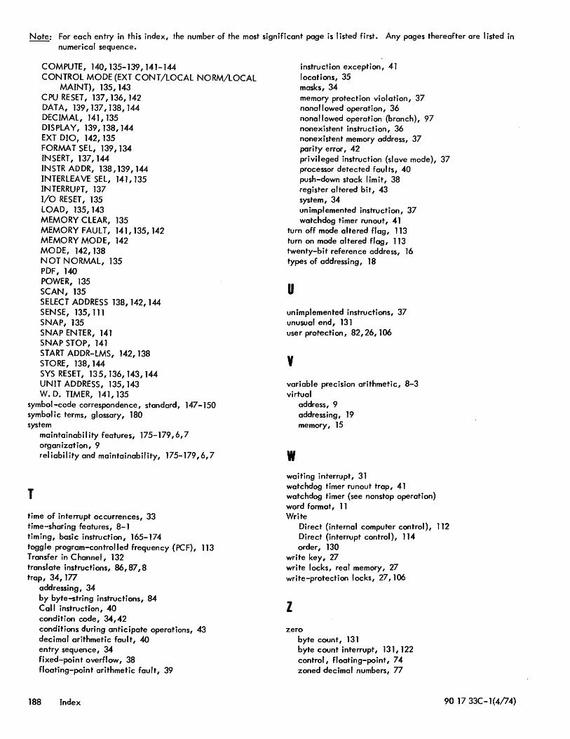
Note: For each entry in this index, the number of the most significant page is listed first. Any pages thereafter are listed in numerical sequence.
COMPUTE, 140, 135-139, 141-144 CONTROL MODE (EXT CONT/LOCAL NORM/LOCAL
MAINT), 135, 143 CPU RESET, 137,136,142 DATA, 139,137,138,144 DECIMAL, 141, 135 DISPLAY, 139,138,144 EXT DIO, 142, 135 FORMAT SEL, 139, 134 INSERT, 137, 144 INSTR ADDR, 138,139,144 INTERLEAVE SEL, 141, 135 INTERRUPT, 137 I/O RESET, 135 LOAD, 135, 143 MEMORY CLEAR, 135 MEMORY FAULT, 141,135,142 MEMORY MODE, 142 MODE, 142, 138 NOT NORMAL, 135 PDF, 140 POWER, 135 SCAN, 135 SELECT ADDRESS 138, 142, 144 SENSE, 135, 111 SNAP, 135 SNAP ENTER, 141 SNAP STOP, 141 START ADDR-LMS, 142, 138 STORE, 138, 144 SYS RESET, 135,136, 143, 144 UNIT ADDRESS, 135, 143 W. D. TIMER, 141, 135
symbol-code correspondence, standard, 147-150 symbol i c terms, glossary, 180 system
T
maintainability features, 175-179,6,7 organization, 9 reliabil ity and maintainabil ity, 175-179,6,7
time of interrupt occurrences, 33 time-sharing features, 8-1 timing, basic instruction, 165-174 toggle program-controlled frequency (PCF), 113 Transfer in Channel, 132 translate instructions, 86,87,8 trap, 34, 177
addressing, 34 by byte-string instructions, 84 Call instruction, 40 condition code, 34,42 conditions during anticipate operations, 43 decimal arithmetic fault, 40 entry sequence, 34 fixed-point overflow, 38 floating-point arithmetic fault, 39
188 Index
instruction exception, 41 locations, 35 masks, 34 memory protection violation, 37 nonallowed operation, 36 nona"owed operation (branch), 97 nonexistent instruction, 36 nonexistent memory address, 37 parity error, 42 privileged instruction (slave mode), 37 processor detected faults, 40 push-down stack I im it, 38 register altered bit, 43 system, 34 unimplemented instruction, 37 watchdog timer runout, 41
turn off mode altered flag, 113 turn on mode altered flag, 113 twenty-bit reference address, 16 types of addressing, 18
u unimplemented instructions, 37 unusual end, 131 user protection, 82,26, 106
v variable precision arithmetic, 8-3 virtual
address, 9 addressing, 19 memory, 15
w waiting interrupt, 31 watchdog timer runout trap, 41 watchdog timer (see nonstop operation) word format, 11 Write
Direct (internal computer control), 112 Direct (interrupt controf), 114 order, 130
write key, 27 write locks, real memory, 27 write-protection locks, 27, 106
z zero
byte count, 131 byte count interrupt, 131, 122 control, floating-point, 74 zoned decimal numbers, 77
90 17 33C-1(4/74)
Xerox Corporation 701 South Aviation Boulevard EI Segundo, California 90245
.Reader Comment Form We would appreciate your comments and suggestions for improving this publication.
XEROX
Publ ication No. I Rev. Letter I Title I Current Date
How did you use this publication? Is the material presented effectively?
o Learning o Installing 0 Sales o Fully Covered DWell o Well Organized o Clear Illustrated o Reference o Maintaining 0 Operating
What is your overall rating of this publication? What is your occupation?
o Very Good o Fair o Very Poor
o Good o Poor
Your other comments may be entered here. Please be specific and give page, column, and line number references where applicable. To report errors, Please use the Xerox Software Improvement or Difficulty Report (1188) instead of this form.
Your Name & Return Address
2190( lV72) Thank You For Your Interest. (fold & fasten as shown on back, no postage needed if mailed in U.S.A.)
Fold
Attn: Programming Publications
Fold
BUSINESS REPLY MAIL No postage stamp necessary if mailed in the United States
Postage will be paid by
Xerox Corporation 701 South Aviation Boulevard EI Segundo, California 90245
First Class Permit No. 229
EI Segundo. California
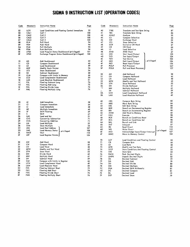
SIGMA 9 INSTRUCTION LIST [OPERATION CODES)
Code Mnemonic Instruction Name Page Code Mnemonic Instruction Name Page
02 LCFI Load Conditions and Floating Control Immediate 52 40 HBS Translate and Test Byte String 87 04 CALI Call I 100 41 TBS Translate Byte String 86 05 CAL2 Call 2 100 44 ANLZ Analyze 55 06 CAL3 Call 3 100 45 CS Compare Selective 66 07 CAL4 Call 4 100 46 XW Exchange Word 53 08 PLW Pull Word 94 47 STS Store Selective 54 09 PSW Push Word 94 48 EOR Exclusive OR Word 67 OA PLM Pull Multiple 95 49 OR OR Word 66 OB PSM Push Multiple 94 4A LS Load Selective 51 OE LPSD Load Program Status Doubleword (privileged) 101 4B AND AND Ward 67 OF XPSD Exchange Program Status Doubleword (privileged) 102 4C SIO
Stoc' 'op,'/O,'p" I 123 40 TIO Test Input/Output 124 4E TOV Test Device 125
10 AD Add Doubleword 59 4F HIO Halt Input/Output privileged 126 11 CD Compare Doubleword 65 4F RIO Reset Input/Output 126 12 LD Load Doubleword 49 ~F POLP Poll Processor 127 13 MSP Modify Stack Pointer 96 ~F POLR Poll and Reset Processor 127 IS STD Store Doubleword 54 18 SO Subtract Doubleword 60
50 AH Add Ha I fword 58 19 ClM Compare with Limits in Memory 66
51 CH Compare Halfword 65 IA LCD Load Complement Doubleword 50
52 LH Load Ha I fward 48 IB LAD Load Absolute Doubleword 51
53 MTH Modify and Test Halfword 63 IC FSL Floating Subtract Long 76
55 STH Stare Halfword 53 10 FAL Floating Add Long 75
56 DH Divide Halfword 61 IE FDL Floating Divide Long 76 -7 MH Multiply Halfword 61 IF FML Floating Multiply Long 76
SH Subtract Halfword 59 SA LCH Load Complement Halfward 49 5B LAH Load Absolute Halfward 49
58 60 CBS Compare Byte String 85
20 AI Add Immediate 61 MBS Move Byte Stri ng 84
21 CI Compare Immediate 64 63 EBS Edit Byte String 88
22 LI Load Immediate 48 64 BDR Branch on Decrementing Register 99
23 MI Multiply Immediate 60 65 BIR Branch on Incrementing Register 99
24 SF Shift Floating 69 66 AWM Add Word to Memory 62
25 S Shift 67 26 LAS Load and Set 51
67 EXU Execute 98 68 BCR Branch on Conditions Reset 99
28 CVS Convert by Subtraction 71 69 BCS Branch on Conditions Set 98
29 CVA Convert by Addition 71 6A BAL Branch and Link 99
2A LM Load Multiple 52 6B INT Interpret 57
2B STM Store Multiple 54 6C RD Rood D;md } 110
2C LRA Lood lleol Addc~, } 107 60 WD Write Direct privileged 112
20 LMS Load Memory Status privileged 108 6E AIO 127
2E WAIT Wait 110 Acknowledge Input/Output Interrupt
2F LRP Load Register Pointer 104 6F MMC Move to Memory Control 104
70 LCF load Conditions and Flooting Control 53 30 AW Add Word 58 71 CB Compare Byte 64 31 CW Compare Word 65 72 LB Load Byte 48 32 LW Load Word 48 73 MTB Modi fy and Test Byte 62 33 MTW Modify and Test Word 63 74 STCF Store Conditions and Floating Control 54 35 STW Store Word 53 75 STB Store Byte 53 36 OW Divide Word 62 76 PACK Pack Decimal Digits 81 37 MW Multiply Word 61 77 UNPK Unpack Decimal Digits 82 38 SW Subtract Word 59 78 OS Decimal Subtract 79 39 CLR Compare with Limits in Register 66 79 DA Decimal Add 79 3A LCW Load Complement Word 49 7A DO Decimal Divide 80 3B LAW Load Absolute Word 50 7B OM Decimal Multiply 80 3C FSS Floating Subtract Short 75 7C DSA Decimal Shift Arithmetic 81 3D FAS Floating Add Short 74 70 DC Decimal Compare 81 3E FDS Floating Divide Short 76 7E DL Decimal Load 79 3F FMS Floating Multiply Short 76 7F DST Decimal Store 79

701 South Aviation Boulevard EI Segundo, California 90245 213679-4511
XE
XEROX® is a trademark of XEROX CORPORATiON .
"
',.
,.
f ~
:' \.
~ , .. ..
•
• " •
~ • .. '