Wide band gap tunability of bulk Cd1−xCaxO
8
Wide band gap tunability of bulk Cd1−xCaxO Velaga Srihari, V. Sridharan, Sharat Chandra, V. S. Sastry, H. K. Sahu et al. Citation: J. Appl. Phys. 109, 013510 (2011); doi: 10.1063/1.3526300 View online: http://dx.doi.org/10.1063/1.3526300 View Table of Contents: http://jap.aip.org/resource/1/JAPIAU/v109/i1 Published by the American Institute of Physics. Related Articles Visible light photocatalysis of single-walled (Zn4/6Cu2/6O)3/(Zn5/6Cu1/6O)3 superlattice nanotube for redox reaction of water calculated by generalized gradient approximations with the Hubbard U model J. Appl. Phys. 111, 034318 (2012) Electronic structure of ternary CdxZn1−xO (0≤x≤0.075) alloys Appl. Phys. Lett. 100, 072106 (2012) A reconstruction of cubic rs-ZnO on MgO (200) substrate through (100) plane of w-ZnO:rs-ZnO for transparent electronic application Appl. Phys. Lett. 100, 072102 (2012) Conduction band structure in wurtzite GaAs nanowires: A resonant Raman scattering study Appl. Phys. Lett. 100, 073102 (2012) Energy band engineering and controlled ptype conductivity of CuAlO2 thin films by nonisovalent CuO alloying Appl. Phys. Lett. 100, 062102 (2012) Additional information on J. Appl. Phys. Journal Homepage: http://jap.aip.org/ Journal Information: http://jap.aip.org/about/about_the_journal Top downloads: http://jap.aip.org/features/most_downloaded Information for Authors: http://jap.aip.org/authors Downloaded 16 Feb 2012 to 203.199.205.25. Redistribution subject to AIP license or copyright; see http://jap.aip.org/about/rights_and_permissions
Transcript of Wide band gap tunability of bulk Cd1−xCaxO

Wide band gap tunability of bulk Cd1−xCaxOVelaga Srihari, V. Sridharan, Sharat Chandra, V. S. Sastry, H. K. Sahu et al. Citation: J. Appl. Phys. 109, 013510 (2011); doi: 10.1063/1.3526300 View online: http://dx.doi.org/10.1063/1.3526300 View Table of Contents: http://jap.aip.org/resource/1/JAPIAU/v109/i1 Published by the American Institute of Physics. Related ArticlesVisible light photocatalysis of single-walled (Zn4/6Cu2/6O)3/(Zn5/6Cu1/6O)3 superlattice nanotube for redoxreaction of water calculated by generalized gradient approximations with the Hubbard U model J. Appl. Phys. 111, 034318 (2012) Electronic structure of ternary CdxZn1−xO (0≤x≤0.075) alloys Appl. Phys. Lett. 100, 072106 (2012) A reconstruction of cubic rs-ZnO on MgO (200) substrate through (100) plane of w-ZnO:rs-ZnO for transparentelectronic application Appl. Phys. Lett. 100, 072102 (2012) Conduction band structure in wurtzite GaAs nanowires: A resonant Raman scattering study Appl. Phys. Lett. 100, 073102 (2012) Energy band engineering and controlled ptype conductivity of CuAlO2 thin films by nonisovalent CuO alloying Appl. Phys. Lett. 100, 062102 (2012) Additional information on J. Appl. Phys.Journal Homepage: http://jap.aip.org/ Journal Information: http://jap.aip.org/about/about_the_journal Top downloads: http://jap.aip.org/features/most_downloaded Information for Authors: http://jap.aip.org/authors
Downloaded 16 Feb 2012 to 203.199.205.25. Redistribution subject to AIP license or copyright; see http://jap.aip.org/about/rights_and_permissions
Wide band gap tunability of bulk Cd1−xCaxOVelaga Srihari,1 V. Sridharan,1,a� Sharat Chandra,2 V. S. Sastry,1 H. K. Sahu,1 andC. S. Sundar3
1X-ray Scattering and Crystal Growth Section, Condensed Matter Physics Division, Indira Gandhi Centrefor Atomic Research, Kalpakkam, Tamil Nadu 603102, India2Ion Beam and Computer Simulation Section, Materials Physics Division, Indira Gandhi Centre for AtomicResearch, Kalpakkam, Tamil Nadu 603102, India3Materials Science Group, Indira Gandhi Centre for Atomic Research, Kalpakkam, Tamil Nadu 603102,India
�Received 25 June 2010; accepted 16 November 2010; published online 6 January 2011�
We report the lattice parameter variation and the band gap tuning of CdO with Ca by preparingthermodynamically stable Cd1−xCaxO solid solution in the entire composition range 0�x�1. Thefunctional dependence of the lattice parameter on Ca concentration is found to deviate fromVegard’s law. The principal band gap is found to vary nonmonotonically over a wide range, from 1.4to 3.9 eV for 0�x�0.8. First principles density functional theory calculations, using full potentiallinearized augmented plane wave methods also predict a nonlinear variation for the lattice parameterand the optical band gap with Ca concentration. From these calculations, contributions from volumedeformation, electron transfer, and structural relaxation are estimated and the results are comparedwith experiments. © 2011 American Institute of Physics. �doi:10.1063/1.3526300�
I. INTRODUCTION
Metal oxide semiconductors, by virtue of their highchemical stability, are attractive alternatives to the conven-tional semiconductors for a wide variety of electronic andoptoelectronic applications. These materials have potentialapplications as transparent conducting oxides �TCOs� anddilute magnetic semiconductors. In view of their importance,there exists a sustained effort to tailor the band gap of thesematerials. This is usually done by alloying together semicon-ductors with differing band gaps. Such alloys, broadly clas-sified as structurally matched and mismatched alloys, fre-quently exhibit nontrivial variations in their structural andoptical properties. These issues are important and warrantdetailed investigations.1 Many groups have focused attentionon the mismatched oxide systems such as ZnO–MgO,2
ZnO–CdO,2 ZnO–CaO �Ref. 3� and matched oxide systemslike BeO–ZnO �Ref. 2� and MgO–NiO.4 Belonging to thelater class, CdO and CaO, on their own, are fairly importantfor technological applications. While CaO is being widelyused as a catalyst,5 cadmium oxide, for instance, is widelyused as TCO in solar cell applications,6,7 flat-panel displays,smart windows, phototransistors as well as IR heat mirrors,gas sensors, low emissive windows, etc. Considering the po-tential applications of CdO, structural, and optical propertiesof rare earth �Y,8 La,9 Sm,10 Gd,11,12 Eu,13 and Dy14�, transi-tion elements �In,8,15,16 Fe,17 Ga,18 and Al19�, Te,20 Tl,21 andSn22,23 doped CdO have been investigated.
For most of the systems, the band gap variation withcomposition deviates from linearity. Conventionally, suchnonlinear variation is fitted to a second order equation,24,25
namely,
Eg�x� = xEg�A� + �1 − x�Eg�B� − boptx�1 − x� , �1�
where Eg �A /B� correspond to the band gap of the end mem-ber A /B and bopt is the optical bowing parameter. The originof the optical bowing parameter is of fundamental impor-tance. Bernard and Zunger24,25 identified three major contri-butions to the optical bowing parameter: �i� volume deforma-tion �VD� contribution due to change in the latticedimensions, �ii� charge exchange �CE� in the alloy relative toits constituent binary subsystems due to the differences in theelectronegativity between the constituents, and �iii� structuralcontribution �S� due to cation–anion bond length relaxationsin the alloy. Correspondingly, the optical bowing parameteris given by24,25
bopt = bVD + bCE + bS. �2�
A linear sum of all these three effects contribute to the non-linearity in Eg as a function of concentration. The opticalbowing parameter of the pseudoternary oxide systems ZnO–CdO and ZnO–BeO systems was reported to be 1.75 eV andas high as 9.3 eV, respectively.2
CdO is an n-type semiconductor with a band gap Eg
=2.2–2.4 eV, crystallizing in a rock salt structure �space
group: Fm3̄m� with a lattice parameter a=4.695 Å.6,26–28
Calcium oxide is an insulator with Eg=7.1 eV and is isos-tructural to CdO and has lattice parameter a=4.81 Å.29–31
CaO, being isostructural with CdO with low lattice param-eter mismatch ��2.6%�, is not only a good candidate fortailoring the band gap of CdO but also for obtaining homo-geneous samples in bulk form. To the best of our knowledge,there are scant systematic and careful investigations of theoptical properties of Cd1−xCaxO system. The present workattempts to fill this gap.
In the present work, high quality specimens ofCd1−xCaxO �0�x�1� have been prepared in bulk form.Systematic and careful investigations of the structural anda�Electronic mail: [email protected].
JOURNAL OF APPLIED PHYSICS 109, 013510 �2011�
0021-8979/2011/109�1�/013510/7/$30.00 © 2011 American Institute of Physics109, 013510-1
Downloaded 16 Feb 2012 to 203.199.205.25. Redistribution subject to AIP license or copyright; see http://jap.aip.org/about/rights_and_permissions

optical properties of II–VI semiconducting Cd1−xCaxO sys-tem were carried out. The optical band gap is found to varynonmonotonically from 1.4 to 3.9 eV for 0�x�0.8, withinthe measurement range. Both, the lattice parameter and theband gap deviate from linearity as expected by virtual crystalapproximation. In order to understand the negative deviationof the optical band gap, detailed band structure calculationwas undertaken and the various contributions to optical bow-ing parameter were calculated.
II. EXPERIMENTAL DETAILS
Solid solution of Cd1−xCaxO with x=0–100 at. % wereprepared by solid state reaction, with CdO �99.999%STREM Chemicals� and CaCO3 �99.95% CERAC� as start-ing materials. Stoichiometric amounts of starting materialswere weighed and mixed thoroughly using mortar and pestle.These mixed powders were heat treated at 800 °C for 8 hand pelletized. Since the melting point of CdO is 1430 °C�Ref. 32� and that of CaO is �2500 °C,33–35 heat treatmentwas carried out for 24 h at different temperatures; forsamples with 5 and 10 at. % Ca at 800 °C, for samples with20, 30, and 40 at. % Ca at 900 °C and for the remainingsamples at 1100 °C. CdO was pelletized and sintered at800 °C for 8 h.
Scanning electron microscope �SEM� and energy disper-sive x-ray spectroscopy �EDX� were carried out on the pel-lets using a Philips XL30 environmental SEM at an operat-ing voltage of 30 kV. Room temperature powder x-raydiffraction �XRD� studies using Cu K� radiation were carriedout on powder samples, using a STOE diffractometer oper-ated in Bragg–Brentano geometry and attached with a sec-ondary graphite monochromator. The measurements wereperformed over the angular range 2�=30° –96° in steps of0.05°. As the atomic scattering factors of cadmium �37.7�and calcium �14.1� �at sin � /�=0.2 Å−1�36 differ widely,dwell time at each 2� step was adjusted such that about 104
counts were obtained for the 100% intense peak ��111� peakin CdO rich samples and �200� peak in CaO rich samples�.UV-Vis-NIR diffuse reflectance spectroscopy �DRS� in therange of 2000–9000 Å was recorded on pelletized samplesusing Thermo Scientific Evaluation 600 UV-Vis Spectrom-eter with BaSO4 coated integration sphere. First principlesband structure calculations were carried out using theWIEN2K package.37 A single unit cell of CdO in rock saltstructure was relaxed for finding the lowest energy latticeparameters. In this configuration we have replaced the Cdatoms by Ca atoms one by one corresponding to 0, 25%,50%, 75%, and 100%. These structures were relaxed fully toobtain the minimum energy configuration. Further calcula-tions were done on these relaxed minimum energy configu-rations in order to obtain the band gap.
III. RESULTS AND DISCUSSIONS
The color of the pellets varies from dark brown at thecadmium oxide end to white at the calcium oxide end. TheSEM images of the samples show that the individual par-ticles are well faceted grains of about 0.9 to 4 �m in sizeand as representative, SEM image of samples with x=0.2
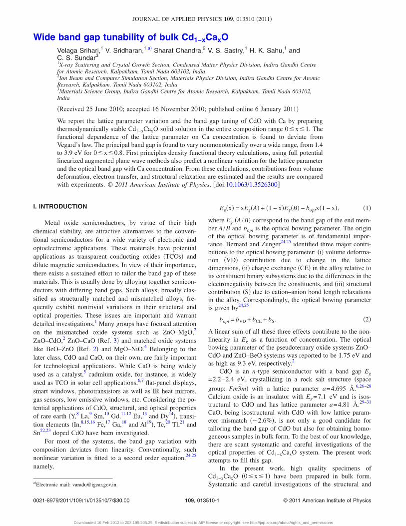
and 0.6 are shown in Fig. 1. The stoichoimetric compositionof the samples was measured by EDX �Fig. 1�. The measuredcomposition agrees, within the instrumental resolution, withthe nominal composition of the samples. Also, we did notobserve any detectable change in the composition, sampledover different regions of a pellet of given nominal composi-tion.
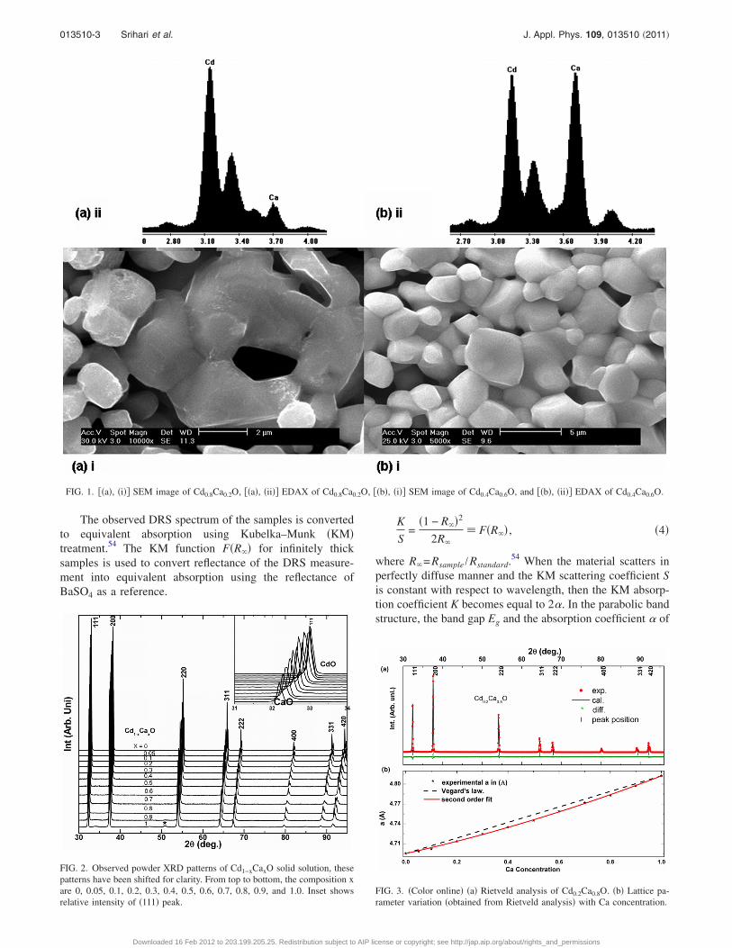
The room temperature powder XRD patterns ofCd1−xCaxO are shown in Fig. 2. No additional peaks couldbe detected in the XRD patterns, indicating that the samplesare monophasic and complete miscibility exists between theend members, except for a minor amount of CaCO3 in CaO�marked by � in Fig. 2�. This may be due to reaction of CaOwith CO2 present in the atmosphere, during the XRD mea-surement. A monotonic shift of all the diffraction peaks tolow 2� value is observed, indicating expansion in the unitcell volume. This is expected as the ionic radius of Ca �1 Å�is larger than Cd �0.95 Å�.38 The inset in Fig. 2 shows theintensity variation in �111� reflection �100% intense peak inCdO� with x. The progressive decrease in the intensity of thisBragg reflection with x is commensurate with the lowZ-element �Ca� progressively substituting the high Z-element�Cd�. The observed XRD patterns are analyzed by Rietveldrefinement39 using GSAS �Ref. 40� for precise lattice param-eter estimation �Fig. 3�a��. The lattice parameters calculatedfrom Rietveld refinement are given in Table I. Figure 3�b�shows the variation in lattice parameter with x. The latticeparameter variation deviates from the linearity as expectedby Vegard’s law.51 The observed variation in lattice param-eter is fitted to a second order equation, similar to that of Eq.�1�.
a�x� = aCaOx + aCdO�1 − x� − bXRDx�1 − x� , �3�
where aCdO /aCaO correspond to the lattice parameter of CdO/CaO and bXRD is the lattice bowing parameter. From the fitthe lattice bowing parameter was estimated to be 0.030 88.
Analogous deviation has been reported for many solidsolutions, such as Mg1−xNixO, which structurally are akin tothe system under study with a bowing of �0.01 �calculatedfrom the work of Kuzmin. et al.4�. Larger deviation fromVegard’s law in the present system is consistent with largerionic radius difference between Cd2+ and Ca2+ �0.05 Å� com-pared to that of Mg2+ and Ni2+ �0.02 Å�.38 For theMg1−xNixO system, the lattice parameter variation was ex-plained by taking into account the second nearest neighbordistance variation, estimated from the x-ray absorption spec-troscopy on the Mg2+ and Ni2+ ions4 or the bond alteration atmicroscopic scale retaining the space group as a whole, asobserved in other systems.52,53 The observed deviation fromthe Vegard’s law in the Cd1−xCaxO system could also arisefrom similar reasons. Thus, detailed information regardinginter-atomic distances �Cd–O, Ca–O, and Ca–Cd� and theirdistribution in the solid solution is crucial to arrive at reliableconclusions regarding large deviation from the Vegard’s law.This is beyond the scope of the conventional XRD studies,which covers only limited scattering vector Q, which isabout 6 Å−1 for Cu K� radiation. Thus, we could not arriveat a conclusion that leads to actual cause for deviation fromthe Vegard’s law.
013510-2 Srihari et al. J. Appl. Phys. 109, 013510 �2011�
Downloaded 16 Feb 2012 to 203.199.205.25. Redistribution subject to AIP license or copyright; see http://jap.aip.org/about/rights_and_permissions
The observed DRS spectrum of the samples is convertedto equivalent absorption using Kubelka–Munk �KM�treatment.54 The KM function F�R�� for infinitely thicksamples is used to convert reflectance of the DRS measure-ment into equivalent absorption using the reflectance ofBaSO4 as a reference.
K
S=
�1 − R��2
2R�
� F�R�� , �4�
where R�=Rsample /Rstandard.54 When the material scatters inperfectly diffuse manner and the KM scattering coefficient Sis constant with respect to wavelength, then the KM absorp-tion coefficient K becomes equal to 2�. In the parabolic bandstructure, the band gap Eg and the absorption coefficient � of
FIG. 1. ��a�, �i�� SEM image of Cd0.8Ca0.2O, ��a�, �ii�� EDAX of Cd0.8Ca0.2O, ��b�, �i�� SEM image of Cd0.4Ca0.6O, and ��b�, �ii�� EDAX of Cd0.4Ca0.6O.
FIG. 2. Observed powder XRD patterns of Cd1−xCaxO solid solution, thesepatterns have been shifted for clarity. From top to bottom, the composition xare 0, 0.05, 0.1, 0.2, 0.3, 0.4, 0.5, 0.6, 0.7, 0.8, 0.9, and 1.0. Inset showsrelative intensity of �111� peak.
FIG. 3. �Color online� �a� Rietveld analysis of Cd0.2Ca0.8O. �b� Lattice pa-rameter variation �obtained from Rietveld analysis� with Ca concentration.
013510-3 Srihari et al. J. Appl. Phys. 109, 013510 �2011�
Downloaded 16 Feb 2012 to 203.199.205.25. Redistribution subject to AIP license or copyright; see http://jap.aip.org/about/rights_and_permissions

a direct band gap semiconductor are related through the wellknown equation:55
��h�n = C�h − Eg� , �5�
where � is the linear absorption coefficient of the material,h is the photon energy, C is a proportionality constant, andn is a constant depending on the nature of the electronictransition. The value of n equals 2, 1/2, 1/3, and 2/3 in thecase of direct allowed, indirect allowed, indirect forbidden,and direct forbidden transition, respectively.56 Using thefunction in Eqs. �4� and �5� one can arrive at:
�F�R�� h�n = C1�hv − Eg� . �6�
Figure 4 shows the �F�R��h�n versus h plots for the
measured composition range, for n=2, namely direct allowedtransition, these plots are linear over wide data range. Thedirect �n=2� band gap Eg of the samples is determined fromintercept of the linear fit of the absorption edge on the ab-scissa �at �F�R��h�2=0�. The absorption edge for the CdOis rather steep with a meniscus tail effect. For 0�x�0.3, theabsorption edge shifts to lower energy, indicating loweringof the fundamental band gap below that of CdO with Casubstitution. With further increase in x, absorption edgeshifts to higher energy, indicating that Eg corresponding tothese compositions are higher than that of CdO. Also, for theCd rich samples �x�0.5�, the absorption edge exhibits sub-stantial tail below Eg, which is absent in the Ca rich samples�x�0.5�. The band gap of CdO is determined to be 2.21 �2�eV and is in agreement with the reported value of CdO.6,26
Due to presence of secondary phase �Fig. 2� and upper limitof instrumental range, optical studies of x=0.9 and 1.0 werenot carried out. The Eg values so obtained are plotted in Fig.5 which shows the variation in direct band gap Eg as a func-tion of x. For the sake of completeness, we have adopted theband gap value of CaO from Refs. 29 and 30 and same isincluded in Table I and in Fig. 5. The observed nonlinearityin band gap is fitted to Eq. �1�, yielding a large value for thebowing parameter bopt, of 8.90 eV. Since the fitting is ratherpoor, no further comment or comparison is made on thisvalue.
A similar nonlinearity in band gap as a function of com-position was observed in Zn1−xCdxO,57 SrS1−xOx,58 Eu dopedCdO,13 and several II–IV as well as III–V semiconductoralloys.2 It is important to note that experimentally observedEg values for 0.05�x�0.3 are lower than that of CdO. Sucha decrease in the band gap is well known in semiconductingalloys such as ZnTe1−xSx system.2 This behavior is also ex-pected in alloys with large difference in the band gap of theend members,25 as in the present study, implying a large
TABLE I. Experimentally observed lattice constants and fundamental direct band gap of Cd1−xCaxO compared to experiment, theoretical results, and otherreports. The superscripts indicate the reference numbers.
Caconcentration
�at. %�
a��
Eg
�eV�
Experimental�Rietveld�
Calculated�DFT�
Experimental Calculated
This work Other workThis work
�DFT� Other work
0 �CdO� 4.6950 �4� 4.69 2.23 2.3 �Ref. 26� 1.82 0.8 �Ref. 41�, 1.8 �Ref. 42�, 2.4 �Ref. 43�, 1.61 �Ref. 44�5 4.6985 �2� 1.410 4.7017 �1� 1.3820 4.7145 �8� 1.6125 4.7191 1.8730 4.7246 �4� 2.0840 4.7359 �5� 2.4150 4.7448 �5� 4.7449 2.83 2.0760 4.7578 �4� 3.1970 4.7716 �4� 3.5475 4.7773 3.2680 4.7839 �8� 3.990 4.7974 �5�
100 �CaO� 4.8123 �7� 4.81 7.1 �Refs. 29 and 30� 4.64.5 �Ref. 3�, 4.79 �Ref. 45�, 5.02 �Ref. 46�, 5.2 �Ref. 47�, 5.93
�Ref. 48�, 7.1 �Ref. 49�, 7.74 �Ref. 50�
FIG. 4. �Color online� Plot of ��h�F�R���2 vs h, absorption edge ener-gies are determined by the intercept of linear fit to the absorption edge forthe samples with Ca concentration up to 80 at. %.
013510-4 Srihari et al. J. Appl. Phys. 109, 013510 �2011�
Downloaded 16 Feb 2012 to 203.199.205.25. Redistribution subject to AIP license or copyright; see http://jap.aip.org/about/rights_and_permissions

value for optical bowing parameter.25 One possible causemay be the introduction of defect states within the band gap.This view is supported by the marginal increase in the tail ofthe absorption edge observed, indicating the possibility ofthe presence of defects. However, it is pertinent to note thatdecrease in the Eg is not observed to be correlated with theincrease in the width of the tail. Hence, the observed lower-ing of the band gap may not fundamentally arise only fromthe defect states, and may be intrinsic to the alloys them-selves. Also, the defect states are generally expected to beshallow states, typically about 500 meV below the conduc-tion band edge resulting in n-type degenerate system. It isknown that such systems exhibit an optical band gap, whichis more than the fundamental band gap and is known asMoss–Brustein �MB� effect. Hence, observed decrease in theoptical band gap is not due to defects.
Another possibility to be considered is that the opticalband gap estimated for pure CdO suffers from MB effect.MB effect has been reported in anivalent substituted systemslike �In3+�,16 �Ga3+�,18 �Al3+�,19 and �Y3+� �Ref. 8� or in thinfilms, wherein the CdO is shown to be highly degeneraten-type semiconductor. In all these studies, the reported opti-cal band gap is found to fall in a narrow range, 2.3 eV to2.63 eV. However, optical band gap reported for polycrystal-line CdO in the present work is 2.21 �2� eV, lower than theoptical band gap range for the samples suffering from MBeffect. This implies that the reported optical band gap of CdOrepresents the fundamental band gap free from MB effect.
With a view to understand the deviation from linearity ofthe lattice parameter and band gap with composition, a de-tailed band structure calculation was carried out. We per-formed first principles calculations using the nonscalar rela-tivistic full potential linearized augmented plane wave �FP-LAPW� method for Cd1−xCaxO �x=0, 25, 50, 75, and100 at. %� in order to study its structural and electronicproperties within the frame-work of density functional theory�DFT� with the generalized gradient approximation using thePBE96 �Ref. 59� for the exchange and correlation functional.The Kohn–Sham equations were solved with the FP-LAPWtechnique, as implemented in the WIEN2K package.37 In thepresent self-consistent calculation, a muffin-tin model for the
crystal potential is assumed. The electrons are divided intotwo groups: the core electrons whose charge densities areconfined within the muffin-tin spheres and the valence elec-trons outside the spheres. In either region of the unit cell,different basis sets are used to expand the wave function,charge density, and the potential function. Inside the non-overlapping spheres of muffin-tin radius, RMT, around eachatom, a linear combination of the product of the radial solu-tions of the Schrodinger equation and the spherical harmon-ics is used, while the plane wave basis set is used in theinterstitial region. Nonoverlapping sphere radius RMT is cho-sen in such a way that there is no charge leakage from thecore and total energy convergence is ensured. The values ofRMT for Cd, Ca, and O are of 2.33 a.u., 2.33 a.u., and 2.07a.u., respectively. These RMT values were chosen such thatthe core charge leakage from the muffin-tin spheres is mini-mum. The maximum value of angular momentum lmax=10 istaken for the wave function expansion inside the atomicspheres. For plane wave expansion of the electronic wavefunction in the interstitial region a plane wave cut-off valueof KmaxRMT=12 was taken for all the calculations. A meshof �1000 k-points in the binary compounds is taken for theirreducible Brillouin zone integrations. Total energy conver-gence is ensured using different values of the plane wavecut-off as well as the number of k-points. Real and imaginaryparts of the dielectric constant were calculated using the codeincorporated in the WIEN2K package. A single unit cell ofCdO in rock salt structure was relaxed for finding the lowestenergy lattice parameters. In this configuration we have re-placed the Cd atoms by Ca atoms one by one correspondingto 0, 25%, 50%, 75%, and 100%. These structures were re-laxed fully to obtain the new minimum energy configuration.Further calculations were done on these relaxed minimumenergy configurations in order to derive the different physicalquantities.
The calculated lattice parameters of the relaxed struc-tures are given in Table I and are in agreement with thatestimated from the XRD studies. It is clearly seen from Fig.6�a� that calculated lattice parameter variation also exhibits adeviation from Vegard’s law. Fitted to Eq. �1�, the latticeconstant bowing parameter was estimated to be 0.014 69 and
FIG. 5. �Color online� Variation in the band gap with Ca concentration. Thevalue of Eg for CaO adopted from Whited et al. �Ref. 56�.
FIG. 6. �Color online� �a� The variation in lattice parameter obtained fromDFT calculation with Ca concentration. �b� Variation in the band gap withCa concentration �calculated using DFT�.
013510-5 Srihari et al. J. Appl. Phys. 109, 013510 �2011�
Downloaded 16 Feb 2012 to 203.199.205.25. Redistribution subject to AIP license or copyright; see http://jap.aip.org/about/rights_and_permissions

is half of the value estimated from the diffraction data. Fromthe calculated absorption data, analysis similar to experimen-tal data was carried out and optical band gap was calculated.Figure 6�b� shows the variation in calculated optical bandgap with composition. The band gap calculated by DFT isless than the experimentally observed value, a generic fea-ture of the DFT calculations.60 Notwithstanding this, DFTcalculations also show a nonlinear variation in bad gap withdopant concentration x. In view of the perfect crystal �with-out defects and disorder� considered for the DFT calcula-tions, the quadratic variation in the Eg with x, implies thatthis feature is intrinsic to the Cd1−xCaxO system. A fit to Eq.�1�, yields optical bowing parameter to be 4.42 eV which isalso about half of the value, 8.90 eV, estimated from theexperimental data.
Following Bernard and Zunger24,25 the values of bVD,bCE, and bS were calculated. It is found that bVD=1.34 eV,bCE=0.7 eV, and bS=2.52 eV, which adds to bopt
=4.56 eV and this compares well with calculated opticalbowing parameter from Eg variation �Fig. 6�b��. From therelative magnitude of these factors, it is seen that contribu-tion of structural relaxation is most significant as is found inmany of the semiconducting systems. Contribution from vol-ume change is expected since the difference between the cellvolumes is about 7%. Least contribution comes from chargetransfer, which arises due to change in the bond characteris-tics. In order to see changes in bonding character, the elec-tron density was extracted using maximum entropy method�MEM�. The observed powder XRD patterns are used to cal-culate the real and imaginary parts of structure factor usingRIETAN,61 which are further used for calculating the chargedensity in a unit cell using PRIMA.62,63 The MEM refinementsare carried out by dividing the unit cell into 505050 pixels. As a representative, the three-dimensional elec-tron density distribution in the form of isoelectron density
surfaces in the unit cell and two-dimensional isoelectrondensity contour plots on the �100� plane of CdO, Cd0.4Ca0.6Oand CaO are shown in Fig. 7, plotted using VESTA.62,63
Substantial change in the bonding nature, estimated interms of Philip’s electronegativity is amply born out in theelectron density distribution �Fig. 7�. Owing to the large dif-ferences in density of the core electrons in Cd, Ca, and O, aprofound variation in the size of the core region and thedensity of the electrons at the atom site can be seen. Thecharge density in the region between Cd/Ca and O atoms isfound to be more in Cd rich samples than in the Ca richsamples. The charge density in the Ca rich samples is con-centrated on the ions whereas a wider distribution of thecharge density between the ions in the Cd rich samples canbe observed. It implies that the bonding character betweenthe cation and anion progressively changes from covalent toionic bonding as the concentration of the Ca is increased.The observed change in bonding character from covalent toionic is in accordance with Phillip’s ionic electronegativityof CdO �0.785 eV,64 likely to be covalent� and CaO �0.913eV,64 more likely to be ionic�. This manifest in the opticalbowing parameter.
IV. CONCLUSIONS
The lattice parameter and band gap of the Ca1−xCaxOsolid solution deviates strongly from linearity. Despite theirsimilarity in structure and small mismatch between the lat-tice parameter of the end members, deviation of the latticeparameter from Vegard’s law indicates that local structure isdifferent from that of average structure as determined frompowder XRD studies. For 0.05�x�0.3, the band gap �Eg�value is lower than that of CdO itself. In absence of appre-ciable change in the tail of the absorption curve with x andnoticeable correlation, it is argued that lowering of Eg value
FIG. 7. �Color online� Volume isosurfaces and 2D contour plots �in �001� plane� of the charge density of ��a1� and �a2�� CdO, ��b1� and �b2�� Cd0.4Ca0.6O,and ��c1� and �c2�� CaO.
013510-6 Srihari et al. J. Appl. Phys. 109, 013510 �2011�
Downloaded 16 Feb 2012 to 203.199.205.25. Redistribution subject to AIP license or copyright; see http://jap.aip.org/about/rights_and_permissions
is not due to defects but is intrinsic to the system, though theprecise cause is not understood. FP-LAPW methods also pre-dict negative deviation for the lattice parameter and Eg withx. From the calculation, it is seen that structural relaxationand VD contribute largest to the observed negative deviationof the Eg with x, though there is substantial change in thebonding nature from more covalent �CdO� to ionic �CaO�.From these observations, it is being speculated that theCd1−xCaxO might belong to persistence type alloy systemwhich has to be confirmed by other optical studies.
ACKNOWLEDGMENTS
Authors would like to acknowledge the National Centerfor Catalysis Research �NCCR� at the Department of Chem-istry, Indian Institute of Technology Madras, Chennai forhelping in carrying out DRS measurement. Srihari acknowl-edges the financial support provided by Department ofAtomic Energy �DAE�, India for pursuing this research aspart of his doctoral work at Indira Gandhi Center for AtomicResearch �IGCAR�, Kalpakkam, India.
1J. Wu, W. Shan, and W. Walukiewicz, Semicond. Sci. Technol. 17, 860�2002�.
2S. Adachi, Properties of Semiconductor Alloys: Group-IV, III–V and II–VISemiconductors �Wiley, New York, 2009�, and the references therein.
3S. Nazir, N. Ikram, B. Amin, M. Tanveer, A. Shaukat, and Y. Saeed, J.Phys. Chem. Solids 70, 874 �2009�.
4A. Kuzmin and N. Mironova, J. Phys.: Condens. Matter 10, 7937 �1998�.5M. Kouzu, S. Yamanaka, J. Hidaka, and M. Tsunomori, Appl. Catal., A355, 94 �2009�.
6N. Ueda, H. Maeda, H. Hosono, and H. Kawazoe, J. Appl. Phys. 84, 6174�1998�.
7J. Santos-Cruz, G. Torres-Delgado, R. Castanedo-Pérez, S. Jiménez-Sandoval, J. Márquez-Marίn, and O. Zelaya-Angel, Sol. Energy 80, 142�2006�.
8Y. Dou, T. Fishlock, R. G. Egdell, D. S. L. Law, and G. Beamson, Phys.Rev. B 55, R13381 �1997�.
9A. A. Dakhel and A. Y. Ali-Mohamed, J. Sol-Gel Sci. Technol. 44, 241�2007�.
10A. A. Dakhel, Mater. Chem. Phys. 117, 284 �2009�.11A. A. Dakhel and A. Y. Ali-Mohamed, J. Sol-Gel Sci. Technol. 55, 348
�2010�.12A. A. Dakhel, J. Alloys Compd. 504, 7 �2010�.13A. A. Dakhel, Opt. Mater. 31, 691 �2009�.14A. A. Dakhel, Eur. Phys. J.: Appl. Phys. 45, 20303 �2009�.15S. Kose, F. Atay, V. Bilgin, and I. Akyuz, Int. J. Hydrogen Energy 34,
5260 �2009�.16H. M. Ali, H. A. Mohamed, M. M. Wakkad, and M. F. Hasaneen, Thin
Solid Films 515, 3024 �2007�.17A. A. Dakhel, Thin Solid Films 518, 1712 �2010�.18A. A. Dakhel, Sol. Energy 82, 513 �2008�.19M. K. R. Khan, M. A. Rahman, M. Shahjahan, M. M. Rahman, M.A.
Hakim, D. K. Saha ,and J. U. Khan, Curr. Appl. Phys. 10, 790 �2010�.20A. A. Dakhel, Sol. Energy 84, 1433 �2010�.21A. A. Dakhel, Phys. Status Solidi A 205, 2704 �2008�.22Z. Zhao, D. L. Morel, and C. S. Ferekides, Thin Solid Films 413, 203
�2002�.23L. R. de León-Gutiérrez, J. J. Cayente-Romero, J. M. Peza-Tapia, E.
Barrera-Calva, J. C. Martínez-Flores, and M. Ortega-López, Mater. Lett.60, 3866 �2006�.
24J. E. Bernard and A. Zunger, Phys. Rev. B 34, 5992 �1986�.25J. E. Bernard and A. Zunger, Phys. Rev. B 36, 3199 �1987�.
26F. P. Koffyberg, Phys. Rev. B 13, 4470 �1976�.27I. N. Demchenko, J. D. Denlinger, M. Chernyshova, K. M. Yu, D. T.
Speaks, P. Olalde-Velasco, O. Hemmers, W. Walukiewicz, A. Derkachova,and K. Lawniczak-Jablonska, Phys. Rev. B 82, 075107 �2010�.
28ICDD PDF No. 05-0640.29J. A. McLeod, R. G. Wilks, N. A. Skorikov, L. D. Finkelstein, M. Abu-
Samak, E. Z. Kurmaev, and A. Moewes, Phys. Rev. B 81, 245123 �2010�,and the references therein.
30R. C. Whited, C. J. Flaten, and W. C. Walker, Solid State Commun. 13,1903 �1973�.
31ICDD PDF No. 37-1497.32D. H. Fan, J. Cryst. Growth 311, 2300 �2009�, and the references therein.33J. Yang, M. Kuwabara, T. Asano, A. Chuma, and J. Du, ISIJ Int. 47, 1401
�2007�.34C. C. Wang, S. A. Akbar, W. Chen, and V. D. Patton, J. Mater. Sci. 30,
1627 �1995�.35R. H. Borgwardt, Chem. Eng. Sci. 44, 53 �1989�.36B. D. Cullity, Elements of X-Ray Diffraction, 3rd ed. �Prentice Hall, Upper
Saddle River, NJ, 2001�.37P. Blaha, K. Schwarz, G. K. H. Madsen, D. Kvasnicka, and J. Luitz,
WIEN2K, An Augmented Plane Wave, Local Orbitals Program for Calcu-lating Crystal Properties �Karlheinz Schwarz, Technical Universität,Wien, Austria, 2001�.
38R. D. Shannon and C. T. Prewitt, Acta Crystallogr., Sect. B: Struct. Crys-tallogr. Cryst. Chem. 25, 925 �1969�.
39R. A. Young, The Rietveld Method �Oxford University Press, USA, 2002�.40A. C. Larson and R. B. Von Dreele, “General structure analysis system
�GSAS�,” Los Alamos National Laboratory Report No. LAUR 86-748,1994 �unpublished�.
41J. C. Boettger and A. B. Kunz, Phys. Rev. B 27, 1359 �1983�.42J. E. Jaffe, R. Pandey, and A. B. Kunz, Phys. Rev. B 43, 14030 �1991�,
and the references therein.43A. Breeze and P. G. Perkins, Solid State Commun. 13, 1031 �1973�.44Y. Dou, R. G. Egdell, D. S. L. Law, N. M. Harrison, and B. G. Searle, J.
Phys.: Condens. Matter 10, 8447 �1998�.45S. K. Medeiros, E. L. Albuquerque, F. F. Maia, Jr., J. S. de Sousa, E. W. S.
Caetano, and V. N. Freire, J. Phys. D: Appl. Phys. 40, 1655 �2007�.46H. Baltache, R. Khenata, M. Sahnoun, M. Driz, B. Abbar, and B. Bouhafs,
Physica B 344, 334 �2004�.47G. Kalpana, B. Palanivel, and M. Rajagopalan, Phys. Rev. B 52, 4 �1995�.48L. F. Mattheiss, Phys. Rev. B 5, 290 �1972�.49N. Daude, C. Jouanin, and C. Gout, Phys. Rev. B 15, 2399 �1977�.50R. Pandey, J. E. Jaffe, and A. Barry Kunz, Phys. Rev. B 43, 9228 �1991�.51D. Zhou and B. F. Usher, J. Phys. D: Appl. Phys. 34, 1461 �2001�.52I.-K. Jeong, F. Mohiuddin-Jacobs, V. Petkov, S. J. L. Billinge, and S.
Kycia, Phys. Rev. B 63, 205202 �2001�.53V. Petkov, I.-K. Jeong, J. S. Chung, M. F. Thorpe, S. Kycia, and S. J. L.
Billinge, Phys. Rev. Lett. 83, 4089 �1999�.54G. Kortüm, Reflectance Spectroscopy �Springer, Berlin, 1969�.55J. I. Pankove, Optical Processes in Semiconductors �Prentice-Hall, New
Jersey, 1971�.56D. G. Barton, M. Shtein, R. D. Wilson, S. L. Soled, and E. Iglesia, J. Phys.
Chem. B 103, 630 �1999�.57J. Ishihara, A. Nakamura, S. Shigemori, T. Aoki, and J. Temmyo, Appl.
Surf. Sci. 244, 381 �2005�.58S. Labidi, M. Labidi, H. Meradji, S. Ghemid, and F. El Haj Hassan,
Physica B 404, 4100 �2009�.59J. P. Perdew, K. Burke, and M. Ernzerhof, Phys. Rev. Lett. 77, 3865
�1996�.60D. S. Sholl and J. A. Steckel, Density Functional Theory: A Practical
Introduction �Wiley, New York, 2009�, p. 28.61F. Izumi and T. Ikeda, Mater. Sci. Forum 321–324, 198 �2000�.62F. Izumi and R. A. Dilanian, Recent Research Developments in Physics
�Transworld Research Network, Trivandrum, 2002�, Pt. II, Vol. 3, pp. 699–726.
63F. Izumi, Solid State Ionics 172, 1 �2004�.64J. C. Phillips, Rev. Mod. Phys. 42, 317 �1970�.
013510-7 Srihari et al. J. Appl. Phys. 109, 013510 �2011�
Downloaded 16 Feb 2012 to 203.199.205.25. Redistribution subject to AIP license or copyright; see http://jap.aip.org/about/rights_and_permissions