uPD78011H(A), 78012H(A), 78013H(A), 78014H(A) DS
68
To our customers, Old Company Name in Catalogs and Other Documents On April 1 st , 2010, NEC Electronics Corporation merged with Renesas Technology Corporation, and Renesas Electronics Corporation took over all the business of both companies. Therefore, although the old company name remains in this document, it is a valid Renesas Electronics document. We appreciate your understanding. Renesas Electronics website: http://www.renesas.com April 1 st , 2010 Renesas Electronics Corporation Issued by: Renesas Electronics Corporation (http://www.renesas.com) Send any inquiries to http://www.renesas.com/inquiry.
-
Upload
khangminh22 -
Category
Documents
-
view
5 -
download
0
Transcript of uPD78011H(A), 78012H(A), 78013H(A), 78014H(A) DS
To our customers,
Old Company Name in Catalogs and Other Documents
On April 1st, 2010, NEC Electronics Corporation merged with Renesas Technology
Corporation, and Renesas Electronics Corporation took over all the business of both companies. Therefore, although the old company name remains in this document, it is a valid Renesas Electronics document. We appreciate your understanding.
Renesas Electronics website: http://www.renesas.com
April 1st, 2010 Renesas Electronics Corporation
Issued by: Renesas Electronics Corporation (http://www.renesas.com)
Send any inquiries to http://www.renesas.com/inquiry.
Notice 1. All information included in this document is current as of the date this document is issued. Such information, however, is
subject to change without any prior notice. Before purchasing or using any Renesas Electronics products listed herein, please confirm the latest product information with a Renesas Electronics sales office. Also, please pay regular and careful attention to additional and different information to be disclosed by Renesas Electronics such as that disclosed through our website.
2. Renesas Electronics does not assume any liability for infringement of patents, copyrights, or other intellectual property rights of third parties by or arising from the use of Renesas Electronics products or technical information described in this document. No license, express, implied or otherwise, is granted hereby under any patents, copyrights or other intellectual property rights of Renesas Electronics or others.
3. You should not alter, modify, copy, or otherwise misappropriate any Renesas Electronics product, whether in whole or in part. 4. Descriptions of circuits, software and other related information in this document are provided only to illustrate the operation of
semiconductor products and application examples. You are fully responsible for the incorporation of these circuits, software, and information in the design of your equipment. Renesas Electronics assumes no responsibility for any losses incurred by you or third parties arising from the use of these circuits, software, or information.
5. When exporting the products or technology described in this document, you should comply with the applicable export control laws and regulations and follow the procedures required by such laws and regulations. You should not use Renesas Electronics products or the technology described in this document for any purpose relating to military applications or use by the military, including but not limited to the development of weapons of mass destruction. Renesas Electronics products and technology may not be used for or incorporated into any products or systems whose manufacture, use, or sale is prohibited under any applicable domestic or foreign laws or regulations.
6. Renesas Electronics has used reasonable care in preparing the information included in this document, but Renesas Electronics does not warrant that such information is error free. Renesas Electronics assumes no liability whatsoever for any damages incurred by you resulting from errors in or omissions from the information included herein.
7. Renesas Electronics products are classified according to the following three quality grades: “Standard”, “High Quality”, and “Specific”. The recommended applications for each Renesas Electronics product depends on the product’s quality grade, as indicated below. You must check the quality grade of each Renesas Electronics product before using it in a particular application. You may not use any Renesas Electronics product for any application categorized as “Specific” without the prior written consent of Renesas Electronics. Further, you may not use any Renesas Electronics product for any application for which it is not intended without the prior written consent of Renesas Electronics. Renesas Electronics shall not be in any way liable for any damages or losses incurred by you or third parties arising from the use of any Renesas Electronics product for an application categorized as “Specific” or for which the product is not intended where you have failed to obtain the prior written consent of Renesas Electronics. The quality grade of each Renesas Electronics product is “Standard” unless otherwise expressly specified in a Renesas Electronics data sheets or data books, etc.
“Standard”: Computers; office equipment; communications equipment; test and measurement equipment; audio and visual equipment; home electronic appliances; machine tools; personal electronic equipment; and industrial robots.
“High Quality”: Transportation equipment (automobiles, trains, ships, etc.); traffic control systems; anti-disaster systems; anti-crime systems; safety equipment; and medical equipment not specifically designed for life support.
“Specific”: Aircraft; aerospace equipment; submersible repeaters; nuclear reactor control systems; medical equipment or systems for life support (e.g. artificial life support devices or systems), surgical implantations, or healthcare intervention (e.g. excision, etc.), and any other applications or purposes that pose a direct threat to human life.
8. You should use the Renesas Electronics products described in this document within the range specified by Renesas Electronics, especially with respect to the maximum rating, operating supply voltage range, movement power voltage range, heat radiation characteristics, installation and other product characteristics. Renesas Electronics shall have no liability for malfunctions or damages arising out of the use of Renesas Electronics products beyond such specified ranges.
9. Although Renesas Electronics endeavors to improve the quality and reliability of its products, semiconductor products have specific characteristics such as the occurrence of failure at a certain rate and malfunctions under certain use conditions. Further, Renesas Electronics products are not subject to radiation resistance design. Please be sure to implement safety measures to guard them against the possibility of physical injury, and injury or damage caused by fire in the event of the failure of a Renesas Electronics product, such as safety design for hardware and software including but not limited to redundancy, fire control and malfunction prevention, appropriate treatment for aging degradation or any other appropriate measures. Because the evaluation of microcomputer software alone is very difficult, please evaluate the safety of the final products or system manufactured by you.
10. Please contact a Renesas Electronics sales office for details as to environmental matters such as the environmental compatibility of each Renesas Electronics product. Please use Renesas Electronics products in compliance with all applicable laws and regulations that regulate the inclusion or use of controlled substances, including without limitation, the EU RoHS Directive. Renesas Electronics assumes no liability for damages or losses occurring as a result of your noncompliance with applicable laws and regulations.
11. This document may not be reproduced or duplicated, in any form, in whole or in part, without prior written consent of Renesas Electronics.
12. Please contact a Renesas Electronics sales office if you have any questions regarding the information contained in this document or Renesas Electronics products, or if you have any other inquiries.
(Note 1) “Renesas Electronics” as used in this document means Renesas Electronics Corporation and also includes its majority-owned subsidiaries.
(Note 2) “Renesas Electronics product(s)” means any product developed or manufactured by or for Renesas Electronics.
The information in this document is subject to change without notice.
© 1997
DATA SHEET
Document No. U12174EJ1V0DS00 (1st edition)Date Published March 1997 NPrinted in Japan
MOS INTEGRATED CIRCUIT
µPD78011H(A), 78012H(A), 78013H(A), 78014H(A)
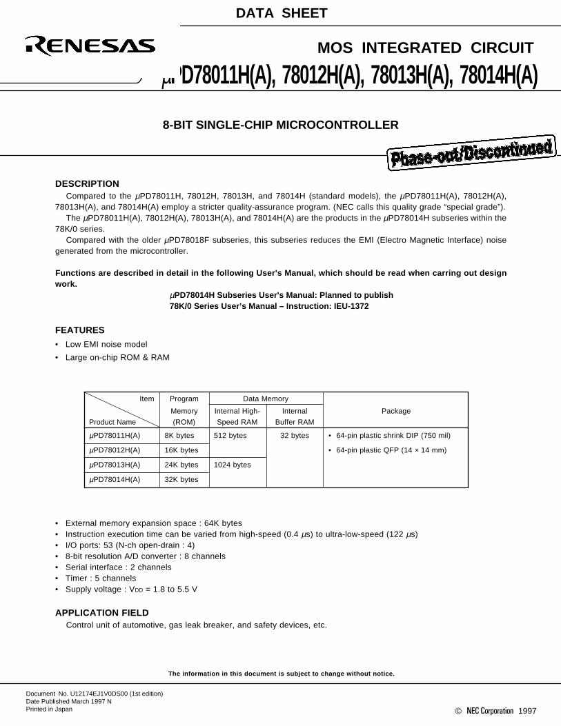
DESCRIPTIONCompared to the µPD78011H, 78012H, 78013H, and 78014H (standard models), the µPD78011H(A), 78012H(A),
78013H(A), and 78014H(A) employ a stricter quality-assurance program. (NEC calls this quality grade “special grade”).The µPD78011H(A), 78012H(A), 78013H(A), and 78014H(A) are the products in the µPD78014H subseries within the
78K/0 series.Compared with the older µPD78018F subseries, this subseries reduces the EMI (Electro Magnetic Interface) noise
generated from the microcontroller.
Functions are described in detail in the following User's Manual, which should be read when carring out designwork.
µPD78014H Subseries User's Manual: Planned to publish78K/0 Series User’s Manual – Instruction: IEU-1372
FEATURES
• Low EMI noise model
• Large on-chip ROM & RAM
8-BIT SINGLE-CHIP MICROCONTROLLER
Item Program Data Memory
Memory Internal High- Internal Package
Product Name (ROM) Speed RAM Buffer RAM
µPD78011H(A) 8K bytes 512 bytes 32 bytes • 64-pin plastic shrink DIP (750 mil)
µPD78012H(A) 16K bytes • 64-pin plastic QFP (14 × 14 mm)
µPD78013H(A) 24K bytes 1024 bytes
µPD78014H(A) 32K bytes
• External memory expansion space : 64K bytes• Instruction execution time can be varied from high-speed (0.4 µs) to ultra-low-speed (122 µs)• I/O ports: 53 (N-ch open-drain : 4)• 8-bit resolution A/D converter : 8 channels• Serial interface : 2 channels• Timer : 5 channels• Supply voltage : VDD = 1.8 to 5.5 V
APPLICATION FIELDControl unit of automotive, gas leak breaker, and safety devices, etc.
µPD78011H(A), 78012H(A), 78013H(A), 78014H(A)
2
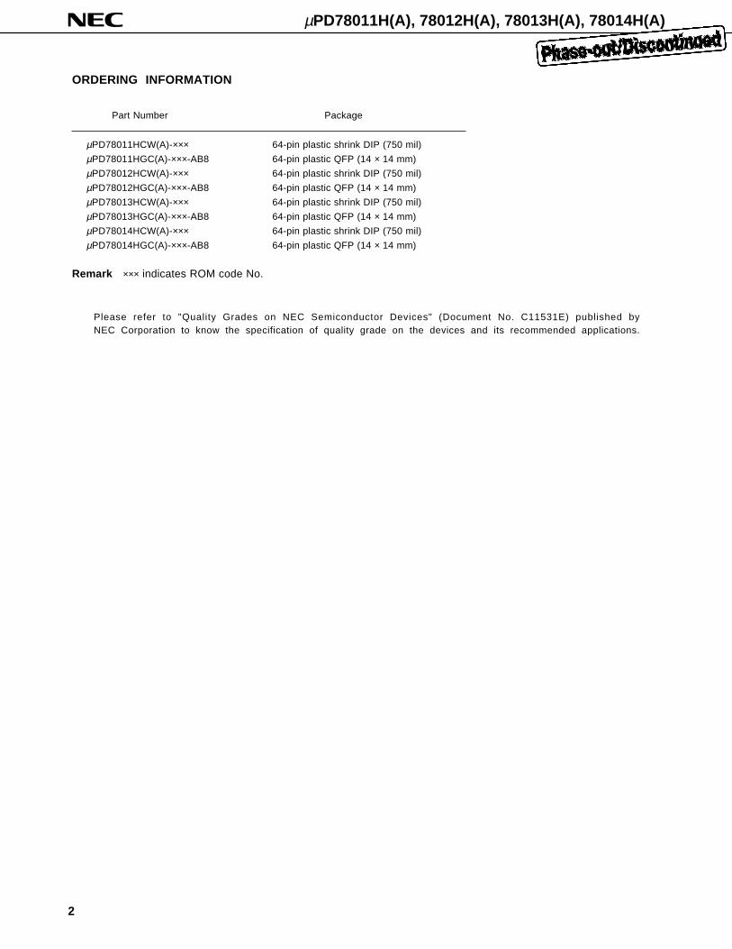
ORDERING INFORMATION
Part Number Package
µPD78011HCW(A)-××× 64-pin plastic shrink DIP (750 mil)
µPD78011HGC(A)-×××-AB8 64-pin plastic QFP (14 × 14 mm)
µPD78012HCW(A)-××× 64-pin plastic shrink DIP (750 mil)
µPD78012HGC(A)-×××-AB8 64-pin plastic QFP (14 × 14 mm)
µPD78013HCW(A)-××× 64-pin plastic shrink DIP (750 mil)
µPD78013HGC(A)-×××-AB8 64-pin plastic QFP (14 × 14 mm)
µPD78014HCW(A)-××× 64-pin plastic shrink DIP (750 mil)
µPD78014HGC(A)-×××-AB8 64-pin plastic QFP (14 × 14 mm)
Remark ××× indicates ROM code No.
Please refer to "Quality Grades on NEC Semiconductor Devices" (Document No. C11531E) published byNEC Corporation to know the specification of quality grade on the devices and its recommended applications.
µPD78011H(A), 78012H(A), 78013H(A), 78014H(A)
3
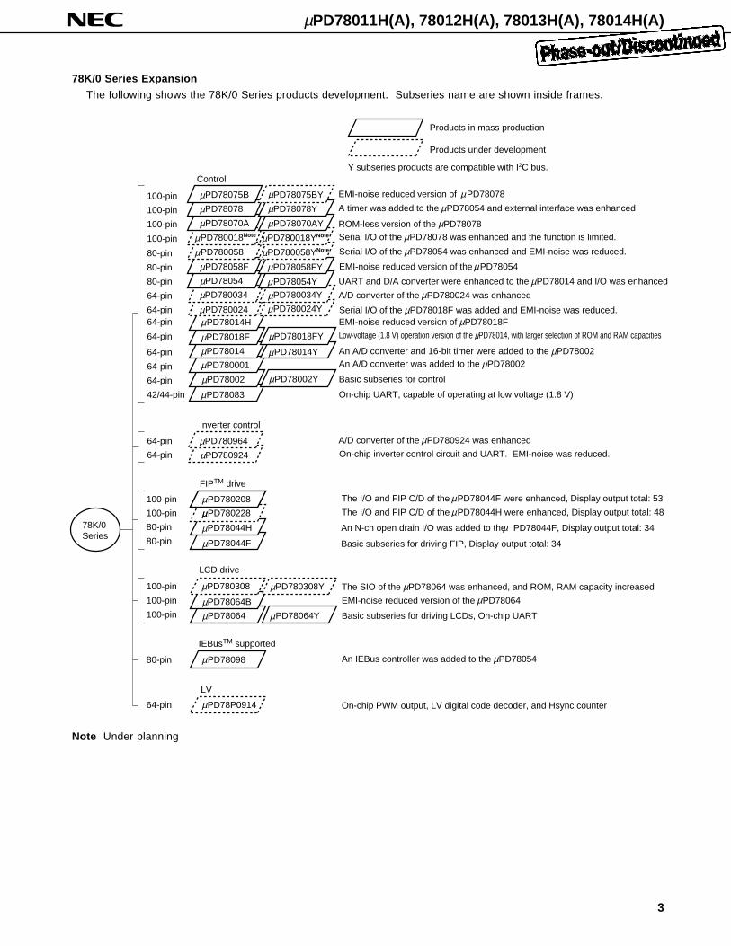
78K/0 Series Expansion
The following shows the 78K/0 Series products development. Subseries name are shown inside frames.
Note Under planning
64-pin
64-pin
64-pin
64-pin
80-pin
80-pin EMI-noise reduced version of the PD78054
UART and D/A converter were enhanced to the PD78014 and I/O was enhanced PD78054 PD78054Y
PD78058F PD78058FY
PD780034
PD780024
PD780964
PD780924
PD780034Y
PD780024Y
µµµµ
µ
µµµµ
µ
64-pin
A/D converter of the PD780024 was enhanced
Serial I/O of the PD78018F was added and EMI-noise was reduced.
On-chip inverter control circuit and UART. EMI-noise was reduced.
µµ
µµ
A/D converter of the PD780924 was enhancedµ
PD78044F
PD78044H
80-pin
80-pin
PD78064
PD78064B
PD780308
100-pin
100-pin
100-pin PD780308Y
PD78064Y
PD7809880-pin
PD78P091464-pin
78K/0Series
An N-ch open drain I/O was added to the PD78044F, Display output total: 34
Basic subseries for driving FIP, Display output total: 34
LCD drive
The SIO of the PD78064 was enhanced, and ROM, RAM capacity increased
EMI-noise reduced version of the PD78064
Basic subseries for driving LCDs, On-chip UART
IEBusTM supported
An IEBus controller was added to the PD78054
LV
On-chip PWM output, LV digital code decoder, and Hsync counter
µ
µ
µ
µµµ
µ
µ
µ
µµ
µ
µµ
µ
µ
PD78083
PD78002 PD78002Y
PD780001
PD78014 PD78014Y
PD78018F PD78018FY Low-voltage (1.8 V) operation version of the PD78014, with larger selection of ROM and RAM capacities
An A/D converter and 16-bit timer were added to the PD78002An A/D converter was added to the PD78002
Basic subseries for control
On-chip UART, capable of operating at low voltage (1.8 V)
µµµµµ
µ
µ
µ
42/44-pin
64-pin
64-pin
64-pin
64-pin
PD78014Hµ EMI-noise reduced version of PD78018Fµ
µPD780058 PD780058YNoteµ µ80-pin Serial I/O of the PD78054 was enhanced and EMI-noise was reduced.
100-pin
100-pin
Products in mass production
Products under development
Y subseries products are compatible with I2C bus.
A timer was added to the PD78054 and external interface was enhanced
ROM-less version of the PD78078 PD78070A PD78070AY
µ
PD78078 PD78078Y
PD780018Note PD780018YNote
µµ
µ
µµ
µ100-pin Serial I/O of the PD78078 was enhanced and the function is limited.
µ
µ
100-pin
Control
PD78075B PD78075BYµ µ EMI-noise reduced version of PD78078µ
Inverter control
PD780228100-pin The I/O and FIP C/D of the PD78044H were enhanced, Display output total: 48 µ µµPD780208100-pin
FIPTM drive
The I/O and FIP C/D of the PD78044F were enhanced, Display output total: 53 µ µPD780208µ
µPD78011H(A), 78012H(A), 78013H(A), 78014H(A)
4
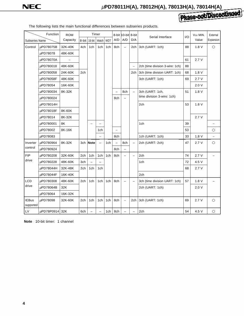
The following lists the main functional differences between subseries products.
Function ROM Timer 8-bit 10-bit 8-bitSerial Interface I/O
VDD MIN. External
Subseries Name Capacity 8-bit 16-bit Watch WDT A/D A/D D/A Value Expansion
Control µPD78075B 32K-40K 4ch 1ch 1ch 1ch 8ch – 2ch 3ch (UART: 1ch) 88 1.8 V
µPD78078 48K-60K
µPD78070A – 61 2.7 V
µPD780018 48K-60K – 2ch (time division 3-wire: 1ch) 88
µPD780058 24K-60K 2ch 2ch 3ch (time division UART: 1ch) 68 1.8 V
µPD78058F 48K-60K 3ch (UART: 1ch) 69 2.7 V
µPD78054 16K-60K 2.0 V
µPD780034 8K-32K – 8ch – 3ch (UART: 1ch, 51 1.8 V
µPD780024 8ch – time division 3-wire: 1ch)
µPD78014H 2ch 53 1.8 V
µPD78018F 8K-60K
µPD78014 8K-32K 2.7 V
µPD780001 8K – – 1ch 39 –
µPD78002 8K-16K 1ch – 53
µPD78083 – 8ch 1ch (UART: 1ch) 33 1.8 V –
Inverter µPD780964 8K-32K 3ch Note – 1ch – 8ch – 2ch (UART: 2ch) 47 2.7 V
control µPD780924 8ch –
FIP µPD780208 32K-60K 2ch 1ch 1ch 1ch 8ch – – 2ch 74 2.7 V –
drive µPD780228 48K-60K 3ch – – 1ch 72 4.5 V
µPD78044H 32K-48K 2ch 1ch 1ch 68 2.7 V
µPD78044F 16K-40K 2ch
LCD µPD780308 48K-60K 2ch 1ch 1ch 1ch 8ch – – 3ch (time division UART: 1ch) 57 1.8 V –
drive µPD78064B 32K 2ch (UART: 1ch) 2.0 V
µPD78064 16K-32K
IEBus µPD78098 32K-60K 2ch 1ch 1ch 1ch 8ch – 2ch 3ch (UART: 1ch) 69 2.7 V
supported
LV µPD78P0914 32K 6ch – – 1ch 8ch – – 2ch 54 4.5 V
Note 10-bit timer: 1 channel
µPD78011H(A), 78012H(A), 78013H(A), 78014H(A)
5
8K bytes 16K bytes 24K bytes 32K bytes
32 bytes
64K bytes
8 bits × 32 registers (8 bits × 8 registers × 4 banks)
On-chip instruction execution time cycle modification function
0.4 µs/0.8 µs/1.6 µs/3.2 µs/6.4 µs (at 10.0 MHz operation)
122 µs (at 32.768 kHz operation)
• 16-bit operation
• Multiplication/division (8 bits × 8 bits,16 bits ÷ 8 bits)
• Bit manipulation (set, reset, test, boolean operation)
• BCD correction, etc.
Total : 53
• CMOS input : 02
• CMOS I/O : 47
• N-channel open-drain I/O
(15 V withstand voltage) : 04
• 8-bit resolution × 8 channels
• Operable over a wide power supply voltage range: AVDD = 1.8 to 5.5 V
• 3-wire serial I/O/SBI /2-wire serial I/O mode selectable: 1 channel
• 3-wire serial I/O mode (on-chip max. 32 bytes automatic data transmit/receive function): 1 channel
• 16-bit timer/event counter : 1 channel
• 8-bit timer/event counter : 2 channels
• Watch timer : 1 channel
• Watchdog timer : 1 channel
3 (14-bit PWM output × 1)
39.1 kHz, 78.1 kHz, 156 kHz, 313 kHz, 625 kHz, 1.25 MHz (at main system clock: 10.0 MHz
operation), 32.768 kHz (at subsystem clock: 32.768 kHz operation)
2.4 kHz, 4.9 kHz, 9.8 kHz (at main system clock: 10.0 MHz operation)
Internal : 8, External : 4
Internal : 1
1
Internal : 1, External : 1
VDD = 1.8 to 5.5 V
TA = –40 to +85°C
• 64-pin plastic shrink DIP (750 mil)
• 64-pin plastic QFP (14 × 14 mm)
Internal
memory
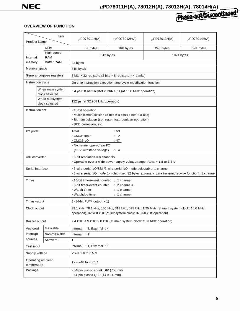
OVERVIEW OF FUNCTION
Product Name
ROM
High-speed
RAM
Buffer RAM
512 bytes 1024 bytes
µPD78011H(A) µPD78012H(A) µPD78013H(A) µPD78014H(A)Item
Memory space
General-purpose registers
Instruction cycle
When main system
clock selected
When subsystem
clock selected
Instruction set
I/O ports
A/D converter
Serial interface
Timer
Timer output
Clock output
Buzzer output
Vectored
interrupt
sources
Test input
Supply voltage
Operating ambient
temperature
Maskable
Non-maskable
Software
Package
µPD78011H(A), 78012H(A), 78013H(A), 78014H(A)
6
1. PIN CONFIGURATION (Top Vie w) ......................................................................................................... 7
2. BLOCK DIAGRA M ................................................................................................................................... 10
3. PIN FUNCTIONS ...................................................................................................................................... 113.1 PORT PINS ........................................................................................................................................................ 113.2 OTHER PORTS ................................................................................................................................................. 123.3 PIN I/O CIRCUIT AND RECOMMENDED CONNECTION OF UNUSED PINS ................................................ 14
4. MEMORY SPACE .................................................................................................................................... 16
5. PERIPHERAL HARDWARE FUNCTION FEATURE S ............................................................................ 175.1 PORTS ............................................................................................................................................................... 175.2 CLOCK GENERATO R....................................................................................................................................... 185.3 TIMER/EVENT COUNTER ................................................................................................................................ 195.4 CLOCK OUTPUT CONTROL CIRCUI T ............................................................................................................ 215.5 BUZZER OUTPUT CONTROL CIRCUIT........................................................................................................... 215.6 A/D CONVERTER.............................................................................................................................................. 225.7 SERIAL INTERFACE S ...................................................................................................................................... 23
6. INTERRUPT FUNCTIONS AND TEST FUNCTIONS .............................................................................. 256.1 INTERRUPT FUNCTIONS ................................................................................................................................. 256.2 TEST FUNCTIONS ............................................................................................................................................ 28
7. EXTERNAL DEVICE EXPANSION FUNCTION S ................................................................................... 29
8. STANDBY FUNCTIONS........................................................................................................................... 29
9. RESET FUNCTIONS ................................................................................................................................ 29
10. INSTRUCTION SET ................................................................................................................................. 30
11. ELECTRICAL SPECIFICATION S ............................................................................................................ 33
12. PACKAGE DRAWING S ........................................................................................................................... 57
13. RECOMMENDED SOLDERING CONDITIONS ..................................................................................... 59
APPENDIX A. DEVELOPMENT TOOL S ......................................................................................................... 60
APPENDIX B. RELATED DOCUMENT S ........................................................................................................ 62
TABLE OF CONTENTS
µPD78011H(A), 78012H(A), 78013H(A), 78014H(A)
7
• 64-Pin Plastic Shrink DIP (750 mil)
µPD78011HCW(A)-×××, 78012HCW(A)-×××, 78013HCW(A)-×××, 78014HCW(A)-×××
1. PIN CONFIGURATION (Top View)
Cautions 1. Always connect the IC (Internally Connected) pin to V SS directly.2. The AV DD pin is multiplexed with an A/D converter power pin and a port power pin. In an applica-
tion where the noise generated from the microcontroller must be reduced, connect the AV DD pinto a power supply of the same voltage as V DD.
3. The AV SS pin is multiplexed with an A/D converter ground pin and a port ground pin. In anapplication where the noise generated from the microcontroller must be reduced, connect AV SS
pin to a ground line separate from V SS.
1P20/SI1
2P21/SO1
3P22/SCK1
4P23/STB
5P24/BUSY
6P25/SI0/SB0
7P26/SO0/SB1
8P27/SCK0
9 P30/TO0
10P31/TO1
11P32/TO2
12P33/TI1
13P34/TI2
14P35/PCL
15P36/BUZ
16P37
17VSS
18P40/AD0
19P41/AD1
20P42/AD2
21P43/AD3
22P44/AD4
23P45/AD5
24P46/AD6
25P47/AD7
26P50/A8
27P51/A9
28P52/A10
29P53/A11
30P54/A12
31P55/A13
32 VSS
64
63
62
61
60
59
58
57
56
55
54
53
52
51
50
49
48
47
46
45
44
43
42
41
40
39
38
37
36
35
34
33
AVREF
AVDD
P17/ANI7
P16/ANI6
P15/ANI5
P14/ANI4
P13/ANI3
P12/ANI2
P11/ANI1
P10/ANI0
AVSS
P04/XT1
XT2
IC
X1
X2
VDD
P03/INTP3
P02/INTP2
P01/INTP1
P00/INTP0/TI0
RESET
P67/ASTB
P66/WAIT
P65/WR
P64/RD
P63
P62
P61
P60
P57/A15
P56/A14
µPD78011H(A), 78012H(A), 78013H(A), 78014H(A)
8
• 64-Pin Plastic QFP (14 × 14 mm)
µPD78011HGC(A)-×××-AB8, 78012HGC(A)- ×××-AB8, 78013HGC(A)- ×××-AB8, 78014HGC(A)-×××-AB8
Cautions 1. Always connect the IC (Internally Connected) pin to V SS directly.2. The AV DD pin is multiplexed with an A/D converter power pin and a port power pin. In an applica-
tion where the noise generated from the microcontroller must be reduced, connect the AV DD pinto a power supply of the same voltage as V DD.
3. The AV SS pin is multiplexed with an A/D converter ground pin and a port ground pin. In anapplication where the noise generated from the microcontroller must be reduced, connect AV SS
pin to a ground line separate from V SS.
1
2
3
4
5
6
7
8
9
10
11
12
13
14
15
16
P11/ANI1
P10/ANI0
AVSS
P04/XT1
XT2
IC
X1
X2
VDD
P03/INTP3
P02/INTP2
P01/INTP1
P00/INTP0/TI0
RESET
P67/ASTB
P66/WAIT
P37
VSS
P30/TO0
P31/TO1
P32/TO2
P33/TI1
P34/TI2
P35/PCL
P36/BUZ
P40/AD0
P41/AD1
P42/AD2
P43/AD3
P44/AD4
P45/AD5
P46/AD617 18 19 20 21 22 23 24 25 26 27 28 29 30 31 32
64 63 62 61 60 59 58 57 56 55 54 53 52 51 50 4948
47
46
45
44
43
42
41
40
39
38
37
36
35
34
33
P2
7/S
CK
0
P2
6/S
O0
/SB
1
P2
5/S
I0/S
B0
P2
4/B
US
Y
P2
3/S
TB
P2
2/S
CK
1
P2
1/S
O1
P2
0/S
I1
AV
RE
F
AV
DD
P1
7/A
NI7
P1
6/A
NI6
P1
5/A
NI5
P1
4/A
NI4
P1
3/A
NI3
P1
2/A
NI2
P4
7/A
D7
P5
0/A
8
P5
1/A
9
P5
2/A
10
P5
3/A
11
P5
4/A
12
P5
5/A
13
VS
S
P5
6/A
14
P5
7/A
15
P6
0
P6
1
P6
2
P6
3
P6
4/R
D
P6
5/W
R
µPD78011H(A), 78012H(A), 78013H(A), 78014H(A)
9
P60-P67 : Port 6
PCL : Programmable Clock
RD : Read Strobe
RESET : Reset
SB0, SB1 : Serial Bus
SCK0, SCK1 : Serial Clock
SI0, SI1 : Serial Input
SO0, SO1 : Serial Output
STB : Strobe
TI0-TI2 : Timer Input
TO0-TO2 : Timer Output
VDD : Power Supply
VSS : Ground
WAIT : Wait
WR : Write Strobe
X1, X2 : Crystal (Main System Clock)
XT1, XT2 : Crystal (Subsystem Clock)
A8-A15 : Address BusAD0-AD7 : Address/Data Bus
ANI0-ANI7 : Analog Input
ASTB : Address Strobe
AVDD : Analog Power Supply
AVREF : Analog Reference Voltage
AVSS : Analog Ground
BUSY : Busy
BUZ : Buzzer Clock
IC : Internally Connected
INTP0-INTP3 : Interrupt from Peripherals
P00-P04 : Port 0
P10-P17 : Port 1
P20-P27 : Port 2
P30-P37 : Port 3
P40-P47 : Port 4
P50-P57 : Port 5
µPD78011H(A), 78012H(A), 78013H(A), 78014H(A)
10
2. BLOCK DIAGRAM
Remark Internal ROM & RAM capacity varies depending on the product.
16-bit TIMER/ EVENT COUNTER
8-bit TIMER/ EVENT COUNTER 1
8-bit TIMER/ EVENT COUNTER 2
WATCHDOG TIMER
SERIAL INTERFACE 0
SERIAL INTERFACE 1
A/D CONVERTER
INTERRUPT CONTROL
WATCH TIMER
BUZZER OUTPUT
CLOCK OUTPUT CONTROL
TO0/P30
TI0/INTP0/P00
TO1/P31
TI1/P33
TO2/P32
TI2/P34
SI0/SB0/P25
SO0/SB1/P26
SCK0/P27
SI1/P20
SO1/P21
SCK1/P22
STB/P23
BUSY/P24
ANI0/P10- ANI7/P17
AVREF
INTP0/P00- INTP3/P03
BUZ/P36
PCL/P35
78K/0 CPU CORE
ROM
RAM
PORT0
PORT1
PORT2
PORT3
PORT4
PORT5
PORT6
EXTERNAL ACCESS
SYSTEM CONTROL
P00
P01-P03
P04
P10-P17
P20-P27
P30-P37
P40-P47
P50-P57
P60-P67
AD0/P40- AD7/P47
A8/P50- A15/P57
RD/P64
WR/P65
WAIT/P66
ASTB/P67
RESET
X1
X2
XT1
XT2
VDD VSS AVDD AVSS IC
µPD78011H(A), 78012H(A), 78013H(A), 78014H(A)
11
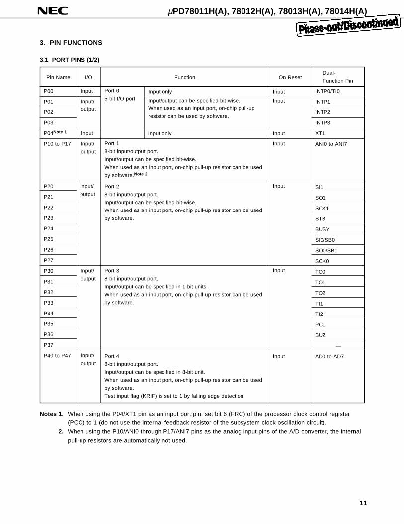
Input
Input/
output
Input/
output
Input/
output
Input
P00
P01
P02
P03
P04Note 1
P10 to P17
P20
P21
P22
P23
P24
P25
P26
P27
P30
P31
P32
P33
P34
P35
P36
P37
P40 to P47
3. PIN FUNCTIONS
3.1 PORT PINS (1/2)
Input/output can be specified bit-wise.
When used as an input port, on-chip pull-up
resistor can be used by software.
Input/
output
Input/
output
Input only
Input only
Port 2
8-bit input/output port.
Input/output can be specified bit-wise.
When used as an input port, on-chip pull-up resistor can be used
by software.
Port 1
8-bit input/output port.
Input/output can be specified bit-wise.
When used as an input port, on-chip pull-up resistor can be used
by software.Note 2
Port 0
5-bit I/O port
Port 3
8-bit input/output port.
Input/output can be specified in 1-bit units.
When used as an input port, on-chip pull-up resistor can be used
by software.
Port 4
8-bit input/output port.
Input/output can be specified in 8-bit unit.
When used as an input port, on-chip pull-up resistor can be used
by software.
Test input flag (KRIF) is set to 1 by falling edge detection.
Notes 1. When using the P04/XT1 pin as an input port pin, set bit 6 (FRC) of the processor clock control register
(PCC) to 1 (do not use the internal feedback resistor of the subsystem clock oscillation circuit).
2. When using the P10/ANI0 through P17/ANI7 pins as the analog input pins of the A/D converter, the internal
pull-up resistors are automatically not used.
Pin Name I/O Function On ResetDual-
Function Pin
Input
Input
Input
Input
Input
Input
Input
INTP0/TI0
INTP1
INTP2
INTP3
XT1
ANI0 to ANI7
SI1
SO1
SCK1
STB
BUSY
SI0/SB0
SO0/SB1
SCK0
TO0
TO1
TO2
TI1
TI2
PCL
BUZ
—
AD0 to AD7
µPD78011H(A), 78012H(A), 78013H(A), 78014H(A)
12
3.1 PORT PINS (2/2)
Input/
output
P50 to P57
Input/
output
P60
P61
P62
P63
P64
P65
P66
P67
Input
Input
A8 to A15Port 5
8-bit input/output port.
LED can be driven directly.
Input/output can be specified bit-wise.
When used as an input port, on-chip pull-up resistor can be used by
software.
Port 6
8-bit input/output port.
Input/output can be specified
bit-wise.
When used as an input port, on-chip
pull-up resistor can be used by soft-
ware.
N-ch open-drain input/output port.
On-chip pull-up resistor can be
specified by mask option.
LED can be driven directly.
RD
WR
WAIT
ASTB
Pin Name I/O Function On ResetDual-
Function Pin
3.2 OTHER PORTS (1/2)
INTP0
INTP1
INTP2
INTP3
SI0
SI1
SO0
SO1
SB0
SB1
SCK0
SCK1
STB
BUSY
Input
Input
Output
Input
/output
Input
/output
Output
Input
External interrupt request input by which the effective edge (rising
edge, falling edge, or both rising edge and falling edge) can be
specified.
Input
Input
Input
Input
P00/TI0
P01
P02
P03
P25/SB0
P20
P26/SB1
P21
P25/SI0
P26/SO0
P27
P22
P23
P24
Falling edge detection external interrupt request input.
Serial interface serial data input.
Serial interface serial data output.
Serial interface serial data input/output.
Serial interface serial clock input/output.
Serial interface automatic transmit/receive strobe output.
Serial interface automatic transmit/receive busy input.
Input
Input
Input
Pin Name I/O Function On ResetDual-
Function Pin
Caution Do not manipulate the pins multiplexed with a port pin as follows during A/D conversion; otherwise,
the rated total error during A/D conversion may not be satisfied.
<1> Rewriting the contents of the output latch when the pin is used as an output port pin.
<2> Changing the output level of the pin used as an output pin even when the pin is not used as a
port pin.
µPD78011H(A), 78012H(A), 78013H(A), 78014H(A)
13
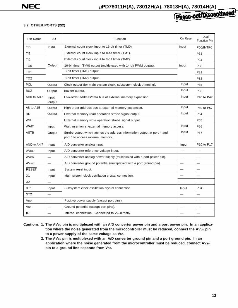
8-bit timer (TM1) output.
8-bit timer (TM2) output.
TI0
TI1
TI2
TO0
TO1
TO2
PCL
BUZ
AD0 to AD7
A8 to A15
RD
WR
WAIT
ASTB
Input
Output
External count clock input to 16-bit timer (TM0).
External count clock input to 8-bit timer (TM1).
External count clock input to 8-bit timer (TM2).
16-bit timer (TM0) output (multiplexed with 14-bit PWM output).
Output
Input
/output
Clock output (for main system clock, subsystem clock trimming).
Buzzer output.
Low-order address/data bus at external memory expansion.
High-order address bus at external memory expansion.
External memory read operation strobe signal output.
External memory write operation strobe signal output.
Wait insertion at external memory access.
Output
Strobe output which latches the address information output at port 4 and
port 5 to access external memory.
Output
Output
Input
Output
3.2 OTHER PORTS (2/2)
A/D converter analog input.
A/D converter reference voltage input.
A/D converter analog power supply (multiplexed with a port power pin).
A/D converter ground potential (multiplexed with a port ground pin).
System reset input.
Main system clock oscillation crystal connection.
Subsystem clock oscillation crystal connection.
Positive power supply (except port pins).
Ground potential (except port pins).
Internal connection. Connected to VSS directly.
ANI0 to ANI7
AVREF
AVDD
AVSS
RESET
X1
X2
XT1
XT2
VDD
VSS
IC
Input
Input
—
—
Input
Input
—
Input
—
—
—
—
Input
Input
Input
Input
Input
Input
Input
Input
Input
Input
Input
—
—
—
—
—
—
—
—
—
—
P00/INTP0
P33
P34
P30
P31
P32
P35
P36
P40 to P47
P50 to P57
P64
P65
P66
P67
P10 to P17
—
—
—
—
—
—
P04
—
—
—
—
Pin Name I/O Function On Reset Dual-Function Pin
Cautions 1. The AV DD pin is multiplexed with an A/D converter power pin and a port power pin. In an applica-tion where the noise generated from the microcontroller must be reduced, connect the AV DD pinto a power supply of the same voltage as V DD.
2. The AV SS pin is multiplexed with an A/D converter ground pin and a port ground pin. In anapplication where the noise generated from the microcontroller must be reduced, connect AV SS
pin to a ground line separate from V SS.
µPD78011H(A), 78012H(A), 78013H(A), 78014H(A)
14
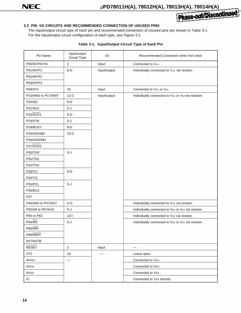
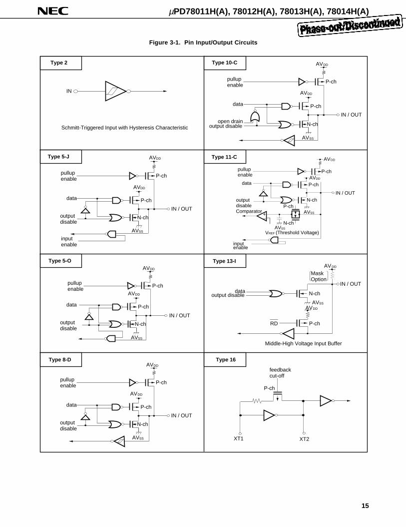
3.3 PIN I/O CIRCUITS AND RECOMMENDED CONNECTION OF UNUSED PINSThe input/output circuit type of each pin and recommended connection of unused pins are shown in Table 3-1.For the input/output circuit configuration of each type, see Figure 3-1.
Table 3-1. Input/Output Circuit Type of Each Pin
2
8-D
16
11-C
8-D
5-J
8-D
5-J
8-D
10-C
5-J
8-D
5-J
5-O
5-J
13-I
5-J
2
16
—
Pin Name I/O Recommended Connection when Not UsedInput/outputCircuit Type
Input
Input/output
Input
Input/output
Input
—
Connected to VSS .
Individually connected to VSS via resistor.
Connected to VDD or VSS.
Individually connected to VDD or VSS via resisitor.
Individually connected to VDD via resistor.
Individually connected to VDD or VSS via resistor.
Individually connected to VDD via resistor.
Individually connected to VDD or VSS via resistor.
—
Leave open.
Connected to VSS .
Connected to VDD .
Connected to VSS .
Connected to VSS directly.
P00/INTP0/TI0
P01/INTP1
P02/INTP2
P03/INTP3
P04/XT1
P10/ANI0 to P17/ANI7
P20/SI1
P21/SO1
P22/SCK1
P23/STB
P24/BUSY
P25/SI0/SB0
P26/SO0/SB1
P27/SCK0
P30/TO0
P31/TO1
P32/TO2
P33/TI1
P34/TI2
P35/PCL
P36/BUZ
P37
P40/AD0 to P47/AD7
P50/A8 to P57/A15
P60 to P63
P64/RD
P65/WR
P66/WAIT
P67/ASTB
RESET
XT2
AVREF
AVDD
AVSS
IC
µPD78011H(A), 78012H(A), 78013H(A), 78014H(A)
15
Figure 3-1. Pin Input/Output Circuits
Type 10-C
Type 13-I
Type 16Type 8-D
Type 5-J
Type 2
Type 5-O
Type 11-C
IN
Schmitt-Triggered Input with Hysteresis Characteristic
pullup enable
data
output disable
AV
P-ch
N-ch
P-ch
IN / OUT
DD
AVDD
AVSS
pullup enable
data
output disable
AV
P-ch
N-ch
P-ch
IN / OUT
DD
AVDD
open drain
AVSS
dataoutput disable N-ch
IN / OUT
AVDD
AVDD
RD
Mask Option
Middle-High Voltage Input Buffer
P-ch
AVSS
XT1
feedback cut-off
XT2
P-ch
pullup enable
data
output disable
AV
P-ch
N-ch
P-ch
IN / OUT
DD
AVDD
AVSS
pullup enable
data
output disable
IN / OUT
N-ch
VREF
inputenable
(Threshold Voltage)
AVP-ch
N-ch
P-chDD
AV
P-ch
+–
Comparator
DD
AVSS
AVSS
pullup enable
data
output disable
P-ch
N-ch
P-ch
IN / OUT
AVSS
input enable
AVDD
AVDD
µPD78011H(A), 78012H(A), 78013H(A), 78014H(A)
16
1FFFH
3FFFH
5FFFH
7FFFH
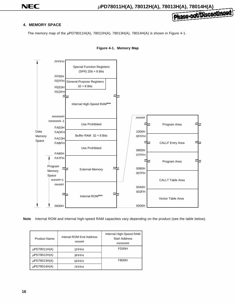
4. MEMORY SPACE
The memory map of the µPD78011H(A), 78012H(A), 78013H(A), 78014H(A) is shown in Figure 4-1.
Figure 4-1. Memory Map
Note Internal ROM and internal high-speed RAM capacities vary depending on the product (see the table below).
µPD78011H(A)
µPD78012H(A)
µPD78013H(A)
µPD78014H(A)
Intenal ROM End Address
nnnnHProduct Name
Internal High-Speed RAM
Start Address
mmmmH
FD00H
FB00H
FFFFH
FF00H
FEFFH
mmmmH
mmmmH–1
FEE0H
FEDFH
FAE0H
FADFH
FAC0H
FABFH
FA80H
FA7FH
nnnnH+1
nnnnH
0000H
nnnnH
1000H
0FFFH
0800H
07FFH
0080H
007FH
0040H
003FH
0000H
Special Function Registers
(SFR) 256 × 8 Bits
General-Purpose Registers
32 × 8 Bits
Internal High-Speed RAMNote
Use Prohibited
Buffer RAM 32 × 8 Bits
Use Prohibited
External Memory
Program Area
CALLF Entry Area
Program Area
CALLT Table Area
Vector Table Area
Program
Memory
Space
Data
Memory
Space
Internal ROMNote
µPD78011H(A), 78012H(A), 78013H(A), 78014H(A)
17
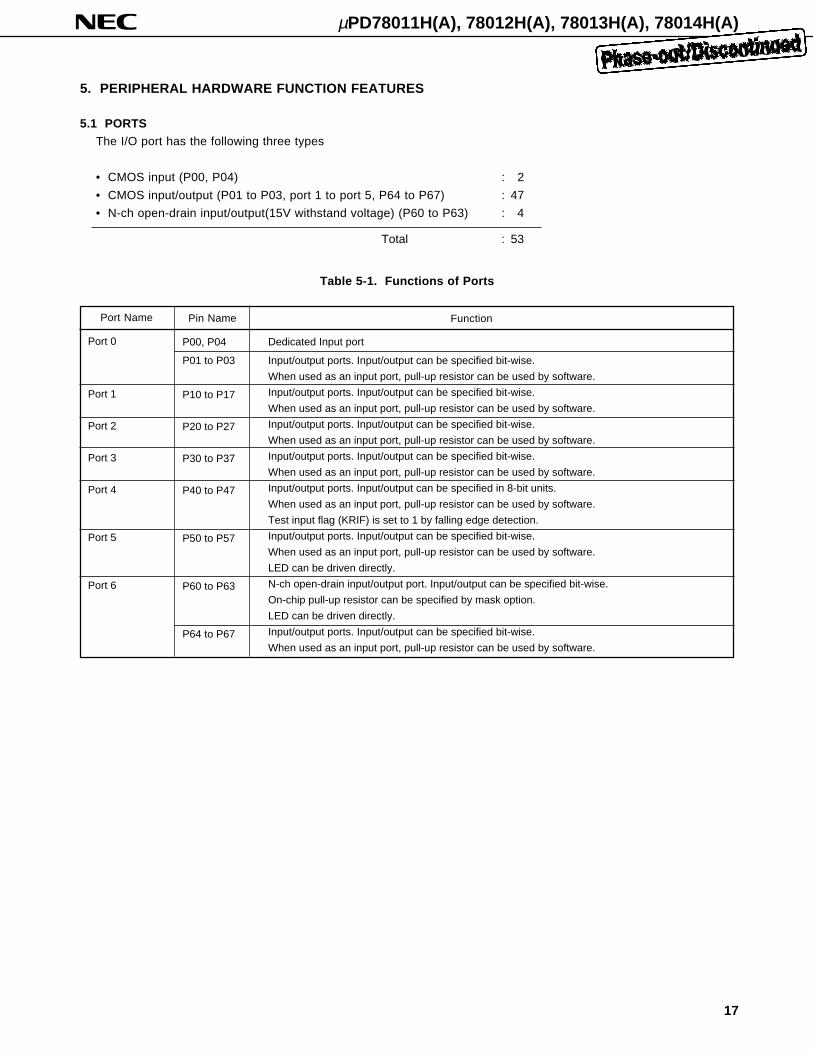
5. PERIPHERAL HARDWARE FUNCTION FEATURES
5.1 PORTS
P00, P04
P01 to P03
P10 to P17
P20 to P27
P30 to P37
P40 to P47
P50 to P57
P60 to P63
P64 to P67
Port 0
Port 1
Port 2
Port 3
Port 4
Port 5
Port 6
Dedicated Input port
Input/output ports. Input/output can be specified bit-wise.
When used as an input port, pull-up resistor can be used by software.
Input/output ports. Input/output can be specified bit-wise.
When used as an input port, pull-up resistor can be used by software.
Input/output ports. Input/output can be specified bit-wise.
When used as an input port, pull-up resistor can be used by software.
Input/output ports. Input/output can be specified bit-wise.
When used as an input port, pull-up resistor can be used by software.
Input/output ports. Input/output can be specified in 8-bit units.
When used as an input port, pull-up resistor can be used by software.
Test input flag (KRIF) is set to 1 by falling edge detection.
Input/output ports. Input/output can be specified bit-wise.
When used as an input port, pull-up resistor can be used by software.
LED can be driven directly.
N-ch open-drain input/output port. Input/output can be specified bit-wise.
On-chip pull-up resistor can be specified by mask option.
LED can be driven directly.
Input/output ports. Input/output can be specified bit-wise.
When used as an input port, pull-up resistor can be used by software.
FunctionPort Name
Table 5-1. Functions of Ports
Pin Name
The I/O port has the following three types
• CMOS input (P00, P04) : 2
• CMOS input/output (P01 to P03, port 1 to port 5, P64 to P67) : 47
• N-ch open-drain input/output(15V withstand voltage) (P60 to P63) : 4
Total : 53
µPD78011H(A), 78012H(A), 78013H(A), 78014H(A)
18
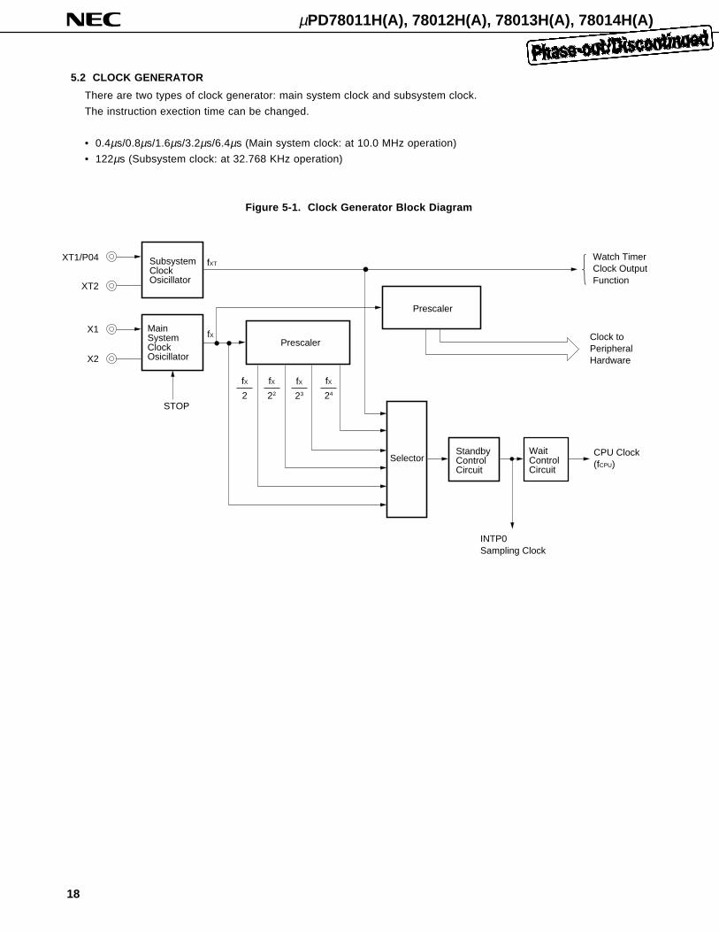
5.2 CLOCK GENERATOR
Figure 5-1. Clock Generator Block Diagram
Prescaler
Prescaler
XT1/P04
XT2
X1
X2
STOP
fX
23
fX
24
fX
22
fX
2
fX
fXT
Clock toPeripheralHardware
SubsystemClockOsicillator
MainSystemClockOsicillator
StandbyControlCircuit
WaitControlCircuit
CPU Clock(fCPU)
INTP0Sampling Clock
There are two types of clock generator: main system clock and subsystem clock.
The instruction exection time can be changed.
• 0.4µs/0.8µs/1.6µs/3.2µs/6.4µs (Main system clock: at 10.0 MHz operation)
• 122µs (Subsystem clock: at 32.768 KHz operation)
Watch TimerClock OutputFunction
Selector
µPD78011H(A), 78012H(A), 78013H(A), 78014H(A)
19
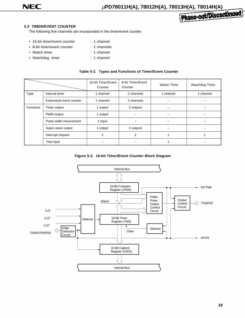
Type Interval timer 1 channel 2 channels 1 channel 1 channel
Externanal event counter 1 channel 2 channels – –
Functions Timer output 1 output 2 outputs – –
PWM output 1 output – – –
Pulse width mesurement 1 input – – –
Sqare wave output 1 output 2 outputs – –
Interrupt request 2 2 1 1
Test input – – 1 –
5.3 TIMER/EVENT COUNTERThe following five channels are incorporated in the timer/event counter.
• 16-bit timer/event counter : 1 channel
• 8-bit timer/event counter : 2 channels
• Watch timer : 1 channel
• Watchdog timer : 1 channel
Table 5-2. Types and Functions of Timer/Event Counter
16-bit Timer/Event
Counter Watch Timer Watchdog Timer
8-bit Timer/Event
Counter
Figure 5-2. 16-bit Timer/Enent Counter Block Diagram
fX/22
fX/2
fX/23
TI0/INTP0/P00 Clear
Selector
Output Control Circuit
INTTM0
TO0/P30
INTP0
Match
Selector
Internal Bus
PWM Pulse Output Control Circuit
Edge Detection Circuit
16-Bit Compare Register (CR00)
16-Bit TimerRegister (TM0)
16-Bit CaptureRegister (CR01)
Internal Bus
µPD78011H(A), 78012H(A), 78013H(A), 78014H(A)
20
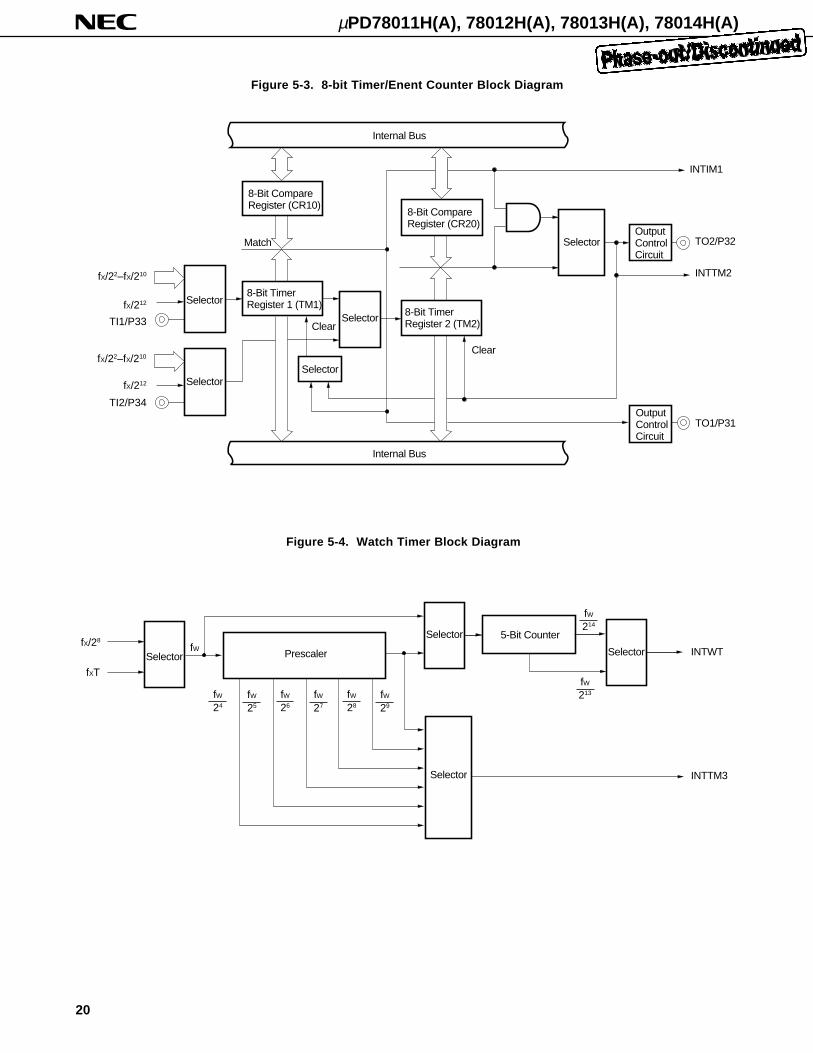
INTTM3
INTWT
5-Bit Counter
PrescalerSelector
Selector
Selector
Selector
Figure 5-3. 8-bit Timer/Enent Counter Block Diagram
Figure 5-4. Watch Timer Block Diagram
fW24
fW25
fW26
fW27
fW28
fW29
fX/28
fXT
fW214
fW213
fW
Internal Bus
8-Bit Compare Register (CR10)
8-Bit Timer Register 1 (TM1)
Clear
Output Control Circuit
Output Control Circuit
INTIM1
TO2/P32
INTTM2
TO1/P31
Clear
Match
Selector
8-Bit Compare Register (CR20)
8-Bit Timer Register 2 (TM2)
Internal Bus
Selector
Selector
Selector
Selector
fX/212
fX/22–fX/210
TI1/P33
fX/22–fX/210
TI2/P34
fX/212
µPD78011H(A), 78012H(A), 78013H(A), 78014H(A)
21
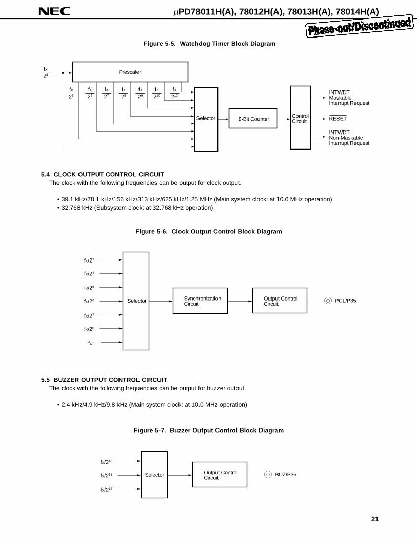
Figure 5-5. Watchdog Timer Block Diagram
fX/210
fX/211
fX/212
5.5 BUZZER OUTPUT CONTROL CIRCUITThe clock with the following frequencies can be output for buzzer output.
• 2.4 kHz/4.9 kHz/9.8 kHz (Main system clock: at 10.0 MHz operation)
Figure 5-7. Buzzer Output Control Block Diagram
5.4 CLOCK OUTPUT CONTROL CIRCUITThe clock with the following frequencies can be output for clock output.
• 39.1 kHz/78.1 kHz/156 kHz/313 kHz/625 kHz/1.25 MHz (Main system clock: at 10.0 MHz operation)• 32.768 kHz (Subsystem clock: at 32.768 kHz operation)
Figure 5-6. Clock Output Control Block Diagram
fXT
fX/23
fX/24
fX/25
fX/26
fX/27
fX/28
fX25
fX26
fX27
fX28
fX29
fX212
fX210
fX24
Control Circuit 8-Bit Counter
Prescaler
INTWDTNon-MaskableInterrupt Request
INTWDTMaskableInterrupt Request
RESETSelector
Selector Synchronization Circuit
Output Control Circuit
PCL/P35
Selector Output Control Circuit
BUZ/P36
µPD78011H(A), 78012H(A), 78013H(A), 78014H(A)
22
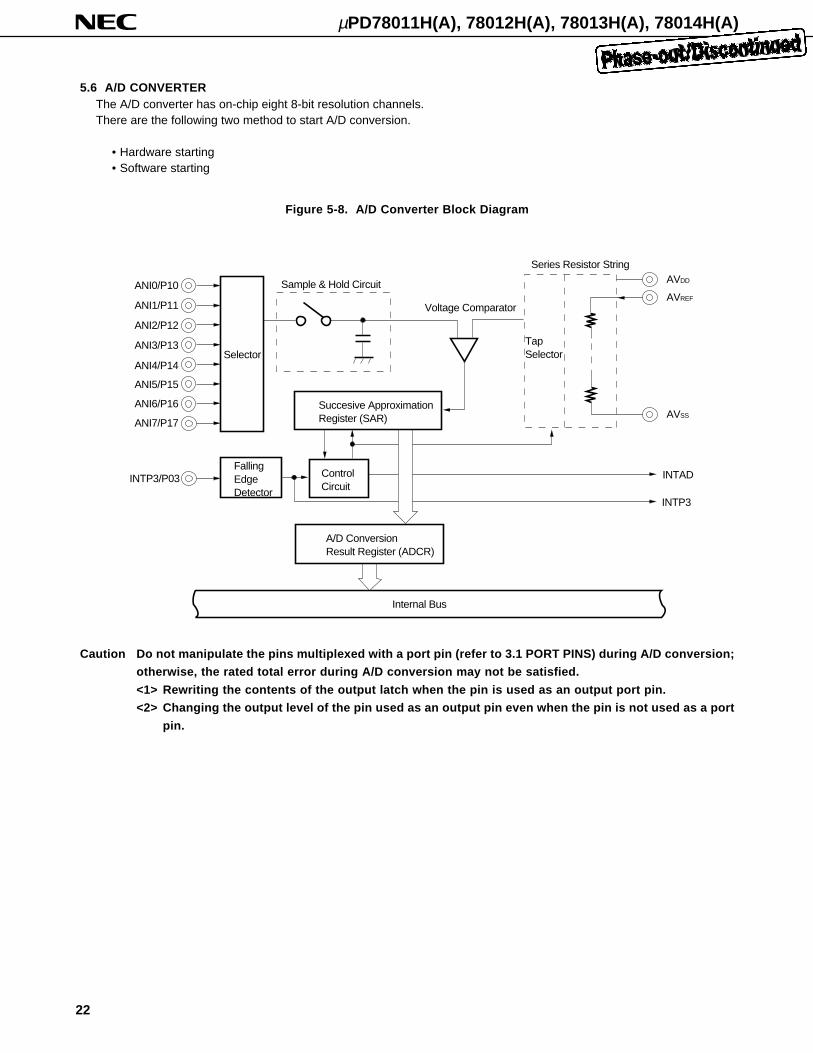
5.6 A/D CONVERTERThe A/D converter has on-chip eight 8-bit resolution channels.There are the following two method to start A/D conversion.
• Hardware starting• Software starting
Figure 5-8. A/D Converter Block Diagram
Caution Do not manipulate the pins multiplexed with a port pin (refer to 3.1 PORT PINS) during A/D conversion;
otherwise, the rated total error during A/D conversion may not be satisfied.
<1> Rewriting the contents of the output latch when the pin is used as an output port pin.
<2> Changing the output level of the pin used as an output pin even when the pin is not used as a port
pin.
Tap Selector
INTAD
AVDD
INTP3
Internal Bus
AVREF
AVSS
A/D Conversion Result Register (ADCR)
Control Circuit
Succesive Approximation Register (SAR)
Falling Edge Detector
ANI0/P10
ANI1/P11
ANI2/P12
ANI3/P13
ANI4/P14
ANI5/P15
ANI6/P16
ANI7/P17
INTP3/P03
Selector
Sample & Hold Circuit
Voltage Comparator
Series Resistor String
µPD78011H(A), 78012H(A), 78013H(A), 78014H(A)
23
5.7 SERIAL INTERFACESThere are two on-chip clocked serial interfaces as follows.
• Serial Interface channel 0• Serial Interface channel 1
Function Serial Interface Channel 0 Serial Interface Channel 1
3-wire serial I/O mode O (MSB/LSB-first switchable) O (MSB/LSB-first switchable)
3-wire serial I/O mode with automatic data transmit/ – O (MSB/LSB-first switchable)
receive function
SBI (Serial Bus Interface) mode O (MSB-first) –
2-wire serial I/O mode O (MSB-first) –
Table 5-3. Type and Function of Serial Interface
Figure 5-9. Serial Interface Channel 0 Block Diagram
SI0/SB0/P25
SO0/SB1/P26
SCK0/P27INTCSI0
TO2
fx/22–fx/29
Busy/Acknowledge Output Circuit
Output Latch
Serial I/O Shift Register 0 (SIO0)
Internal Bus
Interrupt Request Signal Generator
Serial Clock Counter
Bus Release/Command/ Acknowledge Detection Circuit
Serial Clock Control Circuit
Selector
Selector
Selector
µPD78011H(A), 78012H(A), 78013H(A), 78014H(A)
24
SCK1/P22
BUSY/P24
STB/P23
SO1/P21
SI1/P20
fX/22 – fX/29
TO2
INTCSI1
Figure 5-10. Serial Interface Channel 1 Block Diagram
Internal Bus
Interrupt Request Signal Generator
Handshake Control Circuit
Buffer RAM
Serial Clock Control Circuit Selector
Serial Clock Counter
Serial I/O Shift Register 1 (SIO1)
Automatic Data Transmit/Receive Address Pointer (ADTP)
µPD78011H(A), 78012H(A), 78013FH(A), 78014H(A)
25
Default Interrupt Source Internal/ Vector Table Basic
Interrupt Type Priority Note 1
Name TriggerExternal Address Configuratin
Type Note 2
Non-maskable ––– INTWDT Watchdog timer overflow (with watchdog Internal 0004H (A)
timer mode 1 selected)
Maskable 0 INTWDT Watchdog timer overflow (with interval (B)
timer mode selected)
1 INTP0 Pin input edge detection External 0006H (C)
2 INTP1 0008H (D)
3 INTP2 000AH
4 INTP3 000CH
5 INTCSI0 Serial interface channel 0 transfer end Internal 000EH (B)
6 INTCSI1 Serial interface channel 1 transfer end 0010H
7 INTTM3 Reference time interval signal from 0012H
watch timer
8 INTTM0 16 bit timer/event counter match signal 0014H
generation
9 INTTM1 8-bit timer/event counter 1 match signal 0016H
generation
10 INTTM2 8-bit timer/event counter 2 match signal 0018H
generation
11 INTAD A/D converter conversion end 001AH
Software ––– BRK BRK instruction execution – 003EH (E)
6. INTERRUPT FUNCTIONS AND TEST FUNCTIONS
6.1 INTERRUPT FUNCTIONS
Table 6-1. Interrupt Source List
Notes 1. The default pririty is the priority applicable when more than one maskable interrupt is generated. 0 is the highest
priority and 11, the lowest.
2. Basic configuration types (A) to (E) correspond to (A) to (E) on the next page.
There are the 14 interrupt sources of 3 different kind as shown below.
• Non-maskable : 1
• Maskable : 12
• Software : 1
µPD78011H(A), 78012H(A), 78013H(A), 78014H(A)
26
Figure 6-1. Basic Interrupt Function Configuration (1/2)
(A) Internal Non-Maskable Interrupt
(C) External Maskable Interrupt (INTP0)
(B) Internal Maskable Interrupt
Internal Bus
Priority Control Circuit
Vector Table Address Generator
Standby Release Signal
InterruptRequest
MK
Internal Bus
IE PR ISP
IFPriority Control Circuit
Vector Table Address Generator
Standby Release Signal
InterruptRequest
MK IE PR ISP
IFPriority Control Circuit
Vector Table Address Generator
Sampling Clock Select Register (SCS)
External Interrupt Mode Register (INTM0)
Edge Detector
Sampling Clock
Internal Bus
Standby Release Signal
InterruptRequest
µPD78011H(A), 78012H(A), 78013FH(A), 78014H(A)
27
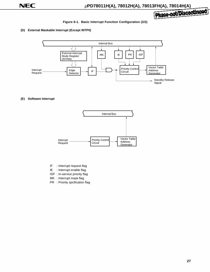
(D) External Maskable Interrupt (Except INTP0)
Figure 6-1. Basic Interrupt Function Configuration (2/2)
(E) Software Interrupt
IF : Interrupt request flagIE : Interrupt enable flagISP : In-service priority flagMK : Interrupt mask flagPR : Priority spcification flag
MK IE PR ISP
IFPriority Control Circuit
Vector Table Address Generator
External Interrupt Mode Register (INTM0)
Edge Detector
Internal Bus
Standby Release Signal
InterruptRequest
Priority Control Circuit
Vector Table Address Generator
Internal Bus
InterruptRequest
µPD78011H(A), 78012H(A), 78013H(A), 78014H(A)
28
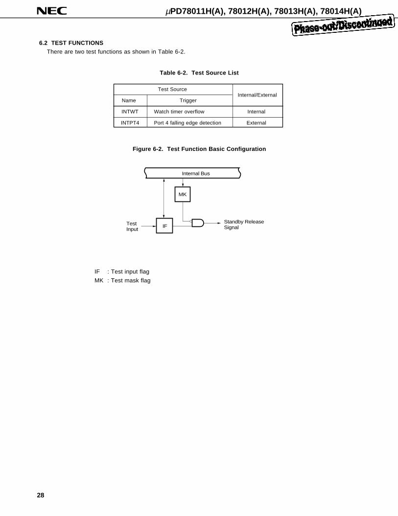
6.2 TEST FUNCTIONS
There are two test functions as shown in Table 6-2.
Figure 6-2. Test Function Basic Configuration
IF : Test input flag
MK : Test mask flag
Table 6-2. Test Source List
Test SourceInternal/External
Name Trigger
INTWT Watch timer overflow Internal
INTPT4 Port 4 falling edge detection External
MK
Internal Bus
IFStandby Release Signal
TestInput
µPD78011H(A), 78012H(A), 78013FH(A), 78014H(A)
29
7. EXTERNAL DEVICE EXPANSION FUNCTIONS
The external device expansion function is used to connect external devices to areas other than the internal ROM, RAM
and SFR.
Ports 4 to 6 are used for connection with external devices.
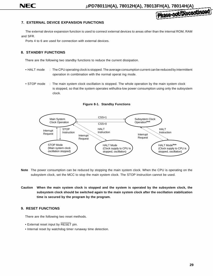
8. STANDBY FUNCTIONS
There are the following two standby functions to reduce the current dissipation.
• HALT mode : The CPU operating clock is stopped. The average consumption current can be reduced by intermittent
operation in combination with the normal operat ing mode.
• STOP mode : The main system clock oscillation is stopped. The whole operation by the main system clock
is stopped, so that the system operates withultra-low power consumption using only the subsystem
clock.
Figure 8-1. Standby Functions
Note The power consumption can be reduced by stopping the main system clock. When the CPU is operating on the
subsystem clock, set the MCC to stop the main system clock. The STOP instruction cannot be used.
Caution When the main system clock is stopped and the system is operated by the subsystem clock, the
subsystem clock should be switched again to the main system clock after the oscillation stabilization
time is secured by the program by the program.
9. RESET FUNCTIONS
There are the following two reset methods.
• External reset input by RESET pin.
• Internal reset by watchdog timer runaway time detection.
Main System Clock Operation
STOP Mode(Main system clock oscillation stopped)
HALT Mode(Clock supply to CPU isstopped, oscillation)
Subsystem Clock OperationNote
HALT ModeNote
(Clock supply to CPU isstopped, oscillation)
InterruptRequest
InterruptRequest
InterruptRequest
HALT Instruction
HALT Instruction
STOPInstruction
CSS=1
CSS=0
µPD78011H(A), 78012H(A), 78013H(A), 78014H(A)
30
2nd Operand [HL+byte]
#byte A r Note sfr saddr !addr16 PSW [DE] [HL] [HL+B] $adder16 1 None
1st Operand [HL+C]
A ADD MOV MOV MOV MOV MOV MOV MOV MOV ROR
ADDC XCH XCH XCH XCH XCH XCH XCH ROL
SUB ADD ADD ADD ADD ADD RORC
SUBC ADDC ADDC ADDC ADDC ADDC ROLC
AND SUB SUB SUB SUB SUB
OR SUBC SUBC SUBC SUBC SUBC
XOR AND AND AND AND AND
CMP OR OR OR OR OR
XOR XOR XOR XOR XOR
CMP CMP CMP CMP CMP
r MOV MOV INC
ADD DEC
ADDC
SUB
SUBC
AND
OR
XOR
CMP
r1 DBNZ
sfr MOV MOV
sadder MOV MOV DBNZ INC
ADD DEC
ADDC
SUB
SUBC
AND
OR
XOR
CMP
!adder16 MOV
PSW MOV MOV PUSH
POP
[DE] MOV
[HL] MOV ROR4
ROL4
[HL+byte] MOV
[HL+B]
[HL+C]
X MULU
C DIVUW
Note Except r=A
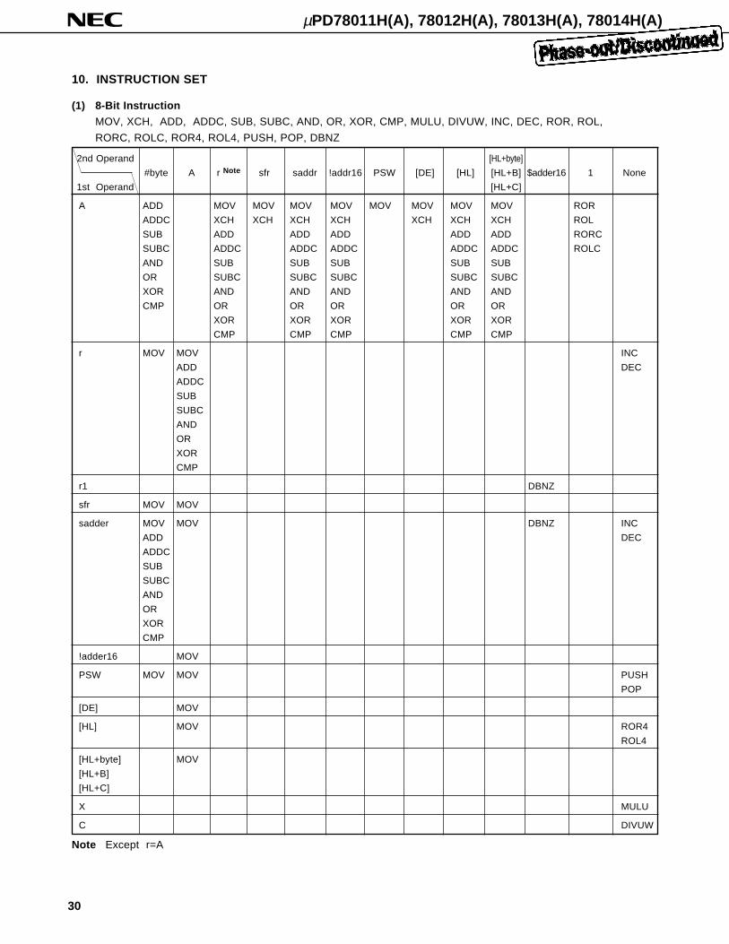
10. INSTRUCTION SET
(1) 8-Bit Instruction
MOV, XCH, ADD, ADDC, SUB, SUBC, AND, OR, XOR, CMP, MULU, DIVUW, INC, DEC, ROR, ROL,
RORC, ROLC, ROR4, ROL4, PUSH, POP, DBNZ
µPD78011H(A), 78012H(A), 78013FH(A), 78014H(A)
31
(2) 16-Bit Instruction
MOVW, XCHW ADDW, SUBW, CMPW, PUSH, POP, INCW, DECW
2nd Operand
1st Operand#byte AX rp saddrp !addr16 SP None
AX ADDW MOVW MOVW MOVW MOVW MOVW
SUBW XCHW
CMPW
rp MOVW MOVWNote INCW, DECW
PUSH, POP
sfrp MOVW MOVW
saddrp MOVW MOVW
!addr16 MOVW
SP MOVW MOVW
Note Only when rp=BC, DE, HL.
(3) Bit Manipulation Instruction
MOV1, AND1, OR1, XOR1, SET1, CLR1, NOT1, BT, BF, BTCLR
2nd Operand
1st OperandA.bit sfr.bit saddr.bit PWS.bit [HL].bit CY $addr16 None
A.bit MOV1 BT SET1
BF CLR1
BTCLR
sfr.bit MOV1 BT SET1
BF CLR1
BTCLR
saddr.bit MOV1 BT SET1
BF CLR1
BTCLR
PSW.bit MOV1 BT SET1
BF CLR1
BTCLR
[HL].bit MOV1 BT SET1
BF CLR1
BTCLR
CY MOV1 MOV1 MOV1 MOV1 MOV1 SET1
AND1 AND1 AND1 AND1 AND1 CLR1
OR1 OR1 OR1 OR1 OR1 NOT1
XOR1 XOR1 XOR1 XOR1 XOR1
Note
µPD78011H(A), 78012H(A), 78013H(A), 78014H(A)
32
(4) Call Instruction/Branch InstructionCALL, CALLF, CALLT, BR, BC, BNC, BZ, BNZ, BT, BF, BTCLR, DBNZ
2nd Operand
1st OperandAX !addr16 !addr11 [addr5] $addr16
Basic instruction BR CALL, BR CALLF CALLT BR, BC, BNC,
BZ, BNZ
Compound instruction BT, BF, BTCLR,
DBNZ
(5) Other InstructionADJBA, ADJBS, BRK, RET, RETI, RETB, SEL, NOP, EI, DI, HALT, STOP
µPD78011H(A), 78012H(A), 78013H(A), 78014H(A)
33
11. ELECTRICAL SPECIFICATIONS
Absolute Maximum Ratings (TA = 25 °C)
Parameter Symbol Test Conditions Rating Unit
Supply voltage VDD –0.3 to + 7.0 V
AVDD –0.3 to VDD + 0.3 V
AVREF –0.3 to VDD + 0.3 V
AVSS –0.3 to + 0.3 V
Input voltage P00 to P04, P10 to P17, P20 to P27, P30 to P37–0.3 to VDD + 0.3 V
P40 toP47, P50 to P57, P64 to P67, X1, X2, XT2
VI2 P60 to P67 Open-drain –0.3 to +16 V
Output voltage VO –0.3 to VDD + 0.3 V
Analog inputP10 to P17 Analog input pin AVSS –0.3 to AVREF + 0.3 V
voltage
Output 1 pin –10 mAcurrent high
IOH P10 to P17, P20 to P27, P30 to P37 total –15 mA
P01 to P03, P40 to P47, P50 to P57, P60 to P67 total –15 mA
Output1 pin
Peak value 30 mAcurrent low
rms 15 mA
P40 to P47, P50 to P55 total Peak value 100 mA
rms 70 mA
P01 to P03, P56, P57, Peak value 100 mA
P60 to P67 total rms 70 mA
P01 to P03, Peak value 50 mA
P64 to P67 total rms 20 mA
P10 to P17, P20 to P27, P30 to P37 Peak value 50 mA
total rms 20 mA
Operating ambient –40 to +85 °C
temperature
Storage –65 to +150 °C
temperature
VI1
VAN
IOLNote
TA
Tstg
Note rms should be calculated as follows: [rms] = [peak value] × √duty
Caution Product quality may suffer if the absolute maximum rating is exceeded for even a single parameter or
even momentarily. That is, the absolute maximuam ratings are rated values at which the product is on
the verge of suffering physical damage, and therefore the product must be used under conditions which
ensure that the absolute maximum ratings are not exceeded.
µPD78011H(A), 78012H(A), 78013H(A), 78014H(A)
34
Parameter Symbol Test Conditions MIN. TYP. MAX. Unit
Input capacitance CIN f = 1 MHz Unmeasured pins returned to 0 V 15 pF
I/O capacitance P01 to P03, P10 to P17,
f = 1 MHz Unmeasured P20 to P27, P30 toP37, 15 pF
CIO pins returned to 0 V P40 toP47, P50 to P57,
P64 to P67
P60 to P63 20 pF
Unit
MHz
ms
MHz
ms
MHz
ns
2.7 V ≤ VDD ≤ 5.5 V 1 10
1.8 V ≤ VDD < 2.7 V 1 5
VDD = 4.5 to 5.5 V 10
30
Capacitance ( TA = 25 °C, VDD = VSS = 0 V )
Remark The characteristics of a dual-function pin and a port pin are the same unless specified otherwise.
Main System Clock Oscillation Circuit Characteristics ( TA = –40 to +85 °C, VDD = 1.8 to 5.5 V)
Resonator
Ceramic
resonator
Crystal
resonator
External
clock
RecommendedCircuit Parameter
Oscillator
frequency (fX) Note 1
Oscillation
stabilization time Note 2
Oscillator
frequency (fX) Note 1
Oscillation
stabilization time Note 2
X1 input
frequency (fX) Note 1
X1 input
high/low level width
(tXH , tXL)
TYP. MAX.Test Conditions
After VDD reaches oscil-
lator voltage range MIN.
Notes 1. Indicates only oscillation circuit characteristics. Refer to AC Characteristics for instruction execution time.
2. Time required to stabilize oscillation after reset or STOP mode release.
Cautions 1. When using the main system clock oscillator, wirinin the area enclosed with the dotted line should
be carried out as follows to avoid an adverse effect from wiring capacitance.
Wiring should be as short as possible.
Wiring should not cross other signal lines.
Wiring should not be placed close to a varying high current.
The potential of the oscillator capacitor ground should be the same as V SS.
Do not ground wiring to a ground pattern in which a high current flows.
Do not fetch a signal from the oscillator.
2. When the main system clock is stopped and the system is operated by the subsystem clock, the
subsystem clock should be switched again to the main system clock after the oscillation stabilization
time is secured by the program.
MIN.
2.7 V ≤ VDD ≤ 5.5 V 1 10
1.8 V ≤ VDD < 2.7 V 1 5
4
1.0 10.0
45 500
X1 X2
C2C1
R1
IC
X1 X2
C2C1
IC
X1 X2
PD74HCU04µ
µPD78011H(A), 78012H(A), 78013H(A), 78014H(A)
35
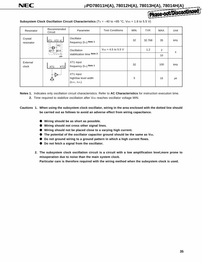
Subsystem Clock Oscillation Circuit Characteristics (TA = –40 to +85 °C, VDD = 1.8 to 5.5 V)
Notes 1. Indicates only oscillation circuit characteristics. Refer to AC Characteristics for instruction execution time.
2. Time required to stabilize oscillation after VDD reaches oscillator voltage MIN.
MIN.
32
32
5
TYP.
32.768
1.2
MAX.
35
2
10
100
15
Unit
kHz
s
kHz
µs
Resonator
Crystal
resonator
External
clock
Test Conditions
VDD = 4.5 to 5.5 V
Parameter
Oscillator
frequency (fXT) Note 1
Oscillation
stabilization time Note 2
XT1 input
frequency (fXT) Note 1
XT1 input
high/low level width
(tXTH , tXTL)
Cautions 1. When using the subsystem clock oscillator, wiring in the area enclosed with the dotted line should
be carried out as follows to avoid an adverse effect from wiring capacitance.
Wiring should be as short as possible.
Wiring should not cross other signal lines.
Wiring should not be placed close to a varying high current.
The potential of the oscillator capacitor ground should be the same as V SS.
Do not ground wiring to a ground pattern in which a high current flows.
Do not fetch a signal from the oscillator.
2. The subsystem clock oscillation circuit is a circuit with a low amplification level,more prone to
misoperation due to noise than the main system clock.
Particular care is therefore required with the wiring method when the subsystem clock is used.
RecommendedCircuit
XT1 XT2
C4C3
R2
IC
XT1 XT2
µPD78011H(A), 78012H(A), 78013H(A), 78014H(A)
36
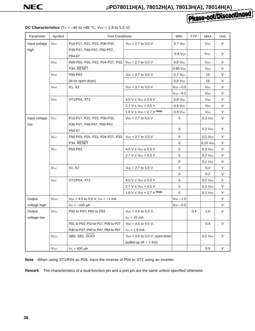
Parameter Symbol Test Conditions MIN. TYP. MAX. Unit
Input voltage VIH1 P10-P17, P21, P23, P30-P32, VDD = 2.7 to 5.5 V 0.7 VDD VDD V
high P35-P37, P40-P47, P50-P57,
P64-67
VIH2 P00-P03, P20, P22, P24-P27, P33, VDD = 2.7 to 5.5 V 0.8 VDD VDD V
P34, RESET 0.85 VDD VDD V
VIH3 P60-P63 VDD = 2.7 to 5.5 V 0.7 VDD 15 V
(N-ch open-drain) 0.8 VDD 15 V
VIH4 X1, X2 VDD = 2.7 to 5.5 V VDD – 0.5 VDD V
VDD – 0.2 VDD V
VIH5 XT1/P04, XT2 4.5 V ≤ VDD ≤ 5.5 V 0.8 VDD VDD V
2.7 V ≤ VDD < 4.5 V 0.9 VDD VDD V
1.8 V ≤ VDD < 2.7 V Note 0.9 VDD VDD V
Input voltage VIL1 P10-P17, P21, P23, P30-P32, VDD = 2.7 to 5.5 V 0 0.3 VDD V
low P35-P37, P40-P47, P50-P57,
P64-67
VIL2 P00-P03, P20, P22, P24-P27, P33, VDD = 2.7 to 5.5 V 0 0.2 VDD V
P34, RESET 0 0.15 VDD V
VIL3 P60-P63 4.5 V ≤ VDD ≤ 5.5 V 0 0.3 VDD V
2.7 V ≤ VDD < 4.5 V 0 0.2 VDD V
0 0.1 VDD V
VIL4 X1, X2 VDD = 2.7 to 5.5 V 0 0.4 V
0 0.2 V
VIL5 XT1/P04, XT2 4.5 V ≤ VDD ≤ 5.5 V 0 0.2 VDD V
2.7 V ≤ VDD < 4.5 V 0 0.1 VDD V
1.8 V ≤ VDD < 2.7 V Note 0 0.1 VDD V
Output VOH1 VDD = 4.5 to 5.5 V, IOH = –1 mA VDD – 1.0 V
voltage high IOH = –100 µA VDD – 0.5 V
Output VOL1 P50 to P57, P60 to P63 VDD = 4.5 to 5.5 V, 0.4 2.0 V
voltage low IOL = 15 mA
P01 to P03, P10 to P17, P20 to P27 VDD = 4.5 to 5.5 V, 0.4 V
P30 to P37, P40 to P47, P64 to P67 IOL = 1.6 mA
VOL2 SB0, SB1, SCK0 VDD = 4.5 to 5.5 V, open-drain 0.2 VDD V
pulled-up (R = 1 KΩ)
VOL3 IOL = 400 µA 0.5 V
DC Characteristics (TA = –40 to +85 °C, VDD = 1.8 to 5.5 V)
0.8 VDD VDD V
Note When using XT1/P04 as P04, input the inverse of P04 to XT2 using an inverter.
Remark The characteristics of a dual-function pin and a port pin are the same unless specified otherwise.
0 0.2 VDD V
µPD78011H(A), 78012H(A), 78013H(A), 78014H(A)
37
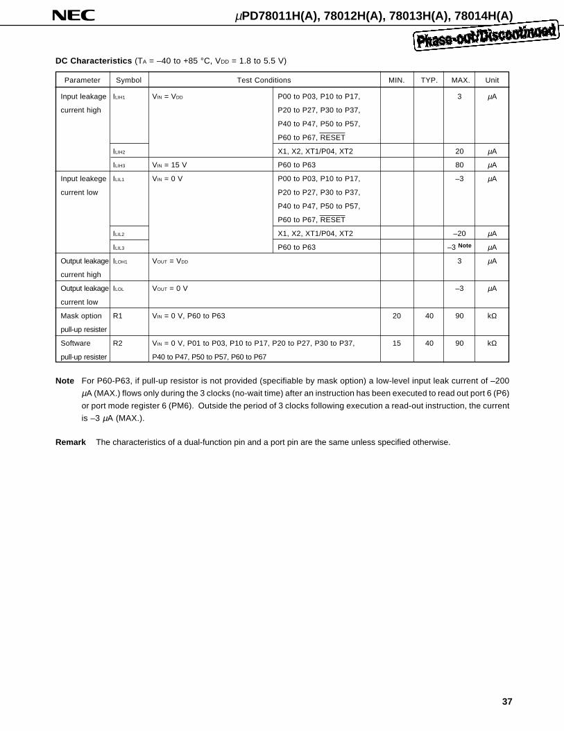
Parameter Symbol Test Conditions MIN. TYP. MAX. Unit
Input leakage ILIH1 VIN = VDD P00 to P03, P10 to P17, 3 µA
current high P20 to P27, P30 to P37,
P40 to P47, P50 to P57,
P60 to P67, RESET
ILIH2 X1, X2, XT1/P04, XT2 20 µA
ILIH3 VIN = 15 V P60 to P63 80 µA
Input leakege ILIL1 VIN = 0 V P00 to P03, P10 to P17, –3 µA
current low P20 to P27, P30 to P37,
P40 to P47, P50 to P57,
P60 to P67, RESET
ILIL2 X1, X2, XT1/P04, XT2 –20 µA
ILIL3 P60 to P63 –3 Note µA
Output leakage ILOH1 VOUT = VDD 3 µA
current high
Output leakage ILOL VOUT = 0 V –3 µA
current low
Mask option R1 VIN = 0 V, P60 to P63 20 40 90 kΩ
pull-up resister
Software R2 VIN = 0 V, P01 to P03, P10 to P17, P20 to P27, P30 to P37, 15 40 90 kΩ
pull-up resister P40 to P47, P50 to P57, P60 to P67
DC Characteristics (TA = –40 to +85 °C, VDD = 1.8 to 5.5 V)
Note For P60-P63, if pull-up resistor is not provided (specifiable by mask option) a low-level input leak current of –200
µA (MAX.) flows only during the 3 clocks (no-wait time) after an instruction has been executed to read out port 6 (P6)
or port mode register 6 (PM6). Outside the period of 3 clocks following execution a read-out instruction, the current
is –3 µA (MAX.).
Remark The characteristics of a dual-function pin and a port pin are the same unless specified otherwise.
µPD78011H(A), 78012H(A), 78013H(A), 78014H(A)
38
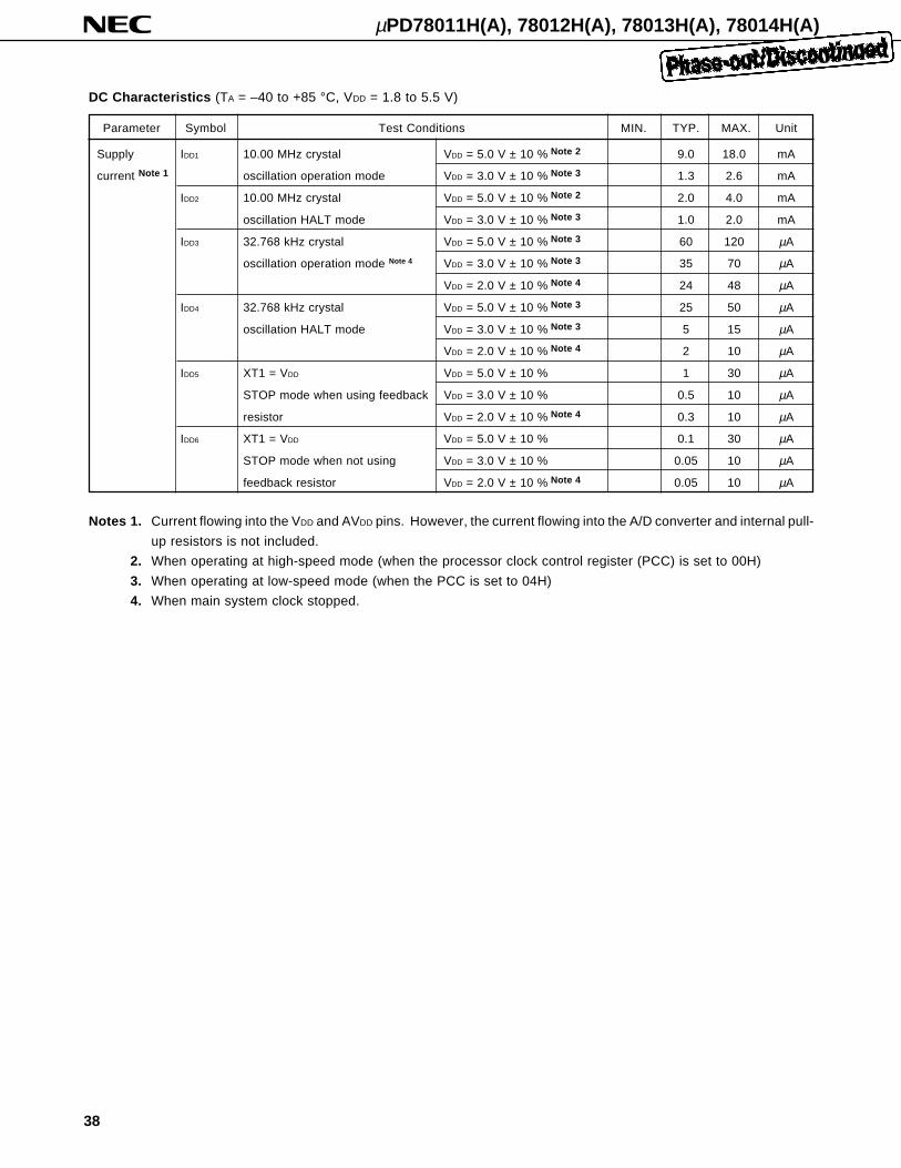
Parameter Symbol Test Conditions MIN. TYP. MAX. Unit
Supply IDD1 10.00 MHz crystal VDD = 5.0 V ± 10 % Note 2 9.0 18.0 mA
current Note 1 oscillation operation mode VDD = 3.0 V ± 10 % Note 3 1.3 2.6 mA
IDD2 10.00 MHz crystal VDD = 5.0 V ± 10 % Note 2 2.0 4.0 mA
oscillation HALT mode VDD = 3.0 V ± 10 % Note 3 1.0 2.0 mA
IDD3 32.768 kHz crystal VDD = 5.0 V ± 10 % Note 3 60 120 µA
oscillation operation mode Note 4 VDD = 3.0 V ± 10 % Note 3 35 70 µA
VDD = 2.0 V ± 10 % Note 4 24 48 µA
IDD4 32.768 kHz crystal VDD = 5.0 V ± 10 % Note 3 25 50 µA
oscillation HALT mode VDD = 3.0 V ± 10 % Note 3 5 15 µA
VDD = 2.0 V ± 10 % Note 4 2 10 µA
IDD5 XT1 = VDD VDD = 5.0 V ± 10 % 1 30 µA
STOP mode when using feedback VDD = 3.0 V ± 10 % 0.5 10 µA
resistor VDD = 2.0 V ± 10 % Note 4 0.3 10 µA
IDD6 XT1 = VDD VDD = 5.0 V ± 10 % 0.1 30 µA
STOP mode when not using VDD = 3.0 V ± 10 % 0.05 10 µA
feedback resistor VDD = 2.0 V ± 10 % Note 4 0.05 10 µA
DC Characteristics (TA = –40 to +85 °C, VDD = 1.8 to 5.5 V)
Notes 1. Current flowing into the VDD and AVDD pins. However, the current flowing into the A/D converter and internal pull-
up resistors is not included.
2. When operating at high-speed mode (when the processor clock control register (PCC) is set to 00H)
3. When operating at low-speed mode (when the PCC is set to 04H)
4. When main system clock stopped.
µPD78011H(A), 78012H(A), 78013H(A), 78014H(A)
39
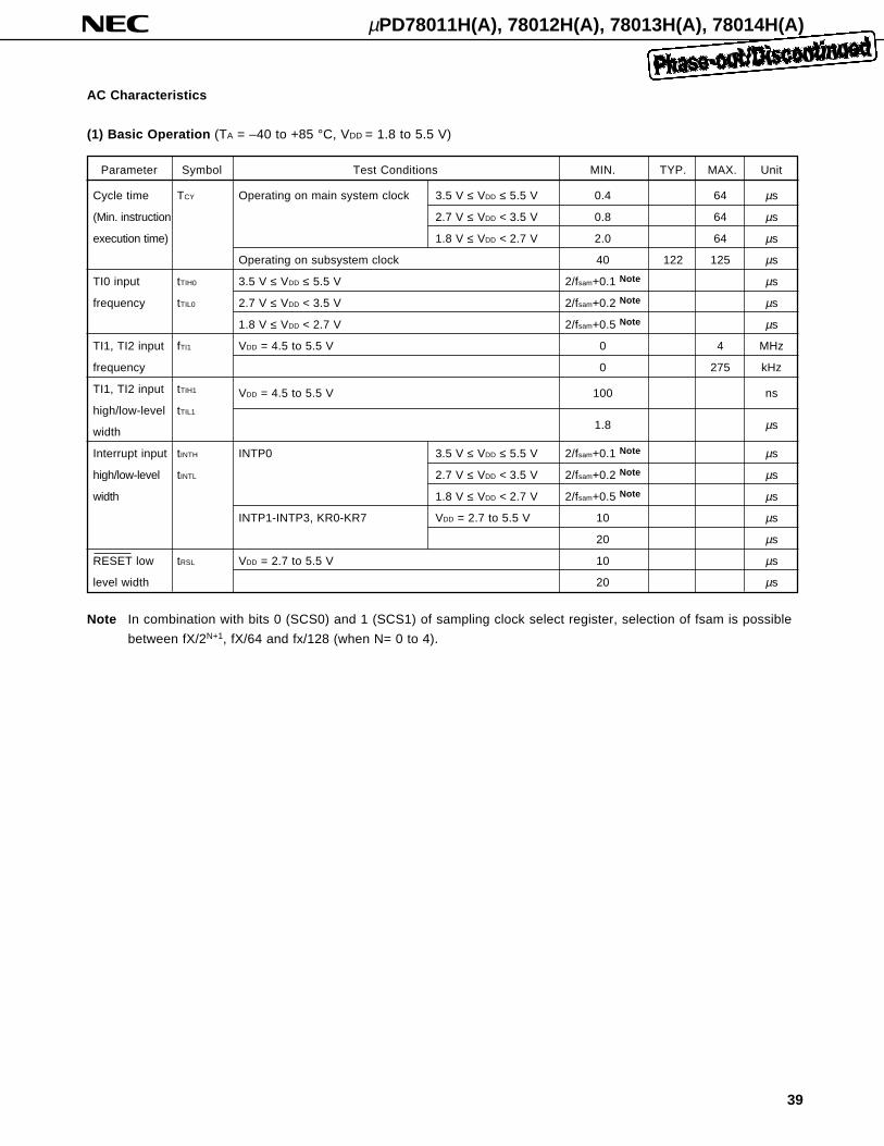
1.8 µs
Parameter Symbol Test Conditions MIN. TYP. MAX. Unit
Cycle time TCY Operating on main system clock 3.5 V ≤ VDD ≤ 5.5 V 0.4 64 µs
(Min. instruction 2.7 V ≤ VDD < 3.5 V 0.8 64 µs
execution time) 1.8 V ≤ VDD < 2.7 V 2.0 64 µs
Operating on subsystem clock 40 122 125 µs
TI0 input tTIH0 3.5 V ≤ VDD ≤ 5.5 V 2/fsam+0.1 Note µs
frequency tTIL0 2.7 V ≤ VDD < 3.5 V 2/fsam+0.2 Note µs
1.8 V ≤ VDD < 2.7 V 2/fsam+0.5 Note µs
TI1, TI2 input fTI1 VDD = 4.5 to 5.5 V 0 4 MHz
frequency 0 275 kHz
TI1, TI2 input tTIH1
high/low-level tTIL1
width
Interrupt input tINTH INTP0 3.5 V ≤ VDD ≤ 5.5 V 2/fsam+0.1 Note µs
high/low-level tINTL 2.7 V ≤ VDD < 3.5 V 2/fsam+0.2 Note µs
width 1.8 V ≤ VDD < 2.7 V 2/fsam+0.5 Note µs
INTP1-INTP3, KR0-KR7 VDD = 2.7 to 5.5 V 10 µs
20 µs
RESET low tRSL VDD = 2.7 to 5.5 V 10 µs
level width 20 µs
AC Characteristics
(1) Basic Operation (TA = –40 to +85 °C, VDD = 1.8 to 5.5 V)
Note In combination with bits 0 (SCS0) and 1 (SCS1) of sampling clock select register, selection of fsam is possible
between fX/2N+1, fX/64 and fx/128 (when N= 0 to 4).
VDD = 4.5 to 5.5 V 100 ns
µPD78011H(A), 78012H(A), 78013H(A), 78014H(A)
40
TCY vs VDD (At main system clock operation)
60.0
5.0
1.0
0.5
0.1
Supply voltage VDD [V]
Cyc
le T
ime
TC
Y [
S]
0
10.0
1.0 2.0 3.0 4.0 5.0 6.01.8
3.5 5.5
2.7
Operation GuaranteedRange
µ
µPD78011H(A), 78012H(A), 78013H(A), 78014H(A)
41
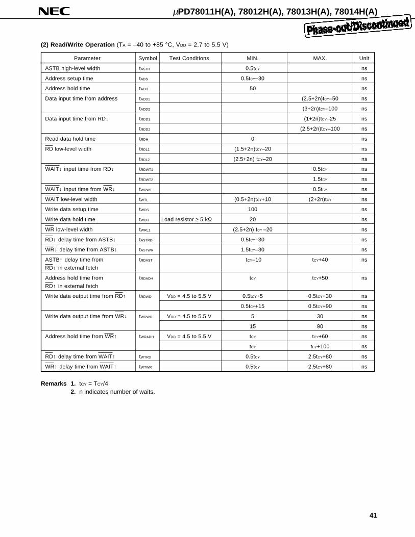
Parameter Symbol Test Conditions MIN. MAX. Unit
ASTB high-level width tASTH 0.5tCY ns
Address setup time tADS 0.5tCY–30 ns
Address hold time tADH 50 ns
Data input time from address tADD1 (2.5+2n)tCY–50 ns
tADD2 (3+2n)tCY–100 ns
Data input time from RD↓ tRDD1 (1+2n)tCY–25 ns
tRDD2 (2.5+2n)tCY–100 ns
Read data hold time tRDH 0 ns
RD low-level width tRDL1 (1.5+2n)tCY–20 ns
tRDL2 (2.5+2n) tCY–20 ns
WAIT↓ input time from RD↓ tRDWT1 0.5tCY ns
tRDWT2 1.5tCY ns
WAIT↓ input time from WR↓ tWRWT 0.5tCY ns
WAIT low-level width tWTL (0.5+2n)tCY+10 (2+2n)tCY ns
Write data setup time tWDS 100 ns
Write data hold time tWDH Load resistor ≥ 5 kΩ 20 ns
WR low-level width tWRL1 (2.5+2n) tCY –20 ns
RD↓ delay time from ASTB↓ tASTRD 0.5tCY–30 ns
WR↓ delay time from ASTB↓ tASTWR 1.5tCY–30 ns
ASTB↑ delay time from tRDAST tCY–10 tCY+40 ns
RD↑ in external fetch
Address hold time from tRDADH tCY tCY+50 ns
RD↑ in external fetch
Write data output time from RD↑ tRDWD VDD = 4.5 to 5.5 V 0.5tCY+5 0.5tCY+30 ns
0.5tCY+15 0.5tCY+90 ns
Write data output time from WR↓ tWRWD VDD = 4.5 to 5.5 V 5 30 ns
15 90 ns
Address hold time from WR↑ tWRADH VDD = 4.5 to 5.5 V tCY tCY+60 ns
tCY tCY+100 ns
RD↑ delay time from WAIT↑ tWTRD 0.5tCY 2.5tCY+80 ns
WR↑ delay time from WAIT↑ tWTWR 0.5tCY 2.5tCY+80 ns
(2) Read/Write Operation (TA = –40 to +85 °C, VDD = 2.7 to 5.5 V)
Remarks 1. tCY = TCY/42. n indicates number of waits.
µPD78011H(A), 78012H(A), 78013H(A), 78014H(A)
42
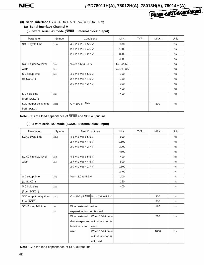
(ii) 3-wire serial I/O mode (SCK0... External clock input)
Parameter Symbol Test Conditions MIN. TYP. MAX. Unit
SCK0 cycle time tKCY2 4.5 V ≤ VDD ≤ 5.5 V 800 ns
2.7 V ≤ VDD < 4.5 V 1600 ns
2.0 V ≤ VDD < 2.7 V 3200 ns
4800 ns
SCK0 high/low-level tKH2 4.5 V ≤ VDD ≤ 5.5 V 400 ns
width tKL2 2.7 V ≤ VDD < 4.5 V 800 ns
2.0 V ≤ VDD < 2.7 V 1600 ns
2400 ns
SI0 setup time tSIK2 VDD = 2.0 to 5.5 V 100 ns
(to SCK0↑) 150 ns
SI0 hold time tKSI2 400 ns
(from SCK0↑)
SO0 output delay time tKSO2 C = 100 pF Note VDD = 2.0 to 5.5 V 300 ns
from SCK0↓ 500 ns
SCK0 rise, fall time tR2 When external device 160 ns
tF2 expansion function is used
When external When 16-bit timer 700 ns
device expansion output function is
function is not used
used When 16-bit timer 1000 ns
output function is
not used
(3) Serial Interface (TA = –40 to +85 °C, VDD = 1.8 to 5.5 V)
(a) Serial Interface Channel 0
(i) 3-wire serial I/O mode (SCK0... Internal clock output)
Parameter Symbol Conditions MIN. TYP. MAX. Unit
SCK0 cycle time tKCY1 4.5 V ≤ VDD ≤ 5.5 V 800 ns
2.7 V ≤ VDD < 4.5 V 1600 ns
2.0 V ≤ VDD < 2.7 V 3200 ns
4800 ns
SCK0 high/low-level tKH1 VDD = 4.5 to 5.5 V tKCY1/2–50 ns
width tKL1 tKCY1/2–100 ns
SI0 setup time tSIK1 4.5 V ≤ VDD ≤ 5.5 V 100 ns
(to SCK0↑) 2.7 V ≤ VDD < 4.5 V 150 ns
2.0 V ≤ VDD < 2.7 V 300 ns
400 ns
SI0 hold time tKSI1 400 ns
(from SCK0↑)
SO0 output delay time tKSO1 C = 100 pF Note 300 ns
from SCK0↓
Note C is the load capacitance of SCK0 and SO0 output line.
Note C is the load capacitance of SO0 output line.
µPD78011H(A), 78012H(A), 78013H(A), 78014H(A)
43
Parameter Symbol Test Conditions MIN. TYP. MAX. Unit
SCK0 cycle time tKCY3 4.5 V ≤ VDD ≤ 5.5 V 800 ns
2.0 V ≤ VDD < 4.5 V 3200 ns
4800 ns
SCK0 high/low-level tKH3 VDD = 4.5 to 6.0 V tKCY3/2–50 ns
width tKL3 tKCY3/2–150 ns
SB0, SB1 setup time tSIK3 4.5 V ≤ VDD ≤ 5.5 V 100 ns
(to SCK0↑) 2.0 V ≤ VDD < 4.5 V 300 ns
400 ns
SB0, SB1 hold time tKSI3 tKCY3/2 ns
(from SCK0↑)
SB0, SB1output delay tKSO3 R = 1 kΩ, VDD = 4.5 to 5.5 V 0 250 ns
time from SCK0↓ C = 100 pF Note 0 1000 ns
SB0, SB1↓ from SCK0↑ tKSB tKCY3 ns
SCK0↓ from SB0, SB1↓ tSBK tKCY3 ns
SB0, SB1 high-level tSBH tKCY3 ns
width
SB0, SB1 low-level tSBL tKCY3 ns
width
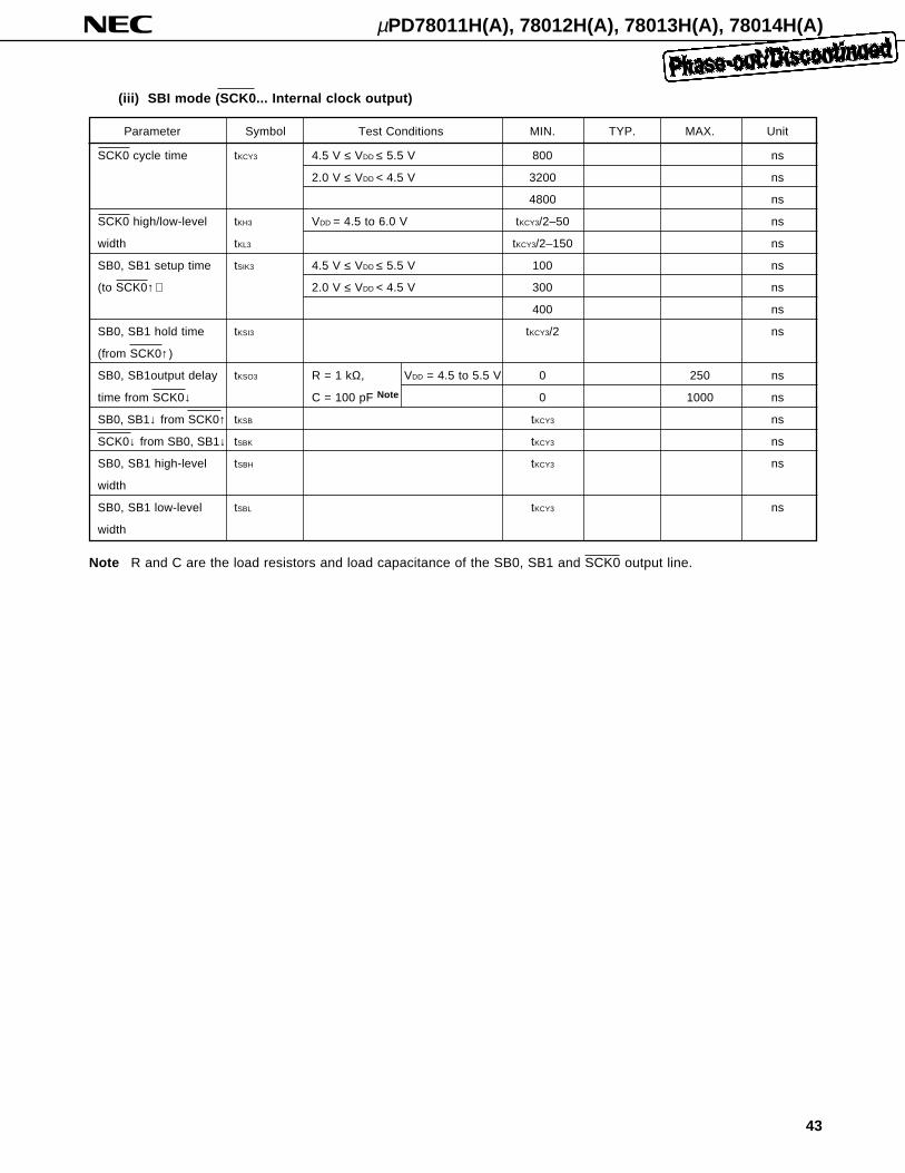
(iii) SBI mode (SCK0... Internal clock output)
Note R and C are the load resistors and load capacitance of the SB0, SB1 and SCK0 output line.
µPD78011H(A), 78012H(A), 78013H(A), 78014H(A)
44
Parameter Symbol Test Conditions MIN. TYP. MAX. Unit
SCK0 cycle time tKCY4 4.5 V ≤ VDD ≤ 5.5 V 800 ns
2.0 V ≤ VDD < 4.5 V 3200 ns
4800 ns
SCK0 high/low-level tKH4 4.5 V ≤ VDD ≤ 5.5 V 400 ns
width tKL4 2.0 V ≤ VDD < 4.5 V 1600 ns
2400 ns
SB0, SB1 setup time tSIK4 4.5 V ≤ VDD ≤ 5.5 V 100 ns
(to SCK0↑) 2.0 V ≤ VDD < 4.5 V 300 ns
400 ns
SB0, SB1 hold time tKSI4 tKCY4/2 ns
(from SCK0↑)
SB0, SB1 output delay tKSO4 R = 1 kΩ, VDD = 4.5 to 5.5 V 0 300 ns
time from SCK0↓ C = 100 pF Note 0 1000 ns
SB0, SB1↓ from SCK0↑ tKSB tKCY4 ns
SCK0↓ from SB0, SB1↓ tSBK tKCY4 ns
SB0, SB1 high-level tSBH tKCY4 ns
width
SB0, SB1 low-level tSBL tKCY4 ns
width
SCK0 rise, fall time tR4 When external device 160 ns
tF4 expansion function is used
When external When 16-bit timer 700 ns
device expansion output function is
function is not used
used When 16-bit timer 1000 ns
output function is
not used
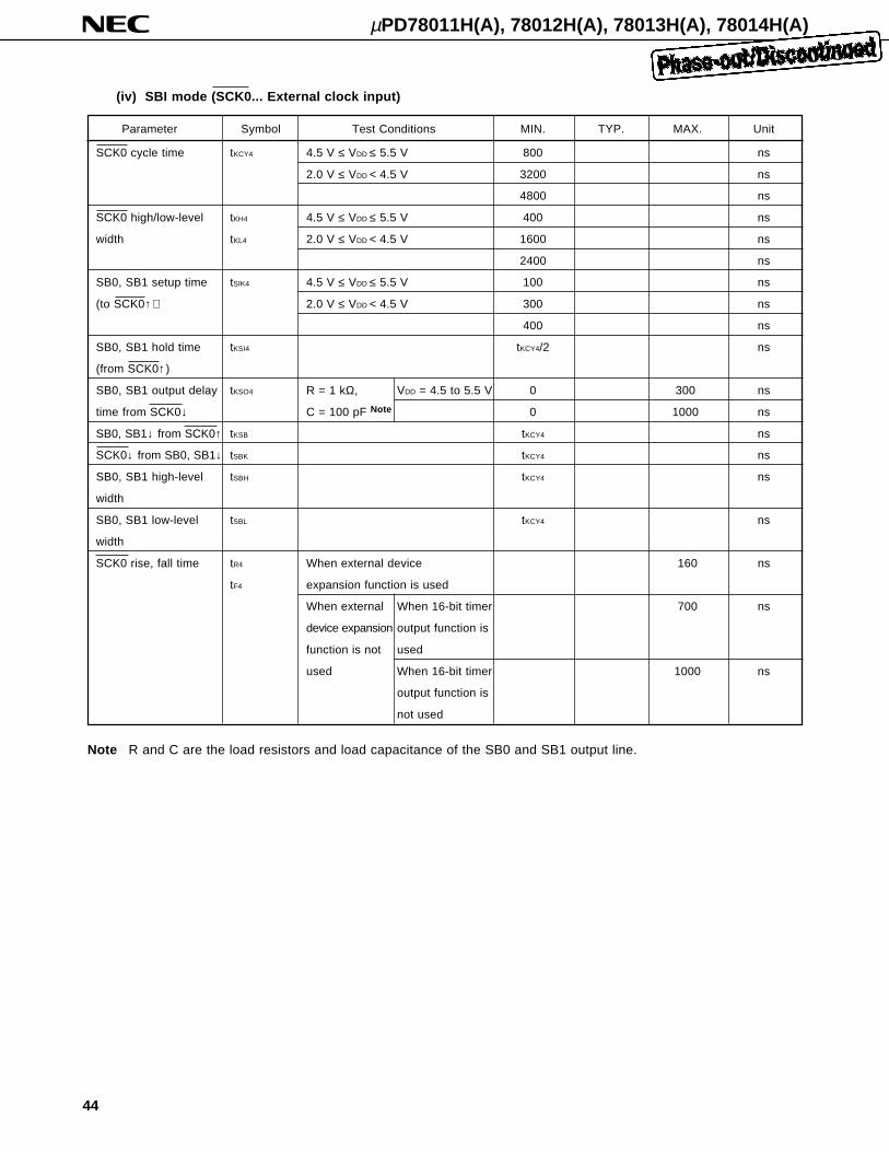
(iv) SBI mode (SCK0... External clock input)
Note R and C are the load resistors and load capacitance of the SB0 and SB1 output line.
µPD78011H(A), 78012H(A), 78013H(A), 78014H(A)
45
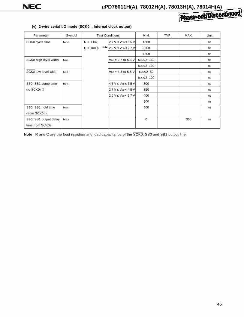
(v) 2-wire serial I/O mode (SCK0... Internal clock output)
Note R and C are the load resistors and load capacitance of the SCK0, SB0 and SB1 output line.
Parameter Symbol Test Conditions MIN. TYP. MAX. Unit
SCK0 cycle time tKCY5 R = 1 kΩ, 2.7 V ≤ VDD ≤ 5.5 V 1600 ns
C = 100 pF Note 2.0 V ≤ VDD < 2.7 V 3200 ns
4800 ns
SCK0 high-level width tKH5 VDD = 2.7 to 5.5 V tKCY5/2–160 ns
tKCY5/2–190 ns
SCK0 low-level width tKL5 VDD = 4.5 to 5.5 V tKCY5/2–50 ns
tKCY5/2–100 ns
SB0, SB1 setup time tSIK5 4.5 V ≤ VDD ≤ 5.5 V 300 ns
(to SCK0↑) 2.7 V ≤ VDD < 4.5 V 350 ns
2.0 V ≤ VDD < 2.7 V 400 ns
500 ns
SB0, SB1 hold time tKSI5 600 ns
(from SCK0↑)
SB0, SB1 output delay tKSO5 0 300 ns
time from SCK0↓
µPD78011H(A), 78012H(A), 78013H(A), 78014H(A)
46
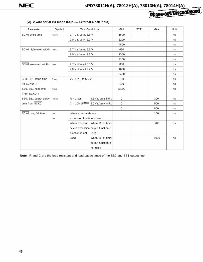
Parameter Symbol Test Conditions MIN. TYP. MAX. Unit
SCK0 cycle time tKCY6 2.7 V ≤ VDD ≤ 5.5 V 1600 ns
2.0 V ≤ VDD < 2.7 V 3200 ns
4800 ns
SCK0 high-level width tKH6 2.7 V ≤ VDD ≤ 5.5 V 650 ns
2.0 V ≤ VDD < 2.7 V 1300 ns
2100 ns
SCK0 low-level width tKL6 2.7 V ≤ VDD ≤ 5.5 V 800 ns
2.0 V ≤ VDD < 2.7 V 1600 ns
2400 ns
SB0, SB1 setup time tSIK6 VDD = 2.0 to 5.5 V 100 ns
(to SCK0↑) 150 ns
SB0, SB1 hold time tKSI6 tKCY6/2 ns
(from SCK0↑)
SB0, SB1 output delay tKSO6 R = 1 kΩ, 4.5 V ≤ VDD ≤ 5.5 V 0 300 ns
time from SCK0↓ C = 100 pF Note 2.0 V ≤ VDD < 4.5 V 0 500 ns
0 800 ns
SCK0 rise, fall time tR6 When external device 160 ns
tF6 expansion function is used
When external When 16-bit timer 700 ns
device expansion output function is
function is not used
used When 16-bit timer 1000 ns
output function is
not used
(vi) 2-wire serial I/O mode (SCK0... External clock input)
Note R and C are the load resistors and load capacitance of the SB0 and SB1 output line.
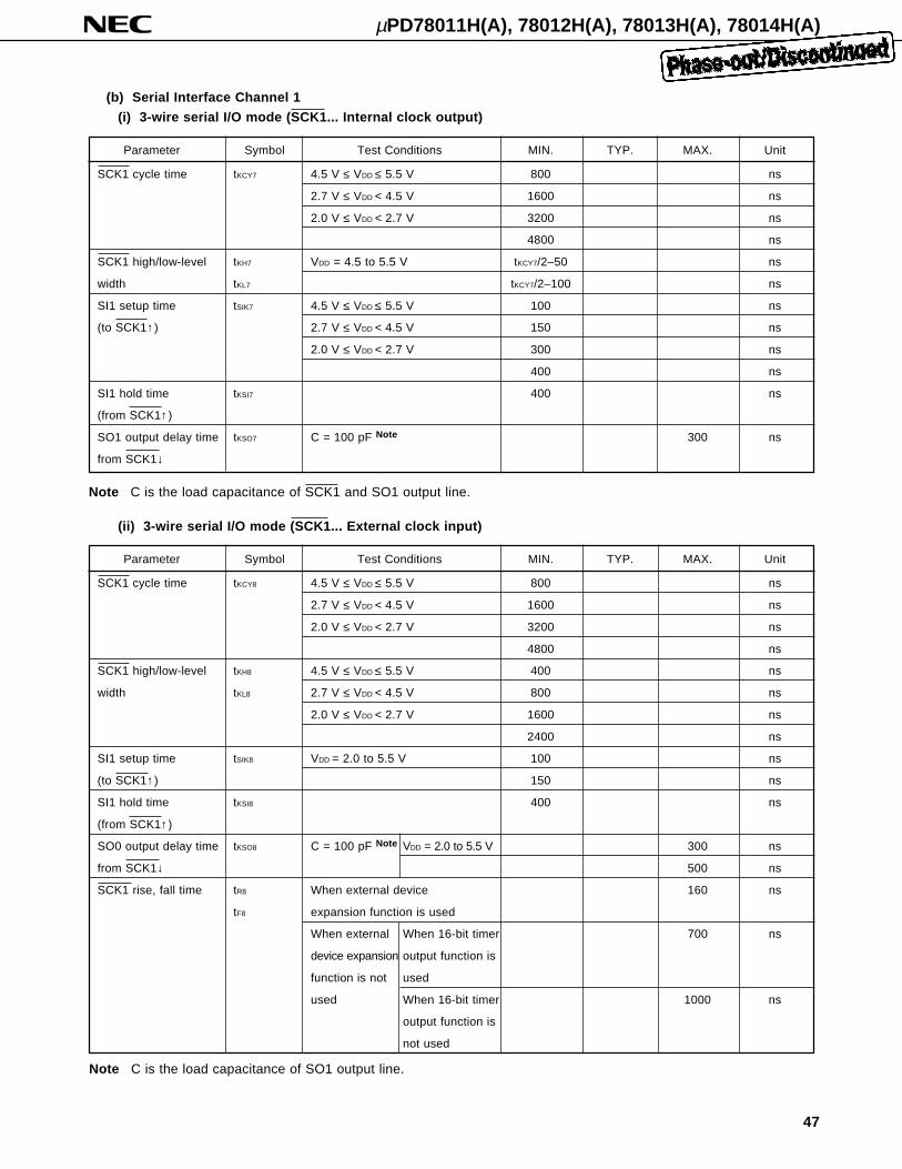
µPD78011H(A), 78012H(A), 78013H(A), 78014H(A)
47
Parameter Symbol Test Conditions MIN. TYP. MAX. Unit
SCK1 cycle time tKCY8 4.5 V ≤ VDD ≤ 5.5 V 800 ns
2.7 V ≤ VDD < 4.5 V 1600 ns
2.0 V ≤ VDD < 2.7 V 3200 ns
4800 ns
SCK1 high/low-level tKH8 4.5 V ≤ VDD ≤ 5.5 V 400 ns
width tKL8 2.7 V ≤ VDD < 4.5 V 800 ns
2.0 V ≤ VDD < 2.7 V 1600 ns
2400 ns
SI1 setup time tSIK8 VDD = 2.0 to 5.5 V 100 ns
(to SCK1↑) 150 ns
SI1 hold time tKSI8 400 ns
(from SCK1↑)
SO0 output delay time tKSO8 C = 100 pF Note VDD = 2.0 to 5.5 V 300 ns
from SCK1↓ 500 ns
SCK1 rise, fall time tR8 When external device 160 ns
tF8 expansion function is used
When external When 16-bit timer 700 ns
device expansion output function is
function is not used
used When 16-bit timer 1000 ns
output function is
not used
(b) Serial Interface Channel 1
(i) 3-wire serial I/O mode (SCK1... Internal clock output)
Parameter Symbol Test Conditions MIN. TYP. MAX. Unit
SCK1 cycle time tKCY7 4.5 V ≤ VDD ≤ 5.5 V 800 ns
2.7 V ≤ VDD < 4.5 V 1600 ns
2.0 V ≤ VDD < 2.7 V 3200 ns
4800 ns
SCK1 high/low-level tKH7 VDD = 4.5 to 5.5 V tKCY7/2–50 ns
width tKL7 tKCY7/2–100 ns
SI1 setup time tSIK7 4.5 V ≤ VDD ≤ 5.5 V 100 ns
(to SCK1↑) 2.7 V ≤ VDD < 4.5 V 150 ns
2.0 V ≤ VDD < 2.7 V 300 ns
400 ns
SI1 hold time tKSI7 400 ns
(from SCK1↑)
SO1 output delay time tKSO7 C = 100 pF Note 300 ns
from SCK1↓
Note C is the load capacitance of SCK1 and SO1 output line.
(ii) 3-wire serial I/O mode (SCK1... External clock input)
Note C is the load capacitance of SO1 output line.

µPD78011H(A), 78012H(A), 78013H(A), 78014H(A)
48
Parameter Symbol Test Conditions MIN. TYP. MAX. Unit
SCK1 cycle time tKCY9 4.5 V ≤ VDD ≤ 5.5 V 800 ns
2.7 V ≤ VDD < 4.5 V 1600 ns
2.0 V ≤ VDD < 2.7 V 3200 ns
4800 ns
SCK1 high/low-level tKH9 VDD = 4.5 to 5.5 V tKCY9/2–50 ns
width tKL9 tKCY9/2–100 ns
SI1 setup time tSIK9 4.5 V ≤ VDD ≤ 5.5 V 100 ns
(to SCK1↑) 2.7 V ≤ VDD < 4.5 V 150 ns
2.0 V ≤ VDD < 2.7 V 300 ns
400 ns
SI1 hold time tKSI9 400 ns
(from SCK1↑)
SO1 output delay time tKSO9 C = 100 pF Note 300 ns
from SCK1↓
STB↑ from SCK1↑ tSBD tKCY9/2–100 tKCY9/2+100 ns
Strobe signal tSBW 2.7 V ≤ VDD ≤ 5.5 V tKCY9–30 tKCY9+30 ns
high-level width 2.0 V ≤ VDD < 2.7 V tKCY9–60 tKCY9+60 ns
tKCY9–90 tKCY9+90 ns
Busy signal setup time tBYS 100 ns
(to busy signal
detection timing)
Busy signal hold time tBYH 4.5 V ≤ VDD ≤ 5.5 V 100 ns
(from busy signal 2.7 V ≤ VDD < 4.5 V 150 ns
detection timing) 2.0 V ≤ VDD < 2.7 V 200 ns
300 ns
SCK1↓ from busy tSPS 2tKCY9 ns
inactive
(iii) 3-wire serial I/O mode with automatic transmit/receive function (SCK1... Internal clock output)
Note C is the load capacitance of SCK1 and SO1 output line.
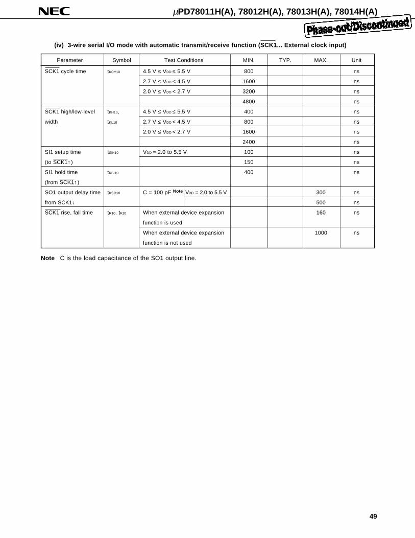
µPD78011H(A), 78012H(A), 78013H(A), 78014H(A)
49
(iv) 3-wire serial I/O mode with automatic transmit/receive function (SCK1... External clock input)
Parameter Symbol Test Conditions MIN. TYP. MAX. Unit
SCK1 cycle time tKCY10 4.5 V ≤ VDD ≤ 5.5 V 800 ns
2.7 V ≤ VDD < 4.5 V 1600 ns
2.0 V ≤ VDD < 2.7 V 3200 ns
4800 ns
SCK1 high/low-level tKH10, 4.5 V ≤ VDD ≤ 5.5 V 400 ns
width tKL10 2.7 V ≤ VDD < 4.5 V 800 ns
2.0 V ≤ VDD < 2.7 V 1600 ns
2400 ns
SI1 setup time tSIK10 VDD = 2.0 to 5.5 V 100 ns
(to SCK1↑) 150 ns
SI1 hold time tKSI10 400 ns
(from SCK1↑)
SO1 output delay time tKSO10 C = 100 pF Note VDD = 2.0 to 5.5 V 300 ns
from SCK1↓ 500 ns
SCK1 rise, fall time tR10, tF10 When external device expansion 160 ns
function is used
When external device expansion 1000 ns
function is not used
Note C is the load capacitance of the SO1 output line.
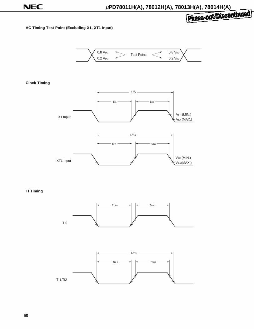
µPD78011H(A), 78012H(A), 78013H(A), 78014H(A)
50
AC Timing Test Point (Excluding X1, XT1 Input)
TI Timing
Clock Timing
0.8 VDD
0.2 VDD
Test Points0.8 VDD
0.2 VDD
TI0
tTIL0 tTIH0
TI1,TI2
1/fTI1
tTIL1 tTIH1
X1 InputVIH4 (MIN.)
VIL4 (MAX.)
1/fX
tXL tXH
XT1 InputVIH5 (MIN.)
VIL5 (MAX.)
1/fXT
tXTL tXTH
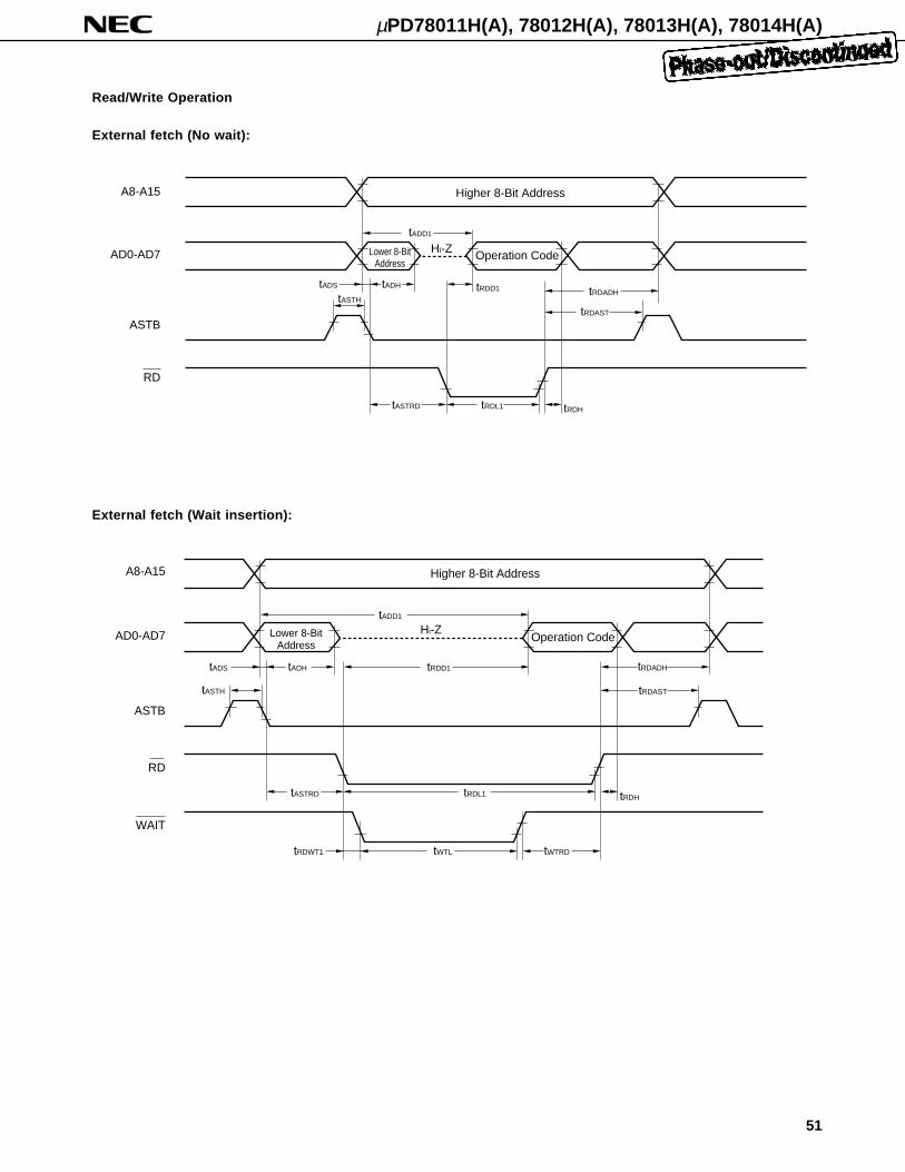
51
µPD78011H(A), 78012H(A), 78013H(A), 78014H(A)
Read/Write Operation
External fetch (No wait):
External fetch (Wait insertion):
A8-A15
AD0-AD7
ASTB
RD
Higher 8-Bit Address
Lower 8-BitAddress
tADD1
Hi-Z
tADS
tASTH
tADH tRDD1
Operation Code
tRDADH
tRDAST
tASTRD tRDL1 tRDH
A8-A15
AD0-AD7
ASTB
RD
Higher 8-Bit Address
tADD1
Hi-Z
tADS
tASTH
tADH tRDD1
Operation Code
tRDADH
tRDAST
tASTRD tRDL1 tRDH
WAIT
tRDWT1 tWTL tWTRD
Lower 8-BitAddress
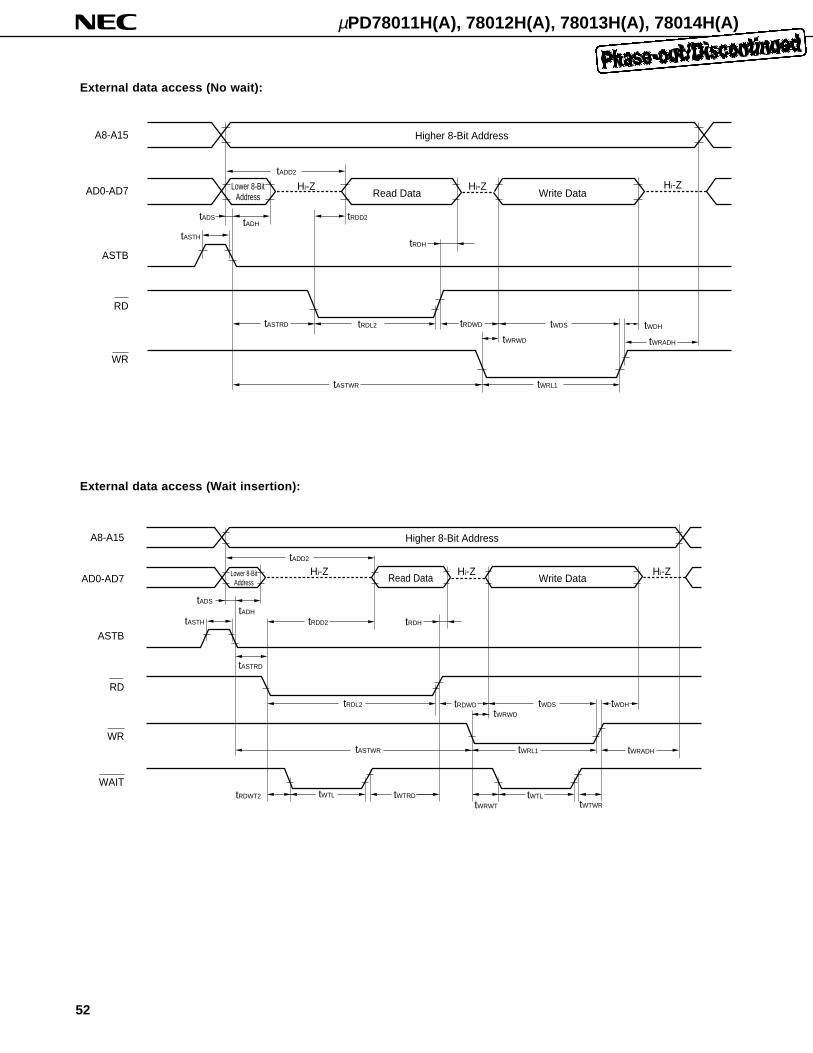
µPD78011H(A), 78012H(A), 78013H(A), 78014H(A)
52
External data access (No wait):
A8-A15
AD0-AD7
ASTB
RD
Higher 8-Bit Address
tADD2
Hi-Z
tADS
tASTH
tADHtRDD2
Read Data
tASTRD tRDWD
WR
tASTWR
Write DataHi-Z
tWDH
tWRADH
tWDS
tWRWD
tWRL1
tRDH
tRDL2
Hi-ZLower 8-BitAddress
External data access (Wait insertion):
A8-A15
AD0-AD7
ASTB
RD
Higher 8-Bit Address
tADD2
tADS
tASTH
tADH
tRDD2
Read Data
tASTRD
WRtASTWR
Write DataHi-Z
tWDH
tWRADH
tWDS
tWRWD
tWRL1
tRDH
tRDL2
tRDWT2 tWTL
tWRWT
tWTLtWTWR
tWTRD
WAIT
tRDWD
Hi-Z Hi-ZLower 8-BitAddress
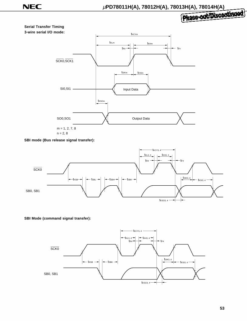
53
µPD78011H(A), 78012H(A), 78013H(A), 78014H(A)
SBI mode (Bus release signal transfer):
SBI Mode (command signal transfer):
Serial Transfer Timing
3-wire serial I/O mode:
SCK0
SB0, SB1
tKSB tSBL tSBH tSBK
tKCY3, 4
tKL3, 4 tKH3, 4
tSIK3, 4tKSI3, 4
tKSO3, 4
tR4 tF4
SCK0
SB0, SB1
tKSB tSBK
tKCY3, 4
tKL3, 4 tKH3, 4
tSIK3, 4
tKSI3, 4
tKSO3, 4
tR4 tF4
SI0,SI1
SO0,SO1
m = 1, 2, 7, 8
n = 2, 8
tKCYm
tKLm tKHm
tSIKm tKSIm
Input Data
tKSOm
Output Data
tFntRn
SCK0,SCK1
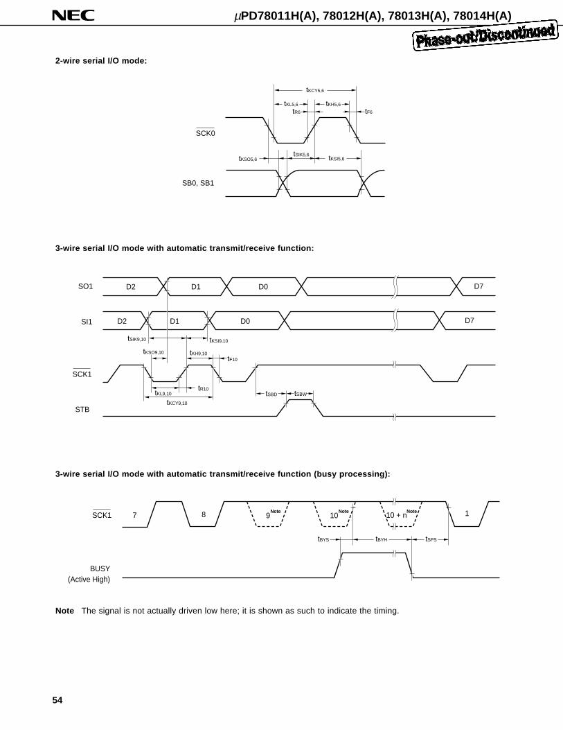
µPD78011H(A), 78012H(A), 78013H(A), 78014H(A)
54
2-wire serial I/O mode:
Note The signal is not actually driven low here; it is shown as such to indicate the timing.
SCK0
SB0, SB1
tKCY5,6
tKL5,6 tKH5,6
tR6 tF6
tKSO5,6tSIK5,6 tKSI5,6
SO1
SCK1
SI1
STB
D2 D1 D0
D2 D1 D0
tSIK9,10 tKSI9,10
tKSO9,10 tKH9,10tF10
tR10tKL9,10
tKCY9,10
tSBWtSBD
D7
D7
3-wire serial I/O mode with automatic transmit/receive function:
SCK1
BUSY
7 8 9 10 10 + n
tBYS tBYH tSPS
1
(Active High)
Note NoteNote
3-wire serial I/O mode with automatic transmit/receive function (busy processing):
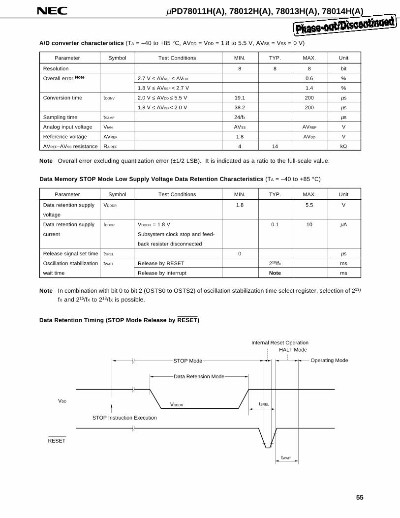
55
µPD78011H(A), 78012H(A), 78013H(A), 78014H(A)
Data Retention Timing (STOP Mode Release by RESET)
Parameter Symbol Test Conditions MIN. TYP. MAX. Unit
Resolution 8 8 8 bit
Overall error Note 2.7 V ≤ AVREF ≤ AVDD 0.6 %
1.8 V ≤ AVREF < 2.7 V 1.4 %
Conversion time tCONV 2.0 V ≤ AVDD ≤ 5.5 V 19.1 200 µs
1.8 V ≤ AVDD < 2.0 V 38.2 200 µs
Sampling time tSAMP 24/fX µs
Analog input voltage VIAN AVSS AVREF V
Reference voltage AVREF 1.8 AVDD V
AVREF–AVSS resistance RAIREF 4 14 kΩ
A/D converter characteristics (TA = –40 to +85 °C, AVDD = VDD = 1.8 to 5.5 V, AVSS = VSS = 0 V)
Note Overall error excluding quantization error (±1/2 LSB). It is indicated as a ratio to the full-scale value.
Data Memory STOP Mode Low Supply Voltage Data Retention Characteristics (TA = –40 to +85 °C)
Parameter Symbol Test Conditions MIN. TYP. MAX. Unit
Data retention supply VDDDR 1.8 5.5 V
voltage
Data retention supply IDDDR VDDDR = 1.8 V 0.1 10 µA
current Subsystem clock stop and feed-
back resister disconnected
Release signal set time tSREL 0 µs
Oscillation stabilization tWAIT Release by RESET 218/fX ms
wait time Release by interrupt Note ms
Note In combination with bit 0 to bit 2 (OSTS0 to OSTS2) of oscillation stabilization time select register, selection of 213/
fX and 215/fX to 218/fX is possible.
VDD
STOP Instruction Execution
RESET
VDDDR
Internal Reset OperationHALT Mode
Operating Mode
tWAIT
tSREL
Data Retension Mode
STOP Mode
µPD78011H(A), 78012H(A), 78013H(A), 78014H(A)
56
Data Retention Timing (Standby Release Signal : STOP Mode Release by Interrupt Signal)
VDD
STOP Instruction Execition
Standby Release Signal(Interrupt Request)
VDDDR
HALT Mode
Operating Mode
tSREL
tWAIT
Data Retension Mode
STOP Mode
Interrupt Input Timing
RESET Input Timing
tINTL tINTH
tINTL
INTP0-INTP2
INTP3
tRSL
RESET
µPD78011H(A), 78012H(A), 78013H(A), 78014H(A)
57
12. PACKAGE DRAWINGS
Remark Dimensions and materials of ES products are the same as those of mass-production products.
A
I
JG
H F
D N M C BM R
64 33
321
K
L
NOTE
Each lead centerline is located within 0.17 mm (0.007 inch) of its true position (T.P.) at maximum material condition.
P64C-70-750A,C-1
ITEM MILLIMETERS INCHES
A
B
C
D
F
G
H
I
J
K
58.68 MAX.
1.78 MAX.
1.778 (T.P.)
0.50±0.10
3.2±0.3
0.51 MIN.
4.31 MAX.
5.08 MAX.
L
M
0.17
19.05 (T.P.)
17.0
0.25
N
0~15°
0.9 MIN.
R
2.311 MAX.
0.070 MAX.
0.020
0.035 MIN.
0.126±0.012
0.020 MIN.
0.170 MAX.
0.200 MAX.
0.750 (T.P.)
0.669
0.010
0.007
0~15°
+0.004–0.003
0.070 (T.P.)
1)
Item "K" to center of leads when formed parallel.2)
+0.10–0.05
+0.004–0.005
64 PIN PLASTIC SHRINK DIP (750 mil)
µPD78011H(A), 78012H(A), 78013H(A), 78014H(A)
58
Remark Dimensions and materials of ES products are the same as those of mass-production products.
N
A
M
FB
4849 32
K
L
64 PIN PLASTIC QFP ( 14)
641
1716
33
DC
detail of lead end
S
Q
5°±
5°
P
MIH JG
P64GC-80-AB8-2
ITEM MILLIMETERS INCHES
A
B
C
D
F
G
H
I
J
K
L
17.6±0.4
14.0±0.2
1.0
0.35±0.10
0.15
14.0±0.2
0.693±0.016
0.039
0.039
0.006
0.031 (T.P.)
0.551
NOTE
M
N 0.10
0.15
1.8±0.2
0.8 (T.P.)
0.004
0.006+0.004–0.003
Each lead centerline is located within 0.15 mm (0.006 inch) of its true position (T.P.) at maximum material condition.
0.071±0.008
0.014
0.551
0.8±0.2 0.031
P 2.55 0.100
0.693±0.01617.6±0.4
1.0
+0.009–0.008
Q 0.1±0.1 0.004±0.004
S 2.85 MAX. 0.112 MAX.
+0.10–0.05
+0.009–0.008
+0.004–0.005
+0.009–0.008
µPD78011H(A), 78012H(A), 78013H(A), 78014H(A)
59
13. RECOMMENDED SOLDERING CONDITIONS
These products should be soldered and mounted under the conditions recommended in the table below.
For detail of recommended soldering conditions, refer to the information document Semiconductor Device
Mounting Technology Manual (C10535E) .
For soldering methods and conditions other than those recommended below, contact our salespersonnel.
Table 13-1. Surface Mounting Type Soldering Conditions
µPD78011HGC(A)-×××-AB8 : 64-Pin Plastic QFP (14 × 14 mm)
µPD78012HGC(A)-×××-AB8 : 64-Pin Plastic QFP (14 × 14 mm)
µPD78013HGC(A)-×××-AB8 : 64-Pin Plastic QFP (14 × 14 mm)
µPD78014HGC(A)-×××-AB8 : 64-Pin Plastic QFP (14 × 14 mm)
Recommended
Condition SymbolSoldering Method Soldering Conditions
Infrared reflow
VPS
Wave soldering
Partial heating
Package peak temperature: 235 °C, Duration: 30 sec. max. (at 210 °C or above),
Number of times: Thrice max.
Package peak temperature: 215 °C, Duration: 40 sec. max. (at 200 °C or above),
Number of times: Thrice max.
Solder bath temperature: 260 °C max. Duration: 10 sec. max.
Number of times: Once
Preliminary heat temperature: 120 °C max. (Package surface temperature)
Pin temperature: 300 °C max., Duration: 3 sec. max. (per device side)
IR35-00-3
VP15-00-3
WS60-00-1
—
Caution Use more than one soldering method should be avoided (except in the case of partial heating).
Table 13-2. Insertion Type Soldering Conditions
µPD78011HCW(A)-××× : 64-Pin Plastic Shrink DIP (750 mil)
µPD78012HCW(A)-××× : 64-Pin Plastic Shrink DIP (750 mil)
µPD78013HCW(A)-××× : 64-Pin Plastic Shrink DIP (750 mil)
µPD78014HCW(A)-××× : 64-Pin Plastic Shrink DIP (750 mil)
Soldering Method Soldering Conditions
Wave soldering
(pin only)
Partial heating
Solder bath temperature: 260°C max., Duration: 10 sec. max.
Pin temperature: 300°C max., Duration: 3 sec. max. (per pin)
Caution Wave soldering is only for the lead part in order that jet solder can not contact with the chip directly.
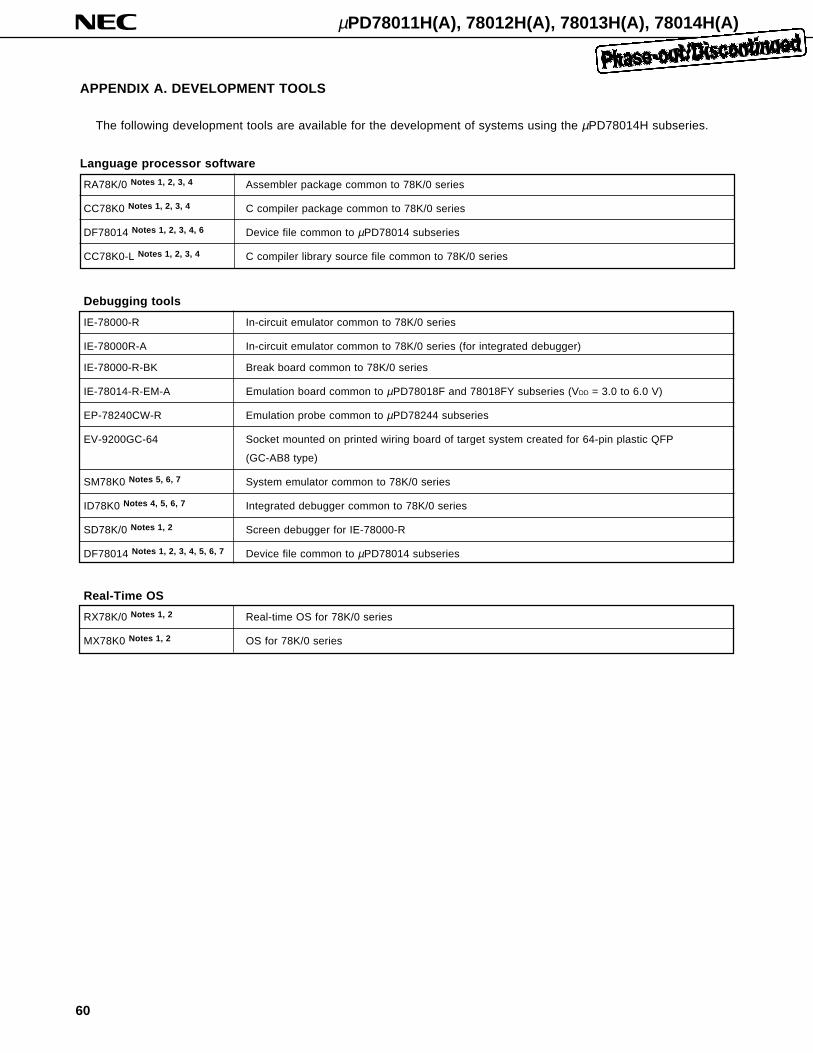
µPD78011H(A), 78012H(A), 78013H(A), 78014H(A)
60
APPENDIX A. DEVELOPMENT TOOLS
The following development tools are available for the development of systems using the µPD78014H subseries.
Language processor software
RA78K/0 Notes 1, 2, 3, 4 Assembler package common to 78K/0 series
CC78K0 Notes 1, 2, 3, 4 C compiler package common to 78K/0 series
DF78014 Notes 1, 2, 3, 4, 6 Device file common to µPD78014 subseries
CC78K0-L Notes 1, 2, 3, 4 C compiler library source file common to 78K/0 series
Debugging tools
IE-78000-R In-circuit emulator common to 78K/0 series
IE-78000R-A In-circuit emulator common to 78K/0 series (for integrated debugger)
IE-78000-R-BK Break board common to 78K/0 series
IE-78014-R-EM-A Emulation board common to µPD78018F and 78018FY subseries (VDD = 3.0 to 6.0 V)
EP-78240CW-R Emulation probe common to µPD78244 subseries
EV-9200GC-64 Socket mounted on printed wiring board of target system created for 64-pin plastic QFP
(GC-AB8 type)
SM78K0 Notes 5, 6, 7 System emulator common to 78K/0 series
ID78K0 Notes 4, 5, 6, 7 Integrated debugger common to 78K/0 series
SD78K/0 Notes 1, 2 Screen debugger for IE-78000-R
DF78014 Notes 1, 2, 3, 4, 5, 6, 7 Device file common to µPD78014 subseries
Real-Time OS
RX78K/0 Notes 1, 2 Real-time OS for 78K/0 series
MX78K0 Notes 1, 2 OS for 78K/0 series
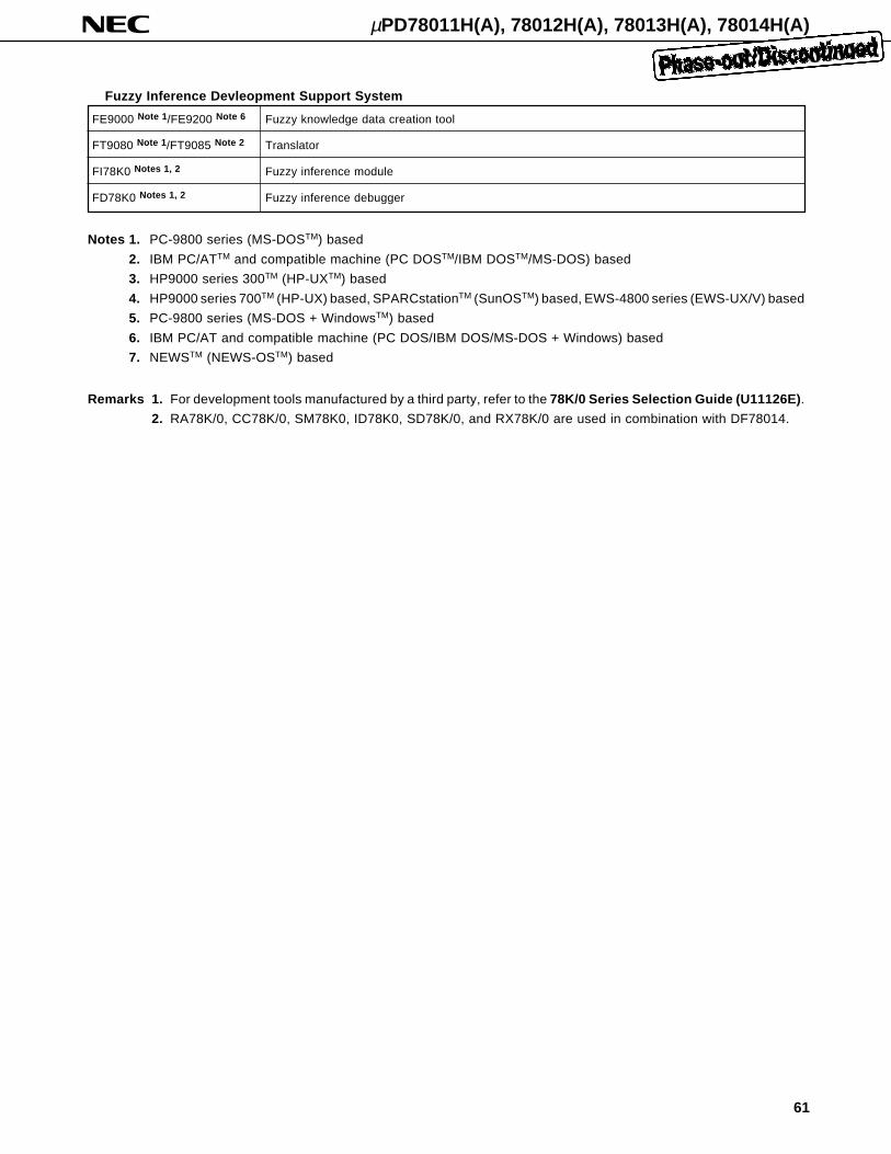
µPD78011H(A), 78012H(A), 78013H(A), 78014H(A)
61
Fuzzy Inference Devleopment Support System
FE9000 Note 1 /FE9200 Note 6 Fuzzy knowledge data creation tool
FT9080 Note 1 /FT9085 Note 2 Translator
FI78K0 Notes 1, 2 Fuzzy inference module
FD78K0 Notes 1, 2 Fuzzy inference debugger
Notes 1. PC-9800 series (MS-DOSTM) based
2. IBM PC/ATTM and compatible machine (PC DOSTM/IBM DOSTM/MS-DOS) based
3. HP9000 series 300TM (HP-UXTM) based
4. HP9000 series 700TM (HP-UX) based, SPARCstationTM (SunOSTM) based, EWS-4800 series (EWS-UX/V) based
5. PC-9800 series (MS-DOS + WindowsTM) based
6. IBM PC/AT and compatible machine (PC DOS/IBM DOS/MS-DOS + Windows) based
7. NEWSTM (NEWS-OSTM) based
Remarks 1. For development tools manufactured by a third party, refer to the 78K/0 Series Selection Guide (U11126E) .
2. RA78K/0, CC78K/0, SM78K0, ID78K0, SD78K/0, and RX78K/0 are used in combination with DF78014.
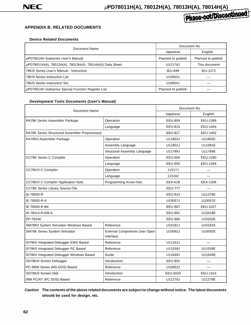
µPD78011H(A), 78012H(A), 78013H(A), 78014H(A)
62
APPENDIX B. RELATED DOCUMENTS
Device Related Documents
Document NameDocument No.
Japanese English
µPD78014H Subseries User's Manual Planned to publish Planned to publish
µPD78011H(A), 78012H(A), 78013H(A), 78014H(A) Data Sheet U12174J This document
78K/0 Series User's Manual - Instruction IEU-849 IEU-1372
78K/0 Series Instruction List U10903J —
78K/0 Series Instruction Set U10904J —
µPD78014H Subseries Special Function Register List Planned to publish —
Development Tools Documents (User's Manual)
Document NameDocument No.
Japanese English
RA78K Series Assembler Package Operation EEU-809 EEU-1399
Language EEU-815 EEU-1404
RA78K Series Structured Assembler Preprocessor EEU-817 EEU-1402
RA78K0 Assembler Package Operation U11802J U11802E
Assembly Language U11801J U11081E
Structural Assembly Language U11789J U11789E
CC78K Series C Compiler Operation EEU-656 EEU-1280
Language EEU-655 EEU-1284
CC78K/0 C Compiler Operation 11517J —
Language 11518J —
CC78K/0 C Compiler Application Note Programming Know-how EEA-618 EEA-1208
CC78K Series Library Source File EEU-777 —
IE-78000-R EEU-810 U11376E
IE-78000-R-A U10057J U10057E
IE-78000-R-BK EEU-867 EEU-1427
IE-78014-R-EM-A EEU-962 U10418E
EP-78240 EEU-986 U10332E
SM78K0 System Simulator Windows Based Reference U10181J U10181E
SM78K Series System Simulator External Components User Open U10092J U10092E
Interface
ID78K0 Integrated Debugger EWS Based Reference U11151J —
ID78K0 Integrated Debugger PC Based Reference U11539J U11539E
ID78K0 Integrated Debugger Windows Based Guide U11649J U11649E
SD78K/0 Screen Debugger Introduction EEU-852 —
PC-9800 Series (MS-DOS) Based Reference U10952J —
SD78K/0 Screen Deb Introduction EEU-5024 EEU-1414
IBM PC/AT (PC DOS) Based Reference U11279J U11279E
Caution The contents of the above related documents are subject to change without notice. The latest documents
should be used for design, etc.
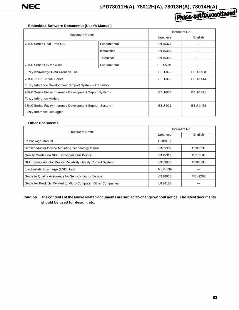
µPD78011H(A), 78012H(A), 78013H(A), 78014H(A)
63
Embedded Software Documents (User's Manual)
Document NameDocument No.
Japanese English
78K/0 Series Real-Time OS Fundamental U11537J —
Installation U11536J —
Technical U11538J —
78K/0 Series OS MX78K0 Fundamental EEU-5010 —
Fuzzy Knowledge Data Creation Tool EEU-829 EEU-1438
78K/0, 78K/II, 87AD Series EEU-862 EEU-1444
Fuzzy Inference Development Support System - Translator
78K/0 Series Fuzzy Inference Development Suport System - EEU-858 EEU-1441
Fuzzy Inference Module
78K/0 Series Fuzzy Inference Development Support System - EEU-921 EEU-1458
Fuzzy Inference Debugger
Other Documents
Document NameDocument No.
Japanese English
IC Package Manual C10943X
Semiconductor Device Mounting Technology Manual C10535J C10535E
Quality Grades on NEC Semiconductor Device C11531J C11531E
NEC Semiconductor Device Reliability/Quality Control System C10983J C10983E
Electrostatic Discharge (ESD) Test MEM-539 —
Guide to Quality Assurance for Semiconductor Device C11893J MEI-1202
Guide for Products Related to Micro-Computer: Other Companies U11416J —
Caution The contents of the above related documents are subject to change without notice. The latest documents
should be used for design, etc.
µPD78011H(A), 78012H(A), 78013H(A), 78014H(A)
64
NOTES FOR CMOS DEVICES
1 PRECAUTION AGAINST ESD FOR SEMICONDUCTORS
Note: Strong electric field, when exposed to a MOS device, can cause destruction
of the gate oxide and ultimately degrade the device operation. Steps must
be taken to stop generation of static electricity as much as possible, and
quickly dissipate it once, when it has occurred. Environmental control must
be adequate. When it is dry, humidifier should be used. It is recommended
to avoid using insulators that easily build static electricity. Semiconductor
devices must be stored and transported in an anti-static container, static
shielding bag or conductive material. All test and measurement tools
including work bench and floor should be grounded. The operator should
be grounded using wrist strap. Semiconductor devices must not be touched
with bare hands. Similar precautions need to be taken for PW boards with
semiconductor devices on it.
2 HANDLING OF UNUSED INPUT PINS FOR CMOS
Note: No connection for CMOS device inputs can be cause of malfunction. If no
connection is provided to the input pins, it is possible that an internal input
level may be generated due to noise, etc., hence causing malfunction. CMOS
device behave differently than Bipolar or NMOS devices. Input levels of
CMOS devices must be fixed high or low by using a pull-up or pull-down
circuitry. Each unused pin should be connected to V DD or GND with a
resistor, if it is considered to have a possibility of being an output pin. All
handling related to the unused pins must be judged device by device and
related specifications governing the devices.
3 STATUS BEFORE INITIALIZATION OF MOS DEVICES
Note: Power-on does not necessarily define initial status of MOS device. Produc-
tion process of MOS does not define the initial operation status of the device.
Immediately after the power source is turned ON, the devices with reset
function have not yet been initialized. Hence, power-on does not guarantee
out-pin levels, I/O settings or contents of registers. Device is not initialized
until the reset signal is received. Reset operation must be executed imme-
diately after power-on for devices having reset function.
µPD78011H(A), 78012H(A), 78013H(A), 78014H(A)
65
NEC Electronics Inc. (U.S.)Santa Clara, CaliforniaTel: 800-366-9782Fax: 800-729-9288
NEC Electronics (Germany) GmbHDuesseldorf, GermanyTel: 0211-65 03 02Fax: 0211-65 03 490
NEC Electronics (UK) Ltd.Milton Keynes, UKTel: 01908-691-133Fax: 01908-670-290
NEC Electronics Italiana s.r.1.Milano, ItalyTel: 02-66 75 41Fax: 02-66 75 42 99
NEC Electronics Hong Kong Ltd.Hong KongTel: 2886-9318Fax: 2886-9022/9044
NEC Electronics Hong Kong Ltd.Seoul BranchSeoul, KoreaTel: 02-528-0303Fax: 02-528-4411
NEC Electronics Singapore Pte. Ltd.United Square, Singapore 1130Tel: 253-8311Fax: 250-3583
NEC Electronics Taiwan Ltd.Taipei, TaiwanTel: 02-719-2377Fax: 02-719-5951
NEC do Brasil S.A.Sao Paulo-SP, BrasilTel: 011-889-1680Fax: 011-889-1689
NEC Electronics (Germany) GmbHBenelux OfficeEindhoven, The NetherlandsTel: 040-2445845Fax: 040-2444580
NEC Electronics (France) S.A.Velizy-Villacoublay, FranceTel: 01-30-67 58 00Fax: 01-30-67 58 99
NEC Electronics (France) S.A.Spain OfficeMadrid, SpainTel: 01-504-2787Fax: 01-504-2860
NEC Electronics (Germany) GmbHScandinavia OfficeTaeby, SwedenTel: 08-63 80 820Fax: 08-63 80 388
Regional Information
Some information contained in this document may vary from country to country. Before using any NECproduct in your application, please contact the NEC office in your country to obtain a list of authorizedrepresentatives and distributors. They will verify:
• Device availability
• Ordering information
• Product release schedule
• Availability of related technical literature
• Development environment specifications (for example, specifications for third-party tools andcomponents, host computers, power plugs, AC supply voltages, and so forth)
• Network requirements
In addition, trademarks, registered trademarks, export restrictions, and other legal issues may also varyfrom country to country.
J96. 8
µPD78011H(A), 78012H(A), 78013H(A), 78014H(A)
66
Some related decuments are preliminary versions. This document, however, is not indicated as preliminary.
The export of this product from Japan is regulated by the Japanese government. To export this product may beprohibited without governmental license, the need for which must be judged by the customer. The export or re-export of this product from a country other than Japan may also be prohibited without a license from that country.Please call an NEC sales representative.
No part of this document may be copied or reproduced in any form or by any means without the prior writtenconsent of NEC Corporation. NEC Corporation assumes no responsibility for any errors which may appear inthis document.NEC Corporation does not assume any liability for infringement of patents, copyrights or other intellectual propertyrights of third parties by or arising from use of a device described herein or any other liability arising from useof such device. No license, either express, implied or otherwise, is granted under any patents, copyrights or otherintellectual property rights of NEC Corporation or others.While NEC Corporation has been making continuous effort to enhance the reliability of its semiconductor devices,the possibility of defects cannot be eliminated entirely. To minimize risks of damage or injury to persons orproperty arising from a defect in an NEC semiconductor device, customers must incorporate sufficient safetymeasures in its design, such as redundancy, fire-containment, and anti-failure features.NEC devices are classified into the following three quality grades:"Standard", "Special", and "Specific". The Specific quality grade applies only to devices developed based on acustomer designated "quality assurance program" for a specific application. The recommended applications ofa device depend on its quality grade, as indicated below. Customers must check the quality grade of each devicebefore using it in a particular application.
Standard: Computers, office equipment, communications equipment, test and measurement equipment,audio and visual equipment, home electronic appliances, machine tools, personal electronicequipment and industrial robots
Special: Transportation equipment (automobiles, trains, ships, etc.), traffic control systems, anti-disastersystems, anti-crime systems, safety equipment and medical equipment (not specifically designedfor life support)
Specific: Aircrafts, aerospace equipment, submersible repeaters, nuclear reactor control systems, lifesupport systems or medical equipment for life support, etc.
The quality grade of NEC devices is "Standard" unless otherwise specified in NEC's Data Sheets or Data Books.If customers intend to use NEC devices for applications other than those specified for Standard quality grade,they should contact an NEC sales representative in advance.Anti-radioactive design is not implemented in this product.
M4 96.5
FIP and IEBus are trademarks of NEC Corporation.
MS-DOS and Windows are trademarks of Microsoft Corporation.
IBM-DOS, PC/AT, and PC DOS are trademarks of IBM Corporation.
HP9000 Series 300, HP9000 series 700, and HP-UX are trademarks of Hewlett-Packard Company.
SPARCstation is a tradmark of SPARC International, Inc.
SunOS is a tradmark of Sun Microsystems, Inc.
NEWS and NEWS-OS are trademarks of Sony Corporation.