UNIVERSITY OF CALIFORNIA RIVERSIDE Magnetic ...
141
-
Upload
khangminh22 -
Category
Documents
-
view
5 -
download
0
Transcript of UNIVERSITY OF CALIFORNIA RIVERSIDE Magnetic ...

UNIVERSITY OF CALIFORNIA
RIVERSIDE
Magnetic Properties of Ferromagnetic and Antiferromagnetic Materials and
Low-Dimensional Materials
A Dissertation submitted in partial satisfaction
of the requirements for the degree of
Doctor of Philosophy
in
Electrical Engineering
by
Md. Rakibul Karim Akanda
September 2021
Dissertation Committee:
Dr. Roger K. Lake, ChairpersonDr. Alexander BalandinDr. Ran Cheng

Copyright byMd. Rakibul Karim Akanda
2021

The Dissertation of Md. Rakibul Karim Akanda is approved:
Committee Chairperson
University of California, Riverside

Acknowledgments
I would like to express my hear-felt gratitude and appreciation to my supervisor and mentor
Roger K. Lake for his guidance, support and encouragement during the past ve years. I
have learned a lot from him about magnetism, micromagnetic simulation, condensed mat-
ter physics, material science, nonequilibrium Greens functions, programming languages,
manuscript writing, proposal writing, and data science. When I was struggling with my
project, he encouraged and guided me. He encouraged me to learn new and diverse topics.
He also encouraged and helped me to learn dierent softwares and programming languages.
Moreover, before being a PhD candidate, I was not good at writing manuscripts. He guided
me and helped me to learn how to write a good manuscript. He often suggested reading
several manuscripts, which helped me to learn new information and to learn about writing a
manuscript. It goes without saying that devoid of his constant support and guidance, none
of the works appearing in the thesis would have ever been possible.
I want to thank my committee member Prof. Alexander Balandin, as I have learned
much about the experimental issues from Dr. Balandin and his group. I also want to thank
my committee member Prof. Ran Cheng, as I have learned much from his lecture classes on
magnetics and magnetic properties of materials.
Special thanks to my current lab mates in LATTE, Sohee Kwon, Yuhang Liu,
Topojit Denbath, and Hector Gomez, as well as my former colleagues Dr. Mahesh Neupane,
Dr. In Jun Park, Dr. Tonmoy Kumar Bhowmick, Dr. Bishwajit Debnath, Dr. Protik
Das, Dr. Shanshan Su, Dr. Nima Djavid, and Dr. Yizhou Liu, for their help and support
with many ideas, collaborative projects and enjoyable discussions. A special thanks to Prof.
iv

Shane Cybart for his funding support during several semesters of my PhD.
On the personal side, I would like rst to acknowledge my parents for their guidance
and support for my higher education. Lastly, I would like to thank to my dear wife Azmeri
Ferdous for her love and great support.
The text of this dissertation, in part or in full, is a reprint of the material as it
appears in the following journal and/or proceedings:
• Physical Review B [1]. Reprinted with permission from [1]. © [2020] APS
• Applied Physics Letters [2]. Reprinted with permission from [2]. © [2021] AIP
The co-author Roger K. Lake, listed in the above publications directed and super-
vised the research which forms the basis for this dissertation. The remaining co-authors
listed provided technical expertise and support as collaborators.
This work was supported in part by the Spins and Heat in Nanoscale Electronic
Systems (SHINES) an Energy Frontier Research Center funded by the U.S. Department of
Energy, Oce of Science, Basic Energy Sciences under Award #DE-SC0012670. This work
used the Extreme Science and Engineering Discovery Environment (XSEDE) [3] which is
supported by National Science Foundation Grant No. ACI-1548562 and allocation ID TG-
DMR130081. Used resources include Stampede-2 and Comet.
v

To my parents and dear wife Azmeri Ferdous, love you forever.
vi

ABSTRACT OF THE DISSERTATION
Magnetic Properties of Ferromagnetic and Antiferromagnetic Materials andLow-Dimensional Materials
by
Md. Rakibul Karim Akanda
Doctor of Philosophy, Graduate Program in Electrical EngineeringUniversity of California, Riverside, September 2021
Dr. Roger K. Lake, Chairperson
Magnetic skyrmions oer various advantages compared to domain wall based mem-
ory applications. A skyrmion based shift register is analyzed that uses either ferromagnetic
or synthetic anti-ferromagnetic skyrmions. The energy requirement to shift a ferromagnetic
(FM) skyrmion is less than that required to create or annihilate a skyrmion in conventional
race track memory. Two dierent types of skyrmion shift register structures are investigated.
They dier in the geometry used to conne a skyrmion into an individual cell. One struc-
ture uses a rectangular channel combined with a modication of the gate metal above the
channel to dene individual cells. In the the second structure, the channel width is modied
into an hourglass type shape, and the narrow regions of the channel serve to conne the
skyrmion to an individual cell. The eects of the shape of the structures, the thickness of the
top heavy metal layer, the gap between the gate regions, and the presence of disorder and
nite temperature are analysed using micromagnetic simulations. Synthetic antiferromag-
netic (SAFM) skyrmions provide higher velocity and reduced switching energy compared
to ferromagnetic skyrmions, and they can be stable above room temperature. All of the
vii

necessary phase diagrams for obtaining stable skyrmions are presented, which can help to
select the correct ferromagnetic material and heavy metal combinations to obtain skyrmions
with desired diameters.
To stabilize skyrmions, the interfacial Dzyaloshinskii-Moriya interaction (iDMI)
plays a vital role. The interface between a ferromagnet (FM) or antiferromagnet (AFM)
and a heavy metal (HM) results in an antisymmetric exchange interaction known as the
interfacial Dzyaloshinskii-Moriya interaction (iDMI) which favors non-collinear spin cong-
urations. The iDMI is responsible for stabilizing noncollinear spin textures such as skyrmions
in materials with bulk inversion symmetry. Interfacial DMI values have been previously de-
termined theoretically and experimentally for FM/HM interfaces, and, in this work, they
are calculated for the metallic AFM MnPt and the insulating AFM NiO. The heavy metals
considered are W, Re, and Au. Values for the iDMI, exchange, and anisotropy constants
are determined for dierent AFM and HM thicknesses. The iDMI values of the MnPt het-
erolayers are comparable to those of the common FM materials, and those of NiO are lower.
In few-layer lms of (001) MnPt, the high spin orbit coupling of the Pt layers can give rise
to a small DMI in the absence of a HM layer.
Magnetic properties have also been determined for a new family of two-dimensional
ferromagnetic materials. The recent demonstration of MoSi2N4 and its exceptional stability
to air, water, acid, and heat has generated intense interest in this family of two-dimensional
(2D) materials. Among these materials, monolayers of NbSi2N4, VSi2N4, and VSi2P4 are
semiconducting, easy-plane ferromagnets with negligible in-plane magnetic anisotropy. They
thus satisfy a necessary condition for exhibiting a dissipationless spin superuid mode. The
viii

Curie temperatures of monolayer VSi2P4 and VSi2N4 are determined to be above room
temperature based on Monte Carlo and density functional theory calculations. The magnetic
moments of VSi2N4 can be switched from in-plane to out-of-plane by applying tensile biaxial
strain or electron doping.
Besides magnetic materials, topological materials also oer various prospective ap-
plications. There have been also a tremendous interests in nding 1D and 2D materials. To
facilitate identifying materials of interest, 27 one dimensional and 300 two dimensional topo-
logical materials are identied using several databases. 1D and 2D topological insulators and
semimetals are identied. 1D and 2D topological materials which have been experimentally
demonstrated, are also identied.
ix

Contents
List of Figures xii
List of Tables xvi
1 Rationale 1
1.1 Objectives . . . . . . . . . . . . . . . . . . . . . . . . . . . . . . . . . . . . . . 11.2 Organization . . . . . . . . . . . . . . . . . . . . . . . . . . . . . . . . . . . . 3
2 Above Room Temperature Low Power FM and SAFM Skyrmion Shift
Register in Presence of Disorder 4
2.1 Introduction . . . . . . . . . . . . . . . . . . . . . . . . . . . . . . . . . . . . . 42.2 Device Structure and Operation . . . . . . . . . . . . . . . . . . . . . . . . . . 82.3 Theory . . . . . . . . . . . . . . . . . . . . . . . . . . . . . . . . . . . . . . . . 112.4 Simulation Details . . . . . . . . . . . . . . . . . . . . . . . . . . . . . . . . . 152.5 Results . . . . . . . . . . . . . . . . . . . . . . . . . . . . . . . . . . . . . . . . 162.6 Conclusions . . . . . . . . . . . . . . . . . . . . . . . . . . . . . . . . . . . . . 242.7 Acknowledgements . . . . . . . . . . . . . . . . . . . . . . . . . . . . . . . . . 25
3 Interfacial Dzyaloshinskii-Moriya Interaction of Antiferromagnetic Mate-
rials 26
3.1 Introduction . . . . . . . . . . . . . . . . . . . . . . . . . . . . . . . . . . . . . 263.2 Method . . . . . . . . . . . . . . . . . . . . . . . . . . . . . . . . . . . . . . . 303.3 Results . . . . . . . . . . . . . . . . . . . . . . . . . . . . . . . . . . . . . . . . 353.4 Conclusions . . . . . . . . . . . . . . . . . . . . . . . . . . . . . . . . . . . . . 413.5 Acknowledgement . . . . . . . . . . . . . . . . . . . . . . . . . . . . . . . . . . 41
4 Magnetic Properties of NbSi2N4, VSi2N4, and VSi2P4 Monolayers 43
4.1 Introduction . . . . . . . . . . . . . . . . . . . . . . . . . . . . . . . . . . . . . 434.2 Method . . . . . . . . . . . . . . . . . . . . . . . . . . . . . . . . . . . . . . . 464.3 Results . . . . . . . . . . . . . . . . . . . . . . . . . . . . . . . . . . . . . . . . 494.4 Conclusions . . . . . . . . . . . . . . . . . . . . . . . . . . . . . . . . . . . . . 564.5 Supplementary Material . . . . . . . . . . . . . . . . . . . . . . . . . . . . . . 574.6 Curie temperatures of other 2D Materials . . . . . . . . . . . . . . . . . . . . 60
x

4.7 Acknowledgement . . . . . . . . . . . . . . . . . . . . . . . . . . . . . . . . . . 61
5 1D and 2D Topological Insulators and Semimetals 62
5.1 Introduction . . . . . . . . . . . . . . . . . . . . . . . . . . . . . . . . . . . . . 625.2 Results . . . . . . . . . . . . . . . . . . . . . . . . . . . . . . . . . . . . . . . . 63
6 Summary and Outlook 94
7 Appendix 97
Bibliography 107
xi

List of Figures
2.1 (a) 3D view of FM skyrmion shift register where presence or absence of askyrmion is used as a memory bit instead of creation and annihilation of theskyrmion. The skyrmion will be detected under only one gate between twoconsecutive gates and the remaining gate will be used to aid in shifting theskyrmion back and forth. (b) Shifting the skyrmion by applying current alongthe Y-axis in the top metal gate region. (c) Cross section of the FM rectan-gular gate structure showing a 5nm wide gap region between two consecutivegates where the gap region acts as a barrier for skyrmion motion and thedummy gates to the left and right are used to create a symmetric potentialwithin each cell to bring the skyrmion to rest near the center of a cell. (d)Cross section of SAFM rectangular gate structure where current is applied inthe top gate. . . . . . . . . . . . . . . . . . . . . . . . . . . . . . . . . . . . . 6
2.2 Micromagnetic simulation of two dierent types of FM structures (165 nm× 64 nm × 0.8 nm) showing top view at 0 K: (a) Shifting operation of therectangular gate structure having a 5 nm gap where the skyrmion moves backand forth due to positive and negative current along the width direction and(b) Hourglass structure with single metal gate on top of the FM showing ashifting operation where the notch diameter acts as a barrier for skyrmionmotion and separates two cells. Only the FM rectangular and hourglassstructures at 0K are shown, however both FM and SAFM having these twotypes of structures are simulated at 0K and at 300K. . . . . . . . . . . . . . . 10
2.3 Change of current for dierent iDMI strengths in the gap region betweentwo gates. The FM structure is simulated keeping the iDMI strength of 1.93mJ/m2 constant under the gate regions and reducing the iDMI strength inthe gap region from 1.93 mJ/m2: (a) FM structure having width of 64nm at0 K, (b) FM structure having width of 128nm at 300 K. The SAFM structureis simulated keeping the iDMI strength of 3.5 mJ/m2 constant under the gateregion and reducing the iDMI strength in the gap region from 3.5 mJ/m2: (c)SAFM structure having width of 55nm at 0 K and (d) SAFM structure havingwidth of 86nm at 300 K. Current requirement increases with the increase ofiDMI variation in the gap region. Variation of iDMI in the gap region can beachieved by reducing the Pt thickness or by using HfO2. . . . . . . . . . . . 14
xii

2.4 Switching time versus current for the rectangular gate structure where thereduction of the iDMI strength in the gap region with respect to the gateregion is 0.25 mJ/m2. (a) FM structure having a width of 64nm at 0 K, (b)FM structure having a width of 128nm at 300 K, (c) SAFM structure havinga width of 55nm at 0 K, and (d) SAFM structure having width of 86nm at300 K. The switching time reduces with increasing injected current, and theswitching time of the SAFM skyrmion is less than that of the FM skyrmion. . 16
2.5 Switching time versus current in the hourglass structure for three dierentnotch diameters: (a) FM structure having width of 64nm at 0 K, (b) FMstructure having width of 128nm at 300 K, (c) SAFM structure having widthof 64nm at 0 K and (d) SAFM structure having width of 128nm at 300 K. . . 19
2.6 Velocity of SAFM skyrmion with current owing only in the top gate, andfor current in both the top and bottom gates. In our simulations, current isonly applied in the top gate, since such types of structures are easier to buildexperimentally. But if current is injected in both the top and bottom gatesin opposite directions, then velocity of the SAFM skyrmion becomes almostdouble. . . . . . . . . . . . . . . . . . . . . . . . . . . . . . . . . . . . . . . . . 20
2.7 The rectangular gate structure used as a racetrack memory. Double skyrmionsare simulated to show the repulsion between skyrmions: (a) Rectangular gateswith two SAFM skyrmions undergoing a shifting operation at T = 0 K. Theskyrmion and anti-skyrmion in the top and bottom layers are individuallyshown. Current ows only in the second from the left gate, labeled 2ndGate, and it moves both skyrmions due to the repulsion force between them.(b) The same as (a) but at T = 300 K. . . . . . . . . . . . . . . . . . . . . . . 21
2.8 Distance between two FM skyrmions and two SAFM skyrmions versus theskyrmion diameter. . . . . . . . . . . . . . . . . . . . . . . . . . . . . . . . . 22
2.9 Phase diagrams of a FM skyrmion in a 40nm wide region. The color shows theskyrmion diameter as indicated by the color bars. Parameters that are notvaried are given by the values listed in column 2 of Table 2.1. (a) InterfacialDMI strength versus Heisenberg exchange energy stiness. (b) iDMI strengthversus anisotropy energy. (c) iDMI strength versus external magnetic eld.(d) iDMI strength versus saturation magnetization. . . . . . . . . . . . . . . 24
3.1 (a) Unit cell of MnPt having stripe-type AFM spin congurations. (b) Unitcell of NiO having G-type AFM spin congurations. Spin directions are shownin 3d orbital magnetic materials (Mn or Ni) and atoms without spin are Pt(grey) and oxygen (red). . . . . . . . . . . . . . . . . . . . . . . . . . . . . . . 27
3.2 Spiral spin congurations used in the DMI calculations for (a,b,e) MnPt and(c,d) NiO. A 4× 1× 1 unit cell supercell of MnPt is constructed with a spinspiral in the (a) clockwise and (b) counterclockwise directions. A 2 × 2 × 1unit cell supercell of NiO is constructed with a spin spiral in the (c) clockwiseand (d) counterclockwise directions. (e) Clockwise rotated spin congurationin one layer of MnPt with labels used in Eq. (3.2). . . . . . . . . . . . . . . . 29
3.3 (a) MnPt on top of W. Mn atoms are purple. (b) NiO on top of Au. Oxygenatoms are red. . . . . . . . . . . . . . . . . . . . . . . . . . . . . . . . . . . . . 35
xiii

3.4 (a) Dtot and (b) Dµ of MnPt-W, MnPt-Re, and NiO-Au as a function of thethickness of the AFM. The thickness of the HM is xed at 3 layers. PositiveDMI indicates that the CCW spin spiral is the lower energy state. . . . . . . 36
3.5 iDMI of monolayer AFM for two dierent HM thicknesses: (a) Dtot with onemagnetic layer and (b) Dµ. . . . . . . . . . . . . . . . . . . . . . . . . . . . . 37
3.6 Magnetic moments and saturation magnetization of (a) MnPt-W, (b) MnPt-Re and (c) NiO-Au as a function of the thickness of the AFM. The thicknessof the HM is xed at 3 layers. . . . . . . . . . . . . . . . . . . . . . . . . . . 38
3.7 Local density of states of Mn atom in 3 layers of MnPt on top of 3 layers ofRe: (a) middle Mn atom which is far from Re, (b) bottom Mn atom which isclose to Re and is aected by proximity induced magnetic moment. . . . . . 39
3.8 (a) Magnetic anisotropy constant of MnPt with 3 layers of heavy metals. (b)Exchange stiness of MnPt with 3 layers of heavy metals. . . . . . . . . . . . 40
4.1 Structures and magnetic orientations of α1-NbSi2N4, α1-VSi2N4, and α1-VSi2P4. Blue atoms are Si, white atoms are N, and pink atoms are P. Thedirections of the magnetic moments are shown on the transition metals Nband V. All materials are easy-plane, semiconducting ferromagnets. . . . . . . 44
4.2 Spin resolved energy bands of VSi2N4 and VSi2P4 calculated with (a,b)HSE06 and (c,d) PBE+U. Spin up bands are red and spin down bands areblue. The two spin-split, narrow bands on either side of the Fermi level ared-orbital bands centered on the transition metal. . . . . . . . . . . . . . . . . 49
4.3 Monte Carlo calculations of the normalized magnetization as a function oftemperature for (a) VSi2N4 and (b) VSi2P4. The solid lines show the bestts to the analytical expression given by Eq. (4.2). . . . . . . . . . . . . . . . 52
4.4 MAE as a function of uniaxial and biaxial strain calculated with PBE(SOC)+U.MAE versus uniaxial strain: (a) VSi2N4 and (b) VSi2P4. MAE versus biaxialstrain: (c) VSi2N4 and (d) VSi2P4. Values are shown for the strain coecientsfor dierent regions discussed in the text. The orientation of the magnetiza-tion of VSi2N4 rotates from in-plane to out-of-plane with 3.3% biaxial strain.. . . . . . . . . . . . . . . . . . . . . . . . . . . . . . . . . . . . . . . . . . . . 54
4.5 MAE as a function of band lling calculated with PBE(SOC)+U. MAE as afunction of excess electrons per unit cell for (a) VSi2N4 and (b) VSi2P4. Valuesare shown for the lling coecients discussed in the text. The orientationof the magnetization of VSi2N4 rotates from in-plane to out-of-plane withelectron doping of 2.0× 1014 cm−2. . . . . . . . . . . . . . . . . . . . . . . . 55
4.6 Orbital resolved PBE band structure of VSi2N4 at equilibrium: (a) s-orbitalcontribution, (b) p-orbital contribution, and (c) d-orbital contribution. Theweight is given by the color bars at right. The two isolated, narrow bands nearthe Fermi level are d-orbital bands centered on the transition metal atomsvanadium (V). The higher valence bands are primarily p-orbital bands whichcome from the N atoms. The lower conduction bands are primarily d-orbitalbands. . . . . . . . . . . . . . . . . . . . . . . . . . . . . . . . . . . . . . . . 58
xiv

4.7 d-orbital resolved PBE band structure of VSi2N4: (a) spin up bands, (c) spindown bands. d-orbital resolved band structure of VSi2P4: (b) spin up bands,(d) spin down bands. . . . . . . . . . . . . . . . . . . . . . . . . . . . . . . . 58
4.8 Spin resolved PBE band structure: (a) NbSi2N4, (b) VSi2N4, and (c) VSi2P4.Spin resolved PBE+U band structure: (d) NbSi2N4, (e) VSi2N4, and (f)VSi2P4. Spin resolved HSE06 band structure: (g) NbSi2N4, (h) VSi2N4, and(i) VSi2P4. . . . . . . . . . . . . . . . . . . . . . . . . . . . . . . . . . . . . . 59
4.9 MC calculations of the normalized magnetization as a function of temper-ature with exchange constants extracted from PBE DFT for (a) NbSi2N4,(b) VSi2N4, and (c) VSi2P4. Curie temperatures are calculated from MonteCarlo simulation using the VAMPIRE software. . . . . . . . . . . . . . . . . . 59
5.1 Flowchart of identifying 1D and 2D topological materials from several database.. . . . . . . . . . . . . . . . . . . . . . . . . . . . . . . . . . . . . . . . . . . . 64
xv

List of Tables
2.1 LLG parameters used for simulating the FM and SAFM structures. . . . . . . 112.2 Comparison of energy, switching time, charge current density, and width
among two dierent types of FM and SAFM structures at 0K and at 300K.The gap is 5nm in the rectangular gate structures. In the hourglass struc-tures, the notch diameter is 10nm for FM, 15nm for SAFM at 0K and 45nmfor SAFM at 300K. SAFM generally requires less switching energy comparedto FM. The current requirement increases at 300K to overcome the ther-mal eld. A wider simulation region is needed at 300K as the skyrmion islarger compared to 0K. SAFM rectangular structure can be made narrowercompared to FM as skyrmion moves in a straight line in the SAFM struc-ture. Hourglass structures generally need less current and energy comparedto rectangular structures. . . . . . . . . . . . . . . . . . . . . . . . . . . . . . 17
3.1 Interlayer distances in the system of three layers of MnPt on top of threelayers of W or Re and in the system of three layers of NiO on top of threelayers of Au. . . . . . . . . . . . . . . . . . . . . . . . . . . . . . . . . . . . . . 30
4.1 Magnetic moment, exchange energy per link, equilibrium magnetic anisotropyenergy (MAE), and Curie temperature, calculated using dierent functionalsfor NbSi2N4, VSi2N4, and VSi2P4. ∗TC is calculated using the HSE06 ex-change energy and the PBE(SOC)+U MAE. . . . . . . . . . . . . . . . . . . . 51
5.1 2D topological insulators . . . . . . . . . . . . . . . . . . . . . . . . . . . . . . 735.2 2D topological semimetals . . . . . . . . . . . . . . . . . . . . . . . . . . . . . 795.3 1D topological insulators . . . . . . . . . . . . . . . . . . . . . . . . . . . . . . 805.4 1D topological semimetals . . . . . . . . . . . . . . . . . . . . . . . . . . . . . 815.5 2D topological insulators . . . . . . . . . . . . . . . . . . . . . . . . . . . . . . 875.6 2D topological semimetals . . . . . . . . . . . . . . . . . . . . . . . . . . . . . 905.7 2D experimental topological insulators . . . . . . . . . . . . . . . . . . . . . . 925.8 2D experimental topological semimetals . . . . . . . . . . . . . . . . . . . . . 93
xvi

Chapter 1
Rationale
1.1 Objectives
Magnetic based memory is one of the leading approaches for non-volatile memory.
Skyrmions are being considered as an alternative to other magnetic based memory devices,
such as the magnetic tunnel junction (MTJ), since skyrmion based memory can require lower
power to operate. [4] Previous works on ferromagnetic (FM) and synthetic antiferromagnetic
(SAFM) skyrmion shifting or moving did not have any mechanism to x the skyrmion in
a certain region, since the skyrmion always tries to move where it feels least repulsion
force. [510] In racetrack type memories, this property is a feature, since skyrmions have the
ability to move around defects. [11] Here, two dierent types of structures are investigated,
which can force skyrmion to stay at a specic location even in presence of thermal energy.
These two types of structures are compared for FM and SAFM skyrmions in terms of energy
and switching time at room temperature in presence of disorder. SAFM skyrmions, where
two ferromagnetic layers are antiferromagnetically exchange coupled by a spacer layer, oers
1

higher velocity compared to FM skyrmions. [12]
Antiferromagnetic (AFM) materials oer various promising spintronic applications
exploiting skyrmions or domain walls, which can be used as non-volatile memory and race-
track memory [1320]. A bilayer consisting of a heavy metal (HM), which oers high spin or-
bit coupling (SOC), and a magnetic material can be created that breaks inversion symmetry
at the interface. At a HM/FM or HM/AFM interface, the interfacial Dzyaloshinskii-Moriya
interaction (iDMI), which is an anti-symmetric exchange interaction, can stabilize Néel type
domain walls and skyrmions [2131]. There have been prior theoretical and experimental
studies of the iDMI in engineered or synthetic antiferromagnetic systems [3235]. This the-
sis describes the results of ab initio calculations of the iDMI for three dierent material
combinations of HMs and AFMs.
Two dimensional (2D) layered materials with transition metals have been of in-
terest for many decades due to the correlated phenomena and multiple polymorphs and
phases that they can exhibit such as charge density waves, [36] superconductivity, [37] and
magnetism. [38] The most recent addition to the family of 2D materials are the transition
metal silicon nitrides, phosphides, and arsenides with the chemical formulas MA2Z4, where
M is the transition metal, A ∈ Si, Ge, and Z ∈ N, P, As. [39] High quality multilayers
and monolayers of MoSi2N4 were grown using chemical vapor deposition, and what was
particulary notable was the stability of the material. In this thesis, we theoretically inves-
tigate the magnetic properties of the three Si based magnetic materials: VSi2N4, VSi2P4,
NbSi2N4 which are from MA2Z4 family. The exchange constants are determined, the Curie
temperatures are calculated, and the Curie temperature of VSi2N4 is found to be at room
2

temperature. The magnetic anisotropy energies of VSi2N4, VSi2P4, and NbSi2N4 are calcu-
lated as a function of uniaxial and biaxial strain and electron and hole doping.
1.2 Organization
The rest of the dissertation is organized as follow: Chapter 2 presents skyrmion
based ferromagnetic and synthetic antiferromagnetic memory devices, which can operate
near room temperature. Chapter 3 presents the interfacial Dzyaloshinskii-Moriya interac-
tion of three antiferromagnetic Materials which are needed to stabilize skyrmions. Chap-
ter 4 presents magnetic properties such as the Curie temperatures, exchange energies and
magnetic anisotropy energies of ferromagnetic NbSi2N4, VSi2N4, and VSi2P4 Monolayers.
Chapter 5 describes the identicaiton of 1D and 2D topological materials from several ma-
terial databases. Chapter 6 is a summary of all the interesting ndings and an outlook for
future work. In the Appendix, the codes for topological materials, skyrmions, Monte Carlo
simulation, band structures plotting are documented.
3

Chapter 2
Above Room Temperature Low
Power FM and SAFM Skyrmion Shift
Register in Presence of Disorder
2.1 Introduction
Magnetic based memory oers certain advantages over traditional charge based
memory, since it is non-volatile and can require less power to operate. Skyrmion based
memory is being considered as an alternative to other spintronic based memory devices such
as the magnetic tunnel junction (MTJ) since it can require less power to operate. [4] A
skyrmion is a topologically protected swirling spin texture that relies on the presence of
the Dzyaloshinskii-Moriya interaction (DMI) for its stabilization. The DMI requires broken
inversion symmetry in a magnetic material. The B20 compounds are bulk magnetic materials
4

that satisfy this criterion, but they are not very common. However, inversion symmetry
is always broken at an interface. Bilayers consisting of a heavy metal (HM) with high
spin orbit coupling and a ferromagnetic material have an interfacial DMI (iDMI) that can
support an interfacial skyrmion [21]. These engineered structures have made stabilization
of skyrmions near room temperature possible [2224]. There are several ways to control
the iDMI: changing the FM or heavy metal (HM) or oxide layer material [40, 41], changing
the FM or HM or oxide layer thickness [4247], increasing the number of layers [48], using
congurations such as HM/FM, HM1/FM/HM2, HM/FM/Oxide, HM1/HM2/FM/Oxide,
HM/FM/Metal/Oxide [6, 6, 47, 4953], and by changing their relative positions. Similar to
controlling the iDMI, the sign and amplitude of the spin Hall angle (θSH) of the HM layer
can be adjusted with the appropriate choice of heavy metal and its relative position. The
eective spin Hall angle can be increased by adding top and bottom HM layers with additive
iDMI [5456].
5

Figure 2.1: (a) 3D view of FM skyrmion shift register where presence or absence of a
skyrmion is used as a memory bit instead of creation and annihilation of the skyrmion.
The skyrmion will be detected under only one gate between two consecutive gates and the
remaining gate will be used to aid in shifting the skyrmion back and forth. (b) Shifting
the skyrmion by applying current along the Y-axis in the top metal gate region. (c) Cross
section of the FM rectangular gate structure showing a 5nm wide gap region between two
consecutive gates where the gap region acts as a barrier for skyrmion motion and the dummy
gates to the left and right are used to create a symmetric potential within each cell to bring
the skyrmion to rest near the center of a cell. (d) Cross section of SAFM rectangular gate
structure where current is applied in the top gate.
Racetrack memory based on domain wall motion is a low energy memory [57].
Skyrmion based racetrack memory requires even less energy, and it has the added advantage
that skyrmions move around obstacles such as defects. In skyrmion based racetrack memory,
skyrmion creation and annihilation are needed each time to represent 1/0 bit. Instead of
6

creating and annihilating a skyrmion each time, the presence or absence of the skyrmion can
be considered as a memory bit. The skyrmion can move along the X-direction by applying
current in Y-direction in the adjacent heavy metal layer using the property of the skyrmion
Hall angle and the edge repulsion force. [58] This shifting or sliding switch memory (Fig. 2.1a
and Fig. 2.1b) requires lower energy compared to the switching energy of a magnetic tunnel
junction (MTJ). [59]
Previous works on FM and SAFM skyrmion shifting or moving do not include
a mechanism to x the skyrmion in a certain region, since the skyrmion always tries to
move where it feels least repulsion force. [510] Here, two dierent types of structures are
considered which can force the skyrmion to stay at a specic location even in presence of
thermal energy. These two types of structures are compared for FM and SAFM skyrmions
in terms of energy and switching time at room temperature in the presence of disorder.
SAFM skyrmions, where two FM layers are antiferromagnetically exchange coupled by a
spacer layer, oer higher velocity compared to FM skyrmions [12]. The proposed structures
can work both as a shift memory where a single skyrmion is shuttled back and forth between
two cells and as racetrack memory where several skyrmions will be clocked along a gated
track. All of the necessary phase diagrams are calculated showing the relation among DMI
strength, exchange stiness, anisotropy energy, magnetic eld and saturation magnetization
considering the diameter variation of the skyrmion which in turn determines the device
dimension.
7

2.2 Device Structure and Operation
Two dierent types of structures are made using FM and SAFM skyrmions. The
FM device structure, shown in Fig. 2.1c, has three layers. (i) The bottom layer or back gate
or substrate can be made of a HM, HM1/HM2, oxide, or metal/oxide. The choice will aect
the iDMI. This back gate or bottom layer provides iDMI even when a top HM layer is not
present. This layer is considered in the simulation by adding the appropriate iDMI. (ii) The
middle FM layer consists of a 0.8 nm thick CoFeB lm. The Heisenberg exchange energy
stiness, anisotropy energy, damping constant, and saturation magnetization are used to
represent its properties. (iii) The top Pt heavy metal gate increases the iDMI, and the
charge current is injected in this layer.
The SAFM device structure, shown in Fig. 2.1d, is made of two FM layers antifer-
romagnetically coupled by a spacer layer The SAFM device has ve layers. (i) The bottom
layer is Pt which increases iDMI. (ii) The bottom cobalt layer supports a skyrmion. (iii) The
spacer layer antiferromagnetically couples the top and bottom Co layers and also provides
iDMI. (iv) The top cobalt layer supports an anti-skyrmion with opposite magnetization to
that in the bottom Co layer. (v) The top Pt layer increases the iDMI and carries charge
current that injects spin through the spin Hall eect.
Two dierent structure geometries are simulated for both FM and SAFM skyrmions:
a rectangular gate structure (Fig. 2.2a) and an hourglass structure (Fig. 2.2b). In the rect-
angular gate structure, in the gap between the two gates, the iDMI is lower, and the reduced
iDMI serves as a barrier to conne the skyrmion within an individual cell after the drive
current is turned o. The gap region of the rectangular gate structure can be made by
8

reducing the Pt thickness or by replacing the Pt with an insulator. Pt resistivity is strongly
dependent on its thickness. The resistivity increases to a high value for 1 nm thick Pt,
which then acts as an insulator in the gap region of the rectangular gate structure. [60] The
thinner Pt also reduces the iDMI in the gap region, so that the gap region acts as a barrier
to conne skyrmions within an individual cell after the drive current is switched o. An
insulator like HfO2 can also be used in the gap region, and it also provides reduced iDMI
to the magnetic layers. [61,62] DMI can be increased by reducing the thickness of FM layer
(CoFeB or Cobalt). [63] DMI can also be increased by increasing the heavy metal layer (Pt)
thickness. [64] Dummy gates at two ends help to create a symmetric potential in each cell so
that the skyrmion comes to rest at the center of a cell. Centering the skyrmion maximizes
the magnetoresistive readout performed with an MTJ.
The Hourglass shape provides control of the skyrmion with the use of a single gate
over the entire FM region. The narrow region of the hourglass shape acts as a barrier for
localizing the skyrmion when there is no current.
9

Figure 2.2: Micromagnetic simulation of two dierent types of FM structures (165 nm ×
64 nm × 0.8 nm) showing top view at 0 K: (a) Shifting operation of the rectangular gate
structure having a 5 nm gap where the skyrmion moves back and forth due to positive
and negative current along the width direction and (b) Hourglass structure with single
metal gate on top of the FM showing a shifting operation where the notch diameter acts
as a barrier for skyrmion motion and separates two cells. Only the FM rectangular and
hourglass structures at 0K are shown, however both FM and SAFM having these two types
of structures are simulated at 0K and at 300K.
A skyrmion can be moved back and forth by reversing the Y-direction of current in
the top heavy metal layer (Fig. 2.1a and Fig. 2.1b). Larger width structures show skyrmion
velocities with both X and Y components as a result of the skyrmion Hall eect. The
Y-component vanishes once the skyrmion is pushed against the channel edge boundary.
For narrow width channels, the velocity is always along the X-direction, since the motion
along Y-direction is nullied due to the repulsion from the nearby edge. A skyrmion can
move back and forth in this structure by applying positive and negative current along the
10

Parameters FM (CoFeB) [6, 65] SAFM (Cobalt) [7
10,66,67]
Msat 0.9 MA/m 0.58 MA/m
Intralayer Aex 14 pJ/m 15 pJ/m
Interlayer Aex 0 −1 pJ/m
Ku 0.779 MJ/m3 0.8 MJ/m3
α 0.5 0.3
Bext 12.5 mT 0
Dind 1.93 mJ/m2 3.5 mJ/m2
Dind in gap region 1.68 mJ/m2 3.25 mJ/m2
Table 2.1: LLG parameters used for simulating the FM and SAFM structures.
width (Y) direction of the HM gate layer. At smaller currents, the channel edge serves as a
repulsive boundary that connes the skyrmion. At higher drive currents, the channel edge
will annihilate the skyrmion as it is driven towards the edge.
2.3 Theory
The spin dynamics of skyrmions in these two types of structures can be described
by the Landau-Lifshitz-Gilbert (LLG) equation, [68]
∂mi
∂t= −γmi ×Heff + αmi ×
∂mi
∂t, (2.1)
11

where i denotes lattice site, α is the Gilbert damping, and the eective eldHeff is computed
as Heff = − 1|µi|
∂H∂mi
.
The Slonczewski torque due to the ow of current is transformed to the Landau-
Lifshitz formalism and is added in the LLG equation which is dened in MuMax3 [69].
Generally, the Landau-Lifshitz-Gilbert-Slonczewski (LLGS) equation takes the form which
contains only the anti-damping torque due to the spin Hall eect. Later it was found that
there is an additional eld-like (FL) spin orbit torque (SOT) which had been previously
neglected [70].
The total Hamiltonian incudes the classical Heisenberg ferromagnetic exchange
interaction (represented by J), the Dzyaloshinskii-Moriya interaction (Dij), the uniaxial
anisotropy (Ku) along the z axis, and the magnetic eld (h) applied to the system in the
positive z direction. Therefore, the total Hamiltonian of the system is given by [68]
H =− J∑<i,j>
mi ·mj +∑<i,j>
Dij · [mi ×mj ]
−∑i
Ku(ez ·mi)2 −
∑i
|µi|h ·mi, (2.2)
where Dij is the DMI vector and mi is the unit vector of a magnetic moment µi = −ℏγS
with S being the atomic spin and γ the gyromagnetic ratio. With this Hamiltonian, the
dipole interaction energy and thermal energy are also included. The dipole interaction
or demagnetizing eld is included using a nite dierence discretization, which allows the
demagnetizing eld to be evaluated as a (discrete) convolution of the magnetization with
a demagnetizing kernel as implemented in MuMax3. Finite temperature is included by
calculating the thermal eld using a time step and a random vector from a standard normal
distribution whose value is changed after every time step [71]. The eective eld, Heff in
12

the torque of Eq. (2.1) is computed from the total Hamiltonian as Heff = − 1|µi|
∂H∂mi
.
The velocity of skyrmion motion can be found from Thiele's equation:
G× v − α←→D · v + FSH = 0 (2.3)
where FSH is the force due to the spin current, α the Gilbert damping, and←→D the dissipative
tensor. Here, the gyrotropic vector is represented as G =(0, 0,−4πQ
), where Q is the
skyrmion topological number, and the velocity has X and Y components, v =(vx, vy
). Both
components of the velocity depend on the magnitude and direction of the current, and the
velocity perpendicular to the current also depends on the skyrmion number Q.
13

Figure 2.3: Change of current for dierent iDMI strengths in the gap region between two
gates. The FM structure is simulated keeping the iDMI strength of 1.93 mJ/m2 constant
under the gate regions and reducing the iDMI strength in the gap region from 1.93 mJ/m2:
(a) FM structure having width of 64nm at 0 K, (b) FM structure having width of 128nm at
300 K. The SAFM structure is simulated keeping the iDMI strength of 3.5 mJ/m2 constant
under the gate region and reducing the iDMI strength in the gap region from 3.5 mJ/m2:
(c) SAFM structure having width of 55nm at 0 K and (d) SAFM structure having width of
86nm at 300 K. Current requirement increases with the increase of iDMI variation in the gap
region. Variation of iDMI in the gap region can be achieved by reducing the Pt thickness or
by using HfO2.
14

2.4 Simulation Details
LLG parameters used here are for room temperature interfacial skyrmion hosting
materials CoFeB and Cobalt. The saturation magnetization, exchange stiness, uniax-
ial anisotropy constant in the Z-direction, Landau-Lifshitz damping constant, interfacial
Dzyaloshinskii-Moriya strength are used to simulate the CoFeB or Co layers. An external
eld is applied only for the FM, and an antiferromagnetic exchange stiness is used to sim-
ulate the spacer layer between the top and bottom Co layers in the SAFM (Table 2.1). For
the Pt metal gate on top of the FM layer, the spin Hall angle is almost −0.1. In MuMax3,
the Slonczewski spin torque equation consists of polarization term which is set as 0.5 here.
The spin torque equation includes the spin Hall angle, and these two forms of equations are
compared to nd the actual charge current needed in the top Pt metal layer. The eect of
disorder has been simulated by using 10% variation of magnitude and direction of uniaxial
anisotropy. The eect of temperature is included by using Heun's method which oers 2nd
order Runge-Kutta method for convergence and a 1st order method for error estimation.
15

2.5 Results
Figure 2.4: Switching time versus current for the rectangular gate structure where the
reduction of the iDMI strength in the gap region with respect to the gate region is 0.25
mJ/m2. (a) FM structure having a width of 64nm at 0 K, (b) FM structure having a width
of 128nm at 300 K, (c) SAFM structure having a width of 55nm at 0 K, and (d) SAFM
structure having width of 86nm at 300 K. The switching time reduces with increasing injected
current, and the switching time of the SAFM skyrmion is less than that of the FM skyrmion.
The iDMI in the gap region can be varied by changing the Pt thickness in the gap
region or by lling with an insulator material like HfO2. As the iDMI in the gap is reduced,
the current required to push a skyrmion through the gap region from one cell to another
increases as shown in Fig. 2.3. The required current also increases for wider gap regions.
To determine the eect of current on the switching time, the iDMI in the gap region is kept
16

Device Energy Time JC (A/cm2) Width
(nm)
FM Rectangular (0 K) 38.3 fJ 3.4 ns 3× 10⁸ 64
FM Hourglass (0 K) 5.36 fJ 4.2 ns 0.7× 10⁸ 64
SAFM Rectangular (0 K) 18.8 fJ 0.7 ns 5× 10⁸ 55
SAFM Hourglass (0 K) 7.82 fJ 3 ns 1× 10⁸ 64
FM Rectangular (300 K) 121 fJ 1.6 ns 5.5× 10⁸ 128
FM Hourglass (300 K) 233 fJ 2.8 ns 4× 10⁸ 128
SAFM Rectangular (300
K)
104 fJ 2.05 ns 5.5× 10⁸ 86
SAFM Hourglass (300 K) 45.8 fJ 2.2 ns 2× 10⁸ 128
Table 2.2: Comparison of energy, switching time, charge current density, and width among
two dierent types of FM and SAFM structures at 0K and at 300K. The gap is 5nm in
the rectangular gate structures. In the hourglass structures, the notch diameter is 10nm for
FM, 15nm for SAFM at 0K and 45nm for SAFM at 300K. SAFM generally requires less
switching energy compared to FM. The current requirement increases at 300K to overcome
the thermal eld. A wider simulation region is needed at 300K as the skyrmion is larger
compared to 0K. SAFM rectangular structure can be made narrower compared to FM as
skyrmion moves in a straight line in the SAFM structure. Hourglass structures generally
need less current and energy compared to rectangular structures.
17

xed (0.25 mJ/m2 lower compared to gate region) and the switching time is plotted as a
funciont of the drive current in Fig. 2.4. To determine the switching time, A large number
of images are generated from the micromagnetic simulation as a funciton of time to track
the position of the skyrmion with time. The switching time is calculated by nding the time
for a skyrmion to move from its initial relaxed position in one gate/cell, to the nal relaxed
position in another gate/cell. The switching time of the SAFM skyrmion is less than that
of the FM skyrmion, since its velocity is higher and it travels in a straight path whereas FM
skyrmion moves in a curved path due to the skyrmion Hall eect. In presence of temperature
(300K) and disorder, the size of the skyrmion increases, but it can still move perpendicular
to the channel in the wider simulation regions. For the FM structure, the required width
of the FM region increases from 64 nm at 0 K to 128 nm at 300K. The SAFM requires less
width (55 nm at 0 K and 86 nm at 300 K) since the SAFM skyrmion moves in a straight
path whereas the FM skyrmion follows a curved path.
18

Figure 2.5: Switching time versus current in the hourglass structure for three dierent notch
diameters: (a) FM structure having width of 64nm at 0 K, (b) FM structure having width of
128nm at 300 K, (c) SAFM structure having width of 64nm at 0 K and (d) SAFM structure
having width of 128nm at 300 K.
In the hourglass shape structure shown in Fig. 2.2b the skyrmion can pass the
narrow region if the current is sucient. The switching times as a function of current are
shown in Fig. 2.5. The FM skyrmion moves in a curved way, so the notch diameter in the
FM structure is generally smaller compared to that in the SAFM structure. We have also
varied the diameter of the notches to restrict the passageway of the skyrmions. As the notch
diameter increases, it makes the skyrmion passageway narrower, and the current requirement
increases. A comparison of current, switching time, energy and width are shown in Table
2.2 for the rectangular gate structure and the hourglass structure made of FM and SAFM
(at 0K and at 300K). The switching energy is calculated from the resistance of a 3 nm thick
19

Pt metal gate and the charge current owing through the metal. It is the I2R power times
the switching time.
Figure 2.6: Velocity of SAFM skyrmion with current owing only in the top gate, and for
current in both the top and bottom gates. In our simulations, current is only applied in the
top gate, since such types of structures are easier to build experimentally. But if current is
injected in both the top and bottom gates in opposite directions, then velocity of the SAFM
skyrmion becomes almost double.
The SAFM skyrmion can move if current is injected in both the top and bottom
gate, or if it is injected only in the top gate. The skyrmion and antiskyrmion pairs in the
top and bottom FM layers of the synthetic antiferromagnet require opposite directions of
the top and bottom currents to drive them in the same direction, since their topological
charges are opposite. In all of the previous simulations, current is injected only in the top
gate, since such a structure is easier to build experimentally. If the current is applied in
both gates as shown in Fig. 2.6, the velocity almost doubles.
20

Figure 2.7: The rectangular gate structure used as a racetrack memory. Double skyrmions
are simulated to show the repulsion between skyrmions: (a) Rectangular gates with two
SAFM skyrmions undergoing a shifting operation at T = 0 K. The skyrmion and anti-
skyrmion in the top and bottom layers are individually shown. Current ows only in the
second from the left gate, labeled 2nd Gate, and it moves both skyrmions due to the
repulsion force between them. (b) The same as (a) but at T = 300 K.
Apart from the application as a switching memory, the proposed structure can
also be used as racetrack memory where multiple skyrmions can be clocked along the track.
Multiple skyrmions can be controlled individually, and due to the presence of multiple
skyrmions, the skyrmion-skyrmion repulsion force needs to be considered. Two synthetic
AFM skyrmions are simulated to address the issue of repulsion, and, as shown in Fig. 2.7,
they always stay some distance from each other due to the repulsion force between skyrmions.
A skyrmion moving under one gate with current ow, can move the skyrmion under another
gate even though there is no current owing in the other gate. We must determine the gate
width required to keep only one skyrmion under one gate to avoid errors during the read
operation using a magnetic tunnel junction (MTJ). The distance between two skyrmions
21

depends on their diameters. The variation of the distance with FM and SAFM skyrmion
diameter (by changing iDMI) is shown in Fig. 2.8. The distance is calculated as the center-
to-center distance of the skyrmions where image processing has been used to determine
the the center of the skyrmions. The center-to-center distance is always greater than the
diameter, and the FM skyrmions stay farther apart compared to the SAFM skyrmions.
Figure 2.8: Distance between two FM skyrmions and two SAFM skyrmions versus the
skyrmion diameter.
To understand the eect of the LLG parameters on the skyrmion diameter, which in
turn will determine the dimension of the device, all necessary phase diagrams are included
here for the FM skyrmion. Field-dependent size and shape variations of single magnetic
skyrmions are available in the literature [72]. The Ku-Dind phase diagram for a small range
is available, but it does not contain information of the skyrmion size. [68] Here, the Aex-Dind
phase diagram of the skyrmion diameter is determined. For this purpose, a 128 nm × 40
nm × 0.8 nm ferromagnetic material is simulated for a large array of Aex and Dind values.
Skyrmion formation depends on a specic range of ratios between Aex and Dind, as shown in
the phase diagram Fig. 2.9(a). The skyrmion diameter stays well below the width of the FM
22

region (40nm) due to the repulsion force from the boundary. For small Dind, the exchange
energy dominates and the system is ferromagnetic with all spins aligned. At larger ratios
of Dind/Aex, the iDMI dominates and the system is helical. In between, there is a balance
between the exchange energy favoring parallel alignment of the spins and the iDMI favoring
perpendicular alignment, with the result being the skyrmion phase.
Fig. 2.9b shows the phase diagram of the anisotropy constant (Ku) and the iDMI
strength (Dind). A larger Ku favors out-of-plane spin alignment and a larger Dind favors
nearest-neighbor spins to be perpendicular to each other resulting in in-plane components
of the spin. Thus, for larger Ku, a larger Dind is required to support a skyrmion with in-
plane components to the spins. Fig. 2.9b also shows that to stabilize skyrmion, a minimum
amount of DMI and anisotropy is required to support a skyrmion. The phase diagram of
the external magnetic eld Bext versus the iDMI strength (Dind) (Fig. 2.9c) shows behavior
similar to that of the Ku-Dind phase diagram. This is not surprising since the z-directed
magnetic eld also favors out-of-plane spin alignment. A larger magnetic eld requires a
larger iDMI to stabilize the skyrmion, and larger magnetic eld makes the skyrmion diameter
smaller for a xed iDMI [72]. The phase diagram of the saturation magnetization (Msat)
versus the iDMI strength (Dind), shown in Fig. 2.9d, shows a pattern opposite to that
of the Ku-Dind phase diagram, because increasing Msat decreases the eective anisotropy
(Keff = Ku−2πM2sat) [73]. A higherMsat reduces the eective anisotropy, and the skyrmion
can be stabilized with a smaller iDMI [73]. Since the iDMI, Heisenberg exchange, anisotropy,
and Zeeman energy do not depend on the damping constant (α), the skyrmion stability does
not depend on α. However, the damping constant does eect the velocity of skyrmion, so that
23

the switching time increases with an increase in the damping constant of the ferromagnetic
material. [70]
Figure 2.9: Phase diagrams of a FM skyrmion in a 40nm wide region. The color shows the
skyrmion diameter as indicated by the color bars. Parameters that are not varied are given
by the values listed in column 2 of Table 2.1. (a) Interfacial DMI strength versus Heisenberg
exchange energy stiness. (b) iDMI strength versus anisotropy energy. (c) iDMI strength
versus external magnetic eld. (d) iDMI strength versus saturation magnetization.
2.6 Conclusions
The energy requirement for SAFM skyrmion switching is much less compared to
that for FM skyrmion switching, and the switching time is less. The SAFM skyrmions have
higher velocity and do not experience the skyrmion Hall eect. For prospective applications,
these phase diagrams can be useful for selecting the right combinations of materials. The
successful simulation of two types of shift registers will pave the way for low power memory
24

design with minimized area.
2.7 Acknowledgements
This work was supported as part of Spins and Heat in Nanoscale Electronic Systems
(SHINES) an Energy Frontier Research Center funded by the U.S. Department of Energy,
Oce of Science, Basic Energy Sciences under Award #DE-SC0012670.
25
Chapter 3
Interfacial Dzyaloshinskii-Moriya
Interaction of Antiferromagnetic
Materials
3.1 Introduction
Antiferromagnetic (AFM) materials are of current interest due to their insensitivity
to external magnetic elds, absence of demagnetizing elds, scalability to small dimensions,
widespread availability in nature with high Néel temperatures, and operation in the THz
frequency range [7481]. Antiferromagnetic materials exhibit various interesting phenomena
such as a large anomalous Hall eect, spin Seebeck eect, spin Hall magnetoresistance and
spin galvanic eects [8294]. They oer various promising spintronic applications exploiting
skyrmions or domain walls which can be used as non-volatile memory and racetrack memory
26

Figure 3.1: (a) Unit cell of MnPt having stripe-type AFM spin congurations. (b) Unit
cell of NiO having G-type AFM spin congurations. Spin directions are shown in 3d orbital
magnetic materials (Mn or Ni) and atoms without spin are Pt (grey) and oxygen (red).
[1320].
Noncollinear spin congurations such as skyrmions and chiral helices are found
in non-centrosymmetric materials with broken inversion symmetry [9597]. Since non-
centrosymmetric magnetic materials are not common in nature, heterolayers consisting of
a heavy metal (HM), which oers high spin orbit coupling (SOC), and a magnetic mate-
rial can be created that breaks inversion symmetry at the interface. At an HM/FM or
HM/AFM interface, the interfacial Dzyaloshinskii-Moriya interaction (iDMI), which is an
anti-symmetric exchange interaction, can stabilize Néel type domain walls and skyrmions
[2131]. The interfacial DMI of FM materials is generally measured using Brillouin light
scattering (BLS) [98104]. Experimentally AFM spin textures are measured using spin po-
larized scanning tunneling microscopy (STM), and the bulk DMI in non-centrosymmetric
materials is measured using inelastic neutron scattering [105,106].
There have been prior theoretical and experimental studies of iDMI in engineered
27

or synthetic antiferromagnetic systems [3235]. In [34,35], spin-polarized scanning tunneling
microscopy was used to study heterostructures of monolayer Mn on W(110) and Re(0001),
and the iDMI was calculated using density functional theory (DFT). The same theoretical
approach was used to study the iDMI of Fe/Ir bilayers on Rh(001) [32]. In [33], the two-
dimensional AFM-Rashba model was introduced to calculate the iDMI in 2D Rashba AFMs.
This paper describes the results of ab initio calculations of the iDMI for three
dierent material combinations of HMs and AFMs. Since the iDMI helps to stabilize Néel
type skyrmions in which spins rotate from out-of-plane to in-plane, the AFM materials
MnPt and NiO are chosen with Néel vectors oriented out-of-plane [107111]. Also, both
MnPt and NiO have high Néel temperatures (975K and 530K, respectively) [112114], which
are required for on-chip applications. MnPt has a stripe-type AFM spin texture, and NiO
has a G-type AFM spin texture. Creating heterolayers for density functional theory (DFT)
calculations requires lattice matching to create a periodic structure. This generally requires
choosing materials with lattice constants that are relatively close to minimize strain. For
this reason, the two HMs paired with MnPt are tungsten (W) and rhenium (Re), and the
HM paired with NiO is gold (Au). MnPt-W has lattice mismatch of 1.49%, MnPt-Re has a
mismatch of 1.25%, and NiO-Au has a mismatch of 0.7%. The eects of thickness variation
of the AFM layer and the heavy metal layer on the iDMI are discussed. The magnetic
moments, magnetizations, exchange constants, and magnetic anisotropy constants are also
calculated as functions of layer thicknesses. These values provide required input parameters
for micromagnetic modeling of AFM spin textures.
28

Figure 3.2: Spiral spin congurations used in the DMI calculations for (a,b,e) MnPt and
(c,d) NiO. A 4 × 1 × 1 unit cell supercell of MnPt is constructed with a spin spiral in the
(a) clockwise and (b) counterclockwise directions. A 2 × 2 × 1 unit cell supercell of NiO is
constructed with a spin spiral in the (c) clockwise and (d) counterclockwise directions. (e)
Clockwise rotated spin conguration in one layer of MnPt with labels used in Eq. (3.2).
29

Interlayer Distance (Å)
Mn-Pt 1.85
Mn-Re 1.84
Mn-W 1.81
Ni-Ni 2.09
Ni-Au 2.59
Table 3.1: Interlayer distances in the system of three layers of MnPt on top of three layers
of W or Re and in the system of three layers of NiO on top of three layers of Au.
3.2 Method
The interfacial DMI is evaluated using rst principles calculations based on the
Vienna Ab initio Simulation Package (VASP) [115]. The electron-core interactions are de-
scribed by the projected augmented wave (PAW) potentials [116], and the exchange correla-
tion energy is included with the generalized gradient approximation (GGA) parameterized
by Perdew-Burke-Ernzerhof (PBE) [117]. The cuto energy for the plane wave basis is 550
eV in all calculations. The Monkhorst-Pack scheme is used with Γ-centered 10 × 10 × 1
k-point grids to make sure the total energy is converged within 10-5 eV per unit cell.
For calculations of the iDMI, the unit cells in Fig. 3.1 are repeated as shown in
Fig. 3.2, so that spin orientations can be rotated in clockwise (CW) and counter-clockwise
(CCW) directions [118120]. MnPt and W (or Re) unit cells are repeated four times to
make a supercell (4× 1× 1) in which spins of the Mn atoms are rotated one period over the
30

length of the supercell as shown in Fig. 3.3(a). A vacuum layer of 15 Å is added along the
out-of-plane direction. NiO and Au unit cells are repeated to make a supercell (2×2×1) in
which the spins of the Ni atoms are rotated once over the length of the supercell as shown
in Fig. 3.3(b).
Calculations are performed in three steps to nd the interfacial Dzyaloshinskii-
Moriya interaction [118120]. The supercell structure is relaxed until the forces are smaller
than 0.01 eV/Å to determine the most stable interfacial geometries. Table 3.1 shows the
relaxed interlayer distances between the interfacial atoms of the magnetic layer and the
heavy metal layer. Next, the KohnSham equations are solved without spin orbit coupling
(SOC) to determine the charge distribution of the system's ground state. Finally, spin orbit
coupling (SOC) is included and the total energy of the system is determined for the CW
and CCW spin spirals having 90 degree rotation. The total DMI strength, Dtot, is found
from the energy dierence between the CW and CCW spin congurations [118].
The iDMI is calculated using the approach of Yang et al. [118] generalized for an
AFM system. The energy due to the Dzyaloshinskii-Moriya interaction can be written as
EDMI =∑⟨i,j⟩
dij · [Si × Sj ] (3.1)
where dij is the DMI vector and Si is the unit vector of a magnetic moment. dij is found
from d(z × uij), where uij is the unit vector between sites i and j, and z is the direction
normal to the lm which is oriented from the heavy metal to the magnetic lm [118].
To numerically determine the value of d, AFM Nèel-vector spirals are created in
a supercell. Fig. 3.2(e) illustrates such a spiral along the x-direction. The spins that form
the anti-aligned spin pairs of the AFM primitive cells are numbered 1,1′, 2,2′, 3,3′, and
31

4,4′. Each pair is successively rotated 90 with respect to the pair on the left. The local
magnetization of each primitive cell remains zero. Writing out the sum in Eq. (3.1) over
the four nearest neighbours of atom 2, the energy of atom 2 is
E2 =1
2[d22′ · (S2 × S2′) + d22′′ · (S2 × S2′′)
+ d23′ · (S2 × S3′) + d23′′ · (S2 × S3′′)]
+ Eother (3.2)
where Eother is the spin independent, anisotropy and symmetric exchange energy contribu-
tions. The rst two terms, 2,2′ and 2,2′′, on the right side of Eq. (3.2) are zero due to
parallel or antiparallel magnetic moments in the cross products. The 2,2′ term is an intra
primitive cell term, and atom 2′′ is equivalent to atom 2′ but in the next primitive cell in
the y-direction. The non-zero terms come from the two nearest neighbor pairs 2,3′ and 2,3′′
resulting in
E2 =1
2[1√2Dtot +
1√2Dtot] + Eother (3.3)
where the factors of 1√2are due to the 45 angle between d23′ and S2 × S3′ . Dtot is the
total DMI strength which is considered as the DMI strength concentrated in a single atomic
layer [118]. The energies of atom 2 resulting from CW and CCW spirals are
E2,CW =1√2Dtot + Eother (3.4)
E2,CCW = − 1√2Dtot + Eother (3.5)
A single Mn layer of a supercell that contains eight magnetic atoms is shown in Fig. 3.2(e).
Note that the last line of atoms along the x and y directions are repeated and belong to the
32

next supercell, and are therefore not counted. For the Mn layer of Fig. 3.2(e),
∆EDMI = (ECW − ECCW ) = 8√2Dtot, (3.6)
so that Dtot is
Dtot = (ECW − ECCW )/m, (3.7)
where m = 8√2 for both MnPt and NiO. From Dtot, we determine the micromagnetic DMI,
Dµ, which is the parameter used in micromagnetic simulations. Considering four nearest
neighbours, Dµ is found from [118],
Dµ =4Dtot
NLa2(3.8)
where a is the lattice constant, and NL is the number of magnetic layers.
This approach for determining iDMI values has been used in several dierent stud-
ies and applied to dierent heterostructure systems [118120]. The approach assumes that
the iDMI can be described in a nearest neighbor approximation. It results in a minimal
length periodic spin spiral and minimal size supercell as shown in Fig. 3.2. There are
other approaches. Longer spin spirals with smaller angles can be used, however the su-
percells quickly become extremely large. For example, with 30 between nearest neighbor
spins, a 3 layer MnPt / 3 layer HM structure results in a supercell containing 216 atoms.
Furthermore, in this approach, several dierent spin spirals with dierent nearest neighbor
angles must be simulated and the resulting energies tted to a parabolic curve to extract
the iDMI [32,34,35,121,122]. Beyond the above two methods of creating spin spirals in su-
percells, there are several other approaches such as (i) the Korringa-Kohn-Rostoker (KKR)
Green function method [123], (ii) the coned full potential linearized augmented plane wave
33

generalized Bloch theorem (FLAPW-gBT) method [124, 125], (iii) the at FLAPW-gBT
method [124, 125], and (iv) the coned supercell spin spiral method [126]. Variations of the
DMI values calculated from the dierent methods have been studied [126]. Compared to
the approach used in this work, the KKR method varied by 6.7%, the coned FLAPW-gBT
method varied by 23%, the at FLAPW-gBT method varied by 21%, and the coned super-
cell method varied by 6.8% for monolayer Co on Pt [126]. Several papers containing both
experimental and theoretical results showed that the method used in this paper provides
DMI values which are comparable to experimental results for dierent systems [120,127].
The magnetic moment and magnetization are calculated from the collinear AFM
spin congurations of the three dierent combinations of materials where the magnetization
is the magnetic moment per unit volume. The magnetic anisotropy energy is calculated
from the energy dierence between the in plane and out of plane spin congurations of
MnPt [127].
The exchange energy (J) is calculated from the total energy dierence between
collinear antiferromagnetic (EAFM ) and ferromagnetic (EFM ) congurations [126,128130].
With four nearest neighbours, the nearest-neighbor exchange energy is found from VASP
[129,130],
J =EAFM − EFM
8. (3.9)
The micromagnetic exchange stiness (A) is related to J by [126,128]
A =1
2VΩ
∑j
J0j(R0j)2 (3.10)
where VΩ is the volume of the primitive AFM unit cell, R0j = a√2is the distance between
nearest-neighbor magnetic atoms, and a is the lattice constant of the primitive AFM unit
34

Figure 3.3: (a) MnPt on top of W. Mn atoms are purple. (b) NiO on top of Au. Oxygen
atoms are red.
cell. For four nearest neighbours, the micromagnetic parameter is [126],
A =a2J
NLVΩ. (3.11)
3.3 Results
Calculated values ofDtot andDµ for MnPt-Re, MnPt-W, and NiO-Au as a function
of AFM layer number are shown in Fig. 3.4. The structures consist of the AFM layers on
top of three layers of HM. The trends and quantitative values are similar to those in HM/FM
interfaces [131]. For a monolayer of MnPt, the strength of the iDMI, in terms of Dtot, is
larger with W than with Re, and this is consistent with the fact that the SOC of W is
larger than that of Re. Both MnPt-W and MnPt-Re show larger iDMI compared to that
of NiO-Au, and this is consistent with the fact that the magnetic moment of Mn is larger
than that of Ni. The trend that higher magnetic moments provide larger interfacial DMI
following Hund's rule [131] is also observed in HM/FM interfaces.
35

Figure 3.4: (a) Dtot and (b) Dµ of MnPt-W, MnPt-Re, and NiO-Au as a function of the
thickness of the AFM. The thickness of the HM is xed at 3 layers. Positive DMI indicates
that the CCW spin spiral is the lower energy state.
The magnitude of the volume averaged interfacial DMI (Dµ), shown in Fig. 3.4(b),
decreases with increasing thickness of the AFM material, and it will eventually approach
zero for thick magnetic material [63, 118]. However, this does not necessarily hold true
for the rst two to three layers in terms of the total DMI strength Dtot, as shown in Fig.
3.4(a). In MnPt, each layer of magnetic atoms (Mn) is sandwiched between layers of HM
atoms (Pt). Thus, Dtot depends not only on the spin orbit coupling (SOC) arising from
the interfacial heavy metal W (or Re), but also on the SOC from the inner heavy metal Pt,
and the resulting total DMI strength initially varies non-monotonically with layer number
as shown in Fig. 3.4(a). In contrast, NiO contains no HM atoms, and the magnitude of Dtot
decreases monotonically with thickness.
The iDMI values of antiferromagnetic materials are comparable to those of fer-
romagnetic materials. The iDMI of monolayer MnPt on W or Re is comparable to that
of monolayer Fe sandwiched between Pd and Ir, which is well known for hosting nm scale
36
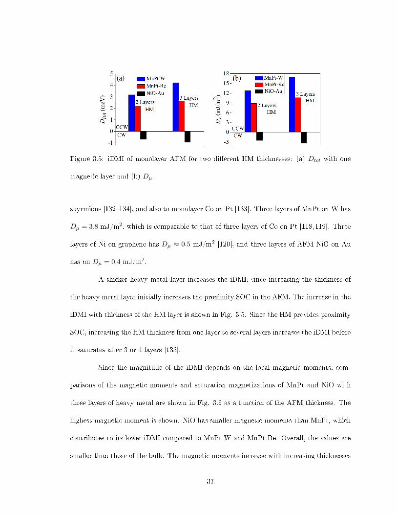
Figure 3.5: iDMI of monolayer AFM for two dierent HM thicknesses: (a) Dtot with one
magnetic layer and (b) Dµ.
skyrmions [132134], and also to monolayer Co on Pt [133]. Three layers of MnPt on W has
Dµ = 3.8 mJ/m2, which is comparable to that of three layers of Co on Pt [118,119]. Three
layers of Ni on graphene has Dµ ≈ 0.5 mJ/m2 [120], and three layers of AFM NiO on Au
has an Dµ = 0.4 mJ/m2.
A thicker heavy metal layer increases the iDMI, since increasing the thickness of
the heavy metal layer initially increases the proximity SOC in the AFM. The increase in the
iDMI with thickness of the HM layer is shown in Fig. 3.5. Since the HM provides proximity
SOC, increasing the HM thickness from one layer to several layers increases the iDMI before
it saturates after 3 or 4 layers [135].
Since the magnitude of the iDMI depends on the local magnetic moments, com-
parisons of the magnetic moments and saturation magnetizations of MnPt and NiO with
three layers of heavy metal are shown in Fig. 3.6 as a function of the AFM thickness. The
highest magnetic moment is shown. NiO has smaller magnetic moments than MnPt, which
contributes to its lower iDMI compared to MnPt-W and MnPt-Re. Overall, the values are
smaller than those of the bulk. The magnetic moments increase with increasing thicknesses
37
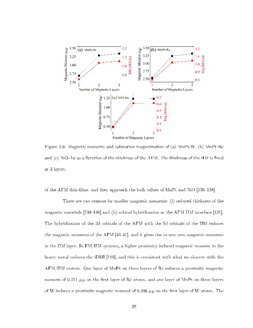
Figure 3.6: Magnetic moments and saturation magnetization of (a) MnPt-W, (b) MnPt-Re
and (c) NiO-Au as a function of the thickness of the AFM. The thickness of the HM is xed
at 3 layers.
of the AFM thin-lms, and they approach the bulk values of MnPt and NiO [136138].
There are two reasons for smaller magnetic moments: (i) reduced thickness of the
magnetic materials [139,140] and (ii) orbital hybridization at the AFM-HM interface [131].
The hybridization of the 3d orbitals of the AFM with the 5d orbitals of the HM reduces
the magnetic moments of the AFM [40,41], and it gives rise to non-zero magnetic moments
in the HM layer. In FM/HM systems, a higher proximity induced magnetic moment in the
heavy metal reduces the iDMI [118], and this is consistent with what we observe with the
AFM/HM system. One layer of MnPt on three layers of Re induces a proximity magnetic
moment of 0.211 µB on the rst layer of Re atoms, and one layer of MnPt on three layers
of W induces a proximity magnetic moment of 0.206 µB on the rst layer of W atoms. The
38

Figure 3.7: Local density of states of Mn atom in 3 layers of MnPt on top of 3 layers of Re:
(a) middle Mn atom which is far from Re, (b) bottom Mn atom which is close to Re and is
aected by proximity induced magnetic moment.
enhanced magnetic moment in the HM is accompanied by a reduced magnetic moment in
the interfacial magnetic atoms. For a system with three layers of MnPt on top of three
layers of Re, the magnetic moment of a Mn atom at the HM interface is 2.18 µB, and the
magnetic moment of a Mn atom in the middle layer is 3.13 µB. This eect is apparent
in the spin-resolved local density of states (LDOS) of the Mn atoms. Fig. 3.7 shows the
spin-resolved LDOS of Mn atoms in the (a) middle layer and (b) interfacial layer from the
heterostructure of three layers of MnPt on three layers of heavy metal (Re). The upper (red)
39

Figure 3.8: (a) Magnetic anisotropy constant of MnPt with 3 layers of heavy metals. (b)
Exchange stiness of MnPt with 3 layers of heavy metals.
and lower (blue) curves show the spin-up D↑ and spin down D↓ LDOS, respectively. The
magnetic moment is proportional to the integration of D↑ −D↓ over the occupied energies
E ≤ EF . The LDOS of the minority down spin is larger in the interfacial layer than in the
middle layer, with the result that the Mn atoms at the interface are less polarized.
MnPt consists of alternating layers of magnetic Mn atoms and heavy metal Pt
atoms with high SOC. A nite (001) slab of MnPt, consisting of an integer number of unit
cells, breaks inversion symmetry since one face is a Mn layer and the opposing face is a Pt
layer. The combination of high SOC and broken inversion symmetry gives rise to a small
amount of DMI even without a proximity HM layer. For a three layer slab of MnPt with
the Mn layer on the bottom and the Pt layer on the top, Dtot = −1.02 meV/3d atom, and
Dµ = −1.37 mJ/m2. In contrast, NiO does not contain any heavy metal atoms, 3 layers
remain geometrically inversion symmetric, and it exhibits zero DMI in the absence of an
adjacent heavy metal layer.
Calculated values for the magneto-crystalline anisotropy constants and exchange
40

stinesses are shown in Fig. 3.8 for dierent numbers of magnetic layers. The magnetic
anisotropy constant decreases with thickness, and the exchange stiness slightly increases
with the number of layers, which is consistent with a previous study [127].
3.4 Conclusions
The interfacial Dzyaloshinskii-Moriya interaction of MnPt/W, MnPt/Re, and NiO/Au
are calculated for dierent thicknesses of both the AFM and the HM. Values of iDMI, mag-
netic moments, exchange and magnetic anisotropy constants required for the micromagnetic
simulations are determined. The values of the iDMI of the MnPt/HM heterolayers are com-
parable to those of the common ferromagnetic materials such as Fe, Co or CoFeB. The iDMI
of the NiO/Au system is approximately a factor of 7 lower. In general, iDMI is maximized by
choosing AFM materials with larger magnetic moments, heavy metals with high spin orbit
coupling, thinner AFM layers from 1 - 3 monolayers, and HM thicknesses of at least 3 to 4
layers. Few layer (001) MnPt which contains both HM atoms and magnetic atoms exhibits
an intrinsic DMI, albeit smaller than the iDMI induced by a proximity HM layer. These
results and the quantitative values provided will help guide experimental realization and
provide needed parameters for micromagnetic simulations of AFM materials with domain
walls and skyrmions supported by iDMI.
3.5 Acknowledgement
This work was supported as part of Spins and Heat in Nanoscale Electronic Systems
(SHINES) an Energy Frontier Research Center funded by the U.S. Department of Energy,
41

Oce of Science, Basic Energy Sciences under Award #DE-SC0012670. This work used the
Extreme Science and Engineering Discovery Environment (XSEDE) [3], which is supported
by National Science Foundation Grant No. ACI-1548562 and allocation ID TG-DMR130081.
42

Chapter 4
Magnetic Properties of NbSi2N4,
VSi2N4, and VSi2P4 Monolayers
4.1 Introduction
Two dimensional (2D) layered materials with transition metals have been of interest
for many decades due to the correlated phenomena and multiple polymorphs and phases that
they can exhibit such as charge density waves, [36] superconductivity, [37] and magnetism.
[38] The ability to exfoliate or grow single monolayers renewed the interest in these materials
for possible electronic and optoelectronic applications [141,142] by both traditional transistor
type devices [143,144] and by exploiting external control of their phase transitions. [145] The
relatively recent demonstration of magnetism in single monolayer of CrI3 [146] and bilayers
of Cr2Ge2Te6 [147] has spurred intense experimental and theoretical activity to nd other
2D magnetic materials with higher transition temperatures. [148155]
43

Figure 4.1: Structures and magnetic orientations of α1-NbSi2N4, α1-VSi2N4, and α1-VSi2P4.
Blue atoms are Si, white atoms are N, and pink atoms are P. The directions of the magnetic
moments are shown on the transition metals Nb and V. All materials are easy-plane, semi-
conducting ferromagnets.
The most recent addition to the family of 2D materials are the transition metal
silicon nitrides, phosphides, and arsenides with the chemical formulas MA2Z4, where M is
the transition metal, A ∈ Si, Ge, and Z ∈ N, P, As. [39] High quality multilayers and
monolayers of MoSi2N4 were grown using chemical vapor deposition, and what was particu-
larly notable was their stability to air, water, acid, and heat that was unprecedented among
transition metal 2D materials. [39] This rather mundane property is highly desirable for
manufacturing applications. While BN encapsulation is an eective solution for stabilizing
reactive 2D materials for laboratory experiments, [156] it is less than ideal for manufactur-
ing. Only MoSi2N4 was experimentally characterized in detail, WSi2N4 was also grown, and
12 materials were simulated with density functional theory (DFT) and found to be stable.
Among these 12, two of the nitrides, VSi2N4 and NbSi2N4, were identied as magnetic.
44

This work motivated immediate follow-on theoretical investigations of this ma-
terial family both determining properties of the materials and extending the list of stable
materials. [157165] The most extensive theoretical survey found 32 thermodynamically and
dynamically stable compounds of the form MA2Z4. [160] Of these, 6 were magnetic: VSi2N4,
VSi2P4, NbSi2N4, VGe2N4, VGe2P4, and TaGe2N4. Based on the formation enthalpies, a Si
based compound MSi2Z4 is approximately 3 times more stable than its equivalent Ge based
compound MGe2Z4, and a silicon nitride compound MSi2N4 is also approximately 3 times
more stable than its equivalent silicon phosphide compound MSi2P4.
Other recent works investigated MSi2Z4 bilayers (M = Ti, Cr, Mo; Z = N, P) for
their sensitivity to vertical strain [163, 164], and MoSi2N4 and WSi2N4 for their sensitivity
to biaxial strain and vertical applied electric eld. [163] It was found that vertical strain can
cause an insulator to metal transition; [164] biaxial strain can lead to an indirect to direct
bandgap transition; [163] and that an applied electric eld can result in an insulator to
metal transition. [163] A theoretical investigation of 2D-2D contacts to monolayer MoSi2N4
using NbS2 and graphene found ultralow p-type Schottky barriers with NbS2 contacts and
approximately equal n-type and p-type Schottky barriers with graphene contacts. [158] The
graphene Schottly barriers were shown to be tunable with an applied vertical electric eld.
In this letter, we theoretically investigate the magnetic properties of the three Si
based magnetic materials: VSi2N4, VSi2P4, NbSi2N4. Values of the exchange constants and
magnetic anisotropy energies are determined, and the Curie temperatures are calculated.
The Curie temperatures of VSi2N4 and VSi2P4 are near or at room temperature and above,
depending on the model used, whereas the Curie temperature of NbSi2N4 is low. Therefore,
45

the primarily focus will be on the two vanadium compounds. The magnetic anisotropy
energies of VSi2N4 and VSi2P4 are calculated as a function of uniaxial and biaxial strain
and electron and hole doping.
These materials can exist in a variety of hexagonal phases. Ref. [ [160]] calculated
the formation energies of 30 dierent phases and found that the lowest energy phase of
NbSi2N4 and VSi2N4 was the α1 phase, which is the same phase as the lowest energy phase
of MoSi2N4. The formation energy of the next higher energy phase (δ4) of NbSi2N4 was
13 meV per atom higher than the α1 phase, and the formation energy of the next higher
energy phase (β2) of VSi2N4 was 6 meV per atom higher than the α1 phase. For VSi2P4,
the lowest energy phase was δ4 with a formation energy 0.3 meV below that of α1. Since
the formation energy of the α1 phase of VSi2P4 is so close to that of the δ4 phase, and
since the δ4 phase has been previously analyzed [160], we will consider the α1 phase of all
3 materials: NbSi2N4, VSi2N4, and VSi2P4. We note that the piezoelectric and magnetic
properties of the α1 phase of VSi2P4 have recently been investigated with DFT using the
generalized gradient approximation (GGA). [157]
4.2 Method
DFT combined with Monte Carlo (MC) calculations are applied to determine the
electronic and magnetic properties of these materials. The magnetic anisotropy energy
(MAE) and exchange energy are evaluated from DFT calculations implemented in the Vi-
enna ab initio simulation package (VASP). [115] The electron-core interactions are described
by the projected augmented wave (PAW) potentials. [116] Electronic structure is calculated
46

using three dierent functionals: GGA as parameterized by Perdew-Burke-Ernzerhof (PBE),
PBE plus the Hubbard U correction (PBE+U), and the Heyd-Scuseria-Ernzerhof hybrid
functional (HSE06). [117, 166168] The PBE+U calculation includes a Hubbard U correc-
tion term Ueff = 1 eV for the V atom where Ueff = U − J . [169, 170] For calculations of the
MAE, spin orbit coupling (SOC) must also be included. All plots shown for the MAE are
the results from PBE(SOC)+U calculations. The cuto energies for expanding the plane
wave basis are 600 eV. Integration over the Brillouin zone uses a MonkhorstPack scheme
with a Γ-centered 16× 16× 1 k-point grid, an energy broadening parameter of 50 meV, and
the total energy is converged to 10−6 eV. Structures are relaxed until the forces are less than
0.001 eV/Å. A vacuum spacing of 20 Å is used in the direction normal to the 2D mono-
layer to eliminate the interactions from periodic images. The calculated lattice constants
for NbSi2N4, VSi2N4, and VSi2P4 are 2.96 Å, 2.88 Å, and 3.47 Å, respectively, and they are
very close to previous reported results. [39, 157]
Uniaxial strain is applied along the x axis corresponding to lattice vector a1. The
applied strain is evaluated using ϵ = (a − a0)/a0 × 100%, where a and a0 are the lattice
parameters of the strained and unstrained monolayer. Biaxial strain is applied by uniformly
varying both in-plane lattice constants. For each strain, the atomic positions are relaxed
using the DFT parameters described above. Spin-polarized self consistent calculations are
performed with the relaxed structure for each strain to obtain the charge density. Using the
charge densities, total energies are calculated in the presence of spin orbit coupling (SOC) for
in-plane (E||) and out-of-plane (E⊥) magnetization to nd the magnetic anisotropy energy
(MAE). The MAE is dened as EMAE = E⊥ − E||. Positive magnetic anisotropy indicates
47

that in-plane magnetization is favored. The values provided in meV are per magnetic atom,
which for these 3 materials under consideration, are also per unit cell.
To investigate the transition temperatures, a nearest neighbor Heisenberg type
Hamiltonian with magnetic anisotropy and long range dipole-dipole interactions is con-
structed,
H = −12J
∑⟨i,j⟩
Si · Sj + ku∑i
(Szi )
2 +Hdd, (4.1)
where Si is the spin for magnetic atom i, ⟨i, j⟩ are the indices of nearest neighbor magnetic
atoms, ku > 0 is the easy-plane magnetic anisotropy energy per magnetic atom, and Hdd is
the dipole-dipole interaction. The exchange energies (J) of these materials are calculated
from the total energy dierences between the antiferromagnetic (EAFM ) and ferromagnetic
(EFM ) states. [126,128130] With six nearest neighbours in the monolayer of 2D hexagonal
lattice, the nearest-neighbor exchange energy is given by, [1,129,130] J = (EAFM−EFM)/12.
In these monolayer materials all of the magnetic atoms are in the same plane. The second
neighbor exchange energies were previously determined for VSi2P4 and found to be negligi-
ble compared to the nearest neighbor energies, [160] and, therefore, they are ignored. The
Curie temperatures are determined from Monte Carlo (MC) calculations as implemented
in the VAMPIRE software package using a 10 × 10 supercell. [171, 172] The MC calcula-
tions incorporate the magnetic anisotropy energies, the magnetic moments, the exchange
energies, lattice constants, and atomic positions determined from the DFT calculations, and
they also include the long range dipolar interactions. This MC approach has been used to
determine the Curie temperatures in other monolayer 2D materials such as VSi2P4, VI3,
CrSBr, and CrSeBr. [160, 173, 174] We note that the Curie temperatures in other mono-
48

Figure 4.2: Spin resolved energy bands of VSi2N4 and VSi2P4 calculated with (a,b) HSE06
and (c,d) PBE+U. Spin up bands are red and spin down bands are blue. The two spin-split,
narrow bands on either side of the Fermi level are d-orbital bands centered on the transition
metal.
layer 2D materials determined from the MC approach have been shown to compare well to
temperatures determined from renormalized spin wave theory (RSWT). For example, the
MC/RSWT predicted Curie temperatures for monolayer CrSBr and CrSeBr were 168/150
K and 150/152 K, respectively. [174]
4.3 Results
The structures and the ground state orientations of the magnetic moments of
NbSi2N4, VSi2N4, and VSi2P4 are shown in Fig. 4.1, and the spin-resolved band struc-
ture for VSi2N4 and VSi2P4, calculated with the HSE06 and PBE+U functionals, are shown
49

in Fig. 4.2. The band structure for all three materials calculated with PBE, PBE+U, and
HSE06 are shown in the Fig. S3 of the Supplement, and the d-orbital resolved bands of
VSi2N4 and VSi2P4 are shown in Fig. S2. For all 3 materials at Γ, the two isolated narrow
bands near the Fermi level are spin-polarized, dz2 − orbital bands centered on the transi-
tion metal atoms. Near K, these bands transition to dx2−y2 . The next higher conduction
band is primarily dx2−y2 at Γ, and it transitions to dz2 at K. The electronic structures from
the HSE06 calculations show the following properties. In VSi2N4 and VSi2P4, the higher
spin-up conduction band at Γ crosses the lower spin-down band near K where the orbital
composition of the two bands switch, dz2 ⇐⇒ dx2−y2 . VSi2N4 is direct gap (0.78 eV) at K
with a dx2−y2 spin-up valence band and a dz2 spin-up conduction band. VSi2P4 is indirect
gap (0.84 eV) with the dz2 spin-up valence band edge at Γ and a mixed dz2 + dx2−y2 spin-
down conduction band edge at M (the spin-up band at K is 40 meV higher) . NbSi2N4 is
indirect gap (0.54 eV) with the spin-up dz2 valence band at Γ and a mixed orbital dz2 +
dx2−y2 spin-down conduction band near M. The lower valence bands are primarily p-orbital
bands which come from the N and P atoms. At the PBE level of theory, all 3 materials
are semi-metals. Adding the Hubbard U correction creates a small gap at the Fermi level
for VSi2N4 and VSi2P4. Adding a percentage of exact exchange with the HSE06 functional
increases the gap substantially. We note that the HSE06 calculations match those reported
in the Supplement of Ref. [ [160]].
The equilibrium NbSi2N4, VSi2N4, and VSi2P4 monolayers are easy-plane, semi-
conducting ferromagnets. The calculated equilibrium magnetic moments, exchange energies,
magnetic anisotropy energies, and Curie temperatures are shown in Table 4.1 for dierent
50

Materials (Theory) Magnetic Mo-
ment (µB)
Exchange
energy
(×10−21J)
MAE (MJm3 ) TC (K)
NbSi2N4 (PBE) 0.32 0.064 0.30 12
VSi2N4 (PBE) 0.93 1.50 0.24 301
VSi2P4 (PBE) 0.96 1.11 0.14 235
VSi2N4 (PBE+U) 1.05 2.53 0.25 452
VSi2P4 (PBE+U) 1.04 1.77 0.11 350
VSi2N4 (HSE06) 1.19 2.80 −− ∗506
Table 4.1: Magnetic moment, exchange energy per link, equilibrium magnetic anisotropy
energy (MAE), and Curie temperature, calculated using dierent functionals for NbSi2N4,
VSi2N4, and VSi2P4. ∗TC is calculated using the HSE06 exchange energy and the
PBE(SOC)+U MAE.
levels of theory. The magnetic moments are comparable to those from prior studies. [39,157]
The positive MAE values indicate in-plane alignment of the magnetic moments. Within
the energy resolution of our calculations (1 µeV), the total energy is independent of the
angle of the magnetic moment within the plane of the monolayer. Since the monolayers
are insulating, easy-plane FMs with extremely weak in-plane anisotropy, they satisfy the
necessary conditions for exhibiting a dissipationless spin superuid mode. [175]
The normalized magnetizations, determined from Monte Carlo calculations, are
plotted as a function of temperature for VSi2N4 and VSi2P4 in Fig. 4.3. The solid lines
51

Figure 4.3: Monte Carlo calculations of the normalized magnetization as a function of
temperature for (a) VSi2N4 and (b) VSi2P4. The solid lines show the best ts to the
analytical expression given by Eq. (4.2).
show the best ts to the analytic expression,
m(T ) = (1− T/TC)β. (4.2)
The tted values of TC and β are shown on the plots. At the PBE+U level of theory, both
monolayer VSi2P4 and VSi2N4 have Curie temperatures above room temperature, 350 K
and 452 K, respectively. The eect of the increasing levels of theory, PBE, PBE+U, and
HSE06, is to successively increase the bandgap between the two spin-polarized dz2 bands,
so that at the HSE06 level, the two bands are completely gapped which maximizes the spin
polarization, magnetic moment, and the exchange constant. The predicted TC increases
with the increasing gap, giving a maximum value of 506 K for VSi2N4 using the exchange
constant determined from the HSE06 calculation. Since VSi2N4 has the same structure,
surface chemistry, and formation energy [160] as the experimentally characterized MoSi2N4,
we expect VSi2N4 to also be an air/water-stable material with Tc > 100 C, which is a
criterion for operation in a modern integrated circuit environment.
52

For context, we compare to several other 2D materials with similar predicted Curie
or Néel temperatures. A more comprehensive comparison is provided in the supplementary
material. The calculated Curie-temperatures for monolayers of the transition metal dichalco-
genides (TMDs) VS2, VSe2, and VTe2 are 292 K, 472 K, and 553 K, respectively. [176] The
predicted monolayer Curie temperatures for the ternary 2D materials CrSeCl, VSeTe, and
CrSeI are 320 K, 350 K, and 360 K, respectively. [153,174,177] Monolayers of ferromagnetic
semiconductors TcSiTe3 have a predicted Curie temperature of 538 K. [178] We note that
Tc is radioactive, so that Tc compounds are unlikely to see magnetic applications. Mono-
layers of RuI3, MnN, Co2S2, and 3R-MoN2 have Curie temperatures of 360 K, 368 K, 404
K, and 420 K, respectively. [179182] We note that synthesis of layered 3R-MoN2 requires
high pressure, [183] which is not amenable to thin lm growth techniques, and the proposed
graphitization synthesis route to achieve MnN monolayers [184] has not yet been demon-
strated. Within the list above, VSi2N4 stands out for its combination of air stability and
relatively high Curie temperature.
The equilibrium values of the MAE are listed in Table 4.1. The equilibrium values
of VSi2N4 and VSi2P4 range from 0.11 to 0.25 meV / magnetic atom. For comparison,
monolayers of CrCl3, CrBr3, and CrI3 have equilibrium MAEs of 0.02 meV, 0.16 meV,
and 0.8 meV, respectively. [185] Two-dimensional FeCl2, NiI2, Fe3P, and Fe3GeTe2 have
equilibrium MAE values of 0.07 meV, 0.11 meV, 0.72 meV, and 1 meV, respectively in their
monolayer limit. [186189] In general, the MAE values of VSi2N4, and VSi2P4 are on the
lower end of values for other 2D magnetic materials.
The calculated values of the MAE of VSi2N4 and VSi2P4 as a function of uniaxial
53

ε μeV
ε μeV
ε μeV
ε μeV
ε μeV
ε μeV
Figure 4.4: MAE as a function of uniaxial and biaxial strain calculated with PBE(SOC)+U.
MAE versus uniaxial strain: (a) VSi2N4 and (b) VSi2P4. MAE versus biaxial strain: (c)
VSi2N4 and (d) VSi2P4. Values are shown for the strain coecients for dierent regions
discussed in the text. The orientation of the magnetization of VSi2N4 rotates from in-plane
to out-of-plane with 3.3% biaxial strain.
54

n = -0.29 meV n = 0.31 meV
Figure 4.5: MAE as a function of band lling calculated with PBE(SOC)+U. MAE as a
function of excess electrons per unit cell for (a) VSi2N4 and (b) VSi2P4. Values are shown
for the lling coecients discussed in the text. The orientation of the magnetization of
VSi2N4 rotates from in-plane to out-of-plane with electron doping of 2.0× 1014 cm−2.
strain and biaxial strain are shown in Fig. 4.4. We quantify the sensitivity by dening a
strain coecient as αϵ = dEMAE/dϵ. For small strain of both types in both materials, the
values for αϵ are well below the value of 32 µeV/%strain recently calculated for a 1.1 nm
slab of CrSb. [190] For compressive uniaxial and biaxial strain in VSi2N4, αϵ = −10 and −6
µeV/%strain, respectively. For VSi2P4, αϵ = −6 µeV/%strain for uniaxial tensile strain, -10
µeV/%strain for biaxial tensile strain, and 17 µeV/%strain for biaxial compressive strain.
For large (3-4%) biaxial strain in VSi2N4, the magnitude of the sensitivity increases. At a
strain of 3.3%, the MAE changes sign, and the spins rotate from in-plane to out-of-plane.
This magnitude of strain should be experimentally accessible, since 2D materials can sustain
large strain. [191]
The eects of band lling on the MAE are shown in Fig. 4.5. The MAE is reduced
in VSi2N4 and VSi2P4 for both electron and hole doing. To quantify the sensitivity of the
55

MAE to charge lling we dene the parameter [190] αn = dEMAE/dn evaluated at zero lling.
For electron lling in VSi2N4, αn = −0.29 meV, and for hole lling in VSi2P4, αn = 0.31
meV. What is most interesting is that the sign of the MAE can be reversed in VSi2N4 at an
electron lling of 0.28 electrons per unit cell corresponding to a sheet carrier concentration
of ns = 2.0 × 1014 cm−2. At this doping density, the orientation of the magnetization of
VSi2N4 rotates from in-plane to out-of-plane. These densities are high, however since the
thickness of the monolayer is under 1 nm, such densities could be experimentally accessible
using electrolytic gating.
4.4 Conclusions
In conclusion, NbSi2N4, VSi2N4, and VSi2P4 are easy-plane, semiconducting FMs
with negligible in-plane anisotropy. Exchange constants extracted from PBE+U DFT used
in MC calculations predict Curie temperatures for monolayer VSi2P4 and VSi2N4 of 350 K
and 452 K, respectively. The eect of the increasing levels of theory, PBE, PBE+U, and
HSE06, is to successively increase the energy gap between the two spin-polarized dz2 bands,
so that at the HSE06 level, the two bands are completely gapped which maximizes the spin
polarization, magnetic moment, and the exchange constant. The predicted TC increases
with the increasing gap, giving a maximum value of 506 K for VSi2N4 using the exchange
constant determined from the HSE06 calculation. Since VSi2N4 has the same structure,
surface chemistry, and formation enthalpy as MoSi2N4, it is expected to also be air and
water stable. The magnetic anisotropy energies of VSi2N4 and VSi2P4, determined by the
dierence in the total energies resulting from out-of-plane versus in-plane alignment of the
56
magnetic moments, are small, ranging from 0.11 to 0.25 meV / magnetic atom. Tensile
biaxial strain of 3.3% in VSi2N4 causes the MAE to change sign such that the magnetic
moments rotate from in-plane to out-of-plane. Band lling of 0.28 electrons per unit cell
(2.0 × 1014 cm−2) also causes VSi2N4 to switch from in-plane to perpendicular magnetic
anisotropy.
4.5 Supplementary Material
The supplementary material contains plots of orbital projected band diagrams,
comparisons of electronic bandstructures calculated with PBE, PBE+U, and HSE06 func-
tionals, and MC calculations of the normalized magnetization as a function of temperature
with exchange constants extracted from PBE DFT. It also contains an extended comparison
of Curie temperatures of 2D materials. Fig. 4.6 shows the orbital resolved band structure of
VSi2N4. Fig. 4.7 shows the d-orbital resolved band structures of VSi2N4 and VSi2P4. Spin
resolved PBE, PBE+U, and HSE06 band structures are shown in Fig. 4.8. Monte Carlo
calculations using exchange constants extracted from PBE DFT are shown in Fig. 4.9.
57

Figure 4.6: Orbital resolved PBE band structure of VSi2N4 at equilibrium: (a) s-orbital
contribution, (b) p-orbital contribution, and (c) d-orbital contribution. The weight is given
by the color bars at right. The two isolated, narrow bands near the Fermi level are d-orbital
bands centered on the transition metal atoms vanadium (V). The higher valence bands are
primarily p-orbital bands which come from the N atoms. The lower conduction bands are
primarily d-orbital bands.
Figure 4.7: d-orbital resolved PBE band structure of VSi2N4: (a) spin up bands, (c) spin
down bands. d-orbital resolved band structure of VSi2P4: (b) spin up bands, (d) spin down
bands.
58

Figure 4.8: Spin resolved PBE band structure: (a) NbSi2N4, (b) VSi2N4, and (c) VSi2P4.
Spin resolved PBE+U band structure: (d) NbSi2N4, (e) VSi2N4, and (f) VSi2P4. Spin
resolved HSE06 band structure: (g) NbSi2N4, (h) VSi2N4, and (i) VSi2P4.
Figure 4.9: MC calculations of the normalized magnetization as a function of temperature
with exchange constants extracted from PBE DFT for (a) NbSi2N4, (b) VSi2N4, and (c)
VSi2P4. Curie temperatures are calculated from Monte Carlo simulation using the VAM-
PIRE software.
59

4.6 Curie temperatures of other 2D Materials
For context, we provide comparisons to some of the more heavily studied 2D mag-
netic materials and other predictions in the literature. CrI3 has Curie temperatures of
45 K in monolayers and 61 K in bulk. [146] Cr2Ge2Te6 (CGT) has Curie temperatures of
30 K for bilayers and 66 K for bulk. [147] Magnesium chloride has Curie temperature of
250 K. [192] The ternary compound Fe3GeTe2 (FGT) has Curie temperatures of 130 K for
monolayers [193] and 205 K for bulk [148]. MnBi2Te4, a ferromagnetic insulator, has a Curie
temperature of about 20 K for monolayers. [194] MnPS3 and FePS3 have antiferromagnetic
ordering temperatures of 78 K and 118 K, respectively. [195] Ta3FeS6 is reported to be air
stable with a Curie temperature of 80 K. [196] There are many theoretical predictions in
the literature. The calculated Curie temperatures of the Dirac half-metal monolayers of
VCl3 and VI3 are 80 K and 98 K, respectively. [197] The predicted Curie-temperatures of
the transition metal dichalcogenide monolayers tend to be high, but these materials suer
from air/water instability. The calculated Curie-temperatures for monolayers of VS2, VSe2,
and VTe2 are 292 K, 472 K, and 553 K, respectively. [176] The predicted monolayer Curie
temperatures for the ternary 2D materials VSeTe, CrSBr, CrSeBr, CrSeCl and CrSeI 350
K, 168 K, 150 K, 320 K and 360 K, respectively. [153, 174, 177] Monolayers of ferromag-
netic semiconductors TcSiTe3, TcGeSe3, and TcGeTe3 have predicted Curie temperatures
of 538 K, 212 K, and 187 K, respectively. [178] We note that Tc is radioactive, so that
the Tc compounds are unlikely to see magnetic applications. Monolayers of Co2S2, ScCl,
RuI3, 3R-MoN2 and MnN have Curie temperatures of 404 K, 185 K, 360 K 420 K, and
368 K, respectively. [179182,198] We note that synthesis of layered 3R-MoN2 requires high
60

pressure, [183] which is not amenable to thin lm growth techniques, and the proposed
graphitization synthesis route to achieve MnN monolayers [184] has not yet been demon-
strated.
4.7 Acknowledgement
This work used the Extreme Science and Engineering Discovery Environment
(XSEDE), [3] which is supported by National Science Foundation Grant No. ACI-1548562
and allocation ID TG-DMR130081. MRKA thanks A. Bafekry from University of Guilan,
and San-Dong Guo from Xi'an University of Posts and Telecommunications for providing
initial crystal structures.
61

Chapter 5
1D and 2D Topological Insulators and
Semimetals
5.1 Introduction
One dimensional (1D) and two dimensional (2D) materials provide promising ap-
plications in nanoelectronics and optoelectronics due to their ultimately scaled sizes and
thicknesses [199201]. The availability of a large number of 1D and 2D candidate materi-
als will accelerate progress in this area. Previously, data mining of the Materials Project
database identied 1173 two dimensional materials and 487 one dimensional materials [202].
Approximately 6000 two dimensional materials have been identied and generated in a sep-
arate work [203]. At rst, a geometry-based algorithm was used to classify 2D materials
within existing material databases [202], and then the number of 2D materials was enlarged
by chemical substitution of elements in known 2D materials by others from the same group
62

in the periodic table, followed by DFT calculations [203]. 1,036 easily exfoliable 2D materials
that have been experimentally demonstrated have also been identied [204].
Topological insulators and semimetals are also gaining interest due to their var-
ious prospective applications, and they can oer various functionalities similar to transis-
tors [205210]. Using rst-principles calculations, 8,056 topological materials have been
identied considering spinorbit coupling [211]. A total of 10,007 topological semimetals,
4321 topological insulators, and 550 magnetic topological materials have been found found
from ICSD materials database [212214]. From several databases of 1D, 2D, and topological
materials, we identied a large number of 1D and 2D topological materials.
5.2 Results
A summary of the results is shown in Fig. 5.1. Topological insulators and semimet-
als from the topological materials database [211] and 2D materials from 2D matpedia [203]
are used to identify 150 two dimensional topological insulators and 98 two dimensional
topological semimetals listed in Tables 5.1 and 5.2, respectively. Topological insulators and
semimetals from the topological materials database [211] and 1D materials from database
of Evan Reed et al. [202] are used to identify the 12 one dimensional topological insulators
and 15 one dimensional topological semimetals listed in Tables 5.3 and 5.4, respectively.
Topological insulators and semimetals from the topological materials database [211] and
2D materials from the database of Evan Reed et al. [202] are used to identify the 93 two
dimensional topological insulators and 46 two dimensional topological semimetals listed in
Tables 5.5 and 5.6), respectively. Topological insulators and semimetals from the topological
63

materials database [211] and 2D materials from the experimental database [204] are used to
identify the 27 experimentally demonstrated two dimensional topological insulators and 8
two dimensional topological semimetals listed in Tables 5.7 and 5.8, respectively.
Figure 5.1: Flowchart of identifying 1D and 2D topological materials from several database.
MPID Material Formula
mp-570122 Cr3Te4
mp-2430 ZrGe2
mp-20738 FeSi2
mp-504594 ZrBr
mp-568746 Bi2Pd
mp-570197 Bi2Pd
Continued on next page
64

Table 5.1 continued from previous page
MPID Material Formula
mp-1168 HfTe5
mp-1334 Y2C
mp-20311 FeSe
mp-7655 BaSi2
mp-30428 BaCu
mp-1201 Sb2Te3
mp-583234 Bi4I
mp-541837 Bi2Se3
mp-7459 Te2Mo
mp-2089 ZrTe3
mp-2330 Nb2Se3
mp-692 Tb2C
mp-542634 Ta2Te3
mp-571033 NiSe
mp-605 ZrTe5
mp-399 Te2Pt
mp-570451 Nb2Te3
Continued on next page
65

Table 5.1 continued from previous page
MPID Material Formula
mp-29652 TaSe3
mp-27440 ZrCl
mp-9897 Te3As2
mp-1371 Sn3Pd
mp-30500 TiCd
mp-21296 PtPb4
mp-8094 Ba2Hg
mp-984703 CeGe5
mp-567510 BaSn2
mp-570286 BiSe
mp-628781 GeTe
mp-21042 Te4Pt3
mp-22562 YS
mp-615366 FeS2
mp-554055 HoS
mp-1879 SmS
mp-1056059 O2
Continued on next page
66

Table 5.1 continued from previous page
MPID Material Formula
mp-12574 Dy2C
mp-1078737 HoCoGe2
mp-130 P
mp-1008498 Ca
mp-1080587 CdNCl3
mp-1078753 LiTl
mp-1009757 Se
mp-13962 HfSiSe
mp-1078904 Sb2Te3
mp-1091417 AgN
mp-1025084 HoBC
mp-13963 HfSiTe
mp-1070135 Er2Mg2Ru
mp-1080184 LaIO3
mp-1080466 Nb2PdS6
mp-11 As
mp-1078645 YCoGe2
Continued on next page
67

Table 5.1 continued from previous page
MPID Material Formula
mp-104 Sb
mp-1079936 TbCoGe2
mp-10283 SmSi3Ni
mp-13683 HfGe2
mp-157 P
mp-19810 TaNiTe2
mp-1065583 LaSe
mp-2578 NiTe2
mp-19917 ZrSiTe
mp-158 As
mp-23224 BiTe
mp-1080067 ErCoGe2
mp-27910 Bi2Te2S
mp-27947 Sn(SbTe2)2
mp-1006619 Sn3PO6
mp-22777 NaN3
mp-15605 ScSi3Ni2
Continued on next page
68

Table 5.1 continued from previous page
MPID Material Formula
mp-2755 SiTe2
mp-24242 CuHOF
mp-27848 TiIN
mp-23896 LuHCl
mp-20757 MnAlGe
mp-24081 ScHCl
mp-23152 Bi
mp-27948 Ge(BiTe2)2
mp-24051 ErHCl
mp-27902 BiSe
mp-545706 Ca3Cu2(BrO2)2
mp-20506 NbNiTe2
mp-31507 Sb2Te4Pb
mp-4384 Nb2CS2
mp-7716 SbTe
mp-571550 Sb2TeSe2
mp-8677 ZrTiTe4
Continued on next page
69

Table 5.1 continued from previous page
MPID Material Formula
mp-48 C
mp-19607 K(MoO3)3
mp-3525 Sb2Te2Se
mp-79 Zn
mp-94 Cd
mp-569831 Zr3(Al2C3)2
mp-980004 SmGa2Co
mp-570930 Bi2Pb2Se5
mp-30485 Ca3Zn
mp-8211 GaGeTe
mp-7574 AlBMo
mp-567970 Hf3(Al2C3)2
mp-569044 Bi2Te5Pb2
mp-557597 K2Ca(NO2)4
mp-977592 Bi2Rh3S2
mp-34202 Bi2Te3
mp-642803 Zr2HBr2
Continued on next page
70

Table 5.1 continued from previous page
MPID Material Formula
mp-8742 DyCoSi2
mp-542640 GePt
mp-31406 Bi2TeSe2
mp-3534 Ge2Sb2Te5
mp-568050 Ca3SiBr2
mp-569358 Bi
mp-9936 DyBC
mp-644389 Li2H2Pd
mp-568730 Ge4Te7As2
mp-3128 ErCoSi2
mp-9379 Sr(SnAs)2
mp-8806 Sr2Cu2O3
mp-557619 Bi14Te13S8
mp-29666 Bi2Te2Se
mp-972406 YbSi2Ni
mp-4628 ZrSiSe
mp-571471 NbCoTe2
Continued on next page
71

Table 5.1 continued from previous page
MPID Material Formula
mp-864790 Nd2BC
mp-541449 CrGeTe3
mp-9983 Ta2Se3
mp-634817 CaZn2(PO)2
mp-639496 EuIn2Au
mp-624889 C
mp-31025 Sc5NCl8
mp-8436 Ta2PdSe6
mp-644136 Li2H2Pt
mp-541070 Ta2NiSe5
mp-782 Te2Pd
mp-643743 CuHClO
mp-558696 CuTeO3
mp-7814 Ta2CS2
mp-3208 ZrGeTe
mp-676250 Bi2Te4Pb
mp-1072085 CeSi5
Continued on next page
72

Table 5.1 continued from previous page
MPID Material Formula
mp-7263 CaGaN
mp-973938 LuCoGe2
mp-24522 CuH2SO5
mp-557946 Cu3Se2(ClO3)2
mp-28487 Ge5(Te4As)2
mp-27548 CuTe2O5
mp-683904 Yb2Te5O13
mp-1078720 Pt(NCl)4
Table 5.1: 2D topological insulators
MPID Material Formula
mp-20826 CuTe
mp-23313 InBi
mp-2129 NdGe2
mp-740 NdTe3
Continued on next page
73

Table 5.2 continued from previous page
MPID Material Formula
mp-580226 CuSe
mp-1080586 Sn4Ir
mp-9399 SmTe3
mp-570356 Ca5Ir
mp-604914 VSe
mp-12351 PrTe3
mp-7542 GeP3
mp-525 NbSe3
mp-998972 TiAu
mp-28149 Bi9I2
mp-29941 Sc2C
mp-30527 TaS3
mp-945077 YTe3
mp-7541 SnP3
mp-1229 CuF2
mp-12750 SmGe2
mp-2294 Al3Ir
Continued on next page
74

Table 5.2 continued from previous page
MPID Material Formula
mp-13152 TiSe
mp-1861 Cu2Te
mp-1001825 LiBe
mp-569701 ErTe3
mp-29663 Si3Ir
mp-1008600 ZrN2
mp-1008682 TiS2
mp-10021 Ga
mp-1079923 H3W
mp-1087512 TmTe3
mp-1084847 TbTe3
mp-1077588 SiNiSb
mp-1018658 CaCoSi
mp-10033 NbS2
mp-1077298 TbMgNi
mp-1078651 ErNiGe2
mp-1086673 DyTe3
Continued on next page
75

Table 5.2 continued from previous page
MPID Material Formula
mp-1086674 YbCoGe2
mp-1079251 W2N3
mp-1095661 YbCuPbSe3
mp-1372 Cd3As2
mp-10231 LiMnSe2
mp-1094089 NiS2
mp-1018654 BaMgSn
mp-1018653 BaMgPb
mp-1072320 HgSBr
mp-1077470 CaNiGe
mp-1080689 LuTe3
mp-1018808 MgCoGe
mp-1078069 Al2ZnS4
mp-1078637 Bi
mp-1080714 Li2AgSn2
mp-20698 LiCoAs
mp-28616 NbTe5Pd
Continued on next page
76

Table 5.2 continued from previous page
MPID Material Formula
mp-28754 Nb3GeTe6
mp-22992 TiClO
mp-22965 BiTeI
mp-23002 TiBrO
mp-17801 Hf2CuGe4
mp-22152 NaFeAs
mp-23095 Ca3Cu2(ClO2)2
mp-24164 CuH2(SeO3)2
mp-2194 TiSe2
mp-18279 Zr2CuGe4
mp-505137 Nb3SiTe6
mp-554027 Y7C3I6O
mp-541937 Zn(InS2)2
mp-8768 K2CoSe2
mp-29772 YGe3
mp-622009 TaNi2TeSe
mp-971806 TmFeGe2
Continued on next page
77

Table 5.2 continued from previous page
MPID Material Formula
mp-500 TaSe2
mp-570141 Sm2(PPt2)3
mp-3421 CuCN2
mp-4437 NdTe2Se
mp-30125 PrTe2Se
mp-601693 YbBrO
mp-8999 NbNiTe5
mp-8998 TaNiTe5
mp-3250 Ni2SbTe2
mp-567826 Sr
mp-608254 SmClF
mp-973954 LuFeGe2
mp-8848 TaFeTe3
mp-505042 Cu(BiO2)2
mp-7754 Si2Ru
mp-630773 CdInGaS4
mp-20049 LiFeP
Continued on next page
78

Table 5.2 continued from previous page
MPID Material Formula
mp-9391 TaNi2Te3
mp-28667 Ta(NiTe)2
mp-1078991 ErTe3
mp-1018798 MgCuGe
mp-505206 Ta3SiTe6
mp-14815 TaTe5Pt
mp-1078612 LaTe3
mp-4034 LaTe2Se
mp-11879 BaNiSn3
Table 5.2: 2D topological semimetals
MPID Material Formula
mp-637982 As5Pb3S10
mp-583234 Bi4I
mp-568758 BiBr
Continued on next page
79

Table 5.3 continued from previous page
MPID Material Formula
mp-568388 BiI
mp-7302 CrP4
mp-29279 CuClF10
mp-11508 MoP4
mp-558408 Nb4Te9I4O
mp-654051 Nb6SI9
mp-29579 Sc7NCl12
mp-684021 Sn4Sb6S13
mp-680836 Ta4Te9I4O
Table 5.3: 1D topological insulators
MPID Material Formula
mp-28661 Ba2Cu3P4
mp-21653 BaNiN
mp-28149 Bi9I2
Continued on next page
80

Table 5.4 continued from previous page
MPID Material Formula
mp-3199 CuSe2O5
mp-568002 HfI3
mp-17867 Mn2NbP12
mp-754514 N2
mp-568616 Nb2Br5
mp-14 Se
mp-19 Te
mp-571143 TiCl3
mp-8251 VP4
mp-9847 YbP5
mp-23247 ZrBr3
mp-22871 ZrCl3
Table 5.4: 1D topological semimetals
81

MPID Material Formula
mp-11 As
mp-21032 BaIn2Pt
mp-23152 Bi
mp-557619 Bi14Te13S8
mp-570930 Bi2Pb2Se5
mp-570197 Bi2Pd
mp-541837 Bi2Se3
mp-29666 Bi2Te2Se
mp-34202 Bi2Te3
mp-676250 Bi2Te4Pb
mp-569044 Bi2Te5Pb2
mp-23435 Bi2TeI
mp-31406 Bi2TeSe2
mp-581990 Bi3Rh
mp-27607 Bi4Se3
mp-23005 Bi4Te7Pb
mp-680214 Bi8Se7
mp-27902 BiSe
Continued on next page
82

Table 5.5 continued from previous page
MPID Material Formula
mp-23224 BiTe
mp-568286 C
mp-570122 Cr3Te4
mp-541449 CrGeTe3
mp-559094 Cu2H3ClO3
mp-643743 CuHClO
mp-24242 CuHOF
mp-12574 Dy2C
mp-30196 ErCuP2
mp-24051 ErHCl
mp-20311 FeSe
mp-8211 GaGeTe
mp-27948 Ge(BiTe2)2
mp-3534 Ge2Sb2Te5
mp-568730 Ge4Te7As2
mp-28487 Ge5(Te4As)2
mp-29644 GeBi4Te7
Continued on next page
83

Table 5.5 continued from previous page
MPID Material Formula
mp-29641 GeSb4Te7
mp-8645 GeTe7As4
mp-13962 HfSiSe
mp-13963 HfSiTe
mp-1168 HfTe5
mp-1640 Ho2C
mp-568574 LaGeI
mp-22716 LiCu2P
mp-23896 LuHCl
mp-570849 Mg5Tl2
mp-4384 Nb2CS2
mp-571471 NbCoTe2
mp-20506 NbNiTe2
mp-864790 Nd2BC
mp-571033 NiSe
mp-2578 NiTe2
mp-104 Sb
Continued on next page
84
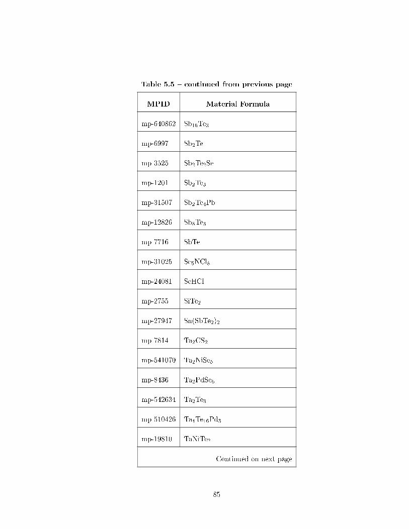
Table 5.5 continued from previous page
MPID Material Formula
mp-640862 Sb16Te3
mp-6997 Sb2Te
mp-3525 Sb2Te2Se
mp-1201 Sb2Te3
mp-31507 Sb2Te4Pb
mp-12826 Sb8Te3
mp-7716 SbTe
mp-31025 Sc5NCl8
mp-24081 ScHCl
mp-2755 SiTe2
mp-27947 Sn(SbTe2)2
mp-7814 Ta2CS2
mp-541070 Ta2NiSe5
mp-8436 Ta2PdSe6
mp-542634 Ta2Te3
mp-510426 Ta4Te16Pd3
mp-19810 TaNiTe2
Continued on next page
85

Table 5.5 continued from previous page
MPID Material Formula
mp-29652 TaSe3
mp-692 Tb2C
mp-782 Te2Pd
mp-399 Te2Pt
mp-9897 Te3As2
mp-541180 Te3Pt2
mp-8628 Te4Pt3
mp-11693 TePt
mp-27848 TiIN
mp-579614 Y16B4C8I19
mp-1334 Y2C
mp-568046 Y5Mg13Cu5
mp-683904 Yb2Te5O13
mp-680388 ZnCuTeCl2O3
mp-642803 Zr2HBr2
mp-504594 ZrBr
mp-27440 ZrCl
Continued on next page
86

Table 5.5 continued from previous page
MPID Material Formula
mp-3208 ZrGeTe
mp-4628 ZrSiSe
mp-19917 ZrSiTe
mp-2089 ZrTe3
mp-605 ZrTe5
mp-570062 ZrTiSe4
mp-8677 ZrTiTe4
Table 5.5: 2D topological insulators
MPID Material Formula
mp-2284 AgF2
mp-11078 BaIn2Rh
mp-28229 Bi4Te3
mp-22965 BiTeI
mp-630773 CdInGaS4
Continued on next page
87

Table 5.6 continued from previous page
MPID Material Formula
mp-721072 Cu3As2H2PbO10
mp-24164 CuH2(SeO3)2
mp-580226 CuSe
mp-20826 CuTe
mp-10021 Ga
mp-23313 InBi
mp-4034 LaTe2Se
mp-28628 Li3FeN2
mp-30739 Mg3Ir
mp-645592 Nb3(BiO3)5
mp-28754 Nb3GeTe6
mp-505137 Nb3SiTe6
mp-8999 NbNiTe5
mp-10033 NbS2
mp-2207 NbSe2
mp-525 NbSe3
mp-28616 NbTe5Pd
Continued on next page
88

Table 5.6 continued from previous page
MPID Material Formula
mp-4437 NdTe2Se
mp-740 NdTe3
mp-3250 Ni2SbTe2
mp-10264 NiTe
mp-30125 PrTe2Se
mp-12351 PrTe3
mp-29941 Sc2C
mp-9399 SmTe3
mp-28667 Ta(NiTe)2
mp-505206 Ta3SiTe6
mp-505132 Ta3Te14Pd3
mp-8848 TaFeTe3
mp-9391 TaNi2Te3
mp-622009 TaNi2TeSe
mp-8998 TaNiTe5
mp-30527 TaS3
mp-500 TaSe2
Continued on next page
89

Table 5.6 continued from previous page
MPID Material Formula
mp-14815 TaTe5Pt
mp-23002 TiBrO
mp-22992 TiClO
mp-2194 TiSe2
mp-604914 VSe
mp-554027 Y7C3I6O
mp-561015 Y9C4I8O
Table 5.6: 2D topological semimetals
MPID Material Formula
mp-23152 Bi
mp-541837 Bi2Se3
mp-29666 Bi2Te2S
mp-29666 Bi2Te2Se
mp-34202 Bi2Te3
Continued on next page
90

Table 5.7 continued from previous page
MPID Material Formula
mp-31406 Bi2TeSe2
mp-48 C
mp-24051 ErHCl
mp-20311 FeSe
mp-8211 GaGeTe
mp-13963 HfSiTe
mp-568574 LaGeI
mp-23896 LuHCl
mp-558544 MoS2
mp-5745 Nb2CS2
mp-104 Sb
mp-3525 Sb2Te2Se
mp-1201 Sb2Te3
mp-571550 Sb2TeSe2
mp-24081 ScHCl
mp-2755 SiTe2
mp-504594 ZrBr
Continued on next page
91

Table 5.7 continued from previous page
MPID Material Formula
mp-27440 ZrCl
mp-19917 ZrSiTe
mp-1018107 ZrTe2
mp-570062 ZrTiSe4
mp-8677 ZrTiTe4
Table 5.7: 2D experimental topological insulators
MPID Material Formula
mp-2284 AgF2
mp-568390 Bi2Te3
mp-1861 Cu2Te
mp-623012 CuTe
mp-2207 NbSe2
mp-500 TaSe2
mp-2194 TiSe2
Continued on next page
92

Table 5.8 continued from previous page
MPID Material Formula
mp-1079251 W2N3
Table 5.8: 2D experimental topological semimetals
93

Chapter 6
Summary and Outlook
In conclusion, the energy requirement for switching with SAFM skyrmions is much
less compared to that for FM skyrmions, and the switching time is less. The phase diagrams
of skyrmion diameters as a function of dierent magnetic parameters can be used for selecting
the right combinations of materials. The simulations of rectangular and hourglass skyrmion
shift registers show an approach for low power memory design using SAFM skyrmions that
reduces chip area, reduces power, and increases switching speed.
To stabilize skyrmions, the interfacial Dzyaloshinskii-Moriya interaction plays a vi-
tal role. The interfacial Dzyaloshinskii-Moriya interaction of antiferromagnetic/heavy metal
systems MnPt/W, MnPt/Re, and NiO/Au are calculated for dierent thicknesses of both the
AFM and the HM. Values of iDMI, magnetic moments, exchange and magnetic anisotropy
constants for these bilayer structures required for the micromagnetic simulations are deter-
mined. The values of the iDMI of the MnPt/HM heterolayers are comparable to those of
the common ferromagnetic materials such as Fe, Co or CoFeB. The iDMI of the NiO/Au
94

system is approximately a factor of 7 lower. In general, the iDMI is maximized by choosing
AFM materials with larger magnetic moments, heavy metals with high spin orbit coupling,
thinner AFM layers from 1 - 3 monolayers, and HM thicknesses of at least 3 to 4 layers.
Few layer (001) MnPt which contains both HM atoms and magnetic atoms exhibits an in-
trinsic DMI, albeit smaller than the iDMI induced by a proximity HM layer. These results
and the quantitative values provided will help guide experimental realization and provide
needed parameters for micromagnetic simulations of AFM materials with domain walls and
skyrmions supported by iDMI.
Besides antiferromagnetic systems, ferromagnetic systems are also analyzed. The
Curie temperatures, exchange energies, and magnetic anisotropy energies as a function of
strain and band lling have been calculated for a new class of transition metal 2D mono-
layers of ferromagnetic NbSi2N4, VSi2N4, and VSi2P4. NbSi2N4, VSi2N4, and VSi2P4 are
easy-plane, semiconducting FMs with negligible in-plane anisotropy. Exchange constants
extracted from PBE+U DFT used in MC calculations predict Curie temperatures for mono-
layer VSi2P4 and VSi2N4 of 350 K and 452 K, respectively. The eect of the increasing levels
of theory, PBE, PBE+U, and HSE06, is to successively increase the energy gap between the
two spin-polarized dz2 bands, so that at the HSE06 level, the two bands are completely
gapped which maximizes the spin polarization, magnetic moment, and the exchange con-
stant. The predicted TC increases with the increasing gap, giving a maximum value of 506
K for VSi2N4 using the exchange constant determined from the HSE06 calculation. Since
VSi2N4 has the same structure, surface chemistry, and formation enthalpy as MoSi2N4, it
is expected to also be air and water stable. The magnetic anisotropy energies of VSi2N4
95

and VSi2P4, determined by the dierence in the total energies resulting from out-of-plane
versus in-plane alignment of the magnetic moments, are small, ranging from 0.11 to 0.25
meV / magnetic atom. Tensile biaxial strain of 3.3% in VSi2N4 causes the MAE to change
sign such that the magnetic moments rotate from in-plane to out-of-plane. Band lling of
0.28 electrons per unit cell (2.0× 1014 cm−2) also causes VSi2N4 to switch from in-plane to
perpendicular magnetic anisotropy.
To facilitate identifying materials of interest, 1D and 2D topological materials are
identied using several databases. 1D and 2D topological insulators and semimetals are
identied. 1D and 2D topological materials which are experimentally feasible, have also
been identied.
Going forward, the list of identied materials can serve as a starting point for
selecting and investigating materials with desired and improved characteristics. The ex-
tracted magnetic properties of ferromagnetic and antiferromagnetic materials can facilitate
experimental realization of improved memory devices at room temperature.
96

Chapter 7
Appendix
Code for Topological Materials
from pymatgen import MPRester , Composition
from pymatgen . e l e c t r on i c_s t r u c t u r e . p l o t t e r import BSPlotter
import pymatgen . a n a l y s i s . f ind_dimension
import pymatgen . i o . c i f as p c i f
import pandas as pd
import pymatgen . a n a l y s i s . f ind_dimension as pfd
from tqdm import tqdm
df1 = pd . read_excel ( "500 Experimental 2d mate r i a l s c loud . x l sx " ,0 )
df2 = pd . read_excel ( " space group Al l TI and TCI Chinese Database3000 New. x l sx "
,0 )
p r i n t ( df1 . columns )
p r i n t ( df2 . columns )
TI_id = df1 [ ' Formula ' ] . t o l i s t ( )
TI_symmetry = df1 [ ' Spacegroup ' ] . t o l i s t ( )
97

Reference_All_id = df2 [ ' formula ' ] . t o l i s t ( )
Reference_symmetry = df2 [ ' spacegroup ' ] . t o l i s t ( )
Unknown_dict = d i c t ( z ip (TI_id , TI_symmetry ) )
p r i n t (Unknown_dict )
Ref_dict = d i c t ( z ip ( Reference_All_id , Reference_symmetry ) )
p r i n t ( Ref_dict )
import re
f i l ename = ' seq_match_CompareChineseTIandExperimental2d_with_material . csv '
f = open ( f i l ename , 'w ' )
headers = 'TI_id , TI_symmetry , Reference_All_id , Reference_symmetry\n '
f . wr i t e ( headers )
f o r TI_id , TI_symmetry in Unknown_dict . i tems ( ) :
f o r Reference_All_id , Reference_symmetry in Ref_dict . i tems ( ) :
m = re . fu l lmatch ( s t r (TI_id ) , s t r ( Reference_All_id ) )
i f m:
f . wr i t e ( s t r (TI_id ) + ' , ' + s t r (TI_symmetry ) + ' , ' + s t r (
Reference_All_id ) + ' , ' + s t r ( Reference_symmetry ) + ' \n ' )
f . c l o s e ( )
Code for Generating Skyrmion
// s t r u c tu r e
s e t g r i d s i z e (128 , 128 , 4)
s e t c e l l s i z e (1 e=9, 1e=9, 0 . 2 e=9)
//magntic parameters
Msat = 900 e3
Aex = 14e=12
98

anisU = vector (0 , 0 , 1)
Ku1 = 0.779 e6
alpha = 0 .5
Dind = 1.68 e=3
// ex t e rna l f i e l d
B_ext = vector (0 , 0 , 12 .5E=3)
// skyrmion
m = BlochSkyrmion (1 , =1) . s c a l e (3 , 3 , 1)
r e l a x ( )
// cur rent
j = vec to r (0 , 2e11 , 0)
po l = 0 .5
// Schedule output
run (10 e=9)
Monte Carlo Simulation Code
# Creat ion a t t r i b u t e s :
c r e a t e : c r y s t a l=s t r u c tu r e=hcp
c r ea t e : p e r i od i c=boundaries=x
c r ea t e : p e r i od i c=boundaries=y
# System Dimensions :
dimensions : unit=c e l l=s i z e=x = 3.47 !A
dimensions : unit=c e l l=s i z e=y = 3.47 !A
dimensions : unit=c e l l=s i z e=z = 9.24 !A
dimensions : system=s i z e=x = 4 .0 !nm
dimensions : system=s i z e=y = 4 .0 !nm
99

dimensions : system=s i z e=z = 9.24 !A
# Mater ia l F i l e s :
mate r i a l : f i l e=mate r i a l . mat
# Simulat ion a t t r i b u t e s :
sim : temperature=300
sim :minimum=temperature=0
sim :maximum=temperature=400
sim : temperature=increment=5
sim : time=s teps=increment=1
sim : e qu i l i b r a t i o n=time=s t ep s=2000
sim : loop=time=s t ep s=2000
sim : enable=dipo le= f i e l d s
# Program and i n t e g r a t o r d e t a i l s
sim : program=cur i e=temperature
sim : i n t e g r a t o r=monte=c a r l o
# data output
output : r ea l=time
output : temperature
output : magnet i sat ion
sc r e en : magnet isat ion=l ength
sc r e en :mean=magnet isat ion=l ength
PyProcar Code for Band Structures and Density of States [215]
import pyprocar
pyprocar . bandsplot ( 'PROCAR' , outcar='OUTCAR' , e l im i t =[=2 ,2] ,mode=' p l a i n ' , c o l o r='
blue ' , code=' vasp ' )
100

pyprocar . bandsplot ( 'PROCAR' , outcar='OUTCAR' , e l im i t =[=2 ,2] ,mode=' p l a i n ' , c o l o r='
blue ' , k p o i n t s f i l e='KPOINTS ' )
pyprocar . bandsplot ( 'PROCAR' , outcar='OUTCAR' , e l im i t =[=2 ,2] ,mode=' p l a i n ' , c o l o r='
blue ' , k t i c k s =[0 ,39 ,79 ,119 ,159 ] , knames=[ 'G' , 'X ' , 'M' , 'G' , 'R ' ] , code=' vasp ' )
pyprocar . bandsplot ( 'PROCAR' , outcar='OUTCAR' , e l im i t =[=5 ,5] , k t i c k s
=[0 ,39 ,79 ,119 ,159 ] , knames=[ 'G' , 'X ' , 'M' , 'G' , 'R ' ] , cmap=' j e t ' ,mode='
parametr ic ' , sp in=1)
pyprocar . bandsplot ( 'PROCAR' , outcar='OUTCAR' , e l im i t =[=5 ,5] , k t i c k s
=[0 ,39 ,79 ,119 ,159 ] , knames=[ 'G' , 'X ' , 'M' , 'G' , 'R ' ] , cmap=' j e t ' , mode='
parametr ic ' , atoms=[1 ] )
pyprocar . bandsplot ( 'PROCAR' , outcar='OUTCAR' , e l im i t =[=5 ,5] , k t i c k s
=[0 ,39 ,79 ,119 ,159 ] , knames=[ 'G' , 'X ' , 'M' , 'G' , 'R ' ] , cmap=' j e t ' ,mode='
parametr ic ' , o r b i t a l s = [4 , 5 , 6 , 7 , 8 ] )
pyprocar . dosp lo t ( f i l ename=' vasprun . xml ' ,
mode=' p l a i n ' ,
e l im i t =[=4, 4 ] ,
o r i e n t a t i o n=' ho r i z on t a l ' ,
l a b e l s =[ r ' $\uparrow$ ' , r ' $\downarrow$ ' ] ,
t i t l e=r ' Total Density o f Sta t e s SrVO$_3$ ' )
pyprocar . dosp lo t ( f i l ename=' vasprun . xml ' ,
mode=' p l a i n ' ,
e l im i t =[=4, 4 ] ,
s p in s =[0 ] ,
o r i e n t a t i o n=' v e r t i c a l ' ,
l a b e l s =[ r ' $\uparrow$ ' , r ' $\downarrow$ ' ] ,
t i t l e=r ' Total Density o f Sta t e s SrVO$_3$ ' ,
s a v e f i g=' dos_plain_ver . png ' )
101

pyprocar . dosp lo t ( f i l ename=' vasprun . xml ' ,
mode=' parametr ic ' ,
o r b i t a l s =[1 , 2 , 3 ] ,
atoms=[2 , 3 , 4 ] ,
e l im i t =[=4, 4 ] ,
o r i e n t a t i o n=' ho r i z on t a l ' ,
p l o t_tota l=True ,
t i t l e=r ' Pro jec ted DOS o f p o r b i t a l s o f Oxygen in SrVO$_3$ ' )
pyprocar . bandsdosplot ( f i l ename=' vasprun . xml ' ,
mode=' parametr i c_l ine ' ,
o r b i t a l s =[1 , 2 , 3 ] ,
atoms=[2 , 3 , 4 ] ,
e l im i t =[=4, 4 ] ,
l a b e l s =[ 'O=up ' , 'O=down ' ] ,
p l o t_tota l=True )
pyprocar . dosp lo t ( f i l ename=' vasprun . xml ' ,
mode=' s tack ' ,
c o l o r s =[ ' lawngreen ' , ' orangered ' , ' r oya lb lu e ' ] ,
i tems=d i c t ( Sr=[4 , 5 , 6 , 7 , 8 ] , O=[1 , 2 , 3 ] , V=[0 , 1 , 2 , 3 ] ) ,
o r i e n t a t i o n=' ho r i z on t a l ' ,
e l im i t =[=4, 4 ] ,
p l o t_tota l=True )
pyprocar . dosp lo t ( f i l ename=vasprun ,
mode=' s tack_spec i e s ' ,
o r i e n t a t i o n=' ho r i z on t a l ' ,
e l im i t =[=4, 4 ] ,
p l o t_tota l=True )
102

pyprocar . dosp lo t ( f i l ename=vasprun ,
mode=' s t a ck_orb i t a l s ' ,
atoms=[2 , 3 , 4 ] ,
o r i e n t a t i o n=' ho r i z on t a l ' ,
e l im i t =[=4, 4 ] ,
p l o t_tota l=True )
Code for HSE Band Structures Using Files from VASPKIT
[216]
c l e a r a l l
c l c
c l f
[ k , down1 , down2 , down3 , down4 , down5 , down6 , down7 , down8 , down9 , down10 , down11 , down12 ,
down13 , down14 , down15 , down16 , down17 , down18 , down19 , down20 , down21 , down22 ,
down23 , down24 , down25 , down26 , down27 , down28 , down29 , down30 , down31 , down32 ] =
text read ( 'REFORMATTED_BAND_DW. dat ' , '%f %f %f %f %f %f %f %f %f %f %f %f %f
%f %f %f %f %f %f %f %f %f %f %f %f %f %f %f %f %f %f %f %f ' ) ;
f i g u r e (1 )
p l o t (k , down1 , 'b ' )
hold on
p l o t (k , down2 , 'b ' )
p l o t (k , down3 , 'b ' )
p l o t (k , down4 , 'b ' )
p l o t (k , down5 , 'b ' )
p l o t (k , down6 , 'b ' )
103

p lo t (k , down7 , 'b ' )
p l o t (k , down8 , 'b ' )
p l o t (k , down9 , 'b ' )
p l o t (k , down10 , 'b ' )
p l o t (k , down11 , 'b ' )
p l o t (k , down12 , 'b ' )
p l o t (k , down13 , 'b ' )
p l o t (k , down14 , 'b ' )
p l o t (k , down15 , 'b ' )
p l o t (k , down16 , 'b ' )
p l o t (k , down17 , 'b ' )
p l o t (k , down18 , 'b ' )
p l o t (k , down19 , 'b ' )
p l o t (k , down20 , 'b ' )
p l o t (k , down21 , 'b ' )
p l o t (k , down22 , 'b ' )
p l o t (k , down23 , 'b ' )
p l o t (k , down24 , 'b ' )
p l o t (k , down25 , 'b ' )
p l o t (k , down26 , 'b ' )
p l o t (k , down27 , 'b ' )
p l o t (k , down28 , 'b ' )
p l o t (k , down29 , 'b ' )
p l o t (k , down30 , 'b ' )
p l o t (k , down31 , 'b ' )
p l o t (k , down32 , 'b ' )
[ k , up1 , up2 , up3 , up4 , up5 , up6 , up7 , up8 , up9 , up10 , up11 , up12 , up13 , up14 , up15 , up16 , up17
104

, up18 , up19 , up20 , up21 , up22 , up23 , up24 , up25 , up26 , up27 , up28 , up29 , up30 , up31 ,
up32 ] = text read ( 'REFORMATTED_BAND_UP. dat ' , '%f %f %f %f %f %f %f %f %f %f
%f %f %f %f %f %f %f %f %f %f %f %f %f %f %f %f %f %f %f %f %f %f %f ' ) ;
p l o t (k , up1 , ' r ' )
p l o t (k , up2 , ' r ' )
p l o t (k , up3 , ' r ' )
p l o t (k , up4 , ' r ' )
p l o t (k , up5 , ' r ' )
p l o t (k , up6 , ' r ' )
p l o t (k , up7 , ' r ' )
p l o t (k , up8 , ' r ' )
p l o t (k , up9 , ' r ' )
p l o t (k , up10 , ' r ' )
p l o t (k , up11 , ' r ' )
p l o t (k , up12 , ' r ' )
p l o t (k , up13 , ' r ' )
p l o t (k , up14 , ' r ' )
p l o t (k , up15 , ' r ' )
p l o t (k , up16 , ' r ' )
p l o t (k , up17 , ' r ' )
p l o t (k , up18 , ' r ' )
p l o t (k , up19 , ' r ' )
p l o t (k , up20 , ' r ' )
p l o t (k , up21 , ' r ' )
p l o t (k , up22 , ' r ' )
p l o t (k , up23 , ' r ' )
p l o t (k , up24 , ' r ' )
105

p lo t (k , up25 , ' r ' )
p l o t (k , up26 , ' r ' )
p l o t (k , up27 , ' r ' )
p l o t (k , up28 , ' r ' )
p l o t (k , up29 , ' r ' )
p l o t (k , up30 , ' r ' )
p l o t (k , up31 , ' r ' )
p l o t (k , up32 , ' r ' )
p l o t ( [ 0 , 3 . 1 2 0 ] , [ 0 , 0 ] , ' k== ' )
hold o f f
ax = gca ;
ax . FontSize = 12 ;
s e t ( gca , ' fontname ' , ' t imes ' )
y l ab e l ( [ ' \ f o n t s i z e 12E=E_f [ eV ] ' ] )
xl im ( [ 0 3 . 2 1 4 ] )
yl im ([=4 4 ] )
x=[0.000 0 .841 2 .102 3 . 2 1 4 ] ;
s e t ( gca , 'XTick ' , x )
s e t ( gca , ' XTickLabel ' , str2mat ( 'K' , ' \Gamma ' , 'M' , 'K ' ) , ' f o n t s i z e ' , 12)
106

Bibliography
[1] Md. Rakibul Karim Akanda, In Jun Park, and Roger K. Lake. Interfacialdzyaloshinskii-moriya interaction of antiferromagnetic materials. Phys. Rev. B,102:224414, 2020.
[2] Roger K Lake Md. Rakibul Karim Akanda. Magnetic properties of nbsi2n4, vsi2n4,and vsi2p4 monolayers. arXiv:2105.01857v1, pages 19, 2021.
[3] John Towns, Timothy Cockerill, Maytal Dahan, Ian Foster, Kelly Gaither, An-drew Grimshaw, Victor Hazlewood, Scott Lathrop, Dave Lifka, Gregory D Peterson,et al. Xsede: accelerating scientic discovery. Computing in Science & Engineering,16(5):6274, 2014.
[4] H. Zhao, A. Lyle, Y. Zhang, P. K. Amiri, G. Rowlands, Z. Zeng, J. Katine, H. Jiang,K. Galatsis, K. L. Wang, I. N. Krivorotov, and J. P. Wang. Low writing energy andsub nanosecond spin torque transfer switching of in-plane magnetic tunnel junction forspin torque transfer random access memory. Journal of Applied Physics, 109:07C720,2011.
[5] Wanjun Jiang, Xichao Zhang, Guoqiang Yu, Wei Zhang, XiaoWang, M. Ben-jamin Jungeisch, John E. Pearson, Xuemei Cheng, Olle Heinonen, Kang L. Wang,Yan Zhoua nd Axel Homann, and Suzanne G. E. te Velthuis. Direct observation ofthe skyrmion hall eect. Nature Physics, 13:162, 2017.
[6] Seonghoon Woo, Kyung Mee Song, Hee Sung Han, Min Seung Jung, Mi Young Im,Ki Suk Lee, Kun Soo Song, Peter Fischer, Jung Il Hong, Jun Woo Choi, Byoung ChulMin, Hyun Cheol Koo, and Joonyeon Chang. Spin-orbit torque-driven skyrmion dy-namics revealed by time-resolved x-ray microscopy. Nature Communications, 8:15573,2017.
[7] Joo Von Kim and Myoung Woo Yoo. Current-driven skyrmion dynamics in disorderedlms. Appl. Phys. Lett., 110:132404, 2017.
[8] A. Hrabec, J. Sampaio, M. Belmeguenai, I. Gross, R. Weil, S.M. Chérif, A. Stashke-vich, V. Jacques, A. Thiaville, and S. Rohart. Current-induced skyrmion generationand dynamics in symmetric bilayers. Nature Communications, 8:15765, 2017.
107

[9] Xichao Zhang, Yan Zhou, and Motohiko Ezawa. Magnetic bilayer-skyrmions withoutskyrmion hall eect. Nature Communications, 7:10293, 2016.
[10] Xichao Zhang, Motohiko Ezawa, and Yan Zhou. Thermally stable magnetic skyrmionsin multilayer synthetic antiferromagnetic racetracks. Phys. Rev. B, 94:064406, 2016.
[11] J. Sampaio, V. Cros, S. Rohart, A. Thiaville, and A. Fert. Nucleation, stability andcurrent-induced motion of isolated magnetic skyrmions in nanostructures. Nature
Nanotechnology, 8:839, 2013.
[12] S. H. Yang, K. S. Ryu, and S. Parkin. Domain-wall velocities of up to 750ms-1 drivenby exchange-coupling torque in synthetic antiferromagnets. Nature Nanotechnology,10:221, 2015.
[13] J. Barker and O. A. Tretiakov. Static and dynamical properties of antiferromag-netic skyrmions in the presence of applied current and temperature. Phys. Rev. Lett.,116:147203, 2016.
[14] I. Rai£evi¢, D. Popovi¢, C. Panagopoulos, L. Benfatto, M. B. Silva Neto, E. S. Choi,and T. Sasagawa. Skyrmions in a doped antiferromagnet. Phys. Rev. Lett., 106:227206,2011.
[15] P. M. Buhl, F. Freimuth, S. Blügel, and Y. Mokrousov. Topological spin hall eect inantiferromagnetic skyrmions. Phys. Status Solidi, 11:1700007, 2017.
[16] B. Göbel, A. Mook, J. Henk, and I. Mertig. Antiferromagnetic skyrmion crystals:Generation, topological hall, and topological spin hall eect. Phys. Rev. B, 96:060406,2017.
[17] X. Zhang, Y. Zhou, and M. Ezawa. Antiferromagnetic skyrmion: Stability, creationand manipulation. Scientic Reports, 6:24795, 2016.
[18] C. Chappert, A. Fert, and F. N. Van Dau. The emergence of spin electronics in datastorage. Nature Materials, 6:813, 2007.
[19] C. Marrows. Addressing an antiferromagnetic memory. Science, 351:58, 2016.
[20] Stuart S. P. Parkin, Masamitsu Hayashi, and Luc Thomas. Magnetic domain-wallracetrack memory. Science, 320:190, 2008.
[21] A. Fert, V. Cros, and J. Sampaio. Skyrmions on the track. Nature Nanotechnology,8:152, 2013.
[22] Olivier Boulle, Jan Vogel, Hongxin Yang, Stefania Pizzini, Dayane de Souza Chaves,Andrea Locatelli, Tevk Onur Mente³, Alessandro Sala, Liliana D. Buda Pre-jbeanu, Olivier Klein, Mohamed Belmeguenai, Yves Roussigné, Andrey Stashkevich,Salim Mourad Chérif, Lucia Aballe, Michael Foerster, Mairbek Chshiev, StéphaneAuret, Ioan Mihai Miron, and Gilles Gaudin. Room-temperature chiral magneticskyrmions in ultrathin magnetic nanostructures. Nature Nanotechnology, 11:449, 2016.
108

[23] Seonghoon Woo, Kai Litzius, Benjamin Krüger, Mi Young Im, Lucas Caretta, KornelRichter, Maxwell Mann, Andrea Krone, Robert M. Reeve, Markus Weigand, ParnikaAgrawal, Ivan Lemesh, Mohamad Assaad Mawass, Peter Fischer, Mathias Kläui, andGeorey S. D. Beach. Observation of room-temperature magnetic skyrmions and theircurrent-driven dynamics in ultrathin metallic ferromagnets. Nature Materials, 15:501,2016.
[24] William Legrand, Davide Maccariello, Nicolas Reyren, Karin Garcia, ChristoforosMoutas, Constance Moreau Luchaire, Sophie Collin, Karim Bouzehouane, VincentCros, and Albert Fert. Room-temperature current-induced generation and motion ofsub-100 nm skyrmions. Nano Lett., 17:4, 2017.
[25] William Legrand, Davide Maccariello, Fernando Ajejas, Sophie Collin, Aymeric Vec-chiola, Karim Bouzehouane, Nicolas Reyren, Vincent Cros, and Albert Fert. Room-temperature stabilization of antiferromagnetic skyrmions in synthetic antiferromag-nets. Nature Materials, 19:34, 2020.
[26] Xichao Zhang, Yan Zhou, and Motohiko Ezawa. Antiferromagnetic skyrmion: Stabil-ity, creation and manipulation. Scientic Reports, 6:24795, 2016.
[27] Cyrill B. Muratov, Valeriy V. Slastikov, Alexander G. Kolesnikov, and Oleg A. Treti-akov. Theory of the dzyaloshinskii domain-wall tilt in ferromagnetic nanostrips. Phys.Rev. B, 96:134417, Oct 2017.
[28] Valeriy V. Slastikov, Cyrill B. Muratov, Jonathan M. Robbins, and Oleg A. Tretiakov.Walker solution for dzyaloshinskii domain wall in ultrathin ferromagnetic lms. Phys.Rev. B, 99:100403, Mar 2019.
[29] Y. Zhu, J.Y. Fan, and R.Q. Wu. Extend ndj relationship with the size, multipleexchanges and dzyaloshinskii-moriya interaction for néel skyrmions in hexagonal mag-netic interfaces. Journal of Magnetism and Magnetic Materials, 507:166805, 2020.
[30] Weichao Yu, Jin Lan, Ruqian Wu, and Jiang Xiao. Magnetic snell's law and spin-waveber with dzyaloshinskii-moriya interaction. Phys. Rev. B, 94:140410, Oct 2016.
[31] Bernd Zimmermann, William Legrand, Davide Maccariello, Nicolas Reyren, VincentCros, Stefan Blügel, and Albert Fert. Dzyaloshinskii-moriya interaction at disor-dered interfaces from ab initio theory: Robustness against intermixing and tunabilitythrough dusting. Applied Physics Letters, 113(23):232403, 2018.
[32] Sebastian Meyer, Bertrand Dupé, Paolo Ferriani, and Stefan Heinze. Dzyaloshinskii-moriya interaction at an antiferromagnetic interface: First-principles study of fe/irbilayers on rh(001). Phys. Rev. B, 96:094408, Sep 2017.
[33] Alireza Qaiumzadeh, Ivan A. Ado, Rembert A. Duine, Mikhail Titov, and ArneBrataas. Theory of the interfacial dzyaloshinskii-moriya interaction in rashba anti-ferromagnets. Phys. Rev. Lett., 120:197202, May 2018.
109
[34] M. Bode, M. Heide, K. von Bergmann, P. Ferriani, S. Heinze, G. Bihlmayer, A. Kubet-zka, O. Pietzsch, S. Blügel, and R. Wiesendanger. Chiral magnetic order at surfacesdriven by inversion asymmetry. Nature, 447:190, 2007.
[35] Jonas Spethmann, Sebastian Meyer, Kirsten von Bergmann, Roland Wiesendanger,Stefan Heinze, and André Kubetzka. Discovery of magnetic single- and triple-q statesin Mn/Re(0001). Phys. Rev. Lett., 124:227203, Jun 2020.
[36] R. H. Friend and A. D. Yoe. Electronic properties of intercalation complexes of thetransition metal dichalcogenides. Adv. Phys., 36(1):194, 1987.
[37] R. A. Klemm. Layered Superconductors, volume 1. Oxford University Press, NewYork, 2012.
[38] L. J. de Jongh, editor. Magnetic Properties of Layered Transition Metal Compounds,volume 9 of Physics and Chemistry of Materials with Low-Dimensional Structures.Kluwer Academic Publishers, 1989.
[39] Yi-Lun Hong, Zhibo Liu, Lei Wang, Tianya Zhou, Wei Ma, Chuan Xu, Shun Feng,Long Chen, Mao-Lin Chen, Dong-Ming Sun, Xing-Qiu Chen, Hui-Ming Cheng, andWencai Ren. Chemical vapor deposition of layered two-dimensional mosi2n4 materials.Science, 369(6504):670674, 2020.
[40] Sanghoon Kim, Kohei Ueda, Gyungchoon Go, Peong Hwa Jang, Kyung Jin Lee, Ab-derrezak Belabbes, Aurelien Manchon, Motohiro Suzuki, Yoshinori Kotani, TetsuyaNakamura, Kohji Nakamura, Tomohiro Koyama, Daichi Chiba, Kihiro. T. Yamada,Duck Ho Kim, Takahiro Moriyama, Kab Jin Kim, and Teruo Ono. Correlation of thedzyaloshinskiimoriya interaction with heisenberg exchange and orbital asphericity.Nature Communications, 9:1648, 2018.
[41] Xin Ma, Guoqiang Yu, Chi Tang, Xiang Li, Congli He, Jing Shi, Kang L. Wang, andXiaoqin Li. Interfacial dzyaloshinskii-moriya interaction: Eect of 5d band lling andcorrelation with spin mixing conductance. Phys. Rev. Lett., 120:157204, 2018.
[42] Mohamed Belmeguenai, Jean-Paul Adam, Yves Roussigné, Sylvain Eimer, Thibaut De-volder, Joo Von Kim, Salim Mourad Cherif, Andrey Stashkevich, and André Thiaville.Interfacial dzyaloshinskii-moriya interaction in perpendicularly magnetized pt/co/aloxultrathin lms measured by brillouin light spectroscopy. Phys. Rev. B, 91:180405, 2015.
[43] Chi Feng Pai, Maxwell Mann, Aik Jun Tan, and Georey S. D. Beach. Determinationof spin torque eciencies in heterostructures with perpendicular magnetic anisotropy.Phys. Rev. B, 93:144409, 2016.
[44] Jaehun Cho, Nam Hui Kim, Sukmock Lee, June Seo Kim, Reinoud Lavrijsen, AurelieSolignac, Yuxiang Yin, Dong Soo Han, Niels J. J. van Hoof, Henk J. M. Swagten, BertKoopmans, and Chun Yeol You. Thickness dependence of the interfacial dzyaloshinskii-moriya interaction in inversion symmetry broken systems. Nature Communications,6:7635, 2015.
110

[45] Avinash Kumar Chaurasiya, Chandrima Banerjee, Santanu Pan, Sourav Sahoo, Sami-ran Choudhury, Jaivardhan Sinha, and Anjan Barman. Direct observation of in-terfacial dzyaloshinskii-moriya interaction from asymmetric spin-wave propagation inw/cofeb/sio2 heterostructures down to sub-nanometer cofeb thickness. Scientic Re-
ports, 6:32592, 2016.
[46] S. Tacchi, R. E. Troncoso, M. Ahlberg, G. Gubbiotti, M. Madami, J. Akerman, andP. Landeros. Interfacial dzyaloshinskii-moriya interaction in pt/cofeb lms: Eect ofthe heavy-metal thickness. Phys. Rev. Lett., 118:147201, 2017.
[47] Anni Cao, Xueying Zhang, Bert Koopmans, Shouzhong Peng, Yu Zhang, Zilu Wang,Shaohua Yan, Hongxin Yang, and Weisheng Zhao. Tuning the dzyaloshinskiimoriyainteraction in pt/co/mgo heterostructures through the mgo thickness. Nanoscale,10:25, 2018.
[48] Shawn D. Pollard, Joseph A. Garlow, Jiawei Yu, Zhen Wang, Yimei Zhu, and Hyun-soo Yang. Observation of stable néel skyrmions in cobalt/palladium multilayers withlorentz transmission electron microscopy. Nature Communications, 8:14761, 2017.
[49] Seung Jae Lee, Jung Hwan Moon, and Kyung Jin Lee. Eect of external eldon current-induced skyrmion dynamics in a nanowire. Journal of Applied Physics,117:17E505, 2015.
[50] S. Jaiswal, K. Litzius, I. Lemesh, F. Büttner, S. Finizio, J. Raabe, M. Weigand, K. Lee,J. Langer, B. Ocker, G. Jakob, G. S. D. Beach, and M. Kläui. Investigation of thedzyaloshinskii-moriya interaction and room temperature skyrmions in w/cofeb/mgothin lms and microwires. Appl. Phys. Lett., 111:022409, 2017.
[51] Nam Hui Kim, Jinyong Jung, Jaehun Cho, Dong Soo Han, Yuxiang Yin, June SeoKim, Henk J. M. Swagten, and Chun Yeol You1. Interfacial dzyaloshinskii-moriyainteraction, surface anisotropy energy, and spin pumping at spin orbit coupled ir/cointerface. Appl. Phys. Lett., 108:142406, 2016.
[52] Avinash Kumar Chaurasiya, Chandrima Banerjee, Santanu Pan, Sourav Sahoo, Sami-ran Choudhury, Jaivardhan Sinha, and Anjan Barman. Direct observation of in-terfacial dzyaloshinskii-moriya interaction from asymmetric spin-wave propagation inw/cofeb/sio2 heterostructures down to sub-nanometer cofeb thickness. Scientic Re-
ports, 6:32592, 2016.
[53] S. Jaiswal, K. Litzius, I. Lemesh, F. Büttner, S. Finizio, J. Raabe, M. Weigand, K. Lee,J. Langer, B. Ocker, G. Jakob, G. S. D. Beach, and M. Kläui. Investigation of thedzyaloshinskii-moriya interaction and room temperature skyrmions in w/cofeb/mgothin lms and microwires. Appl. Phys. Lett., 111:022409, 2017.
[54] Seonghoon Woo, Maxwell Mann, Aik Jun Tan, Lucas Caretta, and Georey S. D.Beach. Enhanced spin-orbit torques in pt/co/ta heterostructures. Appl. Phys. Lett.,105:212404, 2014.
111

[55] Chi Feng Pai, Luqiao Liu, Y. Li, H. W. Tseng, D. C. Ralph, and R. A. Buhrman. Spintransfer torque devices utilizing the giant spin hall eect of tungsten. Appl. Phys.
Lett., 101:122404, 2012.
[56] Jaehun Cho, Nam Hui Kim, Seung Ku Kang, Hee Kyeong Hwang, Jinyoung Jung,Henk J M Swagten, June Seo Kim, and Chun Yeol You. The sign of the interfacialdzyaloshinskiimoriya interaction in ultrathin amorphous and polycrystalline magneticlms. J. Phys. D: Appl. Phys, 50:425004, 2017.
[57] S. S. Parkin, M. Hayashi, and L. Thomas. Magnetic domain-wall racetrack memory.Science, 11:320, 2008.
[58] Wataru Koshibae, Yoshio Kaneko, Junichi Iwasaki, Masashi Kawasaki, YoshinoriTokura, and Naoto Nagaosa. Memory functions of magnetic skyrmions. Japanese
Journal of Applied Physics, 54:053001, 2015.
[59] E. Kitagawa, S. Fujita, K. Nomura, H. Noguchi, K. Abe, K. Ikegami, T. Daibou,Y. Kato, C. Kamata, S. Kashiwada, N. Shimomura, J. Ito, and H. Yoda. Impactof ultra low power and fast write operation of advanced perpendicular mtj on powerreduction for high-performance mobile cpu. IEDM, page 29.4.1, 2012.
[60] Minh Hai Nguyen and D. C. Ralphand R. A. Buhrman. Spin torque study of thespin hall conductivity and spin diusion length in platinum thin lms with varyingresistivity. Phys. Rev. Lett., 116:126601, 2016.
[61] D. Chiba, M. Kawaguchi, S. Fukami, N. Ishiwata, K. Shimamura, K. Kobayashi, andT. Ono. Electric-eld control of magnetic domain-wall velocity in ultrathin cobaltwith perpendicular magnetization. Nature Communications, 3:888, 2012.
[62] Bart F. Vermeulen, Jackson Wu, Johan Swerts, Sebastien Couet, Iuliana P. Radu,Guido Groeseneken, Christophe Detavernier, Margriet Van Bael, Kristiaan Temst,Amit Shukla, Shinji Miwa nad Yoshishige Suzuki, and Koen Martens. Perpendicularmagnetic anisotropy of cofeb/ta bilayers on ald hfo2. AIP Advances, 7:055933, 2017.
[63] Jaehun Cho, Nam Hui Kim, Sukmock Lee, June Seo Kim, Reinoud Lavrijsen, AurelieSolignac, Yuxiang Yin, Dong Soo Han, Niels J. J. Hoof, Henk J. M. Swagten, BertKoopmans, and Chun Yeol You. Thickness dependence of the interfacial dzyaloshin-skiimoriya interaction in inversion symmetry broken systems. Nature Communica-
tions, 6:7635, 2015.
[64] S. Tacchi, R.E. Troncoso, M. Ahlberg, G. Gubbiotti, M. Madami, J. Akerman, andP. Landeros. Interfacial dzyaloshinskii-moriya interaction in pt/cofeb lms: Eect ofthe heavy-metal thickness. Phys. Rev. Lett., 118:147201, 2017.
[65] Victor Raposo, Ricardo Francisco Luis Martinez, and Eduardo Martinez. Current-driven skyrmion motion along disordered magnetic tracks. AIP Advances, 7:056017,2017.
112

[66] C. P. Chui, Fusheng Ma, and Yan Zhou. Geometrical and physical conditions forskyrmion stability in a nanowire. AIP Advances, 5:047141, 2015.
[67] H. Y. Yuan and X. R. Wang. Skyrmion creation and manipulation by nano-secondcurrent pulses. Scientic Reports, 6:22638, 2016.
[68] Bin Zhang, Weiwei Wang, Marijan Beg, Hans Fangohr, and Wolfgang Kuch.Microwave-induced dynamic switching of magnetic skyrmion cores in nanodots. Appl.Phys. Lett., 106:102401, 2015.
[69] Arne Vansteenkiste, Jonathan Leliaert, Mykola Dvornik, Mathias Helsen, Felipe Gar-cia Sanchez, and Bartel Van Waeyenberge. The design and verication of mumax3.AIP Advances, 4:107133, 2014.
[70] Kai Litzius, Ivan Lemesh, Benjamin Krüger, Pedram Bassirian, Lucas Caretta, KornelRichter, Felix Buttner, Koji Sato, Oleg A. Tretiakov, Johannes Förster, Robert M.Reeve, Markus Weigand, Iuliia Bykova, Hermann Stoll, Gisela Schütz, Georey S. D.Beach, and Mathias Kläui. Skyrmion hall eect revealed by direct time-resolved x-raymicroscopy. Nature Physics, 13:170, 2017.
[71] William Fuller Brown. Thermal uctuations of a single-domain particle. Journal of
Applied Physics, 34(4):13191320, 1963.
[72] Niklas Romming, André Kubetzka, Christian Hanneken, Kirsten von Bergmann, andRoland Wiesendanger. Field-dependent size and shape of single magnetic skyrmions.Phys. Rev. Lett., 114:177203, 2015.
[73] Jae Woong Yoo, Seung Jae Lee, Jung Hwan Moon, and Kyung Jin Lee. Phase dia-gram of a single skyrmion in magnetic nanowires. IEEE Transactions on Magnetics,,50:1500504, 2014.
[74] V. Baltz, A. Manchon, M. Tsoi, T. Moriyama, T. Ono, and Y. Tserkovnyak. Antifer-romagnetic spintronics. Rev. Mod. Phys., 90:015005, 2018.
[75] I. uti¢, J. Fabian, and S. D. Sarma. Spintronics: Fundamentals and applications.Rev. Mod. Phys., 76:323, 2004.
[76] David D. Russell, Abbey J. Neer, Brent C. Melot, and Shahab Derakhshan. Long-rangeantiferromagnetic ordering in b-site ordered double perovskite ca2scoso6. Inorganic
Chemistry, 55(5):22402245, 2016.
[77] Brent C. Melot, Brian Paden, Ram Seshadri, Emmanuelle Suard, Gwilherm Nénert,Ambesh Dixit, and Gavin Lawes. Magnetic structure and susceptibility of cose2o5:An antiferromagnetic chain compound. Phys. Rev. B, 82:014411, Jul 2010.
[78] Abbey J. Neer, JoAnna Milam-Guerrero, Justin E. So, Brent C. Melot, Kate A. Ross,Zeric Hulvey, Craig M. Brown, Alexey A. Sokol, and David O. Scanlon. Ising-likeantiferromagnetism on the octahedral sublattice of a cobalt-containing garnet and thepotential for quantum criticality. Phys. Rev. B, 95:144419, Apr 2017.
113

[79] Yusheng Hou and Ruqian Wu. Axion insulator state in a ferromagnet/topologicalinsulator/antiferromagnet heterostructure. Nano Letters, 19(4):24722477, 2019.
[80] O. Gomonay, T. Jungwirth, and J. Sinova. Concepts of antiferromagnetic spintronics.physica status solidi (RRL) Rapid Research Letters, 11(4):1700022, 2017.
[81] Saima A. Siddiqui, Joseph Sklenar, Kisung Kang, Matthew J. Gilbert, André Schleife,Nadya Mason, and Axel Homann. Metallic antiferromagnets. Journal of Applied
Physics, 128(4):040904, 2020.
[82] S. Nakatsuji, N. Kiyohara, and T. Higo. Large anomalous hall eect in a non-collinearantiferromagnet at room temperature. Nature, 527:212, 2015.
[83] N. Kiyohara, T. Tomita, and S. Nakatsuji. Giant anomalous hall eect in the chiralantiferromagnet mn3ge. Phys. Rev. Applied, 5:064009, 2016.
[84] C. Sürgers, T. Wolf, P. Adelmann, W. Kittler, G. Fischer, and H. V. Löhneysen.Switching of a large anomalous hall eect between metamagnetic phases of a non-collinear antiferromagnet. Sci. Rep., 7:42982, 2017.
[85] S. M. Wu, W. Zhang, A. Kc, P. Borisov, J. E. Pearson, J. S. Jiang, D. Lederman,A. Homann, and A. Bhattacharya. Antiferromagnetic spin seebeck eect. Phys. Rev.Lett., 116:097204, 2016.
[86] S. Seki, T. Ideue, M. Kubota, Y. Kozuka, R. Takagi, M. Nakamura, Y. Kaneko,M. Kawasaki, and Y. Tokura. Thermal generation of spin current in an antiferromag-net. Phys. Rev. Lett., 115:266601, 2015.
[87] J. B. S. Mendes, R. O. Cunha, S. O. Alves, P. R. T. Ribeiro, F. L. A. Machado,R. L. R. Suárez, A. Azevedo, and S. M. Rezende. Large inverse spin hall eect in theantiferromagnetic metal ir20mn80. Phys. Rev. B, 89:140406, 2014.
[88] S. M. Rezende, R. L. Rodríguezsuárez, and A. Azevedo. Theory of the spin seebeckeect in antiferromagnets. Phys. Rev. B, 93:014425, 2016.
[89] A. Prakash, J. Brangham, F. Yang, and J. P. Heremans. Spin seebeck eect throughantiferromagnetic nio. Phys. Rev. B, 94:014427, 2016.
[90] X. Zhou, L. Ma, Z. Shi, W. J. Fan, J. G. Zheng, R. F. L. Evans, and S. M. Zhou.Magnetotransport in metal/insulating-ferromagnet heterostructures: Spin hall mag-netoresistance or magnetic proximity eect. Phys. Rev. B, 92:060402, 2015.
[91] J. H. Han, C. Song, F. Li, Y. Y. Wang, G. Y. Wang, Q. H. Yang, and F. Pan.Antiferromagnet-controlled spin current transport in srmno3/pt hybrids. Phys. Rev.
B, 90:144431, 2014.
[92] W. Lin and C. L. Chien. Electrical detection of spin backow from an antiferromagneticinsulator/y3fe5o12 interface. Phys. Rev. Lett., 118:067202, 2017.
114

[93] J. Sinova, S. O. Valenzuela, J. Wunderlich, C. H. Back, and T. Jungwirth. Spin halleects. Rev. Mod. Phys., 87:1213, 2015.
[94] Hua Chen, Qian Niu, and A. H. MacDonald. Anomalous hall eect arising fromnoncollinear antiferromagnetism. Phys. Rev. Lett., 112:017205, Jan 2014.
[95] S. Heinze, K. von Bergmann, M. Menzel, J. Brede, A. Kubetzka, R. Wiesendanger,G. Bihlmayer, and S. Blugel. Spontaneous atomic-scale magnetic skyrmion lattice intwo dimensions. Nature Physics, 7:713, 2011.
[96] H. Du, D. Liang, C. Jin, L. Kong, M. J. Stolt, W. Ning, J. Yang, Y. Xing, J. Wang,R. Che, J. Zang, S. Jin, Y. Zhang, and M. Tian. Electrical probing of eld-drivencascading quantized transitions of skyrmion cluster states in mnsi nanowires. NatureCommunications, 6:7637, 2015.
[97] N. Nagaosa and Y. Tokura. Topological properties and dynamics of magneticskyrmions. Nature Nanotechnology, 8:899, 2013.
[98] L. Udvardi and L. Szunyogh. Chiral asymmetry of the spin-wave spectra in ultrathinmagnetic lms. Phys. Rev. Lett., 102:207204, 2009.
[99] A. T. Costa, R. B. Muniz, S. Lounis, A. B. Klautau, and D. L. Mills. Spin-orbitcoupling and spin waves in ultrathin ferromagnets: The spin-wave rashba eect. Phys.Rev. B, 82:014428, 2010.
[100] J. H. Moon, S. M. Seo, K. J. Lee, K. W. Kim, J. Ryu, H. W. Lee, R. D. McMichael,and M. D. Stiles. Spin-wave propagation in the presence of interfacial dzyaloshinskii-moriya interaction. Phys. Rev. B, 88:184404, 2013.
[101] A. F. Volkov, F. S. Bergeret, and K. B. Efetov. Spin polarization and orbital eectsin superconductor-ferromagnet structures. Phys. Rev. B, 99:144506, 2019.
[102] Kai Di, Vanessa Li Zhang, Hock Siah Lim, Ser Choon Ng, Meng Hau Kuok, JiaweiYu, Jungbum Yoon, Xuepeng Qiu, and Hyunsoo Yang. Direct observation of thedzyaloshinskii-moriya interaction in a pt/co/ni lm. Phys. Rev. Lett., 114:047201,2015.
[103] Xin Ma, Guoqiang Yu, Xiang Li, Tao Wang, Di Wu, Kevin S. Olsson, ZhaodongChu, Kyongmo An, John Q. Xiao, Kang L. Wang, and Xiaoqin Li. Interfacial con-trol of dzyaloshinskii-moriya interaction in heavy metal/ferromagnetic metal thin lmheterostructures. Phys. Rev. B, 94:180408, Nov 2016.
[104] Xin Ma, Guoqiang Yu, Seyed A. Razavi, Stephen S. Sasaki, Xiang Li, Kai Hao,Sarah H. Tolbert, Kang L. Wang, and Xiaoqin Li. Dzyaloshinskii-moriya interac-tion across an antiferromagnet-ferromagnet interface. Phys. Rev. Lett., 119:027202,2017.
[105] O. Gomonay, V. Baltz, A. Brataas, and Y. Tserkovnyak. Antiferromagnetic spintextures and dynamics. Nature Physics, 14:213, 2018.
115

[106] G. Gitgeatpong, Y. Zhao, P. Piyawongwatthana, Y. Qiu, L. W. Harriger, N. P. Butch,T. J. Sato, and K. Matan. Nonreciprocal magnons and symmetry-breaking in thenoncentrosymmetric antiferromagnet. Phys. Rev. Lett., 119:047201, 2017.
[107] Han Yan, Zexin Feng, Shunli Shang, Xiaoning Wang, Zexiang Hu, Jinhua Wang, Zeng-wei Zhu, Hui Wang, Zuhuang Chen, Hui Hua, Wenkuo Lu, Jingmin Wang, Peixin Qin,Huixin Guo, Xiaorong Zhou, Zhaoguogang Leng, Zikui Liu, Chengbao Jiang, MichaelCoey, and Zhiqi Liu. A piezoelectric, strain-controlled antiferromagnetic memory in-sensitive to magnetic elds. Nature Nanotechnology, 14:131, 2019.
[108] L. Pál, E. Krén, G. Kádár, P. Szabó, and T. Tarnóczi. Magnetic structures and phasetransformations in mn-based cuau-i type alloys. Journal of Applied Physics, 39:538,1968.
[109] Q. Li, J. H. Liang, Y. M. Luo, Z. Ding, T. Gu, Z. Hu, C. Y. Hua, H. J. Lin, T. W. Pi,S. P. Kang, C. Won, and Y. Z. Wu. Antiferromagnetic proximity eect in epitaxialcoo/nio/mgo(001) systems. Scientic Reports, 6:22355, 2016.
[110] Kuniaki Arai, Taichi Okuda, Arata Tanaka, Masato Kotsugi, Keiki Fukumoto, TakuoOhkochi, Tetsuya Nakamura, Tomohiro Matsushita, Takayuki Muro, Masaki Oura,Yasunori Senba, Haruhiko Ohashi, Akito Kakizaki, Chiharu Mitsumata, and ToyohikoKinoshita. Three-dimensional spin orientation in antiferromagnetic domain walls ofnio studied by x-ray magnetic linear dichroism photoemission electron microscopy.Phys. Rev. B, 85:104418, 2012.
[111] Jayanta Das and Krishnakumar S.R. Menon. On the evolution of antiferromagneticnanodomains in nio thin lms: A leem study. Journal of Magnetism and Magnetic
Materials, 449:415, 2018.
[112] E. Krén, G. Kádár, L. Pál, J. Sólyom, P. Szabó, and T. Tarnóczi. Magnetic structuresand exchange interactions in the mn-pt system. Phys. Rev., 171:574, 1968.
[113] Tapan Chatterji, G. J. McIntyre, and P. A. Lindgard. Antiferromagnetic phase tran-sition and spin correlations in nio. Phys. Rev. B, 79:172403, 2009.
[114] Natalia Rinaldi Montes, Pedro Gorria, David Martínez Blanco, Antonio B. Fuertes,Inés Puente Orench, Luca Olivi, and Jesús A. Blanco. Size eects on the néel temper-ature of antiferromagnetic nio nanoparticles. AIP Advances, 6:056104, 2016.
[115] G. Kresse and J. Hafner. Ab initio molecular dynamics for liquid metals. Phys. Rev.B, 47:558, 1993.
[116] P. E. Blochl. Projector augmented-wave method. Phys. Rev. B, 50:17953, 1994.
[117] P. Perdew, K. Burke, and M. Ernzerhof. Generalized gradient approximation madesimple. Phys. Rev. Lett., 77:3865, 1996.
[118] H. Yang, A. Thiaville, S. Rohart, A. Fert, and M. Chshiev. Anatomy of dzyaloshinskii-moriya interaction at co/pt interfaces. Phys. Rev. Lett., 115:267210, 2015.
116

[119] Hongxin Yang, Olivier Boulle, Vincent Cros, Albert Fert, and Mairbek Chshiev. Con-trolling dzyaloshinskii-moriya interaction via chirality dependent atomic-layer stack-ing, insulator capping and electric eld. Scientic Reports, 8:12356, 2018.
[120] Hongxin Yang, Gong Chen, Alexandre A. C. Cotta, Alpha T. N'Diaye, Sergey A.Nikolaev, Edmar A. Soares, Waldemar A. A. Macedo, Kai Liu, Andreas K. Schmid,Albert Fert, and Mairbek Chshiev. Signicant dzyaloshinskiimoriya interaction atgrapheneferromagnet interfaces due to the rashba eect. Nature Materials, 17:605,2018.
[121] M. Heide, G. Bihlmayer, and S. Blügel. Dzyaloshinskii-moriya interaction accountingfor the orientation of magnetic domains in ultrathin lms: Fe/w(110). Phys. Rev. B,78:140403, Oct 2008.
[122] A. Belabbes, G. Bihlmayer, F. Bechstedt, S. Blügel, and A. Manchon. Hund'srule-driven dzyaloshinskii-moriya interaction at 3d−5d interfaces. Phys. Rev. Lett.,117:247202, Dec 2016.
[123] S. Mankovsky, S. Polesya, and H. Ebert. Spin-wave stiness and micromagnetic ex-change interactions expressed by means of the kkr green function approach. Phys.
Rev. B, 99:104427, Mar 2019.
[124] Ph. Kurz, F. Förster, L. Nordström, G. Bihlmayer, and S. Blügel. Ab initio treat-ment of noncollinear magnets with the full-potential linearized augmented plane wavemethod. Phys. Rev. B, 69:024415, Jan 2004.
[125] Bernd Zimmermann, Marcus Heide, Gustav Bihlmayer, and Stefan Blügel. First-principles analysis of a homochiral cycloidal magnetic structure in a monolayer cr onw(110). Phys. Rev. B, 90:115427, Sep 2014.
[126] Bernd Zimmermann, Gustav Bihlmayer, Marie Böttcher, Mohammed Bouhassoune,Samir Lounis, Jairo Sinova, Stefan Heinze, Stefan Blügel, and Bertrand Dupé. Com-parison of rst-principles methods to extract magnetic parameters in ultrathin lms:Co/pt(111). Phys. Rev. B, 99:214426, Jun 2019.
[127] Anjan Soumyanarayanan, M. Raju, A. L. Gonzalez Oyarce, Anthony K. C. Tan, Mi-Young Im, A. P. Petrovi¢, Pin Ho, K. H. Khoo, M. Tran, C. K. Gan, F. Ernult,and C. Panagopoulos. Tunable room-temperature magnetic skyrmions in ir/fe/co/ptmultilayers. Nature Materials, 16:898, 2017.
[128] B. Schweinghaus, B. Zimmermann, M. Heide, G. Bihlmayer, and S. Blügel. Role ofdzyaloshinskii-moriya interaction for magnetism in transition-metal chains at pt stepedges. Phys. Rev. B, 94:024403, Jul 2016.
[129] Masayuki Toyoda, Kunihiko Yamauchi, and Tamio Oguchi. Ab initio study of magneticcoupling in cacu3B4o12 (b = Ti, ge, zr, and sn). Phys. Rev. B, 87:224430, Jun 2013.
117

[130] H. J. Xiang, E. J. Kan, Su-Huai Wei, M.-H. Whangbo, and X. G. Gong. Predicting thespin-lattice order of frustrated systems from rst principles. Phys. Rev. B, 84:224429,Dec 2011.
[131] A. Belabbes, G. Bihlmayer, F. Bechstedt, S. Blugel, and A. Manchon. Hund'srule-driven dzyaloshinskii-moriya interaction at 3d-5d interfaces. Phys. Rev. Lett.,117:247202, 2016.
[132] E. Simon, K. Palotás, L. Rózsa, L. Udvardi, and L. Szunyogh. Formation of magneticskyrmions with tunable properties in pdfe bilayer deposited on ir(111). Phys. Rev. B,90:094410, Sep 2014.
[133] Bertrand Dupé, Markus Homann, Charles Paillard, and Stefan Heinze. Tailoringmagnetic skyrmions in ultra-thin transition metal lms. Nature Communications,5:4020, 2014.
[134] Dax M. Crum, Mohammed Bouhassoune, Juba Bouaziz, Benedikt Schweinghaus,Stefan Blügel, and Samir Lounis. Perpendicular reading of single conned magneticskyrmions. Nature Communications, 6:8541, 2015.
[135] S. Tacchi, R. E. Troncoso, M. Ahlberg, G. Gubbiotti, M. Madami, J. Åkerman, andP. Landeros. Interfacial dzyaloshinskii-moriya interaction in pt/cofeb lms: Eect ofthe heavy-metal thickness. Phys. Rev. Lett., 118:147201, 2017.
[136] E. Krén, G. Kádár, L. Pál, J. Sólyom, P. Szabó, and T. Tarnóczi. Magnetic structuresand exchange interactions in the mn-pt system. Phys. Rev., 171:574, 1968.
[137] C. S. Severin, C. W. Chen, and C. Stassis. Neutron-diraction study of the magneticstructure of mnpt alloys. Journal of Applied Physics, 50:4259, 1979.
[138] S. K. Kwon and B. I. Min. Unquenched large orbital magnetic moment in nio. Phys.Rev. B, 62:73, 2000.
[139] K. Ishigami, K. Yoshimatsu, D. Toyota, M. Takizawa, T. Yoshida, G. Shibata, T. Ha-rano, Y. Takahashi, T. Kadono, V. K. Verma, V. R. Singh, Y. Takeda, T. Okane,Y. Saitoh, H. Yamagami, T. Koide, M. Oshima, H. Kumigashira, and A. Fujimori.Thickness-dependent magnetic properties and strain-induced orbital magnetic momentin srruo3 thin lms. Phys. Rev. B, 92:064402, 2015.
[140] Tetsuro Ueno, Jaivardhan Sinha, Nobuhito Inami, Yasuo Takeichi, Seiji Mitani, KantaOno, and Masamitsu Hayashi. Enhanced orbital magnetic moments in magnetic het-erostructures with interface perpendicular magnetic anisotropy. Scientic Reports,5:14858, 2015.
[141] Branimir Radisavljevic, Aleksandra Radenovic, Jacopo Brivio, V Giacometti, andA Kis. Single-layer mos2 transistors. Nature nanotechnology, 6(3):147150, 2011.
118

[142] Sojung Kang, Donghun Lee, Jonghun Kim, Andrea Capasso, Hee Seong Kang, Jin-Woo Park, Chul-Ho Lee, and Gwan-Hyoung Lee. 2d semiconducting materials forelectronic and optoelectronic applications: potential and challenge. 2D Materials,7(2):022003, feb 2020.
[143] Qing Hua Wang, Kourosh Kalantar-Zadeh, Andras Kis, Jonathan N Coleman, andMichael S Strano. Electronics and optoelectronics of two-dimensional transition metaldichalcogenides. Nature nanotechnology, 7(11):699, 2012.
[144] Gianluca Fiori, Francesco Bonaccorso, Giuseppe Iannaccone, Tomás Palacios, DanielNeumaier, Alan Seabaugh, Sanjay K. Banerjee, and Luigi Colombo. Electronics basedon two-dimensional materials. Nature Nanotechnology, 9(10):768779, 2014.
[145] Wenbin Li, Xiaofeng Qian, and Ju Li. Phase transitions in 2d materials. Nature
Reviews Materials, pages 118, 2021.
[146] Bevin Huang, Genevieve Clark, Efrén Navarro-Moratalla, Dahlia R. Klein, Ran Cheng,Kyle L. Seyler, Ding Zhong, Emma Schmidgall, Michael A. McGuire, David H. Cob-den, Wang Yao, Di Xiao, Pablo Jarillo-Herrero, and Xiaodong Xu. Layer-dependentferromagnetism in a van der waals crystal down to the monolayer limit. Nature,546:270273, 2017.
[147] Cheng Gong, Lin Li, Zhenglu Li, Huiwen Ji, Alex Stern, Yang Xia, Ting Cao, WeiBao, Chenzhe Wang, Yuan Wang, Z. Q. Qiu, R. J. Cava, Steven G. Louie, Jing Xia,and Xiang Zhang. Discovery of intrinsic ferromagnetism in two-dimensional van derwaals crystals. Nature, 546:265269, 2017.
[148] Yujun Deng, Yijun Yu, Yichen Song, Jingzhao Zhang, Nai Zhou Wang, Zeyuan Sun,Yangfan Yi, Yi Zheng Wu, Shiwei Wu, Junyi Zhu, Jing Wang, Xian Hui Chen, andYuanbo Zhang. Gate-tunable room-temperature ferromagnetism in two-dimensionalFe3GeTe2. Nature, 563(7729):9499, 2018.
[149] M. Gibertini, M. Koperski, A. F. Morpurgo, and K. S. Novoselov. Magnetic 2d mate-rials and heterostructures. Nature Nanotechnology, 14(5):408419, 2019.
[150] Hui Li, Shuangchen Ruan, and Yu-Jia Zeng. Intrinsic van der waals magnetic ma-terials from bulk to the 2d limit: New frontiers of spintronics. Advanced Materials,31(27):1900065, 2019.
[151] Bheema Lingam Chittari, Dongkyu Lee, Nepal Banerjee, Allan H. MacDonald, Euy-heon Hwang, and Jeil Jung. Carrier- and strain-tunable intrinsic magnetism in two-dimensional MAX3 transition metal chalcogenides. Phys. Rev. B, 101:085415, Feb2020.
[152] Arnab Kabiraj, Mayank Kumar, and Santanu Mahapatra. High-throughput discov-ery of high curie point two-dimensional ferromagnetic materials. npj Computational
Materials, 6(1):35, 2020.
119

[153] Ruilin Han, Zhou Jiang, and Yu Yan. Prediction of novel 2d intrinsic ferromagneticmaterials with high curie temperature and large perpendicular magnetic anisotropy.The Journal of Physical Chemistry C, 124(14):79567964, 2020.
[154] Palani R. Jothi, Jan P. Scheifers, Yuemei Zhang, Mohammed Alghamdi, DejanStekovic, Mikhail E. Itkis, Jing Shi, and Boniface P. T. Fokwa. Fe5-xge2te2-a new exfo-liable itinerant ferromagnet with high curie temperature and large perpendicular mag-netic anisotropy. Physica Status Solidi (RRL) - Rapid Research Letters, 14(3):1900666,2020.
[155] Yahya Khan, Sk. Md. Obaidulla, Mohammad Rezwan Habib, Anabil Gayen, TaoLiang, Xuefeng Wang, and Mingsheng Xu. Recent breakthroughs in two-dimensionalvan der waals magnetic materials and emerging applications. Nano Today, 34:100902,2020.
[156] Nathaniel Gillgren, Darshana Wickramaratne, Yanmeng Shi, Tim Espiritu, JiaweiYang, Jin Hu, Jiang Wei, Xue Liu, Zhiqiang Mao, Kenji Watanabe, Takashi Taniguchi,Marc Bockrath, Yas Barlas, Roger K Lake, and Chun Ning Lau. Gate tunable quan-tum oscillations in air-stable and high mobility few-layer phosphorene heterostructures.2D Materials, 2(1):011001, dec 2014.
[157] San-Dong Guo, Wen-Qi Mu, Yu-Tong Zhu, and Xing-Qiu Chen. Coexistence of in-trinsic piezoelectricity and ferromagnetism induced by small biaxial strain in septuple-atomic-layer vsi2p4. Phys. Chem. Chem. Phys., 22:2835928364, 2020.
[158] Liemao Cao, Guanghui Zhou, Qianqian Wang, L. K. Ang, and Yee Sin Ang. Two-dimensional van der waals electrical contact to monolayer MoSi2N4. Applied Physics
Letters, 118(1):013106, 2021.
[159] Si Li, Weikang Wu, Xiaolong Feng, Shan Guan, Wanxiang Feng, Yugui Yao, andShengyuan A. Yang. Valley-dependent properties of monolayer mosi2n4,wsi2n4, andmosi2as4. Phys. Rev. B, 102:235435, Dec 2020.
[160] Lei Wang, Yongpeng Shi, Mingfeng Liu, Ao Zhang, Yi-Lun Hong, Ronghan Li, QiangGao, Mingxing Chen, Wencai Ren, Hui-Ming Cheng, Yiyi Li, and Xing-Qiu Chen.Intercalated architecture of ma2z4 family layered van der waals materials with emerg-ing topological, magnetic and superconducting properties. Nature Communications,12:2361, 2021.
[161] A. Bafekry, M. Faraji, D. M. Hoat, M. M. Fadlallah, M. Shahrokhi, F. Shojaei,D. Gogova, and M. Ghergherehchi. MoSi2N4 single-layer: a novel two-dimensionalmaterial with outstanding mechanical, thermal, electronic, optical, and photocatalyticproperties. arXiv:2009.04267v1, pages 18, 2020.
[162] Jihai Yu, Jian Zhou, Xiangang Wan, and Qingfang Li. High intrinsic lattice thermalconductivity in monolayer MoSi2n4. New Journal of Physics, 23(3):033005, mar 2021.
120

[163] Qingyun Wu, Liemao Cao, Yee Sin Ang, and Lay Kee Ang. Semiconductor-to-metaltransition in bilayer MoSi2N4 and WSi2N4 with strain and electric eld. Applied
Physics Letters, 118(11):113102, 2021.
[164] Hongxia Zhong, Wenqi Xiong, Pengfei Lv, Jin Yu, and Shengjun Yuan. Strain-inducedsemiconductor to metal transition in mA2z4 bilayers (m = Ti,Cr,Mo; a = Si; z =N,P). Phys. Rev. B, 103:085124, Feb 2021.
[165] Hui Yao, Chao Zhang, Qiang Wang, Jianwei Li, Yunjin Yu, Fuming Xu, Bin Wang,and Yadong Wei. Novel two-dimensional layered MoSi2Z4 (Z = P, As): New promisingoptoelectronic materials. Nanomaterials, 11(3):559, 2021.
[166] S. L. Dudarev, G. A. Botton, S. Y. Savrasov, C. J. Humphreys, and A. P. Sutton.Electron-energy-loss spectra and the structural stability of nickel oxide: An lsda+ustudy. Phys. Rev. B, 57:15051509, Jan 1998.
[167] Jochen Heyd, Gustavo E. Scuseria, and Matthias Ernzerhof. Hybrid functionals basedon a screened coulomb potential. The Journal of Chemical Physics, 118(18):82078215,2003.
[168] Aliaksandr V. Krukau, Oleg A. Vydrov, Artur F. Izmaylov, and Gustavo E. Scuseria.Inuence of the exchange screening parameter on the performance of screened hybridfunctionals. The Journal of Chemical Physics, 125(22):224106, 2006.
[169] Alper Kinaci, Motohisa Kado, Daniel Rosenmann, Chen Ling, Gaohua Zhu, Deba-sish Banerjee, and Maria K. Y. Chan. Electronic transport in vo2experimentallycalibrated boltzmann transport modeling. Applied Physics Letters, 107(26):262108,2015.
[170] Yiqun Wang, Danilo Puggioni, and James M. Rondinelli. Assessing exchange-correlation functional performance in the chalcogenide lacunar spinels GaM4Q8 (m =Mo,V,Nb,Ta; q = S,Se). Phys. Rev. B, 100:115149, Sep 2019.
[171] VAMPIRE software package version 5.0 available from https://vampire.york.ac.uk.
[172] R F L Evans, W J Fan, P Chureemart, T A Ostler, M O A Ellis, and R W Chantrell.Atomistic spin model simulations of magnetic nanomaterials. J. Phys.: Condens.
Matter, 26:103202, 2014.
[173] Fazle Subhan and Jisang Hong. Magnetic anisotropy and Curie temperature of two-dimensional VI3 monolayer. Journal of Physics: Condensed Matter, 32(24):245803,mar 2020.
[174] Hua Wang, Jingshan Qi, and Xiaofeng Qian. Electrically tunable high curie tem-perature two-dimensional ferromagnetism in van der waals layered crystals. Applied
Physics Letters, 117(8):083102, 2020.
[175] So Takei and Yaroslav Tserkovnyak. Superuid spin transport through easy-planeferromagnetic insulators. Phys. Rev. Lett., 112:227201, Jun 2014.
121

[176] Huei-Ru Fuh, Ching-Ray Chang, Yin-Kuo Wang, Richard F. L. Evans, Roy W.Chantrell, and Horng-Tay Jeng. Newtype single-layer magnetic semiconductor intransition-metal dichalcogenides vx2 (x=s, se and te). Scientic Reports, 6:32625,2016.
[177] Zhaoyong Guan and Shuang Ni. Predicted 2d ferromagnetic janus vsete monolayerwith high curie temperature, large valley polarization and magnetic crystal anisotropy.Nanoscale, 12:2273522742, 2020.
[178] Jing-Yang You, Zhen Zhang, Xue-Juan Dong, Bo Gu, and Gang Su. Two-dimensionalmagnetic semiconductors with room curie temperatures. Phys. Rev. Research,2:013002, Jan 2020.
[179] Yun Zhang, Jingman Pang, Meiguang Zhang, Xiao Gu, and Li Huang. Two-dimensional co2s2 monolayer with robust ferromagnetism. Scientic Reports, 7:15993,2017.
[180] Chengxi Huang, Jian Zhou, Haiping Wu, Kaiming Deng, Puru Jena, and Erjun Kan.Quantum anomalous hall eect in ferromagnetic transition metal halides. Phys. Rev.B, 95:045113, Jan 2017.
[181] Fang Wu, Chengxi Huang, Haiping Wu, Changhoon Lee, Kaiming Deng, Erjun Kan,and Puru Jena. Atomically thin transition-metal dinitrides: High-temperature fer-romagnetism and half-metallicity. Nano Letters, 15(12):82778281, 2015. PMID:26575002.
[182] Zhenming Xu and Hong Zhu. Two-dimensional manganese nitride monolayer withroom temperature rigid ferromagnetism under strain. The Journal of Physical Chem-
istry C, 122(26):1491814927, 2018.
[183] Shanmin Wang, Hui Ge, Shouli Sun, Jianzhong Zhang, Fangming Liu, Xiaodong Wen,Xiaohui Yu, Liping Wang, Yi Zhang, Hongwu Xu, Joerg C. Neuefeind, Zhangfeng Qin,Changfeng Chen, Changqin Jin, Yongwang Li, Duanwei He, and Yusheng Zhao. A newmolybdenum nitride catalyst with rhombohedral mos2 structure for hydrogenationapplications. Journal of the American Chemical Society, 137(14):48154822, 2015.PMID: 25799018.
[184] Pavel B. Sorokin, Alexander G. Kvashnin, Zhen Zhu, and David Tománek. Spon-taneous graphitization of ultrathin cubic structures: A computational study. Nano
Letters, 14(12):71267130, 2014. PMID: 25384500.
[185] Lucas Webster and Jia-An Yan. Strain-tunable magnetic anisotropy in monolayercrcl3, crbr3, and cri3. Phys. Rev. B, 98:144411, Oct 2018.
[186] Houlong L. Zhuang, P. R. C. Kent, and Richard G. Hennig. Strong anisotropy andmagnetostriction in the two-dimensional stoner ferromagnet fe3gete2. Phys. Rev. B,93:134407, Apr 2016.
122

[187] E. Torun, H. Sahin, C. Bacaksiz, R. T. Senger, and F. M. Peeters. Tuning the magneticanisotropy in single-layer crystal structures. Phys. Rev. B, 92:104407, Sep 2015.
[188] Shuang Zheng, Chengxi Huang, Tong Yu, Meiling Xu, Shoutao Zhang, Haiyang Xu,Yichun Liu, Erjun Kan, Yanchao Wang, and Guochun Yang. High-temperature fer-romagnetism in an fe3p monolayer with a large magnetic anisotropy. The Journal of
Physical Chemistry Letters, 10(11):27332738, 2019.
[189] Hecheng Han, Huiling Zheng, Qiushi Wang, and Yu Yan. Enhanced magneticanisotropy and curie temperature of the nii2 monolayer by applying strain: a rst-principles study. Phys. Chem. Chem. Phys., 22:2691726922, 2020.
[190] In Jun Park, Sohee Kwon, and Roger K. Lake. Eects of lling, strain, and electriceld on the néel vector in antiferromagnetic CrSb. Phys. Rev. B, 102:224426, Dec2020.
[191] Xihong Peng, Qun Wei, and Andrew Copple. Strain-engineered direct-indirect bandgap transition and its mechanism in two-dimensional phosphorene. Phys. Rev. B,90:085402, Aug 2014.
[192] Gargee Bhattacharyya, Indrani Choudhuri, Preeti Bhauriyal, Priyanka Garg, andBiswarup Pathak. Ferromagnetism in magnesium chloride monolayer with an un-usually large spin-up gap. Nanoscale, 10:2228022292, 2018.
[193] Zaiyao Fei, Bevin Huang, Paul Malinowski, Wenbo Wang, Tiancheng Song, JoshuaSanchez, Wang Yao, Di Xiao, Xiaoyang Zhu, Andrew F. May, Weida Wu, David H.Cobden, Jiun-Haw Chu, and Xiaodong Xu. Two-dimensional itinerant ferromagnetismin atomically thin fe3gete2. Nature Materials, 17:778782, 2018.
[194] Yang Li, Zeyu Jiang, Jiaheng Li, Shengnan Xu, and Wenhui Duan. Magneticanisotropy of the two-dimensional ferromagnetic insulator mnbi2te4. Phys. Rev. B,100:134438, Oct 2019.
[195] Y Takano, N Arai, A Arai, Y Takahashi, K Takase, and K Sekizawa. Magnetic prop-erties and specic heat of mps3 (m=mn, fe, zn). Journal of Magnetism and Magnetic
Materials, 272-276:E593E595, 2004. Proceedings of the International Conference onMagnetism (ICM 2003).
[196] Jianwei Su, Mingshan Wang, Guiheng Liu, Huiqiao Li, Junbo Han, and Tianyou Zhai.Air-stable 2d intrinsic ferromagnetic ta3fes6 with four months durability. Advanced
Science, 7(22):2001722, 2020.
[197] Junjie He, Shuangying Ma, Pengbo Lyu, and Petr Nachtigall. Unusual dirac half-metallicity with intrinsic ferromagnetism in vanadium trihalide monolayers. J. Mater.
Chem. C, 4:25182526, 2016.
[198] Bing Wang, Qisheng Wu, Yehui Zhang, Yilv Guo, Xiwen Zhang, Qionghua Zhou,Shuai Dong, and Jinlan Wang. High curie-temperature intrinsic ferromagnetism and
123

hole doping-induced half-metallicity in two-dimensional scandium chlorine monolayers.Nanoscale Horiz., 3:551555, 2018.
[199] Manish Chhowalla, Debdeep Jena, and Hua Zhang. Two-dimensional semiconductorsfor transistors. Nature Reviews Materials, 1:16052, 2016.
[200] Zahra Barani, Fariborz Kargar, Yassamin Ghafouri, Saba Baraghani, Sriharsha Sud-hindra, Amirmahdi Mohammadzadeh, Tina T. Salguero, and Alexander A. Balandin.Electromagnetic-polarization-selective composites with quasi-1d van der waals llers:Nanoscale material functionality that mimics macroscopic systems. ACS Applied Ma-
terials & Interfaces, 13(18):2152721533, 2021. PMID: 33929179.
[201] Zahra Barani, Fariborz Kargar, Yassamin Ghafouri, Subhajit Ghosh, KonradGodziszewski, Saba Baraghani, Yevhen Yashchyshyn, Grzegorz Cywi«ski, SergeyRumyantsev, Tina T. Salguero, and Alexander A. Balandin. Electrically insulatingexible lms with quasi-1d van der waals llers as ecient electromagnetic shields inthe ghz and sub-thz frequency bands. Advanced Materials, 33(11):2007286, 2021.
[202] Gowoon Cheon, Karel-Alexander N. Duerloo, Austin D. Sendek, Chase Porter, YuanChen, and Evan J. Reed. Data mining for new two- and one-dimensional weaklybonded solids and lattice-commensurate heterostructures. Nano Letters, 17(3):19151923, 2017.
[203] Jun Zhou, Lei Shen, Miguel Dias Costa, Kristin A. Persson, Shyue Ping Ong, PatrickHuck, Yunhao Lu, Xiaoyang Ma, Yiming Chen, Hanmei Tang, and Yuan Ping Feng.2dmatpedia, an open computational database of two-dimensional materials from top-down and bottom-up approaches. Scientic Data, 6:86, 2019.
[204] Nicolas Mounet, Marco Gibertini, Philippe Schwaller, Davide Campi, Andrius Merkys,Antimo Marrazzo, Thibault Sohier, Ivano Eligio Castelli, Andrea Cepellotti, GiovanniPizzi, and Nicola Marzari. Two-dimensional materials from high-throughput com-putational exfoliation of experimentally known compounds. Nature Nanotechnology,13:246252, 2018.
[205] Tayyaba Aftab and Kashif Sabeeh. Anisotropic magnetic response of weyl semimetalsin a topological insulator multilayer. Journal of Applied Physics, 127(16):163905, 2020.
[206] Zhen Wang, Qi Wei, Heng-Yi Xu, and Da-Jian Wu. A higher-order topologicalinsulator with wide bandgaps in lamb-wave systems. Journal of Applied Physics,127(7):075105, 2020.
[207] Yu-Hang Li and Ran Cheng. Spin uctuations in quantized transport of magnetictopological insulators. Phys. Rev. Lett., 126:026601, Jan 2021.
[208] Ahmed Kamal Reza and Kaushik Roy. Topological semi-metal na3bi as ecientspin injector in current driven magnetic tunnel junction. Journal of Applied Physics,126(23):233901, 2019.
124

[209] Md. Rakibul Karim Akanda. Catalog of magnetic topological semimetals. AIP Ad-
vances, 10(9):095222, 2020.
[210] Anzar Ali, Shama, and Yogesh Singh. Rotating magnetocaloric eect in the ferromag-netic weyl semi-metal co3sn2s2. Journal of Applied Physics, 126(15):155107, 2019.
[211] Tiantian Zhang, Yi Jiang, Zhida Song, He Huang, Yuqing He, Zhong Fang, HongmingWeng, and Chen Fang. Catalogue of topological electronic materials. Nature, 566:475479, 2019.
[212] Barry Bradlyn, L. Elcoro, Jennifer Cano, M. G. Vergniory, Zhijun Wang, C. Felser,M. I. Aroyo, and B. Andrei Bernevig. Topological quantum chemistry. Nature, 547:298,2017.
[213] M. G. Vergniory, L. Elcoro, Claudia Felser, Nicolas Regnault, B. Andrei Bernevig,and Zhijun Wang. A complete catalogue of high-quality topological materials. Nature,566:480, 2019.
[214] Yuanfeng Xu, Luis Elcoro, Zhi-Da Song, Benjamin J. Wieder, M. G. Vergniory, NicolasRegnault, Yulin Chen, Claudia Felser, and B. Andrei Bernevig. High-throughputcalculations of magnetic topological materials. Nature, 586:702, 2020.
[215] Uthpala Herath, Pedram Tavadze, Xu He, Eric Bousquet, Sobhit Singh, FranciscoMuñoz, and Aldo H. Romero. Pyprocar: A python library for electronic structurepre/post-processing. Computer Physics Communications, 251:107080, 2020.
[216] Vei Wang, Nan Xu, Jin-Cheng Liu, Gang Tang, and Wen-Tong Geng. Vaspkit: Auser-friendly interface facilitating high-throughput computing and analysis using vaspcode. Computer Physics Communications, 267:108033, 2021.
125