Statistical Analysis of Incomplete Data - Course Notes: Prof. Dr ...
Programmable Logic Devices
Ayoush Johari
Assistant Professor
Department of Electronics and Communication Engineering
Lakshmi Narain College of Technology and Science, Bhopal
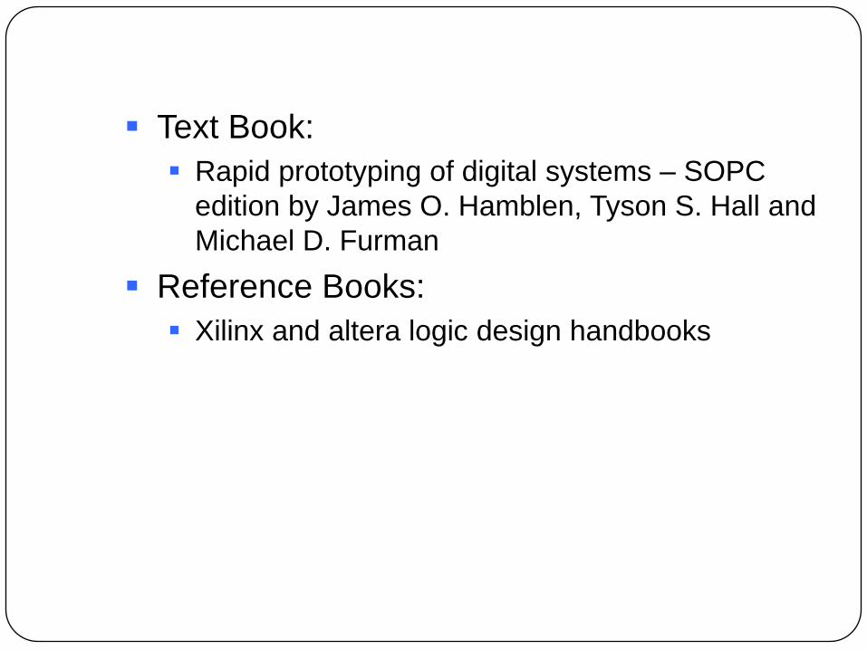
Text Book:
Rapid prototyping of digital systems – SOPC
edition by James O. Hamblen, Tyson S. Hall and
Michael D. Furman
Reference Books:
Xilinx and altera logic design handbooks
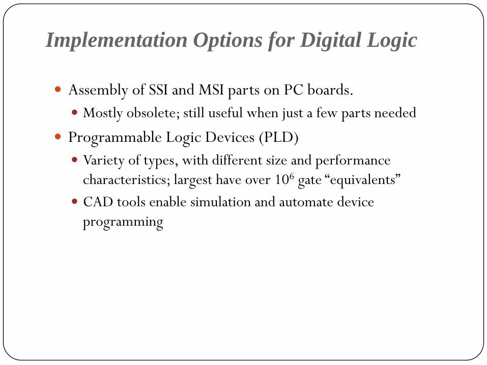
Implementation Options for Digital Logic
Assembly of SSI and MSI parts on PC boards.
Mostly obsolete; still useful when just a few parts needed
Programmable Logic Devices (PLD)
Variety of types, with different size and performance
characteristics; largest have over 106 gate “equivalents”
CAD tools enable simulation and automate device
programming
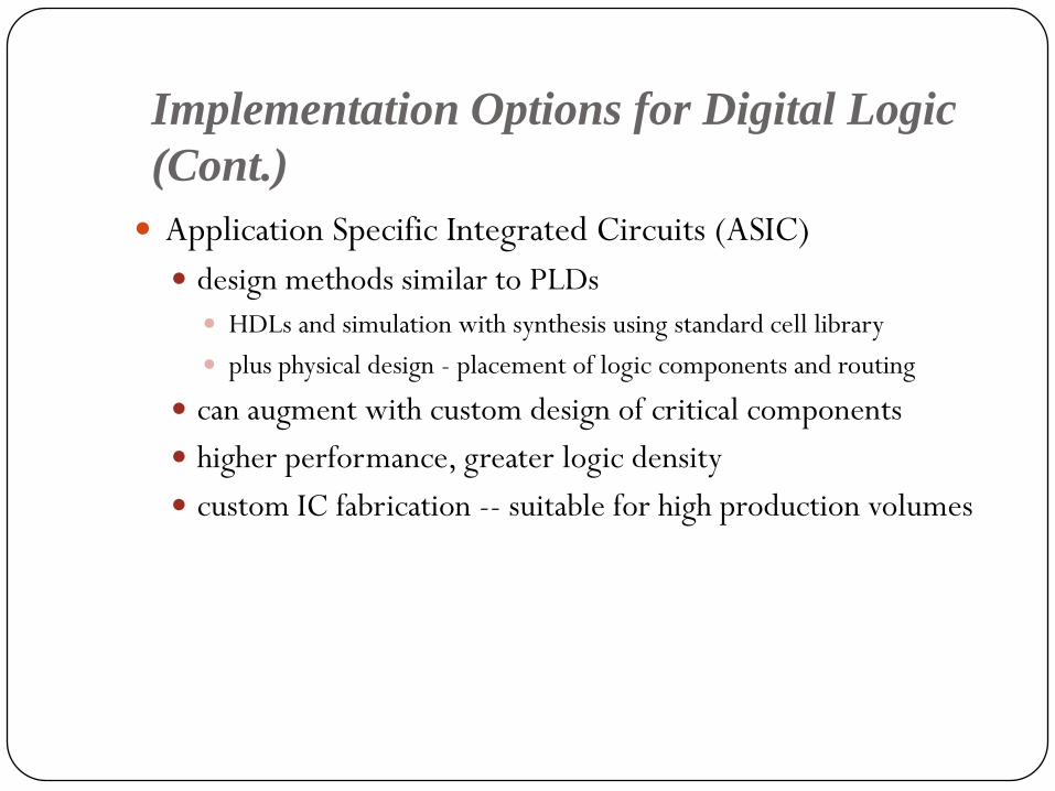
Implementation Options for Digital Logic
(Cont.)
Application Specific Integrated Circuits (ASIC)
design methods similar to PLDs
HDLs and simulation with synthesis using standard cell library
plus physical design - placement of logic components and routing
can augment with custom design of critical components
higher performance, greater logic density
custom IC fabrication -- suitable for high production volumes
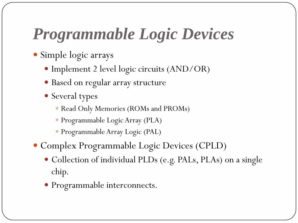
Programmable Logic Devices
Simple logic arrays
Implement 2 level logic circuits (AND/OR)
Based on regular array structure
Several types
Read Only Memories (ROMs and PROMs)
Programmable Logic Array (PLA)
Programmable Array Logic (PAL)
Complex Programmable Logic Devices (CPLD)
Collection of individual PLDs (e.g. PALs, PLAs) on a single
chip.
Programmable interconnects.
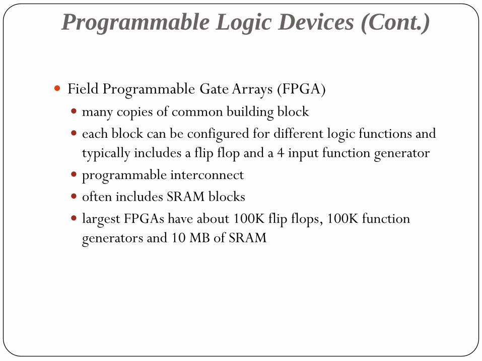
Programmable Logic Devices (Cont.)
Field Programmable Gate Arrays (FPGA)
many copies of common building block
each block can be configured for different logic functions and
typically includes a flip flop and a 4 input function generator
programmable interconnect
often includes SRAM blocks
largest FPGAs have about 100K flip flops, 100K function
generators and 10 MB of SRAM
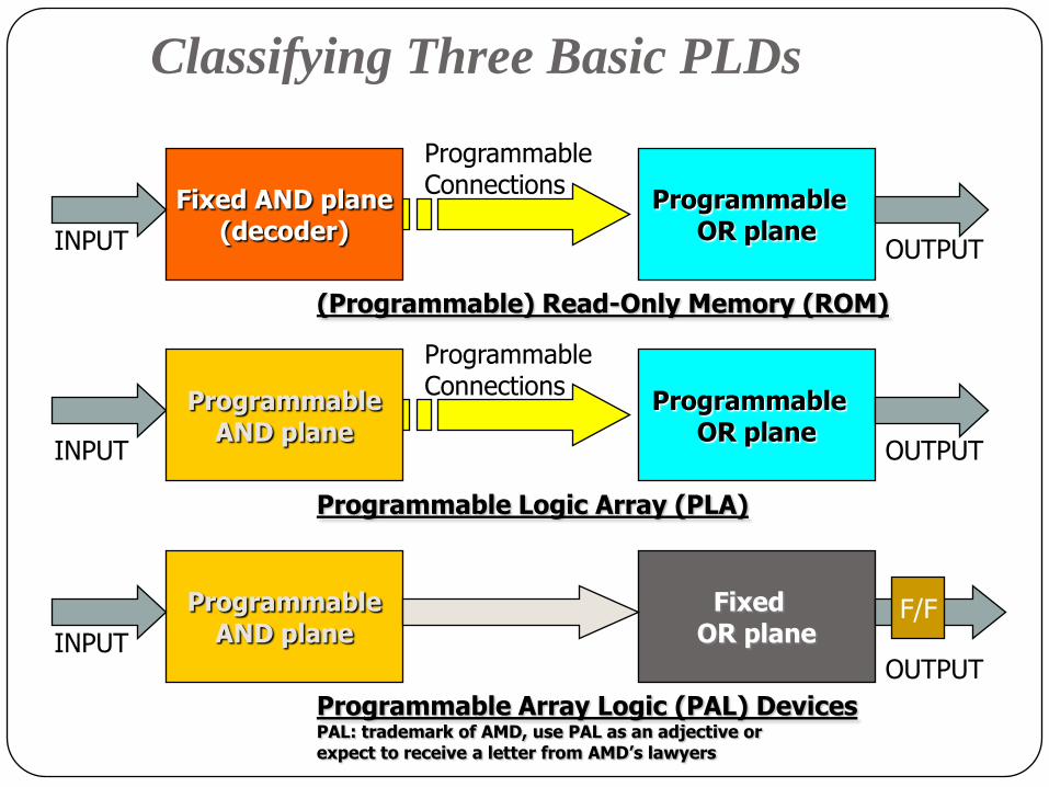
Classifying Three Basic PLDs
Fixed AND plane(decoder)
Programmable OR plane
ProgrammableConnections
(Programmable) Read-Only Memory (ROM)
INPUT OUTPUT
Programmable OR plane
ProgrammableConnections
Programmable Logic Array (PLA)
ProgrammableAND plane
INPUT OUTPUT
ProgrammableAND plane
Fixed OR plane
Programmable Array Logic (PAL) DevicesPAL: trademark of AMD, use PAL as an adjective orexpect to receive a letter from AMD’s lawyers
INPUTOUTPUT
F/F
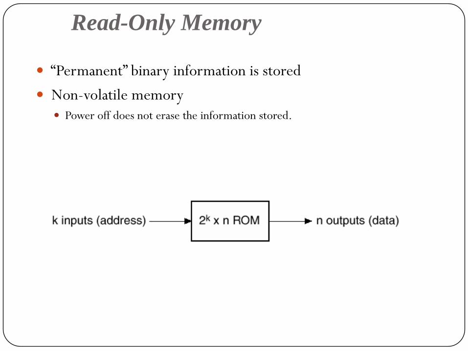
Read-Only Memory
“Permanent” binary information is stored
Non-volatile memory Power off does not erase the information stored.
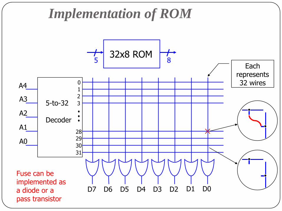
Implementation of ROM
32x8 ROM85
0
1
2
3
28
29
30
31
D7 D6 D5 D4 D3 D2 D1 D0
A4
A3
A2
A1
A0
5-to-32
Decoder
Each represents 32 wires
Fuse can beimplemented as a diode or a pass transistor
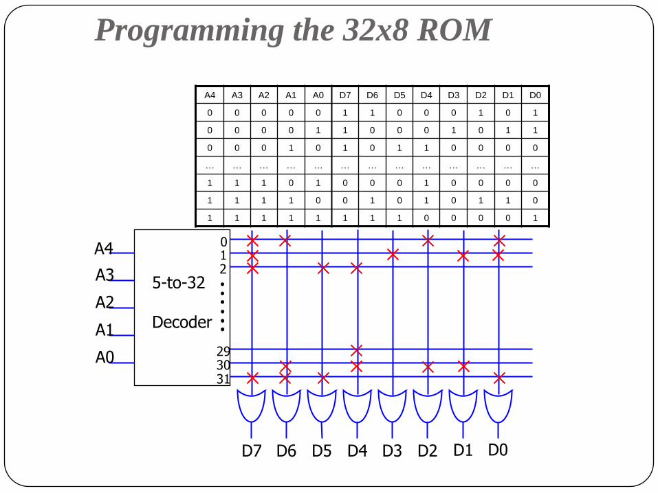
Programming the 32x8 ROM
A4 A3 A2 A1 A0 D7 D6 D5 D4 D3 D2 D1 D0
0 0 0 0 0 1 1 0 0 0 1 0 1
0 0 0 0 1 1 0 0 0 1 0 1 1
0 0 0 1 0 1 0 1 1 0 0 0 0
… … … … … … … … … … … … …
1 1 1 0 1 0 0 0 1 0 0 0 0
1 1 1 1 0 0 1 0 1 0 1 1 0
1 1 1 1 1 1 1 1 0 0 0 0 1
012
293031
D7 D6 D5 D4 D3 D2 D1 D0
A4
A3
A2
A1
A0
5-to-32
Decoder
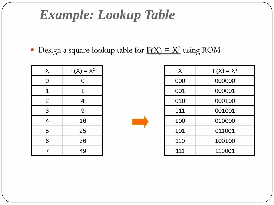
Example: Lookup Table
Design a square lookup table for F(X) = X2 using ROM
X F(X) = X2
0 0
1 1
2 4
3 9
4 16
5 25
6 36
7 49
X F(X) = X2
000 000000
001 000001
010 000100
011 001001
100 010000
101 011001
110 100100
111 110001
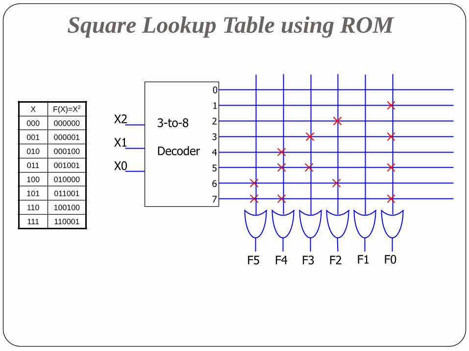
Square Lookup Table using ROM
X F(X)=X2
000 000000
001 000001
010 000100
011 001001
100 010000
101 011001
110 100100
111 110001
0
1
2
3
F5 F4 F3 F2 F1 F0
X2
X1
X0
3-to-8
Decoder 4
5
6
7
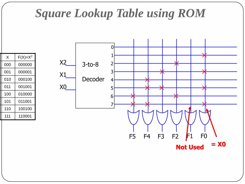
Square Lookup Table using ROM
X F(X)=X2
000 000000
001 000001
010 000100
011 001001
100 010000
101 011001
110 100100
111 110001
= X0Not Used
0
1
2
3
F5 F4 F3 F2 F1 F0
3-to-8
Decoder 4
5
6
7
X2
X1
X0
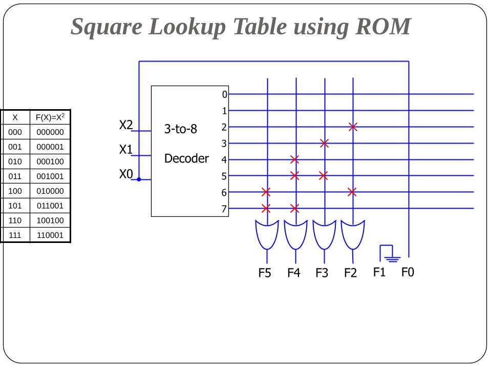
Square Lookup Table using ROM
X F(X)=X2
000 000000
001 000001
010 000100
011 001001
100 010000
101 011001
110 100100
111 110001
0
1
2
3
F5 F4 F3 F2 F0
3-to-8
Decoder 4
5
6
7
F1
X2
X1
X0
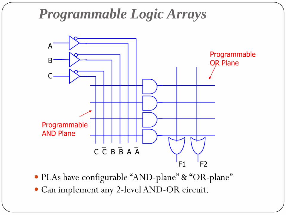
Programmable Logic Arrays
PLAs have configurable “AND-plane” & “OR-plane”
Can implement any 2-level AND-OR circuit.
C
B
A
C C B B A A
Programmable OR Plane
Programmable AND Plane
F2F1
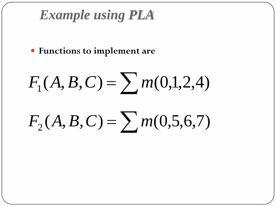
Example using PLA
Functions to implement are
)4,2,1,0(),,(1 mCBAF
)7,6,5,0(),,(2 mCBAF
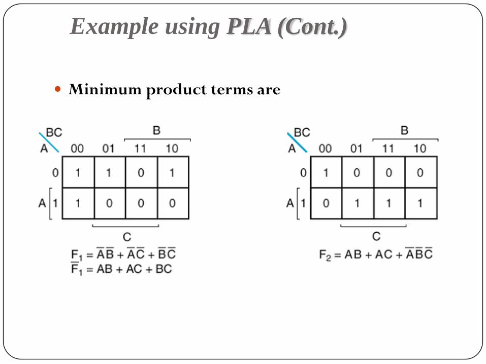
Example using PLA (Cont.)
Minimum product terms are
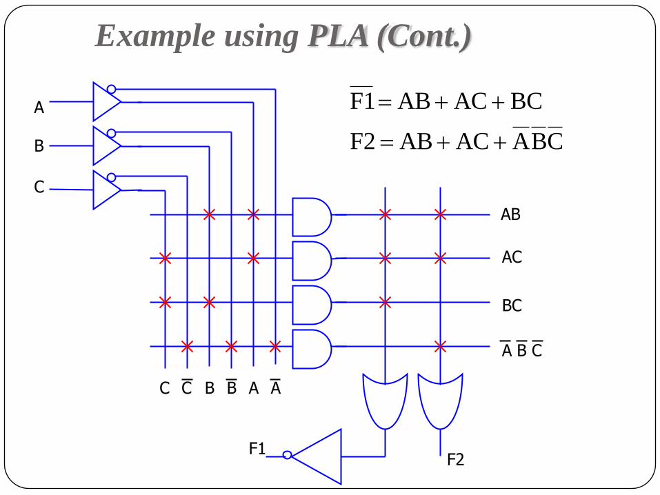
Example using PLA (Cont.)
C
B
A
C C B B A A
CBAACABF2
BCACABF1
AB
AC
BC
A B C
F2F1
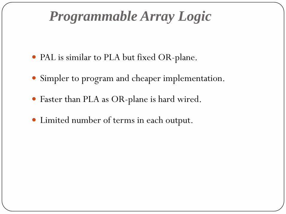
Programmable Array Logic
PAL is similar to PLA but fixed OR-plane.
Simpler to program and cheaper implementation.
Faster than PLA as OR-plane is hard wired.
Limited number of terms in each output.
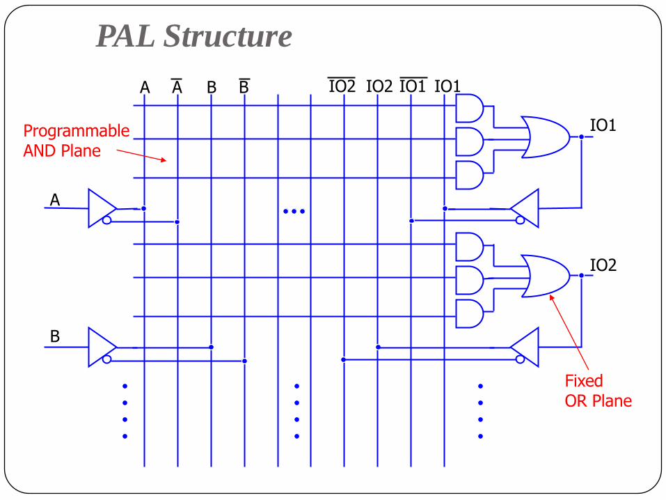
PAL Structure
A
B
IO1
IO2
B BA A
Programmable AND Plane
Fixed OR Plane
IO1 IO1IO2 IO2
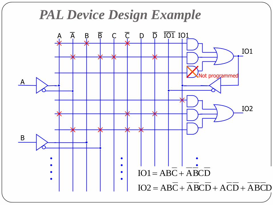
PAL Device Design Example
A
B
IO1
IO2
IO1 IO1B BA A
DCBADCADCBACABIO2
DCBACABIO1
D DC C
Not programmed
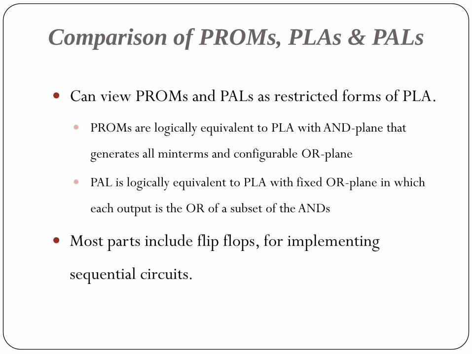
Comparison of PROMs, PLAs & PALs
Can view PROMs and PALs as restricted forms of PLA.
PROMs are logically equivalent to PLA with AND-plane that
generates all minterms and configurable OR-plane
PAL is logically equivalent to PLA with fixed OR-plane in which
each output is the OR of a subset of the ANDs
Most parts include flip flops, for implementing
sequential circuits.

Why CPLD ?
16V8 PLD (20 Pins)
can have 16 inputs (max) and/or 8 outputs
has 32 inputs to each of the AND gates
22V10 PLD (24 pins)
can have 22 inputs and/or 10 outputs (max)
has 44 inputs to each of the AND gates
How about a “128V64” for larger applications?
It will be much slower and will more wasted silicon space
Solution? Use CPLDs
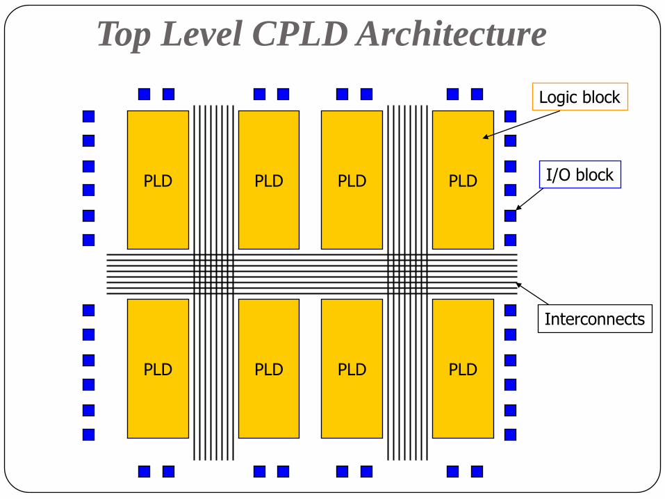
Top Level CPLD Architecture
PLD PLD PLD PLD
PLD PLD PLD PLD
Logic block
Interconnects
I/O block
Field Programmable Gate Arrays
FPGAs can be used to construct more complex circuits.
Chip contains a large number (tens of thousands) of
configurable logic building blocks.
Typically each block includes a 4 input function generator, a flip
flop and some “glue” logic.
CAD tools map high level circuit to basic blocks, configuring
function generators & other configurable elements as needed.
Field Programmable Gate Arrays
(Cont.) Programmable interconnect used to wire logic blocks. Wire segments connected to logic blocks and to other wire
segments by configurable switches.
CAD tools determine switch configuration needed to provide
right connectivity.
CAD tools perform mapping, placement, routing. Routing information used in timing analysis & simulation.
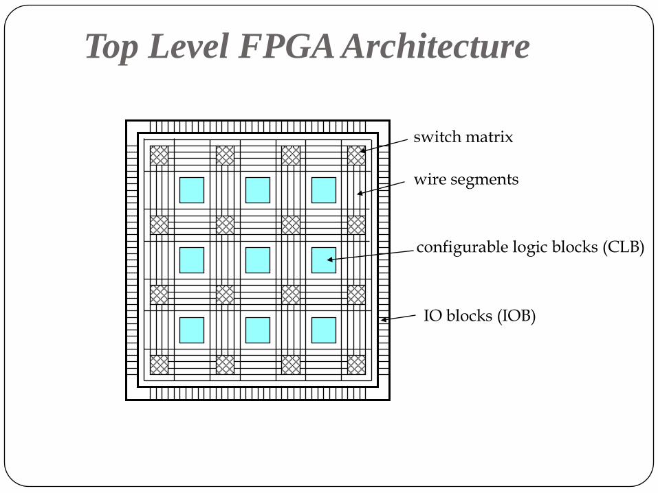
Top Level FPGA Architecture
switch matrix
wire segments
configurable logic blocks (CLB)
IO blocks (IOB)

Top Level FPGA Architecture
(Cont.)
CLBs can be connected to “passing” wires.
Wire segments connected by switch matrix.
Long wire segments used to connect distant CLBs.
Configuration information stored in SRAM bits that are
loaded when power turns on.
Copyright © 2022 FDOKUMEN