The Definitive Guide to the ARM Cortex M3 2010
447
Transcript of The Definitive Guide to the ARM Cortex M3 2010


Newnes is an imprint of Elsevier30 Corporate Drive, Suite 400Burlington, MA 01803, USA
The Boulevard, Langford LaneKidlington, Oxford, OX5 1GB, UK
© 2010 Elsevier Inc. All rights reserved.
No part of this publication may be reproduced or transmitted in any form or by any means, electronic or mechanical, including photocopying, recording, or any information storage and retrieval system, without permission in writing from the publisher. Details on how to seek permission, further information about the Publisher’s permissions policies and our arrangements with organizations such as the Copyright Clearance Center and the Copyright Licensing Agency, can be found at our website: www.elsevier.com/permissions.
This book and the individual contributions contained in it are protected under copyright by the Publisher (other than as may be noted herein).
NoticesKnowledge and best practice in this field are constantly changing. As new research and experience broaden our understanding, changes in research methods, professional practices, or medical treatment may become necessary.
Practitioners and researchers must always rely on their own experience and knowledge in evaluating and using any information, methods, compounds, or experiments described herein. In using such information or methods they should be mindful of their own safety and the safety of others, including parties for whom they have a professional responsibility.
To the fullest extent of the law, neither the Publisher nor the authors, contributors, or editors, assume any liability for any injury and/or damage to persons or property as a matter of products liability, negligence or otherwise, or from any use or operation of any methods, products, instructions, or ideas contained in the material herein.
Library of Congress Cataloging-in-Publication DataYiu, Joseph.
The definitive guide to the ARM Cortex-M3 / Joseph Yiu.p. cm.
Includes bibliographical references and index.ISBN 978-1-85617-963-8 (alk. paper)
1. Embedded computer systems. 2. Microprocessors. I. Title. TK7895.E42Y58 2010621.39’16—dc22 2009040437
British Library Cataloguing-in-Publication DataA catalogue record for this book is available from the British Library.
For information on all Academic Press publications visit our Web site at www.elsevierdirect.com
Printed in the United States09 10 11 12 13 10 9 8 7 6 5 4 3 2 1

xvii
Foreword
Progress in the ARM microcontroller community since the publication of the first edition of this book has been impressive, significantly exceeding our expectations and it is no exaggeration to say that it is revolutionizing the world of Microcontroller Units (MCUs). There are many thousands of end users of ARM-powered MCUs, making it the fastest growing MCU technology on the market. As such, the second edition of Joseph’s book is very timely and provides a good opportunity to present updated information on MCU technology.
As a community, progress has been made in many important areas including the number of com-panies building Cortex™-M3 processor-based devices (now over 30), development of the Cortex Microcontroller Software Interface Standard (CMSIS) enabling simpler code portability between Cortex processors and silicon vendors, improved versions of development tool chains, and the release of the Cortex-M0 processor to take ARM MCUs into even the lowest cost designs.
With such a rate of change it is certainly an exciting time to be developing embedded solutions based on the Cortex-M3 processor!
—Richard York
Director of Product Marketing, ARM

xviii
Foreword
Microcontroller programmers, by nature, are truly resourceful beings. From a fixed design, they create fantastic new products by using the microcontroller in a unique way. Constantly, they demand highly efficient computing from the most frugal of system designs. The primary ingredient used to perform this alchemy is the tool chain environment, and it is for this reason that engineers from ARM’s own tool chain division joined forces with CPU designers to form a team that would rationalize, simplify, and improve the ARM7TDMI processor design.
The result of this combination, the ARM Cortex™-M3, represents an exciting development to the original ARM architecture. The device blends the best features from the 32-bit ARM architecture with the highly successful Thumb-2 instruction set design while adding several new capabilities. Despite these changes, the Cortex-M3 retains a simplified programmer’s model that will be easily recognizable to all existing ARM aficionados.
—Wayne Lyons
Director of Embedded Solutions, ARM

xix
Preface
This book is for both hardware and software engineers who are interested in the ARM Cortex™-M3 processor. The Cortex-M3 Technical Reference Manual (TRM) and the ARMv7-M Architecture Appli-cation Level Reference Manual already provide lots of information on this processor, but they are very detailed and can be challenging for novice readers.
This book is intended to be a lighter read for programmers, embedded product designers, system-on-chip (SoC) engineers, electronics enthusiasts, academic researchers, and others who are investigat-ing the Cortex-M3 processor, with some experience of microcontrollers or microprocessors. The text includes an introduction to the architecture, an instruction set summary, examples of some instruc-tions, information on hardware features, and an overview of the processor’s advanced debug system. It also provides application examples, including basic steps in software development for the Cortex-M3 processor using ARM tools as well as the Gnu’s Not Unix tool chain. This book is also suitable for engineers who are migrating their software from ARM7TDMI to the Cortex-M3 processor because it covers the differences between the two processors, and the porting of application software from the ARM7TDMI to the Cortex-M3.
AcknowledgmentsI would like to thank the following people for providing me with help, advice, and feedback to the first or the second edition of this book:
Richard York, Andrew Frame, Reinhard Keil, Nick Sampays, Dev Banerjee, Robert Boys, Domi-nic Pajak, Alan Tringham, Stephen Theobald, Dan Brook, David Brash, Haydn Povey, Gary Camp-bell, Kevin McDermott, Richard Earnshaw, Shyam Sadasivan, Simon Craske, Simon Axford, Takashi Ugajin, Wayne Lyons, Samin Ishtiaq, and Simon Smith.
I would like to thank Ian Bell and Jamie Brettle at National Instruments for their help in reviewing the materials covering NI LabVIEW and for their support. I would also like to express my gratitude to Carlos O’Donell, Brian Barrera, and Daniel Jacobowitz from CodeSourcery for their support and help in reviewing the materials covering software development with the CodeSourcery tool chain. And, of course, thanks to the staff at Elsevier for their professional work toward the publication of this book.
Finally, a special thank-you to Peter Cole and Ivan Yardley for their continuous support and advice during this project.

xx
Conventions
Various typographical conventions have been used in this book, as follows:
Normal assembly program codes:• MOV R0, R1; Move data from Register R1 to Register R0
Assembly code in generalized syntax; items inside < > must be replaced by real register names:• MRS <reg>, <special_reg>
C program codes:• for (i=0;i<3;i++) { func1(); }
Pseudocode:• if (a > b) { ...
Values:• 4’hC, 0x123 are both hexadecimal values1. 2. #3 indicates item number 3 (e.g., IRQ #3 means IRQ number 3) 3. #immed_12 refers to 12-bit immediate data
Register bits:•Typically used to illustrate a part of a value based on bit position; for example, bit[15:12] meansbit number 15 down to 12.
Register access types are as follows:• R is Read only1. W is Write only2. R/W is Read or Write accessible3. R/Wc is Readable and clear by a Write access4.
xxi
Terms and Abbreviations
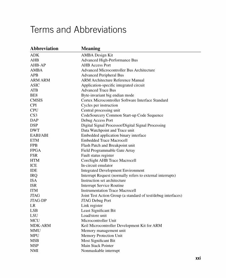
Abbreviation MeaningADK AMBA Design KitAHB Advanced High-Performance BusAHB-AP AHB Access PortAMBA Advanced Microcontroller Bus ArchitectureAPB Advanced Peripheral BusARM ARM ARM Architecture Reference ManualASIC Application-specific integrated circuitATB Advanced Trace BusBE8 Byte-invariant big endian modeCMSIS Cortex Microcontroller Software Interface StandardCPI Cycles per instructionCPU Central processing unitCS3 CodeSourcery Common Start-up Code SequenceDAP Debug Access PortDSP Digital Signal Processor/Digital Signal ProcessingDWT Data Watchpoint and Trace unitEABI/ABI Embedded application binary interfaceETM Embedded Trace MacrocellFPB Flash Patch and Breakpoint unitFPGA Field Programmable Gate ArrayFSR Fault status registerHTM CoreSight AHB Trace MacrocellICE In-circuit emulatorIDE Integrated Development EnvironmentIRQ Interrupt Request (normally refers to external interrupts)ISA Instruction set architectureISR Interrupt Service RoutineITM Instrumentation Trace MacrocellJTAG Joint Test Action Group (a standard of test/debug interfaces)JTAG-DP JTAG Debug PortLR Link registerLSB Least Significant BitLSU Load/store unitMCU Microcontroller UnitMDK-ARM Keil Microcontroller Development Kit for ARMMMU Memory management unitMPU Memory Protection UnitMSB Most Significant BitMSP Main Stack PointerNMI Nonmaskable interrupt

xxii Terms and Abbreviations
NVIC Nested Vectored Interrupt ControllerOS Operating systemPC Program counterPMU Power management unitPSP Process Stack PointerPPB Private Peripheral BusPSR Program Status RegisterSCB System control blockSCS System control spaceSIMD Single Instruction, Multiple DataSoC System-on-ChipSP Stack pointerSRPG State retention power gatingSW Serial-WireSW-DP Serial-Wire Debug PortSWJ-DP Serial-Wire JTAG Debug PortSWV Serial-Wire Viewer (an operation mode of TPIU)TCM Tightly coupled memory (Cortex-M1 feature)TPA Trace Port AnalyzerTPIU Trace Port Interface UnitTRM Technical Reference ManualUAL Unified Assembly LanguageUART Universal Asynchronous Receiver TransmitterWIC Wakeup Interrupt Controller

1Copyright © 2010, Elsevier Inc. All rights reserved.DOI: 10.1016/B978-1-85617-963-8.00004-1
In ThIs ChapTer
What Is the arM Cortex-M3 processor? ..................................................................................................... 1Background of arM and arM architecture ................................................................................................ 2Instruction set Development ...................................................................................................................... 7The Thumb-2 Technology and Instruction set architecture .......................................................................... 8Cortex-M3 processor applications ............................................................................................................. 9Organization of This Book ....................................................................................................................... 10Further reading ...................................................................................................................................... 10
CHAPTER
Introduction 1
1.1 WhaT Is The arM COrTex-M3 prOCessOr?The microcontroller market is vast, with more than 20 billion devices per year estimated to be shipped in 2010. A bewildering array of vendors, devices, and architectures is competing in this market. The requirement for higher performance microcontrollers has been driven globally by the industry’s chang-ing needs; for example, microcontrollers are required to handle more work without increasing a prod-uct’s frequency or power. In addition, microcontrollers are becoming increasingly connected, whether by Universal Serial Bus (USB), Ethernet, or wireless radio, and hence, the processing needed to support these communication channels and advanced peripherals are growing. Similarly, general application complexity is on the increase, driven by more sophisticated user interfaces, multimedia requirements, system speed, and convergence of functionalities.
The ARM Cortex™-M3 processor, the first of the Cortex generation of processors released by ARM in 2006, was primarily designed to target the 32-bit microcontroller market. The Cortex-M3 processor provides excellent performance at low gate count and comes with many new features previously avail-able only in high-end processors. The Cortex-M3 addresses the requirements for the 32-bit embedded processor market in the following ways:
• Greater performance efficiency: allowing more work to be done without increasing the frequency or power requirements
• Low power consumption: enabling longer battery life, especially critical in portable products including wireless networking applications

2 CHAPTER 1 Introduction
• Enhanced determinism: guaranteeing that critical tasks and interrupts are serviced as quickly as possible and in a known number of cycles
• Improved code density: ensuring that code fits in even the smallest memory footprints• Ease of use: providing easier programmability and debugging for the growing number of 8-bit and
16-bit users migrating to 32 bits• Lower cost solutions: reducing 32-bit-based system costs close to those of legacy 8-bit and 16-bit
devices and enabling low-end, 32-bit microcontrollers to be priced at less than US$1 for the first time• Wide choice of development tools: from low-cost or free compilers to full-featured development
suites from many development tool vendors
Microcontrollers based on the Cortex-M3 processor already compete head-on with devices based on a wide variety of other architectures. Designers are increasingly looking at reducing the system cost, as opposed to the traditional device cost. As such, organizations are implementing device aggregation, whereby a single, more powerful device can potentially replace three or four traditional 8-bit devices.
Other cost savings can be achieved by improving the amount of code reuse across all systems. Because Cortex-M3 processor-based microcontrollers can be easily programmed using the C language and are based on a well-established architecture, application code can be ported and reused easily, reducing development time and testing costs.
It is worthwhile highlighting that the Cortex-M3 processor is not the first ARM processor to be used to create generic microcontrollers. The venerable ARM7 processor has been very successful in this market, with partners such as NXP (Philips), Texas Instruments, Atmel, OKI, and many other vendors delivering robust 32-bit Microcontroller Units (MCUs). The ARM7 is the most widely used 32-bit embedded processor in history, with over 1 billion processors produced each year in a huge variety of electronic products, from mobile phones to cars.
The Cortex-M3 processor builds on the success of the ARM7 processor to deliver devices that are significantly easier to program and debug and yet deliver a higher processing capability. Additionally, the Cortex-M3 processor introduces a number of features and technologies that meet the specific requirements of the microcontroller applications, such as nonmaskable interrupts for critical tasks, highly deterministic nested vector interrupts, atomic bit manipulation, and an optional Memory Protec-tion Unit (MPU). These factors make the Cortex-M3 processor attractive to existing ARM processor users as well as many new users considering use of 32-bit MCUs in their products.
1.2 BaCkgrOunD OF arM anD arM arChITeCTure1.2.1 a Brief historyTo help you understand the variations of ARM processors and architecture versions, let’s look at a little bit of ARM history.
ARM was formed in 1990 as Advanced RISC Machines Ltd., a joint venture of Apple Computer, Acorn Computer Group, and VLSI Technology. In 1991, ARM introduced the ARM6 processor family, and VLSI became the initial licensee. Subsequently, additional companies, including Texas Instru-ments, NEC, Sharp, and ST Microelectronics, licensed the ARM processor designs, extending the applications of ARM processors into mobile phones, computer hard disks, personal digital assistants (PDAs), home entertainment systems, and many other consumer products.

3
Nowadays, ARM partners ship in excess of 2 billion ARM processors each year. Unlike many semiconductor companies, ARM does not manufacture processors or sell the chips directly. Instead, ARM licenses the processor designs to business partners, including a majority of the world’s leading semiconductor companies. Based on the ARM low-cost and power-efficient processor designs, these partners create their processors, microcontrollers, and system-on-chip solutions. This business model is commonly called intellectual property (IP) licensing.
In addition to processor designs, ARM also licenses systems-level IP and various software IPs. To support these products, ARM has developed a strong base of development tools, hardware, and software products to enable partners to develop their own products.
1.2.2 architecture VersionsOver the years, ARM has continued to develop new processors and system blocks. These include the popular ARM7TDMI processor and, more recently, the ARM1176TZ(F)-S processor, which is used in high-end applications such as smart phones. The evolution of features and enhancements to the processors over time has led to successive versions of the ARM architecture. Note that architecture version numbers are independent from processor names. For example, the ARM7TDMI processor is based on the ARMv4T architecture (the T is for Thumb® instruction mode support).
The COrTex-M3 prOCessOr Versus COrTex-M3-BaseD MCusThe Cortex-M3 processor is the central processing unit (CPU) of a microcontroller chip. In addition, a number of other components are required for the whole Cortex-M3 processor-based microcontroller. After chip manufacturers license the Cortex-M3 processor, they can put the Cortex-M3 processor in their silicon designs, adding memory, peripherals, input/output (I/O), and other features. Cortex-M3 processor-based chips from different manufacturers will have different memory sizes, types, peripherals, and features. This book focuses on the architecture of the processor core. For details about the rest of the chip, readers are advised to check the particular chip manufacturer’s documentation.
1.2 Background of ARM and ARM Architecture
FIgure 1.1
The Cortex-M3 Processor versus the Cortex-M3-Based MCU.
Cortex-M3core
Debugsystem
MemoryPeripherals
Internal bus
Clock andreset
I/O
Cortex-M3 chip Developed byARM
Developed bychip
manufacturersDeveloped byARM, designhouses, chip
manufacturers

4 CHAPTER 1 Introduction
The ARMv5E architecture was introduced with the ARM9E processor families, including the ARM926E-S and ARM946E-S processors. This architecture added “Enhanced” Digital Signal Processing (DSP) instructions for multimedia applications.
With the arrival of the ARM11 processor family, the architecture was extended to the ARMv6. New features in this architecture included memory system features and Single Instruction–Multiple Data (SIMD) instructions. Processors based on the ARMv6 architecture include the ARM1136J(F)-S, the ARM1156T2(F)-S, and the ARM1176JZ(F)-S.
Following the introduction of the ARM11 family, it was decided that many of the new technologies, such as the optimized Thumb-2 instruction set, were just as applicable to the lower cost markets of micro-controller and automotive components. It was also decided that although the architecture needed to be con-sistent from the lowest MCU to the highest performance application processor, there was a need to deliver processor architectures that best fit applications, enabling very deterministic and low gate count processors for cost-sensitive markets and feature-rich and high-performance ones for high-end applications.
Over the past several years, ARM extended its product portfolio by diversifying its CPU develop-ment, which resulted in the architecture version 7 or v7. In this version, the architecture design is divided into three profiles:
The • A profile is designed for high-performance open application platforms.The • R profile is designed for high-end embedded systems in which real-time performance is needed.The • M profile is designed for deeply embedded microcontroller-type systems.
Let’s look at these profiles in a bit more detail:
• A Profile (ARMv7-A): Application processors which are designed to handle complex applications such as high-end embedded operating systems (OSs) (e.g., Symbian, Linux, and Windows Embedded). These processors requiring the highest processing power, virtual memory system support with memory management units (MMUs), and, optionally, enhanced Java support and a secure program execution environment. Example products include high-end mobile phones and electronic wallets for financial transactions.
• R Profile (ARMv7-R): Real-time, high-performance processors targeted primarily at the higher end of the real-time1 market—those applications, such as high-end breaking systems and hard drive controllers, in which high processing power and high reliability are essential and for which low latency is important.
• M Profile (ARMv7-M): Processors targeting low-cost applications in which processing efficiency is important and cost, power consumption, low interrupt latency, and ease of use are critical, as well as industrial control applications, including real-time control systems.
The Cortex processor families are the first products developed on architecture v7, and the Cortex-M3 processor is based on one profile of the v7 architecture, called ARM v7-M, an architecture specification for microcontroller products.
1 There is always great debate as to whether we can have a “real-time” system using general processors. By definition, “real time” means that the system can get a response within a guaranteed period. In any processor-based system, you may or may not be able to get this response due to choice of OS, interrupt latency, or memory latency, as well as if the CPU is running a higher priority interrupt.

51.2 Background of ARM and ARM Architecture
This book focuses on the Cortex-M3 processor, but it is only one of the Cortex product families that use the ARMv7 architecture. Other Cortex family processors include the Cortex-A8 (application processor), which is based on the ARMv7-A profile, and the Cortex-R4 (real-time processor), which is based on the ARMv7-R profile (see Figure 1.2).
The details of the ARMv7-M architecture are documented in The ARMv7-M Architecture Applica-tion Level Reference Manual [Ref. 2]. This document can be obtained via the ARM web site through a simple registration process. The ARMv7-M architecture contains the following key areas:
Programmer’s model•Instruction set•Memory model•Debug architecture•
Processor-specific information, such as interface details and timing, is documented in the Cortex-M3 Technical Reference Manual (TRM) [Ref. 1]. This manual can be accessed freely on the ARM web site. The Cortex-M3 TRM also covers a number of implementation details not covered by the architec-ture specifications, such as the list of supported instructions, because some of the instructions covered in the ARMv7-M architecture specification are optional on ARMv7-M devices.
1.2.3 processor namingTraditionally, ARM used a numbering scheme to name processors. In the early days (the 1990s), suffixes were also used to indicate features on the processors. For example, with the ARM7TDMI processor, the T indicates Thumb instruction support, D indicates JTAG debugging, M indicates fast multiplier, and I indicates an embedded ICE module. Subsequently, it was decided that these features should become standard features of future ARM processors; therefore, these suffixes are no longer added to the new
FIgure 1.2
The Evolution of ARM Processor Architecture.
ARM7TDMI,920T,
Intel StrongARM
Architecturev4/v4T
Examples
Architecture v7
v7-A (application)e.g., Cortex-A8
v7-R (real-time)e.g., Cortex-R4
v7-M (microcontroller)e.g., Cortex-M3
Architecturev5/v5E
ARM926, 946,966,
Intel XScale
Architecture v6
ARM1136, 1176,1156T-2
Cortex-M0,Cortex-M1 (FPGA)
Architecture v6-M

6 CHAPTER 1 Introduction
processor family names. Instead, variations on memory interface, cache, and tightly coupled memory (TCM) have created a new scheme for processor naming.
For example, ARM processors with cache and MMUs are now given the suffix “26” or “36,” whereas processors with MPUs are given the suffix “46” (e.g., ARM946E-S). In addition, other suf-fixes are added to indicate synthesizable2 (S) and Jazelle (J) technology. Table 1.1 presents a summary of processor names.
With version 7 of the architecture, ARM has migrated away from these complex numbering schemes that needed to be decoded, moving to a consistent naming for families of processors, with Cortex its initial brand. In addition to illustrating the compatibility across processors, this system removes confu-sion between architectural version and processor family number; for example, the ARM7TDMI is not a v7 processor but was based on the v4T architecture.
2A synthesizable core design is available in the form of a hardware description language (HDL) such as Verilog or VHDL and can be converted into a design netlist using synthesis software.
Table 1.1 ARM Processor Names
Processor Name Architecture VersionMemory Management Features Other Features
ARM7TDMI ARMv4TARM7TDMI-S ARMv4TARM7EJ-S ARMv5E DSP, JazelleARM920T ARMv4T MMUARM922T ARMv4T MMUARM926EJ-S ARMv5E MMU DSP, JazelleARM946E-S ARMv5E MPU DSPARM966E-S ARMv5E DSPARM968E-S ARMv5E DMA, DSPARM966HS ARMv5E MPU (optional) DSPARM1020E ARMv5E MMU DSPARM1022E ARMv5E MMU DSPARM1026EJ-S ARMv5E MMU or MPU DSP, JazelleARM1136J(F)-S ARMv6 MMU DSP, JazelleARM1176JZ(F)-S ARMv6 MMU + TrustZone DSP, JazelleARM11 MPCore ARMv6 MMU + multiprocessor cache
supportDSP, Jazelle
ARM1156T2(F)-S ARMv6 MPU DSPCortex-M0 ARMv6-M NVICCortex-M1 ARMv6-M FPGA TCM interface NVICCortex-M3 ARMv7-M MPU (optional) NVIC

71.3 Instruction Set Development
1.3 InsTruCTIOn seT DeVelOpMenTEnhancement and extension of instruction sets used by the ARM processors has been one of the key driving forces of the architecture’s evolution (see Figure 1.3).
Historically (since ARM7TDMI), two different instruction sets are supported on the ARM processor: the ARM instructions that are 32 bits and Thumb instructions that are 16 bits. During program execution, the processor can be dynamically switched between the ARM state and the Thumb state to use either
Table 1.1 ARM Processor Names Continued
Processor Name Architecture VersionMemory Management Features Other Features
Cortex-R4 ARMv7-R MPU DSPCortex-R4F ARMv7-R MPU DSP + Floating
pointCortex-A8 ARMv7-A MMU + TrustZone DSP, Jazelle,
NEON + floating point
Cortex-A9 ARMv7-A MMU + TrustZone + multiprocessor
DSP, Jazelle, NEON + floating point
FIgure 1.3
Instruction Set Enhancement.
v4
ARM
Thumb
v5 v5E v6
EnhancedDSP
instructionsadded
SIMD, v6memorysupportadded
v7
Architecture development
Thumbinstructionsintroduced
Thumb-2technologyintroduced
v4T

8 CHAPTER 1 Introduction
one of the instruction sets. The Thumb instruction set provides only a subset of the ARM instructions, but it can provide higher code density. It is useful for products with tight memory requirements.
As the architecture version has been updated, extra instructions have been added to both ARM instructions and Thumb instructions. Appendix B provides some information on the change of Thumb instructions during the architecture enhancements. In 2003, ARM announced the Thumb-2 instruction set, which is a new superset of Thumb instructions that contains both 16-bit and 32-bit instructions.
The details of the instruction set are provided in a document called The ARM Architecture Reference Man-ual (also known as the ARM ARM). This manual has been updated for the ARMv5 architecture, the ARMv6 architecture, and the ARMv7 architecture. For the ARMv7 architecture, due to its growth into different pro-files, the specification is also split into different documents. For the Cortex-M3 instruction set, the complete details are specified in the ARM v7-M Architecture Application Level Reference Manual [Ref. 2]. Appendix A of this book also covers information regarding instruction sets required for software development.
1.4 The ThuMB-2 TeChnOlOgy anD InsTruCTIOn seT arChITeCTure
The Thumb-23 technology extended the Thumb Instruction Set Architecture (ISA) into a highly efficient and powerful instruction set that delivers significant benefits in terms of ease of use, code size, and per-formance (see Figure 1.4). The extended instruction set in Thumb-2 is a superset of the previous 16-bit Thumb instruction set, with additional 16-bit instructions alongside 32-bit instructions. It allows more complex operations to be carried out in the Thumb state, thus allowing higher efficiency by reducing the number of states switching between ARM state and Thumb state.
Focused on small memory system devices such as microcontrollers and reducing the size of the proces-sor, the Cortex-M3 supports only the Thumb-2 (and traditional Thumb) instruction set. Instead of using ARM instructions for some operations, as in traditional ARM processors, it uses the Thumb-2 instruction set for all operations. As a result, the Cortex-M3 processor is not backward compatible with traditional
3 Thumb and Thumb-2 are registered trademarks of ARM.
FIgure 1.4
The Relationship between the Thumb Instruction Set in Thumb-2 Technology and the Traditional Thumb.
Thumbinstructions
(16 bits)
Thumb-2 technology32-bit and 16-bit
Thumb instruction set
Cortex-M3
ARMv7-Marchitecture

91.5 Cortex-M3 Processor Applications
ARM processors. That is, you cannot run a binary image for ARM7 processors on the Cortex-M3 processor. Nevertheless, the Cortex-M3 processor can execute almost all the 16-bit Thumb instructions, including all 16-bit Thumb instructions supported on ARM7 family processors, making application porting easy.
With support for both 16-bit and 32-bit instructions in the Thumb-2 instruction set, there is no need to switch the processor between Thumb state (16-bit instructions) and ARM state (32-bit instructions). For example, in ARM7 or ARM9 family processors, you might need to switch to ARM state if you want to carry out complex calculations or a large number of conditional operations and good performance is needed, whereas in the Cortex-M3 processor, you can mix 32-bit instructions with 16-bit instructions without switching state, getting high code density and high performance with no extra complexity.
The Thumb-2 instruction set is a very important feature of the ARMv7 architecture. Compared with the instructions supported on ARM7 family processors (ARMv4T architecture), the Cortex-M3 processor instruction set has a large number of new features. For the first time, hardware divide instruc-tion is available on an ARM processor, and a number of multiply instructions are also available on the Cortex-M3 processor to improve data-crunching performance. The Cortex-M3 processor also supports unaligned data accesses, a feature previously available only in high-end processors.
1.5 COrTex-M3 prOCessOr applICaTIOnsWith its high performance and high code density and small silicon footprint, the Cortex-M3 processor is ideal for a wide variety of applications:
• Low-cost microcontrollers: The Cortex-M3 processor is ideally suited for low-cost microcontrollers, which are commonly used in consumer products, from toys to electrical appliances. It is a highly competitive market due to the many well-known 8-bit and 16-bit microcontroller products on the market. Its lower power, high performance, and ease-of-use advantages enable embedded developers to migrate to 32-bit systems and develop products with the ARM architecture.
• Automotive: Another ideal application for the Cortex-M3 processor is in the automotive industry. The Cortex-M3 processor has very high-performance efficiency and low interrupt latency, allowing it to be used in real-time systems. The Cortex-M3 processor supports up to 240 external vectored interrupts, with a built-in interrupt controller with nested interrupt supports and an optional MPU, making it ideal for highly integrated and cost-sensitive automotive applications.
Data communications• : The processor’s low power and high efficiency, coupled with instructions in Thumb-2 for bit-field manipulation, make the Cortex-M3 ideal for many communications applications, such as Bluetooth and ZigBee.
• Industrial control: In industrial control applications, simplicity, fast response, and reliability are key factors. Again, the Cortex-M3 processor’s interrupt feature, low interrupt latency, and enhanced fault-handling features make it a strong candidate in this area.
• Consumer products: In many consumer products, a high-performance microprocessor (or several of them) is used. The Cortex-M3 processor, being a small processor, is highly efficient and low in power and supports an MPU enabling complex software to execute while providing robust memory protection.
There are already many Cortex-M3 processor-based products on the market, including low-end products priced as low as US$1, making the cost of ARM microcontrollers comparable to or lower than that of many 8-bit microcontrollers.
10 CHAPTER 1 Introduction
1.6 OrganIzaTIOn OF ThIs BOOkThis book contains a general overview of the Cortex-M3 processor, with the rest of the contents divided into a number of sections:
• Chapters 1 and 2, Introduction and Overview of the Cortex-M3• Chapters 3 through 6, Cortex-M3 Basics• Chapters 7 through 9, Exceptions and Interrupts• Chapters 10 and 11, Cortex-M3 Programming• Chapters 12 through 14, Cortex-M3 Hardware Features• Chapters 15 and 16, Debug Supports in Cortex-M3• Chapters 17 through 21, Application Development with Cortex-M3
Appendices•
1.7 FurTher reaDIngThis book does not contain all the technical details on the Cortex-M3 processor. It is intended to be a starter guide for people who are new to the Cortex-M3 processor and a supplemental reference for people using Cortex-M3 processor-based microcontrollers. To get further detail on the Cortex-M3 processor, the following documents, available from ARM (www.arm.com) and ARM partner web sites, should cover most necessary details:
• The Cortex-M3 Technical Reference Manual (TRM) [Ref. 1] provides detailed information about the processor, including programmer’s model, memory map, and instruction timing.
• The ARMv7-M Architecture Application Level Reference Manual [Ref. 2] contains detailed information about the instruction set and the memory model.
Refer to datasheets for the Cortex-M3 processor-based microcontroller products; visit the manufacturer •web site for the datasheets on the Cortex-M3 processor-based product you plan to use.
• Cortex-M3 User Guides are available from MCU vendors. In some cases, this user guide is available as a part of a complete microcontroller product manual. This document contains a programmer’s model for the ARM Cortex-M3 processor, and instruction set details, and is customized by each MCU vendors to match their microcontroller implementations.
Refer to • AMBA Specification 2.0 [Ref. 4] for more detail regarding internal AMBA interface bus protocol details.
C programming tips for Cortex-M3 can be found in the • ARM Application Note 179: Cortex-M3 Embedded Software Development [Ref. 7].
This book assumes that you already have some knowledge of and experience with embedded programming, preferably using ARM processors. If you are a manager or a student who wants to learn the basics without spending too much time reading the whole book or the TRM, Chapter 2 of this book is a good one to read because it provides a summary on the Cortex-M3 processor.

11
CHAPTER
Copyright © 2010, Elsevier Inc. All rights reserved.DOI: 10.1016/B978-1-85617-963-8.00005-3
In ThIs ChapTer
Fundamentals ������������������������������������������������������������������������������������������������������������������������������������������11registers �������������������������������������������������������������������������������������������������������������������������������������������������12Operation Modes �������������������������������������������������������������������������������������������������������������������������������������14The Built-In nested Vectored Interrupt Controller ��������������������������������������������������������������������������������������15The Memory Map �������������������������������������������������������������������������������������������������������������������������������������16The Bus Interface ������������������������������������������������������������������������������������������������������������������������������������17The MpU �������������������������������������������������������������������������������������������������������������������������������������������������18The Instruction set ����������������������������������������������������������������������������������������������������������������������������������18Interrupts and exceptions �������������������������������������������������������������������������������������������������������������������������19Debugging support ��������������������������������������������������������������������������������������������������������������������������������� 21Characteristics summary ������������������������������������������������������������������������������������������������������������������������ 22
Overview of the Cortex-M3 2
2�1 FUnDaMenTalsThe Cortex™-M3 is a 32-bit microprocessor. It has a 32-bit data path, a 32-bit register bank, and 32-bit memory interfaces (see Figure 2.1). The processor has a Harvard architecture, which means that it has a separate instruction bus and data bus. This allows instructions and data accesses to take place at the same time, and as a result of this, the performance of the processor increases because data accesses do not affect the instruction pipeline. This feature results in multiple bus interfaces on Cortex-M3, each with optimized usage and the ability to be used simultaneously. However, the instruction and data buses share the same memory space (a unified memory system). In other words, you cannot get 8 GB of memory space just because you have separate bus interfaces.
For complex applications that require more memory system features, the Cortex-M3 processor has an optional Memory Protection Unit (MPU), and it is possible to use an external cache if it’s required. Both little endian and big endian memory systems are supported.
The Cortex-M3 processor includes a number of fixed internal debugging components. These components provide debugging operation supports and features, such as breakpoints and watchpoints.

12 CHAPTER 2 Overview of the Cortex-M3
In addition, optional components provide debugging features, such as instruction trace, and various types of debugging interfaces.
2�2 regIsTersThe Cortex-M3 processor has registers R0 through R15 (see Figure 2.2). R13 (the stack pointer) is banked, with only one copy of the R13 visible at a time.
2�2�1 r0–r12: general-purpose registersR0–R12 are 32-bit general-purpose registers for data operations. Some 16-bit Thumb® instructions can only access a subset of these registers (low registers, R0–R7).
2�2�2 r13: stack pointersThe Cortex-M3 contains two stack pointers (R13). They are banked so that only one is visible at a time. The two stack pointers are as follows:
• Main Stack Pointer (MSP): The default stack pointer, used by the operating system (OS) kernel and exception handlers
• Process Stack Pointer (PSP): Used by user application code
The lowest 2 bits of the stack pointers are always 0, which means they are always word aligned.
FIgUre 2�1
A Simplified View of the Cortex-M3.
Memory interface
Registerbank
ALUInst
ruct
ion
fetc
h un
it
Dec
oder
Inte
rrup
t con
trol
ler
(NV
IC)
Memoryprotection
unit
Memory systemand peripherals
Cortex-M3
Processor core system
Interrupts
Debug
Trace
Instruction bus
Tra
ce in
terf
ace
Bus interconnect
Optional
Debuginterface
Debugsystem
Privateperipherals
Codememory
Data bus

132.2 Registers
2�2�3 r14: The link registerWhen a subroutine is called, the return address is stored in the link register.
2�2�4 r15: The program CounterThe program counter is the current program address. This register can be written to control the program flow.
2�2�5 special registersThe Cortex-M3 processor also has a number of special registers (see Figure 2.3). They are as follows:
Program Status registers (PSRs)•Interrupt Mask registers (PRIMASK, FAULTMASK, and BASEPRI)•Control register (CONTROL)•
These registers have special functions and can be accessed only by special instructions. They cannot be used for normal data processing (see Table 2.1).
FIgUre 2�2
Registers in the Cortex-M3.
Name
R0
R1
R2
R3
R4
R5
R6
R7
R8
R9
R10
R11
R12
R13 (MSP)
R14
R15
R13 (PSP)
General-purpose register
General-purpose register
General-purpose register
General-purpose register
General-purpose register
General-purpose register
General-purpose register
General-purpose register
General-purpose register
General-purpose register
General-purpose register
General-purpose register
General-purpose register
Main Stack Pointer (MSP), Process Stack Pointer (PSP)
Link Register (LR)
Program Counter (PC)
Low registers
High registers
Functions (and banked registers)

14 CHAPTER 2 Overview of the Cortex-M3
2�3 OperaTIOn MODesThe Cortex-M3 processor has two modes and two privilege levels. The operation modes (thread mode and handler mode) determine whether the processor is running a normal program or running an excep-tion handler like an interrupt handler or system exception handler (see Figure 2.4). The privilege levels (privileged level and user level) provide a mechanism for safeguarding memory accesses to critical regions as well as providing a basic security model.
When the processor is running a main program (thread mode), it can be either in a privileged state or a user state, but exception handlers can only be in a privileged state. When the processor exits reset, it is in thread mode, with privileged access rights. In the privileged state, a program has access to all memory ranges (except when prohibited by MPU settings) and can use all supported instructions.
Software in the privileged access level can switch the program into the user access level using the control register. When an exception takes place, the processor will always switch back to the privileged state and return to the previous state when exiting the exception handler. A user program cannot change back to the privileged state by writing to the control register (see Figure 2.5). It has to go through an exception handler that programs the control register to switch the processor back into the privileged access level when returning to thread mode.
The separation of privilege and user levels improves system reliability by preventing system config-uration registers from being accessed or changed by some untrusted programs. If an MPU is available,
FIgUre 2�3
Special Registers in the Cortex-M3�
Name
xPSR
PRIMASK
FAULTMASK
BASEPRI
Functions
Program status registers
Interrupt maskregisters
Control registerCONTROL
Specialregisters
Table 2.1 Special Registers and Their Functions
Register Function
xPSR Provide arithmetic and logic processing flags (zero flag and carry flag), execution status, and current executing interrupt number
PRIMASK Disable all interrupts except the nonmaskable interrupt (NMI) and hard faultFAULTMASK Disable all interrupts except the NMIBASEPRI Disable all interrupts of specific priority level or lower priority levelCONTROL Define privileged status and stack pointer selection
For more information on these registers, see Chapter 3.

152.4 The Built-In Nested Vectored Interrupt Controller
it can be used in conjunction with privilege levels to protect critical memory locations, such as pro-grams and data for OSs.
For example, with privileged accesses, usually used by the OS kernel, all memory locations can be accessed (unless prohibited by MPU setup). When the OS launches a user application, it is likely to be exe-cuted in the user access level to protect the system from failing due to a crash of untrusted user programs.
2�4 The BUIlT-In nesTeD VeCTOreD InTerrUpT COnTrOllerThe Cortex-M3 processor includes an interrupt controller called the Nested Vectored Interrupt Control-ler (NVIC). It is closely coupled to the processor core and provides a number of features as follows:
Nested interrupt support•Vectored interrupt support•Dynamic priority changes support•Reduction of interrupt latency•Interrupt masking•
2�4�1 nested Interrupt supportThe NVIC provides nested interrupt support. All the external interrupts and most of the system excep-tions can be programmed to different priority levels. When an interrupt occurs, the NVIC compares
FIgUre 2�5
Allowed Operation Mode Transitions.
Privilegedhandler
User thread
Privilegedthread
Start(reset)
Exception
Exceptionexit
Exception
Exceptionexit
Program ofCONTROL
register
FIgUre 2�4
Operation Modes and Privilege Levels in Cortex-M3.
Handler mode
Thread mode Thread mode
Privileged
When running an exception handler
When not running an exceptionhandler (e.g., main program)
User

16 CHAPTER 2 Overview of the Cortex-M3
the priority of this interrupt to the current running priority level. If the priority of the new interrupt is higher than the current level, the interrupt handler of the new interrupt will override the current run-ning task.
2�4�2 Vectored Interrupt supportThe Cortex-M3 processor has vectored interrupt support. When an interrupt is accepted, the starting address of the interrupt service routine (ISR) is located from a vector table in memory. There is no need to use software to determine and branch to the starting address of the ISR. Thus, it takes less time to process the interrupt request.
2�4�3 Dynamic priority Changes supportPriority levels of interrupts can be changed by software during run time. Interrupts that are being ser-viced are blocked from further activation until the ISR is completed, so their priority can be changed without risk of accidental reentry.
2�4�4 reduction of Interrupt latencyThe Cortex-M3 processor also includes a number of advanced features to lower the interrupt latency. These include automatic saving and restoring some register contents, reducing delay in switching from one ISR to another, and handling of late arrival interrupts. Details of these optimization features are covered in Chapter 9.
2�4�5 Interrupt MaskingInterrupts and system exceptions can be masked based on their priority level or masked completely using the interrupt masking registers BASEPRI, PRIMASK, and FAULTMASK. They can be used to ensure that time-critical tasks can be finished on time without being interrupted.
2�5 The MeMOry MapThe Cortex-M3 has a predefined memory map. This allows the built-in peripherals, such as the inter-rupt controller and the debug components, to be accessed by simple memory access instructions. Thus, most system features are accessible in C program code. The predefined memory map also allows the Cortex-M3 processor to be highly optimized for speed and ease of integration in system-on-a-chip (SoC) designs.
Overall, the 4 GB memory space can be divided into ranges as shown in Figure 2.6.The Cortex-M3 design has an internal bus infrastructure optimized for this memory usage. In addi-
tion, the design allows these regions to be used differently. For example, data memory can still be put into the CODE region, and program code can be executed from an external Random Access Memory (RAM) region.

172.6 The Bus Interface
The system-level memory region contains the interrupt controller and the debug components. These devices have fixed addresses, detailed in Chapter 5. By having fixed addresses for these peripherals, you can port applications between different Cortex-M3 products much more easily.
2�6 The BUs InTerFaCeThere are several bus interfaces on the Cortex-M3 processor. They allow the Cortex-M3 to carry instruc-tion fetches and data accesses at the same time. The main bus interfaces are as follows:
Code memory buses•System bus•Private peripheral bus•
The code memory region access is carried out on the code memory buses, which physically consist of two buses, one called I-Code and other called D-Code. These are optimized for instruction fetches for best instruction execution speed.
The system bus is used to access memory and peripherals. This provides access to the Static Ran-dom Access Memory (SRAM), peripherals, external RAM, external devices, and part of the system-level memory regions.
FIgUre 2�6
The Cortex-M3 Memory Map.
CODE
SRAM
External RAM
External device
Peripherals
0x00000000
0x1FFFFFFF
0x20000000
0x3FFFFFFF
0x40000000
0x5FFFFFFF
0x60000000
0x9FFFFFFF
System level
0xA0000000
0xDFFFFFFF
0xE0000000
0xFFFFFFFF
Mainly used for programcode. Also provides exceptionvector table after power up
Mainly used as static RAM
Mainly used as peripherals
Mainly used as externalmemory
Mainly used as externalperipherals
Private peripherals includingbuild-in interrupt controller(NVIC), MPU controlregisters, and debugcomponents

18 CHAPTER 2 Overview of the Cortex-M3
The private peripheral bus provides access to a part of the system-level memory dedicated to private peripherals, such as debugging components.
2�7 The MpUThe Cortex-M3 has an optional MPU. This unit allows access rules to be set up for privileged access and user program access. When an access rule is violated, a fault exception is generated, and the fault exception handler will be able to analyze the problem and correct it, if possible.
The MPU can be used in various ways. In common scenarios, the OS can set up the MPU to protect data use by the OS kernel and other privileged processes to be protected from untrusted user programs. The MPU can also be used to make memory regions read-only, to prevent accidental erasing of data or to isolate memory regions between different tasks in a multitasking system. Overall, it can help make embedded systems more robust and reliable.
The MPU feature is optional and is determined during the implementation stage of the microcon-troller or SoC design. For more information on the MPU, refer to Chapter 13.
2�8 The InsTrUCTIOn seTThe Cortex-M3 supports the Thumb-2 instruction set. This is one of the most important features of the Cortex-M3 processor because it allows 32-bit instructions and 16-bit instructions to be used together for high code density and high efficiency. It is flexible and powerful yet easy to use.
In previous ARM processors, the central processing unit (CPU) had two operation states: a 32-bit ARM state and a 16-bit Thumb state. In the ARM state, the instructions are 32 bits and can execute all supported instructions with very high performance. In the Thumb state, the instructions are 16 bits, so there is a much higher instruction code density, but the Thumb state does not have all the functionality of ARM instructions and may require more instructions to complete certain types of operations.
To get the best of both worlds, many applications have mixed ARM and Thumb codes. However, the mixed-code arrangement does not always work best. There is overhead (in terms of both execution time and instruction space, see Figure 2.7) to switch between the states, and ARM and Thumb codes might need to be compiled separately in different files. This increases the complexity of software develop-ment and reduces maximum efficiency of the CPU core.
With the introduction of the Thumb-2 instruction set, it is now possible to handle all process-ing requirements in one operation state. There is no need to switch between the two. In fact, the Cortex-M3 does not support the ARM code. Even interrupts are now handled with the Thumb state. (Previously, the ARM core entered interrupt handlers in the ARM state.) Since there is no need to switch between states, the Cortex-M3 processor has a number of advantages over traditional ARM processors, such as:
No state switching overhead, saving both execution time and instruction space•No need to separate ARM code and Thumb code source files, making software development and •maintenance easierIt’s easier to get the best efficiency and performance, in turn making it easier to write software, •because there is no need to worry about switching code between ARM and Thumb to try to get the best density/performance

192.9 Interrupts and Exceptions
The Cortex-M3 processor has a number of interesting and powerful instructions. Here are a few examples:
• UFBX, BFI, and BFC: Bit field extract, insert, and clear instructions• UDIV and SDIV: Unsigned and signed divide instructions• WFE, WFI, and SEV: Wait-For-Event, Wait-For-Interrupts, and Send-Event; these allow the
processor to enter sleep mode and to handle task synchronization on multiprocessor systems• MSR and MRS: Move to special register from general-purpose register and move special register to
general-purpose register; for access to the special registers
Since the Cortex-M3 processor supports the Thumb-2 instruction set only, existing program code for ARM needs to be ported to the new architecture. Most C applications simply need to be recompiled using new compilers that support the Cortex-M3. Some assembler codes need modification and porting to use the new architecture and the new unified assembler framework.
Note that not all the instructions in the Thumb-2 instruction set are implemented on the Cortex-M3. The ARMv7-M Architecture Application Level Reference Manual [Ref. 2] only requires a subset of the Thumb-2 instructions to be implemented. For example, coprocessor instructions are not supported on the Cortex-M3 (external data processing engines can be added), and Single Instruction–Multiple Data (SIMD) is not implemented on the Cortex-M3. In addition, a few Thumb instructions are not supported, such as Branch with Link and Exchange (BLX) with immediate (used to switch processor state from Thumb to ARM), a couple of change process state (CPS) instructions, and the SETEND (Set Endian)instructions, which were introduced in architecture v6. For a complete list of supported instructions, refer to Appendix A.
2�9 InTerrUpTs anD exCepTIOnsThe Cortex-M3 processor implements a new exception model, introduced in the ARMv7-M architec-ture. This exception model differs from the traditional ARM exception model, enabling very efficient
FIgUre 2�7
Switching between ARM Code and Thumb Code in Traditional ARM Processors Such as the ARM7.
Timing critical codein ARM state
Main programin Thumb state
Main programin Thumb state
Thumb state(16-bit
instructions)
ARM state(32-bit
instructions)
Time
Overhead
Branch withstate change(e.g., BLX)
Return(e.g., BX LR)

20 CHAPTER 2 Overview of the Cortex-M3
exception handling. It has a number of system exceptions plus a number of external Interrupt Request (IRQs) (external interrupt inputs). There is no fast interrupt (FIQ) (fast interrupt in ARM7/ARM9/ARM10/ARM11) in the Cortex-M3; however, interrupt priority handling and nested interrupt support are now included in the interrupt architecture. Therefore, it is easy to set up a system that supports nested interrupts (a higher-priority interrupt can override or preempt a lower-priority interrupt handler) and that behaves just like the FIQ in traditional ARM processors.
The interrupt features in the Cortex-M3 are implemented in the NVIC. Aside from supporting exter-nal interrupts, the Cortex-M3 also supports a number of internal exception sources, such as system fault handling. As a result, the Cortex-M3 has a number of predefined exception types, as shown in Table 2.2.
2�9�1 low power and high energy efficiencyThe Cortex-M3 processor is designed with various features to allow designers to develop low power and high energy efficient products. First, it has sleep mode and deep sleep mode supports, which can work with various system-design methodologies to reduce power consumption during idle period.
Table 2.2 Cortex-M3 Exception Types
Exception Number
Exception Type
Priority (Default to 0 if Programmable)
Description
0 NA NA No exception running1 Reset -3 (Highest) Reset2 NMI -2 NMI (external NMI input)3 Hard fault -1 All fault conditions, if the corresponding
fault handler is not enabled4 MemManage fault Programmable Memory management fault; MPU
violation or access to illegal locations5 Bus fault Programmable Bus error (prefetch abort or data abort)6 Usage fault Programmable Program error7–10 Reserved NA Reserved11 SVCall Programmable Supervisor call12 Debug monitor Programmable Debug monitor (break points,
watchpoints, or external debug request)13 Reserved NA Reserved14 PendSV Programmable Pendable request for system service15 SYSTICK Programmable System tick timer16 IRQ #0 Programmable External interrupt #017 IRQ #1 Programmable External interrupt #1… … … …255 IRQ #239 Programmable External interrupt #239
The number of external interrupt inputs is defined by chip manufacturers. A maximum of 240 external interrupt inputs can be supported. In addition, the Cortex-M3 also has an NMI interrupt input. When it is asserted, the NMI-ISR is executed unconditionally.

212.10 Debugging Support
Second, its low gate count and design techniques reduce circuit activities in the processor to allow active power to be reduced. In addition, since Cortex-M3 has high code density, it has lowered the program size requirement. At the same time, it allows processing tasks to be completed in a short time, so that the processor can return to sleep modes as soon as possible to cut down energy use. As a result, the energy efficiency of Cortex-M3 is better than many 8-bit or 16-bit microcontrollers.
Starting from Cortex-M3 revision 2, a new feature called Wakeup Interrupt Controller (WIC) is available. This feature allows the whole processor core to be powered down, while processor states are retained and the processor can be returned to active state almost immediately when an interrupt takes place. This makes the Cortex-M3 even more suitable for many ultra-low power applications that previ-ously could only be implemented with 8-bit or 16-bit microcontrollers.
2�10 DeBUggIng sUppOrTThe Cortex-M3 processor includes a number of debugging features, such as program execution con-trols, including halting and stepping, instruction breakpoints, data watchpoints, registers and memory accesses, profiling, and traces.
The debugging hardware of the Cortex-M3 processor is based on the CoreSight™ architecture. Unlike traditional ARM processors, the CPU core itself does not have a Joint Test Action Group (JTAG) interface. Instead, a debug interface module is decoupled from the core, and a bus interface called the Debug Access Port (DAP) is provided at the core level. Through this bus interface, external debuggers can access control registers to debug hardware as well as system memory, even when the processor is running. The control of this bus interface is carried out by a Debug Port (DP) device. The DPs currently available are the Serial-Wire JTAG Debug Port (SWJ-DP) (supports the traditional JTAG protocol as well as the Serial-Wire protocol) or the SW-DP (supports the Serial-Wire protocol only). A JTAG-DP module from the ARM CoreSight product family can also be used. Chip manufacturers can choose to attach one of these DP modules to provide the debug interface.
Chip manufacturers can also include an Embedded Trace Macrocell (ETM) to allow instruction trace. Trace information is output via the Trace Port Interface Unit (TPIU), and the debug host (usually a Personal Computer [PC]) can then collect the executed instruction information via external trace-capturing hardware.
Within the Cortex-M3 processor, a number of events can be used to trigger debug actions. Debug events can be breakpoints, watchpoints, fault conditions, or external debugging request input signals. When a debug event takes place, the Cortex-M3 processor can either enter halt mode or execute the debug monitor exception handler.
The data watchpoint function is provided by a Data Watchpoint and Trace (DWT) unit in the Cortex-M3 processor. This can be used to stop the processor (or trigger the debug monitor excep-tion routine) or to generate data trace information. When data trace is used, the traced data can be output via the TPIU. (In the CoreSight architecture, multiple trace devices can share one single trace port.)
In addition to these basic debugging features, the Cortex-M3 processor also provides a Flash Patch and Breakpoint (FPB) unit that can provide a simple breakpoint function or remap an instruction access from Flash to a different location in SRAM.

22 CHAPTER 2 Overview of the Cortex-M3
An Instrumentation Trace Macrocell (ITM) provides a new way for developers to output data to a debugger. By writing data to register memory in the ITM, a debugger can collect the data via a trace interface and display or process them. This method is easy to use and faster than JTAG output.
All these debugging components are controlled via the DAP interface bus on the Cortex-M3 or by a program running on the processor core, and all trace information is accessible from the TPIU.
2�11 CharaCTerIsTICs sUMMaryWhy is the Cortex-M3 processor such a revolutionary product? What are the advantages of using the Cortex-M3? The benefits and advantages are summarized in this section.
2�11�1 high performanceThe Cortex-M3 processor delivers high performance in microcontroller products:
Many instructions, including multiply, are single cycle. Therefore, the Cortex-M3 processor •outperforms most microcontroller products.Separate data and instruction buses allow simultaneous data and instruction accesses to be •performed.The Thumb-2 instruction set makes state switching overhead history. There’s no need to spend time •switching between the ARM state (32 bits) and the Thumb state (16 bits), so instruction cycles and program size are reduced. This feature has also simplified software development, allowing faster time to market, and easier code maintenance.The Thumb-2 instruction set provides extra flexibility in programming. Many data operations can •now be simplified using shorter code. This also means that the Cortex-M3 has higher code density and reduced memory requirements.Instruction fetches are 32 bits. Up to two instructions can be fetched in one cycle. As a result, •there’s more available bandwidth for data transfer.The Cortex-M3 design allows microcontroller products to operate at high clock frequency (over •100 MHz in modern semiconductor manufacturing processes). Even running at the same frequency as most other microcontroller products, the Cortex-M3 has a better clock per instruction (CPI) ratio. This allows more work per MHz or designs can run at lower clock frequency for lower power consumption.
2�11�2 advanced Interrupt-handling FeaturesThe interrupt features on the Cortex-M3 processor are easy to use, very flexible, and provide high inter-rupt processing throughput:
The built-in NVIC supports up to 240 external interrupt inputs. The vectored interrupt feature •considerably reduces interrupt latency because there is no need to use software to determine which IRQ handler to serve. In addition, there is no need to have software code to set up nested interrupt support.

232.11 Characteristics Summary
The Cortex-M3 processor automatically pushes registers R0–R3, R12, Link register (LR), PSR, •and PC in the stack at interrupt entry and pops them back at interrupt exit. This reduces the IRQ handling latency and allows interrupt handlers to be normal C functions (as explained later in Chapter 8).Interrupt arrangement is extremely flexible because the NVIC has programmable interrupt priority •control for each interrupt. A minimum of eight levels of priority are supported, and the priority can be changed dynamically.Interrupt latency is reduced by special optimization, including late arrival interrupt acceptance and •tail-chain interrupt entry.Some of the multicycle operations, including Load-Multiple (LDM), Store-Multiple (STM), •PUSH, and POP, are now interruptible.On receipt of an NMI request, immediate execution of the NMI handler is guaranteed unless the •system is completely locked up. NMI is very important for many safety-critical applications.
2�11�3 low power ConsumptionThe Cortex-M3 processor is suitable for various low-power applications:
The Cortex-M3 processor is suitable for low-power designs because of the low gate count.•It has power-saving mode support (SLEEPING and SLEEPDEEP). The processor can enter sleep •mode using WFI or WFE instructions. The design has separated clocks for essential blocks, so clocking circuits for most parts of the processor can be stopped during sleep.The fully static, synchronous, synthesizable design makes the processor easy to be manufactured •using any low power or standard semiconductor process technology.
2�11�4 system FeaturesThe Cortex-M3 processor provides various system features making it suitable for a large number of applications:
The system provides bit-band operation, byte-invariant big endian mode, and unaligned data access •support.Advanced fault-handling features include various exception types and fault status registers, making •it easier to locate problems.With the shadowed stack pointer, stack memory of kernel and user processes can be isolated. With the •optional MPU, the processor is more than sufficient to develop robust software and reliable products.
2�11�5 Debug supportsThe Cortex-M3 processor includes comprehensive debug features to help software developers design their products:
Supports JTAG or Serial-Wire debug interfaces•Based on the CoreSight debugging solution, processor status or memory contents can be accessed •even when the core is running

24 CHAPTER 2 Overview of the Cortex-M3
Built-in support for six breakpoints and four watchpoints•Optional ETM for instruction trace and data trace using DWT•New debugging features, including fault status registers, new fault exceptions, and Flash Patch •operations, make debugging much easierITM provides an easy-to-use method to output debug information from test code•PC sampler and counters inside the DWT provide code-profiling information•

25Copyright © 2010, Elsevier Inc. All rights reserved.DOI: 10.1016/B978-1-85617-963-8.00006-5
In ThIs ChapTer
registers ................................................................................................................................................ 25special registers ................................................................................................................................... 29Operation Mode ...................................................................................................................................... 32exceptions and Interrupts ........................................................................................................................ 35Vector Tables ......................................................................................................................................... 36stack Memory Operations ....................................................................................................................... 36reset sequence ...................................................................................................................................... 40
CHAPTER
Cortex-M3 Basics 3
3.1 regIsTersAs we’ve seen, the Cortex™-M3 processor has registers R0 through R15 and a number of special registers. R0 through R12 are general purpose, but some of the 16-bit Thumb® instructions can only access R0 through R7 (low registers), whereas 32-bit Thumb-2 instructions can access all these reg-isters. Special registers have predefined functions and can only be accessed by special register access instructions.
3.1.1 general purpose registers r0 through r7The R0 through R7 general purpose registers are also called low registers. They can be accessed by all 16-bit Thumb instructions and all 32-bit Thumb-2 instructions. They are all 32 bits; the reset value is unpredictable.
3.1.2 general purpose registers r8 through r12The R8 through R12 registers are also called high registers. They are accessible by all Thumb-2 instructions but not by all 16-bit Thumb instructions. These registers are all 32 bits; the reset value is unpredictable (see Figure 3.1).

26 CHAPTER 3 Cortex-M3 Basics
3.1.3 stack pointer r13R13 is the stack pointer (SP). In the Cortex-M3 processor, there are two SPs. This duality allows two separate stack memories to be set up. When using the register name R13, you can only access the cur-rent SP; the other one is inaccessible unless you use special instructions to move to special register from general-purpose register (MSR) and move special register to general-purpose register (MRS). The two SPs are as follows:
• Main Stack Pointer (MSP) or SP_main in ARM documentation: This is the default SP; it is used by the operating system (OS) kernel, exception handlers, and all application codes that require privileged access.
• Process Stack Pointer (PSP) or SP_process in ARM documentation: This is used by the base-level application code (when not running an exception handler).
FIgure 3.1
Registers in the Cortex-M3.
Name
R0
R1
R2
R3
R4
R5
R6
R7
R8
R9
R10
R11
R12
R13 (MSP)
R14
R15
R13 (PSP)
General purpose register
General purpose register
General purpose register
General purpose register
General purpose register
General purpose register
General purpose register
General purpose register
General purpose register
General purpose register
General purpose register
General purpose register
General purpose register
Main Stack Pointer (MSP), Process Stack Pointer (PSP)
Link Register (LR)
Program Counter (PC)
Low registers
High registers
xPSR
PRIMASK
FAULTMASK
BASEPRI
Program status registers
Interrupt maskregisters
Control registerCONTROL
Specialregisters
Functions (and banked registers)

273.1 Registers
It is not necessary to use both SPs. Simple applications can rely purely on the MSP. The SPs are used for accessing stack memory processes such as PUSH and POP.
In the Cortex-M3, the instructions for accessing stack memory are PUSH and POP. The assembly language syntax is as follows (text after each semicolon [;] is a comment):
PUSH {R0} ; R13=R13-4, then Memory[R13] = R0POP {R0} ; R0 = Memory[R13], then R13 = R13 + 4
The Cortex-M3 uses a full-descending stack arrangement. (More detail on this subject can be found in the “Stack Memory Operations” section of this chapter.) Therefore, the SP decrements when new data is stored in the stack. PUSH and POP are usually used to save register contents to stack memory at the start of a subroutine and then restore the registers from stack at the end of the subroutine. You can PUSH or POP multiple registers in one instruction:
subroutine_1PUSH {R0-R7, R12, R14} ; Save registers... ; Do your processingPOP {R0-R7, R12, R14} ; Restore registersBX R14 ; Return to calling function
sTaCk push and pOpStack is a memory usage model. It is simply part of the system memory, and a pointer register (inside the processor) is used to make it work as a first-in/last-out buffer. The common use of a stack is to save register contents before some data processing and then restore those contents from the stack after the processing task is done.
When doing PUSH and POP operations, the pointer register, commonly called stack pointer, is adjusted automatically to prevent next stack operations from corrupting previous stacked data. More details on stack operations are provided on later part of this chapter.
FIgure 3.2
Basic Concept of Stack Memory.
Data processing(original register
contents destroyed)
SP
Memory
Registercontents
PUSH
Memory
POP
Registercontentsrestored
Stack PUSH operation toback up register contents
Stack POP operation torestore register contents

28 CHAPTER 3 Cortex-M3 Basics
Instead of using R13, you can use SP (for SP) in your program codes. It means the same thing. Inside program code, both the MSP and the PSP can be called R13/SP. However, you can access a particular one using special register access instructions (MRS/MSR).
The MSP, also called SP_main in ARM documentation, is the default SP after power-up; it is used by kernel code and exception handlers. The PSP, or SP_process in ARM documentation, is typically used by thread processes in system with embedded OS running.
Because register PUSH and POP operations are always word aligned (their addresses must be 0x0, 0x4, 0x8, ...), the SP/R13 bit 0 and bit 1 are hardwired to 0 and always read as zero (RAZ).
3.1.4 Link register r14R14 is the link register (LR). Inside an assembly program, you can write it as either R14 or LR. LR is used to store the return program counter (PC) when a subroutine or function is called—for example, when you’re using the branch and link (BL) instruction:
main ; Main program ... BL function1 ; Call function1 using Branch with Link instruction. ; PC = function1 and ; LR = the next instruction in main ...function1 ... ; Program code for function 1 BX LR ; Return
Despite the fact that bit 0 of the PC is always 0 (because instructions are word aligned or half word aligned), the LR bit 0 is readable and writable. This is because in the Thumb instruction set, bit 0 is often used to indicate ARM/Thumb states. To allow the Thumb-2 program for the Cortex-M3 to work with other ARM processors that support the Thumb-2 technology, this least significant bit (LSB) is writable and readable.
3.1.5 program Counter r15R15 is the PC. You can access it in assembler code by either R15 or PC. Because of the pipelined nature of the Cortex-M3 processor, when you read this register, you will find that the value is different than the location of the executing instruction, normally by 4. For example:
0x1000 : MOV R0, PC ; R0 = 0x1004
In other instructions like literal load (reading of a memory location related to current PC value), the effective value of PC might not be instruction address plus 4 due to alignment in address calculation. But the PC value is still at least 2 bytes ahead of the instruction address during execution.
Writing to the PC will cause a branch (but LRs do not get updated). Because an instruction address must be half word aligned, the LSB (bit 0) of the PC read value is always 0. However, in branching, either by writing to PC or using branch instructions, the LSB of the target address should be set to 1 because it is used to indicate the Thumb state operations. If it is 0, it can imply trying to switch to the ARM state and will result in a fault exception in the Cortex-M3.

293.2 Special Registers
3.2 speCIaL regIsTersThe special registers in the Cortex-M3 processor include the following (see Figures 3.3 and 3.4):
Program Status registers (PSRs)•Interrupt Mask registers (PRIMASK, FAULTMASK, and BASEPRI)•Control register (CONTROL)•
Special registers can only be accessed via MSR and MRS instructions; they do not have memory addresses:
MRS <reg>, <special_reg>; Read special registerMSR <special_reg>, <reg>; write to special register
3.2.1 program status registersThe PSRs are subdivided into three status registers:
Application Program Status register (APSR)•Interrupt Program Status register (IPSR)•Execution Program Status register (EPSR)•
The three PSRs can be accessed together or separately using the special register access instructions MSR and MRS. When they are accessed as a collective item, the name xPSR is used.
You can read the PSRs using the MRS instruction. You can also change the APSR using the MSR instruction, but EPSR and IPSR are read-only. For example:
MRS r0, APSR ; Read Flag state into R0MRS r0, IPSR ; Read Exception/Interrupt stateMRS r0, EPSR ; Read Execution stateMSR APSR, r0 ; Write Flag state
FIgure 3.3
Program Status Registers (PSRs) in the Cortex-M3.
31
APSR
IPSR
EPSR
30 29 28 27 26:25 24 23:20 19:16 15:10 9 8 7 6 5 4:0
N Z C V Q
Exception number
ICI/IT ICI/ITT
FIgure 3.4
Combined Program Status Registers (xPSR) in the Cortex-M3.
31
xPSR
30 29 28 27 26:25 24 23:20 19:16 15:10 9 8 7 6 5 4:0
N Z C V Q Exception numberICI/IT ICI/ITT

30 CHAPTER 3 Cortex-M3 Basics
In ARM assembler, when accessing xPSR (all three PSRs as one), the symbol PSR is used:
MRS r0, PSR ; Read the combined program status wordMSR PSR, r0 ; Write combined program state word
The descriptions for the bit fields in PSR are shown in Table 3.1.If you compare this with the Current Program Status register (CPSR) in ARM7, you might find
that some bit fields that were used in ARM7 are gone. The Mode (M) bit field is gone because the Cortex-M3 does not have the operation mode as defined in ARM7. Thumb-bit (T) is moved to bit 24. Interrupt status (I and F) bits are replaced by the new interrupt mask registers (PRIMASKs), which are separated from PSR. For comparison, the CPSR in traditional ARM processors is shown in Figure 3.5.
3.2.2 prIMask, FauLTMask, and BaseprI registersThe PRIMASK, FAULTMASK, and BASEPRI registers are used to disable exceptions (see Table 3.2).
The PRIMASK and BASEPRI registers are useful for temporarily disabling interrupts in tim-ing-critical tasks. An OS could use FAULTMASK to temporarily disable fault handling when a task has crashed. In this scenario, a number of different faults might be taking place when a task crashes. Once the core starts cleaning up, it might not want to be interrupted by other faults caused by the crashed process. Therefore, the FAULTMASK gives the OS kernel time to deal with fault conditions.
Table 3.1 Bit Fields in Cortex-M3 Program Status Registers
Bit Description
N NegativeZ ZeroC Carry/borrowV OverflowQ Sticky saturation flagICI/IT Interrupt-Continuable Instruction (ICI) bits, IF-THEN instruction status bitT Thumb state, always 1; trying to clear this bit will cause a fault exceptionException number Indicates which exception the processor is handling
FIgure 3.5
Current Program Status Registers in Traditional ARM Processors.
31
ARM(general)
30 29 28 27 26:25 24 23:20 19:16 15:10 9 8 7 6 5 4:0
N Z C V Q IT ITJ Reserved E A I F T M[4:0]GE[3:0]
ARM7 TDMI N Z C V Reserved I F T M[4:0]

313.2 Special Registers
To access the PRIMASK, FAULTMASK, and BASEPRI registers, a number of functions are available in the device driver libraries provided by the microcontroller vendors. For example, the following:
x = __get_BASEPRI(); // Read BASEPRI registerx = __get_PRIMARK(); // Read PRIMASK registerx = __get_FAULTMASK(); // Read FAULTMASK register__set_BASEPRI(x); // Set new value for BASEPRI__set_PRIMASK(x); // Set new value for PRIMASK__set_FAULTMASK(x); // Set new value for FAULTMASK__disable_irq(); // Clear PRIMASK, enable IRQ__enable_irq(); // Set PRIMASK, disable IRQ
Details of these core register access functions are covered in Appendix G. A detailed introduction of Cortex Microcontroller Software Interface Standard (CMSIS) can be found in Chapter 10.
In assembly language, the MRS and MSR instructions are used. For example:
MRS r0, BASEPRI ; Read BASEPRI register into R0MRS r0, PRIMASK ; Read PRIMASK register into R0MRS r0, FAULTMASK ; Read FAULTMASK register into R0MSR BASEPRI, r0 ; Write R0 into BASEPRI registerMSR PRIMASK, r0 ; Write R0 into PRIMASK registerMSR FAULTMASK, r0 ; Write R0 into FAULTMASK register
The PRIMASK, FAULTMASK, and BASEPRI registers cannot be set in the user access level.
3.2.3 The Control registerThe control register is used to define the privilege level and the SP selection. This register has 2 bits, as shown in Table 3.3.
CONTROL[1]In the Cortex-M3, the CONTROL[1] bit is always 0 in handler mode. However, in the thread or base level, it can be either 0 or 1.
Table 3.2 Cortex-M3 Interrupt Mask Registers
Register Name Description
PRIMASK A 1-bit register, when this is set, it allows nonmaskable interrupt (NMI) and the hard fault exception; all other interrupts and exceptions are masked. The default value is 0, which means that no masking is set.
FAULTMASK A 1-bit register, when this is set, it allows only the NMI, and all interrupts and fault handling exceptions are disabled. The default value is 0, which means that no masking is set.
BASEPRI A register of up to 8 bits (depending on the bit width implemented for priority level). It defines the masking priority level. When this is set, it disables all interrupts of the same or lower level (larger priority value). Higher priority interrupts can still be allowed. If this is set to 0, the masking function is disabled (this is the default).

32 CHAPTER 3 Cortex-M3 Basics
This bit is writable only when the core is in thread mode and privileged. In the user state or handler mode, writing to this bit is not allowed. Aside from writing to this register, another way to change this bit is to change bit 2 of the LR when in exception return. This subject is discussed in Chapter 8, where details on exceptions are described.
CONTROL[0]The CONTROL[0] bit is writable only in a privileged state. Once it enters the user state, the only way to switch back to privileged is to trigger an interrupt and change this in the exception handler.
To access the control register in C, the following CMSIS functions are available in CMSIS compli-ant device driver libraries:
x = __get_CONTROL(); // Read the current value of CONTROL__set_CONTROL(x); // Set the CONTROL value to x
To access the control register in assembly, the MRS and MSR instructions are used:
MRS r0, CONTROL ; Read CONTROL register into R0MSR CONTROL, r0 ; Write R0 into CONTROL register
3.3 OperaTIOn MOdeThe Cortex-M3 processor supports two modes and two privilege levels (see Figure 3.6).
When the processor is running in thread mode, it can be in either the privileged or user level, but handlers can only be in the privileged level. When the processor exits reset, it is in thread mode, with privileged access rights.
In the user access level (thread mode), access to the system control space (SCS)—a part of the memory region for configuration registers and debugging components—is blocked. Furthermore, instructions that access special registers (such as MSR, except when accessing APSR) cannot be used. If a program running at the user access level tries to access SCS or special registers, a fault exception will occur.
Software in a privileged access level can switch the program into the user access level using the con-trol register. When an exception takes place, the processor will always switch to a privileged state and
Table 3.3 Cortex-M3 Control Register
Bit Function
CONTROL[1] Stack status: 1 = Alternate stack is used0 = Default stack (MSP) is usedIf it is in the thread or base level, the alternate stack is the PSP. There is no alternate stack for handler mode, so this bit must be 0 when the processor is in handler mode.
CONTROL[0] 0 = Privileged in thread mode 1 = User state in thread mode If in handler mode (not thread mode), the processor operates in privileged mode.

333.3 Operation Mode
return to the previous state when exiting the exception handler. A user program cannot change back to the privileged state directly by writing to the control register. It has to go through an exception handler that programs the control register to switch the processor back into privileged access level when return-ing to thread mode. (See Figures 3.7).
The support of privileged and user access levels provides a more secure and robust architecture. For example, when a user program goes wrong, it will not be able to corrupt control registers in the Nested Vectored Interrupt Controller (NVIC). In addition, if the Memory Protection Unit (MPU) is present, it is possible to block user programs from accessing memory regions used by privileged processes.
In simple applications, there is no need to separate the privileged and user access levels. In these cases, there is no need to use user access level and no need to program the control register.
You can separate the user application stack from the kernel stack memory to avoid the possibility of crashing a system caused by stack operation errors in user programs. With this arrangement, the user program (running in thread mode) uses the PSP, and the exception handlers use the MSP. The switching of SPs is automatic upon entering or leaving the exception handlers (see section 3.6.3). This topic is discussed in more detail in Chapter 8.
The mode and access level of the processor are defined by the control register. When the control reg-ister bit 0 is 0, the processor mode changes when an exception takes place (see Figures 3.8 and 3.9).
FIgure 3.6
Operation Modes and Privilege Levels in Cortex-M3.
Handler mode(CONTROL[1] 5 0)
Thread mode(CONTROL[0 ] 5 0)
Thread mode(CONTROL[0 ] 5 1)
When running an exception handler
When not running an exception handler (e.g., main program)
(not allowed)
CONTROL [1] can be either 0 or 1
Privileged User
FIgure 3.7
Switching of Operation Mode by Programming the Control Register or by Exceptions.
Startingcode
Privilegedthread
User thread
Privilegedhandler
Switch to usermode by writingto CONTROL
register
Usermode
Exception Exception
Usermode
ReprogramCONTROL
register
Privilegedthread
Exceptionhandler
Exceptionhandler

34 CHAPTER 3 Cortex-M3 Basics
When control register bit 0 is 1 (thread running user application), both processor mode and access level change when an exception takes place (see Figure 3.10).
Control register bit 0 is programmable only in the privileged level (see Figure 2.5). For a user-level program to switch to privileged state, it has to raise an interrupt (for example, supervisor call [SVC]) and write to CONTROL[0] within the handler.
FIgure 3.8
Simple Applications Do Not Require User Access Level in Thread Mode.
Privilegedthread
Privilegedthread
Privilegedthread
Exceptionhandler
Startingcode
Privilegedthread
User thread
Privilegedhandler
ExceptionException
Exceptionhandler
FIgure 3.9
Switching Processor Mode at Interrupt.
Thread mode(privileged)
Handler mode(privileged)
Thread mode(privileged)
Time
Mainprogram
Interruptevent
Interrupt serviceroutine (ISR)
Interruptexit
Stacking Unstacking
FIgure 3.10
Switching Processor Mode and Privilege Level at Interrupt.
Thread mode(user)
Handler mode(privileged)
Thread mode(user)
Time
Mainprogram
Interruptevent
Interrupt serviceroutine (ISR)
Interruptexit
Stacking Unstacking
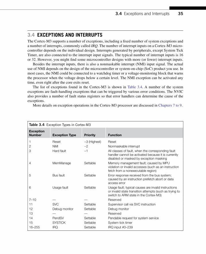
353.4 Exceptions and Interrupts
3.4 exCepTIOns and InTerrupTsThe Cortex-M3 supports a number of exceptions, including a fixed number of system exceptions and a number of interrupts, commonly called IRQ. The number of interrupt inputs on a Cortex-M3 micro-controller depends on the individual design. Interrupts generated by peripherals, except System Tick Timer, are also connected to the interrupt input signals. The typical number of interrupt inputs is 16 or 32. However, you might find some microcontroller designs with more (or fewer) interrupt inputs.
Besides the interrupt inputs, there is also a nonmaskable interrupt (NMI) input signal. The actual use of NMI depends on the design of the microcontroller or system-on-chip (SoC) product you use. In most cases, the NMI could be connected to a watchdog timer or a voltage-monitoring block that warns the processor when the voltage drops below a certain level. The NMI exception can be activated any time, even right after the core exits reset.
The list of exceptions found in the Cortex-M3 is shown in Table 3.4. A number of the system exceptions are fault-handling exceptions that can be triggered by various error conditions. The NVIC also provides a number of fault status registers so that error handlers can determine the cause of the exceptions.
More details on exception operations in the Cortex-M3 processor are discussed in Chapters 7 to 9.
Table 3.4 Exception Types in Cortex-M3
Exception Number Exception Type Priority Function
1 Reset −3 (Highest) Reset2 NMI −2 Nonmaskable interrupt3 Hard fault −1 All classes of fault, when the corresponding fault
handler cannot be activated because it is currently disabled or masked by exception masking
4 MemManage Settable Memory management fault; caused by MPU violation or invalid accesses (such as an instruction fetch from a nonexecutable region)
5 Bus fault Settable Error response received from the bus system; caused by an instruction prefetch abort or data access error
6 Usage fault Settable Usage fault; typical causes are invalid instructions or invalid state transition attempts (such as trying to switch to ARM state in the Cortex-M3)
7–10 — — Reserved11 SVC Settable Supervisor call via SVC instruction12 Debug monitor Settable Debug monitor13 — — Reserved14 PendSV Settable Pendable request for system service15 SYSTICK Settable System tick timer16–255 IRQ Settable IRQ input #0–239

36 CHAPTER 3 Cortex-M3 Basics
3.5 VeCTOr TaBLesWhen an exception event takes place on the Cortex-M3 and is accepted by the processor core, the corresponding exception handler is executed. To determine the starting address of the exception han-dler, a vector table mechanism is used. The vector table is an array of word data inside the system memory, each representing the starting address of one exception type. The vector table is relocatable, and the relocation is controlled by a relocation register in the NVIC (see Table 3.5). After reset, this relocation control register is reset to 0; therefore, the vector table is located in address 0x0 after reset.
For example, if the reset is exception type 1, the address of the reset vector is 1 times 4 (each word is 4 bytes), which equals 0x00000004, and NMI vector (type 2) is located in 2 × 4 = 0x00000008. The address 0x00000000 is used to store the starting value for the MSP.
The LSB of each exception vector indicates whether the exception is to be executed in the Thumb state. Because the Cortex-M3 can support only Thumb instructions, the LSB of all the exception vec-tors should be set to 1.
3.6 sTaCk MeMOry OperaTIOnsIn the Cortex-M3, besides normal software-controlled stack PUSH and POP, the stack PUSH and POP operations are also carried out automatically when entering or exiting an exception/interrupt handler. In this section, we examine the software stack operations. (Stack operations during exception handling are covered in Chapter 9.)
Table 3.5 Vector Table Definition after Reset
Exception Type Address Offset Exception Vector
18–255 0x48–0x3FF IRQ #2–23917 0x44 IRQ #116 0x40 IRQ #015 0x3C SYSTICK14 0x38 PendSV13 0x34 Reserved12 0x30 Debug monitor11 0x2C SVC7–10 0x1C–0x28 Reserved6 0x18 Usage fault5 0x14 Bus fault4 0x10 MemManage fault3 0x0C Hard fault2 0x08 NMI1 0x04 Reset0 0x00 Starting value of the MSP

373.6 Stack Memory Operations
3.6.1 Basic Operations of the stackIn general, stack operations are memory write or read operations, with the address specified by an SP. Data in registers is saved into stack memory by a PUSH operation and can be restored to registers later by a POP operation. The SP is adjusted automatically in PUSH and POP so that multiple data PUSH will not cause old stacked data to be erased.
The function of the stack is to store register contents in memory so that they can be restored later, after a processing task is completed. For normal uses, for each store (PUSH), there must be a cor-responding read (POP), and the address of the POP operation should match that of the PUSH opera-tion (see Figure 3.11). When PUSH/POP instructions are used, the SP is incremented/decremented automatically.
When program control returns to the main program, the R0–R2 contents are the same as before. Notice the order of PUSH and POP: The POP order must be the reverse of PUSH.
These operations can be simplified, thanks to PUSH and POP instructions allowing multiple load and store. In this case, the ordering of a register POP is automatically reversed by the processor (see Figure 3.12).
You can also combine RETURN with a POP operation. This is done by pushing the LR to the stack and popping it back to PC at the end of the subroutine (see Figure 3.13).
3.6.2 Cortex-M3 stack ImplementationThe Cortex-M3 uses a full-descending stack operation model. The SP points to the last data pushed to the stack memory, and the SP decrements before a new PUSH operation. See Figure 3.14 for an example showing execution of the instruction PUSH {R0}.
FIgure 3.11
Stack Operation Basics: One Register in Each Stack Operation.
Main program
...; R0 X, R1 Y, R2 ZBL function1
; Back to main program; R0 X, R1 Y, R2 Z... ; next instructions
function1PUSH {R0} ; store R0 to stack & adjust SPPUSH {R1} ; store R1 to stack & adjust SPPUSH {R2} ; store R2 to stack & adjust SP... ; Executing task (R0, R1 and R2
; could be changed)POP {R2} ; restore R2 and SP re adjustedPOP {R1} ; restore R1 and SP re adjustedPOP {R0} ; restore R0 and SP re adjustedBX LR ; Return
Subroutine

38 CHAPTER 3 Cortex-M3 Basics
FIgure 3.12
Stack Operation Basics: Multiple Register Stack Operation.
Main program...
BL function 1
; Back to main program
... ; next instructions
function 1PUSH {R0 R2} ; Store R0, R1, R2 to stack... ; Executing task (R0, R1 and R2
; could be changed)POP {R0 R2} ; restore R0, R1, R2BX LR ; Return
Subroutine; R0 X, R1 Y, R2 Z
; R0 X, R1 Y, R2 Z
FIgure 3.13
Stack Operation Basics: Combining Stack POP and RETURN.
Main program...
; R0 X, R1 Y, R2 ZBL function 1
; Back to main program; R0 X, R1 Y, R2 Z... ; next instructions
function 1PUSH {R0 R2, LR} ; Save registers
; including link register... ; Executing task (R0, R1 and R2
; could be changed)POP {R0 R2, PC} ; Restore registers and
; return
Subroutine
FIgure 3.14
Cortex-M3 Stack PUSH Implementation.
Last pushed data--
Memoryaddress
OccupiedOccupied
SP
0x12345678R0
PUSH {R0}
Occupied0x12345678
-
OccupiedOccupied
SP
Stackgrow

393.6 Stack Memory Operations
For POP operations, the data is read from the memory location pointer by SP, and then, the SP is incremented. The contents in the memory location are unchanged but will be overwritten when the next PUSH operation takes place (see Figure 3.15).
Because each PUSH/POP operation transfers 4 bytes of data (each register contains 1 word, or 4 bytes), the SP decrements/increments by 4 at a time or a multiple of 4 if more than 1 register is pushed or popped.
In the Cortex-M3, R13 is defined as the SP. When an interrupt takes place, a number of registers will be pushed automatically, and R13 will be used as the SP for this stacking process. Similarly, the pushed registers will be restored/popped automatically when exiting an interrupt handler, and the SP will also be adjusted.
3.6.3 The Two-stack Model in the Cortex-M3As mentioned before, the Cortex-M3 has two SPs: the MSPS and the PSP. The SP register to be used is controlled by the control register bit 1 (CONTROL[1] in the following text).
When CONTROL[1] is 0, the MSP is used for both thread mode and handler mode (see Figure 3.16). In this arrangement, the main program and the exception handlers share the same stack memory region. This is the default setting after power-up.
When the CONTROL[1] is 1, the PSP is used in thread mode (see Figure 3.17). In this arrangement, the main program and the exception handler can have separate stack memory regions. This can prevent
FIgure 3.15
Cortex-M3 Stack POP Implementation.
POP {R0}
R0
-
-
Memoryaddress
OccupiedOccupiedOccupied
SP0x12345678Occupied
0x12345678
0x12345678R0
-
OccupiedOccupied
SP
FIgure 3.16
CONTROL[1]=0: Both Thread Level and Handler Use Main Stack.
Thread mode(use MSP)
Handler mode(use MSP)
Thread mode(use MSP)
Time
Mainprogram
Interruptevent
Interrupt serviceroutine (ISR)
Interruptexit
Stacking Unstacking

40 CHAPTER 3 Cortex-M3 Basics
a stack error in a user application from damaging the stack used by the OS (assuming that the user application runs only in thread mode and the OS kernel executes in handler mode).
Note that in this situation, the automatic stacking and unstacking mechanism will use PSP, whereas stack operations inside the handler will use MSP.
It is possible to perform read/write operations directly to the MSP and PSP, without any confusion of which R13 you are referring to. Provided that you are in privileged level, you can access MSP and PSP values:
x = __get_MSP(); // Read the value of MSP__set_MSP(x); // Set the value of MSPx = __get_PSP(); // Read the value of PSP__set_PSP(x); // Set the value of PSP
In general, it is not recommended to change current selected SP values in a C function, as the stack memory could be used for storing local variables. To access the SPs in assembly, you can use the MRS and MSR instructions:
MRS R0, MSP ; Read Main Stack Pointer to R0MSR MSP, R0 ; Write R0 to Main Stack PointerMRS R0, PSP ; Read Process Stack Pointer to R0MSR PSP, R0 ; Write R0 to Process Stack Pointer
By reading the PSP value using an MRS instruction, the OS can read data stacked by the user application (such as register contents before SVC). In addition, the OS can change the PSP pointer value—for example, during context switching in multitasking systems.
3.7 reseT sequenCeAfter the processor exits reset, it will read two words from memory (see Figure 3.18):
Address 0x00000000: Starting value of R13 (the SP)•
FIgure 3.17
CONTROL[1]=1: Thread Level Uses Process Stack and Handler Uses Main Stack.
Thread mode(use PSP)
Handler mode(use MSP)
Thread mode(use PSP)
Time
Mainprogram
Interruptevent
Interrupt serviceroutine (ISR)
Interruptexit
Stacking Unstacking

413.7 Reset Sequence
Address 0x00000004: Reset vector (the starting address of program execution; LSB should be set •to 1 to indicate Thumb state)
This differs from traditional ARM processor behavior. Previous ARM processors executed program code starting from address 0x0. Furthermore, the vector table in previous ARM devices was instructions (you have to put a branch instruction there so that your exception handler can be put in another location).
FIgure 3.18
Reset Sequence.
Address5reset vector
Time
ResetAddress5
0x00000000Address5
0x00000004
Fetch initialSP value
Fetch resetvector
Instructionfetch
FIgure 3.19
Initial Stack Pointer Value and Initial Program Counter Value Example.
Other memory
0x200080001st stacked item2nd stacked item
Other memory
0x20007 FFC0x20007 FF8
0x20007 C00
Stackmemory
Initial SP value0x20008000
Stack growsdownwards
0x200080000x000000000x00000004 0x00000101
Boot code0x00000100
Resetvector
Other exceptionvectors
Flash

42 CHAPTER 3 Cortex-M3 Basics
In the Cortex-M3, the initial value for the MSP is put at the beginning of the memory map, followed by the vector table, which contains vector address values. (The vector table can be relocated to another location later, during program execution.) In addition, the contents of the vector table are address values not branch instructions. The first vector in the vector table (exception type 1) is the reset vector, which is the second piece of data fetched by the processor after reset.
Because the stack operation in the Cortex-M3 is a full descending stack (SP decrement before store), the initial SP value should be set to the first memory after the top of the stack region. For example, if you have a stack memory range from 0x20007C00 to 0x20007FFF (1 KB), the initial stack value should be set to 0x20008000.
The vector table starts after the initial SP value. The first vector is the reset vector. Notice that in the Cortex-M3, vector addresses in the vector table should have their LSB set to 1 to indicate that they are Thumb code. For that reason, the previous example has 0x101 in the reset vector, whereas the boot code starts at address 0x100 (see Figure 3.19). After the reset vector is fetched, the Cortex-M3 can then start to execute the program from the reset vector address and begin normal operations. It is necessary to have the SP initialized, because some of the exceptions (such as NMI) can happen right after reset, and the stack memory could be required for the handler of those exceptions.
Various software development tools might have different ways to specify the starting SP value and reset vector. If you need more information on this topic, it’s best to look at project examples provided with the development tools. Simple examples are provided in Chapters 10 and 20 for ARM tools and in Chapter 19 for the GNU tool chain.

43Copyright © 2010, Elsevier Inc. All rights reserved.DOI: 10.1016/B978-1-85617-963-8.00007-7
In ThIs ChapTer
assembly Basics ..................................................................................................................................... 43Instruction List ....................................................................................................................................... 46Instruction Descriptions .......................................................................................................................... 52several Useful Instructions in the Cortex-M3 ........................................................................................... 70
CHAPTER
Instruction Sets 4
This chapter provides some insight into the instruction set in the Cortex™-M3 and examples for a number of instructions. You’ll also find more information on the instruction set in Appendix A of this book. For complete details of each instruction, refer to the ARM v7-M Architecture Application Level Reference Manual [Ref. 2] or user guides from microcontroller vendors.
4.1 asseMBLy BasICsHere, we introduce some basic syntax of ARM assembly to make it easier to understand the rest of the code examples in this book. Most of the assembly code examples in this book are based on the ARM assembler tools, with the exception of those in Chapter 19, which focus on the Gnu’s Not Unix tool chain.
4.1.1 assembler Language: Basic syntaxIn assembler code, the following instruction formatting is commonly used:
labelopcode operand1, operand2, ...; Comments
The label is optional. Some of the instructions might have a label in front of them so that the address of the instructions can be determined using the label. Then, you will find the opcode (the instruction) followed by a number of operands. Normally, the first operand is the destination of the operation. The number of operands in an instruction depends on the type of instruction, and the syntax format of the

44 CHAPTER 4 Instruction Sets
operand can also be different. For example, immediate data are usually in the form #number, as shown here:
MOV R0, #0x12 ; Set R0 = 0x12 (hexadecimal)MOV R1, #'A' ; Set R1 = ASCII character A
The text after each semicolon (;) is a comment. These comments do not affect the program operation, but they can make programs easier for humans to understand.
You can define constants using EQU, and then use them inside your program code. For example,
NVIC_IRQ_SETEN0 EQU 0xE000E100NVIC_IRQ0_ENABLE EQU 0x1
...LDR R0,=NVIC_IRQ_SETEN0; ; LDR here is a pseudo-instruction that ; convert to a PC relative load by ; assembler.MOV R1,#NVIC_IRQ0_ENABLE ; Move immediate data to registerSTR R1,[R0] ; Enable IRQ 0 by writing R1 to address ; in R0
A number of data definition directives are available for insertion of constants inside assembly code. For example, DCI (Define Constant Instruction) can be used to code an instruction if your assembler cannot generate the exact instruction that you want and if you know the binary code for the instruction.
DCI 0xBE00 ; Breakpoint (BKPT 0), a 16-bit instruction
We can use DCB (Define Constant Byte) for byte size constant values, such as characters, and Define Constant Data (DCD) for word size constant values to define binary data in your code.
LDR R3,=MY_NUMBER ; Get the memory address value of MY_NUMBERLDR R4,[R3] ; Get the value code 0x12345678 in R4...LDR R0,=HELLO_TXT ; Get the starting memory address of ; HELLO_TXTBL PrintText ; Call a function called PrintText to ; display string...
MY_NUMBERDCD 0x12345678
HELLO_TXTDCB "Hello\n",0 ; null terminated string
Note that the assembler syntax depends on which assembler tool you are using. Here, the ARM assembler tools syntax is introduced. For syntax of other assemblers, it is best to start from the code examples provided with the tools.
4.1.2 assembler Language: Use of suffixesIn assembler for ARM processors, instructions can be followed by suffixes, as shown in Table 4.1.
For the Cortex-M3, the conditional execution suffixes are usually used for branch instructions. However, other instructions can also be used with the conditional execution suffixes if they are inside an IF-THEN instruction block. (This concept is introduced in a later part of this chapter.) In those

454.1 Assembly Basics
cases, the S suffix and the conditional execution suffixes can be used at the same time. Fifteen condition choices are available, as described later in this chapter.
4.1.3 assembler Language: Unified assembler LanguageTo support and get the best out of the Thumb®-2 instruction set, the Unified Assembler Language (UAL) was developed to allow selection of 16-bit and 32-bit instructions and to make it easier to port applications between ARM code and Thumb code by using the same syntax for both. (With UAL, the syntax of Thumb instructions is now the same as for ARM instructions.)
ADD R0, R1 ; R0 = R0 + R1, using Traditional Thumb syntaxADD R0, R0, R1 ; Equivalent instruction using UAL syntax
The traditional Thumb syntax can still be used. The choice between whether the instructions are interpreted as traditional Thumb code or the new UAL syntax is normally defined by the directive in the assembly file. For example, with ARM assembler tool, a program code header with “CODE16” directive implies the code is in the traditional Thumb syntax, and “THUMB” directive implies the code is in the new UAL syntax.
One thing you need to be careful with reusing traditional Thumb is that some instructions change the flags in APSR, even if the S suffix is not used. However, when the UAL syntax is used, whether the instruction changes the flag depends on the S suffix. For example,
AND R0, R1 ; Traditional Thumb syntaxANDS R0, R0, R1 ; Equivalent UAL syntax (S suffix is added)
With the new instructions in Thumb-2 technology, some of the operations can be handled by either a Thumb instruction or a Thumb-2 instruction. For example, R0 = R0 + 1 can be implemented as a 16-bit Thumb instruction or a 32-bit Thumb-2 instruction. With UAL, you can specify which instruction you want by adding suffixes:
ADDS R0, #1 ; Use 16-bit Thumb instruction by default ; for smaller sizeADDS.N R0, #1 ; Use 16-bit Thumb instruction (N=Narrow)ADDS.W R0, #1 ; Use 32-bit Thumb-2 instruction (W=wide)
The .W (wide) suffix specifies a 32-bit instruction. If no suffix is given, the assembler tool can choose either instruction but usually defaults to 16-bit Thumb code to get a smaller size. Depending on tool support, you may also use the .N (narrow) suffix to specify a 16-bit Thumb instruction.
Again, this syntax is for ARM assembler tools. Other assemblers might have slightly different syntax. If no suffix is given, the assembler might choose the instruction for you, with the minimum code size.
Table 4.1 Suffixes in Instructions
Suffix Description
S Update Application Program Status register (APSR) (flags); for example: ADDS R0, R1 ; this will update APSR
EQ, NE, LT, GT, and so on
Conditional execution; EQ = Equal, NE = Not Equal, LT = Less Than, GT = Greater Than, and so forth. For example: BEQ <Label> ; Branch if equal

46 CHAPTER 4 Instruction Sets
In most cases, applications will be coded in C, and the C compilers will use 16-bit instructions if possible due to smaller code size. However, when the immediate data exceed a certain range or when the operation can be better handled with a 32-bit Thumb-2 instruction, the 32-bit instruction will be used.
The 32-bit Thumb-2 instructions can be half word aligned. For example, you can have a 32-bit instruction located in a half word location.
0x1000 : LDR r0,[r1] ;a 16-bit instructions (occupy 0x1000-0x1001)0x1002 : RBIT.W r0 ;a 32-bit Thumb-2 instruction (occupy ; 0x1002-0x1005)
Most of the 16-bit instructions can only access registers R0–R7; 32-bit Thumb-2 instructions do not have this limitation. However, use of PC (R15) might not be allowed in some of the instructions. Refer to the ARM v7-M Architecture Application Level Reference Manual [Ref. 2] (section A4.6) if you need to find out more detail in this area.
4.2 InsTrUCTIon LIsTThe supported instructions are listed in Tables 4.2 through 4.9. The complete details of each instruction are available in the ARM v7-M Architecture Application Level Reference Manual [Ref. 2]. There is also information of the supported instruction sets in Appendix A.
Table 4.2 16-Bit Data Processing Instructions
Instruction Function
ADC Add with carryADD AddADR Add PC and an immediate value and put the result in a registerAND Logical ANDASR Arithmetic shift rightBIC Bit clear (Logical AND one value with the logic inversion of another value)CMN Compare negative (compare one data with two’s complement of another data and
update flags)CMP Compare (compare two data and update flags)CPY Copy (available from architecture v6; move a value from one high or low register to
another high or low register); synonym of MOV instructionEOR Exclusive ORLSL Logical shift leftLSR Logical shift rightMOV Move (can be used for register-to-register transfers or loading immediate data)MUL MultiplyMVN Move NOT (obtain logical inverted value)NEG Negate (obtain two’s complement value), equivalent to RSB

474.2 Instruction List
Table 4.2 16-Bit Data Processing Instructions Continued
Instruction Function
ORR Logical ORRSB Reverse subtractROR Rotate rightSBC Subtract with carrySUB SubtractTST Test (use as logical AND; Z flag is updated but AND result is not stored)REV Reverse the byte order in a 32-bit register (available from architecture v6)REV16 Reverse the byte order in each 16-bit half word of a 32-bit register (available from
architecture v6)REVSH Reverse the byte order in the lower 16-bit half word of a 32-bit register and sign
extends the result to 32 bits (available from architecture v6)SXTB Signed extend byte (available from architecture v6)SXTH Signed extend half word (available from architecture v6)UXTB Unsigned extend byte (available from architecture v6)UXTH Unsigned extend half word (available from architecture v6)
Table 4.3 16-Bit Branch Instructions
Instruction Function
B BranchB<cond> Conditional branchBL Branch with link; call a subroutine and store the return address in LR (this is actually
a 32-bit instruction, but it is also available in Thumb in traditional ARM processors)BLX Branch with link and change state (BLX <reg> only)1
BX <reg> Branch with exchange stateCBZ Compare and branch if zero (architecture v7)CBNZ Compare and branch if nonzero (architecture v7)IT IF-THEN (architecture v7)
1BLX with immediate is not supported because it will always try to change to the ARM state, which is not supported in the Cortex-M3. Attempts to use BLX <reg> to change to the ARM state will also result in a fault exception.
Table 4.4 16-Bit Load and Store Instructions
Instruction Function
LDR Load word from memory to registerLDRH Load half word from memory to registerLDRB Load byte from memory to register
Continued

48 CHAPTER 4 Instruction Sets
Table 4.4 16-Bit Load and Store Instructions Continued
Instruction Function
LDRSH Load half word from memory, sign extend it, and put it in registerLDRSB Load byte from memory, sign extend it, and put it in registerSTR Store word from register to memorySTRH Store half word from register to memorySTRB Store byte from register to memoryLDM/LDMIA Load multiple/Load multiple increment afterSTM/STMIA Store multiple/Store multiple increment afterPUSH Push multiple registersPOP Pop multiple registers
Table 4.5 Other 16-Bit Instructions
Instruction Function
SVC Supervisor callSEV Send eventWFE Sleep and wait for eventWFI Sleep and wait for interruptBKPT Breakpoint; if debug is enabled, it will enter debug mode (halted), or if debug
monitor exception is enabled, it will invoke the debug exception; otherwise, it will invoke a fault exception
NOP No operationCPSIE Enable PRIMASK (CPSIE i)/FAULTMASK (CPSIE f ) register (set the register to 0)CPSID Disable PRIMASK (CPSID i)/ FAULTMASK (CPSID f ) register (set the register to 1)
Table 4.6 32-Bit Data Processing Instructions
Instruction Function
ADC Add with carryADD AddADDW Add wide (#immed_12)ADR Add PC and an immediate value and put the result in a registerAND Logical ANDASR Arithmetic shift rightBIC Bit clear (logical AND one value with the logic inversion of another value)BFC Bit field clearBFI Bit field insertCMN Compare negative (compare one data with two’s complement of another data and
update flags)

494.2 Instruction List
Table 4.6 32-Bit Data Processing Instructions Continued
Instruction Function
CMP Compare (compare two data and update flags)CLZ Count leading zeroEOR Exclusive ORLSL Logical shift leftLSR Logical shift rightMLA Multiply accumulateMLS Multiply and subtractMOV MoveMOVW Move wide (write a 16-bit immediate value to register)MOVT Move top (write an immediate value to the top half word of destination reg)MVN Move negativeMUL MultiplyORR Logical ORORN Logical OR NOTRBIT Reverse bitREV Byte reverse wordREV16 Byte reverse packed half wordREVSH Byte reverse signed half wordROR Rotate rightRSB Reverse subtractRRX Rotate right extendedSBC Subtract with carrySBFX Signed bit field extractSDIV Signed divideSMLAL Signed multiply accumulate longSMULL Signed multiply longSSAT Signed saturateSBC Subtract with carrySUB SubtractSUBW Subtract wide (#immed_12)SXTB Sign extend byteSXTH Sign extend half wordTEQ Test equivalent (use as logical exclusive OR; flags are updated but result is not
stored)TST Test (use as logical AND; Z flag is updated but AND result is not stored)UBFX Unsigned bit field extractUDIV Unsigned divideUMLAL Unsigned multiply accumulate longUMULL Unsigned multiply longUSAT Unsigned saturate
Continued

50 CHAPTER 4 Instruction Sets
Table 4.6 32-Bit Data Processing Instructions Continued
Instruction Function
UXTB Unsigned extend byteUXTH Unsigned extend half word
Table 4.7 32-Bit Load and Store Instructions
Instruction Function
LDR Load word data from memory to registerLDRT Load word data from memory to register with unprivileged accessLDRB Load byte data from memory to registerLDRBT Load byte data from memory to register with unprivileged accessLDRH Load half word data from memory to registerLDRHT Load half word data from memory to register with unprivileged accessLDRSB Load byte data from memory, sign extend it, and put it to registerLDRSBT Load byte data from memory with unprivileged access, sign extend it, and put it to
registerLDRSH Load half word data from memory, sign extend it, and put it to registerLDRSHT Load half word data from memory with unprivileged access, sign extend it, and put
it to registerLDM/LDMIA Load multiple data from memory to registersLDMDB Load multiple decrement beforeLDRD Load double word data from memory to registersSTR Store word to memorySTRT Store word to memory with unprivileged accessSTRB Store byte data to memorySTRBT Store byte data to memory with unprivileged accessSTRH Store half word data to memorySTRHT Store half word data to memory with unprivileged accessSTM/STMIA Store multiple words from registers to memorySTMDB Store multiple decrement beforeSTRD Store double word data from registers to memoryPUSH Push multiple registersPOP Pop multiple registers
Table 4.8 32-Bit Branch Instructions
Instruction Function
B BranchB<cond> Conditional branchBL Branch and linkTBB Table branch byte; forward branch using a table of single byte offsetTBH Table branch half word; forward branch using a table of half word offset
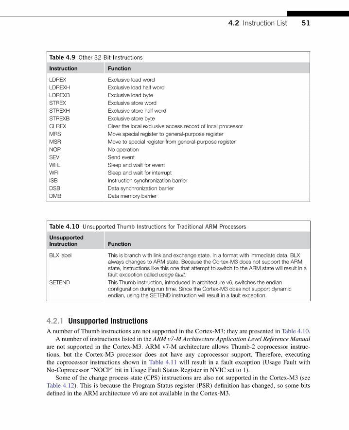
514.2 Instruction List
4.2.1 Unsupported InstructionsA number of Thumb instructions are not supported in the Cortex-M3; they are presented in Table 4.10.
A number of instructions listed in the ARM v7-M Architecture Application Level Reference Manual are not supported in the Cortex-M3. ARM v7-M architecture allows Thumb-2 coprocessor instruc-tions, but the Cortex-M3 processor does not have any coprocessor support. Therefore, executing the coprocessor instructions shown in Table 4.11 will result in a fault exception (Usage Fault with No-Coprocessor “NOCP” bit in Usage Fault Status Register in NVIC set to 1).
Some of the change process state (CPS) instructions are also not supported in the Cortex-M3 (see Table 4.12). This is because the Program Status register (PSR) definition has changed, so some bits defined in the ARM architecture v6 are not available in the Cortex-M3.
Table 4.9 Other 32-Bit Instructions
Instruction Function
LDREX Exclusive load wordLDREXH Exclusive load half wordLDREXB Exclusive load byteSTREX Exclusive store wordSTREXH Exclusive store half wordSTREXB Exclusive store byteCLREX Clear the local exclusive access record of local processorMRS Move special register to general-purpose registerMSR Move to special register from general-purpose registerNOP No operationSEV Send eventWFE Sleep and wait for eventWFI Sleep and wait for interruptISB Instruction synchronization barrierDSB Data synchronization barrierDMB Data memory barrier
Table 4.10 Unsupported Thumb Instructions for Traditional ARM Processors
Unsupported Instruction Function
BLX label This is branch with link and exchange state. In a format with immediate data, BLX always changes to ARM state. Because the Cortex-M3 does not support the ARM state, instructions like this one that attempt to switch to the ARM state will result in a fault exception called usage fault.
SETEND This Thumb instruction, introduced in architecture v6, switches the endian configuration during run time. Since the Cortex-M3 does not support dynamic endian, using the SETEND instruction will result in a fault exception.

52 CHAPTER 4 Instruction Sets
In addition, the hint instructions shown in Table 4.13 will behave as NOP in the Cortex-M3.All other undefined instructions, when executed, will cause the usage fault exception to take place.
4.3 InsTrUCTIon DesCrIpTIonsHere, we introduce some of the commonly used syntax for ARM assembly code. Some of the instruc-tions have various options such as barrel shifter; these will not be fully covered in this chapter.
Table 4.11 Unsupported Coprocessor Instructions
Unsupported Instruction Function
MCR Move to coprocessor from ARM processorMCR2 Move to coprocessor from ARM processorMCRR Move to coprocessor from two ARM registerMRC Move to ARM register from coprocessorMRC2 Move to ARM register from coprocessorMRRC Move to two ARM registers from coprocessorLDC Load coprocessor; load memory data from a sequence of consecutive memory
addresses to a coprocessorSTC Store coprocessor; stores data from a coprocessor to a sequence of consecutive
memory addresses
Table 4.12 Unsupported Change Process State Instructions
Unsupported Instruction
Function
CPS<IE|ID>.W A There is no A bit in the Cortex-M3CPS.W #mode There is no mode bit in the Cortex-M3 PSR
Table 4.13 Unsupported Hint Instructions
Unsupported Instruction Function
DBG A hint instruction to debug and trace systemPLD Preload data; this is a hint instruction for cache memory, however, since there is no
cache in the Cortex-M3 processor, this instruction behaves as NOPPLI Preload instruction; this is a hint instruction for cache memory, however, since there
is no cache in the Cortex-M3 processor, this instruction behaves as NOPYIELD A hint instruction to allow multithreading software to indicate to hardware that it is
doing a task that can be swapped out to improve overall system performance.

534.3 Instruction Descriptions
4.3.1 assembler Language: Moving DataOne of the most basic functions in a processor is transfer of data. In the Cortex-M3, data transfers can be of one of the following types:
Moving data between register and register•Moving data between memory and register•Moving data between special register and register•Moving an immediate data value into a register•
The command to move data between registers is MOV (move). For example, moving data from register R3 to register R8 looks like this:
MOV R8, R3
Another instruction can generate the negative value of the original data; it is called MVN (move negative).
The basic instructions for accessing memory are Load and Store. Load (LDR) transfers data from memory to registers, and Store transfers data from registers to memory. The transfers can be in different data sizes (byte, half word, word, and double word), as outlined in Table 4.14.
Multiple Load and Store operations can be combined into single instructions called LDM (Load Multiple) and STM (Store Multiple), as outlined in Table 4.15.
The exclamation mark (!) in the instruction specifies whether the register Rd should be updated after the instruction is completed. For example, if R8 equals 0x8000:
STMIA.W R8!, {R0-R3} ; R8 changed to 0x8010 after store ; (increment by 4 words)STMIA.W R8 , {R0-R3} ; R8 unchanged after store
ARM processors also support memory accesses with preindexing and postindexing. For preindex-ing, the register holding the memory address is adjusted. The memory transfer then takes place with the updated address. For example,
LDR.W R0,[R1, #offset]! ; Read memory[R1+offset], with R1 ; update to R1+offset
Table 4.14 Commonly Used Memory Access Instructions
Example Description
LDRB Rd, [Rn, #offset] Read byte from memory location Rn + offsetLDRH Rd, [Rn, #offset] Read half word from memory location Rn + offsetLDR Rd, [Rn, #offset] Read word from memory location Rn + offsetLDRD Rd1,Rd2, [Rn, #offset] Read double word from memory location Rn + offsetSTRB Rd, [Rn, #offset] Store byte to memory location Rn + offsetSTRH Rd, [Rn, #offset] Store half word to memory location Rn + offsetSTR Rd, [Rn, #offset] Store word to memory location Rn + offsetSTRD Rd1,Rd2, [Rn, #offset] Store double word to memory location Rn + offset

54 CHAPTER 4 Instruction Sets
The use of the “!” indicates the update of base register R1. The “!” is optional; without it, the instruc-tion would be just a normal memory transfer with offset from a base address. The preindexing memory access instructions include load and store instructions of various transfer sizes (see Table 4.16).
Postindexing memory access instructions carry out the memory transfer using the base address specified by the register and then update the address register afterward. For example,
LDR.W R0,[R1], #offset ; Read memory[R1], with R1 ; updated to R1+offset
When a postindexing instruction is used, there is no need to use the “!” sign, because all postindex-ing instructions update the base address register, whereas in preindexing you might choose whether to update the base address register or not.
Similarly to preindexing, postindexing memory access instructions are available for different trans-fer sizes (see Table 4.17).
Table 4.15 Multiple Memory Access Instructions
Example Description
LDMIA Rd!,<reg list> Read multiple words from memory location specified by Rd; address increment after (IA) each transfer (16-bit Thumb instruction)
STMIA Rd!,<reg list> Store multiple words to memory location specified by Rd; address increment after (IA) each transfer (16-bit Thumb instruction)
LDMIA.W Rd(!),<reg list> Read multiple words from memory location specified by Rd; address increment after each read (.W specified it is a 32-bit Thumb-2 instruction)
LDMDB.W Rd(!),<reg list> Read multiple words from memory location specified by Rd; address Decrement Before (DB) each read (.W specified it is a 32-bit Thumb-2 instruction)
STMIA.W Rd(!),<reg list> Write multiple words to memory location specified by Rd; address increment after each read (.W specified it is a 32-bit Thumb-2 instruction)
STMDB.W Rd(!),<reg list> Write multiple words to memory location specified by Rd; address DB each read (.W specified it is a 32-bit Thumb-2 instruction)
Table 4.16 Examples of Preindexing Memory Access Instructions
Example Description
LDR.W Rd, [Rn, #offset]! LDRB.W Rd, [Rn, #offset]! LDRH.W Rd, [Rn, #offset]! LDRD.W Rd1, Rd2,[Rn, #offset]!
Preindexing load instructions for various sizes (word, byte, half word, and double word)
LDRSB.W Rd, [Rn, #offset]! LDRSH.W Rd, [Rn, #offset]!
Preindexing load instructions for various sizes with sign extend (byte, half word)
STR.W Rd, [Rn, #offset]! STRB.W Rd, [Rn, #offset]! STRH.W Rd, [Rn, #offset]! STRD.W Rd1, Rd2,[Rn, #offset]!
Preindexing store instructions for various sizes (word, byte, half word, and double word)

554.3 Instruction Descriptions
Two other types of memory operation are stack PUSH and stack POP. For example,
PUSH {R0, R4-R7, R9} ; Push R0, R4, R5, R6, R7, R9 into ; stack memoryPOP {R2,R3} ; Pop R2 and R3 from stack
Usually a PUSH instruction will have a corresponding POP with the same register list, but this is not always necessary. For example, a common exception is when POP is used as a function return:
PUSH {R0-R3, LR} ; Save register contents at beginning of ; subroutine.... ; ProcessingPOP {R0-R3, PC} ; restore registers and return
In this case, instead of popping the LR register back and then branching to the address in LR, we POP the address value directly in the program counter.
As mentioned in Chapter 3, the Cortex-M3 has a number of special registers. To access these regis-ters, we use the instructions MRS and MSR. For example,
MRS R0, PSR ; Read Processor status word into R0MSR CONTROL, R1 ; Write value of R1 into control register
Unless you’re accessing the APSR, you can use MSR or MRS to access other special registers only in privileged mode.
Moving immediate data into a register is a common thing to do. For example, you might want to access a peripheral register, so you need to put the address value into a register beforehand. For small values (8 bits or less), you can use MOVS (move). For example,
MOVS R0, #0x12 ; Set R0 to 0x12
For a larger value (over 8 bits), you might need to use a Thumb-2 move instruction. For example,
MOVW.W R0, #0x789A ; Set R0 to 0x789A
Or if the value is 32-bit, you can use two instructions to set the upper and lower halves:
MOVW.W R0,#0x789A ; Set R0 lower half to 0x789AMOVT.W R0,#0x3456 ; Set R0 upper half to 0x3456. Now ; R0=0x3456789A
Table 4.17 Examples of Postindexing Memory Access Instructions
Example Description
LDR.W Rd, [Rn], #offsetLDRB.W Rd, [Rn], #offsetLDRH.W Rd, [Rn], #offsetLDRD.W Rd1, Rd2,[Rn], #offset
Postindexing load instructions for various sizes (word, byte, half word, and double word)
LDRSB.W Rd, [Rn], #offsetLDRSH.W Rd, [Rn], #offset
Postindexing load instructions for various sizes with sign extend (byte, half word)
STR.W Rd, [Rn], #offsetSTRB.W Rd, [Rn], #offsetSTRH.W Rd, [Rn], #offsetSTRD.W Rd1, Rd2,[Rn], #offset
Postindexing store instructions for various sizes (word, byte, half word, and double word)

56 CHAPTER 4 Instruction Sets
Alternatively, you can also use LDR (a pseudo-instruction provided in ARM assembler). For example,
LDR R0, =0x3456789A
This is not a real assembler command, but the ARM assembler will convert it into a PC relative load instruction to produce the required data. To generate 32-bit immediate data, using LDR is recom-mended rather than the MOVW.W and MOVT.W combination because it gives better readability and the assembler might be able to reduce the memory being used if the same immediate data are reused in several places of the same program.
4.3.2 LDr and aDr pseudo-InstructionsBoth LDR and ADR pseudo-instructions can be used to set registers to a program address value. They have different syntaxes and behaviors. For LDR, if the address is a program address value, the assem-bler will automatically set the LSB to 1. For example,
LDR R0, =address1 ; R0 set to 0x4001...
address1 ; address here is 0x4000MOV R0, R1 ; address1 contains program code...
You will find that the LDR instruction will put 0x4001 into R1; the LSB is set to 1 to indicate that it is Thumb code. If address1 is a data address, LSB will not be changed. For example,
LDR R0, =address1 ; R0 set to 0x4000...
address1 ; address here is 0x4000DCD 0x0 ; address1 contains data...
For ADR, you can load the address value of a program code into a register without setting the LSB automatically. For example,
ADR R0, address1...
address1 ; (address here is 0x4000)MOV R0, R1 ; address1 contains program code...
You will get 0x4000 in the ADR instruction. Note that there is no equal sign (=) in the ADR statement.LDR obtains the immediate data by putting the data in the program code and uses a PC relative
load to get the data into the register. ADR tries to generate the immediate value by adding or subtract-ing instructions (for example, based on the current PC value). As a result, it is not possible to create all immediate values using ADR, and the target address label must be in a close range. However, using ADR can generate smaller code sizes compared with LDR.
The 16-bit version of ADR requires that the target address must be word aligned (address value is a multiple of 4). If the target address is not word aligned, you can use the 32-bit version of ADR instruc-tion “ADR.W.” If the target address is more than ± 4095 bytes of current PC, you can use “ADRL” pseudo-instruction, which gives ±1 MB range.

574.3 Instruction Descriptions
4.3.3 assembler Language: processing DataThe Cortex-M3 provides many different instructions for data processing. A few basic ones are introduced here. Many data operation instructions can have multiple instruction formats. For example, an ADD instruction can operate between two registers or between one register and an immediate data value:
ADD R0, R0, R1 ; R0 = R0 + R1ADDS R0, R0, #0x12 ; R0 = R0 + 0x12ADD.W R0, R1, R2 ; R0 = R1 + R2
These are all ADD instructions, but they have different syntaxes and binary coding.With the traditional Thumb instruction syntax, when 16-bit Thumb code is used, an ADD instruc-
tion can change the flags in the PSR. However, 32-bit Thumb-2 code can either change a flag or keep it unchanged. To separate the two different operations, the S suffix should be used if the following operation depends on the flags:
ADD.W R0, R1, R2 ; Flag unchangedADDS.W R0, R1, R2 ; Flag change
Aside from ADD instructions, the arithmetic functions that the Cortex-M3 supports include subtract (SUB), multiply (MUL), and unsigned and signed divide (UDIV/SDIV). Table 4.18 shows some of the most commonly used arithmetic instructions.
Table 4.18 Examples of Arithmetic Instructions
Instruction Operation
ADD Rd, Rn, Rm ; Rd = Rn + RmADD Rd, Rd, Rm ; Rd = Rd + RmADD Rd, #immed ; Rd = Rd + #immedADD Rd, Rn, # immed ; Rd = Rn + #immed
ADD operation
ADC Rd, Rn, Rm ; Rd = Rn + Rm + carryADC Rd, Rd, Rm ; Rd = Rd + Rm + carryADC Rd, #immed ; Rd = Rd + #immed + carry
ADD with carry
ADDW Rd, Rn,#immed ; Rd = Rn + #immed ADD register with 12-bit immediate valueSUB Rd, Rn, Rm ; Rd = Rn − RmSUB Rd, #immed ; Rd = Rd − #immedSUB Rd, Rn,#immed ; Rd = Rn − #immed
SUBTRACT
SBC Rd, Rm ; Rd = Rd − Rm − borrowSBC.W Rd, Rn, #immed ; Rd = Rn − #immed − borrowSBC.W Rd, Rn, Rm ; Rd = Rn − Rm − borrow
SUBTRACT with borrow (not carry)
RSB.W Rd, Rn, #immed ; Rd = #immed –RnRSB.W Rd, Rn, Rm ; Rd = Rm − Rn
Reverse subtract
MUL Rd, Rm ; Rd = Rd * RmMUL.W Rd, Rn, Rm ; Rd = Rn * Rm
Multiply
UDIV Rd, Rn, Rm ; Rd = Rn/RmSDIV Rd, Rn, Rm ; Rd = Rn/Rm
Unsigned and signed divide

58 CHAPTER 4 Instruction Sets
These instructions can be used with or without the “S” suffix to determine if the APSR should be updated. In most cases, if UAL syntax is selected and if “S” suffix is not used, the 32-bit version of the instructions would be selected as most of the 16-bit Thumb instructions update APSR.
The Cortex-M3 also supports 32-bit multiply instructions and multiply accumulate instructions that give 64-bit results. These instructions support signed or unsigned values (see Table 4.19).
Another group of data processing instructions are the logical operations instructions and logical operations such as AND, ORR (or), and shift and rotate functions. Table 4.20 shows some of the most commonly used logical instructions. These instructions can be used with or without the “S” suffix to determine if the APSR should be updated. If UAL syntax is used and if “S” suffix is not used, the 32-bit version of the instructions would be selected as all of the 16-bit logic operation instructions update APSR.
The Cortex-M3 provides rotate and shift instructions. In some cases, the rotate operation can be combined with other operations (for example, in memory address offset calculation for load/store instructions). For standalone rotate/shift operations, the instructions shown in Table 4.21 are pro-vided. Again, a 32-bit version of the instruction is used if “S” suffix is not used and if UAL syntax is used.
Table 4.19 32-Bit Multiply Instructions
Instruction Operation
SMULL RdLo, RdHi, Rn, Rm ; {RdHi,RdLo} = Rn * RmSMLAL RdLo, RdHi, Rn, Rm ; {RdHi,RdLo} += Rn * Rm
32-bit multiply instructions for signed values
UMULL RdLo, RdHi, Rn, Rm ; {RdHi,RdLo} = Rn * RmUMLAL RdLo, RdHi, Rn, Rm ; {RdHi,RdLo} += Rn * Rm
32-bit multiply instructions for unsigned values
Table 4.20 Logic Operation Instructions
Instruction Operation
AND Rd, Rn ; Rd = Rd & RnAND.W Rd, Rn,#immed ; Rd = Rn & #immedAND.W Rd, Rn, Rm ; Rd = Rn & Rd
Bitwise AND
ORRRd, Rn ; Rd = Rd | RnORR.W Rd, Rn,#immed ; Rd = Rn | #immedORR.W Rd, Rn, Rm ; Rd = Rn | Rd
Bitwise OR
BIC Rd, Rn ; Rd = Rd & (~Rn)BIC.W Rd, Rn,#immed ; Rd = Rn &(~#immed)BIC.W Rd, Rn, Rm ; Rd = Rn &(~Rd)
Bit clear
ORN.W Rd, Rn,#immed ; Rd = Rn | (~#immed)ORN.W Rd, Rn, Rm ; Rd = Rn | (~Rd)
Bitwise OR NOT
EOR Rd, Rn ; Rd = Rd ^ RnEOR.W Rd, Rn,#immed ; Rd = Rn | #immedEOR.W Rd, Rn, Rm ; Rd = Rn | Rd
Bitwise Exclusive OR

594.3 Instruction Descriptions
In UAL syntax, the rotate and shift operations can also update the carry flag if the S suffix is used (and always update the carry flag if the 16-bit Thumb code is used). See Figure 4.1.
If the shift or rotate operation shifts the register position by multiple bits, the value of the carry flag C will be the last bit that shifts out of the register.
Table 4.21 Shift and Rotate Instructions
Instruction Operation
ASR Rd, Rn,#immed ; Rd = Rn » immedASRRd, Rn ; Rd = Rd » RnASR.W Rd, Rn, Rm ; Rd = Rn » Rm
Arithmetic shift right
LSLRd, Rn,#immed ; Rd = Rn « immedLSLRd, Rn ; Rd = Rd « RnLSL.W Rd, Rn, Rm ; Rd = Rn « Rm
Logical shift left
LSRRd, Rn,#immed ; Rd = Rn » immedLSRRd, Rn ; Rd = Rd » RnLSR.W Rd, Rn, Rm ; Rd = Rn » Rm
Logical shift right
ROR Rd, Rn ; Rd rot by RnROR.W Rd, Rn,#immed ; Rd = Rn rot by immed ROR.W Rd, Rn, Rm ; Rd = Rn rot by Rm
Rotate right
RRX.W Rd, Rn ; {C, Rd} = {Rn, C} Rotate right extended
FIgUre 4.1
Shift and Rotate Instructions.
Logical Shift Left (LSL)
Logical Shift Right (LSR)
Rotate Right (ROR)
Arithmetic Shift Right (ASR)
Rotate Right eXtended (RRX)
C Register 0
CRegister0
CRegister
CRegister
CRegister

60 CHAPTER 4 Instruction Sets
For conversion of signed data from byte or half word to word, the Cortex-M3 provides the two instructions shown in Table 4.22. Both 16-bit and 32-bit versions are available. The 16-bit version can only access low registers.
Another group of data processing instructions is used for reversing data bytes in a register (see Table 4.23). These instructions are usually used for conversion between little endian and big endian data. See Figure 4.2. Both 16-bit and 32-bit versions are available. The 16-bit version can only access low registers.
The last group of data processing instructions is for bit field processing. They include the instruc-tions shown in Table 4.24. Examples of these instructions are provided in a later part of this chapter.
4.3.4 assembler Language: Call and Unconditional BranchThe most basic branch instructions are as follows:
B label ; Branch to a labeled addressBX reg ; Branch to an address specified by a register
In BX instructions, the LSB of the value contained in the register determines the next state (Thumb/ARM) of the processor. In the Cortex-M3, because it is always in Thumb state, this bit should be set to 1. If it is zero, the program will cause a usage fault exception because it is trying to switch the proces-sor into ARM state (See Figure 4.2.).
To call a function, the branch and link instructions should be used.
BL label ; Branch to a labeled address and save return ; address in LR
Why Is There roTaTe rIghT BUT no roTaTe LeFT?The rotate left operation can be replaced by a rotate right operation with a different rotate offset. For example, a rotate left by 4-bit operation can be written as a rotate right by 28-bit instruction, which gives the same result and takes the same amount of time to execute.
Table 4.22 Sign Extend Instructions
Instruction Operation
SXTB Rd, Rm ; Rd = signext(Rm[7:0]) Sign extend byte data into wordSXTH Rd, Rm ; Rd = signext(Rm[15:0]) Sign extend half word data into word
Table 4.23 Data Reverse Ordering Instructions
Instruction Operation
REV Rd, Rn ; Rd = rev(Rn) Reverse bytes in wordREV16 Rd, Rn ; Rd = rev16(Rn) Reverse bytes in each half wordREVSH Rd, Rn ; Rd = revsh(Rn) Reverse bytes in bottom half word and sign extend the
result

614.3 Instruction Descriptions
BLX reg ; Branch to an address specified by a register and ; save return ; address in LR.
With these instructions, the return address will be stored in the link register (LR) and the func-tion can be terminated using BX LR, which causes program control to return to the calling process. However, when using BLX, make sure that the LSB of the register is 1. Otherwise the processor will produce a fault exception because it is an attempt to switch to the ARM state.
You can also carry out a branch operation using MOV instructions and LDR instructions. For example,
MOV R15, R0 ; Branch to an address inside R0LDR R15, [R0] ; Branch to an address in memory location ; specified by R0
FIgUre 4.2
Operation of Reverse instructions.
REV.W(Reverse bytes in word)
Bit[7:0]
Bit[15:8]
Bit[23:16]
Bit[31:24]
REV16.W(Reverse bytes in half word)
REVSH.W(Reverse bytes in bottom
half word and sign extend results)
sign extend
Table 4.24 Bit Field Processing and Manipulation Instructions
Instruction Operation
BFC.W Rd, Rn, #<width> Clear bit field within a registerBFI.W Rd, Rn, #<lsb>, #<width> Insert bit field to a registerCLZ.W Rd, Rn Count leading zeroRBIT.W Rd, Rn Reverse bit order in registerSBFX.W Rd, Rn, #<lsb>, #<width> Copy bit field from source and sign extend itUBFX.W Rd, Rn, #<lsb>, #<width> Copy bit field from source register

62 CHAPTER 4 Instruction Sets
POP {R15} ; Do a stack pop operation, and change the ; program counter value ; to the result value.
When using these methods to carry out branches, you also need to make sure that the LSB of the new program counter value is 0x1. Otherwise, a usage fault exception will be generated because it will try to switch the processor to ARM mode, which is not allowed in the Cortex-M3 redundancy.
4.3.5 assembler Language: Decisions and Conditional BranchesMost conditional branches in ARM processors use flags in the APSR to determine whether a branch should be carried out. In the APSR, there are five flag bits; four of them are used for branch decisions (see Table 4.25).
There is another flag bit at bit[27], called the Q flag. It is for saturation math operations and is not used for conditional branches.
save The Lr IF yoU neeD To CaLL a sUBroUTIneThe BL instruction will destroy the current content of your LR. So, if your program code needs the LR later, you should save your LR before you use BL. The common method is to push the LR to stack in the beginning of your subroutine. For example,
main...BL functionA...
functionAPUSH {LR} ; Save LR content to stack...BL functionB...POP {PC} ; Use stacked LR content to return to main
functionBPUSH {LR}...POP {PC} ; Use stacked LR content to return to functionA
In addition, if the subroutine you call is a C function, you might also need to save the contents in R0–R3 and R12 if these values will be needed at a later stage. According to AAPCS [Ref. 5], the contents in these registers could be changed by a C function.
Table 4.25 Flag Bits in APSR that Can Be Used for Conditional Branches
Flag PSR Bit Description
N 31 Negative flag (last operation result is a negative value)Z 30 Zero (last operation result returns a zero value)C 29 Carry (last operation returns a carry out or borrow)V 28 Overflow (last operation results in an overflow)

634.3 Instruction Descriptions
With combinations of the four flags (N, Z, C, and V ), 15 branch conditions are defined (see Table 4.26). Using these conditions, branch instructions can be written as, for example,
BEQ label ; Branch to address 'label' if Z flag is set
You can also use the Thumb-2 version if your branch target is further away. For example,
BEQ.W label ; Branch to address 'label' if Z flag is set
FLags In arM proCessorsOften, data processing instructions change the flags in the PSR. The flags might be used for branch decisions, or they can be used as part of the input for the next instruction. The ARM processor normally contains at least the Z, N, C, and V flags, which are updated by execution of data processing instructions.
Z (Zero) flag: This flag is set when the result of an instruction has a zero value or when a comparison of two •data returns an equal result.N (Negative) flag: This flag is set when the result of an instruction has a negative value (bit 31 is 1).•C (Carry) flag: This flag is for unsigned data processing—for example, in add (ADD) it is set when an •overflow occurs; in subtract (SUB) it is set when a borrow did not occur (borrow is the invert of carry).V (Overflow) flag: This flag is for signed data processing; for example, in an add (ADD), when two positive •values added together produce a negative value, or when two negative values added together produce a positive value.
These flags can also have special results when used with shift and rotate instructions. Refer to the ARM v7-M Architecture Application Level Reference Manual [Ref. 2] for details.
Table 4.26 Conditions for Branches or Other Conditional Operations
Symbol Condition Flag
EQ Equal Z setNE Not equal Z clearCS/HS Carry set/unsigned higher or same C setCC/LO Carry clear/unsigned lower C clearMI Minus/negative N setPL Plus/positive or zero N clearVS Overflow V setVC No overflow V clearHI Unsigned higher C set and Z clearLS Unsigned lower or same C clear or Z setGE Signed greater than or equal N set and V set, or N clear and V clear (N == V)LT Signed less than N set and V clear, or N clear and V set (N != V)GT Signed greater than Z clear, and either N set and V set, or N clear and
V clear (Z == 0, N == V)LE Signed less than or equal Z set, or N set and V clear, or N clear and V set
(Z == 1 or N != V)AL Always (unconditional) —

64 CHAPTER 4 Instruction Sets
The defined branch conditions can also be used in IF-THEN-ELSE structures. For example,
CMP R0, R1 ; Compare R0 and R1ITTEE GT ; If R0 > R1 Then ; if true, first 2 statements execute, ; if false, other 2 statements executeMOVGT R2, R0 ; R2 = R0MOVGT R3, R1 ; R3 = R1MOVLE R2, R0 ; Else R2 = R1MOVLE R3, R1 ; R3 = R0
APSR flags can be affected by the following:
Most of the 16-bit • ALU instructions32-bit (Thumb-2) ALU instructions with the • S suffix; for example, ADDS.WCompare (e.g., CMP) and Test (e.g., TST, TEQ)•Write to APSR/xPSR directly•
Most of the 16-bit Thumb arithmetic instructions affect the N, Z, C, and V flags. With 32-bit Thumb-2 instructions, the ALU operation can either change flags or not change flags. For example,
ADDS.W R0, R1, R2 ; This 32-bit Thumb instruction updates flagADD.W R0, R1, R2 ; This 32-bit Thumb instruction does not ; update flag
Be careful when reusing program code from old projects. If the old project is in tradition Thumb syntax; for example, “CODE16” directive is used with ARM assembler, then
ADD R0, R1 ; This 16-bit Thumb instruction updates flagADD R0, #0x1 ; This 16-bit Thumb instruction updates flag
However, if you used the same code in UAL syntax; that is “THUMB” directive is used with ARM assembler, then
ADD R0, R1 ; This 16-bit Thumb instruction does not ; update flagADD R0, #0x1 ; This will become a 32-bit Thumb instruction ; that does not update flag
To make sure that the code works correctly with different tools, you should always use the S suffix if the flags need to be updated for conditional operations such as conditional branches.
The compare (CMP) instruction subtracts two values and updates the flags (just like SUBS), but the result is not stored in any registers. CMP can have the following formats:
CMP R0, R1 ; Calculate R0 – R1 and update flagCMP R0, #0x12 ; Calculate R0 – 0x12 and update flag
A similar instruction is the CMN (compare negative). It compares one value to the negative (two’s complement) of a second value; the flags are updated, but the result is not stored in any registers:
CMN R0, R1 ; Calculate R0 – (-R1) and update flagCMN R0, #0x12 ; Calculate R0 – (-0x12) and update flag
The TST (test) instruction is more like the AND instruction. It ANDs two values and updates the flags. However, the result is not stored in any register. Similarly to CMP, it has two input formats:

654.3 Instruction Descriptions
TST R0, R1 ; Calculate R0 AND R1 and update flagTST R0, #0x12 ; Calculate R0 AND 0x12 and update flag
4.3.6 assembler Language: Combined Compare and Conditional BranchWith ARM architecture v7-M, two new instructions are provided on the Cortex-M3 to supply a simple compare with zero and conditional branch operations. These are CBZ (compare and branch if zero) and CBNZ (compare and branch if nonzero).
The compare and branch instructions only support forward branches. For example,
i = 5;while (i != 0 ){func1(); ; call a functioni−−;}
This can be compiled into the following:
MOV R0, #5 ; Set loop counterloop1 CBZ R0,loop1exit ; if loop counter = 0 then exit the loop
BL func1 ; call a function SUB R0, #1 ; loop counter decrement B loop1 ; next loop
loop1exit
The usage of CBNZ is similar to CBZ, apart from the fact that the branch is taken if the Z flag is not set (result is not zero). For example,
status = strchr(email_address, '@');if (status == 0){//status is 0 if @ is not in email_address
show_error_message(); exit(1); }
This can be compiled into the following:
...BL strchrCBNZ R0, email_looks_okay ; Branch if result is not zeroBL show_error_messageBL exit
email_looks_okay...
The APSR value is not affected by the CBZ and CBNZ instructions.
Assembler Language: Conditional Execution Using IT InstructionsThe IT (IF-THEN) block is very useful for handling small conditional code. It avoids branch penalties because there is no change to program flow. It can provide a maximum of four conditionally executed instructions.
In IT instruction blocks, the first line must be the IT instruction, detailing the choice of execution, followed by the condition it checks. The first statement after the IT command must be

66 CHAPTER 4 Instruction Sets
TRUE-THEN- EXECUTE, which is always written as ITxyz, where T means THEN and E means ELSE. The second through fourth statements can be either THEN (true) or ELSE (false):
IT<x><y><z> <cond> ; IT instruction (<x>, <y>, ; <z> can be T or E)instr1<cond> <operands> ; 1st instruction (<cond> ; must be same as IT)instr2<cond or not cond> <operands> ; 2nd instruction (can be ; <cond> or <!cond>instr3<cond or not cond> <operands> ; 3rd instruction (can be ; <cond> or <!cond>instr4<cond or not cond> <operands> ; 4th instruction (can be ; <cond> or <!cond>
If a statement is to be executed when <cond> is false, the suffix for the instruction must be the opposite of the condition. For example, the opposite of EQ is NE, the opposite of GT is LE, and so on. The following code shows an example of a simple conditional execution:
if (R1<R2) then R2=R2−R1 R2=R2/2else R1=R1−R2 R1=R1/2
In assembly,
CMP R1, R2 ; If R1 < R2 (less then)ITTEE LT ; then execute instruction 1 and 2 ; (indicated by T) ; else execute instruction 3 and 4 ; (indicated by E)SUBLT.W R2,R1 ; 1st instructionLSRLT.W R2,#1 ; 2nd instructionSUBGE.W R1,R2 ; 3rd instruction (notice the GE is ; opposite of LT)LSRGE.W R1,#1 ; 4th instruction
You can have fewer than four conditionally executed instructions. The minimum is 1. You need to make sure the number of T and E occurrences in the IT instruction matches the number of conditionally executed instructions after the IT.
If an exception occurs during the IT instruction block, the execution status of the block will be stored in the stacked PSR (in the IT/Interrupt-Continuable Instruction [ICI] bit field). So, when the exception handler completes and the IT block resumes, the rest of the instructions in the block can con-tinue the execution correctly. In the case of using multicycle instructions (for example, multiple load and store) inside an IT block, if an exception takes place during the execution, the whole instruction is abandoned and restarted after the interrupt process is completed.

674.3 Instruction Descriptions
4.3.7 assembler Language: Instruction Barrier and Memory Barrier InstructionsThe Cortex-M3 supports a number of barrier instructions. These instructions are needed as memory systems get more and more complex. In some cases, if memory barrier instructions are not used, race conditions could occur.
For example, if the memory map can be switched by a hardware register, after writing to the mem-ory switching register you should use the DSB instruction. Otherwise, if the write to the memory switching register is buffered and takes a few cycles to complete, and the next instruction accesses the switched memory region immediately, the access could be using the old memory map. In some cases, this might result in an invalid access if the memory switching and memory access happen at the same time. Using DSB in this case will make sure that the write to the memory map switching register is completed before a new instruction is executed.
The following are the three barrier instructions in the Cortex-M3:
DMB•DSB•ISB•
These instructions are described in Table 4.27.The memory barrier instructions can be accessed in C using Cortex Microcontroller Software Inter-
face Standard (CMSIS) compliant device driver library as follows:
void __DMB(void); // Data Memory Barriervoid __DSB(void); // Data Synchronization Barriervoid __ISB(void); // Instruction Synchronization Barrier
The DSB and ISB instructions can be important for self-modifying code. For example, if a program changes its own program code, the next executed instruction should be based on the updated program. However, since the processor is pipelined, the modified instruction location might have already been fetched. Using DSB and then ISB can ensure that the modified program code is fetched again.
Architecturally, the ISB instruction should be used after updating the value of the CONTROL regis-ter. In the Cortex-M3 processor, this is not strictly required. But if you want to make sure your applica-tion is portable, you should ensure an ISB instruction is used after updating to CONTROL register.
DMB is very useful for multi-processor systems. For example, tasks running on separate processors might use shared memory to communicate with each other. In these environments, the order of memory accesses to the shared memory can be very important. DMB instructions can be inserted between accesses to the shared memory to ensure that the memory access sequence is exactly the same as expected.
Table 4.27 Barrier Instructions
Instruction Description
DMB Data memory barrier; ensures that all memory accesses are completed before new memory access is committed
DSB Data synchronization barrier; ensures that all memory accesses are completed before next instruction is executed
ISB Instruction synchronization barrier; flushes the pipeline and ensures that all previous instructions are completed before executing new instructions

68 CHAPTER 4 Instruction Sets
More details about memory barriers can be found in the ARM v7-M Architecture Application Level Reference Manual [Ref. 2].
4.3.8 assembly Language: saturation operationsThe Cortex-M3 supports two instructions that provide signed and unsigned saturation operations: SSAT and USAT (for signed data type and unsigned data type, respectively). Saturation is commonly used in signal processing—for example, in signal amplification. When an input signal is amplified, there is a chance that the output will be larger than the allowed output range. If the value is adjusted simply by removing the unused MSB, an overflowed result will cause the signal waveform to be completely deformed (see Figure 4.3).
The saturation operation does not prevent the distortion of the signal, but at least the amount of distortion is greatly reduced in the signal waveform.
The instruction syntax of the SSAT and USAT instructions is outlined here and in Table 4.28.
FIgUre 4.3
Signed Saturation Operation.
Amplify
Withoutsaturation
Withsigned
saturation
Dynamic range 0
0
Table 4.28 Saturation Instructions
Instruction Description
SSAT.W <Rd>, #<immed>, <Rn>, {,<shift>} Saturation for signed valueUSAT.W <Rd>, #<immed>, <Rn>, {,<shift>} Saturation for a signed value into an unsigned value
Rn: Input valueShift: Shift operation for input value before saturation; optional, can be #LSL N or #ASR NImmed: Bit position where the saturation is carried outRd: Destination register

694.3 Instruction Descriptions
Besides the destination register, the Q-bit in the APSR can also be affected by the result. The Q flag is set if saturation takes place in the operation, and it can be cleared by writing to the APSR (see Table 4.29). For example, if a 32-bit signed value is to be saturated into a 16-bit signed value, the fol-lowing instruction can be used:
SSAT.W R1, #16, R0
Similarly, if a 32-bit unsigned value is to saturate into a 16-bit unsigned value, the following instruc-tion can be used:
USAT.W R1, #16, R0
This will provide a saturation feature that has the properties shown in Figure 4.4.For the preceding 16-bit saturation example instruction, the output values shown in Table 4.30 can
be observed.Saturation instructions can also be used for data type conversions. For example, they can be used
to convert a 32-bit integer value to 16-bit integer value. However, C compilers might not be able to directly use these instructions, so intrinsic function or assembler functions (or embedded/inline assem-bler code) for the data conversion could be required.
Table 4.29 Examples of Signed Saturation Results
Input (R0) Output (R1) Q Bit
0x00020000 0x00007FFF Set0x00008000 0x00007FFF Set0x00007FFF 0x00007FFF Unchanged0x00000000 0x00000000 Unchanged0xFFFF8000 0xFFFF8000 Unchanged0xFFFF7FFF 0xFFFF8000 Set0xFFFE0000 0xFFFF8000 Set
AmplifyDynamic
range
0 0 0
Withunsignedsaturation
FIgUre 4.4
Unsigned Saturation Operation.

70 CHAPTER 4 Instruction Sets
4.4 severaL UseFUL InsTrUCTIons In The CorTex-M3Several useful Thumb-2 instructions from the architecture v7 and v6 are introduced here.
4.4.1 Msr and MrsThese two instructions provide access to the special registers in the Cortex-M3. Here is the syntax of these instructions:
MRS <Rn>, <SReg> ; Move from Special RegisterMSR <SReg>, <Rn> ; Write to Special Register
where <SReg> could be one of the options shown in Table 4.31.For example, the following code can be used to set up the process stack pointer:
LDR R0,=0x20008000 ; new value for Process Stack Pointer (PSP)MSR PSP, R0
Unless accessing the APSR, the MRS and MSR instructions can be used in privileged mode only. Oth-erwise the operation will be ignored, and the returned read data (if MRS is used) will be zero.
After updating the value of the CONTROL register using MSR instruction, it is recommended to add an ISB instruction to ensure that the effect of the update takes place immediately. On the Cor-tex-M3 processor this is not strictly required, but for software portability (if the software code is to be used on other ARM processor) this is needed.
4.4.2 More on the IF-Then Instruction BlockThe IF-THEN instruction was introduced briefly in an earlier section in this chapter “Conditional Exe-cution Using IT instruction.” In here, we will cover more details about this instruction.
The IF-THEN (IT) instructions allow up to four succeeding instructions (called an IT block) to be conditionally executed. They are in the following formats as shown in Table 4.32, where,
<• x> specifies the execution condition for the second instruction<• y> specifies the execution condition for the third instruction<• z> specifies the execution condition for the fourth instruction<• cond> specifies the base condition of the instruction block; the first instruction following IT executes if <cond> is true
Table 4.30 Examples of Unsigned Saturation Results
Input (R0) Output (R1) Q Bit
0x00020000 0x0000FFFF Set0x00008000 0x00008000 Unchanged0x00007FFF 0x00007FFF Unchanged0x00000000 0x00000000 Unchanged0xFFFF8000 0x00000000 Set0xFFFF8001 0x00000000 Set0xFFFFFFFF 0x00000000 Set

714.4 Several Useful Instructions in the Cortex-M3
The <cond> part uses the same condition symbols as conditional branch. If “AL” is used as <cond>, then you cannot use “E” in the condition control as it implies the instruction should never get executed.
Each of <x>, <y>, and <z> can be either T (THEN) or E (ELSE), which refers to the base condition <cond>, whereas <cond> uses traditional syntax such as EQ, NE, GT, or the like.
Table 4.31 Special Register Names for MRS and MSR Instructions
Symbol Description
IPSR Interrupt status registerEPSR Execution status register (read as zero)APSR Flags from previous operationIEPSR A composite of IPSR and EPSRIAPSR A composite of IPSR and APSREAPSR A composite of EPSR and APSRPSR A composite of APSR, EPSR, and IPSRMSP Main stack pointerPSP Process stack pointerPRIMASK Normal exception mask registerBASEPRI Normal exception priority mask registerBASEPRI_MAX Same as normal exception priority mask register, with conditional write (new
priority level must be higher than the old level)FAULTMASK Fault exception mask register (also disables normal interrupts)CONTROL Control register
Table 4.32 Various Length of IT Instruction Block
IT Block (each of <x>, <y> and <z> can either be T [true] or E [else]) Examples
Only one conditional instruction
IT <cond>instr1<cond>
IT EQADDEQ R0, R0, R1
Two conditional instructions
IT<x> <cond>instr1<cond>instr2<cond or ~(cond)>
ITE GEADDGE R0, R0, R1ADDLT R0, R0, R3
Three conditional instructions
IT<x><y> <cond>instr1<cond>instr2<cond or ~(cond)>instr3<cond or ~(cond)>
ITET GTADDGT R0, R0, R1ADDLE R0, R0, R3ADDGT R2, R4, #1
Four conditional instructions
IT<x><y><z> <cond>instr1<cond>instr2<cond or ~(cond)>instr3<cond or ~(cond)>instr4<cond or ~(cond)>
ITETT NEADDNE R0, R0, R1ADDEQ R0, R0, R3ADDNE R2, R4, #1MOVNE R5, R3

72 CHAPTER 4 Instruction Sets
Here is an example of IT use:
if (R0 equal R1) then { R3 = R4 + R5 R3 = R3/2 } else { R3 = R6 + R7 R3 = R3/2 }
This can be written as follows:
CMP R0, R1 ; Compare R0 and R1ITTEE EQ ; If R0 equal R1, Then-Then-Else-ElseADDEQ R3, R4, R5 ; Add if equalASREQ R3, R3, #1 ; Arithmetic shift right if equalADDNE R3, R6, R7 ; Add if not equalASRNE R3, R3, #1 ; Arithmetic shift right if not equal
Aside from using the IT instruction directly, the IT instruction also helps porting of assembly appli-cation codes from ARM7TDMI to Cortex-M3. When ARM assembler (including KEIL RealView Microcontroller Development Kit, which is covered in Chapter 20) is used, and if a conditional execu-tion instruction is used in assembly code without IT instruction, the assembler can insert the required IT instruction automatically. An example is shown in Table 4.33. This feature allows existing assembly code to be reused on Cortex-M3 without modifications.
Note that 16-bit data processing instructions does not update APSR if they are used inside an IT instruction block. If you add the S suffix in the conditional executed instruction, the 32-bit version of the instruction would be used by the assembler.
4.4.3 sDIv and UDIvThe syntax for signed and unsigned divide instructions is as follows:
SDIV.W <Rd>, <Rn>, <Rm>UDIV.W <Rd>, <Rn>, <Rm>
The result is Rd = Rn/Rm. For example,
LDR R0,=300 ; Decimal 300MOV R1,#5UDIV.W R2, R0, R1
This will give you an R2 result of 60 (0x3C).
Table 4.33 Automatic Insertion of IT Instruction in ARM Assembler
Original Assembly Code Disassembled Assembly Code from Generated Object File
CMP R1, #2ADDEQ R0, R1, #1...
CMP R1, #2IT EQADDEQ R0, R1, #1

734.4 Several Useful Instructions in the Cortex-M3
You can set up the DIVBYZERO bit in the NVIC Configuration Control Register so that when a divide by zero occurs, a fault exception (usage fault) takes place. Otherwise, <Rd> will become 0 if a divide by zero takes place.
4.4.4 rev, revh, and revshREV reverses the byte order in a data word, and REVH reverses the byte order inside a half word. For example, if R0 is 0x12345678, in executing the following:
REV R1, R0REVH R2, R0
R1 will become 0x78563412, and R2 will be 0x34127856. REV and REVH are particularly useful for converting data between big endian and little endian.
REVSH is similar to REVH except that it only processes the lower half word, and then it sign extends the result. For example, if R0 is 0x33448899, running:
REVSH R1, R0
R1 will become 0xFFFF9988.
4.4.5 reverse BitThe RBIT instruction reverses the bit order in a data word. The syntax is as follows:
RBIT.W <Rd>, <Rn>
This instruction is very useful for processing serial bit streams in data communications. For exam-ple, if R0 is 0xB4E10C23 (binary value 1011_0100_1110_0001_0000_1100_0010_0011), executing:
RBIT.W R0, R1
R0 will become 0xC430872D (binary value 1100_0100_0011_0000_1000_0111_0010_1101).
4.4.6 sxTB, sxTh, UxTB, and UxThThe four instructions SXTB, SXTH, UXTB, and UXTH are used to extend a byte or half word data into a word. The syntax of the instructions is as follows:
SXTB <Rd>, <Rn>SXTH <Rd>, <Rn>UXTB <Rd>, <Rn>UXTH <Rd>, <Rn>
For SXTB/SXTH, the data are sign extended using bit[7]/bit[15] of Rn. With UXTB and UXTH, the value is zero extended to 32-bit.
For example, if R0 is 0x55AA8765:
SXTB R1, R0 ; R1 = 0x00000065SXTH R1, R0 ; R1 = 0xFFFF8765UXTB R1, R0 ; R1 = 0x00000065UXTH R1, R0 ; R1 = 0x00008765

74 CHAPTER 4 Instruction Sets
4.4.7 Bit Field Clear and Bit Field InsertBit Field Clear (BFC) clears 1–31 adjacent bits in any position of a register. The syntax of the instruc-tion is as follows:
BFC.W <Rd>, <#lsb>, <#width>
For example,
LDR R0,=0x1234FFFFBFC.W R0, #4, #8
This will give R0 = 0x1234F00F.Bit Field Insert (BFI) copies 1–31 bits (#width) from one register to any location (#lsb) in another
register. The syntax is as follows:
BFI.W <Rd>, <Rn>, <#lsb>, <#width>
For example,
LDR R0,=0x12345678LDR R1,=0x3355AACCBFI.W R1, R0, #8, #16 ; Insert R0[15:0] to R1[23:8]
This will give R1 = 0x335678CC.
4.4.8 UBFx and sBFxUBFX and SBFX are the unsigned and signed bit field extract instructions. The syntax of the instruc-tions is as follows:
UBFX.W <Rd>, <Rn>, <#lsb>, <#width>SBFX.W <Rd>, <Rn>, <#lsb>, <#width>
UBFX extracts a bit field from a register starting from any location (specified by #lsb) with any width (specified by #width), zero extends it, and puts it in the destination register. For example,
LDR R0,=0x5678ABCDUBFX.W R1, R0, #4, #8
This will give R1 = 0x000000BC.Similarly, SBFX extracts a bit field, but its sign extends it before putting it in a destination register.
For example,
LDR R0,=0x5678ABCDSBFX.W R1, R0, #4, #8
This will give R1 = 0xFFFFFFBC.
4.4.9 LDrD and sTrDThe two instructions LDRD and STRD transfer two words of data from or into two registers. The syn-tax of the instructions is as follows:
LDRD.W <Rxf>, <Rxf2>, [Rn, #+/−offset]{!} ; Pre-indexed

754.4 Several Useful Instructions in the Cortex-M3
LDRD.W <Rxf>, <Rxf2>, [Rn], #+/−offset ; Post-indexedSTRD.W <Rxf>, <Rxf2>, [Rn, #+/−offset]{!} ; Pre-indexedSTRD.W <Rxf>, <Rxf2>, [Rn], #+/−offset ; Post-indexed
where <Rxf> is the first destination/source register and <Rxf2> is the second destination/source regis-ter. Avoid using same register for <Rn> and <Rxf> when using LDRD because of an erratum in Cortex-M3 revision 0 to 2.
For example, the following code reads a 64-bit value located in memory address 0x1000 into R0 and R1:
LDR R2,=0x1000LDRD.W R0, R1, [R2] ; This will gives R0 = memory[0x1000], ; R1 = memory[0x1004]
Similarly, we can use STRD to store a 64-bit value in memory. In the following example, preindexed addressing mode is used:
LDR R2,=0x1000 ; Base addressSTRD.W R0, R1, [R2, #0x20] ; This will gives memory[0x1020] = R0, ; memory[0x1024] = R1
4.4.10 Table Branch Byte and Table Branch halfwordTable Branch Byte (TBB) and Table Branch Halfword (TBH) are for implementing branch tables. The TBB instruction uses a branch table of byte size offset, and TBH uses a branch table of half word offset. Since the bit 0 of a program counter is always zero, the value in the branch table is multiplied by two before it’s added to PC. Furthermore, because the PC value is the current instruction address plus four, the branch range for TBB is (2 × 255) + 4 = 514, and the branch range for TBH is (2 × 65535) + 4 = 131074. Both TBB and TBH support forward branch only.
TBB has this general syntax:
TBB.W [Rn, Rm]
where Rn is the base memory offset and Rm is the branch table index. The branch table item for TBB is located at Rn + Rm. Assuming we used PC for Rn, we can see the operation as shown in Figure 4.5.
For TBH instruction, the process is similar except the memory location of the branch table item is located at Rn + 2 x Rm and the maximum branch offset is higher. Again, we assume that Rn is set to PC, as shown in Figure 4.6.
If Rn in the table branch instruction is set to R15, the value used for Rn will be PC + 4 because of the pipeline in the processor. These two instructions are more likely to be used by a C compiler to generate code for switch (case) statements. Because the values in the branch table are relative to the current pro-gram counter, it is not easy to code the branch table content manually in assembler as the address offset value might not be able to be determined during assembly/compile stage, especially if the branch target is in a separate program code file. The coding syntax for calculating TBB/TBH branch table content could be dependent on the development tool. In ARM assembler (armasm), the TBB branch table can be created in the following way:
TBB.W [pc, r0] ; when executing this instruction, PC equal ; branchtable

76 CHAPTER 4 Instruction Sets
branchtableDCB ((dest0 − branchtable)/2) ; Note that DCB is used because ; the value is 8-bitDCB ((dest1 − branchtable)/2)DCB ((dest2 − branchtable)/2)DCB ((dest3 − branchtable)/2)
dest0... ; Execute if r0 = 0
dest1... ; Execute if r0 = 1
dest2... ; Execute if r0 = 2
dest3... ; Execute if r0 = 3
FIgUre 4.5
TBB Operation.
TBB [PC, Rm]PC
Rn 5 (PC 1 4)
VAL_N[7:0]Rn 1 Rm
Programflow
New PC 5 (PC 1 4) 1 2 3 VAL_N[7:0]
VAL_0[7:0]
VAL_1[7:0]
Rm 5 N
FIgUre 4.6
TBH Operation.
New PC 5 (PC 1 4) 1 2 3 VAL_N[15:0]
TBH [PC, Rm, LSL #1]PC
Rn 5 (PC 1 4)
VAL_N[15:0]Rn 1 2 3 Rm
Programflow
VAL_0[15:0]
VAL_1[15:0]
Rm 5 N

774.4 Several Useful Instructions in the Cortex-M3
When the TBB instruction is executed, the current PC value is at the address labeled as branchtable (because of the pipeline in the processor). Similarly, for TBH instructions, it can be used as follows:
TBH.W [pc, r0, LSL #1]branchtable
DCI ((dest0 − branchtable)/2) ; Note that DCI is used because ; the value is 16-bitDCI ((dest1 − branchtable)/2)DCI ((dest2 − branchtable)/2)DCI ((dest3 − branchtable)/2)
dest0... ; Execute if r0 = 0
dest1... ; Execute if r0 = 1
dest2... ; Execute if r0 = 2
dest3... ; Execute if r0 = 3

79
CHAPTER
Copyright © 2010, Elsevier Inc. All rights reserved.DOI: 10.1016/B978-1-85617-963-8.00008-9
In ThIs ChapTer
Memory system Features Overview �����������������������������������������������������������������������������������������������������������79Memory Maps ������������������������������������������������������������������������������������������������������������������������������������������79Memory access attributes ������������������������������������������������������������������������������������������������������������������������82Default Memory access permissions ��������������������������������������������������������������������������������������������������������83Bit-Band Operations ���������������������������������������������������������������������������������������������������������������������������������84Unaligned Transfers ���������������������������������������������������������������������������������������������������������������������������������92exclusive accesses ���������������������������������������������������������������������������������������������������������������������������������93endian Mode �������������������������������������������������������������������������������������������������������������������������������������������95
Memory Systems 5
5�1 MeMOry sysTeM FeaTUres OvervIewThe Cortex™-M3 processor has different memory architecture from that of traditional ARM proces-sors. First, it has a predefined memory map that specifies which bus interface is to be used when a memory location is accessed. This feature also allows the processor design to optimize the access behavior when different devices are accessed.
Another feature of the memory system in the Cortex-M3 is the bit-band support. This provides atomic operations to bit data in memory or peripherals. The bit-band operations are supported only in special memory regions. This topic is covered in more detail later in this chapter.
The Cortex-M3 memory system also supports unaligned transfers and exclusive accesses. These features are part of the v7-M architecture. Finally, the Cortex-M3 supports both little endian and big endian memory configuration.
5�2 MeMOry MapsThe Cortex-M3 processor has a fixed memory map (see Figure 5.1). This makes it easier to port soft-ware from one Cortex-M3 product to another. For example, components described in previous sections, such as Nested Vectored Interrupt Controller (NVIC) and Memory Protection Unit (MPU), have the

80 CHAPTER 5 Memory Systems
same memory locations in all Cortex-M3 products. Nevertheless, the memory map definition allows great flexibility so that manufacturers can differentiate their Cortex-M3-based product from others.
Some of the memory locations are allocated for private peripherals such as debugging components. They are located in the private peripheral memory region. These debugging components include the following:
Fetch Patch and Breakpoint Unit (FPB)•Data Watchpoint and Trace Unit (DWT)•
FIgUre 5�1
Cortex-M3 Predefined Memory Map.
ROM table
External private peripheral bus
ETM
TPIU
Reserved
NVIC
Reserved
FPB
DWT
ITM
Vendor specific
Private peripheral bus:Debug/external
Private peripheral bus:Internal
External device
External RAM
Peripherals
SRAM
Code
0.5 GB
0.5 GB
1 GB
0.5 GB
1 GB
0x00000000
0x1FFFFFFF
0x20000000
0x3FFFFFFF
0x40000000
0x5FFFFFFF
0x60000000
0x9FFFFFFF
0xA0000000
0xDFFFFFFF
0xE0000000
0xE003FFFF
0xE0040000
0xE00FFFFF
0xE0100000
0xE0000000
0xE0001000
0xE0002000
0xE0003000
0xE000E000
0xE000F000
Bit-band alias
32 MB
Bit-band region
31 MB
1 MB
Bit-band alias
32 MB
Bit-band region
31 MB
1 MB
0xE000DFFF
0xE003FFFF
0xFFFFFFFF
0xE0040000
0xE0041000
0xE0042000
0xE00FF000
0xE00FEFFF
0x40000000
0x40100000
0x41FFFFFF
0x42000000
0x43FFFFFF
0x20000000
0x20100000
0x21FFFFFF
0x22000000
0x23FFFFFF

815.2 Memory Maps
Instrumentation Trace Macrocell (ITM)•Embedded Trace Macrocell (ETM)•Trace Port Interface Unit (TPIU)•ROM table•
The details of these components are discussed in later chapters on debugging features.The Cortex-M3 processor has a total of 4 GB of address space. Program code can be located in the
code region, the Static Random Access Memory (SRAM) region, or the external RAM region. How-ever, it is best to put the program code in the code region because with this arrangement, the instruction fetches and data accesses are carried out simultaneously on two separate bus interfaces.
The SRAM memory range is for connecting internal SRAM. Access to this region is carried out via the system interface bus. In this region, a 32-MB range is defined as a bit-band alias. Within the 32-bit-band alias memory range, each word address represents a single bit in the 1-MB bit-band region. A data write access to this bit-band alias memory range will be converted to an atomic READ- MODIFY-WRITE operation to the bit-band region so as to allow a program to set or clear individual data bits in the memory. The bit-band operation applies only to data accesses not instruction fetches. By putting Boolean information (single bits) in the bit-band region, we can pack multiple Boolean data in a single word while still allowing them to be accessible individually via bit-band alias, thus saving memory space without the need for handling READ-MODIFY-WRITE in software. More details on bit-band alias can be found later in this chapter.
Another 0.5-GB block of address range is allocated to on-chip peripherals. Similar to the SRAM region, this region supports bit-band alias and is accessed via the system bus interface. However, instruction execution in this region is not allowed. The bit-band support in the peripheral region makes it easy to access or change control and status bits of peripherals, making it easier to program peripheral control.
Two slots of 1-GB memory space are allocated for external RAM and external devices. The differ-ence between the two is that program execution in the external device region is not allowed, and there are some differences with the caching behaviors.
The last 0.5-GB memory is for the system-level components, internal peripheral buses, external peripheral bus, and vendor-specific system peripherals. There are two segments of the private periph-eral bus (PPB):
Advanced High-Performance Bus (AHB) PPB, for Cortex-M3 internal AHB peripherals only; this •includes NVIC, FPB, DWT, and ITM
• Advance Peripheral Bus (APB) PPB, for Cortex-M3 internal APB devices as well as external peripherals (external to the Cortex-M3 processor); the Cortex-M3 allows chip vendors to add additional on-chip APB peripherals on this private peripheral bus via an APB interface
The NVIC is located in a memory region called the system control space (SCS) (see Figure 5.2). Besides providing interrupt control features, this region also provides the control registers for SYS-TICK, MPU, and code debugging control.
The remaining unused vendor-specific memory range can be accessed via the system bus interface. However, instruction execution in this region is not allowed.
The Cortex-M3 processor also comes with an optional MPU. Chip manufacturers can decide whether to include the MPU in their products.

82 CHAPTER 5 Memory Systems
What we have shown in the memory map is merely a template; individual semiconductor vendors provide detailed memory maps including the actual location and size of ROM, RAM, and peripheral memory locations.
5�3 MeMOry aCCess aTTrIBUTesThe memory map shows what is included in each memory region. Aside from decoding which memory block or device is accessed, the memory map also defines the memory attributes of the access. The memory attributes you can find in the Cortex-M3 processor include the following:
• Bufferable: Write to memory can be carried out by a write buffer while the processor continues on next instruction execution.
• Cacheable: Data obtained from memory read can be copied to a memory cache so that next time it is accessed the value can be obtained from the cache to speed up the program execution.
• Executable: The processor can fetch and execute program code from this memory region.• Sharable: Data in this memory region could be shared by multiple bus masters. Memory system
needs to ensure coherency of data between different bus masters in shareable memory region.
The Cortex-M3 bus interfaces output the memory access attributes information to the memory system for each instruction and data transfer. The default memory attribute settings can be overridden if MPU is present and the MPU region configurations are programmed differently from the default. Though the Cortex-M3 processor does not have a cache memory or cache controller, a cache unit can be added on the microcontroller which can use the memory attribute information to define the memory access behaviors. In addition, the cache attributes might also affect the operation of memory control-lers for on-chip memory and off-chip memory, depending on the memory controllers used by the chip manufacturers.
The memory access attributes for each memory region are as follows:
• Code memory region (0x00000000–0x1FFFFFFF): This region is executable, and the cache attribute is write through (WT). You can put data memory in this region as well. If data operations are carried out for this region, they will take place via the data bus interface. Write transfers to this region are bufferable.
FIgUre 5�2
The System Control Space.
System level
0xE0000000
0xFFFFFFFF
0xE00FFFFF0xE0000000
0xE003FFFF
0xE0040000
0xE00FFFFF
InternalPPB
ExternalPPB
Privateperipheral bus
Systemcontrol space
0xE000E000
0xE000EFFF
NVIC, CPUID,
SYSTICK,MPU, coredebug, etc.
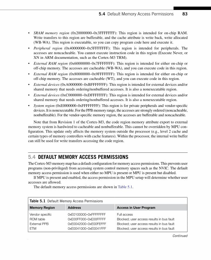
835.4 Default Memory Access Permissions
• SRAM memory region (0x20000000–0x3FFFFFFF): This region is intended for on-chip RAM. Write transfers to this region are bufferable, and the cache attribute is write back, write allocated (WB-WA). This region is executable, so you can copy program code here and execute it.
• Peripheral region (0x40000000–0x5FFFFFFF): This region is intended for peripherals. The accesses are noncacheable. You cannot execute instruction code in this region (Execute Never, or XN in ARM documentation, such as the Cortex-M3 TRM).
• External RAM region (0x60000000–0x7FFFFFFF): This region is intended for either on-chip or off-chip memory. The accesses are cacheable (WB-WA), and you can execute code in this region.
• External RAM region (0x80000000–0x9FFFFFFF): This region is intended for either on-chip or off-chip memory. The accesses are cacheable (WT), and you can execute code in this region.
• External devices (0xA0000000–0xBFFFFFFF): This region is intended for external devices and/or shared memory that needs ordering/nonbuffered accesses. It is also a nonexecutable region.
• External devices (0xC0000000–0xDFFFFFFF): This region is intended for external devices and/or shared memory that needs ordering/nonbuffered accesses. It is also a nonexecutable region.
• System region (0xE0000000–0xFFFFFFFF): This region is for private peripherals and vendor-specific devices. It is nonexecutable. For the PPB memory range, the accesses are strongly ordered (noncacheable, nonbufferable). For the vendor-specific memory region, the accesses are bufferable and noncacheable.
Note that from Revision 1 of the Cortex-M3, the code region memory attribute export to external memory system is hardwired to cacheable and nonbufferable. This cannot be overridden by MPU con-figuration. This update only affects the memory system outside the processor (e.g., level 2 cache and certain types of memory controllers with cache features). Within the processor, the internal write buffer can still be used for write transfers accessing the code region.
5�4 DeFaUlT MeMOry aCCess perMIssIOnsThe Cortex-M3 memory map has a default configuration for memory access permissions. This prevents user programs (non-privileged) from accessing system control memory spaces such as the NVIC. The default memory access permission is used when either no MPU is present or MPU is present but disabled.
If MPU is present and enabled, the access permission in the MPU setup will determine whether user accesses are allowed.
The default memory access permissions are shown in Table 5.1.
Table 5.1 Default Memory Access Permissions
Memory Region Address Access in User Program
Vendor specific 0xE0100000–0xFFFFFFFF Full accessROM table 0xE00FF000–0xE00FFFFF Blocked; user access results in bus faultExternal PPB 0xE0042000–0xE00FEFFF Blocked; user access results in bus faultETM 0xE0041000–0xE0041FFF Blocked; user access results in bus fault
Continued

84 CHAPTER 5 Memory Systems
5�5 BIT-BanD OperaTIOnsBit-band operation support allows a single load/store operation to access (read/write) to a single data bit. In the Cortex-M3, this is supported in two predefined memory regions called bit-band regions. One of them is located in the first 1 MB of the SRAM region, and the other is located in the first 1 MB of the peripheral region. These two memory regions can be accessed like normal memory, but they can also be accessed via a separate memory region called the bit-band alias (see Figure 5.3). When the bit-band alias address is used, each individual bit can be accessed separately in the least significant bit (LSB) of each word-aligned address.
For example, to set bit 2 in word data in address 0x20000000, instead of using three instructions to read the data, set the bit, and then write back the result, this task can be carried out by a single instruction (see Figure 5.4). The assembler sequence for these two cases could be like the one shown in Figure 5.5.
Similarly, bit-band support can simplify application code if we need to read a bit in a memory loca-tion. For example, if we need to determine bit 2 of address 0x20000000, we use the steps outlined in Figure 5.6. The assembler sequence for these two cases could be like the one shown in Figure 5.7.
Bit-band operation is not a new idea; in fact, a similar feature has existed for more than 30 years on 8-bit microcontrollers such as the 8051. Although the Cortex-M3 does not have special instructions for bit operation, special memory regions are defined so that data accesses to these regions are automati-cally converted into bit-band operations.
Note that the Cortex-M3 uses the following terms for the bit-band memory addresses:
• Bit-band region: This is a memory address region that supports bit-band operation.• Bit-band alias: Access to the bit-band alias will cause an access (a bit-band operation) to the
bit-band region. (Note: A memory remapping is performed.)
Table 5.1 Default Memory Access Permissions Continued
Memory Region Address Access in User Program
TPIU 0xE0040000–0xE0040FFF Blocked; user access results in bus faultInternal PPB 0xE000F000–0xE003FFFF Blocked; user access results in bus faultNVIC 0xE000E000–0xE000EFFF Blocked; user access results in bus fault, except
Software Trigger Interrupt Register that can be programmed to allow user accesses
FPB 0xE0002000–0xE0003FFF Blocked; user access results in bus faultDWT 0xE0001000–0xE0001FFF Blocked; user access results in bus faultITM 0xE0000000–0xE0000FFF Read allowed; write ignored except for stimulus
ports with user access enabledExternal device 0xA0000000–0xDFFFFFFF Full accessExternal RAM 0x60000000–0x9FFFFFFF Full accessPeripheral 0x40000000–0x5FFFFFFF Full accessSRAM 0x20000000–0x3FFFFFFF Full accessCode 0x00000000–0x1FFFFFFF Full access
When a user access is blocked, the fault exception takes place immediately.

85
Within the bit-band region, each word is represented by an LSB of 32 words in the bit-band alias address range. What actually happens is that when the bit-band alias address is accessed, the address is remapped into a bit-band address. For read operations, the word is read and the chosen bit location is shifted to the LSB of the read return data. For write operations, the written bit data are shifted to the required bit position, and a READ-MODIFY-WRITE is performed.
5.5 Bit-Band Operations
FIgUre 5�3
Bit Accesses to Bit-Band Region via the Bit-Band Alias.
0x20000000
0x20000004
0x20000008
0x200FFFFC031
0x220000000x2200002C
0x22000080
0x22000010
81624
Bit-bandregion
address
Bit-band aliasaddress
Bit
FIgUre 5�4
Write to Bit-Band Alias.
Read 0x20000000to register
Set bit 2 in register
Write register to0x20000000
Without bit-band With bit-band
Write 1 to0x22000008
Read data from0x20000000 to
buffer
Write to0x20000000 from
buffer with bit 2 set
Mapped to 2bus transfers
FIgUre 5�5
Example Assembler Sequence to Write a Bit with and without Bit-Band.
LDR R0,=0x20000000 ; Setup addressLDR R1, [R0] ; ReadORR.W R1, #0x4 ; Modify bitSTR R1, [R0] ; Write back result
With bit-band
LDR R0,=0x22000008 ; Setup addMOV R1, #1 ; Setup datSTR R1, [R0] ; Write
Without bit-band

86 CHAPTER 5 Memory Systems
There are two regions of memory for bit-band operations:
0x20000000–0x200FFFFF (SRAM, 1 MB)•0x40000000–0x400FFFFF (peripherals, 1 MB)•
For the SRAM memory region, the remapping of the bit-band alias is shown in Table 5.2.Similarly, the bit-band region of the peripheral memory region can be accessed via bit-band aliased
addresses, as shown in Table 5.3.
FIgUre 5�6
Read from the Bit-Band Alias.
Read 0x20000000to register
Shift bit 2 to LSBand mask other bits
Without bit-band With bit-band
Read from0x22000008
Mapped to 1bus transfers
Read data from0x20000000, and
extract bit 2 toregister
FIgUre 5�7
Read from the Bit-Band Alias.
LDR R0,=0x20000000 ; Setup addressLDR R1, [R0] ; ReadUBFX.W R1, R1, #2, #1 ; Extract bit[2]
With bit-band
LDR R0,=0x22000008 ; Setup addressLDR R1, [R0] ; Read
Without bit-band
Table 5.2 Remapping of Bit-Band Addresses in SRAM Region
Bit-Band Region Aliased Equivalent
0x20000000 bit[0] 0x22000000 bit[0]0x20000000 bit[1] 0x22000004 bit[0]0x20000000 bit[2] 0x22000008 bit[0]… …0x20000000 bit[31] 0x2200007C bit[0]0x20000004 bit[0] 0x22000080 bit[0]… …0x20000004 bit[31] 0x220000FC bit[0]… …0x200FFFFC bit[31] 0x23FFFFFC bit[0]

875.5 Bit-Band Operations
Here’s a simple example:
Set address 0x20000000 to a value of 0x3355AACC.1� Read address 0x22000008. This read access is remapped into read access to 0x20000000. The 2� return value is 1 (bit[2] of 0x3355AACC).Write 0x0 to 0x22000008. This write access is remapped into a READ-MODIFY-WRITE to 3� 0x20000000. The value 0x3355AACC is read from memory, bit 2 is cleared, and a result of 0x3355AAC8 is written back to address 0x20000000.Now, read 0x20000000. That gives you a return value of 0x3355AAC8 (bit[2] cleared).4�
When you access bit-band alias addresses, only the LSB (bit[0]) in the data is used. In addition, accesses to the bit-band alias region should not be unaligned. If an unaligned access is carried out to bit-band alias address range, the result is unpredictable.
5�5�1 advantages of Bit-Band OperationsSo, what are the uses of bit-band operations? We can use them to, for example, implement serial data transfers in general-purpose input/output (GPIO) ports to serial devices. The application code can be implemented easily because access to serial data and clock signals can be separated.
Bit-band operation can also be used to simplify branch decisions. For example, if a branch should be carried out based on 1 single bit in a status register in a peripheral, instead of
Reading the whole register•Masking the unwanted bits•Comparing and branching•
Table 5.3 Remapping of Bit-Band Addresses in Peripheral Memory Region
Bit-Band Region Aliased Equivalent
0x40000000 bit[0] 0x42000000 bit[0]0x40000000 bit[1] 0x42000004 bit[0]0x40000000 bit[2] 0x42000008 bit[0]… …0x40000000 bit[31] 0x4200007C bit[0]0x40000004 bit[0] 0x42000080 bit[0]… …0x40000004 bit[31] 0x420000FC bit[0]… …0x400FFFFC bit[31] 0x43FFFFFC bit[0]
BIT-BanD versUs BIT-BangIn the Cortex-M3, we use the term bit-band to indicate that the feature is a special memory band (region) that provides bit accesses. Bit-bang commonly refers to driving I/O pins under software control to provide serial communication functions. The bit-band feature in the Cortex-M3 can be used for bit-banging implementations, but the definitions of these two terms are different.

88 CHAPTER 5 Memory Systems
you can simplify the operations to
Reading the status bit via the bit-band alias (get 0 or 1)•Comparing and branching•
Besides providing faster bit operations with fewer instructions, the bit-band feature in the Cortex-M3 is also essential for situations in which resources are being shared by more than one process. One of the most important advantages or properties of a bit-band operation is that it is atomic. In other words, the READ-MODIFY-WRITE sequence cannot be interrupted by other bus activities. Without this behav-ior in, for example, using a software READ-MODIFY-WRITE sequence, the following problem can occur: consider a simple output port with bit 0 used by a main program and bit 1 used by an interrupt handler. A software-based READ-MODIFY-WRITE operation can cause data conflicts, as shown in Figure 5.8.
With the Cortex-M3 bit-band feature, this kind of race condition can be avoided because the READ-MODIFY-WRITE is carried out at the hardware level and is atomic (the two transfers cannot be pulled apart) and interrupts cannot take place between them (see Figure 5.9).
Similar issues can be found in multitasking systems. For example, if bit 0 of the output port is used by Process A and bit 1 is used by Process B, a data conflict can occur in software-based READ-MODIFY-WRITE (see Figure 5.10).
FIgUre 5�8
Data Are Lost When an Exception Handler Modifies a Shared Memory Location.
Without bit-band operation
Output portread to register
Output portread to register
Bit 0 setby mainprogram
Bit 0 clearby mainprogram
Write tooutput port
Write tooutput port
Main program
Interrupt handler
Output portread
Bit 1 modified by interrupt
handler
Write tooutput port
Time
0x00 0x01 0x03 0x00
Thread mode
Handler mode
Change made byinterrupt handler lost
Output portvalue

895.5 Bit-Band Operations
FIgUre 5�9
Data Loss Prevention with Locked Transfers Using the Bit-Band Feature.
With bit-band operation
Main program
Interrupt handler
Time
Output portvalue
0x00 0x01 0x00 0x02
Thread mode
Handler mode
Locked read-modify-write
Write tooutput port via bit-band alias
Locked read-modify-write
Locked read-modify-write
Bit 0 set by main programby write to bit-band alias
Bit 1 modified by interrupthandler by write to bit-band
alias
FIgUre 5�10
Data Are Lost When a Different Task Modifies a Shared Memory Location.
Without bit-band operation
Output portread to register
Output portread to register
Bit 0 set bytask A
Write tooutput port
Bit 0 clear bytask A
Write tooutput port
Task A
Task B
Output portread
Bit 1 modifiedby task B
Write tooutput port
Time
Output port value
0x00 0x01 0x03 0x00
Current task
Change made bytask B is lost
Task A Task B Task A Task B Task A

90 CHAPTER 5 Memory Systems
Again, the bit-band feature can ensure that bit accesses from each task are separated so that no data conflicts occur (see Figure 5.11).
Besides I/O functions, the bit-band feature can be used for storing and handling Boolean data in the SRAM region. For example, multiple Boolean variables can be packed into one single memory location to save memory space, whereas the access to each bit is still completely separated when the access is carried out via the bit-band alias address range.
For system-on-chip (SoC) designers designing a bit-band-capable device, the device’s memory address should be located within the bit-band memory, and the lock (HMASTLOCK) signal from the AHB interface must be checked to make sure that writable register contents will not be changed except by the bus when a locked transfer is carried out.
5�5�2 Bit-Band Operation of Different Data sizesBit-band operation is not limited to word transfers. It can be carried out as byte transfers or half word transfers as well. For example, when a byte access instruction (LDRB/STRB) is used to access a bit-band alias address range, the accesses generated to the bit-band region will be in byte size. The same applies to half word transfers (LDRH/STRH). When you use nonword transfers to bit-band alias addresses, the address value should still be word aligned.
5�5�3 Bit-Band Operations in C programsThere is no native support of bit-band operation in most C compilers. For example, C compilers do not understand that the same memory can be accessed using two different addresses, and they do not know that accesses to the bit-band alias will only access the LSB of the memory location. To use the
FIgUre 5�11
Data Loss Prevention with Locked Transfers Using the Bit-Band Feature.
With bit-band operation
Task A
Task B
Time
Output portvalue 0x00 0x01 0x00 0x02
Locked read-modify-write
Write tooutput port via bit-band alias
Locked read-modify-write
Locked read-modify-write
Bit 0 set by task A by write to bit-band alias
Bit 1 modified by task B bywrite to bit-band alias
Current task Task A Task B Task A Task B Task A

915.5 Bit-Band Operations
bit-band feature in C, the simplest solution is to separately declare the address and the bit-band alias of a memory location. For example:
#define DEVICE_REG0 *((volatile unsigned long *) (0x40000000))#define DEVICE_REG0_BIT0 *((volatile unsigned long *) (0x42000000))#define DEVICE_REG0_BIT1 *((volatile unsigned long *) (0x42000004))...DEVICE_REG0 = 0xAB; // Accessing the hardware register by normal // address...DEVICE_REG0 = DEVICE_REG0 | 0x2; // Setting bit 1 without using // bitband feature...DEVICE_REG0_BIT1 = 0x1; // Setting bit 1 using bitband feature // via the bit band alias address
It is also possible to develop C macros to make accessing the bit-band alias easier. For example, we could set up one macro to convert the bit-band address and the bit number into the bit-band alias address and set up another macro to access the memory location by taking the address value as a pointer:
// Convert bit band address and bit number into// bit band alias address#define BITBAND(addr,bitnum) ((addr & 0xF0000000)+0x2000000+((addr & 0xFFFFF)<<5)+(bitnum <<2))// Convert the address as a pointer#define MEM_ADDR(addr) *((volatile unsigned long *) (addr))
Based on the previous example, we rewrite the code as follows:
#define DEVICE_REG0 0x40000000#define BITBAND(addr,bitnum) ((addr & 0xF0000000)+0x02000000+((addr & 0xFFFFF)<<5)+(bitnum<<2))#define MEM_ADDR(addr) *((volatile unsigned long *) (addr))...MEM_ADDR(DEVICE_REG0) = 0xAB; // Accessing the hardware // register by normal address...// Setting bit 1 without using bitband featureMEM_ADDR(DEVICE_REG0) = MEM_ADDR(DEVICE_REG0) | 0x2;...// Setting bit 1 with using bitband featureMEM_ADDR(BITBAND(DEVICE_REG0,1)) = 0x1;
Note that when the bit-band feature is used, the variables being accessed might need to be declared as volatile. The C compilers do not know that the same data could be accessed in two different addresses, so the volatile property is used to ensure that each time a variable is accessed, the memory location is accessed instead of a local copy of the data inside the processor.
Starting from ARM RealView Development Suite version 4.0 and Keil MDK-ARM 3.80, bit band support is provided by __attribute__((bitband)) language extension and __bitband command line option (see reference 6). You can find further examples of bit-band accesses with C macros using ARM RealView Compiler Tools in the ARM Application Note 179 [Ref. 7].

92 CHAPTER 5 Memory Systems
5�6 UnalIgneD TransFersThe Cortex-M3 supports unaligned transfers on single accesses. Data memory accesses can be defined as aligned or unaligned. Traditionally, ARM processors (such as the ARM7/ARM9/ARM10) allow only aligned transfers. That means in accessing memory, a word transfer must have address bit[1] and bit[0] equal to 0, and a half word transfer must have address bit[0] equal to 0. For example, word data can be located at 0x1000 or 0x1004, but it cannot be located in 0x1001, 0x1002, or 0x1003. For half word data, the address can be 0x1000 or 0x1002, but it cannot be 0x1001.
So, what does an unaligned transfer look like? Figures 5.12 through 5.16 show some examples. Assuming that the memory infrastructure is 32-bit (4 bytes) wide, an unaligned transfer can be any word size read/write such that the address is not a multiple of 4, as shown in Figures 5.12–5.14, or when the transfer is in half word size, and the address is not a multiple of 2, as shown in Figures 5.15 and 5.16.
All the byte-size transfers are aligned on the Cortex-M3 because the minimum address step is 1 byte.
FIgUre 5�12
Unaligned Transfer Example 1.
Address NAddress N14
Byte3
Byte2
Byte1
Byte0
[23:16] [15:8] [7:0][31:24] Unaligned word data
at address N11
FIgUre 5�13
Unaligned Transfer Example 2.
Address NAddress N�4
Byte3
Byte2
Byte1
Byte0
[15:8] [7:0][31:24] Unaligned word data
at address N�2[23:16]
FIgUre 5�14
Unaligned Transfer Example 3.
Byte3
Byte2
Byte1
Byte0
[7:0][31:24] Unaligned word data
at address N�3[23:16] [15:8]
Address NAddress N�4
FIgUre 5�15
Unaligned Transfer Example 4.
Byte3
Byte2
Byte1
Byte0
[7:0]Unaligned half word dataat address N�1[15:8]Address N
Address N�4
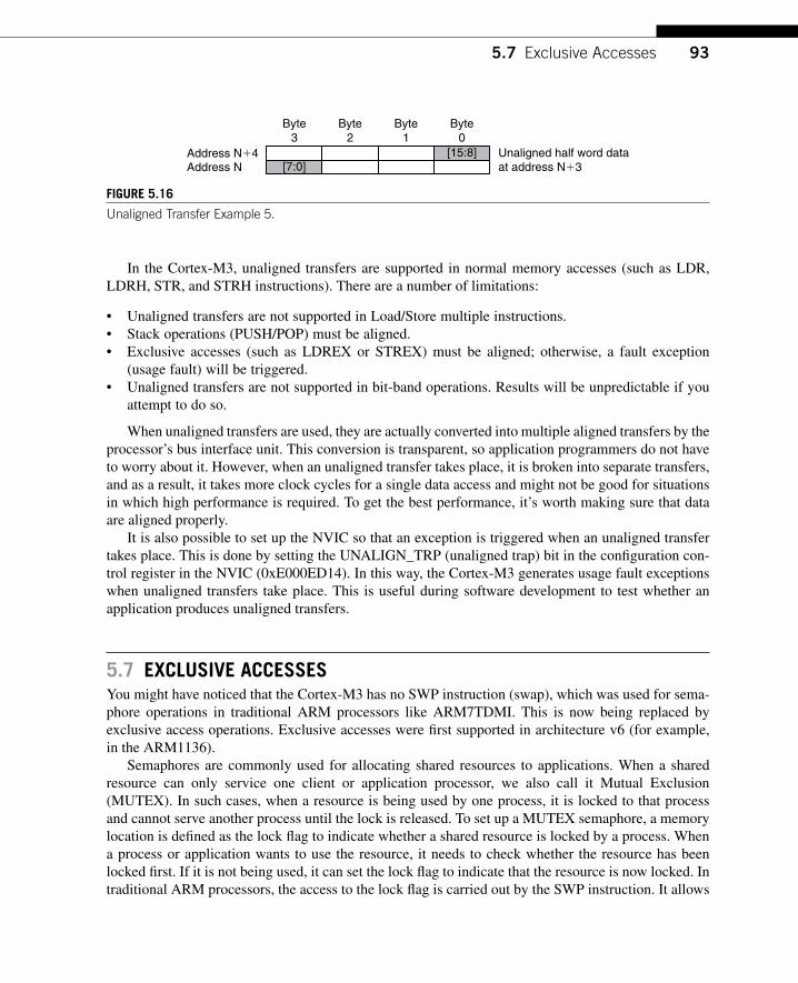
935.7 Exclusive Accesses
In the Cortex-M3, unaligned transfers are supported in normal memory accesses (such as LDR, LDRH, STR, and STRH instructions). There are a number of limitations:
Unaligned transfers are not supported in Load/Store multiple instructions.•Stack operations (PUSH/POP) must be aligned.•Exclusive accesses (such as LDREX or STREX) must be aligned; otherwise, a fault exception •(usage fault) will be triggered.Unaligned transfers are not supported in bit-band operations. Results will be unpredictable if you •attempt to do so.
When unaligned transfers are used, they are actually converted into multiple aligned transfers by the processor’s bus interface unit. This conversion is transparent, so application programmers do not have to worry about it. However, when an unaligned transfer takes place, it is broken into separate transfers, and as a result, it takes more clock cycles for a single data access and might not be good for situations in which high performance is required. To get the best performance, it’s worth making sure that data are aligned properly.
It is also possible to set up the NVIC so that an exception is triggered when an unaligned transfer takes place. This is done by setting the UNALIGN_TRP (unaligned trap) bit in the configuration con-trol register in the NVIC (0xE000ED14). In this way, the Cortex-M3 generates usage fault exceptions when unaligned transfers take place. This is useful during software development to test whether an application produces unaligned transfers.
5�7 exClUsIve aCCessesYou might have noticed that the Cortex-M3 has no SWP instruction (swap), which was used for sema-phore operations in traditional ARM processors like ARM7TDMI. This is now being replaced by exclusive access operations. Exclusive accesses were first supported in architecture v6 (for example, in the ARM1136).
Semaphores are commonly used for allocating shared resources to applications. When a shared resource can only service one client or application processor, we also call it Mutual Exclusion (MUTEX). In such cases, when a resource is being used by one process, it is locked to that process and cannot serve another process until the lock is released. To set up a MUTEX semaphore, a memory location is defined as the lock flag to indicate whether a shared resource is locked by a process. When a process or application wants to use the resource, it needs to check whether the resource has been locked first. If it is not being used, it can set the lock flag to indicate that the resource is now locked. In traditional ARM processors, the access to the lock flag is carried out by the SWP instruction. It allows
FIgUre 5�16
Unaligned Transfer Example 5.
Byte3
Byte2
Byte1
Byte0
[7:0]Unaligned half word dataat address N�3
[15:8]Address NAddress N�4

94 CHAPTER 5 Memory Systems
the lock flag read and write to be atomic, preventing the resource from being locked by two processes at the same time.
In newer ARM processors, the read/write access can be carried out on separated buses. In such situations, the SWP instructions can no longer be used to make the memory access atomic because the read and write in a locked transfer sequence must be on the same bus. Therefore, the locked transfers are replaced by exclusive accesses. The concept of exclusive access operation is quite simple but different from SWP; it allows the possibility that the memory location for a semaphore could be accessed by another bus master or another process running on the same processor (see Figure 5.17).
To allow exclusive access to work properly in a multiple processor environment, an additional hardware called “exclusive access monitor” is required. This monitor checks the transfers toward shared address locations and replies to the processor if an exclusive access is success. The processor bus interface also provides additional control signals1 to this monitor to indicate if the transfer is an exclusive access.
If the memory device has been accessed by another bus master between the exclusive read and the exclusive write, the exclusive access monitor will flag an exclusive failed through the bus system when the processor attempts the exclusive write. This will cause the return status of the exclusive write to be 1. In the case of failed exclusive write, the exclusive access monitor also blocks the write transfer from getting to the exclusive access address.
1Exclusive access signals are available on the system bus and the D-Code bus of the Cortex-M3 processor. They are EXREQD and EXRESPD for the D-Code bus and EXREQS and EXRESPS for the system bus. The I-Code bus that is used for instruc-tion fetch cannot generate exclusive accesses.
Exclusive Read(e.g., LDREX)
Exclusive Write(e.g., STREX)
Read lock bit
Check lock bit set?
Set lock bit
Yes
YesNo
No
Failed: Lock bit already set,indicates the requestedresource is used by anotherprocess or processor
Failed: Memory regionwhere the lock bit is couldhave been accessed byanother process or anotherprocessor
Success. The lock bit is setand the processor can haveaccess to the sharedresource
Return statusfrom exclusive
write 5 0(success)?
FIgUre 5�17
Using Exclusive Access in MUTEX Semaphores.

955.8 Endian Mode
Exclusive access instructions in the Cortex-M3 include LDREX (word), LDREXB (byte), LDREXH (half word), STREX (word), STREXB (byte), and STREXH (half word). A simple example of the syn-tax is as follows:
LDREX <Rxf>, [Rn, #offset]STREX <Rd>, <Rxf>,[Rn, #offset]
Where Rd is the return status of the exclusive write (0 = success and 1 = failure). Example code for exclusive accesses can be found in Chapter 10. You can also access exclusive
access instructions in C using intrinsic functions provided in Cortex Microcontroller Software Inter-face Standard (CMSIS) compliant device driver libraries from microcontroller vendors: __LDREX, __LEDEXH, __LDREXB, __STREX, __STREXH, __STREXB. More details of these functions are covered in Appendix G.
When exclusive accesses are used, the internal write buffers in the Cortex-M3 bus interface will be bypassed, even when the MPU defines the region as bufferable. This ensures that semaphore infor-mation on the physical memory is always up to date and coherent between bus masters. SoC design-ers using Cortex-M3 on multiprocessor systems should ensure that the memory system enforces data coherency when exclusive transfers occur.
5�8 enDIan MODeThe Cortex-M3 supports both little endian and big endian modes. However, the supported memory type also depends on the design of the rest of the microcontroller (bus connections, memory control-lers, peripherals, and so on). Make sure that you check your microcontroller datasheets in detail before developing your software. In most cases, Cortex-M3-based microcontrollers will be little endian. With little endian mode, the first byte of a word size data is stored in the least significant byte of the 32-bit memory location (see Table 5.4).
There are some microcontrollers that use big endian mode. In such a case, the first byte of a word size data is stored in the most significant byte of the 32-bit address memory location (see Table 5.5).
The definition of big endian in the Cortex-M3 is different from the ARM7. In the ARM7TDMI, the big endian scheme is called word-invariant big endian, also referred as BE-32 in ARM documentation, whereas in the Cortex-M3, the big endian scheme is called byte-invariant big endian, also referred as BE-8 (byte-invariant big endian is supported on ARM architecture v6 and v7). The memory view of both schemes is the same, but the byte lane usage on the bus interface during data transfers is different (see Tables 5.6 and 5.7).
Note that the data transfer on the AHB bus in BE-8 mode uses the same data byte lanes as in little endian. However, the data byte inside the half word or word data is reversely ordered compared to little endian (see Table 5.8).
Table 5.4 The Cortex-M3 Little Endian Memory View Example
Address Bits 31 – 24 Bits 23 – 16 Bits 15 – 8 Bits 7 – 0
0x1003 – 0x1000 Byte – 0x1003 Byte – 0x1002 Byte – 0x1001 Byte – 0x10000x1007 – 0x1004 Byte – 0x1007 Byte – 0x1006 Byte – 0x1005 Byte – 0x1004… Byte – 4xN+3 Byte – 4xN+2 Byte – 4xN+1 Byte – 4xN

96 CHAPTER 5 Memory Systems
Table 5.5 The Cortex-M3 Big Endian Memory View Example
Address Bits 31 – 24 Bits 23 – 16 Bits 15 – 8 Bits 7 – 0
0x1003 – 0x1000 Byte – 0x1000 Byte – 0x1001 Byte – 0x1002 Byte – 0x10030x1007 – 0x1004 Byte – 0x1004 Byte – 0x1005 Byte – 0x1006 Byte – 0x1007… Byte – 4xN Byte – 4xN+1 Byte – 4xN+2 Byte – 4xN+3
Table 5.6 The Cortex-M3 (Byte-Invariant Big Endian, BE-8)—Data on the AHB Bus
Address, Size Bits 31 – 24 Bits 23 – 16 Bits 15 – 8 Bits 7 – 0
0x1000, word Data bit [7:0] Data bit [15:8] Data bit [23:16] Data bit [31:24]0x1000, half word — — Data bit [7:0] Data bit [15:8]0x1002, half word Data bit [7:0] Data bit [15:8] — —0x1000, byte — — — Data bit [7:0]0x1001, byte — — Data bit [7:0] —0x1002, byte — Data bit [7:0] — —0x1003, byte Data bit [7:0] — — —
Table 5.7 ARM7TDMI (Word-Invariant Big Endian, BE-32)—Data on the AHB Bus
Address, Size Bits 31 – 24 Bits 23 – 16 Bits 15 – 8 Bits 7 – 0
0x1000, word Data bit [7:0] Data bit [15:8] Data bit [23:16] Data bit [31:24]0x1000, half word Data bit [7:0] Data bit [15:8] — —0x1002, half word — — Data bit [7:0] Data bit [15:8]0x1000, byte Data bit [7:0] — — —0x1001, byte — Data bit [7:0] — —0x1002, byte — — Data bit [7:0] —0x1003, byte — — — Data bit [7:0]
Table 5.8 The Cortex-M3 Little Endian—Data on the AHB Bus
Address, Size Bits 31 – 24 Bits 23 – 16 Bits 15 – 8 Bits 7 – 0
0x1000, word Data bit [31:24] Data bit [23:16] Data bit [15:8] Data bit [7:0]0x1000, half word — — Data bit [15:8] Data bit [7:0]0x1002, half word Data bit [15:8] Data bit [7:0] — —0x1000, byte — — — Data bit [7:0]0x1001, byte — — Data bit [7:0] —0x1002, byte — Data bit [7:0] — —0x1003, byte Data bit [7:0] — — —

975.8 Endian Mode
In the Cortex-M3 processor, the endian mode is set when the processor exits reset. The endian mode cannot be changed afterward. (There is no dynamic endian switching, and the SETEND instruction is not supported.) Instruction fetches are always in little endian as are data accesses in the system control memory space (such as NVIC and FPB) and the external PPB memory range (memory range from 0xE0000000 to 0xE00FFFFF is always little endian).
In case your SoC does not support big endian but one or some of the peripherals you are using con-tain big endian data, you can easily convert the data between little endian and big endian using some of the data type conversion instructions in the Cortex-M3. For example, REV and REV16 are very useful for this kind of conversion.

99Copyright © 2010, Elsevier Inc. All rights reserved.DOI: 10.1016/B978-1-85617-963-8.00009-0
In ThIs ChapTer
The pipeline ........................................................................................................................................... 99a Detailed Block Diagram ..................................................................................................................... 101Bus Interfaces on the Cortex-M3 ........................................................................................................... 104Other Interfaces on the Cortex-M3 ......................................................................................................... 105The external ppB .................................................................................................................................. 105Typical Connections .............................................................................................................................. 106reset Types and reset signals .............................................................................................................. 107
Cortex-M3 Implementation Overview 6
This chapter is mainly written for system-on-chip (SoC) designers who are interested in using the Cortex™-M3 processor in their project. Normal microcontroller users do not need to learn these details. However, for those who are interested in understanding the internal operations of the Cortex-M3 processor, this chapter provides a good overview of the design.
6.1 The pIpelIneThe Cortex-M3 processor has a three-stage pipeline. The pipeline stages are instruction fetch, instruc-tion decode, and instruction execution (see Figure 6.1).
Some people might argue that there are four stages because of the pipeline behavior in the bus interface when it accesses memory, but this stage is outside the processor, so the processor itself still has only three stages.
When running programs with mostly 16-bit instructions, you will find that the processor might not fetch instructions in every cycle. This is because the processor fetches up to two instructions (32-bit) in one go, so after one instruction is fetched, the next one is already inside the processor. In this case, the processor bus interface may try to fetch the instruction after the next or, if the buffer is full, the bus interface could be idle. Some of the instructions take multiple cycles to execute; in this case, the pipeline will be stalled.
In executing a branch instruction, the pipeline will be flushed. The processor will have to fetch instructions from the branch destination to fill up the pipeline again. However, the Cortex-M3 processor
CHAPTER

100 CHAPTER 6 Cortex-M3 Implementation Overview
supports a number of instructions in v7-M architecture, so some of the short-distance branches can be avoided by replacing them with conditional execution codes.1
Because of the pipeline nature of the processor and to ensure that the program is compatible with Thumb® codes, the read value will be the address of the instruction plus 4, when the program counter is read during instruction execution. If the program counter is used for address generation for memory accesses, the word aligned value of the instruction address plus 4 would be used. This offset is constant, independent of the combination of 16-bit Thumb instructions and 32-bit Thumb-2 instructions. This ensures consistency between Thumb and Thumb-2.
Inside the instruction prefetch unit of the processor core, there is also an instruction buffer (see Figure 6.2). This buffer allows additional instructions to be queued before they are needed. This buffer
1For more information, refer to the “IF-THEN Instructions” section of Chapter 4.
FIgure 6.1
The Three-Stage Pipeline in the Cortex-M3.
Instruction N
Instruction N�1
Instruction N�2
Instruction N�3
Fetch Decode
Fetch Decode Execute
Fetch Decode Execute
Fetch Decode Execute
Execute
FIgure 6.2
Use of a Buffer in the Instruction Fetch Unit to Improve 32-Bit Instruction Handling.
Instructionfetch
(Inst C2 & D)
Decode(Inst B)
Execute(Inst A)
Instructionbuffer
(Inst C1)
Instruction
B1 A2
C1 B2
D
A1
C2
Instructionmemory
N
N 1 4
N 1 8
N 1 0xC
Byte
0123
Executing
Decoding
Fetching
Pipeline stage
Unaligned 32-bit Thumb-2instruction in memory

1016.2 A Detailed Block Diagram
prevents the pipeline being stalled when the instruction sequence contains 32-bit Thumb-2 instructions that are not word aligned. However, this buffer does not add an extra stage to the pipeline, so it does not increase the branch penalty.
6.2 a DeTaIleD BlOCk DIagraMThe Cortex-M3 processor contains not only the processor core but also a number of components for system management, as well as debugging support components (see Figure 6.3). These components are linked together using an Advanced High-Performance Bus (AHB), and an Advanced Peripheral Bus (APB). The AHB and APB are part of the Advanced Microcontroller Bus Architecture (AMBA) standards [Ref. 4].
Note that the MPU, WIC, and ETM blocks are optional blocks that can be included in the microcon-troller system at the time of implementation. A number of new components are shown in Table 6.1.
The Cortex-M3 processor is released as a processor subsystem (see Figure 6.3). The CPU core itself is closely coupled to the interrupt controller (NVIC) and various debug logic blocks:
• CM3Core: The Cortex-M3 core contains the registers, ALU, data path, and bus interface.
• NVIC: The NVIC is a built-in interrupt controller. The number of interrupts is customized by chip manufacturers. The NVIC is closely coupled to the CPU core and contains a number of system
FIgure 6.3
The Cortex-M3 Processor System Block Diagram.
CM3CoreNMI
Interrupts
MPU
Instruction bus Data bus
AHB interconnect(Internal BusMatrix)
Connection to AHB slaves
Connection to AHB masters
AHB-APSWJ-DP/SW-DP
interface
Debuginterface
AHB toAPB
bridge
Instruction bus(I.Code)
Data bus(D.Code)
Systembus
Private peripheralbus (PPB)
DWT
FPB
Internal private peripheral bus
(APB)
Internal private peripheral bus
(AHB)
ITM
TPIUNVIC
Traceoutput
SYSTICK
WIC
ROMTable
ETM
Trigger
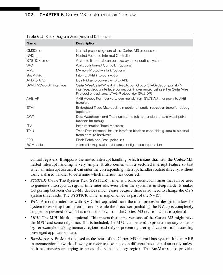
102 CHAPTER 6 Cortex-M3 Implementation Overview
control registers. It supports the nested interrupt handling, which means that with the Cortex-M3, nested interrupt handling is very simple. It also comes with a vectored interrupt feature so that when an interrupt occurs, it can enter the corresponding interrupt handler routine directly, without using a shared handler to determine which interrupt has occurred.
• SYSTICK Timer: The System Tick (SYSTICK) Timer is a basic countdown timer that can be used to generate interrupts at regular time intervals, even when the system is in sleep mode. It makes OS porting between Cortex-M3 devices much easier because there is no need to change the OS’s system timer code. The SYSTICK Timer is implemented as part of the NVIC.
• WIC: A module interface with NVIC but separated from the main processor design to allow the system to wake up from interrupt events while the processor (including the NVIC) is completely stopped or powered down. This module is new from the Cortex-M3 revision 2 and is optional.
• MPU: The MPU block is optional. This means that some versions of the Cortex-M3 might have the MPU and some might not. If it is included, the MPU can be used to protect memory contents by, for example, making memory regions read-only or preventing user applications from accessing privileged applications data.
• BusMatrix: A BusMatrix is used as the heart of the Cortex-M3 internal bus system. It is an AHB interconnection network, allowing transfer to take place on different buses simultaneously unless both bus masters are trying to access the same memory region. The BusMatrix also provides
Table 6.1 Block Diagram Acronyms and Definitions
Name Description
CM3Core Central processing core of the Cortex-M3 processorNVIC Nested Vectored Interrupt ControllerSYSTICK timer A simple timer that can be used by the operating systemWIC Wakeup Interrupt Controller (optional)MPU Memory Protection Unit (optional)BusMatrix Internal AHB interconnectionAHB to APB Bus bridge to convert AHB to APBSW-DP/SWJ-DP interface Serial Wire/Serial Wire Joint Test Action Group (JTAG) debug port (DP)
interface; debug interface connection implemented using either Serial Wire Protocol or traditional JTAG Protocol (for SWJ-DP)
AHB-AP AHB Access Port; converts commands from SW/SWJ interface into AHB transfers
ETM Embedded Trace Macrocell; a module to handle instruction trace for debug (optional)
DWT Data Watchpoint and Trace unit; a module to handle the data watchpoint function for debug
ITM Instrumentation Trace MacrocellTPIU Trace Port Interface Unit; an interface block to send debug data to external
trace capture hardwareFPB Flash Patch and Breakpoint unitROM table A small lookup table that stores configuration information
1036.2 A Detailed Block Diagram
additional data transfer management, including a write buffer as well as bit-oriented operations (bit-band).
• AHB to APB: An AHB-to-APB bus bridge is used to connect a number of APB devices such as debugging components to the private peripheral bus in the Cortex-M3 processor. In addition, the Cortex-M3 allows chip manufacturers to attach additional APB devices to the external private peripheral bus (PPB) using this APB bus.
The rest of the components in the block diagram are for debugging support and normally should not be used by application code.
• SW-DP/SWJ-DP: The Serial Wire Debug Port (SW-DP)/Serial Wire JTAG Debug Port (SWJ-DP) work together with the AHB Access Port (AHB-AP) so that external debuggers can generate AHB transfers to control debug activities. There is no JTAG scan chain inside the processor core of the Cortex-M3; most debugging functions are controlled by the NVIC registers through AHB accesses. SWJ-DP supports both the Serial Wire Protocol and the JTAG Protocol, whereas SW-DP can support only the Serial Wire Protocol.
• AHB-AP: The AHB-AP provides access to the whole Cortex-M3 memory through a few registers. This block is controlled by the SW-DP/SWJ-DP through a generic debug interface called the Debug Access Port (DAP). To carry out debugging functions, the external debugging hardware needs to access the AHB-AP through the SW-DP/SWJ-DP to generate the required AHB transfers.
• ETM: The ETM is an optional component for instruction trace, so some Cortex-M3 products might not have real-time instruction trace capability. Trace information is output to the trace port through TPIU. The ETM control registers are memory mapped, which can be controlled by the debugger through the DAP.
• DWT: The DWT allows data watchpoints to be set up. When a data address or data value match is found, the match hit event can be used to generate watchpoint events to activate the debugger, generate data trace information, or activate the ETM.
• ITM: The ITM can be used in several ways. Software can write to this module directly to output information to TPIU, or the DWT matching events can be used to generate data trace packets through ITM for output into a trace data stream.
• TPIU: The TPIU is used to interface with external trace hardware such as trace port analyzers. Internal to the Cortex-M3, trace information is formatted as Advanced Trace Bus (ATB) packets, and the TPIU reformats the data to allow data to be captured by external devices.
• FPB: The FPB is used to provide Flash Patch and Breakpoint functionalities. Flash Patch means that if an instruction access by the CPU matches a certain address, the address can be remapped to a different location so that a different value is fetched. Alternatively, the matched address can be used to trigger a breakpoint event. The Flash Patch feature is very useful for testing, such as adding diagnosis program code to a device that cannot be used in normal situations unless the FPB is used to change the program control.
• ROM table: A small ROM table is provided. This is simply a small lookup table to provide memory map information for various system devices and debugging components. Debugging systems use this table to locate the memory addresses of debugging components. In most cases, the memory map

104 CHAPTER 6 Cortex-M3 Implementation Overview
should be fixed to the standard memory location, as documented in the Cortex-M3 Technical Reference Manual (TRM) [Ref. 1], but because some of the debugging components are optional and additional components can be added, individual chip manufacturers might want to customize their chip’s debugging features. In this case, the ROM table must be customized and used for debugging software to determine the correct memory map and hence detect the type of debugging components available.
6.3 Bus InTerFaCes On The COrTex-M3Unless you are designing an SoC product using the Cortex-M3 processor, it is unlikely that you can directly access the bus interface signals described here. Normally, the chip manufacturer will hook up all the bus signals to memory blocks and peripherals, and in a few cases, you might find that the chip manufacturer connected the bus to a bus bridge and allows external bus systems to be connected off-chip. The bus interfaces on the Cortex-M3 processor are based on AHB-Lite and APB protocols, which are documented in the AMBA Specification [Ref. 4].
6.3.1 The I-Code BusThe I-Code bus is a 32-bit bus based on the AHB-Lite bus protocol for instruction fetches in memory regions from 0x00000000 to 0x1FFFFFFF. Instruction fetches are performed in word size, even for 16-bit Thumb instructions. Therefore, during execution, the CPU core could fetch up to two Thumb instructions at a time.
6.3.2 The D-Code BusThe D-Code bus is a 32-bit bus based on the AHB-Lite bus protocol; it is used for data access in memory regions from 0x00000000 to 0x1FFFFFFF. Although the Cortex-M3 processor supports unaligned transfers, you won’t get any unaligned transfer on this bus, because the bus interface on the processor core converts the unaligned transfers into aligned transfers for you. Therefore, devices (such as memory) that attach to this bus need only support AHB-Lite (AMBA 2.0) aligned transfers.
6.3.3 The system BusThe system bus is a 32-bit bus based on the AHB-Lite bus protocol; it is used for instruction fetch and data access in memory regions from 0x20000000 to 0xDFFFFFFF and 0xE0100000 to 0xFFFFFFFF. Similar to the D-Code bus, all the transfers on the system bus are aligned.
6.3.4 The external ppBThe External PPB is a 32-bit bus based on the APB bus protocol. This is intended for private periph-eral accesses in memory regions 0xE0040000 to 0xE00FFFFF. However, since some part of this APB memory is already used for TPIU, ETM, and the ROM table, the memory region that can be used for attaching extra peripherals on this bus is only 0xE0042000 to 0xE00FF000. Transfers on this bus are word aligned.

1056.5 The External PPB
6.3.5 The Dap BusThe DAP bus interface is a 32-bit bus based on an enhanced version of the APB specification. This is for attaching debug interface blocks such as SWJ-DP or SW-DP. Do not use this bus for other purposes. More information on this interface can be found in Chapter 15, or in the ARM document CoreSight Technology System Design Guide [Ref. 3].
6.4 OTher InTerFaCes On The COrTex-M3Apart from bus interfaces, the Cortex-M3 processor has a number of other interfaces for various pur-poses. These signals are unlikely to appear on the pins of the silicon chip, because they are mostly for connecting to various parts of the SoC or are unused. The details of the signals are contained in the Cortex-M3 Technical Reference Manual [Ref. 1]. Table 6.2 contains a short summary of some of them.
6.5 The exTernal ppBThe Cortex-M3 processor has an External PPB interface. The External PPB interface is based on the APB protocol in AMBA specification 2.0 (for Cortex-M3 revision 0 and revision 1) or 3.0 (for Cortex-M3 revision 2). It is intended for system devices that should not be shared, such as debugging components.
Table 6.2 Miscellaneous Interface Signals
Signal Group Function
Multiprocessor communication (TXEV, RXEV) Simple task synchronization signals between multiple processors
Sleep signals (SLEEPING, SLEEPDEEP) Sleep status for power managementInterrupt status signals (ETMINTNUM, ETMINTSTATE, CURRPRI)
Status of interrupt operation, for ETM operation and debug usage
Reset request (SYSRESETREQ) Resets request output from NVICLockup2 and Halted status (LOCKUP, HALTED) Indicate that the processor core has entered a lockup
state (caused by error conditions within hard fault handler or Nonmaskable Interrupt handler) or a halted state (for debug operations)
Endian input (ENDIAN) Sets the endian of the Cortex-M3 when the core is resetETM interface Connects to ETM for instruction traceITM’s ATB interface ATB is a bus protocol in ARM’s CoreSight debug
architecture for trace data transfer; here this interface provides trace data output from Cortex-M3’s ITM, which is connected to the TPIU
2More information on lockup is included in Chapter 12.

106 CHAPTER 6 Cortex-M3 Implementation Overview
This bus interface supports the use of CoreSight compliant debug components. To achieve this, this interface is slightly different from normal APB—it contains an extra signal called PADDR31 that indicates the source of a transfer. If this signal is 0, it means that the transfer is generated from soft-ware running on the Cortex-M3. If this signal is 1, it means that the transfer is generated by debugging hardware. Based on this signal, a peripheral can be designed so that only a debugger can use it, or when being used by software, only some of the features are allowed.
This bus is not intended for general use, as in peripherals. Although there is nothing to stop chip designers from designing and attaching general peripherals on this bus, users might find it a problem for programming later, because of privileged access-level management—for example, to program the device in the user state or to separate the devices from other memory regions when the MPU is used.
The External PPB does not support unaligned accesses. Because the data width of the bus is 32-bit and APB based, when you’re designing peripherals for this memory region, it is necessary to make sure that all register addresses in the peripheral are word aligned. In addition, when writing software access-ing devices in this region, it is recommended that you make sure that all the accesses are in word size. The PPB accesses are always in little endian.
6.6 TypICal COnneCTIOnsBecause there are a number of bus interfaces on the Cortex-M3 processor, you might find it confusing to see how it will connect with other devices such as memory or peripherals. Figure 6.4 shows a simpli-fied example.
Since the Code memory region can be accessed by the instruction bus (if it is an instruction fetch) and from the data bus (if it is a data access), an AHB bus switch called the BusMatrix3 or an AHB bus multiplexer is needed. With the BusMatrix, the Flash memory and the additional Static Random Access Memory (SRAM) (if implemented) can be accessed by either bus interface. The BusMatrix is available from ARM in the AMBA Design Kit4 (ADK). When both data bus and instruction bus are trying to access the same memory device at the same time, the data bus access could be given higher priority for best performance.
Using the AHB BusMatrix, if the instruction bus and the data bus are accessing different memory devices at the same time (for example, an instruction fetch from fetch and a data bus reading data from the additional SRAM), the transfers can be carried out simultaneously. If a bus multiplexer is used, however, the transfers cannot take place at the same time, but the circuit size would be smaller. Com-mon Cortex-M3 microcontroller designs use system bus for SRAM connection.
The main SRAM block should be connected through the system bus interface, using the SRAM memory address region. This allows data access to be carried out at the same time as instruction access. It also allows setting up of Boolean data types by using the bit-band feature.
Some microcontrollers might have an external memory interface. That requires an external memory controller because you cannot connect off chip memory devices directly to AHB. The external memory
4ADK is a collection of AMBA components and example systems in VHDL/Verilog.
3The BusMatrix required here is different from the internal BusMatrix inside the Cortex-M3 shown in Figure 6.4. The Cortex-M3 internal BusMatrix is specially designed and is different from standard AMBA Design Kit (ADK) version.

1076.7 Reset Types and Reset Signals
controller can be connected to the system bus of the Cortex-M3. Additional AHB devices can also be easily connected to the system bus without the need for a BusMatrix.
Simple peripherals can be connected to the Cortex-M3 through an AHB-to-APB bridge. This allows the use of the simpler bus protocol APB for peripherals.
The diagram shown in Figure 6.4 is just a very simple example; chip designers might choose different bus connection designs. For software/firmware development, you will only need to know the memory map.
Design blocks shown in the diagram, such as the BusMatrix, AHB-to-APB bus bridge, memory controller, I/O interface, timer, and universal asynchronous receiver/transmitter (UART), are all avail-able from ARM and a number of Internet Protocol providers. Because microcontrollers can have dif-ferent providers for the peripherals, you need to access your microcontroller’s datasheet for the correct programmer model when you’re developing software for Cortex-M3 systems.
6.7 reseT Types anD reseT sIgnalsThere are a number of different reset types on a Cortex-M3 system. Some Cortex-M3 product might have more reset types depending on the design of reset circuitry on the Cortex-M3 microcontroller or SoC (see Figure 6.5). In general, there are at least three types of reset as shown in Table 6.3.
FIgure 6.4
The Cortex-M3 Processor System Block Diagram.
Cortex-M3
Bus multiplexeror
AHB BusMatrix
Flashmemory
Additionalstatic RAM(optional)
StaticRAM
Externalmemory
controller
Device#1
Device#2
AHB toAPB
bridge
System bus (AHB)
Peripheral bus (APB)
I/O UART Timer
Additionaldebug
components
External privateperipheral bus
Systembus
Databus
Instructionbus
External RAM

108 CHAPTER 6 Cortex-M3 Implementation Overview
The details of the reset signals on the processor can be found in the Cortex-M3 Technical Reference Manual [Ref. 1]. The reset signals on the processors are connected to the reset generator inside the microcontroller or SoC. Externally you may find only one or two reset signals.
Table 6.3 Common Reset Types on Cortex-M3 Microcontrollers
Reset TypeReset Signal on the Cortex-M3 Processor Description
Power on reset PORESETn Reset that should be asserted when the device is powered up; resets processor core, peripherals, and debugging systemActivate by power up sequence of the device
System reset SYSRESETn System reset; affects the whole system including processor core, NVIC (except debug control registers), MPU, peripherals but not the debugging system;activate by power up sequence of the device, reset request from debugger through NVIC register “AIRCR”
Processor reset VECTRESET bit in the NVIC AIRCR register
Reset processor core only; affect the processor system including processor core, NVIC (except debug control registers), MPU, but not the debugging system;activate reset request from debugger through NVIC register “AIRCR”—intended to be used by debugger
JTAG reset nTRST Reset for JTAG tap controller (only if JTAG interface is available)
FIgure 6.5
Generation of Internal Reset Signals in a Typical Cortex-M3 Microcontroller.
Built-indebug system
Optionaldebug system
Processor core
Cortex-M3
Resetgenerator
Externalreset signal
Debuginterface
SYSRESETn
PORESETn
nTRST(from JTAG)
Microcontroller /SoC
Systemreset
request

109Copyright © 2010, Elsevier Inc. All rights reserved.DOI: 10.1016/B978-1-85617-963-8.00010-7
CHAPTER
In ThIs ChapTer
exception Types .................................................................................................................................... 109Definitions of priority ............................................................................................................................ 111Vector Tables ....................................................................................................................................... 117Interrupt Inputs and pending Behavior ................................................................................................... 118Fault exceptions ................................................................................................................................... 120supervisor Call and pendable service Call ............................................................................................ 126
Exceptions 7
7.1 exCepTIon TypesThe Cortex™-M3 provides a feature-packed exception architecture that supports a number of system exceptions and external interrupts. Exceptions are numbered 1–15 for system exceptions and 16 and above for external interrupt inputs. Most of the exceptions have programmable priority, and a few have fixed priority.
Cortex-M3 chips can have different numbers of external interrupt inputs (from 1 to 240) and dif-ferent numbers of priority levels. This is because chip designers can configure the Cortex-M3 design source code for different needs.
Exception types 1–15 are system exceptions (there is no exception type 0), as outlined in Table 7.1. Exceptions of type 16 or above are external interrupt inputs (see Table 7.2).
The value of the current running exception is indicated by the special register Interrupt Program Status register (IPSR), or from the Nested Vectored Interrupt Controllers (NVICs) Interrupt Control State register (the VECTACTIVE field).
Note that here the interrupt number (e.g., Interrupt #0) refers to the interrupt inputs to the Cortex-M3 NVIC. In actual microcontroller products or system-on-chips (SoCs), the external interrupt input pin number might not match the interrupt input number on the NVIC. For example, some of the first few interrupt inputs might be assigned to internal peripherals, and external interrupt pins could be assigned to the next couple of interrupt inputs. Therefore, you need to check the chip manufacturer’s datasheets to determine the numbering of the interrupts.

110 CHAPTER 7 Exceptions
Table 7.1 List of System Exceptions
Exception Number
Exception Type
Priority
Description
1 Reset −3 (Highest) Reset2 NMI −2 Nonmaskable interrupt (external NMI input)3 Hard fault −1 All fault conditions if the corresponding fault
handler is not enabled4 MemManage fault Programmable Memory management fault; Memory
Protection Unit (MPU) violation or access to illegal locations
5 Bus fault Programmable Bus error; occurs when Advanced High-Performance Bus (AHB) interface receives an error response from a bus slave (also called prefetch abort if it is an instruction fetch or data abort if it is a data access)
6 Usage fault Programmable Exceptions resulting from program error or trying to access coprocessor (the Cortex-M3 does not support a coprocessor)
7–10 Reserved NA —11 SVC Programmable Supervisor Call12 Debug monitor Programmable Debug monitor (breakpoints, watchpoints, or
external debug requests)13 Reserved NA —14 PendSV Programmable Pendable Service Call15 SYSTICK Programmable System Tick Timer
Table 7.2 List of External Interrupts
Exception Number Exception Type Priority
16 External Interrupt #0 Programmable17 External Interrupt #1 Programmable… … …
255 External Interrupt #239 Programmable
When an enabled exception occurs but cannot be carried out immediately (for instance, if a higher-pri-ority interrupt service routine is running or if the interrupt mask register is set), it will be pended (except for some fault exceptions1). This means that a register (pending status) will hold the exception request until the exception can be carried out. This is different from traditional ARM processors. Previously, the
1There are a few exceptions for the exception-pending behavior. If a fault takes place and the corresponding fault handler cannot be executed immediately because a higher-priority handler is running, the hard fault handler (highest priority fault handler) might be executed instead. More details on this topic are covered later in this chapter, where we look at fault excep-tions; full details can be found in the ARM v7-M Architecture Application Level Reference Manual.

1117.2 Definitions of Priority
devices that generate interrupts, such as interrupt request (IRQ)/fast interrupt request (FIQ), must hold the request until they are served. Now, with the pending registers in the NVIC, an occurred interrupt will be handled even if the source requesting the interrupt deasserts its request signal.
7.2 DeFInITIons oF prIorITyIn the Cortex-M3, whether and when an exception can be carried out can be affected by the priority of the exception. A higher-priority (smaller number in priority level) exception can preempt a lower- priority (larger number in priority level) exception; this is the nested exception/interrupt scenario. Some of the exceptions (reset, NMI, and hard fault) have fixed priority levels. They are negative num-bers to indicate that they are of higher priority than other exceptions. Other exceptions have program-mable priority levels.
The Cortex-M3 supports three fixed highest-priority levels and up to 256 levels of programmable priority (a maximum of 128 levels of preemption). However, most Cortex-M3 chips have fewer sup-ported levels—for example, 8, 16, 32, and so on. When a Cortex-M3 chip or SoC is being designed, designers can customize it to obtain the number of levels required. This reduction of levels is imple-mented by cutting out the Least Significant Bit (LSB) part of the priority configuration registers.
For example, if only 3 bits of priority level are implemented in the design, a priority-level configu-ration register will look like Figure 7.1.
Because bit 4 to bit 0 are not implemented, they are always read as zero, and writes to these bits will be ignored. With this setup, we have possible priority levels of 0x00 (high priority), 0x20, 0x40, 0x60, 0x80, 0xA0, 0xC0, and 0xE0 (the lowest).
Similarly, if 4 bits of priority level are implemented in the design, a priority-level configuration register will look like Figure 7.2.
FIgure 7.1
A Priority Level Register with 3 Bits Implemented.
Bit 7 Bit 6 Bit 5 Bit 4 Bit 3 Bit 2 Bit 1 Bit 0
Implemented Not implemented
FIgure 7.2
A Priority Level Register with 4 Bits Implemented.
Bit 7 Bit 6 Bit 5 Bit 4 Bit 3 Bit 2 Bit 1 Bit 0
Implemented Not implemented
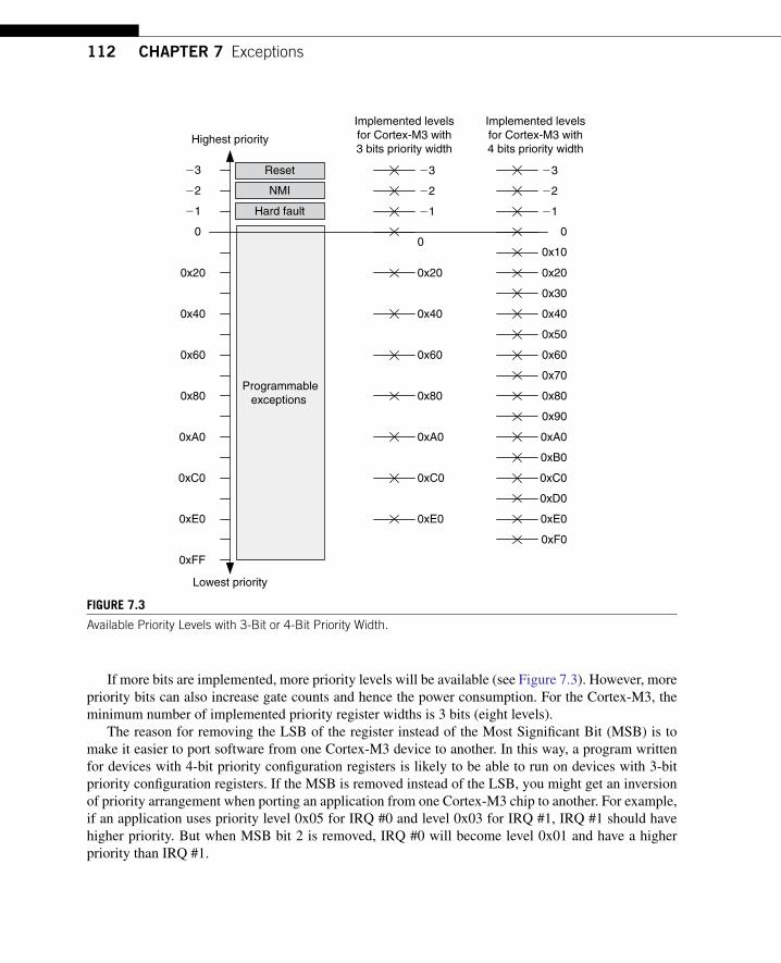
112 CHAPTER 7 Exceptions
If more bits are implemented, more priority levels will be available (see Figure 7.3). However, more priority bits can also increase gate counts and hence the power consumption. For the Cortex-M3, the minimum number of implemented priority register widths is 3 bits (eight levels).
The reason for removing the LSB of the register instead of the Most Significant Bit (MSB) is to make it easier to port software from one Cortex-M3 device to another. In this way, a program written for devices with 4-bit priority configuration registers is likely to be able to run on devices with 3-bit priority configuration registers. If the MSB is removed instead of the LSB, you might get an inversion of priority arrangement when porting an application from one Cortex-M3 chip to another. For example, if an application uses priority level 0x05 for IRQ #0 and level 0x03 for IRQ #1, IRQ #1 should have higher priority. But when MSB bit 2 is removed, IRQ #0 will become level 0x01 and have a higher priority than IRQ #1.
FIgure 7.3
Available Priority Levels with 3-Bit or 4-Bit Priority Width.
Programmableexceptions
0
21
22
23
21
22
23
21
22
23
0x20
0x40
0x60
0x80
0xA0
0xC0
0xE0
0xFF
Highest priority
Lowest priority
Reset
NMI
Hard fault
Implemented levelsfor Cortex-M3 with3 bits priority width
Implemented levelsfor Cortex-M3 with4 bits priority width
0
0x20
0x40
0x60
0x80
0xA0
0xC0
0xE0
0
0x20
0x40
0x60
0x80
0xA0
0xC0
0xE0
0x30
0x50
0x70
0x90
0xB0
0xD0
0xF0
0x10

113
Examples of available exception priority levels for devices with 3-bit, 5-bit, and 8-bit priority reg-isters are shown in Table 7.3.
Some readers might wonder whether, if the priority level configuration registers are 8 bits wide, why there are only 128 preemption levels? This is because the 8-bit register is further divided into two parts: preempt priority and subpriority.
Using a configuration register in the NVIC called Priority Group (a part of the Application Interrupt and Reset Control register in the NVIC, see Table 7.4), the priority-level configuration registers for each exception with programmable priority levels is divided into two halves. The upper half (left bits) is the preempt priority, and the lower half (right bits) is the subpriority (see Table 7.5).
Table 7.3 Available Priority Levels for Devices with 3-Bit, 5-Bit, and 8-Bit Priority Level Registers
Priority Level Exception Type
Devices with 3-Bit Priority Configuration Registers
Devices with 5-Bit Priority Configuration Registers
Devices with 8-Bit Priority Configuration Registers
−3 (Highest) Reset −3 −3 −3−2 NMI −2 −2 −2−1 Hard fault −1 −1 −10, 1, … 0xFF Exceptions with
programmable priority level
0x00, 0x20, … 0xE0
0x00, 0x08, … 0xF8
0x00, 0x01, 0x02, 0x03, … 0xFE, 0xFE
Table 7.4 Application Interrupt and Reset Control Register (Address 0xE000ED0C)
Bits Name Type Reset Value Description
31:16 VECTKEY R/W — Access key; 0x05FA must be written to this field to write to this register, otherwise the write will be ignored; the read-back value of the upper half word is 0xFA05
15 ENDIANNESS R — Indicates endianness for data: 1 for big endian (BE8) and 0 for little endian; this can only change after a reset
10:8 PRIGROUP R/W 0 Priority group2 SYSRESETREQ W — Requests chip control logic to generate a reset1 VECTCLRACTIVE W — Clears all active state information for exceptions;
typically used in debug or OS to allow system to recover from system error (Reset is safer)
0 VECTRESET W — Resets the Cortex-M3 processor (except debug logic), but this will not reset circuits outside the processor
7.2 Definitions of Priority

114 CHAPTER 7 Exceptions
The preempt priority level defines whether an interrupt can take place when the processor is already running another interrupt handler. The subpriority level value is used only when two exceptions with the same preempt priority level occurred at the same time. In this case, the exception with higher sub-priority (lower value) will be handled first.
As a result of the priority grouping, the maximum width of preempt priority is 7, so there can be 128 levels. When the priority group is set to 7, all exceptions with a programmable priority level will be in the same level, and no preemption between these exceptions will take place, except that hard fault, NMI, and reset, which have priority of -1, -2, and −3, respectively, can preempt these exceptions.
When deciding the effective preempt priority level and subpriority level, you must take the follow-ing factors into account:
Implemented priority-level configuration registers•Priority group setting•
For example, if the width of the configuration registers is 3 (bit 7 to bit 5 are available) and priority group is set to 5, you can have four levels of preempt priority levels (bit 7 to bit 6), and inside each preempt level there are two levels of subpriority (bit 5).
With the setting as shown in Figure 7.4, the available priority levels are illustrated in Figure 7.5. For the same design, if the priority group is set to 0x1, there can be only eight preempt priority levels and no further subpriority levels inside each preempt level. (Bit [1:0] of preempt priority is always 0.) The definition of the priority level configuration registers is shown in Figure 7.6, and the available priority levels are illustrated in Figure 7.7.
Table 7.5 Definition of Preempt Priority Field and Subpriority Field in a Priority Level Register in Different Priority Group Settings
Priority Group Preempt Priority Field Subpriority Field
0 Bit [7:1] Bit [0]1 Bit [7:2] Bit [1:0]2 Bit [7:3] Bit [2:0]3 Bit [7:4] Bit [3:0]4 Bit [7:5] Bit [4:0]5 Bit [7:6] Bit [5:0]6 Bit [7] Bit [6:0]7 None Bit [7:0]
FIgure 7.4
Definition of Priority Fields in a 3-Bit Priority Level Register with Priority Group Set to 5.
Bit 7 Bit 6 Bit 5 Bit 4 Bit 3 Bit 2 Bit 1 Bit 0
Not implementedPreemptpriority
Sub-priority

115
If a Cortex-M3 device has implemented all 8 bits in the priority-level configuration registers, the maximum number of preemption levels it can have is only 128, using a priority group setting of 0. The priority fields definition is shown in Figure 7.8.
FIgure 7.5
Available Priority Levels with 3-Bit Priority Width and Priority Group Set to 5.
Programmableexceptions
0
21
22
23
0x20
0x40
0x60
0x80
0xA0
0xC0
0xE0
0xFF
Highest priority
Lowest priority
Reset
NMI
Hard fault
Implemented levelsfor Cortex-M3 with3-bits priority width
Preempt levelswith priority group
set to 5
0
21
22
23
0x20
0x40
0x60
0x80
0xA0
0xC0
0xE0
0
21
22
23
0x40
0x80
0xC0
Subpriority levels
0
0x20
0x40
0x60
0x80
0xA0
0xC0
0xE0
7.2 Definitions of Priority
FIgure 7.6
Definition of Priority Fields in an 8-Bit Priority Level Register with Priority Group Set to 1.
Bit 7 Bit 6 Bit 5 Bit 4 Bit 3 Bit 2 Bit 1 Bit 0
Preempt priority [5:3]Preempt priority [2:0]
(always 0)
Sub-priority [1:0](always 0)

116 CHAPTER 7 Exceptions
When two interrupts are asserted at the same time with exactly the same preempt priority level as well as subpriority level, the interrupt with the smaller exception number has higher priority. (IRQ #0 has higher priority than IRQ #1.)
To avoid unexpected changes of priority levels for interrupts, be careful when writing to the Application Interrupt and Reset Control register (address 0xE000ED0C). In most cases, after the
FIgure 7.7
Available Priority Levels with 3-Bit Priority Width and Priority Group Set to 1.
Programmableexceptions
0
21
22
23
0x20
0x40
0x60
0x80
0xA0
0xC0
0xE0
0xFF
Highest priority
Lowest priority
Reset
NMI
Hard fault
Implemented levelsfor Cortex-M3 with3-bits priority width
Preempt levelswith priority group
set to 1
0
21
22
23
0x20
0x40
0x60
0x80
0xA0
0xC0
0xE0
0
21
22
23
Subpriority levels
0
0x20
0x40
0x60
0x80
0xA0
0xC0
0xE0
0x20
0x40
0x60
0x80
0xA0
0xC0
0xE0
FIgure 7.8
Definition of Priority Fields in an 8-Bit Priority Level Register with Priority Group Set to 0.
Bit 7 Bit 6 Bit 5 Bit 4 Bit 3 Bit 2 Bit 1 Bit 0
Preempt priority Subpriority

1177.3 Vector Tables
priority group is configured, there is no need to use this register except to generate a reset (see Table 7.4).
7.3 VeCTor TaBlesWhen an exception takes place and is being handled by the Cortex-M3, the processor will need to locate the starting address of the exception handler. This information is stored in the vector table in the memory. By default, the vector table starts at memory address 0, and the vector address is arranged according to the exception number times four (see Table 7.6).
Since the address 0x0 should be boot code, usually it will be either Flash memory or ROM devices, and the value cannot be changed at run time. However, the vector table can be relocated to other memory locations in the code or Random Access Memory (RAM) region where the RAM is so that we can change the handlers during run time. This is done by setting a register in the NVIC called the vector table offset register (address 0xE000ED08). The address offset should be aligned to the vector table size, extended to the next larger power of 2. For example, if there are 32 IRQ inputs, the total number of exceptions will be 32 + 16 (system exceptions) = 48. Extending it to the power of 2 makes it 64. Multiplying it by 4 (4 bytes per vector) makes it 256 bytes (0x100). Therefore, the vector table offset can be programmed as 0x0, 0x100, 0x200, and so on. The vector table offset register contains the items shown in Table 7.7.
In applications where you want to allow dynamic changing of exception handlers, in the beginning of the boot image, you need to have the following (at a minimum):
Initial main stack pointer value•Reset vector•NMI vector•Hard fault vector•
Table 7.6 Exception Vector Table After Power Up
Address Exception Number Value (Word Size)
0x00000000 — MSP initial value0x00000004 1 Reset vector (program counter initial value)0x00000008 2 NMI handler starting address0x0000000C 3 Hard fault handler starting address… … Other handler starting address
Table 7.7 Vector Table Offset Register (Address 0xE000ED08)
Bits Name Type Reset Value Description
29 TBLBASE R/W 0 Table base in code (0) or RAM (1)28:7 TBLOFF R/W 0 Table offset value from code
region or RAM region

118 CHAPTER 7 Exceptions
These are required because the NMI and hard fault can potentially occur during your boot process. Other exceptions cannot take place until they are enabled.
When the booting process is done, you can define a part of your Static Random Access Memory as the new vector table and relocate the vector table to the new one, which is writable.
7.4 InTerrupT InpuTs anD penDIng BehaVIorThis section describes the behavior of IRQ inputs and pending behavior. It also applies to NMI input, except that an NMI will be executed immediately in most cases, unless the core is already executing an NMI handler, halted by a debugger, or locked up because of some serious system error.
When an interrupt input is asserted, it will be pended, which means it is put into a state of waiting for the processor to process the request. Even if the interrupt source deasserts the interrupt, the pended interrupt status will still cause the interrupt handler to be executed when the priority is allowed. Once the interrupt handler is started, the pending status is cleared automatically. This is shown in Figure 7.9.
However, if the pending status is cleared before the processor starts responding to the pended inter-rupt (for example, the interrupt was not taken immediately because PRIMASK/FAULTMASK is set to 1, and the pending status was cleared by software writing to NVIC interrupt control registers), the interrupt can be cancelled (Figure 7.10). The pending status of the interrupt can be accessed in the NVIC and is writable, so you can clear a pending interrupt or use software to pend a new interrupt by setting the pending register.
FIgure 7.9
Interrupt Pending.
Interruptrequest
Interruptpending status
Processormode
Threadmode
Handler mode
FIgure 7.10
Interrupt Pending Cleared Before Processor Takes Action.
Interruptrequest
Interruptpending status
Processormode
Threadmode
Pending statuscleared by software

1197.4 Interrupt Inputs and Pending Behavior
When the processor starts to execute an interrupt, the interrupt becomes active and the pending bit will be cleared automatically (Figure 7.11). When an interrupt is active, you cannot start processing the same interrupt again, until the interrupt service routine is terminated with an interrupt return (also called an exception exit, as discussed in Chapter 9). Then the active status is cleared, and the interrupt can be processed again if the pending status is 1. It is possible to repend an interrupt before the end of the interrupt service routine.
If an interrupt source continues to hold the interrupt request signal active, the interrupt will be pended again at the end of the interrupt service routine as shown in Figure 7.12. This is just like the traditional ARM7TDMI.
If an interrupt is pulsed several times before the processor starts processing it, it will be treated as one single interrupt request as illustrated in Figure 7.13. If an interrupt is deasserted and then pulsed again during the interrupt service routine, it will be pended again as shown in Figure 7.14.
FIgure 7.11
Interrupt Active Status Set as Processor Enters Handler.
Interruptrequest
Interruptpending status
Processormode
Threadmode
Handler mode
Interruptactive status
Interrupt requestclear by software
Interrupt return
FIgure 7.12
Continuous Interrupt Request Pends Again After Interrupt Exit.
Interruptrequest
Interruptpending status
Processormode
Threadmode
Handler mode
Interruptactive status
Interrupt request stay active
Interrupt return
Interrupt reentered
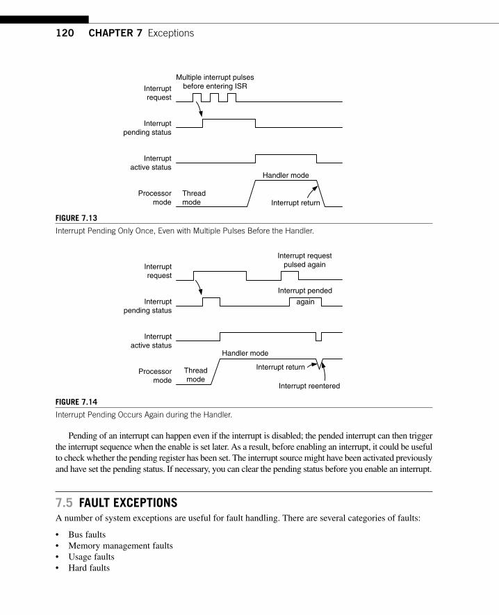
120 CHAPTER 7 Exceptions
Pending of an interrupt can happen even if the interrupt is disabled; the pended interrupt can then trigger the interrupt sequence when the enable is set later. As a result, before enabling an interrupt, it could be useful to check whether the pending register has been set. The interrupt source might have been activated previously and have set the pending status. If necessary, you can clear the pending status before you enable an interrupt.
7.5 FaulT exCepTIonsA number of system exceptions are useful for fault handling. There are several categories of faults:
Bus faults•Memory management faults•Usage faults•Hard faults•
FIgure 7.13
Interrupt Pending Only Once, Even with Multiple Pulses Before the Handler.
Interruptrequest
Interruptpending status
Processormode
Threadmode
Handler mode
Interruptactive status
Interrupt return
Multiple interrupt pulsesbefore entering ISR
FIgure 7.14
Interrupt Pending Occurs Again during the Handler.
Interruptrequest
Interruptpending status
Processormode
Threadmode
Handler mode
Interruptactive status
Interrupt return
Interrupt requestpulsed again
Interrupt reentered
Interrupt pended
again

1217.5 Fault Exceptions
7.5.1 Bus FaultsBus faults are produced when an error response is received during a transfer on the AHB interfaces. It can happen at these stages:
Instruction fetch, commonly called • prefetch abortData read/write, commonly called • data abort
In the Cortex-M3, bus faults can also occur during the following:
Stack PUSH in the beginning of interrupt processing, called a • stacking errorStack POP at the end of interrupt processing, called an • unstacking errorReading of an interrupt vector address (vector fetch) when the processor starts the interrupt-•handling sequence (a special case classified as a hard fault)
When these types of bus faults (except vector fetches) take place and if the bus fault handler is enabled and no other exceptions with the same or higher priority are running, the bus fault handler will be executed. If the bus fault handler is enabled but at the same time the core receives another exception handler with higher priority, the bus fault exception will be pending. Finally, if the bus fault handler is not enabled or when the bus fault happens in an exception handler that has the same or higher priority than the bus fault handler, the hard fault handler will be executed instead. If another bus fault takes place when running the hard fault handler, the core will enter a lockup state.2
To enable the bus fault handler, you need to set the BUSFAULTENA bit in the System Handler Control and State register in the NVIC. Before doing that, make sure that the bus fault handler starting address is set up in the vector table if the vector table has been relocated to RAM.
Hence, how do you find out what went wrong when the processor entered the bus fault handler? The NVIC has a number of Fault Status registers (FSRs). One of them is the Bus Fault Status register (BFSR). From this register, the bus fault handler can find out if the fault was caused by data/instruction access or an interrupt stacking or unstacking operation.
For precise bus faults, the offending instruction can be located by the stacked program counter, and if the BFARVALID bit in BFSR is set, it is also possible to determine the memory location that caused the bus fault. This is done by reading another NVIC register called the Bus Fault Address
2More information on the lockup state is covered in Chapter 12.
WhaT Can Cause ahB error responses?Bus faults occur when an error response is received on the AHB bus. The common causes are as follows:
Attempts to access an invalid memory region (for example, a memory location with no memory attached)•The device is not ready to accept a transfer (for example, trying to access SDRAM without initializing the •SDRAM controller)Attempts to carry out a transfer with a transfer size not supported by the target device (for example, doing a •byte access to a peripheral register that must be accessed as a word)The device does not accept the transfer for various reasons (for example, a peripheral that can only be •programmed at the privileged access level)

122 CHAPTER 7 Exceptions
register (BFAR). However, the same information is not available for imprecise bus faults because by the time the processor receives the error, the processor could have already executed a number of other instructions.
The programmer’s model for BFSR is as follows: It is 8 bits wide and can be accessed through byte transfer to address 0xE000ED29 or with a word transfer to address 0xE000ED28 with BFSR in the second byte (see Table 7.8). The error indication bit is cleared when a 1 is written to it.
7.5.2 Memory Management FaultsMemory management faults can be caused by memory accesses that violate the setup in the MPU or by certain illegal accesses (for example, trying to execute code from nonexecutable memory regions), which can trigger the fault, even if no MPU is presented.
Some of the common MPU faults include the following:
Access to memory regions not defined in MPU setup•Writing to read-only regions•An access in the user state to a region defined as privileged access only•
When a memory management fault occurs and if the memory management handler is enabled, the memory management fault handler will be executed. If the fault occurs at the same time a higher- priority exception takes place, the other exceptions will be handled first and the memory management fault will be pended. If the processor is already running an exception handler with the same or higher
Table 7.8 Bus Fault Status Register (0xE000ED29)
Bits Name Type Reset Value Description
7 BFARVALID — 0 Indicates BFAR is valid6:5 — — — —4 STKERR R/Wc 0 Stacking error3 UNSTKERR R/Wc 0 Unstacking error2 IMPRECISERR R/Wc 0 Imprecise data access violation1 PRECISERR R/Wc 0 Precise data access violation0 IBUSERR R/Wc 0 Instruction access violation
preCIse anD IMpreCIse Bus FaulTsBus faults caused by data accesses can be further classified as precise or imprecise. In imprecise bus faults, the fault is caused by an already completed operation (such as a buffered write) that might have occurred a number of clock cycles ago. Precise bus faults are caused by the last completed operation—for example, a memory read is precise on the Cortex-M3 because the instruction cannot be completed until it receives the data.

123
priority or if the memory management fault handler is not enabled, the hard fault handler will be executed instead. If a memory management fault takes place inside the hard fault handler or the NMI handler, the processor will enter the lockup state.
Like the bus fault handler, the memory management fault handler needs to be enabled. This is done by the MEMFAULTENA bit in the System Handler Control and State register in the NVIC. If the vec-tor table has been relocated to RAM, the memory management fault handler starting address should be set up in the vector table first.
The NVIC contains a Memory Management Fault Status register (MFSR) to indicate the cause of the memory management fault. If the status register indicates that the fault is a data access viola-tion (DACCVIOL bit) or an instruction access violation (IACCVIOL bit), the offending code can be located by the stacked program counter. If the MMARVALID bit in the MFSR is set, it is also possible to determine the memory address location that caused the fault from the Memory Management Address register (MMAR) in the NVIC.
The programmer’s model for the MFSR is shown in Table 7.9. It is 8 bits wide and can be accessed through byte transfer or with a word transfer to address 0xE000ED28, with the MFSR in the lowest byte. As with other FSRs, the fault status bit can be cleared by writing 1 to the bit.
7.5.3 usage FaultsUsage faults can be caused by a number of things:
Undefined instructions•Coprocessor instructions (the Cortex-M3 processor does not support a coprocessor, but it is •possible to use the fault exception mechanism to run software compiled for other Cortex processors through coprocessor emulation)Trying to switch to the ARM state (software can use this faulting mechanism to test whether the •processor it is running on supports the ARM code; because the Cortex-M3 does not support the ARM state, a usage fault takes place if there’s an attempt to switch)Invalid interrupt return (link register contains invalid/incorrect values)•Unaligned memory accesses using multiple load or store instructions•
7.5 Fault Exceptions
Table 7.9 Memory Management Fault Status Register (0xE000ED28)
Bits Name Type Reset Value Description
7 MMARVALID — 0 Indicates the MMAR is valid
6:5 — — — —
4 MSTKERR R/Wc 0 Stacking error
3 MUNSTKERR R/Wc 0 Unstacking error
2 — — — —1 DACCVIOL R/Wc 0 Data access violation0 IACCVIOL R/Wc 0 Instruction access violation

124 CHAPTER 7 Exceptions
It is also possible, by setting up certain control bits in the NVIC, to generate usage faults for the following:
Divide by zero•Any unaligned memory accesses•
When a usage fault occurs and if the usage fault handler is enabled, normally the usage fault handler will be executed. However, if at the same time a higher-priority exception takes place, the usage fault will be pended. If the processor is already running an exception handler with the same or higher priority or if the usage fault handler is not enabled, the hard fault handler will be executed instead. If a usage fault takes place inside the hard fault handler or the NMI handler, the processor will enter the lockup state.
The usage fault handler is enabled by setting the USGFAULTENA bit in the System Handler Control and State register in the NVIC. If the vector table has been relocated to RAM, the usage fault handler starting address should be set up in the vector table first.
The NVIC provides a Usage Fault Status register (UFSR) for the usage fault handler to determine the cause of the fault. Inside the handler, the program code that causes the error can also be located using the stacked program counter value.
The UFSR is shown in Table 7.10. It occupies 2 bytes and can be accessed by half word transfer to address 0xE000ED2A, or as a word transfer to address 0xE000ED28 with the UFSR in the upper half word. As with other FSRs, the fault status bit can be cleared by writing 1 to the bit.
Table 7.10 Usage Fault Status Register (0xE000ED2A)
Bits Name Type Reset Value Description
9 DIVBYZERO R/Wc 0 Indicates a divide by zero has taken place (can be set only if DIV_0_TRP is set)
8 UNALIGNED R/Wc 0 Indicates that an unaligned access fault has taken place
7:4 — — — —3 NOCP R/Wc 0 Attempts to execute a coprocessor instruction2 INVPC R/Wc 0 Attempts to do an exception with a bad value
in the EXC_RETURN number1 INVSTATE R/Wc 0 Attempts to switch to an invalid state (e.g.,
ARM)0 UNDEFINSTR R/Wc 0 Attempts to execute an undefined instruction
aCCIDenTally sWITChIng To The arM sTaTeOne of the most common causes of usage faults is accidentally trying to switch the processor to ARM mode. This can happen if you load a new value to PC with the LSB equal to 0—for example, if you try to branch to an address in a register using the BX or BLX instruction without setting the LSB of the target address, have zero in the LSB of a vector in the exception vector table, or the stacked PC value to be read by POP {PC} is modified manually, leaving the LSB cleared. When these situations happen, the usage fault exception will take place with the INVSTATE bit in the UFSR set.

125
7.5.4 hard FaultsThe hard fault handler can be caused by usage faults, bus faults, and memory management faults if their handler cannot be executed. In addition, it can also be caused by a bus fault during vector fetch (reading of a vector table during exception handling). In the NVIC, there is a hard fault status register that can be used to determine whether the fault was caused by a vector fetch. If not, the hard fault handler will need to check the other FSRs to determine the cause of the hard fault.
Details of the Hard Fault Status register (HFSR) are shown in Table 7.11. As with other FSRs, the fault status bit can be cleared by writing 1 to the bit.
7.5.5 Dealing with FaultsDuring software development, we can use the FSRs to determine the causes of errors in the program and correct them. A troubleshooting guide is included in Appendix E of this book for common causes of various faults. In a real running system, the situation is different. After the cause of a fault is deter-mined, the software will have to decide what to do next. In systems that run an OS, the offending tasks or applications could be terminated. In some other cases, the system might need a reset. The require-ments of fault recovery depend on the target application. Doing it properly could make the product more robust, but it is best to prevent the faults from happening in the first place. The following are some fault-handling methods:
• Reset: This can be carried out using the SYSRESETREQ control bit in the Application Interrupt and Reset Control register in the NVIC. This will reset most parts of the system apart from the debug logic. Depending on the application, if you do not want to reset the whole system, you could reset just the processor using the VECTRESET bit.
• Recovery: In some cases, it might be possible to resolve the problem that caused the fault exception. For example, in the case of coprocessor instructions, the problem can be resolved using coprocessor emulation software.
• Task termination: For systems running an OS, it is likely that the task that caused the fault will be terminated and restarted if needed.
The FSRs retain their status until they are cleared manually. Fault handlers should clear the fault status bit they have dealt with. Otherwise, the next time another fault takes place, the fault handler will
Table 7.11 Hard Fault Status Register (0xE000ED2C)
Bits Name Type Reset Value Description
31 DEBUGEVT R/Wc 0 Indicates hard fault is triggered by debug event30 FORCED R/Wc 0 Indicates hard fault is taken because of bus fault,
memory management fault, or usage fault29:2 — — — —1 VECTBL R/Wc 0 Indicates hard fault is caused by failed vector
fetch0 — — — —
7.5 Fault Exceptions

126 CHAPTER 7 Exceptions
be invoked again and could mistake that the first fault still exists and so will try to deal with it again. The FSRs use a write-to-clear mechanism (clear by writing 1 to the bits that need to be cleared).
Chip manufacturers can also include an auxiliary FSR in the chip to indicate other fault situations. The implementation of an AFSR depends on individual chip design requirements.
7.6 superVIsor Call anD penDaBle serVICe CallSupervisor Call (SVC) and Pendable Service Call (PendSV) are two exceptions targeted at software and operating systems. SVC is for generating system function calls. For example, instead of allowing user programs to directly access hardware, an operating system may provide access to hardware through an SVC. So when a user program wants to use certain hardware, it generates the SVC exception using SVC instructions, and then the software exception handler in the operating system is executed and provides the service the user application requested. In this way, access to hardware is under the control of the OS, which can provide a more robust system by preventing the user applications from directly accessing the hardware.
SVC can also make software more portable because the user application does not need to know the programming details of the hardware. The user program will only need to know the application programming interface (API) function ID and parameters; the actual hardware-level programming is handled by device drivers (see Figure 7.15).
SVC exception is generated using the SVC instruction. An immediate value is required for this instruction, which works as a parameter-passing method. The SVC exception handler can then extract the parameter and determine what action it needs to perform. For example,
SVC #0x3 ; Call SVC function 3
The traditional syntax for SVC is also acceptable (without the “#”):
SVC 0x3 ; Call SVC function 3
For C language development, the SVC instruction can be generated using __svc function (for ARM RealView C Compiler or KEIL Microcontroller Development Kit for ARM), or using inline assembly in other C compilers.
FIgure 7.15
SVC as a Gateway for OS Functions.
SVC
Unprivileged
Privileged
Userprogram
Operating system
APIDevicedrivers
Peripherals
HardwareKernel

127
When the SVC handler is executed, you can determine the immediate data value in the SVC instruc-tion by reading the stacked program counter value, then reading the instruction from that address and masking out the unneeded bits. If the system uses a Process Stack Pointer for user applications, you might need to determine which stack was used first. This can be determined from the link register value when the handler is entered. (This topic is covered in more depth in Chapter 8).
Because of the interrupt priority model in the Cortex-M3, you cannot use SVC inside an SVC han-dler (because the priority is the same as the current priority). Doing so will result in a usage fault. For the same reason, you cannot use SVC in an NMI handler or a hard fault handler.
PendSV (Pendable Service Call) works with SVC in the OS. Although SVC (by SVC instruction) cannot be pended (an application calling SVC will expect the required task to be done immediately), PendSV can be pended and is useful for an OS to pend an exception so that an action can be performed after other important tasks are completed. PendSV is generated by writing 1 to the PENDSVSET bit in the NVIC Interrupt Control State register.
A typical use of PendSV is context switching (switching between tasks). For example, a system might have two active tasks, and context switching can be triggered by the following:
Calling an SVC function•The system timer (SYSTICK)•
Let’s look at a simple example of having only two tasks in a system, and a context switch is trig-gered by SYSTICK exceptions (see Figure 7.16).
If an interrupt request takes place before the SYSTICK exception, the SYSTICK exception will preempt the IRQ handler. In this case, the OS should not carry out the context switching. Otherwise the
7.6 Supervisor Call and Pendable Service Call
sVC anD soFTWare InTerrupT InsTruCTIon (arM7)If you have used traditional ARM processors (such as the ARM7), you might know that they have a software interrupt instruction (SWI). The SVC has a similar function, and in fact the binary encoding of SVC instructions is the same as SWI in ARM7. However, since the exception model has changed, this instruction is renamed to make sure that programmers will properly port software code from ARM7 to the Cortex-M3.
FIgure 7.16
A Simple Scenario Using SYSTICK to Switch between Two Tasks.
Task A Task B
OS
Priority
OS
Task A
OSOSSYSTICK
Thread
IRQ
Contextswitching
Contextswitching
Contextswitching
Time

128 CHAPTER 7 Exceptions
IRQ handler process will be delayed, and for the Cortex-M3, a usage fault could be generated if the OS tries to switch to thread mode when an interrupt is active (see Figure 7.17).
To avoid the problem of delaying the IRQ processing, some OS implementations carry out only context switching if they detect that none of the IRQ handlers are being executed. However, this can result in a very long delay for task switching, especially if the frequency of an interrupt source is close to that of the SYSTICK exception.
FIgure 7.17
Problem with Context Switching at the IRQ.
Task A Task B
OS
Priority
OS
Task A
OSSYSTICK
Thread
IRQ
Contextswitching Context switching
Time
IRQ processingdelayed
IRQ
Usage fault: return toThread with active interrupt
IRQ
FIgure 7.18
Example Context Switching with PendSV.
Priority
SYSTICK
Interrupt
SVC &PendSV
Thread
Time
Task ATask BTask A
[1]
[3] [4]
[2] [5]
[6]
[7]
[8]
[9]
[10]
Context switchin PendSV
ISR continueISR started
SYSTICK (OS)
SVC (OS) pendPendSV
Contextswitch inPendSV
ISR completed
Interrupt occurred

129
The PendSV exception solves the problem by delaying the context-switching request until all other IRQ handlers have completed their processing. To do this, the PendSV is programmed as the lowest priority exception. If the OS detects that an IRQ is currently active (IRQ handler running and preempted by SYSTICK), it defers the context switching by pending the PendSV exception. Figure 7.18 illustrates a context switching example with the following event sequence:
Task A calls SVC for task switching (for example, waiting for some work to complete).1. The OS receives the request, prepares for context switching, and pends the PendSV exception.2. When the CPU exits SVC, it enters PendSV immediately and does the context switch.3. When PendSV finishes and returns to the thread level, it executes Task B.4. An interrupt occurs and the interrupt handler is entered.5. While running the interrupt handler routine, a SYSTICK exception (for OS tick) takes place.6. The OS carries out the essential operation, then pends the PendSV exception and gets ready for 7. the context switch.When the SYSTICK exception exits, it returns to the interrupt service routine.8. When the interrupt service routine completes, the PendSV starts and does the actual context 9. switch operations.When PendSV is complete, the program returns to the thread level; this time it returns to Task A 10. and continues the processing.
7.6 Supervisor Call and Pendable Service Call

131Copyright © 2010, Elsevier Inc. All rights reserved.DOI: 10.1016/B978-1-85617-963-8.00011-9
In ThIs ChapTer
nested Vectored Interrupt Controller Overview ....................................................................................... 131The Basic Interrupt Configuration .......................................................................................................... 132example procedures in setting Up an Interrupt ...................................................................................... 138software Interrupts ............................................................................................................................... 140The sYsTICK Timer ............................................................................................................................... 141
8.1 nesTed VeCTOred InTerrUpT COnTrOller OVerVIewAs we’ve seen, the Nested Vectored Interrupt Controller (NVIC) is an integrated part of the Cortex™-M3 processor. It is closely linked to the Cortex-M3 CPU core logic. Its control registers are accessible as memory-mapped devices. Besides control registers and control logic for interrupt processing, the NVIC unit also contains control registers for the SYSTICK Timer, and debugging controls. In this chapter, we’ll examine the control logic for interrupt processing. Memory Protection Unit and debug-ging control logic are discussed in later chapters.
The NVIC supports 1–240 external interrupt inputs (commonly known as interrupt request [IRQs]). The exact number of supported interrupts is determined by the chip manufacturers when they develop their Cortex-M3 chips. In addition, the NVIC also has a Nonmaskable Interrupt (NMI) input. The actual function of the NMI is also decided by the chip manufacturer. In some cases, this NMI cannot be controlled from an external source.
The NVIC can be accessed in the System Control Space (SCS) address range, which is memory location 0xE000E000. Most of the interrupt control/status registers are accessible only in privileged mode, except the Software Trigger Interrupt register (STIR), which can be set up to be accessible in user mode. The interrupt control/status register can be accessed in word, half word, or byte transfers.
In addition, a few other interrupt-masking registers are also involved in the interrupts. They are the “special registers” covered in Chapter 3 and are accessed through special registers access instructions: move special register to general-purpose register (MRS) and move to special register from general-purpose register (MSR) instructions.
The Nested Vectored Interrupt Controller and Interrupt Control 8
CHAPTER

132 CHAPTER 8 The Nested Vectored Interrupt Controller and Interrupt Control
8.2 The BasIC InTerrUpT COnfIgUraTIOnEach external interrupt has several registers associated with it.
Enable and Clear Enable registers•Set-Pending and Clear-Pending registers•Priority level•Active status•
In addition, a number of other registers can also affect the interrupt processing:
Exception-masking registers (PRIMASK, FAULTMASK, and BASEPRI)•Vector Table Offset register•STIR•Priority group•
8.2.1 Interrupt enable and Clear enableThe Interrupt Enable register is programmed through two addresses. To set the enable bit, you need to write to the SETENA register address; to clear the enable bit, you need to write to the CLRENA register address. In this way, enabling or disabling an interrupt will not affect other interrupt enable states. The SETENA/CLRENA registers are 32 bits wide; each bit represents one interrupt input.
As there could be more than 32 external interrupts in the Cortex-M3 processor, you might find more than one SETENA and CLRENA register—for example, SETENA0, SETENA1, and so on (see Table 8.1). Only the enable bits for interrupts that exist are implemented. So, if you have only 32 inter-rupt inputs, you will only have SETENA0 and CLRENA0. The SETENA and CLRENA registers can be accessed as word, half word, or byte. As the first 16 exception types are system exceptions, external Interrupt #0 has a start exception number of 16 (see Table 7.2).
8.2.2 Interrupt set pending and Clear pendingIf an interrupt takes place but cannot be executed immediately (for instance, if another higher-priority interrupt handler is running), it will be pended. The interrupt-pending status can be accessed through the Interrupt Set Pending (SETPEND) and Interrupt Clear Pending (CLRPEND) registers. Similarly to the enable registers, the pending status controls might contain more than one register if there are more than 32 external interrupt inputs.
The values of pending status registers can be changed by software, so you can cancel a current pended exception through the CLRPEND register, or generate software interrupts through the SET-PEND register (see Table 8.2).
8.2.3 priority levelsEach external interrupt has an associated priority-level register, which has a maximum width of 8 bits and a minimum width of 3 bits. As described in the previous chapter, each register can be further divided into preempt priority level and subpriority level based on priority group settings. The priority-level registers can be accessed as byte, half word, or word. The number of priority-level registers depends on how many external interrupts the chip contains (see Table 8.3). The priority level configura-tion registers details can be found in Appendix D, Table D.19.

1338.2 The Basic Interrupt Configuration
Table 8.1 Interrupt Set Enable Registers and Interrupt Clear Enable Registers (0xE000E100-0xE000E11C, 0xE000E180-0xE000E19C)
Address Name Type Reset Value Description
0xE000E100 SETENA0 R/W 0 Enable for external Interrupt #0–31 bit[0] for Interrupt #0 (exception #16) bit[1] for Interrupt #1 (exception #17) … bit[31] for Interrupt #31 (exception #47) Write 1 to set bit to 1; write 0 has no effect Read value indicates the current status
0xE000E104 SETENA1 R/W 0 Enable for external Interrupt #32–63 Write 1 to set bit to 1; write 0 has no effect Read value indicates the current status
0xE000E108 SETENA2 R/W 0 Enable for external Interrupt #64–95 Write 1 to set bit to 1; write 0 has no effect Read value indicates the current status
… — — — —0xE000E180 CLRENA0 R/W 0 Clear enable for external Interrupt #0–31
bit[0] for Interrupt #0 bit[1] for Interrupt #1 … bit[31] for Interrupt #31 Write 1 to clear bit to 0; write 0 has no effect Read value indicates the current enable status
0xE000E184 CLRENA1 R/W 0 Clear enable for external Interrupt #32–63 Write 1 to clear bit to 0; write 0 has no effect Read value indicates the current enable status
0xE000E188 CLRENA2 R/W 0 Clear enable for external Interrupt #64–95 Write 1 to clear bit to 0; write 0 has no effect Read value indicates the current enable status
… — — — —
Table 8.2 Interrupt Set-Pending Registers and Interrupt Clear-Pending Registers (0xE000E200-0xE000E21C, 0xE000E280-0xE000E29C)
Address Name Type Reset Value Description
0xE000E200 SETPEND0 R/W 0 Pending for external Interrupt #0–31 bit[0] for Interrupt #0 (exception #16) bit[1] for Interrupt #1 (exception #17) … bit[31] for Interrupt #31 (exception #47) Write 1 to set bit to 1; write 0 has no effect Read value indicates the current status
0xE000E204 SETPEND1 R/W 0 Pending for external Interrupt #32–63 Write 1 to set bit to 1; write 0 has no effect Read value indicates the current status
Continued

134 CHAPTER 8 The Nested Vectored Interrupt Controller and Interrupt Control
8.2.4 active statusEach external interrupt has an active status bit. When the processor starts the interrupt handler, the bit is set to 1 and cleared when the interrupt return is executed. However, during an Interrupt Service Rou-tine (ISR) execution, a higher-priority interrupt might occur and cause preemption. During this period, although the processor is executing another interrupt handler, the previous interrupt is still defined as active. The active registers are 32 bit but can also be accessed using half word or byte-size transfers. If there are more than 32 external interrupts, there will be more than one active register. The active status registers for external interrupts are read-only (see Table 8.4).
Table 8.2 Interrupt Set-Pending Registers and Interrupt Clear-Pending Registers (0xE000E200-0xE000E21C, 0xE000E280-0xE000E29C) Continued
Address Name Type Reset Value Description
0xE000E208 SETPEND2 R/W 0 Pending for external Interrupt #64–95 Write 1 to set bit to 1; write 0 has no effect Read value indicates the current status
… — — — —0xE000E280 CLRPEND0 R/W 0 Clear pending for external Interrupt #0–31
bit[0] for Interrupt #0 (exception #16) bit[1] for Interrupt #1 (exception #17) … bit[31] for Interrupt #31 (exception #47) Write 1 to clear bit to 0; write 0 has no effect Read value indicates the current pending status
0xE000E284 CLRPEND1 R/W 0 Clear pending for external Interrupt #32–63 Write 1 to clear bit to 0; write 0 has no effect Read value indicates the current pending status
0xE000E288 CLRPEND2 R/W 0 Clear pending for external Interrupt #64–95 Write 1 to clear bit to 0; write 0 has no effect Read value indicates the current pending status
… — — — —
Table 8.3 Interrupt Priority-Level Registers (0xE000E400-0xE000E4EF)
Address Name Type Reset Value Description
0xE000E400 PRI_0 R/W 0 (8 bit) Priority-level external Interrupt #00xE000E401 PRI_1 R/W 0 (8 bit) Priority-level external Interrupt #1… — — — —0xE000E41F PRI_31 R/W 0 (8 bit) Priority-level external Interrupt #31… — — — —

1358.2 The Basic Interrupt Configuration
8.2.5 prIMasK and faUlTMasK special registersThe PRIMASK register is used to disable all exceptions except NMI and hard fault. It effectively changes the current priority level to 0 (highest programmable level). In C programming, you can use the intrinsic functions provided in Cortex Microcontroller Software Interface Standard (CMSIS) com-pliant device driver libraries or provided in the compiler to set and clear PRIMASK:
void __enable_irq(); // Clear PRIMASKvoid __disable_irq(); // Set PRIMASKvoid __set_PRIMASK(uint32_t priMask); // Set PRIMASK to valueuint32_t __get_PRIMASK(void); // Read the PRIMASK value
For assembly language users, you can change the current status of PRIMASK using Change Pro-cess State (CPS) instructions:
CPSIE I ; Clear PRIMASK (Enable interrupts)CPSID I ; Set PRIMASK (Disable interrupts)
This register is also programmable using MRS and MSR instructions. For example,
MOV R0, #1MSR PRIMASK, R0 ; Write 1 to PRIMASK to disable all ; interrupts
and
MOV R0, #0MSR PRIMASK, R0 ; Write 0 to PRIMASK to allow interrupts
PRIMASK is useful for temporarily disabling all interrupts for critical tasks. When PRIMASK is set, if a fault takes place, the hard fault handler will be executed.
FAULTMASK is just like PRIMASK except that it changes the effective current priority level to 21, so that even the hard fault handler is blocked. Only the NMI can be executed when FAULT-MASK is set. It can be used by fault handlers to raise its priority to 21, so that they can have access to some features for hard fault exception (more information on this is provided in Chapter 12). In C programming with CMSIS compliant driver libraries, you can use the intrinsic functions provided in device driver libraries to set and clear FAULTMASK as follows:
void __set_FAULTMASK(uint32_t faultMask);uint32_t __get_FAULTMASK(void);
Table 8.4 Interrupt Active Status Registers (0xE000E300-0xE000E31C)
Address Name Type Reset Value Description
0xE000E300 ACTIVE0 R 0 Active status for external Interrupt #0–31 bit[0] for Interrupt #0 bit[1] for Interrupt #1 … bit[31] for Interrupt #31
0xE000E304 ACTIVE1 R 0 Active status for external Interrupt #32–63… — — — —

136 CHAPTER 8 The Nested Vectored Interrupt Controller and Interrupt Control
For assembly language users, you can change the current status of FAULTMASK using CPS instructions as follows:
CPSIE F ; Clear FAULTMASKCPSID F ; Set FAULTMASK
You can also access the FAULTMASK register using MRS and MSR instructions.FAULTMASK is cleared automatically upon exiting the exception handler except return from NMI
handler. Both FAULTMASK and PRIMASK registers cannot be set in the user state.
8.2.6 The BaseprI special registerIn some cases, you might want to disable interrupts only with priority lower than a certain level. In this case, you could use the BASEPRI register. To do this, simply write the required masking priority level to the BASEPRI register. For example, if you want to block all exceptions with priority level equal to or lower than 0x60, you can write the value to BASEPRI:
__set_BASEPRI(0x60); // Disable interrupts with priority // 0x60-0xFF using CMSIS
Or in assembly language:
MOV R0, #0x60MSR BASEPRI, R0 ; Disable interrupts with priority ; 0x60-0xFF
You can also read back the value of BASEPRI:
x = __get_BASEPRI(void); // Read value of BASEPRI
Or in assembly language:
MRS R0, BASEPRI
To cancel the masking, just write 0 to the BASEPRI register:
__set_BASEPRI(0x0); // Turn off BASEPRI masking
Or in assembly language:
MOV R0, #0x0MSR BASEPRI, R0 ; Turn off BASEPRI masking
The BASEPRI register can also be accessed using the BASEPRI_MAX register name. It is actually the same register, but when you use it with this name, it will give you a conditional write operation. (As far as hardware is concerned, BASEPRI and BASEPRI_MAX are the same register, but in the assembler code they use different register name coding.) When you use BASEPRI_MAX as a register, the processor hardware automatically compares the current value and the new value and only allows the update if it is to be changed to a higher priority level; it cannot be changed to lower priority levels. For example, consider the following instruction sequence:
MOV R0, #0x60MSR BASEPRI_MAX, R0 ; Disable interrupts with priority ; 0x60, 0x61,..., etc

1378.2 The Basic Interrupt Configuration
MOV R0, #0xF0MSR BASEPRI_MAX, R0 ; This write will be ignored because ; it is lower ; level than 0x60MOV R0, #0x40MSR BASEPRI_MAX, R0 ; This write is allowed and change the ; masking level to 0x40
To change to a lower masking level or disable the masking, the BASEPRI register name should be used. The BASEPRI/ BASEPRI_MAX register cannot be set in the user state.
As with other priority-level registers, the formatting of the BASEPRI register is affected by the number of implemented priority register widths. For example, if only 3 bits are imple-mented for priority-level registers, BASEPRI can be programmed as 0x00, 0x20, 0x40 … 0xC0, and 0xE0.
8.2.7 Configuration registers for Other exceptionsUsage faults, memory management faults, and bus fault exceptions are enabled by the System Handler Control and State register (0xE000ED24). The pending status of faults and active status of most system exceptions are also available from this register (see Table 8.5).
Table 8.5 The System Handler Control and State Register (0xE000ED24)
Bits Name Type Reset Value Description
18 USGFAULTENA R/W 0 Usage fault handler enable17 BUSFAULTENA R/W 0 Bus fault handler enable16 MEMFAULTENA R/W 0 Memory management fault handler enable15 SVCALLPENDED R/W 0 SVC pended; SVC was started but was replaced
by a higher-priority exception14 BUSFAULTPENDED R/W 0 Bus fault pended; bus fault handler was started
but was replaced by a higher-priority exception13 MEMFAULTPENDED R/W 0 Memory management fault pended; memory
management fault started but was replaced by a higher-priority exception
12 USGFAULTPENDED R/W 0 Usage fault pended; usage fault started but was replaced by a higher-priority exception
11 SYSTICKACT R/W 0 Read as 1 if SYSTICK exception is active10 PENDSVACT R/W 0 Read as 1 if PendSV exception is active 8 MONITORACT R/W 0 Read as 1 if debug monitor exception is active 7 SVCALLACT R/W 0 Read as 1 if SVC exception is active 3 USGFAULTACT R/W 0 Read as 1 if usage fault exception is active 1 BUSFAULTACT R/W 0 Read as 1 if bus fault exception is active 0 MEMFAULTACT R/W 0 Read as 1 if memory management fault is active
Note: Bit 12 (USGFAULTPENDED) is not available on revision 0 of Cortex-M3.

138 CHAPTER 8 The Nested Vectored Interrupt Controller and Interrupt Control
Be cautious when writing to this register; make sure that the active status bits of system exceptions are not changed accidentally. Otherwise, if an activated system exception has its active state cleared by accident, a fault exception will be generated when the system exception handler generates an excep-tion exit.
Pending for NMI, the SYSTICK Timer, and PendSV is programmable through the Interrupt Control and State register. In this register, quite a number of the bit fields are for debugging purposes. In most cases, only the pending bits would be useful for application development (see Table 8.6).
8.3 exaMple prOCedUres In seTTIng Up an InTerrUpTFor most simple applications, the application is stored in ROM and there is no need to change the exception handlers, we can have the whole vector table coded in the beginning of ROM in the Code region (0x00000000). This way, the vector table offset will always be 0 and the interrupt vector is already in ROM. The only steps required to set up an interrupt will be as follows:
Set up the priority group setting. This step is optional. By default priority group setting is zero—1. only bit 0 of the priority level register is used for subpriority.Set up the priority level of the interrupt. This step is optional. By default, all interrupts are at 2. priority level 0 (highest).Enable the interrupt.3.
Here is a simple example procedure for setting up an interrupt:
NVIC_SetPriorityGrouping(5);NVIC_SetPriority(7, 0xC0); // Set IRQ#7 priority level to 0xC0NVIC_EnableIRQ(7);
Table 8.6 Interrupt Control and State Register (0xE000ED04)
Bits Name Type Reset Value Description
31 NMIPENDSET R/W 0 NMI pended28 PENDSVSET R/W 0 Write 1 to pend system call
Read value indicates pending status27 PENDSVCLR W 0 Write 1 to clear PendSV pending status26 PENDSTSET R/W 0 Write 1 to pend SYSTICK exception
Read value indicates pending status25 PENDSTCLR W 0 Write 1 to clear SYSTICK pending status23 ISRPREEMPT R 0 Indicates that a pending interrupt is going to be
active in the next step (for debug)22 ISRPENDING R 0 External interrupt pending (excluding system
exceptions such as NMI for fault)21:12 VECTPENDING R 0 Pending ISR number11 RETTOBASE R 0 Set to 1 when the processor is running an
exception handler; will return to thread level if interrupt return and no other exceptions pending
9:0 VECTACTIVE R 0 Current running ISR

1398.3 Example Procedures in Setting Up an Interrupt
In addition, make sure that you have enough stack memory if you allow a large number of nested inter-rupt levels. Because exception handlers always use the Main Stack Pointer, the main stack memory should contain enough space for the largest number of nesting interrupts.
If the interrupt handlers need to be changed at different stage of the application, we might need to relocate the vector table to Static Random Access Memory (SRAM), so that we can modify the excep-tion vectors. In this case, the following extra steps would be required:
When the system boots up, the priority group register might need to be set up. By default, the 1. priority group 0 is used (bit[7:1] of priority level is the preemption level and bit[0] is the subpriority level).Copy the hard fault, NMI handlers and other required vector to a new vector table location in 2. SRAM.Set up the Vector Table Offset register (3. Table 7.7) to point to the new vector table.Set up the interrupt vector for the interrupt in the new vector table.4. Set up the priority level for the interrupt.5. Enable the interrupt.6.
For example, this can be done in C programming with a CMSIS compliant device driver library, assume the starting address of the new vector table is defined as "NEW_VECT_TABLE":
// HW_REG is a macro to convert address value to pointer#define HW_REG(addr) (*((volatile unsigned long *)(addr)))#define NEW_VECT_TABLE 0x20008000 // An SRAM region for vector table NVIC_SetPriorityGrouping(5); ... HW_REG((NEW_VECT_TABLE +0x8)) = HW_REG(0x8); // Copy NMI vector HW_REG((NEW_VECT_TABLE +0xC)) = HW_REG(0xC); // Copy HardFault ... SCB->VTOR = NEW_VECT_TABLE; // Relocate vector table to SRAM ... HW_REG(4*(7+16)) = (unsigned) IRQ7_Handler; // Setup vector ... NVIC_SetPriority(7, 0xC0); // Set IRQ#7 priority level to 0xC0 ... NVIC_EnableIRQ(7);
The program in assembly might be something like this:
LDR R0, =0xE000ED0C ; Application Interrupt and Reset ; Control RegisterLDR R1, =0x05FA0500 ; Priority Group 5 (2/6)STR R1, [R0] ; Set Priority Group...MOV R4,#8 ; Vector Table in ROMLDR R5,=(NEW_VECT_TABLE+8)LDMIA R4!,{R0-R1} ; Read vectors address for NMI and ; Hard FaultSTMIA R5!,{R0-R1} ; Copy vectors to new vector table...LDR R0,=0xE000ED08 ; Vector Table Offset RegisterLDR R1,=NEW_VECT_TABLE

140 CHAPTER 8 The Nested Vectored Interrupt Controller and Interrupt Control
STR R1,[R0] ; Set vector table to new location...LDR R0,=IRQ7_Handler ; Get starting address of IRQ#7 handlerLDR R1,=0xE000ED08 ; Vector Table Offset RegisterLDR R1,[R1]ADD R1, R1, #(4*(7+16)) ; Calculate IRQ#7 handler vector ; addressSTR R0,[R1] ; Setup vector for IRQ#7...LDR R0,=0xE000E400 ; External IRQ priority baseMOV R1, #0x0STRB R1,[R0,#7] ; Set IRQ#7 priority to 0x0...LDR R0,=0xE000E100 ; SETEN registerMOV R1,#(1<<7) ; IRQ#7 enable bit (value 0x1 shifted ; by 7 bits)STR R1,[R0] ; Enable the interrupt
In cases where the software needs to be able to run on a number of hardware devices, it might be necessary to determine the following:
The number of interrupts supported in the design•The number of bits in priority-level registers•
The Cortex-M3 has an Interrupt Controller Type register that gives the number of interrupt inputs supported, in granularities of 32 (see Table 8.7). Alternatively, you can detect the exact number of external interrupts by performing a read/write test to interrupt configuration registers such as SETEN or priority registers.
To determine the number of bits implemented for interrupt priority-level registers, you can write 0xFF to one of the priority-level registers, then read it back and see how many bits are set. The mini-mum number is three. In that case you should get a read-back value of 0xE0.
8.4 sOfTware InTerrUpTsSoftware interrupts can be generated in more than one way. The first one is to use the SETPEND reg-ister; the second solution is to use the STIR, outlined in Table 8.8.
For example, you can generate Interrupt #3 by writing the following code in C:
NVIC->STIR = 3; /* NVIC->STIR is defined in CMSIS compliant device driver library */
This is functionally equivalent to using SETPEND register using CMSIS function:
NVIC_SetPendingIRQ(3);
System exceptions (NMI, faults, PendSV, and so on) cannot be pended using this register. By default, a user program cannot write to the NVIC; however, if it is necessary for a user program to write to this register, the bit 1 (USERSETMPEND) of the NVIC Configuration Control register (0xE000ED14) can be set to allow user access to the NVIC’s STIR.

1418.5 The SYSTICK Timer
8.5 The sYsTICK TIMerThe SYSTICK Timer is integrated with the NVIC and can be used to generate a SYSTICK exception (exception type #15). In many operating systems, a hardware timer is used to generate interrupts so that the OS can carry out task management—for example, to allow multiple tasks to run at different time slots and to make sure that no single task can lock up the whole system. To do that, the timer needs to be able to generate interrupts, and if possible, it should be protected from user tasks so that user appli-cations cannot change the timer behavior.
The Cortex-M3 processor includes a simple timer. Because all Cortex-M3 chips have the same timer, porting software between different Cortex-M3 products is simplified. The timer is a 24-bit down counter. It can use the internal free running processor clock signal on the Cortex-M3 processor or an external reference clock (documented as the STCLK signal on the Cortex-M3 TRM). However, the source of the STCLK will be decided by chip designers, so the clock frequency might vary between products. You should check the chip’s datasheet carefully when selecting a clock source.
The SYSTICK Timer can be used to generate interrupts. It has a dedicated exception type and exception vector. It makes porting operating systems and software easier because the process will be the same across different Cortex-M3 products. The SYSTICK Timer is controlled by four registers, shown in Tables 8.9–8.12.
The Calibration Value register provides a solution for applications to generate the same SYS-TICK interrupt interval when running on various Cortex-M3 products. To use it, just write the value in TENMS to the reload value register. This will give an interrupt interval of about 10 ms. For other interrupt timing intervals, the software code will need to calculate a new suitable value from the cali-bration value. However, the TENMS field might not be available in all Cortex-M3 products (the cali-bration input signals to the Cortex-M3 might have been tied low), so check with your manufacturer’s datasheets before using this feature.
Aside from being a system tick timer for operating systems, the SYSTICK Timer can be used in a number of ways: as an alarm timer, for timing measurement, and more. Note that the SYSTICK
Table 8.7 Interrupt Controller Type Register (0xE000E004)
Bits Name Type Reset Value Description
4:0 INTLINESNUM R — Number of interrupt inputs in step of 32 0 = 1 to 32 1 = 33 to 64 …
Table 8.8 Software Trigger Interrupt Register (0xE000EF00)
Bits Name Type Reset Value Description
8:0 INTID W — Writing the interrupt number sets the pending bit of the interrupt; for example, write 0 to pend external Interrupt #0

142 CHAPTER 8 The Nested Vectored Interrupt Controller and Interrupt Control
Table 8.9 SYSTICK Control and Status Register (0xE000E010)
Bits Name Type Reset Value Description
16 COUNTFLAG R 0 Read as 1 if counter reaches 0 since last time this register is read; clear to 0 automatically when read or when current counter value is cleared
2 CLKSOURCE R/W 0 0 = External reference clock (STCLK) 1 = Use processor free running clock
1 TICKINT R/W 0 1 = Enable SYSTICK interrupt generation when SYSTICK Timer reaches 0 0 = Do not generate interrupt
0 ENABLE R/W 0 SYSTICK Timer enable
Table 8.10 SYSTICK Reload Value Register (0xE000E014)
Bits Name Type Reset Value Description
23:0 RELOAD R/W 0 Reload value when timer reaches 0
Table 8.11 SYSTICK Current Value Register (0xE000E018)
Bits Name Type Reset Value Description
23:0 CURRENT R/Wc 0 Read to return current value of the timer. Write to clear counter to 0. Clearing of current value also clears COUNTFLAG in SYSTICK Control and Status register
Table 8.12 SYSTICK Calibration Value Register (0xE000E01C)
Bits Name Type Reset Value Description
31 NOREF R — 1 = No external reference clock (STCLK not available) 0 = External reference clock available
30 SKEW R — 1 = Calibration value is not exactly 10 ms 0 = Calibration value is accurate
23:0 TENMS R/W 0 Calibration value for 10 ms; chip designer should provide this value through Cortex-M3 input signals. If this value is read as 0, calibration value is not available

1438.5 The SYSTICK Timer
Timer stops counting when the processor is halted during debugging. Depending on the design of the microcontroller, the SYSTICK Timer could also be stopped when the processor enters certain type of sleep modes.
To set up the SYSTICK Timer, the recommended programming sequence is as follows:
Disable • SYSTICK by writing 0 to the SYSTICK Control and Status register.Write new reload value to the SYSTICK Reload Value register.•Write to the SYSTICK Current Value register to clear the current value to 0.•Write to the SYSTICK Control and Status register to start the • SYSTICK timer.
This programming sequence can be used on all Cortex-M3 processors. More details of the SYSTICK setup is covered in Chapter 14.

145Copyright © 2010, Elsevier Inc. All rights reserved.DOI: 10.1016/B978-1-85617-963-8.00012-0
In ThIs ChapTer
Interrupt/exception sequences .............................................................................................................. 145exception exits ..................................................................................................................................... 147nested Interrupts .................................................................................................................................. 148Tail-Chaining Interrupts ......................................................................................................................... 148Late arrivals ......................................................................................................................................... 149More on the exception return Value ...................................................................................................... 149Interrupt Latency .................................................................................................................................. 152Faults related to Interrupts ................................................................................................................... 152
9.1 InTerrupT/exCepTIon sequenCesWhen an exception takes place, a number of things happen, such as
Stacking (pushing eight registers’ contents to stack)•Vector fetch (reading the exception handler starting address from the vector table)•Update of the stack pointer, link register (LR), and program counter (PC)•
9.1.1 stackingWhen an exception takes place, the registers R0–R3, R12, LR, PC, and Program Status (PSR) are pushed to the stack. If the code that is running uses the Process Stack Pointer (PSP), the process stack will be used; if the code that is running uses the Main Stack Pointer (MSP), the main stack will be used. Afterward, the main stack will always be used during the handler, so all nested interrupts will use the main stack.
The block of eight words of data being pushed to the stack is commonly called a stack frame. Prior to Cortex™-M3 revision 2, the stack frame was started in any word address by default. In Cortex-M3 revision 2, the stack frame is aligned to double word address by default, although the alignment feature can be turned off by programming the STKALIGN bit in Nested Vectored Interrupt Controller (NVIC)
CHAPTER
Interrupt Behavior 9

146 CHAPTER 9 Interrupt Behavior
Configuration Control register to zero. The stack frame feature is also available in Cortex-M3 revision 1, but it needs to be enabled by writing 1 to the STKALIGN bit. More details on this register can be found in Chapter 12.
The data arrangement inside an exception stack frame is shown in Figure 9.1. The order of stack-ing is shown in Figure 9.2 (assuming that the stack pointer [SP] value is N after the exception). Due to the pipeline nature of the Advanced High-Performance Bus (AHB) interface, the address and data are offset by one pipeline state.
The values of PC and PSR are stacked first so that instruction fetch can be started early (which requires modification of PC) and the Interrupt Program Status register (IPSR) can be updated early. After stacking, SP will be updated, and the stacked data arrangement in the stack memory will look like Figure 9.1.
The reason the registers R0–R3, R12, LR, PC, and PSR are stacked is that these are caller-saved registers, according to C standards (C/C++ standard Procedure Call Standard for the ARM Architecture,
FIgure 9.1
Exception Stack Frame.
xPSR (with bit 9 equal 0)
PC
LR
R12
R3
R2
R1
R0New SPlocation
Freestackspace
Previous SPlocation
New SPlocation
Previous SPlocation
Previousstackeddata
Previous stack point at double wordaddress or STKALIGN is 0
xPSR (with bit 9 equal 1)
PC
LR
R12
R3
R2
R1
R0
Freestackspace
Previousstackeddata
Previous stack point not at doubleword address and STKALIGN is 1
Not used
Stack align adjustment not required Stack align adjustment required
Address Address
FIgure 9.2
Stacking Sequence.
N124Address bus
PC
N128
PSR
N
R0
N14
R1
N18
R2
N112
R3
N116
R12
N120
LRData bus
Time

1479.2 Exception Exits
AAPCS [Ref. 5]). This arrangement allows the interrupt handler to be a normal C function because reg-isters that could be changed by the exception handler are saved in the stack.
The general registers (R0–R3 and R12) are located at the end of the stack frame so that they can be easily accessed using SP-related addressing. As a result, it’s easy to pass parameters to software inter-rupts using stacked registers.
9.1.2 Vector FetchesAlthough the data bus is busy stacking the registers, the instruction bus carries out another important task of the interrupt sequence: It fetches the exception vector (the starting address of the exception handler) from the vector table. Since the stacking and vector fetch are performed on separate bus inter-faces, they can be carried out at the same time.
9.1.3 register updatesAfter the stacking and vector fetch are completed, the exception vector will start to execute. On entry of the exception handler, a number of registers will be updated. They are as follows:
• SP: The SP (either the MSP or the PSP) will be updated to the new location during stacking. During execution of the interrupt service routine, the MSP will be used if the stack is accessed.
• PSR: The IPSR (the lowest part of the PSR) will be updated to the new exception number.
• PC: This will change to the vector handler as the vector fetch completes and starts fetching instructions from the exception vector.
• LR: The LR will be updated to a special value called EXC_RETURN.1 This special value drives the interrupt return operation. The last 4 bits of the LR is used to provide exception return information. This is covered later in this chapter.
A number of other NVIC registers will also be updated. For example, the pending status of the exception will be cleared and the active bit of the exception will be set.
9.2 exCepTIon exITsAt the end of the exception handler, an exception exit (known as an interrupt return in some proces-sors) is required to restore the system status so that the interrupted program can resume normal execu-tion. There are three ways to trigger the interrupt return sequence; all of them use the special value stored in the LR in the beginning of the handler (see Table 9.1).
Some microprocessor architectures use special instructions for interrupt returns (for example, reti in 8051). In the Cortex-M3, a normal return instruction is used so that the whole interrupt handler can be implemented as a C subroutine.
When the interrupt return instruction is executed, the unstacking and the NVIC registers update processes that are listed in Table 9.1 are carried out.
1EXC_RETURN has bit 31 to 4 all set to one (i.e., 0xfffffffx). The last 4 bits define the return information. More information on the EXC_RETURN value is covered later in this chapter.
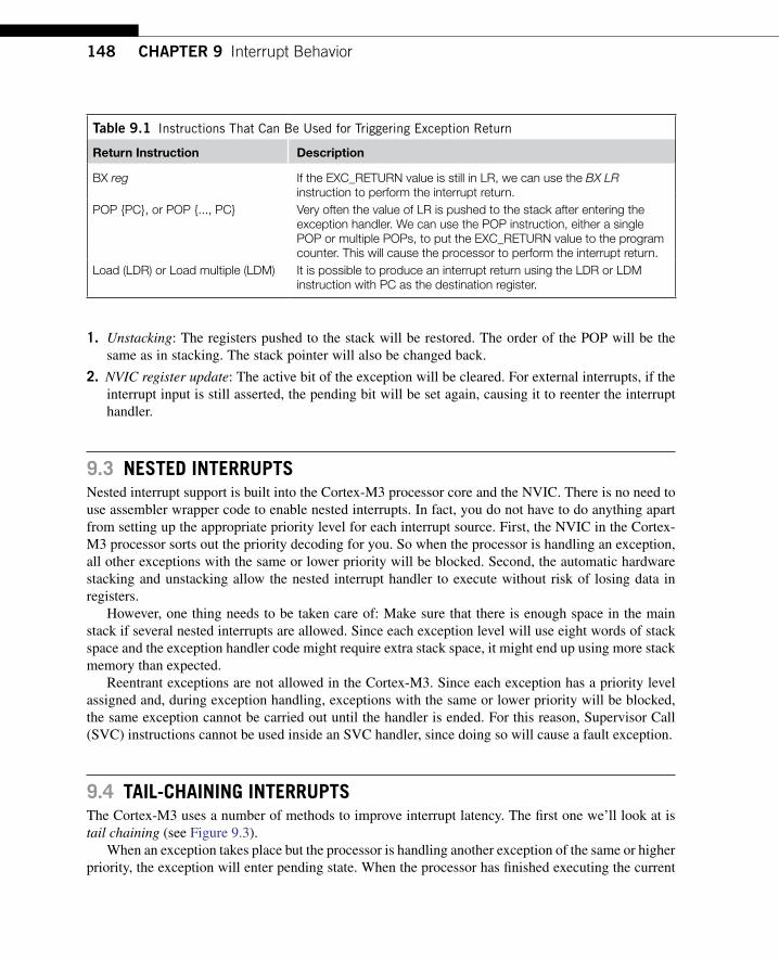
148 CHAPTER 9 Interrupt Behavior
1. Unstacking: The registers pushed to the stack will be restored. The order of the POP will be the same as in stacking. The stack pointer will also be changed back.
2. NVIC register update: The active bit of the exception will be cleared. For external interrupts, if the interrupt input is still asserted, the pending bit will be set again, causing it to reenter the interrupt handler.
9.3 nesTed InTerrupTsNested interrupt support is built into the Cortex-M3 processor core and the NVIC. There is no need to use assembler wrapper code to enable nested interrupts. In fact, you do not have to do anything apart from setting up the appropriate priority level for each interrupt source. First, the NVIC in the Cortex-M3 processor sorts out the priority decoding for you. So when the processor is handling an exception, all other exceptions with the same or lower priority will be blocked. Second, the automatic hardware stacking and unstacking allow the nested interrupt handler to execute without risk of losing data in registers.
However, one thing needs to be taken care of: Make sure that there is enough space in the main stack if several nested interrupts are allowed. Since each exception level will use eight words of stack space and the exception handler code might require extra stack space, it might end up using more stack memory than expected.
Reentrant exceptions are not allowed in the Cortex-M3. Since each exception has a priority level assigned and, during exception handling, exceptions with the same or lower priority will be blocked, the same exception cannot be carried out until the handler is ended. For this reason, Supervisor Call (SVC) instructions cannot be used inside an SVC handler, since doing so will cause a fault exception.
9.4 TaIL-ChaInIng InTerrupTsThe Cortex-M3 uses a number of methods to improve interrupt latency. The first one we’ll look at is tail chaining (see Figure 9.3).
When an exception takes place but the processor is handling another exception of the same or higher priority, the exception will enter pending state. When the processor has finished executing the current
Table 9.1 Instructions That Can Be Used for Triggering Exception Return
Return Instruction Description
BX reg If the EXC_RETURN value is still in LR, we can use the BX LR instruction to perform the interrupt return.
POP {PC}, or POP {..., PC} Very often the value of LR is pushed to the stack after entering the exception handler. We can use the POP instruction, either a single POP or multiple POPs, to put the EXC_RETURN value to the program counter. This will cause the processor to perform the interrupt return.
Load (LDR) or Load multiple (LDM) It is possible to produce an interrupt return using the LDR or LDM instruction with PC as the destination register.

1499.6 More on the Exception Return Value
exception handler, it can then process the pended interrupt. Instead of restoring the registers back from the stack (unstacking) and then pushing them onto the stack again (stacking), the processor skips the unstacking and stacking steps and enters the exception handler of the pended exception as soon as pos-sible. In this way, the timing gap between the two exception handlers is considerably reduced.
9.5 LaTe arrIVaLsAnother feature that improves interrupt performance is late arrival exception handling. When an exception takes place and the processor has started the stacking process, and if during this delay a new exception arrives with higher preemption priority, the late arrival exception will be processed first.
For example, if Exception #1 (lower priority) takes place a few cycles before Exception #2 (higher priority), the processor will behave as shown in Figure 9.4, such that Handler #2 is executed as soon as the stacking completes.
9.6 More on The exCepTIon reTurn VaLueWhen entering an exception handler, the LR is updated to a special value called EXC_RETURN, with the upper 28 bits all set to 1. This value, when loaded into the PC at the end of the exception handler execution, will cause the processor to perform an exception return sequence.
The instructions that can be used to generate exception returns are as follows:
POP/LDM•LDR with PC as a destination•BX with any register•
The EXC_RETURN value has bit (31:4) all set to 1, and bit (3:0) provides information required by the exception return operation (see Table 9.2). When the exception handler is entered, the LR value is updated automatically, so there is no need to generate these values manually.
FIgure 9.3
Tail Chaining of Exceptions.
Interrupt #1
Interrupt #2
Main program
Processorstate
Interrupt serviceroutine #1
Interrupt serviceroutine #2
Main program
Interruptevent #1 Interrupt exit Interrupt exit
Stacking Unstacking
Thread mode Handler mode Handler mode Thread mode

150 CHAPTER 9 Interrupt Behavior
Bit 0 indicates the process state being used after the exception return. Since the Cortex-M3 supports only the Thumb® state, bit 0 must be 1. The valid values (for the Cortex-M3) are shown in Table 9.3.
If the thread is using the MSP (main stack), the value of LR will be set to 0xFFFFFFF9 when it enters an exception, and 0xFFFFFFF1 when a nested exception is entered, as shown in Figure 9.5. If the thread is using PSP (process stack), the value of LR would be 0xFFFFFFFD when entering the first exception and 0xFFFFFFF1 for entering a nested exception, as shown in Figure 9.6.
As a result of the EXC_RETURN number format, you cannot perform interrupt returns to an address in the 0xFFFFFFF0–0xFFFFFFFF memory range. However, since this address is in a nonexecutable region anyway, it is not a problem.
Table 9.2 Description of Bit Fields in EXC_RETURN Value
Bits 31:4 3 2 1 0
Descriptions 0xFFFFFFF Return mode (thread/handler)
Return stack Reserved; must be 0
Process state (Thumb/ARM)
Table 9.3 Allowed EXC_RETURN Values on Cortex-M3
Value Condition
0xFFFFFFF1 Return to handler mode0xFFFFFFF9 Return to thread mode and on return use the main stack0xFFFFFFFD Return to thread mode and on return use the process stack
FIgure 9.4
Late Arrival Exception Behavior.
Interrupt #1(Low priority)
Interrupt #2(High priority)
Processorstate
Thread Handler #2Exception sequence
Data bus Stacking
Instructionbus
Thread
Vector fetch
Handler instruction fetch

1519.6 More on the Exception Return Value
FIgure 9.5
LR Set to EXC_RETURN at Exception (Main Stack Used in Thread Mode).
Interrupt #1(Low priority)
Interrupt #2(High priority)
Main program
Interrupt exit
Interruptexit
Unstacking
Interrupt serviceroutine #2
Interrupt serviceroutine #1
Stacking
Executionstatus
Interruptevent #1
Thread modeHandlermode
Handlermode
Handlermode
Thread mode
LR 5 0xFFFFFFF9 LR 5 0xFFFFFFF1
Main stackMain stack Main stack
FIgure 9.6
LR Set to EXC_RETURN at Exception (Process Stack Used in Thread Mode).
Interrupt #1(Low priority)
Interrupt #2(High priority)
Main program
Interrupt exit
Interruptexit
Unstacking
Interrupt serviceroutine #2
Interrupt serviceroutine #1
Stacking
Executionstatus
Interruptevent #1
Thread modeHandlermode
Handlermode
Handlermode
Thread mode
LR 5 0xFFFFFFFD LR 5 0xFFFFFFF1
Main stackProcess stack Process stack

152 CHAPTER 9 Interrupt Behavior
9.7 InTerrupT LaTenCyThe term interrupt latency refers to the delay from the start of the interrupt request to the start of interrupt handler execution. In the Cortex-M3 processor, if the memory system has zero latency, and provided that the bus system design allows vector fetch and stacking to happen at the same time, the interrupt latency can be as low as 12 cycles. This includes stacking the registers, vector fetch, and fetch-ing instructions for the interrupt handler. However, this depends on memory access wait states and a few other factors.
For tail-chaining interrupts, since there is no need to carry out stacking operations, the latency of switching from one exception handler to another exception handler can be as low as six cycles.
When the processor is executing a multicycle instruction, such as divide, the instruction could be abandoned and restarted after the interrupt handler completes. This also applies to load double (LDRD) and store double (STRD) instructions.
To reduce exception latency, the Cortex-M3 processor allows exceptions in the middle of Mul-tiple Load and Store instructions (LDM/STM). If the LDM/STM instruction is executing, the current memory accesses will be completed, and the next register number will be saved in the stacked xPSR (Interrupt-Continuable Instruction [ICI] bits). After the exception handler completes, the multiple load/store will resume from the point at which the transfer stopped. There is a corner case: If the multiple load/store instruction being interrupted is part of an IF-THEN (IT) instruction block, the load/store instruction will be cancelled and restarted when the interrupt is completed. This is because the ICI bits and IT execution status bits share the same space in the Execution Program Status Register (EPSR).
In addition, if there is an outstanding transfer on the bus interface, such as a buffered write, the processor will wait until the transfer is completed. This is necessary to ensure that a bus fault handler preempts the correct process.
Of course, the interrupt could be blocked if the processor is already executing another exception handler of the same or higher priority or if the Interrupt Mask register was masking the interrupt request. In these cases, the interrupt will be pended and will not be processed until the blocking is removed.
9.8 FauLTs reLaTed To InTerrupTsVarious faults can be caused by exception handling. Let’s take a look at these now.
9.8.1 stackingIf a bus fault takes place during stacking, the stacking sequence will be terminated and the bus fault exception will be triggered or pended. If the bus fault is disabled, the hard fault handler will be executed. Otherwise, if the bus fault handler has higher priority than the original exception, the bus fault handler will be executed; if not, it will be pended until the original exception is completed. This scenario, called a stacking error, is indicated by the STKERR (bit 4) in the Bus Fault Status register (0xE000ED29).
If the stacking error is caused by a Memory Protection Unit (MPU) violation, the memory man-agement fault handler will be executed and the MSTKERR (bit 4) in the Memory Management Fault Status register (0xE000ED28) will be set to indicate the problem. If the memory management fault is disabled, the hard fault handler will be executed.

1539.8 Faults Related to Interrupts
9.8.2 unstackingIf a bus fault takes place during unstacking (an interrupt return), the unstacking sequence will be termi-nated and the bus fault exception will be triggered or pended. If the bus fault is disabled, the hard fault handler will be executed. Otherwise, if the bus fault handler has higher priority than the current priority of the executing task (the core could already be executing another exception in a nested interrupt case), the bus fault handler will be executed. This scenario, called an unstacking error, is indicated by the UNSTKERR (bit 3) in the Bus Fault Status register (0xE000ED29).
Similarly, if the stacking error is caused by an MPU violation, the memory management fault han-dler will be executed and the MUNSTKERR (bit 3) in the Memory Management Fault Status register (0xE000ED28) will be set to indicate the problem. If the memory management fault is disabled, the hard fault handler will be executed.
9.8.3 Vector FetchesIf a bus fault or memory management fault takes place during a vector fetch, the hard fault handler will be executed. This is indicated by VECTTBL (bit 1) in the Hard Fault Status register (0xE000ED2C).
9.8.4 Invalid returnsIf the EXC_RETURN number is invalid or does not match the state of the processor (as in using 0xFFFFFFF1 to return to thread mode), it will trigger the usage fault. If the usage fault handler is not enabled, the hard fault handler will be executed instead. The INVPC bit (bit 2) or INVSTATE (bit 1) bit in the Usage Fault Status register (0xE000ED2A) will be set, depending on the actual cause of the fault.

155Copyright © 2010, Elsevier Inc. All rights reserved.DOI: 10.1016/B978-1-85617-963-8.00013-2
CHAPTER
In ThIs ChapTer
Overview .............................................................................................................................................. 155a Typical Development Flow .................................................................................................................. 155Using C ................................................................................................................................................ 156CMsIs .................................................................................................................................................. 164Using assembly .................................................................................................................................... 169Using exclusive access for semaphores ................................................................................................ 177Using Bit Band for semaphores ............................................................................................................. 179Working with Bit Field extract and Table Branch .................................................................................... 181
10.1 OvervIeWThe Cortex™-M3 can be programmed using either assembly language, C language, or other high-level languages like National Instruments LabVIEW. For most embedded applications using the Cortex-M3 processor, the software can be written entirely in C language. There are of course some people who pre-fer to use assembly language or a combination of C and assembly language in their projects. The pro-cedure of building and downloading the resultant image files to the target device is largely dependent on the tool chain used. Although this is not the main focus of this book, some simple examples showing how to use the Gnu’s Not Unix (GNU) and Keil tool chains are provided in Chapters 19 and 20, and an introduction of using LabVIEW on Cortex-M3 is covered in Chapter 21.
10.2 a TypICal DevelOpMenT FlOWVarious software programs are available for developing Cortex-M3 applications. The concepts of code generation flow in terms of these tools are similar. For the most basic uses, you will need assembler, a C compiler, a linker, and binary file generation utilities. For ARM solutions, the RealView Develop-ment Suite (RVDS) or RealView Compiler Tools (RVCT) provide a file generation flow, as shown in
Cortex-M3 Programming 10

156 CHAPTER 10 Cortex-M3 Programming
Figure 10.1. The scatter-loading script is optional but often required when the memory map becomes more complex.
Besides these basic tools, RVDS also contains a large number of utilities, including an Integrated Development Environment (IDE) and debuggers. Please visit the ARM web site (www.arm.com) for details.
10.3 UsIng CFor beginners in embedded programming, using C language for software development on the Cortex-M3 processor is the best choice. Programming in C with the Cortex-M3 processor is made even easier as most microcontroller vendors provide device driver libraries written in C to control peripherals. These can then be included into your project. Since modern C compilers can generate very efficient code, it is better to program in C than spending a lot of time to try to develop complex routines in assembly language, which is error prone and less portable.
In this chapter, we will have a quick look at a simple example of using C language to create a simple program image. Then, we will have a look at some C language development areas including using device driver libraries and the Cortex Microcontroller Software Interface Standard (CMSIS).
C has the advantage of being portable and easier for implementing complex operations, compared with assembly language. Since it’s a generic computer language, C does not specify how the processor is initialized. For these areas, tool chains can have different approaches. The best way to get started is to look at example codes. For users of ARM C compiler products, such as RVDS or Keil RealView Micro-controller Development Kit (MDK-ARM), a number of Cortex-M3 program examples are already included in the installation. For users of the GNU tool chain, Chapter 19 provides a simple C example based on the CodeSourcery GNU tool chain for ARM.
FIgUre 10.1
Example Flow Using ARM Development Tools.
C files (.c)
armcc(compiler)
Object files (.o)
Assembly files (.s)
armasm(compiler)
Object files (.o)
Scatter loading script
Executableimage file(.axf /.elf)
Armlink(linker)
fromelf
fromelf
Binaryprogram
image (.bin)
Disassembledcode (.txt)
Memorylayout

15710.3 Using C
10.3.1 example of a simple C program Using realview Development siteA normal program for the Cortex-M3 contains at least the “main” program and a vector table. Let’s start with the most basic main program that toggles an Light Emitting Diode (LED):
#define LED *((volatile unsigned int *)(0xDFFF000C))
int main (void){int i; /* loop counter for delay function */volatile int j; /* dummy volatile variable to prevent C compiler from optimize the delay away */
while (1) { LED = 0x00; /* toogle LED */ for (i=0;i<10;i++) {j=0;} /* delay */ LED = 0x01; /* toogle LED */ for (i=0;i<10;i++) {j=0;} /* delay */ } return 0;}
This file is named “blinky.c.” For the vector table, we create a separate C program called “vectors.c.” The file “vectors.c” contains the vector table, as well as a number of dummy exception handlers (these can be customized for target application later on):
typedef void(* const ExecFuncPtr)(void) __irq;extern int __main(void);
/* * Dummy handlers Exception Handlers */__irq void NMI_Handler(void){ while(1); }__irq void HardFault_Handler(void){ while(1); }__irq void SVC_Handler(void){ while(1); }__irq void DebugMon_Handler(void){ while(1); }__irq void PendSV_Handler(void){ while(1); }__irq void SysTick_Handler(void){ while(1); }__irq void ExtInt0_IRQHandler(void){ while(1); }__irq void ExtInt1_IRQHandler(void){ while(1); }__irq void ExtInt2_IRQHandler(void){ while(1); }__irq void ExtInt3_IRQHandler(void){ while(1); }
#pragma arm section rodata="exceptions_area"

158 CHAPTER 10 Cortex-M3 Programming
ExecFuncPtr exception_table[] = { /* vector table */(ExecFuncPtr)0x20002000,(ExecFuncPtr)__main,NMI_Handler, /* NMI */HardFault_Handler,0, /* MemManage_Handler in Cortex-M3 */0, /* BusFault_Handler in Cortex-M3 */0, /* UsageFault_Handler in Cortex-M3 */
0, /* Reserved */0, /* Reserved */0, /* Reserved */0, /* Reserved */SVC_Handler,0, /* DebugMon_Handler in Cortex-M3 */0, /* Reserved */PendSV_Handler,SysTick_Handler,
/* External Interrupts*/ExtInt0_IRQHandler,ExtInt1_IRQHandler,ExtInt2_IRQHandler,ExtInt3_IRQHandler
};#pragma arm section
Assuming you are using RVDS, you can compile the program using the following command line:
$> armcc –c –g –W blinky.c –o blinky.o$> armcc –c –g –W vectors.c –o vectors.o
Then the linker can be used to generate the program image. A scatter loading file “led.scat” is used to tell the linker the memory layout and to put the vector table in the starting of the program image. The “led.scat” is
#define HEAP_BASE 0x20001000#define STACK_BASE 0x20002000#define HEAP_SIZE ((STACK_BASE-HEAP_BASE)/2)#define STACK_SIZE ((STACK_BASE-HEAP_BASE)/2)
LOAD_REGION 0x00000000 0x00200000{VECTORS 0x0 0xC0{; Provided by the user in vectors.c* (exceptions_area)
}
CODE 0xC0 FIXED{* (+RO)
}
DATA 0x20000000 0x00010000{* (+RW, +ZI)
}

15910.3 Using C
;; Heap starts at 4KB and grows upwardsARM_LIB_HEAP HEAP_BASE EMPTY HEAP_SIZE{}
;; Stack starts at the end of the 8KB of RAM;; And grows downwards for 2KBARM_LIB_STACK STACK_BASE EMPTY -STACK_SIZE{}
}
And the command line for the linker is
$> armlink –scatter led.scat "--keep=vectors.o(exceptions_area)" blinky.o vectors.o –o blinky.elf
The executable image blinky.elf is now generated. We can convert it to binary file and disassem-bly file using fromelf.
/* create binary file */$> fromelf –-bin blinky.elf –output blinky.bin/* Create disassembly output */$> fromelf –c blinky.elf > list.txt
Previously in ARM processors, because there is a Thumb® state and an ARM state, the code for differ-ent states has to be compiled differently. In the Cortex-M3, there is no such need because everything is in the Thumb state, and project file management is much simpler.
When you’re developing applications in C, it is recommended that you use the double word stack alignment function (configured by the STKALIGN bit in the Nested Vectored Interrupt Controller [NVIC] Configuration Control register). For users of Cortex-M3 revision 2 or future products, the STKALIGN bit is set by default at reset so there is no need to set up this bit in the software. Users of Cortex-M3 revision 1 can enable this feature by setting this bit in the beginning of their applications, for example. The details of STKALIGN feature are covered in Chapter 9.
SCB->CCR = SCB->CCR | 0x200; /* Set STKALIGN *//* SCB->CCR is defined in device driver library. */
If you are not using a CMSIS compliant device driver, you can use the following code instead.
#define NVIC_CCR *((volatile unsigned long *)(0xE000ED14))NVIC_CCR = NVIC_CCR | 0x200; /* Set STKALIGN */
Using this feature ensures that the system conforms to Procedure Call Standards for the ARM Architecture (AAPCS). Additional information on this subject is covered in Chapter 12.
10.3.2 Compile the same example Using Keil MDK-arMFor users of Keil MDK-ARM, it is possible to compile the same program as in RVDS. However, the command line options and a few symbols in the linker script (scatter loading file) have to be modified. Based on the example in Section 10.3.1, scatter loading file “led.scat” needed to be modified to

160 CHAPTER 10 Cortex-M3 Programming
#define HEAP_BASE 0x20001000#define STACK_BASE 0x20002000#define HEAP_SIZE ((STACK_BASE-HEAP_BASE)/2)#define STACK_SIZE ((STACK_BASE-HEAP_BASE)/2)
LOAD_REGION 0x00000000 0x00200000{VECTORS 0x0 0xC0{
; Provided by the user in vectors.c* (exceptions_area)
}
CODE 0xC0 FIXED{
* (+RO)}
DATA 0x20000000 0x00010000{
* (+RW, +ZI)}
;; Heap starts at 4KB and grows upwardsHeap_Mem HEAP_BASE EMPTY HEAP_SIZE{}
;; Stack starts at the end of the 8KB of RAM;; And grows downwards for 2KBStack_Mem STACK_BASE EMPTY -STACK_SIZE{}
}
And the compile sequence can be created in a DOS batch file
SET PATH=C:\Keil\ARM\BIN40\;%PATH%SET RVCT40INC=C:\Keil\ARM\RV31\INCSET RVCT40LIB=C:\Keil\ARM\RV31\LIBSET CPU_TYPE=Cortex-M3SET CPU_VENDOR=ARMSET UV2_TARGET=Target 1SET CPU_CLOCK=0x00000000C:\Keil\ARM\BIN40\armcc -c -O3 -W -g -Otime --device DLM vectors.cC:\Keil\ARM\BIN40\armcc -c -O3 -W -g -Otime --device DLM blinky.c C:\Keil\ARM\BIN40\armlink --device DLM "--keep=Startup.o(RESET)" "--first=Startup.o(RESET)" -scatter led.scat --map vectors.o blinky.o -o blinky.elfC:\Keil\ARM\BIN40\fromelf --bin blinky.elf -o blinky.bin
In general, it is much easier to use the μVision IDE to create and compile projects rather than using command lines. Chapter 20 is ideal for beginners who want to start using the Cortex-M3 microcon-trollers with the Keil Microcontroller Development Kit for ARM (MDK-ARM).

16110.3 Using C
10.3.3 accessing Memory-Mapped registers in CThere are various ways to access memory-mapped peripheral registers in C language. For illustration, we will use the System Tick (SYSTICK) Timer in the Cortex-M3 as an example peripheral to demon-strate different access methods in C language. The SYSTICK is a 24-bit timer which contains only four registers. The functionality of the SYSTICK will be covered in Chapter 14. In the previous examples, we have already illustrated the easiest method—defining each register as a pointer. To apply the same solution to the SYSTICK, we can define each register separately. This is illustrated in Figure 10.2.
Based on the same method, we can define a macro to convert address values to C pointer. The C-code looks a bit different, but the generated code is the same as previous implementation. This is illustrated in Figure 10.3.
Method 2 is to define the registers as a data structure, and then define a pointer of the defined structure. This is the method used in CMSIS compliant device driver libraries. This is illustrated in Figure 10.4.
Method 3 also uses data structure, but the base address of the peripheral is defined using a scatter loading file (or linker script) during linking stage. This is illustrated in Figure 10.5.
FIgUre 10.2
Accessing Peripheral Registers as Pointers.
#define SYSTICK_CTRL (*((volatile unsigned long *)(0xE000E010)))#define SYSTICK_LOAD (*((volatile unsigned long *)(0xE000E014)))#define SYSTICK_VAL (*((volatile unsigned long *)(0xE000E018)))#define SYSTICK_CALIB (*((volatile unsigned long *)(0xE000E01C)))
/* Setup SYSTICK */SYSTICK_LOAD 5 0xFFFF; // Set reload valueSYSTICK_VAL 5 0x0; // Clear current valueSYSTICK_CTRL 5 0x5; // Enable SYSTICK and select core clock
CTRL
RELOAD
VALUE
CALIB
SYSTICKTimer
registers
0xE000E010
0xE000E014
0xE000E018
0xE000E01C
FIgUre 10.3
Alternative Way of Accessing Peripheral Registers as Pointers.
#define HW_REG(addr) (*((volatile unsigned long *)(addr)))#define SYSTICK_CTRL 0xE000E010#define SYSTICK_LOAD 0xE000E014#define SYSTICK_VAL 0xE000E018#define SYSTICK_CALIB 0xE000E01C
/* Setup SysTick */HW_REG(SYSTICK_LOAD) 5 0xFFFF; // Set reload valueHW_REG(SYSTICK_VAL) 5 0x0; // Clear current valueHW_REG(SYSTICK_CTRL) 5 0x5; // Enable SYSTICK and select core clock CTRL
RELOAD
VALUE
CALIB
SYSTICKTimer
registers
0xE000E010
0xE000E014
0xE000E018
0xE000E01C

162 CHAPTER 10 Cortex-M3 Programming
In this case (method is shown in Figure 10.5), the program code using the peripheral has to define the peripheral as a C pointer in an external object. The code for accessing the register is the same as in the second method.
Method 1 (shown in Figures 10.2 and 10.3) is the simplest, however, it can result in less efficient code compared with the others as the address value for the registers are stored separately as constant. As a result, the code size can be larger and might be slower as it requires more accesses to the program memory to set up the address values. However, for peripheral control code that only access to one register, the efficiency of method 1 is identical to others.
Method 2 (using data structure and a pointer defined in the C-code) is possibly the most com-monly used. It allows the registers in a peripheral to share just one constant for base address value. The immediate offset address mode can be used for access of each register. This is the method used in CMSIS, which will be covered later in this chapter.
FIgUre 10.5
Defining Peripheral-Based Address Using Scatter Loading File.
__attribute__ ((zero_init)) struct { volatile unsigned long CTRL; /* systick control */
volatile unsigned long RELOAD; /* systick reload */volatile unsigned long VAL; /* systick value */volatile unsigned long CALIB; /* systick calibration */
} systick_struct;
In the C file, define the data structure as
LOAD_FLASH 0x0000{ :
SYSTICK 0xE000E010 UNINIT{
systick_reg.o ( 1ZI)}
:}
Then create a scatter loading file to place the data structureto specific address CTRL
RELOAD
VALUE
CALIB
SYSTICKTimer
registers
0xE000E010
0xE000E014
0xE000E018
0xE000E01C
SYSTICK_struct
FIgUre 10.4
Accessing Peripheral Registers as Pointers to Elements in a Data Structure.
typedef struct{
volatile unsigned long CTRL; /* SysTick Control and Status register */ volatile unsigned long LOAD; /* SysTick Reload Value register */ volatile unsigned long VAL; /* SysTick Current Value register */ volatile unsigned long CALIB; /* SysTick Calibration register */
} SysTick_Type;
#define SysTick ((SysTick_Type *) 0xE000E010) /* SysTick struct */
/* Setup SysTick */SysTick->LOAD 5 0xFFFF; // Set reload valueSysTick->VAL 5 0x0; // Clear current valueSysTick->CTRL 5 0x5; // Enable SYSTICK and select core clock
CTRL
RELOAD
VALUE
CALIBSYSTICK
Timerregisters
0xE000E010
0xE000E014
0xE000E018
0xE000E01C
SYSTICK_Type

16310.3 Using C
Method 3 (using scatter loading file or linker script, as shown in figure 10.5) has the same efficiency as method 2, but it is less portable due to the use of a scatter loading file (scatter loading file syntax is tool chain specific). Method 3 is required when you are developing a device driver library for a peripheral that is used in multiple devices, and the base address of the peripheral is not known until in the linking stage.
10.3.4 Intrinsic FunctionsUse of the C language can often speed up application development, but in some cases, we need to use some instructions that cannot be generated using normal C-code. Some C compilers provide intrinsic functions for accessing these special instructions. Intrinsic functions are used just like normal C functions. For example, ARM compilers (including RealView C Compilers and Keil MDK-ARM) provide the intrinsic functions listed in Table 10.1 for commonly used instructions.
10.3.5 embedded assembler and Inline assemblerAs an alternative to using intrinsic functions, we can also directly access assembly instructions in C-code. This is often necessary in low-level system control or when you need to implement a timing critical routine and decide to implement it in assembly for the best performance. Most ARM C compil-ers allow you to include assembly code in form of inline assembler.
Table 10.1 Intrinsic Functions Provided in ARM Compilers
Assembly Instructions ARM Compiler Intrinsic Functions
CLZ unsigned char __clz(unsigned int val)CLREX void __clrex(void)CPSID I void __disable_irq(void)CPSIE I void __enable_irq(void)CPSID F void __disable_fiq(void)CPSIE F void __enable_fiq(void)LDREX/LDREXB/LDREXH unsigned int __ldrex(volatile void *ptr)LDRT/LDRBT/LDRSBT/LDRHT/LDRSHT unsigned int __ldrt(const volatile void *ptr)NOP void __nop(void)RBIT unsigned int __rbit(unsigned int val)REV unsigned int __rev(unsigned int val)ROR unsigned int __ror(unsigned int val, unsigned int shift)SSAT int __ssat(int val, unsigned int sat)SEV void __sev(void)STREX/STREXB/STREXH int __strex(unsigned int val, volatile void *ptr)STRT/STRBT/STRHT void int __strt(unsigned int val, const volatile void *ptr)USAT int __usat(unsigned int val, unsigned int sat)WFE void __wfe(void)WFI void __wfi(void)BKPT void __breakpoint(int val)

164 CHAPTER 10 Cortex-M3 Programming
In the ARM compiler, you can add assembly code inside the C program. Traditionally, inline assembler is used, but the inline assembler in RealView C Compiler does not support instructions in Thumb-2 technology. Starting with RealView C Compiler version 3.0, a new feature called the Embed-ded Assembler is included, and it supports the instruction set in Thumb-2. For example, you can insert assembly functions in your C programs this way:
__asm void SetFaultMask(unsigned int new_value){// Assembly code hereMSR FAULTMASK, new_value // Write new value to FAULTMASKBX LR // Return to calling program
}
Detailed descriptions of Embedded Assembler in RealView C Compiler can be found in the RVCT 4.0 Compilation Tools Compiler Guide [Ref. 6].
For the Cortex-M3, Embedded Assembler is useful for tasks, such as direct manipulation of the stacks and timing critical processing task (codec software).
10.4 CMsIs10.4.1 Background of CMsIsThe Cortex-M3 microcontrollers are gaining momentum in the embedded application market, as more and more products based on the Cortex-M3 processor and software that support the Cortex-M3 proces-sor are emerging. At the end of 2008, there were more than five C compiler vendors, and more than 15 embedded Operating Systems (OS) supporting the Cortex-M3 processor. There are also a num-ber of companies providing embedded software solutions, including codecs, data processing libraries, and various software and debug solutions. The CMSIS was developed by ARM to allow users of the Cortex-M3 microcontrollers to gain the most benefit from all these software solutions and to allow them to develop their embedded application quickly and reliably (see Figure 10.6).
FIgUre 10.6
CMSIS Provides a Standardized Access Interface for Embedded Software Products.
Device driver library
CMSIS
Microcontrollerhardware
Cortex-M3/Cortex-M0/Cortex-M1
Software
EmbeddedOS
Applicationsoftware
Middleware

16510.4 CMSIS
The CMSIS was started in 2008 to improve software usability and inter-operability of ARM micro-controller software. It is integrated into the driver libraries provided by silicon vendors, providing a standardized software interface for the Cortex-M3 processor features, as well as a number of common system and I/O functions. The library is also supported by software companies including embedded OS vendors and compiler vendors.
The aims of CMSIS are to:
improve software portability and reusability•enable software solution suppliers to develop products that can work seamlessly with device •libraries from various silicon vendorsallow embedded developers to develop software quicker with an easy-to-use and standardized •software interfaceallow embedded software to be used on multiple compiler products•avoid device driver compatibility issues when using software solutions from multiple sources•
The first release of CMSIS was available from fourth quarter of 2008 and has already become part of the device driver library from microcontroller vendors. The CMSIS is also available for Cortex-M0.
10.4.2 areas of standardizationThe scope of CMSIS involves standardization in the following areas:
• Hardware Abstraction Layer (HAL) for Cortex-M processor registers: This includes standardized register definitions for NVIC, System Control Block registers, SYSTICK register, MPU registers, and a number of NVIC and core feature access functions.
• Standardized system exception names: This allows OS and middleware to use system exceptions easily without compatibility issues.
• Standardized method of header file organization: This makes it easier for users to learn new Cortex microcontroller products and improve software portability.
• Common method for system initialization: Each Microcontroller Unit (MCU) vendor provides a SystemInit() function in their device driver library for essential setup and configuration, such as initialization of clocks. Again, this helps new users to start to use Cortex-M microcontrollers and aids software portability.
• Standardized intrinsic functions: Intrinsic functions are normally used to produce instructions that cannot be generated by IEC/ISO C.* By having standardized intrinsic functions, software reusability and portability are considerably improved.
• Common access functions for communication: This provides a set of software interface functions for common communication interfaces including universal asynchronous receiver/transmitter (UART), Ethernet, and Serial Peripheral Interface (SPI). By having these common access functions in the device driver library, reusability and portability of embedded software are improved. At the time of writing this book, it is still under development.
• Standardized way for embedded software to determine system clock frequency: A software variable called SystemFrequency is defined in device driver code. This allows embedded OS to set up the SYSTICK unit based on the system clock frequency.
*C/C++ features are specified in a standard document “ISO/IEC 14882” prepared by the International Organization for Standards (ISO) and the International Electrotechnical Commission (IEC).
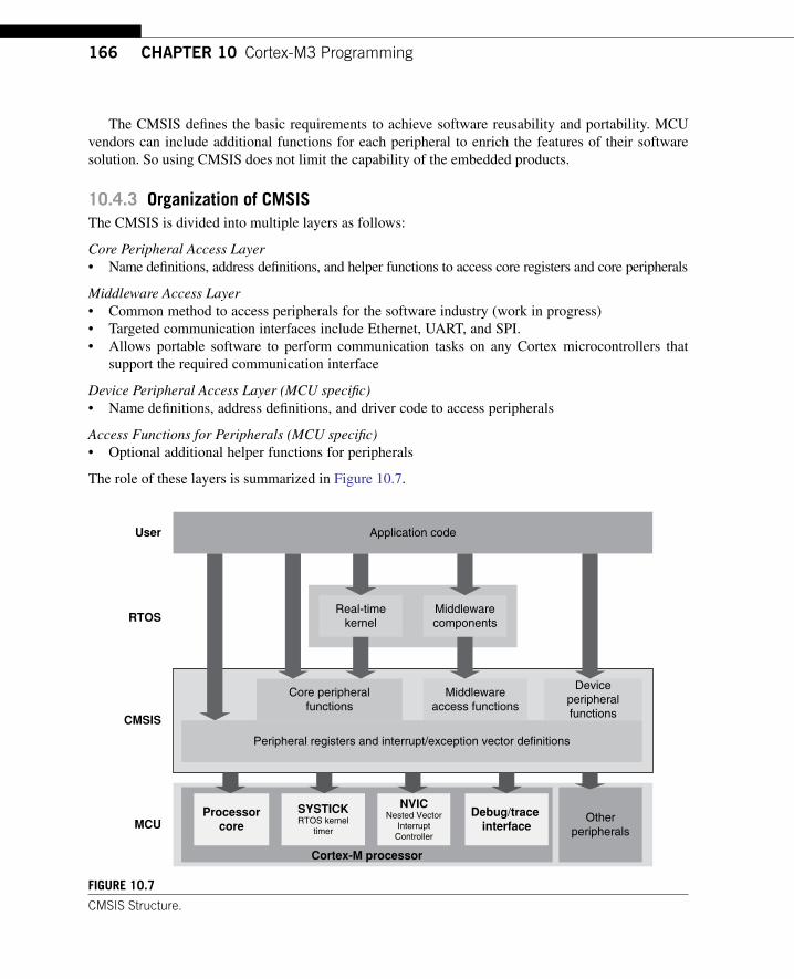
166 CHAPTER 10 Cortex-M3 Programming
The CMSIS defines the basic requirements to achieve software reusability and portability. MCU vendors can include additional functions for each peripheral to enrich the features of their software solution. So using CMSIS does not limit the capability of the embedded products.
10.4.3 Organization of CMsIsThe CMSIS is divided into multiple layers as follows:
Core Peripheral Access LayerName definitions, address definitions, and helper functions to access core registers and core peripherals•
Middleware Access LayerCommon method to access peripherals for the software industry (work in progress)•Targeted communication interfaces include Ethernet, UART, and SPI.•Allows portable software to perform communication tasks on any Cortex microcontrollers that •support the required communication interface
Device Peripheral Access Layer (MCU specific)Name definitions, address definitions, and driver code to access peripherals•
Access Functions for Peripherals (MCU specific)Optional additional helper functions for peripherals•
The role of these layers is summarized in Figure 10.7.
FIgUre 10.7
CMSIS Structure.
User Application code
Real-timekernelRTOS
Middlewarecomponents
CMSIS
Peripheral registers and interrupt/exception vector definitions
Core peripheralfunctions
Middlewareaccess functions
Deviceperipheralfunctions
MCUOther
peripherals
Cortex-M processor
NVICNested Vector
InterruptController
SYSTICKRTOS kernel
timer
Debug/trace interface
Processorcore

16710.4 CMSIS
10.4.4 Using CMsIsSince the CMSIS is incorporated inside the device driver library, there is no special setup requirement for using CMSIS in projects. For each MCU device, the MCU vendor provides a header file, which pulls in additional header files required by the device driver library, including the Core Peripheral Access Layer defined by ARM (see Figure 10.8).
The file core_cm3.h contains the peripheral register definitions and access functions for the Cortex-M3 processor peripherals like NVIC, System Control Block registers, and SYSTICK registers. The core_cm3.h file also contains declaration of CMSIS intrinsic functions to allow C applications to access instructions that cannot be generated using IEC/ISO C language. In addition, this file also con-tains a function for outputting a debug message via the Instrumentation Trace Module (ITM).
Note that in some cases, the intrinsic functions in CMSIS could have similar names compared with the intrinsic functions provided in the C compilers, whereas the CMSIS intrinsic functions are compiler independent.
The file core_cm3.c contains implementation of CMSIS intrinsic functions that cannot be imple-mented in core_cm3.h using simple definitions.
The system_<device>.h file contains microcontroller specific interrupt number definitions, and peripheral register definitions. The system_<device>.c file contains a microcontroller specific function called SystemInit for system initialization.
In addition, CMSIS compliant device drivers also contain start-up code (which contains the vector table) for various supported compilers, and CMSIS version of intrinsic functions to allow embedded software access to all processor core features on different C compiler products.
Examples of using CMSIS can be found on the microcontroller vendor’s web site. You might also find examples in the device driver libraries itself. Alternatively, you can download the ARM CMSIS
FIgUre 10.8
CMSIS Files.
<device>.h
core_cm3.h
system_<device>.c
Core peripheralaccess layer
System functionsincluding initialization
Other header files
Device peripheralaccess layer andadditional access
functions
system_<device>.hInterrupt number andperipheral registers
definitions
core_cm3.cCore intrinsic function
implementations
Different startup code fordifferent tool chain
Startup code files

168 CHAPTER 10 Cortex-M3 Programming
package from www.onarm.com, which contains examples and documentation. Documentation of the common functions can also be found in this package.
A simple example of using CMSIS in your application development is shown in Figure 10.9. To use the CMSIS to set up interrupts and exceptions, you need to use the exception/interrupt constants defined in the system_<device>.h. These exception and interrupt constants are different from the exception number used in the core internal registers (e.g., Interrupt Program Status Register [IPSR]). For CMSIS, negative numbers are for system exceptions and positive numbers are for peripheral interrupts.
For development of portable code, you should use the core access functions to access core function-alities and middleware access functions to access peripheral. This allows the porting of software to be minimized between different Cortex microcontrollers.
Details of common CMSIS access functions and intrinsic functions can be found in Appendix G.
10.4.5 Benefits of CMsIsSo what does CMSIS mean to end users?
The main advantage is much better software portability and reusability. Besides easy migration between different Cortex-M3 microcontrollers, it also allows software to be quickly ported between Cortex-M3 and other Cortex-M processors, reducing time to market.
For embedded OS vendors and middleware providers, the advantages of the CMSIS are signifi-cant. By using the CMSIS, their software products can become compatible with device drivers from multiple microcontroller vendors, including future microcontroller products that are yet to be released (see Figure 10.10). Without the CMSIS, the software vendors either have to include a small library for
FIgUre 10.9
CMSIS Example.
#include "vendor_device.h" // For example,// lm3s_cmsis.h for LuminaryMicro devices// LPC17xx.h for NXP devices// stm32f10x.h for ST devices
void main(void) {SystemInit();…NVIC_SetPriority(UART1_IRQn, 0x0);NVIC_EnableIRQ(UART1_IRQn);…
}void UART1_IRQHandler {...
}
void SysTick_Handler(void) {…}
Common name forsystem initialization code
(from CMSIS v1.30, this functionis called from startup code)
Interrupt numbers defined insystem_<device>.h
NVIC setup by core accessfunctions
System exception handlernames are common to allCortex microcontrollers
Peripheral interrupt names aredevice specific, define in device
specific startup code

16910.5 Using Assembly
Cortex-M3 core functions or develop multiple configurations of their product so that it can work with device libraries from different microcontroller vendors.
The CMSIS has a small memory footprint (less than 1 KB for all core access functions and a few bytes of RAM). It also avoids overlapping of core peripheral driver code when reusing software code from other projects.
Since CMSIS is supported by multiple compiler vendors, embedded software can compile and run with different compilers. As a result, embedded OS and middleware can be MCU vendor inde-pendent and compiler tool vendor independent. Before availability of CMSIS, intrinsic functions were generally compiler specific and could cause problems in retargetting the software in a different compiler.
Since all CMSIS compliant device driver libraries have a similar structure, learning to use different Cortex-M3 microcontrollers is even easier as the software interface has similar look and feel (no need to relearn a new application programming interface).
CMSIS is tested by multiple parties and is Motor Industry Software Reliability Association (MISRA) compliant, thus reducing the validation effort required for developing your own NVIC or core feature access functions.
10.5 UsIng asseMBlyFor small projects, it is possible to develop the whole application in assembly language. However, this is often much harder for beginners. Using assembler, you might be able to get the best optimization you want, though it might increase your development time, and it could be easy to make mistakes. In addition, handling complex data structures or function library management can be extremely difficult
FIgUre 10.10
CMSIS Avoids Overlapping Driver Code.
Driver library fromOS/middleware
vendor
Driver library frommicrocontroller
vendors
Embedded OS/middlewareApplication
PeripheralsProcessor
core
EmbeddedOS/
middlewareApplication
PeripheralsProcessor
core
Driver library frommicrocontroller vendors with CMSIS
Without CMSIS, embedded OS ormiddleware needs to include processor
core access functions and mightneed to include a few peripheral drivers
With CMSIS, embedded OS ormiddleware can use standardized
core access functions in the driver library

170 CHAPTER 10 Cortex-M3 Programming
in assembler. Yet even when the C language is used in a project, in some situations part of the program is implemented in assembly language as follows:
Functions that cannot be implemented in C, such as direct manipulation of stack data or special •instructions that cannot be generated by the C compiler in normal C-codeTiming-critical routines•Tight memory requirements, causing part of the program to be written in assembly to get the •smallest memory size
10.5.1 The Interface between assembly and CIn various situations, assembly code and the C program interact. For example,
When embedded assembly (or inline assembler, in the case of the GNU tool chain) is used in C •program codeWhen C program code calls a function or subroutine implemented in assembler in a separate file•When an assembly program calls a C function or subroutine•
In these cases, it is important to understand how parameters and return results are passed between the calling program and the function being called. The mechanisms of these interactions are specified in the ARM Architecture Procedure Call Standard [AAPCS, [Ref. 5]].
For simple cases, when a calling program needs to pass parameters to a subroutine or function, it will use registers R0–R3, where R0 is the first parameter, R1 is the second, and so on. Similarly, R0 is used for returning a value at the end of a function. R0–R3 and R12 can be changed by a function or subroutine whereas the contents of R4–R11 should be restored to the previous state before entering the function, usually handled by stack PUSH and stack POP.
To make them easier to understand, the examples in this book do not strictly follow AAPCS prac-tices. If a C function is called by an assembly code, the effect of a possible register change to R0–R3 and R12 will need to be taken into account. If the contents of these registers are needed at a later stage, these registers might need to be saved on the stack and restored after the C function completes. Since the example codes mostly only call assembly functions or subroutines that affect a few registers or restore the register contents at the end, it’s not necessary to save registers R0–R3 and R12.
10.5.2 The First step in assembly programmingThis chapter reviews a few examples in assembly language. In most cases, you will be programming in C, but by looking into some assembler examples, we can gain a better understanding of how to use the Cortex-M3 processor. The examples here are based on ARM assembler tools (armasm) in RVDS. For users of Keil MDK-ARM, the command line options are slightly different. For other assembler tools, the file format and instruction syntax will also need to be modified. In addition, some develop-ment tools will actually do the startup code for you, so you might not need to worry about creating your assembly startup code.
The first simple program can be something like this
STACK_TOP EQU 0x20002000; constant for SP starting value
AREA |Header Code |, CODEDCD STACK_TOP ; Stack top

17110.5 Using Assembly
DCD Start ; Reset vectorENTRY ; Indicate program execution start here
Start ; Start of main program; initialize registersMOV r0, #10 ; Starting loop counter valueMOV r1, #0 ; starting result; Calculated 10+9+8+...+1
loopADD r1, r0 ; R1 = R1 + R0SUBS r0, #1 ; Decrement R0, update flag ("S" suffix)BNE loop ; If result not zero jump to loop; Result is now in R1
deadloopB deadloop ; Infinite loopEND ; End of file
This simple program contains the initial stack pointer (SP) value, the initial program counter (PC) value, and setup registers and then does the required calculation in a loop.
Assuming you are using ARM RealView compilation tools, this program can be assembled using
$> armasm --cpu cortex-m3 -o test1.o test1.s
The -o option specifies the output file name. The test1.o is an object file. We then need to use a linker to create an executable image (ELF). This can be done by
$> armlink --rw_base 0x20000000 --ro_base 0x0 --map -o test1.elf test1.o
Here, --ro-base 0x0 specifies that the read-only region (program ROM) starts at address 0x0; --rw-base specifies that the read/write region (data memory) starts at address 0x20000000. (In this example test1.s, we did not have any RAM data defined.) The --map option creates an image map, which is use-ful for understanding the memory layout of the compiled image.
Finally, we need to create the binary image
$> fromelf --bin --output test1.bin test1.elf
For checking that the image looks like what we wanted, we can also generate a disassembled code list file by
$> fromelf -c --output test1.list test1.elf
If everything works fine, you can then load your ELF image or binary image into your hardware or instruction set simulator for testing.
10.5.3 producing OutputsIt is always more fun when you can connect your microcontroller to the outside world. The simplest way to do that is to turn on/off the LEDs. However, this practice is quite limiting because it can only rep-resent very limited information. One of the most common output methods is to send text messages to a console. In embedded product development, this task is often handled by a UART interface connecting

172 CHAPTER 10 Cortex-M3 Programming
to a personal computer. For example, a computer running a Windows1 system with the Hyper-Terminal program acting as a console can be a handy way to produce outputs (see Figure 10.11).
The Cortex-M3 processor does not contain a UART interface, but most Cortex-M3 microcontrollers come with UART provided by the chip manufacturers. The specification of the UART can differ among various devices, so we won’t attempt to cover the topic in this book. Our next example assumes that a UART is available and has a status flag to indicate whether the transmit buffer is ready for sending out new data. A level shifter is needed in the connection because RS-232 has a different voltage level than the microcontroller I/O pins.
UART is not the only solution to output text messages. A number of features are implemented on the Cortex-M3 processor to help output debugging messages:
• Semihosting: Depending on the debugger and code library support, semihosting (outputting printf messages via a debug probe device) can be done via debug register in the NVIC. More information on this topic is covered in Chapter 15. In these cases, you can use printf within your C program, and the output will be displayed on the console/standard output (STDOUT) of the debugger software.
• Instrumentation trace: If the Cortex-M3 microcontroller provides a trace port and an external Trace Port Analyzer (TPA) is available, instead of using UART to output messages, we can use the ITM. The trace port works much faster than UART and can offer more data channels.
• Instrumentation trace via Serial-Wire Viewer (SWV): Alternatively, the Cortex-M3 processor (revision 1 and later) also provides an SWV operation mode on the Trace Port Interface Unit (TPIU). This interface allows outputs from ITM to be captured using low-cost hardware instead of a TPA. However, the bandwidth provided with the SWV mode is limited, so it is not ideal for large amounts of data (e.g., instruction trace operation).
10.5.4 The “hello World” exampleBefore we try to write a “Hello world” program, we should figure out how to send one character through the UART. The code used to send a character can be implemented as a subroutine, which can
1Windows and Hyper-Terminal are trademarks of Microsoft Corporation.
FIgUre 10.11
A Low-Cost Test Environment for Outputting Text Messages.
Cortex-M3microcontroller
Levelshifter
Hyper-Terminalrunning onwindows
RS-232serial cable

17310.5 Using Assembly
be called by other message output codes. If the output device changes, we only need to change this subroutine and all the text messages can be output by a different device. This modification is usually called retargetting.
A simple routine to output a character could be something like this
UART0_BASE EQU 0x4000C000UART0_FLAG EQU UART0_BASE+0x018UART0_DATA EQU UART0_BASE+0x000
Putc ; Subroutine to send a character via UART ; Input R0 = character to send PUSH {R1,R2, LR} ; Save registers LDR R1,=UART0_FLAG
PutcWaitLoop LDR R2,[R1] ; Get status flag TST R2, #0x20 ; Check transmit buffer full flag
; bit BNE PutcWaitLoop ; If busy then loop LDR R1,=UART0_DATA ; otherwise STRB R0, [R1] ; Output data to transmit buffer POP {R1,R2, PC} ; Return
The register addresses and bit definitions here are just examples; you might need to change the value for your device. In addition, some UART might require a more complex status-checking process before the character is output to the transmit buffer. Furthermore, another subroutine call ( Uart0Initialize in the following example) is required to initialize the UART, but this depends on the UART specification and will not be covered in this chapter. An example of UART initialization in C for Luminary Micro LM3S811 devices is covered in Chapter 20.
Now, we can use this subroutine to build a number of functions to display messages:
Puts ; Subroutine to send string to UART ; Input R0 = starting address of string. ; The string should be null terminated PUSH {R0 ,R1, LR} ; Save registers MOV R1, R0 ; Copy address to R1, because R0 will ; be used
PutsLoop ; as input for Putc LDRB R0,[R1],#1 ; Read one character and increment
; address CBZ R0, PutsLoopExit ; if character is null, goto end BL Putc ; Output character to UART B PutsLoop ; Next character
PutsLoopExit POP {R0, R1, PC} ; Return
With this subroutine, we are ready for our first “Hello world” program:
STACK_TOP EQU 0x20002000; constant for SP starting valueUART0_BASE EQU 0x4000C000UART0_FLAG EQU UART0_BASE+0x018UART0_DATA EQU UART0_BASE+0x000

174 CHAPTER 10 Cortex-M3 Programming
AREA | Header Code|, CODE DCD STACK_TOP ; Stack Pointer initial value DCD Start ; Reset vector ENTRY
Start ; Start of main program MOV r0, #0 ; initialize registers MOV r1, #0 MOV r2, #0 MOV r3, #0 MOV r4, #0 BL Uart0Initialize ; Initialize the UART0 LDR r0,=HELLO_TXT ; Set R0 to starting address of string BL Puts
deadend B deadend ; Infinite loop ;-------------------------------- ; subroutines ;--------------------------------
Puts ; Subroutine to send string to UART ;Input R0 = starting address of string. ; The string should be null terminated PUSH {R0 ,R1, LR} ; Save registers MOV R1, R0 ; Copy address to R1, because R0 will
; be usedPutsLoop ; as input for Putc
LDRB R0,[R1],#1 ; Read one character and increment ; address
CBZ R0, PutsLoopExit ; if character is null, goto end BL Putc ; Output character to UART B PutsLoop ; Next character
PutsLoopExit POP {R0, R1, PC} ; Return ;--------------------------------
Putc ; Subroutine to send a character via UART ; Input R0 = character to send PUSH {R1,R2, LR} ; Save registers LDR R1,=UART0_FLAG
PutcWaitLoop LDR R2,[R1] ; Get status flag TST R2, #0x20 ; Check transmit buffer full flag bit BNE PutcWaitLoop ; If busy then loop LDR R1,=UART0_DATA ; otherwise STR R0, [R1] ; Output data to transmit buffer POP {R1,R2, PC} ; Return ;--------------------------------
Uart0Initialize ; Device specific, not shown here BX LR ; Return
;--------------------------------HELLO_TXT
DCB "Hello world\n",0 ; Null terminated Hello ; world string END ; End of file

17510.5 Using Assembly
The only thing you need to add to this code is the details for the Uart0Initialize subroutine and modify the UART register address constants at the top of the file.
It will also be useful to have subroutines that output register values as well. To make things easier, they can all be based on Putc and Puts subroutines we have already done. The first subroutine is to display hexadecimal values.
PutHex ; Output register value in hexadecimal format ; Input R0 = value to be displayed
PUSH {R0-R3,LR}MOV R3, R0 ; Save register value to R3 because R0 is used ; for passing input parameter MOV R0,#'0' ; Starting the display with "0x" BL Putc MOV R0,#'x' BL Putc MOV R1, #8 ; Set loop counter MOV R2, #28 ; Rotate offset
PutHexLoopROR R3, R2 ; Rotate data value left by 4 bits ; (right 28)AND R0, R3,#0xF ; Extract the lowest 4 bitCMP R0, #0xA ; Convert to ASCIIITE GEADDGE R0, #55 ; If larger or equal 10, then convert ; to A-FADDLT R0, #48 ; otherwise convert to 0-9BL Putc ; Output 1 hex characterSUBS R1, #1 ; decrement loop counterBNE PutHexLoop ; if all 8 hexadecimal character been ; display thenPOP {R0-R3,PC} ; return, otherwise process next 4-bit
This subroutine is useful for outputting register values. However, sometimes we also want to output register values in decimal. This sounds like a rather complex operation, but in the Cortex-M3 it is easy because of the hardware multiply and divide instructions. One of the other main problems is that during calculation, we will get output characters in reverse order, so we need to put the output results in a text buffer first, wait until the whole text is ready to display, and then use the Puts function to display the whole result. In this example, a part of the stack memory is used as the text buffer:
PutDec ; Subroutine to display register value in decimal ; Input R0 = value to be displayed. ; Since it is 32 bit, the maximum number of character ; in decimal format, including null termination is 11 PUSH {R0-R5, LR} ; Save register values MOV R3, SP ; Copy current Stack Pointer to R3 SUB SP, SP, #12 ; Reserved 12 bytes as text buffer MOV R1, #0 ; Null character STRB R1,[R3, #-1]!; Put null character at end of text
; buffer,pre-indexed MOV R5, #10 ; Set divide value
PutDecLoop UDIV R4, R0, R5 ; R4 = R0 / 10

176 CHAPTER 10 Cortex-M3 Programming
MUL R1, R4, R5 ; R1 = R4 * 10 SUB R2, R0, R1 ; R2 = R0 - (R4 * 10) = remainder ADD R2, #48 ; convert to ASCII (R2 can only be 0-9) STRB R2,[R3, #-1]! ; Put ascii character in text
; buffer, pre-indexed MOVS R0, R4 ; Set R0 = Divide result and set Z flag
; if R4=0 BNE PutDecLoop ; If R0(R4) is already 0, then there
; is no more digit MOV R0, R3 ; Put R0 to starting location of text
; buffer BL Puts ; Display the result using Puts ADD SP, SP, #12 ; Restore stack location POP {R0-R5, PC} ; Return
With various features in the Cortex-M3 instruction set, the processing to convert values into deci-mal format display can be implemented in a very short subroutine.
10.5.5 Using Data MemoryBack to our first example: When we were doing the linking stage, we specified the read/write memory region. How do we put data there? The method is to define a data region in your assembly file. Using the same example from the beginning, we can store the data in the data memory at 0x20000000 (the SRAM region). The location of the data section is controlled by a command-line option when you run the linker:
STACK_TOP EQU 0x20002000 ; constant for SP starting value AREA | Header Code|, CODE DCD STACK_TOP ; SP initial value DCD Start ; Reset vector ENTRY
Start ; Start of main program ; initialize registers MOV r0, #10 ; Starting loop counter value MOV r1, #0 ; starting result ; Calculated 10+9+8+…+1
loop ADD r1, r0 ; R1 = R1 + R0 SUBS r0, #1 ; Decrement R0, update flag ("S"
; suffix) BNE loop ; If result not zero jump to loop ; Result is now in R1 LDR r0,=MyData1 ; Put address of MyData1 into R0 STR r1,[r0] ; Store the result in MyData1
deadloop B deadloop ; Infinite loop AREA | Header Data|, DATA ALIGN 4
MyData1 DCD 0 ; Destination of calculation resultMyData2 DCD 0
END ; End of file

17710.6 Using Exclusive Access for Semaphores
During the linking stage, the linker will put the DATA region into read/write memory, so the address for MyData1 will be 0x20000000 in this case.
10.6 UsIng exClUsIve aCCess FOr seMaphOresExclusive access instructions are used for semaphore operations—for example, a MUTEX (Mutual Exclusion) to make sure that a resource is used by only one task. For instance, let’s say that a data vari-able DeviceALocked in memory can be used to indicate that Device A is being used. If a task wants to use Device A, it should check the status by reading the variable DeviceALocked. If it is zero, it can write a 1 to DeviceALocked to lock the device. After it’s finished using the device, it can then clear the DeviceALocked to zero so that other tasks can use it.
What will happen if two tasks try to access Device A at the same time? In that case, possibly both tasks will read the variable DeviceALocked, and both will get zero. Then both of them will try writing back 1 to the variable DeviceALocked to lock the device, and we’ll end up with both tasks believing that they have exclusive access to Device A. That is where exclusive accesses are used. The STREX instruction has a return status, which indicates whether the exclusive store has been successful. If two tasks try to lock a device at the same time, the return status will be 1 (exclusive failed) and the task can then know that it needs to retry the lock.
Chapter 5 provided some background on the use of exclusive accesses. The flowchart in that earlier discussion is shown in Figure 10.12.
FIgUre 10.12
Using Exclusive Access for Semaphore Operations.
Exclusive Read(e.g., LDREX)
Exclusive Write(e.g., STREX)
Read lock bit
Check lock bit set?
Set lock bit
Yes
YesNo
No
Failed. Lock bit already setindicates the requested resource isused by another process orprocessor
Failed. The memory region wherethe lock bit could have beenaccessed by another process oranother processor
Success. The lock bit is set andthe processor can have access tothe shared resource
Return status fromexclusive write 5 0
(success)?

178 CHAPTER 10 Cortex-M3 Programming
The operation can be carried out by the following C-code using intrinsic functions from CMSIS. Note that the data write operation of STREX will not be carried out if the exclusive monitor returns a fail status, preventing a lock bit being set when the exclusive access fails:
volatile unsigned int DeviceALocked; // lock variable
int LockDeviceA(void){unsigned int status; // variable to hold STREX status// Get the lock status and see if it is already locked
if (__LDREXW(&DeviceALocked) = 0) {// if not locked, try set lock to 1status = __STREXW(1, &DeviceALocked);if (status!=0) return (1); // return fail statuselse return(0); // return success status
} else {return(1); // return fail status}
}
The same operation can also be carried out by the following assembly code:
LockDeviceA ; A simple function to try to lock Device A ; Output R0 : 0 = Success, 1 = failed If successful, value of 1 will be written to variable ; DeviceALocked PUSH {R1, R2, LR}
TryToLockDeviceA LDR R1,=DeviceALocked ; Get the lock status LDREX R2,[R1] CMP R2,#0 ; Check if it is locked BNE LockDeviceAFailed
DeviceAIsNotLocked MOV R0,#1 ; Try to write 1 to
; DeviceALocked STREX R2,R0,[R1] ; Exclusive write CMP R2, #0 BNE LockDeviceAFailed ; STREX Failed
LockDeviceASucceed MOV R0,#0 ; Return success status POP {R1, R2, PC} ; Return
LockDeviceAFailed MOV R0,#1 ; Return fail status POP {R1, R2, PC} ; Return
If the return status of this function is 1 (exclusive failed), the application tasks should wait a bit and retry later. In single-processor systems, the common cause of an exclusive access failing is an Interrupt occurring between the exclusive load and the exclusive store. If the code is run in privileged mode, this situation can be prevented by setting an Interrupt Mask register, such as PRIMASK, for a short time to increase the chance of getting the resource locked successfully.
In multiprocessor systems, aside from interrupts, the exclusive store could also fail if another processor has accessed the same memory region. To detect memory accesses from different processors,

17910.7 Using Bit Band for Semaphores
the bus infrastructure requires exclusive access monitor hardware to detect whether there is an access from a different bus master to a memory between the two exclusive accesses. However, in most low-cost Cortex-M3 microcontrollers, there is only one processor, so this monitor hardware is not required.
With this mechanism, we can be sure that only one task can have access to certain resources. If the application cannot gain the lock to the resource after a number of times, it might need to quit with a timeout error. For example, a task that locked a resource might have crashed and the lock remained set. In these situations, the OS should check which task is using the resource. If the task has completed or terminated without clearing the lock, the OS might need to unlock the resource.
If the process has started an exclusive access using LDREX and then found that the exclusive access is no longer needed, it can use the CLREX instruction to clear the local record in the exclusive access monitor. This can be done with CMSIS function:
void __CLREX(void);
If assembly language is used, the CLREX instruction can be used:
CLREX
or
CLREX.W
For the Cortex-M3 processor, all exclusive memory transfers must be carried out sequentially. However, if the exclusive access control code has to be reused on other ARM Cortex processors, the Data Memory Barrier (DMB) instruction might need to be inserted between exclusive transfers to ensure correct ordering of the memory accesses. Example code of using barrier instructions with exclu-sive accesses can be found in Section 14.3, Multiprocessor Communication.
10.7 UsIng BIT BanD FOr seMaphOresIt is possible to use the bit-band feature to carry semaphore operations, provided that the memory system supports locked transfers or only one bus master is present on the memory bus. With bit band, it is possible to carry out the semaphore in normal C-code, but the operation is different from using exclusive access. To use bit band as a resource allocation control, a memory location (such as word data) with a bit-band memory region is used, and each bit of this variable indicates that the resource is used by a certain task.
Since the bit-band alias writes are locked READ-MODIFY-WRITE transfers (the bus master can-not be switched to another one between the transfers), provided that all tasks only change the lock bit representing themselves, the lock bits of other tasks will not be lost, even if two tasks try to write to the same memory location at the same time. Unlike using exclusive accesses, it is possible for a resource to be “locked” simultaneously by two tasks for a short period of time until one of them detects the conflict and releases the lock (see Figure 10.13).
Using bit band for semaphores can work only if all the tasks in the system change only the lock bit they are assigned to using the bit-band alias. If any of the tasks change the lock variable using a normal write, the semaphore can fail because another task sets a lock bit just before the write to the lock vari-able, the previous lock bit set by the other task will be lost.

180 CHAPTER 10 Cortex-M3 Programming
FIgUre 10.13
Mutex Implemented Using Bit Band as a Semaphore Control.
Read whole word of theresource lock variable
Value iszero N
Resource is alreadylocked by one of the
tasks. Retry later.
Try to lock the resource by settingone bit (bit[1]), using bit-band alias
Read back whole word again tocheck if resource is locked by another
task at the same time.
N
Another bit hasalso been set,
resource has beenlocked by another
task/processor
Only the bit setby the taskitself is 1
(value 5 0x2)
Clear the lock bit for thetask itself (bit[1]), using
bit-band alias
Y
Y
Resource has beenlocked sucessfully
Each bit in the wordrepresents the resource used by a particular task.One of the bits representsthis task itself (e.g., Task 1).
Resource lock variable
Task 3Task 2Task 1Task 0
FIgUre 10.14
Bit Field Decoder: Example Use of UBFX and TBB Instructions.
A[7:0]
A[7:6] 5 00
A[7:6] 5 01 A[7:6] 5 10
A[7:6] 5 11
Branchto P2 Branch
to P3Branchto P4
Branchto P1
Branchto P5
Branchto P6
A[4:3] 5 00
A[4:3] 5 01 A[4:3] 5 1x
Branchto P0
A[2] 5 0A[2] 5 1

18110.8 Working with Bit Field Extract and Table Branch
10.8 WOrKIng WITh BIT FIelD exTraCT anD TaBle BranChWe examined the unsigned bit field extract (UBFX) and Table Branch (TBB/TBH) instructions in Chapter 4. These two instructions can work together to form a very powerful branching tree. This capability is very useful in data communication applications where the data sequence can have differ-ent meanings with different headers. For example, let’s say that the following decision tree based on Input A is to be coded in assembler (see Figure 10.14).
DecodeA LDR R0,=A ; Get the value of A from memory LDR R0,[R0] UBFX R1, R0, #6, #2 ; Extract bit[7:6] into R1 TBB [PC, R1]
BrTable1 DCB ((P0 -BrTable1)/2) ; Branch to P0 if A[7:6] = 00 DCB ((DecodeA1-BrTable1)/2) ; Branch to DecodeA1 if A[7:6] = 01 DCB ((P1 -BrTable1)/2) ; Branch to P1 if A[7:6] = 10 DCB ((DecodeA2-BrTable1)/2) ; Branch to DecodeA1 if A[7:6] = 11
DecodeA1 UBFX R1, R0, #3, #2 ; Extract bit[4:3] into R1 TBB [PC, R1]
BrTable2 DCB ((P2 -BrTable2)/2) ; Branch to P2 if A[4:3] = 00 DCB ((P3 -BrTable2)/2) ; Branch to P3 if A[4:3] = 01 DCB ((P4 -BrTable2)/2) ; Branch to P4 if A[4:3] = 10 DCB ((P4 -BrTable2)/2) ; Branch to P4 if A[4:3] = 11
DecodeA2 TST R0, #4 ; Only 1 bit is tested, so no need to use UBFX BEQ P5 B P6
P0 ... ; Process 0P1 ... ; Process 1P2 ... ; Process 2P3 ... ; Process 3P4 ... ; Process 4P5 ... ; Process 5P6 ... ; Process 6
This code completes the decision tree in a short assembler code sequence. If the branch target addresses are at a larger offset, some of the TBB instructions would have to be replaced by TBH instructions.

183
CHAPTER
Copyright © 2010, Elsevier Inc. All rights reserved.DOI: 10.1016/B978-1-85617-963-8.00014-4
In ThIs ChapTer
Using Interrupts �������������������������������������������������������������������������������������������������������������������������������������183exception/Interrupt handlers ������������������������������������������������������������������������������������������������������������������188software Interrupts ��������������������������������������������������������������������������������������������������������������������������������189example of Vector Table relocation ��������������������������������������������������������������������������������������������������������190Using sVC ���������������������������������������������������������������������������������������������������������������������������������������������193sVC example: Use for Text Message Output Functions ���������������������������������������������������������������������������� 194Using sVC with C ���������������������������������������������������������������������������������������������������������������������������������� 197
11�1 UsIng InTerrUpTsInterrupts are used in almost all embedded applications. In the Cortex™-M3 processor, the interrupt controller Nested Vectored Interrupt Controller (NVIC) handles a number of processing tasks for you, including priority checking and stacking/unstacking of registers. However, a number of tasks have to be prepared before interrupts can be used:
Stack setup•Vector table setup•Interrupt priority setup•Enable the interrupt•
11�1�1 stack setupFor simple application development, you can use the Main Stack Pointer (MSP) for the whole program. That way you need to reserve memory that’s just large enough and set the MSP to the top of the stack. When determining the stack size required, besides checking the stack level that could be used by the software, you also need to check how many levels of nested interrupts can occur.
For each level of nested interrupts, you need at least eight words of stack. The processing inside interrupt handlers might need extra stack space as well.
Exception Programming 11

184 CHAPTER 11 Exception Programming
Because the stack operation in the Cortex-M3 is full descending, it is common to put the stack initial value at the end of the static memory so that the free space in the Static Random Access Memory (SRAM) is not fragmented (see Figure 11.1).
For applications that use separate stacks for user code and kernel code, the main stack should have enough memory for the nested interrupt handlers as well as the stack memory used by the kernel code. The process stack should have enough memory for the user application code plus one level of stack-ing space (eight words). This is because stacking from the user thread to the first level of the interrupt handler uses the process stack.
11�1�2 Vector Table setupFor simple applications that have fixed interrupt handlers, the vector table can be coded in Flash or ROM. In this case, there is no need to set up the vector table during run time. However, in some appli-cations, it is necessary to change the interrupt handlers for different situations. Then, you will need to relocate the vector table to writable memory.
Before the vector table is relocated, you might need to copy the existing vector table content to the new vector table location. This includes vector addresses for fault handlers, the nonmaskable interrupt (NMI), system calls, and so on. Otherwise, invalid vector addresses will be fetched by the processor if these exceptions take place after the vector table relocation.
After the necessary vector table items are set up and the vector table is relocated, we can add new vectors to the vector table. For users of Cortex Microcontroller Software Interface Standard (CMSIS) compliant driver libraries, the vector table offset register can be accessed by “SCB->VTOR” in the core peripheral definition.
void SetVector(unsigned int ExcpType, unsigned int VectorAddress) { // Calculate vector location = VTOR + (Exception_Type * 4)
FIgUre 11�1
A Simple Memory Usage Example.
SRAM
Flash
Peripherals
Memoryaddress
Stackpointer
initial value
Program
Data
Stack

18511.1 Using Interrupts
*((volatile unsigned int *) (SCB->VTOR + (ExcpType << 2))) = VectorAddress | 0x1; // LSB of vector set to 1 to indicate Thumbreturn;
}
For users who prefer programming in assembly, this can be done by the following code example:
; Subroutine for setting vector of an exception based on; exception type; (For IRQs add 16 : IRQ #0 = exception type 16)
SetVector; Input R0 = exception type; Input R1 = vector address valuePUSH {R2, LR}LDR R2,=0xE000ED08 ; Vector table offset registerLDR R2, [R2]ORR R1, R1, #1 ; Set LSB of vector to indicate ThumbSTR R1, [R2, R0, LSL #2] ; Write vector to VectTblOffset+
; ExcpType*4POP {R2, PC} ; Return
The setting of least significant bit (LSB) to 1 in the vector is not necessary in most case, as the compiler or assembler should recognize the address as a Thumb® instruction address and set it automatically.
11�1�3 Interrupt priority setupBy default, after a reset, all exceptions with programmable priority are in priority level 0. For hard fault exceptions and NMI, the priority levels are -1 and -2, respectively. For users of CMSIS compliant device driver libraries, you can use the CMSIS function to set priority level value. For example, to set the priority of interrupt request (IRQ) #4 to 0xC0, you can use
NVIC_SetPriority(IRQ4_IRQn, 0xC); // This function// automatically shifts the priority value to implemented bits// in the priority level registers
The constant IRQ4_IRQn above is just an example of an interrupt identifier. When using CMSIS interrupt control functions, it is recommended to use the interrupt identifiers defined in the header file (device.h as shown in Figure 10.8) to help readability and portability.
You can use the NVIC_SetPriority function with another CMSIS function that calculates the prior-ity level value based on the preempt priority, subpriority and priority group setting:
NVIC_SetPriority(IRQ4_IRQn, NVIC_EncodePriority(PriorityGroup, PreemptPriority, SubPriority));
Additional details on these functions are described in Appendix G.If you are programming in assembly language, to program priority-level registers, we can take
advantage of the fact that the registers are byte addressable, making the coding easier. For example:
; Setting IRQ #4 priority to 0xC0LDR R0, =0xE000E400 ; External Interrupt Priority Reg starting ; address

186 CHAPTER 11 Exception Programming
LDR R1, =0xC0 ; Priority levelSTRB R1, [R0, #4] ; Set IRQ #4 priority (Byte write)
In the Cortex-M3, the width of the interrupt priority configuration registers is specified by chip manufacturers. The minimum width is 3 bits, and the maximum width is 8 bits. In a CMSIS compliant device driver, the width of a priority level register is specified by __NVIC_PRIO_BITS. You can deter-mine the implemented width by writing 0xFF to one of the priority configuration registers and reading it back. For example, you can do it in assembly with the following code:
; Determine the implemented priority widthLDR R0,=0xE000E400 ; Priority Configuration register for ; external interrupt #0LDR R1,=0xFFSTRB R1,[R0] ; Write 0xFF (note : byte size write)LDRB R1,[R0] ; Read back (e.g. 0xE0 for 3-bits)RBIT R2, R1 ; Bit reverse R2 (e.g. 0x07000000 for ; 3-bits)CLZ R1, R2 ; Count leading zeros (e.g. 0x5 for 3-bits)MOV R2, #8SUB R2, R2, R1 ; Get implemented width of priority ; (e.g. 8−5=3 for 3-bits)MOV R1, #0x0STRB R1,[R0] ; Restore to reset value (0x0)
If your application needs to be portable, it is best to use priority levels 0x00, 0x20, 0x40, 0x60, 0x80, 0xA0, 0xC0, and 0xE0 only. This is because all Cortex-M3 devices have these priority levels.
Do not forget to set up the priority for system exceptions and fault handler exceptions as well. If it is necessary for some of the important interrupts to have higher priority than other system exceptions or fault handlers, you will need to reduce the priority level of these system exceptions and fault handlers so that the important interrupts can preempt these handlers.
11�1�4 enable the InterruptAfter the vector table and interrupt priority are set up, it’s time to enable the interrupt. However, two steps might be required before you actually enable the interrupt:
If the vector table is located in a memory region that is write buffered, a Data Synchronization 1� Barrier (DSB) instruction might be needed to ensure that the vector table memory is updated. In
aCCessIng nVIC InTerrUpT regIsTersFor best software compatibility, CMSIS core peripheral access functions should be used for accessing the NVIC registers including interrupt configurations. Details of the CMSIS core peripheral access function are covered in Appendix G.
You can also develop your own NVIC interrupt control function if necessary; selecting the right transfer size can make your program development easier. For the Cortex-M3 processor, most registers in the NVIC can be accessed using word, half word, or byte transfers. For example, priority-level registers are best programmed with byte transfers. In this way, there is no need to worry about accidentally changing the priority of other exceptions. However, this method will not work with Cortex-M0 because the NVIC registers in Cortex-M0 only accept word size transfers.

18711.1 Using Interrupts
most cases, the memory write should be completed within a few clock cycles. However, if your software needs to be portable between different ARM processors, this step ensures that the core will get the updated vector if the interrupt takes place immediately after being enabled.
An interrupt might already be pended or asserted beforehand, so it might be needed to clear the 2� pending status. For example, signal glitches during power-up might have accidentally triggered some interrupt generation logic. In addition, in some peripherals such as a universal asynchronous receiver/transmitter (UART), noise from the UART receiver before connection might be mistaken as data and can cause an interrupt to be pended. Therefore, it can be safer to check and clear the pending status of an interrupt before enabling it. Depending on the peripheral design, the peripheral might also need some reinitialization if the pending status was set already.
Inside the NVIC, two separate register addresses are used for enabling and disabling interrupts. This duality ensures that each interrupt can be enabled or disabled without affecting or losing the other inter-rupt enable status. Otherwise, through software-based READ-MODIFY-WRITE, changes in enable register status carried out by interrupt handlers could be lost. To set an enable, the software needs to compute the correct bit location in the SETEN registers in the NVIC and write 1 to it. Similarly, to clear an interrupt, the software needs to write a 1 to the corresponding bit in the CLREN registers:
For users of CMSIS compliant driver libraries, the interrupt enable/disable feature can be accessed by the “NVIC_EnableIRQ” and “NVIC_DisableIRQ” functions. For example:
NVIC_EnableIRQ(UART1_IRQn); // Enable UART#1 interrupt // UART1_IRQn is MCU specific and is defined // in the device driver library
NVIC_DisableIRQ(UART1_IRQn); // Disable UART#1 interrupt
Details of these functions are described in Appendix G.Assembly language users can create an assembly function to carry out the same operation:
; A subroutine to enable an IRQ based on IRQ numberEnableIRQ
; Input R0 = IRQ numberPUSH {R0–R2, LR}AND.W R1, R0, #0x1F ; Generate enable bit pattern for ; the IRQMOV R2, #1LSL R2, R2, R1 ; Bit pattern = (0x1 << (N & 0x1F))AND.W R1, R0, #0xE0 ; Generate address offset if IRQ number
; is above 31LSR R1, R1, #3 ; Address offset = (N/32)*4 (Each word ; has 32 IRQ enable)LDR R0,=0xE000E100 ; SETEN register for external interrupt ; #31–#0STR R2, [R0, R1] ; Write bit pattern to SETEN registerPOP {R0–R2, PC} ; Restore registers and Return
Likewise, we can write another subroutine for disabling IRQ:
; A subroutine to disable an IRQ based on IRQ numberDisableIRQ
; Input R0 = IRQ number

188 CHAPTER 11 Exception Programming
PUSH {R0–R2, LR}AND.W R1, R0, #0x1F ; Generate Disable bit pattern for ; the IRQMOV R2, #1LSL R2, R2, R1 ; Bit pattern = (0x1 << (N & 0x1F))AND. W R1, R0, #0xE0 ; Generate address offset if IRQ number ; is above 31LSR R1, R1, #3 ; Address offset = (N/32)*4 (Each word ; has 32 IRQ enable)LDR R0,=0xE000E180 ; CLREN register for external interrupt ; #31–#0STR R2, [R0, R1] ; Write bit pattern to CLREN registerPOP {R0–R2, PC} ; Restore registers and Return
Similar subroutines can be developed for setting and clearing IRQ pending status registers.
11�2 exCepTIOn/InTerrUpT handlersIn the Cortex-M3, interrupt handlers can be programmed completely in C, whereas in ARM7, an assembly handler is commonly used to ensure that all registers are saved, and in cases of systems with nested interrupt support, the processor needs to switch to a different mode to prevent losing informa-tion. These steps are not required in the Cortex-M3, making programming much easier.
In C language, an interrupt handler could be like
void UART1_Handler(void) { ... // processing task for the peripheral return;}
For users of the CMSIS compliant device driver library, the interrupt handler name should match the interrupt handler name defined by the Microcontroller Unit (MCU) vendor to ensure that the vector is set up in the vector table correctly. You can find the handler function name in the vector table inside the start-up codes. For example, for a Keil Microcontroller Development Kit user, the file is startup_<device>.s.
For users of ARM RealView Compilers or the Keil Microcontroller Development Kit, for clarity, you can add the optional __irq keyword. For example:
__irq void UART1_Handler(void) { ... // process IRQ request for the peripheral ... // Deassert IRQ request in peripheral return;}
In assembler, a simple exception handler might look like this:
irq1_handler ; Process IRQ request ... ; Deassert IRQ request in peripheral ... ; Interrupt return BX LR
18911.3 Software Interrupts
The deassertion of an IRQ inside the interrupt service routine depends on the peripheral design. If the peripheral generates IRQs in the form of pulses, this step is not required. With the Cortex-M3, if a peripheral generates IRQs in the form of pulses, the NVIC can store the request as a pending request status. Once the processor enters the exception handler, the pending status is cleared automatically. This is different from traditional ARM processors that a peripheral has to maintain its IRQ until it is served because the interrupt controllers designed for previous ARM cores like ARM7TDMI do not have the pending memory.
In some cases, where the peripheral can generate multiple IRQs in a short period, the deassertion of the IRQ in the peripheral might have to be done conditionally to ensure that no requests are missed.
In many cases, the interrupt handler requires more than R0–R3 and R12 to process the interrupt, so we might need to save some other registers as well. For C language users, there is no need to worry about this, as the C function saves additional registers automatically if required. For assembly language users, their interrupt handlers have to perform stack PUSH and POP to ensure the values of R4–R11 are preserved.
The following example saves all registers that are not saved during the stacking process, but if some of the registers are not used by the exception handler, they can be omitted from the saved register list:
irq1_handler PUSH {R4–R11, LR} ; Save all registers that are not saved ; during stacking ; Process IRQ request ... ; Deassert IRQ request in peripheral (optional) ... POP {R4–R11, PC} ; Restore registers and Interrupt return
Because POP is one of the instructions that can start interrupt returns, we can combine the register restore and interrupt return in the same instruction.
Depending on the design of a peripheral, it might be necessary for an exception handler to program the peripheral to deassert the exception request. If the exception request from the peripheral to the NVIC is a pulse signal, then there is no need for the exception handler to clear the exception request. Otherwise, the exception handler needs to clear the exception request so that it won’t be pending again immediately after exception exits. In traditional ARM processors, a peripheral has to maintain its IRQ until it is served because the interrupt controllers designed for previous ARM cores do not have the pending memory.
With the Cortex-M3, if a peripheral generates IRQs in the form of pulses, the NVIC can store the request as a pending request status. Once the processor enters the exception handler, the pending status is cleared automatically. In this way, the exception handler does not have to program the peripheral to clear the IRQ.
11�3 sOFTware InTerrUpTsThere are various ways to trigger an interrupt:
External interrupt input•Setting an interrupt pending register in the NVIC (see • Chapter 8)Via the Software Trigger Interrupt register (STIR) in the NVIC (see • Chapter 8)

190 CHAPTER 11 Exception Programming
In most cases, some of the interrupts are unused and can be used as software interrupts. Soft-ware interrupts can work similar to supervisor call (SVC), allowing accesses to system services. However, by default, user programs cannot access the NVIC; they can only access the NVIC’s STIR if the USERSETMPEND bit in the NVIC Configuration Control register is set (see Table D.18 in Appendix D).
Unlike the SVC, software interrupts are not precise. In other words, the interrupt preemption does not necessarily happen immediately, even when there is no blocking from Interrupt Mask registers or other interrupt service routines. As a result, if the instruction immediately following the write to the NVIC STIR depends on the result of the software interrupt, the operation could fail because the soft-ware interrupt could invoke after the instruction is executed.
To solve this problem, use the DSB instruction. For example, users of CMSIS compliant device driver libraries can use the following code:
NVIC_SetPendingIRQ(SOFTWARE_INTERRUPT_NUMBER); __DSB();
For assembly language users:
MOV R0, #SOFTWARE_INTERRUPT_NUMBER LDR R1,=0xE000EF00 ; NVIC Software Interrupt Trigger ; Register address STR R0, [R1] ; Trigger software interrupt DSB ; Data synchronization barrier ...
However, there is still another possible problem. If the Interrupt Mask register is set or if the pro-gram code generating the software interrupt is an exception handler itself, there could be a chance that the software interrupt cannot execute. Therefore, the program code generating the software interrupt should check to see whether the software interrupt has been executed. This can be done by having a software flag set by the software interrupt handler.
Finally, setting USERSETMPEND can lead to another problem. After this is set, user programs can trigger any software interrupt except system exceptions. As a result, if the USERSETMPEND is used and the system contains untrusted user programs, exception handlers need to check whether the excep-tion is allowed because it could have been triggered from user programs. Ideally, if a system contains untrusted user programs, it is best to provide system services only via SVC.
11�4 exaMple OF VeCTOr Table relOCaTIOnIn Chapter 7, we mentioned that the starting vector table should contain a reset vector, an NMI vector, and a hard fault vector because the NMI and hard fault handler can take place without any exception enabling. After the program starts, we can then relocate the vector table to a different place in the SRAM if necessary. In most simple applications, there is no need to relocate the vector table.
If it is necessary to relocate the vector table, then the following steps would be required:
Reserve a memory space for the new vector table• : You might need to use linker scripts to reserve the memory space. The vector table address should be aligned to the vector table size, extended to the next larger power of 2.

19111.4 Example of Vector Table Relocation
• Copy the existing vector table to the new vector table: Before relocating the vector table, you need to ensure that the new vector table contains valid vector entries for all required exceptions including NMI, hard fault, and all enabled exceptions.
• Write the new exception vector into the new vector table and write to Vector Table Offset Register to relocate the vector table.
An example of relocating the vector table is covered in Chapter 8. In the following assembly exam-ple, we demonstrate reservation of memory space for the vector table in the beginning of SRAM and then the other data variables following it:
STACK_TOP EQU 0x20002000 ; constant for the SP starting valueNVIC_SETEN EQU 0xE000E100 ; NVIC Interrupt Set Enable Registers ; base addressNVIC_VECTTBL EQU 0xE000ED08 ; Vector Table Offset RegisterNVIC_AIRCR EQU 0xE000ED0C ; Application Interrupt and Reset ; Control RegisterNVIC_IRQPRI EQU 0xE000E400 ; Interrupt Priority Level register
AREA | Header Code |, CODE DCD STACK_TOP ; SP initial value DCD Start ; Reset vector DCD Nmi_Handler ; NMI handler DCD Hf_Handler ; Hard fault handler ENTRYStart ; Start of main program ; initialize registers MOV r0, #0 ; initialize registers MOV r1, #0 ...
; Copy old vector table to new vector tableLDR r0,=0LDR r1,=VectorTableBaseLDMIA r0!,{r2–r5} ; Copy 4 wordsSTMIA r1!,{r2–r5}
DSB ; Data synchronization barrier.
; Set vector table offset registerLDR r0,=NVIC_VECTTBLLDR r1,=VectorTableBaseSTR r1,[r0]
...; Setup Priority group registerLDR r0,=NVIC_AIRCRLDR r1,=0x05FA0500 ; Priority group 5STR R1,[r0]
; Setup IRQ 0 vectorMOV r0, #0 ; IRQ#0LDR r1, =Irq0_HandlerBL SetupIrqHandler

192 CHAPTER 11 Exception Programming
; Setup priorityLDR r0,=NVIC_IRQPRILDR r1,=0xC0 ; IRQ#0 prioritySTRB r1,[r0,#0] ; Set IRQ0 priority at offset=0.
; Note : Byte store ;(IRQ#1 will have offset = 1)
DSB ; Data synchronization barrier. Make sure ; everything ready before enabling interruptMOV r0, #0 ; select IRQ#0BL EnableIRQ
...;------------------------; functions
SetupIrqHandler; Input R0 = IRQ number; R1 = IRQ handlerPUSH {R0, R2, LR}LDR R2,=NVIC_VECTTBL ; Get vector table offsetLDR R2,[R2]ADD R0, #16 ; Exception number = IRQ number + 16LSL R0, R0, #2 ; Times 4 (each vector is 4 bytes)ADD R2, R0 ; Find vector addressSTR R1,[R2] ; store vector handlerPOP {R0, R2, PC} ; Return
EnableIRQ ; Input R0 = IRQ number PUSH {R0 – R3, LR} AND R1, R0, #0x1F ; Get lower 5 bit to find bit pattern MOV R2, #1 LSL R2, R2, R1 ; Bit pattern in R2 BIC R0, #0x1F LSR R0, #3 ; word offset. (IRQ number can be ; higher than 32) LDR R1, =NVIC_SETEN STR R2,[R1, R0] ; Set enable bit POP {R0 – R3, PC} ; Return ;------------------------ ; Exception handlersHf_Handler ... ; insert your code here BX LR ; ReturnNmi_Handler ... ; insert your code here BX LR ; ReturnIrq0_Handler ... ; insert your code here BX LR ; Return ;------------------------ AREA | Header Data|, DATA ALIGN 4 ; Relocated vector tableVectorTableBase SPACE 256 ; Number of bytes

19311.5 Using SVC
VectorTableEnd ; (256 / 4 = up to 64 exceptions)MyData1 DCD 0 ; VariablesMyData2 DCD 0
END ; End of file
This is a slightly long example. Let’s start from the end, the data region, first.In the data memory region (almost the end of the program), we define a space of 256 bytes as a
vector table (SPACE 256). This allows up to 64 exception vectors to be stored here. You might want to change the size if you want less or more space for the vector table. The other software variables follow the vector table space, so the variable MyData1 is now in address 0x20000100.
At the beginning of the code, we defined a number of address constants for the rest of the program. So, instead of using numbers, we can use these constant names to make the program easier to understand.
The initial vector table now contains the reset vector, the NMI vector, and the hard fault handler vector. The preceding example code illustrates how to set up the exception vectors and does not contain actual NMI, hard fault, or IRQ handlers. Depending on the actual application, these handlers will have to be developed. The example uses branch with exchange state (BX) Link register (LR) as the excep-tion return, but that could be replaced by other valid exception return instructions.
After the initialization of registers, we copy the vector handlers to the new vector table in the SRAM. This is done by one multiple load and one multiple store instruction. If more vectors need to be copied, we can simply add extra load/store multiple instructions or increase the number of words to be copied for each pair of load and store instructions.
After the vector table is ready, we can relocate the vector table to the new one in the SRAM. How-ever, to ensure that the transfer of the vector handler is complete, the DSB instruction is used.
We then need to set up the rest of the interrupt setting. The first one is the priority group setup. This needs to be done only once. In the example, two subroutines called SetupIrqHandler and EnableIRQ have been developed to make it easier to set up interrupts. Using the same code and simply changing the NVIC_SETEN to NVIC_CLREN, we can also add a similar function called DisableIRQ. After the handler and priority level have been set up, the IRQ can then be enabled.
11�5 UsIng sVCSVC is a common way to allow user applications to access the application programming interface (API) in an OS. This is because the user applications only need to know what parameters to pass to the OS; they don’t need to know the memory address of API functions.
SVC instructions contain a parameter, which is 8-bit immediate data inside the instruction. The value is required for using the SVC instruction. For example:
SVC #3 ; Call system service number 3
The alternative syntax can also be used (without the “#”):
SVC 3 ; Call system service number 3
Inside the SVC handler, the parameter can be extracted back from the instruction by locating the executed SVC instruction from the stacked PC. To do this, the procedures illustrated in Figure 11.2 can be used.

194 CHAPTER 11 Exception Programming
Here’s some simple assembly code to do this:
svc_handler TST LR, #0x4 ; Test EXC_RETURN number in LR bit 2 ITE EQ ; if zero (equal) then MRSEQ R0, MSP ; Main Stack was used, put MSP in R0 MRSNE R0, PSP ; else, Process Stack was used, put PSP ; in R0 LDR R1,[R0,#24] ; Get stacked PC from stack LDRB R0,[R1,# −2] ; Get the immediate data from the ; instruction ; Now the immediate data is in R0 ... BX LR ; Return to calling function
Once the calling parameter of the SVC is determined, the corresponding SVC function can be exe-cuted. An efficient way to branch into the correct SVC service code is to use table branch instructions such as Table Branch Byte (TBB) and Table Branch Halfword (TBH). However, if the table branch instruction is used, unless it is certain that the SVC calling parameter contains a correct value, you should do a value check on the parameter to prevent invalid SVC calling from crashing the system.
Note that passing of parameters to the SVC handler and the return value from the SVC handler has to be carried out via stack frame. The reason for this is covered in the next section.
Because an SVC cannot request another SVC service via the exception mechanism, the SVC han-dler should directly call another SVC function (for example, BL).
11�6 sVC exaMple: Use FOr TexT Message OUTpUT FUnCTIOnsPreviously we developed various subroutines for output functions. Sometimes it is not good enough to use BL to call the subroutines—for example, when the software code is running in nonprivileged access level and the text output I/O need privileged accesses. In these cases, we might want to use
FIgUre 11�2
One Way to Extract the SVC Parameter.
Determine which stackwas used in calling
process using the LRvalue (bit[2])
Locate stackedPC using MSP
Locate stackedPC using PSP
Extract immediatevalue from stacked PC
Bit 2 5 0
Bit 2 5 1

19511.6 SVC Example: Use for Text Message Output Functions
SVC to act as an entry point for the output functions. For example, a user program can use SVC with different parameters to access different services:
LDR R0,=HELLO_TXTSVC #0 ; Display string pointed to by R0MOV R0,#'A'SVC #1 ; Display character in R0LDR R0,=0xC123456SVC #2 ; Display hexadecimal value in R0MOV R0,#1234SVC #3 ; Display decimal value in R0
To use SVC, we might need to set up the SVC handler if the vector table is relocated to SRAM. We can modify the function that we have created to handle the interrupt (SetupIrqHandler function in previous section). The only difference is that this function takes an exception type as input (SVC is exception type 11). In addition, this time we have further optimized the code to use the 32-bit Thumb instruction features:
SetupExcpHandler ; Setup vector in relocated vector table in SRAM ;Input R0 = Exception number ; R1 = Exception handler PUSH {R0, R2, LR} LDR R2,=NVIC_VECTTBL ; Get vector table offset LDR R2,[R2] STR.W R1,[R2, R0, LSL #2] ; store vector handler in [R2+R0<<2] POP {R0, R2, PC} ; Return
For svc_handler, the SVC calling number can be extracted as in the previous example, and the parameter passed to the SVC can be accessed by reading from the stack. In addition, the decision branches to reach various functions are added:
svc_handlerTST LR, #0x4 ; Test EXC_RETURN number in LR bit 2ITTEE EQ ; if zero (equal) thenMRSEQ R1, MSP ; Main Stack was used, put MSP in R1MRSNE R1, PSP ; else, Process Stack was used, put PSP ; in R1LDR R0,[R1,#0] ; Get stacked R0 from stackLDR R1,[R1,#24] ; Get stacked PC from stackLDRB R1,[R1,#−2] ; Get the immediate data from the ; instruction; Now the immediate data is in R1, input parameter is in R0PUSH {LR} ; Store LR to stackCBNZ R1,svc_handler_1BL Puts ; Branch to PutsB svc_handler_end
svc_handler_1CMP R1,#1BNE svc_handler_2BL Putc ; Branch to PutcB svc_handler_end

196 CHAPTER 11 Exception Programming
svc_handler_2CMP R1,#2BNE svc_handler_3BL PutHex ; Branch to PutHexB svc_handler_end
svc_handler_3CMP R1,#3BNE svc_handler_4BL PutDec ; Branch to PutDecB svc_handler_end
svc_handler_4B error ; input not known...
svc_handler_endPOP {PC} ; Return
The svc_handler code should be put close together with the outputting functions so that we can ensure that they are within the allowed branch range.
Notice that instead of the current contents of the register bank, the stacked register contents are used for parameter passing. This is because if a higher-priority interrupt takes place when the SVC is executed, the SVC starts immediately after other interrupt handlers (tail chaining), and the contents of R0–R3 and R12 might be changed by the executed interrupt handler. This is caused by the characteristic that unstacking is not carried out if there is tail chaining of interrupts. For example:
A parameter is put in R0.1�
SVC is executed at the same time as a higher-priority interrupt takes place.2�
Stacking is carried out, and R0–R3, R12, LR, PC, and xPSR are saved to the stack.3�
The interrupt handler is executed. R0–R3 and R12 can be changed by the handler. This is acceptable 4� because these registers will be restored by hardware unstacking.The SVC handler tail chains the interrupt handler. When SVC is entered, the contents in R0–R3 and 5� R12 can be different from the value when SVC is called. However, the correct parameter is stored in the stack and can be accessed by the SVC handler.
Make The MOsT OF The addressIng MOdesFrom the code examples of the SetupIrqHandler and SetupExcpHandler routines, we find that the code can be shortened a lot if we use the addressing mode feature in the Cortex-M3. In SetupIrqHandler, the destination address of the IRQ vector is calculated, and then, the store is carried out:
SetupIrqHandler /* R0 = IRQ number, R1 = handler address */PUSH {R0, R2, LR}LDR R2,=NVIC_VECTTBL ; Get vector table offset ; Step 1LDR R2,[R2] ; Step 2ADD R0, #16 ; Exception number = IRQ number + 16 ; Step 3LSL R0, R0, #2 ; Times 4 (each vector is 4 bytes) ; Step 4ADD R2, R0 ; Find vector address ; Step 5STR R1,[R2] ; store vector handler ; Step 6POP {R0, R2, PC} ; Return

19711.7 Using SVC with C
11�7 UsIng sVC wITh CIn most cases, an assembler handler code is needed for parameter passing to SVC functions. This is because the parameters should be passed by the stack, not by registers, as explained earlier. If the SVC handler is to be developed in C, a simple assembly wrapper code can be used to obtain the stacked register location and pass it on to the SVC handler. The SVC handler can then extract the SVC number and parameters from the stack pointer information. Assuming that the RealView Development Suite (RVDS) or Keil Microcontroller Development Kit for ARM (MDK-ARM) is used, the assembler wrap-per can be implemented with an Embedded Assembler:
// Assembler wrapper for extracting stack frame starting location.// Starting address of stack frame is put into R0 and then branch// to the actual SVC handler.__asm void svc_handler_wrapper(void){ TST LR, #4 ITE EQ MRSEQ R0, MSP MRSNE R0, PSP B __cpp(svc_handler)} // No need to add return (BX LR) at the end of this wrapper // because return of svc_handler will return execution to where // SVC is called from
The rest of the SVC handler can then be implemented in C using R0 as input (stack frame starting location), which is used to extract the SVC number and passing parameters (R0–R3):
In SetupExcpHandler, the operation Steps 4–6 are reduced to just one step:
SetupExcpHandler /* R0 = exception number, R1 = handler address */PUSH {R0, R2, LR}LDR R2,=NVIC_VECTTBL ; Get vector table offsetLDR R2,[R2]STR.W R1,[R2, R0, LSL #2] ; store vector handler in ; [R2+R0<<2]POP {R0, R2, PC} ; Return
In general, we can reduce the number of instructions required if the data address is like one of these:
Rn + (2^N) × Rm•Rn +/– immediate_offset•
For the SetupIrqHandler routine, the shortest code we can get is this:
SetupIrqHandlerPUSH {R0, R2, LR}LDR R2,=NVIC_VECTTBL ; Get vector table offset ; Step 1LDR R2,[R2] ; Step 2ADD R2, #(16*4) ; Get IRQ vector start ; Step 3STR.W R1,[R2, R0, LSL #2] ; Store vector handler ; Step 4POP {R0, R2, PC} ; Return

198 CHAPTER 11 Exception Programming
// SVC handler in C, with stack frame location as an input parameter// used as a memory pointer to an array of arguments.// svc_args[0] = R0 , svc_args[1] = R1// svc_args[2] = R2 , svc_args[3] = R3// svc_args[4] = R12, svc_args[5] = LR// svc_args[6] = Return address (Stacked PC)// svc_args[7] = xPSRvoid svc_handler(unsigned int * svc_args){ unsigned int svc_number; unsigned int svc_r0; unsigned int svc_r1; unsigned int svc_r2; unsigned int svc_r3;
svc_number = ((char *) svc_args[6])[-2]; // Memory[(Stacked PC)-2] svc_r0 = ((unsigned long) svc_args[0]); svc_r1 = ((unsigned long) svc_args[1]); svc_r2 = ((unsigned long) svc_args[2]); svc_r3 = ((unsigned long) svc_args[3]); printf ("SVC number = %xn", svc_number); printf ("SVC parameter 0 = %x\n", svc_r0); printf ("SVC parameter 1 = %x\n", svc_r1); printf ("SVC parameter 2 = %x\n", svc_r2); printf ("SVC parameter 3 = %x\n", svc_r3); return;}
Note that SVC cannot return results to the calling program in the same way as in normal C functions. Normal C functions return values by defining the function with a data type such as unsigned int func( ) and use return to pass the return value, which actually puts the value in register R0. If an SVC handler put return values in register R0–R3 when exiting the handler, the register values would be overwritten by the unstacking sequence. Therefore, if an SVC has to return results to a calling program, it must directly modify the stack frame so that the value can be loaded into the register during unstacking.
To call an SVC inside a C program for ARM RVDS or Keil MDK-ARM, we can use the _ _svc compiler keyword. For example, if four variables are to be passed to an SVC function number 3, an SVC named call_svc_3 can be declared as
void __svc(0x03) call_svc_3(unsigned long svc_r0, unsigned longsvc_r1, unsigned long svc_r2, unsigned long svc_r3);
This will then allow the C program code to call the SVC function by
int main(void){ unsigned long p0, p1, p2, p3; // parameters to pass to SVC handler ... call_svc_3(p0, p1, p2, p3); // call SVC number 3, with parameters // p0, p1, p2, p3 pass to the SVC ... return;}

19911.7 Using SVC with C
Detailed information on using the _ _svc keyword in RVDS or RealView C Compiler can be found in the RVCT 4.0 Compilation Tools Compiler Reference Guide [Ref. 8].
For users of the Gnu’s Not Unix (GNU) tool chain, because there is no _ _svc keyword in GNU C Compiler (GCC), the SVC has to be accessed by an inline assembler. For example, if the SVC call number 3 is needed with one input variable and it returns one variable via register R0 (according to the AAPCS [Ref. 5], the first passing variable uses register R0), the following inline assembler code can be used to call the SVC:
int MyDataIn = 0x123;__asm __volatile ("mov R0, %0\n" "svc 3 \n" : "" : ""r" (MyDataIn) );
This inline assembler code can be broken down into the following parts, with input data specified by r (MyDataIn) and no output field (indicated as "" in the preceding code):
__asm ( assembler_code : output_list : input_list )
More examples using inline assembler in the GNU tool chain can be found in Chapter 19. For complete details on passing parameters to or from inline assembler, refer to the GNU tool chain documentation.

201Copyright © 2010, Elsevier Inc. All rights reserved.DOI: 10.1016/B978-1-85617-963-8.00015-6
In ThIs ChapTer
running a system with Two separate stacks ......................................................................................... 201Double-Word stack alignment ............................................................................................................... 204nonbase Thread enable ........................................................................................................................ 205performance Considerations .................................................................................................................. 206Lockup situations ................................................................................................................................. 208FaULTMasK .......................................................................................................................................... 210
12.1 rUnnIng a sysTeM WITh TWo separaTe sTaCKsOne of the important features of ARMv7-M architecture is the capability to allow the user application stack to be separated from the privileged/kernel stack. If the optional Memory Protection Unit (MPU) is implemented, it could be used to block user applications from accessing kernel stack memory so that they cannot crash the kernel by memory corruption.
Typically, a robust system based on the Cortex™-M3 has the following properties:
Exception handlers using Main Stack Pointer (MSP)•Kernel code invoked by a System Tick (SYSTICK) exception at regular intervals, running in the •privileged access level for task scheduling and system managementUser applications running as threads with the user access level (nonprivileged); these applications •use Process Stack Pointer (PSP)Stack memory for kernel and exception handlers is pointed to by the MSP, and the stack memory •is restricted to privileged accesses only, if the MPU is availableStack memory for user applications is pointed to by the PSP•
Assume that the system memory has a Static Random Access Memory (SRAM) memory and a Memory Protection Unit (MPU), we could set up the MPU so that the SRAM is divided into two regions for user and privileged access (see Figure 12.1). Each region is used by application data, as well as by stack memory space. Since stack operation in the Cortex-M3 is full descending, the initial value of stack pointers needs to be pointed to the top of the regions.
Advanced Programming Features and System Behavior 12
CHAPTER

202 CHAPTER 12 Advanced Programming Features and System Behavior
After power-up, only the MSP is initialized (by fetching address 0x0 in the power-up sequence). Additional steps are required to set up a completely robust two-stack system. For applications in assem-bly code, it can simply be
; Start at privileged level (this code locates in user; accessible memory)BL MpuSetup ; Setup MPU regions and enable memory ; protectionLDR R0,=PSP_TOP ; Setup Process SP to top of process stackMSR PSP, R0BL SystickSetup ; Setup Systick and systick exception to ; invoke OS kernel at regular intervalsMOV R0, #0x3 ; Setup CONTROL register so that user ; program use PSP,MSR CONTROL, R0 ; and switch current access level to userISB ; Instruction Synchronization BarrierB UserApplicationStart ; Now we are in user access ; level. Start user code
This arrangement is fine for assembler, but for C programs, switching stack pointers in the middle of a C function can cause loss of local variables (because in C functions or subroutines, local variables may be put onto stack memory). The Cortex-M3 Technical Reference Manual (TRM) [Ref. 1] suggests that we use an interrupt service routine (ISR) like Supervisor Call (SVC) to invoke the kernel, and then change the stack pointer by modifying the EXC_RETURN value (see Figure 12.2).
In most cases, EXC_RETURN modification and stack switching are included in the operating system (OS). After the user application starts, the SYSTICK exception can be used regularly to invoke the OS for system management and possibly arrange context switching, if needed (see Figure 12.3).
FIgUre 12.1
Example Memory Use with Privileged Data and User Application Data.
User accessible
Memoryaddress
Main stack pointerinitial value
Privilegeddata
Privilegedstack
Privilegedaccess only
SRAM
User data
User stack
Process stackpointer initial value

20312.1 Running a System with Two Separate Stacks
Note that context switching is carried out in PendSV (a low-priority exception) to prevent context switching at the middle of an interrupt handler.
However, many applications do not require an OS, but it is still helpful to use separate stacks for different sections of application code as a way to improve reliability. One possible way to handle this is to start Cortex-M3 with the MSP pointed to a process stack region. This way the initialization is done with the process stack region but using MSP. Before starting the user application, the following code is executed:
; Start at privileged level, MSP point to User stackMpuSetup(); // Setup MPU regions and enable memory protectionSystickSetup(); // Setup Systick and systick exception for routine // system management codeSwitchStackPointer(); // Call an assembly subroutine to switch SP /*; ------Inside SwitchStackPointer ----- PUSH {R0, R1, LR}
FIgUre 12.2
Initialization of Multiple Stacks in a Simple OS.
Initialization
OSinitialization
Setup PSP andcreate userstack frame(PC, xPSR)
ModifyEXC_RETURNto 0xFFFFFFFD
and return
Userapplication
Operating system
User stackframe load toregisters
SVC
EXC_RETURN� 0xFFFFFFF9
Privilegedhandler
Privilegedthread
User thread
FIgUre 12.3
Context Switching in a Simple OS.
OSsystem
management
Set PendSVto carry out
context switchlater
Save PSP forapplication #1,and set PSP tostack frame forapplication #2
Userapplication #2
Userapplication #1
SYSTICK
User stackframe #2 load
to registers
SYSTICKexception
PendSV
Registercontents
saved to stackframe #1
Exceptionreturn
EXC_RETURN� 0xFFFFFFFD
Privilegedhandler
Privilegedthread
User thread

204 CHAPTER 12 Advanced Programming Features and System Behavior
MRS R0, MSP ; Save current stack pointer LDR R1, =MSP_TOP ; Change MSP to new location MSR MSP, R1 MSR PSP, R0 ; Store current stack pointer in PSP MOV R0, #0x3 MSR CONTROL, R0 ; Switch to user mode, and use PSP as ; current stack POP {R0, R1, PC} ; Return ; ------ Back to C program -----*/ ; Now we are in User mode, using PSP and the local variables ; still here UserApplicationStart(); // Start application code in user mode
12.2 DoUbLe-WorD sTaCK aLIgnMenTIn applications that conform to AAPCS1, it is necessary to ensure that the stack pointer value at function entry should be aligned to the double word address. To achieve this requirement, the stacking address of registers at exception handling is adjusted accordingly. This is a configurable option on the Cortex-M3 processor. To enable this feature, the STKALIGN bit in the Nested Vectored Interrupt Controller (NVIC) Configuration Control register needs to be set (see Table D.18 in Appendix D). For example, if CMSIS compliant device driver is used in C language project
SCB->CCR = SCB->CCR | 0x200;
If the project is in C but CMSIS is not used,
#define NVIC_CCR *((volatile unsigned long *) (0xE000ED14))NVIC_CCR = NVIC_CCR | 0x200; /* Set STKALIGN in NVIC */
This can also be done in assembly language
LDR R0,=0xE000ED14 ; Set R0 to be address of NVIC CCRLDR R1, [R0]ORR.W R1, R1, #0x200 ; Set STKALIGN bitSTR R1, [R0] ; Write to NVIC CCR
When the STKALIGN bit is set during exception stacking, bit 9 of the stacked xPSR (combined Program Status Register) is used to indicate whether a stack pointer adjustment has been made to align the stacking. When unstacking, the stack pointer (SP) adjustment checks bit 9 of the stacked xPSR and adjusts the SP accordingly.
To prevent stack data corruption, the STKALIGN bit must not be changed within an exception handler. This can cause a mismatch of stack pointer location before and after the exception.
This feature is available from Cortex-M3 revision 1 onward. Early Cortex-M3 products based on revision 0 do not have this feature. In Cortex-M3 revision 2, this feature is enabled by default whereas in revision 1, this needs to be turned on by software.
This feature should be used if the AAPCS conformation is required.
1Procedure Call Standard for the ARM Architecture (AAPCS) [Ref. 5]. An advisory note has been published on the ARM web site regarding SP alignment and AAPCS; see http://infocenter.arm.com/help/topic/com.arm.doc.ihi0046a/IHI0046A_ABI_ Advisory_1.pdf.

20512.3 Nonbase Thread Enable
12.3 nonbase ThreaD enabLeIn the Cortex-M3, it is possible to switch a running interrupt handler from privileged level to user access level. This is needed when the interrupt handler code is part of a user application and should not be allowed to have privileged access. This feature is enabled by the Nonbase Thread Enable (NONBASETHRDENA) bit in the NVIC Configuration Control register.
To use this feature, an exception handler redirection is involved. The vector in the vector table points to a handler running in privileged mode but located in user mode accessible memory
redirect_handler PUSH {LR} SVC 0 ; A SVC function to change from privileged to ; user mode BL User_IRQ_Handler SVC 1 ; A SVC function to change back from user to ; privileged mode POP {PC} ; Return
The SVC handler is divided into three parts as follows:
Determine the parameter when calling SVC.•SVC service #0 enables the NONBASETHRDENA, adjusts the user stack and EXC_RETURN •value, and returns to the redirect handler in user mode, using the process stack.SVC service #1 disables the NONBASETHRDENA, restores the user stack pointer position, and •returns to the redirect handler in privileged mode, using the main stack.
svc_handler TST LR, #0x4 ; Test EXC_RETURN bit 2 ITE EQ ; if zero then MRSEQ R0, MSP ; Get correct stack pointer to R0 MRSNE R0, PSP LDR R1,[R0, #24] ; Get stacked PC LDRB R0,[R1, #−2] ; Get parameter at stacked PC – 2 CBZ r0, svc_service_0 CMP r0, #1 BEQ svc_service_1 B.W Unknown_SVC_Request
svc_service_0 ; Service to switch handler from privileged mode to ; user mode MRS R0, PSP ; Adjust PSP
Use ThIs FeaTUre WITh CaUTIonBecause of the need to manually adjust the stack and modify the stacked data, this feature should be avoided in normal application programming. If it is necessary to use this feature, it must be done very carefully, and the system designer must ensure that the interrupt service routine is terminated correctly. Otherwise, it could cause some interrupts with the same or lower priority levels to be masked.

206 CHAPTER 12 Advanced Programming Features and System Behavior
SUB R0, R0, #0x20 ; PSP = PSP - 0x20 MSR PSP, R0 MOV R1, #0x20 ; Copy stack frame from main stack to ; process stack
svc_service_0_copy_loop SUBS R1, R1, #4 LDR R2,[SP, R1] STR R2,[R0, R1] CMP R1, #0 BNE svc_service_0_copy_loop STRB R1,[R0, #0x1C] ; Clear stacked IPSR of user stack to 0 LDR R0, =0xE000ED14 ; Set Non-base thread enable in CCR LDR r1,[r0] ORR r1, #1 STR r1,[r0] ORR LR, #0xC ; Change LR to return to thread, using PSP BX LR
svc_service_1 ; Service to switch handler back from user mode to ; privileged mode MRS R0, PSP ; Update stacked PC in privileged ; stack so that it LDR R1,[R0, #0x18] ; return to the instruction after 2nd ; SVC in redirect STR R1,[SP, #0x18] ; handler MRS R0, PSP ; Adjust PSP back to what it was ; before 1st SVC ADD R0, R0, #0x20 MSR PSP, R0 LDR R0, =0xE000ED14 ; Clear Non-base thread enable in CCR LDR r1,[r0] BIC r1, #1 STR r1,[r0] BIC LR, #0xC ; Return to handler mode, using main ; stack BX LR
The SVC services are used because the only way you can change the Interrupt Status register (IPSR) is via an exception return. Other exceptions, such as software-triggered interrupts, could be used, but they are not recommended because they are imprecise and could be masked, which means that there is a possibility that the required stack copying and switch operation is not carried out imme-diately. The sequence of the code is illustrated in Figure 12.4, which shows the stack pointer changes and the current exception priority.
In this figure, the manual adjustment of the PSP inside the SVC services is highlighted by circles indicated by dotted lines.
12.4 perForManCe ConsIDeraTIonsTo get the best out of the Cortex-M3, a few aspects need to be considered. First, we need to avoid memory wait states. During the design stage of the microcontroller or SoC, the designer should

20712.4 Performance Considerations
optimize the memory system design to allow instruction and data accesses to be carried out at the same time, and use 32-bit memories, if possible. For developers, the memory map should be arranged so that program code is executed from the code region and the majority of data accesses is done via the system bus. This way data accesses can be carried out at the same time as instruction fetches.
Second, the interrupt vector table should also be put into the code region, if possible. Thus, vector fetch and stacking can be carried out at the same time. If the vector table is located in the SRAM, extra clock cycles might result in interrupt latency because both vector fetch and stacking could share the same system bus (unless the stack is located in the code region, which uses a D-Code bus).
If possible, avoid using unaligned transfers. An unaligned transfer might take two or more Advanced High-Performance Bus (AHB) transfers to complete and will slow program performance, so plan your data structure carefully. In assembly language with ARM tools, you can use the ALIGN directive to ensure that a data location is aligned.
Most of you might be using C language for development, but for those who are using assembly, you can use a few tricks to speed up parts of the program.
FIgUre 12.4
Operation of NONBASETHRDENA.
Main stackpointer(MSP)
Process stackpointer(PSP)
Processor stateIPSR
Thread Handler Handler
Memoryaddress
User IRQhandler
Interrupt SVC 0 SVC 1SVC 0return
SVC 1return
Stack framecopied to
process stack
Thread Handler Handler Thread
Interruptreturn
0 IRQ number 11 (SVC) 0 11 (SVC) IRQ num 0
PSPmanuallyadjusted
PSPmanuallyadjusted
Priority level
Interrupt
Privilegedthread
User thread
IRQ active
SVC

208 CHAPTER 12 Advanced Programming Features and System Behavior
Use memory access instruction with offset. When multiple memory locations in a small region are 1. to be accessed, instead of writing
LDR R0, =0xE000E400 ; Set interrupt priority #3,#2,#1,#0LDR R1, =0xE0C02000 ; priority levelsSTR R1,[R0]LDR R0, =0xE000E404 ; Set interrupt priority #7,#6,#5,#4LDR R1, =0xE0E0E0E0 ; priority levelsSTR R1,[R0]you can reduce the program code to the following:LDR R0, =0xE000E400 ; Set interrupt priority #3,#2,#1,#0LDR R1, =0xE0C02000 ; priority levelsSTR R1,[R0]LDR R1,=0xE0E0E0E0 ; priority levelsSTR R1,[R0,#4] ; Set interrupt priority #7,#6,#5,#4
The second store uses an offset of the first address and hence reduces the number of instructions.
Combine multiple memory accesses into Load/Store Multiple instructions (LDM/STM). The 2. preceding example can be further reduced by using STM instruction as follows:
LDR R0,=0xE000E400 ; Set interrupt priority baseLDR R1,=0xE0C02000 ; priority levels #3,#2,#1,#0LDR R2,=0xE0E0E0E0 ; priority levels #7,#6,#5,#4STMIA R0, {R1, R2}
Use IF-THEN (IT) instruction blocks to replace small conditional branches. Since the Cortex-M3 is 3. a pipelined processor, a branch penalty happens when a branch operation is taken. If the conditional branch operation is used to skip a few instructions, this can be replaced by the IT instruction block, which might save a few clock cycles.
If an operation can be carried out by either two Thumb4. ® instructions or a single Thumb-2 instruction, the Thumb-2 instruction method should be used because it gives a shorter execution time, despite the fact that the memory size is the same.
12.5 LoCKUp sITUaTIonsWhen an error condition occurs, the corresponding fault handler will be triggered. If another fault takes place inside the usage fault/bus fault/memory management fault handler, the hard fault handler will be triggered. However, what if we get another fault inside the hard fault handler? In this case, a lockup situation will take place (see Figure 12.5).
12.5.1 What happens During Lockup?During lockup, the program counter will be forced to 0xFFFFFFFX and will keep fetching from that address. In addition, an output signal called LOCKUP from the Cortex-M3 will be inserted to indicate the situation. Chip designers might use this signal to trigger a reset at the system reset generator.

20912.5 Lockup Situations
Lockup can take place when
Faults occur inside the hard fault handler (double fault)•Faults occur inside the nonmaskable interrupt (NMI) handler•Bus faults occur during the reset sequence (initial SP or program counter (PC) fetch)•
For double-fault situations, it is still possible for the core to respond to an NMI and execute the NMI handler. But after the handler completes, it will return to the lockup state, with the program counter restored to 0xFFFFFFFX. In this case, the system locks up and the current priority level is held at -1. If an NMI occurs, the processor will still preempt and execute the NMI handler because the NMI has a higher priority (-2) than the current priority level (-1). When the NMI is complete and returns to the lockup state, the current exception priority is returned to -1.
Normally, the best way to exit a lockup is to perform a reset. Alternatively, for a system with a debugger attached, it is possible to halt the core, change the PC to a different value, and start the pro-gram execution from there. In most cases this might not be a good idea, since a number of registers, including the interrupt system, might need reinitialization before the system can be returned to normal operation.
You might wonder why we do not simply reset the core when a lockup takes place. You might want to do that in a live system, but during software development, we should first try to find out the cause of the problem. If we reset the core immediately, we might not be able to analyze what went wrong because registers will be reset and hardware status will be changed. In most Cortex-M3 microcon-trollers, a watchdog timer can be used to reset the core if it enters the lockup state.
Note that a bus fault that occurs during stack when entering a hard fault handler or NMI handler does not cause lockup, but the bus fault handler will be pended.
FIgUre 12.5
Only a Fault Occurring During a Hard Fault or NMI Handler Will Cause Lockup.
21/22
0 to 255
Priority
Hard fault or NMI handler
Stacking Unstacking
Faults that take place here causeLOCKUP Faults that take place
here do not causeLOCKUP
Faults that take placehere do not cause
LOCKUP
Time

210 CHAPTER 12 Advanced Programming Features and System Behavior
12.5.2 avoiding LockupIt is important to take extra care to prevent lockup problems when you’re developing an NMI or hard fault handler. For example, we can avoid unnecessary stack accesses in a hard fault handler unless we know that the memory is functioning correctly and the stack pointer is still valid. In developing com-plex systems, one of the possible causes of a bus fault or memory fault is stack pointer corruption. If we start the hard fault handler with something like this
hard_fault_handler PUSH {R4-R7,LR} ; Bad idea unless you are sure that the ; stack is safe to use! . . .
and if the fault was caused by a stack error, we could enter lockup in our hard fault handler straight away. In general, when programming hard fault, bus fault, and memory management fault handlers, it might be worth checking whether the stack pointer is in a valid range before we carry out more stack operations. For coding NMI handlers, we can try to reduce risk caused by stack operation by using R0–R3 and R12 only, since they are already stacked.
One approach for developing hard fault and NMI handlers is to carry out only the essential tasks inside the handlers, and the rest of the tasks, such as error reporting, can be pended using a separate exception, such as PendSV or a software interrupt. This helps to ensure that the hard fault handler or NMI is small and robust.
Furthermore, we should ensure that the NMI and hard fault handler code will not try to use SVC instruc-tions. Since SVC always has lower priority than hard fault and NMI, using SVC in these handlers will cause lockup. This might look simple, but when your application is complex and you call functions from different files in your NMI and hard fault handler, you might accidentally call a function that contains an SVC instruc-tion. Therefore, before you develop your software, you need to carefully plan the SVC implementation.
12.6 FaULTMasKFAULTMASK is used to escalate a configurable fault handler (bus fault, usage fault or memory man-agement fault) to hard fault level without the need to invoke hard fault by a real fault. This allows the configurable fault handler to pretend to be the hard fault handler. By doing this, the fault handler can have the ability to
Mask bus fault by setting HFHFNMIGN in Configuration Control register. It can be used to probe 1. the bus system without causing lockup. For example, for checking if a bus bridge is working correctly.Bypass the MPU. This allows the fault handler to access an MPU protected memory location 2. without reprogramming the MPU just to carry out a few transfers to fix faults.
The FAULTMASK usage is different from PRIMASK. PRIMASK is generally used in timing critical code, but it doesn’t have the ability to mask bus fault or bypass MPU. With PRIMASK set, all configurable faults will be escalated to hard fault handler. FAULTMASK is used to allow a configurable fault handler to solve memory-related problems by using features normally only available for a hard fault handler. However, when FAULTMASK is set, faults such as incorrect undefined instruction, or using SVC in the wrong priority level, can still cause lockup.

211
CHAPTER
Copyright © 2010, Elsevier Inc. All rights reserved.DOI: 10.1016/B978-1-85617-963-8.00016-8
In ThIs ChapTer
Overview .............................................................................................................................................. 211MpU registers ...................................................................................................................................... 212setting Up the MpU .............................................................................................................................. 218Typical setup ....................................................................................................................................... 225
The Memory Protection Unit 13
13.1 OvervIewThe Cortex™-M3 design includes an optional Memory Protection Unit (MPU). Including the MPU in the microcontrollers or system-on-chip (SoC) products provides memory protection features, which can make the developed products more robust. The MPU needs to be programmed and enabled before use. If the MPU is not enabled, the memory system behavior is the same as though no MPU is present.
The MPU can improve the reliability of an embedded system by
Preventing user applications from corrupting data used by the operating system•Separating data between processing tasks by blocking tasks from accessing others’ data•Allowing memory regions to be defined as read-only so that vital data can be protected•Detecting unexpected memory accesses (for example, stack corruption)•
In addition, the MPU can also be used to define memory access characteristics such as caching and buffering behaviors for different regions.
The MPU sets up the protection by defining the memory map as a number of regions. Up to eight regions can be defined, but it is also possible to define a default background memory map for privileged accesses. Accesses to memory locations that are not defined in the MPU regions or not permitted by the region settings will cause the memory management fault exception to take place.
MPU regions can be overlapped. If a memory location falls on two regions, the memory access attributes and permission will be based on the highest-numbered region. For example, if a trans-fer address is within the address range defined for region 1 and region 4, the region 4 settings will be used.

212 CHAPTER 13 The Memory Protection Unit
13.2 MpU regIsTersThe MPU contains a number of registers. The first one is the MPU Type register. The MPU Type register can be used to determine whether the MPU is fitted. If the DREGION field is read as 0, the MPU is not implemented (see Table 13.1).
The MPU is controlled by a number of registers. The first one is the MPU Control register (see Table 13.2). This register has three control bits. After reset, the reset value of this register is zero, which disables the MPU. To enable the MPU, the software should set up the settings for each MPU regions, and then, set the ENABLE bit in the MPU Control register.
By using PRIVDEFENA and if no other regions are set up, privileged programs will be able to access all memory locations, and only user programs will be blocked. However, if other MPU regions are programmed and enabled, they can override the background region. For example, for two systems with similar region setups but only one with PRIVDEFENA set to 1 (the right-hand side in Figure 13.1), the one with PRIVDEFENA set to 1 will allow privileged access to background regions.
Setting the enable bit in the MPU Control register is usually the last step in the MPU setup code. Otherwise, the MPU might generate faults by accident before the region configuration is done. In some situations, it might be worth clearing the MPU Enable at the start of the MPU configuration routine to make sure that the MPU faults won’t be triggered by accident during setup of MPU regions.
Table 13.1 MPU Type Register (0xE000ED90)
Bits Name TypeReset Value Description
23:16 IREGION R 0 Number of instruction regions supported by this MPU; because ARMv7-M architecture uses a unified MPU, this is always 0
15:8 DREGION R 0 or 8 Number of regions supported by this MPU; in the Cortex-M3, this is either 0 (MPU not present) or 8 (MPU present)
0 SEPARATE R 0 This is always 0, as the MPU is unified
Table 13.2 MPU Control Register (0xE000ED94)
Bits Name TypeReset Value Description
2 PRIVDEFENA R/W 0 Privileged default memory map enable; when set to 1 and if the MPU is enabled, the default memory map will be used for privileged accesses as a background region. If this bit is not set, the background region is disabled and any access not covered by any enabled region will cause a fault.
1 HFNMIENA R/W 0 If set to 1, it enables the MPU during the hard fault handler and nonmaskable interrupt (NMI) handler; otherwise, the MPU is not enabled (bypassed) for the hard fault handler and NMI.
0 ENABLE R/W 0 It enables the MPU if set to 1.

21313.2 MPU Registers
The next MPU control register is the MPU Region Number register (see Table 13.3), before each region is set up, write to this register to select the region to be programmed.
The starting address of each region is defined by the MPU Region Base Address register (see Table 13.4). Using the VALID and REGION fields in this register, we can skip the step of programming the MPU Region Number register. This might reduce the complexity of the program code, especially if the whole MPU setup is defined in a lookup table.
We also need to define the properties of each region. This is controlled by the MPU Region Base Attribute and Size register (see Table 13.5).
The REGION SIZE field (5 bits) in the MPU Region Base Attribute and Size register determines the size of the region (see Table 13.6).
Table 13.3 MPU Region Number Register (0xE000ED98)
Bits Name TypeReset Value Description
7:0 REGION R/W — Select the region that is being programmed. Because eight regions are supported in the Cortex-M3 MPU, only bit [2:0] of this register is implemented.
FIgUre 13.1
The Effect of PRIVDEFENA.
PRIVDEFENA 5 0 PRIVDEFENA 5 1
0
4 GB
Region 0
Region 1
Region 2
Access notallowed
Region 2permission
Region 1permission
Region 0permission
Region 3permission
overrideregion 2
Access notallowed
0
4 GB
Region 0permission
Privilegedaccesses only
Region 1permission
Region 2permission
Region 3permission
overrideregion 2
Privilegedaccesses only
Region 3
Region 1
Region 0
Region 1
Region 1
Region 2
Region 3

214 CHAPTER 13 The Memory Protection Unit
Table 13.4 MPU Region Base Address Register (0xE000ED9C)
Bits Name TypeReset Value Description
31:N ADDR R/W — Base address of the region; N is dependent on the region size—for example, a 64 KB size region will have a base address field of [31:16].
4 VALID R/W — If this is 1, the REGION defined in bit [3:0] will be used in this programming step; otherwise, the region selected by the MPU Region Number register is used.
3:0 REGION R/W — This field overrides the MPU Region Number register if VALID is 1; otherwise, it is ignored. Because eight regions are supported in the Cortex-M3 MPU, the region number override is ignored if the value of the REGION field is larger than 7.
Table 13.5 MPU Region Base Attribute and Size Register (0xE000EDA0)
Bits Name Type Reset Value
Description
31:29 Reserved — — —28 XN R/W — Instruction Access Disable (1 = disable instruction fetch
from this region; an attempt to do so will result in a memory management fault)
27 Reserved — — —26:24 AP R/W — Data Access Permission field23:22 Reserved — — —21:19 TEX R/W — Type Extension field18 S R/W — Shareable17 C R/W — Cacheable16 B R/W — Bufferable15:8 SRD R/W — Subregion disable7:6 Reserved — — —5:1 REGION SIZE R/W — MPU Protection Region size0 ENABLE R/W — Region enable
Table 13.6 Encoding of REGION Field for Different Memory Region Sizes
REGION Size Size
b00000 Reservedb00001 Reservedb00010 Reservedb00011 Reserved

21513.2 MPU Registers
The subregion disable field (bit [15:8] of the MPU Region Base Attribute and Size register) is used to divide a region into eight equal subregions and then to define each as enabled or disabled. If a sub-region is disabled and overlaps another region, the access rules for the other region are applied. If the subregion is disabled and does not overlap any other region, access to this memory range will result in a memory management fault. Subregions cannot be used if the region size is 128 bytes or less. The data Access Permission (AP) field (bit [26:24]) defines the AP of the region (see Table 13.7).
The XN (Execute Never) field (bit [28]) decides whether an instruction fetch from this region is allowed. When this field is set to 1, all instructions fetched from this region will generate a memory management fault when they enter the execution stage.
Table 13.6 Encoding of REGION Field for Different Memory Region Sizes Continued
REGION Size Size
b00100 32 bytes
b00101 64 bytesb00110 128 bytesb00111 256 bytesb01000 512 bytesb01001 1 KBb01010 2 KBb01011 4 KBb01100 8 KBb01101 16 KBb01110 32 KBb01111 64 KBb10000 128 KBb10001 256 KBb10010 512 KBb10011 1 MBb10100 2 MBb10101 4 MBb10110 8 MBb10111 16 MBb11000 32 MBb11001 64 MBb11010 128 MBb11011 256 MBb11100 512 MBb11101 1 GBb11110 2 GBb11111 4 GB

216 CHAPTER 13 The Memory Protection Unit
The TEX, S, B, and C fields (bit [21:16]) are more complex. Despite that the Cortex-M3 processor does not have cache, its implementation follows ARMv7-M architecture, which can support external cache and more advanced memory systems. Therefore, the region access properties can be programmed to support different types of memory management models.
Table 13.7 Encoding of AP Field for Various Access Permission Configurations
AP Value Privileged Access User Access Description
000 No access No access No access001 Read/write No access Privileged access only010 Read/write Read only Write in a user program
generates a fault011 Read/write Read/write Full access100 Unpredictable Unpredictable Unpredictable101 Read only No access Privileged read only110 Read only Read only Read only111 Read only Read only Read only
Table 13.8 ARMv7-M Memory Attributes
TEX C B Description Region Shareability
b000 0 0 Strongly ordered (transfers carry out and complete in programmed order)
Shareable
b000 0 1 Shared device (write can be buffered)
Shareable
b000 1 0 Outer and inner write-through; no write allocate
[S]
b000 1 1 Outer and inner write-back; no write allocate
[S]
b001 0 0 Outer and inner non cacheable [S]b001 0 1 Reserved Reservedb001 1 0 Implementation defined –b001 1 1 Outer and inner write-back;
write and read allocate[S]
b010 0 0 Nonshared device Not sharedb010 0 1 Reserved Reservedb010 1 X Reserved Reservedb1BB A A Cached memory; BB = outer
policy, AA = inner policy[S]
Note: [S] indicates that shareability is determined by the S bit field (shared by multiple processors).
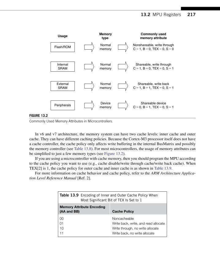
21713.2 MPU Registers
In v6 and v7 architecture, the memory system can have two cache levels: inner cache and outer cache. They can have different caching policies. Because the Cortex-M3 processor itself does not have a cache controller, the cache policy only affects write buffering in the internal BusMatrix and possibly the memory controller (see Table 13.8). For most microcontrollers, the usage of memory attributes can be simplified to just a few memory types (see Figure 13.2).
If you are using a microcontroller with cache memory, then you should program the MPU according to the cache policy you want to use (e.g., cache disable/write through cache/write back cache). When TEX[2] is 1, the cache policy for outer cache and inner cache is as shown in Table 13.9.
For more information on cache behavior and cache policy, refer to the ARM Architecture Applica-tion Level Reference Manual [Ref. 2].
FIgUre 13.2
Commonly Used Memory Attributes in Microcontrollers.
Flash/ROM
Memorytype
Normalmemory
Normalmemory
Normalmemory
Commonly usedmemory attribute
InternalSRAM
PeripheralsDevicememory
Nonshareable, write throughC 5 1, B 5 0, TEX 5 0, S 5 0
Shareable, write throughC 5 1, B 5 0, TEX 5 0, S 5 1
ExternalSRAM
Shareable, write backC 5 1, B 5 1, TEX 5 0, S 5 1
Shareable deviceC 5 0, B 5 1, TEX 5 0, S 5 1
Usage
Table 13.9 Encoding of Inner and Outer Cache Policy When Most Significant Bit of TEX Is Set to 1
Memory Attribute Encoding (AA and BB) Cache Policy
00 Noncacheable01 Write back, write, and read allocate10 Write through, no write allocate11 Write back, no write allocate

218 CHAPTER 13 The Memory Protection Unit
13.3 seTTIng Up The MpUThe MPU register might look complicated, but as long as you have a clear idea of the memory regions that are required for your application, it should not be difficult. Typically, you need to have the follow-ing memory regions:
Program code for privileged programs (for example, OS kernel and exception handlers)•Program code for user programs•Data memory for privileged and user programs in various memory regions (e.g., • data and stack of the application situated in the SRAM (Static Random Access Memory) memory region--0x20000000 to 0x3FFFFFFF)Other peripherals•
It is not necessary to set up a region for the memory in the private peripheral bus range. The MPU automatically recognizes the private peripheral bus memory addresses and allows privileged software to perform data accesses in this region.
For Cortex-M3 products, most memory regions can be set up with TEX = b000, C = 1, B = 1. System devices such as the Nested Vectored Interrupt Controller (NVIC) should be strongly ordered, and peripheral regions can be programmed as shared devices (TEX = b000, C = 0, B = 1). However, if you want to make sure that any bus faults occurring in the region are precise bus faults, you should use a strongly ordered memory attribute (TEX = b000, C = 0, B = 0) so that write buffering is disabled. However, doing so can reduce system performance.
For users of a Cortex Microcontroller Software Interface Standard (CMSIS) compliant device driver, the MPU registers can be accessed using the following register names as shown in Table 13.10. A simple flow for an MPU setup routine is shown in Figure 13.3 on page 220.
Before the MPU is enabled and if the vector table is relocated to RAM, remember to set up the fault handler for the memory management fault in the vector table, and enable the memory management fault in the System Handler Control and State register. They are needed to allow the memory manage-ment fault handler to be executed if an MPU violation takes place.
Table 13.10 MPU Register Names in CMSIS
Register Names MPU Register Address
MPU->TYPE MPU Type register 0xE000ED90MPU->CTRL MPU Control register 0xE000ED94MPU->RNR MPU Region Number register 0xE000ED98MPU->RBAR MPU Region Base Address register 0xE000ED9CMPU->RASR MPU Region Attribute and Size register 0xE000EDA0MPU->RBAR_A1 MPU Alias 1 Region Base Address register 0xE000EDA4MPU->RBAR_A2 MPU Alias 2 Region Base Address register 0xE000EDACMPU->RBAR_A3 MPU Alias 3 Region Base Address register 0xE000EDB4MPU->RASR_A1 MPU Alias 1 Region Attribute and Size register 0xE000EDA8MPU->RASR_A2 MPU Alias 2 Region Attribute and Size register 0xE000EDB0MPU->RASR_A3 MPU Alias 3 Region Attribute and Size register 0xE000EDB8

21913.3 Setting Up the MPU
For a simple case of only four required regions, the MPU setup code (without the region checking and enabling) looks like this:
MPU->RNR = 0; // MPU Region Number Register // select region 0MPU->RBAR = 0x00000000; // MPU Region Base Address Register // Base Address = 0x00000000MPU->RASR = 0x0307002F; // Region Attribute and Size Register // R/W, TEX=0,S=1,C=1,B=1, 16MB, Enable=1MPU->RNR = 1; // select region 1MPU->RBAR = 0x20000000; // Base Address = 0x20000000MPU->RASR = 0x03070033; // R/W, TEX=0,S=1,C=1,B=1, 64MB, Enable=1MPU->RNR = 2; // select region 2MPU->RBAR = 0x40000000; // Base Address = 0x40000000MPU->RASR = 0x03050033; // R/W, TEX=0,S=1,C=0,B=1, 64MB, Enable=1MPU->RNR = 3; // select region 3MPU->RBAR = 0xA0000000; // Base Address = 0xA0000000MPU->RASR = 0x01040027; // Privileged R/W, TEX=0,S=1,C=0,B=0, // 1MB, Enable=1MPU->CTRL = 1; // MPU Control register – Enable MPU
This can also be coded in assembly language:
LDR R0,=0xE000ED98 ; Region number registerMOV R1,#0 ; Select region 0STR R1, [R0]LDR R1,=0x00000000 ; Base Address = 0x00000000STR R1, [R0, #4] ; MPU Region Base Address RegisterLDR R1,=0x0307002F ; R/W, TEX=0,S=1,C=1,B=1, 16MB, Enable=1STR R1, [R0, #8] ; MPU Region Attribute and Size RegisterMOV R1,#1 ; Select region 1STR R1, [R0]LDR R1,=0x20000000 ; Base Address = 0x20000000STR R1, [R0, #4] ; MPU Region Base Address RegisterLDR R1,=0x03070033 ; R/W, TEX=0,S=1,C=1,B=1, 64MB, Enable=1STR R1, [R0, #8] ; MPU Region Attribute and Size RegisterMOV R1,#2 ; Select region 2STR R1, [R0]LDR R1,=0x40000000 ; Base Address = 0x40000000STR R1, [R0, #4] ; MPU Region Base Address RegisterLDR R1,=0x03050033 ; R/W, TEX=0,S=1,C=0,B=1, 64MB, Enable=1STR R1, [R0, #8] ; MPU Region Attribute and Size RegisterMOV R1,#3 ; Select region 3STR R1, [R0]LDR R1,=0xA0000000 ; Base Address = 0xA0000000STR R1, [R0, #4] ; MPU Region Base Address RegisterLDR R1,=0x01040027 ; Privileged R/W, TEX=0,S=1,C=0,B=0, 1MB, ; Enable=1STR R1, [R0, #8] ; MPU Region Attribute and Size RegisterMOV R1,#1 ; Enable MPUSTR R1, [R0,#-4] ; MPU Control register ; (0xE000ED98-4=0xE000ED94)

220 CHAPTER 13 The Memory Protection Unit
This provides four regions:
• Code: 0x00000000–0x00FFFFFF (16 MB), full access, cacheableData• : 0x20000000–0x02003FFFF (64 MB), full access, cacheable
• Peripheral: 0x40000000–0x5FFFFFFF (64 MB), full access, shared device• External device: 0xA0000000–0xA00FFFFF (1 MB), privileged access, strongly ordered, XN
FIgUre 13.3
Example Steps to Set Up the MPU.
Check MPU Type registerto see if MPU exists andthere are enough regions
ErrorNo
Yes
Disable MPU
Select region #0
Program regionbase address
and configuration
Select region #1
Program regionbase address
and configuration
Select region #N
Program regionbase address
and configuration
Enable MPU
MPU setupcompleted
Region selection andprogramming of region
registers can be combinedin one step
Setup for otherregions

22113.3 Setting Up the MPU
By combining region selection and writing to the base address register, we can shorten the code to this:
MPU->RBAR = 0x00000010; // MPU Region Base Address Register // Base Address = 0x00000000, valid, region 0MPU->RASR = 0x0307002F; // Region Attribute and Size Register // R/W, TEX=0,S=1,C=1,B=1, 16MB, Enable=1MPU->RBAR = 0x20000011; // Base Address = 0x20000000, valid, region 1MPU->RASR = 0x03070033; // R/W, TEX=0,S=1,C=1,B=1, 64MB, Enable=1MPU->RBAR = 0x40000012; // Base Address = 0x40000000, valid, region 2MPU->RASR = 0x03050033; // R/W, TEX=0,S=1,C=0,B=1, 64MB, Enable=1MPU->RBAR = 0xA0000013; // Base Address = 0xA0000000, valid, region 3MPU->RASR = 0x01040027; // Privileged R/W, TEX=0,S=1,C=0,B=0, // 1MB, Enable=1MPU->CTRL = 1; // MPU Control register – Enable MPU
Or, in assembly:
LDR R0,=0xE000ED9C ; Region Base Address registerLDR R1,=0x00000010 ; Base Address = 0x00000000, region 0, ; valid=1STR R1, [R0, #0] ; MPU Region Base Address RegisterLDR R1,=0x0307002F ; R/W, TEX=0,S=1,C=1,B=1, 16MB, Enable=1STR R1, [R0, #4] ; MPU Region Attribute and Size RegisterLDR R1,=0x20000011 ; Base Address = 0x20000000, region 1, ; valid=1STR R1, [R0, #0] ; MPU Region Base Address RegisterLDR R1,=0x03070033 ; R/W, TEX=0,S=1,C=1,B=1, 64MB, Enable=1STR R1, [R0, #4] ; MPU Region Attribute and Size RegisterLDR R1,=0x40000012 ; Base Address = 0x40000000, region 2, ; valid=1STR R1, [R0, #0] ; MPU Region Base Address RegisterLDR R1,=0x03050033 ; R/W, TEX=0,S=1,C=0,B=1, 64MB, Enable=1STR R1, [R0, #4] ; MPU Region Attribute and Size RegisterLDR R1,=0xA0000013 ; Base Address = 0xA0000000, region 3, ; valid=1STR R1, [R0, #0] ; MPU Region Base Address RegisterLDR R1,=0x01040027 ; R/W, TEX=0,S=1,C=0,B=0, 1MB, Enable=1STR R1, [R0, #4] ; MPU Region Attribute and Size RegisterMOV R1,#1 ; Enable MPUSTR R1, [R0,#-8] ; MPU Control register ; (0xE000ED9C-8=0xE000ED94)
We’ve shortened the code quite a bit. However, you can make further enhancements to create even faster setup code. This is done using MPU aliased register addresses (see Table D.34 in Appendix D). The aliased register addresses follow the MPU Region Attribute and Size registers and are aliased to the MPU Base Address register and the MPU Region Attribute and Size register. They produce a continuous address of eight words, making it possible to use Load/Store Multiple (LDM and STM) instructions:
LDR R0,=0xE000ED9C ; Region Base Address register LDR R1,=MPUconfig ; Table of predefined MPU setup variables

222 CHAPTER 13 The Memory Protection Unit
LDMIA R1!, {R2, R3, R4, R5}; Read 4 words from table STMIA R0!, {R2, R3, R4, R5}; write 4 words to MPU LDMIA R1!, {R2, R3, R4, R5}; Read next 4 words from table STMIA R0!, {R2, R3, R4, R5}; write next 4 words to MPU B MPUconfigEnd ALIGN 4 ; This is needed to make sure the following table ; is word alignedMPUconfig ; so that we can use load multiple instruction DCD 0x00000010 ; Base Address = 0x00000000, region 0, ; valid=1 DCD 0x0307002F ; R/W, TEX=0,S=1,C=1,B=1, 16MB, Enable=1 DCD 0x20000011 ; Base Address = 0x08000000, region 1, ; valid=1 DCD 0x03070033 ; R/W, TEX=0,S=1,C=1,B=1, 64MB, Enable=1 DCD 0x40000012 ; Base Address = 0x40000000, region 2, ; valid=1 DCD 0x03050033 ; R/W, TEX=0,S=1,C=0,B=1, 64MB, Enable=1 DCD 0xA0000013 ; Base Address = 0xA0000000, region 3, ; valid=1 DCD 0x01040027 ; R/W, TEX=0,S=1,C=0,B=0, 1MB, Enable=1MPUconfigEnd LDR R0,=0xE000ED94 ; MPU Control register MOV R1,#1 ; Enable MPU STR R1, [R0]
This solution, of course, can be used only if all the required information is known beforehand. Otherwise, a more generic approach has to be used. One way to handle this is to use a subroutine (Mpu RegionSetup) that can set up a region based on a number of input parameters and then call it sev-eral times to set up different regions:
void MpuRegionSetup(unsigned int addr, unsigned int region, unsigned int size, unsigned int ap, unsigned int MemAttrib, unsigned int srd, unsigned int XN, unsigned int enable){ // Setup procedure for each region MPU->RBAR = (addr & 0xFFFFFFE0) | (region & 0xF) | 0x10; MPU->RASR = ((XN & 0x1)<<28) | ((ap & 0x7)<<24) | ((MemAttrib & 0x3F)<<16) | ((srd&0xFF)<<8) | ((size & 0x1F)<<1)| (enable & 0x1); return;}void MpuRegionDisable(unsigned int region){ // Function to disable an unused region MPU->RBAR = (region & 0xF) | 0x10; MPU->RASR = 0; // disable return;}void MpuSetup(void){ // Setup the whole MPU MPU->CTRL = 0; // Disable MPU first MpuRegionSetup(0x00000000, 0, 0x17, 3, 7, 0, 0, 1); // Region 0,16M MpuRegionSetup(0x20000000, 1, 0x19, 3, 7, 0, 0, 1); // Region 1,64M MpuRegionSetup(0x40000000, 2, 0x19, 3, 5, 0, 0, 1); // Region 2,64M

22313.3 Setting Up the MPU
MpuRegionSetup(0xA0000000, 3, 0x13, 1, 4, 0, 0, 1); // Region 3, 1M MpuRegionDisable(4); // Disable unused region 4 MpuRegionDisable(5); // Disable unused region 5 MpuRegionDisable(6); // Disable unused region 6 MpuRegionDisable(7); // Disable unused region 7 MPU->CTRL = 1; // Enable MPU return;}
In this example, we included a subroutine that is used to disable a region that is not used. This is necessary if you do not know whether a region has been programmed previously. If an unused region is previously programmed to be enabled, it needs to be disabled so that it doesn’t affect the new configuration.
The MPU setup routines can be rewritten in assembly as
MpuSetup ; A subroutine to setup the MPU by calling subroutines that ; setup regions PUSH {R0-R6,LR} LDR R0,=0xE000ED94 ; MPU Control Register MOV R1,#0 STR R1,[R0] ; Disable MPU ; --- Region #0 --- LDR R0,=0x00000000 ; Region 0: Base Address = 0x00000000 MOV R1,#0x0 ; Region 0: Region number = 0 MOV R2,#0x17 ; Region 0: Size = 0x17 (16MB) MOV R3,#0x3 ; Region 0: AP = 0x3 (full
access)MOV R4,#0x7 ; Region 0: MemAttrib = 0x7MOV R5,#0x0 ; Region 0: Sub R disable = 0MOV R6,#0x1 ; Region 0: {XN, Enable} = 0,1BL MpuRegionSetup; --- Region #1 ---LDR R0,=0x20000000 ; Region 1: Base Address = 0x20000000MOV R1,#0x1 ; Region 1: Region number = 1MOV R2,#0x19 ; Region 1: Size = 0x19 (64MB)MOV R3,#0x3 ; Region 1: AP = 0x3 (full access)MOV R4,#0x7 ; Region 1: MemAttrib = 0x7MOV R5,#0x0 ; Region 1: Sub R disable = 0MOV R6,#0x1 ; Region 1: {XN, Enable} = 0,1BL MpuRegionSetup... ; setup for region #2 and #3; --- Region #4-#7 Disable ---MOV R0,#4BL MpuRegionDisableMOV R0,#5BL MpuRegionDisableMOV R0,#6BL MpuRegionDisableMOV R0,#7BL MpuRegionDisableLDR R0,=0xE000ED94 ; MPU Control Register

224 CHAPTER 13 The Memory Protection Unit
MOV R1,#1STR R1,[R0] ; Enable MPUPOP {R0-R6,PC} ; Return
MpuRegionSetup; MPU region setup subroutine; Input R0 : Base Address; R1 : Region number; R2 : Size; R3 : AP (access permission); R4 : MemAttrib ({TEX[2:0], S, C, B}); R5 : Sub region disable; R6 : {XN,Enable}PUSH {R0-R1, LR}BIC R0, R0, #0x1F ; Clear unused bits in addressBFI R0, R1, #0, #4 ; Insert region number to R0[3:0]ORR R0, R0, #0x10 ; Set valid bitLDR R1,=0xE000ED9C ; MPU Region Base Address RegisterSTR R0,[R1] ; Set base address regAND R0, R6, #0x01 ; Get Enable bitUBFX R1, R6, #1, #1 ; Get XN bitBFI R0, R1, #28, #1 ; Insert XN to R0[28]BFI R0, R2, #1 , #5 ; Insert Region Size field (R2[4:0]) to ; R0[5:1]BFI R0, R3, #24, #3 ; Insert AP fields (R3[2:0]) to R0[26:24]BFI R0, R4, #16, #6 ; Insert memattrib field (R4[5:0]) to ; R0[21:16]BFI R0, R5, #8, #8 ; Insert subregion disable (SRD) fields ; to R0[15:8]LDR R1,=0xE000EDA0 ; MPU Region Base Size and Attribute ; RegisterSTR R0,[R1] ; Set base attribute and size regPOP {R0-R1, PC} ; Return
MpuRegionDisable; Subroutine to disable unused region; Input R0 : Region numberPUSH {R1, LR}AND R0, R0, #0xF ; Clear unused bits in Region NumberORR R0, R0, #0x10 ; Set valid bitLDR R1,=0xE000ED9C ; MPU Region Base Address RegisterSTR R0,[R1]MOV R0, #0LDR R1,=0xE000EDA0 ; MPU Region Base Size and Attribute ; RegisterSTR R0,[R1] ; Set base attribute and size reg to 0 ; (disabled)POP {R1, PC} ; Return
The example shows the application of the Bit Field Insert (BFI) instruction in the Cortex-M3. This can greatly simplify bit-field merging operations.

22513.4 Typical Setup
13.4 TypICal seTUpIn typical applications, the MPU is used when there is a need to prevent user programs from accessing privileged process data and program regions. Usually, this is done by the embedded OS. Between each context switching, the MPU is reprogrammed by the OS to allow user applications to access their application code and data and any other resources they are entitled to access. When developing the setup routine for the MPU, you need to consider a number of regions:
Code region:1. Privileged code, including a starting vector tablea. User codeb.
SRAM region:2. Privileged data, including the main stacka. User data, including the process stackb. Privileged bit-band alias regionc. User bit-band alias regiond.
Peripherals:3. Privileged peripheralsa. User peripheralsb. Privileged peripheral bit-band alias regionc. User peripheral bit-band alias regiond.
From this list, we have identified 10 regions; more than the eight regions supported by the Cortex-M3 MPU. However, we can define the privileged regions by means of a background region (PRIVDEFENA set to 1), so there are only five user regions to set up, leaving three spare MPU regions. The unused regions might still be used for setting up additional regions in external memory, to protect read-only data or to completely block some part of the memory if necessary. Alternatively, some of the regions could be merged together to reduce the number of regions required.
13.4.1 example Use of the subregion DisableIn some cases, we might have some peripherals accessible by user programs, and a few should be pro-tected to be privileged accesses only, resulting in fragmentation of user-accessible peripheral memory space. In this kind of scenario, we could do one of these things:
Define multiple user regions•Define privileged regions inside the user peripheral region•Use subregion disable within the user region•
The first two methods can use up available regions very easily. With the third solution, using the subregion disable feature, we can easily set up AP to separate peripheral blocks without using extra regions. For example, see Figure 13.4.
The same techniques can be applied to memory regions as well. However, it is more likely that peripherals will have a fragmented privilege setup.
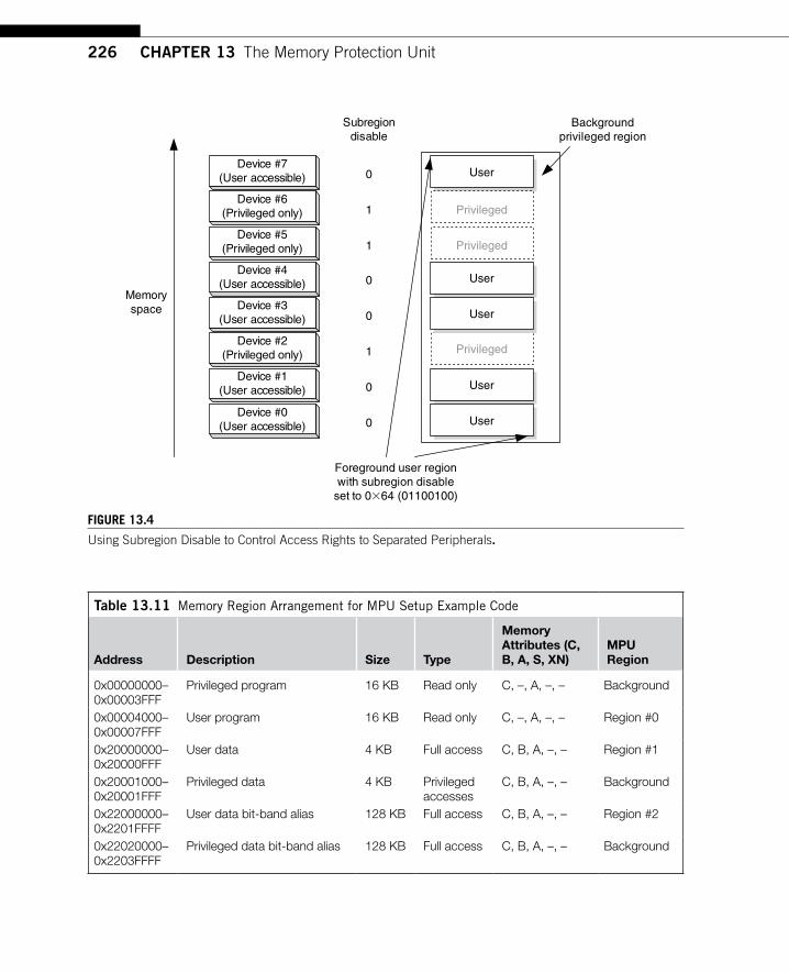
226 CHAPTER 13 The Memory Protection Unit
Memoryspace
Device #7(User accessible)
Device #6(Privileged only)
Subregiondisable
0
1
1
0
0
1
0
0
User
User
User
User
User
Backgroundprivileged region
Foreground user regionwith subregion disable
set to 0364 (01100100)
Privileged
Privileged
Privileged
Device #5(Privileged only)
Device #4(User accessible)
Device #3(User accessible)
Device #1(User accessible)
Device #0(User accessible)
Device #2(Privileged only)
FIgUre 13.4
Using Subregion Disable to Control Access Rights to Separated Peripherals.
Table 13.11 Memory Region Arrangement for MPU Setup Example Code
Address Description Size Type
Memory Attributes (C, B, A, S, XN)
MPU Region
0x00000000–0x00003FFF
Privileged program 16 KB Read only C, –, A, –, – Background
0x00004000–0x00007FFF
User program 16 KB Read only C, –, A, –, – Region #0
0x20000000–0x20000FFF
User data 4 KB Full access C, B, A, –, – Region #1
0x20001000–0x20001FFF
Privileged data 4 KB Privileged accesses
C, B, A, –, – Background
0x22000000–0x2201FFFF
User data bit-band alias 128 KB Full access C, B, A, –, – Region #2
0x22020000–0x2203FFFF
Privileged data bit-band alias 128 KB Full access C, B, A, –, – Background

22713.4 Typical Setup
Let’s assume that the memory regions in Table 13.11 will be used. After the required regions are defined, we can create the MPU setup code. To make the code easier to understand and modify, we used the function that we created earlier to develop the completed MPU setup example:
void MpuSetup(void){ // Setup the whole MPUMPU->CTRL = 0; // Disable MPU first
// Parameters: Address Region Size AP Mem SRD XN EnableMpuRegionSetup(0x00004000, 0, 0x0D, 3, 0x2, 0, 0, 1); // Region 0// 0x00004000-0x00007FFF: user program , 16kB, full access,// MemAttrib = 0x2 (TEX=0,S=0,C=1,B=0), Subregion disable = 0, XN=0
MpuRegionSetup(0x20000000, 1, 0x0B, 3, 0xB, 0, 0, 1); // Region 1// 0x20000000-0x20000FFF: user data, 4kB, full access,// MemAttrib = 0xB (TEX=1,S=0,C=1,B=1), Subregion disable = 0, XN=0
MpuRegionSetup(0x22000000, 2, 0x10, 3, 0xB, 0, 0, 1); // Region 2// 0x22000000-0x2201FFFF: user bit band, 128kB, full access,// MemAttrib = 0xB (TEX=1,S=0,C=1,B=1), Subregion disable = 0, XN=0
MpuRegionSetup(0x40000000, 3, 0x13, 3, 0x1,0x64,0,1); // Region 3// 0x40000000-0x400FFFFF: user peripherals, 1MB, full access,// MemAttrib = 0x1 (TEX=0,S=0,C=0,B=1), Subregion disable=0x64, XN=0// Note: Sub-region disable = 0x64 based on figure 13.4
MpuRegionSetup(0x42000000, 4, 0x18, 3, 0x1,0x64,0,1); // Region 4// 0x42000000-0x43FFFFFF: user peripheral bit band, 32MB, full access,// MemAttrib = 0x1 (TEX=0,S=0,C=0,B=1), Subregion disable=0x64, XN=0
Table 13.11 Memory Region Arrangement for MPU Setup Example Code Continued
Address Description Size Type
Memory Attributes (C, B, A, S, XN)
MPU Region
0x40000000–0x400FFFFF
User peripherals 1 MB Full access –, B, –, –, XN Region #3
0x40040000–0x4005FFFF
Privileged peripherals within user peripheral region
128 KB Privileged accesses
–, B, –, –, XN Disabled subregions in Region #3
0x42000000–0x43FFFFFF
User peripherals bit-band alias 32 MB Full access –, B, –, –, XN Region #4
0x42800000–0x42BFFFFF
Privileged peripherals bit-band alias within user region
4 MB Privileged accesses
–, B, –, –, XN Disabled subregion in Region #4
0x60000000–0x60FFFFFF
External RAM 16 MB Full access C, B, A, –, – Region #5
0xE0000000–0xF00FFFFF
NVIC, debug, and private peripheral bus
1 MB Privileged accesses
–, –, –, –, XN Background
Note: A in memory attribute refers to cache allocate.

228 CHAPTER 13 The Memory Protection Unit
// Note: Sub-region disable = 0x64 based on figure 13.4
MpuRegionSetup(0x60000000, 5, 0x17, 3, 0x3, 0, 0, 1); // Region 5// 0x60000000-0x60FFFFFF: external RAM, 16MB, full access,// MemAttrib = 0x3 (TEX=0,S=0,C=1,B=1), Subregion disable = 0, XN=0
MpuRegionDisable(6); // Disable unused region 6MpuRegionDisable(7); // Disable unused region 7MPU->CTRL = 5; // Enable MPU with Default memory map enabled // for privileged accessesreturn;}

229Copyright © 2010, Elsevier Inc. All rights reserved.DOI: 10.1016/B978-1-85617-963-8.00017-X
In ThIs ChapTerThe sYsTICK Timer ............................................................................................................................... 229power Management .............................................................................................................................. 232Multiprocessor Communication ............................................................................................................. 236self-reset Control ................................................................................................................................. 241
14.1 The sYsTICK TIMerThe SYSTICK register in the Nested Vectored Interrupt Controller (NVIC) was covered briefly in Chapter 8. As we saw, the SYSTICK timer is a 24-bit down counter. Once it reaches zero, the counter loads the reload value from the RELOAD register. It does not stop until the enable bit in the SYSTICK Control and Status register is cleared (see Figure 14.1).
The Cortex™-M3 processor allows two different clock sources for the SYSTICK counter. The first one is the core free-running clock (not from the system clock HCLK, so it does not stop when the system clock is stopped). The second one is an external reference clock. This clock signal must be at least two times slower than the free-running clock because this signal is sampled by the free-running clock. Because a chip designer might decide to omit this external reference clock in the design, it might not be available. To determine whether the external clock source is available, you should check bit 31 of the SYSTICK Calibration register. The chip designer should connect this pin to an appropriate value based on the design.
When the SYSTICK timer changes from 1 to 0, it will set the COUNTFLAG bit in the SYSTICK Control and Status register. The COUNTFLAG can be cleared by one of the following:
Read of the SYSTICK Control and Status register by the processor•Clear of the SYSTICK counter value by writing any value to the SYSTICK Current Value register•
The SYSTICK counter can be used to generate SYSTICK exceptions at regular intervals. This is often necessary for the OS, for task and resources management. To enable SYSTICK exception generation, the TICKINT bit should be set. In addition, if the vector table has been relocated to Static
Other Cortex-M3 Features 14CHAPTER

230 CHAPTER 14 Other Cortex-M3 Features
Random Access Memory (SRAM), it would be necessary to set up the SYSTICK exception handler in the vector table. For example:
*((volatile unsigned int *)(SCB->VTOR+(15<<2))) = (unsigned int) SysTick_Handler;
This can be written in assembly language as
; Setup SYSTICK exception handler (only needed if vector table; is located in RAM)MOV R0, #0xF ; Exception type 15LDR R1, =SysTick_handler ; address of exception handlerLDR R2, =0xE000ED08 ; Vector table offset registerLDR R2, [R2]STR R1, [R2, R0, LSL #2] ; Write vector to ; VectTblOffset+ExcpType*4
For users of Cortex Microcontroller Software Interface Standard (CMSIS) compliant device driver, a function call “SysTick_Config” is available for configuration of the SYSTICK Timer. Please refer to Appendix G for information on this function. You can also access the SYSTICK registers directly via the following register names:
• SysTick->CTRL (Control and Status register)• SysTick->LOAD (Reload Value register)• SysTick->VAL (Current Value register)• SysTick->CALIB (Calibration Value register)
For example, to generate SYSTICK exception every 1024 processor clock cycle, you can use the following C code:
SysTick->LOAD = 1023;// Count down from 1023 to 0SysTick->VAL = 0;// Clear current value to 0SysTick->CTRL = 0x7; // Enable SysTick, enable SysTick // exception and use processor clock
FIgure 14.1
SYSTICK Registers in the NVIC.
0xE000E010 Control and status
0xE000E014 Reload value
0xE000E018 Current value
0xE000E01C Calibration
EnableTICKINT
CLKSOURCECOUNTFLAG
RELOAD
CURRENT
TENMS
NOREF SKEW16 02331

23114.1 The SYSTICK Timer
The same operation can be written in assembly language as follows:
; Enable SYSTICK timer operation and enable SYSTICK interruptLDR R0, =0xE000E010 ; SYSTICK control and status registerMOV R1, #0STR R1, [R0] ; Stop counter to prevent interrupt
; triggered accidentallyLDR R1, =1023 ; Trigger every 1024 cycles (since counter
; decrement from 1023 to 0, total of 1024 ; cycles, reload value is set to 1023)STR R1, [R0,#4] ; Write reload value to reload register
; addressSTR R1, [R0,#8] ; Write any value to current value
; register to clear current value to 0 and ; clear COUNTFLAGMOV R1, #0x7 ; Clock source = core clock, Enable
; Interrupt, Enable ; SYSTICK counterSTR R1, [R0] ; Start counter
The SYSTICK counter provides a simple way to allow timing calibration information to be accessed. The top level of the Cortex-M3 processor has a 24-bit input to which a chip designer can input a reload value that can be used to generate a 10-ms time interval. This value can be accessed by the SYSTICK Calibration register. However, this option is not necessarily available, so you’ll need to check the device’s datasheet to see if you can use this feature.
The SYSTICK counter can also be used as an alarm timer that starts a certain task after a number of clock cycles. For example, if a task has to be started to execute after 300 clock cycles, we could set up the task at the SYSTICK exception handler and program the SYSTICK timer so that the task will be executed when the 300 cycle count is reached:
volatile int SysTickFired; // A global software flag to // indicate SysTickAlarm executed...// Optional:Setup SYSTICK Handler, only needed if vector table// relocated to SRAM*((volatile unsigned int *)(SCB->VTOR+(15<<2))) = (unsigned int) SysTickAlarm;
SysTick->CTRL = 0x0; // Disable SysTickSysTick->LOAD = (300-12); // Set Reload value // Minus 12 because of exception latencySysTick->VAL = 0; // Clear current value to 0SysTickFired = 0; // Setup software flag to zeroSysTick->CTRL = 0x7; // Enable SysTick, enable SysTick // exception and use processor clockwhile (SysTickFired == 0); // Wait until software flag is set by // SYSTICK handler
The exception handler can be written as follows:
void SysTickAlarm(void) // SYSTICK exception handler{
232 CHAPTER 14 Other Cortex-M3 Features
SysTick->CTRL = 0x0; // Disable SysTick // Execute required processing taskSCB->ICSR = SCB->ICSR & (0xFDFFFFFF); // Clear SYSTICK pend bit // in case it has been pended againSysTickFired++; // Update software flag so that the // main program know that SysTick alarm // task has been carried outreturn;}
The counter starts with an initial value of zero because it was manually cleared from the main pro-gram. It then immediately reloads to 288 (300 – 12). We subtract 12 from the count because this is the number of clock cycles for minimum exception latency. However, if another exception with the same or a higher priority is running when the SYSTICK counter reaches zero, the start of the exception could be delayed.
Note that the subtraction of 12 cycles from the reload value in this example is required for only one-shot alarm timer usage. For periodic counting usage, the reload value should be the number of clock cycles per period minus 1.
Because the SYSTICK counter does not stop automatically, we need to stop it within the SYSTICK handler (SysTickAlarm). Furthermore, there’s a chance that the SYSTICK exception could have been pended again if it was delayed by processing of other exceptions, so the pending status of a SYSTICK exception needs to be cleared if the SYSTICK exception uses a one-off processing.
In the final step of the SYSTICK exception handler, we set a software variable called SysTickFired so that the main program knows the required task has been carried out.
14.2 power ManageMenT14.2.1 sleep ModesThe Cortex-M3 provides sleep modes as a power management feature. During sleep mode, the system clock can be stopped, but the free-running clock input could still be running to allow the processor to be woken by an interrupt. The two sleep modes are as follows:
Sleep: Indicated by the SLEEPING signal from the Cortex-M3 processor•Deep sleep: Indicated by the SLEEPDEEP signal from the Cortex-M3 processor•
To decide which sleep mode will be used, the NVIC System Control register has a bit field called SLEEPDEEP (see Table 14.1). The actions of SLEEPING and SLEEPDEEP depend on the particular Microcontroller Unit (MCU) implementation. In some implementations, the action will be the same in both cases.
The sleep modes are invoked by Wait-For-Interrupt (WFI) or Wait-For-Event (WFE) instructions. Events can be interrupts, a previously triggered interrupt, or an external event signal pulse via the Receive Event (RXEV) signal. Inside the processor, there is a latch for events, so a past event can wake up a processor from WFE (see Figure 14.2).
For users of a CMSIS compliant device driver, WFI and WFE instructions can be accessed by __WFI( ) and __WFE( ) intrinsic functions. The System Control register can be accessed using the “SCB->SCR” register name.

23314.2 Power Management
What exactly happens when the processor enters sleep mode depends on the chip design. The common case is that some of the clock signals can be stopped to reduce power consumption. How-ever, the chip can also be designed to shut down part of the chip to further reduce power, or it is also possible that a design can shut down the chip completely, and all the clock signals will be stopped. In a case where the chip is shut down completely, the only way to wake the system from sleep is via a system reset.
To wake the processor from WFI sleep, the interrupt will have to be higher priority than the current priority level (if it is an executing interrupt) and higher than the level set by the BASEPRI register or mask registers (PRIMASK and FAULTMASK). If an interrupt is not going to be accepted due to prior-ity level, it will not wake up a sleep caused by WFI.
The situation for WFE is slightly different. If the interrupt triggered during sleep has lower or equal priority than the mask registers or BASEPRI registers and if the SEVONPEND is set, it could still wake the processor from sleep. The rules of waking the Cortex-M3 processor from sleep modes are summarized in Table 14.2.
Table 14.1 System Control Register (0xE000ED10)
Bits Name Type Reset Value Description
4 SEVONPEND R/W 0 Send Event on Pending; wakes up from WFE if a new interrupt is pended, regardless of whether the interrupt has priority higher than the current level
3 Reserved — — —2 SLEEPDEEP R/W 0 Enable SLEEPDEEP output signal when entering
sleep mode1 SLEEPONEXIT R/W 0 Enable Sleep-On-Exit feature0 Reserved — — —
FIgure 14.2
Sleep Operations.
WFI WFE
Event latch 5 1?
Clear event latchand continue tonext instruction
YesNo
SLEEPDEEP 5 1?
YesNo
Enter sleep (bothSLEEPING andSLEEPDEEPsignal high)
Enter sleep(SLEEPING signalhigh, SLEEPDEEP
signal low)
Clear event latch

234 CHAPTER 14 Other Cortex-M3 Features
14.2.2 sleep-on-exit FeatureAnother feature of sleep mode is that it can be programmed to go back to sleep automatically after the interrupt routine exit. In this way, we can make the core sleep all the time unless an interrupt needs to be served. To use this feature, we need to set the SLEEPONEXIT bit in the System Control register (see Figure 14.3).
Note that if the Sleep-On-Exit feature is enabled, the processor can enter sleep at any exception return to thread level, even if no WFE/WFI instruction is executed. To ensure that the processor only enter sleep when required, set the SLEEPONEXIT bit only when the system is ready for entering sleep.
14.2.3 wakeup Interrupt ControllerStarting from revision 2 of Cortex-M3, additional low-power features have been added. A new unit called the Wakeup Interrupt Controller (WIC) is available as an optional component. This controller is coupled to the existing NVIC and is used to generate a wakeup request when an interrupt arrives.
From a software point of view, the WFI and WFE behaviors remain the same. There are no program-mable registers in the WIC, as it gets all the required interrupt information via the interface between WIC and NVIC. By using the WIC, the clock signals going into the processor core can be completely stopped. When an interrupt request arrives, the WIC can send a wakeup request to the system controller or Power Management Unit (PMU) in the chip to restore the processor clock (figure 14.4).
The availability of the WIC also provides a new method for reducing power consumption during sleep mode. By using new technologies in digital logic design, it is now possible to power down most of
Table 14.2 WFI and WFE Wakeup Behavior
WFI Behavior Wake Up IRQ Execution
IRQ with BASEPRIIRQ priority > BASEPRIv Y YIRQ priority =< BASEPRI N N
IRQ with BASEPRI and PRIMASKIRQ priority > BASEPRI Y NIRQ priority =< BASEPRI N N
WFE Behavior
IRQ with BASEPRI, SEVONPEND = 0IRQ priority > BASEPRI Y YIRQ priority =< BASEPRI N N
IRQ with BASEPRI, SEVONPEND = 1IRQ priority > BASEPRI Y YIRQ priority =< BASEPRI Y N
IRQ with BASEPRI and PRIMASK, SEVONPEND = 0IRQ priority > BASEPRI N NIRQ priority =< BASEPRI N N
IRQ with BASEPRI & PRIMASK, SEVONPEND = 1IRQ priority > BASEPRI Y NIRQ priority =< BASEPRI Y N

23514.2 Power Management
FIgure 14.3
Example Use of the Sleep-On-Exit Feature.
WFI/WFE
Processor wake up andcontinue to next
instruction
Yes
No
Sleep
Wake up and run theinterrupt handler
Processor detect ifSLEEPONEXIT 5 1?
Exception exit andreturning to thread
Processor return to sleepautomatically withoutsoftware intervention
FIgure 14.4
WIC Mirrors the Interrupt Detection Function when clock signals to Cortex-M3 stops.
Cortex-M3
IRQ
NMI
WIC
IRQ
NMI
Mask
Powermanagement
unit
Sleep status
Wake up

236 CHAPTER 14 Other Cortex-M3 Features
the Cortex-M3 processor, leaving a small portion of the logic gates to retain the current state of the logic. This technology is called State Retention Power Gating (SRPG). By using SRPG and WIC together, most portions of the Cortex-M3 processor can be powered down during deep sleep, leaving a small amount of logic for state retention (see Figure 14.5). During this power down state, the WIC remains operational and generates a wakeup request to power up and restore the system state when an interrupt arrives. As a result, the processor can resume operation and service the interrupt request in a very short time. The maximum interrupt latency with such arrangement depends on the time required to power up the system. In most cases, it is in the range of 20 to 30 clock cycles. Normal sleep (SLEEPDEEP bit in the System Control register is zero) does not trigger the power down feature.
The new power down capability is optional and may not be included in some microcontroller prod-ucts. It requires an on-chip PMU developed by silicon vendors to control the power up and power down sequences and might need to be programmed before the power down feature is used. Please refer to the silicon vendor’s documentation for further information. A couple of points to be aware of: the power down feature stops the SYSTICK timer during deep sleep, and the power down feature is disabled when a debugger is attached (this is required because debugger needs to access the debug registers regularly to examine the status of the processor).
14.3 MulTIproCessor CoMMunICaTIonThe Cortex-M3 comes with a simple multiprocessor communication interface for event communication. The processor has one output signal, called Transmit Event (TXEV), for sending out events, and an input
FIgure 14.5
WIC Mirrors the Interrupt Detection Function when Cortex-M3 is in state retention.
Cortex-M3
IRQ
NMI
WIC
IRQ
NMI
Mask
Powermanagement
unit Wake up
Sleep status
Powered downduring deep sleep
Processor state held instate retention flip-flops
WIC detect and hold interruptrequest while processor is
powered down
PMU restore powerwhen wake up
request from WIC isgenerated
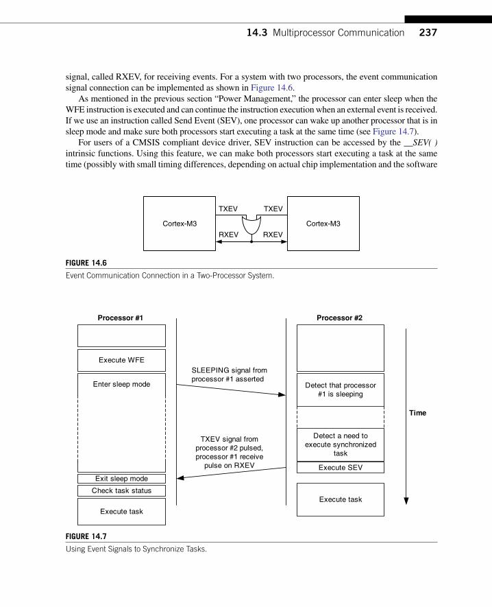
23714.3 Multiprocessor Communication
signal, called RXEV, for receiving events. For a system with two processors, the event communication signal connection can be implemented as shown in Figure 14.6.
As mentioned in the previous section “Power Management,” the processor can enter sleep when the WFE instruction is executed and can continue the instruction execution when an external event is received. If we use an instruction called Send Event (SEV), one processor can wake up another processor that is in sleep mode and make sure both processors start executing a task at the same time (see Figure 14.7).
For users of a CMSIS compliant device driver, SEV instruction can be accessed by the __SEV( ) intrinsic functions. Using this feature, we can make both processors start executing a task at the same time (possibly with small timing differences, depending on actual chip implementation and the software
FIgure 14.6
Event Communication Connection in a Two-Processor System.
Cortex-M3 Cortex-M3
TXEV TXEV
RXEV RXEV
FIgure 14.7
Using Event Signals to Synchronize Tasks.
Processor #1 Processor #2
Execute WFE
Exit sleep mode
Check task status
Execute SEV
Execute task
Execute task
Detect a need toexecute synchronized
task
Detect that processor#1 is sleeping
Enter sleep mode
TXEV signal fromprocessor #2 pulsed,processor #1 receive
pulse on RXEV
SLEEPING signal fromprocessor #1 asserted
Time

238 CHAPTER 14 Other Cortex-M3 Features
code for checking task status). The number of processors invoked can be any number, but it requires that one processor acts as a master to generate the event pulse to other processors.
It is important to note that the processor could also be woken by other events, such as interrupt and debugging events. Therefore, before starting the required synchronized task, it is necessary to check whether the wakeup was caused by task synchronization. In most multitasking systems, an interprocessor messaging system like mailbox is still required to ensure that the tasks are synchro-nized correctly.
It is also important to note that execution of WFE does not always cause the processor to enter sleep mode. Therefore, WFE is normally used with looping (to reduce system power consumption) and status checking code to check if the required synchronized task should be carried out after the WFE, as shown in Figure 14.8.
When the WFE instruction is executed, it first checks the local event latch. If the latch is not set, the core enters sleep mode. If the latch is set, it will be cleared and the instruction execution continues without entering sleep mode. The local event latch can be set by previously occurring exceptions and by the SEV instruction. So, if you execute an SEV and then execute a WFE, the processor will not enter sleep and will simply continue on to the next instruction, with the event latch cleared by WFE.
An example of WFE usage is semaphore in a multiprocessor system. In a typical scenario like Mutual Exclusion (MUTEX), system-level exclusive-access monitor and exclusive-access instructions are used for spin locks for granting accesses to shared memory or a shared peripheral. A process requir-ing a resource would need to call a function to gain the “lock”:
void get_lock(volatile int * Lock_Variable){ // __LDREXW and __STREXW are intrinsic functions in CMSIS // compliant device driver libraries
int status = 0;do {while ( __LDREXW(&Lock_Variable) != 0); // Wait until lock // variable is freestatus = __STREXW(1, &Lock_Variable); // Try set Lock_Variable // to 1 using STREX} while (status != 0); // retry until lock successfully__DMB(); // Data memory Barrierreturn;
}
The same process can be carried out in assembly code:
get_lock ; an assembly function to get the lock LDR r0, =Lock_Variable MOVS r2, #1 ; use for locking STREXget_lock_loop LDREX r1, [r0] CMP r1, #0 BNE get_lock_loop ; It is locked, retry again STREX r1, r2, [r0] ; Try set Lock_Variable to 1 using STREX CMP r1, #0 ; Check return status of STREX BNE get_lock_loop ; STREX was not successful, retry DMB ; Data Memory Barrier BX LR ; Return

23914.3 Multiprocessor Communication
On the other hand, a process using the resource should unlock the resource when it is no longer required:
void free_lock(volatile int * Lock_Variable){ __DMB(); // Data memory Barrier Lock_Variable = 0; // Free the lockreturn;}
The same operation can be written in assembly as follows:
free_lock ; an assembly function to free the lock LDR r0, =Lock_Variable MOVS r1, #0 DMB ; Data Memory Barrier STR r1, [r0] ; Clear lock BX LR ; Return
The spin lock can result in unnecessary power consumption when the processor is idle. As a result, we add WFE into these operations to reduce power consumption, while allowing the processor waiting for the lock to be woken up as soon as the resource is free.
FIgure 14.8
Example Use of the WFE Feature.
WFE
Exit loop
Sleep
Run synchronized task
Exit Idle loop?
Event
Yes
No
Wake up by tasksynchronization?
Idle loop
Check task status
No
Yes

240 CHAPTER 14 Other Cortex-M3 Features
void get_lock_with_WFE(volatile int * Lock_Variable){ int status = 0; do { while ( __LDREXW(&Lock_Variable) != 0){ // Wait until lock __WFE();} // variable is free, if not, enter sleep until event status = __STREXW(1, &Lock_Variable); // Try set Lock_Variable // to 1 using STREX } while (status != 0); // retry until lock successfully __DMB(); // Data memory Barrier return;}
For the function to free the lock, the SEV instruction is used to wake up other processors that are waiting for the lock.
void free_lock(volatile int * Lock_Variable){ __DMB(); // Data memory Barrier Lock_Variable = 0; // Free the lock __DSB(); // ensure the store is complete __SEV(); // Send Event to wake up other processors return;}
The same operation can be written in assembly as follows:
get_lock_with_WFE ; an assembly function to get the lock LDR r0, =Lock_Variable MOVS r2, #1 ; use for locking STREXget_lock_loop LDREX r1,[r0] CBNZ r1, lock_is_set; If lock is set, sleep and retry later STREX r1, r2, [r0] ; Try set Lock_Variable to 1 using STREX CMP r1, #0 ; Check return status of STREX BNE get_lock_loop ; STREX was not successful, retry DMB ; Data Memory Barrier BX LR ; Returnlock_is_set WFE ; Wait for event B get_lock_loop ; woken up, retry again
And for the function that frees the lock, it can be written in assembly as follows:
free_lock_with_SEV ; an assembly function to free the lock LDR r0, =Lock_Variable MOVS r1, #0 DMB ; Data Memory Barrier STR r1, [r0] ; Clear lock DSB ; ensure the store is complete SEV ; Send Event to wake up other processors BX LR ; Return
By combining event communication interface and necessary semaphore code, the power consump-tion during spin lock can be reduced. Similar techniques can be created for message passing and tasks synchronizations.

24114.4 Self-Reset Control
In most Cortex-M3-based products, there will be only one processor, and the RXEV input is likely tied to 0 or connected to peripherals that generate events.
14.4 selF-reseT ConTrolThe Cortex-M3 provides two self-reset control features. The first reset feature is the SYSRESETREQ (System Reset Request) bit in the same NVIC register. It allows the Cortex-M3 processor to assert a reset request signal to the system’s reset generator. Because the system reset generator is not part of Cortex-M3 design, the implementation of this reset feature depends on the chip design. Therefore, it is necessary to carefully check the chip’s specification to determine which part of the chip is reset by this reset control bit.
For users of a CMSIS compliant device driver, the NVIC_SystemReset() function can be used to trig-ger the system reset using SYSRESETREQ. (A summary of this function can be found in Appendix G.) Users not using CMSIS can use:
*((volatile unsigned int *)(0xE000ED0C))= 0x05FA0004;// Set SYSRESETREQ bit (05FA is a write access key)while(1); // a deadloop is used to ensure no other // instructions follow the reset is executed
Assembly language users can generate the system reset request using the following example code:
LDR R0,=0xE000ED0C ; NVIC AIRCR address LDR R1,=0x05FA0004 ; Set SYSRESETREQ bit (05FA is a write
; access key) STR R1,[R0]deadloop B deadloop ; a deadloop is used to ensure no other
; instructions follow the reset is executed
The second reset feature is the VECTRESET control bit in the NVIC Application Interrupt and Reset Control register (bit [0]). Writing 1 to this bit will reset the Cortex-M3 processor, excluding the debug logic. This does not reset any circuit outside the Cortex-M3 processor. For example, if the system-on-chip (SoC) contains a universal asynchronous receiver/transmitter (UART), writing to this bit does not reset the UART or any peripherals outside the Cortex-M3. This feature is mainly targeted for debug, or in some case, where the software needs to reset the processor only but not the rest of the system.
*((volatile unsigned int *)(0xE000ED0C))= 0x05FA0001;// Set VECTRESET bit (05FA is a write access key)while(1); // a deadloop is used to ensure no other // instructions follow the reset is executed
The same operation can be carried out in the following assembly code:
LDR R0,=0xE000ED0C ; NVIC AIRCR address LDR R1,=0x05FA0001 ; Set VECTRESET bit (05FA is a write
; access key) STR R1,[R0]deadloop B deadloop ; a deadloop is used to ensure no other
; instructions following the reset is ; executed

242 CHAPTER 14 Other Cortex-M3 Features
In general, software reset should be generated using SYSRESETREQ instead of VECTRESET. This ensures most parts of the system will be reset at the same time. Depending on the chip design, it might or might not reset all peripherals, the chip and the clocking control logic including Phase-Locked Loop (PLL). Please refer to the manufacturer datasheet for details.
Note that the delay from assertion of SYSRESETREQ to actual reset from the reset generator can be an issue in some cases. If there is a delay in the reset generator, you might find the processor still accepting interrupts after the reset request is set. If you want to stop the core from accepting interrupts before running this code, you can set the Interrupt Mask register (e.g., PRIMASK or FAULTMASK) before requesting the reset.

243Copyright © 2010, Elsevier Inc. All rights reserved.DOI: 10.1016/B978-1-85617-963-8.00018-1
In ThIs ChapTer
Debugging Features Overview ................................................................................................................ 243Coresight Overview ............................................................................................................................... 244Debug Modes ....................................................................................................................................... 248Debugging events ................................................................................................................................. 250Breakpoint in the Cortex-M3 ................................................................................................................. 251accessing register Content in Debug ..................................................................................................... 253Other Core Debugging Features ............................................................................................................. 254
Debug Architecture 15CHAPTER
15.1 DeBuggIng FeaTures OvervIewThe Cortex™-M3 processor provides a comprehensive debugging environment. Based on the nature of operations, the debugging features can be classified into two groups.
Invasive debugging:1. Program halt and stepping• Hardware breakpoints• Breakpoint instruction• Data watchpoint on access to data address, address range, or data value• Register value accesses (both read or write)• Debug monitor exception• • ROM-based debugging (Flash Patch)
Noninvasive debugging:2. Memory accesses (memory contents can be accessed even when the core is running)• Instruction trace (through the optional Embedded Trace Module)• Data trace• Software trace (through the Instrumentation Trace Module)• Profiling (through the Data Watchpoint and Trace [DWT] Module)•

244 CHAPTER 15 Debug Architecture
A number of debugging components are included in the Cortex-M3 processor. The debugging sys-tem is based on the CoreSight debug architecture, allowing a standardized solution to access debugging controls, gather trace information, and detect debugging system configuration.
15.2 COresIghT OvervIewThe CoreSight debug architecture covers a wide area, including the debugging interface protocol, debug-ging bus protocol, control of debugging components, security features, trace data interface, and more. The CoreSight Technology System Design Guide [Ref. 3] is a useful document for getting an overview of the architecture. In addition, a number of sections in the Cortex-M3 Technical Reference Manual [Ref. 1] are descriptions of the debugging components in Cortex-M3 design. These components are normally used only by debugger software, not by application code. However, it is still useful to briefly review these items so that we can have a better understanding of how the debugging system works.
15.2.1 processor Debugging InterfaceUnlike traditional ARM7 or ARM9, the debugging system of the Cortex-M3 processor is based on the CoreSight debug architecture. Traditionally, ARM processors provide a Joint Test Action Group (JTAG) interface, allowing registers to be accessed and memory interface to be controlled. In the Cortex-M3, the control to the debug logic on the processor is carried out through a bus interface called the Debug Access Port (DAP), which is similar to Advanced Peripheral Bus (APB) in Advanced Micro-controller Bus Architecture (AMBA). The DAP is controlled by another component that converts JTAG or Serial-Wire (SW) communication protocols into the DAP bus interface protocol.
Because the internal debug bus is similar to APB, a generic bus protocol, it is easy to connect multiple debugging components, resulting in a very scalable debugging system. In addition, by separating the debug interface and debug control hardware, the actual interface type used on the chip can become trans-parent; hence, the same debugging tasks can be carried out no matter what debugging interface you use.
The actual debugging functions in the Cortex-M3 processor core are controlled by the Nested Vec-tored Interrupt Controller (NVIC) and a number of other debugging components, such as the Flash Patch and Breakpoint (FPB), DWT, and Instrumentation Trace Macrocell (ITM). The NVIC contains a number of registers to control the core debugging actions, such as halt and stepping, whereas the other blocks support features such as watchpoints, breakpoints, and debug message outputs.
15.2.2 The Debug host InterfaceCoreSight technology supports a number of interface types for connection between the debug host and the system-on-chip (SoC). Traditionally, this has always been JTAG. Now, because the processor debugging interface has been changed to a generic bus interface, by putting a different interface module between the debug host and the debug interface of the processor, we can come up with different chips that have different debug host interfaces, without redesigning the debug interface on the processor.
Currently, Cortex-M3 systems support two types of debug host interface. The first one is the well-known JTAG interface, and the second one is a new interface protocol called Serial-Wire. The SW interface reduces the number of signals to two. Several types of debug host interface modules (called Debug Port, or DP) are available from ARM and they provide the support for the different interface

24515.2 CoreSight Overview
protocols. The debugger hardware is connected to one side of a DP, and the other side is connected to the DAP, a generic bus interface on the processor.
15.2.3 Dp Module, ap Module, and DapThe connection from external debugging hardware to the debug interface in the Cortex-M3 processor is divided into multiple stages (see Figure 15.1).
The DP interface module (normally either Serial-Wire JTAG Debug Port [SWJ-DP] or Serial-Wire Debug Port [SW-DP]) first converts the external signals into a generic 32-bit debug bus (a DAP bus in the diagram). SWJ-DP supports both JTAG and SW, and SW-DP supports SW only. In the ARM CoreSight product series, there is also a JTAG Debug Port, which only supports the JTAG protocol; chip manu-facturers can choose to use one of these DP modules to suit their needs. The address of the DAP bus is 32-bit, with the upper 8 bits of the address bus used to select which device is being accessed. Up to 256 devices can be attached to the DAP bus. Inside the Cortex-M3 processor, only one of the device addresses is used, so you can attach 255 more access port (AP) devices to the DAP bus if needed. So, theoretically, you can have hundreds of processors in one chip sharing one JTAG or SW debug connection.
After passing through the DAP interface in the Cortex-M3 processor, an AP device called Advanced High-Performance Bus Access Port (AHB-AP) is connected. This acts as a bus bridge to convert commands into AHB transfers, which are inserted into the internal bus network inside the Cortex-M3. This allows the memory map of the Cortex-M3, including the debug control registers in the NVIC, to be accessed.
why serIal-wIre?The Cortex-M3 is targeted at the low-cost microcontroller market in which some devices have very low pin counts. For example, some of the low-end versions are in 28-pin packages. Despite the fact that JTAG is a very popular protocol, using four pins to debug is a lot for a 28-pin device. Therefore, SW is an attractive solution because it can reduce the number of debug pins to two.
FIgure 15.1
Connection from the Debug Host to the Cortex-M3.
Debug host(PC)
Debuginterface hardware
USB orEthernet
JTAG orSerial-Wire
Microcontroller
SWJ-DPor SW-DP
AHB-AP
Other AP
Cortex-M3core
NVIC
Memory
AHBinterconnect
Cortex-M3
DAPbus

246 CHAPTER 15 Debug Architecture
In the CoreSight product series, several types of Access Port (AP) devices are available, including an Advanced Peripheral Bus Access Port (APB-AP) and a JTAG Access Port (JTAG-AP). The APB-AP can be used to generate APB transfers, and the JTAG-AP can be used to control traditional JTAG-based test interfaces such as the debug interface on ARM7.
15.2.4 Trace InterfaceAnother part of the CoreSight architecture concerns tracing. In the Cortex-M3, there can be three types of trace sources:
Instruction trace: Generated by the Embedded Trace Macrocell (ETM)•Data trace: Generated by the DWT unit•Debug message: Generated by ITM, provides message output such as • printf in the debugger graphical user interface
During tracing, the trace results, in the form of data packets, are output from the trace sources like ETM, using a trace data bus interface called Advanced Trace Bus (ATB). Based on the CoreSight architecture, if an SoC contains multiple trace sources (e.g., multiprocessors), the ATB data stream can be merged using ATB merger hardware (in the CoreSight architecture this hardware is called ATB fun-nel). The final data stream on the chip can then be connected to a Trace Port Interface Unit (TPIU) and exported to external trace hardware. Once the data reach the debug host (for example, a PC), the data stream can then be converted back into multiple data streams.
Despite the Cortex-M3 having multiple trace sources, its debugging components are designed to handle trace merging so that there is no need to add ATB funnel modules. The trace output interface can be connected directly to a special version of the TPIU designed for the Cortex-M3. The trace data are then captured by external hardware and collected by the debug host (e.g., a PC) for analysis.
15.2.5 Coresight CharacteristicsThe CoreSight-based design has a number of advantages:
The memory content and peripheral registers can be examined even when the processor is running.•Multiple processor debug interfaces can be controlled with a single piece of debugger hardware. •For example, if JTAG is used, only one Test Access Port (TAP) controller is required, even when there are multiple processors on the chip.Internal debugging interfaces are based on simple bus design, making it scalable and easy to •develop additional test logic for other parts of the chip or SoC.It allows multiple trace data streams to be collected in one trace capture device and separated back •into multiple streams on the debug host.
The debugging system used in the Cortex-M3 processor is slightly different from the standard Core-Sight implementation.
Trace components are specially designed in the Cortex-M3. Some of the ATB interface is 8 bits •wide in the Cortex-M3, whereas in CoreSight the width is 32 bits.The debug implementation in the Cortex-M3 does not support TrustZone.• 1
1TrustZone is an ARM technology that provides security features to embedded products.

24715.2 CoreSight Overview
The debug components are part of the system memory map, whereas in standard CoreSight systems, •a separate bus (with a separate memory map) is used for controlling debug components. For example, the conceptual system connection in a CoreSight system can be like the one shown in Figure 15.2.
In the Cortex-M3, the debugging devices share the same system memory map (see Figure 15.3).Additional information about the CoreSight debug architecture can be found in the CoreSight
Technology System Design Guide [Ref. 3].
FIgure 15.2
Design Concept of a CoreSight System.
JTAG orSerial-Wire
Interface todebug host
Basic concept of a CoreSightdebug control system
System bus Memory
JTAGdevices
Debug APB
DAP bus
JTAG
APBmultiplexer
Debugdevice
#1
Debugdevice
#2
Debugdevice
#3
AHB-AP
JTAG-AP
SWJ-DPor SW-DP
APB-AP
FIgure 15.3
The Debug System in the Cortex-M3.
SWJ-DPor SW-DP
AHB-AP
NVIC
DWT
FPBJTAG orSerial-Wire
Interface todebug host
Basic concept of Cortex-M3debug control system
Memory
External PPB
DAP bus
ITM
AHB toAPB
TPIU ETM ROMtable
CM3Core
System bus
APB Peripherals(via PPB interface)

248 CHAPTER 15 Debug Architecture
Although the debug components in Cortex-M3 are build differently from normal CoreSight systems, the communication interface and protocols in the Cortex-M3 are compliant to CoreSight architecture and can be directly attached to other CoreSight systems. For example, CoreSight debug components like CoreSight TPIU, DPs, and trace infrastructure blocks can be used with Cortex-M3 and allow it to be extended to a multicore debug system.
15.3 DeBug MODesThere are two types of debug operation modes in the Cortex-M3. The first one is halt, whereby the pro-cessor stops program execution completely. The second one is the debug monitor exception, whereby the processor executes an exception handler to carry out the debugging tasks while still allowing higher-priority exceptions to take place. Debug monitor is exception type 12 and its priority is programmable. It can be invoked by means of debug events, as well as by manually setting the pending bit. In summary:
Halt mode:1. Instruction execution is stopped• The System Tick Timer (SYSTICK) counter is stopped• Supports single-step operations• Interrupts can be pended and can be invoked during single stepping or be masked so that •
external interrupts are ignored during stepping
Debug monitor mode:2. Processor executes exception handler type 12 (debug monitor)• SYSTICK counter continues to run• New arrive interrupts may or may not preempt, depending on the priority of the debug monitor •
and the priority of the new interrupt If the debug event takes place when a higher-priority interrupt is running, the debug event will •
be missed Supports single-step operations• Memory contents (for example, stack memory) could be changed by the debug monitor han-•
dler during stacking and handler execution
The reason for having a debug monitor is that in some electronic systems, stopping a processor for a debugging operation can be infeasible. For example, in automotive engine control or hard disk controller applications, the processor should continue to serve interrupt requests during debugging, to ensure safety of operations or to prevent damage to the device being tested. With a debug monitor, the debugger can stop and debug the thread level application and lower-priority interrupt handlers, whereas higher-priority interrupts and exceptions can still be executed.
To enter halt mode, the C_DEBUGEN bit in the NVIC Debug Halting Control and Status register (DHCSR) must be set. This bit can only be programmed through the DAP, so you cannot halt the Cortex-M3 processor without a debugger. After C_DEBUGEN is set, the core can be halted by setting the C_HALT bit in DHCSR. This bit can be set by either the debugger or by the software running on the processor itself.
The bit field definition of DHCSR differs between read operations and write operations. For write operations, a debug key value must be used on bit 31 to bit 16. For read operations, there is no debug key and the return value of the upper half word contains the status bits (see Table 15.1).

249
In normal situations, the DHCSR is used only by the debugger. Application codes should not change DHCSR contents to avoid causing problems to debugger tools.
The control bit in DHCSR is reset by power-on reset. System reset (for example, by the Application •Interrupt and Reset Control register of NVIC) does not reset the debug controls. For debugging using the debug monitor, a different NVIC register, the NVIC’s Debug Exception and Monitor Control register, is used to control the debug activities (see Table 15.2). Aside from the debug monitor control bits, the Debug Exception and Monitor Control register contains the trace system enable bit (TRCENA) and a number of vector catch (VC) control bits. The VC feature can be used only with halt mode debugging. When a fault (or core reset) takes place and the corresponding VC control bit is set, the halt request will be set and the core will halt as soon as the current instruction completes.The TRCENA control bit and VC control bits in • Debug Exception and Monitor Control register (DEMCR) are reset by power-on reset. System reset does not reset these bits. The control bits for monitor mode debug, however, are reset by power-on reset as well as system reset.
Table 15.1 Debug Halting Control and Status Register (0xE000EDF0)
Bits Name TypeReset Value Description
31:16 KEY W — Debug key; value of 0xA05F must be written to this field to write to this register, otherwise the write will be ignored
25 S_RESET_ST R — Core has been reset or being reset; this bit is clear on read
24 S_RETIRE_ST R — Instruction is completed since last read; this bit is clear on read
19 S_LOCKUP R — When this bit is 1, the core is in a locked-up state18 S_SLEEP R — When this bit is 1, the core is in sleep mode17 S_HALT R — When this bit is 1, the core is halted16 S_REGRDY R — Register read/write operation is completed15:6 Reserved — — Reserved5 C_SNAPSTALL R/W 0* Use to break a stalled memory access4 Reserved — — Reserved3 C_MASKINTS R/W 0* Mask interrupts while stepping; can only be modified
when the processor is halted2 C_STEP R/W 0* Single step the processor; valid only if C_DEBUGEN
is set1 C_HALT R/W 0* Halt the processor core; valid only if C_DEBUGEN
is set0 C_DEBUGEN R/W 0* Enable halt mode debug
* The control bit in DHCSR is reset by power on reset. System reset (for example, by the Application Interrupt and Reset Control register of NVIC) does not reset the debug controls.
15.3 Debug Modes

250 CHAPTER 15 Debug Architecture
15.4 DeBuggIng evenTsThe Cortex-M3 can enter debug mode (both halt or debug monitor exception) for a number of possible reasons. For halt mode debugging, the processor will enter halt mode if conditions resemble those shown in Figure 15.4.
The external debug request is from a signal called EDBGREQ on the Cortex-M3 processor. The actual connection of this signal depends on the microcontroller or SoC design. In some cases, this signal could be tied low and never occur. However, this can be connected to accept debug events from additional debug components (chip manufacturers can add extra debug components to the SoC) or, if the design is a multiprocessor system, it could be linked to debug events from another processor.
After debugging is completed, the program execution can be returned to normal by clearing the C_HALT bit. Similarly, for debugging with the debug monitor exceptions, a number of debug events can cause a debug monitor to take place (see Figure 15.5).
Table 15.2 Debug Exception and Monitor Control Register (0xE000EDFC)
Bits Name TypeReset Value Description
24 TRCENA R/W 0* Trace system enable; to use DWT, ETM, ITM, and TPIU, this bit must be set to 1
23:20 Reserved — — Reserved19 MON_REQ R/W 0 Indication that the debug monitor is caused by a manual
pending request rather than hardware debug events18 MON_STEP R/W 0 Single step the processor; valid only if MON_EN is set17 MON_PEND R/W 0 Pend the monitor exception request; the core will enter
monitor exceptions when priority allows16 MON_EN R/W 0 Enable the debug monitor exception15:11 Reserved — — Reserved10 VC_HARDERR R/W 0* Debug trap on hard faults9 VC_INTERR R/W 0* Debug trap on interrupt/exception service errors8 VC_BUSERR R/W 0* Debug trap on bus faults7 VC_STATERR R/W 0* Debug trap on usage fault state errors6 VC_CHKERR R/W 0* Debug trap on usage fault-enabled checking errors
(e.g., unaligned, divide by zero)5 VC_NOCPERR R/W 0* Debug trap on usage fault, no coprocessor errors4 VC_MMERR R/W 0* Debug trap on memory management fault3:1 Reserved — — Reserved
0 VC_CORERESET R/W 0* Debug trap on core reset
* The control bit in DHCSR is reset by power on reset. System reset (for example, by the Application Interrupt and Reset Control register of NVIC) does not reset the debug controls.

25115.5 Breakpoint in the Cortex-M3
For debug monitor, the behavior is a bit different from halt mode debugging. This is because the debug monitor exception is just one type of exception and can be affected by the current priority of the processor if it is running another exception handler.
After debugging is completed, the program execution can be returned to normal by carrying out an exception return.
15.5 BreakpOInT In The COrTex-M3One of the most commonly used debug features in most microcontrollers is the breakpoint feature. In the Cortex-M3, the following two types of breakpoint mechanisms are supported:
Breakpoint instruction•Breakpoint using address comparators in the FPB•
FIgure 15.4
Debugging Events for Halt Mode Debugging.
C_HALT get setmanually
Watchpointfrom DWT
External debugrequest
Breakpoint from FPB
Vector catch events
Execution ofbreakpointinstruction
Debugevents
C_DEBUGEN 5 1
C_DEBUGEN 5 0
HALT
Ignore
C_DEBUGEN 5 1
C_DEBUGEN 5 0
Hard fault
Debug monitorexception
Debug monitordisabled
Debugmonitor enabled

252 CHAPTER 15 Debug Architecture
The breakpoint instruction (BKPT #immed8) is a 16-bit Thumb® instruction with encoding 0xBExx. The lower 8 bits depend on the immediate data given following the instruction. When this instruction is executed, it generates a debug event and can be used to halt the processor core if C_DBGEN is set, or if the debug monitor is enabled, it can be used to trigger the debug monitor exception. Because the debug monitor is one type of exception with programmable priority, it can only be used in thread or exception handlers with priority lower than itself. As a result, if debug monitor is used for debugging, the BKPT instructions should not be used in exception handlers such as nonmaskable interrupt or hard fault, and the debug monitor can only be pended and executed after the exception handler is completed.
When the debug monitor exception returns, it is returned to the address of the BKPT instruction, not the address after the BKPT instruction. This is because in normal use of breakpoint instructions, the BKPT is used to replace a normal instruction, and when the breakpoint is hit and the debug action is carried out, the instruction memory is restored to the original instruction, and the rest of the instruction memory is unaffected.
If the BKPT instruction is executed with C_DEBUGEN = 0 and MON_EN = 0, it will cause the processor to enter a hard fault exception, with DEBUGEVT in the Hard Fault Status register (HFSR) set to 1, and BKPT in the Debug Fault Status register (DFSR) also set to 1.
FIgure 15.5
Debugging Events for Debug Monitor Exceptions.
MON_REQ get setmanually
Watchpointfrom DWT
Breakpoint from FPB
External debugrequest
Execution ofbreakpoint instruction
Debugevents
MON_EN � 1 and monitorexception priority higher
than current priority
Debug monitorexception invoke
Ignore
MON_EN � 0 or monitorexception priority same orlower than current priority
Faultexception
MON_EN � 0 or monitorexception priority same orlower than current priority
MON_EN � 1 and monitorexception priority higher
than current priority
Debug monitorexception pended
MON_EN � 1 and monitorexception priority same orlower than current priority

25315.6 Accessing Register Content in Debug
The FPB unit can be programmed to generate breakpoint events even if the program memory cannot be altered. However, it is limited to six instruction addresses and two literal addresses. More informa-tion about FPB is covered in the next chapter.
15.6 aCCessIng regIsTer COnTenT In DeBugTwo more registers are included in the NVIC to provide debug functionality. They are the Debug Core Register Selector register (DCRSR) and the Debug Core Register Data register (DCRDR) (see Tables 15.3 and 15.4). These two registers allow the debugger to access registers of the processors. The register transfer feature can be used only when the processor is halted.
To use these registers to read register contents, the following procedure must be followed:
Make sure the processor is halted.1. Write to the DCRSR with bit 16 set to 0, indicating it is a read operation.2. Poll until the S_REGRDY bit in DHCSR (0xE000EDF0) is 1.3. Read the DCRDR to get the register content.4.
Table 15.3 Debug Core Register Selector Register (0xE000EDF4)
Bits Name Type Reset Value Description
16 REGWnR W — Direction of data transfer: Write = 1, Read = 0
15:5 Reserved — — —4:0 REGSEL W — Register to be accessed:
00000 = R000001 = R1. . .01111 = R1510000 = xPSR/flags10001 = Main Stack Pointer (MSP)10010 = Process Stack Pointer (PSP)10100 = Special registers: [31:24] Control [23:16] FAULTMASK [15:8] BASEPRI [7:0] PRIMASKOther values are reserved
Table 15.4 Debug Core Register Data Register (0xE000EDF8)
Bits Name Type Reset Value Description
31:0 Data R/W — Data register to hold register read result or to write data into selected register

254 CHAPTER 15 Debug Architecture
Similar operations are needed for writing to a register:
Make sure the processor is halted.1. Write data value to the DCRDR.2. Write to the DCRSR with bit 16 set to 1, indicating it is a write operation.3. Poll until the S_REGRDY bit in DHCSR (0xE000EDF0) is 1.4.
The DCRSR and the DCRDR registers can only transfer register values during halt mode debug. For debugging using a debug monitor handler, the contents of some of the register can be accessed from the stack memory; the others can be accessed directly within the monitor exception handler.
The DCRDR can also be used for semihosting if suitable function libraries and debugger support are available. For example, when an application executes a printf statement, the text output could be generated by a number of putc (put character) function calls. The putc function calls can be imple-mented as functions that store the output character and status to the DCRDR and then trigger the debug mode. The debugger can then detect the core halt and collect the output character for display. This operation, however, requires the core to halt, whereas the semihosting solution using ITM does not have this limitation.
15.7 OTher COre DeBuggIng FeaTuresThe NVIC also contains a number of other features for debugging. These include the following:
• External debug request signal: The NVIC provides an external debug request signal that allows the Cortex-M3 processor to enter debug mode through an external event such as debug status of other processors in a multiprocessor system. This feature is very useful for debugging a multiprocessor system. In simple microcontrollers, this signal is likely to be tied low.
• DFSR: Because of the various debug events available on the Cortex-M3, a DFSR (Debug Fault Status Register) is available for the debugger to determine the debug event that has taken place.
Reset control• : During debugging, the processor core can be restarted using the VECTRESET control bit or SYSRESETREQ control bit in the NVIC Application Interrupt and Reset Control register (0xE000ED0C). Using this reset control register, the processor can be reset without affecting the debug components in the system.
• Interrupt masking: This feature is very useful during stepping. For example, if you need to debug an application but do not want the code to enter the interrupt service routine during the stepping, the interrupt request can be masked. This is done by setting the C_MASKINTS bit in the DHCSR (0xE000EDF0).
• Stalled bus transfer termination: If a bus transfer is stalled for a very long time, it is possible to terminate the stalled transfer by an NVIC control register. This is done by setting the C_SNAPSTALL bit in the DHCSR (0xE000EDF0). This feature can be used only by a debugger during halt.

255Copyright © 2010, Elsevier Inc. All rights reserved.DOI: 10.1016/B978-1-85617-963-8.00019-3
In ThIs ChapTer
Introduction �������������������������������������������������������������������������������������������������������������������������������������������255Trace Components: DWT ����������������������������������������������������������������������������������������������������������������������� 256Trace Components: ITM ��������������������������������������������������������������������������������������������������������������������������258Trace Components: eTM �������������������������������������������������������������������������������������������������������������������������260Trace Components: TpIU ������������������������������������������������������������������������������������������������������������������������261The Flash patch and Breakpoint Unit ������������������������������������������������������������������������������������������������������262The advanced high-performance Bus access port ����������������������������������������������������������������������������������264rOM Table ���������������������������������������������������������������������������������������������������������������������������������������������265
CHAPTER
Debugging Components 16
16�1 InTrODUCTIOnThe Cortex™-M3 processor comes with a number of debugging components used to provide debugging features such as breakpoint, watchpoint, Flash Patch, and trace. If you are an application developer, there might be a chance that you’ll never need to know the details about these debugging components because they are normally used only by debugger tools. This chapter will introduce you to the basics of each debug component. If you want to know the details about things such as the actual programmer’s model, refer to the Cortex-M3 Technical Reference Manual [Ref. 1].
All the debug trace components, as well as the Flash Patch and Breakpoint (FPB), can be pro-grammed through the Cortex-M3 Private Peripheral Bus (PPB). In most cases, the components will only be programmed by the debugging host. It is not recommended for applications to try accessing the debug components (except stimulus port registers in the Instrumentation Trace Macrocell [ITM]) because this could interfere with the debugger’s operation.
16�1�1 The Trace system in the Cortex-M3The Cortex-M3 trace system is based on the CoreSight architecture. Trace results are generated in the form of packets, which can be of various lengths (in terms of number of bytes). The trace components transfer the packets using Advanced Trace Bus (ATB) to the Trace Port Interface Unit (TPIU), which

256 CHAPTER 16 Debugging Components
formats the packets into Trace Interface Protocol. The data is then captured by an external trace capture device such as a Trace Port Analyzer (TPA), as shown in Figure 16.1.
There are up to three trace sources in a standard Cortex-M3 processor: Embedded Trace Macrocell (ETM), ITM, and Data Watchpoint and Trace (DWT). Note that the ETM in the Cortex-M3 is optional, so some Cortex-M3 products do not have instruction trace capability. During operation, each trace source is assigned a 7-bit ATB Trace ID value (ATID), which is transferred along the trace packets during merging in the ATB so that the packets can be separated back into multiple trace streams when they reach the debug host.
Unlike many other standard CoreSight components, the debug components in the Cortex-M3 pro-cessor include the functionality of merging ATB streams, whereas in standard CoreSight systems, ATB packet merger, called ATB funnel, is a separate block.
Before using the trace system, the Trace Enable (TRCENA) bit in the Debug Exception and Moni-tor Control register (DEMCR) must be set to 1 (see Table 15.2 or D.38). Otherwise, the trace system will be disabled. In normal operations that do not require tracing, clearing the TRCENA bit can disable some of the trace logic and reduce the power consumption.
16�2 TraCe COMpOnenTs: DWTThe DWT has a number of debugging functionalities:
It has four comparators, each of which can be configured as follows:1� Hardware watch point (generates a watch point event to the processor to invoke debug modes a� such as halt or debug monitor)ETM trigger (causes the ETM to emit a trigger packet in the instruction trace stream)b� PC sampler event triggerc� Data address sampler triggerd�
The first comparator can also be used to compare against the clock cycle counter (CYCCNT) instead of comparing with a data address.
FIgUre 16�1
The Cortex-M3 Trace System.
Cortex-M3processor core
ETM ATB
DWT ITM ATBATB
TPIU
Instructiontrace
Hardware andsoftware trace
Trace port
Trace portanalyzer
Debughost
ChipboundaryCortex-M3

25716.2 Trace Components: DWT
Counters for counting the following:2� Clock cycles (CYCCNT)a� Folded instructionsb� Load store unit operationsc� Sleep cyclesd� Cycles per instructione� Interrupt overheadf�
PC sampling at regular intervals3�
Interrupt events trace4�
When used as a hardware watchpoint or ETM trigger, the comparator can be programmed to compare either data addresses or program counters. When programmed as other functions, it compares the data addresses.
Each of the comparators has three corresponding registers, which are as follows:
COMP (compare) register•MASK register•FUNCTION control register•
The COMP register is a 32-bit register that the data address (or program counter value, or CYCCNT) compares to. The MASK register determines whether any bit in the data address will be ignored during the compare (see Table 16.1).
By using the mask register, it is possible to trace data access in an address range of 32 KB maximum size. However, because of the limited first in/first out (FIFO) size in the DWT and the ITM, it is not practical to trace lots of data transfers as this will cause trace overflow and result in loss of trace data.
The comparator’s FUNCTION register determines its function. To avoid unexpected behavior, the MASK register and the COMP register should be programmed before this register is set. If the comparator’s function is to be changed, you should disable the comparator by setting FUNCTION to 0 (disable), then program the MASK and COMP registers, and then enable the FUNCTION register in the last step.
The rest of the DWT counters are typically used for profiling the application codes. They can be programmed to emit events (in the form of trace packets) when the counter overflows. One typical application is to use the CYCCNT register to count the number of clock cycles required for a specific task, for benchmarking purposes.
Table 16.1 Encoding of the DWT Mask Registers
MASK Ignore Bit
0 All bits are compared1 Ignore bit [0]2 Ignore bit [1:0]3 Ignore bit [2:0]… …15 Ignore bit [14:0]

258 CHAPTER 16 Debugging Components
For example, the Keil μVision development tool can use these profiling counters to generate statis-tical information (see Figure 16.2). These counters trigger event packets to be generated and are col-lected by the debugger through the Serial Wire Viewer (SWV) output.
The TRCENA bit in the DEMCR must be set to 1 before the DWT is used. If the DWT is being used to generate a trace, the DWT enable (DWTEN) bit in the ITM control register should also be enabled.
16�3 TraCe COMpOnenTs: ITMThe ITM has the following functionalities, as shown in Figure 16.3:
Software can directly write console messages to ITM stimulus ports and output them as trace data.•The DWT can generate trace packets and output them through the ITM.•The ITM can generate timestamp packets that are inserted into a trace stream to help the debugger •find out the timing of events.
Because the ITM uses a trace port to output data, if the microcontroller or system-on-chip (SoC) does not have TPIU support, the traced information cannot be output. Therefore, it is necessary to check whether the microcontroller or SoC has all the required features before you use the ITM. In the
FIgUre 16�3
Merging of Trace Packets on the ITM and TPIU.
DWT
Software trace
Timestampgenerator
ITM
Mergedpackets
TPIU
Tracepackets
from ETM
External tracecapture device(e.g., RealView
Trace unit)
FIgUre 16�2
Program Execution Statistics in Keil μVision Using DWT Counters.
25916.3 Trace Components: ITM
worst case, if these features are not available, you can still use semihosting via the Nested Vectored Interrupt Controller (NVIC) debug register (supported by ARM RealView Debugger) or a universal asynchronous receiver/transmitter (UART) to output console messages.
To use the ITM, the TRCENA bit in the DEMCR must be set to 1. Otherwise, the ITM will be disabled and ITM registers cannot be accessed.
In addition, there is also a lock register in the ITM. You need to write the access key 0xC5ACCE55 (CoreSight ACCESS) to this register before programming the ITM. Otherwise, all write operations to the ITM will be ignored.
Finally, the ITM itself is another control register to control the enabling of individual features. The control register also contains the ATID field, which is an ID value for the ITM in the ATB. This ID value must be unique from the IDs for other trace sources, so that the debug host receiving the trace packet can separate the ITM’s trace packets from other trace packets.
16�3�1 software Trace with the ITMOne of the main uses of the ITM is to support debug message output (such as printf ). The ITM contains 32 stimulus ports, allowing different software processes to output to different ports, and the messages can be separated later at the debug host. Each port can be enabled or disabled by the Trace Enable regis-ter and can be programmed (in groups of eight ports) to allow or disallow user processes to write to it.
Unlike UART-based text output, using the ITM to output does not cause much delay for the applica-tion. A FIFO buffer is used inside the ITM, so writing output messages can be buffered. However, it is still necessary to check whether the FIFO is full before you write to it.
The output messages can be collected at the trace port interface or the Serial Wire Viewer interface (SWV) on the TPIU. There is no need to remove code that generates the debug messages from the final code because if the TRCENA control bit is low, the ITM will be inactive and debug messages will not be output. You can also switch on the output message in a “live” system and use the Trace Enable register in the ITM to limit which ports are enabled so that only some of the messages can be output.
For example, the Keil μVision development tool can collect and display the text output using the ITM viewer shown in Figure 16.4.
FIgUre 16�4
μVision ITM Viewer Display Shows the Software Generated ITM Text Output.

260 CHAPTER 16 Debugging Components
16�3�2 hardware Trace with ITM and DWTThe ITM is used in output of hardware trace packets. The packets are generated from the DWT, and the ITM acts as a trace packet merging unit. To use DWT trace, you need to enable the DWTEN bit in the ITM control register; the rest of the DWT trace settings still need to be programmed at the DWT.
16�3�3 ITM TimestampITM has a timestamp feature that allows trace capture tools to find out timing information by inserting delta timestamp packets into the traces when a new trace packet enters the FIFO inside the ITM. The timestamp packet is also generated when the timestamp counter overflows.
The timestamp packets provide the time difference (delta) with previous events. Using the delta timestamp packets, the trace capture tools can then establish the timing of when each packet is gener-ated, and hence reconstruct the timing of various debug events.
Combining the trace functionality of DWT and ITM, we can collect a lot of useful information. For example, the exception trace windows in the Keil μVision development tool can tell you what excep-tions have been carried out and how much time was spend on the exceptions, as shown in Figure 16.5.
16�4 TraCe COMpOnenTs: eTMThe ETM block is used for providing instruction traces. It is optional and might not be available on some Cortex-M3 products. When it is enabled and when the trace operation starts, it generates instruc-tion trace packets. A FIFO buffer is provided in the ETM to allow enough time for the trace stream to be captured.
To reduce the amount of data generated by the ETM, it does not always output exactly what address the processor has reached/executed. It usually outputs information about program flow and outputs full addresses only if needed (e.g., if a branch has taken place). Because the debugging host should have a copy of the binary image, it can then reconstruct the instruction sequence the processor has carried out.
The ETM also interacts with other debugging components such as the DWT. The comparators in the DWT can be used to generate trigger events in the ETM or to control the trace start/stop.
FIgUre 16�5
μVision Exception Trace Output.

26116.5 Trace Components: TPIU
Unlike the ETM in traditional ARM processors, the Cortex-M3 ETM does not have its own address comparators, because the DWT can carry out the comparison for ETM. Furthermore, because the data trace functionality is carried out by the DWT, the ETM design in the Cortex-M3 is quite different from traditional ETM for other ARM cores.
To use the ETM in the Cortex-M3, the following setup is required (handled by debug tools):
The TRCENA bit in the DEMCR must be set to 1 (refer to 1� Table 15.2 or D.38).The ETM needs to be unlocked so that its control registers can be programmed. This can be done 2� by writing the value 0xC5ACCE55 to the ETM LOCK_ACCESS register.The ATB ID register (ATID) should be programmed to a unique value so that the trace packet 3� output through the TPIU can be separated from packets from other trace sources.The Non-Invasive Debug Enable (4� NIDEN) input signal of the ETM must be set to high. The implementation of this signal is device specific. Refer to the datasheet from your chip’s manufacturer for details. Program the ETM control registers for trace generation.5�
16�5 TraCe COMpOnenTs: TpIUThe TPIU is used to output trace packets from the ITM, DWT, and ETM to the external capture device (for example, a TPA). The Cortex-M3 TPIU supports two output modes:
Clocked mode, using up to 4-bit parallel data output ports•SWV mode, using single-bit SWV output• 1
In clocked mode, the actual number of bits being used on the data output port can be programmed to dif-ferent sizes. This will depend on the chip package as well as the number of signal pins available for trace output in the application. The maximum trace port size supported by the chip can be determined from one of the registers in the TPIU. In addition, the speed of trace data output can also be programmed.
1Available in Cortex-M3 products based on Cortex-M3 revision 1 and onwards.
FIgUre 16�6
Pin Sharing of SWV Output.
Serial-WireJTAG
(SWJ_DP)
TMS (SWIO)
TCK (SWCLK)
TDI
TDO
Cortex-M3
Trace PortInterface
Unit(TPIU)
SWV
TDO
Protocol selection
Trace data bit 3
Trace data bit 2
Trace data bit 1
Trace data bit 0/SWV
SWV
Clockedmode
paralleloutput
ULink2,ULinkPro, or
RealView ICE
ULink Proor
RealViewTrace

262 CHAPTER 16 Debugging Components
In SWV mode, a one-bit serial protocol is used and this reduces the number of output signal to 1, but the maximum bandwidth for trace output will also be reduced. When combining SWV with Serial-Wire debug protocol, the Text Data Output (TDO) pin normally used for Joint Test Action Group (JTAG) protocol can be shared with SWV (see Figure 16.6). For example, the trace output in SWV mode can be collected using a standard debug connector for JTAG using a Keil U-Link2 module.
Alternatively, the SWV output mode can also share a pin with the trace output pin in clocked mode. The trace data (either in clocked mode or SWV mode) can be collected by external TPA like the ARM RealView Trace.
When instruction trace (using ETM) is required, the clocked mode is more suitable than SWV mode as it provides higher trace bandwidth. For simple data trace and event trace (e.g., tracing of exception events), the SWV mode is usually sufficient and can be used with less connection pins.
To use the TPIU, the TRCENA bit in the DEMCR must be set to 1, and the protocol (mode) selection register and trace port size control registers need to be programmed by the trace capture software.
16�6 The Flash paTCh anD BreakpOInT UnITThe FPB has the following two functions:
Hardware breakpoint (generates a breakpoint event to the processor to invoke debug modes such •as halt or debug monitor)Patch instruction or literal data from Code memory space to Static Random Access Memory •(SRAM) memory region
16�6�1 Breakpoint FeatureThe breakpoint function is fairly easy to understand—during debugging, you can set one or multiple breakpoints to program addresses or literal constant addresses. If the program code at the breakpoint addresses get executed, or if the literal constant addresses get accessed, then this triggers the break-point debug event and causes the program execution to halt (for halt mode debug) or triggers the debug monitor exception (if debug monitor is used). Then, you can examine the register’s content, memory contents, debug using single stepping, and so on.
16�6�2 Flash patch FeatureThe Flash Patch function allows using a small programmable memory in the system to apply patches to a program memory which cannot be modified. For products to be produced in high volume, using mask ROM or one-time-programmable ROM can reduce the cost of the product. But, if a software bug is found after the device is programmed, it could be costly to replace the devices. By integrat-ing a small reprogrammable memory, for example, a very small Flash or Electrically Erasable Programmable Read Only Memory (EEPROM), patches can be made to the original software pro-grammed in the device. For microcontrollers that only use Flash to store software, Flash Patch is not required as the whole Flash can be erased and reprogrammed easily.

26316.6 The Flash Patch and Breakpoint Unit
16�6�3 ComparatorsThe FPB contains eight comparators:
Six instruction comparators•Two literal comparators•
The comparators can be used either for breakpoint function or Flash Patch function, but both do not function at the same time.
The FPB has a Flash Patch control register that contains an enable bit to enable the FPB. In addition, each comparator comes with a separate enable bit in its comparator control register. Both of the enable bits must be set to 1 for a comparator to operate.
The comparators can be programmed to remap addresses from Code space to the SRAM memory region. When this function is used, the REMAP register needs to be programmed to provide the base address of the remapped contents. The upper three bits of the REMAP register (bit[31:29]) is hardwired to b001, limiting the remap base address location to within 0x20000000 to 0x3FFFFF80, which is always within the SRAM memory region.
When the instruction address or the literal address hits the address defined by the comparator, the read access is remapped to the table pointed to by the REMAP register (see Figure 16.7).
WhaT are lITeral lOaDs?When we program in assembler language, very often we need to set up immediate data values in a register. When the value of the immediate data is large, the operation cannot be fitted into one instruction space. For example,
LDR R0, =0xE000E400 ; External Interrupt Priority Register ; starting address
Because no instruction has an immediate value space of 32, we need to put the immediate data in a different memory space, usually after the program code region, and then use a PC relative load instruction to read the immediate data into the register. So what we get in the compiled binary code will be something like the following:
LDR R0, [PC, #<immed_8>*4] ; immed_8 = (address of literal value – PC)/4...; literal pool...DCD 0xE000E400...
or with Thumb-2 instructions:
LDR.W R0, [PC, #+/- <offset_12>] ; offset_12 = address of literal value - PC...; literal pool...DCD 0xE000E400...
Because we are likely to use more than one literal value in our code, the assembler or compiler will usually generate a block of literal data, it is commonly called literal pool.
In Cortex-M3, the literal loads are data read operation carried out on the data bus (D-CODE bus or System bus depending on memory location).

264 CHAPTER 16 Debugging Components
Using the remap function, it is possible to create some “what-if” test cases in which the original instruction or a literal value is replaced by a different one; even the program code is in ROM or Flash memory. An example use is to allow execution of a program or subroutine in the SRAM region by patching program ROM in the Code region so that a branch to the test program or subroutine can take place. This makes it possible to debug a ROM-based device.
Alternatively, the six instruction address comparators can be used to generate breakpoints as well as to invoke halt mode debug or debug monitor exceptions.
16�7 The aDvanCeD hIgh-perFOrManCe BUs aCCess pOrTThe Advanced High-Performance Bus Access Port (AHB-AP) is a bridge between the debug interface module (Serial-Wire JTAG Debug Port or Serial-Wire Debug Port) and the Cortex-M3 memory system (see Figure 16.8). For the most basic data transfers between the debug host and the Cortex-M3 system, the following three registers in the AHB-AP are used:
FIgUre 16�7
Flash Patch: Remap of Instructions and Literal Read.
Inst #3
Inst #2
Inst #1
Literal #1
0x20000000
New Inst #3New Inst #2New Inst #1
New literal #1
REMAP base address
0x20000000
CODEregion
SRAMregion
COMP6
COMP1
COMP0
COMP20x00000000
Remapoperations
Memoryspace

26516.8 ROM Table
Control and Status Word (CSW)•Transfer Address register (TAR)•Data Read/Write (DRW)•
The CSW register can control the transfer direction (read/write), transfer size, transfer types, and so on. The TAR register is used to specify the transfer address, and the DRW register is used to carry out the data transfer operation (transfer starts when this register is accessed).
The data register DRW represents exactly what is shown on the bus. For half word and byte trans-fers, the required data will have to be manually shifted to the correct byte lane by debugger software. For example, if you want to carry out a data transfer of half word size to address 0x1002, you need to have the data on bit [31:16] of the DRW register. The AHB-AP can generate unaligned transfers, but it does not rotate the result data based on the address offset. So, the debugger software will have to either rotate the data manually or split an unaligned data access into several accesses if needed.
Other registers in the AHB-AP provide additional features. For example, the AHB-AP provides four banked registers and an automatic address increment function so that access to memory within close range or sequential transfers can be speeded up. The AHB-AP also contains a register called base address to indicate the address of ROM table.
In the CSW register, there is one bit called MasterType. This is normally set to 1 so that hardware receiving the transfer from AHB-AP knows that it is from the debugger. However, the debugger can pretend to be the core by clearing this bit. In this case, the transfer received by the device attached to the AHB system should behave as though it is accessed by the processor. This is useful for testing peripher-als with FIFO that can behave differently when accessed by the debugger.
16�8 rOM TaBleThe ROM table is used to allow autodetection of debug components inside a Cortex-M3 chip. The Cortex-M3 processor is the first product based on ARM v7-M architecture. It has a defined memory map and includes a number of debug components. However, in newer Cortex-M devices or if the chip
FIgUre 16�8
Connection of the AHB-AP in the Cortex-M3.
SWJ-DP orSW-DP
Debughost
DAP porton
Cortex-M3
AHB-AP
TARCSWDATA
Cortex-M3core system
Address
Control
Data
Memorysystem
AHB Businterconnection
Cortex-M3

266 CHAPTER 16 Debugging Components
designers modified the default debug components, the memory map for the debug devices could be dif-ferent. To allow debug tools to detect the components in the debug system, a ROM table is included; it provides information on the NVIC and debug block addresses.
The ROM table is located in address 0xE00FF000. Using contents in the ROM table, the memory locations of system and debug components can be calculated. The debug tool can then check the ID registers of the discovered components and determine what is available on the system.
For the Cortex-M3, the first entry in the ROM table (0xE00FF000) should contain the offset to the NVIC memory location. (The default value in the ROM table’s first entry is 0xFFF0F003; bit[1:0] means that the device exists and there is another entry in the ROM table following. The NVIC offset can be calculated as 0xE00FF000 + 0xFFF0F000 = 0xE000E000.)
The default ROM table for the Cortex-M3 is shown in Table 16.2. However, because chip manufac-turers can add, remove, or replace some of the optional debug components with other CoreSight debug components, the value you find on your Cortex-M3 device could be different.
The lowest two bits of the value indicate whether the device exists. In normal cases, the NVIC, DWT, and FPB should always be there, so the last two bits are always 1. However, the TPIU and the
Table 16.2 Cortex-M3 Default ROM Table Values
Address Value Name Description
0xE00FF000 0xFFF0F003 NVIC Points to the NVIC base address at 0xE000E0000xE00FF004 0xFFF02003 DWT Points to the DWT base address at 0xE00010000xE00FF008 0xFFF03003 FPB Points to the FPB base address at 0xE00020000xE00FF00C 0xFFF01003 ITM Points to the ITM base address at 0xE00000000xE00FF010 0xFFF41003 TPIU Points to the TPIU base address at 0xE0040000
/ 0xFFF410020xE00FF014 0xFFF42003 ETM Points to the ETM base address at 0xE0041000
/ 0xFFF420020xE00FF018 0 End End-of-table marker0xE00FFFCC 0x1 MEMTYPE Indicates that system memory can be accessed on
this memory map0xE00FFFD0 0 / 0x04 PID4 Peripheral ID space; reserved0xE00FFFD4 0 / 0x00 PID5 Peripheral ID space; reserved0xE00FFFD8 0 / 0x00 PID6 Peripheral ID space; reserved0xE00FFFDC 0 / 0x00 PID7 Peripheral ID space; reserved0xE00FFFE0 0 / 0xC3 PID0 Peripheral ID space; reserved0xE00FFFE4 0 / 0xB4 PID1 Peripheral ID space; reserved0xE00FFFE8 0 / 0x0B PID2 Peripheral ID space; reserved0xE00FFFEC 0 / 0x00 PID3 Peripheral ID space; reserved0xE00FFFF0 0 / 0x0D CID0 Component ID space; reserved0xE00FFFF4 0 / 0x10 CID1 Component ID space; reserved0xE00FFFF8 0 / 0x05 CID2 Component ID space; reserved0xE00FFFFC 0 / 0xB1 CID3 Component ID space; reserved

26716.8 ROM Table
ETM could be taken out by the chip manufacturer and might be replaced with other debugging compo-nents from the CoreSight product family.
The upper part of the value indicates the address offset from the ROM table base address. For example,
NVIC address = 0xE00FF000 + 0xFFF0F000 = 0xE000E000 (truncated to 32-bit)
For debug tool development using CoreSight technology, it is necessary to determine the address of debug components from the ROM table. Some Cortex-M3 devices might have a different setup of the debug component connection that can result in additional base addresses. By calculating the cor-rect device address from this ROM table, the debugger can determine the base address of the provided debug component, and then from the component ID of those components the debugger can determine the type of debug components that are available (see Figure 16.9).
FIgUre 16�9
Automatic Detection of Components via CoreSight Technology.
Debuggerconnection
SWJ-DP
AHB-AP
base address
Debugger detectsSWJ-DP via
JTAG or Serial Wire protocol
Debugger detectsconnection of
AHB-AP by reading the ID registers
in AHB-AP
ROM table
Using a register calledbase address in AHB-AP,the debugger detects the
ROM table
NVIC / SCS
DWT
FPB
ITM
TPIU
ETM
The debugger goes through each entry on ROM table, and reads
the ID values of debug components
NVIC
ID registers
DWT
ID registers
FPBNumber ofbreakpoints
Number ofwatchpoints
Debugger can thendetermine availabledebug features byother registers in
the debugcomponents
ID registers
ETM
ID registers

269Copyright © 2010, Elsevier Inc. All rights reserved.DOI: 10.1016/B978-1-85617-963-8.00020-X
CHAPTER
In ThIs ChapTer
Choosing a Cortex-M3 product .............................................................................................................. 269Development Tools ................................................................................................................................ 270Differences between the Cortex-M3 revision 0 and revision 1 ............................................................... 272Differences between the Cortex-M3 revision 1 and revision 2 ............................................................... 274Benefits and effects of the revision 2 new Features .............................................................................. 277Differences between the Cortex-M3 and Cortex-M0 ................................................................................ 278
Getting Started with the Cortex-M3 Processor 17
17.1 ChoosIng a CorTex-M3 proDuCTAside from memory, peripheral options, and operation speed, a number of other factors make one Cortex™-M3 product different from another. The Cortex-M3 design supplied by ARM contains a num-ber of features that are configurable, such as
Number of external interrupts•Number of interrupt priority levels (width of priority-level registers)•With Memory Protection Unit (MPU) or without MPU•With Embedded Trace Macrocell (ETM) or without ETM•Choice of debug interface (Serial-Wire (SW), Joint Test Action Group (JTAG), or both)•
In most projects, the features and specification of the microcontroller will certainly affect your choice of Cortex-M3 product. For example,
• Peripherals: For many applications, peripheral support is the main criterion. More peripherals might be good, but this also affects the microcontroller’s power consumption and price.
• Memory: Cortex-M3 microcontrollers can have Flash memory from several kilobytes to several megabytes. In addition, the size of the internal memory might also be important. Usually these factors will have a direct impact on the price.
• Clock speed: The Cortex-M3 design from ARM can easily reach more than 100 MHz, even in 0.18 µm processes. However, manufacturers might specify a lower operation speed due to limitations of memory access speed.

270 CHAPTER 17 Getting Started with Cortex-M3 Processor
• Footprint: The Cortex-M3 can be available in many different packages, depending on the chip manufacturer’s decision. Many Cortex-M3 devices are available in low pin count packages, making them ideal for low-cost manufacturing environments.
Currently, a number of microcontroller vendors are already shipping Cortex-M3-based microcon-trollers, and a number of other vendors will also soon be shipping Cortex-M3 products. Here, we list a number of them:
Texas Instruments (formerly LuminaryMicro): The Stellaris Cortex-M3 microcontroller product range has over 100 devices in the family, including devices with 10/100 Ethernet MAC and PHY, USB, CAN, SPI, I2C, I2S, and so on.
ST Microelectronics: The ST’s Cortex-M3 products included several product lines as follows: STM32 connectivity line for feature-packed device supporting USB On-The-Go (USB OTG), •
Ethernet, and memory cards. STM32L for ultralow-power applications with analog and • LCD interface support. STM32 value line for low-cost applications.•
Toshiba: The TX03 product series targets various application areas including industrial and automotive applications, consumer applications, and supporting interfaces, including USB, CAN, Ethernet, and analog interface on a number of devices.
Atmel: The SAM3U product family supports high-speed USB interface, dual bank flash, communica-tion interface (SPI, Secure Digital Input Output (SDIO), and Serial Synchronous Controller (SSC)), memory card interface, as well as ADC.
Energy Micro: The EFM®32 is a highly energy efficient product family with innovative peripherals that can react and respond without central processing unit (CPU) intervention. Interface support includes I2C, LCD, ADC, DAC, and special features like Advanced Encryption Standard (AES) support.
NXP: There are two Cortex-M3 product lines in the NXP LPC® product family: the LPC1700 product line and the LPC1300 product line. The LPC1700 is targeted at high-performance application with support for fast communication, motor control, and industrial control (e.g., USB, CAN, I2S, and DAC). LPC1300 is targeted at low-power and mixed signal applications.
17.2 DevelopMenT ToolsTo start using the Cortex-M3, you’ll need a number of tools. Typically, they will include the following:
A compiler and/or assembler• : Software to compile your C or assembler application codes. Almost all C compiler suites come with an assembler.
• Instruction set simulator: Software to simulate the instruction execution for debugging in early stages of software development. This is optional.In-circuit emulator (ICE) or debug probe• : A hardware device to connect your debug host (usually a personal computer) to the target circuit. The interface can be either JTAG or SW.A development board• : A circuit board that contains the microcontroller.Trace capture• : An optional hardware and software package for capturing instruction traces or output from Data Watchpoint and Trace (DWT) and Instrumentation Trace Macrocell (ITM)

27117.2 Development Tools
modules that outputs them to human-readable format. Sometimes the trace capture feature can be build-in as a part of the ICE.
• An embedded operating system: An operating system (OS) running on the microcontroller. This is optional; many applications do not require an OS.
17.2.1 C Compiler and DebuggersA number of C compiler suites and development tools are already available for the Cortex-M3 (see Table 17.1).
Table 17.1 Examples of Development Tools Supporting Cortex-M3
Company Product1
ARM (www.arm.com) The Cortex-M3 is supported by RealView Development Suite (RVDS). RealView-ICE (RVI) is available for connecting debug target to debug environment. Note that older products, such as ARM Development Suite (ADS) and Software Development Toolkit (SDT), do not support the Cortex-M3.
Keil, an ARM company (www.keil.com)
The Cortex-M3 is supported in Microcontroller Development Kit (MDK-ARM). The ULINK™ USB-JTAG adapters are available for connecting debug target to debug Integrated Development Environment (IDE).
CodeSourcery (www.codesourcery.com)
GNU Tool Chain for ARM processors is now available at www .codesourcery.com/gnu_toolchains/arm/
Rowley Associates (www.rowley.co.uk)
CrossWorks for ARM is a GNU C compiler (GCC)-based development suite supporting the Cortex-M3 (www.rowley.co.uk/arm/index.htm).
IAR Systems (www.iar.com) IAR Embedded Workbench for ARM and Cortex provides a C/C++ compiler and debug environment (v4.40 or above). A KickStart kit is also available, based on the Luminary Micro LM3S102 microcontroller, including debugger and a J-Link Debug Probe for connecting the target board to debug IDE.
Lauterbach (www.lauterbach.com)
JTAG debugger and trace utilities are available from Lauterbach.
Segger (www.segger.com) Segger J-Link and J-Trace support Cortex-M3 microcontrollers for debug and trace operations.
Signum (www.signum.com) JTAGJet and JTAGJet-Trace are in-circuit debuggers supporting Cortex-M3 microcontrollers for debug and trace operations.
Code Red (www.code-red-tech.com)
Red Suite™ 2 provides a GCC-based development environment, and Red Probe is for debug operations supporting JTAG and SW protocols.
National Instrument (www.ni.com)
LabVIEW Embedded Module for ARM Microcontroller
Raisonance (www.raisonance.com)
RKit-ARM Software Toolset is a GCC-based toolchain for ARM Microcontroller. Raisonance also provides debugger (RLink) and starter kit (STM32 Primer)
GNU GCC (www.gcc.gnu.org)
The support for the Cortex-M3 processor has been added to the GCC.
1Product names are registered trademarks of the companies listed on the left-hand side of the table.

272 CHAPTER 17 Getting Started with Cortex-M3 Processor
Free GCC-based C compilers are available from Gnu’s Not Unix (GNU) web site and companies including Code Sourcery and Raisonance. You can also get evaluation versions of some commercial tools, such as Keil MDK-ARM, which are fully functional.
17.2.2 embedded os supportMany applications require an OS to handle multithreading and resource management. Many OSs are developed for the embedded market. Currently, a number of these OSs are supported on the Cortex-M3 (see Table 17.2).
17.3 DIFFerenCes BeTween The CorTex-M3 revIsIon 0 anD revIsIon 1Early versions of Cortex-M3 products were based on revision 0 of the Cortex-M3 processor. Products based on Cortex-M3 revision 1 have been available since the third quarter of 2006. When this book was first published, all new Cortex-M3-based products should have been based on revision 1. Revision 2 of the Cortex-M3 was released in 2008 with products based on this release available in 2009. It could be important to know the revision of the chip you are using because there are a number of changes and improvements in these releases.
Table 17.2 Examples of Embedded OSs Supporting Cortex-M3
Company Product2
FreeRTOS (www.freertos.org) FreeRTOSExpress Logic (www.rtos.com) ThreadX(TM) RTOSMicrium (www.micrium.com) µC/OS-IIMentor Graphics (www.mentor.com) Nucleus/Nucleus PlusPumpkin Inc. (www.pumpkininc.com) Salvo RTOSCMX Systems (www.cmx.com) CMX-RTXKeil (www.keil.com) ARM RTXSegger (www.segger.com) embossIAR Systems (www.iar.com) IAR PowerPac for ARMeCosCentric (www.ecoscentric.com, www.ecos.sourceware.org) eCosInterniche Technologies Inc. (www.nichetask.com) NicheTaskGreen Hills Software (www.ghs.com) µVelOSityOpen source (www.linux-arm.org/LinuxKernel/LinuxM3) µCLinuxQuadros System (www.quadros.com) RTXCENEA (www.enea.com) OSE Epsilon RTOSRaisonance (www.stm32circle.com/projects/circleos.php) CircleOSSCIOPTA (www.sciopta.com) SCIOPTA RTOSMicro Digital (www.smxrtos.com) SMX RTOS
2Product names are registered trademarks of the companies listed on the left-hand side of the table.

27317.3 Differences between the Cortex-M3 Revision 0 and Revision 1
For revision 1, the visible changes in the programmer’s model and development features include the following:
From revision 1, the stacking of registers when an exception occurs can be configured such that it is •forced to begin from a double word aligned memory address. This is done by setting the STKALIGN bit in the Nested Vectored Interrupt Controller (NVIC) Configuration Control register.For that reason, the NVIC Configuration Control register has the STKALIGN bit.•
• Release r1p1 includes the new AUXFAULT (Auxiliary Fault) status register (optional).Additional features include data value matching added to the DWT.•ID register value changes due to the revision fields update.•
Changes invisible to end users include the following:
The memory attribute for Code memory space is hardwired to cacheable, allocated, nonbufferable, •and nonshareable. This affects the I-Code Advanced High-Performance Bus (AHB) and the D-Code AHB interface but not the system bus interface. The change only affect caching and buffering behavior outside the processor (e.g. level 2 cache or memory controllers with cache). The processor internal write buffer behavior does not change and this modification has no effect on most microcontroller products.Supports bus multiplexing operation mode between I-Code AHB and D-Code AHB. Under this •operation mode, the I-Code and D-Code buses can be merged using a simple bus multiplexer (the previous solution used an ADK BusMatrix component). This can lower the total gate count.Added new output port for connection to the AHB Trace Macrocell (HTM, a CoreSight debug •component from ARM) for complex data trace operations.Debug components or debug control registers can be accessed even during system reset; only •during power-on reset are those registers inaccessible.The Trace Port Interface Unit (TPIU) has • Serial-Wire Viewer (SWV) operation mode support. This allows trace information to be captured with low-cost hardware.In revision 1, the VECTPENDING field in the NVIC Interrupt Control and Status register can be affec-•ted by the C_MASKINTS bit in the NVIC Debug Halting Control and Status register. If C_MASKINTS is set, the VECTPENDING value could be zero if the mask is masking a pending interrupt.The JTAG-DP debug interface module has been changed to the SW JTAG-Debug Port (SWJ-DP) •module (see the next section, “Revision 1 Change: Moving from JTAG-DP to SWJ-DP”). Chip manufacturers can continue to use JTAG-DP, which is still a product in the CoreSight product family.
Since revision 0 of the Cortex-M3 does not have a double word stack alignment feature in its exception sequence, some compiler tools, such as ARM RealView Development Suite (RVDS) and the Keil RealView Microcontroller Development Kit, have special options to allow software adjustment of stacking, which allow the developed application to be embedded-application binary interface (EABI) compliant. This could be important if it has to work with other EABI-compliant development tools.
To determine which revision of the Cortex-M3 processor is used inside the microcontroller or system-on-chip (SoC), you can use the CPU ID Base register in the NVIC. The revision and variant number indicates which version of the Cortex-M3 it is, as shown in Table 17.3.
Individual debug components inside the Cortex-M3 processor also carry their own ID registers, and the revision field might also be different between revision 0 and revision 1.

274 CHAPTER 17 Getting Started with Cortex-M3 Processor
17.3.1 revision 1 Change: Moving from JTag-Dp to swJ-DpThe JTAG-DP provided in some earlier Cortex-M3 products is replaced with the SWJ-DP. The SWJ-DP combines the function of the SW-DP and the JTAG-DP and with protocol detection (see Figure 17.1). Using this component, a Cortex-M3 device can support debugging with both SW and JTAG interfaces.
17.4 DIFFerenCes BeTween The CorTex-M3 revIsIon 1 anD revIsIon 2In mid-2008, Revision 2 (r2p0) of the Cortex-M3 was released to silicon vendors. Products using revi-sion 2 arrived on the market in 2009. Revision 2 has a number of new features, most of them targeted
Table 17.3 CPU ID Base Register (0xE000ED00)
Implementer [31:24]
Variant [23:20]
Constant [19:16] Part No [15:4] Revision [3:0]
Revision 0 (r0p0)
0x41 0x0 0xF 0xC23 0x0
Revision 1 (r1p0)
0x41 0x0 0xF 0xC23 0x1
Revision 1 (r1p1)
0x41 0x1 0xF 0xC23 0x1
Revision 2 (r2p0)
0x41 0x2 0xF 0xC23 0x0
FIgure 17.1
SWJ-DP: Combining JTAG-DP and SW-DP Functionalities.
Debug host(PC)
Debuginterfacehardware
USB orethernet
JTAG orSerial-Wire
Microcontroller
AHB-AP
Other AP
Cortex-M3core
NVIC
Memory
AHBinterconnect
Cortex-M3
DAPbus
JTAGinterface
Serial-Wireinterface
Protocoldetection
SWJ-DP

27517.4 Differences between the Cortex-M3 Revision 1 and Revision 2
at reducing power consumption and offering better debug flexibility. Changes that are visible in the programmer’s model include the following:
17.4.1 Default Configuration of Double word stack alignmentThe double word stack alignment feature for exception stacking is now enabled by default (silicon vendors may select to retain revision 1 behavior). This reduces the start up overhead for most C appli-cations (removing the need to set the STKALIGN bit in the NVIC Configuration Control register).
17.4.2 auxiliary Control registerAn Auxiliary Control register is added to NVIC to allow fine tuning of the processor behavior. For example, for debugging purposes, it is possible to switch off the write buffers in Cortex-M3 so that bus faults will be synchronous to the memory access instruction (precise). In this way, the faulting instruc-tion can be pinpointed from the stacked return address (stacked PC) easily.
The details of the Auxiliary Control register are shown in Table 17.4.
17.4.3 ID register values updatesVarious ID registers in NVIC and debug components have been updated. For example, the CPU ID register in the NVIC is changed to 0x412FC230 (refer to Table 17.3).
17.4.4 Debug FeaturesFor debug features, revision 2 has a number of improvements as follows:
Watchpoint triggered data trace in the DWT now supports tracing of read transfers only and write •transfers only. This can reduce the trace data bandwidth required as you can specify the data are traced only when it is changed, or only when the data are read.Higher flexibility in implementation of debug features. For example, the number of breakpoints and •watchpoints can be reduced to reduce the size of the design in very low-power designs.Better support in multiprocessor debugging. A new interface is introduced to allow simultaneous •restart and single stepping of multiple processors (not visible in the programmer’s view).
Table 17.4 Auxiliary Control Register (0xE000E008)
Bits Name Type Reset Value Description
2 DISFOLD R/W 0 Disable IT folding (prevent overlap of IT instruction execution phase with next instruction)
1 DISDEFWBUF R/W 0 Disable write buffer for default memory map (memory accesses in MPU-mapped regions are not affected)
0 DISMCYCINT R/W 0 Disable interruption of multiple cycle instructions like Load Multiple instruction (LDM), store multiple instruction, (STM), and 64-bit multiply and divide instructions.

276 CHAPTER 17 Getting Started with Cortex-M3 Processor
17.4.5 sleep FeaturesOn the system design level, the existing sleep features have also improved (see Figure 17.2). In revision 2, it is possible for the wake up of the processor to be delayed. This allows more parts of the chip to be powered down, and the power management system can resume the program execution when the system is ready. This is needed in some microcontroller designs where some parts of the system are powered down during sleep, as it might take some time for the voltage supply to be stabilized after power is restored.
Aside from sleep extension, new technology has been used to allow the design to push the power consumption lower. In previous versions of the Cortex-M3, to allow the processor to wake up from sleep mode via interrupts, the free running clock of the core needed to be active. Although the free running clock only drives a small part of the system, it is still better to have this turned off completely.
FIgure 17.2
Sleep Extension Capability Added in Cortex-M3 Revision 2.
Program execution Sleep Waking up Program execution
Interrupt requestIRQ
Flash voltage
Sleep extension
FIgure 17.3
WIC Added in Cortex-M3 Revision 2.
Cortex-M3
IRQ
NMI
WIC
IRQ
NMI
Mask
Powermanagement
unit Wake up
Sleep status
Powered downduring deep sleep
Processor state held instate retention flip-flops
WIC detects and holds anyinterrupt request while
processor is powered down
PMU restores powerwhen wake up
request from WIC isgenerated

27717.5 Benefits and Effects of the Revision 2 New Features
To solve this problem, a simple interrupt controller is added externally to the processor. This controller, called Wake up Interrupt Controller (WIC), mirrors the interrupt masking function inside the NVIC during deep sleep and can tell the power management system when a wake up is required. By doing this, all the clock signals going to the Cortex-M3 processor could be stopped (see Figure 17.3).
In addition to stopping the clocks, the new design methodology also allows most parts of the proces-sor to be powered down, with the state of the processor saved in special logic cells. When an interrupt arrives, the WIC sends a request to Power Management Unit (PMU) to power up the system. After the processor is powered up, the previous state of the processor is restored from the special logic cells and the processor is then ready to process the interrupt.
This power down feature reduces the power consumption of the design during sleep. However, this feature depends on the silicon manufacturing process being used and might not be available on some of the revision 2 products.
17.5 BeneFITs anD eFFeCTs oF The revIsIon 2 new FeaTuresSo what does that means in terms of developing embedded product development?
First, it means lower power consumption for the embedded products and better battery life. When WIC mode deep sleep is used, only a very small portion of the design needs to be active. Also, in designs targeted at extremely low power, the silicon vendor can reduce the size of the design by reduc-ing the number of breakpoint and watchpoints.
Second, it provides better flexibility in debugging and troubleshooting. Beside from the improved data trace feature that can be used by debugger, we can also use the new Auxiliary Control register to force write transfers to be nonbufferable to pinpoint faulting instruction or disable interrupts during multiple cycle instructions so that each multiple load/store instruction will be completed before the exception is taken, this can make the analysis of memory contents easier. For systems of multiple Cortex-M3, revi-sion 2 also brings the capability of simultaneous restarting and stepping of multiple cores.
In addition, revision 2 has a number of internal optimizations to allow higher performance and better interface features. This allows silicon vendors to develop faster Cortex-M3 products with more features. However, there are a few things that embedded programmers need to be aware of. They are as follows:
Double word stack alignment for exception stack frame1. : The exception stack frames will be aligned to double word memory location by default. Some assembly applications written for revision 0 or revision 1 that use stack to transfer data to exception handlers could be affected. The exception handler should determine if stack alignment has been carried out by reading the bit 9 of the stacked Program Status register (PSR) in the stack frame, then it can determine the address of the stacked data before the exception. Alternatively, the application can program the STKALIGN bit to 0 to get the same stacking behavior as revision 0 and revision 1. Applications compliant to EABI standard (e.g., C-Code compiled using an EABI compliant compiler) are not affected.
2. SYSTICK Timer might stop in deep sleep: If the Cortex-M3 microcontroller included power down feature or the core clocks are completely stopped for deep sleep mode, then the SYSTICK Timer might not be running during deep sleep. Embedded applications that use OS will need to use a timer externally to the processor core to wake up the processor for event scheduling.

278 CHAPTER 17 Getting Started with Cortex-M3 Processor
3. Debug and power-down feature: The new power down feature is disabled when the processor is connected to a debugger. This is because the debugger needs to access to the processor’s debug registers during a debug session. During a debug session, the core will still need to be able to be halted or enter sleep modes, but it should not trigger the power down sequence even if the power down feature is enabled. For testing of power down operations, the device under test should be disconnected from the debugger.
17.6 DIFFerenCes BeTween The CorTex-M3 anD CorTex-M0Some of you might have heard of the ARM Cortex-M0 processor. The programmer’s model of the Cortex-M0 processor is quite similar to the Cortex-M3. However, it is smaller, supports fewer instructions and is based on the Von Neumann architecture. The Cortex-M0 processor is developed for ultralow-power designs and mixed signal applications, where logic gate count is critical. In minimum configuration, the Cortex-M0 processor is only 12 k logic gates in size, smaller than most 16-bit processors and some of the high-end 8-bit processors. However, the performance of the Cortex-M0 is 0.9 DMIPS per MHz, more than double of most 16-bit processors, and nearly 10 times of modern 8-bit microcontrollers. This makes the Cortex-M0 the most energy efficient 32-bit processor for microcontrollers.
17.6.1 programmer’s ModelThere are a number of differences between the programmer’s model of Cortex-M3 and Cortex-M0 processors (see Figure 17.4). The unprivileged level is only available in the Cortex-M3 processor. In addition, the FAULTMASK and BASEPRI special registers are not present in the Cortex-M0 either.
FIgure 17.4
Programmer’s Model Differences between the Cortex-M3 and Cortex-M0.
Privilegedhandler
User thread
Privilegedthread
Start(reset)
ExceptionException
exit
Exception
Exceptionexit
Program ofcontrolregister
Not availablein Cortex-M0
Functions (and banked registers)
R0
R1
R2
R3
R4
R5
R6
R7
R8
R9
R10
R11
R12
R13 (MSP)
R14
R15
R13 (PSP)
General-purpose register
General-purpose register
General-purpose register
General-purpose register
General-purpose register
General-purpose register
General-purpose register
General-purpose register
General-purpose register
General-purpose register
General-purpose register
General-purpose register
General-purpose register
Main Stack Pointer, Process Stack Pointer
Link register (LR)
Program counter (PC)
Low registers
High registers
Name
xPSR
PRIMASK
FAULTMASK
BASEPRI
Functions
Program Status registers
Interrupt Maskregisters
Control registerCONTROL
Specialregisters
Name

27917.6 Differences between the Cortex-M3 and Cortex-M0
The xPSR also has some minor differences. The Q bit in the Application Program Status register (APSR) and the Interrupt Continuable Instruction/IF-THEN (ICI/IT) bit fields in the Execution Program Status register (EPSR) are not available in the Cortex-M0. The Cortex-M0 processor does not support the IT instruction block, and interruption of a multiple load or store instruction will result in the instruction being cancelled and restarted when the interrupt handler completes.
17.6.2 exceptions and nvICThe exception operation of the Cortex-M0 processor is the same as in the Cortex-M3. The interrupts and exceptions are vectored, and the NVIC handles nested exceptions automatically. Some of the sys-tem exceptions on the Cortex-M3 are not available on the Cortex-M0 processor. These include the bus fault, usage fault, memory management fault, and the debug monitor exceptions. If a fault occurs in a Cortex-M0 application, the hard fault handler is executed. Some of the fault status registers available on the Cortex-M3 are also not available on the Cortex-M0.
The priority registers in the Cortex-M0 are only 2 bits. As a result, only four priority levels are available for interrupts and system exceptions with configurable priority. There is no dynamic priority switching support in the Cortex-M0 processor, so the priority of interrupt and exceptions are normally programmed at the beginning of the application and remain unchanged afterwards. The NVIC in the Cortex-M0 has a similar programmer’s model compared with the one in the Cortex-M3. However, the registers are word accessible only. So if the priority level of an interrupt needs to be changed, it might be necessary to read the whole word, modify the priority level for the interrupt, and then write it back. A number of registers in the Cortex-M3 NVIC are also not available in the Cortex-M0 NVIC as follows:
• Vector Table Offset register: The vector table is fixed at address 0x0. However, microcontrollers might feature memory map switching features to allow changing of exception vectors at run time.Software Trigger Interrupt register• : To generate an exception by software, the Interrupt Set Pending register is used instead.Interrupt Active Status register•
• Interrupt Controller Type register
17.6.3 Instruction setThe Cortex-M0 processor is based on ARMv6-M architecture. It supports 16-bit Thumb® instructions and a few 32-bit Thumb instructions (branch with link [BL], instruction synchronization barrier [ISB], data synchronization barrier [DSB], data memory barrier [DMB], MRS, and MSR). A number of instructions in Cortex-M3 are not supported on the Cortex-M0. For example,
IT instruction block•Compare and branch (compare and branch if zero [CBZ] and compare and branch if nonzero •[CBNZ])Multiple accumulate instructions (multiply accumulate [MLA], multiply and subtract [MLS], •signed multiply accumulate long [SMLAL], and unsigned multiply accumulate long [UMLAL]) and multiply instructions with 64-bit results (unsigned multiply long [UMULL] and signed multiply long [SMULL])

280 CHAPTER 17 Getting Started with Cortex-M3 Processor
Hardware divide instructions (unsigned divide [UDIV] and signed divide [SDIV]) and saturation •(signed saturate [SSAT] and unsigned saturate [USAT])Table branch instruction (Table Branch Half word [TBH] and Table Branch Byte [TBB])•Exclusive access instructions•Bit field processing instructions (unsigned bit field extract [UBFX], signed bit field extract [SBFX], •Bit Field Insert [BFI], and Bit Field Clear [BFC])Some data processing instructions (count leading zero [CLZ], rotate right extended [RRX], and •reverse bit [RBIT])Load/store instructions with address modes or register combinations that are only supported with •32-bit instruction formatLoad/store instructions with translate • (load word data from memory to register with unprivileged access [LDRT] and store word to memory with unprivileged access [STRT])
17.6.4 Memory system FeaturesBoth the memory maps from the Cortex-M3 and Cortex-M0 are divided into a number of regions including CODE, SRAM, peripherals, and so on. However, a number of memory system features on the Cortex-M3 are not available in the Cortex-M0. These include the following:
Bit band regions•Unaligned transfer support•MPU (optional in Cortex-M3 processor)•Exclusive accesses•
17.6.5 Debug FeaturesThe Cortex-M0 processor does not include any trace feature (no ETM, ITM). When compared with the Cortex-M3, it supports a smaller number of breakpoints and watchpoints. (See Table 17.5.)
In most cases, the debug connection of Cortex-M0 microcontrollers only supports one type of debug communication protocol (SW debug or JTAG). While for Cortex-M3 microcontroller products, the debug interface normally supports both SW and JTAG protocols and allows dynamic switching between the two.
17.6.6 CompatibilityThe Cortex-M0 processor is upwards compatible with the Cortex-M3 processor. Programs compiled for the Cortex-M0 can be used on Cortex-M3 directly. However, programs compiled for Cortex-M3
Table 17.5 Debug Feature Comparison
Cortex-M0 Cortex-M3
Breakpoints Up to 4 Up to 8Watchpoints Up to 2 Up to 4

28117.6 Differences between the Cortex-M3 and Cortex-M0
cannot be used on Cortex-M0 (see Figure 17.5). Due to similarities between the two processors, most microcontroller applications can be written so that they can be used on either processor (provided that the memory map and the peripherals are compatible).
If an embedded application is to be used on both Cortex-M3 and Cortex-M0 products, there are various areas we need to pay attention to so that the application can be compatible with both processors as follows:
Access to the NVIC registers should use word access only or use core access functions in the 1. CMSIS compliant device drivers.
To not use any unaligned data: In the Cortex-M3 processor, you can set the UNALIGN_TRP bit 2. in the Configuration Control register to detect accidental generation of unaligned transfers. On the Cortex-M0 processor, attempts to generate unaligned transfers always result in a hard fault exception.
Since bit-band regions are not supported on the Cortex-M0, if the application needs to be used 3. on both processors, the bit-band feature cannot be used. Alternatively, you can add conditionally compiled code to provide a software-based solution on the Cortex-M0.
The compatibility between Cortex-M0 and Cortex-M3 brings many advantages to embedded product developers. Besides from making software porting easy, it also allows embedded developers to debug their Cortex-M0 applications on a Cortex-M3 platform, which has more debug features like instruction trace and event trace. To make the behavior of the Cortex-M3 more like Cortex-M0, we can use the Auxiliary Control register in Cortex-M3 to disable buffered writes. However, since the Cortex-M3 processor has different instruction timing in a number of instructions compared with the Cortex-M0, there may still be execution cycle differences between the two.
FIgure 17.5
Compatibility between the Cortex-M3 and Cortex-M0 Processors.
Cortex-M0 Cortex-M3
Upwardcompatible
Simple porting /recompile
0.9 DMIP/MHz 1.25 DMIPS/MHz
Harvard busarchitecture
Von Neumannarchitecture
ARMv7-Marchitecture
ARMv6-Marchitecture

283Copyright © 2010, Elsevier Inc. All rights reserved.DOI: 10.1016/B978-1-85617-963-8.00021-1
In ThIs ChapTerOverview .............................................................................................................................................. 283system Characteristics ......................................................................................................................... 283assembly Language Files ...................................................................................................................... 286C program Files .................................................................................................................................... 288precompiled Object Files ...................................................................................................................... 288Optimization ......................................................................................................................................... 289
18.1 OvervIewFor many engineers, porting existing program code to new architecture is a typical task. With the Cortex™-M3 products starting to emerge on the market, many of us have to face the challenge of porting ARM7TDMI (referred to as ARM7 in the following text) code to the Cortex-M3. This chapter evaluates a number of aspects involved in porting applications from the ARM7 to the Cortex-M3.
There are several areas to consider when you’re porting from the ARM7 to the Cortex-M3. They are as follows:
System characteristics•Assembly language files•C language files•Optimization•
Overall, low-level code, such as hardware control, task management, and exception handlers, requires the most changes whereas application codes normally can be ported with minor modification and recompiling.
18.2 sysTem CharaCTerIsTICsThere are a number of system characteristic differences between ARM7-based systems and Cortex-M3-based systems (e.g., memory map, interrupts, Memory Protection Unit [MPU], system control, and operation modes).
Porting Applications from the ARM7 to the Cortex-M3 18
CHAPTER

284 CHAPTER 18 Porting Applications from the ARM7 to the Cortex-M3
18.2.1 memory mapThe most obvious target of modification in porting programs between different microcontrollers is their memory map differences. In the ARM7, memory and peripherals can be located in almost any address whereas the Cortex-M3 processor has a predefined memory map. Memory address differences are usually resolved in compile and linking stages. Peripheral code porting could be more time consuming because the programmer model for the peripheral could be completely different. In that case, device driver codes might need to be completely rewritten.
Many ARM7 products provide a memory remap feature so that the vector table can be remapped to the Static Random Access Memory (SRAM) after boot-up. In the Cortex-M3, the vector table can be relocated using the NVIC register so that memory remapping is no longer needed. Therefore, the memory remap feature might be unavailable in many Cortex-M3 products.
Big endian support in the ARM7 is different from such support in the Cortex-M3. Program files can be recompiled to the new big endian system, but hardcoded lookup tables might need to be converted during the porting process.
In ARM720T, and some later ARM processors like ARM9, a feature called high vector is available, which allows the vector table to be located to 0xFFFF0000. This feature is for supporting Windows CE and is not available in the Cortex-M3.
18.2.2 InterruptsThe second target is the difference in the interrupt controller being used. Program code to control the interrupt controller, such as enabling or disabling interrupts, will need to be changed. In addition, new code is required for setting up interrupt priority levels and vector addresses for various interrupts.
The interrupt return method is also changed. This requires modification of interrupt return in assembler code or, if C language is used, it might be necessary to make adjustments on compile directives.
Enable and disable of interrupts, previously done by modifying Current Program Status register (CPSR), must be replaced by setting up the Interrupt Mask register. In addition, in the ARM7T-DMI, it is possible to reenable interrupt at the same time as interrupt return due to restore of CPSR from Saved Program Status register (SPSR). In the Cortex-M3, if interrupts are disabled during an interrupt handler by setting PRIMASK, the PRIMASK should be cleared manually before interrupt return. Otherwise, the interrupts will remain disabled.
In the Cortex-M3, some registers are automatically saved by the stacking and unstacking mecha-nisms. Therefore, some of the software stacking operations could be reduced or removed. However, in the case of the Fast Interrupt request (FIQ) handler, traditional ARM cores have separate registers for FIQ (R8–R11). Those registers can be used by the FIQ without the need to push them into the stack. However, in the Cortex-M3, these registers are not stacked automatically, so when an FIQ handler is ported to the Cortex-M3, either the registers being used by the handler must be changed or a stacking step will be needed.
Code for nested interrupt handling can be removed. In the Cortex-M3, the NVIC has built-in nested interrupt handling.
There are also differences in error handling. The Cortex-M3 provides various fault status registers so that the cause of faults can be located. In addition, new fault types are defined in the Cortex-M3 (e.g.,
28518.2 System Characteristics
stacking and unstacking faults, memory management faults, and hard faults). Therefore, fault handlers will need to be rewritten.
18.2.3 mpUThe MPU programming model is another system block that needs new program code set up. Microcon-troller products based on the ARM7TDMI/ARM7TDMI-S do not have MPUs, so moving the applica-tion code to the Cortex-M3 should not be a problem. However, products based on the ARM720T have a Memory Management Unit (MMU), which has different functionalities to the MPU in Cortex-M3. If the application needs to use the MMU (as in a virtual memory system), it cannot be ported to the Cortex-M3.
18.2.4 system ControlSystem control is another key area to look into when you’re porting applications. The Cortex-M3 has built-in instructions for entering sleep mode. In addition, the system controller inside Cortex-M3 prod-ucts is likely to be completely different from that of the ARM7 products, so function code that involves system management features will need to be rewritten.
18.2.5 Operation modesIn the ARM7, there are seven operation modes; in the Cortex-M3, these have been changed to differ-ence exceptions (see Table 18.1).
The FIQ in the ARM7 can be ported as a normal interrupt request (IRQ) in the Cortex-M3 because in the Cortex-M3, we can set up the priority for a particular interrupt to be highest; thus it will be able to preempt other exceptions, just like the FIQ in the ARM7. However, due to the difference between banked FIQ registers in the ARM7 and the stacked registers in the Cortex-M3, the registers being used in the FIQ handler must be changed, or the registers used by the handler must be saved to the stack manually.
Table 18.1 Mapping of ARM7TDMI Exceptions and Modes to the Cortex-M3
Modes and Exceptions in the ARM7
Corresponding Modes and Exceptions in the Cortex-M3
Supervisor (default) Privileged, threadSupervisor (software interrupt) Privileged, Supervisor Call (SVC)FIQ Privileged, interruptInterrupt request (IRQ) Privileged, interruptAbort (prefetch) Privileged, bus fault exceptionAbort (data) Privileged, bus fault exceptionUndefined Privileged, usage fault exceptionSystem Privileged, threadUser User access (nonprivileged), thread

286 CHAPTER 18 Porting Applications from the ARM7 to the Cortex-M3
18.3 assembLy LangUage FILesPorting assembly files depends on whether the file is for ARM state or Thumb® state.
18.3.1 Thumb stateIf the file is for Thumb state, the situation is much easier. In most cases, the file can be reused without a problem. However, a few Thumb instructions in the ARM7 are not supported in the Cortex-M3 as follows:
Any code that tries to switch to ARM state•SWI is replaced by SVC (note that the program code for parameters passing and return need to be •updated.)
Finally, make sure that the program accesses the stack only in full descending stack operations. It is possible, though uncommon, to implement a different stacking model differently (e.g., full ascending) in ARM7TDMI.
18.3.2 arm stateThe situation for ARM code is more complicated. There are several scenarios as follows:
• Vector table: In the ARM7, the vector table starts from address 0x0 and consists of branch instructions. In the Cortex-M3, the vector table contains the initial value for the stack pointer and reset vector address, followed by addresses of exception handlers. Due to these differences, the vector table will need to be completely rewritten.
• Register initialization: In the ARM7, it is often necessary to initialize different registers for different modes. For example, there are banked stack pointers (R13), a link register (R14), and an SPSR in the ARM7. Since the Cortex-M3 has a different programmer’s model, the register initialization code will have to be changed. In fact, the register initialization code on the Cortex-M3 will be much simpler because there is no need to switch the processor into a different mode.
• Mode switching and state switching codes: Since the operation mode definition in the Cortex-M3 is different from that of the ARM7, the code for mode switching needs to be removed. The same applies to ARM/Thumb state switching code.
FIQ and nOnmaskabLe InTerrUpTMany engineers might expect the FIQ in the ARM7 to be directly mapped to the nonmaskable interrupt (NMI) in the Cortex-M3. In some applications it is possible, but a number of differences between the FIQ and the NMI need special attention when you’re porting applications using the NMI as an FIQ.
First, the NMI cannot be disabled whereas on the ARM7, the FIQ can be disabled by setting the F-bit in the CPSR. So it is possible in the Cortex-M3 for an NMI handler to start right at boot-up time whereas in the ARM7, the FIQ is disabled at reset.
Second, you cannot use SVC in an NMI handler on the Cortex-M3 whereas you can use software interrupt (SWI) in an FIQ handler on the ARM7. During execution of an FIQ handler on the ARM7, it is possible for other exceptions to take place (except IRQ, because the I-bit is set automatically when the FIQ is served). However, on the Cortex-M3, a fault exception inside the NMI handler can cause the processor to lock up.

28718.3 Assembly Language Files
• Interrupt enabling and disabling: In the ARM7, interrupts can be enabled or disabled by clearing or setting the I-bit in the CPSR. In the Cortex-M3, this is done by clearing or setting an Interrupt Mask register, such as PRIMASK or FAULTMASK. Furthermore, there is no F-bit in the Cortex-M3 because there is no FIQ input.
• Coprocessor accesses: There is no coprocessor support on the Cortex-M3, so this kind of operation cannot be ported.
• Interrupt handler and interrupt return: In the ARM7, the first instruction of the interrupt handler is in the vector table, which normally contains a branch instruction to the actual interrupt handler. In the Cortex-M3, this step is no longer needed. For interrupt returns, the ARM7 relies on manual adjustment of the return program counter. In the Cortex-M3, the correctly adjusted program counter is saved into the stack and the interrupt return is triggered by loading EXC_RETURN into the program counter. Instructions, such as MOVS and SUBS, should not be used as interrupt returns on the Cortex-M3. Because of these differences, interrupt handlers and interrupt return codes need modification during porting.
Nested interrupt support code• : In the ARM7, when a nested interrupt is needed, usually the IRQ handler will need to switch the processor to system mode and re-enable the interrupt. This is not required in the Cortex-M3.
FIQ handler• : If an FIQ handler is to be ported, you might need to add an extra step to save the contents of R8–R11 to stack memory. In the ARM7, R8–R12 are banked, so the FIQ handler can skip the stack push for these registers. However, on the Cortex-M3, R0–R3 and R12 are saved onto the stack automatically, but R8–R11 are not.
• SWI handler: The SWI is replaced with an SVC. However, when porting an SWI handler to an SVC, the code to extract the passing parameter for the SWI instruction needs to be updated. The calling SVC instruction address can be found in the stacked PC, which is different from the SWI in the ARM7, where the program counter address has to be determined from the link register.
• SWP instruction (swap): There is no swap instruction (SWP) in the Cortex-M3. If the SWP was used for semaphores, the exclusive access instructions should be used as replacement. This requires rewriting the semaphores code. If the instruction was used purely for data transfers, this can be replaced by multiple memory access instructions.
Access to CPSR and SPSR• : The CPSR in the ARM7 is replaced with Combined Program Status registers (xPSR) in the Cortex-M3, and the SPSR has been removed. If the application would like to access the current values of processor flags, the program code can be replaced with read access to the APSR. If an exception handler would like to access the Program Status register (PSR) before the exception takes place, it can find the value in the stack memory because the value of xPSR is automatically saved to the stack when an interrupt is accepted. So there is no need for an SPSR in the Cortex-M3.
• Conditional execution: In the ARM7, conditional execution is supported for many ARM instructions whereas most Thumb-2 instructions do not have the condition field inside the instruction coding. When porting these codes to the Cortex-M3, the assembly tool might automatically convert these conditional codes to use the IF-THEN (IT) instruction block; alternatively, we can manually insert the IT instructions or insert branches to produce conditionally executed codes. One potential issue

288 CHAPTER 18 Porting Applications from the ARM7 to the Cortex-M3
with replacing conditional execution code with IT instruction blocks is that it could increase the code size and, as a result, could cause minor problems, such as load/store operations in some part of the program could exceed the access range of the instruction.
• Use of the program counter value in code that involves calculation using the current program counter: In running ARM code on the ARM7, the read value of the PC during an instruction is the address of the instruction plus 8. This is because the ARM7 has three pipeline stages and, when reading the PC during the execution stage, the program counter has already incremented twice, 4 bytes at a time. When porting code that processes the PC value to the Cortex-M3, since the code will be in Thumb, the offset of the program counter will only be 4.
• Use of the R13 value: In the ARM7, the stack pointer R13 has 32 bits; in the Cortex-M3 processor, the lowest 2 bits of the stack pointer are always forced to zero. Therefore, in the unlikely case that R13 is used as a data register, the code has to be modified because the lowest 2 bits would be lost.
For the rest of the ARM program code, we can try to compile it as Thumb/Thumb-2 and see if further modifications are needed. For example, some of the preindex and postindex memory access instructions in the ARM7 are not supported in the Cortex-M3 and have to be recoded into multiple instructions. Some of the code might have long branch range or large immediate data values that cannot be compiled as Thumb code and so must be modified to Thumb-2 code manually.
18.4 C prOgram FILesPorting C program files is much easier than porting assembly files. In most cases, application code in C can be recompiled for the Cortex-M3 without a problem. However, there are still a few areas that potentially need modification, which are as follows:
• Inline assemblers: Some C program code might have inline assembly code that needs modification. This code can be easily located via the __asm keyword. If RealView Development Suite (RVDS)/RealView Compilation Tools (RVCT) 3.0 or later is used, it should be changed to Embedded Assembler.
• Interrupt handler: In the C program you can use __irq to create interrupt handlers that work with the ARM7. Due to the difference between the ARM7 and the Cortex-M3 interrupt behaviors, such as saved registers and interrupt returns, depending on development tools being used, the __irq keyword might need to be removed. (However, in ARM development tools including RVDS and RVCT, support for the Cortex-M3 is added to the __irq, and use of the __irq directive is recommended for reasons of clarity.)
ARM C compiler pragma directives like “#pragma arm” and “#pragma thumb” should be removed.
18.5 preCOmpILed ObjeCT FILesMost C compilers will provide precompiled object files for various function libraries and startup code. Some of those (such as startup code for traditional ARM cores) cannot be used on the Cortex-M3 due to the difference in operation modes and states. A number of them will have source code available and can be recompiled using Thumb-2 code. Refer to your tool vendor documentation for details.

28918.6 Optimization
18.6 OpTImIzaTIOnAfter getting the program to work with the Cortex-M3, you might be able to further improve it to obtain better performance and lower memory use. A number of areas should be explored:
• Use of the Thumb-2 instruction: For example, if a 16-bit Thumb instruction transfers data from one register to another and then carries a data processing operation on it, it might be possible to replace the sequence with a single Thumb-2 instruction. This can reduce the number of clock cycles required for the operation.
• Bit band: If peripherals are located in bit-band regions, access to control register bits can be greatly simplified by accessing the bit via a bit-band alias.
• Multiply and divide: Routines that require divide operations, such as converting values into decimals for display, can be modified to use the divide instructions in the Cortex-M3. For multiplication of larger data, the multiple instructions in the Cortex-M3, such as unsigned multiply long (UMULL), signed multiply long (SMULL), multiply accumulate (MLA), multiply and subtract (MLS), unsigned multiply accumulate long (UMLAL), and signed multiply accumulate long (SMLAL) can be used to reduce complexity of the code.
Immediate data• : Some of the immediate data that cannot be coded in Thumb instructions can be produced using Thumb-2 instructions.
• Branches: Some of the longer distance branches that cannot be coded in Thumb code (usually ending up with multiple branch steps) can be coded with Thumb-2 instructions.
• Boolean data: Multiple Boolean data (either 0 or 1) can be packed into a single byte/half word/word in bit-band regions to save memory space. They can then be accessed via the bit-band alias.
Bit-field processing• : The Cortex-M3 provides a number of instructions for bit-field processing, including unsigned bit field extract (UBFX), signed bit field extract (SBFX), Bit Field Insert (BFI), Bit Field Clear (BFC), and reverse bits (RBIT). They can simplify many program codes for peripheral programming, data packet formation, or extraction and serial data communications.
• IT instruction block: Some of the short branches might be replaceable by the IT instruction block. By doing that, we could avoid wasting clock cycles when the pipeline is flushed during branching.
ARM/Thumb state switching• : In some situations, ARM developers divide code into various files so that some of them can be compiled to ARM code and others compiled to Thumb code. This is usually needed to improve code density where execution speed is not critical. With Thumb-2 features in the Cortex-M3, this step is no longer needed, so some of the state switching overhead can be removed, producing short code, less overhead, and possibly fewer program files.

291Copyright © 2010, Elsevier Inc. All rights reserved.DOI: 10.1016/B978-1-85617-963-8.00022-3
In ThIs ChapTer
Background .......................................................................................................................................... 291Getting the GnU Tool Chain ................................................................................................................... 292Development Flow ................................................................................................................................. 292examples .............................................................................................................................................. 294accessing special registers ................................................................................................................. 304Using Unsupported Instructions ............................................................................................................. 305Inline assembler in the GnU C Compiler ................................................................................................ 305
Starting Cortex-M3 Development Using the GNU Tool Chain 19
19.1 BaCkGroUnDMany people use Gnu’s Not Unix (GNU) tool chain for ARM product development, and a number of development tools for ARM are based on the GNU tool chain. The GNU tool chains supporting the Cortex™-M3 are available from the GNU gcc source, as well as from a number of vendors providing precompiled ready-to-use tool chains.
One of the vendors providing the GNU that supports the Cortex-M3 processor is CodeSourcery. The CodeSourcery ARM compiler is available in various packages:
CodeSourcery G++ Lite: This is freely available from the CodeSourcery web site (www.codesourcery.com). This free version provides command-line tools only and limited debug support.
CodeSourcery G++ Personal Edition: A popular choice as it is low-cost and has support features, including the following:
Integration of Eclipse Integrated Development Environment • (IDE) environmentSupport for a wide range of ARM microcontrollers, including CS3 support for these •microcontrollers (e.g., linker scripts and debug configurations)Evaluation board support including Luminary Micro (Texas Instrument) Stellaris and •STMicroelectronics STM32 evaluation boards. This allows full browsing of peripheral registers. The list of supported boards grows with every release.
CHAPTER

292 CHAPTER 19 Starting Cortex-M3 Development Using the GNU Tool Chain
Large collection of design examples•Integrated support for multiple debug interfaces including•
ARMUSB (built into Stellaris parts)•Segger J-Link•Keil ULINK2•
Board Builder Wizard to set up support for custom boards•Clone board definitions•Modify memory layout•Modify reset and start-up sequence•Debug configurations•
Support for importing StellarisWare examples•
CodeSourcery G++ Professional Edition: All features in Personal Edition plus addition libraries and unlimited support.
The examples in this chapter are based on the command-line tools in CodeSourcery G++ Lite, as these areas of information are common to most GNU-based tool chains. This chapter intro-duces only the most basic steps in using the GNU tool chain. Detailed uses of the tool chain are available from documentation from tool vendors and on the Internet and are outside the scope of this book.
Assembler syntax for GNU assembler (AS in the GNU tool chain) is a bit different from ARM assembler. These differences include declarations, compile directives, comments, and the like. There-fore, assembly codes for ARM RealView Development Tools need modification before being used with the GNU tool chain.
19.2 GeTTInG The GnU Tool ChaInThe compiled version of the GNU tool chain can be downloaded from www.codesourcery.com/sgpp/lite/arm. A number of binary builds are available. For the simplest uses, let’s select one with embedded-application binary interface (EABI) and without a specific embedded OS as the target platform. The tool chain is available for various development platforms such as Windows and Linux. The examples shown in this chapter should work with either version.
19.3 DevelopmenT FlowAs with ARM tools, the GNU tool chain contains a compiler, an assembler, a linker, and additional utilities. The tools allow projects that contain source code in both C and assembly language (see Figure 19.1).
With GNU C compiler, the linking stage is normally invoked by the C compiler during the compile stage. This ensures that correct libraries and settings are passed on to the linker. If the linker is used directly without correct parameters from the C compiler, it might not be able to link the object files. In addition, without the compiler help routine, the linker might generate an output image that is not EABI compliant.

29319.3 Development Flow
There are versions of the tool chain for different application environments (Symbian, Linux, EABI, and so on). The filenames of the programs usually have a prefix, depending on your tool chain target options. For example, if the EABI1 environment is used, the Gnu C Compiler (GCC) command could be arm-xxxx-eabi-gcc. The following examples use the commands from the CodeSourcery GNU ARM Tool Chain, as shown in Table 19.1.
If your project is developed completely in assembler, then you could link the objects by using the linker directly (see Figure 19.2).
1EABI for the ARM architecture—executables must conform to this specification in order for them to be used with various development tool sets.
FIGUre 19.1
Example Development Flow Based on the CodeSourcery G++ Tool Chain.
C files (.c)
gcc(compile 1 link)
Object files (.o)
Assembly files (.s)
as(compiler)
Object files (.o)
Linker scriptExecutableimage file
objdump
objcopy
Binaryprogramimage(.bin)
Disassembled code(.txt)
memorylayout
ld(linker)
Table 19.1 Command Name of the CodeSourcery Tool Chain
Function Command (EABI Version)
Assembler arm-none-eabi-asC Compiler arm-none-eabi-gccLinker arm-none-eabi-ldBinary image generator arm-none-eabi-objcopyDisassembler arm-none-eabi-objdump
Notice the command names of tool chains differ from other vendors.

294 CHAPTER 19 Starting Cortex-M3 Development Using the GNU Tool Chain
19.4 examplesLet’s look at a few examples using the GNU tool chain.
19.4.1 example 1: The First programFor a start, let’s try a simple assembly program that we covered in Chapter 10 that calculates 10 + 9 + 8 … + 1:
========== example1.s ==========/* define constants */ .equ STACK_TOP, 0x20000800 .text .syntax unified .thumb .global _start .type start, %function_start: .word STACK_TOP, start /* Start of main program */start: movs r0, #10 movs r1, #0 /* Calculate 10+9+8... +1 */loop: adds r1, r0 subs r0, #1 bne loop /* Result is now in R1 */deadloop: b deadloop .end========== end of file ==========
FIGUre 19.2
Example Development Flow for Assembly Projects.
Assembly files (.s)
as(compiler)
Object files (.o)
Linker script
Executableimage file
objdump
objcopy
Binaryprogramimage(.bin)
Disassembled code(.txt)
memorylayout
ld(linker)

29519.4 Examples
The • .word directive here helps us define the starting stack pointer value as 0x20000800 and the reset vector as start.
• .text is a predefined directive indicating that it is a program region that needs to be assembled.• .syntax unified indicates that the unified assembly language syntax is used.• .thumb indicates that the program code is in Thumb® instruction set. Alternatively, you can use
.code16 for legacy Thumb instruction syntax.• .global allows the label _start to be shared with other object files if needed.• _start is a label indicating the starting point of the program region.• start is a separate label indicating the reset handler.• .type start, %function declares that the symbol start is a function. This is necessary for all the
exception vectors in the vector table. Otherwise, the assembler sets the least significant bit (LSB) of the vector to zero.
• .end indicates the end of this program file.
Unlike ARM assembler, labels in GNU assemblers are followed by a colon (:). Comments are quoted with /* and */, and directives are prefixed by a period (.).
Notice that the reset vector (start) is defined as a function (.type start, %function) within thumb code (.thumb). The reason for this is to force the LSB of the reset vector to 1 to indicate that it starts in Thumb state. Otherwise, the processor will try starting in ARM mode, resulting in a hard fault. To assemble this file, we can use as in the following command:
$> arm-none-eabi-as -mcpu=cortex-m3 -mthumb example1.s -o example1.o
This creates the object file example1.o. The options -mcpu and -mthumb define the instruction set to be used. The linking stage can be done by ld as follows:
$> arm-none-eabi-ld -Ttext 0x0 -o example1.out example1.o
Then, the binary file can be created using Object Copy (objcopy) as follows:
$> arm-none-eabi-objcopy -Obinary example1.out example1.bin
We can examine the output by creating a disassembled code listing file using Object Dump (objdump):
$> arm-none-eabi-objdump -S example1.out > example1.list
which looks like this:
example1.out: file format elf32-littlearmDisassembly of section .text:00000000 <_start>: 0: 20000800 .word 0x20000800 4: 00000009 .word 0x00000009
00000008 <start>: 8: 200a movs r0, #10 a: 2100 movs r1, #0
0000000c <loop>: c: 1809 adds r1, r1, r0 e: 3801 subs r0, #1 10: d1fc bne.n c <loop>
00000012 <deadloop>: 12: e7fe b.n 12 <deadloop>

296 CHAPTER 19 Starting Cortex-M3 Development Using the GNU Tool Chain
19.4.2 example 2: linking multiple FilesAs mentioned before, we can create multiple object files and link them together. Here, we have an example of two assembly files: example2a.s and example2b.s; example2a.s contains the vector table only, and example2b.s contains the program code. The .global is used to pass the address from one file to another:
========== example2a.s ==========/* define constants */
.equ STACK_TOP, 0x20000800 .syntax unified .global vectors_table .global start .global nmi_handler .thumb
vectors_table: .word STACK_TOP, start, nmi_handler, 0x00000000 .end========== end of file ==========
========== example2b.s ==========/* Main program */ .text .syntax unified .thumb .type start, %function .type nmi_handler, %function .global _start .global start .global nmi_handler_start: /* Start of main program */start: movs r0, #10 movs r1, #0 /* Calculate 10+9+8... +1 */loop: adds r1, r0 subs r0, #1 bne loop /* Result is now in R1 */deadloop: b deadloop /* Dummy NMI handler for illustration */nmi_handler: bx lr .end========== end of file ==========
To create the executable image, the following steps are used:
Assemble example2a.s:1.
$> arm-none-eabi-as -mcpu=cortex-m3 -mthumb example2a.s -o example2a.o

29719.4 Examples
Assemble example2b.s:2.
$> arm-none-eabi-as -mcpu=cortex-m3 -mthumb example2b.s -o example2b.o
Link the object files to a single image. Note that the order of the object files in the command line 3. affects the order of the objects in the final executable image:
$> arm-none-eabi-ld -Ttext 0x0 -o example2.out example2a.o example2b.o
The binary file can then be generated as follows:4.
$> arm-none-eabi-objcopy -Obinary example2.out example2.bin
As in the previous example, we generate a list file to check that we have a correctly assembled 5. image:
$> arm-none-eabi-objdump -S example2.out > example2.list
As the number of files increases, the compile process can be simplified using a UNIX makefile. Individual development suites may also have built-in facilities to make the compile process easier.
19.4.3 example 3: a simple “hello world” programTo be a bit more ambitious, let’s now try the “Hello World” program. (Note: We skipped the universal asynchronous receiver/transmitter [UART] initialization here; you need to add your own UART ini-tialization code to try this example. An example of UART initialization in C language is provided in Chapter 20.)
========== example3a.s ==========/* define constants */ .equ STACK_TOP, 0x20000800 .syntax unified .thumb .global vectors_table .global _startvectors_table: .word STACK_TOP, _start .end========== end of file ==========
========== example3b.s ========== .text .syntax unified .thumb .global _start .type _start, %function_start: /* Start of main program */ movs r0, #0 movs r1, #0 movs r2, #0 movs r3, #0 movs r4, #0 movs r5, #0

298 CHAPTER 19 Starting Cortex-M3 Development Using the GNU Tool Chain
ldr r0,=hello bl puts movs r0, #0x4 bl putcdeadloop: b deadloophello: .asciz "Hello\n" .align
puts: /* Subroutine to send string to UART */ /* Input r0 = starting address of string */ /* The string should be null terminated */ push {r0, r1, lr} /* Save registers */ mov r1, r0 /* Copy address to R1, because */ /* R0 will be used as input for */ /* putc */putsloop: ldrb.w r0,[r1],#1 /* Read one character and increment address */ cbz r0, putsloopexit /* if character is null, goto end */ bl putc b putsloopputsloopexit: pop {r0, r1, pc} /* return */
.equ UART0_DATA, 0x4000C000
.equ UART0_FLAG, 0x4000C018
putc: /* Subroutine to send a character via UART */ /* Input R0 = character to send */ push{r1, r2, r3, lr} /* Save registers */ LDR r1,=UART0_FLAGputcwaitloop: ldr r2,[r1] /* Get status flag */ tst.w r2, #0x20 /* Check transmit buffer full flag bit */ bne putcwaitloop /* If busy then loop */ ldr r1,=UART0_DATA /* otherwise output data to transmit buffer */ str r0, [r1] pop {r1, r2, r3, pc} /* Return */ .end========== end of file ==========
In this example, we used .asciz to create a null terminated string. This is equivalent to using .ascii to define the string and following .byte to create a byte with a value of null. After defining the string, we used .align to ensure that the next instruction starts in the right place. Otherwise, the assembler might put the next instruction in an unaligned location.
To compile the program, create the binary image and disassemble outputs, the following steps can be used:
$> arm-none-eabi-as –mcpu=cortex-m3 -mthumb example3a.s -o example3a.o$> arm-none-eabi-as –mcpu=cortex-m3 -mthumb example3b.s -o example3b.o

29919.4 Examples
$> arm-none-eabi-ld -Ttext 0x0 -o example3.out example3a.o example3b.o$> arm-none-eabi-objcopy -Obinary example3.out example3.bin$> arm-none-eabi-objdump -S example3.out > example3.list
19.4.4 example 4: Data in ramVery often we will store the data in Static Random Access Memory (SRAM). The following simple example shows the required setup:
========== example4.s ========== .equ STACK_TOP, 0x20000800 .text .syntax unified .thumb .global _start .type start, %function_start: .word STACK_TOP, start /* Start of main program */start: movs r0, #10 movs r1, #0 /* Calculate 10+9+8... +1 */loop: adds r1, r0 subs r0, #1 bne loop /* Result is now in R1 */ ldr r0,=Result str r1,[r0]deadloop: b deadloop /* Data in LC – Local Common section */ .lcomm Result 4 /* A 4 byte data called Result */ .end========== end of file ==========
In the program, the .lcomm pseudo-op is used to create an uninitialized block of storage inside the “bss” region. Inside this region, a .word directive is used to reserve a space labelled Result. The pro-gram code can then access this space using the defined label Result.
To link this program, we need to tell the linker where the RAM is. This can be done using the -Tbss option, which sets the data segment to the required location:
$> arm-none-eabi-as –mcpu=cortex-m3 -mthumb example4.s -o example4.o$> arm-none-eabi-ld -Ttext 0x0 -Tbss 0x20000000 -o example4.out example4.o$> arm-none-eabi-objcopy -Obinary example4.out example4.bin$> arm-none-eabi-objdump -S example4.out > example4.list

300 CHAPTER 19 Starting Cortex-M3 Development Using the GNU Tool Chain
19.4.5 example 5: C programOne of the main components in the GNU tool chain is the C compiler. In this example, the whole executable is coded using C. In addition, a linker script is needed to put the segments in place. First, let’s look at the C program file:
========== example5.c ==========// Declare functionsvoid myputs(char *string1);void myputc(char mychar);int main(void);void Reset_Handler(void);void NMI_Handler(void);void HardFault_Handler(void);void UartInit(void);// Declare _start - C startup codeextern void _start(void);//---------------------------------void Reset_Handler(void){ // Call the CS3 reset handler _start();}//---------------------------------//Dummy handlervoid NMI_Handler(void){ return;}//---------------------------------//Dummy handlervoid HardFault_Handler(void){ return;}//---------------------------------void UartInit(void){ /* Add your UART initialization code here */ return;}//---------------------------------// Start of main programint main(void){#define NVIC_CCR (*((volatile unsigned long *)(0xE000ED14)))const char *helloworld="Hello world\n"; NVIC_CCR = NVIC_CCR | 0x200; /* Set STKALIGN in NVIC */ UartInit(); myputs(helloworld); while(1); return(0);}

30119.4 Examples
//---------------------------------// Function to print a stringvoid myputs(char *string1){char mychar;int j;j=0;do { mychar = string1[j]; if (mychar!=0) { myputc(mychar); j++; } } while (mychar != 0);return;}//---------------------------------void myputc(char mychar){#define UART0_DATA (*((volatile unsigned long *)(0x4000C000)))#define UART0_FLAG (*((volatile unsigned long *)(0x4000C018)))// Wait until busy flag is clearwhile ((UART0_FLAG & 0x20) != 0);// Output character to UARTUART0_DATA = mychar;return;}========== end of file ==========
This program prints the “Hello world” message via a UART interface. Depending on the UART you use, you need to provide your own UART setup code or use the device driver library from a microcon-troller vendor to initialize the UART.
After reset, the reset handler calls the _start function, which is the C start-up routine. When the C runtime initialization is done, it executes the main() code. The CodeSourcery G++ packages use the CS3 (CodeSourcery Common Start-up Code Sequence) for start-up and vector table handling in micro-controllers. CS3 has a predefined vector table for the Cortex-M3 processor called “__cs3_interrupt_ vector_micro.” The vector table is shown in Table 19.2.
The exception handlers we used in the program are mapped into these vector symbols using a linker script. In addition, the memory layout including the vector table positioning is also defined in this file. Users of CodeSourcery G++ Personal and Professional Editions, can find linker scripts for most avail-able Cortex-M3 microcontrollers already included in the installation. For the CodeSourcery G++ Lite edition, a number of generic linker scripts in the arm-none-eabi\lib path can be found. In this example, we use a linker script modified from the generic linker script for Cortex-M processors (generic-m.ld). This modified linker script (cortexm3.ld) is provided in Appendix F.
The command for the compiler and link process is as follows:
$> arm-none-eabi-gcc –mcpu=cortex-m3 -mthumb example5.c -T cortexm3.ld -o example5.o

302 CHAPTER 19 Starting Cortex-M3 Development Using the GNU Tool Chain
The memory map information is passed on to the linker during the compile stage.The gcc automatically carried out the linking, so there is no need to carry out a linking stage.
Finally, the binary and disassembled list file can be generated:
$> arm-none-eabi-objcopy -Obinary example5.out example5.bin$> arm-none-eabi-objdump -S example5.out > example5.list
The use of Reset_Handler in this C example is optional. You can point “__cs_reset” to the “_start” start-up routine in the linker script instead.
19.4.6 example 6: C with retargetingIn the last example, we created our own text output function, but in many cases, we would use the text output function provided by the C library. For example, we might need to use “printf” for text outputting. In this case, we need to implement a function to redirect printf output to the UART output routine.
The following example illustrates how to implement retargeting function to support “printf”:
========== example6.c ==========#include<stdio.h>// Declare functionsvoid myputc(char mychar);int main(void);void Reset_Handler(void);void NMI_Handler(void);void HardFault_Handler(void);void UartInit(void);// Declare _start - C startup codeextern void _start(void);//---------------------------------
Table 19.2 Cortex-M3 Vector Table Definition in CS3
Number Vector Name Description
0 __cs3_stack Initial Main Stack Pointer1 __cs3_reset Reset vector2 __cs3_isr_nmi Nonmaskable interrupt3 __cs3_isr_hard_fault Hard fault4 __cs3_isr_mpu_fault Memory management fault5 __cs3_isr_bus_fault Bus fault6 __cs3_isr_usage_fault Usage fault7 … 10 __cs3_isr_reserved_7 … 10 Reserved exception types11 __cs3_isr_svcall Supervisor Call12 __cs3_isr_debug Debug monitor exception13 __cs3_isr_reserved_13 Reserved exception types14 __cs3_isr_pendsv PendSV15 __cs3_isr_systick System Tick Timer16 … 47 __cs3_isr_external_0 …
__cs3_isr_external_31External interrupt

30319.4 Examples
void Reset_Handler(void){ // Call the CS3 reset handler _start();}//---------------------------------//Dummy handlervoid NMI_Handler(void){ return;}//---------------------------------//Dummy handlervoid HardFault_Handler(void){ return;}//---------------------------------void UartInit(void){ /* Add your UART initialization code here */ return;}//---------------------------------// Retarget functionint _write_r(void *reent, int fd, char *ptr, size_t len){ size_t i; for (i=0; i<len; i++) { myputc(ptr[i]); // call our character output function } return len;}//---------------------------------// Start of main programint main(void){#define NVIC_CCR (*((volatile unsigned long *)(0xE000ED14))) NVIC_CCR = NVIC_CCR | 0x200; /* Set STKALIGN in NVIC */ UartInit(); printf("Hello world\n"); while(1); return(0);}//---------------------------------// Function to output a charactervoid myputc(char mychar){#define UART0_DATA (*((volatile unsigned long *)(0x4000C000)))#define UART0_FLAG (*((volatile unsigned long *)(0x4000C018)))// Wait until busy flag is clear while ((UART0_FLAG & 0x20) != 0);

304 CHAPTER 19 Starting Cortex-M3 Development Using the GNU Tool Chain
// Output character to UART UART0_DATA = mychar;return;}========== end of file ==========
The retargeting is carried out by implementing the “_write_r” function. This function calls our own character output routine to display the “Hello world” message.
19.4.7 example 7: Implement Your own vector TableIf you are not using CodeSourcery G++ tool chain, you might need to implement your own vector table. This can be done by using the following C code:
// Define the vector table__attribute__ ((section("vectors")))void (* const VectorArray[])(void) = { (void (*)(void))((unsigned long) MainStack + sizeof(MainStack)), Reset_Handler, NMI_Handler, HardFault_Handler };
And the stack memory can be defined using an array:
// Reserve 64 words memory space for the main stack static unsigned long MainStack[64];
The vector table can be allocated to the start of the memory using linker script. For example:
.text : { CREATE_OBJECT_SYMBOLS __cs3_region_start_rom = .; *(.cs3.region-head.rom) __cs3_interrupt_vector = __cs3_interrupt_vector_micro; *(vectors) /* vector table */
The “vectors” section needs to match the section name used when we declare the vector table. Other-wise, the vector table will not be allocating to the beginning of the memory correctly.
This method can be useful even when you are using the CodeSourcery tool chain; if you need more than 32 interrupt vectors, you can create extra vectors and place it right after the CS3 vector table.
19.5 aCCessInG speCIal reGIsTersThe CodeSourcery GNU ARM tool chain supports access to special registers. The names of the special registers must be in lowercase. For example:
msr control, r1 mrs r1, control msr apsr, R1 mrs r0, psr

30519.7 Inline Assembler in the GNU C Compiler
19.6 UsInG UnsUpporTeD InsTrUCTIonsIf you are using another GNU ARM tool chain, there might be cases in which the GNU assembler you are using does not support the assembly instruction that you wanted. In this situation, you can still insert the instruction in form of binary data using .word. For example:
.equ DW_MSR_CONTROL_R0, 0x8814F380 ... MOV R0, #0x1 .word DW_MSR_CONTROL_R0 /* This set the processor in user mode */ ...
19.7 InlIne assemBler In The GnU C CompIlerAs in the ARM C Compiler, the GNU C Compiler supports an inline assembler. The syntax is a little bit different:
__asm (" inst1 op1, op2... \n" " inst2 op1, op2... \n" ... " inst op1, op2... \n" : output_operands /* optional */ : input_operands /* optional */ : clobbered_register_list /* optional */ );
For example, a simple code to enter sleep mode looks like this:
void Sleep(void){ // Enter sleep mode using Wait-For-Interrupt __asm ( "WFI\n" );}
If the assembler code needs to have an input variable and an output variable—for example, divide a variable by 5 in the following code—it can be written as follows:
unsigned int DataIn, DataOut; /* variables for input and output */...__asm ("mov r0, %0\n" "mov r3, #5\n" "udiv r0, r0, r3\n" "mov %1, r0\n" :"=r" (DataOut) : "r" (DataIn) : "cc", "r3" );
With this code, the input parameter is a C variable called DataIn (%0 first parameter), and the code returns the result to another C variable called DataOut (%1 second parameter). The inline assembler code manually modifies register r3 and changes the condition flags cc so that they are listed in the clob-bered register list.
For more examples of an inline assembler, refer to the GNU tool chain documentation GCC-Inline-Assembly-HOWTO on the Internet.

307Copyright © 2010, Elsevier Inc. All rights reserved.DOI: 10.1016/B978-1-85617-963-8.00023-5
CHAPTER
In ThIs ChapTer
Overview �����������������������������������������������������������������������������������������������������������������������������������������������307Getting started with μVision �������������������������������������������������������������������������������������������������������������������308Outputting the “hello World” Message Via Universal asynchronous receiver/Transmitter �������������������������314Testing the software ������������������������������������������������������������������������������������������������������������������������������317Using the Debugger �������������������������������������������������������������������������������������������������������������������������������318The Instruction set simulator �����������������������������������������������������������������������������������������������������������������325Modifying the Vector Table ���������������������������������������������������������������������������������������������������������������������326stopwatch example with Interrupts with CMsIs ���������������������������������������������������������������������������������������327porting existing applications to Use CMsIs ��������������������������������������������������������������������������������������������334
Getting Started with the Keil RealView Microcontroller Development Kit 20
20�1 OVerVIeWVarious commercial development platforms are available for the Cortex™-M3. One of the popular choices is the Keil RealView Microcontroller Development Kit (RealView MDK-ARM). The Real-View MDK-ARM contains various components as follows:
μVision Integrated Development Environment (IDE)•Debugger•Simulator•RealView Compilation Tools from ARM•
C/C• ++ Compiler Assembler• Linker and utilities•
RTX Real-Time Kernel•Detailed start-up code for microcontrollers•Flash programming algorithms•Program examples•
308 CHAPTER 20 Getting Started with the Keil RealView Microcontroller
For learning about the Cortex-M3 with RealView MDK-ARM, it is not necessary to have Cortex-M3 hardware. The μVision environment contains an instruction set simulator that allows testing of simple programs that do not require a development board.
A free evaluation compact disc read-only memory (CD-ROM) for the Keil tool can be requested from the Keil web site (www.keil.com). This version is also included in a number of Cortex-M3 evalu-ation kits from various microcontroller vendors.
20�2 GeTTInG sTarTeD WITh mVIsIOnA number of examples are provided with the RealView MDK-ARM, including some examples for various Cortex-M3 microcontroller products and evaluation boards available on the market. In addi-tion, you can also download device driver libraries from microcontroller vendor web sites, which also contain a number of examples. These examples provide a powerful set of device driver libraries that are ready to use. It’s easy to modify the provided examples to start developing your application or you can develop your project from scratch. The following examples illustrate how this is done. The examples shown in this chapter are based on the version 3.80 of Keil MDK-ARM and on Luminary Micro LM3S811 devices.
After installing the RealView MDK, you can start the μVision from the program menu. After installation, the μVision might start with a default project for a traditional ARM processor. We can close the current project and start a new one by selecting New Project in the pull-down menu (see Figure 20.1).
Figure 20.2 shows a new project directory called HelloWorld is created. Now, we need to select the targeted device for this project. In this example, the LM3S811 is selected (see Figure 20.3).
FIGUre 20�1
Selecting a New Project from the Program Menu.

30920.2 Getting Started with µVision
FIGUre 20�2
Choosing the HelloWorld Project Directory.
FIGUre 20�3
Selecting the LM3S811 Device.

310 CHAPTER 20 Getting Started with the Keil RealView Microcontroller
The software will then ask if you would like to use the default startup code. In this case, we select Yes (see Figure 20.4).
As Figure 20.5 shows, we now have a project called Hello with only one file, called Startup.s. We can create a new C program file containing the main program (see Figure 20.6). A text file is created and saved as hello.c (see Figure 20.7). As Figure 20.8 shows, we now need to add this file to our project by right-clicking Source Group 1.
FIGUre 20�4
Choosing to Use the Default Startup Code.
FIGUre 20�5
Project Created with the Default Startup Code.

31120.2 Getting Started with µVision
FIGUre 20�6
Creating a New C Program File.
FIGUre 20�7
A HelloWorld C Example.
Select the hello.c that we created and then close the Add File window. Now, the project contains two files (see Figure 20.9).
We can define the project setting by right clicking on the “Target 1” in the Project Workspace and selecting option for target “Target 1.” In the Target tab, we find that the memory layout details are

312 CHAPTER 20 Getting Started with the Keil RealView Microcontroller
FIGUre 20�8
Adding the Hello.c Example to the Project.
renaMInG The TarGeT anD FIle GrOUpsThe target name “Target 1” and file group name “Source Group 1” can be renamed to give a clearer meaning. This is done by clicking Target 1 and Source Group 1 in the Project Workspace and editing the names from there.
already set up by the tool automatically (see Figure 20.10). From this dialog, you can also access vari-ous other project options by the tabs on the top.
We can now compile the program. This can be done by clicking on the build target icons on the tool bar (see Figure 20.11) or by right-clicking Target 1 and selecting Build target.
You should see the compilation success message in the output window (see Figure 20.12).

31320.2 Getting Started with µVision
FIGUre 20�9
Project Window After the Hello.c Example is Added.
FIGUre 20�10
Project Option Dialog.

314 CHAPTER 20 Getting Started with the Keil RealView Microcontroller
FIGUre 20�11
Starting the Compilation.
FIGUre 20�12
Compilation Result in the Output Window.
20�3 OUTpUTTInG The “hellO WOrlD” MessaGe VIa UnIVersal asynChrOnOUs reCeIVer/TransMITTer
In the program code we created, we used the printf function in the standard C library. Since the C library does not know about the actual hardware we are using, if we want to output the text message using real hardware, such as the universal asynchronous receiver/transmitter (UART) on a chip, we need additional code.

31520.3 Outputting the “Hello World” Message
As mentioned earlier in this book, the implementation of output to actual hardware is often referred to as retargeting. Besides creating text output, the retargeting code might also include func-tions for error handling and program termination. In this example, only the text output retargeting is covered.
For the following code, the “Hello world” message is output to UART 0 of the LM3S811 device. The target system used is the Luminary Micro LM3S811 evaluation board. The board has a 6 MHz crystal as a clock source and an internal Phase-Locked Loop (PLL) module that can step up the clock frequency to 50 MHz after a simple setup process. The baud rate setting is 115 200 and is output to HyperTerminal running on a Windows PC.
To retarget the printf message, we need to implement the fputc function. In the following code, we have created an fputc function that calls the sendchar function, which carries out the UART control.
hello.c
#include "stdio.h"#pragma import(__use_no_semihosting_swi)struct __FILE { int handle; };FILE __stdout;
#define CR 0x0D // Carriage return#define LF 0x0A // Linefeedvoid Uart0Init(void);void SetClockFreq(void);int sendchar(int ch);// Comment out the following line to use 6MHz clock#define CLOCK50MHZ// Register addresses#define SYSCTRL_RCC *((volatile unsigned long *)(0x400FE060))#define SYSCTRL_RIS *((volatile unsigned long *)(0x400FE050))#define SYSCTRL_RCGC1 *((volatile unsigned long *)(0x400FE104))#define SYSCTRL_RCGC2 *((volatile unsigned long *)(0x400FE108))#define GPIOPA_AFSEL *((volatile unsigned long *)(0x40004420))#define UART0_DATA *((volatile unsigned long *)(0x4000C000))#define UART0_FLAG *((volatile unsigned long *)(0x4000C018))#define UART0_IBRD *((volatile unsigned long *)(0x4000C024))#define UART0_FBRD *((volatile unsigned long *)(0x4000C028))#define UART0_LCRH *((volatile unsigned long *)(0x4000C02C))#define UART0_CTRL *((volatile unsigned long *)(0x4000C030))#define UART0_RIS *((volatile unsigned long *)(0x4000C03C))#define NVIC_CCR *((volatile unsigned long *)(0xE000ED14))int main (void){ // Simple code to output hello world messageNVIC_CCR = NVIC_CCR | 0x200; // Set STKALIGNSetClockFreq(); // Setup clock setting (50MHz/6MHz)Uart0Init(); // Initialize Uart0printf ("Hello world!\n");while (1);}void SetClockFreq(void){#ifdef CLOCK50MHZ// Set BYPASS, clear USRSYSDIV and SYSDIVSYSCTRL_RCC = (SYSCTRL_RCC & 0xF83FFFFF) | 0x800 ;
Continued

316 CHAPTER 20 Getting Started with the Keil RealView Microcontroller
The SetupClockFreq routine sets the system clock to 50 MHz. The setup sequence is device dependent. The subroutine can also be used to set the clock frequency to 6 MHz if the “CLOCK50MHZ” compile directive is not set.
The UART initialization is carried out inside the Uart0Init subroutine. The setup process includes setting up the baud rate generator to provide a baud rate of 115 200; configuring the UART to 8 bits,
// Clr OSCSRC, PWRDN and OENSYSCTRL_RCC = (SYSCTRL_RCC & 0xFFFFCFCF);// Change SYSDIV, set USRSYSDIV and Crystal valueSYSCTRL_RCC = (SYSCTRL_RCC & 0xF87FFC3F) | 0x01C002C0;// Wait until PLLLRIS is setwhile ((SYSCTRL_RIS & 0x40)==0); // wait until PLLLRIS is set// Clear bypassSYSCTRL_RCC = (SYSCTRL_RCC & 0xFFFFF7FF) ;#else// Set BYPASS, clear USRSYSDIV and SYSDIVSYSCTRL_RCC = (SYSCTRL_RCC & 0xF83FFFFF) | 0x800 ;#endifreturn;}void Uart0Init(void){SYSCTRL_RCGC1 = SYSCTRL_RCGC1 | 0x0003; // Enable UART0 & UART1 clockSYSCTRL_RCGC2 = SYSCTRL_RCGC2 | 0x0001; // Enable PORTA clockUART0_CTRL = 0; // Disable UART#ifdef CLOCK50MHZUART0_IBRD = 27; // Program baud rate for 50MHz clockUART0_FBRD = 9;#elseUART0_IBRD = 3; // Program baud rate for 6MHz clockUART0_FBRD = 17;#endifUART0_LCRH = 0x60; // 8 bit, no parityUART0_CTRL = 0x301; // Enable TX and RX, and UART enableGPIOPA_AFSEL = GPIOPA_AFSEL | 0x3; // Use GPIO pins as UART0return;}/* Output a character to UART0 (used by printf function to output data) */int sendchar (int ch) {if (ch == '\n') {
while ((UART0_FLAG & 0x8)); // Wait if it is busyUART0_DATA = CR; // output extra CR to get correct
} // display on HyperTerminalwhile ((UART0_FLAG & 0x8)); // Wait if it is busyreturn (UART0_DATA = ch); // output data}/* Retargetting code for text output */int fputc(int ch, FILE *f) {return (sendchar(ch));}void _sys_exit(int return_code) {/* dummy exit */label: goto label; /* endless loop */}

31720.4 Testing the Software
no parity, and 1 stop bit; and switching the General Purpose Input/Output (GPIO) port to alternate function because the UART pins are shared with the GPIO port A. Before accessing the UART and the GPIO, the clocks for these blocks must be turned on. This is done by writing to SYSCTRL_RCGC1 and SYSCTRL_RCGC2.
The retargeting code is carried out by fputc, a predefined function name for character outputs. This function calls the sendchar function to output the character to the UART. The sendchar func-tion outputs an extra carriage return character as a new line is detected. This is needed to get the text output correct on HyperTerminal; otherwise, the new text in the next line will overwrite the previous line of text.
After the hello.c program is modified to include the retargeting code, the program is compiled again.
20�4 TesTInG The sOFTWareIf you’ve got the Luminary Micro LM3S811 evaluation board, you can try out the example by down-loading the compile program into Flash and getting the “Hello world” message display output from the HyperTerminal. Assuming that you have set up the software drivers that come with the evaluation board, you can download and test the program by following these steps.
First, set up the Flash download option. This can be accessed from the Flash pull-down menu, as shown in Figure 20.13.
Inside this menu, we select the Luminary Evaluation Board as the download target for this example (see Figure 20.14). In this menu, we also can see that μVision supports a number of different debug hardware.
After selecting the flash download target, we might need to click on the Setting button to ensure that a suitable setting is used. (The settings are shown in Figure 20.15.)
FIGUre 20�13
Setting Up Flash Programming Configuration.

318 CHAPTER 20 Getting Started with the Keil RealView Microcontroller
FIGUre 20�14
Selecting Flash Programming Driver.
Then, we can download the program to the Flash on a chip by selecting Download in the Flash pull-down menu. The message shown in Figure 20.16 will appear, indicating that the download is complete. Note: If you have the board already running with HyperTerminal, you might need to close HyperTerminal, disconnect the Universal Serial Bus (USB) cable from the PC, and reconnect before programming the Flash.
After the programming is completed, you can start HyperTerminal and connect to the board using the Virtual COM Port driver (via USB connection) and get the text display from the program running on the microcontroller (see Figure 20.17).
20�5 UsInG The DebUGGerThe debugger in μVision supports a number of in-circuit debuggers including the ULINK products (ULINK-2, ULINK-Pro, and ULINK-ME) from Keil (see Figure 20.18) and a number of debugger products from third parties.

31920.5 Using the Debugger
FIGUre 20�15
Flash Download Option.
FIGUre 20�16
Report of the Download Process in the Output Window.

320 CHAPTER 20 Getting Started with the Keil RealView Microcontroller
FIGUre 20�17
Output of the “Hello World” Example from HyperTerminal Console.
Third party in-circuit debugger support includes the following:
Signum JTAGJet and JTAGJet-Trace•Segger J-Link and J-Trace•Luminary Micro Evaluation board•ST ST-Link•
FIGUre 20�18
Keil ULINK Products.
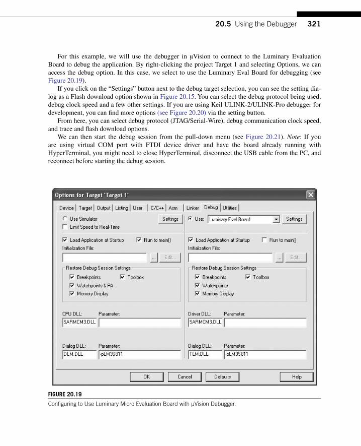
32120.5 Using the Debugger
FIGUre 20�19
Configuring to Use Luminary Micro Evaluation Board with µVision Debugger.
For this example, we will use the debugger in μVision to connect to the Luminary Evaluation Board to debug the application. By right-clicking the project Target 1 and selecting Options, we can access the debug option. In this case, we select to use the Luminary Eval Board for debugging (see Figure 20.19).
If you click on the “Settings” button next to the debug target selection, you can see the setting dia-log as a Flash download option shown in Figure 20.15. You can select the debug protocol being used, debug clock speed and a few other settings. If you are using Keil ULINK-2/ULINK-Pro debugger for development, you can find more options (see Figure 20.20) via the setting button.
From here, you can select debug protocol (JTAG/Serial-Wire), debug communication clock speed, and trace and flash download options.
We can then start the debug session from the pull-down menu (see Figure 20.21). Note: If you are using virtual COM port with FTDI device driver and have the board already running with HyperTerminal, you might need to close HyperTerminal, disconnect the USB cable from the PC, and reconnect before starting the debug session.

322 CHAPTER 20 Getting Started with the Keil RealView Microcontroller
FIGUre 20�20
ULINK-2 Debug Options.
FIGUre 20�21
Starting a Debugger Session in µVision.
When the debugger starts, the IDE provides a register view to display register contents. You can also get the disassemble code window and see the current instruction address. In Figure 20.22, we can see that the core is halted at the Reset_Handler, the first instruction of the program execution.
For demonstration, a breakpoint is set to stop the program execution at the beginning of main. This can be done by right-clicking on the first line of code in the main program in the program code

32320.5 Using the Debugger
FIGUre 20�22
µVision Debug Environment.
window and selecting Insert/Remove Breakpoint (see Figure 20.23). Note: We could also use the Run to main( ) feature in the debug option to get the program execution to stop at the beginning of main.
After the breakpoint is added, a red marker will be shown in the left side of the code line as shown in line 29 of the code in Figure 20.23. The program execution can then be started using the Run button on the tool bar (see Figure 20.24).
FIGUre 20�23
Insert or Remove Breakpoint.

324 CHAPTER 20 Getting Started with the Keil RealView Microcontroller
FIGUre 20�25
Program Execution Halted at the Beginning of Main When a Breakpoint Is Hit.
FIGUre 20�24
Starting Program Execution Using the Run Button.
The program execution is then started, and it stops when it gets to the start of the main program (see Figure 20.25).
We can then use the stepping control of the tool bar to test our application and examine the results using the register window.

32520.6 The Instruction Set Simulator
FIGUre 20�26
Selecting Simulator as Debugging Target.
20�6 The InsTrUCTIOn seT sIMUlaTOrThe μVision IDE also comes with an instruction set simulator that can be used for debugging applications. The operation is similar to using the debugger with hardware and is a useful tool for learning the Cortex-M3. To use the instruction set simulator, change the debug option of the project to Use Simulator (see Figure 20.26). Note that the simulator might not be able to simulate all hardware peripheral behaviors for some microcontroller products, so the UART interface code might not simu-late correctly.
The simulator in μVision has full device level support for a wide range of Cortex-M3 devices. In some cases where full device simulation is not available, you might need to adjust the memory setting when using the simulator for debugging. This is done by accessing the Memory Map option after start-ing the debugging session (see Figure 20.27).
For example, you might need to add the UART memory address range to the memory map (see Figure 20.28). Otherwise, you will get an abort exception in the simulation when you try to access the

326 CHAPTER 20 Getting Started with the Keil RealView Microcontroller
FIGUre 20�27
Accessing the Memory Map Option.
UART. But in most cases, all of the required memory map should have been set up for you when you specified a microcontroller, so usually this is not necessary.
20�7 MODIFyInG The VeCTOr TableIn the previous example, the vector table is defined inside the file Startup.s, which is a standard startup code the tool prepares automatically. This file contains the vector table, a default reset handler, a default nonmaskable interrupt (NMI) handler, a default hard fault handler, and a default interrupt handler. These exception handlers might need to be customized or modified, depending on your application. For

32720.8 Stopwatch Example with Interrupts with CMSIS
FIGUre 20�28
Adding New Memory Range to Simulator Memory Setup.
example, if a peripheral interrupt is required for your application, you need to change the vector table so that the Interrupt Service Routine (ISR) you created will be executed when the interrupt is triggered.
The default exception handlers are in the form of assembly code inside Startup.s. However, the exception handlers can be implemented in C or in a different assembly program file. In these cases, the IMPORT command in the assembler will be required to indicate that the interrupt handler address label is defined in another file.
For example, if we want to add a SYSTICK exception handler and a UART exception handler, we can edit the file startup.s as shown in Figure 20.29 as follows:
Comment out existing default interrupt handler for the exception.•Add the IMPORT commands for the two exception vectors that are defined in the C-code. This is •required if the handlers are in a separated C or assembly program file.Add the exception vectors in the vector table with Define Constant Data (DCD) command.•
These modifications of startup code (startup.s) for adding exception handlers are not required with Cortex Microcontroller Software Interface Standard (CMSIS) compliant device driver libraries if the name of the exception handlers match the handler names specific in the CMSIS startup code. The next example illustrates how this is done.
20�8 sTOpWaTCh exaMple WITh InTerrUpTs WITh CMsIsThis example includes the use of exceptions, such as SYSTICK and the interrupt (UART0). The stop-watch to be developed has three states, as illustrated in Figure 20.30.

328 CHAPTER 20 Getting Started with the Keil RealView Microcontroller
FIGUre 20�29
Adding Exception Vectors to the Vector Table by IMPORT and DCD Commands.
FIGUre 20�30
State Machine Design for Stopwatch.
Idle
StartStop
Key pressed
Key pressedKey pressed
Counting insideSYSTICKexception
Countingstopped
Resultdisplayed
Resultcleared
Based on the previous example, the stopwatch is controlled by the PC using the UART interface. To simplify the example code, we fix the operating speed at 50 MHz.
The timing measurement is carried out by the SYSTICK, which interrupts the processor at 100 Hz. The SYSTICK is running from the core clock frequency at 50 MHz. Every time the SYSTICK excep-tion handler is executed and if the stopwatch is running, the counter variable TickCounter increments.
Since display of text via UART is relatively slow, the control of the stopwatch is handled inside the exception handler and the display of the text and stopwatch values is carried out in the main (thread level). A simple software state machine is used to control the start, stop, and clear of the stopwatch.
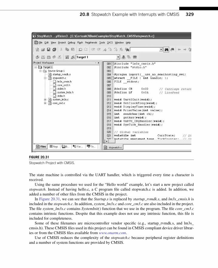
32920.8 Stopwatch Example with Interrupts with CMSIS
The state machine is controlled via the UART handler, which is triggered every time a character is received.
Using the same procedure we used for the “Hello world” example, let’s start a new project called stopwatch. Instead of having hello.c, a C program file called stopwatch.c is added. In addition, we added a number of other files from the CMSIS in the project.
In Figure 20.31, we can see that the Startup.s is replaced by startup_rvmdk.s, and lm3s_cmsis.h is included in the stopwatch.c. In addition, system_lm3s.c and core_cm3.c are also included in the project. The file system_lm3s.c contains SystemInit() function that we use in the program. The file core_cm3.c contains intrinsic functions. Despite that this example does not use any intrinsic function, this file is included for completeness.
Some of these filenames are microcontroller vendor specific (e.g., startup_rvmdk.s, and lm3s_cmsis.h). These CMSIS files used in this project can be found in CMSIS compliant device driver librar-ies or from the CMSIS files available from www.onarm.com.
Use of CMSIS reduces the complexity of the stopwatch.c because peripheral register definitions and a number of system functions are provided by CMSIS.
FIGUre 20�31
Stopwatch Project with CMSIS.

330 CHAPTER 20 Getting Started with the Keil RealView Microcontroller
stopwatch.c
#include "lm3s_cmsis.h" // Vendor specific CMSIS header#include "stdio.h" // For printf function#pragma import(__use_no_semihosting_swi)struct __FILE { int handle; };FILE __stdout;// Special characters for display function#define CR 0x0D // Carriage return#define LF 0x0A // Linefeed
// Function definitionsvoid Uart0Init(void); // Initialization of UART0void SetClockFreq(void); // Set clock frequency to 50MHzvoid DisplayTime(void); // Display time valueint sendchar(int ch); // Output character to UARTint getkey(void); // Read charcter from UARTvoid UART0_IRQHandler(void); // UART0 interrupt handlervoid SysTick_Handler(void); // SysTick exception handler
// Global variablesvolatile int CurrState; // State machinevolatile unsigned long TickCounter; // Stop watch valuevolatile int KeyReceived; // Indicate user pressed a keyvolatile int userinput; // Key pressed by user
#define IDLE_STATE 0 // Definition of state machine#define RUN_STATE 1#define STOP_STATE 2
int main (void){int CurrStateLocal; // A local copy of current state
SystemInit(); // System initialization – part of CMSIS standard // Not required with CMSIS v1.30 or after // because this is done in startup code.SetClockFreq(); // Setup clock setting (50MHz)
// Initialize global variableCurrState = 0;KeyReceived = 0;
// Initialization of hardwareSCB->CCR = SCB->CCR | 0x200; // Set STKALIGNUart0Init(); // Initialize Uart0SysTick_Config(499999); // Initialize Systick (CMSIS function)printf ("Stop Watch\n");
while (1) { CurrStateLocal = CurrState; // Make a local copy because the // value could change by UART handler at any time. switch (CurrStateLocal) { case (IDLE_STATE): printf ("\nPress any key to start\n"); break; case (RUN_STATE): printf ("\nPress any key to stop\n"); break; case (STOP_STATE): printf ("\nPress any key to clear\n"); break;
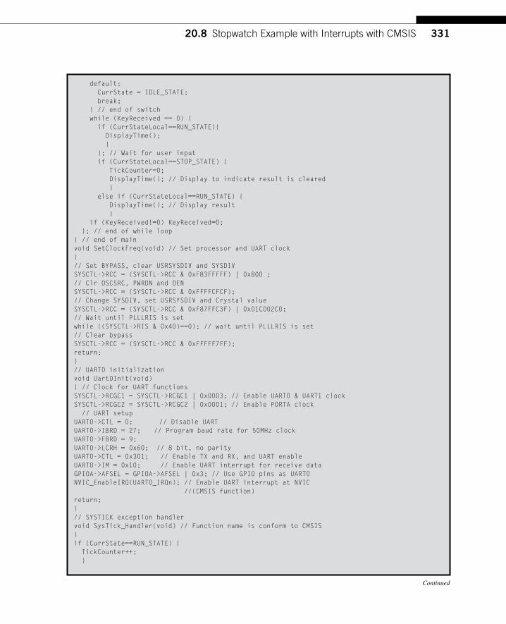
33120.8 Stopwatch Example with Interrupts with CMSIS
default: CurrState = IDLE_STATE; break; } // end of switch while (KeyReceived == 0) { if (CurrStateLocal==RUN_STATE){ DisplayTime(); } }; // Wait for user input if (CurrStateLocal==STOP_STATE) { TickCounter=0; DisplayTime(); // Display to indicate result is cleared } else if (CurrStateLocal==RUN_STATE) { DisplayTime(); // Display result } if (KeyReceived!=0) KeyReceived=0; }; // end of while loop} // end of mainvoid SetClockFreq(void) // Set processor and UART clock{// Set BYPASS, clear USRSYSDIV and SYSDIVSYSCTL->RCC = (SYSCTL->RCC & 0xF83FFFFF) | 0x800 ;// Clr OSCSRC, PWRDN and OENSYSCTL->RCC = (SYSCTL->RCC & 0xFFFFCFCF);// Change SYSDIV, set USRSYSDIV and Crystal valueSYSCTL->RCC = (SYSCTL->RCC & 0xF87FFC3F) | 0x01C002C0;// Wait until PLLLRIS is setwhile ((SYSCTL->RIS & 0x40)==0); // wait until PLLLRIS is set// Clear bypassSYSCTL->RCC = (SYSCTL->RCC & 0xFFFFF7FF);return;}// UART0 initializationvoid Uart0Init(void){ // Clock for UART functionsSYSCTL->RCGC1 = SYSCTL->RCGC1 | 0x0003; // Enable UART0 & UART1 clockSYSCTL->RCGC2 = SYSCTL->RCGC2 | 0x0001; // Enable PORTA clock // UART setupUART0->CTL = 0; // Disable UARTUART0->IBRD = 27; // Program baud rate for 50MHz clockUART0->FBRD = 9;UART0->LCRH = 0x60; // 8 bit, no parityUART0->CTL = 0x301; // Enable TX and RX, and UART enableUART0->IM = 0x10; // Enable UART interrupt for receive dataGPIOA->AFSEL = GPIOA->AFSEL | 0x3; // Use GPIO pins as UART0NVIC_EnableIRQ(UART0_IRQn); // Enable UART interrupt at NVIC //(CMSIS function)return;}// SYSTICK exception handlervoid SysTick_Handler(void) // Function name is conform to CMSIS{if (CurrState==RUN_STATE) { TickCounter++; }
Continued

332 CHAPTER 20 Getting Started with the Keil RealView Microcontroller
return;}// UART0 RX interrupt handlervoid UART0_IRQHandler(void) // Function name defined in CMSIS startup code{userinput = getkey();// Indicate a key has been receivedKeyReceived++;// De-assert UART interruptUART0->ICR = 0x10;// Switch stateswitch (CurrState) { case (IDLE_STATE): CurrState = RUN_STATE; break; case (RUN_STATE): CurrState = STOP_STATE; break; case (STOP_STATE): CurrState = IDLE_STATE; break; default: CurrState = IDLE_STATE; break; } // end of switchreturn;}
// Display the time valuevoid DisplayTime(void){unsigned long TickCounterCopy;unsigned long TmpValue;
sendchar(CR);TickCounterCopy = TickCounter; // Make a local copy because the// value could change by SYSTICK handler at any time.TmpValue = TickCounterCopy / 6000; // Minutesprintf ("%d", TmpValue);TickCounterCopy = TickCounterCopy – (TmpValue * 6000);TmpValue = TickCounterCopy / 100; // Secondssendchar(':');printf ("%d", TmpValue);TmpValue = TickCounterCopy – (TmpValue * 100);sendchar(':');printf ("%d", TmpValue); // mini-secondssendchar(' ');sendchar(' ');return;}
// Output a character to UART0 (used by printf function to output data)int sendchar (int ch){ if (ch == '\n'){ while ((UART0->FR & 0x8)); // Wait if it is busy UART0->DR = CR; // output extra CR to get correct // display on hyperterminal}
while ((UART0->FR & 0x8)); // Wait if it is busy

33320.8 Stopwatch Example with Interrupts with CMSIS
return (UART0->DR = ch); // output data}// Get user inputint getkey (void) { // Read character from Serial Port while (UART0->FR & 0x10); // Wait if RX FIFO empty return (UART0->DR);}// Retarget text outputint fputc(int ch, FILE *f) { return (sendchar(ch));}
void _sys_exit(int return_code) { /* dummy exit */label: goto label; /* endless loop */}
When compared with the previous “Hello world” example, the UART initialization has changed slightly to enable interrupts when a character is received via the UART interface. To enable the UART interrupt request, the interrupt has to be enabled at the UART Interrupt Mask register, as well as at the NVIC. For the SYS-TICK, only the exception control at the SYSTICK Control and Status register needs to be programmed.
In addition, a number of extra functions are added, including the UART and SYSTICK handlers, display functions, and SYSTICK initialization. Depending on the design of the peripheral, an excep-tion/interrupt handler might need to clear the exception/interrupt request. In this case, the UART han-dler clears the UART interrupt request using the Interrupt Clear register (UART0->ICR).
After the program is compiled and downloaded to the evaluation board, it can then be tested by con-necting to a PC running HyperTerminal. Figure 20.32 shows the result.
FIGUre 20�32
Output of the Stopwatch Example on the HyperTerminal Console.

334 CHAPTER 20 Getting Started with the Keil RealView Microcontroller
20�9 pOrTInG exIsTInG applICaTIOns TO Use CMsIsIt is easy to port existing Cortex-M3 applications to use CMSIS. The modifications include the following:
Replace the default startup code with CMSIS startup code for the targeted microcontroller.•Modify the project setup to include CMSIS file.•Modify the program to include CMSIS header file•Modify the register definitions with CMSIS register definitions•Replace existing processor peripheral access functions with CMSIS processor access functions.•Name of exception handlers might need to be modified to ensure that they match the exception •handler names used by the CMSIS startup code.Peripheral setup code could be replaced by device driver library functions if available.•
By changing the application code to use CMSIS, the application becomes more portable, as outlined
in Chapter 10.

335Copyright © 2010, Elsevier Inc. All rights reserved.DOI: 10.1016/B978-1-85617-963-8.00024-7
In ThIs ChapTer
Overview .............................................................................................................................................. 335What Is LabVIeW .................................................................................................................................. 335Development Flow ................................................................................................................................. 337example of a LabVIeW project ............................................................................................................. 339how It Works ....................................................................................................................................... 343additional Features in LabVIeW ............................................................................................................. 344porting to another arM processor ......................................................................................................... 345
21.1 OVerVIeWBesides C language and assembly language, there are other ways to create applications for Cortex™-M3 microcontrollers. One of the possible methods is by using the National Instruments LabVIEW graphical development environment. You can use LabVIEW on PCs as well as ARM microcontrollers, including Cortex-M3 microcontroller products.
21.2 WhaT Is LabVIeWThere are several versions of the LabVIEW development environment, including versions for PC (avail-able for Windows and Linux) and embedded platforms, which support a number of different embedded processors, including the Cortex-M3 processor and ARM7TDMI processor.
The LabVIEW graphical programming language supports all the features that you expect in any programming language such as looping, conditional execution, and the handling of different data types. The main difference in working with LabVIEW is that you design programs in diagrams. For example, a simple loop to compute the sum of 1–10 can be represented by the For Loop shown in Figure 21.1.
The flow of data is represented by connections; different data types are represented in different line styles; and different color and variables are represented by icons. For example, a U32 icon refers to an unsigned 32-bit integer and an I32 icon refers to a signed 32-bit integer.
Programming the Cortex-M3 Microcontrollers in NI LabVIEW 21
CHAPTER

336 CHAPTER 21 Programming the Cortex-M3 Microcontrollers in NI LabVIEW
Similar to function calls and subroutines in traditional programming, in LabVIEW, you can design the software into hierarchy of modules called virtual instruments (VIs). Data passing into and outputs from sub-VIs indicate connection points so that a higher-hierarchy VI can connect input variables and output vari-ables to it. For example, the right side of Figure 21.2 shows a sub-VI block diagram that takes four 32-bit inte-ger inputs and selects the largest value as output. On the left side, the sub-VI is used to find the largest values from four 32-bit integer value sources: three from the slide bar control and one that is a random number.
The LabVIEW programming environment contains a large number of ready-to-use components that make your software development easier. These include common data-processing functions (e.g., abs—absolute value), signal processing functions, such as filter and spectral analysis, and many user interface components.
FIgure 21.1
A Simple For Loop to Add 1–10.
FIgure 21.2
The VI and Sub-VI Allow Programs to Divide into Hierarchy Levels.

33721.2 Development Flow
21.2.1 Typical application areasSo how does LabVIEW programming compare with traditional programming?
Ease of use—The LabVIEW programming environment makes it much easier to develop complex applications without the need to learn low-level hardware and software details. This allows different types of users, from students to scientists, to develop their applications without spending time learning processor architecture—they can focus on developing the algorithms and features. Domain-experts can now take advantage of the benefits of microcontroller designs.
Component library—The large number of software components available in LabVIEW also makes it easy to develop complex applications in a short time. The component library includes hundreds of mathematical and signal processing functions to quickly develop algorithms. Applications running on ARM microcontrollers can even connect to a graphical user interface (GUI) running on a PC so users can control the embedded system and observe the output easily.
Multithreading support—The graphical programming environment is concurrent in nature. It allows multiple threads to run at the same time. In contrast, in a traditional programming environment, it takes time for an inexperienced engineer to learn an embedded real time operating system (RTOS) well enough to develop a multithreading application.
Connectivity to test and data acquisition equipment—The LabVIEW programming environment provides easy-to-use interface components to data acquisition equipment communications systems as well as a large number of interface boards for industrial control and educational purposes.
The LabVIEW programming environment is popular in universities, laboratories, and scientific research institutions. It is commonly used in data acquisition, testing system automation, algorithm development and modeling, industrial control, and embedded system prototyping.
21.2.2 What You need to use LabVIeW and arMTo start using LabVIEW for the Cortex-M3 microcontroller, you need the NI LabVIEW Embedded Module for ARM Microcontrollers, which includes the Keil ARM Microcontroller Development Kit (MDK-ARM). For evaluation, you can purchase a low-cost kit that includes an ARM microcontroller board (Cortex-M3/ARM7), Keil ULINK2 debugger, and the required development software, as shown in Figure 21.3 (a trial version of MDK-ARM is included on the CD). Details of the products are avail-able on the National Instruments web site (www.ni.com/arm).
You can use LabVIEW with other Cortex-M3 microcontrollers or ARM7 microcontrollers. How-ever, LabVIEW does not have device drivers for the peripherals of some of the microcontrollers. For these devices, you may need to develop the interface code in C and access it in LabVIEW.
21.3 DeVeLOpMenT FLOWThe development of a LabVIEW application typically involves the steps below and shown in Figure 21.4.
• Create a project and a VI: You can use the project wizard to create an ARM project easily. This includes setting up the targeted platform and device drivers. After the project creation, a VI (usually a blank one) is created.

338 CHAPTER 21 Programming the Cortex-M3 Microcontrollers in NI LabVIEW
• Define inputs and outputs: These can be hardware interfaces on the microcontroller or user interfaces running on the PC connected to the system. For hardware interfaces, you need to define the inputs and outputs as elemental input/output (I/O) in the project before you can use them in your VI design.
Create • the application using graphical programming.
• Build the design.
• Simulate: It is possible to download the created execution image to the device simulation in the Keil MDK-ARM to test your application.
• Download to the microcontroller and test: By default, the program is downloaded to the microcontroller as a test when the compilation is done. You can use the LabVIEW interface to pause, stop, or single-step the execution. You can also probe the variable value by clicking the connection during execution.
FIgure 21.4
Example Design Flow.
Create a projectDefine input, output,and user interface
Create program usinggraphical language Build the design
Simulate Download tohardware and test
FIgure 21.3
LabVIEW Evaluation Kit for the Cortex-M3 Processor.

33921.3 Example of a LabVIEW Project
Each VI has two views:
• Front panel view: Containing a GUI of the VI.• Block diagram view: Serving as a work-space for graphical programming.
When you create a VI, it has a blank front panel by default. You can then add control elements and indicator elements to define the inputs and outputs of the system. For instance, in the previous example of getting the largest integer from three inputs and a random value, the front panel may be similar to the one shown in Figure 21.5.
You can choose from a variety of control and indicator components in the VI libraries. After you add these controls and indicators, they become visible in the block diagram view. You can then cus-tomize properties like data types and create your graphical program by connecting them with various LabVIEW functions.
21.4 exaMpLe OF a LabVIeW prOjeCT21.4.1 Create the projectThis example creates a simple application that samples analog signals and displays on the Organic LED (OLED) screen as a waveform. The first step is to use the project wizard to create a new project. From the LabVIEW startup screen, select “more” and then “ARM project,” as shown in Figure 21.6. Then you can create a blank VI, or use an existing one. For this example, create a
FIgure 21.5
Simple Front Panel Design for the VI in Figure 2.

340 CHAPTER 21 Programming the Cortex-M3 Microcontrollers in NI LabVIEW
new VI. Now you have the choice of target type. For this example, select the LM3S8962 evaluation kit (Figure 21.7).
In the final step, the project wizard builds the specification that allows you to run the project on a simulator. For this example, run it in hardware instead of selecting the simulator option. The project creation wizard also saves the project and a default blank VI.
FIgure 21.6
Create New ARM Project via the Project Wizard.
FIgure 21.7
Select Target Type.

34121.3 Example of a LabVIEW Project
21.4.2 Define Inputs and OutputsThe next step of the project is to define the inputs and outputs for the applications. In this example, you need to define only the ADC0 input (the OLED display is controlled by library components, so you don’t have to define it here). To complete that, right click on the target in the project window and select “New-> Elemental I/O” (Figure 21.8). Then define the input used in the project in the New Elemental I/O window, as shown in Figure 21.9.
In this window, a number of other I/O options are available. For example, the push buttons, light emitting diode (LED), General Purpose Input/Output (GPIO), and Pulse Width Modulator (PWM) interfaces can help you simplify your project development.
21.4.3 Create the programThen you can create the application code in the block diagram view. LabVIEW features many functions and it is impossible to cover all of these in this chapter. LabVIEW has detailed documen-tation on how to create graphical programming elements, and each element has context-sensitive help information. In general, you can right click on the block diagram area to browse the available components (see Figure 21.10). For example, a number of the OLED screen controls are available in the ARM category.
FIgure 21.8
Define Elemental I/O.

342 CHAPTER 21 Programming the Cortex-M3 Microcontrollers in NI LabVIEW
In addition to the OLED control, you can find the elemental I/O, Controller Area Network (CAN), Inter-Integrated Circuit (I2C), Serial Peripherial Interface (SPI), and interrupt control functions in the ARM category.
In the analog waveform display application, the program code is divided into two parts: on the left side of the block diagram, the code initializes the OLED screen, displays a startup screen, delays for a short period and then clears the screen and displays “Analog Input 0” at the top of the screen. Use this sub-VI, which is specific to the LM3S8962 evaluation board you are using, for the OLED controls provided in the LabVIEW Embedded Module for ARM Microcontrollers (Figure 21.11).
The right side of the block diagram features a While Loop that samples from ADC0 of the LM3S8962 and then displays the waveform by drawing a pixel on the screen. If the X-position is reached on the right side of the OLED screen, the X-position counter resets to 0.
The calculated Y position value is also stored into an array. The array has a size of 128 integers and is used to remove the old waveform before the new pixel is drawn on the screen.
21.4.4 build the Design and Test the applicationOnce you have completed the design, you can build the design and test the application. First click the arrow button on the tool bar. If the program contains an error, the arrow icon displays as broken to indi-cate that the program is not ready. You can click on it to report the errors detected in the program.
When you have completed the compile process, the program is downloaded to the board automati-cally and executed. In this example, the program has executed successfully and generated the waveform for an analog input (see Figure 21.12 on page 345).
FIgure 21.9
Adding Elemental I/O to Your Project.

34321.4 How It Works
21.5 hOW IT WOrksWhen you build the program, LabVIEW generates C code from the VI created. You can then compile C code using the MDK-ARM (Figure 21.13 on page 346). To run VI-s in parallel, the generated C code uses the RealView Real-Time Library (RL-ARM, www.keil.com/arm/rl-arm/), which works with the Keil RTX Real Time Kernel (www.keil.com/arm/rl-arm/kernel.asp).
FIgure 21.10
Access LabVIEW Functions and ARM-Specific Features.

344 CHAPTER 21 Programming the Cortex-M3 Microcontrollers in NI LabVIEW
In addition to the capability of multithreading, using the RL-ARM provides access to a variety of drivers including timing control, Transmission Control Protocol/Internet Protocol (TCP/IP) stack, and CAN protocol stack.
21.6 aDDITIOnaL FeaTures In LabVIeWSemihosting: LabVIEW supports the creation of GUIs running on the debug host (PC). This is very
useful for system prototyping because developing GUIs running on a microcontroller can be a time-consuming task. The LabVIEW library supports user-interface elements including switches, slide bars, and graphs, making it easy to create professional GUIs in just a few mouse clicks. During operation, the GUIs are running on the PC and the data are communicated to the running microcon-troller target via the debug connection Joint Test Action Group, TCP/IP, or Serial. This allows you to control and access the results on the hardware in real time.
C code integration: LabVIEW supports embedding C code inside a VI. This is useful for creating new device drivers and handling data-processing tasks that you cannot complete using elements in LabVIEW.
Debugging: Debugging is easy in the LabVIEW environment. During design simulation or test, you can use the VI design environment as a debugger by showing the values on data variables when it stops. The VI block diagram view provides pause, run, and single-stepping controls as well as value probing (Figure 21.14 on page 346).
In addition, because the Keil μVision comes with a full-featured debugger, you can debug the applica-tion code you generated on LabVIEW using the μVision debugger (Figure 21.15 on page 347).
FIgure 21.11
Block Diagram of the Analog Waveform Display Application.

345
21.7 pOrTIng TO anOTher arM prOCessOrIn addition to running your LabVIEW application using the evaluation kit, you can port the application to other Cortex-M3 microcontrollers or other ARM microcontrollers that are supported by the RTX Real-Time Kernel. This typically involves the following steps:
• Port the RTX Real-Time Kernel: This step is not required for Cortex-M3 devices because the processor contains the required support for the RTX Real-Time Kernel. However, if you choose to use ARM7 microcontrollers, you may need this. A port for the RTX Real-Time Kernel may already be available in the Keil MDK-ARM installation options. You can determine if an RTX port is available for your ARM microcontroller by browsing the \Keil\ARM\Startup directory. If an RTX_Conf*.c is already available for the microcontroller target, then the RTX Real-Time Kernel has already been ported.
21.6 Porting to Another ARM Processor
FIgure 21.12
LabVIEW Application Running on the Evaluation Kit.

346 CHAPTER 21 Programming the Cortex-M3 Microcontrollers in NI LabVIEW
FIgure 21.14
Debugging in a VI Block Diagram.
FIgure 21.13
Design Flow Using LabVIEW and Keil μVision.

347
• Create the target in LabVIEW and incorporate the Keil toolchain: You can do this by manually creating the target folder.
• Integrate the Real-Time Agent Module for debugging: You may need to customize the RTX_config.c to include the Real-Time Agent Configuration option.
• Develop peripheral and I/O drivers: You can implement this step using the Element I/O Device Editor.
For more detailed information on the porting process, view the National Instruments online tutorial titled LabVIEW Embedded for ARM Porting Guide (http://zone.ni.com/devzone/cda/tut/p/id/6994).
21.6 Porting to Another ARM Processor
FIgure 21.15
Using μVision to Debug Code Generated in LabVIEW.
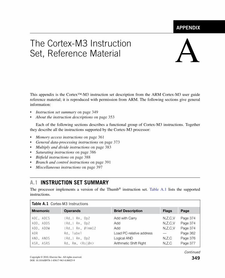
349Copyright © 2010, Elsevier Inc. All rights reserved.DOI: 10.1016/B978-1-85617-963-8.00025-9
This appendix is the Cortex™-M3 instruction set description from the ARM Cortex-M3 user guide reference material; it is reproduced with permission from ARM. The following sections give general information:
• Instruction set summary on page 349• About the instruction descriptions on page 353
Each of the following sections describes a functional group of Cortex-M3 instructions. Together they describe all the instructions supported by the Cortex-M3 processor:
Memory access instructions • on page 361• General data-processing instructions on page 373• Multiply and divide instructions on page 383• Saturating instructions on page 386• Bitfield instructions on page 388• Branch and control instructions on page 391• Miscellaneous instructions on page 397
A.1 InstructIon set summAryThe processor implements a version of the Thumb® instruction set. Table A.1 lists the supported instructions.
Appendix
The Cortex-M3 Instruction Set, Reference Material
Table A.1 Cortex-M3 Instructions
Mnemonic Operands Brief Description Flags Page
ADC, ADCS {Rd,} Rn, Op2 Add with Carry N,Z,C,V Page 374ADD, ADDS {Rd,} Rn, Op2 Add N,Z,C,V Page 374ADD, ADDW {Rd,} Rn, #imm12 Add N,Z,C,V Page 374ADR Rd, label Load PC-relative address — Page 362AND, ANDS {Rd,} Rn, Op2 Logical AND N,Z,C Page 376ASR, ASRS Rd, Rm, <Rs|#n> Arithmetic Shift Right N,Z,C Page 377
Continued
A

350 Appendix A The Cortex-M3 Instruction Set, Reference Material
Table A.1 Cortex-M3 Instructions Continued
Mnemonic Operands Brief Description Flags Page
B Label Branch — Page 391
BFC Rd, #lsb, #width Bit Field Clear — Page 388BFI Rd, Rn, #lsb, #width Bit Field Insert — Page 388BIC, BICS {Rd,} Rn, Op2 Bit Clear N,Z,C Page 376BKPT #imm Breakpoint — Page 397BL Label Branch with Link — Page 391BLX Rm Branch indirect with Link — Page 391BX Rm Branch indirect — Page 391CBNZ Rn, label Compare and Branch if
Nonzero— Page 393
CBZ Rn, label Compare and Branch if Zero — Page 393CLREX — Clear Exclusive — Page 372CLZ Rd, Rm Count leading zeros — Page 378CMN Rn, Op2 Compare Negative N,Z,C,V Page 378CMP Rn, Op2 Compare N,Z,C,V Page 378CPSID iflags Change Processor State,
Disable Interrupts— Page 398
CPSIE iflags Change Processor State, Enable Interrupts
— Page 398
DMB — Data Memory Barrier — Page 398DSB — Data Synchronization Barrier — Page 399EOR, EORS {Rd,} Rn, Op2 Exclusive OR N,Z,C Page 376ISB — Instruction Synchronization
Barrier— Page 399
IT — If-Then condition block — Page 393LDM Rn{!}, reglist Load Multiple registers,
increment after— Page 368
LDMDB, LDMEA Rn{!}, reglist Load Multiple registers, decrement before
— Page 368
LDMFD, LDMIA Rn{!}, reglist Load Multiple registers, increment after
— Page 368
LDR Rt, [Rn, #offset] Load Register with word — Page 362LDRB, LDRBT Rt, [Rn, #offset] Load Register with byte — Page 362LDRD Rt, Rt2, [Rn, #offset] Load Register with 2 bytes — Page 362LDREX Rt, [Rn, #offset] Load Register Exclusive — Page 371LDREXB Rt, [Rn] Load Register Exclusive with
byte— Page 371
LDREXH Rt, [Rn] Load Register Exclusive with halfword
— Page 371
LDRH, LDRHT Rt, [Rn, #offset] Load Register with halfword — Page 362LDRSB, LDRSBT Rt, [Rn, #offset] Load Register with signed
byte— Page 362

351A.1 Instruction Set Summary
Table A.1 Cortex-M3 Instructions Continued
Mnemonic Operands Brief Description Flags Page
LDRSH, LDRSHT Rt, [Rn, #offset] Load Register with signed halfword
— Page 362
LDRT Rt, [Rn, #offset] Load Register with word — Page 362LSL, LSLS Rd, Rm, <Rs|#n> Logical Shift Left N,Z,C Page 377LSR, LSRS Rd, Rm, <Rs|#n> Logical Shift Right N,Z,C Page 377MLA Rd, Rn, Rm, Ra Multiply with Accumulate,
32-bit result— Page 383
MLS Rd, Rn, Rm, Ra Multiply and Subtract, 32-bit result
— Page 383
MOV, MOVS Rd, Op2 Move N,Z,C Page 379MOVT Rd, #imm16 Move Top — Page 381MOVW, MOV Rd, #imm16 Move 16-bit constant N,Z,C Page 379MRS Rd, spec_reg Move from special register to
general register— Page 400
MSR spec_reg, Rm Move from general register to special register
N,Z,C,V Page 400
MUL, MULS Rd, Rn, Rm Multiply, 32-bit result N,Z Page 383MVN, MVNS Rd, Op2 Move NOT N,Z,C Page 379NOP — No Operation — Page 401ORN, ORNS {Rd,} Rn, Op2 Logical OR NOT N,Z,C Page 376ORR, ORRS {Rd,} Rn, Op2 Logical OR N,Z,C Page 376POP reglist Pop registers from stack — Page 370PUSH reglist Push registers onto stack — Page 370RBIT Rd, Rn Reverse bits — Page 381REV Rd, Rn Reverse byte order in a word — Page 381REV16 Rd, Rn Reverse byte order in each
halfword— Page 381
REVSH Rd, Rn Reverse byte order in bottom halfword and sign extend
— Page 381
ROR, RORS Rd, Rm, <Rs|#n> Rotate Right N,Z,C Page 377RRX, RRXS Rd, Rm Rotate Right with Extend N,Z,C Page 377RSB, RSBS {Rd,} Rn, Op2 Reverse Subtract N,Z,C,V Page 374SBC, SBCS {Rd,} Rn, Op2 Subtract with Carry N,Z,C,V Page 374SBFX Rd, Rn, #lsb, #width Signed Bit Field Extract — Page 389SDIV {Rd,} Rn, Rm Signed Divide — Page 386SEV — Send Event — Page 402SMLAL RdLo, RdHi, Rn, Rm Signed Multiply with
Accumulate (32 × 32 + 64), 64-bit result
— Page 385
SMULL RdLo, RdHi, Rn, Rm Signed Multiply (32 × 32), 64-bit result
— Page 385
Continued

352 Appendix A The Cortex-M3 Instruction Set, Reference Material
Table A.1 Cortex-M3 Instructions Continued
Mnemonic Operands Brief Description Flags Page
SSAT Rd, #n, Rm {,shift #s} Signed Saturate Q Page 386STM Rn{!}, reglist Store Multiple registers,
increment after— Page 368
STMDB, STMEA Rn{!}, reglist Store Multiple registers, decrement before
— Page 368
STMFD, STMIA Rn{!}, reglist Store Multiple registers, increment after
— Page 368
STR Rt, [Rn, #offset] Store Register word — Page 362STRB, STRBT Rt, [Rn, #offset] Store Register byte — Page 362STRD Rt, Rt2, [Rn, #offset] Store Register two words — Page 362STREX Rd, Rt, [Rn, #offset] Store Register Exclusive — Page 371STREXB Rd, Rt, [Rn] Store Register Exclusive byte — Page 371STREXH Rd, Rt, [Rn] Store Register Exclusive
halfword— Page 371
STRH, STRHT Rt, [Rn, #offset] Store Register halfword — Page 362STRT Rt, [Rn, #offset] Store Register word — Page 362SUB, SUBS {Rd,} Rn, Op2 Subtract N,Z,C,V Page 374SUB, SUBW {Rd,} Rn, #imm12 Subtract N,Z,C,V Page 374SVC #imm Supervisor Call — Page 402SXTB Rd, Rm {,ROR #n} Sign extend a byte — Page 390SXTH Rd, Rm {,ROR #n} Sign extend a halfword — Page 390TBB [Rn, Rm] Table Branch Byte — Page 395TBH [Rn, Rm, LSL #1] Table Branch Halfword — Page 395TEQ Rn, Op2 Test Equivalence N,Z,C Page 382TST Rn, Op2 Test N,Z,C Page 382UBFX Rd, Rn, #lsb, #width Unsigned Bit Field Extract — Page 389UDIV {Rd,} Rn, Rm Unsigned Divide — Page 386UMLAL RdLo, RdHi, Rn, Rm Unsigned Multiply with
Accumulate (32 × 32 + 64), 64-bit result
— Page 385
UMULL RdLo, RdHi, Rn, Rm Unsigned Multiply (32 × 32), 64-bit result
— Page 385
USAT Rd, #n, Rm {,shift #s} Unsigned Saturate Q Page 386UXTB Rd, Rm {,ROR #n} Zero extend a byte — Page 390UXTH Rd, Rm {,ROR #n} Zero extend a halfword — Page 390WFE — Wait For Event — Page 403WFI — Wait For Interrupt — Page 403
Note: Angle brackets, <>, enclose alternative forms of the operand; braces, {}, enclose optional operands; the Operands column is not exhaustive; Op2 is a flexible second operand that can be either a register or a constant; most instructions can use an optional condition code suffix.
For more information on the instructions and operands, see the instruction descriptions.

353A.2 About the Instruction Descriptions
A.2 About the InstructIon DescrIptIonsThe following sections give more information about using the instructions:
• Operands on page 353• Restrictions when using PC or SP on page 353• Flexible second operand on page 353• Shift Operations on page 354• Address alignment on page 357• PC-relative expressions on page 358• Conditional execution on page 358• Instruction width selection on page 360
A.2.1 operandsAn instruction operand can be an ARM register, a constant, or another instruction-specific parameter. Instructions act on the operands and often store the result in a destination register. When there is a des-tination register in the instruction, it is usually specified before the operands.
Operands in some instructions are flexible in that they can either be a register or a constant; see “Flexible Second Operand” section.
A.2.2 restrictions When using pc or spMany instructions have restrictions on whether you can use the program counter (PC) or stack pointer (SP) for the operands or destination register. See instruction descriptions for more information.
NoteBit[0] of any address you write to the PC with a BX, BLX, LDM, LDR, or POP instruction must be 1 for correct execution, because this bit indicates the required instruction set, and the Cortex-M3 proces-sor only supports Thumb instructions.
A.2.3 Flexible second operandMany general data-processing instructions have a flexible second operand. This is shown as Operand2 in the descriptions of the syntax of each instruction.
Operand2 can be a
• ConstantRegister with optional shift • on page 354.
ConstantYou specify an Operand2 constant in the form:
#constant

354 Appendix A The Cortex-M3 Instruction Set, Reference Material
where constant can be
Any constant that can be produced by shifting an 8-bit value left by any number of bits within a •32-bit wordAny constant of the form • 0x00XY00XYAny constant of the form • 0xXY00XY00Any constant of the form • 0xXYXYXYXY.
NoteIn the constants shown above, X and Y are hexadecimal digits.
In addition, in a small number of instructions, constant can take a wider range of values. These are described in the individual instruction descriptions.
When an Operand2 constant is used with the instructions MOVS, MVNS, ANDS, ORRS, ORNS, EORS, BICS, TEQ, or TST, the carry flag is updated to bit[31] of the constant, if the constant is greater than 255 and can be produced by shifting an 8-bit value. These instructions do not affect the carry flag if Operand2 is any other constant.
Instruction SubstitutionYour assembler might be able to produce an equivalent instruction in cases where you specify a constant that is not permitted. For example, an assembler might assemble the instruction CMP Rd, #0xFFFFFFFE as the equivalent instruction CMN Rd, #0x2.
Register with Optional ShiftYou specify an Operand2 register in the form:Rm {, shift}
where
Rm is the register holding the data for the second operand.shift is an optional shift to be applied to Rm. It can be one of the following:
ASR #n Arithmetic Shift Right n bits, 1 ≤ n ≤ 32 LSL #n Logical Shift Left n bits, 1≤ n ≤ 31 LSR #n Logical Shift Right n bits, 1 ≤ n ≤ 32 ROR #n Rotate Right n bits, 1 ≤ n ≤ 31 RRX Rotate Right 1 bit, with Extend - If omitted, no shift occurs, equivalent to LSL #0
If you omit the shift, or specify LSL #0, the instruction uses the value in Rm.If you specify a shift, the shift is applied to the value in Rm, and the resulting 32-bit value is used
by the instruction. However, the contents in the register Rm remain unchanged. Specifying a register with shift also updates the carry flag when used with certain instructions. For information on the shift operations and how they affect the carry flag, see “Shift Operations” section.
A.2.4 shift operationsRegister shift operations move the bits in a register left or right by a specified number of bits, the shift length. Register shift can be performed
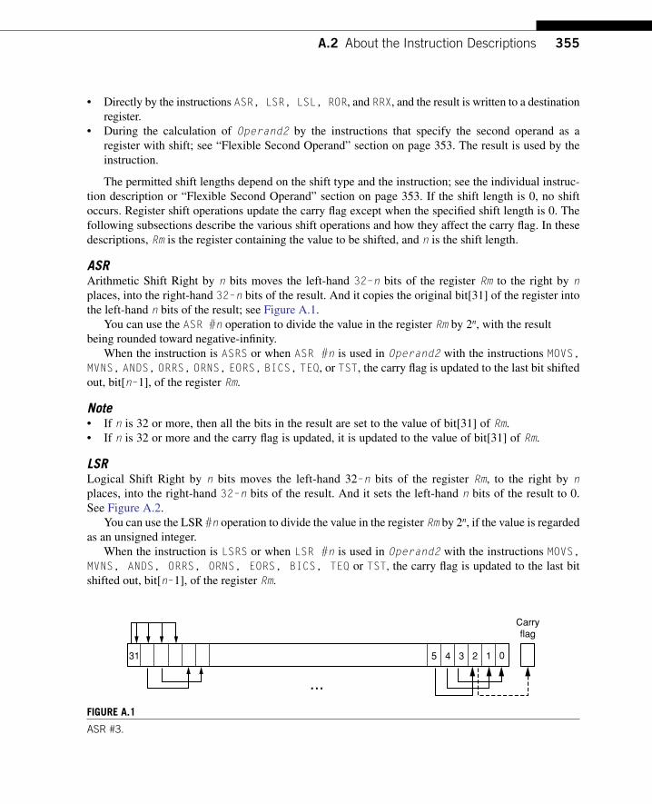
355A.2 About the Instruction Descriptions
Directly by the instructions • ASR, LSR, LSL, ROR, and RRX, and the result is written to a destination register.During the calculation of • Operand2 by the instructions that specify the second operand as a register with shift; see “Flexible Second Operand” section on page 353. The result is used by the instruction.
The permitted shift lengths depend on the shift type and the instruction; see the individual instruc-tion description or “Flexible Second Operand” section on page 353. If the shift length is 0, no shift occurs. Register shift operations update the carry flag except when the specified shift length is 0. The following subsections describe the various shift operations and how they affect the carry flag. In these descriptions, Rm is the register containing the value to be shifted, and n is the shift length.
ASRArithmetic Shift Right by n bits moves the left-hand 32–n bits of the register Rm to the right by n places, into the right-hand 32–n bits of the result. And it copies the original bit[31] of the register into the left-hand n bits of the result; see Figure A.1.
You can use the ASR #n operation to divide the value in the register Rm by 2n, with the result being rounded toward negative-infinity.
When the instruction is ASRS or when ASR #n is used in Operand2 with the instructions MOVS, MVNS, ANDS, ORRS, ORNS, EORS, BICS, TEQ, or TST, the carry flag is updated to the last bit shifted out, bit[n–1], of the register Rm.
NoteIf • n is 32 or more, then all the bits in the result are set to the value of bit[31] of Rm.If • n is 32 or more and the carry flag is updated, it is updated to the value of bit[31] of Rm.
LSRLogical Shift Right by n bits moves the left-hand 32–n bits of the register Rm, to the right by n places, into the right-hand 32–n bits of the result. And it sets the left-hand n bits of the result to 0. See Figure A.2.
You can use the LSR #n operation to divide the value in the register Rm by 2n, if the value is regarded as an unsigned integer.
When the instruction is LSRS or when LSR #n is used in Operand2 with the instructions MOVS, MVNS, ANDS, ORRS, ORNS, EORS, BICS, TEQ or TST, the carry flag is updated to the last bit shifted out, bit[n–1], of the register Rm.
FIgure A.1
ASR #3.
31 1
Carryflag
2345 0
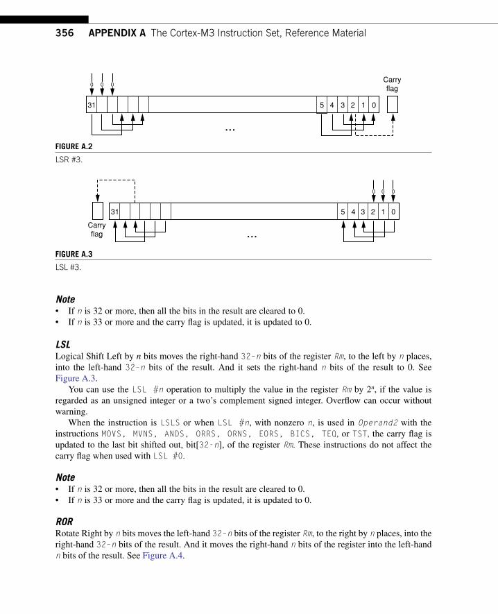
356 Appendix A The Cortex-M3 Instruction Set, Reference Material
NoteIf • n is 32 or more, then all the bits in the result are cleared to 0.If • n is 33 or more and the carry flag is updated, it is updated to 0.
LSLLogical Shift Left by n bits moves the right-hand 32–n bits of the register Rm, to the left by n places, into the left-hand 32–n bits of the result. And it sets the right-hand n bits of the result to 0. See Figure A.3.
You can use the LSL #n operation to multiply the value in the register Rm by 2n, if the value is regarded as an unsigned integer or a two’s complement signed integer. Overflow can occur without warning.
When the instruction is LSLS or when LSL #n, with nonzero n, is used in Operand2 with the instructions MOVS, MVNS, ANDS, ORRS, ORNS, EORS, BICS, TEQ, or TST, the carry flag is updated to the last bit shifted out, bit[32-n], of the register Rm. These instructions do not affect the carry flag when used with LSL #0.
NoteIf • n is 32 or more, then all the bits in the result are cleared to 0.If • n is 33 or more and the carry flag is updated, it is updated to 0.
RORRotate Right by n bits moves the left-hand 32–n bits of the register Rm, to the right by n places, into the right-hand 32–n bits of the result. And it moves the right-hand n bits of the register into the left-hand n bits of the result. See Figure A.4.
FIgure A.3
LSL #3.
31
000
1 02345
Carryflag
FIgure A.2
LSR #3.
31 1 0
000
2345
Carryflag

357A.2 About the Instruction Descriptions
When the instruction is RORS or when ROR #n is used in Operand2 with the instructions MOVS, MVNS, ANDS, ORRS, ORNS, EORS, BICS, TEQ, or TST, the carry flag is updated to the last bit rotation, bit[n-1], of the register Rm.
NoteIf • n is 32, then the value of the result is the same as the value in Rm, and if the carry flag is updated, it is updated to bit[31] of Rm.
• ROR with shift length, n, more than 32 is the same as ROR with shift length n–32.
RRXRotate Right with Extend moves the bits of the register Rm to the right by 1 bit. And it copies the carry flag into bit[31] of the result; see Figure A.5.
When the instruction is RRXS or when RRX is used in Operand2 with the instructions MOVS, MVNS, ANDS, ORRS, ORNS, EORS, BICS, TEQ, or TST, the carry flag is updated to bit[0] of the register Rm.
A.2.5 Address AlignmentAn aligned access is an operation where a word-aligned address is used for a word, dual word, or multiple word access, or where a halfword-aligned address is used for a halfword access. Byte accesses are always aligned.
The Cortex-M3 processor supports unaligned access only for the following instructions:
• LDR, LDRT• LDRH, LDRHT• LDRSH, LDRSHT
FIgure A.4
ROR #3.
31 1 02345
Carryflag
FIgure A.5
RRX.
31 30 1 0
Carryflag

358 Appendix A The Cortex-M3 Instruction Set, Reference Material
• STR, STRT• STRH, STRHT
All other load and store instructions generate a usage fault exception if they perform an unaligned access, and therefore, their accesses must be address aligned.
Unaligned accesses are usually slower than aligned accesses. In addition, some memory regions might not support unaligned accesses. Therefore, ARM recommends that programmers ensure that accesses are aligned. To trap accidental generation of unaligned accesses, use the UNALIGN_TRP bit in the Configuration and Control register to trigger usage fault exception for all unaligned accesses.
A.2.6 pc-relative expressionsA PC-relative expression or label is a symbol that represents the address of an instruction or literal data. It is represented in the instruction as the PC value plus or minus a numeric offset. The assembler calculates the required offset from the label and the address of the current instruction. If the offset is too big, the assembler produces an error.
NoteFor • B, BL, CBNZ, and CBZ instructions, the value of the PC is the address of the current instruc-tion plus 4 bytes.For most other instructions that use labels, the value of the PC is the address of the current •instruction plus 4 bytes, with bit[1] of the result cleared to 0 to make it word-aligned.Your assembler might permit other syntaxes for PC-relative expressions, such as a label plus or •minus a number, or an expression of the form [PC, #number].
A.2.7 conditional executionMost data-processing instructions can optionally update the condition flags in the Application Program Status Register (APSR) according to the result of the operation. Some instructions update all flags, and some only update a subset. If a flag is not updated, the original value is preserved. See the instruction descriptions for the flags they affect.
You can execute an instruction conditionally, based on the condition flags set in another instruc-tion, either immediately after the instruction that updated the flags or after any number of intervening instructions that have not updated the flags.
Conditional execution is available by using conditional branches or by adding condition code suf-fixes to instructions. See Table A.2 for a list of the suffixes to add to instructions to make them con-ditional instructions. The condition code suffix enables the processor to test a condition based on the flags. If the condition test of a conditional instruction fails, the instruction
Does not execute•Does not write any value to its destination register•Does not affect any of the flags•Does not generate any exception.•
Conditional instructions, except for conditional branches, must be inside an If-Then instruction block. See “IT” section on page 393 for more information and restrictions when using the IT instruction.

359A.2 About the Instruction Descriptions
Depending on the vendor, the assembler might automatically insert an IT instruction if you have con-ditional instructions outside the IT block.
Use the CBZ and CBNZ instructions to compare the value of a register against zero and branch on the result.
This section describes
The condition flags• on page 359• Condition code suffixes on page 360.
The Condition FlagsThe APSR contains the following condition flags:
N Set to 1 when the result of the operation was negative, cleared to 0 otherwise.Z Set to 1 when the result of the operation was zero, cleared to 0 otherwise.C Set to 1 when the operation resulted in a carry, cleared to 0 otherwise.V Set to 1 when the operation caused overflow, cleared to 0 otherwise.
A carry occurs
If the result of an addition is greater than or equal to 2• 32
If the result of a subtraction is positive or zero•As the result of an inline barrel shifter operation in a move or logical instruction.•
Overflow occurs when the sign of the result, in bit[31], does not match the sign of the result had the operation been performed at infinite precision, for example:
if adding two negative values results in a positive value•if adding two positive values results in a negative value•
Table A.2 Condition Code Suffixes
Suffix Flags Meaning
EQ Z = 1 EqualNE Z = 0 Not equalCS or HS C = 1 Higher or same, unsigned ≥CC or LO C = 0 Lower, unsigned <MI N = 1 NegativePL N = 0 Positive or zeroVS V = 1 OverflowVC V = 0 No overflowHI C = 1 and Z = 0 Higher, unsigned >LS C = 0 or Z = 1 Lower or same, unsigned ≤GE N = V Greater than or equal, signed ≥LT N != V Less than, signed <GT Z = 0 and N = V Greater than, signed >LE Z = 1 and N != V Less than or equal, signed ≤AL Can have any value Always; default when no suffix is specified

360 Appendix A The Cortex-M3 Instruction Set, Reference Material
if subtracting a positive value from a negative value generates a positive value•if subtracting a negative value from a positive value generates a negative value•
The Compare operations are identical to subtracting, for CMP, or adding, for CMN, except that the result is discarded. See the instruction descriptions for more information.
NoteMost instructions update the status flags only if the S suffix is specified; see the instruction descriptions for more information.
Condition Code SuffixesThe instructions that can be conditional have an optional condition code, shown in syntax descriptions as {cond}. Conditional execution requires a preceding IT instruction. An instruction with a condition code is only executed if the condition code flags in the APSR meet the specified condition. Table A.2 shows the condition codes to use.
You can use conditional execution with the IT instruction to reduce the number of branch instruc-tions in code. Table A.2 also shows the relationship between condition code suffixes and the N, Z, C, and V flags.
Example A.1 shows the use of a conditional instruction to find the absolute value of a number. R0 = ABS(R1).
Example A.2 shows the use of conditional instructions to update the value of R4 if the signed values R0 is greater than R1 and R2 is greater than R3.
A.2.8 Instruction Width selectionThere are many instructions that can generate either a 16-bit encoding or a 32-bit encoding depend-ing on the operands and destination register specified. For some of these instructions, you can force a specific instruction size by using an instruction width suffix. The .W suffix forces a 32-bit instruction encoding. The .N suffix forces a 16-bit instruction encoding.
example A.1 Absolute Value
MOVS R0, R1 ; R0 = R1, setting flagsIT MI ; IT - Skip next instruction if value 0 or positiveRSBMI R0, R1, #0 ; If negative, R0 = –R1
example A.2 Compare and Update Value
CMP R0, R1 ; Compare R0 and R1, setting flagsITT GT ; IT - Skip next two instructions unless GT condition holds
CMPGT R2, R3 ; If 'greater than', compare R2 and R3, setting flagsMOVGT R4, R5 ; If still 'greater than', do R4 = R5

361A.3 Memory Access Instructions
If you specify an instruction width suffix and the assembler cannot generate an instruction encoding of the requested width, it generates an error.
NoteIn some cases, it might be necessary to specify the .W suffix, for example, if the operand is the label of an instruction or literal data, as in the case of branch instructions. This is because the assembler might not automatically generate the right size encoding.
To use an instruction width suffix, place it immediately after the instruction mnemonic and condi-tion code, if any. Example A.3 shows instructions with the instruction width suffix.
A.3 memory Access InstructIonsTable A.3 shows the memory access instructions.
example A.3 Instruction Width Selection
BCS.W label ; creates a 32-bit instruction even for a short branchADDS.W R0, R0, R1 ; creates a 32-bit instruction even though the same
; operation can be done by a 16-bit instruction
Table A.3 Memory Access Instructions
Mnemonic Brief Description See
ADR Generate PC-relative address ADR on page 362CLREX Clear Exclusive CLREX on page 372LDM{mode} Load Multiple registers LDM and STM on page 368LDR{type} Load Register using immediate offset LDR and STR, Immediate Offset on page 362LDR{type} Load Register using register offset LDR and STR, Register Offset on page 365LDR{type}T Load Register with unprivileged
accessLDR and STR, Unprivileged on page 366
LDR Load Register using PC-relative address
LDR, PC-Relative on page 367
LDREX{type} Load Register Exclusive LDREX and STREX on page 371POP Pop registers from stack PUSH and POP on page 370PUSH Push registers onto stack PUSH and POP on page 370STM{mode} Store Multiple registers LDM and STM on page 368STR{type} Store Register using immediate offset LDR and STR, Immediate Offset on page 362STR{type} Store Register using register offset LDR and STR, Register Offset on page 365STR{type}T Store Register with unprivileged
accessLDR and STR, Unprivileged on page 366
STREX{type} Store Register Exclusive LDREX and STREX on page 371

362 Appendix A The Cortex-M3 Instruction Set, Reference Material
A.3.1 ADrGenerate PC-relative address.
SyntaxADR{cond} Rd, label
where
cond is an optional condition code; see “Conditional Execution” section on page 358.Rd is the destination register.label is a PC-relative expression. See “PC-Relative Expressions” section on page 358.
OperationADR generates an address by adding an immediate value to the PC and writes the result to the destina-tion register.
ADR facilitates the generation of position-independent code because the address is PC-relative. If you use ADR to generate a target address for a BX or BLX instruction, you must ensure that bit[0] of the address you generate is set to 1 for correct execution.
Values of label must be within the range of −4095 to +4095 from the address in the PC.
NoteYou might have to use the .W suffix to get the maximum offset range or to generate addresses that are not word-aligned; see “Instruction Width Selection” section on page 360.
RestrictionsRd must not be SP and must not be PC.
Condition FlagsThis instruction does not change the flags.
ExamplesADR R1, TextMessage ; Write address value of a location labelled as ; TextMessage to R1
A.3.2 LDr and str, Immediate offsetLoad and Store with immediate offset, preindexed immediate offset or postindexed immediate offset.
Syntax op{type}{cond} Rt, [Rn {, #offset}] ; immediate offset op{type}{cond} Rt, [Rn, #offset]! ; pre-indexedop{type}{cond} Rt, [Rn], #offset ; post-indexed opD{cond} Rt, Rt2, [Rn {, #offset}] ; immediate offset, two words opD{cond} Rt, Rt2, [Rn, #offset]! ; pre-indexed, two words opD{cond} Rt, Rt2, [Rn], #offset ; post-indexed, two words

363A.3 Memory Access Instructions
where
Op is one of the following: LDR Load Register STR Store Register
Type is one of the following: B Unsigned byte, zero extends to 32 bits on loads SB Signed byte, sign extends to 32 bits (LDR only) H Unsigned halfword, zero extends to 32 bits on loads SH Signed halfword, sign extends to 32 bits (LDR only) - Omit, for word
cond is an optional condition code; see “Conditional Execution” section on page 358.Rt is the register to load or store.Rn is the register on which the memory address is based.Offset is an offset from Rn. If offset is omitted, the address is the contents of Rn.Rt2 is the additional register to load or store for two-word operations.
OperationLDR instructions load one or two registers with a value from memory. STR instructions store one or two register values to memory.
Load and store instructions with immediate offset can use the following addressing modes.
Offset AddressingThe offset value is added to or subtracted from the address obtained from the register Rn. The result is used as the address for the memory access. The register Rn is unaltered. The assembly language syntax for this mode is
[Rn, #offset]
Preindexed AddressingThe offset value is added to or subtracted from the address obtained from the register Rn. The result is used as the address for the memory access and written back into the register Rn. The assembly language syntax for this mode is
[Rn, #offset]!
Postindexed AddressingThe address obtained from the register Rn is used as the address for the memory access. The offset value is added to or subtracted from the address and written back into the register Rn. The assembly language syntax for this mode is
[Rn], #offset
The value to load or store can be a byte, halfword, word, or two words. Bytes and halfwords can either be signed or be unsigned; see “Address Alignment” section on page 357.
Table A.4 shows the ranges of offset for immediate, preindexed, and postindexed forms.

364 Appendix A The Cortex-M3 Instruction Set, Reference Material
RestrictionsFor load instructions:
• Rt can be SP or PC for word loads only.• Rt must be different from Rt2 for two-word loads.• Rn must be different from Rt and Rt2 in the preindexed or postindexed forms.
When Rt is PC in a word load instruction:
bit[0] of the loaded value must be 1 for correct execution.•A branch occurs to the address created by changing bit[0] of the loaded value to 0.•If the instruction is conditional, it must be the last instruction in the IT block.•
For store instructions:
• Rt can be SP for word stores only.• Rt must not be PC.• Rn must not be PC.• Rn must be different from Rt and Rt2 in the preindexed or postindexed forms.
Condition FlagsThese instructions do not change the flags.
ExamplesLDR R8, [R10] ; Loads R8 from the address in R10.LDRNE R2, [R5, #960]! ; Loads (conditionally) R2 from a word ; 960 bytes above the address in R5, and ; increments R5 by 960.STR R2, [R9,#const-struc] ; const-struc is an expression evaluating ; to a constant in the range 0–4095.STRH R3, [R4], #4 ; Store R3 as halfword data into address in ; R4, then increment R4 by 4LDRD R8, R9, [R3, #0x20] ; Load R8 from a word 32 bytes above the ; address in R3, and load R9 from a word 36 ; bytes above the address in R3STRD R0, R1, [R8], #–16 ; Store R0 to address in R8, and store R1 to ; a word 4 bytes above the address in R8, ; and then decrement R8 by 16.
Table A.4 Offset Ranges
Instruction Type Immediate Offset Preindexed Postindexed
Word, halfword, signed halfword, byte, or signed byte
−255 to 4095 −255 to 255 −255 to 255
Two words multiple of 4 in the range −1020 to 1020
multiple of 4 in the range −1020 to 1020
multiple of 4 in the range −1020 to 1020

365A.3 Memory Access Instructions
A.3.3 LDr and str, register offsetLoad and Store with register offset.
Syntaxop{type}{cond} Rt, [Rn, Rm {, LSL #n}]
where
op is one of the following: LDR Load Register STR Store Register
Type is one of the following: B Unsigned byte, zero extends to 32 bits on loads SB Signed byte, sign extends to 32 bits (LDR only) H Unsigned halfword, zero extends to 32 bits on loads SH Signed halfword, sign extends to 32 bits (LDR only) - Omit, for word
Cond is an optional condition code; see “Conditional Execution” section on page 358.Rt is the register to load or store.Rn is the register on which the memory address is based.Rm is a register containing a value to be used as the offset.LSL #n is an optional shift, with n in the range 0 to 3.
OperationLDR instructions load a register with a value from memory.STR instructions store a register value into memory.The memory address to load from or store to is at an offset from the register Rn. The offset is specified by the register Rm and can be shifted left by up to 3 bits using LSL.The value to load or store can be a byte, halfword, or word. For load instructions, bytes and halfwords can either be signed or be unsigned; see “Address Alignment” section on page 357.
RestrictionsIn these instructions:
• Rn must not be PC.• Rm must not be SP and must not be PC.• Rt can be SP only for word loads and word stores.• Rt can be PC only for word loads.
When Rt is PC in a word load instruction:
bit[0] of the loaded value must be 1 for correct execution, and a branch occurs to this halfword-•aligned address.If the instruction is conditional, it must be the last instruction in the IT block.•

366 Appendix A The Cortex-M3 Instruction Set, Reference Material
Condition FlagsThese instructions do not change the flags.
ExamplesSTR R0, [R5, R1] ; Store value of R0 into an address equal to ; sum of R5 and R1LDRSB R0, [R5, R1, LSL #1] ; Read byte value from an address equal to ; sum of R5 and two times R1, sign extended it ; to a word value and put it in R0STR R0, [R1, R2, LSL #2] ; Stores R0 to an address equal to sum of R1 ; and four times R2
A.3.4 LDr and str, unprivilegedLoad and Store with unprivileged access.
Syntaxop{type}T{cond} Rt, [Rn {, #offset}] ; immediate offset
where
op is one of the following: LDR Load Register STR Store Register
type is one of the following: B Unsigned byte, zero extends to 32 bits on loads SB Signed byte, sign extends to 32 bits (LDR only) H Unsigned halfword, zero extends to 32 bits on loads SH Signed halfword, sign extends to 32 bits (LDR only) - Omit, for word
cond is an optional condition code; see “Conditional Execution” section on page 358.Rt is the register to load or store.Rn is the register on which the memory address is based.Offset is an offset from Rn and can be 0–255. If offset is omitted, the address is the value in Rn.
OperationThese load and store instructions perform the same function as the memory access instructions with immediate offset; see “LDR and STR, Immediate Offset” section on page 362. The difference is that these instructions have only unprivileged access even when used in privileged software.
When used in unprivileged software, these instructions behave exactly the same way as normal memory access instructions with immediate offset.
RestrictionsIn these instructions:
• Rn must not be PC.• Rt must not be SP and must not be PC.

367A.3 Memory Access Instructions
Condition FlagsThese instructions do not change the flags.
ExamplesSTRBTEQ R4, [R7] ; Conditionally store least significant byte in ; R4 to an address in R7, with unprivileged accessLDRHT R2, [R2, #8] ; Load halfword value from an address equal to ; sum of R2 and 8 into R2, with unprivileged access
A.3.5 LDr, pc-relativeLoad register from memory.
SyntaxLDR{type}{cond} Rt, labelLDRD{cond} Rt, Rt2, label ; Load two words
where
type is one of the following: B Unsigned byte, zero extends to 32 bits SB Signed byte, sign extends to 32 bits H Unsigned halfword, zero extends to 32 bits SH Signed halfword, sign extends to 32 bits - Omit, for word
cond is an optional condition code; see “Conditional Execution” section on page 358.Rt is the register to load or store.Rt2 is the second register to load or store.label is a PC-relative expression; see “PC-Relative Expressions” section on page 358.
OperationLDR loads a register with a value from a PC-relative memory address. The memory address is specified by a label or by an offset from the PC.
The value to load or store can be a byte, halfword, or word. For load instructions, bytes and half-words can either be signed or be unsigned; see “Address Alignment” section on page 357.
label must be within a limited range of the current instruction. Table A.5 shows the possible off-sets between label and PC.
Table A.5 Offset Ranges
Instruction Type Offset Range
Word, halfword, signed halfword, byte, signed byte −4095 to 4095Two words −1020 to 1020

368 Appendix A The Cortex-M3 Instruction Set, Reference Material
NoteYou might have to use the .W suffix to get the maximum offset range; see “Instruction Width Selection” section on page 360.
RestrictionsIn these instructions:
• Rt can be SP or PC only for word loads.• Rt2 must not be SP and must not be PC.• Rt must be different from Rt2.
When Rt is PC in a word load instruction:
bit[0] of the loaded value must be 1 for correct execution, and a branch occurs to this halfword-•aligned address.If the instruction is conditional, it must be the last instruction in the IT block.•
Condition FlagsThese instructions do not change the flags.
ExamplesLDR R0, LookUpTable ; Load R0 with a word of data from an address ; labelled as LookUpTableLDRSB R7, localdata ; Load a byte value from an address labelled ; as localdata, sign extend it to a word ; value, and put it in R7
A.3.6 LDm and stmLoad and Store Multiple registers.
Syntaxop{addr_mode}{cond} Rn{!}, reglist
where
op is one of the following: LDM Load Multiple registers STM Store Multiple registers
addr_mode is any one of the following: IA Increment address After each access; this is the default DB Decrement address Before each access
Cond is an optional condition code; see “Conditional Execution” section on page 358.Rn is the register on which the memory addresses are based.! is an optional writeback suffix. If ! is present, the final address, that is loaded from
or stored to, is written back into Rn.

369A.3 Memory Access Instructions
reglist is a list of one or more registers to be loaded or stored, enclosed in braces. It can contain register ranges. It must be comma separated if it contains more than one register or register range; see “Examples” section on page 370.
• LDM and LDMFD are synonyms for LDMIA. LDMFD refers to its use for popping data from Full Descending stacks.
• LDMEA is a synonym for LDMDB and refers to its use for popping data from Empty Ascending stacks.
• STM and STMEA are synonyms for STMIA. STMEA refers to its use for pushing data onto Empty Ascending stacks.
• STMFD is synonym for STMDB and refers to its use for pushing data onto Full Descending stacks
OperationLDM instructions load the registers in reglist with word values from memory addresses based on Rn. STM instructions store the word values in the registers in reglist to memory addresses based on Rn.
For LDM, LDMIA, LDMFD, STM, STMIA, and STMEA, the memory addresses used for the accesses are at 4-byte intervals ranging from Rn to Rn + 4 * (n–1), where n is the number of reg-isters in reglist. The accesses happen in order of increasing register numbers, with the lowest numbered register using the lowest memory address and the highest number register using the highest memory address. If the writeback suffix is specified, the value of Rn + 4 * (n–1) is written back to Rn.
For LDMDB, LDMEA, STMDB, and STMFD, the memory addresses used for the accesses are at 4-byte intervals ranging from Rn to Rn – 4 * (n–1), where n is the number of registers in reglist. The accesses happen in order of decreasing register numbers, with the highest numbered register using the highest memory address and the lowest number register using the lowest memory address. If the write-back suffix is specified, the value of Rn – 4 * (n–1) is written back to Rn.
The PUSH and POP instructions can be expressed in this form; see “PUSH and POP” section on page 370 for details.
RestrictionsIn these instructions:
• Rn must not be PC.• reglist must not contain SP.
In any • STM instruction, reglist must not contain PC.In any • LDM instruction, reglist must not contain PC if it contains LR.
• reglist must not contain Rn if you specify the writeback suffix.
When PC is in reglist in an LDM instruction:
bit[0] of the value loaded to the PC must be 1 for correct execution, and a branch occurs to this •halfword-aligned address.If the instruction is conditional, it must be the last instruction in the IT block.•

370 Appendix A The Cortex-M3 Instruction Set, Reference Material
Condition FlagsThese instructions do not change the flags.
ExamplesLDM R8,{R0,R2,R9} ; LDMIA is a synonym for LDMSTMDB R1!,{R3–R6,R11,R12}
Incorrect ExamplesSTM R5!,{R5,R4,R9} ; Value stored for R5 is unpredictableLDM R2, {} ; There must be at least one register in the list
A.3.7 push and popPush registers onto and pop registers off a full-descending stack.
SyntaxPUSH{cond} reglistPOP{cond} reglist
where
cond is an optional condition code; see “Conditional Execution” section on page 358.Reglist is a nonempty list of registers, enclosed in braces. It can contain register ranges.
It must be comma separated if it contains more than one register or register range.
PUSH and POP are synonyms for STMDB and LDM (or LDMIA) with the memory addresses for the access based on SP and with the final address for the access written back to the SP. PUSH and POP are the preferred mnemonics in these cases.
OperationPUSH stores registers on the stack, with the lowest numbered register using the lowest memory address and the highest numbered register using the highest memory address.
POP loads registers from the stack, with the lowest numbered register using the lowest memory address and the highest numbered register using the highest memory address.
PUSH uses the value in the SP register minus four as the highest memory address, POP uses the value in the SP register as the lowest memory address, implementing a full-descending stack. On comple-tion, PUSH updates the SP register to point to the location of the lowest store value, POP updates the SP register to point to the location above the highest location loaded.
If a POP instruction includes PC in its reglist, a branch to this location is performed when the POP instruction has completed. Bit[0] of the value read for the PC is used to update the APSR T-bit. This bit must be 1 to ensure correct operation.
See LDM and STM on page 368 for more information.
RestrictionsIn these instructions:
• reglist must not contain SP.

371A.3 Memory Access Instructions
For the • PUSH instruction, reglist must not contain PC.For the • POP instruction, reglist must not contain PC if it contains LR.
When PC is in reglist in a POP instruction:
bit[0] of the value loaded to the PC must be 1 for correct execution, and a branch occurs to this •halfword-aligned address.If the instruction is conditional, it must be the last instruction in the IT block.•
Condition FlagsThese instructions do not change the flags.
ExamplesPUSH {R0,R4-R7} ; Push R0, R4, R5, R6, R7 onto the stackPUSH {R2,LR} ; Push R2 and the link-register onto the stackPOP {R0,R6,PC} ; Pop R0, R6 and PC from the stack, then branch to the new PC.
A.3.8 LDreX and streXLoad and Store Register Exclusive.
SyntaxLDREX{cond} Rt, [Rn {, #offset}]STREX{cond} Rd, Rt, [Rn {, #offset}]LDREXB{cond} Rt, [Rn]STREXB{cond} Rd, Rt, [Rn]LDREXH{cond} Rt, [Rn]STREXH{cond} Rd, Rt, [Rn]
where
cond is an optional condition code; see “Conditional Execution” section on page 358.Rd is the destination register for the returned status.Rt is the register to load or store.Rn is the register on which the memory address is based.offset is an optional offset applied to the value in Rn. If offset is omitted, the address is
the value in Rn.
OperationLDREX, LDREXB, and LDREXH load a word, byte, and halfword, respectively, from a memory address.
STREX, STREXB, and STREXH attempt to store a word, byte, and halfword, respectively, to a mem-ory address. The address used in any store-exclusive instruction must be the same as the address in the most recently executed load-exclusive instruction. The values stored by the store-exclusive instruction must also have the same data size as the value loaded by the preceding load-exclusive instruction. This means software must always use a load-exclusive instruction and a matching store-exclusive instruc-tion to perform a synchronization operation.
If a store-exclusive instruction performs the store, it writes 0 to its destination register. If it does not perform the store, it writes 1 to its destination register. If the store-exclusive instruction writes 0 to

372 Appendix A The Cortex-M3 Instruction Set, Reference Material
the destination register, it is guaranteed that no other process in the system has accessed the memory location between the load-exclusive and store-exclusive instructions.
For reasons of performance, keep the number of instructions between corresponding load-exclusive and store-exclusive instruction to a minimum.
NoteThe result of executing a store-exclusive instruction to an address that is different from that used in the preceding load-exclusive instruction is unpredictable.
RestrictionsIn these instructions:
Do not use PC.•Do not use SP for • Rd and Rt.For • STREX, Rd must be different from both Rt and Rn.The value of • offset must be a multiple of 4 in the range 0–1020.
Condition FlagsThese instructions do not change the flags.
ExamplesMOV R1, #0x1 ; Initialize the 'lock taken' value tryLDREX R0, [LockAddr] ; Load the lock valueCMP R0, #0 ; Is the lock free?ITT EQ ; IT instruction for STREXEQ and CMPEQSTREXEQ R0, R1, [LockAddr] ; Try and claim the lockCMPEQ R0, #0 ; Did this succeed?BNE try ; No – try again.... ; Yes – we have the lock
A.3.9 cLreXClear Exclusive.
SyntaxCLREX{cond}
where
cond is an optional condition code; see “Conditional Execution” section on page 358.
OperationUse CLREX to make the next STREX, STREXB, or STREXH instructions write 1 to its destination regis-ter and fail to perform the store. It is useful in exception handler code to force the failure of the store exclusive if the exception occurs between a load-exclusive instruction and the matching store-exclusive instruction in a synchronization operation.
Condition FlagsThese instructions do not change the flags.

373A.4 General Data-Processing Instructions
ExamplesCLREX
A.4 generAL DAtA-processIng InstructIonsTable A.6 shows the data-processing instructions.
Table A.6 Data-Processing Instructions
Mnemonic Brief Description See
ADC Add with Carry ADD, ADC, SUB, SBC, and RSB on page 374ADD Add ADD, ADC, SUB, SBC, and RSB on page 374ADDW Add ADD, ADC, SUB, SBC, and RSB on page 374AND Logical AND AND, ORR, EOR, BIC, and ORN on page 376ASR Arithmetic Shift Right ASR, LSL, LSR, ROR, and RRX on page 377BIC Bit Clear AND, ORR, EOR, BIC, and ORN on page 376CLZ Count leading zeros CLZ on page 378CMN Compare Negative CMP and CMN on page 378CMP Compare CMP and CMN on page 378EOR Exclusive OR AND, ORR, EOR, BIC, and ORN on page 376LSL Logical Shift Left ASR, LSL, LSR, ROR, and RRX on page 377LSR Logical Shift Right ASR, LSL, LSR, ROR, and RRX on page 377MOV Move MOV and MVN on page 379MOVT Move Top MOVT on page 381MOVW Move 16-bit constant MOV and MVN on page 379MVN Move NOT MOV and MVN on page 379ORN Logical OR NOT AND, ORR, EOR, BIC, and ORN on page 376ORR Logical OR AND, ORR, EOR, BIC, and ORN on page 376RBIT Reverse Bits REV, REV16, REVSH, and RBIT on page 381REV Reverse byte order in a word REV, REV16, REVSH, and RBIT on page 381REV16 Reverse byte order in each
halfwordREV, REV16, REVSH, and RBIT on page 381
REVSH Reverse byte order in bottom halfword and sign extend
REV, REV16, REVSH, and RBIT on page 381
ROR Rotate Right ASR, LSL, LSR, ROR, and RRX on page 377RRX Rotate Right with Extend ASR, LSL, LSR, ROR, and RRX on page 377RSB Reverse Subtract ADD, ADC, SUB, SBC, and RSB on page 374SBC Subtract with Carry ADD, ADC, SUB, SBC, and RSB on page 374SUB Subtract ADD, ADC, SUB, SBC, and RSB on page 374SUBW Subtract ADD, ADC, SUB, SBC, and RSB on page 374TEQ Test Equivalence TST and TEQ on page 382TST Test TST and TEQ on page 382

374 Appendix A The Cortex-M3 Instruction Set, Reference Material
A.4.1 ADD, ADc, sub, sbc, and rsbAdd, Add with Carry, Subtract, Subtract with Carry, and Reverse Subtract.
Syntaxop{S}{cond} {Rd,} Rn, Operand2op{cond} {Rd,} Rn, #imm12 ; ADD and SUB only
where
op is one of the following: ADD Add ADC Add with Carry SUB Subtract SBC Subtract with Carry RSB Reverse Subtract
S is an optional suffix. If S is specified, the condition code flags are updated on the result of the operation; see “Conditional Execution” section on page 358.
Cond is an optional condition code; see “Conditional Execution” section on page 358.Rd is the destination register. If Rd is omitted, the destination register is Rn.Rn is the register holding the first operand.Operand2 is a flexible second operand; see “Flexible Second Operand” section on page 353 for
details of the options.imm12 is any value in the range 0–4095.
OperationThe ADD instruction adds the value of Operand2 or imm12 to the value in Rn. The ADC instruction adds the values in Rn and Operand2, together with the carry flag.
The SUB instruction subtracts the value of Operand2 or imm12 from the value in Rn. The SBC instruction subtracts the value of Operand2 from the value in Rn. If the carry flag is clear, the result is reduced by one.
The RSB instruction subtracts the value in Rn from the value of Operand2. This is useful because of the wide range of options for Operand2.
Use ADC and SBC to synthesize multiword arithmetic; see “Multiword Arithmetic Examples” section on page 376; see also “ADR” section on page 362.
NoteADDW is equivalent to the ADD syntax that uses the imm12 operand. SUBW is equivalent to the SUB syntax that uses the imm12 operand.
RestrictionsIn these instructions:
• Operand2 must not be SP and must not be PC.• Rd can be SP only in ADD and SUB and only with the additional restrictions.
• Rn must also be SP. Any shift in • Operand2 must be limited to a maximum of 3 bits using LSL.

375A.4 General Data-Processing Instructions
• Rn can be SP only in ADD and SUB.• Rd can be PC only in the ADD{cond} PC, PC, Rm instruction where:
You must not specify the S suffix.• • Rm must not be PC and must not be SP. If the instruction is conditional, it must be the last instruction in the IT block.•
With the exception of the • ADD{cond} PC, PC, Rm instruction, Rn can be PC only in ADD and SUB, and only with the additional restrictions:
You must not specify the S suffix.• The second operand must be a constant in the range 0–4095.•
NoteWhen using the PC for an addition or a subtraction, bits[1:0] of the PC are rounded to b00 before •performing the calculation, making the base address for the calculation word-aligned.If you want to generate the address of an instruction, you have to adjust the constant based on the •value of the PC. ARM recommends that you use the ADR instruction instead of ADD or SUB with Rn equal to the PC, because your assembler automatically calculates the correct constant for the ADR instruction.
When Rd is PC in the ADD{cond} PC, PC, Rm instruction:
bit[0] of the value written to the PC is ignored.•A branch occurs to the address created by forcing bit[0] of that value to 0.•
Condition FlagsIf S is specified, these instructions update the N, Z, C, and V flags according to the result.
ExamplesADD R2, R1, R3SUBS R8, R6, #240 ; Sets the flags on the resultRSB R4, R4, #1280 ; Subtracts contents of R4 from 1280ADCHI R11, R0, R3 ; Only executed if C flag set and Z ; flag clear
Multiword Arithmetic ExamplesExample A.4 shows two instructions that add a 64-bit integer contained in R2 and R3 to another 64-bit integer contained in R0 and R1 and place the result in R4 and R5.
Multiword values do not have to use consecutive registers. Example A.5 shows instructions that subtract a 96-bit integer contained in R9, R1, and R11 from another contained in R6, R2, and R8. The example stores the result in R6, R9, and R2.
example A.4 64-Bit Addition
ADDS R4, R0, R2 ; add the least significant wordsADC R5, R1, R3 ; add the most significant words with carry

376 Appendix A The Cortex-M3 Instruction Set, Reference Material
A.4.2 AnD, orr, eor, bIc, and ornLogical AND, OR, Exclusive OR, Bit Clear, and OR NOT.
Syntaxop{S}{cond} {Rd,} Rn, Operand2
where
op is one of the following: AND Logical AND ORR Logical OR or bit set EOR Logical Exclusive OR
BIC Logical AND NOT or Bit Clear ORN Logical OR NOT
S is an optional suffix. If S is specified, the condition code flags are updated on the result of the operation; see “Conditional Execution” section on page 358.
Cond is an optional condition code; see “Conditional Execution” section on page 358.Rd is the destination register.Rn is the register holding the first operand.Operand2 is a flexible second operand; see “Flexible Second Operand” section on page 353
for details of the options.
OperationThe AND, EOR, and ORR instructions perform bitwise AND, Exclusive OR, and OR operations on the values in Rn and Operand2.
The BIC instruction performs an AND operation on the bits in Rn with the complements of the corresponding bits in the value of Operand2.
The ORN instruction performs an OR operation on the bits in Rn with the complements of the corresponding bits in the value of Operand2.
RestrictionsDo not use SP and do not use PC.
Condition FlagsIf S is specified, these instructions
Update the N and Z flags according to the result•Can update the C flag during the calculation of • Operand2; see “Flexible Second Operand” section on page 353Do not affect the V flag.•
example A.5 96-Bit Subtraction
SUBS R6, R6, R9 ; subtract the least significant wordsSBCS R9, R2, R1 ; subtract the middle words with carrySBC R2, R8, R11 ; subtract the most significant words with carry

377A.4 General Data-Processing Instructions
ExamplesAND R9, R2, #0xFF00ORREQ R2, R0, R5ANDS R9, R8, #0x19EORS R7, R11, #0x18181818BIC R0, R1, #0xabORNS R7, R11, R14, ROR #4ORNS R7, R11, R14, ASR #32
A.4.3 Asr, LsL, Lsr, ror, and rrXArithmetic Shift Right, Logical Shift Left, Logical Shift Right, Rotate Right, and Rotate Right with Extend.
Syntaxop{S}{cond} Rd, Rm, Rsop{S}{cond} Rd, Rm, #nRRX{S}{cond} Rd, Rm
where
op is one of the following: ASR Arithmetic Shift Right LSL Logical Shift Left LSR Logical Shift Right ROR Rotate Right
S is an optional suffix. If S is specified, the condition code flags are updated on the result of the operation; see “Conditional Execution” section on page 358.
Rd is the destination register.Rm is the register holding the value to be shifted.Rs is the register holding the shift length to apply to the value in Rm. Only the least significant
byte is used and can be in the range 0–255.n is the shift length. The range of shift length depends on the instruction:
ASR Shift length from 1 to 32 LSL Shift length from 0 to 31 LSR Shift length from 1 to 32 ROR Shift length from 1 to 31
NoteMOVS Rd, Rm is the preferred syntax for LSLS Rd, Rm, #0.
OperationASR, LSL, LSR, and ROR move the bits in the register Rm to the left or right by the number of places specified by constant n or register Rs. RRX moves the bits in register Rm to the right by 1.
In all these instructions, the result is written to Rd, but the value in register Rm remains unchanged. For details on what result is generated by the different instructions, see “Shift Operations” section on page 354.
RestrictionsDo not use SP and do not use PC.

378 Appendix A The Cortex-M3 Instruction Set, Reference Material
Condition FlagsIf S is specified:
These instructions update the N and Z flags according to the result.•The C flag is updated to the last bit shifted out, except when the shift length is 0; see “Shift •Operations” section on page 354.
ExamplesASR R7, R8, #9 ; Arithmetic shift right by 9 bitsLSLS R1, R2, #3 ; Logical shift left by 3 bits with flag updateLSR R4, R5, #6 ; Logical shift right by 6 bitsROR R4, R5, R6 ; Rotate right by the value in the bottom byte of R6RRX R4, R5 ; Rotate right with extend
A.4.4 cLZCount Leading Zeros.
SyntaxCLZ{cond} Rd, Rm
where
cond is an optional condition code; see “Conditional Execution” section on page 358.Rd is the destination register.Rm is the operand register.
OperationThe CLZ instruction counts the number of leading zeros in the value in Rm and returns the result in Rd. The result value is 32 if no bits are set in the source register and 0 if bit[31] is set.
RestrictionsDo not use SP and do not use PC.
Condition FlagsThis instruction does not change the flags.
ExamplesCLZ R4,R9CLZNE R2,R3
A.4.5 cmp and cmnCompare and Compare Negative.
SyntaxCMP{cond} Rn, Operand2CMN{cond} Rn, Operand2

379A.4 General Data-Processing Instructions
where
cond is an optional condition code; see “Conditional Execution” section on page 358.Rn is the register holding the first operand.Operand2 is a flexible second operand; see “Flexible Second Operand” section on page 353
for details of the options.
OperationThese instructions compare the value in a register with Operand2. They update the condition flags on the result but do not write the result to a register.
The CMP instruction subtracts the value of Operand2 from the value in Rn. This is the same as a SUBS instruction, except that the result is discarded.
The CMN instruction adds the value of Operand2 to the value in Rn. This is the same as an ADDS instruction, except that the result is discarded.
RestrictionsIn these instructions:
Do not use PC.•• Operand2 must not be SP.
Condition FlagsThese instructions update the N, Z, C, and V flags according to the result.
ExamplesCMP R2, R9CMN R0, #6400CMPGT SP, R7, LSL #2
A.4.6 moV and mVnMove and Move NOT.
SyntaxMOV{S}{cond} Rd, Operand02MOV{cond} Rd, #imm16MVN{S}{cond} Rd, Operand2
where
S is an optional suffix. If S is specified, the condition code flags are updated on the result of the operation; see “Conditional Execution” section on page 358.
cond is an optional condition code; see “Conditional Execution” section on page 358.Rd is the destination register.Operand2 is a flexible second operand; see “Flexible Second Operand” section on page 353
for details of the options.imm16 is any value in the range 0–65535.

380 Appendix A The Cortex-M3 Instruction Set, Reference Material
OperationThe MOV instruction copies the value of Operand2 into Rd. When Operand2 in a MOV instruc-tion is a register with a shift other than LSL #0, the preferred syntax is the corresponding shift instruction:
• ASR{S}{cond} Rd, Rm, #n is the preferred syntax for MOV{S}{cond} Rd, Rm, ASR #n.• LSL{S}{cond} Rd, Rm, #n is the preferred syntax for MOV{S}{cond} Rd, Rm, LSL #n if
n != 0.• LSR{S}{cond} Rd, Rm, #n is the preferred syntax for MOV{S}{cond} Rd, Rm, LSR #n.• ROR{S}{cond} Rd, Rm, #n is the preferred syntax for MOV{S}{cond} Rd, Rm, ROR #n.• RRX{S}{cond} Rd, Rm is the preferred syntax for MOV{S}{cond} Rd, Rm, RRX.
Also, the MOV instruction permits additional forms of Operand2 as synonyms for shift instructions:
• MOV{S}{cond} Rd, Rm, ASR Rs is a synonym for ASR{S}{cond} Rd, Rm, Rs.• MOV{S}{cond} Rd, Rm, LSL Rs is a synonym for LSL{S}{cond} Rd, Rm, Rs.• MOV{S}{cond} Rd, Rm, LSR Rs is a synonym for LSR{S}{cond} Rd, Rm, Rs.• MOV{S}{cond} Rd, Rm, ROR Rs is a synonym for ROR{S}{cond} Rd, Rm, Rs.
See ASR, LSL, LSR, ROR, and RRX on page 377.The MVN instruction takes the value of Operand2, performs a bitwise logical NOT operation on
the value, and places the result into Rd.
NoteThe MOVW instruction provides the same function as MOV but is restricted to using the imm16 operand.
RestrictionsYou can use SP and PC only in the MOV instruction, with the following restrictions:
The second operand must be a register without shift.•You must not specify the S suffix.•
When Rd is PC in a MOV instruction:
bit[0] of the value written to the PC is ignored.•A branch occurs to the address created by forcing bit[0] of that value to 0.•
NoteThough it is possible to use MOV as a branch instruction, ARM strongly recommends the use of a BX or BLX instruction to branch for software portability to the ARM instruction set.
Condition FlagsIf S is specified, these instructions:
Update the N and Z flags according to the result•Can update the C flag during the calculation of • Operand2; see “Flexible Second Operand” section on page 353Do not affect the V flag.•

381A.4 General Data-Processing Instructions
Example
A.4.7 moVtMove Top.
SyntaxMOVT{cond} Rd, #imm16
where
cond is an optional condition code; see “Conditional Execution” section on page 358.Rd is the destination register.imm16 is a 16-bit immediate constant.
OperationMOVT writes a 16-bit immediate value, imm16, to the top halfword, Rd[31:16], of its destination register. The write does not affect Rd[15:0].
The MOV, MOVT instruction pair enables you to generate any 32-bit constant.
RestrictionsRd must not be SP and must not be PC.
Condition FlagsThis instruction does not change the flags.
ExamplesMOVT R3, #0xF123 ; Write 0xF123 to upper halfword of R3, lower halfword ; and APSR are unchanged
A.4.8 reV, reV16, reVsh, and rbItReverse bytes and Reverse bits.
Syntaxop{cond} Rd, Rn
where
op is any of the following: REV Reverse byte order in a word
MOVS R11, #0x000B ; Write value of 0x000B to R11, flags get updatedMOV R1, #0xFA05 ; Write value of 0xFA05 to R1, flags are not updatedMOVS R10, R12 ; Write value in R12 to R10, flags get updatedMOV R3, #23 ; Write value of 23 to R3MOV R8, SP ; Write value of stack pointer to R8MVNS R2, #0xF ; Write value of 0xFFFFFFF0 (bitwise inverse of0xF)
; to the R2 and update flags

382 Appendix A The Cortex-M3 Instruction Set, Reference Material
REV16 Reverse byte order in each halfword independently REVSH Reverse byte order in the bottom halfword, and sign extends to 32 bits RBIT Reverse the bit order in a 32-bit word
cond is an optional condition code; see “Conditional Execution” section on page 358.Rd is the destination register.Rn is the register holding the operand.
OperationUse these instructions to change endianness of data:
REV converts 32-bit big-endian data into little-endian data or 32-bit little-endian data into big-endian data.
REV16 converts 16-bit big-endian data into little-endian data or 16-bit little-endian data into big-endian data.
REVSH converts either:16-bit signed big-endian data into 32-bit signed little-endian data16-bit signed little-endian data into 32-bit signed big-endian data.
RestrictionsDo not use SP and do not use PC.
Condition FlagsThese instructions do not change the flags.
Examples
REV R3, R7 ; Reverse byte order of value in R7 and write it to R3REV16 R0, R0 ; Reverse byte order of each 16-bit halfword in R0REVSH R0, R5 ; Reverse Signed HalfwordREVHS R3, R7 ; Reverse with Higher or Same conditionRBIT R7, R8 ; Reverse bit order of value in R8 and write the result to R7
A.4.9 tst and teQTest bits and Test Equivalence.
SyntaxTST{cond} Rn, Operand2TEQ{cond} Rn, Operand2
where
cond is an optional condition code; see “Conditional Execution” section on page 358.Rn is the register holding the first operand.Operand2 is a flexible second operand; see “Flexible Second Operand” section on page 353
for details of the options.

383A.5 Multiply and Divide Instructions
OperationThese instructions test the value in a register against Operand2. They update the condition flags based on the result but do not write the result to a register.
The TST instruction performs a bitwise AND operation on the value in Rn and the value of Operand2. This is the same as the ANDS instruction, except that it discards the result.
To test whether a bit of Rn is 0 or 1, use the TST instruction with an Operand2 constant that has bit set to 1 and all other bits cleared to 0.
The TEQ instruction performs a bitwise Exclusive OR operation on the value in Rn and the value of Operand2. This is same as the EORS instruction, except that it discards the result.
Use the TEQ instruction to test if two values are equal without affecting the V or C flags.TEQ is also useful for testing the sign of a value. After the comparison, the N flag is the logical
Exclusive OR of the sign bits of the two operands.
RestrictionsDo not use SP and do not use PC.
Condition FlagsThese instructions:
Update the N and Z flags according to the result•Can update the C flag during the calculation of • Operand2; see “Flexible Second Operand” section on page 353.Do not affect the V flag.•
ExamplesTST R0, #0x3F8 ; Perform bitwise AND of R0 value to 0x3F8, ; APSR is updated but result is discardedTEQEQ R10, R9 ; Conditionally test if value in R10 is equal to ; value in R9, APSR is updated but result is discarded
A.5 muLtIpLy AnD DIVIDe InstructIonsTable A.7 shows the multiply and divide instructions.
A.5.1 muL, mLA, and mLsMultiply, Multiply with Accumulate, and Multiply with Subtract, using 32-bit operands and producing a 32-bit result.
SyntaxMUL{S}{cond} Rd, Rn, Rm ; MultiplyMLA{cond} Rd, Rn, Rm, Ra ; Multiply with accumulateMLS{cond} Rd, Rn, Rm, Ra ; Multiply with subtract
where
cond is an optional condition code; see “Conditional Execution” section on page 358.S is an optional suffix. If S is specified, the condition code flags are updated on the
result of the operation; see “Conditional Execution” section on page 358.

384 Appendix A The Cortex-M3 Instruction Set, Reference Material
Rd is the destination register. If Rd is omitted, the destination register is Rn.Rn, Rm are registers holding the values to be multiplied.Ra is a register holding the value to be added or subtracted from.
OperationThe MUL instruction multiplies the values from Rn and Rm and places the least significant 32 bits of the result in Rd.
The MLA instruction multiplies the values from Rn and Rm, adds the value from Ra, and places the least significant 32 bits of the result in Rd.
The MLS instruction multiplies the values from Rn and Rm, subtracts the product from the value from Ra, and places the least significant 32 bits of the result in Rd.
The results of these instructions do not depend on whether the operands are signed or unsigned.
RestrictionsIn these instructions, do not use SP and do not use PC.
If you use the S suffix with the MUL instruction:
• Rd, Rn, and Rm must all be in the range R0–R7.• Rd must be the same as Rm.
You must not use the • cond suffix.
Condition FlagsIf S is specified, the MUL instruction:
Updates the N and Z flags according to the result•Does not affect the C and V flags.•
Table A.7 Multiply and Divide Instructions
Mnemonic Brief Description See
MLA Multiply with Accumulate, 32-bit result MUL, MLA, and MLS on page 383MLS Multiply and Subtract, 32-bit result MUL, MLA, and MLS on page 383MUL Multiply, 32-bit result MUL, MLA, and MLS on page 383SDIV Signed Divide SDIV and UDIV on page 386SMLAL Signed Multiply with Accumulate (32 × 32
+ 64), 64-bit resultUMULL, UMLAL, SMULL, and SMLAL on page 385
SMULL Signed Multiply (32 × 32), 64-bit result UMULL, UMLAL, SMULL, and SMLAL on page 385
UDIV Unsigned Divide SDIV and UDIV on page 386UMLAL Unsigned Multiply with Accumulate (32 × 32
+ 64), 64-bit resultUMULL, UMLAL, SMULL, and SMLAL on page 385
UMULL Unsigned Multiply (32 × 32), 64-bit result UMULL, UMLAL, SMULL, and SMLAL on page 385

385A.5 Multiply and Divide Instructions
Examples
MUL R10, R2, R5 ; Multiply, R10 = R2 × R5MLA R10, R2, R1, R5 ; Multiply with accumulate, R10 = (R2 × R1) + R5MULS R0, R2, R2 ; Multiply with flag update, R0 = R2 × R2MULLT R2, R3, R2 ; Conditionally multiply, R2 = R3 × R2MLS R4, R5, R6, R7 ; Multiply with subtract, R4 = R7 – (R5 × R6)
A.5.2 umuLL, umLAL, smuLL, and smLALSigned and Unsigned Long Multiply, with optional Accumulate, using 32-bit operands and producing a 64-bit result.
Syntaxop{cond} RdLo, RdHi, Rn, Rm
where
op is one of the following: UMULL Unsigned Long Multiply UMLAL Unsigned Long Multiply, with Accumulate SMULL Signed Long Multiply SMLAL Signed Long Multiply, with Accumulate
Cond is an optional condition code; see “Conditional Execution” section on page 358.RdHi, RdLo are the destination registers. For UMLAL and SMLAL, they also hold the accumulat-
ing value.Rn, Rm are registers holding the operands.
OperationThe UMULL instruction interprets the values from Rn and Rm as unsigned integers. It multiplies these integers and places the least significant 32 bits of the result in RdLo and the most significant 32 bits of the result in RdHi.
The UMLAL instruction interprets the values from Rn and Rm as unsigned integers. It multiplies these integers, adds the 64-bit result to the 64-bit unsigned integer contained in RdHi and RdLo, and writes the result back to RdHi and RdLo.
The SMULL instruction interprets the values from Rn and Rm as two’s complement signed integers. It multiplies these integers and places the least significant 32 bits of the result in RdLo and the most significant 32 bits of the result in RdHi.
The SMLAL instruction interprets the values from Rn and Rm as two’s complement signed integers. It multiplies these integers, adds the 64-bit result to the 64-bit signed integer contained in RdHi and RdLo, and writes the result back to RdHi and RdLo.
RestrictionsIn these instructions:
Do not use SP and do not use PC.•• RdHi and RdLo must be different registers.

386 Appendix A The Cortex-M3 Instruction Set, Reference Material
Condition FlagsThese instructions do not affect the condition code flags.
ExamplesUMULL R0, R4, R5, R6 ; Unsigned (R4,R0) = R5 × R6SMLAL R4, R5, R3, R8 ; Signed (R5,R4) = (R5,R4) + R3 × R8
A.5.3 sDIV and uDIVSigned Divide and Unsigned Divide.
SyntaxSDIV{cond} {Rd,} Rn, RmUDIV{cond} {Rd,} Rn, Rm
where
cond is an optional condition code; see “Conditional Execution” section on page 358.Rd is the destination register. If Rd is omitted, the destination register is Rn.Rn is the register holding the value to be divided.Rm is a register holding the divisor.
OperationSDIV performs a signed integer division of the value in Rn by the value in Rm. UDIV performs an unsigned integer division of the value in Rn by the value in Rm.
For both instructions, if the value in Rn is not divisible by the value in Rm, the result is rounded toward zero.
RestrictionsDo not use SP and do not use PC.
Condition FlagsThese instructions do not change the flags.
ExamplesSDIV R0, R2, R4 ; Signed divide, R0 = R2/R4UDIV R8, R8, R1 ; Unsigned divide, R8 = R8/R1
A.6 sAturAtIng InstructIonsThis section describes the saturating instructions: SSAT and USAT.
A.6.1 ssAt and usAtSigned Saturate and Unsigned Saturate to any bit position, with optional shift before saturating.

387A.6 Saturating Instructions
Syntaxop{cond} Rd, #n, Rm {, shift #s}
where
op is one of the following: SSAT Saturates a signed value to a signed range USAT Saturates a signed value to an unsigned range
cond is an optional condition code; see “Conditional Execution” section on page 358.Rd is the destination register.
n specifies the bit position to saturate to: n ranges from 1 to 32 for SSAT n ranges from 0 to 31 for USATRm is the register containing the value to saturate.
shift #s is an optional shift applied to Rm before saturating. It must be one of the following: ASR #s where s is in the range 1–31 LSL #s where s is in the range 0–31
OperationThese instructions saturate to a signed or unsigned n-bit value.
The SSAT instruction applies the specified shift and then saturates to the signed range −2n−1 ≤ x ≤ 2n−1 − 1. The USAT instruction applies the specified shift and then saturates to the unsigned range 0 ≤ x ≤ 2n − 1.
For signed n-bit saturation using SSAT, this means that
If the value to be saturated is less than −2• n−1, the result returned is −2n−1.If the value to be saturated is greater than 2• n −1 − 1, the result returned is 2n−1 − 1.Otherwise, the result returned is the same as the value to be saturated.•
For unsigned n-bit saturation using USAT, this means that
If the value to be saturated is less than 0, the result returned is 0.•If the value to be saturated is greater than 2• n − 1, the result returned is 2n − 1.Otherwise, the result returned is the same as the value to be saturated.•
If the returned result is different from the value to be saturated, it is called saturation. If saturation occurs, the instruction sets the Q flag to 1 in the APSR. Otherwise, it leaves the Q flag unchanged. To clear the Q flag to 0, you must use the MSR instruction; see MSR on page 400.
To read the state of the Q flag, use the MRS instruction; see “MRS” section on page 400.
RestrictionsDo not use SP and do not use PC.
Condition FlagsThese instructions do not affect the condition code flags.
If saturation occurs, these instructions set the Q flag to 1.

388 Appendix A The Cortex-M3 Instruction Set, Reference Material
ExamplesSSAT R7, #16, R7, LSL #4 ; Logical shift left value in R7 by 4, then ; saturate it as a signed 16-bit value and ; write it back to R7USATNE R0, #7, R5 ; Conditionally saturate value in R5 as an ; unsigned 7 bit value and write it to R0
A.7 bItFIeLD InstructIonsTable A.8 shows the instructions that operate on adjacent sets of bits in registers or bitfields.
A.7.1 bFc and bFIBit Field Clear and Bit Field Insert.
SyntaxBFC{cond} Rd, #lsb, #widthBFI{cond} Rd, Rn, #lsb, #width
where
cond is an optional condition code; see “Conditional Execution” section on page 358.Rd is the destination register.Rn is the source register.lsb is the position of the least significant bit of the bitfield. lsb must be in the range
0−31.width is the width of the bitfield and must be in the range 1−32−lsb.
OperationBFC clears a bitfield in a register. It clears width bits in Rd, starting at the low bit position lsb. Other bits in Rd are unchanged.
Table A.8 Packing and Unpacking Instructions
Mnemonic Brief Description See
BFC Bit Field Clear BFC and BFI on page 388BFI Bit Field Insert BFC and BFI on page 388SBFX Signed Bit Field Extract SBFX and UBFX on page 389SXTB Sign extend a byte SXT and UXT on page 390SXTH Sign extend a halfword SXT and UXT on page 390UBFX Unsigned Bit Field Extract SBFX and UBFX on page 389UXTB Zero extend a byte SXT and UXT on page 390UXTH Zero extend a halfword SXT and UXT on page 390
389A.7 Bitfield Instructions
BFI copies a bitfield into one register from another register. It replaces width bits in Rd starting at the low bit position lsb, with width bits from Rn starting at bit[0]. Other bits in Rd are unchanged.
RestrictionsDo not use SP and do not use PC.
Condition FlagsThese instructions do not affect the flags.
ExamplesBFC R4, #8, #12 ; Clear bit 8 to bit 19 (12 bits) of R4 to 0BFI R9, R2, #8, #12 ; Replace bit 8 to bit 19 (12 bits) of R9 with ; bit 0 to bit 11 from R2
A.7.2 sbFX and ubFXSigned Bit Field Extract and Unsigned Bit Field Extract.
SyntaxSBFX{cond} Rd, Rn, #lsb, #widthUBFX{cond} Rd, Rn, #lsb, #width
where
cond is an optional condition code; see “Conditional Execution” section on page 358.Rd is the destination register.Rn is the source register.lsb is the position of the least significant bit of the bitfield. lsb must be in the range
0−31.width is the width of the bitfield and must be in the range 1−32−lsb.
OperationSBFX extracts a bitfield from one register; sign extends it to 32 bits and writes the result to the destina-tion register.
UBFX extracts a bitfield from one register; zero extends it to 32 bits and writes the result to the destination register.
RestrictionsDo not use SP and do not use PC.
Condition FlagsThese instructions do not affect the flags.
ExamplesSBFX R0, R1, #20, #4 ; Extract bit 20 to bit 23 (4 bits) from R1 and sign ; extend to 32 bits and then write the result to R0.UBFX R8, R11, #9, #10 ; Extract bit 9 to bit 18 (10 bits) from R11 and zero ; extend to 32 bits and then write the result to R8

390 Appendix A The Cortex-M3 Instruction Set, Reference Material
A.7.3 sXt and uXtSign extend and zero extend.
SyntaxSXT extend{cond} Rd, Rm {, ROR #n}UXT extend{cond} Rd, Rm {, ROR #n}
where
extend is one of the following: B extends an 8-bit value to a 32-bit value. H extends a 16-bit value to a 32-bit value.
cond is an optional condition code; see “Conditional Execution” section on page 358.
Rd is the destination register.Rm is the register holding the value to extend.ROR #n is one of the following:
ROR #8 value from Rm is rotated right 8 bits.ROR #16 value from Rm is rotated right 16 bits.ROR #24 value from Rm is rotated right 24 bits.If ROR #n is omitted, no rotation is performed.
OperationThese instructions do the following:
Rotate the value from 1. Rm right by 0, 8, 16, or 24 bits.Extract bits from the resulting value:2.
SXTB a. extracts bits[7:0], and sign extends to 32 bits.UXTB b. extracts bits[7:0], and zero extends to 32 bits.SXTH c. extracts bits[15:0], and sign extends to 32 bits.UXTH d. extracts bits[15:0], and zero extends to 32 bits.
RestrictionsDo not use SP and do not use PC.
Condition FlagsThese instructions do not affect the flags.
ExamplesSXTH R4, R6, ROR #16 ; Rotate R6 right by 16 bits, then obtain the lower ; halfword of the result and then sign extend to ; 32 bits and write the result to R4.UXTB R3, R10 ; Extract lowest byte of the value in R10 and zero ; extend it, and write the result to R3

391A.8 Branch and Control Instructions
A.8 brAnch AnD controL InstructIonsTable A.9 shows the branch and control instructions.
A.8.1 b, bL, bX, and bLXBranch instructions.
SyntaxB{cond} labelBL{cond} labelBX{cond} RmBLX{cond} Rm
where
B is branch (immediate).BL is branch with link (immediate).BX is branch indirect (register).BLX is branch indirect with link (register).cond is an optional condition code; see “Conditional Execution” section on page 358.label is a PC-relative expression; see “PC-Relative Expressions” section on page 358.Rm is a register that indicates an address to branch to. Bit[0] of the value in Rm must be 1, but
the address to branch to is created by changing bit[0] to 0.
OperationAll these instructions cause a branch to label or to the address indicated in Rm. In addition:
The • BL and BLX instructions write the address of the next instruction to LR (the link register, R14).The • BX and BLX instructions cause a usage fault exception if bit[0] of Rm is 0.
Bcond label is the only conditional instruction that can be either inside or outside an IT block. All other branch instructions must be conditional inside the IT block and must be unconditional outside the IT block; see “IT” section on page 393.
Table A.10 shows the ranges for the various branch instructions.
Table A.9 Branch and Control Instructions
Mnemonic Brief Description See
B Branch B, BL, BX, and BLX on page 391BL Branch with Link B, BL, BX, and BLX on page 391BLX Branch indirect with Link B, BL, BX, and BLX on page 391BX Branch indirect B, BL, BX, and BLX on page 391CBNZ Compare and Branch if Nonzero CBZ and CBNZ on page 393CBZ Compare and Branch if zero CBZ and CBNZ on page 393IT If-Then IT on page 393TBB Table Branch Byte TBB and TBH on page 395TBH Table Branch Halfword TBB and TBH on page 395

392 Appendix A The Cortex-M3 Instruction Set, Reference Material
NoteYou might have to use the .W suffix to get the maximum branch range; see “Instruction Width Selec-tion” section on page 360.
RestrictionsThe restrictions are as follows:
Do not use PC in the • BLX instruction.For • BX and BLX, bit[0] of Rm must be 1 for correct execution, but a branch occurs to the target address created by changing bit[0] to 0.When any of these instructions is inside an IT block, it must be the last instruction of the IT block.•
NoteBcond is the only conditional instruction that is not required to be inside an IT block. However, it has a longer branch range when it is inside an IT block.
Condition FlagsThese instructions do not change the flags.
Examples
B loopA ; Branch to loopABLE ng ; Conditionally branch to label ngB.W target ; Branch to target within 16MB rangeBEQ target ; Conditionally branch to targetBEQ.W target ; Conditionally branch to target within 1MBBL funC ; Branch with link (Call) to function funC, return
address; stored in LR
BX LR ; Return from function callBXNE R0 ; Conditionally branch to address stored in R0BLX R0 ; Branch with link and exchange (Call) to a address
stored; in R0
Table A.10 Branch Ranges
Instruction Branch Range
B label −16 to +16 MBBcond label (outside IT block) −1 to +1 MBBcond label (inside IT block) −16 to +16 MBBL{cond} label −16 to +16 MBBX{cond} Rm Any value in registerBLX{cond} Rm Any value in register
393A.8 Branch and Control Instructions
A.8.2 cbZ and cbnZCompare and Branch on Zero and Compare and Branch on Nonzero.
SyntaxCBZ Rn, labelCBNZ Rn, label
where
Rn is the register holding the operand.label is the branch destination.
OperationUse the CBZ or CBNZ instructions to avoid changing the condition code flags and to reduce the number of instructions.
CBZ Rn, label does not change condition flags but is otherwise equivalent to
CMP Rn, #0BEQ label
CBNZ Rn, label does not change condition flags but is otherwise equivalent to
CMP Rn, #0BNE label
RestrictionsThe restrictions are as follows:
• Rn must be in the range of R0–R7.The branch destination must be within 4–130 bytes after the instruction.•These instructions must not be used inside an IT block.•
Condition FlagsThese instructions do not change the flags.
ExamplesCBZ R5, target ;Forward branch if R5 is zeroCBNZ R0, target ;Forward branch if R0 is not zero
A.8.3 ItIf-Then condition instruction.
Syntax
IT{x{y{z}}} cond
where
x specifies the condition switch for the second instruction in the IT block.y specifies the condition switch for the third instruction in the IT block.

394 Appendix A The Cortex-M3 Instruction Set, Reference Material
z specifies the condition switch for the fourth instruction in the IT block.cond specifies the condition for the first instruction in the IT block.
The condition switch for the second, third, and fourth instruction in the IT block can be either
T Then, applies the condition cond to the instructionE Else, applies the inverse condition of cond to the instruction.
NoteIt is possible to use AL (the always condition) for cond in an IT instruction. If this is done, all the instruc-tions in the IT block must be unconditional, and each of x, y, and z must be T or omitted but not E.
OperationThe IT instruction makes up to four following instructions conditional. The conditions can be all the same, or some of them can be the logical inverse of the others. The conditional instructions following the IT instruction form the IT block.
The instructions in the IT block, including any branches, must specify the condition in the {cond} part of their syntax.
NoteYour assembler might be able to generate the required IT instructions for conditional instructions automatically so that you do not need to write them yourself. See your assembler documentation for details.
A BKPT instruction in an IT block is always executed, even if its condition fails.Exceptions can be taken between an IT instruction and the corresponding IT block or within an
IT block. Such an exception results in entry to the appropriate exception handler, with suitable return information in LR and stacked PSR.
Instructions designed for use for exception returns can be used as normal to return from the excep-tion, and execution of the IT block resumes correctly. This is the only way that a PC-modifying instruc-tion is permitted to branch to an instruction in an IT block.
RestrictionsThe following instructions are not permitted in an IT block:
• IT• CBZ and CBNZ• CPSID and CPSIE
Other restrictions when using an IT block are as follows:
a branch or any instruction that modifies the PC must either be outside an IT block or must be the •last instruction inside the IT block. These are as follows:•ADD PC, PC, Rm•MOV PC, Rm•B, BL, BX, BLX
Any • LDM, LDR, or POP instruction that writes to the PC•TBB and TBH

395A.8 Branch and Control Instructions
Do not branch to any instruction inside an IT block, except when returning from an exception handler.•All conditional instructions except • Bcond must be inside an IT block. Bcond can be either outside or inside an IT block but has a larger branch range if it is inside one.Each instruction inside the IT block must specify a condition code suffix that is either the same or •logical inverse as for the other instructions in the block.
NoteYour assembler might place extra restrictions on the use of IT blocks, such as prohibiting the use of assembler directives within them.
Condition FlagsThis instruction does not change the flags.
Example
ITTE NE ; Next 3 instructions are conditionalANDNE R0, R0, R1 ; ANDNE does not update condition flagsADDSNE R2, R2, #1 ; ADDSNE updates condition flagsMOVEQ R2, R3 ; Conditional moveCMP R0, #9 ; Convert R0 hex value (0 to 15) into ASCII ; ('0'-'9', 'A'-'F')ITE GT ; Next 2 instructions are conditionalADDGT R1, R0, #55 ; Convert 0xA -> 'A'ADDLE R1, R0, #48 ; Convert 0x0 -> '0'IT GT ; IT block with only one conditional instructionADDGT R1, R1, #1 ; Increment R1 conditionallyITTEE EQ ; Next 4 instructions are conditionalMOVEQ R0, R1 ; Conditional moveADDEQ R2, R2, #10 ; Conditional addANDNE R3, R3, #1 ; Conditional ANDBNE.W dloop ; Branch instruction can only be used in the last ; instruction of an IT blockIT NE ; Next instruction is conditionalADD R0, R0, R1 ; Syntax error: no condition code used in IT block
A.8.4 tbb and tbhTable Branch Byte and Table Branch Halfword.
SyntaxTBB [Rn, Rm]TBH [Rn, Rm, LSL #1]
where
Rn is the register containing the address of the table of branch lengths. If Rn is PC, then the address of the table is the address of the byte immediately following the TBB or TBH instruction.
Rm is the index register. This contains an index into the table. For halfword tables, LSL #1 doubles the value in Rm to form the right offset into the table.

396 Appendix A The Cortex-M3 Instruction Set, Reference Material
OperationThese instructions cause a PC-relative forward branch using a table of single byte offsets for TBB or halfword offsets for TBH. Rn provides a pointer to the table, and Rm supplies an index into the table. For TBB, the branch offset is twice the unsigned value of the byte returned from the table, and for TBH, the branch offset is twice the unsigned value of the halfword returned from the table. The branch occurs to the address at that offset from the address of the byte immediately after the TBB or TBH instruction.
RestrictionsThe restrictions are as follows:
• Rn must not be SP.• Rm must not be SP and must not be PC.
When any of these instructions is used inside an IT block, it must be the last instruction of the IT •block.
Condition FlagsThese instructions do not change the flags.
ExamplesADR.W R0, BranchTable_ByteTBB [R0, R1] ; R1 is the index, R0 is the base address of the ; branch tableCase1 ; an instruction sequence followsCase2 ; an instruction sequence followsCase3 ; an instruction sequence followsBranchTable_ByteDCB 0 ; Case1 offset calculationDCB ((Case2-Case1)/2) ; Case2 offset calculationDCB ((Case3-Case1)/2) ; Case3 offset calculation
TBH [PC, R1, LSL #1] ; R1 is the index, PC is used as base of the ; branch tableBranchTable_HDCI ((CaseA - BranchTable_H)/2) ; CaseA offset calculationDCI ((CaseB - BranchTable_H)/2) ; CaseB offset calculationDCI ((CaseC - BranchTable_H)/2) ; CaseC offset calculationCaseA ; an instruction sequence followsCaseB ; an instruction sequence followsCaseC ; an instruction sequence follows

397A.9 Miscellaneous Instructions
A.9 mIsceLLAneous InstructIonsTable A.11 shows the remaining Cortex-M3 instructions.
A.9.1 bKptBreakpoint.
SyntaxBKPT #imm
where
imm is an expression evaluating to an integer in the range 0–255 (8-bit value).
OperationThe BKPT instruction causes the processor to enter Debug state. Debug tools can use this to investigate system state when the instruction at a particular address is reached.
imm is ignored by the processor. If required, a debugger can use it to store additional information about the breakpoint. ARM does not recommend the use of the BKPT instruction with an immediate value set to 0xAB for any purpose other than Semi-hosting.
The BKPT instruction can be placed inside an IT block, but it executes unconditionally, unaffected by the condition specified by the IT instruction.
Condition FlagsThis instruction does not change the flags.
Table A.11 Miscellaneous Instructions
Mnemonic Brief Description See
BKPT Breakpoint BKPT on page 397CPSID Change Processor State, Disable
InterruptsCPS on page 398
CPSIE Change Processor State, Enable Interrupts
CPS on page 398
DMB Data Memory Barrier DMB on page 398DSB Data Synchronization Barrier DSB on page 399ISB Instruction Synchronization Barrier ISB on page 399MRS Move from special register to
registerMRS on page 400
MSR Move from register to special register
MSR on page 400
NOP No Operation NOP on page 401SEV Send Event SEV on page 402SVC Supervisor Call SVC on page 402WFE Wait For Event WFE on page 403WFI Wait For Interrupt WFI on page 403

398 Appendix A The Cortex-M3 Instruction Set, Reference Material
ExamplesBKPT #0x3 ; Breakpoint with immediate value set to 0x3 (debugger can
; extract the immediate value by locating it using the PC)
NoteARM does not recommend the use of the BKPT instruction with an immediate value set to 0xAB for any purpose other than Semi-hosting.
A.9.2 cpsChange Processor State.
SyntaxCPSeffect iflags
where
effect is one of the following: IE clears the special purpose register. ID sets the special purpose register.
iflags is a sequence of one or more flags: i sets or clears PRIMASK. f sets or clears FAULTMASK.
OperationCPS changes the PRIMASK and FAULTMASK special register values.
RestrictionsThe restrictions are as follows:
Use • CPS only from privileged software; it has no effect if used in unprivileged software.• CPS cannot be conditional and so must not be used inside an IT block.
Condition FlagsThis instruction does not change the condition flags.
ExamplesCPSID i ; Disable interrupts and configurable fault handlers (set PRIMASK)CPSID f ; Disable interrupts and all fault handlers (set FAULTMASK)CPSIE i ; Enable interrupts and configurable fault handlers (clear PRIMASK)CPSIE f ; Enable interrupts and fault handlers (clear FAULTMASK)
A.9.3 DmbData Memory Barrier.
SyntaxDMB{cond}

399A.9 Miscellaneous Instructions
where
cond is an optional condition code; see “Conditional Execution” section on page 358.
OperationDMB acts as a Data Memory Barrier. It ensures that all explicit memory accesses that appear, in program order, before the DMB instruction are completed before any explicit memory accesses that appear, in program order, after the DMB instruction. DMB does not affect the ordering or execution of instructions that do not access memory.
Condition FlagsThis instruction does not change the flags.
ExamplesDMB ; Data Memory Barrier
A.9.4 DsbData Synchronization Barrier.
SyntaxDSB{cond}
where
cond is an optional condition code; see “Conditional Execution” section on page 358.
OperationDSB acts as a special data synchronization memory barrier. Instructions that come after the DSB, in program order, do not execute until the DSB instruction completes. The DSB instruction completes when all explicit memory accesses before it complete.
Condition FlagsThis instruction does not change the flags.
ExamplesDSB ; Data Synchronization Barrier
A.9.5 IsbInstruction Synchronization Barrier.
SyntaxISB{cond}
where
cond is an optional condition code; see “Conditional Execution” section on page 358.
OperationISB acts as an Instruction Synchronization Barrier. It flushes the pipeline of the processor so that all instructions following the ISB are fetched from cache or memory again, after the ISB instruction has been completed.

400 Appendix A The Cortex-M3 Instruction Set, Reference Material
Condition FlagsThis instruction does not change the flags.
ExamplesISB ; Instruction Synchronization Barrier
A.9.6 mrsMove the contents of a special register to a general-purpose register.
SyntaxMRS{cond} Rd, spec_reg
where
cond is an optional condition code; see “Conditional Execution” section on page 358.Rd is the destination register.spec_reg can be any of APSR, IPSR, EPSR, IEPSR, IAPSR, EAPSR, PSR, MSP, PSP,
PRIMASK, BASEPRI, BASEPRI_MAX, FAULTMASK, or CONTROL.
OperationUse MRS in combination with MSR as part of a read-modify-write sequence for updating a PSR, for example, to clear the Q flag.
In process swap code, the programmer model state of the process being swapped out must be saved, including relevant PSR contents. Similarly, the state of the process being swapped in must also be restored. These operations use MRS in the state-saving instruction sequence and MSR in the state-restoring instruction sequence.
NoteBASEPRI_MAX is an alias of BASEPRI when used with the MRS instruction; see MSR on page 400.
RestrictionsRd must not be SP and must not be PC.
Condition FlagsThis instruction does not change the flags.
ExamplesMRS R0, PRIMASK ; Read PRIMASK value and write it to R0
A.9.7 msrMove the contents of a general-purpose register into the specified special register.
SyntaxMSR{cond} spec_reg, Rn

401A.9 Miscellaneous Instructions
where
cond is an optional condition code; see “Conditional Execution” section on page 358.Rn is the source register.spec_reg can be any of APSR, IPSR, EPSR, IEPSR, IAPSR, EAPSR, PSR, MSP, PSP,
PRIMASK, BASEPRI, BASEPRI_MAX, FAULTMASK, or CONTROL.
OperationThe register access operation in MSR depends on the privilege level. Unprivileged software can only access the APSR. Privileged software can access all special registers.
In unprivileged software, writes to unallocated or execution state bits in the PSR are ignored.
NoteWhen you write to BASEPRI_MAX, the instruction writes to BASEPRI only if either
• Rn is nonzero and the current BASEPRI value is 0.• Rn is nonzero and less than the current BASEPRI value.
See “MRS” section on page 400.
RestrictionsRn must not be SP and must not be PC.
Condition FlagsThis instruction updates the flags explicitly based on the value in Rn.
ExamplesMSR CONTROL, R1 ; Read R1 value and write it to the CONTROL register
A.9.8 nopNo Operation.
SyntaxNOP{cond}
where
cond is an optional condition code; see “Conditional Execution” section on page 358.
OperationNOP does nothing. NOP is not necessarily a time-consuming NOP. The processor might remove it from the pipeline before it reaches the execution stage.
Use NOP for padding, for example, to place the subsequence instruction on a 64-bit boundary.
Condition FlagsThis instruction does not change the flags.

402 Appendix A The Cortex-M3 Instruction Set, Reference Material
ExamplesNOP ; No operation
A.9.9 seVSend Event.
SyntaxSEV{cond}
where
cond is an optional condition code; see “Conditional Execution” section on page 358.
OperationSEV is a hint instruction that causes an event to be signaled to all processors within a multiprocessor system. It also sets the local event register to 1. More details can be found in Section 14.3, Multiproces-sor communication.
Condition FlagsThis instruction does not change the flags.
ExamplesSEV ; Send Event
A.9.10 sVcSupervisor Call.
SyntaxSVC{cond} #imm
where
cond is an optional condition code; see “Conditional Execution” section on page 358.imm is an expression evaluating to an integer in the range 0–255 (8-bit value).
OperationThe SVC instruction causes the SVC exception.
imm is ignored by the processor. If required, it can be retrieved by the exception handler to determine what service is being requested.
Condition FlagsThis instruction does not change the flags.
ExamplesSVC #0x32 ; Supervisor Call (SVC handler can extract the immediate value ; by locating it via the stacked PC)

403A.9 Miscellaneous Instructions
A.9.11 WFeWait For Event.
SyntaxWFE{cond}
where
cond is an optional condition code; see “Conditional Execution” section on page 358.
OperationWFE is a hint instruction.
If the event register is 0, WFE suspends execution until one of the following events occurs:
An exception, unless masked by the exception mask registers or the current priority level.•An exception enters the pending state, if • SEVONPEND in the System Control register is set.A Debug Entry request, if Debug is enabled.•An event signaled by a peripheral or another processor in a multiprocessor system using the • SEV instruction.
If the event register is 1, WFE clears it to 0 and returns immediately. Please refer to Section 14.2.1, Sleep Mode, for details of WFE and the event register.
Condition FlagsThis instruction does not change the flags.
ExamplesWFE ; Wait for event
A.9.12 WFIWait for Interrupt.
SyntaxWFI{cond}
where
cond is an optional condition code; see “Conditional Execution” section on page 358.
OperationWFI is a hint instruction that suspends execution until one of the following events occurs:
An exception.•A Debug Entry request, regardless of whether Debug is enabled.•
Condition FlagsThis instruction does not change the flags.
ExamplesWFI ; Wait for interrupt
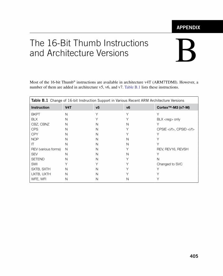
405
BMost of the 16-bit Thumb® instructions are available in architecture v4T (ARM7TDMI). However, a number of them are added in architecture v5, v6, and v7. Table B.1 lists these instructions.
The 16-Bit Thumb Instructions and Architecture Versions
APPENDIX
Table B.1 Change of 16-bit Instruction Support in Various Recent ARM Architecture Versions
Instruction V4T v5 v6 Cortex™-M3 (v7-M)
BKPT N Y Y YBLX N Y Y BLX <reg> onlyCBZ, CBNZ N N N YCPS N N Y CPSIE <i/f>, CPSID <i/f>CPY N N Y YNOP N N N YIT N N N YREV (various forms) N N Y REV, REV16, REVSHSEV N N N YSETEND N N Y NSWI Y Y Y Changed to SVCSXTB, SXTH N N Y YUXTB, UXTH N N Y YWFE, WFI N N N Y

407
CC.1 ExCEption typEs and EnablEs
Appendix
Cortex-M3 Exceptions Quick Reference
Table C.1 Quick Summary of Cortex™-M3 Exception Types and Their Priority Configurations
Exception Type Name Priority (Level Address) Enable
1 Reset –3 Always2 NMI –2 Always3 Hard fault –1 Always4 MemManage fault Programmable
(0xE000ED18)NVIC SHCSR (0xE000ED24) bit[16]
5 Bus fault Programmable (0xE000ED19)
NVIC SHCSR (0xE000ED24) bit[17]
6 Usage fault Programmable (0xE000ED1A)
NVIC SHCSR (0xE000ED24) bit[18]
7–10 — — —11 SVC Programmable
(0xE000ED1F)Always
12 Debug monitor Programmable (0xE000ED20)
NVIC DEMCR (0xE000EDFC) bit[16]
13 — — —14 PendSV Programmable
(0xE000ED22)Always
15 SYSTICK Programmable (0xE000ED23)
SYSTICK CTRLSTAT (0xE000E010) bit[1]
16–255 IRQ Programmable (0xE000E400)
NVIC SETEN (0xE000E100)

408 Appendix C
C.2 staCk ContEnts aftEr ExCEption staCking
Table C.2 Exception Stack Frame
Address Data Push Order
Old SP (N+32)→ (Previously pushed data) —(N+28) PSR 2(N+24) PC 1(N+20) LR 8(N+16) R12 7(N+12) R3 6(N+8) R2 5(N+4) R1 4New SP (N)→ R0 3
Note: If double word stack alignment feature is used and the SP was not double word aligned when the exception occurred, the stack frame top might begin at ([OLD_SP-4] AND 0xFFFFFFF8), and the rest of the table moves one word down.

409
DAppendix
Nested Vectored Interrupt Controller and System Control Block Registers Quick Reference
Table d.1 Interrupt Controller Type Register (0xE000E004)
Bits Name Type Reset Value Description
4:0 INTLINESNUM R — Number of interrupt inputs in steps of 32 0 = 1–32 1 = 33–64 …
Table d.2 Auxiliary Control Register (0xE000E008)
Bits Name Type Reset Value Description
2 DISFOLD R/W 0 When this bit is set, it disables the overlapping of the IT execution cycle with another instruction. The overlapping (called IT folding) is an optimization to allow faster execution of conditional execution.
1 DISDEFWBUF R/W 0 When this bit is set, it disables the use of write buffers within the processor so that an instruction following a store instruction must not start until the store operation is completed. This bit does not affect write buffer outside the processor (e.g., in bus bridge).
0 DISMCYCINT R/W 0 When this bit is set, it disables interruption of multicycle instructions.
Note: The Auxiliary Control register is available from Cortex™-M3 revision 2.
Table d.3 SYSTICK Control and Status Register (0xE000E010)
Bits Name Type Reset Value Description
16 COUNTFLAG R 0 Read as 1 if counter reaches 0 since this is the last time this register is read. Clear to 0 automatically when read or when current counter value is cleared.
2 CLKSOURCE R/W 0 0 = External reference clock (STCLK) 1 = Use core clock
1 TICKINT R/W 0 1 = Enable SYSTICK interrupt generation when SYSTICK timer reaches 0 0 = Do not generate interrupt
0 ENABLE R/W 0 SYSTICK timer enable

410 Appendix d
Table d.4 SYSTICK Reload Value Register (0xE000E014)
Bits Name Type Reset Value Description
23:0 RELOAD R/W 0 Reload value when timer reaches 0.
Table d.5 SYSTICK Current Value Register (0xE000E018)
Bits Name Type Reset Value Description
23:0 CURRENT R/Wc 0 Read to return current value of the timer. Write to clear counter to 0; clearing of current value should also clear COUNTFLAG in SYSTICK Control and Status register.
Table d.6 SYSTICK Calibration Value Register (0xE000E01C)
Bits Name Type Reset Value Description
31 NOREF R — 1 = No external reference clock (STCLK not available) 0 = External reference clock available
30 SKEW R — 1 = Calibration value is not exactly 10 ms 0 = Calibration value is accurate
23:0 TENMS R/W 0 Calibration value for 10 ms. SoC designer should provide this value through Cortex-M3 input signals. If this value is read as 0, it means calibration value is not available.
Table d.7 External Interrupt SETEN Registers (0xE000E100-0xE000E11C)
Address Name Type Reset Value Description
0xE000E100 SETENA0 R/W 0 Enable for external Interrupt #0–#31 bit[0] for Interrupt #0 bit[1] for Interrupt #1 … bit[31] for Interrupt #31
0xE000E104 SETENA1 R/W 0 Enable for external Interrupt #32–#63… … … … …
Table d.8 External Interrupt CLREN Registers (0xE000E180-0xE000E19C)
Address Name Type Reset Value Description
0xE000E180 CLRENA0 R/W 0 Clear Enable for external Interrupt #0–#31bit[0] for Interrupt #0 bit[1] for Interrupt #1 … bit[31] for Interrupt #31
0xE000E184 CLRENA1 R/W 0 Clear Enable for external Interrupt #32–#63… … … … …
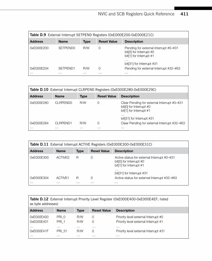
411NVIC and SCB Registers Quick Reference
Table d.9 External Interrupt SETPEND Registers (0xE000E200-0xE000E21C)
Address Name Type Reset Value Description
0xE000E200 SETPEND0 R/W 0 Pending for external Interrupt #0–#31 bit[0] for Interrupt #0 bit[1] for Interrupt #1 …bit[31] for Interrupt #31
0xE000E204 SETPEND1 R/W 0 Pending for external Interrupt #32–#63… … … … …
Table d.10 External Interrupt CLRPEND Registers (0xE000E280-0xE000E29C)
Address Name Type Reset Value Description
0xE000E280 CLRPEND0 R/W 0 Clear Pending for external Interrupt #0–#31 bit[0] for Interrupt #0 bit[1] for Interrupt #1 … bit[31] for Interrupt #31
0xE000E284 CLRPEND1 R/W 0 Clear Pending for external Interrupt #32–#63… … … … …
Table d.11 External Interrupt ACTIVE Registers (0xE000E300-0xE000E31C)
Address Name Type Reset Value Description
0xE000E300 ACTIVE0 R 0 Active status for external Interrupt #0–#31 bit[0] for Interrupt #0 bit[1] for Interrupt #1 … bit[31] for Interrupt #31
0xE000E304 ACTIVE1 R 0 Active status for external Interrupt #32–#63… … … … …
Table d.12 External Interrupt Priority Level Register (0xE000E400-0xE000E4EF; listed as byte addresses)
Address Name Type Reset Value Description
0xE000E400 PRI_0 R/W 0 Priority level external Interrupt #00xE000E401 PRI_1 R/W 0 Priority level external Interrupt #1… … … … …0xE000E41F PRI_31 R/W 0 Priority level external Interrupt #31… … … … …

412 Appendix d
Table d.13 CPU ID Base Register (address 0xE000ED00)
Bits Name Type Reset Value Description
31:24 IMPLEMENTER R 0x41 Implementer code; ARM is 0x4123:20 VARIANT R 0x0/0x1/0x2 Implementation defined variant number19:16 Constant R 0xF Constant15:4 PARTNO R 0xC23 Part number3:0 REVISION R 0x0/0x1 Revision code
Table d.14 Interrupt Control and State Register (0xE000ED04)
Bits Name Type Reset Value Description
31 NMIPENDSET R/W 0 NMI Pended28 PENDSVSET R/W 0 Write 1 to pend system call;
Read value indicates pending status27 PENDSVCLR W 0 Write 1 to clear PendSV pending status26 PENDSTSET R/W 0 Write 1 to pend SYSTICK exception;
Read value indicates pending status25 PENDSTCLR W 0 Write 1 to clear SYSTICK pending status23 ISRPREEMPT R 0 Indicates that a pending interrupt is going to be
active in next step (for debug).22 ISRPENDING R 0 External Interrupt Pending (excluding system
exceptions like NMI for fault)21:12 VECTPENDING R 0 Pending ISR number11 RETTOBASE R 0 Set to 1 when the processor is running an
exception handler and will return to thread level if interrupt return and no other exceptions pending
8:0 VECTACTIVE R 0 Current running interrupt service routine
Table d.15 Vector Table Offset Register (address 0xE000ED08)
Bits Name Type Reset Value Description
29 TBLBASE R/W 0 Table base in Code (0) or RAM (1) memory region28:7 TBLOFF R/W 0 Table offset value from Code region or RAM region
Table d.16 Application Interrupt and Reset Control Register (address 0xE000ED0C)
Bits Name Type Reset Value Description
31:16 VECTKEY R/W — Access key; 0x05FA must be written to this field to write to this register, otherwise the write will be ignored. The read back value is 0xFA05.
15 ENDIANESS R — Indicates endianness for data: 1 for big endian (BE8) and 0 for little endian. This can only change after a reset.

413NVIC and SCB Registers Quick Reference
Table d.16 Application Interrupt and Reset Control Register (address 0xE000ED0C) Continued
Bits Name Type Reset Value Description
10:8 PRIGROUP R/W 0 Priority group
2 SYSRESETREQ W — Request chip control logic to generate a reset
1 VECTCLRACTIVE W — Clear all active state information for exceptions; typically used in debug or OS to allow system to recover from system error (Reset is safer).
0 VECTRESET W — Reset Cortex-M3 (except debug logic); but this will not reset circuits outside the processor.
Table d.17 System Control Register (0xE000ED10)
Bits Name Type Reset Value Description
4 SEVONPEND R/W 0 Send Event on Pending. Wake up from WFE if a new interrupt is pended regardless of whether the interrupt has priority higher than current level.
3 Reserved — — —2 SLEEPDEEP R/W 0 Enable SLEEPDEEP output signal when entering
sleep mode.1 SLEEPONEXIT R/W 0 Enable Sleep on Exit feature0 Reserved — — —
Table d.18 Configuration Control Register (0xE000ED14)
Bits Name Type Reset Value Description
9 STKALIGN R/W 0 or 1 Force exception stacking start in double word aligned address. This bit is reset as zero on Cortex-M3 revision 1, and is reset as one on revision 2. Revision 0 does not have this feature.
8 BFHFNMIGN R/W 0 Ignore data bus fault during hard fault and NMI handlers.
7:5 Reserved — — Reserved4 DIV_0_TRP R/W 0 Trap on divide by 03 UNALIGN_TRP R/W 0 Trap on unaligned accesses2 Reserved — — Reserved1 USERSETMPEND R/W 0 If set to 1, allow user code to write to
Software Trigger Interrupt register0 NONBASETHRDENA R/W 0 Nonbase Thread Enable. If set to 1, allows
exception handler to return to thread state at any level by controlling return value.

414 Appendix d
Table d.19 System Exceptions Priority Level Register (0xE000ED18–0xE000ED23; listed as byte addresses)
Address Name Type Reset Value Description
0xE000ED18 PRI_4 R/W 0 Priority level for memory management fault0xE000ED19 PRI_5 R/W 0 Priority level for bus fault0xE000ED1A PRI_6 R/W 0 Priority level for usage fault0xE000ED1B — — — —0xE000ED1C — — — —0xE000ED1D — — — —0xE000ED1E — — — —0xE000ED1F PRI_11 R/W 0 Priority level for SVC0xE000ED20 PRI_12 R/W 0 Priority level for debug monitor0xE000ED21 — — — —0xE000ED22 PRI_14 R/W 0 Priority level for PendSV0xE000ED23 PRI_15 R/W 0 Priority level for SYSTICK
Table d.20 System Handler Control and State Register (0xE000ED24)
Bits Name Type Reset Value Description
18 USGFAULTENA R/W 0 Usage Fault Handler Enable17 BUSFAULTENA R/W 0 Bus Fault Handler Enable16 MEMFAULTENA R/W 0 Memory Management Fault Enable15 SVCALLPENDED R/W 0 SVC pended; SVC is started but was replaced
by a higher priority exception14 BUSFAULTPENDED R/W 0 Bus fault pended; bus fault is started, but was
replaced by a higher priority exception13 MEMFAULTPENDED R/W 0 Memory management fault pended; memory
management fault started but was replaced by a higher priority exception
12 USGFAULTPENDED R/W 0 Usage fault pended; usage fault started but was replaced by a higher-priority exceptiona
11 SYSTICKACT R/W 0 Read as 1 if SYSTICK exception is active10 PENDSVACT R/W 0 Read as 1 if PendSV exception is active8 MONITORACT R/W 0 Read as 1 if debug monitor exception is active7 SVCALLACT R/W 0 Read as 1 if SVC exception is active3 USGFAULTACT R/W 0 Read as 1 if usage fault exception is active1 BUSFAULTACT R/W 0 Read as 1 if bus fault exception is active0 MEMFAULTACT R/W 0 Read as 1 if memory management fault is active
a Bit 12 (USGFAULTPENDED) is not available on revision 0 of Cortex-M3 processor.

415NVIC and SCB Registers Quick Reference
Table d.21 Memory Management Fault Status Register (0xE000ED28; byte size)
Bits Name Type Reset Value Description
7 MMARVALID — 0 Indicates MMAR is valid6:5 — — — —4 MSTKERR R/Wc 0 Stacking error3 MUNSTKERR R/Wc 0 Unstacking error2 — — — —1 DACCVIOL R/Wc 0 Data access violation0 IACCVIOL R/Wc 0 Instruction access violation
Table d.22 Bus Fault Status Register (0xE000ED29; byte size)
Bits Name Type Reset Value Description
7 BFARVALID — 0 Indicates BFAR is valid6:5 — — — —4 STKERR R/Wc 0 Stacking error3 UNSTKERR R/Wc 0 Unstacking error2 IMPREISERR R/Wc 0 Imprecise data access violation1 PRECISERR R/Wc 0 Precise data access violation0 IBUSERR R/Wc 0 Instruction access violation
Table d.23 Usage Fault Status Register (0xE000ED2A; half word size)
Bits Name Type Reset Value Description
9 DIVBYZERO R/Wc 0 Indicates divide by zero takes place (can only be set if DIV_0_TRP is set)
8 UNALIGNED R/Wc 0 Indicates unaligned access takes place (can only be set if UNALIGN_TRP is set)
7:4 — — — —3 NOCP R/Wc 0 Attempts to execute a coprocessor instruction2 INVPC R/Wc 0 Attempts to do exception with bad value in
EXC_RETURN number1 INVSTATE R/Wc 0 Attempts to switch to invalid state (e.g., ARM)0 UNDEFINSTR R/Wc 0 Attempts to execute an undefined instruction

416 Appendix d
Table d.25 Debug Fault Status Register (0xE000ED30)
Bits Name Type Reset Value Description
4 EXTERNAL R/Wc 0 EDBGRQ signal asserted3 VCATCH R/Wc 0 Vector fetch occurred2 DWTTRAP R/Wc 0 DWT match occurred1 BKPT R/Wc 0 BKPT instruction executed0 HALTED R/Wc 0 Halt requested in NVIC
Table d.26 Memory Manage Address Register MMAR (0xE000ED34)
Bits Name Type Reset Value Description
31:0 MMAR R — Address that caused memory manage fault
Table d.27 Bus Fault Manage Address Register BFAR (0xE000ED38)
Bits Name Type Reset Value Description
31:0 BFAR R — Address that caused bus fault
Table d.28 Auxiliary Fault Status Register (0xE000ED3C)
Bits Name Type Reset Value Description
31:0 Vendor controlled R/Wc 0 Vendor controlled (optional)
Table d.29 MPU Type Register (0xE000ED90)
Bits Name Type Reset Value Description
23:16 IREGION R — Number Instruction region Because ARM v7-M architecture uses a unified MPU, this is always 0.
15:8 DREGION R — Number of regions supported by this MPU0 SEPARATE R — This is always 0 as the MPU is always unified.
Table d.24 Hard Fault Status Register (0xE000ED2C)
Bits Name Type Reset Value Description
31 DEBUGEVT R/Wc 0 Indicates hard fault is triggered by debug event30 FORCED R/Wc 0 Indicates hard fault is taken because of bus fault/
memory management fault/usage fault29:2 — — — —1 VECTBL R/Wc 0 Indicates hard fault is caused by failed vector fetch0 — — — —

417NVIC and SCB Registers Quick Reference
Table d.30 MPU Control Register (0xE000ED94)
Bits Name Type Reset Value Description
2 PRIVDEFENA R/W 0 Privileged Default memory map enable1 HFNMIENA R/W 0 If set to 1, it enables MPU during hard fault
handler and NMI handler. Otherwise, the MPU is not enabled for hard fault handler and NMI.
0 ENABLE R/W 0 Enable the MPU if set to 1.
Table d.31 MPU Region Number Register (0xE000ED98)
Bits Name Type Reset Value Description
7:0 REGION R/W 0 Select which region is being programmed
Table d.32 MPU Region Base Address Register (0xE000ED9C)
Bits Name Type Reset Value Description
31:N ADDR R/W 0 Base address of the region. N is dependent on the region size.
4 VALID R/W 0 If this is 1, the region defined in bit[3:0] will be used in this programming step, otherwise, the region selected by MPU Region Number register is used.
3:0 REGION R/W 0 This field overrides MPU Region Number register if VALID is 1, otherwise, this is ignored.
Table d.33 MPU Region Base Attribute and Size Register (0xE000EDA0)
Bits Name Type Reset Value Description
31:29 Reserved — —28 XN R/W 0 Instruction access disable (1 = Disable)27 Reserved — —26:24 AP R/W 000 Data access permission field23:22 Reserved — —21:19 TEX R/W 000 Type extension field18 S R/W — Shareable17 C R/W — Cacheable16 B R/W — Bufferable15:8 SRD R/W 0x00 Sub region disable7:6 Reserved — —5:1 REGION SIZE R/W — MPU protection region size0 ENABLE R/W 0 Region enable

418 Appendix d
Table d.34 MPU Alias Registers (0xE000EDA4–0xE000EDB8)
Address Name Description
0xE000EDA4 Alias of D9C MPU Alias 1 Region Base Address register0xE000EDA8 Alias of DA0 MPU Alias 1 Region Attribute and Size register0xE000EDAC Alias of D9C MPU Alias 2 Region Base Address register0xE000EDB0 Alias of DA0 MPU Alias 2 Region Attribute and Size register0xE000EDB4 Alias of D9C MPU Alias 3 Region Base Address register0xE000EDB8 Alias of DA0 MPU Alias 3 Region Attribute and Size register
Table d.35 Debug Halting Control and Status Register (0xE000EDF0)
Bits Name Type Reset Value Description
31:16 KEY W — Debug key; value of 0xA05F must be written to this field to write to this register, otherwise, the write will be ignored.
25 S_RESET_ST R — Core has been reset or is being reset. This bit is cleared on read.
24 S_RETIRE_ST R — Instruction is completed since last read. This bit is cleared on read.
19 S_LOCKUP R — When this bit is 1, the core is in locked-up state.
18 S_SLEEP R — When this bit is 1, the core is in sleep mode.17 S_HALT R — When this bit is 1, the core is halted.16 S_REGRDY R — Register read/write operation is completed.15:6 Reserved — — Reserved5 C_SNAPSTALL R/W — Used to break a stalled memory access4 Reserved — — Reserved3 C_MASKINTS R/W — Mask interrupts while stepping; can only be
modified when the processor is halted.2 C_STEP R/W — Single step the processor, valid only if
C_DEBUGEN is set.1 C_HALT R/W — Halt the processor core, valid only if
C_DEBUGEN is set.0 C_DEBUGEN R/W — Enable halt mode debug

419NVIC and SCB Registers Quick Reference
Table d.36 Debug Core Register Selector Register (0xE000EDF4)
Bits Name Type Reset Value Description
16 REGWnR W — Direction of data transfer Write = 1, Read = 0
15:5 Reserved — — —4:0 REGSEL W —
Register to be accessed 00000 = R0 00001 = R1 … 01111 = R15 10000 = xPSR/Flags 10001 = MSP (Main Stack Pointer) 10010 = PSP (Process Stack Pointer) 10100 = Special registers: [31:24] CONTROL, [23:16] FAULTMASK, [15:8] BASEPRI, [7:0] PRIMASK. Others values are reserved
Table d.37 Debug Core Register Data Register (0xE000EDF8)
Bits Name Type Reset Value Description
31:0 Data R/W — Data register to hold register read result or to write data into the selected register.
Table d.38 Debug Exception and Monitor Control Register (0xE000EDFC)
Bits Name Type Reset Value Description
24 TRCENA R/W 0 Trace system enable; to use DWT, ETM, ITM, and TPIU, this bit must be set to 1.
23:20 Reserved — — Reserved19 MON_REQ R/W 0 Indication that the debug monitor is caused by
a manual pending request rather than hardware debug events.
18 MON_STEP R/W 0 Single step the processor; valid only if MON_EN is set.
17 MON_PEND R/W 0 Pend the monitor exception request; the core will enter monitor exception when priority is allowed.
16 MON_EN R/W 0 Enable the debug monitor exception15:11 Reserved — — Reserved
Continued

420 Appendix d
Table d.39 Software Trigger Interrupt Register (0xE000EF00)
Bits Name Type Reset Value Description
8:0 INTID W — Writing the interrupt number sets the pending bit of the interrupt.
Table d.40 NVIC Peripheral ID Registers (0xE000EFD0-0xE000EFFC)
Address Name Type Reset Value Description
0xE000EFD0 PERIPHID4 R 0x04 Peripheral ID register0xE000EFD4 PERIPHID5 R 0x00 Peripheral ID register0xE000EFD8 PERIPHID6 R 0x00 Peripheral ID register0xE000EFDC PERIPHID7 R 0x00 Peripheral ID register0xE000EFE0 PERIPHID0 R 0x00 Peripheral ID register0xE000EFE4 PERIPHID1 R 0xB0 Peripheral ID register0xE000EFE8 PERIPHID2 R 0x0B/0x1B/0x2B Peripheral ID register0xE000EFEC PERIPHID3 R 0x00 Peripheral ID register0xE000EFF0 PCELLID0 R 0x0D Component ID register0xE000EFF4 PCELLID1 R 0xE0 Component ID register0xE000EFF8 PCELLID2 R 0x05 Component ID register0xE000EFFC PCELLID0 R 0xB1 Component ID register
Note: PERIPHID2 value is 0x0B for Cortex-M3 revision 0, 0x1B for revision 1, and 0x2B for revision 2.
Table d.38 Debug Exception and Monitor Control Register (0xE000EDFC) Continued
Bits Name Type Reset Value Description
10 VC_HARDERR R/W 0 Debug trap on hard faults9 VC_INTERR R/W 0 Debug trap on interrupt/exception service
errors8 VC_BUSERR R/W 0 Debug trap on bus faults7 VC_STATERR R/W 0 Debug trap on usage fault state errors6 VC_CHKERR R/W 0 Debug trap on usage fault enabled checking
errors (e.g., unaligned, divide by zero)5 VC_NOCPERR R/W 0 Debug trap on usage fault; no coprocessor
errors4 VC_MMERR R/W 0 Debug trap on memory management fault3:1 Reserved — — Reserved0 VC_CORERESET R/W 0 Debug trap on core reset

421
E.1 OvErviEwOne of the challenges of using the Cortex™-M3 is to locate problems when the program goes wrong. The Cortex-M3 processor provides a number of Fault Status registers to assist in troubleshooting (see Table E.1).
The MMSR, BFSR, and UFSR registers can be accessed in one go using a word transfer instruc-tion. In this situation, the combined fault status register is called the Configurable Fault Status register (CFSR) (see Figure E.1).
For users of CMSIS compliant device drivers, these Fault Status registers can be accessed using the following symbols:
• SCB->CFSR: Configurable Fault Status register• SCB->HFSR: Hard Fault Status register• SCB->DFSR: Debug Fault Status register• SCB->AFSR: Auxiliary Fault Status register
Another important piece of information is the stacked program counter (PC). This is located in memory address [SP + 24] when a fault exception handler is entered. Because there are two stack point-ers in the Cortex-M3, the fault handler might need to determine which stack pointer was used before obtaining the stacked PC.
In addition, for bus faults and memory management faults, you might also be able to determine the address that caused the fault. This is done by accessing the MemManage (Memory Management) Fault Address register (MMAR) and the Bus Fault Address register (BFAR). The contents of these two registers are only valid when the MMAVALID bit (in MMSR) or BFARVALID bit (in BFSR) is set. The MMAR and BFAR are physically the same register, so only one of them can be valid at a time (see
Table E.2).For users of CMSIS compliant device drivers, these Fault Address registers can be accessed using
the following symbols:
• SCB->MMAR: MemManage Fault Address register• SCB->BFAR: Bus Fault Address register
Finally, the link register (LR) value when entering the fault handler might also provide hints about the cause of the fault. In the case of faults caused by invalid EXC_RETURN values, the value of LR when the fault handler is entered shows the previous LR value when the fault occurred. Fault handler can report the faulty LR value, and software programmers can then use this information to check why the LR ends up with an illegal return value.
Appendix
Cortex-M3 Troubleshooting Guide E

422 Appendix e
E.2 DEvElOping Fault HanDlErsIn most cases, fault handlers for development and for real running systems differ from one another. For software development, the fault handler should focus on reporting the type of error, whereas the fault handler for running systems will likely focus on system recovery actions. Here, we cover only the fault reporting because system recovery actions highly depend on design type and requirements.
In complex software, instead of outputting the results inside the fault handler, the contents of these registers can be copied to a memory block and then PendSV can be used to report the fault details later. This avoids potential faults in display or outputting routines causing lockup. For simple applications this might not matter, and the fault details can be output directly within the fault handler routine.
FigurE E.1
Accessing Fault Status Registers.
0xE000ED28
0xE000ED2C
0xE000ED30
0xE000ED3C
UFSR BFSR MFSR
HFSR
DFSR
AFSR
0781516Bit 31
CFSR
Table e.2 Fault Address Registers on Cortex-M3
Address Register Full Name Size
0xE000ED34 MMAR MemManage Fault Address register Word0xE000ED38 BFAR Bus Fault Address register Word
Table e.1 Fault Status Registers on Cortex-M3
Address Register Full Name Size
0xE000ED28 MMSR MemManage Fault Status register Byte0xE000ED29 BFSR Bus Fault Status register Byte0xE000ED2A UFSR Usage Fault Status register Half word0xE000ED2C HFSR Hard Fault Status register Word0xE000ED30 DFSR Debug Fault Status register Word0xE000ED3C AFSR Auxiliary Fault Status register Word

423Cortex-M3 Troubleshooting Guide
E.2.1 report Fault status registersThe most basic step of a fault handler is to report the Fault Status register values. These include the following:
UFSR•BFSR•MMSR•HFSR•DFSR•AFSR (optional)•
E.2.2 report stacked pC and Other stacked registersIn a fault handler, the step for getting the stacked PC is similar to the SVC example in this book.
This process can be carried out in assembly language as follows:
TST LR, #0x4 ; Test EXC_RETURN number in LR bit 2ITTEE EQ ; if zero (equal) thenMRSEQ R0, MSP ; Main Stack was used, put MSP in R0LDREQ R0,[R0,#24] ; Get stacked PC from stack.MRSNE R0, PSP ; else, Process Stack was used, put PSP in R0LDRNE R0,[R0,#24] ; Get stacked PC from stack.
Most Cortex-M3 developers use C for their projects. However, in C, it is difficult to locate and directly access the stack frame (stacked register values) as you cannot obtain the stack point value in C. To report the stack frame contents in your fault handler in C, you need to use a short assembly code to obtain stack point value, and then pass it to the fault reporting function in C as a parameter (see Figure E.2). The mechanism is identical to the SVC example in Chapter 12. The following example
FigurE E.2
Getting the Value of a Stacked PC from Stack Memory.
Determine which stack wasused in calling process using
the LR value (bit[2])
Stacked wasdone using MSP
Stacking wasdone using PSP
Get stacked PC fromstack memory
Bit 2 5 0
Bit 2 5 1

424 Appendix e
uses embedded assembler, which can work with RealView Development Suite (RVDS) and Keil Real-View Microcontroller Development Kit (MDK-ARM).
The first part of the program is an assembly wrapper. The vector table should have the starting address of this wrapper code in the hard fault entry. This wrapper code copies the correct stack pointer value into R0, and passes it to the C function as a parameter.
// hard fault handler wrapper in assembly// it extract the location of stack frame and pass it// to handler in C as pointer.__asm void hard_fault_handler_asm(void){TST LR, #4ITE EQMRSEQ R0, MSPMRSNE R0, PSPB __cpp(hard_fault_handler_c )}
The second part of the handler is in C. Here, we demonstrate how the stacked register contents and the Fault Status registers can be accessed.
// hard fault handler in C,// with stack frame location as input parametervoid hard_fault_handler_c(unsigned int * hardfault_args){unsigned int stacked_r0;unsigned int stacked_r1;unsigned int stacked_r2;unsigned int stacked_r3;unsigned int stacked_r12;unsigned int stacked_lr;unsigned int stacked_pc;unsigned int stacked_psr;
stacked_r0 = ((unsigned long) hardfault_args[0]);stacked_r1 = ((unsigned long) hardfault_args[1]);stacked_r2 = ((unsigned long) hardfault_args[2]);stacked_r3 = ((unsigned long) hardfault_args[3]);
stacked_r12 = ((unsigned long) hardfault_args[4]);stacked_lr = ((unsigned long) hardfault_args[5]);stacked_pc = ((unsigned long) hardfault_args[6]);stacked_psr = ((unsigned long) hardfault_args[7]);
printf ("[Hard fault handler]\n");printf ("R0 = %x\n", stacked_r0);printf ("R1 = %x\n", stacked_r1);printf ("R2 = %x\n", stacked_r2);printf ("R3 = %x\n", stacked_r3);printf ("R12 = %x\n", stacked_r12);printf ("LR = %x\n", stacked_lr);printf ("PC = %x\n", stacked_pc);

425Cortex-M3 Troubleshooting Guide
printf ("PSR = %x\n", stacked_psr);printf ("BFAR = %x\n", (*((volatile unsigned long *)(0xE000ED38))));printf ("CFSR = %x\n", (*((volatile unsigned long *)(0xE000ED28))));printf ("HFSR = %x\n", (*((volatile unsigned long *)(0xE000ED2C))));printf ("DFSR = %x\n", (*((volatile unsigned long *)(0xE000ED30))));printf ("AFSR = %x\n", (*((volatile unsigned long *)(0xE000ED3C))));
exit(0); // terminate
return;}
Please note that this handler will not work correctly if the stack pointer is pointing to an invalid memory region (e.g., because of stack overflow). This affects all C code as stack is required in C func-tions in most cases.
To help with debugging, we should also create a disassembled code list file so that we can locate the problem easily.
E.2.3 read Fault address registerThe Fault Address register can be erased after the MMARVALID or BFARVALID is cleared. To cor-rectly access the Fault Address register, the following procedure should be used:
Read BFAR/MMAR.1. Read BFARVALID/MMARVALID. If it is 0, the BFAR/MMAR read should be discarded.2. Clear BFARVALID/MMARVALID.3.
The reason for this procedure instead of reading valid bits first is to prevent a fault handler being preempted by another higher-priority fault handler after the valid bit is read, which could lead to the following erroneous fault-reporting sequence:
Read BFARVALID/MMARVALID.1. Valid bit is set, going to read BFAR/MMAR.2. Higher-priority exception preempts existing fault handler, which generates another fault, causing 3. another fault handler to be executed.The higher-priority fault handler clears the BFARVALID/MMARVALID bit, causing the BFAR/4. MMAR to be erased.After returning to the original fault handler, the BFAR/MMAR is read, but now the content is 5. invalid and leads to incorrect reporting of the fault address.
Therefore, it is important to read the BFARVALID/MMARVALID after reading the Fault Address register to ensure that the address register content is valid.
E.2.4 Clear Fault status BitsAfter the fault reporting is done, the fault status bit in the FSR should be cleared so that next time the fault handler is executed, the previous faults will not confuse the fault handler. In addition, if the fault address valid bit is not clear, the Fault Address register will not get an update for the next fault.

426 Appendix e
E.2.5 OthersIt is often necessary to save the contents of LR in the beginning of a fault handler. However, if the fault is caused by a stack error, pushing the LR to stack might just make things worst. As we know, R0–R3 and R12 should already been saved, so that we could copy LR to one of these registers before doing any function calls.
E.3 unDErstanDing tHE CausE OF tHE FaultAfter obtaining the information we need, we can establish the cause of the problem. Tables E.3 through E.7 list some of the common reasons that faults occur.
Table e.4 Bus Fault Status Register
Bit possible Causes
BFARVALID (bit 7) Indicates the Bus Fault Address register contains a valid bus fault address.STKERR (bit 4) Error occurred during stacking (starting of exception).
1. Stack pointer is corrupted.2. Stack size became too large, reaching an undefined memory region.3. PSP is used but not initialized.
Table e.3 MemManage Fault Status Register
Bit Possible Causes
MMARVALID (bit 7) Indicates the Memory Manage Address register (MMAR) contains a valid fault addressing value.
MSTKERR (bit 4) Error occurred during stacking (starting of exception).1. Stack pointer is corrupted.2. Stack size is too large, reaching a region not defined by the MPU or disallowed
in the MPU configuration.MUNSTKERR (bit 3) Error occurred during unstacking (ending of exception). If there was no error
stacking but error occurred during unstacking, it might be because of the following reasons:1. Stack pointer was corrupted during exception.2. MPU configuration was changed by exception handler.
DACCVIOL (bit 1) Violation to memory access protection, which is defined by MPU setup. For example, user application trying to access privileged-only region.
IACCVIOL (bit 0) 1. Violation to memory access protection, which is defined by MPU setup. For example, user application trying to access privileged-only region. Stacked PC might be able to locate the code that has caused the problem.
2. Branch to nonexecutable regions.3. Invalid exception return code.4. Invalid entry in exception vector table. For example, loading of an executable
image for traditional ARM core into the memory, or exception happened before vector table was set.
5. Stacked PC corrupted during exception handling.

427Cortex-M3 Troubleshooting Guide
Table e.4 Bus Fault Status Register continued
Bit possible Causes
UNSTKERR(bit 3) Error occurred during unstacking (ending of exception). If there was no error stacking but error occurred during unstacking, it might be that the stack pointer was corrupted during exception.
IMPRECISERR (bit 2) Bus error during data access. Bus error could be caused by the device not being initialized, access of privileged-only device in user mode, or the transfer size is incorrect for the specific device.
PRECISERR (bit 1) Bus error during data access. The fault address may be indicated by BFAR. A bus error could be caused by the device not being initialized, access of privileged-only device in user mode, or the transfer size is incorrect for the specific device.
IBUSERR (bit 0) 1. Branch to invalid memory regions; for example, caused by incorrect function pointers in program code.
2. I nvalid exception return code; for example, a stacked EXC_RETURN code is corrupted, and as a result, an exception return incorrectly treated as a branch.
3. Invalid entry in exception vector table. For example, loading of an executable image for traditional ARM core into the memory, or exception, happens before the vector table is set.
4. Stacked PC corrupted during function calls.5. Access to NVIC or SCB in user mode (nonprivileged).
Table e.5 Usage Fault Status Register
Bit possible Causes
DIVBYZERO (bit 9) Divide by 0 takes place and DIV_0_TRP is set. The code causing the fault can be located using stacked PC.
UNALIGNED (bit 8) Unaligned access attempted with UNALIGN_TRP is set. The code causing the fault can be located using stacked PC.
NOCP (bit 3) Attempt to execute a coprocessor instruction. The code causing the fault can be located using stacked PC.
INVPC (bit 2) 1. Invalid value in EXC_RETURN number during exception return. For example, a. Return to thread with EXC_RETURN = 0xFFFFFFF1 b. Return to handler with EXC_RETURN = 0xFFFFFFF9 To investigate the problem, the current LR value provides the value of LR at the failing exception return.2. Invalid exception active status. For example, a. Exception return with exception active bit for the current exception already
cleared. Possibly caused by use of VECTCLRACTIVE, or clearing of exception active status in NVIC SHCSR.
b. Exception return to thread with one or more exception active bits still active.3. Stack corruption causing the stacked IPSR to be incorrect. For INVPC fault, the stacked PC shows the point where the faulting exception
interrupted the main/preempted program. To investigate the cause of the problem, it is best to use exception trace feature in the DWT.
4. ICI/IT bit invalid for current instruction. This can happen when a multiple-load/store instruction gets interrupted and, during the interrupt handler, the stacked PC is modified. When the interrupt return takes place, the nonzero ICI bit is applied to an instruction that does not use ICI bits. The same problem can also happen because of corruption of stacked PSR.
continued

428 Appendix e
Table e.5 Usage Fault Status Register continued
Bit possible Causes
INVSTATE (bit 1) 1. Loading branch target address to PC with LSB equals 0. Stacked PC should show the branch target.
2. LSB of vector address in vector table is 0. Stacked PC should show the starting of exception handler.
3. Stacked PSR corrupted during exception handling, so after the exception the core tries to return to the interrupted code in ARM state.
UNDEFINSTR (bit 0) 1. Use of instructions not supported in Cortex-M3.2. Bad/corrupted memory contents.3. Loading of ARM object code during link stage. Checks compile steps.4. Instruction align problem. For example, if GNU Tool chain is used, omitting
of .align after .ascii might cause next instruction to be unaligned (start in odd memory address instead of halfword addresses).
Table e.6 Hard Fault Status Register
Bit possible Causes
DEBUGEVF (bit 31) Fault is caused by debug event:1. Breakpoint/watchpoint events.2. If the hard fault handler is executing, it might be caused by execution of BKPT
without enable monitor handler (MON_EN = 0) and halt debug is not enabled (C_DEBUGEN = 0). By default, some C compilers might include semihosting code that use BKPT.
FORCED (bit 30) 1. Trying to run SVC/BKPT within SVC/monitor or another handler with same or higher priority.
2. A fault occurred if the corresponding handler is disabled or cannot be started because another exception with the same or higher priority is running, or because exception mask is set.
VECTBL (bit 1) Vector fetch failed. It could be caused by1. Bus fault at vector fetch.2. Incorrect vector table offset setup.
Table e.7 Debug Fault Status Register
Bit possible Causes
EXTERNAL (bit 4) EDBGRQ signal has been asserted.VCATCH (bit 3) Vector catch event has occurred.DWTTRAP (bit 2) DWT watchpoint event has occurred.BKPT (bit 1) 1. Breakpoint instruction is executed.
2. FPB unit generated a breakpoint event.In some cases, BKPT instructions are inserted by C startup code as part of the semihosting debugging setup. This should be removed for a real application code. Please refer to your compiler document for details.
HALTED (bit 0) Halt request in NVIC.

429Cortex-M3 Troubleshooting Guide
E.4 OtHEr pOssiBlE prOBlEmsA number of other common problems are in Table E.8.
Table e.8 Other Possible Problems
Situations possible Causes
No program execution Vector table could be set up incorrectly.1. Located in incorrect memory location.2. LSB of vectors (including hard fault handler) is not set to 1.3. Use of branch instruction (as in vector table in traditional ARM
processor) in the vector table.Please generate a disassembly code listing to check if the vector table is set up correctly.
Program crashes after a few numbers of instructions
Possibly caused by incorrect endian setting, or incorrect stack pointer setup (check vector table), oruse of C object library for traditional ARM processor (ARM code instead of Thumb® code). The offending C object library code could be part of the C startup routine. Please check compiler and linker options to ensure that Thumb or Thumb-2 library files are used.
Processor does not enter sleep mode when WFE is executed
A WFE instruction does not always result in sleep. If the internal event register was set before the WFE instruction, it will clear the event register and act as NOP. Therefore, in normal coding WFE should be used with a loop.
Processor stops executing unexpectedly
When sleep-on-exit feature is enabled, the processor enters sleep mode when returning from exception handler to thread mode, even if no WFI or WFE instructions are used.
Unexpected SEVONPEND behavior The SEVONPEND in the NVIC System Control register enables a disabled interrupt to wake up the processor from WFE, but not WFI. The wake up event is generated only at a new pending of an interrupt. If the interrupt pending status was already set before execution of WFE, arrival of a new interrupt request will not generate the wake up event and hence will not wake up the processor.
Interrupt priority level not working as expected
Unlike many other processors, the Cortex-M3 processor uses value 0 for highest programmable exception priority level. The larger the priority level value, the lower the priority is.
When programming the priority level registers for interrupt, make sure the priority values are written to the implemented bits of the registers. The least significant bits of the priority level registers are not implemented.
Most Cortex-M3 microcontrollers are either 3 bits (8 levels) or 4 bits (16 levels). When there is less than 8 bits of priority level, the LSBs are not implemented. So, if you write priority level values like 0x03, 0x07, and so forth to these registers, the value will become 0x00.
continued

430 Appendix e
Table e.8 Other Possible Problems continued
Situations possible Causes
SVC instruction result in fault exception The Cortex-M3 processor does not support recursive exception—an exception cannot preempt unless it is higher priority than the current level. As a result, you cannot use SVC within an SVC, hard fault or NMI handler, or any other exception handlers which have the same or higher priority than the SVC exception.
Parameters passing to SVC corrupted When passing parameters to exception handlers like SVC, the extraction of parameters (R0–R3) should be carried by getting the parameters from the stack frame instead of using values on the register bank. This is because there could be a chance that another exception was processed just before entering the SVC (new arrival exception case).
Because the other exception handler can change R0–R3, R12 (AAPCS does not require a C function to keep R0–R3, R12 unchanged), the values of R0–R3 and R12 can be undefined when entering the SVC handler. To obtain the parameters correctly, the stacked data should be used. This involved using a simple SVC wrapper in assembly to extract the correct stack pointer and pass it on to the C handler as a C pointer. Example code of this can be found in chapter 11 of this book and ARM application note AN179.
A similar arrangement can be found in returning data from the exception handler to the interrupted program. The handler should store the return data into the stack frame. Otherwise, the value in the register bank will be overwritten during unstacking.
SYSTICK exception occur after clearing TICKINT
The TICKINT bit in the SYSTICK Control and Status register enables and disables the generation of SYSTICK exception. However, if the SYSTICK exception is already in pending state, clearing of TICKINT will not stop the SYSTICK exception from getting fired. To ensure the SYSTICK exception will not be generated, you need to clear TICKINT and the SYSTICK pending status in the Interrupt Control and Status register in the NVIC.
JTAG locked out In many Cortex-M3-based microcontrollers, the JTAG and I/O pins are shared. If the I/O functions for these pins are enabled right in the start of the program, you could find that you will not be able to debug or erase the Flash again.
Unexpected extra interrupt Some microcontrollers have a write buffer in the bus bridge for the peripheral bus. This makes it possible for an exception handler to clear a peripheral interrupt by writing to the peripherals, exiting the handler, and then entering the interrupt again as the peripheral cannot deassert the interrupt request fast enough. There are several work-arounds for this problem:1. The interrupt service routine (ISR) could carry out a dummy
access to the peripheral before exception exit. However, this can increase the duration of the ISR.
2. The clearing of the interrupt can be moved to the beginning of the ISR so that the interrupt is cleared before the ISR end. This might not work if the ISR duration is shorter than the buffered write delay, so extensive testing should be carried out for various peripheral clock ratios.

431Cortex-M3 Troubleshooting Guide
Table e.8 Other Possible Problems continued
Situations possible Causes
Problem with using the normal interrupt as software interrupt
Some users might intend to use unassigned exception types available in NVIC for software interrupt functions. However, the external interrupt and the PendSV exceptions are imprecise. That means the exception handler might not happen immediately after pending it. To handle this, a polling loop can be used to ensure that the exception is carried out.
Unexpected BLX or BX instructions which switched to ARM state
For users of GNU assembler, if a function symbol is from a different file, you need to ensure the function name is declared as a function:
.text
.global my_function_name
.type my_function_name, %function
Otherwise, a branch or call to this function might result in accidental switching to ARM state.
In addition, during linking stage, you might need “-mcortex-m3 -mthumb” options for the GNU linker. Otherwise, the GNU linker might pull in the wrong version of C library code.
Unexpected disabling of interrupt The behavior of the Cortex-M3 and ARM7TDMI processors are different regarding exception return. In ARM7TDMI, if the interrupt is disabled inside an interrupt handler, it will be automatically reenabled at exception return due to restore of CPSR (I bit).
For the Cortex-M3 processor, if you disable interrupts manually using PRIMASK (e.g., “CPSID I” instruction or __disable_irq( )), you will need to reenable it at a later stage inside the interrupt handler. Otherwise, the PRIMASK register will remain set after exception return and will block all interrupts from occuring.
Unexpected unaligned accesses The Cortex-M3 processor supports unaligned transfers on single load/store. Normally C compilers do not generate unaligned transfer except for packed structures and manual manipulation of pointers. For programming in assembly language, it could be a bigger issue as a user might accidentally use unaligned transfers and not know it.
For example, when a program reads a peripheral with word transfer of an unaligned address, the lowest two bits of the addresses might be ignored when using other ARM processors (as the AHB to APB bridge might force these two bits to 0). In the case of the Cortex-M3 processor, if the same software code is used, it will divide the unaligned transfer into multiple aligned transfers. This could end up with different results. Equally, issues can be found when porting software for the Cortex-M3 processor to other ARM processors that do not support unaligned transfers.
It is easy to detect if the software generates unaligned transfers. This can be done by setting the UNALIGN_TRP bit in the NVIC Configuration Control register in the System Control Block. By doing this, a usage fault will be triggered when an unaligned transfer happens, and you can then eliminate all unexpected unaligned transfers.

433
FF.1 ExamplE linkEr Script For cortEx-m3The following linker script is modified from a generic linker script included in CodeSourcery G++ Lite (generic-m.ld), which is the target for Cortex™-M3 processors. This linker script assumes that the CS3 start up sequence and vector table is used, and therefore, it is toolchain specific. For other GNU C compilers, please refer to the documentation and examples provided in the package.
[cortexm3.ld – Used in Example 5 and Example 6 of Chapter 19]
/* Linker script for generic-m** Version:Sourcery G++ Lite 2009q1-161* BugURL:https://support.codesourcery.com/GNUToolchain/** Copyright 2007, 2008 CodeSourcery, Inc.** The authors hereby grant permission to use, copy, modify, distribute,* and license this software and its documentation for any purpose, provided* that existing copyright notices are retained in all copies and that this* notice is included verbatim in any distributions. No written agreement,* license, or royalty fee is required for any of the authorized uses.* Modifications to this software may be copyrighted by their authors* and need not follow the licensing terms described here, provided that* the new terms are clearly indicated on the first page of each file where* they apply.* */OUTPUT_FORMAT ("elf32-littlearm", "elf32-bigarm", "elf32-littlearm")ENTRY(_start)SEARCH_DIR(.)GROUP(-lgcc -lc -lcs3 -lcs3unhosted -lcs3micro)MEMORY{/* ROM is a readable (r), executable region (x) */rom (rx) : ORIGIN = 0, LENGTH = 32k
/* RAM is a readable (r), writable (w) and *//* executable region (x) */ram (rwx) : ORIGIN = 0x20000000, LENGTH = 16k
}
Appendix
Example Linker Script for CodeSourcery G++

434 Appendix F
/* These force the linker to search for particular symbols from * the start of the link process and thus ensure the user's * overrides are picked up */EXTERN(__cs3_reset_generic_m)INCLUDE micro-names.incEXTERN(__cs3_interrupt_vector_micro)EXTERN(__cs3_start_c main __cs3_stack __cs3_heap_end)
PROVIDE(__cs3_heap_start = _end);PROVIDE(__cs3_heap_end = __cs3_region_start_ram + __cs3_region_size_ram);PROVIDE(__cs3_region_num = (__cs3_regions_end - __cs3_regions) / 20);PROVIDE(__cs3_stack = __cs3_region_start_ram + __cs3_region_size_ram);
SECTIONS{
.text :{CREATE_OBJECT_SYMBOLS__cs3_region_start_rom = .;*(.cs3.region-head.rom)ASSERT (. == __cs3_region_start_rom, ".cs3.region-head.rom not permitted");
/* Vector table */__cs3_interrupt_vector = __cs3_interrupt_vector_micro;*(.cs3.interrupt_vector) /* vector table *//* Make sure we pulled in an interrupt vector. */ASSERT (. != __cs3_interrupt_vector_micro, "No interrupt vector");
/* Map CS3 vector symbols to handler names in C */__cs3_reset = Reset_Handler;__cs3_isr_nmi = NMI_Handler;__cs3_isr_hard_fault = HardFault_Handler;
*(.text .text.* .gnu.linkonce.t.*)*(.plt)*(.gnu.warning)*(.glue_7t) *(.glue_7) *(.vfp11_veneer)
*(.ARM.extab* .gnu.linkonce.armextab.*)*(.gcc_except_table)
} >rom.eh_frame_hdr : ALIGN (4){KEEP (*(.eh_frame_hdr))
} >rom.eh_frame : ALIGN (4){KEEP (*(.eh_frame))
} >rom/* .ARM.exidx is sorted, so has to go in its own output section. */__exidx_start = .;.ARM.exidx :
435Example Linker Script for CodeSourcery G++
{*(.ARM.exidx* .gnu.linkonce.armexidx.*)
} >rom__exidx_end = .;.rodata : ALIGN (4){*(.rodata .rodata.* .gnu.linkonce.r.*)
. = ALIGN(4);KEEP(*(.init))
. = ALIGN(4);__preinit_array_start = .;KEEP (*(.preinit_array))__preinit_array_end = .;
. = ALIGN(4);__init_array_start = .;KEEP (*(SORT(.init_array.*)))KEEP (*(.init_array))__init_array_end = .;
. = ALIGN(4);KEEP(*(.fini))
. = ALIGN(4);__fini_array_start = .;KEEP (*(.fini_array))KEEP (*(SORT(.fini_array.*)))__fini_array_end = .;
. = ALIGN(0x4);KEEP (*crtbegin.o(.ctors))KEEP (*(EXCLUDE_FILE (*crtend.o) .ctors))KEEP (*(SORT(.ctors.*)))KEEP (*crtend.o(.ctors))
. = ALIGN(0x4);KEEP (*crtbegin.o(.dtors))KEEP (*(EXCLUDE_FILE (*crtend.o) .dtors))KEEP (*(SORT(.dtors.*)))KEEP (*crtend.o(.dtors))
/* Add debug information. = ALIGN(4);__my_debug_regions = .;LONG (__cs3_heap_start)LONG (__cs3_heap_end)LONG (__cs3_stack) */
. = ALIGN(4);__cs3_regions = .;LONG (0)LONG (__cs3_region_init_ram)LONG (__cs3_region_start_ram)

436 Appendix F
LONG (__cs3_region_init_size_ram)LONG (__cs3_region_zero_size_ram)__cs3_regions_end = .;
. = ALIGN (8);*(.rom)*(.rom.b)_etext = .;
} >rom
.data : ALIGN (8){__cs3_region_start_ram = .;_data = .;*(.cs3.region-head.ram)KEEP(*(.jcr))*(.got.plt) *(.got)*(.shdata)*(.data .data.* .gnu.linkonce.d.*). = ALIGN (8);*(.ram)_edata = .;
} >ram AT>rom.bss :{_bss = .;*(.shbss)*(.bss .bss.* .gnu.linkonce.b.*)*(COMMON). = ALIGN (8);*(.ram.b)_ebss = .;_end = .;__end = .;
} >ram AT>rom__cs3_region_init_ram = LOADADDR (.data);__cs3_region_init_size_ram = _edata - ADDR (.data);__cs3_region_zero_size_ram = _end - _edata;__cs3_region_size_ram = LENGTH(ram);
.stab 0 (NOLOAD) : { *(.stab) }
.stabstr 0 (NOLOAD) : { *(.stabstr) }/* DWARF debug sections.* Symbols in the DWARF debugging sections are relative to the beginning* of the section so we begin them at 0. *//* DWARF 1 */.debug 0 : { *(.debug) }.line 0 : { *(.line) }/* GNU DWARF 1 extensions */.debug_srcinfo 0 : { *(.debug_srcinfo) }.debug_sfnames 0 : { *(.debug_sfnames) }/* DWARF 1.1 and DWARF 2 */.debug_aranges 0 : { *(.debug_aranges) }

437Example Linker Script for CodeSourcery G++
.debug_pubnames 0 : { *(.debug_pubnames) }/* DWARF 2 */.debug_info 0 : { *(.debug_info .gnu.linkonce.wi.*) }.debug_abbrev 0 : { *(.debug_abbrev) }.debug_line 0 : { *(.debug_line) }.debug_frame 0 : { *(.debug_frame) }.debug_str 0 : { *(.debug_str) }.debug_loc 0 : { *(.debug_loc) }.debug_macinfo 0 : { *(.debug_macinfo) }/* DWARF 2.1 */.debug_ranges 0 : { *(.debug_ranges) }/* SGI/MIPS DWARF 2 extensions */.debug_weaknames 0 : { *(.debug_weaknames) }.debug_funcnames 0 : { *(.debug_funcnames) }.debug_typenames 0 : { *(.debug_typenames) }.debug_varnames 0 : { *(.debug_varnames) }.note.gnu.arm.ident 0 : { KEEP (*(.note.gnu.arm.ident)) }.ARM.attributes 0 : { KEEP (*(.ARM.attributes)) }/DISCARD/ : { *(.note.GNU-stack)
}

439
GThe Cortex™ Microcontroller Software Interface Standard (CMSIS) contains the following standard-ized functions:
Core peripheral access functions•Intrinsic functions•
In this appendix, the basic information about these standardized functions is covered. Some of the functions in CMSIS use the standard data types defined in “stdint.h”. For example,
G.1 ExcEption and intErrupt numbErsA number of functions in CMSIS use interrupt numbers to access interrupt features. The interrupt number definition is different from the processor Interrupt Status register (IPSR) definition. In CMSIS, periph-eral interrupts start from value of 0, and negative numbers are used to indicate system exceptions.
Appendix
CMSIS Core Access Functions Reference
Table G.1 Standard Data Types Used in CMSIS
Type Description
uint32_t Unsigned 32-bit integeruint16_t Unsigned 16-bit integeruint8_t Unsigned 8-bit integer
Table G.2 Exception and Interrupt Number
CMSIS Interrupt Number
Exception Number In Processor (IPSR) Exception
Exception Type Name (enum) – “IRQn_Type”
Exception Handler Name
— — Reset — Reset_Handler−14 2 NMI NonMaskableInt_IRQn NMI_Handler
Continued

440 Appendix G
G.2 nVic accEss FunctionsThe following functions are available for NVIC feature accesses.
Table G.2 Exception and Interrupt Number Continued
CMSIS Interrupt Number
Exception Number In Processor (IPSR) Exception
Exception Type Name (enum) – “IRQn_Type”
Exception Handler Name
−13 3 Hard fault — HardFault_Handler−12 4 Memory
Management fault
MemoryManagement_IRQn MemManage_Handler
−11 5 Bus fault BusFault_IRQn BusFault_Handler−10 6 Usage fault UsageFault_IRQn UsageFault_Handler−5 11 SVC SVCall_IRQn SVC_Handler−4 12 Debug monitor DebugMonitor_IRQn DebugMon_Handler−2 14 PendSV PendSV_IRQn PendSV_Handler−1 15 SysTick SysTick_IRQn SysTick_Handler0 16 Peripheral
interrupt 0<MCU specific> <MCU specific>
1 17 Peripheral interrupt 1
<MCU specific> <MCU specific>
2 18 Peripheral interrupt 2
<MCU specific> <MCU specific>
… … … <MCU specific> <MCU specific>
Function Name void NVIC_SetPriorityGrouping(uint32_t PriorityGroup)
Description Set the priority grouping in NVIC Interrupt Controller. (This function is not available on the Cortex-M0/M1.)
Parameter PriorityGroup is priority grouping field.Return None
Function Name uint32_t NVIC_GetPriorityGrouping(void)
Description Get the priority grouping from NVIC Interrupt Controller. (This function is not available on Cortex-M0/M1.)
Parameter NoneReturn Priority grouping field.

441CMSIS Core Access Functions Reference
Function Name void NVIC_EnableIRQ(IRQn_Type IRQn)
Description Enable Interrupt in NVIC Interrupt Controller.Parameter IRQn_Type IRQn specifies the positive interrupt number. It cannot be system
exception.Return None
Function Name void NVIC_DisableIRQ(IRQn_Type IRQn)
Description Disable Interrupt in NVIC Interrupt Controller.Parameter IRQn_Type IRQn is the positive number of the external interrupt. It cannot be
system exception.Return None
Function Name uint32_t NVIC_GetPendingIRQ(IRQn_Type IRQn)
Description Read the interrupt pending bit for a device-specific interrupt source.Parameter IRQn_Type IRQn is the number of the device-specific interrupt. This function
does not support system exception.Return 1 if pending interrupt, else 0.
Function Name void NVIC_SetPendingIRQ(IRQn_Type IRQn)
Description Set the pending bit for an external interrupt.Parameter IRQn_Type IRQn is the number of the interrupt. This function does not support
system exception.Return None
Function Name void NVIC_ClearPendingIRQ(IRQn_Type IRQn)
Description Clear the pending bit for an external interrupt.Parameter IRQn_Type IRQn is the number of the interrupt. This function does not support
system exception.Return None
Function Name uint32_t NVIC_GetActive(IRQn_Type IRQn)
Description Read the active bit for an external interrupt. (This function is not available on Cortex-M0/M1.)
Parameter IRQn_Type IRQn is the number of the interrupt. This function does not support system exception.
Return 1 if active, else 0.

442 Appendix G
Function Name void NVIC_SetPriority(IRQn_Type IRQn, uint32_t priority)
Description Set the priority for an interrupt or system exception with programmable priority level.
Parameter IRQn_Type IRQn is the number of the interrupt.unint32_t priority is the priority for the interrupt. This function automatically shifts the input priority value left to put priority value in implemented bits.
Return None
Function Name uint32_t NVIC_GetPriority(IRQn_Type IRQn)
Description Read the priority for an interrupt or system exception with programmable priority level.
Parameter IRQn_Type IRQn is the number of the interrupt.Return Return value (type uint32_t) is the priority for the interrupt. This function
automatically shifts the input priority value right to remove unimplemented bits in the priority value register.
Function Nameuint32_t NVIC_EncodePriority (uint32_t PriorityGroup, uint32_t PreemptPriority, uint32_t SubPriority)
Description Encode the priority for an interrupt: Encode the priority for an interrupt with the given priority group, preemptive priority value, and subpriority value. In case of a conflict between priority grouping and available priority bits (__NVIC_PRIO_BITS), the smallest possible priority group is set. (This function is not available on Cortex-M0/M1.)
Parameter PriorityGroup is the used priority group. PreemptPriority is the preemptive priority value (starting from 0). SubPriority is the subpriority value (starting from 0).
Return The priority for the interrupt.
Function Namevoid NVIC_DecodePriority (uint32_t Priority, uint32_t PriorityGroup, uint32_t* pPreemptPriority, uint32_t* pSubPriority)
Description Decode the priority of an interrupt: Decode an interrupt priority value with the given priority group to preemptive priority value and subpriority value. In case of a conflict between priority grouping and available priority bits (__NVIC_PRIO_BITS), the smallest possible priority group is set. (This function is not available on Cortex-M0/M1.)
Parameter Priority is the priority for the interrupt. PriorityGroup is the used priority group. pPreemptPriority is the preemptive priority value (starting from 0). pSubPriority is the subpriority value (starting from 0).
Return None

443CMSIS Core Access Functions Reference
G.3 systEm and systick FunctionsThe following functions are for system setup.
G.4 corE rEGistErs accEss FunctionsThe following functions are for accessing special registers in the processor core.
Function Name void SystemInit (void)
Description Initialize the systemParameter NoneReturn None
Function Name void NVIC_SystemReset(void)
Description Initiate a system reset requestParameter NoneReturn None
Function Name uint32_t SysTick_Config(uint32_t ticks)
Description Initialize and start the SysTick counter and its interrupt. This function program the SysTick to generate SysTick exception for every “ticks” number of core clock cycles.
Parameter ticks is the number of clock ticks between two interrupts.Return None
Function Name Description
uint32_t __get_MSP(void) Get MSP valuevoid __set_MSP(uint32_t topOfMainStack) Change MSP value
Function Name void SystemCoreClockUpdate(void)
Description Update the SystemCoreClock variable. This function should be used each time after the processor clock frequency is changed. This function is introduced from CMSIS version 1.30. Earlier version of CMSIS do not have this function and use a different variable called SystemFrequency for timing information.
Parameter NoneReturn None
Continued

444 Appendix G
G.5 cmsis intrinsic FunctionsThe CMSIS provides a number of intrinsic functions for access to instructions that cannot be generated by ISO/IEC C. The function “__enable_fault_irq” and “__disable_fault_irq” are not available for Cortex-M0/M1.
Functions for system features.
Functions for exclusive memory accesses shown in the next table – these functions are not available on Cortex-M0/M1. Functions for data processing – The “__RBIT” function in the table on the next page is not available for Cortex-M0/M1.
Function Name Instruction Description
void __WFI(void) WFI Wait for interrupt (sleep)void __WFE(void) WFE Wait for event (sleep)void __SEV(void) SEV Send eventvoid __enable_irq(void) CPSIE i Enable interrupt (clear PRIMASK)void __disable_irq(void) CPSID i Disable interrupt (set PRIMASK)void __enable_fault_irq(void) CPSIE f Enable interrupt (clear FAULTMASK)void __disable_fault_irq(void) CPSID f Disable interrupt (set FAULTMASK)void __NOP(void) NOP No operationvoid __ISB(void) ISB Instruction synchronisation barriervoid __DSB(void) DSB Data synchronisation barriervoid __DMB(void) DMB Data memory barrier
Function Name Description
uint32_t __get_PSP(void) Get PSP valuevoid __set_PSP(uint32_t topOfProcStack) Change PSP valueuint32_t __get_BASEPRI(void) Get BASEPRI valuevoid __set_BASEPRI(uint32_t basePri) Change BASEPRI valueuint32_t __get_PRIMASK(void) Get PRIMASK valuevoid __set_PRIMASK(uint32_t priMask) Change PRIMASK valueuint32_t __get_FAULTMASK(void) Get FAULTMASK valuevoid __set_FAULTMASK(uint32_t faultMask) Change FAULTMASK valueuint32_t __get_CONTROL(void) Get CONTROL valuevoid __set_CONTROL(uint32_t control) Change CONTROL value

445
G.6 dEbuG mEssaGE output FunctionA debug message output function is defined to use ITM for message output.
CMSIS Core Access Functions Reference
Function Name Instruction Description
uint8_t __LDREXB(uint8_t *addr) LDREXB Exclusive load byteuint16_t __LDREXH(uint16_t *addr) LDREXH Exclusive load half word
uint32_t __LDREXW(uint32_t *addr) LDREX Exclusive load worduint32_t __STREXB(uint8_t value, uint8_t *addr)
STREXB Exclusive store byte. Return value is the access status (success = 0, failed = 1).
uint32_t __STREXH(uint16_t value, uint8_t *addr)
STREXH Exclusive store half word. Return value is the access status (success = 0, failed = 1).
uint32_t __STREXW(uint32_t value, uint8_t *addr)
STREX Exclusive store word. Return value is the access status (success = 0, failed = 1).
void __CLREX(void) CLREX Reset exclusive lock created by exclusive read.
Function Name Instruction Description
uint32_t __REV(uint32_t value) REV Reverse byte order inside a word.uint32_t __REV16(uint32_t value) REV16 Reverse byte order inside each of the
two half words.uint32_t __REVSH(uint32_t value) REVSH Reverse byte order in the lower half
word and then extend the result to 32-bit.
uint32_t __RBIT(uint32_t value) RBIT Reverse bit order in the word.
Function Name uint32_t ITM_putchar(uint32_t chr)
Description Output a character through the ITM output channel 0. When no debugger is connected, the function returns immediately. If debugger is connected and instrumentation trace is enabled, the function outputs the character to ITM and stalls if the ITM is still busy on the last transfer.
Parameter “chr” is the character to be output.Return The output character “chr”.
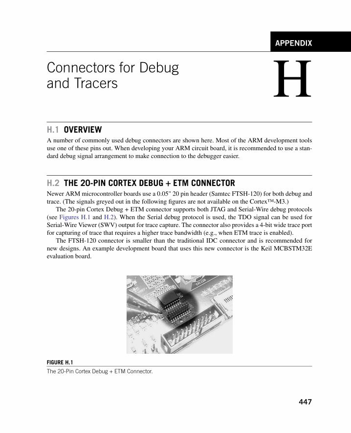
447
HH.1 OverviewA number of commonly used debug connectors are shown here. Most of the ARM development tools use one of these pins out. When developing your ARM circuit board, it is recommended to use a stan-dard debug signal arrangement to make connection to the debugger easier.
H.2 tHe 20-Pin COrtex Debug + etM COnneCtOrNewer ARM microcontroller boards use a 0.05" 20 pin header (Samtec FTSH-120) for both debug and trace. (The signals greyed out in the following figures are not available on the Cortex™-M3.)
The 20-pin Cortex Debug + ETM connector supports both JTAG and Serial-Wire debug protocols (see Figures H.1 and H.2). When the Serial debug protocol is used, the TDO signal can be used for Serial-Wire Viewer (SWV) output for trace capture. The connector also provides a 4-bit wide trace port for capturing of trace that requires a higher trace bandwidth (e.g., when ETM trace is enabled).
The FTSH-120 connector is smaller than the traditional IDC connector and is recommended for new designs. An example development board that uses this new connector is the Keil MCBSTM32E evaluation board.
Appendix
Connectors for Debug and Tracers
Figure H.1
The 20-Pin Cortex Debug + ETM Connector.

448 Appendix H
1 2
19 20
TMS/SWIOVTref
TCK/SWCLK
TDO/SWO/TRACECTL/EXTa
TDI/EXTb/NC
nRESET
TRACECLK
TRACEDATA0
GND
GND
KEY
GNDDetect
GND/TgtPwr 1 Cap
TRACEDATA1
TRACEDATA2
TRACEDATA3
GND
GND
GND
GND/TgtPwr 1 Cap
Figure H.2
The 20-Pin Cortex Debug + ETM Connector Pin Layout.
Figure H.3
The 10-Pin Cortex Debug Connector.
1 2
9 10
TMS/SWIOVTref
TCK/SWCLK
TDO/SWO
TDI
nRESET
GND
GND
KEY
GNDDetect
Figure H.4
The 10-Pin Cortex Debug Connector Pin Layout.

449Connectors for Debug and Tracers
H.3 tHe 10-Pin COrtex Debug COnneCtOrFor devices without ETM, you can use an even smaller 0.05" 10-pin connector for debug. Similar to the 20-pin Cortex Debug + ETM connector, both JTAG and Serial-Wire debug protocols are supported in the 10-pin version (see Figures H.3 and H.4).
H.4 LegaCy 20-Pin iDC COnneCtOrA common debug connector used in ARM development boards is the 20-pin IDC connector (see Figure H.5). The 20 pin IDC connector arrangement support JTAG debug, Serial-Wire debug (SWIO and SWCLK), and SWV. The nICEDETECT pin allows the target system to detect if a debugger is connected. When no debugger is attached, this pin is pulled high. A debugger connection connects this pin to the ground. This is used in some development boards that support multiple JTAG configurations. The nSRST connection is optional; debugger can reset a Cortex-M3 system through the NVIC so this connection is often omitted from the top level of microcontroller designs.
H.5 LegaCy 38-Pin MiCtOr COnneCtOrIn some ARM system designs, a Mictor connector is used when trace port is required (e.g., for instruc-tion trace with ETM; see Figure H.6). It can also be used for JTAG/SWD connection. The 20-pin IDC connector can be connected in parallel with the Mictor connector (only one is used at a time).
Figure H.5
The 20-Pin IDC Connector.
1 2
19 20
3V33V3
GND
GND
GND
GND
GND
GND
GND
GND
nICEDETECT
nTRST
TDI
TMS/SWIO
TCK/SWCLK
RTCK
TDO/SWV
NC/nSRST
NC
NC

450 Appendix H
Typically, a Cortex-M3 microcontroller only has 4 bits of trace data signals, so most of the trace data pins on the Mictor connectors are not used. The Mictor connector is used mostly in other ARM Cortex processors (Cortex-A8/A9, Cortex-R4); in some multiprocessor systems the trace system might require a wider trace port. In such cases, some of the other unused pins on the connector will also be used. For Cortex-M3 systems, the Cortex Debug + ETM connector is recommended.
Figure H.6
The 38-Pin Mictor Connector.
NC
NC
GND
Pulldown
NC/nSRST
TDO/SWV
RTCK
TCK/SWCLK
TMS/SWIO
TDI
nTRST
1 2
37 38
NC
NC
TRACECLK
Pulldown
Pullup (Vref)
VSupply
TRACEDATA[3]
0
0
1
Pulldown
TRACEDATA[2]
TRACEDATA[1]
TRACEDATA[0]
1
3
5
7
9
11
13
15
17
19
21
23
25
27
29
31
33
35
37
2
4
6
8
10
12
14
16
18
20
22
24
26
28
30
32
34
36
38
0/TRACEDATA[4]
0/TRACEDATA[5]
0/TRACEDATA[6]
0/TRACEDATA[7]
0/TRACEDATA[8]
0/TRACEDATA[9]
0/TRACEDATA[10]
0/TRACEDATA[11]
0/TRACEDATA[12]
0/TRACEDATA[13]
0/TRACEDATA[14]
0/TRACEDATA[15]
0/TRACECTRL
451
References
1. Cortex-M3 Technical Reference Manual (TRM): downloadable from the ARM documentation web site at http://infocenter.arm.com/help/topic/com.arm.doc.ddi0337g/index.html
2. ARMv7-M Architecture Application Level Reference Manual: downloadable from the ARM documentation web site at www.arm.com/products/CPUs/ARM_Cortex-M3_v7.html
3. CoreSight Technology System Design Guide: downloadable from the ARM documentation web site at http://infocenter.arm.com/help/topic/com.arm.doc.dgi0012b/index.html
4. AMBA Specification: downloadable from the ARM documentation web site at www.arm.com/products/solutions/AMBA_Spec.html
5. AAPCS Procedure Call Standard for the ARM Architecture: downloadable from the ARM documentation web site at http://infocenter.arm.com/help/topic/com.arm.doc.ihi0042c/index.html
6. RVCT 4.0 Compilation Tools Compiler User Guide: downloadable from the ARM documentation web site at http://infocenter.arm.com/help/topic/com.arm.doc.dui0205i/index.html
7. ARM Application Note 179: Cortex-M3 Embedded Software Development: downloadable from the ARM documentation web site at http://infocenter.arm.com/help/topic/com.arm.doc.dai0179b/index.html
8. RVCT 4.0 Compilation Tools Compiler Reference Guide: downloadable from the ARM documentation web site at http://infocenter.arm.com/help/topic/com.arm.doc.dui0348b/index.html

Copyright © 2010, Elsevier Inc. All rights reserved.DOI: 10.1016/B978-1-85617-963-8.00035-1
AAAPCS (Procedure Call Standard for ARM Architecture),
159, 204assembly code and C program interactions, 170double-word stack alignment, 204
Access port (AP), 245AFSR (Auxiliary Fault Status Register), 126, 416, 421AHB (Advanced High-performance Bus), 80, 101, 146, 207
AHB-AP, 102, 245, 264–265AHB-to-APB, 102, 107in BE-8 Big Endian mode, 95, 96BusMatrix, 102, 105–107error responses, causes, 121in word-invariant big endian, 95, 96
AIRCR (NVIC Application Interrupt and Reset Control Register), 113, 125, 241, 254, 412
AMBA (Advanced Microcontroller Bus Architecture), 101, 244APB (Advanced Peripheral Bus), 80, 101, 104, 244
APB-AP, 246API (Application Programming Interface), 126, 193APSR (Application Program Status Register), 29, 279, 358,
359flag bits for conditional branches, 62and MSR instruction, 29, 55signed saturation results, 69updating instructions, 58with traditional Thumb instruction syntax, 45
ARM Architecture Reference Manual, The, 8ATB (Advanced Trace Bus), 103, 246, 255, 256ATB funnel, 246, 256Auxiliary Control Register, 275, 277, 281
BBackground region (MPU), 212, 225BASEPRI, 16, 30
special register, 136–137use, 31
BFAR (Bus Fault Address Register), 122, 421BFSR (Bus Fault Status Register), 121, 122, 152, 153,
415, 426Big Endian
in ARM7, 95, 96, 284in Cortex-M3, 95, 96memory views, 95
Bit bandalias, 79, 80, 289vs. bit bang, 87operations, 84–91semaphore operation, 179–180
Breakpoint, 21, 262in cortex-M3, 251–253and Flash Patch, 21, 103, 253, 255, 262–264Insert/Remove breakpoint, 323
Bus Fault, 121–122precise and imprecise, 122stacking error, 152status register, 121, 122, 152, 153, 415, 426unstacking error, 153
BusMatrix, 102, 105–107Byte-invariant big endian, 95, 96
CCFSR (Configurable Fault Status Register), 421CMSIS (Cortex Microcontroller Software Interface
Standard), 67, 95, 164–165, 185areas of standardization, 165–166benefit of, 168–169core access functions, 186, 439–445example, 168intrinsic functions, 167, 444–445MPU register names in, 218organization of, 166port existing applications using, 334stopwatch example with interrupts, 327–333
Context Switching, 127example, 128in simple OS, 203
CONTROL (one of the special registers), 14, 31–32CoreSight architecture, 21, 255
debugging hardware, 21overview, 244–248
Cortex-A8, 5, 7Cortex-M0, 278–281, 444Cortex-M3
advantages, 1–2, 18, 22–24, 277–278applications, 9, 334barrier instructions, 67bit-band operation
advantages, 87–90in C programs, 90of different data sizes, 90
breakpoint instruction in, 251–253bus faults, 121bus interfaces on, 17–18, 104–105connection of AHB-AP in, 265data transfers, 53debugging components, 11debugging features, 243
Index
453

454 Index
debugging functions in, 244debugging support, 21–22debug modes in, 248–250debug systems in, 247default configuration, 83default ROM table values, 266differences between Cortex-M0, 278–281differences among other versions, 272–277ETM in, 260–261exception types and enables, 407–408instructions, 19, 57, 58, 60, 70, 349interrupt and exceptions, 19–21, 35–36linker script for, 433–437link register (LR), 28memory attributes 82–83memory map, 16–17, 79–82MPU, 18
registers, 212–217multiprocessor communication, 236–241nested interrupt support in, 148NVIC in, 15–16operation modes, 14–15, 32–34, 285priority levels, 111–116privilege levels in, 15processor-based microcontrollers, 2program counter, 28registers, 12–14, 25–26, 29–32reset types and signals on, 107–108simple timer, 141sleep modes, 232–234stack memory operations, 36–40stack pointer (SP) in, 26–28supporting endian modes, 95–97tail chaining interrupt, 148–149three-stage pipeline in, 99–101trace interfaces in, 246trace system in, 255–256troubleshooting guide, 421unaligned transfers in, 92–93vector table definition in CS3, 302vs. Cortex-M3-based MCUs, 3
Cortex-R4, 5, 7CPI (Cycle Per Instruction), 257CS3, 301, 302CYCCNT (Cycle Counter in DWT), 256, 257
DDAP (Debug Access Port), 21, 102, 104, 244, 245D-Code bus, 17, 103, 273Data abort, 121Debug registers
DCRDR (Debug Core Register Data Register), 253, 254, 419
DCRSR (Debug Core Register Selector Register), 253, 254, 419
DEMCR (Debug Exception and Monitor Control Register), 249, 250, 419–420
DFSR (Debug Fault Status Register), 252, 254, 416, 428DHCSR (Debug Halting Control and Status Register), 248,
249, 418DP (Debug Port), 21, 244, 245DWT (Data Watchpoint and Trace unit), 21, 80, 102, 256–258
and ETM, 260and ITM, 260
EEmbedded Assembler, 163–164, 197, 288, 423EPSR (Execution Program Status Register), 29, 152ETM (Embedded Trace Macrocell), 21, 80, 102, 246, 256,
260–261, 267Exception exit, 119, 147–148Exception Return, 148, 149–151Exceptions
ARM7TDMI mapping, 285configuration registers, 137–138exception handler, 14, 33, 88, 117, 121, 147, 149, 189,
327exits, 147–148fault exceptions, 120–126handling, 19, 36, 125, 148, 149, 152, 204and interrupts, 19–21, 35PendSV, 126–129PRIMASK register, 135–136priority levels, 111–117priority setup, 185register updates, 147return value, 149–151stacking, 145–147, 408SVC, 126–129SYSTICK, 141, 229, 232, 328types, 35, 109–111, 407vector, 117, 147vector table, 36, 117–118
Exclusive accesses, 93–95for semaphores, 177–179
EXC_RETURN, 147, 149–151, 153, 202
FFAULTMASK, 14, 16, 30, 31, 135–136, 210FPB (Flash Patch and Breakpoint Unit), 21, 103, 253,
255, 262–264
HHalt mode debug, 250, 251, 254Hard fault
avoiding lockup, 210
Cortex-M3 Continued

455Index
priority level, 111status register, 125, 416, 428
HFSR (Hard Fault Status Register), 125, 416, 428High registers, 25
II-Code interface bus, 17, 103ICI (Interrupt-Continuable Instructions)
bit field in PSR, 30Inline assembler, 163–164, 198–199, 288, 305Instruction Barrier (ISB), 67Instruction trace, 12, 21
ETM, 102, 260Instrumentation Trace, 172Intellectual property (IP) licensing, 3Interrupt latency, 16, 22, 23, 152, 207Interrupt return, 147–148, 284, 287Intrinsic functions, 135, 163, 165, 167,
444–445IPSR (Interrupt Program Status Register), 29, 168, 206IRQ (Interrupt Request), 20, 131, 189IT (IF-THEN), 65, 152, 393–394
assembler language, 65–66Thumb-2 instructions, 70–72
ITM (Instrumentation Trace Macrocell)ATB interface, 105debugging component, 22, 258–260functionalities, 258–259hardware trace, 260software trace, 259timestamp feature, 260
LLabVIEW, 335–336
for ARM porting, 345–347application areas, 337development of, 337–339features in, 344–345project, example of, 339–343working, 343–344
Literal pool, 263Load/store operations, 84, 152, 287, 427Lockup, 422
situations, 208–210Low registers, 25LR (link register), 149
branch and link instructions, 60R14, 13, 28saving, 62stacking, 145, 146update, 147, 149value, 421
LSU (Load Store Unit), 257
MMemory Barrier Instructions, 67Memory Management fault, 122–123, 137
MMAR, 416, 421and MPU violation, 152, 218status register, 415
Memory Map, 16–17, 67, 79–82, 83, 103, 161–163, 211, 284, 325
MFSR (Memory-management Fault Status Register), 123, 152, 426
MMAR (Memory-management Fault Address Register), 416, 421
Monitor exception, 21, 35, 110, 248, 251–253MPU (Memory Protection Unit), 6, 9, 11, 18, 83, 102,
122, 211registers, 212–217setup, 218–224system characteristics, 285
MSP (Main Stack Pointer), 12, 26, 28, 39, 40, 145, 183MSTKERR (Memory Management Stacking Error), 152,
426MUNSTKERR (Memory Management Unstacking Error),
153, 426
NNMI (nonmaskable interrupt), 2, 23, 35
double fault situations, 209and FIQ, 286
Nonbase Thread Enable, 205–206, 413NVIC (Nested Vectored Interrupt Controller), 131
accessing, 186and CPU core, 101–103DCRDR, 253, 254DCRSR, 253, 254debugging features, 254enabling and disabling interrupts, 187fault status register, 121–122, 123, 124features, 15–16registers, 409ROM table, 265–266SCS, 81, 131System Control register, 232SYSTICK registers, 141–143, 229
PPC (Program Counter)
R15, 13, 28register updation, 147stacked PC, 421value, 288
PendSV context switching, 128and SVC, 126–129

456 Index
Pipeline, 99–100, 288PPB (Private Peripheral Bus), 18
AHB, 80APB, 80external PPB, 104–105
Preempt Priority, 113, 114, 115, 116Prefetch abort, 121PRIMASK, 29, 135–136, 178
function, 14interrupt masking, 16, 30, 31
Priority Group, 113, 114, 115, 116, 132, 193Privileged mode, 70, 131, 178, 205Profiling (Data Watchpoint and Trace unit),
256–258PSP (Process Stack Pointer)
ARM documentation, 26, 28MRS and MSR instructions, 40stacking, 145two-stack model, 39–41
PSR (Program Status register), 29, 145APSR, 29bit fields, 30EPSR, 29flags, 62IPSR, 29, 146, 147
QQ flag, 62, 69, 387
RR13/SP, 28Real time, 4Reset
control, 254fault handling method, 125self-reset control, 241–242signals, 107–108vector, 41, 46, 295
Reset sequence, 41–42Retargeting, 302–304, 315, 317ROM Table, 103, 265–267RXEV (Receive Event), 232, 237
SSaturation
instructions, 68, 69operation, 68–70
Semaphores bit band, usage, 179–180exclusive access, usage, 93, 177–179, 287
Serial-Wire Viewer, 172, 257Serial-Wire, 102, 244, 245Sleep modes, 20, 23, 232–234, 276Sleep-On-Exit, 234
Software Trace (Instrumentation Trace Macrocell), 259
Special registers, 14, 29, 70accessing, 304BASEPRI, 14, 30–31, 136–137control register, 31–32FAULTMASK, 14, 30–31, 135–136for MRS and MSR instructions, 71PRIMASK, 14, 30–31, 135–136PSRs, 29–30
Stack alignment, 204, 275, 277Stack Pointer (SP), 204, 206
R13, 12, 26–28stack memory operations, 36types, 26, 39updating, 147
Stacking error, 152exception sequence, 145–147
STIR (Software Trigger Interrupt register), 131, 141, 420STKERR (stacking error), 152Subpriority, 113, 114Subregion, 215, 225SVC (Supervisor Call), 126–129, 193, 206, 210
handler, 205for output functions, 194–197and SWI, 127user applications, 193–194using with C, 197–199
SWI (Software Interrupt Instruction), 127, 287SWJ-DP, Serial Wire JTAG – Debug Port, 21, 102, 274System Control register, 233, 413System Control Space (SCS), 32, 81, 131SYSTICK
context switching, 127registers, 141–143stopwatch, example, 328Timer, 102, 141–143, 229–232, 277
TTable Branch, 75–77, 181
and SVC, 194Timestamp, 260TPIU (Trace Port Interface Unit), 21, 103, 246,
255, 261Trace Enable (TRCENA), 256
debug, 250in DEMCR, 259, 262
TXEV (Transmit Event), 105, 236
UUFSR (Usage Fault Status Register), 124, 415, 427–428Unaligned transfers, 92–93
and D-Code bus, 103

457Index
Unified Assembler Language (UAL), 49–50Unstacking
and bus fault, 121error, 153interrupt return instruction, 147–148
UNSTKERR (Unstacking error), 153Usage fault, 123–124, 137, 153User mode, 131, 205
VVector catch (Debug event), 249Vector fetch, 121, 147, 153, 207Vector Table Offset register, 117, 132, 279, 412Vector table relocation, 190–193Vector table, 36, 190
and exceptions, 117–118difference in traditional ARM cores, 286modification, 326–327remapping, 284setup and enabling interrupt, 184–188
Virtual instrument (VI), 336, 337, 339, 340, 346
WWIC (Wakeup Interrupt Controller), 21, 102, 234–236,
276, 277Word-invariant big endian, 95, 96
XxPSR – combined Program Status Register (PSR), 14,
29, 204, 287