THC63LVDM83D - All Products
17
THC63LVDM83D_Rev.4.20_E Copyright©2015 THine Electronics, Inc. 1/17 THine Electronics, Inc. Security E 7 PLL TA +/- TB +/- TC +/- TD +/- TCLK +/- R/F /PDWN TA0-6 TC0-6 TD0-6 TRANSMITTER (8 to 160MHz) CMOS/TTL 7 RS 7 TB0-6 7 INPUTS CLOCK (LVDS) 8-160MHz DATA (LVDS) (56-1120Mbit/On Each LVDS Channel) CLKIN THC63LVDM83D CMOS/TTL PARALLEL TO SERIAL 7 PLL TA +/- TB +/- TC +/- TD +/- TCLK +/- R/F /PDWN TA0-6 TC0-6 TD0-6 TRANSMITTER (8 to 160MHz) CMOS/TTL 7 RS 7 TB0-6 7 INPUTS CLOCK (LVDS) 8-160MHz DATA (LVDS) (56-1120Mbit/On Each LVDS Channel) CLKIN THC63LVDM83D CMOS/TTL PARALLEL TO SERIAL THC63LVDM83D 24bit COLOR LVDS TRANSMITTER General Description The THC63LVDM83D transmitter is designed to support pixel data transmission between Host and Flat Panel Display up to 1080p/WUXGA resolutions. The THC63LVDM83D converts 28bits of LVCMOS data into four LVDS data streams. The transmitter can be programmed for rising edge or falling edge clock through a dedicated pin. At a transmit clock frequency of 160MHz, 24bits of RGB data and 4bits of timing and control data (HSYNC, VSYNC, DE, CONT1) are transmitted at an effective rate of 1120Mbps per LVDS channel. Application ・Medium and Small Size Panel ・ Tablet PC / Notebook PC ・Security Camera / Industrial Camera ・Multi Function Printer ・Industrial Equipment ・Medical Equipment Monitor Features ・Compatible with TIA/EIA-644 LVDS Standard ・7:1 LVDS Transmitter ・Operating Temperature Range : 0 to +70C ・No Special Start-up Sequence Required ・Spread Spectrum Clocking Tolerant up to 100kHz Frequency Modulation and +/-2.5% Deviations. ・Wide Dot Clock Range: 8 to 160MHz Suited for TV Signal : NTSC(12.27MHz) - 1080p(148.5MHz) PC Signal : QVGA(8MHz) - WUXGA(154MHz) ・56pin TSSOP Package ・1.2V to 3.3V LVCMOS/ inputs are supported. ・LVDS swing is reducible as 200mV by RS-pin to reduce EMI and power consumption. ・PLL requires no external components. ・Power Down Mode. ・Input clock triggering edge is selectable by R/F-pin ・EU RoHS Compliant. Block Diagram Figure 1. Block Diagram
-
Upload
khangminh22 -
Category
Documents
-
view
0 -
download
0
Transcript of THC63LVDM83D - All Products

THC63LVDM83D_Rev.4.20_E
Copyright©2015 THine Electronics, Inc.
1/17
THine Electronics, Inc.Security E
7
PLL
TA +/-
TB +/-
TC +/-
TD +/-
TCLK +/-
R/F
/PDWN
TA0-6
TC0-6
TD0-6
TRANSMITTER
(8 to 160MHz)
CMOS/TTL
7
RS
7
TB0-67
INPUTS
CLOCK(LVDS)
8-160MHz
DATA(LVDS)
(56-1120Mbit/On EachLVDS Channel)
CLKIN
THC63LVDM83D
CM
OS
/TT
LP
AR
AL
LE
LT
OS
ER
IAL
7
PLL
TA +/-
TB +/-
TC +/-
TD +/-
TCLK +/-
R/F
/PDWN
TA0-6
TC0-6
TD0-6
TRANSMITTER
(8 to 160MHz)
CMOS/TTL
7
RS
7
TB0-67
INPUTS
CLOCK(LVDS)
8-160MHz
DATA(LVDS)
(56-1120Mbit/On EachLVDS Channel)
CLKIN
THC63LVDM83D
CM
OS
/TT
LP
AR
AL
LE
LT
OS
ER
IAL
THC63LVDM83D24bit COLOR LVDS TRANSMITTER
General DescriptionThe THC63LVDM83D transmitter is designed to support pixeldata transmission between Host and Flat Panel Display up to1080p/WUXGAresolutions.The THC63LVDM83D converts 28bits of LVCMOS data intofour LVDS data streams. The transmitter can be programmedfor rising edge or falling edge clock through a dedicated pin.At a transmit clock frequency of 160MHz, 24bits of RGB dataand 4bits of timing and control data (HSYNC, VSYNC, DE,CONT1) are transmitted at an effective rate of 1120Mbps perLVDS channel.
Application・Medium and Small Size Panel
・Tablet PC / Notebook PC
・Security Camera / Industrial Camera
・Multi Function Printer
・Industrial Equipment
・Medical Equipment Monitor
Features・Compatible with TIA/EIA-644 LVDS Standard
・7:1 LVDS Transmitter
・Operating Temperature Range : 0 to +70C・No Special Start-up Sequence Required
・Spread Spectrum Clocking Tolerant up to 100kHz FrequencyModulation and +/-2.5% Deviations.
・Wide Dot Clock Range: 8 to 160MHz Suited forTV Signal : NTSC(12.27MHz) - 1080p(148.5MHz)PC Signal : QVGA(8MHz) -WUXGA(154MHz)
・56pinTSSOPPackage
・1.2V to 3.3V LVCMOS/ inputs are supported.
・LVDS swing is reducible as 200mV by RS-pin to reduce EMIand power consumption.
・PLLrequires no external components.
・Power Down Mode.
・Input clock triggering edge is selectable by R/F-pin
・EU RoHS Compliant.
Block Diagram
Figure 1. Block Diagram

THC63LVDM83D_Rev.4.20_E
Copyright©2015 THine Electronics, Inc.
2/17
THine Electronics, Inc.Security E
Pin Diagram
Figure 2. Pin Diagram

THC63LVDM83D_Rev.4.20_E
Copyright©2015 THine Electronics, Inc.
3/17
THine Electronics, Inc.Security E
Pin DescriptionPin Name Pin # Direction Type Description
TA+, TA- 47, 48
Output LVDSLVDS Data Out
TB+, TB- 45, 46TC+, TC- 41, 42TD+, TD- 37, 38TCLK+,TCLK-
39, 40LVDS Clock Out
TA0 ~ TA6 51, 52, 54, 55, 56, 3,4
Input LVCMOS
Pixel Data Input
TB0 ~ TB6 6, 7, 11, 12, 14, 15,19
TC0 ~ TC6 20, 22, 23, 24, 27, 28,30
TD0 ~ TD6 50, 2, 8, 10, 16, 18,25
/PDWN 32 H : Normal OperationL : Power Down (All outputs are Hi-Z)
RS 1 LVDS Swing Mode, VREF Select See Fig.8,9
VREF : is Input Reference VoltageR/F 17 Input Clock Triggering Edge Select
H : Rising EdgeL : Falling Edge
CLKIN 31 Input ClockVCC 9, 26
Power -
Power Supply Pins for LVCMOS inputs anddigital circuit.
GND 5, 13, 21, 29, 53 Ground Pins for LVCMOS Inputs and DigitalCircuitry.
LVDS VCC 44 Power Supply Pins for LVDS Outputs.LVDS GND 36, 43 49 Ground Pins for LVDS Outputs.PLL VCC 34 Power Supply Pin for PLL Circuitry.PLL GND 33, 35 Ground Supply Pin for PLL Circuitry.
Table 1. Pin Description
RSLVDS
Swing
Small Swing
Input Support
VCC 350mV N/A
0.6 ~ 1.4V 350mV RS=VREFGND 200mV N/A

THC63LVDM83D_Rev.4.20_E
Copyright©2015 THine Electronics, Inc.
4/17
THine Electronics, Inc.Security E
LVDS_OutPLVDS_OutN
IN_N
IN_P
3.5mA
Absolute Maximum RatingsParameter Min Max Unit
Supply Voltage (VCC) -0.3 +4.0 VLVCMOS Input Voltage -0.3 VCC + 0.3 VLVDS Output Pin -0.3 VCC + 0.3 VOutput Current -30 30 mAJunction Temperature - +125 CStorage Temperature -55 +150 CReflow Peak Temperature - +260 CReflow Peak Temperature Time - 10 sec
Maximum Power Dissipation @+25C - 1.8 W
Table 2. Absolute Maximum Ratings
Recommended Operating ConditionsSymbol Parameter Min Typ Max Unit
- All Supply Voltage 3.0 3.3 3.6 VTa Operating Ambient Temperature 0 25 +70 C- Clock Frequency 8 - 160 MHz
Table 3. Recommended Operating Conditions
“Absolute Maximum Ratings” are those values beyond which the safety of the device can not be guaranteed.They are not meant to imply that the device should be operated at these limits. The tables of “ElectricalCharacteristics Table4, 5, 6, 7” specify conditions for device operation.“Absolute Maximum Rating” value also includes behavior of overshooting and undershooting.
Equivalent LVDS Output Schematic Diagram
Figure 3. LVDS Output Schematic Diagram

THC63LVDM83D_Rev.4.20_E
Copyright©2015 THine Electronics, Inc.
5/17
THine Electronics, Inc.Security E
CLKIN
Tx0-6
Power Consumption
Over recommended operating supply and temperature range unless otherwise specified
Symbol Parameter Conditions Typ* Max Unit
ITCCW
LVDS TransmitterOperating CurrentWorst Case Pattern(Fig.4)
RL=100, CL=5pF, f=85MHz, RS=VCC 61 67 mA
RL=100, CL=5pF, f=135MHz,RS=VCC
77 83 mA
RL=100, CL=5pF, f=160MHz,RS=VCC
84 92 mA
RL=100, CL=5pF, f=85MHz, RS=GND 50 56 mA
RL=100, CL=5pF, f=135MHz,RS=GND
65 71 mA
RL=100, CL=5pF, f=160MHz,RS=GND
73 80 mA
ITCCSLVDS TransmitterPower Down Current
/PDWN=L, All Inputs=L or H - 10 µA
*Typ values are at the conditions of VCC=3.3V and Ta = +25ºC
Table 4. Power Consumption
Worst Case Pattern
x=A,B,C,D
Figure 4. Worst Case Pattern

THC63LVDM83D_Rev.4.20_E
Copyright©2015 THine Electronics, Inc.
6/17
THine Electronics, Inc.Security E
Electrical Characteristics
LVCMOS DC Specifications
Over recommended operating supply and temperature range unless otherwise specified
Symbol Parameter Conditions Min Typ* Max UnitVIH High Level Input Voltage RS=VCC or GND 2.0 - VCC VVIL Low Level Input Voltage RS=VCC or GND GND - 0.8 V
VDDQ1 Small Swing Voltage 1.2 - 2.8 V
VREF Input Reference Voltage Small Swing (RS=VDDQ/2) - VDDQ/2 -VSH
2
Small Swing High LevelInput Voltage
VREF= VDDQ/2VDDQ/2+100m
V- - V
VSL2 Small Swing Low Level
Input VoltageVREF= VDDQ/2 - -
VDDQ/2-100mV
V
IINC Input Current GND VIN VCC - - 10 A*Typ values are at the conditions of VCC=3.3V and Ta = +25ºC
Notes : 1 VDDQ voltage defines the max voltage of small swing inputs at RS=VREF. It is not an actual input
voltage.2 Small swing signals are applied to TA0-6, TB0-6, TC0-6, TD0-6 and CLKIN.
Table 5. LV-CMOS DC Specifications
LVDS Transmitter DC SpecificationsOver recommended operating supply and temperature range unless otherwise specified
Symbol Parameter Conditions Min Typ* Max Unit
VOD Differential Output Voltage RL=100Ω
Normal swingRS=VCC
250 350 450 mV
Reducedswing
RS=GND100 200 300 mV
∆VOD Change in VOD betweencomplementary outputstates
RL=100Ω
- - 35 mV
VOC Common Mode Voltage 1.125 1.25 1.375 V∆VOC Change in VOC between
complementary outputstates
- - 35 mV
IOS Output Short CircuitCurrent
VOUT=GND, RL=100Ω - - -24 mA
IOZOutput TRI-STATECurrent
/PDWN=GND,VOUT=GND to VCC
- - 10 A
*Typ values are at the conditions of VCC=3.3V and Ta = +25ºC
Table 6. LVDS Transmitter DC Specifications

THC63LVDM83D_Rev.4.20_E
Copyright©2015 THine Electronics, Inc.
7/17
THine Electronics, Inc.Security E
CLK IN
90%
10%
90%
10%
tTCIT
tTCIT
LVCMOS & LVDS Transmitter AC SpecificationsOver recommended operating supply and temperature range unless otherwise specified
Symbol Parameter Min Typ Max UnittTCIT CLK IN Transition Time - - 5.0 nstTCP CLK IN Period 6.25 T 125 nstTCH CLK IN High Time 0.35T 0.5T 0.65T nstTCL CLK IN Low Time 0.35T 0.5T 0.65T nstTCD CLK IN to TCLK+/- Delay - 3T - nstTS LVCMOS Data Setup to CLK IN 2.0 - - nstTH LVCMOS Data Hold from CLK IN 0.0 - - nstLVT LVDS Transition Time - 0.6 1.5 nstTOP1 Output Data Position0 (T=6.25ns ~ 20ns) -0.15 0.0 +0.15 nstTop0 Output Data Position1 (T=6.25ns ~ 20ns) T/7-0.15 T/7 T/7+0.15 nstTop6 Output Data Position2 (T=6.25ns ~ 20ns) 2T/7-0.15 2T/7 2T/7+0.15 nstTop5 Output Data Position3 (T=6.25ns ~ 20ns) 3T/7-0.15 3T/7 3T/7+0.15 nstTop4 Output Data Position4 (T=6.25ns ~ 20ns) 4T/7-0.15 4T/7 4T/7+0.15 nstTop3 Output Data Position5 (T=6.25ns ~ 20ns) 5T/7-0.15 5T/7 5T/7+0.15 nstTop2 Output Data Position6 (T=6.25ns ~ 20ns) 6T/7-0.15 6T/7 6T/7+0.15 nstTPLL Phase Lock Loop Set - - 10.0 ms
*Typ values are at the conditions of VCC=3.3V and Ta = +25ºC
Table 7. LVCMOS & LVDS Transmitter AC Specifications
LVCMOS Input
Figure 5. CLKIN Transmission Time
LVDS Output
LVDS Output Load
Figure 6. LVDS Output Load and Transmission Time

THC63LVDM83D_Rev.4.20_E
Copyright©2015 THine Electronics, Inc.
8/17
THine Electronics, Inc.Security E
RS VODVCC
0.6 ~ 1.4VGND 200mV
350mV
RS VREF
VCC ---
0.6 ~ 1.4V VDDQ/2
GND ---
tTCP
tTS tTH
tTCH
tTCL
CLKIN
Tx0-Tx6
tTCD
TCLK+
TCLK-
VDDQ
GND
GND
VDDQ
VOC
tTCP
tTS tTH
tTCH
tTCL
CLKIN
Tx0-Tx6
tTCD
TCLK+
TCLK-
VDDQ
GND
GND
VDDQ
VREF
VOC
VREF
V DDQ/2 VDDQ /2
VDDQ/2 VDDQ/2 VDDQ/2
AC Timing Diagrams
LVCMOS Inputs
Note :CLKIN : Solis line denotes the setting of R/F=GND
Dashed line denotes the setting of R/F = VCC
Figure 7. LVCOMS Inputs and LVDS Clock Output Timing 1
Small Swing Inputs
Note :CLKIN : Solid line denotes the setting of R/F=GND
Dashed line denotes the setting of R/F = VCC
Figure 8. LVCMOS Inputs and LVDS Output Timing 2

THC63LVDM83D_Rev.4.20_E
Copyright©2015 THine Electronics, Inc.
9/17
THine Electronics, Inc.Security E
Vdiff
= 0V Vdiff = 0VTCLK+/-
tTOP1
tTOP0
tTOP6
tTOP5
tTOP4
tTOP3
tTOP2
TD6 TD5 TD4 TD3 TD2 TD1 TD0TD+/-
TC6 TC5 TC4 TC3 TC2 TC1 TC0TC+/-
TB6 TB5 TB4 TB3 TB2 TB1 TB0TB+/-
TA6 TA5 TA4 TA3 TA2 TA1 TA0TA+/-
(Differential)
Next CyclePrevious Cycle
2.0V
CLKIN
/PDWN
TCLK+/-
3.0VVCC
tTPLL
Vdiff
= 0V
LVDS Output Data Position
Figure 9. LVDS Output Data Position
Phase Lock Loop Set Time
Figure 10. PLL Lock Loop Set Time

THC63LVDM83D_Rev.4.20_E
Copyright©2015 THine Electronics, Inc.
10/17
THine Electronics, Inc.Security E
Spread Spectrum Clocking Tolerant
Figure 11. Spread Spectrum Clocking Tolerant
The graph indicates the range that the IC works normally under SS clock input operation.The results are measured with a typical sample on condition of +25Cº and 3.3V, therefore thesevalues are for reference and do not guarantee the performance of a product under othercircumstance.
THC63LVDM83D_Rev.4.20_E
Copyright©2015 THine Electronics, Inc.
11/17
THine Electronics, Inc.Security E
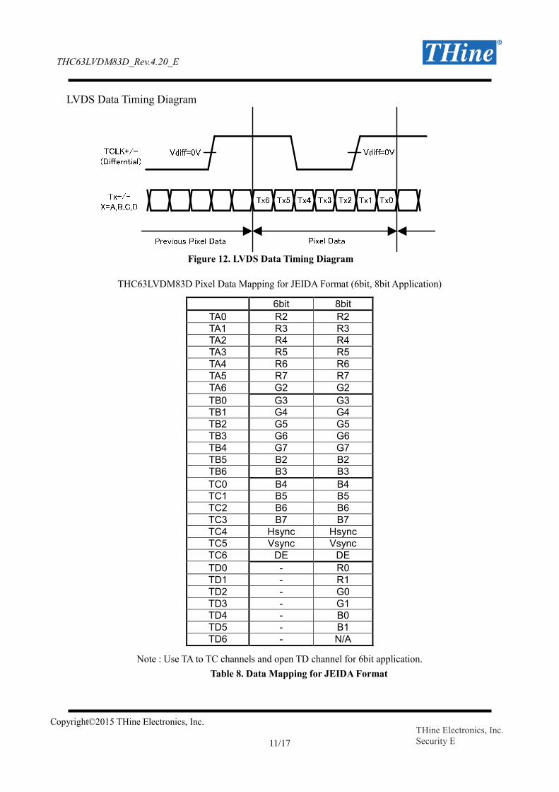
LVDS Data Timing Diagram
Figure 12. LVDS Data Timing Diagram
THC63LVDM83D Pixel Data Mapping for JEIDA Format (6bit, 8bit Application)
Note : Use TA to TC channels and open TD channel for 6bit application.
Table 8. Data Mapping for JEIDA Format
6bit 8bit
TA0 R2 R2TA1 R3 R3TA2 R4 R4TA3 R5 R5TA4 R6 R6TA5 R7 R7TA6 G2 G2
TB0 G3 G3TB1 G4 G4TB2 G5 G5TB3 G6 G6TB4 G7 G7TB5 B2 B2TB6 B3 B3
TC0 B4 B4TC1 B5 B5TC2 B6 B6TC3 B7 B7TC4 Hsync HsyncTC5 Vsync VsyncTC6 DE DE
TD0 - R0TD1 - R1TD2 - G0TD3 - G1TD4 - B0TD5 - B1TD6 - N/A

THC63LVDM83D_Rev.4.20_E
Copyright©2015 THine Electronics, Inc.
12/17
THine Electronics, Inc.Security E
THC63LVDM83D Pixel Data Mapping for VESA Format (6bit, 8bit Application)
Note : Use TA to TC channels and open TD channel for 6bit application.
Table 9. Data Mapping for VESA Format
6bit 8bit
TA0 R0 R0TA1 R1 R1TA2 R2 R2TA3 R3 R3TA4 R4 R4TA5 R5 R5TA6 G0 G0
TB0 G1 G1TB1 G2 G2TB2 G3 G3TB3 G4 G4TB4 G5 G5TB5 B0 B0TB6 B1 B1
TC0 B2 B2TC1 B3 B3TC2 B4 B4TC3 B5 B5TC4 Hsync HsyncTC5 Vsync VsyncTC6 DE DE
TD0 - R6TD1 - R7TD2 - G6TD3 - G7TD4 - B6TD5 - B7TD6 - N/A

THC63LVDM83D_Rev.4.20_E
Copyright©2015 THine Electronics, Inc.
13/17
THine Electronics, Inc.Security E
Normal Connection
Figure 13. Typical Connection Diagram

THC63LVDM83D_Rev.4.20_E
Copyright©2015 THine Electronics, Inc.
14/17
THine Electronics, Inc.Security E
Notes
1) Cable Connection and DisconnectionDo not connect and disconnect the LVDS cable, when the power is supplied to the system.
2) GND ConnectionConnect each GND of the PCB which THC63LVDM83D and LVDS-Rx on it. It is better for EMIreduction to place GND cable as close to LVDS cable as possible.
3) Multi Drop ConnectionMulti drop connection is not recommended.
Figure 14. Multi Drop Connection
4) Asynchronous useAsynchronous using such as following systems is not recommended.
Figure 15. Asynchronous Use
LVDS-RX
THC63LVDM83D LVDS-RX
TCLK+
TCLK-
IC
CLKOUT
CLKOUT
DATA
DATA LVDS-RX
LVDS-RX
IC
TCLK+
TCLK-
TCLK+
TCLK-
CLKOUT
DATA
DATA
THC63LVDM83D
THC63LVDM83D
IC
TCLK+
TCLK-
TCLK+
TCLK-
CLKOUT
CLKOUT
DATA
DATA
IC
THC63LVDM83D
THC63LVDM83D

THC63LVDM83D_Rev.4.20_E
Copyright©2015 THine Electronics, Inc.
15/17
THine Electronics, Inc.Security E
0.2
5
6.1
0+
/-0.1
8.1
0N
OM
0.0
5~
0.1
5
1.2
0M
AX
Package
Figure 16. Package Diagram

THC63LVDM83D_Rev.4.20_E
Copyright©2015 THine Electronics, Inc.
16/17
THine Electronics, Inc.Security E
CY1=
HE= e=
E=
Ttyp.=
Gmin= b=
Zmax= Xmax=
Zmax/2
5 .50
9 .30
0.60
8.100
6.10
10.34
0.500
1 .90 0.200
0 .470
Unit mm
Package
Land Pattern
Reference Land Pattern
Figure 17. Reference of Land Pattern
The recommendation mounting method of THine device is reflow soldering.The reference pattern is using the calculation result on condition of reflow soldering.
NotesThis land pattern design is a calculated value based on JEITA ET-7501.Please take into consideration in an actual substrate design about enough the ease of mounting, the intensity ofconnection, the density of mounting, and the solder paste used, etc… The optimal land pattern size changeswith these parameters. Please use the value shown by the land pattern as reference data.

THC63LVDM83D_Rev.4.20_E
Copyright©2015 THine Electronics, Inc.
17/17
THine Electronics, Inc.Security E
Notices and Requests
1. The product specifications described in this material are subject to change without prior notice.
2. The circuit diagrams described in this material are examples of the application which may not always apply tothe customer's design. We are not responsible for possible errors and omissions in this material. Please note iferrors or omissions should be found in this material, we may not be able to correct them immediately.
3. This material contains our copyright, know-how or other proprietary. Copying or disclosing to third parties thecontents of this material without our prior permission is prohibited.
4. Note that if infringement of any third party's industrial ownership should occur by using this product, we willbe exempted from the responsibility unless it directly relates to the production process or functions of theproduct.
5. Product Application5.1 Application of this product is intended for and limited to the following applications: audio-video device,
office automation device, communication device, consumer electronics, smartphone, feature phone, andamusement machine device. This product must not be used for applications that require extremelyhigh-reliability/safety such as aerospace device, traffic device, transportation device, nuclear power controldevice, combustion chamber device, medical device related to critical care, or any kind of safety device.
5.2 This product is not intended to be used as an automotive part, unless the product is specified as a productconforming to the demands and specifications of ISO/TS16949 ("the Specified Product") in this data sheet.THine Electronics, Inc. (“THine”) accepts no liability whatsoever for any product other than the SpecifiedProduct for it not conforming to the aforementioned demands and specifications.
5.3 THine accepts liability for demands and specifications of the Specified Product only to the extent that theuser and THine have been previously and explicitly agreed to each other.
6. Despite our utmost efforts to improve the quality and reliability of the product, faults will occur with a certainsmall probability, which is inevitable to a semi-conductor product. Therefore, you are encouraged to havesufficiently redundant or error preventive design applied to the use of the product so as not to have ourproduct cause any social or public damage.
7. Please note that this product is not designed to be radiation-proof.
8. Testing and other quality control techniques are used to this product to the extent THine deems necessary tosupport warranty for performance of this product. Except where mandated by applicable law or deemednecessary by THine based on the user’s request, testing of all functions and performance of the product is notnecessarily performed.
9. Customers are asked, if required, to judge by themselves if this product falls under the category of strategicgoods under the Foreign Exchange and Foreign Trade Control Law.
10. The product or peripheral parts may be damaged by a surge in voltage over the absolute maximum ratings ormalfunction, if pins of the product are shorted by such as foreign substance. The damages may cause asmoking and ignition. Therefore, you are encouraged to implement safety measures by adding protectiondevices, such as fuses.
THine Electronics, [email protected]