THAT IN A MI CORA UNA MTOTO NA MTAA MITATE
64
THAT IN A MI CORA UNA MTOTO NA MTAA MITATE US009779884B2 ( 12 ) United States Patent El - Kady et al . ( 10 ) Patent No .: US 9 , 779 , 884 B2 ( 45) Date of Patent : Oct . 3, 2017 ( 54 ) CAPACITOR WITH ELECTRODES MADE OF AN INTERCONNECTED CORRUGATED CARBON - BASED NETWORK ( 71 ) Applicant : The Regents of the University of California , Oakland , CA ( US ) ( 52 ) U.S . CI . CPC . ... . .. . .. ... HOIG 11 / 32 ( 2013 . 01 ); HOIG 11 / 24 ( 2013 . 01 ); HOIG 11 / 26 ( 2013 . 01 ); HOIG 11 / 36 ( 2013 . 01 ) ; ( Continued ) ( 58 ) Field of Classification Search CPC .. . . ... . HO1G 11 / 32 ; H016 11 / 24 ; HO1G 11 / 42 ; HO1G 9 / 155 ; HO1G 9 / 048 ; HO1G 9 / 0425 ( Continued ) ( 72 ) Inventors : Maher F . El - Kady , Los Angeles , CA ( US ); Veronica A . Strong , Portland , OR ( US ); Richard B . Kaner , Pacific Palisades , CA ( US ) ( 56 ) References Cited U . S . PATENT DOCUMENTS ( 73 ) Assignee : The Regents of the University of California , Oakland , CA ( US ) 6 , 982 , 517 B2 8 , 503 , 161 B1 ( * ) Notice : Subject to any disclaimer , the term of this patent is extended or adjusted under 35 U .S .C . 154 (b ) by 312 days . 1 / 2006 Reineke et al . 8/ 2013 Chang et al . ( Continued ) ( 21 ) Appl . No . : 14 / 382 , 463 CN FOREIGN PATENT DOCUMENTS 101723310 A 6 / 2010 20050317902 10 / 2005 ( Continued ) JP ( 22 ) PCT Filed : Mar . 5 , 2013 PCT / US2013 / 029022 ( 86 ) PCT No .: $ 371 (c)(1) , (2 ) Date : OTHER PUBLICATIONS Sep . 2, 2014 ( 87 ) PCT Pub . No . : W02013 / 134207 PCT Pub . Date : Sep . 12 , 2013 Allen , Matthew J., et al ., “ Honeycomb Carbon : A Review of Graphene ,” Chemical Reviews , vol . 110 , Issue 1, Jul . 17 , 2009 , American Chemical Society , pp . 132 - 145 . ( Continued ) ( 65 ) Prior Publication Data US 2015 / 0098167 A1 Apr . 9 , 2015 Primary Examiner — Eric Thomas Assistant Examiner — Arun Ramaswamy ( 74 ) Attorney , Agent , or Firm — Withrow & Terranova , P .L . L . C . Related U .S. Application Data ( 60 ) Provisional application No . 61 / 606 , 637 , filed on Mar . 5 , 2012 , provisional application No . 61 / 757 , 077 , filed on Jan . 25 , 2013 . ( 57 ) ABSTRACT Capacitors having electrodes made of interconnected corru gated carbon - based networks ( ICCNs ) are disclosed . The ICCN electrodes have properties that include high surface area and high electrical conductivity . Moreover , the elec trodes are fabricated into an interdigital planar geometry with dimensions that range down to a sub - micron scale . As such , micro - supercapacitors employing ICCN electrodes are ( Continued ) ( 51 ) Int . Cl . HO1G 9 / 00 HOIG 9 / 04 ( 2006 . 01 ) ( 2006 . 01 ) ( Continued ) W HEHEHITUIT . . . . . . ! ! . . . ICON ttttttttt POLYMER ELECTROLYTE FLEXIBLE SUBSTRATE
-
Upload
khangminh22 -
Category
Documents
-
view
1 -
download
0
Transcript of THAT IN A MI CORA UNA MTOTO NA MTAA MITATE

THAT IN A MI CORA UNA MTOTO NA MTAA MITATE US009779884B2
( 12 ) United States Patent El - Kady et al .
( 10 ) Patent No . : US 9 , 779 , 884 B2 ( 45 ) Date of Patent : Oct . 3 , 2017
( 54 ) CAPACITOR WITH ELECTRODES MADE OF AN INTERCONNECTED CORRUGATED CARBON - BASED NETWORK
( 71 ) Applicant : The Regents of the University of California , Oakland , CA ( US )
( 52 ) U . S . CI . CPC . . . . . . . . . . . . . HOIG 11 / 32 ( 2013 . 01 ) ; HOIG 11 / 24
( 2013 . 01 ) ; HOIG 11 / 26 ( 2013 . 01 ) ; HOIG 11 / 36 ( 2013 . 01 ) ;
( Continued ) ( 58 ) Field of Classification Search
CPC . . . . . . . . HO1G 11 / 32 ; H016 11 / 24 ; HO1G 11 / 42 ; HO1G 9 / 155 ; HO1G 9 / 048 ; HO1G 9 / 0425
( Continued ) ( 72 ) Inventors : Maher F . El - Kady , Los Angeles , CA
( US ) ; Veronica A . Strong , Portland , OR ( US ) ; Richard B . Kaner , Pacific Palisades , CA ( US ) ( 56 ) References Cited
U . S . PATENT DOCUMENTS ( 73 ) Assignee : The Regents of the University of California , Oakland , CA ( US ) 6 , 982 , 517 B2
8 , 503 , 161 B1 ( * ) Notice : Subject to any disclaimer , the term of this patent is extended or adjusted under 35 U . S . C . 154 ( b ) by 312 days .
1 / 2006 Reineke et al . 8 / 2013 Chang et al .
( Continued )
( 21 ) Appl . No . : 14 / 382 , 463 CN
FOREIGN PATENT DOCUMENTS 101723310 A 6 / 2010
20050317902 10 / 2005 ( Continued )
JP ( 22 ) PCT Filed : Mar . 5 , 2013
PCT / US2013 / 029022 ( 86 ) PCT No . : $ 371 ( c ) ( 1 ) , ( 2 ) Date :
OTHER PUBLICATIONS Sep . 2 , 2014
( 87 ) PCT Pub . No . : W02013 / 134207 PCT Pub . Date : Sep . 12 , 2013
Allen , Matthew J . , et al . , “ Honeycomb Carbon : A Review of Graphene , ” Chemical Reviews , vol . 110 , Issue 1 , Jul . 17 , 2009 , American Chemical Society , pp . 132 - 145 .
( Continued )
( 65 ) Prior Publication Data US 2015 / 0098167 A1 Apr . 9 , 2015
Primary Examiner — Eric Thomas Assistant Examiner — Arun Ramaswamy ( 74 ) Attorney , Agent , or Firm — Withrow & Terranova , P . L . L . C .
Related U . S . Application Data ( 60 ) Provisional application No . 61 / 606 , 637 , filed on Mar .
5 , 2012 , provisional application No . 61 / 757 , 077 , filed on Jan . 25 , 2013 .
( 57 ) ABSTRACT Capacitors having electrodes made of interconnected corru gated carbon - based networks ( ICCNs ) are disclosed . The ICCN electrodes have properties that include high surface area and high electrical conductivity . Moreover , the elec trodes are fabricated into an interdigital planar geometry with dimensions that range down to a sub - micron scale . As such , micro - supercapacitors employing ICCN electrodes are
( Continued )
( 51 ) Int . Cl . HO1G 9 / 00 HOIG 9 / 04
( 2006 . 01 ) ( 2006 . 01 )
( Continued )
W HEHEHITUIT . . . . . . ! ! . . .
ICON ttttttttt
POLYMER ELECTROLYTE
FLEXIBLE SUBSTRATE

US 9 , 779 , 884 B2 Page 2
fabricated on flexible substrates for realizing flexible elec tronics and on - chip applications that can be integrated with micro - electromechanical systems ( MEMS ) technology and complementary metal oxide semiconductor technology in a single chip . In addition , capacitors fabricated of ICCN electrodes that sandwich an ion porous separator realize relatively thin and flexible supercapacitors that provide compact and lightweight yet high density energy storage for scalable applications .
JP KR WO WO WO wo WO wo WO WO WO
2011026153 2 / 2011 20070083691 A 8 / 2007
9632618 Al 10 / 1996 2011072213 A2 6 / 2011 2012138302 A1 10 / 2012 2013066474 A2 5 / 2013 2013070989 Al 5 / 2013 2013128082 A1 9 / 2013 2013155276 A1 10 / 2013 2014062133 A14 / 2014 2014134663 AL 9 / 2014
66 Claims , 43 Drawing Sheets OTHER PUBLICATIONS
( 51 ) Int . Cl . HOIG 9 / 145 ( 2006 . 01 ) HOIG 11 / 32 ( 2013 . 01 ) HOIG 11 / 24 ( 2013 . 01 ) HOIG 11 / 42 ( 2013 . 01 ) HONG 9 / 048 ( 2006 . 01 ) HONG 9 / 042 ( 2006 . 01 ) HOIG 11 / 26 ( 2013 . 01 ) HOIG 11 / 36 ( 2013 . 01 ) HOIG 11 / 56 ( 2013 . 01 )
( 52 ) U . S . CI . CPC . . . . . . . . . . . . . . HOIG 11 / 56 ( 2013 . 01 ) ; YO2 E 60 / 13
( 2013 . 01 ) ; YO2T 10 / 7022 ( 2013 . 01 ) ( 58 ) Field of Classification Search
USPC . . . . . . . . . . . . . . . . . . . . . . . . . . . . . . 361 / 502 , 508 , 516 See application file for complete search history .
( 56 ) References Cited U . S . PATENT DOCUMENTS
2002 / 0136881 A1 2003 / 0169560 A1 2004 / 0090736 A 2007 / 0204447 A1 2008 / 0090141 A1 2008 / 0180883 A1 2010 / 0159346 A1 *
9 / 2002 Yanagisawa et al . 9 / 2003 Welsch et al . 5 / 2004 Bendale et al . 9 / 2007 Bernstein et al . 4 / 2008 Meitav et al . 7 / 2008 Palusinski et al . 6 / 2010 Hinago . . . . . . . . . . . . . . .
Author Unknown , “ 125 Volt Transportation Module , ” Maxwell Technologies , retrieved Apr . 13 , 2016 , website last modified Mar . 14 , 2013 , www . maxwell . com / products / ultracapacitors / 125v tranmodules , Maxwell Technologies , Inc . , 2 pages . Author Unknown , “ ELTON : Super Capactiors , ” www . elton - cap . com / , Retrieved Apr . 15 , 2016 , ELTON , 1 page . Author Unknown , “ Monthly battery sales statistics , " Battery Asso ciation of Japan ( BAJ ) , retrieved Apr . 13 , 2016 , website last modified Dec . 2010 , web . archive . org / web / 20110311224259 / http : / / www . baj . or . jp / e / statistics / 02 . php , Battery Association of Japan , 1 page . Arthur , Timothy , S . , et al . , “ Three - dimensional electrodes and battery architectures , ” MRS Bulletin , vol . 36 , Jul . 2011 , Materials Research Society , pp . 523 - 531 . Beidaghi , Majid , et al . , “ Capacitive energy storage in micro - scale devices : recent advances in design and fabrication of micro supercapacitors , ” Energy and Environmental Science , vol . 7 , Issue 3 , Jan . 2 , 2014 , Royal Society of Chemistry , pp . 867 - 884 ( 2014 ) . Beidaghi , Majid , et al . , “ Micro - Supercapacitors Based on Interdigital Electrodes of Reduced Graphene Oxide and Carbon Nanotube Composites with Ultra high Power Handling Perfor mance , " Advanced Functional Materials , vol . 22 , Issue 21 , Nov . 2 , 2012 , WILEY - VCH Verlag GmbH & Co . KGaA , Weinheim , pp . 4501 - 4510 . Beidaghi , Majid , et al . , “ Micro - supercapacitors based on three dimensional interdigital polypyrrole / C - MEMS electrodes , " Electrochimica Acta , vol . 56 , Issue 25 , Oct . 30 , 2011 , Elsevier Ltd . , pp . 9508 - 9514 . Bélanger , Daniel , et al . , “ Manganese Oxides : Battery Materials Make the Leap to Electrochemical Capacitors , " Electrochemical Society Interface , vol . 17 , Issue 1 , Spring 2008 , The Electrochemi cal Society , pp . 49 - 52 . Brodie , B . C . , “ Ueber das Atomgewicht des Graphits , " Justus Liebigs Annalen der Chemie , vol . 114 , Issue 1 , 1860 , WILEY - VCH Verlag GmbH & Co . KGaA , Weinheim , pp . 6 - 24 . Cao , Liujun , et al . , “ Direct Laser - Patterned Micro - Supercapacitors from Paintable Mos , Films , ” Small , vol . 9 , Issue 17 , Apr . 16 , 2013 , WILEY - VCH Verlag GmbH & Co . KGaA , Weinheim , pp . 2905 2910 . Chen , L . Y . , et al . , “ Toward the Theoretical Capacitance of RuO , Reinforced by Highly Conductive Nanoporous Gold , ” Advanced Energy Materials , vol . 3 , Issue 7 , Jul . 2014 , WILEY - VCH Verlag GmbH & Co . KGaA , Weinheim , pp . 851 - 856 . Chen , Wei , et al . , “ High - Performance Nanostructured Supercapaci tors on a Sponge , ” Nano Letters , vol . 11 , Issue 12 , Sep . 16 , 2011 , American Chemical Society , 22 pages . Cheng , Yingwen , et al . , “ Synergistic Effects from Graphene and Carbon Nanotubes Enable Flexible and Robust Electrodes for High - Performance Supercapacitors , ” Nano Letters , vol . 12 , Issue 8 , Jul . 23 , 2012 , American Chemical Society , pp . 4206 - 4211 . Chmiola , John , et al . , “ Monolithic Carbide - Derived Carbon Films for Micro - Supercapacitors , " Science , vol . 328 , Issue 5977 , Apr . 2010 , American Association for the Advancement of Science , 4 pages . Choi , Bong Gill , et al . , “ 3D Macroporous Graphene Frameworks for Supercapacitors with High Energy and Power Densities , ” ACS Nano , vol . 6 , Issue 5 , Apr . 23 , 2012 , American Chemical Society , pp . 4020 - 4028 .
HO1G 9 / 016 429 / 479
2010 / 0159366 A 6 / 2010 Shao - Horn et al . 2010 / 0195269 Al 8 / 2010 Kim et al . 2010 / 0203362 A1 8 / 2010 Lam et al . 2010 / 0221508 AL 9 / 2010 Huang et al . 2010 / 0226066 Al 9 / 2010 Sweeney et al . 2010 / 0266964 Al 10 / 2010 Gilje 2010 / 0317790 Al 12 / 2010 Jang et al . 2011 / 0026189 Al 2 / 2011 Wei et al . 2011 / 0143101 A1 6 / 2011 Sandhu 2011 / 0159372 A1 6 / 2011 Zhamu et al . 2011 / 0318257 Al 12 / 2011 Sokolov et al . 2012 / 0134072 A1 5 / 2012 Bae et al . 2012 / 0145234 A1 6 / 2012 Roy - Mayhew et al . 2013 / 0048949 Al 2 / 2013 Xia et al . 2013 / 0056346 A1 3 / 2013 Sundra et al . 2013 / 0056703 A1 3 / 2013 Elian et al . 2013 / 0161570 AL 6 / 2013 Hwang et al . 2013 / 0168611 AL 7 / 2013 Zhou et al . 2013 / 0264041 Al 10 / 2013 Zhamu et al . 2014 / 0029161 A11 / 2014 Beidaghi et al . 2014 / 0255776 AL 9 / 2014 Song et al . 2014 / 0313636 Al 10 / 2014 Tour et al . 2015 / 0259212 A1 9 / 2015 Li et al . 2015 / 0332868 A1 11 / 2015 Jung et al .
FOREIGN PATENT DOCUMENTS
JE 2009525247 A 2010222245
7 / 2009 10 / 2010

US 9 , 779 , 884 B2 Page 3
( 56 ) References Cited
OTHER PUBLICATIONS
El - Kady , Maher F . , et al . , “ Engineering Three - Dimensional Hybrid Supercapacitors and Micro - Supercapacitors for High - Performance Integrated Energy Storage , ” Proceedings of the National Academy of Sciences of the United States of America , vol . 112 , Issue 14 , Apr . 7 , 2015 , National Academy of Sciences , pp . 4233 - 4238 . Fan , Zhuangjun , et al . , “ Asymmetric Supercapacitors Based on Graphene / MnO , and Activated Carbon Nanofiber Electrodes with High Power and Energy Density , ” Advanced Functional Materials , vol . 21 , Issue 12 , Jun . 21 , 2011 , WILEY - VCH Verlag GmbH & Co . KGaA , Weinheim , pp . 2366 - 2375 . Feng , Jun , et al . , “ Metallic Few - Layered VS , Ultrathin Nanosheets : High Two - Dimensional Conductivity for In - Plane Supercapaci tors , ” Journal of the American Chemical Society , vol . 133 , Issue 44 , Sep . 27 , 2011 , American Chemical Society , pp . 17832 - 17838 . Fischer , Anne E . , et al . , “ Incorporation of Homogeneous , Nanoscale MnO within Ultraporous Carbon Structures via Self - Limiting Electroless Deposition : Implications for Electrochemical Capaci tors , " Nano Letters , vol . 7 , Issue 2 , Jan . 13 , 2007 , American Chemical Society , pp . 281 - 286 . Foo , Ce Yao , et al . , “ Flexible and Highly Scalable V205 - 1GO Electrodes in an Organic Electrolyte for Supercapacitor Devices , " Advanced Energy Materials , vol . 4 , Issue 12 , Aug . 26 , 2014 , WILEY - VCH Verlag GmbH & Co . KGaA , Weinheim , pp . 1 - 7 . Gao , Hongcai , et al . , “ High - Performance Asymmetric Supercapaci tor Based on Graphene Hydrogel and Nanostructured MnO2 , " ACS Applied Materials and Interfaces , vol . 4 , Issue 5 , Apr . 30 , 2012 , American Chemical Society , pp . 2801 - 2810 . Gao , Yu , et al . , “ High power supercapcitor electrodes based on flexible TIC - CDC nano - felts , ” Journal of Power Sources , vol . 201 , Issue 1 , Mar . 2012 , Elsevier B . V . , pp . 368 - 375 . Glavin , M . E . et al , “ A Stand - alone Photovoltaic Supercapacitor Battery Hybrid Energy Storage System , ” Proceedings of the 13th International Power Electronics and Motion Control Conference ( EPE - PEMC ) , Sep . 1 - 3 , 2008 , Pozna? , Poland , IEEE , pp . 1688 1695 . Gogotsi , Y . , et al . , “ True Performance Metrics in Electrochemical Energy Storage , ” Science Magazine , vol . 334 , Issue 6058 , Nov . 18 , 2011 , 4 pages . Griffiths , Katie , et al . , “ Laser - scribed graphene presents an oppor tunity to print a new generation of disposable electrochemical sensors , ” Nanoscale , vol . 6 , Sep . 22 , 2014 , The Royal Society of Chemistry , pp . 13613 - 13622 . Guardia , L . , et al . , “ UV light exposure of aqueous graphene oxide suspensions to promote their direct reduction , formation of graphene - metal nanoparticle hybrids and dye degradation , " Carbon , vol . 50 , Issue 3 , Oct . 12 , 2011 , Elsevier Ltd . , pp . 1014 - 1024 . Hu , Liangbing , et al . , " Symmetrical MnO2 - Carbon Nanotube - Tex tile Nanostructures for Wearable Pseudocapacitors with High Mass Loading , " ACS Nano , vol . 5 , Issue 11 , Sep . 16 , 2011 , American Chemical Society , pp . 8904 - 8913 . Huang , Yi , et al . , “ An Overview of the Applications of Graphene Based Materials in Supercapacitors , " Small , vol . 8 , Issue 12 , Jun . 25 , 2012 , Wiley - VCH Verlag GmbH & Co . KGaA , Weinheim , pp . 1 - 30 . Huang , Ming , et al . , " Self - Assembly of Mesoporous Nanotubes Assembled from Interwoven Ultrathin Bimessite - type MnO , Nanosheets for Asymmetric Supercapacitors , ” Scientific Reports , vol . 4 , Issue 3878 , Jan . 27 , 2014 , ww . nature . com / scientificreports , pp . 1 - 8 . Hwang , Jee Y . , et al . , “ Direct preparation and processing of graphene / RuO2 nanocomposite electrodes for high - performance capacitive energy storage , ” Nano Energy , vol . 18 , Sep . 25 , 2015 , Elsevier B . V . , pp . 57 - 70 . Ji , Junyi , et al . , “ Nanoporous Ni ( OH ) 2 Thin Film on 3D Ultrathin Graphite Foam for Asymmetric Supercapacitor , ” ACS Nano , vol . 7 , Issue 7 , Jun . 11 , 2013 , American Chemical Society , pp . 6237 - 6243 . Khomenko , V . , et al . , " Optimisation of an asymmetric manganese oxide / activated carbon capacitor working at 2 Vin aqueous
medium , ” Journal of Power Sources , vol . 153 , Issue 1 , Mar . 14 , 2005 , Elsevier B . V . , pp . 183 - 190 . Kovtyukhova , Nina , I . , et al . , “ Layer - by - Layer Assembly of Ultrathin Composite Films from Micron - Sized Graphite Oxide Sheets and Polycations , ” Kovtyukhova , et al , Chemistry of Mate rials , vol . 11 , Issue 3 , Jan . 28 , 1999 , American Chemical Society , pp . 771 - 778 . Lang , Xingyou , et al . , “ Nanoporous metal / oxide hybrid electrodes for electrochemical supercapacitors , " Nature Nanotechnology , vol . 6 , Apr . 2011 , Macmillan Publishers Limited , pp . 232 - 236 . Lee , Kyoung , G . , et al , “ Sonochemical - assisted synthesis of 3D graphene / nanoparticle foams and their application in supercapaci tor , ” Ultrasonics Sonochemistry , vol . 22 , May 2 , 2014 , Elsevier B . V . , pp . 422 - 428 . Lee , Seung Woo , et al . , “ Carbon Nanotube / Manganese Oxide Ultrathin Film Electrodes for Electrochemical Capacitors , " ACS Nano , vol . 4 , Issue 7 , Jun . 16 , 2010 , American Chemical Society , pp . 3889 - 3896 . Li , Dan , et al . , “ Processable aqueous dispersions of graphene nanosheets , ” Nature Nanotechnology , vol . 3 , Feb . 2008 , Nature Publishing Group , pp . 101 - 105 . Li , Peixu , et al . , “ Core - Double - Shell , Carbon Nanotube @ Polypyrrole @ MnO , Sponge as Freestanding , Com pressible Supercapacitor Electrode , " ACS Applied Materials and Interfaces , vol . 6 , Issue 7 , Mar . 12 , 2014 , American Chemical Society , pp . 5228 - 5234 . Li , Qi , et al . , “ Design and Synthesis of MnO , Mn MnO , Sandwich Structured Nanotube Arrays with High Supercapacitive Perfor mance for Electrochemical Energy Storage , " Nano Letters , vol . 12 , Issue 7 , Jun . 25 , 2012 , American Chemical Society , pp . 3803 - 3807 . Lin , Jian , et al . , “ 3 - Dimensional Graphene Carbon Nanotube Car pet - Based Microsupercapacitors with High Electrochemical Perfor mance , " Nano Letters , vol . 13 , Issue 1 , Dec . 13 , 2012 , American Chemical Society , pp . 72 - 78 . Liu , Wenwen , et al . , “ Novel and high - performance asymmetric micro - supercapacitors based on graphene quantum dots and polyaniline nanofibers , ” Nanoscale , vol . 5 , Apr . 24 , 2013 , The Royal Society of Chemistry , pp . 6053 - 6062 . Liu , Wen - Wen , et al . , “ Superior Micro - Supercapacitors Based on Graphene Quantum Dots , ” Advanced Functional Materials , vol . 23 , Issue 33 , Mar . 26 , 2013 , WILEY - VCH Verlag GmbH & Co . KGaA , Weinheim , pp . 4111 - 4122 . Long , Jeffrey W . et al . , “ Asymmetric electrochemical capacitors Stretching the limits of aqueous electrolytes , ” MRS Bulletin , vol . 36 , Jul . 2011 , Materials Research Society , pp . 513 - 522 . Maiti , Sandipan , et al . , “ Interconnected Network of MnO2 Nanowires with a " Cocoonlike ” Morphology : Redox Couple - Me diated Performance Enhancement in Symmetric Aqueous Supercapacitor , " ACS Applied Materials & Interfaces , vol . 6 , Issue 13 , Jun . 16 , 2014 , American Chemical Society , pp . 10754 - 10762 . Oudenhoven , Jos F . M . et al . , “ All - Solid - State Lithium - Ion Microbatteries : A Review of Various Three - Dimensional Con cepts , ” Advanced Energy Materials , vol . 1 , Issue 1 , WILEY - VCH Verlag GmbH & Co . KGaA , Weinheim , pp . 10 - 33 . Patel , Mehul N . , et al . , “ Hybrid MnO2 - disordered mesoporous carbon nanocomposites : synthesis and characterization as electro chemical pseudocapacitor electrodes , ” Journal of Materials Chem istry , vol . 20 , Issue 2 , Nov . 11 , 2009 , The Royal Society of Chemistry , pp . 390 - 398 . Pech , David , et al , “ Ultrahigh - power micrometre - sized supercapaci tors based on onion - like carbon , ” Nature Nanotechnology , vol . 5 , Sep . 2010 , Macmillan Publishers Limited , 10 pages . Shen , Caiwei , et al . , “ A high - energy - density micro supercapacitor of asymmetric MnO2 - carbon configuration by using micro - fabrica tion technologies , ” Journal of Power Sources , vol . 234 , Feb . 9 , 2013 , Elsevier B . V . , pp . 302 - 309 . Simon , Patrice , et al . , “ Materials for electrochemical capacitors , " Nature Materials , vol . 7 , Nov . 2008 , Macmillan Publishers Limited , pp . 845 - 854 . First Examination Report for Australian Patent Application No . 2012378149 , mailed Jul . 28 , 2016 , 3 pages . First Examination Report for Australian Patent Application No . 2013230195 , mailed May 27 , 2016 , 4 pages .

US 9 , 779 , 884 B2 Page 4
( 56 ) References Cited
OTHER PUBLICATIONS
Simon , Patrice , et al . , “ Where Do Batteries End and Supercapacitors Begin ? ” Science , vol . 343 , Issue 6176 , Mar . 14 , 2014 , American Association for the Advancement of Science , 3 pages . Su , Zijin , et al . , “ Scalable fabrication of MnO2 nanostructure deposited on free - standing Ni nanocone arrays for ultrathin , flex ible , high - performance micro - supercapacitor , ” Energy and Environ mental Science , vol . 7 , May 28 , 2014 , The Royal Society of Chemistry , pp . 2652 - 2659 . Sumboja , Afriyanti , et al . , “ Large Areal Mass , Flexible and Free Standing Reduced Graphene Oxide / Manganese Dioxide Paper for Asymmetric Supercapacitor Device , ” Advanced Materials , vol . 25 , Issue 20 , May 28 , 2013 , WILEY - VCH Verlag GmbH & Co . KGaA , Weinheim , pp . 2809 - 2815 . Toupin , Mathieu , et al . , " Charge Storage Mechanism of MnO2 Electrode Used in Aqueous Electrochemical Capacitor , " Chemistry of Materials , vol . 16 , Issue 16 , Jul . 16 , 2004 , American Chemical Society , pp . 3184 - 3190 . Viculis , Lisa M . , et al . , " A Chemical Route to Carbon Nanoscrolls , " Science , vol . 299 , Issue 5611 , Feb . 28 , 2003 , American Association for the Advancement of Science , 2 pages . Wang , Guoping , et al . , “ A review of electrode materials for elec trochemical supercapacitors , ” Chemical Society Reviews , vol . 41 , Jul . 21 , 2011 , The Royal Society of Chemistry , pp . 797 - 828 . Wang , Huanlei , et al . , “ Graphene - Nickel Cobaltite Nanocomposite Asymmetrical Supercapacitor with Commercial Level Mass Load ing , ” Nano Research , vol . 5 , Issue 9 , Sep . 2012 , Tsinghua University Press and Springer - Verlag Berlin Heidelberg , pp . 605 - 617 . Wang , Xu , et al . , “ Manganese Oxide Micro - Supercapacitors with Ultra - high Areal Capacitance , ” Electronic Supplementary Material ( ESI ) for Nanoscale , vol . 5 , Mar . 21 , 2013 , The Royal Society of Chemistry , 6 pages . Xie , Guoxin , “ Direct Electrochemical Synthesis of Reduced Graphene Oxide ( rGO ) / Copper Composite Films and Their Elec trical / Electroactive Properties , ” Applied Materials & Interfaces , vol . 6 , Issue 10 , May 1 , 2014 , American Chemical Society , pp . 7444 7455 . Xu , Jing , et al . , “ Flexible Asymmetric Supercapacitors Based upon Co S , Nanorod / / Co20 @ Ruo , Nanosheet Arrays on Carbon Cloth , ACS Nano , vol . 7 , Issue 6 , May 6 , 2013 , American Chemical Society , pp . 5453 - 5462 . Yan , Jun , et al . , “ Fast and reversible surface redox reaction of graphene - MnO2composites as supercapacitor electrodes , " Carbon , vol . 48 , Issue 13 , Jun . 25 , 2010 , Elsevier Ltd . , pp . 3825 - 3833 . Yang , Peihua , et al . , “ Low - Cost High - Performance Solid - State Asymmetric Supercapacitors Based on MnO , Nanowires and Fe203 Nanotubes , ” Nano Letters , vol . 14 , Issue 2 , Jan . 1 , 2014 , American Chemical Society , pp . 731 - 736 . Yang , Xiaowei , et al , “ Liquid - Mediated Dense Integration of Graphene Materials for Compact Capacitive Energy Storage , ” Sci ence , vol . 341 , Issue 6145 , Aug . 2 , 2013 , American Association for the Advancement of Science , 5 pages . Yu , Guihua , et al . , “ Solution - Processed Graphene / MnO2 Nanostructured Textiles for High - Performance Electrochemical Capacitors , ” Nano Letters , vol . 11 , Issue 7 , Jun . 13 , 2011 , American Chemical Society , pp . 2905 - 2911 . Zhang , Yonglai , et al . , “ Direct imprinting of microcircuits on graphene oxides film by femtosecond laser reduction , ” Nano Today , vol . 5 , Issue 1 , Jan . 19 , 2010 , Elsevier Ltd . , pp . 15 - 20 . Zhang , Zheye , et al . , “ Facile Synthesis of 3D MnO , - Graphene and Carbon Nanotube - Graphene Composite Networks for High - Perfor mance , Flexible , All - Solid - State Asymmetric Supercapacitors , " Advanced Energy Materials , vol . 4 , Issue 10 , Jul . 15 , 2014 , WILEY VCH Verlag GmbH & Co . KGaA , Weinheim , pp . 1 - 9 . Zhao , Xin , et al . , “ Incorporation of Manganese Dioxide within Ultraporous Activated Graphene for High - Performance Electro chemical Capacitors , ” ACS Nano , vol . 6 , Issue 6 , May 3 , 2012 , American Chemical Society , pp . 5404 - 5412 .
Zhi , Mingjia , et al , “ Nanostructured carbon - metal oxide composite electrodes for supercapacitors : a review , " Nanoscale , vol . 5 , Issue 1 , Oct . 23 , 2012 , The Royal Society of Chemistry , pp . 72 - 88 . Zhu , Yanwu , et al . , “ Carbon - Based Supercapacitors Produced by Activation of Graphene , ” Science , vol . 332 , May 12 , 2011 , www . sciencemag . org , pp . 1537 - 1541 . Non - Final Office Action for U . S . Appl . No . 13 / 725 , 073 , mailed Apr . 15 , 2016 , 32 pages . Second Office Action for Chinese Application No . 201280070343 . 4 , mailed Apr . 6 , 2016 , 8 pages . International Search Report and Written Opinion for International Patent Application No . PCT / US2015 / 061400 , mailed Mar . 29 , 2016 , 20 pages . Extended European Search Report for European Patent Application No . 12874989 . 2 , issued Jun . 17 , 2015 , 6 pages . Extended European Search Report for European Patent Application No . 13757195 . 6 , issued Jul . 1 , 2015 , 9 pages . Gao , Wei et al . , “ Direct laser writing of micro - supercapacitors on hydrated graphite oxide films , ” Nature Nanotechnology , vol . 6 , Issue 8 , Jul . 2011 , Macmillan Publishers Limited , p . 496 - 500 . Gao , Wei et al . , “ Direct laser writing of micro - supercapacitors on hydrated graphite oxide films , " Supplementary Information , Nature Nanotechnology , vol . 6 , Issue 8 , Jul . 2011 , Macmillan Publishers Limited , 15 pages . Strong , Veronica et al . , “ Patterning and Electronic Tuning of Laser Scribed Graphene for Flexible All - Carbon Devices , ” ACS Nano , vol . 6 , Issue 2 , Jan . 13 , 2012 , American Chemical Society , p . 1395 - 1403 . Kang , Yu Jin et al . , “ All - solid - state flexible supercapacitors based on papers coated with carbon nanotubes and ionic - liquid - based gel electrolytes , ” Nanotechnology , vol . 23 , Issue 6 , Jan . 17 , 2012 , IOP Publishing Ltd , pp . 1 - 6 . Gilje , Scott et al . , “ Photothermal Deoxygenation of Graphene Oxide for Patterning and Distributed Ignition Applications , ” Advanced Materials , vol . 22 , Issue 3 , WILEY - VCH Verlag GmbH & Co . KGaA , Weinheim , Germany , pp . 419 - 423 . First Office Action for Chinese Patent Application No . 201280070343 . 4 , issued Jul . 23 , 2015 , 29 pages . De Volder , Michaël et al . , “ Corrugated Carbon Nanotube Micro structures with Geometrically Tunable Compliance , " ACSNANO , vol . 5 , No . 9 , 2011 , pp . 7310 - 7317 . El - Kady et al . , “ Laser Scribing of High - Performance and Flexible Graphene - Based Electrochemical Capacitors ” , Science Magazine , Mar . 16 , 2012 , vol . 335 , No . 1326 , 6 pages . El - Kady et al . , " Scalable Fabrication of High - Power Graphene Micro - Supercapacitors for Flexible and On - Chip Energy Storage ” , Nature Communications , Submitted for Publication : Oct . 1 , 2012 , vol . 4 , No . 1472 , 23 pages El - Kady , Maher F . et al . , “ Laser Scribing of High - Performance and Flexibile Graphene - Based Electrochemical Capacitors , ” Supporting Online Material Science Magazine , Published Mar . 16 , 2012 , 25 pages , www . sciencemag . org / cgi / content / full / 335 / 6074 / 1326 / DC1 . El - Kady , Maher F . et al . , “ Supplementary Information : Scalable Fabrication of High - Power Graphene Micro - Supercapacitors for Flexible and On - Chip Energy Storage ” , Nature Communications , Submitted for Publication : Oct . 1 , 2012 , 23 pages . Gracia , J . et al . , “ Corrugated Layered Heptazine - Based Carbon Nitride : The Lowest Energy Modifications of C3N4 Ground State , " Journal of Materials Chemistry , vol . 19 , 2009 , pp . 3013 - 3019 . Qiu , Ling et al . , “ Controllable Corrugation of Chemically Con verted Graphene Sheets in Water and Potential Application for Nanofiltration , " ChemComm , vol . 47 , 2011 , pp . 5810 - 5812 . Wassei et al . , “ Oh the Places You ' ll Go with Graphene ” , Accounts of Chemical Research , Dec . 20 , 2012 , Vers . 9 , 11 pages . International Search Report and Written Opinion for PCT / US2013 / 029022 , mailed Jun . 26 , 2013 , 13 pages . International Preliminary Report on Patentability for PCT / US2013 / 029022 mailed Sep . 18 , 2014 , 9 pages . International Search Report and Written Opinion for PCT / US2012 / 071407 , mailed Nov . 12 , 2013 , 9 pages . International Preliminary Report on Patentability for PCT / US2012 / 071407 mailed Jul . 3 , 2014 , 6 pages .

US 9 , 779 , 884 B2 Page 5
( 56 ) References Cited
OTHER PUBLICATIONS Augustyn , Veronica et al . , “ High - rate electrochemical energy stor age through Li intercalation pseudocapacitance , ” Nature Materials , vol . 12 , Jun . 2013 , www . nature . com / naturematerials , Macmillan Publishers Limited , pp . 518 - 522 . Naoi , Katsuhiko et al . , “ Second generation ‘ nanohybrid supercapacitor ' : Evolution of capacitive energy storage devices , ” Energy & Environmental Science , vol . 5 , Issue 11 , Aug . 9 , 2012 , The Royal Society of Chemistry , pp . 9363 - 9373 . First Office Action and Search Report for Chinese Patent Applica tion No . 201380023699 . 7 , issued Nov . 21 , 2016 , 21 pages . International Search Report and Written Opinion for International Patent Application No . PCT / US2015 / 036082 , mailed Aug . 27 , 2015 , 15 pages . International Preliminary Report on Patentability for International Patent Application No . PCT / US2015 / 036082 , mailed Dec . 29 , 2016 , 12 pages . Final Office Action for U . S . Appl . No . 13 / 725 , 073 , mailed Oct . 4 , 2016 , 38 pages . Third Office Action for Chinese Patent Application No . 201280070343 . 4 , issued Sep . 7 , 2016 , 25 pages . Lee , Kyu Hyung et al . , “ Large scale production of highly conductive reduced graphene oxide sheets by a solvent - free low temperature
reduction , ” Carbon , vol . 69 , Dec . 16 , 2013 , Elsevier Ltd . , pp . 327 - 335 . Notice of Reason for Rejection for Japanese Patent Application No . 2014 - 548972 , dated Feb . 7 , 2017 , 5 pages . Notice of Reasons for Rejection for Japanese Patent Application No . 2014 - 561017 , dated Mar . 21 , 2017 , 10 pages . Invitation to Pay Additional Fees for International Patent Applica tion No . PCT / US2016 / 067468 , dated Feb . 13 , 2017 , 2 pages . Fourth Office Action for Chinese Patent Application No . 201280070343 . 4 , issued Apr . 26 , 2017 , 22 pages . Notice of Reason for Rejection for Japanese Patent Application No . 2014 - 548972 , dated May 23 , 2017 , 4 pages . International Preliminary Report on Patentability for International Patent Application No . PCT / US2015 / 061400 , dated Jun . 1 , 2017 , 16 pages . International Search Report and Written Opinion for International Patent Application No . PCT / US2016 / 067468 , dated Apr . 21 , 2017 , 10 pages . International Search Report and Written Opinion for International Patent Application No . PCT / US2017 / 014126 , dated Apr . 20 , 2017 , 13 pages . International Search Report and Written Opinion for International Patent Application No . PCT / US2017 / 023632 , dated May 31 , 2017 , 11 pages .
* cited by examiner

U . S . Patent Oct . 3 , 2017 Sheet 1 of 43 US 9 , 779 , 884 B2
? ? LASER LASER SCO
CRIBED TEXT
FIG . 1 ( PRIOR ART )

U . S . Patent
-
-
-
-
-
-
-
-
-
-
-
-
-
-
-
-
-
-
-
-
-
-
-
-
-
-
-
-
-
-
-
-
-
-
-
-
-
-
-
-
-
-
-
-
-
-
-
-
-
-
-
-
-
-
-
-
-
-
-
-
-
-
-
-
-
-
-
-
-
-
-
-
-
-
-
-
-
-
-
-
-
-
-
-
-
-
-
-
-
-
-
-
-
-
-
-
- - - - -
MEMORY
- - - -
-
-
-
-
-
-
-
-
-
-
-
-
-
-
-
-
-
-
-
- -
LABEL IMAGE DATA ( LID )
- - - - - - -
42
- -
CENTRAL PROCESSING UNIT ( CPU )
- - -
Oct . 3 , 2017
- - - - - - -
OPTICAL DRIVE INTERFACE ( ODI )
- - - -
32
-
-
-
-
-
-
-
-
-
-
-
-
-
-
-
L
-
-
-
- -
-
-
-
-
-
-
- -
- -
- - + - -
-
-
-
-
-
-
-
-
-
-
-
-
-
-
-
- -
- 34
LABEL WRITER LASER ( LWL )
- - -
RADIAL ACTUATOR
- -
36 .
- 38
- -
- 56
Sheet 2 of 43
-
40
- -
FOCUS ACT ' R
-
10
- - 58
- - - - - - -
- 62
- - - - - - - - -
CD / DVD SPINDLE MOTOR
30
60
- - - - - -
-
-
-
-
-
-
-
-
-
-
-
-
-
-
-
-
-
-
-
-
-
-
-
-
-
-
-
-
-
-
-
-
-
-
-
-
-
-
-
-
-
-
-
-
-
-
-
-
-
-
-
-
-
-
-
-
-
-
-
-
-
-
-
-
-
-
-
-
-
-
-
-
-
-
-
-
-
-
-
-
-
-
-
-
-
-
-
-
-
-
-
-
-
-
-
-
-
-
-
-
-
-
-
FIG . 2 ( PRIOR ART )
US 9 , 779 , 884 B2
U . S . Patent Oct . 3 , 2017 Sheet 3 of 43 US 9 , 779 , 884 B2
DEPOSITION 68
100 EXFOLIATED GO FIG . 3
EXFOLIATION 104
SS = * = 0
102 OXIDATION 64

atent
.
v0
Oct . 3 , 2017
200
8
74
XXXX #
AV SUBSTRATE
TOMTO POROUS CARBON POROUS CARBON NETWORK " SEPARATOR & ELECTROLYTE M
| 29 : 24 : 4900
•
4 \ = ZE FAST 4
Sheet 4 of 43
| 208
S
drl
186 70
FIG . 4
UR 9 , 779 , 884 B2

U . S . Patent Oct . 3 , 2017 Sheet 5 of 43 US 9 , 779 , 884 B2
- 80 88
~ 7 . 6 um
FIG . 5
U . S . Patent Oct . 3 , 2017 Sheet 6 of 43 US 9 , 779 , 884 B2
Interconnected Corrugated Carbon - Based Network FIG . 6B
FIG . 6A
Original Image

U . S . Patent
106
? A
LASER REDUCED 1 TIME LASER REDUCED 2 TIMES LASER REDUCED 3 TIMES
105
SHEET RESISTANCE ( 14 / sq )
ã
Oct . 3 , 2017
TTTTTTTTTTTTTTTTTTTTTTTT
ã
0
0
A
À
Sheet 7 of 43
Ž
E
3
O
SID X
liittin
TY
GRAYSCALE LEVEL FIG . 7
US 9 , 779 , 884 B2

U . S . Patent Oct . 3 , 2017 Sheet 8 of 43 US 9 , 779 , 884 B2
Graphite oxide
FIG . 8A
Laser reduced GO
U . S . Patent Oct . 3 , 2017 Sheet 9 of 43 US 9 , 779 , 884 B2
Tum Graphite oxide
FIG . 8B
Postponemos de todo este situati Laser reduced GO

U . S . Patent Oct . 3 , 2017 Sheet 10 of 43 US 9 , 779 , 884 B2
FIG . 8C

U . S . Patent Oct . 3 , 2017 Sheet 11 of 43 US 9 , 779 , 884 B2
TODO
FIG . 8D

U . S . Patent Oct . 3 , 2017 Sheet 12 of 43 US 9 , 779 , 884 B2
— GRAPHITE num
= =
-
COUNTS ( a . u . )
-
11 11 Il - - - GRAPHITE OXIDE
- - - - - - - - - - - - - - - - - - - - - - - - - - - - - - - - - -
I
1
I
11 # 1
- - - - HIGHLY r - ICCN - - - - - - - - - - - - - - - - - - - -
5 15 25 35 45 55 65 75 85 95 20
FIG . 9

atent
- 2 . 8
O EXPERIMENTAL LINEAR FIT asosxxx doo
Oct . 3 , 2017
LOG10 ( ! p , A )
Sheet 13 of 43
- 4 . 0 +
- 2 . 4
- 2 . 0
- 1 . 6
- 1 . 2
- 0 . 8
- 0 . 4
0 . 0
LOG10 ( UV / s )
FIG . 10
US 9 , 779 , 884 B2

U . S . Patent Oct . 3 , 2017 Sheet 14 of 43 US 9 , 779 , 884 B2
OS > - - - GRAPHITE OXIDE - INTERCONNECTED CORRUGATED
CARBON - BASED NETWORK INTENSITY ( a . u . )
^ _ _ $ 3 - - - - - - -
1100 1300 1500 1700 1900 2100 2300 2500 2700 2900
WAVENUMBER ( cm - 1 )
FIG . 11A

www . . U . S . Patent Oct . 3 , 2017 Sheet 15 of 43 US 9 , 779 , 884 B2
015
RSS - TTTTT -
GRAPHITE OXIDE -
-
-
- -
INTENSITY ( a . u . ) -
I / - - - - - - -
-
-
-
-
-
-
-
-
-
- -
015 INTERCONNECTED CORRUGATED CARBON - BASED NETWORK
- - -
-
-
-
-
-
-
. -
800 600 400 200
BINDING ENERGY ( EV )
FIG . 11B

U . S . Patent
GRAPHITE OXIDE
Oct . 3 , 2017
INTENSITY ( a . u . )
SUM . . . . . . C - Csp2
- - - EPOXIDE & HYDROXYL - . . - . CARBONYL . . . 1 - *
IIIIIIIIIITTTTTTTTTT
EM Sheet 16 of 43
N2
! . : . : 5 . 2
296 296
22 292
BINDING ENERGY ( EV )
issus 288
pourrez 284
FIG . 110
US 9 , 779 , 884 B2

U . S . Patent
INTERCONNECTED CORRUGATED CARBON - BASED NETWORK
INTENSITY ( a . u . ) ?????????? ??????
SUM - C - Csp2
EPOXIDE & HYDROXYL - - - - - CARBONYL - - - - TT - T *
Oct . 3 , 2017
erpendapenen que te 292
288
n
296
emos per 284
Sheet 17 of 43
BINDING ENERGY ( EV )
FIG . 11D
US 9 , 779 , 884 B2

U . S . Patent
0 . 11 0 . 08 0 . 06 0 . 04
Oct . 3 , 2017
0 . 02
- -
0
+
ABSORBANCE ( a . u . )
650
700
750
800
850
Sheet 18 of 43
-
- - - - - - -
-
-
-
-
-
200
300
400
500
600
700
800
900
WAVELENGTH ( nm ) FIG . 11E
US 9 , 779 , 884 B2

U . S . Patent Oct . 3 , 2017 Sheet 19 of 43 US 9 , 779 , 884 B2
o
RELEASE - - - -
( AR / Ro ) %
BENDING ?
- 10 1 2 . 5 FLAT 12 10 8 . 5 7 5 . 5 4 . 5 3 . 5
RADIUS OF CURVATURE ( mm )
FIG . 12A
Å
©
( AR / Ro ) % ©
M
0 800 1000 1200 200 400 600 NUMBER OF CYCLES
FIG . 12B

U . S . Patent Oct . 3 , 2017 Sheet 20 of 43 US 9 , 779 , 884 B2
CURRENT ( MA ) o - nw
¿ Ñ
0 . 0 0 . 2 0 . 4 0 . 6 0 . 8 1 . 0 1 . 2 POTENTIAL ( V )
GO - EC - - - ICCN - EC
FIG . 13A
11 11
o ö ü
POTENTIAL ( V ) 11 L1 i -
-
U
0 20 80 100 40 60 TIME ( s )
FIG . 13B

U . S . Patent Oct . 3 , 2017 Sheet 21 of 43 US 9 , 779 , 884 B2
TIT
- -
STACK CAPACITANCE ( F / cm3 )
et
TT
0 1000 2000 3000 4000 5000 CURRENT DENSITY ( MA / cm°stack )
- ACTIVATED CARBON EC - - - - - ICCN - EC
FIG . 13C
Ø
; UNODDDDDDDDDDD0000011 CAPACITANCE RETENTION ( % )
å
o
O 2000 4000 6000 8000 10000 12000 CYCLE NUMBER
FIG . 13D

U . S . Patent Sheet 22 of 4 Oct . 3 , 2017 Sheet 22 of 43 US 9 , 779 , 884 B2
- 4000
– 20 H4
Z imaginary ( Ohms ) Z imaginaty ( Ohms ) dooodoo18 00 H - 158 Hz 2000 Hz 158 Hz 0 20 z reconhso80
1000 2000 3000 4000 Z real ( Ohms )
0
FIG . 13E
PHASE ANGLE ( DEGREES ) $ ?oš $
TITUTT T11 TITUTI TITI 111 80 10 - 2 105
mm 10 - 1 100 101 102 103 104
FREQUENCY ( Hz ) AI ELECTROLYTIC CAPACITOR
- - - - ACTIVATED CARBON EC - - = - ICCN - EC
FIG . 13F

atent Oct . 3 , 2017 Sheet 23 of 43 US 9 , 779 , 884 B2
ros HT XWXXXX ICON
POLYMER ELECTROLYTE
FLEXIBLE SUBSTRATE
FIG . 14A
o O
STACK CAPACITANCE ( F / cm3 )
Ö ö :
TIT TTTIIIIITTTTTTTTTTIII
ITTITTTTTTTTTTT TIIM
0 . 06 10 100 1000 10000
CURRENT DENSITY ( MA / cm ' stack ) TTTTTTTTT
1 10 100 1000 CURRENT DENSITY ( AgICCN / ELECTRODE )
— AQUEOUS ELECTROLYTE - - - GEL ELECTROLYTE
FIG . 14B

U . S . Patent Oct . 3 , 2017 Sheet 24 of 43 US 9 , 779 , 884 B2
000000000 - 00 00
8
8
8 CAPACITANCE RETENTION ( % ) 8
3
8
o
0 20 40 60 80 100 120 140 TIME ( days )
FIG . 140
?
?
DEVICE BENDING ? ANGLES
vuru CURRENT ( MA ) ?? ?
- - - 0° - . - . - . - 30°
- - 60° 90°
- - - - - 120° - - - - - - - - 150°
180° ?
?
?
?
?
- 0 . 2 0 . 0 0 . 2 0 . 4 0 . 6 0 . 8 1 . 0 1 . 2 POTENTIAL ( V )
FIG . 14D

U . S . Patent Oct . 3 , 2017 Sheet 25 of 43 US 9 , 779 , 884 B2
0
A
+
W POTENTIAL ( V ) N
-
2
o
-
0 10 20 30 40 50 60 TIME ( S )
- SINGLE DEVICE - - - 4 DEVICES CONNECTED IN SERIES
FIG . 14E
• POTENTIAL 60 0 10 20 30 40 50
TIME ( s ) - SINGLE DEVICE
- - - 2 SERIAL AND 2 PARALLEL
FIG . 14F

U . S . Patent Oct . 3 , 2017 Sheet 26 of 43 US 9 , 779 , 884 B2
noso
11 -
IL
1 1 1
o
POTENTIAL ( V ) c
ö
ö
-
-
i
en 0 2 4 6 8 10 12
TIME ( S )
FIG . 15

atent Oct . 3 , 2017 Sheet 27 of 43 US 9 , 779 , 884 B2
4 V / 500 uAh Li THIN - FILM BATTERY ICCN - EC , IONIC LIQUID
2175 V / 44 mF COMMERCIAL AC - ECE ICCN - EC , TEA - BFA / CH3CN | ENERGY DENSITY ( Wh / cm3 )
E ???????????????????????? FLECTRO ICCN - EC AQUEOUS ELECTROLYTE ICCN - EC
GELLED ELECTROLYTE
3 V / 3po uF AI ELECTROLYTIC CAPACITOR
TTIIIIII
10 - 3 STTTTTTTTTTTTTTT ST
10 - 1 100 POWER DENSITY ( W / cm3 )
10 - 2 101 101 102 102
FIG . 16

atent Oct . 3 , 2017 Sheet 28 of 43 US 9 , 779 , 884 B2
ICCN
GO
FIG . 17A
TRANSFERRED ICON - - -
- - -
-
-
- -
- - - - - - - - - - -
FIG . 17B

U . S . Patent
06
102
Oct . 3 , 2017
001 Set
100 "
- 104
NOTEIN
XXXXXXXXXXXX
V4Y
XXX X X X X X X2XX . DVA ANXX 1 . 4 . R . O . . . . . AT . 1 X X
Yaaaaaaaaaa
224 AAAAAAAAA KW
49494949494949494
102
Sheet 29 of 43
96
p 86
26
26
76
FIG . 18A
FIG . 18B
US 9 , 779 , 884 B2
U . S . Patent
- 106
118
124H
12
116A
128H
112A
124G
W
120A
128G
124F
-
-
116B
128F
124E
108A
120B
128E
124D
116C
128D
Oct . 3 , 2017
112B
124C
120C
128C
124B
116D
128B
108B
124A
120D
EK
- 114
- 128A
FIG . 19A
110
" FIG . 19B
122
FIG . 190
Sheet 30 of 43
4
8
16
NUMBER OF ELECTRODE DIGITS WIDTH , W ( um )
1770
810
330
LENGTH , L ( um )
4800
4800
4800
INTERSPACE , 1 ( um )
150
150
150
EDGE , E ( um )
200
200
200
TOTAL AREA , ( mm2 )
140
40
1
40
FIG . 20
US 9 , 779 , 884 B2

US 9 , 779 , 884 B2
OLZ ' 91
alt D1
VIZO13
16
26
26
86
96
TL
Sheet 31 of 43
96 96
/
COL
.
S . VY . . . . . . . KYYYYYYYNNY YYYYYYYYYYYY YYYYYYYYY TggIN2 DOLI
001 J
00L
Oct . 3 , 2017
06
ZOL
DOL 06
atent

US 9 , 779 , 884 B2
FIG . 21E
FIG . 21D
Sheet 32 of 43
???????? ( ??
?????? ? ??????? ????? ?
?????
???? )
= = = =
????
???
????
??? ????? / ? - - - - ???? ( ???????????? ??????????? 7???????? ? Illllllllllll
Oct . 3 , 2017
130 ?
130 .
132
ZEL
atent

atent Oct . 3 , 2017 Sheet 33 of 43 US 9 , 779 , 884 B2
Joum ICCN
FIG . 22C
* *
111 ) * * * * * * * et even
* * | wrooz * *
Kurier * * * 1 , 411 * *
FIG . 22B SA
* * * PITY * tatil * * teta
* * * * 111
* - * *
*
134 Contoh
FIG . 22A 36 136 138

U . S . Patent Oct . 3 , 2017 Sheet 34 of 43 US 9 . 779 , 884 B2
. ICCN . … … … Go f yy1 +
- 1 . 5 - 1 - 0 . 5 0 . 5 1 15 CURRENT ( nA ) CURRENT ( mA ) - 1 . 5 - 1 0 . 5 1 1 . 5 - 0 . 5 52
- 104 - 151
- 141 POTENTIAL ( V ) POTENTIAL ( V )
FIG . 22D FIG . 22E
| 104 . hy { u / S ) ALIAILONONO0 101 ) | 100 10 - 1 10 - 2 , 10 - 3
GO ICON
FIG . 22F

U . S . Patent Oct . 3 , 2017 Sheet 35 of 43 US 9 , 779 , 884 B2
???? ??? - - - - - -
5000 - CURRENT ( MA / cm3 ) CURRENT ( mA / cm3 ) O
- 3000 - ??? ??? - - - - . . . - - . - - - - . . -
. . 10000 . - . - . . . . - . -
* -
TTT
0 . 0 0 . 2 0 . 4 0 . 6 0 . 8 1 . 0 1 . 2 0 . 0 0 . 2 0 . 4 0 . 6 0 . 8 1 . 0 1 . 2 POTENTIAL ( V )
. . . SANDWICH - - - - - MSC ( 4 ) - - - - MSC ( 8 )
- MSC ( 16 )
FIG . 23A
POTENTIAL ( V ) · SANDWICH
- - - - - MSC ( 4 ) - - - - - MSC ( 8 )
MSC ( 16 )
FIG . 23B
- . - . - .
CURRENT ( MA / cm3 )
- - - - - - - - - - - - - - . - . . . - . - . -
- 20000 . . - -
TTT
0 . 0 1 . 0 1 . 2 0 . 2 0 . 4 0 . 6 0 . 8 POTENTIAL ( V )
. . . . . . . . . . SANDWICH - - - - - MSC ( 4 )
- MSC ( 8 ) - MSC ( 16 )
FIG . 230

U . S . Patent Oct . 3 , 2017 Sheet 36 of 43 US 9 , 779 , 884 B2
. . . . * * .
. . . . . * . . -
- . - -
? ? ? ? STACK CAPACITANCE ( F / cm3 )
? ?? ?
POTENTIAL ( V )
- - - - -
TITI TI
10 0 . 00 0 . 05 100 1000 10000 SCAN RATE ( MV / s )
SANDWICH - - - MSC ( 4 ) - . - . - . MSC ( 8 ) - - - MSC ( 16 )
0 . 10 0 . 15 0 . 20 TIME ( s )
- MSC ( 4 ) - - - - MSC ( 8 ) - - - MSC ( 16 )
FIG . 23D FIG . 23E
- - - - - STACK CAPACITANCE ( F / cm3 ) & = 3
0 5000 10000 15000 20000 CURRENT DENSITY ( MA / cm )
- - - AC - SC - - - ICCN - MSC ( SANDWICH )
– ICCN - MSC ( 16 )
FIG . 23F

atent Oct . 3 , 2017 Sheet 37 of 43 US 9 , 779 , 884 B2
- - - - - - -
0 - 3007 - - - - -
0 - 250 - ot 10 Hz - -
- 14000 - 12000 - 10000 - 8000 - 6000 - 60000 O
- - - - Z IMAGINARY ( S / cm2 ) - -
ELDOOO O O O o - 200 - 1507 - 100
PHASE ANGLE ( DEGREES ) 838853 oooocan - 4000 -
- 50 + - 2000 200 Hz IULID
ote 0 50 100 150 200 250 300 © 2000 4000 6000 10000 14000 800012000 "
Z REAL ( 92 / cm ? ) 10 - 2 10 - 1 100 101 102 103 104 105
FREQUENCY ( Hz ) AC - SC
- - AI ELECTROLYTIC CAPACITOR - - - ICCN - MSC ( 16 )
od
FIG . 23G FIG . 23H
CAPACITANCE RETENTION ( % ) & Sosio 0 2000 4000 6000 8000 10000 12000
NUMBER OF CYCLES
FIG . 231

U . S . Patent Oct . 3 , 2017 Sheet 38 of 43 US 9 , 779 , 884 B2
3000
CURRENT ( MA / cm3 ) og ?
90 - 1000 - 2000 - 3000 TT
0 . 0
I I
0 . 2 0 . 4 0 . 6 0 . 8 1 . 0 1 . 2 POTENTIAL ( V )
- - - - FLAT DEVICE - - - - - - - - - - TWISTED AT 45°
- - TWISTED AT 90° BENT , RADIUS 7mm
- - - - BENT , RADIUS 4 . 5mm BENT , RADIUS 2 . 5mm
FIG . 24B
i i
I
FIG . 24A
000000000000000000 CAPACITANCE RETENTION ( % )
or OBENT STATE
TWISTED STATE
2000 500 1000 1500 NUMBER OF CYCLES
FIG . 24C

atent Oct . 3 , 2017 Sheet 39 of 43 US 9 , 779 , 884 B2
- SINGLE DEVICE - - - - 4 DEVICES CONNECTED IN SERIES
— SINGLE DEVICE . . . . . 4 DEVICES CONNECTED IN PARALLEL
?
?
.
? POTENTIAL ( V ) ?
POTENTIAL ( V ) SOON ?
?
- 1 4 + . Moner . Hunder : Mandre ogGT - - 2 + V :
- 10 0 60 70 - 0 . 4 +
- 10 • 10 20 30 40 50 TIME ( S )
10 50 60 70 20 30 40 TIME ( S )
FIG . 24D FIG . 24E
SINGLE DEVICE - - - - 2 SERIES + 2 PARALLEL
POTENTIAL ( V ) ÖG OG D monge to WORLD
+ INDONO TE HOUDU - 10 0 10 20 30 40 50 60 70
TIME ( S )
FIG . 24F

U . S . Patent Oct . 3 , 2017 Sheet 40 of 43 US 9 , 779 , 884 B2
144
0 0 - S - N - S - CF2 + FUMED SILICA di riferisce alcoh 7 sioz
FIG . 25A FIG . 25B
146 - 148
HII FIG . 25C

atent Oct . 3 , 2017 Sheet 41 of 43 US 9 , 779 , 884 B2
. . . . . . 1000 mVla - - - 2000 mVla - - - - - 5000 mVla — 10000 mVla
15000 10000
. - . . . - . - . - . - - . - . - . - 5000
- - -
CURRENT ( mA / cm ) - - - - - - - - - - - - - HIER IIIIIIIIIIIIIIIIII
- - - - - - - - - - - - - - - - - -
- 5000 - 10000 - 15000
0 . 0 0 . 5 2 . 5 3 . 0 1 . 0 1 . 5 2 . 0 POTENTIAL ( V )
FIG . 25D
. . . 1 . 06x104 mA / cm3 - - - 5 . 05x103 mA / cm3 - - - - - 2 . 42x103 mA / cm3
- 1 . 38x103 mA / cm3
POTENTIAL ( V ) . . . . . . . . . . . . - . .
. * * * * * * * * * *
- 1 0 1 4 5 6 2 3 TIME ( s )
FIG . 25E

U . S . Patent Oct . 3 , 2017 Sheet 42 of 43 US 9 , 779 , 884 B2
3 . 5V / 25mF SUPERCAPACITOR " 2 . 75V / 44mF SUPERCAPACITOR - - - CCN MICRO - SUPERCAPACITOR
IIIIIIIIIIII LEAKAGE CURRENT ( A )
36397 % TTTT TTT
0 2 4 6 8 10 12 TIME ( HOURS )
14
FIG . 26A
3 . 5V / 25mF SUPERCAPACITOR 1 2 . 75V / 44mF SUPERCAPACITOR
- - - ICCN MICRO - SUPERCAPACITOR
OPEN - CIRCUIT VOLTAGE ( V )
ö
0 4 8 12 16 20 TIME ( HOURS )
FIG . 26B

U . S . Patent
MITT WITT
4 V / 500 Ah Li THIN - FILM BATTERY
ICCN - MSC ( 16 ) FS - IL
+ EEN - SANDWICH
.
2 . 75 V / 44 mF
COMMERCIAL AC - SC
Oct . 3 , 2017
- - - - -
ENERGY DENSITY ( Wh / cm3 )
can - Msd ( 16 ) PVA + 254
TITIT
ICCN - SANDWICH PVA - H2SO4
IT
3 V / 300 uF AI ELECTROLYTIC CAPACITOR
Sheet 43 of 43
100
102
Hiriririnin 10 - 3 10 - 2 10 - 1
101 102
POWER DENSITY ( W / cm3 )
FIG . 27
US 9 , 779 , 884 B2
US 9 , 779 , 884 B2
CAPACITOR WITH ELECTRODES MADE remained lower than expected . These effects are often attrib OF AN INTERCONNECTED CORRUGATED uted to the restacking of carbon sheets during processing as
CARBON - BASED NETWORK a result of the strong sheet - to - sheet van der Waals interac tions . This reduction in the specific surface area of single
RELATED APPLICATIONS 5 layer carbon accounts for the overall low capacitance . In addition , these ECs exhibited relatively low charge / dis
The present application is a 35 USC 371 national phase charge rates , which precludes their use for high power filing of PCT / US 13 / 29022 , filed Mar . 5 , 2013 , which claims applications . Recently , EC devices composed of curved priority to U . S . Provisional Patent Applications No . 61 / 606 , graphene , activated graphene , and solvated graphene have 637 , filed Mar . 5 , 2012 , and No . 61 / 757 , 077 , filed Jan . 25 , 10 demonstrated enhanced performance in terms of energy 2013 . The present application is related to U . S . patent density . However , further improvements in energy density application Ser . No . 13 / 725 , 073 , filed Dec . 21 , 2012 , and are needed that do not sacrifice high power density . In International Patent Application No . PCT / US 12 / 71407 , particular , the production of mechanically robust carbon filed Dec . 21 , 2012 , both of which claim priority to U . S . based electrodes with large thicknesses ( ~ 10 um or higher ) Provisional Patent Application No . 61 / 578 , 431 , filed Dec . 15 and high surface - to - volume ratio in a binder free process 21 , 2011 . would result in high power and high energy density ECs .
All of the applications listed above are hereby incorpo - In the pursuit of producing high quality bulk carbon - based rated herein by reference in their entireties . devices such as ECs and organic sensors , a variety of
This research was supported in part by the Ministry of syntheses now incorporate graphite oxide ( GO ) as a precur Higher Education of Egypt through a graduate research 20 sor for the generation of large scale carbon - based materials . fellowship — the Missions Program . Inexpensive methods for producing large quantities of GO
from the oxidation of graphitic powders are now available . FIELD OF THE DISCLOSURE In addition , the water dispersibility of GO combined with
inexpensive production methods make GO an ideal starting The present disclosure provides an interconnected corru - 25 material for producing carbon - based devices . In particular ,
gated carbon - based network ( ICCN ) and an inexpensive GO has water dispersible properties . Unfortunately , the process for making , patterning , and tuning the electrical , same oxygen species that give GO its water dispersible physical and electrochemical properties of the ICCN . properties also create defects in its electronic structure , and
as a result , GO is an electrically insulating material . There BACKGROUND 30 fore , the development of device grade carbon - based films
with superior electronic properties requires the removal of Batteries and electrochemical capacitors ( ECs ) stand at these oxygen species , re - establishment of a conjugated car
opposite ends of the spectrum in terms of their power and bon network , as well as a method for controllably patterning energy densities . Batteries store energy through electro - carbon - based device features . chemical reactions and can exhibit high energy densities ( on 35 Methods for reducing graphite oxide have included the order of 20 to 150 Wh / kg ) , whereas ECs , which store chemical reduction via hydrazine , hydrazine derivatives , or charge in electrochemical double layers ( EDLs ) , can only other reducing agents , high temperature annealing under achieve values of 4 to 5 Wh / kg . However , because ion flow chemical reducing gases and / or inert atmospheres , solvo is faster than redox reactions , ECs can deliver much higher thermal reduction , a combination of chemical and thermal power densities . ECs are also generally maintenance free 40 reduction methods , flash reduction , and most recently , laser and display a longer shelf and cycle life , so they are often reduction of GO . Although several of these methods have favored in many electronic applications . demonstrated relatively high quality graphite oxide reduc An EC that combines the power performance of capaci - tion , many have been limited by expensive equipment , high
tors with the high energy density of batteries would repre - annealing temperatures and nitrogen impurities in the final sent a major advance in energy storage technology , but this 45 product . As a result , of these difficulties , a combination of requires an electrode with higher and more accessible sur properties that includes high surface area and high electrical face area than that of conventional EC electrodes while conductivity in an expanded interconnected carbon network maintaining high conductivity . Carbon - based materials are has remained elusive . In addition , large scale film patterning attractive in this regard because of their mechanical and via an all - encompassing step for both GO reduction and electrical properties as well as exceptionally high surface 50 patterning has proven difficult and has typically been depen area . Recently , the intrinsic capacitance of single layer dent on photo - masks to provide the most basic of patterns . graphene was reported to be ~ 21 uF / cm² ; this value now sets Therefore , what is needed is an inexpensive process for the upper limit for EDL capacitance for all carbon - based making and patterning an interconnected corrugated carbon materials . Thus , ECs based on carbon - based materials could , based network ( ICCN ) having a high surface area with in principle , achieve an EDL capacitance as high as ~ 550 F / g 55 highly tunable electrical conductivity and electrochemical if their entire surface area could be used . properties .
Currently , carbon - based materials derived from graphite oxide ( GO ) can be manufactured on the ton scale at low cost , SUMMARY making them potentially cost effective materials for charge storage devices . Although these carbon - based materials have 60 The present disclosure provides a capacitor having at least shown excellent power density and life - cycle stability , their one electrode made up of an interconnected corrugated specific capacitance ( 130 F / g in aqueous potassium hydrox - carbon - based network ( ICCN ) . The ICCN produced has a ide and 99 F / g in an organic electrolyte ) still falls far below combination of properties that includes high surface area the theoretical value of ~ 550 F / g calculated for a single layer and high electrical conductivity in an expanded network of of carbon . A variety of other carbon - based materials derived 65 interconnected carbon layers . from GO have also been used , yet the values of specific In one embodiment , each of the expanded and intercon capacitance , energy density , and power density have nected carbon layers is made up of at least one corrugated
US 9 , 779 , 884 B2
carbon sheet that is one atom thick . In another embodiment , laser treatment on the right side of the image in contrast to each of the expanded and interconnected carbon layers is an aligned ICCN on the left side of the image . made up of a plurality of corrugated carbon sheets that are FIG . 8B is an SEM image showing that an ICCN has a each one atom thick . The interconnected corrugated carbon - thickness that is approximately 10 times larger in compari based network is characterized by a high surface area with 5 son to that of untreated GO film . highly tunable electrical conductivity and electrochemical FIG . 8C is an SEM image showing a cross - sectional view properties . of a single laser converted ICCN .
In one embodiment , a method produces a capacitor hav - FIG . 8D is an SEM image showing a greater magnifica ing electrodes made of a patterned ICCN . In that particular tion of a selected area within the ICCN in FIG . 8C . embodiment , an initial step receives a substrate having a 10 FIG . 9 compares a powder X - ray diffraction ( XRD ) carbon - based oxide film . Once the substrate is received , a pattern of the ICCN with both graphite and graphite oxide next step involves generating a light beam having a power diffraction patterns . density sufficient to reduce portions of the carbon - based oxide film to an ICCN . Another step involves directing the FIG . 10 is a plot of logio of peak current versus log10 of light beam across the carbon - based oxide film in a prede - 15 am 15 an applied voltammetric scan rate . termined pattern via a computerized control system while FIGS . 11A - 11E are graphs related to Raman spectroscopy adjusting the power density of the light beam via the analysis . computerized control system according to predetermined FIG . 12A is a graph depicting an electrical resistance power density data associated with the predetermined pat change of a flexible ICCN electrode as a function of a tern . 20 bending radius .
In one embodiment , the substrate is a disc - shaped , digital FIG . 12B is a graph depicting an electrical resistance versatile disc ( DVD ) sized thin plastic sheet removably change of a flexible ICCN electrode as a function of bending adhered to a DVD sized plate that includes a DVD centering cycles . hole . The DVD sized plate carrying the disc - shaped sub - FIG . 13A is a cyclic voltammetry graph comparing a GO strate is loadable into a direct - to - disc labeling enabled 25 electrochemical capacitor ( EC ) with an ICCN EC . optical disc drive . A software program executed by the FIG . 13B is a graph depicting galvanostatic charge computerized control system reads data that defines the discharge ( CC ) curves of an ICCN EC measured at a high predetermined pattern . The computerized control system current density of 10 Ag o sto directs a laser beam generated by the optical disc drive onto FIG 13C is a graph of FIG . 13C is a graph of volumetric stack capacitance of an the disc - shaped substrate , thereby reducing portions of the 30 ICCN EC that is calculated from the CC curves at different carbon - based oxide film to an electrically conductive ICCN charge / discharge current densities . that matches shapes , dimensions , and conductance levels FIG . 13D is a graph of ICCN EC cyclic stability versus dictated by the data of the predetermined pattern . CC cycles . Those skilled in the art will appreciate the scope of the FIG . 13E is a graph of a complex plane plot of the disclosure and realize additional aspects thereof after read - 35 impedance of an ICCN EC , with a magnification for the ing the following detailed description in association with the accompanying drawings . high - frequency region in a graph inset .
FIG . 13F is a graph of impedance phase angle versus BRIEF DESCRIPTION OF THE DRAWINGS frequency for an ICCN EC and a commercial activated
40 carbon EC . The accompanying drawings incorporated in and forming FIG . 14A is a structural diagram of an assembled ICCN
a part of this specification illustrate several aspects of the EC . disclosure , and together with the description serve to explain FIG . 14B is a graph of stack capacitance as a function of the principles of the disclosure . current density .
FIG . 1 depicts the label side of a prior art direct - to - disc 45 FIG . 14C is a graph of capacitance retention for the ICCN labeling type CD / DVD disc . EC over a 4 month period .
FIG . 2 is a schematic of a prior art direct - to - disc labeling FIG . 14D is a graph of cyclic voltammetry ( CV ) perfor type optical disc drive . mance of the ICCN EC when tested under different bending
FIG . 3 is a process diagram for an exemplary process for conditions . providing graphite oxide ( GO ) films on a substrate . 50 FIG . 14E is a graph of galvanostatic charge / discharge
FIG . 4 is a process diagram for laser scribing an inter - curves for four tandem ICCN ECs connected in series . connected corrugated carbon - based network ( ICCN ) and FIG . 14F is a graph of galvanostatic charge / discharge then fabricating electrical components from the ICCN . curves for four ICCN ECs in a series and parallel combi
FIG . 5 is a line drawing of a sample of the ICCN of the nation . present embodiments . 55 FIG . 15 is a graph of galvanostatic charge / discharge
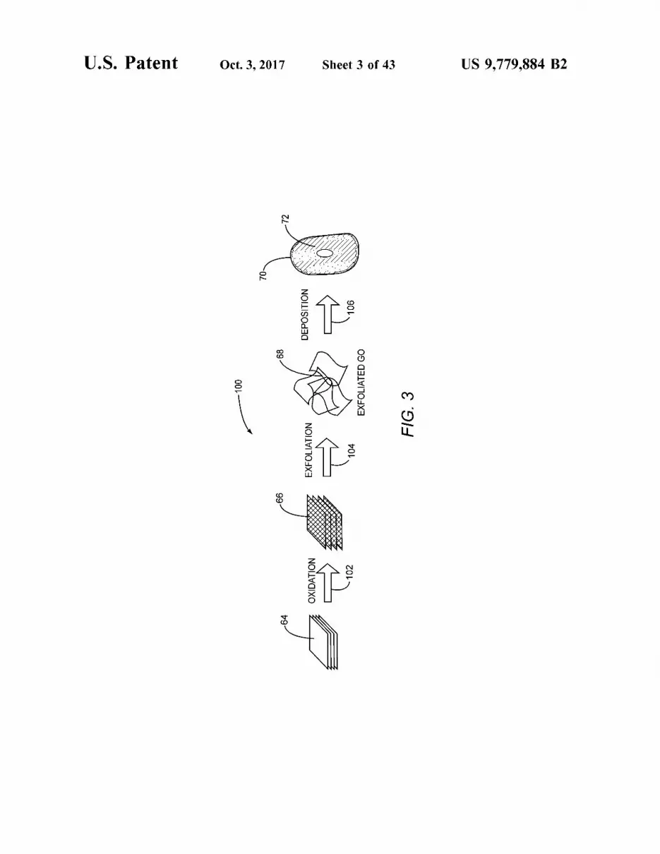
FIG . 6A is an artwork image of a man ' s head covered with curves of the device when operated at an ultrahigh current circuits . density of 250 AlgICCN / electrode :
FIG . 6B is a photograph of a GO film after the artwork FIG . 16 is a Ragone plot comparing the performance of image of FIG . 6A is directly patterned on the GO film using ICCN ECs with different energy storage devices designed the laser scribing technique of the present disclosure . 60 for high power microelectronics .
FIG . 7 is a graph that provides a comparison between FIG . 17A is a structural diagram showing a set of inter changes in electrical conductivity by reducing the GO film digitated electrodes made of ICCNs with dimensions of 6 of FIG . 6B by using various grayscale levels to laser scribe mmx6 mm , spaced at around about 500 um , that are directly the artwork of FIG . 6A to produce the patterned GO film of patterned onto a thin film of GO . FIG . 6B . 65 FIG . 17B is a structural diagram showing the set of
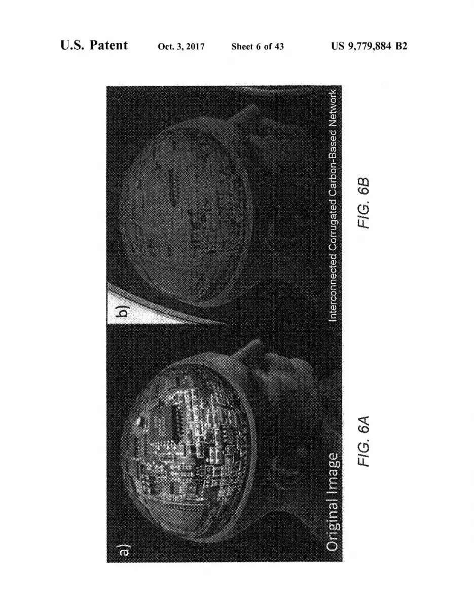
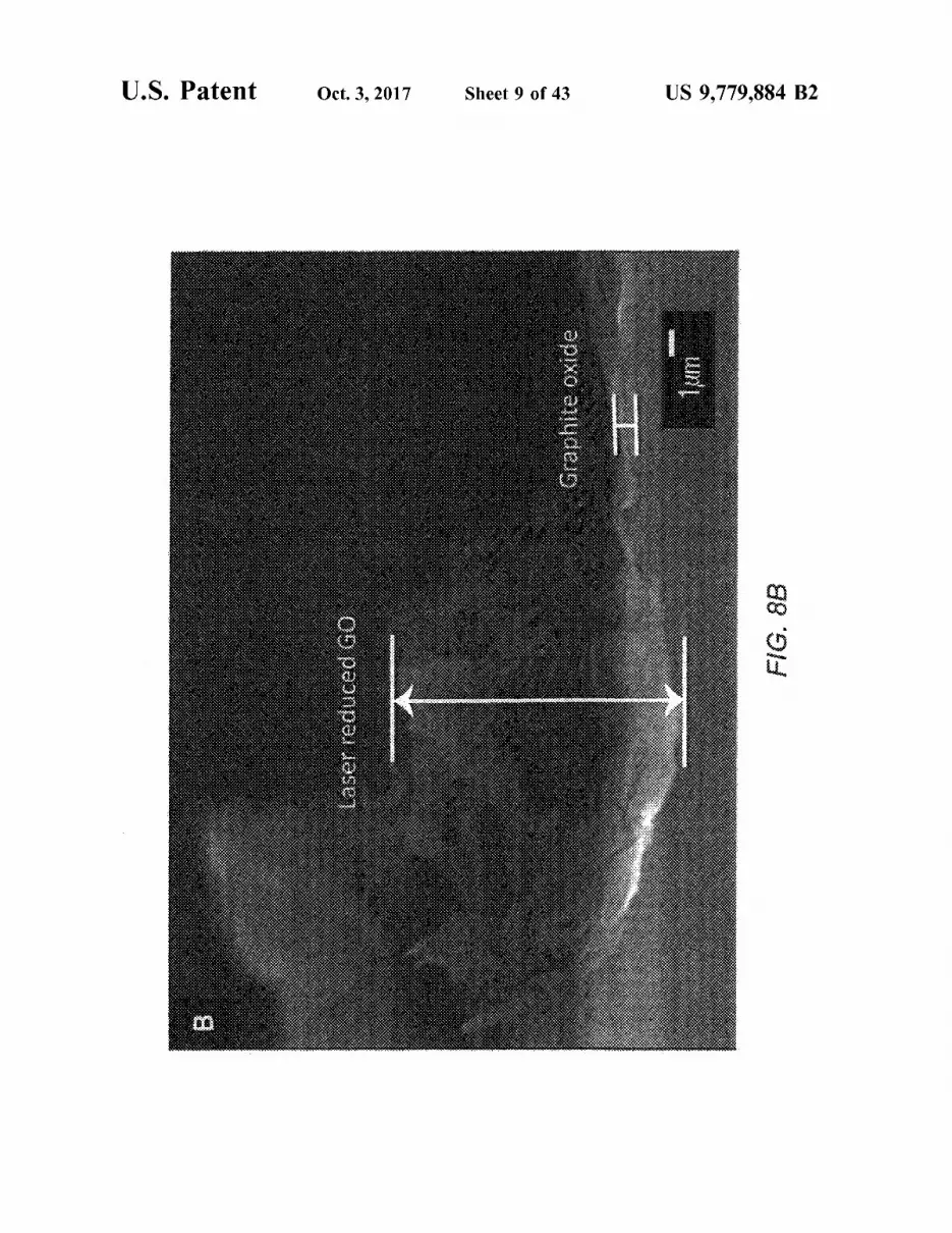
FIG . 8A is a scanning electron microscope ( SEM ) image interdigitated electrodes transferred onto another type of that illustrates an infrared laser ' s effect on GO film prior to substrate .
the ICCN .

US 9 , 779 , 884 B2 FIG . 18A shows an exploded view of a micro - superca duction of the ICCN does not require reducing agents , or
pacitor made up of a plurality of expanded and intercon expensive equipment . The simple direct fabrication of an nected carbon layers that are electrically conductive . ICCN on flexible substrates therefore simplifies the devel
FIG . 18B shows the micro - supercapacitor of FIG . 18A opment of lightweight electrical energy storage devices . The after assembly 5 ICCN can be synthesized on various substrates , such as
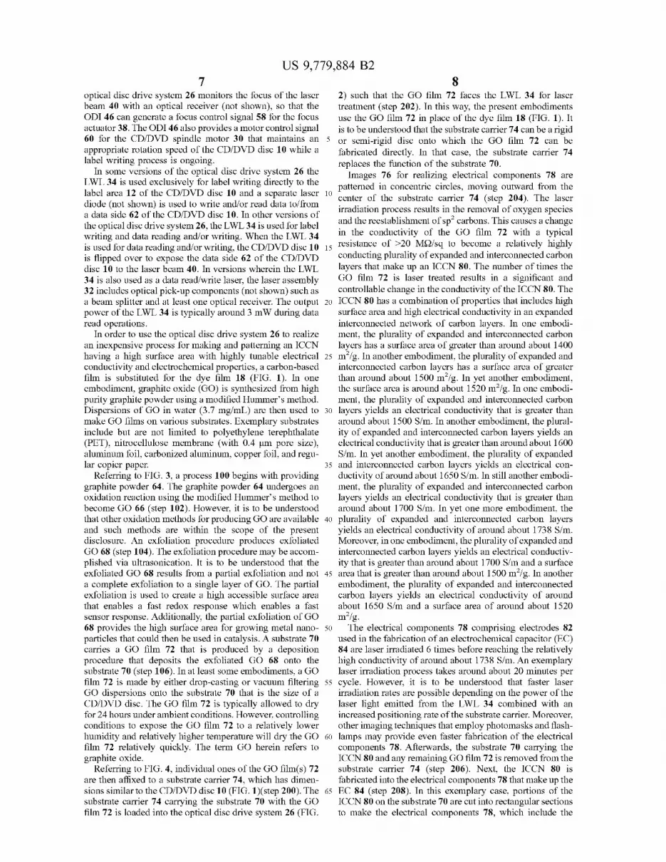
FIG . 19A depicts a micro - supercapacitor configuration plastic , metal , and glass . Herein an electrochemical capaci having a first electrode with two extending electrode digits tor ( EC ) , and in particular a micro - supercapacitor , is dis that are interdigitated with two extending electrode digits of closed . a second electrode . In at least one embodiment , the ICCNs are conducting
FIG . 19B depicts a micro - supercapacitor configuration 10 films produced using a common and inexpensive infrared having a first electrode with four extending electrode digits laser that fits inside a compact disc / digital versatile disc that are interdigitated with four extending electrode digits of ( CD / DVD ) optical drive unit that provides a direct - to - disc a second electrode . label writing function . LightScribe ( Registered Trademark
FIG . 19C depicts a micro - supercapacitor configuration of Hewlett Packard Corporation ) and LabelFlash ( Regis having a first electrode with eight extending electrode digits 15 tered Trademark of Yamaha Corporation ) are exemplary that are interdigitated with eight extending electrode digits direct - to - disc labeling technologies that pattern text and of a second electrode . graphics onto the surface of a CD / DVD disc . LightScribe
FIG . 20 is a table listing dimensions for the micro DVD drives are commercially available for around $ 20 and supercapacitors of FIGS . 19A - 19C . the LightScribing process is controlled using a standard
FIGS . 21A - 21E depict the fabrication of ICCN micro - 20 desktop computer . supercapacitors . FIG . 1 depicts the label side of a standard direct - to - disc
FIG . 22A depicts ICCN micro - devices with 4 , 8 , and 16 labeling type CD / DVD disc 10 that includes a label area 12 interdigitated electrodes . and a clamping area 14 that surrounds a centering hole 16 .
FIG . 22B depicts an ICCN micro - device with 16 inter - A dye film 18 covers the label area 12 and is sensitive to digitated fingers with 150 - um spacings . 25 laser energy that is typically directed onto the label area 12
FIG . 22C is a tilted view ( 459 ) SEM image that shows the to produce a permanent visible image that may comprise direct reduction and expansion of the GO film after exposure graphics 20 and text 22 . A position tracking indicia 24 is to the laser beam . usable by an optical disc drive ( not shown ) to accurately
FIGS . 22D and 22E show I - V curves of GO and an ICCN , locate an absolute angular position of the CD / DVD disc 10 respectively . 30 within the optical disc drive so that the graphics 20 and / or
FIG . 22F is a graphical comparison of electrical conduc - text 22 can be re - written to provide increased contrast . tivity values for GO and an ICCN . Moreover , the position tracking indicia 24 is usable by the FIGS . 23A - 231 are graphs depicting electrochemical per optical disc drive to allow additional graphics and / or text to
formance of ICCN micro - supercapacitors in PVA - H2SO4 be written without undesirably overwriting the graphics 20 gelled electrolyte . 35 and / or text 22 . FIGS . 24A - 24F are graphs depicting the behavior of FIG . 2 is a schematic of a prior art direct - to - disc labeling
ICCN micro - supercapacitors under mechanical stress in type optical disc drive system 26 . In this exemplary case , the series and parallel configurations . CD / DVD disc 10 is depicted in cross - section and loaded
FIGS . 25A - 25E are images depicting the fabrication of onto a spindle assembly 28 that is driven by a CD / DVD ICCN micro - supercapacitors on a chip along with graphs 40 spindle motor 30 . The label area 12 is shown facing a laser showing the characteristics of the micro - supercapacitors . assembly 32 that includes a label writer laser ( LWL ) 34 , a
FIGS . 26A - 26B are graphs depicting self discharge rates lens 36 , and a focus actuator 38 . The LWL 34 is typically a for ICCN micro - supercapacitors . laser diode . Exemplary specifications for the LWL 34
FIG . 27 is a Ragone plot of energy and power densities of includes a maximum pulse optical power of 350 mW at 780 ICCN micro - supercapacitors compared with commercially 45 nm emission and a maximum pulse output power of 300 mW available energy storage systems . at 660 nm emission . A laser beam 40 emitted by the LWL 34
is focused by the lens 36 that is alternately translated DETAILED DESCRIPTION towards and away from the LWL 34 by the focus actuator 38
in order to maintain focus of the laser beam 40 onto the label The embodiments set forth below represent the necessary 50 area 12 of the CD / DVD disc 10 . The laser beam 40 is
information to enable those skilled in the art to practice the typically focused to a diameter that ranges from around 0 . 7 disclosure and illustrate the best mode of practicing the um to around 1 um . disclosure . Upon reading the following description in light The laser assembly 32 is responsive to a control system 42 of the accompanying drawings , those skilled in the art will that provides control signals 44 through an optical drive understand the concepts of the disclosure and will recognize 55 interface ( ODI ) 46 . The control system 42 further includes applications of these concepts not particularly addressed a central processor unit ( CPU ) 48 and a memory 50 . Label herein . It should be understood that these concepts and image data ( LID ) having information needed to realize a applications fall within the scope of the disclosure and the permanent image to be written onto the label area 12 of the accompanying claims . CD / DVD disc 10 is processed by the CPU 48 , which in turn
The present disclosure provides an inexpensive process 60 provides an LID stream signal 52 that pulses the LWL 34 on for making and patterning an ICCN having stringent require - and off to heat the dye film 18 to realize the image defined ments for a high surface area with highly tunable electrical by the LID . conductivity and electrochemical properties . The embodi The CPU 48 also processes the LID through the ODI 46 ments described herein not only meet these stringent to provide a position control signal 54 to a radial actuator 56 requirements , but provide direct control over the conductiv - 65 that translates the laser assembly 32 in relation to the label ity and patterning of an ICCN while creating flexible elec - area 12 in response to position information contained in the tronic devices in a single step process . Moreover , the pro - LID . In some versions of the present embodiments , the
US 9 , 779 , 884 B2
optical disc drive system 26 monitors the focus of the laser 2 ) such that the GO film 72 faces the LWL 34 for laser beam 40 with an optical receiver ( not shown ) , so that the treatment ( step 202 ) . In this way , the present embodiments ODI 46 can generate a focus control signal 58 for the focus use the GO film 72 in place of the dye film 18 ( FIG . 1 ) . It actuator 38 . The ODI 46 also provides a motor control signal is to be understood that the substrate carrier 74 can be a rigid 60 for the CD / DVD spindle motor 30 that maintains an 5 or semi - rigid disc onto which the GO film 72 can be appropriate rotation speed of the CD / DVD disc 10 while a fabricated directly . In that case , the substrate carrier 74 label writing process is ongoing . replaces the function of the substrate 70 .
In some versions of the optical disc drive system 26 the Images 76 for realizing electrical components 78 are LWL 34 is used exclusively for label writing directly to the patterned in concentric circles , moving outward from the label area 12 of the CD / DVD disc 10 and a separate laser 10 center of the substrate carrier 74 ( step 204 ) . The laser diode ( not shown ) is used to write and / or read data to / from irradiation process results in the removal of oxygen species a data side 62 of the CD / DVD disc 10 . In other versions of and the reestablishment of sp² carbons . This causes a change the optical disc drive system 26 , the LWL 34 is used for label in the conductivity of the GO film 72 with a typical writing and data reading and / or writing . When the LWL 34 is used for data reading and / or writing the CD / DVD disc 10 15 resistance of > 20 MQ / sq to become a relatively highly is flipped over to expose the data side 62 of the CD / DVD conducting plurality of expanded and interconnected carbon disc 10 to the laser beam 40 . In versions wherein the LWL layers that make up an ICCN 80 . The number of times the 34 is also used as a data read / write laser , the laser assembly GO film 72 is laser treated results in a significant and 32 includes optical pick - up components ( not shown ) such as controllable change in the conductivity of the ICCN 80 . The a beam splitter and at least one optical receiver . The output 20 ICCN 80 has a combination of properties that includes high power of the LWL 34 is typically around 3 mW during data surface area and high electrical conductivity in an expanded read operations . interconnected network of carbon layers . In one embodi
In order to use the optical disc drive system 26 to realize ment , the plurality of expanded and interconnected carbon an inexpensive process for making and patterning an ICCN layers has a surface area of greater than around about 1400 having a high surface area with highly tunable electrical 25 m² / g . In another embodiment , the plurality of expanded and conductivity and electrochemical properties , a carbon - based interconnected carbon layers has a surface area of greater film is substituted for the dye film 18 ( FIG . 1 ) . In one than around about 1500 m² / g . In yet another embodiment , embodiment , graphite oxide ( GO ) is synthesized from high the surface area is around about 1520 m² / g . In one embodi purity graphite powder using a modified Hummer ' s method . ment , the plurality of expanded and interconnected carbon Dispersions of GO in water ( 3 . 7 mg / mL ) are then used to 30 layers yields an electrical conductivity that is greater than make GO films on various substrates . Exemplary substrates around about 1500 S / m . In another embodiment , the plural include but are not limited to polyethylene terephthalate ity of expanded and interconnected carbon layers yields an ( PET ) , nitrocellulose membrane ( with 0 . 4 um pore size ) , electrical conductivity that is greater than around about 1600 aluminum foil , carbonized aluminum , copper foil , and regu S / m . In yet another embodiment , the plurality of expanded lar copier paper . 35 and interconnected carbon layers yields an electrical con
Referring to FIG . 3 , a process 100 begins with providing ductivity of around about 1650 S / m . In still another embodi graphite powder 64 . The graphite powder 64 undergoes an ment , the plurality of expanded and interconnected carbon oxidation reaction using the modified Hummer ' s method to layers yields an electrical conductivity that is greater than become GO 66 ( step 102 ) . However , it is to be understood around about 1700 S / m . In yet one more embodiment , the that other oxidation methods for producing GO are available 40 plurality of expanded and interconnected carbon layers and such methods are within the scope of the present yields an electrical conductivity of around about 1738 S / m . disclosure . An exfoliation procedure produces exfoliated Moreover , in one embodiment , the plurality of expanded and GO 68 ( step 104 ) . The exfoliation procedure may be accom interconnected carbon layers yields an electrical conductiv plished via ultrasonication . It is to be understood that the ity that is greater than around about 1700 S / m and a surface exfoliated GO 68 results from a partial exfoliation and not 45 area that is greater than around about 1500 mº / g . In another a complete exfoliation to a single layer of GO . The partial embodiment , the plurality of expanded and interconnected exfoliation is used to create a high accessible surface area carbon layers yields an electrical conductivity of around that enables a fast redox response which enables a fast about 1650 S / m and a surface area of around about 1520 sensor response . Additionally , the partial exfoliation of GO ma / g . 68 provides the high surface area for growing metal nano - 50 The electrical components 78 comprising electrodes 82 particles that could then be used in catalysis . A substrate 70 used in the fabrication of an electrochemical capacitor ( EC ) carries a GO film 72 that is produced by a deposition 84 are laser irradiated 6 times before reaching the relatively procedure that deposits the exfoliated GO 68 onto the high conductivity of around about 1738 S / m . An exemplary substrate 70 ( step 106 ) . In at least some embodiments , a GO laser irradiation process takes around about 20 minutes per film 72 is made by either drop - casting or vacuum filtering 55 cycle . However , it is to be understood that faster laser GO dispersions onto the substrate 70 that is the size of a irradiation rates are possible depending on the power of the CD / DVD disc . The GO film 72 is typically allowed to dry laser light emitted from the LWL 34 combined with an for 24 hours under ambient conditions . However , controlling increased positioning rate of the substrate carrier . Moreover , conditions to expose the GO film 72 to a relatively lower other imaging techniques that employ photomasks and flash humidity and relatively higher temperature will dry the GO 60 lamps may provide even faster fabrication of the electrical film 72 relatively quickly . The term GO herein refers to components 78 . Afterwards , the substrate 70 carrying the graphite oxide . ICCN 80 and any remaining GO film 72 is removed from the Referring to FIG . 4 , individual ones of the GO film ( s ) 72 substrate carrier 74 ( step 206 ) . Next , the ICCN 80 is
are then affixed to a substrate carrier 74 , which has dimen - fabricated into the electrical components 78 that make up the sions similar to the CD / DVD disc 10 ( FIG . 1 ) ( step 200 ) . The 65 EC 84 ( step 208 ) . In this exemplary case , portions of the substrate carrier 74 carrying the substrate 70 with the GO ICCN 80 on the substrate 70 are cut into rectangular sections film 72 is loaded into the optical disc drive system 26 ( FIG . to make the electrical components 78 , which include the

US 9 , 779 , 884 B2 10
electrodes 82 formed from the ICCN 80 . A separator / has on the structural properties of GO film by comparing the electrolyte 86 is sandwiched between the electrodes 82 to morphological differences between an ICCN and untreated form the EC 84 . graphite oxide GO film . FIG . 8A is an SEM image that
The ICCN 80 possesses a very low oxygen content of only illustrates the infrared laser ' s effect on GO film prior to laser around about 3 . 5 % , which contributes to a relatively very 5 treatment on the right side of the image in contrast to an high charging rate . In other embodiments , the oxygen con - aligned ICCN on the left side of the image that occurs after tent of the expanded and interconnected carbon layers being reduced with the infrared laser . The image not only ranges from around about 1 % to around about 5 % . FIG . 5 is gives a clear definition between the ICCN and untreated GO a line drawing of a sample of the ICCN 80 , which is made regions , but also demonstrates the level of precision possible up of the plurality of expanded and interconnected carbon 10 when using this method as a means to pattern and reduce layers that include corrugated carbon layers such as a single GO . The regions of ICCN , which result from the laser corrugated carbon sheet 88 . In one embodiment , each of the treatment , can be further analyzed through cross - sectional expanded and interconnected carbon layers comprises at SEM . least one corrugated carbon sheet that is one atom thick . In FIG . 8B is an SEM image showing a cross - sectional view another embodiment , each of the expanded and intercon - 15 of a free standing film of laser treated and untreated GO film , nected carbon layers comprises a plurality of corrugated which shows a significant difference between GO film carbon sheets 88 . The thickness of the ICCN 80 , as mea - thicknesses . As indicated by the white brackets in FIG . 8B , sured from cross - sectional scanning electron microscopy an ICCN increases in thickness by approximately 10 times ( SEM ) and profilometry , was found to be around about 7 . 6 in comparison to that of untreated GO film . Moreover , a um . In one embodiment , a range of thicknesses of the 20 range of thicknesses of the plurality of expanded and inter plurality of expanded and interconnected carbon layers connected carbon layers is from around about 7 um to making up the ICCN 80 is from around about 7 um to 8 um . around 8 um . In one embodiment , an average thickness of
As an illustration of the diversity in image patterning that the plurality of expanded and interconnected carbon layers is possible , a complex image formed by the direct laser is around about 7 . 6 um . The increased thickness stems from reduction of GO is shown in FIGS . 6A and 6B . FIG . 6A is 25 rapid degassing of gases generated and released during laser an artwork image of a man ' s head covered with circuits . treatment , similar to thermal shock , which effectively causes FIG . 6B is a photograph of a GO film after the artwork the reduced GO to expand and exfoliate as these gases image of FIG . 6A is directly patterned on the GO film using rapidly pass through the GO film . FIG . 8C is an SEM image the laser scribing technique of the present disclosure . Essen - showing a cross - sectional view of a single ICCN , which tially , any part of the GO film that comes in direct contact 30 shows an expanded structure that is a characteristic of the with the 780 nm infrared laser is effectively reduced to an ICCN of the present disclosure . ICCN , with the amount of reduction being controlled by the FIG . 8D is an SEM image showing a greater magnifica laser intensity ; a factor that is determined by power density tion of a selected area within the ICCN in FIG . 8C . The SEM of the laser beam impinging on the GO film . The resulting image of FIG . 8D allows the thickness of the plurality of image of FIG . 6B is an effective print of the original image 35 expanded and interconnected carbon layers to be calculated of FIG . 6A . However , in this case the image of FIG . 6B is to be between around about 5 - 10 nm . However , the number made up of various reductions of the GO film . As expected , of carbon layers in the plurality of expanded and intercon the darkest black areas indicate exposure to the strongest nected carbon layers making up the ICCN is greater than laser intensities , while the lighter gray areas are only par - around about 100 . In another embodiment the number of tially reduced . Since different grayscale levels directly cor - 40 carbon layers in the plurality of expanded and intercon relate with the laser ' s intensity , it is possible to tune the nected carbon layers is greater than around about 1000 . In electrical properties of the generated ICCN over five to yet another embodiment the number of carbon layers in the seven orders of magnitude in sheet resistance ( 92 / sq ) by plurality of expanded and interconnected carbon layers is simply changing the grayscale level used during the pattern greater than around about 10 , 000 . In still another embodi ing process . As illustrated in FIG . 7 , there is a clear 45 ment , the number of carbon layers in the plurality of relationship between sheet resistance , grayscale level and expanded and interconnected carbon layers is greater than the number of times the GO film is laser irradiated . Control around about 100 , 000 . The SEM analysis shows that over conductivity from a completely insulating GO film , although an infrared laser emission is only marginally with a typical sheet resistance value of > 20 MQ / sq , to a absorbed by GO , enough power and focus ( i . e . , power conducting ICCN that registers a sheet resistance value of 50 density ) can cause sufficient thermal energy to efficiently approximately 80 2 / sq , which translates to a conductivity of reduce , deoxygenate , expand , and exfoliate the GO film . around about 1650 S / m , is possible . This method is sensitive Moreover , the surface area of the ICCN is greater than enough to differentiate between similar grayscale levels as around about 1500 m² / g . shown in the graph of FIG . 7 , where the sheet resistance Since each of the carbon layers has a theoretical surface varies significantly with only a small variation in grayscale 55 area of around about 2630 m² / g , a surface greater than level . In addition , the number of times a GO film is laser around about 1500 m - / g indicates that almost all surfaces of treated results in a significant and controllable change in the carbon layers are accessible . The ICCN has an electrical sheet resistance . Each additional laser treatment lowers the conductivity that is greater than around about 17 S / cm . The sheet resistance as seen in FIG . 7 , where a film is laser ICCN forms when some wavelength of light hits the surface irradiated once ( black squares ) , twice ( circles ) and three 60 of the GO , and is then absorbed to practically immediately times ( triangles ) with respect to the grayscale level . There convert to heat , which liberates carbon dioxide ( CO2 ) . fore , the film ' s sheet resistance is tunable both by controlling Exemplary light sources include but are not limited to a 780 the grayscale level used and the number of times the film is nm laser , a green laser , and a flash lamp . The light beam reduced by the laser , a property that has so far been difficult emission of the light sources may range from near infrared to control through other methods . 65 to ultraviolet wavelengths . The typical carbon content of the
Scanning electron microscope ( SEM ) techniques are ICCN is greater than around about 97 % with less than usable to understand the effects a low energy infrared laser around about 3 % oxygen remaining . Some samples of the

11 US 9 , 779 , 884 B2
12 ICCN are greater than around about 99 % carbon even domains . The result is consistent with SEM analysis , where though the laser reduction process is conducted in the air . the generation of exfoliated accordion - like graphitic regions
FIG . 9 compares a powder X - ray diffraction ( XRD ) ( FIG . 5 ) caused by the laser treatment creates a large number pattern of the corrugated carbon - based network with both of edges . However the D band also shows a significant graphite and graphite oxide diffraction patterns . A typical 5 overall peak narrowing , suggesting a decrease in these types XRD pattern for graphite , shown in FIG . 9 trace A , displays of defects in the ICCN . The G band experiences a narrowing the characteristic peak of 20 = 27 . 8° with a d - spacing of 3 . 20 and a decrease in peak intensity as well as a peak shift from Å . An XRD pattern ( FIG . 9 , trace B ) for GO , on the other around about 1585 to 1579 cm - 7 . These results are consis hand , exhibits a single peak of 20 = 10 . 769 , which corre - tent with the re - establishment of spa carbons and a decrease sponds to an interlayer d - spacing of 8 . 22 Å . The increased 10 in structural defects within the basal planes . The overall d - spacing in GO is due to the oxygen containing functional changes in the G band indicate a transition from an amor groups in graphite oxide sheets , which tend to trap water p hous carbon state to a more crystalline carbon state . In molecules between the basal planes , causing the sheets to addition , a prominent and shifted 2D peak from around expand and separate . The XRD pattern of the corrugated about 2730 to around about 2688 cm - ' is seen after GO is carbon - based network ( FIG . 9 , trace C ) shows the presence 15 treated with the infrared laser , indicating a considerable of both GO ( 10 . 76° 20 ) and a broad graphitic peak at 25 . 97° reduction of the GO film and strongly points to the presence 20 associated with a d - spacing of 3 . 43 Å . The GO presence of a few - layer interconnected graphite structure . In one in the corrugated carbon - based network is expected since the embodiment , the 2D Raman peak for the ICCN shifts from laser has a desirable penetration depth , which results in the around about 2700 cm - ' to around about 2600 cm - 1 after the reduction of only the top portion of the film with the bottom 20 ICCN is reduced from a carbon - based oxide . Moreover , as layer being unaffected by the laser . The small presence of a result of lattice disorder , the combination of D - G generates GO is more prominent in thicker films , but begins to an S3 second order peak , which appears at around about diminish in thinner films . In addition , one can also observe 2927 cm - 1 and , as expected , diminishes with decreasing a partially obstructed peak at 26 . 66° 20 , which shows a disorder after infrared laser treatment . In some embodi similar intensity to the broad 25 . 97° 20 peak . Both of these 25 ments , the plurality of expanded and interconnected carbon peaks are considered graphitic peaks , which are associated layers has a range of Raman spectroscopy S3 second order to two different lattice spacing between basal planes . peak that ranges from around about 2920 cm to around
It has been previously shown that the immobilization of about 2930 cm - 1 . The Raman analysis demonstrates the carbon nanotubes ( CNTs ) on glassy carbon electrodes will effectiveness of treating GO with an infrared laser as a result in a thin CNT film , which directly affects the volta - 30 means to effectively and controllably produce the ICCN . mmetric behavior of the CNT modified electrodes . In a X - ray photoelectron spectroscopy ( XPS ) was employed ferro / ferrocyanide redox couple , the voltammetric current to correlate the effects of laser irradiation on the oxygen measured at the CNT modified electrode will likely have two functionalities and to monitor the structural changes on the types of contributions . The thin layer effect is a significant GO film . Comparing the carbon to oxygen ( C / O ) ratios contributor to the voltammetric current . The thin layer effect 35 between GO and the ICCN provides an effective measure stems from the oxidation of ferrocyanide ions , which are ment of the extent of reduction achieved using a simple low trapped between the nanotubes . The other contribution energy infrared laser . FIG . 11B illustrates the significant results from the semi - infinite diffusion of ferrocyanide disparity between the C / O ratios before and after laser towards the planar electrode surface . Unfortunately , the treatment of the GO films . Prior to laser reduction , typical mechanistic information is not easily de - convoluted and 40 GO films have a C / O ratio of approximately 2 . 6 : 1 , corre requires knowledge of the film thickness . sponding to a carbon / oxygen content of around about 72 %
In contrast , no thin layer effect is observed in association and 38 % . In one exemplary embodiment , the ICCN has an with the interconnected corrugated carbon - based network of enhanced carbon content of around about 96 . 5 % and a the present disclosure . FIG . 10 is a plot of logio of peak diminished oxygen content of around about 3 . 5 % , giving an current versus logo of an applied voltammetric scan rate . In 45 overall C / O ratio of 27 . 8 : 1 . In yet another exemplary this case , no thin layer effect is observed since the plot has embodiment , a laser reduction of GO results in a C / O ratio a consistent slope of 0 . 53 and is linear . The slope of 0 . 53 is of 333 : 1 , which is around about 0 . 3 % oxygen content . This relatively close to theoretical values calculated using a relatively low oxygen content was measured using photo semi - infinite diffusion model governed by the Randles electron spectroscopy ( XPS ) . In other embodiments , the Sevcik equation : 50 plurality of expanded and interconnected carbon layers has
a C / O ratio that ranges from around about 333 : 1 to around about 25 : 1 . Since the laser reduction process takes place under ambient conditions , it is postulated that some of the DovínF ) 3 oxygen present in the ICCN film is a result of the film having
55 a static interaction with oxygen found in the environment . FIG . 11C shows that the Cls XPS spectrum of GO
Raman spectroscopy is used to characterize and compare displays two broad peaks , which can be resolved into three the structural changes induced by laser treating GO film . different carbon components corresponding to the functional FIGS . 11A - 11E are graphs related to Raman spectroscopic groups typically found on the GO surface , in addition to a analysis . As can be seen in FIG . 11A , characteristic D , G , 2D 60 small i to * peak at 290 . 4 eV . These functional groups and S3 peaks are observed in both GO and the ICCN . The include carboxyl , sp3 carbons in the form of epoxide and presence of the D band in both spectra suggests that carbon hydroxyl , and sp2 carbons , which are associated with the sp3 centers still exist after reduction . Interestingly , the spec - following binding energies : approximately 288 . 1 , 286 . 8 and trum of the ICCN shows a slight increase in the D band peak 284 . 6 eV , respectively . at around about 1350 cm . This unexpected increase is due 65 FIG . 11D shows expected results , in that the large degree to a larger presence of structural edge defects and indicates of oxidation in GO results in various oxygen components in an overall increase in the amount of smaller graphite the GO C1s XPS spectrum . These results are in contrast to
in = 0 . 3443ACOV RT
13 US 9 , 779 , 884 B2
14 the ICCN , which shows a significant decrease in oxygen different designs , including stacked and spirally wound containing functional groups and an overall increase in the structures to target different applications . C - C sp2 carbon peak . This points to an efficient deoxy The ICCN electrodes are fabricated to satisfy the critical genating process as well as the re - establishment of C = C features for high - performance ECs . First , the relatively large bonds in the ICCN . These results are consistent with the 5 and accessible specific surface area of an ICCN ( 1520 m?lg Raman analysis . Thus , an infrared laser such as the LWL 34 compared with 1000 to 2000 m² / g for a typical activated ( FIG . 2 ) is powerful enough to remove a majority of the carbon material ) results in a sizeable charge storage capacity
and accounts for the high areal and volumetric stack capaci oxygen functional groups , as is evident in the XPS spectrum tances observed . Second , the LWL 34 ( FIG . 2 ) that is of the ICCN , which only shows a small disorder peak and a
peak at 287 . 6 eV . The latter corresponds to the presence of f 10 typically a LightScribe or a Label Flash laser , causes the simultaneous reduction and partial exfoliation of GO sheets sp type carbons suggesting that a small amount of carboxyl and produces the ICCN 80 ( FIG . 5 ) . The novel structure of groups remain in the final product . In addition , the presence the ICCN 80 is porous , which prevents the agglomeration of
of a t to I * satellite peak at ~ 290 . 7 eV indicates that carbon sheets , which has been a major barrier in achieving delocalized it conjugation is significantly stronger in the 15 the full potential of carbon - based ECs . The network struc ICCN as this peak is miniscule in the GO XPS spectrum . ture of the ICCN 80 has open pores , which facilitates The appearance of the delocalized IF peak is a clear indi electrolyte accessibility to the electrode surfaces . This offers cation that conjugation in the GO film is restored during the an opportunity to optimize ionic diffusion in the electrodes laser reduction process and adds support that an sp ; carbon 82 , which is crucial for charging the electrochemical double network has been re - established . The decreased intensity of 20 layers ( EDLs ) , and generates high power ECs . Moreover , the oxygen containing functional groups , the dominating the ICCN 80 possesses excellent electronic conductivity , C = C bond peak and the presence of the delocalized it which is another key factor for achieving high power . conjugation all indicate that a low energy infrared laser is an Working with these properties , three dimensional composite effective tool in the generation of the ICCN . electrodes have been successfully used to make batteries
FIG . 11E depicts UV - visible light absorbance spectra of 25 with relatively high energy density and fast charge / discharge GO shown in black . The inset shows a magnified view of the rates . Although activated carbons can provide high surface boxed area showing the absorbance of GO with respect to a area , the difficulty of controlling their pore structure and 780 nm infrared laser in the 650 to 850 nm region . pore size distribution has so far limited the energy densities Having established that an ICCN has an effective Tr and rate capabilities of commercial ECs .
conjugation , it is possible to construct devices to make use 30 In order to demonstrate the superior performance of ICCN of the conducting material . In this regard , at least one electrodes for electrochemical energy storage , symmetric embodiment of the present disclosure provides the produc ICCN ECs were assembled using polyethylene terephthalate tion of ICCN ECs through a simple all - solid - state approach ( PET ) as a thin flexible substrate and an aqueous electrolyte that avoids the restacking of carbon sheets such as the of 1 . 0 molar ( M ) phosphoric acid ( H2PO4 ) . As shown in corrugated carbon sheet 88 ( FIG . 5 ) . Irradiation of the GO 35 FIGS . 13A - 13F , the ICCN EC performance was analyzed film 72 ( FIG . 3 ) with an infrared laser such as the LWL 34 through both cyclic voltammetry ( CV ) and galvanostatic ( FIG . 2 ) inside the inexpensive commercially available charge / discharge ( CC ) experiments . In comparison with direct - to - disc labeling type optical disc drive system 26 GO , the ICCN EC shows an enhanced electrochemical ( FIG . 2 ) which , as discussed above , reduces the GO film 72 performance with a nearly rectangular CV shape at a scan to an ICCN , as indicated by the change in film color from 40 rate of 1000 mV / s , which is indicative of nearly ideal golden brown to black . Analysis of cross sections of the film capacitive behavior ( FIG . 13A ) even though no metal cur with scanning electron microscopy showed that the initially rent collectors , binders , or electroactive additives were used , stacked GO sheets were converted into partially - exfoliated as is the case in commercial ECs . Additionally , the ICCN EC carbon sheets through laser irradiation ( FIG . 3 ) . The result is robust enough to be charged and discharged over a wide ing ICCN showed excellent conductivity ( around about 45 range of scan rates ( 100 to 10 , 000 mV / s ) and still maintain 1738 S / m ) as opposed to 10 to 100 S / m for activated its nearly ideal rectangular CV shape . FIG . 13B shows the carbons , the current state - of - the - art material used in com - nearly triangular shape of the CC curves obtained at a high mercial devices . current density of 10 A / g of ICCN per electrode ( abbreviated
In addition , FIGS . 12A and 12B show that the ICCN made 10 A / S CCN electrode ) . This is indicative of the formation of an up of corrugated carbon sheets shows excellent mechanical 50 efficient EDL and fast ion transport within the ICCN elec flexibility with only around about 1 % change in the electri - trodes . In addition , these CC curves show only a small cal resistance of the film after 1000 bending cycles . Thus , voltage drop of 0 . 018 V at the start of the discharge curve , ICCNs can be directly used as EC electrodes without the indicating a device with a low equivalent series resistance need for any additional binders or conductive additives . ( ESR ) . The specific capacitance from the CC curves was More importantly , these properties allow ICCNs to act as 55 measured over a wide range of charge discharge current both an active material and current collector in the EC . The densities . Here , the areal and volumetric capacitances of the combination of both functions in a single layer leads to a stack ( this includes the flexible substrate , the current col simplified and lightweight architecture . Thus , a device can lector , the active material , and the separator ) were calculated be readily made by sandwiching an ion porous separator and compared with a commercial activated - carbon EC ( AC Celgard 3501 ( Celgard , Charlotte , N . C . ) ] between two 60 EC ) tested under the same dynamic conditions . Although the ICCN electrodes . ICCN ECs are relatively thin with a total AC - EC shows a slightly higher volumetric capacitance at thickness of less than around about 100 mm , making them low charge / discharge rates , its capacitance falls off quickly potentially useful in microdevice applications . Other devices at higher rates , whereas the ICCN EC continues to provide can be made by putting ICCNs on porous substrates such as high capacitance even when operated at very high rates a nitrocellulose membrane or photocopy paper or on con - 65 ( FIG . 13C ) . In addition , the areal capacitance of the ICCN ductive aluminum foil , which is often used in commercial EC was calculated to be 3 . 67 mF / cm and 4 . 04 mF / cm2 in devices . Therefore , ICCN ECs can be readily made into 1 . 0 M H2SO4 at 1 A / 81CCN / electrode . The device also shows

US 9 , 779 , 884 B2 15 16
a a very high rate capability while still maintaining a capaci performance was completely stable over 4 months of testing . tance of more than 1 . 84 mF / cm2 , even when the ICCN EC As with the aqueous ICCN EC , the flexible all - solid - state is operated at an ultrafast charge / discharge rate of 1000 ICCN EC maintains its excellent cycling stability : > 97 % of A / GCCN / electrode . This is comparable with values reported in the initial capacitance was maintained even after 10 , 000 the literature for micro - devices and thin film ECs at much 5 cycles . lower current charge / discharge rates ( 0 . 4 to 2 mF / cm² ) . In order to evaluate under real conditions the potential of These ECs can be efficiently charged / discharged on the 0 . 1 - s all - solid - state ICCN ECs , such as the EC 84 , for flexible time scale . Additionally , the ICCN EC retained around about energy storage , a device was placed under constant mechani 96 . 5 % of its initial capacitance after 10 , 000 cycles ( FIG . cal stress and its performance analyzed . FIG . 14D shows the 13D ) . 10 CV performance of this device when tested under different
Electrochemical impedance spectroscopy ( EIS ) con - bending conditions . The bending had almost no effect on the firmed fast ion transport within the ICCN electrodes . A capacitive behavior ; it can be bent arbitrarily without complex plan plot of the impedance data of the ICCN EC is degrading performance . Moreover , the stability of the device shown in FIG . 13E with an expanded view provided in the was tested for more than 1000 cycles while in the bent state , inset . The device displays a pure capacitive behavior , even 15 with only - 5 % change in the device capacitance . This at high frequencies of up to - 158 Hz . The series resistance performance durability can be attributed to the high of the device is estimated to be ~ 16 ohms . This value can be mechanical flexibility of the electrodes along with the inter attributed to the contact resistance of the device with the penetrating network structure between the ICCN electrodes external circuit that could be reduced by using current and the gelled electrolyte . The electrolyte solidifies during collectors . The dependence of the phase angle on the fre - 20 the device assembly and acts like a glue that holds all the quency for the ICCN EC , AC - EC , and an aluminum elec device components together , improving the mechanical trolytic capacitor is shown in FIG . 13F . For frequencies up integrity and increasing its cycle life even when tested under to 10 Hz , the phase angle of the ICCN EC is close to - 90° , extreme bending conditions . Because the increased cycle which suggests that the device functionality is close to that life of the present EC has yet to be realized in commercial of an ideal capacitor . The characteristic frequency fo for a 25 devices , the present ECs may be ideal for next - generation phase angle of - 45° is 30 Hz for the ICCN EC . This flexible , portable electronics . frequency marks the point at which the resistive and capaci - Portable equipment often requires cells packaged either in tive impedances are equal . The corresponding time constant series , in parallel , or in combinations of the two in order to to ( = 1 / f0 ) equals 33 ms compared with 10 seconds for the meet energy and power requirements . For example , laptop conventional AC - EC and 1 ms for the aluminum electrolytic 30 batteries commonly have four 3 . 6 - V lithium ion cells con capacitor . This rapid frequency response of the ICCN EC nected in series to achieve a voltage of 14 . 4 V , and two in can be accounted for by the large and accessible surface area parallel to increase the capacity from 2400 mAh to 4800 of the ICCN , whose exposed flat sheets enhance the ion mAh . Thus , it would be of interest to develop an EC that transport rate in the device . This is consistent with results could exhibit control over the operating voltage and current reported recently for an EC made from vertically oriented 35 by using tandem serial and parallel assemblies with minimal graphene nanosheets grown directly on metal current col - energy losses . The performances of a set of tandem ICCN lectors and carbon nanotube electrodes made with an elec - ECs were evaluated by assembling four devices both in trophoretic deposition technique . series and in parallel configurations . Compared with a single
The future development of multifunctional flexible elec - EC , which operates at 1 . 0 V , the tandem series ECs exhibited tronics such as roll - up displays , photovoltaic cells , and even 40 a 4 . 0 V charge / discharge voltage window . In the parallel wearable devices presents new challenges for designing and assembly , the output current increased by a factor of 4 , and fabricating lightweight , flexible energy storage devices . thus the discharge time was four times that of a single device Commercially available ECs consist of a separator sand when operated at the same current density . As expected , wiched between two electrodes with liquid electrolyte , when the four ECs were combined , two in series and two in which is then either spirally wound and packaged into a 45 parallel , both the output voltage and the runtime ( capacitive cylindrical container or stacked into a button cell . Unfortu - current ) increased by a factor of 2 under the same charge ! nately , these device architectures not only suffer from the discharge current . As with the single devices , the tandem possible harmful leakage of electrolytes , but their design devices show essentially perfect triangular CC curves with makes it difficult to use them for practical flexible electron - a miniscule voltage drop , which again indicates excellent ics . Referring to FIG . 14A depicting the structure of the EC 50 capacitive properties with minimal internal resistance . Thus , 84 , the liquid electrolyte was replaced with poly ( vinyl when used in tandem , the ICCN ECs undergo minimal alcohol ) ( PVA ) - H2PO4 polymer gelled electrolyte , which energy losses . As a demonstration , a tandem EC ' s ability to also acts as the separator . This electrolyte reduced the device light a red light - emitting diode ( LED ) that operates at a thickness and weight compared with phosphoric acid and minimum voltage of 2 V is shown in the FIGS . 14E and 14F . simplified the fabrication process because it does not require 55 An organic electrolyte was also examined , and was dis any special packaging materials . As demonstrated in FIG . covered to allow the operation of the devices at higher 14B , at any given charge / discharge rate , the specific capaci - voltages , thus achieving higher energy densities . In this case , tance values for the all - solid - state device were comparable tetraethylammonium tetrafluoroborate dissolved in acetoni with those obtained with an aqueous electrolyte . The high - trile was used because this is the most common organic rate performance of the EC 84 can be accounted for by the 60 electrolyte used in commercial devices . As shown in FIG . porous structure of the ICCN electrodes , which can effec - 15 , the ICCN EC again exhibits enhanced performance and tively absorb the gelled electrolyte and act as an electrolyte rate capabilities when compared with the commercial AC reservoir to facilitate ion transport and minimize the diffu - EC ; this is consistent with the data acquired in the aqueous sion distance to the interior surfaces . Another key factor is and gelled electrolytes . Furthermore , the ICCN EC can be that ICCN electrodes are binder free , thus enabling a reduc - 65 operated over a wider voltage window of 3 V . This ICCN EC tion in interfacial resistance and enhancing the electrochemi - offers a specific capacitance of up to 4 . 82 mF / cm2 ( 265 cal reaction rate . As illustrated in FIG . 14C , the device F / 87CCN / electrode ) and retains a capacitance of 2 . 07 mF / cm²

US 9 , 779 , 884 B2 17
when operated at the ultrahigh current density of 1000 remaining one of either the first electrode 92 or the second A / GICCN / electrode . Recently , room - temperature ionic liquids electrode 94 is made of ICCNs . However , the first electrode have been intensively studied as an attractive alternative to 92 and the second electrode 94 are typically laser scribed conventional electrolytes for ECs because of their high ion from a GO film disposed onto a suitable substrate 96 such as density , good thermal stability , and nonvolatility , as well as 5 PET or silicon ( Si ) having an insulating layer 97 such as a their wider potential window when compared with organic silicon dioxide ( SiO2 ) layer . A first conductive strip 98 and electrolytes . An ICCN EC was fabricated using the ionic a second conductive strip 100 are interfaced with the first liquid l - ethyl - 3 - methylimidazoliumtetrafluoroborate electrode 92 and the second electrode 94 to provide electri ( EMIMBF ) that exhibited a specific capacitance as high as cally conductive terminals to couple to external circuitry 5 . 02 mF / cm² ( 276 F / giocletectrode ) and at a wider potential 10 ( not shown ) . Exemplary external circuitry to be powered by window of 4 V . A prototype ICCN EC was made and the micro - supercapacitor 90 can be , but is not limited to , encapsulated in the EMIMBF4 electrolyte , charged at a integrated circuits and other electrically powered micro constant potential of 3 . 5 V , and used to energize a red LED scale devices . A liner 102 that is non - electrically conductive for ~ 24 minutes . covers the portions of the first electrode 92 and the second
FIG . 16 is a Ragone plot comparing the performance of 15 electrode 94 that are interfaced with the first conductive strip ICCN ECs with different energy storage devices designed 98 and the second conductive strip 100 . The liner 102 for high power microelectronics . FIG . 16 also shows the includes a central window through which an electrolyte 104 overall performance of the ICCN ECs using various elec - is placed in contact with the first electrode 92 and the second trolytes . The Ragone plot includes a commercial 2 . 75 V / 44 electrode 94 . A polyimide tape can be used as the liner 102 . mF AC - EC and a 4 V / 500 - uAh thin film lithium battery and 20 The electrolyte is preferably a gel electrolyte such as fumed a 3 V / 300 uF aluminum electrolytic capacitor , all tested silica ( FS ) nano - powder mixed with an ionic liquid . An under the same dynamic conditions . The plot shows the exemplary ionic liquid is 1 - butyl - 3 - methylimidazolium bis volumetric energy density and power density of the stack for ( trifluoromethylsulfonyl ) imide . Another suitable gel electro all the devices tested . The ICCN EC can exhibit energy lyte is a hydrogel such as poly ( vinyl alcohol ) ( PVA ) - H , SO . densities of up to 1 . 36 mWh / cm " , which is a value that is 25 Other electrolytes are also suitable , but the disclosed elec approximately two times higher than that of the AC - EC . trolytes provide a voltage window between a maximum Additionally , ICCN ECs can deliver a power density of charged voltage and a minimum discharged voltage of around about 20 W / cm , which is 20 times higher than that around about 2 . 5V . of the AC - EC and three orders of magnitude higher than that FIG . 18B depicts the micro - supercapacitor 90 fully of the 4 V / 500 - uAh thin film lithium battery . Although the 30 assembled . In this exemplary depiction , the first conductive electrolytic capacitor delivers ultrahigh power , it has an strip 98 becomes a positive terminal and the second con energy density that is three orders of magnitude lower than ductive strip 100 becomes a negative terminal . It is to be the ICCN EC . Because of the simplicity of the device understood that the first conductive strip 98 and the second architecture and the availability of the GO precursor which conductive strip 100 may be made from an electrical con is already manufactured on the ton scale , the ICCN ECs of 35 ductor such as copper ( Cu ) , aluminum ( Al ) , and / or addi the present embodiments hold promise for commercial tional ICCN structures . applications . FIG . 19 A depicts a micro - supercapacitor configuration
Embodiments of the present disclosure also include other having a first electrode 106 with two extending electrode types of ECs , such as planer and interdigitated ECs . For digits 108A and 108B . A second electrode 110 has two example , FIG . 17A shows a set of interdigitated electrodes 40 extending electrode digits 112A and 112B that are interdigi with dimensions of 6 mmx6 mm , spaced at around about tated with the extending electrodes digits 108A and 108B . 500 um , that are directly patterned onto a thin film of GO . FIG . 19B depicts another micro - supercapacitor configu Prior to being patterned , the GO film was deposited on a thin ration having a first electrode 114 with four extending flexible substrate , polyethylene terephthalate ( PET ) , in order electrode digits 116A through 116D . A second electrode 118 to fabricate a set of electrodes that are mechanically flexible . 45 has four extending electrode digits 120 A through 120D that The top arrow points to the region of the ICCN that makes are interdigitated with the four extending electrodes digits up the black interdigitated electrodes , while the bottom 116A through 116D . arrow points to the un - reduced GO film . Since the electrodes FIG . 19C depicts yet another micro - supercapacitor con are directly patterned onto the GO film on a flexible sub - figuration having a first electrode 122 with eight extending strate , the need for post - processing such as transferring the 50 electrode digits 124A through 124H . A second electrode 126 film to a new substrate is unnecessary . Although , if desired , has eight extending electrode digits 128A through 128H that a peel and stick method could be used to selectively lift - off are interdigitated with the eight extending electrode digits the black interdigitated electrodes made of ICCN ( s ) with 124A through 124H . e . g . polydimethysiloxane ( PDMS ) and transfer it onto other FIG . 20 is a table listing exemplary dimensions for the types of substrates ( FIG . 17B ) . The simplicity of this method 55 micro - supercapacitors of FIGS . 19A - 19C . Referring to both allows substantial control over pattern dimensions , substrate FIG . 20 and FIG . 19A , the extending electrode digits 108A , selectivity and electrical properties of the ICCN ( s ) by con - 108B , 112A , and 112B are depicted with exemplary indi trolling laser intensity and thereby the amount of reduction vidual widths ( W ) of 1770 um . The extending electrode in each film . digits 108A , 108B , 112A , and 112B are depicted with an
These interdigitated electrodes can , in turn , be used to 60 exemplary length ( L ) of 4800 um . construct supercapacitors . FIG . 18A shows an exploded Referring to both FIG . 19B and FIG . 20 , the width of the view of a micro - supercapacitor 90 having a first electrode 92 extending electrode digits 116A through 116D and the and a second electrode 94 that are fabricated from ICCNS extending electrode digits 120A through 120D are depicted made up of a plurality of expanded and interconnected with exemplary individual widths of 810 um . Referring to carbon layers that are electrically conductive . It is to be 65 both FIG . 19C and FIG . 20 , the extending electrode digits understood that optionally either the first electrode 92 or the 124A through 124H and the extending electrode digits 128A second electrode 94 can be made of a metal , while the through 128H are depicted with exemplary individual

US 9 , 779 , 884 B2 20
widths of 330 um . The exemplary configurations shown in closure can be sized to supply peak power to a megawatt FIGS . 19A , 19B , and 19C all have an exemplary edge capacity electrical power grid . dimension ( E ) of 200 um , and an exemplary interspace A process for fabricating the supercapacitors of the pres dimension ( I ) that separates the first electrodes 106 , 114 , and ent disclosure is schematically illustrated in FIG . 21A . 122 from the second electrodes 110 , 118 , and 126 with a 5 Circuits designed on a computer can be patterned onto the serpentine gap . Moreover , the exemplary micro - superca GO film 72 on the substrate 70 which is carried by a pacitor configurations shown in FIGS . 19A , 19B , and 19C substrate carrier such as a DVD disc . In the process GO each have a total area 40 mm - . In regard to the micro absorbs high intensity light from a light source such as the supercapacitor configurations of FIGS . 19A , 19B , and 19C , laser beam 40 and is converted into ICCN ( s ) . By using the it is to be understood that ranges of widths ( W ) are available 10 precision of a laser such as the LWL 40 , a direct - to - disc for each of the first extending electrode digits 108A , 108B , 116A through 116D , and 124A through 124H and each of the labeling drive renders a computer - designed pattern onto the
GO film 72 to produce desired ICCN circuits . In this way , second extending electrode digits 112A , 112B , 120A through 120D , and 128A through 128H . In various exem interdigitated ICCN electrodes 92 and 94 can be readily plary embodiments , the width ( W ) of each of the first 15 seri is scribed on the GO film and transferred to the substrate 96 as extending electrode digits 108A , 108B , 116A through 116D , shown in FIG . 21B . With its nearly insulating properties , GO and 124A through 124H and for each of the second extend serves as a good separator between the positive and negative ing electrode digits 112A , 112B , 120A through 120D , and ICCN interdigitated electrodes . These ICCN circuits can 128A through 128H are greater than around about 330 um , thus be directly used as planar micro - supercapacitors after or greater than around about 810 um , or greater than around 20 receiving an electrolyte overcoat , as depicted in FIG . 21C . about 1770 um in width . Moreover , ranges of interspace Unlike conventional micro - fabrication methods , this direct distance ( 1 ) between the first extending electrode digits “ writing ” technique does not require masks , expensive 108A , 108B , 116A through 116D , and 124A through 124H materials , post - processing or clean room operations . Fur and each of the second extending electrode digits 112A , thermore , the technique is cost effective and readily scalable . 112B , 120A through 120D , and 128A through 128H respec - 25 For example , using an exemplary design chosen for this tively , may be less than around about 150 um , or less than work , 112 micro - supercapacitors 130 were produced on a around about 100 um , or less than around about 50 um . The single piece of GO deposited on a flexible DVD disc - shaped edge dimension ( E ) can also have multiple ranges that are substrate 132 as depicted in FIG . 21D . Interdigitated elec around about the same dimensions as those given for the trodes can be precisely patterned with a lateral spatial ranges of width ( W ) . These various dimensions provide 30 resolution of around about 20 um using direct - to - disc label various area ranges for the micro - supercapacitor configura - ing . This technique is thus appropriate for the fabrication of tions of FIG . 19A . For example , in one embodiment , a total high - resolution micro - supercapacitors taking into account geometric area of each of the first electrodes 106 , 114 , and that the interdigitated electrodes made with conventional 122 and each of the second electrodes 110 , 118 and 126 is micro - fabrication techniques are usually on the order of less than around about 50 mm2 . In another embodiment , a 35 around about 100 um . total geometric area of each of the first electrodes 106 , 114 , The laser scribing process of the present disclosure is and 122 and each of the second electrodes 110 , 118 and 126 associated with significant changes in the optical properties , is less than around about 40 mm² . In yet another embodi - the electrical properties and the structure of the film . For ment , a total geometric area of each of the first electrodes example , GO changes from a golden brown color to black ; 106 , 114 , and 122 and each of the second electrodes 110 , 118 40 a direct impact of the reduction of GO into an ICCN . FIG . and 126 is less than around about 30 mm . 22A shows a line drawing of the as - prepared ICCN micro
It is to be understood that the physical size of the supercapacitors 134 . In particular , a micro device 136 hav supercapacitors of the present disclosure is only limited by ing 4 interdigitated electrodes , 2 positive and 2 negative ; the wavelength of light that exfoliates ICCN patterns into along with another micro device having 8 interdigitated GO . Therefore , supercapacitors produced according to the 45 electrodes , 4 positive and 4 negative ; are shown with yet present disclosure range from the macro - scale that includes another micro - device 140 with 16 interdigitated microelec supercapacitors large enough to power electric vehicles and trodes , 8 positive and 8 negative . FIG . 22B is a line drawing supply industrial electrical power grids down to nano scale of an optical microscope image showing a well - defined nano - supercapacitors that are useable to power nano sized pattern with no short circuits between the microelectrodes . devices such as nanoelectromechanical ( NEMS ) devices . 50 FIG . 22C shows the expansion of the GO film when treated
Between the macro - scale and the nano - scale is a sub - with the laser , thus enabling full access to the electrode micron scale that includes a range of micro - supercapacitors surface that is essential for charging the electrodes . Analysis that are usable to power integrated circuits . For example , the of the cross - section of the micro - device reveals a thickness first electrode and the second electrode have dimensions of 7 . 6 um . For comparison , 1 - V tests were carried out for around about a sub - micron range . As such , these micro - 55 both GO and an ICCN as shown in FIGS . 22D and 22E , supercapacitors can be integrated with integrated circuitry respectively . The GO film exhibits nonlinear and slightly such that the integrated circuitry and micro - supercapacitors asymmetric behavior with a differential conductivity value can be fabricated into a single integrated circuit package . ranging from around about 8 . 07x10 - 4 through 5 . 42x10 - 3
The ICCNs of the present disclosure are also usable to S / m depending on the gate voltage . Reducing GO within the fabricate relatively large first and second electrodes sepa - 60 direct - to - disc labeling laser results in a linear I - V curve rated by an electrolyte that provides enough charge storage associated with a significant increase in the film conductivity capacity to power passenger car sized electric vehicles . to around about 2 . 35x10 ' S / m as calculated for the ICCN as Moreover , supercapacitors fabricated in accordance with the depicted in FIG . 22F . Because of its high electrical conduc present disclosure are also usable to supply electrical power tivity and exceptionally high surface area of over 1500 m² / g , to industrial electrical power grids during peak power 65 the ICCN can serve as both the electrode material and demands . For example , the first electrode and the second current collector . This simplifies the fabrication process and electrode of a supercapacitor according to the present dis - results in cost - effective micro - supercapacitors .

US 9 , 779 , 884 B2 21
In order to understand the role of the micro - scale archi hand , is highly accessible to the electrolyte with very little tecture of the device on its electrochemical properties , impediment to ion transport , thus providing high capaci different configurations were designed and tested . Micro - tance even when operated at ultrahigh charge / discharge supercapacitors with 4 ( MSC4 ) , 8 ( MSC8 ) , and 16 ( MSC16 ) rates . For example , ICCN - MSC ( 16 ) exhibits a stack capaci interdigitated microelectrodes were constructed and their 5 tance of around about 3 . 05 F / cm at 16 . 8 mA / cm and electrochemical performance at 1 , 000 , 5 , 000 and 10 , 000 maintains 60 % of this value when operated at an ultrahigh mV / s tested , as shown in FIGS . 23A - 23C . A hydrogel - current density of 1 . 84x104 mA / cm ( FIG . 23F ) . This is polymer electrolyte , PVA - H2SO4 , was used to fabricate the equivalent to the operation of the device at around about all - solid - state micro - supercapacitors . A sandwich - type 1100 AlgicCN electrode which is around about three orders of ICCN supercapacitor was also tested for comparison . 10 magnitude higher than the normal discharge current densi
The CV profiles are all rectangular in shape , confirming ties used for testing traditional supercapacitors . This corre the formation of an efficient electrochemical double layer sponds to an areal capacitance that varies only slightly from ( EDL ) capacitor and fast charge propagation within the around about 2 . 32 mF / cm² at 16 . 8 mA / cm² to 1 . 35 mF / cm2 electrodes . Even at an ultrafast scan rate of 10 , 000 mV / s , the at 1 . 84x104 mA / cm " . Moreover , in traditional supercapaci CV remains rectangular in shape indicating the high power 15 tors made of activated carbon , most of the surface area capability of this micro - supercapacitor . Volumetric and areal resides in the micropores of the carbon ; as such , this is capacitances give a more accurate picture of the true per unlikely to contribute significantly to the charge storage , formance of a supercapacitor compared with gravimetric especially at a high rate . This results in a poor frequency values . This is even more relevant in the case of micro - response , with the energy stored in these carbon electrode devices since the mass of the active material is very small . 20 materials released only at slow rate . On the other hand , the Therefore , calculations of the specific capacitance of the ICCN , with its sheet - like structure , possesses a large open micro - devices have been made based on the volume of the surface area that is readily accessible to an electrolyte with stack . This includes the combined volume of the active a small diffusion barrier . Thus , the ICCN has the potential material , current collector and the gap between the elec - for making supercapacitors with power densities that surpass trodes . The stack capacitances of the different micro - super - 25 any other form of activated carbon . The superior frequency capacitors as a function of the scan rate are shown in FIG . response achieved with ICCN micro - devices is due to the 23D . Interestingly , the micro - devices show higher capaci - excellent electrolyte access to the surfaces of carbon sheets tance when using the interdigitated structure as opposed to through its interconnected pores . The micro - scale design of the sandwich structure . Furthermore , the more interdigitated ICCN devices improves the rate capability through the electrodes per unit area , the more power and energy can be 30 reduction of the ion transport pathways . In addition , ICCN extracted from the micro - devices . This can be explained by forms a highly conductive network , thus reducing the inter the unique porous network structure of the ICCN electrodes nal resistance of microelectrodes that make up micro - super that helps minimize the pathway for ion diffusion from the capacitors . electrolyte to the electrode material . Moreover , the micro - FIG . 23G is a graph of a complex plane plot of the scale architecture of the devices results in a significant 35 impedance of an ICCN - MSG ( 16 ) with a magnification of a reduction of the mean ionic diffusion pathway between two high frequency region shown in an inset . FIG . 23H is a graph microelectrodes . This effect becomes even more pronounced of impedance phase angle versus frequency for an ICCN when increasing the number of interdigitated electrodes per MSG ( 16 ) compared to commercial AC - SC and aluminum unit area . This allows for maximizing the available electro - electrolytic capacitors . FIG . 231 is a graph showing a chemical surface area and results in the increased capaci - 40 relatively high amount of capacitance retention over at least tance and the fast charge / discharge rates observed with the 10 , 000 charge and discharge cycles . In particular , the graph micro - devices . of FIG . 231 shows only a loss of around about 4 % of initial
These conclusions are confirmed by the galvanostatic capacitance over 10 , 000 charge and discharge cycles . charge / discharge ( CC ) curves depicted in FIG . 23E . Note Flexible electronics have recently attracted much atten that all the micro - devices , regardless of whether they pos - 45 tion because of their potential in providing cost - efficient sess 4 , 8 or 16 interdigitated electrodes , show nearly ideal solutions to large - area applications such as roll - up displays triangular CC curves obtained at an ultrahigh current density and TVs , e - paper , smart sensors , transparent RFIDs and of around about 1 . 684x104 mA / cm3 . The voltage drop at the even wearable electronics . However , the fabrication of beginning of each discharge curve , known as the iR drop , is micro - supercapacitors on flexible substrates using current a measure of the overall resistance of the device and since 50 micro - fabrication techniques does not appear to be feasible . its value is proportional to the discharge current , the small iR Attempts to fabricate micro - supercapacitors on flexible sub drop shown in FIG . 23E at a high discharge current indicates strates using a number of printing and electrochemical a very low resistance for all micro - supercapacitors tested techniques have also been reported . However , none of these
The iR drop gradually decreases from ICCN - MSC ( 4 ) configurations has been shown to be suitable for flexible through ICCN - MSC ( 16 ) , thus confirming the increase in 55 energy - storage devices . In fact , the performance durability power density of the micro - devices with an increasing of these devices has not been examined under any strain number of interdigitated electrodes per unit area . FIG . 23F conditions such as bending or twisting . ICCN micro - super shows the volumetric capacitance of the stack as a function capacitors such as micro - supercapacitor 90 are highly flex of the current density for the ICCN micro - supercapacitor for ible and can be bent and twisted without affecting the both the interdigitated and sandwich structures . For com - 60 structural integrity of the device , FIG . 24A . The durability of parison , the data for a commercial activated carbon super - ICCN micro - supercapacitors for flexible energy storage has capacitor obtained under the same dynamic conditions is been demonstrated by tests of their electrochemical perfor also shown . Not only does the activated carbon superca - mance under constant strain . FIG . 24B shows the CV pacitor exhibit lower capacitance , but its performance falls performance of the micro - supercapacitor with different off very quickly at higher charge / discharge rates because of 65 bending and twisting conditions at 1 , 000 mV / s . The micro the limited diffusion of ions in the inner porous network of supercapacitor shows exceptional electrochemical stability the activated carbon . The surface of the ICCN , on the other regardless of the degree of bending or twisting , indicating

US 9 , 779 , 884 B2 23 24
excellent mechanical stability . The flexibility endurance of electrolyte , the all - solid - state micro - supercapacitor can be the device was tested while keeping the device under the operated at a larger potential window of 2 . 5 V . bent or twisted state , as depicted in FIG . 24C . Remarkably , The almost ideal CV profiles and triangular CC curves at the capacitance was reversibly maintained with 97 % reten - ultrafast charge / discharge rates verify good EDLC behavior . tion of the initial capacitance after 2 , 000 cycles . This supe - 5 The ICCN - MSC ( 16 ) achieved a stack capacitance of 2 . 35 rior performance makes ICCN - MSC promising for flexible F / cm at a current density of 16 . 8 mA / cm " . When operated micro - electronics . at an ultrafast charge / discharge current density of 1 . 84x104
In general , the total energy that can be stored in a single mA / cm° , the capacitance of the device drops only slightly to 1 . 40 F / cm " . Since the energy density increases with the supercapacitor is too low for most practical applications .
Thus , depending on the application , supercapacitors need to to 10 square of the operating potential window , the micro - super be connected together in series and / or parallel combinations , capacitor employing a FS - IL ionogel promises an order of
magnitude higher energy density . Furthermore , the high just as batteries are , to form a “ bank ” with a specific voltage thermal stability of ionic liquids eliminates the fire hazards and capacitance rating . The adaptability of ICCN micro associated with commercial supercapacitors . Finally , the supercapacitors for serial parallel combinations is demon - 15 micro - supercapacitor shows excellent cycling stability ; the strated by connecting four devices together both in series capacitance remains unchanged after more than 30 , 000 and in parallel configurations , as depicted in FIGS . 24D - 24F . charge / discharge cycles . The tandem ICCN micro - supercapacitors exhibit a very Current trends for developing miniaturized electronic good control over the operating voltage window and capac devices place emphasis on achieving performance levels ity , thus enabling them to be considered for practical appli - 20 generally associated with integrated circuits . FIG . 25B cations . Like the individual micro - supercapacitors , the tan depicts an exemplary on - chip micro - supercapacitor 144 that dem devices exhibit essentially ideal triangular CC curves can be integrated with MEMS devices and CMOS in a single with a minute voltage drop , which again indicates excellent chip using the direct - to - disc labeling technique . A structure capacitive properties with minimal internal resistance . It is made up of a silicon ( Si ) substrate and a silicon dioxide worth noting that this exceptional performance has been 25 ( SiO2 ) insulating layer for the on - chip micro - supercapacitor achieved without using a voltage balance , which is often 144 is schematically illustrated in FIG . 25B ; with the needed with series connections to prevent any cell from ionogel 142 used as the electrolyte . Other devices 146 going into over - voltage . similar to the micro - supercapacitor 144 were fabricated
Previous research attempts to design supercapacitors in using the same process described earlier except for the the all - solid - state form have focused mainly on using aque - 30 plastic substrate which has been replaced with an oxidized ous hydrogel - polymer electrolytes . Unfortunately , the oper - silicon wafer 148 , as depicted in FIG . 25C . FIGS . 26D - 26E ating voltage range of these devices barely exceeds 1 V , show that the device reveals superior electrochemical per making them non - functional for many applications . Unlike formance with ultrahigh power , comparable to that demon water - based electrolytes , ionic liquids ( IL ) provide an attrac strated on the flexible substrate . This technique may thus tive alternative to these conventional electrolytes owing to 35 present a low - cost and scalable solution for on - chip self their wide electrochemical window and high ionic conduc powered systems . tivity as well as good thermal stability and non - volatility . Charged supercapacitors , like charged batteries , are in a These interesting properties of ILs can be hybridized with state of high free energy relative to that of the discharged another solid component ( e . g . polymer , silica , etc . ) to form state , so there is a thermodynamic driving force for them to gel - like electrolytes called ionogels . 40 self - discharge . The self - discharge behavior of supercapaci
The combination of a solid matrix with ILs preserves the tors is a matter of major practical significance in their main properties of ILs , while allowing easy shaping of the operation and the types of function they may be required to device without having the intrinsic leakage problems of fulfill . During self - discharge , a small amount of leakage liquid electrolytes that limit their flexible operation . current will cause the voltage decay of a charged superca Although promising , the integration of ionogels into all - 45 pacitor over time . The leakage current can be measured by solid - state micro - supercapacitors has not yet been demon - applying a rated DC voltage to the supercapacitor and strated . Here , fumed silica ( FS ) nano - powder was mixed measuring the current required to maintain that voltage . together with the ionic liquid , 1 - butyl - 3 - methylimidazolium Typically , this is done using the voltage at which the bis ( trifluoromethylsulfonyl ) imide to form a clear viscous supercapacitor is operated , Vmax . The results are presented ( FS - IL ) ionogel 142 , as depicted in FIG . 25A . 50 in FIG . 26A which also include the data for two commer
In an exemplary embodiment , the ionogel is prepared by cially available supercapacitors , all tested under the same mixing together a fumed silica nano - powder having an dynamic conditions . The results show that the ICCN micro average particle size 7 nm with the ionic liquid ( 1 - butyl - 3 - supercapacitor exhibits an ultra - small leakage current of less methylimidazolium bis ( trifluoromethylsulfonyl ) imide than around about 150 nA after 12 hours compared to less ( [ BMIM ] [ NTf2 ] ) ) ( 0 . 03 g FS / 1 . 0 g ( [ BMIM ] [ NTf2 ] ) . This 55 than around about 5 uA for both of the commercial super mixture is then stirred under an Argon atmosphere for 5 capacitors . With its low leakage current , ICCN micro hours to produce a clear viscous ionogel ( FS - IL ) . The supercapacitors could be integrated with energy harvesters ionogel is then usable as an electrolyte for the fabrication of to create efficient self - powered systems . all - solid - state micro - supercapacitors that are capable of pro The self - discharge curves obtained immediately after viding 2 . 5 V compared with 1 V for traditional hydrogel - 60 pre - charging to Vmax in the previous test are shown in FIG . polymer electrolytes . Resulting micro - supercapacitors thus 26B . Basically , the voltage difference between the two have a potential for increased energy density by at least one terminals of the supercapacitor is recorded on open circuit as order of magnitude . The ionogel is integrated into an all - a function of time . Normally , most supercapacitors are solid - state micro - supercapacitor . Interestingly , the all - solid - operated in the range of Vmax to approximately 1 / 2 Vmax . state micro - supercapacitor demonstrates ultrahigh charged 65 Thus the time required for the voltage across the superca discharge rates comparable to those with PVA - H , SO pacitor to change from Vmax to 1 / 2 Vmax was measured for hydrogel electrolyte . However , as a result of the ionogel all of the tested supercapacitors . The results show that the

26 US 9 , 779 , 884 B2
25 ICCN micro - supercapacitor self - discharges in 13 hours , a tage of the flexible nature of the substrates , such as elec value comparable to those of commercial supercapacitors tronics embedded into clothing , large - area flexible displays , with self - discharge rates of 8 hours and 21 hours . This fine and roll - up portable displays . performance for the ICCN micro - supercapacitors shows Note that the electrodes made of ICCNs are fabricated on promise for practical applications . 5 flexible PET substrates covered with GO which , when laser
FIG . 27 shows a Ragone plot comparing the performance reduced , serves as both the electrode and the current col of ICCN micro - supercapacitors with different energy stor lector , thus making this particular electrode not only light
age devices designed for high - power microelectronics . The weight and flexible , but also inexpensive . In addition , the Ragone plot shows the volumetric energy density and power low oxygen content in ICCNs ( ~ 3 . 5 % ) as shown through density of the stack for all the devices tested . The Ragone 10 XPS analysis is quite advantageous to the electrochemical
activity seen here , since a higher oxygen content at the edge plot reveals a significant increase in supercapacitor perfor plane sites have been shown to limit and slow down the mance when scaling down the electrode dimensions to the electron transfer of the ferri - / ferrocyanide redox couple . As micro - scale . For example , the interdigitated micro - superca such , embodiments of the present disclosure provide meth pacitors deliver more energy and power than their sandwich 15 odologies for making highly electroactive electrodes for counterparts both in the hydrogel - polymer and ionogel elec potential applications in vapor sensing , biosensing , electro trolytes . Remarkably , compared with the AC supercapacitor , catalysis and energy storage . the ICCN micro - device exhibits three times more energy The present disclosure relates to a facile , solid - state and and around about 200 times more power . Furthermore , the environmentally safe method for generating , patterning , and ICCN micro - supercapacitors demonstrate power densities 20 electronic tuning of graphite - based materials at a low cost . comparable to those of the aluminum electrolytic capacitor , ICCNs are shown to be successfully produced and selec while providing more than three orders of magnitude higher tively patterned from the direct laser irradiation of GO films energy density . Although Li - ion batteries can provide high under ambient conditions . Circuits and complex designs are energy density , they have limited power performance that is directly patterned on various flexible substrates without 4 orders of magnitude lower than the ICCN - MSC . This 25 masks , templates , post - processing , transferring techniques , superior energy and power performance of the ICCN micro - or metal catalysts . In addition , by varying the laser intensity supercapacitors should enable them to compete with micro - and laser irradiation treatments , the electrical properties of batteries and electrolytic capacitors in a variety of applica - ICCNs are precisely tuned over at least five orders of tions . Further miniaturization of the width of the micro - magnitude , a feature that has proven difficult with other electrodes and the space between them would reduce the 30 methods . This new mode of generating ICCNs provides a ionic diffusion pathway , thus leading to micro - supercapaci - new venue for manufacturing all organic based devices such tors with even higher power density . as gas sensors , and other electronics . The relatively inex
The single - step fabrication technique described here obvi - pensive method for generating ICCNs on thin flexible ates the need for time - consuming and labor - intensive lithog - organic substrates makes it a relatively ideal heterogeneous raphy , while enhancing the yield of the process and the 35 scaffold for the selective growth of metal nanoparticles . functionality of the micro - devices produced . Remarkably , Moreover , the selective growth of metal nanoparticles has this technique allows for the fabrication of micro - devices the potential in electrocatalysing methanol fuel cells . Further without the use of organic binders , conductive additives or still , films made of ICCNs show exceptional electrochemical polymer separators that are often needed in commercial activity that surpasses other carbon - based electrodes in the supercapacitors , thus leading to improved performance 40 electron charge transfer of ferro - / ferricyanide redox couple . because of the ease with which ions can access the active The simultaneous reduction and patterning of GO through material . The combination of the microscale design of the the use of an inexpensive laser is a new technique , which device with the ICCN whose surface is fully accessible to offers significant versatility for the fabrication of electronic electrolyte ions is responsible for the high power / energy devices , all organic devices , asymmetric films , microfluidic performance of the the ICCN micro - supercapacitors . They 45 devices , integrated dielectric layers , batteries , gas sensor , combine the power density of electrolytic capacitors with and electronic circuitry . the energy density of micro - batteries that could have a In contrast to other lithography techniques , this process significant impact on high - power microelectronics . These uses a low - cost infrared laser in an unmodified , commer findings also provide a solution to microscale energy storage cially available CD / DVD optical disc drive with LightScribe in numerous areas where electrolytic capacitors cannot 50 technology to pattern complex images on GO and has the provide sufficient volumetric energy density . additional benefit to simultaneously produce the laser con
Furthermore , ICCN micro - supercapacitors show excel verted corrugated carbon network . A LightScribe technology lent cycling stability . This is relatively important when laser is typically operated with a 780 nm wavelength at a compared with micro - batteries whose finite life - time could power output within a range of around 5 mW to around 350 present significant problems when embedded in permanent 55 mW . However , it is to be understood that as long as the structures such as biomedical implants , active radio fre carbon - based oxide absorbs within the spectrum of the quency identification ( RFID ) tags and embedded micro - laser ' s emission , the process is achievable at any wavelength sensors where no maintenance or replacement is possible . at a given power output . This method is a simple , single step , Since these micro - supercapacitors can be directly integrated low cost , and maskless solid - state approach to generating on - chip , they may help to better extract the energy from 60 ICCNs that can be carried out without the necessity of any solar , mechanical , and thermal sources and thus enable more post - processing treatment on a variety of thin films . Unlike efficient self - powered systems . They could also be fabri - other reduction methods for generating graphite - based mate cated on the backside of solar cells in both portable devices rials , this method is a non - chemical route and a relatively and rooftop installations , to store power generated during simple and environmentally safe process , which is not the day for use after sundown and thus may help to provide 65 limited by chemical reducing agents . electricity around the clock where connection to the grid is The technique described herein is inexpensive , does not not possible . Other applications may arise which take advan - require bulky equipment , displays direct control over film

27 US 9 , 779 , 884 B2
28 conductivity and image patterning , can be used as a single 5 . The capacitor of claim 2 wherein each of the plurality step for fabricating flexible electronic devices , all without of first extending electrode digits and each of the plurality of the necessity for sophisticated alignment or producing second extending electrode digits are greater than around expensive masks . Additionally , due to the conductive nature about 330 um in width . of the materials used , it is possible to control the resulting 5 6 . The capacitor of claim 2 wherein each of the plurality conductivity by simply patterning at different laser intensi - of first extending electrode digits and each of the plurality of ties and power , a property that has yet to have been shown second extending electrode digits are greater than around by other methods . Working circuit boards , electrodes , about 810 um in width . capacitors , and / or conducting wires are precisely patterned 7 . The capacitor of claim 2 wherein each of the plurality via a computerized program . The technique allows control 10 of first extending electrode digits and each of the plurality of over a variety of parameters , and therefore provides a venue second extending electrode digits are greater than around for simplifying device fabrication and has the potential to be about 1770 um in width . scaled , unlike other techniques that are limited by cost or equipment . This method is applicable to any photothermi 8 . The capacitor of claim 2 wherein an interspace distance cally active material , which includes but is not limited to 15 between the plurality of first extending electrode digits and GO , conducting polymers , and other photothermically each of the plurality of second extending electrode digits is active compounds such as carbon nanotubes . less than around about 150 um . As described above , a method has been presented for 9 . The capacitor of claim 2 wherein an interspace distance
producing graphite - based materials that is not only facile , between the plurality of first extending electrode digits and inexpensive and versatile , but is a one - step environmentally 20 each of the plurality of second extending electrode digits is safe process for reducing and patterning graphite films in the less than around about 100 um . solid state . A simple low energy , inexpensive infrared laser 10 . The capacitor of claim 2 wherein an interspace is used as a powerful tool for the effective reduction , distance between the plurality of first extending electrode subsequent expansion and exfoliation and fine patterning of digits and each of the plurality of second extending electrode GO . Aside from the ability to directly pattern and effectively 25 digits is less than around about 50 um . produce large areas of highly reduced laser converted graph - 11 . The capacitor of claim 2 wherein a total geometric ite films , this method is applicable to a variety of other thin area of the first electrode and the second electrode is less substrates and has the potential to simplify the manufactur - than around about 50 mm ing process of devices made entirely from organic materials . 12 . The capacitor of claim 2 wherein a total geometric A flexible all organic gas sensor has been fabricated directly 30 area of the first electrode and the second electrode is less by laser patterning of GO deposited on thin flexible PET . An than around about 40 mm . ICCN is also shown to be an effective scaffold for the 13 . The capacitor of claim 2 wherein a total geometric successful growth and size control of Pt nanoparticles via a area of the first electrode and the second electrode is less simple electrochemical process . Finally , a flexible electrode than around about 30 mm2 . made of ICCN was fabricated , which displays a textbook - 35 14 . The capacitor of claim 1 having a power density of like reversibility with an impressive increase of ~ 238 % in greater than around about 150 W / cm3 electrochemical activity when compared to graphite towards 15 . The capacitor of claim 1 having a power density of the electron transfer between the ferri - / ferrocyanide redox greater than around about 200 W / cm3 . couple . This exemplary process has the potential to effec - 16 . The capacitor of claim 1 having a power density of tively improve applications that would benefit from the high 40 greater than around about 250 W / cm3 . electrochemical activity demonstrated here including batter - 17 . The capacitor of claim 1 having a time constant of less ies , sensors and electrocatalysis . than around about 20 ms .
Those skilled in the art will recognize improvements and 18 . The capacitor of claim 1 having a time constant of less modifications to the embodiments of the present disclosure . than around about 15 ms . All such improvements and modifications are considered 45 19 . The capacitor of claim 1 having a time constant of less within the scope of the concepts disclosed herein and the than around about 10 ms . claims that follow . 20 . The capacitor of claim 1 further including an electro
lyte disposed between the first electrode and the second What is claimed is : electrode . 1 . A capacitor comprising : a first electrode ; and a second 50 21 . The capacitor of claim 20 wherein the electrolyte
electrode separated from the first electrode by a dielectric provides a voltage window between a maximum charged wherein at least one of either the first electrode or the second voltage and a minimum discharged voltage of around about electrode is made of an interconnected corrugated carbon - 2 . 5 V . based network ( ICCN ) having a plurality of expanded and 22 . The capacitor of claim 20 wherein the electrolyte is an interconnected carbon layers , wherein each of the expanded 55 ionogel . and interconnected carbon layers comprises at least one 23 . The capacitor of claim 20 wherein the electrolyte is corrugated carbon sheet that is one atom thick . fumed silica ( FS ) nano - powder mixed with an ionic liquid .
2 . The capacitor of claim 1 wherein the first electrode 24 . The capacitor of claim 23 wherein the ionic liquid is comprises a plurality of first extending electrode digits and 1 - butyl - 3 - methylimidazolium bis ( trifluoromethylsulfonyl ) the second electrode comprises a plurality of second extend - 60 imide . ing electrode digits that are interdigitated with the first 25 . The capacitor of claim 20 wherein the electrolyte is a extending electrode digits . hydrogel .
3 . The capacitor of claim 1 wherein both the first electrode 26 . The capacitor of claim 25 wherein the hydrogel is and the second electrode are made of ICCN . poly ( vinyl alcohol ) ( PVA ) - H2SO4 .
4 . The capacitor of claim 1 wherein either the first 65 27 . The capacitor of claim 1 wherein each of the expanded electrode or the second electrode is made of a metal and the and interconnected carbon layers comprises a plurality of remaining electrode is made of ICCN . corrugated carbon sheets that are each one atom thick .

30
cm
whereilla
US 9 , 779 , 884 B2 29
28 . The capacitor of claim 1 wherein the plurality of resistance that is tunable within a range of around about 20 expanded and interconnected carbon layers yields an elec - megaohms per square to around about 80 ohms per square . trical conductivity that is greater than around about 1500 47 . The capacitor of claim 1 wherein the plurality of S / m . expanded and interconnected carbon layers has a Raman
29 . The capacitor of claim 1 wherein the plurality of 5 spectroscopy S3 second order peak at around about 2927 expanded and interconnected carbon layers yields an elec trical conductivity that is greater than around about 1600 4 8 . The capacitor of claim 1 wherein the plurality of S / m . expanded and interconnected carbon layers has a range of
30 . The capacitor of claim 1 wherein the plurality of Raman spectroscopy S3 second order peaks that ranges from expanded and interconnected carbon layers yields an elec - 1 around about 2920 cm - to around about 2930 cm - ? . trical conductivity of around about 1650 S / m . 49 . The capacitor of claim 1 wherein a number of carbon
31 . The capacitor of claim 1 wherein the plurality of layers in the plurality of expanded and interconnected car expanded and interconnected carbon layers yields an elec - bon layers is greater than around about 100 . trical conductivity that is greater than around about 1700 16 50 . The capacitor of claim 1 wherein a number of carbon S / m . layers in the plurality of expanded and interconnected car
32 . The capacitor of claim 1 wherein the plurality of bon layers is greater than around about 1000 . expanded and interconnected carbon layers yields an elec - 51 . The capacitor of claim 1 wherein a number of carbon trical conductivity of around about 1738 S / m . layers in the plurality of expanded and interconnected car
33 . The capacitor of claim 1 wherein the plurality of 20 bon layers is greater than around about 10 , 000 . expanded and interconnected carbon layers has a surface 52 . The capacitor of claim 1 wherein a number of carbon area that is greater than around about 1000 square meters per layers in the plurality of expanded and interconnected car gram ( m?lg ) . bon layers is greater than around about 100 , 000 .
34 . The capacitor of claim 1 wherein the plurality of 53 . A capacitor comprising : a first electrode ; and a second expanded and interconnected carbon layers has a surface 25 electrode separated from the first electrode by a dielectric area that is greater than around about 1500 mº / g . wherein at least one of either the first electrode or the second
35 . The capacitor of claim 1 wherein the plurality of electrode is made of an interconnected corrugated carbon expanded and interconnected carbon layers has a surface based network ( ICCN ) having a plurality of expanded and area of around about 1520 m² / g . interconnected carbon layers wherein an oxygen content of 36 . The capacitor of claim 1 wherein the plurality of 30 the expanded and interconnected carbon layers ranges from expanded and interconnected carbon layers yields an elec around about 1 % to around about 5 % . trical conductivity that is greater than around about 1700 54 . The capacitor of claim 53 wherein the first electrode S / m and a surface area that is around about 1500 m - / g .
37 . The capacitor of claim 1 wherein the plurality of comprises a plurality of first extending electrode digits and expanded and interconnected carbon layers yields an elec - 35 he 35 the second electrode comprises a plurality of second extend trical conductivity of around about 1650 S / m and a surface ing electrode digits that are interdigitated with the first area of around about 1520 m?lg . extending electrode digits .
38 . The capacitor of claim 1 wherein a second order 55 . The capacitor of claim 53 wherein the first electrode disordered ( 2D ) Raman peak for the plurality of expanded and the second electrode are comprised of metal or ICCN . and interconnected carbon layers shifts from around about 40 56 . The capacitor of claim 53 further including an elec 2730 cm - to around about 2688 cm - ? after the ICCN is trolyte disposed between the first electrode and the second reduced from a carbon - based oxide . electrode , wherein the electrolyte comprises a hydrogel or an
39 . The capacitor of claim 1 wherein a 2D Raman peak for ionogel . the ICCN shifts from around about 2700 cm - l to around 57 . The capacitor of claim 53 further having a power about 2600 cm - ' after the ICCN is reduced from a carbon - 45 density of greater than around about 150 W / cm3 . based oxide . 58 . The capacitor of claim 53 wherein the plurality of
40 . The capacitor of claim 1 wherein an average thickness expanded and interconnected carbon layers yields an elec of the plurality of expanded and interconnected carbon trical conductivity that is greater than around about 1500 layers is around about 7 . 6 um . S / m .
41 . The capacitor of claim 1 wherein a range of thick - 50 59 . The capacitor of claim 53 wherein the plurality of nesses of the plurality of expanded and interconnected expanded and interconnected carbon layers has a surface carbon layers is from around about 7 um to around about 8 area that is greater than around about 1000 m² / g . um . 60 . A capacitor comprising : a first electrode ; and a second
42 . The capacitor of claim 1 wherein an oxygen content electrode separated from the first electrode by a dielectric of the expanded and interconnected carbon layers is around 55 wherein at least one of either the first electrode or the second about 3 . 5 % . electrode is made of an interconnected corrugated carbon
43 . The capacitor of claim 1 wherein an oxygen content based network ( ICCN ) having a plurality of expanded and of the expanded and interconnected carbon layers ranges interconnected carbon layers wherein the plurality of from around about 1 % to around about 5 % . expanded and interconnected carbon layers has a C / O ratio
44 . The capacitor of claim 1 wherein the plurality of 60 that ranges from around about 333 : 1 to around about 25 : 1 . expanded and interconnected carbon layers has a carbon to 61 . The capacitor of claim 60 wherein the first electrode oxygen ( C / O ) ratio of around about 27 . 8 : 1 . comprises a plurality of first extending electrode digits and
45 . The capacitor of claim 1 wherein the plurality of the second electrode comprises a plurality of second extend expanded and interconnected carbon layers has a C / O ratio ing electrode digits that are interdigitated with the first that ranges from around about 333 : 1 to around about 25 : 1 . 65 extending electrode digits .
46 . The capacitor of claim 1 wherein the plurality of 62 . The capacitor of claim 60 wherein the first electrode expanded and interconnected carbon layers has a sheet and the second electrode are comprised of metal or ICCN .

US 9 , 779 , 884 B2 31
63 . The capacitor of claim 60 further including an elec trolyte disposed between the first electrode and the second electrode , wherein the electrolyte comprises a hydrogel or an ionogel . 64 . The capacitor of claim 60 further having a power 5
density of greater than around about 150 W / cm3 . 65 . The capacitor of claim 60 wherein the plurality of
expanded and interconnected carbon layers yields an elec trical conductivity that is greater than around about 1500 S / m .
66 . The capacitor of claim 60 wherein the plurality of expanded and interconnected carbon layers has a surface area that is greater than around about 1000 m?lg .
* * * *