Synthesis and characterisation of fluorenone–thiophene-based donor–acceptor oligomers: role of...
13
Synthesis and characterisation of fluorenone–thiophene-based donor–acceptor oligomers: role of moiety sequence upon packing and electronic propertiesw William Porzio,* a Silvia Destri,* a Mariacecilia Pasini, a Umberto Giovanella, a Massimo Ragazzi, a Guido Scavia, a Dariusz Kotowski, a Gianni Zotti b and Barbara Vercelli b Received (in Montpellier, France) 20th January 2010, Accepted 14th April 2010 DOI: 10.1039/c0nj00045k A series of oligomers constituting alternating thiophene and fluorenone residues, designed to evaluate the effect upon both electronic properties and packing of the moiety sequence in the light of donor–acceptor concept, were synthesised and studied by cyclic voltammetry, optical spectroscopy, and XRD investigations into crystals, films, and powders. Moreover, ab initio calculations, based on Density Functional Theory, were carried out on selected molecules. A clear indication of close-packing induction by fluorenone in the oligomers, together with the factors determining the electrical and optical properties, are derived and presented. In the light of the performance of selected compounds in prototypes of p-type FET devices and bulk heterojunction solar cells, some general indications of chemical structure requirements for applications such as photovoltaic cells are described. 1. Introduction The role of oligomers and polymers based on fluorenone (F) and thiophene (T)/aromatic residues in optoelectronics has recently received attention in the literature. 1–9 In summary, F-based polymers 2 and copolymers 3,4 display emission properties and have been considered in light-emitting diodes (LEDs), with the possibility of emitting white light if blended with other molecules. 5 More recently, the F moiety has been used as a minor component in blue-emitting copolymers 6,7 and, when added in strictly controlled amounts, as a stabilizer against oxidation. 8 In addition, non-linear optical properties of truxenone derivatives were recently reported, 10 as well as V-shaped liquid-crystals, 11 and a series of F-containing oligomers was tested with fullerene as a solar-cell-active material. 12 Finally oligomers or polymers comprising the same residues have been reported as quite good candidates for p- and n-type organic field-effect transistor (OFET) materials, displaying significant electron and hole transport. 13–16 Indeed, the F moiety has been often seen as an irregularity of polyfluorene chains – due to oxidation – resulting in a modified spectral response: namely it decreases its luminescence efficiency, 17,18 yielding a green peak in the emission spectrum. In fact, the F moiety, in contrast to fluorene, is stable to oxidation and is capable of close-packing, resulting from H-bond interactions between adjacent molecules. 19 Such a scenario clearly indicates that the optoelectronic properties would change depending on the sequence of F and T (or other) residues, raising the prospect of tailoring these materials towards different applications. As predicted by detailed ab initio calculations 20 and verified in many oligomeric arrangements, 13,19,21–25 crystal structures with an extended p-conjugated systems favor charge transport, particularly when strong H-interactions are established, via the enhancement of crystal packing factor (PF), being a reliable measure of closeness of packing arrangement. It is commonly established that, together with the chemical nature of the molecule, PF addresses both the molecular orientation with respect to the electrodes, induced at the substrate interface, and also crystal dimensions – and hence electric transport performances. 13,19,21–26 This paper presents a series of T–F oligomers, illustrated in Scheme 1, some of which were previously used for the fabrication of p-type OFET devices. 13,14 The considered molecules consist of the alternation of T n (n = 1–6) (donor, D) and F (acceptor, A) moieties (according to the concept introduced by Havinga 27 and subsequently developed by Curtis 28 ) to tune the electronic energy levels, and thus determining stability, spectral window, and the materials used for the electrodes, the work function for which has to match the energy levels. 20,21,24,29,30 In this respect, it is relevant to evaluate these electronic levels, i.e. by comparing ab initio calculations with experimental determinations such as electrochemical measurements. For these reasons, both the electrochemical properties (related to Density Functional Theory (DFT) calculations on most D and A examples) and the packing in the molecule series were studied in order to tailor each molecule to a specific a Istituto CNR per lo Studio delle Macromolecole, via E. Bassini 15, 20133, Milano, Italy. E-mail: [email protected], [email protected] b Istituto CNR per l 0 Energetica e le Interfasi, c.o Stati Uniti 4, 35127 Padova, Italy w Electronic supplementary information (ESI) available: MS and NMR spectra; electrochemistry data; FTIR characterisations; field- effect transistor performances; preparation of bulk heterojunction solar cells; crystal structure data. CCDC reference number 736650. For ESI and crystallographic data in CIF or other electronic format see DOI: 10.1039/c0nj00045k This journal is c The Royal Society of Chemistry and the Centre National de la Recherche Scientifique 2010 New J. Chem., 2010, 34, 1961–1973 | 1961 PAPER www.rsc.org/njc | New Journal of Chemistry Downloaded by CNR Milano on 31 August 2010 Published on 27 May 2010 on http://pubs.rsc.org | doi:10.1039/C0NJ00045K View Online
-
Upload
independent -
Category
Documents
-
view
1 -
download
0
Transcript of Synthesis and characterisation of fluorenone–thiophene-based donor–acceptor oligomers: role of...

Synthesis and characterisation of fluorenone–thiophene-based
donor–acceptor oligomers: role of moiety sequence upon packing
and electronic propertiesw
William Porzio,*aSilvia Destri,*
aMariacecilia Pasini,
aUmberto Giovanella,
a
Massimo Ragazzi,aGuido Scavia,
aDariusz Kotowski,
aGianni Zotti
band
Barbara Vercellib
Received (in Montpellier, France) 20th January 2010, Accepted 14th April 2010
DOI: 10.1039/c0nj00045k
A series of oligomers constituting alternating thiophene and fluorenone residues, designed to
evaluate the effect upon both electronic properties and packing of the moiety sequence in the light
of donor–acceptor concept, were synthesised and studied by cyclic voltammetry, optical
spectroscopy, and XRD investigations into crystals, films, and powders. Moreover, ab initio
calculations, based on Density Functional Theory, were carried out on selected molecules. A clear
indication of close-packing induction by fluorenone in the oligomers, together with the factors
determining the electrical and optical properties, are derived and presented. In the light of the
performance of selected compounds in prototypes of p-type FET devices and bulk heterojunction
solar cells, some general indications of chemical structure requirements for applications such as
photovoltaic cells are described.
1. Introduction
The role of oligomers and polymers based on fluorenone (F)
and thiophene (T)/aromatic residues in optoelectronics has
recently received attention in the literature.1–9 In summary,
F-based polymers2 and copolymers3,4 display emission properties
and have been considered in light-emitting diodes (LEDs),
with the possibility of emitting white light if blended with
other molecules.5 More recently, the Fmoiety has been used as
a minor component in blue-emitting copolymers6,7 and, when
added in strictly controlled amounts, as a stabilizer against
oxidation.8 In addition, non-linear optical properties of
truxenone derivatives were recently reported,10 as well as
V-shaped liquid-crystals,11 and a series of F-containing oligomers
was tested with fullerene as a solar-cell-active material.12
Finally oligomers or polymers comprising the same residues
have been reported as quite good candidates for p- and n-type
organic field-effect transistor (OFET) materials, displaying
significant electron and hole transport.13–16
Indeed, the F moiety has been often seen as an irregularity
of polyfluorene chains – due to oxidation – resulting in a
modified spectral response: namely it decreases its luminescence
efficiency,17,18 yielding a green peak in the emission spectrum.
In fact, the F moiety, in contrast to fluorene, is stable to
oxidation and is capable of close-packing, resulting from
H-bond interactions between adjacent molecules.19
Such a scenario clearly indicates that the optoelectronic
properties would change depending on the sequence of F
and T (or other) residues, raising the prospect of tailoring
these materials towards different applications.
As predicted by detailed ab initio calculations20 and verified
in many oligomeric arrangements,13,19,21–25crystal structures
with an extended p-conjugated systems favor charge transport,
particularly when strong H-interactions are established, via the
enhancement of crystal packing factor (PF), being a reliable
measure of closeness of packing arrangement. It is commonly
established that, together with the chemical nature of the
molecule, PF addresses both the molecular orientation with
respect to the electrodes, induced at the substrate interface,
and also crystal dimensions – and hence electric transport
performances.13,19,21–26
This paper presents a series of T–F oligomers, illustrated
in Scheme 1, some of which were previously used for the
fabrication of p-type OFET devices.13,14 The considered molecules
consist of the alternation of Tn (n = 1–6) (donor, D) and F
(acceptor, A) moieties (according to the concept introduced by
Havinga27 and subsequently developed by Curtis28) to tune the
electronic energy levels, and thus determining stability,
spectral window, and the materials used for the electrodes,
the work function for which has to match the energy
levels.20,21,24,29,30 In this respect, it is relevant to evaluate
these electronic levels, i.e. by comparing ab initio calculations
with experimental determinations such as electrochemical
measurements.
For these reasons, both the electrochemical properties
(related to Density Functional Theory (DFT) calculations on
most D and A examples) and the packing in the molecule
series were studied in order to tailor each molecule to a specific
a Istituto CNR per lo Studio delle Macromolecole, via E. Bassini 15,20133, Milano, Italy.E-mail: [email protected], [email protected]
b Istituto CNR per l0 Energetica e le Interfasi, c.o Stati Uniti 4,35127 Padova, Italy
w Electronic supplementary information (ESI) available: MS andNMR spectra; electrochemistry data; FTIR characterisations; field-effect transistor performances; preparation of bulk heterojunctionsolar cells; crystal structure data. CCDC reference number 736650.For ESI and crystallographic data in CIF or other electronic formatsee DOI: 10.1039/c0nj00045k
This journal is �c The Royal Society of Chemistry and the Centre National de la Recherche Scientifique 2010 New J. Chem., 2010, 34, 1961–1973 | 1961
PAPER www.rsc.org/njc | New Journal of Chemistry
Dow
nloa
ded
by C
NR
Mila
no o
n 31
Aug
ust 2
010
Publ
ishe
d on
27
May
201
0 on
http
://pu
bs.r
sc.o
rg |
doi:1
0.10
39/C
0NJ0
0045
KView Online

potential use, i.e. OFETs and solar cells. With this aim, we
have characterized by cyclic voltammetry, FTIR, light absorption
and emission spectroscopy, the oligomers and the corresponding
polymers of the molecules that irreversibly oxidize.
X-ray diffraction (XRD) analysis on crystals, powders, and
thin films and atomic force microscopy (AFM) characterization
have been performed to shed light on the solid-state arrangement,
which is related to charge transport capability. Finally, the
electrical properties of p-type OFET devices, based on the
oligomer examples reported here, and the optoelectronic
property in a bulk heterojunction (BHJ) solar cell based on
an oligomer and a fullerene derivative, are considered in terms
of the above-mentioned factors.
2. Results and discussion
2.1 Chemistry
Different joinings of T and F units in the oligomers, as well as
their number, strongly affect the chemical, electrochemical,
and optical properties of the materials. Catalyzed couplings
through organometallic compounds and electrosynthesis offer
the possibility to prepare the molecules reported in Scheme 1.
2,7-(2-Thienyl)-9-fluorenone (TFT),13 2,7-di(5-n-hexyl-2,20-
bithienyl)fluoren-9-one (c-H2T2FT2)14 and 5,50-(2,7-fluoren-
9-onyl)-2,20-bithiophene (FT2F)13 were prepared according to
the literature. 2,7-Di(2,20-bithienyl)-9-fluorenone (T2FT2) and
2,7-di(3-n-hexylthien-2-yl)fluoren-9-one (H2TFT) were obtained
by Suzuki coupling of 2,7-dibromofluoren-9-one with
5-(4,4,5,5-tetramethyl-1,3,2-dioxaborolan)-2,2 0-bithiophene
and 2-(4,4,5,5-tetramethyl-1,3,2-dioxaborolan)-3-n-hexylthio-
phene respectively. Monobromofluorenone reacted according
to the standard coupling conditions for the preparation of
(2,20-bithien-5-yl)-9-fluorenone (T2F).
As reported in Scheme 2, to synthesize 2,7-di(30,40-di-
n-hexyl-2,20,50,20 0-terthienyl)fluoren-9-one (H4T3FT3) the
thiophene trimer 30,40-dihexyl-2,20;50,20 0-terthiophene was
prepared in good yield (70%) by Stille coupling of 2,5-dibromo-
3,4-dihexylthiophene and 2-tributylstannylthiophene.31 The
reaction (via lithiation) of the terthiophene with 2-isopropoxy-
(4,4,5,5-tetramethyl)-1,3,2-dioxoborolane gave an intermediate
that reacted immediately with 2,7-dibromofluoren-9-one using
the Suzuki reaction, without any purification.
The reaction with 2-bromofluorenone gave the monomer
H2T3F, which was dimerized by exhaustive electrolysis to
H4FT6F in quantitative yield.32
Scheme 1 The molecules prepared and studied.
1962 | New J. Chem., 2010, 34, 1961–1973 This journal is �c The Royal Society of Chemistry and the Centre National de la Recherche Scientifique 2010
Dow
nloa
ded
by C
NR
Mila
no o
n 31
Aug
ust 2
010
Publ
ishe
d on
27
May
201
0 on
http
://pu
bs.r
sc.o
rg |
doi:1
0.10
39/C
0NJ0
0045
KView Online

2.2 Electrochemistry
The compounds were generally investigated in millimolar
concentrations in acetonitrile + 0.1 M Bu4NClO4. Methylene
chloride and chlorobenzene were used for H4T3FT3 and
T2FT2 respectively for solubility reasons. Electrodeposited
films were in all cases investigated in acetonitrile + 0.1 M
Bu4NClO4. Electrochemical (CV peak at 0.1 Vs�1 or redox
potentials) parameters for the investigated compounds and
coupling products are summarized in Table 1. All the potentials
quoted in this paper are referred to the Ag/Ag+ 0.1 M
electrode.
The electrochemical behaviour can be to some extent
anticipated by the known electrochemistry of the co-monomer
units. The oxidation potentials of T, T2, and T3 are 1.73, 0.97
and 0.71 V33 respectively and that of F is 1.70 V.34
3-Methylthiophene, a representative 3-alkylsubstituted thiophene,
shows an irreversible oxidation cyclic voltammogram (CV)
peak at Ep = 1.46 V,35 so alkyl substitution makes the T ring
electron-rich compared with F. From these values, it is clear
that for 3-alkylthiophenes, T2, T3, and the fluorenone
derivatives of Scheme 1, oxidation is localized at the thiophene
moiety.
The molecules can be divided into three classes depending
on the presence of capping groups.
FT2F and c-H2T2FT2 are T-F compounds where two
fluorenone residues are the outer moieties and both the
bithien-2-yl residues are capped in the 50-position. The CV
of FT2F, i.e. the F-T2-F subunit, as a cast film shows reversible
oxidation at the same E0 value (as average of forward and
backward peak potentials) as for poly(TFT) (see below), as
expected. The CV of c-H2T2FT2, i.e. the end-capped T2FT2
subunit, as a film shows a partially reversible oxidation process
Scheme 2 Reaction pathway for the synthesis of the studied molecules.
Table 1 Molecule oxidation and reduction peak potentials (Epm) in solution, polymer film oxidation and reduction peak potentials (E0) together
with their DE as difference between oxidation and reduction peak potentials, and EgOPT values
Monomer/polymer Epm (V) DE (V) EOPT
g (eV) HOMO (eV) LUMO (eV)
FT2F 0.80; �1.45a 2.25 2.31 5.53 3.28c-H2T2FT2 0.70; �1.45a 2.15 2.09 5.43 3.28T2F 0,75; �1.6 2.35 2.38 5.48 3.13H4FT6F32 0.22, 052; �1.68 1.90 1.96 4.95 3.05TFT 0.95; �1.42a 2.37 2.34 5.68 3.31H2TFT 0.99; �1.50a 2.49 2.41 5.72 3.23T2FT2 050, 080; �1.65b 2.15 2.19 5.23 3.08H4T3FT3 0.66; �1.47a 2.13 2.10 5.39 3.26poly(TFT)a 0.8; �1.6 2.4 2.08 5.53 3.13poly(H2TFT)a 0.95; �1.53 2.48 2.18 5.68 3.20
2.35b
poly(T2FT2)a 0.8; �1.65 2.45 1.85 5.53 3.08
poly(H4T3FT3)a 0.6; �1.6 2.20 1.91 5.33 3.13
a E0 is the average of forward and backward peak potentials; conditions for electrochemistry are given in the text. b Chlorobenzene solution.
This journal is �c The Royal Society of Chemistry and the Centre National de la Recherche Scientifique 2010 New J. Chem., 2010, 34, 1961–1973 | 1963
Dow
nloa
ded
by C
NR
Mila
no o
n 31
Aug
ust 2
010
Publ
ishe
d on
27
May
201
0 on
http
://pu
bs.r
sc.o
rg |
doi:1
0.10
39/C
0NJ0
0045
KView Online

at a potential close to that of FT2F. If a thienyl ring terminates
the molecular backbone, the radical cation will couple at the
free 5-position, giving dimers (if only one 2-thienyl residue
terminates the molecule) or polymers (two 2-thienyl
end-groups).
The T2Fmolecule is expected to undertake a dimerisation to
yield FT4F, not considered in Scheme 1 because it is completely
insoluble. In fact, the CV of T2F indicates irreversible oxidation
at 0.75 V, with dimer formation, and reversible reduction at
�1.6 V.
The electrochemical dimerization ofH2T3F to giveH4FT6F
and the electrochemistry together with other chemical
characterizations (1H-NMR, FTIR, UV-Vis spectroscopy,
MALDI, elemental analysis) of the latter have been reported
in ref. 32.
The CV traces of H2TFT, TFT, T2FT2, and H4T3FT3
monomers (not shown) indicate an irreversible oxidation
process for anodic coupling at peak potentials of 0.99, 0.95,
0.66 and 0.66 V respectively. The absence of any lowering of
the oxidation potential for the longest oligomer can be
accounted for by the presence of the hexyl chains on the inner
thiophene ring producing a twisting of the arms of the
molecule, as described in ref. 36.
Fig. 1 presents the cyclic voltammograms of the polymers
obtained from TFT, H2TFT, T2FT2, and H4T3FT3. The
oxidation of the considered polymers is anodically shifted to
ca. 0.8, 0.95, 0.5 and 0.3 V respectively. Thus the trend of
lower oxidation potential with longer T chains is retained in
the polymer, with an additional reduction by 0.15–0.3 V
from the potential of polymerization. In poly(H2TFT), this
additional reduction does not exceed 0.05 V due to its only
slight gain in conjugation, while in poly(FDOBT),37 obtained
from the corresponding oligomer with the alkyl substitution
on 4-position of thiophene ring, this additional reduction is
maintained (see ESIw). Poly(H4T3FT3) shows the largest shift
of oxidation potential, which can be related to a planarization
of the 30,40-dihexyl-2:20;50:20 0-terthiophene residue in the
polymer with respect to H4T3FT3 molecule, due to the
blocking of the terminal T rings.
The CVs of all compounds in acetonitrile show a reversible
one-electron reduction process due to the fluorenonyl moiety.
The redox potential at ca. �1.45 V in the monomers
is cathodically shifted to �1.60 V in the polymers, as a
result of the electron donor properties of the oligothiophene
moieties in the backbone. The specific electrochemistry of each
molecule to give polymers is reported in the ESI,w together
with the FTIR characterization of the polymers, which
indicates an high degree of polymerization reached by
electrosynthesis.
2.3 Optical characterization of monomers and polymers
In the compounds studied, appropriate setting up of units and
side chains allows for direct control of the energy gap (Eg); in
fact, the optical absorption can be tuned by modulating the
planarity of these compounds. The electronic absorption
spectra of oligomers in the solid-state and solution (CHCl3or chlorobenzene depending on their solubility), shown in
Fig. 2, display characteristic absorption bands, namely a more
intense absorption maximum and a shoulder. The high energy
peak is attributable to transitions from the thiophene-based
valence band to its antibonding counterpart. The weaker
band, often a shoulder, in the visible range (480–650 nm)
has been extensively discussed in literature and is attributable
to the n–p* transition in the carbonyl group of the F unit,1,4 or
to an internal charge transfer band (ICT) due to the combination
of the electron-donating thiophene blocks with an electron-
withdrawing F central unit.12 In addition, unsubstituted
molecules and those with only two end-chains display at
higher energy a further excitonic band, indicating the formation
of H aggregates even at concentration of 10�4–10�5 M. In
contrast, the presence of the band due to the p–p* transition of
the isolated molecule in spin-coated films is attributable to the
disordered regions, and for this reason OFET device films are
deposited by vacuum evaporation. Due to the presence of an
indium thin oxide layer on a glass substrate, the profiles of
absorption spectra of some monomer films (FT2F, H4FT6F,
H4T3FT3) rise and those of all polymer films are cut off at
around 300 nm.
For molecules with four alkyl chains H4T3FT3 and
H4FT6F, the expected bathochromic shift of the absorption
spectrum appears on going from solution to the solid state
(bottom of Fig. 2a and b); moreover, the spectrum of the latter
extends even into the visible part of the solar spectrum,
indicating that they could be candidates for photovoltaic
(PV) applications (see below).12
The Eg values for the monomers were evaluated from the
electrochemical gaps (DE) and from optical data of the
solution regarding the spectra band edge (EOPTg ). A comparison
between these two sets of data reported in Table 1 provides
evidence for a substantial agreement.
Fig. 1 Cyclic voltammogram of (a) poly(TFT); (b) poly(H2TFT);
(c) poly(T2FT2) and (d) poly(H4T3FT3) in acetonitrile + 0.1 M
Bu4NClO4. Scan rate: 0.1 V s�1.
1964 | New J. Chem., 2010, 34, 1961–1973 This journal is �c The Royal Society of Chemistry and the Centre National de la Recherche Scientifique 2010
Dow
nloa
ded
by C
NR
Mila
no o
n 31
Aug
ust 2
010
Publ
ishe
d on
27
May
201
0 on
http
://pu
bs.r
sc.o
rg |
doi:1
0.10
39/C
0NJ0
0045
KView Online

The PL spectra of molecules in solution and as spin-coated
films from chlorobenzene solutions (vacuum-sublimated
in the case of the insoluble T2FT2 and FT2F) are also
shown in Fig. 2. The PL quantum yield (QY) is rather low
even in solution – 10% for TFT in THF and lower for all the
other compounds. This is attributable both to the presence of
F residue, which is low-emitting by itself, and to concentration
quenching effects occurring once F and T units can interact
electronically.6 The PLQY of films decreases further,
which can likely be ascribed to the packing tendency of the
oligomers through their p–p and CT interactions. Substitution
with hexyl chains affects the PLQY, depending both on their
number and position and on the thiophene position in the
oligomer sequence. The distortion of adjacent thiophene rings,
due to hexyl chains in the 3- or 4-positions, leads to a solid-
state PLQY of 3% for H2TFT compound (the highest among
the investigated compounds), while the backbone planarity, as
in T2FT2, FT2F, and c-H2T2FT2 (chains in the 5-position),
causes almost complete quenching of the emission. Details on
peak position for absorption and emission spectra are reported
in the ESIw.The absorption spectra of the polymer films, reported in
Fig. 3, show the same features of the corresponding monomer
in the case of poly(H2TFT), while the spectra are shifted
towards longer wavelengths for poly(TFT), poly(T2FT2) and
poly(H4T3FT3) due to increased planarization of thiophene
segments.
Only in the unique case of a soluble polymer, i.e.
poly(H2TFT), is the EOPTg from the optical band edge of the
solution spectrum close to the electrochemical one, while for
other polymers the difference is significantly larger.
Due to the increasing number of interconnections in
the polymeric films, a further strong decrease of the PLQY
occurs with respect to the corresponding monomers,
and the hence emission intensity is not detectable by the
apparatus.
The PL maximum for poly(H4T3FT3) and poly(TFT) is the
same (lmax at ca. 675 nm), independent of the number of
thiophene rings, whereas it is blue-shifted for poly(H2TFT)
(peak at 600 nm) due to the steric hindrance of the substitution
pattern.
2.4 DFT calculations
Ab initio calculations, especially in the frame of DFT, are
useful in determining electronic properties; as a matter of fact,
recent studies on F-based oligomers, as well as a series of
oligomers based on 3,4-phenylenedioxythiophene, have been
reported.4,19,30,38 We adopted similar procedures, in order to
shed light on chemical stability and extent of delocalization,
and to compare it with electrochemical and spectroscopic
data. The four molecules investigated, namely TFT, T2F,
T2FT2 and FT2F, represent typical alternation of D and A
moieties.28
Calculations were carried out using the B3LYP hybrid density
functional: we tried various basis sets, starting from a plain
3-21G, up to 6-311G-supplemented with polarization functions
and diffuse function on electronegative atoms (S and O).
Fig. 2 Absorption (solid lines) and PL spectra (dashed lines) in solid-state (a) and solution (chloroform or chlorobenzene) of the molecules (b).
Fig. 3 Absorption spectra of poly(H2TFT) (a), poly(TFT) (b),
poly(T2FT2) (c) and poly(H4T3FT3) films (d).
This journal is �c The Royal Society of Chemistry and the Centre National de la Recherche Scientifique 2010 New J. Chem., 2010, 34, 1961–1973 | 1965
Dow
nloa
ded
by C
NR
Mila
no o
n 31
Aug
ust 2
010
Publ
ishe
d on
27
May
201
0 on
http
://pu
bs.r
sc.o
rg |
doi:1
0.10
39/C
0NJ0
0045
KView Online

Geometries in agreement with X-ray data were used
as a starting point for energy minimizations; the latter were
carried out in vacuum. Constrained geometries were also
tested, in order to ensure that the backbone remained
essentially planar. In Table 2, the results of calculations
of the differences between the highest occupied molecular
orbital (HOMO) and the lowest unoccupied molecular orbital
(LUMO) are reported and compared with EOPTg values in
both film and solution, since the calculations refer to an
isolated molecule, while device performances are obviously
determined on thin films. We found the the values of
both series show a trend fully consistent with both the
electrochemical and optical investigations. In Fig. 4,
the HOMO and LUMO orbitals for the four molecules
are shown.
It is evident that for the TFT the HOMO density is equally
distributed all along the molecule (Fig. 4a), as is also observable
for T2FT2 (Fig. 4e), while for T2F (Fig. 4c) the density is
essentially confined onto the T residues. On the other hand, in
FT2F (Fig. 4g) the electronic density is more concentrated on
the inner part. As expected, the LUMO orbitals follow a
different trend, namely that the F moiety has high electron
density in all the cases (Fig. 4b, d, f and h), only in FT2F does
the T segment display some electron density.
Noticeably, both HOMO and LUMO electron density
contours are consistently comparable with those of the
F-containing oligomers reported in ref. 9 and 38. Moreover,
the CV results (see above) completely agree with the reported
observations, i.e. the electron density contours map the ease of
Fig. 4 HOMO and LUMO orbitals (cut-off at 0.025 H) for the molecules TFT (a) and (b), T2F (c) and (d), T2FT2 (e) and (f), FT2F (g) and (h)
respectively. Only parts with positive value are shown for clarity, in transparent mode.
Table 2 (HOMO � LUMO) energy differences (eV) as computed atvarious level of theory with the B3LYP hybrid functionala
FT2F T2FT2 T2F TFT
Experimental values (on oligomers)Eg,obs film solution 2.25 2.19 2.38 2.34Eg,calc 2.85 2.80 3.02 3.22
Calculated values (on monomers)3-21G 2.77 2.84 3.05 3.043-21G* F 2.88 2.77 3.04 3.163-21G* solv 2.77 2.75 2.97 3.116-31G** F 2.80 2.69 2.94 3.076-31G** solv 2.69 2.68 2.88 3.016-311G**+ F 2.72 2.69 — —6-311G**++ 2.73 2.65 — —
a Calculations were performed on an isolated molecule, hence the Eg
value to compare with is the one measured in solution. Addition of the
diffuse functions (+) on S and O atoms does not reflect systematically
on the results; neither does freezing all dihedrals (F) to planarity.
1966 | New J. Chem., 2010, 34, 1961–1973 This journal is �c The Royal Society of Chemistry and the Centre National de la Recherche Scientifique 2010
Dow
nloa
ded
by C
NR
Mila
no o
n 31
Aug
ust 2
010
Publ
ishe
d on
27
May
201
0 on
http
://pu
bs.r
sc.o
rg |
doi:1
0.10
39/C
0NJ0
0045
KView Online
radical formation and subsequent evolution. In this view, TFT
and T2FT2 oligomers undergo polymerization, while T2F
evolves into dimer FT4F; in contrast, FT2F is stable towards
oxidation.
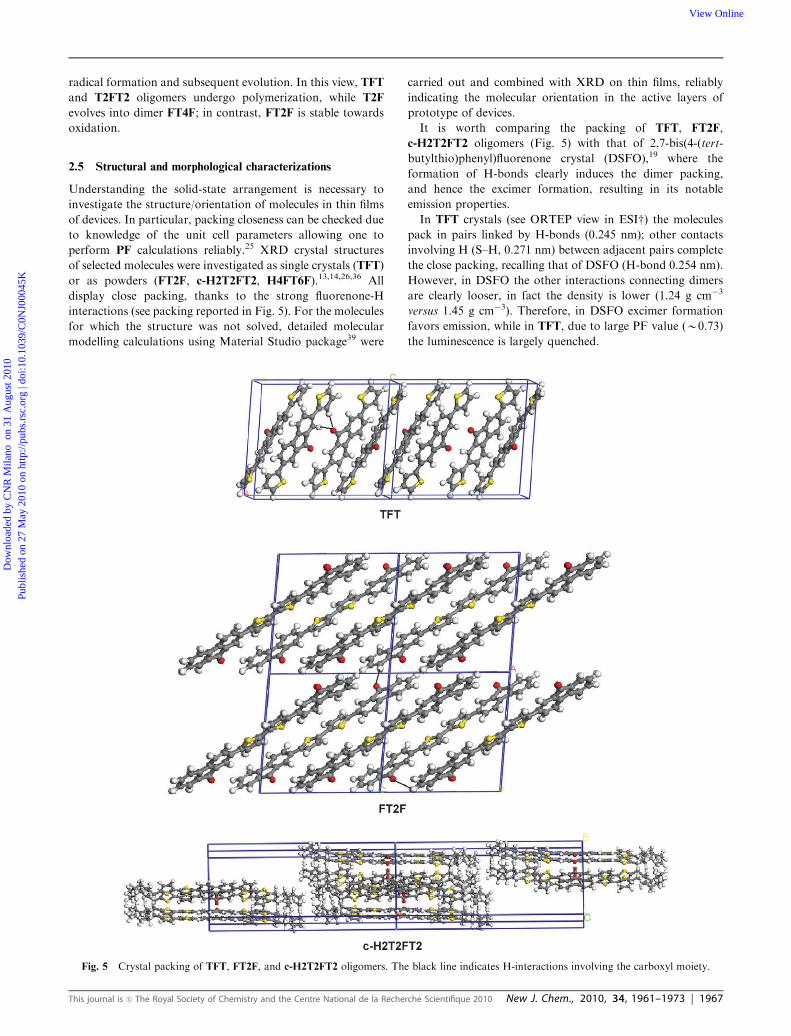
2.5 Structural and morphological characterizations
Understanding the solid-state arrangement is necessary to
investigate the structure/orientation of molecules in thin films
of devices. In particular, packing closeness can be checked due
to knowledge of the unit cell parameters allowing one to
perform PF calculations reliably.25 XRD crystal structures
of selected molecules were investigated as single crystals (TFT)
or as powders (FT2F, c-H2T2FT2, H4FT6F).13,14,26,36 All
display close packing, thanks to the strong fluorenone-H
interactions (see packing reported in Fig. 5). For the molecules
for which the structure was not solved, detailed molecular
modelling calculations using Material Studio package39 were
carried out and combined with XRD on thin films, reliably
indicating the molecular orientation in the active layers of
prototype of devices.
It is worth comparing the packing of TFT, FT2F,
c-H2T2FT2 oligomers (Fig. 5) with that of 2,7-bis(4-(tert-
butylthio)phenyl)fluorenone crystal (DSFO),19 where the
formation of H-bonds clearly induces the dimer packing,
and hence the excimer formation, resulting in its notable
emission properties.
In TFT crystals (see ORTEP view in ESIw) the molecules
pack in pairs linked by H-bonds (0.245 nm); other contacts
involving H (S–H, 0.271 nm) between adjacent pairs complete
the close packing, recalling that of DSFO (H-bond 0.254 nm).
However, in DSFO the other interactions connecting dimers
are clearly looser, in fact the density is lower (1.24 g cm�3
versus 1.45 g cm�3). Therefore, in DSFO excimer formation
favors emission, while in TFT, due to large PF value (B0.73)
the luminescence is largely quenched.
Fig. 5 Crystal packing of TFT, FT2F, and c-H2T2FT2 oligomers. The black line indicates H-interactions involving the carboxyl moiety.
This journal is �c The Royal Society of Chemistry and the Centre National de la Recherche Scientifique 2010 New J. Chem., 2010, 34, 1961–1973 | 1967
Dow
nloa
ded
by C
NR
Mila
no o
n 31
Aug
ust 2
010
Publ
ishe
d on
27
May
201
0 on
http
://pu
bs.r
sc.o
rg |
doi:1
0.10
39/C
0NJ0
0045
KView Online

A different situation occurs in the crystal structure of FT2F,
where strong H-interactions are present (0.26 nm), but where
dimer formation is not observed. The packing can be described
as two inverse sequences of single molecules essentially
overlapping along the short a axis.
Similar packing is found in c-H2T2FT2, where an
alternating sequence of molecules interact by short H-bonds
(0.235–0.241 nm), along the short c axis; however, the other
contacts are a bit looser, approaching the sum of the Van der
Waals radii.
In spite of the close packing observed, none of the structures
investigated support the excimer formation being different
from that for crystals of DSFO,19 fully justifying the observed
poor emission properties (see optical characterization).
Thin-film arrangements were next studied directly in the
device prototypes. Fig. 6 reports the XRD spectrum of film
into OFET device of six typical molecules: TFT, T2F, and
T2FT2 (Fig. 6a) and H4T3FT3, c-H2T2FT2, and FT2F
(Fig. 6b). The experimental film thicknesses range from 25 nm
to 100 nm.
Detailed analyses of the profiles give the following relevant
information:
– in the TFT spectrum, four [100] directions are detected, the
one at largest 2y1 being attributed to the substrate.
– in the T2F spectrum, two medium axis directions (0.91 nm)
are detected.
– in the T2FT2 case, up to eight long axis directions (4.4 nm)
are observable.
– in the H4T3FT3 film, three non-commensurate peaks are
detected, i.e. three different orientations.
– in the c-H2T2FT2 film, two [100] directions are
observed.14
– in the FT2F film, four peaks are detected, the [100]
direction being prevalent, and the remaining three being sums
of other crystallographic directions26 (2–4 reflections), namely
[001], [202], and [113].26
By combining XRD analysis with molecular modeling,39
approximate angles between molecular axis and orientations
direction can be derived, and the results are summarized in
Table 3. As a result, in both the case of card-pack (TFT) and
herringbone arrangements (c-H2T2FT2), shown in Fig. 5, the
angle between the molecular axis and the substrate plane (a) iscrucial to understand the electrical properties.
For the T2FT2 molecule, whatever structural motif is
adopted the a value is over 601, whereas for the T2F oligomer
the value is close to 301. A particular case is presented by FT2F
molecule, whose XRD pattern displays peaks comprising the
combination of different reflections, irrespective of the kind of
deposition adopted (e.g. high-vacuum evaporation or spin-
coating), implying multiple molecular orientations in the
films.26 However, in all the orientations, except for [001], for
which the weight is B0.12, the a value ranges from 151 to 301.
H4T3FT3 adopts three different orientations, likely due to the
position of the alkyl chains. As the length of the molecule’s
conjugated backbone is close to 3.0 nm, the orientation of the
molecular axis perpendicular to the surface has to be ruled out.
In summary, when the molecule comprises a sequence of F
and T residues without substituents, the molecular orientation
is approximately edge-on, i.e. the average molecular axis forms
with the substrate plane an angle greater than 601, unless the
molecule is asymmetric and relatively short (T2F). In contrast,
when alkyl chains are present, the situation is modified
according to the substitution site; namely, if the chains are
end-capping the molecule, the orientation is again edge-on,
while substitution at the 3,4-positions of the thiophene rings
implies a multiple orientation that is partly edge-on, with the
Fig. 6 XRD patterns of oligomer films, with the thickness in
parenthesis: (a) top TFT (30 nm), middle T2F (42 nm), and bottom
T2FT2 (100 nm); (b) topH4T3FT3 (25 nm), middle c-H2T2FT2 (40 nm),
and bottom FT2F (50 nm). The intensities are slightly shifted for clarity.
Table 3 Molecular orientation of selected oligomers from coupling ofXRD analysis and molecular modelling (MM)a
Oligomer Orientation direction a b
TFT [100] 641T2F Medium axis c 301 d
T2FT2 [100] c 601 d
H4T3FT3 Three orientations All o301c-H2T2FT2 [100] b B901FT2F [100] + others c All o451H4FT6F Single f B901
a For details see text. b The angle is formed by molecular axis and the
substrate plane. c More orders of the same crystallographic direction,
i.e. unique orientation along the axis. d The value is similar in case of
card-pack or herringbone arrangements. e The three observed peaks
result from the overlap of more directions, as detailed in ref. 26. f The
unique orientation is detailed in ref. 36.
1968 | New J. Chem., 2010, 34, 1961–1973 This journal is �c The Royal Society of Chemistry and the Centre National de la Recherche Scientifique 2010
Dow
nloa
ded
by C
NR
Mila
no o
n 31
Aug
ust 2
010
Publ
ishe
d on
27
May
201
0 on
http
://pu
bs.r
sc.o
rg |
doi:1
0.10
39/C
0NJ0
0045
KView Online

alkyl chains pointing alternately upwards or towards the
substrate.
Finally, the semi-crystalline H4FT6F adopts an approximate
edge-on orientation of the backbone with side-chains separating
adjacent molecules, yielding relatively loose packing.36
AFM investigations into OFET devices based on three
typical molecules are reported here as examples in order to
verify the crystal interconnections. In Fig. 7 three topographic
images of T2FT2, T2F, and c-H2T2FT2 films (thickness
40–50 nm) obtained by high-vacuum evaporation, are shown
for comparison. The roughness as well as the interconnections
among crystals are different in the three cases:
– in the T2FT2 device, efficient interconnection is detected
(Fig. 7a).
– in the T2F film, some voids are evident due to a larger
aggregate size (Fig. 7b).
– in the optimised layer c-H2T2FT2,14 the interconnection is
guaranteed and the roughness is strongly reduced (Fig. 7c).
These observations are in agreement with OFET device
results (see below).
2.6 Potential applications
2.6.1 OFET device measurements. Many of the reported
molecules were next tested as active layers in p-type devices,
with the aim of putting forward a relation between chemical
constitution and performance of un-optimized devices. In
Table 4 relevant results from molecules displaying closest
packing are presented. The mobility and Ion/off values were
derived from output characteristic I–V curves reported in the
ESIw, according to the procedure described in the Experimental
section and in ref. 14.
The generally low values of both mobility and Ion/off ratios
can be accounted for by coupling the surface/structural
investigations with electrochemical and optical data, and
DFT calculations. In fact, the best value of the OFET
performances in p-type devices is achieved in the case of a
stable molecule, well oriented with respect to the electrode and
with compact morphology (c-H2T2FT2), while the worst
results are found in the case of the well oriented but
T-terminated molecule (irreversible oxidation process)
(TFT), or in the case of molecular multiple orientations
(FT2F); while intermediate values are reached in case of
incomplete substrate coverage (T2F), i.e. bad crystal inter-
connections. Hence the crucial effects dominating the FET
functioning are definitely mapped. In the light of the above
results, the approach followed by Curtis,28 i.e. D and A parts
in the molecule, seems to be rather restrictive for deciding
which compounds to choose for FET applications; in fact, the
possibility of oxidation, the packing interactions, and the
substrate influence contribute to determine the appropriate
choice. Indeed, a recent review by Roncali29 strongly supports
this observation.
2.6.2 Solar cell evaluation. The potential use of the
compounds studied in BHJ solar cells deserves careful evaluation
of their electronic levels. In fact, choosing the typical acceptor
[6,6]-phenyl-C61-butyric acid methyl ester (PCBM),40 in principle
all could be considered as candidates because their HOMO
level values range from 4.95 eV to 5.72 eV (for H4FT6F and
H2TFT respectively). However, their harvesting capability (see
absorption spectra above), coupled with their processability,
limits the choice of compounds to either H4T3FT3 or
H4FT6F, provided that the compatibility of blends with
PCBM or other acceptor molecules allows for homogeneous
film fabrication. As the latter molecule better fits such a
requirement, BHJ devices based on H4FT6F were tested with
PCBM in a 1:1 ratio by weight (see the Experimental section
for details). For a series of un-optimized devices, the results
reported in Table 5 were obtained, i.e. a power conversion
efficiency close to 0.8% was achieved. Comparison with
Demadrille’s results12 concerning a series of T- and F-containing
oligomers reveals that long Tn sequence molecules display the
best performances. The I–V curve together with absorption
spectrum of the device is presented in Fig. 8.
3. Conclusions
A careful study has been performed on fluorenone-containing
oligomers, designed to achieve an effect on the electronic and
optical properties from alternating T and F residues and the
presence and position of alkyl chains. The electrochemical
data, which are in agreement with optical characterizations,
have been corroborated by DFT calculations on four
Fig. 7 AFM height images of OFET devices of: (a) T2FT2, (b) T2F,
and (c) c-H2T2FT2 in tapping mode; only height images are shown for
clarity. The black bar in (a) corresponds to 500 nm for all the
three images. The measured roughnesses are 20 nm, 130 nm, and
10 nm respectively.
Table 4 Electrical measurements of p-type OFET devices based on F-molecules
Oligomer m (cm2 V�1 s�1) Ion/off Ref.
TFT r10�7 o10 15FT2F r10�7 o10 15T2F 2 � 10�6 o102 Present workT2FT2 5 � 10�4 >103 Present workc-H2T2FT2 >2 � 10�3 7 � 105 24H4FT6F 7 � 10�5 r30 36
Table 5 Photovoltaic properties of H4FT6F molecule/PCBM-baseddevices. Measurement under AM 1.5 at 100 mW cm�2). VOC: opencircuit voltage, FF: fill factor, JSC: short-circuit, Z: power conversionefficiency
Samplea Voc (V) FF Jsc (mA cm�2) Z (%)
A, 1000 rpm 0.74 0.34 2.95 0.72B, 1000 rpm 0.74 0.34 2.92 0.73A, 1500 rpm 0.64 0.29 3.05 0.67B, 1500 rpm 0.70 0.37 3.03 0.77
a The values are averaged; the e.s.d. is 0.03.
This journal is �c The Royal Society of Chemistry and the Centre National de la Recherche Scientifique 2010 New J. Chem., 2010, 34, 1961–1973 | 1969
Dow
nloa
ded
by C
NR
Mila
no o
n 31
Aug
ust 2
010
Publ
ishe
d on
27
May
201
0 on
http
://pu
bs.r
sc.o
rg |
doi:1
0.10
39/C
0NJ0
0045
KView Online

examples. These also afforded orbital maps that enabled us to
understand both the chemical stability and the behaviour in
FET devices. Structural analyses, fully in agreement with the
other characterisation data, were carried out on single crystals
and powders, allowing for the determination of molecular
orientations in thin films. The findings clearly explain the
performances in OFETs, taking into account the effective
close-packing induced by fluorenone. In addition, some chemical
structure markers enabling us to identify structures suitable
for FET or solar cell fabrication have been pinpointed.
Namely, alkyl substitution on the thiophene rings, which
enables processability, only results in close-packing if placed
at the 2- and 5-positions (end chains), while positioning the
fluorenone at the end of an oligomer permits reversible
oxidation. Finally, long T-sequences only can supply adequate
light harvesting by extending absorption towards the red
region.
In summary, the F residue, when inserted as end-capper in
the oligomers, results in close-packing formation and chemical
stability.
4. Experimental section
4.1 Chemicals and reagents
All melting points are uncorrected. All reactions of air- or
water-sensitive materials were performed under nitrogen.
Air- and water-sensitive solutions were transferred with
double-ended needles (cannulas). The solvents used in the
reactions – THF (Fluka) and toluene (Aldrich) – were dried
and stored over molecular sieves. Acetonitrile was reagent
grade (Uvasol, Merck) with a water content o0.01%. The
supporting electrolyte tetrabutylammonium perchlorate
(Bu4NClO4), methylene chloride and chlorobenzene were
reagent grade and used as received. Butyllithium (BuLi),
bromohexane, 2-isopropoxy-(4,4,5,5-tetramethyl)-1,3,2-dioxo-
borolane, 2-bromo-9-fluorenone, 2,7-dibromo-9-fluorenone,
2,20-bithiophene-5-boronic acid pinacol ester, and 2-(tributyl-
stannyl)thiophene), N-bromosuccinimide (NBS) and tetrakis-
(triphenylphosphine)palladium [(Ph3P)4Pd] available from
Aldrich, were used as received, while bithiophene and
3-bromothiophene were purified by flash chromatography
and distillation respectively. 5-(4,4,5,5-Tetramethyl-1,3,2-
dioxaborolan-2-yl)-3 0-40-dihexyl-2,20:50,20 0-terthiophene and
3-hexylthiophene-2-boronic acid pinacol ester and were prepared
according to ref. 32 and 41 respectively. Flash chromatography
was carried out using silica gel (200–300 mesh ASTM). Suzuki
reactions were carried out with conventional heating.
4.2 Syntheses
4.2.1 2,7-Bis(3-hexylthien-2-yl)fluoren-9-one (H2TFT). In
a 25 mL Schlenk tube was introduced 213 mg (0.73 mmol)
of 3-hexylthiophene-2-boronic acid pinacol ester, 122 mg
(0.36 mmol) of 2,7-dibromo-9-fluorenone and 21 mg of
(Ph3P)4Pd. Then, 4 mL of anhydrous THF and 2.5 mL 2 M
K2CO3 were added to this mixture under nitrogen. The
reaction was stirred at reflux overnight, and the resulting
orange-brown oil isolated by extraction with dichloromethane
(CH2Cl2) (3 � 100 ml). The combined organic layer was dried
over anhydrous magnesium sulfate, and the solvent removed
by rotary evaporation, giving a powder which was subjected to
purification by flash chromatography using silica gel with
hexane–ethyl acetate 9:1 as eluent, to give 128 mg of pure
product (70% yield). MS (gas-phase) m/z 511 (M+). 1H NMR
(270 MHz, CDCl3 dH/ppm, 25 1C): 7.74 (s, 2H, fluorenyl), 7.56
(br, 4H, fluorenyl), 7.25 (d, J = 5.20 Hz, 2H, thienyl), 6.99
(d, J = 5.20 Hz, 2H, thienyl), 2.67 (t, 4H, J = 7.61, alkyl
chain), 1.62 (m, 4H, alkyl chain), 1.29–1.20 (br, 12H, alkyl
chain), 0.85 (m, 6H, alkyl chain). M.p. = 277 1C. Elemental
analysis: Calc. for C33S2O1H36: C, 77.34; S, 12.51; O, 3.12; H,
7.03. Found: C, 77.41; S, 12.43; H, 7.19.
4.2.2 2-(2,20-Bithiophene-5-yl)fluoren-9-one (T2F). In a
25 ml Schlenk tube was introduced 226 mg (0.77 mmol) of
2,20-bithiophene-5-boronic acid pinacol ester, 128 mg (0.50 mmol)
of 2-bromo-9-fluorenone and 10 mg of (Ph3P)4Pd. Then, 4 ml
of distilled THF and 2.5 ml 2 M K2CO3 were added to this
mixture under nitrogen. The reaction was stirred at reflux
overnight, the mixture poured into water and extracted with
dichloromethane (CH2Cl2) (3 � 100 ml). The combined
organic layer was dried over anhydrous magnesium sulfate,
and the solvent removed by rotary evaporator, giving a
powder which was subjected to purification by flash chromato-
graphy using silica gel with hexane–ethyl acetate 8:2 as eluent,
to obtain 117 mg of pure product (68% yield). MS (gas-phase)
m/z 343 (M+). 1H NMR (270 MHz, CDCl3 dH/ppm, 25 1C):
7.89 (s, 1H, fluorenyl), 7.71–7.67 (br, 2H, fluorenyl),
7.53–748 (br, 3H, fluorenyl), 7.32–7.28 (br, 2H, 1H thienyl +
1H fluorenyl), 7.25 (d, J = 5.81 Hz, 1H, thienyl), 7.22
Fig. 8 J–V curve of the BHJ device: (a) in the dark (dotted line) and
upon AM1.5 irradiation (solid line). Normalized absorption spectrum
(b) of the H4FT6F film (dotted line) and of the device (solid line).
Spectra are shifted for clarity.
1970 | New J. Chem., 2010, 34, 1961–1973 This journal is �c The Royal Society of Chemistry and the Centre National de la Recherche Scientifique 2010
Dow
nloa
ded
by C
NR
Mila
no o
n 31
Aug
ust 2
010
Publ
ishe
d on
27
May
201
0 on
http
://pu
bs.r
sc.o
rg |
doi:1
0.10
39/C
0NJ0
0045
KView Online

(d, J = 3.58 Hz, 1H, thienyl), 7.17 (d, J = 3.58 Hz, 1H,
thienyl), 7.045 (dd, J = 5.81 Hz, J = 3.90 Hz, 1H, thienyl).
Elemental analysis: Calc. for C21S2O1H12: C, 73.25; S, 18.60;
O, 4.65; H, 3.49. Found: C, 73.41; S, 18.56; H, 3.52.
4.2.3 2,7-Bis(3 0,4 0-Dihexyl-2,2 0:5 0,2 0 0-terthiophene-5-yl)-
fluoren-9-one (H4T3FT3). To a Schlenk tube containing
0.57 mmol of 5-(4,4,5,5-tetramethyl-1,3,2-dioxaborolan-2-yl)-
30-40-dihexyl-2,20:50,20 0-terthiophene in THF solution (4.5 mL)
was added 1 mL of a 2 M solution of K2CO3 in degassed
water, and the mixture was stirred for 1 h. Separately, a
solution of 54 mg (0.16 mmol) of 2,7-dibromofluorenone in
1.5 mL of distilled tetrahydrofuran (THF) was transferred via
cannula to the flask containing the borolane derivative. After
the addition of a catalytic amount of (Ph3P)4Pd (11 mg), the
reaction temperature was increased to 70 1C, the mixture
refluxed overnight with stirring, then quenched with acid water
and dried over magnesium sulfate. The solvent was removed
and the residue was purified by flash column chromatography,
using hexane–dichloromethane 7:3 as eluent, to provide 49 mg
of title product as a red-brown solid (55% yield). MS (MALDI):
m/z 1009 1H NMR (270 MHz, CDCl3, dH/ppm, 25 1C): 7.86
(d, 1H, J = 1.5 Hz, fluorenyl), 7.66 (dd, 1H, J3,1 = 1.5 Hz,
J3,4 = 7.8 Hz, fluorenyl), 7.46 (d, 1H, J4,3 = 7.8 Hz,
fluorenyl), 7.29–7.32 (m, 2H, thienyl), 7.09 (d, 1H, J =
3.77 Hz, thienyl), 7.14 (m, 1H, thienyl), 7.06 (m, 1H, thienyl),
2.67–2.75 (m, 4H, alkyl chain), 1.53–1.59 (m, 4H, alkyl chain),
1.32–1.47 (br, 12H, alkyl chain), 0.92 (m, 6H, alkyl chain).
Elemental analysis: Calc. for C61S6O1H68: C, 72.63; S, 19.04;
O, 1.59; H, 6.74. Found: C, 72.97; S, 18.84; H, 6.81.
4.2.4 2,7-Bis(2,20-Bithiophene-50-yl)fluoren-9-one (T2FT2).
In a 25 mL Schlenk tube, 263 mg (0.9 mmol) of 2,20-bithio-
phene-5-boronic acid pinacol ester, 128 mg (0.38 mmol) of
2,7-bromo-9-fluorenone and 20 mg of (Ph3P)4Pd were
introduced. Then, 4 mL of distilled THF and 2.5 mL 2 M
K2CO3 were added to this mixture under nitrogen. The
reaction was stirred at reflux overnight, and the mixture
poured into water and extracted with dichloromethane
(CH2Cl2) (3 � 100 mL). The combined organic layer was
dried over anhydrous magnesium sulfate, and the solvent
removed by rotary evaporator, giving a red powder. MS
(gas-phase) m/z 508 (M+). 1H NMR (270 MHz, d8-dimethyl
formamide, dH/ppm, 120 1C): 7.93–7.90 (m, 2H, fluorenyl),
7.85 (d, 1H, J = 7.4 Hz, fluorenyl), 7.58 (d, 1H, J = 3.82 Hz,
thienyl), 7.49 (dd, 1H, J4,3 = 3.59 Hz, J3,5 = 1.08 Hz thienyl),
7.38 (1H, dd, J5,4 = 5.1 Hz, J3,5 = 1.04 Hz, thienyl), 7.32
(d, 1H, J = 3.82 Hz, thienyl), 7.12 (dd, 1H, J3,4 = 3.72 Hz,
J4,5 = 5.0 Hz, thienyl). Mass fragmentation and 1H NMR
spectra are reported in the ESIw. Elemental analysis: Calc. for
C29S4O1H16: C, 68.51; S, 25.17; H, 3.16. Found: C, 68.80; S,
24.87; H, 3.05.
4.3 Apparatus and procedures
4.3.1 General electrochemistry. The compounds were
generally investigated in acetonitrile + 0.1 M Bu4NClO4
(conc.B10�3 M). Methylene chloride and chlorobenzene were
used for H4T3FT3 and T2FT2 respectively for solubility
reasons. Electrodeposited films were in all cases investigated
in acetonitrile + 0.1 M Bu4NClO4.
Electrochemical experiments were performed at room
temperature under nitrogen in three-electrode cells. The
counter-electrode was platinum; the reference electrode was
silver//0.1 M silver perchlorate in acetonitrile (0.34 V vs. SCE).
The voltammetric apparatus (AMEL, Italy) included a 551
potentiostat modulated by a 568 programmable function
generator and coupled to a 731 digital integrator. The working
electrode for cyclic voltammetry was a platinum minidisc
electrode (0.003 cm2). For electronic spectroscopy, a
0.8 � 2.5 cm indium–tin oxide (ITO) sheet (resistance ca.
20 ohm per square, from Merck) was used.
4.3.2 Molecular characterizations. FTIR spectra were
taken on a Perkin Elmer 2000 FTIR spectrometer. The spectra
of films were taken in reflection–absorption mode.
Matrix-assisted laser desorption ionization time-of-flight
(MALDI-TOF) mass spectra were obtained by an Ultraflex
II mass spectrometer (Bruker Daltonics) operating in the both
positive reflection and linear modes, using 2,5-dihydroxy-
benzoic acid as the matrix.
Gas-phase mass determination was carried out using
Agilent Technologies 7890A GC System coupled with an
Agilent Technologies 5975C VL MSD with triple-axis mass
detector.
Optical absorption measurements for both solutions and
films were performed with a Lambda 900 Perkin-Elmer spectro-
meter. For solution spectra, CHCl3 and chlorobenzene were
used depending on the oligomer solubility, for this reason all
spectra start from 300 nm. CW photoluminescence (PL)
spectra were recorded using a SPEX 270 M monochromator
equipped with a N2-cooled CCD detector, by exciting with a
monochromated Xe lamp. Solution PL quantum yield (QY)
measurements were performed using a quinine sulfate solution
(10�4 M sulfuric acid) as reference (QY= 54.6%) and exciting
at 350 nm (QY = 54.6%). Solid-state PLQY was carried out
using an integrating sphere.42
4.3.3 Structural and morphological analyses. XRD
experiments were carried out using an Enraf Nonius CAD4
instrument for single-crystal analysis (for details see Table 6),
while films and powder were examined using a computer-
controlled Siemens D-500 diffractometer equipped with Soller
slits and an Anton–Paar camera for variable-temperature
experiments under a nitrogen atmosphere.
Morphological characterizations was performed using a
commercial AFM NT-MDT apparatus in non-contact force
modulation mode. Both height images and phase images were
taken at the same time.
4.3.4 Calculations. All ab initio computations were done
with Gaussian0343 with DFT, using the three-parameter
hybrid functional B3LYP.44–46 Graphical representations of
the electron orbitals were obtained with MOLEKEL.47,48
Molecular modelling calculations, crystal structure resolution,
and packing energy minimization were performed using
the Materials Studio package, release 4.0, developed by
Accelrys.39
This journal is �c The Royal Society of Chemistry and the Centre National de la Recherche Scientifique 2010 New J. Chem., 2010, 34, 1961–1973 | 1971
Dow
nloa
ded
by C
NR
Mila
no o
n 31
Aug
ust 2
010
Publ
ishe
d on
27
May
201
0 on
http
://pu
bs.r
sc.o
rg |
doi:1
0.10
39/C
0NJ0
0045
KView Online

4.3.5 Device preparation and measurements. OFET devices
in a bottom-contact architecture were prepared by high-
vacuum evaporation of the active layer, as described in
ref. 14. The final pressure was 10�7 mbar, while the growth
rate ranged from 0.1 to 0.15 A s�1, and the holder temperature
was kept at 100 1C, to avoid partial re-evaporation of the
compound.
The mobilities have been extracted from transfer characteristic
curves in the saturation region, fitting with the standard quadratic
expression: ISD = K(VG � VT)2 where K = 1
2mCoxW/L, where
m is the carrier mobility, Cox (130 nm SiO2) the capacitance per
unit surface, W (15 mm) and L (3, 6, 12 mm) the width and
length of the device respectively, and VT the threshold
voltage. The measurements were performed in vacuum (below
10�5 mbar).
The structure of bulk-heterojunction solar cells investigated
in this work was indium tin oxide (ITO)/poly(3,4-ethylene-
dioxythiophene)-blend-poly(styrene sulfonate) (PEDOT:PSS)/
H4FT6F:PCBM (1:1 wt)/LiF/Al. On the top of pre-cleaned
ITO substrates a 50 nm thick PEDOT:PSS layer was spin-coated,
and subsequently substrates were baked at 100 1C for 10 min
in ambient atmosphere. Then, an active layer of the solar cells
was spin-coated (in glove-box) from chlorobenzene solution
(20 mg mL�1) on top of the PEDOT:PSS layer. Afterwards,
onto the active layer, LiF and Al electrodes were thermally
evaporated using vacuum deposition system at a pressure of
B2 � 10�6 mbar. The thickness of the top electrical contacts
were E 0.8 nm and E 100 nm, respectively, while the
thickness of active layer ranged from 80 to 100 nm (by
AFM determination). The average area of the devices was
4.5 mm2. Before photovoltaic characterisation, the devices
were thermally annealed at 70 1C for 5 min on a calibrated
hotplate in a glove-box.
Acknowledgements
The authors would like to thank Dr D. Natali and Prof. M.
Sampietro of the Dipartimento di Elettronica e Informazione
Politecnico Milano for OFET device measurements and
helpful discussions, and S. Sitran of IENI-CNR for his
technical assistance. We are also indebted to the Italian
Fondazione Cariplo for partial financial support through the
project ‘‘DANAE’’ and to the Italian MIUR through the
project PRIN 2007PBWN44.
References
1 F. Jaramillo-Isaza and M. L. Turner, J. Mater. Chem., 2006, 16,83–89.
2 F. Uckert, Y. Tak, K. Mullen and H. Bassler, Adv. Mater., 2000,12, 905–908.
3 S. Panozzo, J.-C. Vial, Y. Kervella and O. Stephan, J. Appl. Phys.,2002, 92, 3495–3502.
4 R. Demadrille, P. Rannou, J. Bleuse, J.-L. Oddou, A. Pron andM. Zagorska, Macromolecules, 2003, 36, 7045–7054.
5 X. Gong, D. Moses and A. J. Heeger, J. Phys. Chem. B, 2004, 108,8601–8605.
6 M. Sims, D. D. C. Bradley, M. Ariu, M. Koeberg, A. Asimakis,M. Grell and D. G. Lidzey, Adv. Funct. Mater., 2004, 14, 765–781..
7 K. Becker, J. M. Lupton, J. Feldmann, B. S. Nehls, F. Galbrecht,D. Q. Gao and U. Scherf, Adv. Funct. Mater., 2006, 16, 364–370.
8 X. Zhou, Y. Zhang, Y. Xie, Y. Cao and J. Pei, Macromolecules,2006, 39, 3830–3840.
9 M. Linares, L. Sciffo, R. Demadrille, P. Brocorens, D. Beljonne,R. Lazzaroni and B. Grevin, J. Phys. Chem. C, 2008, 112,6850–6859.
10 L. Sanguinet, J. C. Williams, Z. Yang, R. J. Twieg, G. Mao,K. D. Singer, G. Wiggers and R. G. Petschek, Chem. Mater., 2006,18, 4259–4269.
11 M. Lehmann, S. W. Kang, C. Kohn, S. Haseloh, U. Kolb,D. Schollmeyer, Q. B. Wang and S. Kumar, J. Mater. Chem.,2006, 16, 4326–4334.
12 F. Lincker, N. Delbosc, S. Bailly, R. De Bettignies, M. Billon,A. Pron and R. Demadrille, Adv. Funct. Mater., 2008, 18,3444–3453 and references cited therein.
13 W. Porzio, S. Destri, M. Pasini, U. Giovanella, T. Motta,M. D. Iosip, D. Natali, M. Sampietro, L. Franco andM. Campione, Synth. Met., 2004, 146, 259–263.
14 W. Porzio, S. Destri, U. Giovanella, M. Pasini, T. Motta,D. Natali, M. Sampietro and M. Campione, Thin Solid Films,2005, 492, 212–220.
15 M. Yoon, S. A. DiBenedetto, A. Facchetti and T. J. Marks, J. Am.Chem. Soc., 2005, 127, 1348–1349..
16 T. Lee, C. A. Landis, B. M. Dhar, B. J. Jung, J. Sun, A. Sarjeant,H. J. Lee and H. E. Katz, J. Am. Chem. Soc., 2009, 131,1692–1705.
17 P. Scandiucci, U. Scherf, M. Collon and E. J. W. List, E-Polymers,2002, 009, 1–7.
18 T. A. M. Ferenczi, M. Sims and D. D. C. Bradley, J. Phys.Condens. Matter., 2008, 20, 045220(9).
19 Y. Liu, X. Tao, F. Wang, J. Shi, J. Sun, W. Yu, Y. Ren, D. Zouand M. Jiang, J. Phys. Chem. C, 2007, 111, 6544–65.
20 J. Cornil, D. A. dos Santos, X. Crispin, R. Silbey and J. L. Bredas,J. Am. Chem. Soc., 1998, 120, 1289–1299; J. Cornil, J. P. Calbert,
Table 6 Crystallographic details of TFT
Chemical formula C21H12OS2Formula weight 344.43Space group P21/c (no. 14)a/nm 1.4862(2)b/nm 0.5888(2)c/nm 1.8100(3)a (1) 90b (1) 93.09(1)g (1) 90V/nm3 1.5815(6)Z 4Dcalc/g cm�3 1.447Radiation (l) Mo Ka (0.71073 A)Temperature/K 293Parameters refined in full-matrix least-squares 229Unweighted agreement factor on observed data (1457) 0.056Weighted agreement factor on observed data (1457) 0.136
1972 | New J. Chem., 2010, 34, 1961–1973 This journal is �c The Royal Society of Chemistry and the Centre National de la Recherche Scientifique 2010
Dow
nloa
ded
by C
NR
Mila
no o
n 31
Aug
ust 2
010
Publ
ishe
d on
27
May
201
0 on
http
://pu
bs.r
sc.o
rg |
doi:1
0.10
39/C
0NJ0
0045
KView Online

D. Beljonne, R. Silbey and J. L. Bredas, Adv. Mater., 2000, 12,978–983.
21 S. R. Forrest, Nature, 2004, 428, 911–918.22 D. E. Janzen, M. W. Burand, P. C. Ewbank, T. M. Pappenfus,
H. Higuchi, D. A. da Silva Filho, V. G. Young, J. L. Bredas andK. R. Mann, J. Am. Chem. Soc., 2004, 126, 15295–15308.
23 H. Meng, F. Sun, M. B. Goldfinger, G. D. Jaycox, Z. Li,W. J. Marshall and G. S. Blackman, J. Am. Chem. Soc., 2005,127, 2406–2407.
24 J. Locklin, D. W. Li, S. C. B. Mannsfeld, E. J. Borkent, H. Meng,R. Advincula and Z. Bao, Chem. Mater., 2005, 17, 3366–3374;J. Locklin, M. E. Roberts, S. C. B. Mannsfeld and Z. Bao, Polym.Rev., 2006, 46, 79–101.
25 W. Porzio, S. Destri, M. Pasini, A. Rapallo, U. Giovanella,B. Vercelli and M. Campione, Cryst. Growth Des., 2006, 6,1497–1503.
26 W. Porzio, M. Pasini, S. Destri, U. Giovanella and P. Fontaine,Thin Solid Films, 2006, 514, 334–340.
27 E. E. Havinga, W. ten Hoeve and H. Wynberg, Polym. Bull., 1992,29, 119–126.
28 J. Cao, J. W. Kampf and M. D. Curtis, Chem. Mater., 2003, 15,404–411; J. Cao and M. D. Curtis, Chem. Mater., 2003, 15,4424–4432.
29 J. Roncali, Macromol. Rapid Commun., 2007, 28, 1761–1775.30 P. Sonar, S. P. Singh, P. Leclere, M. Surin, R. Lazzaroni, T. T. Lin,
A. Dodabalapur and A. Sellinger, J. Mater. Chem., 2009, 19,3228–3237.
31 C. Wang, M. E. Benz, E. Le Goff, J. L. Schlinder,J. Allbritton-Thomas, C. N. Kannewurf and M. G. Kanatzidis,Chem. Mater., 1994, 6, 401–410.
32 G. Zotti, S. Zecchin, B. Vercelli, M. Pasini, S. Destri, F. Bertiniand A. Berlin, Chem. Mater., 2006, 18, 3151–3161.
33 A. F. Diaz, J. Crowley, J. Bargon, G. P. Gardini andJ. B. Tottance, J. Electroanal. Chem., 1981, 121, 355–61.
34 S. Zecchin, G. Schiavon, R. Tomat and G. Zotti, J. Electroanal.Chem., 1986, 215, 377–383.
35 G. Zotti, S. Zecchin, G. Schiavon and B. Vercelli, J. Electroanal.Chem., 2005, 575, 169–175.
36 W. Porzio, S. Destri, M. Pasini, U. Giovanella, R. Resel,O. Werzer, G. Scavia, L. Fumagalli, D. Natali andM. Sampietro, Synth. Met., 2009, 159, 513–517.
37 M. D. Levi, R. Demadrille, E. Markevich, Y. Gofer, A. Pron andD. Aurbach, Electrochem. Commun., 2006, 8, 993–998.
38 I. F. Perepichka, S. Roquet, P. Leriche, J. M. Raimundo, P. Frereand J. Roncali, Chem.–Eur. J., 2006, 12, 2960–2966.
39 MATSTUDIO Modeling, release 4.0, Accelrys Inc., USA, 2003(www.accelrys.com).
40 C. Winder, D. Muhlbacher, H. Neugebauer, N. S. Sariciftci,C. Brabec, R. A. J. Janssen and J. K. Hummelen, Mol. Cryst.Liq. Cryst., 2002, 385, 213–220.
41 H. Pan, Y. Li, Y. Wu, P. Liu, Beng S. Ong, Shiping Zhu andGu Xu, J. Am. Chem. Soc., 2007, 129, 4112–4113.
42 J. Moreau, U. Giovanella, J.-P. Bombenger, W. Porzio, V. Vohra,L. Spadacini, G. Di Silvestro, L. Barba, G. Arrighetti, S. Destri,M. Pasini, M. Saba, F. Quochi, A. Mura, G. Bongiovanni,M. Fiorini, M. Uslenghi and C. Botta, ChemPhysChem, 2009,10, 647–653.
43 M. J. Frisch, G. W. Trucks, H. B. Schlegel, G. E. Scuseria,M. A. Robb, J. R. Cheeseman, J. A. Montgomery, Jr.,T. Vreven, K. N. Kudin, J. C. Burant, J. M. Millam,S. S. Iyengar, J. Tomasi, V. Barone, B. Mennucci, M. Cossi,G. Scalmani, N. Rega, G. A. Petersson, H. Nakatsuji, M. Hada,M. Ehara, K. Toyota, R. Fukuda, J. Hasegawa, M. Ishida,T. Nakajima, Y. Honda, O. Kitao, H. Nakai, M. Klene, X. Li,J. E. Knox, H. P. Hratchian, J. B. Cross, C. Adamo, J. Jaramillo,R. Gomperts, R. E. Stratmann, O. Yazyev, A. J. Austin,R. Cammi, C. Pomelli, J. W. Ochterski, P. Y. Ayala,K. Morokuma, G. A. Voth, P. Salvador, J. J. Dannenberg,V. G. Zakrzewski, S. Dapprich, A. D. Daniels, M. C. Strain,O. Farkas, D. K. Malick, A. D. Rabuck, K. Raghavachari,J. B. Foresman, J. V. Ortiz, Q. Cui, A. G. Baboul, S. Clifford,J. Cioslowski, B. B. Stefanov, G. Liu, A. Liashenko, P. Piskorz,I. Komaromi, R. L. Martin, D. J. Fox, T. Keith, M. A. Al-Laham,C. Y. Peng, A. Nanayakkara, M. Challacombe, P. M. W. Gill,B. Johnson, W. Chen, M. W. Wong, C. Gonzalez and J. A. Pople,GAUSSIAN 03, Revision C.02, Gaussian, Inc., Wallingford CT,2004.
44 A. D. Becke, Phys. Rev. A: At., Mol., Opt. Phys., 1988, 38,3098–3100.
45 A. D. Becke, J. Chem. Phys., 1993, 98, 5648–5652.46 C. Lee, W. Yang and R. G. Parr, Phys. Rev. B, 1988, 37, 785–789.47 P. Flukiger, H. P. Luthi, S. Portmann and J. Weber, MOLEKEL
4.3, Swiss Centre for Scientific Computing, Manno, Switzerland,2000–2002.
48 S. Portmann and H. P. Luthi, MOLEKEL: An InteractiveMolecular Graphics Tool, Chimia, 2000, 54, 766–771.
This journal is �c The Royal Society of Chemistry and the Centre National de la Recherche Scientifique 2010 New J. Chem., 2010, 34, 1961–1973 | 1973
Dow
nloa
ded
by C
NR
Mila
no o
n 31
Aug
ust 2
010
Publ
ishe
d on
27
May
201
0 on
http
://pu
bs.r
sc.o
rg |
doi:1
0.10
39/C
0NJ0
0045
KView Online


![N ′-[1-(2,4-Dioxo-3,4-dihydro-2 H -1-benzopyran-3-ylidene)ethyl]thiophene-2-carbohydrazide](https://static.fdokumen.com/doc/165x107/63252fe2c9c7f5721c01f37f/n-1-24-dioxo-34-dihydro-2-h-1-benzopyran-3-ylideneethylthiophene-2-carbohydrazide.jpg)