SUMMER STUDENT WORK PROJECT REPORT Positronium ...
18
AE gIS AE gIS g H H 22 Na 1K Ps Ps n = 15 - 25 H Ps p H g Ps 180m -2 s -1 130m -2 s -1 μ ± 50m -2 s -1 e ± 2 × 2 × 10 cm 20 min -1 10 × 10 × 40 cm 400 min -1 dN μ dE μ dΩ ≈ 0.14E -2.7 μ cm 2 s sr GeV × " 1 1+ 1.1Eμ cos(θ) 115GeV + 0.054 1+ 1.1Eμ cos(θ) 850GeV # Ps v particle > c n c n cos θ C 1 βn(ω) ω ze d 2 N dλdx = 2πz 2 α λ 2 1 - 1 β 2 n (ω) 2 ! 1/λ 2
-
Upload
khangminh22 -
Category
Documents
-
view
0 -
download
0
Transcript of SUMMER STUDENT WORK PROJECT REPORT Positronium ...

SUMMER STUDENT WORK PROJECT REPORT
Positronium annihilation detection using Cherenkov radiation
Ivana Belo²evi¢
Supervisor: Michael Doser
1 Introduction
My summer student project was with the AEgIS experi-ment. Primary goal of the AEgIS experiment is to measuregravitational acceleration g of antihydrogen. Important partof this experiment is producing pulsed cold H beam.
Steps for producing H [2] First, positrons are producedfrom a radioactive 22Na source and stored in the positronaccumulator. Antiprotons from AD are accumulated in aPenning trap and cooled to temperatures below1K. Whenpositron pulse bombards cryogenic nanoporous materialpositronium (Ps) is produced. Ps is excited to the Ryd-berg state (n = 15− 25) with lasers. H is then produced byresonant charge exchange between Ps and p.
H we get is accelerated by inhomogeneous electric elds(Stark acceleration) and then measurement of g can be per-formed.
Goal of my project The goal of my project was to testdierent methods for the detection of the positronium an-nihilation. The positronium annihilation detector is neededbeacuse it is important to know how much of Ps is producedand what is its energy and lifetime. The testing of detec-tor was done only with cosmic rays because there was nopositron source available at the time.
Cosmic rays spectrum Cosmic rays that we detect atthe Earth consist mostly of muons and electrons/positrons.Total ux of cosmic rays at the Earth surface passingthrough a horizontal unit area from above is 180m−2s−1
(130m−2s−1 for µ± and 50m−2s−1 for e±)[5]. This meansthat number of cosmic rays that pass through small quartzcrystal (2 × 2 × 10 cm) should be around 20min−1 and forbig crystal (10× 10× 40 cm) 400min−1.
Formula that describes dierential energy spectrum ofmuons is[5]:
dNµdEµdΩ
≈0.14E−2.7
µ
cm2s sr GeV
×
[1
1 +1.1Eµ cos(θ)
115GeV
+0.054
1 +1.1Eµ cos(θ)
850GeV
](1)
See picture below (number 1):
Figure 1: Muon impulse spectrum, taken from [6]
This is what we expected to see with our detector.
Cherenkov radiation[1] Cosmic rays (and Ps annihila-tion) can be detected using Cherenkov radiation, radiationwhich particle emits when it's moving at speed higher thanspeed of light in that medium (vparticle > c
n , where c isspeed of light and n is index of refraction of material). Elec-tromagnetic shock wave is then created. The wavefront isemitted at the angle cos θC=
1βn(ω) , where ω is frequency
of emitted light. This light is what we try to detect usingeither photomultipliers or silicon detectors.
The number of photons emitted per unit wavelength perunit path length for the particle of charge ze is given by thefollowing formula:
d2N
dλdx=
2πz2α
λ2
(1− 1
β2n (ω)2
)(2)
We can see from this formula that the faster the particle is,more photons are produced by the Cherenkov radiation, sowe see larger pulse in our detector. This way we can alsodetermine the energy of the particle that passed throughthe material. Also, because of 1/λ2 dependence most of the
1
radiated light is near the end of visible spectrum.
Medium that we are using in experiment is quartz, whichhas index of refraction of around 1.5 [7], so with Cherenkovradiation, we can detect particles faster than 2
3c. Thismeans that we can detect muons with energy higher than≈ 150MeV and electrons with energy higher than ≈ 1MeV .
Our PMTs are most sensitive for wavelengths between300nm and 650nm, so if we integrate eq. (2) (and if weapproximate that n is constant in that range of wavelengths) we get number of photons that we can detect per unit pathlength:
dN
dx≈ 820 sin2 θCz
2 photons/cm
Pulse shape [1] Width of the pulse of the Cherenkovlight that PMTs detect depends on particle velocity (bothmagnitude and direction) and geometry of crystal in whichlight propagates. Cherenkov light is emitted at angle θCand transported to the PMTs by total internal reections atthe surfaces of the bar (see pictures 2 and 3). We can cal-culate time it takes one photon to reach PMT, dependingon position on track of particle it was emitted. For muonwith energy 4GeV (which is the average energy of cosmicray muons[5]) which emitts Cherenkov radiation in quartz(that's material of our crystal) delay between rst and lastphoton detected can be up to 0.5ns for small crystal and upto almost 2ns for big crystal.
Figure 2: Propagation of Cherenkov light in quartz crystal[3]
Figure 3: Propagation of laser light in quartz crystal [3]
Dierent wavelengths of emitted light propagate at dierentvelocities (because index of refraction depends on the wave-length of light). Delay between 300nm and 650nm light is
proportional to dierence between indexes of refraction forthese wavelengths. For quartz this dierence is around 0.04so delay because of dierent frequencies is only 2.5% of thedelay because of the geometry of crystal. Also particles loseenergy when they pass through some medium (this energyloss is described by Bethe-Bloch formula). Stopping powerof quartz for 4GeV muons is around 4.5Mev/cm[8], whichis negligible for muon track lengths of the order of 10cm.Number of emitted Cherenkov photons also doesn't changesignicantely when muons loses this amount of energy. Wesee that can ignore delays caused by dierent propagationspeeds of dierent light wavelengths and muon energy lossin quartz. Width of light pulse that comes to PMT surfaceis mostly determined by the geometry of crystal and parti-cle velocity. This pulse is very short and has approximatelysquare shape.
2 Experimental setup
Experimental setup consisted of :
• 2 quartz crystals (one with dimensions 2× 2× 10 cm ;the other with dimensions 10× 10× 40 cm)
• 2 photomultipliers (Hamamatsu H7826)
• 2 silicon detectors (Hamamatsu MPPC S10362-11-100C)
• 2 power supplies (TTi PLH120 DC power supply andGW instek GPS-3030DD DC power supply)
• amplier (backplane + analog PCB)
• oscilloscope (LeCroy waverunner LT584)
• optical grease (Rhodorsil paste 7)
• 2 blue LEDs (FNL-U500b22cdsl)
• pulse generator (Agilent 33250A)
• 2 2.5kΩ potentiometers, 2 1.2kΩresistors, 2 10kΩ re-sistors, 2 100kΩ resistors
• coaxial cables
PMTs setup PMTs were attached to opposite sides ofcrystal. When we see signal from both PMTs at the sametime we can be sure that is not just the noise that we areseeing. Before attaching them to crystal, small amount ofoptical grease was applied to the surface of PMTs. Opticalgrease has similar index of refraction as crystal so it mini-mizes reection of light on boundaries of PMTs and crystal.I have tried out dierent ways of wrapping crystal, rst justwith tape, and later with aluminium foil (with small air gapbetween the foil and surface of crystal, which according to[1] is most ecient way of wrapping).
PMTs were connected to power supplies (voltage was setto 15V). Gain of PMTs can be adjusted by changing resis-tance on potentiometer (which changes control voltage, seepictures 4 and 5). Later potentiometers were replaced with10kΩ resistors and after that with 100kΩ resistors (this way
2

control voltage is set to maximal value, so the gain is alsoat the maximum). With potentiometer (set to highest re-sistance) control voltage was 0.90V for PMT 1 and 0.91Vfor PMT 2; with 10kΩ resistor it was 1.10V for PMT 1 and1.11V for PMT 2 and with 100kΩ resistor 1.19V (PMT 1)and 1.20V (PMT 2). Later, I'll refer to these congurationsfor PMT gain as min. PMT gain, 10kΩ PMT gain and max.PMT gain respectively. Output of PMTs was connected tooscilloscope with coaxial cables.
Figure 4: Gain of PMTs vs. control voltage
Figure 5: Resistance programming of PMT
The PMTs and crystal were then taped together and put incardboard box (for smaller crystal I've even used 2 boxes,one inside other because that gives best insulation fromlight). Box was wrapped from the inside and the outsidewith aluminum foil and black plastic bags to ensure thatno light is coming from the outside. Whole setup can be
then tested for light leaks by shining ashlight at the boxfrom dierent directions while monitoring if large amountof signal appears on oscilloscope. This is best done at night(or in a dark room).
I have also installed blue LED on top of crystal to check ifPMTs really see light from the inside of the crystal and tomake sure everything is properly attached. From pulse gen-erator, short square voltage pulses were sent to LED (whichproduced short ashes of light). Current through LED waslimited by 1.2kΩresistor. This way I was able to comparesignal I got from LED light with and without crystal (setupfor measuring PMT response without crystal is shown inpicture 6; LED is installed on top of square cardboard tubewrapped with Al foil on the inside of same size as smallcrystal to make it as close as possible to setup with smallcrystal).
Figure 6: Setup - PMTs and LED
In the end, setup looks like in pictures 8 and 7.
Figure 7: Setup - large crystal
3

Figure 8: Setup - small crystal
MPPCs setup MPPC is soldered to the MPPC holderwhich is attached to the inside of vacuum pump ange with50 pin D-sub connector. Backplane is used to supply aPCBwith high voltage (90V ) and low voltage (9V ). Backplaneis connected to 2 power supplies (low and high voltage) andto the outside of the ange, also via 50 pin D-sub connector.Each pin of this connector can be connected to one MPPC.Analog PCB is plugged into one slot of backplane. In thatway it's connected to MPPC. Each channel on the aPCB isassociated with one pin of D-sub connector (which meanswith one MPPC). Multimeter can be used to nd which pinis connected to which channel (if resistance between somepin and some chanel is 0, they are connected). Alternativelychart of backplane connections can be used. After the rightchannel is found, we connect it to the oscilloscope to moni-tor signal from MPPC.
After all is connected we close the vacuum pump (which hassame role as cardboard box for PMT setup). Then we rstturn on low voltage and after that, high voltage. Reversebias voltage for MPPC should be 70V . We can check if it'sat the right value if we measure voltage with multimeterbetween ground and point indicated in picture 9.
Figure 9: Checking value of reverse bias voltage applied toMPPC
I have also put one blue LED on the inside of the vacuumange. LED is connected via other 50 pin D-sub connectorto the pulse generator. This way we can measure responseof silicon detectors to LED light.Final setup can be seen in the pictures 10 and 11.
Figure 10: MPPC setup
Figure 11: MPPC setup - inside
Data collection and analysis Data from PMTs was col-lected with oscilloscope, for dierent trigger thresold values.Amplitude values can be recorded with oscilloscope usingmath function trend of parameter amplitude. Data that Iwould get was analysed with software Veusz.
The measurements were performed in this order:
1. Min. PMT gain
(a) small crystal (wrapped with tape)
(b) small crystal (wrapped with Al foil)
(c) big crystal
4
2. 10kΩ PMT gain
(a) small crystal (wrapped in Al foil)
(b) big crystal (PMTs on smaller faces of crystal, dis-tance 40 cm)
(c) big crystal (PMTs on bigger faces of crystal, dis-tance 10 cm)
3. MPPCs (just the LED light response)
4. Max. PMT gain
(a) without crystal (measurement of PMT noisespectrum)
(b) small crystal (wrapped in Al foil)
(c) big crystal (PMTs on smaller faces of crystal,distance 40 cm)
The plots that we were interested in were A2 vs.A1 plot,A2 − A1 vs.A1 + A2 plot, A2−A1
A1+A2vs.A1 + A2 (correlation
plots) and histograms of A1 and A2. A1 and A2 are theamplitudes from 1. and 2. PMT respectively.
We expect for real signal (the one from Cherenkov light)to produce proportional pulse amplitudes in both PMTs formost of the time (if signal from one PMT is large then signalfrom the other one should also be large). That is why inA2 vs.A1 scatter plot we expect for points from real signalto be grouped around straight line. For A2−A1 vs.A1 +A2
plot, we know that we are seeing real signal when we get alot of points around A2 − A1 = const. line (if both PMTshave same gain this constant should be zero). We also plotnormalized plot A2−A1
A1+A2vs.A1 + A2 because dierence be-
tween signals from PMTs can be larger if their sum is larger,so in this plot is even easier to see if points are groupingaround line for which A2 −A1 = const..
In histograms of A1 and A2 we should see spectrum of cosmicrays (like in picture 1) for larger values of signal amplitudesand noise spectrum (which has shape of exponential decaybecause the noise is mostly thermal) for smaller amplitudes.
3 Results and discussion
3.1 PMTs setup
3.1.1 Pulse shape
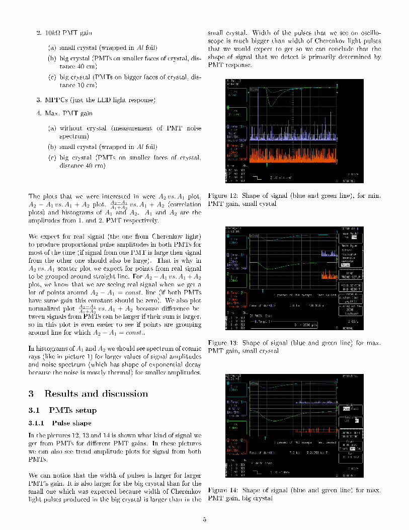
In the pictures 12, 13 and 14 is shown what kind of signal weget from PMTs for dierent PMT gains. In these pictureswe can also see trend amplitude plots for signal from bothPMTs.
We can notice that the width of pulses is larger for largerPMT's gain. It is also larger for the big crystal than for thesmall one which was expected because width of Cherenkovlight pulses produced in the big crystal is larger than in the
small crystal. Width of the pulses that we see on oscillo-scope is much bigger than width of Cherenkov light pulsesthat we would expect to get so we can conclude that theshape of signal that we detect is primarily determined byPMT response.
Figure 12: Shape of signal (blue and green line), for min.PMT gain, small cystal
Figure 13: Shape of signal (blue and green line) for max.PMT gain, small crystal
Figure 14: Shape of signal (blue and green line) for max.PMT gain, big crystal
5

3.1.2 Response to LED light
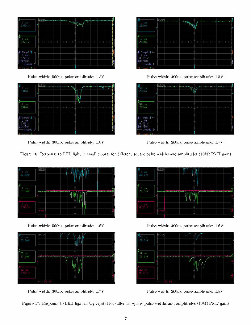
In pictures 16 and 17 is shown response of PMTs for 10kΩPMT gain (for small and big crystal) and in the pictures 18,19, 20 and 21 is shown response of PMTs for max. PMTgain (without crystal, with small and with big crystal re-spectively) to LED light, for dierent amplitudes and widthsof square voltage pulses that were sent to LED.
We can notice that the signal from both PMTs for 10kΩgain have approximately same amplitudes, which is tellingus that both of them have same gain. This is not the casewith max. PMT gain, where signal from PMT2 has twiceas big amplitude as signal from PMT 1.
Also amplitudes of signals are approximatly equal for PMTsseparated by 10 cm and 40 cm distance (for big crystal, max.
PMT gain) which means that there is not much loss of lightwhen it propagates down the crystal.
From this pictures we see that we get much smaller signalwith large crystal than with the small one. The reason forthis might be that the surface of PMT doesn't cover thewhole side of PMT so that reduces probability that thephotons that come to that side will be detected.
I was not able to detect pulses shorter then 200ns, but theLEDs might not be able to produce such short pulses. Alsowhen I shortened the width of pulse I had to increase thevoltage amplitude to be able to detect the LED light. Thecause of that could be that LED doesn't reach full luminos-ity immediately (rise time is around 0.5µs), as we can seefrom the shape of the pulses (picture 15).
pulse width: 1µs, pulse amplitude: 1.5V pulse width: 10µs, pulse amplitude: 1.5V
pulse width: 100µs, pulse amplitude: 1.5V
Figure 15: Response to LED light without any crystal (max.PMT gain)
6
Pulse width: 500ns, pulse amplitude: 1.5V Pulse width: 400ns, pulse amplitude: 1.5V
Pulse width: 300ns, pulse amplitude: 1.6V Pulse width: 200ns, pulse amplitude: 1.7V
Figure 16: Response to LED light in small crystal for dierent square pulse widths and amplitudes (10kΩ PMT gain)
Pulse width: 500ns, pulse amplitude: 1.6V Pulse width: 400ns, pulse amplitude: 1.6V
Pulse width: 300ns, pulse amplitude: 1.7V Pulse width: 200ns, pulse amplitude: 1.8V
Figure 17: Response to LED light in big crystal for dierent square pulse widths and amplitudes (10kΩ PMT gain)
7

Pulse width: 500ns, pulse amplitude: 1.5V Pulse width: 400ns, pulse amplitude: 1.5V
Pulse width: 300ns, pulse amplitude: 1.6V Pulse width: 200ns, pulse amplitude: 1.7V
Figure 18: Response to LED light without any crystal for dierent square pulse widths and amplitudes (max. PMT gain)
Pulse width: 500ns, pulse amplitude: 1.5V Pulse width: 400ns, pulse amplitude: 1.5V
Pulse width: 300ns, pulse amplitude: 1.6V Pulse width: 200ns, pulse amplitude: 1.7V
Figure 19: Response to LED light in small crystal for dierent square pulse widths and amplitudes (max. PMT gain)
8

Pulse width: 500ns, pulse amplitude: 1.6V Pulse width: 400ns, pulse amplitude: 1.6V
Pulse width: 300ns, pulse amplitude: 1.7V Pulse width: 200ns, pulse amplitude: 1.8V
Figure 20: Response to LED light in big crystal (PMT distance 10cm, max. PMT gain)
Pulse width: 500ns, pulse amplitude: 1.6V Pulse width: 400ns, pulse amplitude: 1.6V
Pulse width: 300ns, pulse amplitude: 1.7V Pulse width: 200ns, pulse amplitude: 1.8V
Figure 21: Response to LED light in big crystal (PMT distance 40cm, max. PMT gain)
9
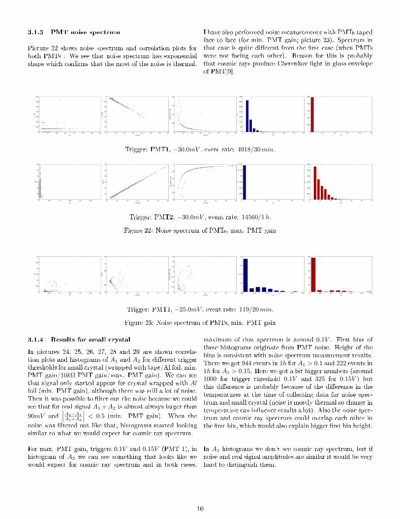
3.1.3 PMT noise spectrum
Picture 22 shows noise spectrum and correlation plots forboth PMTs . We see that noise spectrum has exponentialshape which conrms that the most of the noise is thermal.
I have also performed noise measurements with PMTs tapedface to face (for min. PMT gain; picture 23). Spectrum inthat case is quite dierent from the rst case (when PMTswere not facing each other). Reason for this is probablythat cosmic rays produce Cherenkov light in glass envelopeof PMT[9].
Trigger: PMT1, −30.0mV , event rate: 4918/30min.
Trigger: PMT2, −30.0mV , event rate: 14560/1h.
Figure 22: Noise spectrum of PMTs, max. PMT gain
Trigger: PMT1, −25.0mV , event rate: 119/20min.
Figure 23: Noise spectrum of PMTs, min. PMT gain
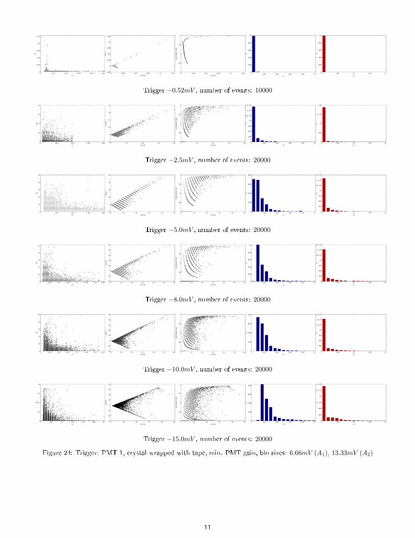
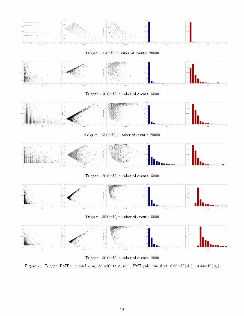
3.1.4 Results for small crystal
In pictures 24, 25, 26, 27, 28 and 29 are shown correla-tion plots and histograms of A1 and A2 for dierent triggerthresholds for small crystal (wrapped with tape/Al foil, min.PMT gain/10kΩ PMT gain/max. PMT gain). We can seethat signal only started appear for crystal wrapped with Alfoil (min. PMT gain), although there was still a lot of noise.Then it was possible to lter out the noise because we couldsee that for real signal A1 +A2 is almost always larger than
90mV and∣∣∣A2−A1
A1+A2
∣∣∣ < 0.5 (min. PMT gain). When the
noise was ltered out like that, histograms started lookingsimilar to what we would expect for cosmic ray spectrum.
For max. PMT gain, triggers 0.1V and 0.15V (PMT 1), inhistogram of A2 we can see something that looks like wewould expect for cosmic ray spectrum and in both cases,
maximum of that spectrum is around 0.1V . First bins ofthese histograms originate from PMT noise. Height of thebins is consistent with noise spectrum measurement results.There we got 944 events in 1h for A1 > 0.1 and 222 events in1h for A1 > 0.15. Here we got a bit bigger numbers (around1000 for trigger threshold 0.1V and 325 for 0.15V ) butthis dierence is probably because of the dierence in thetemperatures at the time of collecting data for noise spec-trum and small crystal (noise is mostly thermal so change intemperature can inuence results a lot). Also the noise spec-trum and cosmic ray spectrum could overlap each other inthe rst bin, which would also explain bigger rst bin height.
In A1 histograms we don't see cosmic ray spectrum, but ifnoise and real signal amplitudes are similar it would be veryhard to distinguish them.
10
Trigger −0.52mV , number of events: 10000
Trigger −2.5mV , number of events: 20000
Trigger −5.0mV , number of events: 20000
Trigger −8.0mV , number of events: 20000
Trigger −10.0mV , number of events: 20000
Trigger −15.0mV , number of events: 20000
Figure 24: Trigger: PMT 1, crystal wrapped with tape, min. PMT gain, bin sizes: 6.66mV (A1), 13.33mV (A2)
11
Trigger −1.4mV , number of events: 20000
Trigger −10.0mV , number of events: 5000
Trigger −15.0mV , number of events: 20000
Trigger −20.0mV , number of events: 5000
Trigger −35.0mV , number of events: 5000
Trigger −50.0mV , number of events: 2000
Figure 25: Trigger: PMT 2, crystal wrapped with tape, min. PMT gain, bin sizes: 6.66mV (A1), 13.33mV (A2)
12

Trigger −10.0mV , event rate: 8042/2h
Trigger −25.0mV , event rate: 19390/2000min.
Trigger−25.0mV , event rate: 1506/2000min., lter:∣∣∣A2−A1
A1+A2
∣∣∣ < 0.5 & A1 +A2 > 90mV
Figure 26: Trigger: PMT 1, crystal wrapped with Al foil, min. PMT gain, bin size: 8.33mV
Trigger −20.0mV , event rate: 13384/2h
Trigger −35.0mV , event rate: 17991/10h
Trigger -35.0mV, event rate: 334/10h , lter:∣∣∣A2−A1
A1+A2
∣∣∣ < 0.5 & A1 +A2 > 90mV
Figure 27: Trigger: PMT 2, crystal wrapped with Al foil, min. PMT gain, bin size: 8.33mV
13

Trigger: PMT 1, −0.2V , event rate: 16078/10h
Trigger: PMT 1,−0.3V , event rate: 548/2h
Trigger: PMT 2, −0.3V , event rate: 970/2h
Figure 28: Crystal wrapped with Al foil, 10kΩ PMT gain, bin size: 46.67mV
Trigger: PMT 1, −0.1V , event rate: 1563/1h
Trigger: PMT 1, −0.15V , event rate: 889/2h
Trigger: PMT 2,−0.2V , event rate: 2123/1h
Trigger: PMT 2, −0.3V , event rate: 551/2h
Figure 29: Crystal wrapped with Al foil, max. PMT gain, bin size: 33.33mV
14

3.1.5 Results for big crystal
Plots of results for big crystal are shown in pictures 30 and31 (for 10kΩ PMT gain and max. PMT gain). Here it'seven easier to distinguish signal from noise in correlationplots. Reason for this is probably that because of the size ofbig crystal, only high energy photons manage to reach sur-face of PMTs so most of the low amplitude signal is comingfrom noise.
For 10kΩ gain, in A2−A1
A1+A2vs.A1 +A2 plot we can see points
grouping around A2−A1
A1+A2= 0 line and for max. gain, points
are grouping around A2−A1
A1+A2= 0.5 line. This means that
signal amplitudes are equal for 10kΩ PMT gain and signalamplitude from PMT 2 is double the signal amplitude fromPMT 1 in case of max. PMT gain, which agrees with resultswe got for response of the PMTs to the LED light.
We don't see cosmic ray spectrum in histograms, but numberof real events (when compared to number of noise events) ismuch smaller than with small crystal.
Trigger: PMT 1,−0.2V , event rate: 5292/4h
Trigger: PMT 1, −0.3V , event rate: 2336/8h
Trigger: PMT 2, −0.3V , event rate: 1297/3h
Figure 30: Plots for big crystal (10kΩ PMT gain)
15

Trigger: PMT 1, −20mV , event rate: 16729/1h
Trigger: PMT 1, −0.1V , event rate: 1019/1h
Trigger 1 −0.15V , event rate: 444/2h
Trigger: PMT 2, −30mV , event rate: 18848/2000s
Trigger: PMT 2, −0.1V , event rate: 18116/1h
Trigger: PMT 2, −0.2V , event rate: 2225/1h
Trigger: PMT 2, −0.3V , event rate: 309/2h
Figure 31: Plots for big crystal (max. PMT gain)
16

3.1.6 Comparison of event rate for the small crys-tal and big crystal
In tables 1 and 2 is shown comparison for number eventsin 1h time for dierent trigger thresolds (10kΩ and max.PMT gain). Comparison was done for small crystal and forbig crystal. With big crystal (just 10kΩ PMT gain) datawas collected for two dierent positions of PMTs: rst onewas with PMTs on smaller faces of crystal (so that the dis-tance between them is 40 cm→1st setup) and second onewas with PMTs on larger sides of crystal (so that the dis-tance between them is 10cm, which is the same distance aswith small crystal →2nd setup).From this table we see that the total event rate for xedtrigger threshold is most of the times smaller for the bigcrystal than for the small crystal.
Trigger Small crystalBig crystal Big crystal(1st setup) (2nd setup)
PMT 1, -0.2V 1607.4 1323 1288.2PMT 1, -0.3V 273 291.6 -PMT 2, -0.3V 484.2 432.6 -
Table 1: Total number of events in 1h., 10kΩ PMT gain
Trigger Small crystal Big crystal (1st setup)
PMT 1, -0.1V 1563 1019PMT 1, -0.15V 444.5 222PMT 2, -0.2V 2123 2225PMT 2, -0.3V 275.5 154.5
Table 2: Total number of events in 1h, max. PMT gain
In table 3 is shown the same thing as in table 1, but only forsignal larger than 0.1 V (which is mostly real signal). It issuprising to see that number of events is much lower for bigcrystal than for small crystal because we would expect justthe opposite: in big crystal we were supposed to get about20 times more events then with small crystal because thesurface of big crystal is 20 times bigger then the surface ofsmall crystal. One possible explanation for this is that be-cause in big crystal PMTs cover only around 1/25 of face ofthe crystal, probability that PMTs will detect photons fromCherenkov radiation is reduced by the same factor. We canalso assume that only Cherenkov photons that are detectedare the ones which are produced near the PMTs.
Table 4 is showing comparison in the number of the realevents for small and big crystal for max. PMT gain. FilterI used here is 0 < A2−A1
A1+A2< 0.75 because in that range
we could see points grouping in correlation plots. Again,the number of events is lower for big crystal than for smallcrystal.
Still, for both gains and both crystals number of events ismuch smaller than what we would expect for cosmic rayswhich means that eciency of our detector is low.
Trigger Small crystalBig crystal Big crystal(1st setup) (2nd setup)
PMT 1, -0.2V 206.4 16.2 15.6PMT 1, -0.3V 86.4 10.2 -PMT 2, -0.3V 88.8 12.6 -
Table 3: Total number of events in 1h, 10kΩ PMT gain(only signals bigger than 0.1V)
Trigger Small crystal Big crystal (1st setup)
PMT 1, -0.1V 192 29PMT 1, -0.15V 28 23PMT 2, -0.2V 304 61PMT 2, -0.3V 89 34
Table 4: Total number of events in 1h, max. PMT gain,ltered
3.2 Silicon detectors setup
For silicon detectors only response to LED light was mea-sured (picture 32). The amplitude of signal that we detectis very small (only 5mV ), even for very high amplitude ofvoltage sent to LED.
Figure 32: MPPC response to LED light (pulse width:500ns, pulse amplitude: 1.8V )
Main problem with MPPCs was reducing noise, which wasmasking the signal in the beginning. Problem was that theconnection of coaxial cable to aPCB was not xed well soeven small vibrations produced strong noise (even when bothhigh and low voltage supplies were switched o); see picture33 . This problem was solved by switching to coaxial cablewith more secure connection.
17

HV o, LV o
HV o, LV on
HV on, LV on
Figure 33: Silicon detectors setup - noise
4 Conclusion
We've seen that it's possible to use Cherenkov radiation todetect cosmic rays so it should also be possible to use itfor Ps annihilation detection, especially because the ux ofthe particles in that case would be much larger than thatof cosmic rays which would make it even easier to separatenoise from the real signal. Also, it seems that it's betteridea to use big crystal because in that case real signal ismore pronounced (although we do get less events then withsmall crystal but maybe that dierence won't matter withstronger source (Ps)).
There are also things that could be further improved, for ex-ample, it would be useful to build some kind of PMT holder(because tape is not permanent solution and it's also notvery secure) and sturdier box for whole PMT setup. Maybeit would also be good idea to cool PMTs (that should reducenoise). In addition, PMTs should be calibrated with someradioactive source so they can be used to measure energy ofparticles.
References
[1] W. R. Leo, Techniques for Nuclear and Particle Physics
Experiments, Springer-Verlag (1994)
[2] Proposal for the AEgIS experiment at the CERNAntiproton decelerator(http://aegis.web.cern.ch/aegis/Proposal/Proposition.pdf)
[3] BaBar-DIRC Collaboration (I. Adam et al.), Nucl. In-strum. Meth. A538 (2005) 281-357
[4] P. K. F. Grieder, Cosmic Rays at Earth, Elsevier (2001)
[5] J. Beringer et al. (Particle Data Group), Phys. Rev.D86, 010001 (2012)
[6] A. A. Kochanov et al., Astroparticle Physics 30 (2008)219233
[7] RefractiveIndex.INFO (Refractive index database)
[8] D. E. Groom et al., Muon stopping power and range ta-
bles, Atomic data and nuclear data tables, Vol. 76, No.2 (2001)
[9] Hamamatsu Photonics K. K., Photomultiplier tubes: Ba-
sics and applications (2006)
18