
Speed Up Li-ion Battery Charging and Reduce Heat with a ...
44
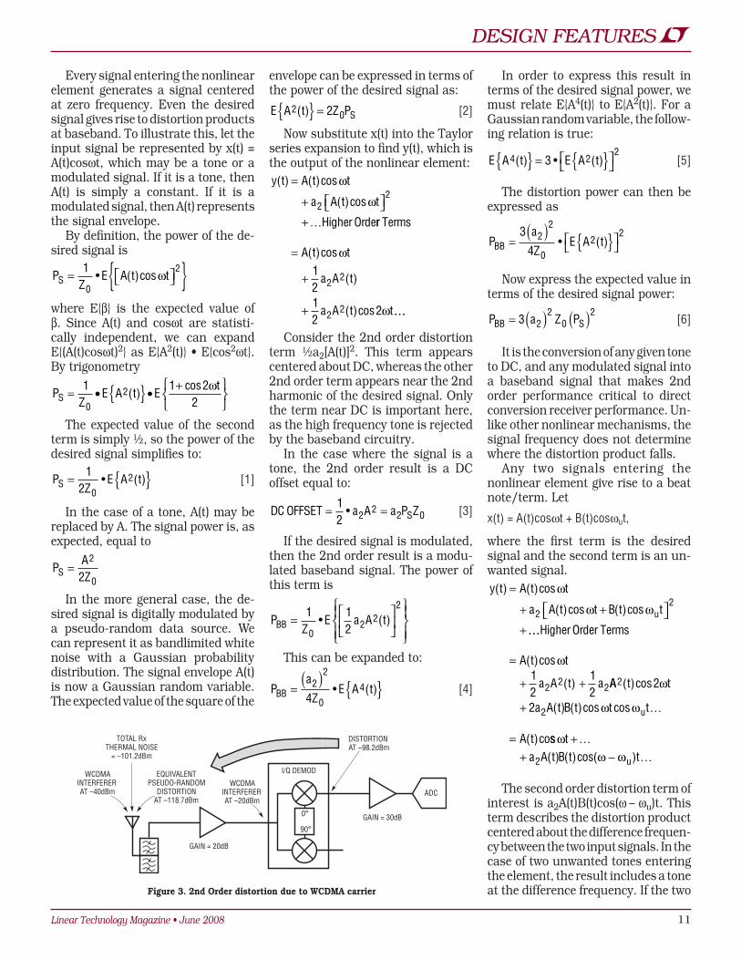
LINEAR TECHNOLOGY LINEAR TECHNOLOGY LINEAR TECHNOL OG Y JUNE 2008 VOLUME XVIII NUMBER 2 Introduction Designers of handheld products race to pack as many “cool” features as possible into ever smaller devices. Big, bright color displays, Wi-Fi, WiMax, Bluetooth, GPS, cameras, phones, touch screens, movie players, music players and radios are just a few of the features common in today’s bat- tery powered portable devices. One big problem with packing so many features into such a small space is that the “cool” product must actually stay cool while in use. Minimizing dis- sipated heat is a priority in handhelds, and a significant source of heat is the battery charger. One component of handhelds has changed little over the years—the Li-ion battery. While the capacities of today’s batteries have increased from a few hundred milliampere hours to several ampere-hours to accom- modate the ever expanding feature set of modern portable products, the basic Li-Ion battery technology has remained unchanged. Why has Li-ion survived so long? Unmatched energy density (both by mass and volume), high voltage, low self-discharge, wide usable temperature range, no memory effect, no cell reversal, no cell balanc- ing, and low environmental impact all make the Li-Ion battery the preferred Speed Up Li-ion Battery Charging and Reduce Heat with a Switching PowerPath Manager by Steven Martin choice for high performance portable products. Charging today’s big batteries, however, is no small deal. In order to charge them in a reasonable amount of time, they should be charged at a rate commensurate with their capacity and with a specific algorithm. For ex- ample, to fully charge a 1Ah battery in approximately one hour requires one amp of charge current. If USB powered charging is desired, then only 500mA of current is available, doubling the charge time to two hours. Another problem with higher charge currents is the additional heat lost in L, LT, LTC, LTM, Burst Mode, OPTI-LOOP, Over-The-Top and PolyPhase are registered trademarks of Linear Technology Corporation. Adaptive Power, Bat-Track, BodeCAD, C-Load, DirectSense, Easy Drive, FilterCAD, Hot Swap, LinearView, µModule, Micropower SwitcherCAD, Multimode Dimming, No Latency ΔΣ, No Latency Delta-Sigma, No R SENSE , Operational Filter, PanelProtect, PowerPath, PowerSOT, SmartStart, SoftSpan, Stage Shedding, SwitcherCAD, ThinSOT, True Color PWM, UltraFast and VLDO are trademarks of Linear Technology Corporation. Other product names may be trademarks of the companies that manufacture the products. continued on page IN THIS ISSUE… COVER ARTICLE Speed Up Li-ion Battery Charging and Reduce Heat with a Switching PowerPath™ Manager..........................1 Steven Martin Linear in the News… ...........................2 DESIGN FEATURES Hot Swap™ Controller Enables Standard Power Supplies to Share Load ........................................6 Vladimir Ostrerov Understanding IP2 and IP3 Issues in Direct Conversion Receivers for WCDMA Wide Area Basestations .......10 Doug Stuetzle Complete Dual-Channel Receiver Combines 14-Bit, 125Msps ADCs, Fixed-Gain Amplifiers and Antialias Filters in a Single 11.25mm × 15mm μModule™ Package ...........................14 Todd Nelson Battery Manager Enables Integrated, Efficient, Scalable and Testable Backup Power Systems......................17 Mark Gurries 500nA Supply Supervisors Extend Battery Life in Portable Electronics ..22 Bob Jurgilewicz Quad Output Regulator Meets Varied Demands of Multiple Power Supplies .........................................................25 Michael Nootbaar Buck, Boost and LDO Regulators Combined in a 4mm × 4mm QFN........28 Chris Falvey DESIGN IDEAS ....................................................30–41 (complete list on page 30) New Device Cameos ...........................42 Design Tools......................................43 Sales Offices .....................................44 POWER DISSIPATION (W) BATTERY VOLTAGE (V) 4.1 3.3 1.8 0 3.4 3.5 3.6 3.7 3.8 3.9 4.0 0.2 0.4 0.6 0.8 1.0 1.2 1.4 1.6 V IN = 5V I CHARGE = 1A LINEAR BATTERY CHARGER SWITCHING BATTERY CHARGER EN ADDITIONAL POWER AVAILABLE FOR CHARGING Figure 1. Reduce battery charge time and keep handheld devices cool by using a switching PowerPath manager/battery charger.
-
Upload
khangminh22 -
Category
Documents
-
view
3 -
download
0
Transcript of Speed Up Li-ion Battery Charging and Reduce Heat with a ...

LINEAR TECHNOLOGYLINEAR TECHNOLOGYLINEAR TECHNOLOGYJune 2008 VOLuMe XVIII nuMBeR 2
IntroductionDesigners of handheld products race to pack as many “cool” features as possible into ever smaller devices. Big, bright color displays, Wi-Fi, WiMax, Bluetooth, GPS, cameras, phones, touch screens, movie players, music players and radios are just a few of the features common in today’s bat-tery powered portable devices. One big problem with packing so many features into such a small space is that the “cool” product must actually stay cool while in use. Minimizing dis-sipated heat is a priority in handhelds, and a significant source of heat is the battery charger.
One component of handhelds has changed little over the years—the Li-ion battery. While the capacities of today’s batteries have increased from a few hundred milliampere hours to several ampere-hours to accom-modate the ever expanding feature set of modern portable products, the basic Li-Ion battery technology has remained unchanged. Why has Li-ion survived so long? unmatched energy density (both by mass and volume), high voltage, low self-discharge, wide usable temperature range, no memory effect, no cell reversal, no cell balanc-ing, and low environmental impact all make the Li-Ion battery the preferred
Speed Up Li-ion Battery Charging and Reduce Heat with a Switching PowerPath Manager
by Steven Martin
choice for high performance portable products.
Charging today’s big batteries, however, is no small deal. In order to charge them in a reasonable amount of time, they should be charged at a rate commensurate with their capacity and with a specific algorithm. For ex-ample, to fully charge a 1Ah battery in approximately one hour requires one amp of charge current. If uSB powered charging is desired, then only 500mA of current is available, doubling the charge time to two hours.
Another problem with higher charge currents is the additional heat lost in
L, LT, LTC, LTM, Burst Mode, OPTI-LOOP, Over-The-Top and PolyPhase are registered trademarks of Linear Technology Corporation. Adaptive Power, Bat-Track, BodeCAD, C-Load, DirectSense, easy Drive, FilterCAD, Hot Swap, LinearView, µModule, Micropower SwitcherCAD, Multimode Dimming, no Latency ΔΣ, no Latency Delta-Sigma, no RSenSe, Operational Filter, PanelProtect, PowerPath, PowerSOT, SmartStart, SoftSpan, Stage Shedding, SwitcherCAD, ThinSOT, True Color PWM, ultraFast and VLDO are trademarks of Linear Technology Corporation. Other product names may be trademarks of the companies that manufacture the products.
continued on page
IN THIS ISSUE…
COVER ARTICLE
Speed Up Li-ion Battery Charging and Reduce Heat with a Switching PowerPath™ Manager ..........................1Steven Martin
Linear in the News… ...........................2
DESIGN FEATURES
Hot Swap™ Controller Enables Standard Power Supplies to Share Load ........................................6Vladimir Ostrerov
Understanding IP2 and IP3 Issues in Direct Conversion Receivers for WCDMA Wide Area Basestations .......10Doug Stuetzle
Complete Dual-Channel Receiver Combines 14-Bit, 125Msps ADCs, Fixed-Gain Amplifiers and Antialias Filters in a Single 11.25mm × 15mm μModule™ Package ...........................14Todd nelson
Battery Manager Enables Integrated, Efficient, Scalable and Testable Backup Power Systems......................17Mark Gurries
500nA Supply Supervisors Extend Battery Life in Portable Electronics ..22Bob Jurgilewicz
Quad Output Regulator Meets Varied Demands of Multiple Power Supplies .........................................................25Michael nootbaar
Buck, Boost and LDO Regulators Combined in a 4mm × 4mm QFN ........28Chris Falvey
DESIGN IDEAS ....................................................30–41(complete list on page 30)
New Device Cameos ...........................42
Design Tools ......................................43
Sales Offices .....................................44
POW
ER D
ISSI
PATI
ON (W
)
BATTERY VOLTAGE (V)4.13.3
1.8
03.4 3.5 3.6 3.7 3.8 3.9 4.0
0.2
0.4
0.6
0.8
1.0
1.2
1.4
1.6
VIN = 5VICHARGE = 1A
LINEAR BATTERY CHARGER
SWITCHING BATTERY CHARGER
ENADDITIONALPOWER AVAILABLE
FOR CHARGING
Figure 1. Reduce battery charge time and keep handheld devices cool by using a switching PowerPath manager/battery charger.

2 Linear Technology Magazine • June 20082
L LINEAR IN THE NEWS
Hot Products in AsiaEDN Asia magazine recently announced their list of the 100 Hot Products of 2007. Included in the list are three Linear Technology products:qLTC6400 Low noise, Low Distortion ADC DriverqLT4356 Overvoltage Protection RegulatorqLT3080 3-Terminal Linear Regulator
For more information, visit www.linear.com.
Editor’s Choice AwardPortable Design magazine recently announced their selections for their annual editor’s Choice Awards. In the RF/Microwave category, the award went to the LT5575 Direct Conversion I/Q Demodulator. The LT5575, which was also selected by Electronic Products magazine as Product of the Year, significantly reduces the cost of 3G
and WiMAX basestation receivers. The LT5575’s extended operating frequency range from 800MHz to 2.7GHz covers all of the cellular and 3G infrastructure, WiMAX and RFID bands with a single part. Its capability to convert from RF directly to baseband at DC or low frequency results in simplified receiver designs, reduced component count and use of lower cost, low frequency components.
The LT5575 offers an outstanding IIP3 of 28dBm and IIP2 of 54.1dBm at 900MHz, and an IIP3 of 22.6dBm and IIP2 of 60dBm at 1.9GHz. Moreover, the device has a conversion gain of 3dB, which when combined with a DSB noise Figure of 12.7dB, produces excellent receiver dynamic range. The device’s I (In-phase) and Q (Quadra-ture phase) outputs have typical amplitude and phase matching of 0.04dB and 0.6°, respectively, providing an unprecedented level of demodulation accuracy.
The LT5575 is capable of supporting multiband basestations covering both the 850MHz GSM/eDGe bands and the 1.9GHz/2.1GHz 3G wireless services (including CDMA2000, WCDMA, uMTS, and TD-SCDMA). It is ideal for single carrier micro- and pico-basestations, where low cost architectures are key. The LT5575’s performance is also well suited for 2.6GHz WiMAX basestations, and as an IF demodulator in a microwave radio link or satellite receiver. L
EDN Innovation Award for Linear Power DeviceEDN magazine announced the selection of Linear’s LT3080 3-terminal parallelable low dropout linear regulator as EDN’s Innovation of the Year in the Power ICs category. The award was presented at the annual EDN Innovation Awards ceremony to Linear Technology Vice President engineering and Chief Technical Officer Robert Dobkin and Design engineer Todd Owen, who developed the product. Other Linear Technology finalists included the LTC6102 current sense amplifier in the Analog ICs category, Robert Dobkin for Innovator of the Year, and Jim Williams’ article, “Designing instrumentation circuitry with RMS/DC con-verters” for Best Contributed Article.
According to Ron Wilson, executive Director of EDN Worldwide, “Selected by their peers in the design com-munity for their outstanding results, these innovators stand in the front rank of the best and brightest electronics engineering has to offer.”
Robert Dobkin stated, “The LT3080 solves two difficult problems for linear regulators: spreading heat to eliminate heat sinks and increasing output current by simply adding additional devices. The circuit architecture is completely new and just as easy to use as older devices. I am proud to introduce this product.”
The LT3080 is a 1.1A 3-terminal linear regulator that can easily be paralleled for heat spreading and higher output current, and is adjustable to zero with a single resistor. This is a new architecture for regulators and uses a current reference and voltage follower to allow sharing between multiple regulators, enabling multiamp linear regulation in all surface-mount systems without heat sinks.
The LT3080 has a wide input voltage capability of 1.2V to 40V, a dropout voltage of only 300mV and millivolt regulation. The output voltage is adjustable, spanning a wide range from 0V to 40V, and the on-chip trimmed reference achieves high accuracy of ±1%.
Linear in the News…

Linear Technology Magazine • June 2008 3
DESIGN FEATURES L
tery chargers from Linear Technology that not only offer the high efficiency of a switching battery charger but also include PowerPath technology. PowerPath control is a technique that uses a third, or intermediate, node to allow instant-on operation, which provides power to the system when the battery voltage is below the system cutoff. Only products like the LTC4088 and LTC4098 combine a step down DC/DC switching regulator with a linear battery charger in a unique way that ensures high efficiency power delivery to both the system load and the battery. Before we delve into these parts, let’s take a look at how it was done before.
Old School: Linear PowerPathThe intermediate node topology isn’t new. Figure 2 shows an example of a linear PowerPath topology. In this architecture, a current limited switch delivers power from an input connector to both the external load and linear battery charger. The linear battery charger then delivers power from the intermediate node to the battery.
If the load current is far enough below the input current limit to allow some current to be directed to battery charging, the voltage at VOuT is nearly equal to the input supply voltage, let’s say 5V. In this case, the path from VIn to
the charging process. Since charge power for these devices usually comes from a 5V source, such as a uSB port or 5V wall adapter, power loss can be significant. Assuming a healthy Li-Ion battery spends significant time at its “happy voltage” of 3.7V during charging, then charging efficiency via a linear charging element can at best be 3.7V/5V or 74%. When the battery voltage is less than 3.7V, losses are even worse. even at the maximum float voltage of 4.2V, where the bat-tery spends about 1/3 of the charge time, charging efficiency can’t be better than 84%.
With a 1Ah battery charged at a “1C” rate, we can expect about 1.3W of power to be lost while delivering 3.7W to the battery over the longest part of the charge cycle. note, however, that the energy delivered to the battery doesn’t result in any significant tem-perature rise as the battery is storing the energy for future use. This means that the predominant source of heat during charging is generated by the charger itself. With this in mind, at a given power level it makes sense to move to a switching battery charger for improved charging efficiency, less charger generated heat and reduced charge time.
Both the LTC4088 and LTC4098 are examples of single-cell Li-ion bat-
VOuT is extremely efficient since there is no significant voltage drop across the pass element. note, however, that the voltage drop between VOuT (~5V) and VBAT (say 3.5V) means the linear charger is running inefficiently. Thus, power delivered to the load arrives ef-ficiently while power delivered to the battery arrives inefficiently.
now take the alternate case where the load current exceeds the input current limit setting. Here the input current limit control engages and the voltage at the intermediate node, VOuT, drops to just under the battery volt-age, thus bringing in the battery as a source of additional current. Although this is desired behavior, ensuring load current is prioritized over charge current, notice that there is now inef-ficiency at the pass element because a large voltage difference does exist between the input pin, again at 5V, and the output pin, which now may be about 3.5V.
From these examples we can see that while a linear PowerPath topology performs the necessary PowerPath control functions under all conditions, it has some inherent inefficiencies. Specifically, with the linear PowerPath topology there is likely to be power wasted in one or the other of the two linear pass elements under various conditions. In the next section we’ll see how a switching PowerPath avoids the pitfalls of the linear PowerPath.
New School: High Efficiency with Switching PowerPathFigure 3 shows an alternative to the linear PowerPath, a switching PowerPath. Here a step-down DC/DC converter delivers power from the input connector to the intermediate node VOuT. A linear battery charger is connected from the intermediate node to the battery as in the case of the linear PowerPath. The big difference from linear PowerPath is that the path from VIn to VOuT maintains relatively high efficiency regardless of the volt-age difference since it is a switching, rather than a linear, path.
Then what about the linear battery charging path, the other big part of
LTC4088/LTC4098, continued from page
1V
CLPROG
ISWITCH/hCLPROG
+–15mV
IDEALDIODE
AVERAGE INPUTCURRENT LIMITCONTROLLER
CONSTANT CURRENTCONSTANT VOLTAGEBATTERY CHARGER
+–
TO SYSTEMLOAD
SINGLE CELLLi-Ion
BAT
VIN VOUTTO USBOR WALLADAPTER
+
Figure 2. Block diagram of a traditional linear PowerPath, which has significant inherent efficiency limitations.

4 Linear Technology Magazine • June 2008
L DESIGN FEATURES
support a higher power 1A setting for wall adapter applications.
For products with large batteries, uSB current control can be the limit-ing factor in determining how much power is delivered to the battery for charging. With a linear PowerPath topology, input and output are current limited—the sum of the load current and the battery charging current cannot exceed the input current. In this case, a switching PowerPath has a significant advantage over a linear PowerPath. In a switching PowerPath topology the input is still current limited, but this only limits available power to the load and charger. This is an important distinction. Figure 4 shows an example of how the LTC4088 can provide up to a 40% increase in
the total efficiency picture? Voltage drops between VOuT and the battery would pretty much erase the efficiency gains made by the switching regulator. Total efficiency remains high with the the LTC4088 and LTC4098 because of a feature called Bat-Track™. With Bat-Track, the output voltage of the switching regulator is programmed to track the battery voltage plus a few hundred millivolt difference. Since the output voltage is never signifi-cantly above the battery voltage, little power is ever lost to the linear battery charger. The battery charger pass ele-ment leaves most of the voltage control duties to the switching regulator and exists merely to control charge current, float voltage and battery safety moni-toring—tasks at which it excels.
USB-Based Constant-Power ChargingThese days, an important feature in many portable products is the convenience of charging from a uSB port. The LTC4088 and LTC4098 have a unique control system that allows them to limit their input cur-rent consumption for uSB compliant applications while maximizing power available to the load and battery charging. These two devices not only have low and high power uSB settings of 100mA and 500mA, but they also
charge current over a linear PowerPath design.
notice that while the uSB current is limited to 500mA, it’s possible for the charge current to be above 500mA due to the high efficiency of the switching PowerPath system. So not only does the higher efficiency produce little heat, but it also reduces charge time.
The input current limited topology of the LTC4088 and LTC4098 offers a big advantage over devices that use an output current controlled topology to maintain uSB compliance. This is because as the battery voltage rises throughout the charge cycle, the ef-fective power consumed by the battery also rises, assuming a constant cur-rent. In order to retain uSB compliance in an output current controlled sys-tem (assuming perfect efficiency) one would have to limit the battery charge current to its power-limited value at the highest battery voltage.
For example, to remain below 2.5W (5VIn • 500mA) of power delivery at a 4.2V battery voltage, the charge cur-rent must not exceed 595mA. This current limit is overly conservative when the battery voltage is low, say 3.4V, where it would be possible to deliver 735mA without violating the uSB specification. Input current lim-ited devices designed specifically for uSB compliance, such as the LTC4088
BATTERY VOLTAGE (V)2.7
500
600
700
3.9
400
300
3.0 3.3 3.6 4.2
200
100
0
CHAR
GE C
URRE
NT (m
A) VBUS = 5VRPROG = 1kRCLPROG = 2.94k
5x USB SETTING,BATTERY CHARGER SET FOR 1A
Figure 4. Input power limited charge current
+–
++– 0.3V
1.188V 3.6V
CLPROG
ISWITCH/hCLPROG
+ –
+–15mV
IDEALDIODE
PWM ANDGATE DRIVE
AVERAGE INPUTCURRENT LIMITCONTROLLER
AVERAGE OUTPUTVOLTAGE LIMITCONTROLLER
CONSTANT CURRENTCONSTANT VOLTAGEBATTERY CHARGER
+–
GATE
VOUT
SW3.5V TO (BAT + 0.3V)TO SYSTEMLOAD
OPTIONALEXTERNALIDEAL DIODEPMOS
SINGLE CELLLi-Ion
BAT
VBUSTO USBOR WALLADAPTER
+
2.94k
8.2Ω
0.1µF
3.3µH
10µF10µF
Si2333DS
LTC4088
Figure 3. Switching PowerPath block diagram. The big advantage of a switching PowerPath scheme over a linear PowerPath is that the path from VIN to VOUT maintains relatively high efficiency regardless of the VIN/VBAT ratio.

Linear Technology Magazine • June 2008 5
DESIGN FEATURES L
and LTC4098, allow the charger to use this additional available current. In contrast, an output current regulated switching charger designed for uSB compliance must be programmed to limit battery charging current to the high voltage case (595mA), thus ham-stringing it at low battery voltages. Said another way, an input current limited switching charger always extracts as much power from the input source as is allowed, whereas an output current controlled one does not.
Instant-On (Low Battery System Start)Figure 5 shows the instant-on feature of the switching PowerPath topology. When the battery voltage is very low and the system load does not exceed the available programmed power, the output voltage is maintained at approximately 3.6V. This prevents the system from having to wait for the battery voltage to come up before turning on the device—a frustrating scenario to the end user.
This is the primary reason for having a decoupled output node and battery node (i.e. the 3-terminal topology). This feature can be used to power the system in a low power mode. For example, it may be just enough power to start up and indicate to the user that the system is charging.
Automatic Load PrioritizationThe current delivered to the system at VOuT, as well as the battery charge current, form a combined load on the switching regulator. If this combined load does not exceed the power level programmed by the input current limit circuit then the switching PowerPath topology happily delivers charge and load current without concern. If, however, the total load exceeds the available power, the battery charger automatically gives up some or all of its share of the power to support the extra load. That is, the system load is always prioritized and battery charging is only performed opportunistically. This algorithm provides uninterrupted power to the system load. even if the system load alone exceeds the power available from the input limiting cir-
cuit, the input current does not exceed its programmed limit. Rather the battery charger shuts off completely and the extra power is drawn from the battery via the ideal diode.
When the ideal diode is engaged, the conduction path from the battery to the output pin is approximately 180mΩ. If this is sufficient for the applica-tion, then no external components are needed. If greater conductance is necessary, however, an external MOSFeT can be used to supplement the internal ideal diode. The LTC4088 and LTC4098 both have a control pin for driving the gate of the optional external transistor. Transistors with resistance of 30mΩ or lower can be used to supplement the internal ideal diode.
Full Featured Battery ChargerThe LTC4088 and LTC4098 both include a full featured battery char-ger. The battery chargers feature programmable charge current, cell preconditioning with bad-cell detec-tion and termination, CC-CV charging, C/10 end of charge detection, safety timer termination, automatic recharge and a thermistor signal conditioner for temperature qualified charging.
LTC4098 EnhancementsThe LTC4098 has a few features that the LTC4088 does not. First, it sup-ports the ability to control an external high voltage switching regulator to receive power from a second input sup-ply such an automobile battery. It also includes an independent overvoltage protection module that can, in con-
BAT (V)2.4
4.5
4.2
3.9
3.6
3.3
3.0
2.7
2.43.3 3.92.7 3.0 3.6 4.2
V OUT
(V) NO LOAD
300mV
Figure 5. VOUT vs BAT
junction with an external MOSFeT, provide significant input protection to the low voltage (uSB/WALL) input.
High Voltage Input ControllerThe LTC4098’s external input control circuit recognizes when a second input supply is present and prioritizes that input in the event that both it and the uSB/WALL input are powered simultaneously. Furthermore, the LTC4098 interfaces with a number of Linear Technology high voltage step-down switching regulators to allow for higher voltage inputs, such as an automotive battery. using the same Bat-Track technique described above, the auxiliary input controller commands the high voltage regula-tor to develop a voltage at VOuT that tracks just above the battery. Again, this technique results in high charging efficiency even when charging from a fairly high voltage.
Overvoltage ProtectionThe LTC4098 includes an overvoltage protection controller that can be used to protect the low voltage uSB/Wall input from the inadvertent applica-tion of high voltage or from a failed wall adapter. This circuit controls the gate of an external high voltage n-type MOSFeT. By using an external transistor for high voltage standoff, the protection level is not limited to the process parameters of the LTC4098. Rather the specifications of the exter-nal transistor determine the level of protection provided.
ConclusionThe LTC4088 and LTC4098 represent a new paradigm in power management and battery charging. Both optimize power delivery by combining constant input power limiting with a high efficiency switching regulator and Bat-Track battery charging. Other benefits include instant-on system starting, automatic load prioritization and unmatched charging efficiency. The LTC4098 goes a step beyond with an auxiliary input controller for higher input voltages (such as a car battery) and an overvoltage protection controller. L

6 Linear Technology Magazine • June 2008
L DESIGN FEATURES
Hot Swap Controller Enables Standard Power Supplies to Share Load
by Vladimir Ostrerov
qRedundancy. These systems, often called n + 1 redundant, use a number of small supplies where n units are needed to power the load, but a “+1” supply is added for redundancy. The theory is, if one supply fails, n units remain to carry the load.
qEfficiency. If the power system must support widely ranging loads, efficiency can be optimized by adjusting the number of operating supplies to the load.
The key to parallel operation is balancing the output current of each supply, so that all are equally loaded if the supplies are identical. If individual supplies with different power ratings are combined for parallel operation,
IntroductionThe LTC4350 Hot Swap™ and load share controller is a powerful tool for developing high availability redun-dant and load sharing power supply systems. It has the unique ability to work with supplies with any output stage topology, including output stages using synchronous rectification.
Although the LTC4350 does much of the heavy lifting in maintaining a well balanced load share system, there are a number of important considerations in designing a stable system.
This article deals with some of the more complex design details of the LTC4350. If you are designing a load share system and LTC4350 is new to you, it may be helpful to first read introductory details in the LTC4350 data sheet, and the article “Combo/Hot Swap Load Share Controller Allows the use of Standard Power Modules in Redundant Power Systems” in the June, 2003 issue of Linear Technology magazine.
A Little BackgroundDC/DC converters are paralleled for any of several reasons:qOne converter may be
insufficient for the required power level. For example, an existing single regulator design may be able to handle 100W, but a new application calls for up to 200W. Paralleling two, production-proven 100W converters saves time over developing a new converter capable of twice the power.
qThe product may need to be scalable. Many rack-based systems feature multiple slots, which may be populated at some future date, but why install power supply sufficient to operate the entire rack when only a fraction of the slots are in use? Paralleling supplies allows addition of power on an as-needed basis.
the output current of each supply must be proportional to the rated supply power.
The LTC4350 performs this func-tion. It forces multiple, paralleled power supplies to share current. The concept behind a LTC4350-based load share controller is simple: a single, overall voltage loop controls the common output while each power converter is controlled by a local cur-rent loop and contributes current in the common output. even so, such a multi-loop feedback system requires careful design.
Active control is achieved by sinking additional current from the +SenSe pin found on many common converter modules, and fooling the converter into believing the output voltage is something different than what it would otherwise detect. Increasing this current causes the output to rise; decreasing it causes the output to fall. Thus the LTC4350 has a means of modulating the output voltage, thereby controlling the companion converter’s contribution to the system.
AC AnalysisThe design of a current sharing power system involves not only the simple matter of DC operating conditions, but also AC analysis. This article covers the AC design aspects of an LTC4350-based load share system.
The design goal is to build a stable system with maximum bandwidth,
POWER SUPPLY
–VIN –VOUT
+VOUT
+SENSE
CH2
CH1
Q1
BC847BPN
R1 = RPS(SENSE)
LT1784 LOADGND
OUTPUT
–SENSE
+VIN
+–
SINUSOIDALGENERATOR
Figure 1. Power supply closed-loop Bode plot measurement block diagram
The LTC4350 Hot Swap and load share controller is a
powerful tool for developing high availability redundant
and load sharing power supply systems.
It has the unique ability to work with supplies with any output stage
topology, including output stages using synchronous
rectification.

Linear Technology Magazine • June 2008 7
DESIGN FEATURES L
with good transient response, and to preserve as much of the inherent performance of the individual power supply as possible.
As each supply in a power system is a fixed configuration component, knowledge of its main characteristics is indispensable for control system design. Among the power supply characteristics essential for design purposes are power supply band-width, output stage topology and power supply output voltage ramp up behavior.
Figures for power supply bandwidth can be obtained directly from the power supply manufacturer or measured in the lab. One way to experimentally measure bandwidth is to use a simple driver, a sine wave generator and an oscilloscope. Figure 1 shows the block
diagram for this measurement. Scope probes are connected to the generator output and power supply output. A power supply Bode plot can be ob-tained significantly faster using special equipment for frequency response measurement, such as a VenABLe Frequency Response Analyzer or AP’s Analog network Analyzer. Power sup-ply bandwidth should be measured with 90%–100% load.
The power supply output stage to-pology should be taken into account when designing the load share power system. If it is a synchronously rectified power supply output stage, it is able to provide bidirectional energy flow and as a result the power supply can operate in the second quadrant and sink current. In this case one of two special measures should be taken:
either synchronize the activation of the LTC4350 controller current share ability with the MOSFeT switch turn-on process, or disable synchronous rectification before the LTC4350 load share capability is activated. Detailed descriptions of those actions are pre-sented below.
The power supply output volt-age ramp-up behavior during turn on should be checked to eliminate LTC4350 operation in the area where output voltage slew rate experiences significant changes. An undervoltage protection circuit, which is connected with pin 1, performs this function.
Unified Approach to Compensation Components Parameters EvaluationA power system with K power sup-plies operating in parallel is a K + 1 loop control system. This system has one voltage loop, which is the highest bandwidth loop, and K current loops. These K current loops work with a common input command signal and individual feedback current signals. All current loops operate in parallel. A block diagram of the control loops is shown in Figure 2.
There are two restrictions on loop bandwidth. All current loops must have equal bandwidths. The volt-age loop bandwidth must be wider than any current loop bandwidth to eliminate current oscillation between power supplies.
LTC4350 error amplifiers eA1 and eA2 are transconductance operational amplifiers. This restricts compensa-tion circuit transfer functions to two types: pole or a pole and zero with TPOLe > TZeRO. A compensation circuit of one capacitor CC implements a transfer function
GT s
EA
POLE + 1 [1]
where GeA is the error amplifier voltage gain, gmRO, and,
TR CPOLEO C
= 12π
.
RO is the internal error amplifier’s output impedance.
PHAS
E (°
)
1M1
180
120
60
0
–60
–120
–18010 100 1k 10k 100k
MAG
NITU
DE (d
B)
FREQUENCY (Hz)
50
60
–50
–60
–40
–30–20
–10
40
30
20
10
0
SYNTHESIZED OPEN CURRENT LOOPCOMPENSATION NETWORKPOWER SUPPLY
Figure 4. Current loop synthesis with 0,–1,–2 shape
PHAS
E (°
)
1M1
180
120
60
0
–60
–120
–18010 100 1k 10k 100k
MAG
NITU
DE (d
B)
FREQUENCY (Hz)
50
60
–50
–60
–40
–30–20
–10
40
30
20
10
0
SYNTHESIZED OPEN CURRENT LOOPCOMPENSATION NETWORKPOWER SUPPLY
Figure 3. Current loop Bode design with power supply having first order transfer function
ERRORAMPLIFIER 1
ERRORAMPLIFIER 2-1
POWER SUPPLY 1
RN
RN
REFERENCEINPUT
SIGNAL
CURRENT 1 SIGNAL
CURRENT 2 SIGNAL
CURRENT N SIGNAL
+ ERRORAMPLIFIER 2-2
POWER SUPPLY 2
LOAD
VOLTAGE SIGNAL
OUTPUTVOLTAGE
DIVIDER FOR FEEDBACK
SIGNAL
–
+
–
+
–
+
–
ERRORAMPLIFIER 2-N
POWER SUPPLY N
Figure 2. Power system control loop

8 Linear Technology Magazine • June 2008
L DESIGN FEATURES
If a compensation circuit has capacitor CC and resistor RC series connected, it implements a transfer function G T s
T sEA ZERO
POLE
( )++
11
[2]
where
TR CZEROC C
= 12π
The equations shown are based on the assumption that RO >> RC.
Current Control Loop Synthesis and Compensation Component CalculationThe Bode amplitude characteristic slope is defined by the integer K (0, 1, 2, etc.) to express the slope
SLOPEdbdec
K= −( • )20
As an outer loop, the voltage loop must have larger bandwidth than the inner current loop. The closed current loop Bode plot should be shaped as 0,–1 or 0,–1,–2 with the –1 segment at least 1.4 decades long.1. If the power supply Bode ampli-
tude characteristic has shape 0,–1 or 0,–1,–2, and the –1 segment is 1.4 decades long, the current loop error amplifier compensation network allows for a current loop bandwidth equal to the power supply bandwidth. This can be achieved by tailoring the current loop compensation network so that its zero frequency is equal to the main power supply pole frequency. Figure 3 demon-strates this approach.
2. If the power supply Bode ampli-tude characteristic has shape 0,–1,–2, and the –1 segment is shorter than 1.4 decades—or at the extreme, the shape is 0,–2—shifting the current loop crossover frequency to the left (this reduces the current loop bandwidth to below the power supply bandwidth) makes it pos-sible to achieve a 0,–1,–2 closed current loop shape with the –1 segment covering least 1.4 de-cades. In the extreme case when
the power supply closed loop frequency response characteristic is 0,–2, placing a compensa-tion network zero exactly at the coordinate where the amplitude is –28db and the frequency is the power supply bandwidth, and placing the pole value so that the crossover frequency is 25× lower than the power supply band-width achieves the desired result. Figure 4 illustrates synthesis of a current loop with shape 0,–1,–2.
A current loop block diagram and current loop control diagram are shown in Figures 5 and 6.
Current open-loop gain is propor-tional to load and it must be calculated at the power supply’s maximum avail-able current. At maximum load current (ILIMIT), an additional 1V output on the
power supply produces additional current in the load as given by
ΔIIVLIMIT
OUT=
and produces a corresponding signal on the sense resistor as follows
ΔVI R
VSENSELIMIT SENSE
OUT= .
Current open-loop gain equalsG G G GCO EA DB CSA= • •2 ,
where GeA2 is the error amplifier eA2 gain, GDB is the driving block gain, and GCSA is the current sense amplifier gain, which is given by
GI R
VRCSA
LIMIT SENSE
OUTGAIN= • •−10 3
It should be noted that RSenSe is a resistor connecting the power sup-
ERROR AMPLIFIER 2 DRIVING BLOCK
CURRENT SENSEAMPLIFIER FILTER CURRENT SENSE AMPLIFIER
POWER SUPPLY
INITIAL OUTPUTVOLTAGE OFFSET
MEASUREDTRANSFER FUNCTION
ORMAGNITUDEBODE PLOT
MAGNITUDEBODE PLOT(FIGURE 5)
VOUT
RLOAD =VOUT/ILIMIT
VSH(BUS)+
++
–
GEA2T2Z s + 1
T2P s + 1
GCSA =
VOUT – 0.2V
ILIMIT • RSENSE • RGAIN10–3
VOUT
Figure 6. Current loop control block diagram
–VOUTRSETRGAIN
RLOAD
RSENSE
CC
RC
RPS(SENSE)
VOLTAGE TOCURRENT
CONVERTER
ERROR AMPLIFIER 2 WITH COMPENSATION
CIRCUIT DRIVING BLOCK
SHARE BUS
POWER SUPPLY
+–
+–
+VOUT+SENSE
gm
Figure 5. Current loop functional block diagram

Linear Technology Magazine • June 2008 9
DESIGN FEATURES L
with lead ratio 1.22/VOuT. Shunting the top resistor in the output voltage divider with a capacitor implements the transfer function
T s
T s Vf ZERO
f POLE OUT
( )
( )
.++
•1
11 22
where
T R Cf ZERO f f( ) = 1
and
T TV
f POLE f ZEROOUT
( ) ( ) .= •
1 22 Rf1 is the top resistor in the voltage
divider and Cf is the shunting capaci-tor. This compensation allows bending of the magnitude response and gives a slope of –20db/dec around the crossover frequency in the restricted frequency area. It is the maximum area for a 12V system; it takes
20121 22
19 85log.
.= db
where GV(OPen) is the voltage open-loop gain.
The same relationship between volt-age loop crossover frequency and the current closed-loop bandwidth should hold in the second case, when the cur-rent closed-loop magnitude response is shaped as 0,–1,–2. The compensation provided should be the same as the first case, as shown in Figure 9.
An additional option exists for im-provement of the voltage open-loop magnitude response by placing in the feedback path lead compensation
ply output to the load. Driving block gain is
GR
RDBPS SENSE
SET= ( )
where RPS(SenSe) is a power supply resistor value and RSeT is a resistor connected to the LTC4350 SeT pin.
The LTC4350’s voltage-to-current converter in the current sensing block has a flat response from low frequen-cies up to 10kHz, where a low frequency pass filter is implemented.
Measured error Amplifier 2 voltage gain is 500–1000.
Voltage Control Loop Synthesis and Compensation Component CalculationThe voltage loop forward path contains an error amplifier (error Amplifier 1) and the current loop, and the feedback path contains an output voltage di-vider. A control diagram for the voltage loop is shown in Figure 7.
Measured error Amplifier 1 voltage gain is 1800–2200.
Bode design for the voltage loop is demonstrated in Figures 8 and 9. The first plot explains the design when the current closed-loop magnitude response has shape 0,–1. To have a voltage loop crossover frequency 6 to 7 times wider than the current closed-loop bandwidth, the compensa-tion should have a zero at the same frequency as the bandwidth, but the magnitude of the gain must be 15dB – 17dB [20log(6) = 15.5; 20log(7) = 16.9]. The pole frequency equals
ff
GPOLEZERO
V OPEN1
13 6( )( )
( )( )= −
LTC4350 LTC4350
RSENSE1
R1DRAIN-SOURCE
I1 I2
EMF1 EMF2
RLOAD CLOAD
R2DRAIN-SOURCE
SHAREBUS
RSENSE2
+–+–
Figure 10. Output power stage equivalent circuitry. The power supply output characteristic exists in the second quadrant
PHAS
E (°
)
1M1
180
120
60
0
–60
–120
–18010 100 1k 10k 100k
MAG
NITU
DE (d
B)
FREQUENCY (Hz)
50
60
–50
–60
–40
–30–20
–10
40
30
20
10
0
CLOSED CURRENT LOOP
VOLTAGE LOOPCOMPENSATION NETWORK
OPEN VOLTAGE LOOP
Figure 9. Voltage loop Bode design with closed current loop having 0,–1,–2 shape
PHAS
E (°
)
1M1
180
120
60
0
–60
–120
–18010 100 1k 10k 100k
MAG
NITU
DE (d
B)
FREQUENCY (Hz)
50
60
–50
–60
–40
–30–20
–10
40
30
20
10
0
CLOSED CURRENT LOOP
VOLTAGE LOOPCOMPENSATION NETWORK
OPEN VOLTAGE LOOP
Figure 8. Voltage loop Bode design with current closed loop having 0,–1 shape
ERRORAMPLIFIER 1
CURRENTCLOSE-LOOP
TRANSFER FUNCTION OR MAGNITUDE
BODE PLOT
REFERNCEINPUT
SIGNAL
OUTPUT VOLTAGE DIVIDER GAIN
+
–
GEA1T1Z s + 1
T1P s + 1
1.22(TFZ s + 1)
VOUT(KDIVTFZ s + 1)
VOUT
Figure 7. Voltage loop control block diagram
continued on page 6

10 Linear Technology Magazine • June 2008
L DESIGN FEATURES
IntroductionA direct conversion receiver architec-ture offers several advantages over the traditional superheterodyne. It eases the requirements for RF front end bandpass filtering, as it is not suscep-tible to signals at the image frequency. The RF bandpass filters need only attenuate strong out-of-band signals to prevent them from overloading the front end. Also, direct conversion eliminates the need for IF amplifiers and bandpass filters. Instead, the RF input signal is directly converted to baseband, where amplification and filtering are much less difficult. The overall complexity and parts count of the receiver are reduced as well.
Direct conversion does, however, come with its own set of implemen-tation issues. Since the receive LO signal is at the same frequency as the RF signal, it can easily radiate from the receive antenna and violate regulatory standards. Also, a thorough understanding of the impact of the IP2 and IP3 issues is required. These parameters are critical to the overall performance of the receiver and the key component is the I/Q demodulator.
unwanted baseband signals can be generated by 2nd order nonlinearity of the receiver. A tone at any frequency entering the receiver gives rise to a DC offset in the baseband circuits. Once generated, straightforward elimination of DC offset becomes very problematic. That is because the frequency response of the post-downconversion circuits must often extend to DC. The 2nd order nonlinearity of the receiver also allows a modulated signal—even the desired signal—to generate a pseudo-random block of energy centered about DC.
unlike superheterodyne receivers, direct conversion receivers are suscep-tible to such 2nd order mechanisms regardless of the frequency of the incoming signal. So minimizing the
effect of finite 2nd order linearity is critical.
Later in this article we consider the effect of 3rd order distortion on a direct conversion receiver. In this case, two signals separated by an appropriate frequency must enter the receiver in order for unwanted products to appear at the baseband frequencies.
Second Order Distortion (IP2)The second order intercept point (IP2) of a direct conversion receiver system is a critical performance parameter. It is a measure of second order non-lin-earity and helps quantify the receiver’s susceptibility to single- and 2-tone interfering signals. Let’s examine how this nonlinearity affects sensitivity.
We can model the transfer function of any nonlinear element as a Taylor series:
y(t)=x(t)+a2x2(t)+a3x3(t)+…
where x(t) is the input signal consist-ing of both desired and undesired signals. Consider only the second order distortion term for this analysis. The coefficient a2 is equal to
aZ IP20
22
=
where IP2 is the single tone intercept point in watts. note that the 2-tone IP2 is 6dB below the single-tone IP2. The more linear the element, the smaller a2 is.
Understanding IP2 and IP3 Issues in Direct Conversion Receivers for WCDMA Wide Area Basestations
by Doug Stuetzle
DIPLEXER
ADC
ADC
0°
I/Q DEMOD
AGCBANDFILTER
LOWPASSFILTERS
BASEBANDAMPLIFIERS
LNARF AT 1920 MHz–1980 MHz
FROM Tx 2110 MHz–2170 MHz
LO AT 1920 MHz–1980 MHz
90°
Figure 1. Direct conversion receiver architecture
LO
RF TONE POWER = PS
RF PASSBAND
SINGLE TONE EXAMPLE MODULATED SIGNAL EXAMPLE
DOWNCONVERSION
LO RF PASSBAND
DC DUE TO 2ND ORDER DISTORTION = a2PSZ0
0 Hz 0 Hz
BASEBAND PSEUDO-RANDOM POWER DUE TO 2ND ORDER DISTORTION = 3a22Z0PS2
RF SIGNAL POWER = PS
Figure 2. Effects of 2nd order distortion
Linear Technology Magazine • June 2008 11
DESIGN FEATURES L
every signal entering the nonlinear element generates a signal centered at zero frequency. even the desired signal gives rise to distortion products at baseband. To illustrate this, let the input signal be represented by x(t) = A(t)cosωt, which may be a tone or a modulated signal. If it is a tone, then A(t) is simply a constant. If it is a modulated signal, then A(t) represents the signal envelope.
By definition, the power of the de-sired signal is
PZ
E A t tS = 1
0
2• ( )cosω
where eβ is the expected value of β. Since A(t) and cosωt are statisti-cally independent, we can expand e(A(t)cosωt)2 as eA2(t) • ecos2ωt. By trigonometry
PZ
E A t Et
S = • • +
1 1 220
2( )cos ω
The expected value of the second term is simply ½, so the power of the desired signal simplifies to:
PZ
E A tS = 12 0
2• ( ) [1]
In the case of a tone, A(t) may be replaced by A. The signal power is, as expected, equal to
PAZS =2
02
In the more general case, the de-sired signal is digitally modulated by a pseudo-random data source. We can represent it as bandlimited white noise with a Gaussian probability distribution. The signal envelope A(t) is now a Gaussian random variable. The expected value of the square of the
envelope can be expressed in terms of the power of the desired signal as:
E A t Z PS202( ) = [2]
now substitute x(t) into the Taylor series expansion to find y(t), which is the output of the nonlinear element: y t A t t
a A t t
HigherOrde
( ) ( )cos
( )cos
=
+ +…
ω
ω22
rr Terms
A t t
a A t
a A t t
=
+
+
( )cos
( )
( )cos
ω
ω
1212
2
22
22 ……
Consider the 2nd order distortion term ½a2[A(t)]2. This term appears centered about DC, whereas the other 2nd order term appears near the 2nd harmonic of the desired signal. Only the term near DC is important here, as the high frequency tone is rejected by the baseband circuitry.
In the case where the signal is a tone, the 2nd order result is a DC offset equal to:
DC OFFSET a A a P ZS= =12 2
22 0• [3]
If the desired signal is modulated, then the 2nd order result is a modu-lated baseband signal. The power of this term is
PZ
E a A tBB =
1 120
22
2
• ( )
This can be expanded to:
Pa
ZE A tBB =
( ) 22
0
44
• ( ) [4]
In order to express this result in terms of the desired signal power, we must relate eA4(t) to eA2(t). For a Gaussian random variable, the follow-ing relation is true:
E A t E A t4 22
3( ) • ( ) = [5]
The distortion power can then be expressed as
Pa
ZE A tBB =
( ) 3
42
2
0
22
• ( )
now express the expected value in terms of the desired signal power:
P a Z PBB S= ( ) ( )3 22
02
[6]
It is the conversion of any given tone to DC, and any modulated signal into a baseband signal that makes 2nd order performance critical to direct conversion receiver performance. un-like other nonlinear mechanisms, the signal frequency does not determine where the distortion product falls.
Any two signals entering the nonlinear element give rise to a beat note/term. Let
x(t)=A(t)cosωt+B(t)cosωut,
where the first term is the desired signal and the second term is an un-wanted signal.y t A t t
a A t t B t tu
( ) ( )cos
( )cos ( )cos
=
+ + +
ω
ω ω22
……
=
+ +
HigherOrder Terms
A t t
a A t a
( )cos
( )
ω12
122
22AA t t
a A t B t t t
A t
u
2
2
2
2
( )cos
( ) ( )cos cos
( )co
ω
ω ω+ …
= ss( ) ( )cos( )
ωω ω
ta A t B t tu
+…+ − …2
The second order distortion term of interest is a2A(t)B(t)cos(ω – ωu)t. This term describes the distortion product centered about the difference frequen-cy between the two input signals. In the case of two unwanted tones entering the element, the result includes a tone at the difference frequency. If the two
ADC
0°
I/Q DEMOD
GAIN = 30dB
GAIN = 20dB
EQUIVALENT PSEUDO-RANDOM
DISTORTION AT –118.7dBm
TOTAL Rx THERMAL NOISE
= –101.2dBm
WCDMAINTERFERERAT –40dBm
WCDMAINTERFERERAT –20dBm
DISTORTION AT –98.2dBm
90°
Figure 3. 2nd Order distortion due to WCDMA carrier
12 Linear Technology Magazine • June 2008
L DESIGN FEATURES
unwanted signals are modulated, then the resultant includes a modulated signal centered about their difference frequency.
We can apply these principles to a direct conversion receiver example. Figure 1 shows the block diagram of a typical WCDMA basestation receiver. Here are some key characteristics of this example:qBasestation Type: FDD, Band IqBasestation Class: Wide Areaqnumber of carriers: 1qReceive band: 1920MHz to
1980MHzqTransmit band: 2110MHz to
2170MHzThe RF section of this receiver in-
cludes a diplexer, a bandpass filter, and at least one Low noise Amplifier (LnA). The frequency selective elements are used to attenuate out-of-band signals and noise. The LnA(s) establishes the noise figure of the receiver. The I/Q demodulator converts the receive signal to baseband.
In the examples illustrated below, the characteristics of the LT5575 I/Q demodulator as representative of a basestation class device of this type. Lowpass filters and baseband amplifiers bandlimit and increase the signal level before it is passed to the A/D converters. The diplexer and RF bandpass filter serve as band filters only; they do not offer any carrier selectivity.
The second order linearity of the LnA is much less important than that of the demodulator. This is because any LnA distortion due to a single signal is be centered about DC and rejected by the demodulator. If there are two unwanted signals in the receive band (1960MHz, for example), then a second order product is generated by the LnA at the difference frequency. This signal is demodulated and ap-pears as a baseband artifact at the A/D converter. We need not address this condition, however, because out of band signals emerging from the front end diplexer are not strong enough to create distortion products of any importance.
Consider first a single unmodulated tone entering the receiver (see Figure
2). As detailed above, this tone gives rise to a DC offset at the output of the demodulator. If the baseband cascade following the demodulator is DC-cou-pled, this offset is applied to the A/D converter, reducing its dynamic range. The WCDMA specification (3GPP TS 25104.740) calls out an out-of-band tone at –15dBm, located 20MHz or more from either receive band edge (section 7.5.1). Compute the DC offset generated in the I/Q demodulator: qTone entering receive antenna
port: –15dBmqDiplexer rejection at 20MHz
offset: 0dBqBandpass rejection at 20MHz
offset: 2dBqRF gain preceding LT5575: 20dBqTone entering LT5575: 3dBmqLT5575 IIP2, 2-tone: 60dBmqLT5575 a2: 0.00317qDC offset at LT5575 output:
0.32mVqBaseband voltage gain: 31.6qDC offset at A/D input: 10mV
Single WCDMA carriers can also serve as interferers, as detailed in section 7.5.1. In one case, this carrier is offset by at least 10MHz from the desired carrier, but is still in the receive band. The power level is –40dBm, and the receiver must meet a sensitivity of –115dBm for a 12.2kbps signal at a BeR of 0.1%. Here are the details: qSignal entering receive antenna
port: –40dBmqRF gain preceding LT5575: 20dBqSignal entering LT5575: –20dBmq LT5575 IIP2, 2-tone: 60dBmqLT5575 a2: 0.00317
A MATLAB simulation performed using a pseudo-random channel
predicts a distortion at the LT5575 output of –98.7dBm. This result agrees well with that given by equation 6, which predicts a distortion power of –98.2dBm.
The baseband product that appears at the LT5575 output is a noiselike signal, created from the interfering WCDMA carrier. If this signal is large enough, it can add to the thermal receiver and A/D converter noise to degrade sensitivity. Compute the equivalent thermal noise at the receiv-er input with no added distortion: qSensitivity: –121dBmqProcessing + coding gain: 25dBqSignal to noise ratio at sensitivity:
5.2dBqThermal noise at receiver input:
–101.2dBmnow refer the distortion signal back to the receiver input: qRF gain preceding LT5575: 20dBqequivalent interference level at
Rx input: –118.7dBmThe baseband second order product
in this case is 17.5dB below the ther-mal noise at the receiver input. The resulting degradation in sensitivity is <0.1dB, so the receiver easily meets the specification of –115dBm. This is illustrated in Figure 3. Single WCDMA carriers can also appear out of band, as specified in section 7.5.1. These can be directly adjacent to the receive band at levels as high as –40dBm. Here again, the second order effect of such carriers upon sensitivity is negligible, as the preceding analysis shows.
Another threat to sensitivity comes from transmitter leakage in FDD sys-tems, as shown in Figure 4. In an FDD system, the transmitter and receiver
Figure 4. Transmitter leakage effects
Linear Technology Magazine • June 2008 13
DESIGN FEATURES L
Third Order Distortion (IP3)The third order intercept point (IP3) has an effect upon the baseband signal when two properly spaced channels or signals enter the nonlinear element.
Refer back to the transfer function: y(t) = x(t) + a2x2(t) + a3x3(t) + …, where x(t) is the input signal consisting of both desired and undesired signals. Consider now the third order distor-tion term. The coefficient a3 is equal to 2/(3Z0IP3) where IP3 is the single tone intercept point in Watts. note that the 2-tone IP3 is 4.78dB below the single-tone IP3.
Two signals entering the nonlinear element generate a signal centered at zero frequency if the spacing be-tween the two signals is equal to the distance to zero frequency. Let x(t) = A(t)cosωt + B(t)cosωut, where the first term is the desired signal and the second term is an unwanted signal. The unwanted signal may be a tone or a modulated signal. If it is a tone, then B(t) is simply a constant. If it is a
modulated signal, then B(t) represents the signal envelope.
The output signal is then equal to y(t):
y t A t t
a A t t B t tu
( ) ( )cos
( )cos ( )cos
= +…
+ +
ω
ω ω333
323
+…
= +…+
HigherOrder Terms
A t ta A t B
( )cos( ) (ω
tt t t
a A t B t t t
A
u
u
)cos cos
( ) ( )cos cos
2
32 23
ω ωω ω+ …
= (( )cos
( ) ( )cos( )
t t
a A t B t tu
ω
ω ω
+…
+ − …34
232
The third order distortion term of in-terest here is ¾a3A(t)B2(t)cos(2ωu – ω)t. In order for this distortion to appear at baseband, set ω = 2ωu. The power of the distortion is
PZ
E a A t B tBB =
1 340
32
2
• ( ) ( )
which can be expanded to
Pa
ZE A t E B tBB =
( ) 9
163
2
0
2 4• ( ) • ( ) [7]
Consider the case of a modulated desired signal and a tone interferer; B(t) may be replaced by B. See Figure 5. The value of eB4 can be expressed as (2Z0Pu)2, where Pu is the power of the tone interferer. We can use equa-tion 2 to express eA2(t) in terms of the desired signal power as 2ZoPs, where Ps is the power of the desired signal. The power level of the distortion at baseband is then:
P P P Z aBB S u= ( ) ( ) ( )92
20
23
2• [8]
If the undesired signal is modulated, use equations 2 and 5 to express eB4(t) as 3(2Z0Pu)2, where Pu is the power of the tone interferer:
P a Z P PBB S u= ( ) ( ) ( )272 3
20
2 2• [9]
In the direct conversion receiver example, Section 7.6.1 of the WCDMA specification calls for two interfering
are operating at the same time. For the WCDMA Band I case, the transmit band is 130MHz above the receive band. A single antenna is commonly used, with the transmitter and receiver joined by a diplexer. Here are some typical basestation coupled resona-tor-type diplexer specifications: qIsolation, Tx to Rx 2110MHz:
55dBqDiplexer insertion loss, Tx path:
1.2dBIn the case of a Wide Area basesta-
tion, the transmit power may be as high as 46dBm. At the transmit port of the diplexer the power is at least 47dBm. This high level modulated signal leaks to the receiver input, and some portion of it drives the I/Q demodulator: qReceiver input power: –8dBmqRx BPF rejection at 2110MHz:
40dBqRF gain preceding LT5575: 20dBqSignal entering LT5575: –28dBmqLT5575 IIP2, 2-tone: 60dBmqLT5575 a2: 0.00317
A MATLAB simulation performed using a pseudo-random channel pre-dicts the following: qDistortion at LT5575 output:
–114.7dBmRefer this signal back to the receiver input: qRF gain preceding LT5575: 20dBqequivalent interference level at
Rx input: –134.7dBmqThermal noise at receiver input:
–101.2dBmThis equivalent interference is
33.5dB below the thermal noise at the receiver input. The resulting degrada-tion in sensitivity is <0.1dB, so the receiver easily meets the specification of –121dBm.
ADC
0°
I/Q DEMOD
GAIN = 30dB
GAIN = 20dB
EQUIVALENT PSEUDO-RANDOM
DISTORTION AT –155.7dBm
TOTAL Rx THERMAL NOISE
= –101.2dBm WCDMA
INTERFERERAT –48dBm + TONE AT –48dBm
INTERFERERSAT –28dBm
DISTORTION AT –135.7dBm
90°
Figure 6. 3rd Order distortion due to WCDMA carrier + tone interferer
MODULATED SIGNAL AND TONE EXAMPLE
DOWNCONVERSION
LO RF PASSBAND
0Hz
BASEBAND PSEUDO-RANDOM POWERDUE TO 3RD ORDER DISTORTION= 9/2a32Z02PSPu2
RF SIGNAL POWER = PS
TONEPOWER = Pu
Figure 5. Effects of 3rd order distortion
continued on page 27
14 Linear Technology Magazine • June 2008
L DESIGN FEATURES
Introductionextensive hands-on applications experience is a prerequisite for any designer hoping to take full advan-tage of an ADC’s capabilities when sampling high dynamic range signals in multichannel IF-sampling or in I/Q baseband communications channels. An intimate knowledge of the ampli-fier output stage and ADC front end is required to match the impedances, while careful attention to layout is required to minimize coupling of the digital outputs into the sensitive analog input.
In fact, good layout is paramount to maintaining ADC performance, yet ever more demanding market requirements call for smaller designs and higher channel density, which exacerbate layout issues. These design requirements can challenge even the most seasoned engineer if
Complete Dual-Channel Receiver Combines 14-Bit, 125Msps ADCs, Fixed-Gain Amplifiers and Antialias Filters in a Single 11.25mm × 15mm μModule Package
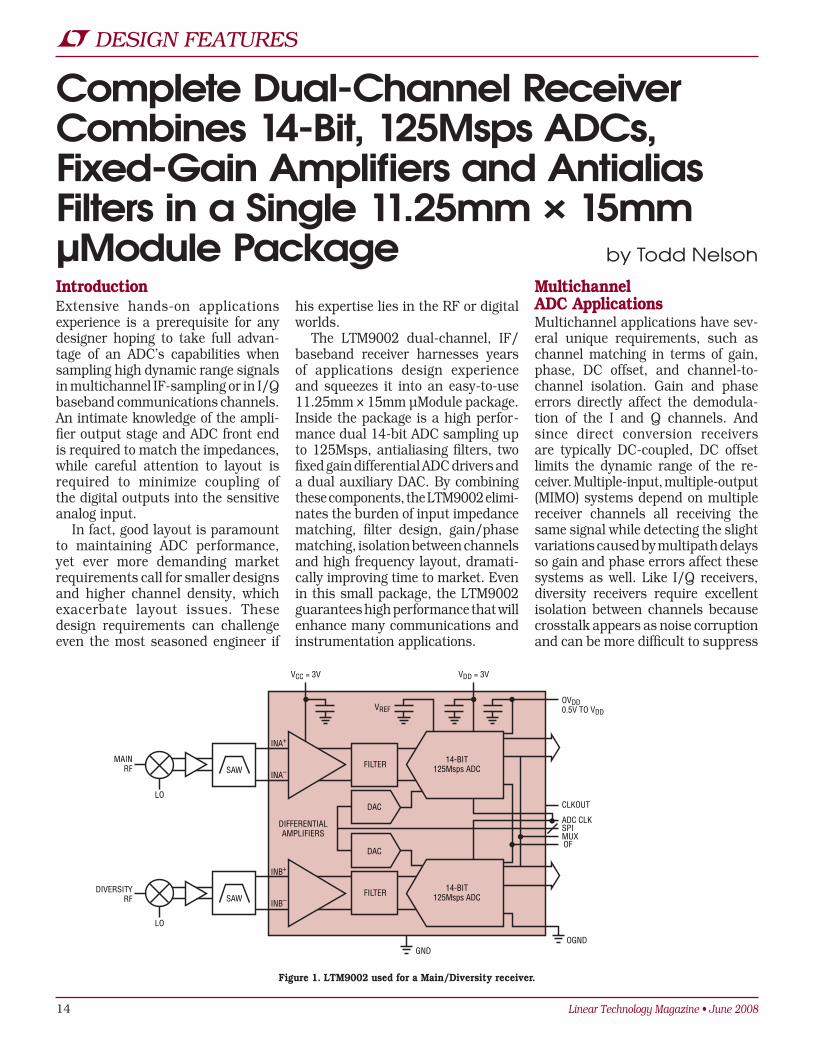
his expertise lies in the RF or digital worlds.
The LTM9002 dual-channel, IF/baseband receiver harnesses years of applications design experience and squeezes it into an easy-to-use 11.25mm × 15mm µModule package. Inside the package is a high perfor-mance dual 14-bit ADC sampling up to 125Msps, antialiasing filters, two fixed gain differential ADC drivers and a dual auxiliary DAC. By combining these components, the LTM9002 elimi-nates the burden of input impedance matching, filter design, gain/phase matching, isolation between channels and high frequency layout, dramati-cally improving time to market. even in this small package, the LTM9002 guarantees high performance that will enhance many communications and instrumentation applications.
Multichannel ADC ApplicationsMultichannel applications have sev-eral unique requirements, such as channel matching in terms of gain, phase, DC offset, and channel-to-channel isolation. Gain and phase errors directly affect the demodula-tion of the I and Q channels. And since direct conversion receivers are typically DC-coupled, DC offset limits the dynamic range of the re-ceiver. Multiple-input, multiple-output (MIMO) systems depend on multiple receiver channels all receiving the same signal while detecting the slight variations caused by multipath delays so gain and phase errors affect these systems as well. Like I/Q receivers, diversity receivers require excellent isolation between channels because crosstalk appears as noise corruption and can be more difficult to suppress
by Todd Nelson
Figure 1. LTM9002 used for a Main/Diversity receiver.
OF
GND
LO
VCC = 3V VDD = 3V
DIFFERENTIALAMPLIFIERS
MAINRF
INA–
INA+
VREFOVDD0.5V TO VDD
SAWFILTER
MUX
CLKOUT
ADC CLKSPI
14-BIT125Msps ADC
LO
DIVERSITYRF INB–
INB+
OGND
SAWFILTER 14-BIT
125Msps ADC
DAC
DAC
Linear Technology Magazine • June 2008 15
DESIGN FEATURES L
with digital filtering. Clearly, channel matching and channel isolation of the ADC and driver circuits directly impact system-level performance. For many multichannel applications, these errors cannot be corrected in the digital domain.
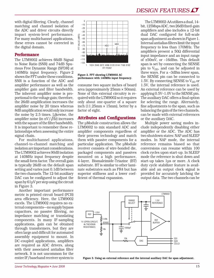
PerformanceThe LTM9002 achieves 66dB Signal to noise Ratio (SnR) and 74dB Spu-rious Free Dynamic Range (SFDR) at 140MHz input frequency. Figure 2 shows the FFT under these conditions. SnR is a function of the ADC and amplifier performance as well as the amplifier gain and filter bandwidth. The inherent amplifier noise is pro-portional to the voltage gain; therefore, the 26dB amplification increases the amplifier noise by 20 times whereas 8dB amplification would only increase the noise by 2.5 times. Likewise, the amplifier noise (in nV/√Hz) increases with the square of the filter bandwidth. It is important to remember these re-lationships when assessing the entire signal chain.
For multichannel applications, channel-to-channel matching and isolation are important considerations. The LTM9002 achieves 90dB isolation at 140MHz input frequency despite the small form factor. The overall gain is typically 26dB on the default span setting and varies just 0.1dB between the two channels. The 12-bit auxiliary DAC can be configured to adjust the span by 61µV per step using the circuit in Figure 3.
Another important performance metric is printed circuit board (PCB) area efficiency. Here, the LTM9002 excels. The LTM9002 requires no ex-ternal components—no supply bypass capacitors, no passive filtering, no impedance matching or translating components. In many IF-sampling applications, gain can be obtained through transformers, but they are often large and difficult for automated assembly equipment to mount. In DC-coupled applications, amplifiers are required as ADC drivers, along with their associated antialias filter network. It is not uncommon for the entire IF/baseband receiver system to
consume two square inches of board area (approximately 25mm × 50mm). none of this external circuitry is re-quired with the LTM9002 so it requires only about one-quarter of a square inch (11.25mm × 15mm), better by a factor of eight.
Attributes and ConfigurationsThe µModule construction allows the LTM9002 to mix standard ADC and amplifier components regardless of their process technology and match them with passive components for a particular application. The µModule receiver consists of wire-bonded die, packaged components and passives mounted on a high performance, 4-layer, Bismaleimide-Triazine (BT) substrate. BT is similar to other lami-nate substrates such as FR4 but has superior stiffness and a lower coef-ficient of thermal expansion.
The LTM9002-AA utilizes a dual, 14-bit, 125Msps ADC, two 26dB fixed-gain amplifiers and also includes a 12-bit dual DAC configured for full-scale span adjustment as shown in Figure 1. Internal antialias filters limit the input frequency to less than 170MHz. The amplifiers present a 50Ω differential input impedance and an input range of ±50mV, or –16dBm. This default span is set by connecting the SenSe pin to VDD, and can be adjusted in three ways. For a –3dBm lower span, the SenSe pin can be connected to 1.5V. By connecting SenSe to VDD or 1.5V, the internal reference is used. An external reference can be used by applying 0.5V–1.0V to the SenSe pin. The auxiliary DAC offers a final option for selecting the range. Alternately, fine adjustments to the span, such as balancing the gain of the two channels, can be made with external references or the auxiliary DAC.
Multiple power saving modes in-clude independently disabling either amplifier or the ADC. The ADC has two shutdown states: nAP and SLeeP modes. In nAP mode, the internal reference remains biased so that conversions can resume within 100 clock cycles upon start-up. In SLeeP mode the reference is shut down and start-up takes 1µs or more. A clock duty cycle stabilizer feature is avail-able and an output clock signal is provided for accurately latching the output data. The two channels can be
FFT
VALU
E (d
BFS)
FFT POINT81921
0
–1201024 2048 3072 4096 5120 6144 7168
–10
–110
–100
–90–80
–70
–20
–30
–40
–50
–60HD3
HD2
Figure 2. FFT showing LTM9002 AC performance with 140MHz input frequency.
REFBUFFER
10k
1.25V
1V (OPEN CIRCUIT,4k THEVENINRESISTANCE)
10k
1000pF
2.49k
SENSE
RANGESELECT
REF
1.5VREFERENCE
LTM9002
DACSDI
CS/LDSCK
Figure 3. Using an external reference and the internal auxiliary DAC for span adjustment.

16 Linear Technology Magazine • June 2008
L DESIGN FEATURES
output on separate parallel busses or multiplexed onto a single parallel bus to save processor pins.
Interfacing to the Analog InputsThe analog inputs of the LTM9002 present a differential 50Ω resistive input impedance, which in most cases exactly matches the signal path. The input common mode level should be approximately VCC/2. Tradition-ally, the input of an ADC requires considerable care in terms of drive current, settling time and response to the nonlinear characteristics of sample-and-hold switching. For lowest distortion performance, the common mode level at the ADC inputs must be optimized for the particular ADC front-end; for best signal-to-noise (SnR) performance, the signal swing must utilize the maximize ADC input range. All this is taken care of within the LTM9002.
Interfacing to the Digital OutputsThe LTM9002 uses standard CMOS output buffers that switch from OVDD
to OGnD. OVDD can range from 0.5V to 3.6V, accommodating many differ-ent logic families and OGnD can be as high as 1V. Because the LTM9002 supplies are internally bypassed, no local supply bypass capacitors are required. The power supply for the digital output buffers should be tied to the same supply that powers the logic being driven. For example, if the converter drives a DSP powered by a 1.8V supply, then OVDD should be tied to that same 1.8V supply. Lower OVDD voltages also help reduce interference from the digital outputs to the analog or clock circuitry. OVDD and OGnD are isolated from the ADC power and ground. An internal resistor in series with the output makes the output ap-pear as 50Ω to external circuitry and may eliminate the need for external damping resistors.
Power Supplies and BypassingThe LTM9002 requires a 3.0V supply. To optimize performance for each block within the LTM9002, multiple supply pins are used. Internally, each sup-ply is bypassed to ground very close to the die to minimize coupled noise.
A common problem with traditional ADC board layouts is long traces from the bypass capacitors to the ADC de-grade system performance. The bare die construction with internal bypass capacitors in the LTM9002 provides the closest possible decoupling and eliminates the need for external bypass capacitors.
ConclusionMultichannel ADC applications need good channel-to-channel matching and isolation without consuming valuable board space. Driving high per-formance ADCs is challenging enough without the matching, isolation and board space constraints. The LTM9002 integrated dual IF/baseband receiver subsystem manages to address all of these requirements while eliminating the design task of mating an ADC and its driver. By integrating the passive filtering and supply bypassing, the overall size is dramatically smaller than otherwise possible with discrete implementations. The LTM9002’s µModule packaging is itself developed to maximize the performance of the integrated components. L
Specifics of Power System Design With a Bidirectional Energy Flow Power SupplyCertain switcher topologies, such as a synchronously rectified buck converter, permit large, uncontrolled reverse current if the output voltage is forced to a potential that is higher than the regulation point. In addition, an unwelcome transient can occur when one LTC4350 power channel is added to an operating system. Due to the difference between the initial power supply output voltage and the operating output voltage (usually 200mV–300mV), significant negative current can be induced in the newly added power supply. This current can disable the LTC4350 if the voltage drop at RSenSe exceeds 50mV. After the negative current drops, the LTC4350 goes into its initial start-up cycle and the process may repeat indefinitely. This current can also damage the
power supply, as it does not have the ability to transform energy to the primary side.
An equivalent output power stage circuit that exemplifies this case is shown in Figure 10.
To reduce or eliminate negative current, it is necessary to reduce the difference between voltages when the MOSFeT switch is first turned on. The newly activated power supply output voltage starts to increase when the LTC4350 load share capability is brought into operation. The LTC4350 is designed to launch the load share mechanism when the gate pin voltage exceeds VCC by 4V but the MOSFeT’s gate threshold is in the range of 1V to 5.5V. To synchronize both events, activating load share capability and turning on the power switch, the MOSFeT threshold voltage must be higher than or equal to 4V. This is easily satisfied by using a sub-logic
level MOSFeT and placing a low knee current Zener diode (Central Semicon-ductor’s CMPZ4676-CMPZ4682) in the MOSFeT gate circuit.
An alternative solution involves disabling synchronized rectification until the LTC4350 STATuS pin signal is low and load share capability is ac-tive, but this method is restricted by the power supply controller’s ability to power up non-synchronously in a condition of unidirectional energy flow.
ConclusionThe calculations and methods de-scribed here show how the LTC4350 can be used to build a stable and ac-curate load share power system with any kind of power supply, including a mix of power modules. The LTC4350 also has the unique feature of oper-ating with bidirectional power flow converters. L
LTC450, continued from page 9

Linear Technology Magazine • June 2008 17
DESIGN FEATURES L
Battery Manager Enables Integrated, Efficient, Scalable and Testable Backup Power Systems by Mark Gurries
IntroductionCustomers of information manage-ment systems demand a guarantee that critical data is always safe. Re-dundant data storage systems and data backups preserve data once it is written to persistent media such as disk or tape, but data stored in cached RAM is vulnerable in the face of a power failure. Some systems always have a significant amount of data in RAM, and in a complete power loss, this data is lost. The typical solution to preserving transient data is an uninterruptible power supply (uPS), which provides AC power to the entire system. The drawback to this method is that it is not easily scalable—one oversized and expensive system must cover all scenarios.
Varying Scales of Battery BackupThe scale of the battery backup ranges from an entire system of multiple in-formation products working together to smaller, self contained products. In the case of the large system, the system must remain running until it has had time to properly save the data and then shutdown. Often this means everything connected to the system must also remain alive. In short, the battery backup system must support the entire system while it running full blast. If the data of concern is contained entirely in the CPu pro-cessor, then naturally the size of the battery back up system scales down appropriately.
AC Backup is Inefficient As mentioned in the introduction, the typical approach to solving the transient data problem is to supply power to the entire system via its AC input. unfortunately, AC-level backup requires inefficient power conversions from DC to AC and back to DC, thus
assuring a relatively large battery ca-pacity for a given backup time. This is good for battery manufacturers, but bad for systems customers. The result
is a physically huge and very expensive third party uPS battery backup system that must be capable of supplying worst case power consumption levels at worst case efficiencies.
Poorly Integrated SolutionsAs is often the case, these information systems were never designed with battery backup in mind, which is one
of the big reasons why AC backup is used. The lack of interoperability between the battery backup and the data system means it is difficult to optimize the complete system to save money, manage energy or generate status reports on what is really going on. The solution looks and acts like it is a cumbersome afterthought, which it is. In an extreme contrast, the every day notebook computer is an excellent example of what could be achieved in integrated power management.
The False Perception of High CostThe consequence of traditionally large and expensive uPS solutions is that it limits the market opportunity for a system builder to offer battery backup as a built-in feature. Customers must weigh the advantages of a uPS against its reputation as a mini power station, often rationalizing ways to avoid it. Low demand drives down the incen-tive for system designers to integrate a uPS system. unfortunately, this type of thinking shuffles profits into the uPS vendor’s pocket that should be in the pockets of the information system vendors.
The reality is that a compact, tightly integrated, efficient and cost-effec-tive battery backup solution can be designed directly into the information system, and it can offer features and
LTC4110BATTERYBACKUPSYSTEM
MANAGER
HOST CPU
STANDARDOR SMARTBATTERY
DC/DCDC OUT 2.5V/1.8VDC IN
(5V OR 12V)
SMBus/I2C BUS
MEMORYCONTROLLER
DIM
MS
Figure 1. Block diagram of LTC4110 in a CPU/server system
The current third-party UPS paradigm takes profits that should be in the pockets of information system vendors
and puts them into the pockets of UPS vendors.
A new paradigm places compact, tightly integrated, efficient and cost-effective battery backup solutions
directly into the information system. The integrated
system offers features and performance beyond the
abilities of any UPS system.

18 Linear Technology Magazine • June 2008
L DESIGN FEATURES
performance beyond the abilities of any uPS system. First of all, there is a huge reduction in power needed since the backup power can be di-rected just to those circuits that need to be kept alive. Likewise, there are no AC efficiency losses to deal with. The combined power savings signifi-cantly reduces the physical size of the battery, making it possible to fit the entire battery backup system inside the product chassis. To address scal-ability issues, the integrated battery backup concept can be extended to other parts of the information system as required if multiple points of data need to be protected.
New Competitive EdgeBy integrating battery backup into the information system, an information system vendor can offer better moni-toring and reporting functions than a third party uPS system at a significant overall cost savings to the customer. This is a competitive advantage, as it is a clear win for both the system designer and the customer.
The ChallengeIf the information system’s design en-gineer is to integrate a reliable backup system as an extension of the product, there are some technical challenges encountered right up front. There are three basic subsystems involved in a complete solution.qBattery chargerqPowerPath managementqStatus reporting
These subsystems are readily avail-able as separate integrated devices, but what if you want features that require these systems to work closely together? For instance, knowing and maintaining the battery’s health and
state of charge at all times in all con-ditions requires the concerted effort of all three systems. Other desirable features in a battery backup system include:qGood battery verification
to eliminate backup failure surprises.
qScalability as the system grows.qefficiency to keep the box cool.qRedundancy support for
customers with contracts guaranteeing no data loss.
qRetain failure status even when the battery has failed, to prevent a false sense of security.
Complete Backup Battery ManagerThe LTC4110 makes it possible to implement a reliable, efficient and scalable battery backup system by integrating the following functions in a single IC:qAn efficient multi-chemistry
standard and smart battery charger: no need to burden processor with charging task.
qAutomatic PowerPath management: Offers smooth switching between all power sources.
qFlexible status reporting: Status of all modes and faults over SMBus.
qGas gauge support: Supports both Smart Battery and simple
capacity verification for standard batteries.
qTest load the battery: Verify it is still good so there are no surprises.
qScalability: Able to add more LTC4110’s to increase total available battery capacity.
qEfficiency: Synchronous rectification, low loss FeT ideal diode and zero heat test loading battery.
qRedundancy support: use multiple LTC4110’s in parallel to provide full single fault tolerance.
qFlexible I/O pins: use definable GPIO pins or status output pins.
qStatus retention: Retains battery backup failure status after battery has died.
This is only a summary of features. Let us look at an example application to see how all of these features come together.
The LTC4110’s Tightly Coupled ArchitectureFigure 1 shows how the LTC4110 fits into a battery-backed-up server memory system. The LTC4110 con-nects to the existing I2C bus, thus leveraging existing communication infrastructure. It stands between the main distribution supply and the memory system power supply, ready to cut in the battery when the input fails.
Table 2. The LTC4110’s battery pack charge voltage capabilities
Chemistry VCELL Full Charge (V) VCELL Adj. Range (V) Series Cell Count Nominal Stack Voltage (V)
LeadAcid 2.35 ±0.15 2,3,5&6 4,6,10and12
Li-ion 4.2 ±0.3 1,2,3&4 3.6,7.2,10.8and14.4
NiMHorNiCd N/A N/A 4,6,9&10 4.8,7.2,10.8and12
SuperCaps 2.5,2.7or3 Yes 2to7 5to18
Table 1. LTC4110 battery pack charge mode capabilities
ParameterChemistry Maximum
Charge Time (SLA excluded)Li-ion NiMH or
NiCdSLA/
Lead Acid
StandardBatterySupport L L Adj.upto12Hours
SmartBatterySupport L L L Unlimited

Linear Technology Magazine • June 2008 19
DESIGN FEATURES L
RSNS(BAT)0.1Ω0.25W
DCININID
CLN
CLP
DCDIVRTHA 1.13k
THA
THB
VREF
10kNTC
I2CTO
HOST
0.1µFLOWESR
22µFVERYLOW ESR
0.1µFLOW ESR
BATTERYIDEALDIODE
INPUTIDEAL DIODE
TO SYSTEMLOAD
TO BACKUPLOAD
VCHG
VCAL
VDIS
ICHG
ICAL
IPCC
SELA
SELC
SDA
SCL
TYPE
DCOUT
SUPPLYINPUT(12V)
NCBATID
CHGFET
DCHFET
ISENSE
CSP
CSN
BAT
ITH
ACPDLY
TIMER
VDD
ACPb
GP101
GP102
GP103
SHDNGND SGND
RTHB 54.9k
0.1µFLOW ESR
22µFVERYLOW ESR
+
+
+I2CTO
HOST
(12.6V)
LTC4110
1.21k
25.5k
51.1k
8.66k
RCL0.033Ω0.5W
0.1µF
Q2
30.1k
187k
37.4k
RSNS(FET)0.05Ω0.5W
33Ω0.5W5%
33Ω0.5W
5%
RSL3.32k
3.01k 0.1µF
1k2k 330nF
1nF1nF
1k2k
330nF
Q3
Q1AQ1B
T1
10.8V3 CELL
0.1µF
100nF
15ms ACPDLY7HR TIMERLOW CURRENT BACKUP DESIGN2.8V CUTOFF VOLTAGE FOR VCAL AND VDIS1A CHARGE CURRENT0.2A CALIBRATION AND PRECONDITIONING CURRENT0.3A BACKDRIVE CURRENT CUTOFFHOST PROVIDES SMBus PULL-UP RESISTORSALL RESISTORS ARE 1% UNLESS NOTED OTHERWISE
Q1: Si7216DNQ2: Si7445DPQ3: SiA911DJT1: BH510-1019
Figure 2. A LTC4110-based battery backup system
It isolates DCIn from DCOuT so that the only load the battery is supporting is memory. The existing DC/DC con-verter converts the unregulated battery voltage and continues to provide the regulated voltage to the memory.
Figure 2 shows the LTC4110 bat-tery backup controller schematic. The schematic shows a 12.6V Li-ion being charged from a fixed 12V power source.
Super Flexible Battery ChargerThe 300kHz battery charger consists of an efficient synchronous rectified flyback charger with an input range of 4.5V to 19V intended for charge
rates of up to 3A. The wide 2.7V to 19V output voltage range is capable of charging batteries to full termina-tion voltage whether the voltage is less than or greater than the input supply voltage. There is no need to configure the battery pack voltage to work within the limits of the input supply, thus giving you total freedom to optimize the battery for the applica-tion. For batteries that use constant voltage charge, the output accuracy is ±0.5%, but at the same time adjust-able allowing you to optimize a battery for longer battery life or maximum capacity. Float voltage temperature compensation is also offered for sealed lead acid batteries.
The LTC4110 contains many battery charge protection systems, including charge-preconditioning qualification for all chemistries before entering bulk charge and a thermistor inter-face to monitor battery temperature. Safety timers are also used in various ways to prevent battery overcharge or to help detect defective batteries. If a battery faults, charge status is updated. In Standard Battery mode, the LTC4110 uses built in charge termination capabilities. In Smart Bat-tery mode, the battery itself controls charge termination. Regardless of the mode, the battery charger is capable of charging many different types of battery chemistries in many different
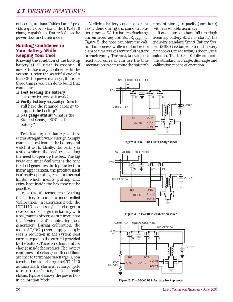
20 Linear Technology Magazine • June 2008
L DESIGN FEATURES
cell configurations. Tables 1 and 2 pro-vide a quick overview of the LTC4110 charge capabilities. Figure 3 shows the power flow in charge mode.
Building Confidence in Your Battery While Keeping Your CoolKnowing the condition of the backup battery at all times is essential if one is to have any confidence in the system. under the watchful eye of a host CPu or power manager, there are three things you can do to build that confidence:qTest loading the battery:
Does the battery still work?qVerify battery capacity: Does it
still have the retained capacity to support the backup?
qGas gauge status: What is the State of Charge (SOC) of the battery?
Test loading the battery at first seems straightforward enough. Simply connect a test load to the battery and watch it work. Ideally, the battery is tested while in the product, avoiding the need to open up the box. The big issue one must deal with is the heat the load generates during the test. In many applications, the product itself is already operating close to thermal limits, which means putting that extra heat inside the box may not be possible.
In LTC4110 terms, test loading the battery is part of a mode called “calibration.” In calibration mode, the LTC4110 uses its flyback charger in reverse to discharge the battery with a programmable constant current into the “system load” eliminating heat generation. During calibration, the main AC/DC power supply simply sees a reduction in the system load current equal to the current provided by the battery. There is no temperature change inside the product. The battery continues to discharge until conditions are met to terminate discharge. upon termination of discharge, the LTC4110 automatically starts a recharge cycle to return the battery back to ready status. Figure 4 shows the power flow in calibration Mode.
Verifying battery capacity can be easily done during the same calibra-tion process. With a battery discharge current accuracy of ±3% at RSnS(BAT) in Figure 2, the host can start the cali-bration process while monitoring the elapsed time it takes for the full battery to reach empty. The host, knowing the fixed load current, can use the time information to determine the battery’s
present storage capacity (amp-hour) with reasonable accuracy.
If one desires to have full time high accuracy battery SOC monitoring, the industry standard Smart Battery Sys-tem (SBS) Gas Gauge, as found in every notebook PC made today, is the only real solution. The LTC4110 fully supports this standard in charge, discharge and calibration modes of operation.
LTC4110
BATTERY
OFF OFFON
BACKUP LOAD
CURRENT FLOW
INID BATID
DCHFET
CHGFET
SYSTEM LOAD
DCIN
Figure 4. LTC4110 in calibration mode
LTC4110
INID BATID
DCDIVDCHFET
CHGFETUVLOSET POINT
BACKUP LOAD (DCOUT)
CURRENT FLOW
SYSTEM LOAD
BATTERY
DCIN0V
ON ONOFF
Figure 5. The LTC4110 in battery backup mode
LTC4110
BACKUP LOADSYSTEM LOAD
BATTERY
OFF OFFON
DCIN
CURRENT FLOW
INID BATID
DCHFET
CHGFET
Figure 3. The LTC4110 in charge mode

Linear Technology Magazine • June 2008 21
DESIGN FEATURES L
LTC4110
INID BATID
DCHFET
CHGFET
SYSTEM LOAD
BATTERY
SUPPLYINPUT
SUPPLYINPUT
LTC4110
BATID
DCHFET
CHGFET
BACKUP LOAD (DCOUT)
BATTERY
Figure 6. Dual LTC4110 system using standard batteries
Lossless Automatic PowerPath Operation The LTC4110 uses ideal diode circuitry to drive its PowerPathTM MOSFeTs. An ideal diode circuit uses a MOSFeT where normally a diode would be used to control the flow of power. Like a true diode, current is only allowed to flow in one direction despite the fact that MOSFeTS can conduct current in both directions. The forward voltage drop of an ideal diode is far less (25mV) than that of a conventional Schottky diode (350mV), and the reverse current leak-age can be smaller for the ideal diode as well. The tiny forward voltage drop reduces power losses, minimizes self-heating and ,in the case of a battery, extends battery life.
In Figure 2, there are two sets of ideal diodes forming a power-OR between the supply input (DCIn) and the battery, forming an output called backup load (DCOuT). In the Figure, two back-to-back MOSFeTs are used in the battery path since in this application the full charge bat-tery voltage is greater than the DCIn voltage. However, if the battery voltage is less than DCIn, only one MOSFeT is needed.
under normal conditions, the input ideal diode is always on. If the DCIn voltage divider senses a condition where battery backup is desired, the battery ideal diode is turned on with the input ideal diode left to figure out when to turn off on its own. The diode action allows the highest supply to take up the backup load. But since DCIn is falling, the input ideal diode turns off as soon as it senses a reverse current
flow. The goal of the ideal diode design is to always attempt to do a “make before break” handover if possible, minimizing the need for any “bridg-ing” or “holdup” capacitance. Figure 5 shows the LTC4110 in battery backup mode. The thick line shows the active power path.
Expandable Capacity or Creating RedundancyIdeal diode technology is also the key that allows one LTC4110 to work with other LTC4110s in safely paralleling batteries for redundancy. Multiple LTC4110s can be connected in paral-lel at the backup load (DCOuT) point. At no time will the batteries exchange current between them regardless of any difference in SOC or voltage.
Assuming the batteries are the same make, model and age, the batteries automatically act as one big battery, sharing discharge load current based on their relative SOC ratios. If all the batteries are the same SOC, the cur-rent is equal among them. Charge current remains independent.
Some battery chemistries, such as Li-ion, have rules about the size of the battery that can be safely trans-ported. If your backup needs exceed 95 watt-hours of capacity, you must use multiple batteries. Simply add another LTC4110 to support dual battery operation. Fortunately, this expansion also gives the system true redundancy by minimizing the num-ber of parts shared between each backup system. Figure 6 shows a dual LTC4110 system using two standard (not Smart) batteries.
Flexible SMBus Addressing and Registers Whether you are using Smart Batteries or standard batteries, the LTC4110 supports an SMBus interface that the host CPu can use to control and moni-tor each part. To make configuration easier with standard batteries, the LTC4110 supports up to three unique SMBus addresses. However, if you use Smart Batteries, all of the LTC4110s must use the same address and each LTC4110 and associated Smart Bat-tery local SMBus must be isolated from all the other LTC4110s. This is easily done with SMBus multiplexer such as the LTC4305 or LTC4306 under the control of the host CPu. Wherever possible, the LTC4110 follows the Smart Battery System (SBS) Charger Specification for registers definitions for compatibility with software that works with Smart Batteries.
Complete Status and Flexible GPIO LinesInternally, the LTC4110 uses two 16-bit SMBus read registers to report 27 unique status items. This includes a bit that retains and reports if the battery backup has failed, even after the battery has gone below the user defined end of discharge cutoff (dead) threshold. Another 16-bit SMBus write register controls the charger and how the three GPIO bits are to be used.
each GPIO bit can be programmed to report selected internal status infor-mation or work as generic digital I/O independently of the other bits. A fixed AC present status output bit is offered
continued on page 24
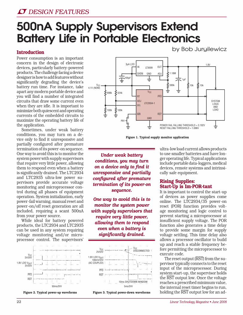
22 Linear Technology Magazine • June 2008
L DESIGN FEATURES
500nA Supply Supervisors Extend Battery Life in Portable Electronics
by Bob JurgilewiczIntroductionPower consumption is an important concern in the design of electronic devices, particularly battery-powered products. The challenge facing a device designer is how to add features without significantly degrading the device’s battery run time. For instance, take apart any modern portable device and you will find a number of integrated circuits that draw some current even when they are idle. It is important to minimize both quiescent and operating currents of the embedded circuits to maximize the operating battery life of the application.
Sometimes, under weak battery conditions, you may turn on a de-vice only to find it unresponsive and partially configured after premature termination of its power-on sequence. One way to avoid this is to monitor the system power with supply supervisors that require very little power, allowing them to respond even when a battery is significantly drained. The LTC2934 and LTC2935 ultra-low power su-pervisors provide accurate voltage monitoring and microprocessor con-trol during all phases of equipment operation. System initialization, early power-fail warning, manual reset and power-on/off reset generation are all included, requiring a scant 500nA from your power source.
While ideal for battery powered products, the LTC2934 and LTC2935 can be used in any system requiring voltage monitoring and/or micro-processor control. The supervisors’
ultra-low load current allows products to use smaller batteries and have lon-ger operating life. Typical applications include portable data-loggers, medical devices, remote systems and intrinsi-cally safe equipment.
Rising Supplies: Start-Up is Im-POR-tantIt is important to control the start-up of devices as power supplies come online. The LTC2934/35 power-on reset (POR) function provides volt-age monitoring and logic control to prevent starting a microprocessor at insufficient supply voltage. The POR function also generates a time delay to provide some margin for supply voltage settling. This time delay also allows a processor oscillator to build up and reach a stable frequency be-fore permitting the microprocessor to execute code.
The reset output (RST) from the su-pervisor typically connects to the reset input of the microprocessor. During system start-up, the supervisor holds the RST output low. Once the voltage reaches a prescribed minimum value, the internal reset timer begins to run, holding the RST output low for an ad-
1.18M
1µF
590k 10k
324k
100k
10k
VCC
SYSTEMLOGICAND
LOAD
POWER FAIL FALLING THRESHOLD = 3.192V RESET FALLING THRESHOLD = 1.696V
698k
100k
RT
ADJ
100µF
SHDN
IN OUT3µA LDO 1.8V
ADJ
PFO
PB1
RST
PFI
MR
LTC2934-1
LT3009
GND
GND
VCC4.1V (NOM)
Figure 1. Typical supply monitor application
VCC2V/DIV
1.8V LDO VOUT2V/DIV
RST
PFO
50ms/DIV
Figure 2. Typical power-up waveforms
VCC2V/DIV
VCCDISCONNECTED
10ms SHUTDOWN WINDOW
1.8V LDO VOUT100mV/DIV
(AC COUPLED)
RST
PFO
5ms/DIV
Figure 3. Typical power-down waveforms
Under weak battery conditions, you may turn on a device only to find it
unresponsive and partially configured after premature termination of its power-on
sequence.
One way to avoid this is to monitor the system power
with supply supervisors that require very little power, allowing them to respond
even when a battery is significantly drained.

Linear Technology Magazine • June 2008 23
DESIGN FEATURES L
ditional time (typically 200ms). When the reset timer expires, the RST output pulls high and releases the micropro-cessor from its reset condition.
Figure 2 shows the supply rising waveforms obtained from the typical application shown in Figure 1. When VCC exceeds the power-fail threshold plus 2.5% hysteresis (3.192V × 1.025 = 3.272V), the power-fail output (PFO) is allowed to pull high. The LT3009 (a 3µA LDO) is powered from VCC. Since the PFO output is pulled up by the LDO output, PFO will follow the LDO. When the LDO output exceeds the reset threshold plus 5% hysteresis (1.696V × 1.05 = 1.781V), the internal reset timer begins to run. After 200ms, RST pulls high and system logic con-nected to RST is released from its reset condition.
Falling Supplies: Heed the Early Warningunmanaged power loss can cause many system problems. The LTC2934 and LTC2935 contain a power-fail logic output (PFO) that pulls low to provide an early warning of impending power loss. To be useful, an early warning should occur before the monitored supply falls to insufficient levels and well before the RST output pulls low. The time between PFO and RST pulling low can be used to initiate a variety of critical operations prior to shutdown. Once the supervisor pulls the microprocessor reset low, it may be impossible to execute operations. Operations initiated by a power-fail
warning include shutting off non-criti-cal components to conserve energy and writing important data to memory. Some secure applications may also require erasing data to thwart memory snoopers.
Figure 3 shows the supply falling waveforms obtained from the applica-tion shown in Figure 1. The waveforms demonstrate how PFO provides ample warning when VCC is suddenly discon-nected from the system. The LT3009 supplies a constant 10mA to a load at 1.8V. The 100µF input capacitor begins to discharge when VCC (4.1V nominal) is disconnected. The power-fail thresh-old is configured for 3.192V.
Because the power-fail condition persists and is not merely transitory, logic output PFO pulls low and re-mains low after a small comparator delay. This is when the system logic
(typically connected to PFO) should take appropriate shutdown action(s). In this application, the remaining operating time beyond power fail is approximately 10ms. eventually VCC becomes so low that the LDO begins to drop out. RST asserts low shortly after the LDO output falls below the reset threshold (1.696V). At this point, the system load is re-moved and the LDO output begins to recover. However, the remaining loads and built-in hysteresis prevent the LDO recovery from glitching the RST output.
Select Fixed or Adjustable ThresholdsThe LTC2935 integrates eight preci-sion reset and power-fail threshold pairs. Configure any one of the eight threshold pairs using three digital select inputs (see Table 1). Typical ap-plications using the LTC2935 require no additional external components. As a result, solutions require little board space and are extremely low power.
use the LTC2934 when custom (adjustable) thresholds are necessary. The LTC2934 monitors voltage applied to its PFI and ADJ inputs, typically through an external resistive divider. external divider resistance values can be large which helps keep the cur-rent low. Divider errors due to input leakage current (1nA maximum over temperature) are often too small to worry about. The PFI and ADJ inputs have precision 400mV thresholds
Figure 4. Stacked Li-ion cell and LDO supervisor
2.8M
1µF
619k 100k
1.3M
200k
100k
VCC
POWER FAIL FALLING THRESHOLD = BAT1 + BAT2 = 6.00VRESET FALLING THRESHOLD = 3.00V
2.8M
200k
LOW BATTERYEARLY WARNING
SYSTEM RESET
RT
ADJ
Li-IonBAT14.1V
(NOM)
Li-IonBAT24.1V
(NOM)
1µFSHDN
IN OUT
3µA LDO3.3V
ADJ
PFO
RST
PFI
MR
LTC2934-1
LT3009
GND
GND
+
+
1µF
Table 1. Falling threshold selection table
Reset Threshold (V)
Power-Fail Threshold (V) S1 S2 S0
3.30 3.45 Low Low Low
3.15 3.30 Low Low High
3.00 3.15 Low High High
2.85 3.00 Low High Low
2.70 2.85 High High Low
2.55 2.70 High Low Low
2.40 2.55 High Low High
2.25 2.40 High High High

24 Linear Technology Magazine • June 2008
L DESIGN FEATURES
at all times. However, if you do not have SMBus in the product, the LTC4110 can be configured to enable preset status information to drive the GPIO bits on power up. This information can be used to drive status LeDs.
Micropower Shutdown and ShippingThe LTC4110 shutdown pin is de-signed to prevent false shutdowns on power up or power down. Reading
(falling), so low voltage monitoring is possible.
The falling threshold accuracy for both the LTC2934 and LTC2935 is ±1.5% over the full operating tempera-ture range. Minimum VCC is a low 1.6V. Configuration details are discussed in the LTC2934 and LTC2935 data sheets.
Manual Reset and Reset TimingThe LTC2934 has two selectable reset timeout periods. Tie the RT input low for a 15ms timeout. Tie the RT input high for a 200ms timeout. The LTC2935 has a fixed 200ms timeout. Both parts have a manual reset input which asserts RST low when the MR input is pulled low (typically with a switch). The MR input has an internal 900k pull-up resistor to VCC, used to pull up the MR input when the switch is open. Alternatively, the MR input may be pulled low with an external logic signal. When the MR input returns high, RST pulls high after the reset timeout period has elapsed, assum-ing that the monitored input voltage is above the reset threshold.
Monitoring a 2-Cell Li-Ion StackSome portable applications utilize a stack of batteries to achieve greater product operating lifetime. For a product using two stacked 4.1V Li-ion cells (or similar), the total stack voltage (8.2V) exceeds the maximum operat-ing voltage (5.5V) of the LTC2934.
However, if the center tap of the 2-cell stack is available, cell monitoring is still possible. Figure 4 shows how the center tap of the stack is used to bias the LTC2934. The total stack voltage is monitored at the power-fail input (PFI). The application is configured to pull the PFO output low when the sum of the battery voltages drops below 6.00V. The adjustable input (ADJ) monitors the LDO output. RST pulls low when the LDO output drops below 3.00V.
Super HysteresisSome applications have a large load transient when powered. This tran-sient can cause significant supply voltage drop if battery series resis-tance is large. If the load is enabled after the reset output pulls high, the subsequent voltage drop could put the voltage at the VCC monitor input below threshold, causing the reset and power-fail outputs to pull low. In such cases, active threshold control (shown
in Figure 5) is helpful. The LTC2935 power-fail output (PFO) can be used to change any (or all) of the threshold control input states (S2, S1, S0). The power fail comparator threshold is always 150mV larger than the reset threshold and the power-fail output does not experience the 200ms reset timeout delay. If the power-fail output pulls high before the reset output (which is almost always the case with rising supplies), it can then be used to lower the falling thresholds to one of the other seven threshold selections. In Figure 5, the reset falling threshold is changed from 3.3V (PFO low) to 2.25V (PFO high), which provides a generous 1.05V of falling hysteresis.
ConclusionThe 500nA current required by the LTC2934 and LTC2935 supervisors is so small, it can be placed into the “Don’t Care” column of your device power budget. Although the power is low, these supervisors don’t discard features. The power-on reset and early power-fail warning signals provide glitch-free logic controls to your sys-tem logic. Reset delay time is built in. Manual reset is available in both parts. Configuring these supervisors is easy, and few if any external components are necessary. ultra-low input leakage specifications make high impedance applications possible. Specifications are guaranteed from –45°C to 85°C. Both parts are available in space saving 8-lead, 2mm × 2mm DFn and TSOT-23 (ThinSOT™) packages. L
VCC
SYSTEMLOGICAND
LOAD
0.1µF
RST
MR
LTC2935-2
GND
S2
S1
S0
PFO
RESET (VCC RISING) THRESHOLD = 3.30VRESET (VCC FALLING) THRESHOLD = 2.25V
+
Figure 5. Active threshold control
LTC40, continued from page 2the pin status is pre-qualified such that it is only honored under normal conditions. This qualification allows the product to ship with the battery installed without fear of the part en-tering into battery backup mode and draining the battery. The shutdown current only draws 20µA from the battery. This is the same shutdown mode that the LTC4110 enters when the backup battery reaches its end of discharge point.
ConclusionThe LTC4110 is a flexible standalone battery backup controller. By inte-grating key features into a single IC, functions work together seamlessly, allowing the designer to offer a reliable and complete battery backup system with minimal design effort. L
Authors can be contactedat (408) 432-1900

Linear Technology Magazine • June 2008 25
DESIGN FEATURES L
Quad Output Regulator Meets Varied Demands of Multiple Power Supplies
by Michael NootbaarIntroductionMany modern electronic devices re-quire a number of power domains to satisfy the needs of a wide variety of de-vices and subsystems. A power supply designer’s job would be relatively easy if the design contraints were limited to simply providing well-regulated volt-ages, but power supply requirements are typically much more complicated. For example, multiple power rails must be sequenced and/or track each other to ensure proper system behavior. High power sections of the design are often powered down when not in use, requiring multiple shutdown options. Powering analog circuitry adds the demand for clean, low noise supplies—no switching transients or excessive voltage ripple allowed. And, of course, all supplies must be
generated as efficiently as possible to minimize power consumption.
The LT3507 meets these require-ments by combining three switching regulators and a low dropout linear regulator in a compact 5mm × 7mm QFn package. The switching regula-tors have internal power switches, independent input supplies, run and track/soft-start controls, and power good indicators. The LDO requires an external nPn pass transistor and includes track/soft-start control.
Three Independent Switching Regulators…The LT3507 includes three indepen-dent, monolithic switching regulators to achieve a space saving solution. Channel 1 is capable of providing up
to 2.4A of output current. Channels 2 and 3 are each capable of providing up to 1.6A of output current. each of the three switching regulators has its own input supply pin to the power switch. The regulators may be operated from different supplies in order to maximize system efficiency.
The maximum voltage on any of the VIn pins is 36V. The LT3507 internal circuitry is powered from VIn1, which requires a minimum operating voltage for VIn1 of 4V. The minimum operating voltage for VIn2 and VIn3 is 3V. Since VIn1 powers the internal circuitry, it must always be at least 4V when any channel is running, even if Channel 1 is off.
All three regulators use a cur-rent mode, constant frequency
VIN1
BOOST1 UVLO
OVLO
BOOST2
SW2
FB2
VC2
BIAS
DRIVEFB4
PGOOD1PGOOD2PGOOD3
PGOOD1PGOOD2PGOOD3
SW1
FB1
VC1
TRK/SS1
BOOST3
0.22µF
22µF
100µF D1
18.7k
680pF
470pF
18.7k
4.7µHVOUT11.8V2.4A
VIN6V TO 36V
VOUT35V
1.5A
15µH
10µH
VIN2 VIN3 VINSW
1k
49.9k 18.2k
100k
VOUT1
15k
SW3
FB3
VC3
RT/SYNC TRK/SS4GND
LT3507
RUN1RUN2RUN3
0.22µF
0.22µF
22µF
22µF
D2
D3
24.3k
16.2k
SHDN
680pF
0.01µF
1000pF53.6k
L1: WÜRTH WE-PD 744 778 9004L2: WÜRTH WE-PD 744 778 9115L3: WÜRTH WE-PD 744 778 910D1, D2, D3: DIODES, INC. B240AQ1: ON SEMICONDUCTOR NSS30101LT1G
11.5k
11.5k
24.3k
105k
fSW = 450kHz
10.2k
2.2nF22µF
BAS70
100k 100k
VOUT23.3V1.3A
VOUT42.5V0.2A
35.7k
TRK/SS3
TRK/SS2 TRK/SS2
VOUT2
VOUT2
CMDSH-4E
CMDSH-4E
CMDSH-4E
15k
18.7k
35.7k
11.5k
TRK/SS2
SYNC SOURCEPOWERED FROM
3.3V OUTPUT, VOUT2
Q1
Figure 1. The LT3507 in a wide input range, quad output application
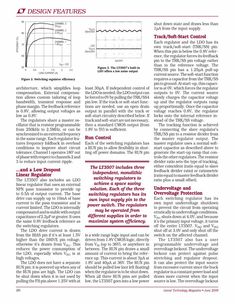
26 Linear Technology Magazine • June 2008
L DESIGN FEATURES
architecture, which simplifies loop compensation. external compensa-tion allows custom tailoring of loop bandwidth, transient response and phase margin. The feedback reference is 0.8V, allowing output voltages as low as 0.8V.
The regulators share a master os-cillator that is resistor programmable from 250kHz to 2.5MHz, or can be synchronized to an external frequency in the same range. each regulator fea-tures frequency foldback in overload conditions to improve short circuit tolerance. Channel 1 operates 180° out of phase with respect to channels 2 and 3 to reduce input current ripple.
…and a Low Dropout Linear RegulatorThe LT3507 also includes an LDO linear regulator that uses an external nPn pass transistor to provide up to 0.5A of output current. The base drive can supply up to 10mA of base current to the pass transistor and is current limited. The LDO is internally compensated and is stable with output capacitance of 2.2µF or greater. It uses the same 0.8V feedback reference as the switching regulators.
The LDO drive current is drawn from the BIAS pin if it’s at least 1.5V higher than the DRIVe pin voltage, otherwise it’s drawn from VIn1. This reduces the power consumption of the LDO, especially when VIn1 is at high voltages.
The LDO does not have a separate Run pin; it is powered up when any of the Run pins are high. The LDO can be shut down when it is not used by pulling the FB pin above 1.25V with at
least 30µA. If independent control of the LDO is needed, the LDO output can be forced to 0V by pulling the TRK/SS4 pin low. If the track or soft-start func-tions are needed, use an open drain output in parallel with the track or soft-start circuitry described below. If track and soft-start are not necessary, then a standard CMOS output (from 1.8V to 5V) is sufficient.
Run Controleach of the switching regulators has a Run pin to allow flexibility in shut-ting off power domains. The Run pin
is a wide range logic input and can be driven from 1.8V CMOS logic, directly from VIn (up to 36V), or anywhere in between. The Run pin draws a small amount of current to bring the refer-ence up. This current is about 3µA at 1.8V and 40µA at 36V. The Run pin should be pulled low (not left floating) when the regulator is to be shut down. When all three Run pins are pulled low, the LT3507 goes into a low power
shut down state and draws less than 1µA from the input supply.
Track/Soft-Start Controleach regulator and the LDO has its own track/soft-start (TRK/SS) pin. When this pin is below the 0.8V refer-ence, the regulator forces its feedback pin to the TRK/SS pin voltage rather than to the reference voltage. The TRK/SS pin has a 1.25µA pull-up current source. The soft-start function requires a capacitor from the TRK/SS pin to ground. At start-up, this capaci-tor is at 0V, which forces the regulator outputs to 0V. The current source slowly charges the capacitor voltage up and the regulator outputs ramp up proportionally. Once the capacitor voltage reaches 0.8V, the regulator locks onto the internal reference in-stead of the TRK/SS voltage.
The tracking function is achieved by connecting the slave regulator’s TRK/SS pin to a resistor divider from the master regulator output. The master regulator uses a normal soft-start capacitor as described above to generate the start-up ramp that con-trols the other regulators. The resistor divider ratio sets the type of tracking, either coincident (ratio equal to slave feedback divider ratio) or ratiometric (ratio equal to master feedback divider ratio plus a small offset).
Undervoltage and Overvoltage Protectioneach switching regulator has its own input undervoltage shutdown to prevent the circuit from operating erratically in undervoltage conditions. VIn1 shuts down at 4.0V, and because it’s the primary input voltage, it turns off the entire LT3507. VIn2 and VIn3 shut off at 3.0V and only shut off the switch on the affected channel.
The LT3507 also has a user programmable undervoltage and overvoltage lockout. The undervoltage lockout can protect against pulse stretching and regulator dropout. It can also protect the input source from excessive current since the buck regulator is a constant power load and draws more current when the input source is low. The overvoltage lockout
EFFI
CIEN
CY (%
)
LOAD CURRENT (A)2.50
90
500.5 1 1.5 2
70
60
80
CHANNEL 35VOUT
CHANNEL 23.3VOUT
CHANNEL 11.8VOUT
VIN = 12V
Figure 2. Switching regulator efficiency
VOUT220mV/DIV
LDOVOUT4
20mV/DIV
2µs/DIV
Figure 3. The LT3507’s built-in LDO offers a low noise output
The LT3507 includes three independent, monolithic switching regulators to achieve a space saving
solution. Each of the three switching regulators has its own input supply pin to the
power switch. The regulators may be operated from
different supplies in order to maximize system efficiency.
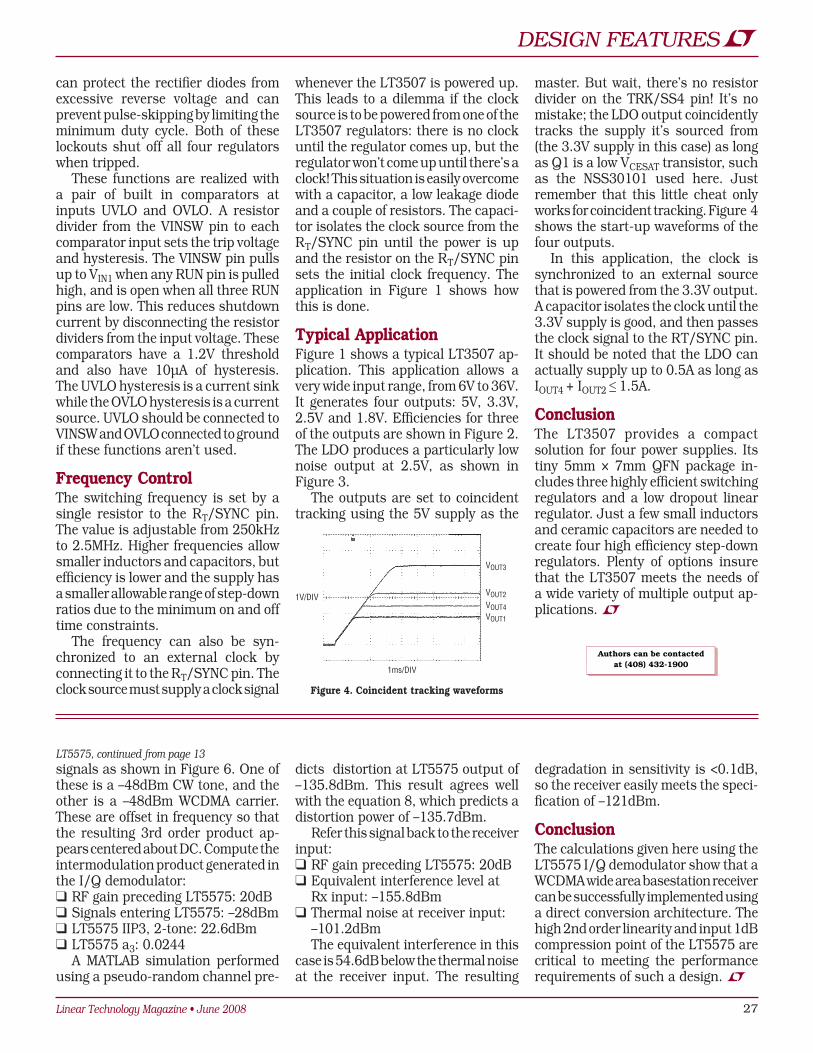
Linear Technology Magazine • June 2008 27
DESIGN FEATURES L
master. But wait, there’s no resistor divider on the TRK/SS4 pin! It’s no mistake; the LDO output coincidently tracks the supply it’s sourced from (the 3.3V supply in this case) as long as Q1 is a low VCeSAT transistor, such as the nSS30101 used here. Just remember that this little cheat only works for coincident tracking. Figure 4 shows the start-up waveforms of the four outputs.
In this application, the clock is synchronized to an external source that is powered from the 3.3V output. A capacitor isolates the clock until the 3.3V supply is good, and then passes the clock signal to the RT/SYnC pin. It should be noted that the LDO can actually supply up to 0.5A as long as IOuT4 + IOuT2 ≤ 1.5A.
ConclusionThe LT3507 provides a compact solution for four power supplies. Its tiny 5mm × 7mm QFn package in-cludes three highly efficient switching regulators and a low dropout linear regulator. Just a few small inductors and ceramic capacitors are needed to create four high efficiency step-down regulators. Plenty of options insure that the LT3507 meets the needs of a wide variety of multiple output ap-plications. L
whenever the LT3507 is powered up. This leads to a dilemma if the clock source is to be powered from one of the LT3507 regulators: there is no clock until the regulator comes up, but the regulator won’t come up until there’s a clock! This situation is easily overcome with a capacitor, a low leakage diode and a couple of resistors. The capaci-tor isolates the clock source from the RT/SYnC pin until the power is up and the resistor on the RT/SYnC pin sets the initial clock frequency. The application in Figure 1 shows how this is done.
Typical ApplicationFigure 1 shows a typical LT3507 ap-plication. This application allows a very wide input range, from 6V to 36V. It generates four outputs: 5V, 3.3V, 2.5V and 1.8V. efficiencies for three of the outputs are shown in Figure 2. The LDO produces a particularly low noise output at 2.5V, as shown in Figure 3.
The outputs are set to coincident tracking using the 5V supply as the
Figure 4. Coincident tracking waveforms
1V/DIV
VOUT3
VOUT2VOUT4VOUT1
1ms/DIV
can protect the rectifier diodes from excessive reverse voltage and can prevent pulse-skipping by limiting the minimum duty cycle. Both of these lockouts shut off all four regulators when tripped.
These functions are realized with a pair of built in comparators at inputs uVLO and OVLO. A resistor divider from the VInSW pin to each comparator input sets the trip voltage and hysteresis. The VInSW pin pulls up to VIn1 when any Run pin is pulled high, and is open when all three Run pins are low. This reduces shutdown current by disconnecting the resistor dividers from the input voltage. These comparators have a 1.2V threshold and also have 10µA of hysteresis. The uVLO hysteresis is a current sink while the OVLO hysteresis is a current source. uVLO should be connected to VInSW and OVLO connected to ground if these functions aren’t used.
Frequency ControlThe switching frequency is set by a single resistor to the RT/SYnC pin. The value is adjustable from 250kHz to 2.5MHz. Higher frequencies allow smaller inductors and capacitors, but efficiency is lower and the supply has a smaller allowable range of step-down ratios due to the minimum on and off time constraints.
The frequency can also be syn-chronized to an external clock by connecting it to the RT/SYnC pin. The clock source must supply a clock signal
signals as shown in Figure 6. One of these is a –48dBm CW tone, and the other is a –48dBm WCDMA carrier. These are offset in frequency so that the resulting 3rd order product ap-pears centered about DC. Compute the intermodulation product generated in the I/Q demodulator: qRF gain preceding LT5575: 20dBqSignals entering LT5575: –28dBmqLT5575 IIP3, 2-tone: 22.6dBmqLT5575 a3: 0.0244
A MATLAB simulation performed using a pseudo-random channel pre-
LT5575, continued from page dicts distortion at LT5575 output of –135.8dBm. This result agrees well with the equation 8, which predicts a distortion power of –135.7dBm.
Refer this signal back to the receiver input: qRF gain preceding LT5575: 20dBqequivalent interference level at
Rx input: –155.8dBmqThermal noise at receiver input:
–101.2dBmThe equivalent interference in this
case is 54.6dB below the thermal noise at the receiver input. The resulting
degradation in sensitivity is <0.1dB, so the receiver easily meets the speci-fication of –121dBm.
ConclusionThe calculations given here using the LT5575 I/Q demodulator show that a WCDMA wide area basestation receiver can be successfully implemented using a direct conversion architecture. The high 2nd order linearity and input 1dB compression point of the LT5575 are critical to meeting the performance requirements of such a design. L
Authors can be contactedat (408) 432-1900
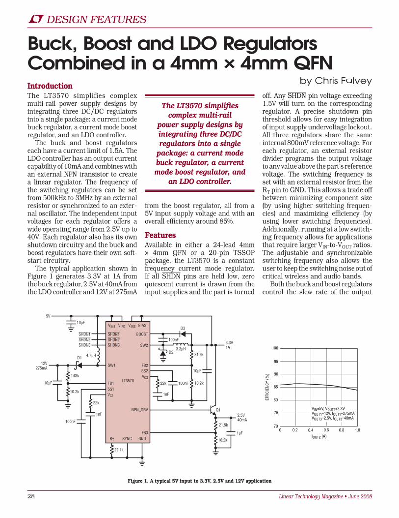
28 Linear Technology Magazine • June 2008
L DESIGN FEATURES
from the boost regulator, all from a 5V input supply voltage and with an overall efficiency around 85%.
FeaturesAvailable in either a 24-lead 4mm × 4mm QFn or a 20-pin TSSOP package, the LT3570 is a constant frequency current mode regulator. If all SHDn pins are held low, zero quiescent current is drawn from the input supplies and the part is turned
IntroductionThe LT3570 simplifies complex multi-rail power supply designs by integrating three DC/DC regulators into a single package: a current mode buck regulator, a current mode boost regulator, and an LDO controller.
The buck and boost regulators each have a current limit of 1.5A. The LDO controller has an output current capability of 10mA and combines with an external nPn transistor to create a linear regulator. The frequency of the switching regulators can be set from 500kHz to 3MHz by an external resistor or synchronized to an exter-nal oscillator. The independent input voltages for each regulator offers a wide operating range from 2.5V up to 40V. each regulator also has its own shutdown circuitry and the buck and boost regulators have their own soft-start circuitry.
The typical application shown in Figure 1 generates 3.3V at 1A from the buck regulator, 2.5V at 40mA from the LDO controller and 12V at 275mA
Buck, Boost and LDO Regulators Combined in a 4mm × 4mm QFN
by Chris Falvey
off. Any SHDn pin voltage exceeding 1.5V will turn on the corresponding regulator. A precise shutdown pin threshold allows for easy integration of input supply undervoltage lockout. All three regulators share the same internal 800mV reference voltage. For each regulator, an external resistor divider programs the output voltage to any value above the part’s reference voltage. The switching frequency is set with an external resistor from the RT pin to GnD. This allows a trade off between minimizing component size (by using higher switching frequen-cies) and maximizing efficiency (by using lower switching frequencies). Additionally, running at a low switch-ing frequency allows for applications that require larger VIn-to-VOuT ratios. The adjustable and synchronizable switching frequency also allows the user to keep the switching noise out of critical wireless and audio bands.
Both the buck and boost regulators control the slew rate of the output
VIN1
SHDN1SHDN2SHDN3
SHDN1SHDN2SHDN3
SW1
FB1
100nF
1nF
100nF
10µF
1µF
2.5V40mA
31.6k
3.3V1A
22k
143k
12V275mA
5V
22k
10.2k
10.2k
21.5k
10.2k
22.1k
10µF
10µF
1nF
100nF
3.3µH
4.7µHD2
D3
D1
BOOST
SW2
FB2SS2
NPN_DRV
FB3
VC2
SS1VC1
VIN2 VIN3 BIAS
RT SYNC
LT3570
GND
Q1
Figure 1. A typical 5V input to 3.3V, 2.5V and 12V application
The LT3570 simplifies complex multi-rail
power supply designs by integrating three DC/DC regulators into a single
package: a current mode buck regulator, a current mode boost regulator, and
an LDO controller.

Linear Technology Magazine • June 2008 29
DESIGN FEATURES L
Applications
“Dying Gasp” ApplicationThe LT3570 provides an ideal solu-tion for any “dying gasp” system. Figure 2 shows a typical application powering an airbag controller. In an automobile accident, the battery may get disconnected from the shock sen-sors yet the airbag must still fire. In this application, the battery supplies power to the boost regulator. VOuT1 is set to 36V and drives VIn2 and VIn3, the inputs to the buck regulator and the LDO controller, respectively. even after the input supply is removed, the buck regulator and the LDO continue to function properly for more than 3ms, as the energy continues to be supplied from the output capacitor of the boost regulator. The buck regulator turns off when VIn2 approaches the input undervoltage lockout of 2.3V (see Figure 3).
The BIAS pin allows the internal circuitry to draw current from a lower voltage supply than the input, reduc-ing power dissipation and increasing efficiency. normally, the quiescent current is supplied from VIn2, but when the voltage on the BIAS pin exceeds 2.5V the current is supplied from the BIAS pin. The BIAS pin is only available on the 24-lead QFn package.
voltage during start-up. A controlled ramp reduces inrush current on the input supply and minimizes output overshoot. An external capacitor con-nected between the SS pin and ground programs the slew rate. The voltage on the SS pin overrides the internal reference voltage to the error amplifier and is charged by a 4.5µA internal current source.
VIN1
SHDN1SHDN2SHDN3
SHDN1SHDN2SHDN3
SW1
FB1
C8100nF
C71nF
C510nF
C210µF
C31µF
VOUT33.3V500mA
R3340k
VOUT25V
R825k
R1100k
VOUT18V
250mA
VIN8V TO 30V
R725k
R211k
R464.9k
R5205k
R664.9k
R924.9k
C910µF
C110µF
C61nF
10nF
L210µH10µH
D2
D3
D1
BOOST
SW2
FB2SS2
NPN_DRV
FB3
VC2
SS1VC1
VIN2 VIN3 BIAS
RT SYNC
LT3570
GND
Q1
Figure 4. DSL modem application
300µs PROPAGATION DELAY
– 2mV DC STEP IOUT1
200mA/DIV
VOUT1100mV/
DIV
VOUT2100mV/
DIV
100µs/DIV
Figure 5. Step response of Figure 4 with boost current stepped from 200mA to 400mA
300µs PROPAGATION DELAY
– 2mV DC STEP VOUT120V/DIV
VIN5V/DIV
VOUT25V/DIV
1ms/DIV
Figure 3. Output waveforms when power is removed from the circuit in Figure 2
Figure 2. Dying gasp system keeps power even when battery is disconnected.
VIN1
SHDN1SHDN2SHDN3
SW1
FB1
C8100nF
C71nF
C510nF
10µF
C31µF
VOUT32.5V100mA
R3205k
VOUT23.3V200mA
R825k
R11.10M
VOUT136V
VIN12V
R725k
R223.7k
R464.9k
R5137k
R664.9k
R924.9k
C910µF
C110µF
C61nFC4
10nF
L210µHL1
10µHD2
D3
D1
BOOST
SW2
FB2SS2
NPN_DRV
FB3
VC2
SS1VC1
VIN2 VIN3 BIAS
RT SYNC
LT3570
GND
Q1
continued on page 4

30 Linear Technology Magazine • June 200830
L DESIGN IDEAS
Compact Power Solution Overcomes Peak Power Limitations in PCMCIA-Based Pulsed-Load GSM and GPRS ApplicationsIntroductionIn an increasingly wireless world, mobile computing applications are driving the need for web-anywhere enabled notebook computers. PC Card or PCMCIA slot powered GSM/GPRS modems are now the standard for these applications. During GSM transmis-sion peak currents can exceed 2A, well beyond the maximum current capa-bility of the PCMCIA slot. Therefore, the modem must be designed to limit input power and draw on card-based
storage for most of the energy required during a transmission cycle.
The LTC3125 is a synchronous step-up DC/DC converter that charges a reservoir capacitor up to the regu-lated output voltage while directly and accurately controlling the average input current. The LTC3125’s 91% efficiency provides the maximum pos-sible output current to the load without impacting the host. Together with an external bulk or reservoir capacitor, the LTC3125 can interface the GSM/GPRS modem directly to a PCMCIA power bus without overloading it.
Power DemandsMuch of the work in GSM/GPRS power supply design revolves around the transmission cycle due to the high current consumption in this mode. Typically the transmitter’s supply current is modulated to 2A pulses, which occupy one or more of the 577µs timeslots from the eight timeslots available.
During a GSM transmission, one timeslot is used for data transmis-sion, the other seven are idle, during which the supply current is reduced to less than 100mA. Therefore, the average current consumed over the 4.6ms window is about 340mA. In the end, the transmitter power supply
design must be capable of an average current of 340mA but also be able to handle the 2A transmit burst currents. Higher data rate standards are also popular. For instance, the GPRS Class 10 standard allows for transmission in two of the eight available timeslots for an average current consumption of almost 575mA and 2A burst duration of 1.15ms.
Based on the standard PC card bus power (3.0V to 3.6V) specification, the maximum peak current must not exceed 1A. This is clearly not suffi-cient for powering these GSM/GPRS applications directly.
The SolutionThe LTC3125 is a 91% efficient step-up DC/DC converter in a 2mm ×
Figure 1. A complete PCMCIA-powered, low profile solution for GSM transmitters
CS
2.2µH
LTC3125
GND
VIN
1.24M 2200µF2
TANT
10µFCER
VOUT4V2A PULSED LOAD
VIN3.3V
500mA
536k
SHDN
PROG
VOUT
FB
90.9k
SW
OFF ON
Figure 2. PC Card or CompactFlash (3.3V/500mA max) 4.0V output, GSM pulsed load
by Timothy Sourdif
DESIGN IDEAS
Compact Power Solution Overcomes Peak Power Limitations in PCMCIA-Based Pulsed-Load GSM and GPRS Applications..............30Timothy Sourdif
Multi-Rail DC/DC Converter in a 3mm × 3mm QFN Takes Inputs as Low as 0.7V .......................32Dave Salerno
Dual ADC Driver with Tightly Matched Gain and Phase Raises Quadrature Demodulation Performance ...............33Kris Lokere
No PWM Signal Needed for Accurate Dim/Bright Control of Automotive Brake Lights and Other Signal LEDs ........................................................34Bill Martin
White LED Driver with Output Disconnect and 1-Wire Current Programming .............36Ahmed Hashim
Ideal Diode Betters a Schottky by a Factor of Four in Power and Space Consumption ....................................38Meilissa Lum
6mm × 6mm DC/DC Controller Regulates Three Outputs; or Combine Two Outputs for Twice the Current .............................40Theo Phillips
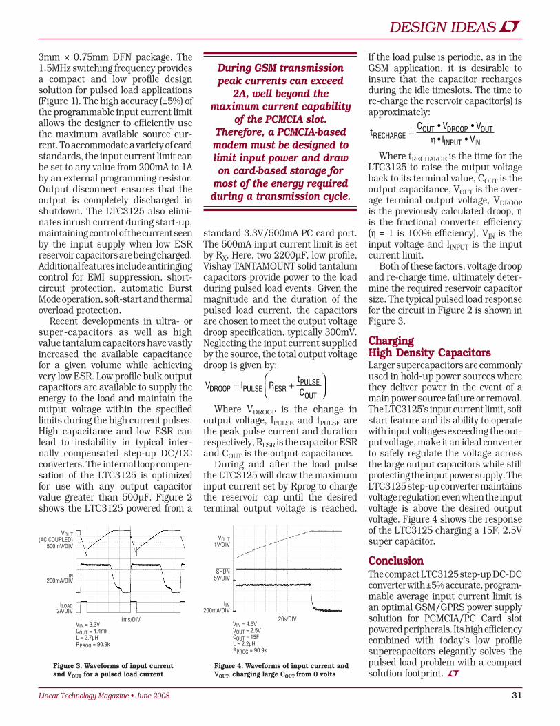
Linear Technology Magazine • June 2008 3131
DESIGN IDEAS L
3mm × 0.75mm DFn package. The 1.5MHz switching frequency provides a compact and low profile design solution for pulsed load applications (Figure 1). The high accuracy (±5%) of the programmable input current limit allows the designer to efficiently use the maximum available source cur-rent. To accommodate a variety of card standards, the input current limit can be set to any value from 200mA to 1A by an external programming resistor. Output disconnect ensures that the output is completely discharged in shutdown. The LTC3125 also elimi-nates inrush current during start-up, maintaining control of the current seen by the input supply when low eSR reservoir capacitors are being charged. Additional features include antiringing control for eMI suppression, short-circuit protection, automatic Burst Mode operation, soft-start and thermal overload protection.
Recent developments in ultra- or super-capacitors as well as high value tantalum capacitors have vastly increased the available capacitance for a given volume while achieving very low eSR. Low profile bulk output capacitors are available to supply the energy to the load and maintain the output voltage within the specified limits during the high current pulses. High capacitance and low eSR can lead to instability in typical inter-nally compensated step-up DC/DC converters. The internal loop compen-sation of the LTC3125 is optimized for use with any output capacitor value greater than 500µF. Figure 2 shows the LTC3125 powered from a
standard 3.3V/500mA PC card port. The 500mA input current limit is set by RX. Here, two 2200µF, low profile, Vishay TAnTAMOunT solid tantalum capacitors provide power to the load during pulsed load events. Given the magnitude and the duration of the pulsed load current, the capacitors are chosen to meet the output voltage droop specification, typically 300mV. neglecting the input current supplied by the source, the total output voltage droop is given by:
V I RtCDROOP PULSE ESRPULSE
OUT= +
Where VDROOP is the change in output voltage, IPuLSe and tPuLSe are the peak pulse current and duration respectively, ReSR is the capacitor eSR and COuT is the output capacitance.
During and after the load pulse the LTC3125 will draw the maximum input current set by Rprog to charge the reservoir cap until the desired terminal output voltage is reached.
ILOAD2A/DIV
VOUT(AC COUPLED)
500mV/DIV
IIN200mA/DIV
1ms/DIVVIN = 3.3VCOUT = 4.4mFL = 2.7µHRPROG = 90.9k
Figure 3. Waveforms of input current and VOUT for a pulsed load current
If the load pulse is periodic, as in the GSM application, it is desirable to insure that the capacitor recharges during the idle timeslots. The time to re-charge the reservoir capacitor(s) is approximately:
tC V V
I VECHARGEOUT DROOP OUT
INPUT INR
• •• •
=η
Where tReCHARGe is the time for the LTC3125 to raise the output voltage back to its terminal value, COuT is the output capacitance, VOuT is the aver-age terminal output voltage, VDROOP is the previously calculated droop, η is the fractional converter efficiency (η = 1 is 100% efficiency), VIn is the input voltage and IInPuT is the input current limit.
Both of these factors, voltage droop and re-charge time, ultimately deter-mine the required reservoir capacitor size. The typical pulsed load response for the circuit in Figure 2 is shown in Figure 3.
Charging High Density CapacitorsLarger supercapacitors are commonly used in hold-up power sources where they deliver power in the event of a main power source failure or removal. The LTC3125’s input current limit, soft start feature and its ability to operate with input voltages exceeding the out-put voltage, make it an ideal converter to safely regulate the voltage across the large output capacitors while still protecting the input power supply. The LTC3125 step-up converter maintains voltage regulation even when the input voltage is above the desired output voltage. Figure 4 shows the response of the LTC3125 charging a 15F, 2.5V super capacitor.
ConclusionThe compact LTC3125 step-up DC-DC converter with ±5% accurate, program-mable average input current limit is an optimal GSM/GPRS power supply solution for PCMCIA/PC Card slot powered peripherals. Its high efficiency combined with today’s low profile supercapacitors elegantly solves the pulsed load problem with a compact solution footprint. L
IIN200mA/DIV
VOUT1V/DIV
SHDN5V/DIV
20s/DIVVIN = 4.5VVOUT = 2.5VCOUT = 15FL = 2.2µHRPROG = 90.9k
Figure 4. Waveforms of input current and VOUT, charging large COUT from 0 volts
During GSM transmission peak currents can exceed
2A, well beyond the maximum current capability
of the PCMCIA slot. Therefore, a PCMCIA-based modem must be designed to limit input power and draw on card-based storage for
most of the energy required during a transmission cycle.
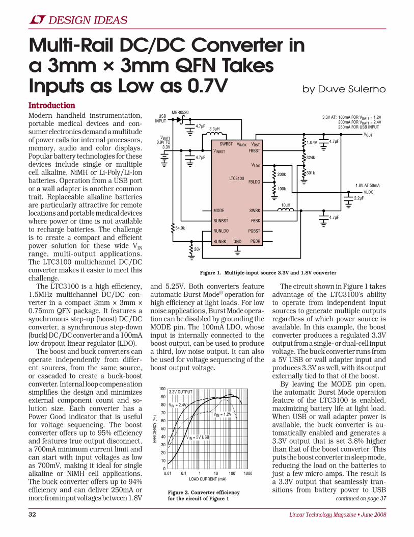
32 Linear Technology Magazine • June 200832
L DESIGN IDEAS
Multi-Rail DC/DC Converter in a 3mm × 3mm QFN Takes Inputs as Low as 0.7V
The circuit shown in Figure 1 takes advantage of the LTC3100’s ability to operate from independent input sources to generate multiple outputs regardless of which power source is available. In this example, the boost converter produces a regulated 3.3V output from a single- or dual-cell input voltage. The buck converter runs from a 5V uSB or wall adapter input and produces 3.3V as well, with its output externally tied to that of the boost.
By leaving the MODe pin open, the automatic Burst Mode operation feature of the LTC3100 is enabled, maximizing battery life at light load. When uSB or wall adapter power is available, the buck converter is au-tomatically enabled and generates a 3.3V output that is set 3.8% higher than that of the boost converter. This puts the boost converter in sleep mode, reducing the load on the batteries to just a few micro-amps. The result is a 3.3V output that seamlessly tran-sitions from battery power to uSB
IntroductionModern handheld instrumentation, portable medical devices and con-sumer electronics demand a multitude of power rails for internal processors, memory, audio and color displays. Popular battery technologies for these devices include single or multiple cell alkaline, niMH or Li-Poly/Li-Ion batteries. Operation from a uSB port or a wall adapter is another common trait. Replaceable alkaline batteries are particularly attractive for remote locations and portable medical devices where power or time is not available to recharge batteries. The challenge is to create a compact and efficient power solution for these wide VIn range, multi-output applications. The LTC3100 multichannel DC/DC converter makes it easier to meet this challenge.
The LTC3100 is a high efficiency, 1.5MHz multichannel DC/DC con-verter in a compact 3mm × 3mm × 0.75mm QFn package. It features a synchronous step-up (boost) DC/DC converter, a synchronous step-down (buck) DC/DC converter and a 100mA low dropout linear regulator (LDO).
The boost and buck converters can operate independently from differ-ent sources, from the same source, or cascaded to create a buck-boost converter. Internal loop compensation simplifies the design and minimizes external component count and so-lution size. each converter has a Power Good indicator that is useful for voltage sequencing. The boost converter offers up to 95% efficiency and features true output disconnect, a 700mA minimum current limit and can start with input voltages as low as 700mV, making it ideal for single alkaline or niMH cell applications. The buck converter offers up to 94% efficiency and can deliver 250mA or more from input voltages between 1.8V
by Dave Salerno
and 5.25V. Both converters feature automatic Burst Mode® operation for high efficiency at light loads. For low noise applications, Burst Mode opera-tion can be disabled by grounding the MODe pin. The 100mA LDO, whose input is internally connected to the boost output, can be used to produce a third, low noise output. It can also be used for voltage sequencing of the boost output voltage.
LOAD CURRENT (mA)
30
EFFI
CIEN
CY (%
)
50
80
0.01 10 100 10000
10
0.1 1
100
70
90
40
60
20
VIN = 1.2V
3.3V OUTPUT
VIN = 2.4V
VIN = 5V USB
Figure 2. Converter efficiency for the circuit of Figure 1
SWBST VINBK VBST
LTC3100
FBBST
1.07M
324k
301k
4.7µF
20k
4.7µF
4.7µF
VLDO
VINBST
FBLDO
SWBK
PGBK
PGBST
VBATT0.9V TO
3.3V
USBINPUT
FBBK
200k
100k
4.7µF
MODE
RUNBST
RUNLDO
RUNBK GND
10µH
1.8V AT 50mA
VLDO
VOUT
64.9k
3.3µH
MBR0520
2.2µF
3.3V AT: 100mA FOR VBATT = 1.2V 300mA FOR VBATT = 2.4V 250mA FOR USB INPUT
Figure 1. Multiple-input source 3.3V and 1.8V converter
continued on page 7

Linear Technology Magazine • June 2008 3333
DESIGN IDEAS L
IntroductionHigh speed differential amplifiers help to drive high performance analog-to-digital converters (ADCs) by providing balanced drive to the differential input stage, setting the common mode level, absorbing the sampling-energy, and taking gain to reduce the output swing requirement of preceding circuitry. In applications involving multiple ADCs, a compact, tightly matched dual differential amplifier such as the LTC6420-20 can further simplify the design by reducing the uncertainty of channel-to-channel variations.
The LTC6420-20 features two 1.8GHz differential amplifiers, each capable of driving 12-, 14- and 16-bit pipeline ADCs at low noise and low distortion levels, even for input frequencies as high as 300MHz. The internal op amps are manufactured on a Silicon Germanium (SiGe) process and feature an ultra-low 1nV/√Hz noise density. even after factoring in
Dual ADC Driver with Tightly Matched Gain and Phase Raises Quadrature Demodulation Performance
the internal feedback resistors, the total input noise density equals only 2.2nV/√Hz. The channel-to-channel gain matching is production tested and guaranteed to be better than ±0.25dB. Moreover, the monolithic design en-sures that both phase and group delay remain tighly matched over the entire bandwidth of the amplifiers.
The dual amplifier is available in a 3mm × 4mm QFn package, which saves space compared to two single
amplifiers. For further space-sav-ings, all gain and feedback resistors are included on-chip, setting a fixed voltage gain of 20dB. The LTC6420-20 consumes 80mA per channel from a supply as low as 2.85V. A 40mA ver-sion, the LTC6421-20, is available to save power at the expense of usable input bandwidth.
Wideband Interface Between an I/Q Demodulator and a Dual ADCWhen an IF or RF signal is applied to a demodulator such as the LT5575, the signal’s information is separated out into two baseband signals: “in-phase” (I) and “quadrature” (Q). Both baseband signals need to be digitized simultaneously, and it is critical that the relationship of gain and phase between the two is maintained. Fur-thermore, if you want to maximize the dynamic range by driving the dual
by Kris Lokere
Figure 1. The voltage gain of the LTC6421-20 reduces the output swing requirements of the LT5575 demodulator. This improves overall system linearity.
LT5575 10Ω
10Ω
56pF
56pF
56pF
56pF
0.1µF
3V
LTC2285
40.2Ω
40.2Ω
VCM
10Ω
10Ω
40.2Ω
40.2Ω
VCM
V+ A ENABLEALTC6421-20
0.1µF–INA 100Ω
1000Ω
1000Ω
+INA
V– V–
+OUTA
–OUTA
VOCMA
V+ B
3V
ENABLEBVOCMB
1000pF
0.1µF100Ω
12.5Ω
12.5Ω
0.1µF+INB 100Ω
1000Ω
1000Ω
–INB
–OUTB
+OUTB0.1µF
100Ω
12.5Ω
12.5Ω
0.1µF
0.1µF1000pF
12pF
27pF27pF
75Ω
75Ω
12pF
27pF27pF
75Ω
75Ω
LO IN2.5GHz
5V
RF IN2.5GHz
In applications involving multiple ADCs, a compact,
tightly matched dual differential amplifier
simplifies design by reducing the uncertainty of channel-
to-channel variations.
continued on page 5

34 Linear Technology Magazine • June 200834
L DESIGN IDEAS
levels. The operating frequency can be set anywhere between 400kHz and 2.2MHz using a single resistor from the RT pin to ground. Set a lower operat-ing frequency for the best efficiency, and a higher frequency for smaller filter components and overall solution size. The LT3592 also incorporates an
The output voltage of the LT3592 can be as high as 20V, but the part is also designed to work well with single red LeDs, which can have forward volt-ages below 2V at reasonable current
IntroductionLeDs are quickly becoming standard lighting for a variety of commercial, automotive, and industrial applica-tions. Some of these applications require wide-range brightness control, spurring a demand for products that offer PWM-based LeD brightness control. However, many applications only require two settings, bright and dim, so generating a PWM signal for a binary choice is inconvenient overkill. The LT3592 LeD driver is the solution to this problem. It simplifies design by offering two LeD current settings with a 10:1 ratio, selected via a simple digital control pin. This pin has a low threshold voltage, but high voltage capability, making it very easy to plug into any automotive or industrial system. For an application such as automotive brake light control, the LT3592’s accurate, consistent output current levels and easy to use small package make it a perfect fit. Further-more, the LT3592 is rugged enough to tolerate a 36V maximum input, making it useful in a wide variety of higher voltage applications.
Simple 2-Level Current ControlThe LT3592 uses a single external current sense resistor between the CAP and OuT pins to set its two output current levels, which have a 10:1 ratio. In bright mode, an internal amplifier regulates the voltage differ-ence between CAP and OuT to 200mV. In dim mode, the voltage is regulated to 20mV. using a 0.4Ω current sense resistor results in a bright current of 500mA and a DIM current of 50mA. Switching between the high and low current levels couldn’t be easier—bring the BRIGHT pin above 1.4V for high current, and below 0.3V for low cur-rent. The bright current level can be as high as 500mA.
No PWM Signal Needed for Accurate Dim/Bright Control of Automotive Brake Lights and Other Signal LEDs
by Bill Martin
Figure 2. Single red LED application with external boost diode to VIN
15µH
30k
22µF
1µF
0.4Ω
10k357k
400kHz
0.1µF
VIN
SHDN
BRIGHT
RT
BOOST
SW
DACAP
OUT
VFB
LT3592
1N4148
MBRA120
LUXEONLXK2-PD12-S00GND
VIN5V TO 16V
FAULT
ONOFF
10µH
51k
CMMSHI-40
4.7µF
1µF
0.4Ω
10k
0.1µF
VIN
SHDN
BRIGHT
RT
BOOST
SW
DACAP
OUT
VFB
LT3592
GND
ON
BRAKE
140k900kHz
+200/20mV
–
VIN7V TO 32V
LUXEONLXK2-PD12-S00
Figure 1. Two red LED application with no external boost diode
INPUT VOLTAGE (V)4
EFFI
CIEN
CY (%
)
100
95
90
60
75
70
65
80
85
55
502012 24 28168
BRIGHT 500mA
Figure 3. Efficiency for Figure 1
100µs/DIV
VSW
VOUT
ILED
C = 4.7µF
Figure 4. Switching between dim (50mA) and bright (500mA) modes with 4.7µF output cap
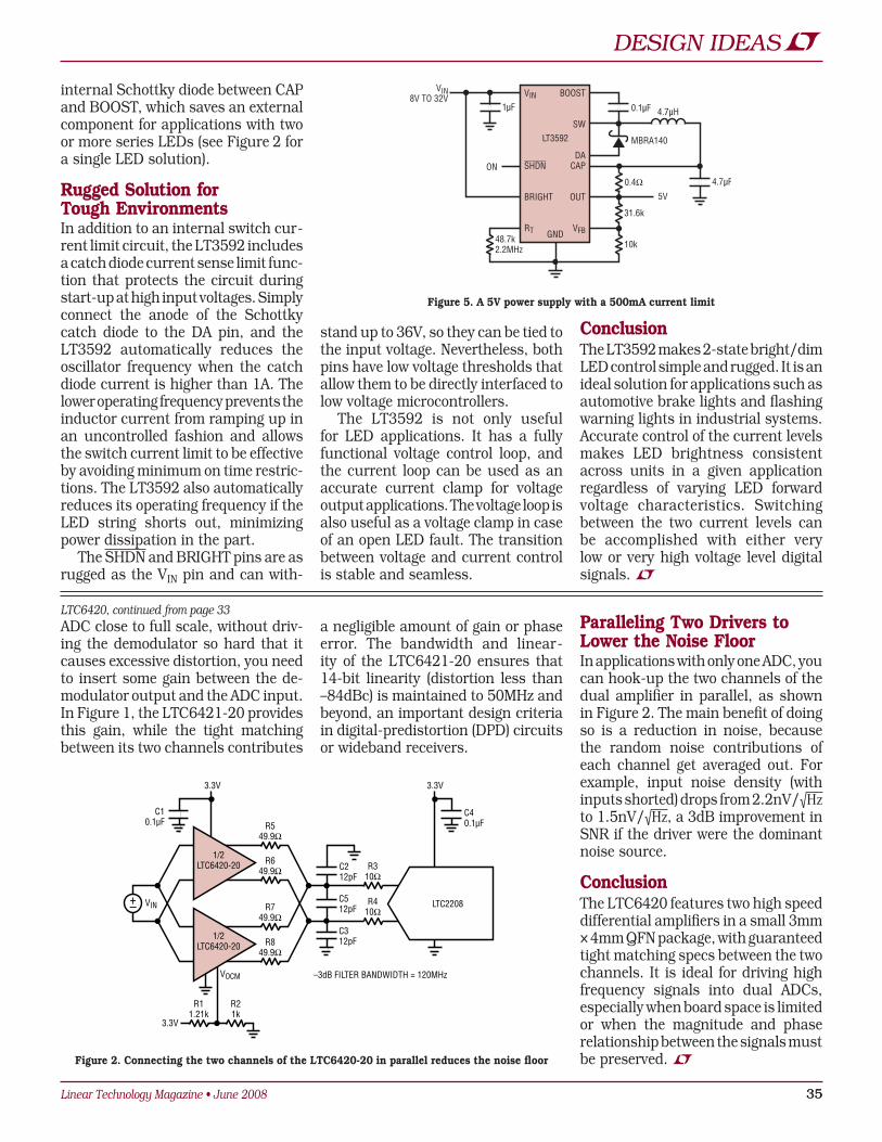
Linear Technology Magazine • June 2008 3535
DESIGN IDEAS L
internal Schottky diode between CAP and BOOST, which saves an external component for applications with two or more series LeDs (see Figure 2 for a single LeD solution).
Rugged Solution for Tough EnvironmentsIn addition to an internal switch cur-rent limit circuit, the LT3592 includes a catch diode current sense limit func-tion that protects the circuit during start-up at high input voltages. Simply connect the anode of the Schottky catch diode to the DA pin, and the LT3592 automatically reduces the oscillator frequency when the catch diode current is higher than 1A. The lower operating frequency prevents the inductor current from ramping up in an uncontrolled fashion and allows the switch current limit to be effective by avoiding minimum on time restric-tions. The LT3592 also automatically reduces its operating frequency if the LeD string shorts out, minimizing power dissipation in the part.
The SHDn and BRIGHT pins are as rugged as the VIn pin and can with-
4.7µH
31.6k
4.7µF
1µF
0.4Ω
10k48.7k2.2MHz
0.1µF
MBRA140
VIN
SHDN
BRIGHT
RT
BOOST
SW
DACAP
OUT
VFB
LT3592
GND
VIN8V TO 32V
5V
ON
Figure 5. A 5V power supply with a 500mA current limit
stand up to 36V, so they can be tied to the input voltage. nevertheless, both pins have low voltage thresholds that allow them to be directly interfaced to low voltage microcontrollers.
The LT3592 is not only useful for LeD applications. It has a fully functional voltage control loop, and the current loop can be used as an accurate current clamp for voltage output applications. The voltage loop is also useful as a voltage clamp in case of an open LeD fault. The transition between voltage and current control is stable and seamless.
ConclusionThe LT3592 makes 2-state bright/dim LeD control simple and rugged. It is an ideal solution for applications such as automotive brake lights and flashing warning lights in industrial systems. Accurate control of the current levels makes LeD brightness consistent across units in a given application regardless of varying LeD forward voltage characteristics. Switching between the two current levels can be accomplished with either very low or very high voltage level digital signals. L
ADC close to full scale, without driv-ing the demodulator so hard that it causes excessive distortion, you need to insert some gain between the de-modulator output and the ADC input. In Figure 1, the LTC6421-20 provides this gain, while the tight matching between its two channels contributes
a negligible amount of gain or phase error. The bandwidth and linear-ity of the LTC6421-20 ensures that 14-bit linearity (distortion less than –84dBc) is maintained to 50MHz and beyond, an important design criteria in digital-predistortion (DPD) circuits or wideband receivers.
Paralleling Two Drivers to Lower the Noise FloorIn applications with only one ADC, you can hook-up the two channels of the dual amplifier in parallel, as shown in Figure 2. The main benefit of doing so is a reduction in noise, because the random noise contributions of each channel get averaged out. For example, input noise density (with inputs shorted) drops from 2.2nV/√Hz to 1.5nV/√Hz, a 3dB improvement in SnR if the driver were the dominant noise source.
ConclusionThe LTC6420 features two high speed differential amplifiers in a small 3mm × 4mm QFn package, with guaranteed tight matching specs between the two channels. It is ideal for driving high frequency signals into dual ADCs, especially when board space is limited or when the magnitude and phase relationship between the signals must be preserved. L
+–
R549.9Ω
3.3V 3.3V
R310Ω
R410ΩR7
49.9Ω
R849.9Ω
R21k
VOCM
R11.21k
3.3V
R649.9Ω
1/2LTC6420-20
1/2LTC6420-20
C212pF
VINC512pF
C312pF
C10.1µF
C40.1µF
LTC2208
–3dB FILTER BANDWIDTH = 120MHz
Figure 2. Connecting the two channels of the LTC6420-20 in parallel reduces the noise floor
LTC6420, continued from page

36 Linear Technology Magazine • June 200836
L DESIGN IDEAS
The LT3593 is available in a 6-lead (2mm × 2mm) DFn as well as 6-lead SOT-23.
1-Wire Current ProgrammingThe LeD current can be programmed linearly to 32 unique values by strobing the CTRL pin. A 5-bit internal counter is decremented on each rising edge on the CTRL pin, reducing the pro-grammed current by 625µA from the full-scale current of 20mA with each step. The programmed LeD current can be calculated using the following equation:
ILED=20mA–(N–1) • 625µA
where n is the number of rising edges on the CTRL pin. Strobing the CTRL pin more than 32 times results in the minimum current of 625µA. The CTRL pin must stay high after the last CTRL strobe and 128µs later the part will turn on and start to regulate the
by Ahmed Hashim
White LED Driver with Output Disconnect and 1-Wire Current ProgrammingIntroductionThe LT3593 is designed to drive up to ten white LeDs in series from a single lithium-ion cell, ensuring matched LeD current and eliminating the need for ballast resistors. The LT3593 in-ternally compensated step-up DC/DC converter switches at 1MHz so that it can be used with tiny, low profile external components.
The LT3593 features an internal 5-bit DAC, allowing the LeD current to be programmed using only one pin. The device features true output disconnect in shutdown as well as a unique high side current sense allow-ing it to function as a “1-wire” current source where the low side of the LeDs can be returned to ground anywhere. A typical application schematic along with expected efficiency can be seen in Figure 1. The functionality and feature set available in the LT3593 make it ideal for portable electronics display back-lighting applications.
programmed current. To shut down the part, the CTRL pin is held low; 128µs after the falling edge of CTRL, the part shuts down. Figure 2 shows current programming and shutdown timing.
If the LeD current needs to be reprogrammed, there is no need to shutdown and then reprogram. The LT3593 can be reprogrammed from one LeD current to another by simply strobing the CTRL pin and, 128µs after the last rising edge, the part starts regulating the newly programmed current (also shown in Figure 2).
Buck-Boost ModeIf a low number of LeDs is needed, there could be a case where the re-quired output voltage is lower than the input voltage. In this case, the LT3593 can be used in buck-boost mode where the LeD string is returned to the input supply instead of ground. Figure 3
Figure 1. LED driver for ten white LEDs
CTRL
VIN
10µHVIN
3V TO 5V
LT3593
SHUTDOWN ANDCURRENT CONTROL
C1: TAIYO YUDEN EMK107BJ105MAC2: MURATA GRM31MR71H105KA88L1: MURATA LQH43CN100D1: CENTRAL CMDSH05-4
SWCAP
LED
GND
1µF 1µF
LED CURRENT (mA)0
EFFI
CIE
NCY
(%)
90
70
50
80
60
40
3010 20155
VIN = 3.6V10 LEDs
CTRL
LEDCURRENT
128µs
20mA 20mA 17.5mA 17.5mA
SHDN
128µs 128µs
Figure 2. Current programming and shutdown timing
LED
VIN
L110µH
VIN3V TO 5V
LT3593
SW
CAP
CTRL
GND
C21µF
D1
C11µF
SHUTDOWN ANDCURRENT CONTROL
C1: TAIYO YUDEN EMK107BJ105MAC2: TAIYO YUDEN GMK316BJ105MLL1: MURATA LQH43CN100D1: CENTRAL CMDSH05-4
Figure 3. LED driver in Buck-Boost mode driving one LED

Linear Technology Magazine • June 2008 3737
DESIGN IDEAS L
shows an application where a single LeD is driven from a 5V supply.
Output Disconnect The LT3593 has an internal disconnect switch that is used to sense the LeD current during normal operation. This internal switch also serves to provide output disconnect during shutdown so that the LeDs are truly disconnected from the output of the regulator.
Fault Protection The LT3593 protects against both open and shorted LeD faults. In the case of an open LeD fault, the output voltage VCAP continues to rise. Once VCAP reaches 38V, an open fault is triggered and the part goes into a low frequency mode clamping the output to 38V and minimizing input current.
A waveform showing the LT3593’s response to an open LeD fault can be seen in Figure 4.
In a shorted LeD fault, the LeD pin can be shorted to ground, running excessive current from VCAP. To protect from such a fault, the LT3593 limits the maximum current out of the LeD pin to approximately 45mA.
ConclusionThe LT3593 is a step-up LeD driver that can drive up to ten white LeDs from a single lithium-ion cell. It can easily be programmed through a single pin interface and combines many desirable features as well as fault protection against open or shorted LeDs.
The feature-rich LT3593 is available in the 6-lead (2mm × 2mm) DFn as
well as the 6-lead SOT-23. These two small, low profile packages, together with internal compensation and an output disconnect device, are ideal for a complete small board area LeD driver solution, especially in portable device display backlighting applica-tions. L
VCAP20V/DIV
400µs/DIVVIN = 3.6VFIGURE 1APPLICATION CIRCUIT
IL200mA/DIV
VSW20V/DIV
LEDs DISCONNECTEDAT THIS INSTANT
Figure 4. Open LED fault protection
Because the buck converter input can come from the boost output, the LTC3100 can function as an ultra-low voltage buck-boost converter, provid-ing a regulated 1.2V output from a single alkaline or niMH cell. This is shown in Figure 3, where the LTC3100 generates two regulated outputs from a single cell input (whose voltage may be above or below 1.2V) by boosting VIn up to 3.5V and then regulating down to 1.2V and 3.3V using the buck and the LDO. In this example, the Power Good outputs and the LDO are used
to provide voltage sequencing, so that the 1.2V core supply comes up before the 3.3V I/O supply, as shown in the scope photo of Figure 4. The LDO also provides additional noise filtering and ripple rejection for the 3.3V output, guaranteeing a low noise output for sensitive analog circuitry, even when the converters are in Burst Mode operation.
ConclusionThe LTC3100 is a high efficiency, mul-tichannel converter that can operate from a wide range of voltage sources. Independent input voltages for each converter, Power Good outputs and an LDO make the LTC3100 a small, highly integrated and flexible solution for many demanding applications. L
power while maximizing battery life. The diode on the uSB input prevents any reverse current from the 3.3V output (while operating on batter-ies) back to the uSB input when it is open or grounded. Figure 2 shows the converter efficiency versus load with various input sources, illustrating the high efficiency over a wide load range. The LDO in the LTC3100 (with its input internally tied to the Boost output) provides a second regulated output, in this case programmed to 1.8V.
1ms/DIV
VCORE, 1V/DIV
VBST, 1V/DIVVI/O, 1V/DIV
Figure 4. Voltage sequencing of the output voltages for the circuit of Figure 3
SWBST VINBK VBST
LTC3100
FBBST
3.3µH 3.5V
1M
523k
10µF
CIN2.2µF
VLDO
VINBST
FBLDO
SWBK
PGBKPGBST
115k
25.5k
VBATT0.9V TO 1.5V
2.2µF
FBBK
1M
1M
10µF
MODE
RUNBST
RUNLDO
RUNBK GND
FF EN_BURST
OFF ON
3.3µH
3.3V AT 50mAV_I/O
120mA AT VBATT = 0.9V220mA AT VBATT = 1.2V
V_CORE = 1.2V
BOOST_GOOD
BUCK_GOOD
1M 1M
+
Figure 3. Single-cell dual output converter with voltage sequencing
LTC00, continued from page 2

38 Linear Technology Magazine • June 200838
L DESIGN IDEAS
and LTC4358 enable MOSFeT-based ideal diode solutions for various ap-plications—the choice depends on the current and operating voltage of the application. Table 1 compares these devices.
Ideal Diode Easier to Use Than a SchottkyOf particular interest is the LTC4358, which includes an internal 20mΩ
IntroductionHigh availability systems often use parallel power supplies or battery feeds to achieve redundancy and enhance system reliability. Tradition-ally, Schottky ORing diodes are used to connect these supplies at the point of load and prevent backfeeding into a faulty power supply. unfortunately, the forward voltage drop of these diodes reduces the available supply voltage and dissipates significant power at high currents—costly heat sinks and elaborate layouts are needed to keep the diodes cool.
When power dissipation is a concern, the Schottky diode can be replaced with a MOSFeT-based ideal diode. This reduces the voltage drop and power dissipation, thereby reduc-ing the complexity, size and cost of the thermal layout and increasing system efficiency. The LTC4355, LTC4357
by Meilissa Lum
Table 1. Comparison of ideal diode parts
Part Number Description Operating Voltage Configuration Package
LTC4355 PositiveVoltageDiode-ORControllerandMonitor
9V–80V,100VAbsMax Dual,ExternalMOSFETs DFN14(4mm×3mm),SO16
LTC4357 SinglePositiveVoltageIdealDiodeController
9V–80V,100VAbsMax Single,ExternalMOSFET DFN6(2mm×3mm),MSOP8
LTC4358 IdealDiode 9V–26.5V,28VAbsMax 5AInternalMOSFET DFN14(4mm×3mm),TSSOP16
Figure 2. The LTC4358 ideal diode takes on a 5A B530C Schottky diode. The LTC4358 easily wins in voltage drop, power loss and package size.
4358
B530C
CURR
ENT
(A)
VOLTAGE DROP (mV)5000
6
0100 200 300 400
1
2
4
3
5
DIODE (B530C)
FET (LTC4358)
CURRENT (A)0
0
POW
ER D
ISSI
PATI
ON (W
)
0.5
1.0
1.5
2.0
2.5
21 3 4 5 6
DIODE (B530C)
POWER SAVED
FET (LTC4358)
LTC4358
GND
IN DRAIN
VDD
OUT
VIN = 12V VOUT TO5A LOAD
Figure 1. No external components are needed for a 12V/5A ideal diode.
Ideal Diode Betters a Schottky by a Factor of Four in Power and Space Consumption
With one-fourth the dissipated power, system
efficiency is increased and PCB layout is simplified—no
need for costly and bulky heat sinks.

Linear Technology Magazine • June 2008 3939
DESIGN IDEAS L
MOSFeT as the pass element. no ex-ternal components are required. The In pins are the source of the MOSFeT and act like the anode of a diode, while the drain behaves as the cathode, as shown for a 12V/5A application in Figure 1. When power is first ap-plied, the load current initially flows through the MOSFeT’s body diode. The MOSFeT’s gate is enhanced and turned on to maintain a 25mV forward voltage drop. If the load current causes more than 25mV of voltage drop, the MOSFeT is driven fully on, and the forward drop equals RDS(On) • ILOAD. If the load current reverses, as may occur during an input short, the LTC4358 responds by turning off the internal MOSFeT in less than 0.5µs.
Power Saved Versus Schottky DiodeCompared to a B530C Schottky di-ode in the SMC package, not only is the LTC4358’s De14 (4mm × 3mm) package one-fourth the size, the volt-age drop and power dissipation are also considerably less as shown in Figure 2. The reduced voltage drop
of the ideal diode also increases the voltage at the load, which reduces the capacitance required to hold up the output during supply disruptions. The
power dissipated at 5A in the Schottky is 2W versus 0.5W for the LTC4358. With one-fourth the power dissipated, system efficiency is increased and PCB
layout is simplified—no need for costly and bulky heat sinks.
PCB LayoutAs described above, with only one-fourth as much power dissipation as a Schottky, thermal layout with the LTC4358 is much easier. Most of the heat escapes the part through the DRAIn/exposed pad, while some exits through the In pins. Maximizing the copper of these connections increases the allowable maximum current. Figure 3 shows an optimal layout for a 1" × 1" single sided PCB with the DFn package. Copper connected to the exposed pad above and below the LTC4358 helps remove heat from the package. If you are using a two-sided PCB, use vias under the LTC4358 to transfer heat to copper on the bot-tom of the PCB, thus increasing the maximum current by 10%. use Figure 4 to determine the amount of copper area needed for a specified current and ambient temperature.
ConclusionThe LTC4358 is a MOSFeT-based ideal diode that can directly replace a 5A Schottky diode in 9V to 26.5V applications. The LTC4358 betters a Schottky by a factor of four on volt-age drop, power loss and package size, thus significantly shrinking the thermal layout and improving overall performance. Also, simple optimiza-tion the PCB layout increases the maximum current—no heat sinks required. L
VIN
GND
VOUT
Figure 3. DFN layout considerations for 1" × 1" single sided PCB
DIODE CURRENT (A)
3.5
AREA
(INC
H2 )
4.5
10
0.1
1
4.0 6.56.05.55.03.0
85 C 70 C 25 C
TA =
50 C
Figure 4. Maximum diode current vs PCB area
Not only is the LTC4358’s DE14 (4mm × 3mm) package
one-fourth the size, the voltage drop and power
dissipation are also considerably less than
a Schottky. The reduced voltage drop of the ideal diode also increases the
voltage at the load, which reduces the capacitance required to hold up the output during supply
disruptions.
Authors can be contactedat (408) 432-1900

40 Linear Technology Magazine • June 200840
L DESIGN IDEAS
6mm × 6mm DC/DC Controller Regulates Three Outputs; or Combine Two Outputs for Twice the Current
by Theo PhillipsIntroductionThe LTC3853 is a versatile 3-phase synchronous buck controller with on-chip drivers in a 6mm × 6mm QFn package. While each channel can independently deliver currents in excess of 15A, two of the channels can be combined for twice the current, with their relative operating phase automatically optimized to reduce output ripple. Channels 1 and 2 can be programmed for outputs from 0.8V to 5V, while channel 3 can support outputs from 0.8V to 13.2V.
Multiphase OperationThe LTC3853 can be configured for three single phase outputs, or for two outputs with channels 1 and 2 tied together. In a 3-output setup, the switches operate 120° out of phase, reducing the input RMS ripple current
and minimizing the input capacitance requirement.
Dual Output Converter with 2 + 1 OperationFigure 1 shows a 2-output converter working from a 14V to 24V input. Channels 1 and 2 feed the same 1.8V output, while channel 3 controls a second 12V output. This 2 + 1 mode requires just one Run pin (Run1) to enable both channels 1 and 2. The error amp of channel 2 is disabled and both channels share channel 1’s feedback divider. Post package trim-ming of the current sense comparators provides excellent current sharing between channels 1 and 2, as the load step of Figure 2 shows. Channels 1 and 2 run 180° out of phase to minimize the output ripple on their 2-phase
single output. A minimum on-time of <90 nanoseconds allows low duty cycle operation even at high frequencies—at 24VIn to 1.8VOuT, this 500kHz regula-tor never misses a pulse.
The eXTVCC pin can be connected to a 5V supply to power the internal MOSFeT drivers and control circuits. An internal switch connects eXTVCC to InTVCC with a typical voltage drop of just 50mV. If eXTVCC is not connected, the LTC3853’s internal regulator uses the main input supply, VIn, to provide 5V to the internal circuitry and drivers at InTVCC. In either case, the switching frequency is set with a divider from the predictable 5V at InTVCC, with 1.2V at the FReQ pin corresponding to free-running 500kHz. If an external frequency source is available, a phase locked loop enables the LTC3853 to
TG1 TG2
BOOST1,2,3SW1 SW2
BG1 BG2
SENSE1+ SENSE2+
SENSE1–SENSE2–
VFB1
VFB2ITH3
ITH1ITH2
VIN INTVCCDRVCC1,2
LTC3853EUH
MODE
20k1%
FREQILIMPGND
PGOOD1,2
SGND
RUN2
TK/SS2 TK/SS3TK/SS1
VFB3
SENSE3–SENSE3+
SW3TG3
BG3
PGOOD3
EXVCC
RUN1
10Ω
10Ω
4.7µF
10k 1%INTVCC
VOUT1,21.8V10A
3.16k1%
20k1%
RSENSE28mΩ5% VOUT3
12V5A
VIN14V TO 24V
CITH11.5nF
RITH1825Ω
1%
RITH36.49k1%
470pF
COUT1470µF2.5V
COUT1: SANYO 2R5TPE470M9COUT3: SANYO 16TQC47ML1, L2, L3: VISHAY IHLP2525CZ-11M1, M2, M3: Si4816BDY
CITH1a220pF
22µF50VX5R
CSS10.22µF
CSS30.1µF
CITH31nF
470pF
CITH3a220pF
470pF 10Ω
L21.5µHL1
1.5µH
L34.7µH
CB1,2,3 0.1µF
SW1,2,3
DB1,2,3M2M1 M3
10Ω
+
COUT3247µF16V
+
10Ω
280k1%
10Ω
24.9k1%
RSENSE18mΩ5%
RSENSE38mΩ5%
10µFX5R
5V
200k
1µF +
10µFX5R
100k
100k
RUN3
Figure 1. For applications that need up to 30A of current, channels 1 and 2 of the LTC3853 can be combined to share the load for a single output. The two channels operate 180º out of phase to minimize output ripple. Channel 3’s high common mode range allows it to provide 12V.

Linear Technology Magazine • June 2008 4141
DESIGN IDEAS L
to drop, current limit fold back protects the power components by reducing the current limit. For predictable tracking, current limit fold back is disabled during start-up. Input undervoltage lockout, output overvoltage shutdown and thermal shutdown also protect the power components and the IC from damage.
ConclusionThe LTC3853’s small footprint belies its versatility and extensive feature set. From inputs up to 24V it can regulate three separate outputs, or it can be configured for higher currents by tying channels 1 and 2 together. either way, the phase relationship between channels is automatically optimized to reduce ripple currents. At low duty cycles, the short minimum on-time ensures constant frequency operation, and peak current limit remains constant even as duty cycle changes. The cost-effective LTC3853 incorporates these features, and more, into a 40-pin 6mm × 6mm QFn package. L
sync with frequencies between 250kHz and 750kHz.
The LTC3853 can be set to operate in one of three modes under light load conditions. Burst Mode operation of-fers the highest light load efficiency by switching in a “burst” of one to several pulses replenishing the charge stored in the output capacitors, followed by a long sleep period when the load current is supplied by the output capacitors. Forced continuous mode offers fixed frequency operation from no load to full load, providing the lowest output voltage ripple at the cost of light load efficiency. Pulse-skipping mode oper-ates by preventing inductor current reversal by turning off the synchro-nous switch as needed. This mode is a compromise between the other two modes, offering lower ripple than Burst Mode operation and better light load efficiency than forced continuous mode. Regardless of the mode selected, the LTC3853 operates in constant fre-quency mode at higher load currents. Figure 3 shows the efficiency in each of the three modes.
each of the LTC3853’s channels can be enabled with its own Run pin, or slewed up or down with its own TRACK/SS pin. Tracking holds the feedback voltage to the lesser of the internal reference voltage or the voltage on TRACK/SS, which can be brought up with an external ramp or with its own 1.2µA internal current source. With all of the TRACK/SS pins held low and any output enabled through its Run pin, the 5V InTVCC is still available for ancillary keep-alive circuits.
Pulse-skipping mode is always enabled at start-up to prevent sink-ing current from a pre-biased output voltage. When the output reaches 80% of the set value, the part switches over to forced continuous mode until the output has entered the POWeR GOOD window, at which point it switches over to the selected mode of opera-tion. Forced continuous mode reduces the output ripple as the power good threshold is crossed, to ensure that the POWeR GOOD indicators make just one low to high transition.
Three different max current com-parator sense thresholds can be set via the ILIM pin. The current is sensed using a high speed rail-to-rail differ-ential current sense comparator. The circuit of Figure 1 uses accurate sense resistors between the inductors and the outputs. For reduced power loss at high load currents, the LTC3853 can also monitor the parasitic resistance of the inductor (DCR sensing). Peak inductor current is limited on a cycle-by-cycle basis and is independent of duty cycle. If load current is high enough to cause the feedback voltage
POW
ER L
OSS
(mW
)
EFFI
CIEN
CY (%
)
LOAD CURRENT (A)100.1
100
0
10k
1001
1k
10
20
30
40
50
60
70
80
90
VIN = 24VVOUT3 = 12V
2+1 MODE
EFFICIENCY
POWER LOSS
CONTINUOUS MODEPULSE-SKIPPING MODE
BURST MODE OPERATION
Figure 3. Efficiency for channel 3 in Figure 1—in each of the three modes of operation
VOUT1,2200mV/DIV
IL22A/DIV
IL12A/DIV
25µs/DIVVIN = 14VVOUT1,2 (NOM) = 1.8VLOAD STEP ON VOUT1,2 = 1A TO 6A
Figure 2. Post-package trimming of the LTC3853’s current sense comparators provides excellent current sharing between channels 1 and 2, even during a transient.
DSL ModemFigure 4 shows an application for a DSL modem or set-top box. The sup-ply voltage for VIn2 comes from a wall adapter that can range from 8V to 30V. This voltage is stepped down to 5V at 100mA for VOuT2, which then supplies the power to drive both the boost regulator and LDO controller. VOuT1 is set to 8V at 200mA and VOuT3 is set
to 3.3V at 500mA. Figure 5 shows the load step response of VOuT1 and VOuT2 with a 200mA load step on VOuT1.
ConclusionThe LT3570 is a monolithic dual output switching regulator (buck and boost) with a nPn LDO controller and is ideal for a broad variety of applica-tions. Because the LT3570 offers a high
level of system integration, it greatly simplifies board design for complex applications that need multiple volt-age supply rails. With the flexibility of independent supply inputs and adjust-able frequency, the user can set a wide array of custom output voltages. The LT3570 is a feature rich solution that satisfies the needs for multiple output voltages in a compact solution. L
LT570, continued from page 29

42 Linear Technology Magazine • June 200842
L NEW DEVICE CAMEOS
New Device Cameos
The LTM4616 is a complete dual DC/DC µModule regulator system in a tiny surface mount package. The LTM4616 can regulate either two voltages rang-ing from 0.6V to 5V at up to 8A each, or one output voltage at up to 16A by sharing current from each output in a multiphase configuration.
The LTM4616’s versatility is ex-tended by its ability to operate from either two different input supply rails ranging from 2.375V to 5.5V (6V max) or from one input supply by tying the input pins together. This complete DC/DC system solution includes all the support components needed for a dual point-of-load regulator: induc-tors, capacitors, DC/DC controller, compensation circuitry and power switches. All are encapsulated and protected within a plastic surface mount LGA (land grid array) package. The package dimensions are 15mm × 15mm with a height of only 2.8mm, providing a low profile point-of-load regulator that allows smooth air flow for cooling in densely populated circuit boards. It is also a simple solution for powering both core and I/O supplies for FPGAs and ASICs.
The LTM4616 is guaranteed to have only ±1.75% total DC output error over the full operating temperature range, including the line and load regulation. As a current mode device with high switching frequency, the LTM4616 has a very fast transient response to line and load changes while operating with excellent stability with a variety of output capacitors, including all ceramic capacitors. ef-ficiency is as high as 94%. The device supports frequency synchroniza-tion, multiphase operation, spread spectrum phase modulation, output voltage tracking and margining. Safety features include overvoltage and overcurrent protection as well as thermal shutdown.
The LTC3558 is an efficient, multifunc-tion power management solution for handheld applications. The LTC3558 integrates a stand-alone Li-Ion/Poly-mer battery charger and two high efficiency synchronous regulators—one buck-boost and one buck—in a compact low profile 3mm × 3mm QFn package. The linear battery charger can deliver up to 950mA charge cur-rent from a wall adapter supply, or up to 500mA charge current from a uSB port. The LTC3558’s standalone autonomous operation simplifies design, eliminating the need for an external microprocessor for charge termination. Both switching regula-tors are designed to operate over the Li-Ion/Polymer range of 2.7V to 4.2V while delivering output currents up to 400mA each.
The LTC3558’s integrated syn-chronous buck regulator features 100% duty cycle operation, while the buck-boost regulator is capable of regulating its programmed output voltage (typically 3.3V) over the entire Li-Ion/Polymer operating range. The integrated low RDS(On) switches enable efficiencies as high as 92%, maximiz-ing battery run time. In addition, Burst Mode operation optimizes efficiency at light loads with a quiescent cur-rent of only 20µA for the buck-boost and 35µA for the buck (less than 1µA in shutdown for each). The high 2.25MHz switching frequency allows the utilization of tiny low cost capaci-tors and inductors less than 1mm in height. Furthermore, the regulators are stable with ceramic output ca-pacitors, achieving very low output voltage ripple.
The LTC3558’s battery charger con-tains a high degree of uSB functionality, including 20%/100% full-scale charge current setting, an SuSP pin for shut-down/enable, and 4 different indication states on the CHRG pin.
The LTC2366 is a 12-bit successive approximation register (SAR) ADC that outputs data at up to 3Msps in tiny 6- and 8-lead TSOT-23 packages. Operating from a single 2.35V to 3.6V supply, the LTC2366 consumes only 7.2mW at the maximum output rate, a 20% power savings over the near-est competitor. With its tiny footprint and very low power dissipation, the LTC2366 is ideal for a wide variety of portable and space-constrained applications, including medical de-vices, communication systems, and industrial monitors.
The LTC2366 is Linear’s fastest offering in a family of five TSOT-23 pin- and software-compatible ADCs. The LTC2365 output data rate is guar-anteed up to 1Msps and the LTC2362 up to 500ksps. For lower speeds, the LTC2361 is guaranteed up to 250ksps and the LTC2360 up to 100ksps. Power is optimized for each sample rate, as the LTC2360 draws just 1.5mW at 100ksps. Power dissipation can be further decreased with a shutdown mode that reduces the supply cur-rent to 2µA (max), saving battery life. All five ADCs are offered in industry standard 6-pin TSOT-23 packages, as well as 8-pin TSOT-23 packages that include an external reference pin and a digital output supply pin (OVDD) that can range between 1V and VDD. The LTC2366, LTC2365, LTC2362, LTC2361, and LTC2360 can be used for monitoring precision DC or AC signals in a variety of applications, including automotive.
These ADCs Communicate via a serial SPI/QSPI/Microwire-compat-ible interface with no data latency and achieve excellent DC specifications of ±1LSB InL and ±1LSB DnL. These con-verters also excel when digitizing AC signals. The LTC2366 measures 72dB SnR, –80dB THD, and 82dB SFDR at a 1MHz input frequency.L
Dual 8A or Single 16A Step-Down DC/DC µModule Regulator in a 15mm × 15mm Surface Mount Package
Monolithic Linear USB Battery Charger with High Efficiency Buck-Boost and Buck Converters
12-Bit, 3Msps SAR ADC Dissipates Only 7.2mW in Tiny TSOT-23 Package

Linear Technology Magazine • June 2008 4343
www.linear.com
DESIGN TOOLS L
Product and Applications InformationAt www.linear.com you will find our complete collection of product and applications information available for download. Resources include:
Data Sheets — Complete product specifications, applications information and design tips
Application Notes — In depth collection of solutions, theory and design tips for a general application area
Design Notes — Solution-specific design ideas and circuit tips
LT Chronicle — A monthly look at LTC products for specific end-markets
Product Press Releases — New products are announced constantly
Solutions Brochures — Complete solutions for automo-tive electronics, high speed ADCs, LED drivers, wireless infrastructure, industrial signal chain, handheld, battery charging, and communications and industrial DC/DC conversion applications.
Product SelectionThe focus of Linear Technology’s website is simple—to get you the information you need quickly and easily. With that goal in mind, we offer several methods of finding the product and applications information you need.
Part Number and Keyword Search — Search Linear Technology’s entire library of data sheets, Application Notes and Design Notes for a specific part number or keyword.
Sortable Parametric Tables — Any of Linear Tech-nology’s product families can be viewed in table form, allowing the parts to be sorted and filtered by one or many functional parameters.
Applications Solutions — View block diagrams for a wide variety of automotive, communcations, industrial and military applications. Click on a functional block to generate a complete list of Linear Technology’s product offerings for that function.
Design SupportPackaging (www.linear.com/packaging) — Visit our packaging page to view complete information for all of Linear Technology’s package types. Resources include package dimensions and footprints, package cross reference, top markings, material declarations, assembly procedures and more.
Quality and Reliability (www.linear.com/quality) — The cornerstone of Linear Technology’s Quality, Reliability & Service (QRS) Program is to achieve 100% customer satisfaction by producing the most technically advanced product with the best quality, on-time delivery and service. Visit our quality and reliability page to view complete reliability data for all of LTC’s products and processes. Also available is complete documentation on assembly and manufacturing flows, quality and environ-mental certifications, test standards and documentation and failure analysis policies and procedures.
Lead Free (www.linear.com/leadfree) — A complete resource for Linear Technology’s Lead (Pb) Free Program and RoHS compliance information.
Simulation and SoftwareLinear Technology offers several powerful simulation tools to aid engineers in designing, testing and trouble-shooting their high performance analog designs.
LTspice/SwitcherCAD™ III (www.linear.com/swcad) — LTspice / SwitcherCAD III is a powerful SPICE simu-lator and schematic capture tool specifically designed to speed up and simplify the simulation of switching regulators. LTspice / SwitcherCAD III includes:
• Powerful SPICE simulator specifically designed for switching regulator simulation
• Complete and easy to use schematic capture and waveform viewer
• Macromodels for most of Linear Technology’s switch-ing regulators as well as models for many of LTC’s high performance linear regulators, op amps, comparators, filters and more.
• Ready to use demonstration circuits for over one hun-dred of Linear Technology’s most popular products.
FilterCAD — FilterCAD 3.0 is a computer-aided design program for creating filters with Linear Technology’s filter ICs.
Noise Program — This program allows the user to calculate circuit noise using LTC op amps and determine the best LTC op amp for a low noise application.
SPICE Macromodel Library — A library includes LTC op amp SPICE macromodels for use with any SPICE simulation package.
MyLinear (www.linear.com/mylinear)
MyLinear is a customizable home page to store your favorite LTC products, categories, product tables, contact information, preferences and more. Creating a MyLinear account allows you to…
• Store and update your contact information. No more reentering your address every time you request a sample!
• Edit your subscriptions to Linear Insider email newsletter and Linear Technology Magazine.
• Store your favorite products and categories for future reference.
• Store your favorite parametric table. Customize a table by editing columns, filters and sort criteria and store your settings for future use.
• View your sample history and delivery status.
Using your MyLinear account is easy. Just visit www.linear.com/mylinear to create your account.
Purchase Products (www.linear.com/purchase)
Purchase products directly from Linear Technology either through the methods below or contact your local LTC sales representative or licensed distributor.
Credit Card Purchase — Your Linear Technology parts can be shipped almost anywhere in the world with your credit card purchase. Orders up to 500 pieces per item are accepted. You can call (408) 433-5723 or email [email protected] with questions regarding your order.
Linear Express — Purchase online with credit terms. Linear Express is your new choice for purchasing any quantity of Linear Technology parts. Credit terms are available for qualifying accounts. Minimum order is only $250.00. Call 1-866-546-3271 or email us at [email protected].

North AmericA
Linear Technology Corporation 1630 McCarthy Blvd.
Milpitas, CA 95035-7417 1-800-4-LINEAR • 408-432-1900 • 408-434-0507 (fax)
www.linear.com
NORTHERN CALIFORNIA / NEVADABay Area 720SycamoreDr.Milpitas,CA95035Tel:(408)428-2050Fax:(408)432-6331
Sacramento / Nevada2260DouglasBlvd.,Ste.280Roseville,CA95661Tel:(916)787-5210Fax:(916)787-0110
PACIFIC NORTHWESTDenver7007WinchesterCir.,Ste.130Boulder,CO80301Tel:(303)926-0002Fax:(303)530-1477
Portland5005SWMeadowsRd.,Ste.410LakeOswego,OR97035Tel:(503)520-9930Fax:(503)520-9929
Salt Lake City Tel:(801)731-8008
Seattle 2018156thAve.NE,Ste.100Bellevue,WA98007Tel:(425)748-5010Fax:(425)748-5009
SOUTHWESTLos Angeles 21243VenturaBlvd.,Ste.238WoodlandHills,CA91364Tel:(818)703-0835Fax:(818)703-0517
Orange County 15375BarrancaPkwy.,Ste.A-213Irvine,CA92618Tel:(949)453-4650Fax:(949)453-4765
Phoenix2085E.TechnologyCir.,Ste.101Tempe,AZ85284Tel:(480)777-1600Fax:(480)838-1104
San Diego 5090ShorehamPlace,Ste.110SanDiego,CA92122Tel:(858)638-7131Fax:(858)638-7231
CENTRALChicago 2040E.AlgonquinRd.,Ste.512 Schaumburg,IL60173Tel:(847)925-0860Fax:(847)925-0878
Cleveland 7550LucerneDr.,Ste.106 MiddleburgHeights,OH44130Tel:(440)239-0817Fax:(440)239-1466
Columbus Tel:(614)488-4466
Detroit39111WestSixMileRoadLivonia,MI48152Tel:(734)779-1657Fax:(734)779-1658
Indiana Tel:(317)581-9055
IowaTel:(319)393-5763
Kansas Tel:(913)829-8844
Minneapolis 7805TelegraphRd.,Ste.225Bloomington,MN55438Tel:(952)903-0605Fax:(952)903-0640
Wisconsin Tel:(262)859-1900
NORTHEASTBoston15ResearchPlaceNorthChelmsford,MA01863Tel:(978)656-4750Fax:(978)656-4760
ConnecticutTel:(860)228-4104
Philadelphia3220TillmanDr.,Ste.120Bensalem,PA19020Tel:(215)638-9667Fax:(215)638-9764
SOUTHEASTAtlanta Tel:(770)888-8137
Austin 8500N.Mopac,Ste.603Austin,TX78759Tel:(512)795-8000Fax:(512)795-0491
Dallas 17000DallasPkwy.,Ste.200Dallas,TX75248Tel:(972)733-3071Fax:(972)380-5138
Fort Lauderdale Tel:(954)473-1212
Houston1080W.SamHoustonPkwy.,Ste.225Houston,TX77043Tel:(713)463-5001Fax:(713)463-5009
Huntsville Tel:(256)881-9850
Orlando Tel:(407)688-7616
Raleigh 15100WestonPkwy.,Ste.202Cary,NC27513Tel:(919)677-0066Fax:(919)678-0041
Tampa Tel:(813)634-9434
CANADACalgary, ABTel:(403)455-3577
Montreal, QCTel:(450)689-2660
Ottawa, ONTel:(613)421-3090
Toronto, ONTel:(440)239-0817
Vancouver, BCTel:(604)729-1204
AsiA AUSTRALIA / NEW ZEALAND Linear Technology Corporation133AlexanderStreetCrowsNestNSW2065AustraliaTel:+61(0)294327803Fax:+61(0)294392738
CHINALinear Technology Corp. Ltd.Units1503-04,MetroplazaTower2223HingFongRoadKwaiFong,N.T.,HongKongTel:+8522428-0303Fax:+8522348-0885
Linear Technology Corp. Ltd.Room2701,CityGatewayNo.398CaoXiNorthRoadShanghai,200030,PRCTel:+86(21)6375-9478Fax:+86(21)5465-5918
Linear Technology Corp. Ltd.Room816,8/FChinaElectronicsPlazaBNo.3DanLingRd.,HaiDianDistrictBeijing,100080,PRCTel:+86(10)6801-1080Fax:+86(10)6805-4030
Linear Technology Corp. Ltd.Room2604,26/FExcellenceTimesSquareBuilding4068YiTianRoad,FutianDistrictShenzhen,518048,PRCTel:+86755-8236-6088Fax:+86755-8236-6008
europe FINLANDLinear Technology ABTeknobulevardi3-5P.O.Box35FIN-01531VantaaFinlandTel:+358(0)925178200Fax:+358(0)925178201
FRANCELinear Technology S.A.R.L.ParcTertiaireSilic2RuedelaCouture,BP1021794518RungisCedexFranceTel:+33(1)56701990Fax:+33(1)56701994
GERMANYLinear Technology GmbH Osterfeldstrasse84,HausC D-85737Ismaning Germany Tel:+49(89)962455-0 Fax:+49(89)963147
Linear Technology GmbH HaselburgerDamm4D-59387AschebergGermanyTel:+49(2593)9516-0Fax:+49(2593)951679
Linear Technology GmbHJesingerStrasse65D-73230Kirchheim/TeckGermanyTel:+49(0)702180770Fax:+49(0)7021807720
ITALYLinear Technology Italy Srl Orione3,C.D.ColleoniViaColleoni,17I-20041AgrateBrianza(MI)ItalyTel:+390395965080Fax:+390395965090
SWEDENLinear Technology AB Electrum204Isafjordsgatan22SE-16440KistaSwedenTel:+46(8)6231600Fax:+46(8)6231650
UNITED KINGDOMLinear Technology (UK) Ltd. 3TheListons,ListonRoadMarlow,BuckinghamshireSL71FDUnitedKingdomTel:+44(1628)477066Fax:+44(1628)478153
SALES OFFICES
JAPANLinear Technology KK 8FShuwaKioichoParkBldg.3-6KioichoChiyoda-kuTokyo,102-0094,JapanTel:+81(3)5226-7291Fax:+81(3)5226-0268
Linear Technology KK 6FKearnyPlaceHonmachiBldg.1-6-13Awaza,Nishi-kuOsaka-shi,550-0011,JapanTel:+81(6)6533-5880Fax:+81(6)6543-2588
Linear Technology KK 7F,SakuradoriOhtsuKTBldg.3-20-22Marunouchi,Naka-kuNagoya-shi,460-0002,JapanTel:+81(52)955-0056Fax:+81(52)955-0058
KOREALinear Technology Korea Co., Ltd. YundangBuilding,#1002Samsung-Dong144-23Kangnam-Ku,Seoul135-090KoreaTel:+82(2)792-1617Fax:+82(2)792-1619
SINGAPORELinear Technology Pte. Ltd. 507YishunIndustrialParkASingapore768734Tel:+656753-2692Fax:+656752-0108
TAIWANLinear Technology Corporation 8F-1,77,NankingE.Rd.,Sec.3Taipei,TaiwanTel:+886(2)2505-2622Fax:+886(2)2516-0702
Linear Technology Magazine • June 2008© 2008 Linear Technology Corporation/Printed in U.S.A./43K