SOM neural network design - a new Simulink library based ...
9
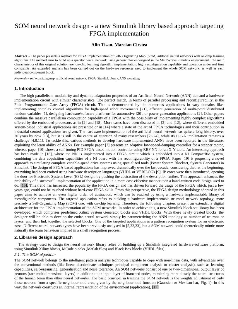
SOM neural network design - a new Simulink library based approach targeting FPGA implementation Alin Tisan, Marcian Cirstea Abstract - The paper presents a method for FPGA implementation of Self- Organizing Map (SOM) artificial neural networks with on-chip learning algorithm. The method aims to build up a specific neural network using generic blocks designed in the MathWorks Simulink environment. The main characteristics of this original solution are: on-chip learning algorithm implementation, high reconfiguration capability and operation under real time constraints. An extended analysis has been carried out on the hardware resources used to implement the whole SOM network, as well as each individual component block. Keywords – self organizing map, artificial neural network, FPGA, Simulink library, ANN modelling 1. Introduction The high parallelism, modularity and dynamic adaptation properties of an Artificial Neural Network (ANN) demand a hardware implementation circuit with similar characteristics. The perfect match, in terms of parallel processing and reconfigurability, is the Field Programmable Gate Array (FPGA) circuit. This is demonstrated by the numerous applications in vary domains like: implementing complex control algorithms for high-speed robot movements [21], efficient generation of multi-point distributed random variables [1], designing hardware/software platforms for automotive [20], or power generation applications [2]. Other papers combine the massive parallelism computation capability of a FPGA with the possibility of implementing highly complex algorithms offered by the embedded processors as in [2] and [18]. More cases have been discussed in [3] and [12], where different embedded system-based industrial applications are presented or in [14] where a state of the art of FPGA technologies and their contribution in industrial control applications are given. The hardware implementation of the artificial neural network has quite a long history, over 20 years by now [13], but it is still in the centre of attention of many researchers [23,24], while its FPGA implantation remains a challenge [4,8,11]. To tackle this, various methods to develop hardware implemented ANNs have been reported in the literature, exploiting the learn ability of ANNs. For example paper [7] presents an adaptive low-speed-damping controller for a stepper motor, whereas paper [10] shows a self-tuning PID FPGA-based motion controller using RBF NN for an X-Y table. An interesting approach has been made in [16], where the NN is implemented into a FPGA circuit which is embedded into a NI CompactRio system, combining the data acquisition capabilities of a NI board with the reconfigurability of a FPGA. Paper [19] is proposing a novel approach to simulating complete variable-speed drive systems using specialized tools (Power System Blockset, System Generator) in Simulink. The design of FPGA based applications has improved dramatically over the last decade, considering that, at the beginning, everything had been crafted using hardware description languages (VHDL or VERILOG) [9]. IP cores were then introduced, opening the door for Electronic System Level (ESL) design, by pushing the abstraction of the description further. This approach enhances the probability of a successful implementation of the application in a more cost-effective manner than a hand-written code design used to do, [15]. This trend has increased the popularity the FPGA design and has driven forward the usage of the FPGA which, just a few years ago, could not be touched without hard-core FPGA skills. From this perspective, the FPGA design methodology adopted in this paper aims to achieve an even higher order of abstraction, which can be reached by using a hardware implementable library of reconfigurable components. The targeted application refers to building a hardware implementable neuronal network topology, more precisely a Self-Organizing Map (SOM) one, with on-chip learning. Therefore, the following chapters present an extendable digital architecture for the FPGA implementation of the SOM networks. In order to achieve this, a new Simulink block set library has been developed, which comprises predefined Xilinx System Generator blocks and VHDL blocks. With these newly created blocks, the designer will be able to develop the entire neural network simply by parameterizing the ANN topology as number of neurons or layers, and then link together the selected blocks. One of the targeted applications is a pattern recognition system for an electronic nose. Different neural network types have been previously analysed in [5,22,23], but a SOM network could theoretically mimic more naturally the brain behaviour implied in a smell recognition process. 2. Libraries design approach The strategy used to design the neural network library relies on building up a Simulink integrated hardware-software platform, using Simulink Xilinx blocks, MCode blocks (Matlab files) and Black Box blocks (VHDL files). 2.1. The SOM algorithm The SOM network belongs to the intelligent pattern analysis techniques capable to cope with non-linear data, with advantages over the conventional methods (like linear discriminate technique, principal component analysis or cluster analysis), such as learning capabilities, self-organising, generalisation and noise tolerance. An SOM networks consist of one or two-dimensional output layer of neurons (rare multidimensional layers) in addition to an input layer of branched nodes, mimicking more closely the neural structures of the human brain than other neural networks. The basic principal in training the SOM network is the weights adjustment of only those neurons from a specific neighbourhood area, given by the neighbourhood function (Gaussian or Mexican hat, Fig. 1). In this way, the network constructs an internal representation of the environment (application), [17].
-
Upload
khangminh22 -
Category
Documents
-
view
1 -
download
0
Transcript of SOM neural network design - a new Simulink library based ...
SOM neural network design - a new Simulink library based approach targeting
FPGA implementation
Alin Tisan, Marcian Cirstea
Abstract - The paper presents a method for FPGA implementation of Self- Organizing Map (SOM) artificial neural networks with on-chip learning
algorithm. The method aims to build up a specific neural network using generic blocks designed in the MathWorks Simulink environment. The main
characteristics of this original solution are: on-chip learning algorithm implementation, high reconfiguration capability and operation under real time
constraints. An extended analysis has been carried out on the hardware resources used to implement the whole SOM network, as well as each
individual component block.
Keywords – self organizing map, artificial neural network, FPGA, Simulink library, ANN modelling
1. Introduction
The high parallelism, modularity and dynamic adaptation properties of an Artificial Neural Network (ANN) demand a hardware
implementation circuit with similar characteristics. The perfect match, in terms of parallel processing and reconfigurability, is the
Field Programmable Gate Array (FPGA) circuit. This is demonstrated by the numerous applications in vary domains like:
implementing complex control algorithms for high-speed robot movements [21], efficient generation of multi-point distributed
random variables [1], designing hardware/software platforms for automotive [20], or power generation applications [2]. Other papers
combine the massive parallelism computation capability of a FPGA with the possibility of implementing highly complex algorithms
offered by the embedded processors as in [2] and [18]. More cases have been discussed in [3] and [12], where different embedded
system-based industrial applications are presented or in [14] where a state of the art of FPGA technologies and their contribution in
industrial control applications are given. The hardware implementation of the artificial neural network has quite a long history, over
20 years by now [13], but it is still in the centre of attention of many researchers [23,24], while its FPGA implantation remains a
challenge [4,8,11]. To tackle this, various methods to develop hardware implemented ANNs have been reported in the literature,
exploiting the learn ability of ANNs. For example paper [7] presents an adaptive low-speed-damping controller for a stepper motor,
whereas paper [10] shows a self-tuning PID FPGA-based motion controller using RBF NN for an X-Y table. An interesting approach
has been made in [16], where the NN is implemented into a FPGA circuit which is embedded into a NI CompactRio system,
combining the data acquisition capabilities of a NI board with the reconfigurability of a FPGA. Paper [19] is proposing a novel
approach to simulating complete variable-speed drive systems using specialized tools (Power System Blockset, System Generator) in
Simulink. The design of FPGA based applications has improved dramatically over the last decade, considering that, at the beginning,
everything had been crafted using hardware description languages (VHDL or VERILOG) [9]. IP cores were then introduced, opening
the door for Electronic System Level (ESL) design, by pushing the abstraction of the description further. This approach enhances the
probability of a successful implementation of the application in a more cost-effective manner than a hand-written code design used to
do, [15]. This trend has increased the popularity the FPGA design and has driven forward the usage of the FPGA which, just a few
years ago, could not be touched without hard-core FPGA skills. From this perspective, the FPGA design methodology adopted in this
paper aims to achieve an even higher order of abstraction, which can be reached by using a hardware implementable library of
reconfigurable components. The targeted application refers to building a hardware implementable neuronal network topology, more
precisely a Self-Organizing Map (SOM) one, with on-chip learning. Therefore, the following chapters present an extendable digital
architecture for the FPGA implementation of the SOM networks. In order to achieve this, a new Simulink block set library has been
developed, which comprises predefined Xilinx System Generator blocks and VHDL blocks. With these newly created blocks, the
designer will be able to develop the entire neural network simply by parameterizing the ANN topology as number of neurons or
layers, and then link together the selected blocks. One of the targeted applications is a pattern recognition system for an electronic
nose. Different neural network types have been previously analysed in [5,22,23], but a SOM network could theoretically mimic more
naturally the brain behaviour implied in a smell recognition process.
2. Libraries design approach
The strategy used to design the neural network library relies on building up a Simulink integrated hardware-software platform,
using Simulink Xilinx blocks, MCode blocks (Matlab files) and Black Box blocks (VHDL files).
2.1. The SOM algorithm
The SOM network belongs to the intelligent pattern analysis techniques capable to cope with non-linear data, with advantages over
the conventional methods (like linear discriminate technique, principal component analysis or cluster analysis), such as learning
capabilities, self-organising, generalisation and noise tolerance. An SOM networks consist of one or two-dimensional output layer of
neurons (rare multidimensional layers) in addition to an input layer of branched nodes, mimicking more closely the neural structures
of the human brain than other neural networks. The basic principal in training the SOM network is the weights adjustment of only
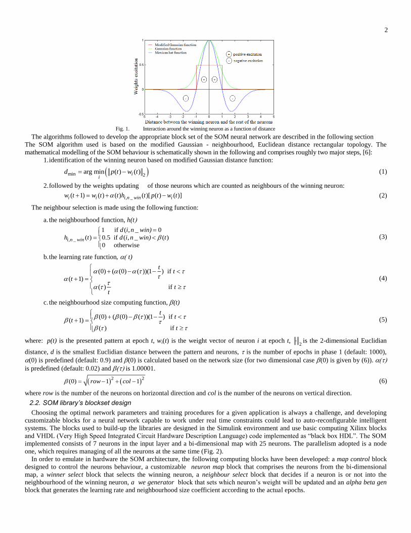
those neurons from a specific neighbourhood area, given by the neighbourhood function (Gaussian or Mexican hat, Fig. 1). In this
way, the network constructs an internal representation of the environment (application), [17].
2
Fig. 1. Interaction around the winning neuron as a function of distance
The algorithms followed to develop the appropriate block set of the SOM neural network are described in the following section
The SOM algorithm used is based on the modified Gaussian - neighbourhood, Euclidean distance rectangular topology. The
mathematical modelling of the SOM behaviour is schematically shown in the following and comprises roughly two major steps, [6]:
1. identification of the winning neuron based on modified Gaussian distance function:
min 2arg min ( ) ( )i
id p t w t (1)
2. followed by the weights updating of those neurons which are counted as neighbours of the winning neuron:
, _( 1) ( ) ( ) ( )[ ( ) ( )]i i i n win iw t w t t h t p t w t (2)
The neighbour selection is made using the following function:
a. the neighbourhood function, h(t
, _
1 if ( , _ 0
( ) 0.5 if ( , _ ( )
0 otherwisei n win
d i n win)
h t d i n win) t
(3)
b. the learning rate function t)
(0) ( (0) ( ))(1 ) if
( 1)
( ) if
tt
t
tt
(4)
c. the neighbourhood size computing function,(t)
(0) ( (0) ( ))(1 ) if ( 1)
( ) if
tt
t
t
(5)
where: p(t) is the presented pattern at epoch t, wi(t) is the weight vector of neuron i at epoch t, 2
is the 2-dimensional Euclidian
distance, d is the smallest Euclidian distance between the pattern and neurons, is the number of epochs in phase 1 (default: 1000),
(0) is predefined (default: 0.9) and (0) is calculated based on the network size (for two dimensional case (0) is given by (6)).
is predefined (default: 0.02) and is 1.00001.
2 2
(0) 1 1row col (6)
where row is the number of the neurons on horizontal direction and col is the number of the neurons on vertical direction.
2.2. SOM library’s blockset design
Choosing the optimal network parameters and training procedures for a given application is always a challenge, and developing
customizable blocks for a neural network capable to work under real time constraints could lead to auto-reconfigurable intelligent
systems. The blocks used to build-up the libraries are designed in the Simulink environment and use basic computing Xilinx blocks
and VHDL (Very High Speed Integrated Circuit Hardware Description Language) code implemented as “black box HDL”. The SOM
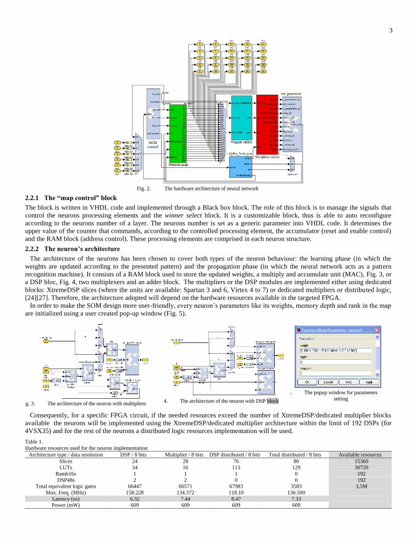
implemented consists of 7 neurons in the input layer and a bi-dimensional map with 25 neurons. The parallelism adopted is a node
one, which requires managing of all the neurons at the same time (Fig. 2).
In order to emulate in hardware the SOM architecture, the following computing blocks have been developed: a map control block
designed to control the neurons behaviour, a customizable neuron map block that comprises the neurons from the bi-dimensional
map, a winner select block that selects the winning neuron, a neighbour select block that decides if a neuron is or not into the
neighbourhood of the winning neuron, a we generator block that sets which neuron’s weight will be updated and an alpha beta gen
block that generates the learning rate and neighbourhood size coefficient according to the actual epochs.
3
Fig. 2. The hardware architecture of neural network
2.2.1 The “map control” block
The block is written in VHDL code and implemented through a Black box block. The role of this block is to manage the signals that
control the neurons processing elements and the winner select block. It is a customizable block, thus is able to auto reconfigure
according to the neurons number of a layer. The neurons number is set as a generic parameter into VHDL code. It determines the
upper value of the counter that commands, according to the controlled processing element, the accumulator (reset and enable control)
and the RAM block (address control). These processing elements are comprised in each neuron structure.
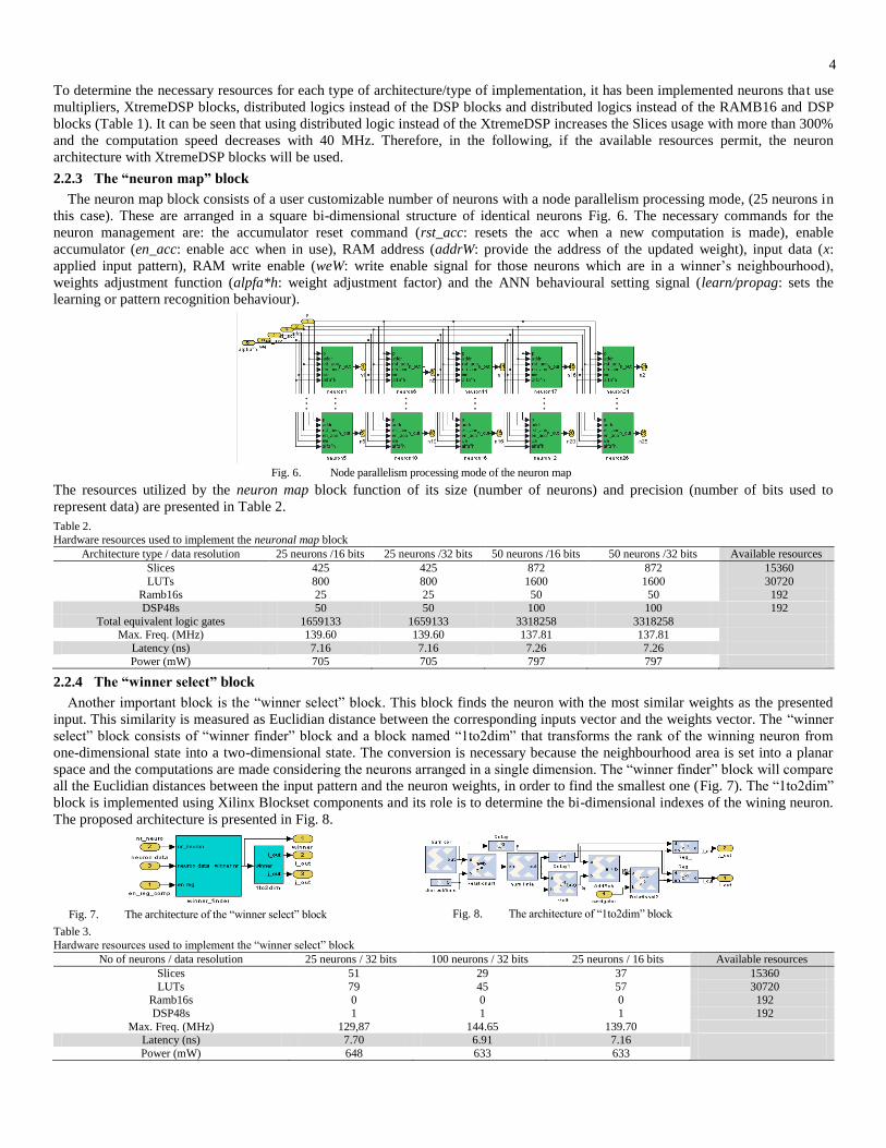
2.2.2 The neuron’s architecture
The architecture of the neurons has been chosen to cover both types of the neuron behaviour: the learning phase (in which the
weights are updated according to the presented pattern) and the propagation phase (in which the neural network acts as a pattern
recognition machine). It consists of a RAM block used to store the updated weights, a multiply and accumulate unit (MAC), Fig. 3, or
a DSP bloc, Fig. 4, two multiplexers and an adder block. The multipliers or the DSP modules are implemented either using dedicated
blocks: XtremeDSP slices (where the units are available: Spartan 3 and 6, Virtex 4 to 7) or dedicated multipliers or distributed logic,
[24][27]. Therefore, the architecture adopted will depend on the hardware resources available in the targeted FPGA.
In order to make the SOM design more user-friendly, every neuron’s parameters like its weights, memory depth and rank in the map
are initialized using a user created pop-up window (Fig. 5).
Fig. 3. The architecture of the neuron with multipliers
Fig. 4. The architecture of the neuron with DSP block
Fig. 5. The popup window for parameters
setting
Consequently, for a specific FPGA circuit, if the needed resources exceed the number of XtremeDSP/dedicated multiplier blocks
available the neurons will be implemented using the XtremeDSP/dedicated multiplier architecture within the limit of 192 DSPs (for
4VSX35) and for the rest of the neurons a distributed logic resources implementation will be used.
Table 1.
Hardware resources used for the neuron implementation
Architecture type / data resolution DSP / 8 bits Multiplier / 8 bits DSP distributed / 8 bits Total distributed / 8 bits Available resources
Slices 24 28 76 80 15360 LUTs 34 16 113 129 30720
Ramb16s 1 1 1 0 192
DSP48s Total equivalent logic gates
2 66447
2 66571
0 67983
0 3583
192 3,5M
Max. Freq. (MHz) 158.228 134.372 118.10 136.500
Latency (ns) 6.32 7.44 8.47 7.33 Power (mW) 609 609 609 609
4
To determine the necessary resources for each type of architecture/type of implementation, it has been implemented neurons that use
multipliers, XtremeDSP blocks, distributed logics instead of the DSP blocks and distributed logics instead of the RAMB16 and DSP
blocks (Table 1). It can be seen that using distributed logic instead of the XtremeDSP increases the Slices usage with more than 300%
and the computation speed decreases with 40 MHz. Therefore, in the following, if the available resources permit, the neuron
architecture with XtremeDSP blocks will be used.
2.2.3 The “neuron map” block
The neuron map block consists of a user customizable number of neurons with a node parallelism processing mode, (25 neurons in
this case). These are arranged in a square bi-dimensional structure of identical neurons Fig. 6. The necessary commands for the
neuron management are: the accumulator reset command (rst_acc: resets the acc when a new computation is made), enable
accumulator (en_acc: enable acc when in use), RAM address (addrW: provide the address of the updated weight), input data (x:
applied input pattern), RAM write enable (weW: write enable signal for those neurons which are in a winner’s neighbourhood),
weights adjustment function (alpfa*h: weight adjustment factor) and the ANN behavioural setting signal (learn/propag: sets the
learning or pattern recognition behaviour).
Fig. 6. Node parallelism processing mode of the neuron map
The resources utilized by the neuron map block function of its size (number of neurons) and precision (number of bits used to
represent data) are presented in Table 2.
Table 2. Hardware resources used to implement the neuronal map block
Architecture type / data resolution 25 neurons /16 bits 25 neurons /32 bits 50 neurons /16 bits 50 neurons /32 bits Available resources
Slices 425 425 872 872 15360
LUTs 800 800 1600 1600 30720 Ramb16s 25 25 50 50 192
DSP48s 50 50 100 100 192
Total equivalent logic gates 1659133 1659133 3318258 3318258 Max. Freq. (MHz) 139.60 139.60 137.81 137.81
Latency (ns) 7.16 7.16 7.26 7.26
Power (mW) 705 705 797 797
2.2.4 The “winner select” block
Another important block is the “winner select” block. This block finds the neuron with the most similar weights as the presented
input. This similarity is measured as Euclidian distance between the corresponding inputs vector and the weights vector. The “winner
select” block consists of “winner finder” block and a block named “1to2dim” that transforms the rank of the winning neuron from
one-dimensional state into a two-dimensional state. The conversion is necessary because the neighbourhood area is set into a planar
space and the computations are made considering the neurons arranged in a single dimension. The “winner finder” block will compare
all the Euclidian distances between the input pattern and the neuron weights, in order to find the smallest one (Fig. 7). The “1to2dim”
block is implemented using Xilinx Blockset components and its role is to determine the bi-dimensional indexes of the wining neuron.
The proposed architecture is presented in Fig. 8.
Fig. 7. The architecture of the “winner select” block
Fig. 8. The architecture of “1to2dim” block
Table 3. Hardware resources used to implement the “winner select” block
No of neurons / data resolution 25 neurons / 32 bits 100 neurons / 32 bits 25 neurons / 16 bits Available resources
Slices 51 29 37 15360
LUTs 79 45 57 30720 Ramb16s 0 0 0 192
DSP48s 1 1 1 192
Max. Freq. (MHz) 129,87 144.65 139.70 Latency (ns) 7.70 6.91 7.16
Power (mW) 648 633 633
5
The power consumed, the maximum processing frequency and the resources used to implement in FPGA the “winner_finder” block
considering different numbers of neurons and precisions are presented in Table 3.
2.2.5 The “neighbours select” block
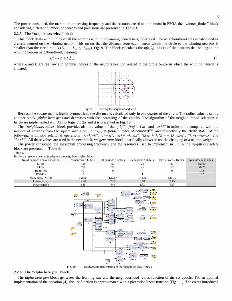
This block deals with finding of all the neurons within the winning neuron neighbourhood. The neighbourhood area is calculated as
a circle centred on the winning neuron. This means that the distance from each neuron within the circle to the winning neurons is
smaller than the circle radius (D1, ..., Dk ≤ Dmax), Fig. 9. The block calculates the n(ki,kj) indices of the neurons that belong to the
winning neuron neighbourhood, meaning:
2 2 2maxi jk k D (7)
where ki and kj are the row and column indices of the neurons position related to the circle centre in which the winning neuron is
situated.
Fig. 9. Setting the neighborhood area
Because the square map is highly symmetrical, the distance is calculated only in one quarter of the circle. The radius value is set by
another block (alpha beta gen) and decreases with the increasing of the epochs. The algorithm of the neighbourhood selection is
hardware implemented with Xilinx logic blocks and it is presented in Fig. 10
The “neighbours select” block provides also the values of the “j-kj”, “j+kj”, “i-ki” and “i+ki” in order to be compared with the
number of neurons from the square map side, i.e. “kmax = (total number of neurons)1/2
” and respectively the “truth state” of the
following arithmetic relational operations “ki=kj=0”, “j>=kj”, “kj+j<=kmax”, “ki^2 + kj^2 <= Dmax^2”, “ki+i<=kmax” and
“i>+ki”. All these values are used in the next block, we generator block, that finally allows or not the changing of a neuron weight.
The power consumed, the maximum processing frequency and the resources used to implement in FPGA the neighbours select
block are presented in Table 4. Table 4. Hardware resource used to implement the neighbours select block
No of neurons / data resolution 25 neurons / 32 bits 100 neurons / 32 bits 25 neurons / 16 bits 100 neurons / 16 bits Available resources
Slices 158 51 29 37 15360 LUTs 199 79 45 57 30720
Ramb16s 0 0 0 0 192
DSP48s 3 1 1 1 192 Max. Freq. (MHz) 128.54 129,87 144.65 139.70
Latency (ns) 7.78 7.70 6.91 7.15
Power (mW) 645 648 633 633
Fig. 10. Hardware implementation of the “neighbors select” block
2.2.6 The “alpha beta gen” block
The alpha beta gen block generates the learning rate and the neighbourhood radius function of the set epochs. For an optimal
implementation of the equation (4), the 1/τ function is approximated with a piecewise linear function (Fig. 11). The errors introduced
6
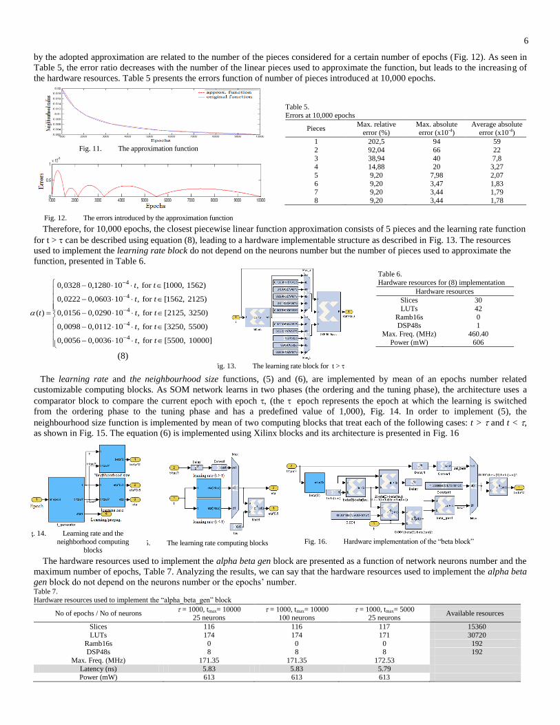
by the adopted approximation are related to the number of the pieces considered for a certain number of epochs (Fig. 12). As seen in
Table 5, the error ratio decreases with the number of the linear pieces used to approximate the function, but leads to the increasing of
the hardware resources. Table 5 presents the errors function of number of pieces introduced at 10,000 epochs.
Fig. 11. The approximation function
Fig. 12. The errors introduced by the approximation function
Table 5.
Errors at 10,000 epochs
Pieces Max. relative
error (%) Max. absolute error (x10-4)
Average absolute error (x10-4)
1 202,5 94 59
2 92,04 66 22
3 38,94 40 7,8 4 14,88 20 3,27
5 9,20 7,98 2,07
6 9,20 3,47 1,83 7 9,20 3,44 1,79
8 9,20 3,44 1,78
Therefore, for 10,000 epochs, the closest piecewise linear function approximation consists of 5 pieces and the learning rate function
for t > can be described using equation (8), leading to a hardware implementable structure as described in Fig. 13. The resources
used to implement the learning rate block do not depend on the neurons number but the number of pieces used to approximate the
function, presented in Table 6.
4
4
4
4
4
0,0328 0,1280 10 , for [1000, 1562)
0,0222 0,0603 10 , for [1562, 2125)
( ) 0,0156 0,0290 10 , for [2125, 3250)
0,0098 0,0112 10 , for [3250, 5500)
0,0056 0,0036 10 , for [5500,
t t
t t
t t t
t t
t t
10000]
(8) Fig. 13. The learning rate block for t >
Table 6.
Hardware resources for (8) implementation
Hardware resources
Slices 30
LUTs 42
Ramb16s 0 DSP48s 1
Max. Freq. (MHz) 460.40
Power (mW) 606
The learning rate and the neighbourhood size functions, (5) and (6), are implemented by mean of an epochs number related
customizable computing blocks. As SOM network learns in two phases (the ordering and the tuning phase), the architecture uses a
comparator block to compare the current epoch with epoch (the epoch represents the epoch at which the learning is switched
from the ordering phase to the tuning phase and has a predefined value of 1,000), Fig. 14. In order to implement (5), the
neighbourhood size function is implemented by mean of two computing blocks that treat each of the following cases: t > and t < , as shown in Fig. 15. The equation (6) is implemented using Xilinx blocks and its architecture is presented in Fig. 16
Fig. 14. Learning rate and the
neighborhood computing
blocks
Fig. 15. The learning rate computing blocks
Fig. 16. Hardware implementation of the “beta block”
The hardware resources used to implement the alpha beta gen block are presented as a function of network neurons number and the
maximum number of epochs, Table 7. Analyzing the results, we can say that the hardware resources used to implement the alpha beta
gen block do not depend on the neurons number or the epochs’ number. Table 7.
Hardware resources used to implement the “alpha_beta_gen” block
No of epochs / No of neurons = 1000, tmax= 10000
25 neurons = 1000, tmax= 10000
100 neurons = 1000, tmax= 5000
25 neurons Available resources
Slices 116 116 117 15360
LUTs 174 174 171 30720
Ramb16s 0 0 0 192 DSP48s 8 8 8 192
Max. Freq. (MHz) 171.35 171.35 172.53
Latency (ns) 5.83 5.83 5.79 Power (mW) 613 613 613
7
2.2.7 The “we generator” block
The we generator block compares the distances calculated by the neighbours select block with the current neighbourhood size and
sets or resets the write enable of the corresponding weights RAM addresses according to the position of each neuron in the map (the
write enable is set, we = ‘1’, if the neuron is in the winning neuron’s neighbourhood and reset if it is not). In order to make the
calculus in a one-dimensional way, the planar indexes (ki, kj) are convert into a linear one, k, using the formula stated in (9):
maxi jk k k k (9)
where, i is the raw index, j is the column index and kmax is the neurons number per raw (or column).
The block verifies if the control signals are 0 or 1 logic (1 logic means that the corresponding index is in the winner’s neighbourhood).
The outcome is a signal bus n bits wide, where n is equal with the number of neurons from the square map (Fig. 17). An ISE report
about the utilized resources has been presented in Table 8. These values are used for the overall resource estimation given in Table 9.
Fig. 17. Write enable (WE) signal bus
Table 8.
Hardware resources used for we_gen
block implementation
Hardware resources (% used)
Slices 30 (0.2%)
LUTs 42 (0.13%)
Ramb16s 0 (0%)
DSP48s 1 (0.5%)
Max. Freq. (MHz) 460.40
Power (mW) 606
A
Fig. 18. Simulink library of SOM network
3. The overall hardware implementation
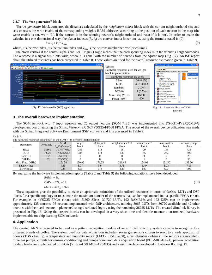
The SOM network with 7 input neurons and 25 output neurons (SOM 7_25) was implemented into DS-KIT-4VSX35MB-G
development board featuring the Xilinx Virtex-4 SX XC4VSX35-FF668 FPGA. The report of the overall device utilization was made
with the Xilinx Integrated Software Environment (ISE) software and it is presented in Table 9.
Table 9.
The hardware resources breakdown of the SOM 7_25 network implementation
Resources Available SOM
7_25 (% used) we gen block
alpha_beta block
neighbours select block
winner select block
map control block
neuronal map block
Slices 15360 1174 (7.6%) 245 116 98 29 146 425
LUTs 30720 1736 (5.6%) 314 174 130 45 262 800 Ramb16s 192 25 (13%) 0 0 0 0 0 25
DSP48s 192 62 (38%) 0 8 3 1 0 50
Max. Freq. (MHz) 101.54 120,96 171,35 210,65 154,01 121,50 139.60 Latency (ns) 9.85 8.27 5.84 4.75 6.49 8.23 7.16
Power (mW) 724 605 613 633 609 607 705
By analyzing the hardware implementation reports (Table 2 and Table 9) the following equations have been developed:
2 12
32 + 925
o
o
o
RAMs N
DSPs N
LUTs N
(10)
These equations give the possibility to make an aprioristic estimation of the utilized resources in terms of RAMs, LUTs and DSP
blocks for a specific topology or to estimate the maximum number of the neurons that can be implemented into a specific FPGA circuit.
For example, in 4VSX35 FPGA circuit with 15,360 Slices, 30,720 LUTs, 192 RAMB16s and 192 DSPs can be implemented
approximately 135 neurons: 95 neurons implemented with DSP architecture, utilizing 3965 LUTs from 30720 available and 42 other
neurons with their architecture implemented using distributed logics, using the remaining 26755 LUTs. The created Simulink library is
presented in Fig. 18. Using the created blocks can be developed in a very short time and flexible manner a customized, hardware
implementable on-chip learning SOM network.
4. Application
The created ANN is targeted to be used as a pattern recognition module of an artificial olfactory system capable to recognize four
different brands of coffee. The system used for data acquisition includes: seven gas sensors chosen to react to a wide spectrum of
odours (TGS - family), a temperature and humidity sensor (LM35, SY-HS-230), a test chamber (where all the sensors are mounted),
three gas pumps, circuits for sensors conditioning and pumps command, data acquisition board (PCI-MIO-16E-1), pattern recognition
module hardware implemented in FPGA (Virtex-4 SX MB - 4VSX35) and a user interface developed in Labview 8.2, Fig. 19.
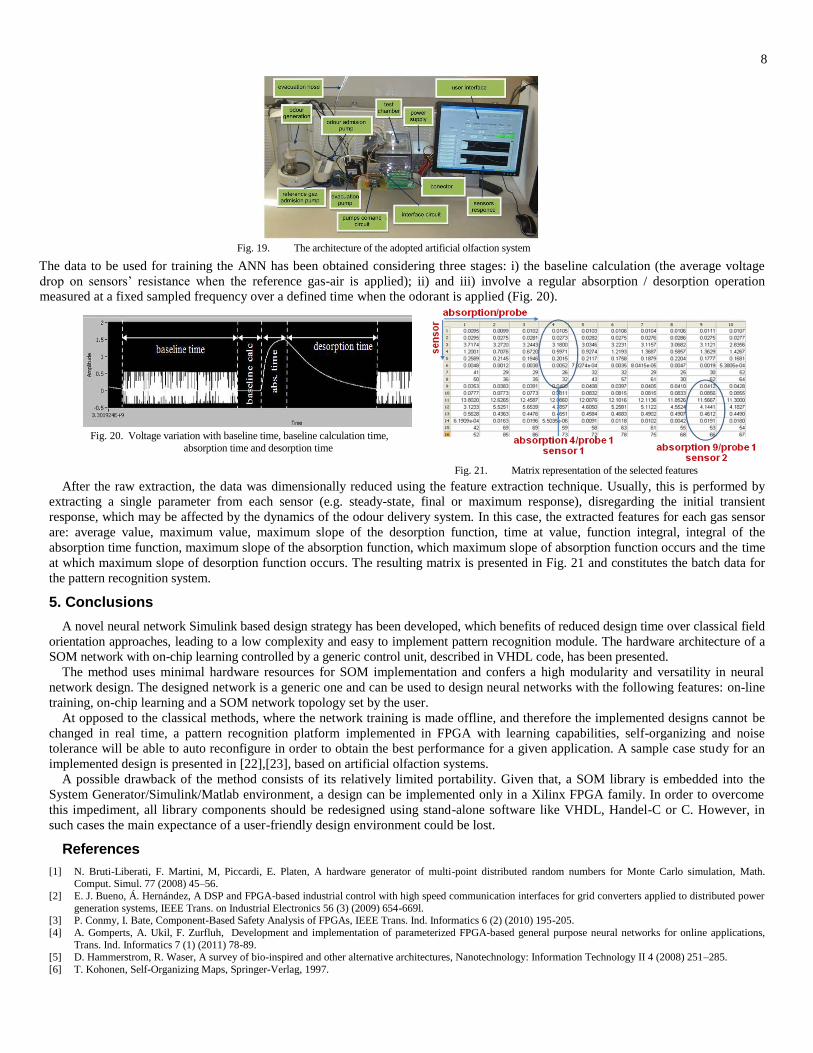
8
Fig. 19. The architecture of the adopted artificial olfaction system
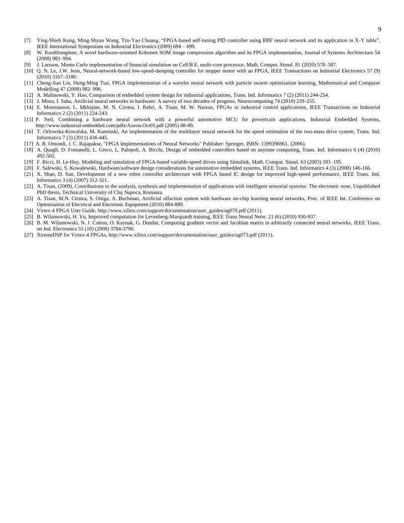
The data to be used for training the ANN has been obtained considering three stages: i) the baseline calculation (the average voltage
drop on sensors’ resistance when the reference gas-air is applied); ii) and iii) involve a regular absorption / desorption operation
measured at a fixed sampled frequency over a defined time when the odorant is applied (Fig. 20).
Fig. 20. Voltage variation with baseline time, baseline calculation time,
absorption time and desorption time
Fig. 21. Matrix representation of the selected features
After the raw extraction, the data was dimensionally reduced using the feature extraction technique. Usually, this is performed by
extracting a single parameter from each sensor (e.g. steady-state, final or maximum response), disregarding the initial transient
response, which may be affected by the dynamics of the odour delivery system. In this case, the extracted features for each gas sensor
are: average value, maximum value, maximum slope of the desorption function, time at value, function integral, integral of the
absorption time function, maximum slope of the absorption function, which maximum slope of absorption function occurs and the time
at which maximum slope of desorption function occurs. The resulting matrix is presented in Fig. 21 and constitutes the batch data for
the pattern recognition system.
5. Conclusions
A novel neural network Simulink based design strategy has been developed, which benefits of reduced design time over classical field
orientation approaches, leading to a low complexity and easy to implement pattern recognition module. The hardware architecture of a
SOM network with on-chip learning controlled by a generic control unit, described in VHDL code, has been presented.
The method uses minimal hardware resources for SOM implementation and confers a high modularity and versatility in neural
network design. The designed network is a generic one and can be used to design neural networks with the following features: on-line
training, on-chip learning and a SOM network topology set by the user.
At opposed to the classical methods, where the network training is made offline, and therefore the implemented designs cannot be
changed in real time, a pattern recognition platform implemented in FPGA with learning capabilities, self-organizing and noise
tolerance will be able to auto reconfigure in order to obtain the best performance for a given application. A sample case study for an
implemented design is presented in [22],[23], based on artificial olfaction systems.
A possible drawback of the method consists of its relatively limited portability. Given that, a SOM library is embedded into the
System Generator/Simulink/Matlab environment, a design can be implemented only in a Xilinx FPGA family. In order to overcome
this impediment, all library components should be redesigned using stand-alone software like VHDL, Handel-C or C. However, in
such cases the main expectance of a user-friendly design environment could be lost.
References
[1] N. Bruti-Liberati, F. Martini, M, Piccardi, E. Platen, A hardware generator of multi-point distributed random numbers for Monte Carlo simulation, Math. Comput. Simul. 77 (2008) 45–56.
[2] E. J. Bueno, Á. Hernández, A DSP and FPGA-based industrial control with high speed communication interfaces for grid converters applied to distributed power
generation systems, IEEE Trans. on Industrial Electronics 56 (3) (2009) 654-669l. [3] P. Conmy, I. Bate, Component-Based Safety Analysis of FPGAs, IEEE Trans. Ind. Informatics 6 (2) (2010) 195-205.
[4] A. Gomperts, A. Ukil, F. Zurfluh, Development and implementation of parameterized FPGA-based general purpose neural networks for online applications,
Trans. Ind. Informatics 7 (1) (2011) 78-89.
[5] D. Hammerstrom, R. Waser, A survey of bio-inspired and other alternative architectures, Nanotechnology: Information Technology II 4 (2008) 251–285.
[6] T. Kohonen, Self-Organizing Maps, Springer-Verlag, 1997.
9
[7] Ying-Shieh Kung, Ming-Shyan Wang, Tzu-Yao Chuang, “FPGA-based self-tuning PID controller using RBF neural network and its application in X-Y table”,
IEEE International Symposium on Industrial Electronics (2009) 694 – 699.
[8] W. Kurdthongmee, A novel hardware-oriented Kohonen SOM image compression algorithm and its FPGA implementation, Journal of Systems Architecture 54 (2008) 983–994.
[9] J. Larsson, Monte Carlo implementation of financial simulation on Cell/B.E. multi-core processor, Math. Comput. Simul. 81 (2010) 578–587.
[10] Q. N. Le, J.W. Jeon, Neural-network-based low-speed-damping controller for stepper motor with an FPGA, IEEE Transactions on Industrial Electronics 57 (9) (2010) 3167–3180.
[11] Cheng-Jian Lin, Hung-Ming Tsai, FPGA implementation of a wavelet neural network with particle swarm optimization learning, Mathematical and Computer
Modelling 47 (2008) 982–996. [12] A. Malinowski, Y. Hao, Comparison of embedded system design for industrial applications, Trans. Ind. Informatics 7 (2) (2011) 244-254.
[13] J. Misra, I. Saha, Artificial neural networks in hardware: A survey of two decades of progress, Neurocomputing 74 (2010) 239-255.
[14] E. Monmasson, L. Idkhajine, M. N. Cirstea, I. Bahri, A. Tisan, M. W. Naouar, FPGAs in industrial control applications, IEEE Transactions on Industrial Informatics 2 (2) (2011) 224-243.
[15] P. Neil, Combining a hardware neural network with a powerful automotive MCU for powertrain applications, Industrial Embedded Systems,
http://www.industrial-embedded.com/pdfs/Axeon.Oct05.pdf (2005) 88-89. [16] T. Orlowska-Kowalska, M. Kaminski, An implementation of the multilayer neural network for the speed estimation of the two-mass drive system, Trans. Ind.
Informatics 7 (3) (2011) 436-445.
[17] A. R. Omondi, J. C. Rajapakse, "FPGA Implementations of Neural Networks" Publisher: Springer, ISBN: 1399396961, (2006). [18] A. Quagli, D. Fontanelli, L. Greco, L. Palopoli, A. Bicchi, Design of embedded controllers based on anytime computing, Trans. Ind. Informatics 6 (4) (2010)
492-502.
[19] F. Ricci, H. Le-Huy, Modeling and simulation of FPGA-based variable-speed drives using Simulink, Math. Comput. Simul. 63 (2003) 183–195. [20] F. Salewski, S. Kowalewski, Hardware/software design considerations for automotive embedded systems, IEEE Trans. Ind. Informatics 4 (3) (2008) 146-166.
[21] X. Shao, D. Sun, Development of a new robot controller architecture with FPGA based IC design for improved high-speed performance, IEEE Trans. Ind.
Informatics 3 (4) (2007) 312-321. [22] A. Tisan, (2009), Contributions to the analysis, synthesis and implementation of applications with intelligent sensorial systems: The electronic nose, Unpublished
PhD thesis, Technical University of Cluj Napoca, Romania.
[23] A. Tisan, M.N. Cirstea, S. Oniga, A. Buchman, Artificial olfaction system with hardware on-chip learning neural networks, Proc. of IEEE Int. Conference on Optimisation of Electrical and Electronic Equipment (2010) 884-889.
[24] Virtex-4 FPGA User Guide, http://www.xilinx.com/support/documentation/user_guides/ug070.pdf (2011).
[25] B. Wilamowski, H. Yu, Improved computation for Levenberg-Marquardt training, IEEE Trans Neural Netw. 21 (6) (2010) 930-937. [26] B. M. Wilamowski, N. J. Cotton, O. Kaynak, G. Dundar, Computing gradient vector and Jacobian matrix in arbitrarily connected neural networks, IEEE Trans.
on Ind. Electronics 55 (10) (2008) 3784-3790.
[27] XtremeDSP for Virtex-4 FPGAs, http://www.xilinx.com/support/documentation/user_guides/ug073.pdf (2011).