Solution-Processed Zinc Oxide/Polyethylenimine Nanocomposites as Tunable Electron Transport Layers...
9
Solution-Processed Zinc Oxide/Polyethylenimine Nanocomposites as Tunable Electron Transport Layers for Highly Efficient Bulk Heterojunction Polymer Solar Cells Hsiu-Cheng Chen, Shu-Wei Lin, Jian-Ming Jiang, Yu-Wei Su, and Kung-Hwa Wei* Department of Materials Science and Engineering, National Chiao Tung University, 300 Hsinchu, Taiwan * S Supporting Information ABSTRACT: In this study, we employed polyethylenimine- doped sol-gel-processed zinc oxide composites (ZnO:PEI) as efficient electron transport layers (ETL) for facilitating electron extraction in inverted polymer solar cells. Using ultraviolet photoelectron spectroscopy, synchrotron grazing- incidence small-angle X-ray scattering and transmission electron microscopy, we observed that ZnO:PEI composite films’ energy bands could be tuned considerably by varying the content of PEI up to 7 wt %the conduction band ranged from 4.32 to 4.0 eVand the structural order of ZnO in the ZnO:PEI thin films would be enhanced to align perpendicular to the ITO electrode, particularly at 7 wt % PEI, facilitating electron transport vertically. We then prepared two types of bulk heterojunction systemsbased on poly(3-hexylthiophene) (P3HT):phenyl-C 61 -butryric acid methyl ester (PC 61 BM) and benzo[1,2-b:4,5-b ́ ]dithiophene-thiophene-2,1,3-benzooxadiazole (PBDTTBO):phenyl-C 71 -butryric acid methyl ester (PC 71 BM)that incorporated the ZnO:PEI composite layers. When using a composite of ZnO:PEI (93:7, w/w) as the ETL, the power conversion efficiency (PCE) of the P3HT:PC 61 BM (1:1, w/w) device improved to 4.6% from a value of 3.7% for the corresponding device that incorporated pristine ZnO as the ETLa relative increase of 24%. For the PBDTTBO:PC 71 BM (1:2, w/w) device featuring the same amount of PEI blended in the ETL, the PCE improved to 8.7% from a value of 7.3% for the corresponding device that featured pure ZnO as its ETLa relative increase of 20%. Accordingly, ZnO:PEI composites can be effective ETLs within organic photovoltaics. KEYWORDS: photovoltaics, conduction band, zinc oxide: polyethylenimine nanocomposites, electron transport layer, grazing-incidence small-angle X-ray scattering ■ INTRODUCTION Organic photovoltaics (OPVs) have progressed significantly in terms of their power conversion efficiencies (PCEs) as a result of recent developments in their active layer materials, interfacial layers, and device architecture. 1-9 Although the active layer material (e.g., conjugated polymers and fullerenes) has a critical effect on the PCE, the electron transfer layer (ETL), 10-13 used as an interfacial layer between the active layer and cathode, also plays an important role because it can establish ohmic contact, modify the internal electric field, and minimize the carrier recombination rate in an OPV. 14-17 In a conventional device structure, the use of an air-sensitive ETL makes it impossible to perform the fabrication process in air, thereby necessitating that thermal evaporation techniques be performed under vacuum, increasing the complexity and fabrication cost of these devices. To solve this problem, inverted device structures have been designed, reversing the transport direction of the electrons and holes by adopting a metal having a high work function as the anode on top of the device that comprised ITO as the cathode in the bottom. 18,19 Zinc oxide (ZnO) 20-26 has been used as an ETL in inverted OPV devices as a result of its air-stability, high transparency to visible light, high electron affinity, and tunable electrical optical properties. On the other hand, organic polymers containing simple aliphatic amine groups, namely, polyethylenimine ethoxylated (PEIE) and polyethylenimine (PEI), have also been employed as ETLs to decrease the work function of indium tin oxide (ITO) and lower the interfacial energy barrier for electron transport from the active layer to the electrode approaching ohmic contactby forming a thin interfacial dipole between the active layer and the ETL. 27-30 Moreover, the PCEs of devices can be improved significantly when using a conjugated polymer electrolyte as an ETL in an inverted structure. 31,32 Although ZnO is a suitable material for an ETL, the application of ZnO nanoparticles (NPs) can, however, lead to electron trapping and a high series resistance because of the presence of traps/defects with adsorbed oxygen on the NP Received: January 20, 2015 Accepted: February 20, 2015 Published: February 20, 2015 Research Article www.acsami.org © 2015 American Chemical Society 6273 DOI: 10.1021/acsami.5b00521 ACS Appl. Mater. Interfaces 2015, 7, 6273-6281
Transcript of Solution-Processed Zinc Oxide/Polyethylenimine Nanocomposites as Tunable Electron Transport Layers...
Solution-Processed Zinc Oxide/Polyethylenimine Nanocomposites asTunable Electron Transport Layers for Highly Efficient BulkHeterojunction Polymer Solar CellsHsiu-Cheng Chen, Shu-Wei Lin, Jian-Ming Jiang, Yu-Wei Su, and Kung-Hwa Wei*
Department of Materials Science and Engineering, National Chiao Tung University, 300 Hsinchu, Taiwan
*S Supporting Information
ABSTRACT: In this study, we employed polyethylenimine-doped sol−gel-processed zinc oxide composites (ZnO:PEI) asefficient electron transport layers (ETL) for facilitatingelectron extraction in inverted polymer solar cells. Usingultraviolet photoelectron spectroscopy, synchrotron grazing-incidence small-angle X-ray scattering and transmissionelectron microscopy, we observed that ZnO:PEI compositefilms’ energy bands could be tuned considerably by varying thecontent of PEI up to 7 wt %the conduction band rangedfrom 4.32 to 4.0 eVand the structural order of ZnO in theZnO:PEI thin films would be enhanced to align perpendicularto the ITO electrode, particularly at 7 wt % PEI, facilitatingelectron transport vertically. We then prepared two types of bulk heterojunction systemsbased on poly(3-hexylthiophene)(P3HT):phenyl-C61-butryric acid methyl ester (PC61BM) and benzo[1,2-b:4,5-b]dithiophene-thiophene-2,1,3-benzooxadiazole(PBDTTBO):phenyl-C71-butryric acid methyl ester (PC71BM)that incorporated the ZnO:PEI composite layers. When using acomposite of ZnO:PEI (93:7, w/w) as the ETL, the power conversion efficiency (PCE) of the P3HT:PC61BM (1:1, w/w) deviceimproved to 4.6% from a value of 3.7% for the corresponding device that incorporated pristine ZnO as the ETLa relativeincrease of 24%. For the PBDTTBO:PC71BM (1:2, w/w) device featuring the same amount of PEI blended in the ETL, the PCEimproved to 8.7% from a value of 7.3% for the corresponding device that featured pure ZnO as its ETLa relative increase of20%. Accordingly, ZnO:PEI composites can be effective ETLs within organic photovoltaics.
KEYWORDS: photovoltaics, conduction band, zinc oxide: polyethylenimine nanocomposites, electron transport layer,grazing-incidence small-angle X-ray scattering
■ INTRODUCTION
Organic photovoltaics (OPVs) have progressed significantly interms of their power conversion efficiencies (PCEs) as a resultof recent developments in their active layer materials, interfaciallayers, and device architecture.1−9 Although the active layermaterial (e.g., conjugated polymers and fullerenes) has a criticaleffect on the PCE, the electron transfer layer (ETL),10−13 usedas an interfacial layer between the active layer and cathode, alsoplays an important role because it can establish ohmic contact,modify the internal electric field, and minimize the carrierrecombination rate in an OPV.14−17 In a conventional devicestructure, the use of an air-sensitive ETL makes it impossible toperform the fabrication process in air, thereby necessitating thatthermal evaporation techniques be performed under vacuum,increasing the complexity and fabrication cost of these devices.To solve this problem, inverted device structures have beendesigned, reversing the transport direction of the electrons andholes by adopting a metal having a high work function as theanode on top of the device that comprised ITO as the cathodein the bottom.18,19
Zinc oxide (ZnO)20−26 has been used as an ETL in invertedOPV devices as a result of its air-stability, high transparency tovisible light, high electron affinity, and tunable electrical opticalproperties. On the other hand, organic polymers containingsimple aliphatic amine groups, namely, polyethylenimineethoxylated (PEIE) and polyethylenimine (PEI), have alsobeen employed as ETLs to decrease the work function ofindium tin oxide (ITO) and lower the interfacial energy barrierfor electron transport from the active layer to the electrodeapproaching ohmic contactby forming a thin interfacialdipole between the active layer and the ETL.27−30 Moreover,the PCEs of devices can be improved significantly when using aconjugated polymer electrolyte as an ETL in an invertedstructure.31,32 Although ZnO is a suitable material for an ETL,the application of ZnO nanoparticles (NPs) can, however, leadto electron trapping and a high series resistance because of thepresence of traps/defects with adsorbed oxygen on the NP
Received: January 20, 2015Accepted: February 20, 2015Published: February 20, 2015
Research Article
www.acsami.org
© 2015 American Chemical Society 6273 DOI: 10.1021/acsami.5b00521ACS Appl. Mater. Interfaces 2015, 7, 6273−6281

surfaces.33,34 To overcome this obstacle, a double-layerstructure that features a thin polymer layer of, for example,poly[(9,9-bis[3′-(N,N-dimethylamino)propyl]-2,7-fluorene)-alt-2,7-(9,9-dioctyl-fluorene)] dibromide (PFN-Br),35,36
PEI,37,38 or PEIE,39−42 on top of the metal oxide layer, suchas ZnO layer, can be adopted to decrease the work function ofthe metal oxide and further reduce the energy barrier for chargetransport from the active layer to the ETL. When comparedwith devices based on a single metal oxide layer, the PCEs ofcorresponding devices containing a metal oxide/polymerbilayer as the ETL can be increased by approximately 10−40%, depending on the nature of the conjugated polymer in theactive layer.An alternative approach is to blend polymers that possess
polar functional groups for interacting electrostatically withsurfaces of ZnO to form composites as ETL for polymer solarcells. Nevertheless, only a few reports have appeared in which acomposite ETL has been used instead of a bilayer ETL in aninverted polymer solar cell. For examples, polyvinylpyrrolidone(PVP),28 poly(ethylene glycol) (PEG),43 and poly(ethyleneoxide) (PEO)44 have been blended with the ZnO films to forma composite interfacial layer in a polymer solar cell; the PCEs ofsuch devices containing a composite ETL layer can be increasedby 25% relative to that of the corresponding device containing asingle metal oxide layer.In this present study, we blended a sol−gel ZnO solution
with a PEI solution prior to their final consolidation into thecomposite layer as the ETL layer. Relative to PEIE, PEI has ahigher [N+]/[C] ratio,45 implying more protonated aminogroups that can induce stronger electrostatic or dipole−dipoleinteractions with a ZnO surface.37 As a result, we expected thatthe use of ZnO:PEI composites as ETLs would improve thedevice performance of inverted polymer solar cells based ontwo different bulk heterojunction (BHJ) active layerspoly(3-hexylthiophene) (P3HT):phenyl-C61-butryric acid methyl ester(PC61BM) (system 1) and benzo[1,2-b:4,5-b]dithiophene-thiophene-2,1,3-benzooxadiazole (PBDTTBO):phenyl-C71-bu-tryric acid methyl ester (PC71BM) (system 2). We usedultraviolet photoelectron spectroscopy (UPS) to characterizethe conduction band energy of the ZnO:PEI composite layers,and grazing-incidence small-angle X-ray scattering (GISAXS)and TEM to decipher the nanostructures of our ZnO:PEIcomposite ETLs and to discern how the content of PEIinfluenced the device performance.
■ EXPERIMENTAL SECTIONMaterials. Zinc acetate dihydrate [Zn(CH3COO)2·2H2O (1 g)]
and ethanolamine (0.28 g) were dissolved in 2-methoxyethanol (10mL) under vigorous stirring for 12 h in exposure to the air.21 Thisstock solution remained transparent and stable for more than onemonth. For preparation of the composite ETL structure device, thestock solution was mixed with a set amount of PEI (branched; averageMn = ca. 10k; Sigma−Aldrich) and stirred vigorously for 12 h. Forpreparation of the bilayer ETL structure device, the branched-PEIsolution was diluted with DI water to give a 0.01 wt % solution. Forthe preparation of the BHJ systems, PBDTTBO (Mn = 268.8k; PDI =4.4) was synthesized using a previously reported method,46 whileregioregular P3HT was purchased from Rieke Metals. PC61BM andPC71BM were obtained from FEM Technology. The blend solutionsof the active layer were prepared by dissolving P3HT (10 mg mL−1)with PC61BM (10 mg mL−1) and PBDTTBO (10 mg mL−1) withPC71BM (20 mg mL−1) in dichlorobenzene (DCB), resulting in a totalconcentration of 4 and 3 wt %, respectively. The blend solutions werestirred continuously in a glovebox for 12 h at 90 °C to completelydissolve the polymer and fullerene.
Solar Cell Device Fabrication and Characterization. Thepatterned ITO glass substrate (5 Ω cm−2, Merck) was cleaned throughsequential ultrasonic treatments with detergent, DI water, acetone, andisopropanol and then dried under a flow of N2. ZnO and ZnO:PEIwere spin-coated on the UV ozone-treated ITO for 15 min and theannealed at 200 °C for 1 h. The ZnO/PEI structures were preparedusing methods reported previously.37 PEI layers (thickness: 2 nm)were coated on top of the ZnO layers that had been prepared throughsol−gel processing. The substrates were then transferred into a dry N2-filled glovebox. The ETLs were deposited at a thickness ofapproximately 40 nm, followed by deposition of the active layers.The active layers, formed from either a P3HT:PC61BM orPBDTTBO:PC71BM blend solution in DCB, were prepared in aglovebox and then spin-casted on top of the ETL film. After spincoating, the P3HT:PC61BM film was annealed in a glass Petri dish atroom temperature for 30 min and then dried at 150 °C for 15 minunder a N2 atmosphere. The PBDTTBO:PC71BM film was aged for 30min under ambient conditions prior to the deposition of the anode.The active films of P3HT:PC61BM and PBDTTBO:PC71BM hadthicknesses of approximately 150 and 100 nm, respectively. The BHJdevices were fabricated with structures incorporating ITO/ZnO, ITO/ZnO:PEI (composite), or ZnO/PEI (bilayer). Device fabrication wascomplete after thermal evaporation of the P-type material (MoO3, 10nm) and the anode (Ag, 100 nm) under high vacuum (ca. 10−7 Torr).A shadow mask was used during the thermal evaporation process todefine a device area of 0.1 cm2.
The current density−voltage (J−V) characteristics were measuredusing a Keithley 2400 source meter. The photocurrent was measuredunder simulated AM 1.5 G illumination at 100 mW cm−2 using a Xelamp-based 150-W solar simulator (Newport 66902). A calibrated Siphotodiode with a KG-5 filter was employed to confirm theillumination intensity. The spectral mismatch factor was calculatedby comparing the solar simulator spectrum with the AM1.5G (ASTMG173) spectrum. External quantum efficiencies (EQEs) weremeasured using an SRF50 system (Optosolar, Germany). A calibratedmonosilicon diode was used as a reference exhibiting a response at300−800 nm.
Electron Device Characterization of ZnO:PEI CompositeFilms. Space charge limited currents (SCLC) for the ZnO:PEIcomposite films have measured in electron only devices with aconfiguration of ITO/ZnO:PEI/Al (100 nm). The devices wereprepared following the same procedure described in the ExperimentalSection for the photovoltaic devices, except that of the metal electrode.The ZnO:PEI films were prepared by spin-coating on UV ozone-treated ITO for 15 min and annealed at 200 °C for 1 h. The preparedZnO:PEI films on ITO/glass were transferred to a vacuumevaporation chamber for the deposition of the Al (100 nm) topelectrodes to complete the electron-only devices. The dark J−Vcharacteristics measurements were performed using a Keithley 2400source unit and calculated using SCLC Model.
Characterization of the ZnO:PEI Nanocomposite Layers. AUV−vis spectrophotometer (Hitachi U-4100) equipped with anintegrating sphere was used to acquire transmission spectra. Afluorescence spectrophotometer (Hitachi F-7000) was used to recordthe steady state PL spectra under ambient conditions in air. The filmmorphology was determined through AFM in the tapping mode(Veeco Innova) under ambient conditions and the field emissionscanning electron microscopy (FE-SEM, JEOL JSM-6700) undervacuum conditions. TEM images were recorded using an FEI TecnaiSpirit TWIN instrument operated at 120 keV. TEM samples wereprepared on a C-covered Ni TEM micro grid. GISAXS analysis [X-raybeam energy: 8 keV (λ = 1.550 Å); incident angle: 0.2°; sample-to-detector distance: 5 m] over the sampled volume was conducted at theBL23A SWAXS end-station of the National Synchrotron RadiationResearch Center (NSRRC), Hsinchu, Taiwan. The samples wereprepared on 2 cm × 2 cm ITO substrates through spin-coating ofZnO:PEI solutions. The states of the Zn, O, and N atoms in the thinfilm were examined using XPS (ULVAC-PHI Quantera SXM). UPSwas performed using He irradiation (photon energy: 21.21 eV) at asample bias of 4 V. Synchrotron XRR analyses were performed at the
ACS Applied Materials & Interfaces Research Article
DOI: 10.1021/acsami.5b00521ACS Appl. Mater. Interfaces 2015, 7, 6273−6281
6274
wiggler beamline BL-17B1 using an eight-circle diffractometer at theNational Synchrotron Radiation Research Center (NSRRC), Hsinchu,Taiwan.
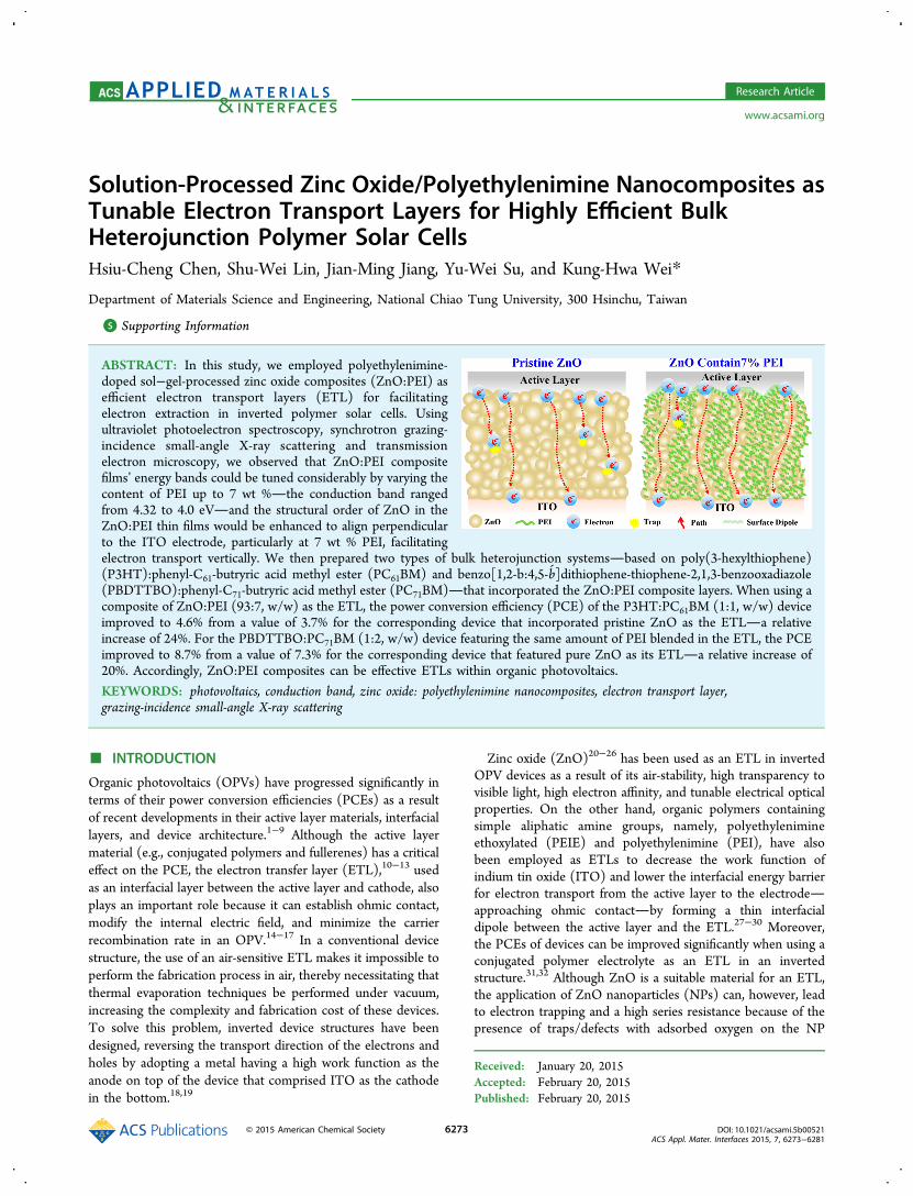
■ RESULTS AND DISCUSSIONFigure 1 displays the inverted BHJ system 1 or 2 devicestructure we tested in this study. As the electron donor, weused P3HT or PBDTTBO,46 prepared through polymerizationof electron-rich benzo[1,2-b:4,5-b′]dithiophene (BDT) andelectron-deficient 2,1,3-benzooxadiazole (BO) moieties; as theelectron acceptor, we used PC61BM or PC71BM; BHJ systems 1and 2 indicate P3HT:PC61BM and PBDTTBO:PC71BM,respectively. We employed the nanocomposite ZnO:PEI layersas the underneath ETL, and deposited high-work-functionmolybdenum trioxide (MoO3) on top of the bulk hetero-junction (BHJ) layer as the hole transport layer. We preparedthe ZnO:PEI composites through sol−gel processing of ZnOwith PEI and then spin-coated them on top of the ITO.Subsequently, the active layer was spin-coated on top of theZnO:PEI, followed by thermal evaporation of layers ofmolybdenum oxide (MoO3) and silver (Ag). The detailedsteps for fabricating the inverted bulk heterojunction (BHJ)polymer:fullerene solar cells with the PEI-blended ZnO layersare provided in the Experimental Section. The final devicestructure was glass/ITO/ZnO:PEI/BHJ system 1 or 2/MoO3/Ag. We estimated the band gaps of our ZnO:PEI filmsincorporating 0%, 1%, 3%, 5%, 7%, and 9% (w/w) PEI fromtheir transmittance spectra (see Supporting Information FigureS1), obtaining values of 3.32, 3.25, 3.29, 3.33, 3.40, and 3.39 eV,respectively. We applied UPS (photon source: He I, 21.21 eV)to determine the valence band energies of our ZnO:PEI films(see Supporting Information Figure S2). For the valence bandenergy, Φ, we applied the formula
υΦ = − Δh E
where hυ was equal to 21.21 eV, with
Δ = −E E E1 2
The upper emission onset energies (E1) of the ZnO:PEIfilms appeared with high-energy-side shoulder tangents in thecutoff region; the lower emission onset energies (E2) of thesecondary photoelectrons appeared in the valence band region.
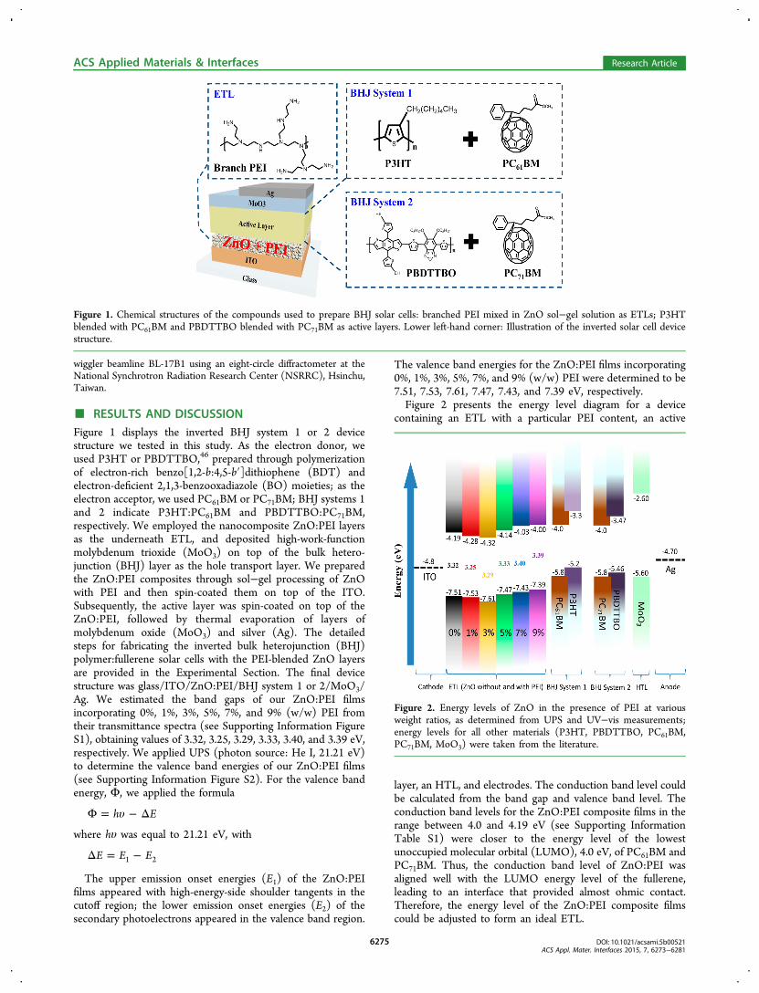
The valence band energies for the ZnO:PEI films incorporating0%, 1%, 3%, 5%, 7%, and 9% (w/w) PEI were determined to be7.51, 7.53, 7.61, 7.47, 7.43, and 7.39 eV, respectively.Figure 2 presents the energy level diagram for a device
containing an ETL with a particular PEI content, an active
layer, an HTL, and electrodes. The conduction band level couldbe calculated from the band gap and valence band level. Theconduction band levels for the ZnO:PEI composite films in therange between 4.0 and 4.19 eV (see Supporting InformationTable S1) were closer to the energy level of the lowestunoccupied molecular orbital (LUMO), 4.0 eV, of PC61BM andPC71BM. Thus, the conduction band level of ZnO:PEI wasaligned well with the LUMO energy level of the fullerene,leading to an interface that provided almost ohmic contact.Therefore, the energy level of the ZnO:PEI composite filmscould be adjusted to form an ideal ETL.
Figure 1. Chemical structures of the compounds used to prepare BHJ solar cells: branched PEI mixed in ZnO sol−gel solution as ETLs; P3HTblended with PC61BM and PBDTTBO blended with PC71BM as active layers. Lower left-hand corner: Illustration of the inverted solar cell devicestructure.
Figure 2. Energy levels of ZnO in the presence of PEI at variousweight ratios, as determined from UPS and UV−vis measurements;energy levels for all other materials (P3HT, PBDTTBO, PC61BM,PC71BM, MoO3) were taken from the literature.
ACS Applied Materials & Interfaces Research Article
DOI: 10.1021/acsami.5b00521ACS Appl. Mater. Interfaces 2015, 7, 6273−6281
6275
To investigate the passivation effect of PEI modification onthe surface defects of the ZnO films, we recorded thephotoluminescence (PL) spectra of our ZnO:PEI films. Figure3 reveals that a strong emission peak appeared near the band
edge at 364 nm, arising from recombination of excitons orradiative annihilation of excitons, while no apparent emissionappeared near 535 nm owing to trap emission or surfacerecombination,2,22,47 indicating that very few oxygen vacancydefects48,49 were present in our ZnO thin films. The PL peakemission intensity increased upon increasing the ratio ofincorporated PEI. Therefore, we suspected that the impact ofoxygen vacancy defects on the overall device efficiency wouldbe negligible. Typically, in a solar cell device, a decrease in thecontent of traps in the electron transport layer wouldpresumably decrease the possibility of trap-assisted interfacialrecombination of carriers and, consequently, enhance the valueof short current density (Jsc) and the fill factor (FF), therebyimproving the power conversion efficiency (PCE) of thedevice.44,50 The UV−vis absorption spectra of various filmstructures: a ZnO:PEI/active layer film, a composite ZnO:PEIfilm, and a ZnO/PEI bilayer film (see Supporting InformationFigure S3). Notably, the ZnO:PEI composite layer and ZnO/PEI bilayer provided similar or almost overlapping opticalabsorption spectra. The SEM images reveal that the pristinesample featured ripples on its surface; increasing the PEIcontent (1−5%) lessened the formation of ripples, whereasgranular features appeared in the presence of 7% PEI (seeSupporting Information Figure S4).Figure 4 presents AFM surface topography images of the
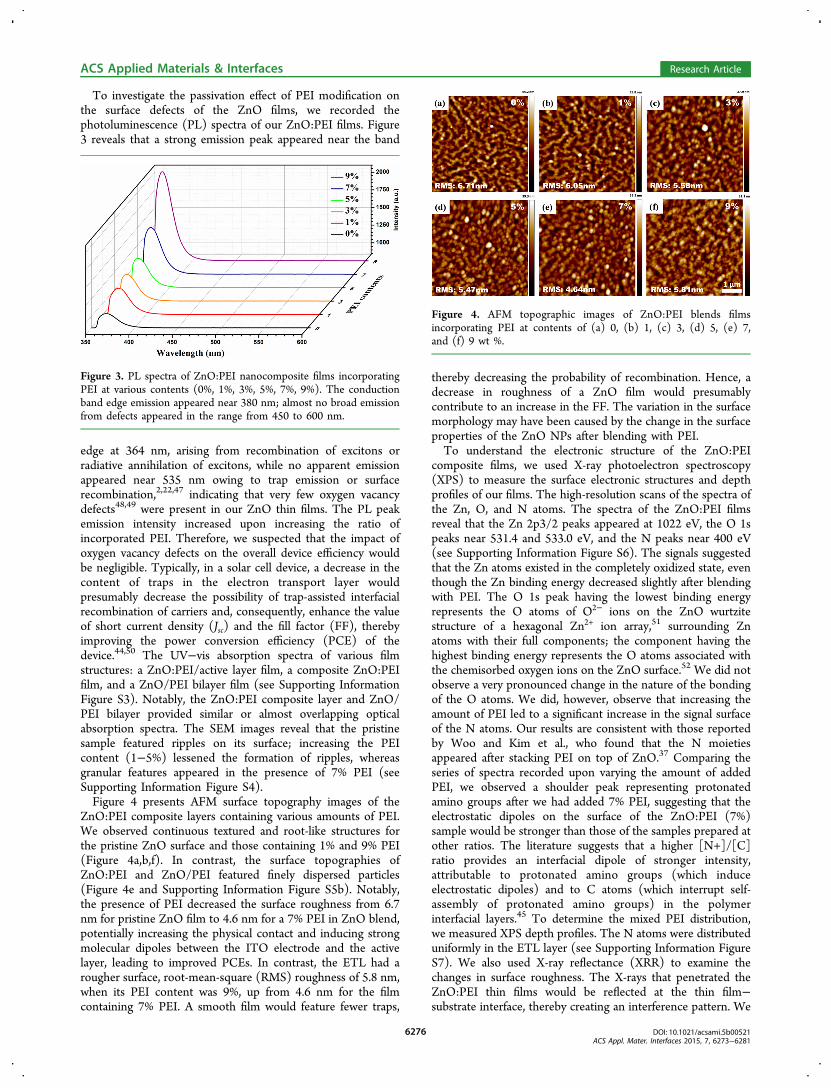
ZnO:PEI composite layers containing various amounts of PEI.We observed continuous textured and root-like structures forthe pristine ZnO surface and those containing 1% and 9% PEI(Figure 4a,b,f). In contrast, the surface topographies ofZnO:PEI and ZnO/PEI featured finely dispersed particles(Figure 4e and Supporting Information Figure S5b). Notably,the presence of PEI decreased the surface roughness from 6.7nm for pristine ZnO film to 4.6 nm for a 7% PEI in ZnO blend,potentially increasing the physical contact and inducing strongmolecular dipoles between the ITO electrode and the activelayer, leading to improved PCEs. In contrast, the ETL had arougher surface, root-mean-square (RMS) roughness of 5.8 nm,when its PEI content was 9%, up from 4.6 nm for the filmcontaining 7% PEI. A smooth film would feature fewer traps,
thereby decreasing the probability of recombination. Hence, adecrease in roughness of a ZnO film would presumablycontribute to an increase in the FF. The variation in the surfacemorphology may have been caused by the change in the surfaceproperties of the ZnO NPs after blending with PEI.To understand the electronic structure of the ZnO:PEI
composite films, we used X-ray photoelectron spectroscopy(XPS) to measure the surface electronic structures and depthprofiles of our films. The high-resolution scans of the spectra ofthe Zn, O, and N atoms. The spectra of the ZnO:PEI filmsreveal that the Zn 2p3/2 peaks appeared at 1022 eV, the O 1speaks near 531.4 and 533.0 eV, and the N peaks near 400 eV(see Supporting Information Figure S6). The signals suggestedthat the Zn atoms existed in the completely oxidized state, eventhough the Zn binding energy decreased slightly after blendingwith PEI. The O 1s peak having the lowest binding energyrepresents the O atoms of O2− ions on the ZnO wurtzitestructure of a hexagonal Zn2+ ion array,51 surrounding Znatoms with their full components; the component having thehighest binding energy represents the O atoms associated withthe chemisorbed oxygen ions on the ZnO surface.52 We did notobserve a very pronounced change in the nature of the bondingof the O atoms. We did, however, observe that increasing theamount of PEI led to a significant increase in the signal surfaceof the N atoms. Our results are consistent with those reportedby Woo and Kim et al., who found that the N moietiesappeared after stacking PEI on top of ZnO.37 Comparing theseries of spectra recorded upon varying the amount of addedPEI, we observed a shoulder peak representing protonatedamino groups after we had added 7% PEI, suggesting that theelectrostatic dipoles on the surface of the ZnO:PEI (7%)sample would be stronger than those of the samples prepared atother ratios. The literature suggests that a higher [N+]/[C]ratio provides an interfacial dipole of stronger intensity,attributable to protonated amino groups (which induceelectrostatic dipoles) and to C atoms (which interrupt self-assembly of protonated amino groups) in the polymerinterfacial layers.45 To determine the mixed PEI distribution,we measured XPS depth profiles. The N atoms were distributeduniformly in the ETL layer (see Supporting Information FigureS7). We also used X-ray reflectance (XRR) to examine thechanges in surface roughness. The X-rays that penetrated theZnO:PEI thin films would be reflected at the thin film−substrate interface, thereby creating an interference pattern. We
Figure 3. PL spectra of ZnO:PEI nanocomposite films incorporatingPEI at various contents (0%, 1%, 3%, 5%, 7%, 9%). The conductionband edge emission appeared near 380 nm; almost no broad emissionfrom defects appeared in the range from 450 to 600 nm.
Figure 4. AFM topographic images of ZnO:PEI blends filmsincorporating PEI at contents of (a) 0, (b) 1, (c) 3, (d) 5, (e) 7,and (f) 9 wt %.
ACS Applied Materials & Interfaces Research Article
DOI: 10.1021/acsami.5b00521ACS Appl. Mater. Interfaces 2015, 7, 6273−6281
6276
could take advantage of the resulting period of oscillations inthe XRR pattern, also known as Kiessig fringes, to determinethe film thickness or roughness, in which the intensity of itsreflected X-rays will drop off rapidly (lower slope) uponincreasing the angle of incidence if a film surface is rough.53
Among our tested samples, the XRR curves of the 7%PEI-blended ZnO films exhibited the most striking oscillations andlower slopes, providing direct evidence that PEI treatmentdecreased the roughness of the films (see SupportingInformation Figure S8).Although a clear indication of the structural changes of a film
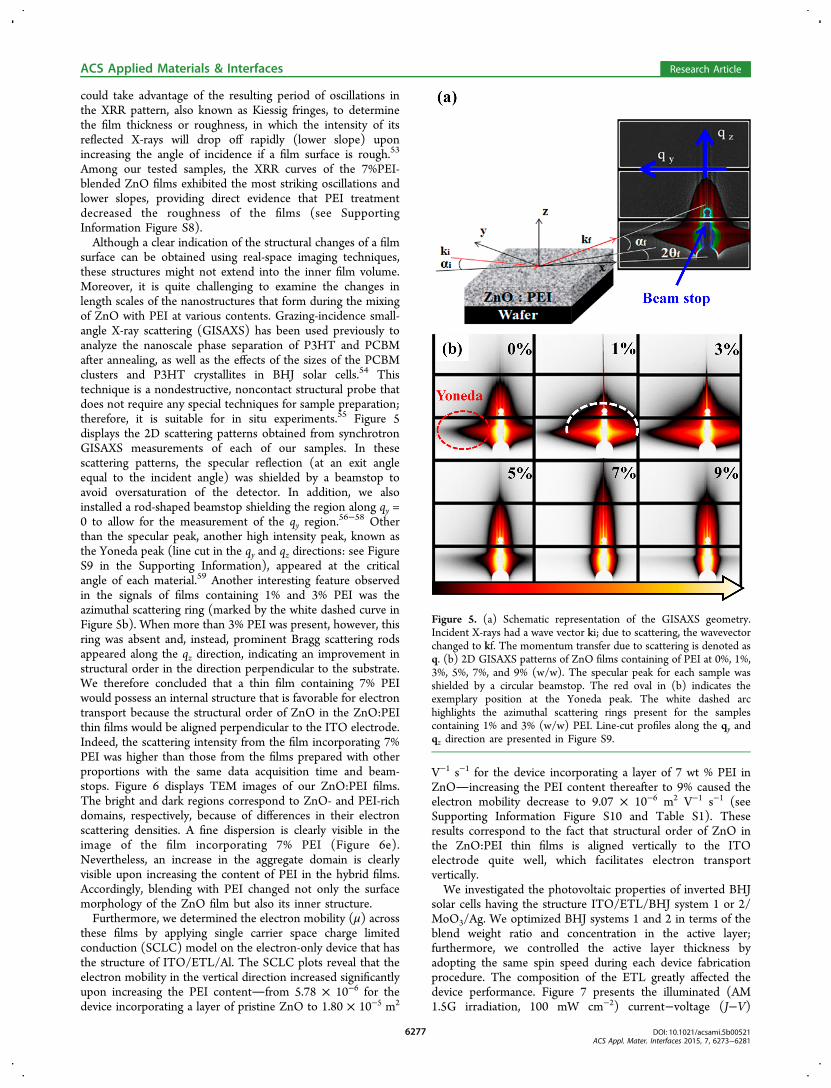
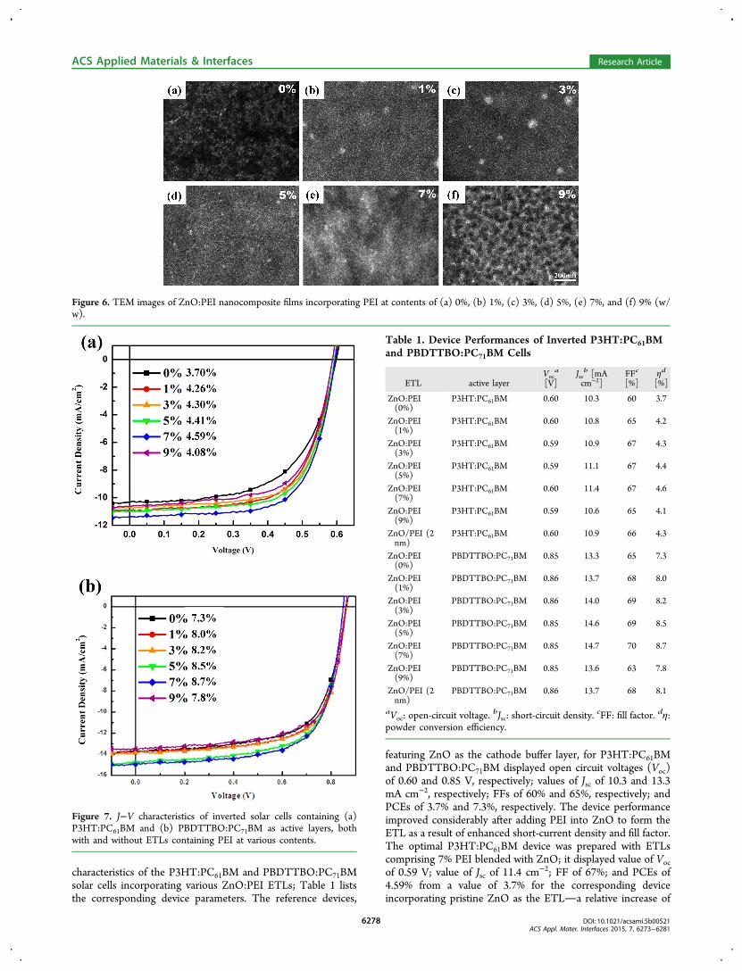
surface can be obtained using real-space imaging techniques,these structures might not extend into the inner film volume.Moreover, it is quite challenging to examine the changes inlength scales of the nanostructures that form during the mixingof ZnO with PEI at various contents. Grazing-incidence small-angle X-ray scattering (GISAXS) has been used previously toanalyze the nanoscale phase separation of P3HT and PCBMafter annealing, as well as the effects of the sizes of the PCBMclusters and P3HT crystallites in BHJ solar cells.54 Thistechnique is a nondestructive, noncontact structural probe thatdoes not require any special techniques for sample preparation;therefore, it is suitable for in situ experiments.55 Figure 5displays the 2D scattering patterns obtained from synchrotronGISAXS measurements of each of our samples. In thesescattering patterns, the specular reflection (at an exit angleequal to the incident angle) was shielded by a beamstop toavoid oversaturation of the detector. In addition, we alsoinstalled a rod-shaped beamstop shielding the region along qy =0 to allow for the measurement of the qy region.
56−58 Otherthan the specular peak, another high intensity peak, known asthe Yoneda peak (line cut in the qy and qz directions: see FigureS9 in the Supporting Information), appeared at the criticalangle of each material.59 Another interesting feature observedin the signals of films containing 1% and 3% PEI was theazimuthal scattering ring (marked by the white dashed curve inFigure 5b). When more than 3% PEI was present, however, thisring was absent and, instead, prominent Bragg scattering rodsappeared along the qz direction, indicating an improvement instructural order in the direction perpendicular to the substrate.We therefore concluded that a thin film containing 7% PEIwould possess an internal structure that is favorable for electrontransport because the structural order of ZnO in the ZnO:PEIthin films would be aligned perpendicular to the ITO electrode.Indeed, the scattering intensity from the film incorporating 7%PEI was higher than those from the films prepared with otherproportions with the same data acquisition time and beam-stops. Figure 6 displays TEM images of our ZnO:PEI films.The bright and dark regions correspond to ZnO- and PEI-richdomains, respectively, because of differences in their electronscattering densities. A fine dispersion is clearly visible in theimage of the film incorporating 7% PEI (Figure 6e).Nevertheless, an increase in the aggregate domain is clearlyvisible upon increasing the content of PEI in the hybrid films.Accordingly, blending with PEI changed not only the surfacemorphology of the ZnO film but also its inner structure.Furthermore, we determined the electron mobility (μ) across
these films by applying single carrier space charge limitedconduction (SCLC) model on the electron-only device that hasthe structure of ITO/ETL/Al. The SCLC plots reveal that theelectron mobility in the vertical direction increased significantlyupon increasing the PEI contentfrom 5.78 × 10⁻⁶ for thedevice incorporating a layer of pristine ZnO to 1.80 × 10⁻⁵ m2
V−1 s−1 for the device incorporating a layer of 7 wt % PEI inZnOincreasing the PEI content thereafter to 9% caused theelectron mobility decrease to 9.07 × 10⁻⁶ m2 V−1 s−1 (seeSupporting Information Figure S10 and Table S1). Theseresults correspond to the fact that structural order of ZnO inthe ZnO:PEI thin films is aligned vertically to the ITOelectrode quite well, which facilitates electron transportvertically.We investigated the photovoltaic properties of inverted BHJ
solar cells having the structure ITO/ETL/BHJ system 1 or 2/MoO3/Ag. We optimized BHJ systems 1 and 2 in terms of theblend weight ratio and concentration in the active layer;furthermore, we controlled the active layer thickness byadopting the same spin speed during each device fabricationprocedure. The composition of the ETL greatly affected thedevice performance. Figure 7 presents the illuminated (AM1.5G irradiation, 100 mW cm−2) current−voltage (J−V)
Figure 5. (a) Schematic representation of the GISAXS geometry.Incident X-rays had a wave vector ki; due to scattering, the wavevectorchanged to kf. The momentum transfer due to scattering is denoted asq. (b) 2D GISAXS patterns of ZnO films containing of PEI at 0%, 1%,3%, 5%, 7%, and 9% (w/w). The specular peak for each sample wasshielded by a circular beamstop. The red oval in (b) indicates theexemplary position at the Yoneda peak. The white dashed archighlights the azimuthal scattering rings present for the samplescontaining 1% and 3% (w/w) PEI. Line-cut profiles along the qy andqz direction are presented in Figure S9.
ACS Applied Materials & Interfaces Research Article
DOI: 10.1021/acsami.5b00521ACS Appl. Mater. Interfaces 2015, 7, 6273−6281
6277
characteristics of the P3HT:PC61BM and PBDTTBO:PC71BMsolar cells incorporating various ZnO:PEI ETLs; Table 1 liststhe corresponding device parameters. The reference devices,
featuring ZnO as the cathode buffer layer, for P3HT:PC61BMand PBDTTBO:PC71BM displayed open circuit voltages (Voc)of 0.60 and 0.85 V, respectively; values of Jsc of 10.3 and 13.3mA cm−2, respectively; FFs of 60% and 65%, respectively; andPCEs of 3.7% and 7.3%, respectively. The device performanceimproved considerably after adding PEI into ZnO to form theETL as a result of enhanced short-current density and fill factor.The optimal P3HT:PC61BM device was prepared with ETLscomprising 7% PEI blended with ZnO; it displayed value of Vocof 0.59 V; value of Jsc of 11.4 cm−2; FF of 67%; and PCEs of4.59% from a value of 3.7% for the corresponding deviceincorporating pristine ZnO as the ETLa relative increase of
Figure 6. TEM images of ZnO:PEI nanocomposite films incorporating PEI at contents of (a) 0%, (b) 1%, (c) 3%, (d) 5%, (e) 7%, and (f) 9% (w/w).
Figure 7. J−V characteristics of inverted solar cells containing (a)P3HT:PC61BM and (b) PBDTTBO:PC71BM as active layers, bothwith and without ETLs containing PEI at various contents.
Table 1. Device Performances of Inverted P3HT:PC61BMand PBDTTBO:PC71BM Cells
ETL active layerVoc
a
[V]Jscb [mAcm−2]
FFc
[%]ηd
[%]
ZnO:PEI(0%)
P3HT:PC61BM 0.60 10.3 60 3.7
ZnO:PEI(1%)
P3HT:PC61BM 0.60 10.8 65 4.2
ZnO:PEI(3%)
P3HT:PC61BM 0.59 10.9 67 4.3
ZnO:PEI(5%)
P3HT:PC61BM 0.59 11.1 67 4.4
ZnO:PEI(7%)
P3HT:PC61BM 0.60 11.4 67 4.6
ZnO:PEI(9%)
P3HT:PC61BM 0.59 10.6 65 4.1
ZnO/PEI (2nm)
P3HT:PC61BM 0.60 10.9 66 4.3
ZnO:PEI(0%)
PBDTTBO:PC71BM 0.85 13.3 65 7.3
ZnO:PEI(1%)
PBDTTBO:PC71BM 0.86 13.7 68 8.0
ZnO:PEI(3%)
PBDTTBO:PC71BM 0.86 14.0 69 8.2
ZnO:PEI(5%)
PBDTTBO:PC71BM 0.85 14.6 69 8.5
ZnO:PEI(7%)
PBDTTBO:PC71BM 0.85 14.7 70 8.7
ZnO:PEI(9%)
PBDTTBO:PC71BM 0.85 13.6 63 7.8
ZnO/PEI (2nm)
PBDTTBO:PC71BM 0.86 13.7 68 8.1
aVoc: open-circuit voltage.bJsc: short-circuit density.
cFF: fill factor. dη:powder conversion efficiency.
ACS Applied Materials & Interfaces Research Article
DOI: 10.1021/acsami.5b00521ACS Appl. Mater. Interfaces 2015, 7, 6273−6281
6278

24%. The optimal PBDTTBO:PC71BM device was alsoprepared with ETLs comprising 7% PEI blended with ZnO;it displayed a value of Voc of 0.85 V; value of Jsc of 14.7 cm−2;FF of 70%; and PCEs of 8.7% from a value of 7.3% for thecorresponding device incorporating pristine ZnO as the ETLa relative increase of 20%. Increasing the PEI loading beyond7% decreased the device performance; for example, when thePEI con ten t was 9% , the P3HT:PC6 1BM andPBDTTBO:PC71BM devices displayed lower values of Jsc(10.6 and 13.6 mA cm−2, respectively) and lower FFs (65%and 63%, respectively), resulting in PCEs of 4.08% and 7.8%,respectively. The EQE curves provided integrated values of Jscthat were close to those measured directly from the J−V curvesof the optimized BHJ systems 1 and 2 (see SupportingInformation Figure S11). We also fabricated another set (fivedevices in each case) of control devices having the structuresglass/ITO/ZnO (2 nm)/PEI/BHJ system 1 or 2/MoO3/Ag,and chose the best performing ones for comparison (seeSupporting Information Figure S12). Surprisingly, the illumi-nated J−V characteristics of the devices incorporated ZnO:PEIsystems were better than those of the devices incorporated thebilayer (ZnO/PEI) ETL systems, with values of Jsc and Vocgreater than those of corresponding devices containing eitherZnO or ZnO/PEI as the ETL. This might be explained by thefact that there is only one interface between the active layer andthe ZnO:PEI composite layer, whereas there are two interfacesbetween the active layer and the ZnO/PEI bilayer, reducing theefficiency of carrier transport vertically slightly because ofinterfacial traps.
■ CONCLUSIONSThrough systematic characterizations of these ZnO:PEInanocomposite ETL films using ultraviolet photoelectronspectroscopy, synchrotron grazing-incidence small-angle X-rayscattering and reflectivity, atomic force microscopy, andtransmission electron microscopy, we found that the ZnO:PEInanocomposites’ physical, optical, electronic, morphological,and inner structural properties are superior to that of thepristine ZnO film as electron transport layers for invertedpolymer solar cells. In particular, we found that N atoms(electron-donating) from the PEI component existed not onlyon the surface after the blending process, but they were alsodistributed in the ETL layer; hence the blending of PEI withinthe ZnO films improved the surface roughness of the ZnO layerand enhanced the structural order of ZnO in the ZnO:PEI layerperpendicular to the ITO electrode, thereby increasing theelectron mobility in the vertical direction significantly. As aresult, introducing PEI-blended ZnO as the ETL between theactive layer P3HT:PC61BM and PBDTTBO:PC71BM and theITO substrate improved the interfacial smoothness, bandalignment (near ohmic contact), and electron mobility, therebyenhancing the photovoltaic performance of the devices. Forinstance, the values of Jsc and FF of inverted BHJ system solarcells featuring a composite of ZnO:PEI (93:7, w/w) as the ETLwere improved considerably compared to those of the deviceincorporating the pristine ZnO layer; the power conversionefficiency (PCE) of the P3HT:PC61BM (1:1, w/w) deviceusing a composite of ZnO:PEI (93:7, w/w) improved to 4.6%from a value of 3.7% for the corresponding device incorporatingpristine ZnO as the ETLa relative increase of 24%. For thePBDTTBO:PC71BM (1:2, w/w) device featuring the samecomposite of ZnO:PEI (93:7, w/w) as the ETL, the PCEimproved to 8.7% from a value of 7.3% for the corresponding
device featuring pure ZnO as its ETLa relative increase of20%. Therefore, ZnO:PEI composites can be effective ETLswithin organic photovoltaics.
■ ASSOCIATED CONTENT*S Supporting InformationTable showing energy level diagram, surface roughness, andelectron mobility for ZnO:PEI nanocomposite films. Determi-nation of the energy gap and valence band of ZnO:PEI bytransmittance spectra and UPS analysis. Optical absorptionspec t r a and EQE da t a o f P3HT:PC6 1BM andPBDTTBO:PC71BM systems incorporating PEI (7%) asETLs. SEM image and XRR shown the ZnO incorporatingdifferent PEI ratios. Determination of the Zn, O, N atoms ofelectron structures and depth profiles by XPS results. Electronmobility determined by electron-only device and calculated bySCLC model. Performance of P3HT:PC61BM andPBDTTBO:PC71BM devices based on pristine ZnO, ZnO:PEI,and ZnO/PEI. This material is available free of charge via theInternet at http://pubs.acs.org.
■ AUTHOR INFORMATIONCorresponding Author*E-mail: [email protected] authors declare no competing financial interest.
■ ACKNOWLEDGMENTSWe thank the National Science Council, Taiwan, for financialsupport (NSC 102-3113-P-009-002), and Ming-Wei Lin andYu-Ling Lai from Dr. Yao-Jane Hsu’s group (NSRRC) for helpwith the UPS measurements.
■ REFERENCES(1) Steim, R.; Kogler, F. R.; Brabec, C. J. Interface Materials forOrganic Solar Cells. J. Mater. Chem. 2010, 20, 2499−2512.(2) Lai, T.-H.; Tsang, S.-W.; Manders, J. R.; Chen, S.; So, F.Properties of Interlayer for Organic Photovoltaics. Mater. Today 2013,16, 424−432.(3) Su, Y.-W.; Lan, S.-C.; Wei, K.-H. Organic Photovoltaics. Mater.Today 2012, 15, 554−562.(4) Liu, S.; Zhang, K.; Lu, J.; Zhang, J.; Yip, H.-L.; Huang, F.; Cao, Y.High-Efficiency Polymer Solar Cells via the Incorporation of anAmino-Functionalized Conjugated Metallopolymer as a CathodeInterlayer. J. Am. Chem. Soc. 2013, 135, 15326−15329.(5) Liao, S.-H.; Jhuo, H.-J.; Cheng, Y.-S.; Chen, S.-A. FullereneDerivative-Doped Zinc Oxide Nanofilm as the Cathode of InvertedPolymer Solar Cells with Low-Bandgap Polymer (PTB7-Th) for HighPerformance. Adv. Mater. 2013, 25, 4766−4771.(6) Zhou, L.; Ou, Q.-D.; Chen, J.-D.; Shen, S.; Tang, J.-X.; Li, Y.-Q.;Lee, S.-T. Light Manipulation for Organic Optoelectronics Using Bio-inspired Moth’s Eye Nanostructures. Sci. Rep. 2014, 4, 4040.(7) Li, C.-Z.; Chang, C.-Y.; Zang, Y.; Ju, H.-X.; Chueh, C.-C.; Liang,P.-W.; Cho, N.; Ginger, D. S.; Jen, A. K. Y. Suppressed ChargeRecombination in Inverted Organic Photovoltaics via EnhancedCharge Extraction by Using a Conductive Fullerene ElectronTransport Layer. Adv. Mater. 2014, 26, 6262−6267.(8) Chen, J.-D.; Cui, C.; Li, Y.-Q.; Zhou, L.; Ou, Q.-D.; Li, C.; Li, Y.;Tang, J.-X. Single-Junction Polymer Solar Cells Exceeding 10% PowerConversion Efficiency. Adv. Mater. 2015, 27, 1035−1041.(9) Liao, S.-H.; Jhuo, H.-J.; Yeh, P.-N.; Cheng, Y.-S.; Li, Y.-L.; Lee, Y.-H.; Sharma, S.; Chen, S.-A. Single Junction Inverted Polymer SolarCell Reaching Power Conversion Efficiency 10.31% by EmployingDual-Doped Zinc Oxide Nano-Film as Cathode Interlayer. Sci. Rep.2014, 4, 6813.
ACS Applied Materials & Interfaces Research Article
DOI: 10.1021/acsami.5b00521ACS Appl. Mater. Interfaces 2015, 7, 6273−6281
6279

(10) Liu, C.-M.; Su, M.-S.; Jiang, J.-M.; Su, Y.-W.; Su, C.-J.; Chen, C.-Y.; Tsao, C.-S.; Wei, K.-H. Distribution of Crystalline Polymer andFullerene Clusters in Both Horizontal and Vertical Directions of High-Efficiency Bulk Heterojunction Solar Cells. ACS Appl. Mater. Interfaces2013, 5, 5413−5422.(11) Su, M.-S.; Kuo, C.-Y.; Yuan, M.-C.; Jeng, U. S.; Su, C.-J.; Wei,K.-H. Improving Device Efficiency of Polymer/Fullerene BulkHeterojunction Solar Cells Through Enhanced Crystallinity andReduced Grain Boundaries Induced by Solvent Additives. Adv.Mater. 2011, 23, 3315−3319.(12) Chiu, M.-Y.; Jeng, U. S.; Su, M.-S.; Wei, K.-H. Morphologies ofSelf-Organizing Regioregular Conjugated Polymer/Fullerene Aggre-gates in Thin Film Solar Cells. Macromolecules 2010, 43, 428−432.(13) Lai, Y.-Y.; Cheng, Y.-J.; Hsu, C.-S. Applications of FunctionalFullerene Materials in Polymer Solar Cells. Energy Environ. Sci. 2014,7, 1866−1883.(14) Yip, H.-L.; Jen, A. K. Y. Recent Advances in Solution-ProcessedInterfacial Materials for Efficient and Stable Polymer Solar Cells.Energy Environ. Sci. 2012, 5, 5994−6011.(15) Chen, L.-M.; Xu, Z.; Hong, Z.; Yang, Y. Interface Investigationand Engineering - Achieving High Performance Polymer PhotovoltaicDevices. J. Mater.Chem. 2010, 20, 2575−2598.(16) Ma, H.; Yip, H.-L.; Huang, F.; Jen, A. K. Y. InterfaceEngineering for Organic Electronics. Adv. Funct. Mater. 2010, 20,1371−1388.(17) Intemann, J. J.; Yao, K.; Li, Y.-X.; Yip, H.-L.; Xu, Y.-X.; Liang, P.-W.; Chueh, C.-C.; Ding, F.-Z.; Yang, X.; Li, X.; Chen, Y.; Jen, A. K. Y.Highly Efficient Inverted Organic Solar Cells Through Material andInterfacial Engineering of Indacenodithieno[3,2-b]thiophene-BasedPolymers and Devices. Adv. Funct. Mater. 2014, 24, 1465−1473.(18) Lloyd, M. T.; Olson, D. C.; Lu, P.; Fang, E.; Moore, D. L.;White, M. S.; Reese, M. O.; Ginley, D. S.; Hsu, J. W. P. Impact ofContact Evolution on the Shelf Life of Organic Solar Cells. J. Mater.Chem. 2009, 19, 7638−7642.(19) He, Z.; Zhong, C.; Su, S.; Xu, M.; Wu, H.; Cao, Y. EnhancedPower-Conversion Efficiency in Polymer Solar Cells Using an InvertedDevice Structure. Nat. Photonics 2012, 6, 591−595.(20) Park, H.-Y.; Lim, D.; Kim, K.-D.; Jang, S.-Y. PerformanceOptimization of Low-Temperature-Annealed Solution-ProcessableZnO Buffer Layers for Inverted Polymer Solar Cells. J. Mater. Chem.A 2013, 1, 6327−6334.(21) Sun, Y.; Seo, J. H.; Takacs, C. J.; Seifter, J.; Heeger, A. J.Inverted Polymer Solar Cells Integrated with a Low-Temperature-Annealed Sol-Gel-Derived ZnO Film as an Electron Transport Layer.Adv. Mater. 2011, 23, 1679−1683.(22) Chen, S.; Small, C. E.; Amb, C. M.; Subbiah, J.; Lai, T.-h.;Tsang, S.-W.; Manders, J. R.; Reynolds, J. R.; So, F. Inverted PolymerSolar Cells with Reduced Interface Recombination. Adv. Energy Mater.2012, 2, 1333−1337.(23) Kim, K.-D.; Lim, D. C.; Hu, J.; Kwon, J.-D.; Jeong, M.-G.; Seo,H. O.; Lee, J. Y.; Jang, K.-Y.; Lim, J.-H.; Lee, K. H.; Jeong, Y.; Kim, Y.D.; Cho, S. Surface Modification of a ZnO Electron-Collecting LayerUsing Atomic Layer Deposition to Fabricate High-PerformingInverted Organic Photovoltaics. ACS Appl. Mater. Interfaces 2013, 5,8718−8723.(24) Bai, S.; Jin, Y.; Liang, X.; Ye, Z.; Wu, Z.; Sun, B.; Ma, Z.; Tang,Z.; Wang, J.; Wurfel, U.; Gao, F.; Zhang, F. Ethanedithiol Treatmentof Solution-Processed ZnO Thin Films: Controlling the IntragapStates of Electron Transporting Interlayers for Efficient and StableInverted Organic Photovoltaics. Adv. Energy Mater. 2014, 1401606.(25) Sanchez, S.; Berson, S.; Guillerez, S.; Levy-Clement, C.; Ivanova,V. Toward High-Stability Inverted Polymer Solar Cells with anElectrodeposited ZnO Electron Transporting Layer. Adv. EnergyMater. 2012, 2, 541−545.(26) Liang, Z.; Zhang, Q.; Wiranwetchayan, O.; Xi, J.; Yang, Z.; Park,K.; Li, C.; Cao, G. Effects of the Morphology of a ZnO Buffer Layer onthe Photovoltaic Performance of Inverted Polymer Solar Cells. Adv.Funct. Mater. 2012, 22, 2194−2201.
(27) Kang, H.; Lee, J.; Jung, S.; Yu, K.; Kwon, S.; Hong, S.; Kee, S.;Lee, S.; Kim, D.; Lee, K. Self-Assembly of Interfacial and PhotoactiveLayers via One-Step Solution Processing for Efficient Inverted OrganicSolar Cells. Nanoscale 2013, 5, 11587−11591.(28) Zhou, Y.; Fuentes-Hernandez, C.; Shim, J.; Meyer, J.; Giordano,A. J.; Li, H.; Winget, P.; Papadopoulos, T.; Cheun, H.; Kim, J.; Fenoll,M.; Dindar, A.; Haske, W.; Najafabadi, E.; Khan, T. M.; Sojoudi, H.;Barlow, S.; Graham, S.; Bredas, J.-L.; Marder, S. R.; Kahn, A.;Kippelen, B. A Universal Method to Produce Low−Work FunctionElectrodes for Organic Electronics. Science 2012, 336, 327−332.(29) Kang, H.; Hong, S.; Lee, J.; Lee, K. Electrostatically Self-Assembled Nonconjugated Polyelectrolytes as an Ideal InterfacialLayer for Inverted Polymer Solar Cells. Adv. Mater. 2012, 24, 3005−3009.(30) Li, P.; Wang, G.; Cai, L.; Ding, B.; Zhou, D.; Hu, Y.; Zhang, Y.;Xiang, J.; Wan, K.; Chen, L.; Alameh, K.; Song, Q. High-EfficiencyInverted Polymer Solar Cells Controlled by the Thickness ofPolyethylenimine Ethoxylated (PEIE) Interfacial Layers. Phys. Chem.Chem. Phys. 2014, 16, 23792−23799.(31) Liu, J.; Wu, J.; Shao, S.; Deng, Y.; Meng, B.; Xie, Z.; Geng, Y.;Wang, L.; Zhang, F. Printable Highly Conductive Conjugated PolymerSensitized ZnO NCs as Cathode Interfacial Layer for Efficient PolymerSolar Cells. ACS Appl. Mater. Interfaces 2014, 6, 8237−8245.(32) Xie, C.; Chen, L.; Chen, Y. Electrostatic Self-Assembled MetalOxide/Conjugated Polyelectrolytes as Electron-Transporting Layersfor Inverted Solar Cells with High Efficiency. J. Phys. Chem. C 2013,117, 24804−24814.(33) Small, C. E.; Chen, S.; Subbiah, J.; Amb, C. M.; Tsang, S.-W.;Lai, T.-H.; Reynolds, J. R.; So, F. High-Efficiency InvertedDithienogermole-Thienopyrrolodione-Based Polymer Solar Cells.Nat. Photonics 2012, 6, 115−120.(34) Manor, A.; Katz, E. A.; Tromholt, T.; Krebs, F. C. EnhancingFunctionality of ZnO Hole Blocking Layer in Organic Photovoltaics.Sol. Energy Mater.Sol. Cells 2012, 98, 491−493.(35) Chang, Y.-M.; Leu, C.-Y. Conjugated Polyelectrolyte and ZincOxide Stacked Structure as an Interlayer in Highly Efficient and StableOrganic Photovoltaic Cells. J. Mater. Chem. A 2013, 1, 6446−6451.(36) Yang, T.; Wang, M.; Duan, C.; Hu, X.; Huang, L.; Peng, J.;Huang, F.; Gong, X. Inverted Polymer Solar Cells with 8.4% Efficiencyby Conjugated Polyelectrolyte. Energy Environ. Sci. 2012, 5, 8208−8214.(37) Woo, S.; Hyun Kim, W.; Kim, H.; Yi, Y.; Lyu, H.-K.; Kim, Y.8.9% Single-Stack Inverted Polymer Solar Cells with Electron-RichPolymer Nanolayer-Modified Inorganic Electron-Collecting BufferLayers. Adv. Energy Mater. 2014, 4, 1301692.(38) Yang, D.; Fu, P.; Zhang, F.; Wang, N.; Zhang, J.; Li, C. HighEfficiency Inverted Polymer Solar Cells with Room-TemperatureTitanium Oxide/Polyethylenimine Films as Electron TransportLayers. J. Mater. Chem. A 2014, 2, 17281−17285.(39) Yao, K.; Intemann, J. J.; Yip, H.-L.; Liang, P.-W.; Chang, C.-Y.;Zang, Y.; Li, Z. a.; Chen, Y.; Jen, A. K. Y. Efficient all Polymer SolarCells from Layer-Evolved Processing of a Bilayer Inverted Structure. J.Mater. Chem. C 2014, 2, 416−420.(40) Cha, H.-C.; Huang, Y.-C.; Hsu, F.-H.; Chuang, C.-M.; Lu, D.-H.; Chou, C.-W.; Chen, C.-Y.; Tsao, C.-S. Performance Improvementof Large-Area Roll-to-Roll Slot-Die-Coated Inverted Polymer SolarCell by Tailoring Electron Transport Layer. Sol. Energy Mater. Sol. Cells2014, 130, 191−198.(41) Kyaw, A. K. K.; Wang, D. H.; Gupta, V.; Zhang, J.; Chand, S.;Bazan, G. C.; Heeger, A. J. Efficient Solution-Processed Small-Molecule Solar Cells with Inverted Structure. Adv. Mater. 2013, 25,2397−2402.(42) Lee, T. H.; Choi, H.; Walker, B.; Kim, T.; Kim, H.-B.; Kim, J. Y.Replacing the Metal Oxide Layer with a Polymer Surface Modifier forHigh-Performance Inverted Polymer Solar Cells. RSC Adv. 2014, 4,4791−4795.(43) Jo, S. B.; Lee, J. H.; Sim, M.; Kim, M.; Park, J. H.; Choi, Y. S.;Kim, Y.; Ihn, S.-G.; Cho, K. High Performance Organic Photovoltaic
ACS Applied Materials & Interfaces Research Article
DOI: 10.1021/acsami.5b00521ACS Appl. Mater. Interfaces 2015, 7, 6273−6281
6280

Cells Using Polymer-Hybridized ZnO Nanocrystals as a CathodeInterlayer. Adv. Energy Mater. 2011, 1, 690−698.(44) Shao, S.; Zheng, K.; Pullerits, T.; Zhang, F. EnhancedPerformance of Inverted Polymer Solar Cells by Using Poly(ethyleneoxide)-Modified ZnO as an Electron Transport Layer. ACS Appl.Mater. Interfaces 2012, 5, 380−385.(45) Kim, Y.-H.; Han, T.-H.; Cho, H.; Min, S.-Y.; Lee, C.-L.; Lee, T.-W. Polyethylene Imine as an Ideal Interlayer for Highly EfficientInverted Polymer Light-Emitting Diodes. Adv. Funct. Mater. 2014, 24,3808−3814.(46) Jiang, J.-M.; Lin, H.-K.; Lin, Y.-C.; Chen, H.-C.; Lan, S.-C.;Chang, C.-K.; Wei, K.-H. Side Chain Structure Affects the Photo-voltaic Performance of Two-Dimensional Conjugated Polymers.Macromolecules 2013, 47, 70−78.(47) Dkhil, S. B.; Duche, D.; Gaceur, M.; Thakur, A. K.; Aboura, F.B.; Escoubas, L.; Simon, J.-J.; Guerrero, A.; Bisquert, J.; Garcia-Belmonte, G.; Bao, Q.; Fahlman, M.; Videlot-Ackermann, C.; Margeat,O.; Ackermann, J. Interplay of Optical, Morphological, and ElectronicEffects of ZnO Optical Spacers in Highly Efficient Polymer Solar Cells.Adv. Energy Mater. 2014, 4, 1400805.(48) Ye, J. D.; Gu, S. L.; Qin, F.; Zhu, S. M.; Liu, S. M.; Zhou, X.; Liu,W.; Hu, L. Q.; Zhang, R.; Shi, Y.; Zheng, Y. D. Correlation BetweenGreen Luminescence and Morphology Evolution of ZnO Films. Appl.Phys. A: Mater. Sci. Process. 2005, 81, 759−762.(49) Djurisic, A. B.; Choy, W. C. H.; Roy, V. A. L.; Leung, Y. H.;Kwong, C. Y.; Cheah, K. W.; Gundu Rao, T. K.; Chan, W. K.; Fei Lui,H.; Surya, C. Photoluminescence and Electron ParamagneticResonance of ZnO Tetrapod Structures. Adv. Funct. Mater. 2004,14, 856−864.(50) Yao, I. C.; Pang, L.; Tseng, T.-Y. Field Emission Properties andReliability of ZnO Nanorod, Nanopagoda, and Nanotip CurrentEmitters. IEEE Trans. Nanotechnol. 2012, 11, 746−750.(51) Ramgir, N. S.; Mulla, I. S.; Pillai, V. K. Micropencils andMicrohexagonal Cones of ZnO. J. Phys. Chem. B 2006, 110, 3995−4001.(52) De la Rosa, E.; Sepulveda-Guzman, S.; Reeja-Jayan, B.; Torres,A.; Salas, P.; Elizondo, N.; Yacaman, M. J. Controlling the Growth andLuminescence Properties of Well-Faceted ZnO Nanorods. J. Phys.Chem. C 2007, 111, 8489−8495.(53) Croce, P.; Devant, G.; Sere, M. G.; Verhaeghe, M. F. Thin FilmSurface Studies by X-ray Reflection. Surf. Sci. 1970, 22, 173−186.(54) Chiu, M.-Y.; Jeng, U. S.; Su, C.-H.; Liang, K. S.; Wei, K.-H.Simultaneous Use of Small- and Wide-Angle X-ray Techniques toAnalyze Nanometerscale Phase Separation in Polymer HeterojunctionSolar Cells. Adv. Mater. 2008, 20, 2573−2578.(55) Muller-Buschbaum, P. The Active Layer Morphology of OrganicSolar Cells Probed with Grazing Incidence Scattering Techniques. Adv.Mater. 2014, 26, 7692−7709.(56) Kaune, G.; Memesa, M.; Meier, R.; Ruderer, M. A.; Diethert, A.;Roth, S. V.; D’Acunzi, M.; Gutmann, J. S.; Muller-Buschbaum, P.Hierarchically Structured Titania Films Prepared by Polymer/Colloidal Templating. ACS Appl. Mater. Interfaces 2009, 1, 2862−2869.(57) Sarkar, K.; Schaffer, C. J.; Gonzalez, D. M.; Naumann, A.;Perlich, J.; Muller-Buschbaum, P. Tuning the Pore Size of ZnO Nano-Grids via Time-Dependent Solvent Annealing. J. Mater. Chem. A 2014,2, 6945−6951.(58) Chen, C.-M.; Liu, C.-M.; Tsai, M.-C.; Chen, H.-C.; Wei, K.-H. ANanostructured Micellar Diblock Copolymer Layer Affects theMemory Characteristics and Packing of Pentacene Molecules inNon-Volatile Organic Field-Effect Transistor Memory Devices. J.Mater. Chem. C 2013, 1, 2328−2337.(59) Yoneda, Y. Anomalous Surface Reflection of X Rays. Phys. Rev.1963, 131, 2010−2013.
ACS Applied Materials & Interfaces Research Article
DOI: 10.1021/acsami.5b00521ACS Appl. Mater. Interfaces 2015, 7, 6273−6281
6281