
Solid-Liquid Interdiffusion Bonding of Silicon ... - UC Berkeley
111
UC Berkeley UC Berkeley Electronic Theses and Dissertations Title Solid-Liquid Interdiffusion Bonding of Silicon Carbide to Steel for High Temperature MEMS Sensor Packaging and Bonding Permalink https://escholarship.org/uc/item/0r09f7ns Author Chan, Matthew Publication Date 2013 Peer reviewed|Thesis/dissertation eScholarship.org Powered by the California Digital Library University of California
-
Upload
khangminh22 -
Category
Documents
-
view
2 -
download
0
Transcript of Solid-Liquid Interdiffusion Bonding of Silicon ... - UC Berkeley

UC BerkeleyUC Berkeley Electronic Theses and Dissertations
TitleSolid-Liquid Interdiffusion Bonding of Silicon Carbide to Steel for High Temperature MEMS Sensor Packaging and Bonding
Permalinkhttps://escholarship.org/uc/item/0r09f7ns
AuthorChan, Matthew
Publication Date2013 Peer reviewed|Thesis/dissertation
eScholarship.org Powered by the California Digital LibraryUniversity of California

Solid-Liquid Interdiffusion Bonding of Silicon Carbide to Steel for High TemperatureMEMS Sensor Packaging and Bonding
By
Matthew Wei-Jen Chan
A dissertation submitted in partial satisfaction of the
requirements for the degree of
Doctor of Philosophy
in
Engineering - Mechanical Engineering
in the
Graduate Division
of the
University of California, Berkeley
Committee in charge:
Professor Albert P. Pisano, ChairProfessor Liwei Lin
Professor Junqiao Wu
Fall 2013

Solid-Liquid Interdiffusion Bonding of Silicon Carbide to Steel for High TemperatureMEMS Sensor Packaging and Bonding
Copyright © 2013
by
Matthew Wei-Jen Chan

Abstract
Solid-Liquid Interdiffusion Bonding of Silicon Carbide to Steel for High TemperatureMEMS Sensor Packaging and Bonding
by
Matthew Wei-Jen Chan
Doctor of Philosophy in Engineering - Mechanical Engineering
University of California, Berkeley
Professor Albert P. Pisano, Chair
Complex engineering systems ranging from automobile engines to geothermal wells re-quire specialized sensors to monitor conditions such as pressure, acceleration and temper-ature in order to improve efficiency and monitor component lifetime in what may be hightemperature, corrosive, harsh environments. Microelectromechanical systems (MEMS) havedemonstrated their ability to precisely and accurately take measurements under such con-ditions. The systems being monitored are typically made from metals, such as steel, whilethe MEMS sensors used for monitoring are commonly fabricated from silicon, silicon carbideand aluminum nitride, and so there is a sizable thermal expansion mismatch between thetwo. For these engineering applications the direct bonding of MEMS sensors to the com-ponents being monitored is often required. This introduces several challenges, namely thedevelopment of a bond that is capable of surviving high temperature harsh environmentswhile mitigating the thermally induced strains produced during bonding.
This project investigates the development of a robust packaging and bonding process, us-ing the gold-tin metal system and the solid-liquid interdiffusion (SLID) bonding process, tojoin silicon carbide substrates directly to type-316 stainless steel. The SLID process enablesbonding at lower temperatures while producing a bond capable of surviving higher tempera-tures. Finite element analysis was performed to model the thermally induced strains gener-ated in the bond and to understand the optimal way to design the bond. The cross-sectionalcomposition of the bonds has been analyzed and the bond strength has been investigatedusing die shear testing. The effects of high temperature aging on the bond’s strength andthe metallurgy of the bond were studied. Additionally, loading of the bond was performedat temperatures over 415 ◦C, more than 100 ◦C above the temperature used for bonding,with full survival of the bond, thus demonstrating the benefit of SLID bonding for hightemperature applications.
Lastly, this dissertation provides recommendations for improving the strength and dura-bility of the bond at temperatures of 400 ◦C and provides the framework for future work inthe area of high temperature harsh environment MEMS packaging that would take directlybonded MEMS to temperatures of 600 ◦C and beyond.
1

Dedicated to my wife, Krissy, and my parents, Gaik and Charles.It’s been quite a journey and your support has meant the world to me.
i

Contents
Abstract 1
Dedication i
Contents ii
List of Figures v
List of Tables vii
Acknowledgements viii
1 Introduction 11.1 Direct Bonding Applications and the Need for High Temperature Bonds . . . 21.2 A Survey of Existing Bonding Methods . . . . . . . . . . . . . . . . . . . . . 3
1.2.1 Lower Temperature Application Bonding: Below 250 ◦C . . . . . . . 51.2.2 Higher Temperature Application Bonding: 300 - 500 ◦C . . . . . . . . 6
1.3 Materials for Bonding . . . . . . . . . . . . . . . . . . . . . . . . . . . . . . . 91.4 Outline of Dissertation . . . . . . . . . . . . . . . . . . . . . . . . . . . . . . 9
2 Solid-Liquid InterDiffusion Bonding Process 112.1 The Process of Solid-Liquid InterDiffusion . . . . . . . . . . . . . . . . . . . 112.2 Material System Selection for SLID Bonding . . . . . . . . . . . . . . . . . . 142.3 Fabrication Process for Silicon to Silicon Substrate SLID Bonding . . . . . . 162.4 Fabrication Process for Silicon Carbide Substrate to Steel SLID Bonding . . 17
2.4.1 The SiC Substrates . . . . . . . . . . . . . . . . . . . . . . . . . . . . 182.4.2 The Type-316 Stainless Steel Substrate . . . . . . . . . . . . . . . . . 182.4.3 Electroplating of Soft Gold . . . . . . . . . . . . . . . . . . . . . . . . 192.4.4 Selection and Preparation of Low Melting-Point Metal . . . . . . . . 252.4.5 Heating Process for SLID Bonding . . . . . . . . . . . . . . . . . . . 26
3 Design and Theory of SLID Bonds for High Temperatures Applications 303.1 Tailoring the Thicknesses of the SLID Bond Layer . . . . . . . . . . . . . . . 30
3.1.1 Layer Thicknesses in Silicon to Silicon SLID Bonding . . . . . . . . . 313.1.2 Layer Thicknesses in Silicon Carbide to Steel SLID Bonding . . . . . 31
3.2 Analytical Modeling of Thermally Induced Strains . . . . . . . . . . . . . . . 32
ii

3.3 Computer Modeling of Thermally Induced Strains . . . . . . . . . . . . . . . 393.3.1 Bond Shape Geometries of the SLID Bond . . . . . . . . . . . . . . . 413.3.2 Cooling the Square Shaped SLID Bond After Bonding . . . . . . . . 423.3.3 Reheating the Square Shaped SLID Bond to Operational Temperature 433.3.4 Modeling of Alternate Bond Geometries . . . . . . . . . . . . . . . . 44
4 Characterization and Testing of the SLID Bonds 504.1 Die Shear Testing Method . . . . . . . . . . . . . . . . . . . . . . . . . . . . 504.2 Microscopy and Chemical Composition Analysis Methods . . . . . . . . . . . 53
4.2.1 Optical microscopy . . . . . . . . . . . . . . . . . . . . . . . . . . . . 534.2.2 Scanning Electron Microscopy and Energy Dispersive X-Ray Analysis 544.2.3 Metallographic Polishing . . . . . . . . . . . . . . . . . . . . . . . . . 55
4.3 Characterization and Testing of Si to Si SLID Bonds . . . . . . . . . . . . . 574.3.1 Die Shear Testing of Si to Si SLID Bonds . . . . . . . . . . . . . . . . 574.3.2 Optical and Compositional Analysis of Si to Si SLID Bonds . . . . . 57
4.4 Characterization and Testing of SiC to Steel SLID Bonds . . . . . . . . . . . 604.4.1 Die Shear Testing of SiC to Steel SLID Bond After Cooling . . . . . . 604.4.2 Compositional Analysis of SiC to Steel SLID Bond After Cooling . . 624.4.3 Die Shear Testing of SiC to Steel Bonds after High Temperature Aging 674.4.4 Elevated Temperature Loading of SiC to Steel Bonds . . . . . . . . . 704.4.5 High Temperature Exposure Testing of SiC to Steel SLID Bond . . . 74
5 Conclusion 765.1 Improving the SLID Bonding of Silicon Carbide to Steel . . . . . . . . . . . 765.2 Future Works and Directions . . . . . . . . . . . . . . . . . . . . . . . . . . . 77
5.2.1 SLID Bonding with Nanoparticles or Reactive Nano-Layers . . . . . . 775.2.2 Gradual Layering of Increasing CTE Materials . . . . . . . . . . . . . 775.2.3 Material Systems for Higher Temperature Bonds (>600 ◦C) . . . . . 78
Bibliography 79
Appendix A 85
A ANSYS Code for Thermal Strain Modeling of SLID Bond 86A.1 MATLAB Script for Calculating SLID Bond Layer Thicknesses and Compo-
sitions . . . . . . . . . . . . . . . . . . . . . . . . . . . . . . . . . . . . . . . 86A.2 MATLAB Script for Analytical Model of In-Plane Stresses . . . . . . . . . . 86A.3 ANSYS Model Code for Stress Distribution . . . . . . . . . . . . . . . . . . 90A.4 ANSYS Macro Code for Material Properties . . . . . . . . . . . . . . . . . . 92A.5 MATLAB Script for Calculating SLID Bond Area in Si-to-Si Bond . . . . . . 96A.6 MATLAB Script for Calculating DOE Cause and Effects . . . . . . . . . . . 97
B Process Recipes and Notes for SLID Bonding 98B.1 E-Beam Evaporation Thin Films Deposition . . . . . . . . . . . . . . . . . . 98B.2 Electroplating . . . . . . . . . . . . . . . . . . . . . . . . . . . . . . . . . . . 98B.3 Substrate Dicing . . . . . . . . . . . . . . . . . . . . . . . . . . . . . . . . . 98
iii

B.4 Heating the SLID Bond . . . . . . . . . . . . . . . . . . . . . . . . . . . . . 99
iv

List of Figures
1.1 Overview of sensor bonding for high temperature applications . . . . . . . . 21.2 Si MEMS DETF resonant strain gauge bonded to steel via induction heating 61.3 Residual flux on SiC die after brazing . . . . . . . . . . . . . . . . . . . . . . 71.4 Breakage of Si die upon cooling after high temperature brazing . . . . . . . . 81.5 Bonding of Si dies to steel engine valves using S-Bond 400 . . . . . . . . . . 8
2.1 Generic eutectic binary phase diagram . . . . . . . . . . . . . . . . . . . . . 122.2 Phase diagram for gold-tin metal system . . . . . . . . . . . . . . . . . . . . 142.3 Overview of gold-tin SLID bonding process . . . . . . . . . . . . . . . . . . . 152.4 Metal layer combinations used in Si to Si SLID bonds . . . . . . . . . . . . . 172.5 Gold electroplating bath setup . . . . . . . . . . . . . . . . . . . . . . . . . . 202.6 SLID bonding fabrication process for MEMS substrate . . . . . . . . . . . . 212.7 Inspection of electroplated film on SiC die . . . . . . . . . . . . . . . . . . . 222.8 SLID bonding fabrication process for type-316 stainless steel . . . . . . . . . 242.9 ASTM D3359-09 adhesion testing of plated gold . . . . . . . . . . . . . . . . 252.10 Step height profile of gold electroplating on stainless steel . . . . . . . . . . . 262.11 Components of the heater setup for SLID bonding . . . . . . . . . . . . . . . 272.12 Assembled heater with sample for SLID bonding . . . . . . . . . . . . . . . . 282.13 Heating profile for SLID Bonding . . . . . . . . . . . . . . . . . . . . . . . . 29
3.1 Layers of SLID bond for analytical model . . . . . . . . . . . . . . . . . . . . 333.2 Analytical calculations of bond’s in-plane thermal stresses . . . . . . . . . . 383.3 Finite element analysis mesh for SLID bonding simulation . . . . . . . . . . 403.4 Different SLID bond geometries modeled in ANSYS . . . . . . . . . . . . . . 413.5 Thermal stress model of bonding stack cooled to room temperature . . . . . 423.6 Thermal stress model of bonding stack at operating temperature . . . . . . . 433.7 Comparison of thermal stresses generated when cooling and reheating SLID
bond . . . . . . . . . . . . . . . . . . . . . . . . . . . . . . . . . . . . . . . . 443.8 Thermal stress from cooling center-bonded geometry . . . . . . . . . . . . . 473.9 Thermal stress from reheating center-bonded geometry . . . . . . . . . . . . 473.10 Thermal stress from cooling small center-bonded geometry . . . . . . . . . . 483.11 Thermal stress from reheating small center-bonded geometry . . . . . . . . . 483.12 Thermal stress from cooling cross-bonded geometry . . . . . . . . . . . . . . 493.13 Thermal stress from reheating cross-bonded geometry . . . . . . . . . . . . . 49
4.1 MIL-STD 883J die shear strength requirements for the SLID bond . . . . . . 51
v

4.2 Schematic of the die shear bond tester . . . . . . . . . . . . . . . . . . . . . 524.3 Graph of shear force versus time for an example die shear test . . . . . . . . 534.4 EDX analysis spectrum for Au80%wt.-Sn20%wt. . . . . . . . . . . . . . . . . 554.5 Metallographic polishing samples of bonded SiC to Steel . . . . . . . . . . . 564.6 Top-down view of Si to Si bond surface before and after shear testing . . . . 584.7 Cross-sectional image of the Si to Si Bond . . . . . . . . . . . . . . . . . . . 584.8 Top-down view of Si to Si bond surface before and after shear testing . . . . 594.9 SEM Image of SLID bond before and after bonding . . . . . . . . . . . . . . 634.10 Fracture surface EDX analysis on steel side of bond after shear testing . . . 654.11 Fracture surface EDX analysis on SiC side of bond after shear testing . . . . 664.12 Oven setup for high temperature loading tests . . . . . . . . . . . . . . . . . 684.13 Cross section of SLID bond before and after high temperature aging . . . . . 684.14 Excess solder diffusion outside bond area after high temperature exposure . . 694.15 Cross section compositional analysis of fresh SLID bond . . . . . . . . . . . 704.16 Cross section compositional analysis of aged SLID bond . . . . . . . . . . . . 714.17 Test apparatus for high temperature loading of SLID bond . . . . . . . . . . 724.18 Operational schematic of high temperature loading apparatus . . . . . . . . 734.19 High temperature loading apparatus operating in oven . . . . . . . . . . . . 744.20 High temperature melting test of SLID bond using IR lamp . . . . . . . . . 75
vi

List of Tables
2.1 Metallization used for Si to Si SLID bonding . . . . . . . . . . . . . . . . . . 16
3.1 Material properties of SLID bond components for finite element and analyticalmodeling . . . . . . . . . . . . . . . . . . . . . . . . . . . . . . . . . . . . . . 34
3.2 Analytically modeled in-plane stresses from heating and cooling the SLID bond 37
4.1 Design of experiments with SLID bonding parameters . . . . . . . . . . . . . 614.2 Die shear testing strength results . . . . . . . . . . . . . . . . . . . . . . . . 62
B.1 Heating recipe for HP 6263B and MS-M1000 ceramic heater . . . . . . . . . 99
vii

Acknowledgements
First and foremost, I acknowledge Professor Albert Pisano for his support and guidanceover the course of my graduate studeis. My peers in Professor Pisano’s lab have offeredinvaluable support over the course of my studies, and have made the lab an enjoyable placeto work. For this I thank all the members of the Berkeley MEMS Analysis and Designlaboratory, especially Fabian Goericke, Michael Sheppy, Debbie Senesky, David Myers, SarahWodin-Schwartz and Kirti Mansukhani.
I thank Professor Knut Aasmundtveit of Vestfold University College in Norway for hisassistance and mentorship with my research. Visiting Norway to conduct my research andlearn in depth about microelectronic packaging and experimentation has shaped my scientificapproach.
The staff of the Mechanical Engineering Student Machine Shop have provided me withgreat assistance in the design and fabrication of my test setups and I would like to thankGordon Long and Mick Franssen in particular. I would also like to thank the staff of theMarvell Nanofabrication Laboratory, especially Joe Donnelly and Jay Morford, for keepingthe tools running and enabling the microfabrication in my research.
viii
Chapter 1
Introduction
High temperature harsh environments are difficult places to deploy sensors, yet sensorsin such places can provide critical data to improve complex engineering systems. Silicon(Si) microelectromechanical systems (MEMS) have long demonstrated their ability to takehighly precise, highly accurate measurements of temperature, acceleration, pressure, iner-tia, and strain, and have demonstrated their ability to operate in moderate temperatureapplications, below 100 ◦C [1, 2]; however, for high temperature applications, a more robustmaterial system is required. For such high temperature applications, silicon carbide (SiC) hasdemonstrated outstanding mechanical, electrical, and chemical properties for MEMS sensortechnology and electrical circuits. It softens less than silicon at elevated temperatures, asa wide bandgap semiconductor it is suitable for operation at high temperatures, and it isresistant to chemical attack [3, 4, 5]. This dissertation investigates the solid-liquid interdif-fusion (SLID) packaging approach for directly bonding silicon carbide substrates onto steelfor high temperature harsh environment applications and the approach used to join materi-als with large mismatches in coefficients of thermal expansion, for high temperature harshenvironment monitoring applications.
Much effort has been spent by many groups to develop sensor technologies and materialsystems capable of withstanding these environments, such as silicon carbide (SiC), aluminumnitride (AlN) and aluminum oxide (Al2O3) [6, 7, 8, 9, 10, 11, 12, 13]. In university researchthese MEMS sensors have demonstrated their ability to function unencapsulated in labo-ratory settings and conditions, and the materials used in these sensors have been testedindependently for survival in high temperature steam environments[14, 15]. However, to bedeployed in real-world harsh environment applications successfully, where the sensor cavitymust maintain hermeticity and the sensor requires attachment directly to mechanical com-ponents being monitored, a new packaging approach is required. This packaging approachmust ensure a robust connection of the sensor to the component under a wide range ofconditions.
1

Figure 1.1: Sensor bonding for high temperature applications, such as geothermal well mon-itoring, require a robust direct attachment of the sensor to the component being monitored.In the case of geothermal well monitoring, the sensor must be directly bonded to the pipewall of the extraction or injection well in order to measure the pressure of the fluid passingthrough the pipe.
1.1 Direct Bonding Applications and the Need for High
Temperature Bonds
With intensified global interest in meeting the world’s current energy demands there isa need to better tap renewable resources and improve the efficiency and lifetime of manycurrently existing engineering systems[16]. These engineering systems, such as geothermalwells, oil-and-gas pipelines and steam turbines often operate at high temperatures and re-quire the implementation of robust sensors to provide needed data on operating conditionsand environmental conditions. In the case of geothermal well monitoring sensors, as shownin Figure 1.1, increasing the operating efficiency of the wells would require down-hole moni-toring of temperature and pressure. These measurements would allow enhanced geothermalsystems, which pump water deep into bedrock to be heated and recovered, to determine theright pumping conditions to maximize energy output from a production well. At depth, theseenhanced geothermal systems operate at temperatures around 375 ◦C and with wet steam,and sometimes corrosive environments and such an application would require a robust sen-sor bonding method to survive. Additionally, in the cases of enhanced geothermal systemsand oil and gas well exploration, the use of robust MEMS accelerometers and inertial mea-
2

surement sensors would improve navigation for well-drilling, enabling these systems to moreaccurately navigate to subterranean areas of interest while drilling the wells. With steamturbines, high-temperature MEMS sensors could provide in-turbine structural monitoringto measure the mechanical creep of turbine blades and enable the lifetime monitoring ofturbine rotors and stators. In each these long-term applications, it is unavoidable to exposethe MEMS to elevated temperatures for prolonged periods of time, and so a direct bond-ing method is required for securing MEMS sensors to the metal in question for successfuldeployment.
The direct bonding of MEMS sensors to the metal components being monitored is re-quired for applications requiring strain monitoring, torque measuring, or pressure monitor-ing. For strain monitoring applications it is imperative that the strain from the componentis being measured directly and that the strain transfer from the component to the sensor,through the bonding layer must be well characterized and repeatable. Yielding of the bondlayer would affect the sensitivity of the sensor and limit the range of strains that could bemeasured. Similarly, for pressure sensing applications, the hermeticity of the bond connect-ing the sensor to the component is of major importance. For accelerometers and inertialstrain sensors, it is paramount that the mechanical stress from the packaging operation doesnot affect the sensitivity and accuracy of the sensor, and further, that the bond can survivethe shocks encountered in the application.
Packaging is responsible for the stability and performance of MEMS sensors and it re-quires great attention to mitigate the effects of thermal stress mismatches and the effectof the packaging process on the sensor. The packaging development cost for microsystemscan range from 20% to 95% of the total production cost, depending on wether the MEMSdevice requires a simple plastic encapsulation or a highly-specialized packaging design andapproach. Additionally, the design of the MEMS packaging has a significant impact on thesensitivity of device and its overall performance[17]. When considering the packaging andbonding of MEMS sensors directly to metals like steel, several issues arise, namely the dis-tinct differences in material properties between ceramics, such as silicon carbide, and metalslike steel.
The main obstacle encountered for the success of directly bonded MEMS sensors madefrom materials like crystalline silicon carbide is that the high temperature harsh environmentcomponents they are meant to monitor are typically made from materials like steel; a materialwith a significantly different coefficient of thermal expansion (CTE). With a CTE mismatchof around 13.3× 10⁻⁶ ◦C−1 between steel and silicon carbide, large changes in temperatureimpart significant thermal strains as a result of the mismatch. This dissertation investigatesan approach to overcome this problem and enable direct bonding of silicon carbide to steel.
1.2 A Survey of Existing Bonding Methods
A survey of existing technologies for joining MEMS substrates to steel reveals the benefitsand drawbacks of each technology. When considering the joining of components several meth-ods the most common engineering methods used are mechanical fastening, adhesive bonding,soldering, brazing and welding. Mechanical fastening consists of using bolts, screws, or rivetsto provide friction and clamping forces to hold components together. This type of joining
3

method is suitable for operation over wide temperature ranges and in harsh environments;however, it is typically reserved for macro-scale applications and would be difficult to im-plement for interfacing MEMS-scaled devices. Furthermore, mechanical fastening of MEMSmaterials would obscure the measurement of mechanical strain, without a direct bond be-tween the strain sensor and the object being monitored.
Adhesive bonding is a method suitable for many MEMS applications for lower temper-ature applications, below 250 ◦C. For many low temperature applications polymer-basedadhesives are suitable and economically viable. At higher temperatures and longer servicelives, however, these polymeric adhesives tend to degrade mechanically. When subjectedto humid environments, these adhesives tend to absorb moisture, which interacts with thepolymers and causes a reduction in cohesive and adhesive strength [18]. High temperatureepoxies such as ceramic adhesives can be used for extreme high temperatures, ranging from700 ◦C to 1100 ◦C. These adhesives can be designed to have high coefficients of thermalexpansion, however they are best suited for joining materials closely matched in coefficientof thermal expansion. Ceramic adhesives tend to be brittle and do not accommodate thebonding of materials with mismatched CTE, such as silicon carbide and steel. Furthermore,if electrical contact from the sensor to the metal component being monitored is required (i.e.,for electrical grounding), non-conductive ceramics would not work for such applications.
Soldering is traditionally a reflow process which utilizes low melting-point metals withliquidus points below 400 ◦C and it is a technique widely used throughout the electronicsand MEMS industry[19]. Typical solders have liquidus temperatures ranging from 100 ◦C to400 ◦C and come in many different metallurgies suitable for different moderate temperatureapplications. In soldering, the temperature is raised above the melting point of the solder, atwhich point the liquid solder interacts with the components being joined, both mechanicaland chemically. Upon cooling, the solder solidifies and a solid joint is made. Soldering is anacceptable for the joining of materials that are mismatched in CTE because with the lowoperating temperatures, the thermal strains generated are relatively low. Though suitablefor joining metalized semiconductor materials such as silicon and silicon carbide with metalslike steel, for high temperature applications most solders would reflow before reaching theharsh environment’s operating conditions.
Brazing is a technique similar to soldering, however, it requires higher temperatures tomelt the braze. In conventional brazing the components being brazed are both heated abovethe melting point of the braze used, and held close together. The braze alloys is then fedinto the gap between the components and when heated and liquefied, capillary action pullsthe liquid braze into the gap. Braze alloys range in melting point from 400 ◦C to above1000 ◦C[20]. With the high bonding temperatures used in brazing several complicationsarise, namely oxidation and large thermally induced strains caused by CTE mismatch and alarge temperature range. Oxidation of the metals in brazing material stack can be mitigatedthrough the use of flux or inert environments. Fluxes are reducing agents that help preventthe formation of surface oxides during heating, and often these fluxes contain acids. Somefluxes are volatile and decompose when thermal energy is provided; however, if the fluxresidue does not fully escape during the bonding process corrosive impurities are left behindpromoting corrosion and degrading the strength of the bond. One category of brazes thatis recommended for joining ceramics and metals are Active Metal Brazes (AMB). AMBalloys typically contain metals such as titanium and aluminum which are capable of forming
4

compounds with ceramics such as silicon and silicon carbide to improve wetting; howeverthe brazing temperature of most AMBs is upwards of 600 ◦C, reaching up to 980 ◦C forTitanium-Nickel brazes. Brazing temperatures that high would impart extreme thermalstrains for materials not closely matched in CTE.
Finally, welding is a commonly used joining method that one would typically encounterwhen joining metals in large structures such as bridge trusses, automobile chassis andskyscrapers. It has been investigated as an appropriate method for joining materials onthe micro-scale as well, and in certain applications it can be quite advantageous. However,when joining silicon carbide with metals, unlike other ceramics such as aluminum oxide(Al2O3) and Sillimanite (Al2O3 − SiO2) which can be fusion welded, silicon carbide vapor-izes [21]. In this regard, welding is not a viable technique for bonding silicon carbide MEMSdirectly to metals.
1.2.1 Lower Temperature Application Bonding: Below 250 ◦C
Many engineering applications exist that require highly sensitive and accurate measure-ments to be made at temperatures below 250 ◦C. Because of their sensing capabilities andsmall form factor, MEMS sensors are becoming ever more prevalent throughout the consumerelectronics industry in products such as cell phones and tablet personal computers. Beyondconsumer electronics, MEMS can also be used in other monitoring applications includingpressure and acceleration sensing for automobiles, automotive shaft torque monitoring andpressure monitoring in deep sea oceanic conditions [22, 23, 24]. In these lower temperatureapplications, the concern of imparting large thermally induced strains is significantly reducedand polymeric adhesives and low temperature reflow solders can be used with satisfactoryresults.
For solder bonding of such MEMS and electronics components, many different methodsof heating are readily available and well suited. Vacuum furnaces, rapid thermal annealingfurnaces and hotplate ovens can be used for packaging MEMS in cleanroom environments,soldering irons and hot-air pencils can be used for spot heating in the research lab setting.Additionally, for solders there are several heating methods that are well suited for bondingMEMS to metals outside of the cleanroom setting in more high-throughput production en-vironments. Induction heating, for example, is a non-contact, rapid and clean method oflocally heating an area for bonding. Induction heating is a method already in widespreaduse in the automotive industry to heat-treat shafts and other various metal components.The direct bonding of silicon double ended tuning fork (DETF) resonant strain gauges tosteels, as shown in Figure 1.2, was demonstrated by Chan et al. using inductive heating and96.5Sn-3Ag-0.5Cu solder with a melting point of 217 ◦C [25] and could be used in situ tomount MEMS sensors to shafts in production environments. While solder bonding performswell in enabling many MEMS technologies for lower temperature applications, as aforemen-tioned at high temperatures, these solders are insufficient for survival of the bonds at hightemperatures as they would simply reflow and melt away.
5

Figure 1.2: For moderate temperature MEMS applications, sensors such as this MEMSDETF resonant strain gauge can be bonded directly to steel using induction heating.
1.2.2 Higher Temperature Application Bonding: 300 - 500 ◦C
With the need and transition to bonding MEMS for higher temperatures and raisingthe bar on operational temperatures comes several challenges are introduced. The bondingmaterials chosen must have melting points exceeding the operational temperatures of the hightemperature applications and those materials must be strong enough to make a robust bond.Additionally, with higher temperature bonding, oxidation of the materials being bonded andoxidation of the solders or brazes being used hinder the bonding process and weaken theadhesion of the bond. To combat the issue of melting at low temperatures, proper selectionof materials for bonding is paramount. Materials chosen for bonding must be compatiblewith the processes used for bonding and with the other materials being bonded. To mitigatesome the oxidation of the bonds at high temperatures, additional steps can be carried outsuch as performing the bonding in vacuum or using a chemical flux as a reducing agent toeliminate oxide formation. These additional steps and requirements for the bonding processadd complexity and cost to bonding and depend highly upon the bonding application. Inextreme harsh environment sensing applications, the additional cost of bonding complexitiesmay be outweighed by the benefit the sensors provide.
In a survey of work performed on silicon and silicon carbide packaging for high tempera-ture applications, it is apparent that the high temperature deployment of silicon carbide andsilicon MEMS and electronics is of great interest. In literature there are many explorations ofjoining silicon to silicon for wafer level high-temperature packaging application using metalthin films and glass frit[26, 27]. In these studies the bonding temperatures run quite highand unlike the bonding of silicon carbide to steel, both top and bottom silicon substrates arematched in the coefficient of thermal expansion, so as they are heated to great temperatures,they expand equally and the produced thermal strains are balanced symmetrically in thebonding stack. Work has been performed in joining sintered (non-crystalline) silicon car-bide composites to ferritic steel using a tungsten-palladium-nickel bond for high temperaturemacro-scale structural and mechanical applications; however, this type of silicon carbide isincompatible with the fabrication of microcircuitry and MEMS sensors [28]. Bonding pro-
6

cesses for joining silicon carbide with various components, such silicon nitride circuit boardsthat have been metalized with copper active metal brazes have also been studied thoughin these works, although the silicon carbide is bonded directly to the copper layer, the un-derlying silicon nitride circuit board aids in the absorption of some of the thermal strainsdistributed through the layer stack and balances the strains generated from bonding [29, 30].
These works have not explicitly explored the development of a direct bonding process forjoining materials with large CTE mismatches, such as steel and silicon carbide. For the taskof developing a bond that would survive high temperatures and be suitable for joining siliconand silicon carbide to steel, traditional brazing was initially investigated in this project.Several braze alloys and active metal brazes including silver-nickel brazes and commerciallyavailable S-Bond 400 (Zn− Al− Ag) alloy were tested for the bonding of silicon and siliconcarbide dies to steel using induction heating and infrared lamp heating. In bonding attemptswith the silver-nickel brazes, with melting points between 630 ◦C and 680 ◦C, fluxes had tobe used, due to accelerated oxidation of the steel and braze alloys at high temperatures.When too much flux was used in the bonding process or when the flux could not escape fromunderneath the bond during heating, flux residue was often left behind, as shown in Figure1.3. These flux residues can lead to deteriorated bond performance as the residual acids inthe bond will promote corrosion.
Figure 1.3: Brazing with fluxes introduces additional complications to the bonding of siliconcarbide to metals. If the volatile fluxes do not fully escape during bonding, corrosive residuesare left behind, impeding the survival of the bond.
When successful brazes with good adhesion and no flux residue was left behind, anadditional complication was introduced. With the high temperatures used for brazing, thelarge thermal strains generated from the CTE mismatch between semiconductor and steelcaused the rupture of the dies upon cooling to room temperature, 25 ◦C, as shown in Figure1.4. The excellent adhesion of the bonded dies to the steel components was able to transferthermally induced stresses to the dies greater than the ultimate strengths of the dies, whichresulted in the destruction of the die.
Bonding attempts with the S-Bond 400 active braze alloy were also attempted to joiningsilicon and silicon carbide dies to engine intake valves as shown in Figure 1.5. In accordancewith the manufacturer’s recommendations, flux was not used for the bonding process andbonds were performed in ambient atmospheric conditions. With the S-Bond 400 active
7
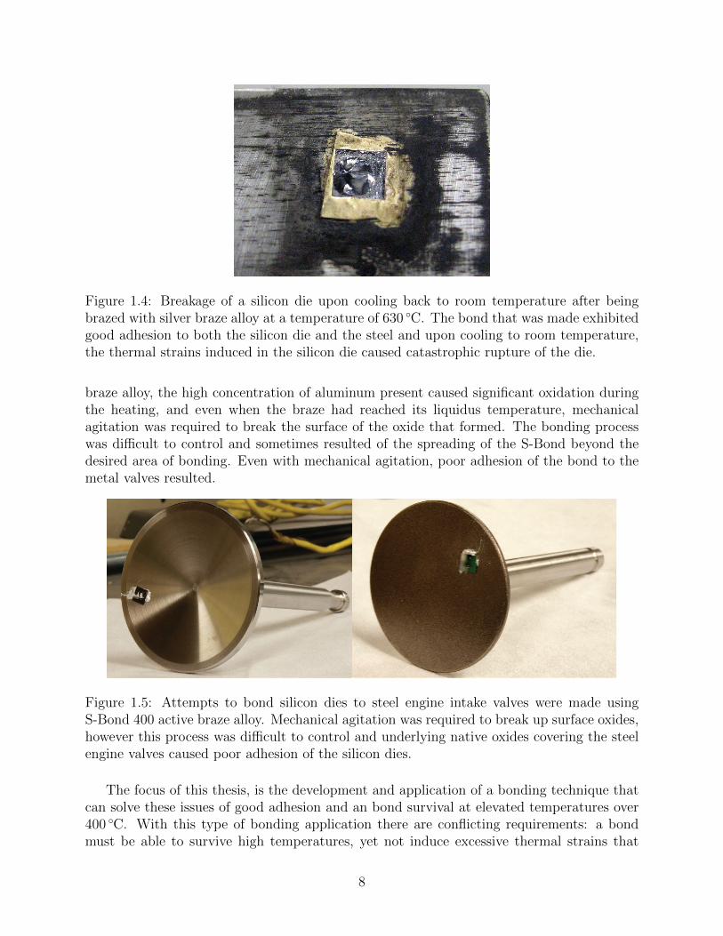
Figure 1.4: Breakage of a silicon die upon cooling back to room temperature after beingbrazed with silver braze alloy at a temperature of 630 ◦C. The bond that was made exhibitedgood adhesion to both the silicon die and the steel and upon cooling to room temperature,the thermal strains induced in the silicon die caused catastrophic rupture of the die.
braze alloy, the high concentration of aluminum present caused significant oxidation duringthe heating, and even when the braze had reached its liquidus temperature, mechanicalagitation was required to break the surface of the oxide that formed. The bonding processwas difficult to control and sometimes resulted of the spreading of the S-Bond beyond thedesired area of bonding. Even with mechanical agitation, poor adhesion of the bond to themetal valves resulted.
Figure 1.5: Attempts to bond silicon dies to steel engine intake valves were made usingS-Bond 400 active braze alloy. Mechanical agitation was required to break up surface oxides,however this process was difficult to control and underlying native oxides covering the steelengine valves caused poor adhesion of the silicon dies.
The focus of this thesis, is the development and application of a bonding technique thatcan solve these issues of good adhesion and an bond survival at elevated temperatures over400 ◦C. With this type of bonding application there are conflicting requirements: a bondmust be able to survive high temperatures, yet not induce excessive thermal strains that
8

cause the bond to fail. This dissertation resolves this issue through the use of the solid-liquid interdiffusion bonding process, described in detail in Chapter 2.
1.3 Materials for Bonding
This dissertation investigates the bonding of silicon to silicon and the bonding of siliconcarbide to steel. These two materials are important for sensor deployment of MEMS andcircuits into traditional commercial electronics applications and high temperature harsh en-vironment applications. The majority of today’s MEMS sensors are made from silicon forcommercial grade applications and for high temperature harsh environment applications, sil-icon carbide devices have drawn much attention for their mechanical, electrical, and chemicalrobustness. With myriad MEMS sensors for all different applications, the packaging require-ments are not uniform across the wide range of applications.
Silicon to silicon bonding is widespread throughout the electronic industry and manytypes of bonding processes for joining silicon, including anodic bonding and solder reflowbonding, have been developed and well documented. The hermetic sealing of cavities andthe direct bonding of silicon to silicon are typical packaging needs that must be fulfilled.This work starts with an investigation of silicon to silicon bonding using the SLID processbecause crystalline silicon wafers are significantly more cost effective and readily availablethan crystalline silicon carbide wafers. Bonding with silicon makes for a good starting pointfor the process development of a bonding method that could be translated to the siliconcarbide material system.
For the high temperature harsh environment aspect of this project, the joining of siliconcarbide to steel is extremely compelling. Steel is one of the world’s most prevalent engineer-ing materials, with uses in automobiles, pipelines, buildings and other aspects of the builtinfrastructure. The majority of engineering systems that handle or operate in high temper-ature harsh environments are fabricated out of various grades of steel. In this work, with anemphasis on harsh environment bonding, type-316 stainless steel was chosen for use as thebase substrate material used for bonding. Type-316 stainless steel is an abundant marine-grade engineering material used when corrosion resistance is required [31]. In this workthe 4H polymorph of silicon carbide was chosen for bonding because it’s increased electronmobility and larger bandgap than the more commonly used 6H silicon carbide polymorph[32]. In the niche of high temperature harsh environment electronics, 4H silicon carbide isgaining significant interest for the development of new transistors and circuitry which willsoon directly integrate with silicon carbide MEMS devices. This bonding research aims topave the way to enable the direct bonding of such future circuits and MEMS.
1.4 Outline of Dissertation
This dissertation covers the solid-liquid interdiffusion bonding process in Chapter 2, fol-lowed by the theory used to design the bond in Chapter 3. The characterization and testingof the bond are presented to show that SLID bonding is an appropriate approach to solvingthermal mismatch issues encountered with bonding for high temperature harsh environments
9

are discussed in Chapter 4. Lastly the conclusion is presented and some key directions forfuture works in high temperature harsh environment bonding are laid out in Chapter 5.
10

Chapter 2
Solid-Liquid InterDiffusion BondingProcess
Alloying in metallurgy is a technique that has been observed as early as 3000 BCE, duringthe Bronze Age and it has played an important role in both the development of technologyand human history. The concept of melting metals together in various proportions to createalloys with different mechanical properties or to join materials together has a long historyand has been well documented. Diffusion bonding as we know it was already exploredin the 16th century by Italian goldsmith Benvenuto Cellini, who joined small decorativegold spheres onto ornate gold artwork using a reducing flame and copper oxide paint as asolder[33, 34]. The operating principles behind these old processes hold much value and havemuch value when applied to today’s cutting-edge semiconductor packaging technology. Thefollowing sections detail the process and mechanism of the solid-liquid interdiffusion (SLID)bonding, the joining of silicon to silicon using SLID bonding and the joining of silicon carbideto steel.
2.1 The Process of Solid-Liquid InterDiffusion
The SLID process, sometimes also known as the transient liquid phase (TLP) bondingprocess or isothermal solidification bonding process, is a type of diffusion bonding processthat differs from typical wide-gap brazing that is encountered in macro-scale engineeringbecause it relies upon the interaction of solid and liquid phases with the bonding temperatureheld constant. The SLID process arose in the late 1950s and early 1960s and by that timesignificant amounts of work had been conducted on understanding soldering and brazingprocesses as well as the diffusion of metals. The basic SLID process involves the use of twometals, M1 and M2, which are capable of forming intermetallic alloys with one another. Ahypothetical phase diagram for the M1 and M2 material system is presented in Figure 2.1for clarity. As described by Tuah-Poku, the simplest case used to illustrate the SLID processconsists of two layers of M1 that are to be joined by an interlayer of M2. It is acceptedthat there are four distinct steps that make up the SLID process and as described by Tuah-Poku these steps are: the dissolution of the interlayer used, homogenization of the liquid,isothermal solidification and homogenization of the bond region [35].
11

Figure 2.1: A generic binary phase diagram with one eutectic point is provided here for theexplanation of the SLID bonding process. This hypothetical phase diagram is for two metals,M1 and M2 which are used as the SLID bonding layer in the described bonding process.
In the first step, one metal, M2, is chosen to be the interlayer and the other, M1, isused to sandwich the M2 interlayer. Some bonding force must be applied to ensure excellentcontact of the faying surfaces of M1 with the M2 interlayer. The temperature is raised abovethe melting point of the eutectic composition of M1 and M2, shown at the eutectic pointin Figure 2.1, and is held at a constant temperature for the rest of the bonding process.Due to the intimate contact of the two metals, some of the solid M1 dissolves into M2
interlayer. This dissolving process continues because there is a concentration gradient witha surplus of M2 and it is energetically favorable for the dissolution to continue at the bondingtemperature. This process continues into the second step, the homogenization of the liquid,as more M1 dissolves into M2 until M2 is completely and the liquid composition behindbecomes homogenous and the liquid zone widens to its maximum thickness. Following this,the third stage of the SLID bonding process occurs: isothermal solidification. In isothermalsolidification, the surplus of solid M1 that contacts the liquid mixture of M1 and M2 beginsto diffuse into the liquid mixture. As this happens, the liquid zone begins to shrink andsolidify as its composition changes and completely freezes [36]. Fick’s second law of diffusiongoverns the rates at which the diffusion reactions occur and the Gibbs free energy dictatesthe change of states. In the final stage of the SLID bonding process, solid-state diffusioncontinues with the homogenization of the bond until the system reaches equilibrium [37].The final composition of the SLID bond depends on the thicknesses of the layers used atthe start of bonding. Depending on how much M1 and M2 are supplied, after the bondhomogenizes and the intermetallic alloys have been formed, there may be an excess of pureM1 or pure M2 left after bonding.
The SLID process has been the subject of focus for many research groups. Many macro-scale applications of the SLID process have been studied for the joining of titanium alloys,
12

nickel superalloys, stainless steel and aluminum [38, 39, 40]. In these large-scale structuralapplications the temperatures and metallurgy used for SLID bonding require the use oftemperatures similar to those in traditional reflow brazing operations and the CTEs of thematerials being joined are closely matched: for joining nickel superalloys, bonding temper-atures above of 1090 ◦C are used; for joining stainless steel, temperatures over 870 ◦C wererequired; for titanium joining, the temperatures used exceed 700 ◦C; and for joining alu-minum, bonding temperatures are over 550 ◦C [41, 42]. Additionally, with the thicker layersused, the times required for the diffusion of the bonds are increased to several hours [43],with homogenization of the bond taking up to 100 hours. In these works, the SLID bondingprocess involves the bonding of two pure metals with both relatively high melting points andwhose phase diagrams have an low melting point eutectic point. By requiring the solid metalsto form an intermetallic liquid through solid state diffusion, bonding times are significantlyincreased.
Several groups have specialized in using the SLID process for microelectronic packagingapplications [44, 45, 46, 47, 48]. In these studies, the goal of SLID bonding is somewhatdifferent from that of the aforementioned macro scale engineering systems. For these ap-plications, the bonding utilizes the direct melting of a low melting point metal to form aliquid phase, instead of relying upon solid-state diffusion. Using this method, diffusion isapproximately 3 times faster and bonding times can be reduced significantly [49]. With mi-croelectronic devices, lower processing temperatures and faster bonding times are attractivedue to the thermal budget of the components and so different metal systems are used. TheSLID bonding process can not only be applied to the bonding of substrates to circuit boardsbut to the hermetic sealing of MEMS cavities. The SLID bonding process is achievablewith metals commonly used in microelectronic fabrication, including gold, titanium, nickel,silver, tin and indium. One added benefit of performing the SLID bonding process withlow melting point metals such as indium or tin is that if the bonding temperature is abovethe liquidus temperature of the low melting-point metal, the liquid metal will make goodcontact with the sandwiching layers and the need for applying high clamping forces duringbonding is reduced. Additionally, with smaller scale components, bond layer thicknesses canbe reduced and the processing time for bonding can be reduced.
One major benefit of the SLID bonding process, and the one that is of greatest importanceto this study on SiC to steel bonding, is that with the right choice of materials for bonding theprocess can be tailored to achieve a low bonding temperature with much higher operationaltemperatures. This type of behavior has been studied in several material systems includingcopper-tin, copper-indium, silver-tin, silver-indium, gold-indium and gold-tin [50, 51, 52, 53,54, 55]. With these material systems, the copper, silver and gold each serve as the highmelting point metal while the tin and indium play the role of melting point depressants asthey reduce the temperature required for bonding. As the solid-liquid interdiffusion processis carried out in these systems, intermetallic compositions with melting points greater thanthose of indium and tin are formed. This aspect of SLID bonding is highly appealing formicroelectronics applications where subsequent elevated temperature steps are required whilethe bond remains intact.
13

Figure 2.2: Okamoto’s phase diagram of the gold-tin material system[59]1
2.2 Material System Selection for SLID Bonding
For SLID bonding of silicon carbide to stainless steel for high temperature applications,the gold-tin material system was chosen. There are many benefits of the using the gold-tinmaterial system for SLID Bonding. Gold is an inherently corrosion resistant material anddoes not easily oxidize. This enables the gold-tin SLID bonding process to be performedwithout the use of fluxes which can detrimentally affect the bond, as mentioned in Section1.2. This oxidation resistance has enabled the gold-tin SLID bonding process to be per-formed in ambient atmospheric air environments, free from the use of forming gas or otherprocessing gasses [56]. For commercial applications or bonding of silicon carbide sensors tocomponents in the field, this aspect is highly attractive. With reported gold diffusivitiesof 5.8 × 10⁻³exp−(11000/RT)cm2 s−1 along the c-direction in the crystal structure of tin and1.6 × 10−1exp−(17700/RT)cm2 s−1 along the a-direction of the tin crystal, gold quickly diffuseinto tin at elevated temperatures which reduces the time required for bonding [57]. Alongwith the good diffusion rates, alloys of gold-tin exhibit good wetting with gold, ensuring thatduring the bonding process a good liquid layer can be formed, and large clamping forces forbonding are not required [58]. Additionally, there are intermetallic compositions of gold-tinthat are suitable for high temperature survival, above 450 ◦C.
14

Figure 2.3: The steps of the solid-liquid interdiffusion bonding process, expanded into 6images for clarity and completeness. In each step of the process, the layers of the SLIDbond are shown on the left. The top layer in green is the silicon carbide die and the greylayer at the bottom of the stack is the type-316 stainless steel substrate. To the right of eachmaterial stack, the composition of the bond layers, as lined up with the phase diagram below,is presented to show the evolution of the SLID bonding stack as the process progresses. Thephase diagrams provided show the Au - Au80%wt.-Sn20%wt. metal system.
Gold is also widely used throughout microelectronic and MEMS industries, so fabricatingprocesses with gold are compatible with such applications. It readily adheres to commonlyused adhesion layers such as nickel, titanium and aluminum. In the case of the gold-tin metalsystem, pure gold serves as the high melting point metal, with a melting point of 1064.43 ◦C,and pure tin or gold-tin eutectic (Au80%wt.-Sn20%wt.) can serve as the low melting pointmetal with respective melting points of 232 ◦C and 278 ◦C. The gold-tin material systemconsists of seven different stable intermetallic compositions: Au0.970Sn0.030 (α), Au3.6Sn0.4(β),Au0.85Sn0.15(ζ which exists above 190 ◦C), Au5Sn(ζ’ which exists below 190 ◦C), AuSn(δ),AuSn2(ε), and AuSn4(η). The phase diagram of the gold-tin metal system is provided inFigure 2.2. From analyzing this phase diagram it is evident that the β and ζ phases of gold-tin, with respective melting points of 532 ◦C and 522 ◦C, are attractive for high temperatureharsh environment applications based on their high temperature stability.
In SLID bonding with the gold-tin system, if pure tin is used as the melting pointdepressant for bonding with pure gold with a thickness ratio of at least 3Au:2Sn, uponbonding at temperatures between 232 ◦C and 419 ◦C, the tin layer melts and turns completelyliquid. The gold that is in contact with this molten tin dissolves into the liquid, as isprescribed by the SLID process. However, there is a tendency for the composition to toreach the δ phase and settle there and form a AuSn barrier layer, due to the minimizing of
1Figure reproduced with the expressed permission of Springer Link and ASM International
15

the Gibbs free energy of the system. With this system, if there is additional gold and the goalis to make a final bond composition that is more gold rich, the temperature must be raisedabove the 419 ◦C melting point of δ phase gold-tin in order for the diffusion to progress andrun to completion [20]. To get around the issue of terminating the diffusion process at theδ phase, the Au80%wt.-Sn20%wt. eutectic composition can be used in substitution for puretin. In soldering, the most commonly used gold-tin alloy is the Au80%wt.-Sn20%wt. eutecticsolder and it consists of a mixture of the Au5Sn (ζ’) and AuSn (δ) phases. By starting theSLID process with the eutectic alloy on the gold rich side of the phase diagram, it is possibleto drive the SLID reaction towards the ζ and β phases and bonding must be performed above278 ◦C to liquefy the Au80%wt.-Sn20%wt. alloy. The process of SLID bonding with puregold and Au80%wt.-Sn20%wt. eutectic solder is shown in Figure 2.3 along with a detailedschematic of the composition of the bond layers in each of the SLID process steps.
2.3 Fabrication Process for Silicon to Silicon Substrate
SLID Bonding
An initial investigation was performed to understand the process of SLID Bonding usingsilicon dies. Silicon, being less expensive than silicon carbide, was deemed a good place tostart for understanding the bonding process. Additionally, as outlined in Section 1.3, thebonding of Si to Si using the SLID process to package silicon based MEMS or microelectronicscan provide additional freedom to the thermal budget of subsequent processing steps. Usingreadily available microfabrication techniques in the UC Berkeley Marvell NanofabricationLaboratory, the bonding of silicon to silicon using thin metal films investigated the feasibilityof thin film SLID bonding.
Two prime grade silicon wafers with {1 0 0} crystal orientation and p-type doping withdifferent thin-film metallizations were chosen for bonding to one another. The thicknessesof the metallization are provided in Table 2.1. The metal thin-films were deposited ontothe wafers sequentially under continuous vacuum using an Edwards Auto-306 electron beamevaporation tool. Film thicknesses during deposition were monitored using a crystal growth-rate monitor and later verified using scanning electron microscopy.
Table 2.1: The thicknesses used for the metallization of Si substrates in Si to Si SLID Bondingexperiments.
Wafer Name ChromiumAdhesion LayerThickness (nm)
Gold FilmThickness (nm)
Tin LayerThickness (nm)
TLP3 20 200 250TLP6 50 275 305
Following film deposition, the wafers were coated with a protective coating of OCG
16

Figure 2.4: Bonding combinations with different metal layer thicknesses used in Si to SiSLID bonding. Three gold-tin metal layer thickness variations were tested: TLP3 to TLP3,TLP6 to TLP 6 and TLP6 to TLP3.
OiR-700 10 i-line Photoresist, 2 µm thick, to protect the evaporated films during the dicingprocess. A Keteca K3T20L45 dicing blade was used to cut the Si wafers into 1 cm by 2 cmrectangles. A cutting speed of 1.0 mm s−1 was chosen to reduce potential chipping of thesilicon dies, and a dicing height was selected to cut completely through the bottom of thesilicon wafer. The dies were cleaned with acetone, isopropanol, and methanol and dried withan N2 spray gun. The metalized dies were not dried using a hotplate because the elevatedtemperatures for drying would initiate the premature diffusion of the gold into the tin film.
For this study, a Yield Engineering Systems vacuum oven was used for the bonding ofthe Si samples. The samples were placed in contact with one another as shown in Figure2.4 and a 500 g weight was placed on top of each sample to provide a constant low clampingforce during the bonding. The bonding chamber was pumped down to a pressure of 200 torrprior to the start of heating. The heating program ramped the temperature from ambientroom temperature, 25 ◦C, to 350 ◦C in 1 hour, followed by 30 minutes of dwell at 350 ◦C anda cooling back down to 25 ◦C. The cooling of the chamber from 350 ◦C to 25 ◦C was verygradual and took 6 hours. The details of the analysis and characterization of the silicon tosilicon bonds are discussed in Chapter 4.
2.4 Fabrication Process for Silicon Carbide Substrate
to Steel SLID Bonding
The fabrication process for making the SiC to steel SLID bonds was a bit more involvedthan that for the initial Si to Si SLID bonding investigation; however it consisted of threeprimary steps: the deposition of gold layers onto the faying surfaces of the substrates beingbonded, the selection and placement of the low melting-point metal, and the heating process.This section details the specific process steps that were developed for the fabrication of thesilicon carbide to steel SLID bonding process.
17

2.4.1 The SiC Substrates
For this work, commercially available 4H silicon carbide substrates, (model number:W4NRF0X-0D00), were purchased from Cree. These wafers were 100 mm research gradeSiC with nitrogen N-type doping, double-side polished and 523 µm in thickness. Siliconcarbide in the 4H polymorph was chosen for this work because of its suitability for use infabricating silicon carbide electronics for high temperature applications. The silicon carbidewafers are manufactured and cut with one of the polished sides having a carbon-rich face andthe other having a silicon-rich face. In this work, the silicon-rich face was used for bondingand the subsequent metal layers and processing was performed on the silicon-rich face.
The deposition of a high-quality seed layer ensures good adhesion of the subsequent metallayers that are deposited onto the Si and SiC substrates. This adhesion is critical for thesurvival of the bond. E-beam evaporation was chosen as the method to deposit the adhesionlayers onto the 4H SiC substrate, using the Edwards Auto-306 electron beam evaporator tool.Prior to deposition the Edwards Auto 306 vacuum chamber housing the e-beam evaporatorwas purged and vented with nitrogen before pulling vacuum to 5× 10⁻⁶ torr. The purging,in combination with a liquid nitrogen trap, ensured that residual water vapor in the chamberwould not interfere with the deposition process and degrade the quality of the films beingdeposited. During deposition, the film thicknesses were measured using a resonating crystalmonitor with a tooling factor of 0.5. This tooling factor was calibrated by measuring thefilm thicknesses on test wafers using scanning electron microscope.
While several metals such as nickel and chromium are commonly used for adhesion ofmetal films to Si and SiC, titanium was chosen to be the metal used for the adhesion layer.Gold interacts with Ni and Cr by rapidly diffusing into the Ni or Cr to form intermetallicfilms and such films have been observed to form during high temperature bonding[60, 61].With this rapid diffusion, the formation of voids were observed by Tsai and Bohan. Titaniumadhesion layers, on the other hand, have been demonstrated to work well with gold filmswithout such drawbacks [62]. Using high purity (99.9 % pure) titanium pellets from AlfaAesar a titanium adhesion layer of 50 nm in thickness was deposted. Immediately followingthe deposition of the titanium adhesion layer a 50 nm thick seed layer of gold (99.9 % purity)was also deposited using electron-beam evaporation. Vacuum was not broken between tita-nium and gold depositions to minimize potential contamination and to ensure good adhesionbetween the layers.
2.4.2 The Type-316 Stainless Steel Substrate
As the aim of this project is to directly bond silicon carbide dies to stainless steel afabrication process for electroplating stainless steel dies that could eventually be transferredto locally electroplating large steel components was developed. The work in this dissertationfocuses on bonding silicon carbide dies to stainless steel substrates, which could then bejoined onto other steel components. For this project, type-316 stainless steel sheets, 762 µmthick, were used as the substrates to which the silicon carbide dies would be bonded. Thesteel was punched into 1 cm by 1 cm squares in the UC Berkeley Mechanical EngineeringMachine shop using a hydraulic press. After punching, the steel was flattened using anotherpress to ensure flatness. The surface of the stainless steel was them mechanically sanded
18

using 800 grit sandpaper followed by 1200 grit sandpaper to reduce the surface roughnessto approximately 5 µm. Following sanding, the stainless steel samples were cleaned withacetone, isopropanol, and methanol.
2.4.3 Electroplating of Soft Gold
Physical vapor deposition techniques, such as evaporation and sputtering, are capable ofdepositing high purity metal films onto a substrate; however, during thick-film depositionsmuch metal would be spent coating the walls of the evaporation chamber instead of theactual substrate. With precious metals such as gold, such waste would be inexcusable and soelectroplating was chosen as the method for the deposition of thick gold films. Electroplatingis a cost-effective deposition method and it reduces the amount of wasted metal; however,with electroplating there are added challenges to obtain high quality films with good purity.Electroplating of gold is typically conducted using either direct current (DC) or pulsedcurrent electroplating.
Several gold electroplating chemistries are readily available and these include cyanide-based solutions, acid-based solutions and non-cyanide solutions [63, 64]. Of these platingbaths, alkaline cyanide baths are not well suited for use with the photoresists used in semi-conductor processing. Alkaline cyanide electroplating solutions have a tendency to attackthe photoresist used for patterning the substrate being plated because of their high pH andhigh concentration of free cyanide. Acidic cyanide baths, while suitable for electroplatingwith photoresists, can exhibit a tendency to co-deposit cobalt and potassium complexes [65].Non-cyanide baths can be used as an alternative to toxic cyanide based solutions, howeverthey also introduce issues with stability and plating consistency [66]. Electroless gold platingmethods are also available, however, these methods are not well suited for the deposition ofthick gold films.
For this work, Technigold 434RTU, a commercially available soft gold and neutral pHelectroplating solution, was chosen. Soft gold is pure 24 Carat gold, in contrast with hardbright gold which has added nickel and cobalt to improve hardness and luster. In goldelectroplating, the deposition of gold at lower current densities and higher mass transport,from agitation, reduces the porosity of the gold films, however, it also increases the chancesof depositing impurities that may be present in the electroplating bath. Higher currentdensities may be used to reduce the presence of impurities at the tradeoff of increasing metalgrain size. The ideal high quality gold film would have small grain sizes and no impuritiespresent.
For the deposition of the soft gold, an electroplating bath setup was built, shown inFigure 2.5. Before using the electroplating tank, the setup was cleaned and leached withsulfuric acid according to the manufacturer’s recommendation. The plating setup utilized ahot water bath to heat the electroplating solution in a non-reactive polypropylene containerto the temperature of 62 ◦C, within the manufacturer’s recommended range of 60 ◦C to 65 ◦C.Temperature of the electroplating solution was monitored using a glass thermometer placedinside the solution. Mechanical agitation of the plating solution to improve mass transportof the electrolyte to the plating work was achieved using a magnetic stirrer. A 5 cm by5 cm titanium electrode platinized with 125 µm thick platinum cladding was used for theelectroplating anode. The lid of the polypropylene container was modified to accommodate
19

Figure 2.5: The electroplating bath used for depositing gold onto semiconductor substratesand stainless steel substrates. A nickel strike solution, shown in the foreground, was used toimprove adhesion of the electroplated gold onto the stainless steel.
20

Figure 2.6: The four steps of the fabrication process used to prepare the MEMS substratefor the SLID bonding process.
the placement of the platinized anode and allow for the insertion of a workpiece for plat-ing. The separation between anode and workpiece was set at 5 cm. To monitor the currentand voltage used for electroplating, a Keithley 2400 Source-Meter was used to provide theconstant-current used for electroplating while measuring the voltage potential. A recom-mended current density of 0.3 A
dm2 was used to electroplate at a deposition rate of 0.19 µmmin
.A LabVIEW virtual instrument was programmed to record the voltage potential and currentversus time, to monitor the electroplating conditions.
Electroplating on SiC Substrates
The electroplating of the silicon carbide substrates involved two steps, the dicing of thesilicon carbide wafer into smaller, more manageable samples, and the electroplating of thesubstrates in the previously mentioned electroplating bath setup. Following the evaporationof the 50 nm titanium and 50 nm gold seed layers on the 100 mm silicon carbide wafer, thesamples were diced. To ensure an anode-to-cathode area ratio of at least 1:1, the siliconcarbide wafer was diced into 23 mm by 23 mm squares. Prior to dicing the samples werecoated with 2 µm of OCG OiR-700 10 i-line Photoresist to protect the surface of the e-beamevaporated titanium and gold layers.
Dicing of the samples was performed using a Disco DAD 3420 automatic dicing saw.A Dicing Technologies CX-010-270-090-H blade was used for the cutting of silicon carbidesamples. A dicing speed of 0.65 mm s−1 was used to reduce chipping and scalloping of theedges of the samples. Chips and scallops in the substrate could cause unnecessary stressconcentrations that would affect the quality and performance of the subsequent bonds duringtesting. Following dicing, the samples were cleaned in acetone to remove the protectivephotoresist, then rinsed with isopropanol, rinsed with methanol, and dried on a hotplate at110 ◦C for 3 minutes to remove any residual moisture from the samples.
21

Figure 2.7: Confocal microscopy of the electroplated SiC die as performed to measure uni-formity across the surface of the die as well as to measure the thickness of the plated film.
With the silicon carbide samples diced into 23 mm by 23 mm samples and cleaned, thesesamples were alligator clipped in a corner to make contact with the e-beam evaporated goldseed layer and placed into the electroplating bath. The alligator clip was positioned so thatit was not submerged in the plating solution. For the size of the sample, a plating currentof 12.55 mA was used to electroplate according to the manufacturer’s recommended currentdensity with a rate of 0.19 µm
min. The duration of time used for electroplating was varied
in order to adjust the thickness of the deposited gold films. Electroplating times and theresulting gold film thicknesses are discussed in Chapter 4. Following the electroplating ofthick gold onto the silicon carbide squares, the samples were again coated with a 2 µm thickprotective coating of OCG OiR-700 10 i-line Photoresist, and diced into 3.8 mm by 3.8 mmsquares for bonding with the SLID process. A complete overview of the fabrication processused to prepare the silicon carbide substrates for SLID bonding is shown in 2.6.
After the final dicing of the electroplated into square dies for bonding, the dies wereoptically inspected using an Olympus LEXT OLS4000 confocal microscope to verify thethickness of the plated gold and the surface uniformity of the plated film, as shown in Figure2.7. It was found that the film thickness uniformity was good across the die, and the averagesurface roughness and root mean square roughness were 0.247 µm and 0.331 µm respectively.The skewness and kurtosis of the area was 0.327 and 6.385 respectively. These values showthat the surface of the electroplated gold was quite smooth, however there were localizedareas that had slight peaks. During the SLID bonding process, the liquid layer formed woulddissolve these areas first and the homogenization of the bond would even out the compositionof the bond. Additionally, as a result of the final dicing process, there was a slight raise inthe gold electroplated film thickness near the edge of the dies. During dicing, it is suspected
22

that the dicing saw smears the soft pure gold during cutting and causes a slight bulge in thegold film at the edges of the dies. The average raise in film thickness at the edge of the dieswas found to be 1.58 µm. Though this raise in height at the edges of the die would causeinitial contact at the periphery and initiate diffusion at the edge of the bond, during theSLID bonding processes the liquefied solder would be able to make uniform contact acrossthe bond surface.
Electroplating on Type-316 Stainless Steel
An electroplating process was developed to metalize the type-316 stainless steel with puregold. With the potential transfer of fabrication process from metalizing 1 cm by 1 cm steeldies to much larger real-world engineering components, a method of locally electroplating thesteel was developed. A photolithography process was used to pattern an area on the stainlesssteel substrate for electroplating. This photoresist would serve as a mask for the subsequentelectroplating process, protecting the underlying steel from electroplating. Following thecleaning of the steel samples discussed in Section 2.4.2, the steel samples were coated with athick layer of Rohm-Hass Megaposit™SPR™220 Photoresist. A manual photoresist spinnerwas used to coat the steel substrates with 15 µm of photoresist. After coating the backs of thestainless steel samples, the photoresist was hardened by baking on a hotplate at 80 ◦C for 60minutes. Following this bake step, the front sides of the stainless steel were manually coatedwith another 15 µm thick layer of SPR 220 photoresist. A prebake of this new photoresistcoating was performed for 300 seconds at 115 ◦C. A lithography mask with an 31.67 mm2
opening in the center was used to pattern the opening for electroplating and a Karl SussMA6 mask aligner was used to expose the prebaked photoresist with a does of 300 mJ
cm2 .Following exposure, the samples were allowed to hold in darkness for 120 minutes to ensureproper photo-reaction before performing the post-exposure bake. The post-exposure bakeconsisted of heating the steel dies to 115 ◦C for 6.5 minutes and then gently cooling backto room temperature. Rohm-Hass Megaposit™MF™-26A Developer was used to develop thepatternedphotoresist. Following this, a final hardbake for 15 minutes at 80 ◦C was performedto harden the patternedphotoresist in preparation for direct electroplating. The sequence ofprocessing steps is outlined in Figure 2.8.
Electroplating gold directly onto stainless steel is not as straightforward as electroplatingit onto metalized silicon carbide substrates. Stainless steel is inherently more resistant tocorrosion than ferretic steels because of its higher chromium content, which is capable offorming a passive film of chromium (III) oxide (Cr2O3). This thin protective oxide has arelatively low resistance and hence plating layers can form on top of it; however, in terms ofadhesion, these plated films exhibit poor adhesion to the native oxide present on stainlesssteel. Initial electroplating experiments with gold films directly on stainless steel dies revealedpoor adhesion. This poor adhesion was characterized using an ASTM adhesion test (D3359-09) of the electroplated gold, as shown in Figure 2.9. Pressure sensitive tape was used toadhere to the gold plated film and in accordance with the ASTM testing standard, the tapewas pulled back at an acute angle, as close to 0° as possible, in relation to the surface of thesample. The poor adhesion of the film was characterized by the delamination of the goldfrom the steel.
To overcome this obstacle in gold film adhesion, a pickling step and a plating strike
23

Figure 2.8: The six steps of the fabrication process used to prepare the type-316 stainlesssteel for the SLID bonding process.
were used to prepare the steel. The pickling of steel consisted of immersing the photoresistpatterned stainless steel in 30% hydrochloric acid (HCl) for 60 seconds. This process etchessurface oxide that forms on the exposed stainless steel. Immediately after pickling, the steelwas connected to an alligator clip and placed in the nickel strike bath, and electroplated.The nickel strike solution consisted of 60 g L−1 of commercially available Krohn Nickel BrightPlating Solution and 80 mL L−1 HCl. The nickel bright plating solution contained nickelchloride (NiCl2) and nickel sulfate (NiSO4), and the proportion of Krohn Nickel BrightPlating Solution to HCl was determined to have the proper concentration of nickel chlorideto HCl as called for in the recipe for Wood’s Nickel Strike bath. For the electroplating ofstainless steel, Wood’s Nickel Strike is a plating solution with low ion concentration thatis used in conjunction with high electroplating current densities, to electrodeposit a thinfilm onto the stainless steel to improve the adherence of subsequent electroplated layers. Asstudied by Dini et al., following the use of Wood’s Nickel Strike or Nickel Sulfamate Strikeon stainless steel, adhesion of the plated layers was significantly improved, and maximumbond strengths were achieved when a current density of 1076 A m−2 was used [67]. In thenickel strike process used for preparing the stainless steel for the SLID bonding process, acurrent of 31.67 mA and plating time of 120 seconds were used to deposit the thin nickellayer, of a few nanometers in thickness. This current, given the size of the electroplatingarea, corresponded to a current density of 1076 A m−2. To make electrical contact with thestainless steel sample, the protective photoresist was scratched off in a corner of the die, sothat an alligator clip could make direct contact to the steel. The stainless steel was held inplace so that only the exposed area for SLID bonding was submerged in the electroplatingsolution. A stainless steel anode, 1 cm wide and 3 cm long, was used for this strike processand mechanical agitation was provided by stirring with a glass rod.
Following the nickel strike process, the stainless steel was rinsed in deionized water beforeimmersion in the gold electroplating bath. Gold electroplating was performed in the same
24

Figure 2.9: Adhesion testing was performed on the electroplated gold films. In the electro-plating of the sample shown in the top row, the HCl pickling and nickel strike steps wereomitted. From left to right, the progression of the ASTM D3359-09 testing is shown. Forthe sample shown in the bottom row, both HCl pickling and nickel strike steps were used.From left to right, the adhesion test shows significant improvement of adhesion.
electroplating setup used for electroplating the silicon carbide substrates. Thorough rinsingin the deionized water would help to reduce the likelihood of contaminating the gold platingbath. For the plating of gold films on the stainless steel, a current of 1.2 mA, with a currentdensity of 0.37 A
dm2 . The electroplating times were varied to change the thickness of the films.Following electroplating, the deposited gold films on the stainless steel were characterized
using an Olympus LEXT OLS4000 confocal microscope. Step heights and surface roughnessmeasurements of the films were made as shown in Figure 2.10. For these gold films plated onstainless steel, the averaged root mean square roughnesses and the average roughnesses forthe electroplated samples were 0.310 µm and 0.229 µm respectively. The average skewwnessand kurtosis were 0.5815 and 7.647 respectively. As a result the topography of the electro-plated gold films on stainless steel were quite similar to the films deposited onto the siliconcarbide substrates.
2.4.4 Selection and Preparation of Low Melting-Point Metal
With the gold-tin material system chosen for SLID bonding, and the selection of Au80%wt.-Sn20%wt. eutectic solder as the chosen melting point depressant, solder preforms were ob-tained for bonding. Preforms in sizes 1 cm by 1 cm by 5 µm and 1 cm by 1 cm by 12.7 µmwere purchased from AMETEK. For SLID bonding, the preforms were cut into 5 mm by5 mm squares using scissors. These preforms were cut larger than the silicon carbide dies,so that full contact across the bonding area would be ensured when the bonding stacks wereassembled. As later discussed in Section 3.1, the choice of eutectic solder preform thicknessdictates the final composition of the SLID bond.
25

Figure 2.10: Confocal microscopy was performed to measure the step height and the surfaceprofile of the gold electroplating film on the stainless steel substrate after the electroplatingprocess. On the left, an 20× microscope image shows the gold electroplated steel and on theright, the step profile measured along the trace is provide.
2.4.5 Heating Process for SLID Bonding
The heating process for the SLID bonding consists of heating the bond to a temperatureabove the melting point of the eutectic alloy, in the case of this bonding research, theAu80%wt.-Sn20%wt. alloy. The bonding process also requires that the temperature be heldconstant while the bond isothermally solidifies and homogenizes. To perform these steps, abonding setup was designed and fabricated.
In the heating process there are several factors of key importance: the heating rate ofthe samples, the duration of the applied heating, and the environmental conditions of thebonding chamber. The heating rate of the bond must be high enough to ensure that melt-ing of the eutectic layer and resolidification of the generated intermetallics do not happenat temperatures much lower than the desired bonding temperature. If solid state diffusionand non-uniform solid-liquid interdiffusion occur too soon and form high melting point in-termetallics, voids can be left behind in the bonding layer [68]. These voids, known asKirkendall Voids, are a result of differences in diffusion rates of metals.
In this work various heating rates were tested and the best compromise between ther-mally shocking the materials in the bond and accomplishing a good bond was found to be aheating rate of 50 ◦C min−1 to bring the bond from room temperature, 25 ◦C, to the bondingtemperature of 300 ◦C. The bonding time used for the bonding of silicon carbide to steel waschosen to be 12 minutes. As reported by Tollefsen et al. in his studies of SLID bonding withthe gold-tin material system, good bond strengths were achieved with a bonding temperatureof at least 300 ◦C and a bonding time of at least 6 minutes. Increasing the bonding tem-perature and bond times beyond that showed no significant improvment of bond strenghth[56].
The construction of the heater setup is in Figure 2.11. Two stainless steel ConFlatvacuum flanges were machined and modified to fit the resistive heater and hold the samplesin place for bonding during the heating process. The base of the heater was machined tofit two insulating ceramic disks that would help hold the generated heat in and preventexcessive conduction from the resistive heater to the bonding setup and bonding chamber.The ceramic chosen for this was a low thermal conductivity alumina silicate ceramic. On
26

Figure 2.11: Schematic of the top and bottom halves of the bonding setup.
the top half of the heater, these low conductivity ceramics were also placed to thermallyisolate the bonding samples and prevent excessive heat escape to the bonding setup. Onthe top surface of these ceramic blocks, a K-type thermocouple was mounted to monitor thetemperature at that location in the bonding stack. The temperature response of the systemto different voltage inputs to the heater was characterized and it was calibrated so that arepeatable 300 ◦C bonding temperature, ±5 ◦C, could be obtained by following the heatingschedule.
To place the gold-metalized silicon carbide, Au80%wt.-Sn20%wt. solder preform andgold-metalized stainless steel substrate for bonding, the top half of the heater setup wasplaced flat. The stainless steel was first placed on the insulating ceramic layer, followed bythe solder preform and the silicon carbide die. The electroplated gold layers of the siliconcarbide and stainless steel were placed in direct contact with the solder preform. Alignmentof the edge of the silicon carbide die and the edge of the stainless steel was performed visually.After alignment of the bonding layers, the base of the heating jig, with the resistive heater inplace, was turned upside down and placed onto the top half of the heating jig, sandwichingthe layers of the bond in place and in direct contact with the heater. Six hex-cap bolts wereused as alignment pins to mate the top half of the heater setup to the bottom half, and toallow for additional weight, in the form of an additional ConFlat vacuum flange, to be addedfor increased bonding pressure. Figure 2.12 shows the fabricated components of the heaterand the assembled setup in operation.
Once the layers were brought into contact and alignment of the heater with the siliconcarbide die was confirmed, the assembly was brought into contact and the entire assemblywas inverted so that the top half was on top and the bottom half was on the bottom. Withthe additional ConFlat flange in place, the total weight pushing down on the bond was 720 g,equivalent to a 49.86 kPa bonding pressure distributed evenly across the 3.8 mm by 3.8 mmbond area. During bonding, an additional K-type thermocouple was used to probe the siliconcarbide die and the stainless steel substrate and measure the temperature of the bondingprocess at the location of the bond. A Stanford Research SR630 Thermocouple reader wasused to monitor the temperatures measured by the thermocouples using a LabVIEW virtual
27

Figure 2.12: The assembled bonding setup in operation.
instrument.In this study a 5 mm by 5 mm Sakaguchi E.H Voc Corp. MS-M1000 micro ceramic heater
was used to heat the samples to the bonding temperature. A Hewlett Packard 6263B DCpower supply with a 0 V to 20 V and 0 A to 10 A limit was used to provide power to theresistive heater. To heat the sample, the Power supply was operated in a voltage limitedmode and voltage was increased from 0 V to 8.5 V according to a calibrated heating-timeschedule. During the raising of the voltage, the current draw from the heater was an almostconstant 1.2 A. The heating-time schedule for the bonding is provided in Appendix B inSection B.4. Figure 2.13 shows the heating profile obtained when following the developedheating recipe with the resistive heater and power supply.
28

Figure 2.13: The temperature profile of the SLID Bond interface versus time, using thevacuum chamber heating setup.
29

Chapter 3
Design and Theory of SLID Bonds forHigh Temperatures Applications
As described in Chapter 2, to achieve the desired SLID bond and to have the proper alloycomposition for the desired melting point, the thicknesses of the SLID bond must be carefullytailored. In addition to the adjusting the metallurgical composition of the bond in order toachieve a high enough melting point for successful bonding, the mechanical properties ofthe different layers of the bond must also be considered to ensure proper bond survival. Inthis chapter, the theory and reasoning behind the layer thicknesses of the SLID bond arediscussed. Additionally, the analytical calculations and the finite element analysis modelsthat were used to support the design of the SLID bond are presented.
3.1 Tailoring the Thicknesses of the SLID Bond Layer
The amount of gold and tin present in the layers of the bond dictate the bond’s finalcomposition after the SLID bonding process is performed. The phase diagram of the gold-tin system, covered in Section 2.2, provides a roadmap for what intermetallic alloys willbe formed depending on the quantities of materials present during bonding. To predict thecomposition of the silicon to silicon SLID bonds and the silicon carbide to stainless steel SLIDbonds calculations were performed based on the atomic composition of the films used in SLIDbonding and the thicknesses of the films. For the silicon to silicon SLID bonds, compositioncalculations were performed for different thickness layers of electron beam evaporated goldand tin thin films. For the silicon carbide to steel SLID bonds, based on the two differentthicknesses of commercially available Au80%wt.-Sn20%wt. eutectic preforms, calculationsusing different thicknesses of gold electroplating were performed to determine how much goldwould be required to form the high melting point intermetallics and how much excess goldwould remain. In addition to determining the composition of the bond after diffusion, thelayer thicknesses play an important role in the mechanical transfer of stresses and thermallyinduced strains in the bond. Varying the thicknesses of the different layers shifts the neutralstress axis in the system and alters the distribution of in-plane stresses through the bond[69].
30
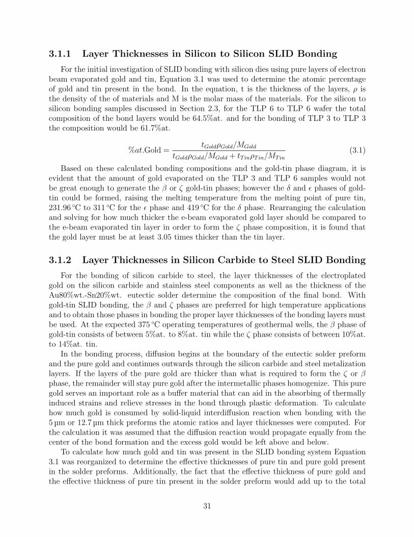
3.1.1 Layer Thicknesses in Silicon to Silicon SLID Bonding
For the initial investigation of SLID bonding with silicon dies using pure layers of electronbeam evaporated gold and tin, Equation 3.1 was used to determine the atomic percentageof gold and tin present in the bond. In the equation, t is the thickness of the layers, ρ isthe density of the of materials and M is the molar mass of the materials. For the silicon tosilicon bonding samples discussed in Section 2.3, for the TLP 6 to TLP 6 wafer the totalcomposition of the bond layers would be 64.5%at. and for the bonding of TLP 3 to TLP 3the composition would be 61.7%at.
%at.Gold =tGoldρGold/MGold
tGoldρGold/MGold + tT inρT in/MT in
(3.1)
Based on these calculated bonding compositions and the gold-tin phase diagram, it isevident that the amount of gold evaporated on the TLP 3 and TLP 6 samples would notbe great enough to generate the β or ζ gold-tin phases; however the δ and ε phases of gold-tin could be formed, raising the melting temperature from the melting point of pure tin,231.96 ◦C to 311 ◦C for the ε phase and 419 ◦C for the δ phase. Rearranging the calculationand solving for how much thicker the e-beam evaporated gold layer should be compared tothe e-beam evaporated tin layer in order to form the ζ phase composition, it is found thatthe gold layer must be at least 3.05 times thicker than the tin layer.
3.1.2 Layer Thicknesses in Silicon Carbide to Steel SLID Bonding
For the bonding of silicon carbide to steel, the layer thicknesses of the electroplatedgold on the silicon carbide and stainless steel components as well as the thickness of theAu80%wt.-Sn20%wt. eutectic solder determine the composition of the final bond. Withgold-tin SLID bonding, the β and ζ phases are preferred for high temperature applicationsand to obtain those phases in bonding the proper layer thicknesses of the bonding layers mustbe used. At the expected 375 ◦C operating temperatures of geothermal wells, the β phase ofgold-tin consists of between 5%at. to 8%at. tin while the ζ phase consists of between 10%at.to 14%at. tin.
In the bonding process, diffusion begins at the boundary of the eutectic solder preformand the pure gold and continues outwards through the silicon carbide and steel metalizationlayers. If the layers of the pure gold are thicker than what is required to form the ζ or βphase, the remainder will stay pure gold after the intermetallic phases homogenize. This puregold serves an important role as a buffer material that can aid in the absorbing of thermallyinduced strains and relieve stresses in the bond through plastic deformation. To calculatehow much gold is consumed by solid-liquid interdiffusion reaction when bonding with the5 µm or 12.7 µm thick preforms the atomic ratios and layer thicknesses were computed. Forthe calculation it was assumed that the diffusion reaction would propagate equally from thecenter of the bond formation and the excess gold would be left above and below.
To calculate how much gold and tin was present in the SLID bonding system Equation3.1 was reorganized to determine the effective thicknesses of pure tin and pure gold presentin the solder preforms. Additionally, the fact that the effective thickness of pure gold andthe effective thickness of pure tin present in the solder preform would add up to the total
31

thickness of the solder was used to develop a system of two equations and two unknowns todetermine the thicknesses of gold and tin present, as shown in Equations 3.2 and 3.3.
(%at.Gold− 1)tGoldρGold
MGold
+ (%at.Gold)tT inρT in
MT in
= 0 (3.2)
tGold + tT in = tPreformThickness (3.3)
The atomic percentage composition of the Au80%wt.-Sn20%wt. eutectic solder is 70.7%at.gold and 29.3%at. tin. Using this information, for the 5 µm thick solder preform the equiv-alent film thicknesses of pure tin and pure gold are 2.276 µm and 2.724 µm respectively. Forthe 12.7 µm thick preform, there is an equivalent 5.781 µm of pure tin and 6.919 µm of puregold. With the equivalent compositions of pure tin and gold in the preform known, it can befurther calculated to see how much additional pure gold from the electroplated layers wouldbe required to form the ζ and β phases.
With the effective layer thicknesses of pure tin in the preforms, it is possible to determinehow much additional pure gold would be consumed in making the ζ and β phases. For thecase of the 5 µm thick eutectic preform, a total gold layer of 6.934 µm thickness would berequired to form the ζ phase intermetallic, and for the β phase intermetallic it would take12.981 µm. In addition to the gold already in the solder preform, an additional 4.21 µm thicklayer of gold from the electroplated gold layers on the steel and silicon carbide would diffuseto form ζ phase gold-tin and an additional 10.257 µm of gold would be required for the βphase gold tin intermetallic. For the 12.7 µm eutectic preform, to form the ζ phase andβ phase intermetallics it would require 17.612 µm and 32.972 µm thick layers of pure gold,respectively. In addition to the gold already present in the 12.7 µm preform, it would require10.693 µm and 26.053 µm of gold from the electroplated layers to form the ζ and β phases ofgold tin. It is apparent from these calculations that a large amount of pure gold is requiredto form these gold-rich intermetallic compounds. Additionally, if the electroplated gold layerthickness is not large enough on the silicon carbide or steel side, then the diffusion of the tinwill reach the silicon carbide or steel. The choice of electroplating layer thickness should bemade to ensure enough gold is present on either side of the bond.
3.2 Analytical Modeling of Thermally Induced Strains
To calculate and understand the thermally induced stresses encountered by bonding theSiC samples to steel, an analytical model was created to determine the in-plane stressesoccurring at different locations of the bonding stack as a result of bonding the SiC dies tostainless steel. The analysis, developed by Hall et al. and based upon the works publishedby Timoshenko and Goodier, was used to determine the amount of in-plane stresses presentin the different layers of the bond. These in-plane stresses arise from the differences inthermal expansion of the various materials present. With the SLID bonding process, it isassumed that since the bond is formed isothermally at the bonding temperature of 300 ◦C,no thermally induced strains are present in the bonding stack. When cooling or heating thesample to temperatures away from the bonding temperature, however, thermally inducedstrains are developed.
32

For the analysis of the films, the layers of the bond that were considered were the siliconcarbide die, the excess gold layer of the silicon carbide die, the ζ phase gold-tin, the excessgold layer on the stainless steel and the stainless steel substrate, as shown in Figure 3.1.The thicknesses of the layers used in this analysis were taken from the physical thicknessdimensions of the silicon carbide and steel components. Based on the calculations of layercomposition in Section 3.1.2, it was assumed that the thickness of the excess gold left on thesilicon carbide and steel substrates from the electroplating process would be 14.5 µm and thethickness of the formed ζ’ phase gold-tin would be 11 µm in thickness. In this investigation,the ζ’ gold-tin intermetallic was considered for the intermetallic present in the SLID bondlayer because at that atomic composition of gold-tin it is the phase that is stable below190 ◦C. At temperatures above 190 ◦C the ζ’ phase of gold-tin changes to the ζ phase.
Figure 3.1: The analytical analysis of the thermally induced strains incorporated propertiesof the materials comprising the SLID bonding stack. The bonding stack consists of thestainless steel substrate, a gold layer, a ζ’ gold-tin layer, another gold layer, and the siliconcarbide substrate.
Material properties including the Young’s modulus of elasticity and coefficients of thermalexpansion were tabulated from literature for the steel, gold, ζ phase gold-tin and 4H SiCas shown in Table 3.1 [70, 71]. The values of these properties are tabulated in Table 3.1for the various materials used in the SLID bond. For the analytical analysis, the ElasticModulus, the Poisson’s Ratio and the coefficient of thermal expansion were used to performthe calculations.
33

Tab
le3.
1:T
he
mat
eria
lpro
per
ties
ofth
esi
lico
nca
rbid
eto
stee
lSL
IDb
ond
com
pon
ents
use
dfo
rth
ean
alyti
cal
anal
ysi
san
dfinit
eel
emen
tan
alysi
s.(F
orth
eA
NSY
Sm
ater
ial
pro
per
ties
mac
ro,
refe
rto
Sec
tion
A.4
).
4H-S
iC[7
2]T
yp
e-31
6Sta
inle
ssSte
el[7
3]
Au
βG
old-T
inA
u10Sn
[44,
74]
ζ′
Gol
d-T
inA
u5Sn
[44,
74,
75]
ζG
old-T
inA
u0.85Sn0.15
[44,
74,
75]
Mel
ting
Poi
nt
(◦C
)27
0013
7110
6453
2-
522
Den
sity
(gcm−3)
3.2
7.99
19.3
2-
16.3
-C
TE
(ppm
/K)
3.21
15.7
14.4
-18
.020
.0Y
oung’
sM
odulu
s(G
Pa)
340
193
77.2
8869
58Shea
rM
odulu
s(G
Pa)
130.
882
27.2
33.1
2220
Poi
sson
’sra
tio
0.3
0.3
0.42
0.33
0.4
0.4
34

The analytical model used in this investigation utilizes the general equations and relationsof stress and strain with the inclusion of strains arising from thermal expansion mismatch.The model assumes that the in-plane stresses are a linear function of vertical position, z, inthe bond stack, and are independent of their position in plane. It is assumed that the totaldeflections encountered from the bending or curving of the bond layers are no larger than theoverall thickness of the bond stack. Lastly, it is assumed that the system behaves uniformlyin the plane of the structure, perpendicular to the vertical z-position in the bond. The bondis assumed to behave uniformly in the x and y directions and the materials are assumed tobehave isotropically in-plane, reducing this analysis to a one-dimensional analysis.
For the analytical analysis of thermal strains, the general equation used to relate stressand strain, with the inclusion of thermal expansion is given by Equation 3.4. This equationshows that the total strain present is a combination of the thermally induced strains as wellas the stress-induced strain. In this equation ε is the strain, σ is the in-plane stress, α isthe coefficient of thermal expansion, E and ν are the elastic modulus and Poisson’s ratiorespectively, and ∆T is the change in temperature.
ε = α∆T +σ(1− ν)
E(3.4)
From the assumption that the strains are a linear function of vertical position, z, anequation for strain can be formed in terms of strain present at the top of the entire bondingstack at the top of the silicon carbide substrate, εT , and the strain present at the bottom ofthe bonding stack on the bottom surface of the stainless steel substrate, εB. Equation 3.5shows this relation of strain as a function of εB and εT . In this equation the term h is thetotal thickness of the bonding stack from the bottom of the steel to the top of the siliconcarbide.
ε = εB +z
h(εT − εB) (3.5)
Equation 3.4 holds for each layer present in the bonding stack and so Equations 3.4 and3.5 can be combined to form a stress-train relation, presented in Equation 3.6, in terms ofthe aforementioned parameters and material properties where the subscript, i, correspondsto the i-th layer of the bonding stack, as shown in Figure 3.1.
σ =Ei
1− νi
[(1− z
h)εB +
z
hεT − αi∆T
](3.6)
In this equation, the values of εT and εB are not initially known. By using the knownmaterial properties and establishing two relations for the radial force component and themoment the values for the strains at the top and bottom of the bonding stack can bedetermined. These two relations, given in Equations 3.7 and 3.8 respectively, provide anequation for the radial force and moment in the i-th layer of the bonding stack. In theseequations the limits of integration zi and zi−1 correspond to the position at the top of thei-th layer and the position at the bottom of the i-th layer respectively. For the bottom-mostlayer, zi−1 = 0.
35

Pi =
∫ zi
zi−1
σ dz (3.7)
Mi =
∫ zi
zi−1
zσ dz (3.8)
Expanding these two equations for the radial force and moment by substituting the stressrelation from Equation 3.6 produces the following two expanded equations, Equation 3.9 and3.10.
Pi =Ei
1− νi
[(εB − αi∆T)(zi − zi−1) +
1
2h(εT − εB)(zi
2 − zi−12)]
(3.9)
Mi =Ei
1− νi
[1
2(εB − αi∆T)(zi
2 − zi−12) +1
3h(εT − εB)(zi
3 − zi−13)]
(3.10)
In these two equations, the two unknowns are εB and εT , and to solve for their valuesand to calculate the stresses and strains in each layer, two boundary conditions are required.With no external forces or moments applied to the system, it can be shown that the sum offorces and the sum of moments are equal to zero, as shown in Equations 3.11 and 3.12.
n∑i=1
Pi = 0 (3.11)
n∑i=1
Mi = 0 (3.12)
These two boundary conditions allow for Equations 3.9 and 3.10 to be solved for εB andεT . The calculation requires quite a bit of arithmetic and introducing variables for the termsthat sum up through the i-layers of the material stack to simplify the system of equations.The MATLAB script used to perform these calculations is provided in Appendix A in SectionA.2, as well as in Hall’s work on, and the details of these constructed variables are presentedthere [70]. With the determination of εB and εT , the radius of curvature of the entire bondingstack can be calculated using Equation 3.13.
1
ρ=εT − εB
h(3.13)
Additionally, using the radius of curvature, the deflection of the center of the materialstack was calculated using Equation 3.14, where R is the radius of a cylindrical materialstack from the center of the stack to the edge. For the analysis to be valid, the deflectionof the center of the material stack should not be on the same order of magnitude as theentire thickness of the stack. In the analysis, the radius of this cylindrical bonding stack wasassumed to be 2.5 mm
δ =R2
2ρ(3.14)
36

Table 3.2: The calculated maximum and minimum in-plane stresses from the AnalyticalModel in each layer of the SLID bond are presented here for the cases of initially cooling thebond down from 300 ◦C to 25 ◦C and heating the bond past 300 ◦C to 375 ◦C.
Stresses Given in (MPa) Layer 1:Stainless
Steel
Layer 2:Gold
Layer 3:ζ’
Gold-Tin
Layer 4:Gold
Layer 5:SiliconCarbide
Max. Stress from Cooling 447.3 180.9 305.2 192.6 405.6Min. Stress from Cooling -229.4 174.3 300.4 185.9 -758.2Max. Stress from Heating 625.6 -47.5 -81.9 -50.7 206.8Min. Stress from Heating -122 -49.3 -83.2 -52.5 -110.6
Performing the analytical analysis of thermal strains with the aforementioned bondingstack thicknesses and material properties, it was found that for the cooling of the stack fromthe bonding temperature of 300 ◦C to 25 ◦C, εT was found to be −799× 10−6 and εB wasfound to be −5.2× 10⁻³. Using the equations for the radius of curvature, ρ, was found to be0.298 m. The deflection, δ, was calculated to be 10.5 µm, which is 0.8 % of the total thicknessof the assembly, ensuring that the analytical model was not invalid. The in-plane stressesin the bonding stack were calculated using the strain values at the top and bottom of thestack and the results are plotted in Figure 3.2.
For the case of heating of the bond to the operating temperature of 375 ◦C, a ∆T of 75 ◦C,the calculations were performed again and the values for in-plane stress were also plotted inFigure 3.2. For the heating case, the strain at the bottom of the material stack was foundto be 1.43× 10⁻³ and the strain at the top of the stack was found to be 218.0× 10⁻⁶. Theradius of curvature was found to be −1.09 m and the deflection was found to be −2.86 µm.The results for the in-plane stresses from heating the bond are plotted in Figure 3.2 and themaximum and minimum stresses for the cooling and heating case are presented in Table
Upon analyzing the stresses generated from the cooling and heating of the bonding stackaway from the bonding temperature, it is apparent that significant stresses are induced inthe layers. First of all, it is noted that although the stresses in the silicon carbide andsteel layers are quite significant, they are within the ultimate strength limitations of thematerials. The magnitude of the induced stresses in the layers of the bond is much greaterfor the cooling process in comparison to the heating process and this is simply due to thechange in temperature when heating being about 27 % that of the cooling ∆T. The analyticalsimulation was carried out with different thicknesses of the layers to determine the effect ofvarying layer sizes. It was found that varying the thicknesses of the silicon carbide and steelhad the most impact on the distribution of stresses in the layers of the bond.
When thinning the silicon carbide substrate from 500 µm to 300 µm, but keeping the restof the layer thicknesses constant, there was a significant reduction in the stress in the siliconcarbide layer. The maximum stress in the silicon carbide layer decreased by 296 MPa and
37

Figure 3.2: The in-plane thermal stresses analytically calculated as a function of positionin the bond stack, starting from the bottom of the steel and moving upwards to the topsurface of the SiC die. The cases of cooling the bond and reheating the bond are shown. Atthe bonding temperature of 300 ◦C the system is at equilibrium so no thermal stresses areinduced.
the minimum stress also relaxed by 100 MPa. The stresses in the steel substrate; however,increased significantly. Conversely, with the original bonding layer thicknesses and originalsilicon carbide thickness but with the thickness of the stainless steel increased from 762 µmto 3 cm, compressive stresses were calculated to be about 1.67 GPa, a significant increase, inthe silicon carbide layer when cooling and the stresses in the stainless steel layer relaxed.
Increasing the thickness of the gold layers and the ζ’ gold-tin layer formed during SLIDbonding causes the thermally induced stresses in them to increase, while reducing the mag-nitude of stresses in the silicon carbide and steel layers. However, the thicknesses of thegold layers must approach 50 µm to 100 µm and the thickness of the formed ζ’ gold-tin layerwould have to increase between 50 µm to 150 µm in order for adequate reduction of stressesin the silicon carbide and steel layers.
The analytical model presented here did not account for the effects of plasticity, and so
38

due to yielding and plastic deformation, the stresses encountered in the layers of the bondshould be reduced. Additionally, the bond geometry assumed in the study was that of radialdisks of the bonding materials stacked on top of one another; effects of stress concentrationsand non-uniform geometries were not analyzed in this analytical model. To account for thesegeometries and the effects of plasticity, an improved model would be required. However, fromthe simplistic model it is clear that the thickness of the steel substrate can easily dominatethe stress effects encountered in the bond. By thinning the silicon carbide die, it is possibleto reduce the in-plane stresses in the silicon carbide, but the stresses in the steel componentwill increase. Tailoring the thicknesses of the layers causes great changes in the stress stateof the bond.
3.3 Computer Modeling of Thermally Induced Strains
To investigate the stresses induced in the SLID bond, from the thermal expansion mis-match between the silicon carbide and steel components and to include the geometries ofthe bonding stack, a finite element analysis ANSYS 14.0 model was created to simulate thethermal strains. The model simulated the stresses induced when cooling th SLID bondingstack from the bonding temperature of 300 ◦C to room temperature, 25 ◦C, and then bringingthe sample back up to the operating temperature of 375 ◦C which would be encountered ingeothermal environments, as was performed in the analytical calculation model in Section3.2. It was assumed that since the bond was fabricated at 300 ◦C, that the system would beat mechanical equilibrium and free of induced thermal strains.
Material properties for the different materials present in the bond were taken from ex-perimental values reported in literature and were reported in Table 3.1. For the Au80%wt.-Sn20%wt. alloy and ζ-phase gold-tin alloy the material properties found in literature, suchas the yield strength and Young’s Modulus, were determined from microindentation testing[76]. For the type-316 stainless steel, material properties were taken from the ASM Interna-tional Atlas of Stress-Strain Curves [77]. To include the effects of plasticity, for the materialproperties of the gold and stainless steel, a bilinear kinematic hardening option was used inthe ANSYS model. This option takes into consideration the yield stress of the material and
For the simulation, one quarter of the bond was modeled and symmetry constraintswere applied to the boundaries to simplify the model and reduce the number of requiredcalculations necessary for the simulation. Along these boundaries, the displacement degreeof freedom allowing the nodes to pass through the plane was fixed. The geometry of thematerials in the bonding stack were based off the physical dimensions of the silicon carbideand steel samples, and the layer thicknesses of the SLID bonding layers were based offobservations made in initial experiments. In these geometries, the quarter of the siliconcarbide die was given a thickness of 520 µm, a width and length of 1.9 mm. The type-316stainless steel was modeled with a thickness of 762 µm and a width and length of 5 mm. Inthe SLID layer, it was simulated that an excess layer of pure gold, 15 µm in thickness, wouldbe present and in contact with both silicon carbide and steel substrates after the SLID bondprocess was completed. In between these pure gold layers, a layer of ζ-phase gold-tin, thealloy formed during SLID bonding, 15 µm in thickness was simulated. The different layersof the model were created using block volumes.
39

Meshing of the elements was performed using the Solid 185 element type as shown inFigure 3.3. This element type is a structural solid capable of accepting plasticity and largestrain inputs and thermal loads. Meshing of the model was performed from the bottomup, starting in the stainless steel layer and moving upwards through the silicon carbide dieto ensure that the mesh was fine enough near the edge of the bond on the stainless steelsubstrate. ANSYS simulation code provided in A.3 and the properties of the materials usedin this investigation are presented in A.4.
Figure 3.3: The mesh used for the finite element analysis of the bonded SiC die on steel.The mesh is finer near the areas of interest, such as the die corner, and more sparse towardsthe periphery of the stainless steel substrate.
The type of analysis performed in the ANSYS model was a static analysis. After meshingall the nodes were assigned with a uniform reference temperature of 300 ◦C. This referenceassumed that the layers in the bond would be at the same temperature at the time ofbonding, making for an isothermal bonding stack. In the various analyses performed theload applied to the system was a thermal load. All nodes in the model would be set to aconstant final temperature and the change in temperature would drive the thermal strains.After the simulation had completed and a simulation had been converged upon, the deformedshape of the bonding stack was plotted to visualize the deflections and displacements of partsof the bond that arose form expansion or contraction. The Von Mises stresses calculated ateach node were plotted on the deformed model’s shape. For this analysis, the Von Misesstress was of the greatest interest because it combines the effects of the principle stressesand can be used to check if yielding and failure of the materials would occur.
40

3.3.1 Bond Shape Geometries of the SLID Bond
Several bonding geometries were investigated to determine how different shapes of theSLID bond would affect the distribution of thermally induced stresses in the sample. Theprimary geometry of the SLID bond that was investigated was that of a complete squareSLID layer, fully contacting the square silicon carbide die and steel. In this model the SLIDlayer was given the same length and width as the silicon carbide die, 1.9 mm by 1.9 mm.The complete underside of the silicon carbide die is in contact with the bonding layer inthis configuration, ensuring a robust connection of the silicon carbide across the entire bond.This geometry of the bond corresponded to the dimensions of the silicon carbide dies afterthe dicing process and would be the most suitable for joining a wide variety of differentsensors, such as strain, pressure, acceleration and temperature sensors or harsh environmentelectronics to the steel.
The second bond geometry that was investigated was a cross-shaped SLID bond layer. Inthis configuration the SLID bond was designed to not join the corners of the silicon carbidedie to the steel. In the corners, the silicon carbide die would hang freely over the steelsubstrate below, while a cross-shaped region in the center of the bond would contact thesilicon carbide and steel. A schematic showing the different investigated bonding geometriesis shown in Figure 3.4. The third geometry investigated was the center-only SLID bond, witha square bond region joining the silicon carbide die and steel substrate. A common approachto reducing the thermal strains encountered through bonding materials mismatched in CTEis to only bond the center portion of the die and allow the bulk of the die to expand orcontract freely. In this investigation the center-only SLID bond was given a length andwidth that was a fraction of the silicon carbide die’s area. The dimensions used for thesealternate geometries are presented in Section 3.3.4. For each of these bonding configurations,the same material properties used for each layer of the SLID bond and the same meshingprocedure was used. Lastly, in addition to the effects of different bond pad shapes, the effectsof varying the thickness of the silicon carbide die, the steel substrate and the gold-tin bondlayers were also investigated.
Figure 3.4: Three different SLID bond geometries were modeled in ANSYS to determine howthe shape of the SLID bond would affect the distribution of stresses in the bonding stack.
41
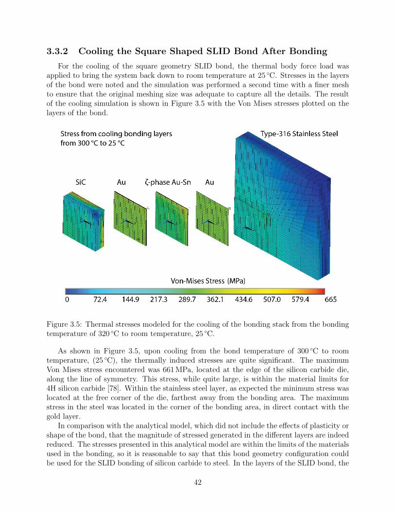
3.3.2 Cooling the Square Shaped SLID Bond After Bonding
For the cooling of the square geometry SLID bond, the thermal body force load wasapplied to bring the system back down to room temperature at 25 ◦C. Stresses in the layersof the bond were noted and the simulation was performed a second time with a finer meshto ensure that the original meshing size was adequate to capture all the details. The resultof the cooling simulation is shown in Figure 3.5 with the Von Mises stresses plotted on thelayers of the bond.
Figure 3.5: Thermal stresses modeled for the cooling of the bonding stack from the bondingtemperature of 320 ◦C to room temperature, 25 ◦C.
As shown in Figure 3.5, upon cooling from the bond temperature of 300 ◦C to roomtemperature, (25 ◦C), the thermally induced stresses are quite significant. The maximumVon Mises stress encountered was 661 MPa, located at the edge of the silicon carbide die,along the line of symmetry. This stress, while quite large, is within the material limits for4H silicon carbide [78]. Within the stainless steel layer, as expected the minimum stress waslocated at the free corner of the die, farthest away from the bonding area. The maximumstress in the steel was located in the corner of the bonding area, in direct contact with thegold layer.
In comparison with the analytical model, which did not include the effects of plasticity orshape of the bond, that the magnitude of stressed generated in the different layers are indeedreduced. The stresses presented in this analytical model are within the limits of the materialsused in the bonding, so it is reasonable to say that this bond geometry configuration couldbe used for the SLID bonding of silicon carbide to steel. In the layers of the SLID bond, the
42

stress distribution in both the gold layers and the ζ’ gold-tin layer was quite uniform andthe maximum stresses occurredin the corner of the bonding area, farthest from the center ofthe quarter model.
3.3.3 Reheating the Square Shaped SLID Bond to OperationalTemperature
In the reheating of the SLID bond, before the new thermal load was applied to all thenodes the coordinates of all the nodes were updated. This process ensured that the existingplastic deformations and deformed shape of the modeled bond layers would be accountedfor when reheating the bond. A thermal load was applied by selecting all the nodes andsetting their temperature to the operational temperature of 375 ◦C. With the ∆T betweenthe operational temperature and the bonding temperature being smaller than that of thecooling case, smaller stresses were expected. The result of the reheating analysis is presentedin Figure 3.6.
Figure 3.6: Thermal stresses modeled for the reheating of the bonding stack from roomtemperature,25 ◦C, after initial cooling, back to the operating temperature of 375 ◦C.
With the reheating of the sample, the Von Mises stress distribution was analyzed andit was found that the steel substrate and the silicon carbide die had significantly reducedstress. The maximum stress in the silicon carbide layer was calculated to be 299.0 MPa andwas located at the bottom of the silicon carbide die at the corner of the silicon carbide die.In the steel layer, the maximum stress was also found to be in the corner of the bonding area
43

and the Von Mises stress there was 238.6 MPa. The highest Von Mises stresses present inthe bond, with a value of 378.9 MPa, were found to occur in the corner of the gold/ζ’ gold-tin/gold layers of the SLID bond in the corner of the bond. Again, the stresses simulatedin the reheating of the bond satisfied the limitations of the materials and were in favor ofthe materials surviving the stresses induced at the operating temperature. A side-by-sidecomparison of the thermally induced stresses and their distribution due to the heating andcooling of the materials is provided in Figure 3.7.
Figure 3.7: Comparison of the thermal stress generated when cooling and reheating SLIDbond for the primary square-shaped, full-coverage SLID bond.
3.3.4 Modeling of Alternate Bond Geometries
Depending on the type of silicon carbide sensors being bonded to stainless steel, it ispossible to consider other bonding geometries and different bond pad shapes, and so finiteelement modeling of the stress distributions generated by these geometries. For this modelingwork, the same material properties were used but the shape of the SLID bond layer waschanged to match the geometries shown in Figure 3.4. The geometries used in this modeland the results of the finite element analysis are presented here.
For the consideration of the center-only SLID bond, two different dimensions for the SLIDbond were considered. In the first, the gold and gold-tin layers of the SLID bond was modeledto extend outward to one-half of the silicon carbide die’s width. In the quarter-model thatwas used, the length and width dimensions of the gold and gold-tin layers were 950 µm for
44

this geometry. In the second, the SLID bond layer was extended to only one-quarter of thesilicon carbide die’s width, with the lengths and widths of the gold and gold-tin layer being475 µm. The results for the cooling and reheating of the larger center-bond geometry areshown in Figures 3.8 and 3.9. The modeling results for the cooling and reheating of thesmaller center-bond geometry are shown in Figures 3.10 and 3.11.
With these two bond geometry configurations, it was found that the stress in the stainlesssteel and silicon carbide layers were reduced for both cooling and reheating the bond, as theywere allowed to expand and contract more freely away from the bonding area. The gold andgold-tin bonding layer also experienced reduced stress during initial cooling and reheating.The greater freedom that was given to the silicon carbide die and stainless steel’s expansionby the smaller sized center-bond, the lower the stresses were found to be. However, in real-world applications, with the reduced footprint of the bond area the durability and overallstrength of the bond would be detrimentally affected. For high temperature integratedcircuit die-attach applications , where electrical connection is the primary goal, a simplepost structure, or set of posts, could be use to reduce the negative effects of the thermallyinduced stresses.
To determine if an alternate bond pad geometry could increase the contact area betweenthe silicon carbide die and the stainless steel substrate, the cross-shaped bond geometry wasanalyzed. In this model, from the center of the bond the arms of the cross shape extendto the edge of the silicon carbide die. The length of the sides of the cross were designedto be 950 µm, one-half the width of the silicon die. The corners of the silicon carbide diewere allowed to protrude freely over the stainless steel, while the rest of the die was ableto maintain a reasonable amount of contact with the layers below. The results of the finiteelement analysis of the cross-bonded geometry are presented in Figures 3.12 and 3.13.
Upon cooling, the maximum stresses observed in the cooling of the cross-shaped SLIDbond occurred in the corners of the cross, closest to the corner of the silicon carbide die. Inthe steel substrate, a stress of 312.9 MPa was observed at these locations. In the gold andgold-tin layers, the stresses were quite uniform through the cross and the maximum VonMises stress found in those layers was 484.8 MPa, at the corners of the cross. In the siliconcarbide die, the maximum Von Mises stress of 629.7 MPa was still located along the sidesof the die, on the bottom side of the die which contacts the gold of the SLID layer. Beingunrestrained in the corner of the die, minimum stress in the silicon carbide die was foundalong the edges.
From reheating the cross-shaped SLID bond, the Von Mises stresses were found to lowerthan those calculated in both of the center-bonded cases. The maximum stress in the stainlesssteel layer was 238.3 MPa, in the SLID bond layer, the maximum stress was 387.4 MPa andin the silicon carbide layer, the stress maximum stress was 350.6 MPa. In comparison withthe primary full-square bond, the cross bond did provide a slight reduction in maximum VonMises stress upon cooling. After reheating, the stresses calculated in both cases were quitecomparable, except that the maximum stress in the silicon carbide die increased by about17 % due to the concentrations at the corners of the cross. The stresses calculated for eachof the bonding geometries analyzed are within the material limits of the materials and sothermal stresses alone should not cause the failure of the bonds.
Since the amount of contact area between the silicon carbide die and steel was notcompromised with the regular square bond area and the stresses were manageable with the
45

materials, it was the chosen geometry for SLID bonding. The choice of the square bond overthe cross and center bonded geometries added the benefits of simpler preform fabricationand reduced effort to align and place the silicon carbide die on the bond. To determinehow changes in the layer thicknesses would affect the performance of the square SLID bond,several more simulations were performed. One variable at a time, the Von Mises stresseswere simulated for cases with the silicon carbide die thinned to 250 µm, the steel substrateincreased to a thickness of 3 cm, the gold layers increased to 100 µm thick and the ζ’ gold-tinlayer increased to 100 µm.
The effects of varying these parameters were recorded and it was determined that bythinning the silicon carbide die, Von Mises stresses in all the layers decreased, in comparisonto the primary case of the square bond. However, thinning the silicon carbide die alsocaused the Von Mises stresses in the gold and gold-tin layers of the SLID bond to be greateras distance from the silicon carbide die decreased. In agreement with the analytical modelof Section 3.2, as the steel substrate was increased to a thickness of 3 cm, the stresses inthe layers increased significantly. The increased thickness of the steel caused its thermalexpansion to dominate in the system. With the thick steel, the Von Mises stresses in thegold and gold-tin layer of the SLID bond increased by 18 % from the primary bond simulationwith the original dimensions. Lastly, by increasing the thicknesses of the gold and the gold-tin films, the maximum Von Mises stresses in the silicon carbide and steel layers 5 % duringthe cooling and both decreased by about 13 % during reheating, in comparison with theoriginal model.
From these observed trends in the finite element model, it is possible to determine theset of parameters that would best facilitate the bond. In terms of bond geometry andpracticality during the implementation of SLID bonding, the square-bond with full areacoverage is a good candidate. With the thicknesses of silicon carbide and stainless steeldiscussed in Chapter 2 a bond that does not exceed the limits of the bonding materialsshould be achievable. Although the increased thicknesses of the modeled gold and gold-tinlayers does reduce the stress in the system, it also requires a significant amount of additionalprocessing to form layers of such thick pure gold, and so there is an engineering tradeoff tomake the gold-tin SLID bond work with thinner layers.
46

Figure 3.8: Thermal stress analysis of cooling the center-bonded silicon carbide to steel from300 ◦C to 25 ◦C.
Figure 3.9: Thermal stress analysis of reheating the center-bonded silicon carbide to steelfrom 25 ◦C to 375 ◦C.
47

Figure 3.10: Thermal stress analysis of cooling the smaller center-bonded silicon carbide tosteel from 300 ◦C to 25 ◦C.
Figure 3.11: Thermal stress analysis of reheating the smaller center-bonded silicon carbideto steel from 25 ◦C to 375 ◦C.
48

Figure 3.12: Thermal stress analysis of cooling the cross-bonded silicon carbide to steel from300 ◦C to 25 ◦C.
Figure 3.13: Thermal stress analysis of reheating the cross-bonded silicon carbide to steelfrom 25 ◦C to 375 ◦C.
49

Chapter 4
Characterization and Testing of theSLID Bonds
For the MEMS sensors to operate in high temperature harsh environment conditions, itis imperative that the SLID bond joining them to the metal components be able to survivethe same conditions. To evaluate the bond strength of the SLID bonded samples and tocharacterize how varying the different bonding parameters affected the overall bond strength,destructive testing of the bond was performed. The bonds were tested mechanically at roomtemperature and at elevated temperatures. Cross-sectional compositional analysis of thebonds was performed before and after subjecting the bonds to high temperatures. The effectof high temperature aging and its effect on bond strength and metallurgical composition ofthe SLID bond were also studied. A rigorous testing protocol was developed to measure thestrength of the silicon carbide to steel bonds. In some of the testing the bonds were subjectedto temperatures which would be encountered in geothermal well monitoring applications toensure that the bond would survive high temperatures beyond the bonding temperature. Thecross sections of the bonds were inspected and the mettalurgical compositions of the SLIDbonds were investigated to understand how prolonged high temperature exposure wouldaffect the integrity and composition of the gold-tin SLID bond. This chapter outlines thebonding parameters that were varied, the testing performed on the SLID Bonds, and thecharacterization of the SLID bonding process for SiC to steel.
4.1 Die Shear Testing Method
A crucial metric for the performance of the SLID bond is the strength of the bond. In thepackaging industry, the strength metric of a bonded die is typically given by the ultimate dieshear strength of the bond when tested in accordance with Military Standard 883, method2019.7 [79]. This standard outlines the protocol used to investigate the integrity of the bondmaterials and the bond quality by destructively testing the bond to failure. It also classifiesthe separation of the bonded die from the underlying substrate into three categories: cohesivefailure of the bonded die, in which residual parts of the die are left bonded to the substrate;adhesive failure between the bonded die to the die-attach medium, in this case the gold-tinSLID bond layer; and adhesive failure between the SLID bond layer and the underlying
50

stainless steel substrate.Cohesive and adhesive failure mechanisms refer to the way the bond or bonding materials
break when tested. Cohesive failures occur within a given material, such as the within theSiC die or within the gold-tin SLID bond layer, in the case of silicon carbide to steel SLIDbonding. During die shear testing, if the SLID bond layer separates while remaining adheredto both the SiC die and the stainless steel, the failure is considered to be a cohesive failurewithin the SLID bond layer. Similarly, cohesive failures can occur within the SiC die, in whichcase part of the die would fracture while leaving behind SiC material bonded to the SLIDbond. In contrast with cohesive failures, adhesive failures occur at the interface between twodifferent materials, such as between the SLID bond layer and the underlying steel sample.Adhesive failures would include the SLID bond layer separating from the stainless steel.
The military standard’s strength requirement of the bond, based on the size of the bondeddie, is outlined in Figure 4.1. Based on a the size of the bonded SiC dies being 3.8 mmby 3.8 mm in area, (0.0224 in) to fulfill the 1.0×, 1.25×, and 2.0× standards, the bondmust survive shear forces of 25.53 N, 30.66 N and 49.05 N respectively, which translate to torespective shear stresses of 1.698 MPa, 2.123 MPa and 3.397 MPa.
Figure 4.1: The MIL-STD 883J die shear strength requirements for microelectronics devicesbonded to substrates. Die shear strengths versus die bond area are plotted to satisfy thestandard’s 1.0×, 1.25×, and 2.0× strength requirements.
To perform the die shear testing two bond testers were employed; a Nordson DAGE4000 Bondtester and a XYZTec Condor Sigma Bondtester. Both systems were used todestructively evaluate the ultimate shear strength of the bonded samples. These die sheartesters were equipped with a shearing wedge, which was designed to be wider than the partbeing sheared to ensure that contact would be made to the entire surface of the part beingsheared. In the testing process, the sample being sheared would be secured onto a stageconsisting of vise jaws or a vacuum chuck stage, as shown in Figure 4.2. With the sample
51

secured to the stage, the stage was aligned to the die shear wedge to ensure that the flat of thewedge would be parallel to the edge of the component being sheared. Errors in the alignmentwould cause a significant concentration of stress in the small area initially contacted by thetester.
The height at which the die shearing wedge contacts the sample is also of critical im-portance. If the shear height is too great and the wedge contacts bonded samples too high,excessive stress is developed in the top part of the sample, and if the sample is brittle likesilicon or silicon carbide they tend to fracture before the bond fails. If the shear height is nothigh enough, wedge will scrape into the bond layer, measuring the cohesion of the bondinglayer instead of accurately measuring the total bond strength of the sample. The load wasapplied to the dies using a die shear speed of 300 µm s−1; a speed commonly used in industryfor the testing of solder strength in microelectronic components. In each test performed, theshear wedge would back away from the edge of the die, lower itself until it contacted theunderlying substrate, raise itself to the assigned die shear height, and then process forwardinto the sample at the prescribed die shear rate. For the application of loads, both the Nord-son DAGE 4000 and XYZTec Condor Sigma were equipped with 100 kg weight cartridges,capable of applying and measuring up to 981 N of force in the shear direction.
Figure 4.2: Operation of the high temperature die shear testing apparatus. The load-applicator block passes over the stainless steel substrate and contacts the SiC die.
In die shear testing, the profile of the force application versus time is recorded andpresented as shown in Figure 4.3. The force versus time graph gives some insight as to howthe bond yields and when combined with optical inspection during the die shear testing, itcan be used to distinguish if damage occurs to the die before the bond fails. When totalfailure of the bond occurs and it has been successfully sheared, the force rapidly decreases.
52

Figure 4.3: Plot of the die shear force versus displacement for a die-shear test of a SiC diebonded to stainless steel substrate. The maximum force registered before the failure of thedie or bond is used to determine the strength of the bond.
4.2 Microscopy and Chemical Composition Analysis
Methods
To improve the understanding of what occurs in the SLID bonding layer, optical mi-croscopy, scanning electron microscopy and energy dispersive x-ray analysis were employedto investigate the appearance of the bond layers, where fractures occurred during die sheartesting and to determine the chemical composition of different areas of the bond. Thesevisual inspection techniques offer great insight as to how and where a particular bond failedas well as visually identifying differences in alloy composition in the bond. Chemical com-positional analysis further aids in identifying the materials present in the bond and providesadditional information to characterizing the failure of the bond. Metallographic polishingof the samples was performed to enable the inspection of the cross-section of the bonds forboth chemical composition as well as physical appearance.
4.2.1 Optical microscopy
An Olympus LEXT OLS3000 3D laser confocal microscope was used to inspect thefracture surfaces and cross sections of the bonds. Using 10×, 20× and 50× objective lenses
53

provided high resolution optical images of the bond in color. The ability to distinguish colorand luster significantly aids in the determination of how far the gold-tin diffusion spreads inthe gold-tin SLID bond. There are noticeable visual differences in color between pure gold,Au80%wt.-Sn20%wt., and ζ’ gold-tin phases. Additionally, the software integrated with theLEXT microscope allows for the measurement of distances which was used to verify thethickness of the formed SLID bonds and to measure features within the bond.
4.2.2 Scanning Electron Microscopy and Energy Dispersive X-Ray Analysis
Scanning electron microscopy was used to analyze the fracture surfaces of the die-sheartested bonds as well as the cross-sections of the bonded samples after metallographic pol-ishing. Scanning electron microscopy offers the ability to image the areas of interest in thebond with magnifications much greater than optical light microscopy. Although the imageproduced by the SEM is black and white, the high magnification and the slight differencein contrast between materials enables the distinction between some phases of gold-tin. AFEI Quanta scanning electron microscope, equipped with an Oxford energy-dispersive x-ray(EDX) detector was used to determine the species of elements present in regions of the bond.
Although several other chemical compositional analysis tools were available, such as X-ray photoelectron spectroscopy (XPS) and Auger electron spectroscopy (AES), EDX analysiswas chosen as the method for analyzing the SLID bond because of its spatial resolution.XPS analysis would provide a highly accurate compositional analysis of the layers in thebond, however, the preparation of the layers would be quite difficult and require the carefulstripping away of the bonded silicon carbide die and careful removal of material throughthe gold-tin bond layers to get an accurate compositional profile versus depth into the bond.EDX spectroscopy, on the other hand, provides a better spot measurement of a localized areaand can be performed on various regions of a cross section to determine the composition ofthe metal. EDX spectroscopy operates by using a high-energy beam of charged particles tostrike the specimen being studied. The high energy excites electrons present in the atomselectron shells to a higher energy state, and as those electrons return to recombine in theelectron shell, X-rays are emitted. The number of X-rays and the energies of the emitted X-Rays provide a signature for the elements present and are used to determine the compositionof the scanned area.
For EDX analysis, after finding the area of interest for analysis and zooming in as far aspossible with the SEM, an excitation voltage of 30 keV was used for the X-ray analysis. InEDX analysis, as the accelerated particles hit the specimen being analyzed, there is sometunneling and penetration into the sample. Due to this phenomenon, instead of measuringan exact spot of material in the specimen, an excitation volume is analyzed. The equationsused to calculate the depth of this excitation volume is given in 4.1, and the width of theexcitation volume is calculated using Equation 4.2, where the density, ρ (in g cm−3), of thematerial being analyzed and the acceleration voltage, Eo (in keV), are accounted for.
x(µm) =0.1Eo
1.5
ρ(4.1)
54

Figure 4.4: An EDX analysis spectrum for the analysis of a Au80%wt.-Sn20%wt. solderpreform is shown here. The overall EDX analysis accuracy is around ±2% due to scatteringand the software’s corrections applied to the raw data.
y(µm) =0.077Eo
1.5
ρ(4.2)
For a 30 keV acceleration voltage, this translates to an excitation volume depth of 0.851 µmand a width of 0.656 µm. The accuracy for EDX spectroscopy compositional analysis is about±2% due to the scattering events during measurement and the statistical corrections thatthe software applies to the raw data collected by the X-ray detector. An example of an EDXanalysis spectrum for Au80%wt.-Sn20%wt. is shown in Figure 4.4.
4.2.3 Metallographic Polishing
Metallographic polishing is a destructive inspection tool that enables the inspection ofcross-sections and internal compositions, such as the grain structure of metals. In thisresearch the application of metallographic polishing is highly relevant in that it can exposethe cross-section of the completed SLID bond and enable characterization of the bondscomposition as a function of position in the bond. Preparation of the samples for cross-sectional analysis after bonding consisted of casting the samples in an epoxy resin, as shownin Figure 4.5. The samples were held in place with plastic clips as the epoxy was pouredinto the mold. After pouring, the samples were placed in a vacuum chamber and allowedto outgas for 5 minutes before the chamber was vented. The epoxy was allowed to hardenovernight in ambient laboratory room conditions. Due to the geometry of the Silicon carbidedies being bonded to the center of the steel square, after casting in epoxy a lathe was usedto remove the excess epoxy leading up to the cross section. Care was taken to avoid cuttinginto the stainless steel and the silicon carbide dies as machining into them would cause severe
55

shock and the mechanical deformation of the steel would cause the silicon carbide substrateto fracture and dislodge from the bond layer, thus invalidating the sample for later analysis.Following lathing a manual rough sanding with coarse 180, 320 and 400 grit sand papers withwater cooling was performed to abrade the remaining steel and epoxy preceding the SiC toSteel bond interface. Water cooling during the sanding ensured that the temperature rise ofthe steel due to the abrasion would not cause significant heating that would affect the stateof the SiC to Steel SLID bond. Excess heating would considerably raise the temperatureof the steel and could provide enough thermal energy to alter the composition of the SLIDBond.
Figure 4.5: Bonded SiC to steel samples were casted in epoxy for metallographic polishingoperations to enable detailed analysis of the cross section of the bond.
After the rough preparation, a Pace Technologies Nano 2000 metallographic polisher with8 inch wheels was used to finish preparing the final sanding and the polishing of the sample[80]. If planarity issues were encountered between the silicon carbide and the steel substrate,a Cermesh™metal mesh abrasive cloth was used for polishing in conjunction with 30 µmabrasive grit. The final sanding procedure consisted of manually sanding the epoxy-castsamples by hand with 800 grit SiC sandpaper at 300 rpm, followed by 1200 grit sandpaperat 200 rpm, bringing the surface roughness of the sample down to approximately 9 µm. Thepolishing procedure was carried out with 6 µm and 1 µm polycrystalline diamond suspensionsin colloidal silica on respective low-napped polymer polishing pads. After polishing, thesamples were thoroughly rinsed with water to remove any remnants of the polishing grit anddried with compressed air before performing an inspection of the cross-section.
56

4.3 Characterization and Testing of Si to Si SLID Bonds
For the silicon to silicon SLID bonded dies whose fabrication process was outlined in Sec-tion 2.3, die shear strength testing as well as chemical compositional analysis was performed.These silicon to silicon bonds were part of the initial investigation to understand the SLIDbonding process and observe the SLID process in action. The results of the characterizationare presented in this section.
4.3.1 Die Shear Testing of Si to Si SLID Bonds
Die shear testing of the initial Si to Si SLID bonds were performed in the microfabricationfacilities at Vestfold University College in Norway using a Nordson Dage 4000 Bondtester.The dies tested were the silicon samples metalized with chromium-tin-gold as described inSection 2.3. For testing, due to the gripping limitations of the available vise jaw stage,the bottom surface of the bonded silicon to silicon samples were glued to a larger ceramiccircuit board substrate using a cyanoacrylate adhesive. After allowing the adhesive to set,the bottom half of the bonded stack was securely attached for die shear testing. Followingthe setting of the glue, the vise jaws of the tester were aligned so that their 1 cm edge wasparallel to the die-shear wedge. A die shear testing height of 570 µm was used to ensure safeclearance over the bottom silicon die and the bond layer.
During testing of the bonds of samples TLP6 to TLP6 the average force the bondssurvived was 37.37 N, or a 186.83 kPa shear stress based on the 1 cm by 2 cm die area). Basedon the size of these dies the bonds of TLP6 to TLP6 surpassed the 1.25× requirement ofMIL-STD 883J, but not the 2.0× requirement. For the bonds of TLP3 to TLP3, the bondeddies survived an average of 20.38 N force in the shear direction, or a 101.90 kPa shear stress.The bonds of TLP3 to TLP3 did not meet the MIL-STD883J requirements. Lastly, thebonds of TLP6 to TLP3 generated no force measurements when they were tested. The topsubstrate simply glided off the bottom substrate with minimal force applied, resulting in nomeasurement. The bond strengths of these silicon to silicon samples was relatively and soan optical analysis of the fracture surface was performed to understand what the fracturesurface looked like and to see if the underlying cause of the weakness of the bond could bedetermined.
4.3.2 Optical and Compositional Analysis of Si to Si SLID Bonds
After die shear testing, the surface of the sheared silicon substrates and the cross-sectionof other TLP6 to TLP6 and TLP 3 to TLP3 samples were inspected using optical microscopyas well as scanning electron microscopy and energy dispersive x-ray analysis. Upon inspectionof the die-shear tested surface it was evident that the bond layer was not uniform. An opticalmicroscopy image of the bond taken at 250×, shown in Figure 4.6, shows that the bond layerwas not a continuous layer of metal and that mounds of gold-tin alloy had formed. Figure4.6 compares the surface of the e-beam evaporated silicon surface before bonding and afterbonding, and shows the mounds of metals that were generated during the bonding process.
Additionally, the cross section images of the silicon to silicon SLID bonding samples,shown in in Figure 4.7, processed alongside the samples that were die shear tested, revealed
57
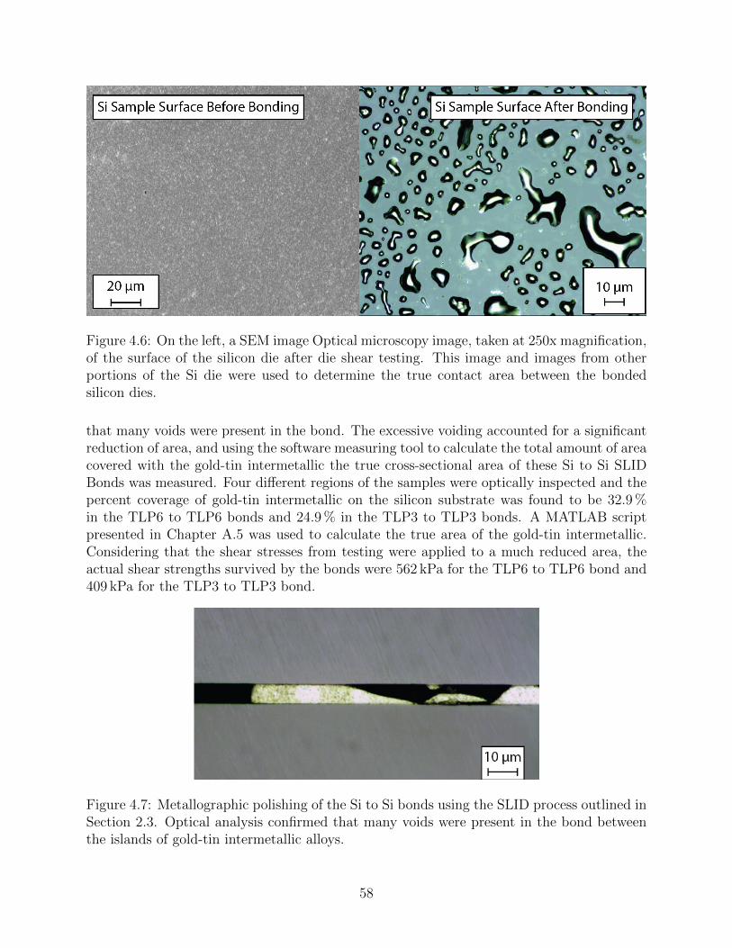
Figure 4.6: On the left, a SEM image Optical microscopy image, taken at 250x magnification,of the surface of the silicon die after die shear testing. This image and images from otherportions of the Si die were used to determine the true contact area between the bondedsilicon dies.
that many voids were present in the bond. The excessive voiding accounted for a significantreduction of area, and using the software measuring tool to calculate the total amount of areacovered with the gold-tin intermetallic the true cross-sectional area of these Si to Si SLIDBonds was measured. Four different regions of the samples were optically inspected and thepercent coverage of gold-tin intermetallic on the silicon substrate was found to be 32.9 %in the TLP6 to TLP6 bonds and 24.9 % in the TLP3 to TLP3 bonds. A MATLAB scriptpresented in Chapter A.5 was used to calculate the true area of the gold-tin intermetallic.Considering that the shear stresses from testing were applied to a much reduced area, theactual shear strengths survived by the bonds were 562 kPa for the TLP6 to TLP6 bond and409 kPa for the TLP3 to TLP3 bond.
Figure 4.7: Metallographic polishing of the Si to Si bonds using the SLID process outlined inSection 2.3. Optical analysis confirmed that many voids were present in the bond betweenthe islands of gold-tin intermetallic alloys.
58

To determine the composition of the intermetallic mounds that had formed during bond-ing, EDX analysis was performed on different regions of the mounds as shown in Figure 4.8.In the top-down inspection of the surface after die-shear testing, the peaks of the moundsand the bases of the mounds were scanned to see if there was a difference in composition.Additionally, in the cross section analysis, sections of the gold-tin intermetallic were analyzedcloser to the silicon substrate as well as in the middle of the intermetallic. In the regionsnearer the silicon substrate, there was a higher concentration of gold present, and the EDXanalysis recorded a composition of Au66%at.-Sn33%at, which corresponds to the ε gold-tinphase (AuSn2). The remaining 1%at. was measured as a trace amount of silicon measuredby the scattered electron beam. Farther away from the silicon die, it was determined that thecomposition was Au51%at.-Sn48%at., which given the accuracy of EDX analysis suggestedthe δ phase of gold-tin (AuSn).
Figure 4.8: On the left, a SEM image Optical microscopy image, taken at 250x magnification,of the surface of the silicon die after die shear testing. This image and images from otherportions of the Si die were used to determine the true contact area between the bondedsilicon dies.
Referring back to the phase diagram of the gold tin metal system, it is apparent thatthe gold layer did diffuse into the tin and formed the δ phase closer to the center of thebond, where there was an excess of pure tin. Nearer to the silicon substrates, where thee-beam evaporated films were originally pure gold, the ε phase was formed. With the 350 ◦Cbond temperature used in the preparation of the TLP6 and TLP3 bonds, not enough ther-mal energy was provided to bring the system through the stable δ gold-tin phase. Duringthe bonding process, it appears that as the temperature in the bonding chamber rose, thediffusion of gold into tin formed the δ phase alloy locally, before the pure tin layer could
59

completely melt and form a uniform liquid layer. As the δ phase solidified and as diffusioncontinued it was increasingly difficult for the bond layer to become even and the mounds ofintermetallic were formed. In order to overcome this limit of the δ phase gold tin, a temper-ature greater than 419 ◦C and a faster heating rate would have been required for bondingwhen using pure tin as the melting point depressant. Additionally, for this type of bonding,with evaporated thin films of gold and tin, the thickness ratio should have been closer to3Au:2Sn in order to form the higher melting point β, ζ and ζ’ gold-tin intermetallics, basedon the thickness calculations performed in Section 3.1. The use of pure gold and pure tin thinfilms shows promise for wafer level and die level attachment schemes for high temperaturesurvival as long as the proper film thicknesses are used.
4.4 Characterization and Testing of SiC to Steel SLID
Bonds
A thorough investigation of the silicon carbide to steel bonds was performed and thesuitability of the bond for high temperature harsh environment applications was analyzed.The effect that the thicknesses of the SLID bonding layers had on the strength of the bond wascharacterized and the composition of the SLID layer after bonding was analyzed. Die sheartesting was performed at room temperature after the bonds had cooled after bonding alongwith a thorough analysis of the bond’s chemical composition. The effects of high temperatureaging on the bonds strength was investigated along with how the composition of the SLIDbond reacted to prolonged high temperature exposure. Additionally, the bond strength ofthe silicon carbide to steel SLID bonds as well as their survivability at high temperatureswas tested. This section documents the characterization and testing performed on the siliconcarbide to steel SLID bonds.
4.4.1 Die Shear Testing of SiC to Steel SLID Bond After Cooling
After the fabrication and bonding of the silicon carbide dies to stainless steel, the dieshear strengths of the bonds were characterized at room temperature. An orthogonal arrayof experiments, shown in Table 4.1, was designed to determine the effect of gold thicknesson steel, gold thickness on the silicon carbide substrate and the thickness of the Au80%wt.-Sn20%wt. eutectic solder preform on the strength of the bond. Eight sets of experimentswere made to understand the effect of these parameters on the bond’s shear strength usinga two-level full factorial design of experiments.
In this design of experiments the examined gold-plating thicknesses on steel were 10 µmand 20 µm. The two tested thicknesses of pure gold, electroplated on the SiC substrate,were 20 µm and 40 µm thick. These films were electroplated and prepared using the proce-dures described in Section 2.4.3. The gold-plated steel samples were fabricated using theelectroplating procedure discussed in Section 2.4.3. The Au80%wt.-Sn20%wt. solder pre-form thicknesses that were tested were 5 µm and 12.7 µm thick. The different thicknesses ofAu80%wt.-Sn20%wt. eutectic would affect the required amount of gold to form the ζ andβ phases of gold-tin, and alter the amount of remaining pure gold left over after the SLIDbonding process. These 8 combinations of experimental parameters were organized in such
60

Table 4.1: The design of experiments used to determine the effect of SLID bonding param-eters on the strength of the bond.
Experiment Au80/Sn20 PreformThickness (µm)
Au Thickness onStainless Steel (µm)
Au Thickness onSiC (µm)
1 5 10 202 12.7 10 203 5 20 204 12.7 20 205 5 10 406 12.7 10 407 5 20 408 12.7 20 40
a way that the effects of the three independent variables, (solder preform thickness, goldthickness on steel and gold thickness on silicon carbide) could be characterized and theirindividual contributions to how they affected bond strength could be analyzed.
For the determination of the bond strength an XYZtec Condor Sigma and Nordson DAGE4000 were used. The wedge used to apply shear force to the die was flat and measured 10 mmwide, larger than the 3.8 mm width of the SiC die, to ensure that the wedge would not imparta localized stress concentration to the SiC. A die shear height of 70 µm was used for testingto ensure clearance over the SLID bond, so that contact would be made solely between thedie shear wedge and the flat edge of the SiC die.
The die shear strength results from the testing of the eight variations of parameters areshown in Table 4.2. Several samples of each bonding configuration had to be fabricated andtested to account for minor variations in the die shear testing process and the fabricationsteps. From this set of raw data it is evident that for the die size of 3.8 mm by 3.8 mmall the tested configurations of bond thicknesses, except the 5th experimental combination,surpassed the 2.0×MIL-STD 883J die shear requirement outlined in Section 4.1. The averagestrength for the 5th experimental configuration surpassed the military standard’s 1.25× butnot the 2.0× benchmark.
From the results of testing these 8 combinations of the parameters, the main effect of eachparameter can be calculated [81]. For a particular variable, Au80%wt.-Sn20%wt. thicknessfor example, the calculation involves averaging the die shear strength data collected in whichthe thick 12.7 µm preforms were used, and subtracting the average die shear strength for theexperiments in which the thin 5 µm preforms were used. A MATLAB script, presented inSection A.6 was used to aid in performing the effect calculation for each of the variables. Itwas found that both thicker electroplating on the silicon carbide die and a thicker gold-tineutectic preform improved the overall bond strength. Analyzing the effect of the electroplatedgold thickness on bond strength showed a slight trend that that the thicker plated films onsteel did not improve the overall bond strength. This result was counterintuitive to the
61

Table 4.2: The average die shear strengths (in MPa) are given for the samples tested usingthe parameters stated in Table 4.1.
Experiment Number ofSamples Tested
Average Die ShearStrength (MPa)
1 3 15.82 3 8.033 4 13.54 4 6.345 3 3.906 3 32.27 4 6.368 4 28.7
finite element analysis calculations from Chapter 3, and so further investigation into thecomposition and integrity of the bonds were performed.
4.4.2 Compositional Analysis of SiC to Steel SLID Bond AfterCooling
Before bonding the samples, the cross-section of an assembled silicon carbide to steelbond was imaged, as shown in Figure 4.9. The cross section of the bonds were investigatedas shown in Figure 4.9. In the SEM image alone, the difference between the gold-tin eutecticpreform and the pure electroplated gold can be seen. The eutectic solder contains darkregions corresponding to the δ phase of gold-tin and the lighter region surrounding the δphase is the ζ’ phase of gold tin. In the layer of pure gold that has been electroplated to thesteel, there are a few voids present in the electroplated film. These voids could have arisenduring the electroplating process, as larger metal grains form with applied current densitiesapplied, as discussed in Section 2.4.3. After bonding, the cross section of an identicallyprepared and bonded sample shows that the SLID process does occur and there is a cohesivejoint formed between the silicon carbide and steel substrates. EDX analysis of the layersbefore the bond verified that the composition of the electroplated layers on the silicon carbideand stainless steel substrates were indeed pure gold and that the eutectic solder compositionwas correct. Following the bonding, spot analyses set 5 µm apart from one another wereperformed to determine the composition of the bond as a function of vertical position in thebonding stack. Layers of pure gold were present on either side of the SLID bonding region,where the ζ’ phase of gold-tin was formed. The proportions of pure gold on either side ofthe SLID bond layer to the ζ’ gold-tin intermetallic corresponded to what had been modeledin the simulations of Chapter 3.
62

Fig
ure
4.9:
An
SE
Mim
age
ofth
eSL
IDB
ond
bef
ore
bon
din
g,le
ft,
and
afte
rb
ondin
g,ri
ght,
show
show
the
diff
usi
onof
the
gold
into
the
tin
laye
rocc
urs
and
how
the
com
pos
itio
nof
the
bon
dch
ange
saf
ter
bei
ng
sub
ject
edto
the
SL
IDb
ondin
gpro
cess
.
63

After investigating the cross section and seeing how the diffusion of the gold into theeutectic solder was distributed in the bond, the fracture surfaces of the bond were investigatedon both the silicon carbide side as well as the stainless steel side. Using the FEI QuantaSEM and the Oxford EDX the fracture surfaces were analyzed and compositional analyseswere performed on various parts of the fracture surface. With an understanding of how thematerials were distributed through the bond from the cross-sectional analysis, looking atthe fracture surface would provide insight as to where the bond failed and what parts ofthe bond were the weakest. Example top-down SEM images taken of the fracture surfacesof the stainless steel and silicon carbide halves of the bond are shown in Figures 4.10 and4.11 respectively. The material composition of the different features in the Figures weredetermined using EDX analysis.
From the fracture surface analysis, in the strongest of the bonds tested, it was madeapparent that both cohesive and adhesive failures occurred in the bond. On the steel sides ofthe bonds, in some regions within the bonding area, bare stainless steel was found, indicatingthat the adhesive Nickel Strike and gold layer had been sheared off. Gold was also foundadhered to the stainless steel in other areas, indicating that there were some adhesive failureswithing the gold layer that was electroplated onto the stainless steel. Some peeling of the ζ’gold-tin was observed, indicating that there could have been an adhesive failure between thegold tin intermetallic and the pure gold layer or a cohesive failure within the ζ’ intermetallic.Due to the accuracy limitations of the EDX it was difficult to determine the extent of theparticular separation. Higher up in the bonding stack, pure gold with a trace of titanium wasfound, signaling that the electroplated gold had come off the silicon carbide die. Because notall the gold from the silicon carbide die had been torn off, there was some cohesive failurein the gold film.
Looking to the surface of the silicon carbide die to verify the findings, the same trends incohesive and adhesive failures were noticed. There was shearing of the SLID bond layers offthe silicon carbide substrate in areas, as was noticed from the inspection of the stainless steelsample. Similarly, in some areas on the silicon carbide die, the electroplated gold from thestainless steel sample was found. For these strong bonds, the multiple types of adhesive andcohesive failures are characteristic of a strong bond, as when failure occurs, it does not simplyoccur in one material interface, but in a variety of locations and in a variety of materials.Intermetallic alloys, such as the β phase and ζ phases of gold-tin have a reputation for beingsomewhat brittle, however, as demonstrated by the methods of failure encountered from thistesting, there is some evidence that they are more robust than how they are typically viewedin literature, as argued by Lee et al. [82].
Analyzing the fracture surfaces for the cases with the weakest bonds, the failure seemedto occur most often from the adhesion of the gold layer to the stainless steel, in spite of thenickel strike efforts to improve adhesion. Though the same processing steps were used forthe investigation across all of the stainless steel samples, it is possible that the electroplat-ing process used for fabricating the steel side of the bond experienced issues that were notencountered with the electroplating of the silicon carbide. The plating area of the steel sam-ple was 31.67 mm2 while the area of the silicon carbide sample was 529 mm2 and althoughthe same current densities were used, mass transport of the electrolyte to the steel surfacedue to the patterning of the thick photoresist mask could have been affected. Addition-ally, the difference in anode to cathode surface areas could have resulted in the differences
64
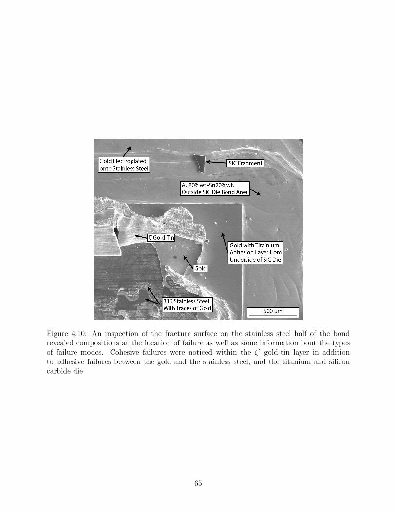
Figure 4.10: An inspection of the fracture surface on the stainless steel half of the bondrevealed compositions at the location of failure as well as some information bout the typesof failure modes. Cohesive failures were noticed within the ζ’ gold-tin layer in additionto adhesive failures between the gold and the stainless steel, and the titanium and siliconcarbide die.
65

Figure 4.11: An inspection of the fracture surface on the silicon carbide half of the SLIDbond confirmed that there was adhesive failure within the ζ’ gold-tin layer as well as adhesivefailure of the titanium layer on the silicon carbide substrate.
66

encountered.
4.4.3 Die Shear Testing of SiC to Steel Bonds after High Temper-ature Aging
To investigate the effects of prolonged exposure to high temperatures that would becharacteristic of geothermal well environments, high temperature aging was performed inambient atmospheric conditions using the Thermo Scientific Thermolyne furnace shown inFigure 4.12. The furnace was designed with a thermocouple feedthrough that was used tomanually connect a k-type thermocouple to the samples being tested and to ensure thatthe proper temperatures were being applied to the samples. The samples were placed ona larger stainless steel block that was placed inside the high temperature furnace. Thisblock acted as a heat-sink and was intended to provide some thermal stability to the diesduring the exposure and retard any thermal fluctuations caused by the heater’s periodicheating to maintain a constant temperature. The high temperature heating recipe consistedof raising the temperature to 386 ◦C at a rate of 25 ◦C min−1. In this investigation theslow heating rate was used to ensure that the furnace would not significantly overshoot thedesired holding temperature. The temperature was held at 386 ◦C for a duration of 100hours. After 100 hours, the composition of the SLID bond would have reached equilibriumand homogenization would have completed [37].
In the high temperature aging investigation, the two sets of samples tested both had 20 µmthick gold metallizations on the stainless steel substrate and 40 µm thick gold metallizationson the silicon carbide dies, but one set of samples was bonded with 5 µm thick eutectic solderpreforms and the other set was bonded with 12.7 µm thick preforms. The bonding techniqueused for bonding these samples were the same as discussed in Section2.4.5.
Die shear testing was performed on the aged samples to determine if the aging processaffected the strength of the bond; however, the die shear tests were performed at roomtemperature. In the testing of the aged samples, there was no apparent decrease in bondstrength of the samples in comparison with those that had been tested after cooling, withno further processing after bonding. In fact, out of the aged group of samples tested, onesample with 20 µm thick gold plating on the steel, 40 microm gold plating on the siliconcarbide and a 5 µm thick eutectic solder preform, demonstrated the second highest recordeddie-shear strength, with a 431.7 N shear load (an equivalent shear stress of 29.9 MPa. In allthe cases of die shear testing the high temperature aged, the samples all surpassed the 2.0×Mil-STD 883J requirement.
The compositional change and homogenization of the bond’s cross section was investi-gated to determine what materials were present. Using regular optical microscopy, as shownin Figure 4.13, it was clearly visible that the bond had homogenized, as the distinction be-tween the ζ’ gold-tin layer and the pure gold layer was less pronounced. Before aging, thepure gold layers exhibited a darker yellow luster, while the areas rich in tin exhibited a lightermore silver tone of yellow. After the high temperature aging, the entire bond appeared to bea of a homogeneous composition, and so EDX analysis was used on the cross sections beforean after aging, to track the progress of the diffusion.
Before analyzing the cross section of the aged bonds, the periphery of the SLID bonding
67

Figure 4.12: The Thermo Scientific Thermolyne furnace used for the high temperature agingof bonded samples operated in atmospheric conditions and enabled the use of a externalthermocouple to monitor the temperature inside the chamber.
Figure 4.13: Optical images of the SLID bond’s cross section before and after high tempera-ture aging show how the bond homogenizes with prolonged exposure to high temperatures.
68

Figure 4.14: The bonded sample was optically inspected after the high temperature agingto determine if the area outside the bonding area was affected. This top-down image of thebond shows diffusion of gold, from the electroplated gold layer on stainless steel, into excesseutectic solder preform that protruded outside the bonding area. No significant externalchanges that would affect the strength of the bond were found.
area was investigated to see if diffusion from the gold outside the bonding area was contribut-ing to the observed homogenization of the bond. Outside the SLID bonding area, there wasnoticed a slight roughening in the electroplated gold on the stainless steel. This roughening,which is representative of bulk diffusion of the gold, however, seemed to be caused only bythe presence of excess gold-tin eutectic solder preform, hanging over the gold-plated steelsubstrate abd contacting the electroplated film[69]. The area investigated outside of thebond after 100 hour aging is shown in Figure 4.14. This external diffusion of the excesssolder preform and excess gold outside the bonding area did not have any apparent effect onthe performance of the bonds.
EDX analysis of the cross sections of the bond, before and after the aging revealed theextent of the diffusion and the material composition within the bond. Figure 4.15 showsa metallographically prepared cross-section of the SLID bond, immediately after bonding.In the analysis, EDX scans were performed approximately 10 µm apart to determine thecompositional profile within the bond layer. The SEM image in this figure corresponds tothe same non-aged sample that was photographed in Figure 4.13. In this EDX analysis,the findings observed from the optical inspection were confirmed; a pure layer of gold waspresent at both the silicon carbide and stainless steel interfaces and a ζ’ gold-tin layer waspresent in the middle of the bond. In the aged sample, the measurements from the EDXanalysis pointed towards the majority of the bond having a β gold-tin composition, with
69

Figure 4.15: Compositional cross sectional analysis of fresh SLID bond using EDX analysis.Immediately after SLID bonding, pure gold films are present at both the silicon carbide andstainless steel interfaces while the material in the center of the bond has formed the ζ’ phaseof gold-tin.
an atomic percentage makeup of 92.75 % gold and 7.25 % tin. On the phase diagram, thisis right along the edge of the β phase gold-tin boundary with pure gold. At the top-mostEDX scan location, the measurement taken in atomic percentages was 95.1 % gold, 4.9 %tin. At this topmost region, it is reasonable that due to the spread of the electron beam theinitial thickness of the electroplated gold layer on the silicon carbide and the proximity tothe silicon carbide layer, this area of the inspected consisted of pure gold with a trace of thebeta phase. From the results of the die shear testing and the compositional inspection of theaged samples, it is determined that prolonged exposure to high temperatures homogenizesthe composition of the bond, and that homogenized composition is strong enough to surpassthe military packaging standards.
4.4.4 Elevated Temperature Loading of SiC to Steel Bonds
As the silicon carbide sensors, bonded to steel, are likely to operate in the high tem-perature for harsh environments for long periods of time, the strength of the bond at hightemperatures was investigated. Mechanical creep is the tendency of a material, such as theSLID bond layer, to deform from the action of a sustained stress. At high temperatures,the rate of mechanical creep under constant loading increases as shown in Equation 4.3, thegeneral equation for creep rate. Where ε is the creep strain, CC is a constant that dependson the material and mechanism of creep, m and b are exponents that are dependent on thecreep mechanism. Q is the activation energy for the creep mechanism, σ is the applied stress,
70

Figure 4.16: Compositional cross sectional analysis of SLID bond after 100 hours of agingat 382 ◦C using EDX. After prolonged high temperature exposure, the layers of the SLIDbond have homogenized but there remains a trace of pure gold with β phase gold-tin nearthe silicon carbide die, which had a much thicker gold metalization than the steel.
71

Figure 4.17: Testing apparatus built to apply shear loads to SiC to steel SLID bond at hightemperatures in environmental chambers. A shear wedge, capable of accepting additionalweights, was used to impart a load to the bonded SiC die during testing.
d is the grain size of the material, T is the absolute temperature given in Kelvin, and k isBoltzmann’s constant. From this equation is is clear that as applied stress and temperatureare increased, that the rate of creep will also increase [83].
dε
dt=Cσm
dbe
−QkT (4.3)
To evaluate the performance of the SiC to steel SLID bonds, a testing jig, shown infigure 4.17 was developed to apply constant load to the SiC die while being exposed to hightemperatures. The loading setup was designed to allow the application of a shear load to theSiC die bonded to stainless steel. To ensure constant load application to the die, weights wereused to impart a vertical force for loading, as springs or other mechanical load applicatorswould soften at the high temperatures and cause fluctuations in loading. A set of guide railson the vertical section of the testing apparatus to guide the shearing block to the bonded die.A loading applicator was machined to slide along the guides and pass over the stainless steelsubstrate and SLID bond layer, only applying a distributed load across the flat edge of theSiC die, as shown in Figure 4.18. The tolerances of the setup were designed to have enoughslop to accomodate for the thermal expansion and potential warping of the components.Prior to testing the samples in the jig, the jig was heated to 415 ◦C to ensure that it couldoperate freely at high temperatures. Additionally, a k-type thermocouple was bonded to thetesting jig to monitor the temperature of the component during high temperature testing.
The testing apparatus was built using 6061 Aluminum, limiting the maximum operatingtemperature of the tester to below 530 ◦C [84], and was designed to hold the bonded SiC tosteel sample, perpendicularly oriented to the load applicator and mounted vertically againstthe upright of the testing jig. To ensure proper alignment of the load applicator to the die,
72

Figure 4.18: Operation of the high temperature die shear testing apparatus. The load-applicator block passes over the stainless steel substrate and contacts the SiC die.
the dies were loosely clamped and allowed to shift and rotate while the load applicator wasbrought into contact with the dies. After good contact was ensured, the dies were clampedinto place. Stainless steel flat-head screws were used to secure the components of the testingjig together.
The high temperature creep testing began with loading the die with an applied mass of24.5 g, which would apply a shear stress of 16.64 kPa to the sample’s bond area, and bringingthe testing chamber up to 200 ◦C. A Thermal Product Solutions Tenny Junior environmentaltesting chamber with a maximum operating temperature of 200 ◦C was use to perform theheating for the initial creep testing. The temperature was held constant for 7 hours atthis temperature before cooling back down to 25 ◦C. Upon inspection of the die under amicroscope, the die seems completely intact, and so the load was increased for further creeptesting. Using the same sample, the load was increased to 772.8 g, which would impart ashear force of 525.0 kPa. The loaded testing jig was placed back in the furnace and broughtback to a temperature of 200 ◦C and held at temperature for an additional 10 hours. Afterreturning the testing setup to room temperature, the bond was inspected once more usingan optical microscope and no noticeable damage or sliding of the bond was observed.
With the bond having survived the loads, durations and temperatures, the applied loadwas further increased as was the temperature. A load of 1009.0 g was applied to the top ofthe shearing block using stainless steel rounds and an additional CF vacuum flange. Thetesting jig was then placed in the Thermo Scientific Thermolyne furnace and graduallybrought to a temperature of 416 ◦C over 1 hour, and held at a constant 416 ◦C for 100 hours.The high temperature creep testing of the sample in the Thermolyne furnace is shown in
73

Figure 4.19: The high temperature loading apparatus, loaded with 1009 g of mass, was placedinto a Thermo Scientific Thermolyne furnace and brought to a temperature of 423 ◦C for 100hours to test mechanical creep of the SLID bond.
Figure 4.19. Due to the size limitations of the furnace, increasing the applied load by usingmore weights was not feasible and so the temperature was increased instead, as loadingwith the same weight at a higher temperature would produce an increased strain rate. Byraising the temperature within 110 ◦C of the melting point of the material, and by loadingthe sample for 100 hours, it was expected that the bond would fail; however, it survived.Optical inspection of the bond of this bond showed no significant change in the bond orsliding of the die. Optically, the only noticeable differences were the diffusion of the excessAu80%wt.-Sn20%wt. solder into the excess electroplated gold, outside the bond area. Thiswas the same characteristic encountered during the aging tests of the bond, indicating thehomogenization of the bond due to the prolonged exposure to 416 ◦C.
4.4.5 High Temperature Exposure Testing of SiC to Steel SLIDBond
In the interest of verifying the maximum survival temperature of the bond, an investi-gation of its melting point was performed. To test the melting point of the bond, a samplewas bonded using a 12.7 µm gold-tin eutectic preform, silicon carbide electroplated with a40 µm gold layer and stainless steel electroplated with a 20 µm gold layer. Following thebonding, and before testing the melting temperature, the bonded samples were not aged, sothe composition of the bond would have been the same as the samples discussed in Section4.1, with ζ’ gold-tin sandwiched between excess gold layers.
A k-type thermocouple was bonded to the stainless steel, using thermocouple adhesivecement from OMEGA Engineering, Inc., to monitor the temperature of the bond. A Re-search, Inc. SpotIR Model 4085 infrared heater lamp was used to heat the sample. After
74

Figure 4.20: An infrared lamp was used to heat the sample to its ultimate melting point todemonstrate bond survivability up to the melting point, shown on the left. A thermocouplewas bonded to the stainless steel substrate to monitor the temperature experienced by thebond. On the right, after the melting point of the bond layer was reached, 520 ◦C ±5 ◦C, thesilicon carbide die fell off the steel substrate.
the bonding of the thermocouple was performed, the sample was placed upside-down, sus-pended between two ceramic cinder-blocks, as shown in Figure 4.20. The temperature of thesubstrate was monitored with a Stanford Research SR630 Thermocouple reader. The powersupplied to the IR lamp was slowly ramped and the samples were steadily heated. As thesamples were heated, a small force, applied manually with wafer tweezers, was used to tryto slide the silicon carbide off the stainless steel. Before each contact, the tweezers were alsoheated under the IR Lamp, to reduce the cooling of the bond sample during contact. Onlyafter the samples reached a temperature of 520 ◦C, did the silicon carbide die detach fromthe substrate. Other work in literature has shown that the strength of the bond does de-crease with high temperatures, and though quantitative measurements of shear force duringheating were not possible with the current experimental setup, the minimal force required toslide the silicon carbide die off the stainless steel at 520 ◦C does support those findings [85].
75

Chapter 5
Conclusion
In this work, a bonding method for joining silicon carbide to steel for high temperatureharsh environment applications has been developed. Using the SLID bonding approach,bonds were formed at temperatures lower than the final operating temperature of the bond.Analytical and finite element analysis simulations were performed to determine the distri-bution of stresses in the bonds. Bond survival was demonstrated at elevated temperaturesand the effects of temperature on the silicon carbide to steel bonds was investigated. Thischapter recapitulates the work performed in this thesis and sets forth new areas of researchinterest for high temperature harsh environment packaging.
5.1 Improving the SLID Bonding of Silicon Carbide to
Steel
The SLID bonding of silicon carbide to steel is a process that can greatly benefit manyMEMS applications. This work investigated a bonding approach that mitigated the effectsof thermally induced strains in trying to bond silicon carbide and steel. Finite elementanalysis simulations and analytical calculations demonstrated that the stresses would notexceed the limits of the materials used in the bond. Furthermore, work has demonstratedthe successful joining of silicon carbide to steel where traditional brazing methods have failed.With the gold-tin material system, using bonding temperatures as low as 300 ◦C the bondhas demonstrated performance at 416 ◦C and bond survival up to 520 ◦C. The effects ofdifferent bonding parameters and high temperature aging on the strength of the bonds wereinvestigated, and die shear testing of the bonds demonstrated that they surpass the militarystandard for die shear strengths of microelectronics.
To deepen the investigation into silicon carbide to steel bonding, exposure testing of thebonds in downhole conditions with geothermal brines should be performed. The robustnessof the bond under such conditions would confirm the suitability of SLID bonding for suchapplications. Additionally, this investigation would benefit the bonding of silicon carbide tosilicon carbide bonding for MEMS encapsulations applications requiring high temperaturesurvival.
Another area of for investigation would be the improvement of adhesion strength ofthe SLID bonding materials onto both steel and silicon carbide. In the work performed in
76

this thesis, an improved electroplating scheme was developed for the electroplating of goldon stainless steel by including a pickling step and a nickel strike, resulting in significantlystronger gold film adhesion. However, as the adhesion of the gold films to the silicon substrateand stainless steel were found to be a location of failure in several of the bonds during dieshear testing, the interface between gold and silicon carbide as well as gold and stainlesssteel are of value.
5.2 Future Works and Directions
Based upon the results found in this work, several new directions of bonding and packag-ing work for high temperature harsh environment MEMS applications are suggested. Severalapplications, such as MEMS monitoring on the inside of gas turbines and automotive engines,would benefit from bonds capable of surviving temperatures greater than 600 ◦C. For theseapplications, the gold-tin material system with the SLID bonding process would not producebonds capable of surviving the temperatures. Additionally, depending upon the materialsbonded, the CTE mismatch encountered during bonding would introduce significant stressesthat would cause the bond to fail. Several suggestions to overcome these issues are providedin this section to push bonds to higher temperatures and greater extremes.
5.2.1 SLID Bonding with Nanoparticles or Reactive Nano-Layers
One key aspect of interest with the use of nanoparticles is that the melting point ofthe nanoparticles depends on their size [86, 87]. With the melting point dependence onsize, particles of materials suitable for SLID bonding could be dispersed and mixed ontosubstrates for suppressed temperature SLID bonding. For examples, nanoparticles of puretin and pure gold could be mixed in a 3Au:2Sn ratio and designed to melt below the 232 ◦Cmelting point of tin. These melted particles could diffuse and form intermetallics with highermelting points. Additionally, if the bonding is performed using nanoparticles, this processcould be combined with nanoparticle printing to enable direct-print packaging technologies.
5.2.2 Gradual Layering of Increasing CTE Materials
As one of the main issues with bonding materials mismatched in coefficients of thermalexpansion is the thermally induced stresses, one area of investigation for high temperatureharsh environment bonding would be SLID bonding with intermediate metal layers. Throughthe use of materials like molybdenum, which is better matched in CTE with silicon carbidethan steel, a gradient of thermally induced strains could be constructed. The use of othermaterials like nickel superalloys, with extremely low coefficients of thermal expansion couldalso be investigated for use in such interlayers to change the distribution of thermal stressesin the layers of the bond.
Another option for absorbing the thermally induced stresses would be to select a ductilematerial to act as an intermediate bonding layer and design the bond such that the materialyields to absorb the thermal stress. This particular approach would not work well for theattachment of silicon carbide strain sensors or pressure sensors, as the yielding of the bonding
77

material would skew the measurements of the sensor; however, for the die-attach applicationsof inertial sensors and accelerometers, this type of process may hold some potential.
5.2.3 Material Systems for Higher Temperature Bonds (>600 ◦C)
Lastly, to pursue higher temperatures, above 600 ◦C, the use of different SLID bondingmaterial systems is of interest. The copper-tin material system boasts several high meltingpoint intermetallic alloys, such as Cu3Sn with a melting point of 756 ◦C and Cu0.85Sn0.15 witha melting point of 799 ◦C. Such material systems would still offer the benefit of lowering thetemperature used for bonding, while enabling the formation of a robust high-melting pointmaterial.
78

Bibliography
[1] S. Beeby, E. Graham, and M. Kraft. MEMS Mechanical Sensors. Artech House, Boston,2004.
[2] M. W. Chan, D. R. Myers, B. D. Sosnowchik, Lin Liwei, and A. P. Pisano. Local-ized strain sensing using high spatial resolution, highly-sensitive MEMS resonant straingauges for failure prevention. In Solid-State Sensors, Actuators and Microsystems Con-ference (TRANSDUCERS), 2011 16th International, pages 2859–2862, 2011.
[3] Wei-Cheng Lien, Debbie G. Senesky, and Albert P. Pisano. 4H-SiC Lateral JFETfor Low Power Operational Amplifier Applications. Electrochemical Society MeetingAbstracts, (41):3032–3032, 2012.
[4] Philip G. Neudeck, David J. Spry, Liang-Yu Chen, Carl W. Chang, Glenn M. Beheim,Robert S. Okojie, Laura J. Evans, Roger Meredith, Terry Ferrier, and Michael J. Kra-sowski. 6H-SiC transistor integrated circuits demonstrating prolonged operation at 500◦C. In IMAPS International Conference and Exhibition on High Temperature Electron-ics (HiTEC 2008), 2008.
[5] Philip G. Neudeck, David J. Spry, Liang-Yu Chen, G. M. Beheim, R. S. Okojie, C. W.Chang, R. D. Meredith, T. L. Ferrier, L. J. Evans, M. J. Krasowski, and N. F. Prokop.Stable Electrical Operation of 6H-SiC JFETs and ICs for Thousands of Hours at 500◦C. Electron Device Letters, IEEE, 29(5):456–459, 2008.
[6] D. G. Senesky, B. Jamshidi, Cheng Kan Bun, and A. P. Pisano. Harsh EnvironmentSilicon Carbide Sensors for Health and Performance Monitoring of Aerospace Systems:A Review. Sensors Journal, IEEE, 9(11):1472–1478, 2009.
[7] M. Mehregany, C. A. Zorman, N. Rajan, and Wu Chien Hung. Silicon carbide MEMSfor harsh environments. Proceedings of the IEEE, 86(8):1594–1609, 1998.
[8] R. G. Azevedo, Zhang Jingchun, D. G. Jones, D. R. Myers, A. V. Jog, B. Jamshidi,M. B. J. Wijesundara, R. Maboudian, and A. P. Pisano. Silicon carbide coated MEMSstrain sensor for harsh environment applications. In Micro Electro Mechanical Systems,2007. MEMS. IEEE 20th International Conference on, pages 643–646, 2007.
[9] R. G. Azevedo, D. G. Jones, A.V. Jog, B. Jamshidi, D. R. Myers, L. Chen, Xiao-an Fu,Mehran Mehregany, M. B. J. Wijesundara, and A. P. Pisano. A SiC MEMS ResonantStrain Sensor for Harsh Environment Applications. Sensors Journal, IEEE, 7(4):568–576, 2007.
79

[10] Pasqualina M. Sarro. Silicon carbide as a new MEMS technology. Sensors and ActuatorsA: Physical, 82(1-3):210–218, 2000.
[11] F. T. Goericke, M. W. Chan, G. Vigevani, I. Izyumin, B. E. Boser, and A. P. Pisano.High temperature compatible aluminum nitride resonating strain sensor. In Solid-StateSensors, Actuators and Microsystems Conference (TRANSDUCERS), 2011 16th Inter-national, pages 1994–1997, 2011.
[12] Babak Jamshidi. Poly-Crystalline Silicon Carbide Passivated Capacitive MEMS StrainGauge for Harsh Environments. PhD thesis, University of California, Berkeley, 2008.
[13] Gabriele Vigevani, Fabian T. Goericke, Albert P. Pisano, Igor I. Izyumin, and Bern-hard E. Boser. Microleverage detf aluminum nitride resonating accelerometer. In Fre-quency Control Symposium (FCS), 2012 IEEE International, pages 1–4. IEEE, 2012.
[14] D. G. Jones, R. G. Azevedo, M. W. Chan, A. P. Pisano, and M. B. J. Wijesundara.Low temperature ion beam sputter deposition of amorphous silicon carbide for wafer-level vacuum sealing. In Micro Electro Mechanical Systems, 2007. MEMS. IEEE 20thInternational Conference on, pages 275–278, 2007.
[15] S. Wodin-Schwartz, J. C. Cheng, D. G. Senesky, J. E. Hammer, and A. P. Pisano.Geothermal environmental exposure testing of encapsulant and device materials forharsh environment MEMS sensors. In Micro Electro Mechanical Systems (MEMS),2012 IEEE 25th International Conference on, pages 432–435, 2012.
[16] State of California. Energy action plan ii: Implementation roadmap for energy policies,October 2005 2005.
[17] Jiri Marek. Trends and challenges in modern mems sensor packages, July 2013.
[18] D. R. Lefebvre, K. M. Takahashi, A. J. Muller, and V. R. Raju. Degradation of epoxycoatings in humid environments: the critical relative humidity for adhesion loss. Journalof Adhesion Science and Technology, 5(3):201–227, 1991.
[19] Tai-Ran Hsu. Mems packaging, 2009.
[20] G. Humpston and D. M. Jacobson. Principles of Soldering and Brazing. ASM Interna-tional, 1993.
[21] Thomas J. Moore. Feasibility study of the welding of sic. Journal of the AmericanCeramic Society, 68(6):C–151–C–151, 1985.
[22] J. Turner. Automotive Sensors. Momentum Press, 2009.
[23] D. R. Myers and A. P. Pisano. Torque measurements of an automotive halfshaft utilizinga MEMS resonant strain gauge. In 15th International Conference on Solid-State Sensors,Actuators and Microsystems. Transducers 2009, pages 1726–1729, Denver, CO, USA,2009. IEEE.
80

[24] A. Mohan, A. P. Malshe, S. Aravamudhan, and S. Bhansali. Piezoresistive mems pres-sure sensor and packaging for harsh oceanic environment. In Electronic Componentsand Technology Conference, 2004. Proceedings. 54th, volume 1, pages 948–950 Vol.1,2004.
[25] Matthew W. Chan. Localized Strain Sensing Using High Resolution, Highly-sensitiveMEMS Resonant Strain Gauges. Masters, University of California, Berkeley, 2010.
[26] Wenming Tang, Anqiang He, Qi Liu, and Douglas Ivey. Fabrication and microstructuresof sequentially electroplated au-rich, eutectic au/sn alloy solder. Journal of MaterialsScience: Materials in Electronics, 19(12):1176–1183, 2008.
[27] Martin A. Schmidt. Wafer-to-wafer bonding for microstructure formation. Proceedingsof the IEEE, 86(8):1575–1585, 1998.
[28] Z. H. Zhong, T. Hinoki, and A. Kohyama. Joining of silicon carbide to ferritic stainlesssteel using a w-pd-ni interlayer for high-temperature applications. International Journalof Applied Ceramic Technology, 7(3):338–347, 2010.
[29] H. A. Mustain, W. D. Brown, and S. S. Ang. Transient liquid phase die attach for high-temperature silicon carbide power devices. Components and Packaging Technologies,IEEE Transactions on, 33(3):563–570, 2010.
[30] T. A. Tollefsen, A. Larsson, O. M. Lovvik, and K. E. Aasmundtveit. High temperatureinterconnect and die attach technology: Au-sn slid bonding. Components, Packagingand Manufacturing Technology, IEEE Transactions on, 3(6):904–914, 2013.
[31] R. A. Lula. Stainless steel. American Society for Metals, Materials Park, Ohio, 1985.
[32] M. Mehregany and C. A. Zorman. SiC MEMS: opportunities and challenges for ap-plications in harsh environments. Thin Solid Films, 355-356:518–524, 1999. doi: DOI:10.1016/S0257-8972(99)00374-6.
[33] Benvenuto Cellini. Due Trattati, uno inorno alle otto principali arti del l’oreficiera.L’altro in material dell’arte della scultura. Florence, 1568.
[34] Jochem Wolters. The ancient craft of granulation. Gold Bulletin, 14(3):119–129, 1981.Gold Bull.
[35] Isaac Tuah-Poku, M. Dollar, and T. B. Massalski. A study of the transient liquid phasebonding process applied to a ag/cu/ag sandwich joint. Metallurgical and MaterialsTransactions A, 19(3):675–686, 1988.
[36] Y. Zhou, W. F. Gale, and T. H. North. Modelling of transient liquid phase bonding.International Materials Reviews, 40(5):181–196, 1995.
[37] W. D. MacDonald and T. W. Eagar. Transient liquid phase bonding. Annual Reviewof Materials Science, 22(1):23–46, 1992.
81

[38] D. S. Duvall, W. A. Owczarski, and D. F. Paulonis. Tlp bonding: a new method forjoining heat resistant alloys. Welding Journal, 53(4):203–214.
[39] R. R. Wells. Microstructural control of thin-film diffusion-brazed titanium. WeldingJournal, 55(1):S20–S27, 1976. WELLS, RR.
[40] Byjt Niemann and R. A. Garrett. Eutectic bonding of boron-aluminum structuralcomponents. In Annual Meeting held in Chicago during, 1973.
[41] Ahmed Elrefaey and Wolfgang Tillmann. Evaluation of transient liquid phase bondingbetween titanium and steel. Advanced Engineering Materials, 11(7):556–560, 2009.
[42] Yu ichi Komizo, Fumio Kashimoto, Toshiro Tomita, and Kazuhiro Ogawa. Diffusionbonding of stainless steel pipes by using fe-base and ni-base interlayer alloys. QUAR-TERLY JOURNAL OF THE JAPAN WELDING SOCIETY, 8(2):197–204, 1990.
[43] W. D. MacDonald and T. W. Eagar. Isothermal solidification kinetics of diffusionbrazing. Metallurgical and Materials Transactions a-Physical Metallurgy and MaterialsScience, 29(1):315–325, 1998.
[44] Torleif A. Tollefsen, Andreas Larsson, OleMartin Lovvik, and Knut Aasmundtveit. Au-sn slid bonding-properties and possibilities. Metallurgical and Materials TransactionsB, 43(2):397–405, 2012. Metall and Materi Trans B.
[45] K. E. Aasmundtveit, K. Wang, N. Hoivik, J. M. Graff, and A. Elfving. Au-Sn SLIDbonding: Fluxless bonding with high temperature stability to above 350 ◦c. In Micro-electronics and Packaging Conference, 2009. EMPC 2009. European, pages 1–6, 2009.
[46] K. E. Aasmundtveit, Luu Thi Thuy, Nguyen Hoang-Vu, R. Johannessen, N. Hoivik,and Wang Kaiying. Au-Sn fluxless SLID bonding: Effect of bonding temperature forstability at high temperature, above 400 ◦c. In Electronic System-Integration TechnologyConference (ESTC), 2010 3rd, pages 1–6, 2010.
[47] T. B. Wang, Z. Z. Shen, R. Q. Ye, X. M. Xie, F. Stubhan, and J. Freytag. Die bond-ing with au/in isothermal solidification technique. Journal of Electronic Materials,29(4):443–447, 2000. Journal of Elec Materi.
[48] III Welch, W., Chae Junseok, Lee Sang-Hyun, N. Yazdi, and K. Najafi. Transient liquidphase (TLP) bonding for microsystem packaging applications. In Solid-State Sensors,Actuators and Microsystems, 2005. Digest of Technical Papers. TRANSDUCERS ’05.The 13th International Conference on, volume 2, pages 1350–1353 Vol. 2, 2005.
[49] C. C. Lee, C. Y. Wang, and G. S. Matijasevic. A new bonding technology using goldand tin multilayer composite structures. Components, Hybrids, and ManufacturingTechnology, IEEE Transactions on, 14(2):407–412, 1991.
[50] Chuan Seng Tan, Ronald J. Gutmann, L. Rafael Reif, A. Munding, H. Hubner,A. Kaiser, S. Penka, P. Benkart, and E. Kohn. Cu/sn solid-liquid interdiffusion bond-ing. In Wafer Level 3-D ICs Process Technology, Integrated Circuits and Systems, pages1–39. Springer US, 2008.
82

[51] Leonard Bernstein. Semiconductor Joining by the Solid-Liquid Interdiffusion (SLID)Process: I . The Systems Ag-In, Au-In, and Cu-In. Journal of The ElectrochemicalSociety, 113(12):1282–1288, 1966.
[52] Liu He, G. Salomonsen, Wang Kaiying, K. E. Aasmundtveit, and N. Hoivik. Wafer-levelcu/sn to cu/sn slid-bonded interconnects with increased strength. Components, Pack-aging and Manufacturing Technology, IEEE Transactions on, 1(9):1350–1358, 2011.
[53] R. W. Chuang and C. C. Lee. Silver-indium joints produced at low temperature for hightemperature devices. Components and Packaging Technologies, IEEE Transactions on,25(3):453–458, 2002.
[54] W. C. Welch and K. Najafi. Gold-indium transient liquid phase (tlp) wafer bondingfor mems vacuum packaging. In Micro Electro Mechanical Systems, 2008. MEMS 2008.IEEE 21st International Conference on, pages 806–809, 2008.
[55] Goran S. Matijasevic, Chin C. Lee, and Chen Y. Wang. Au-sn alloy phase diagram andproperties related to its use as a bonding medium. Thin Solid Films, 223(2):276–287,1993. doi: 10.1016/0040-6090(93)90533-U.
[56] Torleif A. Tollefsen, Maaike M. Visser Taklo, Knut E. Aasmundtveit, and Andreas Lars-son. Reliable ht electronic packaging - optimization of a au-sn slid joint. In ElectronicSystem-Integration Technology Conference (ESTC), 2012 4th, pages 1–6, 2012.
[57] Brian F. Dyson. Diffusion of gold and silver in tin single crystals. Journal of AppliedPhysics, 37(6):2375–2377, 1966.
[58] Liang Yin, Stephan J. Meschter, and Timothy J. Singler. Wetting in the au-sn system.Acta Materialia, 52(10):2873–2888, 2004.
[59] H. Okamoto. Au-sn (gold-tin). Journal of Phase Equilibria and Diffusion, 28(5):490–490, 2007. J Phs Eqil and Diff.
[60] J. Tsai, C. Chang, Y. Shieh, Y. Hu, and C. Kao. Controlling the microstructure fromthe gold-tin reaction. Journal of Electronic Materials, 34(2):182–187, 2005.
[61] Yan Bohan, Wang Chunqing, and Zhang Wei. The microstructure of eutectic au-snand in-sn solders on au/ti and au/ni metallizations during laser solder bonding processfor optical fiber alignment. In High Density Microsystem Design and Packaging andComponent Failure Analysis, 2006. HDP’06. Conference on, pages 298–303, 2006.
[62] Basudev Lahiri, Rafal Dylewicz, Richard M. De La Rue, and Nigel P. Johnson. Impactof titanium adhesion layers on the response of arrays of metallic split-ring resonators(SRRs). Opt. Express, 18(11):11202–11208, May 2010.
[63] A. K. Graham and H. L. Pinkerton. Electroplating Engineering Handbook. John Wiley& Sons, Incorporated, 1971.
83

[64] W. B. Hogaboom and G. B. Hogaboom. Principles of Electroplating and Electroforming,Third Edition.
[65] Y. Okinaka, F. B. Koch, C. Wolowodiuk, and D. R. Blessington. ”polymer” inclu-sions in cobalt-hardened electroplated gold. Journal of The Electrochemical Society,125(11):1745–1750, 1978.
[66] Silvana Dimitrijevic, M. Rajcic-Vujasinovic, and V. Trujic. Non-cyanide electrolytes forgold plating - a review. Int. J. Electrochem. Sci, 8:6620–6646, 2013.
[67] J. W. Dini and H. R. Johnson. Plating on stainless steel alloys. Technical report,Lawrence Livermore National Lab., CA (USA); Sandia National Labs., Livermore, CA(USA), 1981.
[68] E. Zakel and H. Reichl. Au-sn bonding metallurgy of tab contacts and its influence onthe kirkendall effect in the ternary cu-au-sn. Components, Hybrids, and ManufacturingTechnology, IEEE Transactions on, 16(3):323–332, 1993.
[69] John A. Thornton and D. W. Hoffman. Stress-related effects in thin films. Thin SolidFilms, 171(1):5–31, 1989.
[70] P. M. Hall, F. L. Howland, Y. S. Kim, and L. H. Herring. Strains in aluminum-adhesive-ceramic trilayers. Journal of Electronic Packaging, 112(4):288–302, 1990.
[71] S. Timoshenko and J. N. Goodier. Theory of Elasticity, by S. Timoshenko and JNGoodier. McGraw-Hill Book Company, 1951.
[72] John A. Carlisle, N. Moldovan, Xingcheng Xiao, C. A. Zorman, D. C. Mancini, B. Peng,H. D. Espinosa, Thomas Aquinas Friedmann, and Orlando Auciello. A comparison ofmechanical properties of three MEMS materials - silicon carbide, ultrananocrystallinediamond, and hydrogen-free tetrahedral amorphous carbon (Ta-C). 2004.
[73] Philip D. Harvey. Engineering properties of steel. American Society for Metals, MetalsPark, Ohio, 1982.
[74] Rong An, Chunqing Wang, and Yanhong Tian. Determination of the elastic properties ofau5sn and ausn from ab initio calculations. Journal of Electronic Materials, 37(7):968–974, 2008.
[75] F. G. Yost, M. M. Karnowsky, W. D. Drotning, and J. H. Gieske. Thermal expansionand elastic properties of high gold-tin alloys. Metallurgical Transactions A, 21(7):1885–1889, 1990.
[76] David Tabor. The hardness of metals. Oxford University Press, New York, 1951.
[77] Howard E. Boyer. Atlas of stress-strain curves. ASM International, Metals Park, Ohio,1987.
84

[78] W. N. Sharpe, G. M. Beheim, L. J. Evans, N. N. Nemeth, and O. M. Jadaan. Fracturestrength of single-crystal silicon carbide microspecimens at 24 ◦c and 1000 ◦c. Micro-electromechanical Systems, Journal of, 17(1):244–254, 2008.
[79] United States of America - Department of Defense. MIL-STD-883J - Test MethodStandard Microcircuits. 2013.
[80] Donald C. Zipperian. Metallographic Handbook. PACE Technologies, USA, Tucson,Arizona, 2011.
[81] Nist Sematech. Engineering statistics handbook, 2006.
[82] C. C. Lee, P. J. Wang, and J. S. Kim. Are intermetallics in solder joints really brittle?In Electronic Components and Technology Conference, 2007. ECTC ’07. Proceedings.57th, pages 648–652, 2007.
[83] J.A. Collins. Failure of Materials in Mechanical Deisgn: Analysis, Prediction, Preven-tion. John Wiley & Sons, Incorporated, New York, 1993.
[84] A. S. M. International Handbook Committee. ASM Handbook, Volume 02 - Propertiesand Selection: Nonferrous Alloys and Special-Purpose Materials, 1990.
[85] Torleif Andre Tollefsen, OleMartin Lovvik, Knut Aasmundtveit, and Andreas Larsson.Effect of temperature on the die shear strength of a au-sn slid bond. Metallurgical andMaterials Transactions A, 44(7):2914–2916, 2013. Metall and Mat Trans A.
[86] K. K. Nanda, S. N. Sahu, and S. N. Behera. Liquid-drop model for the size-dependentmelting of low-dimensional systems. Physical Review A, 66(1):013208, 2002.
[87] W. H. Qi and M. P. Wang. Size and shape dependent melting temperature of metallicnanoparticles. Materials chemistry and physics, 88(2):280–284, 2004.
85

Appendix A
ANSYS Code for Thermal StrainModeling of SLID Bond
A.1 MATLAB Script for Calculating SLID Bond Layer
Thicknesses and Compositions
%SLIDlayers.m
%SLID Layer Composition Effective Thicknesses
clear all, clc,
PreformThickness=5 %microns, use 12.7 for other preform
MAu=196.966; %g/mol
MSn=118.710; %g/mol
rhoAu=19.3; %g/cm^3
rhoSn=5.769; %g/cm^3
PercentAu=.707 %atomic percentage of Gold. 0.707 =80Au/20Sn Slder
A=[1, 1; ((PercentAu-1)*(rhoAu/MAu)), (PercentAu*(rhoSn/MSn))];
B=[PreformThickness;0];
x=A\B;
GoldThickness=x(1)
TinThickness=x(2)
A.2 MATLAB Script for Analytical Model of In-Plane
Stresses
%%%Calculation of stress in n layers%%%
clear all; clc;
%Layer 1 1095 STEEL
86

E(1)= 193E9; %Pa
nu(1)= 0.27; %no units
alpha(1)= 15.9E-6; %1/degC
thick(1)= .030*.0254;%m
z(1)=thick(1); %z is the z-pos at the top of the layer...
%Layer 2 Au
E(2)= 79E9; %Pa
nu(2)= 0.42; %no units
alpha(2)= 14.4E-6; %1/degC
thick(2)= 14.5E-6; %m
z(2)=thick(2)+z(1);
%Layer 3 Au5Sn Solder Layer
E(3)= 78E9; %Pa
nu(3)= 0.398; %no units
alpha(3)= 18E-6; %1/degC
thick(3)= 11E-6; %m
z(3)=z(2)+thick(2);
z(3)=thick(3)+z(2);
%Layer 4 Au
E(4)= 79E9; %Pa
nu(4)= 0.42; %no units
alpha(4)= 14.4E-6; %1/degC
thick(4)= 14.5E-6; %m
z(4)=z(3)+thick(3);
z(4)=thick(4)+z(3);
%Layer 5 Silicon Carbide
E(5)= 530E9; %Pa
nu(5)= 0.2045; %no units
alpha(5)= 5.12E-6; %1/degC
thick(5)= 520E-6; %m
z(5)=z(4)+thick(4);
z(5)=thick(5)+z(4);
h=sum(thick); %total thickness, m
%deltaT= %Tf-Ti = Change in temp degC -51to Geothermal
%Operating 374C +96 to 521 MAX
% deltaT=25-300; %delta T = 25C-290C = -265C
deltaT=375-300;
%Establish A coefficient
A=[0 0 0];
for k=1:3
for ii=1:length(E)
dummy(ii)=(E(ii)/(1-nu(ii)))*z(ii)^k;
A(k)=dummy(ii)+A(k);
end
end
87

clear dummy;
%Establish B coefficient
B=[0 0 0];
for k=1:3
for ii=1:length(E)
if ii-1==0
dummy(ii)=0;
else
dummy(ii)=(E(ii)/(1-nu(ii)))*z(ii-1)^k;
end
B(k)=dummy(ii)+B(k);
end
end
clear dummy;
%Establish C coefficient
C=[0 0];
for k=1:2
for ii=1:length(E)
dummy(ii)=(E(ii)/(1-nu(ii)))*alpha(ii)*z(ii)^k;
C(k)=dummy(ii)+C(k);
end
end
clear dummy;
%Establish D coefficient
D=[0 0];
for k=1:2
for ii=1:length(E)
if ii-1==0
dummy(ii)=0;
else
dummy(ii)=(E(ii)/(1-nu(ii)))*alpha(ii)*z(ii-1)^k;
end
D(k)=dummy(ii)+D(k);
end
end
clear dummy;
%2 equations, two unknowns, Ax=B
bmatrix=[2*h*deltaT*(C(1)-D(1)); 3*h*deltaT*(C(2)-D(2))];
amatrix=[(2*h*(A(1)-B(1)))+B(2)-A(2), (A(2)-B(2));...
(3*h*(A(2)-B(2)))+(2*B(3))-(2*A(3)), 2*(A(3)-B(3))];
strain=amatrix\bmatrix;
ebot=strain(1);
etop=strain(2);
88

%Calculate stress as a function of Z
for ii=1:length(E)
kk=linspace(z(ii)-thick(ii),z(ii),100);
sigma=(E(ii)/(1-nu(ii)))*((ebot*(1-kk./h))+(etop*(kk./h))-...
(alpha(ii)*deltaT));
% sigma=(E(ii)/(1-nu(ii)))*(ebot+(kk./h)*(etop-ebot)-...
% (alpha(ii)*deltaT));
if ii==1
sigma1=sigma;
elseif ii==2
sigma2=sigma;
elseif ii==3
sigma3=sigma;
elseif ii==4
sigma4=sigma;
elseif ii==5
sigma5=sigma;
else
sigma6=sigma;
end
end
hold on;
plot(linspace(z(1)-thick(1),z(1),100),sigma1)
plot(linspace(z(2)-thick(2),z(2),100),sigma2)
plot(linspace(z(3)-thick(3),z(3),100),sigma3)
plot(linspace(z(4)-thick(4),z(4),100),sigma4)
plot(linspace(z(5)-thick(5),z(5),100),sigma5)
xlabel(’Position in Material Stack from Bottom (m)’)
ylabel(’In-Plane Stress (Pa)’)
hold off;
MaxStresses=[max(sigma1) max(sigma2) max(sigma3) max(sigma4) max(sigma5)]
MinStresses=[min(sigma1) min(sigma2) min(sigma3) min(sigma4) min(sigma5)]
sigmatot=[sigma1, sigma2, sigma3, sigma4, sigma5];
xtotal=[linspace(z(1)-thick(1),z(1),100),linspace(z(2)-...
thick(2),z(2),100),...
linspace(z(3)-thick(3),z(3),100),linspace(z(4)-...
thick(4),z(4),100),...
linspace(z(5)-thick(5),z(5),100)];
% xlswrite(’MattPhDcalc.xlsx’,xtotal.’,’Cool300ToRmTemp’,’A1:A500’)
% xlswrite(’MattPhDcalc.xlsx’,sigmatot.’,’Cool300ToRmTemp’,’B1:B500’)
xlswrite(’MattPhDcalc.xlsx’,xtotal.’,’Heat300ToOpr’,’A1’)
xlswrite(’MattPhDcalc.xlsx’,sigmatot.’,’Heat300ToOpr’,’B1:B500’)
89

A.3 ANSYS Model Code for Stress Distribution
finish !Exit any previous processor
/clear !Clear everything and start from scratch
!UNITS: micrometer,kilogram,micronewton,degC,seconds,miliVolts,miliAmps
/title,SLIDexpansion Quarter Model Small SiC
!seltol,1e-6 !Select within 10 microns.
!Preprocessing: Defining the problem
/prep7 !Enter pre-processor
thisteel=762
thiau=15
thislid=15
thisubs=300
steelwid=5000
slidwid=1900
tempbond=300
tempfinal=25
tempoperate=375
tref,tempbond
antype,static !Type of Analysis
et,1,solid185,,2,,,,,!For ET, refer to Path: // Element Reference
block,0,steelwid,0,steelwid,0,thisteel !Steel Parallel,0.032 in thick
block,0,slidwid,0,steelwid,0,thisteel !Makes it so the steel can be meshed
block,0,steelwid,0,slidwid,0,thisteel !Makes it so the steel can be meshed
vovlap,all
!Pure Au, 5 micron thick
block,0,slidwid,0,slidwid,thisteel,thisteel+thiau
!Au5Sn, 32 micron thick
block,0,slidwid,0,slidwid,thisteel+thiau,thisteel+thiau+thislid
!Pure Au, 5 micron thick
block,0,slidwid,0,slidwid,thisteel+thiau+thislid,thisteel+thiau+...
thislid+thiau
!Sensor Substrate, 550 micron thick
block,0,slidwid,0,slidwid,thisteel+thiau+thislid+thiau,thisteel+thiau ...
+thislid+thiau+thisubs
vglue,all
lsel,s,length,,slidwid
lesize,all,,,20
*use,matpropmattchan.mac
!To check the parameters, run:
!TBLIST,lab,mat ! List the data table
!/XRANGE,0,0.1 ! X-axis of TBPLOT to extend from varepsilon=0 to 0.01
!TBPLOT,BKIN,mat ! Display the data table
!Mesh from Bottom Up
!316 Stainless Steel
90

mat,3
vsel,s,loc,z,0,thisteel
vmesh,all
!Pure Au
mat,10
vsel,s,loc,z,thisteel,thisteel+thiau
vmesh,all
!zeta’ Gold-Tin Au5Sn
mat,14
vsel,s,loc,z,thisteel+thiau,thisteel+thiau+thislid
vmesh,all
!Pure Au
mat,10
vsel,s,loc,z,thisteel+thiau+thislid,thisteel+thiau+thislid+thiau
vmesh,all
!SiC Properties for the SiC
mat,8
vsel,s,loc,z,thisteel+thiau+thislid+thiau,thisteel+thiau+thislid+...
thiau+thisubs
vmesh,all
!Solution: Assigning loads, constraints, and Solving
nsel,s,loc,x,0
d,all,ux,0
nsel,s,loc,y,0
d,all,uy,0
nsel,s,loc,x,0
nsel,r,loc,y,0
nsel,r,loc,z,0
d,all,uz,0
nsel,all
bf,all,TEMP,tempfinal !set body force load as a temperature change.
finish
/solu
antype,static
allsel
solve
finish
/contour,all,101,0,,640
!The Reheating Phase!
upcoord,1,on
nsel,all
/prep7
bf,all,TEMP,tempoperate !set body force load as a temperature change.
finish
/solu
91

antype,static
allsel
solve
finish
/contour,all,101,0,,380
vsel,s,loc,z,0,thisteel
allsel,below,volu
vsel,s,loc,z,thisteel,thisteel+thiau
allsel,below,volu
vsel,s,loc,z,thisteel,thisteel+thiau+thislid
allsel,below,volu
vsel,s,loc,z,thisteel,thisteel+thiau+thislid+thiau
allsel,below,volu
vsel,s,loc,z,thisteel+thiau+thislid+thiau,thisteel+thiau ...
+thislid+thiau+thisubs
allsel,below,volu
A.4 ANSYS Macro Code for Material Properties
! --- Define standard set of material properties for use in simulations
! =====================================================================
! Materials list:
! 1: Silicon [anisotropic]
! 2: Silicon [isotropic]
! 3: 316L Stainless Steel [Bilinear kinematic hardening = elastic-plastic]
! 4: 63Sn-37Pb solder [bilinear kinematic hardening]
! 5: Aluminum (6061-T6)
! 6: Nickel [bilinear kinematic hardening]
! 7: Silicon carbide (TekVac system values)
! 8: Silicon carbide (CWRU values)
! 9: Silicon carbide (Di Gao’s paper values)
! 10: Gold
! 11: Sn Tin (Torleif’s Paper)
! 12: delta-AuSn
! 13: Eutectic AuSn
! 14: zeta’-AuSn
! 15: zeta-AuSn
! 16: beta-AuSn
! 17: 1095 Steel
! 18: Chromium
! 19: 96.5Sn-3.5Ag lead-free solder
! 20: Titanium
! =====================================================================
! Remember, Units are in Microns, Kilograms, Seconds
92

! This makes Stresses in MPa (i.e. 166e3 = 166 GPa)
! Setup temperature table
! (not exploiting, but used for setting properties as fcn of temperature)
MPTEMP,1,0,50,100,150,200,250,!MPTEMP,STLOC,T1,T2,T3,T4,T5,T6
MPTEMP,7,300,350,400,450,500,550
MPTEMP,13,600
! --- MATERIAL #1: - Anisotropic Silicon ! Si properties from Kaajakari
MPDATA,dens,1,,2.329e-15 ! MPDATA,Lab,MAT,STLOC,C1,C2,C3,C4,C5,C6
mp,ctex,1,2.6e-6
TB,ANEL,1,1 ! TB,Lab,MAT,NTEMP,NPTS,TBOPT,EOSOPT,FuncName
TBTEMP,0.0 ! TBTEMP,TEMP,KMOD
TBDATA,,166e3,64e3,64e3,0,0,0 ! TBDATA,STLOC,C1,C2,C3,C4,C5,C6
TBDATA,,166e3,64e3,0,0,0,166e3
TBDATA,,0,0,0,80e3,0,0
TBDATA,,80e3,0,80e3,,,
!TBLIST,lab,mat ! List the data table
! --- MATERIAL #2: - Isotropic Silicon ! Si properties from Maluf
MPDATA,EX,2,,160e3
MPDATA,PRXY,2,,0.227
mpdata,dens,2,,2.329e-15
mp,ctex,2,2.6e-6
!MPTEMP,1,0, !MPTEMP,STLOC,T1,T2,T3,T4,T5,T6
! --- MATERIAL #3: - 316L Stainless Steel
! Steel properties from http://www.azom.com/article.aspx?ArticleID=863
! 193GPa Young’s Modulus, 205 MPa Yield stress at 0.2 percent Offset yield
MPDATA,EX,3,,193e3
MPDATA,PRXY,3,,0.30
! 15.9 CTE 0-100 degC, 16.2 0-315 degC, 17.5 0-538 degC from:AZOM1
MP,CTEX,3,15.74e-6,2.430e-9,3.018e-12,
! 16.3 W/m.K Therm Conductivity at 100 degC, 21.5 W/m.K at 500 degC.
!MP,KXX,16.3e6
!MP,KYY,16.3e6
!MP,KZZ,16.3e6
TB,BKIN,3,1,2,1
!!TBTEMP,0.0
TBDATA,,205,3200
! TBPLOT,BKIN,mat ! Display the data table
! --- MATERIAL #4: - 63sn-37pb solder (eutectic)
mpdata,ex,4,,32e3 ! Solder values from MatWeb
mpdata,prxy,4,,0.38
mp,ctex,4,21.6e-6
TB,BKIN,4,1,2,1 ! INTRODUCE BILINEAR KINEMATIC HARDENING
TBDATA,,43,28,,,,
! --- MATERIAL #5: - Aluminum (6061-T6)
mpdata,ex,5,,70e3 ! Aluminum values from Popov
93

mpdata,prxy,5,,0.33 ! 241 MPa Yield strength, 300MPa uts @ 0.25
!from http://www.makeitfrom.com/material-data/?for=6061-AlMg1SiCu-Aluminum
! http://asm.matweb.com/search/SpecificMaterial.asp?bassnum=MA6061t6
mp,ctex,5,25.2e-6
TB,BKIN,5,1,2,1
TBDATA,,241,219
! --- MATERIAL #6: Nickel
mpdata,ex,6,,207e3 ! Nickel values from MatWeb
mpdata,prxy,6,,0.31
mp,ctex,6,13e-6
TB,BKIN,6,1,2,1 ! INTRODUCE BILINEAR KINEMATIC HARDENING
TBTEMP,0.0
TBDATA,,59,860,,,,
mp,ctex,6,13e-6
! --- MATERIAL #7: Silicon carbide (using TekVac system properties)
!Silicon carbide values from Moboudian’s research papers
mp,CTEX,7,3.21e-6,3.56e-9,1.62e-12
mpdata,ex,7,,700e3 ! Much higher than standard (why?), ~400 GPa
mpdata,prxy,7,,0.3 ! No Poisson value available
! --- MATERIAL #8: Silicon carbide (using CWRU paper values)
!Silicon carbide values from Mehregany’s research papers
mpdata,ex,8,,340e3 ! From Trevino, et al. (2005)
mpdata,prxy,8,,0.3 ! No Poisson value available
mp,ctex,8,3.21e-6,3.56e-9,1.62e-12
mpdata,dens,8,,3.2e-15
! They never measured this, it was assumed to be the same as bulk
! --- MATERIAL #9: Silicon carbide (Roya’s values) Values from Di Gao
mpdata,ex,9,,740e3
mpdata,prxy,9,,0.227 ! Guess
mp,ctex,9,3.21e-6,3.56e-9,1.62e-12
mpdata,dens,9,,3.2e-15
! They never measured this, it was assumed to be the same as bulk
! --- MATERIAL #10: Gold Values from MatWeb
mpdata,ex,10,,77.2e3
mpdata,prxy,10,,0.42
mp,CTEX,10,27.2e-6 !From Torleif Paper
mp,DENS,10,19.320e-15 !From Torleif Paper
!mpdata,kxx,10,,301e6
!mpdata,kyy,10,,301e6
!mpdata,kzz,10,,301e6
!mp,GXY,10,27.2e3 !From Torleif Paper
!mp,C,10,128e12
TB,BKIN,10,1,2,1 !Values from Emery Paper
!TBTEMP,0.0
TBDATA,,377,1000
94

! --- MATERIAL #11: Sn Tin (Torleif’s Paper)
mp,DENS,11,7.290e-15
mpdata,ex,11,,41e3
mpdata,prxy,11,,0.33
mp,CTEX,11,22e-6
!mp,GXY,11,16e3
!mpdata,kxx,11,,63e6
!mpdata,kyy,11,,63e6
!mpdata,kzz,11,,63e6
! --- MATERIAL #12: delta-AuSn
mp,DENS,12,11.7e-15
mpdata,ex,12,,78e3
mpdata,prxy,12,,0.3
mp,CTEX,12,14e-6
!mp,GXY,12,25e3
!mpdata,kxx,12,,57e6
!mpdata,kyy,12,,57e6
!mpdata,kzz,12,,57e6
! --- MATERIAL #13: Eutectic AuSn
mp,DENS,13,14.7e-15
mpdata,ex,13,,72e3
mpdata,prxy,13,,0.4
mp,CTEX,13,16e-6
!mp,GXY,13,25e3
!mpdata,kxx,13,,57.3e6
!mpdata,kyy,13,,57.3e6
!mpdata,kzz,13,,57.3e6
! --- MATERIAL #14: zeta’-Au5Sn
mp,DENS,14,16.3e-15
mpdata,ex,14,,69e3
mpdata,prxy,14,,0.4
mp,CTEX,14,18e-6
!mp,GXY,14,22e3
! --- MATERIAL #15: zeta-AuSn 0.85-0.15 at.%
mpdata,ex,15,,58e3
mpdata,prxy,15,,0.4
!mp,GXY,15,20e3
mp,CTEX,15,20e-6
! --- MATERIAL #16: beta-AuSn
mpdata,ex,16,,88e3
mpdata,prxy,16,,0.33
mp,ctex,16,14e-6 !***GUESS***
! --- MATERIAL #17: 1095 Steel Data from MatWeb
mpdata,ex,17,,205e3
mpdata,prxy,17,,0.29
95

mpdata,dens,17,,7.85e-15
mp,ctex,17,11.4e-6
! --- MATERIAL #18: Chromium
mpdata,ex,18,,248e3 ! Chromium values from MatWeb (recrystallized Cr)
mpdata,prxy,18,,0.3 ! No value for Poisson ratio found
mp,ctex,18,8.2e-6 !Ranges from 4.9-8.2
! --- MATERIAL #19: 96.5Sn-3.5Ag lead-free solder
mpdata,ex,19,,26.2e3
mpdata,prxy,19,,0.3 ! Not known, taken as 0.3
mpdata,dens,19,,7.5e-15
mp,ctex,19,21.7e-6
TB,BKIN,19,1,18,1 ! INTRODUCE BILINEAR KINEMATIC HARDENING
TBDATA,,22.5,26.7,,,, ! (E.G. ELASTIC-PLASTIC BEHAVIOR)
! --- MATERIAL #20: Titanium
mpdata,ex,20,,116e3
mpdata,prxy,20,,0.32
mp,CTEX,20,8.6e-6
mpdata,dens,20,,4.51E-15
!mp,GXY,20,44e3
A.5 MATLAB Script for Calculating SLID Bond Area
in Si-to-Si Bond
%TLP3-3-Middle_1000x.jpg
Solderarea=295.38+78.34+110.87+9.08+69.28+317.42+21.43+23.18+14.70+20.84;
Scanarea=69.50*55.59; %um^2
midTLP33=Solderarea/Scanarea
clear
%TLP6-6_surface_measured250x_BottomCorner.jpg
Solderarea=17+29.41+11.92+96.34+76.22+104.24+247.46+406.67+79.51+...
29.72+108.45+44.60+91.82+163.65+106.22+55.96+52.16+19.59+29.08+...
68.15+77.08+31.56+44.96+39.35+37.31+79.26+18.70+32.29+21.74+8.76+...
61.68+27.85+39.24+86.46+58.8;
Scanarea=66.15*104.19; %um^2
botcorTLP66=Solderarea/Scanarea
clear
%TLP6-6_Surface_measured1000x_AboveMiddleAwaySquare.jpg
Solderarea=13.59+17.43+85.42+274.36+35.64+85.99+35+117.84+50.97+90.03+...
100.75+70.87+36.32+19.79+75.04+9.42+15.82+13.57+15.42+2.97;
Scanarea=69.5*55.59; %um^2
midtopTLP66=Solderarea/Scanarea
%TLP6-6_Surface_measured1000x_Bottom.jpg
Solderarea=17.34+31.58+140.37+71.02+156.09+63.64+75.25+67.56+51.14+63.40+...
96

57.49+113.19+187.85+60.64+64.03+20.17;
Scanarea=55.59*69.50;
botTLP66=Solderarea/Scanarea
%TLP6-6_Surface_measured1000x_MiddleOfSample.jpg
Solderarea=19.06+22.92+64.26+28.78+116.67+48.30+69.63+44.54+39.17+...
11.52+14.07+90.54+60.80+12.02+35.8+116.96+67.83+186.13+83.55+35.14;
Scanarea=55.59*69.50;
midTLP66=Solderarea/Scanarea
%TLP6-6_Surface_measured1000x_Top.jpg
Solderarea=34.48+8.4+29.94+137.39+105.20+51.25+15.36+47.48+190.77+...
80.44+17.84+70.4+37.39+32.2+65.35+21.2+85.37+116.6+41.12+32.65+54.04;
Scanarea=55.59*69.5;
topTLP66=Solderarea/Scanarea
A.6 MATLAB Script for Calculating DOE Cause and
Effects
%PhDMattDOE.m
%Matt Chan DOE Observations
%Full Factorial Design of Experiments to quantify effects of
%SLID Bonding Parameters
y1=23.327; %Units in kg "force" applied to die
y2=11.821;
y3=19.814;
y4=9.328;
y5=5.734;
y6=47.429;
y7=9.370;
y8=42.227;
c1=((1/4)*(y2+y4+y6+y8))-((1/4)*(y1+y3+y5+y7)) %Thick. of Au80Sn20 Foil
c2=((1/4)*(y3+y4+y7+y8))-((1/4)*(y1+y2+y5+y6)) %Thick. of Au Plating on SS316
c3=((1/4)*(y5+y6+y7+y8))-((1/4)*(y1+y2+y3+y4)) %Thick. of Au Plating on SiC
97

Appendix B
Process Recipes and Notes for SLIDBonding
B.1 E-Beam Evaporation Thin Films Deposition
Electron Beam evaporation was used to deposit the adhesion layers of titanium and goldonto the silicon carbide substrates. The EdwardsEB3 evaporation tool in the UC BerkeleyNanofabrication laboratory was used to deposit the films. A tooling factor of 0.5 was usedfor the titanium and gold films.
After pumping to a chamber pressure of 1× 10⁻⁶ torr, a tooling factor of 0.5 was usedand a crystal monitor was used to measure the thickness of the deposited film. 50 nm oftitanium and 50 nm of gold were deposited as an adhesion layer and seed layer for thefollowing electroplating steps.
B.2 Electroplating
Electroplating was performed with Technigold 434-RTU (ready-to-use) neutral gold elec-troplating solution, manufactured by Technic, Inc. A platinized electrode 2 cm by 2 cm wasused as the anode. An alligator clip was used to connect the prepared silicon carbide diesand stainless steel dies, making them the cathode. A Keithley 2400 Sourcemeter was used tomonitor the process through the use of a GPIB cable and a National Instruments LabVIEWvirtual instrument.
The manufacturer’s recommended current density of 0.3 Adm2 was used to achieve an elec-
troplating rate of 0.19 µmmin
.
B.3 Substrate Dicing
Dicing of the silicon carbide substrate was performed in the UC Berkeley Marvell Nanofab-rication Laboratory. A Dicing Technology CX-010-270-080-H blade was used for the dicingof the silicon carbide wafers.
98

A spindle speed of 30,000 rpm and a cutting speed of 0.25 mms
was used. With a dicingtape thickness of 120 µm a blade dicing height of 100 µm was used to ensure that the bladewould cut all the way through the silicon carbide die.
B.4 Heating the SLID Bond
For the heating of the SLID bond a Hewlett Packard 6263B DC power supply was used tosupply power to the Sakaguchi E.H Voc Corp. MS-M1000 micro ceramic heater. The powersupply was operated in a voltage limited mode, and the voltage was increased at specifiedtime intervals to achieve the desired heating rate and temperatures for the SLID bond. TableB.1 provides the recipe used
Table B.1: The recipe used for the heating of the MS-M1000 micro ceramic heater using theHewlett Packard 6263B DC power supply. 1 A of current was drawn by the heater for thevarious voltages applied
Time (s) Applied Voltage (V)
0 010 120 230 345 3.560 475 4.590 5
120 6150 6.5180 7210 7.5240 8270 8.5
... 8.51100 71140 61180 51220 41260 31300 21340 0
99