Adaptive Consistency Protocols for Replicated Data in Modern ...
Small Solutions to the Large Telescope Problem: A MassivelyReplicated MEMS Spectrograph
Nicholas P. Konidaris IIa, Joel A. Kubbyb and Andrew I. Sheinisc
a Department of Astronomy and Astrophyiscs, UCSC, Santa Cruz, CA;b Department of Electrical Engineering, UCSC, Santa Cruz, CA;c Astronomy Department, University of Wisconsin, Madison, WI
ABSTRACT
In traditional seeing-limited observations the spectrograph aperture scales with telescope aperture, driving sizesand costs to enormous proportions. We propose a new solution to the seeing-limited spectrograph problem. Amassively fiber-sliced configuration feeds a set of small diffraction-limited spectrographs. We present a prototype,tunable, J-band, diffraction grating, designed specifically for Astronomical applications: The grating sits at theheart of a spectrograph, no bigger than a few inches on a side. Throughput requirements dictate using tens-of-thousands of spectrographs on a single 10 to 30 meter telescope. A full system would cost significantly less thantypical instruments on 10m or 30m telescopes.
Keywords: astronomy, MEMS, seeing limited, fiber slicing, NIR, tunable diffraction grating
1. INTRODUCTION
The next generation of large telescopes is designed, among other scientific requirements, to measure fundamentalproperties of galaxies from high-redshift (z) to today. However, the instrumentation cost for the next generationof telescopes will be enormous. Here, we present an approach that combines several modern technologies tosignificantly reduce the cost of astronomical spectrographs.
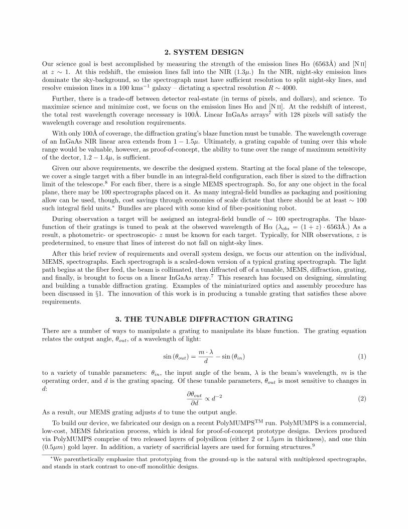
For any two functionally equivalent spectrographs, their volume increases, roughly, with the telescope diam-eter cubed.1 There is a power-law relationship between telescope diameter (volume) and instrument cost, wherethe exponent sits between two and three. For example, DEIMOS, on a 10m telescope cost US$10m dollars2
(though it was originally budgeted for less.) The preliminary estimate for an instrument with less multiplex-ing capability, on a 30m telescope, is US$60m.3 This growth of telescope diameter, and instrument cost andcomplexity, is schematically illustrated in Figure 1.
In this paper we describe the design of a spectrograph, built with tens of thousands of mini-spectrographs. Byclever use of fiber multiplexing and slicing, enormous optics disappear, simplifying alignment and test procedures,which ultimately drive down the cost of the instrument package. A single, MEMS, spectrograph, includingdetector, costs manufacturers roughly US$20 per part.
It is well understood that industrial replication reduces the cost of an individual component. However, asurprising recent result, is that replicated spectrographs reduce the total cost of an instrument. For example, therecently designed Visible Integral-Field Replicable Unit Spectrographs (VIRUS), which is replicated by ∼ 100×,saves approximately a factor of two or three compared to a monolithic design.4
Micro-electrical-mechanical-systems (MEMS) technology, allows the production of spectrographs even smallerthan the VIRUS. The drive to reduce spectrograph size is the drive reduce total instrument cost. Though theseMEMS spectrographs may sound exotic, we emphasize that this technology is not new,5,6 commercial, off-theshelf MEMS spectrographs exist today. However, these commercial spectrographs, are typically tuned for specificapplications (e.g. laser communication, television displays and molecular identification.) This work leveragesthe research of MEMS spectroscopy, to design an instrument tuned for a specific astronomical application.
arX
iv:0
807.
2481
v1 [
astr
o-ph
] 1
5 Ju
l 200
8

Each Spectrograph ~ Size of Palm
Image on left is seeing-limited, z~0.7 galaxy. Seeing Disk (mm) ~ Primary Diameter (D) x f/# x Seeing
SDSS Spectrograph Small camera, grating & detector Volume ~ Dinner Table
Keck DEIMOS spectrograph Enormous camera, grating & detector Volume ~ Bus
This Work
Traditional Instruments 2.5m
10m
Proposed 30mMany tiny spectrographs
(c) Axsun Technologies
Figure 1. A schematic illustration of the evolution in size and cost of optical spectrgraphs. The top two rows showpictures of the Sloan digital Sky Survey (SDSS; 2.5m primary) multi-object spectrograph, and the Keck (10m primary)spectrograph, DEep Imaging Multi-Object Spectrograph. Notice the relationship between telescope size (going down thepage) and instrument volume. At 10m, the spectrograph dwarfs the PI and engineers. For the proposed 30m telescopeand wide field optical spectrograph (WFOS), a CAD model is rendered next to DEIMOS. The WFOS is the size of asmall house. The device in the bottom left is a Fabry-Perot spectrograph built by Axsun Technologies, it illustrates theprinciple behind this design: build thousands of miniature spectrographs.
2. SYSTEM DESIGN
Our science goal is best accomplished by measuring the strength of the emission lines Hα (6563A) and [N ii]at z ∼ 1. At this redshift, the emission lines fall into the NIR (1.3µ.) In the NIR, night-sky emission linesdominate the sky-background, so the spectrograph must have sufficient resolution to split night-sky lines, andresolve emission lines in a 100 kms−1 galaxy – dictating a spectral resolution R ∼ 4000.
Further, there is a trade-off between detector real-estate (in terms of pixels, and dollars), and science. Tomaximize science and minimize cost, we focus on the emission lines Hα and [N ii]. At the redshift of interest,the total rest wavelength coverage necessary is 100A. Linear InGaAs arrays7 with 128 pixels will satisfy thewavelength coverage and resolution requirements.
With only 100A of coverage, the diffraction grating’s blaze function must be tunable. The wavelength coverageof an InGaAs NIR linear area extends from 1 − 1.5µ. Ultimately, a grating capable of tuning over this wholerange would be valuable, however, as proof-of-concept, the ability to tune over the range of maximum sensitivityof the dector, 1.2− 1.4µ, is sufficient.
Given our above requirements, we describe the designed system. Starting at the focal plane of the telescope,we cover a single target with a fiber bundle in an integral-field configuration, each fiber is sized to the diffractionlimit of the telescope.8 For each fiber, there is a single MEMS spectrograph. So, for any one object in the focalplane, there may be 100 spectrographs placed on it. As many integral-field bundles as packaging and positioningallow can be used, though, cost savings through economies of scale dictate that there should be at least ∼ 100such integral field units.∗ Bundles are placed with some kind of fiber-positioning robot.
During observation a target will be assigned an integral-field bundle of ∼ 100 spectrographs. The blaze-function of their gratings is tuned to peak at the observed wavelength of Hα (λobs = (1 + z) · 6563A.) As aresult, a photometric- or spectroscopic- z must be known for each target. Typically, for NIR observations, z ispredetermined, to ensure that lines of interest do not fall on night-sky lines.
After this brief review of requirements and overall system design, we focus our attention on the individual,MEMS, spectrographs. Each spectrograph is a scaled-down version of a typical grating spectrograph. The lightpath begins at the fiber feed, the beam is collimated, then diffracted off of a tunable, MEMS, diffraction, grating,and finally, is brought to focus on a linear InGaAs array.7 This research has focused on designing, simulatingand building a tunable diffraction grating. Examples of the miniaturized optics and assembly procedure hasbeen discussed in §1. The innovation of this work is in producing a tunable grating that satisfies these aboverequirements.
3. THE TUNABLE DIFFRACTION GRATING
There are a number of ways to manipulate a grating to manipulate its blaze function. The grating equationrelates the output angle, θout, of a wavelength of light:
sin (θout) =m · λd− sin (θin) (1)
to a variety of tunable parameters: θin, the input angle of the beam, λ is the beam’s wavelength, m is theoperating order, and d is the grating spacing. Of these tunable parameters, θout is most sensitive to changes ind:
∂θout
∂d∝ d−2 (2)
As a result, our MEMS grating adjusts d to tune the output angle.
To build our device, we fabricated our design on a recent PolyMUMPSTM run. PolyMUMPS is a commercial,low-cost, MEMS fabrication process, which is ideal for proof-of-concept prototype designs. Devices producedvia PolyMUMPS comprise of two released layers of polysilicon (either 2 or 1.5µm in thickness), and one thin(0.5µm) gold layer. In addition, a variety of sacrificial layers are used for forming structures.9
∗We parenthetically emphasize that prototyping from the ground-up is the natural with multiplexed spectrographs,and stands in stark contrast to one-off monolithic designs.

Relaxed Stretched
70µ
3µ
Figure 2. A small grating test-structure. On the left is the relaxed grating, anchored to the substrate by the anchor bladeon top, the remainder of the grating is floating. On the right is the same grating, stretched by an off-chip probe (blackshadow.) This figure illustrates the basic principle of the diffraction grating “accordion” operation. Thick blades are thediffracting elements, while thin springs (3µ) thick connect the thick blades. Not shown in this diagram is the diffractiongrating connection to the drive system by replacing the probe hole with the drive shuttle.
To tune the grating spacing, the grating is designed to stretch in an “accordion” style. Figure 2 shows atest grating operated by hand. This Figure is taken through a microscope objective. A grating is comprised ofthick diffraction blades, blades are made of polysilicon (Poly1), the total thickness of a blade is 2µm. Blades areconnected via long, skinny springs, each 3µm thick. In this figure, the grating is stretched, “by hand.” That is,an off-chip probe, driven by hand turned screws pulls on the large circle.
We explored a number of spring designs by varying spring sizes. Using the Intellisuite(tm) finite elementanalysis (FEA) code, we simulated displacements and measured spring constants, as well as maximum stress onthe polysilicon, in steady state. Typical simulated spring constants varied from 7.3N m−1 to 61.0N m−1.
Aside from the spring constant, the design attempts to minimize the stress per unit displacement. Our gratingis fully compliant, so at sharp edges, the polysilicon fracture strength of ∼ 1.5GPa must be considered. Thoughsmaller features increase fracture strength, the PolyMUMPS design rules dictate a minimize feature size of 2µand recommend at least 3µ features to ensure that the lithographic process does not affect the features. As aresult, our final design has springs that are 3× 70µm (as marked on Figure 2.)
As part of our inspection process, we attempted to measure the spring constant of our design. An inhomoge-nous spring constant would result because polysilicon deposition may have varying material properties over thewafer. Our measurements were performed using the lab microscope, but were not able to detect any differences,largely due to the large, 2µm, uncertainty in measurements. Future work will use an interferometric approach.
Our diffraction grating is connected to a drive system described in the next section. To envision this linkage,replace the probe hole seen in Figure 2 with a connection to the actuation system.
3.1 Grating Diffraction Efficiency
We use gsolver to simulate the efficiency of an alternating gold, polysilicon, diffraction grating. The simulationtakes account of the etch release holes, and dimples, visible in Figure 2. Simulations showed acceptable efficiencyin first order, typically greater than 50%.
Most of our efficiency loss is due to the design rules dictated by the PolyMUMPS process. PolyMUMPS is arobust, and relatively simple service, designed to be general purpose with high yield. As a result, our gratingsare limited to square blaze functions. Square blaze angles reduce the efficiency of the grating. In §5 we brieflydescribe an alternative approach that increases simulated efficiency to greater than 85%.

4. THE DRIVE SYSTEM
The drive system must deal with the trade off between actuator force, and total displacement. Recall from theprior section, the displacement is directly responsible for the tunability of our system. The tunable diffractiongrating requires a large displacement of ∼ 100µm, under strong force, ∼ 10µN . MEMS actuators trade-off eitherforce, or displacement. As a result, we combine a set of small-stroke, yet high-force, actuators, and a ratchetingsystem.10
Two classes of thermal actuators are used in our design. Thermal actuators deflect during thermal expansioninduced by Joule heating. To capitalize on deflection, asymmetries in the mechanical design yield directionalnet forces. Because of small thermal masses, temperature changes are rapid, and these devices can be controlledaccurately with electric currents.
This system design is shown in Figure 3. This image is taken directly from the TannerTM/EDA layoutpackage. In the Tanner/EDA design drawings, the first polysilicon layer (Poly0) is shown in orange, the thirdpolysilicon layer (Poly2) is shown in red, and the gold layer (Metal) is shown in black. Because many of ourstructures are free-floating, the second polysilicon layer (Poly1) is hard to see on this drawing. Probe points arelabeled in Poly0.
150µ
Thermal Actuator
Thermal A
ctuator
Shuttle
Pawl
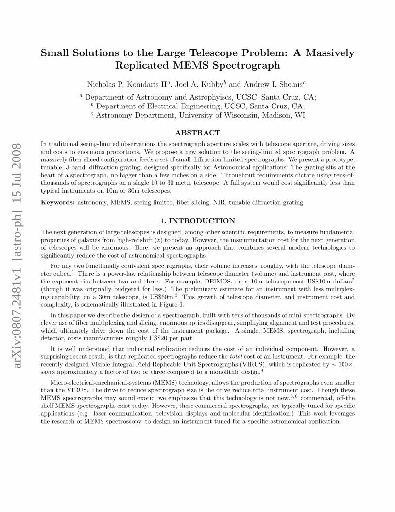
Figure 3. Tanner EDA/MEMS design layout with major components labeled in black. Starting from center, and workingout clockwise within the large black box, we see: The shuttle system, which, is connected to, and stretches the diffractiongrating. Left of the shuttle is a pair of thermal actuators. Thermal actuators only actuate in one direction, as indicatedby arrows. Each side drives the shuttle in one direction only, and provides a locking mechanism. Finally is the pawl, thisdevice grips the shuttle through gears. Figure 4 zooms in to the black box.
Figure 3 shows the design: a simple, transverse, pawl and shuttle system, provides the ratcheting systemfor the grating. By synchronized motions of opposing sets of actuator banks, the pawls drive the shuttles. The
design is axially symmetric, the two sets of opposing actuators surround the central shuttle system. The shuttleis connected to a diffraction grating (not shown.) The shuttle slides up and down on a track, constrained bysmall pill-boxes.
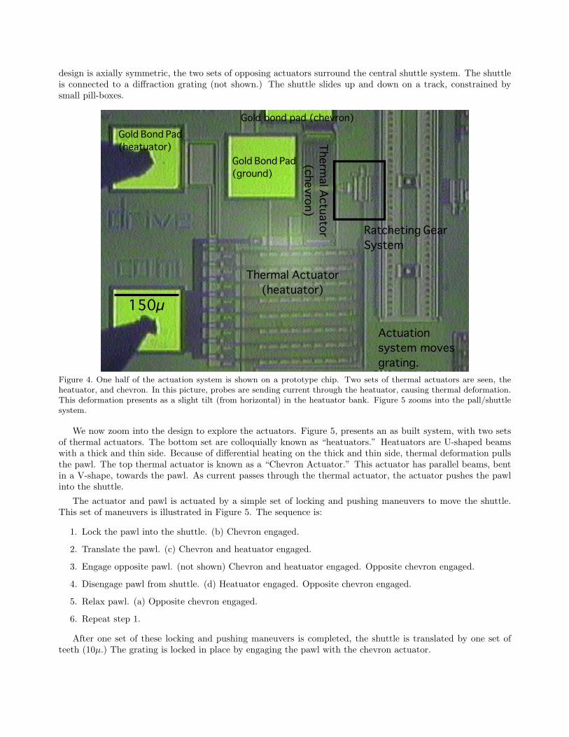
Gold Bond Pad (ground)
Thermal Actuator (heatuator)
Thermal A
ctuator (chevron)
Ratcheting Gear System
Actuation system moves grating.
150µ
Gold Bond Pad (heatuator)
Gold bond pad (chevron)
Figure 4. One half of the actuation system is shown on a prototype chip. Two sets of thermal actuators are seen, theheatuator, and chevron. In this picture, probes are sending current through the heatuator, causing thermal deformation.This deformation presents as a slight tilt (from horizontal) in the heatuator bank. Figure 5 zooms into the pall/shuttlesystem.
We now zoom into the design to explore the actuators. Figure 5, presents an as built system, with two setsof thermal actuators. The bottom set are colloquially known as “heatuators.” Heatuators are U-shaped beamswith a thick and thin side. Because of differential heating on the thick and thin side, thermal deformation pullsthe pawl. The top thermal actuator is known as a “Chevron Actuator.” This actuator has parallel beams, bentin a V-shape, towards the pawl. As current passes through the thermal actuator, the actuator pushes the pawlinto the shuttle.
The actuator and pawl is actuated by a simple set of locking and pushing maneuvers to move the shuttle.This set of maneuvers is illustrated in Figure 5. The sequence is:
1. Lock the pawl into the shuttle. (b) Chevron engaged.
2. Translate the pawl. (c) Chevron and heatuator engaged.
3. Engage opposite pawl. (not shown) Chevron and heatuator engaged. Opposite chevron engaged.
4. Disengage pawl from shuttle. (d) Heatuator engaged. Opposite chevron engaged.
5. Relax pawl. (a) Opposite chevron engaged.
6. Repeat step 1.
After one set of these locking and pushing maneuvers is completed, the shuttle is translated by one set ofteeth (10µ.) The grating is locked in place by engaging the pawl with the chevron actuator.
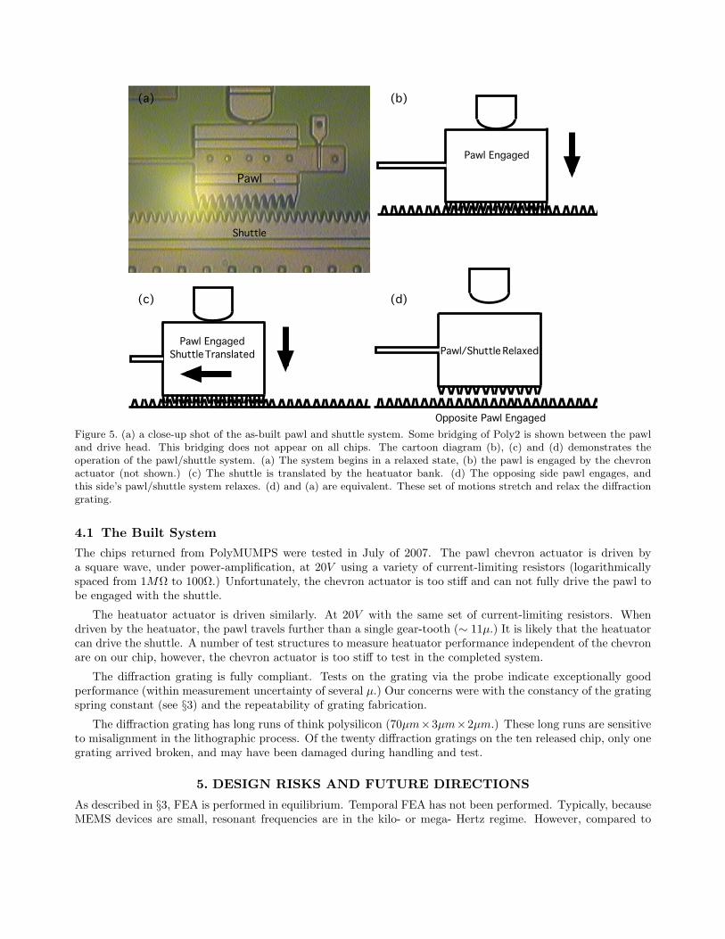
Pawl
Shuttle
Pawl Engaged
Pawl Engaged Shuttle Translated
(a) (b)
(c) (d)
Pawl/Shuttle Relaxed
Opposite Pawl EngagedFigure 5. (a) a close-up shot of the as-built pawl and shuttle system. Some bridging of Poly2 is shown between the pawland drive head. This bridging does not appear on all chips. The cartoon diagram (b), (c) and (d) demonstrates theoperation of the pawl/shuttle system. (a) The system begins in a relaxed state, (b) the pawl is engaged by the chevronactuator (not shown.) (c) The shuttle is translated by the heatuator bank. (d) The opposing side pawl engages, andthis side’s pawl/shuttle system relaxes. (d) and (a) are equivalent. These set of motions stretch and relax the diffractiongrating.
4.1 The Built System
The chips returned from PolyMUMPS were tested in July of 2007. The pawl chevron actuator is driven bya square wave, under power-amplification, at 20V using a variety of current-limiting resistors (logarithmicallyspaced from 1MΩ to 100Ω.) Unfortunately, the chevron actuator is too stiff and can not fully drive the pawl tobe engaged with the shuttle.
The heatuator actuator is driven similarly. At 20V with the same set of current-limiting resistors. Whendriven by the heatuator, the pawl travels further than a single gear-tooth (∼ 11µ.) It is likely that the heatuatorcan drive the shuttle. A number of test structures to measure heatuator performance independent of the chevronare on our chip, however, the chevron actuator is too stiff to test in the completed system.
The diffraction grating is fully compliant. Tests on the grating via the probe indicate exceptionally goodperformance (within measurement uncertainty of several µ.) Our concerns were with the constancy of the gratingspring constant (see §3) and the repeatability of grating fabrication.
The diffraction grating has long runs of think polysilicon (70µm×3µm×2µm.) These long runs are sensitiveto misalignment in the lithographic process. Of the twenty diffraction gratings on the ten released chip, only onegrating arrived broken, and may have been damaged during handling and test.
5. DESIGN RISKS AND FUTURE DIRECTIONS
As described in §3, FEA is performed in equilibrium. Temporal FEA has not been performed. Typically, becauseMEMS devices are small, resonant frequencies are in the kilo- or mega- Hertz regime. However, compared to
typical MEMS, the designed grating is an enormous spring. Temporal FEA should be performed, and its resultsfed into our grating efficiency simulation.
Because of the internal crystal stresses associated with etching polysilicon layers and the bulk micromachiningprocess, the resulting diffraction grating may not be of “optical quality” (λ/8 surface quality.) In addition, bulkmicromachining limits the grating blaze angle to 90. Both flaws can be mitigated by starting with a well-polished wafer, and using an etch based manufacturing process.11,12 As a result of silicon’s crystal structure,and the readily available supply of wafers with crystal faces orthogonal to the wafer’s plane, the blaze angle isfixed at 54.7.
Because of the chemical vapor deposition (CVD) process used to deposit polysilicon in the PolyMUMPSprocess, the resulting diffraction grating may not have surfaces that are of optical quality (λ/8.) The SandiaUltra-planar, Multi-level MEMS Technology 5 (SUMMiT V) Fabrication Process is a five-layer polycrystallinesilicon surface micromaching process that uses chemical mechanical polishing (CMP) to obtain optical qualitysurfaces. SUMMiT V is a likely candidate for the next generation fabrication run of the tunable grating.
PolyMUMPS design rules require that the pawl and shuttle gears are not fabricated in a meshed configuration.As a result, the translator is locked only when a thermal actuator is pushing the gears together. Thermal photonsfrom the engaged actuator would add background noise to our NIR detector. The SUMMiT V process allowsgears to be fabricated meshed, and so this thermal background will disappear.
Packaging and assembly of a full optical design, though not an impossible task (see Axsun technologies fora design with similar level of complication) has not been considered for this design. Future work will requirecareful consideration of packaging and test.
The resolution of a spectrograph is R = m ·N where R is the resolution, m the order and N the number ofilluminated grating elements. The system requirements in §2, indicate that we need R=4000. By pushing upm, it is possible to significantly increase resolution while reducing the grating size, however, the trade-off is thatorders begin to overlap, and some kind of order-blocking filter is necessary. Therefor, to reduce the complexityof the design, small values of m are valued. We have not fully explored the value of m for the grating.
MEMS design experience dictates† the designs which rely on friction, gears, or stiction, often have low yieldsand are not robust to repeated use. Our design, due to the conflicting requirements of large displacement andlarge force, is a gear-based design. A fully compliant13 MEMS design, cleverly using geometric advantage, maybe more robust.
In summary, we present a new, MEMS, tunable diffraction grating. This grating sits at the heart of aminiature, fiber-fed, NIR, medium-resolution, spectrograph. The advantage of miniaturizing spectrographs comesfrom economies of scale. By reproducing the same spectrograph 10, 000×, the total cost of an instrument isdrastically reduced.
ACKNOWLEDGMENTS
We acknowledge the UCSC MEMS laboratory. In addition, the authors acknowledge Mahyar X Fotovatjah,Stefan Gadomski, and Chung Quang Thai.
REFERENCES[1] Schroeder, D. J., [Astronomical Optics ], San Diego: Academic Press, 1987 (1987).[2] Faber, S. M., Phillips, A. C., Kibrick, R. I., Alcott, B., Allen, S. L., Burrous, J., Cantrall, T., Clarke,
D., Coil, A. L., Cowley, D. J., Davis, M., Deich, W. T. S., Dietsch, K., Gilmore, D. K., Harper, C. A.,Hilyard, D. F., Lewis, J. P., McVeigh, M., Newman, J., Osborne, J., Schiavon, R., Stover, R. J., Tucker, D.,Wallace, V., Wei, M., Wirth, G., and Wright, C. A., “The DEIMOS spectrograph for the Keck II Telescope:integration and testing,” 4841, 1657–1669 (Mar. 2003).
†For example, see the web page: http://www.memsrus.com/documents/PolyMUMPsNotes.Microsoft.pdf

[3] Pazder, J. S., Roberts, S., Abraham, R., Anthony, A., Fletcher, M., Hardy, T., Loop, D., and Sun, S.,“WFOS: a wide field optical spectrograph for the Thirty Meter Telescope,” in [Ground-based and AirborneInstrumentation for Astronomy. ], SPIE 6269 (July 2006).
[4] Hill, G. J., MacQueen, P. J., Tufts, J. R., Kelz, A., Roth, M. M., Altmann, W., Segura, P., Gebhardt, K.,and Palunas, P., “VIRUS: a massively replicated integral-field spectrograph for HET,” in [Ground-based andAirborne Instrumentation for Astronomy. ], SPIE 6269 (July 2006).
[5] Onat, B. M., Masaun, N., Huang, W., Lange, M., and Dries, C., “Hyperspectral imaging with MEMsintegrated focal plane arrays,” in [Semiconductor Photodetectors II. ], Cohen, M. J. and Dereniak, E. L.,eds., SPIE 5726, 92–102 (Apr. 2005).
[6] Musca, C., Antoszewski, J., Winchester, K., Keating, A., Nguyen, T., Silva, K., Dell, J., Faraone, L., Mitra,P., Beck, J., Skokan, M., and Robinson, J., “Monolithic integration of an infrared photon detector with aMEMS-based tunable filter,” in [Electron Device Letters, IEEE ], 26 (2005).
[7] Nelson, M., Bush, M., Skrutskie, M., Kanneganti, S., Park, C., and Fox, O., “Development of extendedwavelength response InGaAs detectors for astronomical applications,” in [High Energy, Optical, and InfraredDetectors for Astronomy II. ], SPIE 6276 (July 2006).
[8] Sheinis, A. I., Nigra, L., and Kuhlen, M. Q., “Mems-based speckle spectrometer,” in [Advances in AdaptiveOptics II. ], SPIE 6272 (July 2006).
[9] Carter, J., Cowen, A., Mahadevan, R., Stonefield, M., and Wilcenski, S., [PolyMUMPs Design Handbook,Rev. 11 ], MEMSCAP, USA (2005).
[10] Kolesar, E., “Design and performance of an electrothermal mems microengine capable of bi-directionalmotion.,” in [Thin Solid Films ], 447 (2004).
[11] Mar, D. J., Marsh, J. P., Jaffe, D. T., Keller, L. D., and Ennico, K. A., “Performance of large chemi-cally etched silicon grisms for infrared spectroscopy,” in [Ground-based and Airborne Instrumentation forAstronomy. ], SPIE 6269 (July 2006).
[12] Tormen, M., “Deformable MEMS grating for wide tunability and high operating speed,” Journal of optics.A, Pure and applied optics 8(7) (2006).
[13] Kota, S., “Design of compliant mechanisms: Applications to mems.,” Analog integrated circuits and signalprocessing 29(1/2) (2001).
Copyright © 2022 FDOKUMEN