SERVICE MANUAL - Dansk kassesystem
127
ELECTRONIC CASH REGISTER QT-2000 (EX-580) JUNE 1997 C 7 4 1 0 8 5 2 00 9 6 3 ¥ SERVICE MANUAL (without price)
-
Upload
khangminh22 -
Category
Documents
-
view
5 -
download
0
Transcript of SERVICE MANUAL - Dansk kassesystem

ELECTRONIC CASH REGISTER
QT-2000 (EX-580)
JUNE 1997
C
7
4
1
0
8
5
200
9
6
3
¥
SERVICE MANUAL(without price)

CONTENTS
QT-2000 Page
1. GENERAL ............................................................................................................... 11-1. System chart .................................................................................................... 11-2. Device list (Option) .......................................................................................... 2
2. SPECIFICATIONS ................................................................................................. 33. QT-2000 CONNECTOR LOCATIONS .................................................................... 84. INITIALIZE OPERATION ...................................................................................... 11
4-1. To initialize QT-2000 terminal ........................................................................ 114-2. To initialize QT-2000 terminal(add/replace one QT-2000) ............................ 144-3. To flag clear QT-2000 terminal(INIT2, Restore from flash) ........................... 17
5. CIRCUIT EXPLANATION ..................................................................................... 185-1. Block diagram (MAIN PCB E580-1)............................................................... 185-2. Memory map.................................................................................................. 195-3. I/O address map ............................................................................................ 205-4. LSI Pin description ......................................................................................... 215-5. Power down detection circuit ......................................................................... 335-6. Option RAM circuit ......................................................................................... 34
6. OPTION INSTALLATION ...................................................................................... 356-1. Clerk key unit (CLK-K17,CLK-K18) ............................................................... 356-2. Rear display (QT-2060D)............................................................................... 366-3. MCR unit (QT-2046MC)................................................................................. 376-4. Multi drawer (MDL-8) ..................................................................................... 38
7.IN / ON LINE .......................................................................................................... 397-1. C-In line (ARCNET) ....................................................................................... 397-2. On line ........................................................................................................... 42
1. Direct connection to PC ................................................................................. 422. MODEM system ............................................................................................. 43
7-3. Kitchen printer connection ............................................................................. 448.DIAGNOSTIC OPERATION ................................................................................... 479.ERROR CODE LIST .............................................................................................. 6710.IC DATA ............................................................................................................... 7311.PCB LAYOUT ...................................................................................................... 8012.CIRCUIT DIAGRAM ............................................................................................. 8213. PARTS LIST...................................................................................................... 104

— 1 —
The QT-2000 has the following unique points:(The system configuration is shown in the chart above.)
1. Separete R/J printer
2. Small foot-print and low-profile design
3. LCD display : Max. 2 LCD display
4. Flat keyboard menu holder : Max. 8 menu can be contorolled.4 (direction) x 2 (holder)
5. Data backup function by EEPROM (Flash ROM)
6. Infrared communication interface
2nd Display
QT-2000
Cable SA-1062S
Kitchen Printer
KP-200 / KP-300
R/J Printer
TM-U950
TM-T85
TM-T88
SA-3015
TM-T85
UP-350
Clerk Key
CLK-K17 (6 clerk)CLK-K18 (15 clerk)
MCR unit
Multi Drawer
MDL-8
QT-2046MC
RAM6104M bits
RAM5301M bits
Slip Printer
SP-1200
ScannerHHS-9
1. GENERAL
1-1. System chart
CustomerDisplay
Pole
QT-2063D
QT-2061S
RearDisplay
QT-2060D

— 2 —
1-2. Device list (Option)
No. Model Name Device Name Note
Sheet holder
1 SH-KIT1 Sheet holder kit 2 holders (1st - 4th, 5th - 8th)
Kitchen Printer
2 KP-200 Kitichen printer3 KP-300 Kitchen printer with auto cutter
Slip printer
4 SP-1200 Slip printer
R/J printer
5 SA-3015 R/J and slip printer TM-U950 Paper size : 70mmDot matrix printer
6 TM-T85 Receipt printer TM-T85 Paper size : 80mmThermal printer
7 UP-350 Receipt printer TM-T88 Paper size : 80mmThermal printer
8 PS-150/PS-170 AC adaptor for TM-T85 / UP-3509 SA-3087TM Printer cable for TM-T85 / UP-350
(Cable length : 3 m)
Display
10 QT-2062D Second LCD display11 QT-2060D Rear display12 QT-2063D Customer display13 QT-2061S Pole for QT-2063D14 SA-1062S Expantion cable for QT-2063D
(Cable length : 5 m)
Multi drawer
15 MDL-8 Multi drawer kit Additional 1 drawer
Memory
16 RAM-610-10LL RAM chip 4 M bits chip17 RAM-530-10 RAM chip 1 M bits chip
MCR
18 QT-2046MC Magnetic card reader
Clerk key
19 CLK-K17 Clerk key kit for 6 clerk20 CLK-K18 Clerk key kit for 15 clerk
Hand held scanner
21 HHS-9 scanner RS-232C

— 3 —
2. SPECIFICATION
2-1. QT-2000
120V 230VPower consumption In operation Max.: 0.7A 0.4A
Stand-by Max.: 0.4A 0.3AMode SW OFF Max.: 0.3A 0.2A
Memory Standard: 384 KBMax: 1MB
Memory protection Back up battery Lithium-Banadium battery VL3032/S6ABack up period 30 days ( 25°C )Battery life Replace every 5 yearsCharging time 48 hours for full charge
Clock and calender Accuracy within ±30 sec./month ( 25 °C )Auto calender Effective 2099 A.D.
Environment Operating temperature 0°C ~ 40°COperating humidity 20% ~ 65%Strorage temperature -20°C ~ 60°CStorage humidity 10% ~ 80%In the carton box : Storage temperature -20°C ~ 65°C
Storage humidity 10% ~ 80%
LCD display LCD life 15,000 hours
Back light Back light life 10,000 hours
Power prutection battery No function
CAUTIONDanger of explosion if battery is incorrectly replaced.
Replace only with the same or equivalent typerecommended by the manufacturer.Dispose of used batteries accordingto the manufacture’s instructions.
VORSICHT !Explosionsgefahr bei unsachgemäßem Austausch der Batterie.
Ersatz nur durch denselben oder einen vomHersteller empfohlenen gleichwertigen Typ.
Entsorgung gebrauchter Batterien nachAngaben des Herstellers.
ADVARSEL !Lithiumbatteri - Eksplosionsfare ved fejlagtig hándtering.
Udskiftning má kun ske med batteriaf samme fabrikat og type.
Levér det brugte batteri tilbage til leverandØren.

— 4 —
2-2. Printer
2-2-1. Model name : SA-3015
Item DescriptionPrinter name TM-U950Power source +24V DC ±10%Current consumprion R/J Average : Approx. 1.8A Max : Approx. 8A
Slip Average : Approx. 2.3AStandby : 0.3A
Print method Serial impact dot-matrix printerMCBF 5,000,000 lines (auto-cutter and stamp once every 15 lines)Print speed 233 CPS ( 9x9 dots : High speed )
311 CPS ( 7x9 dots : Low speed )Charactor per line R/J : 30 (9x9), 40 (7x9)
Slip : 66 (9x9), 88 (7x9)Stamp size 42 x 20 mm (Print area)Roll paper Type : Fine quality paper ( Single layer only)
Width : 69.5 ±0.5 mmPaper diameter : 83 mm or lessPaper thickeness : 0.06 to 0.09 mm
Slip paper Type : Plane paper, Carbon copy paper,Pressure-sensitive paper
Number of paper : Original + 4 copiesDimension : 70x70 to 210x297mm (WxH)Thickness : 0.09 to 0.36mm
Ink ribbon Type : ERC-31Ribbon life : 7,000,000 characters (18 dots per charactor)
Interface Serial RS-232C interface
2-2-2. Model name : TM-T85
Item DescriptionPrinter name TM-T85Power source +24V DC ±7%Current consumprion Average : Approx. 1.3A Max : Approx. 6.0A
Standby : Approx. 0.1APrint method Line thermal printing methodMCBF 3,500,000 lines (font A printing)Print speed 12 lines/sec. (1/6 inch line feed)
13 lines/sec. (1/9 inch line feed)Charactor per line 42 digits (12x24), 56 digits (9x7), 21 digits (24x24)Print width 72mmRoll paper Type : Prescribed thermal paper
Width : 80mmPaper diameter : 83 mm or lessPaper thickeness : 65±5µ m
Interface Serial RS-232C interface

— 5 —
2-2-3. Model name : UP-350 (TM-T88)
Item DescriptionPrinter name TM-T88Power source +24V DC ±7%Current consumprion Average : Approx. 1.5A Max : Approx. 5.0A
Standby : Approx. 0.2APrint method Line thermal printing methodMCBF 10,000,000 lines (font A printing)Print speed High speed : 16.5 lines/sec. (1/6 inch line feed)
Low speed : 11.8 lines/sec. (1/6 inch line feed)Charactor per line 42 digits (12x24), 56 digits (9x7)Print width 72.2 ±0.2mmRoll paper Type : Prescribed thermal paper
Width : 79.5±0.5mmPaper diameter : 83 mm or less
Interface Serial RS-232C interface
2-3. Slip printer
Model name : SP-1200
Item DescriptionPrinter name Model 290Power source +24V DC ±10%Print method Dot print ( with built-in shuttle head)MCBF 1,500,000 linesPrint speed Approx. 2.3 to 1.9 lines/sec.Charactor per line Max. : 35 digits (5x7)Slip paper Type : Prescribed thermal paper
Carbon copy paperPressure-sensitive paper
Width : 80x80 to 182x257mm (WxL)Number of paper : Max. : 3 sheets (Original + 2 copies)Thickness : Total thickness : 0.35mm
Nomal paper : 0.09 to 0.25mmCopy paper :Base sheet : 0.07 to 0.2mm
Duplicate : 0.04 to 0.07mmCarbon paper : Approx 0.035mm
Ink ribbon Type : ERC-27Ribbon life : 1,500,000 characters
Interface Serial interface

— 6 —
2-4. Kitchen printer
Model name : KP-300
Item DescriptionPrinter name DP-617Power source AC115V / AC230VCurrent consumprion 30wPrint method Serial impact printing method
Both direction printingMCBF Printer mechanism : 2,500,000 lines
Head : 50,000,000 characterPrint speed 2.4 lines/sec.Character per line 40 digits 400 dots/lineRoll paper Width : 76mm
Paper diameter : 80mm or lessInk ribbon RE-1Interface RS-422 interface
Model name : KP-200
Item DescriptionPrinter name DP-575Power source AC115V / AC230VCurrent consumprion 25wPrint method Serial impact printing method
1 direction printing ( L to R )MCBF Printer mechanism : 1,500,000 lines
Head : 50,000,000 characterPrint speed 1.2 lines/sec.Character per line 40 digitsRoll paper Width : 69mm
Paper diameter : 80mm or lessInk ribbon RB-2Interface RS-422 interface
2-5. Hand scanner
Model name : HHS-9
Item DescriptionPower supply +5.0 V DC ± 5%Power consumption Max. 0.4 WRush current Max. 1.5 AOperating temperrature 0 to 40°COperating humidity 10 to 90% RH (not to condence dew)Reading width 65 mmReading resolution less than 0.125 mm (NW-7,CODE39,ITF,STF)
less than 0.15 mm (CODE93,CODE128)PCS value 0.45 or more
(wavelength 660 nm, white bar reflectivity ≥ 85%)
— 7 —
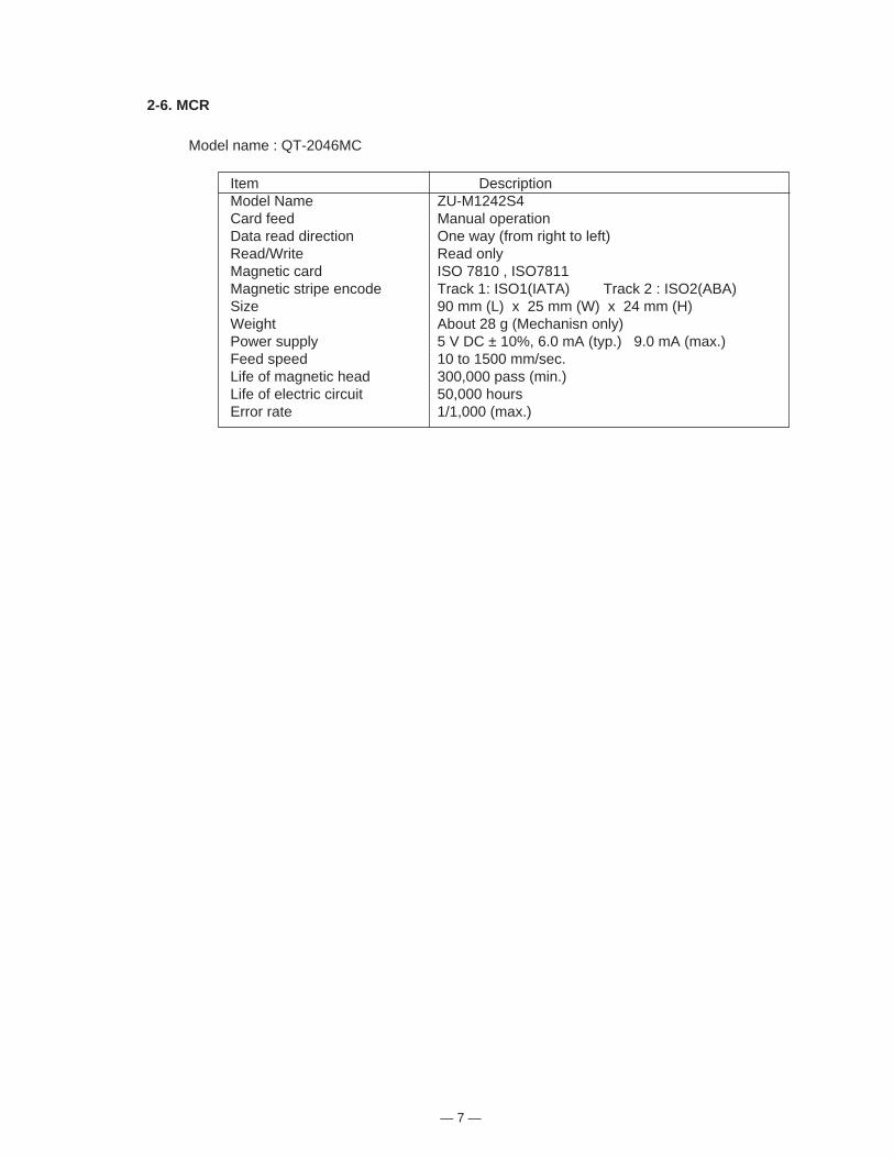
2-6. MCR
Model name : QT-2046MC
Item DescriptionModel Name ZU-M1242S4Card feed Manual operationData read direction One way (from right to left)Read/Write Read onlyMagnetic card ISO 7810 , ISO7811Magnetic stripe encode Track 1: ISO1(IATA) Track 2 : ISO2(ABA)Size 90 mm (L) x 25 mm (W) x 24 mm (H)Weight About 28 g (Mechanisn only)Power supply 5 V DC ± 10%, 6.0 mA (typ.) 9.0 mA (max.)Feed speed 10 to 1500 mm/sec.Life of magnetic head 300,000 pass (min.)Life of electric circuit 50,000 hoursError rate 1/1,000 (max.)

— 8 —
3. QT-2000 CONNECTOR LOCATIONS
3-1. QT-2000 connector location
RS-232C Com1
RS-232C Com3
Slip printer port
Power switch
RS-232C Com2
Drawer cable
Infrared port
In-lineKP In-line
Bottom view
Com 1 : for hand held scanner HHS-9Com 2 : for R/J printer (UP-350, SA-3015 and TM-T85)Com 3 : for MODEM or PCPower switch : for service maintenance
Make sure off this switch when open the machine.Because, the power is applied even if the mode swith is off.

— 9 —
3-2. Interface pin asignment
Com1: Hand held scanner HHS-9 (Location : CN2 on E580-CNB)
Pin No. Description 1 TXD1 2 RXD1 3 RTS1 4 CTS1 5 DSR1 6 DTR1 7 GND 8 NC 9 VCC 10 NC 11 GND 12 NC 13 NC 14 NC 15 GND
Com2 : R/J printer (Location : CN1 on E580-CNB)
Pin No. Description 1 NC 2 RXD2 3 TXD2 4 DTR2 5 GND 6 DSR2 7 RTS2 8 CTS2 9 NC
Com3 : Modem / PC (Location : CN4)
Pin No. Description 1 CD3 2 RXD3 3 TXD3 4 DTR3 5 GND 6 DSR3 7 RTS3 8 CTS3 9 CI3

— 10 —
Slip printer : SP-1200 (Location : CN10)
Pin No. Description 1 VCC 2 VCC 3 Sensor signal 4 NC 5 VP 6 VP 7 VP 8 VP 9 Busy signal 10 NACK signal 11 GNDP 12 GNDP 13 Data signal 14 GNDP 15 NC 16 Clock signal 17 Clear signal 18 Reset signal 19 GNDP 20 GNDP
Kitchen printer : KP-200, KP-300 ( Location : CN2)
Pin No. Description 1 TXD (Red wire) 2 RXD (Black wire)
In-line I/F : C In-Line (ARCNET) (Location : CN2)
Pin No. Description 3 RXD (Black wire) 4 TXD (Red wire)
Drawer I/F (Location : DW1)
Pin No. Description 1 Drive signal (Red wire) 2 Power (Black wire) 3 Sensor siglal (Brown wire)

— 11 —
4. INITIALIZE OPERATION4-1.To initialize QT-2000 terminal
Preparation:
1. All peripheral devices and QT-2000 terminals of this cluster should be turned off.
2. Connect all of the peripheral devices (such as printer, display etc.) to QT-2000 terminal.
3. Connect all QT-2000 terminals by in-line.
Operation:4. Turn on all peripheral devices of a QT-2000 terminal.
5. Turn on this QT-2000 terminal with pressing the left-most
key of the top row and release the key after buzzer sounds.
6. After releasing the key, enter 10000 (for Eu/Di)/20000 (U.S.)
and press the right part of the <ST> key.
7. Enter the current date (YY/MM/DD order) and time and
press the <Yes> key.
8. In ID character field, the auto-defined ID No. is shown.
We recommend that you should not change the value.
9. In these fields, you can select
“1.Master/2.Backup Master/3.Satellite.”
Please select one of these options and press the <Yes> key.
10. In this field, you can select, “1.Non/2.UP-350/3.SA-3015”
for R/J/Order printer.
Please select one of these options and press the <Yes> key.
1
Date 00-00-00 Time 12:34 00
ID Character MC #01 Check System Master KP System Master R/J/Order Printer SA-3015 Slip Printer SA-3015 Rear Display No Remote Display No OK? Yes
Date 97-12-15 Time 12:34 00
ID Character MC #01 Check System Master KP System Master R/J/Order Printer SA-3015 Slip Printer SA-3015 Rear Display No Remote Display No OK? YES
Date 97-12-15 Time 12:34 00
ID Character MC #01 Check System Master KP System Master R/J/Order Printer SA-3015 Slip Printer SA-3015 Rear Display No Remote Display No OK? YES
Date 97-12-15 Time 12:34 00
ID Character MC #01 Check System Master KP System Master R/J/Order Printer SA-3015 Slip Printer SA-3015 Rear Display No Remote Display No OK? YES
Date 97-12-15 Time 12:34 00
ID Character MC #01 Check System Master KP System Master R/J/Order Printer SA-3015 Slip Printer SA-3015 Rear Display No Remote Display No OK? YES

— 12 —
11. In this field, you can select, “1.Non/2.SA-3015/3.SP-1200”
for slip printer.
Please select one of these options and press the <Yes> key.
12. In these fields, you can select, “1.Yes/2.No” for rear display
and remote display.
Please select one of these options and press the <Yes> key.
13. Please confirm all of the field and if they are all right, press
the <Yes> key to proceed the next step.
14. If you want to download program data from other terminal,
press the <Yes> key and proceed the next step.
If you don't need to download any program data, just press the
<No> key (the initialization of this terminal is completed).
Return to step 4 to initialize other terminals.
Date 97-12-15 Time 12:34 00
ID Character MC #01 Check System Master KP System Master R/J/Order Printer SA-3015 Slip Printer SA-3015 Rear Display No Remote Display No OK? YES
Date 97-12-15 Time 12:34 00
ID Character MC #01 Check System Master KP System Master R/J/Order Printer SA-3015 Slip Printer SA-3015 Rear Display No Remote Display No OK? YES
Date 97-12-15 Time 12:34 00
ID Character MC #01 Check System Master KP System Master R/J/Order Printer SA-3015 Slip Printer SA-3015 Rear Display No Remote Display No OK? YES
INIT 97-12-17 12:34 000000 AUTO PGM Start YES
Date 97-12-15 Time 12:34 00
ID Character MC #01 Check System Master KP System Master R/J/Order Printer SA-3015 Slip Printer SA-3015 Rear Display No Remote Display No OK? YES

— 13 —
Program copy from other terminal.
15. In this field, you can select the receiving contents as
“1.All Data (including totalizer)/2.All PGM (program only).”
16. In this field, you should enter the source ID number of
the data and press the <Yes> key.
17. Please confirm all of the fields and if they are all right,
press the <Yes> key to proceed downloading.
After completion of downloading, return to step 4 to initialize
other terminals.
g py
INIT 97-12-15 12:34 000000
Received Data All PGM PGM Receive from MC #05
OK? YES
INIT 97-12-15 12:34 000000
Received Data All PGM PGM Receive from MC #05
OK? YES
INIT 97-12-15 12:34 000000
Received Data All PGM PGM Receive from MC #05
OK? YES

— 14 —
4-2. To initialize QT-2000 terminal (add/replace one QT-2000)
Preparation:
1. All peripheral devices and QT-2000 terminals of this cluster should be turned off.
2. Connect all of the peripheral devices (such as printer, display etc.) to this QT-2000 terminal.
3. Connect this QT-2000 terminal to in-line.
Operation:
4. Turn on all peripheral devices of this QT-2000 terminal.
And turn on all QT-2000 except this terminal of the cluster.
5. Turn on this QT-2000 terminal with pressing the left-most
key of the top row and release the key after buzzer sounds.
6. After releasing the key, enter 10000 (for Eu/Di)/20000 (U.S.)
and press the right part of the <ST> key.
7. Enter the current date (YY/MM/DD order) and time and
press the <Yes> key.
8. In ID character field, the auto-defined ID No. is shown.
Please check if the same value is set in this field.
We recommend that you should not change the value.
9. In these fields, you can select
“1.Master/2.Backup Master/3.Satellite.”
Please choose former options and press the <Yes> key.
10. In this field, you can select, “1.Non/2.UP-350/3.TM-U950”
for R/J/Order printer.
Please choose former option and press the <Yes> key.1
Date 00-00-00 Time 12:34 00
ID Character MC #01 Check System Master KP System Master R/J/Order Printer SA-3015 Slip Printer SA-3015 Rear Display No Remote Display No OK? Yes
Date 97-12-15 Time 12:34 00
ID Character MC #01 Check System Master KP System Master R/J/Order Printer SA-3015 Slip Printer SA-3015 Rear Display No Remote Display No OK? YES
Date 97-12-15 Time 12:34 00
ID Character MC #01 Check System Master KP System Master R/J/Order Printer SA-3015 Slip Printer SA-3015 Rear Display No Remote Display No OK? YES
Date 97-12-15 Time 12:34 00
ID Character MC #01 Check System Master KP System Master R/J/Order Printer SA-3015 Slip Printer SA-3015 Rear Display No Remote Display No OK? YES
Date 97-12-15 Time 12:34 00
ID Character MC #01 Check System Master KP System Master R/J/Order Printer SA-3015 Slip Printer SA-3015 Rear Display No Remote Display No OK? YES

— 15 —
11. In this field, you can select, “1.Non/2.SA-3015/3.SP-1200”
for slip printer.
Please choose former options and press the <Yes> key.
12. In these fields, you can select, “1.Yes/2.No” for rear display
and remote display.
Please choose former options and press the <Yes> key.
13. Please confirm all of the field and if they are all right, press
the <Yes> key to proceed the next step.
14.If you want to download program dasa from other terminal,
press the <Yes> key to proceed the next step.
If you don’t need to download any program data, just press the
<No> key (The initialization is completed).
Date 97-12-15 Time 12:34 00
ID Character MC #01 Check System Master KP System Master R/J/Order Printer SA-3015 Slip Printer SA-3015 Rear Display No Remote Display No OK? YES
Date 97-12-15 Time 12:34 00
ID Character MC #01 Check System Master KP System Master R/J/Order Printer SA-3015 Slip Printer SA-3015 Rear Display No Remote Display No OK? YES
Date 97-12-15 Time 12:34 00
ID Character MC #01 Check System Master KP System Master R/J/Order Printer SA-3015 Slip Printer SA-3015 Rear Display No Remote Display No OK? YES
INIT 97-12-17 12:34 000000 AUTO PGM Start YES
Date 97-12-15 Time 12:34 00
ID Character MC #01 Check System Master KP System Master R/J/Order Printer SA-3015 Slip Printer SA-3015 Rear Display No Remote Display No OK? YES
— 16 —
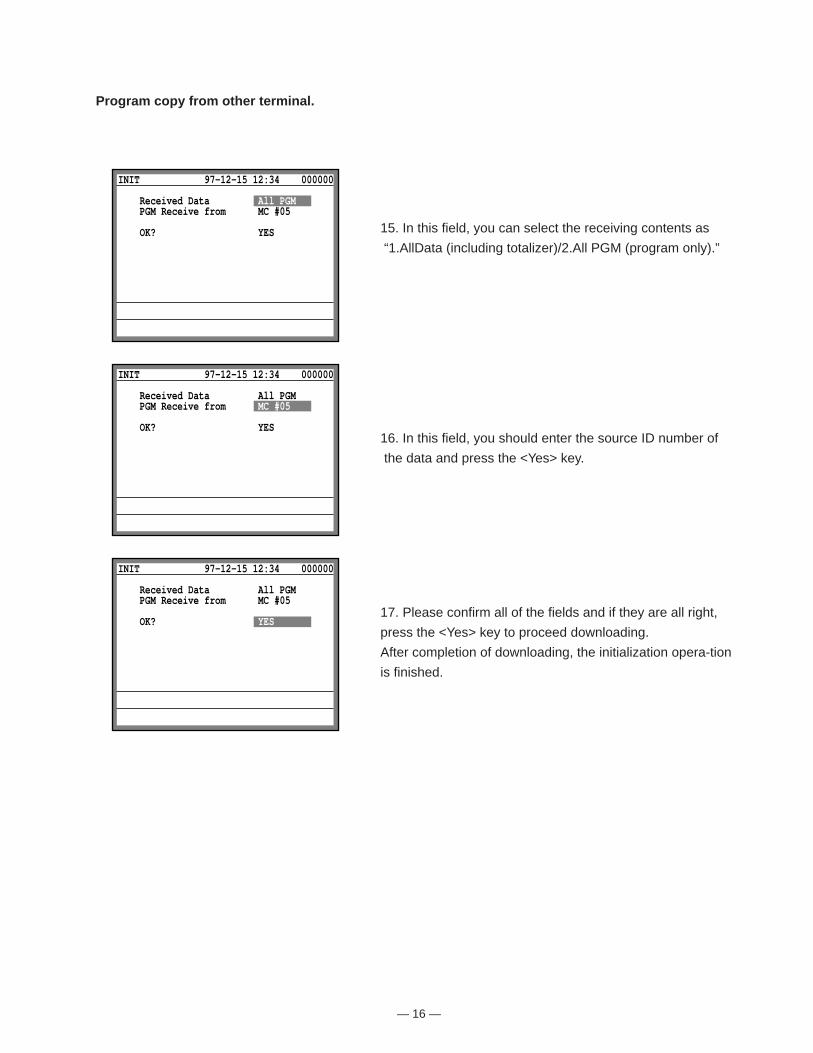
Program copy from other terminal.
15. In this field, you can select the receiving contents as
“1.AllData (including totalizer)/2.All PGM (program only).”
16. In this field, you should enter the source ID number of
the data and press the <Yes> key.
17. Please confirm all of the fields and if they are all right,
press the <Yes> key to proceed downloading.
After completion of downloading, the initialization opera-tion
is finished.
INIT 97-12-15 12:34 000000
Received Data All PGM PGM Receive from MC #05
OK? YES
INIT 97-12-15 12:34 000000
Received Data All PGM PGM Receive from MC #05
OK? YES
INIT 97-12-15 12:34 000000
Received Data All PGM PGM Receive from MC #05
OK? YES

— 17 —
4-3. To flag clear QT-2000 terminal (INIT2, Restore from flash)
Preparation:
1. All peripheral devices and this QT-2000 terminal should be turned off.
2. Check the connection of all peripheral devices (such as printer, display etc.) of this
QT-2000 terminal.
3. Check the connection of this QT-2000 terminal to in-line.
Operation:
4. Turn on all peripheral devices of this QT-2000 terminal.
5. Turn on this QT-2000 terminal with pressing the right-most
key of the top row and release the key after buzzer sounds.
6. After releasing the key, press the right part of the <ST> key.
Note:
Performing “Init 2” requires password “8888888888” and
performing “Restore” requires password “0000000000.”
7. Select "1.Flag Clear" and press the <Yes> key.
The flag clear operation is finished.
0.00
15-12-97 12:34
INIT 1.Flag Clear 2.Init2 3.Restore

— 18 —
5. CIRCUIT EXPLANATION
5-1. Block diagram (MAIN PCB E580-1)
LCD display
IC26
Display controller
IC20
IC36
GA4
IN-LINEARCNET
IC11
GA2
IC12
GA1
IC6
CPU
IC22
IC23
IC32IC33
IC43
IC35 IC39 IC31
IC10
1M EP ROM
16M F-ROM
2M SRAM
4M SRAM
1M SRAM
1M SRAM
GA3
ARCNETController
Video RAM
UARTIR I/F
COM1Scanner
COM2Printer
COM3Modem
RemortDisplay
BackDisplay
SlipPrinter
KitchenPrinter
Keyboard
Drawer
MASS memorycontrol

— 19 —
5-2. Memory map
SYSTEM RAM2Mb x 1
RAM 1Mb x 1
16Mb FLASH ROM
EP ROM1Mb
21 3 4 5 6
00000h
20000h
40000h
60000h
80000h
A0000h
C0000h
E0000h
FFFFFh
Option RAM 1Mb
Option RAM 4MbVRAM256Kb x 2
Bank16
Bank16 contents
40000h
48000h
50000h
58000h
VRAM for LCD2
VRAM for LCD1
Control areafor LCD1
Control areafor LCD2

— 20 —
5-3. I/O Address map
Rererved(INT Status)
System
System
System
System
System
Reserved
Reserved
ARCNET R/W
Back light control for LCD1
Back light control for LCD2
COM3 select W
Flash bank W
Future
Future
Reserved
System
Port #1
Port #2
Port #3
Port #4
Port #5
Port #6
Port #9
Port #7
Port #8
Port #15
Port #10
Port #11
Port #12
Port #13
Port #14
0000h
1000h
2000h
3000h
4000h
5000h
6000h
7000h
8000h
9000h
A000h
B000h
C000h
D000h
E000h
F000h
FFFFh
000h
100h
200h
300h
400h
500h
600h
700h
800h
900h
A00h
B00h
C00h
D00h
E00h
F00h
Users Area( 15 ports )
Interrupt status portThere are 8 bits data for status per 1 port.
I/O port

— 21 —
5-4. LSI pin description
1. CPU (uPD70108HGC-16-3B6)
Pin No. Name Description In/Out1 A18/PS2 Address bus (A18) / Processor status Out2 A17/PS1 Address bus (A17) / Processor status Out3 A16/PS0 Address bus (A16) / Processor status Out4 A15 Address bus (A15) Out5 VDD Power source -6 VDD Power source -7 GND GND -8 GND GND -9 IC Internaly connect (GND) -
10 A14 Address bus (A14) Out11 A13 Address bus (A13) Out12 A12 Address bus (A12) Out13 A11 Address bus (A11) Out14 NC Not used -15 A10 Address bus (A10) Out16 A9 Address bus (A9) Out17 A8 Address bus (A8) Out18 AD7 Address / Data bus (AD7) In/Out19 AD6 Address / Data bus (AD6) In/Out20 AD5 Address / Data bus (AD5) In/Out21 AD4 Address / Data bus (AD4) In/Out22 AD3 Address / Data bus (AD3) In/Out23 AD2 Address / Data bus (AD2) In/Out24 AD1 Address / Data bus (AD1) In/Out25 AD0 Address / Data bus (AD0) In/Out26 NC Not used -27 NC Not used -28 NMI Non-maskable interrupt (GND) -29 INT Maskable interrupt In30 CLK System clock (16MHz) In31 GND GND -32 NC Not used -33 GND GND -34 GND GND -35 RESET Reset In36 READY Ready signal In37 _POLL Polling signal In38 _INTAK Interrupt acknowedge Out39 ASTB Address strobe Out40 NC Not used -41 _BUFEN Buffer enable Out42 BUF_R/W Buffer read/write enable Out43 IO/_M IO / memory select signal Out44 _WR Write strobe Out45 HLDAK Hold acknowlege Out46 NC Not used -47 HLDRQ Hold request In48 _RD Read strobe Out49 S/_LG Small / Large select (5V) -50 LBS0 Not used -51 A19/PS3 Address bus (A19) / Processor status Out52 NC Not used -

— 22 —
Pin No. Name Description In/Out1 E49MX2 Sub clock 4.92MHz Out2 SVSS GND -3 EADB0 Address bus (EADB0) Out4 EADB1 Address bus (EADB1) Out5 EADB2 Address bus (EADB2) Out6 EADB3 Address bus (EADB3) Out7 EADB4 Address bus (EADB4) Out8 EADB5 Address bus (EADB5) Out9 SVSS GND -
10 EADB6 Address bus (EADB6) Out11 EADB7 Address bus (EADB7) Out12 EADB8 Address bus (EADB8) Out13 EADB9 Address bus (EADB9) Out14 EADB10 Address bus (EADB10) Out15 VDD VCC In16 EADB11 Address bus (EADB11) Out17 VSS GND -18 EADB12 Address bus (EADB12) Out19 EADB13 Address bus (EADB13) Out20 EADB14 Address bus (EADB14) Out21 EADB15 Address bus (EADB15) Out22 EADB16 Address bus (EADB16) Out23 SVSS GND -24 EROMDC Direction select signal Out25 _EMRD Output enable signal for system RAM Out26 _EXINT Interruput signal from GA2,3,4 In27 _EMWR Memory write signal Out28 _ECGA2 Chip select signal for GA2 Out29 _ERSET Reset signal In30 _ECRA0 Bank select signal for RAM Out31 _ECRA1 Bank select signal for RAM Out32 _ECRA2 Bank select signal for RAM Out33 _ECRA3 Bank select signal for RAM Out34 EADB17 Address bus (EADB17) Out35 EADB18 Address bus (EADB18) Out36 EADB19 Not used -37 E1MN4M VCC In38 _ECR04 Chip enable for ROM Out39 _ECR03 Chip enable for FROM Out40 _ECR02 Chip enable for FROM Out41 _ECR01 Chip enable for FROM Out42 _ECR00 Chip enable for FROM Out43 _EIREQ VCC In44 EIASTB GND In45 EIHDAK GND In46 VSS GND -47 _EIACK Not used Out48 VDD VCC In49 EIHDRQ Not used Out50 EAD0 Address / Data bus (AD0) In/Out
2. GA1(MN53040KSF1)

— 23 —
Pin No. Name Description In/Out51 EAD1 Address / Data bus (AD1) In/Out52 EAD2 Address / Data bus (AD2) In/Out53 EAD3 Address / Data bus (AD3) In/Out54 EAD4 Address / Data bus (AD4) In/Out55 EAD5 Address / Data bus (AD5) In/Out56 SVSS GND -57 EAD6 Address / Data bus (AD6) In/Out58 EAD7 Address / Data bus (AD7) In/Out59 EA8 Address bus (A8) In60 EA9 Address bus (A9) In61 EA10 Address bus (A10) In62 EA11 Address bus (A11) In63 EA12 Address bus (A12) In64 EA13 Address bus (A13) In65 EA14 Address bus (A14) In66 EA15 Address bus (A15) In67 ECPURS Reset signal Out68 EREADY Ready signal Out69 EA16 Address bus (A16) In70 EA17 Address bus (A17) In71 EA18 Address bus (A18) In72 EA19 Address bus (A19) In73 _EINTA Interrupt acknowledge signal from CPU In74 EASTB Address strobe signal In75 EINT Interrupt signal to CPU Out76 EINMCK IO / Memory select signal Out77 VSS GND -78 _EINSD Not used Out79 VDD VCC In80 _EINRD VCC In81 ESDEND Not used Out82 _EKPSD Send data to kitchen printer Out83 _EKPRD Receive data from kitchen printer In84 EKPEND RTS signal for kitchen printer Out85 ESD Send data for COM1 Out86 ERD Receive data for COM1 In87 _ECI VCC In88 _EDR DSR signal for COM1 In89 _EER DTR signal for COM1 Out90 _ECD VCC In91 _ECS CTS signal for COM1 In92 _ERS RTS signal for COM1 Out93 E16MX1 Main system clock 16MHz In94 E16MX2 Main system clock 16MHz Out95 SVSS GND -96 ECPURC CLock signal from CPU In97 ECPUCK CLock signal from CPU Out98 _FBFEN Buffer enable signal In99 TEST2 GND In
100 EIONM IO / Memory selection signal from CPU In

— 24 —
Pin No. Name Description In/Out101 EWR Write strobe signal from CPU In102 EHLADK Hold acknowledge signal from CPU In103 EHLDRQ Hold request signal to CPU Out104 _ERD Read signal In105 _E1WT VCC In106 _E2WT VCC In107 _EDCR1 Data clear signal for back display Out108 VDD VCC In109 _EDNK1 Data NACK signal for back display In110 VSS GND -111 EDDDAT Data signal for back display Out112 EDDCLK Clock signal for back display Out113 _EDNK2 Data NACK signal for remort display In114 _EDCR2 Data clear signal for remort display Out115 ESPBSY Busy signal for slip printer In116 _ESPNK NACK signal for slip printer In117 ESLPCR Data clear signal for slip printer Out118 EPRDAT Data signal for slip printer Out119 EPRCLK Clock signal for slip printer Out120 ERJBSY GND In121 _ERJNK Interrupt signal from ARCNET controller In122 _ERJCR Not used Out123 TEST1 GND In124 E49MX1 Sub system clock 4.91MHz In
Pin No. Name Description In/Out1 VSS GND -2 XO Clock signal Out3 _K13 Key input data signal (K13) In4 _K12 Key input data signal (K12) In5 _K11 Key input data signal (K11) In6 _K10 Key input data signal (K10) In7 _K9 Key input data signal (K9) In8 _K8 Key input data signal (K8) In9 _K7 Key input data signal (K7) In
10 _K6 Key input data signal (K6) In11 _K5 Key input data signal (K5) In12 _K4 Key input data signal (K4) In13 _K3 Key input data signal (K3) In14 _K2 Key input data signal (K2) In15 _K1 Key input data signal (K1) In16 _K0 Key input data signal (K0) In17 _KO11 Key common signal (KO11) Out18 _KO10 Key common signal (KO10) Out19 _KO9 Key common signal (KO9) Out20 _KO8 Key common signal (KO8) Out
3. GA2 (MN53020KSK)

— 25 —
Pin No. Name Description In/Out21 _KO7 Key common signal (KO7) Out22 _KO6 Key common signal (KO6) Out23 _KO5 Key common signal (KO5) Out24 _KO4 Key common signal (KO4) Out25 _KO3 Key common signal (KO3) Out26 VSS GND -27 _KO2 Key common signal (KO2) Out28 _KO1 Key common signal (KO1) Out29 _KO0 Key common signal (KO0) Out30 _INTPWD Power down signal In31 AD7 Address / Data bus (AD7) In/Out32 AD6 Address / Data bus (AD6) In/Out33 AD5 Address / Data bus (AD5) In/Out34 AD4 Address / Data bus (AD4) In/Out35 AD3 Address / Data bus (AD3) In/Out36 AD2 Address / Data bus (AD2) In/Out37 VSS GND -38 AD1 Address / Data bus (AD1) In/Out39 VDD VDD In40 AD0 Address / Data bus (AD0) In/Out41 _CRAM0 Chip select signal for system RAM Out42 _CRAM1 Chip select signal for system RAM Out43 _CRAM2 Nit used Out44 CPUCLK Clock signal from CPU In45 ASTB Address strobe signal from CPU In46 _WR Write signal from CPU In47 _RD Read signal from CPU In48 ICEASTB GND In49 _RAM3 Bank select signal In50 NC Not used -51 VSS GND -52 _CRAM3 Not used Out53 _RAM2 Bank select signal for RAM In54 _RAM1 Bank select signal for RAM In55 _RAM0 Bank select signal for RAM In56 _RESET Reset signal Out57 _CSGA2 Chip select signal In58 _MEMWR Memory write signal In59 _INT Initilize signal Out60 _REFRESH Not used Out61 _MEMWRT Not used Out62 RFSEL VCC In63 ITEST2 GND In64 ITEST1 GND In65 DIP8 Not used In66 DIP7 Not used In67 CASHSW6 Clerk switch signal In68 CASHSW5 Clerk switch signal In69 CASHSW4 Clerk switch signal In70 CASHSW3 Clerk switch signal In

— 26 —
Pin No. Name Description In/Out71 CASHSW2 Clerk switch signal In72 CASHSW1 Clerk switch signal In73 _SLIPSEN Sensor signal from slip printer In74 OBRCLK Not used Out75 OBRDATA VCC In76 VSS GND -77 _DR4 Not used Out78 _DR3 Not used Out79 _DR2 Drawer open signal (DR2) Out80 _DR1 Drawer open signal (DR1) Out81 DRS Drawer sensor signal In82 TAIWANJ GND In83 TAIWANR GND In84 VLDSEN GND In85 JPEND GND In86 _PWON Not used Out87 VDD VDD In88 BUZER Buzzer signal Out89 VSS GND -90 OFF GND In91 PGM GND In92 RF GND In93 REG1 GND In94 REG2 GND In95 X Sheet select switch signal In96 Z Sheet select switch signal In97 XZ2 Sheet select switch signal In98 _NACK Not used Out99 XI Clock signal In
100 NC Not used -

— 27 —
Pin No. Name Description In/Out1 VSS GND -2 XO Clock signal Out3 SVDD VCC In4 _CLOCK Not used Out5 _ENABLE Not used Out6 WMF1 GND In7 WMF2 GND In8 WMF3 GND In9 WMF4 GND In
10 WMF5 GND In11 WMF6 GND In12 WMF7 GND In13 WMF8 GND In14 WMF9 GND In15 _CLD2 Card loading signal In16 _RCL2 Data sampling clock In17 _RDT2 Data signal In18 _CLD1 Card loading signal In19 _RCL1 Data sampling clock In20 _RDT1 Data signal In21 _RESET Reset signal In22 ASTB Address strobe signal In23 _BUFEN Buffer enable signal In24 BUFNRW Buffer read/write signal In25 _WR Write signal In26 VSS GND -27 INT Initilize signal Out28 AD0 Address / Data bus (AD0) In/Out29 AD1 Address / Data bus (AD1) In/Out30 AD2 Address / Data bus (AD2) In/Out31 AD3 Address / Data bus (AD3) In/Out32 SVSS GND -33 AD4 Address / Data bus (AD4) In/Out34 AD5 Address / Data bus (AD5) In/Out35 AD6 Address / Data bus (AD6) In/Out36 AD7 Address / Data bus (AD7) In/Out37 VSS GND -38 AB8 Address signal (A8) In39 VDD VCC In40 AB9 Adress signal (A9) In41 AB10 Adress signal (A10) In42 AB11 Adress signal (A11) In43 AB12 Adress signal (A12) In44 AB13 Adress signal (A13) In45 AB14 Adress signal (A14) In46 AB15 Adress signal (A15) In47 _RD Read signal In48 ICEASTB GND In49 IOM IO/Memory select signal In50 NC Not used -
4. GA3 (MN53020KSG)

— 28 —
Pin No. Name Description In/Out51 VSS GND -52 USD0 Data bus for USART (USD0) In/Out53 USD1 Data bus for USART (USD1) In/Out54 USD2 Data bus for USART (USD2) In/Out55 USD3 Data bus for USART (USD3) In/Out56 USD4 Data bus for USART (USD4) In/Out57 USD5 Data bus for USART (USD5) In/Out58 SVSS GND -59 USD6 Data bus for USART (USD6) In/Out60 USD7 Data bus for USART (USD7) In/Out61 TOUT Not used Out62 CLK Clock signal for USART Out63 ADB0 Not used Out64 _RXC1 Not used Out65 TXRDY1 Ready signal for IrDA or Com3 In66 RXRDY1 GND In67 _USART1 CH1 select signal for USART Out68 _TXC1 Send clock signal for CH1 Out69 _RXC2 Not used Out70 TXRDY2 Ready signal for Com2 In71 RXRDY2 GND In72 _USART2 CH2 select signal for USART Out73 _TXC2 Not used Out74 _ST2 VCC In75 _RT VCC In76 VSS GND -77 _CD VCC In78 _CI VCC In79 T3 GND In80 SELECT GND In81 PEND GND In82 _FAULT VCC In83 BUSY GND In84 NACK VCC In85 CENTD7 Not used Out86 CENTD8 Not used Out87 VDD VCC In88 CENTD6 Not used Out89 VSS GND -90 CENTD4 Not used Out91 CENTD5 Not used Out92 CENTD3 Not used Out93 CENTD2 Not used Out94 CENTD1 Not used Out95 _STROBE Not used Out96 _INT Not used Out97 T2 GND In98 T1 GND In99 XIN Clock signal In
100 NC Not used -

— 29 —
Pin No. Name Description In/Out1 VSS GND -2 MD2 Data signal for MASS memory (MD2) In / Out3 MD3 Data signal for MASS memory (MD3) In / Out4 MD4 Data signal for MASS memory (MD4) In / Out5 MD5 Data signal for MASS memory (MD5) In / Out6 MD6 Data signal for MASS memory (MD6) In / Out7 MD7 Data signal for MASS memory (MD7) In / Out8 SVSS GND -9 MA0 Address signal for MASS memory (MA0) Out
10 MA1 Address signal for MASS memory (MA1) Out11 MA2 Address signal for MASS memory (MA2) Out12 MA3 Address signal for MASS memory (MA3) Out13 MA4 Address signal for MASS memory (MA4) Out14 MA5 Address signal for MASS memory (MA5) Out15 SVSS GND -16 MA6 Address signal for MASS memory (MA6) Out17 MA7 Address signal for MASS memory (MA7) Out18 MA8 Address signal for MASS memory (MA8) Out19 MA9 Address signal for MASS memory (MA9) Out20 SVSS GND -21 MA10 Address signal for MASS memory (MA10) Out22 MA11 Address signal for MASS memory (MA11) Out23 MA12 Address signal for MASS memory (MA12) Out24 MA13 Address signal for MASS memory (MA13) Out25 VSS GND -26 MA14 Address signal for MASS memory (MA14) Out27 MA15 Address signal for MASS memory (MA15) Out28 MA16 Address signal for MASS memory (MA16) Out29 _INT Initilize signal Out30 _RESET Reset signal In31 AB19 Address bus (AB19) In32 AB18 Address bus (AB18) In33 AB17 Address bus (AB17) In34 AB16 Address bus (AB16) In35 AB15 Address bus (AB15) In36 AB14 Address bus (AB14) In37 VSSI GND -38 AB13 Address bus (AB13) In39 AB12 Address bus (AB12) In40 AB11 Address bus (AB11) In41 AB10 Address bus (AB10) In42 AB9 Address bus (AB9) In43 AB8 Address bus (AB8) In44 AD7 Address / Data bus (AD7) In / Out45 AD6 Address / Data bus (AD6) In / Out46 AD5 Address / Data bus (AD5) In / Out47 AD4 Address / Data bus (AD4) In / Out48 AD3 Address / Data bus (AD3) In / Out49 AD2 Address / Data bus (AD2) In / Out50 VDD VCC In
5. GA4 (MN56020KSJ)

— 30 —
Pin No. Name Description In/Out51 VSS GND -52 AD1 Address / Data bus (AD1) In /Out53 AD0 Address / Data bus (AD0) In / Out54 _RFSHOT Not used Out55 ASTB Address strobe signal In56 IOXM IO / Memory select signal In57 BUFXRW Buffer read/write signal In58 CPUCLK Clock signal from CPU In59 _BUFEN Buffer enable signal In60 _WR Write signal In61 _RD Read signal In62 _RFSH GND In63 ICEAST GND In64 TEST GND In65 RW1 Memory write enable signal Out66 RW2 Not used Out67 _OE1 Memory output enable signal Out68 _OE2 Not used Out69 _CE0 Chip enable for MASS memory Out70 _CE1 Chip enable for MASS memory Out71 _CE2 Chip enable for MASS memory Out72 _CE3 Chip enable for MASS memory Out73 _CE4 Chip enable for MASS memory Out74 _CE5 Chip enable for MASS memory Out75 VSS GND -76 _CE6 Chip enable signal (Not used) -77 _CE7 Chip enable signal (Not used) -78 _CE8 Chip enable signal (Not used) -79 _CE9 Chip enable signal (Not used) -80 _CE10 Chip enable signal (Not used) -81 _CE11 Chip enable signal (Not used) -82 _CE12 Chip enable signal (Not used) -83 _CE13 Chip enable signal (Not used) -84 _CE14 Not used -85 _CE15 Chip select signal for LCD display Out86 LS0 GND In87 VDDI VCC In88 LS1 VCC In89 LS2 GND In90 IOLS0 GND In91 IOLS1 GND In92 IOLS2 GND In93 IOLS3 GND In94 SELECT GND In95 _INTIN VCC In96 CEIN GND In97 CEOT Not used Out98 MD0 Data signal for MASS memory (MD0) In / Out99 MD1 Data signal for MASS memory (MD1) In / Out
100 VDD VCC In

— 31 —
Input. On a non-multiplexed bus,these signals are dirctly connectoed tothe low bits of the host address bus.On a multiplexed address/data bus,A0/MUX is tied low, A1 is left open,and A2 is tied to the address latchenable signal of the host. A1 isconnectoed to an internal pull-upresistor.Input/Output. On a non-multiplexedbus, these signals are used as thedata lines for the device. On amultiplexed address/data bus,AD0~AD2 act as the address lines(latched by ALE) and as the low datalines for the device. D3~D7 arealways used for data only. Thesesignals are connected to internal pull-up resistors.Signal ground.An external crystal shoul be connectedto these pins. If an external TTL clockis used instead, it must be connectedto XTAL1 with a 390 ohms pull-upresistor, and XTAL2 should be leftfloating.Output. In normal mode, these activelow signals carry the transmit datainformation, encoded in pulse format,from the COM20020 to the mediadriver circuitry. When the device is inbackplane mode, the PULSE1 signaldriver is programmable (push/pull oropen-drain), while the PULSE2 signalprovides a clock with frequency ofcrystal/4. PULSE1 is connected to aweek internal pull-up resistor inbackplane mode.Receive input. This signal carries thereceive data information from the linereceiver circuitry to the COM20020.Transmit Enable output. This signalused in backplane mode to enable theline drivers for transmission. Thepolarity of the signal is programmableby grounding the PULSE2 pin. Thisoption is valid only in backplane mode.Input. This active low signal issued bythe microcontroller executes a hard-ware reset. It is used to activate theinternal reset circuitry within theCOM20020.
Pin No. Name In/Out Status Status Status Description of OFF of ON of ON
No Token Token
1 A0/MUX In L L Pulse2 A1 In L L L3 A2/ALE In L L L
4 AD0 In/Out L Pulse Pulse5 AD1 In/Out L Pulse Pulse6 AD2 In/Out L Pulse Pulse8 D3 In/Out L Pulse Pulse9 D4 In/Out L Pulse Pulse10 D5 In/Out L Pulse Pulse11 D6 In/Out L Pulse Pulse12 D7 In/Out L Pulse Pulse
7,12,14 GND Power GND GND GND16 XTAL1 In L Pulse Pulse17 XTAL2 In L Pulse Pulse
18 PULSE1 Out L H Pulse19 PULSE2 Out L L L
20 RXIN In L H Pulse
21 TXEN Out L L Pulse
23 RESET IN In L H H
6. NETWORK DRIVER (COM20020BILJP)

— 32 —
Interrupt output. This active low signalis generated by the COM20020 whenan enabled interrupt condition occurs.INTR returns to its inactive state whenthe interrupt status condition or thecorresponding interrupt mask bit isreset.Chip select input. This active lowsignal issued by the microcontrollerselects the COM20020 for an access.Input. On a 68XX-like bus, this signalis issued by the microcontroller as theRead/Write signal to determine thedirection of data transfer. In this case,a logic "1" selects a read operation,while a logic "0" selects a write opera-tion. In this case, data is actuallystrobed by the DS signal. On an80XX-like bus, this active low signal isisuued by the microcontroller toindicate a write operation. in thiscase, a logic "0" on this pin, when theCOM20020 is accessed, enables datafrom the data bus to be written to thedevice.Read/ Data strobe signal input. On a68XX-like bus, this active low signal isissued by the microcontroller as thedata strobe signal to strobe the dataonto the bus. On a 80XX-like bus, thisactive low signal is issued by themicrocontroller to indicate a readoperation. In this case, a logic "0" onthis pin, when the COM20020 isaccessed, enables data from thedevice to the data bus to be read bythe microcontroller.Power supply +5V.
Pin No. Name In/Out Status Status Status Description of OFF of ON of ON
No token Token
24 INTR Out L H Pulse
25 CS In L H Pulse
26 WR/DIR In L Pulse Pulse
27 RD/DS In L L Pulse
15,18 VCC Power GND +5V +5V

— 33 —
5-5. Power down detection circuit
IC48 : Detection IC
The power is supplied at CN16 from switching power supply unit.When the VP voltage become more than 22V, the voltage appears at pin No.2 of IC48 throughthe zener diode ZD2.The detection IC outputs "High" signal from pin No.6 and its signal going to IC45.Then, the signal "INTPWD" becomes "High" and going to GA2.The GA2 outputs "Reset" signal and reset the all GAs.

— 34 —
5-6. Option RAM circuit
Standard memory capacity : 384 KB
To expand the memory capacity, put the option RAM chip on RAM1 or RAM2 positionIts convination is as follows;
Memory capacity Standard RAM1 RAM2 (Location : IC39) (Location : IC35)
384KB 384KB Nil Nil512KB 384KB RAM530 Nil1MB 384KB RAM530 RAM610
RAM530 : 1Mbits RAM (CXK581000P-10L)RAM610 : 4Mbits RAM (CXK584000P-10LL)
— 35 —
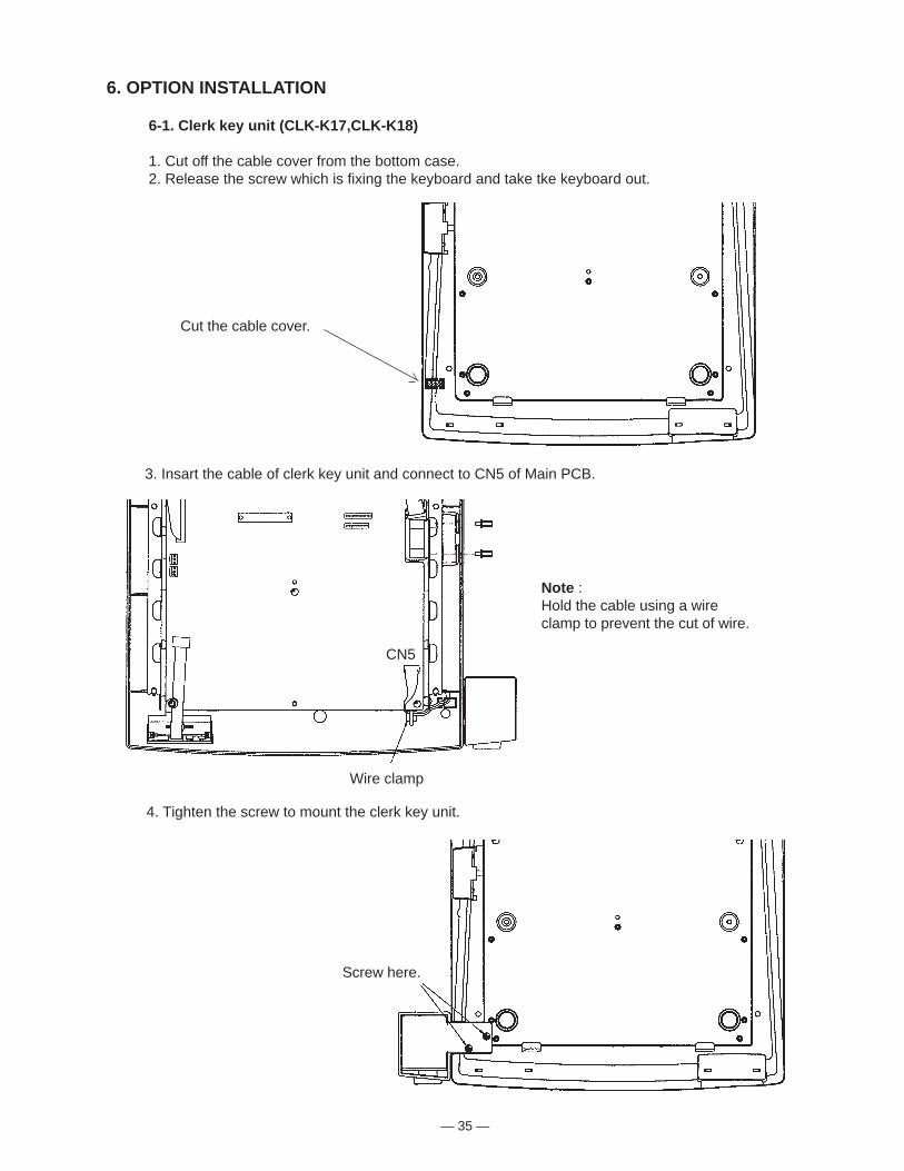
6. OPTION INSTALLATION
6-1. Clerk key unit (CLK-K17,CLK-K18)
1. Cut off the cable cover from the bottom case.2. Release the screw which is fixing the keyboard and take tke keyboard out.
3. Insart the cable of clerk key unit and connect to CN5 of Main PCB.
Cut the cable cover.
Screw here.
4. Tighten the screw to mount the clerk key unit.
Wire clamp
CN5
Note :Hold the cable using a wireclamp to prevent the cut of wire.

— 36 —
6-2. Rear Display (QT-2060D)1. Release the screw which is fixing the keyboard and take tke keyboard out.2. Remove the rear display window.
Slide the keyboard to the allow direction
Release these screws
Rear display window
3. Mount the display fixing plate (L).4. Set the display PCB and display fixing plate (R), then tighten the screw.5. Connect the display cable to CN15 of Main PCB.
Note : FG wire of the power code does not set behind displat PCB.In case the FG wire is set behind the display PCB,the display might occurred flickering
problem.
Display fixing plate (L)
CN15Display fixing plate (R)

— 37 —
Screw here to mountthe MCR unit.
MCR mount stand
Cable for MCR is setlike this.
6-3. MCR Unit (QT-2046MC)1. Release the screw which is fixing the keyboard and take tke keyboard out.2. Remove the Main PCB and solder the connector which is in the QT-2046MC carton to the location CN1 on Main PCB.2. Mount the MCR unit on the lower case by screws and insart the cable to inside of the machine
from connector place.4. Set the MAin PCB and connect the cable to CN1 on Main PCB.
Solder the connector here.
— 38 —
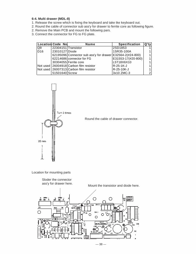
6-4. Multi drawer (MDL-8)1. Release the screw which is fixing the keyboard and take tke keyboard out.2. Round the cable of connector sub ass'y for drawer to ferrite core as following figure.2. Remove the Main PCB and mount the following pars.3. Connect the connector for FG to FG plate.
Location Code No. Name Specification Q'tyQ9 22304151 Transistor 2SD1853 1D16 23010127 Diode 1SR35-100A 1
62195096 Connector sub ass'y for drawer E32564-2(#24-800) 162214686 connector for FG E31553-17(#20-800) 130304055 Ferrite core L5T18X6X10 1
Not used 26004918 Carbon film resistor R-25-1K-J 1Not used 26007313 Carbon film resistor R-25-10K-J 1
51501640 Screw 3x10 ZMC-3 2
Location for mounting parts
Round the cable of drawer connector.
Mount the transistor and diode here.
Sloder the connectorass'y for drawer here.

— 39 —
7-1. C-In line (ARCNET)
1) C-In line connection diagram
The maximum C-In line cable length and the maximum connection unit will be varied by the in-linecommunication speed as shown below list.
[C-In line cable wiring]
C-In line communication speed Maximum Maximum (Baud rate) connection unit cable length A ( m )
1.25 M bps 8 86625 K bps 12 200312.5 K bps 20 430156.25 K bps 32 890
Note : This C-In line system needs a I/O-PB-12 in the PC .
Install the I/O-PB-12 inthe PC.
Total Length : A
QT2000-32QT2000-4QT2000-3QT2000-2
R/JR/JR/JR/J
QT2000-1
R/J
Note: When the cluster has more than 8 QT-2000 terminals, all printer should be local printer. When the cluster has less than or equal to 8 QT-2000 terminals, remote printer is allowable. PC
In-line
7. IN / ON LINE

— 40 —
2) C-In line cable, Connector, and Terminater
C-In line cable
Code No. Parts name Specification1904 4023 In-line cable IPEV-SLA0.5x1P
C-In line connector(ECR side)
Code No. Parts name Specification3500 5820 In-line connector kit XLP-KIT-1
C-In line connector (PC side)
Code No. Parts name Specification1904 4069 Connector DE-9PF-N101904 4070 Junction shell DE-C8-J9-F1
Terminater
Code No. Parts name Specification2600 2516 Carbon film resistor R-25-100-J
ECRPC ECR ECR
Terminater(100 ohms) Terminater(100 ohms)
3) Termination point

— 41 —
4) Cable connection diagram (PC and MasterECR)
Signal Pin Signal Pin
SD 1 SD 1
RD 3 RD 2
FG FG plate FG Disconnect
(PC side) (ECR side)
Shield wire
Terminator (100 ohms)
In-line cable In-line connectorRed
Wrap bent shield wire with Copper tape
Red
Black
In-line connector
Red
Black
BlackBlack
Red
In-line cable
Wrap bent shield wire with Copper tape Shield wire
[Connection between PC and Master ECR]
5)Cable connection diagram (Master ECR and Satellite ECR)
Fold the shield and fasten by wrapping copper tape.
Termination 'R in series are connected at pins 1 and 4 of two connectors at both the ends of the in-line cable.
3

— 42 —
7-2. ON-line
Only the RS-232C Com3 port can be connected with a modem or perssonal computer.
1. Direct connection to PC
1-1. Connection layout
Using Com3 port
1-2. Cable wiring
QT-2000 (Com3) PC
Pin No. Signal name Pin No. Pin No. Signal name(DSUB9) (DSUB25)
3 SD / TXD 3 2 SD 2 RD / RXD 2 3 RD 7 RS / RTS 7 4 RS 8 CS / CTS 8 5 CS 1 CD / DCD 1 8 CD 4 ER / DTR 4 20 ER 6 DR / DSR 6 6 DR 9 CI / RI - 22 CI 5 GND 5 7 GND
KP KP KP
QT2000QT2000QT2000QT2000
R/JSlip SlipSlip
KPPC
RS-232C
Up to 4 kitchen printers
KP/M CHK/BM CHK/M KP/BM

— 43 —
2. MODEM system
2-1. Connection layout
2-2. Cable wiring
QT-2000 (Com2) MODEM (DSUB25)
Pin No. Signal name Pin No. Signal name 3 SD/ TXD 2 SD 2 RD / RXD 3 RD 7 RS / RTS 4 RS 8 CS / CTS 5 CS 1 CD / DCD 8 CD 4 ER / DTR 20 ER 6 DR / DSR 6 DR 9 CI / RI 22 CI 5 GND 7 GND
QT-2000 (Com3) MODEM (DSUB25)
Pin No. Signal name Pin No. Signal name 3 SD/ TXD 2 SD 2 RD / RXD 3 RD 7 RS / RTS 4 RS 8 CS / CTS 5 CS 1 CD / DCD 8 CD 4 ER / DTR 20 ER 6 DR / DSR 6 DR 9 CI / RI 22 CI 5 GND 7 GND
Use Com2 orCom3 port
QT2000-32QT2000-3QT2000-2QT2000-1
R/J
PC
R/JR/JR/J
on-line
Note: When the cluster has more than 8 QT-2000 terminals, all printer should be local printer. When the cluster has less than or equal to 8 QT-2000 terminals, remote printer is allowable.
nals.
MAX : 15 m

— 44 —
7-3. Kitchen printer connection
The kitchen printer control system requires a kitchen printer control master ( and back up master)for kitchen printer control.
Maimum connection number : Max. 4 kitchen printerMax. 4 terminals
1) Connection layout
2) Connector and cable
Cable
Code No. Parts name Specification1904 4023 In-line cable IPEV-SLA0.5x1P
Connector (ECR side)
Code No. Parts name Specification3500 5820 In-line connector kit XLP-KIT-1
Connector (KP side)
Code No. Parts name Specification1904 4069 Connector DE-9PF-N101904 4070 Junction shell DE-C8-J9-F1
KP KP KP
QT2000QT2000QT2000QT2000
R/JSlip SlipSlip
KPPC
RS-232C
Up to 4 kitchen printers
Up to 4 QT-2000 terminals
KP/M CHK/BM CHK/M KP/BM
MAX : 1,000 m
— 44 —

— 45 —
3) Cable connection diagram (ECR and Kitchen printer)
Signal Pin Signal Pin
SD 1 SD 1
RD 2 RD 3
FG FG plate FG Disconnect
(ECR side) (KP side)
Shield wire
Terminator (100 ohms)
In-line cable In-line connectorRed
Wrap bent shield wire with Copper tape
Red
Black
Black
[Connection for ECR side]
Fold the shield and fasten by wrapping copper tape.
Termination 'R in series are connected at pins 1 and 4 of two connectors at both the ends of the in-line cable.
3Solder the cable as above wiring.
[Connection for Kitchen printer side]

— 46 —
4) Kitchen printer controll setting
DIP switch setting for kitchen printer model KP-200 and KP-300 are as follows;When the the DIP switch is changed, it is necessary to make initilize the kitchen printer.Otherwise, DIp switch status can not read the CPU inside the controll board.
To make initilize, pressing "LF" button and power on the machine.
SW No.12345678
Function
Machine number
Baud rate
Factory settingOFFOFFOFFOFFONONOFFOFF
Machine number setting Baud rate setting
Kitchen printermachine number Baud rate
1234
6001200240048009600
DIP SW No. DIP SW No.1
OFFONOFFON
2OFFOFFONON
3OFFOFFOFFOFF
4OFFOFFOFFOFF
5OFFONOFFONOFF
6OFFOFFONONOFF
7OFFOFFOFFOFFON
8OFFOFFOFFOFFOFF
KP-200 Bottom view
} not used
SW No.12345678
Function
Machine number
Baud rate
Factory settingOFFOFFOFFOFFONONOFFOFF
Machine number setting Baud rate setting
Kitchen printermachine number Baud rate
1234
6001200240048009600
DIP SW No. DIP SW No.1
OFFONOFFON
2OFFOFFONON
3OFFOFFOFFOFF
4OFFOFFOFFOFF
5OFFONOFFONOFF
6OFFOFFONONOFF
7OFFOFFOFFOFFON
8OFFOFFOFFOFFOFF
KP-300 Bottom view
} not used

— 47 —
8.DIAGNOSTIC PROGRAM
1. Starting the diagnostic program
(1) While holding down the button on the upper left corner (9 on the standard keyboard sheet), turn the power on.
(2) Release the button when the cash register beeps a buzzer sound.
(3) Using 10-key pad, input [9][9][9][9][9][0][0][0][0][0] then press [SUB TOTAL].Note: While in the diagnostic mode, use the right half of the SUB TOTAL button for [SUB TOTAL] operations.
2. List of the diagnoses
Device to be checked Operation Note
1 Rear display n01
2 Remote display n02
3 RJ printer n03 RS-232C COM2 test
4 Slip printer n04
5 Keyboard n05 buttons 1 to 168 check
6 OBR n06 RS-232C COM1 test.Use checker bar code.
7 MCR n07 Use checker magnetic card.
9 Drawer n09
10 Buzzer n10
11 Switches 11
12 Clock n12
13 ROM n13 EPROM (128kB) x 1
14 RAM n14 Read/Write check
15 RAM n15 Read check
16 MRAM n16 Read/write check
17 MRAM n17 Read check
20 Low-Inline nm20 Transmit check
21 Low-inline nm21 Receive check
25 Async online m25 Loop back test
30 Infrared port 30 Infrared port receive test
31 Infrared port n31 Infrared port transmit test
Commandcode

— 48 —
Device to be checked Operation Note
32 Standard LCD n32
33 Optional LCD n33
34 Flash memory 34 Read/Write/Clear test
38 ARCNET n38 ARCNET ID set
39 ARCNET n39 ARCNET baud rate, token
40 ARCNET 40 ARCNET token stop
41 ARCNET nm41 ARCNET data transmit
42 ARCNET nm42 ARCNET data receive
3. Diagnoses
(1) Dot/7-segment display test
Operation: [n][0][1][SUB TOTAL] (for the rear display)
[n][0][2][SUB TOTAL] (for the remote display)
n = Number of execution and should be within the range of 0 to 9.
If no number or “0” is input, the test continues endlessly.
To stop the test, press [ESC].
Display: <LCD> <Dot/7-segment>
A B C D E F G H I J K L M N O P0,12,34,56,78,90,
a b c d e f g h i j k o l m n o p
12,34,56,78,90,1SUB DISP *01
RJ Print:SUB DISP *01
Displays “END *01” when the test is finished.
Prints “END *01” when the test is fin-ished.
* Displays or prints 02 while testing a remote display.
D isp lays a l te r -nately
Commandcode

— 49 —
(2) R/J Printer test (RS-232C COM2)
Prints B’s on RS-232C printer for specified times.
Operation: [n][0][3][SUB TOTAL]
n = Number of execution and should be within the range of 0 to 9.
If no number or “0” is input, the test continues endlessly.
To stop the test, press [ESC].
Display: <LCD> <Dot/7-segment>
0
R/J print:
Partial cut (TM-950 printer prints “B” on the most sig-nificant digit)Feed
Full cut (TM-950 printer prints “A” on the most signifi-cant digit)
R/J 03BBBBBBBBBBBBBBBBBBBBBBBBBBBBBBBBBBBBBBBBBBBBBBBBBBBBBBBBBBBBBBBBBBBBBBBBBBBBBBBBBBBBBBBBBBBBBBBBBBBBBBBBBBBBBBBBBBBBBBBBBBBBBBBBBBBBBBBBBBBBBBBBBBBBBBBBBBBBBBBBBBBBBBBBBBBBBBBBBBBBBBBBBBBBBBBBBBBBBBBBBBBBBBBBBBBBBBBBBBBBBBBBBBBBBBBBBBBBBBBBBBBBBBBBBBBBBBBBBBBBBBBBBBBBBBBBBBBBBBBBBBBBBBBBBBBBBBBBBBBBBBBBBBBBBBBBBBBBBBBB
R/J Printer; TM-950 (2-sheet dot printer)TM-T85 (1-sheet thermal printer)
(3) Slip Printer test
Prints a test pattern on the slip printer for specified times and releases the slip.
Operation: [n][0][4][SUB TOTAL]
n = Number of execution and should be within the range of 0 to 9.
If no number or “0” is input, the test continues endlessly.
To stop the test, press [ESC].
Display: <LCD> <Dot/7-segment>
Slip print:
slip 04END 04
00
R/J 03R/J 03R/J 03R/J 03END 03
0
Number ofexecution
SLIP TEST PRINTBBBBBBBBBBBBBBBBBBBBBBBB 8888888888
Release
Dot/7-segment display indicates 0 only whenthe test is continued from the “Dot/7-segmentdisplay test.” When the test is performedindipendently, the dot/7-segment display indi-cates nothing.
Dot/7-segment display indicates 0 only whenthe test is continued from the “Dot/7-segmentdisplay test.” When the test is performedindipendently, the dot/7-segment display indi-cates nothing.

— 50 —
(4) Keyboard test
The display shows pressed button number when the key switch functions correctly.
Operation: [0][5][SUB TOTAL]
Press buttons and make sure that the pressed button number is displayed on the LCD.
Note: As [ESC] (button number159) button exits the diagnosis program, press [ESC] at the end.
Display: <LCD> <Dot/7-segment>
R/J Print:
0KEY 05KEY –– 26KEY –– 27KEY –– 28KEY –– 29KEY –––30
KEY 05END 05
“END 05” will be displayed andprinted when [ESC] (button number159) is pressed.
<Button numbers>
Press this button at theend.
Dot/7-segment display indicates 0 only whenthe test is continued from the “Dot/7-segmentdisplay test.” When the test is performedindipendently, the dot/7-segment display indi-cates nothing.

— 51 —
(5) OBR test
Use only the checker bar code in which data 49401387 is written.The program checks if the read data is 49401387.
Operation: [n][0][6][SUB TOTAL]
n = Number of execution and should be within the range of 0 to 9.
If no number or “0” is input, the test continues endlessly.
To stop the test, press [ESC].
Display: <LCD> <Dot/7-segment>
R/J Print:
0OBR 06
OBR OK
OBR NGFF4902580300562
END 06
0
Read data
When the read data is correct.
When the read data is incorrect.
OBR 06OBR OKOBR NG
When the read data is correct.
When the read data is incorrect.
Dot/7-segment display indicates 0 onlywhen the test is continued from the “Dot/7-segment display test.” When the testis performed indipendently, the dot/7-segment display indicates nothing.

— 52 —
(6) MCR test
Use only the checker magnet card.
Operation: [n][0][7][SUB TOTAL]
n = Number of execution and should be within the range of 0 to 9.
If no number or “0” is input, the test continues endlessly.
To stop the test, press [ESC].
Display: <LCD> <Dot/7-segment>
R/J Print:
0
Note: When MCR read error occurs, the display in-dicates “MCR READ ERR.”
MCR 07#1:OK #2:OKEND 07
“NG” when incorrect
(7) Drawer test
Opens two drawers (multi drawer is optional) and shows open sensor status on the LCD.
Operation: [n][0][9][SUB TOTAL]
n = Number of execution and should be within the range of 0 to 9.
If no number or “0” is input, the test continues endlessly.
To stop the test, press [ESC].
Display: <LCD> <Dot/7-segment>
R/J Print:
DRAWER 09DRAWER: OPENEND 09
0
0“NOT OPEN” when drawer doesnot open
DRAWER 09END 09
Dot/7-segment display indicates 0 only whenthe test is continued from the “Dot/7-segmentdisplay test.” When the test is performedindipendently, the dot/7-segment display indi-cates nothing.
Dot/7-segment display indicates 0 only whenthe test is continued from the “Dot/7-segmentdisplay test.” When the test is performedindipendently, the dot/7-segment display indi-cates nothing.
MCR 07
#1:OK #2:OK
#1:NG #2:NGMCR#1
MCR#2
END 07
0
When the read data is incor-rect, display indicates NGand shows read data.

— 53 —
(8) Buzzer test
Beep every 100 milliseconds. In one test, 2 buzzer sound.
Operation: [n][1][0][SUB TOTAL]
n = Number of execution and should be within the range of 0 to 9.
If no number or “0” is input, the test continues endlessly.
To stop the test, press [ESC].
Display: <LCD> <Dot/7-segment>
R/J Print:
BUZZ 10END 10
0
0
BUZZ 10END 10
(9) Switch test
Displays statuses of the switches and sensors of the connected devices.
Operation: [1][1][SUB TOTAL]
To stop the test, press [ESC].
Display: <LCD> <Dot/7-segment>
R/J Print:
0
STSW 11END 11
Dot/7-segment display indicates 0 only whenthe test is continued from the “Dot/7-segmentdisplay test.” When the test is performedindipendently, the dot/7-segment display indi-cates nothing.
Dot/7-segment display indicates 0 only whenthe test is continued from the “Dot/7-segmentdisplay test.” When the test is performedindipendently, the dot/7-segment display indi-cates nothing.
STSW 110 0 0 0 0 0 1 00
Keyboard Sheet 1 - 8Not usedNot used Slip paper sensor (0: slip inserted, 1: no slip inserted)Drawer open sensor (0: close, 1: open)Clerk key (00: not used, 01 - 15: clerk key no.)No used
END 11

— 54 —
(10) Clock test
Operation: (1) Press [0][1][2][SUB TOTAL]Display indicates date 99 12 31 MON, time 23 59 55.If [1] is input instead of the first [0], the display shows the present time.
<LCD> <Dot/7-segment>
(2) Turn the power off.
(3) After for a while, turn the power on andmake sure that the time has been countedwhile the register is off.
(4) Press [ESC] to exit from the program.
R/J Print:
CLOCK 1299 12 31 MON23 59 55 Counts up
0
CLOCK 12END 12
Dot/7-segment display indicates 0 only whenthe test is continued from the “Dot/7-segmentdisplay test.” When the test is performedindipendently, the dot/7-segment display indi-cates nothing.
CLOCK 1200 01 01 TUE00 01 21 Counts up

— 55 —
(11) ROM test
Performs check sum test of the EPROM. Checks all the files written in the ROM and when an error occurs, the LCDindicates the faulty file name and starting address of the file.
Operation: [n][1][3][SUB TOTAL]n = Number of execution and should be within the range of 0 to 9.
If no number or “0” is input, the test continues endlessly.
To stop the test, press [ESC].
<LCD> <Dot/7-segment>
After the test, display indicates the result.
<LCD>
R/J Print:
0
ROM 13configcpyrightcmndrv.exeker.exetbox.exe
Hndl580.exe
File names
ROM 13configcpyrightcmndrv.exefsys.exeker.exetbox.exehndl580.exediag580.exe$tp.execonfig.envini.exeROM SUM CHECK OK
CREATE 97-04-17 11:53Copyright (C) 1997CASIO COMPUTER CO.,LTDAll rights reserved.ROM VER. AAFAB 3075
END 13
Dot/7-segment display indicates 0 only whenthe test is continued from the “Dot/7-segmentdisplay test.” When the test is performedindipendently, the dot/7-segment display indi-cates nothing.
tbox.exehndl580.exediag580.exe$tp.execonfig.envini.exeROM SUM CHECK OK
CREATE 97-04-17 11:53Copywright (C) 1997CASIO COMPUTER CO., LTDAll rights reserved.ROM VER. AAFAB3075
END 130
Indicates “ESC” when the test is finished forcibly by [ESC].

— 56 —
(12) RAM Read/Write test
Performs read after write test on RAM addresses 20000H to 3FFFF.
Operation: [n][1][4][SUB TOTAL]
n = Number of execution and should be within the range of 0 to 9.
If no number or “0” is input, the test continues endlessly.
To stop the test, press [ESC].
Display: <LCD> <Dot/7-segment>
0
R/J print:
Dot/7-segment display indicates 0 only whenthe test is continued from the “Dot/7-segmentdisplay test.” When the test is performedindipendently, the dot/7-segment display indi-cates nothing.
RAM 14RAM#2 OKRAM#2 OKRAM#2 OKEND 14
0
Number of execution.Indicates “NG” when theRAM is faulty.
(13) RAM Read test (memory backup test)
The program checks if RAM contents stored at the “RAM read/write test” are backed up after turning the power off.
Operation: (1) After the above “RAM Read/Write test”, turn the power off.
(2) After for a while, turn the power on then press [n][1][5][SUB TOTAL].
n = Number of execution and should be within the range of 0 to 9.
If no number or “0” is input, the test continues endlessly.
To stop the test, press [ESC].
Display: <LCD> <Dot/7-segment>
0
R/J print:Dot/7-segment display indicates 0 only whenthe test is continued from the “Dot/7-segmentdisplay test.” When the test is performedindipendently, the dot/7-segment display indi-cates nothing.
RAM 15RAM#2 OKRAM#2 OKRAM#2 OKEND 15
0
Number of execution.Indicates “NG” when theRAM is faulty.
RAM 15RAM#2 OKRAM#2 OKRAM#2 OKEND 15
“NG” when the RAM isfaulty
RAM 14RAM#2 OKRAM#2 OKRAM#2 OKEND 14
“NG” when the RAM isfaulty

— 57 —
(15) Mass RAM backup test
The program checks if the memory contents stored in “Mass RAM read/write test” are backed up after power isturned off then on again.
Operation: (1) After the above “RAM Read/Write test”, turn the power off.
(2) After for a while, turn the power on then press [n][1][7][SUB TOTAL].
n = Number of execution and should be within the range of 0 to 9.
If no number or “0” is input, the test continues endlessly.
To stop the test, press [ESC].
Display: <LCD> <Dot/7-segment>
(14) Mass RAM Read/Write test
Using the gate array and the CPU in QT-2000 circuit, the program performs RAM’s mass data (in 128k byte unit)read after write test. The program does not diagnose VRAMs.
Operation: [n][1][6][SUB TOTAL].
n = Number of execution and should be within the range of 0 to 9.
If no number or “0” is input, the test continues endlessly.
To stop the test, press [ESC].
Display: <LCD> <Dot/7-segment>
0
R/J print:
Dot/7-segment display indicates 0 only whenthe test is continued from the “Dot/7-segmentdisplay test.” When the test is performedindipendently, the dot/7-segment display indi-cates nothing.
RAM 16MASS RAM CHIPS : mMASS#mMASS#m OKEND 16
0
MASS 16MASS RAM CHIPS : mMASS#m OKEND 16
m= bank number
or “NG”
prints “ESC” when thetest is finished forciblyby [ESC] button.
0
R/J print:
Dot/7-segment display indicates 0 only whenthe test is continued from the “Dot/7-segmentdisplay test.” When the test is performedindipendently, the dot/7-segment display indi-cates nothing.
MASS 17MASS#m OKEND 17
m= bank numberor “NG”
prints “ESC” when thetest is finished forciblyby [ESC] button.
MASS 17MAS#mMAS”m OKEND 17
0
m= bank numberor “NG”
Indicates “ESC” whenthe test is finishedforcibly by [ESC].
m= bank number
or “NG”Indicates “ESC” whenthe test is finishedforcibly by [ESC].

— 58 —
(16) Low inline data transmission test
Connect two QT-2000s with a standard inline cable (RS-485).
0
Dot/7-segment display indicates 0 only whenthe test is continued from the “Dot/7-segmentdisplay test.” When the test is performedindipendently, the dot/7-segment display indi-cates nothing.
L INLINE TX 20END 20 prints “ESC” when the
test is finished forciblyby [ESC] button.
L INLINE TX 20OK: XX NG: XXEND 20
0
count up
Indicates “ESC” whenthe test is finishedforcibly by [ESC].
Perform the reception unit operation first then the transmission unit.
Operation: [n][m][2][0][SUB TOTAL]
n = Number of execution and should be within the range of 0 to 9.
If no number or “0” is input, the test continues endlessly.
m = baud rate (m > n) ; 0 : 1200 bps, 1: 2400 bps, 2: 4800 bps, 4: 9600 bps, 5: 19200 bps
To stop the test, press [ESC].
Display: <LCD> <Dot/7-segment>
R/J print:
Inline cable: RS-485
SenderCommand code: 20
RecieverCommand code: 21
C
7
4
1
0
8
5
200
9
6
3
•
C
7
4
1
0
8
5
200
9
6
3
•
— 59 —
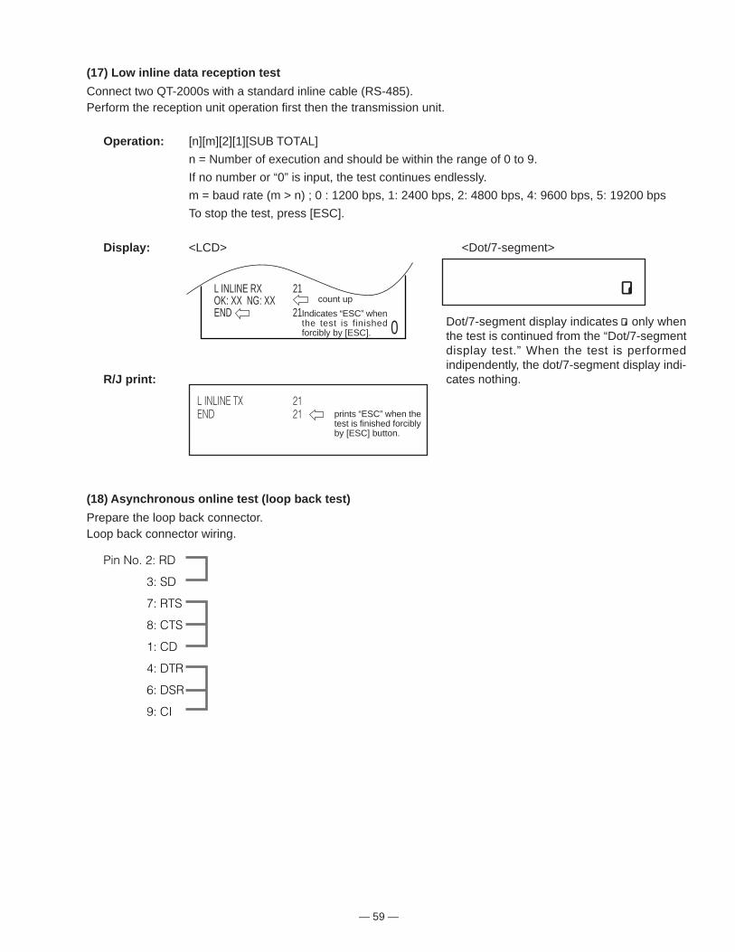
(17) Low inline data reception test
Connect two QT-2000s with a standard inline cable (RS-485).Perform the reception unit operation first then the transmission unit.
Operation: [n][m][2][1][SUB TOTAL]
n = Number of execution and should be within the range of 0 to 9.
If no number or “0” is input, the test continues endlessly.
m = baud rate (m > n) ; 0 : 1200 bps, 1: 2400 bps, 2: 4800 bps, 4: 9600 bps, 5: 19200 bps
To stop the test, press [ESC].
Display: <LCD> <Dot/7-segment>
R/J print:
0
Dot/7-segment display indicates 0 only whenthe test is continued from the “Dot/7-segmentdisplay test.” When the test is performedindipendently, the dot/7-segment display indi-cates nothing.
L INLINE TX 21END 21 prints “ESC” when the
test is finished forciblyby [ESC] button.
L INLINE RX 21OK: XX NG: XXEND 21
0
count up
Indicates “ESC” whenthe test is finishedforcibly by [ESC].
(18) Asynchronous online test (loop back test)
Prepare the loop back connector.Loop back connector wiring.
Pin No. 2: RD
3: SD
7: RTS
8: CTS
1: CD
4: DTR
6: DSR
9: CI

— 60 —
Connect a loop back connector on COM3 port and perform the loop back test.
Operation: [m][2][5][SUB TOTAL]
m = baud rate ; 0: 1200 bps, 1: 2400 bps, 2: 4800 bps, 4: 9600 bps, 5: 19200 bps, 6:38400 bps
To stop the test, press [ESC].
Display: <LCD> <Dot/7-segment>
R/J print:
0
Dot/7-segment display indicates 0 only whenthe test is continued from the “Dot/7-segmentdisplay test.” When the test is performedindipendently, the dot/7-segment display indi-cates nothing.
ASYNC ONLINE 25ESC 25
ASYNC ONLINE 25OK: XX NG: XXESC 21
0
count up
(19) Infrared
Prepare two units of QT-2000 and set both units on the diagnostic mode. Face both units so that they can commu-nicate by the infrared ports.
C
7
4
1
0
8
5
200
9
6
3
•
Prepare 2 machine and touch each IR I/F.
IR I/FSenderCommand code: 30
RecieverCommand code: 31

— 61 —
ASYNC RX 30✼ESC 30
0
0
Dot/7-segment display indicates 0 only whenthe test is continued from the “Dot/7-segmentdisplay test.” When the test is performedindipendently, the dot/7-segment display indi-cates nothing.
ASYNC TX/RX 31OK: XX NG: XXEND 31
0
count upIndicates “ESC” whenthe test is finishedforcibly by [ESC].
ASYNC TX/RX 31OK: XX NG: XXEND 31 Prints “ESC” when the
test is finish forcibly by[ESC] button.
Operation: (1) On the receiving unit, press [3][0][SUB TOTAL].
The LCD on the receiving unit indicates;
(2) On the transmission unit, press [n][3][1][SUB TOTAL].
n= Number of execution and should be within the range of 0 to 9.
If no number or “0” is input, the test continues endlessly.
To stop the test, press [ESC].
Display <LCD> <Dot/7-segment>

— 62 —
(20) LCD test
Operation: [n][3][2][SUB TOTAL] (for standard LCD)
[n][3][3][SUB TOTAL] (for optional LCD)
n = Number of execution and should be within the range of 0 to 9.
If no number or “0” is input, the test continues endlessly.
To stop the test, press [ESC].
Display: <LCD>
Repeats “n” times
LCD 32END 32
R/J print

— 63 —
(21) Flash memory read/write/clear test
Performs read after write check on each bank of the flash memory. At the end of the test, all the data in the flashmemory are cleared.The following table illustrates the relation between the address and the bank of the flash memory.
Bank 1 Bank 9 Bank 17 Bank 25
Bank 2 Bank 10 Bank 18 Bank 26
Bank 3 Bank 11 Bank 19 Bank 27
Bank 4 Bank 12 Bank 20 Bank 28
Bank 5 Bank 13 Bank 21 Bank 29
Bank 6 Bank 14 Bank 22 Bank 30
Bank 7 Bank 15 Bank 23 Bank 31
Bank 8 Bank 16 Bank 24 Bank 32E0000h
C0000h
A0000h
80000h
60000h
Operation: [3][4][SUB TOTAL]
To stop the test, press [ESC].
Display: <LCD> <Dot/7-segment>
R/J print:
0
Dot/7-segment display indicates 0 only whenthe test is continued from the “Dot/7-segmentdisplay test.” When the test is performedindipendently, the dot/7-segment display indi-cates nothing.
FLASH 34BANK#1 OKBANK#2 OKBANK#3 OK
BANK#32 OKEND 34
......
......
......
.
or “NG”
Flash 34BANK#1 OKBANK#2 OKBANK#3 OKBANK#4 OKBANK#5 OK
BANK#32 OKEND 34
0
or “NG”
......
.....

— 64 —
(22) ARCNET test-1 (ID number setting)
Sets ID number of ARCNET. Be sure to perform this program before doing the following ARCNET tests.
Operation: [m][m][m][3][8][SUB TOTAL]
mmm = ID number (001 to 253)
Display: <LCD> <Dot/7-segment>
R/J print:
0
Dot/7-segment display indicates 0 only whenthe test is continued from the “Dot/7-segmentdisplay test.” When the test is performedindipendently, the dot/7-segment display indi-cates nothing.
ARC-ID 38END 38
ARC - ID 38ARCNET MY - ID: xxxEND 38
0
ID No. ; 1 to 253Indicates “INVALID ID XXX”when invalid number is in-put.
(23) ARCNET test-2 (baud rate setting, ARCNET communication)
After setting the baud rate, QT-2000s in the ARCNET start communications.
Operation: [n][3][9][SUB TOTAL]
n = baud rate; 0: 156.25kbps, 1: 312.5kbps, 2: 625kbps, 3: 1.25Mbps
Display: <LCD> <Dot/7-segment>
R/J print:
0
Dot/7-segment display indicates 0 only whenthe test is continued from the “Dot/7-segmentdisplay test.” When the test is performedindipendently, the dot/7-segment display indi-cates nothing.
ARC–BPS 39END 39
ARC–BPS 39OKEND 39
0
or “NG”

— 65 —
(24) ARCNET test-3 (ARCNET communication stop)
Terminates the ARCNET communications.
Operation: [4][0][SUB TOTAL]
Display: <LCD> <Dot/7-segment>
R/J print:
0
Dot/7-segment display indicates 0 only whenthe test is continued from the “Dot/7-segmentdisplay test.” When the test is performedindipendently, the dot/7-segment display indi-cates nothing.
ARC–STP 40END 40
(25) ARCNET test-4 (ARCNET data transmission/reception)
Checks data transmission and reception in the ARCNET.
ARC–STP 40OKEND 40
0
or “NG”
Preparation
ARCNET
SenderCommand code: 41
RecieverCommand code: 42
C
7
4
1
0
8
5
200
9
6
3
•
C
7
4
1
0
8
5
200
9
6
3
•

— 66 —
(3) On the transmission unit, press [n][m][m][m][4][1][SUB TOTAL].
n = number of execution. Should be within 0 to 9. If 0 or no number is input, the execution
continues endlessly.
mmm = ID number of the unit to which the data is sent.
To stop the test press [ESC].
Display: <LCD> <Dot/7-segment>
R/J print:
0
Dot/7-segment display indicates 0 only whenthe test is continued from the “Dot/7-segmentdisplay test.” When the test is performedindipendently, the dot/7-segment display indi-cates nothing.
ARC–TX 41END 41
ARC–TX 41peer–node:mmmARC–TX OK:xx NG:xxEND 41
0
Associated unit’s ID number
0
Dot/7-segment display indicates 0 only whenthe test is continued from the “Dot/7-segmentdisplay test.” When the test is performedindipendently, the dot/7-segment display indi-cates nothing.
ARC–RX 42END 42
ARC–RX 42peer–node:mmmARC–RX OK:xx NG:xxEND 42
0
Associated unit’s ID number
Operation: (1) Connect QT-2000s with ARCNET (inline) cable.
(2) On the reception unit, press [n][m][m][m][4][2][SUB TOTAL].
n = number of execution. Should be within 0 to 9. If 0 or no number is input, the execution
continues endlessly.
mmm = ID number of the unit from which the data is sent.
To stop the test press [ESC].
Display: <LCD> <Dot/7-segment>
R/J print:

— 67 —
9. ERROR CODE LIST
9-1. Error message
When an error occurs on the QT-2000 terminal, buzzer sounds and the error message
appears on the main LCD screen.
The following table lists the error messages and descibes the action to takae.
Prompt message
Operator mistake
E001 Wrong Mode
E003 Wrong operator
E005 Insufficient memory
E011 Close the drawer
E012 Change journal roll
E013 Change receipt roll
E016 Change back to REG mode
E017 Enter Check/TBL number
E018 Enter Table No.
E019 Enter Number of covers
E020 Enter Seat number
E027 Cancel buffer full.
Please finalize the transaction
E029 No registration is possible
while you are in the tender
operation.
E031 Press ST key before Finalization
E033 Enter tendered amount
E035 Change amount exceeds the limit.
E037 Digit or Amount Limitation Over
E038 Perform Money Declaration
E040 Issue Guest Receipt
E041 Print Validation
E042 Insert VLD Paper and retry
E043 Remove VLDed paper or check
VLD sensor
E044 Print Check
E045 Print Check-Endorsement
E046 REG Buffer Full. Please
Finalize or NB.
E047 Print bill
E048 Insert Slip Paper and retry.
E049 CHECK memory full
E050 Detail memory Full.
E051 CHK/TBL No. is occupied.
Meaning
Operation error
Check tracking (Open mode error)
Error clerk/Error clerk in CHK tracking
Memory allocation over
Drawer compulsory
Journal paper near end
Receipt/order paper near end
Prohibit plural operation in RF mode
Check # compulsory
Table # compulsory
Cover compulsory
Seat number compulsory
Alarm when any item drops below its programmed mini-
mum stock quantity during registration
Error when actual stock value for a registration items is a
negative value
ST compulsory
Amount tender compulsory
Change amount exceeds the limit.
Contents of the drawer exceed the programmed limit—
Sentinel function
H.D.L., H.A.L.O error
Money declaration compulsory
Guest receipt compulsory
Validation compulsory
Alarm when no paper is inserted.
Alarm when the paper is left in the validation stage of the
printer.
CHK-PRT compulsory
CHK-END compulsory
Slip compulsory
Alarm when no paper is inserted in the Slip.
CHK tracking index full/near end
CHK tracking memory full/near end
Attempt made to use the New Check key to open a new
check using a number that is already used for and existing
check tracking memory
Attempt to use the same check number whilst the specified
number is used in the other terminal
All void buffer full
E036 Remove money from the drawer.
Registration buffer full
E052 CHK/TBL No. is busy.
Attemted registraion whilist partial tender operation is be-
ing done.
E023 Stock running short
E024 No stock is available

— 68 —
Prompt message
E053 CHK/TBL No. is not opened.
E054 Out of CHK/TBL No. Range
**********
E060 Printer offline.
**********
E061 Printer error
**********
E062 Printer paper end
E064 Printer buffer full
E067 Both KP Master&Backup master down.
KP control is not available.
**********
E068 KP Master is removed from system.
**********
E069 Kitchen Printer Master down.
Retry or Remove it from system?
YES: Retry for connection.
NO : Remove it from system.
**********
E070 Terminal out of action.
Cannot print.
**********
E071 Target terminal printer BF full.
Retry?
**********
E072 Target printer terminal is busy.
Retry?
**********
E073 No answer from target terminal.
E075 Negative Balance.
Cannot be finalized.
E080 Journal Memory Full
Please clear J-memo file.
E081 Data not found in J-memo
E082 ***** Illegal Data *****
E083 Cannot create J-memo file.
Check Flash memory.
E085 Data exist in Consolidation area.
**********
E105 Check/TBL Tracking Master down.
Retry or Remove it from system?
YES: Retry for connection.
NO : Remove it from system.
**********
E106 Check/TBL Tracking Backup master
down. Retry or Remove it from
system?
YES: Retry for connection.
NO : Remove it from system.
Meaning
CHECK# not found
CHECK# range over
Printer offline. "****" means ECR logical ID or
KP1 ~ KP4.
Printer downed. "****" means ECR logical ID or
KP1 ~ KP4.
Paper near-end/end "****" means ECR logical ID or
KP1 ~ KP4.
Print buffer full at sender side
KP master is removed from the system.
"****" means ECR logical ID.
Time out at ECR which has printer "****" means
ECR logical ID.
Data cannot be found in journal memory
Illegal J-memo data
Data exists in consolidation area
CHK master down "****" means ECR logical ID.
CHK BM down "****" means ECR logical ID.
KP printing is disabled.
Down at target ECR which has printer "****" means
ECR logical ID.
KP control master down
"****" means ECR logical ID.
Printer buffer full at target ECR which has printer
"****" means ECR logical ID.
Busy at target ECR which has printer "****" means
ECR logical ID.
Attempted finalization when balance is less than zero
J-memo full
J-memo file cannot be created.

— 69 —
Meaning
Void operation is prohibited because of entering quantity.
This sheet holder is prohibited by PGM
Arrangement syntax error
Incorrect entry for PGM
Linking is incorrect
Flash memory full
No data is backuped in Flash memory
Prompt message
**********
E107 Both Master&Backup master down.
CHK/TBL tracking or Clerk inter-
rupt is not available.
**********
E108 CHK/TBL Master is removed from
system.
**********
E109 CHK/TBL Backup master is removed
for system.
E110 CHK data mismatch between
Master&Backup master.
E130 Middle of Pick up or Loan
Press Cancel Key.
E131 Middle of <Bill Copy> Press Cancel
key
E132 Middle of Money Declaration.
Press Cancel key
E133 Middle of <Media Change>
Press Cancel key
E134 Middle of Clerk Transfer
Press Cancel key
E136 Middle of <Separate Check>
Press ESC key
E138 Item are consolidated.
Change display mode and perform VOID
operation.
E139 Not allowed to be negative by
Minus/Coupon key.
E140 Wrong menu.
E145 Arrangement syntax error.
E150 Incorrect value entry.
E151 Incorrect key Pressed.
E152 PGM File or Record number does not
Exist.
E160 Flash memory full
E161 No backup data in Flash Memory
CHK M/BM down "****" means ECR logical ID.
Master down then take it off from system "****" means
ECR logical ID.
Backup master down then take it off from system "****"
means ECR logical ID.
No such file, no such record
Credit balance error
Data mismatch is occured.
During picking up
During Bill copy
During Money declaration
During Media CHG
During CLK Trans
During SEP CHK

— 70 —
edocrorrE gninaeM
0100 )erawtfos(rorresseccareldnaH1100 )noitarugifnocmetsys(reldnahetucexetonnaC2100 CPybkaerB3100 RCEybkaerB4100 tekcapdnammocgniviecererofebffoRSD5100 tekcapdnammocforebmundnammoclagellievieceR6100 retcarahclagellievieceR7100 )erawdrah(rorredneS8100 )erawdrah(rorreevieceR9100 tekcapatadlagellievieceR0200 rorreesnopseroN1200 DItegtonnacroezilaitinitonnaC2200 tekcaplagellidevieceR3200 rorreeviecerTENC4200 rednesybnoitanimretlagellI5200 stekcaprehtogniviecergnirudtekcaplagellidevieceR6200 deviecerstekcapatadhguonetoN7200 rorreesarehsalF8200 rorreetirwhsalF0400 noitamrofni"H"oN1400 noitamrofni"I"oN2400 noitamrofni"F"oN4400 emaneliflagellI5400 stsixeelifoN6400 kcolblagellI7400 tekcapdnammoclagellI8400 )DMCtoN(.oNdnammoclagellI9400 )ATADtoN(.oNdnammoclagellI0500 rorreecneuqeS1500 langisRSDffonruT2500 noitallecnacdevieceR3500 dnammocgnitiawelihwrevoyrteR4500 TOEgnitiawelihwrevoyrteR5500 atadgnitiawelihwrevoyrteR6500 TOEdevieceR7500 KCAgnitiawelihwrevoyrteR8500 atadgnidneselihwrevoyrteR9500 "C"gnitiawelihwrevoyrteR0600 esnopsergnidneselihwrevoyrteR1600 gnidulcxeelihwrevoyrteR4600 dnekaerB5600 redaehtropergnitnirpgnirudrorrE6600 atadtropergnitnirpgnirudrorrE7600 aerakrowniatadtropergnitnirpgnirudrorrE8600 aeranoitadilosnocniatadtropergnitnirpgnirudrorrE9600 rorreraelcelifkroW0700 rorreraelcelifnoitadiolosnoC1700 rorrekcolZ2700 rorreraelcZ3700 rorreesaelerkcolZ
9-2. System error code
Thses error codes are displayed or printed on error log report.
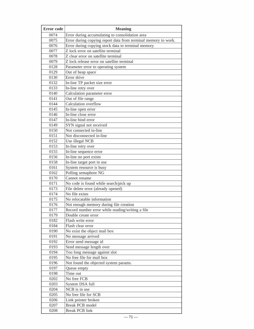
— 71 —
edocrorrE gninaeM
4700 aeranoitadilosnocotgnitalumuccagnirudrorrE5700 .krowotyromemlanimretmorfatadtropergniypocgnirudrorrE6700 yromemlanimretotatadkcotsgniypocgnirudrorrE7700 lanimretetilletasnororrekcolZ8700 lanimretetilletasnororreraelcZ9700 lanimretetilletasnororreesaelerkcolZ8210 metsysgnitarepootrorreretemaraP9210 ecapspaehfotuO0310 evirdrorrE2310 rorreezistekcapPTenil-nI3310 revoyrterenil-nI0410 rorreretemarapnoitaluclaC1410 egnareliffotuO4410 wolfrevonoitaluclaC5410 rorrenepoenil-nI6410 rorreesolcenil-nI7410 rorrednibenil-nI9410 deviecertonlangisNYS0510 enil-nidetcennoctoN1510 enil-nidetcennocsidtoN2510 BCNlagelliesU3510 revoyrterenil-nI5510 rorreecneuqesenil-nI6510 stsixetroponenil-nI8510 esunitroptegratenil-nI1610 ysubsiecruosermetsyS2610 GNerohpamesgnilloP0710 emanertonnaC1710 pukcip/hcraeselihwdnuofsiedocoN3710 )denepoydaerla(rorreeteledeliF4710 stsixeelifoN5710 noitamrofnielbatacoleroN6710 noitaercelifgnirudyromemhguonetoN7710 elifagnitirw/gnidaerelihwrorrerebmundroceR9710 rorreetaercelbuoD2810 rorreetirwhsalF4810 rorreraelchsalF0910 xobliamtcejboehttsixeoN1910 devirraegassemoN2910 diegassemdnesrorrE3910 revohtgnelegassemdneS4910 tolstsniagaegassemgnolooT5910 xobliamrofelifeerfoN6910 .smarapmetsysdetcejboehtdnuoftoN7910 ytpmeeueuQ8910 tuoemiT2020 BCFeerfoN3020 llufASDmetsyS4020 esunisiBCN5020 BCSrofelifeerfoN6020 nekorbretniopkniL7020 ledomBCPkaerB8020 knilBCPkaerB

— 72 —
edocrorrE gninaeM
9020 aeraBCPmorfegnarfotuO0120 aeraBCRmorfegnarfotuO1120 aeraeueuqmorfegnarfotuO2120 aeraeueuqmorfegnarfotuO3120 aeraBCSmorfegnarfotuO4120 redaeheueuqehtdnuoftoN5120 ytiroirpehtdnuoftoN6120 rorremuskcehC7120 rorresutatsssecorP5320 rorrelocotorpenil-nI7420 nekotenil-nipotS
Prompt message Meaning
Data cannot be printed out.
Do you want to display?
Do you want to clear data?
Cancel OK?
Please wait.
Item Consolidation Mode.
Non Consolidation Mode.
REG Mode
REFUND Mode
REG– Mode
REG2 Mode
Training
Please Sign on.
Enter Check/Table Number.
Enter Table Number.
Enter Number of covers.
Enter Seat Number
Perform Slip Printing
Issue Guest Receipt.
Perform Validation Printing.
Perform Check Printing.
Perform Check Endorsement.
Operation Code?
The terminal losts system con-
figuration. Execute reconfigu-
ration procedure as soon as
possible. OK ?
This procedure stops system
maximum 60 sec.
OK ?
Request to check the data which cannot be printedout.Confirmation to reset displayed report.Confirmation of all void operation.Please wait. ECR now processing.In the item consolidation mode.Not in the item consolidation mode.Mode change : REG modeMode change : RF modeMode change : REG– modeMode change : REG 2 modeTraining operatorSign offCHK# compulsoryTBL# compulsoryCovers compulsorySeat# compulsorySlip compulsoryGUEST RCT compulsoryVLD compulsoryCHK-PRT compulsoryCHK-END compulsorySecret No entry for REG 2 mode.
Requirement for system re-configuration.
Alert before flash memory clear.
9-3. Operation prompt
All prompt messages, together with descriptions and symbol characrer for printing on receipts,
slip or reports are contained in the listbelow.
These messages connot be added, modified or deleted.

— 73 —
10. IC data
1. COM20030BILJP
2. TC7S04F 3. TC7S08F
4. TC7S32F 5. TC4SU69F

— 74 —
6. SED1351F0A
MPX MPX
VRAMCONTROL
OSC
16BIT
CONTROL REGISTER
ADDRESSBUFFER
DATABUFFER
I/O CONTROL
DISPLAYTIMINGCONTROL
DISPLAYDATACONTROL
REFRESHADDRESSCOUNTER
TIMING LOGIC

— 75 —
7. LH28F016SUT

— 76 —
8. UPD70108HGC

— 77 —
9. TC74HC00 10. TC74HC02
11. TC74HC137
12. TC74HC157
13. TC74HC244 14. TC74HC245

— 78 —
15. TC74HC373 16. TC74HC4049
17. TC74HC4050 18. TC74HC74
19. TC74HC751178

— 79 —
20. M51957BFP
21. M5291FP
22. SN75188 23. SN75189
OSC
1.17VOLTAGE
COMPARATOR
COLLECTOR
EMITTER
EARTH
DRIVER
PEAK CURRENT DETECTION
POWER
COMPARATOR INPUT
NC
INPUTNC
GND
POWEROUTPUT
NC
INPUT OUTPUT
GND
POWER
CLOCK STD VOLTAGE SUPPLY
DELAY VALUE
DELAY VALUE

— 80 —
11.PCB LAYOUT
TOP VIEW

— 81 —
Bottom View

— 82 —
DESCRIPITION DRAWING NO. PRINTED BOARD NO.
REAR DISPLAY E-210838 E-404-2 (1/3)
REAR DISPLAY E-310971 E-404-2 (2/3)
REAR DISPLAY E-310972 E-404-2 (3/3)
DESCRIPITION DRAWING NO. PRINTED BOARD NO.
BLOCK DIAGRAM
SHP PRINTER (1/2) E-210604 E-901-1
SHP PRINTER (2/2) E-411006 E-901-1
ONNECTOR WIRING
12.CIRCUIT DIAGRAMCONTENTS
QT-2000
REAR DISPLAY
SLIP PRINTER SP1200
DESCRIPITION DRAWING NO. PRINTED BOARD NO.
BLOCK DIAGRAM E240446
MAIN PCB(1/9) E140201 E580-1 (1/9)
MAIN PCB(2/9) E140201 E580-1 (2/9)
MAIN PCB(3/9) E140201 E580-1 (3/9)
MAIN PCB(4/9) E240447 E580-1 (4/9)
MAIN PCB(5/9) E240447 E580-1 (5/9)
MAIN PCB(6/9) E240447 E580-1 (6/9)
MAIN PCB(7/9) E240447 E580-1 (7/9)
MAIN PCB(8/9) E240447 E580-1 (8/9)
MAIN PCB(9/9) E240447 E580-1 (9/9)
KEY BOARD 1 E240448
KEY BOARD 2 E440509 E580-E4-1
KEY SHEET SW E440510 E580-E4-2
IR BOARD E440511 E580-IR
VORUME E440508 E580-E2-1
CONNECTOR BOARD E440512 E580-CNB
2nd DISPLAY E240449 E580-E2

— 83 —
2
1
3
4
5
6
7
8
2
1
3
4
5
6
7
8
B C D E F G H I J KA
B C D E F G H I J KA
Description: Board No. Drawing No.E240446BLOCK DIAGRAM
SHEET DETECT SWITCH

— 84 —A B C D E F G H I J K L M N O P
A B C D E F G H I J K L M N O P
1
2
3
4
5
6
7
8
9
10
1
2
3
4
5
6
7
8
9
10
Description: Board No. Drawing No.E140201E580-1 (1/9)MAIN PCB

— 85 —A B C D E F G H I J K L M N O P
A B C D E F G H I J K L M N O P
1
2
3
4
5
6
7
8
9
10
1
2
3
4
5
6
7
8
9
10
Description: Board No. Drawing No.E140201E580-1 (2/9)MAIN PCB

— 86 —A B C D E F G H I J K L M N O P
A B C D E F G H I J K L M N O P
1
2
3
4
5
6
7
8
9
10
1
2
3
4
5
6
7
8
9
10
Description: Board No. Drawing No.E140201E580-1 (3/9)MAIN PCB

— 87 —
2
1
3
4
5
6
7
8
2
1
3
4
5
6
7
8
B C D E F G H I J KA
B C D E F G H I J KA
Description: Board No. Drawing No.E240447E580-1 (4/9)MAIN PCB

— 88 —
2
1
3
4
5
6
7
8
2
1
3
4
5
6
7
8
B C D E F G H I J KA
B C D E F G H I J KA
Description: Board No. Drawing No.E240447E580-1 (5/9)MAIN PCB
Non used pin conditionInput sideOutput side
: GND: Not connected

— 89 —
2
1
3
4
5
6
7
8
2
1
3
4
5
6
7
8
B C D E F G H I J KA
B C D E F G H I J KA
Description: Board No. Drawing No.E240447E580-1 (6/9)MAIN PCB
B : Power supply from VDD.

— 90 —
2
1
3
4
5
6
7
8
2
1
3
4
5
6
7
8
B C D E F G H I J KA
B C D E F G H I J KA
Description: Board No. Drawing No.E240447E580-1 (7/9)MAIN PCB

— 91 —
2
1
3
4
5
6
7
8
2
1
3
4
5
6
7
8
B C D E F G H I J KA
B C D E F G H I J KA
Description: Board No. Drawing No.E240447E580-1 (8/9)MAIN PCB

— 92 —
2
1
3
4
5
6
7
8
2
1
3
4
5
6
7
8
B C D E F G H I J KA
B C D E F G H I J KA
Description: Board No. Drawing No.E240447E580-1 (9/9)MAIN PCB

— 93 —
2
1
3
4
5
6
7
8
2
1
3
4
5
6
7
8
B C D E F G H I J KA
B C D E F G H I J KA
Description: Board No. Drawing No.E240448KEY BOARD 1
KE
Y B
OA
RD
CO
NT
AC
T P
OS
ITIO
N

— 94 —A B C D
1
2
3
4
5
6
1
2
3
4
5
6
A B C D
Description: Board No. Drawing No.E440509E580-E4-1KEY BOARD 2
A B C D
1
2
3
4
5
6
1
2
3
4
5
6
A B C D
Description: Board No. Drawing No.E440510E580-E4-2KEY SHEET SW

— 95 —A B C D
1
2
3
4
5
6
1
2
3
4
5
6
A B C D
Description: Board No. Drawing No.E440511E580-IRIR BOARD
A B C D
1
2
3
4
5
6
1
2
3
4
5
6
A B C D
Description: Board No. Drawing No.E440508E580-E2-1VOLUME

— 96 —A B C D
1
2
3
4
5
6
1
2
3
4
5
6
A B C D
Description: Board No. Drawing No.E440512E580-CNBCONNECTOR BOARD

— 97 —
2
1
3
4
5
6
7
8
2
1
3
4
5
6
7
8
B C D E F G H I J KA
B C D E F G H I J KA
Description: Board No. Drawing No.E240449E580-E22nd DISPLAY

— 98 —

— 99 —

— 100 —

— 101 —
Printer
Model-290
25P
5P
5P
10P 15P
5P 4P
3P
Lamp
Connector for ECR
Main P.C.Board
(E901-1)
14P
1. CIRCUIT DIAGRAM for SP-1200
1-1. BLOCK DIAGRAM
1-2. CONTROL BOARD

— 102 —
1-3. CONNECTOR WIRING (ECR CONTROL BOARD)
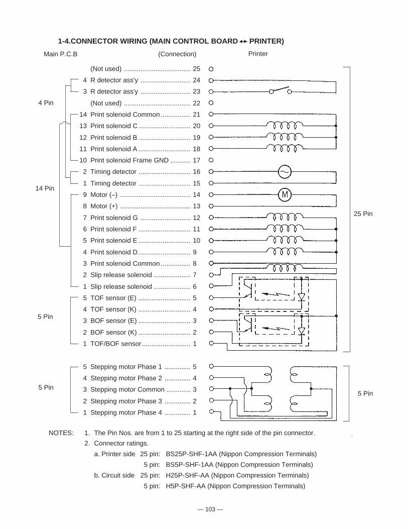
— 103 —
1-4.CONNECTOR WIRING (MAIN CONTROL BOARD — PRINTER)
(Not used) .................................... 25
4 R detector ass'y ........................... 24
3 R detector ass'y ........................... 23
(Not used) .................................... 22
14 Print solenoid Common ................ 21
13 Print solenoid C ............................ 20
12 Print solenoid B ............................ 19
11 Print solenoid A ............................ 18
10 Print solenoid Frame GND ........... 17
2 Timing detector ............................ 16
1 Timing detector ............................ 15
9 Motor (–) ...................................... 14
8 Motor (+) ...................................... 13
7 Print solenoid G ........................... 12
6 Print solenoid F ............................ 11
5 Print solenoid E ............................ 10
4 Print solenoid D ............................ 9
3 Print solenoid Common ................ 8
2 Slip release solenoid .................... 7
1 Slip release solenoid .................... 6
5 TOF sensor (E) ............................ 5
4 TOF sensor (K) ............................ 4
3 BOF sensor (E) ............................ 3
2 BOF sensor (K) ............................ 2
1 TOF/BOF sensor .......................... 1
5 Stepping motor Phase 1 .............. 5
4 Stepping motor Phase 2 .............. 4
3 Stepping motor Common ............. 3
2 Stepping motor Phase 3 .............. 2
1 Stepping motor Phase 4 .............. 1
4 Pin
Main P.C.B (Connection) Printer
14 Pin
5 Pin
5 Pin
25 Pin
5 Pin
NOTES: 1. The Pin Nos. are from 1 to 25 starting at the right side of the pin connector.
2. Connector ratings.
a. Printer side 25 pin: BS25P-SHF-1AA (Nippon Compression Terminals)
5 pin: BS5P-SHF-1AA (Nippon Compression Terminals)
b. Circuit side 25 pin: H25P-SHF-AA (Nippon Compression Terminals)
5 pin: H5P-SHF-AA (Nippon Compression Terminals)

— 104 —
13. PARTS LIST
1. QT-2000 ................................................................................................... 108
2. MCR ASS'Y(QT-2046MC) ....................................................................... 114
3. REAR DISPLAY ASS'Y(QT-2060D) ........................................................ 116
4. DISPLAY ASS'Y(QT-2063D) ................................................................... 118
5. SP-1200 ................................................................................................... 120
6. PRINTER UNIT MODEL-209 ................................................................... 122
Notes:
1. Prices and specifications are subject to change without notice.
2. As for order / supply of spare parts, refer to the "GUIDEBOOK for Spare Parts Supply", a separatepublication.
3. The numbers in item column correspond to the same numbers in drawing.
4. MARKS:
Q: Quantity used per unit
R: Rank
A: EssentialB: Stock recommendedC: Less recommendedX: No stock recommended

— 105 —
36
35
10
46
49
750
58
59
33
E58
0-C
NB
Ass
`yE
580-
CN
B-1
1
47
53
618
14
12
3
11
8
E58
0-E
2-1
Ass
`y
13
17
15
56
Key
boar
d B
lock
51
49
52
2
57
3254
48
34
516

— 106 —

— 107 —
19
23
25
30
28
E58
0-E
4-1P
CB
E58
0-E
4-2P
CB
31
27
21
20
24
26
22
29

QT-2000
N Item Code No. Parts Name Specification Version Qt'y Price code RQT2000
MAIN PCB BLOCK6193 3504 Main PCB ass'y E580-1 E240399*1 1 EP A
IC36 2001 9905 LSI/Gate array MN56020KSJ 1 BP AIC12 2003 0755 LSI/Gate array MN53040KSF1 1 BZ AIC32 2003 0771 LSI/Gate array MN53020KSG 1 BP AIC11 2003 0780 LSI/Gate array MN53020KSK 1 BP AIC23 2006 1613 LSI/S-RAM CXK582000M-85/10LL 1 BW AIC10 2006 1620 LSI COM20020BILJP 1 CT AIC20 2006 1627 LSI LC36256AMLL70-10 1 BF AIC26 2006 1634 LSI SED1351F0A 1 BS AIC33 2006 1680 LSI TL16C552AFN 1 BY AIC22 2006 1681 LSI LH28F016SUT-70/10 1 DA AIC43 2006 1682 LSI SRM20100LLM70-10 1 BM AIC6 2011 7154 LSI UPD70108HGC-16-3B6 1 BP AIC40 2101 0286 IC/MOS TC74HC02AF-TP1 1 AC AIC24,25,46,53 2101 0294 IC/MOS TC74HC74AF-TP1 4 AD AIC1,27,37,47 2101 0308 IC/MOS TC74HC4050AF-TP1 4 AF AIC54 2101 0618 IC/MOS TC7S08F-TE85L 1 AC AIC34 2101 0651 IC/MOS TC74HC00AF-TP1 1 AC AIC14,15,52 2101 0677 IC/MOS TC74HC138AF-TP1 3 AF AIC2,3 2101 1053 IC/MOS TC4SU69F TE85L 2 AC AIC45 2101 1061 IC/MOS TC7S32F TE85L 1 AC AIC4,29,30 2101 1134 IC/MOS TC74HC244AF-TP1 3 AK AIC13,44,51 2105 1414 IC/MOS TC7S04F-TE85L 3 AC AIC16 2112 0077 IC/Linear M5291FP-T1 1 AL AIC8,17,28 2112 0273 IC/Linear SN75189ANS-TP-L 3 AE AIC7,19,38 2112 0287 IC/Linear SN75188NS-TP-L 3 AE AIC31 2112 0714 LSI/EP-ROM M27C1001-10/12F1 1 BI AIC21 2112 0721 IC/MOS TC74AC245AF-TP1 1 AN AIC5 2112 0728 IC/MOS TC74HC21AF-TP1 1 AD AIC50 2112 0735 IC/MOS TC74HC373AF-TP1 1 AI AIC42 2112 0742 IC/MOS TC74HC4049AF-TP1 1 AE AIC9,18 2112 0749 IC/TTL SN751178NS-TP-L 2 BJ AIC48 2112 0763 IC/Linear M51957BFP-T1 1 AJ AIC49 2112 0784 IC/MOS TC74HCT157AF-TP1 1 AG AQ5,7 2250 0910 Transistor 2SA1729-TC 2 AE BQ1 2250 1519 Transistor/Digital DTC123JKAT146 1 AA BQ10 2250 1526 Transistor 2SD1625-TD 1 AC BQ4,8 2254 0434 Transistor/Digital DTA114EKAT146 2 AA BQ6 2254 0441 Transistor/Digital DTC114EKAT146 1 AA BZD1 2310 9409 Diode/Zener RD5.1FB3 1 AC BZD2 2315 3088 Diode/Zener RD22EB1 1 AA BD9,10,13,14,17 2390 1820 Diode 1SS355TE-17 5 AA BD12 2390 1848 Diode D1FS4-4063 1 AB BD15 2390 2058 Diode 1SR154-400TE25 1 AB BX4-6 2520 1744 Oscillator/Ceramic CSA4.91MG040 3 AD AX1 2520 3445 Oscillator/Crystal C-002RX(M90-76) 1 AD AX2 2590 0203 Oscillator/Ceramic CSA16.00MX040 1 AE AX3 2590 1197 Oscillator/Ceramic CSA20.00MXZ040 1 AD AR29 Resistor/Chip carbon film MCR25JZHJR62 1 XR119 Resistor/Chip carbon film MCR10EZHF2400 1 XR118 Resistor/Chip carbon film MCR10EZHF91R0 1 XR40 Resistor/Chip carbon film MCR100JZHJ5R6 1 XRA6 Resistor/Chip network MNR38H0AJ562 1 XRA1 Resistor/Chip network MNR38H0AJ153 1 XR112 Resistor/Chip carbon film MCR10EZHJ202 1 XRA3 Resistor/Chip network MNR34J5AJ472 1 X
- 108 -

N Item Code No. Parts Name Specification Version Qt'y Price code RQT2000
R32-39,41,69,71-76, R78,80,82-86,92,98, R100,108,109,120-145
Resistor/Chip carbon film MCR10EZHJ101 54 X
R46 Resistor/Chip carbon film MCR10EZHJ473 1 XR42,47,54,56,62,106, R111,114,116,153155
Resistor/Chip carbon film MCR10EZHJ102 12 X
R28,48-53 Resistor/Chip carbon film MCR10EZHJ331 7 XR104 Resistor/Chip carbon film MCR10EZHJ563 1 XR2,45,68,101-103,R107,146,148-150 R148-150
Resistor/Chip carbon film MCR10EZHJ472 11 X
R21-25 Resistor/Chip carbon film MCR10EZHJ221 5 XR70,117 Resistor/Chip carbon film MCR10EZHJ152 2 XR43,44,57,60,91,93,99, R105,113,115,151,152
Resistor/Chip carbon film MCR10EZHJ103 12 X
R3 Resistor/Chip carbon film MCR10EZHJ334 1 XR4,6,55,58,59,61 Resistor/Chip carbon film MCR10EZHJ100 6 XR110 Resistor/Chip carbon film MCR10EZHJ332 1 XR77,79,81 Resistor/Chip carbon film MCR10EZHJ562 3 XRA13,14 Resistor/Chip network MNR38H0AJ101 2 XRA11,12,15,16 Resistor/Chip network MNR34J5AJ101 4 XRA2,4,5,7-10 Resistor/Chip network MNR38H0AJ472 7 XR63-66,88-90,94-97 Resistor/Chip carbon film MCR10EZHJ683 11 XR5,7 Resistor/Chip carbon film MCR10EZHJ203 2 XR26 Resistor/Chip carbon film MCR10EZHJ561 1 XR8-20,31,67 Resistor/Chip carbon film MCR10EZHJ303 15 XR1 Resistor/Chip carbon film MCR10EZHJ106 1 XC43 Capacitor/Electrolytic 50RE3-1000 1 XC25,28,33 Capacitor/Electrolytic 16RE2-10 3 XC30,35,38 Capacitor/Electrolytic 50RE2-10 3 XC32 Capacitor/Electrolytic 16RE2-47 1 XC31 Capacitor/Electrolytic 50RE3-100 1 XC40 Capacitor/Electrolytic 16RE3-470 1 XC9 Capacitor/Electrolytic 16RE3-100 1 XC41,42 Capacitor/Electrolytic 25RE3-470 2 XC53,79,104,112 Capacitor/Chip ceramic GRM40F104Z50PT 4 XC7,8,10-22,50,51,54, C55,57,58,64,68,69,77, C89,91,92,98,99,101, C103,113,115,116
Capacitor/Chip ceramic GRM40CH101J50PT 35 X
C1,3,37,39,44-49,52, C56,60-63,67,70,72-74, C76,78,80-88,90,93-97, C100,102,105-111,114, C117-123,127,128, C130-132,134-137
Capacitor/Chip ceramic GRM40R104K25PT 65 X
C125,126 Capacitor/Chip ceramic GRM40R221K50PT 2 XC129 Capacitor/Chip ceramic GRM40R471K50PT 1 XC6 Capacitor/Chip ceramic GRM40CH100D50PT 1 XC29,59,71,124 Capacitor/Chip ceramic GRM40R102K50PT 4 XF5 3000 7938 Fuse 473.750F10-20 1 AE AD1-8 3000 7959 Diode 1SS376TE-17 8 AA B
- 109 -

N Item Code No. Parts Name Specification Version Qt'y Price code RQT2000
F1-4 3000 7966 Fuse 452.5 4 AD AL1 3013 1673 Coil RCH855-181K 1 AD CFT21 Filter/EMI NFM40R11C222T1 1 XFT1-20,22-25,27-39 Filter/EMI NFM840R01G101T1 37 XFT26 Filter/EMI NFM39R12C222T1 1 XBZ1 3240 2089 Buzzer PKM22EPT-2001 1 AE XCN5 3500 3240 Connector/7P IL-G-7P-S3T2-E 1 AB CCN14 3500 3681 Connector/12P IL-G-12P-S3T2-E 1 AC CCN17,18 3500 5846 Connector 53253-0210 2 AA CCN10 3510 4119 Connector FRC3-C20L13-OS 1 AS CCN15 3510 4127 Connector FRC3-C20S13-OL 1 AT CCN16 3540 3183 Connector/9P 5275-09A 1 AE CCN4 3540 5109 Connector HLEM9S-1 1 AB CCN11 3540 5116 Connector HLEM19S-1 2 AC CCN13 3540 5123 Connector 52411-0601 1 AW CCN6 3540 5137 Connector 53047-1410 1 AE CCN9 3540 5144 Connector 53047-1510 1 AE CCN7 3540 5151 Connector 53047-1610 1 AF CCN19 3540 5158 Connector HLEM8R-1 1 AB CCN12 3540 5173 Connector B05-DR 1 AB CIC31,35,39 3610 6859 Socket/IC DILB32P-8JK 3 AD XCN2 6247 9598 Connector/In-line E340561*1 1 AM AC2,4,5,23,24,65,66 Capacitor/Chip GRM40CH330J50PT 7 XC26,27,34,36 Capacitor/Chip GRM40CH300J50PT 4 XCN8 7740 0742 Connector 53047-0210 1 AA CR30 Resistor/Chip MCR10EZHF5103 1 X
PCB/E580-1 E240408B-1 1 XStopper HU-006 2 X
1 6221 1326 Connector/1625-03R E32564-7(#24-250) 1 AI C
E580-IR ASS'YIC1 2112 0756 IC ST84C01CF8-TR 1 BA AR1 Resistor/Chip carbon film MCR10EZHJ101 1 XR2 Resistor/Chip carbon film MCR10EZHJ7R5 1 XR3 Resistor/Chip carbon film MCR10EZHJ470 1 XC1 Capacitor/Chip electrolytic RV2-10V470M-R 1 XC2 Capacitor/Chip ceramic GRM40R104K25PT 1 XC3 Capacitor/Chip ceramic GRM40R472K50PT 1 XCN1 3540 5158 Connector HLEM8R-1 1 AB CFT1 Filter/EMI NFM40R11C102T1 1 XLED1 2408 8380 LED GL1F20C 1 AT BLED2 2408 8387 LED IS1U20C 1 AU B
DISPLAY ASS'Y BLOCK2 3000 7973 LCD module MD32PM6R-SNA 1 DM A3 3000 7980 Inverter/CFL PS-10058-002 1 CC A4 5500 1897 Shaft KH52A050 1 BK X
N 1004 2373 Shaft KH62B075L 0 BT XN 1004 2374 Spacer/Circuit board MSPLS-3 0 AA X
5 6247 7183 Case/LCD R-1 E140126-1 1 AT X6 6247 7281 Panel/LCD E340436-1 1 BG X7 6247 7295 Hinge/LCD E340438-1 1 AK X8 6247 7302 Knob E340439-1 1 AK X9 6247 7358 Roller/Hinge E440396-1 1 AC X
10 6248 0179 Chassis/LCD E340613-1 1 AV X11 6248 0186 Sheet/Blind E440470-1 1 AD X12 6248 0193 Plate/Blind E440472-1 1 AH X13 6248 0200 Cable/51021-15 E340541-1(#26-350) 1 AP C14 6248 0763 Connector/51021 E340539C-1 1 BC X
N 1004 4397 Connector/51021sub assy E340539C-4 0 BD C15 6248 0767 Case/F LCD E140125A-1 1 AS X16 6248 0769 Cover/LCD E240331A-1 1 AT X
- 110 -

N Item Code No. Parts Name Specification Version Qt'y Price code RQT2000
17 6248 0878 Cushion/ V LCD E440561-1 2 AA X18 6248 0879 Cushion/H LCD E440562-1 2 AB X
N 1004 2350 Plate/Water protection L E441193-1 0 AA XN 1004 2363 Case/F LCD E140414-1 0 AT XN 1004 2366 Case/R LCD E140415-1 0 AV XN 1004 2369 Chassis/Blind E240729-1 0 AU XN 1004 2371 Spacer/Rubber E580 E441186-1 0 AF XN 1004 2372 Plate/Water protection E441189-1 0 AA X
E580-E2-1 ASS'YVR1 3502 2012 Resistor/Variable RS10F12-A-5-10KB 1 AM CCN1 6248 0766 Connector/51005-02 E340629A-1 1 AG C
E580-CNB ASS'YCN2 3540 5116 Connector HLEM19S-1 1 AC CCN3 3000 7924 Connector/D-sub/Female ID15S33E4GX28 1 AL CCN1 3000 7917 Connector/D-sub/Male ID9P33E4GX28 1 AK C
E580-CNB-1CNB1 3540 5109 Connector HLEM9S-1 1 AB CCNB2 3000 7917 Connector/D-sub/Male ID9P33E4GX28 1 AK C
KEYBOARD BLOCK B19 6193 3434 Keyboard ass'y E240387*1 1 CW X20 6247 7596 Frame/Keyboard E140104-1 1 BI X21 6247 7603 Holder/Keyboard E240342-1 1 AM X22 6247 7225 Chassis/Keyboard E240299-1 1 AR X23 6247 7309 Rubber/Contact E340446-1 4 AT A24 6247 7204 Sheet/Common keyboard E240296-1 1 AT A25 6248 0898 Spacer/Keyboard E240297A-1 1 AM A26 6247 7218 Cable/Joint E240298-1 1 AY C27 5500 1690 Plate B-MMC12 2 AN X28 6247 7351 Cable/Joint E440380-4 1 AC C29 6248 0742 Cable/Keyboard E440551*1 1 BQ C30 5500 1683 Spacer/Card KGTS-4K 3 AC X
Screw/3X6 3X6ZMC-3 27 X31 6248 0770 Button/Detection E440387A-1 3 AA C
Screw/3X8 3X8 ZMC-3 6 X
E580-E4-1 PCB BLOCKCN1 3500 5848 Connector/FFC HLEM26R-1 1 AC ACN2 3540 5151 Connector 53047-1610 1 AF CCN3 3540 5137 Connector 53047-1410 1 AE CCN4 3540 5095 Connector HLEM4R-1 1 AA C
E580-E4-2 PCB BLOCKCN1 3540 5095 Connector HLEM4R-1 1 AA CSW1-3 3000 7931 Switch ABU8112S 3 AI B
LOWER CASE BLOCK32 6247 7575 Case/Lower E140122-1 1 BU C
N 32 1004 3933 Case/Lower E140122A-1 0 BY CN 1004 3934 Plate/Blind E441195-1 1 AH C
33 6247 7582 Plate/Display filler E440403-1 1 AC XChassis/B E140132-1 1 XChassis/R E240344-1 1 XChassis/L E240343-1 1 XHolder/Cable E440375-1 1 XTerminal/Earth E440398-1 1 X
34 6247 7456 Filter/IR E440418-1 1 AK CRubber/Foot E412136-1 2 X
35 3000 8020 Power supply unit/Switching PS-10055-003 (200V) 1 DJ A35 3000 8021 Power supply unit/Switching PS-10055-004 (100V) 1 DI A36 6221 4802 Cord/Power M2511(EU,G,DI) 1 BC C36 3701 0242 Cord/Power MP5004 (EU,UK,DI) 1 BO C36 3700 4283 Cord/Power M3203 (DI) 1 AZ C
- 111 -

N Item Code No. Parts Name Specification Version Qt'y Price code RQT2000
36 3700 4281 Cord/Power PS204 (US,L,DI) 1 AV CScrew 3X8 ZMC-3 8 XScrew 3X6 ZMC-3 12 XScrew 3X5 ZMC-3 1 XScrew 4X5 ZMC-3 1 XScrew 3X8 ZMC-3 2 XClip/Wire CS-2-U 1 XWire/FG E310997C-29 1 XPlate/Earth S E440449-1 2 XCable/Joint CE2 2 CFerrite core RI-12-15-8.5 1 XBush TB-0813 1 XScrew 4X8 ZMC-3 3 XGermany only E340509*1
CLERK KEY ASS'Y37 3400 2576 Switch/Clerk key J-Y7541 1 BM C38 5111 5760 Screw 2.6X8 ZMC-3 2 AA X39 5440 0483 Screw 3X8 ZMC-3 1 AA X40 6215 2303 Spring/Earth clerk E42180-1 1 AK X41 6247 7365 Plate/Clerk SW E440397-1 1 AL X42 6247 7673 Case/Clerk SW E340469-1 1 AK X43 6248 0687 Connector/IL-G E440507*1 1 AM X44 3418 1594 Key set/Clerk 6 306JYB-135-01 1 CJ C45 3418 1609 Key set/Clerk 15 306JYB-135-03 1 DD C
GENERAL COMPONENTS46 6248 0972 Plate/Rear display E140127B-1 1 BM C
N 1004 2392 Plate/Rear display E140127B-2 0 BH CN 1004 2394 Plate/ LCD fixing E580 E341122-1 0 AT XN 1004 2396 Hinge/Upper case E580 E240727-1 0 AI XN 1004 2397 Hinge/Lower case E580 E240728-1 0 AG XN 1004 2398 Knob/Slide E580 E341120-1 0 AE XN 1004 2399 Plate/Screw blind E341121-1 0 AC XN 5500 1550 Spacer/Circuit board RSPS-6 0 AA X
47 6247 7568 Cover/Connector E340445-1 1 AK C48 6247 7316 Cover/Bottom E340461-1 1 AR X
Grommet B-1 1 XPlate/Shield IR E440539-1 1 X
49 6220 6829 Rubber/Spacer E411002-1 2 AE X50 6247 7330 Cable/Joint 1 E440380-1 1 AE C51 6247 7337 Cable/Joint 2 E440380-2 1 AC C52 6247 7344 Cable/Joint 3 E440380-3 1 AC C53 6247 7470 Plate/Name E440437-1 1 AG C
N 1003 9258 Plate/Name E580B E440437-2 0 AE C54 3000 7588 Battery/Lithium vanadium VL3032/S6A 1 BT A55 3500 5820 Connector/In-line XLP-KIT-1 1 AM A56 6248 0221 Opener/Sheet E440503-1 1 AC C
Clip (Germany only) CA-8 1 XN 1004 2349 Cover/Sheet E240724-1 0 AY C
Screw 3X15 ZMC-3 5 XScrew 3X8 NI 2 XScrew 3X12 NI 1 XScrew 3X6 ZMC-3 3 XFerritte core TFC-23-11-14 1 XScrew E440564-1 2 X
U.S.A. and CANADA only57 6247 7449 Stand/Rear R E440415-1 1 AV C58 6247 7442 Stand/Rear L E440414-1 1 AV C59 5500 1802 Guide GR-80S 2 AE C60 6193 4575 E404-E2 ass'y E210694H*3 1 DE A
Screw 3X5 ZMC-3 4 X
- 112 -

Item Code No. Parts Name Specification Version Q R
Ferritte core TFC-23-11-14 1 XScrew E440564-1 2 X
U.S.A. and CANADA only57 6247 7449 Stand/Rear R E440415-1 1 C58 6247 7442 Stand/Rear L E440414-1 1 C59 5500 1802 Guide GR-80S 2 C60 6193 4575 E404-E2 ass'y E210694H*3 1 A
Screw 3X5 ZMC-3 4 X
— 113 —

— 114 —
2. MCR ASS'Y (QT-2046MC)
1 4
8
2
5
7 36
911
1210

QT-2046MC
Item Code No. Parts Name Specification Version Q R
1 1090 5665 MCR unit ZU-M1242S4 1 A2 6220 5857 Earth plate E410943-1 1 C3 6248 0088 Upper case E210283-4 1 C4 6248 0095 Lower case E210351A-3 1 C5 6248 0756 MCR cable sub ass'y E340562-1 1 B6 Screw 2.3x8 ZMC-3 2.3X8 ZMC-3 4 X7 Screw 2.6x8 ZMC-3 2.6X8 ZMC-3 2 X8 Screw 2.6x8 ZMC-3 2.6X8 ZMC-3 2 X
9 6193 4211 MCR mount ass'y E440500*1 1 C10 6248 0102 Fixing metal E310425A-3 1 X11 6248 0144 MCR stay E440493-1 2 X12 6248 0151 MCR mount E440494-1 1 X
Screw 4x16 ZMC-3 4X16 ZMC-3 4 X
— 115 —

— 116 —
3. REAR DISPLAY ASS'Y (QT-2060D)
2
1
5
34

QT-2060D
Item Code No. Parts Name Specification Version Q R
1 6193 4575 PCB ass'y E404-E2 E210694H*3 1
IC5 2003 0704 LSI M50722-101FP 1 AIC1,2 2003 0712 LSI M34203M4-140FP 2 AIC3 2101 0294 MOS IC TC74HC74AF-TP1 1 AIC6 2101 0961 MOS IC TC4050BF-TP1 1 AIC4 2112 0231 MOS IC TC4069UBF-TP1 1 AQ2 2220 3720 Transistor 2SC3074-Y 1 BQ1 2280 0017 Transistor 2SC1815-GR 1 BD1-4 2301 0445 Diode 1SS130 4 BZD1 2310 7113 Zener diode RD22EB2 1 BX1 2520 1817 Ceramic oscillator CSAC5.00MGCM-TC 1 BR5,16,18 2792 0152 Chip resistor MCR18EZHJ472 3 XR1,7,8,15 2792 0179 Chip resistor MCR18EZHJ103 4 XR2-4,10-12 2792 0276 Chip resistor MCR18EZHJ101 6 XR13,19 2792 0314 Chip resistor MCR18EZHJ102 2 XR17 2792 0748 Chip resistor MCR18EZHJ105 1 XRA1,4 2792 1299 Chip module resistor MNR38H0AJ103 2 XR6 2792 1329 Chip resistor MCR18EZHJ680 1 XRA2,3 2792 1337 Chip resistor MNR38H0AJ563 2 XR9 2795 2856 Chip resistor MCR18EZHJ151 1 XC1,14 2807 3596 Electrolytic capacitor RJJ-50V390MF3 2 XC3,7 2807 3603 Electrolytic capacitor RJJ-16V471MG5 2 XC5,6 2818 3771 Chip caramic capacitor GRM40CH300K50PT 2 XC4,11,12 2818 3780 Chip caramic capacitor GRM40CH101K50PT 3 XC10,13 2818 3801 Ceramic capacitor GRM40CH102K50PT 2 XC2 2818 3836 Chip caramic capacitor GRM40R103K50PT 1 XC30-35 2818 3844 Ceramic capacitor GRM40R104K25PT 6 XC9 2818 3852 Ceramic capacitor GRM40R332K50PT 1 XC8 2818 3861 Chip capacitor GRM40R682K50PT 1 XT1 3010 6504 DC/DC convertor DCSS-404 1 AEMI1 3020 2376 EMI filter ZJSR5101-101-R 1 XDISPLAY 3300 3552 Display tube CP4006C 1 ACN1 3500 3681 Pin ass'y 12P IL-G-12P-S3T2-E 1 C
4308 1390 PCB E404-E2 (Without components) E210707C-1 1 X2 6220 9232 Connector sub ass'y E310897*1 1 C
6221 1261 Display cushion E411210-1 2 X6221 1474 Display cushion E411235-1 4 X
3 5500 1802 Guide rail (GR) GR-80S 2 C4 6247 7442 Display mount stand L E440414-1 1 C5 6247 7449 Display mount stand R E440415-1 1 C
Screw 3x5 ZMC-3 3X5 ZMC-3 4 X
— 117 —
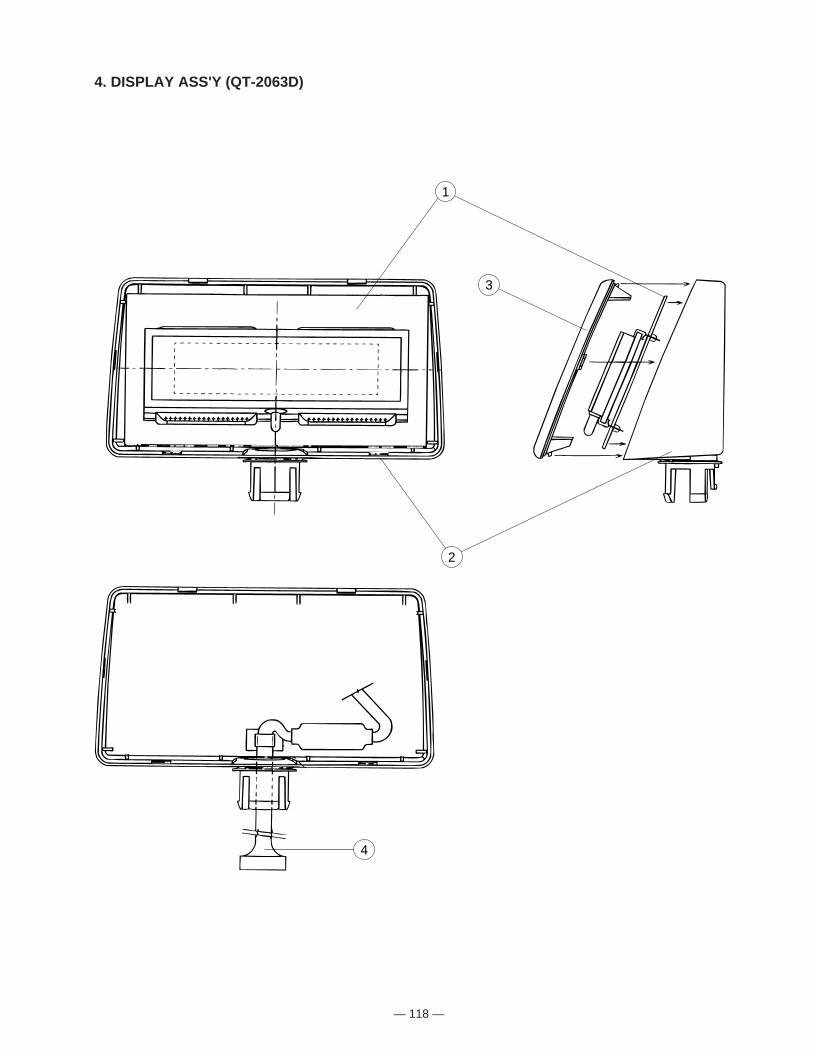
— 118 —
4. DISPLAY ASS'Y (QT-2063D)
2
1
3
4

QT-2063D
Item Code No. Parts Name Specification Version Q R
1 6190 8751 PCB ass'y E404-2 E210694*1 1 B
IC5 2003 0704 LSI M50722-101FP 1 AIC1,2 2003 0712 LSI M34203M4-140FP 2 AIC3 2101 0294 MOS IC TC74HC74AF-TP1 1 AIC6 2101 0961 MOS IC TC4050BF-TP1 1 AIC4 2112 0231 MOS IC TC4069UBF-TP1 1 AQ2 2220 3720 Transistor 2SC3074-Y 1 BQ1 2280 0017 Transistor 2SC1815-GR 1 BD1-4 2301 0445 Diode 1SS130 4 BZD1 2310 7113 Zener diode RD22EB2 1 BX1 2520 1817 Ceramic oscillator CSAC5.00MGCM-TC 1 BR5,16,18 2792 0152 Chip resistor MCR18EZHJ472 3 XR1,7,8,15 2792 0179 Chip resistor MCR18EZHJ103 4 XR2-4,10-12 2792 0276 Chip resistor MCR18EZHJ101 6 XR13,19 2792 0314 Chip resistor MCR18EZHJ102 2 XR17 2792 0748 Chip resistor MCR18EZHJ105 1 XRA1,4 2792 1299 Chip module resistor MNR38H0AJ103 2 XR6 2792 1329 Chip resistor MCR18EZHJ680 1 XRA2,3 2792 1337 Chip resistor MNR38H0AJ563 2 XR9 2795 2856 Chip resistor MCR18EZHJ151 1 XC1,14 2807 3596 Electrolytic capacitor RJJ-50V390MF3 2 XC3,7 2807 3603 Electrolytic capacitor RJJ-16V471MG5 2 XC5,6 2818 3771 Chip ceramic capacitor GRM40CH300K50PT 2 XC4,11,12 2818 3780 Chip ceramic capacitor GRM40CH101K50PT 3 XC10,13 2818 3801 Ceramic capacitor GRM40CH102K50PT 2 XC2 2818 3836 Chip capacitor GRM40R103K50PT 1 XC30-35 2818 3844 Ceramic capacitor GRM40R104K25PT 6 XC9 2818 3852 Ceramic capacitor GRM40R332K50PT 1 XC8 2818 3861 Chip capacitor GRM40R682K50PT 1 XT1 3010 6504 DC/DC convertor DCSS-404 1 AEMI1 3020 2376 EMI filter ZJSR5101-101-R 1 XDISPLAY 3300 3552 Display tube CP4006C 1 ACN1 3500 3681 Pin ass'y 2P IL-G-12P-S3T2-E 1 C
4308 1390 PCB E404-E2 (without components) E210707C-1 1 X2 6248 0606 Display case E110169-2 1 C3 6248 0613 Display window E110170-7 1 C
6220 9232 Connector sub ass'y E310897*1 1 C6231 8813 Connector sub ass'y E310855A*1 1 C6221 1261 Display cushion E411210-1 2 X6221 1474 Display cushion E411235-1 4 X
— 119 —

— 120 —
5. SP-120017
6
45
10
9
12
21
3
11
207
19
23
24
22
25
18
13
16
15
14

— 121 —
I t em Code No. Parts Name Specification Version Q R
Inductor EXC-ELSA35 2 X3 3500 5781 Connector 3pin W-P7503 1 C4 3500 5790 Connector 10pin W-P7910 1 C5 3500 5803 Connector 15pin W-P7915 1 C6 3500 5811 Connector 4pin W-P7904 1 C7 5560 0511 Wire band BK-1 1 X9 6231 7540 SLIP IF sub ass'y E310627A*1 1 B
10 6220 4672 SLIP IF sub ass'y E310628*1 1 B11 6220 6039 W-A2404 connector sub ass'y E310482-6(#24-100) 1 B
PCB E901-1 (Without components) E210521B-1 1
Housing block12 6220 4681 Lamp case E410767-1 1 X13 6248 0627 Upper case sub ass'y E310538*4 1 C14 6220 4699 Diffusion plate E410768-1 1 C15 6248 0655 Ribbon caver sub ass'y E411894*2 1 C16 6220 5075 Insulation sheet E410920-1 1 X17 6002 3514 Wire fixing metal P4454-1 1 X18 6231 9597 Shield plate E310516A-1 1 X19 6220 4613 Shield spacer E310517-1 1 X20 6248 0641 Lower case sub ass'y E310539A*4 1 C21 6236 6133 Connector sub ass'y E310863B*1 1 C22 3030 4055 Ferrite core L5T18X6X10 1 X23 1000 7941 Printer unit MODEL-290-001 1 A
Screw 2.6x6 ZMC-3 2.6X6 ZMC-3 2 XScrew 4x6 ZMC-3 4X6 ZMC-3 1 XScrew 3x10 ZMC-3 3X10 ZMC-3 1 XScrew 3x8 ZMC-3 3X8 ZMC-3 1 XScrew 3x6 ZMC-3 3X6 ZMC-3 2 XScrew 2.3x6 ZMC-3 2.3X6 ZMC-3 2 XScrew 3x8 ZMC-3 3X8 ZMC-3 6 XScrew 3x10 3X10 2 XScrew 3x10 ZMC-3 3X10 ZMC-3 4 XScrew 3x6 ZMC-3 3X6 ZMC-3 1 XEarth metal E411468A-1 1 X
I t em Code No. Parts Name Specification Version Q R
Control PCB block6190 9470 PCB ass'y E901-1 E210517H*2 1 A
2001 9832 LSI HD614089FB67 1 A2101 0898 MOS IC TC74HC245AF 1 A2101 0901 MOS IC TC4030BF 1 A2101 1118 MOS IC TC74HC32AF 1 A2106 0007 MOS IC TC4050BF 1 A2112 0427 Regurator IC UPC7805AHF 1 A2120 7306 Liner IC M5233FP 2 A2120 8795 Monolythic IC TH3L10Z 1 A2120 9180 Monolythic IC MTB001 2 A2210 7305 Transistor 2SB1282 1 B2220 2375 Transistor 2SC945-(K,P,Q,R) 1 B2220 2456 Transistor 2SC945(K,P,Q,R)-T 2 B2230 4135 Transistor 2SD1853-AA 2 B2230 5280 Transistor 2SD1192 1 B2301 0127 Diode 1SR35-100A 2 B2310 9174 Zener diode HZ-24-C2 1 B2310 9182 Zener diode HZ-4-C1 1 B2390 0140 Diode 1SS270-TD-T 1 B2520 1680 Ceramic oscillator CST4.00MGW 1 A
Carbon film resistor R-20-750-J-T24-T 1 XCarbon film resistor R-20-2K-J-T24-T 1 XCarbon film resistor R-20-220-J-T24-T 6 XCarbon film resistor R-20-560-J-T24-T 2 XCarbon film resistor R-20-1K-J-T24-T 9 XCarbon film resistor R-20-2.2K-J-T24-T 2 XCarbon film resistor R-20-3.3K-J-T24-T 1 XCarbon film resistor R-20-4.7K-J-T24-T 2 XCarbon film resistor R-20-10K-J-T24-T 9 XCarbon film resistor R-20-150K-J-T24-T 2 XCarbon film resistor R-20-1M-J-T24-T 1 XCarbon film resistor R-20-2.7K-J-T24-T 2 XCarbon film resistor R-20-12K-J-T24-T 1 XCarbon film resistor R-20-62K-J-T24-T 2 XCarbon film resistor R-20-22-J-T24-T 1 XCarbon film resistor R-20-22K-J-T24-T 4 XCarbon film resistor R-20-56K-J-T24-T 1 XCarbon film resistor R-20-6.8K-J-T24-T 1 XCarbon film resistor R-20-1.2K-J-T24-T 2 XCarbon film resistor R-50X-2K-J 1 XRC network EXBY14B379J 2 X
2739 5002 Potentionmeter 3321P-1-503 1 AElectrolytic capacitor 10RE2-220 3 XElectrolytic capacitor 50RE2-1 1 XElectrolytic capacitor 35RE3-1000 2 XElectrolytic capacitor 100RE2-1-T2-T 1 XCeramic capacitor HE70SJYB332K 2 XCeramic capacitor RT-HE40TKYB471K-T 5 XCeramic capacitor RT-HE40TKYB101K-T 2 XCeramic capacitor RT-HE95TKYB682K-T 1 XTF capacitor ECQ-V1H-104-JZ3-T 4 XTF capacitor ECQ-B1H103KF3-T 12 X
SP-1200

— 122 —
6. PRINTER UNIT MODEL-290

PRINTER UNIT MODEL-290
Item Code No. Parts Name Specification Version Q R
Driving mechanism components100 0008 7580 Motor ass'y F250051000 1 A101 0008 7581 Motor gear F250051020 1 B102 0008 7582 C.B. screw M2×3 B010309411 1 X
103 0008 7583 Motor mount plate F250002010 1 X10⁴ 0008 7584 Shaft holder guide F250002020 1 C105 0008 7585 Guide shaft F250002030 1 C106 0008 7586 Return support spring F230004030 1 B107 0008 7587 Cup screw (S tight) M2.5×5 B300302211 3 X
108 0003 0791 Retaining ring TYPE-E(1.5) B150300311 1 B109 0008 7588 Carriage spring F250003000 1 B110 0008 7582 C.B. screw M2X3 B010309411 1 X111 0008 7589 Intermittent gear F250101010 1 B112 0008 7587 Cup screw (S tight) M2.5×5 B300302211 4 X
Detecting mechanism components300 0008 7591 R detector ass'y F230003000 1 B301 0008 7592 BOF cover F250153020 1 C
Printing mechanism components400 0008 7593 Carrier drive cam shaft ass'y F250201000 1 A401 0008 7594 Dot head unit H F230727000 1 A
Paper feeding mechanism components500 0008 7595 Paper hold roller ass'y F250251000 1 B501 0007 4057 Retaining ring TYPE-E(2) B150300411 1 B502 0008 7596 Paper feed motor mount plate sub ass'y F250253000 1 C503 0008 7597 Paper feed motor F250252010 1 A504 0008 7598 Cup screw S tight (Flat type) B300500211 2 X505 0008 7599 Paper feed transmission gear F250254010 1 B506 0008 7600 Leaf spring B101250590 1 B507 0008 7587 Cup screw (S tight) M2.5×5 B300302211 2 X
508 0008 7601 Paper hold lever sub ass'y F250262000 1 B509 0008 7602 Release cam sub ass'y F250263000 1 B510 0008 7603 Paper feed roller sub ass'y F250264000 1 B511 0008 7604 Platen F250261010 1 C512 0008 7605 Platen adjustment roller F250261020 2 B513 0008 7606 Platen adjustment roller holder F250261030 2 B514 0008 7607 Release cam spring F250261040 1 B515 0003 0791 Retaining ring TYPE-E(1.5) B150300311 1 B516 0008 7608 Paper guide sub ass'y F250265000 1 B517 0008 7609 Paper hold lever shaft F250260020 1 B518 0008 7610 Paper hold lever spring F250260030 1 B519 0008 7611 C.T.B.S. screw M2.5×5 B300202211 1 X
520 0003 0791 Retaining ring TYPE-E(1.5) B150300311 1 B
Inking mechanism components600 0008 7612 Ribbon frame sub ass'y F250352001 1 B602 0008 7613 Ribbon roll shaft F230001030 1 B603 0008 7614 Ribbon gear F230001040 1 B604 0003 0715 Retaining ring TYPE-E(4) B150300711 1 B
— 123 —

Item Code No. Parts Name Specification Version Q R
Connector800 0008 7615 Main circuit board ass'y F250601000 1 B810 0008 7587 Cup screw (S tight) M2.5×5 B300302211 1 X
Option1 0008 7616 TOF sensor ass'y F250151000 1 B2 0008 7617 BOF sensor ass'y F250152000 1 B3 0008 7618 Document table 176-085 F250254020 1 C4 0008 7611 C.T.B.S. screw M2.5×5 B300202211 2 X5 0008 7619 C.C.S. screw M3×6 B300304211 2 X
6 0008 7620 Main circuit board insulation cover F250602010 1 C10 0008 7621 Stopper guide lever F250266010 1 B11 0008 7622 Form stopper F250266020 1 B12 0008 7623 Stopper actuate lever F250266030 1 B13 0008 7624 Form stopper spring F250266040 1 B14 0007 4057 Retaining ring TYPE-E(2) B150300411 1 B15 0007 2308 Cup screw M2.5×4 B040301311 1 X
— 124 —

MA0900971A