SERVICE MANUAL - Audio-Circuit.dk
103
SERVICE MANUAL COMPACT COMPONENT MD SYSTEM No.20887 Nov. 2000 COPYRIGHT 2000 VICTOR COMPANY OF JAPAN, LTD. MX-S6MD MX-S6MD Safety Precautions Preventing static electricity Important for laser products Disassembly method Adjustment method Flow of functional operation until TOC read (MD section) Maintenace of laser pickup (MD) Replacement of laser pickup (MD) Flow of functional operation until TOC read (CD section) Maintenance of laser pickup (CD) Replacement of laser pickup (CD) Description of major ICs 1-2 1-3 1-4 1-5 1-31 1-37 1-38 1-38 1-39 1-40 1-40 1-40~69 Area Suffix US UB UT Singapore Hong Kong Taiwan CA-MXS6MD SP-MXS6MD SP-MXS6MD Contents
-
Upload
khangminh22 -
Category
Documents
-
view
1 -
download
0
Transcript of SERVICE MANUAL - Audio-Circuit.dk

SERVICE MANUALCOMPACT COMPONENT MD SYSTEM
No.20887Nov. 2000
COPYRIGHT 2000 VICTOR COMPANY OF JAPAN, LTD.
MX-S6MD
MX-S6MD
Safety PrecautionsPreventing static electricityImportant for laser productsDisassembly methodAdjustment methodFlow of functional operation until TOC read (MD section)
Maintenace of laser pickup (MD)Replacement of laser pickup (MD)Flow of functional operation until TOC read (CD section)Maintenance of laser pickup (CD)Replacement of laser pickup (CD)Description of major ICs
1-21-31-41-51-31
1-37
1-381-38
1-391-401-401-40~69
Area SuffixUSUBUT
SingaporeHong Kong
Taiwan
CA-MXS6MDSP-MXS6MD SP-MXS6MD
Contents

MX-S6MD
1-2
1. This design of this product contains special hardware and many circuits and components specially for safety purposes. For continued protection, no changes should be made to the original design unless authorized in writing by the manufacturer. Replacement parts must be identical to those used in the original circuits. Services should be performed by qualified personnel only.
2. Alterations of the design or circuitry of the product should not be made. Any design alterations of the product should not be made. Any design alterations or additions will void the manufacturer`s warranty and will further relieve the manufacture of responsibility for personal injury or property damage resulting therefrom.
3. Many electrical and mechanical parts in the products have special safety-related characteristics. These characteristics are often not evident from visual inspection nor can the protection afforded by them necessarily be obtained by using replacement components rated for higher voltage, wattage, etc. Replacement parts which have these special safety characteristics are identified in the Parts List of Service Manual. Electrical components having such features are identified by shading on the schematics and by ( ) on the Parts List in the Service Manual. The use of a substitute replacement which does not have the same safety characteristics as the recommended replacement parts shown in the Parts List of Service Manual may create shock, fire, or other hazards.
4. The leads in the products are routed and dressed with ties, clamps, tubings, barriers and the like to be separated from live parts, high temperature parts, moving parts and/or sharp edges for the prevention of electric shock and fire hazard. When service is required, the original lead routing and dress should be observed, and it should be confirmed that they have been returned to normal, after re-assembling.
5. Leakage currnet check (Electrical shock hazard testing)After re-assembling the product, always perform an isolation check on the exposed metal parts of the product (antenna terminals, knobs, metal cabinet, screw heads, headphone jack, control shafts, etc.) to be sure the product is safe to operate without danger of electrical shock.Do not use a line isolation transformer during this check.
Plug the AC line cord directly into the AC outlet. Using a "Leakage Current Tester", measure the leakage current from each exposed metal parts of the cabinet , particularly any exposed metal part having a return path to the chassis, to a known good earth ground. Any leakage current must not exceed 0.5mA AC (r.m.s.)Alternate check methodPlug the AC line cord directly into the AC outlet. Use an AC voltmeter having, 1,000 ohms per volt or more sensitivity in the following manner. Connect a 1,500 10W resistor paralleled by a 0.15 F AC-type capacitor between an exposed metal part and a known good earth ground.Measure the AC voltage across the resistor with the AC voltmeter. Move the resistor connection to eachexposed metal part, particularly any exposed metal part having a return path to the chassis, and meausre the AC voltage across the resistor. Now, reverse the plug in the AC outlet and repeat each measurement. voltage measured Any must not exceed 0.75 V AC (r.m.s.). This corresponds to 0.5 mA AC (r.m.s.).
1. This equipment has been designed and manufactured to meet international safety standards.2. It is the legal responsibility of the repairer to ensure that these safety standards are maintained.3. Repairs must be made in accordance with the relevant safety standards.4. It is essential that safety critical components are replaced by approved parts.5. If mains voltage selector is provided, check setting for local voltage.
Good earth ground
Place this probe on each exposedmetal part.
AC VOLTMETER(Having 1000 ohms/volts,or more sensitivity)
1500 10W
0.15 F AC TYPE
! Burrs formed during molding may be left over on some parts of the chassis. Therefore, pay attention to such burrs in the case of preforming repair of this system.

MX-S6MD
1-3
Electrostatic discharge (ESD), which occurs when static electricity stored in the body, fabric, etc. is discharged, can destroy the laser diode in the traverse unit (optical pickup). Take care to prevent this when performing repairs.
1.1. Grounding to prevent damage by static electricityStatic electricity in the work area can destroy the optical pickup (laser diode) in devices such as CD/MD players. Be careful to use proper grounding in the area where repairs are being performed.
1.1.1. Ground the workbench1. Ground the workbench by laying conductive material (such as a conductive sheet) or an iron plate over it before placing the traverse unit (optical pickup) on it.
1.1.2. Ground yourself1. Use an anti-static wrist strap to release any static electricity built up in your body.
1.1.3. Handling the optical pickup1. In order to maintain quality during transport and before installation, both sides of the laser diode on the replacement optical pickup are shorted. After replacement, return the shorted parts to their original condition. (Refer to the text.)2. Do not use a tester to check the condition of the laser diode in the optical pickup. The tester's internal power source can easily destroy the laser diode.
1.2. Handling the traverse unit (optical pickup)1. Do not subject the traverse unit (optical pickup) to strong shocks, as it is a sensitive, complex unit. 2. Cut off the shorted part of the flexible cable using nippers, etc. after replacing the optical pickup. For specific details, refer to the replacement procedure in the text. Remove the anti-static pin when replacing the traverse unit. Be careful not to take too long a time when attaching it to the connector. 3. Handle the flexible cable carefully as it may break when subjected to strong force. 4. It is not possible to adjust the semi-fixed resistor that adjusts the laser power. Do not turn it
Conductive material (conductive sheet) or iron plate
(caption)Anti-static wrist strap
CN321
CN451
Pickup Soldering part
Main board Flexible board
Soldering part
MD pickupCD pickup
Preventing static electricity

MX-S6MD
1-4
Important for laser products
1.CLASS 1 LASER PRODUCT
2.DANGER : Invisible laser radiation when open and inter
lock failed or defeated. Avoid direct exposure to beam.
3.CAUTION : There are no serviceable parts inside the
Laser Unit. Do not disassemble the Laser Unit. Replace
the complete Laser Unit if it malfunctions.
4.CAUTION : The compact disc player uses invisible
laserradiation and is equipped with safety switches
whichprevent emission of radiation when the drawer is
open and the safety interlocks have failed or are de
feated. It is dangerous to defeat the safety switches.
5.CAUTION : If safety switches malfunction, the laser is able
to function.
6.CAUTION : Use of controls, adjustments or performance of
procedures other than those specified herein may result in
hazardous radiation exposure.
VARNING : Osynlig laserstrålning är denna del är öppnad
och spårren är urkopplad. Betrakta ej strålen.
VARO : Avattaessa ja suojalukitus ohitettaessa olet
alttiina näkymättömälle lasersäteilylle.Älä katso
säteeseen.
ADVARSEL : Usynlig laserstråling ved åbning , når
sikkerhedsafbrydere er ude af funktion. Undgå
udsættelse for stråling.
ADVARSEL : Usynlig laserstråling ved åpning,når
sikkerhetsbryteren er avslott. unngå utsettelse
for stråling.
REPRODUCTION AND POSITION OF LABEL
WARNING LABEL
CLASS 1LASER PRODUCT
! CAUTION Please use enough caution not to see the beam directly or touch it in case of an adjustment or operationcheck.
DANGER : Invisibie laser radiation
when open and interlock or
defeated.
AVOID DIRECT EXPOSURE TO
BEAM (e)
VARNING : Osynlig laserstrålning är
denna del är öppnad och spårren är
urkopplad. Betrakta ej strålen. (s)
VARO : Avattaessa ja suojalukitus
ohitettaessa olet alttiina
näkymättömälle lasersäteilylle.Älä
katso säteeseen. (d)
ADVARSEL :Usynlig laserstråling
ved åbning , når
sikkerhedsafbrydere er ude af
funktion. Undgå udsættelse for
stråling. (f)

MX-S6MD
1-5
Remove the four screws A on the back of the body.
Remove the two screws B on both sides of the body.
Lift up the rear part of the top cover while pulling both sides, then remove the top cover.
1.
2.
3.
Disassembly method<Main body>
Removing the top cover (See Fig. 1 and 2)
Prior to performing the following procedure, remove the top cover.
Disconnect the card wire from connector CN661 on the input board.
Remove the four screws C on the upper side of the body.
Remove the screw D on the left side of the body.
Release the wires from the clamp on the right side of the CD changer mechanism assembly. Lift up the rear part of the CD changer mechanism assembly and pull out it from the front assembly.
1.
2.
3.
4.
Removing the CD changer mechanism assembly (See Fig.3 to 5)
Fig.1
Fig.2
Fig.3
Fig.4Fig.5
Top cover AA
A
A
A
A
C C
Bx2
A
Top cover
CD changer mechanism assembly
CD changer mechanism assemblyCD changer mechanism assembly
Clamp
Input board
Front panel assembly
CN661
C C
D

MX-S6MD
1-6
Prior to performing the following procedure, remove the top cover.
Disconnect the wire from connector CN603 on the input board and the card wire from CN801 on the microcomputer board.
Remove the two screws E on the bottom of the body.
Release the joint a on the bottom and the two joints b and c on the lower sides of the body using a screwdriver. Detach the front panel assembly toward the front.
1.
2.
3.
Removing the font panel assembly (See Fig.6 to 8)
Prior to performing the following procedure, remove the top cover and the front panel assembly.
Remove the nine screws F attaching the display board to the front panel assembly.
Disconnect connector CN791 on the display board from the control board on the front panel assembly.
1.
2.
Removing the display board (See Fig.9)
Prior to performing the following procedure, remove the top cover, the front panel assembly and the display board.
Remove the five screws G and the four screws H attaching the control board and the key board.
1.
Removing the control board / the key board (See Fig.10)
When removing the control board and the key board respectively, unsolder each board.
REFERANCE:
Fig.8
Front panel assembly Joint a
Joint b
Joint c
Front panel assembly
CN603
CN801Microcomputer board
Display board
Key board
Control board
Input board
E E
F
G
G
G
H
H
F
F
F
Fig.6
Fig.7
Fig.9
Fig.10
Front panel assembly
Front panel assembly
Soldering
Front panel assembly
CN791

MX-S6MD
1-7
Prior to performing the following procedure, remove the top cover and the CD changer mechanism assembly.
Disconnect the card wire from connectors CN511 on the main board.
Remove the four screws I on both sides of the body.
Pull out the MD changer mechanism assembly from behind upward while releasing the four joints d using a screwdriver.
1.
2.
3.
Removing the MD changer mechanism (See Fig.11 to 13 )
Prior to performing the following procedure, remove the top cover.
Disconnect the card wire from connector CN801 on the microcomputer board.
Remove the screw D attaching the microcomputer board.
Disconnect the lower connector CN391, CN392 and CN393 from the main board by pulling them.
1.
2.
3.
Removing the microcomputer board (See Fig.14)
MD changer mechanism assembly
CN511
Microcomputer board
CN801
CN393
CN392
CN391
Joints d
I
I
D
Fig.11
Fig.12
Fig.13
Fig.14
MD changer mechanism assembly
MD changer mechanism assembly
Joints d
MX-S6MD
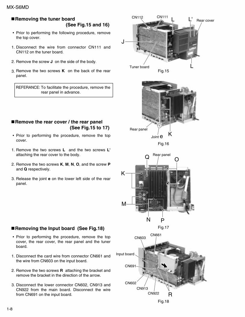
1-8
Prior to performing the following procedure, remove the top cover.
Disconnect the wire from connector CN111 and CN112 on the tuner board.
Remove the screw J on the side of the body.
Remove the two screws K on the back of the rear panel.
1.
2.
3.
Removing the tuner board (See Fig.15 and 16)
Prior to performing the procedure, remove the top cover.
Remove the two screws L and the two screws L' attaching the rear cover to the body.
Remove the two screws K, M, N, O, and the screw P and Q respectively.
Release the joint e on the lower left side of the rear panel.
1.
2.
3.
Remove the rear cover / the rear panel (See Fig.15 to 17)
Prior to performing the procedure, remove the top cover, the rear cover, the rear panel and the tuner board.
Disconnect the card wire from connector CN661 and the wire from CN603 on the input board.
Remove the two screws R attaching the bracket and remove the bracket in the direction of the arrow.
Disconnect the lower connector CN602, CN913 and CN922 from the main board. Disconnect the wire from CN691 on the input board.
1.
2.
3.
Removing the Input board (See Fig.18)
To facilitate the procedure, remove the rear panel in advance.
REFERANCE:
CN111Rear cover
CN661CN603
Input board
CN691
CN602
CN913CN922
Joint e
Tuner board
J
K
L
L
OQ
K
M
N
R
P
Fig.15
Fig.16
CN112
Rear panel
Rear panel
Fig.17
Fig.18
L'

MX-S6MD
1-9
Prior to performing the procedure, remove the top cover, the CD changer mechanism assembly, the rear cover, the rear panel, the tuner board and the input board.
Remove the four screws S attaching the bracket.
Disconnect connector CN924 and CN394 from the main board.
1.
2.
Removing the heat sink assembly (See Fig.19 and 20)
Prior to performing the procedure, remove the top cover, the CD changer mechanism assembly, the rear cover, the rear panel, the tuner board, the input board and the heat sink assembly.
Remove the two screws T or U attaching the regulator board and the amplifier board to the heat sink.
1.
Removing the regulator board / the amplifier board (See Fig.21)
Heat sink assembly
Heat sink assembly
Heat sink
Bracket
CN924
Main board
Amplifier boardRegulator board
CN394
S
UT
S
Fig.19
Fig.20
Fig.21

MX-S6MD
1-10
Prior to performing the procedure, remove the top cover, the CD changer mechanism assembly, the rear cover, the rear panel, the tuner board, the input board and the heat sink assembly.
Disconnect the wire from connector CN911 on the main board and CN991 on the power transformer assembly.
Disconnect the card wire from connector CN511 on the main board.
Remove the four screws V attaching the main board.
If necessary, unsolder the wire on the headphone board.
1.
2.
3.
4.
Removing the Main board (See Fig.22)
Prior to performing the procedure, remove the top cover, the CD changer mechanism assembly, the front panel assembly, the rear cover, the rear panel, the tuner board and the input board.
Remove the screw X attaching the headphone board.
If necessary, unsolder the wire on the headphone board.
1.
Removing the headphone board (See Fig.25)
Prior to performing the following procedure, remove the top cover, the rear cover, the voltage selector.
Remove the four screws W attaching the power transformer assembly.
Pull out the power cord stopper from the body upward. Turn the power transformer assembly while lifting it as shown in the figure.
Disconnect the wire from connector CN911 on the main board and CN991 on the power transformer board. Remove the power transformer assembly from the body.
1.
2.
3.
Removing the power transformer assembly (See Fig.23 and 24)
Main boardCN911
CN991
CN511
Soldering
Power cord stopper
Power transformer assembly
Power transformer assemblyMain board
Headphone board Soldering
V
W W
X
V
CN911
CN991
Fig.22
Fig.23
Fig.24
Fig.25

MX-S6MD
1-11
Prior to performing the following procedure, remove the top cover and the rear cover.
Remove the plastic rivet retaining the voltage selector.
Disengage the joint f to release the voltage selector from the transformer bracket. If necessary, unsolder each wire.
1.
2.
Removing the voltage selector (See Fig.26)
Fig.26
Joint f
Voltage selector
Plastic rivet

MX-S6MD
1-12
Turn over the body and disconnect the card wire from connector CN408 and the flexible wire from CN407 on the main board.
Remove the two screws A attaching the main board. Slide the main board in the direction of the arrow to release the two joints a with the single flame.
Solder part b on the pickup in the body. Disconnect the flexible harness from connector CN321 and CN451 on the underside of the main board. Then remove the main board.
1.
2.
3.
Removing the main board(See Fig.1 and 2)
Remove the four screws B on both sides of the body.
Move the mechanism cover toward the front to disengage the front hook of the mechanism cover from the internal loading assembly (Joint c). Then remove the mechanism cover upward.
1.
2.
Removing the mechanism cover(See Fig.3)
<MD section>
Fig.1
Fig.2
Fig.3
AA
Main board
(Bottom)
CN408
CN321
CN451
Pickup
Joint c
Fook
Joint c
Mechanism cover
Solder part b
CN407
Joint b Joint b
Main board
B
B

MX-S6MD
1-13
Move the head lifter on top of the body in the direction of the arrow and turn around.
Detach the spring from the hook of the body. Remove the head lifter with the spring.
If necessary, remove the spring from the head lifter.
1.
2.
3.
Removing the head lifter (See Fig.4 to 6)
Remove the screw C on the upper side of the body. Remove the head assembly while pulling the flexible harness from the body.
1.
Removing the head assembly (See Fig.7)
Fig.4
Fig.5
Fig.6
Fig.7
C
Head lifter
Spring
Spring
Head lifter
Head assembly
Head lifter

MX-S6MD
1-14
Prior to performing the following procedure, remove the main board, the mechanism cover, the head lifter and the head assembly.
Remove the three screws D on the upper side of the body.
Move the loading assembly forward to disengage it from the traverse mechanism assembly (Joint d). Then remove it upward.
Remove the traverse mechanism assembly from the single flame.
1.
2.
3.
Removing the Loading assembly(See Fig.8 and 9)
The loading assembly, the traverse mechanism assembly and the single flame will be removable after removing the loading assembly from the body.
Ref:
Fig.8
Fig.9
D
Loading assembly
Joint d
D
D
Loading assembly
Traverse mechanism assembly
Single flame

MX-S6MD
1-15
Remove the two screws E on the upper side of the loading assembly.
Remove the slide base (L) outward. (Release it from the joint bosses E.)
Remove the slide base (R) outward.
1.
2.
3.
Removing the slide base (L) / (R)(See Fig.10)
Detach the loading mechanism assembly upward to release the four pins on both sides from the loading motor, paying attention to the part e of the loading mechanism base.
1.
Removing the loading mechanism assembly (See Fig.11)
Disconnect the harnesses from the wire holder and from connector CN612 on the cam switch board.
Remove the screw F attaching the loading motor and release the joint f.
Remove the belt from the loading motor assembly.
Remove the two screws G attaching the loading motor.
1.
2.
3.
4.
Removing the loading motor (See Fig.12 and 13)
Loading mechanism assembly
Remove the slit washer attaching the cam gear and pull out the cam gear.
Disconnect the harness from the wire holder and from connector CN612 on the cam switch board.
Remove the two screws H and the clamp. Remove the cam switch board.
1.
2.
3.
Removing the cam gear and the cam switch board (See Fig.12)
<Loading assembly>
Fig.10
Fig.11
Fig.12
Fig.13
E'
E'
E
E
Loading motor assembly
Loading mechanism assembly
Loading mechanism base
Slide base (R)
Slide base (L)
F
H
H
Joint f
Part e
CN612
Slit washer
Cam gear
Loading motor
Cam switch board
Wire holder
Belt
G

MX-S6MD
1-16
Remove the two screws I on the upper side of the loading assembly.
1.
Removing the cartridge holder assembly (See Fig.14 and 15)
Prior to performing the following procedure, remove the cartridge holder assembly.
Remove the slide bar upward.
Move the eject bar outward until it stops as shown in Fig.14. Push the convex part g on the bottom of the body and remove the eject bar from the chassis.
1.
2.
Removing the slide bar and the eject bar (See Fig.14 and 15) Fig.14
Fig.15
I
I
I
Slide bar
Slide bar
Eject bar
Part g
Cartridge holder assembly
Cartridge holder assembly
Eject bar
Eject bar
k
UD base

MX-S6MD
1-17
Disengage the four insulators from the notches of the traverse mechanism chassis.
1.
Removing the Insulators (See Fig.16)
Turn over the traverse mechanism assembly and remove the screw J attaching the shaft holder (F).
Move the shaft inward and remove it from the shaft holder (R).
Detach the shaft side of the pickup unit upward and release the joint h with the pickup guide. Then remove the pickup unit with the shaft.
1.
2.
3.
Removing the pickup unit (See Fig.17)
Draw out the shaft from the pickup.
Remove the two screws K attaching the rack spring.
1.
2.
Removing the pickup (See Fig.18)
<Traverse mechanism assembly>
Fig.16
Fig.17
Fig.18
K
J
Insulators
Insulators
Joint h Pickup guide
Pickup unit
Shaft holder (F)
Shaft holder (R)
Pickup unit
Traverse machanism chassis
Shaft
Pickup
Rack spring
MX-S6MD
1-18
It is not necessary to remove the pickup unit.
For the white and black harnesses extending from the feed motor assembly, unsolder the soldering i on the traverse mechanism board.
Remove the two screws L attaching the feed motor assembly.
Remove the two screws N attaching the feed motor bracket.
1.
2.
3.
Removing the feed motor assembly (See Fig.19-1, 19-2)
Prior to performing procedure, remove the feed motor assembly.
For the red and black harnesses extending from the spindle motor, unsolder the soldering j on the traverse mechanism board.
Remove the screw M attaching the traverse mechanism board.
1.
2.
Removing the traverse mechanism board (See Fig.19-1)
Fig.19-1
Fig.19-2
M
L
N
Feed motor assembly
Feed motor
Feed motor bracket
Traberse mechanism board Soldering j
Soldering i
MX-S6MD
1-19
Reattach the eject bar to the UD base. (Fig.15 and 20)
Reattach the slide bar to the loading mechanism chassis while fitting the boss marked k to the eject bar slot. (Fig.20)
Slide the slide bar and the eject bar in the direction of the arrow in Fig.20 and reattach the cartridge holder assembly using the two screws I.
(Fig.20 and 21)
1.
2.
3.
<Reattaching the loading assembly>
Make sure the pin of the eject lever marked l is fitted to the slot of the eject bar marked m at the bottom of the loading mechanism chassis after moving the eject lever and the loading slider of the cartridge holder assembly in the direction of the arrow.
(Refer to Fig.21)
ATTENTION:
Fig.20
Fig.21
I
I
H
H
UD base
UD base (Bottom)
Ditch m
Cam switch boardPoint marked
Ditch
Cam switch boss
Slide bar
Eject bar
Eject lever
l
Loading slider
Cartridge holder assembly

MX-S6MD
1-20
Reattach the wire holder to the UD base while engaging the UD base hook marked u to the wire holder slot marked t (At the same time, the boss on the reverse side of the wire holder is fitted to the UD base round hole).
Reattach the cam switch board using the two screws H. (Fig.22)
Turn the cam switch to bring the boss to the point marked on the cam switch board. Reattach the cam gear using a slit washer while fitting the cam gear slot to the cam switch boss. (Fig.22)
4.
5.
6.
Reattach the loading motor assembly, using the screw F. Connect the harness extending from the loading motor to connector CN612 on the switch board and fix it with the wire holder. (Fig.22)
7.
When reattaching the cam gear, the cam switch boss should be fitted to the cam gear slot, and the triangle mark of the cam gear should be aligned to the hole of the eject bar as shown in Fig.22.
ATTENTION:
Fig.22
F
Cam switch
Boss
Point marked
Cam switch board
Cam gear
Slide bar CN612
Loading motor assembly
Eject lever
Eject lever
Cam gear(Triangle mark)
n

MX-S6MD
1-21
Reattach the UD base while engaging the four pins on both sides of the UD base to the notches of the loading mechanism base and placing the edge (marked e’) of the cartridge holder assembly under the hook e of the loading mechanism base. (Fig.23)
Reattach the slide base (R) while fitting the two pins on another side of the UD base to the slots of the slide base (R). (Fig.24)
8.
9.
Reattach the slide base (L) on the slide base (R) while fitting the two pins on another side of the UD base to the slots of the slide base (L) (Fig.25). Make sure the two slots of the slide base (L) are fitted to the two bosses marked E’ and tighten the two screws E. (Fig.26)
10.
Fit the part v of the slide base (R) to the part w on the inward side of the cam gear rib. (Fig.25)
ATTENTION:
To expedite the work, bring up the UD base slightly when fitting each pin to the appropriate notch.
Ref:
Fig.23
Fig.24
Fig.25Fig.26
E
Loading mechanism base
Slide base (R)
Slide base (L)
Pin
Pin
Pin
Pin
Part w
Part v
Hook e'
Hook e'Hook e
E
E'
E'
Part wPart v
Slide base (L)Slide base (R)Slide base (R)
Cam gear
MX-S6MD
1-22
Insert a screwdriver into the sub chassis slot on the back of the body and push the slider (R) toward the front.
From the top of the body, slide the hook and the slider (R) forward until they stop.
From the right side of the body, slide the slide cam (L) backward until it stops. The sub chassis unit will move to the lowest position.
From the bottom of the body, unsolder each soldered part a and b of the motors on the servo control board.
Remove the five screws A attaching the servo control board.
Disconnect connector CN610 on the servo control board from the tray select switch board to suspend the servo control board tentatively. Solder the part c of the flexible wire connected to connector CN601 on the underside of the servo control board.
Disconnect the flexible wire from connector CN601 and remove the servo control board from the body.
1.
2.
3.
4.
5.
6.
7.
Removing the servo control board (See Fig.1 to 4)
In case of disconnecting the flexible wire without soldering, the CD pick up may be damaged.
ATTENTION:
When reassembling, make sure the cam switch boss of the servo control board is fitted to the slot p of the control cam on the bottom of the body (Refer to Fig.3-1).
ATTENTION:
Make sure the sub chassis unit is locating at the lowest position. If not,perform the following procedure from 1 to 3.
ATTENTION:
Fig.1
Fig.2
Fig.3-1
Fig.4Fig.3-2
Slot
Slide cam (L)
Slider (R)
Sub chassis unit
Slide cam (L)Hook
ATray select switch board
Solder part a
A
CN610
Solder part b
A
CN601
A
Servocontrol board
A
Cam switch
Cam switch boss
Main boardSlot p
Control cam
Servo control board
CN601
Solder part c
Gear base unit
<CD mechanism section>

MX-S6MD
1-23
The tray unit can be removed despite the position of the sub chassis unit, but the lowest position is recommended to expedite the work.
Remove the four screws B attaching the top cover on the top of the body.
Remove the top cover with the two rods attached to the top cover and the clamper base unit.
Pull the lock lever of the return spring on the right side of the body to eject the tray unit.
From the top of the body, release the tray from the joint hook marked d (Push the tray toward the front).
Release the stoppers on both sides in the direction of the arrow and pull out the tray unit from the body.
1.
2.
3.
4.
5.
Removing the tray unit (See Fig.5 to 8)
Pull out the tray unit from the top tray 3 in sequence.
ATTENTION:
Fig.5
Fig.6
Fig.7Fig.8
B
Top cover
B
Rod
Clamper base unit
Top cover
Rod
Clamper base unit
Tray 3
Return spring
Lock lever
Tray unit
Tray
Tray Tray
Tray
Joint d
Tray unit
Both
Hook Hook
Both
MX-S6MD
1-24
Prior to performing the following procedures, remove the servo control board, the top cover and the tray unit.
Remove the two screws C attaching the side unit (L).
Slide and remove the side unit (L) toward the front while releasing the two joints e and the joint f with the chassis unit.
Slide the slide cam (L) toward the front until it stops to place the sub chassis unit at the top position.
1.
2.
3.
Removing the side unit (L) and (R) (See Fig.9-1 to 9-5)
The side unit (R) can be removed when the sub chassis unit is located at the top position.
ATTENTION:
Turn the hook gear counterclockwise to move the slide hook and the slider (R) backward until they stop.
Remove the three screws D attaching the side unit (R). Raise the side unit (R) upward and release the joint g with the chassis unit and the boss from the select arm marked h. Then remove the side unit (R) from the body.
4.
5.
When reassembling, make sure the boss is fitted to the select arm marked h.
ATTENTION:
Fig.9-1
Fig.9-2
Fig.9-3
Fig.9-5Fig.9-4
D
D
Side unit (R)
Joints e
Side unit (L)
Joint fCHook gear
slide hook
D
Select arm
Slider (R)
CJoint h
Side unit (L)
Joints e
Side unit (L)
Joint fD
Side unit (R)
Joint g
Joint g
Select arm
Boss
D
Side unit (R)
Slide cam(L)
Joint h

MX-S6MD
1-25
Prior to performing the following procedures, remove the servo control board, the top cover, the tray unit, the side unit (L) and the side unit (R).
Turn the hook gear counterclockwise to move the slide hook and the slider (R) backward until they stop.
Slide the slide cam (L) and the slide cam (R) in the direction of the arrow until they stop.
(The notches of each slide cam are fitted to the pins on both sides of the sub chassis unit.)
Detach the sub chassis unit upward.
1.
2.
3.
Removing the sub chassis unit(See Fig.10 to 12)
When reassembling, turn the hook gear of the chassis unit counterclockwise until it stops and slide the slide hook and the slider (R) of the sub chassis unit backward until they stop.
ATTENTION: Fig.10
Fig.11
Fig.12
Slide cam (L)
Slide cam (R)
Sub chassis unit
Sub chassis unit
Pin Pin
Slide cam (L)
Slider (R)
Hook gear
slide hook
Notch

MX-S6MD
1-26
Prior to performing the following procedures, remove the servo control board, the top cover, the tray unit, the side unit (L) and the side unit (R).
Remove the screw E attaching the flap base unit. Release the joint tabs i and j, then remove the flap base unit from the body.
Remove the belts from the two pulleys on the gear base unit.
Remove the three screws F and remove the gear base unit from the body.
1.
2.
3.
Removing the flap base unit and the gear base unit (See Fig.13 and 14)
Prior to performing the following procedure, remove the main board.
Remove the belts from the two pulleys.
Remove the four screws G and detach each motor from the body.
1.
2.
Removing the motors (See Fig.15)
Fig.13
Fig.14
Fig.15
Flap base unitJoint tab j
Joint tab i
E
Gear base unit F
F
FBelt
Belt
Motor
Motor
G
G
MX-S6MD
1-27
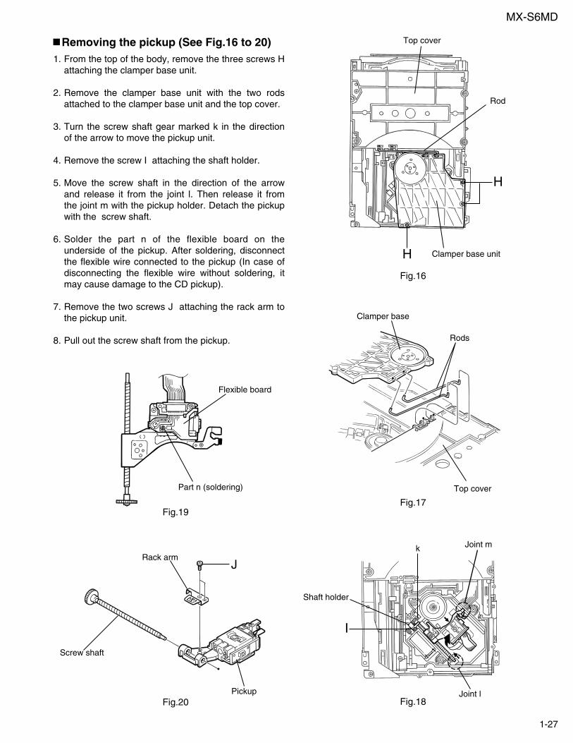
From the top of the body, remove the three screws H attaching the clamper base unit.
Remove the clamper base unit with the two rods attached to the clamper base unit and the top cover.
Turn the screw shaft gear marked k in the direction of the arrow to move the pickup unit.
Remove the screw I attaching the shaft holder.
Move the screw shaft in the direction of the arrow and release it from the joint l. Then release it from the joint m with the pickup holder. Detach the pickup with the screw shaft.
Solder the part n of the flexible board on the underside of the pickup. After soldering, disconnect the flexible wire connected to the pickup (In case of disconnecting the flexible wire without soldering, it may cause damage to the CD pickup).
Remove the two screws J attaching the rack arm to the pickup unit.
Pull out the screw shaft from the pickup.
1.
2.
3.
4.
5.
6.
7.
8.
Removing the pickup (See Fig.16 to 20)
Fig.16
Fig.17
Fig.18Fig.20
Fig.19
Top cover
Rod
H
H
Rods
Top cover
Clamper base
Joint l
Joint mk
Shaft holder
I
Flexible board
Part n (soldering)
JRack arm
Pickup
Screw shaft
Clamper base unit

MX-S6MD
1-28
Prior to performing the following procedure, remove the servo control board and the clamper base unit.
Remove the three screws K attaching the traverse mechanism assembly.
Detach the rear part of the traverse mechanism assembly upward to release the joint o with the sub chassis unit. Then remove the assembly from the body.
1.
2.
Removing the traverse mechanism assembly (See Fig.21)
Prior to performing the following procedure, remove the traverse mechanism assembly.
Remove the screw L attaching the feed motor.1.
Removing the feed motor (See Fig.22)
Fig.21
Fig.22
K
K
KTraverse mechanism assembly
Traverse mechanism assembly
Joint o
Feed motor
L
Fig.23
Tray select switch board
CN620M
Fig.5
Fig.6
B
Top cover
B
Rod
Clamper base unitTop cover
Rod
Clamper base unit
Remove the four screws B attaching the top cover on the top of the body.
Remove the top cover with the two rods attached to the top cover and the clamper base unit.
Remove the screw M on the right side of the body.
1.
2.
3.
Removing the tray select switch board (See Fig.5,6 and 23)

MX-S6MD
1-29
Insert a screwdriver under the ornament grille attached to the woofer.
Pull out the ornament grille with each boss by means of a lever as shown in Fig.2.
1.
2.
Remove the four screws A and the woofer from the body. Disconnect the wire from the speaker terminals.
3.
Removing the speaker (woofer)(See Fig.1,3 to 5)
As the ornament grille is damaged, replace it with the woofer.
ATTENTION:
Prior to performing the following procedure, remove the front grille.
When replacing the ornament grille, make sure the boss with adequate amount of bond.
ATTENTION:
<Speaker section>
Information This is a method of dis assembly. As parts of the repair of this speaker system, it is only the speaker box assemblies. It is not possible to supply with each part unit.
Fig.3
Ornament grille Tweeter
Woofer
Ornament grille
Boss
Boss
Push
DriverStick
Woofer
Ornament grilleBoss
Fig.1
Fig.2
Boss 4

MX-S6MD
1-30
Insert a screwdriver under the ornament grille and remove it from the body.
1.
Remove the three screws B and the tweeter from the body. Disconnect the wire from the speaker terminals.
3.
Removing the speaker (tweeter) (See Fig.4 and 5)
As the ornament grille is damaged, replace it with the tweeter.
ATTENTION:
Fig.4
Fig.5
Driver
Ornament grille
Tweeter
TweeterB
B
AA
Woofer

MX-S6MD
1-31
Adjustment method
MD TEST MODE 1
1.Setting the TEST MODE1
Press [STOP key] and [CANCEL key] together,
and connect the power cord.
LCD indicationMD TEST MODE 1
Setting the MD TEST MODE1by press [POWER key]
LCD indication [HELLO] then
[MD TEST MODE 1]
Setting OK
Adjustment complete
3.Laser power adjustment
Insert the sensorof laser power meter
Press [ 2 key ] ofRemote controller
LCD indicationL.POWER PLAY
LCD indicationL.POWER UP
LCD indicationL.POWER DOWN
Adjust the PLAYBACKlaser power
Adjust the RECORDINGlaser power
0.68mW Adjustment
2.Initialize the EEPROM
Setting the MD TEST MODE 1
Press [REC PAUSE key]of the Remote controller
LCD indicationDATA INITIAL
Initialize OK
Laser power up by [ key]of Remote controller
Laser power down by [ key]of Remote controller
Laser power up by [ key]of Remote controller
Laser power down by [ key]of Remote controller
Press [ 4 key] ofRemote controller
LCD indicationL.POWER REC
LCD indicationL.POWER UP
LCD indicationL.POWER DOWN
Press [STOP key] ofRemote controller
6.23mW Adjustment
Press [STOP key] ofRemote controller
Press [EJECT key]of main body
Playback laser poweradjustment complete
(CAUTION) MD mode should NO DISC condition, when POWER ON to not read TOC.
This model is auto adjust system.

MX-S6MD
1-32
4.Disc adjustment
InsertPre-master disc
Complete TOC read
Complete TOC read
LCD indicationON TUNING
LCD indicationON TUNING
Start auto adjustment
AdjustmentOK?
AdjustmentOK?
Start auto adjustment
LCD indicationOK_TUNING
LCD indicationOK_TUNING
LCD indicationNG_ERR _!
Eject thePre-master disc
Insert theRecordable disc
This adjustment should done after laser power adjustment.
Press [MD key] ofthe Remote controller
Press [MD key] ofthe Remote controller
<Refer the NG code list>
Complete the adjustment
Press [STOP key] ofthe Remote controller
Press [EJECT key]of the main body
<NG code list>
CODE000102030405060708090A0B0C0D0EFF
Adjustment NG sectionAuto adjustment not completeREST switch detectionFOCUS ONPIT section EF balance, tracking offset adjustmentPIT section ABCD level (IV impedance) adjustmentPIT section focus servo AGCPIT section tracking servo AGCPIT section focus bias adjustmentGRV section EF balance, tracking offset adjustmentGRV section ABCD level (IV impedance) adjustmentGRV section focus servo AGCGRV section tracking servo AGCGRV section focus bias adjustmentRoom temperatureEEPROM writingAuto adjustment complete (OK)
LCD indicationNG_ERR _!
<Refer the NG code list>
Please push the [STOP key] to remote control when theLCD display becomes [NG ERROR], and push the[MD key] to remote control again./
[CAUTION]

MX-S6MD
1-33
5.Independent operation modeIn case the checking mode or adjustmentwhen occur the error at disc adjustment,Independent mode into by select the keybefore release the TERST MODE.
Operation keyRemote controller [SLEEP]Remote controller [6 key]Remote controller [7 key]Remote controller [8 key]Remote controller [9 key]Remote controller [STOP]Main body [EJECT]
MODEFocus search [FOCUS_SEARCH]
Pit rough servo [P.R.SERVO]Groove rough servo [GR.R.SERVO]Tracking ON [TRACKING_ON]Tracking OFF [TRACKING_OFF]
STOP [STOP]EJECT [EJECT]
Release the TEST MODE
MD TEST MODE 2
TEST MODE 2
Read the TOC
Press [6 key] of theRemote controller
LCD indication[ _ ]
Insert the Pre-master disc
2.Indication the drift level of the pickup adjustment value
4.Release the MD TEST MODETEST MODE 2
Read the TOC
Press [8 key] ofthe Remote controller
LCD indication (change by each 10sec.)[_ _ _ _ _]
Insert the recordabledisc (basically 74min.)
LCD indication (change be each 10sec.)[______ Times_]
3.Indication the C1 ERROR
Adjustment value
IVRTAGCTBALLPOWFBIAFAGCTEOFSAGC
IVR (Pre-master, Recordable groove)TRK AGC ( )TRK BALANCE ( ) = 0Laser power (Play power=0 Rec power)Focus bias ( ) = 0Focus AGC ( )TE offset ( ) = 0Sled AGC ( )
TEST MODE
Press [POWER key]
POWER OFF
1.Setting the TEST MODE 2
Press [STOP key] and [CANCEL key] together,
and connect the power cord.
LCD indicationMD TEST MODE 1
Setting the MD TEST MODE1by press [POWER key]
LCD indication [HELLO] then
[MD TEST MODE 1]
Setting OK
Setting the MD TEST MODE2by press [STOP key] and[TITLE/EDIT key] together
(CAUTION) MD mode should NO DISC condition, when POWER ON to not read TOC.

MX-S6MD
1-34
CD TEST MODE
1.Setting the TEST MODE
LCD indicationCD TEST MODE
CD TEST MODE setting bypress [POWER key]
LCD indication[HELLO] then
CD TEST MODE
Complete setting
Press [STOP key] and[HIGH SPEED CD MD REC key]
of the main body together andconnect the power cord
Release the TEST MODE
3.Release the CD TEST MODE
TEST MODE
Read TOC
Press [1 key] of the Remote controller ( x1 speed)
Press [2 key] of the Remote controller ( x2 speed)
Playback each 10sec.C1 ERROR q'ty indicate by 2byte
2.Indication the C1 ERROR
LCD indication (change each 10sec.)[__________ __ ]
LCD indication (change each 10sec.)[________ Times__]
TEST MODE
Press [POWER key]
Power to OFF
CD section is no need the adjustment by design.

MX-S6MD
1-35
LCD ALL INDICATION, TIME COMPRESSION TEST MODE
POWER ON
Press [POWER key],[1 key] and[STOP key] together of the
Remote controller (1st time)
Press [POWER key],[1 key] and[STOP key] together of the
Remote controller (2nd time)
Press [POWER key],[1 key] and[STOP key] together of the
Remote controller (3rd time)
Press [POWER key],[1 key] and[STOP key] together of the
Remote controller (4th time)
LCD and LED are all ONFull color LED is WHITE
Inspection for staticelectricity broken check mode
for full color LED (RED)
1.Setting the TEST MODE
2.Fast forward of CLOCK/SLEEP TIMER
(press any key) Change to normal indication
It can check for red color chip part
Inspection for staticelectricity broken check mode
for full color LED (GREEN)
It can check for green color chip part
Inspection for staticelectricity broken check mode
for full color LED (BLUE)
It can check for blue color chip part
Caution:Full color LED is keep white condition, when loop out by any key at test mode.
Including the ALL LED ON mode and Static electricity broken thes, clock count up is change to1min. to 1sec.Check for only [CLOCK mode] and [SLEEP TIMER].
3.Release the TEST MODETEST MODE is release by disconnect the AC power cord.
MX-S6MD
1-36
RUNNING MODE
Indication the [CAUTION !] when abnormal
1.Setting the TEST MODE
2.Release the TEST MODE
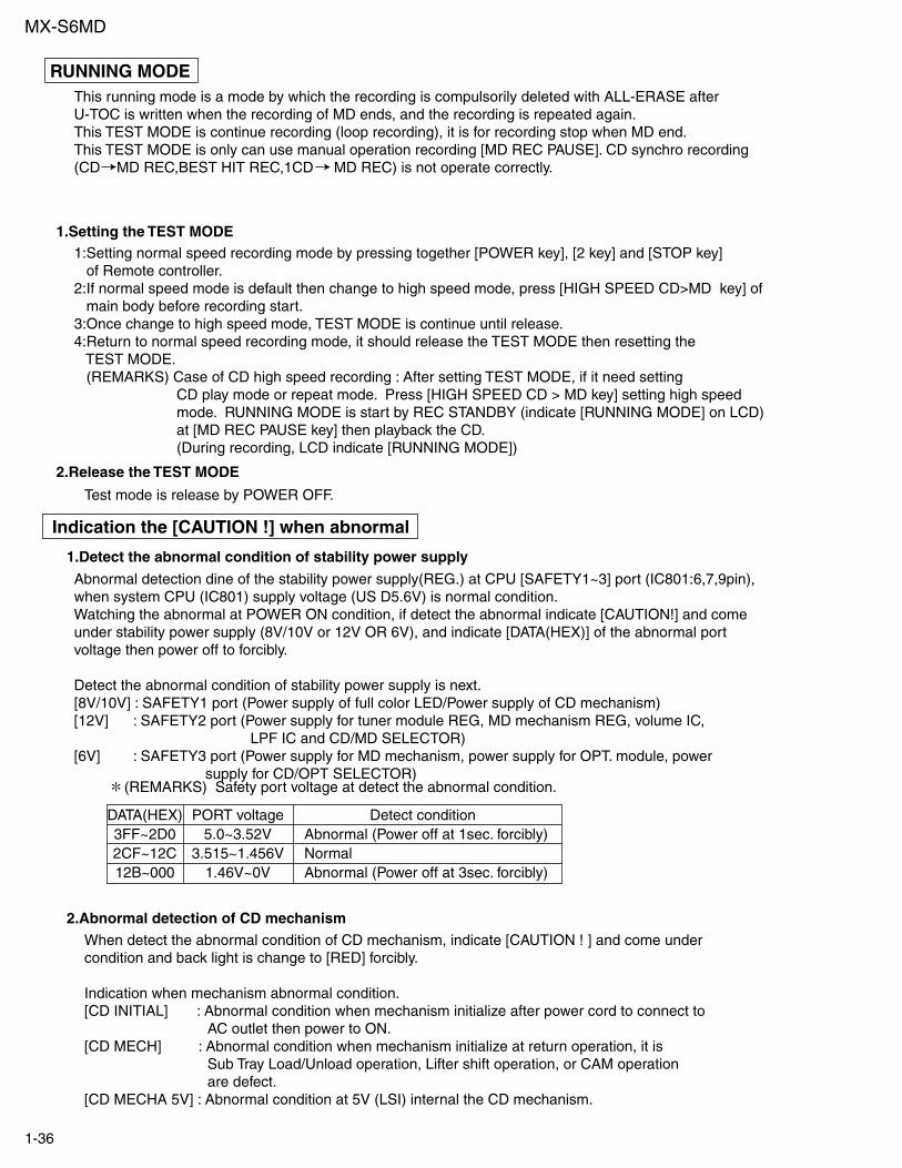
This running mode is a mode by which the recording is compulsorily deleted with ALL-ERASE afterU-TOC is written when the recording of MD ends, and the recording is repeated again. This TEST MODE is continue recording (loop recording), it is for recording stop when MD end.This TEST MODE is only can use manual operation recording [MD REC PAUSE]. CD synchro recording(CD MD REC,BEST HIT REC,1CD MD REC) is not operate correctly.
1:Setting normal speed recording mode by pressing together [POWER key], [2 key] and [STOP key] of Remote controller.2:If normal speed mode is default then change to high speed mode, press [HIGH SPEED CD>MD key] of main body before recording start.3:Once change to high speed mode, TEST MODE is continue until release.4:Return to normal speed recording mode, it should release the TEST MODE then resetting the TEST MODE. (REMARKS) Case of CD high speed recording : After setting TEST MODE, if it need setting CD play mode or repeat mode. Press [HIGH SPEED CD > MD key] setting high speed mode. RUNNING MODE is start by REC STANDBY (indicate [RUNNING MODE] on LCD) at [MD REC PAUSE key] then playback the CD. (During recording, LCD indicate [RUNNING MODE])
Abnormal detection dine of the stability power supply(REG.) at CPU [SAFETY1~3] port (IC801:6,7,9pin),when system CPU (IC801) supply voltage (US D5.6V) is normal condition.Watching the abnormal at POWER ON condition, if detect the abnormal indicate [CAUTION!] and comeunder stability power supply (8V/10V or 12V OR 6V), and indicate [DATA(HEX)] of the abnormal portvoltage then power off to forcibly.
Detect the abnormal condition of stability power supply is next.[8V/10V] : SAFETY1 port (Power supply of full color LED/Power supply of CD mechanism)[12V] : SAFETY2 port (Power supply for tuner module REG, MD mechanism REG, volume IC, LPF IC and CD/MD SELECTOR)[6V] : SAFETY3 port (Power supply for MD mechanism, power supply for OPT. module, power supply for CD/OPT SELECTOR)
Test mode is release by POWER OFF.
When detect the abnormal condition of CD mechanism, indicate [CAUTION ! ] and come undercondition and back light is change to [RED] forcibly.
Indication when mechanism abnormal condition.[CD INITIAL] : Abnormal condition when mechanism initialize after power cord to connect to AC outlet then power to ON.[CD MECH] : Abnormal condition when mechanism initialize at return operation, it is Sub Tray Load/Unload operation, Lifter shift operation, or CAM operation are defect.[CD MECHA 5V] : Abnormal condition at 5V (LSI) internal the CD mechanism.
1.Detect the abnormal condition of stability power supply
2.Abnormal detection of CD mechanism
(REMARKS) Safety port voltage at detect the abnormal condition.
DATA(HEX)3FF~2D02CF~12C12B~000
PORT voltage5.0~3.52V
3.515~1.456V1.46V~0V
Detect conditionAbnormal (Power off at 1sec. forcibly)NormalAbnormal (Power off at 3sec. forcibly)

MX-S6MD
1-37
Flow of functional operation until TOC read (MD section)
Power ON
MD play Key
Slider turns RESTswitch ON
Disc detection
Focus servo ON(Tracking servo ON)
Mechanism operation ONLaser ON
Automatic tuning ofFocus S-curve amplitude
Disc is rotated
Confirm that the Focus errorS-curve signal at the pin 34 ofIC310 is approx.2Vp-p.
TOC reading
Play a disc
Automatic tuning ofTracking error gain
Automatic tuning ofFocus error gain
Confirm that the eye-patternat the pin38 of IC310.
Check point
Confirm that the voltageat the pin 50 of IC500 are 4V.
Confirm that the voltageat the pin 9 of CN408 are0V.
It is confirmed that pin 2 of CN408become 0V from VREF as an accelerationpulse between about 400ms.

MX-S6MD
1-38
(1) Prior to changing the pickup, clean the pickup lens.
(2) For cleaning the lens, use the following cotton swab after mearsing it in alcohol. Product No : JCB-B4 Manufacturer : Nippon Cotton Swab
Is therecording power
(6.23mW) output withthe laser power under
test mode?
The drive currentof laser diode 120mA
or less?
ChangeNO
YES
Change
O.K.
NO
YES
The semi-solid state resistor on the APC boardattached to the pickup is used for adjusting the laserpower. Since these resistor should be adjusted inpair according to the characteristics of the opticalblock, be sure not touch on the resistors.Since the service life of the laser diode will beexhausted when the laser power is low, it isnecessary to change the pickup.Meanwhile, do not pickup.Otherwise, the pickup will be damaged due to overcurrent.
Replacement of laser pickup(MD)
Change the MD pickup by referring to"Removing the MD pickup" in the disassembly method.
Set the pickup to [TEST] mode accordingto the procedures described in theadjustment method.
Adjust the laser power.
Completion the disc.
Completion of changing the MD pickup.
Since this system is designed to perform magneticrecording, the laser power ten times or over of theconventional MD player will be output. Therefore, besure to perform not only adjustment and operationof this system so carefully as not to directly look atthe laser beam or touch on the body.
CAUTION
Maintenance of laser pickup(MD)
1. Cleaning of pickup lens
2. Confirmation of the service life of laser diode when the service life of the laser diode has been exhausted, the following symptoms will appear.
(1) Recording will become impossible.
(2) The RF output (EFM output and eye-pattern amplitude) will become lower.
(3) The drive current required for light emitting of laser diode will be increased.
Confirm the service life according to the following flow chart.
3. Method of measuring the drive current of laser diode
When the voltage measured at each side of R337,it become 120mV or over, the service life of laserdiode is judged to have been exhausted.
4.Semi-solid state resistors on the APC board.

MX-S6MD
1-39
REST switch to ONby slider
TE offset auto adjust
Laser ON
Disc detection
Auto measure FOS curve amplitude
FO offset auto adjust
Disc rotated
Focus servo ON(tracking servo ON)
Auto measureTE balance
Auto measureTE amplitude
FO balance auto adjust
Disc to bebraked to stop
TE servoON start
TE servo OFFstart
Disc statusto rotate
TOC readingfinishesAutomatic measurement
at TE amplitude andTE balance
500mv/div 2ms/div
Approx.3secIC60125pin(TE)
Approx 1.8V
VREF
Tracking error waveform at TOC reading
Power ON Disc play Key
Confirm that the Focus errorS-curve signal at the pin28 ofIC603 is approx.2Vp-p
Confirm that the signal formpin24 of IC603 is 0V as aaccelerated pulse duringapprox.400ms.
Confirm the waveform of thetracking error signal at thepin25 of IC601.(about 1.8Vpp)
FO gain auto adjust
TE gain auto adjust
TOC read
Play
Confirm the eye-patternat the lead of TP602.
Check Point
Check the voltage at the pin40of IC603 + side is +5V?
Check that the voltage atthe pin33 of IC701 or pin3of CN694 is 0V(a moment)?
Flow of functional operation until TOC read (CD section)

MX-S6MD
1-40
(1) Cleaning the pickup lens
Before you replace the pickup, please try to
clean the lens with a alcohol soaked cotton
swab.
(2) Life of the laser diode
When the life of the laser diode has expired,
the following symptoms will appear.
(1) The level of RF output (EFM output : amplitude
of eye-pattern) will below.
Change
O.K.
NO
YES
Replacement of laser pickup(CD)
Turn of the power switch and, disconnect thepower cord from the AC outlet.
Replace the pickup with a normal one.(Referto "Pickup Removal" on the previous page)
Plug the power cord in, and turn the power on.At this time, check that the laser emits forabout 3seconds and the objective lens movesup and down.CAUTION : Do not observe the laser beam directly.
Play disc
Check the eye-pattern at TP602.
Finish
Maintenance of laser pickup(CD)
Is RF output
1.25 0.22VP-P?
(3) Semi-fixed resistor on the APC boardThe semi-fixed resistor on the APC boardwhich is attached to the pickup is used toadjust the laser power.Since this adjustment should be performedto match the characteristics of the whole optical block, do not touch the semi-fixedresistor.If the laser power is lower than specifiedvalue, the laser diode is almost worm out,and the pickup should be replaced.If the semi-fixed resistor is adjust while thepickup is functioning normally, the laserpickup may be damaged due to excessivecurrent.

MX-S6MD
1-41
MCLKCMODE
LRCKSCLK
SDTOSDTI
AINLVCML
AINRVCMR
VRADARDV
VCOM
AOUTL
VA AGND VB VD DGND
AOUTR
PWAD PWDA
ClockDivider
Serial I/OInterface
DecimationFilter
DecimationFilter
8xInterpolator
8xInterpolatorModulator
Modulator
Modulator
Modulator
Common Voltage
LPF
LPF
AK4519VF-X (IC480) : A / D D / A converter1.Pin layout
2.Block diagram
3.Pin Function
1
2
3
4
5
6
7
8
9
10
11
12
24
23
22
21
20
19
18
17
16
15
14
13
123456789
101112131415161718192021222324
IIIOOIIIIIIO--IIIIOOO---
VRDAVRADAINRVCMRVCMLAINLPWADPWDAMCLKLRCKSCLKSDTODGNDVDSDTICMODEDEM1DEM0AOUTLAOUTRVCOMAGNDVBVA
Voltage Reference Input Pin for DAC, VAVoltage Reference Input Pin for ADC, VARCH Analog Input PinRch Common Voltage Output Pin, 0.45xVALch Common Voltage Output Pin, 0.45xVALch Analog Input PinADC Power-Down Mode Pin "L":Power DownDAC Power-Down Mode Pin "L":Power DownMaster Clock Input PinInput/Output Channel Clock PinAudio Serial Data Clock PinAudio Serial Data Output PinDigital Ground PinDigital Power Supply PinAudio Serial Data Input PinMaster Clock Select PinDe-emphasis Frequency Select PinDe-emphasis Frequensy Select PinLch Analog Output PinRch Analog Output PinCommon Voltage Output Pin, 0.45xVAAnalog Ground PinSubstrate PinAnalog Power Supply Pin
PinNO. Symbol I/O Function
Description of major ICs

MX-S6MD
1-42
DET
BDO
OFTR
GCTRL
DET
AGCEQ
171098653
36
35
34
33
32
31
21 23 25 2724 26
30
28
11 12
Substraction
Substraction
FBAL
TBAL
29
16
15
14
13
AN8849SB-W (IC601) : Head amp
1.Pin layout
2.Block diagram

MX-S6MD
1-43
3.Pin Function
123456789101112131415161718192021222324252627282930313233343536
Photo detector signal input.Laser diode drive terminal.RF amp negative input terminal.Power supply terminal.Equaruzer connect terminal.Power supply terminal.RF AGC input terminal.RF AGC filter connect terminal.ARF output terminal.3T envelope detect filter terminal.Envelope detect output circuit.Low level DO detect connect terminal.DO detect signal output terminal.OFF TRACK detect signal connect terminal.OFF TRACK detect signal output terminal.RF signal amp. detection output.Ground.LD APC ON / OFF select.Reference voltage output terminal.CROSS detect signal output terminal.Reference voltage output terminal.CROSS detect filter connect terminal.Tracking error output terminal.TE amp.negative input terminal.FE amp.negative input terminal.Focus error output terminal.Focus gain, tracking gain adjust control signal inout terminal.Focus barance adjust control input terminal.Tracking barance adjust control input terminal.Connect PDIC.Connect PDIC.Connect PDIC.Connect PDIC.Connect PDIC.Connect PDIC.Connect PDIC.
PDLD
RFNVcc1
RFOUTEQSWVcc2RFC
CAGCARFCEAENV
CBDOBDO
COFTROFTR
NRFDETGNDLDONVREF1CROSSVREF2CCRSTEN
TEOUTFEN
FEOUTGCTRLFBALTBAL
EFDBCA
PinNO. Symbol Function
1
2
3
4
5
6
7
14
13
12
11
10
9
8
IN/OUT1
OUT/IN1
OUT/IN2
IN/OUT2
CONT2
CONT3
VSS
VDD
CONT1
CONT4
IN/OUT4
OUT/IN4
OUT/IN3
IN/OUT3
O/II / O
CONT
TC4066BP / N / (IC673) : Switch
1.Pin layout & block diagram 2.The truth circuit

MX-S6MD
1-44
37
38
PEAK
RF
39RFAGC
40AGCI
41COMPO
42COMPP
43ADDC
44OPO
45OPN
46RFO
47MORFI
48
1 2
MORFO
24
23
Vcc
3TADJ
22 EQADJ
21 VREF
20 F0CNT
19 XSTBY
18 XLAT
17 SCLK
16 SWDT
15 TEMP R
14 TEMP I
13 GND
I J
3
VC
4
A
5
B
6
C
7
D
8
E
9
F
10
PD
11
AP
C
12
AP
CR
EF
36 35
BO
TM
AB
CD
34
FE
33
AU
X
32
AD
FG
31
AD
AG
C
30
AD
IN
29
AD
FM
28
SE
27
CS
LE
D
26
TE
25
WB
LA
DJ
Peak,
Bottom
Dete
ctor
AG
C, E
QU
SE
RC
om
pU
SE
RO
P A
mp
RF
Am
p 3T
Dete
ctor
AB
CD
Am
p
I-V Amp APC
TEMP Amp
MUX FE Amp
ADIP Amp TE/SE Amp
CPUCommand I/F
CXA2523AR (IC310) : MD servo1.Block diagram
2.Pin function
1234567891011121314151617181920
I-V converted RF signal I input.I-V converted RF signal J input.Vcc/2 voltage output.A current input for main beam servo signal.B current input for main beam servo signal.C current input for main beam servo signal.D current input for main beam servo signal.E current input for side beam servo signal.F current input for side beam servo signal.Reflection light quantity monitor signal input.Laser APC output.Reference voltage input for the laser power intensity setting.Connect to GND.Connects the temperature sensor.Connects the temperature sensor. outputs the reference voltage.Data input for microcomputer serial interface.Shift clock input for microcomputer serial interface.Latch signal input for microcomputer serial interface.Latched when low.Standby setting pin. Normal operation when high Standby when low.Internal current source setting pin.
IJ
VCABCDEF
PDAPC
APCREFGND
TEMPITEMP RSWDTSCLKXLAT
XSTBYF0CNT
IIOIIIIIIIOI-IIIIIII
Pin No. Symbol I/O Function

MX-S6MD
1-45
21222324252627282930313233343536373839404142434445464748
Reference voltage output.Equalizer center frequency setting pin.BPF3T center frequency setting pin.Power supply.BPF22 center frequency setting pin.Tracking error signal output.Connects the sled error signal LPF capacitor.Sled error signal output.ADIP FM signal output.ADIP signal comparator input.Connects the ADIPAGC capacitor.ADIP2 binary value signal output.13 output / temperature signal output. Switched with serial commands.Focus error signal output.Reflection light quantity signal output for the main beam servo detector.RF/ABCD bottom hold signal output.Peak hold signal output for the RF/ABCD signals.RF equalizer output.Connects the RFAGC capacitor.RFAGC input.User comparator output.User comparator non-inverted input.Connects the capacitor for ADIP amplifier feedback circuit.User operational amplifier output.User operational amplifier inverted input.RF amplifier output. Eye pattern checkpoint.Input of the groove RF signal with AC coupling.Groove RF signal output.
VREFEQADJ3TADJ
VccWBLADJ
TECSLED
SEADFMADIN
ADAGCADFGAUXFE
ABCDBOTMPEAK
RFRFAGCAGCI
COMPOCOMPPADDCOPOOPNRFO
MORFIMORFO
OI/OI/O-
I/OO-OOI-OOOOOOO-IOI
I/OOIOIO
Pin No. Symbol I/O Function
1 2 3 4 5 6 7 8 9 10
GND OUT1 P1 VZ IN1 IN2 VCC1 VCC2 P2 OUT2
Input OutputMode
IN1 IN2 OUT1 OUT2
Brake0 0 0 0
1 0 1 0
0 1 0 1
1 1 0 0
CLOCKWISE
COUNTER-CLOCKWISE
Brake
LB1641 (IC851,IC852) : DC motor driver
1. Pin layout
2. Pin function

MX-S6MD
1-46
PWM
GENERATOR
MONITORCONTROL
CPU I/FAUTOSEQUENCER
A/DCONVERTER
AN
ALO
G M
UX
SPINDLESERVO
ADIP DECODER
COMP
EFM / ACIRCENCODER / DECODER
PLL
PCO
FILI
FILO
CLTV
59
60
61
62
EFM
RFI
ASYI
BIAS
100
57
54
56
ASYO
ADFG
53
78
FGIN
SPFD
SPRD
F0CNT
95
94
93
79
APC
FE
TE
SE
PEAK
BOTM
ABCD
AUX1
DCHG
VC
ADIO
ADRT
ADRB
DTRF
CKRF
XLRF
77
66
75
74
63
64
65
67
76
68
69
71
72
82
81
80
CLOCK
GENERATOR
each block
each block each block
16 17 18 29 27 28 90 52
OS
CI
OS
CO
XT
SL
FS
256
LRC
K
XB
CK
FS
4
MD
DT
1
SHOCK RESISTANTMEMORY CONTROLLER
ATRAC/ATRAC3ENCODER/DECODER
DIGITALAUDIOI/F
SAMPLING RATECONVERTER
SUBCODEPROCESSOR
4
4
4
12
2
46
44
47
43
XRAS
XCAS
XWE
XOE
A00~A11
D0~D3
14
15
XINT
TX
26
25
24
23
22
21
DADT
ADDT
XBCKI
LRCKI
DATAI
DIN~DIN1
DOUT
12
11
DQSY
SQSY
84
88
89
86
85
92
91
83
LDDR
FFDR
FRDR
TFDR
TRDR
SFDR
SRDR
APCREF
10 7 5 6 8 9 1 2 3 4 13
SERVO DSP
MN
T0
MN
T1
MN
T2
MN
T3
RE
CP
XR
ST
XLA
T
SW
DT
SC
LK
SR
DT
SE
NS
CXD2662R (IC350) : DSP 1.Pin layout
2.Block diagram
1 ~ 25
75 ~ 51
50
26
76
100
~ ~

MX-S6MD
1-47
123456789
101112
13
1415161718
19202122232425262728293031323334353637383940414243
Monitor output.Monitor output.Monitor output.Monitor output.Data input for microcomputer serial interface.Shift clook input for microcomputer serial interface.Latch input for microcomputer serial interface.Latched at the falling edge.Data output for microcomputer serial interface.Outputs the internal status corresponding to the microcomputer serial interface address.Reset input. Low : resetDisc subcode Q sync / ADIP sync output.Subcode Q sync output in U-bit CD or MD format when the Digital In source is CD or MD.Laser power switching input.High : recording power ; low ; playback powerInterruption request output. Low when the interruption status occurs.Enable signal input for recoding data output. High : enabledCrystal oscillation circuit input.Crystal oscillation circuit output. (inverted output ofthe OSCI pin)OSCI input frequency switching.XTSL1(command) = low and XTSL = high : 512Fs (22.5792MHz)XTSL1(command) = low and XTSL = low : 1024Fs (45.1584MHz)XTSL1(command) = high : 2048Fs (90.3168MHz)Digital audio interface signal input 1.Digital audio interface signal input 2.Digital audio interface signal output.Test pin. Connect to GND.Test pin. Connect to GND.Test pin. Connect to GND.Data input from A / D converter.REC monitor output / decoded audio data output.LA clock (44.1kHz) output to the external audio block.Bit clock (2.8224kHz) output to the external audio block.256Fs output.Digital power supply.External DRAM address output.External DRAM address output.External DRAM address output.External DRAM address output.External DRAM address output.External DRAM address output.External DRAM address output.External DRAM address output.External DRAM address output.External DRAM address output.External DRAM address output.Digital ground.External DRAM output enable.
MNT0MNT1MNT2MNT3SWDTSCLKXLATSRDTSENS
XRSTSQSYDQSY
RECP
XINTTX
OSCIOSCOXTSL
DIN0DIN1DOUTDATAILRCKIXBCKIADDTDADTLRCKXBCKFS256DVDDA03A02A01A00A10A04A05A06A07A08A11
DVSSXOE
I/OOOOIIIOO
IOO
I
OIIOI
IIOIIIIOOOO-OOOOOOOOOOO-O
Pin No. Symbol I/O Function
3.Pin function

MX-S6MD
1-48
44454647484950515253545556575859
606162
63646566676869707172737475767778798081828384858687888990
External DRAM CAS output.External DRAM address output.External DRAM RAS output.External DRAM write enable.External DRAM data bus.External DRAM data bus.External DRAM data bus.External DRAM data bus.MD-DATA mode 1 switching input. (Low : normal mode ; high : MD-DATA mode 1)Playback EFM full-swing input. (Low : vss ; jigh : Vdd)Playback EFM comparator slice voltage input.Analog power supply.Playback EFM comparator bias current input.Playback EFM RE signal input.Analog ground.Phase comparison output for master PLL of playback digital PLL and recording EFM PLL.Filter input for master PLL of playback digital PLL and recording EFM PLL.Filter output for master PLL of playback digital PLL and recording EFM PLL.Internal VCO control voltage input for master PLL of playback digital EFM PLL and recording EFM PLL.Peak hold signal input for quantity of light.Bottom hold signal input for quantity of light.Signal input for quantity of light.Focus error signal input.Auxillary input 1.Center voltage input.Monitor output for A / D converter input signal.Analog power supply.Voltage input for the upper limit of the A / D converter operating range.Voltage input for the lower limit of the A / D converter operating range.Analog ground.Sled error signal input.Tracking error signal input.Connect to he low-inpedance power supply.Error signal input for laser digital APC.ADIP binary FM signal (22.05 1kHz) input.CXA2523 current source setting output.CXA2523 control latch output. Latched at the falling edge.CXA2523 control shift clook output.CXA2523 control data output.Referevce PWM output for laser APC.PWM output for laser digital APC.Tracking servo drive PWM output. ( )Tracking servo drive PWM output. (+)Digital power supply.Focus servo drive PWM output. (+)Focus servo drive PWM output. ( )4Fs output. (176.4kHz)
XCASA09
XRASXWED1D0D2D3
MDDTIASYOASYIAVDDBIASRFI
AVSSPCO
FILIFILOCLTV
PEAKBOTMABCD
FEAUXIVC
ADIOAVDDADRTADRBAVSS
SETE
DCHGAPC
ADFGF0CNTXLRFCKRFDTRF
APCREFLDDRTRDRTFDRDVDDFFDRFRDRFS4
OOOOI/OI/OI/OI/OIOI-II-O
IOI
IIIIIII-II-IIIIIOOOOOOOO-OOO
Pin No. Symbol I/O Function

MX-S6MD
1-49
919293949596979899
100
Sled servo drive PWM output. ( )Sled servo drive PWM output. (+)Spindle servo drive output. (PWM ( ) or polarty)Spindle servo drive output. (PWM (+) or PWM absolute value)Spindle CAV servo FG input.Test pin. Connect to GND.Test pin. Connect to GND.Test pin. Connect to GND.Digital ground.Low when playback ; EFM (encoded data) output when recording.
SRDRSFDRSPRDSPFDFGIN
TEST1TEST2TEST3DVSSEFMO
OOOOIIII-O
Pin No. Symbol I/O Function
1
2
3
4
5
6
7
8
9
10
Vreg IN
Reg GN
NC
VG
SVCC
PDGND
EFM
MUTE
NC
NC
Regulator input and regulator
power supply
Regulator GND
Non connect
Voltage input for power MOS drive
EFM high level output voltage
Pre-driver GND
EFM signal input
Mute control (Low active)
Non conncet
Non connect
11
12
13
14
15
16
17
18
19
20
NC
VOD2
VSS
VOD1
VOS1
VDD
VOS2
Reg DRV
Reg OUT
Reg NF
Non connect
Sync.output (Lower power MOS,drain)
"H"bridge GND (Lower power MOS,source)
Sync.output (Lower power MOS,drain)
Source output (Upper power MOS,source)
"H" bridge power supply terminal
(Upper power MOS,source)
Source output (Upper power MOS,source)
External PNP drive output for regulator
Reglator output (Emitter follower output)
Regulator feedbaack terminal
I
-
-
I
O
-
I
I
O
O
-
O
-
O
O
-
O
O
O
-
PinNo.
PinNo.Symbol SymbolI/O I/OFunction Function
2.Pin function
BD7910FV-X (IC450) : Pre driver
1.Block diagram
20 19 18 17 16 15 14 13 12 11
1 2 3 4 5 6 7 8 9 10
Vregin
VG
SVcc Pre driver
EFM
Mute
- + - +

MX-S6MD
1-50
DODI
SCLCS
STSRDYNC
VSSSTATUSSWDT
COMMANDSRDT
COMCLKSCLK
NCPOWER
VSSPWADPWDA
EMPHANC
MODONMODCHG
NCMONIDATAMONICLKMONILAT
XTSLVSSTXNC
RECPNC
XRSTSENSXLATVCC
MNT3~0CAM4^1
VSSDRVON
12345678910111213
14~161718192021
22,232425262728293031323334
35,3637383940
41~4445~48
4950
Data input for EEPROM.Data input for EEPROM.Clock output for EEPROM.Chip select for EEPROM 1.Non connected.Non connected.GroundStatus output for host.Data output to CXD2662R.Command input from host.Data input from CXD2662R.Clock input from host.Serial clock output to CDX2662R.Non connected.Power supply.GroundAD power control output.DA power control output.Emphasis control output.Non connected.High frequency ON / OFF output.High frequency power select output.Non connected.Data output for debag / test mode.Clock output for debag / test mode.Latch output for debag / test mode.Input frequency select output to CXD2662R.GroundWrite data output permission to CXD2662R.Non connected.Recording power output to CXD2662R.Non connected.LSI reset output to CXD2662R.Monitor input from CXD2662R.Write protect switch input.Power supply.LSI monitor signal from CXD2662R.Mechanism position detect input.Ground4ch CLV drive power save.
IOOO---OOIIIO---OOO-OO-OOOO-O-O-OII-II-O
PIN No. I/O
HD6432345A15FA (IC500) : MD servo control1.Pin layout
100 ~ 76
26 ~ 50
1
~
25
75
~
51
2.Pin function (1 / 2)
Symbol Function

MX-S6MD
1-51
2.Pin function(2/2)
464748495051525354555657585960616263646566676869707172
73~78798081828384858687888990919293949596
97~99100
IOOOI/OOOIIO--OOOOOOO--OOOOII-II-II--OIIIIII---I--
Common in control signal input terminalCommon clock signal output terminalCommon panel regulator signal output terminalCommon reset signal output terminalTuner data input terminalTuner clock signal output terminalTuner chip enable output terminalTuner MPX signal input terminalTuner tuned signal input terminalTuner mute signal output terminalNon connectNon connectSpeaker mute signal output terminalAmp mute signal output terminalAmp line out mute signal output terminalAmp standby signal output terminalSurround ON/OFF signal control terminalAmp source CD/MD select signal control terminalMD digital CD/AUX select signal control terminalNon connectNon connectIC671 clock signal output terminalAmp data signal control terminalAmp power signal control terminalTR switch control terminalJOG-1 control terminalJOG-2 control terminalNon connectAmp protect signal control terminalAmp inhibit signal control terminalNon connectBAND-1 signal control terminalBAND-2 signal control terminalNon connectNon connectTuner power supply signal control terminalJOY signal control terminal[JOY signal control terminal[JOY signal control terminal[JOY signal control terminal[JOY signal control terminal[JOY signal control terminal[Non connectNon connectConnect to GNDJOY signal control terminal[Non connectDA power supply
COMM INCOMM CLOCK
COMM PANEREQCOMM RESET
TUNER DATA INPUTTUNER CLOCK
TUNER CETUNER MPX
TUNER TUNEDTUNER MUTE
--
SPEAKER RELAYAMP SOURCE MUTEAMP LINE OUT MUTE
AMP STANDBYAMP SOROUND ON/OFF
AMP SOURCE CD/MDMD DIGITAL CD/AUX
--
AMP TDA7439CLOCKAMP DATA
AMP POWERAMP TR.SWITCH
AMP VOLUME JOG-1AMP VOLUME JOG-2
-AMP PROTECT
AMP INH-
AMP BAND-1(CS)AMP BAND-2(CS)
--
TUNER powerJOY A+H(SW1)JOY B+G(SW1)JOY C+F(SW1)JOY D+E(SW1)
JOY COM1(SW1)JOY COM2(SW1)
--
DAVssJOY PUSH(SW2)
-DAVdd
Pin No. I/OSymbol Function
MX-S6MD
1-52
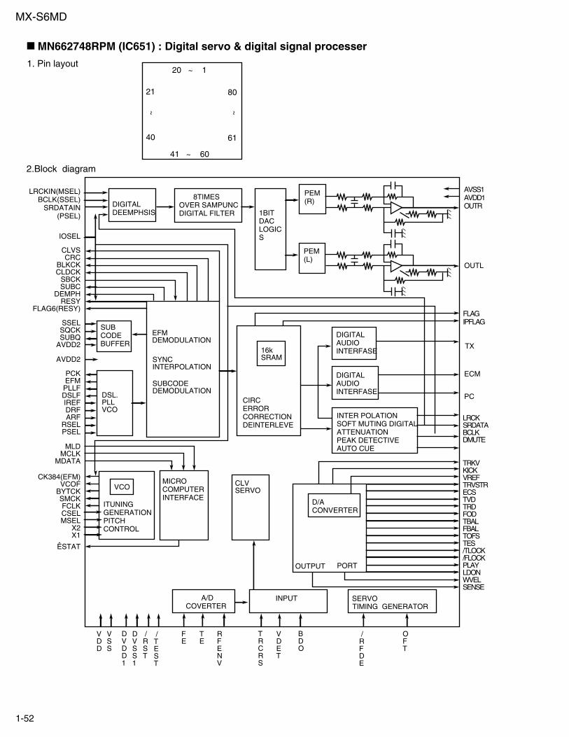
MN662748RPM (IC651) : Digital servo & digital signal processer
1. Pin layout20 ~ 1
41 ~ 60
21
40
~
80
61
~
2.Block diagram
OFT
/RFDE
BDO
VDET
TRCRS
RFENV
TE
FE
INPUT SERVOTIMING GENERATOR
A/DCOVERTER
/TEST
/RST
DVSS1
DVDD1
VSS
VDD
CLVSERVO
MICROCOMPUTERINTERFACE
VCO
ITUNINGGENERATIONPITCHCONTROL
ÊSTAT
CK384(EFM) VCOF BYTCK SMCK FCLK CSEL MSEL X2 X1
PCK EFMPLLFDSLF IREF DRF ARFRSELPSEL
MLD MCLKMDATA
DSL.PLLVCO
AVDD2
SUBCODEBUFFER
SSEL SQCK SUBQAVDD2
CLVS CRC
BLKCKCLDCK SBCK SUBC
DEMPH RESY
FLAG6(RESY)
EFMDEMODULATION
SUBCODEDEMODULATION
SYNCINTERPOLATION
16kSRAM
CIRCERRORCORRECTIONDEINTERLEVE
LRCKIN(MSEL) BCLK(SSEL) SRDATAIN (PSEL)
IOSEL
DIGITALDEEMPHSIS
8TIMESOVER SAMPUNCDIGITAL FILTER 1BIT
DACLOGICS
PEM(R)
PEM(L)
DIGITALAUDIOINTERFASE
DIGITALAUDIOINTERFASE
INTER POLATIONSOFT MUTING DIGITALATTENUATIONPEAK DETECTIVEAUTO CUE
D/ACONVERTER
OUTPUT PORT
AVSS1AVDD1OUTR
OUTL
FLAGIPFLAG
TX
ECM
PC
LRCKSRDATABCLKDMUTE
TRKVKICKVREFTRVSTRECSTVDTRDFODTBALFBALTOFSTES/TLOCK/FLOCKPLAYLDONWVELSENSE

MX-S6MD
1-53
3. Pin functionPinNo. Dymbol I/O
O
O
O
1
2
3
4
5
6
7
8
9
10
11
12
13
14
15
16
17
18
19
20
21
22
23
24
25
26
27
28
29
30
31
32
33
34
35
36
37
38
39
40
PinNo. Symbol I/O
42
41
43
44
45
46
47
48
49
50
51
52
53
54
55
56
57
58
59
60
61
62
63
64
65
66
67
68
69
70
71
72
73
74
75
76
77
78
79
80
O
II
II
O
BCLK
LRCK
SRDATA
DVDD1
DVSS1
TX
MCLK
MDATA
MLD
I
I
I
SENSE
FLOCK
TLOCK
BLKCK
SQCK
O
O
O
O
O
O
I
II
I
I
SUBQ
DMUTE
STATUS
I
O
O
RST
SMCK
PMCK
TRV
TVD
PC
ECM
ECS
KICK
TRD
O
O
O
O
O
O
O
I
I
I
FOD
VREF
FBAL
TBAL
FE
TE
I
I
I
I
IRF ENV
VDET
OFT
TRCRS
I
O
RFDET
BDO
LDON
Function
Not used
Not used
Not used
Connected to GND
Digital audio interface output
Power supply (Digital)
CPU command clock signal input
CPU command load signal input
CPU command data input
Focus lock signal output Active :Low
Sense signal output
(Data is latched at signal's rising point)
Tracking lock signal output Active :Low
sub-code/block/clock signal output
Outside clock for sub-code Q resister input
Sub-code Q -code output
Connected to GND
Status signal
(CRC,CUE,CLVS,TTSTOP,ECLV,SQOK)
Reset signal input (L:Reset)
Not used
Not used
Traverse enforced output
Traverse drive output
Not used
Spindle motor drive signal (Enforced
mode output) 3-State
Spindle motor drive signal (Servo errorsignal output)
Kick pulse output
Tracking drive output
Focus drive output
Reference voltage input pin for D/A
output block (TVD,FOD,FBA,TBAL)
Focus Balance adjust signal output
Tracking Balance adjust signal output
Focus error signal input (Analog input)
Tracking error signal input (Analog input)
RF envelope signal input (Analog input)
Vibration detect signal input (H:detect)
Off track signal input (H:off track)
Track cross signal input
RF detect signal input (L:detect)
BDO input pin (L:detect)
Laser ON signal output (H:on)
I
I
I
I/O
I/O
II
II
II
Function
Not used
Not used
TES
PLAY
WVEL
ARF
IREF
DRF
DSLF
PLLF
Tracking error shunt signal output (H:shunt)
RF signal input
Reference current input pin
Bias pin for DSL
Not used
Loop filter pin for DSL
Loop filter pin for PLL
Power supply (Analog)
Connected to GND (Analog)
Not used
Not used
Not used
Not used
Not used
II
II
Connected to GND (for X'tal oscillation
circuit)
I
OI
O
O
II
II
II
II
II
II
II
II
Not used
Not used
Not used
Not used
Not used
Not used
Not used
Not used
Not used
Pull up
Connected to GND
Connected to GND
Connected to GND
pull up
pull up
pull up
Power supply (Digital)
Lch audio output
Connected to GND
Rch audio output
Power supply (for X'tal oscillation circuit)
Input of 16.9344MHz X'tal oscillation circuit
Output of X'tal oscillation circuit
VCOF
AVDD2
AVSS2
EFM
PCK
PDO
SUBC
SBCK
VSS
XI
X2
VDD
BYTCK
CLDCK
FLAG
IPPLAG
FLAG
CLVS
CRC
DEMPH
RESY
IOSEL
TEST
AVDD1
OUT L
AVSS1
OUT R
RSEL
SSEL
MSEL
PSEL
CSEL
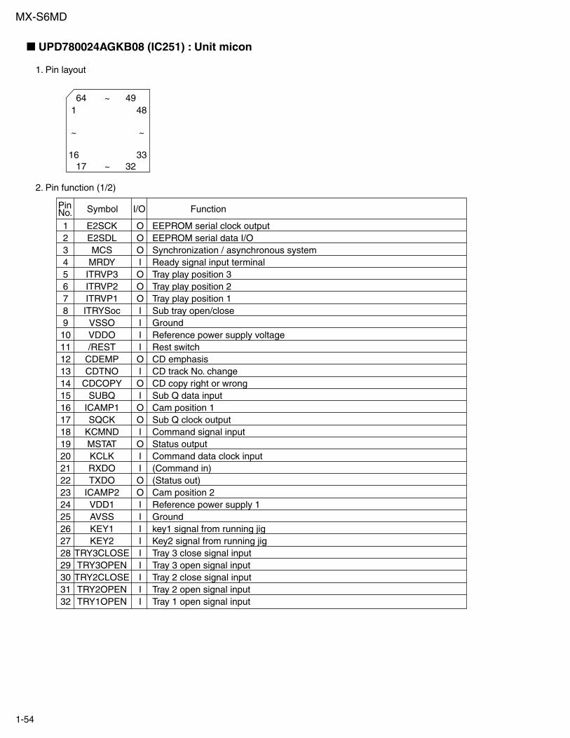
MX-S6MD
1-54
UPD780024AGKB08 (IC251) : Unit micon
1. Pin layout
2. Pin function (1/2)
1
~
16
48
~
3317 ~ 32
64 ~ 49
1234567891011121314151617181920212223242526272829303132
OOOIOOOIIIIOIOIOOIOIIOOIIIIIIIII
EEPROM serial clock outputEEPROM serial data I/OSynchronization / asynchronous systemReady signal input terminalTray play position 3Tray play position 2Tray play position 1Sub tray open/closeGroundReference power supply voltageRest switchCD emphasisCD track No. changeCD copy right or wrongSub Q data inputCam position 1Sub Q clock outputCommand signal inputStatus outputCommand data clock input(Command in)(Status out)Cam position 2Reference power supply 1Groundkey1 signal from running jigKey2 signal from running jigTray 3 close signal inputTray 3 open signal inputTray 2 close signal inputTray 2 open signal inputTray 1 open signal input
E2SCKE2SDLMCS
MRDYITRVP3ITRVP2ITRVP1ITRYSoc
VSSOVDDO/REST
CDEMPCDTNO
CDCOPYSUBQ
ICAMP1SQCK
KCMNDMSTATKCLKRXDOTXDO
ICAMP2VDD1AVSSKEY1KEY2
TRY3CLOSETRY3OPENTRY2CLOSETRY2OPENTRY1OPEN
PinNo. Symbol I/O Function

MX-S6MD
1-55
2. Pin function (2/2)
3334353637383940414243444546474849505152535455565758596061626364
IIIIOIIOIIOOOOOOIIIIOIIIIIIIIIII
Tray 1 close signal inputReference power supply voltageReference power supply voltageCD reset signal inputNon connectReference power supply voltageNo use ( for Flash micon)X'tal osc outputX'tal osc inputGroundFLAG for C1 errorSub Q block clock signal outputCam motor rotation clockwiseCam motor rotation counter clockwiseActuator motor rotation counter clockwiseActuator motor rotation clockwiseGain select 2/4 speedEqualizer select 2/4 speedCam position 3Cam position 4Reset signal outputStatus signal inputDigital mute signal inputPower on signal inputCommand load signal inputCommand data inputCommand clock inputCommunication select signal inputRunning data input from running jigRunning load 2 signal input from running jigRunning load 1 signal input from running jigRunning clock signal input from running jig
TRY1CLOSEAVREFAVDD
/RESETXT2XT1ICX2X1
VSS1FLAG
BLKCKCAM_CW
CAM_CCWACT_CCWACT_CWGCTRLEQSW
ICAMP3ICAMP4/RESET
STAT/DMUTE
/P.ONMLD
MDATAMCLK
SELECTRUNDATA
RUNLOAD2RUNLOAD1RUNCLOCK
PinNo. Symbol I/O Function

MX-S6MD
1-56
INSTRUCTION REGISTER INSTRUCTION
DECODE,CONTROL
ANDCLOCK
GENERATIONADD.
BUFFERS
DATAREGISTER 16
R/W AMPSAND
AUTO ERASE
16
DECODER
EEPROM
4096bit256 x 16
VPP SW
VREFVPP
GENERATOR
DO
DI
CS
SK
PE
1
2
3
4
PE
VCC
CS
SK
NC
GND
DO
DI
8
7
6
5
8 PIN SOP
Pin no. Symbol 1 PE 2 VCC 3 CS 4 SK 5 DI 6 DO 7 GND 8 NC
FunctionProgram enable (With built-in pull-up resistor)Power supplyChip selectionCereal clock inputCereal data inputCereal data outputGroundNo connection
NOTE : The pull-up resistor of the PE pin is about 2.5M (VCC=5V)
AK93C65AF-X (IC590) : EEPROM
1.Pin layout
2.Block diagram
3.Pin function

MX-S6MD
1-57
A0
A1
A2
GND
1
2
3
4
Vcc
WP
SCL
SDA
8
7
6
5
1kbit EEPROM ARRAY
7bit
ADDRESS
DECODER
SLAVE/WORD
ADDRESS REGISTER7bit
8bit
DATA
REGISTER
CONTROL LOGIC
HIGH VOLTAGE GEN. Vcc LEVEL DETECT
ACK
START STOP
BR24C01AFV-W-X (IC201) : EEPROM
1.Pin layout
2.Block diagram
3.Pin function
A0 A1 A2 GND
Vcc WP SCL SDA
Pin name I/O Function
Vcc
GND
A0,A1,A2
SCL
SDA
WP
-
-
IN
IN
IN / OUT
IN
*1 An open drain output requires a pull-up resister.
Power supply
Ground (0v)
Slave address set
Serial clock input
Slave and word address,serial data input, serial data output *1
Write protect input

MX-S6MD
1-58
1.Pin layout
3.Block diagram
2.Pin function
HY51V17400CT-60 (IC390) : DRAM
VccDQ0DQ1WE
RASA11
A10A0A1A2A3
Vcc
VssDQ3DQ2CASOEA9
A8A7A6A5A4Vss
Pin Name Parameter
/RAS
/CAS
/WE
/OE
A0~A11
A0~A10
DQ0~DQ3
Vcc
Vss
NC
Row Address Strobe
Column Address Strobe
Write Enable
Output Enable
Address Input (4K Refresh Product)
Address Input (2K Refresh Product)
Data In/Out
Power (3.3V)
Ground
No Connection
VccVss
Substrate BiasGenerator
X16 ParallelTest
RAS ClockGenerator
Row Presecoder(11/12)*
(11/12)*
RAS
Refresh Counter
Refresh Counter
Add
ress
Buf
fer
Cloumn Predecoder(11/12)*
CAS ClockGenerator
Data Input Buffer
DQ0~3 DQ0~3
4 4
44
Data Output Buffer
(11/10)*
RowDecoder
Memory Array4,194,304 x 4
Sense AmpI/O Gate
Column Decoder
OE
A0A1A2A3A4A5A6A7A8A9
A10*(A11)
WECAS
DQ0 DQ1 DQ2 DQ3
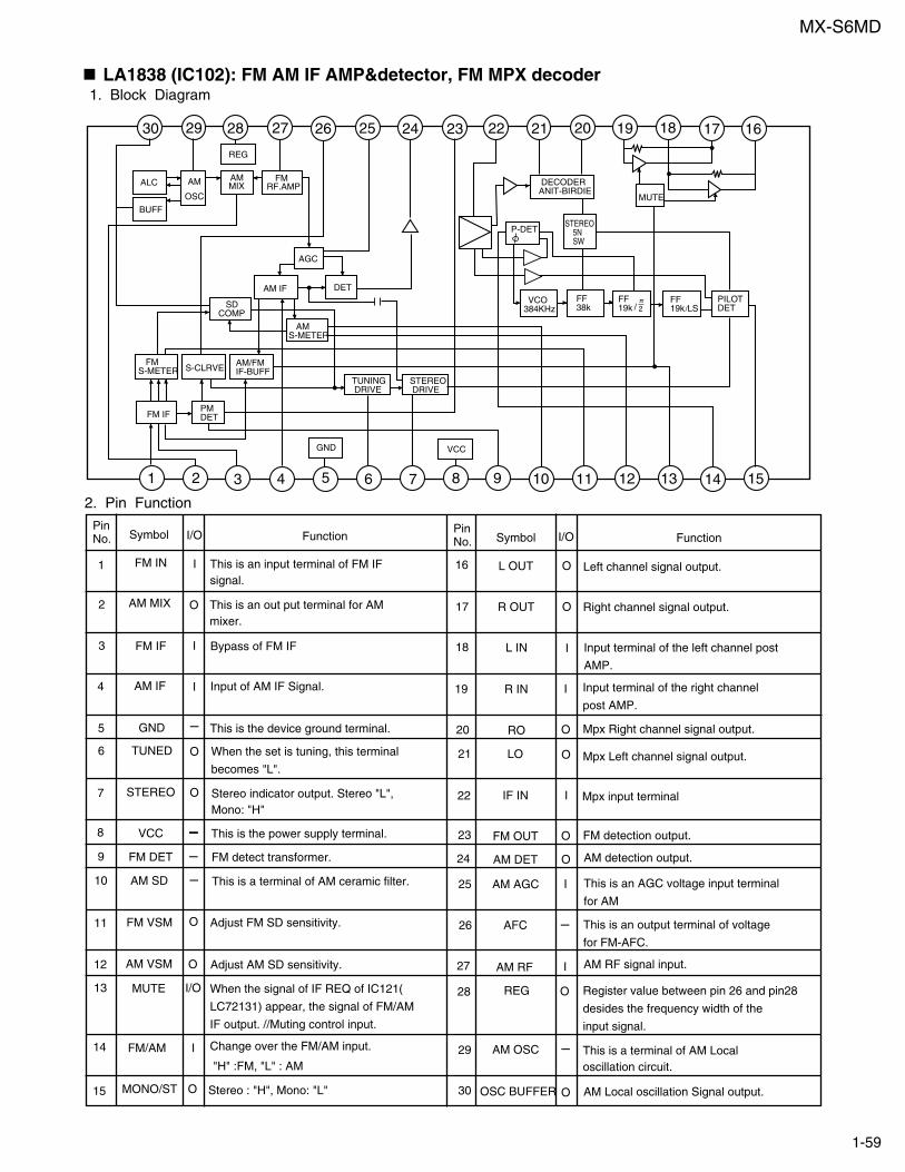
MX-S6MD
1-59
2. Pin Function
PinNo. Symbol I/O Function FunctionI/OSymbol
PinNo.
1
2
3
4
5
6
7
8
9
10
11
12
13
14
15
FM IN
AM MIX
FM IF
AM IF
GND
TUNED
STEREO
VCC
FM DET
AM SD
FM VSM
AM VSM
MUTE
FM/AM
MONO/ST O
I
I/O
O
O
I
O
I
I
I
O
O
IIII
I
This is an input terminal of FM IFsignal.
This is an out put terminal for AMmixer.
Bypass of FM IF
Input of AM IF Signal.
This is the device ground terminal.
When the set is tuning, this terminal
becomes "L".
Stereo indicator output. Stereo "L",Mono: "H"
This is the power supply terminal.
FM detect transformer.
This is a terminal of AM ceramic filter.
Adjust FM SD sensitivity.
Adjust AM SD sensitivity.
When the signal of IF REQ of IC121(
LC72131) appear, the signal of FM/AM
IF output. //Muting control input.
Change over the FM/AM input.
"H" :FM, "L" : AM
Stereo : "H", Mono: "L"
16
17
18
19
20
21
22
23
24
25
26
27
28
29
30 OSC BUFFER
AM OSC
REG
AM RF
AFC
AM AGC
O
I
O
I
I
I
AM Local oscillation Signal output.
This is a terminal of AM Localoscillation circuit.
Register value between pin 26 and pin28
desides the frequency width of the
input signal.
AM RF signal input.
This is an output terminal of voltage
for FM-AFC.
This is an AGC voltage input terminal
for AM
O
O
I
O
AM detection output.
FM detection output.
Mpx input terminal
O
O
I
Left channel signal output.
Right channel signal output.
Input terminal of the left channel post
AMP.
Input terminal of the right channel
post AMP.I
O
Mpx Left channel signal output.
Mpx Right channel signal output.
L OUT
R OUT
L IN
R IN
RO
LO
IF IN
FM OUT
AM DET
1. Block Diagram
ALC
BUFF
AM
OSC
REG
AMMIX
FMRF.AMP
AGC
AM IF DET
SDCOMP
AMS-METER
FMS-METER
FM IFPMDET
S-CLRVEAM/FMIF-BUFF
TUNING DRIVE
GND VCC
STEREO DRIVE
MUTE
DECODERANIT-BIRDIE
STEREO 5N SW
P-DET
PILOTDET
FF19k
FF19k
FF38k
VCO384KHz / 2 /LS
30 29 28 27 26 25 24 23 22 21 20 19 18 17 16
1 2 3 4 6 7 8 9 10 11 12 13 14 155
LA1838 (IC102): FM AM IF AMP&detector, FM MPX decoder

MX-S6MD
1-60
24 23 22 21 20 19Gnd
18 17 16 15 14 13
7 8 9 10 11 12Gnd
1 2 3 4 5 6
Levelshift
B T Ldriver
Levelshift
B T Ldriver
B T Ldriver
11kohm
11kohm
Levelshift
B T Ldriver
Levelshift
Regulator
RESET
11kohm
11kohm
- +- +
Vcc
Vcc Vref Vin4 Vg4 Vo8 Vo7
Vcc Mute Vin1 Vg1 Vo1 Vo2 Vo3 Vo4 Vg2 Vin2 Reg out
Reg In
Vo6 Vo5 Vg3 Vin3 Cd Res
LA6541-X (IC801) : Servo driver1. Pin Layout & block diagram
2. Pin function
1
2
3
4
5
6
7
8
9
10
11
12
13
14
15
16
17
18
19
20
21
22
23
24
Vcc
Mute
Vin1
Vg1
Vo1
Vo2
Vo3
Vo4
Vg2
Vin2
Reg Out
Reg In
Res
Cd
Vin3
Vg3
Vo5
Vo6
Vo7
Vo8
Vg4
Vin4
Vref
Vcc
Power supply (Shorted to pin 24)
All BTL amplifier outputs ON/OFF
BTL AMP 1 input pin
BTL AMP 1 input pin (For gain adjustment)
BTL AMP 1 input pin (Non inverting side)
BTL AMP 1 input pin (Inverting side)
BTL AMP 2 input pin (Inverting side)
BTL AMP 2 input pin (Non inverting side)
BTL AMP 2 input pin (For gain adjustment)
BTL AMP 2 input pin
External transistor collector (PNP) connection. 5V power supply output
External transistor (PNP) base connection
Reset output
Reset output delay time setting (Capacitor connected externally)
BTL AMP 3 input pin
BTL AMP 3 input pin (For gain adjustment)
BTL AMP 3 output pin (Non inverting side)
BTL AMP 3 output pin (Inverting side)
BTL AMP 4 output pin (Inverting side)
BTL AMP 4 output pin (Non inverting side)
BTL AMP 4 output pin (For gain adjustment)
BTL AMP 4 output pin
Level shift circuit's reference voltage application
Power supply (Shorted to pin 1)
PinNo. Symbol Function

MX-S6MD
1-61
1. Pin layout1234567891011
2221201918171615141312
XTFM/AM
CEDI
CLOCKDO
FM/ST/VCOAM/FM
SDIN
XTGNDLPFOUTLPFINPDVCCFMINAMIN
IFCONTIFIN
PinNo.
1
2
3
4
5
6
7
8
9
10
11
PinNo.
12
13
14
15
16
17
18
19
20
21
22
Symbol
XT
FM/AM
CE
DI
CLOCK
DO
FM/ST/VCO
AM/FM
LW
MW
SDIN
Symbol
IFIN
IFCONT
AMIN
FMIN
VCC
PD
LPFIN
LPFOUT
GND
XT
Function
X'tal oscillator connect (75kHz)
LOW:FM mode
When data output/input for 4pin(input) and
6pin(output): H
Input for receive the serial data from
controller
Sync signal input use
Data output for Controller
Output port
"Low": MW mode
Open state after the power on reset
Input/output port
Input/output port
Data input/output
Function
IF counter signal input
IF signal output
Not use
AM Local OSC signal output
FM Local OSC signal input
Power suplly(VDD=4.5-5.5V)
When power ON:Reset circuit move
PLL charge pump output(H: Local OSC
frequency Height than Reference frequency.
L: Low Agreement: Height impedance)
Input for active lowpassfilter of PLL
Output for active lowpassfilter of PLL
Connected to GND
X'tal oscillator(75KHz)
I/O
I
O
I
I
I
O
O
O
I/O
I/O
I/O
I/O
I
O
-
I
I
-
O
I
O
-
I
ReferenceDriver
PhaseDetector
Charge Pump
UnlockDetector
UniversalCounter
Swallow Counter1/16,1/17 4bit
12bitProgrammable
DriverS
Swallow Counter1/16,1/17 4bit
Data Shift Register & Latch
Poweron
Reset
C2BI/F
1/2
7 8 2 11 13
21
17
6
5
4
3
15
16
22
1 18
19
20
12
2. Block diagram
3. Pin function
LC72136N (IC121) : PLL frequency synthesizer

MX-S6MD
1-62
M63008FP-X (IC410) : 5ch Actuator driver
1.Pin layout
2.Block diagram
REG+
REGB
IN1+
VBS1
Vm1
IN1-
OUT1
VM1-
VM1+
VM2+
VM2-
OUT2
IN2-
IN2+
MUTE1
MUTE2
SS,GND
VREF
VREFO
GND
CH3IN
OUT3
IN3-
VBS2
Vm2
IN3+
N.C
VM3-
VM3+
VM4+
VM4-
VM5+
VM5-
OUT5
IN5-
IN5+
IN4+
IN4-
OUT4
GND
1
2
20
21
16
15
13
14
12
8
9
7
6
5
3
4 39 38
40
3741
42
34
35
31
30
23
24
22
29
28
26
25
27
19 17 18 10 11 32 33
IN1+IN1-
OUT1
VM1(+)
VM1(-)
VM2(+)
VM2(-)
OUT2
IN2-IIN2+
VREFO
VREF
REGB
REG+
VREF
E2
CH2
X5
CH1
X5
E1
VREG
VBS1
VBS1
VBS1
VBS2
VBS1
VBS1
VBS2 1.25V
CH3
X8
CH4
X8
CH5
X8
E3
E4
E5
VBS2
VBS2
VBS2
VBS2
Vm1 Vm2
R
R
R
R
Vrefm1 Vrefm2
BIAS HI :Sleep
SLEEP
TSD
Low,Open
MUTE ON
1~4CH 5CH
VBS1
Vm1 VBS1 VBS2 Vm2
IN3-IN3+OUT3CH3 IN
VM3(+)
VM3(-)
VM4(+)
VM4(-)
IN4-IN4+OUT4
VM5(+)
vm5(-)
IN5-IN5+OUT5
VREFO
SS,GNDMUTE1 MUTE2
GND (4PIN)

MX-S6MD
1-63
MN101C12GDW (IC851) : Panel micon
7576
100
51~
~
50
26
~
1 25~
1.Pin layout
2. Pin function
123
4~910111213141516
17~20212223242526
27~3233
34,3536
37~41424344
45~57585960
61,626364
65~7273
74~7879~8687~94
9596979899100
Connect to ground.Input terminal.Input terminal.Connect to ground.A / D Ref. voltage.Ref. voltage.OSC frequency input terminal.OSC frequency output terminal.Connect to ground.Connect to ground.Non use.Connect to ground.System CPU require signal output terminal.Stand by LED (RED) output terminal.Power LED (GREEN) output terminal.Connect to ground.Connect to ground.Panel CPU require signal input terminal.Connect to ground.Reset signal input terminal.Connect to ground.MD (RED) output terminal.Connect to ground.Commor signal output terminal.Commor signal input terminal.Commor clock signal input terminal.Connect to ground.Write enable output terminal.Read enable output terminal.Chip select output terminal.Connect to ground.Data select signal output terminal.LCD reset signal output terminal.Connect to ground.Dimmer control terminal.Connect to ground.Pata bus signal output terminal.Connect to ground.Connect to ground.Non use.Red LED control terminal.Green LED control terminar.Blue LED control terminal.Ref. voltage.
I/O-
LEVEL LchLEVEL Rch
-A / D Power
Vdd8.38MHz8.38MHz
GND---
comm sysreqLED STBY red
LED POWER green--
comm panereq-
comm reset-
LED MD REC-
comm outcomm in
comm clock-
LCD WELCD RELCD CS1
-LCD AO
LCD RESET-
LCD LEDdimmer-
LCD D7~D0-
DVASS-
LED REDLED GREENLED BLUE
DAVdd
-II---IO----OOO--I-I-O-OII-OOO-OO-O-O---OOO-
Pin No. Symbol Function

MX-S6MD
1-64
V+
INPUT+
V-
OUTPUT
A OUT
A -IN
A +IN
V -
1
2
3
4
A B
(TOP VIEW)
8
7
6
5
V+
B -IN
B +IN
B OUT
1.Terminal layout
2.Block diagram
NJM4580D (IC652) : LPF, Mic and H.phone Amp.
A OUT 1
A -IN 2
A +IN 3
V- 4
8 V+
7 B OUT
6 B -IN
5 B +IN
NJM4580E-W (IC672):

MX-S6MD
1-65
1
4
R1
TR1
TR3
TR2
TR4
TR5
TR6
TR8
R8C2
TR14 TR15
TR16
R14
R11
R13
R12
R10
R9
TR9
TR10
TR12
TR13
TR11
TR7
C1
D1
R6
R3
R4
R5
R7
13 11 14 15
9
8
125 67 10
2
R2
SUB
STK402-030 (IC301) :
1.Pin layout
2.Block diagram
1 15

MX-S6MD
1-66
1
2
3
4
5
6
7
14
13
12
11
10
9
8
1Y
1A
1B
2Y
2A
2B
GND
VCC
4Y
4B
4A
3Y
3B
3A
A
L
L
H
H
B
L
H
L
H
Y
H
L
L
L
TC74HC02AP (IC674) : 2ch Nor gate
2.The truth value table1.Pin layout & block diagram
1
2
3
IN B
IN A
Vss
5
4
VDD
OUT X
A
B
Vcc
GND
Y
TC7S08F-W (IC340) : Buffer
1. Pin layout 2. Block diagram
IN B 1
IN A 2
Vss 3
5 VDD
4 OUT X
Vcc
GND
Y
A
A
TC7S32F-X (IC603) : NAND gata
1.Pin layout 2.Block diagram

MX-S6MD
1-67
11
12
13
14
10
9
8
7
15 16 27 26 25 23 24
6
30
1
29
5
34
222212019281817
L-IN1
L-IN2
L-IN3
L-IN4
R-IN1
R-IN2
R-IN3
R-IN4
MU
XO
UT
INR
TR
EB
LE(R
)
MIN
(R)
MO
UT
(R)
BIN
(R)
BO
UT
(R)
CR
EF
AGND
Vs
ROUT
DIG-GND
SDA
SCL
LOUTB
OU
T(L
)
BIN
(L)
MO
T(L
)
MIN
(L)
TR
EB
LE(L
)
INL
MU
XO
UT
VOLUME
VOLUME
TREBLE
TREBLE
MIDLE
MIDLE
SPEAKERATTRIGHT
SPEAKERATTLEFT
BASS
BASS
SUPPLY
G
G
I C BUS DECODER LATCHES20/30dB
2dB STEP
INPUT MULTIPLEXER GAIN
CSLDIG GNDTREBLE(R)TREBLE(L)MIN(L)MOUT(L)BOUT(L)BIN(L)BOUT(R)BIN(R)MOUT(R)MIN(R)INRMUXOUTRINL
SDACRE
VsAGNDROUTLOUTR-IN4R-IN3R-IN2R-IN1L-IN1L-IN2L-IN3L-IN4
MUXOUTL TDA7439
1
2
3
4
5
6
7
8
9
10
11
12
13
14
15
30
29
28
27
26
25
24
23
22
21
20
19
18
17
16
TDA7439 (IC671) : Control volume
1.Pin layout
2.Block diagram

MX-S6MD
1-68
on / off control 1
Np (Vref) 3
GND 2
6 Vin
4 Vout
VOUT
Thermal Sensor
CnpBandgap Reference
GND
VIN
Rin=550k
on / off Ccont.
TK11140SC-W (IC485) :
1.Pin layout
2.Block diagram
OUT1 1
Ii1 2
IN1 3
V- 4
8 V+
7 OUT2
6 Ii2
5 IN2
1 2IN
Ii
Q1Q2
Q5 Q6
Q3Q4
Q7
Q8
V+
OUT
V-
100 A 100 A
UPC393G2-W (IC602) :
1.Pin layout 2.Block diagram

MX-S6MD
1-69
+
-
VDD VOUT
VSS
EXT
CE
CurrentLimit
VoltageReference
XC62ER3602M-X (IC400) :
1.Pin layout
2.Block diagram
3.Pin function
1
5 4
2 3
12345
GNDPower supply inputRegulator outputBase current control terminalChip enable
V V V EXTCE
Pin No. Symbol FunctionSS
IN
OUT

Printed in Japan200011(O)
VICTOR COMPANY OF JAPAN, LIMITEDAUDIO & COMMUNICATION BUSINESS DIVISIONPERSONAL & MOBILE NETWORK BUSINESS UNIT. 10-1,1Chome,Ohwatari-machi,Maebashi-city,371-8543,Japan
No.20887
MX-S6MD

2-1
IHA B C D E F G
1
2
3
4
5
6
MX-S6MD
CN851
CN
791C
N891
CN
801
CN
392C
N393
LCD BACK LIGHTFULL COLOR
LED
IC851PANELMICON
IC801SYSTEMMICON
JS821MASTERVOLUME
S8101~S8106
LCD
LSI,A0LCDRST
WE,REDO~D7
REDGREEN
BLUE
TSU1~6
VOLAVOLB
KEY1
CN
701
IC701REMOCON
LS701JOY
CONTROL
S7001~S7007
KEY SWITCHS7101~S7106
REM
KEY2KEY3
JOYA+HJOYB+GJOYC+FJOYD+EJOYCOM1JOYCOM2JOYPUSH
VOLAVOLBTSU1~6KEY1~3REMJOYA+HJOYB+GJOYC+FJOYD+EJOYCOM1JOYCOM2JOYPUSH
TUNED,MPX,TCE,TCKTDATA,MDSTAT,FCDMDCMND,RSDA,RSCLMDRESET,RESETDAVN,MRDY,CDRESETKCLK,MSTAT,KCMND
SAFETY1~3,FTU,INH,PRTTRSW,POWER,SDA,SCL
CD/OPT,CD/MD,SURRSTANDBY,AMUTE,SMUTE
SPKR,TMUTE
MD PICKUPKMS-260B
IC310RF AMP.
IC350Digital servo &
Encoder/Decoder
IC500MD
Control Micon
IC450Pre Driver
IC480DA/AD converter
IC390D-RAM
FEED MOTORSPINDLE MOTOR
MAGNETICHEAD
LOADINGMOTOR
Detection SWLOAD SWPLAY SW
IC410Power Driver
IC590EEPROM
MPROT,MREF,SSTOP
I,J,A,B,C,D
LOADSW,PLAYSW
XRST
RF
PEAK BOTM ABCD FEAUX ADFG SE TESWDT SCLK XLAT
EMFO XWEXRASXCAS
XOE
PWADPWDA
EMPHE
LRCKSCLKMCLKSDIO
DIN
LIN/RINCOMMAND
STATUS
CN
321C
N408
CN
407
Detection switchSSTOP,MREF,MPROT
FRDR,FFDRTRDR,TFDRSFDR,SRDR
LOADEJECT AOUT L/R
FCSTRK
LM
FMSM
CN
521C
N522
CN
671C
N611
CN
651C
N606
IC201EEPROM
IC652OPE.AMP
IC251UNIT MICON
IC651DSP SRDATA,LRCK,BCK
OUTLOUTR
OUT_LOUT_R
E2SDLE2SCK
TXDO,RXDO,ICRESET
RE
SE
T
RUNCLOCK,RUNDATARUNLOAD1,RUNLOAD2KEY1,KEY2,SELECT
KCMND,MSTATMRDY,KCLK,MCS
CDTNO,CDCOPY,CDEMP
/RESETSTAT
/DMUTESUBQ
BLKCKMLD
MDATAMCLKFLAG
IC801FOCUS/SPINDLEFEED/TRACKING
BTL DRIVER
IC601RF & SERVO
AMP
IC852CUM MOTOR
DRIVER
IC851ACT.MOTOR
DRIVER
SW680SW690~SW693
SW1~SW6
REST SW
CAMP1~CAMP4SUB_OP/CLP.POSI1~P.POSI3
M
M
M
M
COM_CCW,COM_CW
ACTM_CCW,ACTM_CW
AM+AM-
COM+COM-
EQSW
TBAL,FBAL/RFDET,FEBDO,TELDON,OFTRFENV,ARF
TRD,KICK,FODECM,ECS,TVD,TRV
CN
610
CN
602
CN
601
CN
001
CN699
TRY1OPEN,TRY2OPEN,TRY3OPENTRY1CLOSE,TRY2CLOSE,TRY3CLOSE
PICKUP
REST
A+C,B+D,E,FMD,PD,LD
T+,T-,F+,F-FM+,FM-SM+,SM-
FEED
SPINDLE
to Flash Micon
to Running JIG
CN923 CN922
CN
66
1C
N691
J3001
CN394
W601
IC671FUNCTIONVOLUME
IC672CD/MD LPF
IC673CD/MD SEL
IC301POWER AMP
IC674CD/OPT IN SEL
TLOUTTROUT
L,R
CD/OPTCD/MD
TXCDLCDR
CD/MDLCD/MDR
TAPELTAPER
TRECLTRECR
AUXLAUXR
KCMND,MSTATMRDY,KCLK,CDRESET
SDASCL
MDL,MDRMRECLMRECR
LINE
INLIN
E O
UT
LR
LINRIN
LSURRL,R
MUTESPK
from CN304
CN602
CN991W921
T9001POWERTRANS
MAINSPLUGT9002
SUBTRANS
J3102AUX IN
J3101H.P. JACK
CN
692
W3002
AUXLAUXR
LR
CN914
CN
912C
N913
W121
W122
CN911POWERSUPPLY
W3002
CN
303C
N302
CN301
W301
CN304CN511
H.P.MUTE
PROTECTOR
POWERSUPPLY
PRT
L,RSPKMUTE
LSURR
SMUTE
TUNER+9V
TUNER+5.6V
MD A+6V
TLOUTTROUT
MRECLMRECR
MDLMDR
DAVINRSDARSCL
TDATA,TCETCK,TUNEDMPX
MDDIN
CDRESETMRDYFCDKCLKKCMNDMSTAT
SDA,SCLCD/OPTAMUTECD/MD
SW +10V/+8V REG.
US D5.6V REG.
SW 12VREG.
US DM+6V REG.
CN924
AT101
CN
111C
N112
FM RFIC121PLL
IC101FMDET/AMDET
T111AMOSC
ANT
AM AMRF
FMOSC
AMOSCFMIN
CK,CE,DI/DO
LOUT,ROUTFMOUT,STEREOTUNED,MUTE
IC191RDS
Block diagram

2-2
IHA B C D E F G
1
2
3
4
5
6
MX-S6MD MX-S6MD
Parts are safety assurance parts.When replacing those parts makesure to use the specified one.
CN901
R3301
R2101
Q9201
CN304
R1101
Q3201
Q9111R9116
D9501
F9103
F9102
TB992
TB991
C9705
D3304
D3302
D3303
D3301
C3303
C3304
C3302 C3301
F9101
R9206
Q9301
J3102
R2103
Q9204
D9801
Q1301
R3302
Q9401R9401
C1304
R9901 R9902
R9905 R9906
R9903 R9904
R1309
D9802
R1305
Q2301
R2305
C9801
C2304R2309
R2201
CN692
R1201
C9709
R9910
R9106
R9107
R9114
Q9101
EP971
R3038
R1103
D3001
C3011
C3010
R3016
R9104
D9910C1302
C2302
W301
Q3004Q3005
R2016
R1016
R9305
Q9601
CN901
F9103
F9102
TB992
R9205
TB991
F9101
R9404
CN511
R9301
R9601
R9602
Q9602R9603
R9605 R9604
Q9603
Q9604
Q2101
Q1101
EP301
W302
W90
1
CN
912
CN
924
CN
911
D97
07
D97
08
C97
04
CN
913
C32
01
D98
04
C98
04
D95
03
C95
01
Q95
01
Q95
02R
9503
R95
02
C95
02R
9504
D95
04
Q95
03C
N91
4
D97
05
D97
01
D97
03
D97
06
D97
02
D97
04 C97
01
R23
03
D99
04
R93
02
D99
03D
9902
R13
08
C94
01
C94
03
C30
16
R13
06
R23
02
R13
02
C23
01
C13
01
R23
01
R13
01
C94
02
R94
02D
9401
R23
08
R23
06
CN
302
CN
303
Q30
03
CN
301
D98
03
R91
12
C98
05C
9112
R98
01
R97
03
R32
01
C91
11
C31
03
C97
08
R21
02R
1102
D99
01
C99
01
D91
11
R97
02D
9710
D97
09
D91
12
R30
15
R97
01
D30
03
D92
03
D13
01
D23
01
R92
03
Q92
03R
9202
C91
02
Q93
02
C30
04
R30
11
R30
12
R30
13
C30
05
R30
14
D30
02
R93
06
R93
03
W90
1
W12
1
C93
02
D91
01
R92
01
R13
03
D92
01
C92
01
R23
04
R13
04
C92
02
C96
02
C91
03
J310
1
C21
01
C11
01
D91
02
R94
10R
9411
C96
01
C91
01
R91
01
D96
01
C96
06
C96
05
C96
04
D93
01
C93
01
D96
02
R96
06
R94
12
W30
2
QGA2501F1-03
22K
10K
2SD2394/EF/
1N40031N4003
0.1/50
QGB2510J1-12
10K
KRA102M2SD2394/EF/
1N4003
0.068/50
MTZJ5.1C
1
1SS133
QNZ0079-001Z
QNZ0079-001Z
1N40031N40031N40031N40031N40031N4003
0.1/50
6800/25
1N5402M-201N5402M-201N5402M-201N5402M-20 0.01/100
0.01/100
2200/42 2200/42
12SD2394/EF/
QNS0072-001
1.2K
KRC107M
1N4003
2SC2785/FE/
22K
2SD1913/RS/
10
10/50
68K 15K
68K 36K
68K 18K
2.7K
12K 12K
1N4003
6.2K
2SC2785/FE/
QGB2510J1-04
6.2K
1N4003
0.068/50
2200/35
10/502.7K
220220
0.022/50
3.9K
1
1
270
2SD2394/EF/
QNZ0136-001Z
10K
1.2K
MTZJ4.3B
100/10
0.22/50
15K
270
1N400310/50
10/50
WJK0015-004A
2SA1175/FE/
2SC2785/FE/
82K
100K
470
2SC2785/FE/
QGA2501F1-03
QNZ0079-001Z
220
QNZ0079-001Z
100
QGF1016C1-21
4.7
47
1K
2SC2785/FE/
220
1K 2.7K
KRA107M
KRC107M
2SC3576-JVC
2SC3576-JVC
QNZ0136-001Z
QJK
026-
0818
03
QG
B25
10J1
-14
QG
B25
10K
2-09
QG
A25
01C
1-08
QG
B12
14J1
-14S
1/50
2.2/
50KR
C10
4M
KR
C10
7M
10K
10K
4.7/
5010
0K
1SS
133K
RC
104M
QG
B25
10J1
-09
100
1N40
03
470
1N40
031N
4003
4.7K
47/2
5
47/2
5
10/5
0
5.6K
10/2
5
10/2
5
2.2K
2.2K
0.01
/16
1.5K
MT
ZJ6
.8C
4.7K 5.
6K
QG
B12
14J1
-18S
QG
B12
14J1
-18S
KR
C11
0M
270
100/
10
22K
22K
22K
QG
B12
16K
1-06
S
0.01
/25
0.1/
50
0.01
/50
680
680
MT
ZJ4
.3B
100/
10
MT
ZJ6
.2C
10K
1SS
133
1SS
133
MT
ZJ7
.5C
47K
10K
MT
ZJ2
.4B
1SS
133
1SS
133
1SS
133
1K
KR
A10
7M
10K
100/
10
KR
A10
7M
10/5
0
10K
10K
100K
47/2
5
100K
1SS
133
1K
47K
QJK
026-
0818
03
WJK
0016
-003
A
47/1
6
MT
ZJ6
.8B
220
100
MT
ZJ1
1B
0.01
/25
220
220
100/
16
47/2
5
47/1
6
QN
S00
72-0
011000
P/5
0
1000
P/5
0
MT
ZJ6
.8C
100
100
0.01
/16
0.01
/25
270
MT
ZJ1
0C
47/2
5
47/2
5
0.01
/16
MT
ZJ1
3B
0.01
/25
MT
ZJ6
.2C
10K
100
QU
M02
5-15
Z3Z
3
RESET
INH
+8V
R
FTU
MDDINLVL-LLVL-RMRDY
AUXL
MSTATKCMND
AUXR
TCK
CDRESETCD/OPT
L
CD/MDAMUTEFCD
TLOUT
TROUT
MRECR
MRECL
TROUT
POWER
SCLSDA
MDL
TUNEDMPXTCE
MDR
TDATAMDSTATMDCMNDFCD
MPXTUNED
TDATATCETCKTMUTE
RSDARSCLMDRESETRESETDAVNMRDYCDRESETKCLKMSTATKCMND
KCLK
SAFETY3SAFETY2SAFETY1FTUINHPRTTRSWPOWERSDASCLCD/OPTCD/MDSURRSTANDBY
TMUTESPKRSMUTEAMUTE
TLOUT
LVL-
L
SM
UT
E
SU
RR
MD
DIN
MD
L
SA
FE
TY
3
SA
FE
TY
2
SA
FE
TY
1
MR
EC
R
LVL-
R
MR
EC
L
MD
R
ST
AN
DB
Y
MD
RE
SE
TM
DC
MN
DM
DS
TA
T
PR
T
Schematic diagrams
Powre supply section
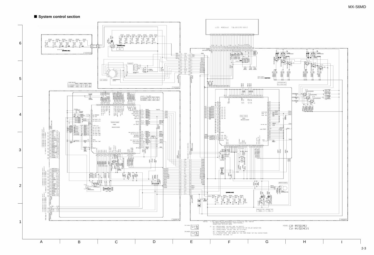
2-3
IHA B C D E F G
1
2
3
4
5
6
MX-S6MD
R7003R7004R7005R7006
IC701
R7002
C8030
C8031
X8002
LS701
R7001
R8084
R8502
R8106
C8007
R8105R8104
IC851
R8103
R8008
R8082
IC801
X8001
R8102
R8071R8072
Q8002
R8101
C7011
R8070
R8022
R8015
R8016R8017
R8023
R8020R8021
R8018
R8024R8025R8026
R8027R8028R8029R8030R8031R8032
C7012
R8050R8051
R8054R8055
R8053
R8056R8057R8058
R8302
R8081
R8059
R8062
R8083
R8501
X8501
R8508R8068R8067R8066R8065
R8064
R8060
R8063
D8502
Q8001
R8518R8519R8520R8521R8522R8523R8524R8525
R8526R8527R8528
R7101R7102R7103R7104R7105R7106
JS821
R8019
R7007
R8507
R8509
R8510R8511
R8201R8202
CN851
D8413D8414
R8446
R8445
R8444
D8417D8418
R8450
R8451R8452
R8453R8454
R8455
C8506
R8111R8211
R8308
C8006
C8005
R8307
R8305R8306
D8501
D8409
C8111
C8211
R8090
R8301 R8303
D8401
CN
391
CN
393
CN
392
S70
02
S70
03
S70
04
S70
05
S70
06R
8077
CN
801
D86
02
C82
01
C82
02
Q86
02R
8602
S70
01
D85
03D
8504
C80
08
C85
03
C80
03
C80
02
C80
01
R80
01R
8002
R80
03R
8004
R80
05R
8006 R
8011
R80
12R
8013
R80
14
R80
46
R80
33R
8034
R80
35R
8036
R80
37R
8038
R80
39R
8040
R80
41R
8042
R80
43
R80
44R
8045
R80
47R
8048
R80
49
CN
701
C80
17
D70
01
Q70
01
S81
06
S81
05
S81
04
S81
03
S81
02
S81
01
R70
20
C85
01
R70
10
R85
12R
8513
R85
14
D80
07
D80
08
D80
09
R85
15
CN
791
C85
02
D80
11
R85
16
D80
10
R80
94
S71
01
S71
02
S71
03
S71
04
S71
05
S71
06
D86
01Q
8601
R86
01
R83
10
R85
03
R85
04R
8505
R82
04
R82
03
CN
891
S70
07
R84
12R
8411
R84
16
R84
19
R84
42
R84
34R
8433
R84
38
R84
41
Q84
11Q84
10
Q84
12
Q84
16
Q84
17
Q84
18
R84
39
R84
35
R84
20
R84
17
R84
13
Q84
19
Q84
20
Q84
21
R84
47
R84
48
R84
49
C84
01
C84
02
C84
03
C80
20
C80
21
R80
80
R81
12
R82
12
W69
3
R80
07
R80
52
C85
10
D80
03D
8002
C80
04
R80
78
C80
23
C85
04
R85
06
C80
18
C83
01
C83
02
C83
03
C83
04C
8305
C83
06C
8307
C83
08C
8309
D84
04D
8403
D84
12D
8411
C83
11
C85
05
1.2K1.5K2.2K2.7K
GP1U261X
QSW0651-001ZQSW0651-001ZQSW0651-001ZQSW0651-001ZQSW0651-001Z
1K
0.01/50
0.01/50
QSW0828-001
1K
QSW0651-001Z
220
100
2.7K
22P/50
2.2K1.5K
MN101C12GDW
1.2K
1M
220
MN101C12GDX
1K
10K10K
DTA144EKA
1K
11K
1K
2.2K
1K
100
1K
1K
1K
1K
2.2K
1K1K
100
100100100100100
0.001/50
QSW0651-001Z
1K
2.2K
1K1K
2.2K
1K1K1K
220K
10K
1K
1K
QSW0651-001ZQSW0651-001ZQSW0651-001ZQSW0651-001ZQSW0651-001Z
10K
1M
1K
22K
22K22K
22K
22K
10K10K
1SS355
DTC114EKA
100100100100100100100100
2.2K2.2K2.2K
1K1K1.2K1.5K2.2K2.7K
QSW0862-001
QSW0651-001ZQSW0651-001ZQSW0651-001ZQSW0651-001ZQSW0651-001ZQSW0651-001Z
100
3.9K
100
2.2K
100100
1K1K
QGF1005F2-28
1SS3551SS355
2SC2412K/RS/
2SC2412K/RS/
2SC2412K/RS/
1K
1K
1K
1SS3551SS355
2.2K
2.2K2.2K
2.2K2.2K
2.2K
100/10
10K10K
300K
0.01/50
0.01/50
300K
300K300K
1SS355
NSTM515AS
0.001/50
0.001/50
47K
1/161/161/161/161/16
360K 620K
NSTM515AS
MA3075/H/MA3075/H/MA3075/H/MA3075/H/
QG
B25
10K
2-04
QG
B12
14K
1-18
SQ
GB
1214
K1-
18S
2.2K
QG
F12
10G
1-23
SLA
-360
MT
0.01
/50
0.01
/50
DT
C11
4EK
A12
0
QA
X04
01-0
01
1SS
355
1SS
355
22P
/50
33P
/50Q
AX
0494
-001
Z18
P/5
0
33P
/50
1.5/
25
2.2K
2.2K
2.2K
2.2K
1K 1K
100/
10
1K 1K 1K 1K
2.2K
1K1K2.
2K2.
2K
2.2K
2.2K
2.2K
2.2K
2.2K
2.2K
2.2K
2.2K
2.2K
2.2K1K1K
QG
B20
11L1
-14
1000
P/5
0
SLR
-342
VC
DT
C11
4EK
A
1K
1.5/
25
220
QA
X04
16-0
01Z
100
100
100
1SS
355
1SS
355
1SS
355
100
QG
B20
11M
4-14
33P
/50
1SS
355
100
1SS
355
10K
SLA
-360
LTD
TC
114E
KA
330
100
100
2.2K
2.2K
10K
10K
QG
F12
05F
1-23
220
220
270
270
270
220
220
270
270
2SC
2412
K/R
S/
2SC
2412
K/R
S/
2SC
2412
K/R
S/
2SC
2412
K/R
S/
2SC
2412
K/R
S/
2SC
2412
K/R
S/
270
220
270
270
220
10K
10K
10K
1/50
1/50
1/50
100/
10
1000
/6.3
47
2.2K
2.2K
QJB
001-
0216
02
1K
47K
100/
10
1SS
355
1SS
355
0.01
/50
10K
100/
10
0.01
/50
10K
1000
P/5
0
4.7/
10
4.7/
10
4.7/
10
4.7/
10
0.02
2/50
1000
P/5
0
VOLA
BAND1
TCE
TSU1
TCK
TSU3
TDATA
JOYPUSH
MDSTATMDCMNDFCDRSDARSCLMDRESETRESET
TSU6
DAVN
KEY1
BAND0
MRDY
REM
CDRESET
KEY3
LED1
TSU6
TSU5
KCLKMSTAT
TSU5
JOYPUSHJOYCOM2
KCMND
JOYCOM1JOYD+EJOYC+F
KEY2
REM
KEY1
MPX
KEY2KEY3
D7D6D5D4D3
TUNED
D2D1
RED
D0
GREEN
LED1
BLUE
SAFETY3SAFETY2SAFETY1FTUINHPRT
JOYA+H
TRSWPOWERSDA
JOYB+G
SCLCD/OPTCD/MDSURRSTANDBY
TSU4
SMUTESPKRTMUTE
AMUTE
VOLB
TSU2
JOYA+HJOYB+G
VOLB
REM
JOYCOM2JOYCOM1JOYD+EJOYC+F
KEY1KEY2
VOLA
TSU4
KEY3
JOYPUSH
REM
MDSTAT
REM
MRDY
RESETMDRST
RSDA
FCDMDCMD
KEY2
RSCL
TSU1TSU6TSU5TSU4
TDATA
DAVN
TSU2TSU3
JOYA+HJOYB+GJOYC+FJOYD+E
JOYCOM1
PRTINH
JOYCOM2
FTUJOYA+HJOYB+GJOYC+FJOYD+EJOYCOM1JOYCOM2
TSU3TSU2
JOYPUSH
RED
GREEN
BLUE
KE
Y1
KE
Y2
KE
Y3
SA
FE
TY
1S
AF
ET
Y2
D7
D6
D5
D4
D3
D2
D1
D0
SD
AS
CL
CD
/OP
T
LCD
RS
TA
0W
ER
E
CD
/MD
LED
3LE
D2
TS
U1
SU
RR
ST
AN
DB
YA
MU
TE
SM
UT
E
MS
TA
T
SP
K
LED
2
TM
UT
ET
UN
ED
MP
XT
CE
TC
K
LED
3
KC
MN
D
KC
LKC
DR
ST
PO
WE
RT
RS
WV
OLA
VO
LB
CS
1
SA
FE
TY
3
System control section

2-4
IHA B C D E F G
1
2
3
4
5
6
MX-S6MD MX-S6MD
Parts are safety assurance parts.When replacing those parts makesure to use the specified one.
C6115
CN922
Q6307
R1020
C6215
C1003
R6114
R6214
C2003
R6108
R6125
R6208
C6207
R6110
R6210
R6109
R6209
CN923
Q6302
Q6301R6128
R6228
Q6306
C1001
C2001
R1003
R2003
Q1002
R6329
R1019
IC674
C6223C6123
J6310
L6241
R2019
R1018
R2018
C1010
C2010
Q6320
RY301
R2009
R6324
IC301
C1011
CN394
Q1001
Q2001
Q6321
Q6305
Q6303
R6112
R6212
L6141
R2010
R2006L2001
Q6304
R2007
Q6308
C3001
R1006
L1001
R1010
R3035
R6311
R3036
R1009
R3005
Q3010
C2007
R2020
R3008
Q3002
C2011
C1007
Q3011
R6225
C6219
R1007C2020
Q3012
CN661
R6235
C6315
D6310
R6135
C6119
R3001
R6132
R6232
D63
07
IC67
2
C62
35
IC67
3
IC67
1
C61
35
C61
04
C63
07
CN
691
J630
1
R61
07R
6207
J630
1
C61
07
C62
04
W60
1
C63
06
C63
04
R63
03R
6304
Q20
02
C20
02
C10
02
CN
603
C63
11
CN
602
R63
32D
6309
L680
1
C61
06C
6101
R10
17R
2017
C62
01
C62
05
C62
06
C62
10C
6211
C62
12C
6213
C61
12C
6113
C61
11C
6110
C61
14C
6214
R62
06
R62
05
R61
05
R61
06
C61
05
C63
10
C63
09D63
08
D10
01
R61
31R
6231
R63
33
C61
41C
6241
D20
01
R63
34
R10
14R
2014
R10
13R
2013
R63
06
R62
18
R61
18
C61
18
C62
18
C61
16
R61
11
R62
11
C62
16
R20
15R
1015
C10
08C
2008
C63
05
R10
11R
2011
R63
05
R63
07
R63
37
R63
38
C10
12
D63
06
Q30
01
C30
15
C10
20R
1031
C10
21
R10
30
R30
09
C30
17
R30
10
C30
12
R30
37
R30
04
C30
13
J300
1
C30
14
C61
17
C63
08
C62
17
C10
22
R30
40
R62
39
R20
31C
2021
R20
30C
2022
R61
39
R63
45
R63
44R
6343
R63
42R
6341
R63
40
C61
03
C62
03
R62
27R
6127
C63
14
C20
12
D63
11
R63
27
R61
33
R62
33
22/50
QGB2510K2-14
KRA104M
1K
22/50
0.1/50
100K
100K
0.1/50
27K
11K
27K
10/50
1K
1K
3.9K
3.9K
QGB1214K1-14S
2SC3576-JVC2SC3576-JVC
2.2K
2.2K
0.022/50
0.022/50
4.7
4.7
2SC3576-JVC
220K
1.5K
TC74HC02AP
150P/50
150P/50
GP1FA550RZ
QQR0590-001
1.5K
1K
1K
4.7/50
4.7/50
KRA104M
QSK0057-001
56K
100
STK402-030
2.2/50
QGB2510K2-12
KRC107M
KTA1273/Y/
2.2K
2.2K
QQR0590-001
4.7
0.33 QQLZ005-R45
0.33
1/50
0.33
QQLZ005-R45
4.7
100
10K
100
56K
1.5K
KRA104M
220P/50
3.3P/50
1K
1.2K
2SK301/PQ/
2.2/50
3.3P/50
KRC104M
11K
0.33220P/50
KRC102M
QGF1016F3-19
13K
47/25
1SS133
13K
100
2.7K
2.7K
1SS
133
NJM
4580
D
0.00
22/5
0
TC
4066
BP
/N/
TD
A74
39
0.00
22/5
0
10/5
0
22/5
0
QG
A25
01C
1-03
QN
N03
65-0
01
27K
27K
QN
N01
73-0
01
10/5
0
KR
C10
4M
10/5
0
QJP
001-
0312
01
100/
10
47/2
5
10K
10K
2SC
3576
-JV
C
0.01
/50
0.01
/50
QG
A20
01F
1-02
1.5/
25
QG
B12
16J1
-06S
100
1SS
133
L231
K-4
R7Y
10/5
0
10/5
0
27K
27K
10/5
0
2.2/
50
10/5
0
0.01
8/50
0.02
2/50
0.15
/50
0.15
0.15
0.15
0.02
2
0.01
8
0.00
56/5
00.
0056
/50
2.7K
5.6K
5.6K
2.7K
2.2/
50
100/
16
10/5
0M
TZ
J11A
1SS
133
4.7K
4.7K
100
0.00
56/5
00.
0056
/50
1SS
133
100
18K
18K
1K1K
KT
A12
68/G
L/K
TA
1268
/GL/
470
220
220
KR
C10
4M
0.1/
50
0.1/
50
0.00
47/5
0
2.2K
2.2K
0.00
47/5
0
47K
47K
0.1/
500.
1/50
0.02
2/50
4.7
4.7
270
2SC
2785
/FE
/
47K
2SC
2785
/FE
/
1K
1K
470P
/50
MT
ZJ5
.1B
KT
D86
3/Y
/
100/
35
56K
47/5
075
0
1M0.
47/5
0
4.7M
100/
35
10K
100K
10/5
0
QN
B00
10-0
01
10/5
0
1000
P/5
0
0.1/
50
4.7/
50
0.1/
50
100P
/50
100
51K
56K
47/5
0
750
100P
/50
51K
100
100
100
100
100
100
10/5
0
10/5
0
18K
18K
47/2
5
470P
/50
1000
P/5
0
1SS
133
47K
6.8K
6.8K
AMUTE
TROUT
CD/MDL
TRECR
MRECR
CD/MDR
TLOUT
TAPER
TRECL
TRECR
RIN
LIN
TAPEL
FCD
AGND
SD
A
CD
/MD
TU
L
CD
R
CD
/OP
T
CD
L
MD
L
MR
DY
MD
DIN
SC
L
MR
EC
L
MR
EC
R
MR
EC
L
CD
/MD
L
CD
/MD
R
MD
R
TA
PE
L
LVL-
L
TA
PE
R
TU
R
LVL-
R
TR
EC
L
TX
TX
SC
L
AM
UT
EC
D/M
DC
D/O
PT
TU
LT
UR
SD
A
FC
D
CD
RE
SE
TK
CLK
KC
MN
DM
ST
AT
LVL-
RLV
L-L
MD
DIN
TLO
UT
TR
OU
T
MD
L
MD
R
Function selector section

2-5
IHA B C D E F G
1
2
3
4
5
6
MX-S6MD
CD PLAYBACK SIGNAL
R802
R809
R808
C821 C822
R806
R805
R804
R803
C608
IC602
C619
C624
IC251
R631
C631
Q631
R666
R632
R635
R634
C632
C815
C816
CN601
C633
CN001
R807
C606
C603
C604
IC602
IC603
R605
R602
R601
C602C601
R636
D667
CN610
CN699
R608
R607
R289
IC651
R661
R667
R288
C661
C651
X651
C652
R287
CN620
IC201
R201
C653
C676
R682
R683
IC652
IC652
C695
R706 R707
C696
R705
R691
R708
R692
R701
R702
C699
R709
R710
C693
C694
C250
TP7
C691
CN651
X251
TP6
R703
R671
C692R704
TP5
SW680
D291
R673
R641
Q291
R292
R291
C291
SW690
R286
R255
R260
R258
SW690
SW691
C642
SW691
SW692
IC603
TP4
C859
C860
SW692
R670
R813
R812
SW693SW693
SW690
SW691
SW692
SW693
R659
R614
CN611
CN671
TP3
R617
TP8
IC851
TP9
C607
R612
R613R611
IC852
CN606
TP2
TP1
R282
R251
R252
R253
R254
R887
R886
R885
R884
R257
R259
M851
TP10L853
M852
L854
TP11
R861
R862
R863
C003 C002
R866
R865
R864
VR001
C001
SW1
SW2
SW3
SW6
SW5
SW4
C658
IC80
1
C85
5
C81
2
C81
4
R80
1C
801
C81
1
C81
3
C80
2
IC60
1 C62
1
C67
7
R64
8
C61
4
C61
5
C61
1
C61
2
C62
3
R64
9
C61
0
R60
4
R64
6
C60
5
R60
3
D85
2
R29
3
R64
5R
644
R65
1
C65
7
C65
5
R65
2
R65
3
R66
5
C65
6
R66
2
R66
3
R66
4
C66
3
C66
4
C66
5
C68
0
C67
9
C67
3
R29
4
C66
9
R66
8
R64
3
C62
2
R81
1
R67
2
Q67
3
D67
3
C66
6
R68
5
R64
2
R64
7
C64
1
C64
4
C25
3
K65
5
K65
6
K65
7
K65
8
C62
5
R66
9
C62
6
C61
7
R26
3
R26
2
R26
1
C27
0
R60
6
R69
5R
696
C66
7
C61
3
C27
2
C27
1
C64
3
R85
2R
851
R85
4
R27
1
R27
2
C85
3
C85
2
R27
4
R28
5
C85
1
R28
4
R28
3
C25
4
R25
6
R27
6
R27
7
R27
8
R27
9
R28
0
R28
1
R65
4
C61
6
3.9k
1.2k
27k
1/16 220/10
27k
8.2k
220k
9.1k
4p
33p
100/10
UPD780024AGKB08
2.2
10/16
2SA1037AK/RS/-X
220
10
120
12
1/16
1/10
2.2/10
QGF1016C1-21
0.022
1.2k
220p
0.022
0.022
UPC393G2-W
68k
180k
680k
0.0010.001
91
MA152WA-X
QGB1214J1-08S
EMV7169-006R
47k
47k
10k
MN662748RPM
1k
4.7
10k
470p
8p
QAX0599-001Z
8p
10k
QGB1214K1-08S
10k
0.33/16
0.1/25
1k
1M
NJM4580E-W
NJM4580E-W
0.047
2k 6.8k
10/16
4.7k
10k
100
10k
820
820
220/10
100
220
0.0068
0.0068
0.1/25
390p
QGF1016F3-19
NAX0397-001X
10k
680k
390p
10k
QSW0865-001
1SS355-X
DTA114EE-X
120k
150k
2SB1424/QR/-X
10k
1.2k
47/16
DA204U-X
QSW0886-002
1k
1k
1k
1k
0.0022
QSW0886-002
QSW0886-002
TC7S32F-X
1/16
1/16
100
1.2k
3.3k
QSW0886-002
1k
0
QGF1016F3-08
NI
2.2k
LB1641
0.1
16k
750750
LB1641
QGF1016F3-07
10k
1k
1k
1k
1k
1k
1k
1k
1k
1k
1k
RF-500TB-12560 10
RF-500TB-12560 10
QAR0123-001
1k
330k
1k
0.1 1
1k
330k
330k
1k
0.1
PPN-13KA10C
VSH1173-001
0.1/25
LA65
41-X
0.1/
25
390p
390p
2.7k
0.01
5
390p
390p
470p
AN
8849
SB
-W
0.1/
25
0.1/
25
10k
0.02
7
820p
1/16
1/501/
16
10k
0.05
6/25
220k
68k
270p
33k
UD
ZS
5.6B
-X
10k
2.2k
2.2k
1k
220/
10
0.1/
16
1k 1k
150
0.1/
25
68k
120k
330
0.02
2
0.02
2
0.15
/16
0.1/
25
100/
10
BR
24C
01A
FV
-W-X
220/
10
0
220/
10
1.5M
68k
100/
10
47k
NI
NI
68k
390k
16k
0.02
2
0.1/
25
0.1/
25
NQ
R00
07-0
02X
NQ
R02
51-0
04X
NQ
R02
51-0
04X
NQ
R02
51-0
04X
0.1/
16
5.6k
NI
330p
22k
22k
22k
1/16
47k
24k
HD
U-1
10
24k
0.47
/16
1/10
1/16
1/16
0.1/
16
0N
I
NI
22k
22k
0.01
0.01
22k
1k
10/1
6
1k 100
47/6
.3
1k
6.8k
6.8k
1k1k 1k 1k
1k
0.00
27
TRY2OPEN
/RFDET
OFT
RFENV
BDO
TRY2CLOSE
TRD
LDON
TEB+D
FE
F
E
FBAL
TBAL
A+C
F
B+D
A+C
F-
F+
T+
T-
TRY2CLOSE
SQCK
KICK
TVD
TRV
ECM
ECS
FOD
TRY3OPEN
KCMND
KCLK
RXDO
TRY3CLOSE
TXDO
TE
TRV
TVD
ECM
ECS
KICK
TRD
FOD
RFENV
FE
TBAL
FBAL
OFT
/RFDET
BDO
LDON
ARF
OUTL
OUTR
P.POSI1
P.POSI2
P.POSI3
SUB_OP/CL
OUT_L
OUT_R
CAMP4
CAMP3
EQSW
GCTRL
EQSW
GCTRL
MCS
KCLK
KCMND
MSTAT
MRDY
RUNLOAD2
RUNLOAD1
RUNDATA
RUNCLOCK
SELECT
KEY1
KEY2
CAMP2
FM+
FM-
SM-
MCLK
TRY1OPEN
SM+
KEY1
KEY2
TXDO
RXDO
OUTL
TRY1OPEN
AM-
CM-
MSTAT
SRDATA
LRCK
BCLK
CDTNO
CDCOPY
OUT_L
OUT_R
CDEMP
RUNCLOCK
RUNLOAD1
RUNLOAD2
RUNDATA
SELECT
MDATA
MLD
/DMUTE
STAT
/RESET
E
ARF
TRY1CLOSE
TRY2OPEN
TRY3OPEN
TRY3CLOSE
CAMP1
CAMP2
CAMP3
CAMP4
OUTR
AM+
CM+
T+
SM
-T-
SM
+
BLK
CK
FM
-
FM
+
F+
F-
SU
BQ
CD
TN
O
MC
S
MR
DY
/RE
SE
T
STA
T
SU
BQ
/DM
UT
E
CA
MP
1S
QC
K
MLD
MD
ATA
MC
LK
SR
DAT
AP.
PO
SI3
P.P
OS
I2
P.P
OS
I1
SU
B_O
P/C
L
CD
CO
PY
AC
TU
_CW
CD
EM
P
TR
Y1C
LOS
E
LRC
K
BC
LK
CA
M_C
W
AM
-
AM
+
AC
TU
_CC
W
CA
M_C
CW
CA
M_C
W
CM
-
CM
+
CA
M_C
CW
AC
TU
_CC
W
AC
TU
_CW
BLK
CK
CD servo control section

2-6
IHA B C D E F G
1
2
3
4
5
6
MX-S6MD MX-S6MD
MD PLAYBACK ANALOG SIGNAL
MD PLAYBACK DIGITAL SIGNAL
MD RECORDING ANALOG SIGNAL
MD RECORDING DIGITAL SIGNAL
C391
R305
H601
R301
C300
IC340
C342
R315
R314D310
R311
C315
R343
R306
R342R341
C341C340
R340
R309
C314
Q331
R310
R455
R324
Q333
C327
C325
C320
C322
C321
IC310
C302
R378 R379
R382 C380
R375 R376
C377R377
R440
R441Q410
Q411
R530
R529
IC450
K522
R528
R451
R452
TP331
C501
C502
C512
R545
R521
R554
R552R551
R553
R518
TP332
R504
C511
R328
C323
R313
R320
R316R317
R496
X350
C358
R520
R516R515 R495
R519
IC485
C355
C328
R322
D452
R323
R389
C372
R502
C453
R395
C390
C311
C312
C310
TP305
K495
R312
K505
IC350
C371
K491
K521
K523
K524
C492
C491
K496
C481
C486 C487
IC500
R523
K492
C480
C482
C330
D451
C334
C485
C483
R491
R492
R481
R524R525
R535R534
R533
R361R362R363R364
R365R366
R367R368
R369
R532R531
R591
C510
R506
R536R537
C515
R326
R321
TP535
D453
D454
C495
D350C301
C331
R302C303
C489
C484
C488
C493
R483
C494
R339
TP441
R453
R454
C374C373
D351
R335R334R333R332
IC390
R549
TP422
IC480
S611
S601
MT602
S602
MT601
CN601
S602
IC410
R456
R438
R436
C439
R439
R437
C497
C437
Q400
C410
C411
C496
C412
R430
R428
R434
R432C433
R433
R422
R420
R424
R426
R421
R427
C421
C427
R423
R425
R435
R429
C423
C425
C435
C429
R356
C329
K530K529K528K527
K532K531
R497
K346
C406
C405
C407
C408
R490
Q451
IC400
C378
C415
C416
C404
R50
9
C30
7
Q33
0R
338
R33
7
C33
3
Q33
2
R59
3
R33
0R
331
C45
0
C32
6
C32
4
IC59
0
C37
9
R38
1
C37
6
C37
5C
353
R54
6
R54
8
C59
1
X50
0
R54
7
R56
0
R56
2R
561
R55
9
R30
0
R55
8R
557
R55
6R
555
R50
3
C35
1
L526
C35
4
C31
6
C31
7
C31
8
C31
9
L351
C35
0
K35
3
R51
4
CN
521
R33
6
L525
C45
5
R37
2R
371
R37
0
C36
1
C45
1
C45
2
R39
6
R39
7
R39
4R
393
R39
2
R50
1
CN
321
R52
2
R32
5
C49
0
C35
2
R59
2
R51
2
R51
0
R51
1
R51
3
R51
7
C59
0
R39
1
R38
0
R39
8
R39
9R
390
R38
7
R53
8
CN
451
CN
408
CN
522
R54
0R
541
CN
407
CN
611
CN
612
R40
1R
402
C40
0
C40
3
C40
2
C40
1
R35
5R
354
R56
3
C35
9
C43
1
R43
1
R56
4R
565
R56
6
R56
7R
568
R56
9
L352
MT
603
NI
2.2k
QAH0039-001
0
0.1
TC7S08F-W
0.1
24k
13k1SS355-X
18k
0.001
1k
470k
2.2k2.2k
0.0220.022
2.2k
470k
0.022
DTA114EKA-X
330
22k
1k
DTA113ZKA-X
0.1
0.01
1
1
0.0047
CXA2523AR
0.1
3.3k 1k
150 0.015
10k 100k
470p
680k
10k
10k
DTC114EKA-X
DTC114EKA-X
NI
NI
BD7910FV-X
NQR0354-001X
NI
47k
56k
NAX0361-002X18p
18p
0.1
0
1k
100k
100k100k
NI
1k
33k
0.1
100
0.0068
100k
56k
100k
10k
470
NAX0355-001X
0.1
1k
1k
1k 470
1k
TK11140SC-W
0.1
0.1
330
SC802-06-X
330
330
330
NI
3.3k
0.1
1k
10
1
47/4
0.001
NQR0022-005X
10k
NQR0389-003X
CXD2662R
NI
NQR0022-005X
NQR0354-001X
NQR0389-003X
NQR0389-003X
0.0022
0.0022
NQR0022-005X
1
0.1 0.1
HD6432345A13FA
1k
NQR0022-005X
47/6.3
22/6.3
0.1
SC802-06-X
0.1
0.1
0.1
470
470
10
1k1k
10k10k
10k
1k1k1k1k
1k1k
1k1k
1k
10k10k
0
NI
47k
10k10k
0.1
330
330
NI
NI
NI
NI
NI
NI
0NI
4.7/35
10/16
10/16
1
0
NI
47k
1
1
NI
NINI
47k47k47k47k
HY51V17400CT-60
NI
AK4519VF-X
QSW0848-001
NSW0057-001X
FF-110PH-08280
NSW0007-001X
QAR0144-001
QGF1006F2-09W
M63008FP-X
NAD0006-103X
22k
22k0.013k
3k
0.1
0.01
2SA1363/EF/-X
47/16
1
1
0.1
15k
15k
12k
12k0.0056
8.2k
22k
22k
22k
22k
10k
10k
560p
560p
10k
10k
8.2k
3.9k
560p
560p
0.0056
0.0039
1k
NI
NINININININI
1
NQR0360-001X
NI
NI
100p
100p
NI
NI
XC62GR3712M-X
33p
0.01
NI
DTA113ZKA-X
DTA114EKA-X
DTC114EKA-X
1000/6.3
100k
0.00
22
2SA
1362
/G/-
X
4.7
1
0.15
DT
A11
3ZK
A-X
10k
8.2
27
100/
16
0.02
20.
22
AK
93C
65A
F-X
0.47
1k0.
47
0.01
1
00
0.1
0 00 0 0
0
1k 1k 1k 1k
10k
1
NQ
L274
M-1
R5X
1
1
NI
0.00
68
0.03
3
10
47/4
NQ
R03
89-0
03X
1k
QG
F10
06F
2-21
W
100k
NQ
L274
M-1
R5X
100p
/100
10k
10k
100k
0.1
100/
4
0.1
330
330
1k 1k1k
NI
QG
F05
01F
2-21
X
2.2k
4.7k
0.01
47/4
100k
1k 1k 1k 1k
100k
100p
560
1M
330
330
330
330
47k
QG
F10
16F
2-04
WQ
GF
1006
F2-
09W
NI
47k
47k
QG
F10
06F
2-08
W
QG
F10
16F
3-08
QG
A15
01F
1-02
15k
5.6k
22/1
6
47/4
330p
100/
6.3
10k
10k
1k
0.1
0.00
39
3.9k
1k 1k 1k 1k 1k 1k
10
QA
R01
44-0
01
SVIB
SPFD
XRST
VREF
4REC
MODCHG
STSRDY
SQSYDQSY
XRST
XINT
MODON
CDEMPCDCOPY
XTSL
CDTNOXBCKILRCKIDATAI
FS256
VREF
EDOEDIESCLECS
DADTEMPHA
SFDR
LM-
SRDR
LM+
CDTNOCDCOPYCDEMP
TRK-
CAM1
CAM4
LOADTFDR
A11
SWDTCOMMAND
COMCLK
EDO
STATUS
FE
TE
EJECT
SPRD
TRK+
FCS-FCS+ SM-
SM+
FM+FM-
LM+LM-TRDR
FFDR
FRDR
ESCLECS
EDI
SCLK
PWADPWDAEMPHA
RESET
PWADPWDA
A04
LRCKXBCKADDT
COMMAND
DIN0DOUT
D0D1XWEXRAS
A00A01A02A03
A09
A10
SET3
A05A06A07A08
XOEXCAS
D2D3
ABCD
AUX
STSRDY
CAM3
CAM2
SSTOPHREF
MPROT
SRDT
BOTM
PEAK
PEAKBOTMABCD
FEAUX
TESE
SWDTSCLKXLAT
RECP
TX
FCS+FCS-TRK+TRK-
STATUS
SM+SM-FM+FM-
MNT0
ADFG
DIN1
COMCLK
SET1MODESE
SE
MNT1MNT2MNT3
SRDTSENS
SQSYDQSY
XINT
FS
256
XB
CK
LRC
KD
AD
T
LOA
DE
JEC
T
4RE
C
AD
DT
SV
IB
XT
SL
TX
RE
CP
XR
ST
XLA
T
CA
M4
CA
M3
CA
M2
CA
M1
MP
RO
TS
ST
OP
HR
EF
MN
T0
MN
T1
MN
T2
MN
T3
SE
NS
SE
T3
DIN
1S
ET
1M
OD
ES
E
SP
FD
SP
RD
SF
DR
SR
DR
FR
DR
FF
DR
TF
DR
TR
DR
A11
AP
CR
EF
DIN
0
MO
DC
HG
F0C
NT
A03
A02
A01
A00
A10
A04
DIN
1D
OU
TD
AT
AI
LRC
KI
XB
CK
I
MO
DO
N
F0C
NT
AP
CR
EF
AD
FG
XLR
FC
KR
FD
TR
F
DT
RF
CK
RF
XLR
F
A05
A06
A07
A08
XR
AS
XO
EX
CA
SA
09
D1
XW
E
D3
D0
D2
MD servo control section

2-7
IHA B C D E F G
1
2
3
4
5
6
MX-S6MD
C6101
C61
03
C6106
C6207
C6310
C61
10C
6111
C61
12
C61
13
C61
14
C63
04
C61
16C
6119
C61
21C
6123
C61
24
C6125
C6141
C62
01
C62
03
C6206
C62
18
C6215
C62
10
C62
11
C62
12
C62
13
C62
14
C63
06
C62
16C
6219
C62
21
C62
23
C62
24
C6225
C62
41
C63
05
C63
07
C63
08
C63
09
C6115
C63
11
C63
14
K6314
C63
16
C63
17
C6318
C6107
C6335
C6336
CN602
C6102
CN922
D6306
D6308
D6309
D6310
D6311
IC671IC67
2
IC673
IC674
J6301
J6310
CN661
Q63
02Q
6301
D6307
C6135
K6334
K6317
K630
3
K630
6
K6318
K630
7
W602
K6340
K633
7
K6319
K6315K6320 K6
304
K630
5
C6235
L614
1
L6241L6801
C61
18
C62
17
Q6303
Q6304
Q6305Q6306
Q63
07
Q6308
Q63
20
Q6321
R61
05
R61
06
R6107
R61
08
R6109
R61
10
R6111 R61
12
R61
14
R6118
R61
25
R6127
R61
28
R61
31
R61
32
R61
33
R6135
R6136
R61
37
R6138
R6139
R62
05
R6206
R62
07
R62
08
R62
09
R62
10
R6211 R62
12
R62
14
R6218
R62
25
R62
27
R62
28
R62
31
R62
32
R62
33
R6235
R6236
R62
37R6238
R6239
R63
03
R63
04
R63
05
R6306
R63
07
R6311
C6202
R6324
R63
25
R6326
R63
27
R63
29
R6332
R6333
R6334
R63
36
R6337
R6338
R6340R6341
R6342
R6343
R6344
R6345CN
603
CN913
C6105
C61
17
CN
691
C6205
C6104
C62
04
K633
2
K633
3
K633
5
K633
6
K633
8
K633
9
C1301
C2301
C3004
C3005
C3010
C3011
C3201
C33
01C
3302
C3303
C3304
C3306
C94
01
C94
02
C94
03
C94
11
C9412
C9501
C9502
C9504
C9601
C9602
C9603
C96
04
C9605
C9606
C97
04
C97
03
C97
05
C9706
C97
07
C9708
C97
01C
9801
C98
02
C98
03
C98
04
C98
05
C98
06
C98
07 C9901
CN
301
C30
16
CN
912
D9905
D3001
D3002
D30
03
D3301
D3302
D3303
D3304
D94
01
D95
01
D9503
D9504
D9601
D9602
D97
01
D97
02D
9703
D97
04
D97
05
D97
06
D97
07
D97
08
D97
09
D97
10
D98
01D
9802
D98
03D
9804
D99
01
D99
02
D9903
D99
04
D99
10
EP301EP
971
K9601
K9401
Q1301
K940
3
K940
6
Q2301
Q1101
Q2101
Q3003
Q3004
Q3005
Q3201
Q9501
Q9502
Q9503
Q9601
Q96
02
Q96
03
Q9604
R1016
R11
01
R11
02
R1103
R1301
R1302
R1303
R1304
R2016
R21
01
R21
02
R2103
R2301
R2302
R2303
R2304
R3011
R3012
R3013
R3014
R3015
R3016
R30
38R3201
R33
01
R33
02
R94
01
R9402
R94
03
R94
04
R94
10
R9411
R94
12
CN
304
Q94
01
R1305
R9420
R9502
R9503
R9504
R9601
R9602
R9603
R9604
R96
05
R9606
R9607
R9701
R9702
R97
03
R98
01
R9901
R99
02
R9903
R99
04
R99
05
R99
06
R9910
W12
1
W12
2
R2306
W302
R2305
CN911
CN
303
CN
302
C9607
C13
02
C23
02
R23
07
D1301
D2301
CN
913
W301
W912
CN
914
CN511
D9402
R21
05
R11
05
Q11
02 Q2102
R11
04
R21
04
K940
5
K940
4
K9402
R2308
R2309
R1306
R13
07
R1308
R1309
C2303
C2304
C1303
C13
04
C9709
C97
02
C10
01
C10
02
C10
05
C20
07
C1010
C10
11
C10
12
C1020
C1022
C20
01
C20
02
C20
05C2010
C20
11
C20
12
C20
20
C1021
C20
22
C30
01
C30
12
C30
13
C30
14
C3015
C3017
C30
20
C20
21
CN394
D10
01
D2001
C10
07
IC30
1
J300
1
L100
1L200
1
Q10
01
Q10
02
Q20
01
Q20
02
Q3001
Q30
02
Q30
10
Q30
11
Q30
12
R3042
R10
03R
1006
R10
07
R10
09
R10
11R
1013
R10
14
R10
15
R10
17
R1018
R1019 R1020
R1030
R10
31
R20
03
R20
06
R20
07
R20
09
R2011
R20
13
R2014
R20
15
R20
17
R2018
R20
19 R20
20
R2030
R20
31
R3001
R30
04
R30
05
R30
08
R30
09
R30
10
C3019
R30
41
R3035
R30
36
R30
37
R20
10 R10
10
R3040
RY301
C1008
C2008
W60
1
C30
40
C11
01
C1201
C2101
C22
01
C31
01
C31
02
C31
03
CN692
J310
1
K3101
R22
01
L1101
R3103
L2101 R3101
R3102
R12
01
W30
2
J310
2
Main board
Printed circuit boards

2-8
IHA B C D E F G
1
2
3
4
5
6
MX-S6MD MX-S6MD
C70
11
C70
12
D7001
IC701
LS701
R7001
R70
02
R7003
R7004
R70
05R
7006
R7007
R70
10
R7020
S7001
S7002 S7003
S7004
S7005
S7006
S7007
CN
701
Q7001
C91
01
C9102
C9103
C91
11
C9112
C9113
C92
01
C9202
C9203
C93
01
C9302
C9303CN924
D9101
D9102
D9111
D9112
D9201
D9202
D92
03
D9301
D9302
Q91
11Q
9201
Q93
01
Q9203
Q92
04
Q93
02
R9101
R91
03
R9104 R9106
R9107
R91
12
R91
13
R91
14
R9116
R9117
R92
01R
9202
R92
03
R92
05
R92
06
R92
07R
9301
R9302
R9303
R9305
R93
06
Q91
01
C9001
C9002
C9003
C90
04
W90
1
D9001
D9003
D90
04
D9005
D90
06
FT911 FT912 FT921 FT922
FT99
1FT
992
Q9004
Q9005
Q90
06
R90
04
R9005
R90
07
R90
08
R90
09
RY9
01
T900
1
T9002
TB90
1
TB90
2
CN991
W921
Q90
03
R7101
R7102
R7103 R7104 R7105 R7106
S7101
S7102
S7103 S7104 S7105
S7106
C80
01
C8002
C8003
C8004
C80
05
C80
06
C8007
C8008
C80
17
C8018
C80
20
C80
21
C80
23
C80
24C
8030
C80
31
CN391
CN
801
D80
02D
8003
D8007
D8008
D8009
D80
10D
8011
IC80
1
K800
1
L800
1
L800
2
R8001
R8002
R8003R8004
R8005
R8006
R8007
R80
08
R80
11R
8012
R8013 R8014
R80
15
R8016
R80
17
R80
18R
8019
R8020
R80
21
R80
22
R80
23R
8024
R80
25
R80
26
R8027
R8028
R8029
R8030
R8031
R8032
R8033
R8034
R8035
R8036
R80
37
R80
38
R80
39R
8040
R80
41
R80
42
R80
43
R80
44R
8045
R80
46R
8047
R80
48R
8049
R80
50
R80
51
R80
52
R8053
R80
54
R80
55R
8056
R80
57
R8058R8059
R8060R8062
R8063
R80
64
R80
65
R80
66R
8067
R80
68
R8070
R8071R8072
R80
75
R8077
R8078
R8080
R80
81R
8082
R80
83R
8084
R8094
X800
1
X800
2
CN392CN393
Q80
01
R80
90Q
8002
C8025
K800
2
K800
3
K800
4
K800
5
C83
01
C8302
C8303C8304
R83
04C
8311
C8401
C8402
C8403
C8404
C8405
C8501
C8502C8503
C8504
C85
05C8506
JS821
CN791
D8402
D8403
D8404
D8406
D8407D8408
D8410
D8411D8412
D8413
D8414
D8415D8416
D85
01
D8502
D85
03D
8504
D8405
K830
1
K8501
K850
2
L830
1
L8501 L850
2
Q8410 Q8411Q8412
Q8413
Q8414 Q8415Q8416 Q8417
Q8418
Q84
19 Q84
20
Q84
21
Q86
01
Q86
02
R81
01
R81
02R
8103
R81
04
R81
05
R81
06
D8401R8201R8202
R8203
R8204
R83
01
R8302
R83
03
R84
11
R84
12R
8413
R84
14R
8415
R84
16R
8417
R84
18
R84
19
R84
20
R84
21R
8422
R84
23R
8424
R84
25
R84
26R
8427
R84
28R
8429
R84
30R
8431
R84
32R
8433
R84
34R
8435
R84
36R
8437
R84
38
R84
39R
8440
R84
41R
8442
R84
43
R84
44R
8445
R84
46
R8447
R84
48
R8449
R84
50R
8451
R84
52R
8453
R84
54R
8455
R8501
R8502
R85
03R
8504
R85
05
R85
06R
8507
R85
08R
8509
R85
10
R85
11R
8512
R85
13
R85
14R
8515
R85
16
R8518 R8519
R85
20
R85
21R
8522
R85
23R
8524
R8525
R85
26
R8527
R8528
R86
01
R86
02
S810
1
S810
2S8
103
S810
4
S8105
S8106
D8409
X8501
D84
17
D8418
IC851
CN851
W693
CN
891
C8305 C8307
C83
09
C83
06
C83
08
D86
02
D86
01
R8308
R8307
R83
06
R83
05
B3003
C8510
R82
11R
8112
R82
12
R81
11
C82
12B3
004
R83
10
B300
5
C82
02
C82
11
R81
11
C82
01
Micon board

2-9
IHA B C D E F G
1
2
3
4
5
6
MX-S6MD
C31
2
C317
C33
1
C35
0
C352
C450
C451
C480
C482
C494
C495
C510
CN
451
D453
D454
Q41
0Q
411
R44
0
R44
1
R490
R45
6
Q45
1
X350
C30
2
C31
1
C315
C316
C32
0C
322
C33
0
C333
C33
4
C340 C34
1
C342
C35
1
C353C354
C35
5
C35
8
C361
C391
C433
C435
C437C439
C45
2
C453
C455 C48
1C
483
C485C486
C487
C49
1C49
2
C51
2
C515
CN
321
D31
0
D45
1
D45
2
IC34
0
IC45
0
IC48
0
K491
K492
Q33
0
Q331
Q332
Q333 R30
0
R311
R31
2
R32
5
R330
R33
1
R332
R333R334
R336
R33
7R
338 R341
R342
K346
L351
L352
K353
R370
R37
1R
372
R39
5
R42
4R426
R432R433
R43
4
R435
R436
R437
R438
R439
R45
1R
452
R45
3
R454
R455
TP42
2
R481
R483
R491
R492
R495
R49
6
K505
R50
9
R515
R516
R517
R518
R51
9
R52
0
R52
1
R52
2
R52
3R
524
R551R552
R55
3R
554
R55
5
R556
R557
R55
8
C590
C32
9
K527K528K529K530
K531K532
C40
4
CN
601
MT601
MT602
S602
C301
C30
3
R35
6
C484
C488
C48
9
CN
407
CN
408
CN521
D35
0
D35
1
IC350
IC50
0
R52
8R
529
R53
0
R54
5
R33
9R343
CN522
X500
C30
0
C307
C310
C314
C318C319
C32
1
C323
C32
4
C32
5C
326
C327
C328
C35
9
C371
C37
2
C373
C37
4
C375
C376 C37
7
C379
C380
C390
C40
0
C40
1
C40
2
C40
3
C410
C411
C412
C42
1
C42
3C
425
C427
C42
9C
431
C490
C49
3
C501C502
C51
1
C591
IC31
0
IC39
0
IC41
0
IC485
IC59
0K495K496
K521
K522K523
K524
L525L526
Q40
0
R302
R30
5R
306
R309
R310
R313
R31
4R
315
R316R317
R320
R321R322
R323R324R326R327
R32
8
R335
R340
R35
4
R35
5
R361R362 R363
R36
4
R36
5
R36
6
R367
R36
8
R36
9
R375R376
R37
7
R378
R379
R380R381R382
R387R389
R390
R391
R392R393
R39
4
R396
R39
7R
398
R399
R40
1
R40
2
R42
0
R42
1
R42
2
R42
3R
425
R427
R428
R42
9
R430
R43
1
R50
1
R502R
503
R504
R51
0
R51
1
R51
2
R51
3
R51
4
R525
R53
1R
532
R533
R53
4R
535
R53
6
R53
7R
538
R540R541
R55
9R
560
R56
1R
562
R591R592
R59
3
R50
6
C49
7
R403
R49
7
C496
R56
3 R56
4
R565R566
R567
R56
8
R569
C408
C407C405
C406
R30
1
IC40
0
R549
C378
C416
C41
5
R40
4
Q401C40
9
S601
MD servo board
(Forward side) (Reverce side)

2-10
IHA B C D E F G
1
2
3
4
5
6
MX-S6MD MX-S6MD
C250
C253
C254
C291
C601
C602
C603
C604
C605
C606
C607
C608
C610C611
C612
C613
C614
C619
C621
C623C624
C631
C632
C633
C641
C642
C644
C651
C652
C653
C656
C657
C658
C661
C663
C664
C665C667
C669
C673
C676
C677
C679
C680
C691
C692
C693
C694
C695
C699
C801
C802
C812
C813
C814
C815
C816
C821
C822
C851
C852
C853
C855
C859
C860
CN601
CN
606
CN
610
CN
611
CN
651
CN
671
R201
R293
IC251
IC601
IC602
IC603
IC651
IC652
IC801
IC851
IC852
L853
L854
M851
M852
Q291
Q631
C666
R251R252
R253R254
R255
R256
R257
R258
R259
R260
C270
R271
R272
C271
R274
C272
R276
R277
R282
R283
R284
R285
R286
R291R292
R601R602
R603
R604
R605
R606
R611R612 R613
R617
R63
1
R632
R634
R635
R636
R641
R642
R643
R644
R645R646
R647
R648
R649
R651R652
R653R654
K655
R661
R662
R663
R664
R665
R666
R667
R669
R670
R682R683
R685
R691
R692
R695
R696
R701
R702R
703
R704
R705
R706
R707
R708
R709
R710
R801
R805
R806
R807R808
R809R811
R812
R813
R851R852
R854
R884R885
SW680
TP1
TP2
TP3TP4TP5TP6TP7
TP8
TP9
TP10
TP11
X651
D667
B602
R614
R659
R294
B651
D852
B607
B613
IC201
B612
B610
B611
B614
R608
R607
R288R287
C255
B615
SW690
SW692
SW691
SW693
R668
C622
B604
CN620
SW1SW2
SW3SW4
SW5SW6
CD servo board(Forward side)
(Reverse side)
C254
C291
C612
C615C616
C624
C631
C643
C655
C657
C669
C673C679
C696
C699
C811
C822
C851
CN601
CN
606
CN
610
CN
611C
N651
IC851
IC852
L853
L854
M851
M852
R278R279
R280R281
K656 K657K658
R802
R803
R804
D673
R861 R862R863R864
R865 R866
R886
R887
SW
680
X651
B657B658
B656
R289
X251
C626
C625
C617
R261
R262
R263
SW
690S
W692
SW
691
SW693
R671
R672
C622
D291
Q673
R673
Tuner board
4
AT101
C101
B189
C103
B195
C105
C107
C111
C112
C117 C118
C121
C122
C123
C126
C128
C129
C130
C133
C135
C136
C137C139
C140
C141
C143
C144
C146
C147
C148
C149
C150
C165
C157
C158
C161
C162
C163
C164
C168
C184
C185
C186
C191
C192
C193
B111
C195
C196
C197
C199
CF101
CF102
CF103
B173
CN
112
D121
D123
D129
D131
CN
111
B123
IC102
IC121
B175
L111
B116
Q102
Q103
Q111
Q112
Q113
Q121
R103
R104
R105
R106
R107
R108
R109
R111
R112
R114
R115
R119
R122
R124R
126
R127
R128
R129
R130
R132
R133
R134
R140
R141
R142
R143
R144
R145
R146
R147
R150
R157
R158
R161
R162
D124
D125
R182
R183
R184
R191
B174
B172
T111
T142
X121
X191
B171
B199
B104
B198
B197
B105
B196
B180B124
B134
B103
B133
B188
C134
D127
B192
B193B186
B190
B194
B182
B132
B122
B121
B181
B151
B187
B135
B178
B131
B106
B102
D126
B176
RF101
R193
B177
B191
IC191
R192
C194
B112
B113
R194
B183
E
BBE
16 151
30
[DOM]
E
[DO
M]
B
[DO
M]
[DOM]
E
B
EB
T2C

3-1
MX-S6MD
PARTS LIST
* All printed circuit boards and its assemblies are not available as service parts.
- Contents -
Exploded view of general assembly and parts list CD changer mechanism assembly and parts list MD mechanism assembly and parts listElectrical parts list Packing materials and accessories parts list
[ MX-S6MD ]
3- 33- 53- 63- 83-22
Area suffix
US --------------------- Singapore UB -------------------- Hong Kong UT -------------------------- Taiwan
CA-MXS6MD

MX-S6MD
3-2
<<MEMO>>

3-3
IHA B C D E F G
1
2
3
4
5
6
MX-S6MD
75
77
76
76
77
69
51
52
68
Microcomputer board
50
86
67
52
5368
68
6162
63
59
59
58
22
22
Display board
22
32
26
28
27
29
74
81
22
23
24 19
18
4
5
7
6
7
3
1
12
12
722
2
72
8 10
11
109 30
1315
14
16
21
25
20
Control board
Key board
22
17
17
17
22
22
38
36
37
37
35
34
38
38
35
5645
82
35
60
3343
62
62
Trans board
Voltage selector board
55
55
49
46
48
47
42
73 78
79
57
71
71
71
70
71
71
54
40
80
41
41
Amplifier board64
65
66
Tuner board
66
Input board
Regulator board
39
38
38
8338
38
Main board
p g y pBlock No. M MM1
31
85
44
87
84
Exploded view of genaral assembly and parts list
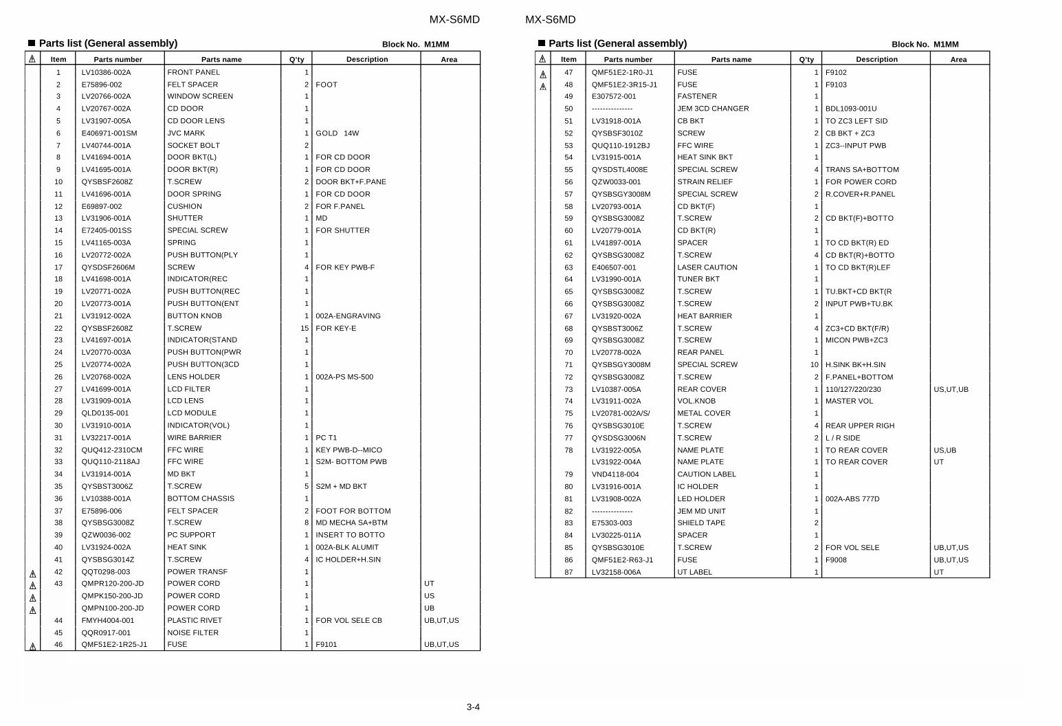
3-4
IHA B C D E F G
1
2
3
4
5
6
MX-S6MD MX-S6MD
Item Parts number Parts name AreaA Q'ty Description
Block No. M1MM
1 LV10386-002A FRONT PANEL 1
2 E75896-002 FELT SPACER 2 FOOT
3 LV20766-002A WINDOW SCREEN 1
4 LV20767-002A CD DOOR 1
5 LV31907-005A CD DOOR LENS 1
6 E406971-001SM JVC MARK 1 GOLD 14W
7 LV40744-001A SOCKET BOLT 2
8 LV41694-001A DOOR BKT(L) 1 FOR CD DOOR
9 LV41695-001A DOOR BKT(R) 1 FOR CD DOOR
10 QYSBSF2608Z T.SCREW 2 DOOR BKT+F.PANE
11 LV41696-001A DOOR SPRING 1 FOR CD DOOR
12 E69897-002 CUSHION 2 FOR F.PANEL
13 LV31906-001A SHUTTER 1 MD
14 E72405-001SS SPECIAL SCREW 1 FOR SHUTTER
15 LV41165-003A SPRING 1
16 LV20772-002A PUSH BUTTON(PLY 1
17 QYSDSF2606M SCREW 4 FOR KEY PWB-F
18 LV41698-001A INDICATOR(REC 1
19 LV20771-002A PUSH BUTTON(REC 1
20 LV20773-001A PUSH BUTTON(ENT 1
21 LV31912-002A BUTTON KNOB 1 002A-ENGRAVING
22 QYSBSF2608Z T.SCREW 15 FOR KEY-E
23 LV41697-001A INDICATOR(STAND 1
24 LV20770-003A PUSH BUTTON(PWR 1
25 LV20774-002A PUSH BUTTON(3CD 1
26 LV20768-002A LENS HOLDER 1 002A-PS MS-500
27 LV41699-001A LCD FILTER 1
28 LV31909-001A LCD LENS 1
29 QLD0135-001 LCD MODULE 1
30 LV31910-001A INDICATOR(VOL) 1
31 LV32217-001A WIRE BARRIER 1 PC T1
32 QUQ412-2310CM FFC WIRE 1 KEY PWB-D--MICO
33 QUQ110-2118AJ FFC WIRE 1 S2M- BOTTOM PWB
34 LV31914-001A MD BKT 1
35 QYSBST3006Z T.SCREW 5 S2M + MD BKT
36 LV10388-001A BOTTOM CHASSIS 1
37 E75896-006 FELT SPACER 2 FOOT FOR BOTTOM
38 QYSBSG3008Z T.SCREW 8 MD MECHA SA+BTM
39 QZW0036-002 PC SUPPORT 1 INSERT TO BOTTO
40 LV31924-002A HEAT SINK 1 002A-BLK ALUMIT
41 QYSBSG3014Z T.SCREW 4 IC HOLDER+H.SIN
42 QQT0298-003 POWER TRANSFA 1
43 QMPR120-200-JD POWER CORD UTA 1
QMPK150-200-JD POWER CORD USA 1
QMPN100-200-JD POWER CORD UBA 1
44 FMYH4004-001 PLASTIC RIVET UB,UT,US1 FOR VOL SELE CB
45 QQR0917-001 NOISE FILTER 1
46 QMF51E2-1R25-J1 FUSE UB,UT,USA 1 F9101
Parts list (General assembly)Item Parts number Parts name AreaA Q'ty Description
Block No. M1MM
47 QMF51E2-1R0-J1 FUSEA 1 F9102
48 QMF51E2-3R15-J1 FUSEA 1 F9103
49 E307572-001 FASTENER 1
50 --------------- JEM 3CD CHANGER 1 BDL1093-001U
51 LV31918-001A CB BKT 1 TO ZC3 LEFT SID
52 QYSBSF3010Z SCREW 2 CB BKT + ZC3
53 QUQ110-1912BJ FFC WIRE 1 ZC3--INPUT PWB
54 LV31915-001A HEAT SINK BKT 1
55 QYSDSTL4008E SPECIAL SCREW 4 TRANS SA+BOTTOM
56 QZW0033-001 STRAIN RELIEF 1 FOR POWER CORD
57 QYSBSGY3008M SPECIAL SCREW 2 R.COVER+R.PANEL
58 LV20793-001A CD BKT(F) 1
59 QYSBSG3008Z T.SCREW 2 CD BKT(F)+BOTTO
60 LV20779-001A CD BKT(R) 1
61 LV41897-001A SPACER 1 TO CD BKT(R) ED
62 QYSBSG3008Z T.SCREW 4 CD BKT(R)+BOTTO
63 E406507-001 LASER CAUTION 1 TO CD BKT(R)LEF
64 LV31990-001A TUNER BKT 1
65 QYSBSG3008Z T.SCREW 1 TU.BKT+CD BKT(R
66 QYSBSG3008Z T.SCREW 2 INPUT PWB+TU.BK
67 LV31920-002A HEAT BARRIER 1
68 QYSBST3006Z T.SCREW 4 ZC3+CD BKT(F/R)
69 QYSBSG3008Z T.SCREW 1 MICON PWB+ZC3
70 LV20778-002A REAR PANEL 1
71 QYSBSGY3008M SPECIAL SCREW 10 H.SINK BK+H.SIN
72 QYSBSG3008Z T.SCREW 2 F.PANEL+BOTTOM
73 LV10387-005A REAR COVER US,UT,UB1 110/127/220/230
74 LV31911-002A VOL.KNOB 1 MASTER VOL
75 LV20781-002A/S/ METAL COVER 1
76 QYSBSG3010E T.SCREW 4 REAR UPPER RIGH
77 QYSDSG3006N T.SCREW 2 L / R SIDE
78 LV31922-005A NAME PLATE US,UB1 TO REAR COVER
LV31922-004A NAME PLATE UT1 TO REAR COVER
79 VND4118-004 CAUTION LABEL 1
80 LV31916-001A IC HOLDER 1
81 LV31908-002A LED HOLDER 1 002A-ABS 777D
82 --------------- JEM MD UNIT 1
83 E75303-003 SHIELD TAPE 2
84 LV30225-011A SPACER 1
85 QYSBSG3010E T.SCREW UB,UT,US2 FOR VOL SELE
86 QMF51E2-R63-J1 FUSE UB,UT,US1 F9008
87 LV32158-006A UT LABEL UT1
Parts list (General assembly)

3-5
IHA B C D E F G
1
2
3
4
5
6
MX-S6MD
24
25
22
23
21
13
12
4715
14
11
2032
31
17
19
16
32
31
32
31
3018
26
29
28
27
37
36
35
36
34 34
33
10
5
4
8
61
3
2
2
46
46
46
7
89
39
4144
44
45
44
44
4339
40
40
38
42
42
42
0.2m
m6.
6
0.1m
m10
.8
0.2m
m66
.7
0.2m
m9.
8
FMU-ZC3-1M
g y pBlock No. M MM2
Grease=EM-30L=FL-7750
CD changer mechanism assembly and parts list

3-6
IHA B C D E F G
1
2
3
4
5
6
MX-S6MD MX-S6MD
Item Parts number Parts name AreaA
Parts list(CD changer mechanism)
Q'ty Description
Block No. M2MM
1 LV20581-001A CHASSIS UNIT 1
2 RF-500TB-12560 MOTOR 2
3 VKS5548-001 MOTOR PULLEY 2
4 QYSPSP2603Z SCREW 4
5 LV31586-001A SELECT GEAR 1
6 LV41427-001A SELECT SPRING 1
7 LV20588-001A GEAR BASE UNIT 1
8 QYSDST2606Z SCREW 3
9 LV41431-001A BELT 2
10 LV20586-001A SUB CHAS. UNIT 1
11 OPTIMA-725A1 CD PICK UNIT 1
12 LV32013-003A RACK ARM 1
13 QYSPSPT1720M MINI SCREW 2
14 LV31744-001A P.S.SPRING 1
15 QYSPSGT1425M TAP SCREW 1
16 VKS1161-005 T.MECHA CHASSIS 1
17 LV31745-001A TURN TABLE ASSY 1
18 QAR0123-001 SPINDLE MOTOR 1
19 VKZ4743-001 SPECIAL SCREW 2
20 WFM214025 WASHER 1
21 VKS5556-001 S.S. GEAR 1
22 VKS5557-001 F.M. GEAR 1
23 PPN-13KA10C MOTOR 1
24 VWE292-07AZAZ UL VINYL WIRE 1
25 VWE290-08AZAZ WIRE 1
26 VKS5558-001 MIDDLE GEAR 1
27 VKM3904-001 SHAFT HOLDER 1
28 VKZ4248-204 MINI TAP SCREW 1
29 QYSPSPL2004Z SCREW 1
30 LVB30006-001A FPC 1
31 LV41424-001A SPECIAL SCREW 3
32 LV41659-001A INSULATOR 3
33 LV31799-001A CLAMPER UNIT 1
34 QYSBSF2608Z T.SCREW 3
35 LV20594-001A SIDE(R) UNIT 1
36 QYSDST2606Z SCREW 3
37 LV31575-001A CLICK SPRING 1
38 LV10308-001A SIDE BKT(L) 1
39 QYSBSF2608Z T.SCREW 1
40 QYSDST2606Z SCREW 2
41 LV32067-001A FLAP BASE UNIT 1
42 LV20590-001A TRAY UNIT 3
43 LV10309-001A TOP COVER 1
44 QYSBSF2608Z T.SCREW 4
45 LV41429-002A ROD 2
46 QYSDST2606Z SCREW 5
47 VKZ4781-002 SCREW SHAFT 1
MD mechanism assembly and parts list Block No. M MM3
FMU-S2M-3M
58
58
17
16
15
57
3
2
4
198
5
60
56
12
11
10
1314
4644
4344
2632 31
30 48
47
45 32
29
3433
42
41
35
28
53
5254
55
36
37
37
40
51
51
51
51
21
49
50
24 23
2525
22
27 27
=EM-30L=CFD-4007HY2=946P
6
20
20
20
18
39
38
9
7
Grease
61.5 0.1mm
42 41
10.0 0.2mm
3938
7.0 0.2mm
9 7
1

3-7
MX-S6MD
Item Parts number Parts name AreaA
Parts list(MD mechanism)
Q'ty Description
Block No. M3MM
1 LV20548-007A LOADING ASSY 1
2 LV31472-002A CAM GEAR 1
3 QYWDL1230252 SLIT WASHER 1
4 LV41477-001A MINI TAP SCREW 2 CAM SW PWB
5 LV32168-001A WIRE HOLDER 1
6 LV31710-002A L.MOTOR ASSY 1
7 QAR0144-001 MOTOR 1
8 WJM0117-003A E-SI C WIRE C-F 1
9 LV41341-001A MOTOR PULLEY 1
10 QYSPSPT2020M MINI SCREW 2 LOAD.MOTOR
11 LV41342-001A BELT 1
12 LV41477-001A MINI TAP SCREW 1 L.MOTOR BKT.
13 LV30225-068A SPACER 1
14 LV30225-085A SPACER 1
15 LV20543-002A SLIDE BASE R 1
16 LV31483-001A SLIDE BASE L 1
17 LV41477-001A MINI TAP SCREW 2 SLIDE BASE
18 LV10286-002A LOAD.MECHA BASE 1
19 LVB40003-001A FPC CABLE 1
20 LV41477-001A MINI TAP SCREW 3 L.MECHA BASE
21 LV31709-003A TM.CHASSIS ASSY 1
22 LV20545-001A SP.MOTOR BASE 1
23 LE40515-001A COLLAR 1
24 LE40516-001A SPRING 1
25 QYSPSPU1720N SCREW 2 SP.MOTOR
26 FF-110PH-08280 SP.MOTOR 1
27 LV41477-001A MINI TAP SCREW 2 SP.MOTOR BASE
28 LE30470-202A T.TABLE ASSY 1
29 LV41343-001A SHAFT HOLDER R 1
30 LV41344-002A SHAFT HOLDER F 1
31 VKH5803-001 GUIDE SHAFT 1
32 LV41477-001A MINI TAP SCREW 2 SHAFT HOLDER
33 LV31484-001A T.SPRING HOLDER 1
34 LV41350-001A COM.SPRING 1
35 LV41477-001A MINI TAP SCREW 1 T.SP.HOLDER
36 LV31485-001A FEED MOTOR BKT. 1
37 QYSPSPT2025N MINI SCREW 2 FEED MOTOR
38 QAR0144-001 MOTOR 1 (FEED MOTOR)
39 LV41345-001A FEED WORM 1
40 LV41477-001A MINI TAP SCREW 2 FEED MOTOR BKT.
41 LV41346-001A SCREW SHAFT 1
42 LV41347-001A S.SHAFT GEAR 1
43 LV31486-001A PICK UP GUIDE 1
44 LV41477-001A MINI TAP SCREW 2 P-UP GUIDE
45 KMS-260B1 MD PICK UNIT 1
46 LVB30007-001A FPC CABLE 1
47 LV41348-001A RACK SPRING 1
48 QYSPSPT1414M MINI SCREW 2 RACK SPRING

MX-S6MD
3-8
Item Parts number Parts name AreaA
Parts list(MD mechanism)
Q'ty Description
Block No. M3MM
49 WJT0042-001A E-CARD WIRE 1
50 LV41477-001A MINI TAP SCREW 1 T.MECHA PWB
51 LV40761-003A INSULATOR 4
52 QAH0039-002 MD HEAD 1
53 QYSPSPT1740N MINI SCREW 1 MD HEAD
54 LV31487-002A HEAD LIFTER 1
55 LV41349-001A H.LIFTER SPRING 1
56 LV10284-002A SINGLE FRAME 1
57 LV10285-003A MECHA COVER 1
58 LV41477-001A MINI TAP SCREW 4 MECHA COVER
59 LV30225-068A SPACER 1
60 VKZ4539-024 MINI SCREW 2 SERVO PWB
61 LV30225-096A SPACER 1
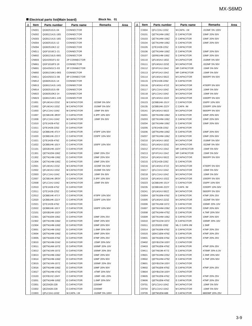
3-9
MX-S6MD
Item Parts number Parts name Area
Electrical parts list(Main board)
Remarks
Block No. 01
A
CN301 QGB2510J1-04 CONNECTOR
CN302 QGB1214J1-18S CONNECTOR
CN303 QGB1214J1-18S CONNECTOR
CN304 QGB2510J1-12 CONNECTOR
CN394 QGB2510K2-12 CONNECTOR
CN511 QGF1016C1-21 CONNECTOR
CN602 QGB1216J1-06S CONNECTOR
CN603 QGA2001F1-02 2P CONNECTOR
CN661 QGF1016F3-19 CONNECTOR
CN691 QGA2501C1-03 3P CONNECTOR
CN692 QGB1216K1-06S CONNECTOR
CN911 QGA2501C1-08 8P CONNECTOR
CN912 QGB2510J1-14 CONNECTOR
CN913 QGB1214J1-14S CONNECTOR
CN914 QGB2510J1-09 CONNECTOR
CN922 QGB2510K2-14 CONNECTOR
CN923 QGB1214K1-14S CONNECTOR
C1001 QFLM1HJ-223Z M CAPACITOR .022MF 5% 50V
C1002 QFLM1HJ-103Z M CAPACITOR .010MF 5% 50V
C1003 QFLC1HJ-104Z M CAPACITOR .10MF 5% 50V
C1007 QCSB1HK-3R3Y C CAPACITOR 3.3PF 10% 50V
C1008 QFLC1HJ-104Z M CAPACITOR .10MF 5% 50V
C1010 QTE1H28-475Z E CAPACITOR
C1011 QTE1H28-225Z E CAPACITOR
C1012 QCBB1HK-471Y C CAPACITOR 470PF 10% 50V
C1020 QCBB1HK-221Y C CAPACITOR 220PF 10% 50V
C1021 QTE1H28-476Z E CAPACITOR
C1022 QCBB1HK-101Y C CAPACITOR 100PF 10% 50V
C1101 QDGB1HK-102Y C CAPACITOR
C1301 QETN1EM-106Z E CAPACITOR 10MF 20% 25V
C1302 QETN1HM-106Z E CAPACITOR 10MF 20% 50V
C1304 QETN1HM-106Z E CAPACITOR 10MF 20% 50V
C2001 QFLM1HJ-223Z M CAPACITOR .022MF 5% 50V
C2002 QFLM1HJ-103Z M CAPACITOR .010MF 5% 50V
C2003 QFLC1HJ-104Z M CAPACITOR .10MF 5% 50V
C2007 QCSB1HK-3R3Y C CAPACITOR 3.3PF 10% 50V
C2008 QFLC1HJ-104Z M CAPACITOR .10MF 5% 50V
C2010 QTE1H28-475Z E CAPACITOR
C2011 QTE1H28-225Z E CAPACITOR
C2012 QCBB1HK-471Y C CAPACITOR 470PF 10% 50V
C2020 QCBB1HK-221Y C CAPACITOR 220PF 10% 50V
C2021 QTE1H28-476Z E CAPACITOR
C2022 QCBB1HK-101Y C CAPACITOR 100PF 10% 50V
C2101 QDGB1HK-102Y C CAPACITOR
C2301 QETN1EM-106Z E CAPACITOR 10MF 20% 25V
C2302 QETN1HM-106Z E CAPACITOR 10MF 20% 50V
C2304 QETN1HM-106Z E CAPACITOR 10MF 20% 50V
C3001 QETN1HM-105Z E CAPACITOR 1.0MF 20% 50V
C3004 QETN1HM-106Z E CAPACITOR 10MF 20% 50V
C3005 QETN1EM-476Z E CAPACITOR 47MF 20% 25V
C3010 QETN1HM-224Z E CAPACITOR .22MF 20% 50V
C3011 QETN1AM-107Z E CAPACITOR 100MF 20% 10V
C3012 QETN1VM-107Z E CAPACITOR 100MF 20% 35V
C3013 QETN1HM-106Z E CAPACITOR 10MF 20% 50V
C3014 QETN1HM-106Z E CAPACITOR 10MF 20% 50V
C3015 QETN1VM-107Z E CAPACITOR 100MF 20% 35V
C3016 QETN1HM-106Z E CAPACITOR 10MF 20% 50V
C3017 QETN1HM-474Z E CAPACITOR .47MF 20% 50V
C3103 QCFB1HZ-104Y C CAPACITOR .10MF +80:-20%
C3201 QETN1HM-105Z E CAPACITOR 1.0MF 20% 50V
C3301 QEZ0428-228 E.CAPACITOR 2200MF
C3302 QEZ0428-228 E.CAPACITOR 2200MF
C3303 QFLC2AJ-103Z M.CAPA. I.M .010MF 5% 100V
C3304 QFLC2AJ-103Z M.CAPA. I.M .010MF 5% 100V
C6101 QETN1HM-106Z E CAPACITOR 10MF 20% 50V
C6103 QETN1HM-106Z E CAPACITOR 10MF 20% 50V
C6104 QETN1HM-106Z E CAPACITOR 10MF 20% 50V
C6105 QTE1H28-225Z E CAPACITOR
C6106 QETN1HM-106Z E CAPACITOR 10MF 20% 50V
C6107 QER61HM-106Z E CAPACITOR 10MF 20% 50V
C6110 QFLM1HJ-183Z M CAPACITOR .018MF 5% 50V
C6111 QFLM1HJ-223Z M CAPACITOR .022MF 5% 50V
C6112 QFVF1HJ-154Z MF CAPACITOR .15MF 5% 50V
C6113 QFVF1HJ-154Z MF CAPACITOR .15MF 5% 50V
C6114 QFLM1HJ-562Z M CAPACITOR 5600PF 5% 50V
C6115 QTE1H28-226Z E CAPACITOR
C6116 QFLM1HJ-472Z M CAPACITOR 4700PF 5% 50V
C6117 QFLC1HJ-104Z M CAPACITOR .10MF 5% 50V
C6118 QFLC1HJ-104Z M CAPACITOR .10MF 5% 50V
C6119 QFLM1HJ-102Z M CAPACITOR 1000PF 5% 50V
C6123 QCBB1HK-151Y C CAPACITOR 150PF 10% 50V
C6135 QCBB1HK-222Y C CAPA IM 2200PF 10% 50V
C6141 QFLM1HJ-562Z M CAPACITOR 5600PF 5% 50V
C6201 QETN1HM-106Z E CAPACITOR 10MF 20% 50V
C6203 QETN1HM-106Z E CAPACITOR 10MF 20% 50V
C6204 QETN1HM-106Z E CAPACITOR 10MF 20% 50V
C6205 QTE1H28-225Z E CAPACITOR
C6206 QETN1HM-106Z E CAPACITOR 10MF 20% 50V
C6207 QETN1HM-106Z E CAPACITOR 10MF 20% 50V
C6210 QFLM1HJ-183Z M CAPACITOR .018MF 5% 50V
C6211 QFLM1HJ-223Z M CAPACITOR .022MF 5% 50V
C6212 QFVF1HJ-154Z MF CAPACITOR .15MF 5% 50V
C6213 QFVF1HJ-154Z MF CAPACITOR .15MF 5% 50V
C6214 QFLM1HJ-562Z M CAPACITOR 5600PF 5% 50V
C6215 QTE1H28-226Z E CAPACITOR
C6216 QFLM1HJ-472Z M CAPACITOR 4700PF 5% 50V
C6217 QFLC1HJ-104Z M CAPACITOR .10MF 5% 50V
C6218 QFLC1HJ-104Z M CAPACITOR .10MF 5% 50V
C6219 QFLM1HJ-102Z M CAPACITOR 1000PF 5% 50V
C6223 QCBB1HK-151Y C CAPACITOR 150PF 10% 50V
C6235 QCBB1HK-222Y C CAPA IM 2200PF 10% 50V
C6241 QFLM1HJ-562Z M CAPACITOR 5600PF 5% 50V
C6304 QETN1EM-476Z E CAPACITOR 47MF 20% 25V
C6305 QFLM1HJ-223Z M CAPACITOR .022MF 5% 50V
C6306 QETN1AM-107Z E CAPACITOR 100MF 20% 10V
C6307 QETN1HM-226Z E CAPACITOR 22MF 20% 50V
C6308 QETN1HM-475Z E CAPACITOR 4.7MF 20% 50V
C6309 QETN1HM-106Z E CAPACITOR 10MF 20% 50V
C6310 QETN1CM-107Z E CAPACITOR 100MF 20% 16V
C6311 QCZ0202-155Z ML C CAPA I/M 1.5MF
C6314 QETN1EM-476Z E CAPACITOR 47MF 20% 25V
C6315 QEKC1EM-476Z E CAPACITOR 47MF 20% 25V
C9401 QETN1EM-476Z E CAPACITOR 47MF 20% 25V
C9402 QDYB1CM-103Y C.CAPACITOR
C9403 QETN1EM-476Z E CAPACITOR 47MF 20% 25V
C9411 QETN0JM-477Z E CAPACITOR 470MF 20% 6.3V
C9501 QETN1HM-225Z E CAPACITOR 2.2MF 20% 50V
C9502 QETN1HM-475Z E CAPACITOR 4.7MF 20% 50V
C9601 QDYB1CM-103Y C.CAPACITOR
C9602 QETN1EM-476Z E CAPACITOR 47MF 20% 25V
C9604 QDYB1CM-103Y C.CAPACITOR
C9605 QETN1EM-476Z E CAPACITOR 47MF 20% 25V
C9606 QETN1EM-476Z E CAPACITOR 47MF 20% 25V
C9701 QFLC1HJ-104Z M CAPACITOR .10MF 5% 50V
C9704 QFLC1HJ-104Z M CAPACITOR .10MF 5% 50V
C9705 QETM1EM-688 E CAPACITOR 6800MF 20% 25V
Item Parts number Parts name AreaRemarksA

MX-S6MD
3-10
Item Parts number Parts name Area
Electrical parts list(Main board)
Remarks
Block No. 01
A
C9708 QDYB1CM-103Y C.CAPACITOR
C9709 QFZ0160-223Z PP CAPA IM .022MF
C9801 QFLM1HJ-683Z M CAPACITOR .068MF 5% 50V
C9804 QFLM1HJ-683Z M CAPACITOR .068MF 5% 50V
C9805 QETM1VM-228 E.CAPACITOR 2200MF 20% 35V
C9901 QETN1AM-107Z E CAPACITOR 100MF 20% 10V
D1001 1SS133-T2 SI DIODE
D1301 1SS133-T2 SI DIODE
D2001 1SS133-T2 SI DIODE
D2301 1SS133-T2 SI DIODE
D3001 MTZJ4.3B-T2 ZENER DIODE
D3002 1SS133-T2 SI DIODE
D3003 MTZJ2.4B-T2 Z.DIODE I.M
D3301 1N5402M-20 DIODEA
D3302 1N5402M-20 DIODEA
D3303 1N5402M-20 DIODEA
D3304 1N5402M-20 DIODEA
D6306 MTZJ5.1B-T2 ZENER DIODE
D6307 1SS133-T2 SI DIODE
D6308 MTZJ11A-T2 Z.DIODE I.M
D6309 1SS133-T2 SI DIODE
D6310 1SS133-T2 SI DIODE
D6311 1SS133-T2 SI DIODE
D9401 MTZJ6.8C-T2 Z DIODE I/M
D9501 1SS133-T2 SI DIODE
D9503 MTZJ5.1C-T2 ZENER DIODE
D9504 1SS133-T2 SI DIODE
D9601 MTZJ10C-T2 Z.DIODE I.M
D9602 MTZJ6.2C-T2 Z DIODE I/M
D9701 1N4003S-T5 SI DIODEA
D9702 1N4003S-T5 SI DIODEA
D9703 1N4003S-T5 SI DIODEA
D9704 1N4003S-T5 SI DIODEA
D9705 1N4003S-T5 SI DIODEA
D9706 1N4003S-T5 SI DIODEA
D9707 1N4003S-T5 SI DIODEA
D9708 1N4003S-T5 SI DIODEA
D9709 1SS133-T2 SI DIODE U ONLY
D9710 1SS133-T2 SI DIODE U ONLY
D9801 1N4003S-T5 SI DIODEA
D9802 1N4003S-T5 SI DIODEA
D9803 1N4003S-T5 SI DIODEA
D9804 1N4003S-T5 SI DIODEA
D9901 MTZJ4.3B-T2 ZENER DIODE
D9902 1N4003S-T5 SI DIODE
D9903 1N4003S-T5 SI DIODE
D9904 1N4003S-T5 SI DIODE
D9910 1N4003S-T5 SI DIODE +10V
EP301 QNZ0136-001Z EARTH PLATE
EP971 QNZ0136-001Z EARTH PLATE
IC301 STK402-030 ICA
IC671 TDA7439 IC
IC672 NJM4580D IC
IC673 TC4066BP/N/ IC
IC674 TC74HC02AP IC
J3001 QNB0010-001 SPK TERMINAL
J3101 QNS0072-001 HEADPHONE JACK
J3102 QNS0072-001 HEADPHONE JACK
J6301 QNN0365-001 PIN JACK
J6310 GP1FA550RZ OPT RECEIVER
L1001 QQLZ005-R45 INDUCTOR
L2001 QQLZ005-R45 INDUCTOR
L6141 QQR0590-001 FILTER
L6241 QQR0590-001 FILTER
L6801 QQL231K-4R7Y INDUCTOR
Q1001 KTA1268/GL/-T TRANSISTOR
Q1002 2SC3576-JVC-T TRANSISTOR I/M
Q1101 2SC3576-JVC-T TRANSISTOR I/M
Q1301 2SC2785/FE/-T TRANSISTOR
Q2001 KTA1268/GL/-T TRANSISTOR
Q2002 2SC3576-JVC-T TRANSISTOR I/M
Q2101 2SC3576-JVC-T TRANSISTOR I/M
Q2301 2SC2785/FE/-T TRANSISTOR
Q3001 KTD863/Y/-T TRANSISTOR
Q3002 2SK301/PQ/-T TRANSISTOR(FET)
Q3003 KRC110M-T TR I/M
Q3004 2SA1175/FE/-T TRANSISTOR
Q3005 2SC2785/FE/-T TRANSISTOR
Q3010 KRA104M-T D.TR.I.M
Q3011 KRC104M-T D.TR.I.M
Q3012 KRC102M-T D.TRANSISTOR
Q3201 KRA102M-T D.TRANSISTOR
Q6301 2SC3576-JVC-T TRANSISTOR I/M
Q6302 2SC3576-JVC-T TRANSISTOR I/M
Q6303 KRC104M-T D.TR.I.M
Q6304 2SC2785/FE/-T TRANSISTOR
Q6305 KTA1273/Y/-T TRANSISTOR
Q6306 KRC104M-T D.TR.I.M
Q6307 KRA104M-T D.TR.I.M
Q6308 2SC2785/FE/-T TRANSISTOR
Q6320 KRA104M-T D.TR.I.M
Q6321 KRC107M-T D.TR.I.M
Q9401 2SD1913/RS/ TRANSISTOR *A
Q9501 KRC104M-T D.TR.I.M
Q9502 KRC107M-T D.TR.I.M
Q9503 KRC104M-T D.TR.I.M
Q9601 2SC2785/FE/-T TRANSISTOR
Q9602 2SC2785/FE/-T TRANSISTOR
Q9603 KRA107M-T D.TR.I.M
Q9604 KRC107M-T D.TR.I.M
RY301 QSK0057-001 RELAY
R1003 QRZ9006-4R7X F RESISTOR 4.7 1/0W
R1006 QRT01DJ-R33X UNF.MF.RES.I/M 5% 1/1W
R1007 QRT01DJ-R33X UNF.MF.RES.I/M 5% 1/1W
R1009 QRE141J-563Y C RESISTOR 56K 5% 1/4W
R1010 QRJ146J-4R7X UNF C.RES I/M 4.7 5% 1/4W
R1011 QRZ9043-4R7X F.RES. I.M 4.7 1/0W
R1013 QRE141J-102Y C RESISTOR 1.0K 5% 1/4W
R1014 QRE141J-183Y C RESISTOR 18K 5% 1/4W
R1015 QRE141J-473Y C RESISTOR 47K 5% 1/4W
R1016 QRE141J-104Y C RESISTOR 100K 5% 1/4W
R1017 QRE141J-273Y C RESISTOR 27K 5% 1/4W
R1018 QRE141J-102Y C RESISTOR 1.0K 5% 1/4W
R1019 QRE141J-152Y C RESISTOR 1.5K 5% 1/4W
R1020 QRE141J-102Y C RESISTOR 1.0K 5% 1/4W
R1030 QRJ146J-751X UNF C.RES I/M 750 5% 1/4W
R1031 QRE141J-563Y C RESISTOR 56K 5% 1/4W
R1101 QRE141J-103Y C RESISTOR 10K 5% 1/4W
R1102 QRJ146J-681X UNF C.RES I/M 680 5% 1/4W
R1103 QRL01DJ-122X OMF RESISTOR 1.2K 5% 1/1W
R1201 QRE141J-221Y C RESISTOR 220 5% 1/4W
R1301 QRE141J-222Y C RESISTOR 2.2K 5% 1/4W
R1302 QRE141J-123Y C RESISTOR 12K 5% 1/4W
R1303 QRE141J-101Y C RESISTOR 100 5% 1/4W
R1304 QRE141J-221Y C RESISTOR 220 5% 1/4W
R1305 QRE141J-622Y C RESISTOR 6.2K 5% 1/4W
Item Parts number Parts name AreaRemarksA
A
A
A
A
A
A
A
A
A

3-11
MX-S6MD
Item Parts number Parts name Area
Electrical parts list(Main board)
Remarks
Block No. 01
A
R1306 QRE141J-562Y C RESISTOR 5.6K 5% 1/4W
R1308 QRE141J-472Y C RESISTOR 4.7K 5% 1/4W
R1309 QRE141J-272Y C RESISTOR 2.7K 5% 1/4W
R2003 QRZ9006-4R7X F RESISTOR 4.7 1/0W
R2006 QRT01DJ-R33X UNF.MF.RES.I/M 5% 1/1W
R2007 QRT01DJ-R33X UNF.MF.RES.I/M 5% 1/1W
R2009 QRE141J-563Y C RESISTOR 56K 5% 1/4W
R2010 QRJ146J-4R7X UNF C.RES I/M 4.7 5% 1/4W
R2011 QRZ9043-4R7X F.RES. I.M 4.7 1/0W
R2013 QRE141J-102Y C RESISTOR 1.0K 5% 1/4W
R2014 QRE141J-183Y C RESISTOR 18K 5% 1/4W
R2015 QRE141J-473Y C RESISTOR 47K 5% 1/4W
R2016 QRE141J-823Y C RESISTOR 82K 5% 1/4W
R2017 QRE141J-273Y C RESISTOR 27K 5% 1/4W
R2018 QRE141J-102Y C RESISTOR 1.0K 5% 1/4W
R2019 QRE141J-152Y C RESISTOR 1.5K 5% 1/4W
R2020 QRE141J-102Y C RESISTOR 1.0K 5% 1/4W
R2030 QRJ146J-751X UNF C.RES I/M 750 5% 1/4W
R2031 QRE141J-563Y C RESISTOR 56K 5% 1/4W
R2101 QRE141J-103Y C RESISTOR 10K 5% 1/4W
R2102 QRJ146J-681X UNF C.RES I/M 680 5% 1/4W
R2103 QRL01DJ-122X OMF RESISTOR 1.2K 5% 1/1W
R2201 QRE141J-221Y C RESISTOR 220 5% 1/4W
R2301 QRE141J-222Y C RESISTOR 2.2K 5% 1/4W
R2302 QRE141J-123Y C RESISTOR 12K 5% 1/4W
R2303 QRE141J-101Y C RESISTOR 100 5% 1/4W
R2304 QRE141J-221Y C RESISTOR 220 5% 1/4W
R2305 QRE141J-622Y C RESISTOR 6.2K 5% 1/4W
R2306 QRE141J-562Y C RESISTOR 5.6K 5% 1/4W
R2308 QRE141J-472Y C RESISTOR 4.7K 5% 1/4W
R2309 QRE141J-272Y C RESISTOR 2.7K 5% 1/4W
R3001 QRZ9005-101X F.RES I/M 100 1/0W
R3004 QRE141J-104Y C RESISTOR 100K 5% 1/4W
R3005 QRE141J-152Y C RESISTOR 1.5K 5% 1/4W
R3008 QRE141J-122Y C RESISTOR 1.2K 5% 1/4W
R3009 QRE141J-105Y C RESISTOR 1.0M 5% 1/4W
R3010 QRE141J-475Y C RESISTOR 4.7M 5% 1/4W
R3011 QRE141J-103Y C RESISTOR 10K 5% 1/4W
R3012 QRE141J-103Y C RESISTOR 10K 5% 1/4W
R3013 QRE141J-104Y C RESISTOR 100K 5% 1/4W
R3014 QRE141J-104Y C RESISTOR 100K 5% 1/4W
R3015 QRE141J-473Y C RESISTOR 47K 5% 1/4W
R3016 QRE141J-153Y C RESISTOR 15K 5% 1/4W
R3035 QRJ146J-101X UNF C.RES I/M 100 5% 1/4W
R3036 QRJ146J-101X UNF C.RES I/M 100 5% 1/4W
R3037 QRE141J-103Y C RESISTOR 10K 5% 1/4W
R3038 QRE141J-103Y C RESISTOR 10K 5% 1/4W
R3040 QRJ146J-101X UNF C.RES I/M 100 5% 1/4W
R3103 QRE141J-101Y C RESISTOR 100 5% 1/4W
R3201 QRE141J-223Y C RESISTOR 22K 5% 1/4W
R3301 QRE141J-223Y C RESISTOR 22K 5% 1/4W
R3302 QRE141J-223Y C RESISTOR 22K 5% 1/4W
R6105 QRE141J-562Y C RESISTOR 5.6K 5% 1/4W
R6106 QRE141J-272Y C RESISTOR 2.7K 5% 1/4W
R6107 QRE141J-273Y C RESISTOR 27K 5% 1/4W
R6108 QRE141J-273Y C RESISTOR 27K 5% 1/4W
R6109 QRE141J-392Y C RESISTOR 3.9K 5% 1/4W
R6110 QRE141J-102Y C RESISTOR 1.0K 5% 1/4W
R6111 QRE141J-222Y C RESISTOR 2.2K 5% 1/4W
R6112 QRE141J-222Y C RESISTOR 2.2K 5% 1/4W
R6114 QRE141J-104Y C RESISTOR 100K 5% 1/4W
R6118 QRE141J-221Y C RESISTOR 220 5% 1/4W
R6125 QRE141J-113Y C RESISTOR 11K 5% 1/4W
R6127 QRE141J-183Y C RESISTOR 18K 5% 1/4W
R6128 QRE141J-222Y C RESISTOR 2.2K 5% 1/4W
R6131 QRE141J-472Y C RESISTOR 4.7K 5% 1/4W
R6132 QRE141J-272Y C RESISTOR 2.7K 5% 1/4W
R6133 QRE141J-682Y C RESISTOR 6.8K 5% 1/4W
R6135 QRE141J-133Y C RESISTOR 13K 5% 1/4W
R6139 QRE141J-513Y C RESISTOR 51K 5% 1/4W
R6205 QRE141J-562Y C RESISTOR 5.6K 5% 1/4W
R6206 QRE141J-272Y C RESISTOR 2.7K 5% 1/4W
R6207 QRE141J-273Y C RESISTOR 27K 5% 1/4W
R6208 QRE141J-273Y C RESISTOR 27K 5% 1/4W
R6209 QRE141J-392Y C RESISTOR 3.9K 5% 1/4W
R6210 QRE141J-102Y C RESISTOR 1.0K 5% 1/4W
R6211 QRE141J-222Y C RESISTOR 2.2K 5% 1/4W
R6212 QRE141J-222Y C RESISTOR 2.2K 5% 1/4W
R6214 QRE141J-104Y C RESISTOR 100K 5% 1/4W
R6218 QRE141J-221Y C RESISTOR 220 5% 1/4W
R6225 QRE141J-113Y C RESISTOR 11K 5% 1/4W
R6227 QRE141J-183Y C RESISTOR 18K 5% 1/4W
R6228 QRE141J-222Y C RESISTOR 2.2K 5% 1/4W
R6231 QRE141J-472Y C RESISTOR 4.7K 5% 1/4W
R6232 QRE141J-272Y C RESISTOR 2.7K 5% 1/4W
R6233 QRE141J-682Y C RESISTOR 6.8K 5% 1/4W
R6235 QRE141J-133Y C RESISTOR 13K 5% 1/4W
R6239 QRE141J-513Y C RESISTOR 51K 5% 1/4W
R6303 QRE141J-103Y C RESISTOR 10K 5% 1/4W
R6304 QRE141J-103Y C RESISTOR 10K 5% 1/4W
R6305 QRE141J-271Y C RESISTOR 270 5% 1/4W
R6306 QRE141J-471Y C RESISTOR 470 5% 1/4W
R6307 QRE141J-473Y C RESISTOR 47K 5% 1/4W
R6311 QRE141J-103Y C RESISTOR 10K 5% 1/4W
R6324 QRJ146J-101X UNF C.RES I/M 100 5% 1/4W
R6327 QRE141J-473Y C RESISTOR 47K 5% 1/4W
R6329 QRE141J-224Y C RESISTOR 220K 5% 1/4W
R6332 QRE141J-101Y C RESISTOR 100 5% 1/4W
R6333 QRE141J-101Y C RESISTOR 100 5% 1/4W
R6334 QRE141J-101Y C RESISTOR 100 5% 1/4W
R6337 QRE141J-102Y C RESISTOR 1.0K 5% 1/4W
R6338 QRE141J-102Y C RESISTOR 1.0K 5% 1/4W
R6340 QRE141J-101Y C RESISTOR 100 5% 1/4W
R6341 QRE141J-101Y C RESISTOR 100 5% 1/4W
R6342 QRE141J-101Y C RESISTOR 100 5% 1/4W
R6343 QRE141J-101Y C RESISTOR 100 5% 1/4W
R6344 QRE141J-101Y C RESISTOR 100 5% 1/4W
R6345 QRE141J-101Y C RESISTOR 100 5% 1/4W
R9401 QRJ146J-100X UNF.C RESISTOR 10 5% 1/4W
R9402 QRE141J-152Y C RESISTOR 1.5K 5% 1/4W
R9404 QRE141J-101Y C RESISTOR 100 5% 1/4W
R9410 QRE141J-101Y C RESISTOR 100 5% 1/4W
R9411 QRE141J-101Y C RESISTOR 100 5% 1/4W
R9412 QRE141J-101Y C RESISTOR 100 5% 1/4W
R9502 QRE141J-103Y C RESISTOR 10K 5% 1/4W
R9503 QRE141J-103Y C RESISTOR 10K 5% 1/4W
R9504 QRE141J-104Y C RESISTOR 100K 5% 1/4W
R9601 QRZ9005-470X F.RES I/M 47 1/0W
R9602 QRE141J-102Y C RESISTOR 1.0K 5% 1/4W
R9603 QRJ146J-221X UNF C.RES I/M 220 5% 1/4W
R9604 QRE141J-272Y C RESISTOR 2.7K 5% 1/4W
R9605 QRE141J-102Y C RESISTOR 1.0K 5% 1/4W
R9606 QRE141J-103Y C RESISTOR 10K 5% 1/4W
R9701 QRE141J-103Y C RESISTOR U ONLY
R9702 QRE141J-103Y C RESISTOR U ONLY
R9703 QRE141J-223Y C RESISTOR 22K 5% 1/4W
Item Parts number Parts name AreaRemarksA
A
A
A
A
A
A
A
A
A
A
A
A
A

MX-S6MD
3-12
Item Parts number Parts name Area
Electrical parts list(Main board)
Remarks
Block No. 01
A
R9801 QRE141J-223Y C RESISTOR 22K 5% 1/4W
R9901 QRE141J-683Y C RESISTOR 68K 5% 1/4W
R9902 QRE141J-153Y C RESISTOR 15K 5% 1/4W
R9903 QRE141J-683Y C RESISTOR 68K 5% 1/4W
R9904 QRE141J-273Y C RESISTOR 27K 5% 1/4W
R9905 QRE141J-683Y C RESISTOR 68K 5% 1/4W
R9906 QRE141J-363Y C RESISTOR 36K 5% 1/4W
R9910 QRJ146J-392X UNF C.RES I/M 3.9K 5% 1/4W
W 121 WJK0016-003A E-SI C WIRE C-B
W 301 WJK0015-004A E-SI C WIRE C-B
W 302 QUM025-15Z3Z3 PARA RIBON WIRE
W 601 QJP001-031201 SHI CR C-B WIRE
W 912 QUM026-24Z3Z3 PARA RIBON WIRE

3-13
MX-S6MD
Item Parts number Parts name Area
Electrical parts list(Micon board)
Remarks
Block No. 02
A
CN391 QGB2510K2-04 CONNECTOR
CN392 QGB1214K1-18S CONNECTOR
CN393 QGB1214K1-18S CONNECTOR
CN701 QGB2011L1-14 B TO B CONNECTO
CN791 QGB2011M4-14 CONNECTOR
CN801 QGF1210G1-23 FFC CONNECTOR
CN851 QGF1005F2-28 FFC/FPC CONNE
CN891 QGF1205F1-23 CONNECTOR
CN924 QGB2510K2-09 CONNECTOR
C7011 QER41AM-107 E CAPACITOR 100MF 20% 10V
C7012 NCB21HK-102X C CAPACITOR
C8001 QCZ0202-155Z ML C CAPA I/M 1.5MF
C8002 NCS21HJ-330X C CAPACITOR
C8003 NCS21HJ-180X C CAPACITOR
C8004 NCB21HK-103X C CAPACITOR
C8005 NCB21HK-103X C CAPACITOR
C8006 NCB21HK-103X C CAPACITOR
C8007 NCS21HJ-220X C CAPACITOR EXCEPT DO
C8008 NCS21HJ-220X C CAPACITOR EXCEPT DO
C8017 NCB21HK-102X C CAPACITOR
C8018 NCB21HK-102X C CAPACITOR
C8020 QETN1AM-107Z E CAPACITOR 100MF 20% 10V
C8021 QETN0JM-108Z E CAPACITOR 1000MF 20% 6.3V
C8023 QETN1AM-107Z E CAPACITOR 100MF 20% 10V
C8030 NCB21HK-103X C CAPACITOR
C8031 NCB21HK-103X C CAPACITOR
C8111 NCB21HK-102X C CAPACITOR
C8201 NCB21HK-103X C CAPACITOR
C8202 NCB21HK-103X C CAPACITOR
C8211 NCB21HK-102X C CAPACITOR
C8301 NCF21AZ-475X C CAPACITOR
C8302 NCF21AZ-475X C CAPACITOR
C8303 NCF21AZ-475X C CAPACITOR
C8304 NCF21AZ-475X C CAPACITOR
C8305 NCB21CK-105X C CAPACITOR
C8306 NCB21CK-105X C CAPACITOR
C8307 NCB21CK-105X C CAPACITOR
C8308 NCB21CK-105X C CAPACITOR
C8309 NCB21CK-105X C CAPACITOR
C8311 NCB21HK-223X C CAPACITOR
C8401 QETN1HM-105Z E CAPACITOR 1.0MF 20% 50V
C8402 QETN1HM-105Z E CAPACITOR 1.0MF 20% 50V
C8403 QETN1HM-105Z E CAPACITOR 1.0MF 20% 50V
C8501 QCZ0202-155Z ML C CAPA I/M 1.5MF
C8502 NCS21HJ-330X C CAPACITOR
C8503 NCS21HJ-330X C CAPACITOR
C8504 NCB21HK-103X C CAPACITOR
C8505 NCB21HK-102X C CAPACITOR
C8506 QEKC1AM-107Z E.CAPACITOR 100MF 20% 10V
C8510 QEKC1AM-107Z E.CAPACITOR 100MF 20% 10V
C9101 QDVB1EZ-103Y C CAPACITOR
C9102 QETN1AM-107Z E CAPACITOR 100MF 20% 10V
C9103 QETN1CM-476Z E CAPACITOR 47MF 20% 16V
C9111 QDVB1EZ-103Y C CAPACITOR
C9112 QETN1AM-107Z E CAPACITOR 100MF 20% 10V
C9201 QDVB1EZ-103Y C CAPACITOR
C9202 QETN1CM-107Z E CAPACITOR 100MF 20% 16V
C9301 QDVB1EZ-103Y C CAPACITOR
C9302 QETN1CM-476Z E CAPACITOR 47MF 20% 16V
D7001 SLR-342VC-T LED
D8002 1SS355-X DIODE
D8003 1SS355-X DIODE
D8007 1SS355-X DIODE
D8008 1SS355-X DIODE
D8009 1SS355-X DIODE
D8010 1SS355-X DIODE
D8011 1SS355-X DIODE
D8401 NSTM515AS LED FULL COLOR
D8403 MA3075/H/-X ZENER DIODE
D8404 MA3075/H/-X ZENER DIODE
D8409 NSTM515AS LED FULL COLOR
D8411 MA3075/H/-X ZENER DIODE
D8412 MA3075/H/-X ZENER DIODE
D8413 1SS355-X DIODE
D8414 1SS355-X DIODE
D8417 1SS355-X DIODE
D8418 1SS355-X DIODE
D8501 1SS355-X DIODE
D8502 1SS355-X DIODE
D8503 1SS355-X DIODE
D8504 1SS355-X DIODE
D8601 SLA-360LT3F LED STBY RED
D8602 SLA-360MT3F LED P-ON GREEN
D9101 MTZJ6.8B-T2 NER DIODE
D9102 MTZJ6.8C-T2 Z DIODE I/M
D9111 MTZJ6.2C-T2 Z DIODE I/M
D9112 MTZJ7.5C-T2 ZENER DIODE
D9201 MTZJ11B-T2 ZENER DIODE
D9203 1SS133-T2 SI DIODE
D9301 MTZJ13B-T2 Z DIODE
IC701 GP1U261X IR DETECT UNIT
IC801 MN101C12GDX1 IC
IC851 MN101C12GDW IC
JS821 QSW0862-001 ROTALY SW
LS701 QSW0828-001 LEVER SWITCH
Q7001 DTC114EKA-X TRANSISTOR
Q8001 DTC114EKA-X TR
Q8002 DTA144EKA-X TRANSISTOR
Q8410 2SC2412K/RS/-X CHIP TRANSISTOR
Q8411 2SC2412K/RS/-X CHIP TRANSISTOR
Q8412 2SC2412K/RS/-X CHIP TRANSISTOR
Q8416 2SC2412K/RS/-X CHIP TRANSISTOR
Q8417 2SC2412K/RS/-X CHIP TRANSISTOR
Q8418 2SC2412K/RS/-X CHIP TRANSISTOR
Q8419 2SC2412K/RS/-X CHIP TRANSISTOR
Q8420 2SC2412K/RS/-X CHIP TRANSISTOR
Q8421 2SC2412K/RS/-X CHIP TRANSISTOR
Q8601 DTC114EKA-X TR
Q8602 DTC114EKA-X TR
Q9101 2SD2394/EF/ TRANSISTORA
Q9111 2SD2394/EF/ TRANSISTORA
Q9201 2SD2394/EF/ TRANSISTORA
Q9203 KRA107M-T D.TR.I.M
Q9204 KRC107M-T D.TR.I.M
Q9301 2SD2394/EF/ TRANSISTORA
Q9302 KRA107M-T D.TR.I.M
R7001 NRSA02J-102X MG RESISTOR
R7002 NRSA02J-102X MG RESISTOR
R7003 NRSA02J-122X MG RESISTOR
R7004 NRSA02J-152X MG RESISTOR
R7005 NRSA02J-222X MG RESISTOR
R7006 NRSA02J-272X MG RESISTOR
R7007 NRSA02J-392X MG RESISTOR
R7010 NRS181J-221X MG RESISTOR
R7020 NRSA02J-102X MG RESISTOR
R7101 NRSA02J-102X MG RESISTOR
Item Parts number Parts name AreaRemarksA

MX-S6MD
3-14
Item Parts number Parts name Area
Electrical parts list(Micon board)
Remarks
Block No. 02
A
R7102 NRSA02J-102X MG RESISTOR
R7103 NRSA02J-122X MG RESISTOR
R7104 NRSA02J-152X MG RESISTOR
R7105 NRSA02J-222X MG RESISTOR
R7106 NRSA02J-272X MG RESISTOR
R8001 NRSA02J-222X MG RESISTOR
R8002 NRSA02J-222X MG RESISTOR
R8003 NRSA02J-222X MG RESISTOR
R8004 NRSA02J-222X MG RESISTOR
R8005 NRSA02J-102X MG RESISTOR
R8006 NRSA02J-102X MG RESISTOR
R8007 NRSA02J-102X MG RESISTOR
R8008 NRSA02J-105X MG RESISTOR
R8011 NRSA02J-102X MG RESISTOR
R8012 NRSA02J-102X MG RESISTOR
R8013 NRSA02J-102X MG RESISTOR
R8014 NRSA02J-102X MG RESISTOR
R8015 NRSA02J-222X MG RESISTOR
R8016 NRSA02J-102X MG RESISTOR
R8017 NRSA02J-101X MG RESISTOR
R8019 NRSA02J-101X MG RESISTOR
R8020 NRSA02J-102X MG RESISTOR
R8021 NRSA02J-102X MG RESISTOR
R8024 NRSA02J-222X MG RESISTOR
R8025 NRSA02J-102X MG RESISTOR
R8026 NRSA02J-102X MG RESISTOR
R8027 NRSA02J-101X MG RESISTOR
R8028 NRSA02J-101X MG RESISTOR
R8029 NRSA02J-101X MG RESISTOR
R8030 NRSA02J-101X MG RESISTOR
R8031 NRSA02J-101X MG RESISTOR
R8032 NRSA02J-101X MG RESISTOR
R8033 NRSA02J-102X MG RESISTOR
R8034 NRSA02J-102X MG RESISTOR
R8035 NRSA02J-222X MG RESISTOR
R8036 NRSA02J-222X MG RESISTOR
R8037 NRSA02J-222X MG RESISTOR
R8038 NRSA02J-222X MG RESISTOR
R8039 NRSA02J-222X MG RESISTOR
R8040 NRSA02J-222X MG RESISTOR
R8041 NRSA02J-222X MG RESISTOR
R8042 NRSA02J-222X MG RESISTOR
R8043 NRSA02J-222X MG RESISTOR
R8044 NRSA02J-222X MG RESISTOR
R8045 NRSA02J-222X MG RESISTOR
R8046 NRSA02J-222X MG RESISTOR
R8047 NRSA02J-222X MG RESISTOR
R8048 NRSA02J-102X MG RESISTOR
R8049 NRSA02J-102X MG RESISTOR
R8050 NRSA02J-102X MG RESISTOR
R8051 NRSA02J-222X MG RESISTOR
R8052 NRSA02J-473X MG RESISTOR
R8053 NRSA02J-222X MG RESISTOR
R8054 NRSA02J-102X MG RESISTOR
R8055 NRSA02J-102X MG RESISTOR
R8056 NRSA02J-102X MG RESISTOR
R8057 NRSA02J-102X MG RESISTOR
R8058 NRSA02J-102X MG RESISTOR
R8059 NRSA02J-102X MG RESISTOR
R8060 NRSA02J-103X MG RESISTOR
R8062 NRSA02J-102X MG RESISTOR
R8063 NRSA02J-103X MG RESISTOR
R8064 NRSA02J-223X MG RESISTOR
R8065 NRSA02J-223X MG RESISTOR
R8066 NRSA02J-223X MG RESISTOR
R8067 NRSA02J-223X MG RESISTOR
R8068 NRSA02J-223X MG RESISTOR
R8070 NRSA02J-113X MG RESISTOR
R8071 NRSA02J-103X MG RESISTOR
R8072 NRSA02J-103X MG RESISTOR
R8077 NRSA02J-222X MG RESISTOR
R8078 NRSA02J-103X MG RESISTOR
R8080 NRS181J-470X MG RESISTOR
R8082 NRSA02J-221X MG RESISTOR E
R8084 NRSA02J-221X MG RESISTOR U
R8090 NRSA02J-473X MG RESISTOR
R8094 NRSA02J-103X MG RESISTOR
R8101 NRSA02J-102X MG RESISTOR
R8102 NRSA02J-102X MG RESISTOR
R8103 NRSA02J-122X MG RESISTOR
R8104 NRSA02J-152X MG RESISTOR
R8105 NRSA02J-222X MG RESISTOR
R8106 NRSA02J-272X MG RESISTOR
R8111 NRSA02J-103X MG RESISTOR
R8112 NRSA02J-222X MG RESISTOR
R8201 NRSA02J-102X MG RESISTOR
R8202 NRSA02J-102X MG RESISTOR
R8203 NRSA02J-103X MG RESISTOR
R8204 NRSA02J-103X MG RESISTOR
R8211 NRSA02J-103X MG RESISTOR
R8212 NRSA02J-222X MG RESISTOR
R8301 NRSA02J-364X MG RESISTOR
R8302 QVP0079-224Z V.RES. I.M
R8303 NRSA02J-624X MG RESISTOR
R8305 NRSA02J-304X MG RESISTOR
R8306 NRSA02J-304X MG RESISTOR
R8307 NRSA02J-304X MG RESISTOR
R8308 NRSA02J-304X MG RESISTOR
R8310 QRE141J-101Y C RESISTOR 100 5% 1/4W
R8411 NRS181J-221X MG RESISTOR RED
R8412 NRS181J-221X MG RESISTOR RED
R8413 NRS181J-221X MG RESISTOR RED
R8416 NRS181J-271X MG RESISTOR BLUE
R8417 NRS181J-271X MG RESISTOR BLUE
R8419 NRS181J-271X MG RESISTOR GREEN
R8420 NRS181J-271X MG RESISTOR GREEN
R8433 NRS181J-221X MG RESISTOR RED
R8434 NRS181J-221X MG RESISTOR RED
R8435 NRS181J-221X MG RESISTOR RED
R8438 NRS181J-271X MG RESISTOR BLUE
R8439 NRS181J-271X MG RESISTOR BLUE
R8441 NRS181J-271X MG RESISTOR GREEN
R8442 NRS181J-271X MG RESISTOR GREEN
R8444 NRSA02J-102X MG RESISTOR
R8445 NRSA02J-102X MG RESISTOR
R8446 NRSA02J-102X MG RESISTOR
R8447 NRSA02J-103X MG RESISTOR
R8448 NRSA02J-103X MG RESISTOR
R8449 NRSA02J-103X MG RESISTOR
R8450 NRS181J-222X MG RESISTOR
R8451 NRS181J-222X MG RESISTOR
R8452 NRS181J-222X MG RESISTOR
R8453 NRS181J-222X MG RESISTOR
R8454 NRS181J-222X MG RESISTOR
R8455 NRS181J-222X MG RESISTOR
R8501 NRSA02J-105X MG RESISTOR
Item Parts number Parts name AreaRemarksA

3-15
MX-S6MD
Item Parts number Parts name Area
Electrical parts list(Micon board)
Remarks
Block No. 02
A
R8502 NRSA02J-101X MG RESISTOR
R8503 NRSA02J-101X MG RESISTOR
R8504 NRSA02J-222X MG RESISTOR
R8505 NRSA02J-222X MG RESISTOR
R8506 NRSA02J-103X MG RESISTOR
R8507 NRSA02J-101X MG RESISTOR
R8508 NRSA02J-102X MG RESISTOR
R8509 NRSA02J-222X MG RESISTOR
R8510 NRSA02J-101X MG RESISTOR
R8511 NRSA02J-101X MG RESISTOR
R8512 NRSA02J-101X MG RESISTOR
R8513 NRSA02J-101X MG RESISTOR
R8514 NRSA02J-101X MG RESISTOR
R8515 NRSA02J-101X MG RESISTOR
R8516 NRSA02J-101X MG RESISTOR
R8518 NRSA02J-101X MG RESISTOR
R8519 NRSA02J-101X MG RESISTOR
R8520 NRSA02J-101X MG RESISTOR
R8521 NRSA02J-101X MG RESISTOR
R8522 NRSA02J-101X MG RESISTOR
R8523 NRSA02J-101X MG RESISTOR
R8524 NRSA02J-101X MG RESISTOR
R8525 NRSA02J-101X MG RESISTOR
R8526 NRSA02J-222X MG RESISTOR
R8527 NRSA02J-222X MG RESISTOR
R8528 NRSA02J-222X MG RESISTOR
R8601 NRSA02J-331X MG RESISTOR
R8602 NRSA02J-121X MG RESISTOR
R9101 QRE141J-271Y C RESISTOR 270 5% 1/4W
R9104 QRE141J-271Y C RESISTOR 270 5% 1/4W
R9106 QRJ146J-1R0X UNF C.RES I/M 1.0 5% 1/4W
R9107 QRJ146J-1R0X UNF C.RES I/M 1.0 5% 1/4W
R9112 QRE141J-271Y C RESISTOR 270 5% 1/4W
R9114 QRE141J-271Y C RESISTOR 270 5% 1/4W
R9116 QRJ146J-1R0X UNF C.RES I/M 1.0 5% 1/4W
R9201 QRE141J-221Y C RESISTOR 220 5% 1/4W
R9202 QRE141J-103Y C RESISTOR 10K 5% 1/4W
R9203 QRE141J-102Y C RESISTOR 1.0K 5% 1/4W
R9205 QRE141J-221Y C RESISTOR 220 5% 1/4W
R9206 QRJ146J-1R0X UNF C.RES I/M 1.0 5% 1/4W
R9301 QRJ146J-4R7X UNF C.RES I/M 4.7 5% 1/4W
R9302 QRE141J-471Y C RESISTOR 470 5% 1/4W
R9303 QRE141J-473Y C RESISTOR 47K 5% 1/4W
R9305 QRE141J-471Y C RESISTOR 470 5% 1/4W
R9306 QRE141J-102Y C RESISTOR 1.0K 5% 1/4W
S7001 QSW0651-001Z TACT SWITCH CANCEL
S7002 QSW0651-001Z TACT SWITCH ENTER
S7003 QSW0651-001Z TACT SWITCH TITLE/EDIT
S7004 QSW0651-001Z TACT SWITCH HIGH SPEED CDMD
S7005 QSW0651-001Z TACT SWITCH REC PAUSE
S7006 QSW0651-001Z TACT SWITCH LONG MODE
S7007 QSW0651-001Z TACT SWITCH REC MODE
S7101 QSW0651-001Z TACT SWITCH MD EJECT
S7102 QSW0651-001Z TACT SWITCH STOP
S7103 QSW0651-001Z TACT SWITCH CD PLAY
S7104 QSW0651-001Z TACT SWITCH MD PLAY
S7105 QSW0651-001Z TACT SWITCH TUNER
S7106 QSW0651-001Z TACT SWITCH LINE
S8101 QSW0651-001Z TACT SWITCH DISC
S8102 QSW0651-001Z TACT SWITCH CD1 EJECT
S8103 QSW0651-001Z TACT SWITCH CD2 EJECT
S8104 QSW0651-001Z TACT SWITCH CD3 EJECT
S8105 QSW0651-001Z TACT SWITCH MENU
S8106 QSW0651-001Z TACT SWITCH POWER
W 693 QJB001-021602 C-B WIRE ASSY
X8001 QAX0494-001Z RESONATOR I.M
X8002 QAX0401-001 CRYSTAL EXCEPT DO
X8501 QAX0416-001Z CERA LOCK
Item Parts number Parts name AreaRemarksA
A
A
A
A
A
Item Parts number Parts name Area
Electrical parts list(Trans board)
Remarks
Block No. 03
A
CN901 QGA2501F1-03 CONNECTOR
FT901 QNG0003-001Z FUSE CLIPA FOR F9101
FT902 QNG0003-001Z FUSE CLIPA FOR F9101
FT903 QNG0003-001Z FUSE CLIPA FOR F9102
FT904 QNG0003-001Z FUSE CLIPA FOR F9102
FT905 QNG0003-001Z FUSE CLIPA FOR F9103
FT906 QNG0003-001Z FUSE CLIPA FOR F9103
FT981 QNG0003-001Z FUSE CLIP UB,UT,USA FOR F9008
FT982 QNG0003-001Z FUSE CLIP UB,UT,USA FOR F9008
S8001 QSW0812-001 VOLTAGE SWITCH UB,UT,USA
TB991 QNZ0079-001Z TAB I.MA
TB992 QNZ0079-001Z TAB I.MA
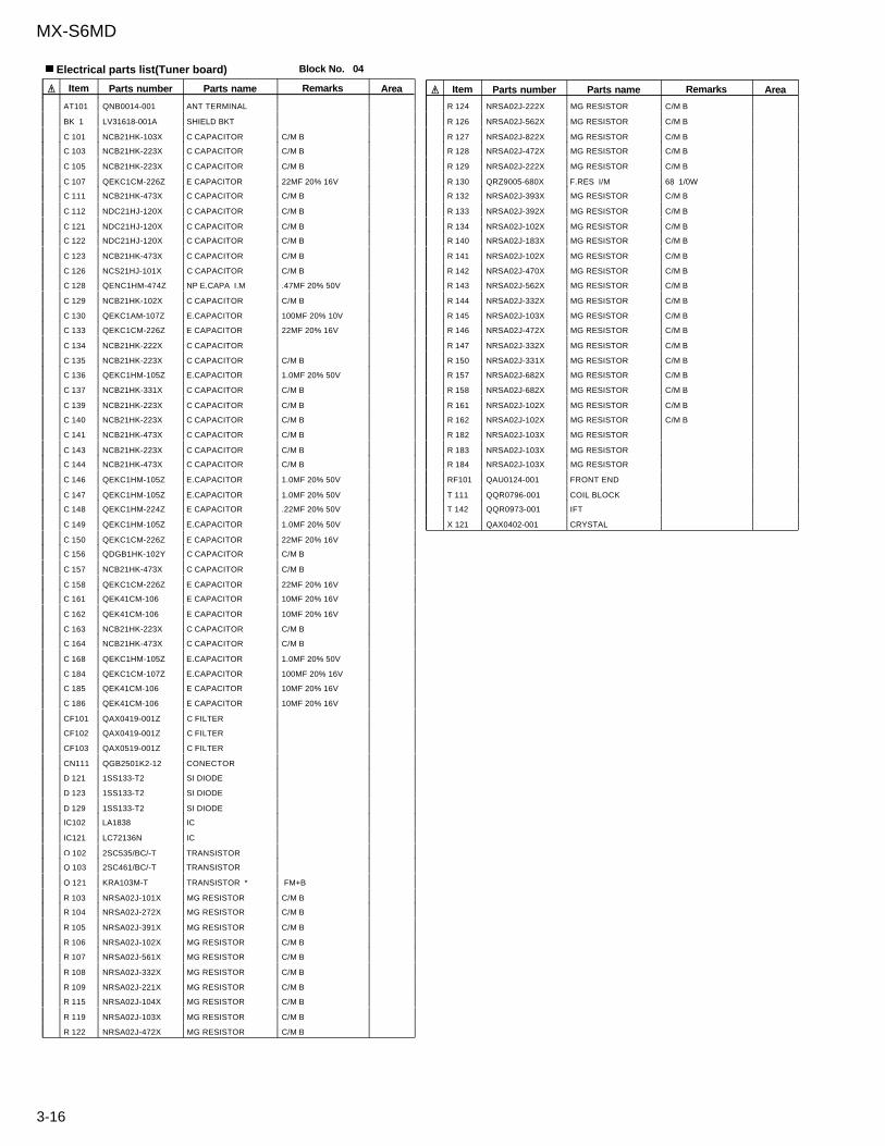
MX-S6MD
3-16
Item Parts number Parts name Area
Electrical parts list(Tuner board)
Remarks
Block No. 04
A
AT101 QNB0014-001 ANT TERMINAL
BK 1 LV31618-001A SHIELD BKT
C 101 NCB21HK-103X C CAPACITOR C/M B
C 103 NCB21HK-223X C CAPACITOR C/M B
C 105 NCB21HK-223X C CAPACITOR C/M B
C 107 QEKC1CM-226Z E CAPACITOR 22MF 20% 16V
C 111 NCB21HK-473X C CAPACITOR C/M B
C 112 NDC21HJ-120X C CAPACITOR C/M B
C 121 NDC21HJ-120X C CAPACITOR C/M B
C 122 NDC21HJ-120X C CAPACITOR C/M B
C 123 NCB21HK-473X C CAPACITOR C/M B
C 126 NCS21HJ-101X C CAPACITOR C/M B
C 128 QENC1HM-474Z NP E.CAPA I.M .47MF 20% 50V
C 129 NCB21HK-102X C CAPACITOR C/M B
C 130 QEKC1AM-107Z E.CAPACITOR 100MF 20% 10V
C 133 QEKC1CM-226Z E CAPACITOR 22MF 20% 16V
C 134 NCB21HK-222X C CAPACITOR
C 135 NCB21HK-223X C CAPACITOR C/M B
C 136 QEKC1HM-105Z E.CAPACITOR 1.0MF 20% 50V
C 137 NCB21HK-331X C CAPACITOR C/M B
C 139 NCB21HK-223X C CAPACITOR C/M B
C 140 NCB21HK-223X C CAPACITOR C/M B
C 141 NCB21HK-473X C CAPACITOR C/M B
C 143 NCB21HK-223X C CAPACITOR C/M B
C 144 NCB21HK-473X C CAPACITOR C/M B
C 146 QEKC1HM-105Z E.CAPACITOR 1.0MF 20% 50V
C 147 QEKC1HM-105Z E.CAPACITOR 1.0MF 20% 50V
C 148 QEKC1HM-224Z E CAPACITOR .22MF 20% 50V
C 149 QEKC1HM-105Z E.CAPACITOR 1.0MF 20% 50V
C 150 QEKC1CM-226Z E CAPACITOR 22MF 20% 16V
C 156 QDGB1HK-102Y C CAPACITOR C/M B
C 157 NCB21HK-473X C CAPACITOR C/M B
C 158 QEKC1CM-226Z E CAPACITOR 22MF 20% 16V
C 161 QEK41CM-106 E CAPACITOR 10MF 20% 16V
C 162 QEK41CM-106 E CAPACITOR 10MF 20% 16V
C 163 NCB21HK-223X C CAPACITOR C/M B
C 164 NCB21HK-473X C CAPACITOR C/M B
C 168 QEKC1HM-105Z E.CAPACITOR 1.0MF 20% 50V
C 184 QEKC1CM-107Z E.CAPACITOR 100MF 20% 16V
C 185 QEK41CM-106 E CAPACITOR 10MF 20% 16V
C 186 QEK41CM-106 E CAPACITOR 10MF 20% 16V
CF101 QAX0419-001Z C FILTER
CF102 QAX0419-001Z C FILTER
CF103 QAX0519-001Z C FILTER
CN111 QGB2501K2-12 CONECTOR
D 121 1SS133-T2 SI DIODE
D 123 1SS133-T2 SI DIODE
D 129 1SS133-T2 SI DIODE
IC102 LA1838 IC
IC121 LC72136N IC
Q 102 2SC535/BC/-T TRANSISTOR
Q 103 2SC461/BC/-T TRANSISTOR
Q 121 KRA103M-T TRANSISTOR * FM+B
R 103 NRSA02J-101X MG RESISTOR C/M B
R 104 NRSA02J-272X MG RESISTOR C/M B
R 105 NRSA02J-391X MG RESISTOR C/M B
R 106 NRSA02J-102X MG RESISTOR C/M B
R 107 NRSA02J-561X MG RESISTOR C/M B
R 108 NRSA02J-332X MG RESISTOR C/M B
R 109 NRSA02J-221X MG RESISTOR C/M B
R 115 NRSA02J-104X MG RESISTOR C/M B
R 119 NRSA02J-103X MG RESISTOR C/M B
R 122 NRSA02J-472X MG RESISTOR C/M B
R 124 NRSA02J-222X MG RESISTOR C/M B
R 126 NRSA02J-562X MG RESISTOR C/M B
R 127 NRSA02J-822X MG RESISTOR C/M B
R 128 NRSA02J-472X MG RESISTOR C/M B
R 129 NRSA02J-222X MG RESISTOR C/M B
R 130 QRZ9005-680X F.RES I/M 68 1/0W
R 132 NRSA02J-393X MG RESISTOR C/M B
R 133 NRSA02J-392X MG RESISTOR C/M B
R 134 NRSA02J-102X MG RESISTOR C/M B
R 140 NRSA02J-183X MG RESISTOR C/M B
R 141 NRSA02J-102X MG RESISTOR C/M B
R 142 NRSA02J-470X MG RESISTOR C/M B
R 143 NRSA02J-562X MG RESISTOR C/M B
R 144 NRSA02J-332X MG RESISTOR C/M B
R 145 NRSA02J-103X MG RESISTOR C/M B
R 146 NRSA02J-472X MG RESISTOR C/M B
R 147 NRSA02J-332X MG RESISTOR C/M B
R 150 NRSA02J-331X MG RESISTOR C/M B
R 157 NRSA02J-682X MG RESISTOR C/M B
R 158 NRSA02J-682X MG RESISTOR C/M B
R 161 NRSA02J-102X MG RESISTOR C/M B
R 162 NRSA02J-102X MG RESISTOR C/M B
R 182 NRSA02J-103X MG RESISTOR
R 183 NRSA02J-103X MG RESISTOR
R 184 NRSA02J-103X MG RESISTOR
RF101 QAU0124-001 FRONT END
T 111 QQR0796-001 COIL BLOCK
T 142 QQR0973-001 IFT
X 121 QAX0402-001 CRYSTAL
Item Parts number Parts name AreaRemarksA
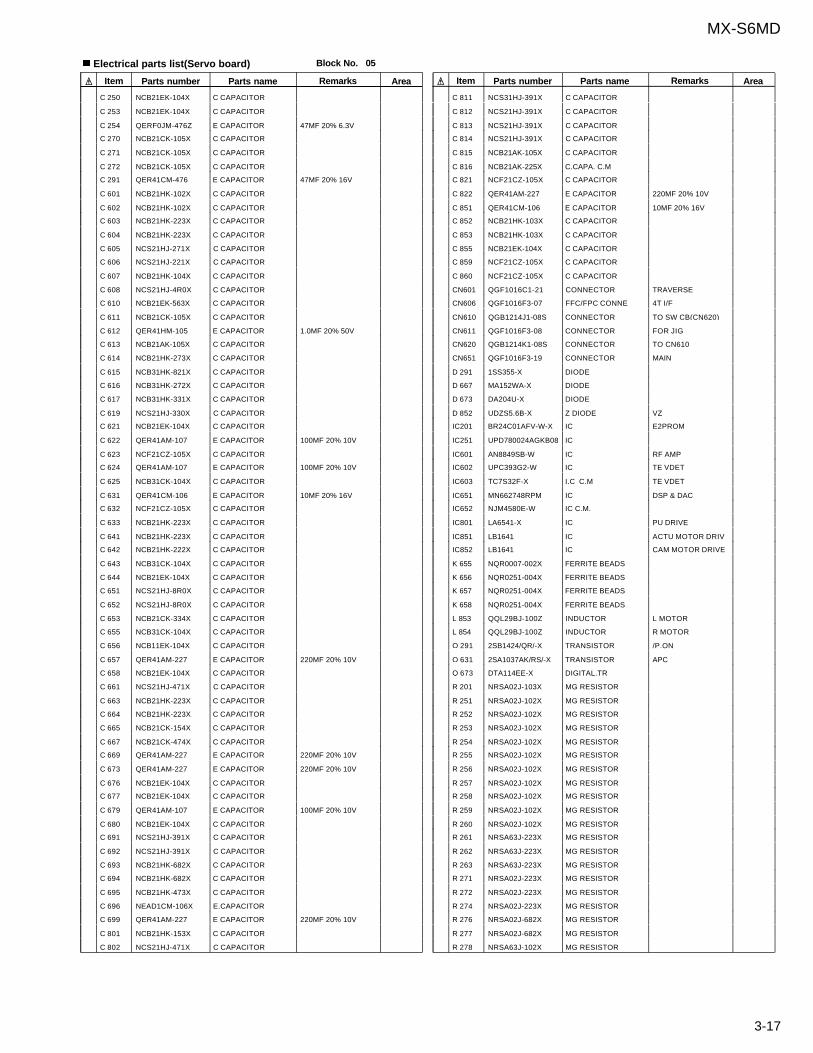
3-17
MX-S6MD
Item Parts number Parts name Area
Electrical parts list(Servo board)
Remarks
Block No. 05
A
C 250 NCB21EK-104X C CAPACITOR
C 253 NCB21EK-104X C CAPACITOR
C 254 QERF0JM-476Z E CAPACITOR 47MF 20% 6.3V
C 270 NCB21CK-105X C CAPACITOR
C 271 NCB21CK-105X C CAPACITOR
C 272 NCB21CK-105X C CAPACITOR
C 291 QER41CM-476 E CAPACITOR 47MF 20% 16V
C 601 NCB21HK-102X C CAPACITOR
C 602 NCB21HK-102X C CAPACITOR
C 603 NCB21HK-223X C CAPACITOR
C 604 NCB21HK-223X C CAPACITOR
C 605 NCS21HJ-271X C CAPACITOR
C 606 NCS21HJ-221X C CAPACITOR
C 607 NCB21HK-104X C CAPACITOR
C 608 NCS21HJ-4R0X C CAPACITOR
C 610 NCB21EK-563X C CAPACITOR
C 611 NCB21CK-105X C CAPACITOR
C 612 QER41HM-105 E CAPACITOR 1.0MF 20% 50V
C 613 NCB21AK-105X C CAPACITOR
C 614 NCB21HK-273X C CAPACITOR
C 615 NCB31HK-821X C CAPACITOR
C 616 NCB31HK-272X C CAPACITOR
C 617 NCB31HK-331X C CAPACITOR
C 619 NCS21HJ-330X C CAPACITOR
C 621 NCB21EK-104X C CAPACITOR
C 622 QER41AM-107 E CAPACITOR 100MF 20% 10V
C 623 NCF21CZ-105X C CAPACITOR
C 624 QER41AM-107 E CAPACITOR 100MF 20% 10V
C 625 NCB31CK-104X C CAPACITOR
C 631 QER41CM-106 E CAPACITOR 10MF 20% 16V
C 632 NCF21CZ-105X C CAPACITOR
C 633 NCB21HK-223X C CAPACITOR
C 641 NCB21HK-223X C CAPACITOR
C 642 NCB21HK-222X C CAPACITOR
C 643 NCB31CK-104X C CAPACITOR
C 644 NCB21EK-104X C CAPACITOR
C 651 NCS21HJ-8R0X C CAPACITOR
C 652 NCS21HJ-8R0X C CAPACITOR
C 653 NCB21CK-334X C CAPACITOR
C 655 NCB31CK-104X C CAPACITOR
C 656 NCB11EK-104X C CAPACITOR
C 657 QER41AM-227 E CAPACITOR 220MF 20% 10V
C 658 NCB21EK-104X C CAPACITOR
C 661 NCS21HJ-471X C CAPACITOR
C 663 NCB21HK-223X C CAPACITOR
C 664 NCB21HK-223X C CAPACITOR
C 665 NCB21CK-154X C CAPACITOR
C 667 NCB21CK-474X C CAPACITOR
C 669 QER41AM-227 E CAPACITOR 220MF 20% 10V
C 673 QER41AM-227 E CAPACITOR 220MF 20% 10V
C 676 NCB21EK-104X C CAPACITOR
C 677 NCB21EK-104X C CAPACITOR
C 679 QER41AM-107 E CAPACITOR 100MF 20% 10V
C 680 NCB21EK-104X C CAPACITOR
C 691 NCS21HJ-391X C CAPACITOR
C 692 NCS21HJ-391X C CAPACITOR
C 693 NCB21HK-682X C CAPACITOR
C 694 NCB21HK-682X C CAPACITOR
C 695 NCB21HK-473X C CAPACITOR
C 696 NEAD1CM-106X E.CAPACITOR
C 699 QER41AM-227 E CAPACITOR 220MF 20% 10V
C 801 NCB21HK-153X C CAPACITOR
C 802 NCS21HJ-471X C CAPACITOR
C 811 NCS31HJ-391X C CAPACITOR
C 812 NCS21HJ-391X C CAPACITOR
C 813 NCS21HJ-391X C CAPACITOR
C 814 NCS21HJ-391X C CAPACITOR
C 815 NCB21AK-105X C CAPACITOR
C 816 NCB21AK-225X C.CAPA. C.M
C 821 NCF21CZ-105X C CAPACITOR
C 822 QER41AM-227 E CAPACITOR 220MF 20% 10V
C 851 QER41CM-106 E CAPACITOR 10MF 20% 16V
C 852 NCB21HK-103X C CAPACITOR
C 853 NCB21HK-103X C CAPACITOR
C 855 NCB21EK-104X C CAPACITOR
C 859 NCF21CZ-105X C CAPACITOR
C 860 NCF21CZ-105X C CAPACITOR
CN601 QGF1016C1-21 CONNECTOR TRAVERSE
CN606 QGF1016F3-07 FFC/FPC CONNE 4T I/F
CN610 QGB1214J1-08S CONNECTOR TO SW CB(CN620)
CN611 QGF1016F3-08 CONNECTOR FOR JIG
CN620 QGB1214K1-08S CONNECTOR TO CN610
CN651 QGF1016F3-19 CONNECTOR MAIN
D 291 1SS355-X DIODE
D 667 MA152WA-X DIODE
D 673 DA204U-X DIODE
D 852 UDZS5.6B-X Z DIODE VZ
IC201 BR24C01AFV-W-X IC E2PROM
IC251 UPD780024AGKB08 IC
IC601 AN8849SB-W IC RF AMP
IC602 UPC393G2-W IC TE VDET
IC603 TC7S32F-X I.C C.M TE VDET
IC651 MN662748RPM IC DSP & DAC
IC652 NJM4580E-W IC C.M.
IC801 LA6541-X IC PU DRIVE
IC851 LB1641 IC ACTU MOTOR DRIV
IC852 LB1641 IC CAM MOTOR DRIVE
K 655 NQR0007-002X FERRITE BEADS
K 656 NQR0251-004X FERRITE BEADS
K 657 NQR0251-004X FERRITE BEADS
K 658 NQR0251-004X FERRITE BEADS
L 853 QQL29BJ-100Z INDUCTOR L MOTOR
L 854 QQL29BJ-100Z INDUCTOR R MOTOR
Q 291 2SB1424/QR/-X TRANSISTOR /P.ON
Q 631 2SA1037AK/RS/-X TRANSISTOR APC
Q 673 DTA114EE-X DIGITAL.TR
R 201 NRSA02J-103X MG RESISTOR
R 251 NRSA02J-102X MG RESISTOR
R 252 NRSA02J-102X MG RESISTOR
R 253 NRSA02J-102X MG RESISTOR
R 254 NRSA02J-102X MG RESISTOR
R 255 NRSA02J-102X MG RESISTOR
R 256 NRSA02J-102X MG RESISTOR
R 257 NRSA02J-102X MG RESISTOR
R 258 NRSA02J-102X MG RESISTOR
R 259 NRSA02J-102X MG RESISTOR
R 260 NRSA02J-102X MG RESISTOR
R 261 NRSA63J-223X MG RESISTOR
R 262 NRSA63J-223X MG RESISTOR
R 263 NRSA63J-223X MG RESISTOR
R 271 NRSA02J-223X MG RESISTOR
R 272 NRSA02J-223X MG RESISTOR
R 274 NRSA02J-223X MG RESISTOR
R 276 NRSA02J-682X MG RESISTOR
R 277 NRSA02J-682X MG RESISTOR
R 278 NRSA63J-102X MG RESISTOR
Item Parts number Parts name AreaRemarksA
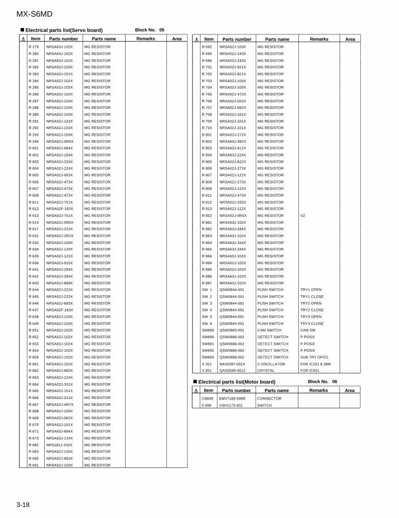
MX-S6MD
3-18
Item Parts number Parts name Area
Electrical parts list(Servo board)
Remarks
Block No. 05
A
R 279 NRSA63J-102X MG RESISTOR
R 280 NRSA63J-102X MG RESISTOR
R 281 NRSA63J-102X MG RESISTOR
R 282 NRSA02J-103X MG RESISTOR
R 283 NRSA02J-101X MG RESISTOR
R 284 NRSA02J-102X MG RESISTOR
R 285 NRSA02J-102X MG RESISTOR
R 286 NRSA02J-102X MG RESISTOR
R 287 NRSA02J-103X MG RESISTOR
R 288 NRSA02J-103X MG RESISTOR
R 289 NRSA63J-103X MG RESISTOR
R 291 NRSA02J-122X MG RESISTOR
R 292 NRSA02J-103X MG RESISTOR
R 293 NRSA02J-103X MG RESISTOR
R 294 NRSA02J-0R0X MG RESISTOR
R 601 NRSA02J-684X MG RESISTOR
R 602 NRSA02J-184X MG RESISTOR
R 603 NRSA02J-333X MG RESISTOR
R 604 NRSA02J-224X MG RESISTOR
R 605 NRSA02J-683X MG RESISTOR
R 606 NRSA02J-473X MG RESISTOR
R 607 NRSA02J-473X MG RESISTOR
R 608 NRSA02J-473X MG RESISTOR
R 611 NRSA02J-751X MG RESISTOR
R 612 NRSA02F-163X MG RESISTOR
R 613 NRSA02J-751X MG RESISTOR
R 614 NRSA02J-0R0X MG RESISTOR
R 617 NRSA02J-222X MG RESISTOR
R 631 NRSA02J-2R2X MG RESISTOR
R 632 NRSA02J-100X MG RESISTOR
R 634 NRSA02J-120X MG RESISTOR
R 635 NRSA02J-121X MG RESISTOR
R 636 NRSA02J-910X MG RESISTOR
R 641 NRSA02J-154X MG RESISTOR
R 642 NRSA02J-394X MG RESISTOR
R 643 NRSA02J-683X MG RESISTOR
R 644 NRSA02J-222X MG RESISTOR
R 645 NRSA02J-222X MG RESISTOR
R 646 NRSA02J-683X MG RESISTOR
R 647 NRSA02F-163X MG RESISTOR
R 648 NRSA02J-103X MG RESISTOR
R 649 NRSA02J-103X MG RESISTOR
R 651 NRSA02J-102X MG RESISTOR
R 652 NRSA02J-102X MG RESISTOR
R 653 NRSA02J-102X MG RESISTOR
R 654 NRSA02J-102X MG RESISTOR
R 659 NRSA02J-102X MG RESISTOR
R 661 NRSA02J-102X MG RESISTOR
R 662 NRSA02J-683X MG RESISTOR
R 663 NRSA02J-124X MG RESISTOR
R 664 NRSA02J-331X MG RESISTOR
R 665 NRSA02J-151X MG RESISTOR
R 666 NRSA02J-221X MG RESISTOR
R 667 NRSA02J-4R7X MG RESISTOR
R 668 NRSA02J-155X MG RESISTOR
R 669 NRSA02J-562X MG RESISTOR
R 670 NRSA02J-101X MG RESISTOR
R 671 NRSA63J-684X MG RESISTOR
R 673 NRSA63J-124X MG RESISTOR
R 682 NRS181J-102X MG RESISTOR
R 683 NRSA02J-105X MG RESISTOR
R 685 NRSA02J-683X MG RESISTOR
R 691 NRSA02J-103X MG RESISTOR
R 692 NRSA02J-103X MG RESISTOR
R 695 NRSA02J-243X MG RESISTOR
R 696 NRSA02J-243X MG RESISTOR
R 701 NRSA02J-821X MG RESISTOR
R 702 NRSA02J-821X MG RESISTOR
R 703 NRSA02J-103X MG RESISTOR
R 704 NRSA02J-103X MG RESISTOR
R 705 NRSA02J-472X MG RESISTOR
R 706 NRSA02J-202X MG RESISTOR
R 707 NRSA02J-682X MG RESISTOR
R 708 NRSA02J-101X MG RESISTOR
R 709 NRSA02J-101X MG RESISTOR
R 710 NRSA02J-221X MG RESISTOR
R 801 NRSA02J-272X MG RESISTOR
R 802 NRSA63J-392X MG RESISTOR
R 803 NRSA63J-912X MG RESISTOR
R 804 NRSA63J-224X MG RESISTOR
R 805 NRSA02J-822X MG RESISTOR
R 806 NRSA02J-273X MG RESISTOR
R 807 NRSA02J-122X MG RESISTOR
R 808 NRSA02J-273X MG RESISTOR
R 809 NRSA02J-122X MG RESISTOR
R 811 NRSA02J-473X MG RESISTOR
R 812 NRSA02J-332X MG RESISTOR
R 813 NRSA02J-122X MG RESISTOR
R 852 NRSA02J-0R0X MG RESISTOR VZ
R 861 NRSA63J-102X MG RESISTOR
R 862 NRSA63J-334X MG RESISTOR
R 863 NRSA63J-102X MG RESISTOR
R 864 NRSA63J-334X MG RESISTOR
R 865 NRSA63J-334X MG RESISTOR
R 866 NRSA63J-102X MG RESISTOR
R 884 NRSA02J-102X MG RESISTOR
R 885 NRSA02J-102X MG RESISTOR
R 886 NRSA63J-102X MG RESISTOR
R 887 NRSA63J-102X MG RESISTOR
SW 1 QSW0844-001 PUSH SWITCH TRY1 OPEN
SW 2 QSW0844-001 PUSH SWITCH TRY1 CLOSE
SW 3 QSW0844-001 PUSH SWITCH TRY2 OPEN
SW 4 QSW0844-001 PUSH SWITCH TRY2 CLOSE
SW 5 QSW0844-001 PUSH SWITCH TRY3 OPEN
SW 6 QSW0844-001 PUSH SWITCH TRY3 CLOSE
SW680 QSW0865-001 CAM SWITCH CAM SW
SW690 QSW0886-002 DETECT SWITCH P.POSI1
SW691 QSW0886-002 DETECT SWITCH P.POSI2
SW692 QSW0886-002 DETECT SWITCH P.POSI3
SW693 QSW0886-002 DETECT SWITCH SUB.TRY OP/CL
X 251 NAX0397-001X C OSCILLATOR FOR IC251 8.38M
X 651 QAX0599-001Z CRYSTAL FOR IC651
Item Parts number Parts name AreaRemarksA
Item Parts number Parts name Area
Electrical parts list(Motor board)
Remarks
Block No. 06
A
CN699 EMV7169-006R CONNECTOR
S 699 VSH1173-001 SWITCH
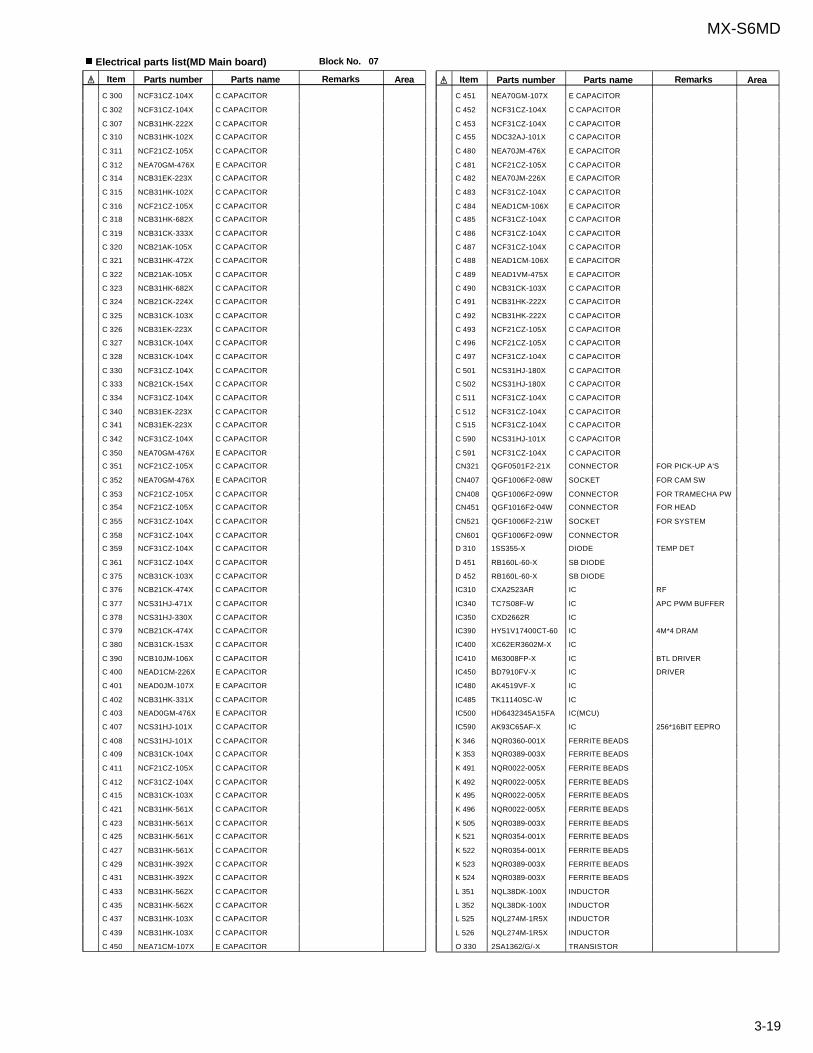
3-19
MX-S6MD
Item Parts number Parts name Area
Electrical parts list(MD Main board)
Remarks
Block No. 07
A
C 300 NCF31CZ-104X C CAPACITOR
C 302 NCF31CZ-104X C CAPACITOR
C 307 NCB31HK-222X C CAPACITOR
C 310 NCB31HK-102X C CAPACITOR
C 311 NCF21CZ-105X C CAPACITOR
C 312 NEA70GM-476X E CAPACITOR
C 314 NCB31EK-223X C CAPACITOR
C 315 NCB31HK-102X C CAPACITOR
C 316 NCF21CZ-105X C CAPACITOR
C 318 NCB31HK-682X C CAPACITOR
C 319 NCB31CK-333X C CAPACITOR
C 320 NCB21AK-105X C CAPACITOR
C 321 NCB31HK-472X C CAPACITOR
C 322 NCB21AK-105X C CAPACITOR
C 323 NCB31HK-682X C CAPACITOR
C 324 NCB21CK-224X C CAPACITOR
C 325 NCB31CK-103X C CAPACITOR
C 326 NCB31EK-223X C CAPACITOR
C 327 NCB31CK-104X C CAPACITOR
C 328 NCB31CK-104X C CAPACITOR
C 330 NCF31CZ-104X C CAPACITOR
C 333 NCB21CK-154X C CAPACITOR
C 334 NCF31CZ-104X C CAPACITOR
C 340 NCB31EK-223X C CAPACITOR
C 341 NCB31EK-223X C CAPACITOR
C 342 NCF31CZ-104X C CAPACITOR
C 350 NEA70GM-476X E CAPACITOR
C 351 NCF21CZ-105X C CAPACITOR
C 352 NEA70GM-476X E CAPACITOR
C 353 NCF21CZ-105X C CAPACITOR
C 354 NCF21CZ-105X C CAPACITOR
C 355 NCF31CZ-104X C CAPACITOR
C 358 NCF31CZ-104X C CAPACITOR
C 359 NCF31CZ-104X C CAPACITOR
C 361 NCF31CZ-104X C CAPACITOR
C 375 NCB31CK-103X C CAPACITOR
C 376 NCB21CK-474X C CAPACITOR
C 377 NCS31HJ-471X C CAPACITOR
C 378 NCS31HJ-330X C CAPACITOR
C 379 NCB21CK-474X C CAPACITOR
C 380 NCB31CK-153X C CAPACITOR
C 390 NCB10JM-106X C CAPACITOR
C 400 NEAD1CM-226X E CAPACITOR
C 401 NEAD0JM-107X E CAPACITOR
C 402 NCB31HK-331X C CAPACITOR
C 403 NEAD0GM-476X E CAPACITOR
C 407 NCS31HJ-101X C CAPACITOR
C 408 NCS31HJ-101X C CAPACITOR
C 409 NCB31CK-104X C CAPACITOR
C 411 NCF21CZ-105X C CAPACITOR
C 412 NCF31CZ-104X C CAPACITOR
C 415 NCB31CK-103X C CAPACITOR
C 421 NCB31HK-561X C CAPACITOR
C 423 NCB31HK-561X C CAPACITOR
C 425 NCB31HK-561X C CAPACITOR
C 427 NCB31HK-561X C CAPACITOR
C 429 NCB31HK-392X C CAPACITOR
C 431 NCB31HK-392X C CAPACITOR
C 433 NCB31HK-562X C CAPACITOR
C 435 NCB31HK-562X C CAPACITOR
C 437 NCB31HK-103X C CAPACITOR
C 439 NCB31HK-103X C CAPACITOR
C 450 NEA71CM-107X E CAPACITOR
C 451 NEA70GM-107X E CAPACITOR
C 452 NCF31CZ-104X C CAPACITOR
C 453 NCF31CZ-104X C CAPACITOR
C 455 NDC32AJ-101X C CAPACITOR
C 480 NEA70JM-476X E CAPACITOR
C 481 NCF21CZ-105X C CAPACITOR
C 482 NEA70JM-226X E CAPACITOR
C 483 NCF31CZ-104X C CAPACITOR
C 484 NEAD1CM-106X E CAPACITOR
C 485 NCF31CZ-104X C CAPACITOR
C 486 NCF31CZ-104X C CAPACITOR
C 487 NCF31CZ-104X C CAPACITOR
C 488 NEAD1CM-106X E CAPACITOR
C 489 NEAD1VM-475X E CAPACITOR
C 490 NCB31CK-103X C CAPACITOR
C 491 NCB31HK-222X C CAPACITOR
C 492 NCB31HK-222X C CAPACITOR
C 493 NCF21CZ-105X C CAPACITOR
C 496 NCF21CZ-105X C CAPACITOR
C 497 NCF31CZ-104X C CAPACITOR
C 501 NCS31HJ-180X C CAPACITOR
C 502 NCS31HJ-180X C CAPACITOR
C 511 NCF31CZ-104X C CAPACITOR
C 512 NCF31CZ-104X C CAPACITOR
C 515 NCF31CZ-104X C CAPACITOR
C 590 NCS31HJ-101X C CAPACITOR
C 591 NCF31CZ-104X C CAPACITOR
CN321 QGF0501F2-21X CONNECTOR FOR PICK-UP A'S
CN407 QGF1006F2-08W SOCKET FOR CAM SW
CN408 QGF1006F2-09W CONNECTOR FOR TRAMECHA PW
CN451 QGF1016F2-04W CONNECTOR FOR HEAD
CN521 QGF1006F2-21W SOCKET FOR SYSTEM
CN601 QGF1006F2-09W CONNECTOR
D 310 1SS355-X DIODE TEMP DET
D 451 RB160L-60-X SB DIODE
D 452 RB160L-60-X SB DIODE
IC310 CXA2523AR IC RF
IC340 TC7S08F-W IC APC PWM BUFFER
IC350 CXD2662R IC
IC390 HY51V17400CT-60 IC 4M*4 DRAM
IC400 XC62ER3602M-X IC
IC410 M63008FP-X IC BTL DRIVER
IC450 BD7910FV-X IC DRIVER
IC480 AK4519VF-X IC
IC485 TK11140SC-W IC
IC500 HD6432345A15FA IC(MCU)
IC590 AK93C65AF-X IC 256*16BIT EEPRO
K 346 NQR0360-001X FERRITE BEADS
K 353 NQR0389-003X FERRITE BEADS
K 491 NQR0022-005X FERRITE BEADS
K 492 NQR0022-005X FERRITE BEADS
K 495 NQR0022-005X FERRITE BEADS
K 496 NQR0022-005X FERRITE BEADS
K 505 NQR0389-003X FERRITE BEADS
K 521 NQR0354-001X FERRITE BEADS
K 522 NQR0354-001X FERRITE BEADS
K 523 NQR0389-003X FERRITE BEADS
K 524 NQR0389-003X FERRITE BEADS
L 351 NQL38DK-100X INDUCTOR
L 352 NQL38DK-100X INDUCTOR
L 525 NQL274M-1R5X INDUCTOR
L 526 NQL274M-1R5X INDUCTOR
Q 330 2SA1362/G/-X TRANSISTOR
Item Parts number Parts name AreaRemarksA

MX-S6MD
3-20
Item Parts number Parts name Area
Electrical parts list(MD Main board)
Remarks
Block No. 07
A
Q 331 DTA114EKA-X DIGITAL.TRANSIS
Q 332 DTA113ZKA-X TRANSISTOR
Q 333 DTA113ZKA-X TRANSISTOR
Q 400 2SA1363/EF/-X TRANSISTOR
Q 401 2SA1363/EF/-X TRANSISTOR
Q 410 DTC114EKA-X TRANSISTOR
Q 411 DTC114EKA-X TRANSISTOR
R 300 NRSA63J-0R0X MG RESISTOR
R 301 NRS181J-0R0X MG RESISTOR
R 302 NRSA63J-0R0X MG RESISTOR
R 305 NRSA63J-222X MG RESISTOR
R 306 NRSA63J-474X MG RESISTOR
R 309 NRSA63J-474X MG RESISTOR
R 310 NRSA63J-331X MG RESISTOR
R 311 NRSA63J-183X MG RESISTOR
R 312 NRSA63J-103X MG RESISTOR
R 313 NRSA63J-104X MG RESISTOR
R 314 NRSA63J-133X MG RESISTOR
R 315 NRSA63J-243X MG RESISTOR
R 316 NRSA63J-104X MG RESISTOR
R 317 NRSA63J-103X MG RESISTOR
R 320 NRSA63J-563X MG RESISTOR
R 321 NRSA63J-331X MG RESISTOR
R 322 NRSA63J-331X MG RESISTOR
R 323 NRSA63J-331X MG RESISTOR
R 324 NRSA63J-102X MG RESISTOR
R 325 NRSA63J-472X MG RESISTOR
R 326 NRSA63J-331X MG RESISTOR
R 327 NRSA63J-331X MG RESISTOR
R 328 NRSA63J-101X MG RESISTOR
R 330 NRSA63J-8R2X MG RESISTOR
R 331 NRSA63J-270X MG RESISTOR
R 332 NRSA63J-473X MG RESISTOR
R 333 NRSA63J-473X MG RESISTOR
R 334 NRSA63J-473X MG RESISTOR
R 335 NRSA63J-473X MG RESISTOR
R 336 NRSA63J-104X MG RESISTOR
R 337 NRSA63J-1R0X MG RESISTOR
R 338 NRSA63J-4R7X MG RESISTOR
R 339 NRSA63J-473X MG RESISTOR
R 340 NRSA63J-222X MG RESISTOR
R 341 NRSA63J-222X MG RESISTOR
R 342 NRSA63J-222X MG RESISTOR
R 343 NRSA63J-102X MG RESISTOR
R 354 NRSA63D-103X MG RESISTER
R 355 NRSA63D-103X MG RESISTER
R 356 NRSA63J-102X MG RESISTOR
R 361 NRSA63J-102X MG RESISTOR
R 362 NRSA63J-102X MG RESISTOR
R 363 NRSA63J-102X MG RESISTOR
R 364 NRSA63J-102X MG RESISTOR
R 365 NRSA63J-102X MG RESISTOR
R 366 NRSA63J-102X MG RESISTOR
R 367 NRSA63J-102X MG RESISTOR
R 368 NRSA63J-102X MG RESISTOR
R 369 NRSA63J-102X MG RESISTOR
R 370 NRSA63J-104X MG RESISTOR
R 371 NRSA63J-103X MG RESISTOR
R 372 NRSA63J-103X MG RESISTOR
R 375 NRSA63J-103X MG RESISTOR
R 376 NRSA63J-104X MG RESISTOR
R 377 NRSA63J-684X MG RESISTOR
R 378 NRSA63J-332X MG RESISTOR
R 379 NRSA63J-102X MG RESISTOR
R 380 NRSA63J-105X MG RESISTOR
R 381 NRSA63J-102X MG RESISTOR
R 382 NRSA63J-151X MG RESISTOR
R 387 NRSA63J-331X MG RESISTOR
R 389 NRSA63J-331X MG RESISTOR
R 390 NRSA63J-331X MG RESISTOR
R 391 NRSA63J-561X MG RESISTOR
R 392 NRSA63J-102X MG RESISTOR
R 393 NRSA63J-102X MG RESISTOR
R 394 NRSA63J-102X MG RESISTOR
R 395 NRSA63J-102X MG RESISTOR
R 396 NRSA63J-331X MG RESISTOR
R 397 NRSA63J-331X MG RESISTOR
R 398 NRSA63J-331X MG RESISTOR
R 399 NRSA63J-331X MG RESISTOR
R 401 NRSA63D-153X MG RESISTOR
R 402 NRSA63D-562X MG RESISTER
R 403 NRSA63D-471X MG RESISTER
R 404 NRSA63D-333X MG RESISTER
R 420 NRSA63D-223X RESISTOR
R 421 NRSA63D-103X MG RESISTER
R 422 NRSA63D-223X MG RESISTER
R 423 NRSA63D-103X MG RESISTER
R 424 NRSA63D-223X MG RESISTER
R 425 NRSA63D-103X MG RESISTER
R 426 NRSA63D-223X MG RESISTER
R 427 NRSA63D-103X MG RESISTER
R 428 NRSA63D-153X MG RESISTOR
R 429 NRSA63D-392X MG RESISTER
R 430 NRSA63D-153X MG RESISTOR
R 431 NRSA63D-392X MG RESISTER
R 432 NRSA63D-123X MG RESISTOR
R 433 NRSA63D-822X MG RESISTER
R 434 NRSA63D-123X MG RESISTOR
R 435 NRSA63D-822X MG RESISTER
R 436 NRSA63J-223X MG RESISTOR
R 437 NRSA63J-302X MG RESISTOR
R 438 NRSA63J-223X MG RESISTOR
R 439 NRSA63J-302X MG RESISTOR
R 440 NRSA63D-103X MG RESISTER
R 441 NRSA63D-103X MG RESISTER
R 451 NRSA63J-473X MG RESISTOR
R 452 NRSA63J-563X MG RESISTOR
R 453 NRSA63J-1R0X MG RESISTOR
R 454 NRSA63J-1R0X MG RESISTOR
R 455 NRSA63J-223X MG RESISTOR
R 456 NAD0006-103X THERMISTOR
R 481 NRSA63J-100X MG RESISTOR
R 483 NRSA63J-0R0X MG RESISTOR
R 491 NRSA63J-471X MG RESISTOR
R 492 NRSA63J-471X MG RESISTOR
R 495 NRSA63J-471X MG RESISTOR
R 496 NRSA63J-471X MG RESISTOR
R 497 NRSA63J-1R0X MG RESISTOR
R 502 NRSA63J-332X MG RESISTOR
R 503 NRSA63J-103X MG RESISTOR
R 504 NRSA63J-333X MG RESISTOR
R 506 NRSA63J-473X MG RESISTOR
R 509 NRSA63J-104X MG RESISTOR
R 510 NRSA63J-102X MG RESISTOR
R 511 NRSA63J-102X MG RESISTOR
R 512 NRSA63J-102X MG RESISTOR
Item Parts number Parts name AreaRemarksA

3-21
MX-S6MD
Item Parts number Parts name Area
Electrical parts list(MD Main board)
Remarks
Block No. 07
A
R 513 NRSA63J-102X MG RESISTOR
R 514 NRSA63J-102X MG RESISTOR
R 515 NRSA63J-102X MG RESISTOR
R 516 NRSA63J-102X MG RESISTOR
R 517 NRSA63J-104X MG RESISTOR
R 518 NRSA63J-102X MG RESISTOR
R 519 NRSA63J-102X MG RESISTOR
R 520 NRSA63J-102X MG RESISTOR
R 521 NRSA63J-102X MG RESISTOR
R 522 NRSA63J-222X MG RESISTOR
R 523 NRSA63J-102X MG RESISTOR
R 524 NRSA63J-102X MG RESISTOR
R 525 NRSA63J-102X MG RESISTOR
R 531 NRSA63J-103X MG RESISTOR
R 532 NRSA63J-103X MG RESISTOR
R 533 NRSA63J-103X MG RESISTOR
R 534 NRSA63J-103X MG RESISTOR
R 535 NRSA63J-103X MG RESISTOR
R 536 NRSA63J-103X MG RESISTOR
R 537 NRSA63J-103X MG RESISTOR
R 538 NRSA63J-473X MG RESISTOR
R 540 NRSA63J-473X MG RESISTOR
R 541 NRSA63J-473X MG RESISTOR
R 545 NRSA63J-0R0X MG RESISTOR
R 551 NRSA63J-104X MG RESISTOR
R 552 NRSA63J-104X MG RESISTOR
R 554 NRSA63J-104X MG RESISTOR
R 555 NRSA63J-102X MG RESISTOR
R 556 NRSA63J-102X MG RESISTOR
R 557 NRSA63J-102X MG RESISTOR
R 558 NRSA63J-102X MG RESISTOR
R 563 NRSA63J-102X MG RESISTOR
R 564 NRSA63J-102X MG RESISTOR
R 565 NRSA63J-102X MG RESISTOR
R 566 NRSA63J-102X MG RESISTOR
R 567 NRSA63J-102X MG RESISTOR
R 568 NRSA63J-102X MG RESISTOR
R 569 NRSA63J-102X MG RESISTOR
R 592 NRSA63J-104X MG RESISTOR
R 593 NRSA63J-103X MG RESISTOR
S 601 NSW0057-001X 2-SWITCH
S 602 NSW0007-001X PUSH SWITCH
X 350 NAX0355-001X CRYSTAL 90.3168MHZ
X 500 NAX0361-002X CRYSTAL 10MHZ 30PPM
Item Parts number Parts name Area
Electrical parts list(Cam Swith board)
Remarks
Block No. 08
A
CN611 QGF1016F3-08 CONNECTOR
CN612 QGA1501F1-02 CONNECTOR
S 611 QSW0848-001 CAM SWITCH

MX-S6MD
3-22
Packing materials and accessories parts listBlock No. M MM4
Block No. M MM5
A12
A11 P9
P9
P7
P10
P8
1/2
2/2
1/2
2/2
A8
A2A7
A1
A5
A3A4
A6
P5
P1P2
P3
P6
P4
SP-MXS6MDCA-MXS6MD
A9
A10

3-23
MX-S6MD
Item Parts number Parts name AreaA Q'ty Description
Block No. M4MM
P 1 QPA01504505 ENVELOPE UB1 CA-MXS6MD
P 2 QPC05006515P POLY BAG 1 CA-MXS6MD
P 3 LV32192-002A PACKING CASE 1 CA-MXS6MD
P 4 LV10394-001A PACKING PAD(FRO 1 CA-MXS6MD
P 5 LV10395-001A PACKING PAD(REA 1 CA-MXS6MD
P 6 QPC02503510P POLY BAG 1 CA-MXS6MD
P 7 8500028981 POLY BAG 1 SP-MXS6MD
P 8 8300040251 PACKING CASE US,UB1 SP-MXS6MD
8300040261 PACKING CASE UT1 SP-MXS6MD
P 9 8000042601 TOP CUSHION 1 SP-MXS6MD
P 10 8000042611 BOTTOM CUSHION 1 SP-MXS6MD
Item Parts number Parts name AreaA Q'ty Description
Block No. M5MM
A 1 QAL0014-001 AM LOOP ANT 1
A 2 EWP503-001C ANT.WIRE 1
A 3 LVT0529-003A I.B(CA-MXS6MD) UT1 CHI(TAIWAN)
LVT0529-001A I.B(CA-MXS6MD) UB,US1 ENG CHI(PEKIN)
A 4 LV42252-001A INST SHEET UB,US,UT1
A 5 --------------- BATTERY 2
A 6 RM-SMXS6MDU REMOCON 1 INSERT TO P.PAD
A 7 QAM0027-001 SIEMENS PLUG UT1
QAM0112-001 AC PLUG ADAPTER US1
A 8 LV30258-073A UB SHEET UB1
A 9 MXS6MDK-SPBOX-L SPEAKER BOX 1 SP-MXS6MD
MXS6MDK-SPBOX-R SPEAKER BOX 1 SP-MXS6MD
A 10 9913006711 SARAN BOARD 1 SP-MXS6MD
A 11 6200036801 SPEAKER CORD 2 SP-MXS6MD
A 12 LVT0575-002A I.B(SP-MXS6MD) UB,US1 CHI(PEKIN)
LVT0575-003A I.B(SP-MXS6MD) UT1 KOR CHI(TAIWAN)
Parts list (Accessories)
Parts list (Packing)