SAMSUNG Anycall - SGH-X640 - Altehandys.de
46
SGH-X640 1. Specification 2. Circuit Description 3. Exploded Views and Parts List 4. Electrical Parts List 5. Block Diagrams 6. PCB Diagrams 7. Flow Chart of Troubleshooting SAMSUNG Anycall CONTENTS SAMSUNG Anycall
-
Upload
khangminh22 -
Category
Documents
-
view
2 -
download
0
Transcript of SAMSUNG Anycall - SGH-X640 - Altehandys.de
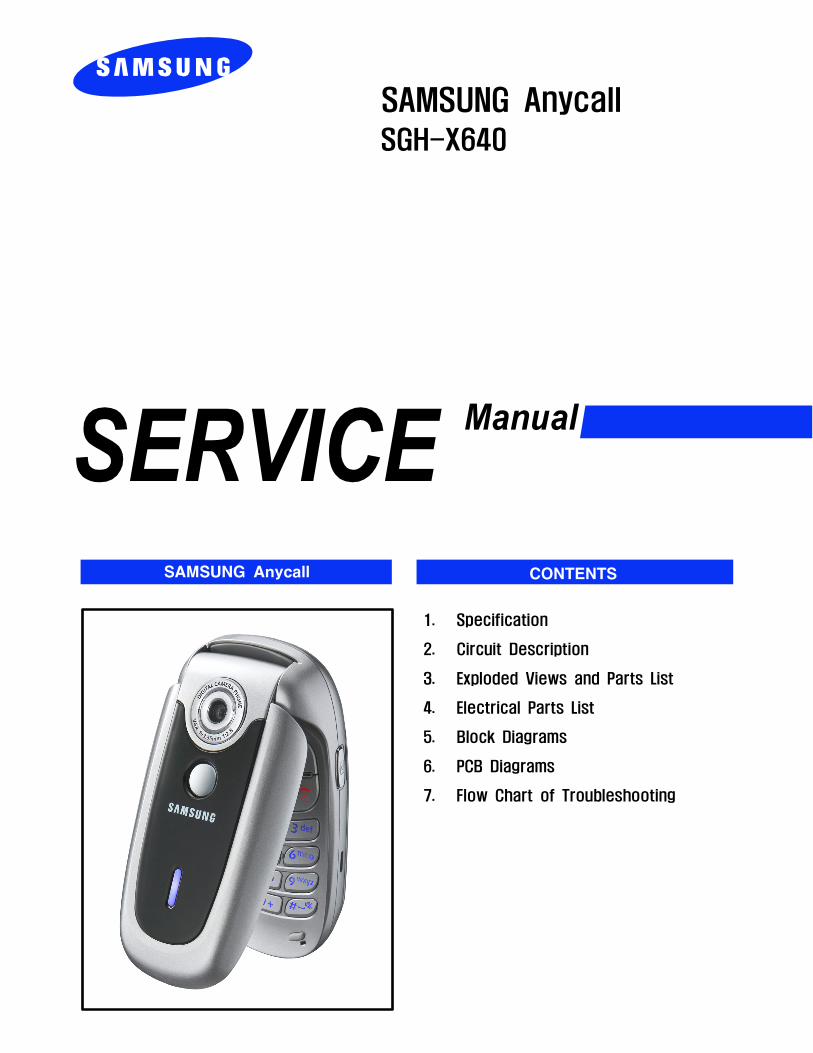
SGH-X640
1. Specification
2. Circuit Description
3. Exploded Views and Parts List
4. Electrical Parts List
5. Block Diagrams
6. PCB Diagrams
7. Flow Chart of Troubleshooting
SAMSUNG Anycall
CONTENTSSAMSUNG Anycall

Samsung Electronics Co.,Ltd. March. 2005
Printed in Korea.
Code No.: GH68-06819A
BASIC.
ⓒThis Service Manual is a property of Samsung Electronics Co.,Ltd.Any unauthorized use of Manual can be punished under applicableInternational and/or domestic law.
SAMSUNG Proprietary-Contents may change without notice
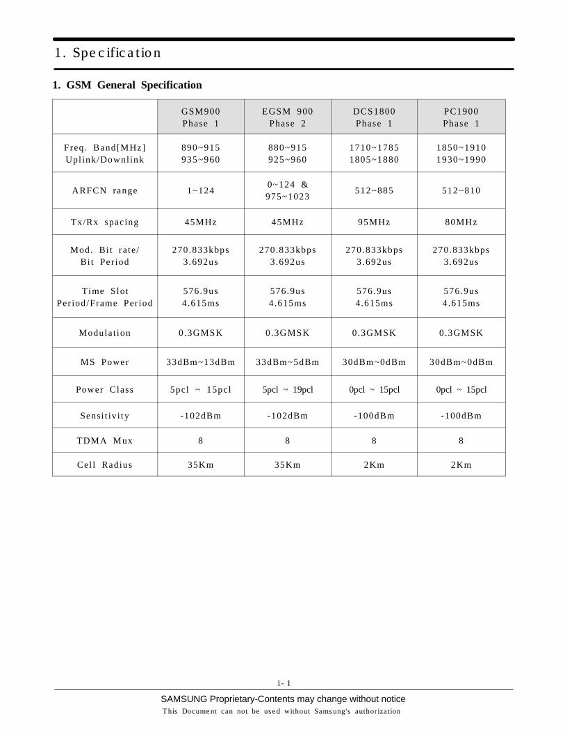
1. Specification
This Document can not be used without Samsung's authorization
1-1
GSM900Phase 1
EGSM 900Phase 2
DCS1800Phase 1
PC1900Phase 1
Freq. Band[MHz]Upl ink/Downlink
890~915935~960
880~915925~960
1710~17851805~1880
1850~19101930~1990
ARFCN range 1~1240~124 &975~1023
512~885 512~810
Tx/Rx spac ing 45MHz 45MHz 95MHz 80MHz
Mod. Bi t rate/Bi t Per iod
270.833kbps3.692us
270.833kbps3.692us
270.833kbps3.692us
270.833kbps3.692us
Time SlotPer iod/Frame Period
576.9us4.615ms
576.9us4.615ms
576.9us4.615ms
576.9us4.615ms
Modula t ion 0.3GMSK 0.3GMSK 0.3GMSK 0.3GMSK
MS Power 33dBm~13dBm 33dBm~5dBm 30dBm~0dBm 30dBm~0dBm
Power Class 5pcl ~ 15pcl 5pcl ~ 19pcl 0pcl ~ 15pcl 0pcl ~ 15pcl
Sensi t iv i ty -102dBm -102dBm -100dBm -100dBm
TDMA Mux 8 8 8 8
Cel l Radius 35Km 35Km 2Km 2Km
1. GSM General Specification
SAMSUNG Proprietary-Contents may change without noticeThis Document can not be used without Samsung's authorization
Specification
1-2
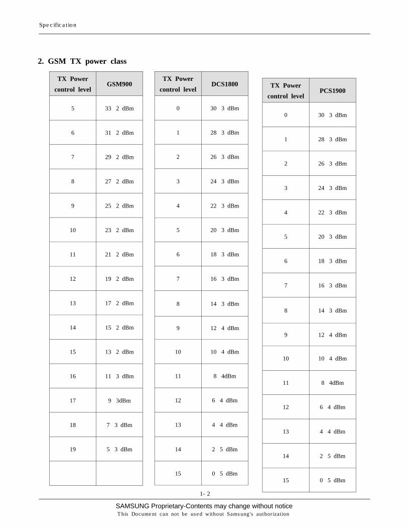
TX Power
control levelPCS1900
0 30±3 dBm
1 28±3 dBm
2 26±3 dBm
3 24±3 dBm
4 22±3 dBm
5 20±3 dBm
6 18±3 dBm
7 16±3 dBm
8 14±3 dBm
9 12±4 dBm
10 10±4 dBm
11 8±4dBm
12 6±4 dBm
13 4±4 dBm
14 2±5 dBm
15 0±5 dBm
TX Power
control levelGSM900
5 33±2 dBm
6 31±2 dBm
7 29±2 dBm
8 27±2 dBm
9 25±2 dBm
10 23±2 dBm
11 21±2 dBm
12 19±2 dBm
13 17±2 dBm
14 15±2 dBm
15 13±2 dBm
16 11±3 dBm
17 9±3dBm
18 7±3 dBm
19 5±3 dBm
TX Power
control levelDCS1800
0 30±3 dBm
1 28±3 dBm
2 26±3 dBm
3 24±3 dBm
4 22±3 dBm
5 20±3 dBm
6 18±3 dBm
7 16±3 dBm
8 14±3 dBm
9 12±4 dBm
10 10±4 dBm
11 8±4dBm
12 6±4 dBm
13 4±4 dBm
14 2±5 dBm
15 0±5 dBm
2. GSM TX power class
SAMSUNG Proprietary-Contents may change without notice
2. Circuit Description
2-1
This Document can not be used without Samsung's authorization
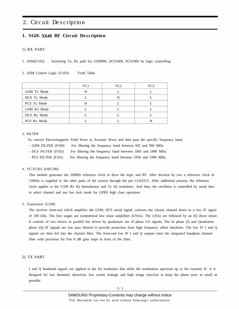
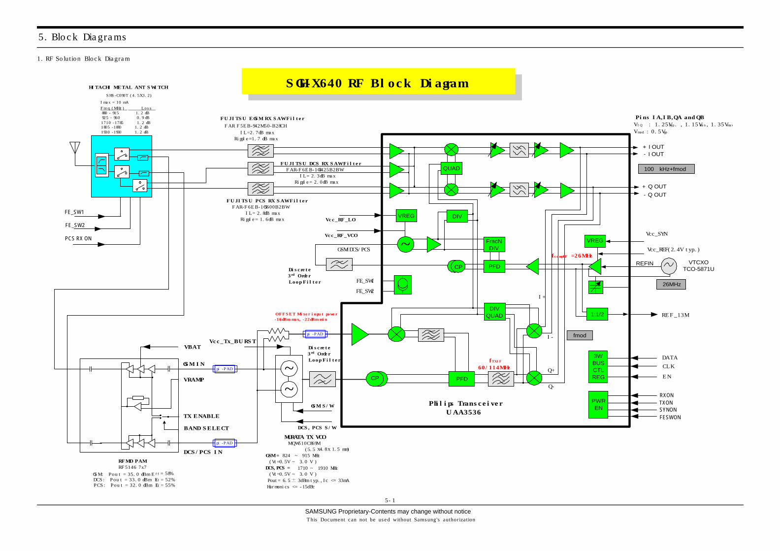
1. SGH-X640 RF Circuit Description
1) RX PART
1. ASM(U103) → Switching Tx, Rx path for GSM900, DCS1800, PCS1900 by logic controlling.
2. ASM Control Logic (U103) → Truth Table
VC1 VC2 VC3
GSM Tx Mode H L L
DCS Tx Mode L H L
PCS Tx Mode H L L
GSM Rx Mode L L L
DCS Rx Mode L L L
PCS Rx Mode L L H
3. FILTER
To convert Electromagnetic Field Wave to Acoustic Wave and then pass the specific frequency band.
- GSM FILTER (F100) → For filtering the frequency band between 925 and 960 MHz
- DCS FILTER (F102) → For filtering the frequency band between 1805 and 1880 MHz.
- PCS FILTER (F101) → For filtering the frequency band between 1930 and 1990 MHz.
4. VC-TCXO (OSC100)
This module generates the 26MHz reference clock to drive the logic and RF. After division by two a reference clock of
13MHz is supplied to the other parts of the system through the pin CLKOUT. After additional process, the reference
clock applies to the U100 Rx IQ demodulator and Tx IQ modulator. And then, the oscillator is controlled by serial data
to select channel and use fast lock mode for GPRS high class operation.
5. Transceiver (U100)
The receiver front-end which amplifies the GSM, DCS aerial signal, converts the chosen channel down to a low IF signal
of 100 kHz. The first stages are symmetrical low noise amplifiers (LNAs). The LNAs are followed by an IQ down mixer.
It consists of two mixers in parallel but driven by quadrature out of phase LO signals. The In phase (I) and Quadrature
phase (Q) IF signals are low pass filtered to provide protection from high frequency offset interferes. The low IF I and Q
signals are then fed into the channel filter. The front-end low IF I and Q outputs enter the integrated bandpass channel
filter with provision for five 8 dB gain steps in front of the filter.
2) TX PART
I and Q baseband signals are applied to the IQ modulator that shifts the modulation spectrum up to the transmit IF. It is
designed for low harmonic distortion, low carrier leakage and high image rejection to keep the phase error as small as
possible.
SAMSUNG Proprietary-Contents may change without notice
Circuit Description
2-2
This Document can not be used without Samsung's authorization
The modulator is loaded at its IF output by an integrated low pass filter that suppress unwanted spurs prior to get into
the phase detector. The clock drive is generated by division of the RFLO signal provided for the transmit offset mixer.
Baseband IQ signal fed into offset PLL, this function is included inside of U100 chip. OSC101 chip generates modulator
signal which power level is about 6.5dBm and fed into Power Amplifier(U102). The PA output power and power ramping
are well controlled by Auto Power Control circuit. We use offset PLL below table.
Modulation Spectrum
200kHz offset30 kHz bandwidth
GSM -35dBc
DCS -35dBc
400kHz offset30 kHz bandwidth
GSM -66dBc
DCS -65dBc
600kHz ~ 1.8MHz offset30 kHz bandwidth
GSM -75dBc
DCS -68dBc
2. Baseband Circuit description of SGH-X640
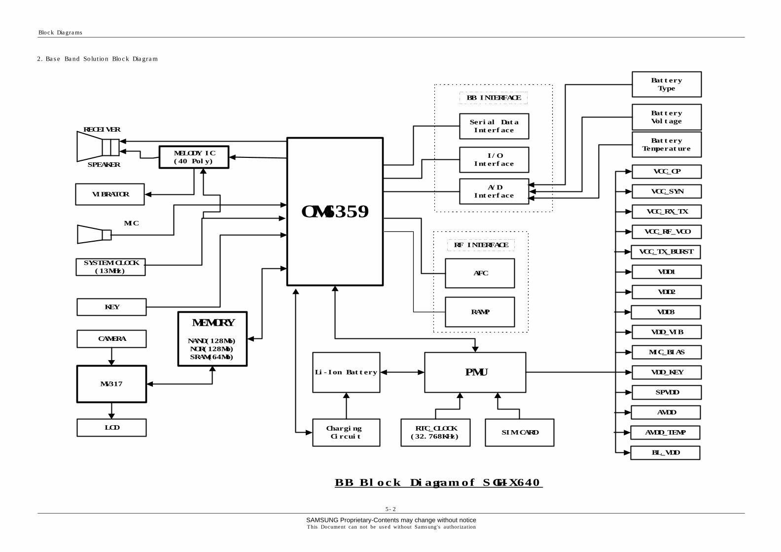
1. PCF50601
1.1. Power Management
Ten low-dropout regulators designed specifically for GSM applications power the terminal and help ensure optimal system
performance and long battery life. A programmable boost converter provides support for 1.8V, 3.0V, and 5.0V SIMs,
while a self-resetting, electronically fused switch supplies power to external accessories. Ancillary support functions, such
as RTC module and High Voltage Charge pump, Clock generator, aid in reducing both board area and system complexity.
I2C BUS serial interface provides access to control and configuration registers. This interface gives a microprocessor full
control of the PCF50601 and enables system designers to maximize both standby and talk times.
Supervisory functions. including a reset generator, an input voltage monitor, and a temperature sensor, support reliable
system design. These functions work together to ensure proper system behavior during start-up or in the event of a fault
condition(low microprocessor voltage, insufficient battery energy, or excessive die temperature).
1.2. Backlight Brightness Modulator
The Backlight Brightness Modulator (BBM) contains a programmable Pulse-width modulator (PWM) and FET
to modulate the intensity of a series of LED’s or to control a DC/DC converter that drives LCD backlight.
But, this phone (SGH-X640) is use UFB LCD. UFB LCD controls backlight brightness by contrast setting.
So "BL_VDD" voltage is always high value when phone is in active mode. When phone is in dimming mode "BL_VDD"
goes to about 10% duty PWM.
1.3. Clock Generator
The Clock Generator (CG) generates all clocks for internal and external usage. The 32768 Hz crystal
oscillator provides an accurate low clock frequency for the PCF50601 and other circuitry.
2. LCD ConnectorLCD is consisted of main LCD(color 65K UFB LCD).
Chip select signals LCD_MAIN_CS can enable LCD. BACKLIGHT signal enables white LED of main LCD.
"RESET_2V8" signal initiates the reset process of the LCD.
SAMSUNG Proprietary-Contents may change without notice
Circuit Description
2-3
This Document can not be used without Samsung's authorization
16-bit data lines(LD(0)~LD(15)) transfers data and commands to LCD through bypass capacitor. Data and commands use
"RS" signal. If this signal is high, inputs to LCD are commands. If it is low, inputs to LCD are data.
The signal which informs the state of LCD is whether input or output, is required. But in this system, there is no input
state from LCD. So only "L_WR" signal is used to indicate write data or command to LCD. Power signals for LCD are
"VBAT and "VDD2".
"M_SCL", "M_SCA", "PCLK", "FVALID", "LVALID" and "STANDBY" signals are all related to camera working.
"SVC_LED" is signal for service led when the signal is low led is on and vice versa. "SPK_P" and "SPK_N" are used
for audio speaker containing voice or melody. And "VDD_VIB" from PCF50601 enables the motor.
3. KeyThis is consisted of key interface pins among OM6359, KBIO(0:7). These signals compose the matrix. Result of matrix
informs the key status to key interface in the OM6359. Power on/off key is separated from the matrix. So power on/off
signal is connected with PCF50601 to enable PCF50601. Fifteen key LEDs are use the "VBAT" as supply voltage.
"VDD_KEY" signal enables LEDs. "FLIP" informs the status of folder (open or closed) to the OM6359. This uses the
hall effect IC, SH248CSP. A magnet under main LCD enables SH248CSP.
4. EMI ESD FilterThis system uses the EMI ESD filter, EMIF09 to protect noise from IF CONNECTOR part.
5. IF connetorIt is 18-pin connector. They are designed to use VBAT, V_EXT_CHARGE, TXD0, RXD0, RTS0, CTS0, JIG_REC,
CHARGER_OK, RXD1, TXD1, AUX_MIC, AUX_SPK and GND. They connected to power supply IC, microprocessor
and signal processor IC.
6. Battery Charge ManagementA complete constant-current/constant-voltage linear charger is used for single cell lithium-ion batteries.
If TA connected to phone, "V_EXT_CHARGE" enable charger IC and supply current to battery.
When fault condition caused, "CHG_ON" signal level change low to high and charger IC stop charging
process.
7. AudioEARP_P and EARP_N from OM6359 are connected to the main speaker. AUXSP is connected to the Hands free kit.
MIC_P and MIC_N are connected to the main MIC. And AUX_MIC_P and AUX_MIC_N are connected to the Hands
free kit.
YMU762C is a LSI for portable telephone that is capable of playing high quality music by utilizing FM synthesizer and
ADPCM decoder that are included in this device.
As a synthesis, YMU762C is equipped 32 voices with different tones. Since the device is capable of simultaneously
generating up to synchronous with the play of the FM synthesizer, various sampled voices can be used as sound effects.
Since the play data of YMU762C are interpreted at anytime through FIFO, the length of the data(playing period) is not
limited, so the device can flexibly support application such as incoming call melody music distribution service. The
hardware sequencer built in this device allows playing of the complex music without giving excessive load to the CPU of
the portable telephones.
SAMSUNG Proprietary-Contents may change without notice
Circuit Description
2-4
This Document can not be used without Samsung's authorization
Moreover, the registers of the FM synthesizer can be operated directly for real time sound generation, allowing, for
example, utilization of various sound effects when using the game software installed in the portable telephone.
YMU762C includes a speaker amplifier with high ripple removal rate whose maximum output is 550mW (SPVDD=3.6V).
The device is also equipped with conventional function including a vibrator and a circuit for controlling LEDs
synchronous with music.
For the headphone, it is provided with a stereophonic output terminal.
For the purpose of enabling YMU762C to demonstrate its full capabilities, Yamaha purpose to use "SMAF:Synthetic music
Mobile Application Format" as a data distribution format that is compatible with multimedia. Since the SMAF takes a
structure that sets importance on the synchronization between sound and images, various contents can be written into it
including incoming call melody with words that can be used for training karaoke, and commercial channel that combines
texts, images and sounds, and others. The hardware sequencer of YMU762C directly interprets and plays blocks relevant
to synthesis (playing music and reproducing ADPCM with FM synthesizer) that are included in data distributed in SMAF.
8. MemorySignals in the OM6359 enable two memories. They use only one volt supply voltage, VDD3 in the PCF50601. This
system uses Samsung's memory, KBB06A500M-T402. It is consisted of 128M bits flash NOR memory and 128M bits
flash NAND memory and 64M bits SCRAM. It has 16 bit data line, HD[0~15] which is connected to OM6359 and
MV317S. It has 26 bit address lines, HA[1~26]. CS_NAND and NCSRAM signals are chip select. Writing process,
HWR_N is low and it enables writing process to flash memory and SRAM. During reading process, HRD_N is low and
it enables reading process to flash memory and SRAM. Each chip select signals in the OM6359 select memory among 2
flash memory and SCRAM. Reading or writing procedure is processed after HWR_N or HRD_N is enabled. Memories
use reset, which is VDD3 delay from PCF50601. HA[25] signal enables lower byte of SRAM and HA[26] signal enables
higher byte of SRAM.
9. OM6359OM6359 is consisted of ARM core and DSP core. It has 8x1Kword on-chip program/data RAM, 55 Kwords
on-chip program ROM in the DSP. It has 4K*32bits ROM and 2K*32bits RAM in the ARM core. DSP is consisted
of KBS, JTAG, EMI and UART. ARM core is consisted of EMI, PIC(Programmable Interrupt Controller),
reset/power/clock unit, DMA controller, TIC(Test Interface Controller), peripheral bridge, PPI, SSI(Synchronous Serial
Interface), ACC(Asynchronous communications controllers), timer, ADC, RTC(Real-Time Clock) and keyboard interface.
KBIO(0:7), address lines of DSP core and HD[0~15]. HA[1~26], address lines of ARM core and HD[0~15], data lines of
ARM core are connected to memory, YMU762C. MV317S(Camera DSP Chip) controls the communication between ARM
core and DSP core.
CS_NAND, NCSRAM, NCSFLASH in the ARM core are connected to each memory. HWR_N and HRD_N control the
process of memory. External IRQ(Interrupt ReQuest) signals from each units, such as, PMU need the compatible process.
KBIO[0~7] receive the status from key and RXD0/TXD0 are used for the communication using data link
cable(DEBUG_DTR/RTS/TXD/RXD/CTS/DSR).
It has JTAG control pins(TDI/TDO/TCK) for ARM core and DSP core. It receives 13MHz clock in CKI pin from
external TCXO. ADC(Analog to Digital Convertor) part receives the status of temperature, battery type and battery voltage.
SAMSUNG Proprietary-Contents may change without notice
Circuit Description
2-5
This Document can not be used without Samsung's authorization
10. TOH2600DGI4KRA(26MHz)
This system uses the 26MHz TCXO, TOH2600DGI4KRA, SEM. AFC control signal from OM6359 controls frequency
from 26MHz x-tal. The clock output frequency of UAA3536 is 13MHz. This clock is connected to OM6359, YMU762C.
11. Camera DSP(MV317S)Tiger is an Integrated circuit for mobile phone camera. This structure will allow effectiveness for large
data management and significantly reduces main processor will get burden.
In hence, Tiger will allow the user to be able to display to LCD direct without burdening the main
processor. It also allows to have various kinds of display size on the LCD and snapshot for Jpeg. Digital
effect will also be executed on real time base resulting Tiger as being a video co-processor in the
mobile platform. Also,an i80 type processor’ s 16bit parallel interface of Tiger makes it available for the CPU to
interchange the data with Tiger. As the additional 8Mbit is usable except 2Mbit buffer embedded in Tiger, the diverse UI
data processing which is not a burden to the CPU is available. JPEG encoder and decoder are baseline
ISO/IEC 10918-1 JPEG compliance (DCT-based). JPEG decoder supports YUV444, YUV422, YUV420 and
YUV411 format standard JPEG image.
SAMSUNG Proprietary-Contents may change without notice
Circuit Description
2-6
This Document can not be used without Samsung's authorization
SAMSUNG Proprietary-Contents may change without notice
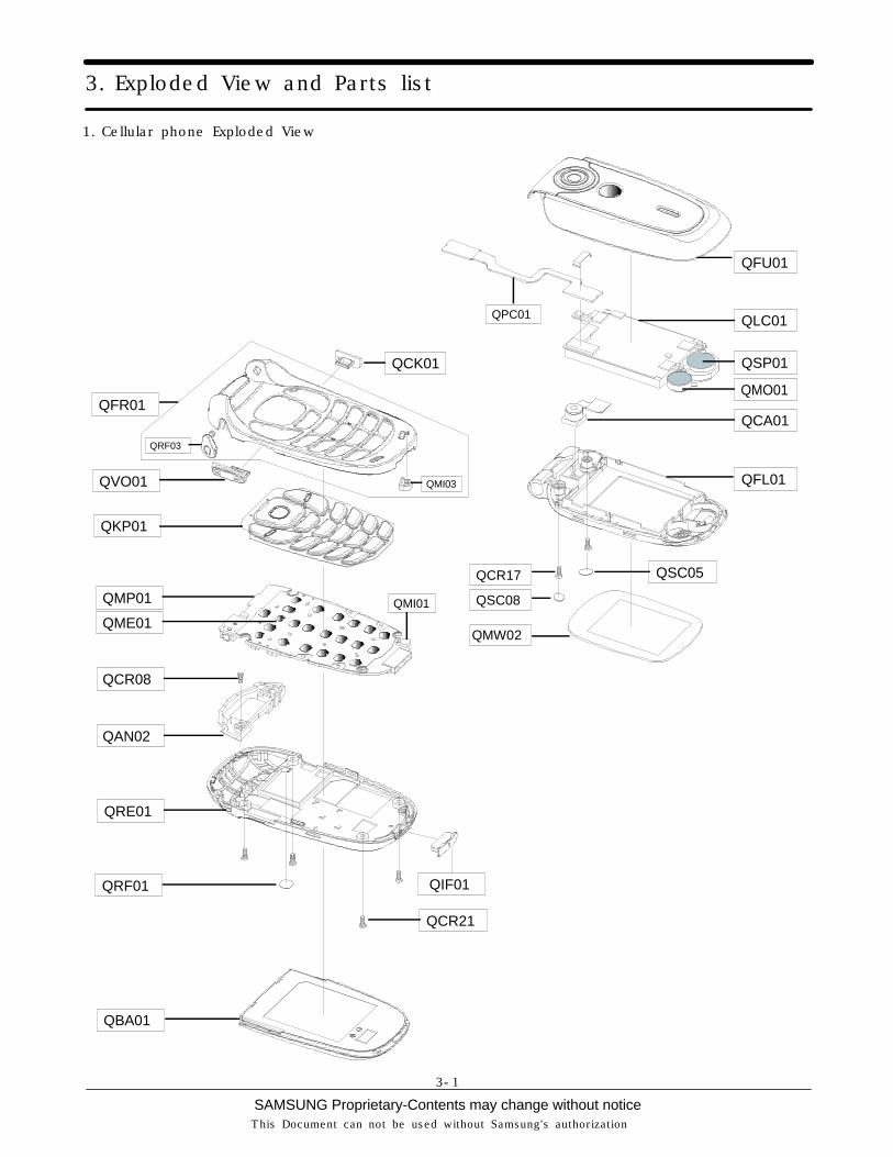
3. Exploded View and Parts list
3-1
This Document can not be used without Samsung's authorization
1. Cellular phone Exploded View
QFU01
QPC01
QVO01
QRF03
QCR08
QME01
QAN02
QRF01
QLC01
QCA01
QFL01
QCR17
QSC08
QMW02
QSP01
QFR01
QKP01
QMI01QMP01
QRE01
QBA01
QCR21
QIF01
QCK01
QMO01
QSC05
QMI03
SAMSUNG Proprietary-Contents may change without notice
Exploded view and Part list
3-2
This Document can not be used without Samsung's authorization
2. Cellular phone Parts list
Location
NO.Description SEC CODE Remark
QFU01 FOLDER UPPER GH75-06199A
QLC01 LCD GH07-00653A
QPC01 FPCB GH41-00774A
QSP01 SPEAKER 3001-001731
QMO01 MOTOR DC 3101-001401
QCA01 UNIT CAMERA GH59-01472A
QFL01 FOLDER LOWER GH75-06200A
QSC05 SCREW SHEET R GH74-08872A
QSC08 SCREW SHEET L GH74-08873A
QCR17 SCREW MACHINE 6001-001639
QMW02 WINDOW MAIN GH72-19197A
QFR01 FRONT COVER GH75-06331A
QRF03 EAR COVER GH72-19199A
QMI03 MIC RUBBER GH73-04064A
QCK01 CAMERA KEY GH75-06567A
QVO01 VOLKEY ASSY GH75-06566A
QKP01 KEYPAD GH75-06201A
QMP01 MAIN PBA GH92-02030A
QME01 UNIT METAL DOME GH59-01921A
QMI01 MICROPHONE ASSY GH30-00130A
QCR08 SCREW MACHINE 6001-001456
QAN02 INTENNA GH42-00523A
QRE01 REAR COVER GH75-06202A
QRF01 RF SHEET GH74-13063A
QIF01 IF COVER GH72-19208A
QCR21 SCREW MACHINE 6001-001507
QBA01 BATTERY GH43-01658A
SAMSUNG Proprietary-Contents may change without notice
Exploded view and Part list
3-3
This Document can not be used without Samsung's authorization
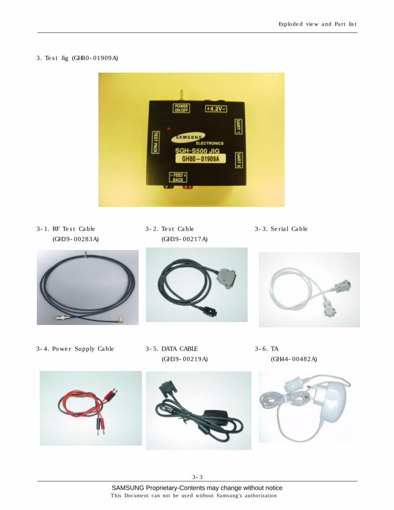
3. Test Jig (GH80-01909A)
3-1. RF Test Cable
(GH39-00283A)
3-2. Test Cable
(GH39-00217A)
3-3. Serial Cable
3-4. Power Supply Cable 3-5. DATA CABLE
(GH39-00219A)
3-6. TA
(GH44-00482A)
SAMSUNG Proprietary-Contents may change without notice
Exploded view and Part list
3-4
This Document can not be used without Samsung's authorization
SAMSUNG Proprietary-Contents may change without notice
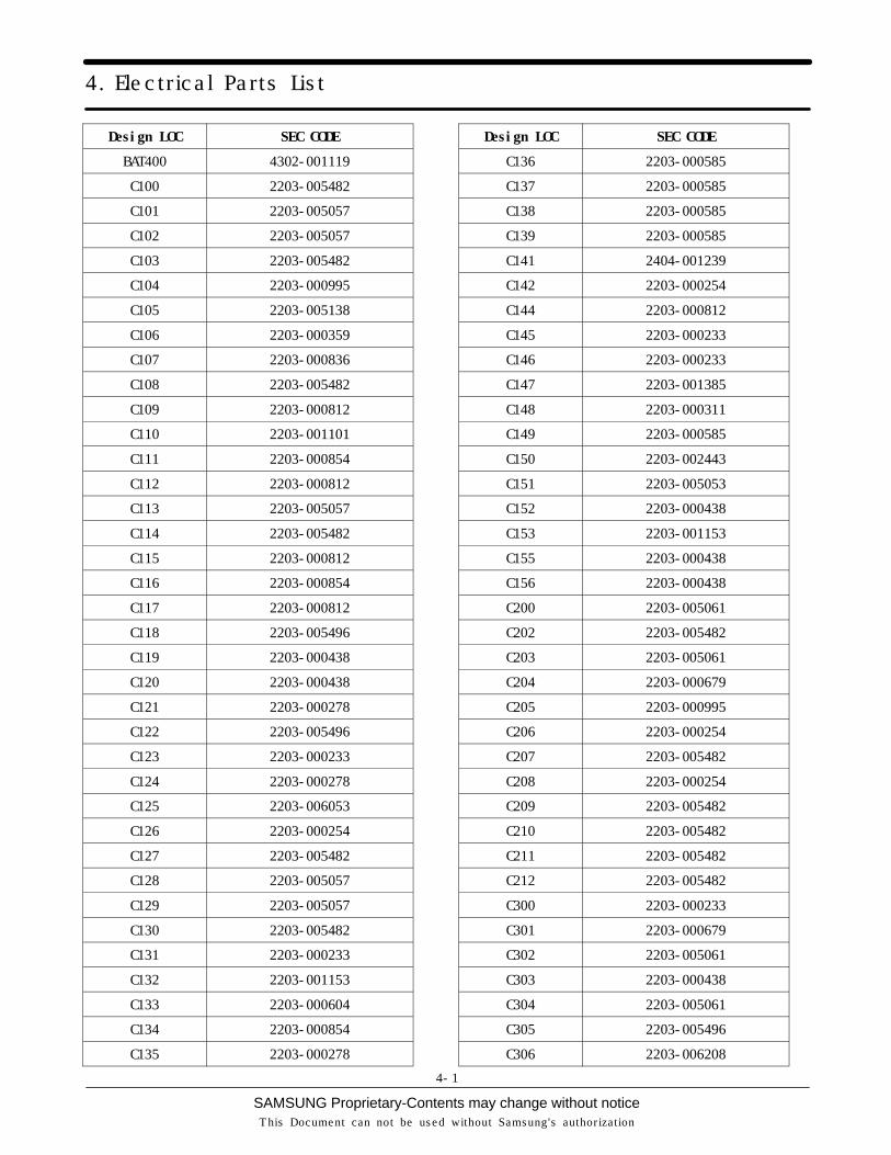
4. Electrical Parts List
This Document can not be used without Samsung's authorization
4-1
Design LOC SEC CODE
BAT400 4302-001119
C100 2203-005482
C101 2203-005057
C102 2203-005057
C103 2203-005482
C104 2203-000995
C105 2203-005138
C106 2203-000359
C107 2203-000836
C108 2203-005482
C109 2203-000812
C110 2203-001101
C111 2203-000854
C112 2203-000812
C113 2203-005057
C114 2203-005482
C115 2203-000812
C116 2203-000854
C117 2203-000812
C118 2203-005496
C119 2203-000438
C120 2203-000438
C121 2203-000278
C122 2203-005496
C123 2203-000233
C124 2203-000278
C125 2203-006053
C126 2203-000254
C127 2203-005482
C128 2203-005057
C129 2203-005057
C130 2203-005482
C131 2203-000233
C132 2203-001153
C133 2203-000604
C134 2203-000854
C135 2203-000278
Design LOC SEC CODE
C136 2203-000585
C137 2203-000585
C138 2203-000585
C139 2203-000585
C141 2404-001239
C142 2203-000254
C144 2203-000812
C145 2203-000233
C146 2203-000233
C147 2203-001385
C148 2203-000311
C149 2203-000585
C150 2203-002443
C151 2203-005053
C152 2203-000438
C153 2203-001153
C155 2203-000438
C156 2203-000438
C200 2203-005061
C202 2203-005482
C203 2203-005061
C204 2203-000679
C205 2203-000995
C206 2203-000254
C207 2203-005482
C208 2203-000254
C209 2203-005482
C210 2203-005482
C211 2203-005482
C212 2203-005482
C300 2203-000233
C301 2203-000679
C302 2203-005061
C303 2203-000438
C304 2203-005061
C305 2203-005496
C306 2203-006208
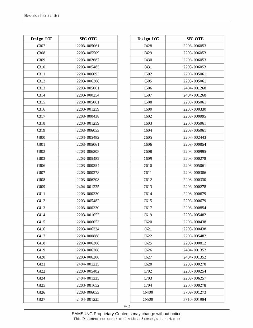
SAMSUNG Proprietary-Contents may change without noticeThis Document can not be used without Samsung's authorization
Electrical Parts List
4-2
Design LOC SEC CODE
C307 2203-005061
C308 2203-005509
C309 2203-002687
C310 2203-005483
C311 2203-006093
C312 2203-006208
C313 2203-005061
C314 2203-000254
C315 2203-005061
C316 2203-001259
C317 2203-000438
C318 2203-001259
C319 2203-006053
C400 2203-005482
C401 2203-005061
C402 2203-006208
C403 2203-005482
C406 2203-000254
C407 2203-000278
C408 2203-006208
C409 2404-001225
C411 2203-000330
C412 2203-005482
C413 2203-000330
C414 2203-001652
C415 2203-006053
C416 2203-006324
C417 2203-000888
C418 2203-006208
C419 2203-006208
C420 2203-006208
C421 2404-001225
C422 2203-005482
C424 2404-001225
C425 2203-001652
C426 2203-006053
C427 2404-001225
Design LOC SEC CODE
C428 2203-006053
C429 2203-006053
C430 2203-006053
C431 2203-006053
C502 2203-005061
C505 2203-005061
C506 2404-001268
C507 2404-001268
C508 2203-005061
C600 2203-000330
C602 2203-000995
C603 2203-005061
C604 2203-005061
C605 2203-002443
C606 2203-000854
C608 2203-000995
C609 2203-000278
C610 2203-005061
C611 2203-000386
C612 2203-000330
C613 2203-000278
C614 2203-000679
C615 2203-000679
C617 2203-000854
C619 2203-005482
C620 2203-000438
C621 2203-000438
C622 2203-005482
C625 2203-000812
C626 2404-001352
C627 2404-001352
C628 2203-000278
C702 2203-000254
C703 2203-006257
C704 2203-000278
CN400 3709-001273
CN500 3710-001994
SAMSUNG Proprietary-Contents may change without notice
Electrical Parts List
4-3
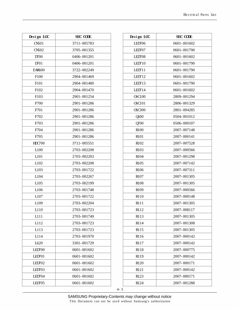
This Document can not be used without Samsung's authorization
Design LOC SEC CODE
CN501 3711-005783
CN502 3705-001355
D700 0406-001201
D701 0406-001201
EAR600 3722-002249
F100 2904-001469
F101 2904-001480
F102 2904-001470
F103 2901-001254
F700 2901-001286
F701 2901-001286
F702 2901-001286
F703 2901-001286
F704 2901-001286
F705 2901-001286
HDC700 3711-005551
L100 2703-002208
L101 2703-002203
L102 2703-002208
L103 2703-001722
L104 2703-002267
L105 2703-002199
L106 2703-001748
L107 2703-001722
L109 2703-002204
L110 2703-001723
L111 2703-001749
L112 2703-001723
L113 2703-001723
L114 2703-001970
L620 3301-001729
LED700 0601-001602
LED701 0601-001602
LED702 0601-001602
LED703 0601-001602
LED704 0601-001602
LED705 0601-001602
Design LOC SEC CODE
LED706 0601-001602
LED707 0601-001790
LED708 0601-001602
LED710 0601-001790
LED711 0601-001790
LED712 0601-001602
LED713 0601-001790
LED714 0601-001602
OSC100 2809-001294
OSC101 2806-001329
OSC300 2801-004285
Q600 0504-001012
Q700 0506-000107
R100 2007-007148
R101 2007-000141
R102 2007-007528
R103 2007-000566
R104 2007-001298
R105 2007-007142
R106 2007-007311
R107 2007-001305
R108 2007-001305
R109 2007-000566
R110 2007-000148
R111 2007-001305
R112 2007-008117
R113 2007-001305
R114 2007-001308
R115 2007-001305
R116 2007-000142
R117 2007-000142
R118 2007-000775
R119 2007-000142
R120 2007-000171
R121 2007-000142
R123 2007-000171
R124 2007-001288
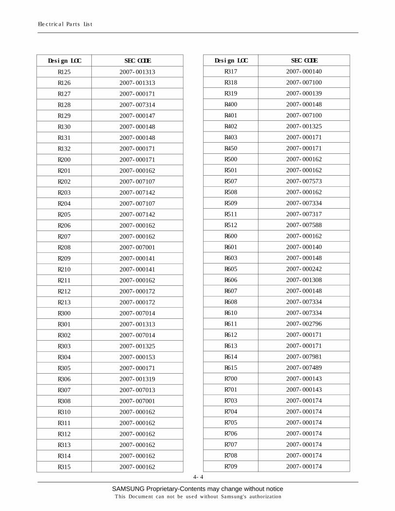
SAMSUNG Proprietary-Contents may change without noticeThis Document can not be used without Samsung's authorization
Electrical Parts List
4-4
Design LOC SEC CODE
R125 2007-001313
R126 2007-001313
R127 2007-000171
R128 2007-007314
R129 2007-000147
R130 2007-000148
R131 2007-000148
R132 2007-000171
R200 2007-000171
R201 2007-000162
R202 2007-007107
R203 2007-007142
R204 2007-007107
R205 2007-007142
R206 2007-000162
R207 2007-000162
R208 2007-007001
R209 2007-000141
R210 2007-000141
R211 2007-000162
R212 2007-000172
R213 2007-000172
R300 2007-007014
R301 2007-001313
R302 2007-007014
R303 2007-001325
R304 2007-000153
R305 2007-000171
R306 2007-001319
R307 2007-007013
R308 2007-007001
R310 2007-000162
R311 2007-000162
R312 2007-000162
R313 2007-000162
R314 2007-000162
R315 2007-000162
Design LOC SEC CODE
R317 2007-000140
R318 2007-007100
R319 2007-000139
R400 2007-000148
R401 2007-007100
R402 2007-001325
R403 2007-000171
R450 2007-000171
R500 2007-000162
R501 2007-000162
R507 2007-007573
R508 2007-000162
R509 2007-007334
R511 2007-007317
R512 2007-007588
R600 2007-000162
R601 2007-000140
R603 2007-000148
R605 2007-000242
R606 2007-001308
R607 2007-000148
R608 2007-007334
R610 2007-007334
R611 2007-002796
R612 2007-000171
R613 2007-000171
R614 2007-007981
R615 2007-007489
R700 2007-000143
R701 2007-000143
R703 2007-000174
R704 2007-000174
R705 2007-000174
R706 2007-000174
R707 2007-000174
R708 2007-000174
R709 2007-000174
SAMSUNG Proprietary-Contents may change without notice
Electrical Parts List
4-5
This Document can not be used without Samsung's authorization
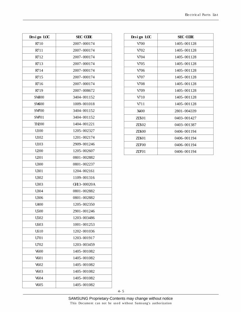
Design LOC SEC CODE
R710 2007-000174
R711 2007-000174
R712 2007-000174
R713 2007-000174
R714 2007-000174
R715 2007-000174
R716 2007-000174
R719 2007-008672
SW300 3404-001152
SW600 1009-001018
SW700 3404-001152
SW701 3404-001152
TH200 1404-001221
U100 1205-002327
U102 1201-002174
U103 2909-001246
U200 1205-002607
U201 0801-002882
U300 0801-002237
U301 1204-002161
U302 1109-001316
U303 GH13-00020A
U304 0801-002882
U306 0801-002882
U400 1205-002350
U500 2901-001246
U502 1203-003486
U603 1001-001253
U610 1202-001036
U701 1203-001917
U702 1203-003459
V600 1405-001082
V601 1405-001082
V602 1405-001082
V603 1405-001082
V604 1405-001082
V605 1405-001082
Design LOC SEC CODE
V700 1405-001128
V702 1405-001128
V704 1405-001128
V705 1405-001128
V706 1405-001128
V707 1405-001128
V708 1405-001128
V709 1405-001128
V710 1405-001128
V711 1405-001128
X400 2801-004339
ZD501 0403-001427
ZD502 0403-001387
ZD600 0406-001194
ZD601 0406-001194
ZD700 0406-001194
ZD701 0406-001194
SAMSUNG Proprietary-Contents may change without noticeThis Document can not be used without Samsung's authorization
Electrical Parts List
4-6
SAMSUNG Proprietary-Contents may change without noticeThis Document can not be used without Samsung's authorization
5. Block Diagrams
5-1
1. RF Solution Block Diagram
SGH-X640 RF Block Diagram
100 kHz+fmod
REFIN VTCXOTCO-5871U
pi -PAD
pi -PAD
I+
fmodI-
Q+
Q-
~~
pi -PAD
Vcc_RF_VCO
Discrete 3rd Order Loop Filter
MURATA TX VCO
GSM = 824 ~ 915 MHz(Vt=0.5V ~ 3.0 V )RFMD PAM
RF5146 7x7
Discrete 3rd Order Loop Filter
RXON
Vcc_Tx_BURST
GSM IN
EN
CLK
DATA
DCS, PCS S/W
OFFSET Mixer input power-16dBm max, -22dBm min
fcompRF =26MHz
Philips TransceiverUAA3536
Pins IA,IB,QA and QBV IQ : 1.25V typ . , 1.15V min , 1.35V max
Vmod : 0.5Vpp
FE_SW1
FE_SW2
QUAD
DIV
PFDCP
VREG
~
Vcc_RF_LO
FracNDIV
1:1/2
VREG
26MHz
Vcc_REF(2.4V typ.)
Vcc_SYN
FE_SW1
FE_SW2
3WBUSCTLREG
PWREN
GSM/DCS/PCS
DIVQUAD
PFDCP
fTXIF
60/114MHz
+ I OUT- I OUT
- Q OUT+ Q OUT
FESWONSYNONTXON
GSM S/W
VRAMP
TX ENABLE
BAND SELECT
DCS/PCS IN
VBAT
REF_13M
MQW510C869M
FUJITSU EGSM RX SAW Filter
FAR F5EB-942M50-B28CH IL=2.7dB max
Ripple=1.7 dB max
FUJITSU DCS RX SAW Filter FAR-F6EB-1G8425B2BW
IL= 2.3dB maxRipple= 2.0dB max
FUJITSU PCS RX SAW Filter FAR-F6EB-1G9600B2BW
IL= 2.8dB maxRipple= 1.6dB max
PCS RX ON
DCS: Pout = 33.0 dBm E ff = 52%PCS: Pout = 32.0 dBm E ff = 55%
GSM: Pout = 35.0 dBm E ff = 58%DCS,PCS = 1710 ~ 1910 MHz(Vt=0.5V ~ 3.0 V )
Harmonics <= -15dBcPout= 6.5 3dBm typ.,Ic <= 33mA
X4.8X 1.5 mm)(5.5
HITACHI METAL ANT SWITCH
SHS-C090T (4.5X3.2)
Imax = 10 mAFreq (MHz ) Loss 880 - 915 1.2 dB 925 - 960 0.9 dB 1710 -1785 1.2 dB 1805 -1880 1.2 dB 1930 -1990 1.2 dB
SAMSUNG Proprietary-Contents may change without notice
Block Diagrams
This Document can not be used without Samsung's authorization
5-2
2. Base Band Solution Block Diagram
BatteryType
BatteryVoltage
BatteryTemperature
AFC
RAMP
Charging Circuit
Li-Ion Battery
OM6359VIBRATOR
SYSTEM CLOCK(13MHz)
MEMORY
NAND(128Mb)NOR(128Mb)SRAM(64Mb)
RTC_CLOCK(32.768KHz)
LCDSIM CARD
RECEIVER
KEY
RF INTERFACE
VCC_CP
Serial DataInterface
I/OInterface
A/DInterface
BB INTERFACE
MELODY IC(40 Poly)SPEAKER
BB Block Diagram of SGH-X640
PMU
CAMERA
MV317
MICVCC_RF_VCO
VCC_RX_TX
VCC_SYN
VCC_TX_BURST
VDD1
VDD2
VDD3
VDD_VIB
MIC_BIAS
VDD_KEY
SPVDD
AVDD
AVDD_TEMP
BL_VDD
SAMSUNG Proprietary-Contents may change without noticeThis Document can not be used without Samsung's authorization
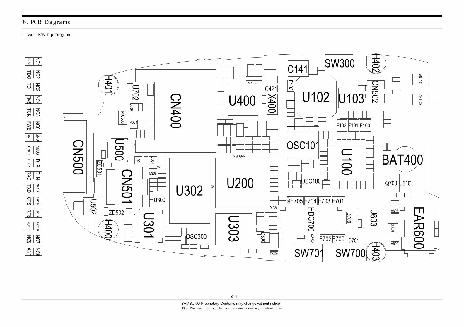
6. PCB Diagrams
6-1
1. Main PCB Top Diagram
SAMSUNG Proprietary-Contents may change without notice
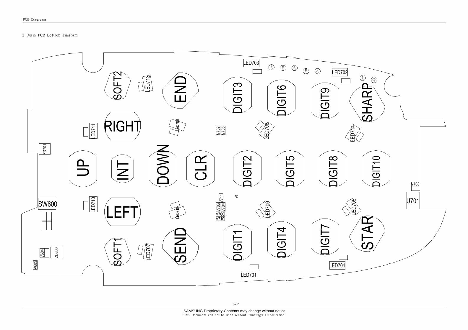
PCB Diagrams
This Document can not be used without Samsung's authorization
6-2
2. Main PCB Bottom Diagram
SAMSUNG Proprietary-Contents may change without notice
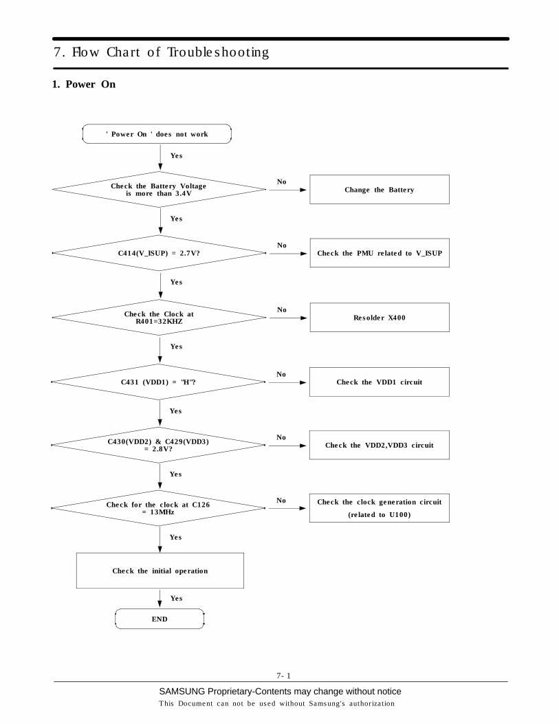
7. Flow Chart of Troubleshooting
This Document can not be used without Samsung's authorization
7-1
1. Power On
Check the Battery Voltageis more than 3.4V
' Power On ' does not work
Change the Battery
END
No
Yes
C414(V_ISUP) = 2.7V? Check the PMU related to V_ISUPNo
Yes
Check the Clock atR401=32KHZ Resolder X400
No
Yes
C431 (VDD1) = "H"? Check the VDD1 circuitNo
Yes
C430(VDD2) & C429(VDD3)= 2.8V? Check the VDD2,VDD3 circuit
No
Yes
Check for the clock at C126= 13MHz
Check the clock generation circuit
(related to U100)
No
Yes
Check the initial operation
Yes
Yes
SAMSUNG Proprietary-Contents may change without noticeThis Document can not be used without Samsung's authorization
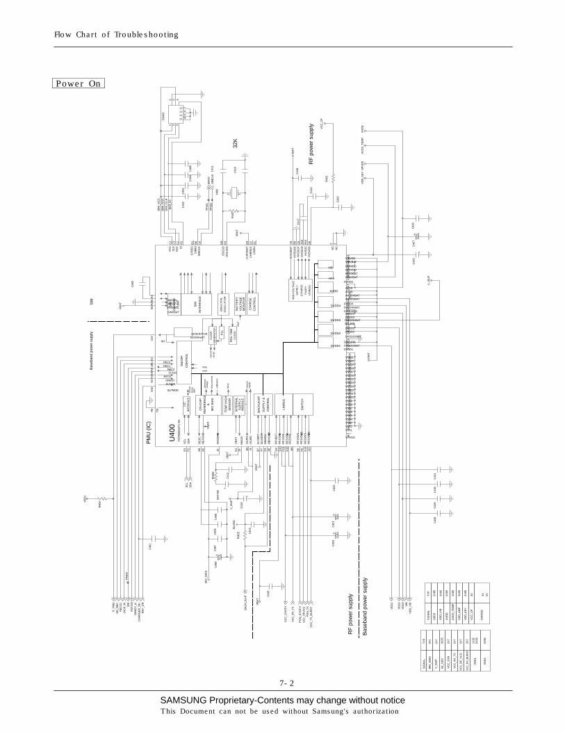
Flow Chart of Troubleshooting
7-2
Power On
4V
2V85
3V05
AV
DD
_TE
MP
2V1
VC
C_R
X_T
X
MIC
_BIA
S
data
RE
FE
RE
NC
E
SIM
_RS
T
INT
ER
FA
CE
SIM
_CLK
2V7
VD
D1
BL_
VD
D
BA
TT
ER
Y
TYP
DVDD1
2V95
2V
7
htm
p
3V25
CLO
CK
HFA
cont
rol
inte
rnal
SIM
_IO
MIC
BIA
S
SW
ITC
H
VC
C_R
F_V
CO
MO
DU
LE
VD
D_A
MP
CO
NTR
OL
INTE
RFA
CE
volta
ge
SU
PP
LY &
RF
pow
er s
uppl
y
ON
-CH
IP
(CH
AR
GE
CLO
CK
AV
DD
VC
C_R
X_B
UR
ST
2V35
PM
U (
IC)
3V05
INTERRUPT
3V
PU
MP
+
TE
MP
HIG
H
SIG
NA
L
12C
CH
AR
GE
2V65
Bas
eban
d po
wer
sup
ply
VD
D_K
EY
VC
C_C
P
&
supp
ly
GENERATOR
ON
/OFF
SIM
VD
D
VD
D2
VD
D_V
IB
htmp
SIM
HIG
H V
OLT
AG
E
VO
LTA
GE
32K
S
EN
SO
R
V_I
SU
P
VC
C_S
YN
BA
CK
LIG
HT
cloc
ks
2V65
TYP
PLL
2V7
stat
us
ovdd
LIN
RE
G)
SIG
NA
L
DVDD2
2V85
CH
AR
GE
C
ON
TRO
L
SU
PP
LY
INT
ER
NA
L
refe
renc
e
RE
AL-
TIM
E
VB
AT
SIM
DVDD3
AVDD
MO
NIT
OR
in
tern
al
5V
32K
Hz
XTA
L O
SC
ILLA
TOR
SIM
2V7
DVDD4
refg
nd
GE
NE
RA
TOR
SIM
_VC
C
CO
NTR
OL
LIN
RE
G
X40
0
2 1
RF
pow
er s
uppl
y
bias
cur
rent
s
SU
PP
LY
VIB
1V35
PU
MP
VD
D3
Bas
eban
d po
wer
sup
ply
2V7
calib
ratio
n
C40
5
C42
1
R40
0
VB
AT
C41
2
C41
8
C42
0
*
C41
4
C42
7
VB
AT
VD
D1
BLV
DD
SP
VD
D
C40
0
V_I
SU
P
TP40
0
C41
7
BA
T400
C40
1
R40
2
R40
1
C41
6
VC
C_C
P
*
C42
5
VB
AT
VB
AT
VB
AT
VD
D_K
EY
4 5 6
G 7
8 G
G 9
10
G
AV
DD
_TE
MP
CN
400
1 2 3
C43
0
C41
3
C40
7 C
408
R40
3
C42
6
C40
3
TP40
1
C40
9
C42
2
C40
4
C40
2
VB
AT
C41
9
V_I
SU
P
C42
8
R45
0
C43
1
VB
AT
C40
6 C
411
C42
4
C41
5
MIC
_BIA
S
C42
9
AV
DD
F4 VSS4 G
4 VSS5 J3 VSS6 G
5 K5
VSS7 VSS8 F
6 G
6
VSS9
D7
VSS15 VSS16 C
7 D
6
VSS17 VSS18 E
5 D
5
VSS19
VSS2 F5
VSS20 D4
C4
VSS21
VSS3
VIBVDD A3
VPROG H7
VSS1 E4
VSS10 G7 G
8
VSS11 VSS12 F
7 E
6
VSS13 VSS14 E
7
SIMSCP
B1
SIMVBAT
B2
SLPMOD D10
TM
H5
J5
VB
AC
K
VB
AT
K4
VC
C C
2
B3
VIBVBAT
E3
SD
A
F2
SEL12RB E9
SEL3RB H4
SIM
CLK
C
6
SIMGND
A2
B8
SIM
IO
SIMSCN
A1
RF1
VD
DS
F
9
RF2
SN
S
H9
RF2
SW
S
E10
RF2
VD
D
H10
RF2
VD
DS
J1
0
RFV
BA
T G
9
C1
RS
T
D9
RSTO
SC
L
K1
REC2
J2 REC3
K2
RE
FC
H8
RE
FGN
D
K6
RF1
SN
S
F10
E8
RF1
SW
S
RF1
VD
D
G10
H6
ISU
PD
J4
MIC
BIA
S
J6
NC
1 N
C 2
H3
ONKEY
K8
OS
C32
I K
9 O
SC
32O
REC1
B9
HV
SO
C
B10
H
VS
SC
N
A10
H
VS
SC
P
C9
HV
SV
BA
T C
8
HV
SV
DD
D
8
C10
INT
IO D
2
ISU
PA
H2
DVDD4
A4
DVDD4ON
F8 DVDD4VBAT
B4
HFAVBAT
A5
B5
HFAVBAT
A6
HFAVDD HFAVDD
B6
HV
SG
ND
CP
RE
S
D1
DVDD1 F1 DVDD1VBAT F
3
DVDD2 G2 G
1
DVDD2
DVDD2VBAT
G3
DVDD3
H1
J1
DVDD3
DVDD3VBAT
BB
MS
W
C5
BLV
BA
T B
7 B
LVD
D
A7
CH
RIV
E
1 C
HR
RE
G
E2
CH
RV
BA
T D
3
CLK
C3
CLK32
A9
PC
F506
01E
T1-N
5
U40
0
K3
AUXON
J7
AVDD AVDD
K7
AVDDS
K10
AVDDVBAT J8 J
9
AVDDVBAT
BB
MG
ND
A
8
TP40
2
VC
C_R
X_T
X
VC
C_S
YN
TH
VC
C_R
FVC
O
VC
C_T
X_B
UR
ST
BA
CK
LIG
HT
VD
D1
VD
D2
VD
D3
VD
D_V
IB
VIB
JIG
_RE
C
RE
F_O
N
SIM
IO
SIM
CLK
PO
N_T
X
PO
N_S
YN
TH
CH
AR
GE
R_O
K
RS
TON
SC
L S
DA
32K
IT_P
MU
ON
KE
Y_N
RE
CO
1 JA
CK
_IN
SAMSUNG Proprietary-Contents may change without notice
Flow Chart of Troubleshooting
This Document can not be used without Samsung's authorization
7-3
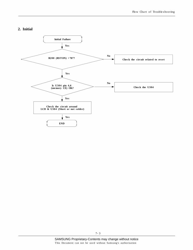
2. Initial
R200 (RSTON) ="H"?
Initial Failure
Check the circuit related to reset
END
No
Yes
Is U304 pin 4,6(memory CE) OK?
Yes
Yes
No
Check the U304
Check the circuit aroundLCD & U304 (Short or not solder)
Yes
SAMSUNG Proprietary-Contents may change without noticeThis Document can not be used without Samsung's authorization
Flow Chart of Troubleshooting
7-4
Initial
R20
2
R71
9 V
DD
1
R20
6
R20
9
VD
D1
DD
R20
1 R
200
AV
DD
R21
2
VSS_VBOUT
C20
1
VSS_I C3
VSS_K G1 VSS_M
VSS_N K1 P1
VSS_O N5 VSS_P
C13 VSS_REF A12
VSS_VB C11
VSS_B
E13 VSS_BB
VSS_C M7
D11 VSS_D
N10 VSS_E
N14 VSS_F N11
VSS_G VSS_H G13
E8
L3 VDDE3_G
F12 VDD_BB VDD_D C9
D14 VDD_REF VDD_VB B12
C12 VDD_VBOUT
C14
V
RE
F
K7 VSS_A J1
N12 VDDE1_B VDDE1_C C8
VDDE1_D H11
VDDE2_C P8 C1 VDDE2_E
VDDE3_A P4 M6 VDDE3_B
VDDE3_F G2
TXD0
TXD A4
G12
T
XO
N
F5 VDDC_A N13 VDDC_B M8 VDDC_C
VDDC_D K6
P9 VDDE1_A
SIM
CLK
M
14
SIM
ER
R
M11
M13
S
IMIO
A3 TCK
D2 TDI
D3 TDO
A2 TMS
A1 TRST_N
C5
M10
R
STO
_N
RS
T_N
H
10
RXT0_N A5
C4 RXD0
D4 RXD1
RX
ON
H
12
C2
SC
K
SD
A
B3
RF
SIG
2 R
FS
IG3
B6
A7
RF
SIG
4 R
FS
IG5
C7
B7
RF
SIG
6 R
FS
IG7
C6
E7
RF
SIG
8 K
10
RF
SIG
9
QN
Q
P
H13
RE
SE
TN
C10
J12
RFE
_N0
K12
R
FE_N
2
D5
RF
SIG
0 R
FS
IG1
A6
RFS
IG10
D
7
D6
L13
KB
IO5
KB
IO6
L12
L14
KB
IO7
D10
M
CLK
MIC
N
B13
A
13
MIC
P
PW
M0
F4
E6
PW
M1
H14
IN
IP
J13
B4 J_SEL
KB
IO0
K11
K
BIO
1 J1
0 K
BIO
2 K
13
J11
KB
IO3
KB
IO4
L11
HD
4 H
D5
H1
B1
HD
6 E
4 H
D7
F3
HD
8 H
D9
F2
HR
D_N
H
5 H
WR
_N
L5
J14
HD
10
HD
11
E1
HD
12
D1
E3
HD
13
HD
14
E2
HD
15
B2
H2
HD
2 J3
H
D3
E5
HA
4 N
3 K
5 H
A5
HA
6 M
3
HA
7 P
2
HA
8 N
2 M
1 H
A9
H4
HD
0 H
D1
H3
F1
G4
HA
20
P5
HA
21
N6
HA
22
L6
HA
23
HA
24
J7
J6
HA
25
HA
26
H6 L4
HA
3
M2
HA
14
J2
J5
HA
15
HA
16
K3 J4
HA
17
HA
18
K4
K2
HA
19
HA
2 P
3
GP
IO8
GP
IO9
N8
GP
ON
1 L1
0 G
PO
N2
N9
M4
HA
1
HA
10
N1 L2
HA
11
HA
12
L1
HA
13
K9
GP
IO10
K
8
GP
IO2
L8
GP
IO3
M9
GP
IO4
P7 L7
GP
IO5
GP
IO6
L9
N7
GP
IO7
P6
CS
_N0
N4
G5
CS
_N1
M5
CS
_N2
CS
_N3
G3
B5 CTS0_N
A11
E
AR
N
EA
RP
B
10
M12
G
PIO
0 G
PIO
1
BU
Z
E10
C
CLK
CD
I D
8 E
9 C
DO
D9
CE
N
CK
I P
11
P13
C
KI3
2I
CK
I32O
P
14
AU
XS
P
A10
G10
A
UX
ST
P12 AVDD
P10 AVSS
BD
IO
E11
BIE
N
F10
F11
BIO
CLK
BO
EN
G
11
B11
AU
XA
DC
3 F1
3 A
UX
AD
C4
E12
A
UX
DA
C1
AU
XD
AC
2 D
13
D12
A
UX
DA
C3
AU
XM
ICN
A
14
B14
A
UX
MIC
P
K14
A
UX
ON
AC
LK
B8
A8
AD
I
AD
O
A9
AFS
B
9
F14
AU
XA
DC
1 A
UX
AD
C2
G14
E
14
R20
3
U20
0
VD
D2
DC
L
VD
D3
DU
VD
D1
R20
4
VD
D1
C20
2
R21
3
TP4
R21
1
VD
D1
R20
5
R20
8
FSC
R20
7
VD
D3
VD
D3
TH20
0
AV
DD
_TE
MP
U20
1
A 1 2
GN
D
VC
C
5 6 Y
0
Y1
43
_E
C20
0
VD
D2
R21
0
HA
(26)
HA
(24)
H
A(2
5)
CS
_NA
ND
CTS
0
ME
LOD
Y_C
S
IMA
GE
_CS
H
A(2
0)
FLA
SH
_EN
EA
RP
_P
EA
RP
_N
AN
TSW
_ON
AV
DD
_TE
MP
NC
SFL
AS
H
GS
M_T
XV
CO
_EN
D
CS
_TX
VC
O_E
N
BA
ND
_SE
L
M_R
ST
IMA
GE
_IN
T
FLIP
RS
TON
R
I_B
LUE
HA
(1:2
6) H
D(0
:15)
32K
JAC
K_E
N
EN
D_O
F_C
HA
RG
E
M_S
EL
VF
CH
G_O
N
ME
S_B
ATT
AU
X_M
IC_N
AU
XS
P
EA
RP
_HF
RF_
BB
I_C
LK
RF_
BB
I_D
ATA
IMA
GE
_RE
SE
T
HA
(23)
RF_
EN
_SY
NTH
PO
N_R
X
PA
M_T
XE
N
AF
C
RA
MP
D_R
EF_
13M
QR
X_T
X_P
Q
RX
_TX
_N
IRX
_TX
_P
IRX
_TX
_N
MIC
_P
MIC
_N
AU
X_M
IC_P
DD
DC
L D
U
FSC
PC
S_R
X
BIO
CLK
BO
EN
B
DIO
B
IEN
CTS0
TXD0 RXD0
SD
A
SC
L
IT_P
MU
SIM
IO
SIM
CLK
RE
F_O
N
J_SEL
RTS0
RXD1
TCK
TDI
TDO
TMS
TRST_N
TXD1
HA
(11)
H
A(1
2)
HA
(13)
H
A(1
4)
HA
(15)
H
A(1
6)
HA
(17)
H
A(1
8)
HA
(19)
H
A(2
0)
HA
(21)
H
A(2
2)
HA
(1)
D_R
EF_
13M
HW
R_N
H
RD
_N
NC
SR
AM
PO
N_T
X
PO
N_S
YN
TH
KB
IO(0
:7)
KB
IO(7
) K
BIO
(6)
KB
IO(5
) K
BIO
(4)
KB
IO(3
) K
BIO
(2)
KB
IO(1
) K
BIO
(0)
HA
(2)
HA
(3)
HA
(4)
HA
(5)
HA
(6)
HA
(7)
HA
(8)
HA
(9)
HA
(10)
HD
(0)
HD
(1)
HD
(2)
HD
(3)
HD
(4)
HD
(5)
HD
(6)
HD
(7)
HD
(8)
HD
(9)
HD
(10)
H
D(1
1)
HD
(12)
H
D(1
3)
HD
(14)
H
D(1
5)
SAMSUNG Proprietary-Contents may change without notice
Flow Chart of Troubleshooting
This Document can not be used without Samsung's authorization
7-5
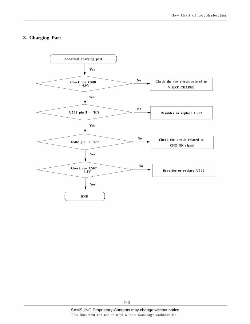
3. Charging Part
Check the C508> 4.9V
Abnormal charging part
END
No
Yes
U502 pin 5 = "H"?No
Yes
Check the C507≒ 4.2V
No
Yes
Check the the circuit related to
V_EXT_CHARGE
Resolder or replace U502
Check the circuit related to
CHG_ON signal
Yes
U502 pin = "L"?
Yes
No
Resolder or replace U502
SAMSUNG Proprietary-Contents may change without noticeThis Document can not be used without Samsung's authorization
Flow Chart of Troubleshooting
7-6
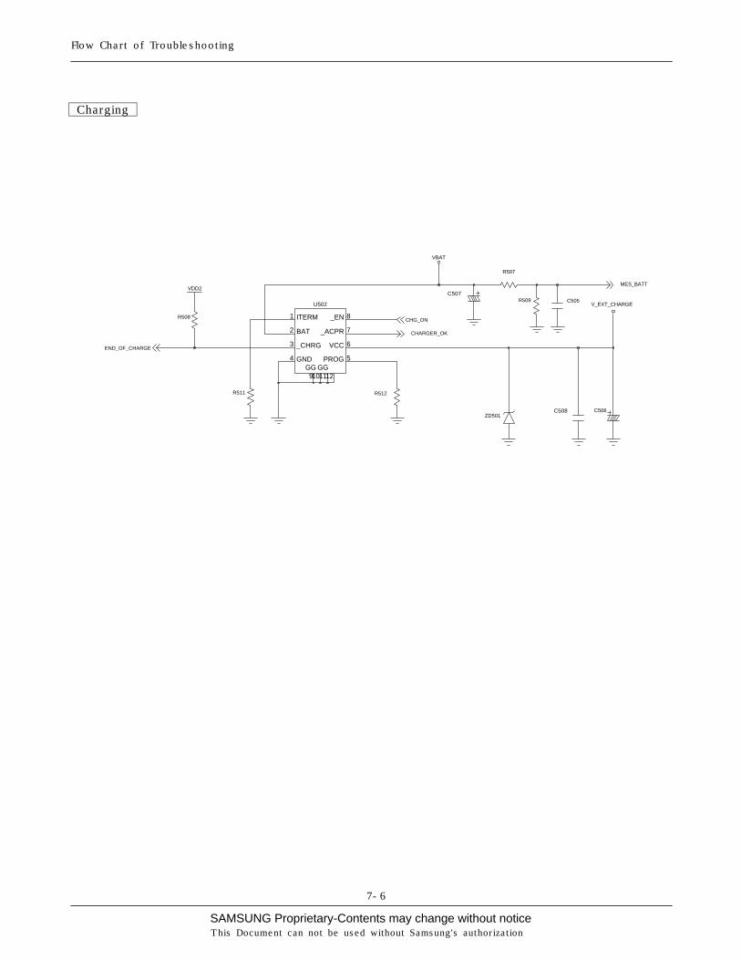
Charging
VDD2
_ACPR 7
_CHRG 3
8 _EN
9 GG
10 11 GG
12
4 GND
ITERM 1
PROG 5
6 VCC
U502
2 BAT
R509 V_EXT_CHARGE
R511
C508
C507
R508
C505
ZD501
VBAT
R507
R512
C506
CHARGER_OK
CHG_ON
MES_BATT
END_OF_CHARGE
SAMSUNG Proprietary-Contents may change without notice
Flow Chart of Troubleshooting
This Document can not be used without Samsung's authorization
7-7
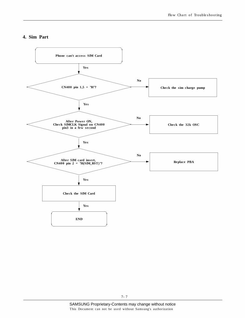
4. Sim Part
CN400 pin 1,5 = "H"?
Phone can't access SIM Card
Check the sim charge pump
Check the SIM Card
END
No
Yes
Yes
Yes
No
Check the 32k OSCAfter Power ON,
Check SIMCLK Signal on CN400pin3 in a few second
Yes
No
Replace PBAAfter SIM card insert,CN400 pin 2 = "H(SIM_RST)"?
Yes
SAMSUNG Proprietary-Contents may change without noticeThis Document can not be used without Samsung's authorization
Flow Chart of Troubleshooting
7-8
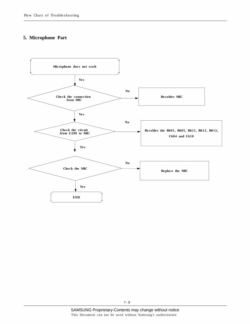
5. Microphone Part
Check the connectionfrom MIC
Check the circuitfrom U200 to MIC
Resolder MIC
Resolder the R601, R605, R611, R612, R613,
C604 and C610
END
No
Yes
Yes
Yes
Yes
No
Check the MIC
No
Replace the MIC
Microphone does not work
SAMSUNG Proprietary-Contents may change without notice
Flow Chart of Troubleshooting
This Document can not be used without Samsung's authorization
7-9
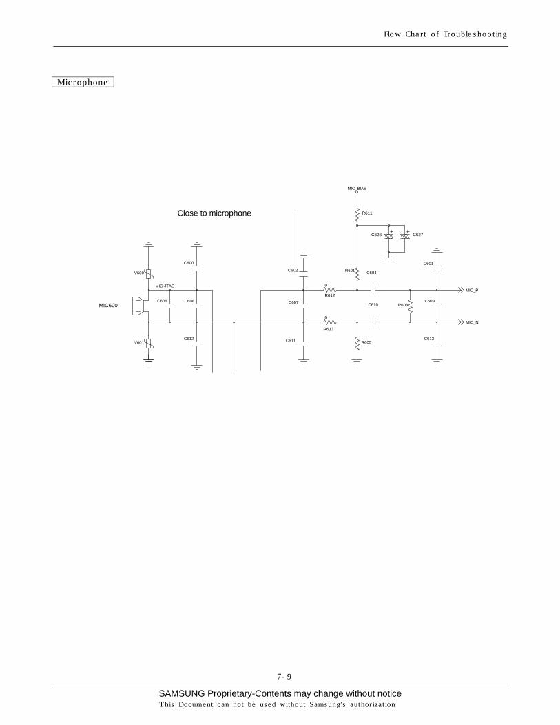
Microphone
Close to microphone
V601 R605 C613
R611
C611
C607
V600
C601
0
R613
MIC_BIAS
R601
C600
C606 R612
0
C608
C626 C627
C602
MIC600
C604
C612
C610 R603 C609
MIC-JTAG
MIC_N
MIC_P
SAMSUNG Proprietary-Contents may change without noticeThis Document can not be used without Samsung's authorization
Flow Chart of Troubleshooting
7-10
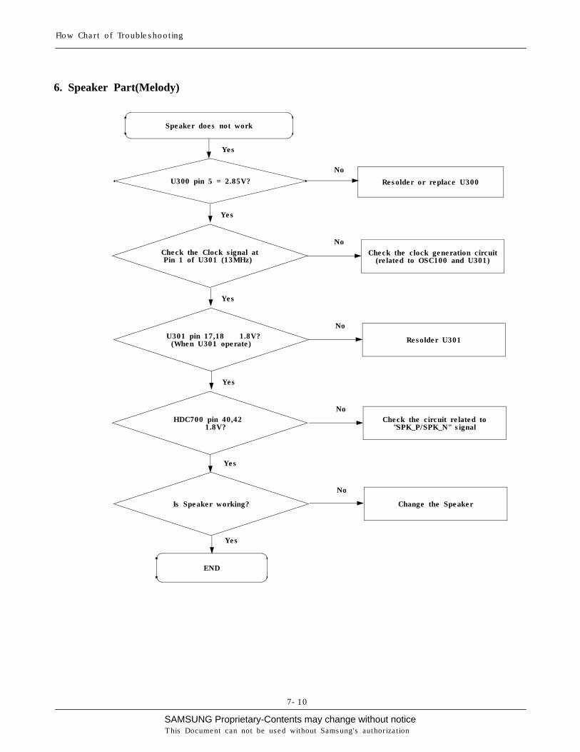
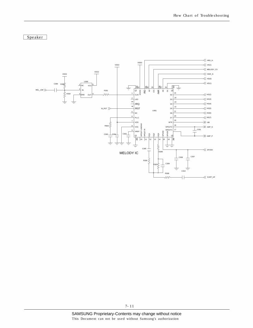
6. Speaker Part(Melody)
U300 pin 5 = 2.85V?
Speaker does not work
Check the Clock signal atPin 1 of U301 (13MHz)
Check the clock generation circuit(related to OSC100 and U301)
END
No
Yes
No
Resolder or replace U300
U301 pin 17,18 ≒ 1.8V?(When U301 operate) Resolder U301
Yes
No
HDC700 pin 40,42≒ 1.8V?
Check the circuit related to"SPK_P/SPK_N" signal
Yes
No
Is Speaker working?
No
Yes
Change the Speaker
Yes
Yes
SAMSUNG Proprietary-Contents may change without notice
Flow Chart of Troubleshooting
This Document can not be used without Samsung's authorization
7-11
Speaker
MELODY IC
R300
R305
C306
VDD3
C309
/WR
7 VDD
9 VREF
8 VSS
/CS
29
3
/IRQ
/RD
31
4
/RST
28
IOV
DD
LED 2
19 MTR
5 NC
PLLC 6
17 SPOUT1
SPOUT2 18
15
SP
VD
D
SP
VS
S
16
EQ
2
EQ
3
14
33
G
G
34
35
G
G
36
HP
OU
T-L/
MO
NO
10 11
HP
OU
T-R
32
D1
25 D2
D3 24
23 D4
D5 22
D6 21
D7 20
EQ
1
12 13
U301
A0
30
1 CLKI
D0
27 26
C303
R303
2
NC 1
OUT 4
VCC 5
U300
GND 3
IN
VDD2 VDD2
R306
C300
C307
C301
C305
C304 C302
R301
R308 C310
VDD2
R302
R307
HD(7)
HD(6)
HD(5)
HD(4)
HD(3)
HD(2)
HD(1)
HD(0)
HA(1)
AMP_P
AMP_N
SPVDD
MELODY_CS
HRD_N
M_RST
HWR_N
VIB
EARP_HF
MEL_13M
SAMSUNG Proprietary-Contents may change without noticeThis Document can not be used without Samsung's authorization
Flow Chart of Troubleshooting
7-12
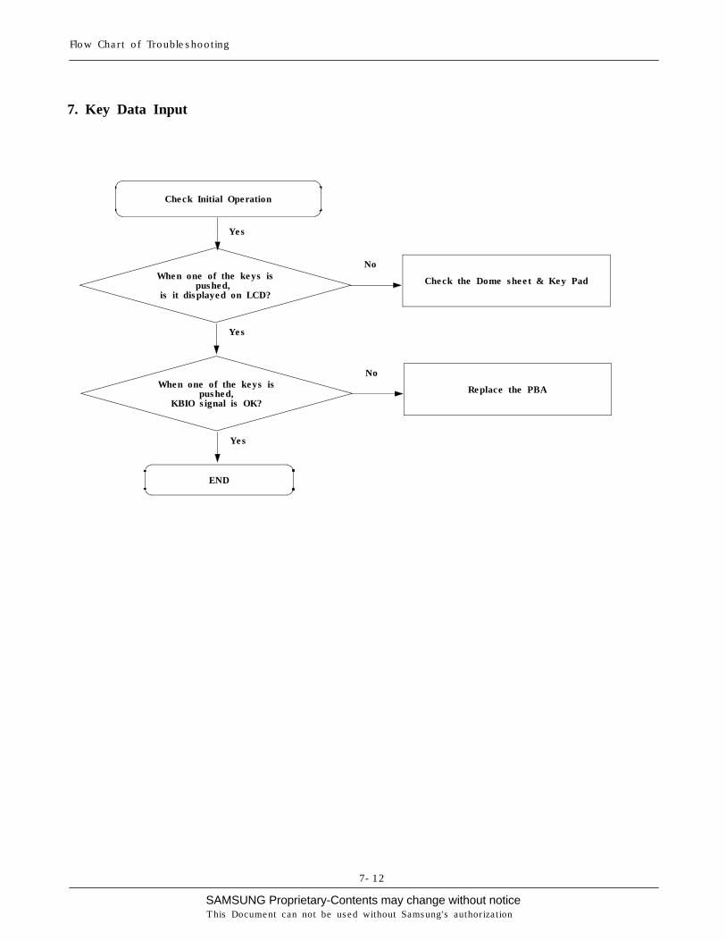
7. Key Data Input
When one of the keys ispushed,
is it displayed on LCD?
Check the Dome sheet & Key Pad
END
No
Yes
Yes
Check Initial Operation
When one of the keys ispushed,
KBIO signal is OK?
Replace the PBA
No
Yes
SAMSUNG Proprietary-Contents may change without notice
Flow Chart of Troubleshooting
This Document can not be used without Samsung's authorization
7-13
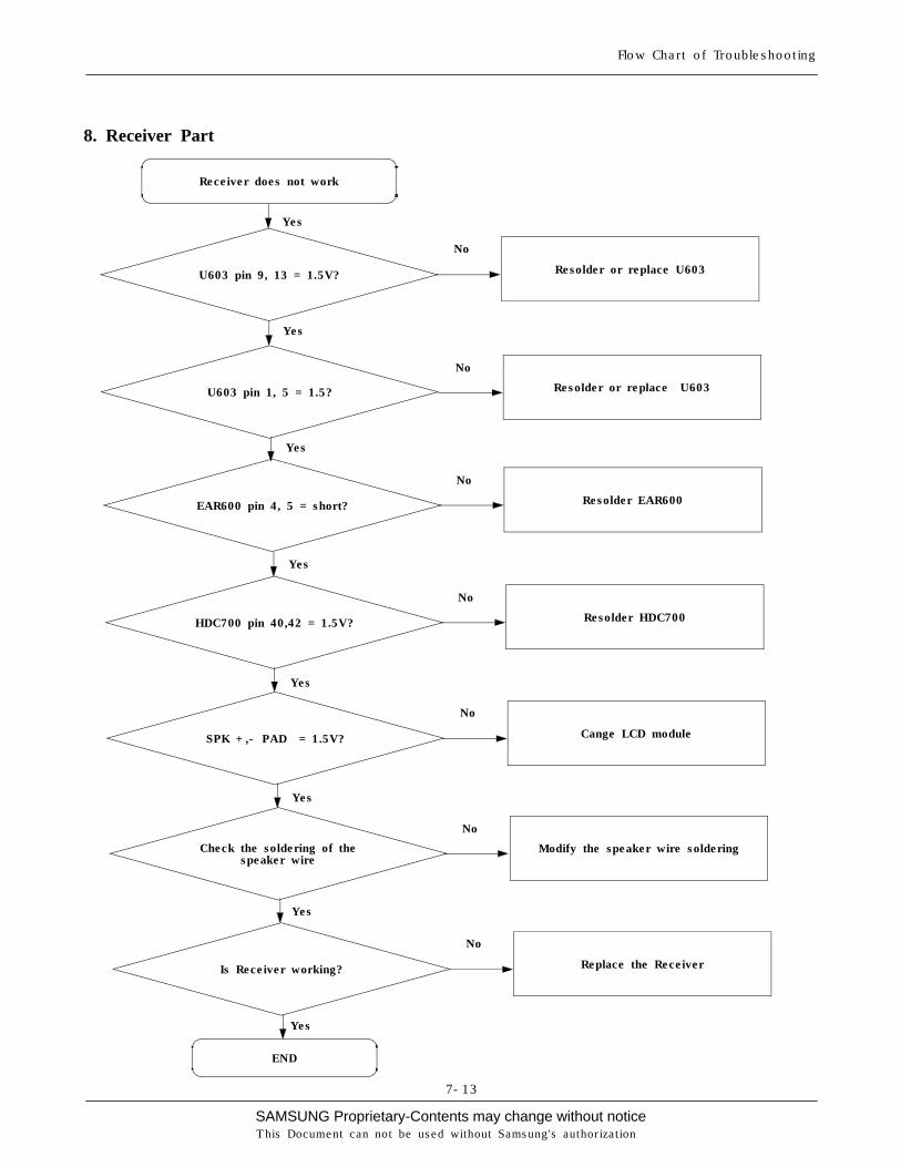
8. Receiver Part
U603 pin 9, 13 = 1.5V? Resolder or replace U603
END
No
Yes
Yes
Receiver does not work
SPK +,- PAD = 1.5V? Cange LCD module
No
Yes
Is Receiver working? Replace the Receiver
No
Yes
No
Resolder or replace U603
Yes
No
Resolder EAR600EAR600 pin 4, 5 = short?
Yes
HDC700 pin 40,42 = 1.5V?
No
Resolder HDC700
Yes
Check the soldering of thespeaker wire
No
Modify the speaker wire soldering
Yes
U603 pin 1, 5 = 1.5?
SAMSUNG Proprietary-Contents may change without noticeThis Document can not be used without Samsung's authorization
Flow Chart of Troubleshooting
7-14
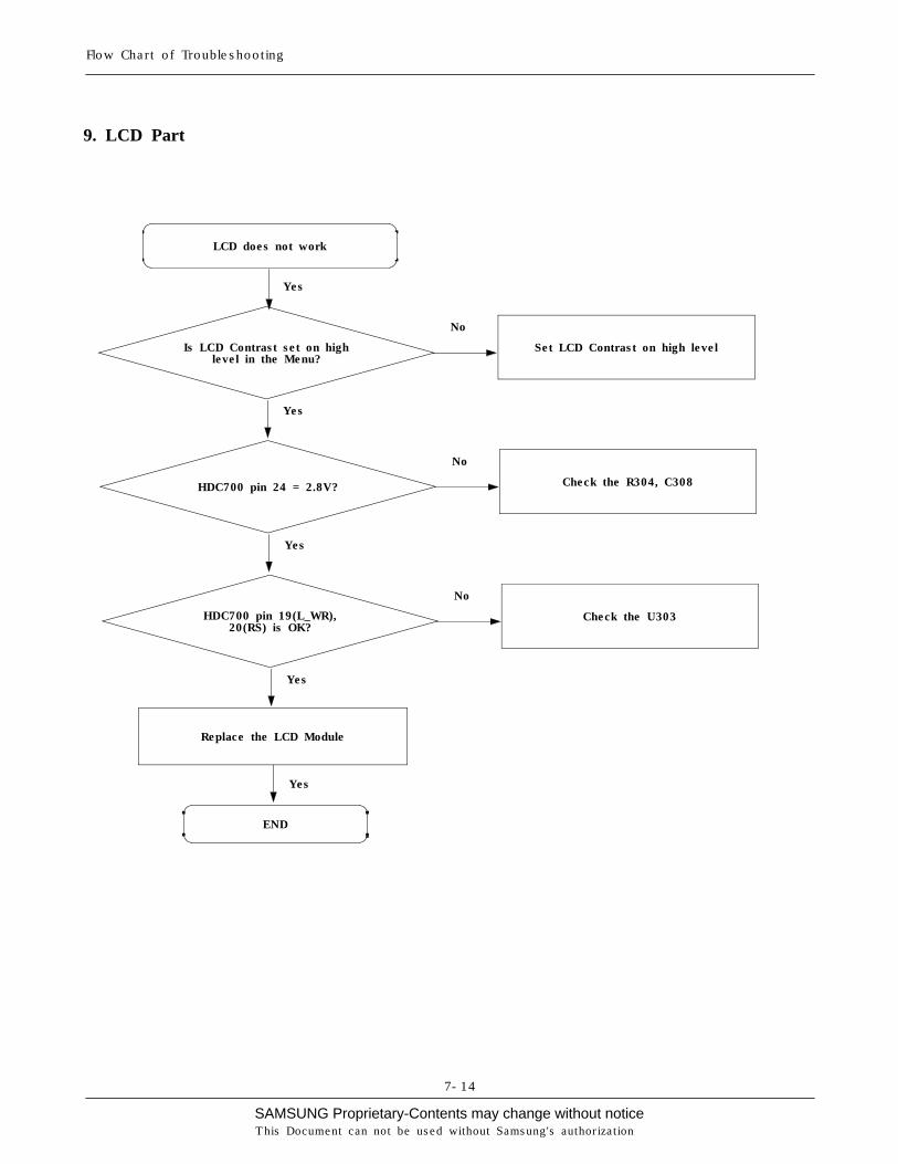
9. LCD Part
Is LCD Contrast set on highlevel in the Menu?
Set LCD Contrast on high level
END
No
Yes
Yes
LCD does not work
HDC700 pin 24 = 2.8V? Check the R304, C308
No
Yes
HDC700 pin 19(L_WR),20(RS) is OK?
Check the U303
No
Yes
Yes
Replace the LCD Module
SAMSUNG Proprietary-Contents may change without notice
Flow Chart of Troubleshooting
This Document can not be used without Samsung's authorization
7-15
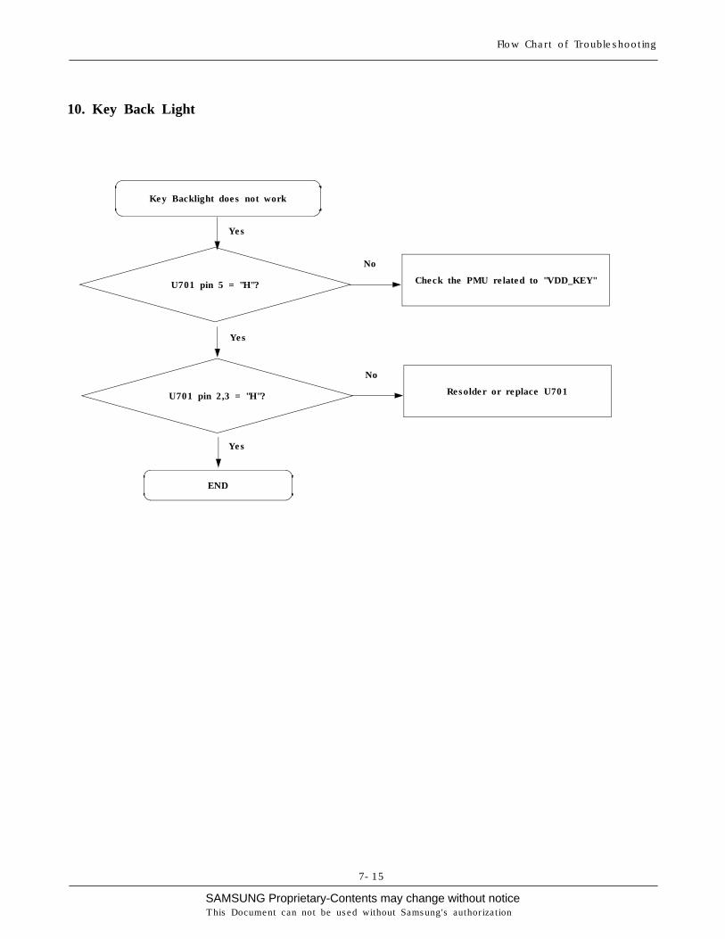
10. Key Back Light
U701 pin 5 = "H"? Check the PMU related to "VDD_KEY"
END
No
Yes
Yes
Key Backlight does not work
U701 pin 2,3 = "H"?
No
Resolder or replace U701
Yes
SAMSUNG Proprietary-Contents may change without noticeThis Document can not be used without Samsung's authorization
Flow Chart of Troubleshooting
7-16
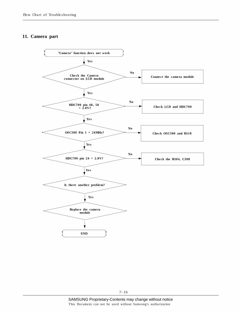
11. Camera part
"Camera" function does not work
Yes
NoConnect the camera moduleCheck the Camera
connector on LCD module
Yes
HDC700 pin 48, 50= 2.8V?
No
Check LCD and HDC700
Yes
OSC300 Pin 1 = 24MHz?No
Check OSC300 and R318
Yes
HDC700 pin 24 = 2.8V?
Yes
No
Check the R304, C308
Is there another problem?
END
Replace the cameramodule
Yes
SAMSUNG Proprietary-Contents may change without notice
Flow Chart of Troubleshooting
This Document can not be used without Samsung's authorization
7-17
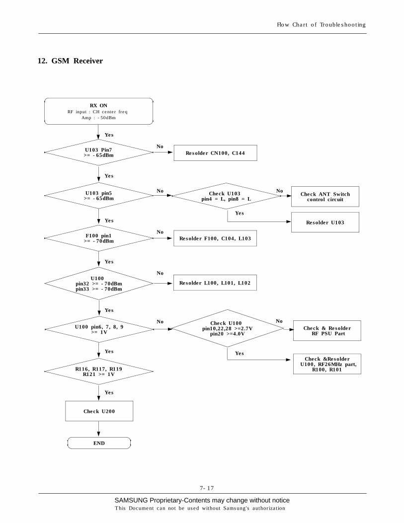
12. GSM Receiver
U103 Pin7>= -65dBm Resolder CN100, C144
END
No
Yes
RX ONRF input : CH center freq
Amp : -50dBm
Check U103pin4 = L, pin8 = L
U103 pin5>= -65dBm
F100 pin1>= -70dBm
U100 pin6, 7, 8, 9>= 1V
U100pin32 >= -70dBmpin33 >= -70dBm
Check ANT Switchcontrol circuit
Resolder U103
Resolder F100, C104, L103
Resolder L100, L101, L102
Check U100pin10,22,28 >=2.7V
pin20 >=4.0VCheck & Resolder
RF PSU Part
Check &ResolderU100, RF26MHz part,
R100, R101R116, R117, R119R121 >= 1V
Yes
Yes
Yes
Yes
Yes
Yes
Yes
Yes
No
No
No
No No
No
Check U200
SAMSUNG Proprietary-Contents may change without noticeThis Document can not be used without Samsung's authorization
Flow Chart of Troubleshooting
7-18
13. GSM Transmitter
U103 Pin7>= 20dBm Resolder CN100, C144
TX ON (5Level)
Check U103pin4 = H (2.68V),
pin2,8 = L
U103 pin11>= 20dBm
U102 pin6>= 20dBm
OSC101 pin1>= 6dBm
U102 pin48>= 3dBm
Change or Resolder U100
Check ANT Switchcontrol circuit
Resolder L113,L114,C151
Resolder R123
U100 pin6, 7, 8, 9>= 500mV
Yes
Check U102VBATT, pin42,43
OK?Resolder or Change U102
or check PAM control signal
Check +VBATT
Check U100pin4 >= 4.0V
pin22,28 >=2.7VOK?
Check & ResolderRF PSU Part
No
No
No
No
No
Yes
No
No
Yes
Yes
Yes
Yes
Yes
Yes
Yes
Yes
No
END
Check U200
Resolder U100or check Txcpo(R114)
No
SAMSUNG Proprietary-Contents may change without notice
Flow Chart of Troubleshooting
This Document can not be used without Samsung's authorization
7-19
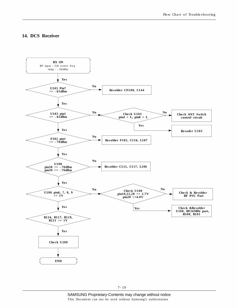
14. DCS Receiver
U103 Pin7>= -65dBm Resolder CN100, C144
No
Yes
RX ONRF input : CH center freq
Amp : -50dBm
Check U103pin4 = L, pin8 = L
U103 pin1>= -65dBm
F102 pin1>= -70dBm
U100 pin6, 7, 8, 9>= 1V
U100pin38 >= -70dBmpin39 >= -70dBm
Check ANT Switchcontrol circuit
Resoder U103
Resolder F102, C116, L107
Resolder C115, C117, L106
Check U100pin10,22,28 >= 2.7V
pin20 >=4.0VCheck & Resolder
RF PSU Part
Check &ResolderU100, RF26MHz part,
R100, R101R116, R117, R119,
R121 >= 1V
Yes
Yes
Yes
Yes
Yes
Yes
Yes
Yes
No
No
No
No No
No
END
Check U200
SAMSUNG Proprietary-Contents may change without noticeThis Document can not be used without Samsung's authorization
Flow Chart of Troubleshooting
7-20
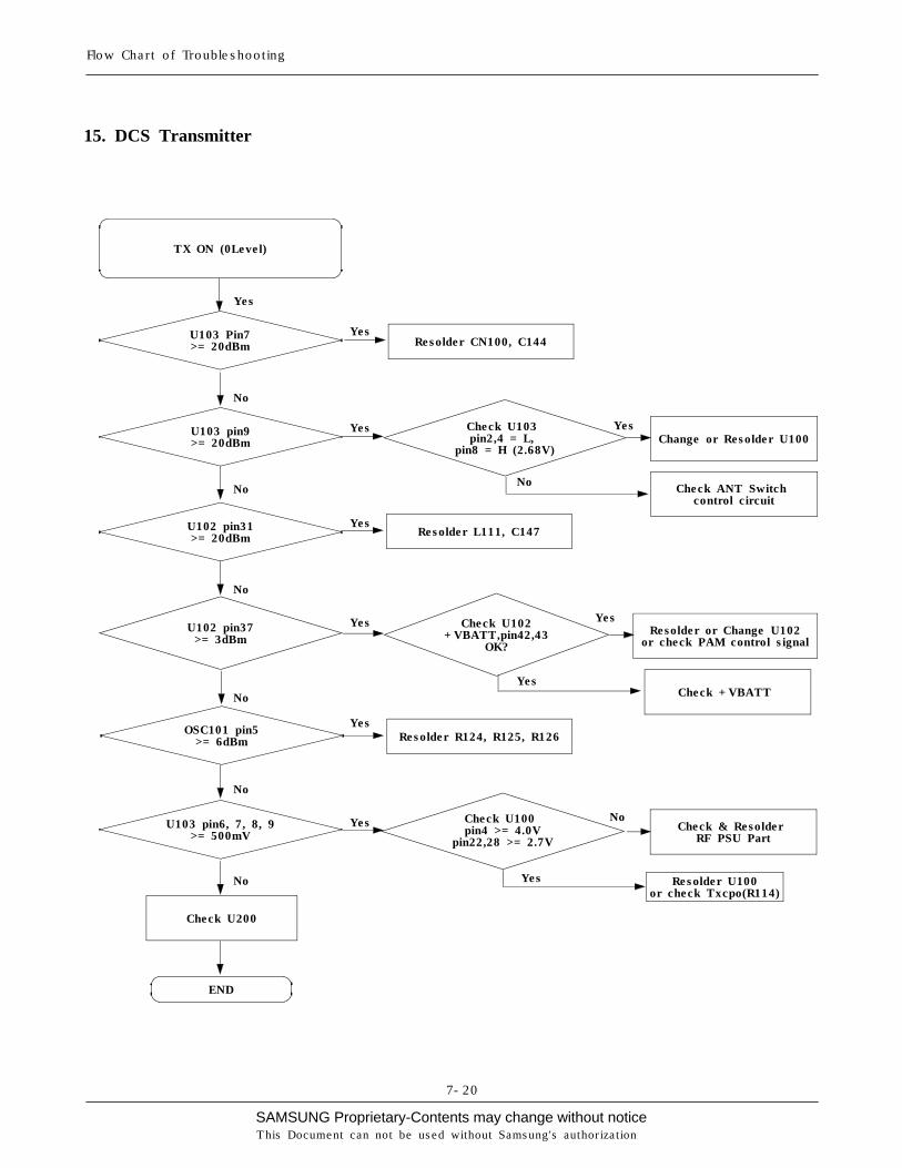
15. DCS Transmitter
U103 Pin7>= 20dBm Resolder CN100, C144
TX ON (0Level)
Check U103pin2,4 = L,
pin8 = H (2.68V)
U103 pin9>= 20dBm
U102 pin31>= 20dBm
OSC101 pin5>= 6dBm
U102 pin37>= 3dBm
Change or Resolder U100
Check ANT Switchcontrol circuit
Resolder L111, C147
Resolder R124, R125, R126
U103 pin6, 7, 8, 9>= 500mV
Yes
Check U102+VBATT,pin42,43
OK?Resolder or Change U102
or check PAM control signal
Check +VBATT
Check U100pin4 >= 4.0V
pin22,28 >= 2.7VCheck & Resolder
RF PSU Part
No
No
No
No
No
No
Yes
No
Yes
Yes
Yes
Yes
Yes
Yes
Yes
Yes
No
END
Check U200
Resolder U100or check Txcpo(R114)
Yes
SAMSUNG Proprietary-Contents may change without notice
Flow Chart of Troubleshooting
This Document can not be used without Samsung's authorization
7-21
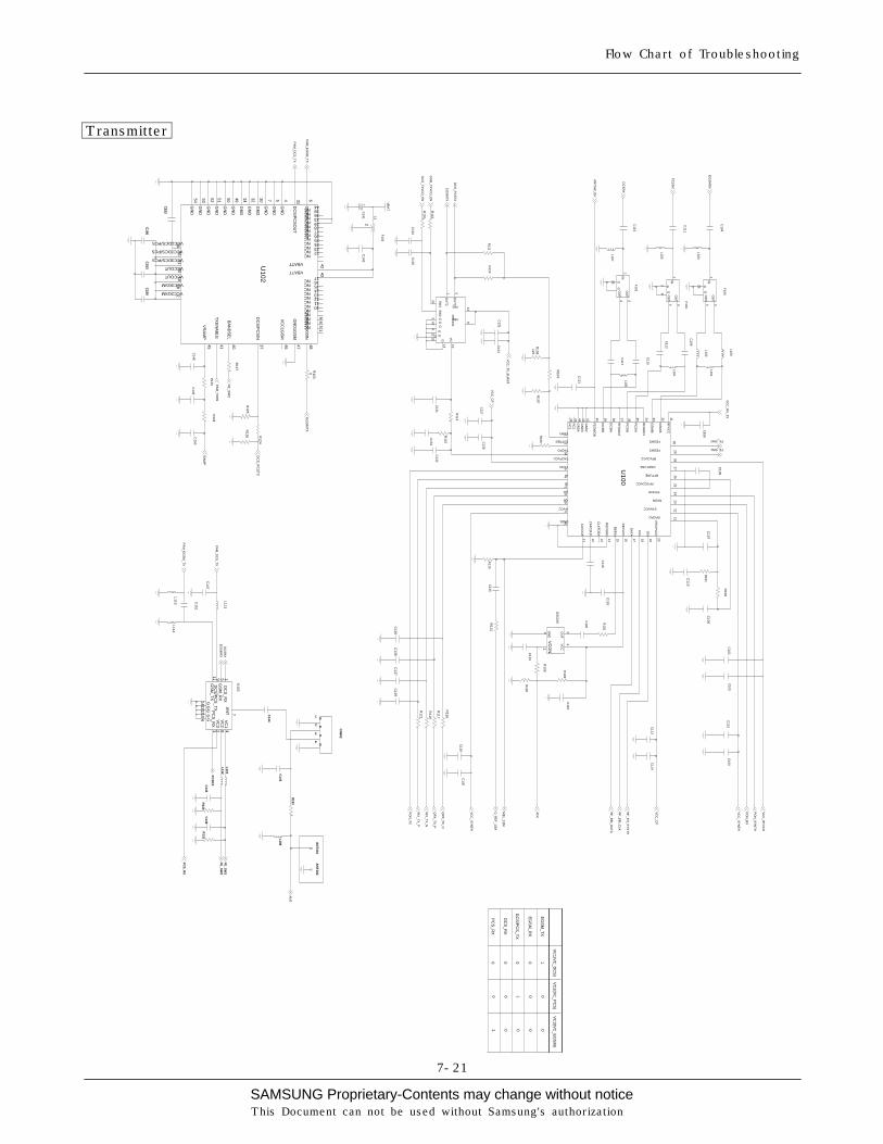
Transmitter
DC
S_R
X
EG
SM
_TX
1
0
0
0
VC
2(VC
_PC
S)
1
00 0
0P
CS
_RX
0
VC
1(VC
_DC
S)
EG
SM
_RX
0
DC
S/P
CS
_TX
0 0
VC
3(VC
_EG
SM
)
0
1R
107R
106
C150
C110
C125
R126
C153
C123
VB
AT
C155
R105
C124
C133
R120
120R
108
2
VCC3DCS/PCS 2118
VCC3GSM
VCCOUT 19
VCCOUT 20
VR
AM
P45
13NC14
TX
EN
AB
LE41
VBATT 4243
VBATT
39
VCC1DCS/PCS
VC
C1G
SM
46
35
VCC2DCS/PCS
VCC2GSM
38
NC36
NC44
8
NCNC
9
10NCNC
11NC12NC
NC24NC25NC26NC27NC28
3
NC
NC29NC33
NC
48G
SM
850/900OU
T6
1
NC
NC15NC16NC17
NC2223
NC
57G
ND
GN
D30
GN
D32
GN
D3449
GN
D50
GN
D
GN
D51
GS
M850/900IN
40
DC
S/P
CS
IN37
DC
S/P
CS
OU
T31
GN
D4
GN
D52
GN
D53
GN
D54
47G
ND
1GS
M
GN
D
U102
BA
ND
SE
L
L113
R114
C118
C137
R113
C114
R101
C103
L111L
110
R130
AN
T102
C141
C107
C144
R117
13
G
5O
UT
1
OU
T2
1
SW
1
24
SW
2
VB1
812
VB2
VC
10
G3
G67
G
11 GG
9
14G
C126
OS
C101
C100
C117
L101
L100
R118
L112
R127
R124
R131
C128
R100
L103
C106
C101
F101
2 G
5
GIN
13
OU
T
OU
T4
C111
C113
AN
T101
C102
C120
C156
C152
R125
C138
R104
C131
C119
R128
R116
C135
C143
L105
R129
C112
L104
C109
F102
G25
G
1IN
OU
T3
OU
T4
G25
G
1IN
OU
T34
OU
T
L107
F100
C104
R112
OS
C100
2 GN
D
3OU
T
4VC
C
VC
ON1
C116
C108
C121
C122
C127
L109
C147
R102
L114
R121
C132
14
5G
SM
_RX
11G
SM
_TX
PC
S_R
X3
VC
148
VC
2V
C3
2
7
AN
TD
CS
_RX
1
DC
S/P
CS
_TX
9
G6G10
G12G13
G
U103
C145
C115
L106
C130
C146
C136
C149
R111
C148
R103
C151
C142
0R
123
R115
R110
F103
2
13
R119
C134
R109
TXON
5
TXRFI
1
L102
3437R
FG
ND
2
RFLOVCC 28
RFTUNE 2631
RF
VC
C
25
RFVCOVCC
23
RXON
SYNON 24
SYNVCC 22
TXCPO
34
TXCPVCC
NC
246
35P
CS
IA
PC
SIB
36
8
QA
QB
9
14R
EF
GN
D
RE
FIN
15 16R
EF
VC
C
21
RFCPO
RF
CP
VC
C20
RF
GN
D1
GND1
GN
D2
4243G
ND
3G
ND
444
27
GNDTUNE
GS
MIA
3233G
SM
IB
6
IA
IB
710
IFVCC
NC
145
CLK
FD
BX
13
CLK
OU
T11
DA
TA
17
DC
SIA
3839D
CS
IB
EN
19
2
EXTRES
29
FESW1
FESW2 30
FE
SW
ON
40
41
U100
12C
AF
CS
UP
18C
LK
C139
R132
C129
C105
CN
502
A2
3C
1G
4G
AN
TS
W_O
N
EG
SM
RX
ME
L_13M
RF
_BB
I_CLK
PC
SR
X
FE_SW2
DC
SR
X
VC
C_R
X_T
X
VC
C_C
P
VC
C_S
YN
TH
FE_SW1
RF
_EN
_SY
NT
H
RF
_BB
I_DA
TA
PA
M_D
CS
_TX
PO
N_T
X
VC
C_C
P
VC
C_S
YN
TH
PO
N_S
YN
TH
PO
N_R
X
VC
C_R
FV
CO
PA
M_E
GS
M_T
X
DC
SR
XE
GS
MR
X
PC
SR
X
PC
S_R
X
FE
_SW
2
DC
S_P
CS
TX
EG
SM
TX
PA
M_E
GS
M_T
X
AN
T
FE
_SW
1F
E_S
W2
VC
C_T
X_B
UR
ST
DC
S_T
XV
CO
_EN
GS
M_T
XV
CO
_EN
PA
M_T
XE
N
PA
M_D
CS
_TX
RA
MP
IRX
_TX
_P
IRX
_TX
_N
QR
X_T
X_P
QR
X_T
X_N
EG
SM
TX
DC
S_P
CS
TX
D_R
EF
_13M
AF
C
SAMSUNG Proprietary-Contents may change without noticeThis Document can not be used without Samsung's authorization
Flow Chart of Troubleshooting
7-22