Question Paper Code: 21398
14
EE2254/LINEAR INTEGRATED CIRCUITS & APPLICATIONS/ PREVIOUS ANNA UNIV QUESTIONS / P.VIVEK /A.P / DEPT OF EEE Reg. No. : Question Paper Code: 21398 B.E./B.Tech. DEGREE EXAMINATION, MAY/JUNE 2013 Fourth Semester Electrical and Electronics Engineering EE2254 — LINEAR INTEGRATED CIRCUITS AND APPLICATIONS (Regulation 2008) (Common to Instrumentation and Control Engineering and Electronics and Instrumentation Engineering) Time: Three hours Maximum: 100 Marks Answer ALL Questions PART A — (10 × 2 = 20 Marks) 1. List the advantages of integrated circuit over discrete component circuit. 2. Explain why inductors are difficult to fabricate in IC's. 3. What are the different linear IC packages? 4. What is the input impedance of a non-inverting amplifier? 5. List the applications of analog multipliers. 6. Write the significance of lock range of a PLL. 7. Define the terms settling time and conversion time related to DAC’s. 8. What is the function of a voltage regulator? 9. What is the principle of switch mode power supplies? 10. How many resistors are required in a 12-bit weighted resistor DAC?
-
Upload
khangminh22 -
Category
Documents
-
view
1 -
download
0
Transcript of Question Paper Code: 21398
EE2254/LINEAR INTEGRATED CIRCUITS & APPLICATIONS/ PREVIOUS ANNA UNIV QUESTIONS / P.VIVEK /A.P / DEPT OF EEE
Reg. No. :
Question Paper Code: 21398
B.E./B.Tech. DEGREE EXAMINATION, MAY/JUNE 2013
Fourth Semester
Electrical and Electronics Engineering
EE2254 — LINEAR INTEGRATED CIRCUITS AND APPLICATIONS
(Regulation 2008)
(Common to Instrumentation and Control Engineering and Electronics and
Instrumentation Engineering)
Time: Three hours Maximum: 100 Marks
Answer ALL Questions
PART A — (10 × 2 = 20 Marks)
1. List the advantages of integrated circuit over discrete component circuit.
2. Explain why inductors are difficult to fabricate in IC's.
3. What are the different linear IC packages?
4. What is the input impedance of a non-inverting amplifier?
5. List the applications of analog multipliers.
6. Write the significance of lock range of a PLL.
7. Define the terms settling time and conversion time related to DAC’s.
8. What is the function of a voltage regulator?
9. What is the principle of switch mode power supplies?
10. How many resistors are required in a 12-bit weighted resistor DAC?
EE2254/LINEAR INTEGRATED CIRCUITS & APPLICATIONS/ PREVIOUS ANNA UNIV QUESTIONS / P.VIVEK /A.P / DEPT OF EEE
PART B — (5 × 16 = 80 Marks)
11. (a) Describe the Epitaxial growth process and photolithography process with
neat diagram.
Or
(b) Give the various ways for making integrated resistor.
12. (a) List the six characteristics of an ideal op-amp and explain in detail. Give the
practical op-amp equivalent circuit.
Or
(b) Explain in detail about DC characteristics of op-amp.
13. (a) Explain the principle of Instrumentation amplifier and derive the gain for
the circuit.
Or
(b) With neat sketches explain in detail about I/V and V/I converter using op-
amp.
(8)
14. (a) Design a first order low pass filter for a high cut-off freq of 2KHz and pass
band gain of 2. Or
(b) Explain the operation of a square wave generator by drawing the capacitor
and output voltage waveforms.
15. (a) Design an adjustable voltage regulator(5V to 15V) with a short circuit current
limit of 50MA using a 723 regulator.
Or
(b) Design a 4 bit R-2R ladder network, determine the size of each step if
r=10kΩ,Rf=40kΩ and Vcc=+15V.Calculate the output voltage for
D0=1,D2=1,D3=1 if the bit ‘1’ applied as 5V and bit ‘0’ applied as 0V.
————————
2 21398
EE2254/LINEAR INTEGRATED CIRCUITS & APPLICATIONS/ PREVIOUS ANNA UNIV QUESTIONS / P.VIVEK /A.P / DEPT OF EEE
Reg. No. :
Question Paper Code: 11366
B.E./B.Tech. DEGREE EXAMINATION, NOVEMBER /DECEMBER 2012
Fourth Semester
Electrical and Electronics Engineering
EE2254 — LINEAR INTEGRATED CIRCUITS AND APPLICATIONS
(Regulation 2008)
(Common to Instrumentation and Control Engineering and Electronics and
Instrumentation Engineering)
Time: Three hours Maximum: 100 Marks
Answer ALL Questions
PART A — (10 × 2 = 20 Marks)
1. What is ion implantation? Give its advantages.
2. Why inductors are difficult to fabricate in integrated circuits?
3. Design a subtractor using op-amp.
4. Define CMRR.
5. What are the applications of peak detector?
6. Why active filters are preferred?
7. In a astable multivibrator using 555 timer RA =6.8 kΩ, RB =3.3 kΩ,C=0.1 μF.
Calculate the free running frequency.
8. Why Vco is called voltage to frequency converter?
9. What is an isolation amplifier?
10. Name the various protection circuits used for voltage regulators.
EE2254/LINEAR INTEGRATED CIRCUITS & APPLICATIONS/ PREVIOUS ANNA UNIV QUESTIONS / P.VIVEK /A.P / DEPT OF EEE
PART B — (5 × 16 = 80 Marks)
11. (a) Explain the basic processes used in the fabrication of monolithic IC.
Or
(b) Explain the fabrication of n-channel JFET with necessary diagrams.
12. (a) (i) What are ideal Op-Amp characteristics? (6)
(ii) With a neat circuit diagram explain the operation of a Op-Amp
differentiator and derive an expression for the output of a practical
differentiator. (10)
Or
(b) Explain the different frequency compensation techniques of Op-Amp. (16)
13. (a) (i) Explain the working principle of successive approximation type ADC.
(12) (ii) Explain the any four specification of data converters. (4)
Or
(b) Explain with neat circuit diagram any one sine wave oscillator using Op-
Amp and derive expression for frequency of oscillation and gain of Op-Amp.
14. (a) Draw the functional diagram of IC 555 Timer in astable mode and explain its
operation and derive expression for frequency. Or
(b) Explain with a schematic how a PLL can be used as
(i) frequency multiplier. (8) (ii) frequency translator. (8)
15. (a) Draw and explain the function block diagram of a 723 IC regulator and make
the necessary changes to make it as low voltage regulator.
Or
(b) Write short notes on:
(i) Opto couplers. (8)
(ii) Switching regulators (8)
————————
2 11366
EE2254/LINEAR INTEGRATED CIRCUITS & APPLICATIONS/ PREVIOUS ANNA UNIV QUESTIONS / P.VIVEK /A.P / DEPT OF EEE
Reg. No. :
Question Paper Code: 10322
B.E./B.Tech. DEGREE EXAMINATION, MAY/JUNE 2012
Fourth Semester
Electrical and Electronics Engineering
EE2254 — LINEAR INTEGRATED CIRCUITS AND APPLICATIONS
(Regulation 2008)
(Common to Instrumentation and Control Engineering and Electronics and
Instrumentation Engineering)
Time: Three hours Maximum: 100 Marks
Answer ALL Questions
PART A — (10 × 2 = 20 Marks)
1. What is the significance of using buried layer?
2. What are the advantages of polysilicon gate MOSFET over aluminium gate?
3. List any four non ideal dc characteristics of opamp.
4. Draw a subtractor using op-amp.
5. Draw the circuit of I-V converter using op-amp.
6. Define Monotonicity with respect to Data converters.
7. In what way VCO is different from other oscillators.
8. Mention any two applications of 555 Timer in Monostable mode.
9. Why do switching regulators have better efficiency then series regulators?
10. What is an optocoupler?
EE2254/LINEAR INTEGRATED CIRCUITS & APPLICATIONS/ PREVIOUS ANNA UNIV QUESTIONS / P.VIVEK /A.P / DEPT OF EEE
PART B — (5 × 16 = 80 Marks)
11. (a) Explain in detail the fabrication process of passive component in Integrated
Circuits.
Or
(b) With necessary diagrams explain the fabrications of MOSFET.
12. (a) Draw the circuit of a symmetrical emitter coupled differential amplifier and
derive for CMRR .
Or
(b) Show with the help of circuit diagram an op-amp used as
(i) Summer . (8) (ii) Integrator and explain their operation. (8)
13. (a) Explain the working principle of RC phase shift sine wave generator using
op-amp and derive the expression for ‘f’.
Or
(b) (i) With an example and diagram explain the working principle of Successive
approximation type ADC. (12)
(ii) Explain the important DAC specifications. (4) Or
14. (a) Design and draw the waveforms of 1KHZ Square waveform generator using 555
Timer for duty cycle.
(i) D=25% . (8) (ii) D=50% (8)
Or
(b) (i) Perform the closed loop analysis of PLL. (8) (ii) Explain any two applications of PLL. (8)
15. (a) Draw and explain the fundamental block diagram of a 723 voltage regulator
and how this IC can be used as High voltage regulator.
Or
(b) Write an explanatory note on :
(i) Power amplifier. (ii) Isolation amplifiers.
————————
2 10322
EE2254/LINEAR INTEGRATED CIRCUITS & APPLICATIONS/ PREVIOUS ANNA UNIV QUESTIONS / P.VIVEK /A.P / DEPT OF EEE
Reg. No. :
Question Paper Code: 11314
B.E./B.Tech. DEGREE EXAMINATION, NOVEMBER /DECEMBER 2011
Fourth Semester
Electrical and Electronics Engineering
EE2254 — LINEAR INTEGRATED CIRCUITS AND APPLICATIONS
(Regulation 2008)
(Common to Instrumentation and Control Engineering and Electronics and
Instrumentation Engineering)
Time: Three hours Maximum: 100 Marks
Answer ALL Questions
PART A — (10 × 2 = 20 Marks)
1. List the basic processes used in IC Fabrication.
2. What is meant by ion implantation?
3. What is thermal drift?
4. Define Input offset voltage.
5. Draw the circuit of first order active filter.
6. Draw the circuit diagram of sample and hold circuit.
7. Define capture range of PLL.
8. What are one, two and four quadrant multipliers?
9. What are the disadvantages of linear voltage regulators?
10. What is isolation amplifier?
EE2254/LINEAR INTEGRATED CIRCUITS & APPLICATIONS/ PREVIOUS ANNA UNIV QUESTIONS / P.VIVEK /A.P / DEPT OF EEE
PART B — (5 × 16 = 80 Marks)
11. (a) (i) Explain the process of epitaxial growth in IC fabrication process with neat
diagrams. (8)
(ii) With neat sketches explain the fabrication of diodes. (8)
Or
(b) (i) Explain the different isolation techniques. (8)
(ii) Describe in detail about the diffusion process of IC fabrication. (8)
12. (a) Explain in detail about the frequency compensation applied to operational
amplifiers. (16)
(b) Draw and explain the working of operational amplifier as
(i) Integrator. (8) (ii) Differentiator. (8)
13. (a) Explain the following applications of operational amplifiers.
(i) Voltage to current converter. (8) (ii) Clamper. (8)
Or
(b) Explain in detail the working of
(i) Weighted resistor type DAC. (8) (ii) Dual slope type ADC. (8)
14. (a) (i) Explain the working of voltage controlled oscillators. (8)
(ii) What is PLL? Explain its application as frequency multiplier. (8)
Or
(b) Explain the astable and bistable operation of IC 555 with necessary waveforms. (8)
15. (a) Draw and explain the application of IC 723 as low voltage regulator and high
voltage regulator. (16) Or
(b) (i) Explain the block diagram of ICL 8038 function generator IC. (8)
(ii) Write short notes on opto couplers. (8)
————————
2 55360
EE2254/LINEAR INTEGRATED CIRCUITS & APPLICATIONS/ PREVIOUS ANNA UNIV QUESTIONS / P.VIVEK /A.P / DEPT OF EEE
Reg. No. :
Question Paper Code: 11314
B.E./B.Tech. DEGREE EXAMINATION, APRIL/MAY 2011
Fourth Semester
Electrical and Electronics Engineering
EE2254 — LINEAR INTEGRATED CIRCUITS AND APPLICATIONS
(Regulation 2008)
(Common to Instrumentation and Control Engineering and Electronics and
Instrumentation Engineering)
Time: Three hours Maximum: 100 Marks
Answer ALL Questions
PART A — (10 × 2 = 20 Marks)
1. Write the basic chemical reaction in the epitaxial growth processes of pure silicon.
2. What are the advantages of integrated circuits over discrete circuits?
3. Mention the important ideal characteristics of An Op-Amp.
4. What are the different kinds of packages of IC 741?
5. What is the need for an instrumentation amplifier?
6. Define conversion time of ADC.
7. List four applications of 555 timer in Astable mode of operation.
8. Define capture range of PLL.
9. Why current boosting is done in 723 regulators?
10. Mention the important advantages of opto-couplers.
EE2254/LINEAR INTEGRATED CIRCUITS & APPLICATIONS/ PREVIOUS ANNA UNIV QUESTIONS / P.VIVEK /A.P / DEPT OF EEE
PART B — (5 × 16 = 80 Marks)
11. (a) Explain in detail about the processing steps involved in the fabrication of
monolithic integrated circuits. (16)
Or
(b) With the neat sketches, describe the operation of Epitaxial growth and
Photolithography. (16)
12. (a) Explain the DC characteristics of operational amplifier with the help of neat
diagram. (16)
Or
(b) With a neat circuit diagram and equations, discuss the operation of summer and
differentiator using Operational amplifier. (16)
13. (a) Discuss the operation of Ladder network DAC with relevant circuit diagram and
waveforms. (16)
Or
(b) Draw the Instrumentation amplifier using 3-Op-amp and derive expression for
overall gain. Illustrate the characteristics and operation in which this is used.
Name any two commonly available Instrumentation amplifiers. (16)
Or
14. (a) List the important features of IC 555 timer. Also write about the two basic modes
in which the 555 timer operates. (16)
Or
(b) With help of schematic circuit, explain the operation of 566 VCO. Also derive an
expression for the output frequency. (16)
15. (a) Draw the circuit of series voltage regulator. Design this circuit to operate from a
supply of 20V and to provide an output of 12V with maximum load current of
40mA. (16) Or
(b) Draw the functional block diagram of ICL 8038 function generator IC and
explain its operation. (16)
————————
2 11314
EE2254/LINEAR INTEGRATED CIRCUITS & APPLICATIONS/ PREVIOUS ANNA UNIV QUESTIONS / P.VIVEK /A.P / DEPT OF EEE
Reg. No. :
Question Paper Code: 53139
B.E./B.Tech. DEGREE EXAMINATION, NOVEMBER /DECEMBER 2010
Fourth Semester
Electrical and Electronics Engineering
EE2254 — LINEAR INTEGRATED CIRCUITS AND APPLICATIONS
(Regulation 2008)
(Common to Instrumentation and Control Engineering and Electronics and
Instrumentation Engineering)
Time: Three hours Maximum: 100 Marks
Answer ALL Questions
PART A — (10 × 2 = 20 Marks)
1. Give the difference between monolithic and hybrid ICs.
2. What is lithography?
3. Give the ideal characteristics of operational amplifier and give its equivalent
circuit.
4. Draw the circuit diagram of an integrator and give its output equation.
5. Draw the circuit diagram of an op-amp based positive clipper
6. Which is the fastest ADC and why?
7. List the applications of NE 565.
8. Draw the relation between the capture range and lock range relationship in a PLL.
9. How will you increase the output of a general purpose op-amp?
10. Using LM380 draw the circuit for audio power amplifier.
PART B — (5 × 16 = 80 Marks)
11. (a) (i) Briefly explain the various types of IC packages. Mention the criteria for
selecting an IC package. (8)
(ii) Write short notes on classification of Integrated circuits. (8)
Or
EE2254/LINEAR INTEGRATED CIRCUITS & APPLICATIONS/ PREVIOUS ANNA UNIV QUESTIONS / P.VIVEK /A.P / DEPT OF EEE
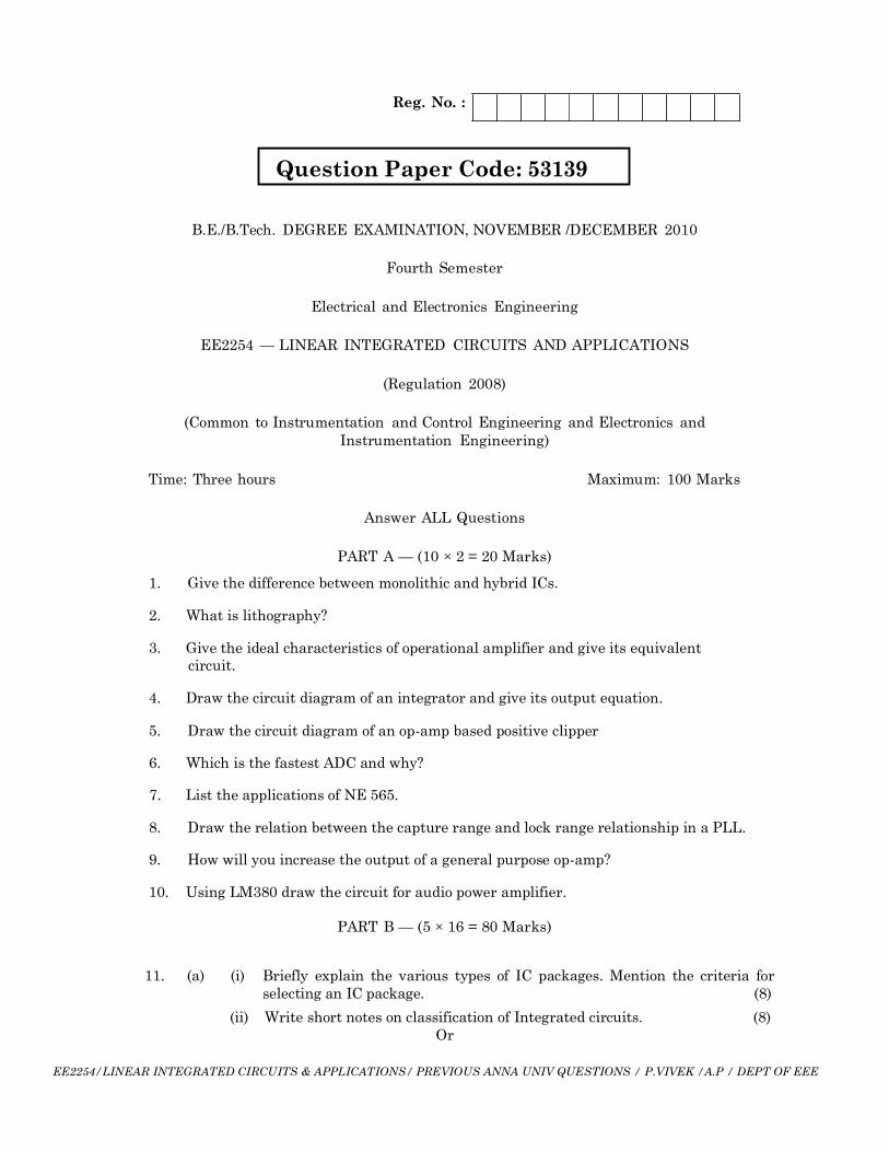
(b) With respect to the BJT based circuit given below, explain the various steps to
implement the circuit into a monolithic IC. (16)
12. (a) (i) With neat diagrams explain the types of feedback configurations
available. (8)
(ii) Briefly explain summing amplifier. Draw an adder circuit for the given
expression Vo = - (0.1 V1 + V2 + 5V3). (8)
Or
(b) Briefly explain the frequency response of op-amp. Give the frequency
compensation techniques adopted in operational amplifiers. (16)
13. (a) (i) Explain the first order low pass Butterworth filter with a neat circuit
diagram. Derive its frequency response and plot the same. (8)
(ii) Design a low pass filter with a cut off frequency of 1 kHz and with a pass
band gain of 2. (8)
Or
(b) What is an instrumentation amplifier? Give the important features of an
instrumentation amplifier. Explain the working of three op-amp instrumentation
amplifier. Give its application. (16)
14. (a) (i) Explain the Voltage Controlled Oscillator with a neat block diagram. Give
its typical connection diagram and its output waveforms. (8)
(ii) Derive the expression for capture range for PLL where a simple RC
network is used as a LPF. (8)
Or
(b) Draw the functional diagram of IC 555 Timer. Explain with a circuit diagram
how it can be connected for monostable operation. (16)
15. (a) (i) Explain the working of series voltage regulator. (8)
(ii) Write a note on optocouplers. (8)
Or
(b) What is a switching regulator? With a neat block diagram explain the internals
of µA 7840. (16)
————————
2 53139
EE2254/LINEAR INTEGRATED CIRCUITS & APPLICATIONS/ PREVIOUS ANNA UNIV QUESTIONS / P.VIVEK /A.P / DEPT OF EEE
Reg. No. :
Question Paper Code: E3089
B.E./B.Tech. DEGREE EXAMINATION, APRIL/MAY 2010
Fourth Semester
Electrical and Electronics Engineering
EE2254 — LINEAR INTEGRATED CIRCUITS AND APPLICATIONS
(Regulation 2008)
(Common to Instrumentation and Control Engineering and Electronics and
Instrumentation Engineering)
Time: Three hours Maximum: 100 Marks
Answer ALL Questions
PART A — (10 × 2 = 20 Marks)
1. What is the purpose of oxidation process in IC fabrication?
2. What is parasitic capacitance?
3. List any four characteristics of an ideal OP-Amp.
4. Design an amplifier with a gain of –10 and input resistance of 10 k Ω .
5. Define slew rate and state its significance.
6. An 8 bit DAC has a resolution of 20mV/bit. What is the analog output voltage
for the digital input code 00010110 (the MSB is the left most bit)?
7. Draw the pin diagram of IC 555 timer.
8. Mention any two application of multiplier IC.
9. List the important parts of regulated power supply.
10. What are the advantages of switch mode power supplies?
PART B — (5 × 16 = 80 Marks)
11. (a) Explain the basic processes used in silicon planar technology with neat
diagram.
Or
(b) Discuss the various methods used for fabricating IC resistors and
compare their performance.
EE2254/LINEAR INTEGRATED CIRCUITS & APPLICATIONS/ PREVIOUS ANNA UNIV QUESTIONS / P.VIVEK /A.P / DEPT OF EEE
12. (a) (i) Explain the functions of all the basic building blocks of an Op-Amp.
(8)
(ii) Explain the application of OPAMP as (1) integrator
(2) differentiator. (8)
Or
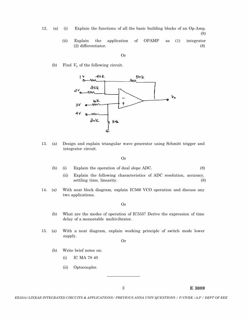
(b) Find V0 of the following circuit.
13. (a) Design and explain triangular wave generator using Schmitt trigger and
integrator circuit.
Or
(b) (i) Explain the operation of dual slope ADC. (8)
(ii) Explain the following characteristics of ADC resolution, accuracy,
settling time, linearity. (8)
14. (a) With neat block diagram, explain IC566 VCO operation and discuss any
two applications.
Or
(b) What are the modes of operation of IC555? Derive the expression of time
delay of a monostable multivibrator.
15. (a) With a neat diagram, explain working principle of switch mode lower
supply.
Or
(b) Write brief notes on:
(i) IC MA 78 40
(ii) Optocoupler.
————————
2 E 3089