Principles of - Electronic Communication Systems
945
Principles of Electronic Communication Systems Louis E. Frenzel Jr. Fourth Edition
-
Upload
khangminh22 -
Category
Documents
-
view
1 -
download
0
Transcript of Principles of - Electronic Communication Systems

P r i n c i p l e s o f
ElectronicCommunication Systems
Louis E. Frenzel Jr.
Fo u rt h E d i t i o n

Louis E. Frenzel Jr.
Principles of Electronic Communication
Systems
Fourth Edition

PRINCIPLES OF ELECTRONIC COMMUNICATION SYSTEMS, FOURTH EDITION
Published by McGraw-Hill Education, 2 Penn Plaza, New York, NY 10121. Copyright © 2016 by McGraw-Hill Education. All rights reserved. Printed in the United States of America. Previous editions © 2008, 2003, and 1998. No part of this publication may be reproduced or distributed in any form or by any means, or stored in a database or retrieval system, without the prior written consent of McGraw-Hill Education, including, but not limited to, in any network or other electronic storage or transmission, or broadcast for distance learning.
Some ancillaries, including electronic and print components, may not be available to customers outside the United States.
This book is printed on acid-free paper.
1 2 3 4 5 6 7 8 9 0 DOW/DOW 1 0 9 8 7 6 5
ISBN 978-0-07-337385-0MHID 0-07-337385-0
Senior Vice President, Products & Markets: Kurt L. Strand
Vice President, General Manager, Products & Markets: Marty Lange
Vice President, Content Design & Delivery: Kimberly Meriwether David
Managing Director: Thomas Timp
Global Publisher: Raghu Srinivasan
Director, Product Development: Rose Koos
Product Developer: Vincent Bradshaw
Marketing Manager: Nick McFadden
Director, Content Design & Delivery: Linda Avenarius
Director of Digital Content: Thomas Scaife, Ph.D
Program Manager: Faye Herrig
Content Project Managers: Kelly Hart, Tammy Juran, Sandy Schnee
Buyer: Laura M. Fuller
Design: Studio Montage, St. Louis, MO
Content Licensing Specialists: DeAnna Dausener
Cover Image: ©Royalty Free/CorbisCompositor: Aptara®, Inc.
Typeface: 10/12 Times Roman
Printer: R.R. Donnelley
All credits appearing on page or at the end of the book are considered to be an extension of the copyright page.
Library of Congress Cataloging-in-Publication Data
Frenzel, Louis E., Jr., 1938– Principles of electronic communication systems / Louis E. Frenzel Jr. —Fourth edition. pages cm Includes index. ISBN 978-0-07-337385-0 (alk. paper) — ISBN 0-07-337385-0 (alk. paper) 1. Telecommunication—Textbooks. 2. Wireless communication systems—Textbooks. I. Title.
TK5101.F664 2014 384.5—dc23
2014031478
The Internet addresses listed in the text were accurate at the time of publication. The inclusion of a website does not indicate an endorsement by the authors or McGraw-Hill Education, and McGraw-Hill Education does not guarantee the accuracy of the information presented at these sites.
www.mhhe.com

Contents
Preface viii
Chapter 1 Introduction to Electronic Communication 11-1 The Signifi cance of Human
Communication 3
1-2 Communication Systems 3
1-3 Types of Electronic Communication 6
1-4 Modulation and Multiplexing 8
1-5 The Electromagnetic Spectrum 12
Chapter 2 Electronic Fundamentals for Communications 302-1 Gain, Attenuation,
and Decibels 31
2-2 Tuned Circuits 41
Chapter 3 Amplitude Modulation Fundamentals 923-1 AM Concepts 93
3-2 Modulation Index and Percentage of Modulation 95
3-3 Sidebands and the Frequency Domain 98
Chapter 4 Amplitude Modulator and Demodulator Circuits 1174-1 Basic Principles of Amplitude
Modulation 118
4-2 Amplitude Modulators 121
4-3 Amplitude Demodulators 129
1-6 Bandwidth 18
1-7 A Survey of Communication Applications 21
1-8 Jobs and Careers in the Communication Industry 23
3-4 AM Power 104
3-5 Single-Sideband Modulation 108
3-6 Classifi cation of Radio Emissions 112
2-3 Filters 56
2-4 Fourier Theory 77
4-4 Balanced Modulators 134
4-5 SSB Circuits 141
iii

Chapter 5 Fundamentals of Frequency Modulation 1505-1 Basic Principles of Frequency
Modulation 151
5-2 Principles of Phase Modulation 153
5-3 Modulation Index and Sidebands 156
Chapter 6 FM Circuits 172 6-1 Frequency Modulators 173
6-2 Phase Modulators 180
6-3 Frequency Demodulators 183
Chapter 7 Digital Communication Techniques 1927-1 Digital Transmission
of Data 193
7-2 Parallel and Serial Transmission 194
7-3 Data Conversion 197
Chapter 8 Radio Transmitters 236 8-1 Transmitter Fundamentals 237
8-2 Carrier Generators 241
8-3 Power Amplifi ers 259
Chapter 9 Communication Receivers 291 9-1 Basic Principles of Signal
Reproduction 292
9-2 Superheterodyne Receivers 295
9-3 Frequency Conversion 297
9-4 Intermediate Frequency and Images 306
iv Contents
5-4 Noise Suppression Ef ects of FM 163
5-5 Frequency Modulation Versus Amplitude Modulation 167
7-4 Pulse Modulation 222
7-5 Digital Signal Processing 228
8-4 Impedance-Matching Networks 276
8-5 Typical Transmitter Circuits 286
9-5 Noise 314
9-6 Typical Receiver Circuits 325
9-7 Receivers and Transceivers 334

Chapter 10 Multiplexing and Demultiplexing 34710-1 Multiplexing Principles 348
10-2 Frequency-Division Multiplexing 349
10-3 Time-Division Multiplexing 357
Chapter 11 Digital Data Transmission 37411-1 Digital Codes 375
11-2 Principles of Digital Transmission 377
11-3 Transmission Ei ciency 383
11-4 Modem Concepts and Methods 389
11-5 Wideband Modulation 403
Chapter 12 Fundamentals of Networking, Local-Area Networks, and Ethernet 43412-1 Network Fundamentals 435 12-3 Ethernet LANs 449
12-2 LAN Hardware 441 12-4 Advanced Ethernet 458
Chapter 13 Transmission Lines 46213-1 Transmission Line
Basics 463
13-2 Standing Waves 476
Chapter 14 Antennas and Wave Propagation 50414-1 Antenna Fundamentals 505
14-2 Common Antenna Types 513
Chapter 15 Internet Technologies 55615-1 Internet Applications 557
15-2 Internet Transmission Systems 561
10-4 Pulse-Code Modulation 365
10-5 Duplexing 371
11-6 Broadband Modem Techniques 412
11-7 Error Detection and Correction 416
11-8 Protocols 426
13-3 Transmission Lines as Circuit Elements 485
13-4 The Smith Chart 490
14-3 Radio Wave Propagation 538
15-3 Storage-Area Networks 577
15-4 Internet Security 580
Contents v

Chapter 16 Microwave and Millimeter-Wave Communication 58816-1 Microwave Concepts 589
16-2 Microwave Lines and Devices 596
16-3 Waveguides and Cavity Resonators 605
16-4 Microwave Semiconductor Diodes 617
Chapter 17 Satellite Communication 65517-1 Satellite Orbits 656
17-2 Satellite Communication Systems 663
17-3 Satellite Subsystems 667
17-4 Ground Stations 673
Chapter 18 Telecommunication Systems 69518-1 Telephones 696
18-2 Telephone System 708
Chapter 19 Optical Communication 72619-1 Optical Principles 727
19-2 Optical Communication Systems 731
19-3 Fiber-Optic Cables 736
19-4 Optical Transmitters and Receivers 747
Chapter 20 Cell Phone Technologies 77520-1 Cellular Telephone
Systems 776
20-2 A Cellular Industry Overview 782
20-3 2G and 3G Digital Cell Phone Systems 785
16-5 Microwave Tubes 621
16-6 Microwave Antennas 625
16-7 Microwave and Millimeter-Wave Applications 642
17-5 Satellite Applications 680
17-6 Global Navigation Satellite Systems 685
18-3 Facsimile 714
18-4 Internet Telephony 720
19-5 Wavelength-Division Multiplexing 762
19-6 Passive Optical Networks 764
19-7 40/100-Gbps Networks and Beyond 767
20-4 Long Term Evolution and 4G Cellular Systems 792
20-5 Base Stations and Small Cells 803
vi Contents

Chapter 21 Wireless Technologies 81521-1 Wireless LAN 817
21-2 PANs and Bluetooth 824
21-3 ZigBee and Mesh Wireless Networks 827
21-4 WiMAX and Wireless Metropolitan-Area Networks 829
21-5 Infrared Wireless 830
Chapter 22 Communication Tests and Measurements 84922-1 Communication Test Equipment 850
22-2 Common Communication Tests 866
22-3 Troubleshooting Techniques 883
22-4 Electromagnetic Interference Testing 888
Answers to Selected Problems 896
Glossary 898
Credits 918
Index 919
21-6 Radio-Frequency Identifi cationand Near-Field Communications 834
21-7 Ultrawideband Wireless 839
21-8 Additional Wireless Applications 843
Contents vii

Preface
This new fourth edition of Principles of Electronic Communication Systems is fully revised and updated to make it one of the most current textbooks available on wireless, networking, and other communications technologies. Because the i eld of electronic communications changes so fast, it is a never-ending challenge to keep a textbook up to date. While principles do not change, their emphasis and relevance do as technology evolves. Furthermore, students need not only a i rm grounding in the fundamentals but also an essential understanding of the real world components, circuits, equipment, and systems in everyday use. This latest edition attempts to balance the principles with an overview of the latest techniques.
A continuing goal of this latest revision is to increase the emphasis on the system
level understanding of wireless, networking, and other communications technologies. Because of the heavy integration of communications circuits today, the engineer and the technician now work more with printed circuit boards, modules, plug-in cards, and equip-ment rather than component level circuits. As a result, older obsolete circuits have been removed from this text and replaced with more integrated circuits and block diagram level analysis. Modern communications engineers and technicians work with specii cations and standards and spend their time testing, measuring, installing, and troubleshooting. This edition moves in that direction. Detailed circuit analysis is still included in selected areas where it proves useful in understanding the concepts and issues in current equipment.
In the past, a course in communications was considered an option in many elec-tronic programs. Today, communications is the largest sector of the electronics i eld with the most employees and the largest equipment sales annually. In addition, wire-less, networking, or other communications technologies are now contained in almost every electronic product. This makes a knowledge and understanding of communica-tion a must rather than an option for every student. Without at least one course in communications, the student may graduate with an incomplete view of the products and systems so common today. This book can provide the background to meet the needs of such a general course.
As the Communications Editor for Electronic Design Magazine (Penton), I have observed the continuous changes in the components, circuits, equipment, systems, and applications of modern communications. As I research the i eld, interview engineers and executives, and attend the many conferences for the articles and columns I write, I have come to see the growing importance of communications in all of our lives. I have tried to bring that perspective to this latest edition where the most recent techniques and technologies are explained. That perspective coupled with the feedback and insight from some of you who teach this subject has resulted in a textbook that is better than ever.
New to this Edition
Here is a chapter-by-chapter summary of revisions and additions to this new edition.
Chapters 1–6 Updating of circuits. Removing obsolete circuits and adding current circuits.
Chapter 7 Updated section on data conversion, including a new section on overs-ampling and undersampling.
viii
Chapter 8 Expanded coverage of the I/Q architecture for digital data transmis-sion. New section on phase noise. Addition of broadband linear power amplii ers using feedforward and adaptive predistortion tech-niques. New coverage of Doherty amplii ers and envelope tracking amplii ers for improved power efi ciency. Addition of new IC trans-mitters and transceivers. New coverage of LDMOS and GaN RF power transistors.
Chapter 9 Expanded coverage of receiver sensitivity and signal-to-noise ratio, its importance and calculation. Addition of AWGN and expanded coverage of intermodulation distortion. Increased coverage of the software-dei ned radio (SDR). New IC receiver circuits and transceivers.
Chapter 10 Updated coverage of multiplexing and access techniques.
Chapter 11 Expanded coverage of digital modulation and spectral efi ciency. Increased coverage of digital modulation schemes. New coverage of DSL, ADSL, and VDSL. Addition of cable TV system coverage. Improved coverage of the OSI model. Addition of an explanation of how different digital modulation schemes affect the bit error rate (BER) in communications systems. Updated sections on spread spec-trum and OFDM. A new section on convolutional and turbo coding and coding gain.
Chapter 12 Heavily revised to emphasize fundamentals and Ethernet. Dated mate-rial removed. Expanded and updated to include the latest Ethernet stan-dards for i ber-optic and copper versions for 100 Gbps.
Chapter 13 Minor revisions and updates.
Chapter 14 Minor revisions and updates.
Chapter 15 Fully updated. Addition of coverage of IPv6 and the Optical Transport Network standard.
Chapter 16 Updated with new emphasis on millimeter waves. Updated circuitry.
Chapter 17 Revised and updated.
Chapter 18 Removal of dated material and updating.
Chapter 19 Expanded section on MSA optical transceiver modules, types and specii cations. OM i ber added. Addition of coverage of 100-Gbps techniques, including Mach-Zehnder modulators and DP-QPSK modulation.
Chapter 20 Extensively revisions on cell phone technologies. New coverage on HSPA and Long Term Evolution (LTE) 4G systems. Analysis of a smartphone. Backhaul. A glimpse of 5G including small cells.
Chapter 21 Updates include addition of the latest 802.11ac and 802.11ad Wi-Fi standards. New coverage on machine-to-machine (M2M), the Internet of Things (IoT), and white space technology.
Chapter 22 Revisions and updates include a new section on vector signal analyzers and generators.
One major change is the elimination of the ineffective chapter summaries. Instead, new Online Activity sections have been added to give students the opportunity to further explore new communications techniques, to dig deeper into the theory, and to become more adept at using the Internet to i nd needed information. These activities show students the massive stores of communications information they can tap for free at any time.
In a large book such as this, it’s difi cult to give every one what he or she wants. Some want more depth, others greater breadth. I tried to strike a balance between the two. As always, I am always eager to hear from those of you who use the book and welcome your suggestions for the next edition.
Preface ix

Learning Features
Principles of Electronic Communication Systems, fourth edition, has an attractive and accessible page layout. To guide readers and provide an integrated learning approach, each chapter contains the following features:
● Chapter Objectives● Key Terms● Good to Know margin features● Examples with solutions● Online Activities● Questions● Problems ● Critical Thinking
Student Resources
Experiments and Activities Manual
The Experiments and Activities Manual has been minimally revised and updated. Building a practical, affordable but meaningful lab is one of the more difi cult parts of creating a college course in communications. This new manual provides practice in the principles by using the latest components and methods. Affordable and readily available components and equipment have been used to make it easy for professors to put together a commu-nications lab that validates and complements the text. A new section listing sources of communications laboratory equipment has been added. The revised Experiments and Activities Manual includes some new projects that involve Web access and search to build the student’s ability to use the vast resources of the Internet and World Wide Web. The practical engineers and technicians of today have become experts at i nding relevant information and answers to their questions and solutions to their problems this way. While practicing this essential skill of any communications engineer or technician knowledge, the student will be able to expand his or her knowl-edge of any of the subjects in this book, either to dig deeper into the theory and practice or to get the latest update information on chips and other products.
Connect Engineering
The online resources for this edition include McGraw-Hill Connect®, a Web-based assignment and assessment platform that can help students to perform better in their coursework and to master important concepts. With Connect®, instructors can deliver assignments, quizzes, and tests easily online. Students can practice important skills at their own pace and on their own schedule. Ask your McGraw-Hill Representative for more detail and check it out at www.mcgrawhillconnect.com.
McGraw-Hill LearnSmart®
McGraw-Hill LearnSmart® is an adaptive learning system designed to help students learn faster and study more efi ciently, and retain more knowledge for greater success. Through a series of adaptive questions, LearnSmart® pinpoints concepts the student does not understand and maps out a personalized study plan for success. It also lets instructors see exactly what students have accomplished, and it features a built-in assessment tool for graded assignments. Ask your McGraw-Hill Representative for more information, and visit www.mhlearnsmart.com for a demonstration.
McGraw-Hill SmartBook™
Powered by the intelligent and adaptive LearnSmart engine, SmartBook is the i rst and only continuously adaptive reading experience available today. Distinguishing what students know from what they don’t, and honing in on concepts they are most likely to forget,
®
x Preface

SmartBook personalizes content for each student. Reading is no longer a passive and linear experience but an engaging and dynamic one, where students are more likely to master and retain important concepts, coming to class better prepared. SmartBook includes powerful reports that identify specii c topics and learning objectives students need to study. These valuable reports also provide instructors insight into how students are progressing through textbook content, and they are useful for identifying class trends, focusing precious class time, providing personalized feedback to students, and tailoring assessment.
How does SmartBook work? Each SmartBook contains four components: Preview, Read, Practice, and Recharge. Starting with an initial preview of each chapter and key learning objectives, students read the material and are guided to topics for which they need the most practice based on their responses to a continuously adapting diagnostic. Read and Practice continue until SmartBook directs students to recharge important material they are most likely to forget to ensure concept mastery and retention.
Electronic Textbooks
This textbook is available as an eBook at www.CourseSmart.com. At CourseSmart, your students can take advantage of signii cant savings off the cost of a print textbook, reduce their impact on the environment, and gain access to powerful Web tools for learning. CourseSmart eBooks can be viewed online or downloaded to a computer. The eBooks allow students to do full text searches, add highlighting and notes, and share notes with classmates. CourseSmart has the largest selection of eBooks available anywhere. Visit www.CourseSmart.com to learn more and to try a sample chapter.
McGraw-Hill Create™
With McGraw-Hill Create, you can easily rearrange chapters, combine material from other content sources, and quickly upload content you have written, like your course syllabus or teaching notes. Find the content you need in Create by searching through thousands of leading McGraw-Hill textbooks. Arrange your book to i t your teaching style. Create even allows you to personalize your book’s appearance by selecting the cover and adding your name, school, and course information. Order a Create book, and you’ll receive a complimentary print review copy in 3–5 business days or a complimentary electronic review copy (eComp) via e-mail in minutes. Go to www.mcgrawhillcreate.com today, and register to experience how McGraw-Hill Create empowers you to teach your students your way.
The Connect site for this textbook includes a number of instructor and student resources, including:
● A MultiSim Primer for those who want to get up and running with this popular simulation software. The section is written to provide communications examples and applications.
● MultiSim circuit i les for communications electronics.● Answers and solutions to the text problems and lab activities and instructor Power-
Point slides, under password protection.
To access the Instructor Resources through Connect, you must i rst contact your McGraw-Hill Learning Technology Representative to obtain a password. If you do not know your McGraw-Hill representative, please go to www.mhhe.com/rep, to i nd your representative. Once you have your password, go to connect.mheducation.com, and log in. Click on the course for which you are using this textbook. If you have not added a course, click “Add Course,” and select “Engineering Technology” from the drop-down menu. Select Principles of Electronic Communication Systems, 4e and click “Next.” Once you have added the course, Click on the “Library” link, and then click “Instructor Resources.”
Preface xi

My special thanks to McGraw-Hill editor Raghu Srinivasan for his continued support and encouragement to make this new edition possible. Thanks also to Vincent Bradshaw and the other helpful McGraw-Hill support staff, including Kelly Lowery and Amy Hill. It has been a pleasure to work with all of you. I also want to thank Nancy Friedrich of Microwaves & RF magazine and Bill Baumann from Electronic Design magazine, both of Penton Media Inc., for permission to use sections of my articles in updating chapters 20 and 21. And my appreciation also goes out to those professors who reviewed the book and offered your feedback, criticism, and suggestions. Thanks for taking the time to provide that valuable input. I have implemented most of your recommendations. The following reviewers looked over the manuscript in various stages, and provided a wealth of good suggestions for the new edition:
With the latest input from industry and the suggestions from those who use the book, this edition should come closer than ever to being an ideal textbook for teaching current day communications electronics.
Lou FrenzelAustin, Texas2014
Norman AhlhelmCentral Texas College
David W. AstorinoLorain County Community College
Noureddine BekhoucheJacksonville State University
Katherine BennettThe University of the Arts
DeWayne R. BrownNorth Carolina A&T State University
Jesus CasasAustin Community College
Dorina Cornea HaseganPortland Community College
Kenneth P. De LuccaMillersville University
Richard FornesJohnson College
Billy GrahamNorthwest Technical Institute
Thomas HendersonTulsa Community College
Paul HollinsheadCochise Community College
Joe Morales Dona Ana Community College
Jeremy SpraggsFulton-Montgomery Community College
Yun LiuBaltimore City Community College
Acknowledgments
xii

The Transmission of Binary Data in Communications Systems xiii
Learning FeaturesThe fourth edition of Principles of Electronic Communication Systems retains many of the popular
learning elements featured in previous editions, as well as a few new elements. These include:
Chapter Objectives
Chapter Objectives provide a concise
statement of expected learning out-
comes.
dBm. When the gain or attenuation of a circuit is expressed in decibels, implicit is a comparison between two values, the output and the input. When the ratio is computed, the units of voltage or power are canceled, making the ratio a dimensionless, or relative, figure. When you see a decibel value, you really do not know the actual voltage or power values. In some cases, this is not a problem; in others, it is useful or necessary to know the actual values involved. When an absolute value is needed, you can use a reference value to compare any other value. An often used reference level in communication is 1 mW. When a decibel value is computed by comparing a power value to 1 mW, the result is a value called the dBm. It is computed with the standard power decibel formula with 1 mW as the denominator of the ratio:
dBm 5 10 log
Pout(W)
0.001(W)
Here Pout is the output power, or some power value you want to compare to 1 mW, and 0.001 is 1 mW expressed in watts. The output of a 1-W amplii er expressed in dBm is, e.g.,
dBm 5 10 log
1
0.0015 10 log 1000 5 10(3) 5 30 dBm
Sometimes the output of a circuit or device is given in dBm. For example, if a micro-phone has an output of 250 dBm, the actual output power can be computed as follows:
250 dBm 5 10 log
Pout
0.001
250 dBm
105 log
Pout
0.001 Therefore
Pout
0.0015 10250 dBm/10
5 10255 0.00001
Pout 5 0.001 3 0.00001 5 10233 1025
5 1028 W 5 10 3 10295 10 nW
Example 2-10A power amplii er has an input of 90 mV across 10 kV. The output is 7.8 V across an 8-V speaker. What is the power gain, in decibels? You must compute the input and output power levels i rst.
2
GOOD TO KNOW
From the standpoint of sound
measurement, 0 dB is the least
perceptible sound (hearing
threshold), and 120 dB equals the
pain threshold of sound. This list
shows intensity levels for com-
mon sounds. (Tippens, Physics,
6th ed., Glencoe/McGraw-Hill,
2001, p. 497)
Intensity
Sound level, dB
Hearing threshold 0
Rustling leaves 10
Whisper 20
Quiet radio 40
Normal conversation 65
Busy street corner 80
Subway car 100
Pain threshold 120
Jet engine 140–160
Reference value
dBm
Examples
Each chapter contains worked-out Examples
that demonstrate important concepts or circuit
operations, including circuit analysis,
applications, troubleshooting, and basic design.
30
chapter 2
Electronic Fundamentals for Communications
To understand communication electronics as presented in this book, you
need a knowledge of certain basic principles of electronics, including the
fundamentals of alternating-current (ac) and direct-current (dc) circuits,
semiconductor operation and characteristics, and basic electronic circuit
operation (amplifi ers, oscillators, power supplies, and digital logic circuits).
Some of the basics are particularly critical to understanding the chapters
that follow. These include the expression of gain and loss in decibels, LC
tuned circuits, resonance and fi lters, and Fourier theory. The purpose of
this chapter is to briefl y review all these subjects. If you have studied the
material before, it will simply serve as a review and reference. If, because
of your own schedule or the school’s curriculum, you have not previously
covered this material, use this chapter to learn the necessary information
before you continue.
Objectives
After completing this chapter, you will be able to:
■ Calculate voltage, current, gain, and attenuation in decibels and
apply these formulas in applications involving cascaded circuits.
■ Explain the relationship between Q, resonant frequency, and bandwidth.
■ Describe the basic confi guration of the di� erent types of fi lters that
are used in communication networks and compare and contrast
active fi lters with passive fi lters.
■ Explain how using switched capacitor fi lters enhances selectivity.
■ Explain the benefi ts and operation of crystal, ceramic, and SAW fi lters.
■ Calculate bandwidth by using Fourier analysis.
Chapter Introduction
Each chapter begins with a brief
introduction setting the stage for what
the student is about to learn.
Good To Know
Good To Know statements, found in margins,
provide interesting added insights to topics
being presented.
Guided Tour
xiii

xiv Chapter 11
90 Chapter 2
CHAPTER REVIEW
Online Activity
2-1 Exploring Filter Options
Objective: Examine several alternatives to LC and crystal i lters.
Procedure:
1. Search on the terms dielectric resonator, mechanical
i lter, and ceramic i lter. 2. Look at manufacturer websites and examine specii c
products. 3. Print out data sheets as need to determine i lter types
and specii cations. 4. Answer the following questions.
Questions:
1. Name one manufacturer for each of the types of i lters you studied.
2. What kinds of i lters did you i nd? (LPF, HPF, BPF, etc.)
3. What frequency range does each type of i lter cover? 4. Dei ne insertion loss and give typical loss factors for
each i lter type. 5. What are typical input and output impedances for each
i lter type?
1. What happens to capacitive reactance as the frequency of operation increases?
2. As frequency decreases, how does the reactance of a coil vary?
3. What is skin effect, and how does it affect the Q of a coil?
4. What happens to a wire when a ferrite bead is placed around it?
5. What is the name given to the widely used coil form that is shaped like a doughnut?
6. Describe the current and impedance in a series RLC circuit at resonance.
7. Describe the current and impedance in a parallel RLC circuit at resonance.
8. State in your own words the relationship between Q and the bandwidth of a tuned circuit.
9. What kind of i lter is used to select a single signal fre-quency from many signals?
10. What kind of i lter would you use to get rid of an an-noying 120-Hz hum?
11. What does selectivity mean? 12. State the Fourier theory in your own words. 13. Dei ne the terms time domain and frequency domain. 14. Write the i rst four odd harmonics of 800 Hz. 15. What waveform is made up of even harmonics only?
What waveform is made up of odd harmonics only? 16. Why is a nonsinusoidal signal distorted when it passes
through a i lter?
Questions
1. What is the gain of an amplii er with an output of 1.5 V and an input of 30 µV? ◆
2. What is the attenuation of a voltage divider like that in Fig. 2-3, where R1 is 3.3 kV and R2 is 5.1 kV?
3. What is the overall gain or attenuation of the com-bination formed by cascading the circuits described in Problems 1 and 2? ◆
4. Three amplii ers with gains of 15, 22, and 7 are cascaded; the input voltage is 120 µV. What are the overall gain and the output voltages of each stage?
5. A piece of communication equipment has two stages of amplii cation with gains of 40 and 60 and two loss stages with attenuation factors of 0.03 and 0.075. The output voltage is 2.2 V. What are the overall gain (or attenuation) and the input volt-age? ◆
6. Find the voltage gain or attenuation, in decibels, for each of the circuits described in Problems 1 through 5.
7. A power amplii er has an output of 200 W and an input of 8 W. What is the power gain in decibels? ◆
8. A power amplii er has a gain of 55 dB. The input power is 600 mW. What is the output power?
9. An amplii er has an output of 5 W. What is its gain in dBm? ◆
10. A communication system has i ve stages, with gains and attenuations of 12, 245, 68, 231, and 9 dB. What is the overall gain?
11. What is the reactance of a 7-pF capacitor at 2 GHz? 12. What value of capacitance is required to produce
50 V of reactance at 450 MHz? 13. Calculate the inductive reactance of a 0.9-µH coil
at 800 MHz.
Problems
Online Activities
These sections give students the opportunity
to further explore new communications
techniques, to dig deeper into the theory,
and to become more adept at using the
Internet to i nd needed information.
Problems
Students can obtain critical feedback by
performing the Practice Problems at the end
of the chapter. Answers to selected problems
are found at the end of the book.
Critical Thinking
A wide variety of questions and problems
are found at the end of each chapter; over
30 percent are new or revised in this edition.
Those include circuit analysis, trouble
shooting, critical thinking, and job interview
questions.
1. Explain how capacitance and inductance can exist in a circuit without lumped capacitors and inductor compo-nents being present.
2. How can the voltage across the coil or capacitor in a series resonant circuit be greater than the source volt-age at resonance?
3. What type of i lter would you use to prevent the harmon-ics generated by a transmitter from reaching the antenna?
4. What kind of i lter would you use on a TV set to pre-vent a signal from a CB radio on 27 MHz from interfer-ing with a TV signal on channel 2 at 54 MHz?
5. Explain why it is possible to reduce the effective Q of a parallel resonant circuit by connecting a resistor in par-allel with it.
6. A parallel resonant circuit has an inductance of 800 nH, a winding resistance of 3 V, and a capacitance of 15 pF.
Calculate (a) resonant frequency, (b) Q, (c) bandwidth, (d) impedance at resonance.
7. For the previous circuit, what would the bandwidth be if you connected a 33-kV resistor in parallel with the tuned circuit?
8. What value of capacitor would you need to produce a high-pass i lter with a cutoff frequency of 48 kHz with a resistor value of 2.2 kV?
9. What is the minimum bandwidth needed to pass a peri-odic pulse train whose frequency is 28.8 kHz and duty cycle is 20 percent? 50 percent?
10. Refer to Fig. 2-60. Examine the various waveforms and Fourier expressions. What circuit do you think might make a good but simple frequency doubler?
Critical Thinking
xiv Guided Tour

1
Introduction to Electronic Communication
chapter1
Objectives
After completing this chapter, you will be able to:
■ Explain the functions of the three main parts of an electronic com-
munication system.
■ Describe the system used to classify dif erent types of electronic
communication and list examples of each type.
■ Discuss the role of modulation and multiplexing in facilitating signal
transmission.
■ Defi ne the electromagnetic spectrum and explain why the nature of
electronic communication makes it necessary to regulate the electro-
magnetic spectrum.
■ Explain the relationship between frequency range and bandwidth
and give the frequency ranges for spectrum uses ranging from voice
to ultra-high-frequency television.
■ List the major branches of the fi eld of electronic communication and
describe the qualifi cations necessary for dif erent jobs.
■ State the benefi t of licensing and certifi cation and name at least
three sources.
chapter

2 Chapter 1
When? Where or Who? What?
1837 Samuel Morse Invention of the telegraph (patented
in 1844).
1843 Alexander Bain Invention of facsimile.
1866 United States and England The i rst transatlantic telegraph cable laid.
1876 Alexander Bell Invention of the telephone.
1877 Thomas Edison Invention of the phonograph.
1879 George Eastman Invention of photography.
1887 Heinrich Hertz Discovery of radio waves.
(German)
1887 Guglielmo Marconi Demonstration of “wireless”
(Italian) communications by radio waves.
1901 Marconi (Italian) First transatlantic radio contact made.
1903 John Fleming Invention of the two-electrode vacuum tube
rectii er.
1906 Reginald Fessenden Invention of amplitude modulation;
i rst electronic voice communication
demonstrated.
1906 Lee de Forest Invention of the triode vacuum tube.
1914 Hiram P. Maxim Founding of American Radio Relay League,
the i rst amateur radio organization.
1920 KDKA Pittsburgh First radio broadcast.
1923 Vladimir Zworykin Invention and demonstration of television.
1933–1939 Edwin Armstrong Invention of the superheterodyne
receiver and frequency modulation.
1939 United States First use of two-way radio (walkie-talkies).
1940–1945 Britain, United Invention and perfection of radar
States (World War II).
1948 John von Neumann Creation of the i rst stored program
and others electronic digital computer.
1948 Bell Laboratories Invention of transistor.
1953 RCA/NBC First color TV broadcast.
1958–1959 Jack Kilby (Texas Invention of integrated circuits.
Instruments) and
Robert Noyce
(Fairchild)
1958–1962 United States First communication satellite tested.
1961 United States Citizens band radio i rst used.
1973–1976 Metcalfe Ethernet and i rst LANs.
1975 United States First personal computers.
1977 United States First use of i ber-optic cable.
1982 United States TCP/IP protocol adopted.
1982–1990 United States Internet development and i rst use.
1983 United States Cellular telephone networks.
1993 United States First browser Mosaic.
1995 United States Global Positioning System deployed.
1996–2001 Worldwide First smartphones by BlackBerry, Nokia, Palm.
1997 United States First wireless LANs.
2000 Worldwide Third-generation digital cell phones.
2009 Worldwide First fourth-generation LTE cellular networks.
2009 Worldwide First 100 Gb/s i ber optical networks.
Figure 1-1 Milestones in the history of electronic communication.
Introduction to Electronic Communication 3
1-1 The Signifi cance of Human CommunicationCommunication is the process of exchanging information. People communicate to convey their thoughts, ideas, and feelings to others. The process of communication is inherent to all human life and includes verbal, nonverbal (body language), print, and electronic processes. Two of the main barriers to human communication are language and distance. Language barriers arise between persons of different cultures or nationalities. Communicating over long distances is another problem. Communication between early human beings was limited to face-to-face encounters. Long-distance communi-cation was i rst accomplished by sending simple signals such as drumbeats, horn blasts, and smoke signals and later by waving signal l ags (semaphores). When mes-sages were relayed from one location to another, even greater distances could be covered. The distance over which communication could be sent was extended by the written word. For many years, long-distance communication was limited to the sending of verbal or written messages by human runner, horseback, ship, and later trains. Human communication took a dramatic leap forward in the late nineteenth century when electricity was discovered and its many applications were explored. The telegraph was invented in 1844 and the telephone in 1876. Radio was discovered in 1887 and demonstrated in 1895. Fig. 1-1 is a timetable listing important milestones in the history of electronic communication. Well-known forms of electronic communication, such as the telephone, radio, TV, and the Internet, have increased our ability to share information. The way we do things and the success of our work and personal lives are directly related to how well we com-municate. It has been said that the emphasis in our society has now shifted from that of manufacturing and mass production of goods to the accumulation, packaging, and exchange of information. Ours is an information society, and a key part of it is com-munication. Without electronic communication, we could not access and apply the avail-able information in a timely way. This book is about electronic communication, and how electrical and electronic principles, components, circuits, equipment, and systems facilitate and improve our abil-ity to communicate. Rapid communication is critical in our very fast-paced world. It is also addictive. Once we adopt and get used to any form of electronic communication, we become hooked on its benei ts. In fact, we cannot imagine conducting our lives or our businesses without it. Just imagine our world without the telephone, radio, e-mail, television, cell phones, tablets, or computer networking.
1-2 Communication SystemsAll electronic communication systems have a transmitter, a communication channel or medium, and a receiver. These basic components are shown in Fig. 1-2. The process of communication begins when a human being generates some kind of message, data, or other intelligence that must be received by others. A message may also be generated by a computer or electronic current. In electronic communication systems, the message is referred to as information, or an intelligence signal. This message, in the form of an electronic signal, is fed to the transmitter, which then transmits the message over the communication channel. The message is picked up by the receiver and relayed to another human. Along the way, noise is added in the communication channel and in the receiver. Noise is the general term applied to any phenomenon that degrades or interferes with the transmitted information.
Communication
GOOD TO KNOW
Marconi is generally credited with
inventing radio, but he did not.
Although he was a key developer
and the fi rst deployer of radio, the
real credit goes to Heinrich Hertz,
who fi rst discovered radio waves,
and Nicola Tesla, who fi rst
developed real radio applications.
Information
Electronic communication systems
Noise

4 Chapter 1
Transmitter
The i rst step in sending a message is to convert it into electronic form suitable for transmission. For voice messages, a microphone is used to translate the sound into an electronic audio signal. For TV, a camera converts the light information in the scene to a video signal. In computer systems, the message is typed on a keyboard and converted to binary codes that can be stored in memory or transmitted serially. Transducers convert physical characteristics (temperature, pressure, light intensity, and so on) into electrical signals. The transmitter itself is a collection of electronic components and circuits designed to convert the electrical signal to a signal suitable for transmission over a given com-munication medium. Transmitters are made up of oscillators, amplii ers, tuned circuits and i lters, modulators, frequency mixers, frequency synthesizers, and other circuits. The original intelligence signal usually modulates a higher-frequency carrier sine wave generated by the transmitter, and the combination is raised in amplitude by power ampli-i ers, resulting in a signal that is compatible with the selected transmission medium.
Communication Channel
The communication channel is the medium by which the electronic signal is sent from one place to another. Many different types of media are used in communication systems, including wire conductors, i ber-optic cable, and free space.
Electrical Conductors. In its simplest form, the medium may simply be a pair of wires that carry a voice signal from a microphone to a headset. It may be a coaxial cable such as that used to carry cable TV signals. Or it may be a twisted-pair cable used in a local-area network (LAN).
Optical Media. The communication medium may also be a fiber-optic cable or “light pipe” that carries the message on a light wave. These are widely used today to carry long-distance calls and all Internet communications. The information is converted to digi-tal form that can be used to turn a laser diode off and on at high speeds. Alternatively, audio or video analog signals can be used to vary the amplitude of the light.
Free Space. When free space is the medium, the resulting system is known as radio. Also known as wireless, radio is the broad general term applied to any form of wireless communication from one point to another. Radio makes use of the electromagnetic spec-trum. Intelligence signals are converted to electric and magnetic fields that propagate nearly instantaneously through space over long distances. Communication by visible or infrared light also occurs in free space.
Audio
Transmitter(TX)
Communicationschannel or medium
Free space (radio),wire, fiber-optic cable, etc.
Informationor
intelligence(audio, video,
computer data, etc.)
Receiver(RX)
Recoveredinformation and
intelligence
Figure 1-2 A general model of all communication systems.
Transmitter
Communication channel
Wireless radio

Introduction to Electronic Communication 5
Other Types of Media. Although the most widely used media are conducting cables and free space (radio), other types of media are used in special communication systems. For example, in sonar, water is used as the medium. Passive sonar “listens” for under-water sounds with sensitive hydrophones. Active sonar uses an echo-reflecting technique similar to that used in radar for determining how far away objects under water are and in what direction they are moving. The earth itself can be used as a communication medium, because it conducts elec-tricity and can also carry low-frequency sound waves. Alternating-current (ac) power lines, the electrical conductors that carry the power to operate virtually all our electrical and electronic devices, can also be used as communication channels. The signals to be transmitted are simply superimposed on or added to the power line voltage. This is known as carrier current transmission or power
line communications (PLC). It is used for some types of remote control of electrical equipment and in some LANs.
Receivers
A receiver is a collection of electronic components and circuits that accepts the transmitted message from the channel and converts it back to a form understandable by humans. Receivers contain amplii ers, oscillators, mixers, tuned circuits and i lters, and a demodulator or detector that recovers the original intelligence signal from the modu-lated carrier. The output is the original signal, which is then read out or displayed. It may be a voice signal sent to a speaker, a video signal that is fed to an LCD screen for display, or binary data that is received by a computer and then printed out or displayed on a video monitor.
Transceivers
Most electronic communication is two-way, and so both parties must have both a transmitter and a receiver. As a result, most communication equipment incorporates circuits that both send and receive. These units are commonly referred to as transceivers.
All the transmitter and receiver circuits are packaged within a single housing and usually share some common circuits such as the power supply. Telephones, handheld radios, cellular telephones, and computer modems are examples of transceivers.
Attenuation
Signal attenuation, or degradation, is inevitable no matter what the medium of transmis-sion. Attenuation is proportional to the square of the distance between the transmitter and receiver. Media are also frequency-selective, in that a given medium will act as a low-pass i lter to a transmitted signal, distorting digital pulses in addition to greatly reducing signal amplitude over long distances. Thus considerable signal amplii cation, in both the transmitter and the receiver, is required for successful transmission. Any medium also slows signal propagation to a speed slower than the speed of light.
Noise
Noise is mentioned here because it is the bane of all electronic communications. Its effect is experienced in the receiver part of any communications system. For that reason, we cover noise at that more appropriate time in Chapter 9. While some noise can be i ltered out, the general way to minimize noise is to use components that contribute less noise and to lower their temperatures. The measure of noise is usually expressed in terms of the signal-to-noise (S/N ) ratio (SNR), which is the signal power divided by the noise power and can be stated numerically or in terms of decibels (dB). Obviously, a very high SNR is preferred for best performance.
Carrier current transmission
Receiver
Transceiver
Attenuation
GOOD TO KNOW
Solar fl ares can send out storms of
ionized radiation that can last for a
day or more. The extra ionization in
the atmosphere can interfere with
communication by adding noise.
It can also interfere because the ion-
ized particles can damage or even
disable communication satellites.
The most serious X-class fl ares can
cause planetwide radio blackouts.

6 Chapter 1
1-3 Types of Electronic CommunicationElectronic communications are classii ed according to whether they are (1) one-way (simplex) or two-way (full duplex or half duplex) transmissions and (2) analog or digital signals.
Simplex
The simplest way in which electronic communication is conducted is one-way com-munications, normally referred to as simplex communication. Examples are shown in Fig. 1-3. The most common forms of simplex communication are radio and TV broad-casting. Another example of one-way communication is transmission to a remotely con-trolled vehicle like a toy car or an unmanned aerial vehicle (UAV or drone).
Simplex communication
TV
transmitter
(a ) TV broadcasting
TVset
Figure 1-3 Simplex communication.
(b) Remote control
Radio control box
Propeller Antenna
Camera
Motor

Introduction to Electronic Communication 7
Full Duplex
The bulk of electronic communication is two-way, or duplex communication. Typical duplex applications are shown in Fig. 1-4. For example, people communicating with one another over the telephone can talk and listen simultaneously, as Fig. 1-4(a) illustrates. This is called full duplex communication.
Half Duplex
The form of two-way communication in which only one party transmits at a time is known as half duplex communication [see Fig. 1-4(b)]. The communication is two-way, but the direction alternates: the communicating parties take turns transmitting and receiv-ing. Most radio transmissions, such as those used in the military, i re, police, aircraft, marine, and other services, are half duplex communication. Citizens band (CB), Family Radio, and amateur radio communication are also half duplex.
Analog Signals
An analog signal is a smoothly and continuously varying voltage or current. Some typical analog signals are shown in Fig. 1-5. A sine wave is a single-frequency analog signal. Voice and video voltages are analog signals that vary in accordance with the sound or light variations that are analogous to the information being transmitted.
Digital Signals
Digital signals, in contrast to analog signals, do not vary continuously, but change in steps or in discrete increments. Most digital signals use binary or two-state codes. Some
Telephone Telephone
TX
RX
Earphone
Microphone
Microphone Microphone
Transceiver Transceiver
Speaker Speaker
Telephone system
The medium or channel
(b) Half duplex (one way at a time)(a) Full duplex (simultaneous, two-way)
TX
RX
Figure 1-4 Duplex communication. (a) Full duplex (simultaneous two-way). (b) Half duplex (one way at a time).
Duplex communication
Full duplex communication
Half duplex communication
Analog signal
Digital signal
(a) (b)
(c)
Sync pulse
Sync pulse
Light variationalong onescan lineof video
Figure 1-5 Analog signals. (a) Sine wave “tone.” (b) Voice. (c) Video (TV) signal.

8 Chapter 1
examples are shown in Fig. 1-6. The earliest forms of both wire and radio communica-tion used a type of on/off digital code. The telegraph used Morse code, with its system of short and long signals (dots and dashes) to designate letters and numbers. See Fig. 1-6(a). In radio telegraphy, also known as continuous-wave (CW) transmission, a sine wave signal is turned off and on for short or long durations to represent the dots and dashes. Refer to Fig. 1-6(b). Data used in computers is also digital. Binary codes representing numbers, letters, and special symbols are transmitted serially by wire, radio, or optical medium. The most com-monly used digital code in communications is the American Standard Code for Information
Interchange (ASCII, pronounced “ask key”). Fig. 1-6(c) shows a serial binary code. Many transmissions are of signals that originate in digital form, e.g., telegraphy messages or computer data, but that must be converted to analog form to match the transmission medium. An example is the transmission of digital data over the tele-phone network, which was designed to handle analog voice signals only. If the digi-tal data is converted to analog signals, such as tones in the audio frequency range, it can be transmitted over the telephone network. Analog signals can also be transmitted digitally. It is very common today to take voice or video analog signals and digitize them with an analog-to-digital (A /D) converter. The data can then be transmitted efi ciently in digital form and processed by computers and other digital circuits.
1-4 Modulation and MultiplexingModulation and multiplexing are electronic techniques for transmitting information efi -ciently from one place to another. Modulation makes the information signal more compatible with the medium, and multiplexing allows more than one signal to be trans-mitted concurrently over a single medium. Modulation and multiplexing techniques are basic to electronic communication. Once you have mastered the fundamentals of these techniques, you will easily understand how most modern communication systems work.
Baseband Transmission
Before it can be transmitted, the information or intelligence must be converted to an electronic signal compatible with the medium. For example, a microphone changes voice signals (sound waves) into an analog voltage of varying frequency and amplitude. This signal is then passed over wires to a speaker or headphones. This is the way the telephone system works. A video camera generates an analog signal that represents the light variations along one scan line of the picture. This analog signal is usually transmitted over a coaxial cable. Binary
Figure 1-6 Digital signals. (a) Telegraph (Morse code). (b) Continuous-wave (CW)
code. (c) Serial binary code.
Mark � on; Space � off
Dot Dash
The letter R
1�5 V
(c )
(b )
(a )
0 0 0 0 01 1 1 1 1
Dot
Mark Mark Mark
Space Space
0 V
ASCII
Modulation
Multiplexing
GOOD TO KNOW
Multiplexing has been used in the
music industry to create stereo
sound. In stereo radio, two signals
are transmitted and received—
one for the right and one for the
left channel of sound. (For more
information on multiplexing,
see Chap. 10.)

Introduction to Electronic Communication 9
data is generated by a keyboard attached to a computer. The computer stores the data and processes it in some way. The data is then transmitted on cables to peripherals such as a printer or to other computers over a LAN. Regardless of whether the original information or intelligence signals are analog or digital, they are all referred to as baseband signals. In a communication system, baseband information signals can be sent directly and unmodii ed over the medium or can be used to modulate a carrier for transmission over the medium. Putting the original voice, video, or digital signals directly into the medium is referred to as baseband transmission. For example, in many telephone and intercom systems, it is the voice itself that is placed on the wires and transmitted over some dis-tance to the receiver. In most computer networks, the digital signals are applied directly to coaxial or twisted-pair cables for transmission to another computer. In many instances, baseband signals are incompatible with the medium. Although it is theoretically possible to transmit voice signals directly by radio, realistically it is impractical. As a result, the baseband information signal, be it audio, video, or data, is normally used to modulate a high-frequency signal called a carrier. The higher- frequency carriers radiate into space more efi ciently than the baseband signals themselves. Such wireless signals consist of both electric and magnetic i elds. These electromagnetic sig-nals, which are able to travel through space for long distances, are also referred to as radio-frequency (RF) waves, or just radio waves.
Broadband Transmission
Modulation is the process of having a baseband voice, video, or digital signal modify another, higher-frequency signal, the carrier. The process is illustrated in Fig. 1-7. The information or intelligence to be sent is said to be impressed upon the carrier. The carrier is usually a sine wave generated by an oscillator. The carrier is fed to a circuit called a modulator along with the baseband intelligence signal. The intelligence signal changes the carrier in a unique way. The modulated carrier is amplii ed and sent to the antenna for transmission. This process is called broadband transmission.
Consider the common mathematical expression for a sine wave:
υ 5 Vp sin (2πft 1 θ) or υ 5 Vp sin (ωt 1 θ)
where υ 5 instantaneous value of sine wave voltage
Vp 5 peak value of sine wave f 5 frequency, Hz ω 5 angular velocity 5 2πf
t 5 time, s ωt 5 2π f t 5 angle, rad (360° 5 2π rad) θ 5 phase angle
Baseband transmission
Carrier
Radio-frequency (RF) wave
Broadband transmission
Baseband signal
High-frequency carrier
oscillator
Modulated carrier
Power amplifier
Antenna
AmplifierMicrophone
Voice
or
other
intelligence
Modulator
Figure 1-7 Modulation at the transmitter.

10 Chapter 1
The three ways to make the baseband signal change the carrier sine wave are to vary its amplitude, vary its frequency, or vary its phase angle. The two most common meth-ods of modulation are amplitude modulation (AM) and frequency modulation (FM). In AM, the baseband information signal called the modulating signal varies the amplitude of the higher-frequency carrier signal, as shown in Fig. 1-8(a). It changes the Vp part of the equation. In FM, the information signal varies the frequency of the carrier, as shown in Fig. 1-8(b). The carrier amplitude remains constant. FM varies the value of f in the i rst angle term inside the parentheses. Varying the phase angle produces phase modula-
tion (PM). Here, the second term inside the parentheses (θ) is made to vary by the intelligence signal. Phase modulation produces frequency modulation; therefore, the PM signal is similar in appearance to a frequency-modulated carrier. Two common examples of transmitting digital data by modulation are given in Fig. 1-9. In Fig. 1-9(a), the data is converted to frequency-varying tones. This is called frequency-shift keying (FSK). In Fig. 1-9(b), the data introduces a 180º-phase shift. This is called phase-shift keying
(PSK). Devices called modems (modulator-demodulator) translate the data from digital to analog and back again. Both FM and PM are forms of angle modulation. At the receiver, the carrier with the intelligence signal is amplii ed and then demod-ulated to extract the original baseband signal. Another name for the demodulation process is detection. (See Fig. 1-10.)
Binary data 1 0 1
High-frequency
sine wave or tone
(a)
(b)
Low-frequency tone
180° phase shifts
Figure 1-9 Transmitting binary data in analog form. (a) FSK. (b) PSK.
Amplitude modulation (AM)
Frequency modulation (FM)
Phase modulation (PM)
Frequency-shift keying (FSK)
Phase-shift keying (PSK)
Modems
Figure 1-8 Types of modulation. (a) Amplitude modulation. (b) Frequency modulation.
0Time
Time
Sinusoidal modulating wave (intelligence)
Amplitude-modulated wave
Sinusoidalunmodulatedcarrier wave
(a)
V
Time
Time
(b)
Sinusoidal modulating signal (intelligence)
Varyingfrequencysinusoidalcarrier
Frequency-modulatedwave

Introduction to Electronic Communication 11
Multiplexing
The use of modulation also permits another technique, known as multiplexing, to be used. Multiplexing is the process of allowing two or more signals to share the same medium or channel; see Fig. 1-11. A multiplexer converts the individual baseband signals to a composite signal that is used to modulate a carrier in the transmitter. At the receiver, the composite signal is recovered at the demodulator, then sent to a demultiplexer where the individual baseband signals are regenerated (see Fig. 1-12). There are three basic types of multiplexing: frequency division, time division, and code division. In frequency-division multiplexing, the intelligence signals modulate sub-carriers on different frequencies that are then added together, and the composite signal is used to modulate the carrier. In optical networking, wavelength division multiplexing (WDM) is equivalent to frequency-division multiplexing for optical signal. In time-division multiplexing, the multiple intelligence signals are sequentially sam-pled, and a small piece of each is used to modulate the carrier. If the information signals are sampled fast enough, sufi cient details are transmitted that at the receiving end the signal can be reconstructed with great accuracy. In code-division multiplexing, the signals to be transmitted are converted to digital data that is then uniquely coded with a faster binary code. The signals modulate a carrier on the same frequency. All use the same communications channel simultaneously. The unique coding is used at the receiver to select the desired signal.
Demodulator
or
detector
Modulated
signal
RF amplifierAF power
amplifier
Speaker
Figure 1-10 Recovering the intelligence signal at the receiver.
Antenna
RF
power
amplifier
Carrier
oscillator
Composite or
multiplexed
signal
TX
Multiple
baseband
intelligence
signals
Multiplexer
(MUX)Modulator
Figure 1-11 Multiplexing at the transmitter.
Antenna
RF
amplifier
RX
Demultiplexer
(DEMUX)Demodulator
Recovered
composite
signalRecovered
baseband
signals
Figure 1-12 Demultiplexing at the receiver.
Frequency-division multiplexing
Time-division multiplexing

12 Chapter 1
1-5 The Electromagnetic SpectrumElectromagnetic waves are signals that oscillate; i.e., the amplitudes of the electric and magnetic i elds vary at a specii c rate. The i eld intensities l uctuate up and down, and the polarity reverses a given number of times per second. The electromagnetic waves vary sinusoidally. Their frequency is measured in cycles per second (cps) or hertz (Hz). These oscillations may occur at a very low frequency or at an extremely high frequency. The range of electromagnetic signals encompassing all frequencies is referred to as the electromagnetic spectrum.
All electrical and electronic signals that radiate into free space fall into the electro- magnetic spectrum. Not included are signals carried by cables. Signals carried by cable may share the same frequencies of similar signals in the spectrum, but they are not radio signals. Fig. 1-13 shows the entire electromagnetic spectrum, giving both frequency and wavelength. Within the middle ranges are located the most commonly used radio fre-quencies for two-way communication, TV, cell phones, wireless LANs, radar, and other applications. At the upper end of the spectrum are infrared and visible light. Fig. 1-14 is a listing of the generally recognized segments in the spectrum used for electronic communication.
Frequency and Wavelength
A given signal is located on the frequency spectrum according to its frequency and wavelength.
Frequency. Frequency is the number of times a particular phenomenon occurs in a given period of time. In electronics, frequency is the number of cycles of a repetitive wave that occurs in a given time period. A cycle consists of two voltage polarity rever-sals, current reversals, or electromagnetic field oscillations. The cycles repeat, forming a continuous but repetitive wave. Frequency is measured in cycles per second (cps). In electronics, the unit of frequency is the hertz, named for the German physicist Heinrich Hertz, who was a pioneer in the field of electromagnetics. One cycle per second is equal to one hertz, abbreviated (Hz). Therefore, 440 cps 5 440 Hz. Fig. 1-15(a) shows a sine wave variation of voltage. One positive alternation and one negative alternation form a cycle. If 2500 cycles occur in 1 s, the frequency is 2500 Hz.
ELF VF VLF LF MF HF VHF UHF SHF EHF
Millimeterwaves
Visiblelight
The opticalspectrum
Wavelength
Radio waves
Frequency
X-rays,gamma rays,cosmic rays,etc.
10
6 m
10
5 m
10
4 m
10
2 m
10
m
1 m
10
21
m
10
22
m
30
Hz
30
0 H
z
3 k
Hz
30
kH
z
30
0 k
Hz
3 M
Hz
30
MH
z
30
0 M
Hz
3 G
Hz
30
GH
z
30
0 G
Hz
30
TH
z
3 T
Hz
10
26
m (
1 m
icro
n)
0.4
1
02
6 m
(vio
let)
0.7
1
02
6 m
(re
d)
10
7 m
10
23
m
10
24
m
10
25
m
10
3 m
Infrared Ultraviolet
Figure 1-13 The electromagnetic spectrum.
Electromagnetic spectrum
Frequency

Introduction to Electronic Communication 13
Prei xes representing powers of 10 are often used to express frequencies. The most frequently used prei xes are as follows:
k 5 kilo 5 1000 5 103
M 5 mega 5 1,000,000 5 106
G 5 giga 5 1,000,000,000 5 109
T 5 tera 5 1,000,000,000,000 5 1012
Thus, 1000 Hz 5 1 kHz (kilohertz). A frequency of 9,000,000 Hz is more commonly expressed as 9 MHz (megahertz). A signal with a frequency of 15,700,000,000 Hz is written as 15.7 GHz (gigahertz).
Wavelength. Wavelength is the distance occupied by one cycle of a wave, and it is usually expressed in meters. One meter (m) is equal to 39.37 in (just over 3 ft, or
PIONEERSOF ELECTRONICS
In 1887 German physicist
Heinrich Hertz was the fi rst to
demonstrate the effect of
electromagnetic radiation through
space. The distance of trans-
mission was only a few feet, but
this transmission proved that
radio waves could travel from one
place to another without the need
for any connecting wires. Hertz
also proved that radio waves,
although invisible, travel at the
same velocity as light waves.
(Grob/Schultz, Basic Electronics,
9th ed., Glencoe/McGraw-Hill,
2003, p. 4)
Figure 1-14 The electromagnetic spectrum used in electronic communication.
kHzMHzGHz
Name Frequency Wavelength
Units of Measure and Abbreviations:� 1000 Hz kHz
MHzGHz
� 1000 kHz � 1 � 106
� 1,000,000 Hz� 1000 MHz � 1 � 10
6� 1,000,000 kHz
� micrometer�m �1,000,000
1m � 1 � 10�6 m
� 1 � 109
� 1,000,000,000 Hz� meterm
Extremely low frequencies(ELFs)
Voice frequencies (VFs)
Very low frequencies (VLFs)
Low frequencies (LFs)
Medium frequencies (MFs)
High frequencies (HFs)
Very high frequencies (VHFs)
Ultra high frequencies (UHFs)
Super high frequencies (SHFs)
Extremely high frequencies(EHFs)
Infrared
The visible spectrum (light)
30–300 Hz
300–3000 Hz
3–30 kHz
30–300 kHz
300 kHz–3 MHz
3–30 MHz
30–300 MHz
3–30 GHz
30–300 GHz
107�106 m
106�105 m
105�104 m
104�103 m
103�102 m
102�101 m
101�1 m
1�10�1 m
10�1�10�2 m
10�2�10�3 m
0.7�10 �m
0.4�0.8 �m—
—
300 MHz–3 GHz
Figure 1-15 Frequency and wavelength. (a) One cycle. (b) One wavelength.
1 wavelength
1 wavelength
Distance, meters
(b)
1 cycleNegative alteration
Positive alteration
0
�
�
(a)
Time (t), seconds
Wavelength

14 Chapter 1
1 yd). Wavelength is measured between identical points on succeeding cycles of a wave, as Fig. 1-15(b) shows. If the signal is an electromagnetic wave, one wavelength is the distance that one cycle occupies in free space. It is the distance between adjacent peaks or valleys of the electric and magnetic fields making up the wave. Wavelength is also the distance traveled by an electromagnetic wave during the time of one cycle. Electromagnetic waves travel at the speed of light, or 299,792,800 m/s. The speed of light and radio waves in a vacuum or in air is usually rounded off to 300,000,000 m/s (3 3 108 m/s), or 186,000 mi/s. The speed of transmission in media such as a cable is less. The wavelength of a signal, which is represented by the Greek letter λ (lambda), is computed by dividing the speed of light by the frequency f of the wave in hertz: λ 5 300,000,000/f. For example, the wavelength of a 4,000,000-Hz signal is
λ 5 300,000,000/4,000,000 5 75 m
If the frequency is expressed in megahertz, the formula can be simplii ed to λ(m) 5 300/f (MHz) or λ(ft) 5 984 f (MHz). The 4,000,000-Hz signal can be expressed as 4 MHz. Therefore λ 5 300/4 5 75 m. A wavelength of 0.697 m, as in the second equation in Example 1-1, is known as a very high frequency signal wavelength. Very high frequency wavelengths are sometimes expressed in centimeters (cm). Since 1 m equals 100 cm, we can express the wavelength of 0.697 m in Example 1-1 as 69.7, or about 70 cm.
Very high frequency signal wavelength
Example 1-1Find the wavelengths of (a) a 150-MHz, (b) a 430-MHz, (c) an 8-MHz, and (d ) a 750-kHz signal.
a. λ 5
300,000,000
150,000,0005
300
1505 2 m
b. λ 5300
4305 0.697 m
d. For Hz (750 kHz 5 750,000 Hz):
c. λ 5300
85 37.5 m
λ 5300,000,000
750,0005 400 m
For MHz (750 kHz 5 0.75 MHz):
λ 5300
0.755 400 m
If the wavelength of a signal is known or can be measured, the frequency of the signal can be calculated by rearranging the basic formula f 5 300/λ. Here, f is in mega-hertz and λ is in meters. As an example, a signal with a wavelength of 14.29 m has a frequency of f 5 300/14.29 5 21 MHz.

Introduction to Electronic Communication 15
Frequency Ranges from 30 Hz to 300 GHz
For the purpose of classii cation, the electromagnetic frequency spectrum is divided into segments, as shown in Fig. 1-13. The signal characteristics and applications for each segment are discussed in the following paragraphs.
Extremely Low Frequencies. Extremely low frequencies (ELFs) are in the 30- to 300-Hz range. These include ac power line frequencies (50 and 60 Hz are common), as well as those frequencies in the low end of the human audio range.
Example 1-2A signal with a wavelength of 1.5 m has a frequency of
f 5300
1.55 200 MHz
Example 1-4The maximum peaks of an electromagnetic wave are separated by a distance of 8 in. What is the frequency in megahertz? In gigahertz?
1 m 5 39.37 in
8 in 58
39.375 0.203 m
f 5300
0.2035 1477.8 MHz
1477.8
103 5 1.4778 GHz
Extremely low frequency (ELF)
Example 1-3A signal travels a distance of 75 ft in the time it takes to complete 1 cycle. What is its frequency?
1 m 5 3.28 ft
75 ft
3.285 22.86 m
f 5300
22.865 13.12 MHz

16 Chapter 1
Voice Frequencies. Voice frequencies (VFs) are in the range of 300 to 3000 Hz. This is the normal range of human speech. Although human hearing extends from approxi-mately 20 to 20,000 Hz, most intelligible sound occurs in the VF range.
Very Low Frequencies. Very low frequencies (VLFs) extend from 9 kHz to 30 kHz and include the higher end of the human hearing range up to about 15 or 20 kHz. Many musical instruments make sounds in this range as well as in the ELF and VF ranges. The VLF range is also used in some government and military communication. For example, VLF radio transmission is used by the navy to communicate with submarines.
Low Frequencies. Low frequencies (LFs) are in the 30- to 300-kHz range. The pri-mary communication services using this range are in aeronautical and marine navigation. Frequencies in this range are also used as subcarriers, signals that are modulated by the baseband information. Usually, two or more subcarriers are added, and the combination is used to modulate the final high-frequency carrier.
Medium Frequencies. Medium frequencies (MFs) are in the 300- to 3000-kHz (0.3- to 3.0-MHz) range. The major application of frequencies in this range is AM radio broadcasting (535 to 1605 kHz). Other applications in this range are various marine and amateur radio communication.
High Frequencies. High frequencies (HFs) are in the 3- to 30-MHz range. These are the frequencies generally known as short waves. All kinds of simplex broadcast-ing and half duplex two-way radio communication take place in this range. Broadcasts from Voice of America and the British Broadcasting Company occur in this range. Government and military services use these frequencies for two-way communication. An example is diplomatic communication between embassies. Amateur radio and CB communication also occur in this part of the spectrum.
Very High Frequencies. Very high frequencies (VHFs) encompass the 30- to 300-MHz range. This popular frequency range is used by many services, including mobile radio, marine and aeronautical communication, FM radio broadcasting (88 to 108 MHz), and television channels 2 through 13. Radio amateurs also have numerous bands in this frequency range.
Ultrahigh Frequencies. Ultrahigh frequencies (UHFs) encompass the 300- to 3000-MHz range. This, too, is a widely used portion of the frequency spectrum. It includes the UHF TV channels 14 through 51, and it is used for land mobile commu-nication and services such as cellular telephones as well as for military communication. Some radar and navigation services occupy this portion of the frequency spectrum, and radio amateurs also have bands in this range.
Microwaves and SHFs. Frequencies between the 1000-MHz (1-GHz) and 30-GHz range are called microwaves. Microwave ovens usually operate at 2.45 GHz. Superhigh
frequencies (SHFs) are in the 3- to 30-GHz range. These microwave frequencies are widely used for satellite communication and radar. Wireless local-area networks (LANs) and many cellular telephone systems also occupy this region.
Extremely High Frequencies. Extremely high frequencies (EHFs) extend from 30 to 300 GHz. Electromagnetic signals with frequencies higher than 30 GHz are referred to as millimeter waves. Equipment used to generate and receive signals in this range is extremely complex and expensive, but there is growing use of this range for satellite communication telephony, computer data, short-haul cellular networks, and some specialized radar.
Frequencies Between 300 GHz and the Optical Spectrum. This portion of the spectrum is virtually uninhabited. It is a cross between RF and optical. Lack of hardware and components limits its use.
High frequency (HF)
Voice frequency (VF)
Very low frequency (VLF)
Low frequency (LF)
Medium frequency (MF)
Subcarrier
Very high frequency (VHF)
Ultrahigh frequency (UHF)
Microwave
Superhigh frequency (SHF)
Extremely high frequency (EHF)
Millimeter wave

Introduction to Electronic Communication 17
The Optical Spectrum
Right above the millimeter wave region is what is called the optical
spectrum, the region occupied by light waves. There are three different types of light waves: infrared, visible, and ultraviolet.
Infrared. The infrared region is sandwiched between the highest radio frequencies (i.e., millimeter waves) and the visible portion of the electromagnetic spectrum. Infrared occupies the range between approximately 0.1 millimeter (mm) and 700 nanometers (nm), or 100 to 0.7 micrometer (μm). One micrometer is one-millionth of a meter. Infrared wavelengths are often given in micrometers or nanometers. Infrared radiation is generally associated with heat. Infrared is pro-duced by light-bulbs, our bodies, and any physical equipment that gen-erates heat. Infrared signals can also be generated by special types of light-emitting diodes (LEDs) and lasers. Infrared signals are used for various special kinds of communi-cation. For example, infrared is used in astronomy to detect stars and other physical bodies in the universe, and for guidance in weapons systems, where the heat radiated from airplanes or missiles can be picked up by infrared detectors and used to guide missiles to targets. Infrared is also used in most new TV remote-control units where special coded signals are transmitted by an infrared LED to the TV receiver for the purpose of changing channels, setting the volume, and performing other functions. Infrared is the basis for all i ber-optic communication. Infrared signals have many of the same properties as signals in the visible spectrum. Optical devices such as lenses and mirrors are often used to process and manipulate infrared signals, and infrared light is the signal usually propagated over i ber-optic cables.
The Visible Spectrum. Just above the infrared region is the visible spectrum we ordinarily refer to as light. Light is a special type of electromagnetic radiation that has a wavelength in the 0.4- to 0.8-µm range (400 to 800 nm). Light wavelengths are usually expressed in terms of angstroms (Å). An angstrom is one ten-thousandth of a micrometer; for example, 1 Å 5 10210 m. The visible range is approximately 8000 Å (red) to 4000 Å (violet). Red is low-frequency or long-wavelength light, whereas violet is high-frequency or short-wavelength light. Light is used for various kinds of communication. Light waves can be modulated and transmitted through glass i bers, just as electric signals can be transmitted over wires. The great advantage of light wave signals is that their very high frequency gives them the ability to handle a tremendous amount of information. That is, the bandwidth of the baseband signals can be very wide. Light signals can also be transmitted through free space. Various types of commu-nication systems have been created using a laser that generates a light beam at a specii c visible frequency. Lasers generate an extremely narrow beam of light, which is easily modulated with voice, video, and data information.
Ultraviolet. Ultraviolet light (UV) covers the range from about 4 to 400 nm. Ultravio-let generated by the sun is what causes sunburn. Ultraviolet is also generated by mercury vapor lights and some other types of lights such as fluorescent lamps and sun lamps. Ultraviolet is not used for communication; its primary use is medical. Beyond the visible region are the X-rays, gamma rays, and cosmic rays. These are all forms of electromagnetic radiation, but they do not i gure into communication systems and are not covered here.
The tablet computer has become a popular
communications device thanks to Wi-Fi and
cellular links.
Optical spectrum
Infrared region
Visible spectrum
Light
Ultraviolet light (UV)
GOOD TO KNOW
Although it is expensive to build
a fi ber-optic or wireless network,
servicing each additional user is
cost-effective. The more users
a network has, the lower the
overall cost.

18 Chapter 1
1-6 BandwidthBandwidth (BW) is that portion of the electromagnetic spectrum occupied by a signal. It is also the frequency range over which a receiver or other electronic circuit operates. More specii cally, bandwidth is the difference between the upper and lower frequency limits of the signal or the equipment operation range. Fig. 1-16 shows the bandwidth of the voice frequency range from 300 to 3000 Hz. The upper frequency is f2 and the lower frequency is f1. The bandwidth, then, is
BW 5 f2 2 f1
Bandwidth (BW)
Example 1-5A commonly used frequency range is 902 to 928 MHz. What is the width of this band?
f1 5 902 MHz f2 5 928 MHz
BW 5 f2 2 f1 5 928 2 902 5 26 MHz
Example 1-6A television signal occupies a 6-MHz bandwidth. If the low-frequency limit ofchannel 2 is 54 MHz, what is the upper-frequency limit?
BW 5 54 MHz f1 5 6 MHz
BW 5 f1 2 f2
f2 5 BW 1 f1 5 6 1 54 5 60 MHz
Bandwidth
(BW)
f1 � 300 Hz f2 � 3000 Hz
Frequency spectrum
BW � f2 � f1� 3000 � 300
� 2700 Hz
Figure 1-16 Bandwidth is the frequency range over which equipment operates or
that portion of the spectrum occupied by the signal. This is the voice
frequency bandwidth.
Sideband
Channel Bandwidth
When information is modulated onto a carrier somewhere in the electromagnetic spectrum, the resulting signal occupies a small portion of the spectrum surrounding the carrier fre-quency. The modulation process causes other signals, called sidebands, to be generated at

Introduction to Electronic Communication 19
frequencies above and below the carrier frequency by an amount equal to the modulating frequency. For example, in AM broadcasting, audio signals up to 5 kHz can be transmit-ted. If the carrier frequency is 1000 kHz, or 1 MHz, and the modulating frequency is 5 kHz, sidebands will be produced at 1000 2 5 5 995 kHz and at 1000 1 5 5 1005 kHz. In other words, the modulation process generates other signals that take up spectrum space. It is not just the carrier at 1000 kHz that is transmitted. Thus the term bandwidth refers to the range of frequencies that contain the information. The term channel bandwidth refers to the range of frequencies required to transmit the desired information. The bandwidth of the AM signal described above is the difference between the high-est and lowest transmitting frequencies: BW 5 1005 kHz 2 995 kHz 5 10 kHz. In this case, the channel bandwidth is 10 kHz. An AM broadcast signal, therefore, takes up a 10-kHz piece of the spectrum. Signals transmitting on the same frequency or on overlapping frequencies do, of course, interfere with one another. Thus a limited number of signals can be transmitted in the fre-quency spectrum. As communication activities have grown over the years, there has been a continuous demand for more frequency channels over which communication can be trans-mitted. This has caused a push for the development of equipment that operates at the higher frequencies. Prior to World War II, frequencies above 1 GHz were virtually unused, since there were no electronic components suitable for generating signals at those frequencies. But technological developments over the years have given us many microwave components such as klystrons, magnetrons, and traveling-wave tubes, and today transistors, integrated circuits, and other semiconductor devices that routinely work in the microwave range.
More Room at the Top
The benei t of using the higher frequencies for communication carriers is that a signal of a given bandwidth represents a smaller percentage of the spectrum at the higher frequen-cies than at the lower frequencies. For example, at 1000 kHz, the 10-kHz-wide AM signal discussed earlier represents 1 percent of the spectrum:
% of spectrum 510 kHz
1000 KHz3 100
5 1%
But at 1 GHz, or 1,000,000 kHz, it represents only one-thousandth of 1 percent:
% of spectrum 510 kHz
1,000,000 kHz3 100
5 0.001%
In practice, this means that there are many more 10-kHz channels at the higher frequencies than at the lower frequencies. In other words, there is more spectrum space for information signals at the higher frequencies. The higher frequencies also permit wider-bandwidth signals to be used. A TV signal, e.g., occupies a bandwidth of 6 MHz. Such a signal cannot be used to modulate a carrier in the MF or HF ranges because it would use up all the available spectrum space. Television signals are transmitted in the VHF and UHF portions of the spectrum, where sufi cient space is available. Today, virtually the entire frequency spectrum between approximately 30 kHz and 30 GHz has been spoken for. Some open areas and portions of the spectrum are not heavily used, but for the most part, the spectrum is i lled with communication activities of all kinds generated from all over the world. There is tremendous competition for these frequencies, not only between companies, individuals, and government services in individual carriers but also between the different nations of the world. The electromagnetic spectrum is one of our most precious natural resources. Because of this, communication engineering is devoted to making the best use of that i nite spectrum. A considerable amount of effort goes into developing communication techniques that will minimize the bandwidth required to transmit given information and thus conserve spectrum space.
Channel bandwidth
GOOD TO KNOW
The Federal Communications
Commission (FCC) was formed in
1934 to regulate interstate and
foreign communication. A primary
function of the FCC is to allocate
bands of frequencies and set
limitations on broadcast power for
different types of radio and TV
operations. The FCC also monitors
broadcasts to detect unlicensed
operations and technical violations.
In addition to TV and radio stations,
the FCC licenses about 50 million
transmitters operated by
individuals, businesses, ships and
airplanes, emergency services, and
telephone systems. FCC policy
is set by fi ve commissioners who
are appointed by the President
for fi ve-year terms.

20 Chapter 1
This provides more room for additional communication channels and gives other ser-vices or users an opportunity to take advantage of it. Many of the techniques discussed later in this book evolved in an effort to minimize transmission bandwidth.
Spectrum Management
Governments of the United States and other countries recognized early on that the fre-quency spectrum was a valuable and i nite natural resource and so set up agencies to control spectrum use. In the United States, Congress passed the Communications Act of 1934. This Act and its various amendments established regulations for the use of spec-trum space. It also established the Federal Communications Commission (FCC), a regu-latory body whose function is to allocate spectrum space, issue licenses, set standards, and police the airwaves. The Telecommunications Act of 1996 has also greatly inl uenced the use of spectrum. The FCC controls all telephone and radio communications in this country and, in general, regulates all electromagnetic emissions. The National Telecom-
munications and Information Administration (NTIA) performs a similar function for government and military services. Other countries have similar organizations. The International Telecommunications Union (ITU), an agency of the United Nations that is headquartered in Geneva, Switzerland, comprises 189 member countries that meet at regular intervals to promote cooperation and negotiate national interests. Typical of these meetings are the World Administrative Radio Conferences, held approximately every two years. Various committees of the ITU set standards for various areas within the communication i eld. The ITU brings together the various countries to discuss how the frequency spectrum is to be divided up and shared. Because many of the signals generated in the spectrum do not carry for long distances, countries can use these frequencies simultaneously without interference. On the other hand, some ranges of the frequency spectrum can literally carry signals around the world. As a result, countries must negotiate with one another to coordinate usage of various por-tions of the high-frequency spectrum to prevent mutual interference.
Standards
Standards are specii cations and guidelines that companies and individuals follow to ensure compatibility between transmitting and receiving equipment in communication systems. Although the concepts of communication are simple, there are obviously many ways to send and receive information. A variety of methods are used to modulate, mul-tiplex, and otherwise process the information to be transmitted. If each system used different methods created at the whim of the designing engineer, the systems would be incompatible with one another and no communication could take place. In the real world, standards are set and followed so that when equipment is designed and built, compatibil-ity is ensured. The term used to describe the ability of equipment from one manufacturer to work compatibly with that of another is interoperability.
Standards are detailed outlines of principles of operation, blueprints for construction, and methods of measurement that dei ne communication equipment. Some of the specii -cations covered are modulation methods, frequency of operation, multiplexing methods, word length and bit formats, data transmission speeds, line coding methods, and cable and connector types. These standards are set and maintained by numerous nonproi t organiza-tions around the world. Committees made up of individuals from industry and academia meet to establish and agree upon the standards, which are then published for others to use. Other committees review, revise, and enhance the standards over time, as needs change. In working in the communication i eld, you will regularly encounter many different stan-dards. For example, there are standards for long-distance telephone transmission, digital cell phones, local-area networks, and computer modems. Listed below are organizations that main-tain standards for communication systems. For more details, go to the corresponding website.
American National Standards Institute (ANSI)—www.ansi.org
Electronic Industries Alliance (EIA)—www.eia.org
National Telecommunications and Information Administration (NTIA)
International Telecommunications Union (ITU)
Standards
Interoperability

Introduction to Electronic Communication 21
European Telecommunications Standards Institute (ETSI)—www.etsi.orgInstitute of Electrical and Electronics Engineers (IEEE)—www.ieee.orgInternational Telecommunications Union (ITU)—www.itu.orgInternet Engineering Task Force (IETF)—www.ietf.orgOptical Internetworking Forum (IF)—www.oiforum.comTelecommunications Institute of America (TIA)—www.tiaonline.org
1-7 A Survey of Communication ApplicationsThe applications of electronic techniques to communication are so common and pervasive that you are already familiar with most of them. You use the telephone, listen to the radio, and watch TV. You also use other forms of electronic communication, such as cellular telephones, ham radios, CB and Family radios, home wireless networks for Internet access, texting, electronic mail, and remote-control garage door openers. Fig. 1-17 lists all the various major applications of electronic communication.
SIMPLEX (ONE-WAY)
1. AM and FM radio broadcasting. Stations broadcast
music, news, weather reports, and programs for
entertainment and information. It includes shortwave.
2. Digital radio. There is both satellite and terrestrial.
Radio programming is transmitted in digital format.
3. TV broadcasting. Stations broadcast entertainment,
informational, and educational programs by radio.
4. Digital television (DTV). Radio transmission of
television programming is performed by digital
methods, both satellite and terrestrial, e.g., high-
dei nition television (HDTV) and Internet Protocol
Television (IPTV).
5. Cable television. Movies, sports events, and other
programs are distributed to subscribers by i ber-optic
and coaxial cable.
6. Facsimile. Printed visual material is transmitted over
telephone lines. A facsimile, or fax, machine scans a
document and converts it to electronic signals that
are sent over the telephone system for reproduction
in printed form by another fax machine. Faxes can
also be sent from a computer.
7. Wireless remote control. This category includes a
device that controls any remote item by radio or
infrared. Examples are missiles, satellites, robots,
toys, and other vehicles or remote plants or
stations. A remote keyless entry device, garage
door opener, and the remote control on your TV
set are other examples.
8. Internet of Things (IoT). The monitoring or control
of remote devices, appliances, and other items
in a home, ofi ce or other facility is usually
accomplished by a combination of wireless
and Internet connectivity.
9. Navigation and direction-fi nding services. Special
stations transmit signals that can be picked up by
receivers for the purpose of identifying exact location
(latitude and longitude) or determining direction and/
or distance from a station. Such systems employ
both land-based and satellite stations. The services
are used primarily by boats and ships or airplanes,
although systems for cars and trucks are being
developed. The Global Positioning System (GPS)
which uses 24 satellites is the most widely used.
10. Telemetry. Measurements are transmitted over a long
distance. Telemetry systems use sensors to deter-
mine physical conditions (temperature, pressure, l ow
rate, voltages, frequency, etc.) at a remote location.
The sensors modulate a carrier signal that is sent by
wire or radio to a remote receiver that stores and/or
displays the data for analysis. Examples are satel-
lites, rockets, pipelines, plants, and factories.
Figure 1-17 Applications of electronic communication.
(continues on next page)

22 Chapter 1
11. Radio astronomy. Radio signals, including infrared,
are emitted by virtually all heavenly bodies such as
stars and planets. With the use of large directional
antennas and sensitive high-gain receivers, these
signals may be picked up and used to plot star
locations and study the universe. Radio astronomy
is an alternative and supplement to traditional
optical astronomy.
12. Surveillance. Surveillance means discreet monitoring
or “spying.” Electronic techniques are widely used by
police forces, governments, the military, business
and industry, and others to gather information for the
purpose of gaining some competitive advantage.
Techniques include phone taps, tiny wireless “bugs,”
clandestine listening stations, and reconnaissance
airplanes and satellites.
13. Music services. Continuous background music is
transmitted for doctors’ ofi ces, stores, elevators,
and so on by local FM radio stations on special
high-frequency subcarriers that cannot be picked
up by conventional FM receivers.
14. Internet radio and video. Music and video are
delivered on a computer via the Internet.
DUPLEX (TWO-WAY)
15. Telephones. One-on-one verbal communication is
transmitted over the vast worldwide telephone networks
employing wire, i ber optics, radio, and satellites.
a. Cordless telephones provide short-distance
wireless communication for cord-free convenience.
b. Cell phones provide worldwide wireless communi-
cations via handsets and base stations and the
wired telephone system. In addition to voice
communications, cell phones facilitate e-mail,
Internet access, instant message service, video,
and games.
c. Internet telephones, known as voice over the
Internet protocol (VoIP) phones, use high-speed
broadband services (cable, DSL, wireless, i ber)
over the Internet to provide digital voice
communications.
d. Satellite phones use low-earth-orbit satellites to
give worldwide voice service from any remote
location on earth.
16. Two-way radio. Commercial, industrial, and
government communication is transmitted
between vehicles, handheld units, and base stations.
Examples include police, i re, taxi, forestry service,
trucking companies, aircraft, marine, military, and
government.
17. Radar. This special form of communication
makes use of rel ected microwave signals for
the purpose of detecting ships, planes, and missiles
and for determining their range, direction, and speed.
Most radar is used in military applications, but civil-
ian aircraft and marine services also use it. Police
use radar in speed detection and enforcement.
18. Sonar. In underwater communication, audible base-
band signals use water as the transmission medium.
Submarines and ships use sonar to detect the
presence of enemy submarines. Passive sonar uses
audio receivers to pick up water, propeller, and other
noises. Active sonar is like an underwater radar with
which rel ections from a transmitted ultrasonic pulse
are used to determine the direction, range, and
speed of an underwater target.
19. Amateur radio. This is a hobby for individuals
interested in radio communication. Individuals may
become licensed “hams” to build and operate two-
way radio equipment for personal communication
with other hams.
20. Citizens radio. Citizens band (CB) radio is a special
service that any individual may use for personal
communication with others. Most CB radios are
used in trucks and cars for exchanging information
about trafi c conditions, speed traps, and emergencies.
21. Family Radio Service. This is a two-way personal
communication with handheld units over short
distances (, 2 mi).
22. The Internet. Worldwide interconnections via i ber-
optic networks, telecommunications companies, cable
TV companies, Internet service providers, and others
provide World Wide Web (WWW) access to millions
of websites and pages and electronic mail (e-mail).
23. Wide-Area Networks (WANs). Worldwide i ber-optic
networks provide long-distance telephone and
Internet services.
24. Metropolitan-area networks (MANs). Networks of com-
puters transmit over a specii c geographic area such
as a college campus, company facility, or city. Nor-
mally they are implemented with i ber-optic cable, but
may also be coaxial cable or wireless.
25. Local-area networks (LANs). Wired (or wireless)
interconnections of personal computers (PCs),
laptops, servers, or mainframe computers within an
ofi ce or building for the purpose of e-mail, Internet
access, or the sharing of mass storage, peripherals,
data, and software.
Figure 1-17 (continued )

Introduction to Electronic Communication 23
1-8 Jobs and Careers in the Communication IndustryThe electronics industry is roughly divided into four major specializations. The largest in terms of people employed and the dollar value of equipment purchased is the com-munications i eld, closely followed by the computer i eld. The industrial control and instrumentation i elds are considerably smaller. Hundreds of thousands of employees are in the communication i eld, and billions of dollars’ worth of equipment is purchased each year. The growth rate varies from year to year depending upon the economy, techno-logical developments, and other factors. But, as in most areas in electronics, the communication i eld has grown steadily over the years thanks to the Internet and the exploding cellular industry, creating a relatively constant opportunity for employment. If your interests lie in communication, you will be glad to know that there are many oppor-tunities for long-term jobs and careers. The next section outlines the types of jobs avail-able and the major kinds of employers.
Types of Jobs
The two major types of technical positions available in the communication i eld are engineer and technician.
Engineers. Engineers design communication equipment and systems. They have bachelor’s (B.S.E.E.), master’s (M.S.E.E.), or doctoral (Ph.D.) degrees in electrical engineering, giving them a strong science and mathematics background combined with specialized education in electronic circuits and equipment. Engineers work from speci-fications and create new equipment or systems, which are then manufactured. Many engineers have a bachelor’s degree in electronics technology from a technical college or university. Some typical degree titles are bachelor of technology (B.T.), bach-elor of engineering technology (B.E.T.), and bachelor of science in engineering technol-ogy (B.S.E.T.). Bachelor of technology programs are sometimes extensions of two-year associate degree programs. In the two additional years required for a bachelor of technology degree, the student takes more complex electronics courses along with additional sci-ence, math, and humanities courses. The main difference between the B.T. graduate and the engineering graduate is that the technologist usually takes courses that are more practical and hands-on than engineering courses. Holders of B.T. degrees can generally design electronic equipment and systems but do not typically have the depth of back-ground in analytical mathematics or science that is required for complex design jobs. However, B.T. graduates are generally employed as engineers. Although many do design work, others are employed in engineering positions in manufacturing and i eld service rather than design. Some engineers specialize in design; others work in manufacturing, testing, quality control, and management, among other areas. Engineers may also serve as i eld service personnel, installing and maintaining complex equipment and systems. If your interest lies in the design of communication equipment, then an engineering position may be for you. Although a degree in electrical engineering is generally the minimum entrance requirement for engineers’ jobs in most organizations, people with other educational backgrounds (e.g., physics and math) do become engineers. Technicians who obtain sufi cient additional education and appropriate experience may go on to become engineers.
Technicians. Technicians have some kind of postsecondary education in electronics, from a vocational or technical school, a community college, or a technical institute. Many technicians are educated in military training programs. Most technicians have
Engineer
Technician

24 Chapter 1
an average of two years of formal post–high school education and an associate degree. Common degrees are associate in arts (A.A.), associate in science (A.S.) or associate of science in engineering technology or electronic engineering technology (A.S.E.T. or A.S.E.E.T.), and associate in applied science (A.A.S.). The A.A.S. degrees tend to cover more occupational and job-related subjects; the A.A. and A.S. degrees are more general and are designed to provide a foundation for transfer to a bachelor’s degree program. Technicians with an associate degree from a community college can usually transfer to a bachelor of technology program and complete the bachelor’s degree in another two years. However, associate degree holders are usually not able to transfer to an engineering degree program but must literally start over if the engineering career path is chosen. Technicians are most often employed in service jobs. The work typically involves equipment installation, troubleshooting and repair, testing and measuring, maintenance and adjustment, or operation. Technicians in such positions are sometimes called i eld
service technicians, i eld service engineers, or customer representatives.
Technicians can also be involved in engineering. Engineers may use one or more technicians to assist in the design of equipment. They build and troubleshoot pro-totypes and in many cases actually participate in equipment design. A great deal of the work involves testing and measuring. In this capacity, the technician is known as an engineering technician, lab technician, engineering assistant, or associate
engineer.
Technicians are also employed in manufacturing. They may be involved in the actual building and assembling of the equipment, but more typically are concerned with i nal testing and measurement of the i nished products. Other positions involve quality control or repair of defective units.
Other Positions. There are many jobs in the communication industry other than those of engineer or technician. For example, there are many outstanding jobs in technical sales. Selling complex electronic communication equipment often requires a strong technical education and background. The work may involve determining cus-tomer needs and related equipment specifications, writing technical proposals, making sales presentations to customers, and attending shows and exhibits where equipment is sold. The pay potential in sales is generally much higher than in the engineering or service positions. Another position is that of technical writer. Technical writers generate the technical documentation for communication equipment and systems, producing installation and service manuals, maintenance procedures, and customer operations manuals. This impor-tant task requires considerable depth of education and experience. Finally, there is the position of trainer. Engineers and technicians are often used to train other engineers and technicians or customers. With the high degree of com-plexity that exists in communication equipment today, there is a major need for training. Many individuals i nd education and training positions to be very desirable and satisfying. The work typically involves developing curriculum and programs, gen-erating the necessary training manuals and presentation materials, creating online training, and conducting classroom training sessions in-house or at a customer site.
Major Employers
The overall structure of the communication electronics industry is shown in Fig. 1-18. The four major segments of the industry are manufacturers, resellers, service organizations, and end users.
Manufacturers. It all begins, of course, with customer needs. Manufacturers translate customer needs into products, purchasing components and materials from other elec-tronics companies to use in creating the products. Engineers design the products, and

Introduction to Electronic Communication 25
Figure 1-18 Structure of the communication electronics industry.
End users
Service
organizationsResellers
Products and
services
Products and
services
Manufacturers
Components Materials
manufacturing produces them. There are jobs for engineers, technicians, salespeople, field service personnel, technical writers, and trainers.
Resellers. Manufacturers who do not sell products directly to end users sell the prod-ucts to reselling organizations, which in turn sell them to the end user. For example, a manufacturer of marine communication equipment may not sell directly to a boat owner but instead to a regional distributor or marine electronics store or shop. This shop not only sells the equipment but also takes care of installation, service, and repairs. A cel-lular telephone or fax machine manufacturer also typically sells to a distributor or dealer who takes care of sales and service. Most of the jobs available in the reselling segment of the industry are in sales, service, and training.
Service Organizations. These com panies usually perform some kind of service, such as repair, installation, or maintenance. One example is an avionics company that does installation or service work on electronic equipment for private planes. Another is a sys-tems integrator, a company that designs and assembles a piece of communication equipment or more often an entire system by using the products of other companies. Systems integrators put together systems to meet special needs and customize existing systems for particular jobs. Other types of service organization are the communications services providers like cellular network carriers (e.g., AT&T, Verizon), Internet providers, cable TV companies, and Internet web companies (e.g., Google, Yahoo, Amazon).
Most communication technicians
per form installation, maintenance,
and troubleshooting.

26 Chapter 1
End Users. The end user is the ultimate customer—and a major employer. Today, almost every person and organization is an end user of communication equipment. The major categories of end users in the communication field are:
Telephone companiesRadio users—mobile, marine, aircraft, etc.
Radio and TV broadcast stations and cable TV companies
Business and industry users of satellites, networks, etc.
Transportation companies (airlines, shipping, railroads)
Government and military
Internet companies
Personal and hobby
Consumers
There are an enormous number of communication jobs with end users. Most are of the service type: installation, repair, maintenance, and operation of equipment.
Licensing and Certifi cation
A good way to validate your knowledge of communications electronics is to obtain a relevant license or certii cation. Some jobs require an FCC license to ensure your com-petence in electronics and knowledge of the related rules and regulations. Otherwise, the main benei t of a license or certii cation is to prove your knowledge and skills to a prospective employer. Such a credential is an added bonus to any A.A.S. or B.S.E.T. degree you may get. For some employers, a license or certii cation may be acceptable in lieu of a degree. Licensing and certii cation typically require taking an exam on communications topics. The FCC exam includes tests on rules and regulations as well as electronic fundamentals and communications circuits, equipment, and practices. Most certii ca-tions also have exams that cover the same electronic fundamentals and communications circuits, equipment, and practices. Some certii cations require a specii c amount of job experience. Listed below are some of the licenses and certii cations available for communications.
• FCC General Radiotelephone Operators License (GROL)—Two-part exam on rules and regulations and communications electronics. An optional exam on radar is avail-able. No job experience is required.
• International Society of Certii ed of Electronic Technicians (ISCET)—This organiza-tion offers several basic certii cations in electronic fundamentals as well as a journey-man certii cation in a variety of electronic specializations including communications. No job experience is required.
• Electronic Technicians Association International (ETA-I)—This organization offers a wide range of certii cations on electronics with specializations in electronic fun-damentals, communications, radar, i ber optics, and several others.
• The International Association for Radio, Telecommunications and Electromagnetics (iNARTE)—This organization offers multiple certii cations in all phases of com-munications, including telecommunications, electromagnetic compatibility, and wireless devices at both the technician and the engineering level. These certii cations require various education levels (degrees) and job experience as well as exams.
• Cisco—This company is a major supplier of networking and wireless equipment and offers certii cations in many networking-related areas. An example is the Cisco Cer-tii ed Network Associate (CCNA) Wireless. Cisco certii cation is widely recognized throughout industry.
There are other certii cations for a variety of specialties that you will discover. Many of the certifying organizations, such as ETA-I, ISCET, and iNARTE, are also granted

Introduction to Electronic Communication 27
CHAPTER REVIEW
Online Activity
1-1 Exploring the Regulatory Agencies
Objective: Become familiar with the FCC and NTIA.
Procedure:
1. Go to the FCC website at www.fcc.gov. 2. Explore the website. 3. Go to the NTIA website at www.nita.doc.gov. 4. Explore the website. 5. Use these websites and their search feature to answer
the questions below.
Questions:
1. To whom does the FCC report within the government? 2. To whom does the NTIA report within the government?
3. What is the purpose and function of the FCC? 4. What is the purpose and function of the NTIA? 5. What is the FCC Code of Federal Regulations (CFR)
Title 47? 6. On the NTIA website, locate the large colorful fre-
quency spectrum chart. Examine it to see what ser-vices are identii ed and where they are located. Is the chart available as a wall chart for purchase?
1-2 Examining FCC Rules and Regulations
Objective: Investigate FCC CFR Title 47 and i nd answers to electronic communication rules and regulations.
Procedure:
1. Go to the FCC website www.fcc.gov. 2. Click on the rules and regulations link on the left. 3. Access FCC CFR Title 47. 4. Study the different parts. 5. Use this reference to answer the questions below.
Questions:
1. What is contained in Subpart A of Part 2 that may be useful?
2. In Part 2, what communications services can occupy the spectrum from 108 to 138 MHz?
3. What part pertains to commercial operators’ licenses? 4. Describe briel y what is in Part 15. 5. Describe briel y what is in Part 18. 6. Which part covers TV broadcasting? 7. What part covers radar? 8. What parts cover Citizens’ Band radio and the Family
Radio Service? State the frequency bands of each. 9. Is cable TV regulated by the FCC? Which part if so? 10. List all of the modes and modulation methods allowed
by amateur radio operation. 11. Which part covers RF interference and electromag-
netic compatibility? 12. Which parts cover cell phones and wireless local area
networks?
authority to give the FCC GROL exams. The GROL is probably the best overall credential to have for wireless jobs, and you may wish to complement it with a certii cation appro-priate to the work you are seeking. Certii cation and licensing is an excellent way to prove to yourself and any employer that you are knowledgeable and competent in communications. Give serious consideration to this opportunity.
1-3 Investigate Licensing and Certifi cation
Objective: To learn more about the benei ts of licensing and certii cation and how to obtain them.
Procedure:
1. Go to the FCC website www.fcc.gov. 2. On the FCC site, locate the information on commercial
operators’ licenses (GROL).
3. Go to each of the following websites and investigate these major certii cation sources:
a. International Society of Certii ed Electronic Technicians—www.iset.org.
b. Electronic Technician Association International—www.eta-i.org.

28 Chapter 1
Questions
1. In what century did electronic communication begin? 2. Name the four main elements of a communication
system, and draw a diagram that shows their relation ship.
3. List i ve types of media used for communication, and state which three are the most commonly used.
4. Name the device used to convert an information sig-nal to a signal compatible with the medium over which it is being transmitted.
5. What piece of equipment acquires a signal from a communication medium and recovers the original in-formation signal?
6. What is a transceiver? 7. What are two ways in which a communication me-
dium can affect a signal? 8. What is another name for communication medium?
9. What is the name given to undesirable interference that is added to a signal being transmitted?
10. Name three common sources of interference. 11. What is the name given to the original information or
intelligence signals that are transmitted directly via a communication medium?
12. Name the two forms in which intelligence signals can exist.
13. What is the name given to one-way communication? Give three examples.
14. What is the name given to simultaneous two-way communication? Give three examples.
15. What is the term used to describe two-way communi-cation in which each party takes turns transmitting? Give three examples.
16. What type of electronic signals are continuously vary-ing voice and video signals?
17. What are on/off intelligence signals called? 18. How are voice and video signals transmitted digitally? 19. What terms are often used to refer to original voice,
video, or data signals? 20. What technique must sometimes be used to make an
information signal compatible with the medium over which it is being transmitted?
21. What is the process of recovering an original signal called? 22. What is a broadband signal?
23. Name the process used to transmit two or more base-band signals simultaneously over a common medium.
24. Name the technique used to extract multiple intelli-gence signals that have been transmitted simultane-ously over a single communication channel.
25. What is the name given to signals that travel through free space for long distances?
26. What does a radio wave consist of? 27. Calculate the wavelength of signals with frequencies
of 1.5 kHz, 18 MHz, and 22 GHz in miles, feet, and centimeters, respectively.
28. Why are audio signals not transmitted directly by electromagnetic waves?
29. What is the human hearing frequency range? 30. What is the approximate frequency range of the hu-
man voice? 31. Do radio transmissions occur in the VLF and LF
ranges? 32. What is the frequency range of AM radio broadcast
stations? 33. What is the name given to radio signals in the
high-frequency range? 34. In what segment of the spectrum do TV channels 2 to
13, and FM broadcasting, appear? 35. List i ve major uses of the UHF band. 36. What are frequencies above 1 GHz called? 37. What are the frequencies just above the EHF range
called? 38. What is a micrometer, and what is it used to measure? 39. Name the three segments of the optical frequency
spectrum. 40. What is a common source of infrared signals? 41. What is the approximate spectrum range of infrared
signals? 42. Dei ne the term angstrom and explain how it is used. 43. What is the wavelength range of visible light? 44. Which two channels or media do light signals use for
electronic communication? 45. Name two methods of transmitting visual data over a
telephone network. 46. What is the name given to the signaling of individuals
at remote locations by radio?
c. The International Association for Radio, Telecommu-nications and Electromagnetics—www.narte.org.
4. Check out the certii cation options at Cisco at www.cisco.com.
5. Answer the questions below.
Questions:
1. What is the GROL and who is required to have one? 2. What is the procedure for getting a GROL?
3. List any available supplements to the GROL. 4. List the basic requirements for a communications-
related certii cation from each of the organizations listed above. Which one appeals to you most?
5. Which certii cation requires education and job experi-ence qualii cations?

Introduction to Electronic Communication 29
47. What term is used to describe the process of making measurements at a distance?
48. List four ways radio is used in the telephone system. 49. What principle is used in radar? 50. What is underwater radar called? Give two examples. 51. What is the name of a popular radio communication
hobby? 52. What device enables computers to exchange digital
data over the telephone network? 53. What do you call the systems of interconnections of
PCs and other computers in ofi ces or buildings? 54. What is a generic synonym for radio? 55. Name the three main types of technical positions
available in the communication i eld. 56. What is the main job of an engineer?
57. What is the primary degree for an engineer? 58. What is the primary degree for a technician? 59. Name a type of technical degree in engineering other
than engineer or technician. 60. Can the holder of an associate of technology degree trans-
fer the credits to an engineering degree program? 61. What types of work does a technician ordinarily do? 62. List three other types of jobs in the i eld of electronic
communication that do not involve engineering or technician’s work.
63. What are the four main segments of the communica-tion industry? Explain briel y the function of each.
64. Why are standards important? 65. What types of characteristics do communication stan-
dards dei ne?
1. Calculate the frequency of signals with wavelengths of 40 m, 5 m, and 8 cm. ◆
2. In what frequency range does the common ac power line frequency fall?
3. What is the primary use of the SHF and EHF ranges? ◆
◆ Answers to Selected Problems follow Chap. 22.
1. Name three ways that a higher-frequency signal called the carrier can be varied to transmit the intelligence.
2. Name two common household remote- control units, and state the type of media and frequency ranges used for each.
3. How is radio astronomy used to locate and map stars and other heavenly bodies?
4. In what segment of the communication i eld are you interested in working, and why?
5. Assume that all the electromagnetic spectrum from ELF through microwaves was fully occupied. Explain some ways that communication capability could be added.
6. What is the speed of light in feet per microsecond? In inches per nanosecond? In meters per second?
7. Make a general statement comparing the speed of light with the speed of sound. Give an example of how the principles mentioned might be demonstrated.
8. List i ve real-life communication applica tions not specii cally mentioned in this chapter.
9. “Invent” i ve new communication methods, wired or wireless, that you think would be practical.
10. Assume that you have a wireless application you would like to design, build, and sell as a commercial product. You have selected a target frequency in the UHF range. How would you decide what frequency to use, and how would you get permission to use it?
11. Make an exhaustive list of all the electronic communi-cation products that you own, have access to at home or in the ofi ce, and/or use on a regular basis.
12. You have probably seen or heard of a simple commu-nication system made of two paper cups and a long piece of string. How could such a simple system work?
Problems
Critical Thinking

30
chapter 2
Electronic Fundamentals for Communications
To understand communication electronics as presented in this book, you
need a knowledge of certain basic principles of electronics, including the
fundamentals of alternating-current (ac) and direct-current (dc) circuits,
semiconductor operation and characteristics, and basic electronic circuit
operation (amplifi ers, oscillators, power supplies, and digital logic circuits).
Some of the basics are particularly critical to understanding the chapters
that follow. These include the expression of gain and loss in decibels, LC
tuned circuits, resonance and fi lters, and Fourier theory. The purpose of
this chapter is to briefl y review all these subjects. If you have studied the
material before, it will simply serve as a review and reference. If, because
of your own schedule or the school’s curriculum, you have not previously
covered this material, use this chapter to learn the necessary information
before you continue.
Objectives
After completing this chapter, you will be able to:
■ Calculate voltage, current, gain, and attenuation in decibels and
apply these formulas in applications involving cascaded circuits.
■ Explain the relationship between Q, resonant frequency, and bandwidth.
■ Describe the basic confi guration of the dif erent types of fi lters that
are used in communication networks and compare and contrast
active fi lters with passive fi lters.
■ Explain how using switched capacitor fi lters enhances selectivity.
■ Explain the benefi ts and operation of crystal, ceramic, and SAW fi lters.
■ Calculate bandwidth by using Fourier analysis.

Electronic Fundamentals for Communications 31
2-1 Gain, Attenuation, and DecibelsMost electronic circuits in communication are used to process signals, i.e., to manipulate signals to produce a desired result. All signal processing circuits involve either gain or attenuation.
Gain
Gain means amplii cation. If a signal is applied to a circuit such as the amplii er shown in Fig. 2-1 and the output of the circuit has a greater amplitude than the input signal, the circuit has gain. Gain is simply the ratio of the output to the input. For input (Vin) and output (Vout) voltages, voltage gain AV is expressed as follows:
AV 5output
input5
Vout
Vin
The number obtained by dividing the output by the input shows how much larger the output is than the input. For example, if the input is 150 µV and the output is 75 mV, the gain is AV 5 (75 3 1023)y(150 3 1026) 5 500. The formula can be rearranged to obtain the input or the output, given the other two variables: Vout 5 Vin 3 AV and Vin 5 Vout
/AV. If the output is 0.6 V and the gain is 240, the input is Vin 5 0.6/240 5
2.5 3 1023 5 2.5 mV.
Gain
Vin
Input signal
A � gain �
Vout
Output signal
Amplifier
Vout
Vin
Figure 2-1 An amplifi er has
gain.
Example 2-1What is the voltage gain of an amplii er that produces an output of 750 mV for a 30-µV input?
AV 5Vout
Vin5
750 3 1023
30 3 1026 5 25,000
Example 2-2The power output of an amplii er is 6 watts (W). The power gain is 80. What is the input power?
AP 5Pout
Pin therefore Pin 5
Pout
AP
Pin 56
805 0.075 W 5 75 mW
Since most amplii ers are also power amplii ers, the same procedure can be used to calculate power gain AP:
AP 5Pout
Pin
where Pin is the power input and Pout is the power output.

32 Chapter 2
When two or more stages of amplii cation or other forms of signal processing are cascaded, the overall gain of the combination is the product of the individual circuit gains. Fig. 2-2 shows three amplii ers connected one after the other so that the output of one is the input to the next. The voltage gains of the individual circuits are marked. To i nd the total gain of this circuit, simply multiply the individual circuit gains: AT 5 A1 3 A2 3 A3 5 5 3 3 3 4 5 60. If an input signal of 1 mV is applied to the i rst amplii er, the output of the third amplii er will be 60 mV. The outputs of the individual amplii ers depend upon their individual gains. The output voltage from each amplii er is shown in Fig. 2-2.
Figure 2-2 Total gain of cascaded circuits is the product of individual stage gains.
Vin � 1 mV 5 mV 15 mV Vout � 60 mV
A1 � 5
AT � A1 � A2 � A3 � 5 � 3 � 4 � 60
A2 � 3 A3 � 4
Example 2-3Three cascaded amplii ers have power gains of 5, 2, and 17. The input power is 40 mW. What is the output power?
AP 5 A1 3 A2 3 A3 5 5 3 2 3 17 5 170
AP 5Pout
Pin therefore Pout 5 APPin
Pout 5 170(40 3 1023) 5 6.8 W
Example 2-4A two-stage amplii er has an input power of 25 µW and an output power of 1.5 mW. One stage has a gain of 3. What is the gain of the second stage?
AP 5Pout
Pin5
1.5 3 1023
25 3 1026 5 60
AP 5 A1 3 A2
If A1 5 3, then 60 5 3 3 A2 and A2 5 60y3 5 20.
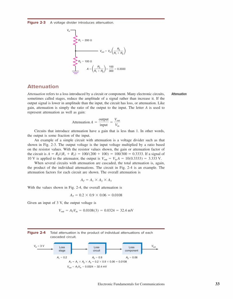
Electronic Fundamentals for Communications 33
Attenuation
Attenuation refers to a loss introduced by a circuit or component. Many electronic circuits, sometimes called stages, reduce the amplitude of a signal rather than increase it. If the output signal is lower in amplitude than the input, the circuit has loss, or attenuation. Like gain, attenuation is simply the ratio of the output to the input. The letter A is used to represent attenuation as well as gain:
Attenuation A 5output
input5
Vout
Vin
Circuits that introduce attenuation have a gain that is less than 1. In other words, the output is some fraction of the input. An example of a simple circuit with attenuation is a voltage divider such as that shown in Fig. 2-3. The output voltage is the input voltage multiplied by a ratio based on the resistor values. With the resistor values shown, the gain or attenuation factor of the circuit is A 5 R2/ (R1 1 R2) 5 100/(200 1 100) 5 100/300 5 0.3333. If a signal of 10 V is applied to the attenuator, the output is Vout 5 Vin A 5 10(0.3333) 5 3.333 V. When several circuits with attenuation are cascaded, the total attenuation is, again, the product of the individual attenuations. The circuit in Fig. 2-4 is an example. The attenuation factors for each circuit are shown. The overall attenuation is
AT 5 A1 3 A2 3 A3
With the values shown in Fig. 2-4, the overall attenuation is
AT 5 0.2 3 0.9 3 0.06 5 0.0108
Given an input of 3 V, the output voltage is
Vout 5 ATVin 5 0.0108(3) 5 0.0324 5 32.4 mV
R1 � 200 �
R2 � 100 �
Vout � Vin
Vin
R2
R1 � R2
A � � �R2
R1 � R2
1000.3333
300
Figure 2-3 A voltage divider introduces attenuation.
Figure 2-4 Total attenuation is the product of individual attenuations of each
cascaded circuit.
Lossstage
AT � A1 � A2 � A3 � 0.2 � 0.9 � 0.06 � 0.0108
Vout � ATVin � 0.0324 � 32.4 mV
A1 � 0.2 A2 � 0.9 A3 � 0.06
Vin � 3 V VoutLosscircuit
Losscomponent
Attenuation

34 Chapter 2
It is common in communication systems and equipment to cascade circuits and components that have gain and attenuation. For example, loss introduced by a circuit can be compensated for by adding a stage of amplii cation that offsets it. An example of this is shown in Fig. 2-5. Here the voltage divider introduces a 4-to-1 voltage loss, or an attenuation of 0.25. To offset this, it is followed with an amplii er whose gain is 4. The overall gain or attenuation of the circuit is simply the product of the attenuation and gain factors. In this case, the overall gain is AT 5 A1A2 5 0.25(4) 5 1. Another example is shown in Fig. 2-6, which shows two attenuation circuits and two amplii er circuits. The individual gain and attenuation factors are given. The overall circuit gain is AT 5 A1 A2 A3 A4 5 (0.1)(10)(0.3)(15) 5 4.5. For an input voltage of 1.5 V, the output voltage at each circuit is shown in Fig. 2-6. In this example, the overall circuit has a net gain. But in some instances, the overall circuit or system may have a net loss. In any case, the overall gain or loss is obtained by multiplying the individual gain and attenuation factors.
Figure 2-5 Gain exactly of sets the attenuation.
Vin
750 �
250 �
A2 � 4
A1 � AT � A1A2 � 0.25(4) � 1
Vout � Vin
250750 � 250
A1 �2501000
� 0.25
Example 2-5A voltage divider such as that shown in Fig. 2-5 has values of R1 5 10 kV and R2 5 470 V.
a. What is the attenuation?
A1 5R2
R1 1 R25
470
10,470 A1 5 0.045
b. What amplifier gain would you need to offset the loss for an overall gain of 1?
AT 5 A1A2
where A1 is the attenuation and A2 is the amplifier gain.
1 5 0.045A2 A2 51
0.0455 22.3
Note: To i nd the gain that will offset the loss for unity gain, just take the reciprocal of attenuation: A2 5 1yA1.

Electronic Fundamentals for Communications 35
Decibels
The gain or loss of a circuit is usually expressed in decibels (dB), a unit of measurement that was originally created as a way of expressing the hearing response of the human ear to various sound levels. A decibel is one-tenth of a bel. When gain and attenuation are both converted to decibels, the overall gain or atten-uation of an electronic circuit can be computed by simply adding the individual gains or attenuations, expressed in decibels. It is common for electronic circuits and systems to have extremely high gains or attenuations, often in excess of 1 million. Converting these factors to decibels and using logarithms result in smaller gain and attenuation i gures, which are easier to use.
Decibel Calculations. The formulas for computing the decibel gain or loss of a circuit are
dB 5 20 log
Vout
Vin
(1)
dB 5 20 log
Iout
Iin
(2)
dB 5 10 log
Pout
Pin
(3)
Formula (1) is used for expressing the voltage gain or attenuation of a circuit; for-mula (2), for current gain or attenuation. The ratio of the output voltage or current to the input voltage or current is determined as usual. The base-10 or common log of the input /output ratio is then obtained and multiplied by 20. The resulting number is the gain or attenuation in decibels.
Figure 2-6 The total gain is the product of the individual stage gains and attenuations.
Lossstage
Lossstage
Vin � 1.5 V
A1 � 0.1 A2 � 10 A3 � 0.3 A4 � 15
AT � A1A2A3A4 � (0.1)(10)(0.3)(15) � 4.5
0.15 V 1.5 V 0.45 V Vout � 6.75 V
Example 2-6An amplii er has a gain of 45,000, which is too much for the application. With an input voltage of 20 µV, what attenuation factor is needed to keep the output voltage from exceeding 100 mV? Let A1 5 amplii er gain 5 45,000; A2 5 attenuation factor; AT 5 total gain.
AT 5Vout
Vin5
100 3 1023
20 3 1026 5 5000
AT 5 A1A2 therefore A2 5AT
A15
5000
45,0005 0.1111
Decibel (dB)
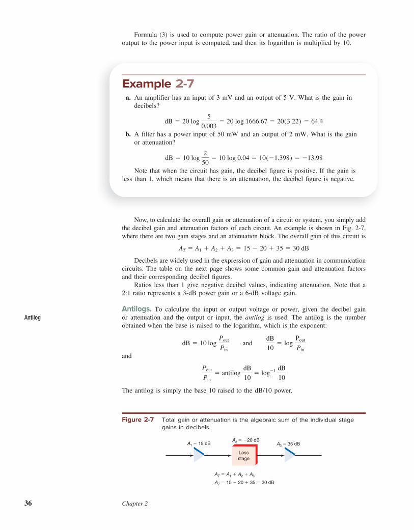
36 Chapter 2
Formula (3) is used to compute power gain or attenuation. The ratio of the power output to the power input is computed, and then its logarithm is multiplied by 10.
Example 2-7 a. An amplifier has an input of 3 mV and an output of 5 V. What is the gain in
decibels?
dB 5 20 log 5
0.0035 20 log 1666.67 5 20(3.22) 5 64.4
b. A filter has a power input of 50 mW and an output of 2 mW. What is the gain or attenuation?
dB 5 10 log 2
505 10 log 0.04 5 10(21.398) 5 213.98
Note that when the circuit has gain, the decibel i gure is positive. If the gain is less than 1, which means that there is an attenuation, the decibel i gure is negative.
Now, to calculate the overall gain or attenuation of a circuit or system, you simply add the decibel gain and attenuation factors of each circuit. An example is shown in Fig. 2-7, where there are two gain stages and an attenuation block. The overall gain of this circuit is
AT 5 A1 1 A2 1 A3 5 15 2 20 1 35 5 30 dB
Decibels are widely used in the expression of gain and attenuation in communication circuits. The table on the next page shows some common gain and attenuation factors and their corresponding decibel i gures. Ratios less than 1 give negative decibel values, indicating attenuation. Note that a 2:1 ratio represents a 3-dB power gain or a 6-dB voltage gain.
Antilogs. To calculate the input or output voltage or power, given the decibel gain or attenuation and the output or input, the antilog is used. The antilog is the number obtained when the base is raised to the logarithm, which is the exponent:
dB 5 10 log
Pout
Pin and
dB
105 log
Pout
Pin
and
Pout
Pin5 antilog
dB
105 log21
dB
10
The antilog is simply the base 10 raised to the dB/10 power.
Antilog
Figure 2-7 Total gain or attenuation is the algebraic sum of the individual stage
gains in decibels.
AT � A1 � A2 � A3
AT � 15 � 20 � 35 � 30 dB
A1 � 15 dBA2 � �20 dB
A3 � 35 dB
Lossstage

Electronic Fundamentals for Communications 37
Remember that the logarithm y of a number N is the power to which the base 10 must be raised to get the number.
N 5 10 y and y 5 log N
Since
dB 5 10 log
Pout
Pin
dB
105 log
Pout
Pin
Therefore
Pout
Pin5 10dB/10 5 log21
dB
10
The antilog is readily calculated on a scientii c calculator. To i nd the antilog for a common or base-10 logarithm, you normally press the Inv or 2nd function key on the calculator and then the log key. Sometimes the log key is marked with 10x, which is the antilog. The antilog with base e is found in a similar way, by using the Inv or 2nd function on the In key. It is sometimes marked e x, which is the same as the antilog.
d B G A I N O R A T T E N U A T I O N
Ratio (Power or Voltage) Power Voltage
0.000001 260 2120
0.00001 250 2100
0.0001 240 280
0.001 230 260
0.01 220 240
0.1 210 220
0.5 23 26
1 0 0
2 3 6
10 10 20
100 20 40
1000 30 60
10,000 40 80
100,000 50 100

38 Chapter 2
Example 2-8A power amplii er with a 40-dB gain has an output power of 100 W. What is the input power?
dB 5 10 log Pout
Pin antilog 5 log21
dB
105 log
Pout
Pin
40
105 log
Pout
Pin
4 5 log Pout
Pin
antilog 4 5 antilog alog Pout
Pinb
log21 4 5Pout
Pin
Pout
Pin5 104 5 10,000
Pin 5Pout
10,0005
100
10,0005 0.01 W 5 10 mW
Example 2-9An amplii er has a gain of 60 dB. If the input voltage is 50 µV, what is the output voltage? Since
dB 5 20 log Vout
Vin
dB
205 log
Vout
Vin
Therefore
Vout
Vin5 log21
dB
20 510dB/20
Vout
Vin5 1060/20 5 103
Vout
Vin5 103 5 1000
Vout 5 1000Vin 5 1000 (50 3 1026) 5 0.05 V 5 50 mV

Electronic Fundamentals for Communications 39
dBm. When the gain or attenuation of a circuit is expressed in decibels, implicit is a comparison between two values, the output and the input. When the ratio is computed, the units of voltage or power are canceled, making the ratio a dimensionless, or relative, figure. When you see a decibel value, you really do not know the actual voltage or power values. In some cases, this is not a problem; in others, it is useful or necessary to know the actual values involved. When an absolute value is needed, you can use a reference value to compare any other value. An often used reference level in communication is 1 mW. When a decibel value is computed by comparing a power value to 1 mW, the result is a value called the dBm. It is computed with the standard power decibel formula with 1 mW as the denominator of the ratio:
dBm 5 10 log
Pout(W)
0.001(W)
Here Pout is the output power, or some power value you want to compare to 1 mW, and 0.001 is 1 mW expressed in watts. The output of a 1-W amplii er expressed in dBm is, e.g.,
dBm 5 10 log
1
0.0015 10 log 1000 5 10(3) 5 30 dBm
Sometimes the output of a circuit or device is given in dBm. For example, if a micro-phone has an output of 250 dBm, the actual output power can be computed as follows:
250 dBm 5 10 log
Pout
0.001
250 dBm
105 log
Pout
0.001 Therefore
Pout
0.0015 10250 dBm/10 5 1025 5 0.00001
Pout 5 0.001 3 0.00001 5 1023 3 1025 5 1028 W 5 10 3 1029 5 10 nW
Example 2-10A power amplii er has an input of 90 mV across 10 kV. The output is 7.8 V across an 8-V speaker. What is the power gain, in decibels? You must compute the input and output power levels i rst.
P 5V
2
R
Pin 5(90 3 1023)2
104 5 8.1 3 1027 W
Pout 5(7.8)2
85 7.605 W
AP 5Pout
Pin5
7.605
8.1 3 1027 5 9.39 3 106
AP (dB) 5 10 log AP 5 10 log 9.39 3 106 5 69.7 dB
GOOD TO KNOW
From the standpoint of sound
measurement, 0 dB is the least
perceptible sound (hearing
threshold), and 120 dB equals the
pain threshold of sound. This list
shows intensity levels for com-
mon sounds. (Tippens, Physics,
6th ed., Glencoe/McGraw-Hill,
2001, p. 497)
Intensity
Sound level, dB
Hearing threshold 0
Rustling leaves 10
Whisper 20
Quiet radio 40
Normal conversation 65
Busy street corner 80
Subway car 100
Pain threshold 120
Jet engine 140–160
Reference value
dBm

40 Chapter 2
dBc. This is a decibel gain attenuation figure where the reference is the carrier. The carrier is the base communication signal, a sine wave that is modulated. Often the ampli-tude’s sidebands, spurious or interfering signals, are referenced to the carrier. For exam-ple, if the spurious signal is 1 mW compared to the 10-W carrier, the dBc is
dBc 5 10 log Psignal
Pcarrier
dBc 5 10 log 0.001
10 5 10(24) 5 240
Example 2-11An amplii er has a power gain of 28 dB. The input power is 36 mW. What is the output power?
Pout
Pin5 10dBy10 5 102.8 5 630.96
Pout 5 630.96 Pin 5 630.96(36 3 1023) 5 22.71 W
Example 2-12A circuit consists of two amplii ers with gains of 6.8 and 14.3 dB and two i lters with attenuations of 216.4 and 22.9 dB. If the output voltage is 800 mV, what is the input voltage?
AT 5 A1 1 A2 1 A3 1 A4 5 6.8 1 14.3 2 16.4 2 2.9 5 1.8 dB
AT 5Vout
Vin5 10dBy20 5 101.8y20 5 100.09
Vout
Vin5 100.09 5 1.23
Vin 5Vout
1.235
800
1.235 650.4 mV
Example 2-13Express Pout 5 12.3 dBm in watts.
Pout
0.0015 10dBmy10 5 1012.3y10 5 101.23 5 17
Pout 5 0.001 3 17 5 17 mW

Electronic Fundamentals for Communications 41
2-2 Tuned CircuitsVirtually all communication equipment contains tuned circuits, circuits made up of inductors and capacitors that resonate at specii c frequencies. In this section, you will review how to calculate the reactance, resonant frequency, impedance, Q , and bandwidth of series and parallel resonance circuits.
Reactive Components
All tuned circuits and many i lters are made up of inductive and capacitive elements, including discrete components such as coils and capacitors and the stray and distributed inductance and capacitance that appear in all elec-tronic circuits. Both coils and capacitors offer an opposition to alternating-current l ow known as reactance, which is expressed in ohms (abbreviated
Ω). Like resistance, reactance is an opposition that directly affects the
amount of current in a circuit. In addition, reactive effects produce a phase
shift between the currents and voltages in a circuit. Capacitance causes the
current to lead the applied voltage, whereas inductance causes the current
to lag the applied voltage. Coils and capacitors used together form tuned,
or resonant, circuits.
Capacitors. A capacitor used in an ac circuit continually charges and dis-
charges. A capacitor tends to oppose voltage changes across it. This translates
to an opposition to alternating current known as capacitive reactance XC.
The reactance of a capacitor is inversely proportional to the value of capacitance C
and operating frequency f. It is given by the familiar expression
XC 51
2πfC
The reactance of a 100-pF capacitor at 2 MHz is
XC 51
6.28(2 3 106) (100 3 10212)5 796.2 V
The formula can also be used to calculate either frequency or capacitance depending
on the application. These formulas are
f 51
2πXCC and C 5
1
2πf XC
The wire leads of a capacitor have resistance and inductance, and the dielectric has
leakage that appears as a resistance value in parallel with the capacitor. These character-
istics, which are illustrated in Fig. 2-8, are sometimes referred to as residuals or parasit-
ics. The series resistance and inductance are very small, and the leakage resistance is
Tuned circuit
Chip capacitors.
Reactance
Capacitor
Capacitive reactance
Residual
GOOD TO KNOW
Stray and distributed capaci-
tances and inductances can
greatly alter the operation and
performance of a circuit.
Figure 2-8 What a capacitor looks like at high frequencies.
R
Rleakage
C
Lead inductance
RL L
Lead resistance

42 Chapter 2
very high, so these factors can be ignored at low frequencies. At radio frequencies,
however, these residuals become noticeable, and the capacitor functions as a complex
RLC circuit. Most of these effects can be greatly minimized by keeping the capacitor
leads very short. This problem is mostly eliminated by using the newer chip capacitors,
which have no leads as such.
Capacitance is generally added to a circuit by a capacitor of a specii c value, but
capacitance can occur between any two conductors separated by an insulator. For exam-
ple, there is capacitance between the parallel wires in a cable, between a wire and a
metal chassis, and between parallel adjacent copper patterns on a printed-circuit board.
These are known as stray, or distributed, capacitances. Stray capacitances are typically
small, but they cannot be ignored, especially at the high frequencies used in communica-
tion. Stray and distributed capacitances can signii cantly affect the performance of a
circuit.
Inductors. An inductor, also called a coil or choke, is simply a winding of multiple
turns of wire. When current is passed through a coil, a magnetic i eld is produced around
the coil. If the applied voltage and current are varying, the magnetic i eld alternately
expands and collapses. This causes a voltage to be self-induced into the coil winding,
which has the effect of opposing current changes in the coil. This effect is known as
inductance.
The basic unit of inductance is the henry (H). Inductance is directly affected by the
physical characteristics of the coil, including the number of turns of wire in the induc-
tor, the spacing of the turns, the length of the coil, the diameter of the coil, and the
type of magnetic core material. Practical inductance values are in the millihenry
(mH 5 1023 H), microhenry (µH 5 1026 H), and nanohenry (nH 5 1029 H) regions.
Fig. 2-9 shows several different types of inductor coils.
● Fig. 2-9(a) is an inductor made of a heavy, self-supporting wire coil.
● In Fig. 2-9(b) the inductor is formed of a copper spiral that is etched right onto the
board itself.
● In Fig. 2-9(c) the coil is wound on an insulating form containing a powdered iron
or ferrite core in the center, to increase its inductance.
● Fig. 2-9(d) shows another common type of inductor, one using turns of wire on a
toroidal or doughnut-shaped form.
● Fig. 2-9(e) shows an inductor made by placing a small ferrite bead over a wire; the
bead effectively increases the wire’s small inductance.
● Fig. 2-9( f ) shows a chip inductor. It is typically no more than 1⁄8 to 1⁄4 in long.
A coil is contained within the body, and the unit is soldered to the circuit board
with the end connections. These devices look exactly like chip resistors and
capacitors.
In a dc circuit, an inductor will have little or no effect. Only the ohmic resistance
of the wire affects current l ow. However, when the current changes, such as during the
time the power is turned off or on, the coil will oppose these changes in current.
When an inductor is used in an ac circuit, this opposition becomes continuous and
constant and is known as inductive reactance. Inductive reactance XL is expressed in
ohms and is calculated by using the expression
XL 5 2πfL
For example, the inductive reactance of a 40-µH coil at 18 MHz is
XL 5 6.28(18 3 106)(40 3 1026) 5 4522 V
In addition to the resistance of the wire in an inductor, there is stray capacitance
between the turns of the coil. See Fig. 2-10(a). The overall effect is as if a small capac-
itor were connected in parallel with the coil, as shown in Fig. 2-10(b). This is the equivalent
circuit of an inductor at high frequencies. At low frequencies, capacitance may be
Stray (or distributed) capacitance
Inductor (coil or choke)
Inductance
Inductive reactance

Electronic Fundamentals for Communications 43
ignored, but at radio frequencies, it is sufi ciently large to affect circuit operation. The
coil then functions not as a pure inductor, but as a complex RLC circuit with a self-
resonating frequency.
Any wire or conductor exhibits a characteristic inductance. The longer the wire, the
greater the inductance. Although the inductance of a straight wire is only a fraction of
Figure 2-9 Types of inductors. (a) Heavy self-supporting wire coil. (b) Inductor made
as copper pattern. (c) Insulating form. (d) Toroidal inductor. (e) Ferrite
bead inductor. (f ) Chip inductor.
(a)
Printed circuit (PC)board
Componentlead or wire
(e)
Ferritebead
Insulatingform
Core moves in orout to vary inductance
Powderediron or ferrite
core
(c)
(b)
PC board
Toroidalinductor
Turnsof wire
(d )
(f )
Toroidalcore
Body
Solderconnection
Figure 2-10 Equivalent circuit of an inductor at high frequencies. (a) Stray capacitance between turns. (b) Equivalent
circuit of an inductor at high frequencies.
Stray capacitancebetween turns
Winding (coil) resistanceL � inductor
C � stray capacitance
(a ) (b)
R

44 Chapter 2
a microhenry, at very high frequencies the reactance can be signii cant. For this reason,
it is important to keep all lead lengths short in interconnecting components in RF circuits.
This is especially true of capacitor and transistor leads, since stray or distributed induc-
tance can signii cantly affect the performance and characteristics of a circuit.
Another important characteristic of an inductor is its quality factor Q, the ratio of
inductive power to resistive power:
Q 5I
2XL
I
2R5
XL
R
This is the ratio of the power returned to the circuit to the power actually dissipated by
the coil resistance. For example, the Q of a 3-µH inductor with a total resistance of 45V
at 90 MHz is calculated as follows:
Q 52πf L
R5
6.28(90 3 106)(3 3 1026)
455
1695.6
455 37.68
Resistors. At low frequencies, a standard low-wattage color-coded resistor offers nearly
pure resistance, but at high frequencies its leads have considerable inductance, and stray
capacitance between the leads causes the resistor to act as a complex RLC circuit, as
shown in Fig. 2-11. To minimize the inductive and capacitive effects, the leads are kept
very short in radio applications.
The tiny resistor chips used in surface-mount construction of the electronic circuits
preferred for radio equipment have practically no leads except for the metallic end pieces
soldered to the printed-circuit board. They have virtually no lead inductance and little
stray capacitance.
Many resistors are made from a carbon-composition material in powdered form
sealed inside a tiny housing to which leads are attached. The type and amount of
carbon material determine the value of these resistors. They contribute noise to the
circuit in which they are used. The noise is caused by thermal effects and the granular
nature of the resistance material. The noise contributed by such resistors in an amplii er
used to amplify very low level radio signals may be so high as to obliterate the desired
signal.
To overcome this problem, i lm resistors were developed. They are made by depos-
iting a carbon or metal i lm in spiral form on a ceramic form. The size of the spiral
and the kind of metal i lm determine the resistance value. Carbon i lm resistors are
quieter than carbon-composition resistors, and metal i lm resistors are quieter than
carbon i lm resistors. Metal i lm resistors should be used in amplii er circuits that must
deal with very low level RF signals. Most surface-mount resistors are of the metallic
i lm type.
Skin Ef ect. The resistance of any wire conductor, whether it is a resistor or capacitor
lead or the wire in an inductor, is primarily determined by the ohmic resistance of the
wire itself. However, other factors inl uence it. The most signii cant one is skin effect,
the tendency of electrons l owing in a conductor to l ow near and on the outer surface
Quality factor Q
Resistor
Skin effect
Figure 2-11 Equivalent circuit of a resistor at high (radio) frequencies.
Resistor Lead inductance
Stray capacitance

Electronic Fundamentals for Communications 45
of the conductor frequencies in the VHF, UHF, and microwave regions (Fig. 2-12). This
has the effect of greatly decreasing the total cross-sectional area of the conductor, thus
increasing its resistance and signii cantly affecting the performance of the circuit in
which the conductor is used. For example, skin effect lowers the Q of an inductor at
the higher frequencies, causing unexpected and undesirable effects. Thus many
high-frequency coils, particularly those in high-powered transmitters, are made with cop-
per tubing. Since current does not l ow in the center of the conductor, but only on the
surface, tubing provides the most efi cient conductor. Very thin conductors, such as a
copper pattern on a printed-circuit board, are also used. Often these conductors are sil-
ver- or gold-plated to further reduce their resistance.
Tuned Circuits and Resonance
A tuned circuit is made up of inductance and capacitance and resonates at a specii c
frequency, the resonant frequency. In general, the terms tuned circuit and resonant circuit
are used interchangeably. Because tuned circuits are frequency-selective, they respond
best at their resonant frequency and at a narrow range of frequencies around the resonant
frequency.
Series Resonant Circuits. A series resonant circuit is made up of inductance,
capacitance, and resistance, as shown in Fig. 2-13. Such circuits are often referred to as
LCR circuits or RLC circuits. The inductive and capacitive reactances depend upon the
frequency of the applied voltage. Resonance occurs when the inductive and capacitive
reactances are equal. A plot of reactance versus frequency is shown in Fig. 2-14, where
fr is the resonant frequency.
Tuned (resonant) circuit
Series resonant circuit
LCR circuit
RLC circuit
Figure 2-12 Skin ef ect increases wire and inductor resistance at high frequencies.
Electronsflow on or
near surface
No current flow in center of wire
Wire
Figure 2-13 Series RLC circuit.
VL
Vs
XL XC
VRR
VC
Figure 2-14 Variation of reactance with
frequency.
Reacta
nce
Frequency
XC XL
XL � XC
fr

46 Chapter 2
The total impedance of the circuit is given by the expression
Z 5 2R2 1 (XL 2 XC)2
When XL equals XC, they cancel each other, leaving only the resistance of the circuit
to oppose the current. At resonance, the total circuit impedance is simply the value of
all series resistances in the circuit. This includes the resistance of the coil and the
resistance of the component leads, as well as any physical resistor in the circuit.
The resonant frequency can be expressed in terms of inductance and capacitance. A
formula for resonant frequency can be easily derived. First, express XL and XC as an
equivalence: XL 5 XC. Since
XL 5 2πfr L and XC 51
2πfr C
we have
2πf rL 51
2πfrC
Solving for fr gives
fr 51
2π1LC
In this formula, the frequency is in hertz, the inductance is in henrys, and the capacitance
is in farads.
Example 2-14What is the resonant frequency of a 2.7-pF capacitor and a 33-nH inductor?
fr 51
2π1LC5
1
6.28233 3 1029 3 2.7 3 10212
5 5.33 3 108 Hz or 533 MHz
It is often necessary to calculate capacitance or inductance, given one of those val-
ues and the resonant frequency. The basic resonant frequency formula can be rearranged
to solve for either inductance and capacitance as follows:
L 51
4π
2f 2C and C 5
1
4π2f 2L
For example, the capacitance that will resonate at a frequency of 18 MHz with a
12-µH inductor is determined as follows:
C 51
4π
2fr
2L5
1
39.478(18 3 106)2 (12 3 1026)
51
39.478(3.24 3 1014)(12 3 1026)5 6.5 3 10212 F or 6.5 pF

Electronic Fundamentals for Communications 47
As indicated earlier, the basic dei nition of resonance in a series tuned circuit is
the point at which XL equals XC. With this condition, only the resistance of the circuit
impedes the current. The total circuit impedance at resonance is Z 5 R. For this reason,
resonance in a series tuned circuit can also be dei ned as the point at which the circuit
impedance is lowest and the circuit current is highest. Since the circuit is resistive at
resonance, the current is in phase with the applied voltage. Above the resonant fre-
quency, the inductive reactance is higher than the capacitive reactance, and the induc-
tor voltage drop is greater than the capacitor voltage drop. Therefore, the circuit is
inductive, and the current will lag the applied voltage. Below resonance, the capacitive
reactance is higher than the inductive reactance; the net reactance is capacitive, thereby
producing a leading current in the circuit. The capacitor voltage drop is higher than
the inductor voltage drop.
The response of a series resonant circuit is illustrated in Fig. 2-15, which is a plot
of the frequency and phase shift of the current in the circuit with respect to frequency.
At very low frequencies, the capacitive reactance is much greater than the induc-
tive reactance; therefore, the current in the circuit is very low because of the high
impedance. In addition, because the circuit is predominantly capacitive, the current
leads the voltage by nearly 90°. As the frequency increases, XC goes down and XL
goes up. The amount of leading phase shift decreases. As the values of reactances
approach one another, the current begins to rise. When XL equals XC, their effects
cancel and the impedance in the circuit is just that of the resistance. This produces a
current peak, where the current is in phase with the voltage (0°). As the frequency
Example 2-15What value of inductance will resonate with a 12-pF capacitor at 49 MHz?
L 51
4π2fr 2C
51
39.478(49 3 106)2(12 3 10212)
5 8.79 3 1027 H or 879 nH
Figure 2-15 Frequency and phase response curves of a series resonant circuit.
Circuit c
urr
ent
I
frBelow resonance (capacitive) Above resonance (inductive)
I
�
�90� (lead)
0�
�90� (lag)
Phase s
hift angle
(�)

48 Chapter 2
continues to rise, XL becomes greater than XC. The impedance of the circuit increases
and the current decreases. With the circuit predominantly inductive, the current lags
the applied voltage. If the output voltage were being taken from across the resistor in
Fig. 2-13, the response curve and phase angle of the voltage would correspond to those
in Fig. 2-15. As Fig. 2-15 shows, the current is highest in a region centered on the
resonant frequency. The narrow frequency range over which the current is highest is
called the bandwidth. This area is illustrated in Fig. 2-16.
The upper and lower boundaries of the bandwidth are dei ned by two cutoff frequen-
cies designated f1 and f2. These cutoff frequencies occur where the current amplitude is
70.7 percent of the peak current. In the i gure, the peak circuit current is 2 mA, and
the current at both the lower ( f1) and upper ( f2) cutoff frequency is 0.707 of 2 mA, or
1.414 mA.
Current levels at which the response is down 70.7 percent are called the half-power
points because the power at the cutoff frequencies is one-half the power peak of the
curve.
P 5 I2R 5 (0.707 Ipeak)2R 5 0.5 Ipeak
2R
The bandwidth BW of the tuned circuit is dei ned as the difference between the
upper and lower cutoff frequencies:
BW 5 f2 2 f1
For example, assuming a resonant frequency of 75 kHz and upper and lower cutoff
frequencies of 76.5 and 73.5 kHz, respectively, the bandwidth is BW 5 76.5 2 73.5 5
3 kHz.
The bandwidth of a resonant circuit is determined by the Q of the circuit. Recall
that the Q of an inductor is the ratio of the inductive reactance to the circuit resistance.
This holds true for a series resonant circuit, where Q is the ratio of the inductive reactance
to the total circuit resistance, which includes the resistance of the inductor plus any
additional series resistance:
Q 5XL
RT
Recall that bandwidth is then computed as
BW 5fr
Q
If the Q of a circuit resonant at 18 MHz is 50, then the bandwidth is BW 5 18/50 5
0.36 MHz 5 360 kHz.
Bandwidth
Half-power points
Figure 2-16 Bandwidth of a series resonant circuit.
0.707 Ipeak � 1.414 mA
Ipeak � 2 mA
f1 fr f2
BW = f2 � f1

Electronic Fundamentals for Communications 49
The formula can be rearranged to compute Q, given the frequency and the
bandwidth:
Q 5fr
BW
Thus the Q of the circuit whose bandwidth was computed previously is Q 5
75 kHz /3kHz 5 25.
Since the bandwidth is approximately centered on the resonant frequency, f1 is the
same distance from fr as f2 is from fr . This fact allows you to calculate the resonant
frequency by knowing only the cutoff frequencies:
fr 5 2f1 3 f2
For example, if f1 5 175 kHz and f2 5 178 kHz, the resonant frequency is
fr 5 2175 3 103 3 178 3 103 5 176.5 kHz
For a linear frequency scale, you can calculate the center or resonant frequency by
using an average of the cutoff frequencies.
fr 5f1 1 f2
2
If the circuit Q is very high (.100), then the response curve is approximately sym-
metric around the resonant frequency. The cutoff frequencies will then be roughly equi-
distant from the resonant frequency by the amount of BW/2. Thus the cutoff frequencies
can be calculated if the bandwidth and the resonant frequency are known:
f1 5 fr 2BW
2 and f2 5 fr 1
BW
2
For instance, if the resonant frequency is 49 MHz (49,000 kHz) and the bandwidth
is 10 kHz, then the cutoff frequencies will be
f1 5 49,000 kHz 210k
25 49,000 kHz 2 5 kHz 5 48,995 kHz
f2 5 49,000 kHz 1 5 kHz 5 49,005 kHz
Keep in mind that although this procedure is an approximation, it is useful in many
applications.
The bandwidth of a resonant circuit dei nes its selectivity, i.e., how the circuit
responds to varying frequencies. If the response is to produce a high current only over
a narrow range of frequencies, a narrow bandwidth, the circuit is said to be highly selec-
tive. If the current is high over a broader range of frequencies, i.e., the bandwidth is
wider, the circuit is less selective. In general, circuits with high selectivity and narrow
bandwidths are more desirable. However, the actual selectivity and bandwidth of a circuit
must be optimized for each application.
Example 2-16What is the bandwidth of a resonant circuit with a frequency of 28 MHz and a Q of 70?
BW 5fr
Q5
28 3 106
705 400,000 Hz 5 400 kHz
Selectivity

50 Chapter 2
The relationship between circuit resistance Q and bandwidth is extremely impor-
tant. The bandwidth of a circuit is inversely proportional to Q. The higher Q is, the
smaller the bandwidth. Low Qs produce wide bandwidths or less selectivity. In turn,
Q is a function of the circuit resistance. A low resistance produces a high Q, a nar-
row bandwidth, and a highly selective circuit. A high circuit resistance produces a
low Q, wide bandwidth, and poor selectivity. In most communication circuits, circuit
Qs are at least 10 and typically higher. In most cases, Q is controlled directly by the
resistance of the inductor. Fig. 2-17 shows the effect of different values of Q on
bandwidth.
Example 2-17The upper and lower cutoff frequencies of a resonant circuit are found to be 8.07 and
7.93 MHz. Calculate (a) the bandwidth, (b) the approximate resonant frequency,
and (c) Q.
a. BW 5 f2 2 f1 5 8.07 MHz 2 7.93 MHz 5 0.14 MHz 5 140 kHz
b. fr 5 1f1 f2 5 1(8.07 3 106) (7.93 3 106) 5 8 MHz
c. Q 5fr
BW5
8 3 106
140 3 1035 57.14
Example 2-18What are the approximate 3-dB down frequencies of a resonant circuit with a Q of
200 at 16 MHz?
BW 5fr
Q5
16 3 106
2005 80,000 Hz 5 80 kHz
f1 5 fr 2BW
25 16,000,000 2
80,000
25 15.96 MHz
f2 5 fr 1BW
25 16,000,000 1
80,000
25 16.04 MHz
Resonance produces an interesting but useful phenomenon in a series RLC circuit.
Consider the circuit in Fig. 2-18(a). At resonance, assume XL 5 XC 5 500 V. The total
circuit resistance is 10 V. The Q of the circuit is then
Q 5XL
R5
500
105 50
If the applied or source voltage Vs is 2 V, the circuit current at resonance will be
I 5Vs
R5
2
105 0.2 A

Electronic Fundamentals for Communications 51
When the reactances, the resistances, and the current are known, the voltage drops
across each component can be computed:
VL 5 IXL 5 0.2(500) 5 100 V
VC 5 IXC 5 0.2(500) 5 100 V
VR 5 IR 5 0.2(10) 5 2 V
As you can see, the voltage drops across the inductor and capacitor are signii cantly
higher than the applied voltage. This is known as the resonant step-up voltage. Although
the sum of the voltage drops around the series circuit is still equal to the source voltage,
at resonance the voltage across the inductor leads the current by 90° and the voltage across
the capacitor lags the current by 90° [see Fig. 2-18(b)]. Therefore, the inductive and reac-
tive voltages are equal but 180° out of phase. As a result, when added, they cancel each
other, leaving a total reactive voltage of 0. This means that the entire applied voltage
appears across the circuit resistance.
The resonant step-up voltage across the coil or capacitor can be easily computed by
multiplying the input or source voltage by Q:
VL 5 VC 5 QVs
In the example in Fig. 2-18, VL 5 50(2) 5 100 V.
Resonant step-up voltage
Figure 2-17 The ef ect of Q on bandwidth and selectivity in a resonant circuit.
fr
BW 1
�3 dB points
BW 2
BW 3
High Q1, narrowbandwidth
Medium Q2,medium bandwidth
Low Q3, widebandwidth
Gain, dB
Figure 2-18 Resonant step-up voltage in a series resonant circuit.
Vs� 2 V
VC � 100 V
VL � 100 V
VL � 100 V
VR � Vs � 2 V
Equal and 180°
out of phaseI
VC � 100 V
VR � 2 V
XC � 500 �
XL � 500 �
R � 10 �
I � 0.2 A
(a ) (b)

52 Chapter 2
Parallel Resonant Circuits. A parallel resonant circuit is formed when the inductor
and capacitor are connected in parallel with the applied voltage, as shown in Fig. 2-19(a).
In general, resonance in a parallel tuned circuit can also be dei ned as the point at which
the inductive and capacitive reactances are equal. The resonant frequency is therefore
calculated by the resonant frequency formula given earlier. If we assume lossless compo-
nents in the circuit (no resistance), then the current in the inductor equals the current in
the capacitor:
IL 5 IC
Although the currents are equal, they are 180° out of phase, as the phasor diagram
in Fig. 2-19(b) shows. The current in the inductor lags the applied voltage by 90°, and
the current in the capacitor leads the applied voltage by 90°, for a total of 180°.
Now, by applying Kirchhoff’s current law to the circuit, the sum of the individual branch
currents equals the total current drawn from the source. With the inductive and capacitive
currents equal and out of phase, their sum is 0. Thus, at resonance, a parallel tuned circuit
appears to have ini nite resistance, draws no current from the source and thus has ini nite
impedance, and acts as an open circuit. However, there is a high circulating current between
the inductor and capacitor. Energy is being stored and transferred between the inductor and
capacitor. Because such a circuit acts as a kind of storage vessel for electric energy, it is
often referred to as a tank circuit and the circulating current is referred to as the tank current.
In a practical resonant circuit where the components do have losses (resistance), the
circuit still behaves as described above. Typically, we can assume that the capacitor has
practically zero losses and the inductor contains a resistance, as illustrated in Fig. 2-20(a).
At resonance, where XL 5 XC, the impedance of the inductive branch of the circuit is
higher than the impedance of the capacitive branch because of the coil resistance. The
capacitive current is slightly higher than the inductive current. Even if the reactances are
Parallel resonant circuit
Tank circuit
Tank current
Example 2-19A series resonant circuit has a Q of 150 at 3.5 MHz. The applied voltage is 3 µV.
What is the voltage across the capacitor?
VC 5 QVs 5 150(3 3 1026) 5 450 3 1026 5 450 µV
Figure 2-19 Parallel resonant circuit currents. (a) Parallel resonant circuit. (b) Current
relationships in parallel resonant circuit.
VsIC IL
Line current
IC
Vs
IL�90°
�90°
(b)(a)
������IT � (IL) 2 � (IC) 2
This interesting and useful phenomenon means that small applied voltages can essen-
tially be stepped up to a higher voltage — a form of simple amplii cation without active
circuits that is widely applied in communication circuits.

Electronic Fundamentals for Communications 53
equal, the branch currents will be unequal and therefore there will be some net current
l ow in the supply line. The source current will lead the supply voltage, as shown in
Fig. 2-20(b). Nevertheless, the inductive and capacitive currents in most cases will cancel
because they are approximately equal and of opposite phase, and consequently the line
or source current will be signii cantly lower than the individual branch currents. The
result is a very high resistive impedance, approximately equal to
Z 5Vs
IT
The circuit in Fig. 2-20(a) is not easy to analyze. One way to simplify the mathematics
involved is to convert the circuit to an equivalent circuit in which the coil resistance is
translated to a parallel resistance that gives the same overall results, as shown in Fig. 2-21.
The equivalent inductance Leq and resistance Req are calculated with the formulas
Leq 5L(Q2 1 1)
Q2 and Req 5 RW(Q2 1 1)
and Q is determined by the formula
Q 5XL
RW
where RW is the coil winding resistance.
If Q is high, usually more than 10, Leq is approximately equal to the actual induc-
tance value L. The total impedance of the circuit at resonance is equal to the equivalent
parallel resistance:
Z 5 Req
Figure 2-20 A practical parallel resonant circuit. (a) Practical parallel resonant circuit
with coil resistance RW. (b) Phase relationships.
Vs IC
RW
IL
Line current
C
IT
(a)
L
IC
Vs
IL
IT
(b)
(Vector sum of IC and ILleads Vs because IC IL)
(lags Vs by less than 90° because of RW)
Figure 2-21 An equivalent circuit makes parallel resonant circuits easier to analyze.
C
C
L
R W
Req
Req = R W (Q 2 + 1)
Leq = L (Q 2 + 1)
Z = Req
Leq
Actual circuit Equivalent circuit
Q 2
Losslessresonant circuit

54 Chapter 2
If the Q of the parallel resonant circuit is greater than 10, the following simplii ed
formula can be used to calculate the resistive impedance at resonance:
Z 5L
CRW
The value of RW is the winding resistance of the coil.
Example 2-20What is the impedance of a parallel LC circuit with a resonant frequency of 52 MHz
and a Q of 12? L 5 0.15 µH.
Q 5XL
RW
XL 5 2πf L 5 6.28(52 3 106)(0.15 3 1026) 5 49 V
RW 5XL
Q5
49
125 4.1 V
Z 5 Req 5 RW (Q2 1 1) 5 4.1(122 1 1) 5 4.1(145) 5 592 V
Example 2-21Calculate the impedance of the circuit given in Example 2-20 by using the formula
Z 5 L/CR.
fr 5 52 MHz RW 5 4.1 V L 5 0.15 µH
C 51
4π
2fr
2L5
1
39.478(52 3 106)2(0.15 3 1026)
5 6.245 3 10211
Z 5L
CRW
50.15 3 1026
(62.35 3 10212)(4.1)5 586 V
This is close to the previously computed value of 592 V. The formula Z 5 L/CRW is an approximation.
A frequency and phase response curve of a parallel resonant circuit is shown in
Fig. 2-22. Below the resonant frequency, XL is less than XC; thus the inductive current
is greater than the capacitive current, and the circuit appears inductive. The line current
lags the applied voltage. Above the resonant frequency, XC is less than XL; thus the
capacitive current is more than the inductive current, and the circuit appears capacitive.
Therefore, the line current leads the applied voltage. The phase angle of the impedance
will be leading below resonance and lagging above resonance.
At the resonant frequency, the impedance of the circuit peaks. This means that the
line current at that time is at its minimum. At resonance, the circuit appears to have a
very high resistance, and the small line current is in phase with the applied voltage.
GOOD TO KNOW
The bandwidth of a circuit is in-
versely proportional to the circuit Q.
The higher the Q, the smaller
the bandwidth. Low Q values
produce wide bandwidths or
less selectivity.

Electronic Fundamentals for Communications 55
Note that the Q of a parallel circuit, which was previously expressed as Q 5 XL /RW,
can also be computed with the expression
Q 5RP
XL
where RP is the equivalent parallel resistance, Req in parallel with any other parallel
resistance, and XL is the inductive reactance of the equivalent inductance Leq.
You can set the bandwidth of a parallel tuned circuit by controlling Q. The Q can
be determined by connecting an external resistor across the circuit. This has the effect
of lowering RP and increasing the bandwidth.d
Figure 2-22 Response of a parallel resonant circuit.
Below
resonance
(inductive)
Above
resonance
(capacitive)
+90° (leading)
-90° (lagging)
Ph
ase
sh
ift o
f lin
e c
urr
en
t
in d
eg
ree
s (
red
cu
rve
on
ly)
0°
fr
Imp
ed
an
ce
(b
lue
cu
rve
on
ly)
Z
Example 2-22What value of parallel resistor is needed to set the bandwidth of a parallel tuned
circuit to 1 MHz? Assume XL 5 300 V, RW 5 10 V, and fr 5 10 MHz.
Q 5XL
RW
5300
105 30
RP 5 RW(Q2 1 1) 5 10(302 1 1) 5 10(901) 5 9010 V
(equivalent resistance of the parallel circuit at resonance)
BW 5fr
Q
Q 5fr
BW 5
10 MHz
1 MHz5 10 (Q needed for 1-MHz bandwidth)
RPnew 5 QXL 5 10(300) 5 3000 V
(this is the total resistance of the circuit RPnew made up of the original RP and an
externally connected resistor Rext)
RPnew 5RPRext
RP 1 Rext
Rext 5RPnewRP
RP 2 RPnew
59010(3000)
9010 2 3000 5 4497.5V

56 Chapter 2
2-3 FiltersA i lter is a frequency-selective circuit. Filters are designed to pass some frequencies and
reject others. The series and parallel resonant circuits reviewed in Section 2-2 are exam-
ples of i lters.
There are numerous ways to implement i lter circuits. Simple i lters created by using
resistors and capacitors or inductors and capacitors are called passive i lters because
they use passive components that do not amplify. In communication work, many i lters
are of the passive LC variety, although many other types are used. Some special types
of i lters are active i lters that use RC networks with feedback in op amp circuits,
switched capacitor i lters, crystal and ceramic i lters, surface acoustic wave (SAW) i l-
ters, and digital i lters implemented with digital signal processing (DSP) techniques.
The i ve basic kinds of i lter circuits are as follows:
Low-pass i lter. Passes frequencies below a critical frequency called the cutoff
frequency and greatly attenuates those above the cutoff frequency.
High-pass i lter. Passes frequencies above the cutoff but rejects those below it.
Bandpass i lter. Passes frequencies over a narrow range between lower and up-
per cutoff frequencies.
Band-reject i lter. Rejects or stops frequencies over a narrow range but allows
frequencies above and below to pass.
All-pass i lter. Passes all frequencies equally well over its design range but has
a fixed or predictable phase shift characteristic.
RC Filters
A low-pass i lter allows the lower-frequency components of the applied voltage to
develop output voltage across the load resistance, whereas the higher-frequency compo-
nents are attenuated, or reduced, in the output.
A high-pass i lter does the opposite, allowing the higher-frequency components of the
applied voltage to develop voltage across the output load resistance.
The case of an RC coupling circuit is an example of a high-pass i lter because the ac
component of the input voltage is developed across R and the dc voltage is blocked by the
series capacitor. Furthermore, with higher frequencies in the ac component, more ac voltage
is coupled.
Any low-pass or high-pass i lter can be thought of as a frequency-dependent voltage
divider because the amount of output voltage is a function of frequency.
RC i lters use combinations of resistors and capacitors to achieve the desired
response. Most RC i lters are of the low-pass or high-pass type. Some band-reject or
notch i lters are also made with RC circuits. Bandpass i lters can be made by combining
low-pass and high-pass RC sections, but this is rarely done.
Low-Pass Filter. A low-pass i lter is a circuit that introduces no attenuation at frequen-
cies below the cutoff frequency but completely eliminates all signals with frequencies
above the cutoff. Low-pass i lters are sometimes referred to as high cut i lters.
The ideal response curve for a low-pass i lter is shown in Fig. 2-23. This response
curve cannot be realized in practice. In practical circuits, instead of a sharp transition at
the cutoff frequency, there is a more gradual transition between little or no attenuation
and maximum attenuation.
The simplest form of low-pass i lter is the RC circuit shown in Fig. 2-24(a). The
circuit forms a simple voltage divider with one frequency-sensitive component, in this
case the capacitor. At very low frequencies, the capacitor has very high reactance com-
pared to the resistance and therefore the attenuation is minimum. As the frequency
increases, the capacitive reactance decreases. When the reactance becomes smaller than
the resistance, the attenuation increases rapidly. The frequency response of the basic
Filter
Passive fi lter
RC fi lter
Low-pass fi lter (high cut fi lter)

Electronic Fundamentals for Communications 57
circuit is illustrated in Fig. 2-24(b). The cutoff frequency of this i lter is that point where
R and XC are equal. The cutoff frequency, also known as the critical frequency, is deter-
mined by the expression
XC 5 R
1
2πfc
5 R
fco 51
2πRC
For example, if R 5 4.7 kV and C 5 560 pF, the cutoff frequency is
fco 51
2π(4700)(560 3 10212)5 60,469 Hz or 60.5 kHz
Figure 2-23 Ideal response curve of a low-pass fi lter.
Frequency
Cutofffrequency
Ou
tpu
t
fco
Signals in the passband passunattenuated Signals above fco
are eliminated
Figure 2-24 RC low-pass fi lter. (a) Circuit. (b) Low-pass fi lter.
VoutVin
XC � R
C
(a)
Vout(max)
(0 dB)0.707 Vout(max)
(�3 dB)
fco
6 dB/octave or 20 dB/decade rate
(b)
fco �1
2RC
R
�9 dB
20 dB
6 dB
�23 dB
1200
6 kHz Hz
600
Example 2-23What is the cutoff frequency of a single-section RC low-pass i lter with R 5 8.2 kV
and C 5 0.0033 µF?
fco 51
2πRC5
1
2π(8.2 3 103)(0.0033 3 1026)
fco 5 5881.56 Hz or 5.88 kHz

58 Chapter 2
At the cutoff frequency, the output amplitude is 70.7 percent of the input amplitude
at lower frequencies. This is the so-called 3-dB down point. In other words, this i lter has
a voltage gain of 23 dB at the cutoff frequency. At frequencies above the cutoff frequency,
the amplitude decreases at a linear rate of 6 dB per octave or 20 dB per decade. An octave
is dei ned as a doubling or halving of frequency, and a decade represents a one-tenth or
times-10 relationship. Assume that a i lter has a cutoff of 600 Hz. If the frequency doubles
to 1200 Hz, the attenuation will increase by 6 dB, or from 3 dB at cutoff to 9 dB at 1200
Hz. If the frequency increased by a factor of 10 from 600 Hz to 6 kHz, the attenuation
would increase by a factor of 20 dB from 3 dB at cutoff to 23 dB at 6 kHz.
If a faster rate of attenuation is required, two RC sections set to the same cutoff
frequency can be used. Such a circuit is shown in Fig. 2-25(a). With this circuit, the rate
of attenuation is 12 dB per octave or 40 dB per decade. Two identical RC circuits are
used, but an isolation or buffer amplii er such as an emitter-follower (gain < 1) is used
between them to prevent the second section from loading the i rst. Cascading two RC
sections without the isolation will give an attenuation rate less than the theoretically ideal
12-dB octave because of the loading effects.
If the cutoff frequency of each RC section is the same, the overall cutoff frequency for
the complete i lter is somewhat less. This is caused by added attenuation of the second section.
With a steeper attenuation curve, the circuit is said to be more selective. The disad-
vantage of cascading such sections is that higher attenuation makes the output signal
considerably smaller. This signal attenuation in the passband of the i lter is called
insertion loss.
A low-pass i lter can also be implemented with an inductor and a resistor, as shown in
Fig. 2-26. The response curve for this RL i lter is the same as that shown in Fig. 2-24(b).
The cutoff frequency is determined by using the formula
fco 5R
2πL
Octave
Decade
Insertion loss
Figure 2-25 Two stages of RC fi lter improve the response but increase signal loss. (a) Circuit. (b) Response curve.
VoutVin
R R
CC
Buffer amplifier to isolateRC sections
(a)
�3 dB
12 dB/octave or40 dB/decade roll-off rate
(b)
Vout(max)
fco
40 dB
12 dB
1200
6 kHz Hz
600
Figure 2-26 A low-pass fi lter implemented with an inductor.
fco �
XL � R
R
2�L
L
R

Electronic Fundamentals for Communications 59
The RL low-pass i lters are not as widely used as RC i lters because inductors are
usually larger, heavier, and more expensive than capacitors. Inductors also have greater
loss than capacitors because of their inherent winding resistance.
High-Pass Filter. A high-pass i lter passes frequencies above the cutoff frequency with
little or no attenuation but greatly attenuates those signals below the cutoff. The ideal
high-pass response curve is shown in Fig. 2-27(a). Approximations to the ideal response
curve shown in Fig. 2-27(b) can be obtained with a variety of RC and LC i lters.
The basic RC high-pass i lter is shown in Fig. 2-28(a). Again, it is nothing more
than a voltage divider with the capacitor serving as the frequency-sensitive component
in a voltage divider. At low frequencies, XC is very high. When XC is much higher than
R, the voltage divider effect provides high attenuation of the low-frequency signals. As
the frequency increases, the capacitive reactance decreases. When the capacitive reac-
tance is equal to or less than the resistance, the voltage divider gives very little attenu-
ation. Therefore, high frequencies pass relatively unattenuated.
The cutoff frequency for this i lter is the same as that for the low-pass circuit and
is derived from setting XC equal to R and solving for frequency:
fco 51
2πRC
The roll-off rate is 6 dB per octave or 20 dB per decade.
A high-pass i lter can also be implemented with a coil and a resistor, as shown in
Fig. 2-28(b). The cutoff frequency is
fco 5R
2πL
The response curve for this i lter is the same as that shown in Fig. 2-27(b). The rate of
attenuation is 6 dB per octave or 20 dB per decade, as was the case with the low-pass
i lter. Again, improved attenuation can be obtained by cascading i lter sections.
High-pass fi lter
Figure 2-27 Frequency response curve of a high-pass filter. (a) Ideal. (b) Practical.
Ou
tpu
t
Frequency
fcofco
(a)
Frequency
(b)
0 dB
�3 dB
6 dB/octave or 20 dB/decade
fco�1
2RC
Passband
Figure 2-28 (a) RC high-pass fi lter. (b) RL high-pass fi lter.
C
R
(a)
fco �1
2RC
R
L
(b)
fco �R
2L

60 Chapter 2
RC Notch Filter. Notch i lters are also referred to as bandstop or band-reject i l-
ters. Band-reject i lters are used to greatly attenuate a narrow range of frequencies
around a center point. Notch i lters accomplish the same purpose, but for a single
frequency.
A simple notch i lter that is implemented with resistors and capacitors as shown in
Fig. 2-29(a) is called a parallel-T or twin-T notch i lter. This i lter is a variation of a
bridge circuit. Recall that in a bridge circuit the output is zero if the bridge is balanced.
If the component values are precisely matched, the circuit will be in balance and produce
an attenuation of an input signal at the design frequency as high as 30 to 40 dB. A
typical response curve is shown in Fig. 2-29(b).
The center notch frequency is computed with the formula
fnotch 51
2πRC
For example, if the values of resistance and capacitance are 100 kV and 0.02 µF, the
notch frequency is
fnotch 51
6.28(105)(0.02 3 1026)5 79.6 Hz
Twin-T notch i lters are used primarily at low frequencies, audio and below. A com-
mon use is to eliminate 60-Hz power line hum from audio circuits and low-frequency
medical equipment amplii ers. The key to high attenuation at the notch frequency is
Notch fi lter (bandstop or band-reject fi lter)
Parallel-T (twin-T) notch fi lter
Example 2-24What is the closest standard EIA resistor value that will produce a cutoff frequency of
3.4 kHz with a 0.047-µF capacitor in a high-pass RC i lter?
fco 51
2πRC
R 51
2πfcoC5
1
2π(3.4 3 103)(0.047 3 1026)5 996 V
The closest standard values are 910 and 1000 V, with 1000 being the closest.
GOOD TO KNOW
Twin-T notch fi lters are used at
low frequencies to eliminate
power line hum from audio
circuits and medical equipment
amplifi ers.
Figure 2-29 RC notch fi lter.
fnotch � 1
2RC
R
2
fnotch
(a) (b)
R R
C C
2C

Electronic Fundamentals for Communications 61
precise component values. The resistor and capacitor values must be matched to achieve
high attenuation.
LC Filters
RC i lters are used primarily at the lower frequencies. They are very common at audio
frequencies but are rarely used above about 100 kHz. At radio frequencies, their
passband attenuation is just too great, and the cutoff slope is too gradual. It is more
common to see LC i lters made with inductors and capacitors. Inductors for lower
frequencies are large, bulky, and expensive, but those used at higher frequencies are
very small, light, and inexpensive. Over the years, a multitude of i lter types have been
developed. Filter design methods have also changed over the years, thanks to computer
design.
Filter Terminology. When working with i lters, you will hear a variety of terms to
describe the operation and characteristics of i lters. The following dei nitions will help
you understand i lter specii cations and operation.
1. Passband. This is the frequency range over which the i lter passes signals. It is the
frequency range between the cutoff frequencies or between the cutoff frequency and
zero (for low-pass) or between the cutoff frequency and ini nity (for high-pass).
2. Stop band. This is the range of frequencies outside the passband, i.e., the range
of frequencies that is greatly attenuated by the i lter. Frequencies in this range are
rejected.
3. Attenuation. This is the amount by which undesired frequencies in the stop band
are reduced. It can be expressed as a power ratio or voltage ratio of the output to
the input. Attenuation is usually given in decibels.
4. Insertion loss. Insertion loss is the loss the i lter introduces to the signals in the
passband. Passive i lters introduce attenuation because of the resistive losses in the
components. Insertion loss is typically given in decibels.
5. Impedance. Impedance is the resistive value of the load and source terminations
of the i lter. Filters are usually designed for specii c driving source and load imped-
ances that must be present for proper operation.
6. Ripple. Amplitude variation with frequency in the passband, or the repetitive rise
and fall of the signal level in the passband of some types of i lters, is known as
ripple. It is usually stated in decibels. There may also be ripple in the stop bandwidth
in some types of i lters.
Passband
Stop band
Attenuation
Insertion loss
Impedance
Ripple
Example 2-25What values of capacitors would you use in an RC twin-T notch i lter to remove
120 Hz if R 5 220 kV?
fnotch 51
2πRC
C 51
2πfnotchR5
1
6.28(120)(220 3 103)
C 5 6.03 3 1029 5 6.03 nF or 0.006 µF
2C 5 0.012 µF

62 Chapter 2
7. Shape factor. Shape factor, also known as bandwidth ratio, is the ratio of the stop
bandwidth to the pass bandwidth of a bandpass i lter. It compares the bandwidth at
minimum attenuation, usually at the 23-dB points or cutoff frequencies, to that of
maximum attenuation and thus gives a relative indication of attenuation rate or selec-
tivity. The smaller the ratio, the greater the selectivity. The ideal is a ratio of 1,
which in general cannot be obtained with practical i lters. The i lter in Fig. 2-30 has
a bandwidth of 6 kHz at the 23-dB attenuation point and a bandwidth of 14 kHz
at the 240-dB attenuation point. The shape factor then is 14 kHz/6 kHz 5 2.333.
The points of comparison vary with different i lters and manufacturers. The points
of comparison may be at the 6-dB down and 60-dB down points or at any other
designated two levels.
8. Pole. A pole is a frequency at which there is a high impedance in the circuit. It is
also used to describe one RC section of a i lter. A simple low-pass RC i lter such as
that in Fig. 2-24(a) has one pole. The two-section i lter in Fig. 2-25 has two poles.
For LC low- and high-pass i lters, the number of poles is equal to the number of
reactive components in the i lter. For bandpass and band-reject i lters, the number
of poles is generally assumed to be one-half the number of reactive components
used.
9. Zero. This term refers to a frequency at which there is zero impedance in the
circuit.
10. Envelope delay. Also known as time delay, envelope delay is the time it takes for
a specii c point on an input waveform to pass through the i lter.
11. Roll-off. Also called the attenuation rate, roll-off is the rate of change of amplitude
with frequency in a i lter. The faster the roll-off, or the higher the attenuation rate,
the more selective the i lter is, i.e., the better able it is to differentiate between two
closely spaced signals, one desired and the other not.
Any of the four basic i lter types can be easily implemented with inductors and
capacitors. Such i lters can be made for frequencies up to about several hundred mega-
hertz before the component values get too small to be practical. At frequencies above
this frequency, special i lters made with microstrip techniques on printed-circuit boards,
surface acoustic wave i lters, and cavity resonators are common. Because two types of
reactances are used, inductive combined with capacitive, the roll-off rate of attenuation
Shape factor
Pole
Zero
Envelope delay
Roll-off
Figure 2-30 Shape factor.
�3 dB
14 kHz
�40 dB
0 dB
6 kHz
BW (�40 dB)BW (�3 dB)
Shape factor � � 14 kHz6 kHz
� 2.3

Electronic Fundamentals for Communications 63
is greater with LC i lters than with RC i lters. The inductors make such i lters larger and
more expensive, but the need for better selectivity makes them necessary.
Low- and High-Pass LC Filters. Fig. 2-31 shows the basic low-pass i lter coni gu-
rations. The basic two-pole circuit in Fig. 2-31(a) provides an attenuation rate of 12 dB
per octave or 20 dB per decade. These sections may be cascaded to provide an even
greater roll-off rate. The chart in Fig. 2-32 shows the attenuation rates for low-pass i lters
with two through seven poles. The horizontal axis f / fc is the ratio of any given frequency
in ratio to the i lter cutoff frequency fc. The value n is the number of poles in the i lter.
Assume a cutoff frequency of 20 MHz. The ratio for a frequency of 40 MHz would be
40/20 5 2. This represents a doubling of the frequency, or one octave. The attenuation
Figure 2-31 Low-pass fi lter confi gurations and response. (a) L section. (b) T section.
(c) π section. (d ) Response curve.
L
C
(a)
RL
L
(c)
RLC C
fC
12 dB/octave
(d)
�3 dB
C
(b)
RL
L L
Figure 2-32 Low-pass Butterworth fi lter attenuation curves beyond the cutof
frequency fc .
Att
enuation (
dB
)
Frequency ratio f /fc
1.0 1.5 2.0 2.5 3.0 3.5 4.0 5 6 7 8 9 10
0
12
24
36
48
60
72
84
96
108
120
n � 2
3
4
5
6
7

64 Chapter 2
on the curve with two poles is 12 dB. The π and T i lters in Fig. 2-31(b) and (c) with
three poles give an attenuation rate of 18 dB for a 2:1 frequency ratio. Fig. 2-33 shows
the basic high-pass i lter coni gurations. A curve similar to that in Fig. 2-32 is also used
to determine attenuation for i lters with multiple poles. Cascading these sections provides
a greater attenuation rate. Those i lter coni gurations using the least number of inductors
are preferred for lower cost and less space.
Types of Filters
The major types of LC i lters in use are named after the person who discovered and
developed the analysis and design method for each i lter. The most widely used
i lters are Butterworth, Chebyshev, Cauer (elliptical), and Bessel. Each can be imple-
mented by using the basic low- and high-pass coni gurations shown previously. The
different response curves are achieved by selecting the component values during the
design.
Butterworth. The Butterworth i lter effect has maximum l atness in response in the
pass band and a uniform attenuation with frequency. The attenuation rate just outside the
passband is not as great as can be achieved with other types of i lters. See Fig. 2-34 for
an example of a low-pass Butterworth i lter.
Chebyshev. Chebyshev (or Tchebyschev) i lters have extremely good selectivity; i.e.,
their attenuation rate or roll-off is high, much higher than that of the Butterworth i lter
(see Fig. 2-34). The attenuation just outside the passband is also very high—again,
better than that of the Butterworth. The main problem with the Chebyshev i lter is that
it has ripple in the passband, as is evident from the i gure. The response is not l at or
constant, as it is with the Butterworth i lter. This may be a disadvantage in some
applications.
Cauer (Elliptical). Cauer i lters produce an even greater attenuation or roll-off rate
than do Chebyshev i lters and greater attenuation out of the passband. However, they
do this with an even higher ripple in the passband as well as outside of the passband.
Bessel. Also called Thomson i lters, Bessel circuits provide the desired frequency
response (i.e., low-pass, bandpass, etc.) but have a constant time delay in the passband.
Butterworth fi lter
Chebyshev fi lter
Cauer (elliptical) fi lter
Bessel (Thomson) fi lter
Figure 2-33 High-pass filters. (a) L section. (b) T section (b) π section.
L RL
L �
(b)
2L2L RL
RL
4fCO
(c )
C2C2C
C �1
4fCORL
12
C
2L RL
(a)

Electronic Fundamentals for Communications 65
Bessel i lters have what is known as a l at group delay: as the signal frequency varies
in the passband, the phase shift or time delay it introduces is constant. In some applications,
constant group delay is necessary to prevent distortion of the signals in the passband due
to varying phase shifts with frequency. Filters that must pass pulses or wideband modu-
lation are examples. To achieve this desired response, the Bessel i lter has lower attenu-
ation just outside the passband.
Mechanical Filters. An older but still useful i lter is the mechanical i lter. This type
of i lter uses resonant vibrations of mechanical disks to provide the selectivity. The sig-
nal to be i ltered is applied to a coil that interacts with a permanent magnet to produce
vibrations in the rod connected to a sequence of seven or eight disks whose dimensions
determine the center frequency of the i lter. The disks vibrate only near their resonant
frequency, producing movement in another rod connected to an output coil. This coil
works with another permanent magnet to generate an electrical output. Mechanical i lters
are designed to work in the 200- to 500-kHz range and have very high Qs. Their per-
formance is comparable to that of crystal i lters.
Whatever the type, passive i lters are usually designed and built with discrete com-
ponents although they may also be put into integrated-circuit form. A number of i lter
design software packages are available to simplify and speed up the design process. The
design of LC i lters is specialized and complex and beyond the scope of this text. How-
ever, i lters can be purchased as components. These i lters are predesigned and packaged
in small sealed housings with only input, output, and ground terminals and can be used
just as integrated circuits are. A wide range of frequencies, response characteristics, and
attenuation rates can be obtained.
Bandpass Filters. A bandpass i lter is one that allows a narrow range of frequencies
around a center frequency fc to pass with minimum attenuation but rejects frequencies
above and below this range. The ideal response curve of a bandpass i lter is shown in
Fig. 2-35(a). It has both upper and lower cutoff frequencies f2 and f1, as indicated. The
bandwidth of this i lter is the difference between the upper and lower cutoff frequencies,
or BW 5 f2 2 f1. Frequencies above and below the cutoff frequencies are eliminated.
The ideal response curve is not obtainable with practical circuits, but close approxima-
tions can be obtained. A practical bandpass i lter response curve is shown in Fig. 2-35(b).
The simple series and parallel resonant circuits described in the previous section have a
response curve like that in the i gure and make good bandpass i lters. The cutoff frequen-
cies are those at which the output voltage is down 0.707 percent from the peak output
value. These are the 3-dB attenuation points.
Bandpass fi lter
Figure 2-34 Butterworth, elliptical, Bessel, and Chebyshev response curves.
Ripple in passband
Chebyshev
Frequency
Ou
tpu
t
Elliptical
Butterworth
Bessel

66 Chapter 2
Two types of bandpass i lters are shown in Fig. 2-36. In Fig. 2-36(a), a series
resonant circuit is connected in series with an output resistor, forming a voltage divider.
At frequencies above and below the resonant frequency, either the inductive or the
capacitive reactance will be high compared to the output resistance. Therefore, the
output amplitude will be very low. However, at the resonant frequency, the inductive
and capacitive reactances cancel, leaving only the small resistance of the inductor. Thus
most of the input voltage appears across the larger output resistance. The response
curve for this circuit is shown in Fig. 2-35(b). Remember that the bandwidth of such
a circuit is a function of the resonant frequency and Q: BW 5 fc /Q.
A parallel resonant bandpass i lter is shown in Fig. 2-36(b). Again, a voltage
divider is formed with resistor R and the tuned circuit. This time the output is taken
from across the parallel resonant circuit. At frequencies above and below the center
resonant frequency, the impedance of the parallel tuned circuit is low compared to that
of the resistance. Therefore, the output voltage is very low. Frequencies above and
below the center frequency are greatly attenuated. At the resonant frequency, the reac-
tances are equal and the impedance of the parallel tuned circuit is very high compared
to that of the resistance. Therefore, most of the input voltage appears across the tuned
circuit. The response curve is similar to that shown in Fig. 2-35(b).
Improved selectivity with steeper “skirts” on the curve can be obtained by cascading
several bandpass sections. Several ways to do this are shown in Fig. 2-37. As sections
are cascaded, the bandwidth becomes narrower and the response curve becomes steeper.
An example is shown in Fig. 2-38. As indicated earlier, using multiple i lter sections
greatly improves the selectivity but increases the passband attenuation (insertion loss),
which must be offset by added gain.
Figure 2-35 Response curves of a bandpass fi lter. (a) Ideal. (b) Practical.
f1 fc f2
BW = f2 – f1
(a)
–3 dB
0
f1 fc f2
BW = f2 – f1
(b)
Passband
Passband
Figure 2-36 Simple bandpass fi lters.
fc �
RW � windingresistanceof coil (L)
fc
1
2 LC��
L
L
R
R
C
(a) (b)
C
Q � RW
2fcL
BW � Q

Electronic Fundamentals for Communications 67
Figure 2-37 Some common bandpass fi lter circuits.
RL RL
RLRL
Figure 2-38 How cascading fi lter sections narrow the bandwidth and improve
selectivity.
Response
One filter section
Two sections
Three sections
Four sections
fcFrequency
Figure 2-39 LC tuned bandstop fi lters. (a) Shunt. (b) Series. (c) Response curve.
R
fc
R
fc �1
2 LC
L
L C
C
(a) (b) (c)

68 Chapter 2
Band-Reject Filters. Band-reject i lters, also known as bandstop i lters, reject a nar-
row band of frequencies around a center or notch frequency. Two typical LC bandstop
i lters are shown in Fig. 2-39. In Fig. 2-39(a), the series LC resonant circuit forms a
voltage divider with input resistor R. At frequencies above and below the center rejection
or notch frequency, the LC circuit impedance is high compared to that of the resistance.
Therefore, signals at frequencies above and below center frequency are passed with
minimum attenuation. At the center frequency, the tuned circuit resonates, leaving only
the small resistance of the inductor. This forms a voltage divider with the input resistor.
Since the impedance at resonance is very low compared to the resistor, the output signal
is very low in amplitude. A typical response curve is shown in Fig. 2-39(c).
A parallel version of this circuit is shown in Fig. 2-39(b), where the parallel resonant
circuit is connected in series with a resistor from which the output is taken. At frequen-
cies above and below the resonant frequency, the impedance of the parallel circuit is very
low; there is, therefore, little signal attenuation, and most of the input voltage appears
across the output resistor. At the resonant frequency, the parallel LC circuit has an
extremely high resistive impedance compared to the output resistance, and so minimum
voltage appears at the center frequency. LC i lters used in this way are often referred to
as traps.
Another bridge-type notch i lter is the bridge-T i lter shown in Fig. 2-40. This i lter,
which is widely used in RF circuits, uses inductors and capacitors and thus has a steeper
response curve than the RC twin-T notch i lter. Since L is variable, the notch is tunable.
Fig. 2-41 shows common symbols used to represent RC and LC i lters or any other
type of i lter in system block diagrams or schematics.
Active Filters
Active i lters are frequency-selective circuits that incorporate RC networks and amplii ers
with feedback to produce low-pass, high-pass, bandpass, and bandstop performance.
These i lters can replace standard passive LC i lters in many applications. They offer the
following advantages over standard passive LC i lters.
Band-reject fi lter (bandstop fi lter)
Trap
Bridge-T fi lter
Active fi lter
Figure 2-40 Bridge-T notch fi lter.
2/LC
L
C C
R1
4fnotch �
L
2CR1RW �
RW � winding resistance of L
Figure 2-41 Block diagram or schematic symbols for fi lters.
Low-pass
In
In
Out
Out
In
In
Out
Out
Bandpass
High-Pass
Band-Reject/Notch

Electronic Fundamentals for Communications 69
1. Gain. Because active filters use amplifiers, they can be designed to amplify as
well as filter, thus offsetting any insertion loss.
2. No inductors. Inductors are usually larger, heavier, and more expensive than capa-
citors and have greater losses. Active filters use only resistors and capacitors.
3. Easy to tune. Because selected resistors can be made variable, the filter cutoff
frequency, center frequency, gain, Q, and bandwidth are adjustable.
4. Isolation. The amplifiers provide very high isolation between cascaded circuits
because of the amplifier circuitry, thereby decreasing interaction between filter
sections.
5. Easier impedance matching. Impedance matching is not as critical as with LC
filters.
Fig. 2-42 shows two types of low-pass active i lters and two types of high-pass active
i lters. Note that these active i lters use op amps to provide the gain. The voltage divider,
made up of R1 and R2, sets the circuit gain in the circuits of Fig. 2-42(a) and (c) as in
any noninverting op amp. The gain is set by R3 and/or R1 in Fig. 2-42(b) and by C3 and/
or C1 in Fig. 2-42(d). All circuits have what is called a second-order response, which
means that they provide the same i ltering action as a two-pole LC i lter. The roll-off
rate is 12 dB per octave, or 40 dB per decade. Multiple i lters can be cascaded to provide
faster roll-off rates.
Second-order response
Figure 2-42 Types of active fi lters. (a) Low-pass. (b) Low-pass. (c ) High-pass. (d ) High-pass.
C1
Vin Vout
R3
R4
C2
R2
R1
(c)
�
�
(d )
C3
Vout
Vin
R1
R2
C1 C2
�
�
C1
Vin
R3 R4
C2
R2
R1
(a)
�
�Vout
Vin
R1
(b)
R3
Vout
R2
C1
C2
�
�

70 Chapter 2
Two active bandpass i lters and a notch i lter are shown in Fig. 2-43. In Fig. 2-43(a),
both RC low-pass and high-pass sections are combined with feedback to give a band-
pass result. In Fig. 2-43(b), a twin-T RC notch i lter is used with negative feedback
to provide a bandpass result. A notch i lter using a twin-T is illustrated in
Fig. 2-43(c). The feedback makes the response sharper than that with a standard pas-
sive twin-T.
Active i lters are made with integrated-circuit (IC) op amps and discrete RC net-
works. They can be designed to have any of the responses discussed earlier, such as
Butterworth and Chebyshev, and they are easily cascaded to provide even greater selec-
tivity. Active i lters are also available as complete packaged components. The primary
disadvantage of active i lters is that their upper frequency of operation is limited by the
frequency response of the op amps and the practical sizes of resistors and capacitors.
Most active i lters are used at frequencies below 1 MHz, and most active circuits operate
in the audio range and slightly above. However, today op amps with frequency ranges
up to one microwave (.1 GHz) mated with chip resistors and capacitors have made RC
active i lters practical for applications up to the RF range.
Crystal and Ceramic Filters
The selectivity of a i lter is limited primarily by the Q of the circuits, which is gen-
erally the Q of the inductors used. With LC circuits, it is difi cult to achieve Q
values over 200. In fact, most LC circuit Qs are in the range of 10 to 100, and as a
result, the roll-off rate is limited. In some applications, however, it is necessary to
Figure 2-43 Active bandpass and notch fi lters. (a) Bandpass. (b) Bandpass. (c) High-Q notch.
(b )
(c )
R R
Vout
Vout
Vin
Vin
2C
C C
R
2
(a )
�
�
�
�
�
�

Electronic Fundamentals for Communications 71
select one desired signal, distinguishing it from a nearby undesired signal (see
Fig. 2-44). A conventional i lter has a slow roll-off rate, and the undesired signal is
not, therefore, fully attenuated. The way to gain greater selectivity and higher Q, so
that the undesirable signal will be almost completely rejected, is to use i lters that
are made of thin slivers of quartz crystal or certain types of ceramic materials. These
materials exhibit what is called piezoelectricity. When they are physically bent or
otherwise distorted, they develop a voltage across the faces of the crystal. Alterna-
tively, if an ac voltage is applied across the crystal or ceramic, the material vibrates
at a very precise frequency, a frequency that is determined by the thickness, shape,
and size of the crystal as well as the angle of cut of the crystal faces. In general,
the thinner the crystal or ceramic element, the higher the frequency of oscillation.
Crystals and ceramic elements are widely used in oscillators to set the frequency of
operation to some precise value, which is held despite temperature and voltage variations
that may occur in the circuit.
Crystals and ceramic elements can also be used as circuit elements to form i lters,
specii cally bandpass i lters. The equivalent circuit of a crystal or ceramic device is a tuned
circuit with a Q of 10,000 to 1,000,000, permitting highly selective i lters to be built.
Crystal Filters. Crystal i lters are made from the same type of quartz crystals normally
used in crystal oscillators. When a voltage is applied across a crystal, it vibrates at a
specii c resonant frequency, which is a function of the size, thickness, and direction of
cut of the crystal. Crystals can be cut and ground for almost any frequency in the 100-kHz
to 100-MHz range. The frequency of vibration of crystal is extremely stable, and crystals
are therefore widely used to supply signals on exact frequencies with good stability.
The equivalent circuit and schematic symbol of a quartz crystal are shown in
Fig. 2-45. The crystal acts as a resonant LC circuit. The series LCR part of the equivalent
circuit represents the crystal itself, whereas the parallel capacitance CP is the capacitance
of the metal mounting plates with the crystal as the dielectric.
Piezoelectricity
Crystal fi lter
Figure 2-45 Quartz crystal. (a) Equivalent circuit. (b) Schematic symbol.
R L CS
CP
(a)
or
(b)
Figure 2-44 How selectivity af ects the ability to discriminate between signals.
f1 f2f
f1 � desired signalf2 � undesired signal
Sharper filter rejects unwanted signal
Slow roll-off lets undesired signal pass
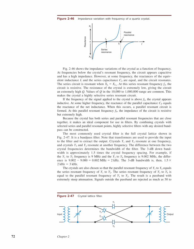
72 Chapter 2
Fig. 2-46 shows the impedance variations of the crystal as a function of frequency.
At frequencies below the crystal’s resonant frequency, the circuit appears capacitive
and has a high impedance. However, at some frequency, the reactances of the equiv-
alent inductance L and the series capacitance CS are equal, and the circuit resonates.
The series circuit is resonant when XL 5 XCS. At this series resonant frequency fS, the
circuit is resistive. The resistance of the crystal is extremely low, giving the circuit
an extremely high Q. Values of Q in the 10,000 to 1,000,000 range are common. This
makes the crystal a highly selective series resonant circuit.
If the frequency of the signal applied to the crystal is above fS, the crystal appears
inductive. At some higher frequency, the reactance of the parallel capacitance CP equals
the reactance of the net inductance. When this occurs, a parallel resonant circuit is
formed. At this parallel resonant frequency fP, the impedance of the circuit is resistive
but extremely high.
Because the crystal has both series and parallel resonant frequencies that are close
together, it makes an ideal component for use in i lters. By combining crystals with
selected series and parallel resonant points, highly selective i lters with any desired band-
pass can be constructed.
The most commonly used crystal i lter is the full crystal lattice shown in
Fig. 2-47. It is a bandpass i lter. Note that transformers are used to provide the input
to the i lter and to extract the output. Crystals Y1 and Y2 resonate at one frequency,
and crystals Y3 and Y4 resonate at another frequency. The difference between the two
crystal frequencies determines the bandwidth of the i lter. The 3-dB down band-
width is approximately 1.5 times the crystal frequency spacing. For example, if
the Y1 to Y2 frequency is 9 MHz and the Y3 to Y4 frequency is 9.002 MHz, the differ-
ence is 9.002 2 9.000 5 0.002 MHz 5 2 kHz. The 3-dB bandwidth is, then, 1.5 3
2 kHz 5 3 kHz.
The crystals are also chosen so that the parallel resonant frequency of Y3 to Y4 equals
the series resonant frequency of Y1 to Y2. The series resonant frequency of Y3 to Y4 is
equal to the parallel resonant frequency of Y1 to Y2. The result is a passband with
extremely steep attenuation. Signals outside the passband are rejected as much as 50 to
Figure 2-46 Impedance variation with frequency of a quartz crystal.
Re
acta
nce
XL
0
XC
fS
fP
Seriesresonance
Parallelresonance
f
Figure 2-47 Crystal lattice fi lter.
Input Output
Y1
Y2
Y3
Y4

Electronic Fundamentals for Communications 73
60 dB below those inside the passband. Such a i lter can easily discriminate between
very closely spaced desired and undesired signals.
Another type of crystal i lter is the ladder i lter shown in Fig. 2-48, which is also a
bandpass i lter. All the crystals in this i lter are cut for exactly the same frequency. The
number of crystals used and the values of the shunt capacitors set the bandwidth. At least
six crystals must usually be cascaded to achieve the kind of selectivity needed in com-
munication applications.
Ceramic Filters. Ceramic is a manufactured crystallike compound that has the same
piezoelectric qualities as quartz. Ceramic disks can be made so that they vibrate at a
i xed frequency, thereby providing i ltering actions. Ceramic i lters are very small and
inexpensive and are, therefore, widely used in transmitters and receivers. Although the
Q of ceramic does not have as high an upper limit as that of quartz, it is typically several
thousand, which is very high compared to the Q obtainable with LC i lters. Typical
ceramic i lters are of the bandpass type with center frequencies of 455 kHz and
10.7 MHz. These are available in different bandwidths depending upon the application.
Such ceramic i lters are widely used in communication receivers.
A schematic diagram of a ceramic i lter is shown in Fig. 2-49. For proper operation,
the i lter must be driven from a generator with an output impedance of Rg and be ter-
minated with a load of RL. The values of Rg and RL are usually 1.5 or 2 kV.
Surface Acoustic Wave Filters. A special form of a crystal i lter is the surface
acoustic wave (SAW) i lter. This i xed tuned bandpass i lter is designed to provide the
exact selectivity required by a given application. Fig. 2-50 shows the schematic design
Ceramic fi lter
Surface acoustic wave (SAW) fi lter
Figure 2-48 Crystal ladder fi lter.
Input Output
Figure 2-49 Schematic symbol for a ceramic fi lter.
RL
Rg
Figure 2-50 A surface acoustic wave fi lter.
Interdigitaltransducers
Interdigitaltransducers
Surface acousticwaves
Input
Out put
Piezoelectric ceramic
GOOD TO KNOW
Ceramic fi lters are used in most
communication receivers and
transmitters because they are
relatively small and inexpensive.

74 Chapter 2
of a SAW i lter. SAW i lters are made on a piezoelectric ceramic substrate such as
lithium niobate. A pattern of interdigital i ngers on the surface converts the signals into
acoustic waves that travel across the i lter surface. By controlling the shapes, sizes, and
spacings of the interdigital i ngers, the response can be tailored to any application. Inter-
digital i ngers at the output convert the acoustic waves back to electrical signals.
SAW i lters are normally bandpass i lters used at very high radio frequencies where
selectivity is difi cult to obtain. Their common useful range is from 10 MHz to 3 GHz.
They have a low shape factor, giving them exceedingly good selectivity at such high
frequencies. They do have a signii cant insertion loss, usually in the 10- to 35-dB range,
which must be overcome with an accompanying amplii er. SAW i lters are widely used
in modern TV receivers, radar receivers, wireless LANs, and cell phones.
Switched Capacitor Filters
Switched capacitor i lters (SCFs) are active IC i lters made of op amps, capacitors,
and transistor switches. Also known as analog sampled data i lters or commutating
i lters, these devices are usually implemented with MOS or CMOS circuits. They can
be designed to operate as high-pass, low-pass, bandpass, or bandstop i lters. The pri-
mary advantage of SCFs is that they provide a way to make tuned or selective circuits
in an IC without the use of discrete inductors, capacitors, or resistors.
Switched capacitor i lters are made of op amps, MOSFET switches, and capacitors.
All components are fully integrated on a single chip, making external discrete compo-
nents unnecessary. The secret to the SCF is that all resistors are replaced by capacitors
that are switched by MOSFET switches. Resistors are more difi cult to make in IC form
and take up far more space on the chip than transistors and capacitors. With switched
capacitors, it is possible to make complex active i lters on a single chip. Other advan-
tages are selectibility of i lter type, full adjustability of the cutoff or center frequency,
and full adjustability of bandwidth. One i lter circuit can be used for many different
applications and can be set to a wide range of frequencies and bandwidths.
Switched Integrators. The basic building block of SCFs is the classic op amp inte-
grator, as shown in Fig. 2-51(a). The input is applied through a resistor, and the feedback
is provided by a capacitor. With this arrangement, the output is a function of the integral
of the input:
Vout 5 21
RC # Vin dt
With ac signals, the circuit essentially functions as a low-pass i lter with a gain of
1/RC.
Switched capacitor fi lter (SCF) or analog sampled data or commutating fi lter
Switched integrator
Figure 2-51 IC integrators. (a) Conventional integrator. (b) Switched capacitor integrator.
Vin
Vin dt Vout � �
(a)
� 1 RC
fc
S1
fc
C1
C2
C2
(b)
C1
�1
�2
MOSFETswitches
Vout �
Vin dt �
�1
�2
Two-phaseclock
S2
Vin��
��

Electronic Fundamentals for Communications 75
To work over a wide range of frequencies, the integrator RC values must be changed.
Making low and high resistor and capacitor values in IC form is difi cult. However, this
problem can be solved by replacing the input resistor with a switched capacitor, as shown
in Fig. 2-51(b). The MOSFET switches are driven by a clock generator whose frequency
is typically 50 to 100 times the maximum frequency of the ac signal to be i ltered. The
resistance of a MOSFET switch when on is usually less than 1000 V. When the switch
is off, its resistance is many megohms.
The clock puts out two phases, designated ϕ1 and ϕ2, that drive the MOSFET
switches. When S1 is on, S2 is off and vice versa. The switches are of the break- before-
make type, which means that one switch opens before the other is closed. When S1 is
closed, the charge on the capacitor follows the input signal. Since the clock period and
time duration that the switch is on are very short compared to the input signal variation,
a brief “sample” of the input voltage remains stored on C1 and S1 turns off.
Now S2 turns on. The charge on capacitor C1 is applied to the summing junction of
the op amp. It discharges, causing a current to l ow in the feedback capacitor C2. The
resulting output voltage is proportional to the integral of the input. But this time, the
gain of the integrator is
f aC1
C2
bwhere f is the clock frequency. Capacitor C1, which is switched at a clock frequency of
f with period T, is equivalent to a resistor value of R 5 T/C1.
The beauty of this arrangement is that it is not necessary to make resistors on the
IC chip. Instead, capacitors and MOSFET switches, which are smaller than resistors,
are used. Further, since the gain is a function of the ratio of C1 to C2, the exact capac-
itor values are less important than their ratio. It is much easier to control the ratio of
matched pairs of capacitors than it is to make precise values of capacitance.
By combining several such switching integrators, it is possible to create low-pass,
high-pass, bandpass, and band-reject i lters of the Butterworth, Chebyshev, elliptical, and
Bessel type with almost any desired selectivity. The center frequency or cutoff frequency
of the i lter is set by the value of the clock frequency. This means that the i lter can be
tuned on the l y by varying the clock frequency.
A unique but sometimes undesirable characteristic of an SCF is that the output
signal is really a stepped approximation of the input signal. Because of the switching
action of the MOSFETs and the charging and discharging of the capacitors, the signal
takes on a stepped digital form. The higher the clock frequency compared to the fre-
quency of the input signal, the smaller this effect. The signal can be smoothed back into
its original state by passing it through a simple RC low-pass i lter whose cutoff frequency
is set to just above the maximum signal frequency.
Various SCFs are available in IC form, both dedicated single-purpose or universal
versions. Some models can be coni gured as Butterworth, Bessel, Eliptical, or other
formats with as many as eight poles. They can be used for i ltering signals up to about
100 kHz. Manufacturers include Linear Technology, Maxim Integrated Products, and
Texas Instruments. One of the most popular is the MF10 made by Texas Instruments. It
is a universal SCF that can be set for low-pass, high-pass, bandpass, or band-reject
operation. It can be used for center or cutoff frequencies up to about 20 kHz. The clock
frequency is about 50 to 100 times the operating frequency.
Commutating Filters. An interesting variation of a switched capacitor i lter is the
commutating i lter shown in Fig. 2-52. It is made of discrete resistors and capacitors with
MOSFET switches driven by a counter and decoder. The circuit appears to be a low-pass
RC i lter, but the switching action makes the circuit function as a bandpass i lter. The
operating frequency fout is related to the clock frequency fc and the number N of switches
and capacitors used.
fc 5 Nfout and fout 5fc
N
Commutating fi lter

76 Chapter 2
The bandwidth of the circuit is related to the RC values and number of capacitors
and switches used as follows:
BW 51
2πNRC
For the i lter in Fig. 2-52, the bandwidth is BW 5 1y(8πRC).
Very high Q and narrow bandwidth can be obtained, and varying the resistor value
makes the bandwidth adjustable.
The operating waveforms in Fig. 2-52 show that each capacitor is switched on and
off sequentially so that only one capacitor is connected to the circuit at a time. A sample
of the input voltage is stored as a charge on each capacitor as it is connected to the input.
The capacitor voltage is the average of the voltage variation during the time the switch
connects the capacitor to the circuit.
Fig. 2-53(a) shows typical input and output waveforms, assuming a sine wave input.
The output is a stepped approximation of the input because of the sampling action of
the switched capacitors. The steps are large, but their size can be reduced by simply
using a greater number of switches and capacitors. Increasing the number of capacitors
from four to eight, as in Fig. 2-53(b), makes the steps smaller, and thus the output more
closely approximates the input. The steps can be eliminated or greatly minimized by
passing the output through a simple RC low-pass i lter whose cutoff is set to the center
frequency value or slightly higher.
One characteristic of the commutating i lter is that it is sensitive to the harmonics
of the center frequency for which it is designed. Signals whose frequency is some
integer multiple of the center frequency of the i lter are also passed by the i lter, although
Figure 2-52 A commutating SCF.
R
Input
2- to 4-line decoder
2-bit counter
Bandpass output fout
Nfout �
fcC
S1
S1
S2
S3
S4
2NRCBW �
1
S2
C
S3
C
S4
C
TA
AClock fc
Clock
TB
B

Electronic Fundamentals for Communications 77
at a somewhat lower amplitude. The response of the i lter, called a comb response, is
shown in Fig. 2-54. If such performance is undesirable, the higher frequencies can be
eliminated with a conventional RC or LC low-pass i lter connected to the output.
2-4 Fourier TheoryThe mathematical analysis of the modulation and multiplexing methods used in com-
munication systems assumes sine wave carriers and information signals. This simplii es
the analysis and makes operation predictable. However, in the real world, not all infor-
mation signals are sinusoidal. Information signals are typically more complex voice and
Comb response
Figure 2-53 Input and output for commutating fi lter. (a) Four-capacitor fi lter.
(b) Eight-capacitor fi lter.
Input signal
Output 4-capacitor filter
Output 8-capacitor filter
(a)
(b)
Figure 2-54 Comb fi lter response of a commutating fi lter.
fout 2fout 3fout 4fout
Outp
ut
Frequency

78 Chapter 2
video signals that are essentially composites of sine waves of many frequencies and
amplitudes. Information signals can take on an ini nite number of shapes, including
rectangular waves (i.e., digital pulses), triangular waves, sawtooth waves, and other
nonsinusoidal forms. Such signals require that a non–sine wave approach be taken to
determine the characteristics and performance of any communication circuit or system.
One of the methods used to do this is Fourier analysis, which provides a means of
accurately analyzing the content of most complex nonsinusoidal signals. Although Fou-
rier analysis requires the use of calculus and advanced mathematical techniques beyond
the scope of this text, its practical applications to communication electronics are rela-
tively straightforward.
Basic Concepts
Fig. 2-55(a) shows a basic sine wave with its most important dimensions and the equa-
tion expressing it. A basic cosine wave is illustrated in Fig. 2-55(b). Note that the cosine
wave has the same shape as a sine wave but leads the sine wave by 90°. A harmonic is
a sine wave whose frequency is some integer multiple of a fundamental sine wave. For
example, the third harmonic of a 2-kHz sine wave is a sine wave of 6 kHz. Fig. 2-56
shows the i rst four harmonics of a fundamental sine wave.
What the Fourier theory tells us is that we can take a nonsinusoidal waveform and
break it down into individual harmonically related sine wave or cosine wave components.
The classic example of this is a square wave, which is a rectangular signal with equal-
duration positive and negative alternations. In the ac square wave in Fig. 2-57, this means
that t1 is equal to t2. Another way of saying this is that the square wave has a 50 percent
duty cycle D, the ratio of the duration of the positive alteration t1 to the period T expressed
as a percentage:
D 5t1
T3 100
Fourier analysis tells us that a square wave is made up of a sine wave at the funda-
mental frequency of the square wave plus an ini nite number of odd harmonics. For
example, if the fundamental frequency of the square wave is 1 kHz, the square wave can
be synthesized by adding the 1-kHz sine wave and harmonic sine waves of 3 kHz, 5 kHz,
7 kHz, 9 kHz, etc.
Fig. 2-58 shows how this is done. The sine waves must be of the correct amplitude
and phase relationship to one another. The fundamental sine wave in this case has a value
of 20 V peak to peak (a 10-V peak). When the sine wave values are added instantaneously,
the result approaches a square wave. In Fig. 2-58(a), the fundamental and third harmonic
Fourier analysis
Harmonic
Square wave
Duty cycle D
Figure 2-55 Sine and cosine waves.
00° 90° 180° 270° 360°
VP
�VP
T
v � VP sin 2ft
v � VP sin �t
0° 90° 180° 270° 360°
VP
�VP
T
v � VP cos 2ft
v � VP cos �t
T � period of one cyclein seconds
f � frequency in Hz
�
v � instantaneousvalue of voltage
VP � peak voltage
� � 2f
1
T

Electronic Fundamentals for Communications 79
are added. Note the shape of the composite wave with the third and i fth harmonics
added, as in Fig. 2-58(b). The more higher harmonics that are added, the more the com-
posite wave looks like a perfect square wave. Fig. 2-59 shows how the composite wave
would look with 20 odd harmonics added to the fundamental. The results very closely
approximate a square wave.
Figure 2-56 A sine wave and its harmonics.
Fundamental (f )
Third harmonic (3f )
Fourth harmonic (4f )
Second harmonic (2f )
Figure 2-57 A square wave.
(a)
t1 t2
T � t1 � t2
(50% duty cyle)
Duty cyle �
t
�V
0
�V
(b)
t1 t2
t
�V
0
� 100t1T
1T
t1 � t2
f �

80 Chapter 2
The implication of this is that a square wave should be analyzed as a collection of
harmonically related sine waves rather than a single square wave entity. This is coni rmed
by performing a Fourier mathematical analysis on the square wave. The result is the
following equation, which expresses voltage as a function of time:
f (t) 54V
π c sin 2π a1
Tb t 1
1
3 sin 2π a3
Tb t 1
1
5 sin 2π a5
Tb t 1
1
7 sin 2π a7
Tb t 1 . . . d
Figure 2-58 A square wave is made up of a fundamental sine wave and an infi nite number of odd harmonics.
T/4 T/2 3T/4 T �t
1 f
Fundamental
Fundamental
With 3rd and 5th harmonics
Perfect square wave(infinite harmonics)
With 3rd harmonic
Composite wave of fundamentalplus 3rd harmonic
Composite wave with 3rd and 5th harmonics added to the fundamental
Period � T
10 V
v v
0
�10 V
10 V
0
�10 V
v
10 V
V
�V
0
�10 V
T/4
T/2
T/2
T
3T/4 T
�t
�t
�
(a) (b)
(c )
Figure 2-59 Square wave made up of 20 odd harmonics added to the fundamental.
�10 V
10 V
0 V

Electronic Fundamentals for Communications 81
where the factor 4V/π is a multiplier for all sine terms and V is the square wave peak
voltage. The i rst term is the fundamental sine wave, and the succeeding terms are the
third, i fth, seventh, etc., harmonics. Note that the terms also have an amplitude factor. In
this case, the amplitude is also a function of the harmonic. For example, the third harmonic
has an amplitude that is one-third of the fundamental amplitude, and so on. The expres-
sion could be rewritten with f 5 1/T. If the square wave is direct current rather than
alternating current, as shown in Fig. 2-57(b), the Fourier expression has a dc component:
f (t) 5V
21
4V
π asin 2πft 1
1
3 sin 2π3ft 1
1
5 sin 2π5ft 1
1
7 sin 2π7ft 1 . . .b
In this equation, V/2 is the dc component, the average value of the square wave. It is
also the baseline upon which the fundamental and harmonic sine waves ride.
A general formula for the Fourier equation of a waveform is
f (t) 5V
21
4V
πn aq
n51
(sin 2πnft)
where n is odd. The dc component, if one is present in the waveform, is V/2.
By using calculus and other mathematical techniques, the waveform is dei ned, ana-
lyzed, and expressed as a summation of sine and/or cosine terms, as illustrated by the
expression for the square wave above. Fig. 2-60 gives the Fourier expressions for some
of the most common nonsinusoidal waveforms.
Example 2-26An ac square wave has a peak voltage of 3 V and a frequency of 48 kHz. Find (a) the
frequency of the i fth harmonic and (b) the rms value of the i fth harmonic. Use the
formula in Fig. 2-60(a).
a. 5 3 48 kHz 5 240 kHz
b. Isolate the expression for the fifth harmonic in the formula, which is 15 sin 2π(5/T ) t. Multiply by the amplitude factor 4V/π. The peak value of
the fifth harmonic VP is
VP 54V
π a1
5b 5
4(3)
5π5 0.76
rms 5 0.707 3 peak value
Vrms 5 0.707VP 5 0.707(0.76) 5 0.537 V
The triangular wave in Fig. 2-60(b) exhibits the fundamental and odd harmonics, but
it is made up of cosine waves rather than sine waves. The sawtooth wave in Fig. 2-60(c)
contains the fundamental plus all odd and even harmonics. Fig. 2-60(d) and (e) shows half
sine pulses like those seen at the output of half and full wave rectii ers. Both have an aver-
age dc component, as would be expected. The half wave signal is made up of even harmon-
ics only, whereas the full wave signal has both odd and even harmonics. Fig. 2-60( f ) shows
the Fourier expression for a dc square wave where the average dc component is Vt0 /T.
Time Domain Versus Frequency Domain
Most of the signals and waveforms that we discuss and analyze are expressed in the time
domain. That is, they are variations of voltage, current, or power with respect to time.
Time domain

82 Chapter 2
All the signals shown in the previous illustrations are examples of time-domain wave-
forms. Their mathematical expressions contain the variable time t, indicating that they
are a time-variant quantity.
Fourier theory gives us a new and different way to express and illustrate complex
signals. Here, complex signals containing many sine and/or cosine components are
expressed as sine or cosine wave amplitudes at different frequencies. In other words, a
graph of a particular signal is a plot of sine and/or cosine component amplitudes with
respect to frequency.
A typical frequency-domain plot of the square wave is shown in Fig. 2-61(a). Note
that the straight lines represent the sine wave amplitudes of the fundamental and
harmonics, and these are plotted on a horizontal frequency axis. Such a frequency-
domain plot can be made directly from the Fourier expression by simply using the fre-
quencies of the fundamentals and harmonics and their amplitudes. Frequency-domain
plots for some of the other common nonsinusoidal waves are also shown in Fig. 2-61.
Figure 2-60 Common nonsinusoidal waves and their Fourier equations. (a) Square wave. (b) Triangle wave. (c) Sawtooth.
(d ) Half cosine wave. (e) Full cosine wave. (f ) Rectangular pulse.
V
cos 2�
(e)
�2T �T T 2T0
�V
f(t)
2V
�
2V
� 1
T
2
T
3
T
2
15f(t) � cos 2� cos 2� …�
2
3 2
35t � t ��
4V
�
1
T
3
T
5
T
1
3f(t) � sin 2� sin 2� sin 2� …t �
1
5t � t �
t
2T�2T �T 0 T
(a)
�V
Vf(t)
cos 2�
(d )
t
�T 0 T
�V
V f(t)
V
�
V
� 1
T
2
T
4
T
6
T
2
3f(t) � cos 2�
cos 2� cos 2� …
t �
2
15
�
2
2
35
t
t � t �
�
�
�V
8V
�2
1
T
3
T
5
T
1
9f(t) � � cos 2� cos 2� cos 2� …t �
1
25t � t �
t
�TT
(b)
V
f(t)
V
t0 t0
�t0
T
(f )
�T T
T
T
0
Vt0 T
2Vt0 T 2�t0
T�t0
T
f(t) �cos
…�
� sin
2�t0
T
2�t0
T
4�t0
Tcos
sin3�t0
T
3�t0
T
6�t0
Tcos
sin
� �
1
f T �
t
�2T �T0
T 2T
�V
V
2V
�
1
T
2
T
3
T
4
T
1
2f(t) � sin 2� sin 2�
sin 2� sin 2� …
t �
1
3
1
4� t �
(c )
t �
t

Electronic Fundamentals for Communications 83
Note that the triangle wave in Fig. 2-61(c) is made up of the fundamental and odd
harmonics. The third harmonic is shown as a line below the axis, which indicates a 180°
phase shift in the cosine wave making it up.
Fig. 2-62 shows how the time and frequency domains are related. The square
wave discussed earlier is used as an example. The result is a three-axis three-
dimensional view.
Figure 2-61 The frequency-domain plots of common nonsinusoidal waves. (a) Square wave. (b) Sawtooth. (c) Triangle.
(d ) Half cosine wave.
Volts
Volts
0
0
0
Harmonic (�)
(d )
1 2 3 4 5 6 7 8 9
Vo
lts
Time
Vo
lts
0
0
1 2 3 4 5 6 7 8 9
Harmonic (�)
(c)
Vo
lts
0
0
1 2 3 4 5 6 7 8 9 10
Frequency
Fundamental
Vo
lts
Fundamental
Fundamental
Harmonic (�)
(a )
Time
Vo
lts
Time
Vo
lts
0
0
1 2 3 4 5 6 7 8 9 10
Fundamental
Harmonic (�)
(b )
DC component
Frequency
Amplitude
Time domain
Time
Frequencydomain
Figure 2-62 The relationship between time and frequency domains.

84 Chapter 2
Signals and waveforms in communication applications are expressed by using both
time-domain and frequency-domain plots, but in many cases the frequency-domain plot
is far more useful. This is particularly true in the analysis of complex signal waveforms
as well as the many modulation and multiplexing methods used in communication.
Test instruments for displaying signals in both time and frequency domains are
readily available. You are already familiar with the oscilloscope, which displays the volt-
age amplitude of a signal with respect to a horizontal time axis.
The test instrument for producing a frequency-domain display is the spectrum
analyzer. Like the oscilloscope, the spectrum analyzer uses a cathode-ray tube for
display, but the horizontal sweep axis is calibrated in hertz and the vertical axis is
calibrated in volts or power units or decibels.
The Importance of Fourier Theory
Fourier analysis allows us to determine not only the sine wave components in any com-
plex signal but also how much bandwidth a particular signal occupies. Although a sine
or cosine wave at a single frequency theoretically occupies no bandwidth, complex sig-
nals obviously take up more spectrum space. For example, a 1-MHz square wave with
harmonics up to the eleventh occupies a bandwidth of 11 MHz. If this signal is to pass
unattenuated and undistorted, then all harmonics must be passed.
An example is shown in Fig. 2-63. If a 1-kHz square wave is passed through a low-
pass i lter with a cutoff frequency just above 1 kHz, all the harmonics beyond the third
harmonic are greatly attenuated or, for the most part, i ltered out completely. The result
is that the output of the low-pass i lter is simply the fundamental sine wave at the square
wave frequency.
If the low-pass i lter were set to cut off at a frequency above the third harmonic,
then the output of the i lter would consist of a fundamental sine wave and the third
harmonic. Such a waveshape was shown in Fig. 2-58(a). As you can see, when the higher
harmonics are not all passed, the original signal is greatly distorted. This is why it is
important for communication circuits and systems to have a bandwidth wide enough to
accommodate all the harmonic components within the signal waveform to be processed.
Fig. 2-64 shows an example in which a 1-kHz square wave is passed through a
bandpass i lter set to the third harmonic, resulting in a 3-kHz sine wave output. In this
case, the i lter used is sharp enough to select out the desired component.
Pulse Spectrum
The Fourier analysis of binary pulses is especially useful in communication, for it gives
a way to analyze the bandwidth needed to transmit such pulses. Although theoretically
Spectrum analyzer
Pulse spectrum
Figure 2-63 Converting a square wave to sine wave by fi ltering out all the harmonics.
1 100
2 3 4 5 6 7 8 9Frequency
Harmonic (�)
Frequency responseof low-pass filter
1 kHz 1 kHz
LPF

Electronic Fundamentals for Communications 85
the system must pass all the harmonics in the pulses, in reality, relatively few must be
passed to preserve the shape of the pulse. In addition, the pulse train in data communi-
cation rarely consists of square waves with a 50 percent duty cycle. Instead, the pulses
are rectangular and exhibit varying duty cycles, from very low to very high. [The Fourier
response of such pulses is given in Fig. 2-60( f ).]
Look back at Fig. 2-60( f ). The period of the pulse train is T, and the pulse width
is t0. The duty cycle is t0 /T. The pulse train consists of dc pulses with an average dc
value of Vt0 /T. In terms of Fourier analysis, the pulse train is made up of a fundamental
and all even and odd harmonics. The special case of this waveform is where the duty
cycle is 50 percent; in that case, all the even harmonics drop out. But with any other
duty cycle, the waveform is made up of both odd and even harmonics. Since this is a
series of dc pulses, the average dc value is Vt0 /T.
A frequency-domain graph of harmonic amplitudes plotted with respect to frequency
is shown in Fig. 2-65. The horizontal axis is frequency-plotted in increments of the pulse
repetition frequency f , where f 5 1/T and T is the period. The i rst component is the
average dc component at zero frequency Vt0 /T, where V is the peak voltage value of
the pulse.
Now, note the amplitudes of the fundamental and harmonics. Remember that each
vertical line represents the peak value of the sine wave components of the pulse train.
Some of the higher harmonics are negative; that simply means that their phase is
reversed.
1 10
0
2 3 4 5 6 7 8 9Frequency
Bandpass filterresponse curve
1 kHzHarmonic (�)
BPF3 kHz
3 kHz
Figure 2-64 Selecting the third harmonic with a bandpass fi lter.
f �
Vt0T
1T
2t0
1t0
3t0
f0
2nd harmonic
Fundamental sine wave
3rd harmonic
7th harmonic
Amplitude of average dc component at zero frequency
Figure 2-65 Frequency domain of a rectangular pulse train.

86 Chapter 2
The dashed line in Fig. 2-65, the outline of the peaks of the individual compo-
nents, is what is known as the envelope of the frequency spectrum. The equation for
the envelope curve has the general form (sin x)/x, where x 5nπt0
T and t0 is the pulse
width. This is known as the sinc function. In Fig. 2-65, the sinc function crosses the
horizontal axis several times. These times can be computed and are indicated in the
i gure. Note that they are some multiple of 1/t0.
The sinc function drawn on a frequency-domain curve is used in predicting the
harmonic content of a pulse train and thus the bandwidth necessary to pass the wave.
For example, in Fig. 2-65, as the frequency of the pulse train gets higher, the period T
gets shorter and the spacing between the harmonics gets wider. This moves the curve
out to the right. And as the pulse duration t0 gets shorter, which means that the duty
cycle gets shorter, the i rst zero crossing of the envelope moves farther to the right. The
practical signii cance of this is that higher-frequency pulses with shorter pulse durations
have more harmonics with greater amplitudes, and thus a wider bandwidth is needed to
pass the wave with minimum distortion. For data communication applications, it is gen-
erally assumed that a bandwidth equal to the i rst zero crossing of the envelope is the
minimum that is sufi cient to pass enough harmonics for reasonable waveshape:
BW 51
t0
Envelope
Sinc function
Example 2-27A dc pulse train like that in Fig. 2-60( f ) has a peak voltage value of 5 V, a frequency
of 4 MHz, and a duty cycle of 30 percent.
a. What is the average dc value? [Vavg 5 Vt0 /T. Use the formula given in
Fig. 2-60( f ).]
Duty cycle 5t0
T5 30% or 0.30
T 51
f5
1
4 3 1065 2.5 3 1027 s 5 250 3 1029 s
T 5 250 ns
t0 5 duty cycle 3 T 5 0.3 3 250 5 75 ns
Vavg 5Vt0
T5 V 3 duty cycle 5 5 3 0.3 5 1.5 V
b. What is the minimum bandwidth necessary to pass this signal without
ex cessive distortions?
Minimum bandwidth BW 51
t0
51
75 3 1029
5 0.013333 3 109 5 13.333 3 106
5 13.333 MHz
Most of the higher-amplitude harmonics and thus the most signii cant part of the
signal power are contained within the larger area between zero frequency and the 1/t0
point on the curve.

Electronic Fundamentals for Communications 87
The Relationship Between Rise Time and Bandwidth
Because a rectangular wave such as a square wave theoretically contains an ini nite
number of harmonics, we can use a square wave as the basis for determining the
bandwidth of a signal. If the processing circuit should pass all or an ini nite number
of harmonics, the rise and fall times of the square wave will be zero. As the band-
width is decreased by rolling off or i ltering out the higher frequencies, the higher
harmonics are greatly attenuated. The effect this has on the square wave is that the
rise and fall times of the waveform become i nite and increase as more and more of
the higher harmonics are i ltered out. The more restricted the bandwidth, the fewer
the harmonics passed and the greater the rise and fall times. The ultimate restriction
is where all the harmonics are i ltered out, leaving only the fundamental sine wave
(Fig. 2-63).
The concept of rise and fall times is illustrated in Fig. 2-66. The rise time tr is the
time it takes the pulse voltage to rise from its 10 percent value to its 90 percent value.
The fall time tf is the time it takes the voltage to drop from the 90 percent value to the
10 percent value. Pulse width t0 is usually measured at the 50 percent amplitude points
on the leading (rise) and trailing (fall) edges of the pulse.
A simple mathematical expression relating the rise time of a rectangular wave and
the bandwidth of a circuit required to pass the wave without distortion is
BW 50.35
tr
Rise time
Example 2-28A pulse train has a rise time of 6 ns. What is the minimum bandwidth to pass this
pulse train faithfully?
BW 50.35
tr
tr 5 6 ns 5 0.006 µs
Minimum BW 50.35
0.0065 58.3 MHz
This is the bandwidth of the circuit required to pass a signal containing the highest-
frequency component in a square wave with a rise time of tr. In this expression, the
bandwidth is really the upper 3-dB down cutoff frequency of the circuit given in mega-
hertz. The rise time of the output square wave is given in microseconds. For example,
if the square wave output of an amplii er has a rise time of 10 ns (0.01 µs), the bandwidth
of the circuit must be at least BW 5 0.35/0.01 5 35 MHz.
Rearranging the formula, you can calculate the rise time of an output signal from the
circuit whose bandwidth is given: tr 5 0.35/ BW. For example, a circuit with a 50-MHz
bandwidth will pass a square wave with a minimum rise time of tr 5 0.35/50 5
0.007 µs 5 7 ns.
This simple relationship permits you to quickly determine the approximate band-
width of a circuit needed to pass a rectangular waveform with a given rise time. This
relationship is widely used to express the frequency response of the vertical amplii er in

88 Chapter 2
an oscilloscope. Oscilloscope specii cations often give only a rise time i gure for the
vertical amplii er. An oscilloscope with a 60-MHz bandwidth would pass rectangular
waveforms with rise times as short as tr 5 0.35/60 5 0.00583 µs 5 5.83 ns.
Figure 2-66 Rise and fall times of a pulse.
Trailingedge
Leadingedge
tr � rise time
tf � fall time
t0 � pulse width (duration)
tr
t0
tf
Time
Vo
lta
ge
90%
100%
50%
10%
0
Example 2-29A circuit has a bandwidth of 200 kHz. What is the fastest rise time this circuit
will pass?
tr (µs) 5
0.35
f (MHz) and 200 kHz 5 0.2 MHz
tr 50.35
0.25 1.75 µs
Similarly, an oscilloscope whose vertical amplii er is rated at 2 ns (0.002 µs) has a
bandwidth or upper cutoff frequency of BW 5 0.35/0.002 5 175 MHz. What this means
is that the vertical amplii er of the oscilloscope has a bandwidth adequate to pass a suf-
i cient number of harmonics so that the resulting rectangular wave has a rise time of
2 ns. This does not indicate the rise time of the input square wave itself. To take this
into account, you use the formula
tr 5 1.12t 2ri 1 t
2ra
where tri 5 rise time of input square wave
tra 5 rise time of amplifier
tr 5 composite rise time of amplifier output

Electronic Fundamentals for Communications 89
Example 2-30An oscilloscope has a bandwidth of 60 MHz. The input square wave has a rise time of
15 ns. What is the rise time of the displayed square wave?
tra (oscilloscope) 50.35
605 0.005833 µs 5 5.833 ns
tri 5 15 ns
tra (composite) 5 1.1 2t 2ri 1 t
2ra 5 1.1 2(15)2 1 (5.833)2
5 1.1 2259 5 17.7 ns
The expression can be expanded to include the effect of additional stages of amplii cation
by simply adding the squares of the individual rise times to the above expression before
taking the square root of it.
The spectrum analyzer shows a frequency-domain plot of electronic signals. It is the
key test instrument in designing, analyzing, and troubleshooting communication
equipment.
Keep in mind that the bandwidth or upper cut-off frequency derived from the rise
time formula on the previous page passes only the harmonics needed to support the rise
time. There are harmonics beyond this bandwidth that also contribute to unwanted emis-
sions and noise.

90 Chapter 2
CHAPTER REVIEW
Online Activity
2-1 Exploring Filter Options
Objective: Examine several alternatives to LC and crystal
i lters.
Procedure:
1. Search on the terms dielectric resonator, mechanical
i lter, and ceramic i lter.
2. Look at manufacturer websites and examine specii c
products.
3. Print out data sheets as need to determine i lter types
and specii cations.
4. Answer the following questions.
Questions:
1. Name one manufacturer for each of the types of i lters
you studied.
2. What kinds of i lters did you i nd? (LPF, HPF,
BPF, etc.)
3. What frequency range does each type of i lter cover?
4. Dei ne insertion loss and give typical loss factors for
each i lter type.
5. What are typical input and output impedances for each
i lter type?
1. What happens to capacitive reactance as the frequency
of operation increases?
2. As frequency decreases, how does the reactance of a
coil vary?
3. What is skin effect, and how does it affect the Q of a
coil?
4. What happens to a wire when a ferrite bead is placed
around it?
5. What is the name given to the widely used coil form
that is shaped like a doughnut?
6. Describe the current and impedance in a series RLC
circuit at resonance.
7. Describe the current and impedance in a parallel RLC
circuit at resonance.
8. State in your own words the relationship between Q
and the bandwidth of a tuned circuit.
9. What kind of i lter is used to select a single signal fre-
quency from many signals?
10. What kind of i lter would you use to get rid of an an-
noying 120-Hz hum?
11. What does selectivity mean?
12. State the Fourier theory in your own words.
13. Dei ne the terms time domain and frequency domain.
14. Write the i rst four odd harmonics of 800 Hz.
15. What waveform is made up of even harmonics only?
What waveform is made up of odd harmonics only?
16. Why is a nonsinusoidal signal distorted when it passes
through a i lter?
Questions
1. What is the gain of an amplii er with an output of
1.5 V and an input of 30 µV? ◆
2. What is the attenuation of a voltage divider like
that in Fig. 2-3, where R1 is 3.3 kV and R2 is
5.1 kV?
3. What is the overall gain or attenuation of the com-
bination formed by cascading the circuits described
in Problems 1 and 2? ◆
4. Three amplii ers with gains of 15, 22, and 7 are
cascaded; the input voltage is 120 µV. What are the
overall gain and the output voltages of each stage?
5. A piece of communication equipment has two
stages of amplii cation with gains of 40 and 60 and
two loss stages with attenuation factors of 0.03 and
0.075. The output voltage is 2.2 V. What are the
overall gain (or attenuation) and the input
voltage? ◆
6. Find the voltage gain or attenuation, in decibels, for
each of the circuits described in Problems 1
through 5.
7. A power amplii er has an output of 200 W and an
input of 8 W. What is the power gain in decibels? ◆
8. A power amplii er has a gain of 55 dB. The input
power is 600 mW. What is the output power?
9. An amplii er has an output of 5 W. What is its gain
in dBm? ◆
10. A communication system has i ve stages, with
gains and attenuations of 12, 245, 68, 231, and
9 dB. What is the overall gain?
11. What is the reactance of a 7-pF capacitor at 2 GHz?
12. What value of capacitance is required to produce
50 V of reactance at 450 MHz?
13. Calculate the inductive reactance of a 0.9-µH coil
at 800 MHz.
Problems

Electronic Fundamentals for Communications 91
14. At what frequency will a 2-µH inductor have a re-
actance of 300 V?
15. A 2.5-µH inductor has a resistance of 23 V. At a
frequency of 35 MHz, what is its Q?
16. What is the resonant frequency of a 0.55-µH coil
with a capacitance of 22 pF?
17. What is the value of inductance that will resonate
with an 80-pF capacitor at 18 MHz?
18. What is the bandwidth of a parallel resonant circuit
that has an inductance of 33 µH with a resistance
of 14 V and a capacitance of 48 pF?
19. A series resonant circuit has upper and lower cutoff
frequencies of 72.9 and 70.5 MHz. What is its
bandwidth?
20. A resonant circuit has a peak output voltage of
4.5 mV. What is the voltage output at the upper and
lower cutoff frequencies?
21. What circuit Q is required to give a bandwidth of
36 MHz at a frequency of 4 GHz?
22. Find the impedance of a parallel resonant circuit
with L 5 60 µH, RW 5 7 V, and C 5 22 pF.
23. Write the i rst four terms of the Fourier equation of
a sawtooth wave that has a peak-to-peak amplitude
of 5 V and a frequency of 100 kHz.
24. An oscilloscope has a rise time of 8 ns. What is the
highest-frequency sine wave that the scope can dis-
play?
25. A low-pass i lter has a cutoff frequency of 24 MHz.
What is the fastest rise time that a rectangular wave
that will pass through the i lter can have?
◆ Answers to Selected Problems follow Chap. 22.
1. Explain how capacitance and inductance can exist in a
circuit without lumped capacitors and inductor compo-
nents being present.
2. How can the voltage across the coil or capacitor in a
series resonant circuit be greater than the source volt-
age at resonance?
3. What type of i lter would you use to prevent the harmon-
ics generated by a transmitter from reaching the antenna?
4. What kind of i lter would you use on a TV set to pre-
vent a signal from a CB radio on 27 MHz from interfer-
ing with a TV signal on channel 2 at 54 MHz?
5. Explain why it is possible to reduce the effective Q of a
parallel resonant circuit by connecting a resistor in par-
allel with it.
6. A parallel resonant circuit has an inductance of 800 nH,
a winding resistance of 3 V, and a capacitance of 15 pF.
Calculate (a) resonant frequency, (b) Q, (c) bandwidth,
(d) impedance at resonance.
7. For the previous circuit, what would the bandwidth be
if you connected a 33-kV resistor in parallel with the
tuned circuit?
8. What value of capacitor would you need to produce a
high-pass i lter with a cutoff frequency of 48 kHz with
a resistor value of 2.2 kV?
9. What is the minimum bandwidth needed to pass a peri-
odic pulse train whose frequency is 28.8 kHz and duty
cycle is 20 percent? 50 percent?
10. Refer to Fig. 2-60. Examine the various waveforms and
Fourier expressions. What circuit do you think might
make a good but simple frequency doubler?
Critical Thinking

92
chapter
Amplitude Modulation Fundamentals
3
In the modulation process, the baseband voice, video, or digital signal
modifi es another, higher-frequency signal called the carrier, which is usu-
ally a sine wave. A sine wave carrier can be modifi ed by the intelligence
signal through amplitude modulation, frequency modulation, or phase
modulation. The focus of this chapter is amplitude modulation (AM).
Objectives
After completing this chapter, you will be able to:
■ Calculate the modulation index and percentage of modulation of an
AM signal, given the amplitudes of the carrier and modulating signals.
■ Defi ne overmodulation and explain how to alleviate its ef ects.
■ Explain how the power in an AM signal is distributed between the
carrier and the sideband, and then compute the carrier and sideband
powers, given the percentage of modulation.
■ Compute sideband frequencies, given carrier and modulating signal
frequencies.
■ Compare time-domain, frequency-domain, and phasor representations
of an AM signal.
■ Explain what is meant by the terms DSB and SSB and state the main
advantages of an SSB signal over a conventional AM signal.
■ Calculate peak envelope power (PEP), given signal voltages and
load impedances.
Carrier
Amplitude modulation (AM)

Amplitude Modulation Fundamentals 93
3-1 AM ConceptsAs the name suggests, in AM, the information signal varies the amplitude of the carrier
sine wave. The instantaneous value of the carrier amplitude changes in accordance with
the amplitude and frequency variations of the modulating signal. Fig. 3-1 shows a single-
frequency sine wave intelligence signal modulating a higher-frequency carrier. The carrier
frequency remains constant during the modulation process, but its amplitude varies in
accordance with the modulating signal. An increase in the amplitude of the modulating
signal causes the amplitude of the carrier to increase. Both the positive and the negative
peaks of the carrier wave vary with the modulating signal. An increase or a decrease in
the amplitude of the modulating signal causes a corresponding increase or decrease in both
the positive and the negative peaks of the carrier amplitude.
An imaginary line connecting the positive peaks and negative peaks of the carrier
waveform (the dashed line in Fig. 3-1) gives the exact shape of the modulating
information signal. This imaginary line on the carrier waveform is known as the
envelope.
Because complex waveforms such as that shown in Fig. 3-1 are difi cult to draw,
they are often simplii ed by representing the high-frequency carrier wave as many equally
spaced vertical lines whose amplitudes vary in accordance with a modulating signal, as
in Fig. 3-2. This method of representation is used throughout this book.
The signals illustrated in Figs. 3-1 and 3-2 show the variation of the carrier ampli-
tude with respect to time and are said to be in the time domain. Time-domain signals—
voltage or current variations that occur over time—are displayed on the screen of an
oscilloscope.
Using trigonometric functions, we can express the sine wave carrier with the simple
expression
υc 5 Vc sin 2πfc
t
In this expression, υc represents the instantaneous value of the carrier sine wave voltage
at some specii c time in the cycle; Vc represents the peak value of the constant unmod-
ulated carrier sine wave as measured between zero and the maximum amplitude of either
the positive-going or the negative-going alternations (Fig. 3-1); fc is the frequency of the
carrier sine wave; and t is a particular point in time during the carrier cycle.
A sine wave modulating signal can be expressed with a similar formula
υm 5 Vm sin 2πfmt
where υm 5 instantaneous value of information signal
Vm 5 peak amplitude of information signal
fm 5 frequency of modulating signal
Envelope
Figure 3-1 Amplitude modulation. (a) The modulating or information signal. (b) The modulated carrier.
Time
Sinusoidal modulating wavevmh Vm
0
(a )
0Time
AMwave
Unmodulatedcarrier wave
vcEnvelope
vc Vch
h
Vc
(b )
Carrier peak iszero referencefor modulating signal

94 Chapter 3
In Fig. 3-1, the modulating signal uses the peak value of the carrier rather than zero
as its reference point. The envelope of the modulating signal varies above and below the
peak carrier amplitude. That is, the zero reference line of the modulating signal coincides
with the peak value of the unmodulated carrier. Because of this, the relative amplitudes
of the carrier and modulating signal are important. In general, the amplitude of the
modulating signal should be less than the amplitude of the carrier. When the amplitude
of the modulating signal is greater than the amplitude of the carrier, distortion will occur,
causing incorrect information to be transmitted. In amplitude modulation, it is particu-
larly important that the peak value of the modulating signal be less than the peak value
of the carrier. Mathematically,
Vm , Vc
Values for the carrier signal and the modulating signal can be used in a formula
to express the complete modulated wave. First, keep in mind that the peak value of
the carrier is the reference point for the modulating signal; the value of the modulating
signal is added to or subtracted from the peak value of the carrier. The instantaneous
value of either the top or the bottom voltage envelope υ1 can be computed by using
the equation
υ1 5 Vc 1 υm 5 Vc 1 Vm sin 2πfmt
which expresses the fact that the instantaneous value of the modulating signal algebra-
ically adds to the peak value of the carrier. Thus, we can write the instantaneous value
of the complete modulated wave υ2 by substituting υ1 for the peak value of carrier
voltage Vc as follows:
υ2 5 υ1 sin 2πfc
t
Now substituting the previously derived expression for v1 and expanding, we get the
following:
υ2 5 (Vc 1 Vm sin 2πfmt) sin 2πfc
t 5 Vc sin 2πfc
t 1 (Vm sin 2πfmt) (sin 2πfc
t)
Figure 3-2 A simplifi ed method of representing an AM high-frequency sine wave.
0
Modulatingsignalenvelope
Equally spaced vertical linesrepresent constant-frequencycarrier sine wave
GOOD TO KNOW
In this text, radian measure will
be used for all angles unless
otherwise indicated. One radian is
approximately 57.3°.
GOOD TO KNOW
If the amplitude of the modulating
signal is greater than the
amplitude of the carrier, distortion
will occur.

Amplitude Modulation Fundamentals 95
where υ2 is the instantaneous value of the AM wave (or υAM), Vc sin 2πfc
t is the carrier
waveform, and (Vm sin 2πfmt) (sin 2πfc
t) is the carrier waveform multiplied by the mod-
ulating signal waveform. It is the second part of the expression that is characteristic of
AM. A circuit must be able to produce mathematical multiplication of the carrier and
modulating signals in order for AM to occur. The AM wave is the product of the carrier
and modulating signals.
The circuit used for producing AM is called a modulator. Its two inputs, the carrier
and the modulating signal, and the resulting outputs are shown in Fig. 3-3. Amplitude
modulators compute the product of the carrier and modulating signals. Circuits that
compute the product of two analog signals are also known as analog multipliers, mixers,
converters, product detectors, and phase detectors. A circuit that changes a lower-frequency
baseband or intelligence signal to a higher-frequency signal is usually called a modulator.
A circuit used to recover the original intelligence signal from an AM wave is known as
a detector or demodulator. Mixing and detection applications are discussed in detail in
later chapters.
3-2 Modulation Index and Percentage of ModulationAs stated previously, for undistorted AM to occur, the modulating signal voltage Vm must
be less than the carrier voltage Vc. Therefore, the relationship between the amplitude of
the modulating signal and the amplitude of the carrier signal is important. This relation-
ship, known as the modulation index m (also called the modulating factor or coefi cient,
or the degree of modulation), is the ratio
m 5Vm
Vc
These are the peak values of the signals, and the carrier voltage is the unmodulated
value.
Multiplying the modulation index by 100 gives the percentage of modulation. For
example, if the carrier voltage is 9 V and the modulating signal voltage is 7.5 V, the
modulation factor is 0.8333 and the percentage of modulation is 0.833 3 100 5 83.33.
Overmodulation and Distortion
The modulation index should be a number between 0 and 1. If the amplitude of the
modulating voltage is higher than the carrier voltage, m will be greater than 1, causing
Modulator
Modulation index m
Percentage of modulation
Figure 3-3 Amplitude modulator showing input and output signals.
Informationor
modulatingsignal
vm
Vc
Output
v2 � Vc sin 2�fct �Vm sin 2�fmt (sin 2�fct )
Carriersignal
Modulator
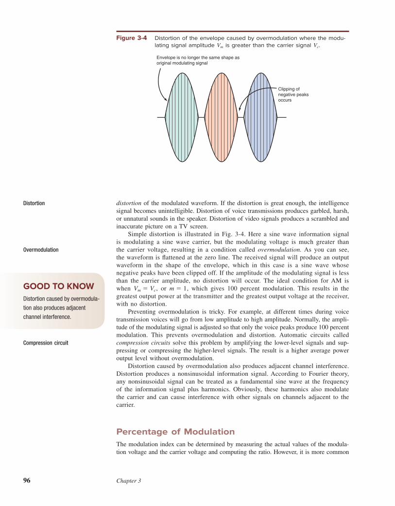
96 Chapter 3
distortion of the modulated waveform. If the distortion is great enough, the intelligence
signal becomes unintelligible. Distortion of voice transmissions produces garbled, harsh,
or unnatural sounds in the speaker. Distortion of video signals produces a scrambled and
inaccurate picture on a TV screen.
Simple distortion is illustrated in Fig. 3-4. Here a sine wave information signal
is modulating a sine wave carrier, but the modulating voltage is much greater than
the carrier voltage, resulting in a condition called overmodulation. As you can see,
the waveform is l attened at the zero line. The received signal will produce an output
waveform in the shape of the envelope, which in this case is a sine wave whose
negative peaks have been clipped off. If the amplitude of the modulating signal is less
than the carrier amplitude, no distortion will occur. The ideal condition for AM is
when Vm 5 Vc, or m 5 1, which gives 100 percent modulation. This results in the
greatest output power at the transmitter and the greatest output voltage at the receiver,
with no distortion.
Preventing overmodulation is tricky. For example, at different times during voice
transmission voices will go from low amplitude to high amplitude. Normally, the ampli-
tude of the modulating signal is adjusted so that only the voice peaks produce 100 percent
modulation. This prevents overmodulation and distortion. Automatic circuits called
compression circuits solve this problem by amplifying the lower-level signals and sup-
pressing or compressing the higher-level signals. The result is a higher average power
output level without overmodulation.
Distortion caused by overmodulation also produces adjacent channel interference.
Distortion produces a nonsinusoidal information signal. According to Fourier theory,
any nonsinusoidal signal can be treated as a fundamental sine wave at the frequency
of the information signal plus harmonics. Obviously, these harmonics also modulate
the carrier and can cause interference with other signals on channels adjacent to the
carrier.
Percentage of Modulation
The modulation index can be determined by measuring the actual values of the modula-
tion voltage and the carrier voltage and computing the ratio. However, it is more common
Distortion
Overmodulation
Compression circuit
Figure 3-4 Distortion of the envelope caused by overmodulation where the modu-
lating signal amplitude Vm is greater than the carrier signal Vc.
Envelope is no longer the same shape asoriginal modulating signal
Clipping ofnegative peaksoccurs
GOOD TO KNOW
Distortion caused by overmodula-
tion also produces adjacent
channel interference.

Amplitude Modulation Fundamentals 97
to compute the modulation index from measurements taken on the composite modulated
wave itself. When the AM signal is displayed on an oscilloscope, the modulation index
can be computed from Vmax and Vmin, as shown in Fig. 3-5. The peak value of the
modulating signal Vm is one-half the difference of the peak and trough values:
Vm 5Vmax 2 Vmin
2
As shown in Fig. 3-5, Vmax is the peak value of the signal during modulation, and Vmin
is the lowest value, or trough, of the modulated wave. The Vmax is one-half the peak-to-peak
value of the AM signal, or Vmax (p 2p)/2. Subtracting Vmin from Vmax produces the peak-
to-peak value of the modulating signal. One-half of that, of course, is simply the peak
value.
The peak value of the carrier signal Vc is the average of the Vmax and Vmin values:
Vc 5Vmax 1 Vmin
2
The modulation index is
m 5Vmax 2 Vmin
Vmax 1 Vmin
The values for Vmax ( p2p) and Vmin ( p2p) can be read directly from an oscilloscope screen
and plugged directly into the formula to compute the modulation index.
The amount, or depth, of AM is more commonly expressed as the percentage of
modulation rather than as a fractional value. In Example 3-1, the percentage of modulation
is 100 3 m, or 66.2 percent. The maximum amount of modulation without signal
distortion, of course, is 100 percent, where Vc and Vm are equal. At this time, Vmin 5 0
and Vmax 5 2Vm, where Vm is the peak value of the modulating signal.
Figure 3-5 An AM wave showing peaks (Vmax) and troughs (Vmin).
0
Vmax
VminVmax(p–p)
Vmin(p–p)

98 Chapter 3
3-3 Sidebands and the Frequency DomainWhenever a carrier is modulated by an information signal, new signals at different
frequencies are generated as part of the process. These new frequencies, which are called
side frequencies, or sidebands, occur in the frequency spectrum directly above and
directly below the carrier frequency. More specii cally, the sidebands occur at frequencies
that are the sum and difference of the carrier and modulating frequencies. When signals
of more than one frequency make up a waveform, it is often better to show the AM
signal in the frequency domain rather than in the time domain.
Sideband Calculations
When only a single-frequency sine wave modulating signal is used, the modulation pro-
cess generates two sidebands. If the modulating signal is a complex wave, such as voice
or video, a whole range of frequencies modulate the carrier, and thus a whole range of
sidebands are generated.
The upper sideband fUSB and lower sideband fLSB are computed as
fUSB 5 fc 1 fm and fLSB 5 fc 2 fm
where fc is the carrier frequency and fm is the modulating frequency.
The existence of sidebands can be demonstrated mathematically, starting with the
equation for an AM signal described previously:
υAM 5 Vc sin 2πfc
t 1 (Vm sin 2πfmt) (sin 2πfc
t)
Sideband
Example 3-1Suppose that on an AM signal, the Vmax (p2p) value read from the graticule on the
oscilloscope screen is 5.9 divisions and Vmin( p–p) is 1.2 divisions.
a. What is the modulation index?
m
Vmax 2 Vmin
Vmax 1 Vmin
55.9 2 1.2
5.9 1 1.25
4.7
7.15 0.662
b. Calculate Vc, Vm, and m if the vertical scale is 2 V per division. (Hint:
Sketch the signal.)
Vc 5Vmax 1 Vmin
25
5.9 1 1.2
25
7.1
25 3.55 @
2 V
div
Vc 5 3.55 3 2 V 5 7.1 V
Vm 5Vmax 2 Vmin
25
5.9 2 1.2
25
4.7
2
5 2.35 @ 2 V
div
Vm 5 2.35 3 2 V 5 4.7 V
m 5Vm
Vc
54.7
7.15 0.662

Amplitude Modulation Fundamentals 99
By using the trigonometric identity that says that the product of two sine waves is
sin A sin B 5cos (A 2 B)
22
cos (A 1 B)
2
and substituting this identity into the expression a modulated wave, the instantaneous
amplitude of the signal becomes
υAM 5 Vc sin 2πfc
t 1Vm
2 cos 2πt( fc 2 fm) 2
Vm
2 cos 2πt( fc 1 fm)
where the i rst term is the carrier; the second term, containing the difference fc 2 fm,
is the lower sideband; and the third term, containing the sum fc 1 fm, is the upper sideband.
For example, assume that a 400-Hz tone modulates a 300-kHz carrier. The upper
and lower sidebands are
fUSB 5 300,000 1 400 5 300,400 Hz or 300.4 kHz
fLSB 5 300,000 2 400 5 299,600 Hz or 299.6 kHz
Observing an AM signal on an oscilloscope, you can see the amplitude variations
of the carrier with respect to time. This time-domain display gives no obvious or out-
ward indication of the existence of the sidebands, although the modulation process does
indeed produce them, as the equation above shows. An AM signal is really a composite
signal formed from several components: the carrier sine wave is added to the upper and
lower sidebands, as the equation indicates. This is illustrated graphically in Fig. 3-6.
Figure 3-6 The AM wave is the algebraic sum of the carrier and upper and lower
sideband sine waves. (a) Intelligence or modulating signal. (b) Lower
sideband. (c ) Carrier. (d ) Upper sideband. (e ) Composite AM wave.
(d )
Cycle(a)
(b)
(e)
(c)
These instantaneousamplitudes are addedto produce this sum

100 Chapter 3
Adding these signals together algebraically at every instantaneous point along the time
axis and plotting the result yield the AM wave shown in the i gure. It is a sine wave at
the carrier frequency whose amplitude varies as determined by the modulating signal.
Frequency-Domain Representation of AM
Another method of showing the sideband signals is to plot the carrier and sideband
amplitudes with respect to frequency, as in Fig. 3-7. Here the horizontal axis represents
frequency, and the vertical axis represents the amplitudes of the signals. The signals may
be voltage, current, or power amplitudes and may be given in peak or rms values. A plot
of signal amplitude versus frequency is referred to as a frequency-domain display. A test
instrument known as a spectrum analyzer is used to display the frequency domain of
a signal.
Fig. 3-8 shows the relationship between the time- and frequency-domain displays of
an AM signal. The time and frequency axes are perpendicular to each other. The
amplitudes shown in the frequency-domain display are the peak values of the carrier and
sideband sine waves.
Whenever the modulating signal is more complex than a single sine wave tone,
multiple upper and lower sidebands are produced by the AM process. For example, a
Frequency-domain display
Spectrum analyzer
Figure 3-7 A frequency-domain display of an AM signal (voltage).
fLSB
fc � fm
fc fUSB
fc � fm
Frequency
Figure 3-8 The relationship between the time and frequency domains.
Time
Lowersideband
(fc � fm)
Am
plit
ude
Modulating(intelligence)
signal
Carrierfc
Uppersideband(fc � fm)
Frequency
Peakamplitudes
ofsine waves
AM wave(time domain)
�
�
fc � fm
fc � fmfc
AM wave (frequency domain)

Amplitude Modulation Fundamentals 101
voice signal consists of many sine wave components of different frequencies mixed
together. Recall that voice frequencies occur in the 300- to 3000-Hz range. Therefore,
voice signals produce a range of frequencies above and below the carrier frequency, as
shown in Fig. 3-9. These sidebands take up spectrum space. The total bandwidth of an
AM signal is calculated by computing the maximum and minimum sideband frequencies.
This is done by i nding the sum and difference of the carrier frequency and maximum
modulating frequency (3000 Hz, or 3 kHz, in Fig. 3-9). For example, if the carrier
frequency is 2.8 MHz (2800 kHz), then the maximum and minimum sideband frequen-
cies are
fUSB 5 2800 1 3 5 2803 kHz and fLSB 5 2800 2 3 5 2797 kHz
The total bandwidth is simply the difference between the upper and lower sideband
frequencies:
BW 5 fUSB 2 fLSB 5 2803 2 2797 5 6 kHz
As it turns out, the bandwidth of an AM signal is twice the highest frequency in the
modulating signal: BW 5 2fm, where fm is the maximum modulating frequency. In the
case of a voice signal whose maximum frequency is 3 kHz, the total bandwidth is simply
BW 5 2(3 kHz) 5 6 kHz
Figure 3-9 The upper and lower sidebands of a voice modulator AM signal.
3 kHz2797 kHz 2800 kHz 2803 kHz
3 kHz
300 Hz
300 Hz
Frequency
fc � 3 kHz fc � 3 kHzfc
Lowersidebands
Uppersidebands
Example 3-2A standard AM broadcast station is allowed to transmit modulating frequencies up to
5 kHz. If the AM station is transmitting on a frequency of 980 kHz, compute the
maximum and minimum upper and lower sidebands and the total bandwidth occupied
by the AM station.
fUSB 5 980 1 5 5 985 kHz
fLSB 5 980 2 5 5 975 kHz
BW 5 fUSB 2 fLSB 5 985 2 975 5 10 kHz or
BW 5 2(5 kHz) 5 10 kHz
As Example 3-2 indicates, an AM broadcast station has a total bandwidth of 10 kHz.
In addition, AM broadcast stations are spaced every 10 kHz across the spectrum from
540 to 1600 kHz. This is illustrated in Fig. 3-10. The sidebands from the i rst AM
broadcast frequency extend down to 535 kHz and up to 545 kHz, forming a 10-kHz
channel for the signal. The highest channel frequency is 1600 kHz, with sidebands

102 Chapter 3
extending from 1595 up to 1605 kHz. There are a total of 107 10-kHz-wide channels
for AM radio stations.
Pulse Modulation
When complex signals such as pulses or rectangular waves modulate a carrier, a broad
spectrum of sidebands are produced. According to Fourier theory, complex signals such
as square waves, triangular waves, sawtooth waves, and distorted sine waves are simply
made up of a fundamental sine wave and numerous harmonic signals at different ampli-
tudes. Assume that a carrier is amplitude-modulated by a square wave that is made up
of a fundamental sine wave and all odd harmonics. A modulating square wave will
produce sidebands at frequencies based upon the fundamental sine wave as well as at
the third, i fth, seventh, etc., harmonics, resulting in a frequency-domain plot like that
shown in Fig. 3-11. As can be seen, pulses generate extremely wide-bandwidth signals.
In order for a square wave to be transmitted and faithfully received without distortion or
degradation, all the most signii cant sidebands must be passed by the antennas and the
transmitting and receiving circuits.
Fig. 3-12 shows the AM wave resulting when a square wave modulates a sine wave
carrier. In Fig. 3-12(a), the percentage of modulation is 50; in Fig. 3-12(b), it is 100. In
this case, when the square wave goes negative, it drives the carrier amplitude to zero.
Amplitude modulation by square waves or rectangular binary pulses is referred to as
amplitude-shift keying (ASK). ASK is used in some types of data communication when
binary information is to be transmitted.
Another crude type of amplitude modulation can be achieved by simply turning the
carrier off and on. An example is the transmitting of Morse code by using dots and dashes.
Pulse modulation
Amplitude-shift keying (ASK)
Figure 3-10 Frequency spectrum of AM broadcast band.
540 kHz
10 kHzchannel
535 kHz
1
550 kHz
2
560 kHz
3
1590 kHz
106
1600 kHz1605 kHz
107
Figure 3-11 Frequency spectrum of an AM signal modulated by a square wave.
Seventhharmonic
Fifthharmonic
Thirdharmonic
Sidebandsproduced by thefundamental andits harmonics
Fundamental
fc
Carrier

Amplitude Modulation Fundamentals 103
A dot is a short burst of carrier, and a dash is a longer burst of carrier. Fig. 3-13 shows
the transmission of the letter P, which is dot-dash-dash-dot (pronounced “dit-dah-dah-
dit”). The time duration of a dash is three times the length of a dot, and the spacing
between dots and dashes is one dot time. Code transmissions such as this are usually
called continuous-wave (CW) transmissions. This kind of transmission is also referred
to as ON/OFF keying (OOK). Despite the fact that only the carrier is being transmitted,
sidebands are generated by such ON/OFF signals. The sidebands result from the frequency
or repetition rate of the pulses themselves plus their harmonics.
As indicated earlier, the distortion of an analog signal by overmodulation also
generates harmonics. For example, the spectrum produced by a 500-Hz sine wave mod-
ulating a carrier of 1 MHz is shown in Fig. 3-14(a). The total bandwidth of the signal
is 1 kHz. However, if the modulating signal is distorted, the second, third, fourth, and
higher harmonics are generated. These harmonics also modulate the carrier, producing
many more sidebands, as illustrated in Fig. 3-14(b). Assume that the distortion is such
that the harmonic amplitudes beyond the fourth harmonic are insignii cant (usually less
than 1 percent); then the total bandwidth of the resulting signal is about 4 kHz instead
of the 1-kHz bandwidth that would result without overmodulation and distortion. The
harmonics can overlap into adjacent channels, where other signals may be present and
interfere with them. Such harmonic sideband inter ference is sometimes called splatter
because of the way it sounds at the receiver. Overmodulation and splatter are easily
eliminated simply by reducing the level of the modulating signal by using gain control
or in some cases by using amplitude-limiting or compression circuits.
Continuous-wave (CW) transmission
ON/OFF keying (OOK)
Splatter
Figure 3-12 Amplitude modulation of a sine wave carrier by a pulse or rectangular
wave is called amplitude-shift keying. (a) Fifty percent modulation.
(b) One hundred percent modulation.
Modulating signal
Carrier
(a )
(b)
Carrier frequency
Dash time � three dot times
Dot DotDash Dash
One dot timespacing betweendots and dashes
Figure 3-13 Sending the letter P by Morse code. An example of ON/OFF keying (OOK).

104 Chapter 3
3-4 AM PowerIn radio transmission, the AM signal is amplii ed by a power amplii er and fed to the
antenna with a characteristic impedance that is ideally, but not necessarily, almost pure
resistance. The AM signal is really a composite of several signal voltages, namely,
the carrier and the two sidebands, and each of these signals produces power in the
antenna. The total transmitted power PT is simply the sum of the carrier power Pc and
the power in the two sidebands PUSB and PLSB:
PT 5 Pc 1 PLSB 1 PUSB
You can see how the power in an AM signal is distributed and calculated by going
back to the original AM equation:
υAM 5 Vc sin 2πfc
t 1Vm
2 cos 2πt ( fc 2 fm) 2
Vm
2 cos 2πt ( fc 1 fm)
where the i rst term is the carrier, the second term is the lower sideband, and the third
term is the upper sideband.
Now, remember that Vc and Vm are peak values of the carrier and modulating sine
waves, respectively. For power calculations, rms values must be used for the voltages.
We can convert from peak to rms by dividing the peak value by 12 or multiplying by
0.707. The rms carrier and sideband voltages are then
υAM 5Vc
12 sin 2π fc
t 1Vm
212 cos 2πt ( fc 2 fm) 2
Vm
212 cos 2πt ( fc 1 fm)
The power in the carrier and sidebands can be calculated by using the power formula
P 5 V 2/R, where P is the output power, V is the rms output voltage, and R is the resis-
tive part of the load impedance, which is usually an antenna. We just need to use the
coefi cients on the sine and cosine terms above in the power formula:
PT 5(Vc
/12)2
R1
(Vm
/212)2
R1
(Vm
/212)2
R5
Vc
2
2R1
Vm
2
8R1
Vm
2
8R
Remembering that we can express the modulating signal Vm in terms of the carrier Vc
by using the expression given earlier for the modulation index m 5 Vm /Vc; we can write
Vm 5 mVc
If we express the sideband powers in terms of the carrier power, the total power
becomes
PT 5(Vc)
2
2R1
(mVc)2
8R1
(mVc)2
8R5
Vc
2
2R1
m2Vc
2
8R1
m2Vc
2
8R
Figure 3-14 The ef ect of overmodulation and distortion on AM signal bandwidth. (a) Sine wave of 500 Hz modulating
a 1-MHz carrier. (b) Distorted 500-Hz sine wave with signifi cant second, third, and fourth harmonics.
0.9995 MHz
Carrier � 1 MHz
BW � 1 kHz
1.0005 MHz
Fourth Fourth
Third Third
Second Second
Harmonic sidebands Harmonic sidebands
Carrier � 1 MHz
BW � 4 kHz
(a ) (b)

Amplitude Modulation Fundamentals 105
Since the term Vc
2/2R is equal to the rms carrier power Pc, it can be factored out,
giving
PT 5Vc
2
2R a1 1
m2
41
m2
4b
Finally, we get a handy formula for computing the total power in an AM signal
when the carrier power and the percentage of modulation are known:
PT 5 Pc a1 1m2
2b
For example, if the carrier of an AM transmitter is 1000 W and it is modulated 100 percent
(m 5 1), the total AM power is
PT 5 1000 a1 112
2b 5 1500 W
Of the total power, 1000 W of it is in the carrier. That leaves 500 W in both side-
bands. Since the sidebands are equal in size, each sideband has 250 W.
For a 100 percent modulated AM transmitter, the total sideband power is always
one-half that of the carrier power. A 50-kW transmitter carrier that is 100 percent mod-
ulated will have a sideband power of 25 kW, with 12.5 kW in each sideband. The total
power for the AM signal is the sum of the carrier and sideband power, or 75 kW.
When the percentage of modulation is less than the optimum 100, there is much less
power in the sidebands. For example, for a 70 percent modulated 250-W carrier, the
total power in the composite AM signal is
PT 5 250 a1 10.72
2b 5 250(1 1 0.245) 5 311.25 W
Of the total, 250 W is in the carrier, leaving 311.25 2 250 5 61.25 W in the sidebands.
There is 61.25/2 or 30.625 W in each sideband.
Example 3-3An AM transmitter has a carrier power of 30 W. The percentage of modulation is
85 percent. Calculate (a) the total power and (b) the power in one sideband.
a. PT 5 Pc a1 1m2
2b 5 30 c1 1
(0.85)2
2d 5 30 a1 1
0.7225
2b
PT 5 30(1.36125) 5 40.8 W
b. PSB (both) 5 PT 2 Pc 5 40.8 2 30 5 10.8 W
PSB (one) 5PSB
25
10.8
25 5.4 W
In the real world, it is difi cult to determine AM power by measuring the output
voltage and calculating the power with the expression P 5 V 2/R. However, it is easy to
measure the current in the load. For example, you can use an RF ammeter connected in
series with an antenna to observe antenna current. When the antenna impedance is
known, the output power is easily calculated by using the formula
PT 5 IT 2R

106 Chapter 3
where IT 5 Ic2(1 1 m2/2). Here Ic is the unmodulated carrier current in the load, and
m is the modulation index. For example, the total output power of an 85 percent modu-
lated AM transmitter, whose unmodulated carrier current into a 50-V antenna load
impedance is 10 A, is
IT 5 10Ba1 10.852
2b 5 1011.36125 5 11.67 A
PT 5 11.672(50) 5 136.2(50) 5 6809 W
One way to i nd the percentage of modulation is to measure both the modulated and
the unmodulated antenna currents. Then, by algebraically rearranging the formula above,
m can be calculated directly:
m 5 B2 c a IT
Ic
b2
2 1 d Suppose that the unmodulated antenna current is 2.2 A. That is the current produced
by the carrier only, or Ic. Now, if the modulated antenna current is 2.6 A, the modulation
index is
m 5 B2 c a2.6
2.2b2
2 1 d 5 22 3 (1.18)2 2 1 4 5 20.7934 5 0.89
The percentage of modulation is 89.
As you can see, the power in the sidebands depends on the value of the modulation
index. The greater the percentage of modulation, the higher the sideband power and the
higher the total power transmitted. Of course, maximum power appears in the sidebands
when the carrier is 100 percent modulated. The power in each sideband PSB is given by
PSB 5 PLSB 5 PUSB 5Pc
m2
4
An example of a time-domain display of an AM signal (power) is as follows.
fc � fm fc
Pc
fc � fm
m2
4 Pcm2
4 Pc
Assuming 100 percent modulation where the modulation factor m 5 1, the power in
each sideband is one-fourth, or 25 percent, of the carrier power. Since there are two
sidebands, their power together represents 50 percent of the carrier power. For example,
if the carrier power is 100 W, then at 100 percent modulation, 50 W will appear in the
sidebands, 25 W in each. The total transmitted power, then, is the sum of the carrier and
sideband powers, or 150 W. The goal in AM is to keep the percentage of modulation as
high as possible without overmodulation so that maximum sideband power is transmitted.
The carrier power represents two-thirds of the total transmitted power. Assuming
100-W carrier power and a total power of 150 W, the carrier power percentage is
100/150 5 0.667, or 66.7 percent. The sideband power percentage is thus 50/150 5 0.333,
or 33.3 percent.
The carrier itself conveys no information. The carrier can be transmitted and received,
but unless modulation occurs, no information will be transmitted. When modulation occurs,
sidebands are produced. It is easy to conclude, therefore, that all the transmitted informa-
tion is contained within the sidebands. Only one-third of the total transmitted power is
allotted to the sidebands, and the remaining two-thirds is literally wasted on the carrier.

Amplitude Modulation Fundamentals 107
At lower percentages of modulation, the power in the sidebands is even less. For
example, assuming a carrier power of 500 W and a modulation of 70 percent, the power
in each sideband is
PSB 5Pc
m2
45
500(0.7)2
45
500(0.49)
45 61.25 W
and the total sideband power is 122.5 W. The carrier power, of course, remains unchanged
at 500 W.
As stated previously, complex voice and video signals vary over a wide amplitude
and frequency range, and 100 percent modulation occurs only on the peaks of the
modulating signal. For this reason, the average sideband power is considerably lower
than the ideal 50 percent that would be produced by 100 percent modulation. With
less sideband power transmitted, the received signal is weaker and communication is
less reliable.
Example 3-4An antenna has an impedance of 40 V. An unmodulated AM signal produces a current
of 4.8 A. The modulation is 90 percent. Calculate (a) the carrier power, (b) the total
power, and (c) the sideband power.
a. Pc 5 I 2R 5 (4.8)2(40) 5 (23.04)(40) 5 921.6 W
b. IT 5 Ic B1 1m2
25 4.8 B1 1
(0.9)2
25 4.8 B1 1
0.81
2
IT 5 4.8 11.405 5 5.7 A
PT 5 IT 2R 5 (5.7)2(40) 5 32.49(40) 5 1295 W
c. PSB 5 PT 2 Pc 5 1295 2 921.6 5 373.4 W (186.7 W each sideband)
Example 3-5The transmitter in Example 3-4 experiences an antenna current change from 4.8 A
unmodulated to 5.1 A. What is the percentage of modulation?
m 5 B2 c a IT
Ic
b2
2 1 d 5 B2 c a5.1
4.8b2
2 1 d 5 22[(1.0625)2 2 1]
5 12(1.13 2 1)
5 12(0.13)
5 10.26
m 5 0.51
The percentage of modulation is 51.

108 Chapter 3
Despite its inefi ciency, AM is still widely used because it is simple and effective.
It is used in AM radio broadcasting, CB radio, TV broadcasting, and aircraft tower com-
munication. Some simple control radios use ASK because of its simplicity. Examples are
garage door openers and remote keyless entry devices on cars. AM is also widely used
in combination with phase modulation to produce quadrature amplitude modulation
(QAM) which facilitates high-speed data transmissions in modems, cable TV, and some
wireless applications.
3-5 Single-Sideband ModulationIn amplitude modulation, two-thirds of the transmitted power is in the carrier, which
itself conveys no information. The real information is contained within the sidebands.
One way to improve the efi ciency of amplitude modulation is to suppress the carrier
and eliminate one sideband. The result is a single-sideband (SSB) signal. SSB is a form
of AM that offers unique benei ts in some types of electronic communication.
DSB Signals
The i rst step in generating an SSB signal is to suppress the carrier, leaving the upper
and lower sidebands. This type of signal is referred to as a double-sideband suppressed
carrier (DSSC or DSB) signal. The benei t, of course, is that no power is wasted on the
carrier. Double-sideband suppressed carrier modulation is simply a special case of AM
with no carrier.
A typical DSB signal is shown in Fig. 3-15. This signal, the algebraic sum of the
two sinusoidal sidebands, is the signal produced when a carrier is modulated by a
single-tone sine wave information signal. The carrier is suppressed, and the time-domain
Single-sideband modulation
Double-sideband suppressed car-rier (DSSC or DSB)
Example 3-6What is the power in one sideband of the transmitter in Example 3-4?
PSB 5 m2 Pc
45
(0.9)2(921.6)
45
746.5
45 186.6 W
Figure 3-15 A time-domain display of a DSB AM signal.Time-domain display
Time
Carrier frequency sine wave
Note phase transition

Amplitude Modulation Fundamentals 109
DSB signal is a sine wave at the carrier frequency, varying in amplitude as shown. Note
that the envelope of this waveform is not the same as that of the modulating signal, as it
is in a pure AM signal with carrier. A unique characteristic of the DSB signal is the
phase transitions that occur at the lower-amplitude portions of the wave. In Fig. 3-15,
note that there are two adjacent positive-going half-cycles at the null points in the wave.
That is one way to tell from an oscilloscope display whether the signal shown is a true
DSB signal.
A frequency-domain display of a DSB signal is given in Fig. 3-16. As shown, the
spectrum space occupied by a DSB signal is the same as that for a conventional AM
signal.
Double-sideband suppressed carrier signals are generated by a circuit called a
balanced modulator. The purpose of the balanced modulator is to produce the sum and
difference frequencies but to cancel or balance out the carrier. Balanced modulators are
covered in detail in Chap. 4.
Despite the fact that elimination of the carrier in DSB AM saves considerable power,
DSB is not widely used because the signal is difi cult to demodulate (recover) at the
receiver. One important application for DSB, however, is the transmission of the color
information in a TV signal.
SSB Signals
In DSB transmission, since the sidebands are the sum and difference of the carrier and
modulating signals, the information is contained in both sidebands. As it turns out, there
is no reason to transmit both sidebands in order to convey the information. One sideband
can be suppressed; the remaining sideband is called a single- sideband suppressed carrier
(SSSC or SSB) signal. SSB signals offer four major benei ts.
1. The primary benei t of an SSB signal is that the spectrum space it occupies is only
one-half that of AM and DSB signals. This greatly conserves spectrum space and
allows more signals to be transmitted in the same frequency range.
2. All the power previously devoted to the carrier and the other sideband can be chan-
neled into the single sideband, producing a stronger signal that should carry farther
and be more reliably received at greater distances. Alternatively, SSB transmitters
can be made smaller and lighter than an equivalent AM or DSB transmitter because
less circuitry and power are used.
3. Because SSB signals occupy a narrower bandwidth, the amount of noise in the
signal is reduced.
Frequency-domain display
Single-sideband suppressed carrier (SSSC or SSB)
Figure 3-16 A frequency-domain display of DSB signal.
fc � fmfc
Frequency
Suppressedcarrier
Sideband Sideband
fc � fm
GOOD TO KNOW
Although eliminating the carrier in
DSB AM saves a great deal of
power, DSB is not widely used
because the signal is diffi cult to
demodulate at the receiver.

110 Chapter 3
4. There is less selective fading of an SSB signal over long distances. An AM signal is
really multiple signals, at least a carrier and two sidebands. These are on different fre-
quencies, so they are affected in slightly different ways by the ionosphere and upper
atmosphere, which have a great inl uence on radio signals of less than about 50 MHz.
The carrier and sidebands may arrive at the receiver at slightly different times, causing
a phase shift that can, in turn, cause them to add in such a way as to cancel one another
rather than add up to the original AM signal. Such cancellation, or selective fading, is
not a problem with SSB since only one sideband is being transmitted.
An SSB signal has some unusual characteristics. First, when no information or
modulating signal is present, no RF signal is transmitted. In a standard AM transmit-
ter, the carrier is still transmitted even though it may not be modulated. This is the
condition that might occur during a voice pause on an AM broadcast. But since there
is no carrier transmitted in an SSB system, no signals are present if the information
signal is zero. Sidebands are generated only during the modulation process, e.g., when
someone speaks into a microphone. This explains why SSB is so much more efi cient
than AM.
Fig. 3-17 shows the frequency- and time-domain displays of an SSB signal produced
when a steady 2-kHz sine wave tone modulates a 14.3-MHz carrier. Amplitude modula-
tion would produce sidebands of 14.298 and 14.302 MHz. In SSB, only one sideband is
used. Fig. 3-17(a) shows that only the upper sideband is generated. The RF signal is
simply a constant-power 14.302-MHz sine wave. A time-domain display of this SSB
signal is shown in Fig. 3-17(b).
Of course, most information signals transmitted by SSB are not pure sine waves. A
more common modulation signal is voice, with its varying frequency and amplitude
content. The voice signal creates a complex RF SSB signal that varies in frequency and
amplitude over the narrow spectrum dei ned by the voice signal bandwidth. The wave-
form at the output of the SSB modulator has the same shape as the baseband waveform,
but it is shifted in frequency.
Disadvantages of DSB and SSB
The main disadvantage of DSB and SSB signals is that they are harder to recover,
or demodulate, at the receiver. Demodulation depends upon the carrier being present. If
the carrier is not present, then it must be regenerated at the receiver and reinserted into the
signal. To faithfully recover the intelligence signal, the reinserted carrier must have the
same phase and frequency as those of the original carrier. This is a difi cult requirement.
When SSB is used for voice transmission, the reinserted carrier can be made variable in
Selective fading
Figure 3-17 An SSB signal produced by a 2-kHz sine wave modulating a 14.3-MHz sine wave carrier.
Suppressed
LSB
Carrier
USB
SSB signal
14.298 14.3 14.302
Frequency (MHz)
SSB signal
14.302-MHz sine wave
(a )(b)

Amplitude Modulation Fundamentals 111
frequency so that it can be adjusted manually while listening to recover an intelligible
signal. This is not possible with some kinds of data signals.
To solve this problem, a low-level carrier signal is sometimes transmitted along
with the two sidebands in DSB or a single sideband in SSB. Because the carrier has
a low power level, the essential benei ts of SSB are retained, but a weak carrier is
received so that it can be amplii ed and reinserted to recover the original information.
Such a low-level carrier is referred to as a pilot carrier. This technique is used in FM
stereo transmissions as well as in the transmission of the color information in a TV
picture.
Signal Power Considerations
In conventional AM, the transmitted power is distributed among the carrier and two
sidebands. For example, given a carrier power of 400 W with 100 percent modulation,
each sideband will contain 100 W of power and the total power transmitted will be 600 W.
The effective transmission power is the combined power in the sidebands, or 200 W.
An SSB transmitter sends no carrier, so the carrier power is zero. A given SSB
transmitter will have the same communication effectiveness as a conventional AM unit
running much more power. For example, a 10-W SSB transmitter offers the performance
capabilities of an AM transmitter running a total of 40 W, since they both show 10 W
of power in one sideband. The power advantage of SSB over AM is 4:1.
In SSB, the transmitter output is expressed in terms of peak envelope power (PEP),
the maximum power produced on voice amplitude peaks. PEP is computed by the equa-
tion P 5 V2/R. For example, assume that a voice signal produces a 360-V, peak-to-peak
signal across a 50-V load. The rms voltage is 0.707 times the peak value, and the peak
value is one-half the peak-to-peak voltage. In this example, the rms voltage is
0.707(360/2) 5 127.26 V.
The peak envelope power is then
PEP 5 Vrms
2/R 5(127.26)2
505 324 W
The PEP input power is simply the dc input power of the transmitter’s i nal ampli-
i er stage at the instant of the voice envelope peak. It is the i nal amplii er stage dc supply
voltage multiplied by the maximum amplii er current that occurs at the peak, or
PEP 5 Vs Imax
where Vs 5 amplii er supply voltage
Imax 5 current peak
For example, a 450-V supply with a peak current of 0.8 A produces a PEP of
450(0.8) 5 360 W.
Note that voice amplitude peaks are produced only when very loud sounds are gen-
erated during certain speech patterns or when some word or sound is emphasized. Dur-
ing normal speech levels, the input and output power levels are much less than the PEP
level. The average power is typically only one-fourth to one-third of the PEP value with
typical human speech:
Pavg 5PEP
3 or Pavg 5
PEP
4
With a PEP of 240 W, the average power is only 60 to 80 W. Typical SSB transmit-
ters are designed to handle only the average power level on a continuous basis, not
the PEP.
The transmitted sideband will, of course, change in frequency and amplitude as a
complex voice signal is applied. This sideband will occupy the same bandwidth as one
sideband in a fully modulated AM signal with carrier.
Pilot carrier
Peak envelope power (PEP)
GOOD TO KNOW
Because DSB and SSB signals are
diffi cult to demodulate, a low-
level carrier signal is sometimes
transmitted along with the
sideband(s). Because the carrier
has a low power level, the
benefi ts of SSB and DSB are
retained. The carrier is then
amplifed and reinserted to
recover the information.

112 Chapter 3
3-6 Classifi cation of Radio EmissionsFig. 3-18 shows the codes used to designate the many types of signals that can be
transmitted by radio and wire. The basic code is made up of a capital letter and a
number, and lowercase subscript letters are used for more specific definitions. For
example, a basic AM voice signal such as that heard on the AM broadcast band or
on a CB or aircraft radio has the code A3. All the variations of AM using voice or
video intelligence have the A3 designation, but subscript letters are used to
Example 3-7An SSB transmitter produces a peak-to-peak voltage of 178 V across a 75-V antenna
load. What is the PEP?
Vp 5Vp–p
25
178
25 89 V
Vrms 5 0.707 Vp 5 0.707(89) 5 62.9 V
P 5V
2
R5
(62 .9)2
755 52.8 W
PEP 5 52.8 W
Example 3-8An SSB transmitter has a 24-V dc power supply. On voice peaks the current achieves
a maximum of 9.3 A.
a. What is the PEP?
PEP 5 Vs Im 5 24(9.3) 5 223.2 W
b. What is the average power of the transmitter?
Pavg
5PEP
35
223.2
35 74.4 W
Pavg
5PEP
45
223.2
45 55.8 W
Pavg 5 55.8 to 74.4 W
Incidentally, it does not matter whether the upper or lower sideband is used, since
the information is contained in either. A i lter is typically used to remove the unwanted
sideband.

Amplitude Modulation Fundamentals 113
distinguish them. Examples of codes designating signals described in this chapter
are as follows:
DSB two sidebands, full carrier 5 A3
DSB two sidebands, suppressed carrier 5 A3b
SSB single sideband, suppressed carrier 5 A3j
SSB single sideband, 10 percent pilot carrier 5 A3a
Vestigial sideband TV 5 A3c
OOK and ASK 5 A1
Note that there are special designations for fax and pulse transmissions, and that the
number 9 covers any special modulation or techniques not covered elsewhere. When a
number precedes the letter code, the number refers to bandwidth in kilohertz. For
example, the designation 10A3 refers to a 10-kHz bandwidth voice AM signal. The
designation 20A3h refers to an AM SSB signal with full carrier and message frequency
to 20 kHz.
Another system used to describe a signal is given in Fig. 3-19. It is similar to
the method just described, but with some variations. This is the definition used by
the standards organization International Telecommunications Union (ITU). Some
examples are
A3F amplitude-modulated analog TV
J3E SSB voice
F2D FSK data
G7E phase-modulated voice, multiple signals
Figure 3-18 Radio emission code designations.
Letter A Amplitude modulation
F Frequency modulation
P Phase modulation
Number 0 Carrier ON only, no message (radio beacon)
1 Carrier ON/OFF, no message (Morse code, radar)
2 Carrier ON, keyed tone ON/OFF (code)
3 Telephony, message as voice or music
4 Fax, nonmoving graphics (slow-scan TV)
5 Vestigial sideband (commercial TV)
6 Four-frequency diplex telegraphy
7 Multiple sidebands each with different message
8
9 General (all others)
Subscripts
None Double sideband, full carrier
a Single sideband, reduced carrier
b Double sideband, no carrier
c Vestigial sideband
d Carrier pulses only, pulse amplitude modulation
(PAM)
e Carrier pulses only, pulse width modulation (PWM)
f Carrier pulses only, pulse position modulation (PPM)
g Quantized pulses, digital video
h Single sideband, full carrier
j Single sideband, no carrier

114 Chapter 3
CHAPTER REVIEW
Online Activity
3-1 AM and SSB Radio Applications
Objective: Determine the modern uses of AM and SSB radio
today.
Procedures:
1. Perform Internet searches on the terms AM, AM
applications, SSB, SSB-SC (suppressed carrier), or
similar terms.
2. Look for the major uses of AM and SSB. What services
use AM/SSB?
3. Answer the following questions. Keep searching until
all questions are answered.
Questions:
1. Name at least i ve places where AM is still used.
2. Name at least three places where SSB is used.
3. What is the main benei t of SSB?
4. What is the main disadvantage of SSB?
5. In what frequency range is SSB normally used?
Questions
1. Dei ne modulation.
2. Explain why modulation is necessary or desirable.
3. Name the circuit that causes one signal to modulate another,
and give the names of the two signals applied to this circuit.
4. In AM, how does the carrier vary in accordance with
the information signal?
5. True or false? The carrier frequency is usually lower
than the modulating frequency.
Type of Modulation
N Unmodulated carrier
A Amplitude modulation
J Single sideband
F Frequency modulation
G Phase modulation
P Series of pulses, no modulation
Type of Modulating Signals
0 None
1 Digital, single channel, no modulation
2 Digital, single channel, with modulation
3 Analog, single channel
7 Digital, two or more channels
8 Analog, two or more channels
9 Analog plus digital
Type of Intelligence Signal
N None
A Telegraphy, human
B Telegraphy, machine
C Fax
D Data, telemetry, control signals
E Telephony (human voice)
F Video, TV
W Some combination of any of the above
Figure 3-19 ITU emissions designations.

Amplitude Modulation Fundamentals 115
6. What is the outline of the peaks of the carrier signal
called, and what shape does it have?
7. What are voltages that vary over time called?
8. Write the trigonometric expression for a sine wave
carrier signal.
9. True or false? The carrier frequency remains constant
during AM.
10. What mathematical operation does an amplitude mod-
ulator perform?
11. What is the ideal relationship between the modulating
signal voltage Vm and the carrier voltage Vc?
12. What is the modulation index called when it is
expressed as a percentage?
13. Explain the effects of a modulation percentage greater
than 100.
14. What is the name given to the new signals generated by
the modulation process?
15. What is the name of the type of signal that is displayed
on an oscilloscope?
16. What is the type of signal whose amplitude compo-
nents are displayed with respect to frequency called,
and on what instrument is this signal displayed?
17. Explain why complex nonsinusoidal and distorted sig-
nals produce a greater bandwidth AM signal than a
simple sine wave signal of the same frequency.
18. What three signals can be added to give an AM wave?
19. What is the name given to an AM signal whose carrier
is modulated by binary pulses?
20. What is the value of phasor representation of AM signals?
21. True or false? The modulating signal appears in the
output spectrum of an AM signal.
22. What percentage of the total power in an AM signal is
in the carrier? One sideband? Both sidebands?
23. Does the carrier of an AM signal contain any informa-
tion? Explain.
24. What is the name of a signal that has both sidebands but
no carrier?
25. What is the name of the circuit used to eliminate the
carrier in DSB/SSB transmissions?
26. What is the minimum bandwidth AM signal that can be
transmitted and still convey all the necessary intelligence?
27. State the four main benei ts of SSB over conventional AM.
28. Name the type of AM used in TV picture transmission.
Why is it used?
29. Using Figs. 3-18 and 3-19, write the designations for a
pulse-amplitude-modulated radio signal and an
amplitude-modulated (VSB) analog fax signal.
30. Explain the bandwidth requirements of a voice signal
of 2 kHz and a binary data signal with a rate of 2 kHz.
1. Give the formula for modulation index and explain its
terms. ◆
2. An AM wave displayed on an oscilloscope has values
of Vmax 5 4.8 and Vmin 5 2.5 as read from the grati-
cule. What is the percentage of modulation?
3. What is the ideal percentage of modulation for maxi-
mum amplitude of information trans mission? ◆
4. To achieve 75 percent modulation of a carrier of
Vc 5 50 V, what amplitude of the modulating signal
Vm is needed?
5. The maximum peak-to-peak value of an AM wave is
45 V. The peak-to-peak value of the modulating signal
is 20 V. What is the percentage of modulation? ◆
6. What is the mathematical relationship of the carrier and
modulating signal voltages when overmodulation occurs?
7. An AM radio transmitter operating on 3.9 MHz is mod-
ulated by frequencies up to 4 kHz. What are the maxi-
mum upper and lower side frequencies? What is the
total bandwidth of the AM signal? ◆
8. What is the bandwidth of an AM signal whose carrier is
2.1 MHz modulated by a 1.5-kHz square wave with
signii cant harmonics up to the i fth? Calculate all the
upper and lower sidebands produced.
9. How much power appears in one sideband of an AM
signal of a 5-kW transmitter modulated by 80 percent? ◆
10. What is the total power supplied by an AM transmitter with
a carrier power of 2500 W and modulation of 77 percent?
11. An AM signal has a 12-W carrier and 1.5 W in each
sideband. What is the percentage of modulation?
12. An AM transmitter puts a carrier of 6 A into an
antenna whose resistance is 52 V. The transmitter is
modulated by 60 percent. What is the total output
power?
13. The antenna current produced by an unmodulated car-
rier is 2.4 A into an antenna with a resistance of 75 V.
When amplitude-modulated, the antenna current rises
to 2.7 A. What is the percentage of modulation?
14. A ham transmitter has a carrier power of 750 W. How
much power is added to the signal when the transmitter
is 100 percent modulated?
15. An SSB transmitter has a power supply voltage of 250 V.
On voice peaks, the i nal amplii er draws a current of
3.3 A. What is the input PEP?
16. The peak-to-peak output voltage of 675 V appears
across a 52-V antenna on voice peaks in an SSB trans-
mitter. What is the output PEP?
17. What is the average output power of an SSB transmitter
rated at 100-W PEP?
18. An SSB transmitter with a carrier of 2.3 MHz is modu-
lated by an intelligence signal in the 150-Hz to 4.2-kHz
range. Calculate the frequency range of the lower
sideband.
◆ Answers to Selected Problems follow Chap. 22.
Problems

116 Chapter 3
1. Can intelligence be sent without a carrier? If so, how?
2. How is the output power of an SSB transmitter
expressed?
3. A subcarrier of 70 kHz is amplitude- modulated by
tones of 2.1 and 6.8 kHz. The resulting AM signal is
then used to amplitude-modulate a carrier of 12.5 MHz.
Calculate all sideband frequencies in the composite
signal, and draw a frequency- domain display of the sig-
nal. Assume 100 percent modulation. What is the band-
width occupied by the complete signal?
4. Explain how you could transmit two independent base-
band information signals by using SSB on a common
carrier frequency.
5. An AM signal with 100 percent modulation has an
upper sideband power of 32 W. What is the carrier
power?
6. Can an information signal have a higher frequency than
that of the carrier signal? What would happen if a
1-kHz signal amplitude- modulated a 1-kHz carrier
signal?
Critical Thinking

117
chapter4
Amplitude Modulator and Demodulator Circuits
Dozens of modulator circuits have been developed that cause the carrier
amplitude to be varied in accordance with the modulating information sig-
nal. There are circuits to produce AM, DSB, and SSB at low or high power
levels. This chapter examines some of the more common and widely used
discrete-component and integrated-circuit (IC) amplitude modulators. Also
covered are demodulator circuits for AM, DSB, and SSB.
The circuits in this chapter show individual components, but keep in
mind, today most circuits are in integrated circuit form. Furthermore, as
you will see in future chapters, modulation and demodulation functions are
commonly implemented in software in digital signal processing circuits.
Objectives
After completing this chapter, you will be able to:
■ Explain the relationship of the basic equation for an AM signal to the
production of amplitude modulation, mixing, and frequency conver-
sion by a diode or other nonlinear frequency component or circuit.
■ Describe the operation of diode modulator circuits and diode detector
circuits.
■ Compare the advantages and disadvantages of low- and high-level
modulation.
■ Explain how the performance of a basic diode detector is enhanced
by using full wave rectifi er circuits.
■ Defi ne synchronous detection and explain the role of clippers in
synchronous detector circuits.
■ State the function of balanced modulators and describe the
dif erences between lattice modulators and IC modulator circuits.
■ Draw the basic components of both fi lter-type and phase-shift-type
circuits for generation of SSB signals.

118 Chapter 4
4-1 Basic Principles of Amplitude
ModulationExamining the basic equation for an AM signal, introduced in Chap. 3, gives us several
clues as to how AM can be generated. The equation is
υAM 5 Vc sin 2πfc t 1 (Vm sin 2πfmt)(sin 2πfc t)
where the i rst term is the sine wave carrier and second term is the product of the sine
wave carrier and modulating signals. (Remember that υAM is the instantaneous value of
the amplitude modulation voltage.) The modulation index m is the ratio of the modu-
lating signal amplitude to the carrier amplitude, or m 5 Vm /Vc , and so Vm 5 mVc.
Then substituting this for Vm in the basic equation yields υAM 5 Vc sin2πfc t 1
(mVc sin 2πfm t)(sin 2πfc
t). Factoring gives υAM 5 Vc sin 2πfc t (1 1 m sin 2πfm
t).
AM in the Time Domain
When we look at the expression for υAM, it is clear that we need a circuit that can mul-
tiply the carrier by the modulating signal and then add the carrier. A block diagram of
such a circuit is shown in Fig. 4-1. One way to do this is to develop a circuit whose
gain (or attenuation) is a function of 1 1 m sin 2πfm t. If we call that gain A, the expres-
sion for the AM signal becomes
υAM 5 A(υc)
where A is the gain or attenuation factor. Fig. 4-2 shows simple circuits based on this
expression. In Fig. 4-2(a), A is a gain greater than 1 provided by an amplii er. In
Fig. 4-2(b), the carrier is attenuated by a voltage divider. The gain in this case is less than
1 and is therefore an attenuation factor. The carrier is multiplied by a i xed fraction A.
Now, if the gain of the amplii er or the attenuation of the voltage divider can be
varied in accordance with the modulating signal plus 1, AM will be produced. In
Fig. 4-2(a) the modulating signal would be used to increase or decrease the gain of the
amplii er as the amplitude of the intelligence changed. In Fig. 4-2(b), the modulating
Figure 4-1 Block diagram of a circuit to produce AM.
VAM
Modulatingsignal
Analogmultiplier
CarrierVc sin 2�fct
Summer
Figure 4-2 Multiplying the carrier by a fi xed gain A.
A is proportional to ora function of m sin 2�fmt � 1.
Gain � A (�1)
AVc
AVc
Vc
Vc
R2
(a ) (b )
A �R1
� R2
(�1)
R2
R1

Amplitude Modulator and Demodulator Circuits 119
signal could be made to vary one of the resistances in the voltage divider, creating a
varying attenuation factor. A variety of popular circuits permit gain or attenuation to be
varied dynamically with another signal, producing AM.
AM in the Frequency Domain
Another way to generate the product of the carrier and modulating signal is to apply both
signals to a nonlinear component or circuit, ideally one that generates a square-law func-
tion. A linear component or circuit is one in which the current is a linear function of the
voltage [see Fig. 4-3(a)]. A resistor or linearly biased transistor is an example of a linear
device. The current in the device increases in direct proportion to increases in voltage. The
steepness or slope of the line is determined by the coefi cient a in the expression i 5 aυ.
A nonlinear circuit is one in which the current is not directly proportional to the
voltage. A common nonlinear component is a diode that has the nonlinear parabolic
response shown in Fig. 4-3(b), where increasing the voltage increases the current but not
in a straight line. Instead, the current variation is a square-law function. A square-law
function is one that varies in proportion to the square of the input signals. A diode gives
a good approximation of a square-law response. Bipolar and i eld- effect transistors
(FETs) can also be biased to give a square-law response. An FET gives a near-perfect
square-law response, whereas diodes and bipolar transistors, which contain higher-order
components, only approximate the square-law function.
The current variation in a typical semiconductor diode can be approximated by the
equation
i 5 aυ 1 bυ
2
where aυ is a linear component of the current equal to the applied voltage multiplied by
the coefi cient a (usually a dc bias) and bυ2 is second-order or square-law component of
the current. Diodes and transistors also have higher-order terms, such as cυ3 and dυ4;
however, these are smaller and often negligible and so are neglected in an analysis.
To produce AM, the carrier and modulating signals are added and applied to the nonlin-
ear device. A simple way to do this is to connect the carrier and modulating sources in series
and apply them to the diode circuit, as in Fig. 4-4. The voltage applied to the diode is then
υ 5 υc 1 υm
The diode current in the resistor is
i 5 a(υc 1 υm) 1 b(υc 1 υm)2
Expanding, we get
i 5 a(υc 1 υm) 1 b(υc
2 1 2υcυm 1 υm
2)
Square-law function
Figure 4-3 Linear and square-law response curves. (a) A linear voltage-current
relationship. (b) A nonlinear or square-law response.
(a ) (b )
i � av
Voltage
Cu
rre
nt
i � bv2
Voltage
Cu
rre
nt

120 Chapter 4
Substituting the trigonometric expressions for the carrier and modulating signals, we
let υc sin 2πfc
t 5 υc sin ωc
t, where ω 5 2πfc, and υm 5 sin 2πfm
t 5 υm sin ωm
t, where
ωm 5 2πfm. Then
i 5 aVc sin ωc
t 1 aVm sin ωm
t 1 bVc
2 sin2 ωc
t 1 2bVcVm sin ωct sin ωmt
1 bυm
2 sin2 ωmt
Next, substituting the trigonometric identity sin2 A 5 0.5(1 2 cos 2A) into the
preceding expression gives the expression for the current in the load resistor in
Fig. 4-4:
i 5 aυc sin ωct 1 aυm sin ωmt 1 0.5bυc
2(1 2 cos 2ωct)
1 2bυcυm sin ωc t sin ωmt 1 0.5bυm
2(1 2 cos ωmt)
The i rst term is the carrier sine wave, which is a key part of the AM wave; the second
term is the modulating signal sine wave. Normally, this is not part of the AM wave.
It is substantially lower in frequency than the carrier, so it is easily i ltered out. The
fourth term, the product of the carrier and modulating signal sine waves, dei nes the
AM wave. If we make the trigonometric substitutions explained in Chap. 3, we obtain
two additional terms—the sum and difference frequency sine waves, which are, of
course, the upper and lower sidebands. The third term cos 2ωc
t is a sine wave at
two times the frequency of the carrier, i.e., the second harmonic of the carrier. The
term cos 2ωmt is the second harmonic of the modulating sine wave. These components
are undesirable, but are relatively easy to i lter out. Diodes and transistors whose func-
tion is not a pure square-law function produce third-, fourth-, and higher-order harmon-
ics, which are sometimes referred to as intermodulation products and which are also
easy to i lter out.
Fig. 4-4 shows both the circuit and the output spectrum for a simple diode modula-
tor. The output waveform is shown in Fig. 4-5. This waveform is a normal AM wave to
which the modulating signal has been added.
If a parallel resonant circuit is substituted for the resistor in Fig. 4-4, the modulator
circuit shown in Fig. 4-6 results. This circuit is resonant at the carrier frequency and has
a bandwidth wide enough to pass the sidebands but narrow enough to i lter out the
modulating signal as well as the second- and higher-order harmonics of the carrier. The
result is an AM wave across the tuned circuit.
This analysis applies not only to AM but also to frequency translation devices such
as mixers, product detectors, phase detectors, balanced modulators, and other heterodyn-
ing circuits. In fact, it applies to any device or circuit that has a square-law function. It
explains how sum and difference frequencies are formed and also explains why most
mixing and modulation in any nonlinear circuit are accompanied by undesirable compo-
nents such as harmonics and intermodulation products.
Intermodulation product
Figure 4-4 A square-law circuit for producing AM.
Vc
V0 � iRL
fc � fm fc � fmfm fc2fm 2fc 3fc
RL
Load
Diode
Carrier fc
Modulatingsignal fm
Modulatingsignal andharmonic
AM wave
Vm
i
Harmonics
Output spectrum

Amplitude Modulator and Demodulator Circuits 121
4-2 Amplitude ModulatorsAmplitude modulators are generally one of two types: low level or high level. Low-level
modulators generate AM with small signals and thus must be amplii ed considerably if
they are to be transmitted. High-level modulators produce AM at high power levels,
usually in the i nal amplii er stage of a transmitter. Although the discrete component
circuits discussed in the following sections are still used to a limited extent, keep in mind
that today most amplitude modulators and demodulators are in integrated-circuit form.
Low-Level AM
Diode Modulator. One of the simplest amplitude modulators is the diode modulator
described in Sec. 4-1. The practical implementation shown in Fig. 4-7 consists of a resis-
tive mixing network, a diode rectii er, and an LC tuned circuit. The carrier (Fig. 4-8b)
is applied to one input resistor and the modulating signal (Fig. 4-8a) to the other. The
mixed signals appear across R3. This network causes the two signals to be linearly mixed,
i.e., algebraically added. If both the carrier and the modulating signal are sine waves,
the waveform resulting at the junction of the two resistors will be like that shown in
Fig. 4-8(c), where the carrier wave is riding on the modulating signal. This signal is not
AM. Modulation is a multiplication process, not an addition process.
The composite waveform is applied to a diode rectii er. The diode is connected so
that it is forward-biased by the positive-going half-cycles of the input wave. During the
negative portions of the wave, the diode is cut off and no signal passes. The current
through the diode is a series of positive-going pulses whose amplitude varies in propor-
tion to the amplitude of the modulating signal [see Fig. 4-8(d)].
Low-level AM
Diode modulator
Figure 4-5 AM signal containing not only the carrier and sidebands but also the modulating signal.
Envelope of modulating sine wave
Figure 4-6 The tuned circuit fi lters out the modulating signal and carrier harmonics,
leaving only the carrier and sidebands.
Vm
Vc
AM
Resonant at thecarrier frequency
Outputspectrum
Diode
fc � fm fc � fm
fc

122 Chapter 4
These positive-going pulses are applied to the parallel-tuned circuit made up of L
and C, which are resonant at the carrier frequency. Each time the diode conducts, a pulse
of current l ows through the tuned circuit. The coil and capacitor repeatedly exchange
energy, causing an oscillation, or “ringing,” at the resonant frequency. The oscillation of
the tuned circuit creates one negative half-cycle for every positive input pulse. High-
amplitude positive pulses cause the tuned circuit to produce high- amplitude negative
pulses. Low-amplitude positive pulses produce corresponding low-amplitude negative
pulses. The resulting waveform across the tuned circuit is an AM signal, as Fig. 4-8(e)
illustrates. The Q of the tuned circuit should be high enough to eliminate the harmonics
and produce a clean sine wave and to i lter out the modulating signal, and low enough
that its bandwidth accommodates the sidebands generated.
Figure 4-7 Amplitude modulation with a diode.
Modulatingsignal
CarrierFig. 4-8(b)
Fig. 4-8(c) Fig. 4-8(d )
Fig. 4-8(e)
Fig. 4-8(a)
AMoutput
R1
R2
R3
D1
C L
Figure 4-8 Waveforms in the diode modulator. (a) Modulating signal. (b) Carrier.
(c) Linearly mixed modulating signal and carrier. (d) Positive-going signal
after diode D1. (e) Am output signal.
(a)
(b)
(c)
(d )
(e)

Amplitude Modulator and Demodulator Circuits 123
This signal produces high-quality AM, but the amplitudes of the signals are critical
to proper operation. Because the nonlinear portion of the diode’s characteristic curve
occurs only at low voltage levels, signal levels must be low, less than a volt, to produce
AM. At higher voltages, the diode current response is nearly linear. The circuit works
best with millivolt-level signals.
Transistor Modulator. An improved version of the circuit just described is shown
in Fig. 4-9. Because it uses a transistor instead of the diode, the circuit has gain. The
emitter-base junction is a diode and a nonlinear device. Modulation occurs as described
previously, except that the base current controls a larger collector current, and there-
fore the circuit amplii es. Rectii cation occurs because of the emitter-base junction.
This causes larger half-sine pulses of current in the tuned circuit. The tuned circuit
oscillates (rings) to generate the missing half-cycle. The output is a classic AM wave.
Dif erential Amplifi er. A differential amplii er modulator makes an excellent ampli-
tude modulator. A typical circuit is shown in Fig. 4-10(a). Transistors Q1 and Q2 form
the differential pair, and Q3 is a constant-current source. Transistor Q3 supplies a i xed
emitter current IE to Q1 and Q2, one-half of which l ows in each transistor. The output
is developed across the collector resistors R1 and R2.
The output is a function of the difference between inputs V1 and V2; that is,
Vout 5 A(V2 2 V1), where A is the circuit gain. The amplii er can also be operated with
a single input. When this is done, the other input is grounded or set to zero. In
Fig. 4-10(a), if V1 is zero, the output is Vout 5 A(V2). If V2 is zero, the output is Vout5
A(2V1) 5 2AV1. This means that the circuit inverts V1.
The output voltage can be taken between the two collectors, producing a balanced,
or differential, output. The output can also be taken from the output of either collector
to ground, producing a single-ended output. The two outputs are 180° out of phase with
each other. If the balanced output is used, the output voltage across the load is twice the
single-ended output voltage.
No special biasing circuits are needed, since the correct value of collector current
is supplied directly by the constant-current source Q3 in Fig. 4-10(a). Resistors R3, R4,
and R5, along with VEE, bias the constant-current source Q3. With no inputs applied, the
current in Q1 equals the current in Q2, which is IE /2. The balanced output at this time
is zero. The circuit formed by R1 and Q1 and R2 and Q2 is a bridge circuit. When no
inputs are applied, R1 equals R2, and Q1 and Q2 conduct equally. Therefore, the bridge
is balanced and the output between the collectors is zero.
Transistor modulator
Differential amplifi er modulator
Bridge circuit
Figure 4-9 Simple transistor modulator.
�VCC
AMCarrier
Modulatingsignal

124 Chapter 4
Figure 4-10 (a) Basic dif erential amplifi er. (b) Dif erential amplifi er modulator.
�VCC
�VEE
(a)
InputV1
Il
InputV2
Output
Gain � A
R1 R2
R3 R4 R5
Q1 Q2
Q3
�VCC
�VEE
(b)
Carrier
Modulatingsignal
Il
RCIE
Gain � A
50A �
RC
R3 R4 R5
Q1 Q2
Q3
Filteror
tunedcircuit
AM

Amplitude Modulator and Demodulator Circuits 125
Now, if an input signal V1 is applied to Q1, the conduction of Q1 and Q2 is affected.
Increasing the voltage at the base of Q1 increases the collector current in Q1 and decreases
the collector current in Q2 by an equal amount, so that the two currents sum to IE.
Decreasing the input voltage on the base of Q1 decreases the collector current in Q1 but
increases it in Q2. The sum of the emitter currents is always equal to the current supplied
by Q3.
The gain of a differential amplii er is a function of the emitter current and the value
of the collector resistors. An approximation of the gain is given by the expression
A 5 RC IE /50. This is the single-ended gain, where the output is taken from one of the
collectors with respect to ground. If the output is taken between the collectors, the gain
is two times the above value.
Resistor RC is the collector resistor value in ohms, and IE is the emitter current in
milliamperes. If RC 5 R1 5 R2 5 4.7 kV and IE 5 1.5 mA, the gain will be about
A 5 4700(1.5)y50 5 7050/50 5 141.
In most differential amplii ers, both RC and IE are i xed, providing a constant gain. But
as the formula above shows, the gain is directly proportional to the emitter current. Thus if
the emitter current can be varied in accordance with the modulating signal, the circuit will
produce AM. This is easily done by changing the circuit only slightly, as in Fig. 4-10(b).
The carrier is applied to the base of Q1, and the base of Q2 is grounded. The output, taken
from the collector of Q2, is single-ended. Since the output from Q1 is not used, its collector
resistor can be omitted with no effect on the circuit. The modulating signal is applied to the
base of the constant-current source Q3. As the intelligence signal varies, it varies the emit-
ter current. This changes the gain of the circuit, amplifying the carrier by an amount deter-
mined by the modulating signal amplitude. The result is AM in the output.
This circuit, like the basic diode modulator, has the modulating signal in the output
in addition to the carrier and sidebands. The modulating signal can be removed by using
a simple high-pass i lter on the output, since the carrier and sideband frequencies are
usually much higher than that of the modulating signal. A bandpass i lter centered on
the carrier with sufi cient bandwidth to pass the sidebands can also be used. A parallel-
tuned circuit in the collector of Q2 replacing RC can be used.
The differential amplii er makes an excellent amplitude modulator. It has a high gain
and good linearity, and it can be modulated 100 percent. And if high-frequency transistors
or a high-frequency IC differential amplii er is used, this circuit can be used to produce
low-level modulation at frequencies well into the hundreds of megahertz. MOSFETs may
be used in place of the bipolar transistors to produce a similar result in ICs.
Amplifying Low-Level AM Signals. In low-level modulator circuits such as those
discussed above, the signals are generated at very low voltage and power amplitudes.
The voltage is typically less than 1 V, and the power is in milliwatts. In systems using
low-level modulation, the AM signal is applied to one or more linear amplii ers, as shown
in Fig. 4-11, to increase its power level without distorting the signal. These amplii er
circuits—class A, class AB, or class B—raise the level of the signal to the desired power
level before the AM signal is fed to the antenna.
High-Level AM
In high-level AM, the modulator varies the voltage and power in the i nal RF amplii er
stage of the transmitter. The result is high efi ciency in the RF amplii er and overall
high-quality performance.
Collector Modulator. One example of a high-level modulator circuit is the collector
modulator shown in Fig. 4-12. The output stage of the transmitter is a high-power class C
amplii er. Class C amplii ers conduct for only a portion of the positive half-cycle of their
input signal. The collector current pulses cause the tuned circuit to oscillate (ring) at the
desired output frequency. The tuned circuit, therefore, reproduces the negative portion of
the carrier signal (see Chap. 7 for more details).
High-level AM
Collector modulator
GOOD TO KNOW
Differential amplifi ers make
excellent amplitude modulators
because they have a high gain
and good linearity and can be
100 percent modulated.

126 Chapter 4
The modulator is a linear power amplii er that takes the low-level modulating signal and
amplii es it to a high-power level. The modulating output signal is coupled through modula-
tion transformer T1 to the class C amplii er. The secondary winding of the modulation trans-
former is connected in series with the collector supply voltage VCC of the class C amplii er.
With a zero-modulation input signal, there is zero-modulation voltage across the
secondary of T1, the collector supply voltage is applied directly to the class C amplii er,
and the output carrier is a steady sine wave.
When the modulating signal occurs, the ac voltage of the modulating signal across
the secondary of the modulation transformer is added to and subtracted from the dc
collector supply voltage. This varying supply voltage is then applied to the class C
amplii er, causing the amplitude of the current pulses through transistor Q1 to vary. As a
result, the amplitude of the carrier sine wave varies in accordance with the mod ulated
signal. When the modulation signal goes positive, it adds to the collector supply voltage,
thereby increasing its value and causing higher current pulses and a higher-amplitude
carrier. When the modulating signal goes negative, it subtracts from the collector supply
voltage, decreasing it. For that reason, the class C amplii er current pulses are smaller,
resulting in a lower-amplitude carrier output.
For 100 percent modulation, the peak of the modulating signal across the secondary
of T1 must be equal to the supply voltage. When the positive peak occurs, the voltage
Amplitudemodulator
Carrieroscillator
Voicemodulating
signalMicrophone
Audioamplifier
AM signal
Linear power amplifiers
Final RFpower amplifier
Antenna
Figure 4-11 Low-level modulation systems use linear power amplifi ers to increase the AM signal level before transmission.
Figure 4-12 A high-level collector modulator.
Carrierinput
Final class CRF poweramplifier
Modulatingsignal
MicrophoneModulationtransformer
�VCC
T1
Q1
High-poweraudio
amplifier

Amplitude Modulator and Demodulator Circuits 127
applied to the collector is twice the collector supply voltage. When the modulating signal
goes negative, it subtracts from the collector supply voltage. When the negative peak is
equal to the supply voltage, the effective voltage applied to the collector of Q1 is zero,
producing zero carrier output. This is illustrated in Fig. 4-13.
In practice, 100 percent modulation cannot be achieved with the high-level collector
modulator circuit shown in Fig. 4-12 because of the transistor’s nonlinear response to
small signals. To overcome this problem, the amplii er driving the i nal class C amplii er
is collector-modulated simultaneously.
High-level modulation produces the best type of AM, but it requires an extremely
high-power modulator circuit. In fact, for 100 percent modulation, the power supplied
by the modulator must be equal to one-half the total class C amplii er input power. If
the class C amplii er has an input power of 1000 W, the modulator must be able to deliver
one-half this amount, or 500 W.
Example 4-1An AM transmitter uses high-level modulation of the i nal RF power amplii er, which
has a dc supply voltage VCC of 48 V with a total current I of 3.5 A. The efi ciency is
70 percent.
a. What is the RF input power to the final stage?
DC input power 5 Pi 5 VCC I P 5 48 3 3.5 5 168 W
b. How much AF power is required for 100 percent modulation? (Hint: For 100 percent
modulation, AF modulating power Pm is one-half the input power.)
Pm 5Pi
25
168
25 84 W
c. What is the carrier output power?
% efficiency 5Pout
Pin
3 100
Pout 5% efficiency 3 Pin
1005
70(168)
1005 117.6 W
d. What is the power in one sideband for 67 percent modulation?
Ps 5 sideband power
Ps 5Pc
(m2)
4
m 5 modulation percentage (%) 5 0.67
Pc 5 168
Ps 5168 (0.67)2
45 18.85 W
e. What is the maximum and minimum dc supply voltage swing with 100 percent
modulation? (See Fig. 4-13.)
Minimum swing 5 0
Supply voltage νCC 5 48 V
Maximum swing 2 3 VCC 5 2 3 48 5 96 V

128 Chapter 4
Series Modulator. A major disadvantage of collector modulators is the need for a
modulation transformer that connects the audio amplii er to the class C amplii er in the
transmitter. The higher the power, the larger and more expensive the transformer. For very
high power applications, the transformer is eliminated and the modulation is accomplished
at a lower level with one of the many modulator circuits described in previous sections.
The resulting AM signal is amplii ed by a high-power linear amplii er. This arrangement
is not preferred because linear RF amplii ers are less efi cient than class C amplii ers.
One approach is to use a transistorized version of a collector modulator in which a
transistor is used to replace the transformer, as in Fig. 4-14. This series modulator
replaces the transformer with an emitter follower. The modulating signal is applied to
the emitter follower Q2, which is an audio power amplii er. Note that the emitter follower
appears in series with the collector supply voltage 1VCC. This causes the amplii ed audio
modulating signal to vary the collector supply voltage to the class C amplii er Q1, as
illustrated in Fig. 4-13. And Q2 simply varies the supply voltage to Q1. If the modulating
signal goes positive, the supply voltage to Q1 increases; thus, the carrier amplitude
increases in proportion to the modulating signal. If the modulating signal goes negative,
the supply voltage to Q1 decreases, thereby decreasing the carrier amplitude in proportion
to the modulating signal. For 100 percent modulation, the emitter follower can reduce
the supply voltage to zero on maximum negative peaks.
Series modulator
Figure 4-13 For 100 percent modulation the peak of the modulating signal must be
equal to VCC.
�VCC
0 V
Modulating signal across thesecondary of T1 and the compositesupply voltage applied to Q1
2VCC
Figure 4-14 Series modulation. Transistors may also be MOSFETs with appropriate
biasing.
�VCC
Carrier
Audiomodulating
signal
Q2 emitter follower
Q1
class Camplifier
To antenna
RFC

Amplitude Modulator and Demodulator Circuits 129
Using this high-level modulating scheme eliminates the need for a large, heavy, and
expensive transformer, and considerably improves frequency response. However, it is
very inefi cient. The emitter-follower modulator must dissipate as much power as the
class C RF amplii er. For example, assume a collector supply voltage of 24 V and a
collector current of 0.5 A. With no modulating signal applied, the percentage of modula-
tion is 0. The emitter follower is biased so that the base and the emitter are at a dc volt-
age of about one-half the supply voltage, or in this example 12 V. The collector supply
voltage on the class C amplii er is 12 V, and the input power is therefore
Pin 5 VCCIc 5 12(0.5) 5 6 W
To produce 100 percent modulation, the collector voltage on Q1 must double, as
must the collector current. This occurs on positive peaks of the audio input, as described
above. At this time most of the audio signal appears at the emitter of Q1; very little of
the signal appears between the emitter and collector of Q2, and so at 100 percent mod-
ulation, Q2 dissipates very little power.
When the audio input is at its negative peak, the voltage at the emitter of Q2 is
reduced to 12 V. This means that the rest of the supply voltage, or another 12 V, appears
between the emitter and collector of Q2. Since Q2 must also be able to dissipate 6 W, it
has to be a very large power transistor. The efi ciency drops to less than 50 percent. With
a modulation transformer, the efi ciency is much greater, in some cases as high as 80
percent.
This arrangement is not practical for very high power AM, but it does make an
effective higher-level modulator for power levels below about 100 W.
4-3 Amplitude DemodulatorsDemodulators, or detectors, are circuits that accept modulated signals and recover the
original modulating information. The demodulator circuit is the key circuit in any radio
receiver. In fact, demodulator circuits can be used alone as simple radio receivers.
Diode Detectors
The simplest and most widely used amplitude demodulator is the diode detector (see
Fig. 4-15). As shown, the AM signal is usually transformer-coupled and applied to a
basic half wave rectii er circuit consisting of D1 and R1. The diode conducts when the
positive half-cycles of the AM signals occur. During the negative half-cycles, the diode
is reverse-biased and no current l ows through it. As a result, the voltage across R1 is a
series of positive pulses whose amplitude varies with the modulating signal. A capacitor
C1 is connected across resistor R1, effectively i ltering out the carrier and thus recovering
the original modulating signal.
One way to look at the operation of a diode detector is to analyze its operation in
the time domain. The waveforms in Fig. 4-16 illustrate this. On each positive alternation
of the AM signal, the capacitor charges quickly to the peak value of the pulses passed
Demodulator (detector)
Diode detector
Figure 4-15 A diode detector AM demodulator.
D1
R1C1
C2 Originalinformation
or modulatingsignal
AM signal

130 Chapter 4
by the diode. When the pulse voltage drops to zero, the capacitor discharges into resistor
R1. The time constant of C1 and R1 is chosen to be long compared to the period of the
carrier. As a result, the capacitor discharges only slightly during the time that the diode
is not conducting. When the next pulse comes along, the capacitor again charges to its
peak value. When the diode cuts off, the capacitor again discharges a small amount into
the resistor. The resulting waveform across the capacitor is a close approximation to the
original modulating signal.
Because the capacitor charges and discharges, the recovered signal has a small
amount of ripple on it, causing distortion of the modulating signal. However, because
the carrier frequency is usually many times higher than the modulating frequency, these
ripple variations are barely noticeable.
Because the diode detector recovers the envelope of the AM signal, which is the
original modulating signal, the circuit is sometimes referred to as an envelope detector.
Distortion of the original signal can occur if the time constant of the load resistor R1
and the shunt i lter capacitor C1 is too long or too short. If the time constant is too long,
the capacitor discharge will be too slow to follow the faster changes in the modulating
signal. This is referred to as diagonal distortion. If the time constant is too short, the
capacitor will discharge too fast and the carrier will not be sufi ciently i ltered out. The
Envelope detector
Diagonal distortion
Figure 4-16 Diode detector waveforms.
Unmodulatedcarrier
Modulatedcarrier
Carrierfrequency
AM signal
RectifiedAM
Recoveredmodulating
signalafter
filtering
DC component
Envelope produced by charging and discharging C1
0 V

Amplitude Modulator and Demodulator Circuits 131
dc component in the output is removed with a series coupling or blocking capacitor, C2
in Fig. 4-15, which is connected to an amplii er.
Another way to view the operation of the diode detector is in the frequency domain.
In this case, the diode is regarded as a nonlinear device to which are applied multiple
signals where modulation will take place. The multiple signals are the carrier and side-
bands, which make up the input AM signal to be demodulated. The components of the
AM signal are the carrier fc , the upper sideband fc 1 fm, and the lower sideband fc 2 fm.
The diode detector circuit combines these signals, creating the sum and difference signals:
fc 1 ( fc 1 fm) 5 2fc 1 fm
fc 2 ( fc 1 fm) 5 2fm
fc 1 ( fc 2 fm) 5 2fc 2 fm
fc 2 ( fc 2 fm) 5 fm
All these components appear in the output. Since the carrier frequency is very much
higher than that of the modulating signal, the carrier signal can easily be i ltered out with
a simple low-pass i lter. In a diode detector, this low-pass i lter is just capacitor C1 across
load resistor R1. Removing the carrier leaves only the original modulating signal. The
frequency spectrum of a diode detector is illustrated in Fig. 4-17. The low-pass i lter, C1
in Fig. 4-15, removes all but the desired original modulating signal.
Crystal Radio Receivers
The crystal component of the crystal radio receivers that were widely used in the past
is simply a diode. In Fig. 4-18 the diode detector circuit of Fig. 4-15 is redrawn, show-
ing an antenna connection and headphones. A long wire antenna picks up the radio
signal, which is inductively coupled to the secondary winding of T1, which forms a series
resonant circuit with C1. Note that the secondary is not a parallel circuit, because the
voltage induced into the secondary winding appears as a voltage source in series with
the coil and capacitor. The variable capacitor C1 is used to select a station. At resonance,
the voltage across the capacitor is stepped up by a factor equal to the Q of the tuned
circuit. This resonant voltage rise is a form of amplii cation. This higher-voltage signal
Crystal radio receiver
Figure 4-17 Output spectrum of a diode detector.
fm fc � fm fc � fmfc 2fc
(LSB) (USB)Carrier
Low-pass filter (C1) responseallows only the modulating
signal fm to pass
Figure 4-18 A crystal radio receiver.
C1
T1
C2
D1
Headphones
Antenna

132 Chapter 4
is applied to the diode. The diode detector D1 and its i lter C2 recover the original
modulating information, which causes current l ow in the headphones. The headphones
serve as the load resistance, and capacitor C2 removes the carrier. The result is a simple
radio receiver; reception is very weak because no active amplii cation is provided. Typ-
ically, a germanium diode is used because its voltage threshold is lower than that of a
silicon diode and permits reception of weaker signals. Crystal radio receivers can easily
be built to receive standard AM broadcasts.
Synchronous Detection
Synchronous detectors use an internal clock signal at the carrier frequency in the receiver
to switch the AM signal off and on, producing rectii cation similar to that in a standard
diode detector (see Fig. 4-19.) The AM signal is applied to a series switch that is opened
and closed synchronously with the carrier signal. The switch is usually a diode or transis-
tor that is turned on or off by an internally generated clock signal equal in frequency to
and in phase with the carrier frequency. The switch in Fig. 4-19 is turned on by the clock
signal during the positive half-cycles of the AM signal, which therefore appears across the
load resistor. During the negative half-cycles of the AM signal, the clock turns the switch
off, so no signal reaches the load or i lter capacitor. The capacitor i lters out the carrier.
A full wave synchronous detector is shown in Fig. 4-20. The AM signal is applied
to both inverting and noninverting amplii ers. The internally generated carrier signal
operates two switches A and B. The clock turns A on and B off or turns B on and A
off. This arrangement simulates an electronic single-pole, double-throw (SPDT) switch.
During positive half-cycles of the AM signal, the A switch feeds the noninverted AM
output of positive half-cycles to the load. During the negative half-cycles of the input,
the B switch connects the output of the inverter to the load. The negative half-cycles are
inverted, becoming positive, and the signal appears across the load. The result is full
wave rectii cation of the signal.
The key to making the synchronous detector work is to ensure that the signal pro-
ducing the switching action is perfectly in phase with the received AM carrier. An internally
generated carrier signal from, say, an oscillator will not work. Even though the frequency
Synchronous detector
Figure 4-19 Concept of a synchronous detector.
Same frequencyand phaseas received
carrier
Diode or transistor switch
R1 C1
AMsignal
AMsignal
ClockSwitch ON
Switch OFF
Clocksignal
Loadpulses
Recoveredenvelope
GOOD TO KNOW
Synchronous detectors or coher-
ent detectors have less distortion
and a better signal-to-noise ratio
than standard diode detectors.

Amplitude Modulator and Demodulator Circuits 133
and phase of the switching signal might be close to those of the carrier, they would not
be perfectly equal. However, there are a number of techniques, collectively referred to
as carrier recovery circuits, that can be used to generate a switching signal that has the
correct frequency and phase relationship to the carrier.
A practical synchronous detector is shown in Fig. 4-21. A center-tapped transformer
provides the two equal but inverted signals. The carrier signal is applied to the center
tap. Note that one diode is connected oppositely from the way it would be if used in a
full wave rectii er. These diodes are used as switches, which are turned off and on by
the clock, which is used as the bias voltage. The carrier is usually a square wave derived
by clipping and amplifying the AM signal. When the clock is positive, diode D1 is
Carrier recovery circuit
Figure 4-20 A full-wave synchronous detector.
Clock
Inverting
NoninvertingA
B
R1
(Load)C1
Recoveredsignal
AMsignal
AMsignal
Clock 1
Clock 2
Switch A ON
Switch A OFF
Switch B ON
Switch B OFF
Loadpulses(R1)
Figure 4-21 A practical synchronous detector.
AMsignal
D1
D2
R1 C1
Recoveredmodulating
signal
�
�
0
Clock

134 Chapter 4
forward-biased. It acts as a short circuit and connects the AM signal to the load resistor.
Positive half-cycles appear across the load.
When the clock goes negative, D2 is forward-biased. During this time, the negative
cycles of the AM signal are occurring, which makes the lower output of the secondary
winding positive. With D2 conducting, the positive half-cycles are passed to the load,
and the circuit performs full wave rectii cation. As before, the capacitor across the load
i lters out the carrier, leaving the original modulating signal across the load.
The circuit shown in Fig. 4-22 is one way to supply the carrier to the synchronous
detector. The AM signal to be demodulated is applied to a highly selective bandpass i lter
that picks out the carrier and suppresses the sidebands, thus removing most of the ampli-
tude variations. This signal is amplii ed and applied to a clipper or limiter that removes
any remaining amplitude variations from the signal, leaving only the carrier. The clipper
circuit typically converts the sine wave carrier into a square wave that is amplii ed and
thus becomes the clock signal. In some synchronous detectors, the clipped carrier is put
through another bandpass i lter to get rid of the square wave harmonics and generate a
pure sine wave carrier. This signal is then amplii ed and used as the clock. A small phase
shifter may be introduced to correct for any phase differences that occur during the
carrier recovery process. The resulting carrier signal is exactly the same frequency and
phase as those of the original carrier, as it is indeed derived from it. The output of this
circuit is applied to the synchronous detector. Some synchronous detectors use a phase-
locked loop to generate the clock, which is locked to the incoming carrier.
Synchronous detectors are also referred to as coherent detectors, and were known
in the past as homodyne detectors. Their main advantage over standard diode detectors
is that they have less distortion and a better signal-to-noise ratio. They are also less prone
to selective fading, a phenomenon in which distortion is caused by the weakening of a
sideband on the carrier during transmission.
4-4 Balanced ModulatorsA balanced modulator is a circuit that generates a DSB signal, suppressing the carrier
and leaving only the sum and difference frequencies at the output. The output of a bal-
anced modulator can be further processed by i lters or phase-shifting circuitry to elimi-
nate one of the sidebands, resulting in an SSB signal.
Lattice Modulators
One of the most popular and widely used balanced modulators is the diode ring or
lattice modulator in Fig. 4-23, consisting of an input transformer T1, an output
transformer T2, and four diodes connected in a bridge circuit. The carrier signal is applied
to the center taps of the input and output transformers, and the modulating signal is
applied to the input transformer T1. The output appears across the secondary of the output
Selective fading
Balanced modulator
Lattice modulator (diode ring)
Figure 4-22 A simple carrier recovery circuit.
BPF Clipper
Phaseshifter
AMsignal
Amplifier Amplifier
BPF orLPF
Clock
Alternate method
Sine clock
Amplifier
GOOD TO KNOW
Demodulator circuits can be used
alone as simple radio receivers.

Amplitude Modulator and Demodulator Circuits 135
transformer T2. The connections in Fig. 4-23(a) are the same as those in Fig. 4-23(b), but
the operation of the circuit is perhaps more easily visualized as represented in part (b).
The operation of the lattice modulator is relatively simple. The carrier sine wave,
which is usually considerably higher in frequency and amplitude than the modulating
signal, is used as a source of forward and reverse bias for the diodes. The carrier turns
the diodes off and on at a high rate of speed, and the diodes act as switches that connect
the modulating signal at the secondary of T1 to the primary of T2.
Figs. 4-24 and 4-25 show how lattice modulators operate. Assume that the modulat-
ing input is zero. When the polarity of the carrier is positive, as illustrated in Fig. 4-25(a),
diodes D1 and D2 are forward-biased. At this time, D3 and D4 are reverse-biased and act
as open circuits. As you can see, current divides equally in the upper and lower portions
of the primary winding of T2. The current in the upper part of the winding produces a
magnetic i eld that is equal and opposite to the magnetic i eld produced by the current
in the lower half of the secondary. The magnetic i elds thus cancel each other out. No
output is induced in the secondary, and the carrier is effectively suppressed.
When the polarity of the carrier reverses, as shown in Fig. 4-25(b), diodes D1 and
D2 are reverse-biased and diodes D3 and D4 conduct. Again, the current l ows in the
secondary winding of T1 and the primary winding of T2. The equal and opposite magnetic
i elds produced in T2 cancel each other out. The carrier is effectively balanced out, and
its output is zero. The degree of carrier suppression depends on the degree of precision
with which the transformers are made and the placement of the center tap: the goal is
Figure 4-23 Lattice-type balanced modulator.
DSBoutput
T2T1
Modulatinginput
Carrier oscillator
(b)
DSBoutput
T2T1
Modulatingsignal
Carrier oscillator
(a)
D1
D2 D3
D4
D1
D3
D4
D2

136 Chapter 4
exactly equal upper and lower currents and perfect magnetic i eld cancellation. The
degree of carrier attenuation also depends upon the diodes. The greatest carrier suppres-
sion occurs when the diode characteristics are perfectly matched. A carrier suppression
of 40 dB is achievable with well-balanced components.
Now assume that a low-frequency sine wave is applied to the primary of T1 as
the modulating signal. The modulating signal appears across the secondary of T1.
The diode switches connect the secondary of T1 to the primary of T2 at different times
depending upon the carrier polarity. When the carrier polarity is as shown in Fig. 4-25(a),
diodes D1 and D2 conduct and act as closed switches. At this time, D3 and D4 are
reverse-biased and are effectively not in the circuit. As a result, the modulating signal at
the secondary of T1 is applied to the primary of T2 through D1 and D2.
When the carrier polarity reverses, D1 and D2 cut off and D3 and D4 conduct. Again,
a portion of the modulating signal at the secondary of T1 is applied to the primary of
T2, but this time the leads have been effectively reversed because of the connections of
D3 and D4. The result is a 180° phase reversal. With this connection, if the modulating
signal is positive, the output will be negative, and vice versa.
In Fig. 4-25, the carrier is operating at a considerably higher frequency than the
modulating signal. Therefore, the diodes switch off and on at a high rate of speed, caus-
ing portions of the modulating signal to be passed through the diodes at different times.
The DSB signal appearing across the primary of T2 is illustrated in Fig. 4-25(c). The steep
Figure 4-24 Operation of the lattice modulator.
��
DSBoutput
T2T1
Modulatinginput
Carrier oscillator
(b)
(a)
D1
D3
D4
D2
� �
DSBoutput
T2T1
Modulatinginput
Carrier oscillator
D1
D3
D4
D2

Amplitude Modulator and Demodulator Circuits 137
rise and fall of the waveform are caused by the rapid switching of the diodes. Because
of the switching action, the waveform contains harmonics of the carrier. Ordinarily, the
secondary of T2 is a resonant circuit as shown, and therefore the high- frequency harmonic
content is i ltered out, leaving a DSB signal like that shown in Fig. 4-25(d).
There are several important things to notice about this signal. First, the output wave-
form occurs at the carrier frequency. This is true even though the carrier has been removed.
If two sine waves occurring at the sideband frequencies are added algebraically, the result
is a sine wave signal at the carrier frequency with the amplitude variation shown in
Fig. 4-25(c) or (d). Observe that the envelope of the output signal is not the shape of the
modulating signal. Note also the phase reversal of the signal in the very center of the
waveform, which is one indication that the signal being observed is a true DSB signal.
Although lattice modulators can be constructed of discrete components, they are
usually available in a single module containing the transformers and diodes in a sealed
package. The unit can be used as an individual component. The transformers are carefully
balanced, and matched hot-carrier diodes are used to provide a wide operating frequency
range and superior carrier suppression.
The diode lattice modulator shown in Fig. 4-24 uses one low-frequency iron-core
transformer for the modulating signal and an air-core transformer for the RF output. This
is an inconvenient arrangement because the low-frequency transformer is large and
expensive. More commonly, two RF transformers are used, as shown in Fig. 4-26, where
the modulating signal is applied to the center taps of the RF transformers. The operation
of this circuit is similar to that of other lattice modulators.
IC Balanced Modulators
Another widely used balanced modulator circuit uses differential amplii ers. A typical
example, the popular 1496/1596 IC balanced modulator, is seen in Fig. 4-27. This circuit
can work at carrier frequencies up to approximately 100 MHz and can achieve a carrier
suppression of 50 to 65 dB. The pin numbers shown on the inputs and outputs of the IC
are those for a standard 14-pin dual in-line package (DIP) IC. The device is also avail-
able in a 10-lead metal can and several types of surface-mount packages.
1496/1596 IC balanced modulator
Figure 4-25 Waveforms in the lattice-type balanced modulator. (a) Carrier. (b) Modulating signal. (c) DSB signal—primary T2.
(d) DSB output.
(a) (b)
(c )
D1 and D2 conductD3 and D4 conduct
D1 and D2 conduct D3 and D4 conduct
Phasereversal
(d )
GOOD TO KNOW
In DSB and SSB, the carrier that
was suppressed at the DSB and
SSB transmitter must be rein-
serted at the receiver to recover
the intelligence.

138 Chapter 4
Figure 4-26 A modifi ed version of the lattice modulator not requiring an iron-core
transformer for the low-frequency modulating signal.
DSBoutput
Carrier
Modulating signal
Figure 4-27 Integrated-circuit balanced modulator.
�
�
� �
Carrierinput
8
10
1
4
5
14
2
3
Modulatingsignal input
Vc
Vs
Bias
�V
Negativepowersupply
500 500 500
Q8
Output
6
12
Gain adjust
Positivepowersupply
R1 R2
DSBoutput
Q1 Q2 Q3 Q4
Q5 Q6
Q7
1496/1596 IC

Amplitude Modulator and Demodulator Circuits 139
In Fig. 4-27, transistors Q7 and Q8 are constant-current sources that are biased with
a single external resistor and the negative supply. They supply equal values of current to
the two differential amplii ers. One differential amplii er is made up of Q1, Q2, and Q5,
and the other of Q3, Q4, and Q6. The modulating signal is applied to the bases of Q5 and
Q6. These transistors are connected in the current paths to the differential transistors and
vary the amplitude of the current in accordance with the modulating signal. The current
in Q5 is 180° out of phase with the current in Q6. As the current in Q5 increases, the
current through Q6 decreases, and vice versa.
The differential transistors Q1 through Q4, which are controlled by the carrier,
op erate as switches. When the carrier input is such that the lower input terminal is pos-
itive with respect to the upper input terminal, transistors Q1 and Q4 conduct and act
as closed switches and Q2 and Q3 are cut off. When the polarity of the carrier signal
reverses, Q1 and Q4 are cut off and Q2 and Q3 conduct, acting as closed switches.
These differential transistors, therefore, serve the same switching purpose as the
diodes in the lattice modulator circuit discussed previously. They switch the modulating
signal off and on at the carrier rate.
Assume that a high-frequency carrier wave is applied to switching transistors Q1
and Q4 and that a low-frequency sine wave is applied to the modulating signal input
at Q5 and Q6. Assume that the modulating signal is positive-going so that the current
through Q5 increases while the current through Q6 decreases. When the carrier po larity
is positive, Q1 and Q4 conduct. As the current through Q5 increases, the current through
Q1 and R2 increases proportionately; therefore, the output voltage at the collector of
Q1 goes in a negative direction. As the current through Q6 decreases, the current
through Q4 and R1 decreases. Thus, the output voltage at the collector of Q4 increases.
When the carrier polarity reverses, Q2 and Q3 conduct. The increasing current of Q5
is passed through Q2 and R1, and therefore the output voltage begins to decrease. The
decreasing current through Q6 is now passed through Q3 and R2, causing the output
voltage to increase. The result of the carrier switching off and on and the modulating
signal varying as indicated produces the classical DSB output signal described before
[see Fig. 4-25(c)]. The signal at R1 is the same as the signal at R2, but the two are
180° out of phase.
Fig. 4-28 shows the 1496 connected to operate as a DSB or AM modulator. The
additional components are included in the circuit in Fig. 4-27 to provide for single-ended
rather than balanced inputs to the carrier, modulating signal inputs, and a way to i ne-
tune the carrier balance. The potentiometer on pins 1 and 4 allows tuning for minimum
carrier output, compensates for minor imbalances in the internal balanced modulator
circuits, and corrects for parts tolerances in the resistors, thus giving maximum carrier
suppression. The carrier suppression can be adjusted to at least 50 dB under most condi-
tions and as high as 65 dB at low frequencies.
Applications for 1496/1596 ICs. The 1496 IC is one of the most versatile cir-
cuits available for communication applications. In addition to its use as balanced mod-
ulator, it can be reconi gured to perform as an amplitude modulator or as a synchronous
detector.
In Fig. 4-28, the 1-kV resistors bias the differential amplii ers into the linear re gion
so that they amplify the input carrier. The modulating signal is applied to the series
emitter transistors Q5 and Q6. An adjustable network using a 50-kV potentiometer allows
control of the amount of modulating signal that is applied to each internal pair of dif-
ferential amplii ers. If the potentiometer is set near the center, the carrier balances out
and the circuit functions as a balanced modulator. When the po tentiometer is i ne-tuned
to the center position, the carrier is suppressed and the output is DSB AM.
If the potentiometer is offset one way or another, one pair of differential ampli-
i ers receives little or no carrier amplii cation and the other pair gets all or most of the
carrier. The circuit becomes a version of the differential amplii er modulator shown in
Fig. 4-10(b). This circuit works quite nicely, but has very low input im pedances. The
carrier and modulating signal input impedances are equal to the in put resistor values
GOOD TO KNOW
The 1496 IC is one of the most
versatile circuits available for
communication applications.
In addition to being a balanced
modulator, it can be reconfi gured
to perform as an amplitude
modulator, a product detector,
or a synchronous detector.

140 Chapter 4
of 51 V. This means that the carrier and modulating signal sources must come from
circuits with low output impedances, such as emitter followers or op amps.
Fig. 4-29 shows the 1496 connected as a synchronous detector for AM. The AM
signal is applied to the series emitter transistors Q5 and Q6, thus varying the emitter cur-
rents in the differential amplii ers, which in this case are used as switches to turn the AM
signal off and on at the right time. The carrier must be in phase with the AM signal.
In this circuit, the carrier can be derived from the AM signal itself. In fact, connect-
ing the AM signal to both inputs works if the AM signal is high enough in amplitude.
When the amplitude is high enough, the AM signal drives the differential amplii er tran-
sistors Q1 through Q4 into cutoff and saturation, thereby removing any amplitude varia-
tions. Since the carrier is derived from the AM signal, it is in perfect phase to provide
high-quality demodulation. The carrier variations are i ltered from the output by an RC
low-pass i lter, leaving the recovered intelligence signal.
Analog Multiplier. Another type of IC that can be used as a balanced modulator is
the analog multiplier. Analog multipliers are often used to generate DSB signals. The
primary difference between an IC balanced modulator and an analog multiplier is that
the balanced modulator is a switching circuit. The carrier, which may be a rectangular
wave, causes the differential amplii er transistors to turn off and on to switch the modu-
lating signal. The analog multiplier uses differential amplii ers, but they operate in the
linear mode. The carrier must be a sine wave, and the analog multiplier produces the
true product of two analog inputs.
IC Devices. In large-scale integrated circuits in which complete receivers are put on
a single silicon chip, the circuits described here are applicable. However, the circuitry is
more likely to be implemented with MOSFETs instead of bipolar transistors.
Analog multiplier
IC devices
Figure 4-28 AM modulator made with 1496 IC.
�VCC � 12 V
R1 � R2 � 3.9 kΩ
R2R1
AM out6
12
2
3
Output
Gain adjust
1
4
8
10
51
51
51
500500500
1496 IC
5
14
6.8 kΩ
1 kΩ
1 kΩ0.1 µF
50 kΩ
�VEE � 8 V
Carrierin
Modulatingsignal
Carrieradjust
Q1 Q2 Q3Q4
Q5 Q6
Q7Q8

Amplitude Modulator and Demodulator Circuits 141
4-5 SSB CircuitsGenerating SSB Signals: The Filter Method
The simplest and most widely used method of generating SSB signals is the i lter method.
Fig. 4-30 shows a general block diagram of an SSB transmitter using the i lter method.
The modulating signal, usually voice from a microphone, is applied to the audio amplii er,
the output of which is fed to one input of a balanced modulator. A crystal oscillator pro-
vides the carrier signal, which is also applied to the balanced modulator. The output of
the balanced modulator is a double-sideband (DSB) signal. An SSB signal is produced
by passing the DSB signal through a highly selective bandpass i lter that selects either
the upper or lower sideband.
The primary requirement of the i lter is, of course, that it pass only the desired
sideband. Filters are usually designed with a bandwidth of approximately 2.5 to 3 kHz,
making them wide enough to pass only standard voice frequencies. The sides of the
i lter response curve are extremely steep, providing for excellent selectivity. Filters are
i xed-tuned devices; i.e., the frequencies they can pass are not alterable. Therefore, the
carrier oscillator frequency must be chosen so that the sidebands fall within the i lter
bandpass. Many commercially available i lters are tuned to the 455-kHz, 3.35-MHz, or
9-MHz frequency ranges, although other frequencies are also used. Digital signal pro-
cessing (DSP) i lters are also used in modern equipment.
With the i lter method, it is necessary to select either the upper or the lower sideband.
Since the same information is contained in both sidebands, it generally makes no differ-
ence which one is selected, provided that the same sideband is used in both transmitter
SSB circuit
Double-sideband (DSB)
Figure 4-29 Synchronous AM detector using a 1496.
�VCC � 12 V
R2R1
Recovered signal6
12
2
3
Output
Q1 Q2 Q3Q4
Q5 Q6
Gain adjust
1
4
8
10
51
0.1
0.1
0.1
Q7 Q8
500500500
1496 IC
5
14
10 kΩ
1 kΩ
To �VCC � 12 V
Carrier
AM input
0.1

142 Chapter 4
and receiver. However, the choice of the upper or lower sideband as a standard varies
from service to service, and it is necessary to know which has been used to properly
receive an SSB signal.
There are two methods of sideband selection. Many transmitters simply contain two
i lters, one that will pass the upper sideband and another that will pass the lower side-
band, and a switch is used to select the desired sideband [Fig. 4-31(a)]. An alternative
method is to provide two carrier oscillator frequencies. Two crystals change the carrier
Carrieroscillator
Modulatingsignal
Balancedmodulator
Uppersideband
filter
Lowersideband
filter
SSBoutput
USB
LSB
(b)
USB
LSB
Carrieroscillator
Modulatingsignal
Balancedmodulator
SSBoutput
(a)
Sidebandfilter
LSB
USB
Crystals
1000 kHz
998 kHz1002 kHz
fc
fm) 2 kHz(
Figure 4-31 Methods of selecting the upper or lower sideband. (a) Two fi lters.
(b) Two carrier frequencies.
Figure 4-30 An SSB transmitter using the fi lter method.
Balancedmodulator
Sidebandfilter
Carrieroscillator DSB
signalSSBsignal
Linear poweramplifier
Microphone Audioamplifier Filter
responsecurve
Suppressedcarrier
Lowersidebands
Uppersidebands

Amplitude Modulator and Demodulator Circuits 143
oscillator frequency to force either the upper sideband or the lower sideband to appear
in the i lter bandpass [see Fig. 4-31(b)].
As an example, assume that a bandpass i lter is i xed at 1000 kHz and the modulat-
ing signal fm is 2 kHz. The balanced modulator generates the sum and difference fre-
quencies. Therefore, the carrier frequency fc must be chosen so that the USB or LSB is
at 1000 kHz. The balanced modulator outputs are USB 5 fc 1 fm and LSB 5 fc 2 fm.
To set the USB at 1000 kHz, the carrier must be fc 1 fm 5 1000, fc 1 2 5 1000,
and fc 5 1000 2 2 5 998 kHz. To set the LSB at 1000 kHz, the carrier must be
fc 2 fm 5 1000, fc 2 2 5 1000, and fc 5 1000 1 2 5 1002 kHz.
Crystal i lters, which are low in cost and relatively simple to design, are by far the
most commonly used i lters in SSB transmitters. Their very high Q provides extremely
good selectivity. Ceramic i lters are used in some designs. Typical center frequencies are
455 kHz and 10.7 MHz. DSP i lters are also used in contemporary designs.
Example 4-2An SSB transmitter using the i lter method of Fig. 4-30 operates at a frequency of
4.2 MHz. The voice frequency range is 300 to 3400 Hz.
a. Calculate the upper and lower sideband ranges.
Upper sideband
Lower limit fLL 5 fc 1 300 5 4,200,000 1 300 5 4,200,300 Hz
Upper limit fUL 5 fc 1 3400 5 4,200,000 1 3400
5 4,203,400 Hz
Range, USB 5 4,200,300 to 4,203,400 Hz
Lower sideband
Lower limit fLL 5 fc 2 300 5 4,200,000 2 300 5 4,199,700 Hz
Upper limit fUL 5 fc 2 3400 5 4,200,000 2 3400
5 4,196,600 Hz
Range, LSB 5 4,196,000 to 4,199,700 Hz
b. What should be the approximate center frequency of a bandpass filter to select the
lower sideband? The equation for the center frequency of the lower sideband fLSB is
fLSB 5 1fLL fUL 5 14,196,660 3 4,199,700 5 4,198,149.7 Hz
An approximation is
fLSB 5fLL 1 fUL
25
4,196,600 1 4,199,700
25 4,198,150 Hz
Generating SSB Signals: Phasing
The phasing method of SSB generation uses a phase-shift technique that causes one of
the sidebands to be canceled out. A block diagram of a phasing-type SSB generator is
shown in Fig. 4-32. It uses two balanced modulators, which effectively eliminate the car-
rier. The carrier oscillator is applied directly to the upper balanced modulator along with
the audio modulating signal. The carrier and modulating signal are then both shifted in
phase by 90° and applied to the second, lower, balanced modulator. The phase-shifting
GOOD TO KNOW
The main applications for SSB
are in amateur radio, citizen’s
band (CB) radio, and long range
marine radio.

144 Chapter 4
action causes one sideband to be canceled out when the two balanced modulator outputs
are added to produce the output.
The carrier signal is Vc sin 2πfct. The modulating signal is Vm sin 2πfmt. Balanced
modulator 1 produces the product of these two signals: (Vm sin 2πfmt) (Vc sin 2πfc t).
Applying a common trigonometric identity
sin A sin B 5 0.5[cos (A 2 B) 2 cos (A 1 B)]
we have
(Vm sin 2πfmt) (Vc sin 2πfc t) 5 0.5VmVc[cos (2πfc 2 2πfm)t 2 cos (2πfc 1 2πfm)t]
Note that these are the sum and difference frequencies or the upper and lower sidebands.
It is important to remember that a cosine wave is simply a sine wave shifted by 90°;
that is, it has exactly the same shape as a sine wave, but it occurs 90° earlier in time. A
cosine wave leads a sine wave by 90°, and a sine wave lags a cosine wave by 90°.
The 90° phase shifters in Fig. 4-32 create cosine waves of the carrier and modulat-
ing signals that are multiplied in balanced modulator 2 to produce (Vm cos 2πfmt) 3
(Vc cos 2πfc t). Applying another common trigonometric identity
cos A cos B 5 0.5[cos (A 2 B) 1 cos (A 1 B)]
we have
(Vm cos 2πfmt)(Vc cos 2πfct) 5 0.5VmVc[cos (2πfc 2 2πfm)t 1 cos (2πfc 1 2πfm)t]
When you add the sine expression given previously to the cosine expression just above,
the sum frequencies cancel and the difference frequencies add, producing only the lower
sideband cos [(2πfc 2 2πfm)t].
Carrier Phase Shift. A phase shifter is usually an RC network that causes the output
to either lead or lag the input by 90°. Many different kinds of circuits have been devised
for producing this phase shift. A simple RF phase shifter consisting of two RC sections,
each set to produce a phase shift of 45°, is shown in Fig. 4-33. The section made up of
R1 and C1 produces an output that lags the input by 45°. The section made up of C2 and
R2 produces a phase shift that leads the input by 45°. The total phase shift between the
two outputs is 90°. One output goes to balanced modulator 1, and the other goes to bal-
anced modulator 2.
Carrier phase shift
SSBoutput�
ModulatingsignalVm sin 2� fm t
Vc sin 2� fc t
Carrieroscillator
Balancedmodulator
1
90�phaseshifter
Balancedmodulator
2
90�phaseshifter
Figure 4-32 An SSB generator using the phasing method.
GOOD TO KNOW
When the fi lter method is used to
produce SSB signals, either the
upper or the lower sideband is se-
lected. The choice of upper or
lower sideband varies from service
to service and must be known to
properly receive an SSB signal.

Amplitude Modulator and Demodulator Circuits 145
Since a phasing-type SSB generator can be made with IC balanced modulators such
as the 1496 and since these can be driven by a square wave carrier frequency signal, a
digital phase shifter can be used to provide the two carrier signals that are 90° out of
phase. Fig. 4-34 shows two D-type l ip-l ops connected as a simple shift register with
feedback from the complement output of the B l ip-l op to the D input of the A l ip-l op.
Also JK l ip-l ops could be used. It is assumed that the l ip-l ops trigger or change state
on the negative-going edge of the clock signal. The clock signal is set to a frequency
exactly four times higher than the carrier frequency. With this arrangement, each l ip-
l op produces a 50 percent duty cycle square wave at the carrier frequency, and the two
signals are exactly 90° out of phase with each other. These signals drive the differential
amplii er switches in the 1496 balanced modulators, and this phase relationship is main-
tained regardless of the clock or carrier frequency. TTL l ip-l ops can be used at
frequencies up to about 50 MHz. For higher frequencies, in excess of 100 MHz, emitter
Figure 4-33 A single-frequency 90° phase shifter.
�45� �45�
90�
Carrieroscillatorfc
R � R1 � R2
C � C1 � C2
R � Xc at fc
R2
R1
C1
C2
Figure 4-34 A digital phase shifter.
Clock frequency � 4fc
CMOS, TTL, or ECL D-type flip-flops
fc � carrier frequency
90
360
D A
T A
D B
A B
T B
Clock
Clock
A Carrier (cos)
B Carrier (sin)

146 Chapter 4
coupled logic (ECL) l ip-l ops can be used. In CMOS integrated circuits, this technique
is useful to frequencies up to 10 GHz.
Audio Phase Shift. The most difi cult part of creating a phasing-type SSB generator
is to design a circuit that maintains a constant 90° phase shift over a wide range of audio
modulating frequencies. (Keep in mind that a phase shift is simply a time shift between
sine waves of the same frequency.) An RC network produces a specii c amount of phase
shift at only one frequency because the capacitive reactance varies with frequency. In
the carrier phase shifter, this is not a problem, since the carrier is maintained at a constant
frequency. However, the modulating signal is usually a band of frequencies, typically in
the audio range from 300 to 3000 Hz.
One of the circuits commonly used to produce a 90° phase shift over a wide band-
width is shown in Fig. 4-35. The phase-shift difference between the output to modulator
1 and the output to modulator 2 is 90° 6 1.5° over the 300- to 3000-Hz range. Resistor
and capacitor values must be carefully selected to ensure phase-shift accuracy, since
inaccuracies cause incomplete cancellation of the undesired sideband.
A wideband audio phase shifter that uses an op amp in an active i lter arrangement
is shown in Fig. 4-36. Careful selection of components will ensure that the phase shift
of the output will be close to 90° over the audio frequency range of 300 to 3000 Hz.
Greater precision of phase shift can be obtained by using multiple stages, with each stage
having different component values and therefore a different phase-shift value. The phase
shifts in the multiple stages produce a total shift of 90°.
Figure 4-35 A phase shifter that produces a 90° shift over the 300- to 3000-Hz range.
Audioinput
To balanced modulator 1
To balanced modulator 2
Figure 4-36 An active phase shifter.
Phase-shifted
outputOp amp
R3
R4
R1
C1
R2
C2
Audio in
10 k
10 k

Amplitude Modulator and Demodulator Circuits 147
The phasing method can be used to select either the upper or the lower sideband.
This is done by changing the phase shift of either the audio or the carrier signals to the
balanced modulator inputs. For example, applying the direct audio signal to balanced
modulator 2 in Fig. 4-32 and the 90° phase-shifted signal to balanced modulator 1 will
cause the upper sideband to be selected instead of the lower sideband. The phase rela-
tionship of the carrier can also be switched to make this change.
The output of the phasing generator is a low-level SSB signal. The degree of suppres-
sion of the carrier depends on the coni guration and precision of the balanced modulators,
and the precision of the phase shifting determines the degree of suppression of the unwanted
sideband. The design of phasing-type SSB generators is critical if complete suppression of
the undesired sideband is to be achieved. The SSB output is then applied to linear RF ampli-
i ers, where its power level is increased before being applied to the transmitting antenna.
DSB and SSB Demodulation
To recover the intelligence in a DSB or SSB signal, the carrier that was suppressed at
the receiver must be reinserted. Assume, e.g., that a 3-kHz sine wave tone is transmitted
by modulating a 1000-kHz carrier. With SSB transmission of the upper sideband, the
transmitted signal is 1000 1 3 5 1003 kHz. Now at the receiver, the SSB signal (the
1003-kHz USB) is used to modulate a carrier of 1000 kHz. See Fig. 4-37(a). If a bal-
anced modulator is used, the 1000-kHz carrier is suppressed, but the sum and difference
signals are generated. The balanced modulator is called a product detector because it is
used to recover the modulating signal rather than generate a carrier that will transmit it.
The sum and difference frequencies produced are
Sum: 1003 1 1000 5 2003 kHz
Difference: 1003 2 1000 5 3 kHz
The difference is, of course, the original intelligence or modulating signal. The sum,
the 2003-kHz signal, has no importance or meaning. Since the two output frequencies of
the balanced modulator are so far apart, the higher undesired frequency is easily i ltered
out by a low-pass i lter that keeps the 3-kHz signal but suppresses everything above it.
Product detector
Figure 4-37 A balanced modulator used as a product detector to demodulate an
SSB signal.
Balanced
modulator
Balanced
modulator
1000 kHz
Carrier oscillator
(a)
1000 � 1003 � 2003 kHz
1003 � 1000 � 3 kHz Low-passfilter
Low-passfilter
3 kHz
Recovered
modulating
signal1003 kHz
USB
SSB
signal
Carrier oscillator
(b)
Recovered
intelligence
signalSSB
signal

148 Chapter 4
Any balanced modulator can be used as a product detector to demodulate SSB sig-
nals. Many special product detector circuits have been developed over the years. Lattice
modulators or ICs such as the 1496 both make good product detectors. All that needs to
be done is to connect a low-pass i lter on the output to get rid of the undesired high-
frequency signal while passing the desired difference signal. Fig. 4-37(b) shows a widely
accepted convention for representing balanced modulator circuits. Note the special sym-
bols used for the balanced modulator and low-pass i lter.
CHAPTER REVIEW
Online Activity
4-1 ASK Transmitters and Receivers
Objective: Explore the availability and application of IC
ASK transmitters, receivers, and transceivers.
Procedure:
1. Perform an Internet search on the terms ASK, ASK
transmitters, ASK receivers, and Ak transceivers.
2. Identify specii c ICs, modules, or other products in this
category. Download any available data sheets or other
sources of information.
3. Answer the following questions. Repeat step 2 until
you are able to answer the questions.
Questions:
1. List at least four manufacturers of ASK ICs in any
form.
2. What frequencies of operation do they normally use?
3. What is a common receiver sensitivity level range?
4. What is a typical transmitter output power range?
5. What are the common dc operating voltages for ASK
receivers?
6. List three common uses for ASK transceivers.
Questions
1. What mathematical operation does an amplitude mod-
ulator perform?
2. What type of response curve must a device that produces
amplitude modulation have?
3. Describe the two basic ways in which amplitude
modulator circuits generate AM.
4. What type of semiconductor device gives a near-perfect
square-law response?
5. Which four signals and frequencies appear at the output
of a low-level diode modulator?
6. Which type of diode would make the best (most sensi-
tive) AM demodulator?
7. Why does an analog multiplier make a good AM
modulator?
8. What kind of amplii er must be used to boost the power
of a low-level AM signal?
9. How does a differential amplii er modulator work?
10. To what stage of a transmitter does the modulator
connect in a high-level AM transmitter?
11. What is the simplest and most common technique for
demodulating an AM signal?
12. What is the most critical component value in a diode
detector circuit? Explain.
13. What is the basic component in a synchronous detector?
What operates this component?
14. What signals does a balanced modulator generate?
Eliminate?
15. What type of balanced modulator uses transformers
and diodes?
16. What is the most commonly used i lter in a i lter-type
SSB generator?
17. What is the most difi cult part of producing SSB for
voice signals by using the phasing methods?
18. Which type of balanced modulator gives the greatest
carrier suppression?
19. What is the name of the circuit used to demodulate an
SSB signal?
20. What signal must be present in an SSB demodulator
besides the signal to be detected?

Amplitude Modulator and Demodulator Circuits 149
1. A collector modulated transmitter has a supply voltage
of 48 V and an average collector current of 600 mA.
What is the input power to the transmitter? How much
modulating signal power is needed to produce 100 per-
cent modulation? ◆
2. An SSB generator has a 9-MHz carrier and is used to
pass voice frequencies in the 300- to 3300-Hz range.
The lower sideband is selected. What is the approximate
center frequency of the i lter needed to pass the lower
sideband?
3. A 1496 IC balanced modulator has a carrier-level input of
200 mV. The amount of suppression achieved is 60 dB.
How much carrier voltage appears at the output? ◆
◆ Answers to Selected Problems follow Chap. 22.
Problems
1. State the relative advantages and disadvantages of
synchronous detectors versus other types of amplitude
demodulators.
2. Could a balanced modulator be used as a synchronous
detector? Why or why not?
3. An SSB signal is generated by modulating a 5-MHz
carrier with a 400-Hz sine tone. At the receiver, the
carrier is reinserted during demodulation, but its
frequency is 5.00015 MHz rather than exactly 5 MHz.
How does this affect the recovered signal? How would
a voice signal be affected by a carrier that is not exactly
the same as the original?
Critical Thinking

Fundamentals of Frequency Modulation
5chapter
A sine wave carrier can be modulated by varying its amplitude, frequency,
or phase shift. The basic equation for a carrier wave is
υ 5 Vc sin(2π ft ± θ)
where Vc 5 peak amplitude, f 5 frequency, and θ 5 phase angle
Impressing an information signal on a carrier by changing its frequency
produces FM. Varying the amount of phase shift that a carrier experiences
is known as phase modulation (PM). Varying the phase shift of a carrier
also produces FM. FM and PM are collectively referred to as angle modu-
lation. Since FM is generally superior in performance to AM, it is widely
used in many areas of communication electronics.
Objectives
After completing this chapter, you will be able to:
■ Compare and contrast frequency modulation and phase modulation.
■ Calculate the modulation index given the maximum deviation and
the maximum modulating frequency and use the modulation index
and Bessel coei cients to determine the number of signifi cant
sidebands in an FM signal.
■ Calculate the bandwidth of an FM signal by using two methods and
explain the dif erence between the two.
■ Explain how preemphasis is used to solve the problem of the
interference of high-frequency components by noise.
■ List the advantages and disadvantages of FM as compared to AM.
■ Give the reasons for FM’s superior immunity to noise.
Angle modulation
150

Fundamentals of Frequency Modulation 151
5-1 Basic Principles of Frequency
ModulationIn FM, the carrier amplitude remains constant and the carrier frequency is changed by
the modulating signal. As the amplitude of the information signal varies, the carrier
frequency shifts proportionately. As the modulating signal amplitude increases, the carrier
frequency increases. If the amplitude of the modulating signal decreases, the carrier fre-
quency decreases. The reverse relationship can also be implemented. A decreasing
modulating signal increases the carrier frequency above its center value, whereas an increas-
ing modulating signal decreases the carrier frequency below its center value. As the mod-
ulating signal amplitude varies, the carrier frequency varies above and below its normal
center, or resting, frequency with no modulation. The amount of change in carrier frequency
produced by the modulating signal is known as the frequency deviation fd. Maximum
frequency deviation occurs at the maximum amplitude of the modulating signal.
The frequency of the modulating signal determines the frequency deviation rate, or
how many times per second the carrier frequency deviates above and below its center
frequency. If the modulating signal is a 500-Hz sine wave, the carrier frequency shifts
above and below the center frequency 500 times per second.
An FM signal is illustrated in Fig. 5-1(c). Normally the carrier [Fig. 5-1(a)] is a sine
wave, but it is shown as a triangular wave here to simplify the illustration. With no
modulating signal applied, the carrier frequency is a constant-amplitude sine wave at its
normal resting frequency.
The modulating information signal [Fig. 5-1(b)] is a low-frequency sine wave. As
the sine wave goes positive, the frequency of the carrier increases proportionately. The
highest frequency occurs at the peak amplitude of the modulating signal. As the modu-
lating signal amplitude decreases, the carrier frequency decreases. When the modulating
signal is at zero amplitude, the carrier is at its center frequency point.
When the modulating signal goes negative, the carrier frequency decreases. It con-
tinues to decrease until the peak of the negative half-cycle of the modulating sine wave
is reached. Then as the modulating signal increases toward zero, the carrier frequency
again increases. This phenomenon is illustrated in Fig. 5-1(c), where the carrier sine
waves seem to be i rst compressed and then stretched by the modulating signal.
Assume a carrier frequency of 150 MHz. If the peak amplitude of the modulating
signal causes a maximum frequency shift of 30 kHz, the carrier frequency will deviate
up to 150.03 MHz and down to 149.97 MHz. The total frequency deviation is 150.03 −
149.97 5 0.06 MHz 5 60 kHz. In practice, however, the frequency deviation is expressed
as the amount of frequency shift of the carrier above or below the center frequency. Thus,
the frequency deviation for the 150-MHz carrier frequency is represented as 6 30 kHz. This
means that the modulating signal varies the carrier above and below its center frequency by
Frequency modulation
Frequency deviation fd
GOOD TO KNOW
The frequency of the modulating
signal determines the frequency
deviation rate, or how many times
per second the carrier frequency
deviates above and below its
center frequency.
Example 5-1A transmitter operates on a frequency of 915 MHz. The maximum FM deviation is
612.5 kHz. What are the maximum and minimum frequencies that occur during
modulation?
915 MHz 5 915,000 kHz
Maximum deviation 5 915,000 1 12.5 5 915,012.5 kHz
Minimum deviation 5 915,000 2 12.5 5 914,987.5 kHz

152 Chapter 5
30 kHz. Note that the frequency of the modulating signal has no effect on the amount of
deviation, which is strictly a function of the amplitude of the modulating signal.
Frequently, the modulating signal is a pulse train or series of rectangular waves, e.g.,
serial binary data. When the modulating signal has only two amplitudes, the carrier
frequency, instead of having an ini nite number of values, as it would have with a con-
tinuously varying (analog) signal, has only two values. This phenomenon is illustrated
in Fig. 5-2. For example, when the modulating signal is a binary 0, the carrier frequency
is the center frequency value. When the modulating signal is a binary 1, the carrier
frequency abruptly changes to a higher frequency level. The amount of the shift depends
on the amplitude of the binary signal. This kind of modulation, called frequency-shift
keying (FSK), is widely used in the transmission of binary data in Bluetooth headsets,
wireless speakers, and many forms of industrial wireless.
Frequency-shift keying
Figure 5-1 FM and PM signals. The carrier is drawn as a triangular wave for
simplicity, but in practice it is a sine wave. (a) Carrier. (b) Modulating
signal. (c) FM signal. (d) PM signal.
�
0
�
�
0
�
�
0
�
�
0
�
(a)
(b)
(c)
(d )
Nosignal
Maximumpositivedeviation
Zerodeviation
Maximumnegativedeviation
Nofrequencychange
change
Nophase

Fundamentals of Frequency Modulation 153
5-2 Principles of Phase ModulationWhen the amount of phase shift of a constant-frequency carrier is varied in accordance
with a modulating signal, the resulting output is a phase modulation (PM) signal [see
Fig. 5-1(d)]. Imagine a modulator circuit whose basic function is to produce a phase
shift, i.e., a time separation between two sine waves of the same frequency. Assume that
a phase shifter can be built that will cause the amount of phase shift to vary with the
amplitude of the modulating signal. The greater the amplitude of the modulating signal,
the greater the phase shift. Assume further that positive alternations of the modulating
signal produce a lagging phase shift and negative signals produce a leading phase shift.
If a constant-amplitude, constant-frequency carrier sine wave is applied to the phase
shifter whose phase shift is varied by the intelligence signal, the output of the phase
shifter is a PM wave. As the modulating signal goes positive, the amount of phase lag,
and thus the delay of the carrier output, increases with the amplitude of the modulating
signal. The result at the output is the same as if the constant-frequency carrier signal had
been stretched out, or had its frequency lowered. When the modulating signal goes
negative, the phase shift becomes leading. This causes the carrier sine wave to be effec-
tively speeded up, or compressed. The result is the same as if the carrier frequency had
been increased.
Note that it is the dynamic nature of the modulating signal that causes the frequency
variation at the output of the phase shifter: FM is produced only as long as the phase shift
is varying. To understand this better, look at the modulating signal shown in Fig. 5-3(a),
which is a triangular wave whose positive and negative peaks have been clipped off at a
i xed amplitude. During time t0, the signal is zero, so the carrier is at its center frequency.
Applying this modulating signal to a frequency modulator produces the FM signal
shown in Fig. 5-3(b). During the time the waveform is rising (t1), the frequency increases.
During the time the positive amplitude is constant (t2), the FM output frequency is
constant. During the time the amplitude decreases and goes negative (t3), the frequency
decreases. During the constant-amplitude negative alternation (t4), the frequency remains
constant, at a lower frequency. During t5, the frequency increases.
Now, refer to the PM signal in Fig. 5-3(c). During increases or decreases in amplitude
(t1, t3, and t5), a varying frequency is produced. However, during the constant-amplitude
positive and negative peaks, no frequency change takes place. The output of the phase mod-
ulator is simply the carrier frequency that has been shifted in phase. This clearly illustrates
that when a modulating signal is applied to a phase modulator, the output frequency
changes only during the time that the amplitude of the modulating signal is varying.
The maximum frequency deviation produced by a phase modulator occurs during
the time when the modulating signal is changing at its most rapid rate. For a sine wave
modulating signal, the rate of change of the modulating signal is greatest when the mod-
ulating wave changes from plus to minus or from minus to plus. As Fig. 5-3(c) shows,
Phase modulation (PM)
GOOD TO KNOW
The maximum frequency deviation
produced by a phase modulator
occurs when the modulating
signal is changing most quickly.
For a sine wave modulating signal,
that time is when the modulating
wave changes from plus to minus
or from minus to plus.
Figure 5-2 Frequency-modulating of a carrier with binary data produces FSK.
Carrier frequency (fc) � 0 Higher frequency � 1
FSK signal
Binary 1 (3 V)
Binary 0 (0 V)

154 Chapter 5
the maximum rate of change of modulating voltage occurs exactly at the zero crossing
points. In contrast, note that in an FM wave the maximum deviation occurs at the peak
positive and negative amplitude of the modulating voltage. Thus, although a phase mod-
ulator does indeed produce FM, maximum deviation occurs at different points of the
modulating signal.
In PM, the amount of carrier deviation is proportional to the rate of change of the
modulating signal, i.e., the calculus derivative. With a sine wave modulating signal, the
PM carrier appears to be frequency-modulated by the cosine of the modulating signal.
Remember that the cosine occurs 90° earlier (leads) than the sine.
Since the frequency deviation in PM is proportional to the rate of change in the
modulating signal, the frequency deviation is proportional to the modulating signal fre-
quency as well as its amplitude. This effect is compensated for prior to modulation.
Relationship Between the Modulating Signal and Carrier Deviation
In FM, the frequency deviation is directly proportional to the amplitude of the modulat-
ing signal. The maximum deviation occurs at the peak positive and negative amplitudes
of the modulating signal. In PM, the frequency deviation is also directly proportional to
the amplitude of the modulating signal. The maximum amount of leading or lagging
phase shift occurs at the peak amplitudes of the modulating signal. This effect, for both
FM and PM, is illustrated in Fig. 5-4(a).
Figure 5-3 A frequency shift occurs in PM only when the modulating signal amplitude
varies. (a) Modulating signal. (b) FM signal. (c) PM signal.
(c)�
�
0
t0
t1
t2
t3
t4
(a)�
�
0
(b)�
�
0
Frequencyincreases
t5
Frequencydecreases

Fundamentals of Frequency Modulation 155
Now look at Fig. 5-4(b), which shows that the frequency deviation of an FM signal
is constant for any value of modulating frequency. Only the amplitude of the modulating
signal determines the amount of deviation. But look at how the deviation varies in a PM
signal with different modulating signal frequencies. The higher the modulating signal
frequency, the shorter its period and the faster the voltage changes. Higher modulating
voltages result in greater phase shift, and this, in turn, produces greater frequency devi-
ation. However, higher modulating frequencies produce a faster rate of change of the
modulating voltage and thus greater frequency deviation. In PM, then, the carrier fre-
quency deviation is proportional to both the modulating frequency (slope of modulating
voltage) and the amplitude. In FM, frequency deviation is proportional only to the ampli-
tude of the modulating signal, regardless of its frequency.
Converting PM to FM
To make PM compatible with FM, the deviation produced by frequency variations in the
modulating signal must be compensated for. This can be done by passing the intelligence
signal through a low-pass RC network, as illustrated in Fig. 5-5. This low-pass i lter,
Figure 5-4 Frequency deviation as a function of (a) modulating signal amplitude
and (b) modulating signal frequency.
Fre
qu
en
cy d
evia
tio
n (
f d o
r �)
Modulating signal amplitude (Vm)
FM o
r PM
Fre
qu
en
cy d
evia
tio
n (
f d o
r �)
Modulating signal frequency (fm)
PM o
nly
FM only
(a ) (b)
Figure 5-5 Using a low-pass fi lter to roll of the audio modulating signal amplitude
with frequency.
Phasemodulator
Carrieroscillator
R
C
Indirect FM
Audioamplifier
Microphone
fco � about 0.1 Hz
Frequency
Roll-off ofaudio signal
with an increasein frequency
��

156 Chapter 5
called a frequency-correcting network, predistorter, or 1/f i lter, causes the higher modulat-
ing frequencies to be attenuated. Although the higher modulating frequencies produce a
greater rate of change and thus a greater frequency deviation, this is offset by the lower
amplitude of the modulating signal, which produces less phase shift and thus less frequency
deviation. The predistorter compensates for the excess frequency deviation caused by
higher modulating frequencies. The result is an output that is the same as an FM signal.
The FM produced by a phase modulator is called indirect FM.
Phase-Shift Keying
PM is also used with binary signals, as Fig. 5-6 shows. When the binary modulating
signal is 0 V, or binary 0, the PM signal is simply the carrier frequency. When a binary
1 voltage level occurs, the modulator, which is a phase shifter, simply changes the phase
of the carrier, not its frequency. In Fig. 5-6 the phase shift is 180°. Each time the signal
changes from 0 to 1 or 1 to 0, there is a 180° phase shift. The PM signal is still the
carrier frequency, but the phase has been changed with respect to the original carrier with
a binary 0 input.
The process of phase-modulating a carrier with binary data is called phase-shift
keying (PSK) or binary phase-shift keying (BPSK). The PSK signal shown in Fig. 5-6
uses a 180° phase shift from a reference, but other phase-shift values can be used, for
example, 45°, 90°, 135°, or 225°. The important thing to remember is that no frequency
variation occurs. The PSK signal has a constant frequency, but the phase of the signal
from some reference changes as the binary modulating signal occurs.
5-3 Modulation Index and SidebandsAny modulation process produces sidebands. When a constant-frequency sine wave mod-
ulates a carrier, two side frequencies are produced. The side frequencies are the sum and
difference of the carrier and the modulating frequency. In FM and PM, as in AM, sum
and difference sideband frequencies are produced. In addition, a large number of pairs
of upper and lower sidebands are generated. As a result, the spectrum of an FM or a PM
signal is usually wider than that of an equivalent AM signal. It is also possible to gener-
ate a special narrowband FM signal whose bandwidth is only slightly wider than that of
an AM signal.
Fig. 5-7 shows the frequency spectrum of a typical FM signal produced by modu-
lating a carrier with a single-frequency sine wave. Note that the sidebands are spaced
from the carrier fc and from one another by a frequency equal to the modulating fre-
quency fm. If the modulating frequency is 1 kHz, the i rst pair of sidebands is above
and below the carrier by 1000 Hz. The second pair of sidebands is above and below the
Frequency-correcting network (predistorter or 1/f fi lter)
Indirect FM
Phase-shift keying (PSK)
Binary phase-shift keying (BPSK)
Sideband
GOOD TO KNOW
In FM, only those sidebands with
the largest amplitudes are
signifi cant in carrying informa-
tion. Sidebands containing less
than 2 percent of the total power
have little overall effect on the
intelligibility of the signal.
Figure 5-6 Phase modulation of a carrier by binary data produces PSK.
180° phase shifts
PSK signal
Binary 1 (3 V)
Binary 0 (0 V)

Fundamentals of Frequency Modulation 157
carrier by 2 3 1000 Hz 5 2000 Hz, or 2 kHz, and so on. Note also that the amplitudes
of the sidebands vary. If each sideband is assumed to be a sine wave, with a frequency
and an amplitude as indicated in Fig. 5-7, and all the sine waves are added, then the
FM signal producing them will be created.
As the amplitude of the modulating signal varies, the frequency deviation changes.
The number of sidebands produced, and their amplitude and spacing, depends on the
frequency deviation and modulating frequency. Keep in mind that an FM signal has a
constant amplitude. Since an FM signal is a summation of the sideband frequencies, the
sideband amplitudes must vary with frequency deviation and modulating frequency if
their sum is to produce a constant-amplitude but variable-frequency FM signal.
Theoretically, the FM process produces an ini nite number of upper and lower side-
bands and, therefore, a theoretically ini nitely large bandwidth. However, in practice, only
those sidebands with the largest amplitudes are signii cant in carrying the information.
Typically any sideband whose amplitude is less than 1 percent of the unmodulated carrier
is considered insignii cant. Thus FM is readily passed by circuits or communication
media with i nite bandwidth. Despite this, the bandwidth of an FM signal is usually much
wider than that of an AM signal with the same modulating signal.
Modulation Index
The ratio of the frequency deviation to the modulating frequency is known as the
modulation index mf :
mf 5fd
fm
where fd is the frequency deviation and fm is the modulating frequency. Sometimes
the lowercase Greek letter delta (δ) is used instead of fd to represent deviation;
then mf 5 δ/fm. For example, if the maximum frequency deviation of the carrier
Modulation index
Figure 5-7 Frequency spectrum of an FM signal. Note that the carrier and sideband amplitudes shown are just
examples. The amplitudes depend upon the modulation index mf .
fc � 6fm
fc � 5fm
fc � 4fm
fc � 3fm
fc � 2fm
fc � fm
fc � 6fm
fc � 5fm
fc � 4fm
fc � 3fm
fc � 2fm
fc � fm
fc
fc
Lower sidebands Upper sidebands
Carrier

158 Chapter 5
is 612 kHz and the maximum modulating frequency is 2.5 kHz, the modulating index
is mf 5 12/2.5 5 4.8.
In most communication systems using FM, maximum limits are put on both the
frequency deviation and the modulating frequency. For example, in standard FM broad-
casting, the maximum permitted frequency deviation is 75 kHz and the maximum
permitted modulating frequency is 15 kHz. This produces a modulation index of
mf 5 75/15 5 5.
When the maximum allowable frequency deviation and the maximum modulating
frequency are used in computing the modulation index, mf is known as the deviation
ratio.
Deviation ratio
Bessel Functions
Given the modulation index, the number and amplitudes of the signii cant sidebands can
be determined by solving the basic equation of an FM signal. The FM equation, whose
derivation is beyond the scope of this book, is υFM 5 Vc sin [2πfc t 1 mf sin (2πfmt)],
where υFM is the instantaneous value of the FM signal and mf is the modulation index.
The term whose coefi cient is mf is the phase angle of the carrier. Note that this equation
expresses the phase angle in terms of the sine wave modulating signal. This equation is
solved with a complex mathematical process known as Bessel functions. It is not neces-
sary to show this solution, but the result is as follows:
υFM 5 Vc5 J0(sin ωct) 1 J1[sin (ωc 1 ωm)t 2 sin(ωc 2 ωm)t]
1 J2[sin(ωc 1 2ωm)t 1 sin(ωc 2 2ωm)t]
1 J3[sin(ωc 1 3ωm)t 2 sin(ωc 2 3ωm)t]
1 J4[sin(ωc 1 4ωm)t 1 sin(ωc 2 4ωm)t]
1 J5[sin . . .] 1 . . .6 where ωc 5 2πfc 5 carrier frequency
ωm 5 2πfm 5 modulating signal frequency
Vc 5 peak value of unmodulated carrier
The FM wave is expressed as a composite of sine waves of different frequencies
and amplitudes that, when added, give an FM time-domain signal. The i rst term is the
carrier with an amplitude given by a Jn coefi cient, in this case J0. The next term repre-
sents a pair of upper and lower side frequencies equal to the sum and difference of the
carrier and modulating signal frequency. The amplitude of these side frequencies is J1.
The next term is another pair of side frequencies equal to the carrier 62 times the
modulating signal frequency. The other terms represent additional side frequencies spaced
from one another by an amount equal to the modulating signal frequency.
Bessel function
Example 5-2What is the deviation ratio of TV sound if the maximum deviation is 25 kHz and the
maximum modulating frequency is 15 kHz?
mf 5fd
fm
525
155 1.667

Fundamentals of Frequency Modulation 159
The amplitudes of the sidebands are determined by the Jn coefi cients, which are,
in turn, determined by the value of the modulation index. These amplitude coefi cients
are computed by using the expression
Jn(mf) 5 a mf
2nn!bn c12
(mf )2
2(2n 1 2)1
(mf )4
2 ? 4(2n 1 2)(2n 1 4)
2(mf )6
2 ? 4 ? 6(2n 1 2)(2n 1 4)(2n 1 6)1 . . . d
where ! 5 factorial
n 5 sideband number (1, 2, 3, etc.)
n 5 0 is the carrier
mf 5
fd
fm
5 frequency deviation
In practice, you do not have to know or calculate these coefi cients, since tables
giving them are widely available. The Bessel coefi cients for a range of modulation
indexes are given in Fig. 5-8. The leftmost column gives the modulation index mf. The
remaining columns indicate the relative amplitudes of the carrier and the various pairs
of sidebands. Any sideband with a relative carrier amplitude of less than 1 percent (0.01)
has been eliminated. Note that some of the carrier and sideband amplitudes have negative
signs. This means that the signal represented by that amplitude is simply shifted in phase
180° (phase inversion).
Fig. 5-9 shows the curves that are generated by plotting the data in Fig. 5-8. The
carrier and sideband amplitudes and polarities are plotted on the vertical axis; the
modulation index is plotted on the horizontal axis. As the i gures illustrate, the carrier
amplitude J0 varies with the modulation index. In FM, the carrier amplitude and the
amplitudes of the sidebands change as the modulating signal frequency and deviation
change. In AM, the carrier amplitude remains constant.
Note that at several points in Figs. 5-8 and 5-9, at modulation indexes of about
2.4, 5.5, and 8.7, the carrier amplitude J0 actually drops to zero. At those points, all
the signal power is completely distributed throughout the sidebands. And as can be
seen in Fig. 5-9, the sidebands also go to zero at certain values of the modulation
index.
GOOD TO KNOW
The symbol ! means factorial.
This tells you to multiply all
integers from 1 through the
number to which the symbol is
attached. For example, 5! means
1 3 2 3 3 3 4 3 5 5 120.
Figure 5-8 Carrier and sideband amplitudes for dif erent modulation indexes of FM signals based on the Bessel
functions.
—
ModulationIndex Carrier 1st 2d 3d 4th 5th 6th 7th 8th 9th 10th 11th 12th 13th 14th 15th 16th
0.000.25
1.000.980.940.770.51
0.120.240.440.56
0.030.110.23
0.020.06 0.01
0.020.040.130.26
0.010.050.13
0.020.05 0.02
0.020.060.130.210.29
0.020.060.120.20
0.030.060.12
0.030.06
0.010.03 0.01
0.030.18
0.010.12
0.51.01.5
—
——
——
——
— ——
———
—————
—————
—
————
——
—
——
—
—
——
————
———
—————
————
—————
—————
—————
—————
—
—————
—————
——
—
—————
—————
——
——
—————
—————
———
—————
—————
————
—————
—————
————
Sidebands (Pairs)
2.02.53.04.05.0
0.22�0.05�0.26�0.40�0.18
0.580.500.34
�0.07�0.33
0.350.450.490.360.05
0.130.220.310.430.36
0.030.070.130.280.39
6.07.08.09.0
10.0
0.150.300.17
�0.09�0.25
�0.280.000.230.240.04
�0.24�0.30�0.11
0.140.25
0.11�0.17�0.29�0.18
0.06
0.360.16
�0.10�0.27�0.22
0.360.350.19
�0.06�0.23
0.250.340.340.20
�0.01
0.130.230.320.330.22
0.060.130.220.300.31
12.015.0
�0.05�0.01
�0.220.21
�0.080.04
0.200.19
0.18�0.12
�0.070.13
�0.240.21
�0.170.03
0.05�0.17
0.23�0.22
0.30�0.09
0.270.10
0.200.24
0.120.28
0.070.25

160 Chapter 5
Fig. 5-10 shows several examples of an FM signal spectrum with different modula-
tion indexes. Compare the examples to the entries in Fig. 5-8. The unmodulated carrier
in Fig. 5-10(a) has a relative amplitude of 1.0. With no modulation, all the power is in
the carrier. With modulation, the carrier amplitude decreases while the amplitudes of the
various sidebands increase.
In Fig. 5-10(d), the modulation index is 0.25. This is a special case of FM in which
the modulation process produces only a single pair of signii cant sidebands like those
produced by AM. With a modulation index of 0.25, the FM signal occupies no more spec-
trum space than an AM signal. This type of FM is called narrowband FM, or NBFM. The
formal dei nition of NBFM is any FM system in which the modulation index is less than
π/2 5 1.57, or mf , π/2. However, for true NBFM with only a single pair of sidebands,
mf must be much less than π/2. Values of mf in the 0.2 to 0.25 range will give true NBFM.
Common FM mobile radios use a maximum deviation of 5 kHz, with a maximum voice
frequency of 3 kHz, giving a modulation index of mf 5 5 kHz/3 kHz 5 1.667. Although
these systems do not fall within the formal dei nition of NBFM, they are nonetheless
regarded as narrowband transmissions.
Narrowband FM (NBFM)
Example 5-3What is the maximum modulating frequency that can be used to achieve a modulation
index of 2.2 with a deviation of 7.48 kHz?
fm 5fd
mf
57480
2.25 3400 Hz 5 3.4 kHz
Figure 5-9 Plot of the Bessel function data from Fig. 5-8.
Valu
e o
f J
n
0
12
Modulation index
0 1 2 3 4 5 6 7 8 9 10 11
J0
J1
J3
J8J7
J6J5
J4
J2
�1.0
�0.9
�0.8
�0.7
�0.6
�0.5
�0.4
�0.3
�0.2
�0.1
�0.1
�0.2
�0.3
�0.4

Fundamentals of Frequency Modulation 161
Figure 5-10 Examples of FM signal spectra. (a) Modulation index of 0 (no modulation
or sidebands). (b) Modulation index of 1. (c) Modulation index of 2.
(d) Modulation index of 0.25 (NBFM).
0.02
0.120.12
0.98
0.11
0.44
0.77
0.44
0.11
0.02
(b)
(d )
0.03
0.13
0.35
0.58 0.58
0.35
0.13
0.22
0.03
(c )
fc � fm fc � fmfc
1.0
(a)
fc

162 Chapter 5
The primary purpose of NBFM is to conserve spectrum space, and NBFM is widely
used in radio communication. Note, however, that NBFM conserves spectrum space at
the expense of the signal-to-noise ratio.
FM Signal Bandwidth
As stated previously, the higher the modulation index in FM, the greater the number of
signii cant sidebands and the wider the bandwidth of the signal. When spectrum conser-
vation is necessary, the bandwidth of an FM signal can be deliberately restricted by
putting an upper limit on the modulation index.
The total bandwidth of an FM signal can be determined by knowing the modulation
index and using Fig. 5-8. For example, assume that the highest modulating frequency of a
signal is 3 kHz and the maximum deviation is 6 kHz. This gives a modulation index of
mf 5 6 kHz/3 kHz 5 2. Referring to Fig. 5-8, you can see that this produces four signii cant
pairs of sidebands. The bandwidth can then be determined with the simple formula
BW 5 2fmN
where N is the number of signii cant sidebands in the signal. According to this
formula, the bandwidth of our FM signal is
BW 5 2(3 kHz)(4) 5 24 kHz
In general terms, an FM signal with a modulation index of 2 and a highest modulating
frequency of 3 kHz will occupy a 24-kHz bandwidth.
Another way to determine the bandwidth of an FM signal is to use Carson’s rule.
This rule recognizes only the power in the most signii cant sidebands with amplitudes
greater than 2 percent of the carrier (0.02 or higher in Fig. 5-8). This rule is
BW 5 2 3 fd(max) 1 fm (max) 4According to Carson’s rule, the bandwidth of the FM signal in the previous example
would be
BW 5 2(6 kHz 1 3 kHz) 5 2(9 kHz) 5 18 kHz
Carson’s rule will always give a bandwidth lower than that calculated with the for-
mula BW 5 2fmN. However, it has been proved that if a circuit or system has the band-
width calculated by Carson’s rule, the sidebands will indeed be passed well enough to
ensure full intelligibility of the signal.
So far, all the examples of FM have assumed a single-frequency sine wave modulat-
ing signal. However, as you know, most modulating signals are not pure sine waves, but
complex waves made up of many different frequencies. When the modulating signal is a
pulse or binary wave train, the carrier is modulated by the equivalent signal, which is
Carson’s rule
Example 5-4State the amplitudes of the carrier and the i rst four sidebands of an FM signal with a
modulation index of 4. (Use Figs. 5-8 and 5-9.)
J0 5 20.4
J1 5 20.07
J2 5 0.36
J3 5 0.43
J4 5 0.28

Fundamentals of Frequency Modulation 163
a mix of a fundamental sine wave and all the relevant harmonics, as determined by Fourier
theory. For example, if the modulating signal is a square wave, the fundamental sine wave
and all the odd harmonics modulate the carrier. Each harmonic produces multiple pairs of
sidebands depending on the modulation index. As you can imagine, FM by a square or
rectangular wave generates many sidebands and produces a signal with an enormous band-
width. The circuits or systems that will carry, process, or pass such a signal must have the
appropriate bandwidth so as not to distort the signal. In most equipment that transmits
digital or binary data by FSK, the binary signal is i ltered to remove higher-level harmonics
prior to modulation. This reduces the bandwidth required for transmission.
Example 5-5What is the maximum bandwidth of an FM signal with a deviation of 30 kHz and
a maximum modulating signal of 5 kHz as determined by (a) Fig. 5-8 and
(b) Carson’s rule?
a. mf 5fd
fm
530 kHz
5 kHz5 6
Fig. 5-8 shows nine signii cant sidebands spaced 5 kHz apart for mf 5 6.
BW 5 2fmN 5 2(5 kHz) 9 5 90 kHz
b. BW 5 2 3 fd (max) 1 fm (max) 4 5 2(30 kHz 1 5 kHz)
5 2(35 kHz)
BW 5 70 kHz
5-4 Noise Suppression Ef ects of FMNoise is interference generated by lightning, motors, automotive ignition systems, and
any power line switching that produces transient signals. Such noise is typically narrow
spikes of voltage with very high frequencies. They add to a signal and interfere with it.
The potential effect of such noise on an FM signal is shown in Fig. 5-11. If the noise
signals were strong enough, they could completely obliterate the information signal.
FM signals, however, have a constant modulated carrier amplitude, and FM receivers
contain limiter circuits that deliberately restrict the amplitude of the received signal. Any
Noise
Figure 5-11 An FM signal with noise.
Amplitude variations above
this level are clipped off
FM signal
allowed to pass0
Amplitude variations below
this level are clipped off
Noise spikes
�V
t
�V

164 Chapter 5
amplitude variations occurring on the FM signal are effectively clipped off, as shown in
Fig. 5-11. This does not affect the information content of the FM signal, since it is
contained solely within the frequency variations of the carrier. Because of the clipping
action of the limiter circuits, noise is almost completely eliminated. Even if the peaks
of the FM signal itself are clipped or l attened and the resulting signal is distorted, no
information is lost. In fact, one of the primary benei ts of FM over AM is its superior
noise immunity. The process of demodulating or recovering an FM signal actually sup-
presses noise and improves the signal-to-noise ratio.
Noise and Phase Shift
The noise amplitude added to an FM signal introduces a small frequency variation, or phase
shift, which changes or distorts the signal. Fig. 5-12 shows how this works. The carrier
signal is represented by a i xed-length (amplitude) phasor S. The noise is usually a short-
duration pulse containing many frequencies at many amplitudes and phases according to
Fourier theory. To simplify the analysis, however, we assume a single high-frequency noise
signal varying in phase. In Fig. 5-12(a), this noise signal is represented as a rotating phasor
N. The composite signal of the carrier and the noise, labeled C, is a phasor whose ampli-
tude is the phasor sum of the signal and noise and a phase angle shifted from the carrier
by an amount ϕ. If you imagine the noise phasor rotating, you can also imagine the com-
posite signal varying in amplitude and phase angle with respect to the carrier.
The maximum phase shift occurs when the noise and signal phasors are at a right
angle to each other, as illustrated in Fig. 5-12(b). This angle can be computed with the
arcsine or inverse sine according to the formula
ϕ 5 sin21
N
C
It is possible to determine just how much of a frequency shift a particular phase shift
produces by using the formula
δ 5 ϕ( fm)
where δ 5 frequency deviation produced by noise
ϕ 5 phase shift, rad
fm 5 frequency of modulating signal
Assume that the signal-to-noise ratio (S/N) is 3 : 1 and the modulating signal frequency is
800 Hz. The phase shift is then ϕ 5 sin21 (N/S) 5 sin21 (1/3) 5 sin21 0.3333 5 19.47°.
Figure 5-12 How noise introduces a phase shift.
C
N
φ
φ
SC
N
S
φ � sin�1 N
C
(a ) (b)

Fundamentals of Frequency Modulation 165
Since there is 57.3° per radian, this angle is ϕ 5 19.47/57.3 5 0.34 rad. The frequency
deviation produced by this brief phase shift can be calculated as
δ 5 0.34(800) 5 271.8 Hz
Just how badly a particular phase shift will distort a signal depends on several factors.
Looking at the formula for deviation, you can deduce that the worst-case phase shift and
frequency deviation will occur at the highest modulating signal frequency. The overall effect
of the shift depends upon the maximum allowed frequency shift for the application. If very
high deviations are allowed, i.e., if there is a high modulation index, the shift can be small
and inconsequential. If the total allowed deviation is small, then the noise-induced deviation
can be severe. Remember that the noise interference is of very short duration; thus, the
phase shift is momentary, and intelligibility is rarely severely impaired. With heavy noise,
human speech might be temporarily garbled, but so much that it could not be understood.
Assume that the maximum allowed deviation is 5 kHz in the example above. The
ratio of the shift produced by the noise to the maximum allowed deviation is
Frequency deviation produced by noise
Maximum allowed deviation5
271.8
50005 0.0544
This is only a bit more than a 5 percent shift. The 5-kHz deviation represents the max-
imum modulating signal amplitude. The 271.8-Hz shift is the noise amplitude. Therefore,
this ratio is the noise-to-signal ratio N/S. The reciprocal of this value gives you the FM
signal-to-noise ratio:
S
N5
1
N/S5
1
0.05445 18.4
For FM, a 3:1 input S/N translates to an 18.4:1 output S/N.
Example 5-6The input to an FM receiver has an S/N of 2.8. The modulating frequency is 1.5 kHz.
The maximum permitted deviation is 4 kHz. What are (a) the frequency deviation
caused by the noise and (b) the improved output S/N?
a. ϕ 5 sin21 N
S5 sin21
1
2.85 sin21 0.3571 5 20.92° or 0.3652 rad
δ 5 ϕ( fm) 5 (0.3652)(1.5 kHz) 5 547.8 Hz
b. N
S5
frequency deviation produced by noise
maximum allowed deviation5
547.8
4000
N
S5 0.13695
S
N5
1
N/S5 7.3
Preemphasis
Noise can interfere with an FM signal, and particularly with the high-frequency com-
ponents of the modulating signal. Since noise is primarily sharp spikes of energy, it
contains a lot of harmonics and other high-frequency components. These frequencies can

166 Chapter 5
be larger in amplitude than the high-frequency content of the modulating signal, causing
frequency distortion that can make the signal unintelligible.
Most of the content of a modulating signal, particularly voice, is at low frequencies.
In voice communication systems, the bandwidth of the signal is limited to about 3 kHz,
which permits acceptable intelligibility. In contrast, musical instruments typically gener-
ate signals at low frequencies but contain many high-frequency harmonics that give them
their unique sound and must be passed if that sound is to be preserved. Thus a wide
bandwidth is needed in high-i delity systems. Since the high-frequency components are
usually at a very low level, noise can obliterate them.
To overcome this problem, most FM systems use a technique known as preem-
phasis that helps offset high-frequency noise interference. At the transmitter, the mod-
ulating signal is passed through a simple network that amplii es the high- frequency
components more than the low-frequency components. The simplest form of such a
circuit is a simple high-pass i lter of the type shown in Fig. 5-13(a). Specii cations
Preemphasis
Figure 5-13 Preemphasis and deemphasis. (a) Preemphasis circuit. (b) Preemphasis curve. (c) Deemphasis circuit.
(d) Deemphasis curve. (e) Combined frequency response.
Frequencymodulator
PreemphasizedFM output
Preemphasis circuit
R1
C
R2
(a )
R1 � R2fu � 2�R1R2C
FMdemodulator
Deemphasiscircuit
Audio outFM in
(c )
RC
1fL �
2�RC
3 dB
0 dB
2123 Hzfu � 30 kHz
(b)
6 dB/octaveslope
�3 dB
2122 Hz
0 dB
(d )
Preemphasis frequencyresponse
Combined frequencyresponse
Deemphasis frequencyresponse
Frequency
Amplitude
�3 dB0 dB
�3 dB
� � 75 s
f � � 2.123 kHz1�
(e )

Fundamentals of Frequency Modulation 167
dictate a time constant t of 75 µs, where t 5 RC. Any combination of resistor and
capacitor (or resistor and inductor) giving this time constant will work.
fL 51
2π RC5
1
2π t
51
2π(75 µs)5 2123 Hz
Such a circuit has a cutoff frequency of 2122 Hz; frequencies higher than 2122 Hz
will be linearly enhanced. The output amplitude increases with frequency at a rate of
6 dB per octave. The preemphasis circuit increases the energy content of the higher-
frequency signals so that they become stronger than the high-frequency noise com-
ponents. This improves the signal-to-noise ratio and increases intelligibility and
i delity.
The preemphasis circuit also has an upper break frequency fu, at which the signal
enhancement l attens out [see Fig. 5-13(b)], which is computed with the formula
fu 5R1 1 R2
2πR1R2C
The value of fu is usually set well beyond the audio range and is typically greater than
30 kHz.
To return the frequency response to its normal, “l at” level, a deemphasis circuit,
a simple low-pass i lter with a time constant of 75 µs, is used at the receiver [see
Fig. 5-13(c)]. Signals above its cutoff frequency of 2123 Hz are attenuated at the rate
of 6 dB per octave. The response curve is shown in Fig. 5-13(d). As a result, the pre-
emphasis at the transmitter is exactly offset by the deemphasis circuit in the receiver,
providing a l at frequency response. The combined effect of preemphasis and deempha-
sis is to increase the signal-to-noise ratio for the high- frequency components during
transmission so that they will be stronger and not masked by noise. Fig. 5-13(e) shows
the overall effect of preemphasis and de emphasis.
5-5 Frequency Modulation Versus Amplitude ModulationAdvantages of FM
In general, FM is considered to be superior to AM. Although both AM and FM signals
can be used to transmit information from one place to another, FM typically offers some
signii cant benei ts over AM.
Noise Immunity. The main benei t of FM over AM is its superior immunity to noise,
made possible by the clipper limiter circuits in the receiver, which effectively strip off
all the noise variations, leaving a constant-amplitude FM signal. Although clipping does
not result in total recovery in all cases, FM can nevertheless tolerate a much higher noise
level than AM for a given carrier amplitude. This is also true for phase-shift-induced
distortion.
Capture Ef ect. Another major benei t of FM is that interfering signals on the same
frequency are effectively rejected. Because of the amplitude limiters and the demodulat-
ing methods used by FM receivers, a phenomenon known as the capture effect takes
place when two or more FM signals occur simultaneously on the same frequency. If
one signal is more than twice the amplitude of the other, the stronger signal captures the
channel, totally eliminating the weaker signal. With modern receiver circuitry, a differ-
ence in signal amplitudes of only 1 dB is usually sufi cient to produce the capture effect.
In contrast, when two AM signals occupy the same frequency, both signals are generally
heard, regardless of their relative signal strengths. When one AM signal is signii cantly
Deemphasis circuit
Capture effect

168 Chapter 5
stronger than another, naturally the stronger signal is intelligible; however, the weaker
signal is not eliminated and can still be heard in the background. When the signal
strengths of given AM signals are nearly the same, they will interfere with each other,
making both nearly unintelligible.
Although the capture effect prevents the weaker of two FM signals from being
heard, when two stations are broadcasting signals of approximately the same amplitude,
i rst one may be captured and then the other. This can happen, e.g., when a driver
moving along a highway is listening to a clear broadcast on a particular frequency.
At some point, the driver may suddenly hear the other broadcast, completely losing
the i rst, and then, just as suddenly, hear the original broadcast again. Which one
dominates depends on where the car is and on the relative signal strengths of the two
signals.
Transmitter Ei ciency. A third advantage of FM over AM involves efi ciency.
Recall that AM can be produced by both low-level and high-level modulation techniques.
The most efi cient is high-level modulation in which a class C amplii er is used as the
i nal RF power stage and is modulated by a high-power modulation amplii er. The AM
transmitter must produce both very high RF and modulating signal power. In addition,
at very high power levels, large-modulation amplii ers are impractical. Under such
conditions, low-level modulation must be used if the AM information is to be preserved
without distortion. The AM signal is generated at a lower level and then amplii ed with
linear amplii ers to produce the i nal RF signal. Linear amplii ers are either class A or
class B and are far less efi cient than class C amplii ers.
FM signals have a constant amplitude, and it is therefore not necessary to use linear
amplii ers to increase their power level. In fact, FM signals are always generated at a
lower level and then amplii ed by a series of class C amplii ers to increase their power.
The result is greater use of available power because of the high level of efi ciency of
class C amplii ers. Even more efi cient class D, E, or F amplii ers are also used in FM
or PM equipment.
Disadvantages of FM
Excessive Spectrum Use. Perhaps the greatest disadvantage of FM is that it sim-
ply uses too much spectrum space. The bandwidth of an FM signal is, in general,
considerably wider than that of an AM signal transmitting similar information. Although
it is possible to keep the modulation index low to minimize bandwidth, reducing the
modulation index also reduces the noise immunity of an FM signal. In commercial two-
way FM radio systems, the maximum allowed deviation is 5 kHz, with a maximum
modulating frequency of 3 kHz. This produces a deviation ratio of 5/3 5 1.67. Deviation
ratios as low as 0.25 are possible, although they result in signals that are much less
desirable than wideband FM signals. Both of these deviation ratios are classii ed as
narrowband FM.
Since FM occupies so much bandwidth, it is typically used only in those portions
of the spectrum where adequate bandwidth is available, i.e., at very high frequencies. In
fact, it is rarely used below frequencies of 30 MHz. Most FM communication work is
done at the VHF, UHF, and microwave frequencies.
Circuit Complexity. One major disadvantage of FM in the past involved the complex-
ity of the circuits used for frequency modulation and demodulation in comparison with
the simple circuits used for amplitude modulation and demodulation. Today, this disad-
vantage has almost disappeared because of the use of integrated circuits. Although the
ICs used in FM transmission are still complex, they require very little effort to use and
their price is just as low as those of comparable AM circuits.
Since the trend in electronic communication is toward higher and higher frequencies
and because ICs are so cheap and easy to use, FM and PM have become by far the most
widely used modulation method in electronic communication today.

Fundamentals of Frequency Modulation 169
FM and AM Applications
Here are some of the major applications for AM and FM.
Application Type of Modulation
AM broadcast radio AM
FM broadcast radio FM
FM stereo multiplex sound DSB (AM) and FM
TV sound FM
TV picture (video) AM, VSB
TV color signals Quadrature DSB (AM)
Cellular telephone FM, FSK, PSK
Cordless telephone FM, PSK
Fax machine FM, QAM (AM plus PSK)
Aircraft radio AM
Marine radio FM and SSB (AM)
Mobile and handheld radio FM
Citizens band radio AM and SSB (AM)
Amateur radio FM and SSB (AM)
Computer modems FSK, PSK, QAM (AM plus PSK)
Garage door opener OOK
TV remote control OOK
VCR FM
Family Radio service FM
Bluetooth radio FSK
CHAPTER REVIEW
Online Activity
5-1 FM Radio Applications
Objective: Determine the modern uses of FM radio today.
Procedures:
1. Perform Internet searches on the terms FM, FM radio
applications, or similar terms.
2. Look for the major uses of FM. What services use FM?
3. Answer the following questions. Keep searching until
all questions are answered.
Questions:
1. Name at least i ve places where FM is still used.
2. What is the main benei t of FM over AM?
3. What is the main disadvantage of FM?
4. In what frequency range is FM normally used?
5. What is the digital version of FM called?
Questions
1. What is the general name given to both FM and PM?
2. State the effect on the amplitude of the carrier during
FM or PM.
3. What are the name and mathematical expressions for
the amount that the carrier varies from its unmodulated
center frequency during modulation?
4. State how the frequency of a carrier varies in an FM
system when the modulating signal amplitude and
frequency change.
5. State how the frequency of a carrier varies in a PM
system when the modulating signal amplitude and
frequency change.
6. When does maximum frequency deviation occur in an
FM signal? A PM signal?
7. State the conditions that must exist for a phase modula-
tor to produce FM.
8. What do you call FM produced by PM techniques?

170 Chapter 5
9. State the nature of the output of a phase modulator
during the time when the modulating signal voltage is
constant.
10. What is the name given to the process of frequency
modulation of a carrier by binary data?
11. What is the name given to the process of phase modula-
tion of a carrier by binary data?
12. How must the nature of the modulating signal be
modii ed to produce FM by PM techniques?
13. What is the difference between the modulation index
and the deviation ratio?
14. Dei ne narrowband FM. What criterion is used to indi-
cate NBFM?
15. What is the name of the mathematical equation used to
solve for the number and amplitude of sidebands in an
FM signal?
16. What is the meaning of a negative sign on the sideband
value in Fig. 5-8?
17. Name two ways that noise affects an FM signal.
18. How is the noise on an FM signal minimized at the
receiver?
19. What is the primary advantage of FM over AM?
20. List two additional advantages of FM over AM.
21. What is the nature of the noise that usually accompa-
nies a radio signal?
22. In what ways is an FM transmitter more efi cient than a
low-level AM transmitter? Explain.
23. What is the main disadvantage of FM over AM? State
two ways in which this disadvantage can be overcome.
24. What type of power amplii er is used to amplify FM
signals? Low-level AM signals?
25. What is the name of the receiver circuit that eliminates
noise?
26. What is the capture effect and what causes it?
27. What is the nature of the modulating signals that are
most negatively affected by noise on an FM signal?
28. Describe the process of preemphasis. How does it improve
communication performance in the presence of noise?
Where is it performed, at the transmitter or receiver?
29. What is the basic circuit used to produce preemphasis?
30. Describe the process of deemphasis. Where is it
performed, at the transmitter or receiver?
31. What type of circuit is used to accomplish deemphasis?
32. What is the cutoff frequency of preemphasis and deem-
phasis circuits?
33. List four major applications for FM.
1. A 162-MHz carrier is deviated by 12 kHz by a 2-kHz
modulating signal. What is the modulation index? ◆
2. The maximum deviation of an FM carrier with a
2.5-kHz signal is 4 kHz. What is the deviation ratio?
3. For Problems 1 and 2, compute the bandwidth occu-
pied by the signal, by using the conventional method
and Carson’s rule. Sketch the spectrum of each signal,
showing all signii cant sidebands and their exact
amplitudes.
4. For a single-frequency sine wave modulating signal of
3 kHz with a carrier frequency of 36 MHz, what is the
spacing between sidebands?
5. What are the relative amplitudes of the fourth pair of
sidebands for an FM signal with a deviation ratio of 8? ◆
6. At approximately what modulation index does the am-
plitude of the i rst pair of sidebands go to zero? Use
Fig. 5-8 or 5-9 to i nd the lowest modulation index that
gives this result.
7. An available channel for FM transmission is 30 kHz
wide. The maximum allowable modulating signal fre-
quency is 3.5 kHz. What deviation ratio should be
used? ◆
8. The signal-to-noise ratio in an FM system is 4:1. The
maximum allowed deviation is 4 kHz. How much fre-
quency deviation is introduced by the phase shift
caused by the noise when the modulating frequency is
650 Hz? What is the real signal-to-noise ratio?
9. A deemphasis circuit has a capacitor value of 0.02 µF.
What value of resistor is needed? Give the closest stan-
dard EIA value. ◆
10. Use Carson’s rule to determine the bandwidth of an FM
channel when the maximum deviation allowed is 5 kHz
at frequencies up to 3.333 kHz. Sketch the spectrum,
showing carrier and sideband values.
◆ Answers to Selected Problems follow Chap. 22.
Problems
1. The AM broadcast band consists of 107 channels for
stations 10 kHz wide. The maximum permitted modu-
lating frequency is 5 kHz. Could FM be used on this
band? If so, explain what would be necessary to make
it happen.
2. A carrier of 49 MHz is frequency-modulated by a
1.5-kHz square wave. The modulation index is 0.25.
Sketch the spectrum of the resulting signal. (Assume
that only harmonics less than the sixth are passed by
the system.)
3. The FM radio broadcast band is allocated the frequency
spectrum from 88 to 108 MHz. There are 100 channels
spaced 200 kHz apart. The i rst channel center fre-
quency is 88.1 MHz; the last, or 100th, channel center
Critical Thinking

Fundamentals of Frequency Modulation 171
frequency is 107.9 MHz. Each 200-kHz channel has a
150-kHz modulation bandwidth with 25-kHz “guard
bands” on either side of it to minimize the effects of
overmodulation (overdeviation). The FM broadcast
band permits a maximum deviation of 675 kHz and a
maximum modulating frequency of 15 kHz.
a. Draw the frequency spectrum of the channel centered
on 99.9 MHz, showing all relevant frequencies.
b. Draw the frequency spectrum of the FM band,
showing details of the three lowest-frequency chan-
nels and the three highest-frequency channels.
c. Determine the bandwidth of the FM signal by using
the deviation ratio and the Bessel table.
d. Determine the bandwidth of the FM signal by using
Carson’s rule.
e. Which of the above bandwidth calculations best i ts
the available channel bandwidth?
4. A 450-MHz radio transmitter uses FM with a maxi-
mum allowed deviation of 6 kHz and a maximum mod-
ulating frequency of 3.5 kHz. What is the minimum
bandwidth required? Use Fig. 5-14 to determine the
approximate amplitudes of the carrier and the i rst three
signii cant sidebands.
5. Assume that you could transmit digital data over the
FM broadcast band radio station. The maximum
allowed bandwidth is 200 kHz. The maximum devia-
tion is 75 kHz, and the deviation ratio is 5. Assuming
that you wished to preserve up to the third harmonic,
what is the highest- frequency square wave you could
transmit?
Figure 5-14
Valu
e o
f J
n
�1.0
�0.9
�0.8
�0.7
�0.6
�0.5
�0.4
�0.3
�0.2
�0.1
0
�0.1
�0.2
�0.3
�0.412
Modulation index
0 1 2 3 4 5 6 7 8 9 10 11
J0
J1
J3
J8
J7J6
J5J4
J2

172
chapter
FM Circuits
6
Many dif erent circuits have been devised to produce FM and PM signals.
There are two dif erent types of frequency modulator circuits, direct circuits
and circuits that produce FM indirectly by phase modulation techniques.
Direct FM circuits make use of techniques for varying the frequency of the
carrier oscillator in accordance with the modulating signal. Indirect
modulators produce FM via a phase shifter after the carrier oscillator stage.
Frequency demodulator or detector circuits convert the FM signal back to
the original modulating signal.
Most FM circuits today are inside integrated circuits, and some are
implemented in software with digital signal processing methods.
Objectives
After completing this chapter, you will be able to:
■ Compare and contrast FM using crystal oscillator circuits with FM
using varactors.
■ Explain the general principles of phase modulator circuits and list the
basic techniques for achieving phase shift.
■ Calculate the total frequency deviation of an FM transmitter given the
original oscillator frequency and the frequency multiplication factor.
■ Describe the operation of slope detectors, pulse-averaging
discriminators, and quadrature detectors.
■ Draw a block diagram of a phase-locked loop (PLL), state what each
component does, explain the operation of the circuit, and defi ne the
capture range and the lock range of a PLL.
■ Explain the operation of a PLL as a frequency demodulator.

FM Circuits 173
6-1 Frequency ModulatorsA frequency modulator is a circuit that varies carrier frequency in accordance with the
modulating signal. The carrier is generated by either an LC or a crystal oscillator circuit,
and so a way must be found to change the frequency of oscillation. In an LC oscillator,
the carrier frequency is i xed by the values of the inductance and capacitance in a tuned
circuit, and the carrier frequency can therefore be changed by varying either inductance
or capacitance. The idea is to i nd a circuit or component that converts a modulating
voltage to a corresponding change in capacitance or inductance.
When the carrier is generated by a crystal oscillator, the frequency is i xed by the
crystal. However, keep in mind that the equivalent circuit of a crystal is an LCR circuit
with both series and parallel resonant points. Connecting an external capacitor to the
crystal allows minor variations in operating frequency to be obtained. Again, the objec-
tive is to i nd a circuit or component whose capacitance will change in response to the
modulating signal. The component most frequently used for this purpose is a varactor.
Also known as a voltage variable capacitor, variable capacitance diode, or varicap, this
device is basically a semiconductor junction diode operated in a reverse-bias mode.
Varactor Operation
A junction diode is created when P- and N-type semiconductors are formed during
the manufacturing process. Some electrons in the N-type material drift over into
the P-type material and neutralize the holes there [see Fig. 6-1(a)], forming a thin
area called the depletion region, where there are no free carriers, holes, or electrons.
Frequency modulator
Carrier frequency
Varactor
Depletion region
Figure 6-1 Depletion region in a junction diode.
P N
Junction
Depletion region actslike an insulator
(a)
��
�
��
�
��
�
��
�
��
�
��
�
��
�
��
�
P N
(b) Forward bias
� �
�
� �
�
�
�
�
� �
�
� �
�
� �
�
Depletion region widenswith higher external bias
P N
(c) Reverse bias
��
��
��
�
�
�
��
��
��
��
�

174 Chapter 6
This region acts as a thin insulator that prevents current from l owing through the device. If a forward bias is applied to the diode, it will conduct. The external potential forces the holes and electrons toward the junction, where they combine and cause a continuous current inside the diode as well as externally. The depletion layer simply disappears [see Fig. 6-1(b)]. If an external reverse bias is applied to the diode, as in Fig. 6-1(c), no cur-rent will l ow. The bias increases the width of the depletion layer, with the amount of increase depending on the amount of the reverse bias. The higher the reverse bias, the wider the depletion layer and the less chance for current l ow. A reverse-biased junction diode acts as a small capacitor. The P- and N-type mate-rials act as the two plates of the capacitor, and the depletion region acts as the dielectric. With all the active current carriers (electrons and holes) neutralized in the depletion region, it functions just as an insulating material. The width of the depletion layer deter-mines the width of the dielectric and, therefore, the amount of capacitance. If the reverse bias is high, the depletion region will be wide and the dielectric will cause the plates of the capacitor to be widely spaced, producing a low capacitance. Decreasing the amount of reverse bias narrows the depletion region; the plates of the capacitor are effectively closer together, producing a higher capacitance. All junction diodes exhibit variable capacitance as the reverse bias is changed. However, varactors are designed to optimize this particular characteristic, so that the capacitance variations are as wide and linear as possible. The symbols used to represent varactor diodes are shown in Fig. 6-2. Varactors are made with a wide range of capacitance values, most units having a nominal capacitance in the 1- to 200-pF range. The capacitance variation range can be as high as 12 :1. Fig. 6-3 shows the curve for a typical diode. A maximum
Figure 6-2 Schematic symbols of a varactor diode.
(a ) (b)
Figure 6-3 Capacitance versus reverse junction voltage for a typical varactor.
80
70
605040302010
Junction c
apacitance (
pF
)
Reverse bias (V)
10
20
30
40
50
60
GOOD TO KNOW
Varactors are made with a wide
range of capacitance values, most
units having a nominal capacitance
in the 1- to 200-pF range. The
capacitance variation range can be
as high as 12:1.

FM Circuits 175
capacitance of 80 pF is obtained at 1 V. With 60 V applied, the capacitance drops to
20 pF, a 4 :1 range. The operating range is usually restricted to the linear center por-
tion of the curve.
Varactor Modulators
Fig. 6-4, a carrier oscillator for a transmitter, shows the basic concept of a varactor
frequency modulator. The capacitance of varactor diode D1 and L1 forms the
parallel-tuned circuit of the oscillator. The value of C1 is made very large at the
operating frequency so that its reactance is very low. As a result, C1 connects
the tuned circuit to the oscillator circuit. Also C1 blocks the dc bias on the base of Q1 from being shorted to ground through L1. The values of L1 and D1 fix the cen-ter carrier frequency. The capacitance of D1 is controlled in two ways, through a i xed dc bias and by the modulating signal. In Fig. 6-4, the bias on D1 is set by the voltage divider potentiometer R4. Varying R4 allows the center carrier frequency to be adjusted over a narrow range. The modulating signal is applied through C5 and the radio frequency choke (RFC); C5 is a blocking capacitor that keeps the dc varactor bias out of the modulating-signal circuits. The reactance of the RFC is high at the carrier frequency to prevent the carrier signal from getting back into the audio modulating-signal circuits. The modulating signal derived from the microphone is amplii ed and applied to the modulator. As the modulating signal varies, it adds to and subtracts from the i xed-bias voltage. Thus, the effective voltage applied to D1 causes its capacitance to vary. This, in turn, produces the desired deviation of the carrier frequency. A positive- going signal at point A adds to the reverse bias, decreasing the capacitance and increasing the carrier frequency. A negative-going signal at A subtracts from the bias, increasing the capaci-tance and decreasing the carrier frequency.
Varactor modulator
Figure 6-4 A direct-frequency-modulated carrier oscillator using a varactor diode.
�VCC
RFCR1
Q1
Output
C4D1 L1
R2
C3
C2
C1
�VCC
R4
ARFC C5
Audio amplifier Microphone
Frequency adjust
R3

176 Chapter 6
The main problem with the circuit in Fig. 6-4 is that most LC oscillators are simply
not stable enough to provide a carrier signal. Even with high-quality components and
optimal design, the frequency of LC oscillators will vary because of temperature changes,
variations in circuit voltage, and other factors. Such instabilities cannot be tolerated in
most modern electronic communication systems, where a transmitter must stay on fre-
quency as precisely as possible. The LC oscillators simply are not stable enough to meet
the stringent requirements imposed by the FCC. As a result, crystal oscillators are
normally used to set carrier frequency. Not only do crystal oscillators provide a highly
accurate carrier frequency, but also their frequency stability is superior over a wide
temperature range.
Frequency-Modulating a Crystal Oscillator
It is possible to vary the frequency of a crystal oscillator by changing the value of
capacitance in series or in parallel with the crystal. Fig. 6-5 shows a typical crystal
oscillator. When a small value of capacitance is connected in series with the crystal, the
Example 6-1The value of capacitance of a varactor at the center of its linear range is 40 pF. This
varactor will be in parallel with a i xed 20-pF capacitor. What value of inductance
should be used to resonate this combination to 5.5 MHz in an oscillator? Total
capacitance CT 5 40 1 20 5 60 pF.
f0 5 5.5 MHz 51
2π1LCT
L 51
(2πf )2CT
51
(6.28 3 5.5 3 106)2 3 60 3 10212
L 5 13.97 3 1026 H or 14 µH
Figure 6-5 Frequency modulation of a crystal oscillator with a VVC.
Crystal
RFC
FMoutput
�VCC
Modulatingsignal
D1

FM Circuits 177
crystal frequency can be “pulled” slightly from its natural resonant frequency. By mak-
ing the series capacitance a varactor diode, frequency modulation of the crystal oscil-
lator can be achieved. The modulating signal is applied to the varactor diode D1, which
changes the oscillator frequency.
It is important to note that only a very small frequency deviation is possible with
frequency-modulated crystal oscillators. Rarely can the frequency of a crystal oscillator be
changed more than several hundred hertz from the nominal crystal value. The resulting
deviation may be less than the total deviation desired. For example, to achieve a total fre-
quency shift of 75 kHz, which is necessary in commercial FM broadcasting, other techniques
must be used. In NBFM communication systems, the narrower deviations are acceptable.
Although it is possible to achieve a deviation of only several hundred cycles from
the crystal oscillator frequency, the total deviation can be increased by using frequency
multiplier circuits after the carrier oscillator. A frequency multiplier circuit is one whose
output frequency is some integer multiple of the input frequency. A frequency multiplier
that multiplies a frequency by 2 is called a doubler, a frequency multiplier circuit that
multiplies an input frequency by 3 is called a tripler, and so on. Frequency multipliers
can also be cascaded.
When the FM signal is applied to a frequency multiplier, both the carrier frequency
of operation and the amount of deviation are increased. Typical frequency multipliers
can increase the carrier oscillator frequency by 24 to 32 times. Fig. 6-6 shows how
frequency multipliers increase carrier frequency and deviation. The desired output fre-
quency from the FM transmitter in the i gure is 156 MHz, and the desired maximum
frequency deviation is 5 kHz. The carrier is generated by a 6.5-MHz crystal oscillator,
which is followed by frequency multiplier circuits that increase the frequency by a fac-
tor of 24 (6.5 MHz 3 24 5 156 MHz). Frequency modulation of the crystal oscillator
by the varactor produces a maximum deviation of only 200 Hz. When multiplied by a
factor of 24 in the frequency multiplier circuits, this deviation is increased to
200 3 24 5 4800 Hz, or 4.8 kHz, which is close to the desired deviation. Frequency
multiplier circuits are discussed in greater detail in Chap. 8.
Voltage-Controlled Oscillators
Oscillators whose frequencies are controlled by an external input voltage are generally
referred to as voltage-controlled oscillators (VCOs). Voltage-controlled crystal oscillators
are generally referred to as VXOs. Although some VCOs are used primarily in FM, they
are also used in other applications where voltage-to-frequency conversion is required. As
you will see, their most common application is in phase-locked loops, discussed later in
this chapter.
Although VCOs for VHF, UHF, and microwaves are still implemented with discrete
components, more and more they are being integrated on a single chip of silicon
along with other transmitter or receiver circuits. An example of such a VCO is shown
in Fig. 6-7. This circuit uses silicon-germanium (SiGe) bipolar transistor to achieve an
operating frequency centered near 10 GHz. The oscillator uses cross- coupled transistors
Q1 and Q2 in a multivibrator or l ip-l op type of design. The signal is a sine wave whose frequency is set by the collector inductances and varactor capacitances. The modulating
Frequency multiplier circuit
Doubler
Tripler
Voltage-controlled oscillator (VCO)
Voltage-controlled crystaloscillator (VXO)
Figure 6-6 How frequency multipliers increase carrier frequency and deviation.
156 MHz
�4 �3 �2
Crystal6.5 MHz
Frequency multipliers
4 � 3 � 2 � 24
4.8-MHz deviation

178 Chapter 6
voltage, usually a binary signal to produce FSK, is applied to the junction of D1 and D2.
Two complementary outputs are available from the emitter followers Q3 and Q4. In this
circuit, the inductors are actually tiny spirals of aluminum (or copper) inside the chip,
with inductance in the 500- to 900-pH range. The varactors are reverse-biased diodes
that function as variable capacitors. The tuning range is from 9.953 to 10.66 GHz.
A CMOS version of the VCO is shown in Fig. 6-8. This circuit also uses a cross-
coupled LC resonant circuit design and operates in the 2.4- to 2.5-GHz range. Variations
of it are used in Bluetooth transceivers and wireless LAN applications. (See Chap. 20.)
There are also many different types of lower-frequency VCOs in common use,
including IC VCOs using RC multivibrator-type oscillators whose frequency can be
Figure 6-7 A 10-GHz SiGe integrated VCO.
Q2
D1
Out Out
LL
�VDDDC control ormodulating
voltage
Current source
D2
Q1
�V
Typicalcurrentsource
Q4Q3

FM Circuits 179
controlled over a wide range by an ac or dc input voltage. These VCOs typically have
an operating range of less than 1 Hz to approximately 1 MHz. The output is either a
square or a triangular wave rather than a sine wave.
Fig. 6-9(a) is a block diagram of one widely used IC VCO, the popular NE566.
External resistor R1 at pin 6 sets the value of current produced by the internal current
NE566 IC VCO
Figure 6-8 A CMOS VCO for a 2.4-GHz FSK.
L
Q1
Q3
�VDD
Current source
Control ormodulating
voltage
N-channelMOSFET
Out
Q2
Q4
Out
D2D1
Figure 6-9 Frequency modulation with an IC VCO. (a) Block diagram with an IC VCO.
(b) Basic frequency modulator using the NE566 VCO.
Currentsources
Schmitttrigger
Bufferamplifier
VC
Modulationinput
Bufferamplifier
C1
7 1
4
3
6 8
V+
R1
5
R21.5 kV
R1
0.001 mF
V�
R310 kV
C2
5
6 8
4
317
NE566
C1
(b)(a)
Modulatingsignal
FMout

180 Chapter 6
sources. The current sources linearly charge and discharge external capacitor C1 at pin 7.
An external voltage VC applied at pin 5 is used to vary the amount of current produced
by the current sources. The Schmitt trigger circuit is a level detector that controls the
current source by switching between charging and discharging when the capacitor charges
or discharges to a specii c voltage level. A linear sawtooth of voltage is developed across
the capacitor by the current source. This is buffered by an amplii er and made available
at pin 4. The Schmitt trigger output is a square wave at the same frequency available at
pin 3. If a sine wave output is desired, the triangular wave is usually i ltered with a tuned
circuit resonant to the desired carrier frequency.
A complete frequency modulator circuit using the NE566 is shown in Fig. 6-9(b).
The current sources are biased with a voltage divider made up of R2 and R3. The mod-
ulating signal is applied through C2 to the voltage divider at pin 5. The 0.001-µF capacitor
between pins 5 and 6 is used to prevent unwanted oscillations. The center carrier fre-
quency of the circuit is set by the values of R1 and C1. Carrier frequencies up to 1 MHz
may be used with this IC. If higher frequencies and deviations are necessary, the outputs
can be i ltered or used to drive other circuits, such as a frequency multiplier. The mod-
ulating signal can vary the carrier frequency over nearly a 10 :1 range, making very large
deviations possible. The deviation is linear with respect to the input amplitude over the
entire range.
6-2 Phase ModulatorsMost modern FM transmitters use some form of phase modulation to produce indirect
FM. The reason for using PM instead of direct FM is that the carrier oscillator can be
optimized for frequency accuracy and stability. Crystal oscillators or crystal-controlled
frequency synthesizers can be used to set the carrier frequency accurately and maintain
solid stability.
The output of the carrier oscillator is fed to a phase modulator where the phase shift
is made to vary in accordance with the modulating signal. Since phase variations produce
frequency variations, indirect FM is the result.
Some phase modulators are based upon the phase shift produced by an RC or LC
tuned circuit. It should be pointed out that simple phase shifters of this type do not
produce linear response over a large range of phase shift. The total allowable phase shift
must be restricted to maximize linearity, and multipliers must be used to achieve the
desired deviation. The simplest phase shifters are RC networks like those shown in
Fig. 6-10(a) and (b). Depending on the values of R and C, the output of the phase shifter
can be set to any phase angle between 0 and 90°. In (a), the output leads the input by
some angle between 0 and 90°. For example, when Xc equals R, the phase shift is 45°.
The phase shift is computed by using the formula
ϕ 5 tan21 XC
R
A low-pass RC i lter can also be used, as shown in Fig. 6-10(b). Here the output is
taken from across the capacitor, so it lags the input voltage by some angle between 0
and 90°. The phase angle is computed by using the formula
ϕ 5 tan21 R
XC
A simple phase-shift circuit can be used as a phase modulator if the resistance or
capacitance can be made to vary with the modulating signal. One way to do this is to
replace the capacitor shown in the circuit of Fig. 6-10(b) with a varactor. The resulting
phase-shift circuit is shown in Fig. 6-11.
In this circuit, the modulating signal causes the capacitance of the varactor to
change. If the modulating signal amplitude at the output of amplii er A becomes more
Schmitt trigger circuit
Phase modulator
GOOD TO KNOW
Simple phase shifters do not
produce a linear response over a
large range of phase shift. To
compensate for this, restrict the
total allowable phase shift to
maximize linearity. Multipliers
must also be used to achieve the
desired deviation.

FM Circuits 181
positive, it adds to the varactor reverse bias from R1 and R2, causing the capacitance to
decrease. This causes the reactance to increase; thus, the circuit produces less phase
shift and less deviation. A more negative modulating signal from A subtracts from the
reverse bias on the varactor diode, increasing the capacitance or decreasing the capac-
itive reactance. This increases the amount of phase shift and the deviation.
Figure 6-10 RC phase-shifter basics.
Carrier (fc)
Vc
Vg R
C
VR
Output
� � tan�1
� � 0��90�
Xc
R
Vc
VR
� tan�1
�
1 2�fcC
Xc �
VR (output) lead
VgVc
(a)
Carrier (fc)
Vg C
Out put
� � tan�1
� � 0��90�
R
Xc
VR
Vc
� tan�1
�
VR
VgVc
(out put)
(b)
R
lag
A
fc
fm
Vg R R1
C1 C2
R2Dv
(C )
Carrier �V (bias)
Output
Inverting amplifier
Modulating signal
Figure 6-11 A varactor phase modulator.

182 Chapter 6
Example 6-2A transmitter must operate at a frequency of 168.96 MHz with a deviation of 65 kHz.
It uses three frequency multipliers––a doubler, a tripler, and a quadrupler. Phase modula-
tion is used. Calculate (a) the frequency of the carrier crystal oscillator and (b) the phase
shift ¢ϕ required to produce the necessary deviation at a 2.8-kHz modulation frequency.
a. The frequency multiplier produces a total multiplication of 2 3 3 3 4 5 24.
The crystal oscillator frequency is multiplied by 24 to obtain the i nal
output frequency of 168.96 MHz. Thus, the crystal oscillator frequency is
f0 5168.96
245 7.04 MHz
b. The frequency multipliers multiply the deviation by the same factor. To
achieve a deviation of 65 kHz, the phase modulator must produce a
deviation of fd 5 5 kHz/24 5 6208.33 Hz. The deviation is computed
with fd 5 ¢ϕ fm; fm 5 2.8 kHz.
¢ϕ 5fd
fm
5208.33
28005 60.0744 rad
Converting to degrees gives
0.0744(57.3°) 5 6 4.263°
The total phase shift is
64.263° 5 2 3 4.263° 5 8.526°
A simple formula for determining the amount of frequency deviation fd represented
by a specii c phase angle is
fd 5 ¢ϕ fm
where ¢ϕ 5 change in phase angle, rad
fm 5 modulating signal frequency
Assume that the lowest modulating frequency for the circuit with the shift of 0.75 rad
is 300 Hz. The deviation is fd 5 0.75(300) 5 225 Hz or 6112.5 Hz. Since this
is PM, the actual deviation is also proportional to the frequency of the modulating
signal. With the same maximum deviation of 0.75 rad, if the modulating frequency is
3 kHz (3000 Hz), the deviation is fd 5 0.75(3000) 5 2250 Hz or 61125 Hz.
To eliminate this effect and to generate real FM, the audio input frequency must be
applied to a low-pass i lter to roll off the signal amplitude at the higher frequencies in
a low-pass i lter.
With this arrangement, there is an inverse relationship between the modulating signal
polarity and the direction of the frequency deviation. This is the opposite of the desired
variation. To correct this condition, an inverting amplii er A can be inserted between the
modulating signal source and the input to the modulator. Then when the modulating signal
goes positive, the inverter output and modulator input go negative and the deviation
increases. In Fig. 6-11 C1 and C2 are dc blocking capacitors and have very low reactance
at the carrier frequency. The phase shift produced is lagging, and as in any phase modulator,
the output amplitude and phase vary with a change in the modulating signal amplitude.

FM Circuits 183
6-3 Frequency DemodulatorsAny circuit that will convert a frequency variation in the carrier back to a proportional
voltage variation can be used to demodulate or detect FM signals. Circuits used to
recover the original modulating signal from an FM transmission are called demodulators,
detectors, or discriminators.
Slope Detectors
The simplest frequency demodulator, the slope detector, makes use of a tuned circuit and
a diode detector to convert frequency variations to voltage variations. The basic circuit
is shown in Fig. 6-12(a). This has the same coni guration as the basic AM diode detector
described in Chap. 4, although it is tuned differently.
The FM signal is applied to transformer T1 made up of L1 and L2. Together L2 and
C1 form a series resonant circuit. Remember that the signal voltage induced into L2 appears
in series with L2 and C1 and the output voltage is taken from across C1. The response
curve of this tuned circuit is shown in Fig. 6-12(b). Note that at the resonant frequency fr
the voltage across
C1
peaks. At lower or higher frequencies, the voltage falls off.
To use the circuit to detect or recover FM, the circuit is tuned so that the center or
carrier frequency of the FM signals is approximately centered on the leading edge of the
response curve, as shown in Fig. 6-12(b). As the carrier frequency varies above and below
its center frequency, the tuned circuit responds as shown in the i gure. If the frequency
goes lower than the carrier frequency, the output voltage across C1 decreases. If the
frequency goes higher, the output across C1 goes higher. Thus, the ac voltage across C1
is proportional to the frequency of the FM signal. The voltage across C1 is rectii ed into
dc pulses that appear across the load R1. These are i ltered into a varying dc signal that
is an exact reproduction of the original modulating signal.
The main difi culty with slope detectors lies in tuning them so that the FM signal is cor-
rectly centered on the leading edge of the tuned circuit. In addition, the tuned circuit does not
have a perfectly linear response. It is approximately linear over a narrow range, as Fig. 6-12(b)
shows, but for wide deviations, amplitude distortion occurs because of the nonlinearity.
Frequency demodulator
Slope detector
Example 6-3For the transmitter in Example 6-2, a phase shifter like that in Fig. 6-10 is used, where
C is a varactor and R 5 1 kV. Assume that the total phase-shift range is centered on 45°.
Calculate the two capacitance values required to achieve the total deviation.
The phase range is centered on 45°, or 45° 6 4.263° 5 40.737°and 49.263°. The
total phase range is 49.263 2 40.737 5 8.526°. If ϕ 5 tan21 (R/XC), then
tan ϕ 5 R/XC.
XC 5R
tan ϕ5
1000
tan 40.7375 1161 V
C 51
2πf XC
51
6.28 3 7.04 3 106 3 11615 19.48 pF
XC 5R
tan ϕ5
1000
tan 49.2635 861 V
C 51
2πf XC
51
6.28 3 7.04 3 106 3 8615 26.26 pF
To achieve the desired deviation, the voice signal must bias the varactor to vary over
the 19.48- to 26.26-pF range.

184 Chapter 6
The slope detector is never used in practice, but it does show the principle of FM
demodulation, i.e., converting a frequency variation to a voltage variation. Numerous prac-
tical designs based upon these principles have been developed. These include the Foster-
Seeley discriminator and the ratio detector, neither of which is used in modern equipment.
Pulse-Averaging Discriminators
A simplii ed block diagram of a pulse-averaging discriminator is illustrated in
Fig. 6-13. The FM signal is applied to a zero-crossing detector or a clipper-limiter that
generates a binary voltage-level change each time the FM signal varies from minus to
plus or from plus to minus. The result is a rectangular wave containing all the frequency
variations of the original signal but without amplitude variations. The FM square wave
is then applied to a one-shot (monostable) multivibrator that generates a i xed-amplitude,
i xed-width dc pulse on the leading edge of each FM cycle. The duration of the one
shot is set so it is less than one-half the period of the highest frequency expected during
maximum deviation. The one-shot output pulses are then fed to a simple RC low-pass
i lter that averages the dc pulses to recover the original modulating signal.
Pulse-averaging discriminator
Figure 6-13 Pulse-averaging discriminator.
�
�
FMinput
Zero-
A B C Dcrossingdetector
or clipper/limiter
One-shotmultivibrator
RC
Load
Low-passfilter Recovered
modulatingsignal
Figure 6-12 Slope detector operation.
Recovered modulating signal
R1
C1
C2
D1
L2L1
T1
(a )
(b)
Voltage a
cro
ss C
1
Lower frequencyproduces lower
voltage
High frequencyproduces higher
voltagefc
fr

FM Circuits 185
The waveforms for the pulse-averaging discriminator are illustrated in Fig. 6-14. At
low frequencies, the one-shot pulses are widely spaced; at higher frequencies, they occur
very close together. When these pulses are applied to the averaging i lter, a dc output volt-
age is developed, the amplitude of which is directly proportional to the frequency deviation.
When a one-shot pulse occurs, the capacitor in the i lter charges to the amplitude
of the pulse. When the pulse turns off, the capacitor discharges into the load. If the RC
time constant is high, the charge on the capacitor does not decrease much. When the
time interval between pulses is long, however, the capacitor loses some of its charge into
the load, so the average dc output is low. When the pulses occur rapidly, the capacitor
has little time between pulses to discharge; the average voltage across it therefore remains
higher. As the i gure shows, the i lter output voltage varies in amplitude with the fre-
quency deviation. The original modulating signal is developed across the i lter output.
The i lter components are carefully selected to minimize the ripple caused by the charg-
ing and discharging of the capacitor while at the same time providing the necessary
high-frequency response for the original modulating signal.
Some pulse-averaging discriminators generate a pulse every half-cycle or at every
zero crossing instead of every one cycle of the input. With a greater number of pulses
to average, the output signal is easier to i lter and contains less ripple.
The pulse-averaging discriminator is a very high-quality frequency demodulator. In
the past, its use was limited to expensive telemetry and industrial control applications.
Today, with the availability of low-cost ICs, the pulse-averaging discriminator is easily
implemented and is used in many electronic products.
Quadrature Detectors
The quadrature detector uses a phase-shift circuit to produce a phase shift of 90° at the
unmodulated carrier frequency. The most commonly used phase-shift arrangement is
shown in Fig. 6-15. The frequency-modulated signal is applied through a very small
capacitor (C1) to the parallel-tuned circuit, which is adjusted to resonate at the center
carrier frequency. At resonance, the tuned circuit appears as a high value of pure resis-
tance. The small capacitor has a very high reactance compared to the tuned circuit
impedance. Thus, the output across the tuned circuit at the carrier frequency is very close
Quadrature detector
Figure 6-14 (a) FM input. (b) Output of zero-crossing detector. (c) Output of one shot.
(d ) Output of discriminator (original modulating signal).
(a )
(b)
(c )
(d )

186 Chapter 6
to 90° and leads the input. When frequency modulation occurs, the carrier frequency
deviates above and below the resonant frequency of the tuned circuit, resulting in an
increasing or a decreasing amount of phase shift between the input and the output.
The two quadrature signals are then fed to a phase detector circuit. The most com-
monly used phase detector is a balanced modulator using differential amplii ers like those
discussed in Chap. 4. The output of the phase detector is a series of pulses whose width
varies with the amount of phase shift between the two signals. These signals are averaged
in an RC low-pass i lter to recreate the original modulating signal.
Normally the sinusoidal FM input signals to the phase detector are at a very high
level and drive the differential amplii ers in the phase detector into cutoff and saturation.
The differential transistors act as switches, so the output is a series of pulses. No limiter
is needed if the input signal is large enough. The duration of the output pulse is deter-
mined by the amount of phase shift. The phase detector can be regarded as an AND gate
whose output is ON only when the two input pulses are ON and is OFF if either one or
both of the inputs are OFF.
Fig. 6-16 shows the typical waveforms involved in a quadrature detector. When there
is no modulation, the two input signals are exactly 90° out of phase and therefore provide
an output pulse with the indicated width. When the FM signal frequency increases, the
amount of phase shift decreases, resulting in a wider output pulse. The wider pulses
averaged by the RC i lter produce a higher average output voltage, which corresponds
to the higher amplitude required to produce the higher carrier frequency. When the signal
frequency decreases, greater phase shift and narrower output pulses occur. The narrower
pulses, when averaged, produce a lower average output voltage, which corresponds to
the original lower-amplitude modulating signal.
Phase-Locked Loops
A phase-locked loop (PLL) is a frequency- or phase-sensitive feedback control circuit
used in frequency demodulation, frequency synthesizers, and various i ltering and
signal detection applications. All phase-locked loops have the three basic elements,
shown in Fig. 6-17.
1. A phase detector is used to compare the FM input, sometimes referred to as the
reference signal, to the output of a VCO.
2. The VCO frequency is varied by the dc output voltage from a low-pass i lter.
3. The low-pass i lter smoothes the output of the phase detector into a control voltage
that varies the frequency of the VCO.
The primary job of the phase detector is to compare the two input signals and gen-
erate an output signal that, when i ltered, will control the VCO. If there is a phase or
frequency difference between the FM input and VCO signals, the phase detector output
varies in proportion to the difference. The i ltered output adjusts the VCO frequency in
an attempt to correct for the original frequency or phase difference. This dc control
voltage, called the error signal, is also the feedback in this circuit.
Phase-locked loop (PLL)
Error signal
GOOD TO KNOW
The term quadrature refers to a
90º phase shift between two
signals.
Figure 6-15 A quadrature FM detector.
FMinput
C1
LC2
0�A
90� BPhase
detector
R
C
Modulatingsignal
Pulse-averaginglow-pass filter

FM Circuits 187
When no input signal is applied, the phase detector and low-pass i lter outputs are
zero. The VCO then operates at what is called the free-running frequency, its normal
operating frequency as determined by internal frequency-determining components. When
an input signal close to the frequency of the VCO is applied, the phase detector compares
Free-running frequency
Figure 6-16 Waveforms in the quadrature detector.
(a)
(b)
(c)
A FM
B FM � 90�
Phase detectoroutput
A FM
B FM � 90�leading
Phase detectoroutput
90�
A FM
B FM 90�
Phase detectoroutput
�90�
Mediumaverage dc
Lowaverage dc
Highaverage dc
90�
No modulation(carrier frequency)
Input frequencylower thancarrierfrequency
Input frequencyhigher thancarrierfrequency
Figure 6-17 Block diagram of a PLL.
FMinput
Phasedetector
Low-passfilter
Recoveredmodulating
signal
Error signal
FeedbackVCO
�

188 Chapter 6
the VCO free-running frequency to the input frequency and produces an output voltage
proportional to the frequency difference. Most PLL phase detectors operate just as the
one discussed in the section on quadrature detectors. The phase detector output is a series
of pulses that vary in width in accordance with the amount of phase shift or frequency
difference that exists between the two inputs. The output pulses are then i ltered into a
dc voltage that is applied to the VCO. This dc voltage is such that it forces the VCO
frequency to move in a direction that reduces the dc error voltage. The error voltage forces
the VCO frequency to change in the direction that reduces the amount of phase or fre-
quency difference between the VCO and the input. At some point, the error voltage causes
the VCO frequency to equal the input frequency; when this happens, the PLL is said to
be in a locked condition. Although the input and VCO frequencies are equal, there is a
phase difference between them, usually exactly 90°, which produces the dc output voltage
that will cause the VCO to produce the frequency that keeps the circuit locked.
If the input frequency changes, the phase detector and low-pass i lter produce a new
value of dc control voltage that forces the VCO output frequency to change until it is
equal to the new input frequency. Any variation in input frequency is matched by a VCO
frequency change, so the circuit remains locked. The VCO in a PLL is, therefore, capable
of tracking the input frequency over a wide range. The range of frequencies over which
a PLL can track an input signal and remain locked is known as the lock range. The lock
range is usually a band of frequencies above and below the free-running frequency of
the VCO. If the input signal frequency is out of the lock range, the PLL will not lock.
When this occurs, the VCO output frequency jumps to its free-running frequency.
If an input frequency within the lock range is applied to the PLL, the circuit
immediately adjusts itself into a locked condition. The phase detector determines the phase
difference between the free-running and input frequencies of the VCO and generates the
error signal that forces the VCO to equal the input frequency. This action is referred to
as capturing an input signal. Once the input signal is captured, the PLL remains locked
and will track any changes in the input signal as long as the frequency is within the lock
range. The range of frequencies over which a PLL will capture an input signal, known as
the capture range, is much narrower than the lock range, but, like the lock range, is gen-
erally centered on the free-running frequency of the VCO (see Fig. 6-18).
The characteristic that causes the PLL to capture signals within a certain frequency
range causes it to act as a bandpass i lter. Phase-locked loops are often used in signal
conditioning applications, where it is desirable to pass signals only in a certain range
and to reject signals outside of that range. The PLL is highly effective in eliminating the
noise and interference on a signal.
The ability of a PLL to respond to input frequency variations makes it useful in FM
applications. The PLL’s tracking action means that the VCO can operate as a frequency
modulator that produces exactly the same FM signal as the input. In order for this to hap-
pen, however, the VCO input must be identical to the original modulating signal. The VCO
output follows the FM input signal because the error voltage produced by the phase detec-
tor and low-pass i lter forces the VCO to track it. Thus, the VCO output must be identical
Lock range
Capture range
Figure 6-18 Capture and lock ranges of a PLL.
Lock range
Capturerange
fo � VCO free-running frequency
fo
GOOD TO KNOW
The ability of a phase-locked loop
to provide frequency selectivity
and fi ltering gives it a signal-to-
noise ratio superior to that of any
other type of FM detector.

FM Circuits 189
Figure 6-19 A PLL FM demodulator using the 565 IC.
VCO
FM input� �
10 F
1 k�
1 k�
4
3
2
Phase detector
565 PLL
Amplifier
3.6 k�
7
0.1 F
0.001 F
0.01 F
C2
10891
Output
C1
VEE ��12 V VCC ��12 V
R1
2.7 k�
Recoveredmodulating
signal
5
to the input signal if the PLL is to remain locked. The error signal must be identical to the
original modulating signal of the FM input. The low-pass i lter cutoff frequency is designed
in such a way that it is capable of passing the original modulating signal.
The ability of a PLL to provide frequency selectivity and i ltering gives it a signal-
to-noise ratio superior to that of any other type of FM detector. The linearity of the VCO
ensures low distortion and a highly accurate reproduction of the original modulating
signal. Although PLLs are complex, they are easy to apply because they are readily
available in low-cost IC form.
Fig. 6-19 is a block diagram of an IC PLL, the 565. The 565 is connected as an FM
demodulator. The 565 circuitry is shown inside the dashed lines; all components outside
the dashed lines are discrete components. The numbers on the connections are the pin
numbers on the 565 IC, which is housed in a standard 14-pin dual-in-line package (DIP).
The circuit is powered by 612-V power supplies.
The low-pass i lter is made up of a 3.6-kV resistor inside the 565 that terminates at
pin 7. A 0.1-µF external capacitor C2 completes the i lter. Note that the recovered orig-
inal modulating signal is taken from the i lter output. The free-running frequency of the
VCO ( f0) is set by external components R1 and C1 according to the formula
f0 5 1.2/4R1C1 5 1.2/4(2700)(0.01 3 1026) 5 11,111 Hz or 11.11 kHz.
The lock range fL can be computed with an expression supplied by the manu-
facturer for this circuit fL 5 16 f0/VS, where VS is the total supply voltage. In the
circuit of Fig. 6-19, VS is the sum of the two 12-V supplies, or 24 V, so the total
lock range centered on the free-running frequency is fL 5 16(11.11 3 103)/24 5
7406.7 Hz, or 63703.3 Hz.
With this circuit, it is assumed that the unmodulated carrier frequency is the same
as the free-running frequency, 11.11 kHz. Of course, it is possible to set this type of
circuit to any other desired center frequency simply by changing the values of R1 and
C1. The upper frequency limitation for the 565 IC is 500 kHz.
PLL demodulator
GOOD TO KNOW
The capture range fo of
a phase-locked loop is smaller
than the lock range. Once the
input frequency is captured, the
output frequency will match it
until the input frequency goes
out of the lock range. Then the
phase-locked loop will return to
the free-running frequency of
the VCO.

190 Chapter 6
Questions
1. What parts of the varactor act as the plates of a capacitor?
2. How does capacitance vary with applied voltage?
3. Do varactors operate with forward or reverse bias?
4. What is the main reason why LC oscillators are not
used in transmitters today?
5. Can the most widely used type of carrier oscillator be
frequency-modulated by a varactor?
6. What is the main advantage of using a phase modulator
rather than a direct frequency modulator?
7. What is the term for frequency modulation produced
by PM?
8. What circuit compensates for the greater frequency
deviation at the higher modulating signal frequencies?
9. What two IC demodulators use the concept of averaging
pulses in a low-pass i lter to recover the original
modulating signal?
10. Which is probably the best FM demodulator of all
those discussed in this chapter?
11. What is a capture range? What is a lock range?
12. What frequency does the VCO assume when the input
is outside the capture range?
13. What type of circuit does a PLL look like over its lock
range?
1. A parallel-tuned circuit in an oscillator consists of a
40-µH inductor in parallel with a 330-pF capacitor.
A varactor with a capacitance of 50 pF is connected in parallel with the circuit. What is the resonant frequency of the tuned circuit and the oscillator operating frequency? ◆
2. If the varactor capacitance of the circuit in Prob. 1 is decreased to 25 pF, (a) how does the frequency change and (b) what is the new resonant frequency?
3. A phase modulator produces a maximum phase shift of 45°. The modulating frequency range is 300 to 4000 Hz. What is the maximum frequency deviation possible? ◆
4. The FM input to a PLL demodulator has an unmodu-lated center frequency of 10.7 MHz. (a) To what fre-quency must the VCO be set? (b) From which circuit is the recovered modulating signal taken?
5. A 565 IC PLL has an external resistor R1 of 1.2 kV and a capacitor C1 of 560 pF. The power supply is 10 V. (a) What is the free-running frequency? (b) What is the total lock range? ◆
6. A varactor phase modulator like the one in Fig. 6-11 has a resistance value of 3.3 kV. The capacitance of the varactor at the center unmodulated frequency is 40 pF and the carrier frequency is 1 MHz. (a) What is the phase shift? (b) If the modulating signal changes the varactor capacitance to 55 pF, what is the new phase shift? (c) If the modulating signal frequency is 400 Hz, what is the approximate frequency deviation repre-sented by this phase shift?
◆ Answers to Selected Problems follow Chap. 22.
Problems
CHAPTER REVIEW
Online Activity
6-1 FSK Radios
Objective: Examine the availability and applications of FSK radio ICs and modules.
Procedure:
1. Perform an Internet search on the terms FSK and FSK transceivers.
2. Identify specii c ICs, modules, or other products in this category. Download any available data sheets or other sources of information.
3. Answer the following questions. Repeat step 2 until you are able to answer the questions.
Questions:
1. List at least four manufacturers of FSK transceivers in any form.
2. What frequencies of operation do they normally use? 3. What is a common power output level range? 4. What is a typical receiver sensitivity range? 5. What are 2FSK and 4FSK? 6. List three common uses for FSK transceivers.

FM Circuits 191
1. What electronic communications products still use FM?
2. Name the three key components of a phase-locked loop
and write a brief explanation of how each component
works.
3. What happens to an FM signal that has been passed
through a tuned circuit that is too narrow, resulting in
the higher upper and lower sidebands to be eliminated?
What would the output of a demodulator processing
this signal look like compared to that of the original
modulating signal?
4. A direct-frequency (DF) modulated crystal oscillator
has a frequency of 9.3 MHz. The varactor produces
a maximum deviation of 250 Hz. The oscillator is
followed by two triplers, a doubler, and a quadru-
pler. What are the final output frequency and the
deviation?
5. Refer to Fig. 6-4. To decrease oscillator frequency,
would you adjust potentiometer R4 closer to 1VCC or
closer to ground?
Critical Thinking

192
chapter 7
Digital Communication Techniques
Since the mid-1970s, digital methods of transmitting data have slowly
but surely replaced the older, more conventional analog ones. Today,
thanks to the availability of fast, low-cost analog-to- digital (A/D) and
digital-to-analog (D/A) converters and high-speed digital signal processors,
most electronic communications is digital.
This chapter begins with the concepts and operation of A/D and D/A
converters. Next, pulse modulation techniques are described, and the
chapter concludes with an introduction to digital signal processing (DSP)
techniques.
Objectives
After completing this chapter, you will be able to:
■ Explain how quantizing error occurs, describe the techniques used
to minimize it, and calculate the minimum sampling rate given the
upper frequency limit of the analog signal to be converted.
■ List the advantages and disadvantages of the three most common
types of analog-to-digital converters.
■ Defi ne oversampling and undersampling and state their advantages
and disadvantages.
■ Explain why pulse-code modulation has superseded pulse-amplitude
modulation (PAM), pulse-width modulation (PWM), and pulse-position
modulation (PPM).
■ Draw and fully label a block diagram of a digital signal-processing
(DSP) circuit.
■ List four analog processes that can be performed by DSP.

Digital Communication Techniques 193
7-1 Digital Transmission of DataThe term data refers to information to be communicated. Data is in digital form if it
comes from a computer. If the information is in the form of voice, video, or some other
analog signal, it can be converted to digital form before it is transmitted.
Digital communication was originally limited to the transmission of data between
computers. Numerous large and small networks have been formed to support communi-
cation between computers, e.g., local-area networks (LANs), which permit PCs to com-
municate (see Chap. 12). Now, because analog signals can be readily and inexpensively
converted to digital and vice versa, data communication techniques can be used to
transmit voice, video, and other analog signals in digital form. Most communication
today is accomplished with digital techniques.
Benefi ts of Digital Communication
Transmitting information by digital means offers several important advantages over
analog methods, as discussed in the next section and in Sec. 7-5.
Noise Immunity. When a signal is sent over a medium or channel, noise is invariably
added to the signal. The S/N ratio decreases, and the signal becomes harder to recover.
Noise, which is a voltage of randomly varying amplitude and frequency, easily corrupts
analog signals. Signals of insufi cient amplitude can be completely obliterated by noise.
Some improvement can be achieved with preemphasis circuits at the transmitter and
deemphasis circuits at the receiver, and other similar techniques. If the signal is analog
FM, the noise can be clipped off at the receiver so that the signal can be more readily
recovered, but phase modulation of the signal by the noise will still degrade quality.
Digital signals, which are usually binary, are more immune to noise than analog
signals because the noise amplitude must be much higher than the signal amplitude to
make a binary 1 look like a binary 0 or vice versa. If the binary amplitudes for binary
0 and 1 are sufi ciently large, the receiving circuitry can easily distinguish between the
0 and 1 levels even with a signii cant amount of noise (see Fig. 7-1).
At the receiver, circuits can be set up so that the noise is clipped off. A threshold
circuit made with a line receiver circuit, an op amp comparator, or a Schmitt trigger will
trigger above or below the thresholds to which it is set. If the thresholds are set carefully,
only the logic levels will trigger the circuit. Thus, a clean output pulse will be generated
by the circuit. This process is called signal regeneration.
Digital signals, like analog signals, experience distortion and attenuation when
transmitted over a cable or by radio. The cable acts as a low-pass i lter and thus i lters
out the higher harmonics in a pulse signal, causing the signal to be rounded and
distorted. When a signal is transmitted by radio, its amplitude is seriously reduced.
Noise immunity
Signal regeneration
(a )
(b)
Threshold levels for triggering Noise
Figure 7-1 (a) Noise on a binary signal. (b) Clean binary signal after regeneration.
GOOD TO KNOW
Digital signals, which are usually
binary, are more immune to noise
than analog signals are.

194 Chapter 7
However, digital signals can be transmitted over long distances if the signal is regenerated
along the way to restore the amplitude lost in the medium and to overcome the noise added
in the process. When the signal reaches its destination, it has almost exactly the same
shape as the original. Consequently, with digital transmission, the error rate is minimal.
Error Detection and Correction. With digital communication, transmission errors
can usually be detected and even corrected. If an error occurs because of a very high
noise level, it can be detected by special circuitry. The receiver recognizes that an error
is contained in the transmission, and data can be retransmitted. A variety of techniques
have been developed to i nd errors in binary transmissions; some of them are discussed
in Chap. 11. In addition, elaborate error detection schemes have been developed so that
the type of error and its location can be identii ed. This kind of information makes it
possible to correct errors before the data is used at the receiver.
Compatibility with Time-Division Multiplexing. Digital data communication is
adaptable to time-division multiplexing schemes. Multiplexing is the process of transmit-
ting two or more signals simultaneously on a single communication channel or medium.
There are two types of multiplexing: frequency-division multiplexing, an analog technique
using modulation methods, and time-division multiplexing, a digital technique. These
techniques are discussed further in Chap. 10.
Digital ICs. A further benei t of digital techniques is that digital ICs are smaller and
easier to make than linear ICs, therefore can be more complex and provide a processing
capability greater than what can be accomplished with analog ICs.
Digital Signal Processing (DSP). DSP is the processing of analog signals by
digital methods. This involves converting an analog signal to digital and then processing
with a fast digital computer. Processing means i ltering, equalization, phase shifting,
mixing, and other traditionally analog methods. Processing also includes data compression
techniques that enhance the speed of data transmission and reduce the digital data storage
capacity required for some applications. Even modulation and demodulation can be
accomplished by DSP. The processing is accomplished by executing unique mathematical
algorithms on the computer. The digital signal is then converted back to analog form.
DSP permits signii cant improvements in processing over equivalent analog techniques.
But best of all, it permits types of processing that were never available in analog form.
Finally, processing also involves storage of data. Analog data is difi cult to store.
But digital data is routinely stored in computers by using a variety of well-proven digital
storage methods and equipment, such as RAM; ROM; l ash, l oppy, and hard disk drives; optical drives; and tape units.
Disadvantages of Digital Communication
There are some disadvantages to digital communication. The most important is the band-width size required by a digital signal. With binary techniques, the bandwidth of a signal can be two or more times greater than it would be with analog methods. Also, digital communication circuits are usually more complex than analog circuits. However, although more circuitry is needed to do the same job, the circuits are usually in IC form, are inexpensive, and do not require much expertise or attention on the part of the user.
7-2 Parallel and Serial TransmissionThere are two ways to move binary bits from one place to another: transmit all bits of a word simultaneously or send only 1 bit at a time. These methods are referred to, respectively, as parallel transfer and serial transfer.
Error
Multiplexing
Digital signal processing (DSP)
GOOD TO KNOW
With binary techniques, the band-
width of a signal may be two or
more times greater than it would
be with analog methods.

Digital Communication Techniques 195
Parallel Transfer
In parallel data transfers, all the bits of a code word are transferred simultaneously (see
Fig. 7-2). The binary word to be transmitted is usually loaded into a register containing one l ip-l op for each bit. Each l ip-l op output is connected to a wire to carry that bit to the receiving circuit, which is usually also a storage register. As can be seen in Fig. 7-2, in par-allel data transmission, there is one wire for each bit of information to be transmitted. This means that a multiwire cable must be used. Multiple parallel lines that carry binary data are usually referred to as a data bus. All eight lines are referenced to a common ground wire. Parallel data transmission is extremely fast because all the bits of the data word are transferred simultaneously. The speed of parallel transfer depends on the propagation delay in the sending and receiving of logic circuits and any time delay introduced by the cable. Such data transfers can occur in only a few nanoseconds in many applications. Parallel data transmission is not practical for long-distance communication. To trans-fer an 8-bit data word from one place to another, eight separate communication channels are needed, one for each bit. Although multiwire cables can be used over limited distances (usually no more than a few feet), for long-distance data communication they are imprac-tical because of cost and signal attenuation. And, of course, parallel data transmission by radio would be even more complex and expensive, because one transmitter and receiver would be required for each bit. Over the years, data transfer rates over parallel buses have continued to increase. For example, in personal computers bus transfer rates have increased from 33 to 66 to 133 MHz and now to 400 MHz and beyond. However, to achieve these speeds, the bus line lengths have had to be considerably shortened. The capacitance and inductance of the bus lines severely distort the pulse signals. Furthermore, crosstalk between the lines also limits the speed. Reducing the line length decreases the inductance and capacitance, permitting higher speeds. To achieve speeds up to 400 MHz, bus lengths must be limited to only a few inches. To achieve higher rates, serial data transfers are being used.
Serial Transfer
Data transfers in communication systems are made serially; each bit of a word is trans-mitted one after another (see Fig. 7-3). This i gure shows the code 10011101 being
Parallel transfer
Data bus
Figure 7-2 Parallel data transmission.
0
1
0
0
0
1
1
1
Data source Data destination
8-bit counter or storage register 8-bit storage register
8-bit busMSB MSB
LSB LSB
Flip-flop
Flip-flop
8-wire cable
GOOD TO KNOW
As data rates have increased, bus
line lengths have had to be short-
ened to eliminate inductance and
capacitance cable effects.

196 Chapter 7
transmitted 1 bit at a time. The least signii cant bit (LSB) is transmitted i rst, and the
most signii cant bit (MSB) last. The MSB is on the right, indicating that it was transmitted
later in time than the LSB. Each bit is transmitted for a i xed interval of time t. The
voltage levels representing each bit appear on a single data line (with respect to ground)
one after another until the entire word has been transmitted. For example, the bit interval
may be 10 µs, which means that the voltage level for each bit in the word appears for
10 µs. It would therefore take 80 µs to transmit an 8-bit word.
Serial-Parallel Conversion
Because both parallel and serial transmission occur in computers and other equipment,
there must be techniques for converting between parallel and serial and vice versa. Such
data conversions are usually taken care of by shift registers (see Fig. 7-4).
Serial-parallel conversion
Figure 7-3 Serial data transmission.
t
Time
LSB MSB
0 0 11
0
01
111
Figure 7-4 Parallel-to-serial and serial-to-parallel data transfers with shift registers.
00 0 0 0 0 0 0
First CP
Second CP
Third CP
Fourth CP
Fifth CP
Sixth CP
Seventh CP
Eighth CP
Transmitting register
Serial data path or communication link
Receiving register
Parallel data output
01 0 1 1 0 0 1
01 0 1 1 0 0 11
00 0 0 0 0 0 0
00 1 1 0 0 1 00
10 0 0 0 0 0 0
01 1 0 0 1 0 01
00 0 0 0 0 0 1
01 0 0 1 0 0 01
10 0 0 0 0 1 0
00 0 1 0 0 0 00
10 0 0 0 1 0 1
00 1 0 0 0 0 00
00 0 0 1 0 1 1
01 0 0 0 0 0 01
00 0 1 0 1 1 0
00 0 0 0 0 0 00
10 1 0 1 1 0 0
Parallel data word loaded into shift register

Digital Communication Techniques 197
A shift register is a sequential logic circuit made up of a number of l ip-l ops connected in cascade. The l ip-l ops are capable of storing a multibit binary word, which is usually loaded in parallel into the transmitting register. When a clock pulse (CP) is applied to the l ip-l ops, the bits of the word are shifted from one l ip-l op to another in sequence. The last (right-hand) l ip-l op in the transmitting register ultimately stores each bit in sequence as it is shifted out. The serial data word is then transmitted over the communication link and is received by another shift register. The bits of the word are shifted into the l ip-l ops one at a time until the entire word is contained within the register. The l ip-l op outputs can then be observed and the data stored in them transferred in parallel to other circuits. These serial-parallel data transfers take place inside the interface circuits and are referred to as serializer/deserializer (SERDES) devices.
Serial data can typically be transmitted faster over longer distances than parallel data. If a two-wire transmission line, rather than multiple interconnecting wires, is used, speeds over 2 GHz can be achieved over a serial link up to several feet long. If the serial data is converted to infrared light pulses, i ber-optic cable can be used. Serial data rates up to 100 GHz can be achieved at distances of many kilometers. Serial buses are now replacing parallel buses in computers, storage systems, and telecommunication equipment where very high speeds are required. For example, suppose that you must transmit data at a rate of 400 Mbytes/s. In a parallel system you could transmit 4 bytes at a time on a 32-bit 100-MHz parallel bus. Bus length would be limited to a few inches. You could also do this serially. Remember that 400 Mbytes/s is the same as 8 3 400 Mbytes/s or 3.2 gigabits per second (Gbps) or 3.2 GHz. This rate is easily obtained serially for several feet with a copper transmission line or up to many kilometers with a i ber-optic cable.
7-3 Data ConversionThe key to digital communication is to convert data in analog form to digital form. Special circuits are available to do this. Once it is in digital form, the data can be processed or stored. Data must usually be reconverted to analog form for i nal consumption by the user; e.g., voice and video must be in analog form. Data conversion is the subject of this section.
Basic Principles of Data Conversion
Translating an analog signal to a digital signal is called analog-to-digital (A/D) conversion,
digitizing a signal, or encoding. The device used to perform this translation is known as an analog-to-digital (A/D) converter or ADC. A modern A/D converter is usually a single-chip IC that takes an analog signal and generates a parallel or serial binary output (see Fig. 7-5). The opposite process is called digital-to-analog (D/A) conversion. The circuit used to perform this is called a digital-to-analog (D/A) converter (or DAC ) or a decoder. The input to a D/A converter may be a serial or parallel binary number, and the output is a proportional analog voltage level. Like the A/D converter, a D/A converter is usually a single-chip IC (see Fig. 7-6) or a part of a large IC.
Shift register
Serializer/deserializer (SERDES) devices
Data conversion
Analog-to-digital (A/D) conversion
Digital-to-analog (D/A) conversion
Figure 7-5 A/D converter.
Analog signalinput Analog-to-digital
converter(A/D converter)
8-bit binaryword output
Figure 7-6 D/A converter.
Analog output
8-bit parallel binary input
Digital-to-analogconverter
(D/A converter)

198 Chapter 7
A/D Conversion. An analog signal is a smooth or continuous voltage or current vari-
ation (see Fig. 7-7). It could be a voice signal, a video waveform, or a voltage represent-
ing a variation of some other physical characteristic such as temperature. Through A/D
conversion these continuously variable signals are changed to a series of binary numbers.
A/D conversion is a process of sampling or measuring the analog signal at regular
time intervals. At the times indicated by the vertical dashed lines in Fig. 7-7, the instan-
taneous value of the analog signal is measured and a proportional binary number is
generated to represent that sample. As a result, the continuous analog signal is translated
to a series of discrete binary numbers representing samples.
A key factor in the sampling process is the frequency of sampling f, which is the
reciprocal of the sampling interval t shown in Fig. 7-7. To retain the high-
frequency information in the analog signal, a sufi cient number of samples must be taken
so that the waveform is adequately represented. It has been found that the minimum
sampling frequency is twice the highest analog frequency content of the signal. For
example, if the analog signal contains a maximum frequency variation of 3000 Hz, the
analog wave must be sampled at a rate of at least twice this, or 6000 Hz. This minimum
sampling frequency is known as the Nyquist frequency fN. (And fN ^ 2fm, where fm is
the frequency of the input signal.) For bandwidth limited signals with upper and lower
limits of f2 and f1, the Nyquist sampling rate is just twice the bandwidth or 2( f2 2 f1).
Although theoretically the highest frequency component can be adequately repre-
sented by a sampling rate of twice the highest frequency, in practice the sampling rate
is much higher than the Nyquist minimum, typically 2.5 to 3 times more. The actual
sampling rate depends on the application as well as factors such as cost, complexity,
channel bandwidth, and availability of practical circuits.
Assume, e.g., that the output of an FM radio is to be digitized. The maximum frequency
of the audio in an FM broadcast is 15 kHz. To ensure that the highest frequency is repre-
sented, the sampling rate must be twice the highest frequency: f 5 2 3 15 kHz 5 30 kHz.
But in practice, the sampling rate is made higher, that is, 3 to 10 times higher, or
3 3 15 kHz 5 45 kHz to 10 3 15 kHz 5 150 kHz. The sampling rate for compact disk
players that store music signals with frequencies up to about 20 kHz is 44.1 kHz or 48 kHz.
Another important factor in the conversion process is that, because the analog signal
is smooth and continuous, it represents an ini nite number of actual voltage values. In a
practical A/D converter, it is not possible to convert all analog samples to a precise
proportional binary number. Instead, the A/D converter is capable of representing only
a i nite number of voltage values over a specii c range. The samples are converted to a
binary number whose value is close to the actual sample value. For example, an 8-bit
binary number can represent only 256 states, which may be the converted values from
Nyquist frequency
Figure 7-7 Sampling an analog signal.
Timet
Sampling time or interval
This voltage ismeasured and
converted into abinary number
Analog signal Each sampleresults in a
binary number
f � 1 t
Vo
lta
ge
GOOD TO KNOW
To calculate the minimum
sampling rate used to represent a
signal, multiply the highest signal
frequency component by 2.
GOOD TO KNOW
MSPS means millions of samples
per second. GSPS means giga
(billions) of samples per second.
SFDR is spurious free dynamic
range. SNR refers to signal-to-
noise ratio.

Digital Communication Techniques 199
an analog waveform having an ini nite number of positive and negative values between
11 V and 21 V.
The physical nature of an A/D converter is such that it divides a voltage range into
discrete increments, each of which is then represented by a binary number. The analog
voltage measured during the sampling process is assigned to the increment of voltage
closest to it. For example, assume that an A/D converter produces 4 output bits. With 4
bits, 24 or 16 voltage levels can be represented. For simplicity, assume an analog voltage
range of 0 to 15 V. The A/D converter divides the voltage range as shown in Fig. 7-8.
The binary number represented by each increment is indicated. Note that although there
are 16 levels, there are only 15 increments. The number of levels is 2N and the number
of increments is 2N 2 1, where N is the number of bits.
Now assume that the A/D converter samples the analog input and measures a voltage
of 0 V. The A/D converter will produce a binary number as close as possible to this value,
in this case 0000. If the analog input is 8 V, the A/D converter generates the binary
number 1000. But what happens if the analog input is 11.7 V, as shown in Fig. 7-8? The
A/D converter produces the binary number 1011, whose decimal equivalent is 11. In fact,
any value of analog voltage between 11 and 12 V will produce this binary value.
The quantizing error can be reduced, of course, by simply dividing the analog voltage
range into a larger number of smaller voltage increments. To represent more voltage incre-
ments, a greater number of bits must be used. For example, using 12 bits instead of 10
allows the analog voltage range to produce 212 or 4096 voltage increments. This more i nely
divides the analog voltage range and thus permits the A/D converter to output a proportional
binary number closer to the actual analog value. The greater the number of bits, the greater
the number of increments over the analog range and the smaller the quantizing error.
As you can see, there is some error associated with the conversion process. This is
referred to as quantizing error.
The maximum amount of error can be computed by dividing the voltage range over
which the A/D converter operates by the number of increments. Assume a 10-bit A/D
converter, with 10 bits, 210 5 1024 voltage levels, or 1024 2 1 5 1023 increments.
Assume that the input voltage range is from 0 to 6 V. The minimum voltage step increment
then is 6/1023 5 5.86 3 1023 5 5.865 mV.
Quantizing error
Figure 7-8 The A/D converter divides the input voltage range into discrete voltage
increments.
1111 15
1110 14
1101 13
1100 12
1011 11
1010 10
1001 9
1000 8
0111 7
0110 6
0101 5
0100 4
0011 3
0010 2
0001 1
0000 0
0111
0100
0011
0101
1000
1001
0111
1000
1100
1100
1001
0101
11.7 V
Binary equivalent
Analog voltage
Binary numbers generated by A/D converter at each sampling point
Time

200 Chapter 7
As you can see, each increment has a range of less than 6 mV. This is the maximum
error that can occur; the average error is one-half that value. The maximum error is said
to be 61y2 LSB or one-half the LSB increment value.
The quantizing error can also be considered as a type of random or white noise.
This noise limits the dynamic range of an A/D converter since it makes low-level signals
difi cult or impossible to convert. An approximate value of this noise is
Vn 5q
112where Vn is the rms noise voltage and q is the weight of the LSB. This approximation
is valid only over the bandwidth from direct current to fs y2 (called the Nyquist band-
width). The input signal is in this range. Using the 10-bit example above, the LSB is
5.865 mV. The rms noise voltage then is
Vn 5q
1125
0.005865
3.4645 0.0017 V or 1.7 mV
The signal to be digitized should be 2 or more times this noise level to ensure a reasonably error-free conversion. It can be shown that the overall quantization noise can be reduced by oversampling, i.e., sampling the signal at a rate that is many times the Nyquist sampling rate of two times the highest signal frequency. Oversampling reduces the quantizing noise by a factor equal to the square root of the oversampling ratio, which is fs
y2fm.
D/A Conversion. To retain an analog signal converted to digital, some form of binary memory must be used. The multiple binary numbers representing each of the samples can be stored in random access memory (RAM). Once they are in this form, the samples can be processed and used as data by a microcomputer which can perform mathematical and logical manipulations. This is called digital signal processing (DSP) and is discussed in Sec. 7-5. At some point it is usually desirable to translate the multiple binary numbers back to the equivalent analog voltage. This is the job of the D/A converter, which receives the binary numbers sequentially and produces a proportional analog voltage at the output. Because the input binary numbers represent specii c voltage levels, the output of the D/A converter has a stairstep characteristic. Fig. 7-9 shows the process of converting the 4-bit
1111 15
1110 14
1101 13
1100 12
1011 11
1010 10
1001 9
1000 8
0111 7
0110 6
0101 5
0100 4
0011 3
0010 2
0001 1
0000 0
0111
0100
0011
0101
1000
1001
0111
1000
1100
1100
1001
0101
11.7 V
Binary equivalent
Continuous analog signal
Stairstep
approximation
of analog signal
Analog voltage
Binary numbers generated by A/D converter at each sampling point
Time
Figure 7-9 A D/A converter produces a stepped approximation of the original signal.

Digital Communication Techniques 201
binary numbers obtained in the conversion of the waveform in Fig. 7-8. If these binary
numbers are fed to a D/A converter, the output is a stairstep voltage as shown. Since the
steps are very large, the resulting voltage is only an approximation to the actual analog
signal. However, the stairsteps can be i ltered out by passing the D/A converter output
through a low-pass i lter with an appropriate cutoff frequency.
Example 7-1An information signal to be transmitted digitally is a rectangular wave with a period
of 71.4 µs. It has been determined that the wave will be adequately passed if the
bandwidth includes the fourth harmonic. Calculate (a) the signal frequency, (b) the
fourth harmonic, and (c) the minimum sampling frequency (Nyquist rate).
a. f 51
t5
1
71.4 3 10265 14,006 Hz > 14 kHz
b. f4th harmonic 5 4 3 14 kHz 5 56 kHz
c. Minimum sampling rate 5 2 3 56 kHz 5 112 kHz
Figure 7-10 Sampling and analog signal to produce pulse-amplitude modulation.
Am
plit
ude
Analog signal
Sample pulses
Narrow samplingpulse timeSampling
interval
Time
If the binary words contain a larger number of bits, the analog voltage range is
divided into smaller increments and the output step increments will be smaller. This leads
to a closer approximation to the original analog signal.
Aliasing. Whenever an analog waveform is sampled, a form of modulation called
pulse-amplitude modulation (PAM) takes place. The modulator is a gating circuit that
momentarily allows a portion of the analog wave to pass through, producing a pulse for
a i xed time duration and at an amplitude equal to the signal value at that time. The
result is a series of pulses as shown in Fig. 7-10. These pulses are passed to the A/D
converter, where each is converted to a proportional binary value. PAM is discussed in
greater detail later in this chapter, but for now we need to analyze the process to see
how it affects the A/D conversion process.
Recall from Chap. 3 that amplitude modulation is the process of multiplying the
carrier by the modulating signal. In this case, the carrier or sampling signal is a series
of narrow pulses that can be described by a Fourier series:
υc 5 D 1 2D asin πD
πD cos ωs
t 1sin 2πD
2πD cos 2ωs
t 1sin 3πD
3πD cos 3ωs
t 1 . . .b
Pulse-amplitude modulation (PAM)

202 Chapter 7
Here, υc is the instantaneous carrier voltage, and D is the duty cycle, which is the ratio of
the pulse duration t to the pulse period T, or D 5 t/T. The term ωs is 2πfs, where fs is
the pulse-sampling frequency. Note that the pulses have a dc component (the D term) plus
sine-cosine waves representing the fundamental frequency and its odd and even harmonics.
When you multiply this by the analog modulating or information signal to be digitized,
you get a messy-looking equation that is remarkably easy to decipher. Assume that the
analog wave to be digitized is a sine wave at a frequency of fm or Vm sin (2 fmt). When you
multiply that by the Fourier equation describing the carrier or sampling pulses, you get
υ 5 Vm D sin ωm t 1 2Vm
D asin πD
πD sin ωm
t cos ωs t 1 Vm
sin 2πD
2πD sin ωm t cos ωs
t
1 Vm sin 3πD
3πD sin ωm
t cos ωs t 1 . . .b
The i rst term in this equation is the original information sine signal. If we put this
complex signal through a low-pass i lter set to a frequency a bit above the modulating
signal, all the pulses will be i ltered out, leaving only the desired information signal.
Looking at the complex signal again, you should see the familiar AM equations
showing the product of sine and cosine waves. If you remember from Chap. 3, these
sine-cosine expressions convert to sum and difference frequencies that form the side bands
in AM. Well, the same thing happens here. The modulating signal forms sidebands with
the sampling frequency fs or fs 1 fm and fs 2 fm. Furthermore, sidebands are also formed
with all the harmonics of the carrier or sampling frequency (2fs 6 fm, 3fs 6 fm, 4fs 6 fm,
etc.). The resulting output is best shown in the frequency domain as in Fig. 7-11. We
are not generally concerned about all the higher harmonics and their sidebands, for they
will ultimately get i ltered out. But we do need to look at the sidebands formed with the
fundamental sine wave. Note in Fig. 7-11 that the Nyquist frequency is shown and
the spectrum is divided into segments called Nyquist zones. A Nyquist zone is one-half the Nyquist frequency. Ideally the signal to be sampled must be less than fs/2 or in the i rst Nyquist zone. All is well with this arrangement as long as the frequency ( fs) or carrier is two or more times the highest frequency in the modulating or information signal. However, if the sampling frequency is not high enough, then a problem called aliasing arises. Aliasing causes a new signal near the original to be created. This signal has a fre-quency of fs 2 fm. When the sampled signal is eventually converted back to analog by a D/A converter, the output will be the alias fs 2 fm, not the original signal fm.
Figure 7-11 Spectrum of PAM signal.
fm fs/2 fs 2fs 3fs
1st 2nd 3rd 4th 5th 6th
Nyquist zones
Nyquist frequency
GOOD TO KNOW
An alias is a signal that is
mistakenly sampled when the
sampling frequency is less than
twice the input frequency. An
antialiasing fi lter is used to
ensure that the correct signal
is used.

Digital Communication Techniques 203
Fig. 7-12(a) shows the spectrum, and Fig. 7-12(b) shows the original analog signal
and the recovered alias signal.
Assume a desired input signal of 2 kHz. The minimum sampling or Nyquist fre-
quency is 4 kHz. But what if the sampling rate is only 2.5 kHz? This results in an alias
signal of 2.5 kHz 2 2 kHz 5 0.5 kHz or 500 Hz. It is this alias signal that will be recov-
ered by a D/A converter, not the desired signal of 2 kHz.
To eliminate this problem, a low-pass i lter called an antialiasing i lter is usually
placed between the modulating signal source and the A/D converter input to ensure that
no signal with a frequency greater than one-half the sampling frequency is passed. This
i lter must have extremely good selectivity. The roll-off rate of a common RC or LC
low-pass i lter is too gradual. Most antialiasing i lters use multiple-stage LC i lters, an
RC active i lter, or high-order switched capacitor i lters to give the steep roll-off required
to eliminate any aliasing. The i lter cutoff is usually set just slightly above the highest-
frequency content of the input signal.
Oversampling and Undersampling
Sampling is the rate at which an analog input signal is measured. For each sample, a
proportional binary number is generated. As you have seen, to preserve the content of
the analog signal for faithful reproduction the sampling rate has to be two or more times
the highest frequency content of the signal. Twice the highest frequency content is gen-
erally referred to as the Nyquist rate.
For example, assume that the input signal is a 2-MHz square wave with odd harmon-
ics. To preserve the square wave, you must include up to at least the 5th harmonic, or
10 MHz. Therefore, the minimum Nyquist sampling rate has to be at least two times
10 MHz or fs $ 20 MHz. Usually the actual rate is more than two times the highest
frequency in the input signal. This is called oversampling. Oversampling has both advan-
tages and disadvantages.
Sampling at a rate less than the Nyquist rate is called undersampling. As you saw
earlier, undersampling causes an undesirable effect called aliasing. Yet undersampling
has some interesting benei ts as well as downsides.
Figure 7-12 Aliasing.
Time
(b) Time domain
Frequency
Input � fm
0.5 kHz 1 kHz 1.5 kHz 2 kHz 2.5 kHz
(a ) Frequency domain
Aliased signal � fs � fm
fs � fm (alias)
fm fs
1fs
1fs

204 Chapter 7
Oversampling. Oversampling is desirable as it is the best way to capture, process, and
retain the i ne detail in a signal. Fast rise and fall times or narrow pulses are examples. The
greater the sampling rate, the i ner the granularity of the digital version of the signal. The
disadvantages of oversampling include higher cost, higher power consumption, increased
memory size, and increased need for faster processing. Faster ADCs simply cost more.
Furthermore, faster ADCs are normally of the l ash or pipelined type with larger, more complex circuitry making them consume more power. In CMOS designs, higher operating frequencies produce more power consumption. If the signal is being stored for later, a much larger memory is needed to store the samples, further increasing cost. If the samples are to be processed in real time as they are generated, the computer processor or digital circuitry in a i eld programmable gate array (FPGA) must be faster, leading to increased cost. As for advantages, oversampling does preserve the signal content. Second, oversampling makes the antialiasing i lter less complex. The closer the upper frequency content is to the sampling rate, the greater the need for a very selective i lter. Multiple stage i lters of the elliptical type may be needed to eliminate any aliasing effects. The greater the oversampling rate, the smaller, simpler, and less expensive the i lter. A key benei t of oversampling is that because it produces many more samples in a given time, it has the effect of decreasing the quantization noise l oor by spreading it over a wider frequency range. In other words, it improves the signal-to-noise ratio (SNR). This improvement in SNR is called processing gain. The SNR is the ratio of the signal power (Ps) to the noise power (Pn). It is usually expressed in decibels:
SNR (dB) 5 10 log (Ps/Pn)
The process gain is computed with the expression:
Process Gain (dB) 5 10 log [(fs/2)/BW]
The sampling frequency is fs and BW is the bandwidth of the signal, which is usually the frequency range of the input signal from 0 Hz or DC to the highest frequency in the input signal to be preserved. The total SNR then is:
SNRtotal 5 SNR 1 Process Gain
For instance, assume an SNR of 68 dB, a signal bandwidth of 20 MHz, and a sampling rate of 100 MHz.
Process Gain (dB) 5 10 log [(100/2)/20] 5 10 log(2.5) 5 4 dB
SNRtotal 5 68 1 4 5 72 dB
For small signal communications applications where the evil noise could mask a weak signal, the disadvantages of oversampling may be overweighed by the positive benei ts of the process gain.
Undersampling. Undersampling is dei ned as sampling a signal at a rate that is less than the desired Nyquist rate of two times the highest frequency in the signal to be digitized. As you have seen, undersampling causes aliasing that upon recovery of the signal in a DAC produces a signal that is much lower in frequency. This is generally an undesirable effect that can be eliminated by adding a low-pass antialiasing i lter in front of the ADC to cut off signals that are more than half the sampling rate. On the other hand, this aliasing effect can be used to advantage because it acts as a form of mixing or modulation that transfers a signal from a higher frequency to a lower frequency. This is often done in radio receivers to translate a high-frequency signal to a lower i xed frequency called an intermediate frequency (IF) where it can be more adequately i ltered for improved frequency selection. You will learn about this in Chap. 9 on receivers. The circuit that performs this equivalent of aliasing is called a mixer or downconverter. As it turns out, an ADC using undersampling becomes a form of downconverter or mixer and can often eliminate mixing stages in modern receivers.

Digital Communication Techniques 205
As indicated earlier, to retain all the relevant information in a signal to be digitized,
the sampling frequency must to two or more times the maximum frequency component in
the target signal. This requirement typically assumes that the spectrum of the signal to be
digitized ranges from DC or 0 Hz to some upper frequency fm. However, what the Nyquist
requirement really says is that all the information will be retained if the signal is sampled
at twice the bandwidth (BW) of the signal. The bandwidth of a signal is simply the dif-
ference between the upper ( f2) and lower ( f1) frequencies dei ning the bandwidth, or:
BW 5 f2 2 f1
If the spectrum is DC to fm, then the bandwidth is clearly just fm, or:
fm 5 fm 2 0 5 fm
However, there are many instances where the signal is clearly a narrow channel around
a center frequency. For example, the signal to be digitized could occupy the range of
70 6 10 MHz or from 60 to 80 MHz. The bandwidth is
BW 5 80 2 60 5 20 MHz
What the sampling theorem says is that all the information will be retained if the sampling
frequency is at least two times the bandwidth of the signal—or equal to or greater than
fs 5 2BW 5 2(20) 5 40 MHz
Normally we would interpret this as having to use a sampling frequency of two times
the upper frequency of 80 MHz. The sampling frequency would need to be at least
2(80) 5 160 MHz. Here the sampling theorem is saying we can sample the 60- to
80-MHz signal at a rate of 40 MHz or more, which is clearly undersampling. Therefore,
aliasing will occur. What happens is that the original signal is translated to a lower
frequency with all the related frequency components that are easily recovered with a
DAC, assuming the use of an appropriate i lter to get rid of the unwanted frequency
components that are generated by this process. An example will illustrate this.
As you saw in Fig. 7-11, the sampling process is amplitude modulation with a rect-
angular wave producing a spectrum that is a collection of signals that represent the
sampling frequency and its harmonics as carriers plus the sidebands based on the mod-
ulating signals. The frequencies are fs 6 fm plus the harmonics and their sidebands of
2fs 6 fm, 3fs 6 fm, and so on. This spectrum is produced even in undersampling.
Now assume a signal of 70 MHz with a bandwidth of 610 MHz or 20 MHz.
The sum and difference frequencies produced by AM are the maximum sidebands of
70 1 10 5 80 MHz and 70 2 10 5 60 MHz. The bandwidth is 20 MHz, so the sam-
pling frequency has to be 40 MHz or greater. Let’s use a sampling frequency of 50 MHz.
This produces the spectrum shown in Fig. 7-13A.
Bandwidth (BW)
Figure 7-13 (a) An example of how aliasing acts as a down conversion.
(b) Centering the spectrum in the fi rst Nyquist zone.
1st
Nyquist 2nd
Nyquist
(a)
(b)
20 30 40 50
fm
fsfs/2
60 70Frequency (MHz)
80 90 100
10
10
4 14 24 28 56
20 30
1st
Nyquist 2nd
Nyquist
40 50
fsfs/2
60 70Frequency (MHz)
80 90 100

206 Chapter 7
The sidebands produced are the images or aliases. In the i rst case we have fs 1 fm,
or 50 1 70 5 120 MHz and fs 2 fm, or 50 2 70 5 220 MHz. The difference is a neg-
ative frequency, which as it turns out is still a valid signal of 20 MHz. It is this difference
signal that is the alias we are interested in. Using this process with the upper- and lower-
band signals of 60 and 80 MHz produces a spectrum that extends from 10 MHz to
30 MHz, still a bandwidth of 20 MHz. What we have done is translated the 70 MHz
signal down to 20 MHz while retaining all the sidebands and information within the
20 MHz bandwidth. A low-pass i lter is used to remove all of the higher-frequency har-
monic signals and their aliases.
There are several key advantages to undersampling. First, we can use a slower sam-
pling ADC. Slower ADCs are usually much less expensive and the related circuitry is
less critical. Second, slower ADCs also typically consume less power. Third, slower
ADCs allow more time between samples for digital signal processing to take place,
meaning that a microcomputer or FPGA does not have to be as fast, providing further
cost and power savings. Fourth, if memory is used after the ADC, less memory capacity
is needed, further reducing cost and power consumption.
The key to a successful undersampling implementation is to choose the sampling
frequency carefully. The example above selected an arbitrary 50 MHz because it was
more than two times the signal bandwidth. It has been determined that the best sampling
frequency can be selected by applying the formulas below. In the i rst application, the
value of Z is determined from a selected sampling rate fs and signal frequency fm. If Z
is not an integer, it is rounded down and used in the second formula to produce the
desired actual sampling frequency. Using these formulas ensures that the signal is cen-
tered in the lowest Nyquist zone.
fs $ 2BW
fs 5 (4fm/2Z 2 1)
The second formula is applied twice.
We have already solved the i rst formula by determining fs $ 40 MHz. We arbitrarily
said fs 5 50 MHz.
Next we solve the second equation for Z. Remember that the center frequency is
fm 5 70 MHz.
Z 5 0.5[(4fm/fs) 1 1]
Z 5 0.5[4(70)/50 1 1] 5 0.5[(280/50) 1 1] 5 0.5(5.6 1 1) 5 3.3
We round this down to the closest integer, 3.
Now use the second formula to get the desired sampling frequency.
fs 5 (4fm/2Z 2 1) 5 4(70)/2(3) 2 1 5 280/5 5 56 MHz
A sampling frequency of 56 MHz centers the bandwidth in the i rst Nyquist zone.
See Fig. 7-13B.
D/A Converters
There are many ways to convert digital codes to proportional analog voltages. However,
the most popular methods are the R-2R, string, and weighted current source converters.
These are available in integrated-circuit form and are also integrated into other larger
systems on a chip (SoC).
R-2R Converter. The R-2R converter consists of four major sections, as shown in
Fig. 7-14 and described in the next paragraphs.
Reference Regulators. The precise reference voltage regulator, a zener diode,
receives the dc supply voltage as an input and translates it to a highly precise reference
voltage. This voltage is passed through a resistor that establishes the maximum input
Reference regulator

Digital Communication Techniques 207
current to the resistor network and sets the precision of the circuit. The current is called
the full-scale current, or IFS:
IFS 5VR
RR
where VR 5 reference voltage
RR 5 reference resistor
Resistor Networks. The precision resistor network is connected in a unique
coni guration. The voltage from the reference is applied to this resistor network, which
converts the reference voltage to a current proportional to the binary input. The output
of the resistor network is a current that is directly proportional to the binary input value
and the full-scale reference current. Its maximum value is computed as follows:
IO 5IFS
(2N 2 1)
2N
For an 8-bit D/A converter, N 5 8.
Some modern D/A converters use a capacitor network instead of the resistor network
to perform the conversion from a binary number to a proportional current.
Resistor network
Example 7-2 1. A signal of 15 MHz is sampled at a rate of 28 MHz. What alias is generated?
2. A signal of 140 MHz has a bandwidth of 620 MHz. What is the Nyquist
sampling rate?
3. What is the aliased spectrum if the 140 MHz signal is sampled at a rate 60 MHz?
4. What is the desired sampling rate for centering the spectrum in the i rst Nyquist zone?
Solution
1. fa 5 fs 2 fm 5 28 2 15 5 13MHz
2. fs $ 2BW 5 2(40) 5 80 MHz
3. The aliased spectrum is from 60 to 100 MHz with a center frequency of 80 MHz
4. A more desirable fs is 62.22 MHz.
Electronicswitches
Ref.reg.
R
VR
Io
Rf
IFS
DC inputProportional current
Analog voltage output
Current-to-voltage converter
Parallel binary input (8 bits)
Vo � �IoRf
255 256
Io � IF
(max)
Resistornetwork
��
Figure 7-14 Major components of a D/A convertor.

208 Chapter 7
Figure 7-15 D/A convertor with R-2R ladder network.
Bin
ary
in
pu
ts
DC reference
R R R R
Rf
2R 2R 2R 2R
R–2R network
�15 V
�15 V
��
Electronic switches
Output Amplifi ers. The proportional current is then converted by an op amp to a
proportional voltage. The output of the resistive network is connected to the summing
junction of the op amp. The output voltage of the op amp is equal to the output current
of the resistor network multiplied by the feedback resistor value. If the appropriate value
of feedback resistance is selected, the output voltage can be scaled to any desired value.
The op amp inverts the polarity of the signal:
VO 5 2IO Rf
Electronic Switches. The resistor network is modii ed by a set of electronic switches
that can be either current or voltage switches and are usually implemented with diodes
or transistors. These switches are controlled by the parallel binary input bits from a
counter, a register, or a microcomputer output port. The switches turn on or off to
coni gure the resistor network.
All the components shown in Fig. 7-14 are usually integrated onto a single IC chip.
The only exception may be the amp, which may be an external circuit.
D/A converters of this type are available in a variety of coni gurations and can
convert 8-, 10-, 12-, 14-, and 16-bit binary words.
The implementation of D/A converter circuitry varies widely. One of the most pop-
ular coni gurations is shown in detail in Fig. 7-15. Only 4 bits is shown, to simplify the
drawing. Of particular interest is the resistor network, which uses only two values of
resistance and thus is known as an R-2R ladder network. More complex networks have
been devised but use a wider range of resistor values that are difi cult to make with
precise values in IC form. In Fig. 7-15 the switches are shown as mechanical devices,
whereas in reality they are transistor switches controlled by the binary input. Many newer
D/A converters and A/D converters use a capacitive network instead of the R-2R network.
String DAC. The string DAC gets its name from the fact that it is made up of a series
string of equal-value resistors forming a voltage divider. See Fig. 7-16. This voltage
divider divides the input reference voltage into equal steps of voltage proportional to the
binary input. There are 2N resistors in the string, where N is the number of input bits
that determines resolution. In Fig. 7-16 the resolution is 23 5 8, so eight resistors are
used. Higher resolutions of 10 and 12 bits are available in this coni guration. If the input
reference is 10 V, the resolution is 10/23 5 10/8 5 1.25 V. The output varies in increments
of 1.25 V from 0 to 8.75 V.

Digital Communication Techniques 209
Figure 7-16 A string DAC.
3-bit to 8-bit decoder
Binary input
Equal- value resistors
111
S.7
S.6
S.5
S.4
S.3
S.2
S.1
S.�
110 101 100 011 010 001 000
DACoutput
MOSFET switch
VREF
The output voltage is determined by a set of enhancement mode MOSFET switches
controlled by a standard binary decoder. With 3 bits in, there are eight decoder outputs, each
driving one MOSFET switch. If the input code is 000, switch S0 is turned on and the output
is ground or 0 V. All other MOSFETs are off at this time. If the input code is 111, then S7 is
turned on and the output voltage is 8.75 V. The output is a voltage and may be further condi-
tioned by an op amp with gain and a lower output impedance as needed by the application.
Weighted Current Source DAC. A popular coni guration for very high-speed
DACs is the weighted current source DAC shown in Fig. 7-17. The current sources
supply a i xed current that is determined by the external reference voltage. Each current
source supplies a binary weighted value of I, I/2, I/4, I/8, etc. The current sources are
made up of some combination of resistors, MOSFETs, or in some cases bipolar transis-
tors. The switches are usually fast enhancement mode MOSFETs, but bipolar transistors
are used in some models. The parallel binary input is usually stored in an input register,
and the register outputs turn the switches off and on as dictated by the binary value.
The current source outputs are added at the summing junction of an op amp. The output
voltage VO is the sum of the currents It multiplied by the feedback resistor Rf.
VO 5 It Rf

210 Chapter 7
In Fig. 7-17, with 4 bits of resolution, there are 2N 5 24 5 16 increments of current.
Assume I 5 100 µA. If the input binary number is 0101, then switches S2 and S4 are
closed and the current is 50 1 12.5 5 62.5 µA. With a 10-kV feedback resistor, the
output voltage would be 62.5 3 1026 3 10 3 103 5 0.625 V.
Current source DACs are used for very fast conversions and are available in resolu-
tions of 8, 10, 12, and 14 bits.
D/A Converter Specifi cations. Four important specii cations are associated with
D/A converters: speed, resolution, error, and settling time. Speed is the fastest rate that
the D/A converter can generate output steps. Modern DACs can achieve rates to 10
Gigasamples per second (10 GSPS).
Resolution is the smallest increment of voltage that the D/A converter produces over
its output voltage range. Resolution is directly related to the number of input bits. It is
computed by dividing the reference voltage VR by the number of output steps 2N 2 1.
There is 1 fewer increment than the number of binary states.
For a 10-V reference and an 8-bit D/A converter the resolution is 10/(28 2 1) 5
10/255 5 0.039 V 5 39 mV.
Resolution
Figure 7-17 Weighted current source DAC.
I/2 I/4 I/8I
MSB
MOSFET
switch
Current source
MSB
LSB
SJ
Op amp
Output current It
SJ � (summing junction virtual ground)
LSB
Input register
Binary input
S1 S2 S3
VREF
S4
Vo
Rf
Vo� It �Rf
��
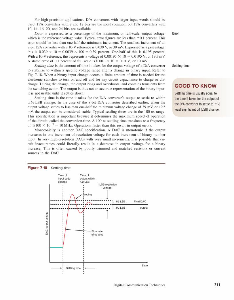
Digital Communication Techniques 211
For high-precision applications, D/A converters with larger input words should be
used. D/A converters with 8 and 12 bits are the most common, but D/A converters with
10, 14, 16, 20, and 24 bits are available.
Error is expressed as a percentage of the maximum, or full-scale, output voltage,
which is the reference voltage value. Typical error i gures are less than 60.1 percent. This
error should be less than one-half the minimum increment. The smallest increment of an
8-bit D/A converter with a 10-V reference is 0.039 V, or 39 mV. Expressed as a percentage,
this is 0.039 4 10 5 0.0039 3 100 5 0.39 percent. One-half of this is 0.195 percent.
With a 10-V reference, this represents a voltage of 0.00195 3 10 5 0.0195 V, or 19.5 mV. A stated error of 0.1 percent of full scale is 0.001 3 10 5 0.01 V, or 10 mV. Settling time is the amount of time it takes for the output voltage of a D/A converter to stabilize to within a specii c voltage range after a change in binary input. Refer to Fig. 7-18. When a binary input change occurs, a i nite amount of time is needed for the electronic switches to turn on and off and for any circuit capacitance to charge or dis-charge. During the change, the output rings and overshoots, and contains transients from the switching action. The output is thus not an accurate representation of the binary input; it is not usable until it settles down. Settling time is the time it takes for the D/A converter’s output to settle to within 61⁄2 LSB change. In the case of the 8-bit D/A converter described earlier, when the output voltage settles to less than one-half the minimum voltage change of 39 mV, or 19.5 mV, the output can be considered stable. Typical settling times are in the 100-ns range. This specii cation is important because it determines the maximum speed of operation of the circuit, called the conversion time. A 100-ns settling time translates to a frequency of 1/100 3 1029 5 10 MHz. Operations faster than this result in output errors. Monotonicity is another DAC specii cation. A DAC is monotonic if the output increases in one increment of resolution voltage for each increment of binary number input. In very high-resolution DACs with very small increments, it is possible that cir-cuit inaccuracies could literally result in a decrease in output voltage for a binary increase. This is often caused by poorly trimmed and matched resistors or current sources in the DAC.
Error
Settling time
DA
C o
utp
ut volta
ge
Settling time
Slow rate
of op amp
Time
Time of
input code
change1 LSB resolution
voltage
Time of
output within
1/2 LSB
1/2 LSB Final DAC
output1/2 LSB
Ringing
Figure 7-18 Settling time.
GOOD TO KNOW
Settling time is usually equal to
the time it takes for the output of
the D/A converter to settle to 61⁄2
least signifi cant bit (LSB) change.

212 Chapter 7
Figure 7-19 An S/H amplifier.
�
�
Analoginput
MOSFET
Op amp
S/Houtput
Storagecapacitor
Sample/trackHold/store
S/Hcontrol
Output
S/H control
Samplingpoint
Storedlevel
Analoginput
Sample/track
0 V
�V
Store/hold
Another specii cation is dc operating voltage and current. Older DACs operated from
15 V, but most of the newer ones operate from 3.3 or 2.5 V. A current consumption
i gure is also usually given.
Another consideration is how many DACs there are per chip. ICs with two, four, and
eight DACs per chip are available. In the multi-DAC chips, the binary input is serial.
Serial input is an option on most DACs today as the serial input greatly reduces the
number of pins devoted to input signals. A 16-bit parallel DAC has, of course, 16 input
pins. The same DAC with a serial input has only one input pin. Typical serial input formats
are the serial peripheral interface (SPI) or the I 2C interface common on most embedded
controllers and microprocessors.
The binary input voltage is also a specii cation. Older DACs used a TTL or CMOS
compatible 15 V input while newer chips use lower input signal voltages of 1.8, 2.5, or
3.3 V. High-speed DACs often use current mode logic (CML) inputs or low-voltage differential
signaling (LVDS) levels with a differential signal swing of only a few hundred millivolts.
The reference voltage is typically from 1 to 5 V from a temperature-compensated
zener diode which is usually on the DAC chip.
A/D Converters
A/D conversion begins with the process of sampling, which is usually carried out by a
sample-and-hold (S/H) circuit. The S/H circuit takes a precise measurement of the ana-
log voltage at specii ed intervals. The A/D converter (ADC) then converts this instanta-
neous value of voltage and translates it to a binary number.
S/H Circuits. A sample-and-hold (S/H) circuit, also called a track/store circuit, accepts
the analog input signal and passes it through, unchanged, during its sampling mode. In
the hold mode, the amplii er remembers or memorizes a particular voltage level at the
instant of sampling. The output of the S/H amplii er is a i xed dc level whose amplitude
is the value at the sampling time.
Fig. 7-19 is a simplii ed drawing of an S/H amplii er. The main element is a high-
gain dc differential op amp. The amplii er is connected as a follower with 100 percent
feedback. Any signal applied to the noninverting (1) input is passed through unaffected.
The amplii er has unity gain and no inversion.
A storage capacitor is connected across the very high input impedance of the ampli-
i er. The input signal is applied to the storage capacitor and the amplii er input through
a MOSFET gate. An enhancement mode MOSFET that acts as an on/off switch is
normally used. As long as the control signal to the gate of the MOSFET is held high,
Sample-and-hold (S/H) circuit (track/store circuit)

Digital Communication Techniques 213
the input signal will be connected to the op amp input and capacitor. When the gate is
high, the transistor turns on and acts as a very low-value resistor, connecting the input
signal to the amplii er. The charge on the capacitor follows the input signal. This is the
sample or track mode for the amplii er. The op amp output is equal to the input.
When the S/H control signal goes low, the transistor is cut off, but the charge on
the capacitor remains. The very high input impedance of the amplii er allows the capac-
itor to retain the charge for a relatively long time. The output of the S/H amplii er, then,
is the voltage value of the input signal at the instant of sampling, i.e., the point at which
the S/H control pulse switches from high (sample) to low (hold). The op amp output
voltage is applied to the A/D converter for conversion to a proportional binary number.
The primary benei t of an S/H amplii er is that it stores the analog voltage during
the sampling interval. In some high-frequency signals, the analog voltage may increase
or decrease during the sampling interval; this is undesirable because it confuses the A/D
converter and introduces what is referred to as aperture error. The S/H amplii er, however,
stores the voltage on the capacitor; with the voltage constant during the sampling inter-
val, quantizing is accurate.
There are many ways to translate an analog voltage to a binary number. The next
sections describe the most common ones.
Successive-Approximations Converters. This converter contains an 8-bit
successive-approximations register (SAR), as shown in Fig. 7-20. Special logic in the
register causes each bit to be turned on one at a time from MSB to LSB until the closest
binary value is stored in the register. The clock input signal sets the rate of turning the
bits off and on.
Assume that the SAR is initially reset to zero. When the conversion is started, the MSB
is turned on, producing 10 000 000 at the output and causing the D/A converter output to
go to half-scale. The D/A converter output is applied to the op amp, which applies it to the
comparator along with the analog input. If the D/A converter output is greater than the input,
the comparator signals the SAR to turn off the MSB. The next MSB is turned on. The D/A
converter output goes to the proportional analog value, which is again compared to the input.
If the D/A converter output is still greater than the input, the bit will be turned off; if the
D/A converter output is less than the input, the bit will be left at binary 1.
The next MSB is then turned on, and another comparison is made. The process
continues until all 8 bits have been turned on or off and eight comparisons have been
made. The output is a proportional 8-bit binary number. With a clock frequency of
Successive-approximations converter
Successive-approximations register (SAR)
Figure 7-20 Successive-approximations A/D converter.
DC ref
Rf
Binary
output
D/A converter��
Analog
input
Start
conversion
Comparator
Clock��
Successive
approximationsregister

214 Chapter 7
200 kHz, the clock period is 1/200 3 103 5 5 µs. Each bit decision is made during
the clock period. For eight comparisons at 5 µs each, the total conversion time is
8 3 5 5 40 µs.
Successive-approximations converters are fast and consistent. They are available
with conversion times from about 0.25 to 200 µs, and 8-, 10-, 12-, and 16-bit versions
are available. Conversion times are also expressed as megasamples per second (MSPS).
Successive-approximations converters with speeds to 5 MSPS are available.
Instead of using a D/A converter with an R-2R network, many newer successive-
approximations converters use capacitors instead of resistors in the weighting network.
The most difi cult part of making an integrated-circuit (IC) A/D or D/A converter is the
resistor network. It can be made with laser-trimmed thin-i lm resistors, but these require
very expensive processing steps in making the IC. Resistors also take up more space on
an IC than any other component. In A/D converters, the R-2R network takes up probably
10 or more times the space of all the rest of the circuitry. To eliminate these problems,
a capacitor network can be used to replace the resistor network. Capacitors are easy to
make and take up little space.
The basic concept of a capacitive network is shown in Fig. 7-21. This is a simple
3-bit D/A converter. Note that the capacitors have binary weights of C, C/2, and C/4.
The total capcitance of all capacitors in parallel is 2C. The actual capacitor values are
irrelevant since the capacitor ratios determine the outcome of the conversion. This fact
also makes it easy to make the IC, since precise capacitor values are not needed. Only
the ratio must be carefully controlled, and this is easier to do when making the IC than
with laser trimming resistors. The switches in this diagram represent MOSFET switches
in the actual circuit. A 3-bit successive-approximations register operates the switches
labeled S1 through S4.
To start the conversion, switches SC and Sin are closed, and switches S1 through
S4 connect Vi to the capacitors, which are in parallel at this time. The comparator is
shorted out temporarily. The input analog signal to be sampled and converted Vi is
applied to all capacitors, causing each to charge up to the current signal value. Next,
the SC and Sin switches are opened, storing the current value of the signal on the
capacitors. Since the capacitors store the input value at sampling time, no separate S/H
circuit is needed. The successive-approximations register and related circuitry switch
the reference voltage VREF to the various capacitors in a specii c sequence, and the
comparator looks at the resulting voltage at each step and makes a decision about
Figure 7-21 A switched-capacitor D/A converter used in newer successive-approximations A/D converters.
VREF
Bit 1
(MSB)
Bit 2 Bit 3
(LSB)
Comparator
Ctotal � 2C
S1
C
Vi
Sc
Sin
�
�
S2
C/2
S3
C/4
S4
C/4
A
GOOD TO KNOW
Resistors on integrated circuits
take up more space than other
components. To save space in IC
chip design, resistor networks
can be redesigned as capacitor
networks.

Digital Communication Techniques 215
whether a 0 or 1 results from the comparison at each step. For example, in the i rst
step S1 connects VREF to capacitor C, and all other capacitors are switched to ground
via S2 to S4. Capacitor C forms a voltage divider with all the other capacitors in par-
allel. The comparator looks at the junction of the capacitors (node A) and then outputs
a 0 or 1 depending upon the voltage. If the voltage at the junction is greater than the
comparator threshold (usually one-half of the supply voltage), a 0 bit appears at the
comparator output and is also stored in an output register. If the voltage at the junction
is less than the threshold, a 1 bit appears at the comparator output and is stored in the
output register. If a 1 bit occurs, capacitor C remains connected to VREF throughout
the remainder of the conversion.
The process continues by connecting the C/2 capacitor from ground to VREF, and
the comparison again takes place and another output bit is generated. This process
continues until all capacitor voltages have been compared. During this process, the initial
charges on the capacitors are redistributed according to the value of the input voltage.
The binary output appears in the successive-approximations register.
The circuit is easily expanded with more capacitors to produce a greater number of
output bits. Both positive and negative reference voltages can be used to accommodate
a bipolar input signal.
A switched-capacitor network makes the A/D converter very small. It can then be
easily integrated into other circuits. A typical case is an A/D converter integrated into a
microcontroller chip with memory.
Flash Converters. A l ash converter takes an entirely different approach to the A/D
conversion process. It uses a large resistive voltage divider and multiple analog
comparators. The number of comparators required is equal to 2N 2 1, where N is the
number of desired output bits. A 3-bit A/D converter requires 23 2 1 5 8 2 1 5 7
comparators (see Fig. 7-22).
The resistive voltage divider divides the dc reference voltage range into a num-
ber of equal increments. Each tap on the voltage divider is connected to a separate
analog comparator. All the other comparator inputs are connected together and driven
by the analog input voltage. Some comparators will be on and others will be off,
depending on the actual value of input voltage. The comparators operate in such a
way that if the analog input is greater than the reference voltage at the divider tap,
the comparator output will be binary 1. For example, if the analog input voltage in
Fig. 7-22 is 4.5 V, the outputs of comparators 4, 5, 6, and 7 will be binary 1. The
other comparator outputs will be binary 0. The encoder logic, which is a special
combinational logic circuit, converts the 7-bit input from the comparators to a 3-bit
binary output.
Successive-approximations converters generate their output voltage after the circuits
go through their decision-making process. The l ash converter, on the other hand, pro-duces a binary output almost instantaneously. Counters do not have to be incremented, and a sequence of bits in a register does not have to be turned on and off. Instead, the l ash converter produces an output as fast as the comparators can switch and the signals can be translated to binary levels by the logic circuits. Comparator switching and logic propagation delays are extremely short. Flash converters, therefore, are the fastest type of A/D converter. Conversion speeds of less than 100 ns are typical, and speeds of less than 0.5 ns are possible. Flash speeds are given in MSPS or gigasamples per second (GSPS) or 109 samples per second. Flash A/D converters are complicated and expensive because of the large number of analog comparators required for large binary numbers. The total number of comparators required is based upon the power of 2. An 8-bit l ash converter has 28 2 1 5 255 com parator circuits. Obviously, ICs requiring this many components are large and difi cult to make. They also consume much more power than a digital circuit because the comparators are linear circuits. Yet for high-speed conver-sions, they are the best choice. With the high speed they can achieve, high-frequency signals such as video signals can be easily digitized. Flash converters are available with output word lengths of 6, 8, and 10.
Flash converter

216 Chapter 7
Figure 7-22 A fl ash converter.
Encoder
logic
circuits
Binary
output
0
1
1
Analog
input
7 V
6 V
5 V
4 V
3 V
2 V
1 V
DC
ref
4
Comparators
�� 1
�� 2
�� 3
�� 4
�� 5
�� 6
�� 7
Example 7-3The voltage range of an A/D converter that uses 14-bit numbers is 26 to 16 V. Find
(a) the number of discrete levels (binary codes) that are represented, (b) the number of
voltage increments used to divide the total voltage range, and (c) the resolution of dig-
itization expressed as the smallest voltage increment.
a. 2N 5 214 5 16,384
b. 2N 2 1 5 16,384 2 1 5 16,383
c. The total voltage range is 26 to 16 V, or 12 V; thus,
Resolution 512
16,3835 0.7325 mV or 732.5 µV

Digital Communication Techniques 217
Pipelined Converters. A pipelined converter is one that uses two or more low-
resolution l ash converters to achieve higher speed and higher resolution than successive-approximations converters but less than a full l ash converter. High-resolution l ash converters with more than 8 bits are essentially impractical because the large number of comparators required makes the power consumption very high. However, it is possible to use several l ash converters with a smaller bit count to achieve very high conversion speeds and higher resolution. An example is the two-stage 8-bit pipeline converter shown in Fig. 7-23. The sampled analog input signal from a sample/hold (S/H) amplii er is applied to a 4-bit l ash converter that generates the 4 most signii cant bits. These bits are applied to a 4-bit DAC and converted back to analog. The DAC output signal is then subtracted from the original analog input signal in a differential amplii er. The residual analog signal represents the least signii cant part of the signal. It is amplii ed and applied to a second 4-bit l ash converter. Its output represents the 4 least signii cant bits of the output. With just two 4-bit l ash converters, only 30 comparators are needed to achieve an 8-bit resolution. Otherwise, it would take 255 comparators, as indicated earlier. The tradeoff here is lower speed. A pipelined converter is obviously slower because it has to undergo a two-step conversion, one in each l ash converter. However, the overall result is still very fast, much faster than that of any successive-approximations converter. This principle can be extended to three, four, or more pipeline stages to achieve resolutions of 12, 14, and 16-bits. Speeds as high as 10 GSPS are possible with this arrangement.
ADC Specifi cations
The key ADC specii cations are speed, resolution, dynamic range, signal-to-noise ratio, effective number of bits, and spurious free dynamic range. Speed is the fastest sampling rate the ADC can achieve. Lower rates may be used. Modern ADCs can sample at rates to 20 GSPS. Resolution is related to the number of bits. Resolution indicated the smallest input voltage that is recognized by the converter and is the reference voltage VREF divided by 2N, where N is the number of output bits. ADCs with resolutions of 8, 10, 12, 14, 16, 18, 20, 22, and 24 are used in a wide range of applications.
Figure 7-23 A two-stage 8-bit pipelined converter.
8-bit storage register
8-bit output
Analog input
from S/H amp
Least
significant
bits
Most
significant
bits
Differential
amp
Amplifier
�
�
4-bit
flash
4-bit
flash
4-bit
DAC

218 Chapter 7
Figure 7-24 Quantizing noise is the error resulting from the difference between the
input signal level and the available quantizing levels.
111
110
101
100
011
010
001
000
0
0
Dig
ita
l o
utp
ut
Quantizing
error
voltage
Input (V)
VREF VREF
8
VREF
4
3VREF
8
VREF
2
5VREF
8
3VREF
4
7VREF
8
1 LSB
1 LSB
Dynamic range is a measure of the range of input voltages that can be converted. It
is expressed as the ratio of the maximum input voltage to the minimum recognizable
voltage and converted to decibels. In any ADC, the minimum input voltage is simply the
value of the LSB voltage or 1. The maximum input is simply related to the maximum
output code or 2N 2 1, where N is the number of bits. Therefore, you can express the
dynamic range with the expression
dB 520 log 2N 2 1
1 or just 20 log(2N 2 1)
The dynamic range of a 12-bit converter then is
dB 5 20 log (212 2 1) 5 20 log (4096 2 1) 5 20 log 4095 5 72.24 dB
The greater the decibel value, the better. The signal-to-noise (S/N) ratio (SNR) plays a major part in the performance of an ADC. This is the ratio of the actual input signal voltage to the total noise in the system. The noise comes from a combination of clock-related noise, power supply ripple, external signal coupling, and quantizing noise. The clock noise can be minimized by locating clock wiring away from the ADC and minimizing jitter on the clock signal. Good bypassing on the power supply should take care of most ripple noise. Then shielding the converter will reduce signals coupled in by inductive or capacitive coupling. Quantizing noise is another matter altogether. It is the result of the conversion process itself and cannot be reduced beyond a certain point. Quantizing noise is an actual voltage that manifests itself as noise added to the analog input signal as the result of the error produced in converting an analog signal to its closest digital value. You can see this error if you plot it over the input voltage range, as shown in Fig. 7-24. This i gure is a plot showing the input voltage and the related output code in a simple 3-bit ADC. The 1-LSB resolution is VR/2N. Below the plot is the noise or error voltage. When the ADC input voltage is exactly equal to the voltage represented by each output code, the error is zero. But as the voltage difference between the actual input voltage and the voltage represented by the code becomes greater, the

Digital Communication Techniques 219
Figure 7-25 A frequency-domain plot of the quantizing noise and signal voltages.
0
dB
Frequency
Input
signal
(rms)
Noise
Average
(rms)
noise
voltage
SNR = �83 dB
10
20
30
40
50
60
70
80
90
�
�
�
�
�
�
�
�
�
error voltage increases. The result is a sawtoothlike error voltage that in effect becomes
noise added to the input signal. Luckily, the maximum noise peak is just 1 LSB, but that
can reduce the conversion accuracy depending upon the input signal level. Quantization
noise can be reduced by using a converter with a greater number of bits, as this reduces
the maximum noise represented by the LSB value.
Another way to show quantizing noise is given in Fig. 7-25. If you could take the
binary output of the ADC and convert it back to analog in a DAC and then show a
frequency-domain plot of the result, this is what you would see. The noise, which is mostly
quantizing noise, has multiple frequency components over a wide frequency range. The
large vertical line represents the analog input signal voltage being converted. This plot
also shows the signal-to-noise ratio in decibels. The rms value of the signal voltage and
the average rms value of the noise are used in computing the decibel value of the SNR.
A related specii cation is spurious free dynamic range (SFDR). See Fig. 7-26. It is
the ratio of the rms signal voltage to the voltage value of the highest “spur” expressed in
Spurious free dynamic range (SFDR)
Figure 7-26 SFDR is the dif erence between the signal voltage and highest spur
voltage.
0
10
20
30
40
50
60
70
80
90
65-dB SFDR
dB
Frequency
Signal
Highest “spur”
�
�
�
�
�
�
�
�
�

220 Chapter 7
decibels. A spur is any spurious or unwanted signal that may result from intermodulation
distortion. This is the formation of signals that are the result of mixing or modulation
action caused by any nonlinear characteristic of the converter circuitry, an amplii er, or
related circuit or component. The spurs are sums or differences between the various
signals present and their harmonics.
As you might suspect, any noise, harmonics, or spurious signals all add together and
basically reduce the resolution of an ADC. Often the combined noise level is greater
than the LSB value, so only those more signii cant bits really dei ne the signal amplitude.
This effect is expressed by a measure known as the effective number of bits (ENOB).
ENOB is computed with the expression
ENOB 5SINAD 2 1.76
6.02
SINAD is the ratio of the signal amplitude to all the noise plus harmonic distortion
in the circuit. SINAD in a totally noise- and distortion-free ADC is 6.02N 1 1.76, where
N is the number of bits of resolution. This is the best SINAD i gure possible, and it will
be less in a practical converter.
Example 7-4 1. Calculate the SINAD for a 12-bit converter.
2. Calculate the ENOB for a converter with a SINAD of 78 dB.
Solution
1. SINAD 5 6.02(12) 1 1.76 5 74 dB
2. ENOB 5 (78 2 1.76)y6.02 5 12.66 bits, or just 12 bits.
Sigma-Delta Converter. Another popular form of ADC is the sigma-delta (o¢)
converter. Also known as a delta-sigma or charge balance converter, this circuit provides
extreme precision, wide dynamic range, and low noise compared to other converters. It
is available with output word lengths of 18, 20, 22, and 24 bits. These converters are
widely used in digital audio applications, for example, CD, DVD, and MP3 players, as
well as in industrial and geophysical applications where low-speed sensor data is to be
captured and digitized. They are not designed for high speed, nor are they adaptable to
applications in which many separate channels must be multiplexed into one.
The o¢ converter is what is known as an oversampling converter. It uses a clock or
sampling frequency that is many times the minimum Nyquist rate required for other types
of converters. Conversion rates are typically 64 to 128 times or more the highest frequency
in the analog input signal. For example, assume a music signal with harmonics up to
24 kHz. A successive-approximations converter would have to sample this at a rate of two
or more times (more than 48 kHz) to avoid aliasing and loss of data. A o¢ converter
would use a clock or sampling rate in the 1.5- to 3-MHz range. Sampling rates of several
hundred times the highest input signal have been used. The reason for this is that the
quantizing noise is reduced by a factor equal to the square root of the oversampling ratio.
The higher the sampling frequency, the lower the noise and as a result the wider the
dynamic range. The oversampling techniques used in the sigma-delta converter essentially
translate the noise to a higher frequency that can be easily i ltered out by a low-pass i lter.
With a lower noise level, lower input levels can be converted, giving the converter extra
dynamic range. Remember, the dynamic range is the difference between the lowest and
the highest signal voltage levels that the converter can resolve, expressed in decibels. Of course,
Sigma-delta (o¢) converter
Oversampling converter

Digital Communication Techniques 221
the other benei t of this technique is that aliasing is no longer a big problem. Often only
a simple RC low-pass i lter is needed to provide adequate protection from aliasing effects.
Fig. 7-27 shows the basic o¢ circuit. The input is applied to a differential amplii er
that subtracts the output voltage of a 1-bit D/A converter from the input signal. This D/A
converter is driven by the comparator output. If the output is a binary 1, the D/A con-
verter outputs 11 V. If the comparator output is binary 0, the D/A converter outputs a 21 V. This sets the input voltage range to 11 V.
The output of the differential amplii er is averaged in an integrator. The integrator
output is compared to ground (0 V) in the comparator. The comparator is clocked by an
external clock oscillator so that the comparator produces one output bit decision for each
clock cycle. The resulting bit stream of binary 0s and 1s represents the varying analog
input signal. This serial bit stream is fed to a digital i lter or decimator that produces the
i nal binary output word.
As the input signal is applied, the o¢ converter produces a serial bit stream output
that represents the average value of the input. The closed-loop circuit causes the input
signal to be compared to the D/A converter output every clock cycle, resulting in a com-
parator decision that may or may not change the bit value or the D/A converter output.
If the input signal is increasing, the D/A converter will continually output binary 1s so
that the average in the integrator increases. If the input signal decreases, the comparator
switches to binary 0, forcing the D/A converter output to 21 V. What happens is that the
D/A converter output, averaged over many cycles, produces an output that equals the input
voltage. The closed loop continually tries to force the differential amplii er output to zero.
To clarify, consider the D/A converter output that switches between 11 and
21 V. If the output is all binary 1s or 11-V pulses, the average value at the D/A
converter output is just 11. If the D/A converter input is all binary 0s, then a series
of 21-V pulses occur, making the output average 21 V over many cycles. Now
assume that the D/A converter input is a series of alternating binary 0s and 1s.
Figure 7-27 A sigma-delta (©¢ ) converter.
Differential
amplifier
Digital filter
or
decimator
Parallel binary output
(18–24 bits)
Serial output
Integrator
Comparator
Serial bit
stream
Clock
�1 V
Vi
�
�
1-bit
D/A converter
�
�
�
�
�
�

222 Chapter 7
The D/A converter output is 11 V for one cycle and 21 V for the next cycle. The average over time is zero. Now you can see that with more binary 1s at the D/A converter input, the average output will rise above zero. With a stream of more binary 0s, the average will become negative. The density of the 0s or 1s determines the aver-age output value over time. The output of the comparator, then, is a bit stream that represents the average of the input value. It is a continuous nonbinary output. This serial bit stream is not very useful as is. Therefore, it is passed through a digital i lter called a decimator. This i lter uses digital signal processing (DSP) techniques that are beyond the scope of this book. But the overall effect of the i lter is to digitally average the serial bit stream and to produce multibit sequential output words that are in effect a rolling average of the input. The i lter or decimator produces binary outputs at some fraction of the clock rate. The overall result is as if the input signal were sampled at a much lower rate but with a very high-resolution converter. The true binary output words may be in serial or parallel form.
7-4 Pulse ModulationPulse modulation is the process of changing a binary pulse signal to represent the infor-mation to be transmitted. The primary benei ts of transmitting information by binary techniques arise from the great noise tolerance and the ability to regenerate the degraded signal. Any noise that gets added to the binary signal along the way is usually clipped off. Further, any distortion of the signal can be eliminated by reshaping the signal with a Schmitt trigger, comparator, or similar circuit. If information can be transmitted on a car-rier consisting of binary pulses, these aspects of binary techniques can be used to improve the quality of communications. Pulse modulation techniques were developed to take advantage of these qualities. The information signal, usually analog, is used to modify a binary (on/off) or pulsed carrier in some way. With pulse modulation the carrier is not transmitted continuously but in short bursts whose duration and amplitude correspond to the modulation. The duty cycle of the carrier is usually made short so that the carrier is off for a longer time than the bursts. This arrangement allows the average carrier power to remain low, even when high peak pow-ers are involved. For a given average power, the peak power pulses can travel a longer distance and more effectively overcome any noise in the system. There are four basic forms of pulse modulation: Pulse-amplitude modulation (PAM),
pulse-width modulation (PWM), pulse-position modulation (PPM), and pulse-code
modulation (PCM).
Comparing Pulse-Modulation Methods
Fig. 7-28 shows an analog modulating signal and the various waveforms produced by PAM, PWM, and PPM modulators. In all three cases, the analog signal is sampled, as it would be in A/D conversion. The sampling points are shown on the analog waveform. The sampling time interval t is constant and subject to the Nyquist conditions described earlier. The sampling rate of the analog signal must be at least two times the highest frequency component of the analog wave. The PAM signal in Fig. 7-28 is a series of constant-width pulses whose amplitudes vary in accordance with the analog signal. The pulses are usually narrow compared to the period of sampling; this means that the duty cycle is low. The PWM signal is binary in amplitude (has only two levels). The width or duration of the pulses varies according to the amplitude of the analog signal: At low analog voltages, the pulses are narrow; at the higher amplitudes, the pulses get wider. In PPM, the pulses change position according to the amplitude of the analog signal. The pulses are very narrow. These pulse signals may be transmitted in a baseband form, but in most applications they modulate a high-frequency radio carrier. They turn the carrier on and off in accordance with their shape.
Decimator
Pulse modulation
Pulse-amplitude modulation (PAM)

Digital Communication Techniques 223
Of the four types of pulse modulation, PAM is the simplest and least expensive to
implement. On the other hand, because the pulses vary in amplitude, they are far more
susceptible to noise, and clipping techniques to eliminate noise cannot be used because
they would also remove the modulation. PWM and PPM are binary and therefore clip-
ping can be used to reduce the noise level.
Although the techniques of pulse modulation have been known for decades, they are
no longer widely used. Of the three types, PWM is the most common. One example is for
remote-control purposes, e.g., in model airplanes, boats, and cars. Pulse-width modulation
(PWM) methods are also used in switch mode power supplies (dc-dc convertors, regulators,
etc.), motor speed control, as well as in class D audio switching power amplii ers.
Today pulse-modulation techniques have been largely superseded by more advanced
digital techniques such as pulse-code modulation (PCM), in which actual binary numbers
representing the digital data are transmitted.
Pulse-Code Modulation
The most widely used technique for digitizing information signals for electronic data
transmission is pulse-code modulation (PCM). PCM signals are serial digital data. There
are two ways to generate them. The more common is to use an S/H circuit and traditional
A/D converter to sample and convert the analog signal to a sequence of binary words,
convert the parallel binary words to serial form, and transmit the data serially, 1 bit at a
time. The second way is to use the delta modulator described earlier.
Pulse-code modulation (PAM)
Figure 7-28 Types of pulse modulation.
Analog
input
Samples
t
Sampling time t � 1
f
Constant width, varying amplitude pulses
PAM
PWM
PPM
Constant amplitude, varying width (duration) pulses
Constant amplitude, varying position pulses

224 Chapter 7
Figure 7-30 Timing signals for PCM.
1 2 3 4 5 6 7 8 1 2 3 4 5 6 7 8
1st word 2d word
Clock
Start
conversion
Serial data out of
shift register
Traditional PCM. In traditional PCM, the analog signal is sampled and converted to
a sequence of parallel binary words by an A/D converter. The parallel binary output word
is converted to a serial signal by a shift register (see Fig. 7-29). Each time a sample is
taken, an 8-bit word is generated by the A/D converter. This word must be transmitted
serially before another sample is taken and another binary word is generated. The clock
and start conversion signals are synchronized so that the resulting output signal is a
continuous train of binary words.
Fig. 7-30 shows the timing signals. The start conversion signal triggers the S/H to
hold the sampled value and starts the A/D converter. Once the conversion is complete,
the parallel word from the A/D converter is transferred to the shift register. The clock
pulses start shifting the data out 1 bit at a time. When one 8-bit word has been transmit-
ted, another conversion is initiated and the next word is transmitted. In Fig. 7-30, the
i rst word sent is 01010101; the second word is 00110011.
At the receiving end of the system, the serial data is shifted into a shift register (see
Fig. 7-31). The clock signal is derived from the data to ensure exact synchronization
with the transmitted data. (The process of clock recovery is discussed in Chap. 11.) Once
one 8-bit word is in the register, the D/A converter converts it to a proportional analog
output. Thus the analog signal is reconstructed one sample at a time as each binary word
representing a sample is converted to the corresponding analog value. The D/A converter
output is a stepped approximation of the original signal. This signal may be passed
through a low-pass i lter to smooth out the steps.
Companding. Companding is a process of signal compression and expansion that is
used to overcome problems of distortion and noise in the transmission of audio signals.
The range of voice amplitude levels in the telephone system is approximately 1000 : 1.
In other words, the largest-amplitude voice peak is approximately 1000 times the smallest
voice signal or 1000 : 1, representing a 60-dB range. If a quantizer with 1000 increments
Companding
Figure 7-29 Basic PCM system.
Analog
signalS/H A/D converter
Shift register
Clock
S/H circuit samples analog signal A/D converter converts samples to 8-bit parallel words
Shift register converts parallel data to serial
Serial digital signal
Start
conversion

Digital Communication Techniques 225
were used, very high-quality analog signal representation would be achieved. For example,
an A/D converter with a 10-bit word can represent 1024 individual levels. A 10-bit A/D
converter would provide excellent signal representation. If the maximum peak audio volt-
age were 1 V, the smallest voltage increment would be 1/1023 of this, or 0.9775 mV.
As it turns out, it is not necessary to use that many quantizing levels for voice, and
in most practical PCM systems, a 7- or 8-bit A/D converter is used for quantizing. One
popular format is to use an 8-bit code, where 7 bits represents 128 amplitude levels and
the eighth bit designates polarity (0 5 1, 1 5 2). Overall, this provides 255 levels;
one-half are positive, and one-half negative.
Although the analog voltage range of the typical voice signal is approximately
1000 : 1, lower-level signals predominate. Most conversations take place at a low level,
and the human ear is most sensitive in the low-amplitude range. Thus the upper end of
the quantizing scale is not often used.
Since most signals are low-level, quantizing error is relatively large. That is, small incre-
ments of quantization become a large percentage of the lower-level signal. This is a small
amount of the peak amplitude value, of course, but this fact is irrelevant when the signals
are low in amplitude. The increased quantizing error can produce garbled or distorted sound.
In addition to their potential for increasing quantizing error, low-level signals are sus-
ceptible to noise. Noise represents random spikes or voltage impulses added to the signal.
The result is static that interferes with the low-level signals and makes intelligibility difi cult.
Companding is the most common means of overcoming the problems of quantizing
error and noise. At the transmitting end of the system, the voice signal to be transmitted
is compressed; i.e., its dynamic range is decreased. The lower-level signals are empha-
sized, and the higher-level signals are deemphasized.
At the receiving end, the recovered signal is fed to an expander circuit that does the
opposite, deemphasizing the lower-level signals and emphasizing the higher-level signals,
thereby returning the transmitted signal to its original condition. Companding greatly
improves the quality of the transmitted signal.
Originally, companding circuits were analog, and the concept is most easily under-
stood when described in analog terms. One type of analog compression circuit is a non-
linear amplii er that amplii es lower-level signals more than it does upper-level signals.
Fig. 7-32 illustrates the companding process. The curve shows the relationship between
the input and output of the compander. At the lower input voltages, the gain of the ampli-
i er is high and produces high output voltages. As the input voltage increases, the curve
begins to l atten, producing proportionately lower gain. The nonlinear curve compresses the upper-level signals while bringing the lower-level signals to a higher amplitude. Such compression greatly reduces the dynamic range of the audio signal. Compression reduces the customary ratio of 1000 : 1 to approximately 60 : 1. The degree of compression can be controlled by careful design of the gain characteristics of the compression amplii er, in which case the 60-dB voice range can be reduced to more like 36 dB. In addition to minimizing quantizing error and the effects of noise, compression lowers the dynamic range so that fewer binary bits are required to digitize the audio signal. A 64 : 1 voltage ratio could be easily implemented with a 6-bit A/D converter, but in practice, a 7-bit A/D converter is used.
Figure 7-31 PCM to analog translation at the receiver.
D/A converterAnalog signal out
Serial
datain
Shift registerClock
GOOD TO KNOW
Companding is the most common
means of overcoming the prob-
lems of quantizing error and
noise.
GOOD TO KNOW
The most widely used technique
for digitizing information signals
for electronic data transmission is
pulse-code modulation (PCM).

226 Chapter 7
Example 7-5The input voltage of a compander with a maximum voltage range of 1 V and a µ of
255 is 0.25. What are the output voltage and gain?
Vout 5Vm ln (1 1 µVin / Vm)
ln (1 1 µ)
Vout 51 ln [1 1 255(0.25)/1]
ln (1 1 255)5
ln 64.75
ln 2565
4.17
5.555 0.75 V
Gain 5Vout
Vin
50.75
0.255 3
Two basic types of companding are used in telephone systems: the µ-law (pro-
nounced “mu law”) compander and the A-law compander. The two companders differ
slightly in their compression and expansion curves. The µ-law compander is used in
telephone systems in the United States and Japan, and the A-law compander is used in
European telephone networks. The two are incompatible, but conversion circuits have
been developed to convert µ-law to A-law and vice versa. According to international
telecommunication regulations, users of µ-law companders are responsible for the
conversions. The voltage formulas for both are as follows:
µ-law: Vout 5Vm ln (1 1 µVin / Vm)
ln (1 1 µ)
A-law: Vout 51 1 ln (AVin / Vm)
1 1 ln A
where Vout 5 output voltage Vm 5 maximum possible input voltage Vin 5 instantaneous value of input voltage
The value of µ is usually 255; A is usually 87.6.
µ-law compander
A-law compander
Figure 7-32 Compression and expansion curves.
Outputvoltage
�
Compression(transmit)
Inputvoltage
� �Inputvoltage
Expansion(receive)
�
Outputvoltage
Vm ln(1 � �Vin /Vm)
ln(1 � �)Vout �

Digital Communication Techniques 227
As the examples show, the gain of a compander is higher at the lower input voltages
than at the higher input voltages.
Older companding circuits used analog methods such as the nonlinear amplii ers
described earlier. Today, most companding is digital. One method is to use a nonlinear
A/D converter. These converters provide a greater number of quantizing steps at the
lower levels than at the higher levels, providing compression. On the receiving end, a
matching nonlinear D/A converter is used to provide the opposite compensating expan-
sion effect. Compression can also be accomplished by digitizing the signal in a linear
ADC and then using an appropriate algorithm to compute the companded digital output
in an embedded microcontroller.
Codecs and Vocoders. Both ends of the communication link in telephone systems
have transmitting and receiving capability. All A/D and D/A conversion and related func-
tions such as serial-to-parallel and parallel-to-serial conversion as well as companding
are usually taken care of by a single large-scale IC chip known as a codec or vocoder.
One codec is used at each end of the communication channel. Codecs are usually com-
bined with digital multiplexers and demultiplexers; clock and synchronizing circuits
complete the system. These elements are discussed in Chap. 10.
Fig. 7-33 is a simplii ed block diagram of a codec. The analog input is sampled by the
S/H amplii er at an 8-kHz rate. The samples are quantized by the successive-approximations
Codec
Vocoder
Example 7-6The input to the compander of Example 7-5 is 0.8 V. What are the output voltage
and gain?
Vout 5Vm ln (1 1 µVin / Vm)
ln (1 1 µ)
Vout 51 ln 31 1 255(0.8) 4 /1
ln (1 1 255)5
ln 205
ln 2565
5.32
5.555 1.02 V
Gain 5Vout
Vin
50.96
0.85 1.2
Figure 7-33 Simplifi ed block diagram of an IC codec.
Successive-approximations
compandingADC
Shiftregister
CompandingDAC
Shiftregister
Analoginput
Serial digitaldata output
S/Hamplifier
8-bitparalleldata
Clock
Clock
Bufferamplifier
Analogoutput
Serial digital data input
CODEC

228 Chapter 7
Figure 7-34 Concept of digital signal processing.
Program
ROM
(holdsprocessing
algorithm
program)
D/A converterA/D converterAnalog
output
DSP
micro-
processor
Analog
signal
Digital
dataoutput
Data
RAM
type of A/D converter. Compression is done digitally in the A/D converter. The parallel A/D
converter output is sent to a shift register to create the serial data output, which usually goes
to one input of a digital multiplexer.
The serial digital input is generally derived from a digital demultiplexer. The clock
shifts the binary words representing the voice into a shift register for serial-to- parallel
conversion. The 8-bit parallel word is sent to the D/A converter, which has built-in
digital expansion. The analog output is then buffered, and it may be i ltered externally.
Most vocoders are made with a complementary metal-oxide semiconductor (CMOS)
circuits and are part of large chips used in telephone (wired and cellular) systems.
7-5 Digital Signal ProcessingAs previous chapters have emphasized, communication involves a great deal of signal
processing. To carry out communication, analog signals must be processed in some way;
e.g., they may be amplii ed or attenuated. Often they must be i ltered to remove undesirable
frequency components. They must be shifted in phase and modulated or demodulated.
Or they may have to be mixed, compared, or analyzed to determine their frequency
components. Thousands of circuits have been devised to process analog signals, and
many have been described in this book.
Although analog signals are still widely processed by analog circuits, increasingly they
are being converted to digital for transmission and processing. As described earlier in this
chapter, there are several important advantages to transmitting and using data in digital form.
One advantage is that signals can now be manipulated by digital signal processing (DSP).
The Basis of DSP
DSP is the use of a fast digital computer or digital circuitry to perform processing on
digital signals. Any digital computer with sufi cient speed and memory can be used for
DSP. The superfast 32-bit and 64-bit reduced-instruction-set computing (RISC) proces-
sors are especially adept at DSP. However, DSP is most often implemented with proces-
sors developed specii cally for this application because they differ in organization and
operation from traditional microprocessors.
The basic DSP technique is shown in Fig. 7-34. An analog signal to be processed is
fed to an A/D converter, where it is converted to a sequence of binary numbers which
Digital signal processing (DSP)

Digital Communication Techniques 229
are stored in a read/write random-access memory (RAM). (See Fig. 7-35.) A program,
usually stored in a read-only memory (ROM), performs mathematical and other manipu-
lations on the data. Most digital processing involves complex mathematical algorithms
that are executed in real time; i.e., the output is produced simultaneously with the occur-
rence of the input. With real-time processing, the processor must be extremely fast so that
it can perform all the computations on the samples before the next sample comes along.
The processing results in another set of data words that may or may not be stored
in RAM. They can then be used or transmitted in digital form, or they may be fed
to a D/A converter where they are converted back to an analog signal. The output
analog signal then looks as though it has undergone processing by an equivalent
analog circuit.
Almost any processing operation that can be done with analog circuits can also be
done with DSP. The most common is i ltering, but equalization, companding, phase
shifting, mixing, signal generation, modulation, and demodulation can also be pro-
grammed on a DSP computer.
DSP Processors
When DSP was i rst developed during the 1960s, only the largest and fastest mainframe
computers were able to handle it, and even then, in some applications real-time process-
ing could not be achieved. As computers got faster, more sophisticated processing could
be performed, and in real time.
With the appearance of fast 16- and 32-bit microprocessors, the use of DSP became
practical for many applications, and i nally in the 1980s special microprocessors opti-
mized for DSP were developed. DSP is also widely implemented by dedicated digital
logic circuits or in an FPGA.
Most computers and microprocessors use an organization known as the Von Neumann
architecture. Physicist John Von Neumann is generally credited with creating the stored
program concept that is the basis of operation of all digital computers. Binary words
representing computer instructions are stored sequentially in a memory to form a pro-
gram. The instructions are fetched and executed one at a time at high speed. The program
usually processes data in the form of binary numbers that are stored in the same memory.
The key feature of the Von Neumann arrangement is that both instructions and data are
stored in a common memory space. That memory space may be read/write RAM or
ROM or some combination thereof. But the important point is that there is only one path
between the memory and the CPU, and therefore only one data or instruction word can
be accessed at a time. This has the effect of greatly limiting execution speed. This short-
coming is generally referred to as the Von Neumann bottleneck. Von Neumann bottleneck
Figure 7-35 Converting the analog signal to binary data in RAM to be operated upon by the DSP processor.
A/D converter
1
2
34
5 6
7
8
910 11
Analog signal
Samples at regular intervals
RAM
1 0 1 1 0 1 0 1 1
1 0 0 0 1 0 1 0 2
0 1 1 0 1 0 1 1 3
0 1 1 0 1 0 1 1 4
1 0 1 1 1 1 1 1 5
0 1 0 0 0 0 0 0 6
1 0 1 1 0 1 0 0 7
1 0 0 1 0 1 1 1 8
0 0 0 0 1 0 0 0 9
0 0 0 0 1 0 0 0 10
0 0 0 0 0 1 1 1 11

230 Chapter 7
DSP microprocessors work in a similar way, but they use a variation called the
Harvard architecture. In a Harvard architecture microprocessor, there are two memories,
a program or instruction memory, usually a ROM, and a data memory, which is a RAM.
Also, there are two data paths into and out of the CPU between the memories. Because
both instructions and data can be accessed simultaneously, very high-speed operation
is possible.
DSP microprocessors are designed to perform the math operations common to DSP.
Most DSP is a combination of multiplication and addition or accumulation operations
on the data words developed by the A/D converter and stored in RAM. DSP processors
carry out addition and multiplication faster than any other type of CPU, and most com-
bine these operations in a single instruction for even greater speed. DSP CPUs contain
two or more multiply and accumulate (MAC) processors.
DSP microprocessors are designed to operate at the highest speeds possible. Clock
speeds over 100 MHz are common, and DSP chips with clock rates as high as 1 GHz
are now being used. Some DSP processors are available as just the CPU chip, but others
combine the CPU with data RAM and a program ROM on chip. Some even include the
A/D and D/A converter circuits. If the desired processing program is written and stored
in ROM, a complete single-chip DSP circuit can be created for customized analog signal
processing by digital techniques. Many conventional embedded (core) processors such
as the ARM, MIPS, and Power PC now have special DSP instructions such as the MAC
operation built in.
Finally, many DSP circuits are embedded or dedicated. Instead of being programmed
in a general-purpose DSP, they are made of logic hardwired to perform only the desired
i ltering or other function. Field programmable logic arrays (FPGAs) are also widely
used to implement custom DSP.
DSP Applications
Filtering. The most common DSP application is i ltering. A DSP processor can be
programmed to perform bandpass, low-pass, high-pass, and band-reject i lter operations.
With DSP, the i lters can have characteristics far superior to those of equivalent analog
i lters: Selectivity can be better, and the passband or reject band can be customized to
the application. Further, the phase response of the i lter can be controlled more easily
than with analog i lters.
Compression. Data compression is a process that reduces the number of binary words
needed to represent a given analog signal. It is often necessary to convert a video analog
signal to digital for storage and processing. Digitizing a video signal with an A/D
converter produces an immense amount of binary data. If the video signal contains fre-
quencies up to 4 MHz, the A/D converter must sample at 8 MHz or faster. Assuming a
sampling rate of 8 MHz with an 8-bit A/D converter, 8 Mbytes/s will be produced.
Digitizing 1 min of video is equal to 60 s 3 8 Mbytes, or 480 Mbytes of data. This
amount of data requires a massive amount of RAM, although a hard disk could store
this data. In terms of data communication, it would take a great deal of time to transmit
this amount of data serially.
To solve this problem, the data is compressed. Numerous algorithms have been
developed to compress data. Examples are MPEG-2 and MPEG-4, widely used in digi-
tal photography and video. The data is examined for redundancy and other characteris-
tics, and a new group of data, based upon various mathematical operations, is created.
Data can be compressed by a factor of up to 100; in other words, the compressed data
is 1/100 its original size. With compression, 480 Mbytes of data becomes 4.8 Mbytes.
This is still a lot, but it is now within the capabilities of standard RAM and disk storage
components. Audio data is also compressed. An example is MP3, the algorithm used in
portable music players. Compression is also widely used in cell phones for voice mini-
mization storage and transmit time.
Harvard architecture
Filtering
Compression
GOOD TO KNOW
DSP microprocessors are
designed to operate at the highest
speeds possible. Speeds up to
1 GHz are not uncommon.

Digital Communication Techniques 231
A DSP chip does the compression on the data received from the A/D converter. The
compressed version of the data is then stored or transmitted. In the case of data com-
munication, compression greatly reduces the time needed to transmit data.
When the data is needed, it must be decompressed. A reverse-calculation DSP algorithm
is used to reconstruct the original data. Again, a special DSP chip is used for this purpose.
Spectrum Analysis. Spectrum analysis is the process of examining a signal to
determine its frequency content. Recall that all nonsinusoidal signals are a combina-
tion of a fundamental sine wave to which have been added harmonic sine waves of
different frequency, amplitude, and phase. An algorithm known as the discrete Fourier
transform (DFT) can be used in a DSP processor or FPGA to analyze the frequency
content of an input signal. The analog input signal is converted to a block of digital
data, which is then processed by the DFT program. The result is a frequency-domain
output that indicates the content of the signal in terms of sine wave frequencies,
amplitudes, and phases.
The DFT is a complex program that is long and time-consuming to run. In general,
computers are not fast enough to perform DFT in real time as the signal occurs.
Therefore, a special version of the algorithm has been developed to speed up the
calculation. Known as the fast Fourier transform (FFT), it permits real-time signal
spectrum analysis.
Other Applications. As mentioned, DSP can do almost everything analog circuits
can do, e.g., phase shifting, equalization, and signal averaging. Signal averaging is the
process of sampling a recurring analog signal which is transmitted in the presence of
noise. If the signal is repeatedly converted to digital and the mathematical average of the
samples is taken, the signal-to-noise ratio is greatly improved. Since the noise is random,
an average of it tends to be zero. The signal, which is constant and unchanging, averages
into a noise-free version of itself.
DSP can also be used for signal synthesis. Waveforms of any shape or character-
istics can be stored as digital bit patterns in a memory. Then when it is necessary to
generate a signal with a specii c shape, the bit pattern is called up and transmitted to
the DAC, which generates the analog version. This type of technique is used in voice
and music synthesis.
Modulation, mixing, and demodulation are also easy to implement in DSP.
DSP is widely used in CD players, modems, all cell phones, and a variety of other
common electronic products. Its use in communication is increasing as DSP processors
become even faster. Some fast DSP processors have been used to perform all the normal
communication receiver functions from the IF stages through signal recovery. All-digital
or software-dei ned radios (SDRs) are a reality now.
How DSP Works
The advanced mathematical techniques used in DSP are beyond the scope of this book
and certainly beyond the knowledge required of electronics engineers and technicians
in their jobs. For the most part, it is sufi cient to know that the techniques exist. How-
ever, without getting bogged down in the math, it is possible to give some insight into
the workings of a DSP circuit. For example, it is relatively easy to visualize the digi-
tizing of an analog signal into a block of sequential binary words representing the
amplitudes of the samples, and then to imagine that the binary words representing the
analog signal are stored in a RAM (see Fig. 7-35). Once the signal is in digital form,
it can be processed in many different ways. Two common applications are i ltering and
spectrum analysis.
Filter Applications. One of the most popular DSP i lters is called a i nite impulse
response (FIR) i lter. It is also called a nonrecursive i lter. (A nonrecursive i lter is one
whose output is only a function of the sum of products of the current input samples.)
Spectrum analysis
Discrete Fourier transform (DFT)
Fast Fourier transform (FFT)
Software-defi ned radios (SDRs)
Finite impulse response (FIR) fi lter or nonrecursive fi lter

232 Chapter 7
A program can be written to create a low-pass, high-pass, bandpass, or band-reject i lter of the FIR type. The algorithm of such a i lter has the mathematical form Y 5 oai bi. In this expression, Y is the binary output, which is the summation (o) of the products of a and b. The terms a and b represent the binary samples, and i is the number of the sample. Usually these samples are multiplied by coefi cients appropriate to the type of i lter, and the results summed. Fig. 7-36 is a graphical representation of what goes on inside the i lter. The term X(n), where n is the number of the sample, represents the input data samples from RAM. The boxes labeled Delay represent delay lines. (A delay line is a circuit that delays a signal or sample by some constant time interval.) In reality, nothing is being delayed. Rather, the circuit generates samples that occur one after another at a i xed time interval equal to the sampling time, which is a function of the A/D converter clock frequency. In effect, the outputs of the delay boxes in Fig. 7-36 are the sequential samples that occur one after another at the sampling rate that is equivalent to a series of delays. Note that the samples are multiplied by some constant represented by the term hn. These constants, or coefi cients, are determined by the algorithm and the type of i lter desired. After the samples have been multiplied by the appropriate coefi cient, they are summed. The i rst two samples are added, this sum is added to the next-multiplied sample, that sum is added to the next sample, and so on. The result is the output Y, which is a value made up of the sum of products of the other samples. The DSP solves the equation: y(n) 5 hoxo 1 h1x1 1 h2x2 1 . . . . The x samples come from the A/D converter. The h values are constants or coefi cients that dei ne the function (i ltering in this case) to be performed. Designing DSP software is essentially i guring out what the constants should be. These new data samples are also stored in RAM. This block of new data is sent to the D/A converter at whose output the i ltered ana-log signal appears. The decimation circuit in the ©¢ converter discussed earlier is a type of FIR i lter. Another type of DSP i lter is the ini nite impulse response (IIR) i lter, a recursive i lter that uses feedback: Each new output sample is calculated by using both the current output and past samples (inputs).
DIT/FFT. As indicated earlier, a DSP processor can perform spectrum analysis by using the discrete or fast Fourier transform (FFT). Fig. 7-37 illustrates the processing that takes place with FFT. It is called a decimation in time (DIT). The x(n) values at the input are the samples, which are processed in three stages. In the i rst stage, a so-called butterl y operation is performed on pairs of samples. Some of the samples are multiplied by a constant and then added. At the second stage, some of the outputs are multiplied by constants, and new pairs of sums, called groups, are formed. Then a similar process is performed to create the i nal outputs, called stages. These outputs are converted to new values that can be plotted in the frequency domain.
Delay line
Infi nite impulse response (IIR) fi lter
Decimation in time (DIT)
Group
Stage
Figure 7-36 A block diagram showing the processing algorithm of a nonrecursive
FIR fi lter.
Delayx(n)
� h0 � h1 � h2 � hN�2 � hN�1
y(n)
N-tap filter
Delay Delay

Digital Communication Techniques 233
In the graph in Fig. 7-38, the horizontal axis in the left-hand plot is frequency,
and the vertical axis is the amplitude of the dc and ac sine wave components that
make up the sampled wave. A 0 frequency component is represented by a vertical line
indicating the dc component of a signal. The 1 indicates the amplitude of the funda-
mental sine wave making up the signal. The other values, at 2, 3, 4, and so on, are
the amplitudes of the harmonics. In the right-hand plot, the phase angle of the sine
waves is given for each harmonic. A negative value indicates phase inversion of
the sine wave (180°).
� � �x(0) X(0)
� � �x(4) X(1)
� � �x(2) X(2)
� � �x(6) X(3)
� � �x(1) X(4)
� � �x(5) X(5)
� � �x(3) X(6)
� � �x(7) X(7)
�
WN0
�
WN0
�
�
WN0
�
WN1
�
WN2
�
WN3
�
WN0
�
WN2
�
WN0
�
�
WN0
Butterfly Group Stage
�
�
�
�
�
�
�
�
�
�
�
�
Stage 1 Stage 2 Stage 3
WN0
WN2
Figure 7-37 The fast Fourier transform decimation in time.
Frequency
�180°
�135°
�90°
�45°
0°
�45°
�90°
�135°
�180°
1 2 3
4
5 6 7
�135°
�45°
�90°
Phase
Frequency
Frequency
Am
plit
ude
0 1 2 3 4 5 6
Figure 7-38 Output plot of an FFT spectrum analysis.

234 Chapter 7
CHAPTER REVIEW
Online Activity
7-1 Exploring DSP
Objective: Delve deeper into the processes of DSP.
Procedure:
1. Do an online search with Google, Yahoo, Bing, or other
search engine on the DSP processes for i ltering, mod-
ulation, and signal generation.
2. Do a library, bookstore, or other search for textbooks
on DSP.
3. Focus on and answer the questions below.
Questions:
1. Draw a simplii ed block diagram similar to that in
Fig. 7-36 showing the basic operations of an IIR i lter. How is it different from the FIR i lter?
2. In what application would an IIR i lter be more appropriate to use than a FIR i lter?
3. What is equalization, and how is it implemented in DSP? 4. Explain how to generate a sine wave signal using DSP
techniques. 5. What is the algorithm for performing amplitude
modulation in DSP? AM demodulation? 6. What is one algorithm for performing frequency
modulation in DSP?
1. Name the four primary benei ts of using digital tech-niques in communication. Which of these is probably the most important?
2. What is data conversion? Name two basic types. 3. What is the name given to the process of measuring the
value of an analog signal at some point in time? 4. What is the name given to the process of assigning a
specii c binary number to an instantaneous value on an analog signal?
5. What is another name commonly used for A/D conversion?
6. Describe the nature of the signals and information obtained when an analog signal is converted to digital form.
7. Describe the nature of the output waveform obtained from a D/A converter.
8. Name the four major components in a D/A converter. 9. Dei ne aliasing and explain its effect in an A/D
converter. 10. What types of circuits are commonly used to translate
the current output from a D/A converter to a voltage output?
11. Name three types of A/D converters, and state which is the most widely used.
12. What A/D converter circuit sequentially turns the bits of the output on one at a time in sequence from MSB to LSB in seeking a voltage level equal to the input volt-age level?
13. What is the fastest type of A/D converter? Briel y de-scribe the method of conversion used.
14. Dei ne oversampling and undersampling. 15. What circuit is normally used to perform serial-to-
parallel and parallel-to-serial data conversion? What is the abbreviation for this process?
16. What circuit performs the sampling operation prior to A/D conversion, and why is it so important?
17. Where are sigma-delta converters used? Why? 18. Undersampling produces an aliasing effect that is
equivalent to what analog signal process? 19. What is the name given to the process of compressing
the dynamic range of an analog signal at the transmitter and expanding it later at the receiver?
20. What is the general mathematical shape of a compand-ing curve?
21. Name the three basic types of pulse modulation. Which type is not binary?
22. Name the DAC that produces a voltage output. 23. What type of DAC is used for very high-speed conversions? 24. True or false? ADC outputs or DAC inputs may be
either parallel or serial. 25. What type of ADC is faster than a successive-approxi-
mations converter but slower than a l ash converter? 26. Which type of ADC gives the best resolution? 27. Why are capacitor D/A converters preferred over R-2R
D/A converters? 28. What does oversampling mean? What converter uses
this technique? Why is it used? 29. How is aliasing prevented? 30. Name two common noncommunication applications
for PWM. 31. Describe briel y the techniques known as digital signal
processing (DSP). 32. What types of circuits perform DSP? 33. Briel y describe the basic mathematical process used in
the implementation of DSP. 34. Give the names for the basic architecture of non-DSP
microprocessors and for the architecture normally used
Questions

Digital Communication Techniques 235
1. A video signal contains light variations that change at a
frequency as high as 3.5 MHz. What is the minimum
sampling frequency for A/D conversion? ◆
2. A D/A converter has a 12-bit binary input. The output
analog voltage range is 0 to 5 V. How many discrete
output voltage increments are there and what is the
smallest voltage increment?
3. Compute the alias created by sampling a 5-kHz signal
at 8 kHz. ◆
4. Calculate the quantizing noise on a 14-bit A/D converter
with a voltage range up to 3 V.
5. What is the SINAD for a 15-bit ADC? ◆
6. Calculate the ENOB for a converter with a SINAD of
83 dB.
7. Calculate the spectrum of a 100-MHz signal with a
bandwidth of 16 MHz that is sampled at 40 MHz.
What is the optimum sampling rate?
◆ Answers to Selected Problems follow Chap. 22.
Problems
in DSP microprocessors. Briel y describe the difference
between the two.
35. Name i ve common processing operations that take
place with DSP. What is probably the most commonly
implemented DSP application?
36. Briel y describe the nature of the output of a DSP
processor that performs the discrete Fourier transform
or the fast Fourier transform.
37. Name the two types of i lters implemented with DSP
and explain how they differ.
38. What useful function is performed by an FFT
computation?
1. List three major types of communication services that are
not yet digital but could eventually be, and explain how
digital techniques could be applied to those applications.
2. Explain how an all-digital receiver would process the
signal of an analog AM radio broadcast signal.
3. What type of A/D converter would work best for video
signals with a frequency content up to 5 MHz? Why?
4. Under what conditions can serial data transfers be
faster than parallel data transfers?
Critical Thinking

236
chapter
Radio Transmitters
8
A radio transmitter takes the information to be communicated and con-
verts it to an electronic signal compatible with the communication medium.
Typically this process involves carrier generation, modulation, and power
amplifi cation. The signal is then fed by wire, coaxial cable, or waveguide
to an antenna that launches it into free space. This chapter covers trans-
mitter confi gurations and the circuits commonly used in radio transmitters,
including oscillators, amplifi ers, frequency multipliers, and impedance-
matching networks.
Objectives
After completing this chapter, you will be able to:
■ Calculate the frequency tolerance of crystal oscillators in percent
and in parts per million (ppm).
■ Discuss the operation of phase-locked loop (PLL) and direct digital
synthesis (DDS) frequency synthesizers, and explain how the output
frequency is changed.
■ Calculate the output frequency of a transmitter given the oscillator
frequency and the number and types of multipliers.
■ Explain the biasing and operation of class A, AB, and C power
amplifi ers using transistors.
■ Discuss the operation and benefi ts of class D, E, and F switching
amplifi ers, and explain why they are more ei cient.
■ Explain the operation and benefi ts of feedforward, digital
predistortion, Doherty, envelope tracking, and GaN power amplifi ers.
■ Explain the basic design of L, π , and T-type LC circuits, and discuss
how they are used for impedance matching.
■ Explain the use of transformers and baluns in impedance matching.

Radio Transmitters 237
8-1 Transmitter FundamentalsThe transmitter is the electronic unit that accepts the information signal to be trans mitted
and converts it to an RF signal capable of being transmitted over long distances. Every
transmitter has four basic requirements.
1. It must generate a carrier signal of the correct frequency at a desired point in the
spectrum.
2. It must provide some form of modulation that causes the information signal to modify
the carrier signal.
3. It must provide sufi cient power amplii cation to ensure that the signal level is high
enough to carry over the desired distance.
4. It must provide circuits that match the impedance of the power amplii er to that of
the antenna for maximum transfer of power.
Transmitter Confi gurations
The simplest transmitter is a single-transistor oscillator connected directly to an antenna.
The oscillator generates the carrier and can be switched off and on by a telegraph key to
produce the dots and dashes of the International Morse code. Information transmitted
in this way is referred to as continuous-wave (CW) transmission. Such a transmitter is
rarely used today, for the Morse code is nearly extinct and the oscillator power is too
low for reliable communication. Nowadays transmitters such as this are built only by
amateur (ham) radio operators for what is called QRP or low-power operation for per-
sonal hobby communication.
The CW transmitter can be greatly improved by simply adding a power amplii er to
it, as illustrated in Fig. 8-1. The oscillator is still keyed off and on to produce dots and
dashes, and the amplii er increases the power level of the signal. The result is a stronger
signal that carries farther and produces more reliable transmission.
The basic oscillator-amplii er combination shown in Fig. 8-1 is the basis for virtually
all radio transmitters. Many other circuits are added depending on the type of modulation
used, the power level, and other considerations.
High-Level AM Transmitters. Fig. 8-2 shows an AM transmitter using high-level
modulation. An oscillator, in most applications a crystal oscillator, generates the i nal
carrier frequency. The carrier signal is then fed to a buffer amplii er whose primary
purpose is to isolate the oscillator from the remaining power amplii er stages. The buf-
fer amplii er usually operates at the class A level and provides a modest increase in
power output. The main purpose of the buffer amplii er is simply to prevent load changes
Transmitter
Continuous-wave (CW) transmission
Figure 8-1 A more powerful CW transmitter.
Key
Crystal
Antenna
Poweramplifier
Oscillator

238 Chapter 8
in the power amplii er stages or in the antenna from causing frequency variations in the
oscillator.
The signal from the buffer amplii er is applied to a class C driver amplii er designed
to provide an intermediate level of power amplii cation. The purpose of this circuit is to
generate sufi cient output power to drive the i nal power amplii er stage. The i nal power
amplii er, normally just referred to as the i nal, also operates at the class C level at very
high power. The actual amount of power depends on the application. For example, in a
CB transmitter, the power input is only 5 W. However, AM radio stations operate at much
higher powers — say, 250, 500, 1000, 5000, or 50,000 W — and the video transmitter at
a TV station operates at even higher power levels. Cell phone base stations operate at
the 30- to 40-W level.
All the RF circuits in the transmitter are usually solid-state; i.e., they are imple-
mented with either bipolar transistors or metal-oxide semiconductor i eld-effect transis-
tors (MOSFETs). Although bipolar transistors are by far the most common type, the use
of MOSFETs is increasing because they are now capable of handling high power at high
frequencies. Transistors are also typically used in the i nal as long as the power level
does not exceed several hundred watts. Individual RF power transistors can handle up
to about 800 W. Many of these can be connected in parallel or in push-pull coni gura-
tions to increase the power-handling capability to many kilowatts. For higher power
levels, vacuum tubes are still used in some transmitters, but rarely in new designs. Vac-
uum tubes function into the VHF and UHF ranges, with power levels of 1 kW or more.
Now, assume that the AM transmitter shown in Fig. 8-2 is a voice transmitter. The input
from the microphone is applied to a low-level class A audio amplii er, which boosts the
small signal from the microphone to a higher voltage level. (One or more stages of ampli-
i cation could be used.) The voice signal is then fed to some form of speech-processing
(i ltering and amplitude control) circuit. The i ltering ensures that only voice frequencies in
a certain range are passed, which helps to minimize the bandwidth occupied by the signal.
Most communication transmitters limit the voice frequency to the 300- to 3000-Hz range,
which is adequate for intelligible communication. However, AM broadcast stations offer
higher i delity and allow frequencies up to 5 kHz to be used. In practice, many AM stations
modulate with frequencies up to 7.5 kHz, and even 10 kHz, since the FCC uses alternate
channel assignments within a given region and the outer sidebands are very weak, so no
adjacent channel interference occurs.
Final power amplifi er
Speech processing
Figure 8-2 An AM transmitter using high-level collector modulation.
Carrieroscillator Driver
Bufferamplifier
Finalpoweramplifier
Microphone
Audioamplifier
Speechprocessing
Driver
Modulationamplifier
GOOD TO KNOW
AM radio stations can operate at
power levels up to 50,000 W, and
TV video transmissions operate at
even higher levels. In contrast, the
power input of a citizens band
(CB) transmitter is only 5 W.

Radio Transmitters 239
Speech processors also contain a circuit used to hold the amplitude to some maxi-
mum level. High-amplitude signals are compressed and lower-amplitude signals are given
more amplii cation. The result is that overmodulation is prevented, yet the transmitter
operates as close to 100 percent modulation as possible. This reduces the possibility of
signal distortion and harmonics, which produce wider sidebands that can cause adjacent
channel interference, but maintains the highest possible output power in the sidebands.
After the speech processor, a driver amplii er is used to increase the power level of
the signal so that it is capable of driving the high-power modulation amplii er. In the AM
transmitter of Fig. 8-2, high-level or collector modulation (plate modulation in a tube) is
used. As stated previously, the power output of the modulation amplii er must be one-half
the input power of the RF amplii er. The high-power modulation amplii er usually operates
with a class AB or class B push-pull coni gu ration to achieve these power levels.
Low-Level FM Transmitters. In low-level modulation, modulation is performed on
the carrier at low power levels, and the signal is then amplii ed by power amplii ers. This
arrangement works for both AM and FM. FM transmitters using this method are far more
common than low-level AM transmitters.
Fig. 8-3 shows the typical coni guration for an FM or PM transmitter. The indirect
method of FM generation is used. A stable crystal oscillator is used to generate the car-
rier signal, and a buffer amplii er is used to isolate it from the remainder of the circuitry.
The carrier signal is then applied to a phase modulator such as those discussed in Chap. 6.
The voice input is amplii ed and processed to limit the frequency range and prevent
overdeviation. The output of the modulator is the desired FM signal.
Most FM transmitters are used in the VHF and UHF range. Because crystals are not
available for generating those frequencies directly, the carrier is usually generated at a
frequency considerably lower than the i nal output frequency. To achieve the desired
output frequency, one or more frequency multiplier stages are used. A frequency multi-
plier is a class C amplii er whose output frequency is some integer multiple of the input
frequency. Most frequency multipliers increase the frequency by a factor of 2, 3, 4, or
5. Because they are class C amplii ers, most frequency multipliers also provide a modest
amount of power amplii cation.
Not only does the frequency multiplier increase the carrier frequency to the desired
output frequency, but also it multiplies the frequency deviation produced by the modula-
tor. Many frequency and phase modulators generate only a small frequency shift, much
lower than the desired i nal deviation. The design of the transmitter must be such that
the frequency multipliers will provide the correct amount of multiplication not only for
the carrier frequency, but also for the modulation deviation. After the frequency multiplier
stage, a class C driver amplii er is used to increase the power level sufi ciently to oper-
ate the i nal power amplii er, which also operates at the class C level.
Figure 8-3 A typical FM transmitter using indirect FM with a phase modulator.
Phasemodulator
Speechprocessing
Carrieroscillator
Buffer
Frequencymultipliers
Driver Finalpoweramplifier
Audioamplifier
Microphone

240 Chapter 8
Most FM communication transmitters operate at relatively low power levels, typ-
ically less than 100 W. All the circuits, even in the VHF and UHF range, use transistors.
For power levels beyond several hundred watts, vacuum tubes must be used. The i nal
amplii er stages in FM broadcast transmitters typically use large vacuum tube class C
amplii ers. In FM transmitters operating in the microwave range, klystrons, magnetrons,
and traveling-wave tubes are used to provide the i nal power amplii cation.
SSB Transmitters. A typical single-sideband (SSB) transmitter is shown in Fig. 8-4. An
oscillator signal generates the carrier, which is then fed to the buffer amplii er. The buffer
amplii er supplies the carrier input signal to the balanced modulator. The audio amplii er and
speech-processing circuits described previously provide the other input to the balanced mod-
ulator. The balanced modulator output — a DSB signal — is then fed to a sideband i lter that
selects either the upper or lower sideband. Following this, the SSB signal is fed to a mixer
circuit, which is used to convert the signal to its i nal operating frequency. Mixer circuits,
which operate as simple amplitude modulators, are used to convert a lower frequency to a
higher one or a higher frequency to a lower one. (Mixers are discussed more fully in Chap. 9.)
Typically, the SSB signal is generated at a low RF. This makes the balanced modula-
tor and i lter circuits simpler and easier to design. The mixer translates the SSB signal to
a higher desired frequency. The other input to the mixer is derived from a local oscillator
set at a frequency that, when mixed with the SSB signal, produces the desired operating
frequency. The mixer can be set up so that the tuned circuit at its output selects either the
sum or the difference frequency. The oscillator frequency must be set to provide the desired
output frequency. For i xed-channel operation, crystals can be used in this local oscillator.
However, in some equipment, such as that used by hams, a variable frequency oscillator
(VFO) is used to provide continuous tuning over a desired range. In most modern com-
munication equipment, a frequency synthesizer is used to set the i nal output frequency.
The output of the mixer in Fig. 8-4 is the desired i nal carrier frequency containing
the SSB modulation. It is then fed to linear driver and power amplii ers to increase the
power level as required. Class C amplii ers distort the signal and therefore cannot be
used to transmit SSB or low-level AM of any kind, including DSB. Class A or AB
linear amplii ers must be used to retain the information content in the AM signal.
Digital Transmitters. Most modern digital radios such as cell phones use DSP to
produce the modulation and related processing of the data to be transmitted. Refer to
Fig. 8-5. The serial data representing the data to be transmitted is sent to the DSP, which
then generates two data streams that are then converted to RF for transmission. The data
paths from the DSP chip are sent to DACs where they are translated to equivalent analog
Single-sideband (SSB) transmitter
Variable frequency oscillator (VFO)
Figure 8-4 An SSB transmitter.
Speech
Sideband
Carrieroscillator
Buffer
Balancedmodulator Mixer
Microphone
Audioamplifier
Lineardriveramplifier
Tunedcircuit
Final linearpower amplifier
LO
filter
processing

Radio Transmitters 241
signals. The analog signals are i ltered in a low-pass i lter (LPF) and then applied to
mixers that will up-convert them to the i nal output frequency. The mixers receive their
second inputs from an oscillator or a frequency synthesizer that selects the operating
frequency. Note that the oscillator signals are in quadrature; i.e., one is shifted 90° from
the other. One is a sine wave, and the other is a cosine wave. The upper signal is referred
to as the in-phase (I ) signal and the other as the quadrature (Q) signal. The output signals
from the mixers are then added, and the result is amplii ed and transmitted by the power
amplii er (PA). Two quadrature signals are needed at the receiver to recover the signal
and demodulate it in a DSP chip. This coni guration works for any type of modulation
as all of the modulation is done with mathematical algorithms. You will learn more about
this technique in Chap. 11.
8-2 Carrier GeneratorsThe starting point for all transmitters is carrier generation. Once generated, the carrier
can be modulated, processed in various ways, amplii ed, and i nally transmitted. The
source of most carriers in modern transmitters is a crystal oscillator. PLL frequency
synthesizers in which a crystal oscillator is the basic stabilizing reference are used in
applications requiring multiple channels of operation.
Crystal Oscillators
Most radio transmitters are licensed by the FCC either directly or indirectly to operate
not only within a specii c frequency band but also on predei ned frequencies or chan-
nels. Deviating from the assigned frequency by even a small amount can cause interfer-
ence with signals on adjacent channels. Therefore, the transmitter carrier generator must
be very precise, operating on the exact frequency assigned, often within very close
tolerances. In some radio services, the frequency of operation must be within 0.001
percent of the assigned frequency. In addition, the transmitter must remain on the
assigned frequency. It must not drift off or wander from its assigned value despite the
many operating conditions, such as wide temperature variations and changes in power
supply voltage, that affect frequency. The only oscillator capable of meeting the preci-
sion and stability demanded by the FCC is a crystal oscillator.
A crystal is a piece of quartz that has been cut and ground into a thin, l at wafer
and mounted between two metal plates. When the crystal is excited by an ac signal
across its plates, it vibrates. This action is referred to as the piezoelectric effect. The
frequency of vibration is determined primarily by the thickness of the crystal. Other
factors inl uencing frequency are the cut of the crystal, i.e., the place and angle of cut
Carrier generator
Crystal oscillator
Crystal
Piezoelectric effect
Figure 8-5 Modern digital transmitter.
Serialdigitaldata to betransmitted
I I
LPF
LPF Mixer
Summer
Mixer
sin
cos
Osc.
Q
Q
90�
PA�
DAC
DAC
DSP
GOOD TO KNOW
The only oscillator capable of
maintaining the frequency preci-
sion and stability demanded by
the FCC is a crystal oscillator.
In fact, the FCC requires that a
crystal oscillator be used in all
transmitters.

242 Chapter 8
made in the base quartz rock from which the crystal was derived, and the size of the
crystal wafer. Crystals frequencies range from as low as 30 kHz to as high as 150 MHz.
As the crystal vibrates or oscillates, it maintains a very constant frequency. Once a
crystal has been cut or ground to a particular frequency, it will not change to any great
extent even with wide voltage or temperature variations. Even greater stability can be
achieved by mounting the crystal in sealed, temperature-controlled chambers known as
crystal ovens. These devices maintain an absolute constant temperature, ensuring a
stable output frequency.
As you saw in Chap. 4, the crystal acts as an LC tuned circuit. It can emulate a series
or parallel LC circuit with a Q as high as 30,000. The crystal is simply substi tuted for
the coil and capacitor in a conventional oscillator circuit. The end result is a very precise,
stable oscillator. The precision, or stability, of a crystal is usually expressed in parts per
million (ppm). For example, to say that a crystal with a frequency of 1 MHz has a preci-
sion of 100 ppm means that the frequency of the crystal can vary from 999,900 to
1,000,100 Hz. Most crystals have tolerance and stability values in the 10- to 1000-ppm
range. Expressed as a percentage, the precision is (100/1,000,000) 3 100 5 0.0001 3
100 5 0.01 percent.
You can also use ratio and proportion to i gure the frequency variation for a crystal
with a given precision. For example, a 24-MHz crystal with a stability of 650 ppm has
a maximum frequency variation ¢f of (50/1,000,000) 3 24,000,000. Thus, ¢ f 5
50(24,000,000)/1,000,000 5 24 3 50 5 1200 Hz or 61200 Hz.
Example 8-1What are the maximum and minimum frequencies of a 16-MHz crystal with a stability
of 200 ppm?
The frequency can vary as much as 200 Hz for every 1 MHz of frequency or
200 3 16 5 3200 Hz.
The possible frequency range is
16,000,000 2 3200 5 15,996,800 Hz
16,000,000 1 3200 5 16,003,200 Hz
Expressed as a percentage, this stability is (3200/16,000,000) 3 100 5 0.0002 3 100 5 0.02 percent.
In other words, the actual frequency may be different from the designated fre-
quency by as much as 50 Hz for every 1 MHz of designated frequency, or
24 3 50 5 1200 Hz.
A precision value given as a percentage can be converted to a ppm value as follows.
Assume that a 10-MHz crystal has a precision percentage of 60.001 percent;
0.001 percent of 10,000,000 is 0.00001 3 10,000,000 5 100 Hz.
Thus,
ppm/1,000,000 5 100/10,000,000
ppm 5 100(1,000,000)/10,000,000 5 10 ppm
However, the simplest way to convert from percentage to ppm is to convert the
percentage value to its decimal form by dividing by 100, or moving the decimal point
two places to the left, and then multiplying by 106, or moving the decimal point six
places to the right. For example, the ppm stability of a 5-MHz crystal with a precision
of 0.005 percent is found as follows. First, put 0.005 percent in decimal form:
0.005 percent 5 0.00005. Next, multiply by 1 million:
0.00005 3 1,000,000 5 50 ppm

Radio Transmitters 243
Typical Crystal Oscillator Circuits. The most common crystal oscillator is a
Colpitts type, in which the feedback is derived from the capacitive voltage divider made
up of C1 and C2. An emitter-follower version is shown in Fig. 8-6. Again, the feedback
comes from the capacitor voltage divider C1–C2. The output is taken from the emitter,
which is untuned. Most oscillators of this type operate as class A amplii ers with a sine
wave output. JFETs are also widely used in discrete component amplii ers.
Occasionally you will see a capacitor in series or in parallel with the crystal (not
both), as shown in Fig. 8-6. These capacitors can be used to make minor adjustments in
Colpitts oscillator
Example 8-2A radio transmitter uses a crystal oscillator with a frequency of 14.9 MHz and a
frequency multiplier chain with factors of 2, 3, and 3. The crystal has a stability of
6300 ppm.
a. Calculate the transmitter output frequency.
Total frequency multiplication factor 5 2 3 3 3 3 5 18
Transmitter output frequency 5 14.9 MHz 3 18
5 268.2 MHz
b. Calculate the maximum and minimum frequencies that the transmitter is likely to
achieve if the crystal drifts to its maximum extreme.
6300 ppm 5300
1,000,0003 100 5 6 0.03%
This variation is multiplied by the frequency multiplier chain, yielding
60.03 percent 3 18 5 60.54 percent. Now, 268.2 MHz 3 0.0054 5 1.45 MHz. Thus, the frequency of the transmitter output is 268.2 6 1.45 MHz. The upper
limit is
268.2 1 1.45 5 269.65 MHz
The lower limit is
268.2 2 1.45 5 266.75 MHz
Figure 8-6 An emitter-follower crystal oscillator.
R1
R2
C2
C1
Q1
XTAL
�V
Output
Crystal “pulling”or “rubbering”
capacitors

244 Chapter 8
the crystal frequency. As discussed previously, it is not possible to affect large frequency
changes with series or shunt capacitors, but they can be used to make i ne adjustments.
The capacitors are called crystal pulling capacitors, and the whole process of i ne-tuning
a crystal is sometimes referred to as rubbering. When the pulling capacitor is a varactor,
FM or FSK can be produced. The analog or binary modulating signal varies the varactor
capacitance that, in turn, shifts the crystal frequency.
Overtone Oscillators. The main problem with crystals is that their upper frequency
operation is limited. The higher the frequency, the thinner the crystal must be to oscillate
at that frequency. At an upper limit of about 50 MHz, the crystal is so fragile that it
becomes impractical to use. However, over the years, operating frequencies have contin-
ued to move upward as a result of the quest for more frequency space and greater chan-
nel capacity, and the FCC has continued to demand the same stability and precision that
are required at the lower frequencies. One way to achieve VHF, UHF, and even micro-
wave frequencies using crystals is by employing frequency multiplier circuits, as described
earlier. The carrier oscillator operates on a frequency less than 50 MHz, and multipliers
raise that frequency to the desired level. For example, if the desired operating frequency
is 163.2 MHz and the frequency multipliers multiply by a factor of 24, the crystal fre-
quency must be 163.2/24 5 6.8 MHz.
Another way to achieve crystal precision and stability at frequencies above 50 MHz
is to use overtone crystals. An overtone crystal is cut in a special way so that it optimizes
its oscillation at an overtone of the basic crystal frequency. An overtone is like a harmonic
as it is usually some multiple of the fundamental vibration frequency. However, the term
harmonic is usually applied to electric signals, and the term overtone refers to higher
mechanical vibration frequencies. Like a harmonic, an overtone is usually some integer
multiple of the base vibration frequency. However, most overtones are slightly more or
slightly less than the integer value. In a crystal, the second harmonic is the i rst overtone,
the third harmonic is the second overtone, and so on. For example, a crystal with a
fundamental frequency of 20 MHz would have a second harmonic or i rst overtone of
40 MHz, and a third harmonic or second overtone of 60 MHz.
The term overtone is often used as a synonym for harmonic. Most manufacturers
refer to their third overtone crystals as third harmonic crystals.
The odd overtones are far greater in amplitude than the even overtones. Most overtone
crystals oscillate reliably at the third or i fth overtone of the frequency at which the crystal
is originally ground. There are also seventh-overtone crystals. Overtone crystals can be
obtained with frequencies up to about 250 MHz. A typical overtone crystal oscillator may
use a crystal cut for a frequency of, say, 16.8 MHz and optimized for overtone service will
have a third-overtone oscillation at 3 3 16.8 5 50.4 MHz. The tuned output circuit made
up of L1 and C1 will be resonant at 50.4 MHz.
Most crystal oscillators are circuits built into other integrated circuits. The crystal is
external to the IC. Another common form is that shown in Fig. 8-7, where the crystal and
oscillator circuit are fully packaged together as an IC. Both sine and square output versions
are available.
There are many different versions of these packaged crystal oscillators. These are the
basic crystal oscillator (XO), the voltage-controlled crystal oscillator (VCXO), the tempera-
ture-compensated crystal oscillator (TCXO), and the oven-controlled crystal oscillator
(OCXO). The selection depends upon the desired degree of frequency stability required by
the application. The basic XO has a stability in the tens of ppm.
A VCXO uses a varactor in series or parallel with the crystal (Fig. 8-6) to vary the
crystal frequency over a narrow range with an external DC voltage.
Improved stability is obtained in the TCXO, which uses a feedback network with a
thermistor to sense temperature variations, which in turn controls a voltage variable capacitor
(VVC) or varactor to pull the crystal frequency to some desired value. TCXOs can achieve
stability values of 60.2 to 62 ppm.
An OCXO packages the crystal and its circuit in a temperature-controlled oven that
holds the frequency stable at the desired frequency. A thermistor sensor in a feedback network
Rubbering
Overtone crystal
Harmonic
Overtone
GOOD TO KNOW
Overtones refer to multiples of the
harmonic frequency. The second
harmonic is the fi rst overtone, the
third harmonic is the second
overtone, and so on.

Radio Transmitters 245
varies the temperature of a heating element in the oven. Stabilities in the 61 3 1028 or
better can be obtained.
Frequency Synthesizers
Frequency synthesizers are variable-frequency generators that provide the frequency sta-
bility of crystal oscillators but with the convenience of incremental tuning over a broad
frequency range. Frequency synthesizers usually provide an output signal that varies in
i xed frequency increments over a wide range. In a transmitter, a frequency synthesizer
provides basic carrier generation for channelized operation. Frequency synthesizers are
also used in receivers as local oscillators and perform the receiver tuning function.
Using frequency synthesizers overcomes certain cost and size disadvantages associ-
ated with crystals. Assume, e.g., that a transmitter must operate on 50 channels. Crystal
stability is required. The most direct approach is simply to use one crystal per frequency
and add a large switch. Although such an arrangement works, it has major disadvantages.
Crystals are expensive, ranging from $1 to $10 each, and even at the lowest price,
50 crystals may cost more than all the rest of the parts in the transmitter. The same
50 crystals would also take up a great deal of space, possibly occupying more than
10 times the volume of all the rest of the transmitter parts. With a frequency synthesizer,
only one crystal is needed, and the requisite number of channels can be generated by
using a few tiny ICs.
Over the years, many techniques have been developed for implementing frequency
synthesizers with frequency multipliers and mixers. Today, however, most frequency
synthesizers use some variation of the phase-locked loop (PLL). A newer technique called
digital signal synthesis (DSS) is becoming more popular as integrated-circuit technology
has made high-frequency generation practical.
Phase-Locked Loop Synthesizers
An elementary frequency synthesizer based on a PLL is shown in Fig. 8-8. Like all phase-
locked loops, it consists of a phase detector, a low-pass i lter, and a VCO. The input to
the phase detector is a reference oscillator. The reference oscillator is normally crystal-
controlled to provide high-frequency stability. The frequency of the reference oscillator
sets the increments in which the frequency may be changed. Note that the VCO output
is not connected directly back to the phase detector, but applied to a frequency divider
i rst. A frequency divider is a circuit whose output frequency is some integer submultiple
of the input frequency. A divide-by-10 frequency synthesizer produces an output frequency
Frequency synthesizer
Phase-locked loop (PLL)
Digital signal synthesis (DSS)
Phase-locked loop synthesizer
Frequency divider
Figure 8-7 The Pierce crystal oscillator using an FET.
GOOD TO KNOW
A growing alternative to crystal
oscillators are those made with
micro-electro-mechanical sys-
tems (MEMS) technology. The
frequency determining element is
a vibrating silicon mechanical
structure within the electronic
silicon oscillator circuit.

246 Chapter 8
that is one-tenth of the input frequency. Frequency dividers can be easily implemented
with digital circuits to provide any integer value of frequency division.
In the PLL in Fig. 8-8, the reference oscillator is set to 100 kHz (0.1 MHz). Assume
that the frequency divider is initially set for a division of 10. For a PLL to become
locked or synchronized, the second input to the phase detector must be equal in fre-
quency to the reference frequency; for this PLL to be locked, the frequency divider
output must be 100 kHz. The VCO output has to be 10 times higher than this, or 1
MHz. One way to look at this circuit is as a frequency multiplier: The 100-kHz input
is multiplied by 10 to produce the 1-MHz output. In the design of the synthesizer, the
VCO frequency is set to 1 MHz so that when it is divided, it will provide the 100-kHz
input signal required by the phase detector for the locked condition. The synthesizer
output is the output of the VCO. What has been created, then, is a 1-MHz signal source.
Because the PLL is locked to the crystal reference source, the VCO output frequency
has the same stability as that of the crystal oscillator. The PLL will track any frequency
variations, but the crystal is very stable and the VCO output is as stable as that of the
crystal reference oscillator.
To make the frequency synthesizer more useful, some means must be provided to
vary its output frequency. This is done by varying the frequency division ratio. Through
various switching techniques, the l ip-l ops in a frequency divider can be arranged to
provide any desired frequency division ratio. In the most sophisticated circuits, a micro-
processor generates the correct frequency division ratio based on software inputs.
Varying the frequency division ratio changes the output frequency. For example, in
the circuit in Fig. 8-8, if the frequency division ratio is changed from 10 to 11, the VCO
output frequency must change to 1.1 MHz. The output of the divider then remains at
100 kHz (1,100,000/11 5 100,000), as necessary to maintain a locked condition. Each
incremental change in frequency division ratio produces an output frequency change of
0.1 MHz. This is how the frequency increment is set by the reference oscillator.
A more complex PLL synthesizer, a circuit that generates VHF and UHF frequencies
over the 100- to 500-MHz range, is shown in Fig. 8-9. This circuit uses a FET oscillator
to generate the carrier frequency directly. No frequency multipliers are needed. The output
of the frequency synthesizer can be connected directly to the driver and power amplii ers
in the transmitter. This synthesizer has an output frequency in the 390-MHz range, and the
frequency can be varied in 30-kHz increments above and below that frequency.
The VCO circuit for the synthesizer in Fig. 8-9 is shown in Fig. 8-10. The frequency
of this LC oscillator is set by the values of L1, C1, C2 and the capacitances of the varac-
tor diodes D1 and D2, Ca and Cb, respectively. The dc voltage applied to the varactors
changes the frequency. Two varactors are connected back to back, and thus the total
effective capacitance of the pair is less than either individual capacitance. Specii cally,
it is equal to the series capacitance CS, where CS 5 CaCb
/ (Ca 1 Cb). If D1 and D2 are
identical, CS 5 Ca
/2. A negative voltage with respect to ground is required to reverse-
bias the diodes. Increasing the negative voltage increases the reverse bias and decreases
the capacitance. This, in turn, increases the oscillator frequency.
Using two varactors allows the oscillator to produce higher RF voltages without the
problem of the varactors becoming forward-biased. If a varactor, which is a diode,
Figure 8-8 Basic PLL frequency synthesizer.
Frequencydivider(� N )
�XTAL
oscillatorreference
Phasedetector
Low-passfilter
Carrier output �1 MHz
100 kHz
100 kHz
� 10
VCO

Radio Transmitters 247
becomes forward-biased, it is no longer a capacitor. High voltages in the tank circuit of
the oscillator can sometimes exceed the bias voltage level and cause forward conduction.
When forward conduction occurs, rectii cation takes place, producing a dc voltage that
changes the dc tuning voltage from the phase detector and loop i lter. The result is called
phase noise. With two capacitors in series, the voltage required to forward-bias the com-
bination is double that of one varactor. An additional benei t is that two varactors in
series produce a more linear variation of capacitance with voltage than one diode. The
dc frequency control voltage is, of course, derived by i ltering the phase detector output
with the low-pass loop i lter.
Figure 8-9 VHF/UHF frequency synthesizer.
FET
VCO
See Fig. 8-10
To transmitter
driver and power
amplifiers
Programming
inputs
f0389.76 MHz
6.09 MHz
3 MHz
30 kHz
� 64
M � 64
R � MN
Programmable
frequency
divider
Exclusive OR
phase detector
fr
Loop filter
� 100
XTAL
oscillator
reference
��
Op
amp
N � 203
–DC
controller
30 kHz
Prescaler
Figure 8-10 VHF/UHF range VCO.
�DC
Controlvoltage
RFC RFC
RFC
D1(Ca)
D2(Cb)
C1
C2
L1
�V

248 Chapter 8
In most PLLs, the phase detector is a digital circuit rather than a linear circuit, since
the inputs to the phase detector are usually digital. Remember, one input comes from
the output of the feedback frequency divider chain, which is certainly digital, and the
other comes from the reference oscillator. In some designs, the reference oscillator fre-
quency is also divided down by a digital frequency divider to achieve the desired fre-
quency step increment. This is the case in Fig. 8-9. Since the synthesizer frequency can
be stepped in increments of 30 kHz, the reference input to the phase detector must be
30 kHz. This is derived from a stable 3-MHz crystal oscillator and a frequency divider
of 100.
The design shown in Fig. 8-9 uses an exclusive-OR gate as a phase detector. Recall
that an exclusive-OR (XOR) gate generates a binary 1 output only if the two inputs are
complementary; otherwise, it produces a binary 0 output.
Fig. 8-11 shows how the XOR phase detector works: Remember that the inputs to
a phase detector must have the same frequency. This circuit requires that the inputs have
a 50 percent duty cycle. The phase relationship between the two signals determines the
output of the phase detector. If the two inputs are exactly in phase with each other, the
XOR output will be zero, as Fig. 8-11(b) shows. If the two inputs are 180° out of phase
with each other, the XOR output will be a constant binary 1 [see Fig. 8-11(c)]. Any other
phase relationship will produce output pulses at twice the input frequency. The duty cycle
of these pulses indicates the amount of phase shift. A small phase shift produces narrow
pulses; a larger phase shift produces wider pulses. Fig. 8-11(d) shows a 90° phase shift.
The output pulses are fed to the loop i lter (Fig. 8-9), an op amp with a capacitor
in the feedback path that makes it into a low-pass i lter. This i lter averages the phase
detector pulses into a constant dc voltage that biases the VCO varactors. The average dc
voltage is proportional to the duty cycle, which is the ratio of the binary 1 pulse time to
the period of the signal. Narrow pulses (low duty cycle) produce a low average dc volt-
age, and wide pulses (high duty cycle) produce a high average dc voltage. Fig. 8-11(e)
shows how the average dc voltage varies with phase shift. Most PLLs lock in at a phase
difference of 90°. Then, as the frequency of the VCO changes because of drift or
because of changes in the frequency divider ratio, the input to the phase detector from
Figure 8-11 Operation of XOR phase detector.
(d )
(c )
A
B
C
XOR
(a )
(b)
(e )
1
1
1
0
0
0
A
B
C
1
1
1
0
0
0
A
B
C
A B C
0 0 00 1 11 0 11 1 0
Truth table
1
1
10
0
0
A
B
C
In phase
180° out of phase
90° phase shiftAverage dc voltage
0° 90° 180° 270° 360°
Avera
ge d
c o
utp
ut Voltage at lock
�

Radio Transmitters 249
the feedback divider changes, varying the duty cycle. This changes the dc voltage from
the loop i lter and forces a change of the VCO frequency to compensate for the original
change. Note that the XOR produces a positive dc average voltage, but the op amp used
in the loop i lter inverts this to a negative dc voltage, as required by the VCO.
The output frequency of the synthesizer fo and the phase detector reference fre-
quency fr are related to the overall divider ratio R as follows:
R 5fo
fr
fo 5 Rfr or fr 5fo
R
In our example, the reference input to the phase detector fr must be 30 kHz to match the
feedback from the VCO output fo. Assume a VCO output frequency of 389.76 MHz. A
frequency divider reduces this amount to 30 kHz. The overall division ratio is
R 5 fo /fr 5 389,760,000/30,000 5 12,992.
In some very high-frequency PLL synthesizers, a special frequency divider called a
prescaler is used between the high-output frequency of the VCO and the programmable
part of the divider. The prescaler could be one or more emitter- coupled logic (ECL) l ip-
l ops or a low-ratio CMOS frequency divider that can operate at frequencies up to 1 to
2 GHz. Refer again to Fig. 8-9. The prescaler divides by a ratio of M 5 64 to reduce
the 389.76-MHz output of the VCO to 6.09 MHz, which is well within the range of most
programmable frequency dividers. Since we need an overall division ratio of R 5 12,992
and a factor of M 5 64 is in the prescaler, the programmable portion of the feedback
divider N can be computed. The total division factor is R 5 MN 5 12,992. Rearranging,
we have N 5 R/M 5 12,992/64 5 203.
Now, to see how the synthesizer changes output frequencies when the division
ratio is changed, assume that the programmable part of the divider is changed by
one increment, to N 5 204. For the PLL to remain in a locked state, the phase
detector input must remain at 30 kHz. This means that the VCO output frequency
must change. The new frequency division ratio is 204 3 64 5 13,056. Multiplying
this by 30 kHz yields the new VCO output frequency fo 5 30,000 3 13,056 5
391,680,000 Hz 5 391.68 MHz. Instead of the desired 30-kHz increment, the VCO out-
put varied by 391,680,000 2 389,760,000 5 1,920,000 Hz, or a step of 1.92 MHz. This
was caused by the prescaler. For a 30-kHz step to be achieved, the feedback divider
should have changed its ratio from 12,992 to 12,993. Since the prescaler is i xed with a
division factor of 64, the smallest increment step is 64 times the reference frequency, or
64 3 30,000 5 1,920,000 Hz. The prescaler solves the problem of having a divider with
a high enough frequency capability to handle the VCO output, but forces the use of
programmable dividers for only a portion of the total divider ratio. Because of the pres-
caler, the divider ratio is not stepped in integer increments but in increments of 64.
Circuit designers can either live with this or i nd another solution.
One possible solution is to reduce the reference frequency by a factor of 64. In the
example, the reference frequency would become 30 kHz/64 5 468.75 Hz. To achieve
this frequency at the other input of the phase detector, an additional division factor of
64 must be included in the programmable divider, making it N 5 203 3 64 5 12,992.
Assuming the original output frequency of 389.76 MHz, the overall divider ratio is
R 5 MN 5 12,992(64) 5 831,488. This makes the output of the programmable divider
equal to the reference frequency, or fr 5 389,760,000/831,488 5 468.75 Hz.
This solution is logical, but it has several disadvantages. First, it increases cost and
complexity by requiring two more divide-by-64 ICs in the reference and feedback paths.
Second, the lower the operating frequency of the phase detector, the more difi cult it is
to i lter the output into direct current. Further, the low-frequency response of the i lter
slows the process of achieving lock. When a change in the divider ratio is made, the
VCO frequency must change. It takes a i nite amount of time for the i lter to develop
the necessary value of corrective voltage to shift the VCO frequency. The lower the phase
detector frequency, the greater this lock delay time. It has been determined that the lowest
acceptable frequency is about 1 kHz, and even this is too low in some applications. At
1 kHz, the change in VCO frequency is very slow as the i lter capacitor changes its charge
Prescaler

250 Chapter 8
in response to the different duty-cycle pulses of the phase detector. With a 468.75-Hz phase
detector frequency, the loop response becomes even slower. For more rapid frequency
changes, a much higher frequency must be used. For spread spectrum and in some satel-
lite applications, the frequency must change in a few microseconds or less, requiring an
extremely high reference frequency.
To solve this problem, designers of high-frequency PLL synthesizers created special
IC frequency dividers, such as the one diagrammed in Fig. 8-12. This is known as a
fractional N divider PLL. The VCO output is applied to a special variable-modulus pres-
caler divider. It is made of emitter-coupled logic or CMOS circuits. It is designed to have
two divider ratios, M and M 1 1. Some commonly available ratio pairs are 10/11, 64/65,
and 128/129. Let’s assume the use of a 64/65 counter. The actual divider ratio is deter-
mined by the modulus control input. If this input is binary 0, the prescaler divides by M,
or 64; if this input is binary 1, the prescaler divides by M 1 1, or 65. As Fig. 8-12 shows,
the modulus control receives its input from an output of counter A. Counters A and N are
programmable down-counters used as frequency dividers. The divider ratios are preset into
the counters each time a full divider cycle is achieved. These ratios are such that N . A.
The count input to each counter comes from the output of the variable-modulus prescaler.
A divider cycle begins by presetting the down-counters to A and N and setting the
prescaler to M 1 1 5 65. The input frequency from the VCO is fo. The input to the
down-counters is fo /65. Both counters begin down-counting. Since A is a shorter coun-
ter than N, A will decrement to 0 i rst. When it does, its detect-0 output goes high,
changing the modulus of the prescaler from 65 to 64. The N counter initially counts
down by a factor of A, but continues to down-count with an input of fo /64. When it
reaches 0, both down-counters are preset again, the dual modulo prescaler is changed
back to a divider ratio of 65, and the cycle starts over.
The total division ratio R of the complete divider in Fig. 8-12 is R 5 MN 1 A. If
M 5 64, N 5 203, and A 5 8, the total divider ratio is R 5 64(203) 1 8 5 12,992 1 8 5 13,000. The output frequency is fo 5 Rfr 5 13,000(30,000) 5 390,000,000 5 390 MHz.
Any divider ratio in the desired range can be obtained by selecting the appropriate
preset values for A and N. Further, this divider steps the divider ratio one integer at a
time so that the step increment in the output frequency is 30 kHz, as desired.
As an example, assume that N is set to 207 and A is set to 51. The total divider
ratio is R 5 MN 1 A 5 64(207) 1 51 5 13,248 1 51 5 13,299. The new output fre-
quency is fo 5 13,299(30,000) 5 398,970,000 5 398.97 MHz.
If the A value is changed by 1, raising it to 52, the new divide ratio is R 5 MN 1 A 5
64(207) 1 52 5 13,248 1 52 5 13,300. The new frequency is fo 5 13,300(3,000) 5
399,000,000 5 399 MHz. Note that with an increment change in A of 1, R changed by
Fractional N divider
Figure 8-12 Using a variable-modulus prescaler in a PLL frequency divider.
� M
� M � 1
Input from VCO
fo
� A
� N
Prescaler
Moduluscontrol Detect zero Preset A
Preset N
Down-counters
Output fr(to phase detector)
Preset

Radio Transmitters 251
1 and the i nal output frequency increased by a 30-kHz (0.03-MHz) increment, from
398.97 to 399 MHz.
The preset values for N and A can be supplied by almost any parallel digital source
but are usually supplied by a microprocessor or are stored in a ROM. Although this
type of circuit is complex, it achieves the desired results of stepping the output fre-
quency in increments equal to the reference input to the phase detector and allowing
the reference frequency to remain high so that the change delay in the output frequency
is shorter.
Example 8-3A frequency synthesizer has a crystal reference oscillator of 10 MHz followed by a
divider with a factor of 100. The variable-modulus prescaler has M 5 31/32. The A
and N down-counters have factors of 63 and 285, respectively. What is the synthesizer
output frequency?
The reference input signal to the phase detector is
10 MHz
1005 0.1 MHz 5 100 kHz
The total divider factor R is
R 5 MN 1 A 5 32 (285) 1 63 5 9183
The output of this divider must be 100 kHz to match the 100-kHz reference signal to
achieve lock. Therefore, the input to the divider, the output of the VCO, is R times
100 kHz, or
fo 5 9183 (0.1 MHz) 5 918.3 MHz
Example 8-4Demonstrate that the step change in output frequency for the synthesizer in
Example 8-3 is equal to the phase detector reference range, or 0.1 MHz.
Changing the A factor one increment to 64 and recalculating the output yield
R 5 32(285) 1 64 5 9184
fo 5 9184(0.1 MHz) 5 918.4 MHz
The increment is 918.4 2 918.3 5 0.1 MHz.
Direct Digital Synthesis
A newer form of frequency synthesis is known as direct digital synthesis (DDS). A DDS
synthesizer generates a sine wave output digitally. The output frequency can be varied in
increments depending upon a binary value supplied to the unit by a counter, a register, or
an embedded microcontroller.
Direct digital synthesis

252 Chapter 8
Figure 8-13 Basic concept of a DDS frequency source.
ROM(sinetable)
D/A converter LPF
Sinewaveout put
Address
Clock
Counter (orregister)
Figure 8-14 Shifting a sine wave to direct current.
0
�1
�1
0� 90� 180� 270� 360�(0�)
(a) Standard sine wave
�1
�2
00� 90� 180� 270� 360�
(0�)(b) Shifted sine wave
The basic concept of the DDS synthesizer is illustrated in Fig. 8-13. A read-only
memory (ROM) is programmed with the binary representation of a sine wave. These are
the values that would be generated by an analog-to-digital (A/D) converter if an analog
sine wave were digitized and stored in the memory. If these binary values are fed to a

Radio Transmitters 253
digital-to-analog (D/A) converter, the output of the D/A converter will be a stepped
approximation of the sine wave. A low-pass i lter (LPF) is used to remove the high-
frequency content near the clock frequency, thereby smoothing the ac output into a nearly
perfect sine wave.
To operate this circuit, a binary counter is used to supply the address word to the
ROM. A clock signal steps the counter that supplies a sequentially increasing address to
ROM. The binary numbers stored in ROM are applied to the D/A converter, and the
stepped sine wave is generated. The frequency of the clock determines the frequency of
the sine wave.
To illustrate this concept, assume a 16-word ROM in which each storage location
has a 4-bit address. The addresses are supplied by a 4-bit binary counter that counts
from 0000 through 1111 and recycles. Stored in ROM are binary numbers represent-
ing values that are the sine of particular angles of the sine wave to be generated. Since
a sine wave is 360° in length, and since the 4-bit counter produces 16 addresses or
increments, the binary values represent the sine values at 360/16 5 22.5° increments.
Assume further that these sine values are represented with 8 bits of precision. The
8-bit binary sine values are fed to the D/A converter, where they are converted to a pro-
portional voltage. If the D/A converter is a simple unit capable of a dc output voltage only,
it cannot produce a negative value of voltage as required by a sine wave. Therefore, we
will add to the sine value stored in ROM an offset value that will produce a sine wave
output, but shifted so that it is all positive. For example, if we wish to produce a sine wave
with a 1-V peak value, the sine wave would vary from 0 to 11, then back to 0, from 0
to 21, and then back to 0, as shown in Fig. 8-14(a). We add a binary 1 to the waveform
so that the output of the D/A converter will appear as shown in Fig. 8-14(b). The D/A
converter output will be 0 at the peak negative value of the sine wave. This value of 1 is
added to each of the sine values stored in ROM. Fig. 8-15 shows the ROM address, the
phase angle, sine value, and the sine value plus 1.
If the counter starts counting at zero, the sine values will be sequentially accessed
from ROM and fed to the D/A converter, which produces a stepped approximation of
the sine wave. The resulting waveform (red) for one complete count of the counter is
shown in Fig. 8-16. If the clock continues to count, the counter will recycle and the sine
wave output cycle will be repeated.
An important point to note is that this frequency synthesizer produces one complete
sine wave cycle for every 16 clock pulses. The reason for this is that we used 16 sine
Figure 8-15 Address and sine values for a 4-bit DDS.
ADDRESS ANGLE (DEGREES) SINE SINE 1
0000 90 2
0001 112.5 1.924
0010 135 1.707
0011 157.5 1.383
0100 180 1
0101 202.5 0.617
0110 225 0.293
0111 247.5 0.076
1000 270 0
1001 292.5 0.076
1010 315 0.293
1011 337.5 0.617
1100 360 1
1101 22.5 1.383
1110 45 1.707
1111 67.5 1.924
0000 90 21
0.924
0.707
0.383
0
�0.383
�0.707
�0.924
�1
�0.924
�0.707
�0.383
0
0.383
0.707
0.924
1
�
GOOD TO KNOW
High-frequency content near the
clock freqency of the D/A con-
verter must be removed from the
waveform. A low-pass fi lter is
used to accomplish this, and a
smooth sine wave results.

254 Chapter 8
values to create the one cycle of the sine wave in ROM. To get a more accurate repre-
sentation of the sine wave, we could have used more bits. For example, if we had used
an 8-bit counter with 256 states, the sine values would be spaced every 360/256 5 1.4°,
giving a highly accurate representation of the sine wave. Because of this relationship,
the output frequency of the sine wave f0 5 the clock frequency fclk /2N, where N is equal
to the number of address bits in ROM.
If a clock frequency of 1 MHz were used with our 4-bit counter, the sine wave output
frequency would be
f0 5 1,000,000/24 5 1,000,000/16 5 62,500 Hz
The stepped approximation of the sine wave is then applied to a low-pass i lter where
the high-frequency components are removed, leaving a low-distortion sine wave.
The only way to change the frequency in this synthesizer is to change the clock fre-
quency. This arrangement does not make much sense in view of the fact that we want our
synthesizer output to have crystal oscillator precision and stability. To achieve this, the clock
oscillator must be crystal-controlled. The question then becomes, How can you modify this
circuit to maintain a constant clock frequency and also change the frequency digitally?
The most commonly used method to vary the synthesizer output frequency is to
replace the counter with a register whose content will be used as the ROM address but
also one that can be readily changed. For example, it could be loaded with an address
from an external microcontroller. However, in most DDS circuits, this register is used in
conjunction with a binary adder, as shown in Fig. 8-17. The output of the address regis-
ter is applied to the adder along with a constant binary input value. This constant value
can also be changed. The output of the adder is fed back into the register. The combina-
tion of the register and adder is generally referred to as an accumulator. This circuit is
arranged so that upon the occurrence of each clock pulse, the constant C is added to the
previous value of the register content and the sum is re-stored in the address register. The
constant value comes from the phase increment register, which in turn gets it from an
embedded microcontroller or other source.
Accumulator
Figure 8-16 Output waveforms of a 4-bit DDS.
0
0.1
0.2
0.3
0.4
0.5
0.6
0.7
0.8
0.9
1.0
1.1
1.2
1.3
1.4
1.5
1.6
1.7
1.8
1.9
2.0
90� 90�180� 270� 360�(0�)
N�1
N�4
N�2
GOOD TO KNOW
The output frequency f0 equals
the clock frequency fclk divided
by 2N, where N is the number of
address bits in ROM.

Radio Transmitters 255
To show how this circuit works, assume that we are using a 4-bit accumulator register
and the same ROM described previously. Assume also that we will set the constant value
to 1. For this reason, each time a clock pulse occurs, a 1 is added to the content of the
register. With the register initially set to 0000, the i rst clock pulse will cause the register
to increment to 1. On the next clock pulse the register will increment to 2, and so on. As
a result, this arrangement acts just as the binary counter described earlier.
Now assume that the constant value is 2. This means that for each clock pulse, the
register value will be incremented by 2. Starting at 0000, the register contents would be
0, 2, 4, 6, and so on. Looking at the sine value table in Fig. 8-15, you can see that the
values output to the D/A converter also describe the sine wave, but the sine wave is being
generated at a more rapid rate. Instead of having eight amplitude values represent the
peak-to-peak value of the sine wave, only four values are used. Refer to Fig. 8-16, which
illustrates what the output looks like (blue curve). The output is, of course, a stepped
approximation of a sine wave, but during the complete cycle of the counter from 0000
through 1111, two cycles of the output sine wave occur. The output has fewer steps and
is a cruder representation. With an adequate low-pass i lter, the output will be a sine wave
whose frequency is twice that generated by the circuit with a constant input of 1.
The frequency of the sine wave can further be adjusted by changing the constant
value added to the accumulator. Setting the constant to 3 will produce an output frequency
that is three times that produced by the original circuit. A constant value of 4 produces
a frequency four times the original frequency.
With this arrangement, we can now express the output sine wave frequency with the
formula
f0 5Cfclk
2N
The higher the constant value C , the fewer the samples used to reconstruct the output
sine wave. When the constant is set to 4, every fourth value in Fig. 8-15 will be sent to
the D/A converter, generating the dashed waveform in Fig. 8-16. Its frequency is four
times the original. This corresponds to two samples per cycle, which is the least number
that can be used and still generate an accurate output frequency. Recall the Nyquist
criterion, which says that to adequately reproduce a sine wave, it must be sampled a
minimum of two times per cycle to reproduce it accurately in a D/A converter.
To make the DDS effective, then, the total number of sine samples stored in ROM
must be a very large value. Practical circuits use a minimum of 12 address bits, giving
4096 sine samples. Even a larger number of samples can be used.
Figure 8-17 Complete DDS block diagram.
ROM(sinetable)
D/A converter LPF
Sinewaveoutput
Addressregister
Adder
Phase incrementregister (counter)
ClockConstantvalue (c)
Input fromprocessor orother source
GOOD TO KNOW
For stepped-up constants added
to the 4-bit accumulator register,
the output can be calculated
based on the constant C multi-
plied by the clock frequency fclk
divided by 2N, where N is the
number of bits in the register.

256 Chapter 8
Fig
ure
8-1
8
An
alo
g D
evic
es A
D9
85
2 D
DS
ch
ip.
Ref
clk
buffer
4X
–20X
ref clk
multi-
plie
r
MU
X
Syste
mclo
ck
Syste
mclo
ck
Syste
mclo
ck
Syste
mclo
ck
Syste
mclo
ck
Syste
mclo
ck
Frequencyaccumulator
ACC 1
Syste
m c
lock
Phaseaccumulator
ACC 2
Phase-to-ampuitudeconverter
DD
S c
ore
Inve
rse
sin
efilter
MUXM
UX
MU
XM
UX
MUX
12
-bit
co
sin
e D
AC
12
-bit
co
ntr
ol
DA
C
12
12
17
17
14
14
14
12
48
48
48
48
48
48
12
Dig
ita
l m
ultip
liers
�
Delta
frequen
cy
rate
tim
er
CK
DO
Inte
rnal
pro
gra
mm
able
update
clo
ck
�2
Delta
frequency
word
Fre
quency
tunin
gw
ord
1
Fre
quency
tunin
gw
ord
2
First
14-b
it p
hase/
off
set
word
Second 1
4-b
it p
hase/
off
set
word
Pro
gra
mm
ab
leam
plit
ud
e a
nd
rate
co
ntr
ol
AM
mo
du
latio
n1
2-b
it D
Cco
ntr
ol
� �
Pro
gra
mm
ing r
egis
ters
AD
9852
I/O
port
buffers
Bus
INT
/EX
T
Read
Wri
teS
eri
al/
para
llel
sele
ct
8-b
it a
ddre
ss
or
seri
al
pro
gra
mm
ing
lines
8-b
itp
ara
llel
loa
d
Ma
ste
rre
se
t
GN
D
�V
s
Sh
ap
ed
ON
/OF
Fke
yin
g
Clo
cko
ut
An
alo
ginA
na
log
ou
t
An
alo
go
ut
DA
C R
se
t
Refe
rence
clo
ck in
Diff/sin
gle
sele
ct
PS
K/B
PS
K/h
old
data
in
Bid
irectional
inte
rnal/exte
rnal
I/O
update
clo
ck
I O
Co
mp
ara
tor

Radio Transmitters 257
The DDS synthesizer described earlier offers some advantages over a PLL synthe-
sizer. First, if a sufi cient number of bits of resolution in ROM word size and the accu-
mulator size are provided, the frequency can be varied in very i ne increments. And
because the clock is crystal-controlled, the resulting sine wave output will have the
accuracy and precision of the crystal clock.
A second benei t is that the frequency of the DDS synthesizer can usually be changed
much faster than that of a PLL synthesizer. Remember that to change the PLL synthesizer
frequency, a new frequency-division factor must be entered into the frequency divider.
Once this is done, it takes a i nite amount of time for the feedback loop to detect the
error and settle into the new locked condition. The storage time of the loop low-pass
i lter considerably delays the frequency change. This is not a problem in the DDS syn-
thesizer, which can change frequencies within nanoseconds.
A downside of the DDS synthesizer is that it is difi cult to make one with very high
output frequencies. The output frequency is limited by the speed of the available D/A
converter and digital logic circuitry. With today’s components, it is possible to produce a
DDS synthesizer with an output frequency as high as 200 MHz. Further developments in
IC technology will increase that in the future. For applications requiring higher frequen-
cies, the PLL is still the best alternative.
DDS synthesizers are available from several IC companies. The entire DDS circuitry is
contained on a chip. The clock circuit is usually contained within the chip, and its frequency
is set by an external crystal. Parallel binary input lines are provided to set the constant value
required to change the frequency. A 12-bit D/A converter is typical. An example of such a
chip is the Analog Devices AD9852, shown in Fig. 8-18. The on-chip clock is derived from
a PLL used as a frequency multiplier that can be set to multiply by any integer value between
4 and 20. With a maximum of 20, a clock frequency of 300 MHz is generated. To achieve
this frequency, the external reference clock input must be 300/20 5 15 MHz. With a
300-MHz clock, the synthesizer can generate sine waves up to 150 MHz.
The outputs come from two 12-bit DACs that produce both the sine and the cosine waves
simultaneously. A 48-bit frequency word is used to step the frequency in 248 increments.
A 17-bit phase accumulator lets you shift the phase in 217 increments.
This chip also has circuitry that lets you modulate the sine wave outputs. AM, FM,
FSK, PM, and BPSK can be implemented. More advanced DDS ICs are available with
DAC resolution to 14-bits and a maximum clock input of 1 GHz.
Keep one important thing in mind. Although there are individual PLL and DDS
synthesizer chips, today these circuits are more likely to be part of a larger system on a
chip (SoC).
Phase Noise
An important specii cation and characteristic of any signal (carrier) source, crystal oscil-
lator, or frequency synthesizer is phase noise. Phase noise is the minor variation in the
amplitude and phase of the signal generator output. The noise comes from natural semi-
conductor sources, power supply variations, or thermal agitation in the components. The
phase variations manifest themselves as frequency variations. The result is what appears
to be a sine wave signal source that has been amplitude and frequency modulated.
Although these variations are small, they can result in degraded signals in both the
transmitter and the receiver circuits.
For example, in the transmitter, variations in the carrier other than those imposed by
the modulator can produce a “fuzzy” signal that can result in transmission errors. In the
receiver, any added noise can mask and interfere with any small signals being received. A
particularly difi cult problem is the multiplication of the phase noise in PLL synthesizers.
A PLL is a natural frequency multiplier that in effect amplii es the phase noise of the input
crystal oscillator. The goal therefore is to minimize phase noise in the carrier signal by
design or through the selection of signal sources with the least phase noise.
When looking at a sine wave carrier on a spectrum analyzer, what you should see
is a single vertical straight line, its amplitude representing the signal power and it

258 Chapter 8
horizontal position representing the carrier frequency (fc). See Fig. 8-19a. However,
because of signal distortion or noise, what you actually see is the carrier signal accom-
panied by sidebands around the carrier made up of harmonics and phase noise compo-
nents. Fig. 8-19b is an example. Serious harmonic distortion can be i ltered out, but the
phase noise cannot.
Notice in Fig. 8-19b that the noise sidebands occur both above and below the carrier
frequency. When measuring phase noise, only the upper sidebands are considered; it is
assumed that, because of the random nature of the noise, both upper and lower sidebands
will be identical. Phase noise is designated as L( f ) and represents the single sideband
power referenced to the carrier. It is calculated and measured as the ratio of the average
noise power (Pn) in a 1 Hz bandwidth at a point offset from the carrier to the carrier
signal power (Pc) expressed in dBc/Hz. The average noise power is referred to as the
spectral power density,
L( f ) 5 Pn /Pc
Fig. 8-20 shows a plot of the phase noise. Note that the noise power is averaged
over a narrow 1-Hz bandwidth. The location of that 1-Hz window is offset from the
Figure 8-19 (a) The ideal carrier plot in the frequency domain. (b) Real-world carrier plot as shown on a spectrum analyzer.
Figure 8-20 A single sideband plot of phase noise in L(f) dBc/Hz vs. frequency,
showing the of set and the 1-Hz measurement bandwidth. Not to scale.
Frequency
–40
0
–120
–180
L(f
) – d
Bc/H
z
1Hz BW
Carrier
fc
Offset
(100 KHz)
(a)
fc
Carrier
Thermal noise
floor
(b)
Carrier
fc

Radio Transmitters 259
carrier. The phase noise is measured at different offset values from 1 kHz to 10 MHz or
more, depending on the frequencies involved, the modulation type, and the application.
Close-in phase noise is in the 1-kHz to 10-kHz range, whereas far-out phase noise is
offset by 1 MHz or more.
The range of common phase noise values is −40 dBc/Hz to −170 dB/Hz. The greater
the number, of course, the lower the phase noise. The noise l oor is the lowest possible
level and is dei ned by the thermal power in the circuitry and could be as low as −180
dBc/Hz. In Fig. 8-20 the phase noise is −120 dBc/Hz at 100 kHz.
8-3 Power Amplifi ersThe three basic types of power amplii ers used in transmitters are linear, class C, and
switching.
Linear amplii ers provide an output signal that is an identical, enlarged replica of
the input. Their output is directly proportional to their input, and they therefore faithfully
reproduce an input, but at a higher power level. Most audio amplii ers are linear. Linear
RF amplii ers are used to increase the power level of variable-amplitude RF signals such
as low-level AM or SSB signals. Most modern digital modulation techniques such as
spread spectrum, QAM and orthogonal frequency division mulitplex (OFDM) require
linear amplii cation to retain the modulating signal information. Linear amplii ers are
class A, AB, or B. The class of an amplii er indicates how it is biased.
Class A amplii ers are biased so that they conduct continuously. The bias is set so
that the input varies the collector (or drain) current over a linear region of the transistor’s
characteristics. Thus its output is an amplii ed linear reproduction of the input. Usually
we say that the class A amplii er conducts for 360° of an input sine wave.
Class B amplii ers are biased at cutoff so that no collector current l ows with zero
input. The transistor conducts on only one-half, or 180°, of the sine wave input. This means
that only one-half of the sine wave is amplii ed. Normally, two class B amplii ers are con-
nected in a push-pull arrangement so that both the positive and negative alternations of the
input are amplii ed.
Class AB linear amplii ers are biased near cutoff with some continuous collector
current l ow. They conduct for more than 180° but less than 360° of the input. They too
are used primarily in push-pull amplii ers and provide better linearity than class B ampli-
i ers, but with less efi ciency.
Class A amplii ers are linear but not very efi cient. For that reason, they make poor
power amplii ers. As a result, they are used primarily as small-signal voltage amplii ers
or for low-power amplii cations. The buffer amplii ers described previously are class A
amplii ers.
Class B amplii ers are more efi cient than class A amplii ers, because current l ows for
only a portion of the input signal, and they make good power amplii ers. However, they
distort an input signal because they conduct for only one-half of the cycle. Therefore,
special techniques are often used to eliminate or compensate for the distortion. For exam-
ple, operating class B amplii ers in a push-pull coni guration minimizes the distortion.
Class C amplii ers conduct for even less than one-half of the sine wave input
cycle, making them very efi cient. The resulting highly distorted current pulse is used
to ring a tuned circuit to create a continuous sine wave output. Class C amplii ers
cannot be used to amplify varying-amplitude signals. They will clip off or otherwise
distort an AM or SSB signal. However, FM signals do not vary in amplitude and can
therefore be amplii ed with more efi cient nonlinear class C amplii ers. This type of
amplii er also makes a good frequency multiplier as harmonics are generated in the
amplii cation process.
Switching amplii ers act like on/off or digital switches. They effectively generate a
square wave output. Such a distorted output is undesirable; however, by using high-Q
tuned circuits in the output, the harmonics generated as part of the switching process can
be easily i ltered out. The on/off switching action is highly efi cient because current l ows
Linear amplifi er
Class A amplifi er
Class B amplifi er
Class AB amplifi er
Class C amplifi er
GOOD TO KNOW
Most audio amplifi ers are linear
and are therefore class A or AB.

260 Chapter 8
during only one-half of the input cycle, and when it does, the voltage drop across the
transistor is very low, resulting in low power dissipation. Switching amplii ers are des-
ignated class D, E, F, and S.
Linear Amplifi ers
Linear amplii ers are used primarily in AM and SSB transmitters, and both low- and
high-power versions are used. Some examples follow.
Class A Buf ers. A simple class A buffer amplii er is shown in Fig. 8-21. This type
of amplii er is used between the carrier oscillator and the i nal power amplii er to isolate
the oscillator from the power amplii er load, which can change the oscillator frequency.
It also provides a modest power increase to provide the driving power required by the
i nal amplii er. Such circuits usually provide milliwatts of power and rarely more than
1 W. The carrier oscillator signal is capacitively coupled to the input. The bias is derived
from R1, R2, and R3. The emitter resistor R3 is bypassed to provide maximum gain. The
collector is tuned with a resonant LC circuit at the operating frequency. An inductively
coupled secondary loop transfers power to the next stage.
High-Power Linear Amplifi ers. A high-power class A linear amplii er is shown in
Fig. 8-22. A power MOSFET may also be used in this circuit with a few modii cations.
Base bias is supplied by a constant-current circuit that is temperature-compensated. The RF
input from a 50-V source is connected to the base via an impedance-matching circuit made
up of C1, C2, and L1. The output is matched to a 50-V load by the impedance-matching
network made up of L2, L3, C3, and C4. When connected to a proper heat sink, the transis-
tor can generate up to 100 W of power up to about 200 MHz. The amplii er is designed
for a specii c frequency that is set by the input and output tuned circuits. Class A amplii ers
have a maximum efi ciency of 50 percent. Thus only 50 percent of the dc power is converted
to RF, with the remaining 50 percent being dissipated in the transistor. For 100-W RF out-
put, the transistor dissipates 100 W. Efi ciencies of less than 50 percent are typical.
Commonly available RF power transistors have an upper power limit of several
hundred watts. To produce more power, two or more devices can be connected in paral-
lel, in a push-pull coni guration, or in some combination. Power levels of up to several
thousand watts are possible with these arrangements.
Figure 8-21 A linear (class A) RF buf er amplifi er.
Carrieroscillator input
R3
�V
R1
R2

Radio Transmitters 261
Class B Push-Pull Amplifi ers. A class B linear power amplii er using push-pull is
shown in Fig. 8-23. The RF driving signal is applied to Q1 and Q2 through input trans-
former T1. It provides impedance-matching and base drive signals to Q1 and Q2 that are
180° out of phase. An output transformer T2 couples the power to the antenna or load.
Bias is provided by R1 and D1.
Push-pull amplifi er
Figure 8-22 A high-power class A linear RF amplifi er.
Basebias
circuit
RFinput(50 �)
C2
L3
�28 V
Toantenna(50 �)
�28 V
C4L1
L2
C1
L2
C3
Figure 8-23 A push-pull class B power amplifi er.
T1 T2
RFinput
Antennaor otherload
R1
D1
RFC
Q1
Q2
�V
�

262 Chapter 8
For class B operation, Q1 and Q2 must be biased right at the cutoff point. The emitter-
base junction of a transistor will not conduct until about 0.6 to 0.8 V of forward bias is
applied because of the built-in potential barrier. This effect causes the transistors to be
naturally biased beyond cutoff, not right at it. A forward-biased silicon diode D1 has about
0.7 V across it, and this is used to put Q1 and Q2 right on the conduction threshold.
On the positive half-cycle of the RF input, the base of Q1 is positive and the base
of Q2 is negative. The Q2 is cut off, but Q1 conducts, linearly amplifying the positive
half-cycle. Collector current l ows in the upper half of T2, which induces an output volt-
age in the secondary. On the negative half-cycle of the RF input, the base of Q1 is
negative, so it is cut off. The base of Q2 is positive, so Q2 amplii es the negative half-
cycle. Current l ows in Q2 and the lower half of T2, completing a full cycle. The power
is split between the two transistors.
The circuit in Fig. 8-23 is an untuned broadband circuit that can amplify signals over
a broad frequency range, typically from 2 to 30 MHz. A low-power AM or SSB signal
is generated at the desired frequency and then applied to this power amplii er before being
sent to the antenna. With push-pull circuits, power levels of up to 1 kW are possible.
Fig. 8-24 shows another push-pull RF power amplii er. It uses two power MOSFETs,
can produce an output up to 1 kW over the 10- to 90-MHz range, and has a 12-dB power
gain. The RF input driving power must be 63 W to produce the full 1-kW output. Toroi-
dal transformers T1 and T2 are used at the input and output for impedance matching.
They provide broadband operation over the 10- to 90-MHz range without tuning. The
20-nH chokes and 20-V resistors form neutralization circuits that provide out-of-phase
feedback from output to input to prevent self- oscillation.
Class C Amplifi ers
The key circuit in most AM and FM transmitters is the class C amplii er. These amplii ers
are used for power amplii cation in the form of drivers, frequency multipliers, and i nal
amplii ers. Class C amplii ers are biased, so they conduct for less than 180° of the input.
A class C amplii er typically has a conduction angle of 908 to 150°. Current l ows
through it in short pulses, and a resonant tuned circuit is used for complete signal
amplii cation.
Figure 8-24 A 1-kW push-pull RF power amplifi er using MOSFETs.
RF in(10–90 MHz)
16:1
0.1 �F
2.7 nH
20 nH
300 pF
0.003 �F
20 �
T1
Q1
2.7 nH
20 nH 20 �
0.003 �F
410 pF
T2
9:1
10 �H
0.003 �F
�50 V
0.47 �F
RFout
Q1 � Q2 � MRF154 MOSFET
Q2

Radio Transmitters 263
Biasing Methods. Fig. 8-25(a) shows one way of biasing a class C amplii er. The
base of the transistor is simply connected to ground through a resistor. No external
bias voltage is applied. An RF signal to be amplii ed is applied directly to the base.
The transistor conducts on the positive half-cycles of the input wave and is cut off
on the negative half-cycles. Although this sounds like a class B coni guration, that
is not the case. Recall that the emitter-base junction of a bipolar transistor has a
forward voltage threshold of approximately 0.7 V. In other words, the emitter-base
junction does not really conduct until the base is more positive than the emitter by
0.7 V. Because of this, the transistor has an inherent built-in reverse bias. When the
input signal is applied, the collector current does not l ow until the base is positive
by 0.7 V. This is illustrated in Fig. 8-25(b). The result is that collector current l ows
through the transistor in positive pulses for less than the full 180° of the positive ac
alternation.
In many low-power driver and multiplier stages, no special biasing provisions other
than the inherent emitter-base junction voltage are required. The resistor between base
and ground simply provides a load for the driving circuit. In some cases, a narrower
conduction angle than that provided by the circuit in Fig. 8-25(a) must be used. In such
cases, some form of bias must be applied. A simple way of supplying bias is with the
Figure 8-25 Using the internal emitter-base threshold for class C biasing.
�0.7
0
RF input
Emitter-basethreshold
120°–150°
Collectorcurrentpulses
(b)
180°180°
120°–150°
(a)
GOOD TO KNOW
The Q of the tuned circuit in
class C amplifi ers should be high
enough to attenuate the harmon-
ics suffi ciently. The tuned circuit
should also have suffi cient band-
width to pass the sidebands cre-
ated by the modulation process.

264 Chapter 8
RC network shown in Fig. 8-26(a). Here the signal to be amplii ed is applied through
capacitor C1. When the emitter-base junction conducts on the positive half-cycle, C1
charges to the peak of the applied voltage less the forward drop across the emitter-base
junction. On the negative half-cycle of the input, the emitter-base junction is reverse-
biased, so the transistor does not conduct. During this time, however, capacitor C1 dis-
charges through R1, producing a negative voltage across R1, which serves as a reverse
bias on the transistor. By properly adjusting the time constant of R1 and C1, an average
dc reverse-bias voltage can be established. The applied voltage causes the transistor to
conduct, but only on the peaks. The higher the average dc bias voltage, the narrower the
conduction angle and the shorter the duration of the collector current pulses. This method
is referred to as signal bias.
Of course, negative bias can also be supplied to a class C amplii er from a i xed dc
supply voltage, as shown in Fig. 8-26(b). After the desired conduction angle is estab-
lished, the value of the reverse voltage can be determined and applied to the base through
the RFC. The incoming signal is then coupled to the base, causing the transistor to
conduct on only the peaks of the positive input alternations. This is called external bias
and requires a separate negative dc supply.
Another biasing method is shown in Fig. 8-26(c). As in the circuit shown in Fig. 8-26(a),
the bias is derived from the signal. This arrangement is known as the self-bias method.
When current l ows in the transistor, a voltage is developed across R1. Capacitor C1 is
charged and holds the voltage constant. This makes the emitter more positive than the
base, which has the same effect as a negative voltage on the base. A strong input
signal is required for proper operation. These circuits also work with an enhancement
mode MOSFET.
Tuned Output Circuits. All class C amplii ers have some form of tuned circuit con-
nected in the collector, as shown in Fig. 8-27. The primary purpose of this
tuned circuit is to form the complete ac sine wave output. A parallel-tuned circuit rings,
Signal bias
Self-bias method
Tuned output circuit
Figure 8-26 Methods of biasing a class C amplifi er. (a) Signal bias. (b) External bias. (c) Self-bias.
� �
R1
(a)
RFC
�VBB
(b)
RFC
�
�
R1 C1
(c)

Radio Transmitters 265
or oscillates, at its resonant frequency whenever it receives a dc pulse. The pulse charges
the capacitor, which, in turn, discharges into the inductor. The magnetic i eld in the
inductor increases and then collapses, inducing a voltage which then recharges the
capacitor in the opposite direction. This exchange of energy between the inductor and
the capacitor, called the l ywheel effect, produces a damped sine wave at the resonant
frequency. If the resonant circuit receives a pulse of current every half-cycle, the voltage
across the tuned circuit is a constant-amplitude sine wave at the resonant frequency. Even
though the current l ows through the transistor in short pulses, the class C amplii er
output is a continuous sine wave.
Another way to look at the operation of a class C amplii er is to view the transistor
as supplying a highly distorted pulse of power to the tuned circuit. According to Fourier
theory, this distorted signal contains a fundamental sine wave plus both odd and even
harmonics. The tuned circuit acts as a bandpass i lter to select the fundamental sine wave
contained in the distorted composite signal.
The tuned circuit in the collector is also used to i lter out unwanted harmonics. The
short pulses in a class C amplii er are made up of second, third, fourth, i fth, etc., har-
monics. In a high-power transmitter, signals are radiated at these harmonic frequencies
as well as at the fundamental resonant frequency. Such harmonic radiation can cause
out-of-band interference, and the tuned circuit acts as a selective i lter to eliminate these
higher-order harmonics. If the Q of the tuned circuit is made high enough, the harmon-
ics will be adequately suppressed.
The Q of the tuned circuit in the class C amplii er should be selected so that it
provides adequate attenuation of the harmonics but also has sufi cient bandwidth to pass
the sidebands produced by the modulation process. Remember that the bandwidth and
Q of a tuned circuit are related by the expression
BW 5fr
Q Q 5
fr
BW
If the Q of the tuned circuit is too high, then the bandwidth will be very narrow and
some of the higher-frequency sidebands will be eliminated. This causes a form of fre-
quency distortion called sideband clipping and may make some signals unintelligible or
will at least limit the i delity of reproduction.
Figure 8-27 Class C amplifi er operation.
Input
Output
�VCC
Input 0
Collectorcurrentpulses
�VCC
Collectoroutputvoltage
0 V
Vp�p � 2VCC

266 Chapter 8
One of the main reasons why class C amplii ers are preferred for RF power
amplii cation over class A and class B amplii ers is their high efi ciency. Remember,
efi ciency is the ratio of the output power to the input power. If all the generated
power, the input power, is converted to output power, the efi ciency is 100 percent.
This doesn’t happen in the real world because of losses. But in a class C amplii er,
more of the total power generated is applied to the load. Because the current l ows
for less than 180° of the ac input cycle, the average current in the transistor is fairly
low; i.e., the power dissipated by the device is low. A class C amplii er functions
almost as a transistor switch that is off for over 180° of the input cycle. The switch
conducts for approximately 90 to 150° of the input cycle. During the time that it
conducts, its emitter-to-collector resistance is low. Even though the peak current may
be high, the total power dissipation is much less than that in class A and class B
circuits. For this reason, more of the dc power is converted to RF energy and passed
on to the load, usually an antenna. The efi ciency of most class C amplii ers is in
the 60 to 85 percent range.
The input power in a class C amplii er is the average power consumed by the
circuit, which is simply the product of the supply voltage and the average collector
current, or
Pin 5 VCC (IC)
For example, if the supply voltage is 13.5 V and the average dc collector current is 0.7 A,
the input power is Pin 5 13.5(0.7) 5 9.45 W.
The output power is the power actually transmitted to the load. The amount of power
depends upon the efi ciency of the amplii er. The output power can be computed with
the familiar power expression
Pout 5V2
RL
where V is the RF output voltage at the collector of the amplii er and RL is the load
impedance. When a class C amplii er is set up and operating properly, the peak-to-peak
RF output voltage is two times the supply voltage, or 2VCC (see Fig. 8-27).
Frequency Multipliers. Any class C amplii er is capable of performing frequency
multiplication if the tuned circuit in the collector resonates at some integer multiple of
the input frequency. For example, a frequency doubler can be constructed by simply
connecting a parallel-tuned circuit in the collector of a class C amplii er that resonates
at twice the input frequency. When the collector current pulse occurs, it excites or rings
the tuned circuit at twice the input frequency. A current pulse l ows for every other cycle
of the input. A tripler circuit is constructed in exactly the same way, except that the tuned
circuit resonates at three times the input frequency, receiving one input pulse for every 3
cycles of oscillation it produces (see Fig. 8-28).
Multipliers can be constructed to increase the input frequency by any integer factor
up to approximately 10. As the multiplication factor gets higher, the power output of the
multiplier decreases. For most practical applications, the best result is obtained with
multipliers of 2 and 3.
Another way to look at the operation of a class C frequency multiplier is to
remember that the nonsinusoidal current pulse is rich in harmonics. Each time the
pulse occurs, the second, third, fourth, fifth, and higher harmonics are generated.
The purpose of the tuned circuit in the collector is to act as a filter to select the
desired harmonic.
In many applications, a multiplication factor greater than that achievable with a
single multiplier stage is required. In such cases, two or more multipliers are cascaded.
Fig. 8-29 shows two multiplier examples. In the i rst case, multipliers of 2 and 3 are
cascaded to produce an overall multiplication of 6. In the second, three multipliers
provide an overall multiplication of 30. The total multiplication factor is the product of
the multiplication factors of the individual stages.
Frequency multiplier
GOOD TO KNOW
Although multipliers can be
constructed to increase the input
frequency by any integer up to
approximately 10, the best results
are obtained with multipliers of 2
and 3.

Radio Transmitters 267
Ei ciency
A key specii cation for all RF power amplii ers, especially linear amplii ers, is their
efi ciency. Efi ciency is simply the ratio of the amplii er power output (Po) to the total
DC power (Pdc) used to produce the output, or:
η 5 Po/Pdc 3 100
Figure 8-28 The relationship between transistor current and tuned circuit voltage in
a frequency tripler.
t
t
Ou
t pu
t vo
lta
ge
Co
llecto
r cu
rre
nt
Figure 8-29 Frequency multiplication with class C amplifi ers.
3 MHz
5 MHz
6 MHz 18 MHz
10 MHz 30 MHz 150 MHz
Class C amplifiers
2 3 5
2 3 � 6
2 3 5 � 30
2 3

268 Chapter 8
Efi ciency is the mathematical percentage of DC input power that is converted into RF
power. The ideal, of course, is 100 percent, which cannot be achieved. Most amplii er designs
emphasize good efi ciency where possible. Good efi ciency means less overall power con-
sumption. Any power not converted to RF is lost as heat dissipated in the power transistors.
Another measure of efi ciency is called power-added efi ciency (PAE), which takes
into consideration the amount of input power needed to drive a higher-power amplii er
to maximum output.
PAE 5 (Po 2 Pin)/Pdc 3 100
Some high-power amplii ers, especially in the VHF/UHF/microwave range, require
high driving power, which adds to the overall efi ciency rating. For example, it may take
100 watts of drive power to obtain an output power of 1500 watts. The 100 watts of
driving power is not insignii cant. The PAE rating factors this in.
Linear power amplii ers are the least efi cient of all the amplii ers. However, most
of the newer digital modulation techniques, such as OFDM, QAM, code division mul-
tiple access (CDMA) spread spectrum, and others (to be discussed in Chap. 11) require
linear amplii cation to retain all the modulating information. Poor efi ciency is a major
issue, especially in cellular base stations where cooling and electrical power costs are
major operational considerations.
Class C and switching power amplii ers are the most efi cient RF power amplii ers
and are used where nonlinear amplii cation can be used, as with some types of AM, FM,
and PM. Otherwise, several special techniques have been developed to improve the efi -
ciency in linear power amplii ers.
Table 8-1 is a summary of the theoretical and practical efi ciencies that can be
obtained with the basic linear power amplii ers.
Table 8-1 Ei ciency Ratings of Linear Power Amplifi ers
Amplifi er Class Theoretical Max.
Ei ciency (%)
Practical Ei ciency
Range (%)
A 50 10–25
B 78.5 50–65
AB 60 40–50
C 90 65–85
The actual efi ciency depends on the design and, in most cases, the input power
level. For example, class A and AB amplii ers are most efi cient when operated at the
maximum possible input level before distortion occurs. Less input results in lower efi -
ciency and signii cant power lost as heat.
Switching Power Amplifi ers
As stated previously, the primary problem with RF power amplii ers is their inefi ciency
and high power dissipation. To generate RF power to transfer to the antenna, the ampli-
i er must dissipate a considerable amount of power itself. For example, a class A power
amplii er using a transistor conducts continuously. It is a linear amplii er whose conduc-
tion varies as the signal changes. Because of the continuous conduction, the class A
amplii er generates a considerable amount of power that is not transferred to the load.
No more than 50 percent of the total power consumed by the amplii er can be transferred

Radio Transmitters 269
to the load. Because of the high-power dissipation, the output power of a class A ampli-
i er is generally limited. For that reason, class A amplii ers are normally used only in
low-power transmitter stages.
To produce greater power output, class B amplii ers are used. Each transistor
conducts for 180° of the carrier signal. Two transistors are used in a push-pull arrange-
ment to form a complete carrier sine wave. Since each transistor is conducting for
only 180° of any carrier cycle, the amount of power it dissipates is considerably less,
and efi ciencies of 70 to 75 percent are possible. Class C power amplii ers are even
more efi cient, since they conduct for less than 180° of the carrier signal, relying on
the tuned circuit in the plate or collector to supply power to the load when they are
not conducting. With current l owing for less than 180° of the cycle, class C ampli-
i ers dissipate less power and can, therefore, transfer more power to the load. Efi cien-
cies as high as about 85 percent can be achieved, and class C amplii ers are therefore
the most widely used type in power amplii ers when the type of modulation permits.
Another way to achieve high efi ciencies in power amplii ers is to use a switching
amplii er. A switching amplii er is a transistor that is used as a switch and is either con-
ducting or nonconducting. Both bipolar transistors and enhancement mode MOSFETs
are widely used in switching-amplii er applications. A bipolar transistor as a switch is
either cut off or saturated. When it is cut off, no power is dissipated. When it is saturated,
current l ow is maximum, but the emitter-collector voltage is extremely low, usually less
than 1 V. As a result, power dissipation is extremely low.
When enhancement mode MOSFETs are used, the transistor is either cut off or
turned on. In the cutoff state, no current l ows, so no power is dissipated. When the
transistor is conducting, its on resistance between source and drain is usually very low—
again, no more than several ohms and typically far less than 1 V. As a result, power
dissipation is extremely low even with high currents.
The use of switching power amplii ers permits efi ciencies of over 90 percent. The
current variations in a switching power amplii er are square waves and thus harmonics
are generated. However, these are relatively easy to i lter out by the use of tuned circuits
and i lters between the power amplii er and the antenna.
The three basic types of switching power amplii ers, class D, class E, and class S, were
originally developed for high-power audio applications. But with the availability of high-power,
high-frequency switching transistors, they are now widely used in radio transmitter design.
Class D Amplifi ers. A class D amplii er uses a pair of transistors to produce a square
wave current in a tuned circuit. Fig. 8-30 shows the basic coni guration of a class D
amplii er. Two switches are used to apply both positive and negative dc voltages to a
load through the tuned circuit. When switch S1 is closed, S2 is open; when S2 is closed,
Switching amplifi er
Class D amplifi er
GOOD TO KNOW
Class D, E, and S amplifi ers were
originally developed for use in
high-power audio applications,
but they are now widely used in
radio transmitters.
Figure 8-30 Basic confi guration of a class D amplifi er.
�V
�V
�V
�V
Transistor
switches
(turn off and
on at the
carrier rate)
0
S2RL (load)
LC
S1
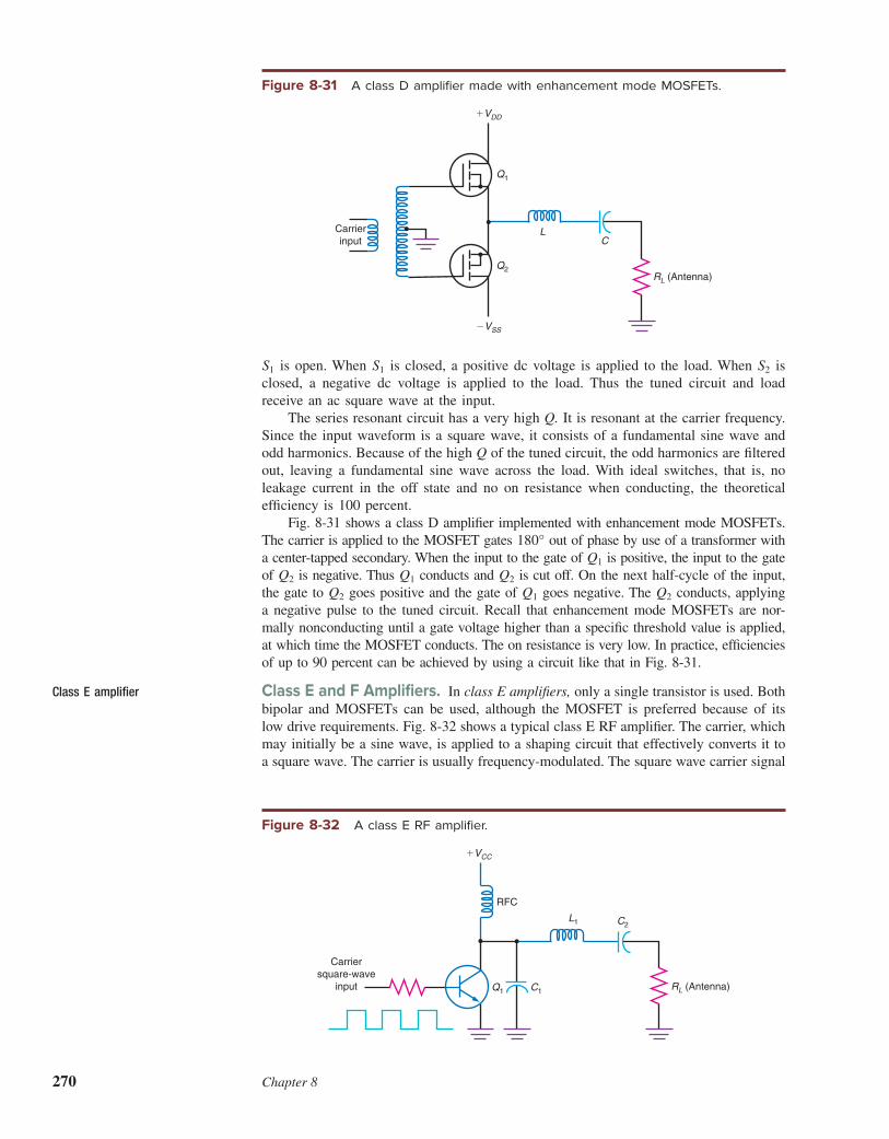
270 Chapter 8
S1 is open. When S1 is closed, a positive dc voltage is applied to the load. When S2 is
closed, a negative dc voltage is applied to the load. Thus the tuned circuit and load
receive an ac square wave at the input.
The series resonant circuit has a very high Q. It is resonant at the carrier frequency.
Since the input waveform is a square wave, it consists of a fundamental sine wave and
odd harmonics. Because of the high Q of the tuned circuit, the odd harmonics are i ltered
out, leaving a fundamental sine wave across the load. With ideal switches, that is, no
leakage current in the off state and no on resistance when conducting, the theoretical
efi ciency is 100 percent.
Fig. 8-31 shows a class D amplii er implemented with enhancement mode MOSFETs.
The carrier is applied to the MOSFET gates 180° out of phase by use of a transformer with
a center-tapped secondary. When the input to the gate of Q1 is positive, the input to the gate
of Q2 is negative. Thus Q1 conducts and Q2 is cut off. On the next half-cycle of the input,
the gate to Q2 goes positive and the gate of Q1 goes negative. The Q2 conducts, applying
a negative pulse to the tuned circuit. Recall that enhancement mode MOSFETs are nor-
mally nonconducting until a gate voltage higher than a specii c threshold value is applied,
at which time the MOSFET conducts. The on resistance is very low. In practice, efi ciencies
of up to 90 percent can be achieved by using a circuit like that in Fig. 8-31.
Class E and F Amplifi ers. In class E amplii ers, only a single transistor is used. Both
bipolar and MOSFETs can be used, although the MOSFET is preferred because of its
low drive requirements. Fig. 8-32 shows a typical class E RF amplii er. The carrier, which
may initially be a sine wave, is applied to a shaping circuit that effectively converts it to
a square wave. The carrier is usually frequency-modulated. The square wave carrier signal
Class E amplifi er
Figure 8-31 A class D amplifi er made with enhancement mode MOSFETs.
Q1
Q2
LC
�VDD
�VSS
RL (Antenna)
Carrier
input
Figure 8-32 A class E RF amplifi er.
�VCC
L1
Q1
C2
C1RL (Antenna)
RFC
Carrier
square-wave
input

Radio Transmitters 271
is then applied to the base of the class E bipolar power amplii er. The Q1 switches off
and on at the carrier rate. The signal at the collector is a square wave that is applied to
a low-pass i lter and tuned impedance-matching circuit made up of C1, C2, and L1. The
odd harmonics are i ltered out, leaving a fundamental sine wave that is applied to the
antenna. A high level of efi ciency is achieved with this arrangement.
A class F amplii er is a variation of the class E amplii er. It contains an additional
resonant network in the collector or drain circuit. This circuit, a lumped LC or even a
tuned transmission line at microwave frequencies, is resonant at the second or third
harmonic of the operating frequency. The result is a waveform at the collector (drain)
that more closely resembles a square wave. The steeper waveform produces faster tran-
sistor switching and better efi ciency.
Class S Amplifi ers. Class S amplii ers, which use switching techniques but with a
scheme of pulse-width modulation, are found primarily in audio applications but have
also been used in low- and medium-frequency RF amplii ers such as those used in AM
broadcast transmitters. The low-level audio signal to be amplii ed is applied to a circuit
called a pulse-width modulator. A carrier signal at a frequency 5 to 10 times the highest
audio frequency to be amplii ed is also applied to the pulse-width modulator. At the
output of the modulator is a series of constant-amplitude pulses whose pulse width or
duration varies with the audio signal amplitude. These signals are then applied to a
switching amplii er of the class D type. High power and efi ciency are achieved because
of the switching action. A low-pass i lter is connected to the output of the switching
amplii er to average and smooth the pulses back into the original audio signal waveform.
A capacitor or low-pass i lter across the speaker is usually sufi cient. These amplii ers
are usually referred to as class D amplii ers in audio applications. They are widely used
in battery-powered portable units where battery life and efi ciency are paramount.
RF Power Transistors
Although bipolar transistors are still used in some RF power amplii er (PA) designs, most
new designs use FETs. They require less drive, and overall the circuitry is generally
simpler. The newer models can achieve power outputs of several hundred watts to fre-
quencies well into the GHz regions. The most widely used devices in modern RF PAs
are LDMOS and GaN HEMT.
The laterally diffused MOS (LDMOS) FET is typically an n-type enhancement-mode
MOSFET with extra large elements to handle high power and heat. The geometry of the
device is designed to reduce the drain to gate feedback capacitance to extend the high-frequency
operating range. LDMOS FETs are widely used in radio transmitters for cellular base stations.
Other RF uses are in radar and high-power transmitters for broadcast and two-way radios.
They can accommodate drain supply voltages to 50 volts and power levels of 600 watts per
device. LDMOS FETs can operate to frequencies of up to about 6 GHz.
A newer form of discrete power FET is one made from gallium nitride (GaN) instead
of silicon. Those semiconductor materials permit the FET to operate at high drain volt-
ages to 100 volts and drain currents to several amperes. GaN FETs are a type of metal–
semiconductor junction FET or MESFET. They are called high-electron-mobility
transistors (HEMT). Instead of the metal–semiconductor junction the gate junction of the
MESFET, the HEMT uses different semiconductor materials for the gate and the channel.
This is called a heterojunction. One common combination is GaAs for the channel and
aluminum gallium arsenide (AlGaAs) for the gate. HEMTs are also made of GaN and
are good power transistors. A variation called a pseudomorphic or pHEMT uses addi-
tional layers of different semiconductor materials, including compounds of indium (In).
These layers are optimized to further speed electron transit, pushing their ability to
amplify well into the millimeter wave range of 30 to 100 GHz.
GaN RF power FETs are of the depletion-mode pHEMT type and handle heat better
than silicon power transistors do. They can operate at power levels of tens of watts to
frequencies of 30 GHz or more. They are used in radar, satellites, and cellular base stations.
Class F amplifi er
Class S amplifi er

272 Chapter 8
Linear Broadband Power Amplifi ers
The power amplii ers described so far in this chapter are narrowband amplii ers. They
provide high-power output over a relatively small range of frequencies. The bandwidth of
the signal to be amplii ed is set by the modulation method and the frequencies of the
modulating signals. In so many applications, the total bandwidth is only a small percent-
age of the carrier frequency, making conventional LC resonant circuits practical. Some of
the untuned push-pull power amplii ers described earlier (Figs. 8-23 and 8-24) do have a
broader bandwidth up to several megahertz. However, some of the newer wireless systems
now require much broader bandwidth. A good example is the code division multiple-
access (CDMA) cell phone standard. The CDMA system uses a modulation/multiplexing
technique called spread spectrum that does, as its name implies, spread the signal out over
a very wide frequency spectrum. The newer long-term evolution (LTE) cellular technology
in modern 4G cell phone systems uses an advanced modulation technique called orthog-
onal frequency division multiplex (OFDM) along with quadrature amplitude modulation
(QAM). Signal bandwidths of 5 to 20 MHz are common. Such complex modulation
schemes require that the amplii cation be linear over a wide frequency range to ensure no
amplitude, frequency, or phase distortion. Special amplii cation techniques have been
developed to meet this need. Four common methods are discussed here.
Feedforward Amplifi er. The concept behind a feedforward amplii er is that the distor-
tion produced by the power amplii er is isolated and then subtracted from the amplii ed
signal, producing a nearly distortion-free output signal. Fig. 8-33 shows one common imple-
mentation of this idea. The wide-bandwidth signal to be amplii ed is fed to a power splitter
that divides the signal into two equal-amplitude signals. A typical splitter may be a trans-
formerlike device or even a resistive network. It maintains the constant impedance, usually
50V, but typically also introduces some attenuation. One-half of the signal is then amplii ed
in a linear power amplii er similar to those broadband class AB amplii ers discussed earlier.
A directional coupler is used next to tap off a small portion of the amplii ed signal that
contains the original input information as well as harmonics resulting from distortion. A
directional coupler is a simple device that picks up a small amount of the signal by induc-
tive coupling. It is typically just a short copper line running adjacent to the signal line on
a printed-circuit board. At microwave frequencies, a directional coupler may be a more
complex device with a coaxial structure. In any case, the sample of the amplii ed signal is
also passed through a resistive attenuator to further reduce the signal level.
Figure 8-33 Feedforward linear power amplifi er.
Signal
combiner
AttenuatorSignal
combinerPower
splitter
PA
PA
Delay
line
Delay
line
Distortion
component
only
Error
power
amp
Amplified
signal only
(less
distortion)
to antenna
Distortion
amplified
Signal plus
distortion
�
�
Directional
coupler
Primary power
amp
Sample of
signal
with distortion

Radio Transmitters 273
The lower output of the signal splitter is sent to a delay line circuit. A delay line is a
low-pass i lter or a section of transmission line such as coaxial cable that introduces a
specii c amount of delay to the signal. It may be a few nanoseconds up to several micro-
seconds depending upon the frequency of operation and the type of power amplii er used.
The delay is used to match the delay encountered by the upper input signal in the power
amplii er. This delayed signal is then fed to a signal combiner along with the attenuated
signal sample from the amplii er output. Amplitude and phase controls are usually provided
in both signal paths to ensure that they are of the same amplitude and phase. The combiner
may be resistive or a transformerlike device. In either case, it effectively subtracts the
original signal from the amplii ed signal, leaving only the harmonic distortion.
The harmonic distortion is now amplii ed by another power amplii er with a power
level equal to that of the upper signal power amplii er. The upper amplii er signal is passed
through the directional coupler and into a delay line that compensates for the delay intro-
duced by the lower error signal amplii er. Again, amplitude and phase controls are usually
provided to adjust the power levels of the upper and lower signal levels, so they are equal.
Finally, the error signal is now subtracted from the amplii ed combined signal in a signal
coupler or combiner. This coupler, like the input splitter, is typically a transformer. The
resulting output is the original amplii ed signal less the distortion.
Amplii ers like this are available with power levels of a few watts to over several
hundred watts. The system is not perfect as the signal cancellations or subtractions are
not precise because of amplitude and phase mismatches. Distortion in the lower power
amplii er also contributes to overall output. Yet with close adjustments, these differences
can be minimized, thereby greatly improving the linearity of the amplii er over other
types. The system is also inefi cient because two power amplii ers are required. But the
tradeoff is wide bandwidth and very low distortion.
Digital Predistortion Amplifi cation. This method of amplii cation, referred to as
digital predistortion (DPD), uses a digital signal processing (DSP) technique to pre-
distort the signal in such a way that when amplii ed the amplii er distortion will offset
or cancel the predistortion characteristics, leaving a distortion-free output signal. The
amplii ed output signal is continuously monitored and used as feedback to the DSP so
that the predistorion calculations can be changed on the l y to provide an inverse pre-
distortion that perfectly matches the amplii er’s distortion.
Refer to Fig. 8-34 that shows a representative system. The digitized information
signal, in serial format, is fed to a digital correction algorithm in a DSP. Inside the DSP
Figure 8-34 Concept of adaptive predistortion amplifi cation.
Serialdigitaldata
Sampleofsignalwithdistortion
Linearpoweramp
Mixer(down converter)
Feedback path
Mixer (up converter)
Osc. orfreq. syn.
DAC
ADC
DSP
Digital
correction
PA
Directional
coupler
Ant.
Digital
modulator

274 Chapter 8
are computing algorithms that feed corrective logic signals to the digital correction algo-
rithm to modify the signal in such a way as to be an inverse match to the distortion
produced by the power amplii er.
Once the corrective action has been taken on the baseband digital signal, it is sent
to a modulator that produces the signal to be transmitted. The modulation is handled by
the DSP chip itself rather than a separate modulator circuit. This modulated signal is
then fed to a digital-to-analog converter (DAC) where it produces the desired analog
signal to be transmitted.
Next, the DAC output is sent to a mixer along with a sine wave signal from an oscil-
lator or frequency synthesizer. A mixer is similar to a low-level amplitude modulator or
analog multiplier. Its output consists of the sum and difference of the DAC and synthesizer
signals. In this application, the sum signal is selected by a i lter making the mixer an
upconverter. The synthesizer frequency is chosen so that the mixer output is at the desired
operating frequency. Any modulation present is also contained on the mixer output.
The predistorted signal is then amplii ed in a highly linear class AB power amplii er
(PA) and fed to the output antenna. Note in Fig. 8-34 that the output signal is sampled
in a directional coupler, amplii ed, and sent to another mixer used as a down converter.
The synthesizer also provides the second input to this mixer. The difference frequency
is selected by a i lter, and the result is sent to an analog-to-digital converter (ADC). The
digital output of the ADC represents the amplii ed signal plus any distortion produced
by the PA. The DSP uses this digital input to modify its algorithm to properly correct for
the actual distortion. The signal is then modii ed by the digital correction algorithm in
such a way that most of the distortion is canceled.
While the DPD method of broadband amplii cation is complex, it provides nearly
distortion-free output. Only a single power amplii er is needed, making it more efi cient
than the feedforward method. Several semiconductor manufacturers make the predistor-
tion circuits needed to make this work.
Envelope Tracking. Envelope tracking (ET) is a technique that allows class A, AB,
and B amplii ers to become more efi cient. Linear amplii ers must be used to amplify
the signals deploying advanced modulation techniques used in 3G and 4G cellular radios,
such as CDMA spread spectrum, QAM, and OFDM. The ET method provides a way to
adopt existing linear amplii ers but increase their efi ciency, making them run cooler and
use less power.
The advanced modulation methods have wide signal amplitude swings that must be
preserved. This condition is generally known as a wide peak-to-average power ratio
(PAPR). This leads to the problem inherent in class A amplii ers, where the efi ciency
is maximum when the signal levels are high and the output is near compression where
the signals come closest to the amplii er supply voltage levels. Efi ciency is high when
the amplii er is near compression where peak clipping occurs. With maximum undistorted
signal level, the efi ciency can approach the theoretical maximum of 50 percent. How-
ever, at lower input signal levels, efi ciency drops to a very low level. Efi ciencies may
be below 10 percent, meaning that most of the dc supply power is dissipated as heat by
the RF power transistors.
The ET system tracks the amplitude or modulation envelope of the RF signal and
uses that to control the dc power supply voltage to the amplii er. In other words, the
signal amplitude modulates the dc supply voltage. The process is similar to the high-level
amplitude modulation technique discussed in Chap. 4 (Fig. 4-13). This allows the amplii er
to always remain close to the compression point where the efi ciency is greatest.
Fig. 8-35a shows the transmitter stages where the analog baseband signal is fed to
the linear RF power amplii er. The power amplii er has a i xed power supply voltage,
usually from a DC-DC converter/regulator. The resulting output signal is shown along
with the power supply level. The red area indicates the power lost as heat.
Fig. 8-35b illustrates the ET method. The analog baseband signal also drives the
power amplii er as before. However, note that the analog signal is passed through a diode
rectii er similar to that used in AM demodulation. This rectii er circuit recovers the

Radio Transmitters 275
envelope of the signal and applies it to the ET power supply that supplies voltage to the
PA. The dc supply voltage therefore tracks the modulation envelope, keeping the amplii er
near compression and operating at maximum efi ciency. The ET power supply is essentially
a very wide bandwidth DC-DC converter that can adequately follow the signal amplitude
and frequency changes. Common dc supply voltage can range from 0.5 to 5 volts.
The ET technique is implemented with special ET tracking and dc modulation cir-
cuits. These may be in IC form or be fully integrated into another IC. The ET technique
is widely used in cellular base station power amplii ers as well as in cellphone handsets
using 3G and 4G (LTE) digital wireless technologies. Practical efi ciencies can be as
high as 40 to 50 percent, delivering considerable power and heat savings in base stations
and providing longer battery life and cooler operation in a cell phone. The ET technique
is also widely used in combination with the DPD technique, described earlier, to provide
even greater linearity and higher efi ciencies.
Doherty Amplifi er. The Doherty amplii er is a unique design using two amplii ers
that work together to maintain linearity while improving efi ciency. The design originated
in 1936 as an attempt to bring greater power and efi ciency to high-power vacuum tube
shortwave radio amplii ers. The design has now been widely adopted in power amplii ers
for multiband, multimode cellular base stations.
Fig. 8-36 shows the basic Doherty arrangement. The main carrier amplii er is a
linear class AB circuit, and the peaking amplii er is usually a class C amplii er. Both
amplii ers supply power to the load (antenna), creating what is referred to as a load-
pulling circuit whose impedance changes with signal levels. The carrier amplii er supplies
power to the load at the lower input signal levels and the peaking amplii er switches in
at the higher power levels.
The signal to be amplii ed is split equally by a power divider circuit. The signal
goes directly to the carrier amplii er and through a quarter wavelength (λ/4) transmission
line that provides a 90-degree phase shift of the signal to the peaking amplii er. The
transmission line is usually a short copper pattern on the amplii er printed circuit board
(PCB). At low signal levels, the peaking amplii er bias keeps it cut off so that it does
not supply power to the load. The carrier amplii er operates near compression to maintain
Figure 8-35 (a) Conventional RF Power amplifi er (PA), (b) PA with envelope tracking.
(a)
DC
Signal to
be amplified
To
antennaPA
DC/DC
converter
(b)
DC
Schottky
rectifier
Signal to be
amplified
To
antennaPA
Envelope
tracking
modulator
Fixed supply
voltage
Transmitted
Dissipated
as heat
Supply
voltage
Transmitted
Dissipated
as heat

276 Chapter 8
high efi ciency and supplies power to the load. At higher input levels, the peaking ampli-
i er cuts in and supplies more power to the load.
The amplii ers deliver power to the load by a λ/4 transmission line used as an
impedance converter and another λ/4 line used as an impedance transformer. These
transmission lines combined provide dynamic load impedance adaption for the amplii ers
to increase efi ciency. The λ/4 lines provide a way to modulate the load impedance so
as to ensure that the amplii ers operate to supply maximum power with the best efi -
ciency. (The characteristics and operation of transmission lines are covered in Chap. 13.)
Doherty amplii ers used today are made with GaN HEMT FETs because of their
high-power, high-frequency capability. They operate in the 700 MHz to 3 GHz range. The
typical 12 to 20 percent efi ciency of a class AB linear amplii er is boosted to the 25 to
40 percent range with the Doherty coni guration. Most Doherty amplii ers are combined
with the DPD linearization technique described earlier to deliver increased efi ciency.
8-4 Impedance-Matching NetworksMatching networks that connect one stage to another are very important parts of any
transmitter. In a typical transmitter, the oscillator generates the basic carrier signal, which
is then amplii ed, usually by multiple stages, before it reaches the antenna. Since the
idea is to increase the power of the signal, the interstage coupling circuits must permit
an efi cient transfer of power from one stage to the next. Finally, some means must be
provided to connect the i nal amplii er stage to the antenna, again for the purpose of
transferring the maximum possible amount of power. The circuits used to connect one
stage to another are known as impedance-matching networks. In most cases, they are LC
circuits, transformers, or some combination. The basic function of a matching network
is to provide for an optimum transfer of power through impedance-matching techniques.
Matching networks also provide i ltering and selectivity. Transmitters are designed to
operate on a single frequency or selectable narrow ranges of frequencies. The various
amplii er stages in the transmitter must coni ne the RF generated to these frequencies. In
class C, D, and E amplii ers, a considerable number of high-amplitude harmonics are
generated. These must be eliminated to prevent spurious radiation from the transmitter.
The impedance-matching networks used for interstage coupling accomplish this.
Impedance-matching network
Figure 8-36 A Doherty power amplifi er.
Power
splitter
PA
PA
Carrier amplifier
(class AB)
Peaking amplifier
(class C)
λ/4 matching
transformer
50 Ω antenna
load
λ/4 transmission
line
λ/4 transmission
line
Signal
to be
amplified

Radio Transmitters 277
The basic problem of coupling is illustrated in Fig. 8-37(a). The driving stage appears
as a signal source with an internal impedance of Zi. The stage being driven represents a
load to the generator with its internal resistance of Zl. Ideally, Zi and Zl are resistive. Recall
that maximum power transfer in dc circuits takes place when Zi equals Zl. This basic
relationship is essentially true also in RF circuits, but it is a much more complex relation-
ship. In RF circuits, Zi and Zl are seldom purely resistive and, in fact, usually include a
reactive component of some type. Further, it is not always necessary to transfer maximum
power from one stage to the next. The goal is to transfer a sufi cient amount of power to
the next stage so that it can provide the maximum output of which it is capable.
In most cases, the two impedances involved are considerably different from each
other, and therefore a very inefi cient transfer of power takes place. To overcome this
problem, an impedance-matching network is introduced between the two, as illustrated
in Fig. 8-37(b). There are three basic types of LC impedance-matching networks: the
L network, the T network, and the π network.
Networks
L networks consist of an inductor and a capacitor connected in various L-shaped con-
i gurations, as shown in Fig. 8-38. The circuits in Fig. 8-38(a) and (b) are low-pass
i lters; those in Fig. 8-38(c) and (d) are high-pass i lters. Typically, low-pass networks
are preferred so that harmonic frequencies are i ltered out.
The L-matching network is designed so that the load impedance is matched to the
source impedance. For example, the network in Fig. 8-38(a) causes the load resistance
to appear larger than it actually is. The load resistance ZL appears in series with the induc-
tor of the L network. The inductor and the capacitor are chosen to resonate at the
transmitter frequency. When the circuit is at resonance, XL equals XC. To the generator
impedance Zi, the complete circuit appears as a parallel resonant circuit. At resonance,
the impedance represented by the circuit is very high. The actual value of the impedance
depends upon the L and C values and the Q of the circuit. The higher the Q, the higher
the impedance. The Q in this circuit is basically determined by the value of the load
impedance. By proper selection of the circuit values, the load impedance can be made
to appear as any desired value to the source impedance as long as Zi is greater than ZL.
By using the L network shown in Fig. 8-39(b), the impedance can be stepped down,
or made to appear much smaller than it actually is. With this arrangement, the capacitor
is connected in parallel to the load impedance. The parallel combination of C and ZL
has an equivalent series RC combination. Both C and ZL appear as equivalent series
values Ceq and Zeq. The result is that the overall network appears as a series resonant
circuit, with Ceq and L resonant. Recall that a series resonant circuit has a very low
impedance at resonance. The impedance is, in fact, the equivalent load impedance Zeq,
which is resistive.
L network
Figure 8-37 Impedance matching in RF circuits.
Internalsource impedance
Load
RFgenerator
Zi
Zl
(a)
RFgenerator
Zi
Zl
Impedance-matchingnetwork
(b)

278 Chapter 8
Figure 8-38 Four L-type impedance-matching networks. (a) ZL , Zi . (b) ZL . Zi . (c) ZL , Zi . (d) ZL . Zi .
RF generator
Z i
ZL
L
C
(a)
RF generator
Zi
ZL
L2
C
(b)
L1
RF generator
Z i
ZLL
C
(c)
RF generator
Z i
ZLL
C
(d )
Figure 8-39 The L network design equations.
L network
L
C
(b)
Zi � Ri
ZL � RL
L network
L
C
(a)
Zi � Ri
ZL� RL
XL � Ri RL � (RL)2
XC � XL
Ri RL
Q �Ri
� 1RL
XL � Ri iRL� (R )2
XC � XL
Ri RL
Q �RL
� 1Ri
RL > Ri
RL < Ri
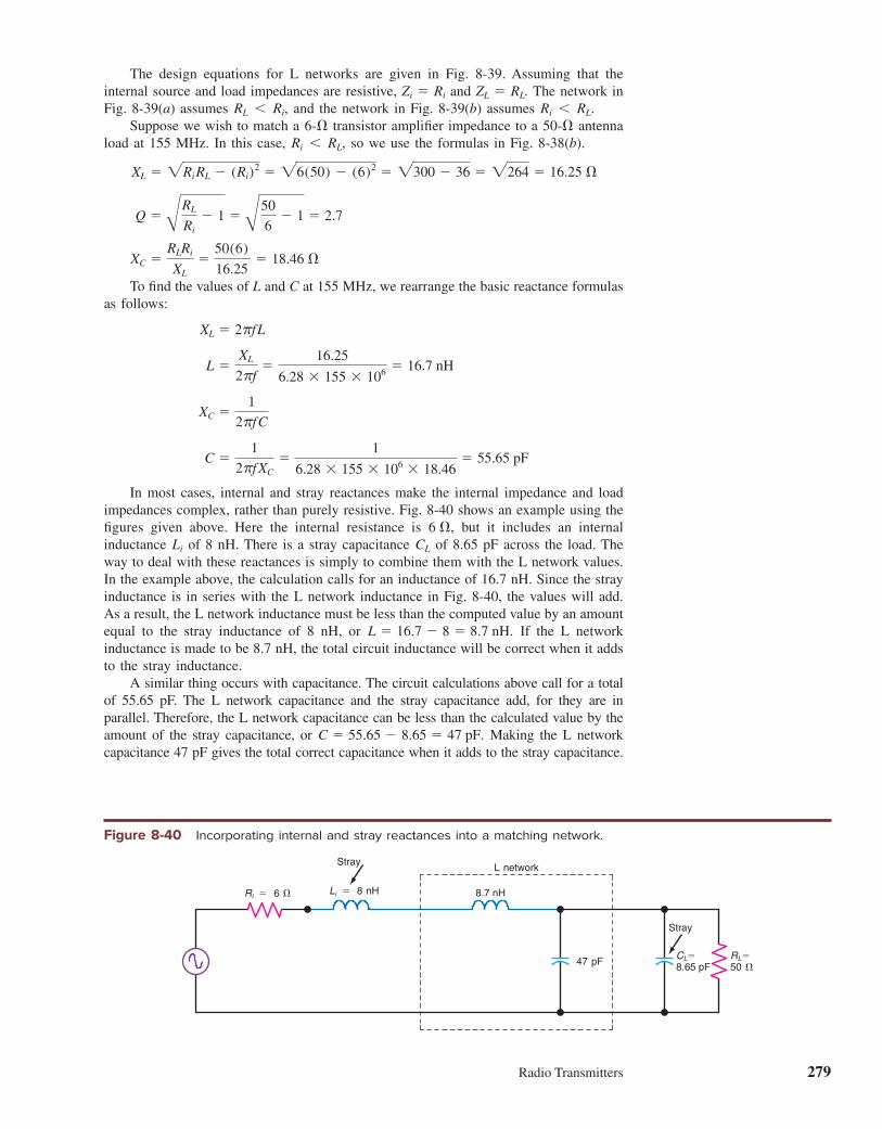
Radio Transmitters 279
The design equations for L networks are given in Fig. 8-39. Assuming that the
internal source and load impedances are resistive, Zi 5 Ri and ZL 5 RL. The network in
Fig. 8-39(a) assumes RL , Ri, and the network in Fig. 8-39(b) assumes Ri , RL.
Suppose we wish to match a 6-V transistor amplii er impedance to a 50-V antenna
load at 155 MHz. In this case, Ri , RL, so we use the formulas in Fig. 8-38(b).
XL 5 2RiRL 2 (Ri)2 5 26(50) 2 (6)2 5 2300 2 36 5 2264 5 16.25 V
Q 5 BRL
Ri
2 1 5 B50
62 1 5 2.7
XC 5RLRi
XL
550(6)
16.255 18.46 V
To i nd the values of L and C at 155 MHz, we rearrange the basic reactance formulas
as follows:
XL 5 2πf L
L 5XL
2πf5
16.25
6.28 3 155 3 1065 16.7 nH
XC 51
2πf C
C 51
2πf XC
51
6.28 3 155 3 106 3 18.465 55.65 pF
In most cases, internal and stray reactances make the internal impedance and load
impedances complex, rather than purely resistive. Fig. 8-40 shows an example using the
i gures given above. Here the internal resistance is 6 V, but it includes an internal
inductance Li of 8 nH. There is a stray capacitance CL of 8.65 pF across the load. The
way to deal with these reactances is simply to combine them with the L network values.
In the example above, the calculation calls for an inductance of 16.7 nH. Since the stray
inductance is in series with the L network inductance in Fig. 8-40, the values will add.
As a result, the L network inductance must be less than the computed value by an amount
equal to the stray inductance of 8 nH, or L 5 16.7 2 8 5 8.7 nH. If the L network
inductance is made to be 8.7 nH, the total circuit inductance will be correct when it adds
to the stray inductance.
A similar thing occurs with capacitance. The circuit calculations above call for a total
of 55.65 pF. The L network capacitance and the stray capacitance add, for they are in
parallel. Therefore, the L network capacitance can be less than the calculated value by the
amount of the stray capacitance, or C 5 55.65 2 8.65 5 47 pF. Making the L network
capacitance 47 pF gives the total correct capacitance when it adds to the stray capacitance.
Figure 8-40 Incorporating internal and stray reactances into a matching network.
L network
Li � 8 nHRi � 6 �
RL �50 �
8.7 nH
47 pFCL�8.65 pF
Stray
Stray

280 Chapter 8
T and π Networks
When one is designing L networks, there is very little control over the Q of the circuit,
which is determined by the values of the internal and load impedances and may not always
be what is needed to achieve the desired selectivity. To overcome this problem, matching
networks using three reactive elements can be used. The three most widely used impedance-
matching networks containing three reactive components are illustrated in Fig. 8-41. The
network in Fig. 8-41(a) is known as a π network because its coni guration resembles the
Greek letter π. The circuit in Fig. 8-41(b) is known as a T network because the circuit
π network
T network
Figure 8-41 Three-element matching networks. (a) π network. (b) T network.
(c) Two-capacitor T network.
RF generator
Zi
ZL
L
C2
(a)
C1
RF generator
Zi
ZL
L2
C
(b)
L1
RF generator
Zi
ZL
C2
(c)
L
C2
L C1
C1

Radio Transmitters 281
elements resemble the letter T. The circuit in Fig. 8-41(c) is also a T network, but it uses
two capacitors. Note that all are low-pass i lters that provide maximum harmonic attenua-
tion. The π and T networks can be designed to either step up or step down the impedance
as required by the circuit. The capacitors are usually made variable so that the circuit can
be tuned to resonance and adjusted for maximum power output.
The most widely used of these circuits is the T network of Fig. 8-41(c). Often called
an LCC network, it is used to match the low output impedance of a transistor power
amplii er to the higher impedance of another amplii er or an antenna. The design proce-
dure and formulas are given in Fig. 8-42. Suppose once again that a 6-V source Ri is to
be matched to a 50-V load RL at 155 MHz. Assume a Q of 10. (For class C operation,
where many harmonics must be attenuated, it has been determined in practice that a Q
of 10 is the absolute minimum needed for satisfactory suppression of the harmonics.) To
coni gure the LCC network, the inductance is calculated i rst :
XL 5 QRi
XL 5 10(6) 5 60 V
L 5XL
2πf5
50
6.28 3 155 3 1065 51.4 nH
Next, C2 is calculated:
XC25 50 B
6(101)
502 1 5 50(3.33) 5 166.73 V
C2 51
2πf XC
51
6.28 3 155 3 106 3 166.735 6.16 3 10212 5 6.16 pF
Finally, C1 is calculated
XC15
6(102 1 1)
10
1
1 2 166.73y(10 3 50)5 60.6(1.5) 5 91 V
C1 51
2πf XC
51
6.28 3 155 3 106 3 915 11.3 pF
Transformers and Baluns
One of the best impedance-matching components is the transformer. Recall that iron-core
transformers are widely used at lower frequencies to match one impedance to
another. Any load impedance can be made to look like a desired load impedance by
selecting the correct value of the transformer turns ratio. In addition, transformers can
be connected in unique combinations called baluns to match impedances.
Transformer
Baluns
Figure 8-42 Design equations for an LCC T network.
2fXC
1
RL
1
T network
XL XC2
Ri � RL
Zi � Ri
ZL� RL
Q
� 1
XC1
Design Procedure:1. Select a desired circuit Q2. Calculate XL � QRi
3. Calculate XC1:
4. Calculate XC2:
5. Compute final L and C values:
XC2� RL
XC1 �
Ri (Q2 � 1)
QRL
XC2
Ri (Q2 � 1)
1 �
L �
C �
2f
XL

282 Chapter 8
Transformer Impedance Matching. Refer to Fig. 8-43. The relationship between
the turns ratio and the input and output impedances is
Zi
ZL
5 aNP
NS
b2
NP
NS
5 BZi
ZL
That is, the ratio of the input impedance Zi to the load impedance ZL is equal to the
square of the ratio of the number of turns on the primary NP to the number of turns on
the secondary NS. For example, to match a generator impedance of 6 V to a 50-V load
impedance, the turns ratio should be as follows:
NP
NS
5 BZi
ZL
5 B6
505 10.12 5 0.3464
NS
NP
51
NP yNS
51
0.34645 2.887
This means that there are 2.89 times as many turns on the secondary as on the primary.
The relationship given above holds true only on iron-core transformers. When air-
core transformers are used, the coupling between primary and secondary windings is not
complete and therefore the impedance ratio is not as indicated. Although air-core trans-
formers are widely used at Fs and can be used for impedance matching, they are less
efi cient than iron-core transformers.
Ferrite (magnetic ceramic) and powdered iron can be used as core materials to pro-
vide close coupling at very high frequencies. Both the primary and the secondary wind-
ings are wound on a core of the chosen material.
The most widely used type of core for RF transformers is the toroid. A toroid is a
circular, doughnut-shaped core, usually made of a special type of powdered iron. Copper
wire is wound on the toroid to create the primary and secondary windings. A typical arrange-
ment is shown in Fig. 8-44. Single-winding tapped coils called autotransformers are also
used for impedance matching between RF stages. Fig. 8-45 shows impedance step-down
and step-up arrangements. Toroids are commonly used in autotransformers.
Unlike air-core transformers, toroid transformers cause the magnetic i eld produced
by the primary to be completely contained within the core itself. This has two important
advantages. First, a toroid does not radiate RF energy. Air-core coils radiate because the
magnetic i eld produced around the primary is not contained. Transmitter and receiver
circuits using air-core coils are usually contained with magnetic shields to prevent them
from interfering with other circuits. The toroid, on the other hand, coni nes all the
magnetic i elds and does not require shields. Second, most of the magnetic i eld produced
by the primary cuts the turns of the secondary winding. Thus the basic turns ratio, input-
output voltage, and impedance formulas for standard low-frequency transformers apply
to high-frequency toroid transformers.
Toroid
Autotransformer
GOOD TO KNOW
Although air-core transformers
are used widely at radio frequen-
cies, they are less effi cient than
iron-core transformers.
Figure 8-43 Impedance matching with an iron-core transformer.
NS
NP
RF generator
Z i
ZLPrimary Secondary
Turns ratio �

Radio Transmitters 283
In most new RF designs, toroid transformers are used for RF impedance matching
between stages. Further, the primary and secondary windings are sometimes used as
inductors in tuned circuits. Alternatively, toroid inductors can be built. Powdered iron-
core toroid inductors have an advantage over air-core inductors for RF applications
because the high permeability of the core causes the inductance to be high. Recall that
whenever an iron core is inserted into a coil of wire, the inductance increases dramati-
cally. For RF applications, this means that the desired values of inductance can be
created by using fewer turns of wire, and thus the inductor itself can be smaller. Further,
fewer turns have less resistance, giving the coil a higher Q than that obtainable with
air-core coils.
Powdered iron toroids are so effective that they have virtually replaced air-core coils
in most modern transmitter designs. They are available in sizes from a fraction of an
inch to several inches in diameter. In most applications, a minimum number of turns are
required to create the desired inductance.
Transmission Line Transformers and Baluns
A transmission line or broadband transformer is a unique type of transformer that is widely
used in power amplii ers for coupling between stages and impedance matching. Such a
transformer is usually constructed by winding two parallel wires (or a twisted pair) on a
toroid, as shown in Fig. 8-46. The length of the winding is typically less than one-eighth
Transmission line transformer
Figure 8-44 A toroid transformer.
Primary Secondary
Powdered iron toroid
Figure 8-45 Impedance matching in an autotransformer. (a) Step down. (b) Step up.
Zi
NP NS
Zl
(a) Step-down
NS
NP
�ZL
Zi
Zi
NS
NP
Zl
NS
NP
�
(b) Step-up
ZL
Zi
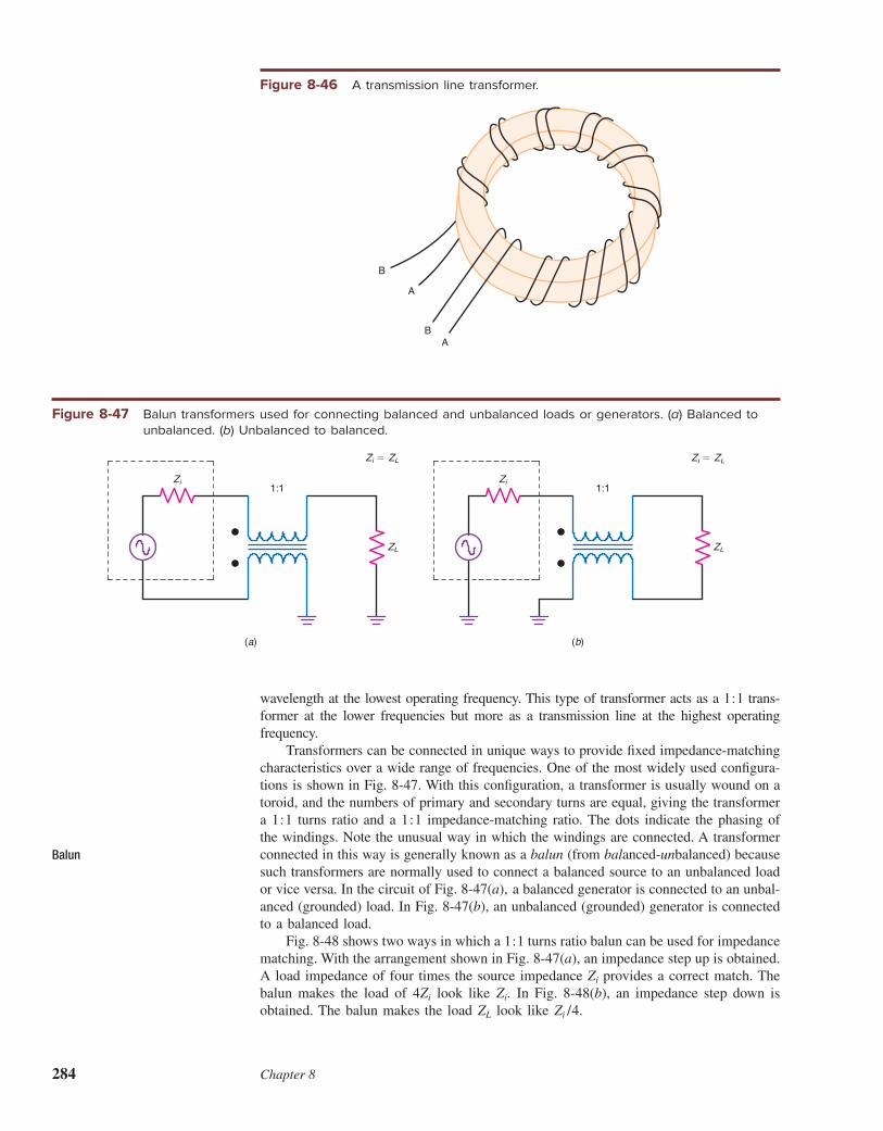
284 Chapter 8
wavelength at the lowest operating frequency. This type of transformer acts as a 1:1 trans-
former at the lower frequencies but more as a transmission line at the highest operating
frequency.
Transformers can be connected in unique ways to provide i xed impedance-matching
characteristics over a wide range of frequencies. One of the most widely used coni gura-
tions is shown in Fig. 8-47. With this coni guration, a transformer is usually wound on a
toroid, and the numbers of primary and secondary turns are equal, giving the transformer
a 1:1 turns ratio and a 1:1 impedance-matching ratio. The dots indicate the phasing of
the windings. Note the unusual way in which the windings are connected. A transformer
connected in this way is generally known as a balun (from balanced-unbalanced) because
such transformers are normally used to connect a balanced source to an unbalanced load
or vice versa. In the circuit of Fig. 8-47(a), a balanced generator is connected to an unbal-
anced (grounded) load. In Fig. 8-47(b), an unbalanced (grounded) generator is connected
to a balanced load.
Fig. 8-48 shows two ways in which a 1:1 turns ratio balun can be used for impedance
matching. With the arrangement shown in Fig. 8-47(a), an impedance step up is obtained.
A load impedance of four times the source impedance Zi provides a correct match. The
balun makes the load of 4Zi look like Zi. In Fig. 8-48(b), an impedance step down is
obtained. The balun makes the load ZL look like Zi /4.
Balun
Figure 8-46 A transmission line transformer.
A
A
B
B
Figure 8-47 Balun transformers used for connecting balanced and unbalanced loads or generators. (a) Balanced to
unbalanced. (b) Unbalanced to balanced.
Zi
ZL
1:1
Zi � ZL
(a)
Zi
ZL
1:1
Zi � ZL
(b)
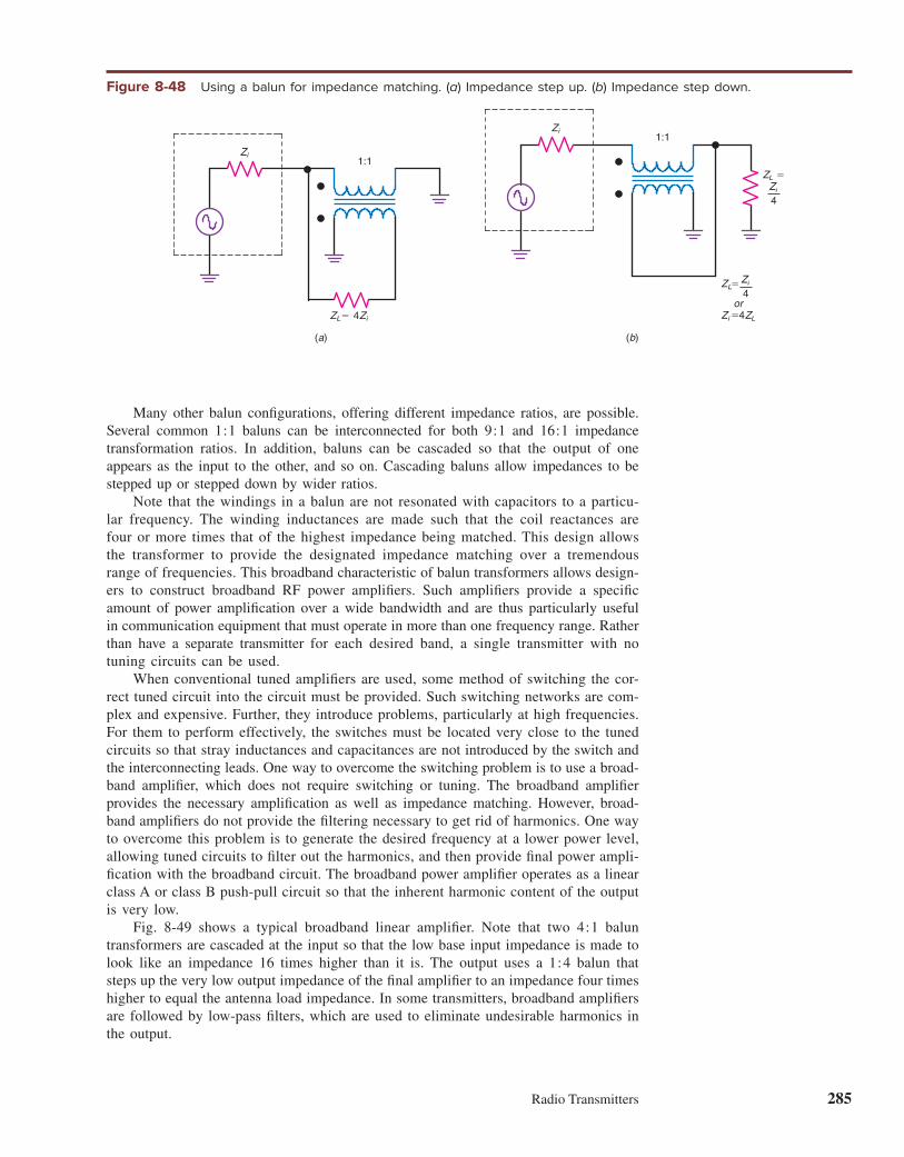
Radio Transmitters 285
Figure 8-48 Using a balun for impedance matching. (a) Impedance step up. (b) Impedance step down.
Zi
1:1
ZL � 4Zi
(a)
4
Zi
Zi
ZL �
1:1
Zi �4ZL
(b)
4
Zi
ZL �
or
Many other balun coni gurations, offering different impedance ratios, are possible.
Several common 1:1 baluns can be interconnected for both 9:1 and 16:1 impedance
transformation ratios. In addition, baluns can be cascaded so that the output of one
appears as the input to the other, and so on. Cascading baluns allow impedances to be
stepped up or stepped down by wider ratios.
Note that the windings in a balun are not resonated with capacitors to a particu-
lar frequency. The winding inductances are made such that the coil reactances are
four or more times that of the highest impedance being matched. This design allows
the transformer to provide the designated impedance matching over a tremendous
range of frequencies. This broadband characteristic of balun transformers allows design-
ers to construct broadband RF power amplii ers. Such amplii ers provide a specii c
amount of power amplii cation over a wide bandwidth and are thus particularly useful
in communication equipment that must operate in more than one frequency range. Rather
than have a separate transmitter for each desired band, a single transmitter with no
tuning circuits can be used.
When conventional tuned amplii ers are used, some method of switching the cor-
rect tuned circuit into the circuit must be provided. Such switching networks are com-
plex and expensive. Further, they introduce problems, particularly at high frequencies.
For them to perform effectively, the switches must be located very close to the tuned
circuits so that stray inductances and capacitances are not introduced by the switch and
the interconnecting leads. One way to overcome the switching problem is to use a broad-
band amplii er, which does not require switching or tuning. The broadband amplii er
provides the necessary amplii cation as well as impedance matching. However, broad-
band amplii ers do not provide the i ltering necessary to get rid of harmonics. One way
to overcome this problem is to generate the desired frequency at a lower power level,
allowing tuned circuits to i lter out the harmonics, and then provide i nal power ampli-
i cation with the broadband circuit. The broadband power amplii er operates as a linear
class A or class B push-pull circuit so that the inherent harmonic content of the output
is very low.
Fig. 8-49 shows a typical broadband linear amplii er. Note that two 4:1 balun
transformers are cascaded at the input so that the low base input impedance is made to
look like an impedance 16 times higher than it is. The output uses a 1:4 balun that
steps up the very low output impedance of the i nal amplii er to an impedance four times
higher to equal the antenna load impedance. In some transmitters, broadband amplii ers
are followed by low-pass i lters, which are used to eliminate undesirable harmonics in
the output.

286 Chapter 8
Figure 8-49 A broadband class A linear power amplifi er.
RFin
16:1
4:1 4:1
�VCC
RFC
1:4
Antennaload
Bias
8-5 Typical Transmitter CircuitsMany transmitters used in recent equipment designs are a combination of ICs and dis-
crete component circuits. Here are two examples.
Short-Range Wireless Transmitter
There are many short-range wireless applications that require a transmitter to send data
or control signals to a nearby receiver. Some examples are the small transmitters in
remote keyless entry (RKE) devices used to open car doors, tire pressure sensors, remote-
control lights and ceiling fans in homes, garage door openers, and temperature sensors.
These unlicensed transmitters use very low power and operate in the FCC’s industrial-
scientii c-medical (ISM) bands. These are frequencies set aside for unlicensed operation
as dei ned in Part 15 of the FCC rules and regulations. The most common frequencies
are 315, 433.92, 868 (Europe), and 915 MHz.
Fig. 8-50 shows a typical transmitter IC, the Freescale MC33493/D. This CMOS device
is designed to operate anywhere in the 315- to 434-MHz and 868- to 928-MHz ranges with
the frequency set by an external crystal. It features OOK or FSK modulation and can handle
a serial data rate up to 10 kbps. Output power is adjustable with an external resistor.
The basic transmitter circuit is simply a PLL used as a frequency multiplier with an
output power amplii er. The internal oscillator XCO uses an external crystal. The PLL
multiplies an external crystal frequency by a factor of 32 or 64 to develop a PLL VCO
signal at the desired operating frequency. For example, if the desired output frequency is
315 MHz, the crystal must have a frequency of 315y32 5 9.84375 MHz. For an output
of 433.92 MHz, a 13.56-MHz crystal is needed. The XCO output is applied to the phase
detector along with the feedback signal from the frequency dividers driven by the PLL
VCO output. The divide-by-2 divider may be switched in when divide-by-64 is needed.
The BAND input signal selects the divide-by-2 divider or takes it out. If the BAND sig-
nal is low, the divide-by-2 circuit is bypassed and the overall PLL multiply factor is 32.
If BAND is high, the divide-by-2 circuit is inserted and the overall multiplication factor
is 64. Using a 13.56-MHz crystal gives an output 867.84 MHz when the divide-by-64 factor
is used.
The PLL VCO output drives a class C power amplii er. An external resistor may be
inserted in the line between REXT and the dc power source to lower the power to the
desired level. Maximum output with no external resistor is 5 dBm (3.1 mW). The dc
supply voltage may be anything in the 1.9- to 3.6-V range usually supplied by a battery.
Remote keyless entry (RKE)

Radio Transmitters 287
Modulation is selected by the MODE pin. If MODE is low, OOK modulation is
selected. The serial binary input at the DATA pin then goes to turn the class C PA dc
power off and on, on for binary 1 and off for binary 0. If MODE is high, FSK is selected.
The DATA input line is then used to pull the crystal frequency between the two desired
shift frequencies. A 45-kHz shift is typical. Two external capacitors C1 and C2 are used to
pull the crystal to the desired frequencies. Either serial or parallel pulling may be used
depending upon the type of crystal.
The PA output is fed to an external LC impedance-matching network as needed to
match the 50-V output to the selected antenna, as Fig. 8-50 shows. Usually the antenna
is a loop of copper on the printed-circuit board holding the transmitter IC.
One other feature of this chip is the data clock DATACLK output line. This output is
the crystal frequency divided by 64. For a 9.84375-MHz crystal, the DATACLK output is
153.8 kHz. With a 13.56-MHz crystal, the DATACLK output is 212 kHz. This clock can
be used with an external embedded microcontroller to synchronize the data stream.
This transmitter chip is designed to be used with an external microcontroller. It gets
its BAND, MODE, and ENABLE signals from the microcontroller.
Software-Defi ned Radio Transmitter
The typical transmitter today is part of what we call a software-dei ned radio (SDR).
The information to be transmitted is in digital form and will be modulated on to a carrier
using digital techniques. The modulation is usually by DSP; therefore, it is a form of
software. Most of the circuitry in the transmitter is digital or software-derived. An exam-
ple of an integrated circuit that provides most of the functions for an SDR transmitter is
the Texas Instruments AFE7070, shown in Fig. 8-51.
The data to be transmitted is organized and modulated by a DSP or FPGA into in-
phase (I) and quadrature (Q) components. These are in the form of 14-bit words and are
applied alternately to the IC input labeled D(13:0). They are demultiplexed into the I
and Q streams and applied to a numerically controlled oscillator (NCO) of the DDS type
that may or may not be used for additional signal generation or mixing operations. The
I and Q streams are then sent to a quadrature modulator correction (QMC) circuit that
provides a way to match their gain, phase, and offset values. The I and Q signals must
be perfectly balanced to provide the optimum error-free transmission.
Figure 8-50 The Freescale MC 33493D UHF ISM transmitter IC.
Band
Controllogic
C2
XTAL
Enable
Inputs from microcontroller
data in
mode
Loopfilter
� 32 � 2
PA
REXT
Phasedetector
OOK data
DATACLK
Pullingcapacitors
C1
� 64
VCO
May beswitchedin or out
Antenna
load
5 Ω
Impedancematching
�V
XCO
CFSK
FSKdata

288 Chapter 8
The I and Q signals then go to a pair of 14-bit DACs where they are converted into
equivalent analog I and Q signals. These are i ltered in a pair of low-pass i lters and
applied to a quadrature modulator that mixes them with the carrier signal from a local
oscillator (LO) or frequency synthesizer. This signal comes in on pin LO_PIN. The mixer
outputs are added together to form the i nal modulated analog signal to be transmitted.
The signal is amplii ed and appears at the RF_OUT pin. It is used to drive the i nal
external power amplii er before going to the antenna. (You will learn more about demul-
tiplexers, mixers, and quadrature modulators in Chaps. 9, 10, and 11.)
The other circuitry in the chip supports the main transmitter circuits. The SPI is a
standard serial peripheral interface used to connect the chip to other circuits. Here the
SPI usually connects to an external microcontroller and memory where data for the
programming registers is generated and stored. The serial data comes in on pin SDIO.
All of the other circuit functions are programmed for the desired outcome by register
codes. The clock input CLK_IO is the master timing signal that controls all other circuits
as well. On the output, the analog signal is converted into a digital signal and divided
by 1, 2, or 4 to create an external clock signal if needed.
The AFE7070 is used in low-power compact SDRs of any type and small cellular base
stations. It can operate anywhere in the 100 MHz to 2.7 GHz frequency range. For further
details on the chip, i nd the data sheet at the Texas Instruments website: www.ti.com.
RESETB
SCLK
SDENB
SDIO
ALARM_SDO
D[13:0]
IQ_FLAG
SYNC_SLEEP
CLK_IO
DACCLKP/N
LO_P/N
BasebandFilter
QuadratureModulator
DualDAC
LVDS_P/N
RF_OUT
BG_BYP
QMCNCO/Mixer(DDS)
Demux
Clock
SPI/Registers
1.2-VREF
42
11,2,4
Figure 8-51 The Texas Instruments AFE7070 is a representative digital radio transmitter IC.
CHAPTER REVIEW
Online Activities
8-1 Exploring MEMS Oscillators
Objective: To become familiar with MEMS oscillators as an
alternative to crystal oscillators.
Procedure:
1. Use Bing, Google, Yahoo, or another search engine
to locate basic information sources on MEMS
oscillators.
2. Go to the websites of Silicon Laboratories, SiTime, and
IDT and look for details on MEMS oscillator products.
Download the data sheets to obtain block diagrams,
specii cations, and input/output dei nitions. Download
any relevant application notes.
3. Answer the following questions.

Radio Transmitters 289
Questions:
1. What is the frequency-determining element in a MEMS
oscillator?
2. What is the highest frequency at which a MEMS oscil-
lator can operate?
3. How is higher frequency obtained with a MEMS oscillator?
4. What is the best precision and stability that a MEMS
oscillator can achieve?
5. Can MEMS oscillators replace crystal oscillators?
6. Are MEMS oscillators less or more expensive than
crystal oscillators?
Objective: Learn more about the characteristics and specii -
cations of IC RF power amplii ers.
Procedure:
1. Use Bing, Google, Yahoo, or another search engine to
locate basic information sources on integrated circuit
power amplii ers for LTE or WCDMA cell phones.
2. Go to the websites of the following companies to
obtain data sheets, block diagrams, specii cations, and
characteristics of RF power amplii ers: Anadigics,
Cree, Freescale, RFMD, NXP, Skyworks, ST Micro,
and TriQuint.
3. Answer the following questions.
Questions:
1. For PAs used for cellphones, what are some of the fre-
quency ranges available?
2. What is the most common input and output impedance?
3. What is the most common power output specii cation
for a cell phone PA?
4. What are some of the semiconductor materials used for
cell phone PAs?
5. Are cell phone PAs linear or nonlinear?
6. What semiconductor materials provide the highest fre-
quency and power capability?
7. Is the Doherty PA available in IC or module format?
Who is the supplier, if so?
8-2 Examining IC RF Power Amplifi ers
Questions
1. What circuits are typically part of every radio
transmitter?
2. Which type of transmitter does not use class C amplii ers?
3. For how many degrees of an input sine wave does a
class B amplii er conduct?
4. What is the name given to the bias for a class C ampli-
i er produced by an input RC network?
5. Why are crystal oscillators used instead of LC oscilla-
tors to set transmitter frequency?
6. What is the most common way to vary the output fre-
quency of a crystal oscillator?
7. How is the output frequency of a frequency of a PLL
synthesizer changed?
8. What are prescalers, and why are they used in VHF and
UHF synthesizers?
9. What is the purpose of the loop i lter in a PLL?
10. What circuit in a direct digital synthesizer (DDS) actu-
ally generates the output waveform?
11. In a DDS, what is stored in ROM?
12. How is the output for frequency of a DDS changed?
13. What is the most efi cient class of RF power amplii er?
14. What is the approximate maximum power of typical
transistor RF power amplii ers?
15. Dei ne power-added efi ciency.
16. What is the main advantage and disadvantage of
switching amplii ers?
17. What is the difference between a class D and a class E
amplii er?
18. Explain how an envelope tracking power amplii er
works.
19. Explain how a feedforward power amplii er reduces
distortion.
20. In a predistortion power amplii er, what is the feedback
signal?
21. Maximum power transfer occurs when what relation-
ship exists between generator impedance Zi and load
impedance ZL?
22. What is a toroid and how is it used? What components
are made from it?
23. What are the advantages of a toroid RF inductor?
24. In addition to impedance matching, what other impor-
tant function do LC networks perform?
25. What is the name given to a single winding trans-
former?
26. What is the name given to an RF transformer with a
1 : 1 turns ratio connected so that it provides a 1 : 4
or 4 : 1 impedance matching? Give a common
application.
27. Why are untuned RF transformers used in power
amplii ers?
28. How is impedance matching handled in a broadband
linear RF amplii er?
29. What are the common impedance-matching ratios of
transmission line transformers used as baluns?
30. Why are π and T networks preferred over L networks?

290 Chapter 8
1. An FM transmitter has an 8.6-MHz crystal carrier
oscillator and frequency multipliers of 2, 3, and 4.
What is the output frequency? ◆
2. A crystal has a tolerance of 0.003 percent. What is the
tolerance in ppm?
3. A 25-MHz crystal has a tolerance of 6200 ppm. If the
frequency drifts upward to the maximum tolerance,
what is the frequency of the crystal? ◆
4. A PLL frequency synthesizer has a reference frequency
of 25 kHz. The frequency divider is set to a factor of
345. What is the output frequency?
5. A PLL frequency synthesizer has an output frequency
of 162.7 MHz. The reference is a 1-MHz crystal oscil-
lator followed by a divider of 10. What is the main
frequency divider ratio? ◆
6. A PLL frequency synthesizer has an output frequency
of 470 MHz. A divide-by-10 prescaler is used. The ref-
erence frequency is 10 kHz. What is the frequency step
increment?
7. A PLL frequency synthesizer has a variable- modulus
prescaler of M 5 10/11 and divider ratios of the A and
N counters of 40 and 260. The reference frequency is
50 kHz. What are the VCO output frequency and the
minimum frequency step increment? ◆
8. In a DDS, the ROM contains 4096 storage locations
holding one cycle of sine wave values. What is the
phase step increment?
9. A DDS synthesizer has a 200-MHz clock and a constant
value of 16. The ROM address register has 16 bits.
What is the output frequency?
10. A PLL multiplier transmitter is to operate with a
915 MHz output. With a divide factor of 64, what value
of crystal is needed?
11. A class C amplii er has a supply voltage of 36 V and a
collector current of 2.5 A. Its efi ciency is 80 percent.
What is the RF output power? ◆
12. Calculate the L and C values of an L network that is to
match a 9-V transistor power amplii er to a 75-V
antenna at 122 MHz.
13. Calculate what L network components will match a
4-V internal resistance in series with an internal
inductance of 9 nH to a 72-V load impedance in paral-
lel with a stray capacitance of 24 pF at a frequency of
46 MHz.
14. Design an LCC T network that will match 5-V internal
resistance to a 52-V load at 54 MHz. Assume a Q of 12.
15. A transformer has 6 turns on the primary and 18 turns
on the secondary. If the generator (source) impedance
is 50 V, what should the load impedance be?
16. A transformer must match a 2500-V generator to a
50-V load. What must the turns ratio be?
◆ Answers to Selected Problems follow Chap. 22.
Problems
1. Name the i ve main parts of a PLL frequency synthe-
sizer. Draw the circuit from memory. From which cir-
cuit is the output taken?
2. Looking at a sine wave, describe how the ROM in a
DDS could use only one-fourth of the memory loca-
tions to store the sine look-up table.
3. Design an LCC network like that in Fig. 8-40 to match
a 5.5-V transistor amplii er with an inductor of 7 nH to
an antenna with an impedance of 50 V and a shunt ca-
pacitance of 22 pf.
4. To match a 6-V amplii er impedance to a 72-V antenna
load, what turns ratio NP /NS must a transformer have?
5. Why are linear power amplii ers required in most trans-
mitters today?
Critical Thinking

291
9chapter
Communication Receivers
In radio communication systems, the transmitted signal is very weak when
it reaches the receiver, particularly when it has traveled over a long
distance. The signal, which has shared the free-space transmission media
with thousands of other radio signals, has also picked up noise of various
kinds. Radio receivers must provide the sensitivity and selectivity that
permit full recovery of the original intelligence signal. This chapter reviews
the basic principles of signal reception and discusses the superheterodyne
receiver, digital software-defi ned receivers including direct conversion.
Objectives
After completing this chapter, you will be able to:
■ Identify the function of each component of a superheterodyne receiver.
■ Express the relationship between the IF, local oscillator, and signal
frequencies mathematically and calculate any one of them, given the
other two.
■ Explain how the design of dual-conversion receivers allows them to
enhance selectivity and eliminate image problems.
■ Describe the operation of the most common types of mixer circuits.
■ Explain the architecture and operation of direct conversion and
digital software-defi ned radios.
■ List the major types of external and internal noise, and explain how each
interferes with signals both before and after they reach the receiver.
■ Calculate the noise factor, noise fi gure, and noise temperature of a
receiver.
■ Describe the operation and purpose of the AGC circuit in a receiver.

292 Chapter 9
9-1 Basic Principles of Signal ReproductionA communication receiver must be able to identify and select a desired signal from thou-
sands of others present in the frequency spectrum (selectivity) and to provide sufi cient
amplii cation to recover the modulating signal (sensitivity). A receiver with good selectiv-
ity will isolate the desired signal in the RF spectrum and eliminate or at least greatly
attenuate all other signals. A receiver with good sensitivity involves high circuit gain.
Selectivity
Selectivity in a receiver is obtained by using tuned circuits and/or i lters. The LC tuned
circuits provide initial selectivity; i lters, which are used later in the process, provide
additional selectivity.
Q and Bandwidth. Initial selectivity in a receiver is normally obtained by using LC
tuned circuits. By carefully controlling the Q of the resonant circuit, you can set the
desired selectivity. The optimum bandwidth is wide enough to pass the signal and its
sidebands but also narrow enough to eliminate or greatly attenuate signals on adjacent
frequencies. As Fig. 9-1 shows, the rate of attenuation or roll-off of an LC tuned circuit
is gradual. Adjacent signals will be attenuated, but in some cases not enough to com-
pletely eliminate interference. Increasing the Q will further narrow the bandwidth and
improve the steepness of attenuation, but narrowing the bandwidth in this way can be
taken only so far. At some point, the circuit bandwidth may become so narrow that it
starts to attenuate the sidebands, resulting in loss of information.
The ideal receiver selectivity curve would have perfectly vertical sides, as in
Fig. 9-2(a). Such a curve cannot be obtained with tuned circuits. Improved selectivity is
achieved by cascading tuned circuits or by using crystal, ceramic, or SAW i lters. At
lower frequencies, digital signal processing (DSP) can provide almost ideal response
curves. All these methods are used in communication receivers.
Selectivity
Bandwidth
GOOD TO KNOW
If you know the Q and the resonant
frequency of a tuned circuit, you
can calculate the bandwidth by
using the equation BW 5 fr/Q.
Figure 9-1 Selectivity curve of a tuned circuit.
Q
fr
BW � f2 � f1
Frequency
f1 fr f2
BW �
0
�3 dB
Att
en
ua
tio
n

Communication Receivers 293
Shape Factor. The sides of a tuned circuit response curve are known as skirts. The
steepness of the skirts, or the skirt selectivity, of a receiver is expressed as the shape
factor, the ratio of the 60-dB down bandwidth to the 6-dB down bandwidth. This is
illustrated in Fig. 9-2(b). The bandwidth at the 60-dB down points is f4 2 f3; the band-
width of the 6-dB down points is f2 2 f1. Thus the shape factor is ( f4 2 f3)/( f2 2 f1).
Assume, for example, that the 60-dB bandwidth is 8 kHz and the 6-dB bandwidth is
3 kHz. The shape factor is 8/3 5 2.67, or 2.67:1.
The lower the shape factor, the steeper the skirts and the better the selectivity. The ideal,
shown in Fig. 9-2(a), is 1. Shape factors approaching 1 can be achieved with DSP i lters.
Sensitivity
A communication receiver’s sensitivity, or ability to pick up weak signals, is mainly a func-
tion of overall gain, the factor by which an input signal is multiplied to produce the output
signal. In general, the higher the gain of a receiver, the better its sensitivity. The greater gain
that a receiver has, the smaller the input signal necessary to produce a desired level of out-
put. High gain in communication receivers is obtained by using multiple amplii cation stages.
Another factor that affects the sensitivity of a receiver is the signal-to-noise (S/N)
ratio (SNR). Noise is the small random voltage variations from external sources and from
noise variations generated within the receiver’s circuits. This noise can sometimes be so
high (many microvolts) that it masks or obliterates the desired signal. Fig. 9-3 shows
what a spectrum analyzer display would show as it monitored two input signals and the
background noise. The noise is small, but it has random voltage variations and frequency
components that are spread over a wide spectrum. The large signal is well above the
noise and so is easily recognized, amplii ed, and demodulated. The smaller signal is
barely larger than the noise and so may not be successfully received.
One method of expressing the sensitivity of a receiver is to establish the minimum
discernible signal (MDS). The MDS is the input signal level that is approximately equal
to the average internally generated noise value. This noise value is called the noise l oor
of the receiver. MDS is the amount of signal that would produce the same audio power
output as the noise l oor signal. The MDS is usually expressed in dBm.
Another often used measure of receiver sensitivity is microvolts or decibels above
1 mV and decibels above 1 mW (0 dBm).
Skirt selectivity
Shape factor
Sensitivity
Figure 9-2 Receiver selectivity response curves. (a) Ideal response curve. (b) Practical response curve showing
shape factor.
0
10
20
30
40
50
60
70
80
90
Frequency
BW
BW � f2 � f1
f3f1
fr
(b)
Att
en
ua
tio
n i
n D
ecib
els
Att
en
ua
tio
n i
n D
ecib
els
0
10
20
30
40
50
60
70
f2
6 dB
f2
f4
fr
f1
f2 � f1
f4 � f3Shape factor �
(a)
Frequency

294 Chapter 9
Most receivers have an antenna input impedance of 50 V. So a 1-µV signal produces
a power P across the 50 V of
P 5V2
R5
1 3 1026
505 2 3 10214 W
Expressing this in dBm (power referenced to 1 mW) gives
dBm 5 10 log P
1 mW5 10 log
2 3 10214
0.0015 2107 dBm
Now if a receiver has a stated sensitivity of 10 µV, then expressing this in decibels yields
dB 5 20 log 10 5 20 dB
The sensitivity above 1 mW then is
dBm 5 10 2 107 5 287 dBm
An input sensitivity of 0.5 µV translates to a sensitivity of
dB 5 20 log 0.5 5 26
dBm 5 26 2 107 5 2113 dBm
There is no one i xed way to dei ne sensitivity. For analog signals, the signal-to-
noise ratio is the main consideration in analog signals. For digital signal transmission,
the bit error rate (BER) is the main consideration. BER is the number of errors made
in the transmission of many serial data bits. For example, one measure is that the
sensitivity is such that the BER is 10210 or 1 bit error in every 10 billion bits transmitted.
Several methods for stating and measuring sensitivity have been dei ned in various
communications standards depending upon the type of modulation used and other factors.
For example, the sensitivity of a high-frequency communication receiver is usually
expressed as the minimum amount of signal voltage input that will produce an output
signal that is 10 dB higher than the receiver background noise. Some specii cations state
a 20-dB S/N ratio. A typical sensitivity i gure might be 1-µV input. The lower this i gure,
the better the sensitivity. Good communication receivers typically have a sensitivity of
0.2 to 1 µV. Consumer AM and FM receivers designed for receiving strong local stations
have much lower sensitivity. Typical FM receivers have sensitivities of 5 to 10 µV; AM
receivers can have sensitivities of 100 µV or higher. Common wireless transceiver
sensitivities are in the 285 to 2140 dBm range.
The Simplest Receiver Confi guration
Fig. 9-4 shows the simplest radio receiver: a crystal set consisting of a tuned circuit, a
diode (crystal) detector, and earphones. The tuned circuit provides the selectivity, the
Bit error rate (BER)
Figure 9-3 Illustrating noise, MDS, and receiver sensitivity.
Frequency
Sig
na
l vo
lta
ge
or
po
we
r a
mp
litu
de
(d
B o
r d
Bm
) MDS
(poor S/N )
Noise
floor
Noise
Desired signal
(good S/N )

Communication Receivers 295
diode and C2 serve as an AM demodulator, and the earphones reproduce the recovered
audio signal.
The crystal receiver in Fig. 9-4 does not provide the kind of selectivity and sensitivity
necessary for modern communication. Only the strongest signals can produce an output, and
selectivity is often insufi cient to separate incoming signals. This receiver can only receive
very strong local AM radio stations, and a very long antenna is needed. However, a demod-
ulator like this is the basic circuit in any receiver. All other circuits in a receiver are designed
to improve sensitivity and selectivity, so that the demodulator can perform better.
9-2 Superheterodyne ReceiversA sensitive and selective receiver can be made using only amplii ers, selective i lters, and
a demodulator. This is called a tuned radio frequency or TRF receiver. Early radios used
this design. However, such a receiver does not usually deliver the kind of performance
expected in modern communications applications. One type of receiver that can provide
that performance is the superheterodyne receiver. Superheterodyne receivers convert all
incoming signals to a lower frequency, known as the intermediate frequency (IF), at which
a single set of amplii ers and i lters is used to provide a i xed level of sensitivity and selec-
tivity. Most of the gain and selectivity in a superheterodyne receiver are obtained in the IF
amplii ers. The key circuit is the mixer, which acts as a simple amplitude modulator to
produce sum and difference frequencies. The incoming signal is mixed with a local oscillator
signal to produce this conversion. Fig. 9-5 shows a general block diagram of a superhetrodyne
Intermediate frequency (IF)
Figure 9-4 The simplest receiver—a crystal set.
Headphones
C2
Primary
T1
C1
Secondary
Figure 9-5 Block diagram of a superheterodyne receiver.
Demodulator
AGC
Local oscillator
or
frequency synthesizer
RF amplifier Mixer
IF amplifiers
Speaker Audio amplifier
Selective
filter
Antenna

296 Chapter 9
receiver. In the following sections, the basic function of each circuit is examined. Although
individual circuits are discussed in the following sections, keep in mind that today most
receivers are made up of circuits fully integrated on a single chip of silicon or other semi-
conductor material. Such circuits cannot usually be changed or accessed.
RF Amplifi ers
The antenna picks up the weak radio signal and feeds it to the RF amplii er, also called
a low-noise amplii er (LNA). Because RF amplii ers provide some initial gain and selec-
tivity, they are sometimes referred to as preselectors. Tuned circuits help select the
desired signal or at least the frequency range in which the signal resides. The tuned
circuits in i xed tuned receivers can be given a very high Q, so that excellent selectivity
can be obtained. However, in receivers that must tune over a broad frequency range,
selectivity is somewhat more difi cult to obtain. The tuned circuits must resonate over a
wide frequency range. Therefore, the Q, bandwidth, and selectivity of the amplii er
change with frequency.
In communication receivers that do not use an RF amplii er, the antenna is connected
directly to a tuned circuit, at the input to the mixer, which provides the desired initial
selectivity. This coni guration is practical in low-frequency applications where extra gain
is simply not needed. (Most of the receiver gain is in the IF amplii er section, and even
if relatively strong signals are to be received, additional RF gain is not necessary.)
Further, omitting the RF amplii er may reduce the noise contributed by such a circuit.
In general, however, it is preferable to use an RF amplii er. RF amplii ers improve
sensitivity, because of the extra gain; improve selectivity, because of the added tuned
circuits; and improve the S/N ratio. Further, spurious signals are more effectively rejected,
minimizing unwanted signal generation in the mixer.
RF amplii ers also minimize oscillator radiation. The local oscillator signal is
relatively strong, and some of it can leak through and appear at the input to the mixer.
If the mixer input is connected directly to the antenna, some of the local oscillator signal
radiates, possibly causing interference to other nearby receivers. The RF amplii er
between the mixer and the antenna isolates the two, signii cantly reducing any local
oscillator radiation.
Both bipolar and i eld-effect transistors, made with silicon, GaAs, or SiGe, can be
used as RF amplii ers. The selection is made based upon frequency, cost, integrated
versus discrete, and desired noise performance.
Mixers and Local Oscillators
The output of the RF amplii er is applied to the input of the mixer. The mixer also
receives an input from a local oscillator or frequency synthesizer. The mixer output is
the input signal, the local oscillator signal, and the sum and difference frequencies of
these signals. Usually a tuned circuit at the output of the mixer selects the difference
frequency, or intermediate frequency (IF). The sum frequency may also be selected as
the IF in some applications. The mixer may be a diode, a balanced modulator, or a
transistor. MOSFETs and hot carrier diodes are preferred as mixers because of their
low-noise characteristics.
The local oscillator is made tunable so that its frequency can be adjusted over a
relatively wide range. As the local-oscillator frequency is changed, the mixer translates
a wide range of input frequencies to the i xed IF.
IF Amplifi ers
The output of the mixer is an IF signal containing the same modulation that appeared
on the input RF signal. This signal is amplii ed by one or more IF amplii er stages, and
most of the receiver gain is obtained in these stages. Selective tuned circuits provide
i xed selectivity. Since the intermediate frequency is usually much lower than the input
RF amplifi er (low-noise amplifi er or preselector)
Mixer
Local oscillator
GOOD TO KNOW
The key circuit in superhetero-
dyne receivers is the mixer, which
acts like a simple amplitude
modulator to produce sum and
difference frequencies.
GOOD TO KNOW
MOSFETs and hot carrier diodes
are preferred as mixers because
of their low noise characteristics.
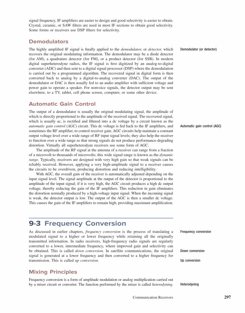
Communication Receivers 297
signal frequency, IF amplii ers are easier to design and good selectivity is easier to obtain.
Crystal, ceramic, or SAW i lters are used in most IF sections to obtain good selectivity.
Some forms or receivers use DSP i lters for selectivity.
Demodulators
The highly amplii ed IF signal is i nally applied to the demodulator, or detector, which
recovers the original modulating information. The demodulator may be a diode detector
(for AM), a quadrature detector (for FM), or a product detector (for SSB). In modern
digital superheterodyne radios, the IF signal is i rst digitized by an analog-to-digital
converter (ADC) and then sent to a digital signal processor (DSP) where the demodulation
is carried out by a programmed algorithm. The recovered signal in digital form is then
converted back to analog by a digital-to-analog converter (DAC). The output of the
demodulator or DAC is then usually fed to an audio amplii er with sufi cient voltage and
power gain to operate a speaker. For nonvoice signals, the detector output may be sent
elsewhere, to a TV, tablet, cell phone screen, computer, or some other device.
Automatic Gain Control
The output of a demodulator is usually the original modulating signal, the amplitude of
which is directly proportional to the amplitude of the received signal. The recovered signal,
which is usually ac, is rectii ed and i ltered into a dc voltage by a circuit known as the
automatic gain control (AGC) circuit. This dc voltage is fed back to the IF amplii ers, and
sometimes the RF amplii er, to control receiver gain. AGC circuits help maintain a constant
output voltage level over a wide range of RF input signal levels; they also help the receiver
to function over a wide range so that strong signals do not produce performance-degrading
distortion. Virtually all superheterodyne receivers use some form of AGC.
The amplitude of the RF signal at the antenna of a receiver can range from a fraction
of a microvolt to thousands of microvolts; this wide signal range is known as the dynamic
range. Typically, receivers are designed with very high gain so that weak signals can be
reliably received. However, applying a very high-amplitude signal to a receiver causes
the circuits to be overdriven, producing distortion and reducing intelligibility.
With AGC, the overall gain of the receiver is automatically adjusted depending on the
input signal level. The signal amplitude at the output of the detector is proportional to the
amplitude of the input signal; if it is very high, the AGC circuit produces a high dc output
voltage, thereby reducing the gain of the IF amplii ers. This reduction in gain eliminates
the distortion normally produced by a high-voltage input signal. When the incoming signal
is weak, the detector output is low. The output of the AGC is then a smaller dc voltage.
This causes the gain of the IF amplii ers to remain high, providing maximum amplii cation.
9-3 Frequency ConversionAs discussed in earlier chapters, frequency conversion is the process of translating a
modulated signal to a higher or lower frequency while retaining all the originally
transmitted information. In radio receivers, high-frequency radio signals are regularly
converted to a lower, intermediate frequency, where improved gain and selectivity can
be obtained. This is called down conversion. In satellite communications, the original
signal is generated at a lower frequency and then converted to a higher frequency for
transmission. This is called up conversion.
Mixing Principles
Frequency conversion is a form of amplitude modulation or analog multiplication carried out
by a mixer circuit or converter. The function performed by the mixer is called heterodyning.
Demodulator (or detector)
Automatic gain control (AGC)
Frequency conversion
Down conversion
Up conversion
Heterodyning

298 Chapter 9
Fig. 9-6 is a schematic diagram of a mixer circuit. Mixers accept two inputs. The
signal fs, which is to be translated to another frequency, is applied to one input, and the
sine wave from a local oscillator fo is applied to the other input. The signal to be trans-
lated can be a simple sine wave or any complex modulated signal containing sidebands.
Like an amplitude modulator, a mixer essentially performs a mathematical multiplication
of its two input signals according to the principles discussed in Chaps. 2 and 3. The
oscillator is the carrier, and the signal to be translated is the modulating signal. The output
contains not only the carrier signal but also sidebands formed when the local oscillator
and input signal are mixed. The output of the mixer, therefore, consists of signals
fs , fo
, fo 1 fs , and fo 2 fs
or fs 2 fo.
The local oscillator signal fo usually appears in the mixer output, as does the orig-
inal input signal fs in some types of mixer circuits. These are not needed in the output
and are therefore i ltered out. Either the sum or difference frequency in the output is the
desired signal. For example, to translate the input signal to a lower frequency, the lower
sideband or difference signal fo 2 fs is chosen. The local oscillator frequency will be
chosen such that when the information signal is subtracted from it, a signal with the
desired lower frequency is obtained. When translating to a higher frequency, the upper
sideband or sum signal fo 1 fs is chosen. Again, the local oscillator frequency determines
what the new higher frequency will be. A tuned circuit or i lter is used at the output of
the mixer to select the desired signal and reject all the others.
For example, for an FM radio receiver to translate an FM signal at 107.1 MHz
to an intermediate frequency of 10.7 MHz for amplii cation and detection, a local
oscillator frequency of 96.4 MHz is used. The mixer output signals are fs 5
107.1 MHz, fo 5 96.4 MHz, fo 1 fs 5 96.4 1 107.1 5 203.5 MHz, and fs 2 fo 5
107.1 2 96.4 5 10.7 MHz. Then a i lter selects the 10.7-MHz signal (the IF, or fIF) and
rejects the others.
As another example, suppose a local oscillator frequency is needed that will produce
an IF of 70 MHz for a signal frequency of 880 MHz. Since the IF is the difference
between the input signal and local oscillator frequencies, there are two possibilities:
fo 5 fs 1 fIF 5 880 1 70 5 950 MHz
fo 5 fs 2 fIF 5 880 2 70 5 810 MHz
There are no set rules for deciding which of these to choose. However, at lower frequen-
cies, say, those less than about 100 MHz, the local oscillator frequency is traditionally
higher than the incoming signal’s frequency, and at higher frequencies, those above
100 MHz, the local oscillator frequency is lower than the input signal frequency.
Keep in mind that the mixing process takes place on the whole spectrum of the input
signal, whether it contains only a single-frequency carrier or multiple carriers and many
complex sidebands. In the above example, the 10.7-MHz output signal contains the
original frequency modulation. The result is as if the carrier frequency of the input sig-
nal is changed, as are all the sideband frequencies. The frequency conversion process
Figure 9-6 Concept of a mixer.
TunedIntermediate
frequency
(IF)
circuitor
filter
Inputsignalfs
Mixer
fo
LO local oscillator
fo � fs
fo � fs
Mixer output: fo � fs
fo � fsfs*fo*
or
* May or may not be in the output dependingupon the type of mixer.

Communication Receivers 299
makes it possible to shift a signal from one part of the spectrum to another, as required
by the application.
Mixer and Converter Circuits
Any diode or transistor can be used to create a mixer circuit, but most modern mixers are
sophisticated ICs. This section covers some of the more common and widely used types.
Diode Mixers. The primary characteristic of mixer circuits is nonlinearity. Any device
or circuit whose output does not vary linearly with the input can be used as a mixer. For
example, one of the most widely used types of mixer is the simple but effective diode
modulator described in Chap. 3. Diode mixers like this are the most common type found
in microwave applications.
A diode mixer circuit using a single diode is shown in Fig. 9-7. The input signal,
which comes from an RF amplii er or, in some receivers, directly from the antenna, is
applied to the primary winding of transformer T1. The signal is coupled to the secondary
winding and applied to the diode mixer, and the local oscillator signal is coupled to the
diode by way of capacitor C1. The input and local oscillator signals are linearly added
in this way and applied to the diode, which performs its nonlinear magic to produce the
sum and difference frequencies. The output signals, including both inputs, are developed
across the tuned circuit, which acts as a bandpass i lter, selecting either the sum or dif-
ference frequency and eliminating the others.
Doubly Balanced Mixer. Balanced modulators are also widely used as mixers. These
circuits eliminate the carrier from the output, making the job of i ltering much easier.
Any of the balanced modulators described previously can be used in mixing applications.
Both the diode lattice balanced modulator and the integrated differential amplii er-type
balanced modulator are quite effective in mixing applications. A version of the diode
balanced modulator shown in Fig. 4-24, known as a doubly balanced mixer and illustrated
in Fig. 9-8, is probably the single best mixer available, especially for VHF, UHF, and
microwave frequencies. The transformers are precision-wound and the diodes matched
in characteristics so that a high degree of carrier or local oscillator suppression occurs.
In commercial products, the local oscillator attenuation is 50 to 60 dB or more.
FET Mixers. FETs make good mixers because they provide gain, have low noise, and
offer a nearly perfect square-law response. An example is shown in Fig. 9-9. The FET
mixer is biased so that it operates in the nonlinear portion of its range. The input signal
is applied to the gate, and the local oscillator signal is coupled to the source. Again, the
tuned circuit in the drain selects the difference frequency.
Diode mixer
Doubly balanced mixer
FET mixer
Figure 9-7 A simple diode mixer.
fo � fsor
fo � fs
C1
Inputfs
T1
fo
LO
Bandpassfilter

300 Chapter 9
Another popular FET mixer, one with a dual-gate MOSFET, is shown in Fig. 9-10.
Here the input signal is applied to one gate, and the local oscillator is coupled to the
other gate. Dual-gate MOSFETs provide superior performance in mixing applications
because their drain current ID is directly proportional to the product of the two gate
voltages. In receivers built for VHF, UHF, and microwave applications, junction FETs
and dual-gate MOSFETs are widely used as mixers because of their high gain and low
noise. Gallium arsenide FETs are preferred over silicon FETs at the higher frequencies
because of their lower noise contribution and higher gain. IC mixers use MOSFETs.
One of the best reasons for using a FET mixer is that its characteristic drain current
versus gate voltage curve is a perfect square-law function. (Recall that square-law for-
mulas show how upper and lower sidebands and sum and difference frequencies are
produced.) With a perfect square-law mixer response, only second-order harmonics are
Figure 9-8 A doubly balanced mixer very popular at high frequencies.
fo � fsand
fo � fs
Input
From antennaor RF amplifier
To bandpass filterand IF amplifier
fs
LOfo
Figure 9-9 A JFET mixer.
LOfo
fs
fo � fs
�VDD
N-channelJFET
From antennaor RF amplifier
To IF amplifier
GOOD TO KNOW
Any device or circuit whose output
is not a linear variation with the
input can be used as a mixer.

Communication Receivers 301
generated in addition to the sum and difference frequencies. Other mixers, such as diodes
and bipolar transistors, approximate a square-law function; however, they are nonlinear,
so that AM or heterodyning does occur. The nonlinearity is such that higher-order prod-
ucts such as the third, fourth, i fth, and higher harmonics are generated. Most of these
can be eliminated by a bandpass i lter that selects out the difference or sum frequency
for the IF amplii er. However, the presence of higher-order products can cause unwanted
low-level signals to appear in the receiver. These signals produce birdlike chirping sounds
known as birdies, which, despite their low amplitude, can interfere with low-level input
signals from the antenna or RF amplii er. FETs do not have this problem, and so FETs
are the preferred mixer in most receivers.
IC Mixers. A typical IC mixer, the NE602 mixer, is shown in Fig. 9-11(a). An improved
version is the SA612 mixer, which has roughly the same characteristics. The NE602/
SA612, also known as a Gilbert transconductance cell, or Gilbert cell, consists of a
doubly balanced mixer circuit made up of two cross-connected differential amplii ers.
Although most doubly balanced mixers are passive devices with diodes, as described
earlier, the NE602 uses bipolar transistors. Also on the chip is an NPN transistor that
can be connected as a stable oscillator circuit and a dc voltage regulator. The device is
housed in an 8-pin DIP. It operates from a single dc power supply voltage of 4.5 to 8 V.
The circuit can be used at frequencies up to 500 MHz, making it useful in HF, VHF,
and low-frequency UHF applications. The oscillator, which operates up to about 200
MHz, is internally connected to one input of the mixer. An external LC tuned circuit or
a crystal is required to set the operating frequency.
Fig. 9-11(b) shows the circuit details of the mixer itself. Bipolar transistors Q1 and
Q2 form a differential amplii er with current source Q3, and Q4 and Q5 form another
differential amplii er with current source Q6. Note that the inputs are connected in
parallel. The collectors are cross-connected; i.e., the collector of Q1 is connected to the
collector of Q4 instead of Q3, as would be the case for a parallel connection, and the
collector of Q2 is connected to the collector of Q3. This connection results in a circuit
that is like a balanced modulator in that the internal oscillator signal and the input signal
are suppressed, leaving only the sum and difference signals in the output. The output
may be balanced or single-ended, as required. A i lter or tuned circuit must be connected
to the output to select the desired sum or difference signal.
Birdies
NE602 mixer (Gilbert cell)
Figure 9-10 A dual-gate MOSFET mixer.
fs
fo � fs
LO
�VDD
Dual-gateMOSFET
To IFamplifier
From antennafo RF amplifier

302 Chapter 9
A typical circuit using the NE602/SA612 IC mixer is shown in Fig. 9-12. Both R1
and C1 are used for decoupling, and a resonant transformer T1 couples the 72-MHz input
signal to the mixer. Capacitor C2 resonates with the transformer secondary at the input
frequency, and C3 is an ac bypass connecting pin 2 to ground. External components C4
and L1 form a tuned circuit that sets the oscillator to 82 MHz. Capacitors C5 and C6
form a capacitive voltage divider that connects the on-chip NPN transistor as a Colpitts
oscillator circuit. Capacitor C7 is an ac coupling and blocking capacitor. The output is
taken from pin 4 and connected to a ceramic bandpass i lter, which provides selectivity.
Figure 9-11 NE602/SA612 IC mixer. (a) Block diagram and pinout. (b) Simplifi ed schematic.
1
2
3
4
8
7
6
5
�V
Osc. emitter
Osc. base
Output BOutput A
Ground
Input B
Input A
Mixer
Notch
Volt.reg.
Localosc.
(a)
Local oscillator
Osc.base
Osc. emitter
Q1 Q2
Input A Q3
Q5 Q4
V8
Volt.reg.
Output A
Output B
4
5
Q6
Input B2
3
(b)
Top view
6
7
1

Communication Receivers 303
The output, in this case the difference signal, or 82 2 72 5 10 MHz, appears across R2.
The balanced mixer circuit suppresses the 82-MHz oscillator signal, and the sum signal
of 154 MHz is i ltered out. The output IF signal plus any modulation that appeared on
the input is passed to IF amplii ers for an additional boost in gain prior to demodulation.
Image Reject Mixer. A special type of mixer is used in designs in which images
cannot be tolerated. All superheterodyne receivers suffer from images (see Sec. 9-4), but
some more than others because of the frequency of operation, chosen IF, and interfering
signal frequency. When proper choice of IF and front-end selectivity cannot eliminate
the images, an image reject mixer can be used. It uses Gilbert cell mixers in a coni guration
like that used in a phasing-type SSB generator. Referring to Chap. 4 and Fig. 4-28, you
can see how this circuit can be used as a mixer. A balanced modulator is also a mixer.
With this technique, the desired signal can be passed, but the image will be canceled by
the phasing technique. Such circuits are sensitive to adjust, but they result in superior
image performance in critical applications. This approach is used in some modern UHF
and microwave IC receivers.
Local Oscillators and Frequency Synthesizers
The local oscillator signal for the mixer comes from either a conventional LC tuned
oscillator such as a Colpitts or Clapp circuit or a frequency synthesizer. The simpler
continuously tuned receivers use an LC oscillator. Channelized receivers use frequency
synthesizers.
LC Oscillators. A representative local oscillator for frequencies up to 100 MHz is
shown in Fig. 9-13. This type of circuit, which is sometimes referred to as a variable-
frequency oscillator, or VFO, uses a JFET Q1 connected as a Colpitts oscillator. Feedback
is developed by the voltage divider, which is made up of C5 and C6. The frequency is
set by the parallel-tuned circuit made up of L1 in parallel with C1, which is also in
parallel with the series combination of C2 and C3. The oscillator is set to the center of
its desired operating range by a coarse adjustment of trimmer capacitor C1. Coarse tuning
can also be accomplished by making L1 variable. An adjustable slug-tuned ferrite core
moved in and out of L1 can set the desired frequency range. The main tuning is accom-
plished with variable capacitor C3, which is connected mechanically to some kind of dial
mechanism that has been calibrated in frequency.
Image reject mixer
LC oscillator
Figure 9-12 NE602/SA612 mixer used for frequency translation.
1
2
3
4
8
7
6
5Not usedMixer
Volt.reg.
Localosc.
C3C2
T1
Input
72 MHz
R1
�6 V
C1
C7
C5C4
C6
L1
82 MHz
Output
10 MHz to IF amplifier
R2
Ceramic bandpassfilter (10 MHz)
Local oscillatortuned circuit
Fromantenna orRF amplifier

304 Chapter 9
Main tuning can also be accomplished with varactors. For example, C3 in Fig. 9-13
can be replaced by a varactor, reverse-biased to make it act as a capacitor. Then a poten-
tiometer applies a variable dc bias to change the capacitance and thus the frequency.
The output of the oscillator is taken from across the RFC in the source lead of Q1
and applied to a direct-coupled emitter follower. The emitter follower buffers the output,
isolating the oscillator from load variations that can change its frequency. The emitter-
follower buffer provides a low-impedance source to connect to the mixer circuit, which
often has a low input impedance. If frequency changes after a desired station is tuned
in, which can occur as a result of outside inl uences such as changes in temperature,
voltage, and load, the signal will drift off and no longer be centered in the passband of
the IF amplii er. One of the key features of local oscillators is their stability, i.e., their
ability to resist frequency changes. The emitter follower essentially eliminates the effects
of load changes. The zener diode gets its input from the power supply, which is regulated,
providing a regulated dc to the circuit and ensuring maximum stability of the supply
voltage to Q1.
Most drift comes from the LC circuit components themselves. Even inductors, which
are relatively stable, have slight positive temperature coefi cients, and special capacitors
that change little with temperature are essential. Usually, negative temperature coefi cient
(NPO) ceramic capacitors are selected to offset the positive temperature coefi cient of
the inductor. Capacitors with a mica dielectric are also used.
Frequency Synthesizers. Most new receiver designs incorporate frequency
synthesizers for the local oscillator, which provides some important benei ts over the
simple VFO designs. First, since the synthesizer is usually of the phase-locked loop
(PLL) design, the output is locked to a crystal oscillator reference, providing a high
degree of stability. Second, tuning is accomplished by changing the frequency division
factor in the PLL, resulting in incremental rather than continuous frequency changes.
Most communication is channelized; i.e., stations operate on assigned frequencies that
are a known frequency increment apart, and setting the PLL step frequency to the channel
spacing allows every channel in the desired spectrum to be selected simply by changing
the frequency division factor. In some advanced digital receivers, a DDS synthesizer is
used for the local oscillator and all tuning is digital.
Frequency synthesizer
Figure 9-13 A VFO for receiver local oscillator service.
L1
C1
C2 R2
R1
D1
Q1
Q2
R3
C5
C4
C3 C6
C8
C7
RFCTo mixer
�V
Main tuning

Communication Receivers 305
The former disadvantages of frequency synthesizers—higher cost and greater circuit
complexity—have been offset by the availability of low-cost PLL synthesizer ICs, which
make local oscillator design simple and cheap. Most modern receivers, from AM/FM car
radios, stereos, and TV sets to military receivers and commercial transceivers, use
frequency synthesis.
The frequency synthesizers used in receivers are largely identical to those described
in Chap. 8. However, some additional techniques, such as the use of a mixer in the
feedback loop, are employed. The circuit in Fig. 9-14 is a traditional PLL coni guration,
with the addition of a mixer connected between the VFO output and the frequency
divider. A crystal reference oscillator provides one input to a phase detector, which is
compared to the output of the frequency divider. Tuning is accomplished by adjusting
the frequency division ratio by changing the binary number input to the divider circuit.
This binary number can come from a switch, a counter, a ROM, or a microprocessor.
The output of the phase detector is i ltered by the loop i lter into a dc control voltage to
vary the frequency of the variable-frequency oscillator, which generates the i nal output
that is applied to the mixer in the receiver.
As stated previously, one of the disadvantages of very high-frequency PLL synthesiz-
ers is that the VFO output frequency is often higher in frequency than the upper operating
limit of the variable-modulus frequency divider ICs commonly available. One approach
to this problem is to use a prescaler to reduce the VFO frequency before it is applied to
the variable-frequency divider. Another is to reduce the VFO output frequency to a lower
value within the range of the dividers by down-converting it with a mixer, as illustrated
in Fig. 9-14. The VFO output is mixed with the signal from another crystal oscillator,
and the difference frequency is selected. With some UHF and microwave receivers, it is
necessary to generate the local oscillator signal at a lower frequency and then use a PLL
frequency multiplier to increase the frequency to the desired higher level. The position
of this optional multiplier is shown by the dotted line in Fig. 9-14.
As an example, assume that a receiver must tune to 190.04 MHz and that the IF is
45 MHz. The local oscillator frequency can be either 45 MHz lower or higher than the
input signal. Using the lower frequency, we have 190.04 2 45 5 145.04 MHz. Now,
when the incoming 190.04-MHz signal is mixed with the 145.04-MHz signal to be gen-
erated by the synthesizer in Fig. 9-14, its IF will be the difference frequency of
190.04 2 145.04 5 45 MHz.
GOOD TO KNOW
Most modern receivers, including
stereos, car radios, and military
and commercial receivers, use
frequency synthesis PLL or DDS.
Figure 9-14 A frequency synthesizer used as a receiver local oscillator.
XTAL
oscillator
LPF
loop
Frequency
multiplier
�4
Variable
modulus
frequency divider
� 268
XTAL
reference
oscillator
VFO�
100
Frequency
multiplier
XTAL
3 MHz
34.25 MHz
137 MHz
Binary inputs
from tuning
circuits
30 kHz30 kHz
Phase
detector
Optional frequency multiplier
Local
oscillator
signal
to mixer
in receiver
145.04 MHz
8.04-MHz
mixer
XTAL

306 Chapter 9
The output of the VFO in Fig. 9-14 is 145.04 MHz. It is mixed with the signal from
a crystal oscillator whose frequency is 137 MHz. The crystal oscillator, set to 34.25 MHz,
is applied to a frequency multiplier that multiplies by a factor of 4. The 145.04-MHz signal
from the VFO is mixed with the 137-MHz signal, and the sum and difference frequencies
are generated. The difference frequency is selected, for 145.04 2 137 5 8.04 MHz. This
frequency is well within the range of programmable-modulus IC frequency dividers.
The frequency divider is set to divide by a factor of 268, and so the output of the
divider is 8,040,000/268 5 30,000 Hz, or 30 kHz. This signal is applied to the phase
detector. It is the same as the other input to the phase detector, as it should be for a
locked condition. The reference input to the phase detector is derived from a 3-MHz
crystal oscillator divided down to 30 kHz by a divide-by-100 divider. This means that
the synthesizer is stepped in 30-kHz increments.
Now, suppose that the divider factor is changed from 268 to 269 to tune the receiver.
To ensure that the PLL stays locked, the VFO output frequency must change. To achieve
30 kHz at the output of the divider with a ratio of 269, the divider input has to be
269 3 30 kHz 5 8070 kHz 5 8.07 MHz. This 8.07-MHz signal comes from the mixer,
whose inputs are the VFO and the crystal oscillator. The crystal oscillator input remains
at 137 MHz, so the VFO frequency must be 137 MHz higher than the 8.07-MHz output
of the mixer, or 137 1 8.07 5 145.07 MHz. This is the output of the VFO and local
oscillator of the receiver. With a i xed IF of 45 MHz, the receiver will now be tuned to
the IF plus the local oscillator input, or 145.07 1 45 5 190.07 MHz.
Note that the change of the divider factor by one increment, from 268 to 269,
changes the frequency by one 30-kHz increment, as desired. The addition of the mixer
to the circuit does not affect the step increment, which is still controlled by the frequency
of the reference input frequency.
9-4 Intermediate Frequency and ImagesThe choice of IF is usually a design compromise. The primary objective is to obtain
good selectivity. Narrowband selectivity is best obtained at lower frequencies, particularly
when conventional LC tuned circuits are used. Even active RC i lters can be used when
IFs of 500 KHz or less are used. There are various design benei ts of using a low IF. At
low frequencies, the circuits are far more stable with high gain. At higher frequencies,
circuit layouts must take into account stray inductances and capacitances, as well as the
need for shielding, if undesired feedback paths are to be avoided. With very high circuit
gain, some of the signal can be fed back in phase and cause oscillation. Oscillation is
not as much of a problem at lower frequencies. However, when low IFs are selected, a
different sort of problem is faced, particularly if the signal to be received is very high
in frequency. This is the problem of images. An image is a potentially interfering RF
signal that is spaced from the desired incoming signal by a frequency that is two times
the intermediate frequency above or below the incoming frequency, or
fi 5 fs 1 2fIF and fi 5 fs 2 2fIF
where fi 5 image frequency
fs 5 desired signal frequency
fIF 5 intermediate frequency
This is illustrated graphically in Fig. 9-15. Note that which of the images occurs depends
on whether the local oscillator frequency fo is above or below the signal frequency.
Frequency Relationships and Images
As stated previously, the mixer in a superhetodyne receiver produces the sum and
difference frequencies of the incoming signal and the local oscillator signal. Normally,
the difference frequency is selected as the IF. The frequency of the local oscillator is
Image
GOOD TO KNOW
Crowding of the RF spectrum
increases the chance that a signal
on the image frequency will
cause image interference. To help
remedy this, high-Q tuned circuits
should be used ahead of the
mixer or RF amplifi er.
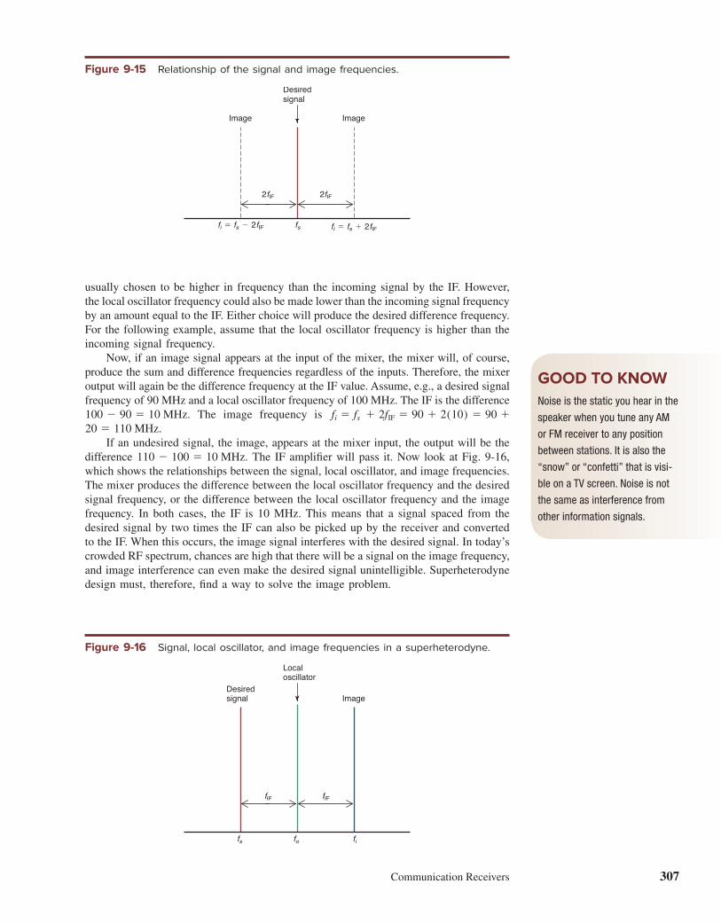
Communication Receivers 307
usually chosen to be higher in frequency than the incoming signal by the IF. However,
the local oscillator frequency could also be made lower than the incoming signal frequency
by an amount equal to the IF. Either choice will produce the desired difference frequency.
For the following example, assume that the local oscillator frequency is higher than the
incoming signal frequency.
Now, if an image signal appears at the input of the mixer, the mixer will, of course,
produce the sum and difference frequencies regardless of the inputs. Therefore, the mixer
output will again be the difference frequency at the IF value. Assume, e.g., a desired signal
frequency of 90 MHz and a local oscillator frequency of 100 MHz. The IF is the difference
100 2 90 5 10 MHz. The image frequency is fi 5 fs 1 2fIF 5 90 1 2(10) 5 90 1
20 5 110 MHz.
If an undesired signal, the image, appears at the mixer input, the output will be the
difference 110 2 100 5 10 MHz. The IF amplii er will pass it. Now look at Fig. 9-16,
which shows the relationships between the signal, local oscillator, and image frequencies.
The mixer produces the difference between the local oscillator frequency and the desired
signal frequency, or the difference between the local oscillator frequency and the image
frequency. In both cases, the IF is 10 MHz. This means that a signal spaced from the
desired signal by two times the IF can also be picked up by the receiver and converted
to the IF. When this occurs, the image signal interferes with the desired signal. In today’s
crowded RF spectrum, chances are high that there will be a signal on the image frequency,
and image interference can even make the desired signal unintelligible. Superheterodyne
design must, therefore, i nd a way to solve the image problem.
Figure 9-15 Relationship of the signal and image frequencies.
2fIF
2fIF
fs fi �2fIFfs �
Image Image
�fi � fs
Desiredsignal
2fIF
Figure 9-16 Signal, local oscillator, and image frequencies in a superheterodyne.
fIF
fo fi
Desiredsignal Image
fs
Localoscillator
fIF
GOOD TO KNOW
Noise is the static you hear in the
speaker when you tune any AM
or FM receiver to any position
between stations. It is also the
“snow” or “confetti” that is visi-
ble on a TV screen. Noise is not
the same as interference from
other information signals.

308 Chapter 9
Solving the Image Problem
Image interference occurs only when the image signal is allowed to appear at the mixer
input. This is the reason for using high-Q tuned circuits ahead of the mixer, or a selective
RF amplii er. If the selectivity of the RF amplii er and tuned circuits is good enough,
the image will be rejected. In a i xed tuned receiver designed for a specii c frequency, it
is possible to optimize the receiver front end for the good selectivity necessary to
eliminate images. But many receivers have broadband RF amplii ers that allow many
frequencies within a specii c band to pass. Other receivers must be made tunable over a
wide frequency range. In such cases, selectivity becomes a problem.
Assume, e.g., that a receiver is designed to pick up a signal at 25 MHz. The IF is
500 kHz, or 0.5 MHz. The local oscillator is adjusted to a frequency right above the
incoming signal by an amount equal to the IF, or 25 1 0.5 5 25.5 MHz. When the local
oscillator and signal frequencies are mixed, the difference is 0.5 MHz, as desired. The
image frequency is fi 5 fs 1 2fIF 5 25 1 2(0.5) 5 26 MHz. An image frequency of
26 MHz will cause interference to the desired signal at 25 MHz unless it is rejected. The
signal, local oscillator, and image frequencies for this situation are shown in Fig. 9-17.
Now, assume that a tuned circuit ahead of the mixer has a Q of 10. Given this and
the resonant frequency, the bandwidth of the resonant circuit can be calculated as
BW 5 fryQ 5 25y10 5 2.5 MHz. The response curve for this tuned circuit is shown in
Fig. 9-17. As shown, the bandwidth of the resonant circuit is relatively wide. The
bandwidth is centered on the signal frequency of 25 MHz. The upper cutoff frequency
is f2 5 26.25 MHz, the lower cutoff frequency is f1 5 23.75 MHz, and the bandwidth
is BW 5 f2 2 f1 5 26.25 2 23.75 5 2.5 MHz. (Remember that the bandwidth is
measured at the 3-dB down points on the tuned circuit response curve.)
The fact that the upper cutoff frequency is higher than the image frequency,
26 MHz, means that the image frequency appears in the passband; it would thus
be passed relatively unattenuated by the tuned circuit, causing interference.
It is clear how cascading tuned circuits and making them with higher Qs can
help solve the problem. For example, assume a Q of 20, instead of the previously
given value of 10. The bandwidth at the center frequency of 25 MHz is then
fsyQ 5 25y20 5 1.25 MHz.
The resulting response curve is shown by the darker line in Fig. 9-17. The image is
now outside of the passband and is thus attenuated. Using a Q of 20 would not solve
the image problem completely, but still higher Qs would further narrow the bandwidth,
attenuating the image even more.
Figure 9-17 A low IF compared to the signal frequency with low-Q tuned circuits causes images to pass and interfere.
23.5
23.75
24 25 25.5 26 26.5
26.25
24.5fo
fo
fi
fi
fs
fs
f1 f2
0 dB
�3 dBQ � 10
Q � 20
Frequency (MHz)
BW � 2.5 MHz
BW � 1.25 MHz

Communication Receivers 309
Higher Qs are, however, difi cult to achieve and often complicate the design of
receivers that must be tuned over a wide range of frequencies. The usual solution to this
problem is to choose a higher IF. Assume, e.g., that an intermediate frequency of 9 MHz
is chosen (the Q is still 10). Now the image frequency is fi 5 25 1 2(9) 5 43 MHz.
A signal at a 43-MHz frequency would interfere with the desired 25-MHz signal if it
were allowed to pass into the mixer. But 43 MHz is well out of the tuned circuit band-
pass; the relatively low-Q selectivity of 10 is sufi cient to adequately reject the image.
Of course, choosing the higher intermediate frequency causes some design difi culties,
as indicated earlier.
To summarize, the IF is made as high as possible for effective elimination of the
image problem, yet low enough to prevent design problems. In most receivers, the IF
varies in proportion to the frequencies that must be covered. At low frequencies, low
values of IF are used. A value of 455 kHz is common for AM broadcast band receivers
and for others covering that general frequency range. At frequencies up to about 30 MHz,
3385 kHz and 9 MHz are common IF frequencies. In FM radios that receive 88 to
108 MHz, 10.7 MHz is a standard IF. In TV receivers, an IF in the 40- to 50-MHz range
is common. In the microwave region, radar receivers typically use an IF in the 60-MHz
range, and satellite communication equipment uses 70- and 140-MHz IFs.
Dual-Conversion Receivers
Another way to obtain selectivity while eliminating the image problem is to use a
dual-conversion superheterodyne receiver. See Fig. 9-18. The receiver shown in the i gure
uses two mixers and local oscillators, and so it has two IFs. The i rst mixer converts the
incoming signal to a relatively high intermediate frequency for the purpose of eliminating
the images; the second mixer converts that IF down to a much lower frequency, where
good selectivity is easier to obtain.
Fig. 9-18 shows how the different frequencies are obtained. Each mixer produces
the difference frequency. The i rst local oscillator is variable and provides the tuning for
the receiver. The second local oscillator is i xed in frequency. Since it need convert only
one i xed IF to a lower IF, this local oscillator does not have to be tunable. In most cases,
its frequency is set by a quartz crystal. In some receivers, the i rst mixer is driven by the
i xed-frequency local oscillator, and tuning is done with the second local oscillator.
Dual-conversion receivers are relatively common. Most shortwave receivers and many at
VHF, UHF, and microwave frequencies use dual conversion. For example, a CB receiver
operating in the 27-MHz range typically uses a 10.7-MHz i rst IF and a 455-kHz second
IF. For some critical applications, triple-conversion receivers are used to further minimize
the image problem, although their use is not common. A triple-conversion receiver uses
three mixers and three different intermediate-frequency values.
Dual-conversion receiver
GOOD TO KNOW
For a dual-conversion superhet-
erodyne, if you have an input
value fs and the two local oscilla-
tor values fLO1 and fLO2
, you can
determine what the two interme-
diate frequencies (IFs) are. First,
determine the difference between
the input and the fi rst local
oscillator: fs 2 fLO15 IF1. Now
the IF1 value is the input for the
second mixer. To determine the
second intermediate frequency,
fi nd the difference between the
fi rst intermediate frequency and
the second local oscillator:
IF1 2 fLO25 IF2.
Figure 9-18 A dual-conversion superheterodyne.
Originalsignal
FirstLO
SecondLO
100 MHz
RF amplifierFirstmixer
Secondmixer IF amplifier
First IF Second IF
110.7 MHz
10.7 MHz
11.155 MHz
455 kHz
Recoveredmodulating
signalTunableor
synthesizedXTAL
Demodulator

310 Chapter 9
Direct Conversion Receivers
A special version of the superheterodyne is known as the direct conversion (DC) or zero-
IF (ZIF) receiver. Instead of translating the incoming signal to another (usually lower)
intermediate frequency, dc receivers convert the incoming signal directly to baseband. In
other words, they perform the demodulation of the signal as part of the translation.
Fig. 9-19 shows the basic ZIF receiver architecture. The low-noise amplii er
(LNA) boosts the signal level before the mixer. The local oscillator (LO) frequency,
usually from a PLL frequency synthesizer fLO, is set to the frequency of the incoming
signal fs.
fLO 5 fs
The sum and difference frequencies as a result of mixing are
fLO 2 fs 5 0
fLO 1 fs 5 2fLO 5 2fs
The difference frequency is zero. Without modulation, there is no output. With AM, the
sidebands mix with the LO to reproduce the original modulation baseband signal. In this
instance, the mixer is also the demodulator. The sum is twice the LO frequency that is
removed by the low-pass i lter (LPF).
Direct conversion (DC) or zero-IF (ZIF) receiver
Example 9-1A superheterodyne receiver must cover the range from 220 to 224 MHz. The i rst IF
is 10.7 MHz; the second is 1.5 MHz. Find (a) the local oscillator tuning range, (b) the
frequency of the second local oscillator, and (c) the i rst IF image frequency range.
(Assume a local oscillator frequency higher than the input by the IF.)
a. 220 1 10.7 5 230.7 MHz
224 1 10.7 5 234.7 MHz
The tuning range is 230.7 to 234.7 MHz
b. The second local oscillator frequency is 1.5 MHz higher than the i rst IF.
10.7 1 1.5 5 12.2 MHz
c. The i rst IF image range is 241.4 to 245.4 MHz.
230.7 1 10.7 5 241.4 MHz
234.7 1 10.7 5 245.4 MHz
Figure 9-19 A direct-conversion (zero-IF) receiver.
LPF
LO
LNA Mixer
Demodulated
baseband outputfs
fLO
fLO � fs

Communication Receivers 311
Assume a carrier of 21 MHz and a voice modulation signal from 300 to 3000 Hz
and AM. The sidebands extend from 20,997,000 to 21,003,000 Hz. At the receiver, the
LO is set to 21 MHz. The mixer produces
21,000,000 2 20,997,000 5 3000 Hz
21,003,000 2 21,000,000 5 3000 Hz
21,000,000 1 21,003,000 5 42,003,000 Hz
21,000,000 1 20,997,000 5 41,997,000 Hz
A low-pass i lter at the mixer output whose cutoff frequency is set to 3 kHz easily i lters
out the 42-MHz components.
The DC receiver has several key benei ts. First, no separate IF i lter is needed. This
is usually a crystal, ceramic, or SAW i lter that is expensive and takes up valuable printed-
circuit board space in compact designs. An inexpensive RC, LC, or active low-pass i lter
at the mixer output supplies the needed selectivity. Second, no separate detector circuit
is needed, because demodulation is inherent in the technique. Third, in transceivers that
use half duplex and in which the transmitter and receiver are on the same frequency, only
one PLL frequency synthesizer voltage-controlled oscillator is needed. All these benei ts
result in simplicity and its attendant lower cost. Fourth, there is no image problem.
The disadvantages of this receiver are subtle. In designs with no RF amplii er (LNA),
the LO signal can leak through the mixer to the antenna and radiate. A LNA reduces this
likelihood, but even so, careful design is required to minimize the radiation. Second, an
undesired dc offset can develop in the output. Unless all circuits are perfectly balanced,
dc offset can upset bias arrangements in later circuits as well as cause circuit saturation
that will prevent amplii cation and other operations. Finally, the ZIF receiver can be used
only with CW, AM, SSB, or DSB. It cannot recognize phase or frequency variations.
To use this type of receiver with FM, FSK, PM, or PSK, or any form of digital
modulation, two mixers are required along with a quadrature LO arrangement. Such
designs are used in most cell phones and other wireless receivers.
Fig. 9-20 shows a direct conversion receiver that is typical of those using digital
modulation. The incoming signal is sent to a SAW i lter that provides some initial selec-
tivity. The LNA provides amplii cation. The LNA output is fed to two mixers. The local
oscillator (LO) signal, usually from a synthesizer, is fed directly to the upper mixer
(sin u) and to a 90° phase shifter that, in turn, supplies the lower mixer (cos u). Remem-
ber, the LO frequency is equal to the incoming signal frequency. The mixers provide
baseband signals at their outputs. The double LO frequency signals resulting from mix-
ing are removed with the low-pass i lters (LPFs). The two baseband signals are separated
in phase by 90°. The upper signal is usually referred to as the in-phase I signal while
Figure 9-20 A direct conversion receiver for FM, FSK, PSK, and digital modulation.
Mixer
I
Q
cos �
sin �
90°
DSP
Mixer
Recoveredbaseband signal
LPF
LO
SAW
filter
ADC
LPF ADC
DAC
LNA
GOOD TO KNOW
Direct conversion receivers save
circuit board space and do not
require a separate demodulator
circuit. However, in this circuit the
LO signal can sometimes leak out
through the mixer.

312 Chapter 9
the lower signal is referred to as the quadrature Q signal. (Quadrature means a 90° phase
difference.) The I and Q signals are then sent to analog-to-digital converters (ADCs)
where they are converted to binary signals. The binary signals are then sent to a digital
signal processor (DSP). The DSP contains a prestored subroutine that performs the
demodulation. This algorithm requires the two quadrature signals in order to have enough
data to distinguish phase and frequency changes in the original signal resulting from
modulation. The output from the demodulation subroutine is fed to an external digital-
to-analog converter (DAC) where the original modulating signal is reproduced. This I-Q
direct conversion architecture is now one of the most common receiver architectures used
in cell phones and wireless networking ICs.
Low IF Receiver
An alternative to a direct conversion receiver is the low IF receiver. This design is used
to mitigate or eliminate the LO leakage and dc output problems. The resulting receiver
is still a superheterodyne, but using a low IF offers other benei ts such as simpler i lters.
What is a low IF? It depends upon the operating frequency. Early cell phone designs
used an IF in the 125 kHz range, making it possible to use simple on-chip RC i lters.
In other designs, a low IF may be in the 1 or 2 MHz range if the operating frequency
is above 1 GHz.
Software-Defi ned Radio
A software-dei ned radio (SDR) is a receiver in which most of the functions are performed
by a digital signal processor. Fig. 9-21 is a general block diagram of an SDR. While
only one mixer and ADC are shown, keep in mind that the I and Q architecture of
Fig. 9-20 is normally used. As in most receivers, a LNA provides initial amplii cation
and a mixer down-converts the signal to an IF or to baseband in a DC receiver. The IF
or baseband signal is then digitized by an analog-to-digital (A/D) converter. The binary
words representing the IF signal with its modulation are stored in RAM. A DSP chip
then performs additional i ltering, demodulation, and baseband operations (voice decod-
ing, companding, etc.).
The fastest A/D converters available today can digitize at a rate of up to 300 MHz.
To meet the Nyquist requirement, this means that the highest frequency that can be
digitized is less than 150 MHz. This is why the SDR must down-convert the incoming
signal to an IF of less than 150 MHz. Further, the DSP must be fast enough to perform
Software-defi ned radio
Figure 9-21 A software-defi ned radio (SDR).
DSP
LO
LNA Mixer
Filtering,
demodulation, etc.
Recovered
baseband signal
A/Dconverter
RAM ROM
Digitized data
stored here
Program
algorithms
stored here

Communication Receivers 313
the DSP math in real time. Although DSP chips can operate at clock rates up to 1 GHz,
the time it takes to execute even at these speeds limits the IF to a lower value. A practical
value is in the 40- to 90-MHz range, where the A/D converter and the DSP can handle
the computing chores.
An alternative is to use a dual-conversion SDR. The i rst mixer converts the signal
to an IF that is then fed to the A/D converter, where it digitizes the data. The DSP chip
is then used to down-convert the signal to an even lower IF. This mixing or down
converstion is done digitally. It is similar to the process of aliasing, in which a lower
difference frequency is generated. From there the DSP performs the i ltering and
demodulation duties. Today, most IC receiver designs are similar to that shown in
Fig. 9-20. For some designs, the critical ADC sampling frequency can be lowered using
undersampling techniques as described in Chap. 7.
The i ltering, demodulation, and other processes are, of course, dei ned by mathe-
matical algorithms that are in turn programmed with a computer language. The resulting
programs are stored in the DSP ROM.
SDR techniques have been known for many years, but only since the early to
mid-1990s have A/D converter circuits and DSP chips become fast enough to perform
the desired operations at radio frequencies. SDRs have already been widely adopted in
military receivers, cell phones, and cell phone base stations. As prices continue to drop
and as A/D converters become even faster, these methods will become even more widely
used in other communication equipment.
The benei ts of SDRs are improved performance and l exibility. DSP i ltering and
other processes are typically superior to equivalent analog techniques. Furthermore, the
receiver characteristics (type of modulation, selectivity, etc.) can be easily changed by
running a different program. SDRs can be changed by downloading or switching to a
new processing program that the DSP can execute. No hardware changes are required.
As A/D converters and DSPs get faster, it is expected that more receiver functions
will become software-dei ned. The ultimate SDR is a LNA connected to an antenna and
whose output goes directly to a fast A/D converter. All mixing, i ltering, demodulation,
and other operations are performed in DSP software.
COGNITIVE RADIO
Cognitive radio is the term describing an advanced form of SDR that is designed to help
alleviate the frequency spectrum shortage. While most of the usable frequency spectrum has
already been assigned by the various government regulating agencies, at any given time much
of that spectrum goes unused, at least for part of the time. The question is, How can that
spectrum be more efficiently assigned and used? A good example is the frequency spectrum
assigned to the UHF TV stations. This spectrum in the 500- to 800-MHz range is essentially
vacant except for the occasional UHF TV station. Few people watch UHF TV directly by radio.
Instead, most watch by cable, satellite, or Internet TV, which may retransmit the UHF TV station.
This is a huge waste of precious spectrum space, yet broadcasters are reluctant to give it up.
The cell phone companies, which are perpetually short of spectrum for new subscribers, covet
this unused but unattainable space.
A cognitive radio is designed to seek out unused spectrum space and then reconfigure
itself to receive and transmit on unused portions of the spectrum that it finds. Such radios are
now possible because of the availability of very agile and wide-ranging frequency synthesizers
and DSP techniques. The radio could easily change frequency as well as modulation/ multiplexing
methods on the fly to establish communications. Consumer, military, and government service
radios are now beginning to take advantage of these techniques. Chap. 21 will discuss a
specific case of cognitive radio called “white space” radio.
Cognitive radio

314 Chapter 9
9-5 NoiseNoise is an electronic signal that is a mixture of many random frequencies at many
amplitudes that gets added to a radio or information signal as it is transmitted from one
place to another or as it is processed. Noise is not the same as interference from other
information signals.
When you turn on any AM, FM, or shortwave receiver and tune it to some position
between stations, the hiss or static that you hear in the speaker is noise. Noise also shows
up on a black-and-white TV screen as snow or on a color screen as confetti. If the noise
level is high enough and/or the signal is weak enough, the noise can completely obliter-
ate the original signal. Noise that occurs in transmitting digital data causes bit errors and
can result in information being garbled or lost.
The noise level in a system is proportional to temperature and bandwidth, and to
the amount of current l owing in a component, the gain of the circuit, and the resistance of the circuit. Increasing any of these factors increases noise. Therefore, low noise is best obtained by using low-gain circuits, low direct current, low resistance values, and narrow bandwidths. Keeping the temperature low can also help. Noise is a problem in communication systems whenever the received signals are very low in amplitude. When the transmission is over short distances or high-power transmitters are being used, noise is not usually a problem. But in most communication systems, weak signals are normal, and noise must be taken into account at the design stage. It is in the receiver that noise is the most detrimental because the receiver must amplify the weak signal and recover the information reliably. Noise can be external to the receiver or originate within the receiver itself. Both types are found in all receivers, and both affect the SNR.
Signal-to-Noise Ratio
The signal-to-noise (S/N) ratio, also designated SNR, indicates the relative strengths of the signal and the noise in a communication system. The stronger the signal and the weaker the noise, the higher the S/N ratio. If the signal is weak and the noise is strong, the S/N ratio will be low and reception will be unreliable. Communication equipment is designed to produce the highest feasible S/N ratio. Signals can be expressed in terms of voltage or power. The S/N ratio is computed by using either voltage or power values:
S
N 5
Vs
Vn
or S
N5
Ps
Pn
where Vs 5 signal voltage Vn 5 noise voltage Ps 5 signal power Pn 5 noise power
Assume, e.g., that the signal voltage is 1.2 µV and the noise is 0.3 µV. The S/N ratio is 1.2/0.3 5 4. Most S/N ratios are expressed in terms of power rather than voltage. For example, if the signal power is 5 µW and the power is 125 nW, the S/N ratio is 5 3 1026/125 3 1029 5 40. The preceding S/N values can be converted to decibels as follows:
For voltage: dB 5 20 log
S
N5 20 log 4 5 20(0.602) 5 12 dB
For power: dB 5 10 log
S
N5 10 log 40 5 10(1.602) 5 16 dB
However, it is expressed, if the S/N ratio is less than 1, the dB value will be negative and the noise will be stronger than the signal.
Noise
Signal-to-noise (S/N ) ratio

Communication Receivers 315
External Noise
External noise comes from sources over which we have little or no control—
industrial, atmospheric, or space. Regardless of its source, noise shows up as a random
ac voltage and can be seen on an oscilloscope. The amplitude varies over a wide range,
as does the frequency. One can say that noise in general contains all frequencies, varying
randomly. This is generally known as white noise.
Atmospheric noise and space noise are a fact of life and simply cannot be eliminated.
Some industrial noise can be controlled at the source, but because there are so many
sources of this type of noise, there is no way to eliminate it. The key to reliable
communication, then, is simply to generate signals at a high enough power to overcome
external noise. In some cases, shielding sensitive circuits in metallic enclosures can aid
in noise control.
Industrial Noise. Industrial noise is produced by manufactured equipment, such as
automotive ignition systems, electric motors, and generators. Any electrical equipment
that causes high voltages or currents to be switched produces transients that create noise.
Noise pulses of large amplitude occur whenever a motor or other inductive device is
turned on or off. The resulting transients are extremely large in amplitude and rich in
random harmonics. Fluorescent and other forms of gas-i lled lights are another common
source of industrial noise.
Atmospheric Noise. The electrical disturbances that occur naturally in the earth’s
atmosphere are another source of noise. Atmospheric noise is often referred to as static.
Static usually comes from lightning, the electric discharges that occur between clouds
or between the earth and clouds. Huge static charges build up on the clouds, and when
the potential difference is great enough, an arc is created and electricity literally l ows
through the air. Lightning is very much like the static charges that we experience during
a dry spell in the winter. The voltages involved are, however, enormous, and these tran-
sient electric signals of megawatt power generate harmonic energy that can travel over
extremely long distances.
Like industrial noise, atmospheric noise shows up primarily as amplitude variations
that add to a signal and interfere with it. Atmospheric noise has its greatest impact on
signals at frequencies below 30 MHz.
Extraterrestrial Noise. Extraterrestrial noise, solar and cosmic, comes from sources
in space. One of the primary sources of extraterrestrial noise is the sun, which radiates
a wide range of signals in a broad noise spectrum. The noise intensity produced by the
sun varies with time. In fact, the sun has a repeatable 11-year noise cycle. During the
peak of the cycle, the sun produces an awesome amount of noise that causes tremendous
radio signal interference and makes many frequencies unusable for communication.
During other years, the noise is at a lower level.
Noise generated by stars outside our solar system is generally known as cosmic
noise. Although its level is not as great as that of noise produced by the sun, because of
the great distances between those stars and earth, it is nevertheless an important source
of noise that must be considered. It shows up primarily in the 10-MHz to
1.5-GHz range, but causes the greatest disruptions in the 15- to 150-MHz range.
Internal Noise
Electronic components in a receiver such as resistors, diodes, and transistors are
major sources of internal noise. Internal noise, although it is low level, is often great
enough to interfere with weak signals. The main sources of internal noise in a
receiver are thermal noise, semiconductor noise, and intermodulation distortion.
Since the sources of internal noise are well known, there is some design control over
this type of noise.
External noise
White noise
Industrial noise
Atmospheric noise
Static
Extraterrestrial noise
Cosmic noise
Internal noise
GOOD TO KNOW
Low noise is best obtained by
using low-gain circuits, low direct
current, low resistance values,
and narrow bandwidths. Keeping
temperature low can also help.

316 Chapter 9
Thermal Noise. Most internal noise is caused by a phenomenon known as thermal
agitation, the random motion of free electrons in a conductor caused by heat. Increasing
the temperature causes this atomic motion to increase. Since the components are
conductors, the movement of electrons constitutes a current l ow that causes a small
voltage to be produced across that component. Electrons traversing a conductor as current
l ows experience l eeting impediments in their path as they encounter the thermally
agitated atoms. The apparent resistance of the conductor thus l uctuates, causing the
thermally produced random voltage we call noise.
You can actually observe this noise by simply connecting a high-value (megohm)
resistor to a very high-gain oscilloscope. The motion of the electrons due to room
temperature in the resistor causes a voltage to appear across it. The voltage variation is
completely random and at a very low level. The noise developed across a resistor is
proportional to the temperature to which it is exposed.
Thermal agitation is often referred to as white noise or Johnson noise, after J. B.
Johnson, who discovered it in 1928. Just as white light contains all other light frequencies,
white noise contains all frequencies randomly occurring at random amplitudes. A white
noise signal therefore occupies, theoretically at least, ini nite bandwidth. Filtered or
band-limited noise is referred to as pink noise.
In a relatively large resistor at room temperature or higher, the noise voltage across
it can be as high as several microvolts. This is the same order of magnitude as or higher
than that of many weak RF signals. Weaker-amplitude signals will be totally masked by
this noise.
Since noise is a very broadband signal containing a tremendous range of random
frequencies, its level can be reduced by limiting the bandwidth. If a noise signal is
fed into a selective tuned circuit, many of the noise frequencies are rejected and the
overall noise level goes down. The noise power is proportional to the bandwidth of
any circuit to which it is applied. Filtering can reduce the noise level, but does not
eliminate it entirely.
The amount of open-circuit noise voltage appearing across a resistor or the input
impedance to a receiver can be calculated according to Johnson’s formula
υn 5 14kTBR
where υn 5 rms noise voltage
k 5 Boltzman’s constant (1.38 3 10223 J/K)
T 5 temperature, K (°C 1 273)
B 5 bandwidth, Hz
R 5 resistance, V
The resistor is acting as a voltage generator with an internal resistance equal to the
resistor value. See Fig. 9-22. Naturally, if a load is connected across the resistor generator,
the voltage will decrease as a result of voltage divider action.
Thermal noise
White (Johnson) noise
GOOD TO KNOW
White noise or Johnson noise
contains all frequencies and
amplitudes.
Example 9-2What is the open-circuit noise voltage across a 100-kV resistor over the frequency
range of direct current to 20 kHz at room temperature (25°C)?
υn 5 14kTBR
5 24(1.38 3 10223)(25 1 273)(20 3 103) (100 3 103)
υn 5 5.74 µV

Communication Receivers 317
Example 9-3The bandwidth of a receiver with a 75-V input resistance is 6 MHz. The temperature
is 29°C. What is the input thermal noise voltage?
T 5 29 1 273 5 302 K
υn 5 14kTBR
υn 5 24(1.38 3 10223)(302)(6 3 106)(75) 5 2.74 µV
VR
L � V
n
RL
RL�
� Rn
Vn �
Vn
Rn
Heat
energy
V
Rn
Noise
voltage
Vn
Vn
V
Rn
RL
Open circuit
4kTBR
Figure 9-22 A resistor acts as a tiny generator of noise voltage.
TEMPERATURE SCALES AND CONVERSIONS
Three temperature scales are in common use: the Fahrenheit scale, expressed in degrees
Fahrenheit (8F); the Celsius scale (formerly centigrade), expressed in degrees Celsius (8C); and
the Kelvin scale, expressed in kelvins (K). The Kelvin scale, which is used by scientists, is also
known as the absolute scale. At 0 K (2273.158C and 2459.698F), or absolute zero, molecular
motion ceases.
When calculating noise values, you will frequently need to make conversions from one of
these temperature scales to another. The most common conversion formulas are given here.
TC 5 5(TF 2 32)/9 or TC = TK 2 273
TF 59TC
51 32
TK 5 TC 1 273

318 Chapter 9
Since noise voltage is proportional to resistance value, temperature, and bandwidth,
noise voltage can be reduced by reducing resistance, temperature, and bandwidth or any
combination to the minimum level acceptable for the given application. In many cases,
of course, the values of resistance and bandwidth cannot be changed. One thing, however,
that is always controllable to some extent is temperature. Anything that can be done to
cool the circuits will greatly reduce the noise. Heat sinks, cooling fans, and good
ventilation can help lower noise. Many low-noise receivers for weak microwave signals
from spacecraft and in radio telescopes are supercooled; i.e., their temperature is reduced
to very low (cryogenic) levels with liquid nitrogen or liquid helium.
Thermal noise can also be computed as a power level. Johnson’s formula is then
Pn 5 kTB
where Pn is the average noise power in watts.
Note that when you are dealing with power, the value of resistance does not enter
into the equation.
Example 9-4What is the average noise power of a device operating at a temperature of 90°F with
a bandwidth of 30 kHz?
TC 5 5(TF 2 32)y9 5 5(90 2 32)y9 5 5(58)y9 5 290y9 5 32.2°C
TK 5 TC 1 273 5 32.2 1 273 5 305.2 K
Pn 5 (1.38 3 10223)(305.2)(30 3 103) 5 1.26 3 10216 W
Semiconductor Noise. Electronic components such as diodes and transistors are
major contributors of noise. In addition to thermal noise, semiconductors produce shot
noise, transit-time noise, and l icker noise.
The most common type of semiconductor noise is shot noise. Current l ow in any
device is not direct and linear. The current carriers, electrons or holes, sometimes take
random paths from source to destination, whether the destination is an output element,
tube plate, or collector or drain in a transistor. It is this random movement that produces
the shot effect. Shot noise is also produced by the random movement of electrons or
holes across a PN junction. Even though current l ow is established by external bias
voltages, some random movement of electrons or holes will occur as a result of dis-
continuities in the device. For example, the interface between the copper lead and the
semiconductor material forms a discontinuity that causes random movement of the
current carriers.
Shot noise is also white noise in that it contains all frequencies and amplitudes over
a very wide range. The amplitude of the noise voltage is unpredictable, but it does follow
a Gaussian distribution curve that is a plot of the probability that specii c amplitudes will
occur. The amount of shot noise is directly proportional to the amount of dc bias l owing
in a device. The bandwidth of the device or circuit is also important. The rms noise
current in a device In is calculated with the formula
In 5 12qIB
where q 5 charge on an electron, 1.6 3 10219 C
I 5 direct current, A
B 5 bandwidth, Hz
Semiconductor noise
Shot noise

Communication Receivers 319
As an example, assume a dc bias of 0.1 mA and a bandwidth of 12.5 kHz. The noise
current is
In 5 22(1.6 3 10219)(0.0001)(12,500) 5 24 3 10219 5 0.632 3 10219 A
In 5 0.632 nA
Now assume that the current is l owing across the emitter-base junction of a bipolar
transistor. The dynamic resistance of this junction re¿ can be calculated with the expression
re¿ 5 0.025/Ie, where Ie is the emitter current. Assuming an emitter current of 1 mA, we
have re¿ 5 0.025/0.001 5 25 V. The noise voltage across the junction is found with
Ohm’s law:
υn 5 Inre¿ 5 0.623 3 1029 3 25 5 15.8 3 1029 V 5 15.8 nV
This amount of voltage may seem negligible, but keep in mind that the transistor
has gain and will therefore amplify this variation, making it larger in the output. Shot
noise is normally lowered by keeping the transistor currents low since the noise current
is proportional to the actual current. This is not true of MOSFETs, in which shot noise
is relatively constant despite the current level.
Another kind of noise that occurs in transistors is called transit-time noise. The term
transit time refers to how long it takes for a current carrier such as a hole or electron to
move from the input to the output. The devices themselves are very tiny, so the distances
involved are minimal, yet the time it takes for the current carriers to move even a short
distance is i nite. At low frequencies, this time is negligible; but when the frequency of
operation is high and the period of the signal being processed is the same order of
magnitude as the transit time, problems can occur. Transit-time noise shows up as a kind
of random variation of current carriers within a device, occurring near the upper cutoff
frequency. Transit-time noise is directly proportional to the frequency of operation. Since
most circuits are designed to operate at a frequency much less than the transistor’s upper
limit, transit-time noise is rarely a problem.
A third type of semiconductor noise, l icker noise or excess noise, also occurs in resis-
tors and conductors. This disturbance is the result of minute random variations of resistance
in the semiconductor material. It is directly proportional to current and temperature. However,
it is inversely proportional to frequency, and for this reason it is sometimes referred to as
1/f noise. Flicker noise is highest at the lower frequencies and thus is not pure white noise.
Because of the dearth of high-frequency components, 1/f noise is also called pink noise.
At some low frequency, l icker noise begins to exceed thermal and shot noise. In
some transistors, this transition frequency is as low as several hundred hertz; in others,
the noise may begin to rise at a frequency as high as 100 kHz. This information is listed
on the transistor data sheet, the best source of noise data.
The amount of l icker noise present in resistors depends on the type of resistor. Fig. 9-23
shows the range of noise voltages produced by the various types of popular resistor types.
The i gures assume a common resistance, temperature, and bandwidth. Because
carbon-composition resistors exhibit an enormous amount of l icker noise—an order of
magnitude more than that of the other types—they are avoided in low-noise amplii ers and
other circuits. Carbon and metal i lm resistors are much better, but metal i lm resistors may
be more expensive. Wire-wound resistors have the least l icker noise, but are rarely used
because they contribute a large inductance to the circuit, which is unacceptable in RF circuits.
Transit-time noise
Flicker noise
Figure 9-23 Flicker noise in resistors.
TYPE OF RESISTOR NOISE VOLTAGE RANGE, µV
Carbon-composition 0.1–3.0
Carbon i lm 0.05–0.3
Metal i lm 0.02–0.2
Wire-wound 0.01–0.2

320 Chapter 9
Fig. 9-24 shows the total noise voltage variation in a transistor, which is a compos-
ite of the various noise sources. At low frequencies, noise voltage is high, because of 1/f
noise. At very high frequencies, the rise in noise is due to transit-time effects near the
upper cutoff frequency of the device. Noise is lowest in the midrange, where most devices
operate. The noise in this range is due to thermal and shot effects, with shot noise
sometimes contributing more than thermal noise.
Intermodulation Distortion. Intermodulation distortion results from the generation
of new signals and harmonics caused by circuit nonlinearities. As stated previously,
circuits can never be perfectly linear, and if bias voltages are incorrect in an amplii er
or it is driven into clipping, it is likely to be more nonlinear than intended.
Nonlinearities produce modulation or heterodyne effects. Any frequencies in the
circuit mix together, forming sum and difference frequencies. When many frequencies
are involved, or with pulses or rectangular waves, the large number of harmonics produces
an even larger number of sum and difference frequencies.
When two signals are near the same frequency, some new sum and difference fre-
quencies are generated by a nonlinearity, and they can appear inside the bandwidth of
the amplii er. In most cases, such signals cannot be i ltered out. As a result they become
interfering signals to the primary signals to be amplii ed. They are a form of noise.
Fig. 9-25 illustrates this. Signals f1 and f2 appear within the bandwidth of an amplii er.
Any nonlinearity generates new signals f1 2 f2 and f1 1 f2. In addition, these new signals
Intermodulation distortion
No
ise
vo
lta
ge
10 100 1 k 1 M10 k 100 k 10 M 100 M
Thermal
and shot noise
Transit-time
noise
1
f
f (Hz)
noise
Figure 9-24 Noise in a transistor with respect to frequency.
Figure 9-25 An illustration of intermodulation distortion products produced from
two input signals f1 and f2 amplifi er nonlinearities.
Frequency
Second-order
products
Third-order
products
Third-order
products
Fundamental
f 1 f 2
f 2 �
f1
2f 1
� f
2
3f 1
2f 1
2f 2
3f 2
2f 1
� f
2
2f 2
� f
1
f 1 �
f2
2f 2
� f
1
Pow
er

Communication Receivers 321
begin to mix with some of the harmonics generated by the nonlinearity (2f1, 2f2, 3f1, 3f2,
etc.). Some of these new signals will occur within the amplii er band pass. Those new
signals that cause the most trouble are the so-called third-order products, specii cally
2f1 6 f2 and 2f2 6 f1. See the i gure. Those most likely to be in the amplii er bandwidth
are 2f1 2 f2 and 2f2 2 f1. These are the third-order products. The key to minimizing
these extraneous intermodulation products is to maintain good linearity through biasing
and input signal level control.
The resulting IMD products are small in amplitude, but can be large enough to
constitute a disturbance that can be regarded as a type of noise. This noise, which
is not white or pink, can be predicted because the frequencies involved in generating
the intermodulation products are known. Because of the predictable correlation
between the known frequencies and the noise, intermodulation distortion is also
called correlated noise. Correlated noise is produced only when signals are present.
The types of noise discussed earlier are sometimes referred to as uncorrelated noise.
Correlated noise is manifested as the low-level signals called birdies. It can be
minimized by good design.
Expressing Noise Levels
The noise quality of a receiver can be expressed as in terms of noise i gure, noise factor,
noise temperature, and SINAD.
Noise Factor and Noise Figure. The noise factor is the ratio of the S/N power at
the input to the S/N power at the output. The device under consideration can be the entire
receiver or a single amplii er stage. The noise factor or noise ratio (NR) is computed
with the expression
NR 5S/N input
S/N output
When the noise factor is expressed in decibels, it is called the noise i gure (NF):
NF 5 10 log NR dB
Amplii ers and receivers always have more noise at the output than at the input
because of the internal noise, which is added to the signal. And even as the signal is
being amplii ed along the way, the noise generated in the process is amplii ed along with
it. The S/N ratio at the output will be less than the S/N ratio of the input, and so the
noise i gure will always be greater than 1. A receiver that contributed no noise to the
signal would have a noise i gure of 1, or 0 dB, which is not attainable in practice. A
transistor amplii er in a communication receiver usually has a noise i gure of several
decibels. The lower the noise i gure, the better the amplii er or receiver. Noise i gures of
less than about 2 dB are excellent.
Correlated noise
Uncorrelated noise
Noise factor
Noise fi gure (NF)
GOOD TO KNOW
When the noise factor is
expressed in decibels, it is
called the noise fi gure.
Example 9-5An RF amplii er has an S/N ratio of 8 at the input and an S/N ratio of 6 at the output.
What are the noise factor and noise i gure?
NR 58
65 1.333
NF 5 10 log 1.3333 5 10 (0.125) 5 1.25 dB

322 Chapter 9
Noise Temperature. Most of the noise produced in a device is thermal noise, which
is directly proportional to temperature. Therefore, another way to express the noise in
an amplii er or receiver is in terms of noise temperature TN. Noise temperature is
expressed in kelvins. Remember that the Kelvin temperature scale is related to the Celsius
scale by the relationship TK 5 TC 1 273. The relationship between noise temperature
and NR is given by
TN 5 290(NR 2 1)
For example, if the noise ratio is 1.5, the equivalent noise temperature is
TN 5 290(1.5 2 1) 5 290(0.5) 5 145 K. Clearly, if the amplii er or receiver contributes
Noise temperature
Example 9-6A receiver with a 75-V input resistance operates at a temperature of 31°C. The
received signal is at 89 MHz with a bandwidth of 6 MHz. The received signal voltage
of 8.3 µV is applied to an amplii er with a noise i gure of 2.8 dB. Find (a) the input
noise power, (b) the input signal power, (c) S/N, in decibels, (d) the noise factor and
S/N of the amplii er, and (e) the noise temperature of the amplii er.
a. TC 5 273 1 31 5 304 K
υn 5 14kTBR
υn 5 24(1.38 3 10223)(304)(6 3 106)(75) 5 2.75 µV
Pn 5(υn)2
R5
(2.75 3 1026)2
755 0.1 pW
b. Ps 5(υs)
2
R5
(8.3 3 1026)2
755 0.918 pW
c. S
N5
Ps
Pn
50.918
0.15 9.18
dB 5 10 log S
N5 10 log 9.18
S
N5 9.63 dB
d. NF 5 10 log NR
NR 5 antilog NF
105 10NF/10
NF 5 2.8 dB
NR 5 102.8/10 5 100.28 5 1.9
NR 5SyN input
SyN output
S
N output 5
S/N input
NR5
9.18
1.95 4.83
S
N (output) 5
S
N (amplifier)
e. TN 5 290 (NR 2 1) 5 290(1.9 2 1) 5 290 (0.9) 5 261 K

Communication Receivers 323
no noise, then NR will be 1, as indicated before. Plugging this value into the expression
above gives an equivalent noise temperature of 0 K:
TN 5 290 (1 2 1) 5 290 (0) 5 0 K
If the noise ratio is greater than 1, an equivalent noise temperature will be produced.
The equivalent noise temperature is the temperature to which a resistor equal in value to
Zo of the device would have to be raised to generate the same Vn as the device generates.
Noise temperature is used only in circuits or equipment that operates at VHF, UHF,
or microwave frequencies. The noise factor or noise i gure is used at lower frequencies.
A good low-noise transistor or amplii er stage typically has a noise temperature of less
than 100 K. The lower the noise temperature, the better the device. Often you will see
the noise temperature of a transistor given in the data sheet.
SINAD. Another way of expressing the quality and sensitivity of communication
receivers is SINAD—the composite signal plus the noise and distortion divided by noise
and distortion contributed by the receiver. In symbolic form,
SINAD 5 S 1 N 1 D (composite signal)
N 1 D (receiver)
Distortion refers to the harmonics present in a signal caused by nonlinearities.
The SINAD ratio is also used to express the sensitivity of a receiver. Note that the SINAD
ratio makes no attempt to discriminate between or to separate noise and distortion signals.
To obtain the SINAD ratio, an RF signal modulated by an audio signal (usually of
400 Hz or 1 kHz) is applied to the input of an amplii er or a receiver. The composite
output is then measured, giving the S 1 N 1 D i gure. Next, a highly selective notch
(band-reject) i lter is used to eliminate the modulating audio signal from the output,
leaving the noise and distortion, or N 1 D.
The SINAD is a power ratio, and it is almost always expressed in decibels:
SINAD 5 10 log S 1 N 1 D
N 1 D dB
SINAD is the most often used measure of sensitivity for FM receivers used in
two-way radios. It can also be used for AM and SSB radios. Sensitivity is quoted as a
microvolt level that will deliver a 12-dB SINAD. It has been determined that voice can
be adequately recovered intelligently with a 12-dB SINAD value. A typical sensitivity
rating may be 0.35 microvolt for a 12-dB SINAD.
Noise in the Microwave Region
Noise is an important consideration at all communication frequencies, but it is particularly
critical in the microwave region because noise increases with bandwidth and affects
high-frequency signals more than low-frequency signals. The limiting factor in most
microwave communication systems, such as satellites, radar, and radio telescope astron-
omy, is internal noise. In some special microwave receivers, the noise level is reduced
by cooling the input stages to the receiver, as mentioned earlier. This technique is called
operating with cryogenic conditions, the term cryogenic referring to very cold conditions
approaching absolute zero.
Noise in Cascaded Stages
Noise has its greatest effect at the input to a receiver simply because that is the point at
which the signal level is lowest. The noise performance of a receiver is invariably deter-
mined in the very i rst stage of the receiver, usually an RF amplii er or mixer. Design of
these circuits must ensure the use of very low-noise components, taking into consideration
current, resistance, bandwidth, and gain i gures in the circuit. Beyond the i rst and second
stages, noise is basically no longer a problem.
SINAD

324 Chapter 9
The formula used to calculate the overall noise performance of a receiver or of
multiple stages of RF amplii cation, called Friis’ formula, is
NR 5 NR1 1NR2 2 1
A1
1NR3 2 1
A1A2
1 p 1 NRn 2 1
A1, A2, p, An21
where NR 5 noise ratio
NR1 5 noise ratio of input or i rst amplii er to receive the signal
NR2 5 noise ratio of second amplii er
NR3 5 noise ratio of third amplii er, and so on
A1 5 power gain of i rst amplii er
A2 5 power gain of second amplii er
A3 5 power gain of third amplii er, and so on
Note that the noise ratio is used, rather than the noise i gure, and so the gains are given
in power ratios rather than in decibels.
As an example, consider the circuit shown in Fig. 9-26. The overall noise ratio for
the combination is calculated as follows:
NR 5 1.6 14 2 1
71
8.5 2 1
(7)(12)5 1.6 1 0.4286 1 0.0893 5 2.12
The noise i gure is
NF 5 10 log NR 5 10 log 2.12 5 10(0.326) 5 3.26 dB
What this calculation means is that the i rst stage controls the noise performance for
the whole amplii er chain. This is true even though stage 1 has the lowest NR, because
after the i rst stage, the signal is large enough to overpower the noise. This result is
true for almost all receivers and other equipment incorporating multistage amplii ers.
Friis’ formula
ADDITIVE WHITE GAUSSIAN NOISE
Additive white Gaussian noise (AWGN) is a noise term you will hear when discussing the
performance of receivers or communications systems in general. AWGN is not a real noise but
one that is created for the purpose of testing and comparing receivers and other communications
gear. It is most commonly used in digital systems testing where the measure of a system to
reproduce a received signal is the bit error rate (BER). BER is the ratio of bit errors that occur
to the total number of bits transmitted. For example if 1,000,000 bits are transmitted and one
error occurs, the BER is 1/1,000,000 5 1026.
AWGN is a statistically random noise with a wide frequency range. It is the addition of a
flat white or thermal noise to Gaussian noise, which is a noise that is statistically distributed
in the form of a Gaussian or standard bell-shaped curve. AWGN is used in modeling or
simulating receivers or communications devices like modems with mathematical algorithms
in software. The software generates the noise. AWGN can also be generated with hardware in
test equipment for testing. Using a standard agreed-upon type of noise allows engineers to
determine which receivers, circuits, or equipment produces the best BER.
Figure 9-26 Noise in cascaded stages of amplifi cation.
OutputSignal input
NR � 1.6
NR � 2.12
NR � 4 NR � 8.5
A1 � 7 A2 � 12 A3 � 10
NF � 3.26 dB
GOOD TO KNOW
Cryogenics is the science of the
behavior of matter at extremely
low temperatures or tempera-
tures approaching absolute zero.

Communication Receivers 325
Receiver SensitivityAs you have seen, receiver sensitivity is essentially determined by the noise level encountered
in the receiver. The noise is from external sources as well as from receiver components such
as transistors and resistors. The RF amplifier in the receiver front-end is the primary con-
tributor to the noise level. For this reason, a low-noise amplifier (LNA) is essential.
The measure of receiver sensitivity can be expressed as signal-to-noise ratio (SNR), noise
factor (NF), or SINAD. It can also be expressed as a microvolt level of input signal. In any case,
some criterion must be stated to ensure that the sensitivity is sufficient for the application.
For FM radios, the 12-dB SINAD measure is an example. It may also be a specific SNR. In
digital radios, bit error rate (BER) is a common measure. Sensitivity is stated in terms of what
minimum level of signal will deliver a stated BER. For instance, a receiver sensitivity may have
to be at least 294 dBm for a maximum BER of 1025.
One way to calculate sensitivity is to use the expression:
dBm 5 2174 1 10 log(B) 1 NF (dB) 1 SNR (dB)
The 2174 dB figure is what we call the noise floor of the receiver. The noise floor is the least
amount of noise for a bandwidth of 1 Hz at a room temperature of 290K (17°C) and is
calculated with the expression:
P 5 kTB
The k is Boltzmann’s constant 1.38 3 10223 and T is 290K and B is 1 Hz. P is in watts.
P 5 (1.38 3 10223)(290)(1) 5 4 3 10221
dBm 5 10 log(4 3 10221/.001) 5 2174
Now let’s assume that a receiver with a bandwidth of 5 MHz requires an SNR of at least 10 dB
to get a desired BER. The receiver noise figure is 6 dB. The minimum receiver sensitivity is:
dBm 5 2174 1 10 log(B) 1 NF (dB) 1 SNR (dB) 5 2174 1 10 log (5000000) 1 6
1 10 dBm 5 2174 1 67 1 6 1 10 5 291
A minimum sensitivity of 291 dBm is required.
Remember that the larger the negative number, the better the sensitivity. A sensitivity of
2108 dBm is better than a 291 dBm sensitivity. The better the sensitivity, the greater the
range between transmitter and receiver can be for a given transmitter output power.
9-6 Typical Receiver CircuitsThis section focuses on RF and IF amplii ers, AGC and AFC circuits, and other special
circuits found in receivers.
RF Input Amplifi ers
The most critical part of a communication receiver is the front end, which usually consists
of the RF amplii er, mixer, and related tuned circuits and is sometimes simply referred
to as the tuner. The RF amplii er, also called a low-noise amplii er (LNA), processes the
very weak input signals, increasing their amplitude prior to mixing. It is essential that
low-noise components be used to ensure a sufi ciently high S/N ratio. Further, the selec-
tivity should be such that it effectively eliminates images.
In some communication receivers, an RF amplii er is not used, e.g., in receivers
designed for frequencies lower than about 30 MHz, where the extra gain of an amplii er

326 Chapter 9
is not necessary and its only contribution is more noise. In such receivers, the RF
amplii er is eliminated, and the antenna is connected directly to the mixer input through
one or more tuned circuits. The tuned circuits must provide the input selectivity neces-
sary for image rejection. In a receiver of this kind, the mixer must also be of the low-
noise variety. Many mixers are MOSFETs, which provide the lowest noise contribution.
Low-noise bipolar transistor mixers are used in IC mixers.
Most LNAs use a single transistor and provide a voltage gain in the 10- to 30-dB
range. Bipolar transistors are used at the lower frequencies, whereas at VHF, UHF, and
microwave frequencies FETs are preferred.
The RF amplii er is usually a simple class A circuit. A typical FET circuit is shown
in Fig. 9-27. FET circuits are particularly effective because their high input impedance
minimizes loading on tuned circuits, permitting the Q of the circuit to be higher and
selectivity to be sharper. Most FETs also have a lower noise i gure than bipolars.
At microwave frequencies (those above 1 GHz), metal-semiconductor FETs, or
MESFETs, are used. Also known as GASFETs, these devices are junction i eld-effect
transistors made with gallium arsenide (GaAs). A cross-section of a typical MESFET is
shown in Fig. 9-28. The gate junction is a metal-to-semiconductor interface because it
is in a Schottky or hot carrier diode. As in other junction FET circuits, the gate-to-source
is reverse-biased, and the signal voltage between the source and the gate controls the
conduction of current between the source and drain. The transit time of electrons through
gallium arsenide is far shorter than that through silicon, allowing the MESFET to provide
high gain at very high frequencies. MESFETs also have an extremely low noise i gure,
typically 2 dB or less. Most MESFETs have a noise temperature of less than 200 K.
RF amplifi er
MESFET
GASFET
Figure 9-27 A typical RF amplifi er used in receiver front ends.
�VDD
Antenna
GOOD TO KNOW
MESFETs provide high gain at
high frequencies because
electrons travel through gallium
arsenide more quickly than
through silicon. They are also the
lowest-noise transistor available.
Figure 9-28 The MESFET confi guration and symbol.
Source (S)Metal
Gate (G) Schottkyjunction
Drain (D)
Substrate
N-channel GaAs G
D
S
Symbol

Communication Receivers 327
As semiconductor processing techniques have made transistors smaller and smaller,
both bipolar and CMOS LNAs are widely used at frequencies up to 10 GHz. Silicon
germanium (SiGe) is widely used to make bipolar LNAs, and BiCMOS (a mixture of
bipolar and CMOS circuits) designs in silicon are also popular. Silicon is preferred
because no special processing is required as with GaAs and SiGe.
Although single-stage RF amplii ers are popular, some small-signal applications
require a bit more amplii cation before the mixer. This can be accomplished with a
cascode amplii er, as shown in Fig. 9-29. This LNA uses two transistors to achieve not
only low noise but also gains of 40 dB or more.
Transistor Q1 operates as a normal common source stage. It is directly coupled to
the second-stage Q2, which is a common gate amplii er. The gate is at ac ground through
C3. The frequency range is set by the input tuned circuit L2 2 C1 and output tuned
circuit L3 2 C5. Bias is provided by R1.
One of the key benei ts of the cascode circuit is that it effectively minimizes the
effect of the Miller capacitance problem associated with single-stage RF amplii ers. The
transistors used to implement these amplii ers, BJT, JFET, or MOSFET, all exhibit some
form of interelectrode capacitance between collector and base (Ccb) in the BJT and
between the drain and gate in FETs (Cdg). This capacitance introduces some feedback
that makes it appear that a larger equivalent capacitance, called the Miller capacitance,
appears between the base or gate to ground. This equivalent Miller capacitance Cm is
equal to the interelectrode capacitance multiplied by the gain of the amplii er A less 1.
Cm 5 Cdg(A 2 1) or Cm 5 Ccb(A 2 1)
This capacitance forms a low-pass i lter with the output impedance of the circuit driving
the amplii er. The result is that the upper frequency limit of the amplii er is limited.
Figure 9-29 A cascode LNA.
C6
C4
C5
Q2
Q1
R2
R1
C3
C1
C2
L2L1
R3
L3
L4
�VDD
Out
In

328 Chapter 9
The cascode circuit of Fig. 9-29 effectively eliminates this problem because the
output signal at the drain of Q2 cannot get back to the gate of Q1 to introduce the Miller
capacitance. As a result, the cascode amplii er has a much wider upper frequency range.
Many RF amplii ers become unstable especially at VHF, UHF, and microwave fre-
quencies because of positive feedback that occurs in the interelectrode capacitances of
the transistors. This feedback can cause oscillation. To eliminate this problem, some kind
of neutralization is normally used, as in RF power amplii ers. In Fig. 9-29, some of the
output is feedback through neutralization capacitor C4. This negative feedback cancels
the positive feedback and provides the necessary stability.
Although this circuit is shown with JFETs, it can also be built with BJTs or
MOSFETs. This circuit is popular in integrated-circuit cell phones and other wireless
receivers and is implemented with silicon CMOS, BiCMOS, or SiGE bipolar transistors.
IF Amplifi ers
As stated previously, most of the gain and selectivity in a superheterodyne receiver are
obtained in the IF amplii er, and choosing the right IF is critical to good design. However,
today most receivers are of the direct conversion type with I and Q mixers, so no IF
stages are used. However, some conventional superheterodyne receivers are still used.
Traditional IF Amplifi er Circuits. IF amplii ers, like RF amplii ers, are tuned class
A amplii ers capable of providing a gain in the 10- to 30-dB range. Usually two or more
IF amplii ers are used to provide adequate overall receiver gain. Fig. 9-30 shows a two-
stage IF amplii er. The amplii ers may be single-stage BJT, JFET, or MOSFET transistors
or a differential amplii er. Most IF amplii ers are integrated-circuit differential amplii ers,
usually either bipolar or MOSFETs.
Older communications receivers used transformer-coupled resonant LC tuned circuits
as the i lters. However, they cannot provide the superior selectivity needed in today’s
wireless applications. Such i lters are not used in new designs. Instead, IF amplii ers use
crystal, ceramic, or SAW i lters for selectivity. They are typically smaller than LC tuned
circuits, provide higher selectivity, and require no tuning or adjustment. Today, high-
performance communication receivers also use DSP i lters to routinely achieve selectivity.
Limiters. In FM receivers, one or more of the IF amplii er stages are used as a limiter,
to remove any amplitude variations on the FM signal before the signal is applied to the
demodulator. Typically, limiters are simply conventional class A IF amplii ers. In fact,
any amplii er will act as a limiter if the input signal is high enough. When a very large
input signal is applied to a single transistor stage, the transistor is alternately driven
between saturation and cutoff.
Driving the transistor between saturation and cutoff effectively l attens or clips off
the positive and negative peaks of the input signal, removing any amplitude variations.
The output signal is, therefore, a square wave. The most critical part of the limiter design
is to set the initial base bias level to that point at which symmetric clipping—i.e., equal
amounts of clipping on the positive and negative peaks—will occur. Differential amplii ers
IF amplifi er
Ceramic fi lter
Crystal fi lter
SAW fi lter
Limiter
Crystal, Ceramic, SAW or
other filter
IF amp IF amp
Output
to
demodulator
Input
from
mixer
Filter Filter
Figure 9-30 A two-stage IF amplifi er using fi xed-tuned crystal, ceramic, SAW or
other highly selective fi lter.
GOOD TO KNOW
Any amplifi er will act as a limiter
if the input signal is high enough.

Communication Receivers 329
are preferred for limiters because they produce the most symmetric clipping. The square
wave at the output, which is made up of many undesirable harmonics, is effectively
i ltered back into a sine wave by the output i lter.
Automatic Gain Control Circuits
The overall gain of a communication receiver is usually selected on the basis of the
weakest signal to be received. In most modern communication receivers, the voltage
gain between the antenna and the demodulator is in excess of 100 dB. The RF
amplii er usually has a gain in the 5- to 15-dB range. The mixer gain is in the 2- to 10-dB
range, although diode mixers, if used, introduce a loss of several decibels. IF amplii ers
have individual stage gains of 20 to 30 dB. Detectors of the passive diode type may intro-
duce a loss, typically from 22 to 25 dB. The gain of the audio amplii er stage is in the
20- to 40-dB range. Assume, e.g., a circuit with the following gains:
RF amplii er 10 dB
Mixer 22 dB
IF amplii ers (three stages) 27 dB (3 3 27 5 81 total)
Demodulator 23 dB
Audio amplii er 32 dB
The total gain is simply the algebraic sum of the individual stage gains, or 10 2 2 1
27 1 27 1 27 2 3 1 32 5 118 dB.
In many cases, gain is far greater than that required for adequate reception. Excessive
gain usually causes the received signal to be distorted and the transmitted information
to be less intelligible. One solution to this problem is to provide gain controls in the
receiver. For example, a potentiometer can be connected at some point in an RF or IF
amplii er stage to control the RF gain manually. In addition, all receivers include a
volume control in the audio circuit.
The gain controls cited above are used, in part, so that the overall receiver gain does
not interfere with the receiver’s ability to handle large signals. A more effective way of
dealing with large signals, however, is to include AGC circuits. As discussed earlier, the
use of AGC gives the receiver a very wide dynamic range, which is the ratio of the larg-
est signal that can be handled to the lowest expressed in decibels. The dynamic range
of a typical communication receiver with AGC is usually in the 60- to 100-dB range.
Controlling Circuit Gain. If the IF and RF amplii ers are simple common-emitter ampli-
i ers as used in older receivers, AGC can be implemented by controlling the collector current
of the transistors. The gain of a bipolar transistor amplii er is proportional to the amount of
collector current l owing. Increasing the collector current from some very low level causes
the gain to increase proportionately. At some point, the gain l attens over a narrow collector
current range and then begins to decrease as the current increases further. Fig. 9-31 shows
an approximation of the relationship between the gain variation and the collector current of
a typical bipolar transistor. The gain peaks at 30 dB over the 6- to 15-mA range.
The amount of collector current in the transistor is, of course, a function of the base
bias applied. A small amount of base current produces a small amount of collector
current, and vice versa. In IF amplii ers, the bias level is not usually i xed by a voltage
divider, but controlled by the AGC circuit. In some circuits, a combination of i xed
voltage divider bias plus a dc input from the AGC circuit controls overall gain.
1. The gain can be decreased by decreasing the collector current. An AGC circuit
that decreases the current l owing in the amplii er to decrease the gain is called
reverse AGC.
2. The gain can be reduced by increasing the collector current. As the signal gets
stronger, the AGC voltage increases; this increases the base current and, in turn,
increases the collector current, reducing the gain. This method of gain control is
known as forward AGC.
Reverse AGC
Forward AGC

330 Chapter 9
In general, reverse AGC is more common in communication receivers. Forward AGC
typically requires special transistors for optimum operation.
Integrated-circuit differential amplii ers are widely used as IF amplii ers. The gain
of a differential amplii er is directly proportional to the amount of emitter current l owing.
Because of this, the AGC voltage can be conveniently applied to the constant-current
source transistor in a differential amplii er. A typical circuit is shown in Fig. 9-32. The
bias on constant-current source Q3 is adjusted by R1, R2, and R3 to provide a i xed level
of emitter current IE to differential transistors Q1 and Q2. Normally, the emitter-current
Figure 9-31 Approximate voltage gain of a bipolar transistor amplifi er versus collec-
tor current.
ReverseAGC
ForwardAGC
�30
0
1 mA 10 mA 100 mA
Collector current (Ic)
Vo
lta
ge
ga
in i
n d
ecib
els
Figure 9-32 An IF dif erential amplifi er with AGC.
�Vcc
IF
�DCAGCvoltage
R1
R2R3
Q3
Q1 Q2
IE

Communication Receivers 331
value in a constant-gain stage is i xed, and the current divides between Q1 and Q2. The
gain is easy to control by varying the bias on Q3. In the circuit shown, increasing the
positive AGC voltage increases the emitter current and increases the gain. Decreasing
the AGC voltage decreases the gain. Such a circuit is usually inside an integrated circuit
with other related circuits.
Fig. 9-33 shows another way to control the gain of an amplii er. Here Q1 is a
dual-gate depletion mode MOSFET connected as a class A amplii er. It may be the
RF amplii er or an IF amplii er. The dual-gate MOSFET actually implements a cascode
circuit arrangement, which is common in RF amplii ers. Normal bias is applied via R1
to the lower gate. Additional bias is derived from the source resistor R2. The input
signal is applied to the lower gate through C1. The signal is amplii ed and appears at
the drain where it is coupled through R2 to the next stage. If this circuit is the RF
amplii er used ahead of the mixer, LC tuned circuits are normally used at the input
and output to provide some initial selectivity and impedance matching. In IF ampli-
i ers, several stages such as this may be cascaded to provide the gain with the selectiv-
ity coming from a single crystal, ceramic, SAW, or mechanical i lter at the output of
the last stage.
The dc AGC control voltage is applied to the second gate through R3. Capacitor C4
is a i lter and decoupling capacitor. Since both gates control the drain current, the AGC
voltage varies the drain current which, in turn, controls the transistor gain.
In most modern receivers, the AGC circuits are simply integrated along with the IF
amplii er stages inside an IC. Some of these ICs may also have an integrated mixer or
integrated demodulator. In some designs, a special IC called a variable gain amplii er
(VGA) is used. It too may be integrated with other circuits. The AGC is controlled by
an input voltage derived from an external circuit. Others incorporate the circuits that
develop the AGC control voltage.
Deriving the Control Voltage. The dc voltage used to control the gain is usually
derived by rectifying either the IF signal or the recovered information signal after the
demodulator.
Figure 9-33 A dual-gate MOSFET’s gain can be controlled with a dc voltage on
the second gate.
�V
R2
R3
R1
C2
Q1
C3
C1
RFC
C4
DD
DC AGC control voltage

332 Chapter 9
In many receivers, a special rectii er circuit devoted strictly to deriving the AGC
voltage is used. Fig. 9-34 shows a typical circuit of this type. The input, which can be
either the recovered modulating signal or the IF signal, is applied to an AGC amplii er.
A voltage-doubler rectii er circuit made up of D1, D2, and C1 is used to increase the
voltage level high enough for control purposes. The RC i lter R12C2 removes any signal
variations and produces a pure dc voltage. In some circuits, further amplii cation of the
dc control voltage is necessary; a simple IC op amp such as that shown in Fig. 9-40 can
be used for this purpose. The connection of the rectii er and any phase inversion in the
op amp will determine the polarity of the AGC voltage, which can be either positive or
negative depending upon the types of transistors used in the IF and their bias connections.
Squelch Circuits
Another circuit found in most communications receivers is a squelch circuit. Also called
a muting circuit, the squelch is used to keep the receiver audio turned off until an RF
signal appears at the receiver input. Most two-way communication consists of short
conversations that do not take place continuously. In most cases, the receiver is left on
so that if a call is received, it can be heard. When there is no RF signal at the receiver
input, the audio output is simply background noise. With no input signal, the AGC sets
the receiver to maximum gain, amplifying the noise to a high level. In AM systems such
as CB radios, the noise level is relatively high and can be very annoying. The noise level
in FM systems can also be high; in some cases, listeners may turn down the audio vol-
ume to avoid listening to the noise and possibly miss a desired signal. Squelch circuits
provide a means of keeping the audio amplii er turned off during the time that noise is
received in the background and enabling it when an RF signal appears at the input.
Noise-Derived Squelch. Noise-derived squelch circuits, typically used in FM
receivers, amplify the high-frequency background noise when no signal is present and
use it to keep the audio turned off. When a signal is received, the noise circuit is over-
ridden and the audio amplii er is turned on.
Continuous Tone-Control Squelch System. A more sophisticated form of
squelch used in some systems is known as the continuous tone-coded squelch system
(CTCSS). This system is activated by a low-frequency tone transmitted along with the
audio. The purpose of CTCSS is to provide some communication privacy on a particular
channel. Other types of squelch circuits keep the speaker quiet when no input signal is
received; however, in communication systems in which a particular frequency channel is
extremely busy, it may be desirable to activate the squelch only when the desired signal
is received. This is done by having the transmitter send a very low-frequency sine wave,
usually in the 60- to 254-Hz range, that is linearly mixed with the audio before being
applied to the modulator. The low-frequency tone appears at the output of the demodu-
lator in the receiver. It is not usually heard in the speaker, since the audio response of
most communication systems rolls off beginning at about 300 Hz, but can be used to
activate the squelch circuit.
Squelch (muting) circuit
Continuous tone-coded squelch system (CTCSS)
Figure 9-34 An AGC rectifi er and amplifi er.
�
�
�
�
�DC AGCcontrol to IFamplifiers
IF oraudio amplifier
R1
C1
C2
AGCamplifier
D1
D2
GOOD TO KNOW
Squelch circuits or muting
circuits are used in systems such
as CB radios to keep the receiver
audio turned off until an RF
signal is received.

Communication Receivers 333
Most modern transmitters using this system have a choice of multiple tone frequen-
cies, so that different remote receivers can be addressed or keyed up independently,
providing a nearly private communication channel. The 52 most commonly used tone
frequencies (given in hertz) are listed here:
60.0 100.0 151.4 192.8
67.0 103.5 156.7 196.6
69.3 107.2 159.8 199.5
71.9 110.9 162.2 203.5
74.4 114.8 165.5 206.5
77.0 118.8 167.9 210.7
79.7 120.0 171.3 218.1
82.5 123.0 173.8 225.7
85.4 127.3 177.3 229.1
88.5 131.8 179.9 133.6
91.5 136.5 183.5 241.8
94.8 141.3 186.2 250.3
97.4 146.2 189.9 254.1
At the receiver, a highly selective bandpass i lter tuned to the desired tone selects
the tone at the output of the demodulator and applies it to a rectii er and RC i lter to
generate a dc voltage that operates the squelch circuit.
Signals that do not transmit the desired tone will not trigger the squelch. When the
desired signal comes along, the low-frequency tone is received and converted to a dc
voltage that operates the squelch and turns on the receiver audio.
Digitally controlled squelch systems, known as digital coded squelch (DCS), are
available in some modern receivers. These systems transmit a serial binary code along
with the audio. There are 106 different codes used. At the receiver, the code is shifted
into a shift register and decoded. If the decode AND gate recognizes the code, the squelch
gate is enabled and passes the audio.
SSB and Continuous-Wave Reception
Communication receivers designed for receiving SSB or continuous-wave signals
have a built-in oscillator that permits recovery of the transmitted information. This circuit,
called the beat frequency oscillator (BFO), is usually designed to operate near the IF
and is applied to the demodulator along with the IF signal containing the modulation.
Recall that the basic demodulator is a balanced modulator (see Fig. 9-35). A balanced
modulator has two inputs, the incoming SSB signal at the intermediate frequency and a
carrier that mixes with the incoming signal to produce the sum and difference frequen-
cies, the difference being the original audio. The BFO supplies the carrier signal at the
IF to the balanced modulator. The term beat refers to the difference frequency output.
The BFO is set to a value above or below the SSB signal frequency by an amount equal
to the frequency of the modulating signal. It is usually made variable so that its frequency
can be adjusted for optimum reception. Varying the BFO over a narrow frequency range
allows the pitch of the received audio to change from low to high. It is typically adjusted
for most natural voice sounds. BFOs are also used in receiving CW code. When dots
and dashes are transmitted, the carrier is turned off and on for short and long periods of
time. The amplitude of the carrier does not vary, nor does its frequency; however, the
on/off nature of the carrier is, in essence, a form of amplitude modulation.
Consider for a moment what would happen if a CW signal were applied to a diode
detector or other demodulator. The output of the diode detector would be pulses of dc voltage
representing the dots and dashes. When applied to the audio amplii er, the dots and dashes
would blank the noise but would not be discernible. To make the dots and dashes audible,
the IF signal is mixed with the signal from a BFO. The BFO signal is usually injected directly
Beat frequency oscillator (BFO)

334 Chapter 9
into the balanced modulator, as shown in Fig. 9-35, where the CW signal at the IF signal is
mixed, or heterodyned, with the BFO signal. Since the BFO is variable, the difference
frequency can be adjusted to any desired audio tone, usually in the 400- to 900-Hz range.
Now the dots and dashes appear as an audio tone that is amplii ed and heard in a speaker
or earphones. Of course, the BFO is turned off for standard AM signal reception.
9-7 Receivers and Transceivers
VHF Aircraft Communication Circuit
Most modern receivers are in IC form. Virtually all of the circuitry can be incorporated
in a single chip. Some external discrete components are still needed but are minimal.
These may include coils, bypass and tuning capacitors, antennas, crystals, i lters, and in
the case of audio, a power amplii er and speaker or headphones.
Some discrete designs still exist and are good examples of overall receiver
architecture. The example to follow is a VHF receiver for aircraft radio.
The typical VHF receiver circuit shown in Fig. 9-36 is designed to receive two-way
aircraft communication between planes and airport controllers, which takes place in the
VHF range of 118 to 135 MHz. Amplitude modulation is used. Like most modern
receivers, the circuit is a combination of discrete components and ICs.
The signal is picked up by an antenna and fed through a transmission line to input
jack J1. The signal is coupled through C1 to a tuned i lter consisting of the series and
parallel-tuned circuits made up of L1–L5 and C2–C6. This broad bandpass i lter passes
the entire 118- to 135-MHz range.
The output of the i lter is connected to an RF amplii er through C7, which is made
up of transistor Q1 and its bias resistor R4 and collector load R5. The signal is then
applied to the NE602 IC, U1–C8, which contains a balanced mixer and a local oscillator.
The local oscillator frequency is set by the circuit made up of inductor L6 and the related
components. And C14 and D1 in parallel form the capacitor that resonates with L6 to set
the frequency of the local oscillator. Tuning of the oscillator is accomplished by varying
the dc bias on a varactor D1. Potentiometer R1 sets the reverse bias, which in turn varies
the capacitance to tune the oscillator.
A superheterodyne receiver is tuned by varying the local oscillator frequency, which
is set to a frequency above the incoming signal by the amount of the IF. In this receiver,
the IF is 10.7 MHz, a standard value for many VHF receivers. To tune the 118- to
135-MHz range, the local oscillator is varied from 128.7 to 145.7 MHz.
The output of the mixer, which is the difference between the incoming signal
frequency and the local oscillator frequency, appears at pin 4 of the NE602 and is fed
to a ceramic bandpass i lter set to the IF of 10.7 MHz. This i lter provides most of the
receiver’s selectivity. The insertion loss of the i lter is made up by an amplii er made of
Q2, its bias resistor R10, and collector load R11. The output of this amplii er drives an
MC1350 IC through C16. An integrated IF amplii er, U2 provides extra gain and selectivity.
The selectivity comes from the tuned circuit made up of IF transformer T1. The MC1350
also contains all the AGC circuitry.
VHF receiver
Figure 9-35 The use of a BFO.
Balancedmodulator
Audio
BFO
IF

Communication Receivers 335
Fig
ure
9-3
6
Th
e a
via
tio
n r
ece
ive
r—a
su
pe
rhe
tero
dyn
e u
nit b
uilt
aro
un
d f
ou
r IC
s—
is d
esig
ne
d t
o r
ece
ive
AM
sig
na
ls i
n t
he
118
- to
13
5-M
Hz
fre
qu
en
cy r
an
ge
. (P
op
ula
r E
lectr
on
ics,
Ja
nu
ary
19
91,
Ge
rnsb
ack P
ub
lica
tio
ns,
Inc.)
R10
1 M
�
R11
1 K
R8
10 K
Q2
2N
3904
R9
47 K
R1
10 K
tunin
g
R7
1 K
R5
1 K
R4
47 K
R2
8
27
0 �
R6
270 �
R2
6
22
K
R1
2
10
K
R2
5
1 K
R22
33 K
R21
47 K
R1
6
47
KR
17
10
K
R19
100 K
D3
1N
914
R18
1 K
R3
10 K
squelc
h
R1
5
47
K
R20
47 K
R24
47 K
R27
1 K
R23
10 K
R1
3
33
K
R2
10
Kvo
lum
e
R1
4
1 M
EG
C16
0.0
01
C8
0.0
01
C7
0.0
01
C1
0.0
01
C13
0.0
01
C9
0.0
1
C12
27 p
F
C6
82 p
F
L5
2 T
C3
1
10
C10
10
C1
8
22
0
S1
C1
7
0.0
1
C19
0.0
1 C20
0.0
1
C24
0.1
C2
.47
C2
3
0.1
C3
0
0.0
1
C2
1
10
FIL
110.7
MH
z4
U1
NE
602
��U
4386
��
U3
-a
��
U3
-b
4 3 7
MC
13
50
�
21
65
8U
2D
2
1N
27
0
�B
1
9 V
T1
10
.7 M
Hz
1 2
C1
10
�
8
Q1
2S
C2570
36
7
�
C15
10
C25
10
C26
10
C28
0.0
1
C29
220
C27
220
C4
82 p
FC
5
3.9
pF
C3
3.9
pF
L3
2 T C2
82 p
F
C14
27 p
F
L1
2 T
L4
0.3
3
H
L2
0.3
3
H
L6
1
H
1 4LM
324
1 4LM
324
1 4L
M3
24
1 4L
M3
24
J1
ante
nna
J2
speaker
�
D1
BB
405
or
BB
505
�9 V
�9 V
1
�9
V
�
2 3
11
7
5 6
�
12
��
U3-d
13
�9 V
�9 V
14
�
8
��
U3-c
10 9
�
23
�
�
5
6
7
4
4
�

336 Chapter 9
The signal at the secondary of T1 is then fed to a simple AM diode detector consisting
of D2, R12, and C30. The demodulated audio signal appears across R12 and is then fed to op
amp U3b, a noninverting circuit biased by R13 and R14 that provides extra amplii cation for
the demodulated audio and the average direct current at the detector output. This amplii er
feeds the volume control, potentiometer R2. The audio signal goes from there through C25
and R24 to another op amp, U3c. Here the signal is further amplii ed and fed to the 386 IC
power amplii er U4. This circuit drives the speaker, which is connected via jack J2.
The audio signal from the diode detector contains the dc level resulting from detection
(rectii cation). Both the audio and the direct current are amplii ed by U3b and further i ltered
into a nearly pure direct current by the low-pass i lter made of R15 and C22. This dc signal
is applied to op amp U3a, where it is amplii ed into a dc control voltage. This direct current
at the output pin 1 of U3 is fed back to pin 5 on the MC1350 IC to provide AGC control,
ensuring a constant comfortable listening level despite wide variations in signal strength.
The AGC voltage from U3a is also fed to an op amp comparator circuit made from
amplii er U3d. The other input to this comparator is a dc voltage from potentiometer R3,
which is used as a squelch control. Since the AGC voltage from U3a is directly propor-
tional to the signal strength, it is used as the basis for setting the squelch to a level that
will blank the receiver until a signal of a predetermined strength comes along.
If the signal strength is very low or no signal is tuned in, the AGC voltage will be
very low or nonexistent. This causes D3 to conduct, effectively disabling amplii er U3c
and preventing the audio signal from the volume control from passing through to the
power amplii er. If a strong signal exists, D3 will be reverse-biased and thus will not
interfere with amplii er U3c. As a result, the signal from the volume control passes to
the power amplii er and is heard in the speaker.
IC AM/FM/SW Radio
A good example of a modern IC receiver is the Silicon Laboratories Si473x-D60. It is
designed to implement standard AM and FM analog radios as well as shortwave (SW)
and long-wave (LW) radios. It is made of silicon CMOS and contains all of the necessary
circuitry except for that needed for the audio output. It is housed in a 20-pin surface-mount
plastic package that measures 3 mm 3 3 mm.
A block diagram of this receiver is given in Fig. 9-37. It is essentially two receivers,
one for AM and SW and the other for FM. The AM receiver covers the 520 to 1710 kHz
range. The FM receiver covers the 64 to 108 MHz range. The shortwave coverage extends
Figure 9-37 Functional block diagram Silicon Labs si473x-D60 integrated circuit AM/FM/SW/LW receiver.
Mux
LDO
LNA
Mux
RDS
(S14731/
35)
LOW-IF
Si473x-D60
DOUT
DFS
GPO/DCLK
ROUT
LOUT
VD
1.62 – 3.6 V
RS
T
SD
IO
SC
LK
SE
N
RC
LK
GND
VA
2.7 ~ 5.5 V (QFN)
2.0 ~ 5.5 V (SSOP)
RFGND
AMI
FMI
FM/SW
ANT
AM/LW
ANT
Control
InterfaceAFC�
AGC
AGC
ADC
ADC
DSP
Digital
Audio
DAC
DAC
LNA

Communication Receivers 337
from 2.3 to 26.1 MHz. The long-wave coverage is from 153 to 279 kHz. The chip operates
from a dc power source in the 2.7 to 5.5 volt range. The dc is applied to the VA pin along
with an external bypass capacitor. This voltage is regulated by an internal low drop out (LDO)
regulator. A separate digital and I/O supply of 1.62 to 3.6 volts is needed at pin VD.
A low-noise amplii er (LNA) amplii es the signal input from an antenna connected
to the FMI pin. AGC is used to control the gain. The signal is then sent to a pair of mixers
connected as an image-reject mixer that down-converts the incoming RF down to a low
IF of 125 kHz. The local oscillator is an on-chip PLL synthesizer. The synthesizer uses
automatic frequency control (AFC) and is locked to an external 32.768-kHz reference
clock (RCLK). A 32.768-kHz crystal is external to the chip. FM tuning is in 10-kHz steps.
A pair of multiplexers (Mux) selects the FM I and Q signals from the mixers and
sends them to a pair of analog to digital converters (ADC). The ADC outputs go to a
digital signal processor (DSP) where the low IF i ltering, demodulation, de-emphasis, ste-
reo processing, and other operations take place. The digital outputs go to digital-to-analog
converters (DAC) that reproduce the analog stereo left and right audio output signals at
ROUT and LOUT pins. This chip can also output serial digital audio signals (DOUT) in
a variety of formats similar to CD audio. The digital audio section may be formatted for
8, 16, 20, or 24 bits at standard sampling rates of 32 kHz, 44.1 kHz, or 48 kHz.
The AM/SW/LW receiver is similar, with input from a loop antenna at pin AMI to
an LNA and image-reject mixer. The multiplexers send the mixer I and Q outputs to the
ADCs and then to the DSP, where demodulation occurs. AM, SW, and LW tuning is in
1-kHz steps. The tuning for both receivers is accomplished digitally by an external
microcontroller by way of the on-chip control interface. The interface signals use the I2C
bus with its SCLK and SDIO signals. Another feature of the chip is the inclusion of a
Radio Data System (RDS) circuit that allows broadcast stations to send station identii -
cation, song titles, and other information to a display on the receiver.
SDR Communications Receiver
Software-dei ned radio (SDR) receivers are becoming the most common form of radio
today, either in integrated circuit form or as a completed product. An example of a com-
mercial shortwave/amateur radio receiver using SDR concepts is the SDR-IQ made by
RFSPACE Inc. Fig. 9-38 shows the receiver along with an antenna tuner that matches a
variety of antenna types to the 50-ohm input to the receiver. The SDR-IQ is designed to
be used with a desktop PC or laptop. The receiver is just the front-end, while the PC is
used for the DSP and the display. The general frequency range is 500 kHz to 30 MHz. It
can demodulate AM, SSB, DSB, FM, and CW (continuous wave or Morse code) signals.
Figure 9-38 A commercial SDR receiver.

338 Chapter 9
A block diagram of the receiver is shown in Fig. 9-39. Input i lters select one of
three ranges: 0 to 5 MHz, 5 MHz to 15 MHz, or 15 MHz to 30 MHz. The selected
bandwidth of signals is applied to an Analog Devices AD8370 variable gain amplii er
(VGA). This amplii er provides the receiver gain selectable digitally in two ranges:
211 dB to 117 dB or 16 dB to 34 dB. The gain is varied digitally to provide AGC.
The VGA output goes to a 40-MHz low-pass i lter (LPF), which serves as an
antialiasing i lter for the ADC. The ADC is an Analog Devices AD9245 digitizer that
samples at a rate of 66.6667 MHz, more than twice the upper signal input of 30 MHz.
The output consists of 14-bit parallel samples.
The 14-bit samples are sent to an Analog Devices AD6620, a digital signal processor for
receivers. It contains digital mixers and a numerically controlled oscillator (NCO) that down-
converts the signal to baseband. The NCO is the local oscillator and is similar to the signal
generation section of a DDS synthesizer as discussed in Chap. 8. The mixer outputs are the
I and Q baseband signals. Circuits called decimators reduce the sampling rate and output the
digital I and Q signals to the ARM7 microcontroller. The microcontroller puts the I and Q
signals into packets and sends them to the USB (Universal Serial Bus) interface, which then
connects to the PC. The microcontroller also operates the i lter selection, AGC, and ADC.
The receiver is also fully powered by the 5-volt dc furnished by the USB port connection.
The PC uses its internal Pentium or equivalent processor with the I and Q signals to
perform the demodulation. Then a fast Fourier transform (FFT) is performed on the data to
provide a frequency domain output. Software on the PC also implements the receiver controls
and display. Fig. 9-40 shows the PC video monitor display. The PC mouse and keyboard are
used to select the frequency and mode of operation. The upper part of the display (dark
background) is the FFT frequency domain display, similar to what you would see on a spec-
trum analyzer. A 190-kHz segment of the received spectrum is shown. The center signal is
that of AM radio station WOAI at 1200 kHz. You can even see the upper and lower sidebands.
The lower part of the display (blue) is called a waterfall display. It shows signal strength
by the color level of the signals within the 190-kHz bandwidth of signals displayed. The
waterfall display is moving and l ows downward slowly over time, emulating a waterfall.
The receiver operator therefore gets an ongoing display of present and past signal conditions.
Transceivers
In the past, communication equipment was individually packaged in units based on
function, and so transmitters and receivers were almost always separate units. Today,
most two-way radio communication equipment is packaged so that both transmitter and
receiver are in a unit known as a transceiver. Transceivers range from large, high-power
desktop units to small, pocket-sized, handheld units. Cell phones are transceivers as are
the wireless local-area networking units on PCs.
Transceivers provide many advantages. In addition to having a common housing and
power supply, the transmitters and receivers can share circuits, thereby achieving cost
Transceiver
Figure 9-39 Simplifi ed block diagram of the RFSPACE SDR-IQ communications receiver.
Antenna
input
Selectable
Filter
AD8370
VGA
AD6620
Receiver
DSP
PCUSB
ARM 7
Micro controller
40 MHz
LPF
66.67 MHz
Clock
AD9245
ADC

Communication Receivers 339
savings and, in some cases, smaller size. Some of the circuits that can perform a dual
function are antennas, oscillators, frequency synthesizers, power supplies, tuned circuits,
i lters, and various kinds of amplii ers. Thanks to modern semiconductor technology,
most transceivers are a single silicon chip.
SSB Transceivers. Fig. 9-41 is a general block diagram of a high-frequency transceiver
capable of CW and SSB operation. Both the receiver and the transmitter make use of het-
erodyning techniques for generating the IF and i nal transmission frequencies, and proper
selection of these intermediate frequencies allows the transmitter and receiver to share local
oscillators. Local oscillator 1 is the BFO for the receiver product detector and the carrier
for the balanced modulator for producing DSB. Later, crystal local oscillator 2 drives the
second mixer in the receiver and the i rst transmitter mixer used for up conversion. Local
oscillator 3 supplies the receiver i rst mixer and the second transmitter mixer.
In transmission mode, the crystal i lter (another shared circuit) provides sideband
selection after the balanced modulator. In the receive mode, the i lter provides selectivity
for the IF section of the receiver. Tuned circuits may be shared. A tuned circuit can be
the tuned input for the receiver or the tuned output for the transmitter. Circuit switching
may be manual, but is often done using relays or diode electronic switches. In most
newer designs, the transmitter and receiver share a frequency synthesizer.
CB Synthesizers. Fig. 9-42 shows a PLL synthesizer for a 40-channel CB trans ceiver.
Using two crystal oscillators for reference and a single-loop PLL, it synthesizes the
transmitter frequency and the two local oscillator frequencies for a dual- conversion
receiver for all 40 CB channels. The reference crystal oscillator, which operates at
10.24 MHz, is divided by 2 with a l ip-l op and then a binary frequency divider that divides
by 1024 to produce a 5-kHz frequency (10.24 MHz/2 5 5.12 MHz/1024 5 5 kHz) that
is then applied to the phase detector. The channel spacing is, therefore, 5 kHz.
The phase detector drives the low-pass i lter and a VCO that generates a signal in
the 16.27- to 16.71-MHz range. This is the local oscillator frequency for the i rst receiver
SSB transceiver
CB synthesizer
Figure 9-40 This is a typical video display of a SDR receiver showing the frequency
spectrum display and the waterfall display.

340 Chapter 9
mixer. Assume, e.g., that it is desired to receive on CB channel 1, or 26.965 MHz.
The programmable divider is set to the correct ratio to produce a 5-kHz output when
the VCO is 16.27. The i rst receiver mixer produces the difference frequency of
26.965 2 16.27 5 10.695 MHz. This is the i rst intermediate frequency. The 16.27-MHz
VCO signal is also applied to mixer A; the other input to this mixer is 15.36 MHz, which
Figure 9-42 A frequency synthesizer for a CB transceiver.
�1024 LPF VCO�2
Programmablefrequency divider
�3
40-channel switching
Mixer B
Mixer A
15.36 MHz
5.12 MHz
5 kHz
10.695 MHz
To transmitter
26.965 to 27.405 MHz
To receiverfirst mixer
16.27 to 16.71 MHz
To receiversecond mixer
Phasedetector
Referenceoscillator10.24 MHz
LO 3 LO 1LO 2
Crystalfilter
TXRX
RF amplifierFirstmixer
Secondmixer IF amplifier
Productdetector
Audioamplifier
Speaker
RX
TX
In Out
RX
TX
Microphone
Audioamplifier
Balancedmodulator
Firsttransmittermixer
Secondtransmittermixer
DriverLinearpoweramplifier
RX � receiverTX � transmitter
Figure 9-41 An SSB transceiver showing circuit sharing.

Communication Receivers 341
is derived from the 10.24-MHz reference oscillator and a frequency tripler (33).
The output of mixer A drives the programmable divider, which feeds the phase detector.
The 10.24-MHz reference output is also used as the local oscillator signal for the second
receiver mixer. With a 10.695 i rst IF, the second IF is, then, the difference, or
10.695 2 10.24 MHz 5 0.455 MHz or 455 kHz.
The VCO output is also applied to mixer B along with a 10.695-MHz signal from a
second crystal oscillator. The sum output is selected, producing the transmit frequency
10.695 1 16.27 5 26.965 MHz. This signal drives the class C drivers and power amplii ers.
Channel selection is achieved by changing the frequency-division ratio on the
programmable divider, usually with a rotary switch or a digital keypad that controls a
microprocessor. The circuitry in the synthesizer is usually contained on a single IC chip.
IC Wi-Fi Transceiver. Fig. 9-43 shows an integrated transceiver typical of those used
in wireless local-area networks (WLANs). The transceiver is built into PCs, laptops, and
other devices to wirelessly communicate with another computer and a network. This
particular transceiver meets the specii cations set by the IEEEs 802.11b standard for
WLANs. Also known as Wi-Fi for wireless i delity, it operates in the industrial- scientii c-
medical (ISM) band of 2.4 to 2.483 GHz. It is made entirely of silicon CMOS and
BiCMOS and contains most of the circuitry needed to form a complete two-way radio for
transmitting and receiving digital data. The device which is housed in a tiny 7 3 7 mm
package is accompanied by two other ICs, the power amplii er (PA) for the transmitter,
and a baseband processor plus the support circuits such as the A/D and D/A converters.
The transceiver can transmit at a speed of up to 11 Mb/s but can also transmit at
lower rates of 5.5, 2, and 1 Mb/s depending upon the noise level, range, and operating
environment. The modulation is some form of phase-shift keying. The maximum range
is about 100 m, although that varies with the conditions of operation. The speed of
transmission is adjusted automatically depending upon the environmental situation. All
these operations are handled automatically by the external processor.
The antenna feeds a bidirectional i lter such as a SAW i lter to provide some selectivity
in both transmit and receive operations. The i lter output is fed to a transmit/receive switch
(T/R) that is implemented with GaAs transistors or PIN diodes and provides automatic swi-
tchover from send to receive. A balun external to the chip provides some impedance match-
ing to the receiver input. The upper part of the transceiver chip is the receiver. The i rst stage
is a low-noise variable-gain amplii er (VGA). This amplii er drives a pair of mixers that are
also fed with local oscillator signals that are 90° out of phase. Since this is a zero-IF (ZIF)
radio, the local oscillator (LO) signal is at the operating frequency. This LO signal is derived
from an internal PLL frequency synthesizer. The reference crystal oscillator and loop i lter
capacitor are off-chip. The I and Q signals generated by the mixers are i ltered by on-chip
active low-pass RC i lters and amplii ed by variable-gain amplii ers. The amplii ed I and Q
signals are sent to analog-to-digital converters (ADCs) whose outputs feed the baseband
processor where demodulation and other operations are performed on the received data.
There are several other features of the receiver to consider. First, note that all transmission
lines between circuits are two-wire. This means that the signals are balanced to ground and
sent and received differentially. This arrangement helps minimize noise. Second, note that a
digital output from the baseband processor feeds a DAC whose output is used to control the
gain of the variable gain amplii ers. This is a form of AGC. Third, note that the frequency
synthesizer is controlled by a serial input signal from the baseband processor. The operating
channel is selected by the processor, and a serial control world is generated and sent via the
serial interface to the programming interface which sets the synthesizer frequency of operation.
The transmitter is located at the bottom of the chip diagram in Fig. 9-43. Binary sig-
nals representing the modulated data to be transmitted are developed by the processor and
sent to DACs in an I and Q coni guration. The signals are all differential. The DAC output
feed amplii ers and i lters in the transceiver chip where they are sent to two I and Q mix-
ers. Here the baseband signals are up-converted to the i nal transmit frequency. The on-chip
synthesizer generates the carrier frequency for the mixers while a phase shifter produces
the quadrature signals. The mixer output are added and then fed to a low-power amplii er

342 Chapter 9
Fig
ure
9-4
3
Sin
gle
-ch
ip 2
.4-G
Hz t
ran
sce
ive
r.
Bia
s/
pow
er
contr
ol
Pro
gra
mm
ing
and m
ode c
ontr
ol
Tx L
PF
LO Q
LO ILO I
LO Q
VC
O
VG
A
ZIF
Tran
sceiv
er
Low
-nois
e L
PF
Serial pro
gra
mm
ing
inte
rface
Inte
ger-
N
synth
esiz
er
Pow
er
am
plif
ier
T/R
sw
itch
BalunBalun
��
�
��
�
�
�
90
0
�
�90
0
�� ��
��
� �
� �
� �
� �
Loop
filt
er
XT
AL
OS
C
Tx g
ain
co
ntr
ol
log
ic
Ba
se
ba
nd
pro
ce
sso
r
Syste
m
clo
ck in
pu
t
Se
ria
l
inte
rfa
ce
Rx g
ain
co
ntr
ol
log
ic
Pow
er
dete
cto
r
PA
bia
s
DA
C
Mo
de
co
ntr
ol
reg
iste
rs
DA
C
DA
C
AD
C
AD
C
DA
C
AD
C
DA
C

Communication Receivers 343
with variable gain. This amplii er feeds an external balun that provides a match to the
power amplii er (PA). The power amplii er is a class AB power amplii er with an output
power of 2 dBm. The power amplii er is a separate chip and not integrated onto the trans-
ceiver chip because it generates too much heat and requires a separate package. The power
amplii er output is fed to the transmit/receive switch and then the antenna via the i lter.
Note that the PA has a power monitoring detector whose output is digitized by a
separate ADC, and this output is used in a feedback scheme to control the transmitter
power. The processor computes the desired power and sends a binary signal to a DAC
that, in turn, drives the variable-gain amplii er at the transceiver output. Various mode
control registers and circuits are also provided to implement the various operations
dictated by the standard. Today, the Wi-Fi transceivers are even more complex, as they
implement the newer IEEE 802.11a/g/n/ac standards. However, the basic structure and
components are the same as those discussed here.
Wireless Transceiver. Fig. 9-44 shows a transceiver IC designed for cellular base
stations or other wireless equipment. It is actually two transceivers in one chip so that
the base station can implement the multiple input multiple output (MIMO) feature.
MIMO is a technique of using two or more antennas, transmitters, and receivers operat-
ing on the same frequency to minimize signal-fading effects for more reliable operation
and to multiply the digital data speed. MIMO will be explained in Chap. 16.
This Analog Devices AD9361 transceiver chip has an operating frequency range of
70 MHz to 6 GHz. The channel bandwidth can be set anywhere in the range of 200 kHz
to 56 MHz. The upper segment of Fig. 9-44 represents the two receivers (RX). Three LNAs
amplify the input signals from the external i lters. The receiver noise i gure is 2 dB at
800 MHz. The signals are next down-converted to baseband by mixers, then amplii ed with
TX LO
Radio
switching
P0_[D11:D0]/
TX_[D5:D0]
RX LO
AD9361
P1_[D11:D0]/
RX_[D5:D0]
CLK_OUTPLLs
GPO
XTALNXTALPAUXDACxAUXADC
CTRL
SPICTRL
AD
C
DA
C
DAC
DAC
ADC
ADC
DA
C
Data
inte
rface
TX2B_P,
TX2B_N
TX2A_P,
TX2A_N
TX1B_P,
TX1B_N
TX_MON2
TX_MON1
TX1A_P,
TX1A_N
RX2C_P,
RX2C_N
RX2A_P,
RX2A_N
RX2B_P,
RX2B_N
RX1C_P,
RX1C_N
RX1A_P,
RX1A_N
RX1B_P,
RX1B_N
Figure 9-44 A dual IC transceiver, (Analog Devices AD9361).

344 Chapter 9
AGC and i ltered. An internal PLL fractional-N synthesizer provides the LO signal for tun-
ing. The signals are then digitized in 12-bit ADCs and the parallel I and Q signals are sent
to the data interface where they will go to a DSP for demodulation and other processing.
The dual transmitters (TX) are shown in the lower part of Fig. 9-44. The parallel
digital I and Q data with modulation comes into the data interface and is applied to 12-bit
DACs, then i ltered and amplii ed. Mixers then up-convert the signals to the i nal output
frequency. A separate PLL synthesizer is used as the TX local oscillator. The maximum
RF power output is 7.5 dBm depending on operating frequency. An external PA is used
to boost signal level to the desired power.
The PLL synthesizer frequencies are set by an external digital programming word
that comes in via a serial interface. Other features and functions of the chip are also
programmed this way with data from an external microcontroller.
An Important Final Consideration
Keep in mind one important thing. Modern communications equipment is implemented
with ICs like those discussed here. The greatest detail that you will ever see is a block
diagram and a set of specii cations. You never really see the exact circuitry, which in
most cases is proprietary to the manufacturer. While some discrete component schematic
diagrams are shown in this and other chapters, they are shown as examples and for
general background and do not imply that they are used inside ICs. You should concentrate
on functions and specii cations of the IC and not specii c circuit operation or other
internal details. It does not matter what the circuit is, whether you are a design engineer
or a maintenance technician. What matters is performance and function. All you need to
worry about are input and output signal levels and dc power levels.
CHAPTER REVIEW
Online Activities
9-1 Investigating Filter Options in Receivers
Objective: Identify alternate types of i lters that provide
selectivity in receivers.
Procedure:
1. Perform an Internet search on each of the following
terms: mechanical i lters and dielectric resonators.
2. Go to the website www.avago.com and look for
information on BAW and FBAR i lters.
3. Answer the following questions.
Questions:
1. Name the four common i lter types used in most receivers.
2. Is there a mechanical i lter? What frequency does it
cover? Who makes it?
3. Is there a dielectric resonator i lter? What frequency
does it cover? Who makes it?
4. Dei ne BAW and FBAR i lters. What frequency ranges
do they cover?
9-2 Becoming Familiar with IC Receiver Data Sheets
Objective: Investigate the formal manufacturer data sheets
for receiver ICs.
Procedure:
1. Go to the website for Silicon Laboratories at www.
silabs.com.
2. Locate and download the full data sheet for the Si473x
IC receiver described in the text.
3. Go to the website for Analog Devices at www.
analog.com.
4. Locate and download the full data sheet for the AD9361
IC receiver described in the text.
5. Answer the following questions.
Questions:
1. To whom are the data sheets addressed?
2. Give the dc supply voltage levels for each IC.
3. List at least three types of external components
normally used with each IC.
4. Name the type, number of pins, and size of each IC package.

Communication Receivers 345
Questions
1. How does decreasing the Q of a resonant circuit affect
its bandwidth?
2. Describe the simplest possible receiver.
3. What can happen to a modulated signal if the selectivity
of a tuned circuit is too sharp?
4. What determines the selectivity of a receiver?
5. A choice is to be made between two 10.7-MHz IF i l-
ters. One has a shape factor of 2.3; the other, 1.8. Which
has the better selectivity?
6. What type of receiver uses only amplii ers and a detector?
7. What type of receiver uses a mixer to convert the
received signal to a lower frequency?
8. What two circuits are used to generate the IF?
9. In what stage are most of the gain and selectivity in a
superheterodyne receiver obtained?
10. What circuit in a receiver compensates for a wide range
of input signal levels?
11. The mixer output is usually the difference between
what two input frequencies?
12. The AGC voltage controls the gain of what two stages
of a receiver?
13. What do you call an interfering signal that is spaced
from the desired signal by twice the IF?
14. What is the primary cause of images appearing at the
mixer input?
15. What advantage does a dual-conversion superhet offer
over a single-conversion superhet?
16. How can the image problem best be solved during the
design of a receiver?
17. Give the expressions for the outputs of a mixer whose
inputs are f1 and f2.
18. Name the best type of passive mixer.
19. Name the best type of transistor mixer.
20. The process of mixing is similar to what kind of
modulation?
21. What is an image reject mixer?
22. What is the primary specii cation of a VFO used for
local oscillator duty?
23. What type of local oscillator is used in most modern
receivers?
24. Why are mixers sometimes used in frequency synthe-
sizers, as in Fig. 9-14?
25. Name the three primary sources of external noise.
26. What is a direct-conversion receiver? What are its main
advantages?
27. Explain the architecture and operation of a software- dei ned
radio. What computer technology makes it possible?
28. Why is it necessary to use quadrature I and Q mixers in
a (Zero-IF) receiver?
29. Name the i ve main types of internal noise that occur in
a receiver.
30. What is the primary source of atmospheric noise?
31. List four common sources of industrial noise.
32. What is the main source of internal noise in a receiver?
33. In what units is the signal-to-noise (S/N) ratio usually
expressed?
34. How does increasing the temperature of a component
affect its noise power?
35. How does narrowing the bandwidth of a circuit affect
the noise level?
36. Name the three types of semiconductor noise.
37. True or false? The noise at the output of a receiver is
less than the noise at the input.
38. What are the three components that make up SINAD?
39. What stages of a receiver contribute the most noise?
40. What are the advantages and disadvantages of using an
RF amplii er at the front end of a receiver?
41. What is the name of the low-noise transistor preferred
in RF amplii ers at microwave frequencies?
42. What types of mixer have a loss?
43. How is the selectivity usually obtained in a modern IF
amplii er?
44. What is AWGN?
45. What is the name given to an IF amplii er that clips the
positive and negative peaks of a signal?
46. Why is clipping allowed to occur in an IF stage?
47. The gain of a bipolar class A amplii er can be varied by
changing what parameter?
48. What is the overall RF–IF gain range of a receiver?
49. What is the process of using the amplitude of an
incoming signal to control the gain of a receiver?
50. What is the difference between forward AGC and
reverse AGC?
51. How is the gain of a differential amplii er varied to
produce AGC?
52. What are two names for the circuit that blocks the audio
until a signal is received?
53. How do you determine the local oscillator frequency in
a direct conversion receiver?
54. Describe the purpose and operation of a CTCSS in a
receiver.
55. A BFO is required to receive what two types of signals?
56. Briel y describe the I and Q signals in an SDR receiver.
57. Name the three main sources of selectivity for receivers
implemented with ICs.
58. In a single chip transceiver, how is the frequency of
operation changed?
59. In a transceiver, what circuitry could be commonly
shared by the receiver and the transmitter?
60. What are the circuits shared by the transmitter and
receiver in an SSB transceiver?
61. The phase-locked loop is often combined with what
circuit to produce multiple frequencies in a transceiver?
62. The synthesizer in a transceiver usually generates what
frequencies?
63. Can a ZIF receiver demodulate FM or PM? How?
64. Name four functions that can be performed by DSP in
an SDR.

346 Chapter 9
The following questions refer to the receiver in Fig. 9-36.
65. What components or circuits determine the bandwidth
of the receiver?
66. As R1 is varied so that the voltage on the arm of the
potentiometer increases toward 19 V, how does the
frequency of the local oscillator vary?
67. What component provides most of the gain in this receiver?
68. Is the squelch signal- or noise-derived?
69. Does this receiver contain a BFO?
70. Could this circuit receive CW or SSB signals?
71. If the dc AGC voltage on pin 5 of U2 is decreased, what
happens to the gain of U2?
72. Where would an audio signal be injected to test the
complete audio section of this receiver?
73. What frequency signal would be used to test the IF
section of this receiver, and where would it be
connected?
74. What component would be inoperable if C31 became
shorted?
1. A tuned circuit has a Q of 80 at its resonant frequency
of 480 kHz. What is its bandwidth? ◆
2. A parallel LC tuned circuit has a coil of 4 µH and a
capacitance of 68 pF. The coil resistance is 9 V. What
is the circuit bandwidth?
3. A tuned circuit has a resonant frequency of 18 MHz
and a bandwidth of 120 kHz. What are the upper and
lower cutoff frequencies? ◆
4. What value of Q is needed to achieve a bandwidth of
4 kHz at 3.6 MHz?
5. A i lter has a 6-dB bandwidth of 3500 Hz and a 60-dB
bandwidth of 8400 Hz. What is the shape factor? ◆
6. A superhet has an input signal of 14.5 MHz. The local
oscillator is tuned to 19 MHz. What is the IF?
7. A desired signal at 29 MHz is mixed with a local
oscillator of 37.5 MHz. What is the image frequency? ◆
8. A dual-conversion superhet has an input frequency of
62 MHz and local oscillators of 71 and 8.6 MHz. What
are the two IFs?
9. What are the outputs of a mixer with inputs of 162 and
189 MHz? ◆
10. What is the most likely IF for a mixer with inputs of
162 and 189 MHz?
11. A frequency synthesizer like the one in Fig. 9-14 has a
reference frequency of 100 kHz. The crystal oscillator
and the multiplier supply a signal of 240 MHz to the
mixer. The frequency divider is set to 1500. What is the
VCO output frequency?
12. A frequency synthesizer has a phase detector input
reference of 12.5 kHz. The divider ratio is 295. What
are the output frequency and the frequency change
increment?
13. The signal input power to a receiver is 6.2 nW. The
noise power is 1.8 nW. What is the S/N ratio? What is
the S/N ratio in decibels?
14. What is the noise voltage produced across a 50-V input
resistance at a temperature of 25°C with a bandwidth
of 2.5 MHz?
15. At what frequencies is noise temperature used to
express the noise in a system?
16. The noise ratio of an amplii er is 1.8. What is the noise
temperature in kelvins?
17. Which receiver sensitivity rating is best? 287 dBm or
2126 dBm.
18. What is the minimum sensitivity necessary for a
receiver with a noise i gure of 5 dB, a SNR of 11
dB, and a bandwidth of 10 MHz to achieve a 10-5
BER?
◆ Answers to Selected Problems follow Chap. 22.
Problems
1. Why is a noise temperature of 155 K a better rating
than a noise temperature of 210 K?
2. An FM transceiver operates on a frequency of
470.6 MHz. The i rst IF is 45 MHz and the second IF is
500 kHz. The transmitter has a frequency-multiplier
chain of 2 3 2 3 3. What three signals must the
frequency synthesizer generate for the transmitter and
two mixers in the receiver?
3. Explain how a digital counter could be connected to the
receiver in Fig. 9-36 so that it would read the frequency
of the signal to which it was tuned.
4. Describe the displays of an SDR receiver that is
connected to a PC.
5. The circuits in a superheterodyne receiver have the
following gains: RF amplii er, 8 dB; mixer, 22.5 dB;
IF amplii er, 80 dB; demodulator, 20.8 dB; audio
amplii er, 23 dB. What is the total gain?
6. A superheterodyne receiver receives a signal on
10.8 MHz. It is amplitude-modulated by a 700-Hz
tone. The local oscillator is set to the signal frequency.
What is the IF? What is the output of a diode detector
demodulator?
7. A software-dei ned radio operates at 1900 MHz. The
local oscillator is set to 1750 MHz. What is the
minimum sampling frequency required in the A/D
converter?
Critical Thinking

347
A communication channel, or link, between two points is established when-
ever a cable is connected or a radio transmitter and receiver are set up
between the two points. When there is only one link, only one function—
whether it involves signal transmission or control operations—can be performed
at a time. For two-way communication, a half duplex process is set up: Both
ends of the communication link can send and receive but not at the same time.
Transmitting two or more signals simultaneously can be accomplished
by running multiple cables or setting up one transmitter/receiver pair for
each channel, but this is an expensive approach. In fact, a single cable or
radio link can handle multiple signals simultaneously by using a technique
known as multiplexing, which permits hundreds or even thousands of sig-
nals to be combined and transmitted over a single medium. Multiplexing
has made simultaneous communication more practical and economically
feasible, helped conserve spectrum space, and allowed new, sophisticated
applications to be implemented.
Objectives
After completing this chapter, you will be able to:
■ Explain why multiplexing techniques are necessary in telemetry, tele-
phone systems, radio and TV broadcasting, and Internet access.
■ Compare frequency division multiplexing with time-division multiplexing.
■ Trace the steps in the transmission and reception of multiplexed signals.
■ List the major subtypes of time-division multiplexing.
■ Defi ne pulse-code modulation, draw the diagram of a typical PCM
multiplexer, and state the primary benefi t of PCM over other forms of
pulse modulation.
■ List the characteristics of the T-carrier system.
■ Explain the dif erence between time and frequency duplexing.
Multiplexing and Demultiplexing
10chapter

348 Chapter 10
10-1 Multiplexing PrinciplesMultiplexing is the process of simultaneously transmitting two or more individual signals
over a single communication channel, cable or wireless. In effect, it increases the num-
ber of communication channels so that more information can be transmitted. Often in
communication it is necessary or desirable to transmit more than one voice or data
signal simultaneously. An application may require multiple signals, or cost savings can
be gained by using a single communication channel to send multiple information signals.
Four applications that would be prohibitively expensive or impossible without
multiplexing are telephone systems, telemetry, satellites, and modern radio and TV
broadcasting.
The greatest use of multiplexing is in the telephone system, where millions of calls
are multiplexed on cables, long-distance i ber-optic lines, satellites, and wireless paths.
Multiplexing increases the telephone carrier’s ability to handle more calls while minimiz-
ing system costs and spectrum usage.
In telemetry, the physical characteristics of a given application are monitored by
sensitive transducers, which generate electric signals that vary in response to changes in
the status of the various physical characteristics. The sensor-generated information can
be sent to a central location for monitoring, or can be used as feedback in a closed-loop
control system. Most spacecraft and many chemical plants, e.g., use telemetry systems
to monitor characteristics, such as temperature, pressure, speed, light level, l ow rate, and liquid level. The use of a single communication channel for each characteristic being measured in a telemetry system would not be practical, because of both the multiple possibilities for signal degradation and the high cost. Consider, e.g., monitoring a space shuttle l ight. Wire cables are obviously out of the question, and multiple transmitters impractical. If a deep-space probe were used, it would be necessary to use multiple transducers, and many transmitters would be required to send the signals back to earth. Because of cost, complexity, and equipment size and weight, this approach would not be feasible. Clearly, telemetry is an ideal application for multiplexing, with which the various information signals can all be sent over a single channel. Finally, modern FM stereo broadcasting requires multiplexing techniques, as does the transmission of stereo sound and color in TV. Digital TV is multiplexed. Multiplexing is accomplished by an electronic circuit known as a multiplexer. A simple multiplexer is illustrated in Fig. 10-1. Multiple input signals are combined by
Multiplexing
Telemetry
Multiplexer
Singlecommunicationschannel(wire or radio)
Multipleinputsignals
Originalinputsignals
Multiplexer (MUX or MPX)combines all inputsinto a single signal
Demultiplexer (DEMUX)processes input signalby sorting it out into theoriginal individual signals
DEMUXMUX
Figure 10-1 Concept of multiplexing.

Multiplexing and Demultiplexing 349
SPATIAL MULTIPLEXING
Spatial multiplexing is the term used to describe the transmission of multiple wireless signals on
a common frequency in such a way that they do not interfere with one another. One way of doing
this is to use low-power transmissions so that the signals do not interfere with one another. When
very low power is used, the signals do not travel very far. The transmission distance is a function
of the power level, frequency, and antenna height. For example, these factors may be used to
ensure that the signals do not travel more than, say, 3 mi. Beyond 3 mi, these same frequencies
may be used again to carry different signals.
Another technique is to use carefully controlled antenna radiation patterns to direct
the signals to different locations in such a way that signals sharing the same frequency
channel do not interfere with one another. Special antennas using multiple transmit and
receive elements and phase-shifting circuits form the beams of radio energy in such a way
as to minimize or in some cases completely eliminate interference from nearby signals on
a common channel.
Spatial multiplexing is sometimes referred to as frequency reuse. This technique is widely
used in satellite and cellular telephone systems.
Spatial multiplexing (frequency reuse)
the multiplexer into a single composite signal that is transmitted over the communication
medium. Alternatively, multiplexed signals can modulate a carrier before transmission.
At the other end of the communication link, a demultiplexer is used to process the com-
posite signal to recover the individual signals.
The two most common types of multiplexing are frequency-division multiplex-
ing (FDM) and time-division multiplexing (TDM). Two variations of these basic
methods are frequency-division multiple access (FDMA) and time-division multiple
access (TDMA). In general, FDM systems are used for analog information and TDM
systems are used for digital information. Of course, TDM techniques are also found
in many analog applications because the processes of A/D and D/A conversion are
so common. The primary difference between these techniques is that in FDM, indi-
vidual signals to be transmitted are assigned a different frequency within a common
bandwidth. In TDM, the multiple signals are transmitted in different time slots on
a single channel.
Another form of multiple access is known as code-division multiple access
(CDMA). It is widely used in cell phone systems to allow many cell phone subscribers
to use a common bandwidth at the same time. This system uses special codes assigned
to each user that can be identii ed. CDMA uses a technique called spread spectrum to
make this type of multiplexing possible. Spread spectrum is covered in Chap. 12.
Code-division multiple access (CDMA)
10-2 Frequency-Division MultiplexingIn frequency-division multiplexing (FDM), multiple signals share the bandwidth of a
common communication channel. Remember that all channels have specii c band-
widths, and some are relatively wide. A coaxial cable, e.g., has a bandwidth of about
1 GHz. The bandwidths of radio channels vary, and are usually determined by FCC
regulations and the type of radio service involved. Regardless of the type of channel,
a wide bandwidth can be shared for the purpose of transmitting many signals at the
same time.
Frequency-division multiplexing (FDM)
GOOD TO KNOW
FDM systems are used for analog
information, and TDM systems
are used for digital information,
although analog or digital signals
may use either type of
multiplexing.

350 Chapter 10
Transmitter-Multiplexers
Fig. 10-2 shows a general block diagram of an FDM system. Each signal to be transmit-
ted feeds a modulator circuit. The carrier for each modulator (fc) is on a different fre-
quency. The carrier frequencies are usually equally spaced from one another over a
specii c frequency range. These carriers are referred to as subcarriers. Each input signal
is given a portion of the bandwidth. The resulting spectrum is illustrated in Fig. 10-3.
Any of the standard kinds of modulation can be used, including AM, SSB, FM, PM, or
any of the various digital modulation methods. The FDM process divides up the band-
width of the single channel into smaller, equally spaced channels, each capable of
carrying information in sidebands.
Subcarrier
Signal 1
Signal 2
Input 3
Input m Modulator
Carrier fcn
Linearmixer
orsummer
Antenna
Transmitter
Singlecommunicationchannel
Modulator
Carrier fc1
Modulator
Carrier fc2
Modulator
Carrier fc3
All carriers arecombined into asingle compositesignal thatmodulates atransmitter
Original datamodulates carriersof different frequencies
Optional
To singlecable
Figure 10-2 The transmitting end of an FDM system.
Figure 10-3 Spectrum of an FDM signal. The bandwidth of a single channel is divided into smaller channels.
Frequencyfcn
fc1fc2
fc3
Bandwidth ofsingle channel
Bandwidthof overallcommunicationchannel

Multiplexing and Demultiplexing 351
The modulator outputs containing the sideband information are added algebraically
in a linear mixer; no modulation or generation of sidebands takes place. The resulting
output signal is a composite of all the modulated subcarriers. This signal can be used
to modulate a radio transmitter or can itself be transmitted over the single communica-
tion channel. Alternatively, the composite signal can become one input to another
multiplexed system.
Receiver-Demultiplexers
The receiving portion of an FDM system is shown in Fig. 10-4. A receiver picks up the
signal and demodulates it, recovering the composite signal. This is sent to a group of band-
pass i lters, each centered on one of the carrier frequencies. Each i lter passes only its chan-
nel and rejects all others. A channel demodulator then recovers each original input signal.
FDM Applications
Telemetry. As indicated earlier, sensors in telemetry systems generate electric signals
that change in some way in response to changes in physical characteristics. An example
of a sensor is a thermistor, a device used to measure temperature. A thermistor’s resis-
tance varies inversely with temperature: As the temperature increases, the resistance
decreases. The thermistor is usually connected into some kind of a resistive network,
such as a voltage divider or bridge, and to a dc voltage source. The result is a dc output
voltage, which varies in accordance with temperature and which is transmitted to a
remote receiver for measurement, readout, and recording. The thermistor becomes one
channel of an FDM system.
Other sensors have different kinds of outputs. Many have varying dc outputs, and
others have ac output. Each of these signals is typically amplii ed, i ltered, and otherwise
conditioned before being used to modulate a carrier. All the carriers are then added to
form a single multiplexed channel.
Thermistor
Receiver
DemodulatorBPFfcn
BPFfc1
BPFfc2
BPFfc3
Demodulator
n
Originalsignals
Demodulator 1
Demodulator 2
Demodulator 3
Demodulatorsrecover original signals
Signal received isdemodulated intocomposite signal
Bandpass filters selectout individual channels
Figure 10-4 The receiving end of an FDM system.

352 Chapter 10
The conditioned transducer outputs are normally used to frequency-modulate a sub-
carrier. The varying direct or alternating current changes the frequency of an oscillator
operating at the carrier frequency. Such a circuit is generally referred to as a voltage-
controlled oscillator (VCO) or a subcarrier oscillator (SCO). To produce FDM, each
VCO operates at a different center or carrier frequency. The outputs of the subcarrier
oscillators are added. A diagram of such a system is shown in Fig. 10-5.
Most VCOs are astable multivibrators whose frequency is controlled by the input
from the signal conditioning circuits. The frequency of the VCO changes linearly in
proportion to the input voltage. Increasing the input voltage causes the VCO frequency
to increase. The rectangular or triangular output of the VCO is usually i ltered into a
sine wave by a bandpass i lter centered on the unmodulated VCO center frequency.
This can be either a conventional LC i lter or an active i lter made with an op amp and
RC input and feedback networks. The resulting sinusoidal output is applied to the
linear mixer.
The linear mixing process in an FDM system can be accomplished with a simple
resistor network. However, such networks greatly attenuate the signal, and some voltage
amplii cation is usually required for practical systems. A way to achieve the mixing and
amplii cation at the same time is to use an op amp summer, such as that shown in
Fig. 10-5. Recall that the gain of each input is a function of the ratio of the feedback
resis tor Rf to the input resistor value (R1, R2, etc.). The output is given by the expression
Vout 5 2[V1(Rf /R1) 1 V2(Rf /R2) 1 V3(Rf /R3) 1 . . . 1 Vn(Rf /Rn)].
In most cases, the VCO FM output levels are the same, and all input resistors on
the summer amplii er are therefore equal. If variations do exist, amplitude corrections
can be accomplished by making the summer input resistors adjustable. The output of the
summer amplii er does invert the signal; however, this has no effect on the content.
The composite output signal is then typically used to modulate a radio transmitter.
Again, most telemetry systems use FM, although it is possible to use other kinds of
Voltage-controlled oscillator (VCO)
Subcarrier oscillator (SCO)
Figure 10-5 An FDM telemetry transmitting system.
�
�
VCO 1
VCO 2
Frequencymodulator
Sensors
Signalconditioningamplifiers
R1
Rf
R2
Op amp
Final RFcarrier
Antenna
Summingamplifier
VCO 4
R4
VCO 3
R3
RFamplifier

Multiplexing and Demultiplexing 353
modulation schemes. A system that uses FM of the VCO subcarriers as well as FM of
the i nal carrier is usually called an FM/FM system.
The receiving end of a telemetry system is shown in Fig. 10-6. A standard super-
heterodyne receiver tuned to the RF carrier frequency is used to pick up the signal. An
FM demodulator reproduces the original composite multiplexed signal, which is then
fed to a demultiplexer. The demultiplexer divides the signals and reproduces the origi-
nal inputs.
The output of the i rst FM demodulator is fed simultaneously to multiple bandpass
i lters, each of which is tuned to the center frequency of one of the specii ed subchannels.
Each i lter passes only its subcarrier and related sidebands and rejects all the others. The
demultiplexing process is, then, essentially one of using i lters to sort the composite
multiplex signal back into its original components. The output of each i lter is the sub-
carrier oscillator frequency with its modulation.
These signals are then applied to FM demodulators. Also known as discriminators,
these circuits take the FM signal and recreate the original dc or ac signal produced by
the transducer. The original signals are then measured or processed to provide the desired
information from the remote transmitting source. In most systems, the multiplexed signal
is sent to a data recorder where it is stored for possible future use. The original telem-
etry output signals can be graphically displayed on a strip chart recorder or otherwise
converted to usable outputs.
The demodulator circuits used in typical FM demultiplexers are of either the phase-
locked loop (PLL) or the pulse-averaging type. PLL circuits have superior noise perfor-
mance over the simpler pulse-averaging types. A PLL discriminator is also used to
demodulate the receiver output.
FDM telemetry systems, which are inexpensive and highly reliable, are still widely
used in aircraft and missile instrumentation and for monitoring of medical devices, such
as pacemakers.
Cable TV. One of the best examples of FDM is cable TV, in which multiple TV signals,
each in its own 6-MHz channel, are multiplexed on a common coaxial or i ber-optic
cable and sent to nearby homes. TV signals include video and audio to modulate carriers
using analog methods. Each channel uses a separate set of carrier frequencies, which can
be added to produce FDM. The cable box acts as a tunable i lter to select the desired
FM/FM system
Discriminator
Figure 10-6 An FM/FM telemetry receiver.
Superheterodynereceiver
FMdemodulator
BPFPLL
discriminator
BPFPLL
discriminator
BPFPLL
discriminator
BPFPLL
discriminator
Compositemultiplexedsignal
Originalbasebandsignals to recorder or display
Compositeto recorder
Demultiplexer

354 Chapter 10
channel. Fig. 10-7 shows the spectrum on the cable. Each 6-MHz channel carries the video
and voice of the TV signal. Coaxial and i ber-optic cables have an enormous bandwidth
and can carry more than one hundred TV channels. Many cable TV companies also use
their cable system for Internet access. A special modem (modulator-demodulator) permits
computer data to be transmitted and received at very high data speeds. You will learn
more about cable modems in Chap. 11.
FM Stereo Broadcasting. In recording original stereo, two microphones are used to
generate two separate audio signals. The two microphones pick up sound from a common
source, such as a voice or an orchestra, but from different directions. The separation of the
two microphones provides sufi cient differences in the two audio signals to provide more
realistic reproduction of the original sound. When stereo is reproduced, the two signals can
come from a cassette tape, a CD, or some other source. These two independent signals must
somehow be transmitted by a single transmitter. This is done through FDM techniques.
Fig. 10-8 is a general block diagram of a stereo FM multiplex modulator. The two
audio signals, generally called the left (L) and right (R) signals, originate at the two
microphones shown in the i gure. These two signals are fed to a combining circuit, where
they are used to form sum (L 1 R) and difference (L 2 R) signals. The L 1 R signal
is a linear algebraic combination of the left and right channels. The composite signal it
produces is the same as if a single microphone were used to pick up the sound. It is this
signal that a monaural receiver will hear. The frequency response is 50 Hz to 15 kHz.
The combining circuit inverts the right channel signal, thereby subtracting it from
the left channel to produce the L 2 R signal. These two signals, the L 1 R and L 2 R,
are transmitted independently and recombined later in the receiver to produce the indi-
vidual right- and left-hand channels.
The L 2 R signal is used to amplitude-modulate a 38-kHz carrier in a balanced
modulator. The balanced modulator suppresses the carrier but generates upper and lower
sidebands. The resulting spectrum of the composite modulating signal is shown in
Fig. 10-9. As shown, the frequency range of the L 1 R signal is from 50 Hz to 15 kHz.
Since the frequency response of an FM signal is 50 to 15 kHz, the sidebands of the
L 2 R signal are in the frequency range of 38 kHz 6 15 kHz or 23 to 53 kHz. This
DSB suppressed carrier signal is algebraically added to, and transmitted along with, the
standard L 1 R audio signal.
Also transmitted with the L 1 R and L 2 R signals is a 19-kHz pilot carrier, which
is generated by an oscillator whose output also modulates the main transmitter. Note that
the 19-kHz oscillator drives a frequency doubler to generate the 38-kHz carrier for the
balanced modulator.
Some FM stations also broadcast one or more additional signals, referred to as
subsidiary communications authorization (SCA) signals. The basic SCA signal is a sep-
arate subcarrier of 67 kHz, which is frequency-modulated by audio signals, usually
music. SCA signals are also used to transmit weather, sports, and i nancial information.
Subsidiary communications authorization (SCA) signal
FrequencyVoice and videoin each channel
6 MHz 6 MHz
Figure 10-7 The spectrum on coaxial cable in a cable TV system with 6-MHz-wide channels.

Multiplexing and Demultiplexing 355
Figure 10-8 General block diagram of an FM stereo multiplex modulator, multiplexer,
and transmitter.
Balancedmodulator
Linearmixer
FMtransmitter
Frequencymodulator
Frequencydoubler
Combiningcircuit
19-kHzoscillator
67-kHzSubcarrieroscillator
Microphones
Or stereo input from cassette tape, CD, etc.
Left (L) Right (R )
(L � R)
(L � R )
38 kHz
QPSKmodulator
57-kHzSubcarrieroscillator
SCAMusicsource
RDSdata
1187.5 b/s
19-kHz Pilot
Frequency (kHz)
Pilot
L � R L � R
Suppressedsubcarrier
50 Hz 15 kHz
19 kHz
23 kHz 37.95 kHz
38 kHz
38.05 kHz 53 kHz
SCAsubcarrier
SCA
67 kHz
74.5 kHz
RDSsubcarrier
RDS
57 kHz
Figure 10-9 Spectrum of FM stereo multiplex broadcast signal. This signal frequency-modulates the RF carrier.

356 Chapter 10
Special SCA FM receivers can pick up these signals. The SCA portion of the system is
generally used for broadcasting background music for elevators, stores, ofi ces, and res-
taurants. If an SCA system is being used, the 67-kHz subcarrier with its music modula-tion will also be added to the L 2 R and L 1 R signals to modulate the FM transmitter. Not all stations transmit SCA, but some transmit several channels, using additional, higher-frequency subcarriers. Another alternative service provided by some FM stations is called the Radio Data
System (RDS). It is widely used in car radios and some home stereo receivers. It allows digital data to be transmitted to the FM receiver. Some examples of the types of data transmitted include station call letters and location, travel and weather data, and short news announcements. A popular use of RDS is to transmit the name and artist of music selections being played by the station. The transmitted data is displayed on a liquid-crystal display (LCD) in the receiver. The data to be transmitted is used to modulate another subcarrier at 57 kHz. This is the third harmonic of the 19-kHz pilot carrier and so helps prevent interaction with the stereo signals. A form of phase modulation called quadrature phase-shift keying (QPSK) is used to modulate the subcarrier. The serial data rate is 1187.5 bits per second (bps). As in other FDM systems, all the subcarriers are added with a linear mixer to form a single signal (Fig. 10-9). This signal is used to frequency-modulate the carrier of the broadcast transmitter. Again, note that FDM simply takes a portion of the frequency spectrum. There is sufi cient spacing between adjacent FM stations so that the additional information can be accommodated. Keep in mind that each additional subcarrier reduces the amount by which the main L 1 R signal can modulate the carrier, since the maximum total modulation voltage is determined by the legal channel width. At the receiving end, the demodulation is accomplished with a circuit similar to that illustrated in Fig. 10-10. The FM superheterodyne receiver picks up the signal, amplii es it, and translates it to an intermediate frequency, usually 10.7 MHz. It is then demodu-lated. The output of the demodulator is the original multiplexed signal. The additional circuits now sort out the various signals and reproduce them in their original form. The original audio L 1 R signal is extracted simply by passing the multiplex signal through a low-pass i lter. Only the 50- to 15-kHz original audio is passed. This signal is
Quadrature phase-shift keying
Figure 10-10 Demultiplexing and recovering the FM stereo and SCA signals.
Superheterodynereceiver
QPSKdemodulator
LCDdisplay
LPF
BPF
Frequencydoubler
Balancedmodulator
Linearcombiner
BPF
BPF
FMdemodulator
(L � R )
(L � R )
L
R
38 kHz
amplifiers
Speakers15 kHzcutoff
38 kHz
19 kHz
57 kHz
Optional
Compositesignal
IF10.7 MHz
FMdemodulator
BPF
SpeakerAmplifier
67 kHz
Power
SCA
RDS

Multiplexing and Demultiplexing 357
fully compatible with monaural FM receivers without stereo capability. In a stereo
system, the L 1 R audio signal is fed to a linear matrix or combiner where it is mixed
with the L 2 R signal to create the two separate L and R channels.
The multiplexed signal is also applied to a bandpass i lter that passes the 38-kHz
suppressed subcarrier with its sidebands. This is the L 2 R signal that modulates the
38-kHz carrier. This signal is fed to a balanced modulator for demodulation.
The 19-kHz pilot carrier is extracted by passing the multiplexed signal through a
narrow bandpass i lter. This 19-kHz subcarrier is then fed to an amplii er and frequency
doubler circuit, which produces a 38-kHz carrier signal that is fed to the balanced mod-
ulator. The output of the balanced modulator, of course, is the L 2 R audio signal. This
is fed to the linear resistive combiner along with the L 1 R signal.
The linear combiner both adds and subtracts these two signals. Addition produces
the left-hand channel: (L 1 R) 1 (L 2 R) 5 2L. Subtraction produces the right-hand
channel: (L 1 R) 2 (L 2 R) 5 2R. The left- and right-hand audio signals are then sent
to separate audio amplii ers and ultimately the speaker.
If an SCA signal is being used, a separate bandpass i lter centered on the 67-kHz
subcarrier will extract the signal and feed it to an FM demodulator. The demodulator
output is then sent to a separate audio amplii er and speaker.
If the RDS signal is used, a 57-kHz bandpass i lter selects this signal and sends it
to a QPSK demodulation. The recovered digital data is then displayed on the receiver’s
LCD. Typically, the recovered data is sent to the receiver’s embedded control micropro-
cessor that also controls the LCD display where the data is conditioned prior to display.
All the circuitry used in the demultiplexing process is usually contained in a single
IC. In fact, most FM receivers contain a single chip that includes the IF, demodulator,
and demultiplexer. Note that the multiplexing and demultiplexing of FM stereo in a TV
set are exactly as described above, but with a different IF.
Example 10-1A cable TV service uses a single coaxial cable with a bandwidth of 860 MHz to
transmit multiple TV signals to subscribers. Each TV signal is 6 MHz wide. How
many channels can be carried?
Total channels 5 860/6 5 143.33 or 143
10-3 Time-Division MultiplexingIn FDM, multiple signals are transmitted over a single channel, each signal being allocated
a portion of the spectrum within that bandwidth. In time-division multiplexing (TDM),
each signal occupies the entire bandwidth of the channel. However, each signal is trans-
mitted for only a brief time. In other words, multiple signals take turns transmitting over
the single channel, as diagrammed in Fig. 10-11. Here, each of the four signals being
transmitted over a single channel is allowed to use the channel for a i xed time, one after
another. Once all four have been transmitted, the cycle repeats. One binary word from
each source creates a frame. The frames are then repeated over and over again.
TDM can be used with both digital and analog signals. For example, if the data
consists of sequential bytes, 1 byte of data from each source can be transmitted during
the time interval assigned to a particular channel. Each of the time slots shown in
Fig. 10-11 might contain a byte from each of four sources. One channel would transmit
Time-division multiplexing

358 Chapter 10
8 bits and then halt, while the next channel transmitted 8 bits. The third channel would
then transmit its data word, and so on. The cycle would repeat itself at a high rate of
speed. By using this technique, the data bytes of individual channels can be interleaved.
The resulting single-channel signal is a digital bit stream that is deciphered and reas-
sembled at the receiving end.
The transmission of digital data by TDM is straightforward in that the incremental
digital data is already broken up into chunks, which can easily be assigned to different
time slots. TDM can also be used to transmit continuous analog signals, whether they
are voice, video, or telemetry-derived. This is accomplished by sampling the analog
signal repeatedly at a high rate and then converting the samples to proportional binary
numbers and transmitting them serially.
Sampling an analog signal creates pulse-amplitude modulation (PAM). As shown in
Fig. 10-12, the analog signal is converted to a series of constant-width pulses whose
amplitude follows the shape of the analog signal. The original analog signal is recovered
by passing it through a low-pass i lter. In TDM using PAM, a circuit called a multiplexer
(MUX or MPX) samples multiple analog signal sources; the resulting pulses are inter-
leaved and then transmitted over a single channel.
PAM Multiplexers
The simplest time multiplexer operates as a single-pole multiple-position mechanical or
electronic switch that sequentially samples the multiple analog inputs at a high rate of speed.
A basic mechanical rotary switch is shown in Fig. 10-13. The switch arm is rotated by a
motor and dwells momentarily on each contact, allowing the input signal to be passed
through to the output. It then switches quickly to the next channel, allowing that channel
to pass for a i xed duration. The remaining channels are sampled in the same way. After
each signal has been sampled, the cycle repeats. The result is that four analog signals are
sampled, creating pulse-amplitude-modulated signals that are interleaved with one another.
The speed of sampling is directly related to the speed of rotation, and the dwell time of
the switch arm on each contact depends on the speed of rotation and the duration of contact.
Figure 10-11 The basic TDM concept.
Signal 2Signal 1 Signal 3 Signal 4 Signal 1 Signal 2
Time
One frame
Note: Equal time slotsfor each signal
Time
Figure 10-12 Sampling an analog signal to produce pulse-amplitude modulation.
Am
plit
ude
Analog signal
Sample pulses
Narrow samplingpulse timeSampling
interval
Time

Multiplexing and Demultiplexing 359
Fig. 10-14 illustrates how four different analog signals are sampled by this technique.
Signals A and C are continuously varying analog signals, signal B is a positive-going
linear ramp, and signal D is a constant dc voltage.
Commutator Switches. Multiplexers in early TDM/PAM telemetry systems used
a form of rotary switch known as a commutator. Multiple switch segments were attached to the various incoming signals while a high-speed brush rotated by a dc motor rapidly sampled the signals as it passed over the contacts. (Commutators have now been totally replaced by electronic circuits, which are discussed in the next section.) In practice, the duration of the sample pulses is shorter than the time that is allocated to each channel. For example, assume that it takes the commutator or multiplexed switch 1 ms to move from one contact to another. The contacts can be set up so that each sample is 1 ms long. Typically, the duration of the sample is set to be about one-half the channel period value, in this example 0.5 ms.
Commutator
Analoginputs
Arm
Contacts
Multiplexed output
Figure 10-13 Simple rotary-switch multiplexer.
GOOD TO KNOW
The commutation rate or multi-
plex rate is derived by multiplying
the number of samples per frame
by the frame rate.
Figure 10-14 Four-channel PAM time division multiplexer.
Fouranaloginputs
PAMoutputs
Time
Time
Oneframe
A
D
B
C
A
D
B
C

360 Chapter 10
One complete revolution of the commutator switch is referred to as a frame. In other
words, during one frame, each input channel is sampled one time. The number of contacts
on the multiplexed switch or commutator sets the number of samples per frame. The
number of frames completed in 1 s is called the frame rate. Multiplying the number of
samples per frame by the frame rate yields the commutation rate or multiplex rate, which
is the basic frequency of the composite signal, the i nal multiplexed signal that is trans-
mitted over the communication channel.
In Fig. 10-14, the number of samples per frame is 4. Assume that the frame rate is
100 frames per second. The period for one frame, therefore, is 1/100 5 0.01 s 5 10 ms. During that 10-ms frame period, each of the four channels is sampled once. Assuming equal sample durations, each channel is thus allotted 10/4 5 2.5 ms. (As indicated ear-lier, the full 2.5-ms period would not be used. The sample duration during that interval might be, e.g., only 1 ms). Since there are four samples taken per frame, the commuta-tion rate is 4 3 100 or 400 pulses per second.
Electronic Multiplexers. In practical TDM/PAM systems, electronic circuits are used instead of mechanical switches or commutators. The multiplexer itself is usually imple-mented with FETs, which are nearly ideal on/off switches and can turn off and on at very high speeds. A complete four-channel TDM/PAM circuit is illustrated in Fig. 10-15. The multiplexer is an op amp summer circuit with MOSFETs on each input resistor. When the MOSFET is conducting, it has a very low on resistance and therefore acts as a closed switch. When the transistor is off, no current l ows through it, and it therefore acts as an open switch. A digital pulse applied to the gate of the MOSFET turns the transistor on. The absence of a pulse means that the transistor is off. The control pulses to the MOSFET switches are such that only one MOSFET is turned on at a time. These MOSFETs are turned on in sequence by the digital circuitry illustrated.
Frame rate
Figure 10-15 A time-division multiplexer used to produce pulse-amplitude modulation.
Oneshot
Clock
0
1
2
3
Analog inputs
R1
R2
R3
R4
MOSFET switch
11 (3) 10 (2) 01 (1) 00 (0)
A
A
B
B
TA
A
T
B
B
AND gatedecoders
Rf
Inverter
Summer Multiplexedoutput
�
�
�
�
4 3 2 1

Multiplexing and Demultiplexing 361
All the MOSFET switches are connected in series with resistors (R1–R4); this, in
combination with the feedback resistor (Rf) on the op amp circuit, determines the gain.
For the purposes of this example, assume that the input and feedback resistors are all
equal in value; in other words, the op amp circuit has a gain of 1. Since this op amp
summing circuit inverts the polarity of the analog signals, it is followed by another
op amp inverter which again inverts, restoring the proper polarity.
All the circuitry shown in Fig. 10-15 is usually contained on a single IC chip.
MOSFET multiplexers are available with 4, 8, and 16 inputs, and these may be grouped
to handle an even larger number of analog inputs.
The digital control pulses are developed by the counter and decoder circuit shown
in Fig. 10-15. Since there are four channels, four counter states are needed. Such a
counter can be implemented with two l ip-l ops, representing four discrete states—00, 01, 10, and 11—which are the binary equivalents of the decimal numbers 0, 1, 2, and 3. The four channels can therefore be labeled 0, 1, 2, and 3. A clock oscillator circuit triggers the two l ip-l op counters. The clock and l ip-l op waveforms are illustrated in Fig. 10-16. The l ip-l op outputs are applied to decoder AND gates that are connected to recognize the four binary combinations 00, 01, 10, and 11. The output of each decoder gate is applied to one of the multiplexed FET gates. The one-shot multivibrator diagrammed in Fig. 10-15 is used to trigger all the decoder AND gates at the clock frequency. It produces an output pulse whose duration has been set to the desired sampling interval, in this case 1 ms. Each time the clock pulse occurs, the one shot generates its pulse, which is applied simultaneously to all four AND decoder gates. At any given time, only one of the gates is enabled. The output of the enabled gate is a pulse whose duration is the same as that of the one shot. When the pulse occurs, it turns on the associated MOSFET and allows the analog signal to be sampled and passed through the op amps to the output. The output of the i nal op amp is a multiplexed PAM signal like that in Fig. 10-14. The PAM output is used to modulate a carrier for transmission to a receiver. FM and PM are common modulation methods.
Demultiplexer Circuits
Once the composite PAM signal is recovered at the receiver, it is applied to a demulti-
plexer (DEMUX). The demultiplexer is, of course, the reverse of a multiplexer. It has a single input and multiple outputs, one for each original input signal. Typical DEMUX circuitry is shown in Fig. 10-17. A four-channel demultiplexer has a single input and four
One-shot multivibrator
Demultiplexer (DEMUX)
Figure 10-16 Waveforms for a PAM multiplexer.
Clock
A
B
Oneshot
Gateoutputs
One frame
1
2
3
4

362 Chapter 10
Fig
ure
10
-17
A
PA
M d
em
ultip
lexe
r.
One
shot
Clo
ck
0 1 2 3
Analo
g i
nputsR
1
R2
R3
R4
MO
SF
ET
sw
itch
11 (
3)
10 (
2)
01 (
1)
00 (
0)
43
21
A A B B
TA A
T
B B
AN
D g
ate
decoders
Rf
Multip
lexed
PA
M s
ignal
LP
F
LP
F
LP
F
LP
F Re
co
ve
red
an
alo
gsig
na
ls
1 o
f 4
decoder
Op
am
ps
2-b
it c
ounte
r

Multiplexing and Demultiplexing 363
outputs. Most demultiplexers use FETs driven by a counter-decoder. The individual PAM
signals are sent to op amps, where they are buffered and possibly amplii ed. They are
then sent to low-pass i lters, where they are smoothed into the original analog signals.
The main problem encountered in demultiplexing is synchronization. That is, for the
PAM signal to be accurately demultiplexed into the original sampled signals, the clock
frequency used at the receiver demultiplexer must be identical to that used at the trans-
mitting multiplexer. In addition, the sequence of the demultiplexer must be identical to
that of the multiplexer so that when channel 1 is being sampled at the transmitter, chan-
nel 1 is turned on in the receiver demultiplexer at the same time. Such synchronization
is usually carried out by a special synchronizing pulse included as a part of each frame.
Some of the circuits used for clock frequency and frame synchronization are discussed
in the following sections.
Clock Recovery. Instead of using a free-running clock oscillator set to the identical
frequency of the transmitter system clock, the clock for the demultiplexer is derived from
the received PAM signal itself. The circuits shown in Fig. 10-18, called clock recovery
circuits, are typical of those used to generate the demultiplexer clock pulses.
In Fig. 10-18(a), the PAM signal has been applied to an amplii er/limiter circuit,
which i rst amplii es all received pulses to a high level and then clips them off at a i xed
level. The output of the limiter is thus a constant-amplitude rectangular wave whose
output frequency is equal to the commutation rate. This is the frequency at which the
PAM pulses occur and is determined by the transmitting multiplexer clock.
The rectangular pulses at the output of the limiter are applied to a bandpass i lter,
which eliminates the upper harmonics, creating a sine wave signal at the transmitting
clock frequency. This signal is applied to the phase detector circuit in a PLL along with
the input from a voltage-controlled oscillator (VCO). The VCO is set to operate at the
frequency of the PAM pulses. However, the VCO frequency is controlled by a dc error
voltage applied to its input. This input is derived from the phase detector output, which
is i ltered by a low-pass i lter into a dc voltage.
Clock recovery circuit
GOOD TO KNOW
Clock recovery circuits are used
to remedy the synchronization
problem encountered in
demultiplexing.
Figure 10-18 Two PAM clock recovery circuits. (a) Closed loop. (b) Open loop.
Amplifierclipper/limiter Phase detector
Phase-locked loop
Errorvoltage
(a)
Amplifier/limiter Amplifier
Clock to demultiplexerPAM input
(b)
BPF
LPF
VCO
Oneshot
90°phaseshifter
PAM input BPF
Oneshot
Clock to PAM demultiplexer

364 Chapter 10
The phase detector compares the phase of the incoming PAM sine wave to the VCO
sine wave. If a phase error exists, the phase detector produces an output voltage, which
is i ltered to provide a varying direct current. The system is stabilized or locked when
the VCO output frequency is identical to that of the sine wave frequency derived from
the PAM input. The difference is that the two are shifted in phase by 90°.
If the PAM signal frequency changes for some reason, the phase detector picks up
the variation and generates an error signal that is used to change the frequency of the
VCO to match. Because of the closed-loop feature of the system, the VCO automatically
tracks even minute frequency changes in the PAM signal, ensuring that the clock fre-
quency used in the demultiplexer will always perfectly match that of the original
PAM signal.
The output signal of the VCO is applied to a one-shot pulse generator that creates
rectangular pulses at the proper frequency. These are used to step the counter in the
demultiplexer; the counter generates the gating pulses for the FET demultiplexer switches.
A simpler, open-loop clock pulse circuit is shown in Fig. 10-18(b). Again, the PAM
signal is applied to an amplii er/limiter and then a bandpass i lter. The sine wave output
of the bandpass i lter is amplii ed and applied to a phase-shift circuit, which produces a
90° phase shift at the frequency of operation. This phase-shifted sine wave is then applied
to a pulse generator, which, in turn, creates the clock pulses for the demultiplexer. One
disadvantage of this technique is that the phase-shift circuit is i xed to create a 90° shift
at only one frequency, and so minor shifts in input frequency produce clock pulses whose
timing is not perfectly accurate. However, in most systems in which frequency variations
are not great, the circuit operates reliably.
Frame Synchronization. After clock pulses of the proper frequency have been
obtained, it is necessary to synchronize the multiplexed channels. This is usually done
with a special synchronizing (sync) pulse applied to one of the input channels at the trans-
mitter. In the four-channel system discussed previously, only three actual signals are
transmitted. The fourth channel is used to transmit a special pulse whose characteristics
are unique in some way so that it can be easily recognized. The amplitude of the pulse
can be higher than the highest-amplitude data pulse, or the width of the pulse can be
wider than those pulses derived by sampling the input signals. Special circuits are then
used to detect the sync pulse.
Fig. 10-19 shows an example of a sync pulse that is higher in amplitude than the
maximum pulse value of any data signal. The sync pulse is also the last to occur in the
frame. At the receiver, a comparator circuit is used to detect the sync pulse. One input
to the comparator is set to a dc reference voltage that is slightly higher than the maximum
amplitude possible for the data pulses. When a pulse greater than the reference amplitude
occurs, i.e., the sync pulse, the comparator immediately generates an output pulse, which
can then be used for synchronization. Alternatively, it is possible not to transmit a pulse
during one channel interval, leaving a blank space in each frame that can then be detected
for the purposes of synchronization.
Frame synchronization
Sync pulse
Figure 10-19 Frame sync pulse and comparator detector.
One frame
12 31
Syncpulse
PAMsignal
Channel no.
Maximumpulse amplitudefor any channel
�
�
Comparator
Syncoutput
DCreference
PAMsignal

Multiplexing and Demultiplexing 365
When the sync pulse is detected at the receiver, it acts as a reset pulse for the coun-
ter in the demultiplexer circuit. At the end of each frame, the counter is reset to
zero (channel 0 is selected). When the next PAM pulse occurs, the demultiplexer will
be set to the proper channel. Clock pulses then step the counter in the proper sequence
for demultiplexing.
Finally, at the output of the demultiplexer, separate low-pass i lters are applied to
each channel to recover the original analog signals. Fig. 10-20 shows the complete PAM
demultiplexer. Keep it in mind that such circuitry today is deep within an integrated
circuit and cannot be accessed. Knowing the concept of internal operations is helpful,
but generally you will only be concerned with the input and output signals.
10-4 Pulse-Code ModulationThe most popular form of TDM uses pulse-code modulation (PCM) (see Sec. 7-4), in
which multiple channels of digital data are transmitted in serial form. Each channel is
assigned a time slot in which to transmit one binary word of data. The data streams from
the various channels are interleaved and transmitted sequentially.
PCM Multiplexers
When PCM is used to transmit analog signals, the signals are sampled with a multiplexer
as described previously for PAM, and then converted by an A/D converter into a series
of binary numbers, where each number is proportional to the amplitude of the analog
signal at the various sampling points. These binary words are converted from parallel to
serial format and then transmitted.
At the receiving end, the various channels are demultiplexed and the original sequen-
tial binary numbers recovered, stored in a digital memory, and then transferred to a D/A
converter that reconstructs the analog signal. (When the original data is strictly digital,
D/A conversion is not required, of course.)
Any binary data, multiplexed or not, can be transmitted by PCM. Most long- distance
space probes have on-board video cameras whose output signals are digitized and trans-
mitted back to earth in binary format. Such PCM video systems make possible the trans-
mission of graphic images over incredible distances. In computer multimedia presentations,
video data is often digitized and transmitted by PCM techniques to a remote source.
Pulse-code modulation (PCM)
Figure 10-20 Complete PAM demultiplexer.
PAMinput
Clockrecovery
circuit
FETDEMUXswitches
LPF
Originalrecoveredanalogsignals
Decoder
Counter
Reset
Syncdetector
LPF
LPF

366 Chapter 10
Fig. 10-21 shows a general block diagram of the major components in a PCM
system, where analog voice signals are the initial inputs. The voice signals are applied
to A/D converters, which generate an 8-bit parallel binary word (byte) each time a
sample is taken. Since the digital data must be transmitted serially, the A/D converter
output is fed to a shift register, which produces a serial data output from the parallel
input. In telephone systems, a codec takes care of the A/D parallel-to-serial con-
version. The clock oscillator circuit driving the shift register operates at the desired
bit rate.
The multiplexing is done with a simple digital MUX. Since all the signals to be
transmitted are binary, a multiplexer constructed of standard logic gates can be used.
A binary counter drives a decoder that selects the desired input channel. The multiplexed output is a serial data waveform of the interleaved binary words. This baseband digital signal can then be encoded and transmitted directly over a twisted pair of cables, a coaxial cable, or a i ber-optic cable. Alternatively, the PCM binary signal can be used to modulate a carrier. A form of phase modulation known as phase-C shift keying (PSK) is the most commonly used. Fig. 10-22 shows the details of a four-input PCM multiplexer. Typically, the inputs to such a multiplexer come from an A/D converter. The binary inputs are applied to a shift register, which can be loaded from a parallel source such as the A/D converter or another serial source. In most PCM systems, the shift registers are part of a codec. The multiplexer itself is the familiar digital circuit known as a data selector. It is made up of gates 1 through 5. The serial data is applied to gates 1 to 4; only one gate at a time is enabled, by a 1-of-4 decoder. The serial data from the enabled gate is passed through to OR gate 5 and appears in the output. Now, assume that all shift registers are loaded with the bytes to be transmitted. The 2-bit counter AB is reset, sending the 00 code to the decoder. This turns on the 00 output, enabling gate 1. Note that the decoder output also enables gate 6. The clock pulses begin to trigger shift register 1, and the data is shifted out 1 bit at a time. The serial bits pass through gates 1 and 5 to the output. At the same time, the bit counter, which is a divide-by-8
Figure 10-21 A PCM system.
ADC
DigitalMUX
AM or FMmodulator
Voice
Clock Similarinputchannels
Clock
RFpoweramplifier
PCM/AM orPCM/FM
Carrieroscillator
Decoder
Counter
Shiftregister
Encoding To twistedpair orcoaxial cable
Baseband PCM signal
GOOD TO KNOW
PCM video systems make the
transmission of graphic images
over great distances possible.

Multiplexing and Demultiplexing 367
circuit, keeps track of the number of bits shifted out. When 8 pulses have occurred, all 8
bits in shift register 1 have been transmitted. After counting 8 clock pulses, the bit coun-
ter recycles and triggers the 2-bit counter. Its code is now 01. This enables gate 2 and gate
7. The clock pulses continue, and now the contents of shift register 2 are shifted out 1 bit
at a time. The serial data passes through gates 2 and 5 to the output. Again, the bit coun-
ter counts 8 bits and then recycles after all bits in shift register 2 have been sent. This
again triggers the 2-bit counter, whose code is now 10. This enables gates 3 and 8. The
contents of shift register 3 are now shifted out. The process repeats for the contents of
shift register 4.
When the contents of all four shift registers have been transmitted once, one PCM
frame has been formed (see Fig. 10-22). The data in the shift registers is then updated
(the next sample of the analog signal converted), and the cycle is repeated.
If the clock in Fig. 10-22 is 64 kHz, the bit rate is 64 kilobits per second (kbps) and
the bit interval is 1/64,000 5 15.625 µs. With 8 bits per word, it takes 8 3 15.6255
125 µs to transmit one word. This means that the word rate is 1/125 3 1026 5 8 kbytes/s. If the shift registers get their data from an A/D converter, the sampling rate is 125 µs or 8 kHz. This is the rate used in telephone systems for sampling voice signals. Assuming a maximum voice frequency of 3 kHz, the minimum sampling rate is twice that, or 6 kHz, and so a sampling rate of 8 kHz is more than adequate to accurately rep resent and repro-duce the analog voice signal. (Serial data rates are further explained in Chap. 11.) As shown in Fig. 10-22, a sync pulse is added to the end of the frame. This signals the receiver that one frame of four signals has been transmitted and that another is about
Figure 10-22 PCM multiplexer.
6
7
8
9
Serial data in
Clock
PCM out
1-of-4decoder
A
A
A
B
B B� �
00 01 10 11
Bitcounter
Frequencydivider
� 8
2-bitcounter
4
3
2
1
5
1
2
3
4
SR 1 SR 2 SR 3 SR 4
Time
PCM frame
Sync pulse Sync pulse
Shift register
Parallel data in

368 Chapter 10
to begin. The receiver uses the sync pulse to keep all its circuits in step so that each
original signal can be accurately recovered.
PCM Demultiplexers
At the receiving end of the communication link, the PCM signal is demultiplexed and
converted back to the original data (see Fig. 10-23). The PCM baseband signal may
come in over a cable, in which case the signal is regenerated and reshaped prior to
being applied to the demultiplexer. Alternatively, if the PCM signal has modulated a
carrier and is being transmitted by radio, the RF signal will be picked up by a receiver
and then demodulated. The original serial PCM binary waveform is recovered and fed
to a shaping circuit to clean up and rejuvenate the binary pulses. The original signal
is then demultiplexed by means of a digital demultiplexer using AND or NAND gates.
The binary counter and decoder driving the demultiplexer are kept in step with the
receiver through a combination of clock recovery and sync pulse detector circuits
similar to those used in PAM systems. The sync pulse is usually generated and sent
at the end of each frame. The demultiplexed serial output signals are fed to a shift
register for conversion to parallel data and sent to a D/A converter and then a low-pass
i lter. The shift register and D/A converter are usually part of a codec. The result is a
highly accurate reproduction of the original voice signal.
Keep in mind that all the multiplexing and demultiplexing circuits are usually in
integrated form. In fact, both MUX and DEMUX circuits are combined on a single
chip to form a TDM transceiver that is used at both ends of the communications link.
The individual circuits are not accessible; however, you do have access to all the
inputs and outputs that allow you to perform tests, measurements, and troubleshooting
as required.
PCM demultiplexer
Figure 10-23 A PCM receiver-demultiplexer.
Superheterodynereceiver
PSKdemodulator
Clockrecovery
circuit
DigitalDEMUX
Decoder
Counter
Syncdetector
Shiftregister
DAC
LPF
Originalanalog
Paralleldata
Clock
Serial data
Similarchannels
Clock
Reset
Baseband PCMfrom cable

Multiplexing and Demultiplexing 369
Benefi ts of PCM
PCM is reliable, inexpensive, and highly resistant to noise. In PCM, the transmitted
binary pulses all have the same amplitude and, like FM signals, can be clipped to
reduce noise. Further, even when signals have been degraded because of noise, attenu-
ation, or distortion, all the receiver has to do is to determine whether a pulse was
transmitted. Amplitude, width, frequency, phase shape, and so on do not affect recep-
tion. Thus PCM signals are easily recovered and rejuvenated, no matter what the cir-
cumstances. PCM is so superior to other forms of pulse modulation and multiplexing
for transmission of data that it has virtually replaced them all in communication
applications.
Example 10-2A special PCM system uses 16 channels of data, one whose purpose is identii cation
(ID) and synchronization. The sampling rate is 3.5 kHz. The word length is 6 bits.
Find (a) the number of available data channels, (b) the number of bits per frame, and
(c) the serial data rate.
a. 16 (total no. of channels) 2 1 (channel used for ID) 5 15 (for data)
b. Bits per frame 5 6 3 16 5 96
c. Serial data rate 5 sampling rate 3 no. bits/frame 5 3.5 kHz 3 96 5 336 kHz
Digital Carrier Systems
The most widespread use of TDM is in the telephone system. All modern telephone
systems use digital transmission via PCM and TDM. The only place where analog
signals are still used is in the local loop—the connection between a telephone com-
pany’s central ofi ce (CO) and the subscriber’s telephone, known as the customer prem-
ises equipment (CPE). All local and long-distance connections are digital. Years ago,
the telephone companies developed a complete digital transmission system called the
T-carrier system. It is used throughout the United States for all telephone calls and for
the transmission of computer data including Internet access. Similar systems are used
in Japan and Europe.
The T-carrier system dei nes a range of PCM TDM systems with progressively
faster data rates. The physical implementations of these systems are referred to as
T-1, T-2, T-3, and T-4. The digital signals they carry are dei ned by the terms DS1,
DS2, DS3, and DS4. It begins with the T-1 system, which multiplexes 24 basic DS1
digital voice signals that are then multiplexed into larger and faster DS2, DS3,
and DS4 signals for transmission. Usually T-1 transmission is by way of a dual twisted-pair cable or coaxial cable. Wireless transmission is also common today. The T-2, T-3, and T-4 systems use coaxial cable, microwave radio, or i ber-optic cable transmission.
T-1 Systems
The most commonly used PCM system is the T-1 system developed by Bell Telephone for transmitting telephone conversations by high-speed digital links. The T-1 system multiplexes 24 voice channels onto a single line by using TDM techniques. Each serial digital word (8-bit words, 7 bits of magnitude, and 1 bit representing polarity) from the
Customer premises equipment (CPE)
T-carrier system
T-1 system

370 Chapter 10
24 channels is then transmitted sequentially. Each frame is sampled at an 8-kHz rate,
producing a 125-µs sampling interval. During the 125-µs interval between analog
samples on each channel, 24 words of 8 bits, each representing one sample from each
of the inputs, are transmitted. The channel sampling interval is 125 µs/24 5 5.2 µs,
which corresponds to a rate of 192 kHz. This represents a total of 24 3 8 5 192 bits.
An additional bit—a frame sync pulse—is added to this stream to keep the transmitting
and receiving signals in synchronization with each other. The 24 words of 8 bits and the
synchronizing bit form one frame of 193 bits. This sequence is carried out repeatedly.
The total bit rate for the multiplexed signal is 193 3 8 kHz 5 1544 kHz or 1.544 MHz.
Fig. 10-24 shows one frame of a T-1 signal.
The T-1 signal can be transmitted via cable, coaxial cable, twisted-pair cable, or
i ber-optic cable; or it can be used to modulate a carrier for radio transmission. For
example, for long-distance telephone calls, T-1 signals are sent to microwave relay
stations, where they frequency-modulate a carrier for transmission over long distances.
Also T-1 signals are transmitted via satellite or i ber-optic cable.
T-Carrier Systems
The T-1 systems transmit each voice signal at a 64-kbps rate. But they are also frequently
used to transmit fewer than 24 inputs at a faster rate. For instance, a T-1 line can trans-
mit a single source of computer data at a 1.544-Mbps rate. It can also transmit two data
sources at a 722-kbps rate or four sources at a 386-kbps rate and so on. These are known
as fractional T-1 lines.
T-2, T-3, and T-4 Systems
To produce greater capacity for voice trafi c as well as computer data trafi c, the DS1
signals may be further multiplexed into faster signals that carry even more channels.
Fig. 10-25 shows how four DS1 signals are multiplexed to form a DS2 signal. The result is a 6.312-Mbps serial digital signal containing 4 3 24 5 96 voice channels. The T-2 systems are not widely used except as a steppingstone to form DS3 signals. As Fig. 10-25 shows, seven DS2 outputs are combined in a T-3 multiplexer to generate a DS3 signal. This signal contains 7 3 96 5 672 voice channels at a data rate of 44.736 Mbps. Four DS3 signals may further be multiplexed to form a DS4 signal. The T-4 multiplexer output data rate is 274.176 Mbps. The T-1 and T-3 lines are widely used by business and industry for telephone service as well as for digital data transmission. These are dedicated circuits leased from the telephone company and used only by the subscriber so that the full data rate is available. These lines are also used in various unmultiplexed forms to achieve fast Internet access or digital data transmission other than voice trafi c. The T-2 and T-4 lines are rarely used by subscribers, but they are used within the telephone system itself.
Figure 10-24 The T-1 frame format, serial data.
Channel no.
5.2 �s
12 3 4 5 23 24
8-bitwords
Syncbit
125 �s
193 bits
1
GOOD TO KNOW
Even though electronic multiplex-
ers do not use mechanical parts to
sample inputs, a complete cycle of
input is still called a frame.

Multiplexing and Demultiplexing 371
Figure 10-25 The T-carrier system.
T-1MPX
24
vo
ice
ch
an
ne
ls
T-2MPX
1.544 Mbps
OtherT-1 lines
T-3MPX
T-4MPX
OtherT-2 inputs
OtherT-3 inputs
6.312 Mbps
44.736 Mbps
274.176 Mbps
10-5 DuplexingDuplexing is the method by which two-way communications are handled. Remember that
half duplexing means that the two stations communicating take turns transmitting and
receiving. Mobile, marine, and aircraft radios use half duplexing. Full duplexing means
that the two stations can send and receive simultaneously. Full duplex is certainly preferred,
as in phone calls. But not all systems require a simultaneous send/receive capability.
As with multiplexing, there are two ways to provide duplexing—frequency-division
duplexing (FDD) and time-division duplexing (TDD). The simplest and perhaps best way
to provide full duplex is to use FDD, which utilizes two separate channels, one for send
and another for receive. Fig. 10-26 shows the concept. The communicating parties are called
station 1 and station 2. Station 1 uses the channel around f1 for receiving only and the
channel around f2 for transmitting. Station 2 uses f1 for transmitting and f2 for receiving. By
spacing the two channels far enough apart, the transmitter will not interfere with the receiver.
Selective i lters keep the signals separated. The big disadvantage of this method is the extra
spectrum space required. Spectrum space is scarce and expensive. Yet most cell phone
systems use this method because it is the easiest to implement and the most reliable.
Figure 10-26 Frequency-division duplexing (FDD).
f1 f2
Frequency
Station 1—Receive Station 1—TransmitStation 2—Transmit Station 2—Receive

372 Chapter 10
Time-division duplexing (TDD) means that signals are transmitted simultaneously
on a single channel by interleaving them in different time slots. For example, alter nating
time slots are devoted to transmitting and receiving. This is illustrated in Fig. 10-27.
During time slot t1, station 1 is transmitting (TX) while station 2 is receiving (RX). Then
during time slot t2, station 1 is receiving while station 2 is transmitting. Each time slot
may contain one data word, such as 1 byte from an A/D converter or a D/A converter.
As long as the serial data rate is high enough, a user will never know the difference.
The primary benei t of TDD is that only one channel is needed. It saves spectrum
space and cost. On the other hand, the TDD method is harder to implement. The key to
making it work is precise timing and synchronization between transmitter and receiver.
Special synchronizing pulses or frame sequences are needed to constantly ensure that
timing will not result in collisions between transmit and receive. Several of the newer
third-generation cell phone systems may use TDD.
Figure 10-27 Time-division duplexing (TDD).
Time
Station 1—TX
Station 2—RX
Station 1—RX
Station 2—TX
TX = transmitRX = receive
Station 1—TX
Station 2—RX
Station 1—RX
Station 2—TX
t1 t2 t3 t4
CHAPTER REVIEW
Online Activity
10-1 Understanding Quadrature Multiplexing
10-2 Digital Television Multiplexing
Objective: To determine what quadrature multiplexing is
and how it works
Procedure:
1. Do an Internet search for the term quadrature
multiplexing.
2. Answer the following questions.
Objective: To determine how video and audio information is
multiplexed in a modern digital television signal.
Procedure:
1. Perform an Internet search on the terms HDTV, digital
television, or high dei nition TV.
Questions:
1. Explain briel y how quadrature multiplexing works. 2. How many signals can be multiplexed? 3. Draw a simplii ed block diagram of a quadrature multi-
plexer and demultiplexer. 4. What does “quadrature” mean? 5. Is quadrature multiplexing FDM or TDM? Explain. 6. State one common application of quadrature multiplexing.
2. Locate documents that explain the operation, modula-tion, and multiplexing of the U.S. HDTV system. It is called the Advanced Television Standards Committee (ATSC) digital TV standard.
3. Answer the following questions.

Multiplexing and Demultiplexing 373
Questions:
1. How many individual signals are multiplexed in the
ATSC HDTV system?
2. Does HDTV use FDM or TDM?
3. What is the bandwidth of an HDTV channel?
4. What is the net data rate through the channel?
5. What kind of modulation is used to transmit the HDTV
signal?
1. Is multiplexing the process of transmitting multiple
signals over multiple channels?
2. State the primary benei t of multiplexing.
3. What is the name of the circuit used at the receiver to
recover multiplexed signals?
4. What is the basic principle of FDM?
5. What circuit combines the multiple signals in an FDM
system?
6. What is the name of the circuit to which the signals to
be frequency-multiplexed are applied?
7. What kind of modulation do most telemetry multiplex
systems use?
8. Name three places where telemetry is used.
9. Dei ne spatial multiplexing. Where is it used?
10. What is the mathematical designation of the monaural
signal in FM stereo multiplexing?
11. Name the four signals transmitted in FM stereo
multiplex.
12. What type of modulation is used on the L 2 R channel?
13. What type of modulation is used by the SCA signals in
stereo systems?
14. What is the basic circuit used for demultiplexing in
FDM systems?
15. In TDM, how do multiple signals share a channel?
16. What type of modulation is produced when an analog
signal is sampled at high speed?
17. What type of circuit is used to recreate the clock pulses
at the receiver in a PAM system?
18. In a PAM system, how are the multiplexer and demul-
tiplexer kept in step with each other?
19. What is the time period called in a PAM or PCM
system when all channels are sampled once?
20. What circuit is used to demodulate a PAM signal?
21. What type of switch is used in an electronic
multiplexer?
22. How is the desired input to a time-division multiplexer
selected?
23. How is a PAM signal transmitted?
24. What type of clock recovery circuit tracks PAM fre-
quency variations?
25. How are analog signals transmitted in a PCM system?
26. What is the name of the IC that converts A/D and D/A
signals in a PCM telephone system?
27. What is the standard audio sampling rate in a PCM
telephone system?
28. What is the standard word size in a PCM telephone
system?
29. What is the main benei t of PCM over PAM, FM, and
other modulation techniques?
30. What is the total number of bits in one T-1 frame?
31. Does a T-1 system use baseband or broadband tech-
niques? Explain.
32. Dei ne half and full duplexing.
33. Explain the difference between FDD and TDD.
34. Discuss the pros and cons of FDD versus TDD.
Questions
◆ Answers to Selected Problems follow Chap. 22.
1. How many 6-MHz-wide TV channels can be multi-
plexed on an 800-MHz coaxial cable? ◆
2. What is the minimum sampling rate for a signal with a
14-kHz bandwidth?
3. State the bit rate and maximum number of channels in
T-1 and T-3 telephone TDM systems. ◆
Problems
1. How long does it take to transmit one PCM frame with
16 bytes, no synchronization, and a clock rate of
46 MHz?
2. A special PCM system uses 12-bit words and 32 chan-
nels. Data is transmitted serially with no sync pulse.
The time duration for 1 bit is 488.28 ns. How many
bits per frame is transmitted and at what rate?
3. Can FDM be used with binary information signals?
Explain.
Critical Thinking

374
chapter11
Most communications applications send digital data over communication
channels. This has resulted in the need for ei cient methods of transmis-
sion, conversion, and reception of digital data. As with analog data, the
amount of digital information that can be transmitted is proportional to the
bandwidth of the communication channel and the time of transmission.
This chapter further develops some of the basic concepts and equipment
used in the transmission of digital data, including some mathematical prin-
ciples that apply to transmission ei ciency, and discusses the development
of digital modulation, standards, error detection and correction methods,
and spread spectrum techniques.
Objectives
After completing this chapter, you will be able to:
■ Explain the dif erence between asynchronous and synchronous data
transmission.
■ State the relationship between communication channel bandwidth
and data rate in bits per second.
■ Name the four basic types of encoding used in the serial transmis-
sion of data.
■ Describe the generation of FSK, PSK, QAM, and OFDM.
■ Name three types of data modems and explain how they operate.
■ Explain the need for and types of communication protocols.
■ Compare and contrast redundancy, parity, block-check sequences,
cyclical redundancy checks, and forward error correction.
■ Explain the operation and benefi ts of spread spectrum systems.
Digital Data Transmission

Digital Data Transmission 375
11-1 Digital CodesData processed and stored by computers can be numerical (e.g., accounting records, spread-
sheets, and stock quotations) or text (e.g., letters, memos, reports, and books). As previ-
ously discussed, the signals used to represent computerized data are digital, rather than
analog. Even before the advent of computers, digital codes were used to represent data.
Early Digital Codes
The i rst digital code was created by the inventor of the telegraph, Samuel Morse. The
Morse code was originally designed for wired telegraph communication but was later
adapted for radio communication. It consists of a series of “dots” and “dashes” that
represent letters of the alphabet, numbers, and punctuation marks. This on/off code is
shown in Fig. 11-1. A dot is a short burst of RF energy, and a dash is a burst of RF that
is three times longer than a dot. The dot and dash on periods are separated by dot-length
spaces or off periods. With special training, people can easily send and receive messages
at speeds ranging from 15 to 20 words per minute to 70 to 80 words per minute.
The earliest radio communication was also carried out by using the Morse code of
dots and dashes to send messages. A hand-operated telegraph key turned the carrier of
a transmitter off and on to produce the dots and dashes. These were detected at the
receiver and mentally converted by an operator back to the letters and numbers making
up the message. This type of radio communication is known as continuous-wave (CW)
transmission.
Another early binary data code was the Baudot (pronounced baw-dough) code used
in the early teletype machine, a device for sending and receiving coded signals over a
communication link. With teletype machines, it was no longer necessary for operators to
learn Morse code. Whenever a key on the typewriter keyboard is pressed, a unique code
is generated and transmitted to the receiving machine, which recognizes and then prints
the corresponding letter, number, or symbol. The Baudot code used 5 bits to represent
letters, numbers, and symbols.
The Baudot code is not used today, having been supplanted by codes that can rep-
resent more characters and symbols.
Modern Binary Codes
For modern data communication, information is transmitted by using a system in which
the numbers and letters to be represented are coded, usually by way of a keyboard, and
the binary word representing each character is stored in a computer memory. The mes-
sage can also be stored on magnetic tape or disk. The following sections describe some
widely used codes for transmission of digitized data.
Morse code
Continuous-wave (CW)
Baudot code
Binary code
Figure 11-1 The Morse code. A dot (.) is a short click; a dash (—) is a long click.
1234567890
ABCDEFGHIJKLM
NOPQRSTUVWXYZ
,.

376 Chapter 11
American Standard Code for Information Interchange. The most widely
used data communication code is the 7-bit binary code known as the American Standard
Code for Information Interchange (abbreviated ASCII and pronounced ass-key), which
can represent 128 numbers, letters, punctuation marks, and other symbols (see Fig. 11-2).
With ASCII, a sufi cient number of code combinations are available to represent both
uppercase and lowercase letters of the alphabet.
The i rst ASCII codes listed in Fig. 11-2 have two- and three-letter designations.
These codes initiate operations or provide responses for inquiries. For example, BEL or
0000111 will ring a bell or a buzzer; CR is carriage return; SP is a space, such as that
American Standard Code for Information Interchange (ASCII)
Figure 11-2 The popular ASCII code.
Bit: 6 5 4 3 2 1 0
VWXYZ[
E]
–¡abcdefghijkl
mnopqrstuvwxyz{
}
DEL
010101010101010101010101010101010101010101
111111111111111111111111111111111111111111
000000000011111111111111111111111111111111
111111111100000000000000001111111111111111
001111111100000000111111110000000011111111
110000111100001111000011110000111100001111
110011001100110011001100110011001100110011
Bit: 6 5 4 3 2 1 0
NULSOHSTXETXEOTENQACKBELBSHTNLVTFFCRSOSI
DLEDC1DC2DC3DC4NAKSYNETBCAN
EMSUBESC
FSGSRSUSSP
!"#$
%&
()*
0101010101010101010101010101010101010101010
0000000000000000000000000000000000000000000
0000000000000000000000000000000011111111111
0000000000000000111111111111111100000000000
0000000011111111000000001111111100000000111
0000111100001111000011110000111100001111000
0011001100110011001100110011001100110011001
Bit: 6 5 4 3 2 1 0
�,-./0123456789:;
�
�
�
?@ABCDEFGHIJKLMNOPQRSTU
1010101010101010101010101010101010101010101
0000000000000000000001111111111111111111111
1111111111111111111110000000000000000000000
0000011111111111111110000000000000000111111
1111100000000111111110000000011111111000000
0111100001111000011110000111100001111000011
1001100110011001100110011001100110011001100
SYN �
ETB �
CAN �
SUB �
ESC �
FS �
GS �
RS �
US �
SP �
DEL �
synchronousend of transmission blockcancelsubstituteescape
field separatorgroup separatorrecord separatorunit separatorspacedelete
NUL �
SOH �
STX �
ETX �
EOT �
ENQ �
ACK �
BEL �
BS �
HT �
NL �
nullstart of headingstart of textend of textend of transmissionenquiryacknowledgebellback space
horizontal tabnew line
VT �
FF �
CR �
SO �
SI �
DLE �
DC1 �
DC2 �
DC3 �
DC4 �
NAK �
vertical tabform feedcarriage returnshift-outshift-indata link escapedevice control 1
device control 2device control 3device control 4negative acknowledge
�
-

Digital Data Transmission 377
between words in a sentence; ACK means “acknowledge that a transmission was
received’’; STX and ETX are start and end of text, respectively; and SYN is a synchro-
nization word that provides a way to get transmission and reception in step with each
other. The meanings of all the letter codes are given at the bottom of the table.
Hexadecimal Values. Binary codes are often expressed by using their hexadecimal,
rather than decimal, values. To convert a binary code to its hexadecimal equivalent, i rst divide
the code into 4-bit groups, starting at the least signii cant bit on the right and working to the
left. (Assume a leading 0 on each of the codes.) The hexadecimal equivalents for the binary
codes for the decimal numbers 0 through 9 and the letters A through F are given in Fig. 11-3.
Two examples of ASCII-to-hexadecimal conversion are as follows:
1. The ASCII code for the number 4 is 0110100. Add a leading 0 to make 8 bits and
then divide into 4-bit groups: 00110100 5 0011 0100 5 hex 34.
2. The letter w in ASCII is 1110111. Add a leading 0 to get 01110111; 01110111 5
0111 0111 5 hex 77.
Extended Binary Coded Decimal Interchange Code. The Extended Binary
Coded Decimal Interchange Code (EBCDIC, pronounced ebb-see-dick), developed by
IBM, is an 8-bit code similar to ASCII allowing a maximum of 256 characters to be
represented. Its primary use is in IBM and IBM-compatible computing systems and
equipment. It is not as widely used as ASCII.
11-2 Principles of Digital TransmissionAs indicated in Chap. 7, data can be transmitted in two ways: parallel and serial.
Serial Transmission
Parallel data transmission is not practical for long-distance communication. Data transfers
in long-distance communication systems are made serially; each bit of a word is transmitted
one after another (see Fig. 11-3). The i gure shows the ASCII form for the letter M
(1001101) being transmitted 1 bit at a time. The LSB is transmitted i rst, and the MSB
last. The MSB is on the right, indicating that it was transmitted later in time. Each bit is
transmitted for a i xed interval of time t. The voltage levels representing each bit appear
on a single data line one after another until the entire word has been transmitted. For
example, the bit interval may be 10 µs, which means that the voltage level for each bit in
the word appears for 10 µs. It would therefore take 70 µs to transmit a 7-bit ASCII word.
Expressing the Serial Data Rate. The speed of data transfer is usually indicated
as number of bits per second (bps or b/s). Some data rates take place at relatively slow
speeds, usually a few hundred or several thousand bits per second. However, in some
data communication systems, such as the Internet and local-area networks, bit rates as
high as hundreds of billions of bits per second are used.
Hexadecimal
Extended Binary Coded Decimal Interchange Code (EBCDIC)
Figure 11-3 Serial transmission of the ASCII letter M.
Binary 1
Binary 0
LSB MSB
1 0 1 1 0 0 01
t
Time
GOOD TO KNOW
The transmitters used in garage
door openers are modulated by
binary-coded pulses.

378 Chapter 11
The speed of serial transmission is, of course, related to the bit time of the
serial data. The speed in bits per second, denoted by bps, is the reciprocal of the bit
time t, or bps 5 1/t. For example, assume a bit time of 104.17 µs. The speed is
bps 5 1/104.17 3 1026 5 9600 bps.
If the speed in bits per second is known, the bit time can be found by rearranging
the formula: t 5 1/bps. For example, the bit time at 230.4 kbps (230,400 bps) is
t 5 1/230,400 5 4.34 3 1026 5 4.34 µs.
Another term used to express the data speed in digital communication systems is
baud rate. Baud rate is the number of signaling elements or symbols that occur in a
given unit of time, such as 1 s. A signaling element is simply some change in the binary
signal transmitted. In many cases, it is a binary logic voltage level change, either 0 or
1, in which case, the baud rate is equal to the data rate in bits per second. In summary,
the baud rate is the reciprocal of the smallest signaling interval.
Bit rate 5 baud rate 3 bit per symbol
Bit rate 5 baud rate 3 log2 S
where S 5 number of states per symbol
The symbol or signaling element can also be one of several discrete signal ampli-
tudes, frequencies, or phase shifts, each of which represents 2 data bits or more. Several
unique modulation schemes have been developed so that each symbol or baud can rep-
resent multiple bits. The number of symbol changes per unit of time is no higher than
the straight binary bit rate, but more bits per unit time are transmitted. Multiple symbol
changes can be combined to further increase transmission speed. For example, a popular
form of modulation known as quadrature amplitude modulation (QAM) combines
multiple amplitude levels with multiple phase shifts to produce many bits per baud.
(QAM is discussed later in this chapter.) Each symbol is a unique amplitude level com-
bined with a unique phase shift that corresponds to a group of bits. Multiple amplitude
levels may also be combined with different frequencies in FSK to produce higher bit
rates. As a result, higher bit rates can be transmitted over telephone lines or other severely
bandwidth-limited communication channels that would not ordinarily be able to handle
them. Several of these modulation methods are discussed later.
Assume, e.g., a system that represents 2 bits of data as different voltage levels. With
2 bits, there are 22 5 4 possible levels, and a discrete voltage is assigned to each.
00 0 V
01 1 V
10 2 V
11 3 V
In this system, sometimes called pulse-amplitude modulation (PAM), each of the four
symbols is one of four different voltage levels. Each level is a different symbol represent-
ing 2 bits. Assume, e.g., that it is desired to transmit the decimal number 201, which is
binary 11001001. The number can be transmitted serially as a sequence of equally spaced
pulses that are either on or off [see Fig. 11-4(a)]. If each bit interval is 1 µs, the bit rate
is 1/1 3 1026 5 1,000,000 bps (1 Mbps). The baud rate is also 1 million bps.
Using the four-level system, we could also divide the word to be transmitted into 2-bit
groups and transmit the appropriate voltage level representing each. The number 11001001
would be divided into these groups: 11 00 10 01. Thus the transmitted signal would be
voltage levels of 3, 0, 2 and 1 V, each occurring for a i xed interval of, say, 1 µs [see
Fig. 11-4(b)]. The baud rate is still 1 million because there is only one symbol or level per
time interval (1 µs). However, the bit rate is 2 million bps—double the baud rate—because
each symbol represents 2 bits. We are transmitting 2 bits per baud. You will sometimes see
this referred to as bits per hertz or bits/Hz. The total transmission time is also shorter. It
would take 8 µs to transmit the 8-bit binary word but only 4 µs to transmit the four-level
signal. The bit rate is greater than the baud rate because multiple levels are used.
Baud rate
Quadrature amplitude modulation (QAM)

Digital Data Transmission 379
The PAM signal in Fig. 11-4(b) can be transmitted over a cable. In wireless applica-
tions, this signal would i rst modulate a carrier before being transmitted. Any type of
modulation can be used, but PSK is the most common.
A good example of modern PAM is the system used in U.S. digital high-dei nition
television (HDTV). The video and audio to be transmitted are put into serial digital
format, then converted to 8-level PAM. Each level can represent one of eight 3-bit com-
binations from 000 to 111. See Fig. 11-5. The symbols occur at a 10,800 rate, producing
a net bit rate of 10,800 3 3 5 32.4 Mbps. The PAM signal is then used to amplitude-
modulate the transmitter carrier. Part of the lower sideband is suppressed to save spectrum.
Figure 11-4 The bit rate can be higher than the baud rate when each symbol represents
2 or more bits. (a) Bit rate 5 baud rate 5 1 bit/ms 5 1,00,000 bps 5 1 Mbps.
(b) Baud rate 5 1 symbol/ms 5 1,000,000 baud rate; bit rate 5 2 bits/Baud 5
2,000,000 bps.
1
Bit rate � baud rate � log22 state
� 1,000,000 � 1
Bit rate � 1 Mbps
Bit rate � baud rate � log24 state
� 1,000,000 � 2
Bit rate � 2 Mbps
Time
3 V
2 V
1 V
0 V11 00 10 01
1
1
00
Time
1 1 10 0 0
1 �s
(a)
(b)
Figure 11-5 Eight-level VSB signal.
Symbol duration
23 � 8
(using 3-bit groups produces 8 levels)
�7
�5
�3
�1
�1
�3
�5
�7
8 levels

380 Chapter 11
The modulation is called 8VSB for 8-level vestigal sideband. The signal is transmitted
in a standard 6-MHz-wide TV channel.
Because of the sequential nature of serial data transmission, naturally it takes longer
to send data in this way than it does to transmit it by parallel means. However, with a
high-speed logic circuit, even serial data transfers can take place at very high speeds.
Currently that data rate is as high as 10 billion bits per second (10 Gbps) on copper wire
cable and up to 100 billion bits per second (100 Gbps) on i ber-optic cable. So although
serial data transfers are slower than parallel transfers, they are fast enough for most
communication applications and require only a single cable pair or i ber.
Asynchronous Transmission
In asynchronous transmission each data word is accompanied by start and stop bits that
indicate the beginning and ending of the word. Asynchronous transmission of an ASCII
character is illustrated in Fig. 11-6. When no information is being transmitted, the commu-
nication line is usually high, or binary 1. In data communication terminology, this is referred
to as a mark. To signal the beginning of a word, a start bit, a binary 0 or space, as shown in
the i gure, is transmitted. The start bit has the same duration as all other bits in the data word.
The transmission from mark to space indicates the beginning of the word and allows the
receiving circuits to prepare themselves for the reception of the remainder of the bits.
After the start bit, the individual bits of the word are transmitted. In this case, the
7-bit ASCII code for the letter U, 1010101, is transmitted. Once the last code bit has
been transmitted, a stop bit is included. The stop bit may be the same duration as all
other bits and again is a binary 1 or mark. In some systems, 2 stop bits are transmitted,
one after the other, to signal the end of the word.
Most low-speed digital transmission (the 1200- to 56,000-bps range) is asynchro-
nous. This technique is extremely reliable, and the start and stop bits ensure that the
sending and receiving circuits remain in step with each other. The minimum separation
between character words is 1 stop plus 1 start bit, as Fig. 11-7 shows. There can also be
time gaps between characters or groups of characters, as the illustration shows, and thus
the stop “bit’’ may be of some indei nite length.
The primary disadvantage of asynchronous communication is that the extra start and stop
bits effectively slow down data transmission. This is not a problem in low-speed applications
such as those involving certain printers and plotters. But when huge volumes of information
must be transmitted, the start and stop bits represent a signii cant percentage of the bits trans-
mitted. We call that percentage the overhead of transmission. A 7-bit ASCII character plus
start and stop bits is 9 bits. Of the 9 bits, 2 bits are not data. This represents 2y9 5 0.222, or 22.2
percent inefi ciency or overhead. Removing the start and stop bits and stringing the ASCII
characters end to end allow many more data words to be transmitted per second.
Asynchronous transmission
Start and stop bits
Figure 11-6 Asynchronous transmission with start and stop bits.
Stopbit
Mark
Space
7-bitASCII codefor U
Startbit
Figure 11-7 Sequential words transmitted asynchronously.
Start bit Stop bit
7-bit
ASCII
Time
� �
GOOD TO KNOW
With a high-speed logic circuit,
even serial data transfers can
take place at very high speeds.
Data on copper wire cable can
travel at speeds up to 1 billion
bits per sec, and fi ber-optic cable
can transport data speeds up to
400 Gbps.

Digital Data Transmission 381
Synchronous Transmission
The technique of transmitting each data word one after another without start and stop
bits, usually in multiword blocks, is referred to as synchronous data transmission. To
maintain synchronization between transmitter and receiver, a group of synchronization
bits is placed at the beginning of the block and the end of the block. Fig. 11-8 shows
one arrangement. Each block of data can represent hundreds or even thousands of 1-byte
characters. At the beginning of each block is a unique series of bits that identii es the
beginning of the block. In Fig. 11-8, two 8-bit synchronous (SYN) codes signal the start
of a transmission. Once the receiving equipment i nds these characters, it begins to
receive the continuous data, the block of sequential 8-bit words or bytes. At the end of
the block, another special ASCII code character, ETX, signals the end of transmission.
The receiving equipment looks for the ETX code; detection of this code is how the
receiving circuit recognizes the end of the transmission. An error detection code usually
appears at the very end of the transmission.
The special synchronization codes at the beginning and end of a block represent a very
small percentage of the total number of bits being transmitted, especially in relation to the
number of start and stop bits used in asynchronous transmission. Synchronous transmission
is therefore much faster than asynchronous transmission because of the lower overhead.
An important consideration in synchronous transmission is how the receiving station
keeps track of the individual bits and bytes, especially when the signal is noisy, since
there is no clear separation between them. This is done by transmitting the data at a
i xed, known, precise clock rate. Then the number of bits can be counted to keep track
of the number of bytes or characters transmitted. For every 8 bits counted, 1 byte is
received. The number of received bytes is also counted.
Synchronous transmission assumes that the receiver knows or has a clock frequency
identical to that of the transmitter clock. Usually, the clock at the receiver is derived
from the received signal, so that it is precisely the same frequency as, and in synchro-
nization with, the transmitter clock.
Synchronous data transmission
Figure 11-8 Synchronous data transmission.
SYN ETX Error
Two 8-bitsynchronizationcharacters
Firstdatabyte
Seconddatabyte
Lastdatabyte
End oftransmissioncharacter
Time
SYN
Example 11-1A block of 256 sequential 12-bit data words is transmitted serially in 0.016 s. Calculate
(a) the time duration of 1 word, (b) the time duration of 1 bit, and (c) the speed
of transmission in bits per second.
a. tword 50.016
2565 0.000625 5 625 µs
b. tbit 5625 µs
12 bits5 52.0833 µs
c. bps 51
t5
1
52.08333 1026 5 19,200 bps or 19.2 kbps

382 Chapter 11
Encoding Methods
Whether digital signals are being transmitted by baseband methods or broadband meth-
ods (see Sec. 1-4), before the data is put on the medium, it is usually encoded in some
way to make it compatible with the medium or to facilitate some desired operation con-
nected with the transmission. The primary encoding methods used in data communication
are summarized below.
Nonreturn to Zero. In the nonreturn to zero (NRZ) method of encoding, the signal
remains at the binary level assigned to it for the entire bit time. Fig. 11-9(a), which
shows unipolar NRZ, is a slightly different version of Fig. 11-4. The logic levels are
0 and 15 V. When a binary 1 is to be transmitted, the signal stays at 15 V for the
entire bit interval. When a binary 0 is to be sent, the signal stays at 0 V for the total bit
time. In other words, the voltage does not return to zero during the binary 1 interval.
In unipolar NRZ, the signal has only a positive polarity. A bipolar NRZ signal has
two polarities, positive and negative, as shown in Fig. 11-9(b). The voltage levels are
112 and 212 V. The popular RS-232 serial computer interface uses bipolar NRZ, where
a binary 1 is a negative voltage between 23 and 225 V and a binary 0 is a voltage
between 13 and 125 V.
The NRZ method is normally generated inside computers, at low speeds, when
asynchronous transmission is being used. It is not popular for synchronous transmission
because there is no voltage or level change when there are long strings of sequential
binary 1s or 0s. If there is no signal change, it is difi cult for the receiver to determine
just where one bit ends and the next one begins. If the clock is to be recovered from the
transmitted data in a synchronous system, there must be more frequent changes, prefer-
ably one per bit. NRZ is usually converted to another format, such as RZ or Manchester,
for synchronous transmissions.
Nonreturn to zero (NRZ) encoding
Figure 11-9 Serial binary encoding methods. (a) Unipolar NRZ. (b) Bipolar NRZ.
(c) Unipolar RZ. (d) Bipolar RZ. (e) Bipolar RZ-AMI. (f ) Manchester
or biphase.
10 0 1 1 0 0 1
�5 V
0 V
10 0 1 1 0 0 1
10 0 1 1 0 0 1
�12 V
�12 V
0 V
�3 V
�3 V
0 V
�3 V
�3 V
0 V
�3 V
�3 V
0 V
(a )
(b)
�5 V
0 V
(c )
(d )
(e )
Highest fundamental frequency
Highest fundamental frequency
(f )
t Bit interval

Digital Data Transmission 383
Return to Zero. In return to zero (RZ) encoding [see Fig. 11-9(c) and (d)], the
voltage level assigned to a binary 1 level returns to zero during the bit period. Uni-
polar RZ is illustrated in Fig. 11-9(c). The binary 1 level occurs for 50 percent of the
bit interval, and the remaining bit interval is zero. Only one polarity level is used.
Pulses occur only when a binary 1 is transmitted; no pulse is transmitted for a
binary 0.
Bipolar RZ is illustrated in Fig. 11-9(d). A 50 percent bit interval 13-V pulse is
transmitted during a binary 1, and a 23-V pulse is transmitted for a binary 0. Because
there is one clearly discernible pulse per bit, it is extremely easy to derive the clock from
the transmitted data. For that reason, bipolar RZ is preferred over unipolar RZ.
A popular variation of the bipolar RZ format is called alternative mark inversion
(AMI) [see Fig. 11-9(e)]. During the bit interval, binary 0s are transmitted as no pulse.
Binary 1s, also called marks, are transmitted as alternating positive and negative pulses.
One binary 1 is sent as a positive pulse, the next binary 1 as a negative pulse, the next
as a positive pulse, and so on.
Manchester. Manchester encoding, also referred to as biphase encoding, can be uni-
polar or bipolar. It is widely used in LANs. In the Manchester system, a binary 1 is
transmitted i rst as a positive pulse, for one half of the bit interval, and then as a negative
pulse, for the remaining part of the bit interval. A binary 0 is transmitted as a negative
pulse for the i rst half of the bit interval and a positive pulse for the second half of the
bit interval [see Fig. 11-9( f )]. The fact that there is a transition at the center of each
0 or 1 bit makes clock recovery very easy. However, because of the transition in the
center of each bit, the frequency of a Manchester-encoded signal is two times an NRZ
signal, doubling the bandwidth requirement.
Choosing a Coding Method. The choice of an encoding method depends on the
application. For synchronous transmission, RZ and Manchester are preferred because
the clock is easier to recover. Another consideration is average dc voltage buildup on the
transmission line. When unipolar modes are used, a potentially undesirable average dc
voltage builds up on the line because of the charging of the line capacitance. To eliminate
this problem, bipolar methods are used, where the positive pulses cancel the negative
pulses and the dc voltage is averaged to zero. Bipolar RZ or Manchester is preferred if
dc buildup is a problem.
DC buildup is not always a problem. In some applications, the average dc value is
used for signaling purposes. An example is an Ethernet LAN, which uses the direct cur-
rent to detect when two or more stations are trying to transmit at the same time.
Other encoding methods are also used. The encoding schemes used to encode the
serial data recorded on hard disks, CDs, and solid-state drives, for example. Other
schemes used in networking will be discussed later.
11-3 Transmission Ei ciencyTransmission efi ciency—i.e., the accuracy and speed with which information, whether
it is voice or video, analog or digital, is sent and received over communication media—
is the basic subject matter of a i eld known as information theory. Information theorists
seek to determine mathematically the likelihood that a given amount of data being trans-
mitted under a given set of circumstances (e.g., medium, bandwidth, speed of transmis-
sion, noise, and distortion) will be transmitted accurately.
Hartley’s Law
The amount of information that can be sent in a given transmission is dependent on
the bandwidth of the communication channel and the duration of transmission.
Return to zero (RZ) encoding
Unipolar RZ
Bipolar RZ
Alternative mark inversion (AMI)
Manchester encoding

384 Chapter 11
A bandwidth of only about 3 kHz is required to transmit voice so that it is intelligible
and recognizable. However, because of the high frequencies and harmonics produced
by musical instruments, a bandwidth of 15 to 20 kHz is required to transmit music
with full i delity. Music inherently contains more information than voice, and so
requires greater bandwidth. A picture signal contains more information than a voice
or music signal. Therefore, greater bandwidth is required to transmit it. A typical TV
signal contains both voice and picture; therefore, it is allocated 6 MHz of spectrum
space.
Stated mathematically, Hartley’s law is
C 5 2B
Here C is the channel capacity expressed in bits per second and B is the channel band-
width. It is also assumed that there is a total absence of noise in the channel. When noise
becomes an issue, Hartley’s law is expressed as
C 5 (B log 2) a1 1S
Nb
where S/N is the signal-to-noise ratio in power. These concepts are expanded upon in
the coming sections.
The greater the bandwidth of a channel, the greater the amount of information that
can be transmitted in a given time. It is possible to transmit the same amount of informa-
tion over a narrower channel, but it must be done over a longer time. This general con-
cept is known as Hartley’s law, and the principles of Hartley’s law also apply to
the transmission of binary data. The greater the number of bits transmitted in a given
time, the greater the amount of information that is conveyed. But the higher the bit
rate, the wider the bandwidth needed to pass the signal with minimum distortion.
Narrowing the bandwidth of a channel causes the harmonics in the binary pulses to be
i ltered out, degrading the quality of the transmitted signal and making error-free trans-
mission more difi cult.
Transmission Media and Bandwidth
The two most common types of media used in data communication are wire cable
and radio. Two types of wire cable are used, coaxial and twisted-pair (see Fig. 11-10).
The coaxial cable shown in Fig. 11-10(a) has a center conductor surrounded by an
Hartley’s law
Figure 11-10 Types of cable used for digital data transmission. (a) Coaxial cable.
(b) Twisted-pair cable, unshielded (UTP).
Outer insulation (PVC)
Insulator
(Teflon or poly foam)
Solid copper wireStranded braid shield
(a )
(b)
PVC insulation
Solid copper wires (Nos. 22, 24, 26)

Digital Data Transmission 385
insulator over which is a braided shield. The entire cable is covered with a plastic
insulation.
A twisted-pair cable is two insulated wires twisted together. The one shown in
Fig. 11-10(b) is an unshielded twisted-pair (UTP) cable, but a shielded version is also
available. Coaxial cable and shielded twisted-pair cables are usually preferred, as they
provide some protection from noise and cross talk. Cross talk is the undesired transfer
of signals from one unshielded cable to another adjacent one caused by inductive or
capacitive coupling.
The bandwidth of any cable is determined by its physical characteristics. All wire
cables act as low-pass i lters because they are made up of the wire that has inductance,
capacitance, and resistance. The upper cutoff frequency of a cable depends upon the
cable type, its inductance and capacitance per foot, its length, the sizes of the conductor,
and the type of insulation.
Coaxial cables have a wide usable bandwidth, ranging from 200 to 300 MHz for
smaller cables to 500 MHz to 50 GHz for larger cables. The bandwidth decreases dras-
tically with length. Twisted-pair cable has a narrower bandwidth, from a few kilohertz
to over 800 MHz. Again, the actual bandwidth depends on the length and other physical
characteristics. Special processing techniques have extended that speed to 100 GHz over
short distances (,100 m).
The bandwidth of a radio channel is determined by how much spectrum space is
allotted to the application by the FCC. At the lower frequencies, limited bandwidth is
available, usually several kilohertz. At higher frequencies, wider bandwidths are avail-
able, from hundreds of kilohertz to many megahertz.
As discussed in Chap. 2, binary pulses are rectangular waves made up of a funda-
mental sine wave plus many harmonics. The channel bandwidth must be wide enough
to pass all the harmonics and preserve the waveshape. Most communication channels or
media act as low-pass i lters. Voice-grade telephone lines, e.g., act as a low-pass i lter
with an upper cutoff frequency of about 3000 Hz. Harmonics higher in frequency than
the cutoff are i ltered out, resulting in signal distortion. Eliminating the harmonics rounds
the signal off (see Fig. 11-11).
If the i ltering is particularly severe, the binary signal is essentially converted to
its fundamental sine wave. If the cutoff frequency of the cable or channel is equal to
or less than the fundamental sine wave frequency of the binary signal, the signal at
the receiving end of the cable or radio channel will be a greatly attenuated sine wave
at the signal fundamental frequency. However, the data is not lost, assuming that the
S/N ratio is high enough. The information is still transmitted reliably, but in the
minimum possible bandwidth. The sine wave signal shape can easily be restored to a
Figure 11-11 Bandwidth limitations fi lter out the higher harmonics in a binary signal,
distorting it. (a) Original binary signal. (b) Distortion or rounding due to
fi ltering (bandwidth limiting). (c) Severe distortion.
(a )
(b)
(c )
0 1 0 1 0 1 0
t
One cycle � 2t
GOOD TO KNOW
The insulator in coaxial cable can
sometimes break if the cable is
bent sharply. This can cause loss
of signal from contact between
the grounded shield and the
copper conductor.
GOOD TO KNOW
The rectangular shape of binary
data should be preserved as
much as possible. Although the
data can usually be recovered if
it is degraded to a sine wave,
recovery is far more reliable if the
original waveshape is maintained.

386 Chapter 11
rectangular wave at the receiver by amplifying it to offset the attenuation of the
transmission medium and then squaring it with a Schmitt-trigger comparator or other
wave -shaping circuit.
The upper cutoff frequency of any communication medium is approximately equal
to the channel bandwidth. It is this bandwidth that determines the information capacity
of the channel according to Hartley’s law. The channel capacity C, expressed in bits per
second, is twice the channel bandwidth B, in hertz:
C 5 2B
The bandwidth B is usually the same as the upper cutoff (3-dB down) frequency of the
channel. This is the maximum theoretical limit, and it assumes that no noise is present.
For example, the maximum theoretical bit capacity for a 10-kHz bandwidth channel
is C 5 2B 5 2(10,000) 5 20,000 bps.
You can see why this is so by considering the bit time in comparison to the period
of the fundamental sine wave. A 20,000-bps (20-kbps) binary signal has a bit period of
t 5 1/20,000 5 50 3 1026 5 50 µs.
It takes 2 bit intervals to represent a full sine wave with alternating binary 0s
and 1s, one for the positive alternation and one for the negative alternation (see Fig.
11-11). The 2 bit intervals make a period of 50 1 50 5 100 µs. This sine wave period
translates to a sine wave frequency of f 5 1/t 5 1/100 µs 5 1/100 3 1026 5
10,000 Hz (10 kHz), which is exactly the cutoff frequency or bandwidth of the
channel.
Ideally, the shape of the binary data should be preserved as much as possible.
Although the data can usually be recovered if it is degraded to a sine wave, recovery is
far more reliable if the rectangular waveshape is maintained. This means that the chan-
nel must be able to pass at least some of the lower harmonics contained in the signal.
As a general rule of thumb, if the bandwidth is roughly 5 to 10 times the data rate, the
binary signal is passed with little distortion. For example, to transmit a 230.4-kbps serial
data signal, the bandwidth should be at least 5 3 230.4 kHz (1.152 MHz) to
10 3 230.4 kHz (2.304 MHz).
The encoding method used also affects the required bandwidth for a given signal.
For NRZ encoding, the bandwidth required is as described above. However, the band-
width requirement for RZ is twice that for NRZ. This is so because the fundamental
frequency contained in a rectangular waveform is the reciprocal of the duration of one
cycle of the highest-frequency pulse, regardless of the duty cycle. The dashed lines in
Fig. 11-9 show the highest fundamental frequencies for NRZ, RZ, RZ-AMI, and
Manchester. AMI has a lower fundamental frequency than does RZ. The rate for
Manchester encoding is twice that for NRZ and AMI.
As an example, assume an NRZ bit interval of 100 ns, which results in a bits per
second-data rate of 1yt 5 1y100 ns 5 1y100 3 1029 5 10 Mbps.
Alternating binary 1s and 0s produces a fundamental sine wave period of twice the
bit time, or 200 ns, for a bandwidth of 1yt 5 1/200 3 1029 5 5 MHz. This is the same
as that computed with the formula
B 5C
25
10 Mbps
2 5 5 MHz
Looking at Fig. 11-9, you can see that the RZ and Manchester pulses occur at a
faster rate, the cycle time being 100 ns. The RZ and Manchester pulses are one-half
the bit time of 100 ns, or 50 ns. The bit rate or channel capacity associated with this
time is 1y50 ns 5 1y50 3 1029 5 20 Mbps. The bandwidth for this bit rate is C/2 5
20 Mbps/2 5 10 MHz.
Thus the RZ and Manchester encoding schemes require twice the bandwidth. This
tradeoff of bandwidth for some benei t, such as ease of clock recovery, may be desirable
in certain applications.

Digital Data Transmission 387
Multiple Coding Levels
Channel capacity can be modii ed by using multiple-level encoding schemes that permit
more bits per symbol to be transmitted. Remember that it is possible to transmit data
using symbols that represent more than just 1 bit. Multiple voltage levels can be used,
as illustrated earlier in Fig. 11-4(b). Other schemes, such as using different phase shifts
for each symbol, are used. Consider the equation
C 5 2B log2 N
where N is the number of different encoding levels per time interval. The implication is
that for a given bandwidth, the channel capacity, in bits per second, will be greater if
more than two encoding levels are used per time interval.
Refer to Fig. 11-4, where two levels or symbols (0 or 1) were used in transmitting
the binary signal. The bit or symbol time is 1 µs. The bandwidth needed to transmit this
1,000,000-bps signal can be computed from C 5 2B, or B 5 C/2. Thus a minimum
bandwidth of 1,000,000 bps/2 5 500,000 Hz (500 kHz) is needed.
The same result is obtained with the new expression. If C 5 2B log2 N, then
B 5 C/ (2 log2 N).
The logarithm of a number to the base 2 can be computed with the expression
log2 N 5log10 N
log10 2
5log10 N
0.301
log2 N 5 3.32 log10 N
where N is the number whose logarithm is to be calculated. The base-10 or common
logarithm can be computed on any scientii c calculator. With two coding levels (binary
0 and 1 voltage levels), the bandwidth is
B 5C
2 log2 N5
1,000,000 bps
2(1) 5 500,000 Hz
Note that log2 2 for a binary signal is simply 1.
Now we continue, using C 5 2B log2 N. Since log2 N 5 log2 2 5 1,
C 5 2B(1) 5 2B
Now let’s see what a multilevel coding scheme does. Again, we start with B 5
C/(2 log2 N). The channel capacity is 2,000,000 bps, as shown in Fig. 11-4(b), because
each symbol (level) interval is 1 µs long. But here the number of levels N 5 4. Therefore,
2 bits are transmitted per symbol. The bandwidth is then (2,000,000 bps) /2 log2 4. Since
log2 4 5 3.32 log10 4 5 3.32 /(0.602) 5 2,
B 52,000,000
2(2)5
2,000,000
45 500,000 Hz 5 500 kHz
By using a multilevel (four-level) coding scheme, we can transmit at twice the speed
in the same bandwidth. The data rate is 2 Mbps with four levels of coding in a 500-kHz
bandwidth compared to 1 Mbps with only two symbols (binary).
To transmit even higher rates within a given bandwidth, more voltages levels can be
used, where each level represents 3, 4, or even more bits per symbol. The multilevel
approach need not be limited to voltage changes; frequency changes and phase changes
can also be used. Even greater increases in speed can be achieved if changes in voltage
levels are combined with changes in phase or frequency.

388 Chapter 11
Impact of Noise in the Channel
Another important aspect of information theory is the impact of noise on a signal. As
discussed in earlier chapters, increasing bandwidth increases the rate of transmission but
also allows more noise to pass, and so the choice of a bandwidth is a tradeoff.
The relationship between channel capacity, bandwidth, and noise is summarized in
what is known as the Shannon-Hartley theorem:
C 5 B log2 a1 1S
Nb
where C 5 channel capacity, bps
B 5 bandwidth, Hz
S/N 5 signal-to-noise ratio
Assume, e.g., that the maximum channel capacity of a voice-grade telephone line
with a bandwidth of 3100 Hz and an S/N of 30 dB is to be calculated.
First, 30 dB is converted to a power ratio. If dB 5 10 log P, where P is the power
ratio, then P 5 antilog (dB/10). Antilogs are easily computed on a scientii c calculator.
A 30-dB S/N ratio translates to a power ratio of
P 5 log21 30
105 log21 3 5 1000
The channel capacity is then
C 5 B log2 a1 1S
Nb 5 3100 log2 (1 1 1000) 5 3100 log2 1001
The base-2 logarithm of 1001 is
log2 1001 5 3.32 log10 1001 5 3.32(3) 5 9.97 or about 10
Therefore, the channel capacity is
C 5 3100(10) 5 31,000 bps
A bit rate of 31,000 bps is surprisingly high for such a narrow bandwidth. In fact,
it appears to conl ict with what we learned earlier, i.e., that maximum channel capacity
is twice the channel bandwidth. If the bandwidth of the voice-grade line is 3100 Hz, then
the channel capacity is C 5 2B 5 2(3100) 5 6200 bps. That rate is for a binary (two-
level) system only, and it assumes no noise. How, then, can the Shannon-Hartley theorem
predict a channel capacity of 31,000 bps when noise is present?
The Shannon-Hartley expression says that it is theoretically possible to achieve a
31,000-bps channel capacity on a 3100-Hz bandwidth line. What it doesn’t say is that
multilevel encoding is needed to do so. Going back to the basic channel capacity expres-
sion C 5 2B log2 N, we have a C of 31,000 bps and a B of 3100 Hz. The number of
coding or symbol levels has not been specii ed. Rearranging the formula, we have
log2 N 5C
2B5
31,000
2(3100)5
31,000
62005 5
Therefore,
N 5 antilog2 5
The antilog of a number is simply the value of the base raised to the number, in this
case, 25, or 32.
Thus a channel capacity of 31,000 can be achieved by using a multilevel encoding
scheme, one that uses 32 different levels or symbols per interval, instead of a two-level
(binary) system. The baud rate of the channel is still C 5 2B 5 2(3100) 5
6200 Bd. But because a 32-level encoding scheme has been used, the bit rate is 31,000 bps.
As it turns out, the maximum channel capacity is very difi cult to achieve in practice.
Typical systems limit the channel capacity to one-third to one-half the maximum to
ensure more reliable transmission in the presence of noise.
Shannon-Hartley theorem

Digital Data Transmission 389
11-4 Modem Concepts and MethodsBinary signals are switched dc pulses, so how do such signals get transmitted over tele-
phone lines, cable TV, coaxial cables, twisted-pair cables, or wireless links? Binary
pulses can be transported over short cables even at very high data rates. The transform-
ers, capacitors, and other ac circuitry in the data path virtually ensure that no dc signals
get through in a recognizable form. Furthermore, high-speed data is i ltered out by the
limited-bandwidth media.
The question is, then: How does digital data get transmitted over cables and wireless
links? The answer is by using broadband communication techniques involving modula-
tion, which are implemented by a modem, a device containing both a modulator and a
demodulator. Modems convert binary signals to analog signals capable of being transmit-
ted over telephone and cable TV lines and by radio and then demodulate such analog
signals, reconstructing the equivalent binary output. Fig. 11-12 shows two ways that
modems are commonly used in digital data transmission. In Fig. 11-12(a), two comput-
ers exchange data by speaking through modems. While one modem is transmitting, the
other is receiving. Full duplex operation is also possible. In Fig. 11-12(b), a remote video
terminal or personal computer is using a modem to communicate with a large server
computer. Modems are also the interface between the millions of personal computers and
servers that make up the Internet.
There are four basic modem types: low-speed analog modems, digital subscriber line
(DSL) modems, cable TV modems, and wireless modems. The i rst three are discussed
in the following sections. Analog modems of the dial-up type are no longer widely used,
but there are many low data rate applications that use these techniques in both wired and
wireless equipment.
Modem
Example 11-2The bandwidth of a communication channel is 12.5 kHz. The S/N ratio is 25 dB.
Calculate (a) the maximum theoretical data rate in bits per second, (b) the maximum
theoretical channel capacity, and (c) the number of coding levels N needed to achieve
the maximum speed. [For part (c), use the y
x key on a scientii c calculator.]
a. C 5 2B 5 2(12.5 kHz) 5 25 kbps
b. C 5 B log2 (1 1 S/N) 5 B(3.32) log10 (1 1 S/N)
25 dB 5 10 log P where P 5 S/N power ratio
log P 5
25
105 2.5
P 5 antilog 2.5 5 log21 2.5 5 316.2 or P 5 102.5 5 316.2
C 5 12,500(3.32) log10 (316.2 1 1)
5 41,500 log10 317.2
5 41,500 (2.5)
C 5 103,805.3 bps or 103.8 kbps
c. C 5 2B log2 N
log2 N 5 C/ (2B)
N 5 antilog2 C/2(B)
N 5 antilog2 (103,805.3)/2(12,500) 5 antilog2 4.152
N 5 24.152 5 17.78 or 17 levels or symbols
GOOD TO KNOW
If a binary signal were applied
directly to a telephone network,
it simply would not pass.

390 Chapter 11
Modulation for Data Communication
Four main types of modulation are used in modern modems: frequency-shift keying
(FSK), phase-shift keying (PSK), quadrature amplitude modulation (QAM), and
orthogonal frequency-division multiplexing (OFDM). FSK is used primarily in lower-
speed (,500 kbps) modems in a noisy environment. PSK operates in narrower band-
widths over a wide range of speeds. QAM is a combination of both amplitude
modulation and PSK. It can produce very high data rates in narrow bandwidths.
OFDM operates over a very wide bandwidth and can achieve very high rates in a
noisy environment.
FSK. The oldest and simplest form of modulation used in modems is frequency-shift
keying (FSK). In FSK, two sine wave frequencies are used to represent binary 0s and 1s.
For example, a binary 0, usually called a space in data communication jargon, has a
frequency of 1070 Hz. A binary 1, referred to as a mark, is 1270 Hz. These two frequen-
cies are alternately transmitted to create the serial binary data. The resulting signal looks
something like that shown in Fig. 11-13. Both of the frequencies are well within the
Frequency-shift keying (FSK)
Space
Mark
Figure 11-12 How modems permit digital data transmission on the telephone network.
Video terminalor personalcomputer
Modem Modem
Modem
Cable TVorTelephonenetworkorWirelesslink
Cable TVorTelephonenetworkorWirelesslink
ModemComputer
Computer
Computer
(a)
(b)
Figure 11-13 Frequency-shift keying. (a) Binary signal. (b) FSK signal.
(a)
(b)
1270 Hz
1070 Hz
101 10 01

Digital Data Transmission 391
300- to 3000-Hz bandwidth normally associated with the telephone system, as illustrated
in Fig. 11-14.
The simultaneous transmit and receive operations that are carried out by a
modem, known as full duplex operation, require that another set of frequencies be
dei ned. These are also indicated in Fig. 11-14. A binary 0 or space is 2025 Hz; a
binary 1 or mark is 2225 Hz. These tones are also within the telephone bandwidth
but are spaced far enough from the other frequencies so that selective i lters can be
used to distinguish between the two. The 1070- and 1270-Hz tones are used for
transmitting (originate), and the 2025- and 2225-Hz tones are used for receiving
(answer).
Fig. 11-15 is a block diagram of the modulator and demodulator sections of an
FSK modem. Each modem contains an FSK modulator and an FSK demodulator so
that both send and receive operations can be achieved. Bandpass i lters at the inputs
to each modem separate the two tones. For example, in the upper modem, a bandpass
i lter allows frequencies between 1950 and 2300 Hz to pass. This means that 2025- and
Figure 11-14 The FSK signals within the telephone audio bandpass.
300 Hz
1070 Hz
1270 Hz 2025 Hz
2225 Hz
3 kHz
Figure 11-15 Block diagram of the modulator-demodulator of an FSK modem.
Computer
UART
Serialdata
FSKmodulator
FSKdemodulator
Tones:2025 Hz (0)2225 Hz (1)
1000–1350 HzBPF
Telephone system
Computer
UARTFSK
modulator
FSKdemodulator 1950–2300 Hz
BPF
1270 Hz (1)
Tones:1070 Hz (0)
Modem
Modem
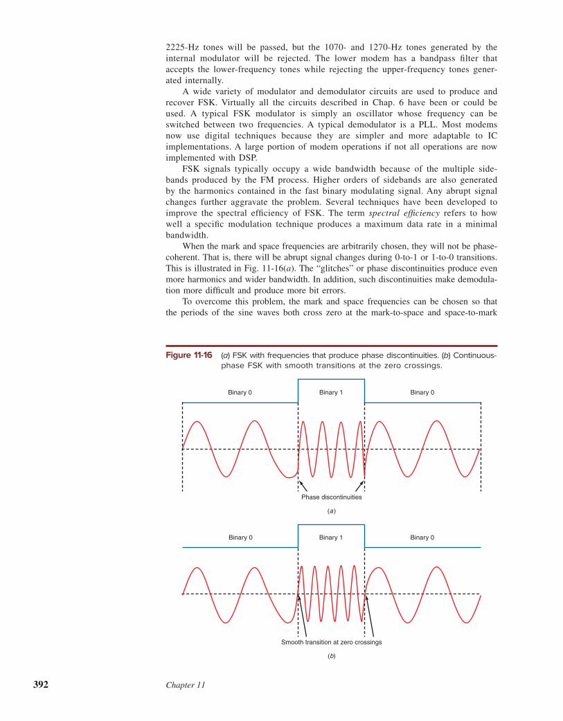
392 Chapter 11
2225-Hz tones will be passed, but the 1070- and 1270-Hz tones generated by the
internal modulator will be rejected. The lower modem has a bandpass i lter that
accepts the lower- frequency tones while rejecting the upper-frequency tones gener-
ated internally.
A wide variety of modulator and demodulator circuits are used to produce and
recover FSK. Virtually all the circuits described in Chap. 6 have been or could be
used. A typical FSK modulator is simply an oscillator whose frequency can be
switched between two frequencies. A typical demodulator is a PLL. Most modems
now use digital techniques because they are simpler and more adaptable to IC
implementations. A large portion of modem operations if not all operations are now
implemented with DSP.
FSK signals typically occupy a wide bandwidth because of the multiple side-
bands produced by the FM process. Higher orders of sidebands are also generated
by the harmonics contained in the fast binary modulating signal. Any abrupt signal
changes further aggravate the problem. Several techniques have been developed to
improve the spectral efi ciency of FSK. The term spectral efi ciency refers to how
well a specii c modulation technique produces a maximum data rate in a minimal
bandwidth.
When the mark and space frequencies are arbitrarily chosen, they will not be phase-
coherent. That is, there will be abrupt signal changes during 0-to-1 or 1-to-0 transitions.
This is illustrated in Fig. 11-16(a). The “glitches” or phase discontinuities produce even
more harmonics and wider bandwidth. In addition, such discontinuities make demodula-
tion more difi cult and produce more bit errors.
To overcome this problem, the mark and space frequencies can be chosen so that
the periods of the sine waves both cross zero at the mark-to-space and space-to-mark
Figure 11-16 (a) FSK with frequencies that produce phase discontinuities. (b) Continuous-
phase FSK with smooth transitions at the zero crossings.
Binary 0 Binary 0Binary 1
Phase discontinuities
(a )
Binary 0 Binary 0Binary 1
Smooth transition at zero crossings
(b)

Digital Data Transmission 393
transitions. This is illustrated in Fig. 11-16(b). No phase discontinuities exist, so the
resulting bandwidth is less. This type of modulation is called continuous-phase
frequency-shift keying (CPFSK).
Another term for signals that start and stop at the zero crossing points is coherent.
You could call this form of modulation coherent FSK. You can also have coherent
ASK or OOK. Coherent versions use less bandwidth and perform better in the pres-
ence of noise.
An improved variation of CPFSK is minimum shift keying (MSK). As in CPFSK, the
mark and space frequencies are some integer multiple of the bit clock frequency. This
ensures that the signals are fully synchronized with one another and that no phase dis-
continuities occur.
MSK further improves spectral efi ciency by using a low modulation index. Recall
from Chap. 5 that the number of pairs of sidebands produced (and therefore the wider
the bandwidth) is proportional to the modulation index. With analog FM, the modulation
index is
mf 5fd
fm
where fd is the frequency deviation and fm is the modulating signal frequency. With FSK,
the modulation index m is
m 5 ¢f (T )
where ¢f is the deviation or frequency shift between the mark frequency fM and the
space frequency fS.
¢f 5 fS 2 fM
Also T is the bit time or the reciprocal of the data rate.
T 51
bps
MSK generally specii es that m must be 0.5. However, other values (0.3) are used.
For example, assume a MSK modem with fM 5 1200 and fS 5 1800 Hz. The bit
rate is 1200 bps. The modulation index is
¢f 5 fS 2 fM 5 1800 2 1200 5 600 Hz
T 51
bps5
1
12005 0.0008333 s
m 5 ¢f (T ) 5 600(0.0008333) 5 0.5
MSK is a very spectrally efi cient form of FSK. But the MSK signal bandwidth can be
further reduced by prei ltering the binary modulating signal. This i lter removes some of
the higher-level harmonics that are responsible for the added sidebands and wider band-
width. One of the best prei lters is called a Gaussian low-pass i lter. It rounds the edges
and somewhat lengthens the rise and fall times. This in turn reduces harmonic content.
And that decreases the overall signal bandwidth. Gaussian i ltered MSK is referred to as
GMSK. It is widely used in data communication and is the basis of the popular GSM
digital cell phones.
PSK. In phase-shift keying (PSK), the binary signal to be transmitted changes the phase
shift of a sine wave character depending upon whether a binary 0 or binary 1 is to be
transmitted. (Recall that phase shift is a time difference between two sine waves of
the same frequency.) Fig. 11-17 illustrates several examples of phase shift. A phase shift
of 180°, the maximum phase difference that can occur, is known as a phase reversal, or
phase inversion.
Continuous-phase frequency-shift keying (CPFSK)
Minimum shift keying (MSK)
Gaussian fi ltered MSK (GMSK)
Phase-shift keying (PSK)

394 Chapter 11
Fig. 11-18 illustrates the simplest form of PSK, binary phase-shift keying (BPSK).
During the time that a binary 0 occurs, the carrier signal is transmitted with one phase;
when a binary 1 occurs, the carrier is transmitted with a 180° phase shift.
Fig. 11-19 shows one kind of circuit used for generating BPSK, a standard lattice
ring modulator or balanced modulator used for generating DSB signals. The carrier sine
wave is applied to the input transformer T1 while the binary signal is applied to the
transformer center taps. The binary signal provides a switching signal for the diodes.
When a binary 0 appears at the input, A is 1 and B is 2, so diodes D1 and D4 conduct.
Binary phase-shift keying (BPSK)
Figure 11-17 Examples of phase shift.
180�
45�
0�
(in phase)
45�
shift
90°shift
180°(phaseinversion)
90�
Figure 11-18 Binary phase-shift keying.
1001 0 1
Serialbinarydata
BPSK
Phase changes whenbinary state changes
Binary 1 � 0Binary 0 � 180

Digital Data Transmission 395
They act as closed switches, connecting the secondary of T1 to the primary of T2. The
windings are phased so that the BPSK output is in phase with the carrier input.
When a binary 1 appears at the input, A is 2 and B is 1, so diodes D1 and D4 are
cut off while diodes D2 and D3 conduct. This causes the secondary of T1 to be connected
to the primary of T2 but with the interconnections reversed. This introduces a 180° phase-
shift carrier at the output.
Demodulation of a BPSK signal is also done with a balanced modulator. A version
of the diode ring or lattice modulator can be used, as shown in Fig. 11-20. This is actu-
ally the same circuit as that in Fig. 11-19, but the output is taken from the center taps.
The BPSK and carrier signals are applied to the transformers. IC balanced modulators
can also be used at the lower frequencies. The modulator and demodulator circuits are
identical to the doubly balanced modulators used for mixers. They are available as fully
wired and tested components for frequencies up to about 1 GHz.
The key to demodulating BPSK is that a carrier with the correct frequency and phase
relationship must be applied to the balanced modulator along with the BPSK signal.
Typically the carrier is derived from the BPSK signal itself, using a carrier recovery
circuit like that shown in Fig. 11-21. A bandpass i lter ensures that only the desired
BPSK signal is passed. The signal is then squared or multiplied by itself by a balanced
modulator or analog multiplier by applying the same signal to both inputs. Squaring
removes all the 180° phase shifts, resulting in an output that is twice the input signal
frequency (2f ). A bandpass i lter set at twice the carrier frequency passes this signal only.
The resulting signal is applied to the phase detector of a PLL. Note that a 32 frequency
Figure 11-19 A BPSK modulator.
BPSKout
Carrierinput
T2T1
D1
D2
D3
D4
A B
Binary input(serial data)
Figure 11-20 A BPSK demodulator.
T2
T1
Carrier
BPSKinput
Binaryoutput

396 Chapter 11
multiplier is used between the VCO and phase detector, ensuring that the VCO frequency
is at the carrier frequency. Use of the PLL means that the VCO will track any carrier
frequency shifts. The result is a signal with the correct frequency and phase relationship
for proper demodulation. The carrier is applied to the balanced modulator-demodulator
along with the BPSK signal. The output is the recovered binary data stream.
DPSK. To simplify the demodulation process, a version of binary PSK called differen-
tial phase-shift keying (DPSK) can be used. In DPSK, there is no absolute carrier phase
reference. Instead, the transmitted signal itself becomes the phase reference. In demodu-
lating DPSK, the phase of the received bit is compared with the phase of the previously
received bit.
For DPSK to work, the original binary bit stream must undergo a process known as
differential phase coding, in which the serial bit stream passes through an inverted
exclusive-NOR circuit (XNOR), as shown in Fig. 11-22(a). Note that the XNOR output
is applied to a 1-bit delay circuit before being applied back to the input. The delay can
simply be a clocked l ip-l op or a delay line. The resulting bit pattern permits the signal
to be recovered because the current bit phase can be compared with the previously
received bit phase.
In Fig. 11-22(b), the input binary word to be transmitted is shown along with the
output of the XNOR. An XNOR circuit is a 1-bit comparator that produces a binary 1
output when both inputs are alike and a binary 0 output when the two bits are differ-
ent. The output of the circuit is delayed a 1-bit interval by being stored in a l ip-l op.
Therefore, the XNOR inputs are the current bit plus the previous bit. The XNOR
signal is then applied to the balanced modulator along with the carrier to produce a
BPSK signal.
Demodulation is accomplished with the circuit shown in Fig. 11-23. The DPSK
signal is applied to one input of the balanced modulator and a 1-bit delay circuit, either
a l ip-l op or a delay line. The output of the delay circuit is used as the carrier. The
resulting output is i ltered by a low-pass i lter to recover the binary data. Typically the
Differential phase-shift keying (DPSK)
Figure 11-21 A BPSK carrier recovery circuit.
BPF
LPF
VCO
BPF
BPSKin(f )
Balanced modulator oranalog multiplier
Phasedetector
Recovered carrier(To demodulator)
2f
�2
Figure 11-22 The DPSK process. (a) DPSK modulator. (b) Dif erential phase encoding.
Serialdatainput
XNORBalancedmodulator
Carrier1-bitdelay
(a) DPSK modulator
Binarydatainput
XNORout
(b) Differential phase encoding
1
0
1
0DPSK

Digital Data Transmission 397
low-pass i lter output is shaped with a Schmitt trigger or comparator to produce clean,
high-speed binary levels.
QPSK. The main problem with BPSK and DPSK is that the speed of data transmission
in a given bandwidth is limited. One way to increase the binary data rate while not
increasing the bandwidth required for the signal transmission is to encode more than
1 bit per phase change. There is a symbol change for each bit change with BPSK and
DPSK, so the baud (symbol) rate is the same as the bit rate. In BPSK and DPSK, each
binary bit produces a specii c phase change. An alternative approach is to use combina-
tions of two or more bits to specify a particular phase shift, so that a symbol change
(phase shift) represents multiple bits. Because more bits per baud are encoded, the bit
rate of data transfer can be higher than the baud rate, yet the signal will not take up
additional bandwidth.
One commonly used system for doing this is known as quadrature, quarternary, or
quadra phase PSK (QPSK or 4-PSK ). In QPSK, each pair of successive digital bits in
the transmitted word is assigned a particular phase, as indicated in Fig. 11-24(a). Each
pair of serial bits, called a dibit, is represented by a specii c phase. A 90° phase shift
exists between each pair of bits. Other phase angles can also be used as long as they
have a 90° separation. For example, it is common to use phase shifts of 45°, 135°, 225°,
and 315°, as shown in Fig. 11-24(b).
The diagram in Fig. 11-24(b) is called a constellation diagram. It shows the
modulation signal in the form of phasors. The length of the arrow or phasor indicates
the peak voltage level of the signal while its angle to the axis is the phase shift.
Sometimes the constellation diagram is simplii ed by just showing dots on the axis
indicating the location of the phasor arrowhead, as in Fig. 11-24(c). This simplii es
the diagram, but you should always imagine a phasor drawn from the origin of the
axis to each dot. Constellation diagrams are widely used to show phase-amplitude
modulation schemes.
Quadrature (quarternary or quadra) phase PSK (QPSK or 4-PSK)
Figure 11-23 A DPSK demodulator.
DPSK
1-bitdelay
LPF Shaper
Recoveredbinary data
Balancedmodulator
Figure 11-24 Quadrature PSK modulation. (a) Phase angle of carrier for dif erent
pairs of bits. (b) Phasor representation of carrier sine wave.
(c) Constellation diagram of QPSK.
Dibit Phaseshift
01
45135225315
00
111
0
(a) (b)
315 � 10225 � 11
135 � 01 45 � 00
(c)
90�
0�
270�
180�
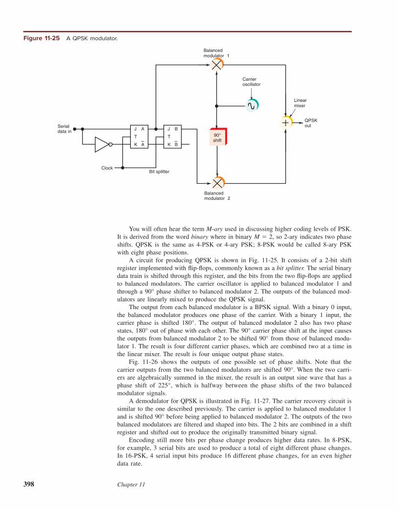
398 Chapter 11
You will often hear the term M-ary used in discussing higher coding levels of PSK.
It is derived from the word binary where in binary M 5 2, so 2-ary indicates two phase
shifts. QPSK is the same as 4-PSK or 4-ary PSK; 8-PSK would be called 8-ary PSK
with eight phase positions.
A circuit for producing QPSK is shown in Fig. 11-25. It consists of a 2-bit shift
register implemented with l ip-l ops, commonly known as a bit splitter. The serial binary
data train is shifted through this register, and the bits from the two l ip-l ops are applied
to balanced modulators. The carrier oscillator is applied to balanced modulator 1 and
through a 90° phase shifter to balanced modulator 2. The outputs of the balanced mod-
ulators are linearly mixed to produce the QPSK signal.
The output from each balanced modulator is a BPSK signal. With a binary 0 input,
the balanced modulator produces one phase of the carrier. With a binary 1 input, the
carrier phase is shifted 180°. The output of balanced modulator 2 also has two phase
states, 180° out of phase with each other. The 90° carrier phase shift at the input causes
the outputs from balanced modulator 2 to be shifted 90° from those of balanced modu-
lator 1. The result is four different carrier phases, which are combined two at a time in
the linear mixer. The result is four unique output phase states.
Fig. 11-26 shows the outputs of one possible set of phase shifts. Note that the
carrier outputs from the two balanced modulators are shifted 90°. When the two carri-
ers are algebraically summed in the mixer, the result is an output sine wave that has a
phase shift of 225°, which is halfway between the phase shifts of the two balanced
modulator signals.
A demodulator for QPSK is illustrated in Fig. 11-27. The carrier recovery circuit is
similar to the one described previously. The carrier is applied to balanced modulator 1
and is shifted 90° before being applied to balanced modulator 2. The outputs of the two
balanced modulators are i ltered and shaped into bits. The 2 bits are combined in a shift
register and shifted out to produce the originally transmitted binary signal.
Encoding still more bits per phase change produces higher data rates. In 8-PSK,
for example, 3 serial bits are used to produce a total of eight different phase changes.
In 16-PSK, 4 serial input bits produce 16 different phase changes, for an even higher
data rate.
Figure 11-25 A QPSK modulator.
Serialdata in
J
T
K
B
B
ClockBit splitter
Balancedmodulator 2
Carrieroscillator
Linearmixer
QPSKout
Balancedmodulator 1
J
T
K
A
A
90°shift

Digital Data Transmission 399
Fig. 11-28 shows the constellation diagram of a 16-PSK signal. The phase increment
is 22.58. Each phasor or dot on the diagram represents a 4-bit number. Note that since all
the dots fall on a circle, the amplitude of the 16-PSK signal remains constant while only
the phase changes. The radius of the circle is the peak amplitude of the signal. It is said
that the signal has a constant “envelope,” where the envelope is simply the line or curve
connecting the peaks of the carrier sine waves. It is l at or constant, as is an FM signal.
QAM. One of the most popular modulation techniques used in modems for increasing
the number of bits per baud is quadrature amplitude modulation (QAM). QAM uses both
amplitude and phase modulation of a carrier; not only are different phase shifts produced,
but also the amplitude of the carrier is varied.
Quadrature amplitude modulation (QAM)
Figure 11-26 How the modulator produces the correct phase by adding two signals.
Outputbalancedmodulator 2(binary 1)
Outputbalancedmodulator 1(binary 1)
QPSK output(linear sum)(225)
Figure 11-27 A QPSK demodulator.
Clock
QPSKinput
Carrierrecovery
circuit
LPF Shaper
2-bit
Binarydata output
LPF Shaper
shift register
shift90°
GOOD TO KNOW
In QAM, the most critical part of
the circuit is the level converters.
These must have very precise
output amplitudes so that the
correct output and phase
combinations are produced.

400 Chapter 11
In 8-QAM, there are four possible phase shifts, as in QPSK, and two different car-
rier amplitudes, so that eight different states can be transmitted. With eight states, 3 bits
can be encoded for each baud or symbol transmitted. Each 3-bit binary word transmitted
uses a different phase-amplitude combination.
Fig. 11-29 is a constellation diagram of an 8-QAM signal showing all possible phase
and amplitude combinations. The points in the diagram indicate the eight possible phase-
amplitude combinations. Note that there are two amplitude levels for each phase position.
Point A shows a low carrier amplitude with a phase shift of 1358. It represents 100. Point
B shows a higher amplitude and a phase shift of 315°. This sine wave represents 011.
A block diagram of an 8-QAM modulator is shown in Fig. 11-30. The binary data
to be transmitted is shifted serially into the 3-bit shift register. These bits are applied in
pairs to two 2-to-4 level converters. A 2-to-4 level converter circuit, basically a simple
D/A converter, translates a pair of binary inputs into one of four possible dc output voltage
levels. The idea is to produce four voltage levels corresponding to the different combina-
tions of 2 input bits, i.e., four equally spaced voltage levels. These are applied to the two
balanced modulators fed by the carrier oscillator and a 90° phase shifter, as in a QPSK
modulator. Each balanced modulator produces four different output phase- amplitude com-
binations. When these are combined in the linear mixer, eight different phase-amplitude
combinations are produced. The most critical part of the circuit is the 2-to-4 level convert-
ers; these must have very precise output amplitudes so that when they are combined in
the linear summer, the correct output and phase combinations are produced.
Constellation diagram
Figure 11-28 Constellation diagram of a 16-PSK signal.
90�
Constantamplitude
22.5� Phase increment
270�
180� 0�
Figure 11-29 A constellation diagram of an 8-QAM signal.
101 111
100 110
000 010
011001
270
0
90
180
A
B
Each vector has a specific amplitude and phase shiftand represents one 3-bit word.
Note:

Digital Data Transmission 401
A 16-QAM signal can also be generated by encoding 4 input bits at a time. The result
is 12 different phase shifts and 3 amplitude levels, producing a total of 16 different
phase-amplitude combinations. Even higher data rates can be achieved with 64-QAM
and 256-QAM. Multilevel modulation schemes using 1024-QAM to 4096-QAM are also
used. These signals are used in cable TV modems, wireless local area networks (WLANs),
satellites, and high-speed i xed broadband wireless applications.
Spectral Ei ciency and Noise
As indicated earlier in this section, spectral efi ciency is a measure of how fast data can
be transmitted in a given bandwidth. The measure is bits per second per hertz (bps/Hz).
As you have seen, different modulation methods give different efi ciencies. The table
shows the common efi ciencies for several common types of modulation.
Modulation Spectral efi ciency, bps/Hz
FSK <1
GMSK 1.35
BPSK 1
QPSK 2
8-PSK 3
16-QAM 4
With a modulation method like BPSK where the efi ciency is 1 bps/Hz, you can actually
transmit data at a rate equal to the bandwidth or
BW 5 fb 51
tb
where fb is the data rate in bits per second and tb is the bit time.
Another factor that clearly inl uences the spectral efi ciency is the noise in the chan-
nel or the signal-to-noise (S/N) ratio. Obviously the greater the noise, the greater the
number of bit errors. The number of errors that occur in a given time is called the bit
error rate (BER). The BER is simply the ratio of the number of errors that occur in 1 s
of a 1-s interval of data transmission. For example, if i ve errors occur in 1 s in a 10
Mbps transmission, the BER is
BER 55
103 106 5 0.5 3 1026 or 5 3 1027
Some modulation schemes are more immune to the noise than others.
Bit error rate (BER)
Figure 11-30 An 8-QAM modulator.
2-to-4level
converter
Serial binarydata input
3-bitshift register
Carrieroscillator
Balancedmodulator 1
Linearmixer
8-QAM
Balancedmodulator 2
2-to-4level
converter
shift90°

402 Chapter 11
The S/N covered in previous chapters was the ratio of signal rms voltage to noise
rms voltage. You can also use the ratio of the average signal power of the carrier plus
the sidebands to the noise power, usually the thermal noise. This is called the carrier-
to-noise (C/N) ratio. Generally C/N is expressed in decibels.
Fig. 11-31 shows the relationship between the C/N and BER for different modulation
methods. What this graph shows is that for a given BER, the modulation methods with
the fewest symbol changes or the smaller bits per hertz give the best performance at the
lower C/N ratios. For a BER of 1026, BPSK needs only a C/N of 11 dB, while for
16-QAM a C/N of 20 dB is needed. Amplitude-modulated signals are always more sus-
ceptible to noise than are constant-envelope forms of modulation such as PSK and FSK,
so you need more signal power to overcome the noise to get the desired BER. Such a
graph lets you compare and evaluate different modulation schemes. Just keep in mind
that bandwidth does not enter the picture here. When comparing methods, you must
remember that noise increases with bandwidth.
A better measure of signal-to-noise ratio for digital data is the ratio of energy per
bit transmitted to the noise power density, or Eb/N0, usually pronounced “E sub b over
N sub zero.” Remember that energy is expressed in joules (J), where one joule per sec-
ond (J/s) is equal to one watt (1 W), or 1 W 5 1 J/s. Therefore, Eb is the power in 1 bit
P multiplied by the bit time tb, or Eb 5 Ptb.
The noise power density in watts per hertz (W/Hz), which we call N0, is the
thermal noise power N divided by the bandwidth of the channel B. Recall that ther-
mal noise power is N 5 kTB, where k is Boltzmann’s constant 1.38 3 10223, T is
the temperature in kelvins, and B is the bandwidth in hertz. Room temperature is
about 290 K.
N0 5kTB
B5 kT
The overall result is
Eb
N0
5Ptb
kT
Carrier-to-noise (C/N)
Figure 11-31 BER versus C/N for popular digital modulation methods.
BE
R
C/N (dB)
BPSK
QPSK
6 10 14 18 22 26 30 34 38
10�3
10�4
10�5
10�6
10�7
10�8
10�9
8-PSK
8-QAM16-PSK
64-QAM
256-QAM

Digital Data Transmission 403
This relationship can be further manipulated to show Eb/N0 in terms of C/N. This rela-
tionship is
Eb
N0
5 aC
Nb aB
fb
bHere B is the bandwidth in hertz and fb is the bit rate or bit frequency (fb) where fb 5
1/tb. Given C/N and the other factors, you can calculate Eb /N0. What Eb /N0 does is to
take bandwidth out of the comparison. It normalizes all the different multiphase/ amplitude
schemes to a noise bandwidth of 1 Hz, giving you a better way to compare and contrast
the various modulation methods for a given BER. You will often see curves like that in
Fig. 11-31 plotted with BER on the vertical axis and Eb /N0 rather than C/N on the
horizontal axis. Fig. 11-32 is an example. Note the role that coherency plays (carrier sine
waves start and stop on the zero crossing). Coherent OOK needs a lower signal-to-noise
ratio than incoherent OOK for a given BER.
11-5 Wideband ModulationMost modulation methods are designed to be spectrally efi cient, i.e., to transmit as many
bits per hertz as possible. The goal is to minimize the use of spectrum space and to
transmit the highest speed possible in the given bandwidth. However, there is another
class of modulation methods that do just the opposite. These methods are designed to
use more bandwidth. The transmitted signal occupies a bandwidth many times greater
than the information bandwidth. Special benei ts derive from such wideband modulation
techniques. The two most widely used wideband modulation methods are spread spec-
trum and orthogonal frequency-division multiplexing.
Spread Spectrum
Spread spectrum (SS) is a modulation and multiplexing technique that distributes a signal
and its sidebands over a very wide bandwidth. Traditionally, the efi ciency of a modula-
tion or multiplexing technique is determined by how little bandwidth it uses. The contin-
ued growth of all types of radio communication, the resulting crowding, and the i nite
bounds of usable spectrum space have made everyone in the world of data communication
Spread spectrum (SS)
Figure 11-32 BER vs. Eb/N0 for dif erent modulation methods.
0 1 2 3 4 5 6 7 8 9 10 11 12 13 14 15 16 17
10�3
10�2
0.1
10�4
10�5
10�6
10�7
BPSK
FSK
16-QAM
DPSK
Coherent OOK
Incoherent OOK
BE
R
Eb /N0 (dB)

404 Chapter 11
sensitive to how much bandwidth a given signal occupies. Designers of communication
systems and equipment typically do all in their power to minimize the amount of band-
width a signal takes. How, then, can a scheme that spreads a signal over a very wide piece
of the spectrum be of value? The answer to this question is the subject of this section.
After World War II, spread spectrum was developed primarily by the military
because it is a secure communication technique that is essentially immune to jam-
ming. In the mid-1980s, the FCC authorized use of spread spectrum in civilian appli-
cations. Currently, unlicensed operation is permitted in the 902- to 928-MHz, 2.4- to
2.483-GHz, and 5.725- to 5.85-GHz ranges, with 1 W of power. Spread spectrum on
these frequencies is being widely incorporated into a variety of commercial com-
munication systems. One of the most important of these new applications is wireless
data communication. Numerous LANs and portable personal computer modems use
SS techniques, as does a class of cordless telephones in the 900-MHz, 2.4-, and 5.8-
GHz ranges. The most widespread use of SS is in cellular telephones in the 800- to
900-MHz and 1800- to 1900-MHz ranges. It is referred to as code-division multiple
access (CDMA).
There are two basic types of spread spectrum: frequency-hopping (FH) and direct-
sequence (DS). In frequency-hopping SS, the frequency of the carrier of the transmitter
is changed according to a predetermined sequence, called pseudorandom, at a rate higher
than that of the serial binary data modulating the carrier. In direct-sequence SS, the serial
binary data is mixed with a higher-frequency pseudorandom binary code at a faster rate,
and the result is used to phase-modulate a carrier.
Frequency-Hopping Spread Spectrum
Fig. 11-33 shows a block diagram of a frequency-hopping SS transmitter. The serial
binary data to be transmitted is applied to a conventional two-tone FSK modulator, and
the modulator output is applied to a mixer. Also driving the mixer is a frequency syn-
thesizer. The output signal from the bandpass i lter after the mixer is the difference
between one of the two FSK sine waves and the frequency of the frequency synthesizer.
As the i gure shows, the synthesizer is driven by a pseudorandom code generator, which
is either a special digital circuit or the output of a microprocessor.
The pseudorandom code is a serial pattern of binary 0s and 1s that changes in a
random fashion. The randomness of the 1s and 0s makes the serial output of this circuit
appear as digital noise. Sometimes the output of this generator is called pseudorandom
noise (PSN). The binary sequence is actually predictable, since it does repeat after many
bit changes (hence “pseudo’’). The randomness is sufi cient to minimize the possibility of
someone accidentally duplicating the code, but the predictability allows the code to be
duplicated at the receiver.
Code-division multiple access (CDMA)
Frequency-hopping (FH) SS
Pseudorandom noise (PSN)
Figure 11-33 A frequency-hopping SS transmitter.
AntennaFSK
modulator
Pseudorandomcode
generator
Frequencysynthesizer
Clock
Mixer
RFpoweramplifier
10 0 1 1 0
Serial binary data
BPF

Digital Data Transmission 405
PSN sequences are usually generated by a shift register circuit similar to that shown
in Fig. 11-34. In the i gure, eight l ip-l ops in the shift register are clocked by an external
clock oscillator. The input to the shift register is derived by X-ORing two or more of the
l ip-l op outputs. It is this connection that produces the pseudorandom sequence. The out-
put is taken from the last l ip-l op in the register. Changing the number of l ip-l ops in
the register and/or which outputs are X-ORed and fed back changes the code sequence.
Alternatively, a microprocessor can be programmed to generate pseudorandom sequences.
In a frequency-hopping SS system, the rate of synthesizer frequency change is higher
than the data rate. This means that although the data bit and the FSK tone it produces
remain constant for one data interval, the frequency synthesizer switches frequencies
many times during this period. See Fig. 11-35, where the frequency synthesizer changes
frequencies four times for each bit time of the serial binary data. The time that the syn-
thesizer remains on a single frequency is called the dwell time. The frequency synthesizer
puts out a random sine wave frequency to the mixer, and the mixer creates a new carrier
frequency for each dwell interval. The resulting signal, whose frequency rapidly jumps
around, effectively scatters pieces of the signal all over the band. Specii cally, the carrier
randomly switches between dozens or even hundreds of frequencies over a given band-
width. The actual dwell time on any frequency varies with the application and data rate,
but it can be as short as 10 ms. Currently, FCC regulations specify that there be a
minimum of 75 hopping frequencies and that the dwell time not exceed 400 µs.
Fig. 11-36 shows a random frequency-hop sequence. The horizontal axis is divided
into dwell time increments. The vertical axis is the transmitter output frequency, divided
into step increments of the PLL frequency synthesizer. As shown, the signal is spread out
over a very wide bandwidth. Thus a signal that occupies only a few kilohertz of spectrum
can be spread out over a range that is 10 to 10,000 times that wide. Because an SS signal
does not remain on any one frequency for a long time, but jumps around randomly, it does
not interfere with a traditional signal on any of the hopping frequencies. An SS signal
actually appears to be more like background noise to a conventional narrow-bandwidth
receiver. A conventional receiver picking up such a signal will not even respond to a signal
of tens of milliseconds duration. In addition, a conventional receiver cannot receive an SS
signal because it does not have a wide enough bandwidth and it cannot follow or track its
random-frequency changes. Therefore, the SS signal is as secure as if it were scrambled.
Figure 11-34 A typical PSN code generator.
Clock
8-bit shift register
X-OR
PSN codeOut
Figure 11-35 Serial data and the PSN code rate.
Serialbinarydata
1 2 3 4 5 6 7 8 9 10 11 12 13 14 15 16 17 18
Dwell time
PSNrate
1-bit interval

406 Chapter 11
Two or more SS transmitters operating over the same bandwidth but with different
pseudorandom codes hop to different frequencies at different times, and do not typically
occupy a given frequency simultaneously. Thus SS is also a kind of multiplexing, as it
permits two or more signals to use a given bandwidth concurrently without interference.
In effect, SS permits more signals to be packed in a given band than any other type of
modulation or multiplexing.
A frequency-hopping receiver is shown in Fig. 11-37. The very wideband signal
picked up by the antenna is applied to a broadband RF amplii er and then to a conven-
tional mixer. The mixer, like that in any superheterodyne receiver, is driven by a local
oscillator. In this case, the local oscillator is a frequency synthesizer like the one used
at the transmitter. The local oscillator at the receiving end must have the same pseudo-
random code sequence as that generated by the transmitter so that it can receive the
signal on the correct frequency. The signal is thus reconstructed as an IF signal that
contains the original FSK data. The signal is then applied to an FSK demodulator, which
reproduces the original binary data train.
One of the most important parts of the receiver is the circuit that is used to acquire and
synchronize the transmitted signal with the internally generated pseudorandom code. The
problem of getting the two codes into step with each other is solved by a preamble signal
and code at the beginning of the transmission. Once synchronization has been established,
Figure 11-36 A pseudorandom frequency-hop sequence.
PL
L fre
qu
en
cy s
tep
Fre
qu
en
cy
Dwell timet1 t2 t3t0
Time
Figure 11-37 A frequency-hopping receiver.
Antenna
IF
PSNcode
generator
Frequencysynthesizer
Clock
Mixer
FSKdemodulator
WidebandRF amplifier
OriginalserialdataSame as
transmitter

Digital Data Transmission 407
the code sequences occur in step. This characteristic makes the SS technique extremely
secure and reliable. Any receiver not having the correct code cannot receive the signal.
Many stations can share a common band if, instead of assigning each station a
single frequency to operate on, each is given a different pseudorandom code within the
same band. This permits a transmitter to selectively transmit to a single receiver without
other receivers in the band being able to pick up the signal.
Direct-Sequence Spread Spectrum
A block diagram of a direct-sequence SS (DSSS) transmitter is shown in Fig. 11-38. The
serial binary data is applied to an X-OR gate along with a serial pseudorandom code
that occurs faster than the binary data. Fig. 11-39 shows typical waveforms. One bit time
for the pseudorandom code is called a chip, and the rate of the code is called the chipping
rate. The chipping rate is faster than the data rate.
The signal developed at the output of the X-OR gate is then applied to a PSK modu-
lator, typically a BPSK device. The carrier phase is switched between 08 and 180° by the
1s and 0s of the X-OR output. QPSK and other forms of PSK can also be used. The PSK
modulator is generally some form of balanced modulator. The signal phase modulating the
carrier, being much higher in frequency than the data signal, causes the modulator to pro-
duce multiple, widely spaced sidebands whose strength is such that the complete signal
takes up a great deal of the spectrum. Thus the resulting signal is spread. Because of its
randomness, the signal looks like wideband noise to a conventional narrowband receiver.
Direct-sequence SS
Chipping rate
Figure 11-38 A direct-sequence SS transmitter.
Clock
10 0 1 1 0
Serial binary data
X-OR
Antenna
RFpoweramplifier
Carrieroscillator
1
PSNcode
generator
BPSKmodulator
Figure 11-39 Data signals in direct-sequence SS.
Serial data
PSN code
X-OR out
Chip time
BPSKcarrier
Phase changes

408 Chapter 11
Fig. 11-40 shows a standard narrowband signal and a spread spectrum signal. Assume
a binary information signal that is occurring at a rate of 13 kbps. If we use BPSK with
its 1 bit/Hz efi ciency, we could transmit this signal in a bandwidth of about 13 kHz.
Now, if we use DSSS with a chipping signal of 1.25 Mbps, the resulting signal will be
spread over about 1.25 MHz of bandwidth if we use BPSK. The spread signal has the
same power as the narrowband signal but far more sidebands, so the amplitudes of the
carrier and sidebands are very low and just above the random noise level. To a narrow-
band receiver, the signal just looks like a part of the noise level.
The effect of spreading the signal is to provide a type of gain called processing gain
to the signal. This gain helps to improve the overall signal-to-noise ratio. The higher the
gain, the greater the ability of the system to i ght interference. This processing gain G is
G 5BW
fb
where BW is the channel bandwidth and fb is the data rate. For the example in Fig. 11-40,
the process gain is
G 51.25 MHz
13 kbps5 96.15
In terms of decibels, this is a power gain of 19.83 dB.
One type of direct-sequence receiver is shown in Fig. 11-41. The broadband SS
signal is amplii ed, mixed with a local oscillator, and then translated down to a lower IF
in mixer 1. For example, the SS signal at an original carrier of 902 MHz might be
translated down to another IF of 70 MHz. The IF signal is then compared to another IF
signal that is produced in mixer 3 using a PSN sequence that is similar to that transmit-
ted. The output of mixer 3 should be identical to the output of mixer 1 but shifted in
time. This comparison process, called correlation, takes place in mixer 2. If the two
signals are identical, the correlation is 100 percent. If the two signals are not alike in
any way, the correlation is 0. The correlation process in the mixer produces a signal that
is averaged in the low-pass i lter at the output of mixer 2. The output signal will be a
high average value if the transmitted and received PSN codes are alike.
The signal out of mixer 2 is fed to a synchronization circuit, which must re create
the exact frequency and phase of the carrier so that demodulation can take place. The
synchronization circuit varies the clock frequency so that the PSN code output frequency
varies, seeking the same chip rate as the incoming signal. The clock drives a PSN code
Figure 11-40 Comparison between narrowband and spread spectrum signals.
BW = 13 kHz
DSSS signal
BW = 1.25 MHz
Narrowband
signal
data rate
13 kbps
BPSK
Random noise
Frequency

Digital Data Transmission 409
generator containing the exact code used at the transmitter. The PSN code in the receiver
is the same as that of the received signal, but the two are out of sync with each other.
Adjusting the clock by speeding it up or slowing it down eventually causes the two to
come into synchronization.
The PSN code produced in the receiver is used to phase-modulate a carrier at the IF
in mixer 3. Like all the other mixers, this one is usually of the double balanced diode ring
type. The output of mixer 2 is a BPSK signal similar to that being received. It is compared
to the received signal in mixer 3, which acts as a correlator. The output of mixer 3 is then
i ltered to recover the original serial binary data. The received signal is said to be despread.
Direct-sequence SS is also called code-division multiple access (CDMA), or SS
multiple access. The term multiple access applies to any technique that is used for
multiplexing many signals on a single communication channel. CDMA is used in
satellite systems so that many signals can use the same transponder. It is also widely
used in cellular telephone systems, for it permits more users to occupy a given band than
other methods.
Benefi ts of Spread Spectrum
Spread spectrum is being used in more and more applications in data communication as
its benei ts are discovered and as new components and equipment become available to
implement it.
● Security. SS prevents unauthorized listening. Unless a receiver has a very wide
bandwidth and the exact pseudorandom code and type of modulation, it cannot
intercept an SS signal.
● Resistance to jamming and interference. Jamming signals are typically restricted
to a single frequency, and jamming one frequency does not interfere with an SS
signal. Similarly, unintentional interference from a signal occupying the same band
is greatly minimized and in most cases virtually eliminated.
● Band sharing. Many users can share a single band with little or no interference.
(As more and more signals use a band, the background noise produced by the switch-
ing of many signals increases, but not enough to prevent highly reliable communication.)
● Resistance to fading and multipath propagation. Frequency-selective fading
occurs during signal propagation because signals of different frequencies arrive at a
receiver at slightly different times due to rel ections from other objects. SS virtually
eliminates wide variations of signal strength due to rel ections and other phenomena
during propagation.
Despread
Code-division multiple access (CDMA)
Multiple access
Figure 11-41 A direct-sequence receiver.
Antenna
LPF
PSNgenerator
Mixer 1BroadbandRF amplifier
Localoscillator
Mixer 2(correlator)
Recovereddata
Mixer 3
Clock
Synccircuits
IFoscillator

410 Chapter 11
● Precise timing. Use of the pseudorandom code in SS provides a way to precisely
determine the start and end of a transmission. Thus SS is a superior method for radar
and other applications that rely on accurate knowledge of transmission time to deter-
mine distance.
Orthogonal Frequency Division Multiplexing (OFDM)
Another wideband modulation method growing in popularity is called OFDM . Also
known as multicarrier modulation (MCM), this relatively new form of modulation was
i rst proposed in the 1950s but was not seriously considered until the 1980s and early
1990s. OFDM was not widely implemented until the late 1990s because of its complex-
ity and cost. Today, fast DSP chips make OFDM practical.
Although OFDM is known as a modulation method as opposed to a multiplexing
method, the term frequency-division multiplexing is appropriate because the method trans-
mits data by simultaneously modulating segments of the high-speed serial bit stream onto
multiple carriers spaced throughout the channel bandwidth. The carriers are
frequency-multiplexed in the channel. The data rate on each channel is very low, making
the symbol time much longer than predicted transmission delays. This technique spreads
the signals over a wide bandwidth, making them less sensitive to the noise, fading, rel ec-
tions, and multipath transmission effects common in microwave communication. Because
of the very wideband nature of OFDM, it is considered to be a hybrid of spread spectrum.
Fig. 11-42 shows the concept of an OFDM modem. The single serial data stream is
divided into multiple slower but parallel data paths, each of which modulates a separate
subcarrier. For example, a 10-Mbps data signal could be split into 1000 data signals of
10 kbps transmitted in parallel. A common format is to space the subcarriers equally across
the channel by a frequency that is the reciprocal of the subcarrier symbol rate. In the situation
described here, the spacing would be 10 kHz. This is what makes the carriers orthogonal.
Orthogonal means that each carrier has an integer number of sine wave cycles in one bit period.
A plot of the bandwidth of each modulated carrier is the familiar (sin x)/x curve
discussed in Chap. 2. (See Fig. 11-43.) Nulls occur at those points equal to the symbol
rate. With this arrangement, all carriers lie at the null frequencies of the adjacent carriers.
Orthogonal frequency-division multiplexing (OFDM)
Figure 11-42 Concept of OFDM.
Modulator (transmitter)
Carrier f1Carrier f2
Carrier fm
Frequencymultiplex
High-speedserialdata
Slower serial data Modulators
OFDM signalSerial-
to-parallel
conversion�
Transmissionchannel
Demodulator (receiver)
Recoveredhigh-speed
data
Parallel-to-
serialconversion
f1
f2
f3Demodulators
BPF1
BPF2
BPFm
Frequencydemultiplex

Digital Data Transmission 411
This permits simplii ed demultiplexing. Typically, BPSK, QPSK, or some form of QAM
is used as the modulation method. In using QPSK or QAM, multiple bits per symbol are
transmitted to permit a higher overall data rate. The subcarriers are algebraically added, and
the resulting composite transmitted. Again referring to Fig. 11-42, note that the demodula-
tor or receiver uses i lters to separate out the individual subcarriers, and demodulators to
recover the individual bit streams, which are then reassembled into the original serial data.
When tens, hundreds, or even thousands of subchannels are used, as is the case in
modern systems, obviously traditional modulator, demodulator, and i lter circuits are
impractical because of size, complexity, and cost. However, all of these functions can be
readily programmed into a fast DSP chip.
A simplii ed version of the process is shown in Fig. 11-44. At the transmitter or
modulator, the serial data is modulated; then a serial-to-parallel conversion is performed.
The inverse fast Fourier transform (IFFT) is then implemented. This process produces
Figure 11-43 Subcarrier spectrum in OFDM.
Subcarrier centerfrequencies
Nullsoccur at
subcarrierfrequencies
f f � 1
Ts
Ts �symbol period
sin x
x
Frequency
Figure 11-44 Simplifi ed processing scheme for OFDM in DSP.
ModulationHigh-speed
serial dataD/A converter
Serial-
to-
parallel
conversion
IFFT
Modulator (transmitter)
Demodulation
Recovered
high-speed
serial dataA/D converter
Transmission
channel
OFDM
signal
Parallel-
to-
serial
conversion
FFT
Demodulator (receiver)

412 Chapter 11
all the orthogonal subcarriers. The D/A converter converts the OFDM signal to analog
form and transmits it over the communication medium.
At the receiver or demodulator, the OFDM signal is digitized by the A/D converter,
and then an FFT is performed. Recall that an FFT essentially does a spectrum analysis
of a time-domain signal. A sampled time-domain analog signal is translated to a
frequency-domain plot of spectral content by the FFT. The receiver FFT DSP sorts out
the subcarriers and demodulates the original data, which is then reassembled into the
original high-speed data stream.
Like most other modems, the OFDM modem is a fast DSP or FPGA chip pro-
grammed with all the mathematical algorithms that produce the functions dei ned by the
blocks in Figs. 11-42 and 11-44.
Today, OFDM is widely used in wireless local-area networks (LANs) and fourth-
generation (4G) Long Term Evolution (LTE) cellular networks. A version of OFDM for
wired communication systems, known as discrete multitone (DMT), used in ADSL
modems is discussed later in this chapter. It is also the method chosen for transmitting
high-quality audio in digital satellite radio broadcasting systems. More recently, it has
been proposed as an alternative to the 8-VSB AM used in digital high-dei nition TV
systems. OFDM is also used in the high-speed version of wireless LANs (802.11 or
Wi-Fi) and in the broadband wireless system called WiMAX. It is also being considered
for future cell phone systems. When the digital data to be transmitted is accompanied
by some form of forward error correction (FEC) scheme (Trellis code, etc.), the method
is called coded OFDM or COFDM. OFDM is also the modulation of choice for the
fourth-generation LTE cellular system. All modern smartphones incorporate LTE.
11-6 Broadband Modem TechniquesA modem or modulator-demodulator is the circuitry used to translate a baseband signal,
usually digital, to a higher transmission frequency that is better suited to the transmission
medium. A good example is that digital data is not that compatible with the twisted-pair
cable used in telephone systems. The bandwidth is too limited. However, modulating the
data onto a carrier provides a way to transmit the data over a system originally designed
for analog voice. Modems are used with all types of cables such as the telephone lines
and the coaxial cable of cable TV. And modems can be of the radio variety where they
are used to transmit data wirelessly. This section provides an overview of several types
of popular modems.
xDSL Modems
Although the twisted-pair telephone line to the central ofi ce is normally said to have a
maximum bandwidth of 4 kHz, the truth is that the bandwidth of this line varies with
its length, and it can handle higher frequencies than expected. Because of the line char-
acteristics, the higher frequencies are greatly attenuated. However, by transmitting the
higher frequencies at higher voltage levels and using line compensation techniques, it is
possible to achieve very high data rates. New modulation methods also permit previously
unachievable line rates. The digital subscriber line (DSL) describes a set of standards set
by the International Telecommunications Union that greatly extend the speed potential
of the common twisted-pair telephone lines. In the term xDSL, the x designates one of
several letters that dei ne a specii c DSL standard.
The most widely used form of DSL is called asymmetric digital subscriber line
(ADSL). This system permits downstream data rates up to 8 Mbps and upstream rates
up to 640 kbps using the existing telephone lines. (Asymmetric means unequal upstream
and downstream rates.)
The connection between a telephone subscriber and the nearest telephone central
ofi ce is twisted-pair cable using size 24 or 26 copper wire. Its length is usually anywhere
xDSL modem
Asymmetric digital subscriber line (ADSL)
Asymmetric

Digital Data Transmission 413
between 9000 and 18,000 ft (2.7 to 5.5 km). This cable acts as a low-pass i lter. Its
attenuation to very high frequencies is enormous. Digital signals are seriously delayed
and distorted by such a line. For this reason, only the lower 0- to 4-kHz bandwidth is
used for voice.
ADSL employs some special techniques so that more of the line bandwidth can be
used to increase data rates. Even though a 1-MHz signal may have an attenuation of up
to 90 dB on an 18,000-ft line, special amplii ers and frequency compensation techniques
make the line usable.
The modulation scheme used with ADSL modems is called discrete multitone
(DMT), another name for OFDM, discussed earlier in this chapter. It divides the upper
frequency spectrum of the telephone line into channels, each 4.3125 kHz wide. See
Fig. 11-45. Each channel, called a bin or subcarrier, is designed to transmit at speeds up
to 15 kbps/Bd or 60 kbps.
Each channel contains a carrier that is simultaneously phase-amplitude-modulated
(QAM) by some of the bits to be transmitted. The serial data stream is divided up so
that each carrier transmits some of the bits. All bits are transmitted simultaneously. Also,
all the carriers are frequency-multiplexed into the line bandwidth above the normal voice
telephone channel, as Fig. 11-45 shows.
The upstream signal uses the 4.3125-kHz bins from 25.875 to 138.8 kHz, and the
downstream signal uses bins in the 138-kHz to 1.1-MHz range.
The number of bits per baud and the data rate per bin vary according to the noise
on the line. The less noise there is in each bin, the higher the data rate. Very noisy
bins will carry few or no bits, whereas quiet bins can accommodate the maximum
15 kbps/Bd or 60 kbps.
This system is very complex and is implemented with a digital signal processor.
The DSP chip handles all modulation and demodulation functions by simulating them
digitally.
Fig. 11-46 shows an ADSL modem. All DMT/OFDM modulation/demodulation is
handled by the DSP chip. The digital output of the DSP is converted to analog by the
D/A converter. The resulting signal is amplii ed, i ltered, and sent to a line driver that
applies a high-level signal to the line. The hybrid is a circuit or transformer that permits
simultaneous transmit and receive operations on the telephone line. The transformer
matches the circuit impedance to the line.
In the receive mode, the incoming DMT analog signal is amplii ed, i ltered, and
applied to a PGA for AGC. The signal is digitized by the A/D converter and applied to
the DSP for recovery of the digital data.
Several different levels of ADSL are available. The data rate for each depends upon
the length of the subscriber twisted-pair cable. The shorter the cable, the higher the
Discrete multitone (DMT)
Bin
Figure 11-45 Spectrum of telephone line used by ADSL and VDSL.
0
4 kHz
26 MHz
Voice UpstreamADSL
downstream
ADSL2 downstream
The spectrum of the unshielded twisted-pair cable showing the subcarriers and the upstream
and downstream allocations for ADSL, ADSL2, VDSL, and VDSL2.
138 MHz 1.1 MHz 2.2 MHz 8.8 MHz
Frequency
30 MHz
4.3125-kHz
wide subcarriers
VDSL downstream
VDSL2 downstream

414 Chapter 11
data rate. The highest standard rate is 6.144 Mbps downstream and 576 kbps upstream
at a line distance not to exceed 9000 ft. The minimum rate is 1.536 Mbps downstream
and 384 kbps upstream at line distances up to 18,000 ft. This is the most common form
of ADSL.
ADSL is available in most cities. ADSL is the most widely used form of high-speed
Internet access throughout the world. ADSL is in second place to cable TV modem
broadband access.
Other forms of DSL have also been dei ned. Two of the most recent versions of
ADSL are ADSL2 and ADSL21. Fig. 11-45 shows the spectrum used by the ADSL2
versions. ADSL2 extends the upper download speed to the 8- to 12-Mbps range at a
distance of about 8000 ft. ADSL21 further boosts speeds to 24 Mbps at a distance to
about 4000 ft. Some newer standards referred to as bonding standards make use of two
twisted pairs in the telephone cable to carry parallel data streams that effectively double
the data rate for a given distance.
VDSL, or very high-speed DSL, offers a data rate of up to 52 Mbps one way (down-
load) or 26 Mbps fully symmetrical using QAM. Fig. 11-45 shows the spectrum used.
It uses 2048 subcarriers to achieve that speed. VDSL permits digital video to be transmit-
ted and thus offers an alternative to cable TV systems. However, to get this speed, the
twisted-pair length is limited to 1000 ft or less at 52 Mbps and less than 3500 ft at
26 Mbps. Internet service providers (ISPs) have also improved DSL service by adding
neighborhood terminals called digital subscriber line access multiplexers (DSLAMs). The
DSLAMs talk to the central ofi ce by way of high-speed i ber-optic cable. The DSLAMs
greatly shorten the distance between the central ofi ce and the homes, making it possible
to achieve the speeds of ADSL2 or VDSL2.
Cable Modems
Most cable TV systems are set up to handle high-speed digital data transmission. The
digital data is used to modulate a high-frequency carrier that is frequency- multiplexed
onto the cable that also carries the TV signals.
Cable TV systems use a hybrid i ber-coaxial (HFC) network. Refer to Fig. 11-47.
It consists of the headend where TV signals are collected and packaged for delivery over
the 6-MHz channels dei ned on the cables. The headend also connects to the Internet.
The TV signals are delivered over fast i ber-optic cables to neighborhood optical nodes
where optical-to-electrical and electrical-to-optical conversions are performed as well as
amplii cation. Then the frequency-multiplexed signals, both TV and Internet access, are
sent over coaxial cables to the homes on the network. The cable used is typically RG-6/U
Figure 11-46 ADSL modem–block diagram.
TX
filter
Hybrid
Telephone
line
To/from
computer
I/O
Line driver
DSP
chip (all
DMT/OFDM
processing)
RX
filter
RX
preamplifier
PGA
TX
gain
A/D converter
D/A converter

Digital Data Transmission 415
75-ohm coaxial. Each optical node serves from about 500 to 2000 homes. Additional
amplii cation is used along the way as needed.
Cable TV systems use a bandwidth of approximately 750 MHz to 1 GHz. This
spectrum is divided into 6-MHz-wide channels for TV signals. The standard VHF and
UHF channels normally assigned to wireless TV are used on the cable, along with some
special cable frequencies. The TV signals are therefore frequency- division-multiplexed
onto the cable. Some of the channels are used exclusively for Internet access.
Fig. 11-48 shows the spectrum of the cable. Television channels extend from 50 MHz
(Channel 2) up to 550 MHz. In this 500 MHz of bandwidth, up to 83 channels of 6 MHz
can be accommodated. In some systems, the number of channels is extended out to about
1 GHz.
The spectrum above the TV channels, from 550 to 850 MHz, is available for digital
data transmission. Standard 6-MHz channels are used, giving approximately 50 channels
or more. These channels are used for downstream data transmission (from the headend
down to the user).
The spectrum from 5 to 50 MHz, as you can see from Fig. 11-48, is divided into
seven 6-MHz channels that are used for upstream data transmission (from the user up
to the server). This frequency range may be 5 to 42 MHz in some systems or 5 to
65 MHz in other systems.
Cable modems use 64-QAM for downstream data. Using 64-QAM in a 6-MHz
channel provides a data rate up to 31.2 Mbps. This method of modulation uses 64
different phase-amplitude combinations (symbols) to represent multiple bits. Because
each channel is shared by multiple users, the 31.2-Mbps rate is not achieved. Typical
rates are in the 500-kbps to 10-Mbps range for downloads. In some systems, 256-QAM
is available to provide a maximum data rate of 41.6 Mbps in a 6-MHz channel. Higher
subscriber download speeds can then be achieved. In older systems, only one TV signal
Figure 11-47 The typical hybrid fi ber coax (HFC) cable TV distribution system
consists of fi ber-optic cable to neighborhood nodes that then
distribute the signals to homes with RG-6/U coax.
Satellite
signals
Internet
Cable
headend
Fiber-optical
cables
Coax
Amp
Homes
Coax cable
Coax cable
Amplifiers
Up to 2000 homes
per optical node
Optical
nodes
Figure 11-48 Cable TV spectrum showing upstream and downstream data channels
on the cable.
6-MHzdata channel
(QPSK @ 10 Mbps)
6-MHzdata channel
(64 QAM @ 31.2 Mbps)
6-MHzTV channel
5 MHz 50 MHz 550 MHz 850 MHz
��
��
��
Up to7 upstream
data channels Up to 83 TV channels
Up to50 downstreamdata channels

416 Chapter 11
was transmitted per channel. However, today with modern digital techniques, several
digital TV signals can be transmitted per channel by using DSP compression techniques.
Standard QPSK and up to 128-QAM are used in the upstream channels to achieve
a data rate of up to about 27 Mbps. With multiple users, the upstream rate is less.
Fig. 11-49 shows a typical cable modem. It is basically a VHF/UHF receiver con-
nected to the cable for downloads and a modulator/transmitter for uploads. The signal
from the cable passes through the diplexer, which is a i lter circuit that permits simulta-
neous transmit and receive operations. The signal is amplii ed and mixed with a local
oscillator signal from the frequency synthesizer to produce an IF signal. The frequency
synthesizer selects the cable channel. The IF signal is demodulated to recover the data.
Reed Solomon error detection circuitry (see Sec. 11-7) i nds and corrects any bit errors.
The digital data then goes to an Ethernet interface to the PC. Ethernet is a popular
networking system to be discussed in Chap. 12.
For transmission, the data from the computer is passed through the interface, where
it is encoded for error detection. The data then modulates a carrier that is up- converted
by the mixer to the selected upstream channel before being amplii ed and passed through
the diplexer to the cable.
Cable modems provide signii cantly higher data rates than can be achieved over the
standard telephone system. The primary limitation is the existence or availability of a
cable TV system that offers such data transmission services.
Cable modem standards are set by an industry consortium called Cable Labs. The
specii cation is referred to as the Data over Cable Service Interface Specii cation (DOCSIS).
The latest version, DOCSIS 3.1, permits channel bonding of two or more channels
to achieve higher data rates. Higher rates also derive from higher modulation levels of
up to 4096-QAM. DOCSIS 3.1 also permits the use of OFDM with 25-kHz to 50-kHz
subcarriers and up to 4096-QAM modulation. This allows the cable companies to deliver
up to 10 Gbps downstream and up to 1 Gbps upstream. The cable companies will be
able to compete with i ber-optic systems.
11-7 Error Detection and CorrectionWhen high-speed binary data is transmitted over a communication link, whether it is a
cable or radio, errors will occur. These errors are changes in the bit pattern caused by
interference, noise, or equipment malfunctions. Such errors will cause incorrect data to
be received. To ensure reliable communication, schemes have been developed to detect
and correct bit errors.
Figure 11-49 Cable modem block diagram.
DiplexerFrequency
synthesisEthernet
interface
Channel
selectionTo/from
cable To/from
PC I/O
QAM
demodulator
Reed Solomon
error correction
Decoding64 QAM or
256 QAM
LNA IF
QPSK or
16-QAM
Reed Solomon
error correction
EncodingModulatorTransmit
amplifier

Digital Data Transmission 417
The number of bit errors that occur for a given number of bits transmitted is referred
to as the bit error rate (BER). The bit error rate is similar to a probability in that it is the
ratio of the number of bit errors to the total number of bits transmitted. If there is 1 error
for 100,000 bits transmitted, the BER is 1 : 100,000 5 1025. The bit error rate depends
on the equipment, the environment, and other considerations. The BER is an average
over a very large number of bits. The BER for a given transmission depends on specii c
conditions. When high speeds of data transmission are used in a noisy environment, bit
errors are inevitable. However, if the S/N ratio is favorable, the number of errors will be
extremely small. The main objective in error detection and correction is to maximize the
probability of 100 percent accuracy.
Bit error rate (BER)
Example 11-3Data is transmitted in 512-byte blocks or packets. Eight sequential packets are trans-
mitted. The system BER is 2 : 10,000 or 2 3 1024. On average, how many errors can
be expected in this transmission?
8 packets 3 512 bytes 5 4096 bytes
4096 bytes 3 8 bits 5 32,768 bits
32,768/10,000 5 3.2768 sets of 10,000 bits
Average number of errors 5 2 3 3.2768 5 6.5536
The process of error detection and correction involves adding extra bits to the data
characters to be transmitted. This process is generally referred to as channel encoding.
The data to be transmitted is processed in a way that creates the extra bits and adds them
to the original data. At the receiver, these extra bits help in identifying any errors that
occur in transmission caused by noise or other channel effects.
A key point about channel encoding is that it takes more time to transmit the data
because of the extra bits. For example, to transmit 1 byte of data, the encoding process
may add 3 extra bits for a total of 11 bits. These extra bits are called overhead in that
they extend the time of transmission. If the bit time is 100 ns, then it takes 800 ns to
send the data bits but 1100 ns to send the encoded data. The extra overhead bits add
37.5 percent more time to the transmission. As a result, to maintain a desired data rate,
the overall clock speed must be increased or the lower data rate must be accepted. While
the extra bits decrease the overall efi ciency of transmission, remember that the benei t
is more reliable data transmission because errors can be detected and/or corrected. Speed
is traded off for higher-quality data transmission.
Channel encoding methods fall into to two separate categories, error detection codes
and error correction codes. Error detection codes just detect the errors but do not take
any corrective action. They simply let the system know that an error has occurred. Typi-
cally, these codes simply initiate retransmission until the data is received correctly. The
other form of channel coding is error correction or forward error correction (FEC). These
coding schemes eliminate the time-wasting retransmission and actually initiate
self-correcting action.
Error Detection
Many different methods have been used to ensure reliable error detection, including
redundancy, special coding and encoding schemes, parity checks, block checks, and
cyclical redundancy check.

418 Chapter 11
Redundancy. The simplest way to ensure error-free transmission is to send each char-
acter or each message multiple times until it is properly received. This is known as
redundancy. For example, a system may specify that each character be transmitted twice
in succession. Entire blocks or messages can be treated in the same way. These retrans-
mission techniques are referred to as automatic repeat request (ARQ).
Encoding Methods. Another approach is to use an encoding scheme like the RZ-
AMI described earlier, whereby successive binary 1 bits in the bit stream are transmit-
ted with alternating polarity. If an error occurs somewhere in the bit stream, then 2 or
more binary 1 bits with the same polarity are likely to be transmitted successively. If
the receiving circuits are set to recognize this characteristic, single bit errors can be
detected.
The turbo codes and trellis codes are another example of the use of special coding
to detect errors. These codes develop unique bit patterns from the data. Since many bit
patterns are invalid in trellis and turbo codes, if a bit error occurs, one of the invalid
codes will appear, signaling an error that can then be corrected. These codes are covered
later in this section.
Parity. One of the most widely used systems of error detection is known as parity, in
which each character transmitted contains one additional bit, known as a parity bit. The
bit may be a binary 0 or binary 1, depending upon the number of 1s and 0s in the char-
acter itself.
Two systems of parity are normally used, odd and even. Odd parity means that the
total number of binary 1 bits in the character, including the parity bit, is odd. Even parity
means that the number of binary 1 bits in the character, including the parity bit, is even.
Examples of odd and even parity are indicated below. The seven left-hand bits are the
ASCII character, and the right-hand bit is the parity bit.
Odd parity: 10110011
00101001
Even parity: 10110010
00101000
The parity of each character to be transmitted is generated by a parity generator
circuit. The parity generator is made up of several levels of exclusive OR (X-OR)
circuits, as shown in Fig. 11-50. Normally the parity generator circuit monitors the shift
register in a UART in the computer or modem. Just before transmitting the data in the
register by shifting it out, the parity generator circuit generates the correct parity value,
inserting it as the last bit in the character. In an asynchronous system, the start bit comes
Redundancy
Parity
Figure 11-50 A parity generator circuit.
�
7-bit ASCIIcharacter stored in a register
XORcircuits
Evenparity
Oddparity
ABC � A
Truth Table
A
0011
B
0101
C
0110
B
Exclusive OR(XOR) circuit

Digital Data Transmission 419
i rst, followed by the character bits, the parity bit, and i nally one or more stop bits
(see Fig. 11-51).
At the receiving modem or computer, the serial data word is transferred into a shift
register in a UART. A parity generator in the receiving UART produces the parity on the
received character. It is then compared to the received parity bit in an XOR circuit, as
shown in Fig. 11-52. If the internally generated bit matches the transmitted and received
parity bit, it is assumed that the character was transmitted correctly. The output of the
XOR will be 0, indicating no error. If the received bit does not match the parity bit
generated from the received data word, the XOR output will be 1, indicating an error.
The system signals the detection of a parity error to the computer. The action taken will
depend on the result desired: The character may be retransmitted, an entire block of data
may be transmitted, or the error may simply be ignored.
The individual-character parity method of error detection is sometimes referred to
as the vertical redundancy check (VRC). To display characters transmitted in a data com-
munication system, the bits are written vertically (see Fig. 11-53). The bit at the bottom
is the parity, or VRC, bit for each vertical word. Horizontal redundancy checks are
discussed later.
Parity checking is useful only for detecting single-bit errors. If two or more bit errors
occur, the parity circuit may not detect it. If an even number of bit changes occur, the
parity circuit will not give a correct indication.
Cyclical Redundancy Check. The cyclical redundancy check (CRC) is a mathemati-
cal technique used in synchronous data transmission that effectively catches 99.9 percent or
more of transmission errors. The mathematical process implemented by CRC is essentially
a division. The entire string of bits in a block of data is considered to be one giant binary
number that is divided by some preselected constant. CRC is expressed by the equation
M(x)
G(x)5 Q(x) 1 R(x)
Vertical redundancy check (VRC)
Cyclical redundancy check (CRC)
Figure 11-51 How parity is transmitted. Figure 11-52 Parity checking at the
receiver.
Mark
Space
Start bit 7-bit ASCII code Stop bit
Parity bit (even)
0 1 0 1 1 0 0 1
Received parity bit 1-bit comparator
Parity error
Received 7-bit data word
Parity
generator
(Fig. 11-50)
Figure 11-53 Vertical and horizontal redundancy checks.
Character
(LSB)
ASCII
Code
(MSB)
Parityor VRC(odd)
D
0010001
1
A
1000001
1
T
0010101
0
A
1000001
1
0000010
0
C
1100001
0
O
1111001
0
M
1011001
1
1000111
0
LRC orBCC (even)

420 Chapter 11
where M(x) is the binary block of data, called the message function, and G(x) is the
generating function. The generating function is a special code that is divided into the
binary message string. The outcome of the division is a quotient function Q(x) and a
remainder function R(x). The quotient resulting from the division is ignored; the remain-
der is known as the CRC character and is transmitted along with the data.
For convenience of calculation, the message and generating functions are usually
expressed as an algebraic polynomial. For example, assume an 8-bit generating function
of 10000101. The bits are numbered such that the LSB is 0 and the MSB is 7.
7 6 5 4 3 2 1 0
1 0 0 0 0 1 0 1
The polynomial is derived by expressing each bit position as a power of x, where
the power is the number of the bit position. Only those terms in which binary 1s appear
in the generating function are included in the polynomial. The polynomial resulting from
the above number is
G(x) 5 x7 1 x
2 1 x0 or G(x) 5 x7 1 x
2 1 1
The CRC mathematical process can be programmed by using a computer’s instruction
set. It can also be computed by a special CRC hardware circuit consisting of several shift
registers into which XOR gates have been inserted at specii c points (see Fig. 11-54). The
data to be checked is fed into the registers serially. There is no output, since no output is
retained. The data is simply shifted in 1 bit at a time; when the data has all been transmit-
ted, the contents will be the remainder of the division, or the desired CRC character. Since
a total of 16 l ip-l ops are used in the shift register, the CRC is 16 bits long and can be
transmitted as two sequential 8-bit bytes. The CRC is computed as the data is transmitted,
and the resulting CRC is appended to the end of the block. Because CRC is used in
synchronous data transmission, no start and stop bits are involved.
At the receiving end, the CRC is computed by the receiving computer and compared
to the received CRC characters. If the two are alike, the message has been correctly
received. Any difference indicates an error, which triggers retransmission or some other
form of corrective action. CRC is probably the most widely used error detection scheme
in synchronous systems. Both 16- and 32-bit CRCs are used. Parity methods are used
primarily in asynchronous systems.
Error Correction
As stated previously, the easiest way to correct transmission errors — to retransmit any
character or block of data that has an error in it — is time-consuming and wasteful.
A number of efficient error correction schemes have been devised to complement
Figure 11-54 A CRC error detection circuit made with a 16-bit shift register and XOR gates.
XOR
Serial datainput
Flip-flop
CRC character

Digital Data Transmission 421
the parity and BCC methods described above. The process of detecting and correct-
ing errors at the receiver so that retransmission is not necessary is called forward
error correction (FEC). There are two basic types of FEC: block codes and convo-
lutional codes.
Block-Check Character. The block-check character (BCC) is also known as a
horizontal or longitudinal redundancy check (LRC). It is the process of logically add-
ing, by exclusive-ORing, all the characters in a specii c block of transmitted data.
Refer to Fig. 11-53. To add the characters, the top bit of the i rst vertical word is
exclusive-ORed with the top bit of the second word. The result of this operation is
exclusive-ORed with the top bit of the third word, and so on until all the bits in a
particular horizontal row have been added. There are no carries to the next bit position.
The i nal bit value for each horizontal row then becomes one bit in a character known
as the block-check character (BCC), or the block-check sequence (BCS). Each row of
bits is done in the same way to produce the BCC. All the characters transmitted in
the text, as well as any control or other characters, are included as part of the BCC.
Exclusive-ORing all bits of all characters is the same as binary addition without a
carry of the codes.
The BCC is computed by circuits in the computer or modem as the data is transmit-
ted, and its length is usually limited to 8 bits, so that carries from one bit position to the
next are ignored. It is appended to the end of a series of bytes that make up the message
to be transmitted. At the receiving end, the computer computes its own version of the
BCC on the received data and compares it to the received BCC. Again, the two should
be the same.
When both the parity on each character and the BCC are known, the exact location
of a faulty bit can be determined. The individual character parity bits and the BCC bits
provide a form of coordinate system that allows a particular bit error in one character to
be identii ed. Once it is identii ed, the bit is simply complemented to correct it. The VRC
identii es the character containing the bit error, and the LRC identii es the bit that con-
tains the error.
Assume, e.g., that a bit error occurs in the fourth vertical character from the left in
Fig. 11-53. The fourth bit down from the top should be 0, but because of noise, it is
received as a 1. This causes a parity error. With odd parity and a 1 in the fourth bit, the
parity bit should be 0, but it is a 1.
Next, the logical sum of the bits in the fourth horizontal row from the top will
be incorrect because of the bit error. Instead of 0, it will be 1. All the other bits in
the BCC will be correct. It is now possible to pinpoint the location of the error
because both the vertical column where the parity error occurred and the horizontal
row where the BCC error occurred are known. The error can be corrected by simply
complementing (inverting) the bit from 1 to 0. This operation can be programmed
in software or implemented in hardware. One important characteristic of BCC is
that multiple errors may not be detected. Therefore, more sophisticated techniques
are needed.
Hamming Code. A popular FEC is the Hamming code. Hamming was a researcher
at Bell Labs who discovered that if extra bits were added to a transmitted word, these
extra bits could be processed in such a way that bit errors could be identii ed and cor-
rected. These extra bits, like several types of parity bits, are known as Hamming bits,
and together they form a Hamming code. To determine exactly where the error is, a
sufi cient number of bits must be added. The minimum number of Hamming bits is
computed with the expression
2n $ m 1 n 1 1
where m 5 number of bits in data word
n 5 number of bits in Hamming code
Forward error correction (FEC)
Longitudinal redundancy check
Block-check character (BCC)
Block-check sequence (BCS)
Hamming bits
Hamming code

422 Chapter 11
Assume, e.g., an 8-bit character word and some smaller number of Hamming bits
(say, 2). Then
2n $ m 1 n 1 1
22 $ 8 1 2 1 1
4 $ 11
Two Hamming bits are insufi cient, and so are three. When n 5 4,
24 $ 8 1 4 1 1
16 $ 13
Thus 4 Hamming bits must be transmitted along with the 8-bit character. Each
character requires 8 1 4 5 12 bits. These Hamming bits can be placed anywhere within
the data string. Assume the placement shown below, where the data bits are shown as a
0 or 1 and the Hamming bits are designated with an H. The data word is 01101010.
12 11 10 9 8 7 6 5 4 3 2 1
H 0 1 H 1 0 H 1 0 H 1 0
One way to look at Hamming codes is simply as a more sophisticated parity system,
where the Hamming bits are parity bits derived from some of but not all the data bits.
Each Hamming bit is derived from different groups of the data bits. (Recall that parity
bits are derived from the data by XOR circuits.) One technique used to determine the
Hamming bits is discussed below.
At the transmitter, a circuit is used to determine the Hamming bits. This is done by
i rst expressing the bit positions in the data word containing binary 1s as a 4-bit binary
number (n 5 4 is the number of Hamming bits). For example, the i rst binary 1 data bit
appears at position 2, so its position code is just the binary code for 2, or 0010. The
other data bit positions with a binary 1 are 5 5 0101, 8 5 1000, and 10 5 1010.
Next, the transmitter circuitry logically adds (XORs) these codes.
Position code 2 0010
Position code 5 0101
XOR sum 0111
Position code 8 1000
XOR sum 1111
Position code 10 1010
XOR sum 0101
This i nal sum is the Hamming code bits from left to right. Position code 12 is 0,
position code 9 is 1, position code 6 is 0, and position code 3 is 1. These bits are inter-
ested in their proper position. The complete 12-bit transmitted word is
12
H
11
0
10
1
9
H
8
1
7
0
6
H
5
1
4
0
3
H
2
1
1
0
120
110
101
91
81
70
60
51
40
31
21
10
The Hamming bits are shown in boldface type.
Now assume that an error occurs in bit position 10. The binary 1 is received as a
binary 0. The received word is
120
110
101
91
81
70
60
51
40
31
21
10
The receiver recognizes the Hamming bits and treats them as a code word, in this case
0101. The circuitry then adds (XORs) this code with the bit number of each position in
the word containing a binary 1, positions 2, 5, and 8.

Digital Data Transmission 423
The Hamming code is then added to the binary numbers representing each position
with a 1.
Hamming code 0101
Position code 2 0010
XOR sum 0111
Position code 5 0101
XOR sum 0010
Position code 8 1000
XOR sum 1010
This i nal sum is a code that identii es the bit position of the error, in this case bit 10
(1010). To correct the bit, it is simply complemented from 0 to 1. If there are no bits in
error, then the XOR sum at the receiver will be zero.
Note that the Hamming code method does not work if an error occurs in one of the
Hamming bits itself.
For the Hamming code method of error detection and correction to work when 2 or
more bit errors occur, more Hamming bits must be added. This increases overall trans-
mission time, storage requirements at the transmitter and receiver, and the complexity of
the circuitry. The benei t, of course, is that errors are reliably detected at the sending
end. The transmitter never has to resend the data, which may in fact be impossible in
some applications. Not all applications require such rigid data correction practices.
Reed Solomon Code. One of the most widely used forward error correction codes
is the Reed Solomon (RS) code. Like Hamming codes, it adds extra parity bits to the
block of data being transmitted. It uses a complex mathematical algorithm beyond the
scope of this book to determine the codes. The beauty of the RS code is that it permits
multiple errors to be detected and corrected. For example, a popular form of the RS code
is designated RS (255,223). A block of binary data contains a total of 255 bytes; 223 bytes
is the actual data and 32 bytes is parity bits computed by the RS algorithm. With this
arrangement, the RS code can detect and correct errors in up to 16 corrupted bytes. An
RS encoder is used on the data to be transmitted. At the receiver, the recovered data is
sent to an RS decoder that corrects any errors. The encoders and decoders can be imple-
mented with software, but hardware ICs are also available. Some common applications
of the RS FEC are in music and data compact disks (CDs), cell phones, digital TV,
satellite communication, and xDSL and cable TV modems.
Interleaving. Interleaving is a method used in wireless systems to reduce the effects
of burst errors. Most errors in wireless transmission are caused by bursts of noise that
destroy a single bit or multiple sequential bits. If we take the bits and interleave them,
we have a better chance of recognizing and recovering the lost bits.
One common way of doing this is to i rst use an error-correcting scheme such as
the Hamming code to encode the data. The data and the Hamming bits are then stored
in consecutive memory locations. For example, assume four 8-bit words consisting of
the data and the Hamming bits. The data words if transmitted sequentially would look
like this.
12345678 12345678 12345678 12345678
Then instead of transmitting the encoded words one at a time, all the i rst bits of each
word are transmitted, followed by all the second bits, followed by all the third bits, and
so on. The result would look like this.
1111 2222 3333 4444 5555 6666 7777 8888
Now if a burst error occurs, the result may look like this.
1111 2222 3333 4444 5555 4218 7777 8888
Reed Solomon (RS) code

424 Chapter 11
At the receiver, the de-interleaving circuits would attempt to recreate the original data,
producing
12345478 12345278 12345178 12345878
Now with only 1 bit in each word in error, a Hamming decoder would detect and correct
the bit.
Convolutional Codes
Convolutional encoding creates additional bits from the data as do Hamming and Reed
Solomon codes, but the encoded output is a function of not only the current data bits
but also previously occurring data bits. Like other forms of FEC, the encoding process
adds extra bits that are derived from the data itself. This is a form of redundancy that
leads to greater reliability in the transmission of the data. Even if errors occur, the redun-
dant bits allow the errors to be corrected.
Convolutional codes are beyond the scope of this text, but essentially what they do
is to pass the data to be transmitted through a special shift register like that shown in
Fig. 11-55. As the serial data is shifted through the shift register l ip-l ops, some of the
l ip-l op outputs are XORed together to form two outputs. These two outputs are the
convolutional code, and this is what is transmitted. There are numerous variations of this
scheme, but note in every case the original data itself is not transmitted. Instead, two
separate streams of continuously encoded data are sent. Since each output code is dif-
ferent, the original data can more likely be recovered at the receiver by an inverse pro-
cess. One of the more popular convolutional codes is the trellis code which is widely
used in dial-up computer modems. The Viterbi code is another that is widely used in
high-speed data access via satellites.
Another type of convolutional code uses feedback. These are called recursive codes
because the output of the shift register is combined with the input code to produce the
output streams. Fig. 11-56 is an example. Recursion means taking the output from a
Figure 11-55 Convolutional encoding uses a shift register with exclusive-OR gates
to create the output.
FF1 FF2 FF3 FF4Serial data
to beencoded
Shift register
XOR
XOR
Encodedoutputs
Figure 11-56 A convolutional encoder using recursion.
FF1 FF2
Encodedoutput
Recursion path
Serial datain

Digital Data Transmission 425
process and applying it back to the input. This procedure has been further developed to
create a new class of convolutional codes called turbo codes. The turbo code is a com-
bination of two concurrent recursive coding processes where one is derived directly from
the data and the other is derived from the data that has been interleaved i rst. See
Fig. 11-57. The result is a far more robust FEC that catches virtually all errors. Most
forms of wireless data transmission today use some form of convolutional coding to
ensure the robustness of the transmission path.
Low-Density Parity Check
Low-density parity check (LDPC) is an error-correcting code scheme that was invented by
R. G. Gallager at MIT in the 1960s but was not widely implemented because of its complex
parallel computational process. It was impractical to implement except on large-scale comput-
ers. However, LDPC was recently rediscovered and today is readily implemented with logic
in an FPGA or a fast processor. With LDPC it is possible to create codes that can reduce the
probability of an error to as small as possible and stay within the bounds of Shannon’s limit.
Figure 11-57 One form of turbo encoding.
FF1 FF2 FF3
Serialdatainput
FF1 FF2 FF3
Interleaver
CODING GAIN
Forward error-correction codes were developed to improve the BER in noisy communications chan-
nels. By exposing a block of data to be transmitted to a coding process, additional bits are added
that permit errors to occur but provide a means of identifying and correcting the errors, thereby
greatly improving the probability of an error-free transmission. Such coding has the same effect
as improving the signal-to-noise ratio (SNR) of the transmission channel. The effect is the same
as if the transmit power was increased. This effect is called coding gain and is usually expressed
in dB. One formal definition of coding gain is the power increase needed to maintain the same
BER as that achieved without coding. Or coding gain is the gain in SNR for a given BER using a
specific coding method before modulation. Coding gains of several dB are possible with FEC.

426 Chapter 11
As with many other FEC codes, the encoding and decoding processes are beyond
the scope of this book. Just be aware that LDPC is replacing other popular FEC codes
in a variety of communications systems. These include Wi-Fi in the IEEE 802.11n and
802.11ac standards, 10-gigabit Ethernet over twisted-pair cable, G.hn power line com-
munications standard, the European digital TV standard DVB-T2, WiMAX 802.16e, and
several satellite systems.
11-8 ProtocolsProtocols are rules and procedures used to ensure compatibility between the sender and
receiver of serial digital data regardless of the hardware and software being used. They
are used to identify the start and end of a message, identify the sender and the receiver,
state the number of bytes to be transmitted, state a method of error detection, and for
other functions. Various protocols, and various levels of protocols, are used in data
communication.
The simplest form of protocol is the asynchronous transmission of data using a start
bit and a stop bit (refer to Fig. 11-6) framing a single character, with a parity bit between
the character bit and the stop bit. The parity bit is part of the protocol, but may or may
not be used. In data communication, however, a message is more than one character. As
discussed previously, it is composed of blocks, groups of letters of the alphabet, numbers,
punctuation marks, and other symbols in the desired sequence. In synchronous data com-
munication applications, the block is the basic transmission unit.
To identify a block, one or more special characters are transmitted prior to the block
and after the block. These additional characters, which are usually represented by 7- or
8-bit codes, perform a number of functions. Like the start and stop bits on a character,
they signal the beginning and end of the transmission. But they are also used to identify
a specii c block of data, and they provide a means for error checking and detection.
Some of the characters at the beginning and end of each block are used for hand-
shaking purposes. These characters give the transmitter and receiver status informa-
tion. Fig. 11-58 illustrates the basic handshaking process. For example, a transmitter
may send a character indicating that it is ready to send data to a receiver. Once the
receiver has identii ed that character, it responds by indicating its status, e.g., by send-
ing a character representing “busy’’ back to the transmitter. The transmitter will con-
tinue to send its ready signal until the receiver signals back that it is not busy, or is
ready to receive.
At that point, data transmission takes place. Once the transmission is complete, some
additional handshaking takes place. The receiver acknowledges that it has received the
information. The transmitter then sends a character indicating that the transmission is
complete, which is usually acknowledged by the receiver.
A common example of the use of such control characters is the XON and XOFF
protocol used between a computer and some other device. XON is usually the ASCII
character DC1, and XOFF is the ASCII character DC3. A device that is ready and able
to receive data will send XON to the computer. If the device is not able to receive data,
it sends XOFF. When the computer detects XOFF, it immediately stops sending data
until XON is again received.
Protocol
Handshaking
Figure 11-58 The handshaking process in data communication.
Transmitter Receiver
Ready
Busy
Data line
Handshaking lines

Digital Data Transmission 427
Asynchronous Protocols
Three popular protocols used for asynchronous ASCII-coded data transmission between
personal computers, via modem, are Xmodem, Kermit, and MPN. These protocols are
no longer widely used, but an example with Xmodem will illustrate the process.
In Xmodem, the data transmission procedure begins with the receiving computer
transmitting a negative acknowledge (NAK) character to the transmitter. NAK is a 7-bit
ASCII character that is transmitted serially back to the transmitter every 10 s until the
transmitter recognizes it. Once the transmitter recognizes the NAK character, it begins
sending a 128-byte block of data, known as a frame (packet) of information (see
Fig. 11-59). The frame begins with a start-of-header (SOH) character, which is another
ASCII character meaning that the transmission is beginning. This is followed by a header,
which usually consists of two or more characters preceding the actual data block, which
give auxiliary information. In Xmodem, the header consists of 2 bytes designating the
block number. In most messages, several blocks of data are transmitted and each is
numbered sequentially. The i rst byte is the block number in binary code. The second
byte is the complement of the block number; i.e., all bits have been inverted. Then the
128-byte block is transmitted. At the end of the block, the transmitting computer sends
a check-sum byte, which is the BCC, or binary sum of all the binary information sent
in the block. (Keep in mind that each character is sent along with its start and stop bits,
since Xmodem is an asynchronous protocol.)
The receiving computer looks at the block data and also computes the check sum.
If the check sum of the received block is the same as that transmitted, it is assumed that
the block was received correctly. If the block was received correctly, the receiving com-
puter sends an acknowledge (ACK) character — another ASCII code — back to the trans-
mitter. Once ACK is received by the transmitter, the next block of data is sent. When a
block has been received incorrectly because of interference or equipment problems, the
check sums will not match and the receiving computer will send a NAK code back to
the transmitter. A transmitter that has received NAK automatically responds by sending
the block again. This process is repeated until each block, and the entire message, has
been sent without errors.
When the entire message has been sent, the transmitting computer sends an end-of-
transmission (EOT) character. The receiving computer replies with an ACK character,
terminating the communication.
Synchronous Protocols
Protocols used for synchronous data communication are more complex than asynchro-
nous protocols. However, like the asynchronous Xmodem and Kermit systems, they use
various control characters for signaling purposes at the beginning and ending of the block
of data to be transmitted.
Bisync. An early synchronous protocol is IBM’s Bisync protocol. It usually begins with
the transmission of two or more ASCII sync (SYN) characters (see Fig. 11-60). These
characters signal the beginning of the transmission and are also used to initialize the
clock timing circuits in the receiving modem. This ensures proper synchronization of the
data transmitted a bit at a time.
Xmodem protocol
Frame
Acknowledge (ACK) character
End-of-transmission (EOT) character
Bisync protocol
Figure 11-59 Xmodem protocol frame.
SOH Block
numberComplement ofblock number
128-byte block BCC
1 byte
Start, stop, and parity bits not shown

428 Chapter 11
After the SYNC characters, a start-of-header (SOH) character is transmitted. The
header is a group of characters that typically identii es the type of message to be sent,
the number of characters in a block (usually up to 256), and a priority code or some
specii c routing destination. The end of the header is signaled by a start-of-text (STX)
character. At this point, the desired message is transmitted, 1 byte at a time. No start
and stop bits are sent. The 7- or 8-bit words are simply strung together one after another,
and the receiver must sort them into individual binary words that are handled on a par-
allel basis farther along on the receiving circuit in the computer.
At the end of a block, an end-of-transmission-block (ETB) character is transmitted.
If the block is the last one in a complete message, an end-of-text (ETX) character is
transmitted. An end-of-transmission (EOT) character, which signals the end of the trans-
mission, is followed by an error detection code, usually a 1- or 2-byte BCC.
SDLC. One of the most l exible and widely used synchronous protocols is the synchronous
data link control (SDLC) protocol (see Fig. 11-61). SDLC is used in networks that are inter-
connections of multiple computers. All frames begin and end with a l ag byte with the code
01111110 or hex 7E, which is recognized by the receiving computer. A sequence of binary
1s starts the clock synchronous process. Next comes an address byte that specii es a specii c
receiving station. Each station on the network is assigned an address number. The address
hex FF indicates that the message to follow is to be sent to all stations on the network.
A control byte following the address allows the programmer or user to specify how
the data will be sent and how it will be dealt with at the receiving end. It allows the user
to specify the number of frames, how the data will be received, and so on.
The data block (all codes are EBCDIC, not ASCII) comes next. It can be any length,
but 256 bytes is typical. The data is followed by a frame-check sequence (FCS), a 16-bit
CRC. A l ag ends the frame.
A variation of the SDLC system, which permits interface between a larger number
of different software and hardware coni gurations, is called high-level data link control
(HDLC). Its format is similar to that shown in Fig. 11-61. It may also use ASCII data
and often has a 32-bit CRC/FCS.
The Open Systems Interconnection Model
As you have seen, there are many types and variations of protocols. If there is to be
widespread compatibility between different systems, then some industrywide
standardization is necessary. The ability of one hardware-software coni guration to
communicate with another, different system is known as interoperability. Only if all
manufacturers and users adopt the same standards can true interoperability be achieved.
One organization that has attempted to standardize data communication procedures is
Start-of-header (SOH) character
Start-of-text (STX) character
End-of-transmission-block (ETB) character
End-of-transmission (EOT) character
Synchronous data link control (SDLC) protocol
High-level data link control (HDLC) protocol
Interoperability
Figure 11-60 Bisync synchronous protocol.
SYN SYN SOH HEADER STX DATA BLOCKETB orETX EOT BCC BCC
Time
8-bit character
Figure 11-61 The SDLC and HDLC frame formats.
FLAG ADDRESS CONTROL DATA BLOCK FCS FLAG
Byte
Flag � 01111110
Any length(EBCDIC or ASCII)
16 bits

Digital Data Transmission 429
the International Organization for Standardization. It has established a framework, or
hierarchy, that dei nes how data can be communicated. This hierarchy, known as the
open systems interconnection (OSI) model, is designed to establish general interoperabil-
ity guidelines for developers of communication systems and protocols. Even though the
OSI model is not implemented by all manufacturers, the functions of each level in the
OSI model outline must be accomplished by each protocol. In addition the OSI model
serves as a common reference for all protocols.
The OSI hierarchy is made up of seven levels, or layers (see Fig. 11-62). Each layer
is dei ned by software (or, in one case, hardware) and is clearly distinct from the other
layers. These layers are not really protocols themselves, but they provide a way to dei ne
and partition protocols to make data transfers in a standardized way. Each layer is
designed to handle messages that it receives from a lower layer or an upper layer. Each
layer also sends messages to the layer above or below it according to specii c guidelines.
Different protocols accomplish each layer and refer to the tasks they perform by refer-
encing the OSI model. Tasks are referred to as a layer 1, layer 2, etc. task.
As shown in the i gure, the highest level is the application layer, which interfaces
with the user’s application program. The lowest level is the physical layer, where the
electronic hardware, interfaces, and transmission media are dei ned.
Layer 1: Physical layer. The physical connections and electrical standards for the
communication system are dei ned here. This layer specii es interface characteristics,
such as binary voltage levels, encoding methods, data transfer rates, and the like.
Layer 2: Data link. This layer dei nes the framing information for the block of
data. It identii es any error detection and correction methods as well as any
synchronizing and control codes relevant to communication. The data link
layer includes basic protocols, such as HDLC and SDLC.
Layer 3: Network. This layer determines network coni guration and the route
the transmission can take. In some systems, there may be several paths for
the data to traverse. The network layer determines the specii c data routing
and switching methods that can occur in the system, e.g., selection of a
dial-up line, a private leased line, or some other dedicated path.
Layer 4: Transport. Included in this layer are multiplexing, if any; error
recovery; partitioning of data into smaller units so that they can be handled
more efi ciently; and addressing and l ow control operations.Layer 5: Session. This layer handles such things as management and synchroni-
zation of the data transmission. It typically includes network log-on and log-off procedures, as well as user authorization, and determines the availabil-ity of the network for processing and storing the data to be transmitted.
International Organization for Stan-dardization
Open systems interconnections (OSI) protocol
Figure 11-62 The seven OSI layers.
Header
7
6
5
4
3
2
1
7
6
5
4
3
2
1
Data
PacketsPhysical Link
(wired or wireless)
Application
Presentation
Session
Transport
Network
Data Link
Physical
App.
Software
Transmitting
Device
App.
Software
Receiving
Device

430 Chapter 11
Layer 6: Presentation. This layer deals with the form and syntax of the mes-
sage. It dei nes data formatting, encoding and decoding, encryption and
decryption, synchronization, and other characteristics. It dei nes any code
translations required, and sets the parameters for any graphics operations.
Layer 7: Applications. This layer is the overall general manager of the network
or the communication process. Its primary function is to format and transfer
i les between the communication message and the user’s applications software.
The basic process is that information is added or removed as data is transmitted from
one layer to another (see Fig. 11-63). Assume, e.g., that the applications program you are
using contains some data that you wish to send to another computer. That data will be
transmitted in the form of some kind of serial packet or frame, or a sequence of packets.
The applications layer attaches the packet to some kind of header or preamble before
sending it to the next level. At the presentation level, more headers and other information
are added. At each of the lower levels, headers and related information are appended until
the data message is almost completely encased in a much larger packet. Finally, at the
physical level, the data is transmitted to the other system. As Fig. 11-63 shows, the mes-
sage that is actually sent may contain more header information than actual data.
At the receiving end, the header information gets stripped off at the various levels
as the data is transferred to successive levels. The headers tell the data where to go and
what to do next. The data comes in at the physical level and goes up through the various
layers until it gets to the applications layer, where it is i nally used.
Note that it is not necessary to use all seven layers. Many modern data communication
applications need only the i rst two or three layers to fully dei ne a given data exchange.
The primary benei t of the OSI standard is that if it is incorporated into data
communication equipment and software, compatibility between systems and equipment
is more likely to be achieved. As more and more computers and networks are intercon-
nected, e.g., on the Internet, true interoperability becomes more and more important.
Figure 11-63 The data as transmitted at the physical layer.
Headers added at each layer
LINK NET TRANS SES PRES APPL DATA ERROR
PCC or CRC
CHAPTER REVIEW
Online Activity
11-1 Spectral Ei ciency
Objective: To compare the spectral efi ciencies of various
digital modulations.
Procedure:
1. Search on the term spectral efi ciency or modulation
comparisons or a similar term.
2. Answer the questions below.
Questions:
1. Which modulation has the greatest spectral efi ciency?
2. What is the second most efi cient modulation method?
3. What role does noise play in comparing modulation
methods?
4. What types of modulation are best in noisy environments?
5. What types of circuits are used to produce most high-
level modulations?

Digital Data Transmission 431
Questions
1. Name the earliest form of binary data communication.
2. What do you call dot-dash code transmission by radio?
3. How do you distinguish between uppercase and
lowercase letters in Morse code?
4. What is Morse code for the characters C, 7, and ??
5. How many bits are in a byte?
6. Name the two ways in which bits are transmitted from
one place to another.
7. What is the most widely used binary data code that uses
7 bits to represent characters?
8. What ASCII character is transmitted to ring a bell?
9. For a given data path length, which is faster, serial or
parallel transmission?
10. What is used to signal the beginning and end of the
transmission of a character in asynchronous trans-
missions?
11. What is the name given to the number of symbols
occurring per second in a data transmission?
12. How can there be more than 1 bit per baud in data
transmissions?
13. How many bits per baud (symbol) can be transmitted
by a four-level FSK signal?
14. Which is faster, asynchronous transmission or synchro-
nous transmission? Explain.
15. How is a message sent using synchronous data
transmission?
16. In serial data transmission, what are the special names
given to a binary 0 and a binary 1?
17. What encoding method is used in most standard digital
logic signals?
18. What occurrence in serial data transmission makes it
difi cult to detect the clock rate when NRZ is used?
19. What two encoding methods are best for clock
recovery?
20. What is a benei t of the RZ-AMI method of encoding?
21. Give two names for the encoding system that makes
use of a transition at the center of each bit.
22. Explain how GMSK permits higher data rates in a
smaller bandwidth.
23. What two factors does the amount of information that
can be sent in a given transmission depend on?
24. True or false? Multilevel or multisymbol binary encod-
ing schemes permit more data to be transmitted in less
time, assuming a constant symbol interval.
25. For a given bandwidth system, what is the advantage of
using a multisymbol encoding scheme?
26. Name the major components and circuits of a modem.
27. What is the function of a modem?
28. What is the maximum download speed of a VDSL2
modem?
29. What kind of modulation is used on an ADSL modem?
What is the maximum download speed?
30. What factor determines the maximum speed of an
ADSL or VDSL modem?
31. Why is a scrambler needed in a modem?
32. What is DOCSIS?
33. What is the bandwidth of a cable TV data channel?
34. What kind of modulation is used for downloads and
uploads in cable TV, and what are the maximum
theoretical data rates?
35. What basic circuit is used to produce BPSK?
36. What circuit is used to demodulate BPSK?
37. What circuit is used to generate the carrier to be used in
demodulating a BPSK signal?
38. What type of PSK does not require a carrier recovery
circuit for demodulation?
39. Name the key circuit used in a DPSK modulator.
40. How many different phase shifts are used in QPSK?
41. In QPSK, how many bits are represented by each phase
shift?
42. How many bits are represented by each phase shift in
16-PSK?
43. Is carrier recovery required in a QPSK demodulator?
44. When QPSK is used, is the bit rate faster than the baud
(symbol) rate?
45. What circuit is used to create a dibit in a QPSK
modulator?
46. What do you call a circuit that converts a 2-bit binary
code into one of four dc voltage levels?
47. QAM is a combination of what two types of modulation?
48. Name the modulation method used with U.S. ATSC
high-dei nition TV.
49. What is trellis code modulation? Why is it used?
50. How many bits per baud are transmitted with 256-QAM?
51. What type of modulation is illustrated by the constella-
tion diagram in Fig. 11-64?
Figure 11-64 Illustration for question 51.
52. State the modulation method used in the DOCSIS 3.1
standard.
53. What is spread spectrum?
54. Name the two main types of spread spectrum.

432 Chapter 11
55. What circuit generates the transmitter frequency in a
frequency-hopping SS system?
56. In a frequency-hopping SS system, what circuit selects
the frequency produced by the synthesizer?
57. True or false? The hop rate is slower than the bit rate of
the digital data.
58. How does an SS signal appear to a narrowband receiver?
59. How are two or more stations using spread spectrum
and sharing a common band identii ed and distin-
guished from one another?
60. What do you call the length of time that a frequency-
hopping SS transmitter stays on one frequency?
61. What circuit is used to generate a PSN signal?
62. What is the purpose of a PSN signal?
63. In a direct-sequence SS transmitter, the data signal is
mixed with a PSN signal in what kind of circuit?
64. True or false? In a direct-sequence SS system, the chip
rate is faster than the data rate.
65. What type of modulation is used with direct-sequence
SS?
66. What is the most difi cult part of spread spectrum
communication?
67. What do you call the process of comparing one signal
to another in an effort to obtain a match?
68. Name the two main benei ts of spread spectrum.
69. How is OFDM generated and demodulated?
70. Name four applications of OFDM.
71. Name the most common application for spread spectrum.
72. How are voice signals transmitted via spread spectrum?
73. What is another name for direct-sequence SS?
74. List two methods of error detection.
75. Name one simple but time-consuming way to ensure an
error-free transmission.
76. What is the most common cause of error in data trans-
mission?
77. What is the name given to the ratio of the number of bit
errors to the total number of bits transmitted?
78. What serial bit encoding method makes it possible to
detect single-bit errors?
79. What is the bit added to a transmitted character to help
indicate an error called?
80. What is the name of a number added to the end of a
data block to assist in detecting errors, and how is it
derived?
81. What is another name for parity?
82. What logic circuit is the basic building block of a parity
generator circuit?
83. What error detection system uses a BCC at the end of a
data block?
84. Describe the process of generating a CRC.
85. What basic circuit generates a CRC?
86. True or false? If a bit error can be identii ed, it can be
corrected.
87. Describe the procedure for checking the accuracy of a
block transmission at the receiver using a CRC.
88. What is the name of the most popular error-correcting
code?
89. What will be the outcome of X-ORing Hamming bits if
no error occurs in the data word during transmission?
90. Name three types of convolutional codes.
91. What is the name given to the rules and procedures that
describe how data will be transmitted and received?
92. What is the process of exchanging signals between
transmitter and receiver to indicate status or
availability?
93. What is a popular asynchronous protocol used with
PCs and other serial devices? What control characters
are used?
94. Name a popular asynchronous protocol used in PC
communication via modem.
95. What is usually in the last i eld of a protocol frame?
96. What is the string of characters making up a message or
part of a message to be transmitted called?
97. What do synchronous protocols usually begin with?
Why?
98. Name two common synchronous protocols.
99. What appears at the very end of most protocol packets?
100. What does interoperability mean?
101. Name one way to achieve interoperability.
102. Name the seven OSI levels in order from highest to
lowest.
103. What are the three or four most used OSI levels?
1. What is the name of the 8-bit character code used in
IBM systems? ◆
2. A serial pulse train has a 70-µs bit time. What is the
data rate in bits per second?
3. The data rate of a serial bit stream is 14,400 bps. What
is the bit interval? ◆
4. The speed of a serial data transmission is 2.5 Mbps.
What is the actual number of bits that occur in 1 s?
5. What is the channel capacity, in bits per second, of a
30-kHz-bandwidth binary system, assuming no noise? ◆
6. If an eight-level encoding scheme is used in a 30-kHz-
bandwidth system, what is the channel capacity in bits
per second?
7. What is the channel capacity, in bits per second, of a
15-MHz channel with an S/N ratio of 28 dB? ◆
8. What is the minimum allowable bandwidth that can
transmit a binary signal with a bit rate of 350 bps?
9. What is the BER if four errors occur in the transmission
of 500,000 bits? ◆
Problems

Digital Data Transmission 433
1. Describe in detail a simple data communication system
that will monitor the temperature of a remote inacces-
sible location and display temperature on a personal
computer.
2. Suggest a future application for spread spectrum tech-
niques, and explain why SS would be appropriate for
that application.
3. Name three or more common data communication
applications that you may use.
4. Why is DSP necessary to implement OFDM in an
ADSL modem?
5. Are spread spectrum and OFDM spectrally efi cient?
Critical Thinking
10. Write the correct parity bits for each number.
a. Odd 1011000 __
b. Even 1011101 __
c. Odd 0111101 __
d. Even 1001110 __
11. Determine the 4 Hamming bits for the 8-bit number
11010110. Use the format illustrated in the text.
12. What is the processing gain in a DSSS system with a
20-MHz channel and a data rate of 11 Mbps?
◆ Answers to Selected Problems follow Chap. 22.

434
chapter
The fi rst computers were stand-alone machines that one person used at a
time. Later, timesharing computers were invented that allowed more than one
person to use the machine concurrently. When personal computers (PCs)
came along, the one computer –one user paradigm came back with a ven-
geance. But all that is in the past. Today, most computers are networked, i.e.,
connected to one another so that they can communicate with one another,
share resources, and access the Internet. Virtually 100 percent of business
and industrial computers are networked. Most home and personal computers
are also networked. This chapter is an introduction to networking, local-area
networks (LANs), and Ethernet, the most widely used networking technology.
Objectives
After completing this chapter, you will be able to:
■ Defi ne the terms LAN, MAN, and WAN.
■ Explain the basic purposes of LANs and describe some specifi c LAN
applications.
■ Draw diagrams of LANs arranged according to the three basic
topologies: star, ring, and bus.
■ Describe how repeaters, transceivers, hubs, bridges, routers, and
gateways are used in LANs.
■ Calculate transmission speed given the length of the data to be transmit-
ted and the characteristics of the LAN over which the data is to be sent.
■ Identify the main classes and specifi cations of Ethernet.
Fundamentals of Networking, Local-Area Networks, and Ethernet
12

Fundamentals of Networking, Local-Area Networks, and Ethernet 435
12-1 Network FundamentalsA network is a communication system with two or more stations that can communicate
with one another. When it is desired to have each computer communicate with two or
more additional computers, the interconnections can become complex. As Fig. 12-1 indi-
cates, if four computers are to be interconnected, there must be three links to each PC.
The number of links L required between N PCs (nodes) is determined by using the formula
L 5N(N 2 1)
2
Assume, e.g., there are six PCs. The number of links is
L 5 6(6 2 1)/2 5 6(5)/2230/2 515.
The number of links or cables increases in proportion to the number of nodes
involved. The type of arrangement shown in Fig. 12-1 is obviously expensive and imprac-
tical. Some special type of network wiring must be used, a combination of hardware and
software that permits multiple computers to be connected inexpensively and simply with
the minimum number of links necessary for communication.
GOOD TO KNOW
If you know how many PCs will
be in the network, you can calcu-
late the number of links (connect-
ing cables) needed to make an
inexpensive network by using the
formula
L 5N(N 2 1)
2
Example 12-1An ofi ce with 20 PCs is to be wired so that any computer can communicate with any
other. How many interconnecting wires (or links, L) are needed?
L 5N(N 2 1)
25
20(20 2 1)
25
20(19)
25 190
Types of Networks
Each computer or user in a network is referred to as a node. The interconnection between
the nodes is referred to as the communication link. In most computer networks, each
node is a personal computer, but in some cases a peripheral device such as a laser printer
or an embedded controller built into another piece of equipment can be a node. There
Node
Figure 12-1 A network of four PCs.
Link
Node
PC
PC
PCPC

436 Chapter 12
are four basic types of electronic networks in common use: wide-area networks (WANs),
metropolitan-area networks (MANs), local-area networks (LANs), and personal-area net-
works (PANs). Let’s take a brief look at each.
Wide-Area Networks (WANs). A WAN covers a signii cant geographic area. Local
telephone systems are WANs, as are the many long-distance telephone systems linked
together across the country and to WANs in other countries. Each telephone set is, in
effect, a node in a network that links local ofi ces and central ofi ces. Any node can
contact any other node in the system. Telephone systems use twisted-pair wire and coax-
ial cable, as well as microwave relay networks, satellites, and i ber- optic cabling.
There are also WANs that are not part of the public telephone networks, e.g., cor-
porate LANs set up to permit independent intercompany communication regardless of
where the various subsidiaries and company divisions, sales ofi ces, and manufacturing
plants may be. The special communication, command, and control networks set up by
the military are also WANs.
The nationwide and worldwide i ber-optic networks set up since the mid-1990s to carry
Internet trafi c are also WANs. Known as the Internet core or backbone, these high-speed
interconnections are coni gured as either direct point-to-point links or large rings with
multiple access points. WANs make it possible for any PC or other Internet-enabled device
such as a cell phone to access the World Wide Web or any entity connected to the Internet.
Metropolitan-Area Networks (MANs). MANs are smaller networks that generally
cover a city, town, or village. Cable TV systems are MANs. The cable TV company
receives signals from multiple sources, including local TV stations, as well as special
programming from satellites, and it assembles all these signals into a single composite
signal that is placed on i ber-optic and coaxial cables. The cables are then channeled to
each subscriber home. The cable TV channel selector boxes are all nodes in the system.
Most existing cable systems are simplex or one-way transmission systems; however,
many cable companies now incorporate two-way communication capability.
Another type of MAN carries computer data. MANs are usually i ber-optic rings encir-
cling a city that provide local access to users. Businesses, governments, schools, hospitals,
and others connect their internal LANs to them. MANs also connect to local and long-
distance telephone companies. The MANs, or metro networks as they are typically called,
also provide fast and convenient connections to WANs for global Internet connectivity.
Local-Area Networks (LANs). A LAN is the smallest type of network in general use.
It consists primarily of personal computers interconnected within an ofi ce or building. LANs
can have as few as 3 to 5 users, although most systems connect 10 to several thousand users.
Small LANs can be used by a company to interconnect several ofi ces in the same
building; in such cases, wiring can be run between different l oors of the building to make the connection. Larger LANs can interconnect several buildings within a complex, e.g., large companies with multiple buildings, military installations, and college campuses. Some LANs consist of multiple PCs that are linked both to each other and to a minicomputer or mainframe. This allows each user on the LAN, to have access to the big computer as well as continue to operate independently. Home networks of two or more PCs are also LANs, and today most home LANs are fully wireless or incorporate wireless segments.
Personal-Area Networks (PANs). A PAN is a short-range wireless network that is set up automatically between two or more devices such as laptop computers, peripheral devices, or cell phones. The distance between the devices is very short, no more than about 10 m and usually much less. PANs are referred to as ad hoc networks that are set up for a specii c single purpose, such as the transfer of data between the devices as required by some application. For example, a laptop computer may link up with a printer, or a smartphone may need to download data from a PC. Most PANs just involve two nodes, but some have been set up to handle up to eight nodes and sometimes more.
Wide-area network (WAN)
Internet core or backbone
Metropolitan-area network (MAN)
Metro networks

Fundamentals of Networking, Local-Area Networks, and Ethernet 437
Storage-Area Networks (SANs). SANs are an outgrowth of the massive data
storage requirements developed over the years thanks to the Internet. These networks
usually attach to a LAN or Internet server and are designed to store and protect huge
data i les. The SAN also provides users on the network access to massive data i les
stored in mass memory units, called redundant arrays of independent disks (RAIDs).
RAIDs use many hard drives interconnected to the network. RAIDs have been available
for years, but they had to be located close to the computers they served to provide
adequate access speed. Today, with high-speed i ber-optic links, the RAIDs may literally
be located anywhere, even across the country, since access can be via the Internet or a
i ber-optic WAN or MAN.
Network Hierarchy. Fig. 12-2 shows a highly simplii ed view of how LANs,
MANs, and WANs are interconnected. LANs inside a building are usually connected
to a MAN that may be a local telephone central ofi ce or a special MAN set up by
the organization itself or one managed by a company that leases lines to the organiza-
tion. The MANs connect to the WANs, which may be a long-distance telephone
network or a special optical WAN set up for Internet access or other data transmission
applications. Some WANs are hierarchies of rings and direct connection points. MANs
and WANs are virtually all i ber-optic networks. The interconnection points of the
networks may be special computers called servers, routers, or switching equipment
such as an add-drop multiplexer (ADM) that allows data to be added to or extracted
from a ring network.
Network Topologies
The topology of a network describes the basic communication paths between, and meth-
ods used to connect, the nodes on a network. The three most common topologies used
are star, ring, and bus. These topologies apply to the LAN, MAN, and WAN.
Servers, routers
Topology
Figure 12-2 Networking hierarchy.
LAN
LAN
LAN
MAN
MAN
MAN
WANring
Point-to-pointWAN (backbone)
WAN
Key:
PC
Node: server,router, add-drop multiplexer
backbone
Telephonecentraloffice

438 Chapter 12
Star Topology. A basic star coni guration consists of a central controller node and
multiple individual stations connected to it (Fig. 12-3). The resulting system resembles
a multipointed star. The central or controlling PC, often referred to as the server, is
typically larger and faster than the other PCs and contains a large hard drive where shared
data and programs are stored. Any communication between two PCs passes through the
server. The server and its software manage the linkup of individual computers and the
transfer of data between them.
A star-type LAN is extremely simple and straightforward. New nodes can be quickly
and easily added to the system. Furthermore, the failure of one node does not disable the
entire system. Of course, if the server node goes down, the network is disabled, although
the individual PCs will continue to operate independently. Star networks generally require
more cable than other network topologies, and the fact that all communication must pass
through the node does place some speed restrictions on the transfer of data.
Ring Topology. In a ring coni guration, the server or main control computer and all
the computers are simply linked in a single closed loop (Fig. 12-4). Usually, data is trans-ferred around the ring in only one direction, passing through each node. Therefore, there is some amplii cation and regeneration of the data at each node, permitting long trans-mission distances between nodes. The ring topology is easily implemented and is low in cost. Expansion is generally simple, since a new node can be inserted in the ring at almost any point. The computer that has a message to send identii es the message with a code or address identifying the destination node, places it on the ring, and sends it to the next computer in the loop. Essentially, each PC in the ring receives and retransmits the message until it reaches the target PC. At that point, the receiving node accepts the message. The downside of a ring network is that a failure in a single node generally causes the entire network to go down. It is also somewhat difi cult to diagnose problems on a ring. Despite these limitations, the ring coni guration is widely used.
Bus Topology. A bus is simply a common cable to which all the nodes are attached. Fig. 12-5 shows the bus coni guration. The bus is bidirectional in that signals can be transmitted in either direction between any two of the nodes; however, only one of the
Star topology
Ring topology
Bus topology
Figure 12-3 A star LAN confi guration with a server as the controlling computer.
PC
PC
PC
PC
PC
PC
PC PC
Optionalgateway tomainframe
Controlling PC Harddisk

Fundamentals of Networking, Local-Area Networks, and Ethernet 439
Figure 12-4 A ring LAN confi guration.
PC
Disk or fileserver
Print server
Printer
PC
PC
PC
PC
PC
Harddisk
Figure 12-5 A bus LAN confi guration.
PC
PC
PC
PCFileserver
Optionalbridge to anotherLAN
PC
PC
Buscable
Harddisk

440 Chapter 12
LOGICAL VERSUS PHYSICAL TOPOLOGY
The topologies illustrated in Figs. 12-1, 12-3, 12-4, and 12-5 are what we call logical topol-
ogies as they show the connections in a formal logical sense. The connections are made in a
theoretical sense that describes how the data flows and how the nodes are connected. How-
ever, in the real world, networks do not appear physically as their logical connections. Because
of the random locations of the computers and other nodes and the fact that cabling must be
run in patterns restricted and dictated by the buildings, the physical appearance of a network
usually bears no relationship to the logical structure.
For example, logical bus-connected computers are usually of the physical star form because
cables from each PC go to a central location and are terminated at a hub or switch. The bus is
actually implemented inside the hub. But the physical arrangement is more of an irregular star.
The same is true for ring networks. The cable to/from each PC terminates at some
central connection point, but the ring logical format is still implemented because the wires in
the cables take the signals into and out of each PC to the central connection point. The ring
is still there, but it looks like a star physically. Keep this key point in mind when you are
working on LANs and other networks.
nodes can transmit at a given time. A signal to be transmitted can be destined for a
single node or broadcast to all nodes simultaneously.
The primary advantage of the bus is that it is faster than any of the other topologies.
The wiring is simple, and the bus can be easily expanded.
Mesh Topology. A mesh network is one in which each node is connected to all other
nodes. You saw this in Fig. 12-1. This is called a full mesh in that every node can talk
directly to any other node. Of course this leads to major costs and complications as the
number of nodes increases. This problem is somewhat mitigated by the use of wireless
interconnections between nodes where there is no expensive wiring and the attendant
routing and maintenance problems. A variation of the full mesh is the partial mesh in
which all nodes can communicate with two or more other nodes. This reduces the num-
ber of interconnections, making it more practical.
The primary value of the mesh network is that there are multiple paths for data to
take from one node to another. This provides for redundancy that can provide a con-
tinuous connection when one or more of the links are broken. The lack of one link does
not keep the data from reaching its destination by another path. This redundancy pro-
vides increased network reliability. Most partial mesh networks are implemented with
wireless links.
Other Topologies. There are many variations and combinations of the basic topolo-
gies discussed above. For example, the daisy chain topology is simply a ring that has
been broken. Another variation is called the tree topology. This topology is simply a bus
design in which each node has multiple interconnections to other nodes through a star
interconnection. In others, the network consists of branches from one node to two or
more other nodes.
LAN Applications
The common denominator of all LANs is the communication of information. Nodes are
linked to transmit and receive information, software, databases, personal messages, or
anything else that can be put in binary form.
Mesh
Daisy chain topology
Tree topology

Fundamentals of Networking, Local-Area Networks, and Ethernet 441
The earliest LANs were developed primarily as a way to control costs. For example,
in an ofi ce with multiple PCs, the cost of permitting each computer to have its own
printer was prohibitive. Networking is an inexpensive way to link all the computers in
the ofi ce to a single computer to which the printer is attached. Users share the printer
by transmitting information to be printed to the server, which controls print operations
for all the ofi ce computers.
Another example is the sharing of large i les and databases. Networks can be used
to connect all the PCs in an ofi ce to a central server with a large hard drive containing
the data or software to be shared, so that any computer can access it. Today, networks
are used for many applications other than centralizing and sharing expensive peripherals
such as printers and for permitting many users access to a large database.
By far the most popular networks applications are e-mail, Internet access, and the
sharing of common software.
12-2 LAN HardwareAll LANs are a combination of hardware and software. The primary hardware devices
are the computers themselves and the cables and connectors that link them. Additional
pieces of hardware unique to networks include network interface cards, repeaters, hubs
and concentrators, bridges, routers, gateways, and many other special interfacing
devices. This section provides an overview of the specii c types of hardware involved
in networking and especially Ethernet.
Cables
Most LANs use some type of copper wire cable to carry data from one computer to
another via baseband transmission. The digital data stored in the computer is con-
verted to serial binary data, and voltages representing binary 1s and 0s are transmit-
ted directly over the cable from one computer to another. The three basic cable types
used in LANs are coaxial cable, twisted-pair, and i ber-optic cable. Most local-area
networks started out using coaxial cable, but today twisted-pair cable domi-
nates. Fiber- optic cable is used in higher-speed, secure networks, which are not as widespread.
Coaxial Cable. Coaxial cable is a superior medium because its extremely wide band-width permits very high-speed bit rates. Although loss is generally high, attenuation is usually offset by using repeaters that boost the signal level and regenerate the signal waveshape. The major benei t of coaxial cable is that it is completely shielded, so that external noise has little or no effect on it. Coax was once widely used in LAN cabling but today has been primarily replaced with twisted-pair cable. Coaxial cable is shown in Fig. 12-6. It consists of a thin center conductor surrounded by an insulating material that is, in turn, completely encircled by a shield. The shield
Coaxial cable
Figure 12-6 Coaxial cable.
Insulator (e.g., Teflonor poly foam)Outer insulation (PVC)
Solid copper wireStranded braid shield

442 Chapter 12
can be crisscrossed wire braid or solid metal foil. Surround-
ing the shield is an outer sheath, usually made of PVC.
(Chap. 13 provides more details on coaxial cable.)
Twisted-Pair Cable. Twisted-pair cable is the most
widely used network cable. Twisted-pair, as the name
implies, is two insulated copper wires twisted together
loosely to form a cable [Fig. 12-7(a)]. Telephone compa-
nies use twisted-pair cable to connect individual telephones
to the central ofi ce. The wire is solid copper, 22-, 24-, or
26-gauge. The insulation is usually PVC. Twisted-pair
cable by itself has a characteristic impedance of about
100 V, but the actual impedance depends on how tightly
or how loosely the cable is twisted and can be anywhere
from about 70 to 150 V.
There are two basic types of twisted-pair cables in use
in LANs: unshielded (UTP) [Fig. 12-7(a)] and shielded
(STP) [Fig. 12-7(b)]. UTP cables are highly susceptible to
noise, particularly over long cable runs. Most twisted pairs
are contained within a common cable sheath along with
several other twisted pairs, and crosstalk, the coupling
between adjacent cables, can also be a problem; again, this is especially true when
transmission distance is great and switching speeds are high.
STP cables, which are more expensive than UTP cables, have a metal foil or braid
shield around them, forming a third conductor. The shield is usually connected to ground
and, therefore, provides protection from external noise and crosstalk. STP cables are,
therefore, routinely used for long cable runs.
STP cables are also typically grouped together, and two, four, or more pairs can
be contained within a single cable housing [Fig. 12-7(b)]. When multiple lines must
be run between computers and connecting devices, multiple cables are the linking
medium of choice.
Twisted-pair cable is available in standard types and sizes that are specii ed and
regulated by the standards organizations the American National Standards Institute
(ANSI), the Electronic Industries Alliance (EIA), and the Telecommunications Industry
Association (TIA). The most often used standard is TIA 568A/568B. This standard
dei nes several categories of twisted-pair cable. These are summarized in Fig. 12-8.
Categories 2 and 4 are rarely used. The bandwidth is an indicator of maximum bit or
baud rate.
The most widely used UTP is category 5 (CAT5). It can carry baseband data at rates
up to 100 Mbps at a range up to 100 m. It contains four twisted pairs within the cable
and is usually terminated in RJ-45 modular connectors. A newer enhanced version
(CAT5e) is also available. It has improved performance and a data rate up to 155 Mbps.
The category 6 and category 7 cables are now widely deployed as network speeds
have steadily increased. Maximum cable lengths of CAT6 and CAT7 are usually less
Twisted-pair cable
Unshielded twisted-pair (UTP)
Shielded twisted-pair (STP)
Figure 12-7 Types of twisted-pair cable. (a) Twisted-pair unshielded (UTP) cable. (b) Multiple shielded twisted-pair
(STP) cable.
(a )
PVC insulationSolid copper wires (22-, 24-, or 26-gauge)
(b)
Insulation Ground
Ground
Twisted pairs
Foil shield
GOOD TO KNOW
Networks have become a factor
in the construction of new offi ce
buildings because channels or
chambers called plenums,
through which cables are run
between fl oors or across ceilings,
are often included.
The Keysight handheld spectrum analyser puts speed and
performance in the field for engineers.

Fundamentals of Networking, Local-Area Networks, and Ethernet 443
than 100 m, and an improved RJ45 connector is used to handle the very high frequencies
involved. A newer, faster CAT8 cable is under development.
Twisted-pair cable specii cations also include attenuation and near-end cross talk
i gures. Attenuation means the amount by which the cable attenuates the signal. The value
for 100 m of CAT5 cable is 26.5 dB at 10 MHz and 222 dB at 100 MHz. The longer
the cable, the greater the amount of loss in the cable and the smaller the output. The cable
acts as a low-pass i lter and also distorts digital signals. See Chap. 13 for more details.
The other key specii cation is near-end cross talk (NEXT). Cross talk refers to the
signal that is transferred from one twisted pair in a cable to another by way of capacitive
and inductive coupling. Near-end cross talk is the signal appearing at the input to the
receiving end of the cable. Like noise, NEXT can interfere with the received signal on
the cable. The NEXT specii cation indicates the level of cross talk signal attenuation. In
100 m of CAT5 cable, it can range from 262 dB at 1 MHz to 232 dB at 100 MHz.
Many newer ofi ce buildings are constructed with special vertical channels or cham-
bers, called plenums, through which cables are run between l oors or across ceilings. Cable used this way, called plenum cable, must be made of i reproof material that will not emit toxic fumes if it catches i re. Plenum cable can be either coaxial or twisted-pair.
Fiber-Optic Cable. Fiber-optic cable is a nonconducting cable consisting of a glass or plastic center cable surrounded by a plastic cladding encased in a plastic outer sheath (Fig. 12-9). Most i ber-optic cables are extremely thin glass, and many are usually bundled together. In a i ber-optic system, the binary data voltage levels turn a laser off and on to at the transmitter to send the 1s and 0s. The light pulses travel down the i ber and are detected at the receiver by a photodetector diode that translates the light pulses back into voltage levels. The two basic types of i ber cables are multimode i ber (MMF) and single-mode i ber (SMF). MMF is usually the plastic type and used in shorter cables because it has greater loss than glass. SMF is glass, more fragile, and thinner, and offers less loss over
Near-end cross talk (NEXT)
PlenumsPlenum cable
Fiber-optic cable
Figure 12-8 Common types of twisted-pair cable.
CATEGORY BANDWIDTH* IMPEDANCE (V)
1 Voice only 75 – 100
2 4 MHz 100
3 10 – 16 MHz 100
4 16 – 20 MHz 100
5 100 MHz 100
5e 155 MHz 100
6 250 MHz 100
6a 500 Mbps 100
7 600 MHz 100
7a 1000 MHz 100
8 1600–2000 MHz 100
*Cable length is 100 m.
Figure 12-9 Fiber-optic cable.
Glass orplastic core
Plastic cladding
Plastic jacket

444 Chapter 12
longer distances. Special i ber-optic connectors are required to attach the cables to the
network equipment. Fiber-optic cables are covered in greater detail in Chap. 19. Speeds
of up to 1 Tbps (terabits per second) are achievable by using i ber optics.
Connectors
All cables used in networks have special terminating connectors that provide a fast and
easy way to connect and disconnect the equipment from the cabling and maintain the
characteristics of the cable through the connection.
Coaxial Cable Connectors. Coaxial cables are no longer used in networks. How-
ever, if you do i nd them, they use two types of connectors, N connectors and BNC
connectors. For details, see Chap. 13.
Twisted-Pair Connectors. Most telephones attach to an outlet by way of an RJ-11
connector or modular plug [Fig. 12-10(a)]. RJ-11 connectors are used to connect PC
modems to the phone line but are not used in LAN connections.
A larger modular connector known as the RJ-45 connector is widely used in termi-
nating twisted pairs [see Fig. 12-10(b)]. The RJ-45 contains eight connectors, so it can
be used to terminate four twisted pairs. Matching jacks on the equipment or wall outlets
are used with these connectors. Most LANs today use RJ-45 connectors.
Fiber-Optic Connectors. A wide range of connectors are available to terminate
i ber-optic cables. Like electrical connectors, these are designed to provide a fast and
easy way to attach or remove cables.
Network Interface Controller
A network interface controller (NIC) provides the I/O interface between each node on a
network and the network wiring. In older PCs, these were printed circuit cards that
plugged into the PC bus. Today the NIC is one or more ICs that are integrated into the
motherboard of the PC and provide connectors at the rear of the computer for attaching
the cable connectors. NICs perform a variety of tasks. For example, when the PC wishes
to transmit information over the network, it takes data stored in RAM to be transmitted
and converts it to a serial data format. This serial information is usually stored within
RAM on the NIC. Logic circuitry in the NIC then groups the information into frames or
packets, the format of which is dei ned by the communication protocol used by the LAN.
Once the packet or frame has been formed, the binary data is encoded, normally by using
the Manchester code, and then sent to a logic-level converter, which generates the proper
binary 0 and binary 1 voltage levels that are sent over the coaxial or twisted-pair cables.
Upon reception, the destination NIC recognizes when it is being addressed, i.e.,
when data is being sent to it. The NIC performs logic-level conversion and decoding,
recovering the serial frame or packet of information; performs housekeeping functions
Coaxial connector
N connector
BNC connector
RJ-11 connector
RJ-45 connector
Fiber-optic connector
Network interface controller (NIC)
Figure 12-10 Modular (telephone) connectors used with twisted-pair cable. (a) RJ-11. (b) RJ-45.
Regular telephone TP cable connector
Up to 6 connections
(a )
Up to 8 connections
(b)
TP cable

Fundamentals of Networking, Local-Area Networks, and Ethernet 445
such as error detection and correction; and places the recovered data in a buffer storage
memory. The data is then converted from serial to parallel, where it is transferred to the
computer RAM and used by the software.
The NIC is the key hardware component in any LAN. It completely dei nes
the protocols and performance characteristics of the LAN. Today, most NICs have been
compressed into a single chip thanks to advanced semiconductor processing. The excep-
tion is the transformer and selected discrete components. Because most PCs are net-
worked, NIC chips are built into all PC and laptop motherboards.
Repeaters
When signals from a NIC must travel a long distance over coaxial cables or twisted-pair
cables, the binary signal is greatly attenuated by the resistance of the wires and distorted
by the capacitance of the cable. In addition, the cable can pick up noise along the way.
As a result, the signal can be too distorted and noisy to be received reliably.
A common solution to this problem is to use one or more repeaters along the way
(see Fig. 12-11). A repeater is an electronic circuit that takes a partially degraded
signal, boosts its level, shapes it up, and sends it on its way. Over long transmission
distances, several repeaters may be required.
Repeaters are small, inexpensive devices that can be inserted into a line with appro-
priate connectors or built into other LAN equipment. Most repeaters are really
transceivers—bidirectional circuits that can both send and receive data. Transceiver repeat-
ers can receive signals from either direction and transmit them in the opposite direction.
Hubs
A hub is a LAN accessory that facilitates the interconnections of the cables to the nodes.
Whether the network topology used by a LAN is bus, ring, or star, the wiring usu ally resem-
bles a star. This is so because the cabling for most networks today is permanently installed
in walls, ceilings, and plenums. Bus and ring topologies, where cables logically run between
individual PCs, are not convenient for plenum wiring, as they do not provide an easy way to
modify the network to add or remove nodes in different parts of the ofi ce or building.
The device that facilitates such wiring is the hub, a central connecting box designed
to receive the cable inputs from the various PC nodes and to connect them to the server
(see Fig. 12-12). In most cases, hub wiring physically resembles a star because all the
Repeater
Hub
Figure 12-11 Concept of a repeater.
Longcable
Repeater
Figure 12-12 A hub facilitates interconnections to the server.
Hub
ServerPC
PC nodes
Printer

446 Chapter 12
cabling comes into a central point, or hub. However, the hub wiring is such that it can
logically implement either the bus or the ring coni guration. That is, inside the hub the
wiring connects the nodes into a miniature ring or bus.
Hubs are usually active devices containing repeaters. Hubs amplify and reshape the
signal and transmit it to all connection parts. Hubs are available with 8, 12, 16, 24, 32,
and 48 ports. All signals received at the hub are repeated to all nodes connected to the hub.
Bridges
A bridge is a network device that is connected as a node on the network and performs
bidirectional communication between two LANs (see Fig. 12-13).
A bridge can also be used when one LAN becomes too big. Most LANs are designed
for a maximum upper limit of nodes. The reason for this is that the greater the number
of nodes, the longer and more complex the wiring. Furthermore, when many individuals
attempt to use a LAN simultaneously, performance deteriorates greatly, leading to net-
work delays. One way to deal with this problem is to break a large LAN into two or
more smaller LANs. First it is determined which nodes communicate with other nodes
the most, and then a logical breakdown into individual LANs is made. Communication
between all users is maintained by interconnecting the separate LANs with bridges. The
result is improved overall performance.
A bridge is generally designed to interconnect two LANs with the same protocol,
e.g., two Ethernet networks. However, there are bridges that are able to accomplish
protocol conversion so that two LANs with different protocols can converse.
Remote bridges are special bridges used to connect two LANs that are separated by
a long distance. A bridge can use the telephone network to connect LANs in two differ-
ent parts of the country, or can connect two LANs on a large campus or the grounds of
a big military base through a i ber-optic cable or wireless connection.
Switches
A switch is a hublike device used to connect individual PC nodes to the network wiring.
Unlike a hub, a switch provides a means to connect or disconnect a PC from the network
wiring. Switches have largely replaced hubs in most large LANs because switches greatly
expand the number of possible nodes and improve performance.
As a network grows, more and more nodes are connected to the wiring. This has
the effect of slowing down data transfers as all nodes must share the media. The longer
cables restrict the data rate. And the greater number of users vying for the cable makes
access times longer. These problems are overcome with a switch. The switch can be used
to divide the LAN into smaller segments. This immediately improves performance.
LAN switches recognize individual node addresses. When transmitting data from
one PC to another, the switch detects the address of the receiving PC and connects it to
the wiring. Otherwise, a PC is disconnected from the wiring by the switch until it is
Bridge
Remote bridge
Switch
GOOD TO KNOW
Large LANs are often broken into
two or more smaller LANs, with
bridges connecting them in order
to compensate for the problem of
poor network performance caused
by many simultaneous users.
Figure 12-13 A bridge connects two LANs.
PC nodes
LAN 1 LAN 2
Bridge

Fundamentals of Networking, Local-Area Networks, and Ethernet 447
ready to send or receive data. By reducing the loads imposed by all the unused PCs, the
switch allows the network to be signii cantly faster.
Ethernet switches have become the key component in most LANs. They implement
the interconnection between servers, PCs, and other nodes but also speed up the entire
network by reducing the number of collisions and allowing one PC to speak directly to
another. This arrangement also provides increased network security by preventing intru-
sions from one node to the others.
Fig. 12-14 shows how a switch works. If PC D wants to send data to PC C, it does
so directly by connecting the two PCs together. The other computers on the network are
not involved, so their connections do not load the network circuitry. No collisions occur,
so the data transfer is as fast as the network allows. The switch is usually provided with
software that allows it to be coni gured in different ways. For example, a broadcast mode
is available where one PC can transmit the same message to all computers on the network.
The switch identii es each PC by its media access control (MAC) address. The MAC
address is a 48-bit number unique to each PC. The MAC address is made up of 6 bytes
or octets identii ed by its hexadecimal code in the following format:
00:A0:C9:14:D3:29
The i rst 3 bytes identify the manufacturer of the NIC or PC, such as Intel, Dell, or
Cisco; the last 3 bytes are special to the PC or other device. The MAC address is hard-
wired into each NIC or PC when it is built and is used as the source or destination
address in the Ethernet protocol frame. Ethernet switches use the MAC address to route
the data from the source to the desired destination. The switch actually “learns” the
addresses as the network is used and creates a MAC address lookup table in its memory.
It also learns which ports each PC is connected to. The lookup table is updated each
time a message is sent or received.
Routers
Like bridges, routers are designed to connect two networks. The main difference between
bridges and routers is that routers are intelligent devices that have decision-making and
switching capabilities.
Routers
Figure 12-14 An Ethernet switch speeds up the network and provides security.
Server
PC A
Switch
PC D
PC E
PC C
PC B

448 Chapter 12
The basic function of a router is to expedite trafi c l ow on both networks and main-tain maximum performance. When many users access a network at the same time, con-l icts occur and speed performance is degraded. Routers are designed to recognize trafi c buildup and provide automatic switching to reroute transmissions in a different direction, if possible. If transmission is blocked in one direction, the router can switch transmission through other nodes or other paths in the network. Some routers are a combination of a bridge and a router. There are many different types of routers for the wide variety of networks in use. They can switch, perform pro-tocol conversion, and serve as communication managers between two LANs or between a LAN and the Internet.
Gateways
A gateway is another internetwork device that acts as an interface between two LANs or between a LAN and a larger computer system. The primary benei t of a gateway is that it can connect networks with incompatible protocols and coni gurations. The gate-way acts as a two-way translator that allows systems of different types to communicate. Fig. 12-15 shows a typical gateway system, one designed to interconnect one or more PC-based LANs to a mainframe. There are many different types of gateways avail-able depending upon the equipment and protocols involved. Most gateways are comput-ers and are sometimes referred to as gateway servers. As the number of companies that provide hardware increases, the functions of each device vary and devices labeled as routers may perform the functions of the switch, router, and gateway.
Modems
As discussed in Chap. 11, modems are interfaces between PCs and communications systems, such as the telephone or cable TV networks. They convert the binary signals of the computer to analog signals compatible with the telephone or cable TV system and, at the other end, convert the analog signals back to digital signals. Modems are widely used in home networking to connect to an Internet service
provider (ISP), which provides services such as Internet access and e-mail.
Wireless LANs
One of the most complex and expensive parts of any LAN is the cabling. The cables themselves, as well as their installation and maintenance, are expensive, especially when the LAN is being installed in an existing building. In addition, in large, growing orga-nizations, LAN needs change regularly. New users must be added, and the network must be reconi gured during expansion, reorganizations, and moves. One way to avoid the expense and headache of running and maintaining LAN cabling is to use wireless LANs, which communicate via radio.
Gateway
Gateway servers
Modem
Internet service provider (ISP)
Wireless LAN
Figure 12-15 A gateway commonly connects a LAN to a larger host computer.
Gatewayserver
LAN
Nodes
LANserver
ISP

Fundamentals of Networking, Local-Area Networks, and Ethernet 449
Each PC in a wireless LAN must contain a wireless modem or transceiver. This
device is usually one or more chips built into the motherboard. In any case, the radio
modem transceiver converts the serial binary data from the computer to radio signals for
transmission and converts the received radio signals back to binary data. Wireless LANs
operate as cable-connected LANs in that any node can communicate with any other node.
Wireless LANs can have a top speed of up to 1 Gbps or more. See Chap. 21 for details.
12-3 Ethernet LANsOne of the oldest and by far the most widely used of all LANs is Ethernet. Ethernet,
which was developed by Xerox Corporation at Palo Alto Research Center in the 1970s,
was based on the Aloha wide-area satellite network implemented at the University of
Hawaii in the late 1960s.
In 1980, Xerox joined with Digital Equipment Corporation (now part of Hewlett-
Packard) and Intel to sponsor a joint standard for Ethernet. The collaboration resulted in
a dei nition that became the basis for the IEEE 802.3 standard. (The Institute of Electrical
and Electronics Engineers [IEEE] establishes and maintains a wide range of electrical,
electronic, and computing standards. The 802.X series relates to LANs.)
Today, there are numerous variants of Ethernet. More than 95 percent of all LANs
use some form of Ethernet. Furthermore, Ethernet has grown more capable over the years
and is now routinely used in both MANs and WANs.
Topology
The original versions of Ethernet used a bus topology. Today, most use a physical star
coni guration (see Fig. 12-16). Each node uses a twisted-pair cable to connect into a
centrally located hub or switch. The switch is then connected to a router or gateway that
provides access to the services needed by each user. Information to be transmitted from
one user to another can move in either direction on the bus, but only one node can
transmit at any given time.
Encoding
Ethernet uses baseband data transmission methods. This means that the serial data to be
transmitted is placed directly on the bus media. Before transmission, however, the binary
data is encoded into a unique variation of the binary code known as the Manchester code
(Fig. 12-17).
Fig. 12-17(a) shows normal serial binary data made up of standard dc binary pulses.
This serial binary data, which is developed internally by the computer, is known as unipolar
Ethernet LAN
Manchester code
Figure 12-16 The Ethernet bus.
Hub or switch
Server
Internet
PC node
Router

450 Chapter 12
NRZ. This data is encoded by using the Manchester format by circuits on the NIC. Manches-
ter coding can be alternating or direct current. In ac Manchester, shown in Fig. 12-17(b), the signal voltage is switched between a minus level and a plus level. Each bit, whether it is a binary 0 or binary 1, is transmitted as a combination of a positive pulse followed by a negative pulse or vice versa. For example, a binary 1 is a positive pulse followed by a nega-tive pulse. A binary 0 is a negative pulse followed by a positive pulse. During each bit interval a positive-to-negative or negative-to-positive voltage transition takes place. This method of encoding prevents the dc voltage level on the transmission cable from building up to an unacceptable level. With standard binary pulses, an average dc voltage will appear on the cable, the value of which depends on the nature of the binary data on the cable, especially the number of binary 1s or 0s occurring in sequence. Large numbers of binary 1 bits will cause the average dc level to be very high. Long strings of binary 0s will cause the average voltage to be low. The resulting binary signal rides up and down on the average dc level, which can cause transmission errors and signal interpretation problems. With Manchester encoding, the positive and negative switching for each bit interval causes the direct current to be averaged out. Ethernet uses dc Manchester [Fig. 12-17(c)]. The average dc level is about 21 V, and the maximum swing is about 0 to 22 V. The average direct current is used to detect the presence of two or more signals transmitting simultaneously. Another benei t of Manchester encoding is that the transition in the middle of each bit time provides a means of detecting and recovering the clock signal from the transmitted data.
Figure 12-17 Manchester encoding eliminates dc shift on baseband lines and
provides a format from which a clock signal can be extracted.
(a) Standard dc binary coding (unipolar NRZ). (b) Manchester
ac encoding. (c) DC Manchester.
1 1 0 0 0 1 0 1
Binary 1
Binary 0
�V
0 V
Bit time 100 ns
Binary 1: �V
Binary 0: �V
0
0
�V
(a )
(b)
(c )

Fundamentals of Networking, Local-Area Networks, and Ethernet 451
Speed
The standard transmission speed for original basic Ethernet LANs is 10 Mbps. The time
for each bit interval is the reciprocal of the speed, or 1/f, where f is the transmission speed
or frequency. With a 10-Mbps speed, the bit time is 1/10 3 106 5 0.1 3 1026 5 0.1 µs
(100 ns) [see Fig. 12-17(a)].
A more widely used version of Ethernet is called Fast Ethernet. It has a speed of
100 Mbps. Other versions of Ethernet run at speeds of 1 Gbps or 10 Gbps, typically
over i ber-optic cable but also on shorter lengths of coaxial or twisted-pair cable. The
most common version of Ethernet today is Gigabit Ethernet (GE), which is essentially
an integral part of every PC and laptop.
Transmission Medium
The original transmission medium for Ethernet was coaxial cable. However, today
twisted-pair versions of Ethernet are more popular.
Coaxial Cable. The two main types of coaxial cable used in Ethernet networks are
RG-8/U and RG-58/U. RG-8/U cable has a characteristic impedance of 53 V and has
approximately a 0.405-in diameter. This large coaxial cable, referred to as thick cable,
was originally designed for antenna transmission lines in RF systems. It is usually bright
yellow. Large type-N coaxial connectors are used to make the interconnections.
Ethernet systems using thick coaxial cable are generally referred to as 10Base-5
systems, where 10 means a 10-Mbps speed, Base means baseband operation, and the 5
designates a 500-m maximum distance between nodes, transceivers, or repeaters. Ethernet
LANs using thick cable are also referred to as Thicknet. This original version of Ether-
net is no longer used.
Ethernet systems implemented with thinner coaxial cable are known as 10Base-2,
or Thinnet systems; here the 2 indicates the maximum 200-m (actually, 185-m) run
between nodes or repeaters. The most widely used thin cable is RG-58/U. It is much
more l exible and easier to work with than RG-8/U cable. Coaxial versions of Ethernet are no longer widely used. Most LANs today use twisted-pair cable because it is simpler and less expensive. Some older legacy coaxial systems may still exist, and some special industrial applications may use them because of the interference rejection provided by the coaxial cable.
Twisted-Pair Cable. More recent versions of Ethernet use twisted-pair cable. The twisted-pair version of Ethernet is referred to as a 10Base-T network, where the T stands for twisted-pair. The twisted-pair cable used in 10Base-T systems is standard 22-, 24-, or 26-gauge solid copper wire with RJ-45 modular connectors. The PC nodes connect to a hub, as shown in Fig. 12-18, which provides a convenient way to connect all nodes. Each port contains a repeater that rejuvenates the signal and buffers it for retransmission.
Fast Ethernet
RG-8/U coaxial cable
RG-58/U coaxial cable
10Base-2 Ethernet LAN
10Base-T network
Figure 12-18 Hub for Ethernet 10Base-T.
1 2 3 4 5 6 7 8 9 10 11 12Ethernet
Twisted pair
RJ-45 modular
jacks for terminal
connections
Thinnet
10Base-2BNC connector
Standard
DB15 connector
for 10Base-5
8 1
15 9

452 Chapter 12
Physically, a 10-Base-T LAN looks like a star, but the bus is implemented inside the
hub itself. It is usually easier and cheaper to install 10Base-T LANs than it is to
install coaxial Ethernet systems, but the transmission distances are often limited to
less than 100 m.
100-Mbps Ethernet. Several 100-Mbps versions have been developed including
100Base-T or 100Base-TX, also called Fast Ethernet, 100VG-AnyLAN, 100Base-T4, and
100Base-FX. All use twisted-pair cable except the FX version, which uses i ber-optic
cable. The TX and FX methods use the carrier sense multiple access with collision detec-
tion (CSMA/CD) access method (described later in this chapter) and have the same
packet size. The 100VG-AnyLAN and -T4 versions use unique access methods. Most,
if not all, NICs support 10-Mbps, 100-Mbps, and 1-Gbps rates.
By far the most popular version of 100-Mbps Ethernet is 100Base-TX, or Fast
Ethernet. It uses two unshielded twisted pairs instead of the single pair used in standard
10Base-T. One pair is used for transmitting, and the other is used for receiving, permit-
ting full duplex operation, which is not possible with standard Ethernet. To achieve
such high speeds on UTP, several important technical changes were implemented in
Fast Ethernet. First, the cable length is restricted to 100 m of category 5 UTP. This
ensures minimal inductance, capacitance, and resistance, which distort and attenuate
the digital data.
Second, a new type of encoding method is used. Called MLT-3, this coding method
is illustrated in Fig. 12-19. The standard NRZ binary signal is shown at (a), and the
MLT-3 signal is illustrated at (b). Note that three voltage levels are used: 11, 0, and
21 V. If the binary data is a binary 1, the MLT-3 signal changes from the current level
to the next level. If the binary input is 0, no transition takes place. If the signal is cur-
rently at 11 and a 1111 bit sequence occurs, the MLT-3 signal changes from 11 to 0
to 21 and then to 0 and then to 11 again. What this coding method does is to greatly
reduce the frequency of the transmitted signal (to one-quarter of its original signal),
making higher bit rates possible over UTP.
As for access method, 100Base-T uses CSMA/CD. Most 100-Mbps Ethernet systems
use the 100Base-T format described here.
100Base-FX is a i ber-optic cable version of Ethernet. It uses two multimode i ber
strands to achieve the 100-Mbps rate. The access method is CSMA/CD. This version of
Ethernet is used primarily to interconnect individual LANs to one another over long
distances. Full duplex operation can be achieved at distances up to 2 km.
Gigabit Ethernet. Gigabit Ethernet (1 GE) is capable of achieving 1000 Mbps or
1 Gbps over category 5 UTP or i ber-optic cable. The 1-Gbps speed is more readily
achieved with i ber-optic cable, but it is more expensive. The UTP version of Gigabit
Ethernet is dei ned by the IEEE standard 802.3ab and is generally referred to as
1000Base-T.
The 1-Gbps rate is achieved by transmitting 1 byte of data at a time as if in a par-
allel data transfer system. This is done by using four UTP cables plus a coding scheme
that transmits 2 bits per baud (b/Bd). The basic arrangement is shown in Fig. 12-20.
One byte of data is divided into 2-bit groups. Each 2-bit group is sent to a D/A converter
100Base-TX (Fast Ethernet)
MLT-3 encoding
Gigabit Ethernet
Figure 12-19 MLT-3 encoding used with 100Base-T Ethernet. (a) NRZ. (b) MLT-3.
(a )
(b)
0
0
0 0 0
�1 V
�1 V
1 1 1 1 1/

Fundamentals of Networking, Local-Area Networks, and Ethernet 453
and an encoder that generates a i ve-level line code. The i ve levels are 12, 11, 0, 21,
and 22 V. Each 2-bit group needs four coding levels. For example, 00 might be
12, 01 5 11, 10 5 21, and 11 5 22 V. The 0-V level is not used in coding but is
used in clock synchronization and in an error detection scheme. You may hear this
encoding scheme referred to as PAM5. The resulting i ve-level code is fed to each
twisted pair at a 125-MBd rate. Since 2 bits is transmitted for each baud or symbol
level, the data rate on each twisted pair is 250 Mbps. Together, the four pairs produce
a composite data rate of 4 3 250 5 1000 Mbps or 1 Gbps. Maximum distance is 100 m. Better and more reliable performance is achieved by restricting the distance from PC to hub to 25 m or less. The CSMA/CD access method is used, and communication can be half or full duplex. The i ber-optic cable versions of Gigabit Ethernet are dei ned under the IEEE 802.3z standard. All data transmissions are serial, unlike transmissions with the 1000Base-T UTP version. The 1000Base-LX version uses a single-mode i ber (SMF) cable with a diameter of 9 µm and a transmitting laser operating at an infrared wavelength of 1310 nm. It can achieve 1 Gbps on a cable length to 10 km. When the larger, less expensive multimode i ber (MMF) is used, the maximum operating distances are 550 m with 50-µm-diameter i ber and 500 m with 62.5-µm-diameter i ber. A less expensive option is 1000Base-SX, which uses a lower-cost 780-µm laser and MMF cable. The maximum cable length is 550 m with 50-µm-diameter i ber and 275 m with 62.5-µm-diameter i ber. You will learn the details of i ber-optic communication in Chap. 19. All the i ber-optic versions of Gigabit Ethernet also use a different data encoding scheme called 8B/10B. This method takes each 8-bit byte (also called an octet) of data and translates it into a 10-bit word. The purpose is to ensure that an equal number of binary 0s and 1s are always transmitted. This makes clock recovery and data synchroni-zation easier. The 8B/10B encoding scheme also allows a simple way to implement error detection for 1-bit errors. In addition, it eliminates any dc bias buildup that may occur if the signal is transmitted through a transformer. Finally, the 8B/10B code also imple-ments frame delimiting, providing a way to clearly mark the beginning and ending of a frame of data with unique 10-bit codes.
10-Gbit Ethernet. An even faster version of Ethernet is 10-Gbit Ethernet (10GE), which permits data speeds up to 10 Gbps over i ber-optic cable as well as higher grades of twisted-pair. The dei ning IEEE standard is 802.3ae. As with Gigabit Ethernet, there are several versions as indicated in the table below. All use 8B/10B coding.
Single-mode fi ber (SMF)
Multimode fi ber (MMF)
10-Gbit Ethernet (10GE)
Figure 12-20 Gigabit Ethernet.
2–5
2–5
2–5
2–5
Shift
register
Decoders
Line receiversLine drivers
2- to 5-level
converter-encoders
Shift
register
Serial NRZ
Ethernet
packet bytes
125-MBd,
2 b/Bd,
250 Mbps
Serial data,
1 Gbps
Category 5 UTP

454 Chapter 12
Laser wavelength λ Cable type/size (µm) Maximum cable length
850-nm serial MMF/50 65 m
1310-nm WWDM MMF 62.5 300 m
1310-nm WWDM SMF/9 10 km
1310-nm serial SMF/9 10 km
1550-nm serial SMF/9 40 km
Three of the i ve variations use serial data transmission. The other two use what is called
wide-wavelength division multiplexing (WWDM). Also known as coarse wavelength division
multiplexing (CWDM), these versions divide the data into four channels and transmit it simul-
taneously over four different wavelengths of infrared light near 1310 nm. WWDM is similar
to frequency-division multiplexing. This technique is described in greater detail in Chap. 19.
It is hard to believe that a 10-Gbps pulse signal could be carried over a copper cable,
given the huge attenuation and distortion that the cable capacitance, inductance, and
resistance can cause. Yet, today there are several copper versions of 10GE now available.
One of them is designated as 10GBase-CX4. This version of Ethernet is standardized by
the IEEE standard 802.3ak. The cable is a special twin axial coaxial cable (called twin-
ax) that contains two conductors inside the outer shield. Four of these coaxial cable
assemblies are combined to make a cable. The data to be transmitted is divided into four
parallel paths that transmit at a 3.125-Gbps rate. The encoding is 8B/10B, meaning that
only 80 percent of the bits transmitted is actual data. This gives an actual data rate of
0.8 3 3.125, or 2.5, Gbps. Four paths give an aggregate of 10 Gbps. The range is limited
to roughly 15 m or about 50 ft. This is sufi cient for connecting several servers, routers,
Ethernet switches, and other equipment in wiring closets, data centers, or server farms,
such as those in Internet companies where the various pieces of equipment are located
close to one another.
Another copper cable version of 10GE has been in development for several years.
Designated 802.3an or 10GBase-T, it is designed to use the four pairs of conductors in
CAT5e or CAT6 UTP so that existing cabling can be used. The range is 100 m as with
most other versions of Ethernet. Because of the severe cross talk that occurs in UTP at
10 Gbps, extensive DSP i ltering and equalization is employed.
One i nal point is in order. Copper cable versions of Ethernet are attractive despite
their complexity simply because they are signii cantly less expensive than i ber-optic
versions. While the cost of i ber-optic equipment has declined over the years, it is still
3 to 10 times more expensive than a copper solution.
The primary application of 1-Gbps and 10-Gbps Ethernet is still in LANs. Not only
can LANs be faster and handle more users, but also they can increase in size with these
forms of Ethernet. Distances up to several kilometers are easily achieved with some ver-
sions. The 1-Gbps and 10-Gbps Ethernet technology is used to create a fast LAN back-
bone that links and aggregates slower LANs. The 1-Gbps and 10-Gbps versions of
Ethernet are also used in data centers. A data center is a central point where multiple
servers, switches, routers, and related equipment are located along with a connection to
the Internet and other networks. The 10GE links are usually used to connect the equip-
ment over distances of less than 100 meters.
The speed and distance capabilities also make 1-Gbps and 10-Gbps Ethernet attractive
for MAN applications. The 40-km version even makes 10-Gbps Ethernet appropriate for
some WAN applications. It is now replacing the more complex and expensive synchronous
optical network (SONET) i ber-optic equipment now common in most MANs and WANs.
(SONET is covered in Chap. 19). And that trend continues with 100 Gbps Ethernet.
Wireless Ethernet. Several versions of Ethernet for transmission by radio have been
developed. This permits wireless LANs to be created. The cost and complexity of buying
and installing cables are eliminated, and nodes can be relocated at any time without
regard to where the cable is. Each PC is equipped with a NIC that incorporates a wire-
less modem transceiver. Wireless LANs using a version of Ethernet called Wi-Fi are
described in detail in Chap. 21.
Wide-wavelength division multiplexing (WWDM)
GOOD TO KNOW
The fast 10-Gbps Ethernet can
be used as a fast LAN backbone
to connect slower LANs, even
over distances of up to several
kilometers.

Fundamentals of Networking, Local-Area Networks, and Ethernet 455
Ethernet in the First Mile. Also known as Ethernet Passive Optical Network
(EPON), Ethernet in the First Mile (EFM) is the IEEE standard 802.3ah. It is a version
of Ethernet designed to be used in i ber-optic networks that connect homes and busi-
nesses to high-speed Internet services. The i rst mile, also called the last mile, is a term
used to describe the relatively short connection from a home or ofi ce to a local terminal
or connection point that distributes data via a i ber-optic link. The EFM system uses the
standard Ethernet protocols at a speed of 1.25 Gbps. It permits up to 32 users per con-
nection, and the maximum range is about 20 km. A 10-Gbps version of EPON is now
also in service. More details on i ber optics are given in Chap. 19.
Power over Ethernet. Power over Ethernet (PoE) is an addition to Ethernet LANs
that is used to deliver dc power to remote devices connected to the network. The related
IEEE standards are 802.3af and 802.3at. Specii cally, it supplies about 48 V of unregu-
lated direct current over two of the twisted pairs in a CAT5 UTP cable. This eliminates
the need for some devices on the LAN to have their own power supply, and it eliminates
the need for that remote device to be near a 120- or 240-V ac outlet. Some examples
are wireless access points used to extend the LAN and Voice over Internet Protocol
(VoIP) telephones, which are rapidly replacing standard switched analog phones. There
are numerous industrial applications as well, such as video surveillance cameras.
Fig. 12-21 shows a common PoE arrangement. On the left, a 48-V dc power supply
is connected to the center taps of the I/O transformers in the Ethernet NIC. These trans-
formers carry the serial Ethernet data. Both wires in each pair carry the direct current.
The wires in the twisted pairs are effectively in parallel for direct current. The direct
current does not interfere with the data.
On the receiving end, transformers accept the signal and pass it along to the NIC
circuitry in that device as usual. The dc voltage is captured from the center taps. This dc
voltage is then translated to another dc level by a dc-dc converter or a voltage regulator.
Voltages of 24, 12, 6, 5, and 3.3 V are common. This voltage powers the interface circuits
at that end of the cable, thereby eliminating the need for a separate ac line or power supply.
The choice of 48 V was based on the fact that the wires in a CAT5 cable are very
small, usually no. 28. Smaller wires have higher dc resistance and so can produce a
rather large voltage drop along the cable. By keeping the voltage high, the line current
is less for a given amount of power consumption in the load, thereby producing much
less of a voltage drop. In practice, the maximum range is 100 m, and the voltage can
usually be anything from 44 to 57 V as the dc supply is unregulated.
The maximum allowed current is 550 mA, although the current is usually held to a
value of 350 mA or less. At 48 V, this translates to a maximum current consumption
Ethernet Passive Optical Network (EPON), Ethernet in the First Mile (EFM)
Power over Ethernet (PoE)
Voice over Internet Protocol (VoIP)
Figure 12-21 Power over Ethernet supplies dc power over the LAN cable to
eliminate the need for external power.
dc
48 V TX
TX
NIC DC/DC
convertor
DC
reg
Interface
4
5
1
2
3
6
7
8
4
5
1
2
3
6
7
8
CAT 5 cableHubs, switch, or server
Remote mode
(wireless access point or VoIP telephone)
RJ-45 connectors
RX
RX
�
�

456 Chapter 12
of 16.8 W. The standard states that the maximum desirable load is 15.4 W. Because some power is dissipated in the cables, the maximum load is 12.9 W. Most loads consume much less than that. A newer version of the standard 802.3 uses larger wire in the CAT5 or CAT6 cable to cut losses and uses all four pairs in the UTP cable to deliver a maximum current to 600 mA and a maximum power of 25.5 W. Power over Ethernet is designed to work with all UTP versions of Ethernet, including 10-, 100-, and 1000-Mbps systems. Only two pairs are used. The dc power is applied to the cable with a separate piece of equipment called an injector. Sometimes the direct current is supplied inside a hub or switch. Different versions of the standard vary with the pairs dei ned to carry the direct current and which pins on the RJ-45 connectors are used. Some companies offer variations that supply 12 V instead of 48 V.
Access Method
Access method refers to the protocol used for transmitting and receiving information on a bus. Ethernet uses an access method known as carrier sense multiple access with col-
lision detection (CSMA/CD), and the IEEE 802.3 standard is primarily devoted to a description of CSMA/CD. Whenever one of the nodes on an Ethernet system has data to transmit to another node, the software sends the data to the NIC in the PC. The NIC builds a packet, a unit of data formed with the information to be transmitted. The completed packet is stored in RAM on the NIC while the sending node monitors the bus. Because all the nodes or PCs in a network monitor activity on the bus, whenever a PC is transmitting information on the bus, all the PCs detect (sense) what is known as the carrier. The carrier in this case is the Ethernet data being transmitted at a 10-Mbps (or 100-Mbps) rate. If a carrier is present, none of the nodes will attempt to transmit. When the bus is free, the sending station initiates transmission. The transmitting node sends one complete packet of information. In a sense, the transmitting node “ broadcasts’’ the data on the bus so that any of the nodes can receive it. However, the packet contains a specii c binary address dei ning the destination or receiving node. When the packet is received, it is decoded by the NIC, and the recovered data is stored in the computer’s RAM. Although a node will not transmit if a carrier is sensed, at times two or more nodes may attempt to transmit at the same time or almost the same time. When this happens, a collision occurs. If the stations that are attempting to transmit sense the presence of more than one carrier on the bus, both will terminate transmission. The CSMA/CD algorithm calls for the sending stations to wait a brief time and then attempt to transmit again. The waiting interval is determined randomly, making it statistically unlikely that both will attempt retransmission at the same time. Once a transmitting node gains control of the bus, no other station will attempt to transmit until the transmission is complete. This method is called a contention system because the nodes compete, or contend, for use of the bus. In Ethernet LANs with few nodes and little activity, gaining access to the bus is not a problem. However, the greater the number of nodes and the heavier the trafi c, the greater the number of message transmissions and potential collisions. The contention process takes time; when many nodes attempt to use a bus simultaneously, delays in transmission are inevitable. Although the initial delay might be only tens or hundreds of microseconds, delay times increase when there are many active users. Delay would become an insurmountable problem in busy networks were it not for the packet system, which allows users to transmit in short bursts. The contention process is worked out completely by the logic in the NICs.
Packet Protocols
Fig. 12-22(a) shows the packet (frame) protocol for the original Ethernet system, and Fig. 12-22(b) shows the packet protocol dei ned by IEEE standard 802.3. The 802.3 protocol is described here.
Access method
Carrier sense multiple access with collision detection (CSMA/CD)
Packet (frame)
GOOD TO KNOW
The Institute of Electrical and
Electronics Engineers (IEEE) es-
tablishes and maintains electrical,
electronic, and computing
standards.

Fundamentals of Networking, Local-Area Networks, and Ethernet 457
The packet is made up of two basic parts: (1) the frame, which contains the data
plus addressing and error detection codes, and (2) an additional 8 bytes (64 bits) at the
beginning, which contains the preamble and the start frame delimiter (SFD). The pre-
amble consists of 7 bytes of alternating 0s and 1s that help to establish clock synchro-
nization within the NIC, and the SFD announces the beginning of the packet itself with
the code 10101011.
The destination address is a 6-byte, 48-bit code that designates the receiving node.
This is followed by a 6-byte source address that identii es the sending node. These are
the MAC addresses. Next is a 2-byte i eld that specii es how many bytes will be sent in
the data i eld. Finally, the data itself is transmitted. Any integer number of bytes in the
range from 46 to 1500 bytes can be sent in one packet. Longer messages are divided up
into as many separate packets as required to send the data.
Finally, the packet and frame end in a 4-byte frame check sequence generated by
putting the entire transmitted data block through a cyclical redundancy check (CRC). The
resulting 32-bit word is a unique number designating the exact combination of bits used
in the data block. At the receiving end, the NIC again generates the CRC from the data
block. If the received CRC is the same as the transmitted CRC, no transmission error
has occurred. If a transmission error occurs, the software at the receiving end will be
notii ed. Sometimes when the data length is short, 1 or more padding bytes (octets) are
added between the data and CRC.
It is important to point out that data transmission in Ethernet systems is synchronous:
The bytes of data are transmitted end to end without start and stop bits. This speeds up
data transmission but puts the burden of sorting the data on the receiving equipment.
The clocking signals to be used by the digital circuits at the receiving end are derived
from the transmitted data itself to ensure proper synchronization and counting of bits,
bytes, i elds, and frames.
Preamble
Start frame delimiter (SFD)
Cyclical redundancy check (CRC)
Figure 12-22 Ethernet frame formats.
Preamble
Preamble
Start of
frame
delimiter
Frame check
sequenceType Data
Source
addressDestination
address
Ethernet (original)
IEEE 802.3
8 bytes
7 bytes
6 bytes
1 byte
Destination
address
6 bytes
6 bytes
Source
address
6 bytes
2 bytes
Length
2 bytes
46–1500 bytes 4 bytes
Frame check
sequenceData
46–1500 bytes 4 bytes
(a )
(b)
Example 12-2How fast can a 1500-byte block of data be transmitted on a 10-Mbps Ethernet (IEEE
802.3) packet? [Note: For the Ethernet IEEE 802.3 format, use Fig. 12-22(b)].
Time for 1 bit 51
103 106 5 100 ns
Time for 1 byte 5 8 3 100 5 800 ns
Time for 1526 bytes 5 1526 3 800 ns 5 1220.800 ns (1.2208 ms)
GOOD TO KNOW
When you want to determine
how long a packet transmission
will take, fi rst fi nd out how fast
the bit rate is; then fi nd out how
large the packet will be. The
frame size is the total of the data
and the header size.

458 Chapter 12
Ethernet and the OSI Layers
It is helpful to understand how Ethernet relates to the OSI model discussed in Chap. 11.
Ethernet actually dei nes the i rst two layers; layer 1 is the physical layer (PHY) and layer
2 is the data link layer. The physical layer dei nes all the hardware that handles the trans-
fer of bits from one place to another. It identii es the medium type, connectors, encoding
and decoding, and all the related signaling functions. Any network interface card or chip
includes the physical layer components. Repeaters and hubs are also layer 1 devices.
The data link layer is actually divided into to sublayers called the media access
control (MAC) sublayer and the logical link control (LLC) sublayer. The MAC layer
handles all the encapsulation of the data to be transmitted, which includes the wrapping
of the preamble, SOF delimiter, destination and source addresses, and CRC around the
data. Hardware within the interface card or chip handles these chores.
The LLC assists the MAC sublayer in dealing with the transmitted or received data
in the upper layers of the OSI stack. In the data i eld shown in Fig. 12-22(b), several
additional i elds are appended to the beginning of the data. These i elds control the
handling of the data, identify services available, and dei ne the protocol to be used in
the upper layers. There are several variations of these additional i elds, which are beyond
the scope of this text.
12-4 Advanced EthernetAs old as Ethernet is, it continues to evolve. Today it is faster than ever and offers mul-
tiple new features and characteristics. Here is a summary of the most recent developments.
40 Gbps and 100 Gbps Ethernet
As semiconductor and optical technologies have progressed, it has been possible to push
Ethernet speeds higher and higher. Over the years, speeds have increased by factors of
10 from 10 to 100 to 1000 Mbps (1GE) and today 10 Gbps (10GE). Now 40 Gbps
(40GE) and 100 Gbps (100GE) versions are available and already deployed. It was ini-
tially thought that the next decade increment from 10 Gbps to 100 Gbps would be too
difi cult and impractical, so a 40-Gbps option was created. As it turned out, the 100-Gbps
level was achievable. The 40GE/100GE version of Ethernet was standardized in 2010 as
IEEE 802.3ba. With these speed levels, Ethernet can compete with MAN and WAN
services as well as maintain its dominance in the LAN arena.
The goal of the 40GE/100GE development was to create a number of different versions
that could be used not only in LANs but also in WAN, MAN, data centers, and equipment
backplanes. Other objectives were to keep the standard frame format and to achieve a BER
of at least 10−12. Those goals were reached, and the result is summarized in Table 12-1.
Most of the options in Table 12-1 are i ber-optic cables. Yet some copper cable
options are available. A backplane is basically a printed circuit board (PCB) used as a
base to interconnect other integrated circuits and PCB assemblies with connectors. Cop-
per line on the PCB replace the cables. The length of the copper lines is less than 1
meter. KR and KP designate copper backplanes. The 4 means four lanes or paths.
The copper cable is the twinax coax as described earlier. The designation CR4 means
four parallel cables. A new version of unshielded twisted-pair designated CAT8 is used
in a 40GBASE-T version. CAT8 cable or connectors are not yet available as of this
writing. All of the other versions are i ber-optic cable. These copper versions are intended
for use in data centers to interconnect servers, switches, routers, and other equipment.
To achieve the 40- and 100-Gbps speeds, a variety of methods are used. First a
64B/66B version of the Reed-Solomon (R-S) forward error correction (FEC) code is used
to ensure a good BER. Each 64-bit block of data is converted to a 66-bit code that per-
mits error detection and correction.
Media access control (MAC)
Logical link control (LLC)

Fundamentals of Networking, Local-Area Networks, and Ethernet 459
Next either 4 or 10 parallel lanes or paths are used. For 40 Gbps, four 10-Gbps paths
are used. Each path may be a separate i ber or a different light “color” or wavelength
on a single i ber. This latter approach is a form of frequency division multiplexing called
wavelength division multiplexing (WDM). See Chap. 19.
To deliver 100 Gbps of data, several methods are used. One of them is to use four
25-Gbps paths on separate i bers or wavelengths of light. Alternately, 10 paths at 10 Gbps
are used. One version uses multilevel PAM4 to deliver 2 bits per baud per path. A single
serial path is used in the 40GBASE-FR version over SMF. Note that 40GBASE-SR4 and
100GBASE-SR10 use different types of MMF cable. OM4 has less loss and attenuation
that OM3. You will learn more about i ber cables in Chap. 19.
In Table 12-1 the terms SR means short range or reach, LR means long range or
reach, FR means far range or reach, and ER means extended range or reach. The numbers
4 and 10 indicate the number of paths used. Also, with the overhead of extra bits added
by using the R-S 64B/66B FEC, that actual line speed is higher. For example, for 10-Gbps
paths the actual rate is 10.3125 Gbps producing a full rate of either 41.25 Gbps or
103.125 Gbps. For the versions using four paths for 100 Gbps, the line rate per path is
25.78125 Gbps giving a total rate of 103.125 Gbps. In all cases, the actual data rates
after FEC processing are 40 Gbps or 100 Gbps.
The 40GE and 100GE versions are being used right now. However, new versions
for even higher data rates are in development. The next increments are 200 Gbps and
400 Gbps. The next decade increment of 1 terabit (1T) Ethernet is still to come. More
details on i ber-optic systems are included in Chap. 19.
Carrier Ethernet
With the 40-Gbps and 100-Gbps speeds, Ethernet can potentially be used to replace
existing technologies in the MANs and WANs. For example, Ethernet could replace
multiple TDM T1 or T3 carrier systems in MANs or Sonet (Synchronous optical net-
work) in WANs. Furthermore, Ethernet can provide communication links in the Internet
backbone networks or mobile backhaul connections. Internet connectivity is now being
referred to as the cloud, where the cloud represents a mixture of networks that connect
users with their smartphones, tablets, laptops, PCs, or even individual devices like sensors
Physical Layer (medium) Range (meters) UP to . . . 40GE 100GE
Backplane 1 m 40GBASE-KR4 100GBASE-KP4
Improved backplane 1 m 100GBASE-KR4
Twinax copper coax cable 7 m 40GBASE-CR4 100GBASE-CR10
CAT8 twisted pair 30 m 40GBASE-T
MMF (OM3) 100 m 40GBASE-SR4 100GBASE-SR10
MMF (OM4) 125 m 40GBASE-SR4 100GBASE-SR10
SMF 2 km 40GBASE-FR
SMF 10 km 40GBASE-LR4 100GBASE-LR4
SMF 40 km 100GBASE-ER4
Table 12-1 Ethernet Cabling Options

460 Chapter 12
or appliances. Cloud computing means that users access storage or software at remote
sites rather than apply those available locally on the user’s device. For these applications,
more than just a high data rate is needed.
Ethernet has been only a “best effort” connection where BER was not particularly
high or necessary. For commercial MANs and WANs, a higher degree of reliability and
better BER are essential. In addition, Ethernet packet or frame delivery times can vary
widely depending on the nature of the media involved and the circuitry. In many systems,
there is considerable latency or delay, which makes the time of delivery highly variable
or unpredictable. For some applications, such as real-time control in industrial applica-
tions of cellular network service, Ethernet must be deterministic or provide some form
of predictable timing and synchronization over distance. Finally, Ethernet for WAN,
MAN, or cloud computing needs greater security.
All of these needs are now being met by an enhancement to Ethernet called Carrier
Ethernet (CE). CE uses additional hardware and software with standard Ethernet to
provide the more reliable, deterministic, and secure service demanded by banks, other
businesses, and industry. Now traditional telecommunications and Internet service com-
panies can begin to use Ethernet to replace existing systems for improved service. In the
meantime, Ethernet can still be repackaged and transported over other technologies, such
as Sonet, that may still be used or the new Optical Transport Network (OTN). These are
discussed later in Chap. 19.
The key feature of Carrier Ethernet is guaranteed Quality of Service (QoS), which
provides the essential reliable and timely delivery of any data (voice, video, etc.). Next
is a feature called Operation, Administration, and Maintenance (OAM), which permits a
carrier to provision the service remotely as well as monitor and control the network from
another site. OAM allows online troubleshooting as well as quick response to customers
who want to expand their service.
Carrier Ethernet is a large and complex addition to Ethernet created and managed
by the Metro Ethernet Foundation (MEF). MEF also certii es systems that meet their
rigid standards and specii cations. With CE, Ethernet offers a lower-cost but effective
networking option to those building MANs and WANs.
CHAPTER REVIEW
Online Activity
12-1 Exploring Ethernet in More Depth
Objective: To learn more details about the world’s most
ubiquitous networking system.
Procedure:
1. Using the questions in the next section as your guide,
conduct any necessary Web searches as needed to
provide the answers. Any other sources, such as books
or other people, may be used.
Questions:
1. Name the person or persons who invented Ethernet.
2. How old is Ethernet?
3. What was the original medium and speed of the i rst
Ethernet bus?
4. What is the IEEE standard designation for Ethernet?
5. What is the PHY (physical layer 1 in OSI) in most
Ethernet networks?
6. At what layer of the OSI networking model is the MAC
address used?
7. What is Energy Efi cient Ethernet?
8. What is the status of CAT8 twisted-pair cable?
9. Ethernet is becoming more widely used in industry.
Name two industrial versions of Ethenet.
10. What technologies have been developed to provide
timing and synchronization operations over Ethernet?
11. Name three companies that make Ethernet chips,
boards, modules, or equipment and state the type of
equipment.
12. Do laptops, tablets, or smartphones have an Ethernet port?

Fundamentals of Networking, Local-Area Networks, and Ethernet 461
Questions
1. What is the main purpose of a LAN?
2. Which is smaller, a WAN or a MAN?
3. What is a common example of a MAN?
4. What is the upper limit on the number of users on
a LAN?
5. What is the name given to each PC in a network?
6. Name the four common LAN topologies.
7. Which two topologies are the most popular?
8. What is the name given to the main controlling PC in
a LAN?
9. Give two examples of a WAN.
10. What transmission medium is used in most MANs and
WANs?
11. What is probably the most common application on a
LAN?
12. What is a SAN?
13. What transmission medium is used in a PAN?
14. What is the main advantage of a mesh networks?
15. What is the main advantage of coaxial cable over
twisted-pair cable?
16. Name the two types of twisted-pair cable.
17. What wire sizes are common in twisted-pair cable?
18. Name the connector most widely used with twisted-pair
cable in LANs.
19. What circuitry is used to connect a PC to a network?
20. What accessory is added to an Ethernet network if the
distance between nodes is long or if the overall cable
length is long and the signal is overly attenuated or
distorted?
21. What piece of equipment is used to connect two LANs
using the same formats or protocols?
22. What is an Ethernet switch, and what benei t does it
offer?
23. What is a hub?
24. What is PoE and why is it used?
25. List the six Ethernet transmission speeds.
26. Name the basic topology of Ethernet.
27. What is the name of the line encoding method used
with Ethernet, and why is it used?
28. Name the two main types of cables used with Ethernet.
29. What is the access method used by Ethernet called?
(Give the full name and the abbreviation.)
30. Explain briel y how a station gains access to the LAN when Ethernet is used.
31. What is the maximum length of data that can be trans-mitted in one Ethernet packet?
32. What is the speed of Fast Ethernet? 33. In which layers of the OSI model does Ethernet work? 34. Explain the process by which data can be transmitted at
1 Gbps over copper cable. 35. What is the maximum transmission distance of 1-Gbps
and 10-Gbps Ethernet? What two factors determine this distance?
36. What are the main applications of 1-Gbps and 10-Gbps Ethernet?
37. What data encoding scheme is used in 1-Gbps and 10-Gbps Ethernet? Why is it used?
38. What transmission medium is used in EFM? 39. Name the two basic types of i ber-optic cable. 40. What is primary medium for 1GE? 41. Dei ne MAC address. 42. What is a backplane? 43. Explain how 40GE and 100GE networks are built using
10GE paths. 44. Why is the network line rate different from the data rate
in 40GE and 100GE networks? 45. True or false: Ethernet is used in MANs and WANs. 46. What enhancement to Ethernet provides greater
reliability and management ability? 47. Dei ne data center.
1. What are the basic data transmission rate of Fast Ether-net and its bit rate interval? ◆
2. What is the fastest Ethernet speed?
3. Using 8B/10B encoding, what is the actual line speed of a network if the actual data rate is 10 Gbps?
◆ Answers to Selected Problems follow Chap. 22.
Problems
1. Networks are usually thought of in terms of general-purpose PCs in a LAN. However, other types of devices and computers are networked. Give one example.
2. Other than speed of transmission, what three key factors inl uence how fast two nodes in a LAN can communicate?
3. Explain why 1-Gbps/10-Gbps Ethernet is slower with the 8B/10B FEC.
4. Can 40GE or 100GE be carried over a single i ber?
Critical Thinking

462
13chapter
Transmission Lines
Transmission lines in communication carry telephone signals, computer
data in LANs, TV and Internet signals in cable TV systems, and signals
from a transmitter to an antenna or from an antenna to a receiver. Trans-
mission lines are also short cables connecting equipment or printed circuit
board copper traces that connect an embedded microcomputer to other
circuits by way of various interfaces. Transmission lines are critical links in
any communication system. They are more than pieces of wire or cable.
Their electrical characteristics are critical and must be matched to the
equipment for successful communication to take place.
Transmission lines are also circuits. At very high frequencies where
wavelengths are short, transmission lines act as resonant circuits and even
reactive components. At VHF, UHF, and microwave frequencies, most tuned
circuits and fi lters are implemented with transmission lines. This chapter
covers basic transmission line principles—theory, behavior, and applications.
Objectives
After completing this chapter, you will be able to:
■ Name the dif erent types of transmission lines and list some specifi c
applications of each.
■ Explain the circumstances under which transmission lines can be
used as tuned circuits and reactive components.
■ Defi ne characteristic impedance and calculate the characteristic
impedance of a transmission line by using several dif erent methods.
■ Compute the length of a transmission line in wavelengths.
■ Defi ne standing wave ratio (SWR), explain its signifi cance for
transmission line design, and calculate SWR by using impedance
values or the refl ection coei cient.
■ State the criterion for a perfectly matched line, and describe condi-
tions that produce an improperly matched line.
■ Use the Smith chart to make transmission line calculations.
■ Defi ne stripline and microstrip, and state where and how they are used.

Transmission Lines 463
13-1 Transmission Line BasicsThe two primary requirements of a transmission line are that (1) the line introduce minimum
attenuation to the signal and (2) the line not radiate any of the signal as radio energy. All
transmission lines and connectors are designed with these requirements in mind.
Types of Transmission Lines
Parallel-Wire Lines. Parallel-wire line is made of two parallel conductors separated
by a space of 1⁄2 in to several inches. Fig. 13-1(a) shows a two-wire balanced line in
which insulating spacers have been used to keep the wires separated. Such lines are rarely
used today. A variation of parallel line is the 300-V twin-lead type shown in Fig. 13-1(b),
where the spacing between the wires is maintained by a continuous plastic insulator.
Parallel-wire lines are rarely used today.
Coaxial Cable. The most widely used type of transmission line is coaxial cable,
which consists of a solid center conductor surrounded by a dielectric material, usually a
plastic insulator such as Tel on [see Fig. 13-1(c)]. An air or gas dielectric, in which the
center conductor is held in place by periodic insulating spacers, can also be used. Over
the insulator is a second conductor, a tubular braid or shield made of i ne wires. An outer
plastic sheath protects and insulates the braid. Coaxial cable comes in a variety of sizes,
from approximately 1⁄4 in to several inches in diameter.
Twisted-Pair Cable. Twisted-pair cable, as the name implies, uses two insulated solid
copper wires covered with insulation and loosely twisted together. See Fig. 13-1 (d). This
type of cable was originally used in telephone wiring and is still used for that today.
But it is also used for security system wiring of sensors and other equipment. And
Transmission line
Parallel-wire line
Coaxial cable
(a)
Ceramic or plastic spacers
Copper wire
(b)
(c)
Outer plasticinsulation
Fine-wire braidshield
Teflon or plasticinsulation
Solid coppercenter conductor
Insulated solidcopper wire,loosely twisted
(d )
Figure 13-1 Common types of transmission lines. (a) Open-wire line. (b) Open-wire line called 300-V twin lead. (c) Coaxial
cable (d) Twisted-pair cable.
GOOD TO KNOW
The major benefi t of coaxial cable
is that it is completely shielded so
that external noise has little or no
effect on it.

464 Chapter 13
twisted-pair cable, as you saw in Chap. 12, is one of the most widely used types of wir-
ing in local-area networks (LANs). It is generally known as unshielded twisted-pair
(UTP) cable. There are many grades of twisted-pair cable for handling low-frequency
audio or high-frequency pulses. The size of wire, type of insulation, and tightness of the
twist (twists per inch) determine its characteristics. It is available with an overall braid
shield and is called shielded twisted-pair (STP) cable. The most common version contains
four pairs within a common insulated tubing.
Balanced Versus Unbalanced Lines
Transmission lines can be balanced or unbalanced. A balanced line is one in which
neither wire is connected to ground. Instead, the signal on each wire is referenced to
ground. The same current l ows in each wire with respect to ground, although the
direction of current in one wire is 180° out of phase with the current in the other wire.
In an unbalanced line, one conductor is connected to ground. The twisted-pair line
[Fig. 13-1(d)] may be used in a balanced or an unbalanced arrangement, although the
balanced form is more common.
Open-wire line has a balanced coni guration. A typical feed arrangement is shown
in Fig. 13-2(a). The driving generator and the receiving circuit are center-tapped trans-
formers in which the center taps are grounded. Balanced-line wires offer signii cant
protection from noise pickup and cross talk. Because of the identical polarities of the
signals on balanced lines, any external signal induced into the cable appears on both
wires simultaneously but cancels at the receiver. This is called common-mode rejection,
and noise reduction can be as great as 60 to 70 dB.
Fig. 13-2(b) shows an unbalanced line. Coaxial cables are unbalanced lines; the
current in the center conductor is referenced to the braid, which is connected to ground.
Coaxial cable and shielded twisted-pair cable provide signii cant but not complete protec-
tion from noise pickup or cross talk from inductive or capacitive coupling due to exter-
nal signals. Unshielded lines may pick up signals and cross talk and can even radiate
energy, resulting in an undesirable loss of signal.
It is sometimes necessary or desirable to convert from balanced to unbalanced operation
or vice versa. This is done with a device called a balun, from “balanced-unbalanced.”
Wavelength of Cables
The two-wire cables that carry 60-Hz power line signals into homes are transmission
lines, as are the wires connecting the audio output of stereo receivers to stereo speakers.
Balanced transmission line
Unbalanced transmission line
Common-mode rejection
Balun
(b)
Coaxial line (or twisted pair)
Voltage on linereferenced toground
Shield is grounded Center conductor
TX RX
Transmitter (TX)
(a )
Open-wire lineor twisted pair
Voltage on eachline equal but 180�out of phase and referenced to ground
Receiver (RX)
Figure 13-2 (a) Balanced line. (b) Unbalanced line.

Transmission Lines 465
At these low frequencies, the transmission line acts as a carrier of the ac voltage. For
these applications, the only characteristic of the cable of interest is resistive loss. The
size and electrical characteristics of low-frequency lines can vary widely without affect-
ing performance. An exception is conductor size, which determines current-carrying
capability and voltage drop over long distances. The electrical length of conductors is
typically short compared to 1 wavelength of the frequency they carry. A pair of current-
carrying conductors is not considered to be a transmission line unless it is at least 0.1 λ
long at the signal frequency.
Cables used to carry RF energy are not simply resistive conductors but are complex
equivalents of inductors, capacitors, and resistors. Furthermore, whenever the length of
a transmission line is the same order of magnitude as or greater than the wavelength of
the transmitted signal, the line takes on special characteristics and requires a more com-
plex analysis.
As discussed earlier, wavelength is the length or distance of one cycle of an ac wave
or the distance that an ac wave travels in the time required for one cycle of that signal.
Mathematically, wavelength λ is the ratio of the speed of light to the frequency of the
signal f: λ 5 300,000,000yf, where 300 million is the speed of light, in meters per sec-
ond, in free space or air (300,000,000 m/s < 186,400 mi/s) and f is in hertz. This is also
the speed of a radio signal.
The wavelength of a 60-Hz power line signal is then
λ 5300,000,000
605 5 3 106 m
That’s an incredibly long distance—several thousand miles. Practical transmission line
distances at such frequencies are, of course, far smaller. At radio frequencies, however,
say 3 MHz or more, the wavelength becomes considerably shorter. The wavelength at
3 MHz is λ 5 300,000,000y3,000,000 5 100 m, a distance of a little more than 300 ft,
or the length of a football i eld. That is a very practical distance. As frequency gets
higher, wavelength gets shorter. At higher frequencies, the wavelength formula is simpli-
i ed to λ 5 300yf, where frequency is in megahertz. A 50-MHz signal has a wavelength
of 6 m. By using feet instead of meters, the wavelength formula becomes λ 5 984/f,
where f is in megahertz (λ is now expressed in feet).
If the wavelength is known, frequency can be computed as follows:
f (MHz) 5300
λ (m) or f (MHz) 5
984
λ (ft)
The distance represented by a wavelength in a given cable depends on the type of cable. The speed in a cable can be anywhere from 0.5 to 0.95 times the speed of light waves (radio waves) in space, and the signal wavelength in a cable will be proportionally
Example 13-1For an operating frequency of 450 MHz, what length of a pair of conductors is consid-ered to be a transmission line? (A pair of conductors does not act as a transmission line unless it is at least 0.1 λ long.)
λ 5984
4505 2.19 ft
0.1 λ 5 2.19 (0.1) 5 0.219 ft (2.628 in)
GOOD TO KNOW
A pair of current-carrying
conductors is not considered a
transmission line unless it is at
least 0.1 λ long at the signal
frequency.

466 Chapter 13
less than the wavelength of that signal in space. Thus the calculated length of cables is
shorter than wavelengths in free space. This is discussed later.
Example 13-2Calculate the physical length of the transmission line in Example 13-1 a 3⁄8 λ long.
3
8 λ 5
2.19(3)
85 0.82 ft (9.84 in)
Connectors
Most transmission lines terminate in some kind of connector, a device that connects
the cable to a piece of equipment or to another cable. An ordinary ac power plug and
outlet are basic types of connectors. Special connectors are used with parallel lines
and coaxial cable. Connectors, ubiquitous in communication equipment, are often taken
for granted. This is unfortunate, because they are a common failure point in many
applications.
Coaxial Cable Connectors. Coaxial cable requires special connectors that will
maintain the characteristics of the cable. Although the inner conductor and shield braid
could theoretically be secured with screws as parallel lines, the result would be a drastic
change in electrical attributes, resulting in signal attenuation, distortion, and other
problems. Thus coaxial connectors are designed not only to provide a convenient way
to attach and disconnect equipment and cables but also to maintain the physical integrity
and electrical properties of the cable.
The choice of a coaxial connector depends on the type and size of cable, the
frequency of operation, and the application. The most common types are the PL-259 or
UHF, BNC, F, SMA, and N-type connectors.
The PL-259 connector is shown in Fig. 13-3(a); the internal construction and
connection principles for the PL-259 are shown in Fig. 13-3(b). The body of the con-
nector is designed to i t around the end of a coaxial cable and to provide convenient
ways to attach the shield braid and the inner conductor. The inner conductor is soldered
to a male pin that is insulated from the body of the connector, which is soldered or
crimped to the braid. A coupler i ts over the body; it has inner threads that permit the
connector to attach to matching screw threads on a female connector called the SO-239.
See Fig. 13-3c.
The PL-259, which is also referred to as a UHF connector, can be used up to low
UHF values (less than 500 MHz), although it is more widely used at HF and VHF. It
can accommodate both large (up to 0.5-in) and small (0.25-in) coaxial cable.
Another very popular connector is the BNC connector (Fig. 13-4). BNC connectors
are widely used on 0.25-in coaxial cables for attaching test instruments, such as
oscilloscopes, frequency counters, and spectrum analyzers, to the equipment being
tested. BNC connectors are also widely used on 0.25-in coaxial cables in LANs and
some UHF radios.
In BNC connectors, the center conductor of the cable is soldered or crimped to a
male pin, and the shield braid is attached to the body of the connector. An outer shell
or coupler rotates and physically attaches the connector to a mating female connector by
way of a pin and cam channel on the rotating coupling [see Fig. 13-4(b)].
One of the many variations of BNC connectors is the barrel connector, which allows
two cables to be attached to each other end to end, and the T coupler, which permits
taps on cables [see Fig. 13-4(a) and (d)]. Another variation is the SMA connector, which
Connector
Coaxial connector
PL-259 connector
BNC connector
SMA connector

Transmission Lines 467
Figure 13-3 UHF connectors. (a) PL-259 male connector. (b) Internal construction
and connections for the PL-259. (c) SO-239 female chassis connector.
Coaxial cable
(a )
Coaxial cablestripped forattachment toconnector
Slidesoverbody
Internalthreads
Threads
Copperwire
Coupler Body
Solder centerconductor
Solder braid4 (places)
Tinned withsolder
(b)
5/16 in
(c )
Figure 13-4 BNC connectors. (a) Male. (b) Female. (c) Barrel connector.
(d) T connector.
Cam slotfor rotating slideconnection
Pin for cam slot
FemaleFemale
Male
Female
Female
(a )
(b)
(c )
(d )

468 Chapter 13
uses screw threads instead of the cam slot and pin (Fig. 13-5). The SMA connector is
characterized by the hexagonal shape of the body of the male connector. Like the BNC
connector, it is used with smaller coaxial cable.
The least expensive coaxial cable connector is the F-type connector, which is widely
used for TV sets, VCRs, DVD players, and cable TV. The cable plug and its matching
chassis jack are shown in Fig. 13-6. The shield of the coaxial cable is crimped to the con-
nector, and the solid wire center conductor of the cable, rather than a separate pin, is used
as the connection. A hex-shaped outer ring is threaded to attach the plug to the mating jack.
Another inexpensive coaxial connector is the well-known RCA phonograph connector
(Fig. 13-7), which is used primarily in audio equipment. Originally designed over 60 years
ago to connect phonograph pick-up arms from turntables to amplii ers, these versatile and
low-cost devices can be used at radio frequencies and have been used for TV set connec-
tions in the low VHF range.
The best-performing coaxial connector is the N-type connector (Fig. 13-8), which is
used mainly on large coaxial cable at the higher frequencies, both UHF and microwave.
N-type connectors are complex and expensive, but do a better job than other connectors
in maintaining the electrical characteristics of the cable through the interconnections.
F-type connector
RCA phonograph connector
N-type connector
Figure 13-5 SMA connector.
Hex sidesof body
Figure 13-6 The F connector used on TV sets, VCRs, and cable TV boxes.
Rotate outer shieldto screw on F-jack
F-jack onequipment(threaded)
Coaxialcable F-plug Center wire
Figure 13-7 RCA phonograph connectors are sometimes used for RF connectors
up to VHF.
Centerconductor
Outershield
Molded RCAphonograph plug
RCA phonographjack on equipment

Transmission Lines 469
Characteristic Impedance
When the length of a transmission line is longer than several wavelengths at the signal
frequency, the two parallel conductors of the transmission line appear as a complex
impedance. The wires exhibit considerable series inductance whose reactance is signii -
cant at high frequencies. In series with this inductance is the resistance of the wire or
braid making up the conductors, which includes inherent ohmic resistance plus any
resistance due to skin effect. Furthermore, the parallel conductors form a distributed
capacitance with the insulation, which acts as the dielectric. In addition, there is a shunt
or leakage resistance or conductance (G) across the cable as the result of imperfections
in the insulation between the conductors. The result is that to a high-frequency signal,
the transmission line appears as a distributed low-pass i lter consisting of series inductors
and resistors and shunt capacitors and resistors [Fig. 13-9(a)]. This is called a lumped
model of a distributed line.
In the simplii ed equivalent circuit in Fig. 13-9(b), the inductance, resistance, and
capacitance have been combined into larger equivalent lumps. The shunt leakage resis-
tance is very high and has negligible effect, so it is ignored. In short segments of the
line, the series resistance of the conductors can sometimes be ignored because it is so
low as to be insignii cant. Over longer lengths, however, this resistance is responsible
for considerable signal attenuation. The effects of the inductance and capacitance are
considerable, and in fact they determine the characteristics of the line.
An RF generator connected to such a transmission line sees an impedance that is a
function of the inductance, resistance, and capacitance in the circuit—the characteristic
or surge impedance Z0. If we assume that the length of the line is ini nite, this impedance
is resistive. The characteristic impedance is also purely resistive for a i nite length of line
if a resistive load equal to the characteristic impedance is connected to the end of the line.
Characteristic (surge) impedance
Figure 13-8 N-type coaxial connector.
Figure 13-9 A transmission line appears as a distributed low-pass fi lter to any driving generator. (a) A distributed line
with lumped components. (b) Simplifi ed equivalent circuit.
C G
L
L
R
C
LRLR
R
C G
(a )
(b)
C
LR
C
LR
C

470 Chapter 13
Determining Z0 from Inductance and Capacitance. For an ini nitely long
transmission line, the characteristic impedance Z0 is given by the formula Z0 5 1LyC,
where Z0 is in ohms, L is the inductance of the transmission line for a given length,
and C is the capacitance for that same length. The formula is valid even for i nite lengths
if the transmission line is terminated with a load resistor equal to the characteristic
impedance (see Fig. 13-10). This is the normal connection for a transmission line in
any application. In equation form,
RL 5 Z0
If the line, load, and generator impedances are made equal, as is the case with
matched generator and load resistances, the criterion for maximum power transfer
is met.
An impedance meter or bridge can be used to measure the inductance and capaci-
tance of a section of parallel line or coaxial cable to obtain the values needed to calcu-
late the impedance. Assume, e.g., that a capacitance of 0.0022 µF (2200 pF) is measured
for 100 ft. The inductance of each conductor is measured separately and then added, for
a total of 5.5 µH. (Resistance is ignored because it does not enter into the calculation of
characteristic impedance; however, it will cause signal attenuation over long distances.)
The surge impedance is then
Z0 5 BL
C5 B
5.5 3 1026
2200 3 102125 22500 5 50 V
In practice, it is unnecessary to make these calculations because cable manufacturers
always specify impedance.
The characteristic impedance of a cable is independent of length. We calculated it
by using a value of L and C for 100 ft, but 50 V is the correct value for 1 ft or 1000 ft.
Note that the actual impedance approaches the calculated impedance only if the cable is
several wavelengths or more in length as terminated in its characteristic impedance. For
line lengths less than 1.0 λ, characteristic impedance does not matter.
Most transmission lines come with standard i xed values of characteristic impedance.
For example, the widely used twin-lead balanced line [Fig. 13-1(b)] has a characteristic
impedance of 300 V. Open-wire line [Fig. 13-1(a)], which is no longer widely used, was
made with impedances of 450 and 600 V. The common characteristic impedances of
coaxial cable are 52, 53.5, 75, 93, and 125 V.
Velocity Factor
An important consideration in transmission line applications is that the speed of the
signal in the transmission line is slower than the speed of a signal in free space.
Figure 13-10 A transmission line whose load is resistive and equal to the surge
impedance appears as an equal resistance to the generator.
Any finite length of 300-� line
Z0 � 300 �
RL � 300 �
Rg
300 �
Generator

Transmission Lines 471
The velocity of propagation of a signal in a cable is less than the velocity of propagation of light in free space by a fraction called the velocity factor (VF), which is the ratio of the velocity in the transmission line Vp to the velocity in free space Vc:
VF 5Vp
Vc
or VF 5Vp
c
where Vc 5 c 5 300,000,000 m /s. Velocity factors in transmission lines vary from approximately 0.5 to 0.9. The veloc-ity factor of a coaxial cable is typically 0.6 to 0.8. Open-wire line has a VF of about 0.9, and 300-V twin-lead line has a velocity factor of about 0.8.
Calculating Velocity Factor. The velocity factor in a line can be computed with the expression VF 5 1y1ε, where ε is the dielectric constant of the insulating material. For example, if the dielectric in a coaxial cable is Tel on, the dielectric constant is 2.1
and the velocity factor is 1y12.1 5 1y1.45 5 0.69. That is, the speed of the signal in
the coaxial cable is 0.69 times the speed of light, or 0.69 3 300,000,000 5
207,000,000 m/s (128,616 mi/s).
If a lossless (zero-resistance) line is assumed, an approximation of the velocity of
propagation can be computed with the expression
Vp 51
1LC ft/s
where l is the length or total distance of travel of the signal in feet or some other
unit of length and L and C are given in that same unit. Assume, e.g., a coaxial cable
with a characteristic impedance of 50 V and a capacitance of 30 pF/ft. The induc-
tance per foot is 0.075 µH or 75 nH. The velocity of propagation per foot in this
cable is
Vp 51
275 3 1029 3 30 3 102125 6.7 3 108 ft/s
or 126,262 mi/s, or 204 3 106 m/s.
The velocity factor is then
VF 5Vp
Vc
5204 3 106
300 3 1065 0.68
Calculating Transmission Line Length. The velocity factor must be taken into
consideration in computing the length of a transmission line in wavelengths. It is
sometimes necessary to use a one-half or one-quarter wavelength of a specii c type
of transmission line for a specii c purpose, e.g., impedance matching, i ltering, and
tuning.
The formula given earlier for one wavelength of a signal in free space is λ 5 984yf.
This expression, however, must be modii ed by the velocity factor to arrive at the true
length of a transmission line. The new formula is
λ (ft) 5 984
VF
f (MHz)
Suppose, e.g., that we want to i nd the actual length in feet of a quarter-wavelength
segment of coaxial cable with a VF of 0.65 at 30 MHz. Using the formula gives
λ 5 984(VFyf ) 5 984(0.65y30) 5 21.32 ft. The length in feet is one-quarter of this,
or 21.32y4 5 5.33 ft.
The correct velocity factor for calculating the correct length of a given transmission
line can be obtained from manufacturers’ literature and various handbooks.
Velocity factor

472 Chapter 13
Time Delay
Because the velocity of propagation of a transmission line is less than the velocity of
propagation in free space, it is logical to assume that any line will slow down or delay
any signal applied to it. A signal applied at one end of a line appears some time later at
the other end of the line. This is called the time delay or transit time for the line. A trans-
mission line used specii cally for the purpose of achieving delay is called a delay line.
Fig. 13-11 shows the effect of time delay on a sine wave signal and a pulse train.
The output sine wave appears later in time than the input, so it is shifted in phase. The
effect is the same as if a lagging phase shift were introduced by a reactive circuit. In
the case of the pulse train, the pulse delay is determined by a factor that depends on the
type and length of the delay line.
The amount of delay time is a function of a line’s inductance and capacitance. The
opposition to changes in current offered by the inductance plus the charge and discharge time
of the capacitance leads to a i nite delay. This delay time is computed with the expression
td 5 1LC
where td is in seconds and L and C are the inductance and capacitance, respectively, per
unit length of line. If L and C are given in terms of feet, the delay time will be per foot.
For example, if the capacitance of a particular line is 30 pF/ft and its inductance is
0.075 µH/ft, the delay time is
td 5 20.075 3 1026 3 30 3 10212 5 1.5 3 1029 or 1.5 ns/ft
A 50-ft length of this line would introduce 1.5 3 50 5 75 ns of delay.
Time delay (transit time)
Figure 13-11 The ef ect of the time delay of a transmission line on signals. (a) Sine
wave delay causes a lagging phase shift. (b) Pulse delay.
td (360)
T� �
1
fT �
Input
Output
td
(a )
td
(b)
Input
GOOD TO KNOW
Transmission line delay is often
the determining factor in calculat-
ing the maximum allowed cable
length in LANs.

Transmission Lines 473
Time delay introduced by a coaxial cable can also be calculated by using the formula
td 5 1.0161ε ns/ft
where td is the time delay in nanoseconds per foot and ε is the dielectric constant of the
cable.
For example, the total time delay introduced by a 75-ft cable with a dielectric con-
stant of 2.3 is
td 5 1.0161ε 5 1.01612.3 5 1.016(1.517) 5 1.54 ns/ft
for a total delay of 1.54(75) 5 115.6 ns.
To determine the phase shift represented by the delay, the frequency and period of
the sine wave must be known. The period or time T for one cycle can be determined
with the well-known formula T 5 1/f, where f is the frequency of the sine wave. Assume
a frequency of 4 MHz. The period is
T 51
4 3 1065 250 3 1029 5 250 ns
The phase shift of the previously described 50-ft line with a delay of 75 ns is
given by
θ 5360 td
T5
360(75)
2505 108°
Transmission line delay is usually ignored in RF applications, and it is virtually
irrelevant in radio communication. However, in high-frequency applications where timing
is important, transmission line delay can be signii cant. For example, in LANs, the time
of transition of the binary pulses on a coaxial cable is often the determining factor in
calculating the maximum allowed cable length.
Some applications require exact timing and sequencing of signals, especially pulses.
A coaxial delay line can be used for this purpose. Obviously, a large roll of coaxial
cable is not a convenient component in modern electronic equipment. As a result, arti-
i cial delay lines have been developed. These are made up of individual inductors and
capacitors connected as a low-pass i lter to simulate a distributed transmission line.
Alternatively, a more compact distributed delay line can be constructed consisting of a
coil of insulated wire wound over a metallic form. The coil of wire provides the dis-
tributed inductance and at the same time acts as one plate of a distributed capacitor. The
metallic form is the other plate. Such artii cial delay lines are widely used in TV sets,
oscilloscopes, radar units, and many other pieces of electronic equipment.
Transmission Line Specifi cations
Fig. 13-12 summarizes the specii cations of several popular types of coaxial cable. Many
coaxial cables are designated by an alphanumeric code beginning with the letters RG or
a manufacturer’s part number. The primary specii cations are characteristic impedance and
attenuation. Other important specii cations are maximum breakdown voltage rating, capac-
itance per foot, velocity factor, and outside diameter in inches. The attenuation is the
amount of power lost per 100 ft of cable expressed in decibels at 100 MHz. Attenuation
is directly proportional to cable length and increases with frequency. Detailed charts and
graphs of attenuation versus frequency are also available, so that users can predict the
losses for their applications. Attenuation versus frequency for four coaxial cable types is
plotted in Fig. 13-13. The loss is signii cant at very high frequencies. However, the larger
the cable, the lower the loss. For purposes of comparison, look at the characteristics of
300-V twin-lead cable listed in Fig. 13-12. Note the low loss compared to coaxial cable.
The loss in a cable can be signii cant, especially at the higher frequencies. In Exam-
ple 13-3, the transmitter put 100 W into the line, but at the end of the line, the output

474 Chapter 13
power—the level of the signal that is applied to the antenna—was only 13.35 W. A major
loss of 86.65 W dissipated as heat in the transmission line.
Several things can be done to minimize loss. First, every attempt should be made to
i nd a way to shorten the distance between the transmitter and the antenna. If that is not
feasible, it may be possible to use a larger cable. For the application in Example 13-3,
the RG-58A/U cable was used. This cable has a characteristic impedance of 53.5 V, so
any value near that would be satisfactory. One possibility would be the RG-8/U, with an
impedance of 52 V and an attenuation of only 2.5 dB/100 ft. An even better choice would
be the 9913 cable, with an impedance of 50 V and an attenuation of 1.3 dB/100 ft.
When you are considering the relationship between cable length and attenuation,
remember that a transmission line is a low-pass i lter whose cutoff frequency depends Cutoff frequency
Figure 13-12 Table of common transmission line characteristics.
Outside
Type of diameter, Attenuation,
cable VF, % C, pF/ft in Vmax, rms dB/100 ft*
RG-8/U 52 66 29.5 0.405 4000 2.5
RG-8/U foam 50 80 25.4 0.405 1500 1.6
RG-11/U 75 66 20.6 0.405 4000 2.5
RG-11/U foam 75 80 16.9 0.405 1600 1.6
RG-58A/U 53.5 66 28.5 0.195 1900 5.3
RG-59/U 73 66 21.0 0.242 2300 3.4
RG-62A/U 93 86 13.5 0.242 750 2.8
RG-214/U 50 66 30.8 0.425 5000 2.5
9913 50 84 24.0 0.405 — 1.3
Twin-lead
(open-line) 300 82 5.8 — — 0.55
*At 100 MHz.
Z0, Ω
Example 13-3A 165-ft section of RG-58A/U at 100 MHz is being used to connect a transmitter to an
antenna. Its attenuation for 100 ft at 100 MHz is 5.3 dB. Its input power from a trans-
mitter is 100 W. What are the total attenuation and the output power to the antenna?
Cable attenuation 55.3 dB
100 ft5 0.053 dB/ft
Total attenuation 5 0.053 3 165 5 8.745 dB or 28.745
dB 5 10 log
Pout
Pin
Pout
Pin
5 log21 dB
10 and Pout 5 Pin alog21
dB
10b
Pout 5 100 log21 a28.745
10b 5 100 log21
(20.8745)
Pout 5 100(0.1335) 5 13.35 W

Transmission Lines 475
both on distributed inductance and capacitance along the line and on length. The longer
the line, the lower its cutoff frequency. This means that higher-frequency signals beyond
the cutoff frequency are rolled off at a rapid rate.
This is illustrated in Fig. 13-14, which shows attenuation curves for four lengths of
a popular type of coaxial cable. Remember that the cutoff frequency is the 3-dB down
point on a frequency-response curve. If we assume that an attenuation of 3 dB is the
same as a 3-dB loss, then we can estimate the cutoff frequency of different lengths of
cable. The 3-dB down level is marked on the graph. Now, note the cutoff frequency for
different lengths of cable. The shorter cable (100 ft) has the highest cutoff frequency,
Figure 13-13 Attenuation versus frequency for common coaxial cables. Note that
both scales on the graph are logarithmic.
10
5.0
2.0
1.0
0.5
0.2
0.1
Lo
ss (
dB
/10
0 ft)
1.0 MHz 10 MHz 100 MHz 1000 MHz(1 GHz)
Frequency
RG-58A/U
RG-59/URG-8A/U
(foam)
9913
Figure 13-14 Attenuation versus length for RG-58A/U coaxial cable. Note that both scales on the graph are logarithmic.
0
5
10
15
20
25
30
1 MHz 2 MHz
8 MHz10 MHz 30 MHz 100 MHz 1000 MHz
(1 GHz)
100 ft200 ft
500 ft1000 ftT
ota
l lo
ss (
dB
)
�3 dB
Frequency
GOOD TO KNOW
Coax cables operate over a wide
frequency range. Their main dis-
advantage is their high attenua-
tion. However, attenuation can be
overcome by keeping cables short
and/or using amplifi cation. Most
cable TV systems use coax to the
home that carries signals up to
about 1 GHz. Microwave signal
above 1 GHz are routinely carried
by coax. Coax cables are available
to transport signals up to about
70 GHz but only for short dis-
tances of a few feet or less.

476 Chapter 13
making the bandwidth about 30 MHz. The 200-ft cable has a cutoff of about 8 MHz, the
500-ft cable has a cutoff of approximately 2 MHz, and the 1000-ft cable has a cutoff of
approximately 1 MHz. The higher frequencies are passed but are severely attenuated by
the cable as it gets longer. It should be clear why it is important to use the larger, lower-
loss cables for longer runs despite cost and handling inconvenience.
Finally, a gain antenna can be used to offset cable loss. These antennas are discussed
in Chap. 14.
Example 13-4A 150-ft length of RG-62A/U coaxial cable is used as a transmission line. Find
(a) the load impedance that must be used to terminate the line to avoid rel ections,
(b) the equivalent inductance per foot, (c) the time delay introduced by the cable,
(d ) the phase shift that occurs on a 2.5-MHz sine wave, and (e) the total attenuation
in decibels. (Refer to Fig. 13-12.)
a. The characteristic impedance is 93 V; therefore the load must offer a resistance of
93 V to avoid rel ections.
b. Z0 5 BL
C Z0 5 93 V C 5 13.5 pF/ft
L 5 CZ 0
2 5 13.5 3 10212 3 (93)2 5 116.76 nH/ft
c. td 5 2LC 5 2116.76 3 1029 3 13.5 3 10212 5 1.256 ns/ft
150 ft 3 1.256 ns/ft 5 188.3 ns
d. T 51
f5
1
2.5 3 10265 400 ns
θ 5188.3(360)
4005 169.47°
e. Attenuation 52.8 dB
100 ft5 0.028 dB/ft
150 ft 3 0.028 dB/ft 5 4.2 dB
13-2 Standing WavesWhen a signal is applied to a transmission line, it appears at the other end of the line
some time later because of the propagation delay. If a resistive load equal to the char-
acteristic impedance of a line is connected at the end of the line, the signal is absorbed
by the load and power is dissipated as heat. If the load is an antenna, the signal is con-
verted to electromagnetic energy and radiated into space.
If the load at the end of a line is an open circuit or a short circuit or has an imped-
ance other than the characteristic impedance of the line, the signal is not fully absorbed
by the load. When a line is not terminated properly, some of the energy is rel ected from
the end of the line and actually moves back up the line, toward the generator. This
rel ected voltage adds to the forward or incident generator voltage and forms a compos-
ite voltage that is distributed along the line. This pattern of voltage and its related current
constitute what is called a standing wave.
Standing waves are not desirable. The rel ection indicates that the power produced
by the generator is not totally absorbed by the load. In some cases, e.g., a short-circuited
Standing wave

Transmission Lines 477
or open line, no power gets to the load because all the power is rel ected back to the
generator. The following sections examine in detail how standing waves are generated.
The Relationship Between Refl ectionsand Standing Waves
Fig. 13-15 will be used to illustrate how rel ections are generated and how they contrib-
ute to the formation of standing waves. Part (a) shows how a dc pulse propagates along
a transmission line made up of identical LC sections. A battery (generator) is used as
the input signal along with a switch to create an on/off dc pulse.
The transmission line is open at the end rather than being terminated in the charac-
teristic impedance of the line. An open transmission line will, of course, produce a
rel ection and standing waves. Note that the generator has an internal impedance of Rg,
which is equal to the characteristic impedance of the transmission line. Assume a trans-
mission line impedance of 75 V and an internal generator resistance of 75 V. The 10 V
supplied by the generator is, therefore, distributed equally across the impedance of the
line and the internal resistance.
Now assume that the switch is closed to connect the generator to the line. As you
know, connecting a dc source to reactive components such as inductors and capacitors
produces transient signals as the inductors oppose changes in current while the capacitors
oppose changes in voltages. Capacitor C1 initially acts as a short circuit when the switch
is closed, but soon begins to charge toward the battery voltage through L1. As soon as the
voltage at point A begins to rise, it applies a voltage to the next section of the transmission
line made up of C2 and L2. Therefore, C2 begins to charge through L2. The process con-
tinues on down the line until C4 charges through L4, and so on. The signal moves down
the line from left to right as the capacitors charge. Lossless (zero-resistance) components
are assumed, and so the last capacitor C4 eventually charges to the supply voltage.
Figure 13-15 How a pulse propagates along a transmission line.
Generator
Rg
75 �
10 V
5 V
5 V
L1 L2 L3 L4
A B C D
C1 C2 C3 C4
Transmission lineZ0 � 75 �
Load (none or open)
�10 V
�5 V
0 V
0 V
�5 V
t00 switch closed
Input to line
Output of line
500 ns
1 �s
Time

478 Chapter 13
For the purposes of this illustration, assume that the length of the line and its other
characteristics are such that the time delay is 500 ns: 500 ns after the switch is closed,
an output pulse will occur at the end of the line. At this time, the voltage across the
output capacitance C4 is equal to 5 V or one-half of the supply voltage.
The instant that the output capacitance charges to its i nal value of 5 V, all current
l ow in the line ceases, causing any magnetic i eld around the inductors to collapse. The
energy stored in the magnetic i eld of L4 is equal to the energy stored in the output
capacitance C4. Therefore, a voltage of 5 V is induced into the inductor. The polarity of
this voltage will be in such a direction that it adds to the charge already on the capaci-
tor. Thus the capacitor will charge to two times the applied 5-V voltage, or 10 V.
A similar effect then takes place in L3. The magnetic i eld across L3 collapses, dou-
bling the voltage charge on C3. Next, the magnetic i eld around L2 collapses, charging
C2 to 10 V. The same effect occurs in L1 and C1. Once the signal reaches the right end
of the line, a reverse charging effect takes place on the capacitors from right to left. The
effect is as if a signal were moving from output to input. This moving charge from right
to left is the rel ection, or rel ected wave, and the input wave from the generator to the
end of the line is the incident wave.
It takes another 500 ns for the rel ected wave to get back to the generator. At the end
of 1 µs, the input to the transmission line goes more positive by 5 V, for a total of 10 V.
Fig. 13-15(b) shows the waveforms for the input, output, and rel ected voltages with
respect to time. Observing the waveforms, follow the previously described action with
the closing of the switch at time t0. Because both the characteristic impedance of the
line and the internal generator resistance are 75 V, one-half of the battery voltage appears
at the input to the line at point A. This voltage propagates down the line, charging the
line capacitors as it goes, until it reaches the end of the line and fully charges the output
capacitance. At that time the current in the inductance begins to cease, with magnetic
i elds collapsing and inducing voltages that double the output voltage at the end of the
line. Thus after 500 ns the output across the open end of the line is 10 V.
The rel ection begins and now moves back down the line from right to left; after
another 500 ns, it reaches the line input, the input to the line to jump to 10 V. Once the
rel ection stops, the entire line capacitance is fully charged to 10 V, as might be expected.
The preceding description concerned what is known as an open-circuit load. Another
extreme condition is a short-circuit load. For this situation, assume a short across C4 in
Fig. 13-15(a).
When the switch is closed, again 5 V is applied to the input of the line, which is
then propagated down the line as the line capacitors charge. Because the end of the line
is short-circuited, inductor L4 is, in effect, the load for this line. The voltage on C3 is
then applied to L4. At this point, the rel ection begins. The current in L4 collapses, induc-
ing a voltage which is then propagated down the line in the opposite direction. The
voltage induced in L4 is equal and opposite to the voltage propagated down the line.
Therefore, this voltage is equal and opposite to the voltage on C3, which causes C3 to
be discharged. As the rel ection works its way back down the line from right to left, the
line capacitance is continually discharged until it reaches the generator. It takes 500 ns
for the charge to reach the end of the line and another 500 ns for the rel ection to move
back to the generator. Thus in a total of 1 µs, the input voltage switches from 5 to 0 V.
Of course, the voltage across the output short remains zero during the entire time.
Open and shorted transmission lines are sometimes used to create special effects. In
practice, however, the load on a transmission line is neither ini nite nor 0 V; rather, it is
typically some value in between. The load may be resistive or may have a reactive compo-
nent. Antennas typically do not have a perfect resistance value. Instead they frequently have
a small capacitive or inductive reactance. Thus the load impedance is equivalent to a series
RC or RL circuit with an impedance of the form R 6 jX. If the load is not exactly resistive
and is equal to the characteristic impedance of the line, a rel ection is produced, the exact
voltage levels depending on the complex impedance of the load. Usually some of the power
is absorbed by the resistive part of the line; the mismatch still produces a rel ection, but the
rel ection is not equal to the original signal, as in the case of a shorted or open load.
Refl ected wave
Incident wave

Transmission Lines 479
In most communication applications, the signal applied to a transmission line is an
ac signal. This situation can be analyzed by assuming the signal to be a sine wave. The
effect of the line on a sine wave is like that described above in the discussion based on
an analysis of Fig. 13-15. If the line is terminated in a resistive load equal to the char-
acteristic impedance of the line, the sine wave signal is fully absorbed by the load and
no rel ection occurs.
Matched Lines
Ideally, a transmission line should be terminated in a load that has a resistive impedance
equal to the characteristic impedance of the line. This is called a matched line. For
example, a 50-V coaxial cable should be terminated with a 50-V resistance, as shown
in Fig. 13-16. If the load is an antenna, then that antenna should look like a resistance
of 50 V. When the load impedance and the characteristic impedance of the line match,
the transmission goes smoothly and maximum power transfer—less any resistive losses
in the line—takes place. The line can be any length. One of the key objectives in design-
ing antenna and transmission line systems is to ensure this match.
Alternating-current voltage (or current) at any point on a matched line is a constant
value (disregarding losses). A correctly terminated transmission line, therefore, is said to
be l at. For example, if a voltmeter is moved down a matched line from generator to
load and the rms voltage values are plotted, the resulting wavelength versus voltage line
will be l at (see Fig. 13-17). Resistive losses in the line would, of course, produce a
small voltage drop along the line, giving it a downward tilt for greater lengths.
Matched line
Figure 13-16 A transmission line must be terminated in its characteristic impedance
for proper operation.
Generatorimpedance
Antennaload
RFsource
50 �
50-� coaxial cable
50 �
Figure 13-17 The voltage on a matched line is constant over length.
Vrms
Z0 � RLRg
Vg
R
Vrms
0
1 2
GOOD TO KNOW
When the mismatch between
load resistive impedance and line
impedance is great, the refl ected
power can be high enough to
damage the transmitter or the
line itself.

480 Chapter 13
If the load impedance is different from the line characteristic impedance, not all
the power transmitted is absorbed by the load. The power not absorbed by the load is
rel ected back toward the source. The power sent down the line toward the load is
called forward or incident power; the power not absorbed by the load is called rel ected
power. The signal actually on a line is simply the algebraic sum of the forward and
rel ected signals.
Rel ected power can represent a signii cant loss. If a line has a 3-dB loss end to end,
only a 3-dB attenuation of the rel ected wave will occur by the time the signal reaches
the generator. What happens there depends upon the relative impedance of the generator
and the line. Only part of the rel ected energy is dissipated in the line. In cases in which
the mismatch between load resistive impedance and line impedance is great, the rel ected
power can be high enough to actually cause damage to the transmitter or the line itself.
Shorted Lines
The condition for a short circuit is illustrated in Fig. 13-18. The graph below the trans-
mission line shows the plot of voltage and current at each point on the line that would
be generated by using the values given by a voltmeter and ammeter moved along the
line. As expected in the case of a short at the end of a line, the voltage is zero when the
current is maximum. All the power is rel ected back toward the generator. Looking at
the plot, you can see that the voltage and current variations distribute themselves accord-
ing to the signal wavelength. The i xed pattern, which is the result of a composite of the
forward and rel ected signals, repeats every half wavelength. The voltage and current
levels at the generator are dependent on signal wavelength and the line length.
The phase of the rel ected voltage at the generator end of the line depends upon the
length of the line. If the line is some multiple of one-quarter wavelength, the rel ected
wave will be in phase with the incident wave and the two will add, producing a signal
at the generator that is twice the generator voltage. If the line length is some multiple of
one-half wavelength, the rel ected wave will be exactly 180° out of phase with the inci-
dent wave and the two will cancel, giving a zero voltage at the generator. In other words,
the effects of the rel ected wave can simulate an open or short circuit at the generator.
Open Lines
Fig. 13-19 shows the standing waves on an open-circuited line. With an ini nite imped-
ance load, the voltage at the end of the line is maximum when the current is zero. All
the energy is rel ected, setting up the stationary pattern of voltage and current standing
waves shown.
Forward (or incident) power
Refl ected power
Figure 13-18 Standing waves on a shorted transmission line.
V
Short
00

Transmission Lines 481
Mismatched (Resonant) Lines
Most often, lines do not terminate in a short or open circuit. Rather, the load impedance
does not exactly match the transmission line impedance. Furthermore, the load, usually
an antenna, will probably have a reactive component, either inductive or capacitive, in
addition to its resistance. Under these conditions, the line is said to be resonant. Such a
mismatch produces standing waves, but the amplitude of these waves is lower than that
of the standing waves resulting from short or open circuits. The distribution of these
standing waves looks like that shown in Fig. 13-20. Note that the voltage or current never
goes to zero, as it does with an open or shorted line.
Resonant circuit
Figure 13-19 Standing waves on an open-circuit transmission line.
Zero
Open
0
V
Peak
Figure 13-20 Transmission line with mismatched load and the resulting standing waves.
0
V
XL
Vmin
Vmax
R
XC
Load � R � jX
min
max

482 Chapter 13
Calculating the Standing Wave Ratio
The magnitude of the standing waves on a transmission line is determined by the ratio
of the maximum current to the minimum current, or the ratio of the maximum voltage
to the minimum voltage, along the line. These ratios are referred to as the standing wave
ratio (SWR).
SWR 5Imax
Imin
5Vmax
Vmin
Under the shorted and open conditions described earlier, the current or voltage min-
ima are zero. This produces an SWR of ini nity. It means that no power is dissipated in
the load; all the power is rel ected.
In the ideal case, there are no standing waves. The voltage and current are constant
along the line, so there are no maxima or minima (or the maximum and minima are the
same). Therefore, the SWR is 1.
Measuring the maximum and minimum values of voltage and current on a line is
not practical in the real world, so other ways of computing the SWR have been devised.
For example, the SWR can be computed if the impedance of the transmission line and
the actual impedance of the load are known. The SWR is the ratio of the load impedance
Zl to the characteristic impedance Z0, or vice versa.
If Zl . Z0:
SWR 5Zl
Z0
If Z0 . Zl:
SWR 5Z0
Zl
For example, if a 75-V antenna load is connected to a 50-V transmission line, the
SWR is 75y50 5 1.5. Since the standing wave is really the composite of the original
incident wave added to the rel ected wave, the SWR can also be dei ned in terms of
those waves. The ratio of the rel ected voltage wave Vr to the incident voltage wave Vi
is called the rel ection coefi cient
G 5Vr
Vi
The rel ection coefi cient provides information on current and voltage along the line.
Also, G 5 rel ected power/incident power.
If a line is terminated in its characteristic impedance, then there is no rel ected volt-
age, so Vr 5 0 and G 5 0. If the line is open or shorted, then total rel ection occurs.
This means that Vr and Vi are the same, so G 5 1. The rel ection coefi cient really
expresses the percentage of rel ected voltage to incident voltage. If G is 0.5, for example,
the rel ected voltage is 50 percent of the incident voltage, and the rel ected power is
25 percent of the incident power 3G2 5 (0.5)2 5 0.25 4 . If the load is not matched but also is not an open or short, the line will have voltage
minima and maxima, as described previously. These can be used to obtain the rel ection
coefi cient by using the formula
G 5Vmax 2 Vmin
Vmax 1 Vmin
5SWR 2 1
SWR 1 1
The SWR is obtained from the rel ection coefi cient according to the equation
SWR 51 1 G
1 2 G5
1 1 1prypi
1 2 1prypi
Standing wave ratio (SWR)
Refl ection coeffi cient

Transmission Lines 483
If the load matches the line impedance, then G 5 0. The preceding formula gives an
SWR of 1, as expected. With an open or shorted load, G 5 1. This produces an SWR
of ini nity.
The rel ection coefi cient can also be determined from the line and load impedances:
G 5Zl 2 Z0
Zl 1 Z0
For the example of an antenna load of 75 V and a coaxial cable of 50 V, the rel ection
coefi cient is G 5 (75 2 50)y(75 1 50) 5 25y125 5 0.2.
The importance of the SWR is that it gives a relative indication of just how much
power is lost in the transmission line and the generator. This assumes that none of the
rel ected power is re-rel ected by the generator. In a typical transmitter, some power is
rel ected and sent to the load again.
The curve in Fig. 13-21 shows the relationship between the percentage of rel ected
power and the SWR. The percentage of rel ected power is also expressed by the term
return loss and is given directly in watts or decibels (dB). Naturally, when the stand-
ing wave ratio is 1, the percentage of rel ected power is 0. But as a line and load
mismatch grows, rel ected power increases. When the SWR is 1.5, the percentage of
rel ected power is 4 percent. This is still not too bad, as 96 percent of the power gets
to the load.
Return loss
Example 13-5An RG-11/U foam coaxial cable has a maximum voltage standing wave of 52 V and
a minimum voltage of 17 V. Find (a) the SWR, (b) the rel ection coefi cient, and
(c) the value of a resistive load.
a. SWR 5Vmax
Vmin
552
175 3.05
b. G 5Vmax 2 Vmin
Vmax 1 Vmin
552 2 17
52 1 175
35
69
G 5 0.51
or
SWR 51 1 G
1 2 G
G 5SWR 2 1
SWR 1 15
3.05 2 1
3.05 1 15
2.05
4.055 0.51
c. SWR 5 3.05 Z0 5 75 V SWR 5Zl
Z0
5Z0
Zl
Zl 5 Z0 (SWR) 5 75(3.05) 5 228.75 V
or
Zl 5Z0
SWR5
75
3.055 24.59 V

484 Chapter 13
It is possible to compute rel ected power Pr if given the SWR and the incident power
Pl. Since G2 5 Pr /Pi, then Pr 5 G2Pi. Knowing the SWR, you can compute G and then
solve by using the preceding equation.
Pr
Pi
5 G2 5 aSWR 2 1
SWR 1 1b2
5 a1.5 2 1
1.5 1 1b2
5 (0.2)2
5 0.04
Pr
Pi
5 4%
One of the best and most practical ways to compute the SWR is to measure the forward
power Pf and rel ected power Pr and then use the formula
SWR 51 1 1Pr
/Pi
1 2 1Pr /Pi
Several good circuits have been invented to measure forward and rel ected power. And
commercial test instruments are also available that can be inserted into a transmission
line and make these measurements. The data is read from a front panel meter or digital
display. Then the i gures are plugged into the formula above. Some sophisticated test
instruments have a built-in embedded computer to make this calculation automatically
and display the SWR value.
Figure 13-21 Percentage of refl ected power on a transmission line for dif erent
SWR values.
GOOD TO KNOW
To calculate the SWR, fi rst deter-
mine the square root of the ratio
of the refl ected power to the
forward power 1Pr yPf . Then
SWR 51 1 1PryPf
1 2 1PryPf

Transmission Lines 485
For example, assume that you measure a forward power of 35 W and a rel ected
power of 7 W. The SWR is
SWR 51 1 17/35
1 2 17/355
1 1 10.2
1 1 10.2
SWR 51 1 0.4472
1 2 0.44725
1.4472
0.5528
SWR 5 2.618
You will learn about the most common power-measuring circuits and equipment in
Chap. 22.
For SWR values of 2 or less, the rel ected power is less than 10 percent, which
means that 90 percent gets to the load. For most applications this is acceptable. For SWR
values higher than 2, the percentage of rel ected power increases dramatically, and mea-
sures must be taken to reduce the SWR to prevent potential damage. Some solid-state
systems shut down automatically if the SWR is greater than 2. The most common
approach to reducing the SWR is to add or include a π, L, or T LC network to offset
antenna reactance and other resistive components and to produce an impedance match.
Antenna length can also be adjusted to improve the impedance match.
Example 13-6The line input to the cable in Example 13-5 is 30 W. What is the output power?
(See Fig. 13-21; disregard attenuation due to length.)
The percentage of rel ected power with the SWR of 3.05 is about 25.62.
Pr 5 0.2562(30 W) 5 7.686 W
Alternatively,
Pr 5 Pi aSWR 2 1
SWR 1 1b2
5 30 a3.05 2 1
3.05 1 1b2
5 7.686 W
Pout 5 Pi 2 Pr 5 30 2 7.686 5 22.314 W
13-3 Transmission Lines as Circuit ElementsThe standing wave conditions resulting from open- and short-circuited loads must usually
be avoided in working with transmission lines. However, with one-quarter and one-half
wavelength transmissions, these open- and short-circuited loads can be used as resonant
or reactive circuits.
Resonant Circuits and Reactive Components
Consider the shorted one-quarter wavelength (λ /4) line shown in Fig. 13-22. At the load
end, voltage is zero and current is maximum. But one-quarter wavelength back, at the

486 Chapter 13
generator, the voltage is maximum and the current is zero. To the generator, the line
appears as an open circuit, or at least a very high impedance. The key point here is that
this condition exists at only one frequency, the frequency at which the line is exactly
one-quarter wavelength. Because of this frequency sensitivity, the line acts as an LC
tuned or resonant circuit, in this case, a parallel resonant circuit because of its very high
impedance at the reference frequency.
With a shorted one-half wavelength line, the standing wave pattern is like that shown
in Fig. 13-23. The generator sees the same conditions as at the end of the line, i.e., zero
voltage and maximum current. This represents a short, or very low impedance. That
condition occurs only if the line is exactly one-half wavelength long at the generator
frequency. In this case, the line looks like a series resonant circuit to the generator.
If the line length is less than one-quarter wavelength at the operating frequency, the
shorted line looks like an inductor to the generator. If the shorted line is between one-
quarter and one-half wavelength, it looks like a capacitor to the generator. All these
conditions repeat with multiple one-quarter or one-half wavelengths of shorted line.
Similar results are obtained with an open line, as shown in Fig. 13-24. To the gen-
erator, a one-quarter wavelength line looks like a series resonant circuit and a one-half
Figure 13-22 A shorted one-quarter
wavelength line acts as a
parallel resonant circuit.
Short
V
0
4
Figure 13-23 A shorted one-half
wavelength line acts
as a series resonant
circuit.
0
2
V
Figure 13-24 One-quarter and one-half wavelength open lines look like resonant
circuits to a generator.
0
2
4
V
Open

Transmission Lines 487
wavelength line looks like a parallel resonant circuit, just the opposite of a shorted line.
If the line is less than one-quarter wavelength, the generator sees a capacitance. If the
line is between one-quarter and one-half wavelength, the generator sees an inductance.
These characteristics repeat for lines that are some multiple of one-quarter or one-half
wavelengths.
Fig. 13-25 is a summary of the conditions represented by open and shorted lines of
lengths up to one wavelength. The horizontal axis is length, in wavelengths, and the
vertical axis is the reactance of the line, in ohms, expressed in terms of the line’s char-
acteristic impedance. The solid curves are shorted lines and the dashed curves are open-
circuit lines.
If the line acts as a series resonant circuit, its impedance is zero. If the line is of
such a length that it acts as a parallel resonant circuit, its impedance is near ini nity. If
the line is some intermediate length, it is reactive. For example, consider a shorted one-
eighth wavelength line. The horizontal divisions represent one-sixteenth wavelength, so
two of these represent one-eighth wavelength. Assume that the line has a characteristic
impedance of 50 V. At the one-eighth wavelength point on the left-hand solid curve is
a reading of 1. This means that the line acts as an inductive reactance of 1 3 Z0, or
1 3 50 5 50 V. An open line about three-eighths wavelength would have the same
effect, as the leftmost dashed curve in Fig. 13-24 indicates.
How could a capacitive reactance of 150 V be created with the same 50-V line?
First, locate the 150-V point on the capacitive reactance scale in Fig. 13-25. Since
150/50 5 3, the 150-V point is at XC 5 3. Next, draw a line from this point to the
right until it intersects with two of the curves. Then read the wavelength from the
horizontal scale. A capacitive reactance of 150 V with a 50-V line can be achieved
with an openline somewhat longer than 1⁄32 wavelength or a shorted line a bit longer
than 9⁄32 wavelength.
Figure 13-25 Summary of impedance and reactance variations of shorted and
open lines for lengths up to one wavelength.
Reacta
nce o
f lin
e e
xpre
ssed
in t
erm
sof chara
cte
ristic im
pedance Z
o o
f th
e lin
e
Xc
XL

488 Chapter 13
Stripline and Microstrip
At low frequencies (below about 300 MHz), the characteristics of open and shorted
lines discussed in the previous sections have little signii cance. At low frequencies the
lines are just too long to be used as reactive components or as i lters and tuned circuits.
However, at UHF (300 to 3000 MHz) and microwave (1 GHz and greater) frequencies
the length of one-half wavelength is less than 1 ft; the values of inductance and capac-
itance become so small that it is difi cult to realize them physically with standard coils
and capacitors. Special transmission lines constructed with copper patterns on a printed-
circuit board (PCB), called microstrip or stripline, can be used as tuned circuits, i lters,
phase shifters, reactive components, and impedance-matching circuits at these high
frequencies.
A PCB is a l at insulating base made of i berglass or some other insulating base
material to which is bonded copper on one or both sides and sometimes in several layers.
Tel on or ceramic is used as the base for some PCBs in microwave applications. In
microwave ICs, the base is often alumina or even sapphire. The copper is etched away
in patterns to form the interconnections for transistors, ICs, resistors, and other compo-
nents. Thus point-to-point connections with wire are eliminated. Diodes, transistors, and
other components are mounted right on the PCB and connected directly to the formed
microstrip or stripline.
Microstrip. Microstrip is a flat conductor separated by an insulating dielectric
from a large conducting ground plane [Fig. 13-26(a)]. The microstrip is usually one-
quarter or one-half wavelength long. The ground plane is the circuit common. This
type of microstrip is equivalent to an unbalanced line. Shorted lines are usually
preferred over open lines. Microstrip can also be made in a two-line balanced version
[Fig. 13-26(b)].
The characteristic impedance of microstrip, as with any transmission line, is depen-
dent on its physical characteristics. It can be calculated by using the formula
Z 587
1ε 1 1.41 ln
5.98h
0.8w 1 t
where Z 5 characteristic impedance
ε 5 dielectric constant
w 5 width of copper trace
t 5 thickness of copper trace
h 5 distance between trace and ground plane (dielectric thickness) of dielectric
Any units of measurement can be used (e.g., inches or millimeters), as long as all dimen-
sions are in the same units. (See Fig. 13-27.) The dielectric constant of the popular FR-4
i berglass PC board material is 4.5. The value of ε for Tel on is 3.
Printed- circuit board (PCB)
Microstrip
Stripline
Figure 13-26 Microstrip. (a) Unbalanced. (b) Balanced.
Ground plane
(a)
Dielectric
Flatconductor
PCB material
(b)

Transmission Lines 489
The characteristic impedance of microstrip with the dimensions h 5 0.0625 in,
w 5 0.1 in, t 5 0.003 in, and ε 5 4.5 is
Z 587
14.5 1 1.41 ln
5.98(.0625)
0.8(0.1) 1 0.003
5 35.8 ln 4.5 5 35.8(1.5)
Z 5 53.9 V
Stripline. Stripline is a l at conductor sandwiched between two ground planes
(Fig. 13-28). It is more difi cult to make than microstrip; however, it does not radiate
as microstrip does. Radiation produces losses. The length is one-quarter or one-half
wavelength at the desired operating frequency, and shorted lines are more commonly
used than open lines.
The characteristic impedance of stripline is given by the formula
Z 560
ε ln
4d
0.67πw(0.8 1 t/h)
Fig. 13-29 shows the dimensions required to make the calculations.
Even tinier microstrip and striplines can be made by using monolithic, thin-i lm, and
hybrid IC techniques. When these are combined with diodes, transistors, and other com-
ponents, microwave integrated circuits (MICs) are formed. Microwave integrated circuits (MICs)
Figure 13-27 Dimensions for calculating characteristic impedance.
h
t
w
Ground plane
� � dielectricconstant
Trace
Figure 13-28 Stripline.
Figure 13-29 Dimensions for calculating stripline impedance.
End view
d
w
h
t

490 Chapter 13
13-4 The Smith ChartThe mathematics required to design and analyze transmission lines is complex, whether the
line is a physical cable connecting a transceiver to an antenna or is being used as a i lter or
impedance-matching network. This is so because the impedances involved are complex ones,
involving both resistive and reactive elements. The impedances are in the familiar rectangular
form R 1 jX. Computations with complex numbers such as this are long and time-consuming.
Example 13-7A microstrip transmission line is to be used as a capacitor of 4 pF at 800 MHz. The
PCB dielectric is 3.6. The microstrip dimensions are h 5 0.0625 in, w 5 0.13 in, and
t 5 0.002 in. What are (a) the characteristic impedance of the line and (b) the reac-
tance of the capacitor?
a. Z0 587
1ε 1 1.41 ln
5.98h
0.8w 1 t
587
13.6 1 1.41 ln
5.98(0.0625)
0.8(0.13) 1 0.002
587
2.24 ln
0.374
0.106
5 (38.8)(1.26) 5 48.9 V
b. XC 51
2πf C5
1
2π(800 3 106)(4 3 10212)5 49.74 V
Example 13-8What is the length of the transmission line in Example 13-7?
Refer to Fig. 13-25. Take the ratio of XC to Z0.
XC
Z0
549.76
48.95 1.02 < 1
Locate 1 on the XC vertical region of the graph. Move to the right to encounter the
dashed curve for an open line. Read the wavelength on the lower horizontal axis of 2 ⁄16 or 1 ⁄8 λ.
λ 5984
8005 1.23 ft
λ
85
1.23
85 0.15375 ft
0.15375 ft 3 12 in/ft 5 1.845 in
The velocity of propagation is
Vp 51
1ε 51
13.65 0.527
λ
83 Vp 5 1.845 in 3 Vp 5 1.845 3 0.527 5 0.9723 in

Transmission Lines 491
Furthermore, many calculations involve trigonometric relationships. Although no individual
calculation is difi cult, the sheer volume of the calculations can lead to errors.
In the 1930s, one clever engineer decided to do something to reduce the chance of
error in transmission line calculations. The engineer’s name was Philip H. Smith, and in
January 1939 he published the Smith chart, a sophisticated graph that permits visual
solutions to transmission line calculations.
Today, of course, the mathematics of transmission line calculations is not a problem,
because of the wide availability of electronic computing options. Transmission line equa-
tions can be easily programmed into a scientii c and engineering calculator for fast, easy
solutions. Personal computers provide an ideal way to make these calculations, either by
using special mathematics software packages or by using BASIC, Fortran, C, or another
language to write the specii c programs. The math software packages commonly available
today for engineering and scientii c computation also provide graphical outputs, if desired.
Despite the availability of all the computing options today, the Smith chart is still
used. Its unique format provides a more or less standardized way of viewing and solving
transmission line and related problems. Furthermore, a graphical representation of an
Smith chart
For every antenna you see here, there is a transmission line. Coaxial cable is the
most common, but waveguides are used for microwaves.

492 Chapter 13
equation conveys more information than is gained by a simple inspection of the equation.
For these reasons, it is desirable to become familiar with the Smith chart.
Fig. 13-30 is a Smith chart. This imposing graph is created by plotting two sets of
orthogonal (at right angles) circles on a third circle. Smith chart graph paper is available from
the original publisher, Analog Instruments Company, and from the American Radio Relay
League. Smith chart graph paper is also available in some college and university bookstores.
The i rst step in creating a Smith chart is to plot a set of eccentric circles along a
horizontal line, as shown in Fig. 13-31. The horizontal axis is the pure resistance or zero-
reactance line. The point at the far left end of the line represents zero resistance, and the
point at the far right represents ini nite resistance. The resistance circles are centered on
and pass through this pure resistance line. The circles are all tangent to one another at
the ini nite resistance point, and the centers of all the circles fall on the resistance line.
Each circle represents all the points of some i xed resistance value. Any point on
the outer circle represents a resistance of 0 V. The other circles have other values of
resistance. The R 5 1 circle passes through the exact center of the resistance line and is
known as the prime center. Values of pure resistance and the characteristic impedance
of transmission line are plotted on this line.
The most common transmission line impedance in use today is 50 V. For that rea-
son, most of the impedances and reactances are in the 50-V range. It is convenient, then,
Prime center
Figure 13-30 The Smith chart.

Transmission Lines 493
to have the value of 50 V located at the prime center of the chart. This means that all
points on the R 5 1 circle represent 50 V, all points on the R 5 0.5 circle represent
25 V, all points on the R 5 2 circle represent 100 V, and so on.
Smith charts are in what is called normalized form, with R 5 1 at the prime center.
Users customize the Smith chart for specii c applications by assigning a different value
to the prime center.
The remainder of the Smith chart is completed by adding reactance circles, as shown
in Fig. 13-32. Like the resistive circles, these are eccentric, with all circles meeting at
Normalized
Figure 13-31 Resistance circles on a Smith chart.
010
1�
R
R � 0
R � 0.2
R � 0.5
R � 1
R � 2
R �
5R � 0
X � 0
Axes
Primecenter
R �
Figure 13-32 Reactance circles on the Smith chart.
R �
0
R �
0.2
R �
0.5
R �
1
R �
2
X � 0
XL � 5
XL � 3
XL � 2
XL � 1.6
XL � 1.2
XL � 1
XC � 0.2
XC � 0.5XC � 1.6X
C � 1.2
XC �
1

494 Chapter 13
the ini nite resistance point. Each circle represents a constant reactance point, with the
inductive-reactance circles at the top and the capacitive-reactance circles at the bottom.
Note that the reactance circles on the chart are incomplete. Only those segments of the
circles within the R 5 0 line are included on the chart. Like the resistive circles, the reac-tive circles are presented in normalized form. Compare Figs. 13-31 and 13-32 to the complete Smith chart in Fig. 13-30 before you proceed.
Plotting and Reading Impedance Values
The Smith chart in Fig. 13-33 shows several examples of plotted impedance values:
Z1 5 1.5 1 j0.5
Z2 5 5 2 j1.6
Z3 5 0.2 1 j3
Z4 5 0.4 2 j0.36
Locate each of those points on the Smith chart, and be sure that you understand how each was obtained.
SWRcircle2:1
Z3
Z2
Z1
Z4
SWR = 2
Figure 13-33 Smith chart with four impedance values plotted.

Transmission Lines 495
The impedance values plotted in Fig. 13-33 are normalized values. Scaling the
Smith chart to a particular impedance range requires multiplying those values by
some common factor. For example, many Smith charts are plotted with 50 V at the
prime center. The above-listed impedances for a prime center value of 50 V would
be as follows:
Z1 5 75 1 j25
Z2 5 250 2 j80
Z3 5 25 1 j150
Z4 5 20 2 j18
To solve problems with real impedance values, put them into normalized form by
dividing the resistive and reactive numbers by a factor equal to the resistance value at
prime center. Then plot the numbers.
When you are reading values from a normalized Smith chart, convert them to stan-
dard impedance form by multiplying the resistance and reactance by a factor equal to
the resistance of the prime center.
Wavelength Scales
The three scales on the outer perimeter of the Smith chart in Fig. 13-30 are wave-
length toward the generator, wavelength toward the load, and angle of rel ection coef-
i cient in degrees. The scale labeled “toward generator” begins at the zero-resistance
and zero-reactance line and moves clockwise around to the ini nite resistance posi-
tion. One-half of a circular rotation is 90º, and on the Smith chart scale, it represents
one-quarter wavelength. One full rotation is one-half wavelength. The transmission
line patterns of voltage and current distributed along a line repeat every one-half
wavelength.
The scale labeled “toward load” also begins at the zero-resistance, zero-reactance
point and goes in a counterclockwise direction for one complete rotation, or one-half
wavelength. The ini nite resistance point is the one-quarter wavelength mark.
The rel ection coefi cient (the ratio of the rel ected voltage to the incident voltage)
has a range of 0 to 1, but it can also be expressed as an angle from 08 to 360º, from
08 to positive 180º, or from 08 to minus 180º. The zero marker is at the ini nite resistance
point on the right hand of the resistance line.
SWR Circle
The SWR of a transmission line plotted on the Smith chart is a circle. If the load is
resistive and matched to the characteristic impedance of the line, the standing wave ratio
is 1. This is plotted as a single point at the prime center of the Smith chart. The imped-
ance of the line is l at at 50 V or any other normalized value. However, if the load is
not perfectly matched to the prime impedance, standing waves will exist. The SWR in
such cases is represented by a circle whose center is the prime center.
To draw an SWR circle, i rst calculate the SWR by using one of the previously given
formulas. For this example, assume an SWR of 2. Starting at the prime center, move to
the right on the resistance line until the value 2 is encountered. Then, using a drawing
compass, place the point at the center and draw a circle through the 2 mark to the right
of prime center. The circle should also pass through the 0.5 mark to the left of prime
center. The red circle drawn in Fig. 13-33 represents a plot of the impedance variations
along an unmatched or resonant transmission line. The variations in the voltage and cur-
rent standing waves mean that there is a continuous variation in the impedance along the
line. In other words, the impedance at one point on the unmatched line is different from
the impedance at all other points on the line. All the impedance values appear on the
SWR circle.
GOOD TO KNOW
The linear scales printed at the
bottom of Smith charts are used
to fi nd the SWR, dB loss, and
refl ection coeffi cient.

496 Chapter 13
The SWR circle can also be used to determine the maximum and minimum volt-
age points along the line. For example, the point at which the SWR circle crosses the
resistance line to the right of the prime center indicates the point of maximum or
peak voltage of the standing wave in wavelengths from the load. This is also the
maximum impedance point on the line. The point at which the SWR circle passes
through the resistance line to the left of prime center indicates the minimum voltage
and impedance points.
The linear scales printed at the bottom of Smith charts are used to i nd the SWR,
dB loss, and rel ection coefi cient. For example, to use the linear SWR scale, simply
draw a straight line tangent to the SWR circle and perpendicular to the resistance line
on the left side of the Smith chart. Make the line long enough that it intersects the SWR
scale at the bottom of the chart. This has been done in Fig. 13-33. Note that the SWR
circle for a value of 2 can be read from the linear SWR scale.
Using the Smith Chart: Examples
As discussed above, when the load does not match the characteristic impedance in a
given application, the length of the line becomes a part of the total impedance seen by
the generator. The Smith chart provides a way to i nd this impedance. Once the imped-
ance is known, an impedance-matching circuit can be added to compensate for the con-
ditions and make the line l at and the SWR as close to 1 as possible.
Example 1 for Fig. 13-34. The operating frequency for a 24-ft piece of RG-58A/U
coaxial cable is 140 MHz. The load is resistive, with a resistance of 93 V. What is the
impedance seen by a transmitter?
The i rst step is to i nd the number of wavelengths represented by 24 ft of cable. A
140-MHz signal has a wavelength of
λ 5984
f5
984
1405 7.02 ft
Figure 13-34 Finding the impedance of a mismatched pair. (a) Actual circuit.
(b) Equivalent circuit.
Transmitter or generator
RG-58A/U coaxial cable
24 ft(5.17 )
ZL � 93 �
140 MHz
(a )
(b)
Transmitter
Z � 36.4 � j18.25
R � 36.4 �
60.74 pF (XC � 18.725 �)

Transmission Lines 497
Remember that coaxial cable has a velocity factor less than 1 due to the slowdown of
RF signals in a cable. The velocity factor of RG-58A/U is 0.66. Therefore, one wave-
length at 140 MHz is
λ 5 7.02 3 0.66 5 4.64 ft
The number of wavelengths represented by the 24-ft cable is 24/4.64 5 5.17 λ.
As indicated earlier, the impedance variations along a line repeat every one-half
wavelength and therefore every full wavelength; thus for the purposes of calculation, we
need only the 0.17 λ of the above value.
Next, we normalize the Smith chart to the characteristic impedance of the coaxial
cable, which is 53.5 V. The value of the prime center is 53.5 V. The SWR is then
computed:
SWR 5Zl
Z0
593
53.55 1.74
This SWR is now plotted on the Smith chart. See Fig. 13-35, where point X represents
the resistive load of 93 V.
Figure 13-35 Finding the generator load with a resistive load.
X
SWR � 1.74
0.17
53.5 �
Z = 0.68�j 0.35or 36.4�j 18.2
Y

498 Chapter 13
To i nd the impedance at the transmitter end of the coaxial cable, we move along
the line 5.17 λ from the load back to the transmitter or generator. Remember that one
full rotation around the Smith chart is one-half wavelength, because the values repeat
every one-half wavelength. Starting at point X, then, move in a clockwise direction
(toward the generator) around the SWR circle for 10 complete revolutions, which repre-
sents 5 λ. This brings you back to point X.
Continue the clockwise rotation for an additional 0.17 λ, stop there, and mark that
point on the SWR circle. Draw a line from the prime center to the location that represents
0.17 λ. The marking on the right-hand side of point X is the 0.25-λ mark. You need to
go 0.17 λ from that, or 0.25 1 0.17 5 0.42. Stop at the 0.42 mark on the lower part of
the circle at Y. Draw a line from there to the prime center. Refer again to Fig. 13-35.
The point at which the line cuts the SWR circle is the impedance that the generator
sees. Reading the values from the chart, you have R < 0.68 and XC < 0.35. Since the
point is in the lower half of the chart, the reactance is capacitive. Thus the impedance
at this point is 0.68 2 j 0.35.
To i nd the actual value, convert from the normalized value by multiplying by the
impedance of the prime center, or 53.5:
Z 5 53.5(0.68 2 j0.35) 5 36.4 2 j18.725 V
The transmitter is seeing what appears to be a 36.4-V resistor in series with a capac-
itor with a reactance of 18.725 V. The equivalent capacitance value is [using XC 5 1y
(2πf C) or C 5 1y(2πf XC)]
C 51
6.28(140 3 106)(18.725)5 60.74 pF
The equivalent circuit is shown in Fig. 13-34(b).
Example 2 for Fig. 13-36. An antenna is connected to the 24-ft 53.5-V RG-58A/U
line described in Example 1. The load is 40 1 j30 V. What impedance does the trans-
mitter see?
The prime center is 53.5 V, as before. Before plotting the load impedance on the
chart, you must normalize it by dividing by 53.5:
Zl 540 1 j30
53.55 0.75 1 j 0.56 V
The plot for this value is shown in Fig. 13-36. Remember that all impedances fall
on the SWR circle. You can draw the SWR circle for this example simply by placing
the compass on the prime center with a radius out to the load impedance point and
rotating 360°.
The SWR is obtained from the chart at the bottom of the i gure by extending a line
perpendicular to the resistance axis down to the SWR line. The SWR is about 2;1.
The next step is to draw a line from the prime center through the plotted load imped-
ance so that it intersects the wavelength scales on the perimeter of the curve. Refer again
to Fig. 13-36. Because our starting point of reference is the load impedance, we use the
“toward generator” scale to determine the impedance at the input to the line. At point X
is the wavelength value of 0.116.
Now, because the generator is 5.17λ away from the load and because the readings
repeat every one-half wavelength, you move toward the generator in the clockwise direc-
tion 0.17λ: 0.116 and 0.17 5 0.286. This point is marked Y in Fig. 13-36.
Draw a line from point Y through the prime center. The point at which it intersects
the SWR circle represents the impedance seen by the generator. The normalized value
is 1.75 2 j 0.55. Correcting this for the 53.5 V prime center, we get
Z 5 53.5(1.75 2 j 0.55) 5 93.6 2 j 29.4 V
This is the impedance that the generator sees.

Transmission Lines 499
Example 3 for Fig. 13-37. In many cases, the antenna or other load impedance
is not known. If it is not matched to the line, the line modifies this impedance so
that the transmitter sees a different impedance. One way to find the overall imped-
ance as well as the antenna or other load impedance is to measure the combined
impedance of the load and the transmission line at the transmitter end, using an
impedance bridge. Then the Smith chart can be used to find the individual imped-
ance values.
A 50-ft RG-11/U foam dielectric coaxial cable with a characteristic impedance of
75 V and a velocity factor of 0.8 has an operating frequency of 72 MHz. The load is
an antenna whose actual impedance is unknown. A measurement at the transmitter end
of the cable gives a complex impedance of 82 1 j 43. What is the impedance of the
antenna?
One wavelength at 72 MHz is 984y72 5 13.67 ft. Taking the velocity factor into
account yields
λ 5 13.67 3 0.8 5 10.93 ft
Figure 13-36 Finding the generator load with a complex load.
SWR � 2
0.17
X
0.75 � j 0.56(40 � j 30)
1.75 �j 0.55(93.6 �j 29.4)
Y

500 Chapter 13
The length of the 50-ft cable, in wavelengths, is 50/10.93 5 4.57. As before, it is the
0.57 λ value that is of practical use.
First, the measured impedance is normalized and plotted. The prime center is
75 V. In Fig. 13-37 Z 5 (82 1 j 43)y75 5 1.09 1 j 0.52 is plotted on the Smith
chart. The SWR circle is plotted through this point from the prime center. A tangent
line is then drawn from the circle to the linear SWR chart on the bottom. The SWR
is 1.67.
Next, a line is drawn from prime center to the normalized impedance point and
through the wavelength plots on the perimeter of the graphs. It intersects the “toward
load” scale at point X, or 0.346 λ. Refer to the i gure.
The plotted impedance is what is seen at the generator end, so it is necessary to
move around the graph to the load in the counterclockwise direction to i nd the load
impedance. We move a distance equal to the length of the cable, which is 4.57 λ. Nine
full rotations from point X represents 4.5 λ, which brings us back to point X. We then
Figure 13-37 Determining load impedance.
SWR � 1.67
Y
X
Prime center 75 �
0.72 � j 0.33(54 � j 24.75)
1.09 � j 0.52(82 � j 43)

Transmission Lines 501
rotate 0.07 λ more, counterclockwise, to complete the length. This puts us at the
0.346 1 0.07 5 0.416λ point, which is designated point Y in Fig. 13-37. We then draw
a line from Y to the prime center. The point at which this line intersects the SWR circle
is the actual antenna impedance. The normalized value is 0.72 1 j 0.33. Multiplying by
75 gives the actual value of the antenna impedance:
Z 5 75(0.72 1 j 0.33) 5 54 1 j 24.75 V
Questions
1. Name the two basic types of transmission lines. Which
is the more widely used?
2. What is the name for a transmission line that has one of
its two conductors connected to ground?
3. Name a popular type of balanced line.
4. What is the name given to the distance that a signal
travels during one cycle?
5. Name a popular UHF connector used for coaxial cable.
6. What is the coaxial cable connector commonly used on
test equipment and in LANs?
7. What is the best coaxial cable connector for UHF and
microwave applications?
8. What type of coaxial connector is widely used for cable
TV and VCR connections?
9. Describe the equivalent circuit of a transmission line.
10. What determines the characteristic impedance of a
transmission line?
11. What is another name for characteristic impedance?
12. What is the importance of the velocity factor in deter-
mining cable lengths?
13. How does the cutoff frequency of a coaxial cable vary
with its length?
14. Describe the pattern of the current and voltage along a
properly matched transmission line.
15. Describe what happens if a transmission line is not ter-
minated in its characteristic impedance.
16. What is the effect on transmitted power when load and
transmission line impedances are mismatched?
CHAPTER REVIEW
Online Activity
13-1 Coax Cable Variations
Objective: Examine several different types of coax cables.
Procedure:
1. Using standard Internet search techniques, look for infor-
mation to answer the following questions. Search on
“coax manufacturers” or “types of coax” or similar terms.
Questions:
1. What is the most common coax characteristic impedance?
2. What is rigid coax, and where is it used?
3. Name the benei ts of rigid coax.
4. What is the highest-frequency coax you can i nd? What
is its attenuation at that frequency?
5. Name one common type of coax connector not listed in
this textbook.

502 Chapter 13
1. Compute the wavelength in meters at a frequency of
350 MHz. ◆
2. At what frequency does a line 3.5 in long represent
one-half wavelength?
3. A coaxial cable has a capacitance of 30 pF/ft and an
inductance of 78 nH/ft. What is the characteristic im-
pedance? ◆
4. A coaxial cable has a capacitance of 17 pF/ft. The char-
acteristic impedance is 75 V. What is the equivalent
inductance per foot?
5. What is the velocity factor of a coaxial cable with a
dielectric constant of 2.5? ◆
6. A manufacturer’s data sheet states that the velocity
factor for a specii c coaxial cable is 0.7. What is the
dielectric constant?
7. Determine the length in feet of a one-quarter wave-
length coaxial cable with a velocity factor of 0.8 at a
frequency of 49 MHz. ◆
8. What is the time delay introduced by a coaxial cable with
the specii cations given in Prob. 7 if the length is 65 ft?
9. What is the time delay of 120 ft of a coaxial cable with
a dielectric constant of 0.7? ◆
10. How much phase shift is introduced by a coaxial cable
15 ft long to a 10-MHz sine wave signal? The dielectric
constant is 2.9.
11. What is the attenuation of 350 ft of RG-11 U coaxial
cable at 100 MHz?
12. What is the approximate attenuation of 270 ft of type
9913 coaxial cable at 928 MHz?
13. A transmitter has an output power of 3 W that is fed to
an antenna through an RG-58A/U cable 20 ft long.
How much power reaches the antenna?
14. What should be the transmission line impedance for opti-
mum transfer of power from a generator to a 52-V load?
15. A 52-V coaxial cable has a 36-V antenna load. What is
the SWR?
16. If the load and line impedances of the cable in Prob. 15
are matched, what is the SWR?
17. The maximum voltage along a transmission line is
170 V, and the minimum voltage is 80 V. Calculate the
SWR and the rel ection coefi cient.
18. The rel ection coefi cient of a transmission line is 0.75.
What is the SWR?
19. What are the rel ection coefi cient and SWR of an open
or shorted transmission line?
20. A transmission line has an SWR of 1.65. The power
applied to the line is 50 W. What is the amount of re-
l ected power?
21. A power meter inserted into a transmission line reads
1150 W of forward power and 50 W of rel ected power.
What is the SWR?
22. What must be the value of the load impedance on a
transmission line if the voltage variations along the line
go to zero at regular intervals?
23. At what frequency does an open-wire transmission line
6 in long act as a parallel resonant circuit? (The
dielectric is air.)
24. A coaxial cable has a velocity factor of 0.68. How
long is one-half wavelength of this cable at
133 MHz?
25. Calculate the impedance of a microstrip line whose
dimensions are h 5 0.05 in, w 5 0.125 in, and t 5
0.002 in. The dielectric constant is 4.5.
26. What is the length of one-quarter wavelength of the
microstrip in Prob. 25 at a frequency of 915 MHz?
27. Plot, in normalized form, the following impedances on
a Smith chart: Z1 5 80 1 j 25 and Z2 5 35 2 j 98, as-
suming a prime center value of 52 V.
28. Plot the load impedance 104 2 j58 on a coaxial line on
a Smith chart. Assume a characteristic impedance value
of 75 V. Then i nd the SWR.
29. If the operating frequency is 230 MHz and the cable
length is 30 ft for Prob. 28, what is the impedance at the
generator if the velocity factor is 0.66? Use the Smith
chart and show all work.
30. What does the SWR circle on a Smith chart look like if
a 52-V load is connected to a 52-V coaxial cable?
◆ Answers to Selected Problems follow Chap. 22.
Problems
17. Under which two conditions will all incident power on
a line be rel ected?
18. What is the ratio of the rel ected voltage to the incident
voltage on a transmission line called?
19. What do you call a mismatched transmission line?
20. How does the length of a matched transmission line
affect the SWR?
21. Name two ways to implement a series resonant circuit
with a transmission line.
22. How do transmission lines that are less than λ/4 or
between λ/4 and λ/2 at the operating frequency act?
23. How many wavelengths does one complete revolution
around a Smith chart represent?

Transmission Lines 503
1. Describe the operation of a transmission line, one-quarter
or one-half wavelength at the operating frequency, if the
line is shorted or open. How can such a line be used?
2. At what frequencies do transmission lines implemented
on a printed-circuit board become practical?
3. Compare the characteristics of microstrip and stripline.
Which is preferred and why?
4. A 22-ft coaxial cable with an impedance of 50 V has a
velocity factor of 0.78. The operating frequency is
400 MHz. The impedance of the antenna load com-
bined with the cable impedance as measured at the
generator end of the cable is 74 1 j 66. What is the
antenna impedance as determined on the Smith chart?
What is the SWR?
5. Assume that a square wave of 10 MHz is applied to a
200-ft-long RG-58A/U coaxial cable. It is properly ter-
minated. Describe the signal at the load, and explain
why the signal appears as it does. (See Fig. 13-13.)
6. Explain how a coaxial transmission line (RG-59/U)
could be used as a i lter to eliminate interference at the
input to a receiver. Assume a frequency of 102.3 MHz.
Design the i lter and calculate size.
Critical Thinking

504
chapter14
Antennas and Wave Propagation
In wireless communication systems, an RF signal generated by a transmit-
ter is sent into free space and eventually picked up by a receiver. The
interface between the transmitter and free space and between free space
and the receiver is the antenna.
The incredible variety of antenna types used in radio communication
are all based on a few key concepts. This chapter introduces all the most
popular and widely used antennas in HF, VHF, and UHF applications.
Microwave antennas are covered in Chap. 16.
Also discussed are the characteristics of free space and its ability to prop-
agate signals over long distances. A study of wave propagation—how radio
signals are af ected by the earth and space in moving from transmitting
antenna to receiving antenna—is critical to understanding how to ensure reli-
able communication over the desired distance at specifi c frequencies.
Objectives
After completing this chapter, you will be able to:
■ Describe the characteristics of a radio wave.
■ Compute the length of one-quarter wavelength and one-half wave-
length antennas, given frequency of operation.
■ Name the basic antenna types and give the characteristics of each.
■ Explain how arrays are used to create directivity and gain.
■ Describe ways in which antenna design can be modifi ed to produce an
optimal match between the impedances of a transmitter and an antenna.
■ Describe the characteristics of ground waves, sky waves, and space
waves.
■ Compute signal strength.
■ Defi ne fading and diversity reception.

Antennas and Wave Propagation 505
14-1 Antenna Fundamentals
Radio Waves
A radio signal is called an electromagnetic wave because it is made up of both electric
and magnetic i elds. Whenever voltage is applied to the antenna, an electric i eld is set
up. At the same time, this voltage causes current to l ow in the antenna, producing a
magnetic i eld. The electric and magnetic i elds are at right angles to each other. These
electric and magnetic i elds are emitted from the antenna and propagate through space
over very long distances at the speed of light.
Magnetic Fields. A magnetic i eld is an invisible force i eld created by a magnet. An
antenna is a type of electromagnet. A magnetic i eld is generated around a conductor
when current l ows through it. Fig. 14-1 shows the magnetic i eld, or l ux, around a wire
carrying a current. Although the magnetic i eld is a continuous force i eld, for calculation
and measurement purposes it is represented as individual lines of force. This is how the
magnetic i eld appears in most antennas. The strength and direction of the magnetic i eld
depend upon the magnitude and direction of the current l ow.
The strength of a magnetic i eld H produced by a wire antenna is expressed by
H 5I
2πd
where I 5 current, A
d 5 distance from wire, m
The SI unit for magnetic i eld strength is ampere-turns per meter.
Electric Field. An electric i eld is also an invisible force i eld produced by the presence
of a potential difference between two conductors. A common example in electronics is the
electric i eld produced between the plates of a charged capacitor (Fig. 14-2). Of course, an
electric i eld exists between any two points across which a potential difference exists.
The strength of an electric i eld E is expressed by
E 5q
4πεd
2
where q 5 charge between the two points, C
ε 5 permittivity
d 5 distance between conductors, m
Electromagnetic wave
Magnetic fi eld
Electric fi eld
Figure 14-1 Magnetic fi eld around a current-carrying conductor. Magnetic fi eld
strength H in ampere-turns per meter 5 H 5 Iy(2 πd).
Magnetic lines of forcecircling conductor
Direction ofconventionalcurrent flow
End view
Conventional currentcoming out of page
Lines of force
Conductor

506 Chapter 14
The SI unit for electric i eld strength is volts per meter.
Permittivity is the dielectric constant of the material between the two conductors.
The dielectric is usually air or free space, which has an ε value of approximately
8.85 3 10212 εr, where εr is the dielectric constant of the medium.
Magnetic and Electric Fields in a Transmission Line. Fig. 14-3(a) shows the
electric and magnetic i elds around a two-wire transmission line. Note that at any given
time, the wires have opposite polarities. During one-half cycle of the ac input, one
wire is positive and the other is negative. During the negative half-cycle, the polarity
reverses. This means that the direction of the electric i eld between the wires reverses
once per cycle. Fig. 14-3(b) is a detail of an electric i eld around conductors.
Note also that the direction of current l ow in one wire is always opposite that
in the other wire. Therefore, the magnetic i elds combine, as shown in Fig. 14-3(c).
The magnetic i eld lines aid one another directly between the conductors, but as the
lines of force spread out, the direction of the magnetic i eld from one conductor is
Permittivity
Figure 14-2 Electric fi eld across the plates of a capacitor.
����������
� �
Capacitor platesShortage ofelectrons
Excesselectrons
Electric field, lines of force
q
4��d
2E �
�
�
�
�
�
�
�
�
�
Figure 14-3 (a) Magnetic and electric fi elds around a transmission line. (b) Electric fi eld.
(c) Magnetic fi elds.
�
�
LoadElectric field
lines
Conventionalcurrent
flow
Magnetic lines of force
(a )
(b) (c )
� Current out of page � Current into page

Antennas and Wave Propagation 507
opposite that of the other conductor, so the i elds tend to cancel one another. The
cancellation is not complete, but the resulting magnetic i eld strength is extremely
small. Although the magnetic and electric i elds are shown separately in Fig. 14-3(b)
and (c) for clarity, remember that they occur simultaneously and at right angles to
one another.
A transmission line, like an antenna, is made up of a conductor or conductors.
However, transmission lines, unlike antennas, do not radiate radio signals efi ciently.
The coni guration of the conductors in a transmission line is such that the electric and
magnetic i elds are contained. The closeness of the conductors keeps the electric i eld
primarily concentrated in the transmission line dielectric. The magnetic i elds mostly
cancel one another. The electric and magnetic i elds do extend outward from the
transmission line, but the small amount of radiation that does occur is extremely
inefi cient.
Fig. 14-4(a) shows the electric i elds associated with a coaxial cable, and
Fig. 14-4(b) shows the magnetic i elds associated with a coaxial cable. The electric i eld
lines are fully contained by the outer shield of the cable, so none are radiated. The direc-
tion of the electric i eld lines reverses once per cycle.
The magnetic i eld around the center conductor passes through the outer shield.
However, note that the magnetic i eld produced by the outer conductor is in the opposite
direction of the i eld produced by the inner conductor. Since the amplitude of the current
in both conductors is the same, the magnetic i eld strengths are equal. The inner and
outer magnetic i elds cancel one another, and so a coaxial cable does not radiate any
electromagnetic energy. That is why coaxial cable is the preferred transmission line for
most applications.
Antenna Operation
As stated above, an antenna acts as the interface between a transmitter or receiver and
free space. It either radiates or senses an electromagnetic i eld. But the question is, What
exactly is an antenna, and what is the relationship between an antenna and a transmission
line? Furthermore, how are the electric and magnetic i elds produced?
The Nature of an Antenna. If a parallel-wire transmission line is left open, the
electric and magnetic i elds escape from the end of the line and radiate into space
[Fig. 14-5(a)]. This radiation, however, is inefi cient and unsuitable for reliable
transmission or reception.
The radiation from a transmission line can be greatly improved by bending the
transmission line conductors so that they are at a right angle to the transmission line, as
Figure 14-4 Electric and magnetic fi elds in a coaxial cable (cross-sectional end
view). (a) Electric fi eld. (b) Magnetic fi elds.
Inner conductor
Outer shield
Electric field lines
(a ) (b)
Magnetic fields
GOOD TO KNOW
To determine the direction of the
magnetic fi eld in a conductor,
remember to use the left-hand
rule. Hold your left thumb in the
direction of electron fl ow (toward
the positive) and point your left
fi ngers in the direction of the
magnetic fi eld lines.

508 Chapter 14
shown in Fig. 14-5(b). The magnetic i elds no longer cancel and, in fact, aid one another.
The electric i eld spreads out from conductor to conductor (Fig. 14-6). The result is an
antenna. Optimum radiation occurs if the segment of transmission wire converted to an
antenna is one-quarter wavelength long at the operating frequency. This makes an antenna
that is one-half wavelength long.
An antenna, then, is a conductor or pair of conductors to which is applied the ac
voltage at the desired frequency. In Fig. 14-5, the antenna is connected to the transmit-
ter by the transmission line that was used to form the antenna. In most practical appli-
cations, the antenna is remote from the transmitter and receiver, and a transmission line
is used to transfer the energy between antenna and transmitter or receiver. It is some-
times useful, however, to analyze an antenna as if the conductors were connected
directly to the generator or transmitter, as in Fig. 14-7. The voltage creates an electric
i eld and the current creates a magnetic i eld. Fig. 14-7(a) shows the magnetic i eld for
one polarity of the generator, and Fig. 14-7(b) shows the accompanying electric i eld.
Fig. 14-7(c) and (d) shows the magnetic and electric i elds, respectively, for the oppo-
site polarity of the generator.
Figure 14-5 Converting a transmission line into an antenna. (a) An open transmission
line radiates a little. (b) Bending the open transmission line at right
angles creates an ei cient radiation pattern.
(a )
Transmitter
Transmission line
�
4
�
4
(b)
Transmitter
Transmission line
Antenna
Figure 14-6 The electric and magnetic fi elds around the transmission line conductors
when an antenna is formed.
�
2
Magnetic fields
� �
Electricfield

Antennas and Wave Propagation 509
The magnetic i elds vary in accordance with the applied signal from the generator,
which is usually a modulated sine wave carrier. The sinusoidal electric i eld changing
over time is similar to a current that causes the generation of the sinusoidal magnetic
i eld. A sinusoidally varying magnetic i eld produces an electric i eld. Thus the two i elds
support and sustain each other. The ratio of the electric i eld strength of a radiated wave
to the magnetic i eld strength is a constant. It is called the impedance of space, or the
wave impedance, and is 377 V. The resulting i elds are radiated into space at the speed
of light (3 3 108 m /s or 186,400 mi/s).
The antenna that is radiating electromagnetic energy appears to the generator as an
ideally resistive electrical load so that the applied power is consumed as radiated energy.
In addition to the resistive component, an antenna can have a reactive component. The
resistive component is called the antenna radiation resistance. This resistance does not
dissipate power in the form of heat, as in electronic circuits. Instead, the power is dis-
sipated as radiated electromagnetic energy.
The Electromagnetic Field. The electric and magnetic i elds produced by the
antenna are at right angles to each other, and both are perpendicular to the direction of
propagation of the wave. This is illustrated in several ways in Fig. 14-8. Fig. 14-8(a)
shows the basic right-angle relationship. Now, assume that you are looking at a small
area of the space around an antenna and that the signal is moving either directly out of
the page toward you or into the page away from you. Fig. 14-8(b) is a view of the i eld
lines in Fig. 14-8(a), but the perspective is shifted 90° so that you are getting an edge
view. Fig. 14-8(c) shows the variation in strength of the electric and magnetic i elds as
they move outward from the antenna. Note that the amplitude and direction of the mag-
netic and electric i elds vary in a sinusoidal manner depending upon the frequency of
the signal being radiated.
Near Field and Far Field. Antennas actually produce two sets of i elds, the near
i eld and the far i eld. The near i eld describes the region directly around the antenna
where the electric and magnetic i elds are distinct. These i elds are not the radio wave,
but they do indeed contain any information transmitted. These i elds weaken with the
distance from the antenna, approximately by the quadruple power of the distance. The
near i eld is also referred to as the Fresnel zone.
The far i eld that is approximately 10 wavelengths from the antenna is the radio
wave with the composite electric and magnetic i elds. For example, at 2.4 GHz, one
wavelength is 984/2400 5 0.41 feet. The far i eld is 10 times that, or 4.1 ft or beyond.
Impedance of space
Wave impedance
Antenna radiation resistance
Electromagnetic fi eld
Near fi eld
Far fi eld
Figure 14-7 Electric and magnetic fi elds around an antenna.
�
�
�
�
�
�
(a ) (b) (c ) (d )
�
�

510 Chapter 14
Inside that 4.1 ft lies the near i eld. The combined i elds actually detach themselves from
the antenna and radiate into space as previously described. Its strength also diminishes
with distance but only at the square of the distance. The far i eld is also called the
Fraunhofer zone.
Most wireless applications use the far i eld wave. And any antenna radiation patterns
are valid only if measurements are taken on the far i eld. The near i eld is rarely used,
but applications such as radio-frequency identii cation (RFID) and near i eld communica-
tion (NFC) make use of the near i eld. Some cell phone manufacturers also build in a
short-range near i eld radio for applications such as wireless building access, ticket pur-
chases, or automotive functions.
Polarization. Polarization refers to the orientation of magnetic and electric i elds
with respect to the earth. If an electric i eld is parallel to the earth, the electromagnetic
wave is said to be horizontally polarized; if the electric i eld is perpendicular to the
earth, the wave is vertically polarized. Antennas that are horizontal to the earth produce
horizontal polarization, and antennas that are vertical to the earth produce vertical
polarization.
Some antennas produce circular polarization, in which the electric and magnetic
i elds rotate as they leave the antenna. There can be right-hand circular polarization
(RHCP) and left-hand circular polarization (LHCP); the type depends on the direction
of rotation as the signal leaves the antenna. An electric i eld can be visualized as rotat-
ing as if the antenna were connected to a large fan blade. The electric i eld and the
accompanying magnetic i eld rotate at the frequency of the transmitter, with one full
rotation occurring in one cycle of the wave. Looking from the transmitter to the distant
receiver, RHCP gives a clockwise rotation to the electric i eld and LHCP gives a coun-
terclockwise rotation.
For optimal transmission and reception, the transmitting and receiving antennas must
both be of the same polarization. Theoretically, a vertically polarized wave will produce
0 V in a horizontal antenna and vice versa. But during transmission over long distances,
the polarization of waves changes slightly because of the various propagation effects in
free space. Thus even when the polarization of the transmitting and receiving antennas
is not matched, a signal is usually received.
A vertical or horizontal antenna can receive circular polarized signals, but the signal
strength is reduced. When circular polarization is used at both transmitter and receiver,
both must use either left- or right-hand polarization if the signal is to be received.
Radio-frequency identifi cation (RFID)
Polarization
Horizontally polarized
Vertically polarized
Circular polarization
Right-hand circular polarization (RHCP)
Left-hand circular polarization (LHCP)
Figure 14-8 Viewing the electromagnetic wave emitted by an antenna.
(a )
(c )
E field lines E field lines
H fieldlines
Direction of propagationinto or out of page
H field linespointing out
of pageArrow shows direction of
wave propagation
Directi
on of w
ave
H
E
Antenna
E � electric field
H � magnetic field
(b)
GOOD TO KNOW
When circular polarization is used
at both transmitter and receiver,
the transmitter and receiver must
both use either left- or right-hand
polarization if the signal is to be
received.

Antennas and Wave Propagation 511
Antenna Reciprocity
The term antenna reciprocity means that the characteristics and performance of an
antenna are the same whether the antenna is radiating or intercepting an electromagnetic
signal. A transmitting antenna takes a voltage from the transmitter and converts it to an
electromagnetic signal. A receiving antenna has a voltage induced into it by the electro-
magnetic signal that passes across it. The voltage is then connected to the receiver. In
both cases, the properties of the antenna — gain, directivity, frequency of operation, etc.—
are the same. However, an antenna used for transmitting high power, such as in a radio
or TV broadcast station, must be constructed of materials that can withstand the high
voltages and currents involved. A receiving antenna, no matter what the design, can be
made of wire. But a transmitting antenna for high-power applications might, e.g., be
designed in the same way but be made of larger, heavier material, such as metal tubing.
In most communication systems, the same antenna is used for both transmitting and
receiving, and these events can occur at different times or can be simultaneous. An
antenna can transmit and receive at the same time as long as some means is provided
for keeping the transmitter energy out of the front end of the receiver. A device called
a diplexer is used for this purpose.
The Basic Antenna
An antenna can be a length of wire, a metal rod, or a piece of tubing. Many different
sizes and shapes are used. The length of the conductor is dependent on the frequency
Antenna reciprocity
Diplexer
MAXWELL’S EQUATIONSA radio wave is an electromagnetic wave, i.e., one made up of both an electric field and a
magnetic field. In your earlier electronic studies, you learned that a magnetic field is created
when electrons flow through a conductor. You also learned that an electric field exists between
two oppositely charged bodies. The big question is, How do these two fields get together to
form a radio wave, and specifically how are they propagated through space?
In the 1870s, Scottish physicist James Clerk Maxwell wrote a book predicting the exis-
tence of electromagnetic waves. Using the basic electrical theories of Faraday, Ohm, Ampère,
and other electrical researchers at the time, he postulated that a rapidly changing field of one
type would produce the other type of field and vice versa over time. Since one type of field
produces the other, the two coexist in a self-sustaining relationship. Maxwell’s equations
express this relationship mathematically.
Later, in the 1880s, German physicist Heinrich Hertz proved Maxwell’s theories by gen-
erating radio waves, radiating and manipulating them, and detecting them at a distance. Thus
the “wireless” or radio was discovered.
Maxwell defined four basic mathematical relationships between the strength and densities
of the electric and magnetic fields as they vary over time. These relationships involve partial
differential equations and are, therefore, beyond the scope of this text. However, Maxwell’s
equations are regularly taught as part of most electrical engineering degree curricula.
Maxwell’s equations tell us that an electric field changing with time acts as charges in
motion or current flow that, in turn, set up a magnetic field. As the magnetic field changes
over time, it sets up an electric field. The electric and magnetic fields interact with each other
and sustain each other as they propagate through space at the speed of light. This explains
how the electromagnetic wave can exist and move through space after it leaves the antenna
or other component or apparatus that initially generates it.
GOOD TO KNOWAn antenna can transmit and
receive at the same time only if a
device such as a diplexer is used
to keep the transmitter energy
out of the receiver.

512 Chapter 14
of operation. Antennas radiate most effectively when their length is directly related
to the wavelength of the transmitted signal. Most antennas have a length that is
some fraction of a wavelength. One-half and one-quarter wavelengths are most
common.
An important criterion for radiation is that the length of the conductor be approxi-
mately one-half or one-quarter wavelength of the ac signal. A 60-Hz sine wave signal
has a wavelength of λ 5 300,000,000/60 5 5,000,000 m. Since 1 mi < 1609.34 m, one
wavelength of a 60-Hz signal is about 5,000,000/1609.34 5 3106.86 mi. One-half wave-
length is 1553.43 mi. Very little radiation of an electromagnetic i eld occurs if antenna
wires are less than this length.
The same is true of wires carrying audio signals. A 3-kHz audio signal has a wave-
length of 300,000,000/3000 5 100,000 m, or 62.14 mi. This wavelength is so long
compared to the length of the wire normally carrying such signals that little radiation
occurs.
However, as frequency is increased, wavelength decreases. At frequencies from
about 1 MHz up to 100 GHz, the wavelength is within the range of practical conductors
and wires. It is within this range that long-distance radiation occurs. For example, a
300-MHz UHF signal has a wavelength of 1 m, a very practical length.
The other factor that determines how much energy is radiated is the arrangement of
the conductors carrying the signal. If they are in the form of a cable such as a transmis-
sion line with a generator at one end and a load at the other, as shown in Fig. 14-3, very
little radiation occurs at any frequency.
As seen in Figs. 14-5 and 14-6, an open transmission line can be made into an
antenna simply by bending the conductors out at a right angle with the transmission line.
This concept is illustrated again in Fig. 14-9. Such a line has a standing wave such that
the voltage is maximum at the end of the line and the current is minimum. One-quarter
wave back from the open end are a voltage minimum and a current maximum, as shown
in the i gure. By bending the conductors at a right angle to the transmission line at the
quarter-wave point, an antenna is formed. The total length of the antenna is one-half
wavelength at the frequency of operation. Note the distribution of the voltage and
current standing waves on the antenna. At the center, the voltage is minimum and the
current is maximum.
Figure 14-9 Standing waves on an open transmission line and an antenna.
I V
Standingwaves
�
4
�
4
�
4 V
I

Antennas and Wave Propagation 513
14-2 Common Antenna TypesAll the most common types of antennas used in the communication industry are based
on a basic dipole, and most are some modii ed form of the one-half wavelength dipole
discussed in the last section.
The Dipole AntennaOne of the most widely used antenna types is the half-wave dipole shown in Fig. 14-10.
This antenna is also formally known as the Hertz antenna after Heinrich Hertz, who i rst
demonstrated the existence of electromagnetic waves. Also called a doublet, a dipole
antenna is two pieces of wire, rod, or tubing that are one-quarter wavelength long at the
operating resonant frequency. Wire dipoles are supported with glass, ceramic, or plastic
insulators at the ends and middle, as shown in Fig. 14-11. Self-supporting dipoles are
made from a stiff metal rod or tubing.
Radiation Resistance. The transmission line is connected at the center. The dipole
has an impedance of 73 V at its center, which is the radiation resistance. At the resonant
frequency, the antenna appears to be a pure resistance of 73 V. For maximum power
transfer, it is important that the impedance of the transmission line match the load.
A 73-V coaxial cable like RG-59/U is a perfect transmission line for a dipole antenna.
RG-11/U coaxial cable with an impedance of 75 V also provides an excellent match.
When the radiation resistance of the antenna matches the characteristic impedance of the
transmission line, the SWR is minimum and maximum power reaches the antenna.
The radiation resistance of the dipole is ideally 73 V when the conductor is ini nitely
thin and the antenna is in free space. Its actual impedance varies depending on the
Dipole antenna
Hertz antenna
Doublet
Radiation resistance
Figure 14-10 The dipole antenna.
�
2 �
4 �
4
73-� radiationresistance
Antennaconductor
Transmission line
Figure 14-11 A half-wave dipole of 18 MHz.
RG-11/L75-�coaxialcable
Support Support
26 ft
Glass, ceramic, or plastic insulators
13 ft 13 ft
73-�radiationresistance
No. 12 or no. 14copper wire

514 Chapter 14
conductor thickness, the ratio of diameter to length, and the proximity of the dipole to
other objects, especially the earth.
As the conductor thickness increases with respect to the length of the antenna, the
radiation resistance decreases. A typical length-to-diameter ratio is about 10,000 for a
wire antenna, for a radiation resistance of about 65 V instead of 73 V. The resistance
drops gradually as the diameter increases. With a large tubing conductor, the resistance
can drop to as low as 55 V.
The graph in Fig. 14-12 shows how radiation resistance is affected by the height of a dipole
above the ground. Curves for both horizontally and vertically mounted antennas are given. The
resistance varies above and below an average of about 73 V, depending on height in wave-
lengths. The higher the antenna, the less effect the earth and surrounding objects have on it,
and the closer the radiation resistance is to the theoretical ideal. Given that radiation resistance
is affected by several factors, it often varies from 73 V. Nevertheless, a 75-V coaxial cable
provides a good match, as does 50-V cable at lower heights with thicker conductors.
Dipole Length. An antenna is a frequency-sensitive device. In Chap. 13, you learned
that the formula λ 5 984/f can be used to calculate one wavelength at a specii c fre-
quency, and λ 5 492/f can thus be used to calculate one-half wavelength. For example,
one-half wavelength at 122 MHz is 492/122 5 4.033 ft.
As it turns out, to get the dipole to resonate at the frequency of operation, the
physical length must be somewhat shorter than the one-half wavelength computed with
the expression given above, since actual length is related to the ratio of length to diameter,
conductor shape, Q, the dielectric (when the material is other than air), and a condition
known as end effect. End effect is a phenomenon caused by any support insulators used
at the ends of the wire antenna and has the effect of adding a capacitance to the end of
each wire. At frequencies up to about 30 MHz, end effect shortens the antenna by about
5 percent. Thus the actual antenna length is only about 95 percent of the computed
length. The formula must be modii ed as follows:
L 5492 3 0.95
f5
468
f
where L 5 length of half-wave dipole antenna.
For half-wave dipole wire antennas used below 30 MHz, the formula L 5 468/f
provides a ballpark i gure, so to speak. Minor adjustments in length can then be made
to i ne-tune the antenna to the center of the desired frequency range.
For example, an antenna for a frequency of 27 MHz would have a length of
468/27 5 17.333 ft. To create a half-wave dipole, two 8.666-ft lengths of wire would be
End effect
Figure 14-12 The ef ect of dipole height above ground on radiation resistance.
120
100
80
60
40
20
0
0 0.2 0.4 0.6 0.8 1.0 1.2 1.4 1.6
�
2
�
2
73 �
Horizontal
Vertical
Ra
dia
tio
n r
esis
tan
ce
, �
Height, �(antenna center)

Antennas and Wave Propagation 515
cut, probably 12- or 14-gauge copper wire. Physically, the antenna would be suspended
between two points as high as possible off the ground (see Fig. 14-11). The wire conductors
themselves would be connected to glass or ceramic insulators at each end and in the middle
to provide good insulation between the antenna and its supports. The transmission line would
be attached to the two conductors at the center insulator. The transmission line should leave
the antenna at a right angle so that it does not interfere with the antenna’s radiation.
At frequencies above 30 MHz, the conductor is usually thicker because thicker rods
or tubing, rather than wire, is used. Using thicker materials also shortens the length by
a factor of about 2 or 3 percent. Assuming a shortening factor of 3 percent, one-half
wavelength would be 492 3 0.97/f.
Antenna Resonance. Because the antenna is one -half wavelength at only one
frequency, it acts as a resonant circuit. To the generator, the antenna looks like a series
resonant circuit (see Fig. 14-13). The inductance represents the magnetic i eld, and the
capacitance represents the electric i eld. The resistance is the radiation resistance. As
always, this resistance varies depending on antenna conductor thickness and height.
If the signal applied to the antenna is such that the antenna is exactly one-half
wavelength long, the equivalent circuit will be resonant and the inductive reactance will
cancel the capacitive reactance. Only the effect of the radiation resistance will be present,
and the signal will radiate.
If the frequency of operation and the antenna length do not match, the equivalent
circuit will not be resonant. Instead, like any resonant circuit, it will have a complex
impedance made up of resistive and reactive components. If the frequency of operation
is too low, the antenna will be too short and the equivalent impedance will be capacitive
because the capacitive reactance is higher at the lower frequency. If the frequency of
operation is too high, the antenna will be too long and the equivalent impedance will be
inductive because the inductive reactance is higher at the higher frequency.
If the dipole is used at a frequency different from its design frequency, the antenna
impedance no longer matches the transmission line impedance, so the SWR rises and
power is lost. However, if the frequency of operation is close to that for which the
antenna was designed, the mismatch will not be great and the antenna will work satis-
factorily despite the higher SWR.
Antenna Q and Bandwidth. The bandwidth of an antenna is determined by the
frequency of operation and the Q of the antenna according to the familiar relationship
BW 5 fr/Q. Although it is difi cult to calculate the exact Q for an antenna, as the above
relationship shows, the higher the Q, the narrower the bandwidth BW. Lowering Q widens
bandwidth. In resonant circuits a high Q (.10) is usually desirable, because it makes the
circuit more selective. For an antenna, low Q, and hence wider bandwidth, is desirable so
that the antenna can operate over a wider range of frequencies with reasonable SWR. As
a rule of thumb, any SWR below 2;1 is considered good in practical antenna work. Mod-
ern communication transceivers rarely operate at just one frequency; typically they operate
on a selected channel inside a broader band of frequencies. Furthermore, the transmitter is
modulated, so there are sidebands. If the antenna has too high a Q and its bandwidth is
too narrow, the SWR will be higher than 2;1 and sideband clipping can occur.
The Q and thus the bandwidth of an antenna are determined primarily by the ratio of
the length of the conductor to the diameter of the conductor. When thin wire is used as the
Antenna resonance
Antenna Q
Antenna bandwidth
GOOD TO KNOWIf a dipole is used at a frequency
different from its design fre-
quency, the SWR rises and power
is lost, because the antenna
impedance no longer matches the
transmission line impedance.
Figure 14-13 The equivalent circuit of a dipole.
L C
R � 73 �(at resonance)
Transmission line

516 Chapter 14
conductor, this ratio is very high, usually in the 10,000 to 30,000 range, resulting in high
Q and narrow bandwidth. A length-to-diameter ratio of 25,000 results in a Q of about 14.
If the antenna conductors are made of larger-diameter wire or tubing, the length-to-
diameter ratio and Q decrease, resulting in a wider bandwidth. A ratio of 1200 results
in a Q of about 8.
When larger-diameter conductors are used to construct an antenna, the larger plate
area causes the inductance of the conductor to decrease and the capacitance to increase.
The L/C ratio is reduced for a given resonant frequency. Lowering L lowers the inductive
reactance, which directly affects Q. Since Q 5 XL/R and BW 5 fr /Q, lowering XL
reduces Q and increases bandwidth.
At UHF and microwave frequencies, antennas are typically made of short, fat
conductors, such as tubing. It is not uncommon to see conductors with diameters as large
as 0.5 in. The result is wider bandwidth.
Bandwidth is sometimes expressed as a percentage of the resonant frequency
of the antenna. A small percentage means a higher Q, and a narrower bandwidth
means a lower percentage. A typical wire antenna has a bandwidth in the range of 3 to
6 percent of the resonant frequency. If thicker conductors are used, this percentage can
be increased to the 7 to 10 percent range, which gives lower Q and wider bandwidth.
For example, if the bandwidth of a 24-MHz dipole antenna is given as 4 percent,
the bandwidth can be calculated as 0.04 3 24 5 0.96 MHz (960 kHz). The operating
range of this antenna, then, is the 960-kHz bandwidth centered on 24 MHz. This gives
upper and lower frequency limits of 24 MHz 6480 kHz or one-half the bandwidth. The
operating range is 23.52 to 24.48 MHz, where the antenna is still close to resonance.
The Q and bandwidth of an antenna are also affected by other factors. In array-type
antennas with many conductors, Q is affected by the number of conductors used and
their spacing to the dipole. These antennas usually have high Q’s and, thus, narrow
bandwidths, and so off-frequency operation produces greater changes in SWR than it
does with lower-Q antennas.
Conical Antennas. Another common way to increase bandwidth is to use a version
of the dipole antenna known as the conical antenna [Fig. 14-14(a)]. Fig. 14-14(b)
shows a l at, broadside view of a conical antenna. The overall length of the antenna is
0.73λ or 0.73(984)/f 5 718.32/f. This is longer than the traditional one-half wave-
length of a dipole antenna, but the physical shape changes the necessary dimensions
for resonance. The cones are shaped such that the shaded area is equal to the unshaded
area. When this is done, the distance between the boundaries marked by A and B in
Fig. 14-14(b) is one-half wavelength, less about 5 percent, or approximately 468/f,
where f is in megahertz.
The center radiation resistance of a conical antenna is much higher than the 73 V
usually found when straight-wire or tubing conductors are used. This center impedance
is given by Z 5 120 ln (θ/2), where Z is the center radiation resistance at resonance and
θ is the angle associated with the cone [see Fig. 14-14(b)]. For an angle of 30°, the
center impedance is thus Z 5 120 ln (30/2) 5 120 ln 15 5 120(2.7) 5325 V. This is a
reasonably good match to 300-V twin-lead transmission line.
To use coaxial cable, which is usually desirable, some kind of impedance-
matching network is needed to transform the high center impedance to the 50 or 75 V
characteristic of most coaxial cables.
Cones are difi cult to make and expensive, and a popular and equally effective vari-
ation of the conical antenna is the bow tie antenna. A two-dimensional cone is a triangle;
therefore, a l at version of the conical antenna looks like two triangles or a bow tie. One
bow tie version of the conical antenna in Fig. 14-14(b) would have the same shape and
dimensions, but it would be made of l at aluminum. Bow tie antennas can also be made
of a grillwork of conductors, instead of a l at plate, as shown in Fig. 14-14(c); this con-
i guration reduces wind resistance. If the spacing between the conductors is made less
than 0.1 wavelength at the highest operating frequency, the antenna appears to be a solid
conductor to the transmitter or receiver.
Conical antenna
Bow tie antenna
GOOD TO KNOWMost half-wave dipole antennas
are mounted horizontally at low
frequencies because the physical
construction, mounting, and sup-
port are easier.

Antennas and Wave Propagation 517
(a )
(b)
(c )
�
2
0.73�
Z � 120 ln
2Z
0.1�
A B
Figure 14-14 The conical dipole and its variation. (a) Conical antenna. (b) Broadside
view of conical dipole antenna (bow tie antenna) showing dimensions.
(c) Open-grill bow tie antenna.
The primary advantage of conical antennas is their tremendous bandwidth: they can
maintain a constant impedance and gain over a 4;1 frequency range. The length of the
antenna is computed by using the center frequency of the range to be covered. For
example, an antenna to cover the 4;1 range at 250 MHz to 1 GHz (1000 MHz) would
be cut for a center frequency of (1000 1 250)/2 5 1250/2 5 625 MHz.
Dipole Polarization. Most half-wave dipole antennas are mounted horizontally to the
earth. This makes the electric i eld horizontal to the earth; therefore, the antenna is
horizontally polarized. Horizontal mounting is preferred at the lower frequencies
(,30 MHz) because the physical construction, mounting, and support are easier. This
type of mounting also makes it easier to attach the transmission line and route it to the
transmitter or receiver.
A dipole antenna can also be mounted vertically, in which case the electric i eld will
be perpendicular to the earth, making the polarization vertical. Vertical mounting is com-
mon at the higher frequencies (VHF and UHF), where the antennas are shorter and made
of self-supporting tubing.
Radiation Pattern and Directivity. The radiation pattern of any antenna is the
shape of the electromagnetic energy radiated from or received by that antenna. Most
antennas have directional characteristics that cause them to radiate or receive energy in
a specii c direction. Typically that radiation is concentrated in a pattern that has a rec-
ognizable geometric shape.
The radiation pattern of a half-wave dipole has the shape of a doughnut. Fig. 14-15
shows the pattern with one-half the doughnut cut away. The dipole is at the center hole of
the doughnut, and the doughnut itself represents the radiated energy. To an observer look-
ing down on the top of the dipole, the radiation pattern would appear to be a i gure 8, as
shown in Fig. 14-16. This horizontal radiation pattern is plotted on a polar coordinate graph
in the i gure. The center of the antenna is assumed to be at the center of the graph. The
dipole is assumed to be aligned with the 90° to 270° axis. As shown, the maximum amount
Antenna radiation pattern
Antenna directivity

518 Chapter 14
of energy is radiated at right angles to the dipole, at 0° and 180°. For that reason, a dipole
is what is known as a directional antenna. For optimum transmission and reception, the
antenna should be aligned broadside to the signal destination or source. For optimal signal
transmission, the transmitting and receiving antennas must be parallel to each other.
Whenever a dipole receiving antenna is pointed toward a transmitter, or vice
versa, it must be broadside to the direction of the transmitter. If the antenna is at some
other angle, the maximum signal will not be received. As can be seen from the radi-
ation pattern in Fig. 14-16, if the end of the receiving antenna is pointed directly at
Directional antenna
Figure 14-15 Three-dimensional pattern of a half-wave dipole.
dipole �
2
Figure 14-16 Horizontal radiation pattern of a half-wave dipole.
Beam width
3-dB down pointsfrom maximumradiation
Point ofmaximumradiation
Plane of dipole0�
180� 165�
150�
135�
120�
105�
90�
75�
60�
45�
30�
15�345�
330�
315�
300�
285�
270�
255�
240�
225�
210�
195�
90�

Antennas and Wave Propagation 519
the transmitting antenna, no signal is received. As indicated earlier, this zero- signal
condition could not occur in practice, because the radiated wave would undergo some
shifts during propagation and, therefore, some minimal signal would be received from
the ends of the antenna.
The measure of an antenna’s directivity is beam width, the angle of the radiation
pattern over which a transmitter’s energy is directed or received. Beam width is measured
on an antenna’s radiation pattern. The concentric circles extending outward from the
pattern in Fig. 14-16 indicate the relative strength of the signal as it moves away from
the antenna. The beam width is measured between the points on the radiation curve that
are 3 dB down from the maximum amplitude of the curve. As stated previously, the
maximum amplitude of the pattern occurs at 0° and 180°. The 3-dB down points are
70.7 percent of the maximum. The angle formed with two lines extending from the
center of the curve to these 3-dB points is the beam width. In this example, the beam
width is 90°. The smaller the beam width angle, the more directional the antenna.
Antenna Gain. Gain was previously dei ned as the output of an electronic circuit or
device divided by the input. Obviously, passive devices such as antennas cannot have
gain in this sense. The power radiated by an antenna can never be greater than the input
power. However, a directional antenna can radiate more power in a given direction than
a nondirectional antenna, and in this “favored” direction, it acts as if it had gain. Antenna
gain of this type is expressed as the ratio of the effective radiated output power Pout to
the input power Pin. Effective radiated power is the actual power that would have to be
radiated by a reference antenna (usually a nondirectional or dipole antenna) to produce
the same signal strength at the receiver as the actual antenna produces. Antenna gain is
usually expressed in decibels:
dB 5 10 log Pout
Pin
The power radiated by an antenna with directivity and therefore gain is called the
effective radiated power (ERP). The ERP is calculated by multiplying the transmitter
power fed to the antenna Pt by the power gain Ap of the antenna:
ERP 5 ApPt
To calculate ERP, you must convert from decibels to the power ratio or gain.
The gain of an antenna is usually expressed in reference to either the dipole or an
isotropic radiator. An isotropic radiator is a theoretical point source of electromagnetic
energy. The E and H i elds radiate out in all directions from the point source, and at any
given distance from the point source, the i elds form a sphere. To visualize this, think of
a lightbulb at the center of a large world globe and the light that illuminates the inside
of the sphere as the electromagnetic energy.
In what is known as the near i eld of the antenna, dei ned as the part of the i eld
less than 10 wavelengths from the antenna at the operating frequency, a portion of the
surface area on the sphere looks something like that shown in Fig. 14-17. In the far i eld,
10 or more wavelengths distant from the source, the sphere is so large that a small area
appears to be l at rather than curved, much as a small area of the earth appears l at. Most
far-i eld analysis of antennas is done by assuming a l at surface area of radiation with
the electric and magnetic i elds at right angles to each other.
In reality, no practical antennas radiate isotropically; instead, the radiation is con-
centrated into a specii c pattern, as seen in Figs. 14-15 and 14-16. This concentration of
electromagnetic energy has the effect of increasing the radiation power over a surface
area of a given size. In other words, antenna directivity gives the antenna gain over an
isotropic radiator. The mathematics involved in determining the power gain of a dipole
over an isotropic source is beyond the scope of this book. As it turns out, this power
gain is 1.64; in decibels, 10 log 1.64 5 2.15 dB.
Most formulas for antenna gain are expressed in terms of gain in decibels over a
dipole (dBd). If the antenna gain is said to be 4.5 dB, this means gain as compared to
Beam width
Gain
Effective radiated power (ERP)
Isotropic radiator
Near fi eld

520 Chapter 14
a dipole. To compute the gain of an antenna with respect to an isotropic radiator (dBi),
add 2.15 dB to the gain over the dipole (dBi 5 dBd 1 2.15). In general, the more con-
centrated an antenna’s energy, the higher the gain. The effect is as if the transmitter
power were actually increased by the antenna gain and applied to a dipole.
Folded Dipoles. A popular variation of the half-wave dipole is the folded dipole,
shown in Fig. 14-18(a). Like the standard dipole, it is one-half wavelength long. How-
ever, it consists of two parallel conductors connected at the ends with one side open at
the center for connection to the transmission line. The impedance of this popular antenna
is 300 V, making it an excellent match for the widely available 300-V twin lead. The
spacing between the two parallel conductors is not critical, although it is typically
inversely proportional to the frequency. For very high-frequency antennas, the spacing is
less than 1 in; for low-frequency antennas, the spacing may be 2 or 3 in.
The radiation pattern and gain of a folded dipole are the same as those of a standard
dipole. However, folded dipoles usually offer greater bandwidth. The radiation resistance
impedance can be changed by varying the size of the conductors and the spacing.
An easy way to make a folded dipole antenna is to construct it entirely of 300-V
twin-lead cable. A piece of twin-lead cable is cut to a length of one-half wavelength,
Folded dipole
Figure 14-17 An isotropic source and its spherical wave front.
Sphere
Sphericalwave front
Isotropicsource
Figure 14-18 Folded dipole. (a) Basic confi guration. (b) Construction with twin lead.
�
2
300-� impedance
300-�twin lead
Spacing
(a)
�
2
300-�twin lead
Wires twistedand soldered
(b)

Antennas and Wave Propagation 521
and the two ends are soldered together [Fig. 14-18(b)]. When one-half wavelength is
calculated, the velocity factor of twin-lead cable (0.8) must be included in the formula.
For example, the length of an antenna cut for 100 MHz (the approximate center of the
FM broadcast band) is λ/2 5 492/f 5 492/100 5 4.92 ft. By taking into account the
velocity factor of twin-lead cables, the i nal length is 4.92 3 0.8 5 3.936 ft.
The center of one conductor in the twin-lead cable is then cut open, and a 300-V
twin-lead transmission line is soldered to the two wires. The result is an effective, low-
cost antenna that can be used for both transmitting and receiving purposes. Note: Twin-
lead is no longer widely used for antennas or transmission lines.
The Marconi or Ground-Plane Vertical AntennaAnother widely used antenna is the one-quarter wavelength vertical antenna, also called
a Marconi antenna. It is similar in operation to a vertically mounted dipole antenna.
However, it offers major advantages because it is one-half the length of a dipole antenna.
Radiation Pattern. Most half-wave dipole antennas are mounted horizontally, but they
can also be mounted vertically. The radiation pattern of a vertically polarized dipole antenna
is still doughnut-shaped, but the radiation pattern, as seen from above the antenna, is a
perfect circle. Such antennas, which transmit an equal amount of energy in the horizontal
direction, are called omnidirectional antennas. Because of the doughnut shape, the vertical
radiation is zero and the radiation at any angle from the horizontal is greatly diminished.
The same effect can be achieved with a one-quarter wavelength antenna. Fig. 14-19
shows a vertical dipole with the doughnut-shaped radiation pattern. One-half of the
pattern is below the surface of the earth. This is called a vertical radiation pattern.
Vertical polarization and omnidirectional characteristics can also be achieved by using
a one-quarter wavelength vertical radiator; see Fig. 14-20(a). This antenna is known as a
Marconi or ground-plane antenna. It is usually fed with coaxial cable; the center con-
ductor is connected to the vertical radiator, and the shield is connected to earth ground.
With this arrangement, the earth acts as a type of electrical “mirror,” effectively provid-
ing the other one-quarter wavelength of the antenna and making it the equivalent of a
vertical dipole. The result is a vertically polarized omnidirectional antenna.
Ground Plane, Radials, and Counterpoise. The effectiveness of a vertically polar-
ized omnidirectional antenna depends on making good electrical contact with the earth. This
can be tricky. Sometimes, a reasonable ground can be obtained by driving a copper rod
5 to 15 ft long into the earth. If the earth is dry and has high resistance because of its con-
tent, however, even a ground rod is insufi cient. Once a good electrical connection to the
earth has been made, the earth becomes what is known as a ground plane. If a good electri-
cal connection (low resistance) cannot be made to the earth, then an artii cial ground plane
can be constructed of several one-quarter wavelength wires laid horizontally on the ground
or buried in the earth [Fig. 14-20(b)]. Four wires are usually sufi cient, but in some antenna
systems, more are used. These horizontal wires at the base of the antenna are referred to as
radials. The greater the number of radials, the better the ground and the better the radiation.
The entire ground-plane collection of radials is often referred to as a counterpoise.
One-quarter wavelength vertical antenna
Omnidirectional antenna
Vertical radiation pattern
Ground-plane antenna
Ground plane
Radial
Counterpoise
Figure 14-19 Side view of the radiation pattern of a vertical dipole.
vertical �
4 Radiationpattern
Earth
Image antenna
radiator
GOOD TO KNOWIf a good electrical connection
(ground plane) cannot be made
to earth, an artifi cial ground can
be constructed of several
one-quarter wavelength wires
laid horizontally on the ground or
buried in the earth.

522 Chapter 14
At very high frequencies, when antennas are short, any large, l at metallic surface
can serve as an effective ground plane. For example, vertical antennas are widely used
on cars, trucks, boats, and other vehicles. The metallic roof of a car makes a superior
ground plane for VHF and UHF antennas. In any case, the ground plane must be large
enough that it has a radius of greater than one-quarter wavelength at the lowest frequency
of operation.
Figure 14-20 Ground-plane antenna. (a) One-quarter wavelength vertical antenna. (b) Using radials
as a ground plane.
�
4
Earth ground
Coaxial cable
(a)
�
4
Radials
(b)
�
4
Each telecommunication dish collects electromagnetic energy from a satellite.

Antennas and Wave Propagation 523
Radiation Resistance. The impedance of a vertical ground-plane antenna is exactly
one-half the impedance of the dipole, or approximately 36.5 V. Of course, this imped-
ance varies depending on the height above ground, the length/diameter ratio of the con-
ductor, and the presence of surrounding objects. The actual impedance can drop to less
than 20 V for a thick conductor very close to the ground.
Since there is no such thing as 36.5-V coaxial cable, 50-V coaxial cable is com-
monly used to feed power to the ground-plane antenna. This represents a mismatch.
However, the SWR of 50/36.5 5 1.39 is relatively low and does not cause any signii cant
power loss.
One way to adjust the antenna’s impedance is to use “drooping” radials, as shown
in Fig. 14-21. At some angle depending upon the height of the antenna above the ground,
the antenna’s impedance will be near 50 V, making it a nearly perfect match for most
50-V coaxial cable.
Antenna Length. In addition to its vertical polarization and omnidirectional charac-
teristics, another major benei t of the one-quarter wavelength vertical antenna is its
length. It is one-half the length of a standard dipole, which represents a signii cant savings
at lower radio frequencies. For example, a one-half wavelength antenna for a frequency
of 2 MHz would have to be 468/f 5 468/2 5 234 ft. Constructing a 234-ft vertical
antenna would present a major structural problem, as it would require a support at least
that long. An alternative is to use a one-quarter wavelength vertical antenna, the length
of which would only have to be 234/f 5 117 ft. Most low-frequency transmitting
antennas use the one-quarter wavelength of vertical coni guration for this reason. AM
broadcast stations in the 535- to 1635-kHz range use one-quarter wavelength vertical
antennas because they are short, inexpensive, and not visually obtrusive. Additionally,
they provide an equal amount of radiation in all directions, which is usually ideal for
broadcasting.
For many applications, e.g., with portable or mobile equipment, it is not possible
to make the antenna a full one-quarter wavelength long. A cordless telephone operat-
ing in the 46- to 49-MHz range would have a one-quarter wavelength of 234/f 5
234/46 5 5.1 ft. A 5-ft whip antenna, or even a 5-ft telescoping antenna, would be
impractical for a device you have to hold up to your ear. And a one-quarter wavelength
vertical antenna for a 27-MHz CB walkie-talkie would have to be an absurdly long
234/27 5 8.7 ft!
Figure 14-21 Drooping radials adjust the antenna’s impedance to near 50 V.
�
4
� 4
50-� coaxial cable

524 Chapter 14
To overcome this problem, much shorter antennas are used, and lumped electrical
components are added to compensate for the shortening. When a vertical antenna is
made less than one-quarter wavelength, the practical effect is a decreased inductance.
The antenna no longer resonates at the desired operating frequency, but at a higher
frequency. To compensate for this, a series inductor, called a loading coil, is connected
in series with the antenna coil (Fig. 14-22). The loading coil brings the antenna back
into resonance at the desired frequency. The coil is sometimes mounted external to
the equipment at the base of the antenna so that it can radiate along with the vertical
rod. The coil can also be contained inside a handheld unit, as in a cordless telephone.
In some cases, the loading coil is placed at the center of the vertical conductor (see
Fig. 14-23). CB antennas and cellular telephone antennas use this method. The CB anten-
nas have a large coil usually enclosed inside a protective housing. The shorter cellular
telephone antennas use a built-in self-supporting coil that looks like and serves the dual
purpose of a l exible spring.
In both types of inductive vertical antennas, the inductor can be made variable, so that
the antenna can be tuned; or the inductor can be made larger than needed and a capacitor
connected in series to reduce the overall capacitance and tune the coil to resonance.
Another approach to using a shortened antenna is to increase the effective capacitance
represented by the antenna. One way to do this is to add conductors at the top of the
antenna, as shown in Fig. 14-24. Sometimes referred to as a top hat, this structure increases
the capacitance to surrounding items, bringing the antenna back into resonance. Obviously,
such an arrangement is too top-heavy and inconvenient for portable and mobile antennas.
However, it is sometimes used in larger i xed antennas at lower frequencies.
One of the most popular variations of the one-quarter wavelength vertical antenna
is the 5⁄8l vertical antenna (5λ/8, or 0.625λ). Like a one-quarter wavelength ground-plane
antenna, the 5⁄8-wavelength vertical antenna is fed at the base with coaxial cable and has
four or more one-quarter wavelength radials or the equivalent (i.e., body of a car).
A 5⁄8l vertical antenna is one-eighth wavelength longer than one-half wavelength.
This additional length gives such an antenna about a 3-dB gain over a basic dipole and
one-quarter wavelength vertical antenna. The gain comes from concentrating the radiation
into a narrower vertical radiation pattern at a lower angle to the horizon. Thus 5⁄8l ver-
tical antennas are ideal for long-distance communication.
Loading coil
Top hat
Figure 14-22 Using a base leading coil to increase ef ective antenna length.
less than
Vertical antenna
�
4
Loading coil
Coaxial feed
Figure 14-23 A center-loaded shortened vertical.
�
4Loading coil
Coaxial feed
total length
Vertical rods,

Antennas and Wave Propagation 525
Since a 5⁄8l antenna is not some integer multiple of a one-quarter wavelength, it
appears too long to the transmission line; i.e., it looks like a capacitive circuit. To com-
pensate for this, a series inductor is connected between the antenna and the transmission
line, making the antenna a very close match to a 50-V coaxial transmission line. The
arrangement is similar to that shown in Fig. 14-22.
The 5⁄8l antenna is widely used in the VHF and UHF bands, where its length is
not a problem. It is very useful in mobile radio installations, where omnidirectional
antennas are necessary but additional gain is needed for reliable transmission over lon-
ger distances.
Figure 14-24 Using a top hat capacitive load to lower the resonant frequency of a
shortened vertical antenna.
Vertical conductor �
4
Coaxial feed
Top hat loading
increases capacitance
Example 14-1Calculate the length of the following antennas and state their radiation resistance at
310 MHz: (a) dipole; (b) folded dipole (twin lead; Z 5 300 V, velocity factor 5 0.8);
(c) bow tie (θ 5 35°, 0.73λ); (d ) ground plane (vertical).
a. λ
25
492 3 0.97
f5
477.25
3105 1.54 ft
Dipole radiation resistance 5 73 V
b. λ
25
492
f5
492
3105 1.587 ft
Taking the velocity factor into account gives 0.8 3 1.587 5 1.27 ft.
c. λ 5984
f5
984
3105 3.16 ft
0.73λ 5 3.16(0.73) 5 2.3 ft
Z 5 120 ln θ
25 120 ln
35
2
5 120 ln 17.5 5 120(2.862)
5 343.5 V
d. λ
45
234
f5 0.755 ft
Z 5 36.5 V
The impedance of the ground-plane antenna is one-half the impedance of the dipole
(73 4 2 5 36.5 V).

526 Chapter 14
DirectivityIn many types of communication systems, it is desirable to use antennas with omnidi-
rectional characteristics, i.e., antennas that can send messages in any direction and receive
them from any direction. In others, it is more advantageous to restrict the direction in
which signals are sent or received. This requires an antenna with directivity.
Directivity refers to the ability of an antenna to send or receive signals over a narrow
horizontal directional range. In other words, the physical orientation of the antenna gives
it a highly directional response or directivity curve. A directional antenna eliminates inter-
ference from other signals being received from all directions other than the direction of the
desired signal. A highly directional antenna acts as a type of i lter to provide selectivity
based on the direction of the signal. The receiving antenna is pointed directly at the station
to be received, thereby effectively rejecting signals from transmitters in all other directions.
Directional antennas provide greater efi ciency of power transmission. With omni-
directional antennas, the transmitted power radiates out in all directions. Only a small
portion of the power is received by the desired station; the rest is, in effect, wasted. When
the antenna is made directional, the transmitter power can be focused into a narrow beam
directed toward the station of interest.
The conventional half-wave dipole has some directivity in that it sends or receives
signals in directions perpendicular to the line of the antenna. (This is illustrated in Fig. 14-16,
which shows the i gure-8 response curve of a half-wave dipole.) The half-wave dipole
antenna is directional in that no signal is radiated from or picked up from its ends. Such an
antenna is referred to as bidirectional, since it receives signals best in two directions.
Antennas can also be designed to be unidirectional; unidirectional antennas send or receive
signals in one direction only. Fig. 14-25(a) shows the directivity pattern of a highly directional
antenna. The larger loop represents the main response curve for the antenna. Maximum radia-
tion or reception is in the direction of 0°. The three smaller patterns or loops going off in
different directions from the main larger pattern are called minor lobes. A three-dimensional
version of the horizontal radiation pattern shown in Fig. 14-25(a) is given in Fig. 14-25(b).
Few antennas are perfectly unidirectional. Because of various imperfections, some
power is radiated (or received) in other directions (the minor lobes). The goal is to
Directivity
Bidirectional antenna
Unidirectional antenna
Minor lobe
Figure 14-25 Radiation pattern of a highly directional antenna with gain. (a) Horizontal radiation
pattern. (b) Three-dimensional radiation pattern.
Beam width30�
(a)
3-dB downpoints 0�
180� 165�
150�
135�
120�
105�
90�
75�
60�
45�
30�
15�345�
330�
315�
300�
285�
270�
255�
240�
225�
210�
195�
Main lobe
Minorlobes
(b)
GOOD TO KNOWDirectional antennas provide
great effi ciency of power trans-
mission because the transmitter
power can be focused into a
narrow beam directed toward
the station of interest.

Antennas and Wave Propagation 527
eliminate or at least minimize the minor lobes through various antenna adjustments and
enhancements designed to put more power into the main lobe.
The beam width on a standard half-wave dipole is approximately 90°. This is not a
highly directional antenna. The narrower the beam width, of course, the better the direc-
tivity and the more highly focused the signal. The antenna whose pattern is shown in
Fig. 14-25 has a beam width of 30°. At microwave frequencies, antennas with beam
widths of less than 1° have been built; these provide pinpoint communication accuracy.
GainWhen a highly directive antenna is used, all the transmitted power is focused in one
direction. Because the power is concentrated into a small beam, the effect is as if the
antenna had amplii ed the transmitted signal. Directivity, because it focuses the power,
causes the antenna to exhibit gain, which is one form of amplii cation. An antenna
cannot, of course, actually amplify a signal; however, because it can focus the energy
in a single direction, the effect is as if the amount of radiated power were substantially
higher than the power output of the transmitter. The antenna has power gain.
The power gain of an antenna can be expressed as the ratio of the power transmitted
Ptrans to the input power of the antenna Pin. Usually, however, power gain is expressed
in decibels:
dB 5 10 log Ptrans
Pin
The total amount of power radiated by the antenna, the ERP, is, as stated previ-
ously, the power applied to the antenna multiplied by the antenna gain. Power gains
of 10 or more are easily achieved, especially at the higher RFs. This means that a
100-W transmitter can be made to perform as a 1000-W transmitter when applied to
an antenna with gain.
Relationship Between Directivity and GainThe relationship between the gain and the directivity of an antenna is expressed math-
ematically by the formula
B 5203
(210)x
where B 5 beam width of antenna, deg
x 5 antenna power gain in decibels divided by 10 (x 5 dB/10)
The beam width is measured at the 3-dB down points on the radiation pattern. It assumes
a symmetric major lobe.
For example, the beam width of an antenna with a gain of 15 dB over a dipole is
calculated as follows (x 5 dB/10 5 15/10 5 1.5):
B 5203
(210)1.55
203
3.1621.55
203
5.625 36.1°
It is possible to solve for the gain, given the beam width, by rearranging the formula
and using logarithms:
x 5 2 log 203
B
The beam width of an antenna of unknown gain can be measured in the i eld, and then the
gain can be calculated. Assume, e.g., a measured 23-dB beam width of 7°. The gain is
x 5 2 log 203
75 2 log 29 5 2(1.462) 5 2.925
Since x 5 dB/10, dB 5 10x. Therefore, the gain in decibels is 2.925 3 10 5 29.25 dB.

528 Chapter 14
To create an antenna with directivity and gain, two or more antenna elements are
combined to form an array. Two basic types of antenna arrays are used to achieve gain
and directivity: parasitic arrays and driven arrays.
Parasitic ArraysA parasitic array consists of a basic antenna connected to a transmission line plus one or
more additional conductors that are not connected to the transmission line. These extra
conductors are referred to as parasitic elements, and the antenna itself is referred to as the
driven element. Typically the driven element is a half-wave dipole or some variation. The
parasitic elements are slightly longer than and slightly less than one-half wavelength long.
These parasitic elements are placed in parallel with and near the driven elements. A common
arrangement is illustrated in Fig. 14-26. The elements of the antenna are all mounted on a
common boom. The boom does not have to be an insulator. Because there is a voltage null
at the center of a one-half wavelength conductor at the resonant frequency, there is no
potential difference between the elements and so they can all be connected to a conducting
boom with no undesirable effect. In other words, the elements are not “shorted together.”
The rel ector, a parasitic element that is typically about 5 percent longer than the half-wave
dipole-driven element, is spaced from the driven element by a distance of 0.15l to 0.25λ.
When the signal radiated from the dipole reaches the rel ector, it induces a voltage into the
rel ector and the rel ector produces some radiation of its own. Because of the spacing, the
rel ector’s radiation is mostly in phase with the radiation of the driven element. As a result,
the rel ected signal is added to the dipole signal, creating a stronger, more highly focused beam
in the direction of the driven element. The rel ector minimizes the radiation to the right of the
driven element and reinforces the radiation to the left of the driven element (see Fig. 14-26).
Another kind of parasitic element is a director. A director is approximately 5 percent
shorter than the half-wave dipole driven element and is mounted in front of the driven
element. The directors are placed in front of the driven element and spaced by some
distance between approximately one-tenth and two-tenths of a wavelength from the
driven element. The signal from the driven element causes a voltage to be induced into
the director. The signal radiated by the director then adds in phase to that from the
driven element. The result is increased focusing of the signal, a narrower beam width,
and a higher antenna gain in the direction of the director. The overall radiation pattern
of the antenna in Fig. 14-16 is very similar to that shown in Fig. 14-25.
An antenna made up of a driven element and one or more parasitic elements is gener-
ally referred to as a Yagi antenna, after one of its inventors. The antenna elements are
usually made of aluminum tubing and mounted on an aluminum cross member or boom.
Antenna array
Parasitic array
Parasitic elements
Driven element
Refl ector
Director
Yagi antenna
Figure 14-26 A parasitic array known as a Yagi antenna.
Coaxialfeed line
�
2
Reflector�5% longer than
�
2
�
2
Director�5% shorter than
Insulator
Direction of maximumradiation or reception
Supportboom
Dipole-drivenelement

Antennas and Wave Propagation 529
Since the centers of the parasitic elements are neutral electrically, these elements can be
connected directly to the boom. For the best lightning protection, the boom can then be
connected to a metal mast and electrical ground. An antenna coni gured in this way is often
referred to as a beam antenna because it is highly directional and has very high gain. Gains
of 3 to 15 dB are possible with beam angles of 208 to 408. The three-element Yagi antenna
shown in Fig. 14-26 has a gain of about 8 dB when compared to a half-wave dipole. The
simplest Yagi is a driven element and a rel ector with a gain of about 3 dB over a dipole.
Most Yagis have a driven element, a rel ector, and from 1 to 20 directors. The greater the
number of directors, the higher the gain and the narrower the beam angle.
Additional gain and directivity can be obtained by combining two or more Yagis to
form an array. Two examples are shown in Fig. 14-27. In Fig. 14-27(a), two nine-element
Yagis are stacked. The spacing determines overall gain and directivity. In Fig. 14-27(b), two
nine-element Yagis are mounted side by side in the same plane. The gain and beam width
depend on the spacing between the two arrays and on how the transmission line is connected.
The drive impedance of a Yagi varies widely with the number of elements and the
spacing. The parasitic elements greatly lower the impedance of the driven element, making
it less than 10 V in some arrangements. Typically, some kind of impedance-matching
circuit or mechanism must be used to attain a reasonable match to 50-V coaxial cable,
which is the most commonly used feed line.
Despite the focusing action of the rel ector and director in a Yagi, so that most power
is radiated in the forward direction, a small amount is lost to the rear, making the Yagi a
less than perfect directional antenna. Thus, in addition to the gain and beam width, another
specii cation of a Yagi is the ratio of the power radiated in the forward direction to the
power radiated in the backward direction, or the front-to-back (F/B) ratio:
F/B 5 10 log Pf
Pb
dB
where Pf 5 forward power
Pb 5 backward power
Relative values of forward and backward power are determined by estimating the sizes
of the loops in the radiation pattern for the antenna of interest. When the radiation patterns
are plotted in decibels rather than in terms of power, the F/B ratio is simply the difference
between the maximum forward value and the maximum rearward value, in decibels.
By varying the number of parasitic elements and their spacing, it is possible to max-
imize the F/B ratio. Of course, varying the number of elements and their spacing also
affects the forward gain. However, maximum gain does not occur with the same conditions
required to achieve the maximum F/B ratio. Most Yagis are designed to maximize F/B ratio
rather than gain, thus minimizing the radiation and reception from the rear of the antenna.
Yagis are widely used communication antennas because of their directivity and gain.
At one time, they were widely used for TV reception, but since they are tuned to only
Beam antenna
Front-to-back (F/B) ratio
Figure 14-27 Yagi arrays. (a) Stacked. (b) Side by side.
Transmission line
To transmitter-receiver
To transmitter-receiver
Reflectors
Support mast
(a ) (b)
Transmission line

530 Chapter 14
one frequency, they are not good for reception or transmission over a wide frequency
range. Amateur radio operators are major users of beam antennas. And many other com-
munication services use them because of their excellent performance and low cost.
Beam antennas such as Yagis are used mainly at VHF and UHF. For example, at a
frequency of 450 MHz, the elements of a Yagi are only about 1 ft long, making the antenna
relatively small and easy to handle. The lower the frequency, the larger the elements and
the longer the boom. In general, such antennas are only practical above frequencies of about
15 MHz. At 15 MHz, the elements are in excess of 35 ft long. Although antennas this long
are difi cult to work with, they are still widely used in some communication services.
Driven ArraysThe other major type of directional antenna is the driven array, an antenna that has two
or more driven elements. Each element receives RF energy from the transmission line,
and different arrangements of the elements produce different degrees of directivity and
gain. The three basic types of driven arrays are the collinear, the broadside, and the
end-i re. A fourth type is the wide-bandwidth log-periodic antenna.
Collinear Antennas. Collinear antennas usually consist of two or more half-
wave dipoles mounted end to end. (See Fig. 14-28.) The lengths of the transmission
Driven array
Collinear antenna
Figure 14-28 Types of collinear antennas.
�
2 �
2 �
2 �
2
(a)
�
2 �
2 �
2
(b)
�
2 �
4 �
4
�
4 �
4
�
4
�
2
(c)
TransmissionlineQuarter-
wavematchingstubs

Antennas and Wave Propagation 531
Figure 14-29 Radiation pattern of a four-element collinear antenna.
y
Axis of antenna
lines connecting the various driven elements are carefully selected so that the energy
reaching each antenna is in phase with all other antennas. With this coni guration,
the individual antenna signals combine, producing a more focused beam. Three dif-
ferent transmission line connections are shown in the i gure. Like dipole antennas,
collinear antennas have a bidirectional radiation pattern, but the two beam widths
are much narrower, providing greater directivity and gain. With four or more half-
wave elements, minor lobes begin to appear. A typical collinear pattern is shown in
Fig. 14-29.
The collinear antennas in Fig. 14-28(b) and (c) use half-wave sections separated by
shorted quarter-wave matching stubs, which ensure that the signals radiated by each
half-wave section are in phase. The greater the number of half-wave sections used, the
higher the gain and the narrower the beam width.
Collinear antennas are generally used only on VHF and UHF bands because their
length becomes prohibitive at the lower frequencies. At high frequencies, collinear anten-
nas are usually mounted vertically to provide an omnidirectional antenna with gain.
Broadside Antennas. A broadside array is, essentially, a stacked collinear
antenna consisting of half-wave dipoles spaced from one another by one-half wave-
lengths, as shown in Fig. 14-30. Two or more elements can be combined. Each is
connected to the other and to the transmission line. The crossover transmission line
ensures the correct signal phasing. The resulting antenna produces a highly direc-
tional radiation pattern, not in the line of the elements, as in a Yagi, but broadside
or perpendicular to the plane of the array. Like the collinear antenna, the broadside
is bidirectional in radiation, but the radiation pattern has a very narrow beam width
and high gain. Its radiation pattern also resembles that of the collinear antenna, as
shown in Fig. 14-29. The radiation pattern is at a right angle to the plane of the
driven elements.
End-Fire Antennas. The end-i re array, shown in Fig. 14-31(a), uses two half-wave
dipoles spaced one-half wavelength apart. Both elements are driven by the transmission
line. The antenna has a bidirectional radiation pattern, but with narrower beam widths
and lower gain. The radiation is in the plane of the driven elements as in a Yagi. The
end of the i re array in Fig. 14-31(b) uses i ve driven elements spaced some fraction of
a wavelength D apart. By careful selection of the optimal number of elements with the
appropriately related spacing, a highly unidirectional antenna is created. The spacing
causes the lobe in one direction to be canceled so that it adds to the other lobe, creat-
ing high gain and directivity in one direction.
Broadside array
End-fi re array

532 Chapter 14
Figure 14-30 A broadside array.
�
4
�
4
�
2
Additional sections
Figure 14-31 End-fi re antennas. (a) Bidirectional. (b) Unidirectional.
�
2
�
2
(a)
�
2
(b)
D < �
D

Antennas and Wave Propagation 533
Log-Periodic Antennas. A special type of driven array is the wide-bandwidth log-
periodic antenna (see Fig. 14-32). The lengths of the driven elements vary from long to
short and are related logarithmically. The longest element has a length of one-half wave-
length at the lowest frequency to be covered, and the shortest element is one-half wave-
length at the higher frequency. The spacing is also variable. Each element is fed with a
special short transmission line segment to properly phase the signal. The transmission
line is attached at the smallest element. The driving impedance ranges from about 200
to 800 V and depends on the length-to-diameter ratio of the driven element. The result
is a highly directional antenna with excellent gain.
The great advantage of the log-periodic antenna over a Yagi or other array is its
very wide bandwidth. Most Yagis and other driven arrays are designed for specii c
frequency or a narrow band of frequencies. The lengths of the elements set the operat-
ing frequency. When more than one frequency is to be used, of course, multiple anten-
nas can be used. The log-periodic antenna can achieve a 4;1 frequency range, giving
it a very wide bandwidth. The driving impedance remains constant over this range.
Some TV antennas in use today are of the log-periodic variety so that they can provide
high gain and directivity on both VHF and UHF TV channels. Log- periodic antennas
are also used in other two-way communication systems where wide bandwidth and
multiple frequencies must be covered.
Log-periodic array
Figure 14-32 Log-periodic antenna.
�
2
�
2
Direction of radiationand reception
200–800 �
(at higher frequency)
(at lowest frequency)

534 Chapter 14
Impedance MatchingOne of the most critical aspects of any antenna system is to ensure maximum power
transfer from the transmitter to the antenna. An important part of this, of course, is the
transmission line itself. When the characteristic impedance of the transmission line
matches the output impedance of the transmitter and the impedance of the antenna itself,
the SWR will be 1 ; 1 and maximum power transfer will take place.
The best way to prevent a mismatch between antenna and transmission line is
through correct design. In practice, when mismatches do occur, some corrections are
possible. One solution is to tune the antenna, usually by adjusting its length to minimize
the SWR. Another is to insert an impedance-matching circuit or antenna tuner between
the transmitter and the transmission line, such as the balun or LC L, T, or π networks
described previously. These circuits can make the impedances equal so that no mismatch
occurs, or at least the mismatch is minimized. The ideal is an SWR of 1, but any SWR
value below 2 is usually acceptable.
Today, most transmitters and receivers are designed to have an antenna impedance of
50 V. Receivers must see an antenna system including transmission line that looks like a
Impedance matching
Example 14-2An antenna has a gain of 14 dB. It is fed by an RG-8/U transmission line 250 ft long
whose attenuation is 3.6 dB/100 ft at 220 MHz. The transmitter output is 50 W.
Calculate (a) the transmission line loss and (b) the effective radiated power.
a. Total line attenuation: 3.6 dB/100 ft
250
1005 2.5 hundreds
2.5 3 3.6 5 29 dB (minus dB indicates a loss)
dB 5 10 log P
P 5 log21 dB
105 log21(20.9) 5 0.126
P 5Pout
Pin
where Pin 5 power into transmission line
Pout 5 power out of transmission line to antenna
Pout
Pin
5 0.126
Pin 5 50 W
Pout 5 0.126(50) 5 6.3 W
b. Gain 5 14 dB
Power ratio 5 log21 dB
10
5 log21 1.4
5 25.1
ERP 5 power to antenna 3 power ratio 5 6.3(25.1) 5 158.2 W

Antennas and Wave Propagation 535
generator with a 50-V resistive impedance. Transmitters must see an antenna including
transmission line with a 50-V resistive impedance over the desired operating frequency
range if the SWR is to be close to 1 and maximum power is to be transferred to the antenna.
For low-frequency applications (, 30 MHz) using wire antennas high above the
ground, the 50-V coaxial cable is a reasonable match to the antenna, and no further
action need be taken. However, if other antenna designs are used, or if the feed point
impedance is greatly different from that of a 50-V coaxial cable, some means must be
used to ensure that the impedances are matched. For example, most Yagis and other
multiple-element antennas have an impedance that is not even close to 50 V. Furthermore,
an antenna that is not the correct length for the desired frequency will have a large reac-
tive component that can severely affect the SWR and power output.
In situations in which a perfect match between antenna, transmission line, and trans-
mitter is not possible, special techniques collectively referred to as antenna tuning or
antenna matching are used to maximize power output and input. Most of these techniques
are aimed at impedance matching, i.e., making one impedance look like another through
the use of tuned circuits or other devices. Several of the most popular methods are
described in the following sections.
Q Sections. A Q section, or matching stub, is a one-quarter wavelength of coaxial or
balanced transmission line of a specii c impedance that is connected between a load and
a source for the purpose of matching impedances (see Fig. 14-33). A one-quarter wave-
length transmission line can be used to make one impedance look like another according
to the relationship
ZQ 5 1Z0ZL
where ZQ 5 characteristic impedance of quarter-wave matching stub or Q section
Z0 5 characteristic impedance of transmission line or transmitter at
input of Q section
ZL 5 impedance of load
Usually ZL is the antenna feed point impedance.
For example, suppose it is desired to use a Q section to match a standard 73-V
coaxial transmission line to the 36.5-V impedance of a quarter-wave vertical antenna.
Using the equation, we have
ZQ 5 136.5 3 73 5 12664.5 5 51.6
This tells us that a one-quarter wavelength section of 50-V coaxial cable will make the
73-V transmission line look like the 36.5-V antenna or vice versa. In this way, maximum
power is transferred.
When open-wire balanced transmission lines are used, a special balanced line can
be designed and built to achieve the desired impedance. If it is desirable to use standard
coaxial cable, then standard available impedances must be used. This means that the Q
section will have to be 50, 75, or 93 V, since these are the only three standard values
commonly available.
Q section (matching stub)
Figure 14-33 A one-quarter wavelength matching stub or Q section.
Transmitteror
receiverInput
Load (antenna)
Q section
Z0
ZQ
ZL
�
4
ZQ � Z0ZL
GOOD TO KNOWWhen impedance mismatch
occurs between an antenna and
transmission line, the problem
might be corrected by adjusting
the antenna’s length to minimize
the SWR, or by inserting an
impedance-matching circuit or
an antenna tuner between the
transmitter and transmission line.
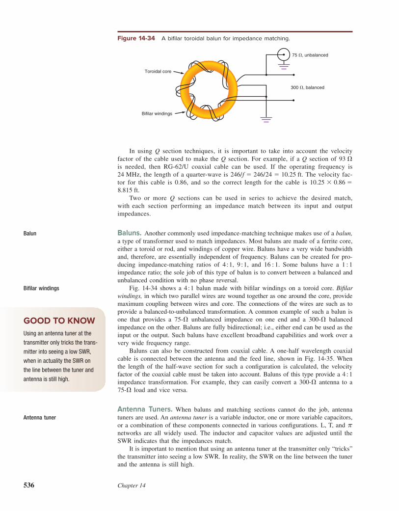
536 Chapter 14
In using Q section techniques, it is important to take into account the velocity
factor of the cable used to make the Q section. For example, if a Q section of 93 V
is needed, then RG-62/U coaxial cable can be used. If the operating frequency is
24 MHz, the length of a quarter-wave is 246/f 5 246/24 5 10.25 ft. The velocity fac-
tor for this cable is 0.86, and so the correct length for the cable is 10.25 3 0.86 5
8.815 ft.
Two or more Q sections can be used in series to achieve the desired match,
with each section performing an impedance match between its input and output
impedances.
Baluns. Another commonly used impedance-matching technique makes use of a balun,
a type of transformer used to match impedances. Most baluns are made of a ferrite core,
either a toroid or rod, and windings of copper wire. Baluns have a very wide bandwidth
and, therefore, are essentially independent of frequency. Baluns can be created for pro-
ducing impedance-matching ratios of 4 ; 1, 9 ; 1, and 16 ; 1. Some baluns have a 1 ; 1
impedance ratio; the sole job of this type of balun is to convert between a balanced and
unbalanced condition with no phase reversal.
Fig. 14-34 shows a 4 ; 1 balun made with bii lar windings on a toroid core. Bii lar
windings, in which two parallel wires are wound together as one around the core, provide
maximum coupling between wires and core. The connections of the wires are such as to
provide a balanced-to-unbalanced transformation. A common example of such a balun is
one that provides a 75-V unbalanced impedance on one end and a 300-V balanced
impedance on the other. Baluns are fully bidirectional; i.e., either end can be used as the
input or the output. Such baluns have excellent broadband capabilities and work over a
very wide frequency range.
Baluns can also be constructed from coaxial cable. A one-half wavelength coaxial
cable is connected between the antenna and the feed line, shown in Fig. 14-35. When
the length of the half-wave section for such a coni guration is calculated, the velocity
factor of the coaxial cable must be taken into account. Baluns of this type provide a 4 ; 1
impedance transformation. For example, they can easily convert a 300-V antenna to a
75-V load and vice versa.
Antenna Tuners. When baluns and matching sections cannot do the job, antenna
tuners are used. An antenna tuner is a variable inductor, one or more variable capacitors,
or a combination of these components connected in various coni gurations. L, T, and π
networks are all widely used. The inductor and capacitor values are adjusted until the
SWR indicates that the impedances match.
It is important to mention that using an antenna tuner at the transmitter only “tricks”
the transmitter into seeing a low SWR. In reality, the SWR on the line between the tuner
and the antenna is still high.
Balun
Bifi lar windings
Antenna tuner
Figure 14-34 A bifi lar toroidal balun for impedance matching.
Toroidal core
Bifilar windings
300 �, balanced
75 �, unbalanced
GOOD TO KNOWUsing an antenna tuner at the
transmitter only tricks the trans-
mitter into seeing a low SWR,
when in actuality the SWR on
the line between the tuner and
antenna is still high.

Antennas and Wave Propagation 537
One popular variation of the antenna tuner is a transmatch circuit, which uses a coil
and three capacitors to tune the antenna for optimal SWR (see Fig. 14-36). Capacitors
C2 and C3 are ganged together and tuned simultaneously. Transmatch circuits can be
made to work over a wide frequency range, typically from about 2 to 30 MHz. A similar
circuit can be made by using lower values of inductance and capacitance for matching
VHF antennas. At UHF and microwave frequencies, other forms of impedance matching
are used.
To use this circuit, an SWR meter is usually connected in series with the antenna
transmission line at the transmatch output. Then L1 is adjusted for minimum SWR, with
the transmitter feeding power to the antenna. Then C1 and C2–C3 are adjusted for minimum
SWR. This procedure is repeated several times, alternately adjusting the coil and capacitors
until the lowest SWR is reached.
A major development in antenna tuners is the automatic tuner. This may be an L, T,
p, or other coni guration that is self-adjusting. For example, the inductor in Fig. 14-36
would be provided with multiple taps along its length. By selecting the desired tap, the
inductance could be changed. In place of each capacitor would be banks of parallel con-
nected capacitors that could be switched in or out. All the inductor taps and capacitors
are switched in or out by relay contacts. The relays in turn are operated by an embedded
microcontroller.
Transmatch circuit
Figure 14-35 A coaxial balun with a 4 ; 1 impedance ratio.
75-� coaxial cable(RG-11/U, RG-59/U, etc.)
300 �
75 �
�
2
Figure 14-36 An antenna tuner.
From transmitter
50 �
L1
C1 C3
C2
Ganged
To antenna

538 Chapter 14
The microcontroller gets its inputs from feedback provided by the outputs of an RF
power meter. Today’s power meters measure both forward and rel ected power and
provide a dc output proportional to those values. These dc values are converted to binary
by an analog-to-digital converter and sent to the microcontroller. In the microcontroller
resides a program that implements an algorithm that automatically adjusts the inductor
and capacitors until the rel ected power is reduced to zero or at least minimized. The
modern antenna tuner can produce an excellent match in a few seconds or less.
Example 14-3Calculate the length of the impedance-matching section needed for a Q section to
match a 50-V transmitter output to a Yagi with a feed impedance of 172 V. The
operating frequency is 460 MHz.
ZQ 5 1Z0ZL 5 150(172) 5 18600 5 92.74 V
The amount 92.74 V is a close match to RG-62 A/U coaxial cable with an impedance
of 93 V (see Fig. 13-14). The velocity factor is 0.86.
λ
45
246
f3 VF 5
246
4603 0.86 5 0.5347 3 0.86 5 0.46 ft (5.5 in)
Example 14-4Calculate the length of the impedance-matching section needed for a λ/4 balun to convert
75 V to 300 V. The operating frequency is 460 MHz. RG-59 A/U coaxial cable is the
line of choice; the velocity factor of RG-59 A/U cable is 0.66.
λ
45 0.5347 3 0.66 5 0.353 ft (4.23 in)
14-3 Radio Wave PropagationOnce a radio signal has been radiated by an antenna, it travels or propagates through
space and ultimately reaches the receiving antenna. The energy level of the signal
decreases rapidly with distance from the transmitting antenna. The electromagnetic wave
is also affected by objects that it encounters along the way such as trees, buildings, and
other large structures. In addition, the path that an electromagnetic signal takes to a
receiving antenna depends upon many factors, including the frequency of the signal,
atmospheric conditions, and time of day. All these factors can be taken into account to
predict the propagation of radio waves from transmitter to receiver.
Optical Characteristics of Radio WavesRadio waves act very much as light waves do. Light waves can be rel ected, refracted,
diffracted, and focused by other objects. The focusing of waves by antennas to make
Radio wave

Antennas and Wave Propagation 539
them more concentrated in a desired direction is comparable to a lens focusing light
waves into a narrower beam. Understanding the optical nature of radio waves gives a
better feel for how they are propagated over long distances.
Refl ection. Light waves are rel ected by a mirror. Any conducting surface looks
like a mirror to a radio wave, and so radio waves are rel ected by any conducting
surface they encounter along a propagation path. All metallic objects rel ect radio
waves, especially if the metallic object is at least one-half wavelength at the frequency
of operation. Any metallic object on a transmission path, such as building parts, water
towers, automobiles, airplanes, and even power lines, causes some rel ection. Rel ec-
tion is also produced by other partially conductive surfaces, such as the earth and
bodies of water.
Radio wave rel ection follows the principles of light wave rel ection. That is, the
angle of rel ection is equal to the angle of incidence, as shown in Fig. 14-37. The radio
wave is shown as a wave front. To simplify the drawing, only the electrical lines of
force, designated by arrows, are shown. The angle of incidence is the angle between
the incoming line of the wave and a perpendicular line to the rel ecting surface. The
angle of rel ection is the angle between the rel ected wave and the perpendicular line.
A perfect conductor would cause total rel ection: All the wave energy striking the
surface would be rel ected. Since there are no perfect conductors in the real world, the
rel ection is never complete. But if the rel ecting surface is a good conductor, such as
copper or aluminum, and is large enough, most of the wave is rel ected. Poorer conduc-
tors simply absorb some of the wave energy. In some cases, the wave penetrates the
rel ecting surface completely.
As Fig. 14-37 shows, the direction of the electric i eld approaching the rel ecting
surface is reversed from that leaving the surface. The rel ection process reverses the
polarity of a wave. This is equivalent to a 180° phase shift.
Refraction. Refraction is the bending of a wave due to the physical makeup of the
medium through which the wave passes. The speed of a radio wave, like the speed of
light, is approximately 300,000,000 m/s (186,400 mi/s) in free space, i.e., in a vacuum
or air. When light passes through another medium, such as water or glass, it slows down.
The slowing down as light enters or exits a different medium causes the light waves
to bend.
The same thing happens to a radio wave. As a radio wave travels through free space,
it encounters air of different densities, the density depending on the degree of ionization
(caused by an overall gain or loss of electrons). This change of air density causes the
wave to be bent.
The degree of bending depends on the index of refraction of a medium n, obtained
by dividing the speed of a light (or radio) wave in a vacuum and the speed of a light
Refl ection
Refraction
Index of refraction
Figure 14-37 How a conductive surface refl ects a radio wave.
Angle ofincidence
Angle ofreflection
Incident wave from transmitter Reflected wave
Reflecting surface

540 Chapter 14
(or radio) wave in the medium that causes the wave to be bent. Since the speed of
a wave in a vacuum is almost the same as the speed of a wave in air, the index of
refraction for air is very close to 1. The index of refraction for any other medium will
be greater than 1, with how much greater depending upon how much the wave speed
is slowed.
Fig. 14-38 shows how a wave is refracted. The incident wave from a transmitter
travels through air, where it meets a region of ionized air that causes the speed of
propagation to slow. The incident wave has an angle of θ1 to a perpendicular to the
boundary line between air and the ionized air. The bent (refracted) wave passes through
the ionized air; it now takes a different direction, however, which has an angle of θ2 with
respect to the perpendicular.
The relationship between the angles and the indices of refraction is given by a for-
mula known as Snell’s law:
n1 sin θ1 5 n2 sin θ2
where n1 5 index of refraction of initial medium
n2 5 index of refraction of medium into which wave passes
θ1 5 angle of incidence
θ2 5 angle of refraction
Note that there will also be some rel ection from the boundary between the two media
because the ionization causes the air to be a partial conductor. However, this rel ection
is not total; a great deal of the energy passes into the ionized region.
Dif raction. Remember that light and radio waves travel in a straight line. If an
obstacle appears between a transmitter and receiver, some of the signal is blocked,
creating what is known as a shadow zone [Fig. 14-39(a)]. A receiver located in the
shadow zone cannot receive a complete signal. However, some signal usually gets
through due to the phenomenon of diffraction, the bending of waves around an object.
Diffraction is explained by what is known as Huygens’ principle. Huygens’ principle
is based on the assumption that all electromagnetic waves, light as well as radio waves,
radiate as spherical wave fronts from a source. Each point on a wave front at any given
time can be considered as a point source for additional spherical waves. When the
waves encounter an obstacle, they pass around it, above it, and on either side. As
the wave front passes the object, the point sources of waves at the edge of the obstacle
create additional spherical waves that penetrate and i ll in the shadow zone. This
phenomenon, sometimes called knife-edge diffraction, is illustrated in Fig. 14-39(b).
Radio Wave Propagation Through Space
The three basic paths that a radio signal can take through space are the ground wave,
the sky wave, and the space wave.
Snell’s law
Diffraction
Huygens’ principle
Figure 14-38 How a change in the index of refraction causes bending of a radio wave.
�2
�1�1
Ionized air
n2 � 1.5
Airn1 � 1
Incidentwave
Refracted wave
Boundary
Reflected wave (partial)

Antennas and Wave Propagation 541
Ground Waves. Ground or surface waves leave an antenna and remain close to the
earth (see Fig. 14-40). Ground waves actually follow the curvature of the earth and can,
therefore, travel at distances beyond the horizon. Ground waves must have vertical polar-
ization to be propagated from an antenna. Horizontally polarized waves are absorbed or
shorted by the earth.
Ground wave propagation is strongest at the low- and medium-frequency ranges.
That is, ground waves are the main signal path for radio signals in the 30-kHz to 3-MHz
range. The signals can propagate for hundreds and sometimes thousands of miles at these
low frequencies. AM broadcast signals are propagated primarily by ground waves during
the day and by sky waves at night.
The conductivity of the earth determines how well ground waves are propagated. The
better the conductivity, the less the attenuation and the greater the distance the waves can
travel. The best propagation of ground waves occurs over salt water because the water is
an excellent conductor. Conductivity is usually lowest in low- moisture areas such as deserts.
At frequencies beyond 3 MHz, the earth begins to attenuate radio signals. Objects
on the earth and features of the terrain become the same order of magnitude in size as
the wavelength of the signal and thus absorb or adversely affect the signal. For this
reason, the ground wave propagation of signals above 3 MHz is insignii cant except
within several miles of the transmitting antenna.
Ground wave
Figure 14-39 Dif raction causes waves to bend around obstacles.
(b)
Building
Shadowzone
ReceiverTransmitter
(a )
Spherical wave fronts
Building
Shadowzone
Transmitter
Spherical wave fronts
Point sources alongwave front producenew spherical fronts
Receiver
Figure 14-40 Ground or surface wave radiation from an antenna.
Antenna
Earth antenna
Surface wave Surface wave

542 Chapter 14
Sky Waves. Sky wave signals are radiated by the antenna into the upper atmosphere,
where they are bent back to earth. This bending of the signal is caused by refraction
in a region of the upper atmosphere known as the ionosphere (see Fig. 14-41). Ultraviolet
radiation from the sun causes the upper atmosphere to ionize, i.e., to become electri-
cally charged. The atoms take on or lose electrons, becoming positive or negative ions.
Free electrons are also present. At its lowest point, the ionosphere is approximately
30 mi (50 km) above the earth and extends as far as 250 mi (400 km) from the earth.
The ionosphere is generally considered to be divided into three layers, the D layer, the
E layer, and the F layer; the F layer is subdivided into the F1 and F2 layers.
The D and E layers, the farthest from the sun, are weakly ionized. They exist only
during daylight hours, during which they tend to absorb radio signals in the
medium-frequency range from 300 kHz to 3 MHz.
The F1 and F2 layers, the closest to the sun, are the most highly ionized and have
the greatest effect on radio signals. The F layers exist during both day and night.
The primary effect of the F layer is to cause refraction of radio signals when they
cross the boundaries between layers of the ionosphere with different levels of ionization.
Sky wave
Ionosphere
D layer
E layer
F layer
Figure 14-41 Sky wave propagation.
Skip zone
lonosphere
Earth
Skip distance
D layer
30 mi
250 mi
E layer
F 1 layer
F 2 layer
Ground wave
Sun

Antennas and Wave Propagation 543
When a radio signal goes into the ionosphere, the different levels of ionization cause the
radio waves to be gradually bent. The direction of bending depends on the angle at which
the radio wave enters the ionosphere and the different degrees of ionization of the layers,
as determined by Snell’s law.
Fig. 14-41 shows the effects of refraction with different angles of radio signals
entering the ionosphere. When the angle is large with respect to the earth, the radio
signals are bent slightly, pass on through the ionosphere, and are lost in space. Radiation
directly vertical from the antenna, or 90° with respect to the earth, passes through the
ionosphere. As the angle of radiation decreases from the vertical, some signals continue
to pass through the ionosphere. But at some critical angle, which varies with signal
frequency, the waves begin to be refracted back to the earth. The smaller the angle with
respect to the earth, the more likely it is that the waves will be refracted and sent back
to earth. This effect is so pronounced that it actually appears as though the radio wave
has been rel ected by the ionosphere.
In general, the higher the frequency, the smaller the radiation angle required for
refraction to occur. At very high frequencies, essentially those above about 50 MHz,
refraction seldom occurs regardless of the angle. VHF, UHF, and microwave signals
usually pass through the ionosphere without bending. However, during a period of sun-
spot activity, or other unusual electromagnetic phenomena, VHF and even UHF waves
may be refracted by the ionosphere.
Rel ected radio waves are sent back to earth with minimum signal loss. The result
is that the signal is propagated over an extremely long distance. This effect is most
pronounced in the 3- to 30-MHz or shortwave range, which permits extremely long
distance communication.
In some cases, the signal rel ected back from the ionosphere strikes the earth, is
rel ected back up to the ionosphere, and is re-rel ected back to earth. This phenomenon
is known as multiple-skip or multiple-hop transmission. For strong signals and ideal
ionospheric conditions, as many as 20 hops are possible. Multiple-hop transmission can
extend the communication range by many thousands of miles. The maximum distance
of a single hop is about 2000 mi, but with multiple hops, transmissions all the way
around the world are possible.
The distance from the transmitting antenna to the point on earth where the i rst
refracted signal strikes the earth to be rel ected is referred to as the skip distance
(see Fig. 14-41). If a receiver lies in that area between the place where the ground wave
is fully attenuated and the point of i rst rel ection from the earth, no signal will be
received. This area is called the skip zone.
Space Waves. The third method of radio signal propagation is by direct waves, or
space waves. A direct wave travels in a straight line directly from the transmitting antenna
to the receiving antenna. Direct wave radio signaling is often referred to as line-of-sight
communication. Direct or space waves are not refracted, nor do they follow the curvature
of the earth.
Because of their straight-line nature, direct wave signals travel horizontally from the
transmitting antenna until they reach the horizon, at which point they are blocked, as
shown in Fig. 14-42. If a direct wave signal is to be received beyond the horizon, the
receiving must be high enough to intercept it.
Obviously, the practical transmitting distance with direct waves is a function of the
height of the transmitting and receiving antennas. The formula for computing the distance
between a transmitting antenna and the horizon is
d 5 12ht
where ht 5 height of transmitting antenna, ft
d 5 distance from transmitter to horizon, mi
This is called the radio horizon.
Skip distance
Skip zone
Direct waves
Space wave
Line-of-sight communication
Radio horizon
GOOD TO KNOWAM broadcast signals are propa-
gated primarily by ground waves
during the day and by sky waves
at night.
GOOD TO KNOWRepeaters are widely used to
increase the communication
range for mobile and handheld
radio units.

544 Chapter 14
To i nd the practical transmission distance D for straight-line wave transmissions,
the height of the receiving antenna must be included in the calculations:
D 5 12ht 1 12hr
where hr 5 height of receiving antenna, ft. For example, if a transmitting antenna is 350 ft
high and the receiving antenna is 25 ft high, the longest practical transmission distance is
D 5 12(350) 1 12(25) 5 1700 1 150 5 26.46 1 7.07 5 33.53 mi
Line-of-sight communication is characteristic of most radio signals with a fre-
quency above approximately 30 MHz, particularly VHF, UHF, and microwave signals.
Such signals pass through the ionosphere and are not bent. Transmission distances at
those frequencies are extremely limited, and it is obvious why very high transmitting
antennas must be used for FM and TV broadcasts. The antennas for transmitters and
receivers operating at the very high frequencies are typically located on top of tall
buildings or on mountains, which greatly increases the range of transmission and
reception.
To extend the communication distance at VHF, UHF, and microwave frequencies,
special techniques have been adopted. The most important of these is the use of
repeater stations (see Fig. 14-43). A repeater is a combination of a receiver and a
transmitter operating on separate frequencies. The receiver picks up a signal from a
remote transmitter, amplii es it, and retransmits it (on another frequency) to a remote
Repeater
Figure 14-42 Line-of-sight communication by direct or space waves.
D
ht hr
d
d � 2ht
D � 2ht � 2hr
Repeaterstation
Figure 14-43 How a repeater extends the communication distance of mobile radio units at VHF
and UHF.

Antennas and Wave Propagation 545
receiver. Usually the repeater is located between the transmitting and receiving
stations, and therefore it extends the communication distance. Repeaters have
extremely sensitive receivers and high-power transmitters, and their antennas are
located at high points.
Repeaters are widely used to increase the communication range for mobile and
handheld radio units, the antennas for which are naturally not very high off the ground.
The limited transmitting and receiving range of such units can be extended considerably
by operating them through a repeater located at some high point.
In high-activity areas, a repeater used for mobile units will become overloaded when
too many users try to access it at the same time. When that happens, some users have
to wait until free time becomes available, continuing to call until they get through. Such
access delays are only a nuisance in some cases, but are clearly not acceptable when
emergency services are unable to get through.
Although multiple repeaters can be used to ease overcrowding, they are often inad-
equate because communication activity is not equally distributed among them. This prob-
lem is solved by using trunked repeater systems in which two or more repeaters are
under the control of a computer system that can transfer a user from an assigned but
busy repeater to another, available repeater. Thus the communication load is spread
around between several repeaters.
Repeaters can also be used in series, as shown in Fig. 14-44. Each repeater contains
a receiver and a transmitter. The original signal is picked up, amplii ed, and retransmit-
ted on a different frequency to a second repeater, which repeats the process. Typically,
such relay stations are located 20 to 60 mi apart, mostly at high elevations to ensure
reliable communication over very long distances. Microwave relay stations are used by
many telephone companies for long-distance communication.
The “ultimate” repeater is, of course, a communication satellite. Most communica-
tion satellites are located in a geostationary orbit 22,500 mi above the equator. Since at
that distance it takes exactly 24 h to rotate around the earth, communication satellites
appear stationary. They act as i xed repeater stations. Signals sent to a satellite are ampli-
i ed and retransmitted to earth long distances away. The receiver- transmitter combination
within the satellite is known as a transponder. Most satellites have many transponders,
so that multiple signals can be relayed, making possible worldwide communication at
microwave frequencies. (See Chap. 17.)
Trunked repeater systems
Communication satellite
Transponder
Figure 14-44 Using repeater stations to increase communication distances at microwave frequencies.
Mountain

546 Chapter 14
Calculating Received PowerA transmitted signal is radiated at a specii c power level. The output power of a transmit-
ter can be accurately determined by calculation or measurement. That power level is
increased if the antenna has gain because of improved directivity. As a signal leaves an
antenna, it immediately begins to become attenuated. Basically, the degree of attenuation
is proportional to the square of the distance between the transmitter and receiver. As
discussed previously, other factors also affect attenuation. Ground wave signals are greatly
attenuated by objects on the earth, which block the signals and reduce their level at the
receiver. In sky wave propagation, the ionospheric conditions and the number of hops
determine the signal level at the receiver, with each hop further reducing the signal level.
Space wave signals are simply absorbed and attenuated by objects in their path such as
trees or walls.
Despite these factors, it is possible to predict the approximate power level at a
receiver, and such calculations are quite accurate for the short distances characteristic of
direct or space wave transmission.
In analyzing the transmission of radio waves, it is often useful to start with the
concept of an isotropic radiator, or point source of radio waves. That is, the signal radi-
ates spherically in all directions. The power density at a given distance from an isotropic
radiator is predicted by the formula
Pd 5Pt
4πd2
where Pd 5 power density of signal, W/m2
d 5 distance from point source, m
Pt 5 total transmitted power, W
The distance d is really the radius of an imaginary sphere enclosing the source, and 4πd2
is the area of that sphere at any given distance. However, since practical antennas are
not purely isotropic sources, this formula must be modii ed somewhat. For example, if
the transmitting antenna is a dipole, the dipole has a gain of 1.64 (or 2.15 dB) over an
isotropic source, so the result must be multiplied by 1.64.
Suppose a transmitter puts a 50-W signal into a dipole antenna. The power density
of the signal at a distance of 30 mi (48.3 km, or 48,300 m) is
Pd 51.64Pt
4πd25
1.64(50)
4(3.1416)(48,300)2
5 3 3 1029 5 3 nW/m2
Knowing the power density at a given distance is not a particularly useful thing.
However, the formula for power at a given distance can be expanded to derive a general
formula for computing the actual power value of a signal at a receiving antenna:
Pr 5PtGtGrλ
2
16π2d2
where λ 5 signal wavelength, m
d 5 distance from transmitter, m
Pr, Pt 5 received and transmitted power, respectively
Gr, Gt 5 receiver and transmitter antenna gains expressed as a power
ratio and referenced to an isotropic source
If the gains are those in reference to a dipole, each must be converted to a power ratio
and multiplied by 1.64 before being used in the formula.
This formula is normally used only for ground wave, direct wave, or space wave
calculations. It is not used for sky wave signal predictions because the refraction and
rel ection that occur make predictions highly inaccurate.

Antennas and Wave Propagation 547
As an example, assume that a transmitter is operating at
150 MHz with a power of 3 W into a one-quarter wavelength ver-
tical antenna. The receiver, which is 20 mi (32.2 km, or 32,200 m)
away, has an antenna with a gain of 8 dB. What is the received
power?
The wavelength at 150 MHz is λ 5 300/f 5 300/150 5 2 m. The
gain of the quarter-wave vertical transmitting antenna is the same as
that for a dipole. With a dipole gain of 1, we must multiply this by 1.64
to get the gain over an isotropic source.
The gain of the receiving antenna is 8 dB. The gain is usually ex-
pressed as the gain over a dipole. To convert to gain with respect to an
isotropic source, we add 2.15 dB. This is the same as multiplying the
power ratio represented by the gain in decibels by 1.64. The result is
8 1 2.15 5 10.15 dB.
This must now be converted to an actual power ratio. Since
dB 5 10 log (Pout /Pin), where Pin and Pout are the input and output
power of the antenna, respectively,
Pout
Pin
5 log21 adB
10b 5 log21 a10.15
10b 5 log21 (1.015) 5 10.35
The received power can now be calculated.
Pr 53(1.64)(10.35)(2)2
16(9.87)(32,200)25
203.7
16.37 3 10110
5 1.24 3 1029 W or 1.24 nW
If the receiver antenna, transmission line, and front-end input
impedance are 50 V, we can calculate the input voltage, given this
input power. Since P 5 V 2/R, V 5 1PR. Substituting into
V 5 1PR gives
V 5 2(1.24 3 1029)(50) 5 2.5 3 1024 5 250 µV
This is a relatively strong signal; most good narrowband receivers can generate full
intelligible output with 1 µV or less.
Path Attenuation. Another way to predict received power is to estimate the total
power attenuation over a transmission path. This attenuation in decibels is given by
dB loss 5 37 dB 1 20 log f 1 20 log d
where f 5 frequency of operation, MHz
d 5 distance traveled, mi
The distance can also be given in kilometers, in which case the 37-dB i gure must be
changed to 32.4 dB. Isotropic antennas are assumed.
The attenuation over a 20-mi path at a frequency of 150 MHz is
dB loss 5 37 1 20 log 150 1 20 log 20 5 37 1 43.52 1 26 5 106.52
The dB loss formula, then, tells us that for every doubling of the distance between
transmitter and receiver, the attenuation increases about 6 dB.
Path attenuation
The expansive use of telephone networks has resulted in
integratively designed transmission of telephone and data
communication. The antennas are covered with a fiberglass
material to protect them from the weather. The covering
material does not impede the RF signals.

548 Chapter 14
Common Propagation ProblemsAlthough radio waves pass right through most objects on their way from transmitter to
receiver, they are negatively inl uenced by these objects. The result is a common problem
called fading. Good design of a communication system can minimize but not completely
eliminate fading. One way to overcome fading is to use a diversity system.
Fading. One of the primary effects of radio wave propagation is called fading. Fad-
ing is the variation in signal amplitude at the receiver caused by the characteristics of
the signal path and changes in it. Fading causes the received signal to vary in ampli-
tude, typically making it smaller. Under some conditions, the received signal may
actually be larger than a direct path signal depending upon the specii c communication
situation. Fading is caused by four factors: variation in distance between transmitter
and receiver, changes in the environmental characteristics of the signal path, the pres-
ence of multiple signal paths, and relative motion between the transmitter and receiver.
As a receiver gets farther away from a transmitter, the signal gets weaker just because
the path length is increasing. If the receiver moves closer to the transmitter, the signal
strength increases. Both types of situations occur when one or perhaps both of the trans-
ceivers are moving with respect to the other. It is especially noticeable in airplanes and
in cars. This type of fading is generally gradual and does not result in severe or rapid
swings in signal amplitude.
Fading is also caused by objects coming between the transmitter and receiver. Known
as shadow fading, this occurs if a vehicle containing a transceiver moves in such a way
that a large building or a mountain comes between it and a base station transceiver. The
obstacle causes the signal to be attenuated, resulting in fading. When a car enters a tun-
nel, the signal may be greatly attenuated so that fading occurs. Even the movement of
a rainstorm or snowstorm between transmitter and receiver can cause fading. Weather-
related effects are especially pronounced at the higher microwave frequencies, where the
signal wavelengths are in the same size range as the raindrops or snowl akes that produce
massive signal scattering by rel ection.
Multipath. One of the worst sources of fading is multipath interference. Sometimes
called Rayleigh fading, this type of fading occurs when a transmitted signal takes mul-
tiple paths to the receiver because of rel ections. The term Rayleigh refers to a particular
type of statistical response curve that mathematically describes the variation of the
received signal. As you saw earlier in this chapter, radio signals are easily rel ected by
conducting objects. The signal is usually radiated by a nondirectional antenna over a
wide horizontal range in such a way that it will strike the receiver antenna directly by
way of the direct line-of-sight space wave, but it may also strike many obstacles along
the way. Buildings, water towers, hills and mountains, and even moving vehicles all have
rel ected surfaces that will direct a signal along a separate path to the receiving antenna.
The signal may also be rel ected from the ground or water. The result is that multiple
signals reach the receiver antenna at different times.
Rel ected signals take a longer path than a direct signal, so they are delayed and
arrive at the antenna later than the direct signal. This time delay is seen as a phase shift
whose magnitude is a function of the total signal path distance and the wavelength
(frequency) of the signal. Keep in mind that as you saw earlier in the chapter, rel ections
produce a 180° phase shift that worsens the problem. The receiver sees a composite of
all the received signals. The phase shifts are usually such that they cancel the direct path
signal, resulting in an overall weaker signal. But the delays could also be such that the
rel ected signals arrive in phase with the direct signal, thereby causing the signals to add
in phase and actually produce a higher-level signal.
Another type of fading is caused by movement of either the transmitter or the receiver.
When the transmitter is in a car, plane, or other vehicle, rapid movement toward or away
from the receiver introduces a signal frequency change called a Doppler shift (to be
described in Chap. 16). Movement that causes the transmitter and receiver to get closer
Fading
Shadow fading
Multipath interference
Rayleigh fading

Antennas and Wave Propagation 549
to each other causes the signal frequency to increase. Movement that increases the distance
causes a frequency decrease. Large signal-frequency changes produce lower-level signals
because the signals are partially out of the passband of the receiver’s selective i lters. In digital systems that predominantly use some form of phase-shift modulation, the Doppler shift confuses the demodulator and produces bit errors. In most cases, several types of fading occur simultaneously. Multipath fading and shadow fading are the worst offenders. If you have ever used a cell phone from a mov-ing car in a changing environment, you know that fading can cause signii cant signal variations, including no service at all. Using a cell phone or radio in a large city with
Example 14-5A 275-ft-high transmitting antenna has a gain of 12 dB over a dipole. The receiving antenna, which is 60 ft high, has a gain of 3 dB. The transmitter power is 100 W at 224 MHz. Calculate (a) the maximum transmitting distance and (b) the received power at the distance calculated in part (a). (There is 1.61 km/mi.)
a. D 5 12ht 1 12hr
5 12(275) 1 12(60) 5 1550 1 1120
5 23.45 1 10.95 5 34.4 mi
34.4 mi 3 1.61 km/mi 5 55.4 km
55.4 km 3 1000 5 55,400 m
b. Pr 5PtGtGrλ
2
16π
2d2
5 100 W
Gt 5 12 dB over dipole
5 12 dB 1 2.15 dB
5 14.15 dB
dB 5 10 log Pout
Pin
Pout
Pin5 log21
adB
10b 5 log21
a14.15
10b 5 log21
(1.415)
5 26
Gt 5 26
Gr 5 3 dB 1 2.15 dB 5 5.15 dB
Pout
Pin5 log21
a5.15
10b 5 log21
(0.515) 5 3.27
Gr 5 3.27
λ 5300
f5
300
2245 1.34 m
λ2 5 (1.34)2 5 1.8
Pr 5100(26)(3.27)(1.8)
16(3.14)2(55,400)2
5
15,303.6
4.85 3 1011 5 3.16 3 1028 5 31.6 nW

550 Chapter 14
many tall buildings produces extreme multipath interference and shadow fading. Using cell phones or other wireless equipment inside a building essentially does the same. When digital communication is involved, multipath fading can cause intersymbol interference. If high-speed data transmission is used, the symbols are short, and multipath delays may be of the same order of magnitude. A symbol received directly may be dif-ferent from a symbol received from a rel ected source. The result is severe bit errors.
Although fading can occur on signals of any frequency, it is most pronounced in UHF
and microwave communication, where the signal wavelengths are very short compared to
the path distances and size of rel ective surfaces. Fading is a signii cant problem with cell
phones and other radio equipment especially when one or more of the transceivers are in
motion. Fading is also a problem in long-distance shortwave communication when the
signal can take several bounces off the ionosphere and the earth to produce canceling or
reinforcing signals. Fading signal variations can be only a few decibels or as much as 20
to 30 dB. A signii cant amount of fading can make communication unreliable.
To overcome fading, most communication systems have a built-in fading margin.
That is, they have a high enough transmitter power and sufi cient receiver sensitivity to
ensure that the weaker rel ective signals do not degrade the direct signal as much. A fade
margin of at least 5 dB is built into most systems.
Multipath fading can also be greatly minimized by using highly directive antennas,
either at the transmitter or at the receiver or at both. Narrow transmit and receive beams
virtually eliminate multiple paths and the related fading. However, in most communica-
tion systems, nondirectional (i.e., omnidirectional) antennas are the norm. Cell phones,
two-way radios, and even base stations must have broad azimuth coverage to receive or
transmit signals over a wide area.
Broadband signals are much less sensitive to multipath fading than narrowband sig-
nals are. If broadband methods such as spread spectrum (CDMA) or OFDM are used,
the signals are spread over a very wide frequency range. Multiple rel ections of signals
over a wide range of frequencies are received in such a way that less cancellation or
intersymbol interference occurs. This is a major factor in designing new communication
systems where fading is expected.
Diversity System. Fading can also be minimized by using what is called a diversity
system. A diversity system uses multiple transmitters, receivers, or antennas to mitigate
the problems caused by multipath signals. Two common types of diversity are fre-
quency and spatial. With frequency diversity, two separate sets of transmitters and
receivers operating on different frequencies are used to transmit the same information
simultaneously. The theory is that signals on different frequencies will react differently
to the various fading mechanisms, thereby resulting in a least one reliably received
signal. To be effective, the frequencies should be widely spaced from one another. Of
course, such systems are very expensive since they require two transmitters, receivers,
and antennas, all on different frequencies. The scarcity of frequency spectrum also
makes this type of system impractical. It is rarely used except in cases where extreme
reliability is a must.
Another more widely used form of diversity is called space or spatial diversity. It
uses two receiver antennas spaced as far apart as possible to receive the signals. Diversity
systems are used mainly at base stations rather than in portable or handheld units. The
basic idea is that antennas at slightly different locations will receive different variations
of the signals, with one being better than another. The spacing may be horizontal or
vertical, whichever is the more convenient. However, in some cases one arrangement will
be superior to the other.
Diversity reception is particularly difi cult at shortwave frequencies, where the spacing
will typically be many hundreds or even thousands of feet. Only horizontal spacing is used.
At UHF and microwave frequencies, wide antenna spacing is relatively simple because the
wavelengths are short. In general, the wider the spacing (10 or 20 wavelengths or more),
the better. Many systems use the relationship h/d 5 11 to determine a minimum and, as
it turns out, optimum spacing for antennas. In this relationship, h is the height of the
Diversity system
Spatial diversity

Antennas and Wave Propagation 551
antenna and d is the spacing distance. For antennas that are 100 ft high, the minimum spacing would be
100
d5 11
d 5100
115 9.09 ft
Fig. 14-45(a) shows a typical spatial diversity system. The two antennas feed a com-biner network, where the two signals are linearly added. The result is a larger signal and minimized fading effects. The signals may be combined at the antenna or almost anywhere in the receiver. Some systems combine after the LNAs. Others combine after the IF. In still other systems, two completely separate receivers are used and the signals are combined after demodulation. Experimentation is required to determine the best results. Another form of spatial diversity is selective or switched diversity. In this system, shown in Fig. 14-45(b), the two antennas feed separate LNAs whose outputs are monitored by circuits that measure received signal strength. In cell phone systems, these circuits are called received signal strength indicators (RSSIs). They determine the signal with the greatest strength and switch that signal to the remainder of the receiver circuits. All this is done automatically at high speed, ensuring that the receiver always has the strongest signal. Diversity systems are widely used in the newer cell phone systems and in wireless LANs that work indoors and, in some cases, with mobile wireless units (laptop computers, PDAs, etc.) that are frequently in motion. New techniques such as multiple-input, multiple-output (MIMO), and smart (adaptive) antennas are now being used to further improve transmission in multipath environments. These techniques will be covered in Chap. 16.
Received signal strengthindicators (RSSIs)
Figure 14-45 Common diversity reception systems. (a) Signals are combined for
maximum output. (b) Only the strongest signal is switched to the
receiver.
Antenna 1
Combiner RXAntenna 2
LNA
(a )
Antenna 1
RSSI RXAntenna 2
LNA
(b)
Electronicswitches
LNA
LNA

552 Chapter 14
CHAPTER REVIEWOnline Activity
14-1 Understanding Passive Intermodulation
Objective: To become aware of the effects of passive inter-modulation (PIM) in some wireless systems.
Procedure: Perform an Internet search on passive inter-
modulation, PIM distortion, or similar terms. Also see Chap. 9. Use the data you i nd to answer the following
questions.
Questions: 1. What is PIM?
2. What causes PIM?
3. What conditions must exist to produce PIM?
4. What are the effects of PIM on the receiver? on the
transmitter?
5. How can PIM be minimized or eliminated?
6. What test instruments can be used to i nd PIM?
14-2 Discovering Near Vertical Incidence Skywave
Objective: Learn about the effect and potential of near verti-
cal incidence skywave (NVIS) propagation.
Procedure: Perform an Internet search on the terms near
vertical incidence skywave, or NVIS and look for answers to
the following questions.
Questions: 1. What is NVIS?
2. At what frequencies does NVIS occur?
3. What problem does NVIS solve?
4. What type of antenna is used to achieve NVIS?
5. Can a vertical antenna be used for NVIS?
6. Name two common NVIS applications.
Questions
1. What is the basic makeup of a radio wave?
2. What is the name of the mathematical expressions that
describe the behavior of electromagnetic waves? Give a
general statement regarding what these expressions state.
3. Describe the relationship between the types of i elds that
make up a radio wave. What is the orientation of these i elds
with respect to the transmission direction of the wave?
4. What part of a radio wave determines its polarization
with respect to the earth’s surface?
5. What is the polarization of a radio wave with a mag-
netic i eld that is horizontal to the earth?
6. Dei ne what is meant by antenna reciprocity.
7. What is the name of the antenna type upon which
most other antennas are based? What is the length of this
antenna in terms of wavelength at the operating frequency?
8. What is the most commonly used medium for connect-
ing an antenna to a transmitter or receiver?
9. What is the length of a dipole?
10. State the theoretical radiation resistance or drive im-
pedance of a dipole.
11. What factors affect the impedance of a dipole and how?
12. What is the equivalent circuit of a dipole at resonance,
above resonance, and below resonance?
13. What factors inl uence antenna bandwidth?
14. Describe the horizontal radiation pattern of a dipole.
What is the three-dimensional shape of a dipole radia-
tion pattern?
15. Dei ne what is meant by directivity in an antenna.
16. What unit is used to state and measure an antenna’s
directivity?
17. Dei ne antenna gain. What gives an antenna gain?
18. What is an isotropic radiator?
19. What gain does a dipole have over an isotropic radiator?
20. State two ways to express antenna gain.
21. Dei ne ERP.
22. What is a folded dipole? What are its advantages over a
standard dipole?
23. What two names are used to refer to a one-quarter
wavelength vertical antenna?
24. What is the horizontal radiation pattern of a one- quarter
wavelength vertical antenna?
25. What term describes an antenna that radiates equally
well in all horizontal directions?
26. What must a one-quarter wavelength vertical antenna
have for proper operation, in addition to a vertical con-
ductor radiator?
27. What is the name of a group of conductors connected to
the transmission line at the base of some vertical antennas?
28. Name the most commonly used type of transmission
line for one-quarter wavelength vertical antennas.
29. What term describes the directivity of an antenna that trans-
mits or receives equally well in two opposite directions?
30. What is a unidirectional antenna?
31. Why does a directional antenna amplify a signal?
32. What physical attributes must an antenna have to
exhibit gain and directivity?

Antennas and Wave Propagation 553
33. Name the two basic classes of antenna arrays. 34. Name the three basic elements in a Yagi antenna. 35. Name the two parasitic elements in a Yagi beam antenna. 36. What is the upper limit on the number of directors that
a Yagi can have? 37. What is the typical beam width range of a Yagi antenna? 38. State two factors that affect the beam width of a Yagi. 39. Dei ne the term front-to-back ratio as it applies to a
Yagi.
40. True or false? A Yagi can be operated with either hori-
zontal or vertical polarization.
41. Which polarization is the more common for a Yagi?
42. List three kinds of driven arrays.
43. Describe the radiation pattern of the three most com-
mon types of driven arrays.
44. Do driven arrays have gain over a dipole?
45. What is the name of a popular wideband driven array
with a unidirectional radiation pattern?
46. State one major benei t of a log-periodic antenna over
other types of driven arrays.
47. What is the most common value of antenna input/output
impedance for modern transmitters and receivers?
48. Why is impedance matching necessary in some an-
tenna installations?
49. What is the name of a type of transformer used for im-
pedance matching in antenna installations?
50. What do you call a one-quarter wavelength section of
transmission line that is used for impedance matching
between antenna and transmission line?
51. What is the impedance-matching ratio of a coaxial balun?
52. Describe how an antenna tuner works.
53. What is the usual procedure for adjusting an antenna tuner?
54. What are the requirements for the rel ection of a radio
signal?
55. Will a vertically polarized radio wave be received by a
horizontally polarized antenna?
56. What is circular polarization? State the two types of
circular polarization.
57. Will horizontally and vertically polarized antennas
pick up circularly polarized signals?
58. What is refraction as it refers to radio waves? What
causes refraction of radio waves?
59. What is diffraction as it refers to radio waves? Is diffrac-
tion harmful or advantageous in radio communication?
60. Name the three paths that a radio signal can take through
space.
61. What two names are used to refer to a radio wave that
propagates near the surface of the earth? Are they verti-
cally or horizontally polarized?
62. What is the frequency range of signals that propagate
best over the surface of the earth?
63. State the name of the radio wave that is refracted by the
ionosphere.
64. What is the frequency range of signals that propagate
best by ionospheric refraction?
65. What is the ionosphere? How is it different from atmo-
spheric layers that are closer to the earth? Why does it differ?
66. What layer of the ionosphere has the greatest effect on
a radio signal?
67. True or false? The ionosphere acts as a mirror, rel ect-
ing radio waves back to earth.
68. What phenomenon of propagation makes worldwide
radio communication possible?
69. What factors determine whether a radio wave is refracted
by the ionosphere or passes through to outer space?
70. What do you call a radio wave that propagates only
over line-of-sight distances?
71. At what frequencies is line-of-sight transmission the
only method of propagation?
72. How can the transmission distance of a UHF signal be
increased?
73. What technique is used to increase transmission dis-
tances beyond the line-of-sight limit at VHF and above?
74. What is a repeater station and how does it work?
75. Which conditions cause the worst kind of fading?
76. What is the name given to multipath fading?
77. Why is frequency diversity undesirable?
78. How does spatial diversity minimize fading?
79. Which produces the fewest fading effects, narrowband
or wideband signals?
1. What is the approximate impedance of a dipole that is
0.1λ aboveground? 0.3λ aboveground? ◆
2. What is the length of a wire dipole antenna at 16 MHz?
3. A wire dipole antenna has length of 27 ft. What is its
frequency of operation? What is its approximate
bandwidth? ◆
4. At low frequencies (less than 30 MHz), what is the nor-
mal polarization of a dipole?
5. What is the most common transmission line used with
low-frequency dipoles? ◆
6. The power applied to an antenna with a gain of 4 dB is
5 W. What is the ERP?
7. What is the length of a folded dipole made with a
300-V twin lead for a frequency of 216 MHz? ◆
8. Calculate the length of a one-quarter wavelength verti-
cal antenna at 450 MHz.
9. What is the length of the driven element in a Yagi at
290 MHz? ◆
10. Calculate the length of the coaxial loop used in a
coaxial balun for a frequency of 227 MHz. Assume a
velocity factor of 0.8.
11. What is the length in inches of a one-quarter wave-
length impedance-matching section of coaxial cable
with a velocity factor of 0.66 at 162 MHz?
Problems

554 Chapter 14
12. How far away is the radio horizon of an antenna 100 ft high?
13. What is the maximum line-of-sight distance between a paging antenna 250 ft high and a pager receiver 3.5 ft off the ground?
14. What is the path attenuation between transmitter and receiver at a frequency of 1.2 GHz and a distance of 11,000 mi?
15. An antenna has a dBd gain of 6. What is its gain with respect to an isotropic radiator?
16. A cell phone antenna tower 240 ft high uses spatial diversity. What is the minimum desirable antenna separation?
◆ Answers to Selected Problems follow Chap. 22.
1. Of two dipoles, one using wire conductors and one using thin tubing conductors, which has a wider bandwidth?
2. The sun is at an angle of 30° to the horizon and causes a tall one-quarter wavelength vertical antenna to cast a shadow 400 ft long. At what frequency does the antenna resonate?
3. Where are the two conductors of a coaxial transmission line connected in a one-quarter wavelength vertical an-tenna installation?
4. Compare and contrast the operation of a one-quarter wavelength vertical antenna to that of a one-half wave-length dipole.
5. What is the feed impedance of a one-quarter wave-length vertical antenna? What factors inl uence this
impedance?
6. If a vertical antenna is too short, what can be done to
bring it into resonance?
7. If a vertical antenna is too long for the desired frequency
of operation, what can be done to make it resonant?
8. See Fig. 14-46. What is the beam width of this antenna?
Calculate its gain. Calculate the front-to-back ratio of
this antenna in decibels. Note: This radiation pattern
Critical Thinking
Figure 14-46 Radiation pattern for Critical Thinking question 8.
0
180
30
60
90
120
150210
240
270
300
330
�4
�6
�8
�10
�20
�30
�2
�50�40

Antennas and Wave Propagation 555
uses a logarithmic scale and is calibrated in decibels. The maximum radiation point on the major lobe at 08 is given the value of 0 dB. The 23-dB down points are clearly identii ed so that beam width can be deter-
mined. The center of the plot is 2100 dB.
9. A transmitter has a directional antenna with a gain of
4 dB. The frequency is 72 MHz. The power into the
antenna is 2 W. The receiver uses a one-quarter wave-
length ground plane. The distance between the trans-
mitting and receiving antennas is 3 mi. What is the
power at the receiver? What is the receiver input volt-
age with a 50-V input impedance?
10. A 915-MHz transmitter sends a signal to a receiver.
The transmitter output power is 1 W. Both transmitter
and receiver use one-quarter wavelength vertical anten-
nas. The receiver input impedance is 50 V. What is the
maximum distance that can be achieved and still deliver
1 µV into the receiver front end?
11. What is the length of a 5⁄8λ vertical antenna at 902 MHz?
12. A very low-power battery-operated transmitter at an
inaccessible location is to send telemetry data to a data
collection center. The signal is often too weak for reli-
able data recovery. List some practical steps that can be
taken to improve transmission.

556
chapter
Internet Technologies
15
The Internet is a worldwide interconnection of computers by means of many
complex networks. The Internet was established in the late 1960s under the
sponsorship of the Department of Defense and later through the National
Science Foundation. It provided a way for universities and companies doing
military and government research to communicate and to share computer
fi les and software. In the early 1990s, the Internet was privatized and opened
to anyone. Today it is a system with billions of users across the world.
This chapter discusses the technology used in transporting data in
packets through large numbers of computers called servers and Internet
appliances called routers and the extensive fi ber-optic Internet backbone.
Technologies such as Frame Relay, asynchronous transfer mode (ATM),
SONET, and the Optical Transport Network (OTN) are discussed. The trans-
mission protocol TCP/IP is discussed, and the operation of a router is
explained. This chapter also includes an introduction to storage-area net-
works (SANs). Finally, the subject of Internet data security is defi ned, and
methods of encryption and authentication are considered.
Objectives
After completing this chapter, you will be able to:
■ Defi ne the Internet and cloud computing.
■ List the main applications of the Internet.
■ Explain how data is transmitted over the Internet.
■ Name and explain the four main types of transmission systems
used in the Internet, including ATM, SONET, OTN, and Frame Relay.
■ Explain the details of the TCP/IP protocol.
■ Explain the operation of a router.
■ Identify and explain the major types of storage-area networks and
their transmission technologies, including Fibre Channel and iSCSI.
■ Name the main types of security systems used with the Internet.
■ Name the encryption systems most commonly used on the Internet.

Internet Technologies 557
15-1 Internet ApplicationsThe Internet is a communication system that accomplishes one of three broad uses: (1) share resources, (2) share i les or data, and (3) communication. The primary applica-
tions of the Internet are e-mail, i le transfer, the World Wide Web, e-commerce, searches,
Voice over Internet Protocol, and video.
E-Mail. E-mail is the exchange of notes, letters, memos, and other personal communi-
cation by way of e-mail software and service companies. You write a message to a
person and send it over the Internet via your e-mail provider, which, in turn, transfers it
to the e-mail provider of the receiving person. That person retrieves the message at his
or her convenience. E-mail is one of the most common communication methods in use
today and the number one application of the Internet.
File Transfer. File transfer refers to the ability to transfer i les of data or software
from one computer to another. The i le may be text, digitized photographic data, a com-
puter program, and so on. A i le transfer program (FTP) allows you to access i les in
remote computers and download them to your computer, where they may be used. Files
can also be “attached” to e-mail messages. File transfer is an excellent research tool
because it allows you to access massive amounts of data in the form of books, articles,
newspapers, brochures, data sheets, and hundreds of other sources. Apple Computer’s
iTunes allows purchase and download of music.
World Wide Web. Whenever most people refer to the Internet, they are really talking
about the World Wide Web (WWW), or the Web for short. The Web is a specialized part
of the Internet where companies, organizations, the government, or even individuals can
post information for others to access and use. To do this, you establish a website, which
is a computer that stores the information you wish to dispense. The information can be
on your own computer or in the computer of a Web service provider. The information
is presented in the form of pages, a logic subunit that may contain text, graphics, anima-
tions, sound, and even video.
You access these websites through the Internet by way of a special piece of software
known as a browser. The browser allows you to call up a desired website by name or
to search the Internet websites containing information of interest to you. The browser is
the software that lets you navigate and explore the Web and access and display the
information. The two most widely used browsers are Netscape Navigator and Microsoft
Internet Explorer.
A key feature of the Web is hypertext. Hypertext is a method that allows different
pages or websites to be linked. When Web pages are created, usually with a language
called hypertext markup language (HTML), programmers can insert links to other pages
on the website, to other parts of the same page, or even to different websites. For exam-
ple, a page may contain a highlighted word (usually in blue letters), which means that
it is a link to some related topic on a different page or different site. Clicking with the
mouse on that word automatically takes you to the related information. This ability to
link to related or relevant information is one of the most powerful and useful features
of the Web.
E-commerce. E-commerce or electronic commerce refers to doing business over the
Internet, usually buying and selling goods and services by way of the Web. Companies
selling products or services set up websites describing their wares and offering them for
sale. Individuals may buy these items by giving a credit card number or making other
forms of payment. The product is then shipped by mail or overnight carrier. Online
shopping is expected to grow signii cantly in the future. Two of the larger e-commerce
retailers are Amazon, a book reseller, and eBay, a site where some items are sold by
auction.
File transfer
World Wide Web
Browser
Hypertext
Hypertext markup language (HTML)
E-Commerce
GOOD TO KNOWA company called Bolt, Baranek
& Newman (BBN) started as an
acoustics consulting fi rm but
ended up writing the protocols
for the ARPANet, the predecessor
to the Internet.

558 Chapter 15
Searches. An Internet search allows a person to look for information on any given topic. Several companies offer the use of free search “engines,” which are specialized software that can look for websites related to the desired search topic. The most commonly used search sites are Google, Yahoo, and Microsoft Bing. You simply access the website through your browser and type in one or more keywords that direct the search engine. Within seconds, the search engine returns a listing of all those sites it i nds containing the key-
words. Most searches return hundreds and even thousands of references such as websites,
advertisements, press releases, magazine and newspaper articles, and many other resources.
Voice over Internet Protocol (VoIP). VoIP is the technique of replacing standard
telephone service with a digital voice version with calls taking place over the Internet.
Voice is digitized, compressed, and transmitted over the Internet in packets to the called
location. There it is decompressed and reconverted to analog. VoIP has largely replaced
standard telephone services in companies and governments and has made great inroads
into homes across the United States and other countries. Its growth continues.
Video over Internet Protocol. Video or TV over the Internet (IPTV) is also becom-
ing more common. The video (and accompanying audio) is digitized, compressed, and
sent via the Internet. This is referred to as over the top (OTT) video. It is gradually
replacing some video transmitted over the air and by cable television systems. Both IPTV
and VoIP make use of the standard Internet connections used for data.
How the Internet WorksThe Internet is the ultimate data communication network. It uses virtually every conceivable
type of data communication equipment and technique. All the concepts you learned earlier
apply to the Internet. Just keep in mind that the information is transmitted as serial binary
pulses, usually grouped as bytes (8-bit chunks) of data within larger groups called
packets. All the different types of communication media are used including twisted-pair
cable, coaxial cable, i ber- optic cable, satellites, and other wireless connections.
Internet Addresses. Each individual or computer on the Internet must have some
kind of identii er or address. An addressing system for the Internet uses a simplii ed
name-address scheme that dei nes a particular hierarchy. The upper level of the hierarchy
is called a top-level domain (TLD). A domain is a specii c type of organization using the
Internet. Such domains are assigned a part of the Internet address. The most common
domains and their address segments are as follows:
Domain Address Segment
Commercial companies .com
Educational institutions .edu
Nonproi t organizations .org
Military .mil
Government .gov
Internet service providers .net
Air transportation .aero
Business .biz
Cooperatives .coop
Information sites .info
International organizations .int
Mobile .mobi
Museums .museum
Families and individuals .name
Professions .pro
Packets

Internet Technologies 559
Travel-related companies .travel
Adult sites .xxx
Country .us, .uk, .fr, .jp, .de(United States, United Kingdom, France, Japan, Germany)
Another part of the address is the host name. The host refers to the particular com-puter connected to the Internet. A host is a computer, device, or user on the network. A server provides services such as e-mail, Web pages, and DNS. The host name is often the name of the company, organization, or department sponsoring the computer. For example, IBM’s host name is ibm.
E-mail Address. The i rst part of the address is the user’s name or some abbreviation,
concatenation, or nickname. You might use your name for an e-mail address or some
made-up name that you would recognize. The complete address might look like this:
The user name is separated from the host by the @ symbol. The host, in this case
xyz, is the e-mail service provider. Note the dot between the host name and the domain
name. This address gets converted to a series of numbers used by computers on the
Internet to identify and locate one another.
WWW Addresses. To locate sites on the Web, you use a special address called a
uniform resource locator (URL). A typical URL is <http://www.abs.com/newinfo>.
The i rst part of the URL specii es the communication protocol to be used, in this
case hypertext transfer protocol (http). The www, of course, designates the World Wide
Web. The abs.com part is the domain or the computer on which the website exists. The
item after the slash (/) indicates a directory within the website software. Most websites
have multiple directories, which are also usually further subdivided into pages.
Initial Connections. A PC is connected to the Internet in a variety of ways. The most
common method is through a modem that connects to the telephone system. There are
traditional dial-up modems such as those described earlier and the newer asynchronous
digital subscriber line (ADSL) and cable TV modems. Wireless modems are also available.
A common way of connecting to the Internet is to use a LAN to which your PC
may be connected. Most company and organization PCs are almost always connected to
a LAN. The LAN has a server that handles the Internet connection, which may be by
way of a T1 line to the telephone system or a i ber-optic connection.
Role of the Telephone System. The familiar telephone system is often the i rst
link to the Internet. Because it is so large and so convenient, it is a logical way to make
connections to remote computers. A standard telephone line is used with dial-up modems
and DSL modems. In many applications, the telephone system is the only connection
between computers. Many corporate computers are connected in this way, and you can
connect directly to an online service provider in this way. Its primary function is to con-
nect you to a facility known as an Internet service provider (ISP).
Broadband Connections. Although most connections to the Internet occur with a
modem over the telephone lines, more and more individuals are acquiring broadband
connections. A broadband connection is a fast Internet connection provided by a tele-
phone company or a cable TV company. The term fast here means a data transmission
speed greater than the speed that can be obtained with a telephone modem, typically
53 kbps. A broadband connection can provide speeds up to many megabits per second.
The most widely used broadband connection is a cable TV modem. Cable TV com-
panies often act as Internet service providers. The cable TV system is ideal for support-
ing fast data transfers. A special cable modem is provided that connects to a PC by way
of an Ethernet interface. Data transfer rates vary depending upon the amount of trafi c
on the line, but they can reach as high as 50 Mbps.
Host
Uniform resource locator (URL)
Hypertext transfer protocol (http)
Internet service provider (ISP)
Broadband connection

560 Chapter 15
The second most widely used broadband connection is the digital subscriber line
(DSL). It is most often offered by a local telephone company but may be delivered by an independent supplier. It gives a data rate from 1.5 to 50 Mbps. Internet access is also available through cell phones.
Internet Service Provider. An ISP is a company set up especially to tap into the network known as the Internet. It can be an independent company or a local telephone company or a cable TV company. The ISP has one or more servers to which are con-nected dozens, hundreds, or even thousands of modems, DSLs, or cable connections from subscribers. It is usually the ISP that provides the software you use in communication over the Internet. The ISP also usually provides e-mail service. There are thousands of ISPs across the United States. Most are set up in medium-size to large cities. Some ISPs are wireless services. The ISP is connected to the Internet backbone by way of a fast digital interface such as via a i ber-optic MAN.
Cloud Computing. The cloud is a general term for the Internet. In system diagrams,
the Internet is sometimes represented by a large white puffy cumulonimbus cloud. The
cloud is a massive unseen networking infrastructure that is constantly changing and has
never been mapped.
Cloud computing is the process of storing and accessing programs or data over the
Internet. Instead of storing your programs and data on your computer’s hard drive, you
access the software and storage capability of remote servers via an Internet connection.
All you need is a minimal computer with a Web browser and possibly an applications
interface program that lets you use the external resources wherever they may be. E-mail is
an example of cloud computing you have probably used. The e-mail programs like Google
gmail and Yahoo mail and e-mail storage are in the cloud and not on your computer.
Cloud computing is a new concept that is gradually replacing the older original form
of local computing. The one thing that makes cloud computing possible, practical, and
acceptable is very high-speed broadband Internet connections.
There are multiple forms of cloud computing. One of them is software as a service
(SaaS). This is the process of subscribing to a software program. It may be a game, a
database, or some applications software. Microsoft offers such software.
Another is platform as a service (PaaS). An example is a development platform that
offers all the tools you need to build your own cloud application. This may be a custom
software application created for your own use but implemented in the cloud.
Then there is Infrastructure as a service (IaaS). The infrastructure is a company that
supplies hardware such as servers or virtual computers and storage units. Users rent
remote equipment, facilities, and services to handle their needs. Amazon and Google are
examples.
The big question is, why would you give up local control of your stored data and
software? There are several benei ts. First is lower cost. The access computer can be a
smaller, less powerful computer with a slower CPU, less RAM, and a smaller hard
drive—all of which costs less. You may not have to buy servers or large storage units.
Second, software costs less. Instead of owning the software, you lease it instead. Third,
you can access your software and data from any place at anytime if you have access to
a laptop, tablet, or smartphone and an Internet connection. Other benei ts, from a com-
pany or business perspective, are lower costs for IT staff support and less need for
physical space and utilities devoted to servers.
There are some insecurities associated with cloud computing. For example, is your
data safe from loss or hacking? Can you get access to it anytime you want? Is there
backup? Is your data really private? Do you really own the data, given that it is stored
remotely? Will ISP outages prevent you from getting to your data or the software you
subscribe to?
Companies and individuals must make up their own minds about the pros and cons
of cloud computing, depending on their needs and resources. In any case, cloud computing
is a growing phenomenon and will expand greatly in the coming years.

Internet Technologies 561
15-2 Internet Transmission SystemsThe Internet is made up of a huge number of individual elements. These elements include the servers, routers, and transmission media that carry the signals. A huge num-ber of components and interconnections are involved. This section shows the overall operation of the Internet, the transmission protocols used, as well as the most widely used transmission media.
Frame RelayFrame Relay (FR) is a packet-switching protocol standardized by the ITU-T. It packages data to be transmitted into FR frames that have the structure shown in Fig. 15-1. The 8-bit l ags signal the beginning and ending of a packet. A two-octet (byte) address i eld
contains all the details regarding the exact destination of the packet through the network.
The data i eld is variable and may contain up to 4096 octets. A 2-octet frame check
sequence (FCS) is an error detection code that is compared to the FCS calculated
from the received data. If any transmission error occurs, the receiving unit asks for a
retransmission.
FR is protocol-independent in that it can carry the data from any other transmis-
sion method such as Ethernet. Ethernet packets are put into the data field and car-
ried unmodified to the destination. Frame Relay uses existing dedicated digital
circuits leased by telecommunications companies. Both T1 and T3 lines are widely
used. The equipment used in handling FR is frame relay switches that examine the
destination address and forward the packets through one switch after another until
the destination is reached. The most common use of FR is in LAN-to-LAN connec-
tions where the LANs are widely separated, as in two different company locations.
The FR service was usually offered by local telecommunications carriers, but it is
no longer a viable service.
Asynchronous Transfer ModeAsynchronous transfer mode (ATM) is also a packet-switching system for transmitting
data. It uses very short 53-byte packets with a 48-byte data payload and a 5-byte header
that designates the destination as well as the type of data to be handled. Any kind of
data may be transmitted in this way, including voice, video, and computer data. The
packet format is shown in Fig. 15-2.
ATM is transmitted by way of switches that pass the packets from one to the other
over the network. An ATM network sets up a virtual circuit that gives the appearance
Frame check sequence (FCS)
Asynchronous transfer mode (ATM)
Figure 15-1 A Frame Relay (FR) frame or packet.
Flag01111110
1 12 20 – 4096
Flag01111110
Address Data
Number of octets
FrameCheck
Sequence
Figure 15-2 An ATM packet.
5 48
Header Data
Number of bytes or octets

562 Chapter 15
of a single continuous path for the data from source to destination. In reality, the packets most likely take several different paths through the network and may even arrive out of order. The ATM system handles these occurrences such that all data arrives in the desired order. The ATM network can use almost any physical layer, but most often it is some i ber-optic system. Early ATM networks operated at 155 and 622 Mbps. Today, ATM
uses 2.5- and 10-Gbps optical networks.
Frame Relay and ATM are gradually being phased out in favor of the newer Optical
Transport Network (OTN) and Ethernet.
SONET*The Synchronous Optical Network (SONET) was developed to transmit digitized tele-
phone calls in T1 format over i ber-optic cable at high speeds. Its primary use is to send
time-multiplexed voice or data over switched networks. SONET is used between tele-
phone central ofi ces, between central ofi ces and long-distance carrier facilities, and for
long-distance transmission. Until recently, most Internet backbones were SONET point-
to-point connections or rings. Today the trend is away from SONET. Most new long-haul
networks use Optical Transport Network (OTN) and Ethernet.
SONET is by far the most widely used optical data transmission network in the
United States. It is an American National Standards Institute (ANSI) standard as
well as a subset of the broader international standard known as the Synchronous
Digital Hierarchy (SDH). The latter was developed and sanctioned by the Interna-
tional Telecommunications Union (ITU) and then used throughout the rest of
the world.
SONET is a physical (PHY) layer standard that dei nes the method for formatting
and transmitting data in sync with a master timing system keyed to an atomic clock. The
standard dei nes different optical-carrier (OC) speeds, from 51.84 Mbps to 39.812 Gbps.
The electric signal to be transmitted is called the synchronous transport signal (STS) and
can exist at several levels or speeds, although the base speed (STS-1) is 51.84 Mbps.
In the SDH system, the signal is also called the synchronous transport mode, or STM.
Fig. 15-3 lists the most common channel speeds.
Earlier systems used OC-3 and OC-12 levels, but today most SONET systems have
been upgraded to operate at OC-48. The OC-192 and OC-768 levels are gradually being
deployed as technology and economics permit.
SONET is a time-division multiplexing (TDM) transmission scheme that sends time-
interleaved data in i xed-length frames of 810 bytes. The frame format consists of nine
90-byte rows. The bytes are transmitted consecutively from left to right and from top to
bottom. See Fig. 15-4. In each row 4 bytes is for overhead, and 86 bytes per row is for
Synchronous Optical Network (SONET)
Synchronous Digital Hierarchy (SDH)
Synchronous Transport Signal (STS)
Synchronous transport mode
*Portions of this section are reprinted with permission from Electronic Design, November 20, 2000. Copyright 2000. Penton Media Inc.
Figure 15-3 SONET data rates.
Sonet level STM level Data rate
STS-1/OC-1STS-3/OC-3STS-12/OC-12STS-48/OC-48STS-192/OC-192STS-768/OC-768
51.84 Mbps155.52 Mbps622.08 Mbps
2.488 Gbps*9.953 Gbps*
39.812 Gbps*
—STM-1STM-4STM-16STM-64STM-256
*Note that when referencing these data rates, they are typically
rounded to 2.5, 10, and 40 Gbps, respectively.

Internet Technologies 563
data payload. The overhead bytes contain framing, control, parity, and pointer informa-tion for managing the payload. Although SONET can operate in a point-to-point link, the most common topology is a ring. Multiple nodes make up the ring, with an add-drop multiplexer (ADM) at each node. One of the key features and benei ts of a SONET system is that the ADM permits
data from multiple sources to be added to or extracted from the data stream as required.
The ring topology also offers data transmission redundancy, which ensures survivability
when a cable has been cut.
The basic SONET transmission speed is OC-1, or 51.84 Mbps. This is the rate
achieved when one SONET frame is transmitted in 125 µs. If higher-speed transmission
is desired, as is usually the case, multiple frames are transmitted in this time period by
a system of byte interleaving.
Most of today’s long-distance telephone service, as well as the Internet backbone,
is made up of a hierarchy of large and small SONET rings. Even though SONET was
designed to carry synchronous voice trafi c in a circuit-switched environment, its primary
function is data transmission with no regard to its content. As a result, SONET can carry
asynchronous, packet-switched data from asynchronous transfer-mode (ATM), Frame
Relay, Ethernet, or Transport Control Protocol/Internet Protocol (TCP/IP) equipment.
Optical Transport NetworkSONET has been adequate for long-haul and metro networks over the past several decades,
but it has not kept pace with the demands of the Internet and other networking efforts. Mas-
sive Internet access has exploded in recent years. Increased viewing of TV and downloading
of videos has further burdened the Internet. Additional stress has come from the new, faster,
fourth-generation (4G) smartphones and the attendant need for faster backhaul networks. On
top of that, the cloud computing movement requires increasingly faster networks.
The solution is i ber-optic networks. Most of the build-out of long-haul and metro
i ber networks in the late 1990s and early 2000s used 2.488-Gbit/s SONET (OC-48)
technology. Since then, many systems underwent upgrades to 10 Gbits/s (9.95328-Gbit/s
Add-drop multiplexor
Figure 15-4 SONET frame format.
Sectionoverhead
Lineoverhead
1 bytepathoverhead
90 bytes (Octets)
87 bytesSynchronous payload environment (SPE)
3 bytes
GOOD TO KNOWResearchers Partha Mitra and
Jason Stark determined that the
maximum theoretical capacity
of a single optical fi ber is
100 terabits (Tbits) equivalent to
20 billion simultaneous one-page
e-mails.

564 Chapter 15
SONET or OC-192) and a precious few to SONET’s peak rate of near 40 Gbits/s (39.81312-Gbit/s SONET or OC-768). These synchronous systems connect to asynchronous Ethernet networks, creating the need for interface solutions such as Ethernet-over-SONET protocols. With faster Ethernet and Internet Protocol (IP) systems growing in number and the emergence of all-IP 4G wireless networks, SONET has struggled to keep pace. Add to that the need for speeds beyond 40 Gbits/s, and suddenly a faster IP-based system is no longer a luxury, but rather a necessity. That new system designated to deal with this problem is called the Optical Transport Network (OTN). It is already in place in some locations and starting to expand. OTN is called the “digital wrapper” or “optical channel wrapper.” It is dei ned by
the ITU-T standards G.872 and G.709. OTN can carry IP trafi c with ease, much like
SONET and SDH (Synchronous Digital Hierarchy). OTN features line rates of 2.66
Gbits/s (OTU1) to carry SONET OC-48, 10.7/11.09 Gbits/s (OTU2/2e) to carry 10- Gigabit
Ethernet or SONET OC-192, and 43.01 Gbits/s (OTU3) to carry SONET OC-768 or
40-Gigabit Ethernet. A line rate of 112 Gbits/s (OTU4) is also dei ned to carry 100- Gigabit
Ethernet. Overall, OTN is gradually replacing SONET/SDH in most long-haul and metro
networks. It is expected that OTN will form most of the Internet backbone, while 40- and
100-Gbit/s optical versions of Ethernet will serve the LANs, data centers, and some
metro areas.
OTN is a packet-based technology and was optimized to carry Ethernet as well as
SONET. It includes support for the operation, administration, maintenance, and provi-
sioning (OAM&P) feature of SONET that allows the network carrier to monitor and
control the network by programming. In addition, unlike SONET, OTN was designed to
operate over one or more wavelengths of light on a single i ber. This wavelength division
multiplexing (WDM) is described later in Chap. 19.
Fig. 15-5 shows the OTN frame format. There are four rows of 4080 bytes (octets)
transmitted one after another left to right and top to bottom. The frame is divided into
overhead, payload, and forward error correction (FEC) i elds. The Ethernet, SONET, and
other protocol frames are mapped into the payload section. Overhead bytes are added
to designate addresses, data types, number of data bytes, OAM&P data, and related
information.
Finally a FEC is added. OTN uses an advanced form of the Reed-Solomon FEC
designated RS (255, 239). For every 239 bytes of data, 16 additional bytes of parity
correction bits are added. This FEC can correct up to 8 bit errors or detect 16 bit errors
per row of data. The key benei t of this FEC is that it adds up to 6.2 dB of coding gain,
allowing a BER of 10−12 to be achieved. In addition, with this coding gain, OTN can be
transmitted over longer spans of i ber without regeneration of the signal. Whereas SONET
was limited to a reach of 200 km, OTN has a reach up to 2000 km.*
Figure 15-5 Simplifi ed OTN frame.
1
2
3
4
OverheadPayload
(4 3 3808 bytes)
FEC
(4 3 256 bytes)
40803824 382516 171Row
*Some of the material in the OTN section was taken from the article “Optical Primed to Handle Data-Speed Demand,” by Louis E. Frenzel, in Electronic Design magazine, June 24, 2011.

Internet Technologies 565
RoutersThe router is the single most important piece of equipment in the Internet. You have prob-ably heard of the world’s largest router manufacturer, Cisco. Routers interconnect the var-ious segments of the WAN backbones. Routers are also used to connect MANs to WANs, LANs to others LANs, and LANs to MANs. The routers connect to one another and to the various servers to form a large mesh network connected usually by i ber-optic cable.
A router is an Intelligent computerlike device that looks at all packets transmitted
to it and examines their Internet protocol (IP) destination addresses. It then determines
the best next path for the data to take to its destination. The router stores information
about the other routers and networks to which it is connected and about any nearby
networks. This information is stored in a routing table that is compared to the destination
address on all incoming packets. Routing algorithms determine the best (closest, fastest)
connection and then retransmit the packet. In any given Internet transmission, most pack-
ets pass through several routers before they reach their i nal target computer.
Physically, a router can have several coni gurations. Any high-speed device can be
used that has serial inputs and outputs and a way to examine packet addresses and make
decisions regarding routing and switching. For example, a computer with a fast processor,
adequate memory, serial I/O, and the appropriate software can serve as a router. Today,
most routers are specialized pieces of equipment optimized for the routing function.
The basic coni guration of a modern router is shown in Fig. 15-6. It consists of a group
of line cards that plug into connectors on a printed-circuit board back plane. The back plane
contains the copper interconnecting lines to allow the line cards to transmit and receive data
from one another. Transfer speeds are typically many gigabits per second. The line cards
communicate with one another through a switch fabric. The switch fabric is a large digital
equivalent of a cross bar switch. A cross bar switch is a matrix of switches in a row- column
format that allows any one of multiple input lines to be connected to any one of multiple
output lines. Superfast electronic switches connect the line cards. See Fig. 15-6.
Each line card has a serial input port and a serial output port. These are usually opti-
cal i ber lines, but they could also be RJ-45 Ethernet ports. At the receive input, the optical
data is converted to serial electric signals that are then deserialized by a circuit called a
serializer/deserializer (SERDES) that performs both serial-to-parallel and parallel-to-serial
data conversion. The parallel data is then stored in a random-access memory (RAM). This
data is then examined by a special processor to determine its destination address. The
processor uses a routing lookup table and algorithms that decide which output line is to be
Router
Serializer/deserializer (SERDES)
Figure 15-6 General block diagram of a router.
Switchfabric
Fast electronicswitch detail
Serial data
in/o
ut —
usually
fib
er-
optic c
able
Linecard
Linecard
Linecard
Linecard
Linecard
Linecard

566 Chapter 15
used. Any input may be routed to any output in this way. The processor then passes the packet to the switch fabric where it is sent to an output port. The packet is serialized by a SERDES circuit and then sent to the output port by using SONET, ATM, Ethernet, or OTN.
The Internet BackboneThe Internet backbone is a collection of companies that install, service, and maintain large nationwide and even worldwide networks of high-speed i ber-optic cable. The com-
panies own the equipment and operate it to provide universal access to the Internet. In
many ways, these companies are the Internet, for they provide the basic communication
medium, equipment, and software that permit any computer to access any other.
Although each of the backbone providers has its own nationwide network, the providers
are usually connected to one another to provide many different paths from one computer to
another. There are more than 50 of these interconnection points in the United States. Known
as network access points (NAPs), these facilities provide the links between backbones.
Fig. 15-7 shows a diagram of the main components of the Internet. On the left are three
ways in which a PC is connected for Internet access, to the telephone local ofi ce via a
conventional or DSL modem or by way of a cable modem and cable TV company. The
telephone company central ofi ce and cable TV company connect to an Internet service
provider by way of a local i ber-optic MAN. (Note: The telephone company or cable TV
company may also be the ISP.) The ISP contains multiple servers that handle the trafi c.
Each connects to the Internet by way of a router that attaches to the Internet backbone at
one of the many network access points. The primary equipment at network access points is
routers that determine the destination of packets. The “cloud” in Fig. 15-7 represents the
Internet backbone. This is one of several large i ber-optic networks, either point-to-point or
a ring, that carry the Internet data and interconnect with one another to exchange data.
On the right in Fig. 15-7 are additional connections. Here a company LAN accesses
the backbone by way of a regional MAN. A company server contains a website that is
regularly accessed by others. Also shown is a Web hosting company that stores the
websites and Web pages of others.
Internet backbone
Network access points (NAPs)
Figure 15-7 Simplifi ed diagram of the Internet.
Internet“cloud”
Fiber-optic backbone
NAP
NAP
NAP
Internetservice provider (ISP)
Telephonecompanycentraloffice
CableTV
company
Webhosting
company
Companyor
organizationwebsite
CompanyLAN
RegionalMANring
Server
Modem
Modem
Modem
DS
L
Key:
� PC
NAP � Network access point (routers)
NAP
GOOD TO KNOWEach packet includes information
about its source, destination, the
sequence of how it should be
reassembled once it reaches its
destination, and some indication
of how large the packet is.

Internet Technologies 567
The Packet-Switching Transmission SystemThe Internet is a packet-switching system. Data to be sent is divided up into short chunks called packets and transmitted one at a time. The term datagram is also used to describe a packet. Packets are typically less than 1500 octets long. (Note: In data communication, a byte is more often called an octet, an 8-bit word.) Each packet i nds its own way through the complex maze that is the Internet by using addressing
information stored in the packet. Not all packets take the same path through the
system, and in fact the packets may arrive at the receiving end out of the order in
which they were sent.
Fig. 15-8 shows a simplii ed version of the packet-switching concept. The packet-
switching network consists of multiple exchanges with high-speed packet switches that
connect to multiple inputs and outputs. The multiple interexchange links produce many
possible paths through the network.
Several popular packet-switching systems are in use in Internet backbones. These
include Frame Relay, asynchronous transfer mode (ATM), and OTN systems. ATM sys-
tems are the fastest and most widely used. They break down all data into 53-byte pack-
ets and transmit them over i ber-optic networks at speeds of up to 100 Gbps. ATM is
also used to transmit voice and video. In some instances, the packets are packaged into
long continuous synchronous data streams and transmitted by way of the SONET. Such
transmissions are called packet over SONET (PoS). Newer parts of the backbone use
OTN. Most modern backbone networks operate at 40 Gbps or 100 Gbps.
Packet switching requires a set of software protocols that make sure that the data
is properly partitioned, transmitted, received, and reassembled. On the Internet, these
protocols are called TCP/IP. TCP means Transmission Control Protocol, and IP means
Internet Protocol. Both protocols are used to send and receive data over the Internet.
TCP/IP was invented in the 1960s, when the Advanced Research Project Agency
(ARPA) of the Department of Defense (DoD) tested and established the i rst packet
network. It was i rst implemented on large computers running the UNIX operating
system. Today, TCP/IP is by far the most widely implemented data communication
protocol, and it is at the heart of the Internet.
TCP/IP is a layered protocol similar to the OSI seven-layer model discussed in
Chap. 11. TCP/IP does not implement all seven layers, although the effect is the same.
Some operations of the individual seven layers are combined to form four layers, as
Packet
Datagram
Packet over SONET (PoS)
TCP/IP protocol
Figure 15-8 The packet-switching concept showing nodes in the backbone.
Data to be transmitted
p1
Divided into packets
Packet-switchingnodes
Packets placedin original
order
Orderof
receivedpackets
p2 p3 p4
p1
p1
p1
p2
p2 p2
p2
p3
p3
p4 p4p4
p1 p2 p3 p4
p1
p2
p3
p4
Key:

568 Chapter 15
shown in Fig. 15-9. The upper, or applications, layer works with other protocols that implement the desired application. The most widely used are the i le transfer protocol
(FTP), which facilitates the transmission of long i les of data; the simple mail transfer
protocol (SMTP), which implements e-mail; and the hypertext transfer protocol (http),
which provides access to the World Wide Web.
Transmission Control Protocol. The host-to-host layer is really TCP. It divides
the data into packets to be sent. To each packet is attached a comprehensive header
containing source and destination addresses, a sequence number, an acknowledgment
number, a check sum for error detection and correction, and other information. The TCP
header is shown in Fig. 15-10. It consists of 20 bytes or octets, minimum, depending
upon what options are added. At the receiving end, TCP reassembles the packets in the
proper order and sends them to the application. It also asks for retransmission if a packet
is received in error.
File transfer protocol (FTP)
Simple mail transfer protocol (SMTP)
Hypertext transfer protocol (http)
Figure 15-9 Comparing the OSI and TCP/IP layers.
6: Presentation
5: Session
7: Application
OSI layers
2: Data link
1: Physical
3: Network
4: TransportHost-to-host
(TCP)
Application
TCP/IP layers
Networkaccess
IP
Dataoffset
Header20 octets
Reserved Flags Window
Urgent pointerChecksum
Options (�padding)
Data (variable)
Destination portSource port
Sequence number
Acknowledge number
32 bits, 4 octets
Figure 15-10 TCP headers.

Internet Technologies 569
TCP is used only to prepare the packets for transmission and reassemble the packets when received. It does not implement the actual packet transmission over the Internet. As you will see, that is the job of IP. TCP’s job is to offer some assurance that the packets arrive in a reliable and high-quality form by providing the error detecting and correcting check sums, sequence numbers, and other features. The TCP header is a single serial bit stream in which each of the i elds is transmit-
ted one after another. This header is difi cult to draw and print as a long single line, so
the presentation format in Fig. 15-10 is used. This representation is widely used to
illustrate other protocols and headers. In reality, data is transmitted serially from left to
right and from top to bottom, row after row, with 4 octets per row.
Internet Protocol. The TCP packet is then sent to the IP layer, where the IP protocol
is used. The IP layer ensures that the packet gets to its destination over the Internet. In
Fig. 15-11, an IP header is attached before the resulting new packet is transmitted.
Note in Fig. 15-11 that the destination address has 32 bits. Every computer has one
of these addresses assigned to it. The addresses are usually expressed in what is called
the dotted decimal form. The 32-bit address is divided into four 8-bit segments. Each
segment can represent 256 numbers from 0 through 255. A typical address would look
like this: 125.63.208.7. Dots separate the four decimal segments. These addresses are
assigned by an organization known as the Internet Assigned Numbers Authority (IANA).
The addresses are subdivided into classes (A through E) to represent different types and
sizes of networks, organizations, and individual users.
The most widely used IP protocol is called IPv4, or Internet Protocol version 4. Its
primary limitation is that its destination address size is only 32 bits; i.e., it is limited to
232, or 4,294,967,296, locations or users. Although more than 4 billion addresses would
seem to be enough, as the Internet has grown, this has become a severe limitation. The
newer version is IPv6, which has a 128-bit address i eld that should provide more than
enough destinations (2128) for massive future expansion. Also IPv6 provides for authen-
tication and multicasting. Multicasting is the ability of IP to move fast audio and video
data over the Internet from a single source to multiple destinations. IPv6 is implemented
on many computers, but not all. It is slowly being phased in as software and hardware
are updated in new systems.
IPv4 (Internet Protocol version 4)
Multicasting
Type of
service
Header
32 octets
IHLVersion
0 3 7 15 31
Total length
FragmentIdentifier
Options and padding
Data
Header checksumProtocolTime to live
Source address
Destination address
Flags
Figure 15-11 IP header (IPv4).
GOOD TO KNOWWhen a packet is sent from a host
to another host over the Internet,
it is fi rst assembled into packets
with TCP format; then the IP layer
adds a new header to send the
packet over the Internet.

570 Chapter 15
The IPv6 packet with header is illustrated in Fig. 15-12. The header is a simpler version of the IPv4 packet; only the basic information is included, to make forwarding more efi cient. A header extension is used if additional instructions are needed.
Key changes to the header are that there is no header checksum and the time to live
i eld is called the hop limit. This is the maximum allowed number of hops between
routers that a packet can make before it is discarded.
Note the 128-bit source and destination addresses. Each address is 16 bytes long
and can provide up to 3.4 3 1038 addresses. Instead of the dotted decimal address rep-
resentation of IPv4, the IPv6 addresses are represented by a 32-digit hexadecimal address.
There are eight groups of four hex digits with colons between. An example is
1974:0000:A56E:FFFF:0000:239C:470D:3C09.
As for payload, the payload length i eld in the header is 16 bits, indicating that the
data payload may be up to 65,535 bytes. This is the same as in the IPv4 packet.
Finally, the network access layer that contains the physical layer connection transports
the data. As explained earlier, there are several different ways that TCP/IP information
is transmitted. For example, the packets may get packaged into Ethernet packets in a
LAN and then delivered to a MAN for ultimate connection to the packet-switched WAN
backbone. Or the TCP/IP packets may travel via a cable TV modem to an ISP that con-
nects to a MAN via a i ber-optic line and then to the WAN. The WAN may carry the
data via ATM, SONET or OTN through the backbone.
TCP/IP*Several protocols or sets of rules are used to communicate over a computer network.
Each protocol must accomplish several tasks, such as encapsulation, fragmentation and
reassembly, connection control, ordered delivery, l ow control, error control, addressing,
multiplexing, and transmission services. Perhaps the most common protocol used to
accomplish these tasks is the Transmission Control Protocol/Internet Protocol or TCP/IP.
TCP/IP is the communications protocol that hosts use to communicate over the Internet,
and it establishes a virtual connection between a destination and source host. TCP/IP
uses two protocols to accomplish this task, TCP and IP.
TCP enables two hosts to establish a connection and exchange data. TCP will guar-
antee both the delivery of data and that the packets will be delivered in the same order
in which they were sent. Remember, packets are sent through a network according to
the best path. This “best path” choice does not guarantee that all packets will take the
same path, nor will they arrive in the same order they were sent. TCP has the job of
Figure 15-12 The IPv6 packet.
0
Version
Payload length
Source address
(128 bits)
Destination address
(128 bits)
Payload
(up to 65,536 bytes)
Traffic
classFlow label
Next
headerHop limit
3 11 15 31
*Courtesy of Walter Currier, Assistant Professor of Computer and Electrical Engineering at Liberty University, Lynchburg, VA.

Internet Technologies 571
ensuring that all the packets are received and put back into the correct order before they are passed up the protocol stack. IP determines the format of the packets. The IP packet format is not discussed in detail, but there are a total of 20 octets in IP version 4 packets. These bits are used to select the type of service, length of datagram, identii cation number, l ags, time to live, next-higher
protocol, header checksum, and various addresses. The packet IP provides a function similar
to the address on a postal letter. You write the address on the letter and put it in the mailbox.
You and the receiver know where it is sent from and to whom it is being sent, but the path
is determined by someone else. That someone else is the routers in the network between the
destination and the source. It is TCP/IP that establishes the connection between the destina-
tion and the source. TCP steps in and cuts the letter up into smaller pieces or packets and
then sends them, ensuring all the packets are received and put back into the proper order.
UDPThe User Datagram Protocol (UDP) is another protocol used at the transport level. UDP
provides a connectionless service for applications. UDP provides few error recovery
services, unlike TCP. However, like TCP, UDP uses IP to route its packets throughout
the Internet. UDP is used when the arrival of a message is not absolutely critical. You
may recall that from time to time you receive letters for Current Resident in your mail-
box. The senders of this “junk mail” are not concerned that everyone receive the pack-
age they send. UDP is similar to the Current Resident mail and is often used to send
broadcast messages over a network. A broadcast message is a message that is sent
periodically to all hosts on the network in order to locate users and collect other data
on the network. UDP messages are also used to request responses from nodes or to
disseminate information. Another application of UDP is in the use of real-time applica-
tions. With real-time applications, retransmitting and waiting for arrival of packets are
not possible, so TCP is not used for these applications. When real-time data (voice or
video) is routed, a connectionless UDP protocol is used. If packets get dropped or fail
to arrive, the overall message is usually not corrupted beyond recognition.
Internet and AddressingYou have seen the components that make up a network and how information travels
across a network, but how does a packet i nd its intended destination? The Internet is
organized in a hierarchical structure. The entire network is often referred to as the Inter-
net or the World Wide Web. The Internet is subdivided into several smaller networks that
are all interconnected by routers.
The Internet connects several separate segments or networks together by using rout-
ers. Routers need some way to identify the destination network to which a packet is
bound. Routers accomplish this by using the network IP address. All devices on that
network share the same network address, but have unique host addresses. Packets get
routed from network to network until they arrive at the network that contains the host
to whom the packet has been sent.
A good example of a hierarchal structure is how large military units are organized.
The largest structure is the brigade. The brigade is separated into two regiments with
three battalions per regiment. Each battalion has i ve companies. Each company then has
platoons, and each platoon has squads. An individual soldier or sailor is in a squad,
platoon, company, battalion, and so on. If you want to contact all the soldiers or sailors
in a particular company, you can send a message to just that company. The same is true
for a battalion, or platoon. In a computer network, the ability to send messages to an
individual host on a particular network is also important. Each network is then connected
into the entire Internet or the so-called Internet cloud.
We can break each connection to the cloud into its own network, and each network
would be connected to the cloud by using a router. Every computer connected off the
router is considered to be on the same network.
User Datagram Protocol (UDP)

572 Chapter 15
This arrangement is similar to a family. The router would represent a single family, say, the Jones family; and all the segments represent children in the Jones family. We can easily identify who is in the Jones family by looking at the last name. A router can recognize who is in its network by using a set of numbers called an IP address. When a computer receives a packet from the router, the computer i rst checks the
destination MAC address of the packet at the data link layer. If it matches, it’s then
passed on to the network layer. At the network layer, it checks the packet to see if the
destination IP address matches the computer’s IP address. From there, the packet is
processed as required by the upper layers. On the other hand, the computer may be
generating a packet to send to the router. Then as the packet travels down the OSI model
and reaches the network layer, the destination and source IP address of this packet are
added in the IP header.
The format of an IPv4 address is called dotted decimal, and it consists of four num-
bers from 0 to 255 separated by periods or dots. Each number between the periods is
considered an octet because it represents 8 binary bits.
Example: 35.75.123.250
The dotted decimal format is convenient for people to use, but in reality the router will
convert this number to binary, and it sees the above dotted decimal number as a con-
tinuous string of 32 bits. The example below shows an IP address in decimal notation.
This IP address (35.75.123.250) is then converted to binary, which is what the computer
understands. It’s easier for us to remember four different numbers than thirty-two
0s or 1s.
35 .75 .123 .250
00100011.01001011.01111011.11111010
The above IP address would look like 00100011010010110111101111111010 to the
computer. The hexadecimal version is 234B7BFA.
To provide l exibility, the early designers of the IP address standard sat down to sort
out the range of numbers that were going to be used by all computers. They organized
the IP address into i ve classes, and we normally use three of these classes. When
people apply for IP addresses, they are given a certain range within a specii c class
depending on the size of their network.
In Table 15-1, you can see the i ve classes. The i rst three classes (A, B, and C) are
used to identify workstations, routers, switches, and other devices, whereas the last two
classes (D and E) are reserved for special use. The IP addresses listed above are not all
usable by hosts!
An IPv4 address consists of 32 bits, which means it is 4 bytes long. The i rst octet
(i rst 8 bits or i rst byte) of an IP address is enough for us to determine the class to
Table 15-1Five Dif erent Classes of IP
Addresses
Class Range of IP Addresses
A 1.0.0.0 to 127.255.255.255
B 128.0.0.0 to 191.255.255.255
C 192.0.0.0 to 223.255.255.255
D 224.0.0.0 to 239.255.255.255
E 240.0.0.0 to 255.255.255.255

Internet Technologies 573
which it belongs. And depending on the class to which the IP address belongs, we can determine which portion of the IP address is the network ID and which is the host ID. For example, if you were told that the i rst octet of an IP address was 168, then, using
the above table, you would notice that it falls within the 128 to 191 range, which makes
it a class B IP address.
Earlier we said that companies are assigned different IP ranges within these classes,
depending on the size of their networks. For instance, if a company required 1000 IP
addresses, it would probably be assigned a range that falls within a class B network
rather than a class A or C.
To get the information to the correct host, the IP address is divided into two
parts, the network ID and the host ID. These two parts contain two pieces of valuable
information:
1. It tells us which network the device is part of (network ID).
2. It identii es that unique device within the network (host ID).
Fig. 15-13 gives you an example to help you understand the concept.
Routers will look at the i rst number or octet to determine the class of the IP address.
The class indicates how many bits are used to represent the network ID and how many
bits are used to represent the host ID. In the above picture, you can see a small network.
We have assigned a class C IP range for this network. Remember that class C IP addresses
are for small networks. Looking now at host B, you will see that its IP address is
202.178.0.3. The network ID is 202.178, and the host ID is 0.3.
Table 15-2 contains the range of numbers used to determine the class of the network
and the number of bits available to assign to a network and the hosts on that network.
For example, 140.179.220.200 is a class B address. The 140 falls within the 128 to
191 range, which makes it a class B IP address. So, by default, the network part of the
GOOD TO KNOWThe class A IP addresses were
designed for large networks, class
B for medium-size networks, and
class C for smaller networks.
GOOD TO KNOWThink of the network ID as the
suburb you live in and the host ID
as your street in that suburb. You
can tell exactly where someone is
if you have their suburb and
street name. In the same way, the
network ID tells us to which net-
work a particular computer be-
longs, and the host ID identifi es
that computer from all the rest
that reside in the same network.
Table 15-2 Identifying Network and Host IDs
Class Range of First Octet
Number of Network ID Bits
Number of Host ID Bits
A 1–127 8 24
B 128–191 16 16
C 192–223 24 8
Figure 15-13 Example showing network and host IDs.
Host A202.178.0.2
202.178.0.1
Host B202.178.0.3
Host ID:3
Router A
Host D 202.178.0.5
Host C202.178.0.4
Network ID
202.178.0.0
Server
202.178.0.6

574 Chapter 15
address (also known as the network address) is dei ned by the i rst 2 octets (140.179.x.x),
and the node part is dei ned by the last 2 octets (x.x.220.200).
Now we can see how the class determines, by default, which part of the IP address
belongs to the network (N) and which part belongs to the host (h).
● Class A—0NNNNNNN.hhhhhhhh.hhhhhhhh.hhhhhhhh
● Class B—10NNNNNN.NNNNNNNN.hhhhhhhh.hhhhhhhh
● Class C—110NNNNN.NNNNNNNN.NNNNNNNN.hhhhhhhh
Take a class A IP address as an example to understand exactly what is happening. Any
class A network has a total of 7 bits for the network ID (bit 8 is always set to 0) and
24 bits for the host ID. Now all we need to do is to calculate how much is 7 bits:
27 5 128 networks, while 224 5 16,777,216 hosts in each network. Of the 16,777,216
hosts in each network, 2 cannot be used. One is the network address, and the other is
the network broadcast address (see Table 15-3). Therefore when we calculate the “valid”
hosts in a network, we always subtract 2.
If asked how many valid hosts you can have on a class A network, you should answer
16,777,214, not 16,777,216. The same story applies for the other two classes we use,
class B and class C. The only difference is that the number of networks and hosts changes
because the bits assigned to them are different for each class. So if asked how many
valid hosts you can have on a class B network, you should answer 65,534, not 65,536.
And if asked how many valid hosts you can have on a class C network, you should
answer 254, not 256.
Now you’ve learned that even though we have three classes of IP addresses that we
can use, some IP addresses have been reserved for special use. This doesn’t mean you
Table 15-3 IP Addresses Unusable by Hosts
IP Address Function
Default—Network 0.0.0.0 Refers to the default route. This route
simplii es routing tables used by IP.
Loopback—Network 127.0.0.1 Reserved for loopback. The address
127.0.0.1 is often used to refer to
the local host. Using this address,
applications can address a local host
as if it were a remote host.
Network address—IP address with
all host bits set to 0 (for e.g.,
192.168.0.0)
Refers to the actual network itself. For
example, network 202.178.0.0 can be
used to identify network 202.178. This
type of notation is often used within
routing tables.
Subnet/network broadcast—IP
address with all node bits set to 1
(for e.g., 202.178.255.255)
IP addresses with all node bits set
to 1 are local network broadcast
addresses and must not be used.
Some examples: 125.255.255.255
(class A), 190.30.255.255 (class B),
203.31.218.255 (class C).
Network broadcast—IP address with
all bits set to 1 (for e.g.,
255.255.255.255)
The IP address with all bits set to 1 is
a broadcast address and must not be
used. These are destined for all nodes
on a network, no matter what IP
address they might have.

Internet Technologies 575
can’t assign them to a workstation; but if you did, it would create serious problems within your network. For this reason, it’s best to avoid using these IP addresses. Table 15-3 shows the IP addresses that you should avoid using. It is imperative that every network, regardless of class and size, have a network address (i rst IP address, for example, 202.178.0.0 for class C network) and a broadcast
address (last IP address, for example, 202.178.0.255 for class C network), as mentioned
in Table 15-3 and the diagrams above, which cannot be used. So when you calculate
available IP addresses in a network, always remember to subtract 2 from the number of
IP addresses within that network.
Reserved Host ID NumbersWhen you design a network, you will be given a network ID from a controlling author-
ity. The network ID portion of your Internet address cannot change, but the host ID
portion of the IP address is the bits you own, and you can assign any IP within the host
ID portion to the computers on your network, other than the all-0s or all-1s host ID
mentioned above. Typically designers will assign the i rst assignable IP to the i rst host,
but there is no restriction and any number can be assigned.
Just as the name Jones identii es the family members, the network ID identii es your
network, but how does the router i gure out that the network ID is a match? Information
travels in packets, and each packet has a header. The header will contain the IP address
of the computer to which the packet is being sent. The router will use a special sequence
of bits called the network mask to determine if the packet is being sent to its network.
The network mask has all 1s in the network ID and all 0s in the host ID. This mask is
then logically ANDed to the packet, and the router will see if the destination host is on
its network. In our 35.0.0.0 network, the network mask would be 255.0.0.0. If the net-
work were a class B, the network mask would be 255.255.0.0, and for a class C the
network mask would be 255.255.255.0.
Network MaskTable 15-4 shows our three network classes with their respective network masks.
An IP address consists of two parts, the network ID and the host ID. We can see
this once again shown below, where the IP address is analyzed in binary, because this is
the way you should work when dealing with network masks:
Network mask
Table 15-4 Network Classes with Network Masks
Class Type Network Range Network Masks
A 1.0.0.0 to 127.255.255.255 255.0.0.0
B 128.0.0.0 to 191.255.255.255 255.255.0.0
C 192.0.0.0 to 223.255.255.255 255.255.255.0
Class C IP Address
IP address: 192. 178. 0. 4
Network mask: 255. 255. 255. 0

576 Chapter 15
This class C network uses 21 bits for the network ID (remember, the i rst 3 bits in the
i rst octet is set) and 8 bits for the host ID. The network mask is what splits the network
ID and host ID.
We are looking at an IP address with its network mask for the i rst time. What we
have done is to take the decimal network mask and convert it to binary, along with the
IP address. It is essential to work in binary because it makes things clearer and we can
avoid making mistakes. The 1s in the network mask are ANDed with the IP address, and
the result dei nes the network ID. If we change any bit within the network ID of the IP
address, then we immediately move to a different network. So in this example, we have
a 24-bit network mask (twenty-four 1s, counting from left to right).
Subnet MaskAs the network grows, it becomes increasingly difi cult to efi ciently route all the trafi c,
since the router needs to keep track of all the hosts on its network. Let’s say that we
have a simple MAN of two routers. Whenever a packet is sent from one host to another
on our network, the router will route the packet to the proper host. When the packet is
sent to a host connected to another router, the network mask will be used to determine
that the packet is not for our network, and the router will send the packet over the com-
munication link to the other network. If each router has only a few hosts connected to
it, then the number of packets that the router has to route is relatively small. As the
network grows, this number of hosts gets quite large. For a class A network, there could
be 224, or close to 17 million, hosts. As a means to help the routers more efi ciently route
packets and manage the size of their router tables, a technique called subnetting is used.
When we subnet a network, we basically split it into smaller networks. By subnet-
ting the network, we can partition it into as many smaller networks as we need. By
default, all types of classes (A, B, and C) have a network mask. However, a network
mask other than the default can be used. This is called a subnet mask. The use of an IP
address with a subnet mask other than the network default results in the standard host
bits (the bits used to identify the host ID) being divided into two parts: a subnet ID and
host ID. Take the same IP address as above, and divide it further into a subnet ID and
host ID, thus changing the default network mask. Then by using the ANDing technique
described earlier, smaller subnets can be created and identii ed as required.
MAC Address Versus IP AddressRecall the media access control (MAC) address discussed earlier. The MAC address is
a unique address assigned to the physical device. The IP address is a logical address
used to determine where in the network a host is located. As in the postal example, the
state could be considered the network, with the city the subnet, and the individual person
as the host in the network. The MAC address is like the Social Security number (SSN)
that each person has. The SSN gives no information about where the person is located,
but does uniquely identify that person. The MAC identii es the manufacturer and has a
Subnetting
Media Access Control (MAC)
Conversion to Binary
IP address: 11001010. 1011 0010 0000 0000. 0000 0100
Network mask: 1111 1111. 1111 1111. 1111 1111. 0000 0000
ANDed result 11001010 1011 0010 0000 0000
Network ID Host ID
GOOD TO KNOWAll class C IP addresses have a
24-bit network mask
(255.255.255.0).
All class B IP addresses have a
16-bit network mask
(255.255.0.0).
All class A IP addresses have an
8-bit network mask (255.0.0.0).

Internet Technologies 577
unique number associated with it. The IP address is used to i nd out where the MAC is
so that packets can be routed to the host.
An Example TransmissionAssume an e-mail application in which a message packaged by the SMTP is sent to the
TCP layer for formatting. The TCP is then sent to the IP layer, which further packages
the message for transmission. Also assume that the IP packets are encapsulated into
Ethernet LAN packets and sent to a WAN. At the i rst WAN node, the router strips off
the Ethernet packets, recovers the IP header, and reveals the destination. The router
makes its routing decision and then reencapsulates the packets into the protocol of the
WAN for this application OTN. The OTN packets then travel from router to router, where
the same thing occurs. The packets i nally reach the i nal destination, where the router
again recovers the IP packets.
At the receiving end, the IP layer verii es that the packet has come to the right place
and then strips off the header and passes it to the TCP layer. Here any errors are detected
and retransmission is requested if necessary. Then all the packets are reassembled in the
correct order, the header is removed, and the i nal data is sent to the applications layer,
where it is sent to the SMTP protocol that delivers the e-mail.
15-3 Storage-Area NetworksStorage-area networks (SANs) are one of the faster-growing segments of data communica-
tions. SANs and similar storage systems provide a way to meet the Internet’s nearly insa-
tiable need for data storage. Besides the need for mass storage of data for websites and e-mail,
there is a growing demand for storage at large companies; also the government needs storage
for backup storage, disaster recovery, and retention of i les for government regulations such
as Sarbanes-Oxley. Add to that the growing use of databases for every conceivable need, and
the result is a need clearly beyond even the very large disk drives in the servers. Special
storage systems have been created to hold these massive data resources, and special networks
and communications systems have been developed to ensure rapid access to this data.
Early storage systems were made up of external disk drives that were not inside the
PCs or servers. These external drives were connected to the PC or server by way of a
fast parallel transmission bus referred to as the Small Computer Storage Interface (SCSI),
nicknamed the “skuzzy” interface. A formalized set of binary commands allowed the
computer to control the disk drives to store or access data. Over the years, the parallel
bus became faster and faster, but the distance over which data can be transmitted in
parallel format declined to several feet with the increased speed. This form of mass stor-
age was referred to as direct attached storage (DAS). While DAS is still used today,
larger, more l exible systems using fast serial data transfer are available.
One of these new systems is called network attached storage (NAS). These systems
are made up of a redundant array of independent disks (RAID) or just a bunch of disks
(JBOD). These large boxes of disk drives are typically connected to a PC or server by
way of the installed Ethernet LAN. They are assigned an IP address so that data can be
accessed in a i le format. Anyone connected to the LAN can access the data on the disks
if authorization is provided.
Very large storage needs are met by storage area networks. These use the RAIDs
and JBODs that are connected via the SAN to the various network servers, database
servers, or other computers designed to provide access to the data. Fig. 15-14 shows a
typical arrangement. All the various user PCs or workstations are connected to a central
LAN using 100-MHz or 1-GHz Ethernet over twisted-pair cable to which all the special-
ized servers (mail, data, application-specii c, etc.) are attached. The servers are also
connected to the SAN, which in turn is attached to each disk storage unit. Fiber-optic
connections are typically used in connecting the SAN to the servers, but in some cases
a 1-GHz twisted-pair Ethernet connection may be used. With this arrangement, any
Small Computer Storage Interface (SCSI)
Direct Attached Storage (DAS)
Network Attached Storage (NAS)
Redundant Array of Independent Disks (RAID)
Just a Bunch of Disks (JBOD)

578 Chapter 15
individual PC or workstation may access the data in any disk system or establish backup i les via the LAN and the SAN. That access may actually be via the Internet. SANs use
block transfers of data instead of i le transfers, where i xed-size blocks of data are trans-
ferred rather than complete i les.
The connection between the servers and the SAN is made usually by a i ber-optic
network known as Fibre Channel (FC). A newer connection system called iSCSI or
Internet SCSI (“I skuzzy”) uses the installed Ethernet LAN plus Ethernet switches.
Fibre ChannelFibre Channel is an optical i ber transmission standard established by the American
National Standards Institute in the late 1980s. The standard dei nes a protocol and a
i ber-optic physical layer (PHY) that can be used to connect computers and storage
systems in a loop or ring, point-to-point or through switches. Early FC systems transmit-
ted at a rate of only a few hundred megabits per second, but today systems transmit at
1, 2, 4, or 10 Gbps. Very high data rate is essential in a SAN if any large block of data
is going to be accessed by a user in a reasonable time.
The FC PHY dei nes the use of a pair of i ber-optic cables, one for transmit and
one for receive. Most systems use 50- or 62.5-µm-diameter multimode i ber (see Chap. 19)
Fibre Channel (FC)
Figure 15-14 The basic architecture of a SAN.
Workstation Workstation Workstation Workstation
LAN
Tape drive
In iSCSI systems, this may bethe enterprise CAT5 LAN partitioned
or a separate fiber backbone
Standard Ethernetenterprise wiring
and switches
In Fiber Channel systems,this is a separate fiber-optic
network with switches
Disk system
RAID/JBOD
Disk system
Databaseserver
Mailserver
Internet Applicationserver
Databaseserver
SAN

Internet Technologies 579
for relatively short connection distances up to several hundred meters. Single-mode i ber
can also be used for longer-range connections from 10 to 40 km. The short-range systems
use 850-µm infrared (IR) laser transmitters, while the longer-range systems use either
1310- or 1550-µm IR laser transmitters.
The protocol dei nes a 2148-byte packet or frame that is transmitted with 8B/10B
coding. A 4-byte (32-bit) CRC is used for error detection. The actual transmission speeds
are 1.0625, 2.125, 4.25, 8.5, 10.5, 2, and 14.025 Gbps. Future rates are 28.05 and 4 3
28.05 Gbps. The connection to the i ber-optic cable is made through an interface card
known as a host bus adapter (HBA). Each HBA plugs into the bus of the server or the
storage control unit of the RAID or JBOD. The connections may be a direct, point-to-
point link or a ring. Today, most connections are made through a very high-speed elec-
tronic cross point switching arrangement known as a switch fabric. The switch fabric is
packaged into a box with the i ber-optic cable connectors, and the entire unit is called
an FC switch. It appears inside the SAN “cloud” shown in Fig. 15-14. This arrangement
essentially lets any server or disk drive node on the network connect to any other. Most
FC switches permit up to 224 devices to be connected.
One of the primary advantages of the FC SAN is that it is inherently secure. Because
it is not connected to the LAN or the Internet, it is essentially immune to outside hack-
ing, virus, spam, or other attacks normally associated with the Internet. The FC SAN is
completely separate from any other network connections.
FC systems can also communicate over longer distances via the Internet by using a
new protocol called Fibre Channel over Internet Protocol (FCIP) developed by the Inter-
net Engineering Task Force (IETF). This protocol encapsulates the FC frames into pack-
ets and transmits them via TCP/IP. With this arrangement, multiple FC SANs can be
interconnected and managed over an IP network. Another arrangement called Internet
Fibre Channel Protocol (iFCP) allows FC SANs to be linked by using TCP/IP with
standard Ethernet switches or routers. The switch or router becomes a gateway that takes
the place of an FC switch.
Internet SCSIWhile FC is used in more than 90 percent of all SANs because of its speed, l exibility,
and reliability, its main downside is high cost. Recently, a lower-cost SAN connection
system called Internet SCSI (iSCSI) has been developed. It uses standard off-the-shelf
Ethernet components and TCP/IP software so widely available. This system is also an
IETF standard. It uses the same command and control protocol developed for parallel
bus SCSI DAS systems except it uses serial data transfers over Ethernet.
Fig. 15-15 shows the data l ow in a data access operation in an iSCSI SAN. The PC
requesting the data notii es the server, and the server operating system then produces an
appropriate SCSI command. The iSCSI protocol that is implemented in the Ethernet
network interface card (NIC) encapsulates the SCSI command into TCP, then into IP
packets that are transmitted by using Ethernet on available LAN connections. In
Fig. 15-14, the SAN “cloud” is usually just the installed LAN wiring with Ethernet rout-
ers and switches. The connection may also be through a MAN or WAN using the Inter-
net. On the receiving end, which is the target RAID or JBOD, the process is reversed,
as Fig. 15-15 shows.
The NICs used in the servers and the RAID/JBOD systems are standard Ethernet
interfaces but are iSCSI-enabled. They may even incorporate what is called a TCP/IP
off-load engine. This is a special processor designed to handle the TCP/IP operations in
hardware rather than in software on the server as usual. This greatly speeds up all
operations.
The primary benei t of an iSCSI SAN is its lower cost and use of existing LAN
wiring or the Internet. The main disadvantage is that such systems are at risk to hacking,
viruses, and other such security problems. This can be taken care of by using security
software and data encryption methods, but these increase the cost and greatly slow down
all data transmission operations.
Host Bus Adapter (HBA)
Fibre Channel over Internet Protocol (FCIP)
Internet Fibre Channel Protocol (iFCP)
Internet SCSI (iSCSI)
Network interface card (NIC)

580 Chapter 15
15-4 Internet SecurityOne of the most important aspects of the Internet is security of the data being transmit-ted. Security refers to protecting the data from interception and protecting the sending and receiving parties from unwanted threats such as viruses and spam. And it means protecting the equipment and software used in the networks. The Internet or any network-connected computer is subject to threats by hackers, individuals who deliberately try to steal data or damage computer systems and software just for the challenge. Prior to the Internet, computer security was primarily limited to sensitive government and military data transmissions. Some large companies also used security measures to transmit critical data. Today the Internet has forced all users and organizations to employ security measures to protect their computer and data. The Internet greatly expanded development in security measures. Wireless systems are also very vulnerable to hacker attacks simply because radio waves are easily picked up and used by anyone with an appropriate receiver. Over the past years, security for wireless systems has been devel-oped and widely deployed. Most security measures are implemented in software. Some security techniques can also be implemented in hardware such as data encryption chips.
Types of Security ThreatsThe most common form of threat is the ability of a hacker to link to an existing network and literally read the data being transmitted. Some types of connections permit disk i les
to be accessed, e-mail i les to be read, data to be modii ed, and new unwanted data to be
added. There are a huge number of specii c ways in which data can be read, stolen, com-
promised, or corrupted. The other common forms of security threats are explained below.
Viruses. A virus is a small program designed to implement some nefarious action in
a computer. A virus typically rides along with some other piece of information or pro-
gram so that it can be surreptitiously inserted into the computer’s hard drive or RAM.
The virus program is then executed by the processor to do its damage. Any number of
Figure 15-15 The sequence of operations for accessing data by using the
iSCSI protocol.
Ethernet
IP
TCP
iSCSI
SCSI
Operating system
Application
Ethernet
IP
TCP
iSCSI
SCSI
Operating system
Application
LAN, MAN, or WAN
Data flow
Initiator (server) Target (storage units)

Internet Technologies 581
viruses have been created over the years and transmitted by e-mails to unsuspecting computers. Sometimes viruses arrive by way of a Trojan horse, a seemingly useful and innocent program that hides the virus. Viruses typically interfere with the operating system, causing it to do unwanted things or not to perform certain functions. Viruses can affect the executable programs on the computer, the i le directory, the data i les them-
selves, and the boot programs. Besides making the computer unusable, a virus can erase
or corrupt i les, cause unknown e-mails to be transmitted, or take other malicious actions.
Like a real virus, computer viruses are designed to spread themselves within the com-
puter or to be retransmitted to others in e-mails. These viruses are called worms as they
automatically duplicate and transmit themselves from network to network and computer
to computer.
Spam. A more recent threat, while not actually damaging, is unwanted ads and solic-
itations via e-mail called spam. Spam clogs up the e-mail system with huge quantities
of unwanted data and uses transmission time and bandwidth that could be used in a more
productive way. Spam is not illegal, but you must remove the spam yourself, thereby
using up valuable time, not to mention memory space in your e-mail system.
Spyware. Spyware is a kind of software that monitors a computer and its user
while he or she accesses the Internet or e-mail. It then collects data about how that
user uses the Internet such as Internet website access, shopping, etc. It uses this
information to send unsolicited ads and spam. Some examples of dangerous prac-
tices are the capture of credit card numbers, delivery of unsolicited pop-up ads, and
capture of Web-browsing activity and transmission to a person or company for use
in unauthorized promotions.
Denial-of-Service (DoS) Attacks. This is a process that transmits errors in the
communications protocol and causes the computer to crash or hang up. This type of
vandalism doesn’t steal information, but it does prevent the user from accessing the
operating system, programs, data i les, applications programs, or communications links.
It is the easiest form of attack that serves no useful purpose other than to hurt others.
One special type of DoS attack is called smuri ng. A smurf attack usually over-
whelms ISP servers with a huge number of worthless packets, thereby preventing other
ISP subscribers from using the system. Smuri ng makes use of a technique called ping-
ing. A ping is the transmission of an inquiry by way of the Internet Control Message
Protocol (ICMP) that is a part of TCP/IP to see if a particular computer is connected to
the Internet and active. In response to the ping, the computer sends back a message
coni rming that it is connected. Hackers substitute the ISP’s own address for the return
message so that it gets repeatedly transmitted, thus tying up the system.
Security MeasuresTo protect data and prevent the kinds of malicious hacking described, special software
or hardware is used. Here is a brief summary of some of the techniques used to secure
a computer system or network.
Encryption and Decryption. Encryption is the process of obscuring information so
that it cannot be read by someone else. It involves converting a message to some other
form that makes it useless to the reader. Decryption is the reverse process that translates
the encrypted message back to readable form.
Encryption has been used for centuries by governments and the military, mainly to
protect sensitive material from enemies. Today it is still heavily used by the government
and the military but also by companies and individuals as they strive to protect their
private information. The Internet has made encryption more important than ever as indi-
viduals and organizations send information to one another. For example, encryption
ensures that a customer’s credit card number is protected in e-commerce transactions
Smurfi ng
Pinging

582 Chapter 15
(buying items over the Internet). Other instances are automated teller machine (ATM) accesses and sending private i nancial information. Even digitized voice in a cell phone
network can be protected by encryption.
Fig. 15-16 shows the basic encryption process. The information or message to be
transmitted is called plaintext. In binary form, the plaintext is encrypted by using some
predetermined computer algorithm. The output of the algorithm is called ciphertext. The
ciphertext is the secret code that is transmitted. At the receiving end, the reverse algo-
rithm is performed on the ciphertext to generate the original plaintext.
Most encryption processes combine the plaintext with another binary number called
a secret key. The key is used as part of the algorithmic computing process. To translate
the ciphertext back to plaintext, the receiving computer must also know the secret key.
The strength of the encryption (meaning how secure the data is from deliberate attempts
at decryption by brute computing force) is determined by the number of bits in the key.
The greater the number of bits, the more difi cult the key is to discover.
There are two basic types of encryption: secret key encryption (SKE), also called
private key encryption, and public key encryption (PKE). SKE is said to be symmetric
because both sending and receiving parties must have the same key. The problem with
this method lies in sharing the key. How do you transmit or distribute the secret key in
a secure manner? This problem led to the development of PKE.
PKE is known as asymmetric encryption. It uses two keys, a public key and a private
key, in the encryption process. The public key can be openly shared in public. In fact,
the public key is sent by the receiver to the transmitting party, and it is used in the
encryption process. A secret key is also needed in the decryption process. The original
PKE method used two factors of a large prime number for the public and private keys.
Other methods are used today.
There are literally dozens of different types of encryption methods. Two of the most
common SKEs are the Data Encryption Standard (DES) and the Advanced Encryption
Standard (AES) developed by the National Institute of Standards and Technology (NIST)
for the U.S. government. DES uses a 56-bit key for encryption. The key is actually
64 bits or 8 bytes long, where 1 bit of each byte is a parity bit. The remaining eight
7-bit bytes make up the key. The plaintext is encoded or encrypted in 64-bit blocks.
DES was found to be insufi ciently secure as the key could actually be discovered
by a very fast computer, simply by trying all the related key combinations. This led to
the development of 3DES (pronounced triple-dez), which puts the plaintext through three
separate sequential DES encryptions, creating a virtually unbreakable code.
The AES algorithm was developed by NIST to replace DES with a method better
suited to network use and hardware as well as software implementation. The resulting
cipher is known as the Rijndael algorithm, named after one of its creators. It uses 128-,
192-, or 256-bit keys, making it ultrasecure and essentially impossible to break.
There are numerous private key methods. Another one that is often used is Rivest
Cipher #4 (RC4), developed by Ron Rivest at the Massachusetts Institute of Technology.
The key length can vary from about 40 to 128 bits.
The original public key encryption concept is known as the Difi e-Hellman key
exchange, named for its inventors Whiti eld Difi e and Martin Hellman. The Difi e-
Hellman algorithm uses random number generation and logarithms to create the keys.
Plaintext
Ciphertext
Secret Key Encryption (SKE)
Public Key Encryption (PKE)
Asymmetric encryption
Data Encryption Standard (DES)
Advanced Encryption Standard (AES)
Figure 15-16 The basic encryption/decryption process.
Encryptionalgorithm
Decryptionalgorithm
Ciphertext
Key
Transmissionmedium
Originalplaintext
Key
Plaintextmessageor data

Internet Technologies 583
One of the most commonly used is the RSA method developed by Rivest, Shamir, and Adleman. It uses large prime numbers to generate 512-, 1024-, or 2048-bit keys to ensure maximum protection. A newer PKE algorithm is the elliptic curve cryptosystem (ECC). Its prime advan-tage is that it uses a smaller 160-bit key that provides equivalent protection of a 1024-bit RSA key, but computation is signii cantly faster. Large keys make it more secure.
Here is a step-by-step sequence to show how PKE is used.
1. Two parties X and Y wish to communicate. Party X will transmit information to Y.
2. Both X and Y have encryption software that generates both public and private keys.
3. The receiving party Y i rst transmits the public key to X. This can be done by using
nonsecure or unencrypted methods.
4. The transmitting party X then uses the public key to encrypt the message that is
sent to Y.
5. Then Y decrypts the message by applying the private key that matches the public key.
Even though a message is encrypted by whatever method, there is no way to
be sure that it arrives unmodified. It could be changed during transmission due to
some form of interception and attack or just muddled by noise. To prevent this
problem, methods of ensuring data integrity have been created. These methods are
referred to as hash functions. Hash functions are a kind of one-way encryption. They
allow you to determine if the original message has been changed in any way during
transmission.
What a hashing function or algorithm does is to compress the plaintext of any length
into a i xed-length binary number. The hash process may be like a checksum where the
bytes of the message are added or XORed together to create a single byte or longer
word. Generating a CRC is another similar example. Modern hash functions are more
complex to be more secure. The hash function takes plaintext of an arbitry length and
maps it to i xed-length blocks. The algorithm is performed on the blocks of data. The
result is a digest of the message. The two most commonly used hash functions are des-
ignated Message Digest 5 (MD5), which produces a 128-bit hash value, and Secure Hash
Algorithm-1 (SHA-1), which generates a 160-bit hash value. SHA-1 is generally more
secure, but both are available in just about all security software. A newer SHA-2 further
improves security.
Authentication. Authentication is the process of verifying that you are who you say
you are. It is a way that you or someone you are communicating with really can coni rm
a true identity. Authentication ensures that the transmitting and receiving parties are really
who they say they are and that their identities have not been stolen or simulated. Digital
authentication allows computer users to coni dently access the Internet, other networks,
computers, software, or other resources such as bank accounts if they can verify their
identities. Authentication is widely used in most Internet transactions such as e-commerce
as it provides a way to control access, keep out unauthorized users, and keep track of
those who are using the resources.
The most common methods of authentication are the use of passwords or personal
identii cation numbers (PIN). Coded ID cards are another way. More recently, biometric
methods of identii cation are being used as security tightens with more and more trans-
actions. Some common biometric ID methods are i ngerprint scans, retinal eye scans,
voiceprints, or video facial recognition.
Passwords and PINs are often encrypted before transmission so that they cannot be
stolen. This is done with the one-way encryption method known as hashing just described.
When you key in your password, a hashing algorithm encrypts it and sends it to the
authorizing computer, which decrypts it and then compares it to the password you orig-
inally created. The process cannot be reversed and so is secure.
The most commonly used process of authentication in network communications is
the use of digital certii cates. Also known as certii cate-based authentication, this method
Elliptic Curve Cryptosystem (ECC)
Hash functions
Authentication

584 Chapter 15
uses hashing and public key encryption to verify identity in various transactions. A digital certii cate is a message or document created by a computer that has been “signed”
by some trusted authority or third party. Several companies have been established to
provide public and private keys for this purpose. Known as a certii cation authority (CA),
these organizations issue public keys to those individuals or organizations and vouches
for their identity. The digital signature binds the person or company to that public key.
Here is the general process for creating a digital signature.
1. The message to be sent is i rst put through the hash process to produce a digest.
2. The digest is then encrypted by using the sender’s private key. The encrypted hash
is the signature.
3. That signature is appended as a header (or trailer) to the message to be transmitted.
The combination is transmitted.
4. At the receiving end, the signature is decrypted by using the sender’ public key. The
result is the original hash of the message.
5. The message itself is then put through the same hash function. The decrypted hash
and the recreated hash are compared. If the two are the same, authentication is
ensured.
Secure Socket Layer (SSL). The processes of encryption/decryption and authenti-
cation are used together to ensure secure transactions over the Internet. All these pro-
cesses are combined into a protocol known as the Secure Socket Layer (SSL). The
resulting process renders the exchange of private information such as credit card numbers
safe and secure. Without such a system, use of the Internet would be more limited.
E-commerce simply would not exist without the safeguards of SSL. SSL or a more
advanced version called Transport Layer Security (TLS) usually resides in layers 5, 6,
or 7 of the OSI model. The SSL or TLS protocol is implemented in the browser software
such as Microsoft Internet Explorer (IE) or Netscape. It uses public key and private key
encryption and authentication via hashing. SSL was originally developed by Netscape,
which invented the browser.
To show how all these techniques are used, here is an example of an e-commerce
transaction. This transaction is handled through the browser software as a person we call
client X accesses the desired website-designated server Y via the Internet.
1. Server X transmits its public key to client X. It is signed by a digital signature as
described earlier.
2. The client then generates a secret key.
3. Client X uses the public key to encrypt the secret key, which is sent to server Y.
4. Client X encrypts the message, using private key encryption methods, and sends the
message to server Y.
5. Server Y decrypts the private key previously sent and then uses it to decrypt the
message.
6. Hashing and digital signatures are used throughout the process to ensure identity.
The encryption, decryption, and authentication processes are computationally intense.
Even with very high-speed computers, the encryption, decryption, and hashing algorithms
take considerable time to execute. The longer the key, e.g., the longer the calculation
time. This adds to the time of transmission via the Internet. The result can be a signii -
cant delay. This is the price to be paid for secure transmissions. Since most of these
processes are software, using a faster computer will speed up the process. In more recent
systems, hardware is used to speed up the process. Most security algorithms can be
implemented in hardware. This hardware can be special processors or logic chips dedi-
cated to the purpose. All signii cantly speed up the security measures.
Firewalls. A i rewall is a piece of software that monitors transmissions on a network
and inspects the incoming information to see if it conforms to a set of guidelines
Certifi cation Authority (CA)
Secure socket layer (SSL)
Transport layer security (TLS)
Firewall

Internet Technologies 585
established by the software or the organization or person owning the network. The i re-
wall controls the l ow of trafi c from the Internet to a LAN or PC or between LANs or
other networks.
The most common type of i rewall operates at the network layer in the OSI model. It
examines TCP/IP packets and acts as a i lter to block access from inputs that do not match
a set of rules set up in the i rewall. The i rewall screens packets for specii c IP sources or
destinations, packet attributes, domain name, or other factors. Firewalls are the i rst line of
defense against intrusions by unwanted sources. Today, any computer connected to the
Internet should have a i rewall. These are available as a software program loaded into a
PC that screens according to the guidelines set up by the software producer. Some operat-
ing systems such as Microsoft Windows now come with a built-in i rewall. More sophis-
ticated i rewalls are available for LANs and other networks. These usually can be coni gured
by the network administrator to i lter on special rules as needed by the organization.
Antivirus, Antispam, and Antispyware Software. There are commercial
programs designed to be installed on a computer to i nd and eliminate these security
problems. The antivirus and antispyware programs scan all i les on the hard drive either
automatically or on command, to look for viruses. The antivirus software looks for a
pattern of code unique to each virus, and when it is identii ed, the software can remove
the virus or in some cases quarantine and isolate the infected i le so that it does no harm.
Antispyware works the same way by scanning all i les, searching for patterns that
designate a spyware program. It then removes the program.
Antispam software is typically set up to monitor incoming e-mail trafi c and look
for clues to whether it is legitimate e-mail or spam. It then blocks the spam from the
e-mail inbox and places it in a special bulk e-mail i le. You will never see the spam
unless your e-mail system allows you to look in a special bulk i le normally furnished
by the e-mail provider. Antispam software is not perfect, and because of its rules for
blocking spam it can also affect desired e-mail. It is worthwhile to examine the bulk i les
occasionally to be sure that legitimate e-mails are getting through. Most antispam
programs allow you to change the i ltering rules to ensure you get all desired mail while
the real spam is rejected.
Virtual Private Network (VPN). One way to achieve security on a LAN is to use
software measures to block off segments of a network or create a subnetwork using
software to assign access only to authorized users. This is referred to as a virtual LAN
or VLAN. Security can also be achieved when you are connecting two remote LANs by
using a leased line. The lease line, such as a T1 or T3 connection, is totally dedicated
to just the connection between the LANs. No one else has access. While this works well,
it is very expensive. A popular alternative is to create a secure connection through the
Internet by using a virtual private network (VPN). In a VPN, the data to be transmitted
is encrypted, encapsulated in a special packet, and then sent over the Internet.
VPNs use one of two special protocols for the encapsulation and encryption process.
One of these is IPsec (Internet Protocol security), a protocol created and supported by
the Internet Engineering Task Force. IPsec encrypts the data along with the TCP header
and then adds another header that identii es the kind of encryption used plus a trailer
that contains the authentication. An IP header is added to form the datagram or packet
to be transmitted.
Next, this datagram is encrypted and encapsulated in one additional IP datagram,
which is also encrypted. The combined packet is transmitted. This process is referred to
as tunneling. The packet containing the message is encrypted, which in turn is wrapped
in a second IP packet and encrypted again. This in effect forms a secure tunnel through
the otherwise insecure Internet. The routers at the sending and receiving ends of the VPN
sort out all the source and destination addresses for the proper delivery of the data.
While IPsec has been widely used for VPNs, it is gradually being replaced by SSL,
which is also an IETF standard. Both IPsec and SSL are usually implemented in software,
but hardware versions are available that greatly speed up transactions.
Virtual LAN
Virtual private network (VPN)
Tunneling

586 Chapter 15
Wireless Security. Security in wireless systems is important because it is relatively easy to capture a radio signal containing important information. A directional antenna and sensitive receiver designed for the specii c wireless service, such as a wireless LAN
and a computer, are all you need. Wireless data can be protected by encryption, and a
number of special methods have been developed especially for wireless systems. These
are discussed later in the wireless chapters, Chaps. 20 and 21.
Internet security is a very broad and complex subject that is far beyond the scope
of this chapter. It is one of the most critical and fastest-growing segments of the network-
ing industry.
CHAPTER REVIEWOnline Activity
15-1 Internet Details
Objective: To dig deeper into Internet technology.
Procedure: Using standard search procedures, provide an-
swers to the questions below.
Questions: 1. What is the name of the organization that assigns Internet
names and addresses?
2. Name three organizations that host the websites of others.
3. Which is more widely used, IPv4 or IPv6?
4. What organization standardizes OTN?
5. What is the physical medium for the Internet
backbone?
6. Which security software is part of every browser?
Questions
1. List i ve common applications of the Internet.
2. In the Internet address www.qxrj.net, what is the type of
domain and what is the host?
3. What symbol or character designates an e-mail address?
4. Name the three most common ways that a person
accesses the Internet from home.
5. What do you call the company that provides an Internet
connection to subscribers?
6. What piece of software is needed to access the World
Wide Web?
7. What networking technology is gradually replacing
ATM and SONET in the backbone?
8. What is the size of the packet used in ATM systems?
9. What piece of equipment is used in the transmission of
ATM packets?
10. What are the main advantages of OTN over SONET?
11. What network topologies are common with SONET?
12. What are the designation and speed of the fastest
SONET connection?
13. Name the equipment used to get data into and out of a
SONET system.
14. What is the total number of bytes or octets in a SONET
frame?
15. True or false? SONET can be used to carry packetized
data.
16. What is the fastest current OTN data rate?
17. What is the maximum payload of an OTN frame?
18. What FEC is used in OTN?
19. What specii cally does a router look for during packet
transmission?
20. How does a router know where to send a packet?
21. What is the name of the basic input/output interfaces
used in routers?
22. What is the name of the circuit that lets any input be
connected to any output in a router?
23. Why is the line rate of an OTN packet higher than the
actual data rate?
24. What is the name of the circuit used for serial-to-
parallel conversion?
25. What is the name given to the i ber-optic network mak-
ing up the Internet?
26. What WAN transmission media and protocols are used
in the Internet?
27. Explain the process of packet switching.
28. What is the name of the equipment used to inspect
every packet transmitted over the Internet?
29. What software protocol prepares packets for transmis-
sion over the Internet?
30. What software protocol actually transmits the packets?

Internet Technologies 587
31. What software makes sure that any packets transmitted out of sequence get reassembled correctly?
32. Is TCP actually called into play during a packet’s trans-mission from source to destination? Explain.
33. Name the two basic speeds of the Internet backbone. 34. What name is given to the format of an IP address? 35. How many different classes of IP addresses are there? 36. What devices are identii ed by IP addresses in classes
A, B, and C?
37. In the IP address 133.46.182.9, identify the class, net-
work ID, and host ID.
38. What is a mask?
39. What logical process is used with the mask and the IP
address?
40. What is a subnet?
41. What are the two names given to clusters of disk drives
used for massive storage?
42. What is the name given to external disk drives con-
nected to a PC or server via the SCSI?
43. What is SCSI? What is its nickname?
44. Name the two kinds of large-scale storage system net-
worked to PCs. What is the main difference between
them?
45. In a SAN, what is the name of the interface and proto-
col used in connecting the disk drive systems to the
servers?
46. What is the physical medium used in an FC system?
47. What are the speeds of transmission of an FC system?
48. Name the interface used to attach a server or disk sys-
tem to the SAN.
49. How are servers and disk systems connected to one
another in a SAN?
50. What is the name of the SAN interface used in place
of FC?
51. What is the advantage of the SAN interface in Question
43 over FC? Its disadvantage?
52. What protocol and medium are commonly used with
iSCSI?
53. List four common Internet security threats.
54. What is the name given to a virus that replicates itself?
55. True or false? Spam and spyware are illegal.
56. What is spyware?
57. How do you detect and get rid of spam, spyware, and
viruses?
58. Name the two broad types of encryption and decryption.
59. What are the names given to the input and output of an
encryption algorithm?
60. What is a key?
61. What is the primary problem with secret key encryption?
62. How does public key encryption work?
63. Name four specii c methods of secret key encryption.
64. Name two specii c methods of public key encryption.
65. What approach is used to make encryption stronger and
more resistant to brute-force computing efforts to break it?
66. What is a hash function? Name the two most common
types.
67. What is the purpose of a digital signature?
68. What protocol is used for authentication and encryp-
tion in e-commerce transactions?
69. What is a i rewall?
70. Explain the operation of a VPN.
71. What two protocols are used to establish a VPN?
72. True or false? Security procedures may also be imple-
mented in hardware.
1. What is the shortest time for transmitting 50 ATM
packets at 2.5 Gbps? ◆
2. How many bits does it take to represent an IPv4 address
of 124.76.190.38?
3. Convert the IPv4 address 222.155.8.17 to binary and
hexadecimal. ◆
4. Logically AND the number 125 with 128, 0, 15, and
240. Express the result in decimal.
5. How many bits and octets are there in the IPv6 address
of: 0123:2456:789A:BCDE:F987:6543:210A:EF75? ◆
◆ Answers to Selected Problems follow Chap. 22.
Problems
1. Besides its use in SANs, where else could Fibre Chan-
nel be used?
2. How many keys are needed in secret key encryption?
Public key encryption?
3. Can a RAID be accessed by a PC over the Internet?
Explain.
4. Suggest some ways to avoid wireless security problems
without encryption.
Critical Thinking

588
chapter
Microwave and Millimeter-Wave Communication
As the use of electronic communication has increased over the years,
the frequency spectrum normally used for radio signals has become
extremely crowded. In addition, there has been an increasing need for
more spectrum space to carry wider-bandwidth video and faster digital
information. One of the primary solutions to this problem has been to
move more radio communication higher in the spectrum, specifi cally the
microwave and millimeter-wave range, the 1- to 300-GHz range.
In the past, because of the dii culty of generating, transmitting, and receiv-
ing microwave signals, only those who truly needed and could af ord the
special equipment used this part of the spectrum. Today, thanks to advances
in semiconductor technology, microwaves and millimeter waves are now
being more widely used. This has opened the microwave spectrum to all sorts
of new services, which include wireless local-area networks, cellular and
cordless phones, short-range wireless, wireless backhaul, digital satellite radio,
and wireless broadband, to name a few. In this chapter, we take a look at
some of the components and techniques used in modern microwave radios.
Objectives
After completing this chapter, you will be able to:
■ Explain the reasons for the growing use of microwaves and
millimeter waves in communications. ■ Identify the microwave and millimeter-wave band segments. ■ Identify the circuits that require the use of special microwave components.■ Defi ne the term waveguide, explain how a waveguide works, and
calculate the cutof frequency of a waveguide.■ Explain the purpose and operation of direction couplers, circulators,
isolators, T sections, cavity resonators, and microwave vacuum tubes.■ Describe the operation of the major types of microwave diodes.■ Name fi ve common types of microwave antennas and calculate the
gain and beam width of horn and parabolic dish antennas.■ Explain the basic concepts and operation of pulsed and Doppler radar.
16
588

Microwave and Millimeter-Wave Communication 589
16-1 Microwave ConceptsMicrowaves are the ultrahigh, superhigh, and extremely high frequencies directly above the lower frequency ranges where most radio communication now takes place and below the optical frequencies that cover infrared, visible, and ultraviolet light. The outstanding benei ts for radio communication of these extremely high frequencies and accompanying
short wavelengths more than offset any problems connected with their use. Today, most
new communication services and equipment use microwaves or the millimeter-wave bands.
Microwave Frequencies and BandsThe practical microwave region is generally considered to extend from 1 to 30 GHz,
although some dei nitions include frequencies up to 300 GHz. Microwave signals of
1 to 30 GHz have wavelengths of 30 cm (about 1 ft) to 1 cm (or about 0.4 in).
The microwave frequency spectrum is divided up into groups of frequencies, or bands,
as shown in Fig. 16-1. Frequencies above 30 GHz are referred to as millimeter waves because
their wavelength is only millimeters (mm). Note that parts of the L and S bands overlap part
of the UHF band, which is 300 to 3000 MHz. Recent developments in semiconductor tech-
nology, such as smaller-geometry silicon and GaN, have made millimeter waves practical
and useful. Frequencies above 300 GHz are in the submillimeter band. Currently the only
communication in the submillimeter ranges is for research and experimental activities.
Benefi ts of MicrowavesEvery electronic signal used in communication has a i nite bandwidth. When a carrier
is modulated by an information signal, sidebands are produced. The resulting signal
occupies a certain amount of bandwidth, called a channel, in the radio-frequency (RF)
spectrum. Channel center frequencies are assigned in such a way that the signals using
Microwave
Millimeter wave
Submillimeter wave
Channel
Band designation
L band 1 to 2 GHz
2 to 4 GHz
4 to 8 GHz
8 to 12 GHz
12 to 18 GHz
18 to 26.5 GHz
26.5 to 40 GHz
30 to 50 GHz
40 to 60 GHz
50 to 75 GHz
60 to 90 GHz
75 to 110 GHz
90 to 140 GHz
110 to 170 GHz
>300 GHz
Q band
U band
V band
E band
W band
F band
D band
Submillimeter
Millimeter
waves
K band
Ku band
Ka band
X band
C band
S band
Frequency range
Figure 16-1 Microwave and millimeter-wave frequency bands.

590 Chapter 16
each channel do not overlap and interfere with signals in adjacent channels. As the number of communication signals and channels increases, more and more of the spec-trum space is used up. Over the years as the need for electronic communication has increased, the number of radio communication stations has increased dramatically. As a result, the radio spectrum has become extremely crowded. Use of the radio-frequency spectrum is regulated by the federal government. In the United States, this job is assigned to the Federal Communications Commission (FCC). The FCC establishes various classes of radio communication and regulates the assignment of spectrum space. For example, in radio and TV broadcasting, certain areas of the spec-trum are set aside, and frequency assignments are given to stations. For two-way radio communication, other portions of the spectrum are used. The various classes of radio communication are assigned specii c areas in the spectrum within which they can operate.
Over the years, the available spectrum space, especially below 300 MHz, has essentially
been used up. In many cases, communication services must share frequency assignments.
In some areas, new licenses are no longer being granted because the spectrum space for
that service is completely full. In spite of this, the demand for new electronic communi-
cation channels continues. The FCC must, on an ongoing basis, evaluate users’ needs and
demands and reassign frequencies as necessary. Many compromises have been necessary.
Technological advances have helped solve some problems connected with over-
crowding. For example, the selectivity of receivers has been improved so that adjacent
channel interference is not as great. This permits stations to operate on more closely
spaced frequencies.
On the transmitting side, new techniques have helped squeeze more signals into the
same frequency spectrum. A classic example is the use of SSB, where only one sideband
is used rather than two, thereby cutting the spectrum usage in half. Limiting the deviation
of FM signals also helps to reduce bandwidth. In data communication, new modulation
techniques such as PSK and QAM have been used to narrow the required bandwidth of
transmitted information or to transmit at higher speeds in narrower bandwidths. Digital
compression methods also transmit more information through a narrow channel. Multi-
plexing techniques help put more signals or information into a given bandwidth. Broad-
band schemes such as spread spectrum and orthogonal frequency-division multiplexing
(OFDM) allow many radios to share a single bandwidth.
The other major approach to solving the problem of spectrum crowding has been
to move into the higher frequency ranges. Initially, the VHF and UHF bands were
tapped. Today, most new communication services are assigned to the microwave and
millimeter-wave regions.
To give you some idea why more bandwidth is available at the higher frequencies,
let’s take an example. Consider a standard AM broadcast station operating on 1000 kHz.
The station is permitted to use modulating frequencies up to 5 kHz, thus producing upper
and lower sidebands 5 kHz above and below the carrier frequency, or 995 and 1005 kHz.
This gives a maximum channel bandwidth of 1005 2 995 510 kHz. This bandwidth
represents 10/1000 5 0.01 or 1 percent of the spectrum space at that frequency.
Now consider a microwave carrier frequency of 4 GHz. One percent of 4 GHz is
0.01 3 4,000,000,000 5 40,000,000 or 40 MHz. A bandwidth of 40 MHz is incredibly
wide. In fact, it represents all the low-frequency, medium-frequency, and high-frequency
portions of the spectrum plus 10 MHz. This is the space that might be occupied by a 4-GHz
carrier modulated by a 20-MHz information signal. Obviously, most information signals do
not require that kind of bandwidth. A voice signal, e.g., would take up only a tiny fraction
of that. A 10-kHz AM signal represents only 10,000/4,000,000,000 5 0.00025 percent of
4 GHz. Up to 4000 AM broadcast stations with 10-kHz bandwidths could be accommodated
within the 40-MHz (1 percent) bandwidth.
Obviously, then, the higher the frequency, the greater the bandwidth available for the
transmission of information. This not only gives more space for individual stations, but
also allows wide-bandwidth information signals such as video and high-speed digital data
to be accommodated. The average TV signal has a bandwidth of approximately 6 MHz.
It is impractical to transmit video signals on low frequencies because they use up entirely
GOOD TO KNOWMost new communication
services and equipment use
microwaves.

Microwave and Millimeter-Wave Communication 591
too much spectrum space. That is why most TV transmission is in the VHF and UHF ranges. There is even more space for video in the microwave region. Wide bandwidth also makes it possible to use various multiplexing techniques to transmit more information. Multiplexed signals generally have wide bandwidths, but these can be easily handled in the microwave region. Finally, transmission of high-speed binary information usually requires wide bandwidths, and these are also easily transmit-ted on microwave frequencies.
Disadvantages of Microwaves and Millimeter WavesThe higher the frequency, the more difi cult it becomes to analyze electronic circuits.
The analysis of electronic circuits at lower frequencies, say, those below 30 MHz, is
based upon current-voltage relationships (circuit analysis). Such relationships are simply
not usable at microwave frequencies. Instead, most components and circuits are analyzed
in terms of electric and magnetic i elds (wave analysis). Thus techniques commonly
used for analyzing antennas and transmission lines can also be used in designing
microwave circuits. Measuring techniques are, of course, also different. In low-frequency
electronics, currents and voltages are calculated. In microwave circuits, measurements
are of electric and magnetic i elds. Power measurements are more common than voltage
and current measurements.
Another problem is that at microwave frequencies, conventional components become
difi cult to implement. For example, a common resistor that looks like pure resistance at
low frequencies does not exhibit the same characteristics at microwave frequencies. The
short leads of a resistor, although they may be less than an inch, represent a signii cant
amount of inductive reactance at very high frequencies. A small capacitance also exists
between the leads. These small stray and distributed reactances are sometimes called
residuals. Because of these effects, at microwave frequencies a simple resistor looks like
a complex RLC circuit. This is also true of inductors and capacitors. Fig. 16-2 shows
equivalent circuits of components at microwave frequencies.
To physically realize resonant circuits at microwave frequencies, the values of induc-
tance and capacitance must be smaller and smaller. Physical limits become a problem. Even
a 0.5-in piece of wire represents a signii cant amount of inductance at microwave frequen-
cies. Tiny surface-mounted chip resistors, capacitors, and inductors have partially solved this
problem. Furthermore, as integrated-circuit dimensions have continued to decrease, smaller
and smaller on-chip inductors and capacitors have been made successfully.
Another solution is to use distributed circuit elements, such as transmission lines,
rather than lumped components, at microwave frequencies. When transmission lines are
cut to the appropriate length, they act as inductors, capacitors, and resonant circuits.
Special versions of transmission lines known as striplines, microstrips, waveguides, and
cavity resonators are widely used to implement tuned circuits and reactances.
In addition, because of inherent capacitances and inductances, conventional semi-
conductor devices such as diodes and transistors simply will not function as amplii ers,
oscillators, or switches at microwave frequencies.
Figure 16-2 Equivalent circuits of components at microwave frequencies. (a) Resistor. (b) Capacitor. (c) Inductor.
Resistor
Distributed inductance of leads
Stray capacitance between leads
Inductor
Distributed resistance of leads
Stray capacitance
(a ) (b) (c )
Distributed inductance of leads
Capacitor
Distributed resistance of leads
GOOD TO KNOWThe great amount of spectrum
space available in the microwave
region makes multiplexing and
the transmission of binary infor-
mation, both of which require
wide bandwidths, more easily
achievable.

592 Chapter 16
Another serious problem is transistor transit time—the amount of time it takes for the current carriers (holes or electrons) to move through a device. At low frequencies, transit times can be neglected; but at microwave frequencies, they are a high percentage of the actual signal period. This problem has been solved by designing smaller and smaller microwave diodes, transistors, and ICs and using special materials such as gallium arsenide (GaAs), indium phosphide (InP), and silicon germanium (SiGe) in which transit time is signii cantly less
than in silicon. In addition, specialized components have been designed for microwave
applications. This is particularly true for power amplii cation, where special vacuum
tubes known as klystrons, magnetrons, and traveling-wave tubes are the primary compo-
nents used for power amplii cation. However, newer GaN semiconductor transistors are
now useful well into the millimeter-wave range.
Another problem is that microwave signals, as do light waves, travel in perfectly
straight lines. This means that the communication distance is usually limited to line-
of-sight range. Antennas must be very high for long-distance transmission. Microwave
signals penetrate the ionosphere, so multiple-hop communication is not possible. The
physics of electromagnetic waves indicates that the shorter the wavelength and the higher
the frequency, the shorter the transmission range for a given power or antenna gain.
Microwave Communication SystemsLike any other communication system, a microwave communication system uses trans-
mitters, receivers, and antennas. The same modulation and multiplexing techniques used
at lower frequencies are also used in the microwave range. But the RF part of the equip-
ment is physically different because of the special circuits and components that are used
to implement the components.
Transmitters. Like any other transmitter, a microwave transmitter starts with a carrier
generator and a series of amplii ers. It also includes a modulator followed by more stages
of power amplii cation. The i nal power amplii er applies the signal to the transmission
line and antenna. The carrier generation and modulation stages of a microwave applica-
tion are similar to those of lower-frequency transmitters. Only in the later power ampli-
i cation stages are special components used.
Fig. 16-3 shows several ways that microwave transmitters are implemented. The special
microwave stages and components are shaded. In the transmitter circuit shown in Fig. 16-3(a)
a microwave frequency is i rst generated in the last multiplier stage. The operating frequency
is 1680 MHz, where special microwave components and techniques must be used. Instead of
tuned circuits made of loops of wire for inductors and discrete capacitors, microstrip transmis-
sion lines are used as tuned circuits and as impedance-matching circuits. SAW i lters are the
most commonly used i lters in low-power circuits. One or more additional power amplii ers
are then used to boost the signal to the desired power level. Both bipolar and MOSFET
microwave power transistors are available that give power levels up to several hundred watts.
When FM is used, the remaining power amplii ers can also be class C, which provides
maximum efi ciency. For phase modulation and QAM, linear amplii ers are needed. If more
power is desired, several transistor power amplii ers can be paralleled, as in Fig. 16-3(a).
If AM is used in a circuit like that in Fig. 16-3(a), an amplitude modulator can be
used to modulate one of the lower-power amplii er stages after the multiplier chain. When
this is done, the remaining power amplii er stages must be linear amplii ers to preserve
the signal modulation.
For very high-power output levels—beyond several hundred watts—a special ampli-
i er must be used, e.g., the klystron.
Fig. 16-3(b) shows another possible transmitter arrangement, in which a mixer is
used to up-convert an initial carrier signal with or without modulation to the i nal micro-
wave frequency.
The synthesizer output and a microwave local oscillator signal are applied to the
mixer. The mixer then translates the signal up to the desired i nal microwave frequency.
Microwave transmitter
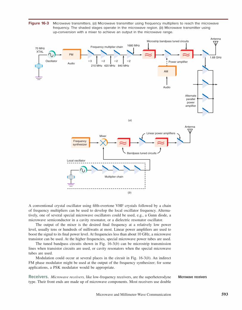
Microwave and Millimeter-Wave Communication 593
A conventional crystal oscillator using i fth-overtone VHF crystals followed by a chain
of frequency multipliers can be used to develop the local oscillator frequency. Alterna-
tively, one of several special microwave oscillators could be used, e.g., a Gunn diode, a
microwave semiconductor in a cavity resonator, or a dielectric resonator oscillator.
The output of the mixer is the desired i nal frequency at a relatively low power
level, usually tens or hundreds of milliwatts at most. Linear power amplii ers are used to
boost the signal to its i nal power level. At frequencies less than about 10 GHz, a microwave
transistor can be used. At the higher frequencies, special microwave power tubes are used.
The tuned bandpass circuits shown in Fig. 16-3(b) can be microstrip transmission
lines when transistor circuits are used, or cavity resonators when the special microwave
tubes are used.
Modulation could occur at several places in the circuit in Fig. 16-3(b). An indirect
FM phase modulator might be used at the output of the frequency synthesizer; for some
applications, a PSK modulator would be appropriate.
Receivers. Microwave receivers, like low-frequency receivers, are the superheterodyne
type. Their front ends are made up of microwave components. Most receivers use double
Microwave receivers
(a )
(b)
70 MHzXTAL
Oscillator
PM
Audio�3 �2 �2 �2
210 MHz 420 MHz 840 MHz
1680 MHzFrequency multiplier chain
Microstrip bandpass tuned circuits
1.68 GHz
Antenna
Antenna
AM
Audio
Power amplifier
Alternateparallelpower
amplifier
Linear power amplifiers
Bandpass tuned circuits
Frequencysynthesizer
Mixer
Local oscillator
Multiplier chain
Figure 16-3 Microwave transmitters. (a) Microwave transmitter using frequency multipliers to reach the microwave
frequency. The shaded stages operate in the microwave region. (b) Microwave transmitter using
up-conversion with a mixer to achieve an output in the microwave range.

594 Chapter 16
conversion. A i rst down-conversion gets the signal into the UHF or
VHF range, where it can be more easily processed by standard meth-
ods. A second conversion reduces the frequency to an IF appropriate
for the desired selectivity.
Fig. 16-4 is a general block diagram of a double-conversion
microwave receiver. The antenna is connected to a tuned circuit,
which could be a cavity resonator or a microstrip or stripline tuned
circuit. The signal is then applied to a special RF amplii er known
as a low-noise amplii er (LNA). Special low-noise transistors,
usually gallium arsenide FET amplii ers, must be used to provide
some initial amplii cation. Another tuned circuit connects the
amplii ed input signal to the mixer. Most mixers are of the doubly
balanced diode type, although some simple single-diode mixers
are also used.
The local oscillator signal is applied to the mixer. The mixer
output is usually within the UHF or VHF range. The 700- to
800-MHz range is typical. A SAW filter selects out the difference
signal, which in Fig. 16-4 is 12 GHz 211.2 GHz 5 0.8 GHz,
or 800 MHz.
The remainder of the receiver is typical of other superhetero-
dynes. Note that the desired selectivity is obtained with a SAW i lter,
which is sometimes used to provide a specially shaped IF response.
Many of the newer microwave cell phone and LAN receivers are of
the direct conversion type, and selectivity is obtained with RC and
DSP i lters.
In more recent microwave equipment such as cell phones and
wireless networking interfaces, the microwave frequencies are
generated by a phase-locked loop (PLL) operating as a multiplier.
See Fig. 16-5. The VCO produces the desired local oscillator (LO)
or i nal transmitting frequency directly. The VCO frequency is con-
trolled by the phase detector and its low-pass loop i lter. The fre-
quency divider and input crystal determine the output frequency.
Recent advances in quartz crystal design permit input oscillator fre-
quencies up to 200 MHz. In Fig. 16-5, the 155-MHz crystal com-
bined with a frequency divider of 20 produces a VCO output at
155 3 20 5 3100 MHz, or 3.1 GHz. The 420 divider reduces the 3.1-GHz output to
155 MHz to match the input crystal signal at the phase detector, as required for closed-loop
control. Of course, the divider can also be part of a microcontroller-based frequency
synthesizer that is designed to permit setting the output to multiple channel frequencies
as required by the application.
Low-noise amplifi er (LNA)
Each of these microwave antennas located in
Stephen Butte, Washington, is specifically designed
for long-distance telephone signal transmission.
They are covered to reduce weather-related mainte-
nance problems.
Antenna
SAWfilter
DemodulatorFrequencysynthesizer
730 MHz11.2 GHz
Localoscillator
First mixer800 MHz
Low-noise amplifier
Tuned bandpass circuits
Second mixer 70 MHz
IF amplifier
Originalintelligence
12 GHz
Figure 16-4 A microwave receiver. The shaded areas denote microwave circuits.

Microwave and Millimeter-Wave Communication 595
Figure 16-6 A direct conversion microwave transceiver.
Antenna
AntennaData
LPFDAC
LPF
LNA
From
LNA
LO
ADC
ADC
BPF
90°
Receiver
Transmitter
Alternative
upconverting mixer
Alternative
down converting mixer
TO PA
LO
LO
PA
Frequency
synthesizer
DAC LPF
Baseband
LPF
90°
Frequencydivider
Crystaloscillator
Phasedetector
Output totransmitteror receiver
mixers
155-MHzXTAL
�20
155 MHz
3.1 GHz
VCOLow-pass
loopfilter
Figure 16-5 A phase-locked loop (PLL) multiplier is the primary signal source in
modern microwave transceivers.
A more common architecture today is direct-conversion transmitters and receivers using I/Q modulators and demodulators, as shown in Fig. 16-6. Most modulation, such as QPSK or QAM, is performed by DSP in a baseband processor. The baseband processor produces the digital in-phase (I) and quadrature (Q) signals dei ning the modulation from the data
input. In the transmitter, the I/Q signals are sent to DACs where they are converted to ana-
log signals and i ltered in a low-pass i lter (LPF) and then sent to mixers. The mixers receive
the local oscillator (LO) signals from a 90° phase shifter driven by the frequency synthesizer
that sets the transmit frequency. The mixer outputs are added to create the i nal signal, which
is amplii ed in a power amplii er (PA) before being sent to the antenna.
The I/Q modulator is in IC form and can usually handle signals in the 200-MHz to 6-GHz
range. If a higher i nal frequency is needed, the modulator output is sent to an up-converting
mixer with its own local oscillator. The resulting higher frequency is then sent to the PA.

596 Chapter 16
At the receiver, the signal from the antenna is fed to a low-noise amplii er (LNA)
and a band-pass i lter (BPF) to dei ne the bandwidth. The signal is then sent to the
mixers in the I/Q demodulator. If higher frequencies are involved, the LNA signal
may go to a down-converting mixer i rst and then to the I/Q demodulator mixers.
The signal is then mixed with the LO signal from the synthesizer at the signal
frequency. The mixer outputs are then i ltered and sent to ADCs, where the
digital I/Q signals are generated. These I/Q signals are then processed in the
baseband circuits to recover the original data.
Transmission Lines. The transmission line most commonly used in lower- frequency
radio communication is coaxial cable. However, coaxial cable has very high attenuation
at microwave frequencies, and conventional cable is unsuitable for carrying microwave
signals except for very short runs, usually several feet or less. Newer types of coaxial
cables permit lengths of up to 100 ft at frequencies to 10 GHz.
Special microwave coaxial cable that can be used on the lower microwave bands—L,
S, and C—is made of hard tubing rather than wire with an insulating cover and a l exible braid shield. The stiff inner conductor is separated from the outer tubing with spacers or washers, forming low-loss coaxial cable known as hard line cable. The insulation between the inner conductor and the outer tubing can be air; in some cases, a gas such as nitrogen is pumped into the cable to minimize moisture buildup, which causes excessive power loss. This type of cable is used for long runs of transmission lines to an antenna on a tower. At higher microwave frequencies, C band and upward, a special hollow rectangu-lar or circular pipe called waveguide is used for the transmission line (see Sec. 16-3).
Antennas. At low microwave frequencies, standard antenna types, including the simple dipole and the one-quarter wavelength vertical antenna, are still used. At these frequencies, antenna sizes are very small; e.g., the length of a half-wave dipole at 2 GHz is only about 3 in. A one-quarter wavelength vertical antenna for the center of the C band is only about 0.6 in long. At the higher frequencies, special antennas are generally used (see Sec. 16-6).
16-2 Microwave Lines and DevicesToday, although vacuum tubes and microwave tubes such as the klystron and magnetron are still used, especially for higher-power applications, most microwave systems use transistor amplii ers. Over the years, semiconductor manufacturers have learned to make transistors work at these higher frequencies. Special geometries are used to make bipolar transistors that provide both voltage and power gain at frequencies up to 100 GHz. Microwave FET transistors have also been created such as the MESFET described in Chap. 9. The use of gallium arsenide (GaAs) and silicon germanium (SiGe) rather than pure silicon has further increased the frequency capabilities of MOSFETs and bipolars. Both small- signal and power MOSFETs are available to operate at frequencies up to about 50 GHz. GaN power FETs are now commonly used at frequencies to 50 GHz. Because most microwave communication activity takes place in the lower-fre-quency ranges (L, S, and C bands), transistors are the primary active components used. In the following sections, we discuss both discrete transistor types with microstrip tuned circuits and monolithic microwave integrated circuits (MMICs).
Microstrip Tuned CircuitsBefore specii c amplii er types are introduced, it is important to examine the method by which tuned circuits are implemented in microwave amplii ers. Lumped components such as coils and capacitors are still used in some cases at the high UHF and low microwave frequencies (below about 2 GHz) to create resonant circuits, i lters, or impedance-matching circuits. However, at higher frequencies, standard techniques for realizing such components become increasingly harder to implement. Instead, transmission lines, specii cally microstrip, are used.
Hard line
Waveguide
Microwave transistor amplifi er
Monolithic microwave integrated circuits (MMICs)
Microstrip tuned circuit
Microstrip
The Keysight 1GC1-
6218(TC233P) is a (DC to
100MHz, MLF-16/QFN-16
Package) tri-state linear
phase and frequency detec-
tor is intended for use in
delta-sigma fractional-N
phase-locked loo(PLL)
applications.
GOOD TO KNOWSpecial microwave coaxial cable
called hard line, which is made of
hard tubing rather than wire with
an insulating cover, can be used
on the lower microwave bands.
At and a b
mix
Trad
at misignals
cables pS

Microwave and Millimeter-Wave Communication 597
Chap. 13 described how transmission lines can be used as inductors and capacitors as well as series and parallel resonant circuits. These are readily implemented at the microwave frequencies because one-half or one-quarter wavelength transmission lines are only inches or some fraction thereof at those frequencies. Microstrip is preferred for reactive circuits at the higher frequencies because it is simpler and less expensive than stripline, but stripline is used where shielding is necessary to minimize noise and cross talk. The tuned circuits are created by using a copper pattern printed-circuit board (PCB) upon which are mounted the transistors, ICs, and other components of the circuit. Fig. 16-7 shows several views of microstrip transmission line used for a reactive circuit. The PCB is usually made of G-10 or FR-4 i berglass or a combination of i berglass
and Tel on. The bottom of the PCB is a thin solid copper sheet that serves as a ground plane and one side of the transmission line. The copper strip is the other conductor of the transmission line. Fig. 16-7(a) is a perspective view of a microstrip line, Fig. 16-7(b) is an end view, and Fig. 16-7(c) and (d) are side views. Both open and shorted segments of line can be used, although shorted segments are preferred because they do not radiate as much as open segments. One-quarter wavelength sections are preferred because they are shorter and take up less space on the PCB. Fig. 16-8 summarizes the open- and shorted-line possibilities for microstrip. An important characteristic of microstrip is its impedance. As discussed in Chap. 13, the characteristic impedance of a transmission line depends on its physical characteristics, in this case, e.g., on the width of the strip and the spacing between the strip and the copper ground plane, which is the thickness of the PCB material. The dielectric constant of the insulating material is also a factor. Most characteristic impedances are less than 100 V; 50 V is the most common, followed closely by 75 V. Values higher than 100 V are used for cases when impedance- matching requirements demand it. One-quarter wavelength transmission line can be used to make one type of component look like another. For example, in Fig. 16-9(a), the λ/4 microstrip line can make a resistor at one end look like a resistance of another value; specii cally,
R2 5Z0
2
R1
Figure 16-7 Microstrip transmission line used for reactive circuits. (a) Perspective view. (b) Edge or end view. (c) Side
view (open line). (d) Side view (shorted line).
Copper strip
PCB material
SideEnd
Copper ground plane Copper ground plane
Copper strip
(a ) (b) (c ) (d )
Ground plane
Insulated PCB material(fiberglass or Teflon)
Microstrip
PCBOpen
Ground plane
Microstrip
PCBShort
Figure 16-8 Equivalent circuits of open and shorted microstrip lines.
Length Shorted Lines Open Lines
Less than λ/4 Inductor Capacitor
λ/4 Parallel resonant Series resonant or
or open circuit short circuit
.λ/4, ,λ/2 Capacitor Inductor
λ/2 Series resonant circuit Parallel resonant
or short repeater circuit or open
repeater

598 Chapter 16
Here R1 is the resistance value of the resistor connected to one end of the line, and Z0 is the characteristic impedance of the microstrip, such as 50 V. If R1 is the characteristic impedance of the microstrip, such as 50 V, the line is matched and the generator sees 50 V. If R1 is 150 V, then the other end of the line will have a value of R2, or
502
1505
2500
1505 16.67 V
This application is the same as the one-quarter wavelength matching transformer or Q section discussed in Chap. 14. Recall that two impedances can be matched by using a line of length λ/4 according to the relationship Z0 5 1R1R2, where Z0 is the characteristic impedance of the one-quarter wavelength line and R1 and R2 are the input and output impedances to be matched. A quarter-wavelength line can also make a capacitor look like an inductor or an induc-tance look like a capacitance [see Fig. 16-9(b) and (c)]. For example, a 75-V microstrip λ/4 long will make an inductive reactance of 30 V look like a capacitive reactance of
Xc 5Z0
2
Xl
5752
305
5635
305 187.5 V
Fig. 16-10 shows the physical coni gurations for equivalent coils and capacitors in
microstrip form. The thin segment of microstrip shown in Fig. 16-10(a) acts like a series
inductor. Fig. 16-10(b) shows a short right-angle segment whose end is grounded; this
microstrip acts as a parallel inductor. When series capacitance or capacitive coupling is
needed, a small capacitor can be created by using the ends of microstrip lines as tiny
capacitor plates separated by an air dielectric [Fig. 16-10(c)]. A shunt capacitor can be
created by using a short, fat segment of microstrip as in Fig. 16-10(d). As these general
forms demonstrate, it is often possible to visualize or even draw the equivalent circuit
of a microstrip amplii er by observing the pattern on the PCB.
Microstrip can also be used to realize coupling from one circuit, as illustrated in
Fig. 16-11. One microstrip line is simply placed parallel to another segment of microstrip.
The degree of coupling between the two depends on the distance of separation and the
length of the parallel segment. The closer the spacing and the longer the parallel run,
the greater the coupling. There is always signal loss by such a coupling method, but it
can be accurately controlled.
Although microstrip performs best when it is a straight line, 90° turns are often
necessary on a PCB. When turns must be used, a straight right-angle turn, like that
shown in Fig. 16-12(a), is forbidden because it acts as a low-pass i lter across the
line. A gradually curved line, like that shown in Fig. 16-12(b) (or Fig. 16-11), is
preferred when the turn radius is much greater than the width of the line. An accept-
able alternative method is shown in Fig. 16-12(c). The cut on the corner is critical.
Note that the dimensions must be held to λ/4, which is one-quarter the width of the
microstrip.
Figure 16-9 How a one-quarter wavelength microstrip can transform impedances and reactances.
�
4
Z0
(a )
R1 R2
Equivalent circuitActual circuit
Microstrip
R2 � Z 1
2
R1
(b)
XL
Xc � XL
Microstrip
Xc
�
4
Z0
Z 02
(c )
�
4
Z0
Z 02
Xc
XL � XcX2
GOOD TO KNOWMicrostrip patterns are made
directly onto printed-circuit
boards.

Microwave and Millimeter-Wave Communication 599
(a )
Microstrip configuration(top view)
Lumped equivalentcircuit
(b)
(c )
(d )
Figure 16-10 Common microstrip patterns and their equivalents.
Top view of PCB
Microstrips
Signal in Signal out
Signal out
Coupling
Figure 16-11 Coupling between microstrips.
Figure 16-12 Microstrip 90° turns. (a) Right angles such as this should be avoided. (b) Gradual curves or turns are
preferred. (c) This arrangement is also acceptable.
(a ) (b) (c )
�
4
w

600 Chapter 16
A special form of microstrip is the hybrid ring shown in Fig. 16-13. The total length of the microstrip ring is 1.5λ. There are four taps or ports on the line, spaced at one-quarter wavelength (λ/4) intervals, which can be used as inputs or outputs. Now, a signal is applied to port 1, and some interesting things happen. Output signals appear at ports 2 and 4, but their levels are at one-half the power of the input. Thus the circuit acts as a power divider to supply two signals of equal level to other circuits. There is no output at port 3. The effect of applying a signal at port 4 is similar. Equal half-power outputs appear at ports 1 and 3, but no signal appears at port 2. If individual signals are applied simultaneously to ports 1 and 3, the output at port 2 will be their sum and the output at port 4 will be their difference. The unique operation of the hybrid ring makes it very useful for splitting signals or combining them. Microstrip can be used to create almost any tuned circuit necessary in an amplii er,
including resonant circuits, i lters, and impedance-matching networks. Fig. 16-14(a)
shows how a low-pass i lter is implemented with microstrip sections. The component
shown is a highly selective low-pass i lter for use in the 1- to 3-GHz range depending
Hybrid ring
Figure 16-13 A microstrip hybrid ring.
�
4
�
4
�
4
3�
4
1
2
3
4
1.5�
Figure 16-14 A microstrip fi lter. (a) Microstrip low-pass fi lter. (b) Lumped constant
equivalent circuit.
Inductors
In
Capacitors
Series resonant sections
Out
Top viewof copperpatternon PCB
(a )
(b)
In Out

Microwave and Millimeter-Wave Communication 601
Microwave TransistorsMicrowave transistors, whether they are bipolar or FET types, operate just as other transistors do. The primary differences between standard lower-frequency transistors and microwave types are internal geometry and packaging. To reduce internal inductances and capacitances of transistor elements, special chip con-i gurations known as geometries are used that permit the transistors to operate at higher power
levels and at the same time minimize distributed and stray inductances and capacitances.
Fig. 16-15 shows several types of microwave transistors. Fig. 16-15(a) and (b) is
low-power small-signal microwave transistors; these types are either NPN silicon or
Microwave transistor
Example 16-1A one-quarter wave Q-matching section made of microstrip is designed to match a
source of 50 V to a load of 136 V at 5.8 GHz. The PCB dielectric constant εr is 2.4.
Calculate (a) the required impedance of the microstrip and (b) its length.
a. ZQ 5 1Zsource 3 Zload
5 150(136) 5 82.46 V
b. λ 5300
f MHz
5.8 GHz 5 5800 MHz
λ 5300
58005 0.0517 m
λ
45
0.0517
45 0.012931 m
1 m 5 38.37 in
λ
45 0.012931(39.37) 5 0.51 in
Velocity of propagation 51
1εr
51
12.45 0.645
λ
45 (0.51 in) (0.645) 5 0.3286 in
on the exact dimensions. The lumped constant equivalent circuit is shown in Fig. 16-14(b). The transmission line segments are formed on the PCB itself and connected end to end as required. The transistors or ICs are then soldered to the PCB along with any resistors or larger discrete components that may be needed.
Figure 16-15 Microwave transistors. (a) and (b) Low-power small signal. (c) FET power. (d) NPN bipolar power.
(a ) (b) (c ) (d )

602 Chapter 16
gallium arsenide FET. Note the very short leads. Both packages are designed for surface mounting directly to microstrip on the PCB. The transistor in Fig. 16-15(b) has four leads, usually two emitter (or source) leads plus the base (or gate) and the collector (or drain). The two emitter leads in parallel ensure low inductance. Some transistors of this type have two base or two collector leads instead of two emitter leads. Fig. 16-15(c) shows an enhancement-mode power MOSFET. The short, fat leads are thick strips of copper that are soldered directly to the microstrip circuitry on the PCB. These wide loads also help transfer heat away from the transistor. Fig. 16-15(d) is an NPN power transistor with two emitter leads. The short, fat leads ensure low inductance and also permit high currents to be accommodated. The fat copper strips help to dissipate heat. The devices in Fig. 16-15(c) and (d) can handle power levels up to several hundred watts. Transistors for small-signal amplii cation and oscillators are available for frequency
up to about 100 GHz. For power amplii cation, transistors are available for frequencies
up to 50 GHz.
Most microwave transistors continue to be made of silicon. As transistor geometry
sizes have decreased below 0.04 µm (40 nm), switching speeds and amplii cation fre-
quencies have increased well into the microwave region. CMOS digital integrated cir-
cuits, which are made with MOSFETs, can operate up to 10 GHz. RF and linear/analog
circuits made with CMOS and used in low-power microwave radios as well as in optical
i ber transmission circuits can achieve operation up to 10 GHz. But beyond 10 GHz,
special devices are necessary.
You have already seen how GaAs MESFETs, a type of JFET using a Schottky barrier
junction, can operate at frequencies in excess of 5 GHz. A variant of the MESFET called
a high electron mobility transistor (HEMT) extends the frequency range beyond 20 GHz
by adding an extra layer of semiconductor material such as AlGaAs.
A highly popular device known as a heterojunction bipolar transistor (HBT) is
making even higher-frequency amplii cation possible in both discrete form and integrated
circuits. A heterojunction is formed with two different types of semiconductor materials.
Some popular combinations are indium-phosphide (InP) and silicon-germanium (SiGe).
Other combinations include AlGaAs/GaAs and InGaAsP. The InP HBTs operate at
frequencies up to 50 GHz, and SiGe HBTs have been developed to operate up to
200 GHz. Both small-signal and power amplii cation versions are available.
For power amplii ers, the LDMOS enhancement mode FETs are popular at
frequencies below 6 GHz. Such transistors can handle power levels to several hundred
watts. At frequencies to 50 GHz, the new gallium nitride (GaN) pHEMET transistors
can supply power levels up to about 100 watts.
Small-Signal Amplifi ersA small-signal microwave amplii er can be made up of a single transistor or multiple
transistors combined with a biasing circuit and any microstrip circuits or components as
required. Most microwave amplii ers are of the tuned variety. That is, their bandwidth is
set by the application and implemented by microstrip series or parallel tuned circuits,
and then microstrip lines are used to perform the various impedance-matching duties
required to get the amplii er to work.
Another type of small-signal microwave amplii er is a multistage integrated circuit,
a variety of MMIC. Besides amplii ers, other MMICs available include mixers, switches,
and phase shifters.
Transistor Amplifi ers. Fig. 16-16 shows a microwave amplii er for small signals.
This type of amplii er is commonly used in the front end of a microwave receiver to
provide initial amplii cation for the mixer. A low-noise transistor is used. The typical
gain range is 10 to 25 dB.
Most microwave amplii ers are designed to have input and output impedances of
50 V. In the circuit shown in Fig. 16-16, the input can come from an antenna or another
microwave circuit. The blocks labeled TL are microstrip sections that act as tuned
High electron mobility transistor (HEMT)
Heterojunction bipolar transistor (HBT)
Small-signal microwave amplifi er
Multistage integrated-circuit amplifi er
Transistor amplifi er

Microwave and Millimeter-Wave Communication 603
circuits, inductors, or capacitors. An input microstrip TL1 acts as an impedance-matching section, and TL2 and TL3 form a tuned circuit. TL4 is another impedance-matching section that matches the tuned circuit to the complex impedance of the base input. The tuned circuits set the bandwidth of the amplii er input.
A similar sequence of impedance-matching sections and tuned circuits is used in the
collector to set the bandwidth and to match the transistor collector impedance to the
output. And C2 and C3 are variable capacitors that allow some tuning of the bandwidth.
All the other components are of the surface-mounted chip type to keep lead induc-
tances short. The microstrip segments TL9 and TL10 act as inductors, forming part of
the substantial decoupling networks used on the base bias supply VBB and the collector
supply VCC. The base supply voltage and the value of R1 set the base bias, thus biasing
the transistor into the linear region for class A amplii cation. RFCs are used in the supply
leads to keep the RF out of the supply and to prevent feedback paths through the supply
that can cause oscillation and instability in multistage circuits. Ferrite beads (FB) are
used in the collector supply lead for further decoupling.
MMIC Amplifi ers. A common monolithic microwave integrated-circuit (MMIC)
amplii er is one that incorporates two or more stages of FET or bipolar transistors made
on a common chip to form a multistage amplii er. The chip also incorporates resistors
for biasing and small bypass capacitors. Physically, these devices look like the transistors
in Fig. 16-15(a) and (b). They are soldered to a PCB containing microstrip circuits for
impedance matching and tuning.
Another popular form of MMIC is the hybrid circuit, which combines an amplii er
IC connected to microstrip circuits and discrete components of various types. All the
components are formed on a tiny alumina substrate that serves as both a base and a place
to form microstrip lines. Surface-mounted chip resistors, capacitors, transistors, and
MMIC amplii ers are connected. The entire unit is packaged into a housing, usually metal
for shielding, and connected to additional circuits on a PCB.
Power Amplifi ers. A typical class A microwave power amplii er is shown in
Fig. 16-17. The microstrip lines are used for impedance matching and tuning. Most
microstrip circuits simulate L-type matching networks with a low-pass coni guration.
Small wire loop inductors and capacitors are used to form the decoupling networks to
prevent feedback through the power supply, which would cause oscillation. The input
and output impedances are 50 V. This particular stage operates at 1.2 GHz and provides
Monolithic microwave integrated circuit (MMIC)
Hybrid circuit
Class A microwave power amplifi er
Figure 16-16 A single-stage class A RF microwave amplifi er.
VCC
C7
R1
C5
C1 C4
C6
C2 C3
C8 C9
RFC RFC
VBB
TL9 TL10
FB
FB
RF input RF outputTL1 TL3 TL4 TL5TL2 TL6 TL8TL7
C10
GOOD TO KNOWMost microwave amplifi ers are
designed to have input and output
impedances of 50 V.

604 Chapter 16
an output power of 1.5 W. Typical power supply voltages are 12, 24, and 28 V, but can go to 36 or 48 V for high-power applications. Note that bias is not supplied by a resistive voltage divider. Instead, it usually comes from a separate bias-current circuit like that shown in Fig. 16-18, which is an ordinary constant-current source. Resistors R1, R2, and R3 form a voltage divider to set the base voltage on Q1. A voltage is developed across emitter resistor R4. This voltage divided by R4 gives the value of the current supplied by Q1 to the transistor in the microwave amplii er. A diode in series with the voltage divider provides some temperature compen-
sation for variations in the emitter-base voltage that occur in Q1. Resistor R1 is adjustable
to set the bias current to the precise value for optimum power and minimum distortion.
Most power amplii ers obtain their bias from constant-current sources; this provides a
bias current that is relatively temperature-independent and thus provides superior protec-
tion against damage.
The bias is applied to the base of the amplii er in Fig. 16-17 through a small inductor.
This and the bypass capacitors keep the microwave energy out of the bias circuit.
Figure 16-17 A class A microwave power amplifi er.
50 �
50 �
50 �
50 �
220 pF
Vbias
C C
C
L
L
VCE
Figure 16-18 A constant-current bias supply for a linear power amplifi er.
C
Vsupply
Vbias
VCE
R4
R1
R2
R3R5
Q1

Microwave and Millimeter-Wave Communication 605
The single-stage FET power amplii er shown in Fig. 16-19 can achieve a power
output of 100 W in the high UHF and low microwave region. The transistor is an
enhancement-mode FET; that means that the FET does not conduct with drain voltage
applied. A positive gate signal of 3 V or more must be applied to achieve conduction.
The gate signal is supplied by a lower-power driver stage, and the gate bias is supplied
by a zener diode. The gate voltage is made adjustable with potentiometer R2. This allows
the bias to be set for linear class B or class C operation. For linear class A operation, a
quiescent value of drain current is set with the bias. This bias circuit can also be used
to adjust the power output over a small range.
In the circuit shown in Fig. 16-19, a combination of LC tuned circuits and microstrips
is used for tuning and impedance matching. Here L1 is a tiny hairpin loop of heavy wire,
and L2 is a larger inductor made of multiple turns of wire to form a high impedance for
decoupling.
Most modern GaN power amplii ers are complete circuits in a single package. Each
targets a specii c frequency range and application, such as cellular or radar.
16-3 Waveguides and Cavity ResonatorsLong parallel transmission lines, such as 300-V twin-lead, radiate electromagnetic energy
while transporting it from one place to another. As the frequency of operation gets higher,
the amount of radiation from the line increases. At microwave frequencies, virtually all
the energy is radiated; almost no energy ever reaches the end of the transmission line.
Despite their high attenuation, coax cables are widely used to carry microwave and even
some millimeter wave signals over short distances. For the lower microwave frequencies,
special coaxial cables have been developed that can be used up to approximately 6 GHz
if the length is kept short (less than 100 ft). Above this frequency, coaxial cable loss is
too great except for lengths of several feet or less. Short lengths of coaxial cable, several
feet or less, can be used to interconnect pieces of equipment that are close together, but
for longer runs other methods of transmission must be used. To minimize loss, special
types of coaxial cables with large inner conductors and shields have been developed;
however, in most cases these cables are rigid rather than l exible, which makes them expensive and difi cult to use.
Figure 16-19 An FET power amplifi er.
Z1
Z2 Z3
R2
R1
R2
D1 C10
C11
C12C13
C14
C8
C6 C7C5 C4 C3 C2
C1 L1
L2C9
FB
�V
Ground
Out
In

606 Chapter 16
Another problem is the power-handling limit of coaxial cables. The larger cables can carry power levels up to about 1 kW. Higher power levels needed in radar and sattelite applications require another solution.
WaveguidesMost high-power microwave energy transmission above about 6 GHz is handled by waveguides, which are hollow metal conducting pipes designed to carry and constrain the electromagnetic waves of a microwave signal. Most waveguides are rectangular. Waveguides can be used to carry energy between pieces of equipment or over longer distances to carry transmitter power to an antenna or microwave signals from an antenna to a receiver. Waveguides are made of copper, aluminum, or brass. These metals are extruded into long rectangular or circular pipes. Often the insides of waveguides are plated with silver to reduce resistance, keeping transmission losses to a very low level.
Signal Injection and Extraction. A microwave signal to be carried by a waveguide is intro duced into one end of the waveguide with an antennalike probe that creates an electro-magnetic wave that propagates through the waveguide. The electric and magnetic i elds asso-
ciated with the signal bounce off the inside walls back and forth as the signal progresses down
the waveguide. The waveguide totally contains the signal so that none escapes by radiation.
The probe shown in Fig. 16-20(a) is a one-quarter wavelength vertical antenna at
the signal frequency that is inserted in the waveguide one-quarter wavelength from the
end, which is closed. The signal is usually coupled to the probe through a short coaxial
cable and a connector. The probe sets up a vertically polarized electromagnetic wave in
the waveguide, which is then propagated down the line. Because the probe is located
one-quarter wavelength from the closed end of the waveguide, the signal from the probe
is rel ected from the closed end of the line back toward the open end. Over a one-quarter wavelength distance, the rel ected signal appears back at the probe in phase to aid the signal going in the opposite direction. Remember that a radio signal consists of both electric and magnetic i elds at right angles to each other. The electric and magnetic i elds established by the probe propagate down the waveguide at a right angle to the two i elds of the radio signal. The position of the probe determines whether the signal is horizontally or vertically polarized. In Fig. 16-20(a), the electric i eld is vertical, so the polarization is vertical. The electric i eld begins propagating down the line and sets up charges on the line that cause current to l ow. This in turn generates a companion magnetic i eld at right angles to the electric i eld and the direction of propagation. A loop can also be used to introduce a magnetic i eld into a waveguide. The loop in Fig. 16-20(b) is mounted in the closed end of the waveguide. Microwave energy applied through a short piece of coaxial cable causes a magnetic i eld to be set up in the loop. The magnetic i eld also establishes an electric i eld, which is then propagated down the waveguide. Probes and loops can also be used to extract a signal from a waveguide. When the signal strikes a probe or a loop, a signal is induced that can then be fed to other circuitry through a short coaxial cable.
Waveguide
Figure 16-20 Injecting a sine wave into a waveguide and extracting a signal.

Microwave and Millimeter-Wave Communication 607
Waveguide Size and Frequency. Fig. 16-21 shows the most important dimensions of a rectangular waveguide: the width a and the height b. Note that these are the inside dimensions of the waveguide. The frequency of operation of a waveguide is determined by the size of a. This dimension is usually made equal to one-half wavelength, a bit below the lowest frequency of operation. This frequency is known as the waveguide
cutoff frequency. At its cutoff frequency and below, a waveguide will not transmit energy. At frequencies above the cutoff frequency, a waveguide will propagate electromagnetic energy. A waveguide is essentially a high-pass i lter with a cutoff frequency equal to
fco 5300
2a
where fco is in megahertz and a is in meters.
For example, suppose it is desired to determine the cutoff frequency of a waveguide
with an a dimension of 0.7 in. To convert 0.7 in to meters, multiply by 2.54 to get
centimeters and divide by 100 to get meters: 0.7 in 5 0.01778 m. Thus,
fco 5300
2(0.01778)5 8436 MHz 5 8.436 GHz
Normally, the height of a waveguide is made equal to approximately one-half the a
dimension, or 0.35 in. The actual size might be 0.4 in.
Waveguide cutoff frequency
Figure 16-21 The dimensions of a waveguide determine its operating frequency
range.
GOOD TO KNOWAt higher microwave frequencies,
above approximately 6 to 10 GHz,
a special hollow rectangular or
circular pipe called a waveguide
is used for the transmission line.
Example 16-2A rectangular waveguide has a width of 0.65 in and a height of 0.38 in. (a) What is
the cutoff frequency? (b) What is a typical operating frequency for this waveguide?
a. 0.65 in 3 2.54 5 1.651 cm
1.651
1005 0.01651 m
fco 5300
2a5
300
2(0.01651)5 9085 MHz 5 9.085 GHz
b. fco 5 0.7f
f 5fco
0.75 1.42fco
5 1.42(9.085) 5 12.98 GHz and above

608 Chapter 16
Example 16-3Would the rectangular waveguide in Example 16-2 operate in the C band?
The C band is approximately 4 to 6 GHz. Because a waveguide acts as a high-pass i lter with a cutoff of 9.085 GHz, it will not pass a C band signal.
Signal Propagation. When a probe or loop launches energy into a waveguide, the signal
enters the waveguide at an angle so that the electromagnetic i elds bounce off the sidewalls
of the waveguides as the signal propagates along the line. In Fig. 16-22(a), a vertical probe
is generating a vertically polarized wave with a vertical electric i eld and a magnetic i eld
at a right angle to the electric i eld. The electric i eld is at a right angle to the direction of
wave propagation, so it is called a transverse electric (TE) i eld. Fig. 16-22(b) shows how
a loop would set up the signal. In this case, the magnetic i eld is transverse to the direction
of propagation, so it is called a transverse magnetic (TM) i eld.
The angles of incidence and rel ection depend on the operating frequency (see Fig. 16-23). At high frequencies, the angle is large and therefore the path between the opposite walls is relatively long, as shown in Fig. 16-23(a). As the operating frequency decreases, the angle also decreases and the path between the sides shortens. When the operating frequency reaches the cutoff frequency of the waveguide, the signal simply bounces back and forth between the sidewalls of the waveguide. No energy is propagated. Whenever a microwave signal is launched into a waveguide by a probe or loop, electric and magnetic i elds are created in various patterns depending upon the method of energy coupling, frequency of operation, and size of waveguide. Fig. 16-24 shows typical i elds in a waveguide. In the end view, the lines represent the electric i eld E lines. The dots represent the magnetic i eld H lines. In the top view, the dashed lines represent the H i eld, and the 3s and dots represent the E i eld. The 3 means that the line is going into the page; the • means that the line is coming out of the page. The pattern of the electromagnetic i elds within a waveguide takes many forms. Each form is called an operating mode. As indicated earlier, the magnetic or the electric i eld must be perpendicular to the direction of propagation of the wave. In the TE mode, the electric i eld exists across the guide and no E lines extend lengthwise along the guide. In the TM mode, the H lines form loops in planes perpendicular to the walls of the guide, and no part of an H line is lengthwise along the guide. Subscript numbers are used along with the TE and TM designations to further describe the E and H i eld patterns. A typical designation is TE0,1. The i rst number indicates the number of half-wavelength patterns of transverse lines that exist along the short dimension of the guide through the center of the cross section. Transverse lines are those perpendicular
Signal propagation
Transverse electric (TE) fi eld
Transverse magnetic (TM) fi eld
Figure 16-22 (a) Transverse electric fi eld. (b) Transverse magnetic fi eld.
Note thatsignal
enters atan angle
Direction of propagation
Probe Loop
E H
H E
(a ) (b)

Microwave and Millimeter-Wave Communication 609
to the walls of the guide. The second number indicates the number of transverse half-wavelength patterns that exist along the long dimension of the guide through the center of the cross section. If there is no change in the i eld intensity of one dimension, a zero is used.
The waveguide in Fig. 16-24 is TE because the E lines are perpendicular (transverse)
to the sides of the guide. Looking at the end view in Fig. 16-24 along the short length,
(a )
(b)
(c)
(d )
Figure 16-23 Wave paths in a waveguide at various frequencies. (a) High frequency.
(b) Medium frequency. (c) Low frequency. (d) Cutof frequency.
Figure 16-24 Electric (E) and magnetic (H) fi elds in a rectangular waveguide.

610 Chapter 16
we see no i eld intensity change, so the i rst subscript is 0. Along the long dimension of
the end view, the E lines spread out at the top and bottom but are close together in the
center. The actual i eld intensity is sinusoidal—zero at the ends, maximum in the center.
This is one-half of a sine wave variation, and so the second subscript is 1. The mode of
the line in Fig. 16-24 is therefore TE0,1. This, by the way, is the main or dominant mode
of most rectangular waveguides. Many other patterns are possible, such as the two shown
in Fig. 16-25.
Waveguide Hardware and AccessoriesIn some ways, waveguides have more in common with plumbing equipment than they
do with the standard transmission lines used in radio communication. And, like plumbing,
waveguides have a variety of special parts, such as couplers, turns, joints, rotary
connections, and terminations. Most waveguides and their i ttings are precision-made so
that the dimensions match perfectly. Any mismatch in dimensions or misalignment of
pieces that i t together will introduce signii cant losses and rel ections. Waveguides are available in a variety of standard lengths that are interconnected to form a path between a microwave generator and its ultimate destination.
Connection Joints. Fig. 16-26 shows a choke joint, which is used to interconnect two sections of waveguide. It consists of two l anges connected to the waveguide at the center. The right-hand l ange is l at, and the one at the left is slotted one- quarter wavelength deep at a distance of one-quarter wavelength from the point at which the walls of the guide are joined. The one-quarter waves together become a half wave and rel ect a short circuit at the place where the walls are joined. Electrically, this creates a short circuit at the junction of the two waveguides. The two sections can actually be separated as much as one-tenth wavelength without excessive loss of energy at the joint. This separation allows room to seal the interior of the waveguide with a rubber gasket for pressurization. Some long waveguides are pressurized with nitrogen gas to reduce moisture buildups. The choke joint effectively keeps the RF inside the waveguide. And it introduces minimum loss, 0.03 dB or less.
Choke joint
Figure 16-25 Other waveguide operating modes.

Microwave and Millimeter-Wave Communication 611
Curved Sections. Special curved waveguide sections are available for making 90° bends. Curved sections introduce rel ections and power loss, but these are kept small by proper design. When the radius of the curved section is greater than 2λ at the signal frequency, losses are minimized. Fig. 16-27 shows several different coni gurations. Flanges are used to connect curve sections with straight runs.
T Sections. It is occasionally necessary to split or combine two or more sources of microwave power. This is done with T sections or T junctions (Fig. 16-28). The T can be formed on the short or long side of the waveguide. If the junction is formed on the short side, it is called a shunt T. If the junction is formed on the long side, it is called a series T. Each T section has three ports, which can be used as inputs or outputs.
T section (T junction)
Figure 16-26 A choke joint permits sections of waveguide to be interconnected
with minimum loss and radiation.
�
4
�
4
Short circuit
Side view
Rectangular waveguide Rectangular waveguide
End view
Flange
�
4
�
4
(a ) (b)
Figure 16-27 Curved waveguide sections. (a) Right-angle bends. (b) Twisted section.

612 Chapter 16
If a signal is propagated along a waveguide connected to the C port of a shunt T like that in Fig. 16-28(a), equal amounts of the signal will appear in phase at output ports A and B. The power level of the signals at A and B is one-half the input power. Such a device is called a power divider.
The shunt T can also combine signals. If the signal input to A is of the same phase as the signal input to B, they will be combined at the output port C. The output power is the sum of the individual powers. This is called a power combiner.
In the series T shown in Fig. 16-28(b), a signal entering port D will be split into two half-power signals that appear at ports A and B but that are 180° out of phase with each other.
Hybrid T’s. A special device called a hybrid T can be formed by combining the series and shunt T sections (see Fig. 16-29). Sometimes referred to as a magic T, this device is used as a duplexer to permit simultaneous use of a single antenna by both a transmitter and a receiver. The antenna is connected to port B. Any received signal is passed to port D, which is connected to the receiver front end. Port A is terminated and not used. The received signal will not enter port C, which is connected to the transmitter. A transmitted signal will pass through to the antenna at port B, but will not enter port D to the receiver. If a transmitter and receiver operate on the same frequency or near the same frequencies, and the transmitter output signal is at a high power level, some means must be used to prevent the power from entering the receiver and causing damage. The hybrid T can be used for this purpose.
Terminations. In many cases, it is necessary to terminate the end of an unused port of a waveguide. For example, port A in Fig. 16-29 would be connected to a load of the correct impedance to prevent high rel ections, unfavorable SWR, and loss. If the length of the line is some multiple of one-quarter or one-half wavelength, it may be possible to open or short the waveguide. In most cases, this is not possible, and other means of termination are used.
Power divider
Power combiner
Hybrid T
Termination
Figure 16-28 Waveguide T sections. (a) Shunt T. (b) Series T.
(a ) (b)
A
B
A
B
C
D
Figure 16-29 A hybrid or magic T used as a duplexer.
DB
A C
D
Termination load
To receiver front end
To and from single shared antenna
From transmitter output

Microwave and Millimeter-Wave Communication 613
One approach to termination is to insert a pyramid-shaped metallic section in the end of the line, as shown in Fig. 16-30(a). The taper provides a correct match. Usually the tapered section is movable so that the termination can be adjusted for minimum SWR. It is also possible simply to i ll the end of the line with a powdered graphite resistive
material, as shown in Fig. 16-30(b). This absorbs the signal and dissipates it as heat so
that no rel ections occur. Termination can be accomplished by using a resistive material shaped as a triangle or wedge at the end of a closed line [see Fig. 16-30(c)]. The tapered resistive element is oriented to match the orientation of the electric i eld in the guide. The magnetic component of the wave induces a voltage into the tapered resistive material, and current l ows. Thus the signal is absorbed and dissipated as heat.
Directional Couplers. One of the most commonly used waveguide components is the directional coupler. Directional couplers are used to facilitate the measurement of micro-wave power in a waveguide and the SWR. They can also be used to tap off a small por-tion of a high-power microwave signal to be sent to another circuit or piece of equipment. The directional coupler in Fig. 16-31 is simply a short segment of waveguide with coupling joints that are designed to be inserted into a longer run of waveguide between
Directional coupler
(a )
Movablemetal pyramid
(b)
Signal in
Powdered graphiteabsorbs signalClosed end
Signal inClosed end
Tapered resistivewedge absorbs
signal
(c )
Figure 16-30 Terminating matched loads for waveguides.
Figure 16-31 Directional coupler.
�
4
Terminator
Main waveguide Main waveguide
X Y
Directional coupler
Poweror
SWRmeter
Coupler Coupler
From microwavepower source
Coupling joints
To load

614 Chapter 16
a transmitter and an antenna or between some source and a load. A similar section of waveguide is physically attached to this short segment of line. It is terminated at one end, and the other end is bent away at a 90° angle. The bent section is designed to attach to a microwave power meter or an SWR meter. The bent section is coupled to the straight section by two holes (X and Y) that are one-quarter wavelength apart at the frequency of operation. Some of the microwave energy passes through the holes in the straight section into the bent section. The amount of coupling between the two sections depends on the size of the holes. If energy from the source at the left moves through the waveguide from left to right, microwave energy passes through hole X into the bent section. The energy splits in half. Part of the energy goes to the left, where it is absorbed by the terminator; the other half moves to the right toward hole Y. This is indicated by the dashed lines. Additional energy from the straight section enters hole Y. It, too, splits into two equal components, one going to the left and the other going to the right. These components are indicated by the solid lines. The energy moving from hole Y to the left toward hole X in the curved section cancels the energy moving from hole X to Y. The signal moving from hole Y to hole X travels a total distance of one-half wavelength or 180°, so it is out of phase with the signal at hole X. But between Y and X, the signals are exactly out of phase and equal in amplitude, so they cancel. Any small residual signal moving to the left is absorbed by the terminator. The remaining signal moves on to the power or SWR meter. The term directional coupler derives from the operation of the device. A portion of the energy of signals moving from left to right will be sampled and measured. Any signal entering from the right and moving to the left will simply be absorbed by the terminator; none will pass on to the meter. The amount of signal energy coupled into the bend section depends on the size of the holes. Usually only a very small portion of the signal, less than 1 percent, is extracted or sampled. Thus the primary signal is not materially attenuated. However, a sufi cient
amount of signal is present to be measured. The exact amount of signal extracted is
determined by the coupling factor C, which is determined by the familiar formula for
power ratio:
C 5 10 log
Pin
Pout
5 coupling factor, dB
where Pin 5 amount of power applied to straight section
Pout 5 signal power going to power meter
Most directional couplers are available with a i xed coupling factor, usually 10, 20, or
30 dB.
The amount of power that is actually measured can be calculated by rearranging the
power ratio formula:
Pout 5Pin
log21(C/10)5
Pin
10C/10
For example, if the input power is 2000 W to a directional coupler with a coupling factor
of 30, the actual power to the meter is 2000/103 5 2000/1000 5 2 W.
A variation of the directional coupler is the bidirectional coupler. Using two sections
of line to sample the energy in both directions allows determination of the SWR. One
segment of line samples the incident or forward power, and the other is set up to sample
the rel ected energy in the opposite direction. One of the most widely used forms of directional coupler today is that made with microstrip transmission line, such as shown in Fig. 16-11. Directional couplers can be made right on the printed-circuit board holding the other circuitry. Directional couplers are also available as separate units with coaxial connectors for inputs and outputs.
Directional coupler
Bidirectional coupler

Microwave and Millimeter-Wave Communication 615
Cavity ResonatorsA cavity resonator is a waveguidelike device that acts as a high-Q parallel resonant circuit. A simple cavity resonator can be formed with a short piece of waveguide one-half wavelength long, as illustrated in Fig. 16-32(a). The ends are closed. Energy is coupled into the cavity with a coaxial probe at the center, as shown in the side view in Fig. 16-32(b). When microwave energy is injected into the cavity, the signal bounces off the shorted ends of the waveguide and rel ects back toward the probe. Because the probe is located one-quarter wavelength from each shorted end, the rel ected signal reinforces the signal at the probe. The result is that the signal bounces back and forth off the shorted ends. If the signal is removed, the wave continues to bounce back and forth until losses cause it to die out. This effect is pronounced at a frequency where the length of the waveguide is exactly one-half wavelength. At that frequency, the cavity is said to resonate and acts as a paral-lel resonant circuit. A brief burst of energy applied to the probe will make the cavity oscillate; the oscillation continues until losses cause it to die out. Cavities such as this have extremely high Q, as high as 30,000. For this reason, they are commonly used to create resonant circuits and i lters at microwave frequencies. A cavity can also be formed by using a short section of circular waveguide such as that shown in Fig. 16-33. With this shape, the diameter should be one-half wavelength at the operating frequency. Other cavity shapes are also possible. Typically, cavities are specially designed components. Often, they are hollowed out sections in a block of metal that have been machined to very precise dimensions for specii c frequencies. The internal walls of the cavity are often plated with silver or some other low-loss material to ensure minimum loss and maximum Q.
Cavity resonator
Figure 16-32 Cavity resonator made with waveguide. (a) A λ /2 section of rectangular waveguide used as a cavity
resonator. (b) Side view of cavity resonator showing coupling of energy by a probe.
�
2
a
b
Closed end
Closed end
(a) (b)
Figure 16-33 Circular resonant cavity with input-output loops.

616 Chapter 16
Some cavities are also tunable. One wall of the cavity is made movable, as shown in Fig. 16-34(a). An adjustment screw moves the end wall in and out to adjust the resonant frequency. The smaller the cavity, the higher the operating frequency. Cavities can also be tuned with adjustable plugs in the side of the cavity, as in Fig. 16-34(b). As the plug is screwed in, more of it intrudes into the cavity and the operating frequency goes up.
CirculatorsA circulator is a three-port microwave device used for coupling energy in only one direction around a closed loop. A schematic diagram of a circulator is shown in Fig. 16-35(a). Microwave energy applied to port 1 is passed to port 2 with only minor attenuation; however, the signal will be greatly attenuated on its way to port 3. The loss from port 1 to port 3 is usually 20 dB or more. A signal applied to port 2 will be passed with little attenuation to port 3, but little or none will reach port 1. The primary application of a circulator is as a diplexer, which allows a single antenna to be shared by a transmitter and receiver. As shown in Fig. 16-35(a), the signal from
Circulator
Diplexer
(b)(a)
Figure 16-34 Adjustable or tunable cavities. (a) Cylindrical cavity with adjustable disk. (b) Cavity with adjustable plugs.
Figure 16-35 Circulator. (a) Circulator used as a diplexer. (b) Construction of a circulator.
1
Transmitter
Receiver
3
2
Antenna
(a ) (b)
Perpendicularmagnetic field Ferrite disk
PCB
Microstrip YPermanent magnet
12
3

Microwave and Millimeter-Wave Communication 617
the transmitter is applied to port 1 and passed to the antenna, which is connected to port 2. The transmitted signal does not reach the receiver connected to port 3. The received signal from the antenna comes into port 2 and is sent to port 3, but is not fed into the transmitter on port 1. A common way of making a circulator is to create a microstrip pattern that looks like a Y, as shown in Fig. 16-35(b). The three ports are 120° apart. These ports, which are formed on PCBs, can be connected to coaxial connectors. On top of the Y junction, and sometimes on the bottom, is a ferrite disk. Ferrites are ceramics made of compounds such as BaFe2O3. They have magnetic properties similar to those of iron or steel, so they support magnetic i elds, but they do not cause the induction of eddy currents. Iron is often mixed with zinc or manganese. A widely used type of ferrite is yttrium-iron-garnet (YIG). A permanent magnet is then placed such that it forces magnetic lines of force perpendicular to the device through the ferrite. This strong magnetic i eld interacts with the magnetic i elds produced by any input signals, creating the characteristic action of the circulator. The type of circulator described here is for low and medium power levels. For high-power applications, a circulator made with a waveguidelike structure containing ferrite material is used.
IsolatorsIsolators are variations of circulators, but they have one input and one output. That is, they are coni gured like the circulator diagrammed in Fig. 16-35, but only ports 1 and 2 are used. An input to port 1 is passed to port 2 with little attenuation. Any rel ected energy, as would occur with an SWR higher than 1, is not coupled back into port 1. Isolators are often used in situations where a mismatch, or the lack of a proper load, could cause rel ection so large as to damage the source.
16-4 Microwave Semiconductor DiodesSmall-Signal DiodesDiodes used for signal detection and mixing are the most common microwave semiconductor devices. Two types are available: the point-contact diode and the Schottky barrier or hot carrier diode. The typical semiconductor diode is a junction formed of P- and N-type semiconductor materials. Because of the relatively large surface area of the junction, diodes exhibit a high capacitance that prevents normal operation at microwave frequencies. For this reason, standard PN junction diodes are not used in the microwave region.
Point-Contact Diodes. Perhaps the oldest microwave semiconductor device is the point-contact diode, also called a crystal diode. A point-contact diode comprises a piece of semiconductor material and a i ne wire that makes contact with the semiconductor material. Because the wire makes contact with the semiconductor over a very small surface area, the capacitance is extremely low. Current l ows easily from the cathode, the i ne wire, to the anode, the semiconductor material. However, current does not l ow easily in the opposite direction. Most early point-contact diodes used germanium as the semiconductor material, but today these devices are made of P-type silicon with a i ne tungsten wire as the cathode. (See Fig. 16-36.) The forward threshold voltage is extremely low. Point-contact diodes are ideal for small-signal applications. They are still used in microwave mixers and detectors and in microwave power measurement equipment. They are extremely delicate and cannot withstand high power. They are also easily damaged and therefore must be used in such a way to minimize shock and vibration.
Ferrite disk
Isolator
Small-signal diode
Semiconductor diode
Point-contact diode (crystal diode)
GOOD TO KNOWAlthough they are widely used in
microwave mixers and detectors
and in microwave power mea-
surement equipment, point-
contact diodes are extremely
delicate and cannot withstand
high power.

618 Chapter 16
Hot Carrier Diodes. For the most part, point-contact diodes have been replaced by Schottky diodes, sometimes referred to as hot carrier diodes. Most Schottky diodes are made with N-type silicon on which has been deposited a thin metal layer. Gallium arsenide is also used. The semiconductor forms the cathode, and the metal forms the anode. The structure and schematic symbol for a Schottky diode are shown in Fig. 16-37. Typical anode materials are nickel chromium and aluminum, although other metals, e.g., gold and platinum, are also used. Like the point-contact diode, the Schottky diode is extremely small and therefore has a tiny junction capacitance. It also has a low bias threshold voltage. It conducts at a forward bias of 0.2 to 0.3 V, whereas the silicon junction diode conducts at 0.6 V. Higher voltage drops across PN silicon diodes result from bulk resistance effects. Schottky diodes are ideal for mixing, signal detection, and other low-level signal operations. They are widely used in balanced modulators and mixers. Because of their very high-frequency response, Schottky diodes are used as fast switches at microwave frequencies. The most important use of microwave diodes is as mixers. Microwave diodes are usually installed as part of a waveguide or cavity resonator tuned to the incoming signal frequency. A local-oscillator signal is injected with a probe or loop. The diode mixes the two signals and produces the sum and difference output frequencies. The difference frequency is usually selected with another cavity resonator or with a low-frequency LC tuned circuit. In a microwave circuit, the mixer is usually the input circuit. This is so because it is desirable to convert the microwave signal down to a lower-frequency level as early as possible, at a point where amplii cation and demodulation can take place with simpler, more conventional electronic circuits.
Frequency-Multiplier Diodes Microwave diodes designed primarily for frequency-multiplier service include varactor diodes and step-recovery diodes.
Varactor Diodes. A varactor diode is basically a voltage variable capacitor. When a reverse bias is applied to the diode, it acts as a capacitor. Its capacitance depends upon the value of the reverse bias. Varactor diodes made with gallium arsenide are optimized for use at microwave frequencies. Their main application in microwave circuits is as frequency multipliers. Fig. 16-38 shows a varactor frequency-multiplier circuit. When an input signal is applied across the diode, it alternately conducts and cuts off. The result is a nonlinear or distorted output containing many harmonics. When a tuned circuit is used in the
Schottky diode
Hot carrier diode
Mixer
Frequency-multiplier diode
Figure 16-36 A point-contact diode. Figure 16-37 Hot carrier or
Schottky diode.
Metal anode
Semiconductor(N-type)cathode

Microwave and Millimeter-Wave Communication 619
output, the desired harmonic is selected and others are rejected. Since the lower harmonics produce the greatest amount of energy, varactor multipliers are usually used only for doubling and tripling operations. In Fig. 16-38, the input tuned circuit L1–C2 resonates at the input frequency fin, and the output tuned circuit L2–C3 resonates at two or three times the input frequency, as desired. In practice, the tuned circuits are not actually made up of individual inductors or capacitors. Instead, they are microstrip, stripline, or cavity resonators. Capacitors C1 and C4 are used for impedance matching. A varactor frequency multiplier does not have gain like that of a class C amplii er
used as a multiplier. In fact, a varactor introduces a signal power loss. However, it is a
relatively efi cient circuit, and the output can be as high as 80 percent of the input.
Typical efi ciencies are in the 50 to 80 percent range. No external source of power is
required for this circuit; only the RF input power is required for proper operation. Outputs
up to 50 W are obtainable with special high-power varactors.
Varactors are used in applications in which it is difi cult to generate microwave
signals. Usually it is a lot easier to generate a VHF or UHF signal and then use a series
of frequency multipliers to put it into the desired microwave region. Varactor diodes are
available for producing relatively high-power outputs at frequencies up to 100 GHz.
Step-Recovery Diodes. Another diode used in microwave frequency-multiplier
circuits like that in Fig. 16-38 is the step-recovery diode or snap-off varactor. It is a
PN-junction diode made with gallium arsenide or silicon. When it is forward-biased, it
conducts as any diode, but a charge is stored in the depletion layer. When reverse bias
is applied, the charge keeps the diode on momentarily. Then the diode turns off abruptly.
This snap-off produces an extremely high-intensity reverse current pulse with a duration
of about 10 ps (1 ps 5 10212 s) or less. It is extremely rich in harmonics. Even the higher
harmonics are of relatively high amplitude.
Step-recovery diodes can also be used circuits like that in Fig. 16-38 to produce mul-
tipliers with power ratings up to 5 and 10 W. Power ratings of 50 W can be obtained.
Operating frequencies up to 100 GHz are possible with an efi ciency of 80 percent or better.
Oscillator Diodes Three types of diodes other than the tunnel diode that can oscillate due to negative- resistance
characteristics are the Gunn diodes and IMPATT and TRAPATT diodes.
Gunn Diodes. Gunn diodes, also called transferred-electron devices (TEDs), are not
diodes in the usual sense because they do not have junctions. A Gunn diode is a thin piece of N-type gallium arsenide (GaAs) or indium phosphide (InP) semiconductor that forms a special resistor when voltage is applied to it. This device exhibits a negative-resistance characteristic. That is, over some voltage range, an increase in voltage results in a decrease in current and vice versa, just the opposite of Ohm’s law. When it is so biased, the time it takes for electrons to l ow across the material is such that the current is 180° out of phase with the applied voltage. If a Gunn diode so biased is connected to a cavity resonant
Step-recovery diode (snap-off varactor)
Oscillator diode
Gunn diode or transferred-electron device (TED)
Figure 16-38 A varactor frequency multiplier.

620 Chapter 16
near the frequency determined by the electron transit time, the resulting combination will oscillate. The Gunn diode, therefore, is used primarily as a microwave oscillator. Gunn diodes are available that oscillate at frequencies up to about 150 GHz. In the lower microwave range, power outputs from milliwats up to several watts are possible. The thick-ness of the semiconductor determines the frequency of oscillation. However, if the cavity is made variable, the Gunn oscillator frequency can be adjusted over a narrow range.
IMPATT and TRAPATT Diodes. Two other microwave diodes widely used as oscil-lators are the IMPATT and TRAPATT diodes. Both are PN-junction diodes made of silicon, GaAs, or InP. They are designed to operate with a high reverse bias that causes them to avalanche or break down. A high current l ows. Over a narrow range, a negative-resistance characteristic is produced that causes oscillation when the diode is mounted in a cavity and properly biased. IMPATT diodes are available with power ratings up to about 25 W to frequencies as high as about 300 GHz. Pulsed power of several hundred watts is pos-sible. IMPATT diodes are preferred over Gunn diodes if higher power is required. Their primary disadvantages are their higher noise level and higher operating voltages.
PIN DiodesA PIN diode is a special PN-junction diode with an I (intrinsic) layer between the P and N sections, as shown in Fig. 16-39(a). The P and N layers are usually silicon, although GaAs is sometimes used. In practice, the I layer is a very lightly doped N-type semiconductor. At frequencies less than about 100 MHz, the PIN diode acts just like any other PN junction diode. At higher frequencies, it acts like a variable resistor or like a switch. When the bias is zero or reverse, the diode acts like a high value of resistance, 5k V and higher. If a forward bias is applied, the diode resistance drops to a very low level, typically a few ohms or less. When the amount of forward bias is varied, the value of the resistance can be varied over a linear range. The characteristic curve for a PIN diode is shown in Fig. 16-39(b).
PIN diodes are used as switches in microwave circuits. A typical application is to connect a PIN diode across the output of a microwave transmission line like microstrip
or stripline. When the diode is reverse-biased, it acts as a very high resistance and has little effect on the normally much lower characteristic impedance of the transmission line. When the diode is forward-biased, it shorts the line, creating almost total rel ection. PIN diodes are widely used to switch sections of quarter- or half-wavelength transmission lines to provide varying phase shifts in a circuit.
A popular switching circuit is the tee coni gu-
ration shown in Fig. 16-39(c), which is a combina-tion of two series switches and a shunt switch. It has excellent isolation between input and output. A simple saturated transistor switch is used for control. When the control input is binary 0, the transistor is off, so positive voltage is applied to the cathodes of diodes D1 and D2. Diode D3 con-ducts; because of the voltage divider, which is made up of RA and RB, the cathode of D3 is at a lower positive voltage level than its anode. Under this condition, the switch is off, so no signal reaches the load.
When the control input is positive, or binary 1, the transistor conducts, pulling the cathodes of D1
and D2 to ground through resistors R3 and R5. The anodes of D1 and D2 are at positive voltage through resistor R4, so these diodes conduct. Diode D3 is cut off. Thus the signal passes to the load.
IMPATT diode
TRAPATT diode
PIN diode
Tee switching confi guration
GOOD TO KNOWPolice radar guns use Gunn diode
oscillators to generate microwave
signals, and radar detector
receivers use Gunn diodes
as local oscillators.
The Keysight 1GG5-4029(TC670) is a GaAs integrated beam lead
diode. The device has diodes, capacitors and a resistor inte-
grated on one chip and is useful for low barrier, zero bias power
sensor applications.

Microwave and Millimeter-Wave Communication 621
PIN diodes are also sometimes used for their variable-resistance characteristics. Varying their bias to change resistance permits variable-voltage attenuator circuits to be created. PIN diodes can also be used as amplitude modulators.
16-5 Microwave TubesBefore transistors were invented, all electronic circuits were implemented with vacuum
tubes. Tubes are devices used for controlling a large current with a small voltage to produce amplii cation, oscillation, switching, and other operations. Today, vacuum
tubes are used only for special applications. The cathode-ray tube (CRT), once used in
TV sets, computer monitors, oscilloscopes, spectrum analyzers, and other display
devices, is a special form of vacuum tube which has been replaced by LCD, LED, and
other l at-panel displays. Vacuum tubes are still found in microwave equipment. This is particularly true in microwave transmitters used for producing high output power. Bipolar i eld-effect transistors can produce power in the microwave region up to approximately several hundred watts, but many applications require more power. Radio transmitters in the UHF and low microwave bands use standard vacuum tubes designed for power ampli-i cation. These can produce power levels of up to several thousand watts. At higher microwave frequencies (above 2 GHz), special tubes are used. In satellites and their earth stations, TV stations, and in some military equipment such as radar, very high output powers are needed. The newer GaN power transistors can produce power levels to about 50 watts but can be paralleled to deliver a power of hundreds and even thousands of watts. However, special microwave tubes developed during World War II—the klystron, the magnetron, and the traveling-wave tube—are still used in some older equipment for microwave power amplii cation.
KlystronsA klystron is a microwave vacuum tube using cavity resonators to produce velocity modulation of an electron beam that produces amplii cation. Fig. 16-40 is a schematic diagram of a two-cavity klystron amplii er. The vacuum tube itself consists of a cathode that is heated by a i lament. At a very high temperature, the cathode emits electrons. These negative electrons are attracted by a plate or collector, which is biased with a high
Microwave tube
Vacuum tube
Klystron
Figure 16-39 A PIN diode. (a) Construction. (b) Characteristic curve. (c) Tee switch.
P I N
(a )
(b)
R
5–10 k�
�VReverse � 0 � Forward
�V
1 �
RFinput
�V
�V
R3 R4 R5
RA
RB
R1
R2
D1 D2
D3
Control
RF out
Load
(c)

622 Chapter 16
positive voltage. Thus current l ow is established between the cathode and the collector inside the evacuated tube. The electrons emitted by the cathode are focused into a very narrow stream by using electrostatic and electromagnetic focusing techniques. In electrostatic focusing, special elements called focusing plates to which have been applied high voltages force the electrons into a narrow beam. Electromagnetic focusing makes use of coils around the tube through which current is passed to produce a magnetic i eld. This magnetic i eld helps focus the electrons into a narrow beam. The sharply focused beam of electrons is then forced to pass through the centers of two cavity resonators that surround the open center cavity. The microwave signal to be amplii ed is applied to the lower cavity through a coupling loop. This sets up electric and magnetic i elds in the cavity, which cause the electrons to speed up and slow down as they pass through the cavity. On one half-cycle, the electrons are speeded up; on the next half cycle of the input, they are slowed down. The effect is to create bunches of electrons that are one-half wavelength apart in the drift space between the cavities. This speeding up and slowing down of the electron beam is known as velocity modulation. Since the input cav-ity produces bunches of electrons, it is commonly referred to as the buncher cavity.
Because the bunched electrons are attracted by the positive collector, they move on through the tube, eventually passing through the center of another cavity known as the catcher cavity. Because the bunched electrons move toward the collector in clouds of alternately dense and sparse areas, the electron beam can be referred to as a density-
modulated beam. As the bunches of electrons pass through the catcher cavity, the cavity is excited into oscillation at the resonant frequency. Thus the dc energy in the electron beam is
Velocity modulation
Buncher cavity
Density-modulated
Figure 16-40 A two-cavity klystron amplifi er.

Microwave and Millimeter-Wave Communication 623
converted to RF energy at the cavity frequency, and amplii cation occurs. The output is
extracted from the catcher cavity with a loop.
Klystrons are also constructed with additional cavities between the buncher and
catcher cavities. These intermediate cavities produce further bunching, which causes
increased amplii cation of the signal. If the buncher cavities are tuned off center frequency
from the input and output cavities, the effect is to broaden the bandwidth of the tube.
The frequency of operation of a klystron is set by the sizes of the input and output
cavities. Because cavities typically have high Qs, their bandwidth is limited. By lowering
the Qs of the cavities and by introducing intermediate cavities, wider-bandwidth opera-
tion can be achieved.
Klystrons are no longer widely used in most microwave equipment. Gunn diodes
and other circuits have replaced the smaller rel ex klystrons in signal-generating applica-tions because they are smaller and lower in cost and do not require high dc supply volt-ages. The larger multicavity klystrons are being replaced by traveling-wave tubes in high-power applications.
MagnetronsAnother widely used microwave tube is the magnetron, a combination of a simple diode vacuum tube with built-in cavity resonators and an extremely powerful permanent magnet. The typical magnetron assembly shown in Fig. 16-41 consists of a circular anode into which has been machined with an even number of resonant cavities. The diameter of each cavity is equal to a one-half wavelength at the desired operating frequency. The anode is usually made of copper and is connected to a high- voltage positive direct current. In the center of the anode, called the interaction chamber, is a circular cathode that emits electrons when heated. In a normal diode vacuum tube, the electrons would l ow directly from the cathode straight to the anode, causing a high current to l ow. In a magnetron tube, however, the direction of the electrons is modii ed because the tube is surrounded by a strong magnetic i eld. The i eld is usually supplied by a C-shaped per-manent magnet centered over the interaction chamber. In the i gure, the i eld is labeled perpendicular to the page; this means that the lines of force could be coming out of the page or going into the page depending upon the construction of the tube. The magnetic i elds of the moving electrons interact with the strong i eld supplied by the magnet. The result is that the path for electron l ow from the cathode is not directly
Magnetron
Interaction chamber
Figure 16-41 A magnetron tube used as an oscillator.

624 Chapter 16
to the anode, but instead is curved. By properly adjusting the anode voltage and the strength of the magnetic i eld, the electrons can be made to bend such that they rarely
reach the anode and cause current l ow. The path becomes circular loops, as illustrated in Fig. 16-41. Eventually, the electrons do reach the anode and cause current l ow. By adjusting the dc anode voltage and the strength of the magnetic i eld, the electron path is made circular. In making their circular passes in the interaction chamber, electrons excite the resonant cavities into oscillation. A magnetron, therefore, is an oscillator, not an amplii er. A takeoff loop in one cavity provides the output. Magnetrons are capable of developing extremely high levels of microwave power. Thousands and even millions of watts of power can be produced by a magnetron. When operated in a pulsed mode, magnetrons can generate several megawatts of power in the microwave region. Pulsed magnetrons are commonly used in radar systems. Continuous-wave magnetrons are also used and can generate hundreds and even thousands of watts of power. A typical application for a continuous-wave magnetron is for heating purposes in microwave ovens at 2.45 GHz.
Traveling-Wave TubesOne of the most versatile microwave RF power amplii ers is the traveling-wave tube (TWT), which can generate hundreds and even thousands of watts of microwave power. The main virtue of the TWT is an extremely wide bandwidth. It is not resonant at a single frequency. Fig. 16-42 shows the basic structure of a traveling-wave tube. It consists of a cath-ode and i lament heater plus an anode that is biased positively to accelerate the electron beam forward and to focus it into a narrow beam. The electrons are attracted by a positive plate called the collector to which is applied a very high dc voltage. Traveling-wave tubes can be anywhere from 1 ft to several feet. In any case, the length of the tube is usually many wavelengths at the operating frequency. Permanent magnets or electro-magnets surround the tube, keeping the electrons tightly focused into a narrow beam. Encircling the length of a traveling-wave tube is a helix or coil. The electron beam passes through the axis of the helix. The microwave signal to be amplii ed is applied to the end of the helix near the cathode, and the output is taken from the end of the helix near the collector. The purpose of the helix is to provide a path for the RF signal that will slow down its propagation. The propagation of the RF signal along the helix is made approximately equal to the velocity of the electron beam from cathode to collector. The helix is coni gured such that the wave traveling along it is slightly slower than that of the electron beam.
Traveling-wave tube (TWT)
Figure 16-42 A traveling-wave tube (TWT).

Microwave and Millimeter-Wave Communication 625
The passage of the microwave signal down the helix produces electric and magnetic i elds that interact with the electron beam. The effect on the electron beam is similar to
that in a klystron. The electromagnetic i eld produced by the helix causes the electrons
to be speeded up and slowed down. This produces velocity modulation of the beam,
which in turn produces density modulation. Density modulation, of course, causes bunches
of electrons to group one wavelength apart. These bunches of electrons travel down the
length of the tube toward the collector. Since the density-modulated electron beam is
essentially in step with the electromagnetic wave traveling down the helix, the electron
bunches induce voltages into the helix that reinforce the existing voltage. The result is
that the strength of the electromagnetic i eld on the helix increases as the wave travels
down the tube toward the collector. At the end of the helix, the signal is considerably
amplii ed. Coaxial cable of waveguide structures is used to extract energy from the helix.
Traveling-wave tubes can be made to amplify signals in a range from UHF to
hundreds of gigahertz. Most TWTs have a frequency range of approximately 2:1 in the
desired segment of the microwave region to be amplii ed. TWTs can be used in both
continuous and pulsed modes of operation. One of the most common applications of
TWTs is as power amplii ers in satellite transponders. GaN power amplii ers are gradu-
ally replacing TWTs in the lower power ranges because they are smaller, more rugged,
and less expensive.
Miscellaneous Microwave TubesIn a backward wave oscillator (BWO), a variation of the TWT, the wave travels from the
anode end of the tube back toward the electron gun, where it is extracted. BWOs can
generate up to hundreds of watts of microwave power in the 20- to 80-GHz range. The
operating frequency of the BWO can easily be tuned by varying the collector voltage.
Gyrotrons, which are built and operated as klystrons, are used for amplii cation at
microwave frequencies above 30 GHz into the millimeter wave range. They can also be
connected to operate as oscillators. Gyrotrons are the only devices currently available
for power amplii cation and signal generation in the millimeter wave range.
A crossed-i eld amplii er (CFA) is similar to a TWT. Its gain is lower but is somewhat
more efi cient. For a given power level, the operating voltage of a CFA is usually lower
than that of a TWT. The bandwidth is about 20 to 60 percent of the design frequency.
Power levels up to several megawatts in a pulse mode can be achieved.
16-6 Microwave AntennasAll the antennas we discussed in Chap. 15 can also be used at microwave frequencies.
However, these antennas will be extremely small. At 5 GHz a half-wave dipole is slightly
less than 1 in long, and a one-quarter wavelength vertical is slightly less than 0.5 in long.
These antennas can, of course, radiate microwave signals, but inefi ciently. Because of
the line-of-sight transmission of microwave signals, highly directive antennas are preferred
because they do not waste the radiated energy and because they provide an increase in
gain, which helps offset the noise and distance problems at microwave frequencies.
For these important reasons, special high-gain, highly directive antennas are normally used in microwave applications.
Low-Frequency AntennasAt low microwave frequencies, less than 2 GHz, standard antennas are commonly used, including the dipole and its variations such as the bow tie, the Yagi, and the ground-plane antenna. Another variation is the corner rel ector shown in Fig. 16-43. This antenna is a fat, wide-bandwidth, half-wave dipole fed with low-loss coaxial cable. Behind the dipole is a rel ector made of solid sheet metal, a group of closely
Backward wave oscillator (BWO)
Gyrotron
Crossed-fi eld amplifi er (CFA)
Microwave antenna
Corner refl ector

626 Chapter 16
spaced horizontal rods, or a i ne-mesh screen material to reduce wind resistance. This
arrangement gives better rel ection than a simple rod rel ector as used in a Yagi, so the gain is higher. The angle of the rel ector is usually 45°, 60°, or 90°. The spacing between the dipole and the corner of the rel ector is usually in the range from about 0.25λ to 0.75λ. Within that spacing range, the gain varies only about 1.5 dB. However, the feed point impedance of the dipole varies considerably with spacing. The spacing is usually adjusted for the best impedance match. It is common to use 50- or 75-V coaxial cable, which is relatively easy to match. The overall gain of a corner rel ector antenna is 10 to 15 dB. Higher gains can be obtained with a parabolic rel ector, but corner rel ectors are easier to make and much less expensive.
Horn AntennasAs discussed previously, waveguides are sometimes used with microwave signals. Below approximately 6 GHz, special coaxial cables can be used effectively if the distances between the antenna and the receiver or transmitter are less than 50 ft. In some micro-wave systems, waveguides are preferred because of their low loss. Microwave antennas, therefore, must be some extension of or compatible with a waveguide. Waveguides are, of course, inefi cient radiators if simply left open at the end. The problem with using a waveguide as a radiator is that it provides a poor impedance match with free space, and the mismatch results in standing waves and rel ected power. The result is tremen-dous power loss of the radiated signal. This mismatch can be offset by simply l aring the end of the waveguide to create a horn antenna, as shown in Fig. 16-44. The longer and more gradual the l air, the better the impedance match and the lower the loss. Horn antennas have excellent gain and directivity. The longer the horn, the greater its gain and directivity. Different kinds of horn antennas can be created by l aring the end of the waveguide in different ways. For example, l aring the waveguide in only one dimension creates a sectoral horn, as shown in Fig. 16-45(a) and (b). Two of the sides of the horn remain parallel with the sides of the waveguide, and the other dimension is l ared. Flaring both
Horn antenna
Figure 16-43 A corner refl ector used with a dipole for low microwave frequencies.
Reflector
Dipole
Feed line
Side view
Bendline
Solidsheet orscreen
reflector
Dipole
Front view
GOOD TO KNOWSpecial high-gain, highly directive
antennas are used in microwave
applications because they do not
waste the radiated energy. They
also provide an increase in gain,
which helps offset the noise prob-
lems at these frequencies.
Figure 16-44 Basic horn antenna.

Microwave and Millimeter-Wave Communication 627
dimensions of the horn produces a pyramidal horn, as shown in Fig. 16-45(c). If a circular waveguide is used, the l are produces a conical horn, as in Fig. 16-45(d). The gain and directivity of a horn are a direct function of its dimensions; the most important dimensions are horn length, aperture area, and l are angle (Fig. 16-46). The length of a typical horn is usually 2λ to 15λ at the operating frequency. Assuming an operating frequency of 10 GHz, the length of λ is 300/f 5 300/10,000 5 0.03 m, where f is in megahertz. A length of 0.03 m equals 3 cm; 1 in equals 2.54 cm, so a wavelength at 10 GHz is 3/2.54 5 1.18 in. Thus a typical horn at 10 GHz could be any-where from about 2½ to 18 in long. Longer horns are, of course, more difi cult to mount and work with, but provide higher gain and better directivity. The aperture is the area of the rectangle formed by the opening of the horn, and it is the product of the height and width of the horn, as shown in Fig. 16-46. The greater this area, the higher the gain and directivity. The l are angle also affects gain and direc-tivity. Typical l are angles vary from about 20° to 60°. Obviously, all these dimensions are interrelated. For example, increasing the l are angle increases the aperture area, and for a given aperture area, decreasing the length increases the l are angle. Any of these dimensions can be adjusted to achieve a desired design objective.
GOOD TO KNOWMost large earth-station antennas
use a Cassegrain feed
arrangement.
Figure 16-45 Types of horn antennas. (a) Sectoral horn. (b) Sectoral horn.
(c) Pyramidal horn. (d) Conical horn.
Figure 16-46 Dimensions of a horn.

628 Chapter 16
Beam Width. Remember that the directivity of an antenna is measured in terms of beam width, the angle formed by extending lines from the center of the antenna response curve to the 3-dB down points. In the example in Fig. 16-47, the beam width is approximately 30°. Horn antennas typically have a beam angle somewhere in the 10° to 60° range. The signal radiated from an antenna is three-dimensional. The directivity pat-terns indicate the horizontal radiation pattern of the antenna. The antenna also has a vertical radiation pattern. Fig. 16-48 is a typical plot of the vertical radiation pat-tern of a horn antenna. On pyramidal and circular horns, the vertical beam width is usually about the same angle as the horizontal beam width. This is not true for sectoral horns. The horizontal beam width B of a pyramidal horn is computed by using the expression
B 580
w/λ
where w 5 horn width λ 5 wavelength of operating frequency
Figure 16-47 Directivity of an antenna as measured by beam width.
Figure 16-48 Vertical directivity of an antenna.

Microwave and Millimeter-Wave Communication 629
As an example, assume an operating frequency of 10 GHz (10,000 MHz), which gives a wavelength of 0.03 m, as computed earlier. If the pyramidal horn is 10 cm high and 12 cm wide, the beam width is 80/(0.12/0.03) 5 80/4 5 20°.
Gain. The gain of a pyramidal horn can also be computed from its dimensions. The approximate power gain of a pyramidal horn antenna is
G 5 4π
KA
λ2
where A 5 aperture of horn, m2
λ 5 wavelength, m K 5 constant derived from how uniformly the phase and amplitude of
electro magnetic i elds are distributed across aperture
The typical values of K are 0.5 to 0.6.
Let us take as an example the previously described horn (height 5 10 cm;
width 5 12 cm). The aperture area is
A 5 height 3 width 5 10 3 12 5 120 cm2 5 0.012 m2
The operating frequency is 10 GHz, so λ 5 0.03 m or 3 cm. The gain is
G 54(3.14)(0.5)(0.012)
(0.03)25
0.07536
0.00095 83.7
This is the power ratio P. To i nd the gain in decibels, the standard power formula is used:
dB 5 10 log P
where P is the power ratio or gain. Here,
dB 5 10 log 83.7
5 10(1.923)
5 19.23
This is the power gain of the horn over a standard half-wave dipole or quarter-wave vertical.
Bandwidth. Most antennas have a narrow bandwidth because they are resonant at
only a single frequency. Their dimensions determine the frequency of operation. Band-
width is an important consideration at microwave frequencies because the spectrum
transmitted on the microwave carrier is usually very wide so that a considerable
amount of information can be carried. Horns are essentially nonresonant or aperiodic,
which means that they can operate over a wide frequency range. The bandwidth of
a typical horn antenna is approximately 10 percent of the operating frequency. The bandwidth of a horn at 10 GHz is approximately 1 GHz. This is an enormous bandwidth—plenty wide enough to accommodate almost any kind of complex modu-lating signal.
Parabolic AntennasHorn antennas are used by themselves in many microwave applications. When higher gain and directivity is desirable, it can easily be obtained by using a horn in conjunc-tion with a parabolic rel ector. A parabolic rel ector is a large dish-shaped structure made of metal or screen mesh. The energy radiated by the horn is pointed at the rel ec-tor, which focuses the radiated energy into a narrow beam and rel ects it toward its destination. Because of the unique parabolic shape, the electromagnetic waves are nar-rowed into an extremely small beam. Beam widths of only a few degrees are typical with parabolic rel ectors. Of course, such narrow beam widths also represent extremely high gains.
Parabolic refl ector
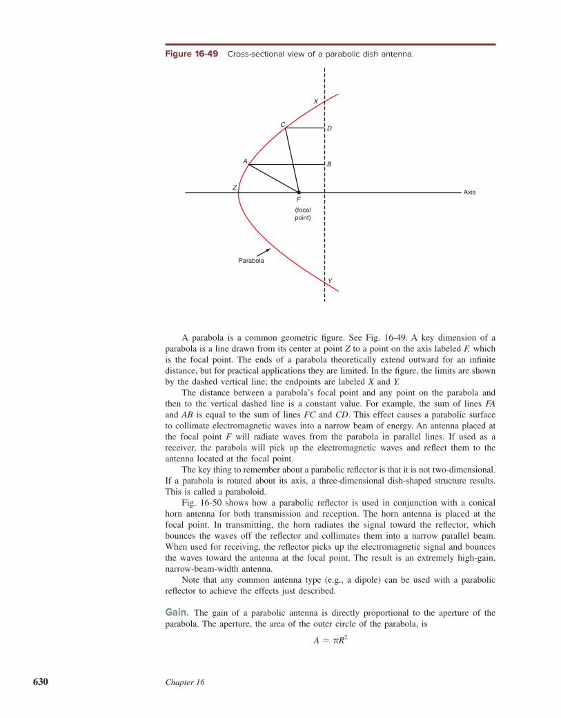
630 Chapter 16
A parabola is a common geometric i gure. See Fig. 16-49. A key dimension of a
parabola is a line drawn from its center at point Z to a point on the axis labeled F, which
is the focal point. The ends of a parabola theoretically extend outward for an ini nite
distance, but for practical applications they are limited. In the i gure, the limits are shown
by the dashed vertical line; the endpoints are labeled X and Y.
The distance between a parabola’s focal point and any point on the parabola and
then to the vertical dashed line is a constant value. For example, the sum of lines FA
and AB is equal to the sum of lines FC and CD. This effect causes a parabolic surface
to collimate electromagnetic waves into a narrow beam of energy. An antenna placed at
the focal point F will radiate waves from the parabola in parallel lines. If used as a
receiver, the parabola will pick up the electromagnetic waves and rel ect them to the antenna located at the focal point. The key thing to remember about a parabolic rel ector is that it is not two-dimensional. If a parabola is rotated about its axis, a three-dimensional dish-shaped structure results. This is called a paraboloid. Fig. 16-50 shows how a parabolic rel ector is used in conjunction with a conical horn antenna for both transmission and reception. The horn antenna is placed at the focal point. In transmitting, the horn radiates the signal toward the rel ector, which bounces the waves off the rel ector and collimates them into a narrow parallel beam. When used for receiving, the rel ector picks up the electromagnetic signal and bounces the waves toward the antenna at the focal point. The result is an extremely high-gain, narrow-beam-width antenna. Note that any common antenna type (e.g., a dipole) can be used with a parabolic rel ector to achieve the effects just described.
Gain. The gain of a parabolic antenna is directly proportional to the aperture of the parabola. The aperture, the area of the outer circle of the parabola, is
A 5 πR2
Figure 16-49 Cross-sectional view of a parabolic dish antenna.
X
C
A
Z
D
B
F
(focalpoint)
Parabola
Axis
Y

Microwave and Millimeter-Wave Communication 631
The gain of a parabolic antenna is given by the simple expression
G 5 6 aD
λb2
where G 5 gain, expressed as a power ratioD 5 diameter of dish, mλ 5 wavelength, m
Most parabolic rel ectors are designed so that the diameter is no less than l at the lowest operating frequency. However, the diameter can be as much as 10λ if greater gain and directivity is required. For example, the power gain of a 5-m-diameter dish at 10 GHz (λ 5 0.03, as com-puter earlier) is
G 5 6 a 5
0.03b2
5 6 (166.67)2
5 6 (27,778.9) 5 166,673
Expressed in decibels, this is
dB 5 10 log 166,673 5 10(5.22) 5 52.2
Beam Width. The beam width of a parabolic rel ector is inversely proportional to the diameter. It is given by the expression
B 570
D/λ
The beam width of our 5-m, 10-GHz antenna is 70(5/0.03) 5 70/166.67 5 0.42°.
Figure 16-50 Sending and receiving with a parabolic refl ector antenna.

632 Chapter 16
With a beam width of less than 0.5°, the signal radiated from a parabolic rel ector is a pencil-thin beam that must be pointed with great accuracy in order for the signal to be picked up. Usually both the transmitting and receiving antennas are of a parabolic design and have extremely narrow beam widths. For that reason, they must be accurately pointed if contact is to be made. Despite the fact that the beam from a parabolic rel ector spreads out and grows in size with distance, directivity is good and gain is high. The precise directivity helps to prevent interference from signals coming in at angles outside of the beam width.
Feed Methods. Keep in mind that the parabolic dish is not the antenna, only a part of it. The antenna is the horn at the focal point. There are many physical arrangements used in positioning the horn. One of the most common is the seemingly awkward coni guration shown in Fig. 16-51. The waveguide feeds through the center of the para-bolic dish and is curved around so that the horn is positioned exactly at the focal point. Another popular method of feeding a parabolic antenna is shown in Fig. 16-52. Here the horn antenna is positioned at the center of the parabolic rel ector. At the focal point is another small rel ector with either a parabolic or a hyperbolic shape. The electromag-netic radiation from the horn strikes the small rel ector, which then rel ects the energy toward the large dish, which in turn radiates the signal in parallel beams. This arrange-ment is known as a Cassegrain feed.
The Cassegrain feed has several advantages over the feed arrangement in Fig. 16-51. The i rst is that the waveguide transmission line is shorter. In addition, the radical bends in the waveguide are eliminated. Both add up to less signal attenuation. The noise i gure is also improved somewhat. Most large earth station antennas use a Cassegrain feed arrangement.
Cassegrain feed
Figure 16-51 Standard waveguide and horn feed.
Figure 16-52 Cassegrain feed.

Microwave and Millimeter-Wave Communication 633
Many other feed arrangements have been developed for parabolic rel ectors. In antennas used for satellite TV reception, a waveguide is not used. Instead, a horn antenna mounted at the focal point is usually fed with microwave coaxial cable. In other large antenna sys-tems, various mechanical arrangements are used to permit the antenna to be rotated or its position otherwise physically changed. Many earth station antennas must be set up so that their azimuth and elevation can be changed to ensure proper orientation for the receiving antenna. This is particularly true of antennas used in satellite communication systems.
Example 16-4A parabolic rel ector antenna has a diameter of 5 ft. Calculate (a) the lowest possible operating frequency, (b) the gain at 15 GHz, and (c) the beam width at 15 GHz. (The lowest operating frequency occurs where the dish diameter is l.)
a. λ 5984
fMHz
5 5 ft
fMHz 5984
55 196.8 MHz
b. There is 3.28 ft/m, so the diameter is 5/3.28 5 1.524 m.
15 GHz 5 15,000 MHz
λ 5300
fMHz5
300
15,0005 0.02 m
G 5 6 aD
λb2
5 6 a1.524
0.02b2
5 34,838.6 (power density ratio)
dB 5 10 log 34,838.6 5 45.42
c. B 570
D/λ5
70λ
D5
70(0.02)
1.5245 0.92°
Some sophisticated systems use multiple horns on a single rel ector. Such multiple feeds permit several signals on different frequencies to be either radiated or received with a single large rel ecting structure.
Helical AntennasA helical antenna, as its name suggests, is a wire helix (Fig. 16-53). A center insulat-ing support is used to hold heavy wire or tubing formed into a circular coil or helix. The diameter of the helix is typically one-third wavelength, and the spacing between turns is approximately one-quarter wavelength. Most helical antennas use from six to eight turns. A circular or square ground-plane antenna or rel ector is used behind the helix. Fig. 16-53 shows a coaxial feed line. Helical antennas are widely used at VHF and UHF ranges. The gain of a helical antenna is typically in the 12- to 20-dB range, and beam widths vary from approximately 12° to 45°. Although these values do not compare favorably with those obtainable with horns and parabolic rel ectors, helical antennas are favored in many applications because of their simplicity and low cost.
Helical antenna

634 Chapter 16
Most antennas transmit either a vertically or a horizontally polarized electromagnetic i eld. With a helical antenna, however, the electromagnetic i eld is caused to rotate. This
is known as circular polarization. Either right-hand (clockwise) or left-hand (counter-
clockwise) circular polarization can be produced, depending on the direction of winding
of the helix. Because of the rotating nature of the magnetic i eld, a circularly polarized
signal can easily be received by either a horizontally or a vertically polarized receiving
antenna. A helical receiving antenna can also easily receive horizontally or vertically
polarized signals. Note, however, that a right-hand circularly polarized signal will not be
picked up by a left-hand circularly polarized antenna, and vice versa. Therefore, helical
antennas used at both transmitting and receiving ends of a communication link must both
have the same polarization.
To obtain greater gain and narrower beam width, several helical antennas can be
used in an array with a common rel ector. A popular arrangement is a group of four helical antennas.
Bicone AntennasMost microwave antennas are highly directional. But in some applications, an omnidi-rectional antenna may be required. One of the most widely used omnidirectional microwave antennas is the bicone (Fig. 16-54). The signals are fed into bicone anten-nas through a circular waveguide ending in a l ared cone. The upper cone acts as a rel ector, causing the signal to be radiated equally in all directions with a very narrow vertical beam width. A version of the bicone replaces the upper cone with a l at horizontal disk that performs the same function.
Slot Antennas A slot antenna is a radiator made by cutting a one-half wavelength slot in a conducting sheet of metal or into the side or top of a waveguide. The basic slot antenna is made by cutting a one-half wavelength slot in a large metal sheet. It has the same characteristics as a standard dipole antenna, as long as the metal sheet is very large compared to λ at the operating frequency. A more common way of making a slot antenna is shown in Fig. 16-55. The slot must be one-half wavelength long at the operating frequency. Fig. 16-55(a) shows how the slots must be positioned on the waveguide to radiate. If the slots are positioned on the center lines of the waveguide sides, as in Fig. 16-55(b), they will not radiate. Several slots can be cut into the same waveguide to create a slot antenna array (Fig. 16-56). Slot arrays, which are equivalent to driven arrays with many elements, have better gain and better directivity than single-slot antennas.
Circular polarization
Bicone antenna
Slot antenna
Figure 16-53 The helical antenna.
GOOD TO KNOWSlot antennas are widely used on
high-speed aircraft because they
can be integrated into the metal-
lic skin of the plane and therefore
do not interfere with the airfl ow
dynamics at high speeds.

Microwave and Millimeter-Wave Communication 635
Figure 16-54 The omnidirectional bicone antenna.
Figure 16-55 Slot antennas on a waveguide. (a) Radiating slots. (b) Nonradiating slots.
(a ) (b)
Center lines
Closed end or terminator
Figure 16-56 A slot antenna array.
12

636 Chapter 16
Slot antennas are widely used on high-speed aircraft. External antennas would be torn off at such high speeds or would slow the aircraft. The slot antenna can be integrated into the metallic skin of the aircraft. The slot itself is i lled in with an insulating material
to create a smooth skin surface.
Dielectric (Lens) AntennasAs discussed previously, radio waves, similar to light waves, can be rel ected, refracted, diffracted, and otherwise manipulated. This is especially true of microwaves, which are close in frequency to light. Thus a microwave antenna can be created by constructing a device that serves as a lens for microwaves just as glass or plastic can serve as a lens for light waves. These dielectric or lens antennas use a special dielectric material to collimate or focus the microwaves from a source into a narrow beam. Fig. 16-57 shows how a lens concentrates light rays from a source into a focused narrow beam. A dielectric lens antenna operates in a similar way. An example of a lens antenna is one used in the millimeter wave range. The micro-wave energy is coupled to a horn antenna through a waveguide. A dielectric lens is placed over the end of the horn, which focuses the waves into a narrower beam with greater gain and directivity. In technical terms, the lens takes the microwaves from a source with a spherical wave front (e.g., a horn antenna) and concentrates them into a plane wave front. A lens like that shown in Fig. 16-58(a) can be used. The shape of the lens ensures that all the entering waves with a spherical wave front are put into phase at the output to create the concentrated plane wave front. However, the lens in Fig. 16-58(a) will work only when it is very thick at the center. This creates great signal loss, especially at the lower microwave frequencies. To get around this problem, a stepped or zoned lens, such as the one shown in Fig. 16-58(b), can be used. The spherical wave front is still converted to a focused plane wave front, but the thinner lens causes less attenuation. Lens antennas are usually made of polystyrene or some other plastic, although other types of dielectric can be used. They are rarely used at the lower microwave frequencies. Their main use is in the millimeter range above 40 GHz.
Dielectric (lens) antenna
Figure 16-57 How a lens focuses light rays.
Focusedrays
Collimatinglens
Lightsource
Figure 16-58 Lens antenna operations. (a) Dielectric lens. (b) Zoned lens.
Horn source
Focused plane waves
(a)
Horn
Dielectric lens Spherical wavesSpherical waves
Plane waves
(b)

Microwave and Millimeter-Wave Communication 637
Patch AntennasPatch antennas are made with microstrip on PCBs. The antenna is a circular or rectan-gular area of copper separated from the ground plane on the bottom of the board by the thickness of the PCB’s insulating material (see Fig. 16-59). The width of the rectangular antenna is approximately one-half wavelength, and the diameter of the circular antenna is about 0.55l to 0.59l. In both cases, the exact dimensions depend upon the dielectric constant and the thickness of the PCB material. The most commonly used PC board material for patch antennas is a Tel on-i berglass combination. The feed method for patch antennas can be either coaxial or edge. With the coaxial method, the center conductor of a coaxial cable is attached somewhere between the center and the edge of the patch, and the coaxial shield is attached to the ground plane [Fig. 16-59(a)]. If the antenna is fed at the edge, a length of microstrip is connected from the source to the edge, as shown in Fig. 16-59(b). The impedance of the edge feed is about 120 V. A quarter-wave Q section can be used to match this impedance to the 50-V impedance that is characteristic of most circuits. When coaxial feed is used, the impedance is zero at the center of the antenna and increases to 120 V at the edge. Cor-rectly positioning the coaxial cable center on the patch [dimension x in Fig. 16-59(a)] allows extremely accurate impedance matching. Patch antennas are small, inexpensive, and easy to construct. In many applications, they can simply be integrated on the PCB with the transmitter or receiver. A disadvantage
Patch antenna
Figure 16-59 Patch or microstrip antennas. (a) Coaxial feed. (b) Edge feed.
�
2D W
xx
L
Top view
D � 0.55� to 0.59�
W �
er
Coaxial cableCoaxial cable
PCB
Ground plane
h
Edge view
(a )
(b)
D W
L
Top view
er
er � dielectric constant of PCB material
PCB
Ground plane
h
Edge view
120-�
edge feed
h � thickness of PCB

638 Chapter 16
of patch antennas is their narrow bandwidth, which is usually no more than about 5 percent of the resonant frequency with circular patches and up to 10 percent with rectangular patches. The bandwidth is directly related to the thickness of the PCB mate rial, i.e., the distance between the antenna and the ground plane [h in Fig. 16-59(b)]. The greater the thickness of the PCB dielectric, the greater the bandwidth. The radiation pattern of a patch antenna is approximately circular in the direction opposite to that of the ground plane.
Phased ArraysA phased array is an antenna system made up of a large group of similar antennas on a common plane. Patch antennas on a common PCB can be used, or separate antennas such as dipoles can be physically mounted together in a plane. See Fig. 16-60. Slot antennas are also used. The antennas are driven by transmission lines that incorporate impedance-matching, power-splitting, and phase-shift circuits. The basic purpose of an array is to improve gain and directivity. Arrays also offer better control of directivity, because individual antennas in an array can be turned off or on, or driven through different phase shifters. The result is that the array can be “steered”—i.e., its radiation pattern can be pointed over a wide range of different directions—without physically moving the antenna, as is necessary with Yagis or parabolic dish antennas. There are two common arrangements for phased arrays. In one coni guration, the
multiple antennas are driven by a common transmitter or feed a common receiver. A
second approach is to have a low-power transmitter amplii er or low-noise receiver
amplii er associated with each dipole or patch in the array. In both cases, the switching
and phase shifting are under the control of a microprocessor or computer. Different
programs in the processor select the gain, directivity, and other factors as required by
the application.
Most phased arrays are used in radar systems, but they are i nding applications in
cell phone systems, wireless local area networks, and satellites.
Printed-Circuit AntennasBecause antennas are so small at microwave frequencies, they can be conveniently made
right on a printed-circuit board that also holds the transmitter and/or receiver ICs and
related circuits. No separate antenna structure, feed line, or connectors are needed. The
patch and slot antennas discussed previously are examples. But there are a few other
Phased array
Figure 16-60 An 8 3 8 phase array using patch antennas. (Feed lines are not shown.)
Printed - circuit board
Patch or slotantenna

Microwave and Millimeter-Wave Communication 639
types that are widely used. These are the loop, the inverted-F, and the meander line antennas shown in Fig. 16-61.
The Loop. A loop antenna is just as its name implies, a single closed loop that is usually rectangular but could be round as well. See Fig. 16-61(a). The length of the loop is usually in the 0.1λ to λ at the operating frequency. The loop is usually resonated with a parallel capacitor. Because the characteristic impedance of the loop is very low, about 10 V at 0.5λ but as high as 120 V for λ, some form of microstrip transmission line is used to match the impedance to the receiver or transmitter. Loops are relatively inefi cient
but are effective in short-range applications such as garage door openers and remote
keyless entry radios in cars and in pagers.
Inverted-F. This unique antenna is a variation of the ground plane as it is designed to
work over a conducting ground plane. See Fig. 16-61(b). Note the lengths of the various
segments. These are experimented with to get the desired performance as well as the
impedance match to the transmission line. A desirable feature is that the radiation pattern
is effectively omnidirectional.
Meander Line. The meander line in Fig. 16-61(c) is an attempt to shorten an antenna
by bending the conductors back on themselves to save space. The design is essentially
Figure 16-61 Popular PCB antennas. (a) Loop. (b) Inverted-F. (c) Meander line.
�
2Feedpoint
Feed point
Copper pattern
Resonatingcapacitor
Z matchTo RX or from TX
Ground plane
0.05�
0.1
�
0.15�
0.1� to 1.0�
(a )
(b)
(c)<

640 Chapter 16
a half-wave dipole and performs as one. All sorts of variations have been created by using curved sections and cross patterns in addition to the bow tie design discussed earlier. The antennas in most cell phones are special variations the antennas in Fig. 16-61. They are designed not only to i t into the small thin cases of a cell phone but also to
have wide bandwidth or to be able to operate on multiple bands.
Dielectric Antennas. A dielectric antenna is one whose copper pattern elements are
formed on some type of resonant dielectric material such as ceramic or some derivative
thereof. The dielectric is designed to be resonant to the frequency of operation and actu-
ally contributes to the radiation. Dielectric antennas often use the inverted-F, dipole, or
meander line coni gurations. No ground plane is necessary for operation. Dielectric
antennas are small and have a wide bandwidth. These antennas are often available as a
component for mounting on a printed-circuit board.
Intelligent Antenna TechnologyIntelligent antennas or smart antennas are antennas that work in conjunction with elec-
tronic decision-making circuits to modify antenna performance to i t changing situations.
They adapt to the signals being received and the environment in which they transmit.
Also called adaptive antennas, these new designs greatly improve transmission and recep-
tion in multipath environments and can also multiply the number of users of a wireless
system. Some popular adaptive antennas today use diversity, multiple-input multiple-
output, and automatic beam forming.
Diversity. Diversity was discussed in Chap. 14. It uses two or more antennas that
receive the signal from different physical positions. In this way, they get different signals.
The antenna with the strongest signal is selected, or the signals are combined to produce
a stronger overall signal. More and more, microwave equipment is using diversity simply
because of the degrading effects of multiple signal paths, rel ections, diffractions, and other conditions that weaken the signal in complex environments. Some systems use three or four antennas with different modes of signal selection to optimize reception.
MIMO. Multiple-input, multiple-output (MIMO) takes the idea of diversity to a whole new level. It uses two or more antennas for receiving but also uses two or more antennas for transmission. One possible arrangement is shown in Fig. 16-62. The data to be transmitted is divided into two separate streams of bits that are transmitted simultaneously. Because there
Figure 16-62 In MIMO, two transmitters send parallel data, doubling the data rate, to multiple receivers that process
the signals to improve gain and reliability.
RX
RX
Dataout
RX
RX
RX
Poweramplifier
Baseband
TX
Poweramplifier
Datain
TX = transmitterRX = receiverADC = analog-to-digital converter
ADC
ADC
ADC
ADC
DSP

Microwave and Millimeter-Wave Communication 641
are two separate data paths, the effect is to double the actual data rate of transmission. For example, in one type of wireless LAN, the maximum data rate is 54 Mbps. With two data streams, the composite throughtput is 108 Mbps. The transmit antennas are physically sepa-rated by a wavelength or more, so that they truly generate different paths to the receiver. The modulation is usually some form of OFDM, and the data is transmitted in the same bandwidth. The arrangement in Fig. 16-62 is designated 2 3 4 MIMO. The i rst number is the num-
ber of transmitters and the second number is the number of receivers. Common MIMO formats
in wireless LANs and cell phone systems are 2 3 2, 2 3 3, 4 3 4, and even 8 3 8.
At the receiving end, three or more antennas are used. The two transmitted signals take
different paths to the four receiver antennas shown in Fig. 16-62. The receiver antennas are
separated by a wavelength or so, providing multiple paths for each of the two transmitted
signals. The signals experience multipath rel ections and other anomalies along the way. The receiver antennas pick up everything. The outputs of the four receivers are then digi-tized with analog-to-digital converters (ADCs), and their outputs are combined in a DSP. Special algorithms programmed into the DSP manipulate and combine the signals in dif-ferent ways to minimize the multipath effects and to create usable signals where none were available with just one transmitter and receiver. MIMO provides an amazing increase in signal gain and reliability. And despite the seemingly high cost and complexity of such a scheme, in reality the very small low-cost IC receivers and transmitters make this technique very simple and affordable from the hardware point of view. The real complexity and “magic” is in the DSP. MIMO makes a previously impossible wireless application work by providing multiple signals that can be combined and processed to produce a usable signal.
Adaptive Beam FormingAdaptive antennas are systems that automatically adjust their characteristics to the environment. They use beam-forming and beam-pointing techniques to zero in on signals to be received and to ensure transmission under noisy conditions with interference from other sources. Beam-forming antennas use multiple antennas such as the phase arrays discussed earlier. By using many antennas, the transmit/receive pattern can be adjusted as required by the situation. The beam may be narrowed or widened, and the direction of the beam may be electronically adjusted on the l y thanks to electronic controls. Such directional antennas can pinpoint a specii c signal while tuning out interfering signals on the same frequency at nearby locations. Beam-forming antennas also have high gain, which helps boost the signal strength of a desired signal and improves the link reliability because noise and interference have been minimized. There are two kinds of adaptive antennas, switched beam arrays and adaptive arrays. The radiation pattern of a switched beam antenna looks something like that in Fig. 16-63. The antenna itself is usually multiple phased arrays. For example, there may be four phased arrays each capable of covering 90° to 100° of azimuth. Multiple beams are
Figure 16-63 A switched beam intelligent antenna.
Selected beam
Location of desiredtransmitting
signal

642 Chapter 16
formed in that 90° range. The electronics controlling the arrays steers the beam by some predetermined algorithm. The most common arrangement is for the antenna to scan the entire 360° range in seeking a signal. As each beam is switched in, the signal strength is monitored. The beam with the strongest signal is then selected. Signals outside the beam will not be received at all, or at most only a small amount of signal will be pres-ent. Such antennas can provide a gain of 20 to 50 dB. An adaptive antenna can also cover the entire 360° range but uses more sophisticated control algorithms. The adaptive array not only seeks out the stongest signal and adjusts the beam width to enhance it, but also recognizes interfering signals and adjusts the antenna to null out the interfering signal. See Fig. 16-64. Adaptive arrays track signals and then i ne-
tune themselves for best reception. All this takes place automatically at electronic speeds.
Both switched beam arrays and adaptive arrays are already being employed in some
cell phone systems and in newer wireless LANs. They are particularly benei cial to cell
phone systems because they can actually boost the system capacity since they can reuse
the same frequencies multiple times and allow the antenna to keep signals on the same
frequency from interfering with one another. This concept is known as spatial division
multiplexing or spatial division multiple access (SDMA).
16-7 Microwave and Millimeter-Wave ApplicationsThe communication applications in which microwaves are most widely used today are
telephone communication, computer networking, cell phones, satellites, and radar. However,
there are many other signii cant uses of microwave frequencies in communication. For
example, TV stations use microwave relay links instead of coaxial cables to transmit TV
signals over long distances, and cable TV networks use satellite communication to transmit
programs from one location to another. Communication with satellites, deep-space probes,
and other spacecraft is usually done by microwave transmission because microwave signals
are not rel ected or absorbed by the ionosphere, as are many lower-frequency signals. Electromagnetic radiation from the stars is also primarily in the microwave region; only
Figure 16-64 An adaptive array zeros in on the desired signal while mulling out
interfering signals.
Antenna
Null
Interferingsignal
Desiredsignal

Microwave and Millimeter-Wave Communication 643
sensitive radio receivers and large antennas operating in the microwave region are used to map outer space with far greater precision than could be achieved with optical telescopes. Finally, microwaves are also used for heating—in the kitchen (microwave ovens), in med-ical practice (diathermy machines used to heat muscles and tissues without causing skin damage), and in industry for melting material and heat treating. Fig. 16-65 summarizes the major applications of microwaves. The military uses micro-wave for multichannel communication with ranges from 1 km to 160 km for line-of-sight and troposcatter communications. The multiple channels can carry a variety of communi-cation signals. The rest of this chapter is devoted to a discussion of radar. Satellites are covered in detail in Chap. 17. Cell phones, wireless computer networks, and other special microwave applications are covered in Chaps. 20 and 21.
RadarThe electronic communication system known as radar (radio detection and ranging) is based on the principle that high-frequency RF signals are rel ected by conductive targets. The usual targets are airplanes, missiles, ships, and automobiles. In a radar system, a
Radar
Figure 16-65 Major applications of microwave and millimeter-wave radio.
1. Radar
a. Aircraft and marine navigation
b. Military threat detection
c. Altimeters
d. Weather plotting
e. Trafi c speed enforcement
f. Automotive collision avoidance and speed control
2. Satellite
a. Telephone communication
b. TV transmission (cable, short-range, direct broadcast)
c. Surveillance
d. Weather plotting
e. Navigation (GPS, etc.)
3. Wireless local-area and personal-area networks
a. IEEE 802.11b/g Ethernet, 2.4 GHz, rates of 11 to 54 Mbps
b. IEEE 802.11a Ethernet, 5 GHz, rate of 54 Mbps
c. 802.11n Ethernet, 2.4 GHz, rate to 600 Mbps
d. 802.11ac Ethernet, 5 GHz, 3 Gbps
e. 802.11ad WiGig, 60 GHz, 7 Gbps
f. Bluetooth 2.4 GHz, rate to 3 Mbps
g. Ultrawideband Rate to 1 Gbps
4. Wireless broadband access to the Internet
a. LTE
b. WiMAX
5. Cell phones (allocations in the 1.8-, 1.9-, 2.3–2.7 and 3.6 GHz ranges)
Fifth generation (5G) cell phones are expected to be in the millimeter
range (e.g., 28 or 38 GHz).
6. Backhaul 18–90 GHz, 500 Mbps-10 Gbps
7. Heating
a. Microwave ovens (domestic)
b. Microwave heating (industrial)
8. Radio telescopes

644 Chapter 16
signal is transmitted toward the target. The rel ected signal is picked up by a receiver in the radar unit. The rel ected or return radio signal is called an echo. The radar unit can then determine the distance to the target (range), its direction (azimuth), and in some cases its elevation (distance above the horizon). The ability of radar to determine the distance between a remote object and the radar unit is dependent upon knowing the exact speed of radio signal transmission. In most radar appli-cations, nautical miles are used instead of statute miles to express transmission speeds. One nautical mile is equal to 6076 ft. The speed of a radio signal is 162,000 nautical miles per second. (Sometimes, a special unit known as a radar mile is used. One radar mile is equal to 6000 ft.) It takes a radio signal 5.375 µs to travel 1 mi and 6.18 µs to travel 1 nautical mile. A radar signal must travel twice the distance between the radar unit and the remote target. The signal is transmitted, a i nite time passes before the signal reaches the target and is rel ected, and the signal then travels an equal distance back to the source. If an object is exactly 1 nautical mile away, the signal takes 6.18 µs to reach the target and 6.18 µs to return. The total elapsed time from the instant of initial transmission to the reception of the echo is 12.36 µs. The distance to a remote target is calculated by using the expression
D 5T
12.36
where D 5 distance between radar unit and remote object, nautical miles T 5 total time between transmission and reception of signal, µs
In short-distance applications, the yard is the common unit of distance measurement. A radio signal travels 328 yd/µs, so the distance to an object in yards is computed as
D 5328T
25 164T
A measured time of 5.6 µs corresponds to a distance of 164 (5.6) 5 918.4 yd. To obtain a strong rel ection or echo from a distant object, the wavelength of the radar signal should be small compared to the size of the object being observed. If the wavelength of the radar signal is long with respect to the distant object, only a small amount of energy will be rel ected. At higher frequencies, the wavelength is shorter and therefore the rel ected energy is greater. For optimal rel ection, the size of the target should be one-quarter wavelength or more at the transmitted frequency. The shorter the wavelength of the signal compared to the observed object, the higher the resolution or dei nition of the remote object. In most cases, it is necessary only to detect the presence of a remote object. But if very short wavelengths are used, in many cases the actual shape of an object can be clearly determined. The term cross section is often used with reference to a radar target. If a target is at least 10 times larger than λ of the radar signal detecting it, the cross section is con-stant. The cross section of a target, a measure of the area of the target “illuminated” by the radar signal, is given in square meters. A target’s cross section is determined by the size of the object, the unique geometry of the target, the viewing angle, and the position. The larger the cross section, the greater the rel ected signal power, the greater the distance of detection, and the higher the probability of the signal being greater than the noise. Another factor inl uencing the return signal strength is the material of the target. Metal returns the greatest signal; other materials can also rel ect radar waves, but not as effectively. Some objects will absorb radar waves, making the rel ected signal very small. The F117, the U.S. Air Force’s stealth i ghter, has a large physical cross section (about 1 m2), but it is designed to del ect and absorb any radar signal aimed at it. All the plane’s surfaces are at an angle such that radio signals striking them are not rel ected directly back to the radar unit. Instead, they are rel ected off at an angle, and little if any rel ected energy is received. The surface of the aircraft is also coated with a material that absorbs radio waves. This combination gives the F117 an effective cross section the size of a small bird.
Cross section

Microwave and Millimeter-Wave Communication 645
All the most important factors affecting the amount of received signal rel ected from a target are summed up in what is called the radar equation:
Pr 5PtGσAe
(4 π)2R 4
where Pr 5 received powerG 5 antenna gain (product of transmitting and receiving gains)σ 5 cross section of target
Ae 5 effective area of receiving antenna (dish area)R 5 range or distance to target
Most of the relationships between the variables are obvious. However, given the fact that the received power is inversely proportional to the fourth power of the distance to the target, it is not surprising that radar range is generally so limited. Keep in mind that the radar equation does not take into account the S/N ratio. Very low-noise receiver front ends are essential for target acquisition. Because radar uses microwave frequencies, line-of-sight communication results. In other words, radar cannot detect objects beyond the horizon. Objects do not have to be physically visible, but must be within line-of-sight radio distance in order for detection to occur. The relationship between range, azimuth, and elevation can be expressed by a right triangle, as shown in Fig. 16-66. Assume that the radar is land-based and used to detect aircraft. The distance between the radar unit and the remote airplane is the hypotenuse of the right triangle. The angle of elevation is the angle between the hypotenuse and the baseline, which is a line tangent to the surface of the earth at the radar location. The altitude is dei ned by the angle of elevation. The greater the angle of elevation, the greater the altitude. Knowing the range and the angle of elevation allows the altitude to be computed by using standard trigonometric techniques. Another important factor in locating a distant object is knowledge of its direction with respect to the radar set. If the radar station is i xed and land-based, the direction (bearing or azimuth) of the remote object is usually given as a compass direction in degrees. Recall that true north is 0° or 360°, east is 90°, south is 180°, and west is 270°. If the radar unit is located in a moving vehicle, such as an airplane or a ship, the azimuth is given as a relative bearing with respect to the forward direction of the vehicle. Straight ahead is 0° or 360°, directly to the right is 90°, directly behind is 180°, and directly to the left is 270°. The ability of a radar unit to determine the direction of a remote object requires the use of a highly directional antenna. An antenna with an extremely narrow beam width
Figure 16-66 The trigonometry of radar.
GOOD TO KNOWAlthough they do not have to be
visible, objects must be within
line-of-sight radio distance in
order for radar detection to occur.

646 Chapter 16
will receive signals only over a narrow angle. The narrower the beam width of the antenna, the more precisely the actual bearing can be determined. Since most radar systems operate in the microwave region, highly directional anten-nas are easily obtained. Horns with parabolic rel ectors are the most common, and beam widths of less than 1° are readily attainable. These highly directional antennas are con-tinuously rotated 360°. The same antenna is used for transmitting the original signal and receiving the rel ected signal. Circuits within the radar unit are calibrated so that the direction in which the antenna is pointing is accurately known. When the echo is received, it is compared to the cali-brated values and the precise direction determined. The ability of a radar unit to determine the altitude of a remote target depends on the vertical beam width of the radar antenna. The radar antenna may scan vertically while measuring the distance of the object during the scan. When the object is detected, the vertical elevation of the antenna is noted and the actual altitude is then computed.
Example 16-5A radar set detects the presence of an aircraft. The time between the radiated and received pulses is 9.2 µs. The antenna is set to an angle of elevation of 20°. Deter-mine (a) the line-of-sight distance to the aircraft in statute miles and (b) the altitude of the aircraft.
a. D (nautical miles) 5T
12.365
9.2
12.365 0.744
1 statute mile 5 5280 ft
1 nautical mile 5 6076 ft
5280
60765 0.87 statute mile/nautical mile
D (statute miles) 5 0.744(0.87) 5 0.647
b. A 5 D sin θ
where θ 5 angle of elevation
A 5 0.647 sin 20
5 0.647(0.342) 5 0.22 mi
5 0.22(5280 ft) 5 1161.6 ft
Pulsed Radar. There are two basic types of radar systems: pulsed and continuous-wave (CW). There are also numerous variations of each. By far the most commonly used radar system is the pulsed type. Signals are transmitted in short bursts or pulses, as shown in Fig. 16-67. The duration or width W of the pulse is very short and, depend-ing upon the application, can be anywhere from less than 1 µs to several microseconds. The time between transmitted pulses is known as the pulse repetition time (PRT). If the PRT is known, the pulse repetition frequency (PRF) can be determined by using the formula
PRF 51
PRT
For example, if the pulse repetition time is 150 µs, the PRF is 1/150 3 1026 5 666.7 kHz.
Pulsed radar

Microwave and Millimeter-Wave Communication 647
The ratio of the pulse width to the PRT is known as the duty cycle. The duty cycle is normally expressed as a percentage:
Duty cycle 5 W 3100
PRT
For example, a pulse width of 7 µs with a PRT of 280 µs produces a duty cycle of 7 3 100/280 5 2.5 percent. It is during the interval between the end of the transmitted pulse and the beginning of the next pulse in sequence in Fig. 16-67 that the echo is received. The duration of the transmitted pulse and the PRT are extremely critical in determin-ing the performance of a radar system. Very short-range radars have narrow pulses and short pulse repetition times. If the target is only a short distance away, the echo travel time will be relatively short. In short-range radars, the pulse width is made narrow to ensure that the pulse is terminated before the echo of the target is received. If the pulse is too long, the return signal may be masked or blanked by the transmitted pulse. Long-range radars typically have a longer pulse repetition time because it takes longer for the echo to return. This also permits a longer burst of energy to be transmitted, ensuring a stronger return. If the PRT is too short relative to the distance of the target, the echo may not return during the time interval between two successive pulses, but after the second transmitted pulse. This is known as a double range or second return echo. Naturally, such echoes lead to imprecise distance measurements.
Continuous-Wave (CW) Radar. In continuous-wave (CW) radar, a constant- amplitude continuous microwave sine wave is transmitted. The echo is also a constant-amplitude microwave sine wave of the same frequency, but of lower amplitude and obviously shifted in phase. The question is, How is such a signal used to determine target characteristics? The answer has to do with the object itself. In most cases, the target is moving with respect to the radar unit. The rel ected signal from a moving airplane, ship, missile, or automobile undergoes a frequency change. It is this frequency change between the trans-mitted signal and the returned signal that is used to determine the speed of the target. The frequency shift that occurs when there is relative motion between the transmitting station and a remote target is known as the Doppler effect. A familiar example of the Doppler effect is the i xed-frequency sound waves emitted by an automobile horn. If the horn sounds when the car is stationery, you will hear a single tone. However, if the car is moving toward you while the horn is on, you will expe-rience a tone of continuously increasing frequency. As the car moves closer to you,
Continuous-wave radar
Doppler effect
Figure 16-67 Pulsed radar signals.

648 Chapter 16
the sound waves are compressed, creating the effect of a higher-frequency signal. If the car is moving away from you with its horn on, you will experience a continually decreasing frequency. As the car moves away, the sound waves are stretched out, creating the effect of a lower-frequency signal. This same effect works on both radio and light waves. In a Doppler system, the transmitter sends out a continuous-frequency signal. If the frequency difference between a transmitted signal and a rel ected signal is known, the relative speed between the radar unit and the observed object can be determined by using the formula
V 5f λ
1.03
where f 5 frequency difference between transmitted and rel ected signals, Hzλ 5 wavelength of transmitted signal, mV 5 relative velocity between the two objects, nautical mi/h
Assume, e.g., a frequency shift of 1500 Hz at a frequency of 10 GHz. A frequency of 10 GHz represents a wavelength of 300/f (in MHz) 5 300/10,000 5 0.03 m. The speed is therefore (1500)(0.03)/1.03 5 43.7 nautical mi/h. There are 1.15 nautical miles per hour per standard miles per hour, so the speed is 43.7 3 1.15 5 50.56 mph. This formula assumes that the moving object is moving directly toward or away form the transmitter. If there is an angular offset, the speed should be multiplied by the cosine of the angle between the direct path and the actual path. In CW radar, it is the Doppler effect that provides frequency modulation of the rel ected carrier. For there to be a frequency change, the observed object must be moving toward or away from the radar unit. If the observed object moves parallel to the radar unit, there is no relative motion between the two and no frequency modula-tion occurs. The greatest value of CW radar is its ability to measure the speed of distant objects. Police radar units use CW Doppler radar for measuring the speed of cars and trucks. Some radar systems combine both pulse and Doppler techniques to improve performance and measurement capabilities. One such system evaluates successive echoes to determine phase shifts that indicate when a target is moving. Such radars are said to incorporate moving target indication (MTI). Through a variety of special signal processing techniques, multiple moving targets can be distinguished not only from one another but from i xed targets as well.
Block Diagram Analysis. Fig. 16-68 is a block diagram of a typical pulsed radar unit. There are four basic subsystems: the antenna, the transmitter, the receiver, and the display unit. The transmitter in a pulsed radar system invariably uses a magnetron. Recall that a magnetron is a special high-power vacuum tube oscillator that operates in the microwave region. The cavity size of the magnetron sets the operating frequency. A master timing generator develops the basic pulses used for triggering the magnetron. The timing generator sets the pulse duration, the PRT, and the duty cycle. The pulses from the tim-ing network trigger the magnetron into oscillation, and it emits short bursts of microwave energy. Magnetrons are capable of extremely high power, especially when operated on a pulse basis. Continuous average power may be low, but when pulsed, magnetrons can produce many megawatts of power for the short duration required by the application. This helps ensure a large rel ection. Klystrons and TWTs are commonly used in CW Doppler radars. Low-power radars such as those used by the police for speed detection use Gunn diodes. In Fig. 16-68, you can see that the transmitter output is passed through a circulator and then applied to the antenna. The circulator is a type of duplexer that allows the transmitter and receiver to share a single antenna and prevents the high-power transmitted signal from getting into the receiver and damaging it.
Moving target indication (MTI)

Microwave and Millimeter-Wave Communication 649
A radar duplexer is a waveguide assembly containing special devices that prevent interference between the transmitter and receiver. The most commonly used device is a spark gap tube. Spark gap tubes are either TR (transmit-receive) or anti-transmit-receive
(ATR) types. TR tubes prevent transmitter power from reaching the receiver. When RF energy from the transmitter is detected, the spark gap breaks down, creating a short circuit for the RF energy. ATR tubes effectively disconnect the transmitter from the circuit during the receive interval. The TR and ATR tubes, when combined with the appropriate one-quarter and one-half wavelength waveguides, provide effective isolation between transmitter and receiver. In low-power radars, PIN diodes or a standard circula-tor can be used for this purpose. The antenna system is typically a horn with a parabolic rel ector that produces a very narrow beam width. A special waveguide assembly with a rotating joint allows the waveguide and horn antenna to be rotated continuously over 360°. The same antenna is also used for reception. During the pulse off time, the received signal passes through the antenna, the associated waveguide, and either the duplexer or the circulator to the receiver. The receiver is a standard high-gain superheterodyne type. The signal is usually fed directly to a mixer in most systems, although some radars use an RF amplii er. The mixer is typically a single diode or diode bridge assembly. The local oscillator feeds a signal to the mixer at the appropriate frequency so that an IF is developed. Both klystrons and Gunn diodes are used in local-oscillator applications. The IF amplii ers provide very high gain prior to demodulation. Some radar receivers use double conversion. The demodulator in a pulsed radar system is typically a diode detector, since only the pulses must be detected. In Doppler and other more complex radars, some form of frequency- and phase-sensitive demodulator is used. Phase-locked loops are common in this application. The output of the demodulator is fed to a video amplii er, which creates signals that are ultimately displayed. The display in most radar systems is a CRT. Various display formats can be used. The most common type of CRT display is known as a type P display or plan position
Transmit-receive (TR) tube
Anti-transmit-receive (ATR) tube
Type P display
Figure 16-68 General block diagram of a pulsed radar system.

650 Chapter 16
indicator (PPI). PPI displays show both the range and the azimuth of a target. The cen-ter of the display is assumed to be the location of the radar unit. Concentric circles indicate the range. The azimuth or direction is indicated by the position of the rel ected target on the screen with respect to the vertical radius line. The targets show up as lighted blips on the screen. The PPI display is developed by a sophisticated scanning system tied into antenna rotation. As the antenna is rotated by a motor, an encoder mechanism sends signals to the PPI control circuits that designate the azimuth or direction of the antenna. At the same time, the horizontal and vertical del ection coils (the yoke) around the neck of the CRT rotate in synchronism with the antenna. The electron beam in the CRT is swept from the center of the screen out to the edge. The sweep begins at the instant of pulse transmission and sweeps outward from the center. The beginning of each transmitted pulse begins another sweep of the electron beam. As the del ection yoke rotates, the beam moves in such a way that it appears that a radius from the center to the edge is con-tinuously rotating. Target rel ections appear as lighted blips on the screen. Calibrations on the screen in the form of graticule markings or superimposed electron beam patterns permit distance and azimuth values to be read directly. Newer radars use a different system with a LCD or other l at-panel display to show the equivalent of the CRT PPI presentation. Some PPI radars scan only a narrow range of azimuth rather than the entire 360°. Airplanes with radars in the nose, e.g., only scan a 90° to 180° range forward. An important high-tech type of radar known as phased array radar provides greater l exibility in scanning narrow sectors and tracking multiple targets. Instead of a single horn and parabolic rel ector, multiple dipoles or patch antennas are used. Slots in a waveguide are also used. A half-wave dipole at microwave frequencies is very short. Therefore, many can be mounted together in a matrix or array. The result is a special collinear array above a rel ecting surface with very high gain. By using a system of separate feed lines and a variable phase shifter for each antenna, the beam width and directivity can be controlled electronically. This permits rapid scanning and on-the-l y adjustment of directivity. Phase array radars eliminate the mechanical systems needed for conventional radars.
UWB Radar. The newest form of radar is called ultrawideband (UWB) radar. It is a form of pulsed radar that radiates a stream of very short pulses several hundred picosec-onds long rather than a burst of RF at a specii c carrier frequency. The resulting spectrum as determined by a Fourier analysis is very broad, usually several gigahertz wide. This spectrum typically overlaps radio signals within the signal bandwidth, commonly in the 1- to 10-GHz range. To avoid interference with other radio signals, very low power (microwatts) is used. The very narrow pulses give this radar extreme precision and reso-lution of small objects and details. However, the low power restricts operation to short distances (,100 m). The circuitry used is relatively simple, so it is possible to make inexpensive, single-chip radars. These are used in short-range collision detection systems in airplanes and soon will be in automobiles for automatic braking based upon distance from the vehicle ahead. Another application of UWB radar is personnel detection on the battlei eld. These radars can penetrate walls to detect the presence of human beings. Chap. 22 provides more details on UWB systems.
Radar Applications. One of the most important uses of radar is in weapons defense systems and in safety and navigation systems. Search radars are used to locate enemy missiles, planes, and ships. Tracking radars are used on missiles and planes to locate and zero in on targets. Radars are widely used on planes and ships for navigating blind in fog or bad weather. Radars help ground controllers locate and identify nearby planes. Special radars assist planes in landing in bad weather when visibility is near zero.
Plan position indicator (PPI)
Phased array radar
Ultrawideband (UWB) radar

Microwave and Millimeter-Wave Communication 651
Radars are also used as altimeters to measure height. High-frequency radars can actually be used to plot or map the terrain in an area. Special terrain-following radars allow high-speed jets to l y very close to the ground to avoid detection by enemy radar. Aircraft collision avoidance systems also use radar. In civilian applications, radars are used on boats of all sizes for navigation in bad weather. The police use radar to catch speeders. Small handheld Doppler radar units can also be used in sporting events—to time race cars or determine the speed of a pitched baseball or tennis serve. Some of the newer upper-scale cars such as Lexus and Mercedes Benz have built in radars that detect the distance between the vehicle ahead and automatically adjust the speed to maintain a safe distance. These short-range radars operate in the 20- to 40-GHz bands. Finally, ground and satellite based radars are widely used to track clouds, storms, and other phenomena for the purpose of weather forecasting.
GOOD TO KNOWPolice radar units use continuous-
wave Doppler radar for measuring
the speed of vehicles. Perhaps the
most signifi cant benefi t of
continuous-wave radar is its
ability to measure the speed of
distant objects.
CHAPTER REVIEWOnline Activity
16-1 Exploring GaN Technology
Objective: To learn more about gallium nitride (GaN) tran-sistors and applications.
Procedure: 1. Using standard Internet search techniques, search on
the terms GaN, GaN transistor, GaN power amplii ers, and similar terms.
2. Answer the questions below.
Questions: 1. Name four companies that make GaN transistors and/
or power amplii ers. 2. What is the maximum operating frequency of most
GaN power transistors?
3. What type of transistor (bipolar, MOSFET, etc.) is made with GaN?
4. What is the maximum power level of most GaN transistors?
5. Name three primary applications for GaN transistors. 6. What devices do GaN transistors replace in microwave
equipment?
16-2 Terahertz Technology
Objective: To become aware of the movement toward terahertz (THz) applications.
Procedure: 1. Search on the terms terahertz, THz, terahertz technol-
ogy, equipment, applications, or similar terms. 2. Answer the questions below.
Questions: 1. How many gigahertz in one terahertz? 2. Where in the electromagnetic spectrum do the THz
frequencies lie?
3. Do normal electronic components work at THz frequencies?
4. What are some potential THz applications? 5. Is THz equipment in operation now? 6. What is the main activity in the THz movement today?

652 Chapter 16
Questions
1. What is the microwave frequency range? 2. What is the primary advantage of using microwave
frequencies? What is the main disadvantage? 3. List seven reasons why microwaves are more difi cult
to work with than lower-frequency signals.
4. What is the designation of the lowest- frequency
microwave band?
5. What is the name for microwaves above 30 GHz?
6. Name four techniques that have helped squeeze more
signals into a given spectrum space.
7. What architecture is used for modern microwave and
millimeter-wave transmitters and receivers?
8. Name two common methods for generating a micro-
wave signal with conventional lower-frequency (VHF
and UHF) components.
9. Name the parts of a microwave receiver and a
microwave transmitter that require special microwave
components.
10. Name the two types of transmission lines made of PCB
material used to produce circuits and components in
the microwave region. Which is the more commonly
used and why?
11. List three common circuits or functions performed by
microstrip in microwave equipment.
12. What is the name of the microstrip device that has four
ports and allows multiple circuits and devices to be
interconnected without interfering with one another?
13. How are microwave transistors different from
lower-frequency transistors?
14. What four semiconductor materials are used instead of
silicon to make transistors and ICs perform satisfactorily
in the microwave region?
15. How are microstrip lines used in microwave amplii ers?
16. Up to what frequency are microwave transistors and
ICs available?
17. How are microwave linear amplii ers biased and why?
18. What is the main disadvantage of using coaxial cable at
microwave frequencies?
19. Coaxial cable is not used beyond a certain frequency.
What is that frequency?
20. Name the special coaxial cable made for microwave
applications. What is its main disadvantage?
21. Name the two ways to couple or extract energy from a
waveguide.
22. A waveguide acts as what kind of i lter?
23. True or false? A waveguide with a cutoff frequency of
6.35 GHz will pass a signal of 7.5 GHz.
24. The magnetic and electric i elds in a waveguide are
designated by what letters?
25. State the basic operating mode of most waveguides.
26. What do you call the coupling mechanism used to
attach two sections of a waveguide?
27. Name the two types of T sections of a waveguide and
briel y tell how each is used. 28. Explain how a hybrid T works and give a common
application. 29. What devices are used to terminate a waveguide? Why
is termination necessary? 30. State the main purpose of a directional coupler. 31. What useful device is created by a one-half wavelength
section of waveguide shorted at both ends? 32. A cavity resonator acts as what type of circuit? 33. How are resonant cavities used in microwave circuits? 34. What characteristic of a cavity can be adjusted by
mechanically varying the cavity’s dimensions? 35. What is a circulator? 36. What is an isolator? 37. What prevents ordinary silicon diodes from working at
microwave frequencies? 38. What are two names for a microwave diode with an
N-type silicon cathode and a metal anode forming a junction?
39. Name the most common application of microwave signal diodes.
40. What is the name of a microwave diode that acts as a variable-voltage capacitor? What is its main application?
16-3 Microwave Magazines
Objective: Become familiar with available microwave- related publications.
Procedure: 1. Search for the websites of the following magazines:
Microwaves & RF, Microwave Journal, and Microwave
Product Digest.
2. Browse the current issues of the magazines. 3. Become familiar with the websites. 4. Register or subscribe to each magazine. Be sure to use
the title “engineer” or a related title, and indicate your interest in the various products.
5. Answer the questions below.
Questions: 1. Are print versions of the magazine available? 2. What is the subscription cost of each? 3. Did you i nd any other microwave-related magazines
or websites? If you did, name them.

Microwave and Millimeter-Wave Communication 653
41. Name two types of diodes widely used as frequency multipliers in the microwave region. Do such multiplier circuits amplify?
42. Name two other diodes used as microwave diode oscillators. 43. Name two ways that a PIN diode is used at microwave
frequencies. 44. Does an IMPATT diode operate with forward or reverse
bias? 45. True or false? Klystrons can be used as amplii ers or
oscillators.
46. True or false? A magnetron operates as an amplii er.
47. True or false? A TWT is an amplii er.
48. The cavities in a klystron produce what kind of
modulation of the electron beam?
49. State at which points in a klystron amplii er the input is
applied and the output is taken from.
50. Low-power klystrons are being replaced by what
semiconductor device? High-power klystrons are being
replaced by what other device?
51. What component of a magnetron causes the electrons
to travel in circular paths?
52. State two major applications of magnetrons.
53. What is the main application of a TWT?
54. How is density modulation of the electron beam in a
TWT achieved?
55. What is the main benei t of a TWT over a klystron?
56. What is the most commonly used microwave antenna?
57. How does increasing the length of a horn affect its gain
and beam width?
58. What is the typical beam width range of horn?
59. Describe the bandwidth of horns.
60. State the geometric shape of a commonly used micro-
wave antenna rel ector. 61. For a dish rel ector to work, how must the antenna be
positioned? 62. What type of antenna is most commonly used with a
dish rel ector? 63. What do you call the feed arrangement of a dish with a
horn at its center and a small rel ector at the focal point? What is its purpose?
64. Name two benei ts of a helical antenna. 65. What is the gain range of a helical antenna? 66. What is the typical beam width range of a helical antenna? 67. What is the type of polarization radiated by a helical
antenna?
68. What does RHCP mean? LHCP? 69. True or false? A helical antenna can receive either
vertically or horizontally polarized signals. 70. True or false? An RHCP antenna can receive a signal
from an LHCP antenna. 71. Name a popular omnidirectional microwave antenna. 72. What is the typical length of a slot antenna? 73. Where are slot antennas most often used? 74. How is a slot antenna driven? 75. What basic function is performed by a lens antenna? 76. What is the name given to antennas made with microstrip? 77. Name the two common shapes of microstrip antennas. 78. Name two ways that microstrip antennas are fed. 79. What is the name of the antenna made of multiple patch
dipoles? Where is it used? 80. Name three popular PCB antennas other than the patch.
Where are they used? 81. Dei ne MIMO. Where is it used? 82. Name the two types of intelligent antennas. Where are
they used? 83. List two benei ts of beam switched and beam-forming
antennas. 84. Explain how spatial division multiple access can
increase the subscriber capacity of a cell phone system. 85. List four popular uses for microwaves in communication. 86. Knowing the speed of radio signals allows radar to
determine what characteristic of a target? 87. What characteristic of a radar antenna determines the
azimuth of a target? 88. What characteristic of a target determines the amount
of rel ected signal? 89. Radars operate in what microwave bands? 90. True or false? Both transmitter and receiver in a radar
share the same antenna. 91. Name the two main types of radar. 92. What is the name given to a frequency shift of sound,
radio, or light waves that occurs as the result of the relative motion between objects?
93. True or false? Distance can be measured with CW radar. 94. What is the key component in a radar transmitter? 95. What are TR and ATR tubes? Why are they used? 96. What is the output display in most radar sets? 97. Name three major military and four civilian uses of radar. 98. Name one advantage and one disadvantage of UWB
radar.
1. The TV channels 2 through 13 occupy a total bandwidth of about 72 MHz. At a frequency of 200 MHz, what is the bandwidth percentage? What is the bandwidth percentage at 20 GHz? ◆
2. A one-quarter wavelength piece of 75-V microstrip line has a capacitive load of Xc 5 22 V. What imped-ance does a driving generator see?
3. What is the length of a one-quarter wavelength microstrip at 2.2 GHz? (The dielectric constant of the PCB is 4.5.) ◆
4. A rectangular waveguide has a width of 1.4 in and a height of 0.8 in. What is the cutoff frequency of the waveguide?
Problems

654 Chapter 16
5. A 20-dB directional coupler is installed in a waveguide carrying a 5-W 6-GHz signal. What is the output of the coupler? ◆
6. What is the length of a dipole at 2.4 GHz? 7. A horn antenna is 5λ long at 7 GHz. What is that length
in inches? ◆
8. A horn aperture is 6 cm wide and 4 cm high. The oper-ating frequency is 18 GHz. Compute the beam angle and the gain. Assume K 5 0.5.
9. A parabolic rel ector antenna has a diameter of 6 m. The frequency of operation is 20 GHz. What are the gain and beam width? ◆
10. What is the approximate lowest frequency of operation of a dish with a diameter of 18 in?
11. State the speed of a radar signal in microseconds per nautical mile.
12. Convert 22 standard statute miles to nautical miles. 13. The elapsed time between radiating a radar signal and
receiving its echo is 23.9 µs. What is the target distance in nautical miles?
14. How many microseconds is the time period between the transmitted signal and receipt of an echo from a target 1800 yd away?
15. For optimum rel ection from a target, what should the size of the target be, in wavelengths of the radar signal?
16. A CW radar operates at a frequency of 9 GHz. A fre-quency shift of 35 kHz is produced by a moving target. What is its speed?
◆ Answers to Selected Problems follow Chap. 22.
1. If microwave power transistors are limited to, say, an upper power limit of 100 W each, explain how you could build a microwave power amplii er with a power rating of 1 kW.
2. A NASA deep-space probe operates on 8.4 GHz. Its location is past Mars, heading into outer space. Explain in detail how you would go about maintaining and/or
improving signal strength at the main receiver in California.
3. What is the one main factor limiting the range of microwave and millimeter-wave signals?
4. What semiconductor technology originally developed for computer and digital applications is now widely used to make microwave radio circuits?
Critical Thinking

655
chapter17
A satellite is a physical object that orbits, or rotates about, some celestial
body. Satellites occur in nature, and our own solar system is a perfect
example. The earth and other planets are satellites rotating about the sun.
The moon is a satellite to the earth. A balance between the inertia of the
rotating satellite at high speed and the gravitational pull of the orbited
body keeps the satellite in place.
Satellites are launched and orbited for a variety of purposes. The most
common application is communication in which the satellite is used as a
repeater. In this chapter, we introduce satellite concepts and discuss how
satellites are identifi ed and explained. We summarize the operation of a
satellite ground station and review typical satellite applications, including
the Global Positioning System, which is a worldwide satellite-based navi-
gational system, and satellite radio and TV systems.
Objectives
After completing this chapter, you will be able to:
■ Defi ne the terms posigrade, retrograde, geocenter, apogee, perigee,
ascending, descending, period, angle of inclination, geosynchronous,
latitude, longitude, and meridian.
■ State the operative physical principles of launching a satellite and
maintaining its orbit.
■ Draw a block diagram of the communication system in a communica-
tion satellite, give its name, and explain how it works.
■ List the six main subsystems of a satellite.
■ Draw a block diagram of a satellite ground station, identifying the
fi ve main subsystems and explaining the operation of each.
■ Name three common applications for satellites and state which is the
most common.
■ Explain the concept and operation of the Global Positioning System.
Draw a block diagram of a GPS receiver and explain the function of
each component.
■ Explain the operation of the U.S. satellite radio and TV systems.
Satellite
Orbit
Satellite Communication

656 Chapter 17
17-1 Satellite OrbitsThe ability to launch a satellite and keep it in orbit depends upon following well-known physical and mathematical laws that are referred to collectively as orbital dynamics. In this section, we introduce these principles before discussing the physical components of a satellite and how it is used in various communication applications.
Principles of Satellite Orbits and PositioningIf a satellite were launched vertically from the earth and then released, it would fall back to earth because of gravity. For the satellite to go into orbit around the earth, it must have some forward motion. For that reason, when the satellite is launched, it is given both verti-cal and forward motion. The forward motion produces inertia, which tends to keep the satellite moving in a straight line. However, gravity tends to pull the satellite toward the earth. The inertia of the satellite is equalized by the earth’s gravitational pull. The satellite constantly changes its direction from a straight line to a curved line to rotate about the earth. If a satellite’s velocity is too high, the satellite will overcome the earth’s pull and go out into space. It takes an escape velocity of approximately 25,000 mi/h to cause a spacecraft to break the gravitational pull of the earth. At lower speeds, gravity constantly pulls the satellite toward the earth. The goal is to give the satellite acceleration and speed that will exactly balance the gravitational pull. The closer the satellite is to earth, the stronger the effect of the earth’s gravitational pull. So in low orbits, the satellite must travel faster to avoid falling back to earth. The lowest practical earth orbit is approximately 100 mi. At this height, the satellite’s speed must be about 17,500 mi/h to keep the satellite in orbit. At this speed, the satellite orbits the earth in approximately 11⁄2 h. Communication satellites are usually much farther from earth. A typical distance is 22,300 mi. A satellite need travel only about 6800 mi/h to stay in orbit at that distance. At this speed, the satellite rotates about the earth in approx-imately 24 h, the earth’s own rotational time. There is more to a satellite orbit than just the velocity and gravitational pull. The satellite is also affected by the gravitational pull of the moon and sun. A satellite rotates about the earth in either a circular or an elliptical path, as shown in Fig. 17-1. Circles and ellipses are geometric i gures that can be accurately described
mathematically. Because the orbit is either circular or elliptical, it is possible to calculate
the position of a satellite at any given time.
(b)(a)
Figure 17-1 Satellite orbits. (a) Circular orbit. (b) Elliptical orbit.
GOOD TO KNOWCommunication satellites
typically orbit the earth at a
distance of about 22,300 mi at
a speed of about 6800 mi/h.

Satellite Communication 657
A satellite rotates in an orbit that forms a plane passing through the center of grav-ity of the earth called the geocenter (Fig. 17-2). In addition, the direction of satellite rotation may be either in the same direction as the earth’s rotation or against the direction of earth’s rotation. In the former case, the orbit is said to be posigrade, and in the latter case, retrograde. Most orbits are posigrade. In a circular orbit, the speed of rotation is constant. However, in an elliptical orbit, the speed changes depending upon the height of the satellite above the earth. Naturally the speed of the satellite is greater when it is close to the earth than when it is far away.
Satellite Height. In a circular orbit, the height is simply the distance of the satellite from the earth. However, in geometric calculations, the height is really the distance between the center of the earth and the satellite. In other words, that distance includes the radius of the earth, which is generally considered to be about 3960 mi (or 6373 km). A satellite that is 5000 mi above the earth in circular orbit is 3960 1 5000, or 8960, mi from the center of the earth (see Fig. 17-3).
Geocenter
Posigrade orbit
Retrograde orbit
Figure 17-2 The orbital plane passes through the geocenter.
Figure 17-3 Satellite height.
GOOD TO KNOWBefore being launched into space,
satellites undergo testing for
vibration, center of gravity,
vacuum, and thermal shock.

658 Chapter 17
When the satellite is in an elliptical orbit, the center of the earth is one of the focal points of the ellipse (refer to Fig. 17-4). In this case, the distance of the satellite from the earth varies according to its position. Typically the two points of greatest interest are the highest point above the earth—the apogee—and the lowest point—the perigee. The apogee and perigee distances typically are measured from the geocenter of the earth.
Satellite Speed. As indicated earlier, the speed varies according to the distance of the satellite from the earth. For a circular orbit the speed is constant, but for an elliptical orbit the speed varies according to the height. Low earth satellites of about 100 mi in height have a speed in the neighborhood of 17,500 mi/h. Very high satellites such as communication satellites, which are approximately 22,300 mi out, rotate much more slowly, a typical speed of such a satellite being in the neighborhood of 6800 mi/h.
Satellite Period. The period is the time it takes for a satellite to complete one orbit. It is also called the sidereal period. A sidereal orbit uses some external i xed or appar-
ently motionless object such as the sun or star for reference in determining a sidereal
period. The reason for using a i xed reference point is that while the satellite is rotating
about the earth, the earth itself is rotating.
Another method of expressing the time for one orbit is the revolution or synodic period.
One revolution (1 r) is the period of time that elapses between the successive passes of the
satellite over a given meridian of earth longitude. Naturally, the synodic and sidereal periods
differ from each other because of the earth’s rotation. The amount of time difference is
determined by the height of the orbit, the angle of the plane of the orbit, and whether the
satellite is in a posigrade or retrograde orbit. Period is generally expressed in hours. Typical
rotational periods range from about 11⁄2 h for a 100-mi height to 24 h for a 22,300-mi height.
Angle of Inclination. The angle of inclination of a satellite orbit is the angle formed
between the line that passes through the center of the earth and the north pole and a line
that passes through the center of the earth but that is also perpendicular to the orbital
plane. This angle is illustrated in Fig. 17-5(a). Satellite orbits can have inclination angles
of 0° through 90°.
Another dei nition of inclination is the angle between the equatorial plane and the
satellite orbital plane as the satellite enters the northern hemisphere. This dei nition may be
a little bit easier to understand, but it means the same thing as the previous dei nition.
Apogee
Perigee
Satellite period
Sidereal period
Angle of inclination
Figure 17-4 Elliptical orbit showing apogee and perigee.

Satellite Communication 659
When the angle of inclination is 0°, the satellite is directly above the equator. When the angle of inclination is 90°, the satellite passes over both the north and the south poles once for each orbit. Orbits with 0° inclination are generally called equatorial orbits, and orbits with inclinations of 90° are referred to as polar orbits.
When the satellite has an angle of inclination, the orbit is said to be either ascend-
ing or descending. As the satellite moves from south to north and crosses the equator, the orbit is ascending. When the satellite goes from north to south across the equator, the orbit is descending [see Fig. 17-5(b)].
Angle of Elevation. The angle of elevation of a satellite is the angle that appears between the line from the earth station’s antenna to the satellite and the line between the earth station’s antenna and the earth’s horizon (see Fig. 17-6). If the angle of elevation is too small, the signals between the earth station and the satellite have to pass through much more of the earth’s atmosphere. Because of the very low powers used and the high absorption of the earth’s atmosphere, it is desirable to minimize the amount of time that the signals spend in the atmosphere. Noise in the atmosphere also contributes to poor performance. The lower the angle of radiation, the more time that this signal spends in the atmosphere. The minimum practical angle of elevation for good satellite performance is generally 5°. The higher the angle of elevation, the better.
Equatorial orbit
Polar orbit
Angle of elevation
Figure 17-5 (a) Angle of inclination. (b) Ascending and descending orbits.
N
S
EquatorAscending
part oforbit (S to N)
Descending partof orbit (N to S) Satellite
(b)
Figure 17-6 Angle of elevation.

660 Chapter 17
Geosynchronous Orbits. To use a satellite for communication relay or repeater purposes, the ground station antenna must be able to follow or track the satellite as it passes overhead. Depending upon the height and speed of the satellite, the earth station is able to use it only for communication purposes for that short period when it is visible. The earth station antenna tracks the satellite from horizon to horizon. But at some point, the satellite disappears around the other side of the earth. At this time, it can no longer support communication. One solution to this problem is to launch a satellite with a very long elliptical orbit so that the earth station can “see” the apogee. In this way, the satellite stays in view of the earth station for most of its orbit and is useful for communication for a longer time. It is only during that short time when the satellite disappears on the other side of the earth (perigee) that it cannot be used. The intermittent communication caused by these orbital characteristics is highly undesirable in many communication applications. One way to reduce interruptions is to use more than one satellite. Typically three satellites, if properly spaced in the correct orbits, can provide continuous communication at all times. However, multiple tracking stations and complex signal switching or “hand-off” systems between stations are required. Maintaining these stations is expensive and inconvenient. Despite the cost and complexity of multiple-satellite systems, they are widely deployed in global telecommunication applications. These systems use anywhere from 24 to more than 100 satellites. At any given time, multiple satellites are in view anywhere on earth, making continuous communication possible. Multiple satellite systems are usually located in two ranges above the earth. Low
earth-orbiting satellites, commonly referred to as LEOs, are placed in the range of 400 to 1000 mi above the earth. Medium earth-orbiting satellites or MEOs occupy the range of 1000 to 6000 mi above the earth. The greater the height above the earth, the better the view and the greater the radio area coverage on the earth’s surface. When the goal is broader coverage per satellite, the MEO is obviously preferred over the LEO. However, the higher the satellite, the higher the power required for reliable communication and the longer the delay. Even though radio waves travel at 186,400 mi/s, there is a noticeable delay in any voice signal from the uplink to the downlink. For MEOs, the round-trip delay averages about 100 ms. The delay in LEOs averages 10 ms. The best solution is to launch a synchronous or geostationary satellite. In a geosynchronous earth orbit (GEO), the satellite orbits the earth about the equator at a distance of 22,300 mi (or 35,888 km). A satellite at that distance rotates about the earth in exactly 24 h. In other words, the satellite rotates in exact synchronism with the earth. For that reason, it appears to be i xed or stationary, thus the terms
synchronous, geosynchronous, or geostationary orbit. Since the satellite remains
apparently i xed, no special earth station tracking antennas are required. The antenna
is simply pointed at the satellite and remains in a i xed position. With this arrange-
ment, continuous communication is possible. Most communication satellites in use
today are of the geosynchronous variety. Approximately 40 percent of the earth’s
surface can be “seen” or accessed from such a satellite. Users inside that area can
use the satellite for communication. Higher power is required for such a great
distance, and the round-trip delay is about 260 ms, which is very noticeable in voice
communication.
Position Coordinates in Latitude and Longitude. To use a satellite, you must
be able to locate its position in space. That position is usually predetermined by the
design of the satellite and is achieved during the initial launch and subsequent position
adjustments. Once the position is known, the earth station antenna can be pointed at the
satellite for optimum transmission and reception. For geosynchronous satellites, the earth
station antenna can be adjusted once, and it will remain in that position except for occa-
sional minor adjustments. The positions of other satellites above the earth vary according
to their orbital characteristics. To use these satellites, special tracking systems must be
Synchronous (geosynchronous or geostationary) orbit
GOOD TO KNOWThe SSP of nongeosynchronous
satellites will move with respect
to a given reference point on
earth. For these satellites, the
SSP traces a line on the earth
known as the subsatellite path,
or ground track.
GOOD TO KNOWGeosynchronous satellites orbit
the earth in exact synchronism
with the earth’s rotation and
therefore appear to be stationary.

Satellite Communication 661
employed. A tracking system is essentially an antenna whose position can be changed to follow the satellite across the sky. To maintain optimum transmission and reception, the antenna must be continually pointed at the satellite as it rotates. In this section, we discuss methods of locating and tracking satellites. The location of a satellite is generally specii ed in terms of latitude and longitude,
just as a point on earth would be described. The satellite location is specii ed by a point
on the surface of the earth directly below the satellite. This point is known as the
subsatellite point (SSP). The subsatellite point is then located by using conventional
latitude and longitude designations.
Latitude and longitude form a system for locating any given point on the surface of
the earth. This system is widely used for navigational purposes. If you have ever studied
a globe of the earth, you have seen the lines of latitude and longitude. The lines of
longitude, or meridians, are drawn on the surface of the earth between the north and
south poles. Lines of latitude are drawn on the surface of the earth from east to west,
parallel to the equator. The centerline of latitude is the equator, which separates the earth
into the northern and southern hemispheres.
Latitude is dei ned as the angle between the line drawn from a given point on the
surface of the earth to the point at the center of the earth called the geocenter and
the line between the geocenter and the equator (see Fig. 17-7). The 0° latitude is at the
equator, and 90° latitude is at either the north or south pole. Usually an N or an S is
added to the latitude angle to designate whether the point is in the northern or southern
hemisphere.
A line drawn on the surface of the earth between the north and south poles is
generally referred to as a meridian. A special meridian called the prime meridian is
used as a reference point for measuring longitude. It is the line on the surface of the
earth, drawn between the north and south poles, that passes through Greenwich,
England. The longitude of a given point is the angle between the line connected to
the geocenter of the earth to the point where the prime meridian and equator and the
meridian containing the given point of interest intersect (see Fig. 17-7). The designa-
tion east or west is usually added to the longitude angle to indicate whether the angle
is being measured to the east or west of the prime meridian. As an example, the
location of Washington, D.C., is given by the latitude and longitude of 39° north and
77° west.
Subsatellite point (SSP)
Meridians
Latitude
Geocenter
Prime meridian
Figure 17-7 Tracking and navigation by latitude and longitude.

662 Chapter 17
To show how latitude and longitude are used to locate a satellite, refer to Fig. 17-8. This i gure shows some of the many geosynchronous communication satellites serving
the United States and other parts of North America. Because geosynchronous satellites
rotate about the equator, their subsatellite point is on the equator. For that reason, all
geosynchronous satellites have a latitude of 0°.
Azimuth and Elevation. Knowing the location of the satellite is insufi cient informa-
tion for most earth stations that must communicate with the satellite. The earth station
really needs to know the azimuth and elevation settings of its antenna to intercept the
satellite. Most earth station satellite antennas are highly directional and must be accu-
rately positioned to “hit” the satellite. The azimuth and elevation designations in degrees
tell where to point the antenna (see Fig. 17-9). Azimuth refers to the direction where
north is equal to 0°. The azimuth angle is measured clockwise with respect to north. The
angle of elevation is the angle between the horizontal plane and the pointing direction
of the antenna.
Once the azimuth and elevation are known, the earth station antenna can be pointed
in that direction. For a geosynchronous satellite, the antenna will simply remain in that
position. For any other satellite, the antenna must be moved as the satellite passes
overhead.
For geosynchronous satellites, the angles of azimuth and elevation are relatively easy
to determine. Because geosynchronous satellites are i xed in position over the equator,
special formulas and techniques have been developed to permit easy determination of
azimuth and elevation for any geosynchronous satellite for any point on earth. Example
17-1 shows how calculations are made.
Azimuth
Azimuth angle
Angle of elevation
Figure 17-8 The location of some of the many communication satellites in
geosynchronous orbit.
Figure 17-9 Azimuth and elevation: Azimuth 5 90°; elevation 5 40°.

Satellite Communication 663
17-2 Satellite Communication SystemsCommunication satellites are not originators of information to be transmitted. Although some other types of satellites generate the information to be transmitted, communication satellites do not. Instead, these satellites are relay stations for earth sources. If a transmit-ting station cannot communicate directly with one or more receiving stations because of line-of-sight restrictions, a satellite can be used. The transmitting station sends the infor-mation to the satellite, which in turn retransmits it to the receiving stations. The satellite in this application is what is generally known as a repeater.
Repeaters and TranspondersFig. 17-10 shows the basic operation of a communication satellite. An earth station transmits information to the satellite. The satellite contains a receiver that picks up the
Communication satellite
Repeater
Example 17-1A satellite earth station is to be located at longitude 95° west, latitude 30° north. The satellite is located at 121° west longitude in geosynchronous orbit. Determine the approximate azimuth and elevation settings for the antenna.
a. Difference between longitude of satellite and longitude of location:
121 2 95 5 26°
b. Locate longitude difference (relative longitude) and latitude.
c. Determine the elevation from the curves:
45°
d. Determine the radial position:
137°
e. Calculate the actual azimuth:
360 2 137 5 223°
Figure 17-10 Using a satellite as a microwave relay link.

664 Chapter 17
transmitted signal, amplii es it, and translates it on another frequency. The signal on the
new frequency is then retransmitted to the receiving stations on earth. The original signal
being transmitted from the earth station to the satellite is called the uplink, and the
retransmitted signal from the satellite to the receiving stations is called the downlink.
Usually the downlink frequency is lower than the uplink frequency. A typical uplink
frequency is 6 GHz, and a common downlink frequency is 4 GHz.
The transmitter-receiver combination in the satellite is known as a transponder.
The basic functions of a transponder are amplii cation and frequency translation (see
Fig. 17-11). The reason for frequency translation is that the transponder cannot transmit
and receive on the same frequency. The transmitter’s strong signal would overload, or
“desensitize,” the receiver and block out the very small uplink signal, thereby prohibiting
any communication. Widely spaced transmit and receive frequencies prevent interference.
Transponders are also wide-bandwidth units so that they can receive and retransmit
more than one signal. Any earth station signal within the receiver’s bandwidth will be
amplii ed, translated, and retransmitted on a different frequency.
Although the typical transponder has a wide bandwidth, it is used with only one
uplink or downlink signal to minimize interference and improve communication reliability.
To be economically feasible, a satellite must be capable of handling several channels.
As a result, most satellites contain multiple transponders, each operating at a different
frequency. For example, a communication satellite may have 24 channels, 12 vertically
polarized and 12 horizontally polarized. Each transponder represents an individual com-
munication channel. Various multiple-access schemes are used so that each channel can
carry multiple information transmissions.
Frequency Allocations. Most communication satellites operate in the microwave
frequency spectrum. However, there are some exceptions. For example, many military
satellites operate in the 200- to 400-VHF/UHF range. Also, the amateur radio OSCAR
satellites operate in the VHF/UHF range. VHF, UHF, and microwave signals penetrate
the ionosphere with little or no attenuation and are not refracted to earth, as are lower-
frequency signals in the 3- to 30-MHz range.
The microwave spectrum is divided up into frequency bands that have been allocated
to satellites as well as other communication services such as radar. These frequency
bands are generally designated by a letter of the alphabet. Fig. 17-12 shows the various
frequency bands used in satellite communication.
One of the most widely used satellite communication bands is the C band. The
uplink frequencies are 5.925 to 6.425 GHz. In any general discussion of the C band, the
uplink is generally said to be 6 GHz. The downlink is in the 3.7- to 4.2-GHz range. But
again, in any general discussion of the C band, the downlink is nominally said to be
4 GHz. Occasionally, the C band is referred to by the designation 6/4 GHz, where the
uplink frequency is given i rst.
Over the past several years, there has been a steady move toward the higher frequen-
cies. Currently, the Ku band is receiving the most attention. The uplinks are in the 14- to
Uplink
Downlink
Transponder
Figure 17-11 A satellite transponder.

Satellite Communication 665
14.5-GHz range, and the downlinks are from 11.7 to 12.2 GHz. You will see the Ku band designated as 14/12 GHz. Use of the Ka band is also increasing. Most new communication satellites will operate in the Ku band. This upward shift in frequency is happening because the C band is overcrowded. Many communication satellites are in orbit now, most of them operating in the C band. However, there is some difi culty
with interference because of the heavy usage. The only way this interference will be
minimized is to shift all future satellite communication to higher frequencies. Naturally,
the electronic equipment that can achieve these higher frequencies is more complex and
expensive. Yet, the crowding and interference problems cannot be solved in any other way.
Furthermore, for a given antenna size, the gain is higher in the Ku band than in the C band.
This can improve communication reliability while decreasing antenna size and cost.
Two other bands of interest are the X and L bands. The military uses the X band
for its satellites and radar. The L band is used for navigation as well as marine and
aeronautical communication and radar.
Spectrum UsageRecall the frequencies designated for the C band uplink and downlink. These are 5925
to 6425 and 3700 to 4200 MHz, respectively. You can see that the bandwidth between
the upper and lower limits is 500 MHz. This is an incredibly wide band, capable of
carrying an enormous number of signals. In fact, 500 MHz covers all the radio spec-
trum so well known from VLF through VHF and beyond. Most communication satel-
lites are designed to take advantage of this full bandwidth. This allows them to carry
the maximum possible number of communication channels. Of course, this extremely
wide bandwidth is one of the major reasons why microwave frequencies are so useful
in communication. Not only can many communication channels be supported, but also
very high-speed digital data requiring a wide bandwidth is supported.
The transponder receiver “looks at” the entire 500-MHz bandwidth and picks up any
transmission there. However, the input is “channelized” because the earth stations operate
on selected frequencies or channels. The 500-MHz bandwidth is typically divided into
12 separate transmit channels, each 36 MHz wide. There are 4-MHz guard bands
between channels that are used to minimize adjacent channel interference (see Fig. 17-13).
Note the center frequency for each channel. Remember that the uplink frequencies are
translated by frequency conversion to the downlink channel. In both cases, the total band-
width (500 MHz) and channel bandwidth (36 MHz) are the same. Onboard the satellite, a
separate transponder is allocated to each of the 12 channels.
Although 36 MHz seems narrow compared to 500 MHz, each transponder bandwidth
is capable of carrying an enormous amount of information. For example, one typical
C band
Figure 17-12 Frequency bands used in satellite communication.
Band Frequency
P 225–390 MHz
J 350–530 MHz
L 1530–2700 MHz
S 2500–2700 MHz
C 3400–6425 MHz
X 7250–8400 MHz
Ku 10.95–14.5 GHz
Ka 17.7–31 GHz
Q 36–46 GHz
V 46–56 GHz
W 56–100 GHz

666 Chapter 17
transponder can handle up to 1000 one-way analog telephone conversations as well as one full-color TV channel. Each transponder channel can also carry high-speed digital data. Using certain types of modulation, a standard 36-MHz bandwidth transponder can handle digital data at rates of up to 60 Mbps.
Figure 17-13 Receive and transmit bandwidths in a C-band communication satellite.
Example 17-2A satellite transponder operates in the C band (see Fig. 17-13). Assume a local- oscillator frequency of 2 GHz.
a. What is the uplink receiver frequency if the downlink transmitter is on channel 4? The downlink frequency of channel 4 is 3840 MHz (Fig. 17-13). The downlink frequency is the difference between the uplink frequency fu and the local-oscillator frequency fLO:
fd 5 fu 2 fLO
Therefore,
fu 5 fd 1 fLO
5 3840 1 2000 5 5840 MHz 5 5.84 GHz
b. What is the maximum theoretical data rate if one transponder is used for binary transmission?
The bandwidth of one transponder channel is 36 MHz. For binary transmission, the maximum theoretical data rate or channel capacity C for a given bandwidth B is
C 5 2B
5 2(36) 5 72 Mbps

Satellite Communication 667
Although the transponders are quite capable, they nevertheless rapidly become over-loaded with trafi c. Furthermore, at times there is more trafi c than there are transponders
to handle it. For that reason, numerous techniques have been developed to effectively
increase the bandwidth and signal-carrying capacity of the satellite. Two of these tech-
niques are known as frequency reuse and spatial isolation.
Frequency Reuse. One system for effectively doubling the bandwidth and information-
carrying capacity of a satellite is known as frequency reuse. In this system, a communi-
cation satellite is provided with two identical sets of 12 transponders. The i rst channel
in one transponder operates on the same channel as the i rst transponder in the other set,
and so on. With this arrangement, the two sets of transponders transmit in the same
frequency spectrum and, therefore, appear to interfere with each other. However, this is
not the case. The two systems, although operating on exactly the same frequencies, are
isolated from each other by the use of special antenna techniques.
One technique for keeping transmissions separate is to use different antenna polar-
izations. For example, a vertically polarized antenna will not respond to a horizontally
polarized signal and vice versa. Or a left-hand circularly polarized (LHCP) antenna will
not respond to a right-hand circularly polarized (RHCP) signal and vice versa.
Another technique is to use spatial isolation. By using narrow beam or spot beam
antennas, the area on the earth covered by the satellite can be divided up into smaller
segments. Earth stations in each segment may actually use the same frequency, but
because of the very narrow beam widths of the antennas, there is no interference between
adjacent segments. This technique is referred to a spatial-division multiple access (SDMA)
in that access to the satellite depends on location and not frequency.
Access Methods. To maximize the use of the available spectrum in satellite transpon-
ders and to ensure access for as many users as possible, all satellites use some form of
multiplexing. Frequency-division multiplexing (FDM), more commonly called frequency-
division multiple access (FDMA), was widely used in early satellites. Today, time-division
multiplexing (TDM), also known as time-division multiple access (TDMA), is more preva-
lent. This digital technique assigns each user a time slot on the full bandwidth of the tran-
sponder channel. Modulation methods are BPSK and QPSK, although multilevel QAM
(16 QAM, 32 QAM, and 256 QAM) is also used to increase digital transmission speeds in
a given bandwidth. Spread spectrum is used in some of the newer satellites. Also known as
code-division multiple access (CDMA), this digital method spreads the signals of multiple
users over the full transponder channel bandwidth and sorts them by use of pseudorandom
codes. CDMA also provides the security so important in today’s wireless systems and today,
more and more satellites use SDMA to give multiple access while conserving spectrum.
17-3 Satellite SubsystemsAll satellite communication systems consist of two basic parts, the satellite or spacecraft
and two or more earth stations. The satellite performs the function of a radio repeater or
relay station. Two or more earth stations may communicate with one another through
the satellite rather than directly point-to-point on the earth.
Satellites vary in size from about 1 ft3 for a small LEO satellite to more than 20 ft
long. The largest satellites are roughly the size of the trailer on an 18-wheeler. Weight
ranges from about 100 lb for the smaller satellites to nearly 10,000 lb for the largest.
The heart of a communication satellite is the communication subsystem. This is a
set of transponders that receive the uplink signals and retransmit them to earth. A tran-
sponder is a repeater that implements a wideband communication channel that can carry
many simultaneous communication transmissions.
The transponders are supported by a variety of additional “housekeeping” subsys-
tems. These include the power subsystem, the telemetry tracking and command
Frequency reuse
Left-hand circularly polarized (LHCP)
Right-hand circularly polarized (RHCP)
Frequency-division multiple access (FDMA)
Time-division multiple access (TDMA)
Code-division multiple access (CDMA)

668 Chapter 17
subsystems, the antennas, and the propulsion and attitude stabilization subsystems. These are essential to the self-sustaining nature of the satellite. Fig. 17-14 is a general block diagram of a satellite. All the major subsystems are illustrated. The solar panels supply the electric power for the spacecraft. They drive regulators that distribute dc power to all other subsystems. And they charge the batteries that operate the satellite during eclipse periods. And ac-to-dc converters and dc-to-ac inverters are used to supply special voltages to some subsystems. Total power capability runs from a few hundred watts in the smaller units to several kilowatts in the largest systems. The communication subsystem consists of multiple transponders. These receive the uplink signals, amplify them, translate them in frequency, and amplify them again for retransmission as downlink signals. The transponders share an antenna subsystem for both reception and transmission. The telemetry, tracking, and command (TT&C) subsystem monitors onboard condi-tions such as temperature and battery voltage and transmits this data back to a ground station for analysis. The ground station may then issue orders to the satellite by transmit-ting a signal to the command subsystem, which then is used to control many spacecraft functions such as i ring the jet thrusters.
Figure 17-14 General block diagram of a communication satellite.
Satellite Communication 669
The jet thrusters and the apogee kick motor (AKM) are part of the propulsion sub-system. They are controlled by commands from the ground. The attitude control subsystem provides stabilization in orbit and senses changes in orientation. It i res the jet thrusters to perform attitude adjustment and station-keeping
maneuvers that keep the satellite in its assigned orbital position.
Communication SubsystemsThe main payload on a communication satellite, of course, is the communication sub-
system that performs the function of a repeater or relay station. An earth station takes
the signals to be transmitted, known as baseband signals, and modulates a microwave
carrier. The three most common baseband signals are voice, video, and computer data.
These uplink signals are then amplii ed, translated in frequency, and retransmitted on the
downlink to one or more earth stations. The component that performs this function
is known as a transponder. Most modern communication satellites contain at least
12 transponders. More advanced satellites contain many more. These transponders oper-
ate in the microwave frequency range.
The basic purpose of a transponder is simply to rejuvenate the uplink signal and
retransmit it over the downlink. In this role, the transponder performs the function of an
amplii er. By the time the uplink’s signal reaches the satellite, it is extremely weak.
Therefore, it must be amplii ed before it can be retransmitted to the receiving earth
station.
However, transponders are more than just amplii ers. An amplii er is a circuit that
takes a signal and increases the voltage or power level of that signal without changing
its frequency or content. Such a transponder, then, literally consists of a receiver and a
transmitter that operate on the same frequency. Because of the close proximity of the
transmitter and the receiver in the satellite, the high transmitter output power for the
downlink is picked up by that satellite receiver. Naturally, the uplink signal is totally
obliterated. Furthermore, the transmitter output fed back into the receiver input causes
oscillation.
To avoid this problem, the receiver and transmitter in the satellite transponder are
designed to operate at separate frequencies. In this way, they will not interfere with each
other. The frequency spacing is made as wide as practical to minimize the effect of the
transmitter desensitizing the receiver. In many repeaters, even though the receive and
transmit frequencies are different, the high output power of the transmitter can still affect
the sensitive receiver input circuits and, in effect, desensitize them, making them less
sensitive in receiving the weak uplink signals. The wider the frequency spacing between
transmitter and receiver, the less of desensitizing problem this is.
In typical satellites, the input and output frequencies are separated by huge amounts.
At C band frequencies, the uplink signal is in the 6-GHz range and the downlink signal
is in the 4-GHz range. This 2-GHz spacing is sufi cient to eliminate most problems. However,
to ensure maximum sensitivity and minimum interference between uplink and downlink
signals, the transponder contains numerous i lters that not only provide channelization but
also help to eliminate interference from external signals regardless of their source.
Three basic transponder coni gurations are used in communication satellites. They
are all essentially minor variations of one another, but each has its advantages and dis-
advantages. These are the single-conversion, double-conversion, and regenerative
transponders.
A single-conversion transponder uses a single mixer to translate the uplink signal to
the downlink frequency. A dual-conversion transponder makes the frequency translation in
two steps with two mixers. No demodulation occurs. A regenerative repeater demodu-
lates the uplink signal after the frequency is translated to some lower intermedi ate frequency.
The recovered baseband signal is then used to modulate the downlink signal.
Multichannel Confi gurations. Virtually all modern communication satellites contain
multiple transponders. This permits many more signals to be received and transmitted.
Baseband signals
Transponder
Single-conversion transponder
Dual-conversion transponder
Regenerative repeater

670 Chapter 17
A typical commercial communication satellite contains 12 transponders, 24 if frequency reuse is incorporated. Military satellites often contain fewer transponders, whereas the newer, larger commercial satellites have provisions for up to 50 channels. Each transpon-der operates on a separate frequency, but its bandwidth is wide enough to carry multiple channels of voice, video, and digital information. There are two basic multichannel architectures in use in communication satellites. One is a broadband system, and the other is a fully channelized system.
Broadband System. As indicated earlier, a typical communication satellite spectrum is 500 MHz wide. This is typically divided into 12 separate channels, each with a band-width of 36 MHz. The center frequency spacing between adjacent channels is 40 MHz, thereby providing a 4-MHz spacing between channels to minimize adjacent channel interference. Refer to Fig. 17-13 for details. A wideband repeater (Fig. 17-15) is designed to receive any signal transmitted within the 500-MHz total bandwidth. The receive antenna is connected to a low-noise amplii er (LNA) as in every tran-
sponder. Very wideband tuned circuits are used so that the entire 500-MHz bandwidth
is received and amplii ed. A low-noise amplii er, usually a GaAs FET, provides gain. A
mixer translates all incoming signals to their equivalent lower downlink frequencies. In
a C-band communication satellite, the incoming signals are located between 5.925 and
6.425 MHz. A local oscillator operating at the frequency of 2.225 GHz is used to trans-
late the inputs to the 3.7- to 4.2-GHz range. A wideband amplii er following the mixer
amplii es this entire spectrum.
Channelization Process. The channelization process occurs in the remainder of the
transponder. For example, in a 12-channel satellite, 12 bandpass i lters, each centered on
one of the 12 channels, are used to separate all the various received signals. Fig. 17-13
shows the 12 basic channels with their center frequencies, each having a bandwidth of
36 MHz. The bandpass i lters separate out the unwanted mixer output signals and retain
only the difference signals. Then individual high-power amplii ers (HPAs) are used to
increase the signal level. These are usually traveling-wave tubes (TWTs). The output of
each TWT amplii er is again i ltered to minimize harmonic and intermodulation distor-
tion problems. These i lters are usually part of a larger assembly known as a multiplexer,
or combiner. This is a waveguide–cavity resonator assembly that i lters and combines all
the signals for application to a single antenna.
Broadband system
Channelization process
High-power amplifi er (HPA)
Traveling-wave tube (TWT)
Figure 17-15 A broadband multiple-channel repeater.

Satellite Communication 671
It is logical to assume that if the receive function can be accomplished by wideband amplii er and mixer circuits, then it must be possible to provide the transmit function in
the same way. However, it is generally not possible to generate very high output power
over such wide bandwidth. The fact is that no components and circuits can do this well.
The high-power amplii ers in most transponders are traveling-wave tubes that inherently
have limited bandwidth. They operate well over a small range but cannot deal with the
entire 500-MHz bandwidth allocated to a satellite. Therefore, to achieve the high power
levels, the channelization process is used.
Power SubsystemToday virtually every satellite uses solar panels for its basic power source. Solar
panels are large arrays of photocells connected in various series and parallel circuits
to create a powerful source of direct current. Early solar panels could generate hun-
dreds of watts of power. Today huge solar panels are capable of generating many
kilowatts. A key requirement is that the solar panels always be pointed toward the
sun. There are two basic satellite coni gurations. In cylindrical satellites, the solar
cells surround the entire unit, and therefore some portion of them is always exposed
to sunlight. In body- stabilized, or three-axis, satellites, individual solar panels are
manipulated with various controls to ensure that they are correctly oriented with
respect to the sun.
Solar panels generate a direct current that is used to operate the various components
of the satellite. However, the dc power is typically used to charge secondary batteries
that act as a buffer. When a satellite goes into an eclipse or when the solar panels are
not properly positioned, the batteries take over temporarily and keep the satellite operat-
ing. The batteries are not large enough to power the satellite for a long time; they are
used as a backup system for eclipses, initial satellite orientation and stabilization, or
emergency conditions.
The basic dc voltage from the solar panels is conditioned in various ways. For
example, it is typically passed through voltage regulator circuits before being used to
power individual electronic circuits. Occasionally, voltages higher than those produced
by the solar panels must also be generated. For example, the TWT amplii ers in most
communication transponders require thousands of volts for proper operation. Special
dc-to-dc converters are used to translate the lower dc voltage of the solar panels to the
higher dc voltage required by the TWTs.
Telemetry, Command, and Control SubsystemsAll satellites have a telemetry, command, and control (TC&C) subsystem that allows a
ground station to monitor and control conditions in the satellite. The telemetry system
is used to report the status of the onboard subsystems to the ground station (see
Fig. 17-16). The telemetry system typically consists of various electronic sensors for
measuring temperatures, radiation levels, power supply voltages, and other key operating
characteristics. Both analog and digital sensors may be used. The sensors are selected
by a multiplexer and then converted to a digital signal, which then modulates an internal
transmitter. This transmitter sends the telemetry information back to the earth station,
where it is recorded and monitored. With this information, the ground station then deter-
mines the operational status of the satellite at all times.
A command and control system permits the ground station to control the satellite.
Typically, the satellite contains a command receiver that receives control signals from an
earth station transmitter. The control signals are made up of various digital codes that
tell the satellite what to do. Various commands may initiate a telemetry sequence, activate
thrusters for attitude correction, reorient an antenna, or perform other operations as
required by the special equipment specii c to the mission. Usually, the control signals
are processed by an onboard computer.
Solar panel
Telemetry, command, and control (TC&C) subsystem
GOOD TO KNOWA typical communication satellite
contains 12 transponders, or 24 if
frequency reuse is incorporated.
Newer, larger satellites may use
up to 50 channels.

672 Chapter 17
Most satellites contain a small digital computer, usually microprocessor-based, that acts as a central control unit for the entire satellite. The computer contains a built-in ROM with a master control program that operates the computer and causes all other subsystems to be operated as required. The command and control receiver typically takes the command codes that it receives from the ground station and passes them on to the computer, which then carries out the desired action. The computer may also be used to make necessary computations and decisions. Information collected from the telemetry system may be i rst processed by the computer
before it is sent to the ground station. The memory of the computer may also be used
to store data temporarily prior to processing or prior to its being transmitted back to
earth. The computer may also serve as an event timer or clock. Thus the computer is a
versatile control element that can be reprogrammed via the command and control system
to carry out any additional functions that may be required, particularly those that were
not properly anticipated by those designing the mission.
Figure 17-16 (a) General block diagram of a satellite telemetry unit. (b) The command receiver and controller.
(a)
(b)

Satellite Communication 673
Applications SubsystemsThe applications subsystem is made up of the special components that enable the satel-lite to fuli ll its intended purpose. For a communication satellite, this subsystem is made
up of the transponders.
An observation satellite such as those used for intelligence gathering or weather
monitoring may use TV cameras or infrared sensors to pick up various conditions on
earth and in the atmosphere. This information is then transmitted back to earth by a
special transmitter designed for this purpose. There are many variations of this subsystem
depending upon the use. The Global Positioning System (GPS) for satellites is an exam-
ple of a subsystem, the application payload for which is used for navigation. This system
is discussed in detail later in this chapter.
17-4 Ground StationsThe ground station, or earth station, is the terrestrial base of the system. The ground
station communicates with the satellite to carry out the designated mission. The earth
station may be located at the end user’s facilities or may be located remotely with
ground-based intercommunication links between the earth station and the end user. In
the early days of satellite systems, earth stations were typically placed in remote country
locations. Because of their enormous antennas and other critical requirements, it was not
practical to locate them in downtown or suburban areas. Today, earth stations are still
complex, but their antennas are smaller. Many earth stations are now located on top of
tall buildings or in other urban areas directly where the end user resides. This offers the
advantage of eliminating complex intercommunication systems between the earth station
and the end user.
Like the satellite, the earth station is made up of a number of different subsystems.
The subsystems, in fact, generally correspond to those onboard the satellite but are larger
and much more complex. Furthermore, several additional subsystems exist at earth
stations that would not be appropriate in a satellite.
An earth station consists of i ve major subsystems: the antenna subsystem, the
receive subsystem, the transmit subsystem, the ground control equipment (GCE) subsys-
tem, and the power subsystem (see Fig. 17-17). Not shown here are the telemetry, control,
and instrumentation subsystems.
The power subsystem furnishes all the power to the other equipment. The primary
source of power is the standard ac power lines. This subsystem operates power supplies
that distribute a variety of dc voltages to the other equipment. The power subsystem also
consists of emergency power sources such as diesel generators, batteries, and inverters
to ensure continuous operation during power failures.
As shown in Fig. 17-17, the antenna subsystem usually includes a diplexer, i.e., a
waveguide assembly that permits both the transmitter and the receiver to use the same
antenna. The diplexer feeds a bandpass i lter (BPF) in the receiver section that ensures
that only the received frequencies pass through to the sensitive receiving circuits. This
bandpass i lter blocks the high-power transmit signal that can occur simultaneously with
reception. This prevents overload and damage to the receiver.
The output of the bandpass i lter feeds a low-noise amplii er that drives a power
divider. This is a waveguidelike assembly that splits the received signal into smaller but
equal power signals. The power divider feeds several down converters. These are standard
mixers fed by local oscillators (LOs) that translate the received signals down to an inter-
mediate frequency, usually 70 MHz. A bandpass i lter ensures the selection of the proper
sidebands out of the down converter.
The IF signal containing the data is then sent to the GCE receive equipment, where
it is demodulated and fed to a demultiplexer, where the original signals are i nally
obtained. The demultiplexer outputs are usually the baseband or original communication
Global Positioning System (GPS)
Ground station
Ground control equipment (GCE) subsystem
Diplexer

674 Chapter 17
signals. In actual systems, several levels of demodulation and demultiplexing may have to take place to obtain the original signals. In the GCE transmit subsystem, the baseband signals such as telephone conversations are applied to a multiplexer that permits multiple signals to be carried on a single channel.
Antenna SubsystemsAll earth stations have a relatively large parabolic dish antenna that is used for sending and receiving signals to and from the satellite. Early satellites had very low power trans-mitters, and so the signals received on earth were extremely small. Huge high-gain antennas were required to pick up minute signals from the satellite. The earth station dishes were 80 to 100 ft or more in diameter. Antennas of this size are still used in some satellite systems today, and even larger antennas have been used for deep-space probes. Modern satellites now transmit with much more power. Advances have also been made in receiver components and circuitry. For that reason, smaller earth station anten-nas are now practical. In some applications, antennas having as small as 18-in diameter can be used.
Antenna subsystem
Figure 17-17 General block diagram of an earth station.

Satellite Communication 675
Typically, the same antenna is used for both transmitting and receiving. A diplexer is used to permit a single antenna to be used for multiple transmitters and/or receivers. In some applications, a separate antenna is used for telemetry and control functions. The antenna in an earth station must also be steerable. That is, it must be possible to adjust its azimuth and elevation so that the antenna can be properly aligned with the satellite. Earth stations supporting geosynchronous satellites can generally be i xed in
position, however. Azimuth and elevation adjustments are necessary to initially pinpoint
the satellite and to permit minor adjustments over the satellite’s life.
Receive SubsystemsThe downlink is the receive subsystem of the earth station. It usually consists of very
low-noise preamplii ers that take the small signal received from the satellite and amplify
it to a level suitable for further processing. The signal is then demodulated and sent on
to other parts of the communication system.
Receiver Circuits. The receive subsystem consists of the LNA, down converters, and
related components. The purpose of the receive subsystem is to amplify the downlink
satellite signal and translate it to a suitable intermediate frequency. From that point, the
IF signal is demodulated and demultiplexed as necessary to generate the original base-
band signals.
Refer to the general block diagram of the receive subsystem shown in Fig. 17-18.
Fig. 17-18(a) shows a typical dual-conversion down converter. The input bandpass i lter
passes the entire 500-MHz satellite signal. This is fed to a mixer along with a local
oscillator. The output of the mixer is an IF signal, usually 770 MHz. This is passed
through a bandpass i lter at that frequency with a bandwidth of 36 MHz.
The signal is then applied to another mixer. When combined with the local- oscillator
frequency, the mixer output is the standard 70-MHz IF value. An IF of 140 MHz is used
in some systems. A 36-MHz-wide bandpass i lter positioned after the mixer passes the
desired channel.
In dual-conversion down converters, two different tuning or channel selection
arrangements are used. One is referred to as RF tuning, and the other is referred to
as IF tuning. In RF tuning, shown in Fig. 17-18(a), the i rst local oscillator is made
Receive subsystem
Receiver circuit
Figure 17-18 Dual-conversion down converters. (a) RF tuning. (b) IF tuning.
(a)
(b)
676 Chapter 17
adjustable. Typically, a frequency synthesizer is used in this application. The fre-quency synthesizer generates a highly stable signal at selected frequency increments. The frequency synthesizer is set to a frequency that will select a desired channel. In RF tuning, the second local oscillator has a i xed frequency to achieve the i nal
conversion.
In IF tuning, the i rst local oscillator is i xed in frequency and the second is made
tunable. Again, a frequency synthesizer is normally used for the tunable local oscillator
[see Fig. 17-18(b)].
Example 17-3Refer to Fig. 17-18(b). If the earth station downlink signal received is at fs 5 4.08 GHz,
what local-oscillator frequencies fLO are needed to achieve IFs of 770 and 140 MHz?
Assume LO frequencies lower than the received signals. First IF:
fIF 5 fs 2 fLO
fLO 5 fs 2 fIF 5 4080 2 770 5 3310 MHz
Second IF:
fLO 5 fs 2 fIF
fs 5 770 MHz
fLO 5 770 2 140 5 630 MHz
Receiver Ground Control Equipment. The receiver ground control equipment
(GCE) consists of one or more racks of equipment used for demodulating and demulti-
plexing the received signals. The down converters provide initial channelization by tran-
sponder, and the demodulators and demultiplexing equipment process the 70-MHz IF
signal into the original baseband signals. Other intermediate signals may be developed
as required by the application.
The outputs from the down converters are usually made available on a patch panel
of coaxial cable connectors. These are interconnected via coaxial cables to the demodu-
lators. The demodulators are typically packaged in a thin, narrow vertical module that
plugs into a chassis in a rack. Many of these demodulators are provided. They are all
identical in that they demodulate the IF signal. In FDM systems, each demodulator is
an FM detector. The most commonly used type is the phase-locked loop discriminator.
Equalization and deemphasis are also taken care of in the demodulator.
In systems using TDM, the demodulators are typically used to detect four-phase, or
quadrature, PSK at 60 or 120 Mbps. The IF is usually at 140 MHz. Again, a patch panel
between the down converters and the demodulators permits l exible interconnection to
provide any desired coni guration. When video is transmitted, the output of the FM
demodulator is the baseband video signal, which can then be transmitted by cable or
used on the premises as required.
If the received signals are telephone calls, the demodulator outputs are sent to
demultiplexing circuits. Again, in many systems a patch panel between the demodula-
tor outputs and the demultiplexer inputs is provided to make various connections as
required. In FDM systems, standard frequency-division multiplexing is used. This
consists of additional single-sideband (SSB) demodulators and i lters. Depending
upon the number of signals multiplexed, several levels of channel i lters and SSB
demodulators may be required to generate the original baseband voice signals. Once
Ground control equipment (GCE)

Satellite Communication 677
this is done, the signal may be transmitted over the standard telephone system network as required. In TDM systems, time-division demultiplexing equipment is used to reassemble the original transmitted data. The original baseband digital signals may be developed in some cases, or in others these signals are used with modems as required for interconnecting the earth station with the computer that will process the data.
Transmitter SubsystemsThe uplink is the transmitting subsystem of the earth station. It consists of all the elec-tronic equipment that takes the signal to be transmitted, amplii es it, and sends it to the
antenna. In a communication system, the signals to be sent to the satellite might be TV
programs, multiple telephone calls, or digital data from a computer. These signals are
used to modulate the carrier, which is then amplii ed by a large traveling-wave tube or
klystron amplii er. Such amplii ers usually generate many hundreds of watts of output
power. This is sent to the antenna by way of microwave waveguides, combiners, and
diplexers.
The transmit subsystem consists of two basic parts, the up converters and the power
amplii ers. The up converters translate the baseband signals modulated on to carriers up
to the i nal uplink microwave frequencies. The power amplii ers generate the high-power
signals that are applied to the antenna. The modulated carriers are created in the
transmit GCE.
Transmit Ground Control Equipment. The transmit subsystem begins with the
baseband signals. These are i rst fed to a multiplexer, if multiple signals are to be
carried by a single transponder. Telephone calls are a good example. Frequency- or
time-division multiplexers are used to assemble the composite signal. The multiplexer
output is then fed to a modulator. In analog systems, a wideband frequency modulator
is normally used. It operates at a carrier frequency of 70 MHz with a maximum
deviation of ;18 MHz. Video signals are fed directly to the modulator; they are not
multiplexed.
In digital systems, analog signals are i rst digitized with PCM converters. The result-
ing serial digital output is then used to modulate a QPSK modulator.
Transmitter Circuits. Once the modulated IF signals have been generated, up conver-
sion and amplii cation will take place prior to transmission. Individual up converters are
connected to each modulator output. Each up converter is driven by a frequency synthe-
sizer that allows selection of the i nal transmitting frequency. The frequency synthesizer
selects the transponder it will use in the satellite. The synthesizers are ordinarily adjust-
able in 1-kHz increments so that any up converter can be set to any channel frequency
or transponder.
As in down converters, most modern up converters use dual conversion. Both RF
tuning and IF tuning are used (Fig. 17-19). With IF tuning, a tunable carrier from a
frequency synthesizer is applied to the mixer to convert the modulated signal to an IF
level, usually 700 MHz. Another mixer fed by a i xed-frequency local oscillator (LO)
then performs the i nal up conversion to the transmitted frequency.
In RF tuning, a mixer fed by a i xed-frequency local oscillator performs an initial
up conversion to 700 MHz. Then a sophisticated RF frequency synthesizer applied to a
second mixer provides up conversion to the i nal microwave frequency.
In some systems, all the IF signals at 70 or 140 MHz are combined prior to the up
conversion. In this system, different carrier frequencies are used on each of the modula-
tors to provide the desired channelization. When translated by the up converter, the car-
rier frequencies will translate to the individual transponder center frequencies. A special
IF combiner circuit mixes all the signals linearly and applies them to a single up con-
verter. This up converter creates the i nal microwave signal.
Transmit subsystem
Transmitter circuit

678 Chapter 17
In most systems, however, individual up converters are used on each modulated channel. At the output of the up converters, all the signals are combined in a microwave combiner, which produces a single output signal that is fed to the i nal amplii ers. This
arrangement is illustrated in Fig. 17-20.
The i nal combined signal to be transmitted to the satellite appears at the output of
the RF combiner. But it must i rst be amplii ed considerably before being sent to the
antenna. This is done by the power amplii er. The power amplii er usually begins with
an initial stage called the intermediate-power amplii er (IPA). This provides sufi cient
drive to the i nal high-power amplii er (HPA). Note also in Fig. 17-20 that redundant
Intermediate-power amplifi er (IPA)
Figure 17-19 Typical up converter circuits. (a) IF tuning. (b) RF tuning.
(a )
(b)
Figure 17-20 An RF combiner and power amplifi ers.

Satellite Communication 679
amplii ers are used. The main IPA and HPA are used until a failure occurs. Switches
(SW) automatically disconnect the defective main amplii er and connect the spare to
ensure continuous operation. The amplii ed signal is then sent to the antenna via a wave-
guide, the diplexer, and a i lter.
Three types of power amplii ers are used in earth stations: transistor, traveling-wave
tube (TWT), and klystron. Transistor power amplii ers are used in small and medium
earth stations with low power. Powers up to 50 W are common. Normally, power gallium
arsenide i eld-effect transistors (GaAs MESFETs) or silicon MOSFETs are used in this
application. The newer GaAs MESFETs and MOSFET power devices, when operated in
parallel, can achieve powers of up to approximately 100 W. Newer GaN transistors are
now being deployed and can achieve power levels of 100 watts or more when parallel
coni gurations are used.
Most medium- and high-power earth stations use either TWTs or klystrons for the
power amplii ers. There are two typical power ranges, one in the 200- to 400-W range
and the other in the 2- to 3-kW range. The amount of power used depends upon the
location of the station and its antenna size. Satellite transponder characteristics also
inl uence the power required by the earth station. As improvements have been made in
low-noise amplii ers, and satellites have been able to carry higher-power transponders,
earth station transmitter power requirements have greatly decreased. This is also true for
antenna sizes.
Power SubsystemsMost earth stations receive their power from the normal ac mains. Standard power sup-
plies convert the ac power to the dc voltages required to operate all subsystems. However,
most earth stations have backup power systems. Satellite systems, particularly those used
for reliable communication of telephone conversations, TV programs, computer data, and
so on, must not go down. The backup power system takes over if an ac power failure
occurs. The backup power system may consist of a diesel engine driving an ac generator.
When ac power fails, an automatic system starts the diesel engine. The generator creates
the equivalent ac power, which is automatically switched to the system. Smaller systems
may use uninterruptible power supplies (UPS), which derive their main power from
batteries. Large battery arrays drive dc-to-ac inverters that produce the ac voltages for
the system. Uninterruptible power supplies are not suitable for long power failures and
interruptions because the batteries quickly become exhausted. However, for short
interruptions of power, i.e., less than an hour, they are adequate.
Telemetry and Control SubsystemsThe telemetry equipment consists of a receiver and the recorders and indicators that
display the telemetry signals. The signal may be received by the main antenna or a
separate telemetry antenna. A separate receiver on a frequency different from that of the
communication channels is used for telemetry purposes. The telemetry signals from the
various sensors and transducers in the satellite are multiplexed onto a single carrier and
are sent to the earth station. The earth station receiver demodulates and demultiplexes
the telemetry signals into the individual outputs. These are then recorded and sent to
various indicators, such as strip chart recorders, meters, and digital displays. Signals may
be in digital form or converted to digital. They can be sent to a computer where they
can be further processed and stored.
The control subsystem permits the ground station to control the satellite. This system
usually contains a computer for entering the commands that modulate a carrier that is
amplii ed and fed to the main antenna. The command signals can make adjustments in
the satellite attitude, turn transponders off and on, actuate redundant circuits if the circuits
they are backing up fail, and so on.
In some satellite systems where communication is not the main function, some
instrumentation may be a part of the ground station. Instrumentation is a general term
Power subsystem
Uninterruptible power supplies (UPS)

680 Chapter 17
for all the electronic equipment used to deal with the information transmitted back to the earth station. It may consist of demodulators and demultiplexers, amplii ers, i lters,
A/D converters, or signal processors. The instrumentation subsystem is in effect an exten-
sion of the telemetry system. Besides relaying information about the satellite itself, the
telemetry system may be used to send back information related to various scientii c
experiments being conducted on the satellite. In satellites used for surveillance, the
instrumentation may be such that it can deal with digital still photographs or TV signals
sent back from an onboard camera. The possibilities are extensive depending upon the
actual satellite mission.
Very Small-Aperture TerminalA very small-aperture terminal (VSAT) is a miniature low-cost satellite ground station.
In the past, most ground stations were large and expensive—large because of the huge
dish antennas that were often needed, and expensive because of the equipment costs. But
over the years, semiconductor and other technology breakthroughs have greatly reduced
the size and cost of ground stations. The VSAT is one result. These units are extremely
small and mount on the top or side of a building and in some versions even i t into a
suitcase. Costs range from a few thousand dollars to no more than about $6000 today.
They can be installed very quickly by plugging them in and pointing the antenna.
A VSAT is a full receive-transmit earth station. Most of those used in the United
States and Europe operate in the Ku band, so the antennas are very small, typically 0.6
to 2.4 m (about 2 to 8 ft) in diameter. Receive-only (RO) VSATs are also available for
special applications such as digital video broadcasts (DVBs). Most of the transmit-receive
electronics in a VSAT is contained in a housing mounted on the dish. A box containing
the feed horn antenna at the focal point of the dish contains the LNA, down converters,
and demodulators in the receiver and the transmit power amplii er. In some systems these
circuits may be contained in a housing near the base of the antenna to keep the coaxial
connection between the feed horn antenna and transmitter-receiver unit short. A cable
then connects the baseband inputs and outputs (voice, video, or data) to a computer that
is connected to the system.
The most common application of VSATs today is in connecting many remote com-
pany or organization sites to a main computer system. For example, most gas stations
and retail stores use VSATs as point-of-sale (PoS) terminals to transmit sales transaction
information to the home ofi ce, check customer credit cards, and relay inventory data.
Companies such as Shell, Wal-Mart, and Barnes & Noble all use VSATs. Most stores
that sell lottery tickets use a VSAT as do most tollbooths using SpeedPass and other
radio-frequency identii cation (RFID) of vehicles for tolls. Broadcast companies like Fox,
CNN, ABC, CBS, NBC, and others use VSATs for remote news gathering and reporting.
A good example of a RO VSAT is the settop box receiver used by consumers for Direct
Broadcast Satellite (DBS) TV reception.
17-5 Satellite ApplicationsEvery satellite is designed to perform some specii c task. Its predetermined application
specii es the kind of equipment it must have onboard and its orbit. Although the emphasis
on satellites in this chapter is communication, satellites are useful for observation purposes.
Communication SatellitesThe main application for satellites today is in communication. Satellites used for this
purpose act as relay stations in the sky. They permit reliable long-distance communi-
cation worldwide. They solve many of the growing communication needs of industry
and government. Communication applications will continue to dominate this industry.
Instrumentation subsystem
Very small-aperture terminal (VSAT)
Receive-only (RO)

Satellite Communication 681
The primary use of communication satellites is in long-distance telephone service. Satellites greatly simplify long-distance calls not only within but also outside the United States. Another major communication application is TV. For years, TV signals have been transmitted through satellites for redistribution. Because of the very high-frequency sig-nals involved in TV transmission, other long-distance transmission methods are not tech-nically or economically feasible. Special coaxial cables and i ber-optic cables as well as
microwave relay links have been used to transmit TV signals from one place to another.
However, with today’s communication satellites, TV signals can be transmitted easily
from one place to another. All the major TV networks and cable TV companies rely on
communication satellites for TV signal distribution.
Direct Broadcast Satellite (DBS). A more recent satellite TV service is the Direct
Broadcast Satellite (DBS) that uses special broad U.S. coverage satellites with high power
to transmit cable-TV-like services direct to homes equipped with the special DBS receivers.
The direct broadcast satellite (DBS) system is an all-digital system. Data compres-
sion techniques are used to reduce the data rate in order to produce high-quality picture
and sound.
To receive the digital video from the satellite, a consumer must subscribe to one of
the two U.S. satellite TV companies, DirecTV or DISH, and acquire a satellite TV
receiver and antenna. These satellite receivers operate in the Ku band. By using high
frequencies as well as higher-power satellite transponders, the dish antenna can be
extremely small. The antennas are only 18 inches in diameter. Several DirecTV and
DISH satellites are in orbit. These multichannel systems provide full coverage of the
major broadcast and cable networks and the premium channels usually distributed to
homes by cable TV.
The video to be transmitted is i rst put into digital form if it is not already digital.
The digital bit stream for high-dei nition TV today can be as high as 270 Mbps. To lower
the data rate and improve the reliability of transmission, the DBS
system uses compressed digital video. Older systems use MPEG2
compression, but newer systems use the more efi cient MPEG4.
(MPEG means Motion Picture Experts Group, which is a standards
organization that establishes technical standards for movies and video.)
Digital compression greatly reduces the actual transmitting speed to
somewhere in the 20- to 30-Mbps range. This allows the satellite to
transmit up to about 200 channels using a TDM format.
The compressed serial digital signal is then encrypted to prevent
nonsubscribers from decoding the signals. Next the signals are sub-
jected to forward error correction (FEC). Both Reed-Solomon and
Viterbi FEC are used to ensure reliable reception and a low BER. The
i nal signal modulates the uplink carrier using QPSK.
The DBS satellite uses the Ku band with a frequency range of 11
to 14 GHz. Uplink signals are usually in the 14- to 14.5-GHz range, and
the downlink usually covers the range of 10.95 to 12.75 GHz.
Finally, the digital signal is transmitted from the satellite to the
receivers using circular polarization. The DBS satellites have right-hand
and left-hand circularly polarized (RHCP and LHCP) helical antennas.
By transmitting both polarities of signal, frequency reuse can be incorpo-
rated to double the channel capacity.
A generic block diagram of a representative DBS digital receiver
is shown in Fig. 17-21. The receiver subsystem begins with the
antenna and its low-noise block (LNB) down-converter. The LNB
includes an LNA, a mixer, and a local oscillator that form the remote
front-end of the receiver. An integrated unit including the feedhorn
is designated LNBF. The horn antenna picks up the Ku band signal
rel ected from the parabolic dish, and the LNB translates a wide
Direct Broadcast Satellite (DBS) service

682 Chapter 17
portion of the band down to the 950- to 2150-MHz range. This approach eliminates the need to send the Ku band signals over a coax cable, which would have enormous attenuation. Control signals from the receiver to the antenna select between RHCP and LHCP. A control signal from the receiver can also switch the local oscillator frequency for some channel-change operations. The RF signal from the antenna and LNB is sent by coaxial cable to the receiver. The type of cable used is usually RG-6/U. A typical DBS downlink signal occurs in the 12.2- to 12.7-GHz portion of the Ku band. Each transponder has a bandwidth of approximately 24 MHz. The digital signal usually occurs at a rate of approximately 27 Mbps. The signal is transmitted as a series of packets, each with both video and audio segments, channel identii cation, encryption
type, and FEC.
The signal received over the coax is passed through another mixer with a variable-
frequency local oscillator to provide channel selection. The digital signal at the second
IF at 70 or 480 MHz is then demodulated to recover the originally transmitted digital
signal. The signal is i rst decrypted and passed through a forward error correction (FEC)
circuit. This circuit is designed to detect bit errors in the transmission and to correct
them on the l y. Any bits lost or obscured by noise during the transmission process are
usually caught and corrected to ensure a near-perfect signal.
The resulting error-corrected signals are then sent to the audio and video decompres-
sion circuits. Then they are stored in random access memory (RAM), after which the
signal is decoded to separate it into the video and the audio portions. The formatted
digital signals are then sent to the TV receiver over a high-dei nition multimedia interface
(HDMI) cable. Older systems sent the digital signals to D/A converters, which modulate
a channel 3 or 4 RF modulator that sends the older analog format signals to the TV set
antenna terminals.
Most newer DBS receivers also include a digital video recorder (DVR) a feature that
lets the consumer record the program being viewed or a program on another channel.
The DVR uses a computer hard drive for storage. The system is programmable so that
a consumer can record future shows on any channel at any time. Most systems permit a
Figure 17-21 A generic DBS receiver.
RG-6/U
coax IF
HDMI
To TV set
Video Audio
Decompress
FECMicrocontroller
Channel
selection
IR or RF
remote
control
RHCP/LHCP
select
Decrypt
DEMOD
(QPSK)
VCDLOLO
MixerMixer
950–2150 MHz
LNA
Ku band
dish
LNB Satellite receiver

Satellite Communication 683
single antenna to serve multiple receivers with splitters. Also, some receivers permit multiple recordings from several channels. Receivers may also communicate with the satellite provider over a standard telephone line or an Internet connection.
Satellite Cell Phones. A common satellite application today is satellite-based cel-lular telephone service. Current cellular telephone systems rely on many low-power, ground-based cells to act as intermediaries between the standard telephone system and the millions of roving cellular telephones. The satellite systems use low-earth-orbit satel-lites to perform the relay services to the main telephone system or to make connection directly between any two cellular telephones using the system. One of the oldest and most widely used is the Iridium system. It uses a constellation of 66 satellites in six polar orbits with 11 satellites per orbit 420 mi above the earth (refer to Fig. 17-22). The satellites operate in the L band over the frequency range of 1.61 to 1.6265 GHz. The satellites communicate with ground stations called gateways that connect the system to the public switched telephone network. The satellites also communicate among themselves. Both gateway and intersatellite communication takes place over Ka band frequencies. The system provides truly global coverage between any two handheld cellular telephones or between one of the cellular telephones and any other telephone on earth. Each satellite in the system transmits back to earth, creating 48 spot beams that in effect form moving cell areas of coverage. The spot beams provide spatial separation to permit more than one satellite to use the same frequencies for simultaneous communica-tion. Frequency reuse makes efi cient use of a small number of frequencies.
Transmission is effected by digital techniques. A special form of QPSK is used for
modulation. Time-division multiple access (TDMA), a special form of time-division
multiplexing, is used to provide multiple voice channels per satellite.
In addition to voice communication, Iridium will be able to provide a whole spec-
trum of other communication services including
1. Data communication E-mail and other computer communication.
2. Fax Two-way facsimile.
3. Paging Global paging to receivers with a two-line alphanumeric display.
4. Radio Determination Services (RDSs) A subsystem that permits satellites to locate
transceivers on earth. Accuracy is expected to be within 3 mi.
Next to Iridium, Globalstar is the most widely used. This LEO system uses 44
satellites in orbits inclined 52° and CDMA for voice and data communication.
Another worldwide satellite system is INMARSAT. INMARSAT, one of the oldest
Iridium system
Gateways
Time-division multiple access (TDMA)
Figure 17-22 The Iridium satellite cellular telephone system.
6 polar orbits, 11 satellites each
420 Nmiles

684 Chapter 17
satellite services companies, has served the marine industry for decades. They use 11 geostationary satellites to provide worldwide coverage. There are several smaller companies offering satellite phone service using geosynchronous satellites. Satellite phones are expensive because they require higher power to reach the satel-lites hundreds or thousands of miles away. Higher power also calls for larger batteries. All satellite phones also have a large antenna that must be fully extended. And all calls must be made outside so the phone can “see” the satellite. Indoor calls do not work.
Digital Satellite RadioOne of the most popular options in new cars and trucks is digital satellite radio. This service provides hundreds of channels of music, news, sports, and talk radio primar-ily to car portable and home radios. Conventional AM and FM radio stations cover only short distances and are subject to local and even national radio propagation effects. As you are traveling by car or truck, radio stations come and go every 40 mi or so. And if you are driving in the rural areas of the United States, you may not get any station. This is not so with satellite radio, which provides full continuous cover-age of the station you select wherever you are in the United States. The system uses digital transmission techniques that ensure high-quality stereo sound that is immune to noise. Furthermore, the digital format allows the satellites to transmit other infor-mation such as song title and artist, type of music, ads, and other data, which are displayed on a LCD screen. Two such systems in the United States are XM Satellite Radio and Sirius Satellite Radio. These were two separate companies initially, but they have now merged to form Sirius XM Radio. The two satellite systems are still separate and different. XM Satellite Radio uses three geosynchronous satellites, named Rock, Roll, and Rhythm, positioned to cover the continental United States. The Sirius Satellite Radio system uses three elliptical-orbit satellites. Each satellite appears over the United States for approximately 16 h/aday. One satellite is always available for coverage anywhere in the United States. Both the XM and Sirius systems use digital audio compression and time division multiplexing to put hundreds of different “channels” on the air. Both systems operate in the 2.3-GHz S band. XM and Sirius generate their programming as do other radio stations, and then they up-link their digitized signals to the satellites. The satellites provide the continuous cov-erage to vehicles on the road and homes in the United States. The microwave receivers are mounted in cars as are other car radios, but they require a special outside antenna for optimum reception. Typically, the unit also contains standard AM and FM receiver capability. These satellite digital radios are available as an option in most new cars, and several manufacturers are offering aftermarket add-on radios for existing vehicles. Home and portable units are also available.
Surveillance SatellitesAnother application of satellites is in surveillance or observation. From their vantage point high in the sky, satellites can look at the earth and transmit what they see to ground stations for a wide variety of purposes. For example, military satellites are used to per-form reconnaissance. Onboard cameras take photographs that can later be ejected from the satellite and brought back to earth for recovery. TV cameras can take pictures and send them back to earth as electric signals. Infrared sensors detect heat sources. Small radars can proi le earth features.
Intelligence satellites collect information about enemies and potential enemies. They
permit monitoring for the purpose of proving other countries’ compliance with nuclear
test ban and missile stockpile treaties.
There are many different kinds of observation satellites. One special type is the
meteorological, or weather, satellite. These satellites photograph cloud cover and send back
to earth pictures that are used for determining and predicting the weather. Geodetic satellites
photograph the earth for the purpose of creating more accurate and more detailed maps.
Digital satellite radio or digital audio radio service (DARS)
Surveillance satellite

Satellite Communication 685
17-6 Global Navigation Satellite SystemsGlobal Navigation Satellite System (GNSS) refers to the multiple satellite systems used for worldwide navigation. The original GNSS was the U.S.’s Global Positioning System (GPS) and still is the most widely used across the globe. Other countries now have separate systems; these will be discussed later in this section. The Global Positioning
System (GPS), also known as Navstar, is a satellite-based navigation system that can be used by anyone with an appropriate receiver to pinpoint her or his location on earth. The array of GPS satellites transmits highly accurate, time-coded information that permits a receiver to calculate its exact location in terms of the latitude and longitude on earth as well as the altitude above sea level. GPS was developed by the U.S. Air Force for the Department of Defense as a con-tinuous global radio navigation system that all elements of the military services would use for precision navigation. Development was started in 1973, and by 1994, the system was fully operational. The GPS Navstar system is an open navigation system; i.e., anyone with a GPS receiver can use it. The system is designed, however, to provide a base navigation system with a horizontal accuracy to within 3 m. This precision is available to any GPS user. As a result, GPS is gradually replacing older military systems and civilian land-based naviga-tion systems. The GPS is an excellent example of a modern satellite-based system and the high-technology communication techniques used to implement it. Learning about GPS is an excellent way to bring together and illustrate the complex concepts presented in this chapter and previous chapters. The GPS consists of three major segments: the space segment, the control segment, and the user segment.
Space SegmentThe space segment is the constellation of satellites orbiting above the earth with trans-mitters that send highly accurate timing information to GPS receivers on earth. The receivers in the user segment themselves may be used on land, sea, or air.
Global Positioning System (GPS) or Navstar
Open navigation system
Space segment
GPS mapping aids are small enough to be mounted on a dashboard or stashed
in a backpacker’s pack. They’re popular with boaters, too.

686 Chapter 17
The fully implemented GPS consists of 24 main operational satellites plus multiple active spare satellites (see Fig. 17-23). The satellites are arranged in six orbits, each orbit containing three or four satellites. The orbital planes form a 55° angle with the equator. The satellites orbit at a height of 10,898 nautical miles above the earth (20,200 km). The orbital period for each satellite is approximately 12h (11 h 58 min). Each of the orbiting satellites contains four highly accurate atomic clocks. They provide precision timing pulses used to generate a unique binary code, i.e., a pseu-dorandom code identifying the specii c satellite in the constellations that is transmit-
ted to earth. The satellite also transmits a set of digitally coded ephemeris data that
completely dei nes its precise orbit. The term ephemeris is normally associated with
specifying the location of a celestial body. Tables have been computed so that it is
possible to pinpoint the location of planets and other astronomical bodies at precise
locations and times. Ephemeris data can also be computed for any orbiting body such
as a satellite. This data tells where the satellite is at any given time, and its location
can be specii ed in terms of the satellite ground track in precise latitude and longitude
measurements. Ephemeris information is coded and transmitted from the satellite,
providing an accurate indication of the exact position of the satellite above the earth
at any given time. The satellite’s ephemeris data is updated once a day by the ground
control station to ensure accuracy.
A GPS receiver on earth is designed to pick up signals from three, four, or more
satellites simultaneously. The receiver decodes the information and, using the time and
ephemeris data, calculates the exact position of the receiver. The receiver contains a
high-speed, l oating-point microcomputer that performs the necessary calculations. The
output of the receiver is a decimal display of latitude and longitude as well as altitude.
Readings from only three satellites are necessary for latitude and longi tude information
only. A fourth satellite reading is required to compute altitude. Most GPS receivers now
include a detailed map display on a color LCD.
Each GPS satellite carries two transmitters that together transmit the timing and
location signals to the earth receivers. One of the transmitters sends a signal called L1
on 1575.42 MHz. The signal transmitted is a pseudorandom code (PRC) called the coarse
Figure 17-23 The GPS space segment.
1
2
3
19
4
5
10
6
7
1812
15
21
8
17
11
14
24
22
16
1323
20
9
6 orbits of 24 satellites, 55° angle of inclinationwith height of 10,898 mi

Satellite Communication 687
acquisition (C/A) code. It is transmitted at a 1-Mbps rate using BPSK. It repeats every 1023 bits. The C/A code is like the pseudorandom codes used in spread spectrum in that they are used to distinguish between transmitted signals at the receiver. All 24 GPS satellites transmit on the same frequency, but the PRC is unique to each satellite so that the receiver can tell them apart. Each satellite also contains another transmitter on a frequency of 1227.6 MHz. This is called the L2 signal. It contains another PRC known as the P code transmitted at a 10-Mbps rate. The P code can also be encrypted, and in this form it was called the Y code. The P and Y codes were originally designed for use by only the military, so that military GPS receivers would be more accurate than the civilian (or enemy) receiv-ers, which receive only L1 signal. This feature was called selective availability (SA). The SA feature was abandoned on May 1, 2000. Today all receivers pick up both signals, enabling all receivers to have an accuracy that identii es the location to within 7.8 m at
a 95 percent coni dence level.
The basic information contained in the L1 signal consists of almanac data, ephem-
eris data, and the current date and time. The almanac data effectively notii es each
receiver of where each satellite is during the day. The almanac data helps the receiver
to initially lock onto a signal. The ephemeris data contains the exact position and tim-
ing of each satellite. It is this data that the receiver uses in the calculations to pinpoint
its location. The time and date signal comes from the atomic clocks carried by each
satellite.
Like all other satellites, GPS satellites contain a TT&C unit that is used by the
ground stations to transmit updated ephemeris data and to make sure the satellite is in
its exact position. Small thrusters i red from the ground allow the ground stations to
correct minor drift that introduces errors into the measurements.
Control Segment and Atomic ClocksThe control segment of the GPS refers to the various ground stations that monitor
the satellites and provide control and update information. The master control sta-
tion is operated by the U.S. Air Force in Colorado Springs. Additional monitoring
and control stations are located in Hawaii, Kwajalein, Diego Garcia, and the Ascen-
sion Islands. These four monitoring stations are not staffed. They constantly mon-
itor the satellites and collect range information from each. The positions of these
monitoring stations are accurately known. The information is sent back to the mas-
ter control station in Colorado, where all the information is collected and position
data on each satellite calculated. The master control station then transmits new
ephemeris and clock data to each satellite on the S-band uplink once per day. This
data updates the NAV-msg or navagation message, a 50 bps signal that modulates
the L1 carrier and contains bits that describe the satellite orbits, clock corrections,
and other system characteristics.
The telemetry data transmitted as part of the NAV-msg is also received by the
ground control station to keep track of the health and status of each receiver. The
uplink S-band control system allows the ground station to do some station keeping
to correct the satellite position as needed. Positioning is accomplished with the
hydrazene thrusters.
Atomic Clocks. The precision timing signals are derived from atomic clocks. Most
digital systems derive their timing information from a precision crystal oscillator called
a clock. Crystal oscillators, although precise and stable, do not have the necessary preci-
sion and stability for the GPS. Timing data must be extremely precise to provide accurate
navigation information.
Atomic clocks are electronic oscillators that use the oscillating energy of a gas to
provide a stable operating frequency. Certain chemicals have atoms that can oscillate
between low and high energy levels. This frequency of oscillation is extremely precise
and stable.
Selective availability (SA)
Control segment
Atomic clock

688 Chapter 17
Cesium and rubidium are used in atomic clocks. In gaseous form, they are irradiated by electromagnetic energy at a frequency near their oscillating point. For cesium, this is 9,192,631,770 Hz; for rubidium, it is 6,834,682,613 Hz. This signal is generated by a quartz crystal-controlled oscillator whose frequency can be adjusted by the application of a control voltage to a varactor. The oscillation signal from the cesium (or rubidium) gas is detected and converted to a control signal that operates the oscillator. An error detector determines the difference between the crystal frequency and the cesium oscillations and generates the control voltage to set the crystal oscillator precisely. The output of the crystal oscillator is then used as the accurate timing signal. Frequency dividers and phase-locked loops are provided to generate the lower-frequency signals to be used. These signals operate the C/A and P code generators. The GPS satellite contains two cesium clocks and two rubidium clocks. Only one is used at any given time. The clocks are kept fully operational so that if one fails, another can be switched in immediately.
GPS ReceiversA GPS receiver is a complex superheterodyne microwave receiver designed to pick up the GPS signals, decode them, and then compute the location of the receiver. The output is usually an LCD display giving latitude, longitude, and altitude information and/or a map of the area. There are many different types of GPS receivers. More than 40 manufacturers now make some form of GPS receiver. The larger and more sophisticated units are used in military vehicles. There are also sophisticated civilian receivers for use in various kinds of precision applications such as surveying and mapmaking. Different models are available for use in aircraft, ships, and trucks. Handheld units are also available. The most widely used GPS receiver is the popular handheld portable type, not much larger than an oversized handheld calculator. Most of the circuitry used in making a GPS receiver has been reduced to integrated-circuit form, thereby permitting an entire receiver to be contained in an extremely small, portable battery-operated unit. Keep in mind that all GPS receivers are not only superheterodyne communication receivers but also sophis-ticated computers. A considerable amount of high-level mathematics must be carried out to compute the receiver position from the received data. Fig. 17-24 is a general block diagram of a GPS receiver, typical of the simpler, low-cost handheld units on the market. The receiver consists of the antenna, the RF/IF
GPS receiver
Crystal clockoscillator
Frequencysynthesizer
Interface
ADC
Optionaldemodulator
Controlanddata
processor
LCDdisplay
ControlKBD
RAM ROM
DSP
RAM ROM
RF amplifier IF amplifierand filters
Mixer
GPS antenna(RHCP)
Figure 17-24 A GPS receiver.

Satellite Communication 689
section, the frequency standard clock oscillator, and a frequency synthesizer that pro-vides local-oscillator signals as well as clock and timing signals for the rest of the receiver. Other sections of the receiver include a digital signal processor and a control micro-computer along with its related RAM and ROM. Interface circuits provide connection to the LCD or other type of display. The antenna system is a type of patch antenna made on a printed-circuit board. It is designed to receive right-hand circularly polarized (RHCP) signals from the GPS satellites. In the handheld units, the antenna is part of the single physical structure and is connected directly to the receiver front end. In some larger and more complex GPS receivers, the antenna is a separate unit and may be mounted at a high clear point and connected to the receiver with coaxial cable. The receiver can determine its exact position only by computing the position information obtained from four satellites. The receiver picks up signals from four satellites simultaneously (see Fig. 17-25). R1 through R4 are the ranges to the satel-lites from the yacht. Because spread spectrum is used, the receiver ignores all the signals except the one whose pseudocode has been entered and used to obtain lock.
GPS TRIANGULATION
The determination of the location of a GPS receiver is based on measuring the distance between
the receiver and three satellites. The distance is determined by measuring the time of arrival of the
satellite signals and then computing distance based on the speed of radio waves, with correction
factors. See Fig. 17-26. Assume three satellites A, B, and C. The receiver first computes the distance
from the receiver to satellite A. Note that the distance from A is on a circle that falls on a wide
range of locations on earth. Then the receiver calculates the distance to satellite B. That distance
is defined along another circle. The two circles intersect at two points. One of those is the exact
location, but we don’t know which until we get a third satellite reading. The distance from satellite
C intersects with the other circles at only one point. That is the location of the receiver.
Now, mentally translate each circle to a sphere. Then you can see how the signals really
come together. Using a fourth satellite gives a fourth intersection point that enables the altitude
to be determined.
Figure 17-25 Navigating with the GPS.
Satellite 2
Satellite 1
Satellite 3
Satellite 4
R1
R2 R3
R4
Yacht

690 Chapter 17
Once the receiver locks on the one satellite, all the information is extracted from the satellite. Then the C/A code is switched to another satellite within view, and the process is repeated. In other words, the receiver performs a time multiplexing opera-tion on the four satellites within view of the receiver. The data is extracted from each of the four satellites and stored in the receiver’s memory. Data from three satellites is needed to i x the receiver’s position. If data from a fourth satellite is available,
altitude can be calculated.
Once all the data has been accumulated, the high-speed control and data micropro-
cessor in the receiver performs the i nal calculations. The microprocessor is typically a
16-bit unit with l oating-point capability. Floating-point numbers must be used to provide
the precision of calculation for accurate location.
The computations performed by the receiver are given below. First the receiver
calculates the ranges R1 through R4 to each of the four satellites. These are obtained by
measuring the time shift between the received pulses, which is the delay in transmission
between the satellite and the receiver. These are the T1 through T4 times given below.
Multiplying these by the speed of light c gives the range in meters between the satellite
and the receiver. These four range values are used in the i nal calculations:
R1 5 c 3 T1
R2 5 c 3 T2
R3 5 c 3 T3
R4 5 c 3 T4
The basic ranging calculation is the solution to four simultaneous equations, as
indicated in Fig. 17-27. The X, Y, and Z values are derived from the NAV-msg data trans-
mitted by each of the satellites. The CB is the clock bias. Because there is a difference
between the clock frequency in the receiver and the clock in the satellites, there will be
some difference called the bias. However, by factoring the clock error into the equations,
it will be canceled out.
The goal of the microprocessor is to solve for the user position, designated UX, UY,
and UZ in the equations. Once the calculation has been made, the microprocessor con-
verts that information to the latitude, longitude, and altitude data, which is displayed on
the LCD screen. The receiver display also shows the time of day, which is highly precise
because it is derived from the atomic clocks in the satellites.
Figure 17-26 How triangulation works to locate a GPS receiver.
A
B
C
Actual receiverlocation

Satellite Communication 691
Enhanced GPSOver the years, a number of services have been created to improve on the accuracy of the GPS. That inherent accuracy is less than 10 m. Yet for many, this accuracy is insufi cient.
Errors caused by signal propagation speed differences in the ionosphere and troposphere,
minor variations in satellite position, multipath signals, and even timing differences caused
by clock drift add up to loss of position accuracy.
One of the enhanced services is differential GPS (DGPS). This service is imple-
mented by the U.S. Coast Guard and is available only in the United States, mostly on
the coasts and along major waterways. DGPS uses a i xed station whose precise location
is known. This station then monitors all satellites and compares location data from the
satellite to its known position. It determines any errors in position that they create and
transmits these errors to GPS receivers, where the error data updates the received data
to give a more accurate position. The error signals are transmitted on a separate radio,
so a GPS receiver must also have a receiver for the DGPS signal to provide the error
correction information. DGPS-enabled GPS radios are widely available but cost a bit
more than a standard unit. If you want the most accurate position information available
with an error of less than 5 m, this is the service to use, if it is available locally.
Another enhanced GPS is called the Wide-Area Augmentation System (WAAS). It
was developed by the Federal Aviation Administration (FAA) and the Department of
Transportation (DoT) so that aircraft could use GPS for blind instrument control landings.
Currently the error even with DGPS is just too great to assume that a plane will be able
to precisely identify the end of the runway and its extremities.
The WAAS consists of about 25 ground stations around the United States with precisely
known locations and two coastal stations that collect all the data from the other stations. The
collected data is used to determine all errors, and then differential correction signals are
transmitted up to one of two geosynchronous satellites that in turn transmit the correction
signals to GPS receivers. As with DGPS, the receiver must be WAAS-enabled to receive the
corrective data. Use of WAAS improves the accuracy with an error of less than 3 ft.
GPS ApplicationsThe primary application of GPS is military and related navigation. GPS is used by all
services for ships, aircraft of all sorts, and ground troops. Civilian uses have also increased
dramatically because of the availability of many low-cost portable receivers. In fact, it
is now possible to purchase a handheld receiver for less than $200. Most civilian appli-
cations involve navigation, which is usually marine-or aviation-related. Hikers and camp-
ers and other outdoors sports enthusiasts also use GPS.
Commercial applications include surveying, mapmaking, and construction. Vehicle
location is a growing application for trucking and delivery companies, taxi, bus, and train
transportation. Police, i re, ambulance, and forest services also use GPS. GPS-based
Differential GPS (DGPS)
Wide-Area Augmentation System (WAAS)
Figure 17-27 The equations solved by the GPS receiver.
(X1 � UX )2 � (Y1 � UY )2 �(Z1� UZ )
2 � (R1 � CB )2
(X2 � UX )2 � (Y2 � UY )2 �(Z2 � UZ )
2� (R2 � CB )2
(X3 � UX )2 � (Y3 � UY )2 �(Z3 � UZ )2� (R3� CB )
2
(X4 � UX )2 � (Y4 � UY )2 �(Z4 � UZ )
2 � (R4� CB )2
Compute position coordinates(four equations with four unknowns)
Solve for position coordinates(UX, UY, UZ ) and clock bias (CB)
GOOD TO KNOWThe GPS was fi rst widely used
in Operation Desert Storm with
much success. Nonmilitary
applications of this system involve
navigation, surveying, mapmaking,
and vehicle tracking devices.

692 Chapter 17
An Air Force major using the Global Positioning System satellites.
navigation systems are now widely available as accessories in cars to provide a continu-ous readout of current vehicle location. GPS is i nding new applications every day. For instance, it is used to keep track of
l eets of trucks. A GPS receiver in each truck transmits its position data by way of a
wireless connection, such as a wireless local-area network or cell phone. Most smartphones
contain a GPS receiver that automatically reports the location of the user if he or she
makes a 911 call. Called Enhanced 911 service (E911), this feature is one that all cell
phone companies must provide. While most location-based services will be used for 911
calls, eventually other location services may be developed for cell phones. Not all cell
phones use GPS. Some use a unique triangulation method based on the cell phone being
able to be in touch with at least three cell sites. Finally, GPS receivers are so inexpensive
and accurate that they have led to a new hobby called geocaching. In this sport, one team
hides an item or “treasure” and then gives the other team coordinates to follow to i nd
the treasure within a given time.
Worldwide GNSSThe success of GPS encouraged other countries to build their own GNSS. Over the years,
several similar systems have been deployed. The largest is Russia’s GLONASS. It was
initially functional in 1995 and was updated and restored in 2011. It too uses 24 satellites
at a height of 11,890 miles. Operational frequencies are 1.602 GHz and 1.246 GHz.
China is building its own system, called Compass. It is an expansion of its regional
system called Beidou. It is made up of 30 satellites at an altitude of 13,140 miles and
5 geostationary satellites. It also uses L-band frequencies of 1.561098, 1.589742, 1.20714,
and 1.26852 GHz.
Geocaching

Satellite Communication 693
The European Union (EU) is building its own system, called Galileo. Currently only a few satellites are operational, but plans call for a total of 30 satellites at a height of 14,430 miles. The system is expected to be more accurate than GPS. The plan is for Galileo to be fully operational by 2020. It uses L-band frequencies of 1.164–1.215 GHz, 1.26–1.3 GHz, and 1.559–1.592 GHz. India also plans its own GNSS, called IRNSS. It will use seven geostationary satel-lites, for coverage mainly around India and the surrounding area. Japan is building a three-satellite system called QZSS that is a supplement to GPS. Because all the GNSSs use the same basic CDMA signals in the L band, they can complement one another to provide increased accuracy. Many GNSS receivers are capa-ble of receiving both GPS and one or more other GNSS signals, and combining them for improved precision of location.
CHAPTER REVIEWOnline Activity
17-1 Low-Noise Block Converters
Objective: To learn more about DBS receivers and the LNB.
Procedure: 1. Search on the terms LNB, low-noise block converter,
satellite TV receiver, or similar terms as needed. 2. Answer the questions below.
Questions: 1. What are the common downlink frequencies used with
DBS receivers?
2. What local oscillator frequencies are typically used? 3. What is the coaxial cable output frequency range used? 4. What characteristics of the LNB are usually controlled
by the remote receiver? 5. What antenna type is used in the LNB? 6. Where does the DC power for the LNB come from?
17-2 Global Positioning System
Objective: To dig deeper into the GPS system.
Procedure: 1. Search on the terms GPS, GPS applications, GPS
receivers, and similar terms as needed. 2. Answer the questions below.
Questions: 1. Name three applications of GPS not mentioned in this
chapter. 2. List three manufacturers of GPS receivers.
3. Which receivers can also receive GLONASS, Galileo, or other GNSS signals?
4. List three manufacturers of GPS receiver integrated circuits.
5. What is the typical receiver sensitivity (dBm) range for a GPS receiver?
6. How could you use a GPS receiver to track another vehicle?
7. Can a GPS receiver be used as a time standard?
Questions
1. Is a satellite that rotates in the same direction as the earth’s rotation said to be in a posigrade orbit or a retrograde orbit?
2. What is the geometric shape of a noncircular orbit? 3. What is the name of the center of gravity of the earth? 4. State the name for the time of one orbit. 5. Dei ne ascending orbit and descending orbit.
6. State the effects on a satellite signal if the angle of
elevation is too low.
7. What do you call a satellite that rotates around the
equator 22,300 mi from the earth?
8. Why are small jet thrusters on a satellite i red
occasionally?
9. What is the name of the point on the earth directly
below a satellite?
10. Name the two angles used to point a ground station
antenna toward a satellite.

694 Chapter 17
11. What is the basic function and purpose of a communi-cation satellite? Why are satellites used instead of stan-dard earthbound radio?
12. What element of a satellite system transmits an uplink signal to the satellite?
13. What do you call the signal path from a satellite to a ground station? What is the name of the signal path from the satellite to ground?
14. State the name of the basic communication electronics unit on a satellite. Explain the purpose and operation of the four main elements.
15. What is the most common operational frequency range of most communication satellites?
16. One of the most popular satellite frequency ranges is 4 to 6 GHz. What letter name is given to that range?
17. Military satellites often operate in which frequency band? 18. What is the frequency range of the Ku band? Ka band? 19. What is the bandwidth of a typical satellite trans-
ponder? 20. A typical C-band transponder can carry how many
channels? What is the bandwidth of each? 21. Name three common baseband signals handled by a
satellite. 22. How is power amplii cation achieved in a trans ponder?
23. What are two common transponder intermediate
frequencies?
24. What is the name of the circuit that provides channel-
ization in a transponder?
25. What is the main power supply in a satellite?
26. What is used to power the satellite during an eclipse?
27. State the purpose of the TC&C subsystem on a satellite.
28. The signals to be communicated by the earth station to
the satellite are known as ______ signals.
29. What does the receiver in a ground station do to the
downlink signal before demodulation and demulti plexing?
30. What kind of circuit is often used to replace local oscil-
lators for channel selection in earth station transmitters
and receivers?
31. Name the three main types of power amplii ers used in
earth stations.
32. Name the four access methods used in satellites. Which
is the most widely used?
33. Name the two digital radio satellite services in the
United States and state the frequency of operation.
34. What is a VSAT? Where is it used?
35. Give an example of an RO VSAT.
36. What digital technology allows satellites to transmit
high-speed video to DBS receivers?
37. What microwave band is used for DBS?
38. What is contained in the LNB converter?
39. Why is the LNB used?
40. What antenna feature permits frequency reuse?
1. What is the angle of inclination of a satellite that orbits
the equator? ◆
2. What standard navigation coordinates are used to locate
a satellite in space?
3. How are satellite attitude adjustments made from the
ground station? ◆
4. How do GPS receivers distinguish between the
different satellite signals all transmitted on the same
frequencies?
5. What GPS signal transmits position data? What is the
data rate? ◆
6. What microwave band is used by GPS?
7. Explain the need for and concept behind differential
GPS. ◆
8. What is the purpose of using multilevel QAM in a sat-
ellite transponder?
◆ Answers to Selected Problems follow Chap. 22.
Problems
1. How is a satellite kept in orbit? Explain the balancing
forces.
2. Dei ne the frequency and format of the C/A and P code
signals. What is the Y code, and why is it needed?
3. Assume a satellite communication system based upon
a highly elliptical polar orbit approximately centered
over the Atlantic Ocean. Communication is to be main-
tained between a U.S. station and one in the United
Kingdom. The frequency of operation is a 435-MHz
uplink and 145-MHz downlink. Discuss the type of an-
tennas that might be used for both uplink and down-
link. What are the implications—pros and cons—of
each type? Will tracking or positioning equipment be
needed? If so, for which types of antennas? Will com-
munication ever be interrupted; if so, when?
4. Explain how you can i nd where you are on the earth if
you have a GPS receiver that gives outputs in latitude
and longitude.
5. Frequency reuse in a satellite allows two transponders
to share a common frequency because the signals are
kept from interfering with each other by using different
antenna polarizations. How else could frequency reuse
be achieved in a given area on earth?
6. List and explain the tradeoffs (distance, power, cost, etc.)
of a global cell phone system using LEO, MEO, and GEO.
7. How do GPS receivers tell one satellite from another?
Critical Thinking

695
Telecommunication Systems
The telephone system is the largest and most complex electronic communica-
tion system in the world. It uses just about every type of electronic communica-
tion technique available including virtually all the ones described in this book.
Although the primary purpose of the telephone system is to provide
voice communication, it is also widely used for many other purposes, includ-
ing facsimile transmission, TV transmission, and computer data transmis-
sion. Data transmission via modems and DSL was discussed in Chap. 11,
so it will not be repeated here. The chapter concludes with coverage of
the newest telephone technology called Voice over Internet Protocol (VoIP).
The wired telephone is gradually becoming history. Less than 50 per-
cent of homes now have a standard wired phone. Most homes now have
a least one wireless cell phone that is the sole telephone connection. The
vast wired network will not go away, but the traditional telephone compa-
nies are now phasing out their standard voice service. That trend will con-
tinue into the future as wireless becomes the dominant phone service.
Objectives
After completing this chapter, you will be able to:
■ Name and describe the components in conventional and electronic
telephones.
■ Describe the characteristics of the various signals used in telephone
communication.
■ State the general operation of a cordless telephone.
■ Describe the operation of a PBX.
■ Explain the hierarchy of signal transmission within the telephone system.
■ Explain the operation of a facsimile machine.
■ Describe the operation of an Internet Protocol telephone.
18chapter

696 Chapter 18
18-1 TelephonesThe original telephone system was designed for full duplex analog communication of voice signals. Today, the telephone system is still primarily used for voice, but it employs mostly digital techniques, not only in signal transmission but also in control operations. The telephone system permits any telephone to connect with any other telephone in the world. This means that each telephone must have a unique identii cation code—the
10-digit telephone number assigned to each telephone. The telephone system provides a
means of recognizing each individual number and provides switching systems that can
connect any two telephones.
The Local LoopStandard telephones are connected to the telephone system by way of a two-wire, twisted-
pair cable that terminates at the local exchange or central ofi ce. As many as 10,000
telephone lines can be connected to a single central ofi ce (see Fig. 18-1). The connec-
tions from the central ofi ce go to the “telephone system” represented in Fig. 18-1 by
the large “cloud.” This part of the system, which is mainly long distance, is described
in Sec. 18-2. A call originating at telephone A will pass through the central ofi ce and
then into the main system, where it is transmitted via one of many different routes to
the central ofi ce connected to the desired location designated as B in Fig. 18-1. The
connection between nearby local exchanges is direct rather than long distance.
The two-wire, twisted-pair connection between the telephone and the central ofi ce
is referred to as the local loop or subscriber loop. You will also hear it referred to as
the last mile or the i rst mile. The circuits in the telephone and at the central ofi ce form a
complete electric circuit, or loop. This single circuit is analog and carries both dc and
ac signals. The dc power for operating the telephone is generated at the central ofi ce
and supplied to each telephone over the local loop. The ac voice signals are transmitted
along with the dc power. Despite the fact that only two wires are involved, full duplex
operation, i.e., simultaneous send and receive, is possible. All dialing and signaling
operations are also carried on this single twisted-pair cable.
Telephone SetA basic telephone or telephone set is an analog baseband transceiver. It has a handset
that contains a microphone and a speaker, better known as a transmitter and a receiver.
Local loop (subscriber loop)
Last mile or fi rst mile
Telephone set
Figure 18-1 The basic telephone system.
Localexchange/
centraloffice
Localexchange/
centraloffice
The telephonesystem including
long distance
Local loop
Twisted pair
Local loop
Twisted pair
A
Local connections
B
Transmitter
Receiver

Telecommunication Systems 697
It also contains a ringer and a dialing mechanism. Overall, the telephone set fuli lls the
following basic functions.
The receive mode provides:
1. An incoming signal that rings a bell or produces an audio tone indicating that a call
is being received
2. A signal to the telephone system indicating that the signal has been answered
3. Transducers to convert voice to electric signals and electric signals to voice
The transmit mode:
1. Indicates to the telephone system that a call is to be made when the handset is lifted
2. Indicates that the telephone system is ready to use by generating a signal called the
dial tone
3. Provides a way of transmitting the telephone number to be called to the telephone
system
4. Receives an indication that the call is being made by receiving a ringing tone
5. Provides a means of receiving a special tone indicating that the called line is busy
6. Provides a means of signaling the telephone system that the call is complete
All telephone sets provide these basic functions. Some of the more advanced electronic
telephones have other features such as multiple line selection, hold, speaker phone, call
waiting, and caller ID.
Fig. 18-2 is a basic block diagram of a telephone set. The function of each block is
described below. Detailed circuits for each of the blocks and their operation are described
later when the standard and electronic telephones are discussed in detail.
Ringer. The ringer is either a bell or an electronic oscillator connected to a speaker. It
is continuously connected to the twisted pair of the local loop back to the central ofi ce.
When an incoming call is received, a signal from the central ofi ce causes the bell or
ringer to produce a tone.
Switch Hook. A switch hook is a double-pole mechanical switch that is usually
controlled by a mechanism actuated by the telephone handset. When the handset is “on
the hook,” the hook switch is open, thereby isolating all the telephone circuitry from the
central ofi ce local loop. When a call is to be made or to be received, the handset is
taken off the hook. This closes the switch and connects the telephone circuitry to the
local loop. The direct current from the central ofi ce is then connected to the telephone,
closing its circuits to operate.
Dialing Circuits. The dialing circuits provide a way for entering the telephone number
to be called. In older telephones, a pulse dialing system was used. A rotary dial connected
Dial tone
Ringer
Switch hook
Dialing circuit
Figure 18-2 Basic telephone set.
Hook switch
Dialingcircuits
Tone or pulseTo telephone company
TP
Ringer(bell or tones)
Hybrid
Transmitter(microphone)
Handset
Receiver(speaker)

698 Chapter 18
to a switch produced a number of on/off pulses corresponding to the digit dialed. These on/off pulses formed a simple binary code for signaling the central ofi ce.
In most modern telephones, a tone dialing system is used. Known as the dual-tone
multifrequency (DTMF) system, this dialing method uses a number of pushbuttons that
generate pairs of audio tones that indicate the digits called.
Whether pulse dialing or tone dialing is used, circuits in the central ofi ce recognize
the signals and make the proper connections to the dialed telephone.
Handset. This unit contains a microphone for the transmitter and a speaker or receiver.
When you speak into the transmitter, it generates an electric signal representing your
voice. When a received electric voice signal occurs on the line, the receiver translates it
to sound waves. The transmitter and receiver are independent units, and each has two
wires connecting to the telephone circuit. Both connect to a special device known as the
hybrid.
Hybrid. The hybrid circuit is a special transformer used to convert signals from the
four wires from the transmitter and receiver to a signal suitable for a single two-line pair
to the local loop. The hybrid permits full duplex, i.e., simultaneous send and receive,
analog communication on the two-wire line. The hybrid also provides a side tone from
the transmitter to the receiver so that the speaker can hear her or his voice in the receiver.
This feedback permits automatic voice-level adjustment.
Standard Telephone and Local LoopFig. 18-3 is a simplii ed schematic diagram of a conventional telephone and the local
loop connections back to the central ofi ce. The circuitry at the central ofi ce is discussed
in greater detail later. For now, note that the central ofi ce applies a dc voltage over the
twisted-pair line to the telephone. This dc voltage is approximately 248 V with respect
to ground in the open-circuit condition. When a subscriber picks up the telephone, the
switch hook closes, connecting the circuitry to the telephone line. The load represented
by the telephone circuitry causes current to l ow in the local loop and the voltage inside
the telephone to drop to approximately 5 to 6 V.
Dual-tone multifrequency (DTMF) system
Handset
Hybrid circuit
Figure 18-3 Standard telephone circuit diagram showing connection to central oi ce.
V2
V1
V3
Receiver
R3
R2
R1
D1 S1
D2
S3
S2C3
C2
C1
C4
Transmitter
L4
L1
L2
L3
Hook switch
Ringer coils
Ring (red, black)
Tip (green, yellow)
Twisted-pairtelephone
line
R
RL
T
� �48 V
K1
K1 � relay coil
To telephonecompany switching
network
Ringingsignal
90 Vrms
20 Hz
Central office
Balancing network
Induction coil orhybrid

Telecommunication Systems 699
The amount of current l owing in the local loop depends upon a number of factors.
The dc voltage supplied by the central ofi ce may not be exactly 248 V. It can, in fact,
vary many volts above or below the 48-V normal value.
As Fig. 18-3 shows, the central ofi ce also inserts some resistance RL to limit the
total current l ow if a short circuit occurs on the line. This resistance can range from
about 350 to 800 V. In Fig. 18-3, the total resistance is approximately 400 V.
The resistance of the telephone itself also varies over a relatively wide range. It
can be as low as 100 V and as high as 400 V, depending upon the circuitry. The resis-
tance varies because of the resistance of the transmitter element and because of the
variable resistors called varistors used in the circuit to provide automatic adjustment of
line level.
The local loop resistance depends considerably on the length of the twisted pair
between the telephone and the central ofi ce. Although the resistance of copper wire in
the twisted pair is relatively low, the length of the wire between the telephone and the
central ofi ce can be many miles long. Thus the resistance of the local loop can be any-
where from 1000 to 1800 V, depending upon the distance. The local loop length can
vary from a few thousand feet up to about 18,000 ft.
Finally, the frequency response of the local loop is approximately 300 to 3400 Hz.
This is sufi cient to pass voice frequencies that produce full intelligibility. An unloaded
twisted pair has an upper cutoff frequency of about 4000 Hz. But this cutoff varies con-
siderably depending upon the overall length of the cable. When long runs of cable are
used, special loading coils are inserted into the line to compensate for excessive roll-off
at the higher frequencies.
The two wires used to connect telephones are labeled tip and ring. These designa-
tions refer to the plug used to connect telephones to one another at the central ofi ce. At
one time, large groups of telephone operators at the central ofi ce used plugs and jacks
at a switchboard to connect one telephone to another manually.
The tip wire is green and is usually connected to ground; the ring wire is red. Many
telephone cables into a home or an ofi ce also contain a second twisted pair if a separate
telephone line is to be installed. These wires are usually color-coded black and yellow.
Black and yellow correspond to ring and tip, respectively, where yellow is ground. Other
color combinations are used in telephone wiring.
Ringer. In Fig. 18-3, the circuitry connected directly to the tip and ring local loop wires
is the ringer. The ringer in most older telephones is an electromechanical bell. A pair of
electromagnetic coils is used to operate a small hammer that alternately strikes two small
metallic bells. When an incoming call is received, a voltage from the central ofi ce oper-
ates the electromagnetic coils, which in turn operate the hammer to ring the bells. The
bells make the familiar tone produced by most standard telephones.
In Fig. 18-3, the ringing coils are connected in series with a capacitor C1. This allows
the ac ringing voltage to be applied to the coils but blocks the 48 V of direct current,
thus minimizing the current drain on the 48 V of power supplied at the central ofi ce.
The ringing voltage supplied by the central ofi ce is a sine wave of approximately
90 Vrms at a frequency of about 20 Hz. These are the nominal values, because the actual
ringing voltage can vary from approximately 80 to 100 Vrms with a frequency somewhere
in the 15- to 30-Hz range. This ac signal is supplied by a generator at the central ofi ce.
The ringing voltage is applied in series with the 248-V dc signal from the central ofi ce
power supply. The ringing signal is connected to the local loop line by way of a trans-
former T1. The transformer couples the ringing signal into its secondary winding where
it appears in series with the 48-V dc supply voltage.
The standard ringing sequence is shown in Fig. 18-4. In U.S. telephones, the ringing
voltage occurs for 1 s followed by a 3-s interval. Telephones in other parts of the world
use different ringing sequences. For example, in the United Kingdom, the standard ring
sequence is a higher-frequency tone occurring more frequently, and it consists of two
ringing pulses 400 ms long, separated by 200 ms. This is followed by a 2-s interval of
quiet before the tone sequence repeats.
Varistor
Tip
Ring
GOOD TO KNOWWhen long runs of cable are used,
special loading coils are inserted
into the line to compensate for
large amounts of roll-off at higher
frequencies.
GOOD TO KNOWIn the United States, the tele-
phone ringing voltage occurs for
1s followed by a 3-s break. Tele-
phones in other countries may
use different ringing sequences.
Smaller offi ce-based systems in
the United States may also use
other sequences for internal calls.

700 Chapter 18
Transmitter. The transmitter is the microphone into which you speak during a telephone call. In a standard telephone, this microphone uses a carbon element that effectively translates acoustical vibrations into resistance changes. The resistance changes, in turn, produce current variations in the local loop representing the speaker’s voice. A dc voltage must be applied to the transmitter so that current l ows through it during operation. The
48 V from the central ofi ce is used in this case to operate the transmitter.
The resulting ac voice signal produced on the telephone line is approximately
1 to 2 Vrms.
Receiver. The receiver, or earpiece, is basically a small permanent-magnet speaker.
A thin metallic diaphragm is physically attached to a coil that rests inside a permanent
magnet. Whenever a voice signal comes down a telephone line, it develops a cur-
rent in the receiver coil. The coil produces a magnetic i eld that interacts with the
permanent-magnet i eld. The result is vibration of the diaphragm in the receiver, which
converts the electric signal to the acoustic energy that supplies the voice to the ear.
As it comes in over the local loop lines, the voice signal has an amplitude of approx-
imately 0.5 to 1 Vrms.
Hybrid. The hybrid is a transformerlike device that is used to simultaneously transmit
and receive on a single pair of wires. The hybrid, which is also sometimes referred to
as an induction coil, is really several transformers combined into a single unit. The wind-
ings on the transformers are connected in such a way that signals produced by the trans-
mitter are put on the two-wire local loop but do not occur in the receiver. In the same
way, the transformer windings permit a signal to be sent to the receiver, but the resulting
voltage is not applied to the transmitter.
In practice, the hybrid windings are set up so that a small amount of the voice signal
produced by the transmitter does occur in the receiver. This provides feedback to the
speaker so that she or he may speak with normal loudness. The feedback from the trans-
mitter to the receiver is referred to as the side tone. If the side tone were not provided,
there would be no signal in the receiver and the person speaking would have the sensa-
tion that the telephone line was dead. By hearing his or her own voice in the receiver at
a moderate level, the caller can speak at a normal level. Without the side tone, the speaker
tends to speak more loudly, which is unnecessary.
Automatic Voice Level Adjustment. Because of the wide variation in the differ-
ent loop lengths of the two telephones connected to each other, the circuit resistances
Side tone
Figure 18-4 Telephone ringing sequence. (a) United States and Europe. (b) United
Kingdom.
(a )
(b)
1 s 3 s
20 Hz 90 Vrms
1 s
400 ms 400 ms
2 s200 ms

Telecommunication Systems 701
will vary considerably, thereby causing a wide variation in the transmitted and received voice signal levels. All telephones contain some type of component or circuit that provides automatic voice level adjustment so that the signal levels are approximately the same regardless of the loop lengths. In the standard telephone, this automatic loop length adjustment is handled by components called varistors. These are labeled V1, V2, and V3 in Fig. 18-3. A varistor is a nonlinear resistance element whose resistance changes depending upon the amount of current passing through it. When the current passing through the varistor increases, its resistance decreases. A decrease in current causes the resistance to increase. The varistors are usually connected across the line. In Fig. 18-3, varistor V1 is connected in series with resistor R1. This varistor automatically shunts some of the current away from the transmitter and the receiver. If the loop is long, the current will be relatively low and the voltage at the telephone will be low. This causes the resistance of the varistor to increase, thus shunting less current away from the transmitter and receiver. On short local loops, the current will be high and the voltage at the telephone will be high. This causes the varistor resistance to decrease; thus more current is shunted away from the transmitter and receiver. The result is a relatively constant level of transmitted or received speech. Note that a second varistor V3 is used in the balancing network. The balancing network (C3, C4, R2) works in conjunction with the hybrid to provide the side tone dis-cussed earlier. The varistor adjusts the level of the side tone automatically.
Pulse Dialing. The term dialing is used to describe the process of entering a telephone number to be called. In older telephones, a rotary dial was used. In more modern telephones, pushbuttons that generate electronic tones are used for “dialing.” The use of a rotary dialing mechanism produces what is known as pulse dialing.
Rotating the dial and releasing it cause a switch contact to open and close at a i xed rate,
producing current pulses in the local loop. These current pulses are detected by the
central ofi ce and used to operate the switches that connect the dialing telephone to the
called telephone. While most telephone companies still support pulse dialing, most dial
phones have been long retired. Pulse dialing is no longer widely used.
Tone Dialing. Although some dial telephones are still in use and all central ofi ces
can accommodate them, most modern telephones use a dialing system known as Touch-
Tone. It uses pairs of audio tones to create signals representing the numbers to be dialed.
This dialing system is referred to as the dual-tone multifrequency (DTMF) system.
A typical DTMF keyboard on a telephone is shown in Fig. 18-5. Most telephones
use a standard keypad with 12 buttons or switches for the numbers 0 through 9 and the
special symbols * and #. The DTMF system also accommodates four additional keys for
special applications.
In Fig. 18-5 numbers represent audio frequencies associated with each row and
column of pushbuttons. For example, the upper horizontal row containing the keys for
1, 2, and 3 is labeled 697, which means that when any one of these three keys is
depressed, a sine wave of 697 Hz is produced. Each of the four horizontal rows produces
a different frequency. The horizontal rows generate what is generally known as the low
group of frequencies.
A higher group of frequencies is associated with the vertical columns of keys. For
example, the keys for the numbers 2, 5, 8, and 0 produce a frequency of 1336 Hz when
depressed.
If the number 2 is depressed, two sine waves are generated simultaneously, one at
697 Hz and the other at 1336 Hz. These two tones are linearly mixed. This combination
produces a unique sound and is easily detected and recognized at the central ofi ce as
the signal representing the dialed digit 2. The tolerance on the generated frequencies is
usually within 61.5 percent.
Automatic voice level adjustment
Varistors
Pulse dialing
Tone dialing
Dual-tone multifrequency (DTMF) system
GOOD TO KNOWThe dial tone is a continuous mix
of 350 and 440 Hz at 213 dB.

702 Chapter 18
Electronic TelephonesWhen solid-state circuits came along in the late 1950s, an electronic telephone became possible and practical. Today, all new telephones are electronic, and they use integrated-circuit technology. The development of the microprocessor has also affected telephone design. Although simple electronic telephones do not contain a microprocessor, most multiple-line and full-feature telephones do. A built-in microprocessor permits automatic control of the telephone’s functions and provides features such as telephone number storage and automatic dialing and redialing that are not possible in conventional telephones.
Typical IC Electronic Telephone. The major components of a typical electronic telephone circuit are shown in Fig. 18-6. Most of the functions are implemented with circuits contained within a single IC. In Fig. 18-6, note that the TouchTone keypad drives a DTMF tone generator circuit. An external crystal or ceramic resonator provides an accurate frequency reference for generating the dual dialing tones. The tone ringer is driven by the 20-Hz ringing signal from the phone line and drives a piezoelectric sound element. The IC also contains a built-in line voltage regulator. It takes the dc voltage from the local loop and stabilizes it to provide a constant voltage to the internal electronic circuits. An external zener diode and transistor provide bias to the electret microphone. The internal speech network contains a number of amplii ers and related circuits that
fully duplicate the function of a hybrid in a standard telephone. This IC also contains a
microcomputer interface. The box labeled MPU is a single-chip microprocessing unit.
Although it is not necessary to use a microprocessor, if automatic dialing and other
functions are implemented, this circuit is capable of accommodating them.
Finally, note the bridge rectii er and hook switch circuit. The twisted pair from the
local loop is connected to the tip and ring. Both the 48-V dc and 20-Hz ring voltages
will be applied to this bridge rectii er. For direct current, the bridge rectii er provides
polarity protection for the circuit, ensuring that the bridge output voltage is always
positive. When the ac ringing voltage is applied, the bridge rectii er rectii es it into a
IC electronic telephone
Figure 18-5 DTMF keypad.
1ABC
2DEF
3A
GHI4
JKL5
MNO6
B
PRS7
TUV8
WXY9
C
*OPER
0# D
Low groupfrequencies (Hz)
697
770
852
941
(R1)
(R2)
(R3)
(R4)
1209 1336 1477 1633
(C1) (C2) (C3) (C4) R � row
C � columnExtendedkeypad
Standard-sizekeypad
High group frequencies (Hz)
GOOD TO KNOWNewer telephones with built-in
microprocessors are able to pro-
vide users with features such as
telephone number storage and
automatic dialing.

Telecommunication Systems 703
pulsating dc voltage. The hook switch is shown with the telephone on the hook or in the “hung-up” position. Thus the dc voltage is not connected to the circuit at this time. However, the ac ringing voltage will be coupled through the resistor and capacitor to the bridge, where it will be rectii ed and applied to the two zener diodes D1 and D2 that
drive the tone ringer circuit.
When the telephone is taken off the hook, the hook switch closes, providing a dc path
around the resistor and capacitor R1 and C1. The path to the tone ringer is broken, and the
output of the bridge rectii er is connected to zener diode D3 and the line voltage regulator.
Thus the circuits inside the IC are powered up, and calls may be received or made.
Microprocessor Control. All modern electronic telephones contain a built-in micro-
controller. Like any microcontroller, it consists of the CPU, a ROM in which a control
program is stored, a small amount of random access read-write memory, and I/O circuits.
The microcontroller, usually a single-chip IC, may be directly connected to the telephone
IC, or some type of intermediate interface circuit may be used.
The functions performed by the microcomputer include operating the keyboard and
any LCD display, if present. Some other functions involve storing telephone numbers and
automatically redialing. Many advanced telephones have the capability of storing 10 or
more commonly called numbers. The user puts the telephone into a program mode and
uses the TouchTone keypad to enter the most frequently dialed numbers. These are stored
in the microcontroller’s RAM. To automatically dial one of the numbers, the user depresses
a pushbutton on the front of the telephone. This may be one of the TouchTone pushbuttons,
or it may be a separate set of pushbuttons provided for the purpose. When one of the
pushbuttons is depressed, the microcontroller supplies a preprogrammed set of binary codes
to the DTMF circuitry in the telephone IC. Thus the number is automatically dialed. Other
features implemented by the microcontroller are caller ID and an answering machine.
Figure 18-6 Single-chip electronic telephone.
1 2 3 A
4 5 6 B
7 8 9 C
* 0 # DLine
voltageregu- lator
Toneringer
Speechnetwork
DTMF
MPUinterface
MPU
Piezoelectricsound
element
Ceramicresonator
Hook switch
D2
D1
C1R1
D3
Tip
Ring
Telephoneline
(local loop)
MC34010 Receiver
Electretmicrophone
Keypad

704 Chapter 18
Voice Mail. Previously called an answering machine, this feature is implemented on most electronic phones. The microcontroller automatically answers the call after a preprogrammed number of rings and saves the voice message. In older answering machines, the message was recorded on a tape cassette. But in modern phones, the voice message is digitized, compressed, and then stored in a small l ash ROM ready for replay.
The outgoing message is also stored there.
Caller ID. Caller ID, also known as the calling line identii cation service, is a feature that
is now widely implemented on most electronic telephones. To make use of this service, you
must sign up and pay for it monthly. With this feature, any calling number will be displayed
on an LCD readout when the phone is ringing. This allows you to identify the caller.
The caller ID service sends a digitized version of the calling number to your phone
during the i rst and second rings. The data transmitted includes the date, time, and calling
number. Data is transmitted by FSK, where a binary 1 (mark) is a 1200-Hz tone and a
binary 0 (space) is a 2200-Hz tone. The data rate is 1200 bps.
There are two message formats in use, the single-data message format (SDMF) and
the multiple-data message format (MDMF). The SDMF is illustrated in Fig. 18-7.
One-half second after the i rst ring, 80 bytes of alternating 0s and 1s (hex 05) is transmitted
for 250 ms followed by 70 ms of mark symbols. These two signals provide initialization
and synchronization of the caller ID circuitry in the phone. This is followed by 1 byte
describing the message type. This is usually a binary 4 (00000100), indicating the SDMF.
This is followed by a byte containing the message length, usually the number of digits
in the calling number. Next the data is transmitted. This is the date, time, and the 10-digit
phone number transmitted as ASCII bytes with the least signii cant digit i rst. The data
format is 2 digits for the month, 2 digits for the day, 2 digits for the hour (military time),
2 digits for the minutes, and up to 10 digits for the calling number. For example, if the
Answering machine
Voice mail
Caller ID (calling line identifi cation service)
Single-data message format (SDMF)
Multiple-data message format (MDMF)
Figure 18-7 The caller ID transmission format.
8Bits
8Bits
8Bits
144 Bits
Month – Day – Hour – Minute – Number
02 14 15 37 5124990033– – – –
Messagetype
Checksum
2 s 2 s4 s
Firstring
Secondring
0.5s
0.5s
495ms
Messagetype word
Data wordcount
Checksum
DataMarks80 Bytes
01010101
250 ms 175 ms70ms
Wordcount
20-Hz ring tone

Telecommunication Systems 705
date is February 14, the time is 3:37 p.m., and the calling number is 512-499-0033, the data sequence would be 021415375124990033. The i nal byte in the message is the
checksum that is used for error detection. The checksum is the 2s complement sum
(XOR) of all the data bytes not including the initialization and sync signals.
If the calling number is outside the calling area, the system will display an O on
the LCD rather than the calling number. Furthermore, a caller may also have his or her
number blocked. This can be done by setting it up with the service provider in advance
or by dialing *67 prior to making the call. This will cause a P to be displayed on the
LCD instead of the calling number.
A more advanced data format is the MDMF. It is similar to the SDMF but includes
an extra i eld for the name of the calling party plus additional identii cation bytes.
Line Interface. Most telephones are connected by way of a thin multiwire cable to a
wall jack. A special connector on the cable, called an RJ-11 modular connector, plugs
into the matching wall jack. Two local loops are available if needed.
The wall jack is connected by way of wiring inside the walls to a central wiring
point called the subscriber interface. Also known as the wiring block or modular inter-
face, this is a small plastic housing containing all the wiring that connects the line from
the telephone company to all the telephone wires in the house. Many houses and apart-
ments are wired so that there is a wall jack in every room.
Fig. 18-8 is a general diagram of the modular interface. The line from the telephone
company usually passes through a protector that provides lightning protection. It then
terminates at the interface box. An RJ-11 jack and plug are provided to connect to the
rest of the wiring. This gives the telephone company a way to disconnect the incoming
line from the rest of the house wiring and makes testing and troubleshooting easier.
All the wiring is made by way of screw terminals. For a single-line house, the green
and red tip and ring connections terminate at the terminals, and all wiring to the room
wall jacks is connected in parallel at these terminals.
If a second line is installed, the black and yellow wires, which are the tip and ring
connections, are also terminated at screw terminals. They are then connected to the inside
house wiring.
RJ-11 modular connector
Subscriber interface
Wiring block or modular interface
Figure 18-8 Subscriber interface.
Lightningprotector
Modularjack
Screw terminals
Subscriber modular interface
RedGreen Black Yellow
For second line
Wiring in wallsto room jacks
Telephoneplugs in here
RJ-11plug
Local loop wiresfrom telephone company
(two or more twisted pairs)

706 Chapter 18
Connections on the RJ-11 connector are shown in Fig. 18-9. The red and green wires terminate at the two center connections, and the black and yellow wires terminate at the two outside connections. Most telephone wire and RJ-11 connectors have four wires and connections. Some cables have only the two inner wires. With four wires a two-line phone can be accommodated.
Cordless TelephonesVirtually all ofi ces and most homes now have two or more telephones, and many homes
and apartments have a standard telephone jack in every room. This permits a single phone
to be moved easily from one place to another, and it permits multiple (extension) phones.
However, the ultimate convenience is a cordless telephone, which uses two-way radio
transmission and provides total portability. Today, most homes have a cordless unit.
Cordless Telephone Concepts. A cordless telephone is a full duplex, two-way
radio system made up of two units, the portable unit or handset and the base unit. The
base unit is wired to the telephone line by way of a modular connector. It receives its
power from the ac line. The base unit is a complete transceiver in that it contains a
transmitter that sends the received audio signal to the portable unit and receives signals
transmitted by the portable unit and retransmits them on the telephone line. It also
contains a battery charger that rejuvenates the battery in the handheld unit.
The portable unit is also a battery-powered transceiver. This unit is designed to rest
in the base unit where its battery can be recharged. Both units have an antenna.
The transceivers in both the portable and the base units use full duplex operation.
To achieve this, the transmitter and receiver must operate on different frequencies.
Fig. 18-10 shows simplii ed block diagrams of the base and portable units of a
typical cordless telephone. Both the base unit and the handset contain an embedded
microcontroller that controls all operations, including the keyboard and display. A high
percentage of cordless units also contain a caller ID function, and many contain a voice
mail feature. An analog-to-digital converter translates a received voice message to digital;
it is compressed by the microcontroller and then stored in a l ash memory connected to
the microcontroller.
Frequency Allocations. The FCC has set aside four primary frequency bands for
cordless telephones: 43 to 50 MHz, 902 to 928 MHz, 2.4 to 2.45 GHz, and 5.8 GHz.
The older analog phones used 25 assigned duplex frequency pairs in the 43- to 50-MHz
range. In the 902- to 928-MHz ISM band, there are more channels, but the number
depends upon the technology used. The 2.4-GHz band has up to 100 wide channels where
many spread spectrum signals can exist concurrently and channels are determined by a
Cordless telephone
Frequency allocation
Figure 18-9 Connections to modular plug.
Wirecontacts
End view
Yellow(R)
Red(R)
Green(T)
Black(T)
SecondlineMain
line
GOOD TO KNOWThe base unit and receiver unit in
cordless telephones each contain
a separate full duplex, complete
transceiver.

Telecommunication Systems 707
pseudorandom code. The 5.8-GHz band is the most recent addition with plenty of spec-trum space for multiple channels. The phones are programmed to automatically seek a channel pair with no activity and minimum noise.
Cordless Phone Features, Capabilities, and Limitations. The frequency range dei nes the three basic classes of cordless telephones available today, but there are
other considerations. Here is a summary of the three basic types.
The simplest and least expensive cordless phones use the 43- to 50-MHz range. They
are analog phones using frequency modulation. The transmitter output power is limited
to 500 mW, and this, in turn, limits the transmission range to a maximum of about
1000 ft, depending upon the environment. The FCC created these limitations deliberately
to reduce the amount of interference with nearby cordless telephones as well as the many
wireless baby monitors and toy walkie-talkies using the same frequencies. While some
43- to 50-MHz phones are still available, for the most part they have been replaced by
the newer digital phones.
Although these older phones work well enough, they are susceptible to noise and
their range is limited. If higher quality and longer range are desired, phones in the
900-MHz, 2.4-GHz, or 5.8-GHz range can be used.
Three types of 900-MHz phones are available. These are analog, digital, and spread
spectrum. The analog phones use FM. Although they can transmit over a longer distance,
they are still susceptible to noise. A digital 900-MHz phone is also available. It uses
Gaussian FSK (GFSK) modulation. The best 900-MHz phones use direct- sequence
spread spectrum (DSSS). With a power of up to 1 W, the transmission distance is a
maximum of about 5000 to 7000 ft, depending on the environment and terrain. Both
types of digital phones are highly immune to noise.
The newer and perhaps the best cordless phones use DSSS in the 2.4-GHz or
5.8-GHz bands. Their maximum range is nearly 7000 ft, and they are virtually immune
to local noise. Although these phones are far more expensive, they offer the highest-quality
sound and greatest reliability.
For the most part, cordless phones in the United State have used proprietary designs
rather than those conforming to a particular standard. Since the phones are only intended
to work in a home or small ofi ce setting and there is no requirement that the phone
interoperate with other cordless phones, any technology will work as long as it meets
the FCC’s frequency and operating mode guidelines. The situation is different in Europe
where standards for cordless phones have existed for many years. The newest standard
Gaussian FSK (GFSK)
Direct- sequence spread spectrum (DSSS)
Figure 18-10 General block diagram of a cordless telephone.
Lineinterface
Micro+ controller Keyboard
Keyboard Battery
Display
Display
Micro+ controller
Handset
Base station
Telephoneline
Power supply
TX
RX
RX
TX
Battery charger
AC line + _1234567
0987654

708 Chapter 18
created by the European Telecommunications Standards Institute (ETSI), called Digital
Enhanced Cordless Telecommunications (DECT) has now been approved for use in the United States. DECT works in the 1.8- to 1.9-GHz band for U.S. use. The DECT phones are digital, using Gaussian FSK modulation. Instead of using frequency-division duplexing (FDD) with two channels, DECT uses only a single chan-nel and time-division duplexing (TTD). In a single channel, time-division multiplexing permits 12 users per channels. Typically 10 channels are available. The raw data rate is 1.152 Mbps. The latest version of the DECT phone is 6.0, and these phones are avail-able in the United States.
18-2 Telephone SystemMost of us take telephone service for granted, as we do other so-called utilities, e.g., electric power. In the United States, telephone service is excellent. But this is certainly not the case in many other countries in the world. When we refer to the telephone system, we are talking about the organizations and facilities involved in connecting your telephone to the called telephone regardless of where it might be in United States or anywhere else in the world. The telephone system is called the Public Switched Telephone Network (PSTN). You will sometimes hear the telephone system referred to as the Plain Old Telephone Service (POTS). A number of different companies are involved in long-distance calls, although a single company is usually responsible for local calls in a given area. These companies make up the telephone system, and they design, build, maintain, and operate all the facilities and equipment used in providing universal telephone service. A vast array of equipment and technology are employed. Practically every conceivable type of electronic technology is used to implement worldwide telephone service, and that continues to change as Internet calling known as Voice over Internet Protocol (VoIP) grows. The telephone, a small but relatively complex entity, is nothing compared to the massive system that backs it up. The telephone system can connect any two telephones in the world, and most people can only speculate on the method by which this connection takes place. It takes place on many levels and involves an incredible array of systems and technology. Obviously, it is difi cult to describe such a massive system here. However,
in this brief section, we attempt to describe the technical complexities of interconnecting
telephones, the central ofi ce and the subscriber line interface that connect each user to
the telephone system, the hierarchy of interconnections within the telephone system,
and the major elements and general operation of the telephone system. Long-distance
operation and special telephone interconnection systems such as the PBX are also
discussed. VoIP is introduced.
Subscriber InterfaceMost telephones are connected to a local central ofi ce by way of the two-line, twisted-
pair local loop cable. The central ofi ce contains all the equipment that operates the
telephone and connects it to the telephone system that makes the connection to any other
telephone.
Each telephone connected to the central ofi ce is provided with a group of basic
circuits that power the telephone and provide all the basic functions, such as ringing, dial
tone, and dialing supervision. These circuits are collectively referred to as the subscriber
interface or the subscriber line interface circuit (SLIC). In older central ofi ce systems, the
subscriber interface circuits used discrete components. Today, most functions of the sub-
scriber line interface are implemented by one or perhaps two integrated circuits plus sup-
porting equipment. The subscriber line interface is also referred to as the line side interface.
The SLIC provides seven basic functions generally referred to as BORSCHT
(representing the i rst letters of the functions battery, overvoltage protection, ringing,
Digital Enhanced Cordless Telecommunications (DECT)
Telephone system
Telephone
Subscriber interface or subscriber line interface circuit (SLIC)
BORSCHT

Telecommunication Systems 709
supervision, coding, hybrid, and test). A general block diagram of the subscriber interface and BORSCHT functions is given in Fig. 18-11.
Battery. The subscriber line interface at the central ofi ce must provide a dc voltage
to the subscriber to operate the telephone. In the United States, this is typically 248 V dc
with respect to ground. The actual voltage can be anything between approximately
220 and 280 V when the phone is on the hook, i.e., disconnected. The voltage at the
telephone drops to approximately 6 V when the phone is taken off the hook. The large dif-
ference between the on-hook and off-hook voltages has to do with the large voltage drop
that occurs across the components in the telephone and the long local loop cable.
Overvoltage Protection. The circuits and components that protect the subscriber
line interface circuits from electrical damage are referred to collectively as overvoltage
protection. The phone lines are vulnerable to many types of electrical problems. Light-
ning is by far the worst threat, although other hazards exist, including accidental
connection to an electric power line or some type of misconnection that would occur
during installation. Induced disturbances from other sources of noise can also cause
problems. Overvoltage protection ensures reliable telephone operation even under such
conditions.
Ringing. When a specii c telephone is receiving a call, the telephone local ofi ce must
provide a ringing signal. As indicated earlier, this is commonly a 90-Vrms ac signal at
approximately 20 Hz. The SLIC must connect the ringing signal to the local loop when
a call is received. This is usually done by closing relay contacts that connect the ringing
signal to the line. The SLIC must also detect when the phone is picked up (off hook) so
that the ringing signal can be disconnected.
Supervision. Supervision refers to a group of functions within the subscriber line
interface that monitor local loop conditions and provide various services. For example,
the supervision circuits in the SLIC detect when a telephone is picked up to initiate a
new call. A sensing circuit recognizes the off-hook condition and signals circuits within
the SLIC to connect a dial tone. The caller then dials the desired number, which causes
interconnection through the telephone system.
The supervision circuits continuously monitor the line during the telephone call. The
circuits sense when the call is terminated and provide the connection of a busy signal if
the called number is not available.
Coding. Coding is another name for A/D conversion and D/A conversion. Today, many
telephone transmissions are made by way of serial digital data methods. The SLIC may
Battery
Overvoltage protection
Ringing
Supervision
Figure 18-11 BORSCHT functions in the subscriber line interface at the central oi ce.
Over-voltage
protection
Hybridand
signalconditioning
Batteryfeed
Super-vision
Ringing
Test
Tip
Ring
Tip
Ring
O
Filt
er
Codec
TransmitTransmit PCM
Receive PCM
H
B
S
R
T
Local loop
Subscribertelephone
Receive
Off-hook
Ground start
Ring trip
Control
Control fromcentral office
computer
C
GOOD TO KNOWOn-hook and off-hook signals
differ in resistance across tip
and ring conductors. On-hook
minimum dc resistance is
30,000 V, and off-hook
maximum resistance is 200 V.

710 Chapter 18
contain codec that converts the analog voice signals to serial PCM format or converts received digital calls back to analog signals to be placed on the local loop. Transmission over trunk lines to other central ofi ces or toll ofi ces or for use in long-distance trans-
mission is typically by digital PCM signals in modern systems.
Hybrid. Recall that in the telephone, a hybrid circuit (also known as a two-wire to
four-wire circuit), usually a transformer, provides simultaneous two-way conversations
on a single pair of wires. The hybrid combines the signal from the telephone transmitter
with the received signal to the receiver on the single twisted-pair cable. It keeps the
signals separate within the telephone.
A hybrid is also used at the central ofi ce. It effectively translates the two-wire line
to the subscriber back into four lines, two each for the transmitted and received signals.
The hybrid provides separate transmit and receive signals. Although a single pair of lines
is used in the local loop to the subscriber, all other connections to the telephone system
treat the transmitted and received signals separately and have independent circuits for
dealing with them along the way.
Test Signals. To check the status and quality of subscriber lines, the phone company
often puts special test tones on the local loop and receives resulting tones in return. These
can give information about the overall performance of the local loop. The SLIC provides
a way to connect the test signals to the local loop and to receive the resulting signals
for measurement.
BORSCHT Functions. The basic BORSCHT functions are usually divided into two
groups, high voltage and low voltage. The high-voltage parts of the system are the battery
feed, overvoltage protection, ringing circuits, and test circuits. The low-voltage group
includes the supervision, coding, and hybrid functions. In older systems, all the functions
were implemented with discrete component circuits. Today, these functions are generally
divided between two ICs, one for the high- voltage functions and the other for the
low-voltage functions. However, single-chip SLIC BORSCHT ICs are now available.
Telephone Hierarchy Whenever you make a telephone call, your voice is connected through your local
exchange to the telephone system. From there it passes through at least one other local
exchange, which is connected to the telephone you are calling. Several other facilities
may provide switching, multiplexing, and other services required to transmit your voice.
The telephone system is referred to as the public switchod telephone network (PSTN).
The organization of this hierarchy in the United States is discussed in the next sections.
Central Oi ce. The central ofi ce or local exchange is the facility to which your
telephone is directly connected by a twisted-pair cable. Also known as an end ofi ce (EO),
the local exchange can serve up to 10,000 subscribers, each of whom is identii ed by a
four-digit number from 0000 through 9999 (the last four digits of the telephone number).
The local exchange also has an exchange number. These are the three additional
digits that make up a telephone number. Obviously, there can be as many as 1000
exchanges with numbers from 000 through 999. These exchanges become part of an area
code region, which is dei ned by an additional three-digit number. Each area code is fully
contained within one of the geographic areas assigned to one of the regional operating
companies.
These companies are called local exchange carriers, or local exchange companies (LECs).
Operational Relationships. The LECs provide telephone services to designated
geographic areas referred to as local access and transport areas (LATAs). The United
States is divided into approximately 200 LATAs. The LATAs are dei ned within the
individual states making up the seven operating regions. The LECs provide the telephone
Coding
Test signal
Telephone hierarchy
Central offi ce (local exchange)
Local exchange companies (or carriers; LECs)
Local access and transport areas (LATAs)

Telecommunication Systems 711
service for the LATAs within their regions but do not provide long-distance service for the LATAs. Long-distance service is provided by long-distance carriers known as interexchange
carriers (IXCs). The IXCs are the familiar long-distance carriers, such as AT&T, Verizon and Sprint. Long-distance carriers must be used for the interconnection for any inter-LATA connections. The LECs can provide telephone service within the LATAs that are part of their operating region, but links between LATAs within a region, even though they may be directly adjacent to one another, must be made through an IXC. Each LATA contains a serving, or point-of-presence (POP), ofi ce that is used to provide the interconnections to the IXCs. The local exchanges communicate with one another via individual trunks. And all local exchanges connect to an LEC central ofi ce,
which provides trunks to the POP. At the POP, the long-distance carriers can make their
interface connections. The POPs must provide equal access for any long-distance carrier
desiring to connect. Many POPs are connected to multiple IXCs, but in many areas, only
one IXC serves a POP.
Fig. 18-12 summarizes the hierarchy just discussed. Individual telephones within a
LATA connect to the local exchange or central ofi ce by way of the two-wire local loop.
The central ofi ces within an LATA are connected to one another by trunks. These trunks
may be standard baseband twisted-pair cables run underground or on telephone poles,
but they may also be coaxial cable, i ber-optic cable, or microwave radio links. In some
areas, two or more central ofi ces are located in the same building or physical facility.
Trunk interconnections are usually made by cables.
The local exchanges are also connected to an LEC central ofi ce when a connection
cannot be made between two local exchanges that are not directly trunked. The call
passes from the local exchange to the LEC central ofi ce, where the connection is made
to the other local exchange.
The LEC central ofi ce is also connected to the POP. Depending upon the organiza-
tion of the LEC within the LATA, the LEC central ofi ce may contain the POP.
Note in Fig. 18-12 that the POP provides the connections to the long-distance
carriers, or IXCs. The “cloud” represents the long-distance networks of the IXCs. The
long-distance network connects to the remote POPs, which in turn are connected to other
central ofi ces and local exchanges.
Most other long-distance carriers have their own specii c hierarchical arrangements.
A variety of switching ofi ces across the country are linked by trunks using i ber-optic
cable or microwave relay links. Multiplexing techniques are used throughout to provide
many simultaneous paths for telephone calls.
Interexchange carriers (IXCs)
Point of presence (POP) offi ce
Figure 18-12 Organization of the telephone system in the United States.
CO CO
COCO
LEC
IXC
IXC
IXC
LEC
Trunks Long-distanceservice
LATA
LATA
CO � central office
POP � point of presence
LATA � local access
and transport area
IXC � interexchange
carrier
POP POP
LEC � local exchange carrier

712 Chapter 18
In all cases, the various central ofi ces and routing centers provide switching services.
The whole idea is to permit any one telephone to directly connect with any other specii c
telephone. The purpose of all the different levels in the telephone system hierarchy is to
provide the interconnecting trunk lines as well as switching equipment that makes the
desired interconnection.
The connections between central ofi ces, central ofi ces and LEC and POPs are dig-
ital and use the T1 and T3 multiplexing schemes described in Chap. 12. The transmission
method in long distance is i ber-optic cable using protocols known as the asynchronous
transfer mode (ATM), the synchronous optical network (SONET), and the optical trans-
port network (OTN). These systems are described in Chap. 12.
System SignalingSignaling refers to the process of setting up and disconnecting calls on the network.
Signaling uses digital packets to perform all of the various operations necessary to estab-
lish a connection and tear it down. Typical functions include billing, call management
(such as call-forwarding, number display, three-way calling, and 800 and 900 calls), and
routing of calls from one point to another. The signaling system used in the United States
and other parts of the world is called Signaling System No. 7 or SS7.
Besides the T1, T3, and other connections between central ofi ces and other facilities,
telephone companies have built a separate signaling network made up of digital links
that run at 56 kbps or 64 kbps. Faster connections also exist at rates of 1.536 kbps and
1.984 kbps. These links carry the digital packets with control words that tell the system
what to do when a call is made.
In addition a formal protocol has been established using the familiar OSI model.
There are dei nitions for the four kinds of layers: physical (1 layer), data link (2), network
(3), and application (7). The SS7 protocol is standardized by the ITU-T and is designated
Q.700. Multiple versions of SS7 exist around the world.
Private Telephone SystemTelephone service provided to companies or large organizations with many employees and
many telephones is considerably different from basic local loop service provided for indi-
viduals. Depending upon the size of the organization, there may be dozens, hundreds, or
even thousands of telephones required. It is simply not economical to provide each telephone
in the organization with its own separate local loop connection to the central ofi ce. It is
also an inefi cient use of expensive facilities to use a remote central ofi ce for intercompany
communication. For example, an individual in one ofi ce often may need to make an inter-
company call to a person in another ofi ce, which may be only a few doors down the hall
or a couple of l oors away. Making this connection through the local exchange is wasteful.
This problem is solved by the use of private telephone systems within a company
or organization. Private telephone systems implement telephone service among the tele-
phones in the organization and provide one or more local loop connections to the central
ofi ce. The two basic types of private telephone systems are known as key systems and
private branch exchanges.
Key Systems. Key systems are small telephone systems designed to serve from 2 to
50 user telephones within an organization. Commercially available systems usually have
provisions for 6, 10, 12, or 50 telephones.
Simple key telephone systems are made up of the individual telephone units generally
referred to as stations, all of which are connected to a central answering station. The
central answering station is connected to one or more local loop lines known as trunks
back to the local exchange. Most systems also contain a central electronic switching unit
that makes all the internal and external connections.
The telephone sets in a key system typically have a group of pushbuttons that allow
each telephone to select two or more outgoing trunking lines. Phone calls are made in
the usual way.
Private telephone system
Key system

Telecommunication Systems 713
Private Branch Exchange. A private branch exchange, or PBX, as it is known, is a private telephone system for larger organizations. Most PBXs are set up to handle 50 or more telephone interconnections. They can handle thousands of individual telephones within an organization. These systems may also be referred to as private automatic
branch exchanges (PABXs) or computer branch exchanges (CPXs). Of the three terms, the expression PBX is the most widely known and used. A PBX (see Fig. 18-13) is, in effect, a miniature complete telephone system. It provides baseband interconnections to all the telephones in an organization. All the telephones connect to a central switching system that makes intercompany connections as well as external connections to multiple trunk lines to the central ofi ce.
Like the key system, the PBX offers the advantages of efi ciency and cost reduction
when many telephones are required. Interofi ce calls can be completed by the PBX sys-
tem without accessing the local exchange. Furthermore, it is more economical to limit
the number of trunk lines to the central ofi ce, for not all telephones in the organization
will be attempting to access an outside line at one time.
The modern PBX is usually fully automated by computer control. Although no
operator is required, most large organizations have one or more operators who answer
incoming telephone calls and route them appropriately with a control console. However,
some PBXs are automated so that the individual user’s telephone whose extension is the
last four digits of the telephone number can be called directly from outside.
As you can see from Fig. 18-13, the PBX is made up of line circuits that are
similar to the subscriber line interface circuits discussed earlier. The matrix is the
electronic switch that connects any phone to any other phone in the system. It also
permits conference calls. The trunk circuits interface to the local loop lines to the
central ofi ce. All the circuits are under the control of a central computer dedicated to
the operation of the PBX.
An alternative to the PBX is known as Centrex. This service, normally provided
by the local telephone company, performs the function of a PBX but uses special
equipment, and most of the switching is carried out by the local exchange switching
equipment over special trunk lines. Its advantage over a standard PBX is that the high
initial cost of PBX equipment can be avoided by leasing the Centrex equipment from
the telephone company.
Private branch exchange (PBX)
Private automatic branch exchange (PABX)
Computer branch exchange (CPX)
Centrex
Figure 18-13 A PBX.
Extension107
Extension 278
Linecircuits
MatrixTrunkcircuits
Extension
345
Control circuits
Switch
Line
Line
Line
Trunk
Trunk
Console
Telephone companylocal exchange
PBX

714 Chapter 18
Today, as more companies adopt VoIP systems, the older style PBX systems are gradually disappearing in favor of an equivalent system that uses VoIP standards. These systems attach to the company’s LAN system that typically uses Ethernet to connect phones to a base or key unit for distribution and calling features such as voice mail and PBX-like answering capability. Most of these functions are implemented in software with a server dedicated to this function.
18-3 FacsimileFacsimile, or fax, is an electronic system for transmitting graphic information by wire or radio. Facsimile is used to send printed material by scanning it and converting it to electronic signals that modulate a carrier to be transmitted over the telephone lines. Since modulation is involved, fax transmission can also take place by radio. With facsimile, documents such as letters, photographs, line drawings, or any printed information can be converted to an electric signal and transmitted with conventional communication techniques. The components of a fax system are illustrated in Fig. 18-14. Although facsimile is used to transmit pictures, it is not TV because it does not transmit sound messages or live scenes and motion. However, it does use scanning tech-niques that are generally similar to those used in TV. A scanning process is used to break a printed document up into many horizontal scan lines that can be transmitted and repro-duced serially.
How Facsimile WorksThe early facsimile machines scanned the document to be transmitted with a light and photocell arrangement. A scanning head consists of a light source and a photocell. A light source, focused to a tiny point with a lens system, was used to scan the document. The lens was also used to focus the rel ected light from on the document onto the
photocell. As the light scanned the letters and numbers in a typed or printed document
or the gray scale in a photograph, the photocell produced a varying electronic signal
whose output amplitude was proportional to the amount of rel ected light. This baseband
signal was then used to amplitude- or frequency-modulate a carrier in the audio frequency
range. This permitted the signal to be transmitted over the telephone lines.
Fig. 18-15 shows how a printed letter might have been scanned. Assume that the letter
F is black on a white background. The output of a photodetector as it scans across line a
is shown in Fig. 18-15(a). The output voltage is high for white and low for black. The
output of the photodetector is also shown for scan lines b and c. The output of the photo-
detector is used to modulate a carrier, and the resulting signal is put on the telephone line.
The resolution of the transmission is determined by the number of scan lines per
vertical inch. The greater the number of lines scanned, the i ner the detail transmitted
and the higher the quality of reproduction. Older systems had a resolution of 96 lines
per inch (LPI), and the new systems have 200 LPI.
Facsimile (fax)
Figure 18-14 Components of a facsimile system.

Telecommunication Systems 715
On the receiving end, a demodulator recovered the original signal information, which was then applied to a stylus. The purpose of the stylus was to redraw the original information on a blank sheet of paper. A typical stylus converted the electric signal to heat variations that burned the image into heat-sensitive paper. Other types of printing mechanisms were used. Today’s modern fax machine is a high-tech electrooptical machine. Scanning is done electronically, and the scanned signal is converted to a binary signal. Then digital trans-mission with standard modem techniques is used. Fig. 18-16 is a block diagram of a modern fax machine. The transmission process begins with an image scanner that converts the document to hundreds of horizontal scan lines. Many different techniques are used, but they all incorporate a photo- (light-) sensitive device to convert light variations along one scanned line into an electrical volt-age. The resulting signal is then processed in various ways to make the data smaller and thus faster to transmit. The resulting signal is sent to a modem where it modulates a carrier set to the middle of the telephone voice spectrum bandwidth. The signal is then transmitted to the receiving fax machine over the public switched telephone network. The receiving fax machine’s modem demodulates the signal that is then processed to recover the original data. The data is decompressed and then sent to a printer, which reproduces the document. Because all fax machines can transmit as well as receive, they are referred to as transceivers. The transmission is half duplex because only one machine may transmit or receive at a time. Most fax machines have a built-in telephone, and the printer can also be used as a copy machine. An embedded microcomputer handles all control and operation, including paper handling.
Figure 18-15 Output of a photosensitive detector during dif erent scans.
White
Black
White
Black
White
Black
Ou
tpu
t vo
lta
ge
Ou
tpu
t vo
lta
ge
Ou
tpu
t vo
lta
ge
(a)
(a) (b) (c)
(b)
(c)
TimeTimeTime
Figure 18-16 Block diagram of modem fax machine.
Microcomputercontrolsystem
Imagesensor
(scanner)
Receiveimage
processing
Documentprinter(copier)
Keypadand
switches
Modemand
telephoneline
interface
Transmitimage
processing
T
R
DTMF dialerplus controls
Transmit-receiveswitch
To
telephone
line
LCDdisplay
Built-in telephone
GOOD TO KNOWFacsimile utilizes scanning tech-
niques similar to those used in TV.
Through this scanning, the docu-
ment is broken up into many
horizontal scan lines that are
transmitted and reproduced
serially.

716 Chapter 18
Image Processing Most fax machines use charge-coupled devices (CCDs) for scanning. A CCD is a light-sensitive semiconductor device that converts varying light amplitudes to an electric signal. The typical CCD is made up of many tiny reverse-biased diodes that act as capacitors, which are manufactured in a matrix on a silicon chip (see Fig. 18-17). The base forms one large plate of a capacitor that is electrically separated by a dielectric
Image processing
Charge-coupled device (CCD)
(a )
(b)
Figure 18-17 A charge-coupled device is used to scan documents in modern fax machines. (a) Cross section.
(b) Detail of capacitor matrix.

Telecommunication Systems 717
from many thousands of tiny capacitor plates, as shown. When the CCD is exposed to light, the CCD capacitors charge to a value proportional to the light intensity. The capacitors are then scanned or sampled electronically to determine their charge. This creates an analog output signal that accurately depicts the image focused on the CCD. A CCD is actually a device that breaks up any scene or picture into individual
picture elements, or pixels. The greater the number of CCD capacitors, or pixels, the higher the resolution and the more faithfully a scene, photograph, or document can be reproduced. CCDs are available with a matrix of many thousands of pixels, thereby permitting very high-resolution picture transmission. CCDs are widely used in modern video cameras in place of the more delicate and more expensive vidicon tubes. In the video camera (camcorder), the lens focuses the entire scene on a CCD matrix. This same approach is used in some fax machines. In one type of fax machine, the docu-ment to be transmitted is placed face down as it might be in a copy machine. The document is then illuminated with brilliant light from a xenon or l uorescent bulb. A
lens system focuses the rel ected light on a CCD. The CCD is then scanned, and the
resulting output is an analog signal whose amplitude is proportional to the amplitude
of the rel ected light.
In most desktop fax machines, the entire document is not focused on a single CCD.
Instead, only a narrow portion of the document is lighted and examined as it is moved
through the fax machine with rollers. A complex system of mirrors is used to focus the
lighted area on the CCD (see Fig. 18-18).
The more modern fax machines use another type of scanning mechanism that does
not use lenses. The scanning mechanism is an assembly made up of an LED array and
a CCD array. These are arranged so that the entire width of a standard 81⁄2 3 11 in page
is scanned simultaneously one line at a time. The LED array illuminates a narrow portion
of the document. The rel ected light is picked up by the CCD scanner. A typical scanner
has 2048 light sensors forming one scan line. Fig. 18-19 shows a side view of the scan-
ning mechanism. The 2048 pixels of light are converted to voltages proportional to the
light variations on one scanned line. These voltages are converted from a parallel format
to a serial voltage signal. The resulting analog signal is amplii ed and sent to an AGC
circuit and an S/H amplii er. The signal is then sent to an A/D converter where the light
signals are translated to binary data words for transmission.
Pixels
Figure 18-18 Scanning mechanism in a fax machine.

718 Chapter 18
Data CompressionAn enormous amount of data is generated by scanning one page of a document. A typical 81⁄2 3 11 in page represents about 40,000 bytes of data. This can be shortened by a factor of 10 or more with data compression techniques. Furthermore, because of the narrow bandwidth of telephone lines, data rates are limited. That is why it takes so long to transmit one page of data. Developments in high-speed modems have helped reduce the transmission time, but the most important developments are data compression techniques that reduce the overall amount of data, which signii cantly decreases the
transmission time and telephone charges.
Data compression is a digital data processing technique that looks for redundancy
in the transmitted signal. White space or continuous segments of the page that are the
same shade produce continuous strings of data words that are the same. These can be
eliminated and transmitted as a special digital code that is signii cantly faster to transmit.
Other forms of data compression use various mathematical algorithms to reduce the
amount of data to be transmitted.
The data compression is carried out by a digital signal processing (DSP) chip. This
is a high-speed microprocessor with embedded ROM containing the compression pro-
gram. The digital data from the A/D converter is passed through the DSP chip, from
which comes a signii cantly shorter string of data that represents the scanned image. This
is what is transmitted, and in far less time than the original data could be transmitted.
At the receiving end, the demodulated signal is decompressed. Again, this is done
through a DSP chip especially programmed for this function. The original data signal is
recovered and sent to the printer.
ModemsEvery fax machine contains a built-in modem that is similar to a conventional data
modem for computers. These modems are optimized for fax transmission and reception.
And they follow international standards so that any fax machine can communicate with
any other fax machine.
Data compression techniques
Modem
Figure 18-19 LED/CCD scanner mechanism in a modern fax machine.
Parallelto serial
converter
A/Dconversion
Signalamplifier
AGCand S/H
Synchronizer
Control and timingsignals
Paper drive roller
CCD array(2048 pixels)
Side view
LEDvoltage
LEDarray
Control signal
Motor
Documentbeing scanned
Digitalimagedata
signal(serial data)
Clock andcontrolsignals
to and fromcontrol system
GOOD TO KNOWBecause of the large amount of
data generated through scanning,
data compression techniques
can be used to shorten facsimile
transmission by a factor of 10
or more.

Telecommunication Systems 719
A number of different modulation schemes are used in fax systems. Analog fax systems use AM or FM. Digital fax uses PSK or QAM. To ensure compatibility between fax machines of different manufacturers, facsimile standards have been developed for speed, modulation methods, and resolution by the International Telegraph and Telephone
Consultative Committee, better known by its French abbreviation, CCITT. The CCITT is now known as the ITU-T, or International Telecommunications Union. The ITU-T fax standards are divided into four groups:
1. Group 1 (G1 or GI): Analog transmission using frequency modulation where white is 1300 Hz and black is 2100 Hz. Most North American equipment uses 1500 Hz for white and 2300 Hz for black. The scanning resolution is 96 lines per inch (LPI). Average transmission speed is 6 minutes per page (81⁄2 3 11 in or A4 metric size, which is slightly longer than 11 in).
2. Group 2 (G2 or GII): Analog transmission using FM or vestigial sideband AM. The vestigial sideband AM uses a 2100-Hz carrier. The lower sideband and part of the upper sideband are transmitted. Resolution is 96 LPI. Transmission speed is 3 min or less for an 81⁄2 3 11 in or A4 page.
3. Group 3 (G3 or GIII): Digital transmission using PCM black and white only or up to 32 shades of gray. PSK or QAM to achieve transmission speeds of up to 9600 Bd. Resolution’s 200 LPI. Transmission speed is less than 1 minute per page, with 15 to 30 s being typical.
4. Group 4 (G4 or GIV): Digital transmission, 56 kbps, resolution up to 400 LPI, and speed of transmission less than 5 s.
The older G1 and G2 machines are no longer used. The most common coni guration
is group 3. Most G3 machines can also read the G2 format.
The G4 machines are not yet widely used. They are designed to use digital transmis-
sion only with no modem over very wideband dedicated digital-grade telephone lines. Both
G3 and G4 formats also employ digital data compression methods that shorten the binary
data stream considerably, thereby speeding up page transmission. This is important because
shorter transmission times cut long-distance telephone charges and reduce operating costs.
Fax Machine OperationFig. 18-20 is a simplii ed block diagram of the transmitting circuits in a modern G3 fax
transceiver. The analog output from the CCD array is serialized and fed to an A/D con-
verter that translates the continuously varying light intensity into a stream of binary
numbers. Sixteen gray scale values between white and black are typical. The binary data
is sent to a DSP digital data compression circuit as described earlier. The binary output
in serial data format is used to modulate a carrier that is transmitted over the telephone
lines. The techniques are similar to those employed in modems. Speeds of 2400/4800
and 7200/9600 Bd are common. Most systems use some form of PSK or QAM to achieve
very high data rates on voice-grade lines.
In the receiving portion of the fax machine, the received signal is demodulated and
then sent to DSP circuits, where the data compression is removed and the binary signals
are restored to their original form. The signal is then applied to a printing mechanism.
The most common fax printer today is an ink jet printer like those popularly used
with PCs. In the high-priced machines, laser scanning of an electrosensitive drum, sim-
ilar to the drum used in laser printers, produces output copies by using the proven
techniques of xerography.
The control logic in Fig. 18-20 is usually an embedded microcomputer. Besides all
the internal control functions it implements, it is used for “handshaking” between the two
machines that will communicate. This ensures compatibility. Handshaking is usually car-
ried out by exchanging different audio tones. The called machine responds with tones
designating its capability. The calling machine compares this to its own standards and
then either initiates the transmission or terminates it because of incompatibility. If the
Facsimile standards
International Telegraph and Telephone Consultative Committee (CCITT)
International Telecommunications Union (ITU-T)
GOOD TO KNOWThe analog signal from the
charge-coupled device is con-
verted to digital values that are
sent to a DSP chip.

720 Chapter 18
transmission proceeds, the calling machine sends synchronizing signals to ensure that both machines start at the same time. The called machine acknowledges the receipt of the sync signal, and transmission begins. All the protocols for establishing communication and sending and receiving the data are standardized by the ITU-T. Transmission is half duplex. As improvements have been made in picture resolution quality, transmission speed, and cost, facsimile machines have become much more popular. The units can be easily attached with standard RJ-11 modular connectors to any telephone system. In most business applications, the fax machine is typically dedicated to a single line. Most fax machines feature fully automatic operation with microprocessor-based control. A docu-ment can be sent to a fax machine automatically. The sending machine simply dials the receiving machine and initiates the transmission. The receiving machine answers the initial call and then reproduces the document before hanging up. Most fax machines have a built-in telephone and are designed to share a single line with conventional voice transmission. The built-in telephone usually features Touch-Tone dialing and number memory plus automatic redial and other modern telephone features. Most fax machines also have automatic send and receive features for fully unattended operation. Fax machines are slowly fading away as technology changes. Today, most computer printers incorporate a scanner and a printer. The fax function including a data-only tele-phone with RJ-11 connection is built into the printer. A scanned document the digitized and sent using the fax procedures described earlier.
18-4 Internet TelephonyInternet telephony, also called Internet Protocol (IP) telephony or Voice over Internet
Protocol (VoIP), uses the Internet to carry digital voice telephone calls. VoIP, in effect, for the most part, bypasses the existing telephone system, but not completely. It has been in development for over a decade, but only recently has it become practical and popular. VoIP
Internet Protocol (IP)
Voice over Internet Protocol (VoIP)
Figure 18-20 Block diagram of a facsimile machine.

Telecommunication Systems 721
is a highly complex digital voice system that relies on high-speed Internet connections from cable TV companies, phone companies supplying DSL, and other broadband systems including wireless. It uses the Internet’s vast i ber-optic cabling network to carry phone
calls without phone company charges. This new telephony system is slowly replacing tra-
ditional phones, especially in large companies. It offers the benei ts of lower long-distance
calling charges and reduces the amount of new equipment needed, because phone service
is essentially provided over the same local-area network (LAN) that interconnects the PCs
in an organization. VoIP is rapidly growing in use and in the future is expected to replace
standard phones in many companies and homes. While the legacy PSTN will virtually never
go away, over time it will play a smaller and smaller role as VoIP is more widely adopted
or as more and more individuals choose a cell phone as their main telephone service.
VoIP FundamentalsThere are two basic parts to an IP phone call: the “dialing” process, which establishes
an initial connection, and the voice signal l ow.
Voice Signal Flow. Fig. 18-21 shows the signal l ow and major operations that
take place during an IP phone call. The voice signal is i rst amplii ed and digitized by
an analog-to-digital converter (ADC) that is part of a coder-decoder (codec) circuit,
which also includes a digital-to-analog converter (DAC). The ADC usually samples
the voice signal at 8 kHz and produces an 8-bit word for each sample. These samples
occur one after another serially and therefore produce a 64-kbps digital signal. A
relatively wide bandwidth is needed to transmit this bit stream (64 kHz or more). To
reduce the data rate and the need for bandwidth, the bit stream is processed by a voice
encoder that compresses the voice signal. This compression is usually done by DSP
either in a separate DSP processor chip or as hardwired logic on a larger chip. The
output is at a greatly reduced serial digital data rate.
The type of compression used is determined by International Telecommunications
Union standards. Various mathematical algorithms beyond the scope of this text are used.
Figure 18-21 Signal fl ow in a VoIP system.
VoIP protocol
processor
Ethernet
DAC
CodecCodec
Amps
Amps
Handset Handset
D
S
P
D
S
PADC ADC
TCP/IP
Ethernet
Compression/Decompression
TCP/IP
VoIP protocol
processor
Internet
DAC

722 Chapter 18
The 64-kbps digital signal is designated as standard G.711 and is better known as pulse-code modulation (PCM), covered earlier in this book. Standard G.729a is probably the most common compression standard used and results in an 8-kbps digital voice sig-nal. Another popular standard is G.723, which produces an even more highly compressed 5.3-kbps signal at the expense of some voice quality. Numerous other compression standards are used, and they are selected based upon the application. Most VoIP phones contain all the common compression standard algorithms in the DSP memory for use as called for. The signal is also processed in the DSP to provide echo cancellation, a problem in digital telephony.
The resulting serial digital signal is put into a special packet by a microcomputer processor running a VoIP protocol and then transmitted by Ethernet over a LAN or via a high-speed Internet connection such as is available from a cable TV company or on DSL. From there the signal travels over standard available Internet connections using TCP/IP through multiple servers and routers until it comes to the desired location. At the receiving phone, the process is reversed. The Internet signal gets converted back to Ethernet, and then the VoIP processor recovers the original packet. From there, the compressed data is extracted, decompressed by a DSP, and sent to the DAC in the codec where the original voice is heard. One of the main problems with VoIP is that it takes a relatively long time to transmit the voice data over the Internet. The packets may take different routes through the Internet. They all do eventually arrive at their intended destination, but often the packets are out of sequence. The receiving phone must put them back together in the correct sequence. This takes time. Furthermore, even though the signals traverse the high-speed optical Internet lines at gigabit speeds, the packets pass through numerous routers and servers, each adding transit time or latency. Latency is the delay between the time the signal is transmitted and the time it is received. It has been determined that the maximum acceptable latency is about 150 ms. Any longer time is noticeable by the user. One party may have to wait a short time before responding to avoid talking while the signal is still be received. This annoying wait is unacceptable to most. Keeping the latency below 150 ms minimizes this problem.
Link Establishment. In the PSTN, the dialing process initiates multiple levels of switching that literally connects the calling phone to the called phone. That link is maintained for the duration of the call because the switches stay in place and the electronic paths stay dedicated to the call. In Internet telephony, no such temporary dedicated link is established because of the packetized nature of the system. Yet some method must be used to get the voice data to the desired phone. This is taken care of by a special protocol developed for this purpose. The initial protocol used was the ITU H.323. Today, however, a newer protocol established by the Internet Engineering Task Force (IETF) called the session initiation protocol (SIP) has been adopted as the de facto standard. In both cases, the protocol sets up the call and then makes sure that the voice packets produced by the calling phone get sent to the receiving phone in a timely manner.
Internet Phone SystemsThere are two basic types of IP phones: those used in the home and those used in larger organizations. The concepts as described above are the same for both, but the details are slightly different.
Home VoIP. To establish IP phone service in the home, the subscriber must have some form of high-speed Internet service. Cable TV provides this service in most homes, but it can also be provided over the standard POTS local loop with DSL. In addition, the subscriber must have a VoIP interface. This is called different things by the different service providers. A common example is the Analog Terminal Adapter (ATA). This device
Latency
Session initiation protocol (SIP)

Telecommunication Systems 723
connects the standard home telephone to the existing broadband Internet modem. Another coni guration is a VoIP gateway that contains the ATA circuitry as well as the
broadband modem.
A general block diagram of an ATA is shown in Fig. 18-22. Notice that the ATA
allows standard telephones and cordless phones to attach to the ATA via the usual
RJ-11 modular plug. In fact, the input to the ATA is the phone wiring in the home.
The home wiring is disconnected from the subscriber interface at the connection pro-
vided outside the home by the phone company. In this way, any of the available home
phones can be used with the ATA over installed wiring. Note in the i gure that because
standard phones are used, they must be provided with SLIC BORSCHT functions. The
SLIC circuitry is usually packaged in a single IC chip, and often the codec is also
contained on this chip.
The codec inputs and outputs go to one or more processors where the H.323 or
SIP protocol is implemented and where the DSP functions for compression and
decompression reside. An Ethernet interface is also provided. The Ethernet signal
connects to the broadband modem for cable TV service or DSL. If the cable modem
is used, the POTS and last mile local loop are simply not used. However, if DSL
service provides the broadband connection, the POTS connection is used for the DSL
modem. The home phone wiring must be disconnected from the POTS line as
described earlier.
Enterprise IP Phones. IP phones in companies or large organizations are especially
designed for VoIP service. The telephone set contains all the ATA circuitry except for
the SLIC and connects directly to the available Ethernet connection usually supplied to
each desk. No broadband modem is needed. Since most employees will also have a PC
connected to the LAN, a two-port Ethernet switch in the phone or PC provides a single
Ethernet connection to the LAN that the phone and PC share.
A major benei t of IP phones is that they may also use wireless Ethernet connections.
Wireless Ethernet, generally called Wi-Fi or the IEEE standard designation 802.11, is
widely used to extend the LANs in most companies. If the IP phone is equipped with a
wireless Ethernet transceiver, then no wired connection is needed. Already some
cell phone manufacturers are including Wi-Fi VoIP in some models. In this way, a
person’s cell phone works outside the company with the standard cell site service but
also serves as the person’s company phone with a wireless Ethernet connection when
inside the company. Wireless systems such as this are covered in Chap. 22.
Figure 18-22 Analog terminal adapter (ATA) or VoIP gateway.
SLIC (BORSCHT) and codec
ATA
RJ-11 jacks
Disconnect from line
To
POTS line
Cable
RJ-11
Home POTS wiring
Embedded processor
G.723, G.729
Embedded processor
H.323 or SIP
Cable TV modem
RJ-45/CAT5 ethernet connections
DSL modem

724 Chapter 18
CHAPTER REVIEWOnline Activity
18-1 The Future of the Telephone System
Objective: To investigate the trends related to the PSTN.
Procedure: 1. Search on the terms PSTN, POTS, future of the
telephone system, and similar expressions. 2. Answer the questions below.
Questions: 1. What one factor has resulted in the decline in the num-
ber of households with standard POTS subscriptions?
2. Approximately what percentage of households have a standard wired phone?
3. When will analog phone service be phased out? 4. How will the local loop be used if analog phone service
is phased out? 5. What wired service is gradually replacing the local
loop?
Questions
1. Dei ne specii cally what is meant by the local loop.
2. What type of power supply is used to power a standard tele-
phone, what are its specii cations, and where is it located?
3. State the characteristics of the ringing signal supplied
by the telephone company.
4. What is a hybrid?
5. True or false? Most telephone companies can still
accommodate pulse dial telephones.
6. What type of transmitter (microphone) is used in a
standard telephone, and how does it work?
7. Dei ne what is meant by tip and ring and state the
colors used to represent them.
8. What is the name of the TouchTone dialing system?
9. What two tone frequencies are generated when you
press the pound key (#) on a TouchTone phone?
10. What is the name of the building or facility to which
every telephone is connected?
11. What kind of microphone is used in an electronic
telephone?
12. What is the purpose of the bridge rectii er circuit at the
input to the connection of the telephone to the line to
the telephone company?
13. Name one type of low-cost sound device used to
implement the bell or ringer in an electronic telephone.
14. True or false? In an electronic telephone, the hybrid is
a special type of transformer.
15. Give two names or designations for the standard
connector used on telephones.
16. State the four frequency ranges used by cordless
telephones, and tell which type of modulation is used.
17. What do you call the circuits that make up the connec-
tions to each telephone at the telephone ofi ce?
18. What is a key telephone system?
19. Does your local telephone company supply long-
distance service?
20. Dei ne POTS and PSTN.
21. True or false? Fax can transmit photographs and
drawings as well as printed text.
22. What is the most common transmission medium for fax
signals? What other medium is commonly used?
23. True or false? Facsimile was invented before radio.
24. Who sets the standards for fax transmission?
25. Vestigial sideband AM is used in what group type of
fax machines?
26. What is the name of the semiconductor photosensitive
device used in most modern fax machines to convert a
scanned line to an analog signal?
27. What is the group designation given to most modern
fax machines?
28. To ensure compatibility between sending and receiving
fax machines, the control logic carries out a procedure
by using audio tones to establish communications.
What is this process called?
29. What circuit in the fax machine makes the fax signal
compatible with the telephone line?
30. What is the upper speed limit of a G3 fax machine over
the telephone lines?
31. What is the resolution of a G3 fax machine in lines per
inch?
32. Is fax transmission usually full duplex or half duplex?
33. Are fax signals representing the image to be transmitted
before they are prepared for the telephone lines analog
or digital?
34. True or false? Group 4 transmissions do not use the
standard telephone lines.
35. What are the speed and resolution of group 4 fax
transmissions?
36. What does caller ID do?
37. Explain how caller ID data is transmitted to the
telephone.
38. Describe the modulation and data rate used in caller ID.
39. Name two ways that caller ID can be blocked.

Telecommunication Systems 725
40. Name the three frequency ranges used by cordless telephones.
41. What are the three primary disadvantages of the older analog cordless phones?
42. Name three types of 900-MHz cordless phone. 43. What type of modulation is used in the best digital
cordless phones? 44. Why are the 2.4-GHz and 5.8-GHz cordless phones
inherently secure? 45. What is the approximate maximum distance over which
a digital cordless phone can transmit? 46. What is the designation and name of the newest digital
cordless telephone standard? 47. Dei ne signaling in the PSTN.
48. Name the signaling system used in the United States.
49. Do VoIP phone systems use the PSTN? Explain.
50. What is the name of the circuit that does the data
conversion in an IP phone?
51. What are the designations of the basic protocol standard
used to implement VoIP?
52. What are some of the standards for compression and
decompression used in IP phones?
53. Why is compression needed in IP phones?
54. How are compression and decompression accomplished
in an IP phone?
55. What two transmission protocols are widely used in
sending and receiving IP phone calls?
56. Give two names of the equipment used in a home to
implement VoIP.
57. True or false? A home VoIP system can use regular
analog phones.
58. True or false? An ofi ce IP phone needs an SLIC.
59. What effect greatly degrades the quality of a VoIP call
and makes it annoying? What causes this problem?
1. What is an SLIC?
2. List the basic BORSCHT functions that are performed
by the telephone company for every telephone. ◆
3. Explain what each of the number groups in a 10-digit
telephone number mean.
4. Describe the types of possible links between telephone
exchanges. Are they two-line or four-line? ◆
5. Briel y dei ne the terms LATA, LEC, POP, and IXC.
Which one means “long-distance carrier”?
6. State the name and basic specii cations and benei ts of
the newest class of digital cordless telephone.
7. Explain the process and hardware used to convert
images to be transmitted to electric signals in a fax
machine. ◆
8. Describe two methods of scanning used in modern fax
machines.
9. What is the most commonly used type of printer in a
fax machine?
10. Describe how fax signals are processed to speed up
transmission.
11. What is the basic frequency response of the telephone
local loop? Can it carry digital as well as analog signals?
12. What is the serial data speed of a G.711 VoIP signal?
13. What are the data rates of G.723 and G.729a compressed
VoIP voice signals?
14. State the maximum allowable latency in an IP phone call.
◆ Answers to Selected Problems follow Chap. 22.
Problems
1. Discuss how it would be possible to use the standard ac
power lines for telephone voice transmission. What
circuits might be needed, and what would be the
limitations of this system?
2. Explain the factors that limit the range of a cordless
telephone.
Critical Thinking

726
19
Optical Communication
chapter
Optical communication systems use light to transmit information from
one place to another. Light is a type of electromagnetic radiation like radio
waves. Today, infrared light is being used increasingly as the carrier for
information in a communication system. The transmission medium is either
free space or a special light-carrying cable called a fi ber-optic cable.
Because the frequency of light is extremely high, it can accommodate very
high rates of data transmission with excellent reliability. This chapter intro-
duces the basic concepts, circuits and the most widely used optical net-
working technologies.
Objectives
After completing this chapter, you will be able to:
■ Defi ne the terms optical and light. Name the three main bands of
the optical spectrum, and state their wavelength ranges.
■ State eight benefi ts of fi ber-optic cables over electrical cables for
communication.
■ Name six typical communication applications for fi ber-optic cable.
■ Explain how light is propagated through a fi ber-optic cable. Name
the three basic types of fi ber-optic cables, and state the two materi-
als from which they are made.
■ Calculate the transmission loss in decibels of fi ber-optic cable and
connectors over a distance.
■ Name the two types of optical transmitter components and their
main operating characteristics.
■ Explain the operation of an optical detector and receiver.
■ State the nature and frequency range of the infrared band, and
name natural and artifi cial sources of infrared light.
■ State the three main methods for achieving 40, 100, and 400 Gbps
on fi ber.
Optical communication systems
Fiber-optic cable

Optical Communication 727
19-1 Optical PrinciplesOptics is a major i eld of study in itself and far beyond the scope of this book.
Most courses in physics introduce the basic principles of light and optics. We review
briel y those principles that relate directly to optical communication systems and components.
Light Light, radio waves, and microwaves are all forms of electromagnetic radiation. Light frequencies fall between those of microwaves and X-rays, as shown in Fig. 19-1(a). Radio frequencies range from approximately 10 kHz to 300 GHz. Microwaves extend from 1 to 300 GHz. The range of about 30 to 300 GHz is generally dei ned as millimeter waves. Further up the scale is the optical spectrum, made up of infrared, visible, and ultraviolet light. The frequency of the optical spectrum is in the range of 3 3 1011 to 3 3 1016 Hz. This includes both the infrared and the ultraviolet bands as well as the visible parts of the spectrum. The visible spectrum is from 4.3 3 1014 to 7.5 3 1014 Hz.
Optics
Optical spectrum
Figure 19-1 The optical spectrum. (a) Electromagnetic frequency spectrum showing the optical spectrum. (b) Optical
spectrum details.
60-Hzpower
Audio orsound frequencies20 Hz–20 kHz
500 kHz
50 MHz20 kHz
TVRadar, data
communicationsRadio
1 GHz
Infrared
Ultraviolet Gammarays
~300 GHz
Red Violet X-rays Cosmicrays
Visiblelight
Opticalspectrum
(a)
Frequency (Hz)
Wavelength
Microwaves Infrared Visible light Ultraviolet
Far Middle Near
X-rays
Long waves Short waves
Wavelength
Red
Red
Orange
Yellow
Green
Blue
Violet
1000 �m 1 �m 0.77 �m0.62 0.6 0.57 0.48 0.45 0.4 �m
0.01 �m
300 GHz 300 THz 3 PHz 30 PHz
Frequency
GHz � gigahertz � 109 Hz, THz � terahertz � 1012 Hz, PHz � petahertz � 1015 Hz
(b)
0.1 �m
GOOD TO KNOWLight is rarely referred to in
terms of frequency; rather, the
wavelength of light is most often
measured in meters between
peaks of a wave.

728 Chapter 19
We rarely refer to the “frequency of light.” Light is expressed in terms of wavelength. Recall that wavelength is a distance measured in meters between peaks of a wave. It is calculated with the familiar expression
λ 5300,000,000
f
where λ (lambda) is the wavelength in meters, 300,000,000 is the speed of light in meters per second, and f is the frequency in hertz. The details of the optical spectrum are shown in Fig. 19-1(b). Light waves are very short and usually expressed in nanometers (nm, one-billionth of a meter) or micrometers (µm, one-millionth of a meter). An older term for micrometer is micron. Visible light is in the 400- to 700-nm range or 0.4 to 0.7 µm depending upon the color of the light. Short-wavelength light is violet (400 nm) and red (700 nm) is long-wavelength light. Another unit of measure for light wavelength is the angstrom. One angstrom (Å) is equal to 10210 m or 1024 µm. To say it the other way, 1 µm equals 10,000 Å. Right below visible light is a region known as infrared. Its spectrum is from 0.7 to 1000 µm. Sometimes you will hear infrared referred to as near or far infrared. Near infrared is those frequencies near the optical spectrum and far infrared is lower in fre-quency near the upper microwave region [see Fig. 19-1(b)]. Right above the visible spectrum is the ultraviolet range. The ultraviolet range is above violet visible light, which has a wavelength of 400 nm or 0.4 µm up to about 1028 m or 0.01 µm or 10 nm. The higher the frequency of the light, the shorter the wavelength. The primary source of ultraviolet light is the sun. Infrared and ultraviolet are included in what we call the optical spectrum.
Speed of Light. Light waves travel in a straight line as microwaves do. Light rays emitted by a candle, lightbulb, or other light source move out in a straight line in all directions. Light waves are assumed to have a spherical wave front as do radio waves. The speed of light is approximately 300,000,000 m/s, or about 186,000 mi/s, in free space. These are the values normally used in calculation, but for a more accurate out-come, the actual values are closer to 2.998 3 108 m/s, or 186,280 mi/s. The speed of light depends upon the medium through which the light passes. The i gures given above are correct for light traveling in free space, i.e., for light traveling
in air or a vacuum. When light passes through another material such as glass, water, or
plastic, its speed is slower.
Physical OpticsPhysical optics refers to the ways that light can be processed. Light can be processed or
manipulated in many ways. For example, lenses are widely used to focus, enlarge, or
decrease the size of light waves from some source.
Refl ection. The simplest way of manipulating light is to rel ect it. When light rays strike a rel ective surface, such as a mirror, the light waves are thrown back or rel ected. By using mirrors, the direction of a light beam can be changed. The rel ection of light from a mirror follows a simple physical law. That is, the direction of the rel ected light wave can be easily predicted if the angle of the light beam striking the mirror is known (refer to Fig. 19-2). Assume an imaginary line that is per-pendicular with the l at mirror surface. A perpendicular line, of course, makes a right angle with the surface, as shown. This imaginary perpendicular line is referred to as the normal. The normal is usually drawn at the point where the mirror rel ects the light beam. If the light beam follows the normal, the rel ection will simply go back along the same path. The rel ected light ray will exactly coincide with the original light ray. If the light ray strikes the mirror at some angle A from the normal, the rel ected light ray will leave the mirror at the same angle B to the normal. This principle is known
Nanometer
Micrometer (mm) or micron
Visible light
Angstrom (Å)
Infrared spectrum
Ultraviolet range
Speed of light
Physical optics
Refl ection

Optical Communication 729
as the law of rel ection. It is usually expressed in the following form: The angle of inci-
dence is equal to the angle of rel ection.
The light ray from the light source is usually called the incident ray. It makes an angle A with the normal at the rel ecting surface, called the angle of incidence. The rel ected ray is the light wave that leaves the mirror surface. Its direction is determined by the angle of rel ection B, which is exactly equal to the angle of incidence.
Refraction. The direction of the light ray can also be changed by refraction, which is the bending of a light ray that occurs when the light rays pass from one medium to another. In rel ection, the light ray bounces away from the rel ecting surface rather than being absorbed by or passing through the mirror. Refraction occurs only when light passes through transparent material such as air, water, and glass. Refraction takes place at the point where two different substances come together. For example, where air and water come together, refraction will occur. The dividing line between the two different substances or media is known as the boundary, or interface.
To visualize refraction, place a spoon or straw into a glass of water, as shown in Fig. 19-3(a). If you observe the glass of water from the side, it will look as if the spoon or straw is bent or offset at the surface of the water. Another phenomenon caused by refraction occurs whenever you observe an object under water. You may be standing in a clear stream and observing a stone at the bottom. The rock is in a different position from where it appears to be from your observation [see Fig. 19-3(b)]. The refraction occurs because light travels at different speeds in different materials. The speed of light in free space is typically much higher than the speed of light in water, glass, or other materials. The amount of refraction of the light of a material is usually expressed in terms of the index of refraction n. This is the ratio of the speed of light in air to the speed of light in the substance. It is also a function of the light wavelength. Naturally, the index of refraction of air is 1, simply because 1 divided by itself is 1. The refractive index of water is approximately 1.3, and that of glass is 1.5. To get a better understanding of this idea, consider a piece of glass with a refractive index of 1.5. This means that light will travel through 1.5 ft of air, but during that same
Law of refl ection
Incident ray
Angle of incidence
Refraction
Index of refraction
Figure 19-2 Illustrating refl ection and refraction at the interface of two optical
materials.
C
A
n1
n2
B
Incident rayReflected ray
Refracted ray
A = B
n1 Sin A =
n2 Sin C
GOOD TO KNOWThe simplest way of manipulating
light is to refl ect it. The direction
of refl ected light can be predicted
by applying the law of refl ection:
The angle of incidence is equal to
the angle of refl ection.

730 Chapter 19
time, the light will travel only 1 ft through the glass. The glass slows down the light wave considerably. The index of the refraction is important because it tells exactly how much a light wave will be bent in various substances. When a light ray passes from one medium to another, the light wave is bent accord-ing to the index of refraction. In Fig. 19-2, the incident ray strikes the surface at angle A to the normal but is refracted at an angle C. The relationship between the angles and indices of refractions are
n1 sin A 5 n2 sin C
Now refer to Fig. 19-4. A light ray is passing through air. It makes an angle A with the normal. At the interface between the air and the glass, the direction of the light ray
(a ) (b)
Figure 19-3 Examples of the ef ect of refraction.
GOOD TO KNOWThe bending of light rays known
as refraction occurs because light
travels at different speeds in dif-
ferent materials. This phenome-
non takes place at the point at
which two different substances
come together.
A
B
A
Figure 19-4 How light rays are bent when passing from one medium to another.

Optical Communication 731
is changed. The speed of light is slower; therefore, the angle that the light beam makes to the normal is different from the incident angle. If the index of refraction is known, the exact angle can be determined with the formula given earlier. If the light ray passes from the glass back into air, it will again change direction, as Fig. 19-4 shows. The important point to note is that the angle of the refracted ray B is not equal to the angle of incidence A. If the angle of incidence is increased, at some point the angle of refraction will equal 90° to the normal, as shown in Fig. 19-5(a). When this happens, the refracted light ray in red travels along the interface between the air and glass. In this case, the angle of incidence A is said to be the critical angle. The critical angle value depends upon the index of refraction of the glass. If you make the angle of incidence greater than the critical angle, the light ray will be rel ected from the interface [see Fig. 19-5(b)]. When the light ray strikes the interface at an angle greater than the critical angle, the light ray does not pass through the inter-face into the glass. The effect is as if a mirror existed at the interface. When this occurs, the angle of rel ection B is equal to the angle of incidence A as if a real mirror were used. This action is known as total internal rel ection, which occurs only in materials in which the velocity of light is slower than that in air. This is the basic principle that allows a i ber-optic cable to work.
19-2 Optical Communication SystemsOptical communication systems use light as the carrier of the information to be transmit-ted. As indicated earlier, the medium may be free space as with radio waves or a special light “pipe” or waveguide known as i ber-optic cable. Both media are used, although the i ber-optic cable is far more practical and more widely used. This chapter focuses on i ber-optic cable.
Critical angle
Total internal refl ection
Figure 19-5 Special cases of refraction. (a) Along the surface. (b) Refl ection.
Angle B � angle A
B
A
(a )
(b)
A
A
B
B

732 Chapter 19
Rationale for Light Wave CommunicationThe main limitation of communication systems is their restricted information- carrying capabilities. In more specii c terms, this means that the communication medium can
carry just so many messages. This information-handling ability is directly proportional
to the bandwidth of the communication channel. Using light as the transmission
medium provides vastly increased bandwidths. Instead of using an electric signal
traveling over a cable or electromagnetic waves traveling through space, the informa-
tion is put on a light beam and transmitted through space or through a special i ber-
optic waveguide.
Light Wave Communication in Free SpaceFig. 19-6 shows the elements of an optical communication system using free space. It
consists of a light source modulated by the signal to be transmitted, a photodetector to
pick up the light and convert it back into an electric signal, an amplii er, and a demodu-
lator to recover the original information signal.
Light Sources. A transmitter is a light source. Other common light sources are light-
emitting diodes (LEDs) and lasers. These sources can follow electric signal changes as
fast as 100 GHz or more.
Lasers generate monochromatic, or single-frequency, light that is fully coherent; i.e.,
all the light waves are lined up in sync with one another and as a result produce a very
narrow and intense light beam.
Modulator. A modulator is used to vary the intensity of the light beam in accordance
with the modulating baseband signal. Amplitude modulation, also referred to as inten-
sity modulation, is used where the information or intelligence signal controls the
brightness of the light. Analog signals vary the brightness continuously over a specii ed
range. This technique is used in some cable TV systems. Digital signals simply turn
the light beam off and on at the data rate. Digital modulation is usually NRZ-format-
ted binary data that turns a laser off or on to produce off-on keying (OOK) or ampli-
tude-shift keying (ASK).
A modulator for analog signals can be a power transistor in series with the light
source and its dc power supply (see Fig. 19-7). The voice, video, or other information
signal is applied to an amplii er that drives the class A modulator transistor. As the ana-
log signal goes positive, the base drive on the transistor increases, turning the transistor
on harder and decreasing its collector-to-emitter base voltage. This applies more of the
supply voltage to the light source, making it brighter. A negative-going or decreasing
signal amplitude drives the transistor toward cutoff, thereby reducing its collector current
and increasing the voltage drop across the transistor. This decreases the voltage to the
light source.
Frequency modulation is not used in light communication. There is no practical way
to vary the frequency of the light source, even a monochromatic source such as an LED
Light-emitting diodes (LEDs)
Modulator
Amplitude modulation
Intensity modulation
Figure 19-6 Free-space optical communication system.
Photodetector Light
source
DemodulatorModulator
Lens Lens
Informationsource
(baseband)
Lightwaves
Free space
Basebandinformation
signal
Amplifier
GOOD TO KNOWMost light wave communication
is accomplished through pulse
modulation, although amplitude
modulation is used with analog
signals.

Optical Communication 733
or a laser. Amplitude modulation is used with analog signals, but otherwise most light wave communication is accomplished by pulse modulation. Pulse modulation refers to turning the light source off and on in accordance with some serial binary signal. The most common type of pulse modulation is pulse-code modulation (PCM), which is serial binary data organized into bytes or longer words. NRZ, RZ, and Manchester formats are common.
Receiver. The modulated light wave is picked up by a photodetector. This is usually a photodiode or transistor whose conduction is varied by the light. The small signal is amplii ed and then demodulated to recover the originally transmitted signal. Digital pro-
cessing may be necessary. For example, if the original signal is voice that was digitized
by an A/D converter before being transmitted as a PCM signal, then a D/A converter
will be needed at the receiver to recover the voice signal.
Communication by light beam in free space is impractical over very long dis-
tances because of the great attenuation of the light due to atmospheric effects. Fog,
haze, smog, rain, snow, and other conditions absorb, rel ect, refract, and disperse the light, greatly attenuating it and thereby limiting the transmission distance. Artii cial light beams used to carry information are obliterated during daylight hours by the sun. And they can be interfered with by any other light source that points in the direc-tion of the receiver. Distances are normally limited to several hundred feet with low-power LEDs and lasers. If high-powered lasers are used, a distance of several miles may be possible. Light beam communication has become far more practical with the invention of the laser, a special high-intensity, single-frequency light source. It produces a very narrow beam of brilliant light of a specii c wavelength (color). Because of its great intensity, a laser beam can penetrate atmospheric obstacles better than other types of light can, thereby making light beam communication more reliable over longer distances. When lasers are used, the light beam is so narrow that the transmitter and receiver must be perfectly aligned with each other for communication to occur. Although this causes initial installation alignment problems, it also helps to eliminate external interfering light sources.
Fiber-Optic Communication SystemInstead of free space, some type of light-carrying cable can be used. Today, fiber- optic cables have been highly refined. Cables many miles long can be constructed and then interconnected for the purpose of transmitting information. Thanks to these
Pulse modulation
Receiver
Laser
Figure 19-7 A simple light transmitter with series amplitude modulator. Analog
signals: Transistor varies its conduction and acts as a variable
resistance. Pulse signals: Transistor acts as a saturated on/of switch.
�DC
LED
Current-limitingresistor
Basebandmodulating
signal
Series amplitudemodulatortransistor
Modulatedlight wave

734 Chapter 19
fiber-optic cables, a new transmission medium is now available. Its great advantage is its immense information- carrying capacity (wide bandwidth). Whereas hundreds of telephone conversations may be transmitted simultane-ously at microwave frequencies, many thousands of sig-nals can be carried on a light beam through a fiber-optic cable. When multiplexing techniques similar to those in telephone and radio systems are used, fiber-optic commu-nication systems have an almost limitless capacity for information transfer. The components of a typical i ber-optic communica-
tion system are shown in Fig. 19-8. The information signal
to be transmitted may be voice, video, or computer data.
The i rst step is to convert the information to a form compat-
ible with the communication medium, usually by converting
continuous analog signals such as voice and video (TV)
signals to a series of digital pulses. An A/D converter is used
for this purpose.
These digital pulses are then used to l ash a power-ful light source off and on very rapidly. In simple low-cost systems that transmit over short distances, the light source is usually a light-emitting diode that emits a low-intensity infrared light beam. Infrared beams such as those used in TV remote controls are also used in transmission. The light beam pulses are then fed into a i ber-optic cable, which can transmit them over long distances. At the receiving end, a light-sensitive device known as a photocell, or light detector, is used to detect the light pulses. It converts the light pulses to an electric signal. The electrical pulses are amplii ed and reshaped back into digital form. They are fed to a decoder, such as a D/A converter, where the origi-nal voice or video is recovered.Light detector (photocell)
Figure 19-8 Basic elements of a fi ber-optic communication system.
Optical waveguide and laser research created a surge
of new products in the communication field.

Optical Communication 735
In very long transmission systems, repeater units must be used along the way. Since the light is greatly attenuated when it travels over long runs of cable, at some point it may be too weak to be received reliably. To overcome this problem, special relay stations are used to pick up the light beam, convert it to electrical pulses that are amplii ed, and
then retransmit on another light beam.
Applications of Fiber OpticsFiber-optic communication systems are being used more and more each day. Their pri-
mary use is in long-distance telephone systems and cable TV systems. Fiber-optic net-
works also form the core or backbone of the Internet. Fiber-optic cables are no more
expensive or complex to install than standard electrical cables, yet their information-carrying
capacity is many times greater.
Fiber-optic communication systems are being used in other applications. For
example, they are being used to interconnect computers in networks within a large
building, to carry control signals in airplanes and in ships, and in TV systems because
of the wide bandwidth. In all cases, the i ber-optic cables replace conventional coax-
ial or twisted-pair cables. Fig. 19-9 lists some of the applications in which i ber-optic
cables are being used.
Benefi ts of Fiber OpticsThe main benei t of i ber-optic cables is their enormous information-carrying capability.
This capacity is dependent upon the bandwidth of the cable. Bandwidth refers to the
range of frequencies that a cable will carry. Electric cables such as coaxial have a wide
bandwidth (up to about 750 MHz), but the bandwidth of i ber-optic cable is much greater.
Data rates in excess of 100 GHz have been achieved, and even higher rates have been
achieved with multiplexing. Fiber-optic cable has many other benei ts, summarized in
Fig. 19-10.
Fiber-optic communication system
Bandwidth
1. TV studio to transmitter
interconnection eliminating a
microwave radio link.
2. Closed-circuit TV systems used
in buildings for security.
3. Secure communication systems
at military bases.
4. Computer networks, wide area,
metro, and local area.
5. Shipboard communication.
6. Aircraft communication/controls.
7. Interconnection of measuring and
monitoring instruments in plants
and laboratories.
8. Data acquisition and control
signal communication in industrial
process control systems.
9. Nuclear plant instrumentation.
10. College campus communication.
11. Utilities (electric, gas, and so on)
station communication.
12. Cable TV systems replacing
coaxial cable.
13. The Internet.
14. Backhaul for cellular basestations.
15. Distributed antenna systems
(DAS).
16. Connections between servers,
routers and switches in data
centers.
17. Connection between the cellular
basestation and the remote radio
head mounted at the antenna.
Figure 19-9 Applications of fi ber-optic cables.
GOOD TO KNOWThe small size and brittleness of
fi ber-optic cable along with the
special tools and techniques
required make it diffi cult to
work with.

736 Chapter 19
There are some disadvantages to i ber-optic cable. High cost is the greatest disad-
vantage. Otherwise, its small size and brittleness make it difi cult to work with. Special,
expensive tools and test instruments are required.
19-3 Fiber-Optic CablesA i ber-optic cable is thin glass or plastic cable that acts as a light “pipe.” It is not really
a hollow tube carrying light, but a long, thin strand of glass or plastic i ber. Fiber cables
have a circular cross section with a diameter of only a fraction of an inch. Some i ber-
optic cables are the size of a human hair. A light source is placed at the end of the i ber,
and light passes through it and exits at the other end of the cable. How the light propa-
gates through the i ber depends upon the laws of optics.
Principles of Fiber-Optic CableFiber-optic cables operate on the optical principles of total internal rel ection as described earlier in this chapter. Fig. 19-11(a) shows a thin i ber-optic cable. A beam of light is focused on the end of the cable. It can be positioned in a number of different ways so that the light enters the i ber at different angles. For example, light ray A enters the cable perpendicular to the end surface. Therefore, the light beam travels straight down the i ber and exits at the other end. This is the most desirable condition.
Critical Angle. The angle of light beam B is such that its angle of incidence is less than the critical angle, and therefore refraction takes place. The light wave passes through the i ber and exits the edge into the air at a different angle. The angle of incidence of light beams C and D is greater than the critical angle. Therefore, total internal rel ection takes place, and the light beams are rel ected off the surface of the i ber cable. The light beam bounces back and forth between the surfaces until it exits at the other end of the cable.
Fiber-optic cable
Figure 19-10 Benefi ts of fi ber-optic cables over conventional electrical cables.
1. Wider bandwidth. Fiber- optic
cables have high information-
carrying capability.
2. Low loss. Fiber-optic cables
have less signal attenuation over a
given distance than an equivalent
length of coaxial cable.
3. Lightweight. Glass or plastic
cables are much lighter than copper
cables and offer benei ts when low
weight is critical (e.g., aircraft).
4. Small size. Practical i ber- optic
cables are much smaller in diameter
than electrical cables and thus can
be contained in a relatively small
space.
5. Security. Fiber-optic cables
cannot be as easily “tapped” as
electrical cables, and they do not
radiate signals that can be picked
up for eavesdropping purposes.
There is less need for complex and
expensive encryption techniques.
6. Interference immunity. Fiber-
optic cables do not radiate signals,
as some electrical cables do, and
cause interference to other cables.
They are immune to the picking up
of interference from other sources.
7. Greater safety. Fiber-optic cables
do not carry electricity. Therefore,
there is no shock hazard. They are
also insulators and thus not suscep-
tible to lightning strikes as electrical
cables are. They can be used in cor-
rosive and/or explosive environments
without danger of sparks.

Optical Communication 737
Figure 19-11 (a) Light rays in a fi ber-optic cable. (b) Critical angle and cone of
acceptance.
Cladding
Cladding
n2
n2
n1
Core
Cone of acceptance
Center axis of core
�c
(b)
When the light beam rel ects off the inner surface, the angle of incidence is equal to the angle of rel ection. Because of this principle, light rays entering at different angles will take different paths through the cable, and some paths will be longer than others. Therefore, if multiple light rays enter the end of the cable, they will take different paths, and so some will exit sooner and some later than others. In practice, the light source is placed so that the angle is such that the light beam passes directly down the center axis of the cable so that the rel ection angles are great. This prevents the light from being lost because of refraction at the interface. Be cause of total internal rel ection, the light beam will continue to propagate through the i ber even though it is bent. With long slow bends, the light will stay within the cable. The core of the i ber has a higher index of refraction than the cladding surrounding the core as shown in Fig. 19-11(b). The light enters the core at an ini nite number of angles but only those rays entering the core at an angle less than the critical angle actu-ally pass down the core. These light rays are rel ected off the interface between core and cladding as they pass down the cable. Fig. 19-11(b) shows the critical angle of the cable θc, sometimes referred to as the acceptance angle θA. This angle is formed between the center axis line of the core and the line that dei nes the maximum point where light entering the cable will undergo total internal rel ection. If the light beam entering the end of the cable has an angle less than the critical angle, it will be internally rel ected and propagated down the cable.
Numerical Aperture. Refer to the angles in Fig. 19-11(b). External to the end of the cable is what is called a cone of acceptance; it is dei ned by the critical angle. Any light beam outside the cone will not be internally rel ected and transmitted down the cable. The cone of acceptance dei nes the numerical aperture (NA) of the cable. This is a number less than 1 that gives some indication of the range of angles over which a par-ticular cable will work. The NA can be calculated with the expression
NA 5 sin θc
For example, if the critical angle is 20°, the NA is
NA 5 sin 20° 5 0.342
The NA can also be determined from the indices of refraction of the core and cladding:
NA 5 2n12 2 n2
2
If n1 5 1.5 and n2 5 1.4, the numerical aperture is
NA 5 2(1.5)2 2 (1.4)2 5 22.25 2 1.96 5 20.29 5 0.5385
Typical numerical apertures for common cables are 0.275 and 0.29.
Cone of acceptance
Numerical aperature (NA)

738 Chapter 19
Fiber-Optic Cable ConstructionFiber-optic cables come in a variety of sizes, shapes, and types. The simplest cable contains a single strand of i ber; a complex cable is made up of multiple i bers with
different layers and other elements.
The portion of a i ber-optic cable that carries the light is made from either glass or
plastic. Another name for glass is silica. The optical characteristics of glass are superior
to those of plastic. However, glass is far more expensive and more fragile than plastic.
Although plastic is less expensive and more l exible, its attenuation of light is greater. For a given intensity, light will travel a farther distance in glass than in plastic. The construction of a i ber-optic cable is shown in Fig. 19-11(b). The glass or plas-tic optical i ber is contained within an outer cladding. The index of refraction of the outer cladding N2 is slightly less than the index of refraction N1 of the core. Typical values for N1 and N2 are 1.5 and 1.4, respectively. Over the cladding is a plastic jacket similar to the outer insulation on an electrical cable. The i ber, which is called the core, is usually surrounded by a protective cladding (see Fig. 19-12). The cladding is also made of glass or plastic but has a lower index of refraction. This ensures that the proper interface is achieved so that the light waves remain within the core. In addition to protecting the i ber core from nicks and scratches, the cladding gives strength. Some i ber-optic cable has a glass core with a glass cladding. Other cables have a plastic core with a plastic cladding. Another arrangement, plastic-clad
silica (PCS) cable, is a glass core with a plastic cladding. Typically the division between the core and the cladding cannot be seen; they are usually made of the same types of material. Over the cladding is usually a plastic jacket similar to the outer insulation on an electrical cable. In addition to the core, its cladding, and a jacket, i ber-optic cable usually contains one or more elements to form a complete cable. The simplest cable is the core with its cladding surrounded by a protective jacket. As in electrical cables, this outer jacket, or insulation, is made of some type of plastic, typically polyethylene, polyurethane, or polyvinyl chloride (PVC). The main purpose of this outer jacket is to protect the core and cladding from damage. Usually i ber-optic cables are buried underground or strung between supports. Therefore, the i bers must be protected from moisture, dirt, tempera-
Silica
Cladding
Core
Jacket
Example 19-1The numerical aperture of a i ber-optic cable is 0.29. What is the critical angle?
NA 5 sin θc
0.29 5 sin θc
θc 5 sin21 0.29 5 arcsin 0.29
θc 5 16.86°
Jacket
Cladding
Glass orplastic core
Figure 19-12 Basic construction of a fi ber-optic cable. Figure 19-13 Typical layers in a fi ber-optic cable.
GOOD TO KNOWPlastic fi ber-optic cables are less
expensive and more fl exible than
glass, but the optical characteris-
tics of glass are superior.

Optical Communication 739
ture variations, and other conditions. The outer jacket also helps minimize physical dam-age, such as cuts, nicks, and crushing. The more complex cables may contain two or more i ber-optic elements. Typical
cables are available with 2, 6, 12, 18, and 24 optical i ber cores.
There are many different types of cable coni gurations. Many have several layers of
protective jackets. Some cables incorporate a l exible strength or tension element that helps minimize damage to the i ber-optic elements when the cable is being pulled or must support its own weight. Typically, this strength member is made up of a stranded steel or a special yarn known as Kevlar, which is strong and preferred over steel because it is an insulator. In some cables, Kevlar forms a protective sleeve or jacket over the cladding. Most claddings are covered with a clear protective coating for added strength and resistance to moisture and damage (see Fig. 19-13). Fiber-optic cables are also available in a l at ribbon form (see Fig. 19-14). Flat ribbon cable works well with multiple i bers. Handling and identii cation of individual i bers are easy. The l at cable is also more space-efi cient for some applications.
Types of Fiber-Optic CablesThere are two basic ways of classifying i ber-optic cables: The i rst method is by the index of refraction, which varies across the cross section of the cable. The second method of classii cation is by mode, which refers to the various paths the light rays can take in passing through the i ber. Usually these two methods of classii cation are combined to dei ne the types of cable.
Step Index Cable. The two ways to dei ne the index of refraction variation across a cable are the step index and the graded index. Step index refers to the fact that there is a sharply dei ned step in the index of refraction where the i ber core and the clad-ding interface. It means that the core has one constant index of refraction N1 and the cladding has another constant index of refraction N2. When the two come together, there is a distinct step (see Fig. 19-15). If you were to plot a curve showing the index of refraction as it varies vertically from left to right across the cross section of the cable, you would see a sharp increase in the index of refraction as the core is encoun-tered and then a sharp decline in the index of refraction as the cladding is encountered.
Graded Index Cable. The other type of cable has a graded index. Here, the index of refraction of the core is not constant. Instead, it varies smoothly and continuously over the diameter of the core (see Fig. 19-16). As you get closer to the center of the core, the index of refraction gradually increases, reaching a peak at the center and then declining as the other outer edge of the core is reached. The index of refraction of the cladding is constant.
Cable Mode. Mode refers to the number of paths for the light rays in the cable. There are two classii cations: single mode and multimode. In single mode, light follows a single path through the core; in multimode, the light takes many paths. Each type of i ber-optic cable uses one of these methods of rating the index or mode. In practice, there are three commonly used types of i ber-optic cable: multimode step
index, single-mode step index, and multimode graded index.
Multimode Step Index Cable. The multimode step index i ber cable is probably the most common and widely used type. It is also the easiest to make and therefore the least expensive. It is widely used for short to medium distances at relatively low pulse frequencies. The main advantage of a multimode stepped index i ber is its large size. Typical core diameters are in the 50- to 1000-µm range. Such large-diameter cores are excellent at gathering light and transmitting it efi ciently. This means that an inexpensive light
Mode of cable
Step index cable
Graded index cable
Multimode
Multimode step index cable
Figure 19-14 Multicore fl at
ribbon cable.

740 Chapter 19
source such as an LED can be used to produce the light pulses. The light takes many hundreds or even thousands of paths through the core before exiting (refer to Fig. 19-11). Because of the different lengths of these paths, some of the light rays take longer to reach the other end of the cable than do others. The problem with this is that it stretches the light pulses. This is called dispersion.
Dispersion. Dispersion is the distortion of the optical signal due to the characteristics of the cable. For example, in Fig. 19-17, a short light pulse is applied to the end of the cable by the source. Light rays from the source travel in multiple paths. At the end of the cable, the rays that travel the shortest distance reach the end i rst. Other rays begin
to reach the end of the cable later, until the light ray with the longest path i nally reaches
the end, concluding the pulse. In Fig. 19-17, ray A reaches the end i rst, then B, and then
C. The result is a pulse at the other end of the cable that is lower in amplitude because
Figure 19-15 A step index cable cross
section.
N
Figure 19-16 Graded index cable cross section.
N
GOOD TO KNOWThe multimode step index fi ber
cable is widely used at short to
medium distances at relatively
low pulse frequencies. This cable
is also the easiest to make and
the least expensive of the
fi ber-optic cables.
Figure 19-17 A multimode step index cable.

Optical Communication 741
of the attenuation of the light in the cable and increased in duration because of the dif-ferent arrival times of the various light rays. This stretching of the pulse is referred to as modal dispersion.
Because the pulse has been stretched, pulses at the input cannot occur at a rate faster than the output pulse duration permits. Otherwise, the pulses will essentially merge (see Fig. 19-18). At the output, one long pulse will occur and will be indistinguishable from the three separate pulses originally transmitted. This means that incorrect information will be received. The only cure for this problem is to reduce the pulse repetition rate or the frequency of the pulses. When this is done, proper operation occurs. But with pulses at a lower frequency, less information can be handled. The key point here is that the type of cable selected must have a modal dispersion sufi ciently low to handle the desired
upper frequency of operation.
Another type of dispersion is chromatic dispersion, which also causes pulse stretch-
ing. Chromatic dispersion occurs when multiple wavelengths of light are used, as in
dense wavelength-division multiplexing (DWDM) systems. Since higher light frequencies
travel faster than lower light frequencies, pulse stretching occurs. This type of dispersion
is the most troubling at data rates above 10 Gbps. Special i ber sections or i lters are
used to correct it.
One more type of pulse stretching is caused by polarization mode dispersion
(PMD). This is a phenomenon that occurs in single-mode i ber (SMF). SMF essen-
tially supports two orthogonal (at a 90° angle) polarizations along the cable. Since
the cable is not a perfect cylinder and because of cable distortions caused by bending,
twisting, and other stresses, pulses with different polarization orientations can travel
at different velocities in different parts of the cable. The orientations of connectors
and splices also introduce this effect and distort the signal. The most common effect
is two pulses produced for each transmitted pulse. PMD is generally measured in
picoseconds, so it does not materially affect pulses at rates under about 5 Gbps. At
10 Gbps and above, PMD becomes noticeable especially in long-haul WANs and
MANs. As with chromatic dispersion, special cable and physical compensators are
available to correct it.
One of the newer and better ways to deal with dispersion is to use electronic
dispersion compensation (EDC). EDC uses equalization techniques to adjust the
received waveform to compensate for any type of dispersion. Equalizers can be made
to correct the frequency response of a circuit, but also can be designed to correct for
phase and amplitude differences. Most equalizers are i xed circuits and so only correct
for problems of one type. However, adaptive equalizers adjust the correction for dif-
ferent speeds and distances. Adaptive equalizers adjust themselves to the i ber link into
which they are connected after a short “training” period provides them with informa-
tion about the type and degree of distortion produced. The equalizer then adds or
subtracts energy to or from the signal in the preceding two or more pulse intervals to
correct for the dispersion.
An electronic dispersion compensation device is usually deployed at the serial out-
put of the receiver. The equalizer is essentially a i nite impulse response (FIR) DSP
i lter. The equalizer uses feedforward and feedback taps whose coefi cients can be
Modal dispersion
Chromatic dispersion
Dense wavelength-division multiplexing (DWDM)
Single-mode fi ber (SMF)
Finite impulse response (FIR)
Figure 19-18 The ef ect of modal dispersion on pulses occurring too rapidly in a
multimode step index cable.

742 Chapter 19
automatically adjusted. The received signal is sampled by a very fast A/D converter, and the samples are processed in a DSP chip. The DSP chip computes coefi cients that
are actively applied to the equalizer. The equalizer in effect performs the inverse func-
tion of the dispersive cable, thereby correcting the problem. Most modern 10-Gbps
optical transceivers employ EDC. It essentially doubles the range that a given optical
transceiver can cover.
Single-Mode Step Index Cable. A single-mode or monomode step index i ber
cable essentially eliminates modal dispersion by making the core so small that the total
number of modes or paths through the core is minimized (see Fig. 19-19). Typical core
sizes are 2 to 15 µm. The only path through the core is down the center. With minimum
refraction, little pulse stretching occurs. The output pulse has essentially the same dura-
tion as the input pulse.
Single-mode step index i bers are by far the best because the pulse repetition rate
can be high and the maximum amount of information can be carried. For very long-
distance transmission and maximum information content, single-mode step index i ber
cables should be used.
The main problem with this type of cable is that it is extremely small, difi cult to
make, and therefore very expensive. It is also more difi cult to handle. Splicing and
making interconnections are more difi cult. Finally, for proper operation, an expensive,
superintense light source such as a laser must be used. For long distances, however, this
is the type of cable preferred.
Multimode Graded Index Cable. Multimode graded index i ber cables have sev-
eral modes, or paths, of transmission through the cable, but they are much more orderly
and predictable. Fig. 19-20 shows the typical paths of the light beams. Because of the
continuously varying index of refraction across the core, the light rays are bent smoothly
and repeatedly converge at points along the cable. The light rays near the edge of the
core take a longer path but travel faster because the index of refraction is lower. All the
modes or light paths tend to arrive at one point simultaneously. The result is less modal
dispersion. As a result, this cable can be used at very high pulse rates, and therefore a
considerable amount of information can be carried. This type of cable is also much wider
in diameter, with core sizes in the 50- to 100- µm range. Therefore, it is easier to splice
and interconnect, and cheaper, less intense light sources can be used.
The most popular kind of graded index multimode i ber is designated OM1 through
OM4. OM means optical multimode. These types are standardized by the TIA/EIA and
are used in applications with shorter ranges up to about several thousand feet, such as a
small campus or a multil oor building. OM cables can handle most common data rates from 1 Gbps and 10 Gbps up to 100 Gbps. Both LED and vertical cavity surface emit-ting laser (VCSEL) sources are common at wavelengths of 850 nm and 1300 nm. The OM i bers are limited in their data rate per unit of length because of dispersion. The measure of this characteristic is the effective modal bandwidth (EMB). The band-width of an OM i ber is the frequency point where the optical power level drops to −3 dB relative to the zero frequency power. EMB is expressed as the bandwidth per unit of length, usually 1 kilometer. An example is 500 MHz-km. One MHz-km approximately
Single-mode step index cable
Multimode graded index cable
Figure 19-19 Single-mode step index cable. Figure 19-20 A multimode graded index cable.

Optical Communication 743
translates to 0.7 to 0.8 Mbps of data rate. Therefore, an EMB of 500 MHz-km would allow a maximum data rate of 350 to 400 Mbps. OM1 is 62.5/125 i ber with an EMB of 200 MHz-km. It is used with 100-Mbps
Ethernet 100BASE-FX to 2000 meters or 1-Gbps Ethernet 1000BASE-SX to 275 meters.
It can be used with 10-Gbps Ethernet 10GBASE-SR to 33 meters.
OM2 is 50/125 i ber with an EMB or 500 MHz-km. It is used with 100-Mbps
Ethernet to 2000 meters, 1-Gbps Ethernet to 550 meters, and 10-Gbps Ethernet to
82 meters. OM3 is 50/125 i ber with an EMB in the 1500 to 2000 MHz-km. It also works with 100-MHz Ethernet to 2000 meters, 1-Gbps Ethernet to 550 meters, and 10-Gbps Ether-net to 300 meters. OM4 is also 50/125 i ber with an EMB in the 3500 to 4700 MHz-km. It also works with 100-MHz Ethernet to 2000 meters, 1-Gbps Ethernet to 1000 meters, and 10-Gbps Ethernet to 550 meters. Both OM3 and OM4 can also be used with 40-Gbps or 100-Gbps Ethernet, up to 100 meters with OM3 or up to 150 meters with OM4.
Fiber-Optic Cable Specifi cationsThe most important specii cations of a i ber-optic cable are size, attenuation, and band-width. The NA is also sometimes given, although this specii cation is needed only when connectors are being designed—a rare occurrence, because standard connectors are available.
Cable Size. Fiber-optic cable comes in a variety of sizes and coni gurations as previ-ously indicated. Size is normally specii ed as the diameter of the core, and cladding is given in micrometers (µm), where 1 micrometer is one-millionth of a meter. For exam-ple, a common size for multimode i ber is 62.5/125, where 62.5 is the diameter of the core and 125 is the diameter of the cladding, both in micrometers (see Fig. 19-21). A PVC or polyurethane plastic jacket over the outer cladding gives a total outside diameter of about 3 mm or 0.118 in. Other common cable sizes for multimode i ber are 50/125 and 100/140, although the 62.5/125 is by far the most widely used. Common sizes for single-mode i bers are 9/125 or 8.3/125 µm. Cables come in two common varieties, simplex and duplex. Simplex cable, as the name implies, is just a single-i ber core cable, as shown in Fig. 19-21. In a common duplex cable, as shown in Fig. 19-22, two cables are combined within a single outer cladding. Cables are available with 4, 10, and 12 parallel i bers.
Cable size
Figure 19-21 Fiber-optic cable
dimensions.
Cladding
CoreProtective
jacket
3 mm
0.118 in
Outsidediameter
Corediameter
62.5 �m
125 �m
Claddingdiameter
62.5/125cable
Figure 19-22 Cross section of a
duplex cable.
6 mm
Two62.5/125cables

744 Chapter 19
Attenuation. The most important specii cation of a i ber-optic cable is its attenuation.
Attenuation refers to the loss of light energy as the light pulse travels from one end of
the cable to the other. The light pulse of a specii c amplitude or brilliance is applied to
one end of the cable, but the light pulse output at the other end of the cable will be much
lower in amplitude. The intensity of the light at the output is lower because of various
losses in the cable. The main reason for the loss in light intensity over the length of the
cable is light absorption, scattering, and dispersion.
Absorption refers to how light energy is converted to heat in the core material
because of the impurity of the glass or plastic. This phenomenon is similar to electrical
resistance. Scattering refers to the light lost due to light waves entering at the wrong
angle and being lost in the cladding because of refraction. Dispersion, as mentioned,
refers to the pulse stretching caused by the many different paths through the cable.
Although no light is lost as such in dispersion, the output is still lower in amplitude than
the input, although the length of the light pulse has increased in duration.
The amount of attenuation varies with the type of cable and its size. Glass has less
attenuation than plastic. Wider cores have less attenuation than narrower cores of the
same material. Wider cores have less absorption and much more dispersion. Wider cores
are also usually plastic, which has greater absorption capacity than glass.
More important, attenuation is directly proportional to the length of the cable. It is
obvious that the longer the distance the light has to travel, the greater the loss due to
absorption, scattering, and dispersion.
The attenuation of a i ber-optic cable is expressed in decibels (dB) per unit of length.
The standard is decibels per kilometer. The standard decibel formula is used
dB 5 10 log Pout
Pin
where Pout is the power out and Pin is the power in. Because light intensity is a type of
electromagnetic radiation, it is normally expressed and measured in power units, watts,
or some fraction thereof. Fig. 19-23 shows the percentage of output power for various
decibel losses.
For example, 3 dB represents half power. In other words, a 3-dB loss means that
only 50 percent of the input appears at the output. The other 50 percent of the power is
lost in the cable. The higher the decibel i gure, the greater the attenuation and loss.
A 30-dB loss means that only one-thousandth of the input power appears at the end. The standard specii cation for i ber-optic cable is attenuation expressed in terms of decibels per kilometer (dB/km).
Attenuation
Absorption
Scattering
Dispersion
Figure 19-23 Decibel (dB) loss table.
Loss, dB Power Output,%
1 79
2 63
3 50
4 40
5 31
6 25
7 20
8 14
9 12
10 10
20 1
30 0.1
40 0.01
50 0.001
An optometer for measuring the power output of laser diodes,
LEDs, and fiber-optic cables over the range 20 to 60 dBm.

Optical Communication 745
The attenuation ratings of i ber-optic cables vary over a considerable range. The
i nest single-mode step index cables have an attenuation of only 1 dB/km. However, very
large core plastic i ber cables can have an attenuation of several thousand decibels per
kilometer. A typical 62.5/125 cable has a loss in the 3- to 5-dB/km range. Typically,
i bers with an attenuation of less than 10 dB/km are called low-loss i bers, and those
with an attenuation between 10 and 100 dB/km are medium-loss i bers. High-loss i bers
have over 100-dB/km ratings. Naturally, the smaller the decibel number, the less the
attenuation and the better the cable.
The total attenuation for a particular cable can be determined from the attenuation
rating of the cable. For example, if a cable has an attenuation of 3.75 dB/km, a 5-km-
long cable has a total attenuation of 3.75 3 15, or 56.25 dB. If two cables are spliced
together and one has an attenuation of 17 dB and the other 24 dB, the total attenuation
is simply the sum, or 17 1 24, or 41 dB.
Bandwidth. The bandwidth of a i ber-optic cable determines the maximum speed of
the data pulses the cable can handle. The bandwidth is normally stated in terms of
megahertz-kilometers (MHz·km). A common 62.5/125-µm cable has a bandwidth in the
100- to 300-MHz·km range. Cables with 500 and 600 MHz·km are also common. Even
higher-bandwidth cables up to 5000 MHz-km are available to carry gigahertz-range
signals.
As the length of the cable is increased, the bandwidth decreases in proportion. If a
160-MHz·km cable length is doubled from 1 to 2 km, its bandwidth is halved to
80 MHz·km.
Bandwidth
Example 19-2A i ber-optic cable has a bandwidth rating of 600 MHz·km. What is the bandwidth of
a 500-ft segment of cable?
1 km 5 0.62 mi
1 mi 5 5280 ft
1 km 5 0.62(5280) 5 3274 ft
500 ft 5500
32745 0.153 km
600 MHz?km 5 600 MHz (1 km)
600 MHz?km 5 xMHz(0.153 km)
xMHz
5600 MHz?km
0.153 km5 3928.3 MHz, or 3.93 GHz
GOOD TO KNOWFor calculating bandwidths of
mile segments of fi ber-optic cable
when the bandwidth rating is
given in units of megahertz-
kilometers, the mile values must
fi rst be converted to kilometers.
Frequency Range. Most i ber-optic cable operates over a relatively wide light fre-
quency range, although it is normally optimized for a narrow range of light frequencies.
The most commonly used light frequencies are 850, 1310, and 1550 nm (or 0.85, 1.31,
and 1.55 µm). The cable has minimum attenuation to these frequencies.
Fig. 19-24 shows attenuation versus wavelength for a typical cable. Note that there
is a peak in the attenuation at approximately 1.4 µm. This is caused by hydroxyl ions or
undesired hydrogen oxygen ions produced during the manufacturing process. These so-
called water losses are avoided by carefully selecting the frequency of light transmission.
Minimal loss occurs at 1.3 and 1.55 µm. Most LED or laser light sources operate at or
near one of these wavelengths.
Frequency range

746 Chapter 19
Connectors and SplicingWhen long i ber-optic cables are needed, two or more cables can be spliced together.
The ends of the cable are perfectly aligned and then fused together with heat. A variety
of connectors are available that provide a convenient way to splice cables and attach
them to transmitters, receivers, and repeaters.
Connectors. Connectors are special mechanical assemblies that allow i ber-optic cables
to be connected to one another. Fiber-optic connectors are the optical equivalent of electrical
plugs and sockets. They are mechanical assemblies that hold the ends of a cable and cause
them to be accurately aligned with the ends of another cable. Most i ber-optic connectors
either snap or twist together or have threads that allow the two pieces to be screwed together.
Connectors ensure precise alignment of the cables. The ends of the cables must be
aligned with precision so that maximum light from one cable is transferred to another.
A poor splice or connection will introduce excessive attenuation as the light exits one
cable and enters the other. Fig. 19-25 shows several ways that cores can be misaligned.
A connector can correct these problems.
A typical i ber-optic connector is shown in Fig. 19-26(a). One end of the connector,
called the ferrule, holds the i ber securely in place. A matching i tting holds the other
i ber securely in place. When the two are screwed together, the ends of the i bers touch,
thereby establishing a low-loss coupling. Fig. 19-26(b) shows in greater detail how the
connector aligns the i bers.
Dozens of different kinds of connectors are available for different applications. They
are used in the parts of the system where it may be desirable to occasionally disconnect the
i ber-optic cable for making tests or repairs. Connectors are normally used at the end of the
cable applied to the light source or the end of the cable connected to the photodetector.
Connectors are also used at the repeater units where the light is picked up, converted
to an electrical pulse, amplii ed and reshaped, and then used to create a new pulse to
continue the transmission over a long line. Connectors are used on the back of interface
adapters that plug into computers.
Connector
Ferrule
Figure 19-24 Attenuation versus wavelength of a typical fi ber-optic cable.
Most commonly used λ
Wavelength λ, nm
2
700 800 900 1000
1310850 1550
1100 1200 1300 1400 1500 1600 1700
4
6
8
10
Atte
nu
atio
n, d
B/k
m
OH− OH−
OH− = hydroxyl losses
OH−
Figure 19-25 Misalignment and rough end surfaces cause loss of light and high
attenuation. (a) Too much end separation. (b) Axial misalignment.
(c) Angular misalignment. (d ) Rough, uneven surfaces.

Optical Communication 747
The two most common connector designations are ST and SMA. The ST connectors, also referred to as bayonet connectors, use a half-twist cam-type arrangement like that used in BNC coaxial connectors. They are convenient for quick connect and disconnect. The SMA connectors are about the same size but have threaded connections. Two other popular connector types are the LC and SC. Both are snap-in type connectors with the LC connector being smaller.
Splicing. Splicing i ber-optic cable means permanently attaching the end of one cable
to another. This is usually done without a connector. The i rst step is to cut the cable,
called cleaving the cable, so that it is perfectly square on the end. Cleaving is so impor-
tant to minimizing light loss that special tools have been developed to ensure perfect cuts.
The two cables to be spliced are then permanently bonded together by heating them
instantaneously to high temperatures so that they fuse or melt together. Special tools and
splicing machines must be used to ensure perfect alignment.
Installing a connector begins with cleaving the i ber so that it is perfectly square.
Polishing usually follows. Again, the special cleaving and polishing machines devised
for this purpose must always be used. Poorly spliced cable or poorly installed connectors
create an enormous loss.
19-4 Optical Transmitters and ReceiversIn an optical communication system, transmission begins with the transmitter, which
consists of a carrier generator and a modulator. The carrier is a light beam that is usually
modulated by turning it on and off with digital pulses. The basic transmitter is essentially
a light source.
Bayonet connectors
Connectors
Splicing
Cleaving
Transmitter
Figure 19-26 Details of a fi ber cable connector.
(a )
(b)

748 Chapter 19
The receiver is a light or photodetector that converts the received light back to an electric signal. In this section, the types of light sources used in i ber-optic systems and
the transmitter circuitry, as well as the various light detectors and the related receiver
circuits, are discussed.
Light SourcesConventional light sources such as incandescent lamps cannot be used in i ber-optic
systems because they are too slow. To transmit high-speed digital pulses, a very fast light
source must be used. The two most commonly used light sources are light-emitting
diodes (LEDs) and semiconductor lasers.
Light-Emitting Diodes. A light-emitting diode (LED) is a PN-junction semiconduc-
tor device that emits light when forward-biased. When a free electron encounters a hole
in the semiconductor structure, the two combine, and in the process they give up energy
in the form of light. Semiconductors such as gallium arsenide (GaAs) are superior to
silicon in light emission. Most LEDs are GaAs devices optimized for producing red light.
LEDs are widely used for displays indicating whether a circuit is off or on, or for dis-
playing decimal and binary data. However, because an LED is a fast semiconductor
device, it can be turned off and on very quickly and is capable of transmitting the narrow
light pulses required in a digital i ber-optics system.
LEDs can be designed to emit virtually any color light desired. The LEDs used for
i ber-optic transmission are usually in the red and near-infrared ranges. Typical wave-
lengths of LED light commonly used are 0.85, 1.31, and 1.55 µm, more commonly
designated 850, 1310, and 1550 nm where 1 micrometer (µm) equals 1000 nm. These
frequencies are all in the near-infrared range just below red light, which is not visible to
the naked eye. These frequencies have been chosen primarily because most i ber-optic
cables have the lowest losses in these frequency ranges.
One physical arrangement of the LED is shown in Fig. 19-27(a). A P-type material
is diffused into the N-type substrate, creating a diode. Radiation occurs from the P-type
material and around the junction. Fig. 19-27(b) shows a common light radiation pattern.
The light output from an LED is expressed in terms of power. Typical light output
levels are in the 10- to 50-µW range. Sometimes the light output is expressed in dBm
or dB referenced of 1 mW (milliwatt). Common levels are 215 to 230 dBm. Forward-
bias current levels to achieve this power level are in the 50- to 200-mA range. High-
output LEDs with output ratings in the 600- to 2500-µW range are also available.
A typical LED used for lighting is relatively slow to turn on and off. A typical turn-
on/turn-off time is about 150 ns. This is too slow for most data communication applica-
tions by i ber optics. Faster LEDs capable of data rates up to 50 MHz are available. For
faster data rates, a laser diode must be used.
Special LEDs are made just for i ber-optic applications. These units are made of
gallium arsenide or indium phosphide (GaAs or InP) and emit light at 1.3 µm. Other LEDs
Receiver
Light sources
Light-emitting diode (LED)
Gallium arsenide (GaAs) semiconductor
Indium phosphide (InP) semiconductor
GOOD TO KNOWThe most widely used light source
in fi ber-optic systems is the injec-
tion laser diode, which produces
a low-level light over a relatively
broad frequency range with a
low-level forward bias current
or a brilliant light over a much
narrower frequency range at the
threshold.
Figure 19-27 (a) Typical LED construction. (b) Light radiation pattern.
(b)
Diffused
P-type
region
Emitted light
N-type
substrate
(a )

Optical Communication 749
with as many as six multiple layers of semiconductor material are used to optimize the device for a particular frequency and light output. Fig. 19-28 shows some LED assem-blies made to accept ST bayonet and SMA i ber-optic cable connectors. These are made
for PC board mounting.
Laser Diodes. The other commonly used light transmitter is a laser, which is a light
source that emits coherent monochromatic light. Monochromatic light is a pure single-
frequency light. Although an LED emits red light, that light covers a narrow spectrum
around the red frequencies. Coherent refers to the fact that all the light waves emitted
are in phase with one another. Coherence produces a focusing effect on a beam so that
it is narrow and, as a result, extremely intense. The effect is somewhat similar to that of
using a highly directional antenna to focus radio waves into a narrow beam that also
increases the intensity of the signal.
The most widely used light source in i ber-optic systems is the injection laser diode
(ILD), also known as a Fabry-Perot (FP) laser. Like the LED, it is a PN junction diode
usually made of GaAs. See Fig. 19-29. At some current level, it emits a brilliant light.
The physical structure of the ILD is such that the semiconductor structure is cut squarely
at the ends to form internal rel ecting surfaces. One of the surfaces is usually coated with a rel ecting material such as gold. The other surface is only partially rel ective. When the diode is properly biased, the light is emitted and bounces back and forth internally between the rel ecting surfaces. The distance between the rel ecting surfaces has been carefully measured so that it is some multiple of a half wave at the light frequency. The bouncing back and forth of the light waves causes their intensity to reinforce and build up. The structure is like a cavity resonator for light. The result is an incredibly high- brilliance, single-frequency light beam that is emitted from the partially rel ecting surface.
Laser
Monochromatic light
Coherent
Injection laser diode (ILD)
Fabry-Perot (FP) laser
Figure 19-28 LED assemblies with connectors.
Housing containing LED
To SMAconnector
To STconnector
ST bayonet SMA
Wire leads ofLED for PC board
mounting
Figure 19-29 A Fabry-Perot injection laser diode.
�
2
Mirroredsurface
Lead
Metal contact
P-type
N-type
Metal contactand heat sink
Partiallymirroredsurface
Length a multiple of
Lightemittedfromjunction

750 Chapter 19
Injection laser diodes are capable of developing light power up to several watts. They are far more powerful than LEDs and, therefore, are capable of transmitting over much longer distances. Another advantage ILDs have over LEDs is their ability to turn off and on at a faster rate. High-speed laser diodes are capable of gigabit per second digital data rates. Although most of the light emitted by an FP ILD is at a single frequency, light is also emitted at frequencies from slightly below to slightly above the main light frequency. As a result, the light occupies a narrow spectrum on the i ber. In systems using multiple
light wavelengths, FP lasers can interfere with one another. To overcome this problem,
a distributed feedback (DFB) laser can be used. This laser is made with a cavity that
contains an integrated grating structure that acts as a selective i lter. The output from a
DFB laser has a much narrower bandwidth and is nearer to a single light wavelength
than any other type of laser. FP and DFB lasers are the highest-power lasers made and
are used primarily in long-distance i ber transmission and in metropolitan-area networks.
Another type of laser used in i ber-optic systems is the vertical cavity surface- emitting
laser (VCSEL). Instead of emitting light from the edge of the diode, the VCSEL is made
on the surface of silicon wafer–like transistors and integrated circuits. The cavity is made
vertical to the wafer surface so that light is emitted from the surface. VCSELs are very
easy to make and low in cost. Furthermore, they can be made in arrays on the wafer
surface. The output power emitted by a VCSEL is greater than that of a LED but less than
that of an FB or a DFB laser. Its bandwidth is less than that of a LED but wider than that
of either the FB or the DFB laser. This makes VCSELs ideal for short-distance LANs or
MANs. Most VCSELs are 850 nm, but recently 1310-nm VCSELs became available.
The most popular laser frequencies are 850, 1310, and 1550 nm. Some lasers are
also made to operated at 980 and 1490 nm. The 850- and 1310-nm lasers are used mainly
in LANs and in some MANs. The 1550-nm lasers are used primarily in long-distance
i ber-optic systems because the i ber attenuation is less near 1550 nm than it is in the
850- and 1310-nm bands.
A recent development is a tunable laser whose frequency can be varied by changing
the dc bias on the device or mechanically adjusting an external cavity. A wavelength
range of more than 100 nm above and below a center wavelength is possible. Wider-range
tunable lasers are being developed. Tunable lasers are used in applications where mul-
tiple frequencies are needed, as in dense wavelength-division multiplexing (DWDM).
Instead of having to inventory many expensive lasers, each on a separate wavelength, a
single laser or at most several lasers are adequate to cover multiple frequencies.
The lasers are modulated by the data in two ways, direct and indirect. In direct
modulation, the data turns the laser off and on to form the binary pulses. Actually the
laser is never turned off completely but is kept biased on at a low light level because it
takes too much time to turn the laser on. This limits the speed of operation. To generate
a maximum light pulse, the bias is then increased to its peak value by a binary 1 level.
This method works well up to about several gigabits per second, but for rates beyond
this, an indirect modulator is used.
Lasers dissipate a tremendous amount of heat and, therefore, must be connected to
a heat sink for proper operation. Because their operation is heat-sensitive, most lasers
are used in a circuit that provides some feedback for temperature control. This not only
protects the laser but also ensures proper light intensity and frequency. Many lasers use
a thermoelectric cooler based upon the Peltier effect.
Light TransmittersLED Transmitter. A light transmitter consists of the LED and its associated driving
circuitry. A typical circuit is shown in Fig. 19-30. The binary data pulses are applied to
a logic gate, which in turn operates a transistor switch Q1 that turns the LED off and
on. A positive pulse at the NAND gate input causes the NAND output to go to zero.
This turns off Q1, so the LED is then forward-biased through R2 and turns on. With zero
input, the NAND output is high, so that Q1 turns on and shunts current away from
Distributed feedback laser (DFL)
Vertical cavity surface-emitting laser (VCSEL)
Tunable laser
LED transmitter
Light transmitter

Optical Communication 751
the LED. Very high current pulses are used to ensure very bright light. High intensity is required if data is to be transmitted reliably over long distances. Most LEDs are capable of generating power levels up to approximately several thousand microwatts. With such low intensity, LED transmitters are good for only short distances. Furthermore, the speed of the LED is limited. Turn-off and turn-on times are no faster than tens of nanoseconds, and so transmission rates are limited. Most LED-like transmitters are used for short- distance, low-speed, digital i ber- optic systems.
Laser Transmitter. A typical laser driver circuit is shown in Fig. 19-31. Most of the circuitry is contained in a single integrated circuit designated the VSC7940 and made by Vitesse Semiconductor Corporation. It operates from 3.3 or 5 V and contains special automatic power control (APC) circuitry that maintains a constant laser output. This circuit can operate at data rates up to 3.125 Gbps.
+ VCC
Figure 19-30 Optical transmitter circuit using an LED.
Figure 19-31 A typical laser driver circuit. (Courtesy Vitesse Semiconductor Corp.)
VCC
VCC
VCC
VCC
CF
RF
MODSET
MODMONBIASMON
BIASMAX CAPC APCSET
IOUT�
IOUT�
Bias
MD
FAIL
1 nF
MUX
Latch
CLR
Q
Q
DSet
DataData
ClkClk
Enable
DisableAPC
Laser diodeMonitorphotodiode

752 Chapter 19
The input data is in differential form, as are most logic signals above several hundred megahertz. A multiplexer is used to either pass the data directly to the laser driver tran-sistors or select data that is clocked via a l ip-l op and an external differential clock signal. Enable/disable signals are used to turn the laser off or on as desired. The laser diode is connected to the driver by means of several resistors and a capac-itor that set the current and switching response. Most laser packages also contain a photodiode that is used to monitor the laser light output and provide feedback to the APC circuit in the chip. If laser output varies because of temperature variations or decreases because of lifetime variations, the APC automatically corrects this, ensuring a constant brightness. The output driver transistors can switch up to 100 mA and have typical rise and fall times of 60 ps. External resistors and capacitors set the laser bias, modulation bias level, average current, and control loop response time.
Data Formats. Digital data is formatted in a number of ways in i ber-optic systems. To transmit information by i ber-optic cable, data is usually converted to a serial digital data stream. A common NRZ serial format is shown in Fig. 19-32(a). The NRZ format at A was discussed in Chap. 11. Each bit occupies a separate time slot and is either a binary 1 or binary 0 during that time period. In the RZ format of Fig. 19-32(b), the same time period is allotted for each bit, but each bit is transmitted as a very narrow pulse (usually 50 percent of the bit time) or as an absence of a pulse. In some systems, the Manchester or biphase code is used, as shown in Fig. 19-32(c). Although the NRZ code can be used, the RZ and Manchester codes are easier to detect reliably at the higher data rates and are thus preferred.
Optical ModulatorsThe most common way to modulate the laser beam is simply to turn the laser off and on in accordance with the binary data to be transmitted. This is called on-off keying (OOK). It is not desirable to turn the laser off completely, so the dc supply current to the laser is modulated by the binary data to produce amplitude-shift keying (ASK). While this works at rates below several Gbps, it is not desirable at higher data rates. Varying the dc power to the laser produces frequency variation in the laser light; chirp, a kind of frequency modulation that occurs with a dc current change; and limited depth (percentage) of mod-ulation. Therefore, at higher frequencies an external modulator is used. External modulators are referred to as indirect modulators or electro-optical modula-tors (EOMs). One type of EOM is a semiconductor device physically attached to a laser that is fully on at all times. The modulator, sometimes called an electroabsorption modu-
lator (EAM), acts as an electrically activated shutter that is turned off and on by the data. Data rates from 10 Gbps to more than 40 Gbps can be achieved with an EAM. Sometimes the EAM is packaged with the laser, but it is also available as a separate component. A popular EOM is the Mach-Zehnder (MZ) modulator. The MZ modulator uses an external electric i eld to control the refractive index of a material to produce a phase or
Data format
Figure 19-32 Data formats used in fi ber-optic transmission. (a) NRZ (nonreturn-
to-zero). (b) RZ (return-to-zero). (c) Biphase (Manchester).
0 1 1 0 1 0
(a )
(b )
(c )

Optical Communication 753
polarization shift. See Fig. 19-33. It is based on the Pockel effect, which uses an external voltage to induce a phase delay or phase shift. The voltage used to produce a π (180°) phase shift is called Vπ or the half-wave voltage. This voltage is a dc bias combined with a high-frequency sine wave that creates an electric i eld between the electrodes that causes
the delay.
To produce an amplitude change, an interferometer is used. The interferometer uses
two equal paths of light from the laser that are mixed to aid or interfere with one another
to convert a phase shift into an amplitude variation.
An MZ modulator is shown in Fig. 19-34(a). The base is made of a material that
exhibits the Pockel effect. A popular material is lithium niobate (LiNbO3). The laser is
on continuously, and the light is split into two paths. In one path, the light just passes
through. The other path is phase-modulated as described above. If the external voltage
is not applied, no phase shift occurs. The light signals at the end of each path are com-
bined in phase to form the output. If the two beams are in phase or add constructively,
a strong light output occurs. This is a binary 1. If a large phase shift is introduced by
applying the external modulating voltage, the two light beams will mix destructively,
causing a low-intensity light or no light output. This is a binary 0. By varying the phase
shift in the controlled path, amplitude modulation (AM) is produced.
In some MZ modulators, both light paths are modulated by the external signals, which
are inverted from one another as shown in Fig. 19-34(b). This permits improved control
of the light output, allowing continuous variable phase shifts and/or amplitude variations.
Figure 19-33 Sample EOM producing phase modulation.
Waveguide
light path
Laser light inLaser light out
Voltage sensitive
light material
Electrodes
AC + DC voltage (modulating signal)
v
Figure 19-34 A Mach-Zehnder Modulator (a) single path, (b) dual path modulation.
Laser light in
Light paths
Electrodes
Modulating signal
AM
laser
light out
(a)
LiNbO3 LiNbO
3
Laser in
Modulating voltage
(inverted)
Modulating voltage
AM out
(b)

754 Chapter 19
Light DetectorsThe receiver part of the optical communication system is relatively simple. It consists of a detector that senses the light pulses and converts them to an electric signal. This signal is amplii ed and shaped into the original serial digital data. The most critical
component is the light sensor.
Photodiode. The most widely used light sensor is a photodiode. It is a silicon
PN-junction diode that is sensitive to light. This diode is normally reverse-biased, as
shown in Fig. 19-35. The only current that l ows through it is an extremely small reverse leakage current. When light strikes the diode, this leakage current increases signii cantly. This current l ows through a resistor and develops a voltage drop across it. The result is an output voltage pulse.
Phototransistor. The reverse current in a diode is extremely small even when exposed to light. The resulting voltage pulse is very small and so must be amplii ed. The base-collector junction is exposed to light. The base leakage current produced causes a larger emitter-to-collector current to l ow. Thus the transistor amplii es the small leakage current into a larger, more useful output (see Fig. 19-36). Phototransistor circuits are far more sensitive to small light levels, but they are relatively slow. Thus further amplii cation and pulse shaping are normally used.
PIN Diode. The sensitivity of a standard PN-junction photodiode can be increased and the response time decreased by creating a new device that adds an undoped or intrinsic
(I) layer between the P and N semiconductors. The result is a PIN diode (Fig. 19-37). The thin P layer is exposed to the light, which penetrates to the junction, causing electron
Photodiode
Phototransistor
PIN diode
Figure 19-35 The conversion
of light, by a
photodiode, to
voltage pulses.
Figure 19-36 A phototransistor is more
sensitive to the light level.
Light
or
�VCC�VCC
Figure 19-37 Structure of a PIN photodiode.
P type
I region
N type
�
�
Light

Optical Communication 755
l ow proportional to the amount of light. The diode is reverse-biased, and the current is very low until light strikes the diode, which signii cantly increases the current. PIN diodes are signii cantly faster in response to rapid light pulses of high frequency. And their light sensitivity is far greater than that of an ordinary photodiode.
Avalanche Diode. The avalanche photodiode (APD) is a more widely used photo sensor. It is the fastest and most sensitive photodiode available, but it is expensive and its circuitry is complex. Like the standard photodiode, the APD is reverse-biased. However, the operation is different. The APD uses the reverse breakdown mode of oper-ation that is commonly found in zener and IMPATT microwave diodes. When a sufi cient amount of reverse voltage is applied, an extremely high current l ows because of the avalanche effect. Normally, several hundred volts of reverse bias, just below the ava-lanche threshold, are applied. When light strikes the junction, breakdown occurs and a large current l ows. This high reverse current requires less amplii cation than the small current in a standard photodiode. Germanium APDs are also signii cantly faster than the other photodiodes and are capable of handling the very high gigabit-per-second data rates possible in some systems.
Light ReceiversFig. 19-38 shows a representative light receiver circuit. This integrated circuit, the VSC7969 by Vitesse Semiconductor Corporation, uses an external PIN or APD photodiode and can operate at rates to 3.125 Gbps. The input stage, generally known as a transimped-
ance amplii er (TIA), converts the diode current to an output voltage and amplii es it. The following stage is a limiter that shapes up the signal and applies it to a differential driver amplii er. The output is capacitively coupled to the next stage in the system. A signal detect circuit provides a CMOS logic output that indicates the presence of an input signal if the diode current exceeds a specii c lower limit. A photodiode current monitor is also provided. The circuit operates from either 3.3 or 5 V dc, and an onboard regula-tor operates the circuitry and provides bias to the photodiode.
Optical TransceiversOptical transceivers or transponders are assemblies called optical modules into which both the light transmitter and light receiver are packaged together to form a single module.
Avalanche photodiode (APD)
Light receiver
Transimpedance amplifi er (TIA)
GOOD TO KNOWThe avalanche photodiode is the
fastest and most sensitive photo-
diode available.
Figure 19-38 A transimpedance photodiode receiver circuit. (Courtesy Vitesse Semiconductor Corp.)
�3.3 V
�3.3 V
�5 V
50 50
Regulator
Outputs need tobe AC-coupled
0.1 �F
0.1 �F
VCCD
VOUTP
VOUTN
SD_OUT
SD_ADJ
IMON
Ground
VCCS
Signaldetect
MonitorVSC7969
In
Filter

756 Chapter 19
Figure 19-39 A standardized optical transponder or transceiver.
See Fig. 19-39. These modules form the interface between the optical transmission medium and the electrical interface to the computer or other networking equipment. These modules are made up of the transmit optical subassembly (TOSA) and the receive optical subassembly (ROSA). Each is provided with an optical connector to get the signals into and out of the unit. These subassemblies connect to the interface circuits that supply the transmit signals and receive the input signals. The entire unit is housed in a metal enclosure suitable for mounting on a printed-circuit board of a router line card or other interface circuit. Fig. 19-40 shows a block diagram of a typical transceiver module. The optical i ber cable connections are on the right, while the electrical connections to the networking equip-ment are on the left. The optical input i ber connects to a PIN diode or APD IR detector and transimpedance amplii er (TIA). The photodiode and TIA are a single package called the receive optical subassembly. This is followed by additional amplii cation in a postam-
plii er (PA). If electronic dispersion compensation (EDC) is used, it appears here in the signal l ow. The EDC output then connects to a clock and data recovery (CDR) unit. The CDR is a phase-locked loop (PLL) that extracts the clock signal from the incom-ing data. The recovered clock signal is then used to time the serial input data and related operations. The PLL voltage-controlled oscillator operates at the clock frequency and is locked to the incoming data frequency. The PLL serves as a i lter and signal regeneration circuit to produce a clean clock signal from the degraded received signal. A serializer/deserializer (SERDES) circuit converts the serial data to parallel and demultiplexes the individual data words and sends them to the interface, where they connect to a host computer or other equipment. The electrical interface circuits are some-times parallel but may also be serial. A 16-bit word is common. On the transmit side of the transceiver, the data to be transmitted is usually received from a network device in parallel form via the interface. The parallel data is converted to serial data by a serializer/deserializer circuit that serves as a multiplexer where the parallel words are put into a serial sequence for transmission. The serial data is clocked out of the multiplexer by a clock signal at the desired transmission rate. A reference clock oscillator, usually external to the transceiver, is multiplied up to the desired clock rate by a clock multiplier unit (CMU). The CMU is a PLL with a frequency divider in the feedback path used as a frequency multiplier. The serial data is then sent to Clock multiplier unit (CMU)

Optical Communication 757
the laser driver (LD), where it operates the directly modulated laser (DML) diode. Direct modulation simply means that the data turns the laser off and on to transmit. In some mod-ules that use higher-power, higher-frequency lasers, the serial data drives an external modu-lator that in turn interrupts the light path of a continuously operating laser. Note that the laser driver and modulated laser form a unit called the transmit optical subassembly. Finally, most transceivers include a serial port called the I2C port that is used to monitor specii c conditions in the module (laser temperature, supply volage, etc.) and to
control some aspect of the module.
Over the years, a variety of such subassemblies have been developed by different
manufacturers. This has led to interconnection and interoperability problems, meaning that
units of different manufacturers cannot be used with one another. Lack of standardization
meant that no second sources of products were possible. The result is that manufacturers
of optical transceivers and network equipment have come together to standardize on opti-
cal transceiver sizes, mechanical characteristics, electrical characteristics, and connectors.
A set of standards known as a multisource agreements (MSAs) has emerged. Referred to
as optical modules, the most common transceiver types are listed below.
300-pin. The most widely used format and standard. Converts between 16-bit
622.08-Mbps electric signals and 10-Gbps optical signals. See Fig. 19-40.
For SONET system, 16-bit words are supplied at the 622.08-MHz rate and
converted to serial data at a rate 16 times greater, or 9.953 Gbps. This
serial rate is usually rounded off and expressed as 10 Gbps. The electrical
interface is a standard called SPI-4 developed by the Optical Internetworking
Foundation (OIF) or one called XSBI, developed by the IEEE. The data paths
are for 16-bit words, and two-wire differential connection are used.
Multisource agreements (MSAs)
Figure 19-40 Block diagram of one type of MSA optical transceiver module.
CMU(PLL)
MUX(SERDES)
16:1
DEMUX(SERDES)
1:16
CDR(PLL)
EDC(if used)
LD DML
PIN diodeor
APD
Control&
monitoring
Interface
Circuits
TOSA
MSA transceiver module
Out
In
Optical
ROSA
PA TIA
16
16
I2C
PA
RA
LLE
LD
AT
A
Connecto
r or
PC
board
connections
to/f
rom
PC
or
oth
er
netw
ork
equip
ment
Referenceclock

758 Chapter 19
QSFP. This is a quad small-form factor pluggable module that is designed to support four channels of 10 Gbps, making it suitable for 40-Gbps Ethernet, SONET/SDH, Fibre Channel, and Ini niband. A QSFP+ module provides four
channels of 28 Gbps.
SFF. Small form factor. A module developed for lower-speed optical applications
in the 1-, 2-, and 4-Gbps range.
SFP. Small form factor pluggable. A module of 1-, 2-, or 4-Gbps applications but
is “pluggable,” meaning that it uses i ber-optic cable connectors rather than
the short i ber links used with SFF modules. The modules are also “hot
pluggable,” meaning that they may be put into or taken out of the system
with power on. Their circuits are protected from transients and surges that
may occur during hot pluggability.
SFP+. This is an enhanced small-form factor pluggable module. It supports data
rates to 10 Gbps and is compatible with 10-Gbps Ethernet, 8-Gbps Fibre
Channel, and OTN OTU2.
XENPAK. A standard for a 10-Gbps optical system using the standard Ethernet
10-Gbps attachment unit interface (XAUI) electrical interface. (Note: The X
is a roman numeral for 10). The XAUI interface uses four 3.125-Gbps serial
electrical channels to achieve a maximum data rate of 4 3 3.125 5 12.5
Gbps. This is the gross serial optical rate in 10-Gbps Ethernet systems. The
net rate is 10 Gbps, but because of the 8B/10B error correction feature of this
protocol, the additional bits cause the gross rate to be higher by a factor of
10/8: 10 3 1.25 5 12.5 Gbps.
X2. This standard is similar to XENPAK but is a smaller and less complex
package because it does not have to deal with the high heat dissipation
common in XENPAK modules. X2 is used in the shorter-reach applications.
XFP. A 10-Gbps small form factor pluggable. It does not use serial-to-parallel or
parallel-to-serial conversion. The electrical interface is a standard 10-Gbps
serial interface referred to as XFI. The input and output frequency range is
9.95 to 10.7 Gbps.
XPAK. This is a smaller version of a XENPAK module for reaches to 10 km.
Most of these modules focus on 10-Gbps applications, which include SONET,
Ethernet, and Fibre Channel. Each has a slightly different data rate depending upon the
standard, use of FEC or not, type of FEC, and other factors. However, the modules
are essentially “protocol-agnostic,” meaning they can handle any standard or protocol. The modules are also generally classii ed by the range or reach of the optical signals. The basic categories are
Very short reach (VSR)—300 to 600 m or less
Short reach (SR)—2 km
Intermediate reach (IR)—10 to 40 km
Long reach (LR)—40 to 80 km
Very long reach (VLR)—120 km
The VSR and SR modules use 850-nm lasers; some SR and LR modules use 1310-nm lasers. The LR and VLR modules use 1550-nm lasers.
Performance Considerations The most important specii cation in a i ber-optic communication system is the data rate, i.e., the speed of the optical pulses. The very best systems use high-power injection laser diodes and APD detectors. This combination can produce data rates of several billion (giga) bits per second (bps). The rate is known as a gigabit rate. Depending upon the application, data rates can be anywhere from about 20 Mbps to 40 Gbps.
Data rate

Optical Communication 759
The performance of a i ber-optic cable system is usually indicated by the bit rate–
distance product. This rating tells the fastest bit rate that can be achieved over a 1-km
cable. Assume a system with a 100-Mbps·km rating. This is a constant i gure and is a
product of the megabits per second and the kilometer values. If the distance increases,
the bit rate decreases in proportion. In the above system, at 2 km the rate drops to
50 Mbps. At 4 km, the rate is 25 Mbps and so on. The upper data rate is also limited by the dispersion factor. The rise and fall times of the received pulse are increased by an amount equal to the dispersion value. If the dispersion factor is 10 ns/km, over a 2-km distance the rise and fall times are increased by 20 ns each. The data rate can never be more than the frequency corresponding to the sum of the rise and fall times at the receiver. A handy formula for determining the maximum data rate R in megabits per second (Mbps) for a given distance D in kilometers of cable with a dispersion factor of d, given in microseconds per kilometer (µs/km), is
R 51
5dD
Assume a cable length of 8 km and a dispersion factor of 10 ns/km, or 0.01 µs/km:
R 51
5(0.01)(8)5
1
0.45 2.5 Mbps
This relationship is only an approximation, but it is a handy way to predict system limitations.
Example 19-3A measurement is made on a i ber-optic cable 1200 ft long. Its upper frequency limit is determined to be 43 Mbps. What is the dispersion factor d?
1 km 5 3274 ft
D 5 1200 ft 51200
32745 0.367 km
R 51
5dD
d 51
5RD
51
5(43 3 106)(0.367)5 12.7 ns/km
Power BudgetA power budget, sometimes called a l ux budget, is an accounting of all the attenuation and gains in a i ber-optic system. Gains must be greater than losses for the system to work. A designer must determine whether an adequate amount of light power reaches the receiver. Does the receiver get as much input light as its sensitivity dictates, given the power output of the transmitter and all the cable and other losses?
Losses. There are numerous sources of losses in a i ber-optic cable system:
1. Cable losses. These vary with the type of cable and its length. The range is from less than 1 dB/km up to tens of decibels per kilometer.
Power (fl ux) budget
Losses in fi ber-optic cable system

760 Chapter 19
2. Connections between cable and light source and photodetector. These vary widely depending upon how they are made. Today, the attachment is made by the manufacturer, who specii es a loss factor. The resulting assembly has a
connector to be attached to the cable. Such terminations can produce attenuations
of 1 to 6 dB.
3. Connectors. Despite their precision, connectors still introduce losses. These typi-
cally run from 0.5 to 2 dB each.
4. Splices. If done properly, the splice may introduce an attenuation of only a few
tenths of a decibel. But the amount can be much more, up to several decibels if
splicing is done incorrectly.
5. Cable bends. If a i ber-optic cable is bent at too great an angle, the light rays will
come under a radically changed set of internal conditions. The total internal rel ec-tion will no longer be effective, for angles have changed due to the bend. The result is that some of the light will be lost by refraction in the cladding. If bend radii are made 1000 times more than the diameter of the cable, the losses are minimal. Decreasing the bend radius to less than about 100 times the cable diameter will increase the attenuation. A bend radius approaching 100 to 200 times the cable diameter could cause cable breakage or internal damage.
All the above losses will vary widely depending upon the hardware used. Check the manufacturer’s specii cations for every component to be sure that you have the correct information. Then, as a safety factor, add 5 to 10 dB of loss. This contingency factor will cover incidental losses that cannot be predicted.
Calculating the Budget. The losses work against the light generated by the LED or ILD. The idea is to use a light power sufi cient to give an amount of received power in excess of the minimum receiver sensitivity with the losses in the system.
While fiber-optic cable does carry visible light as shown here, in practice, networking
technologies use infrared (IR) light, which is invisible to the human eye.

Optical Communication 761
Assume a system with the following specii cations:
1. Light transmitter LED output power: 30 µW
2. Light receiver sensitivity: 1 µW
3. Cable length: 6 km
4. Cable attenuation: 3 dB/km, 3 3 6 5 18 dB total
5. Four connectors: attenuation 0.8 dB each, 4 3 0.8 5 3.2 dB total
6. LED-to-connector loss: 2 dB
7. Connector-to-photodetector loss: 2 dB
8. Cable dispersion: 8 ns/km
9. Data rate: 3 Mbps
First, calculate all the losses; add all the decibel loss factors.
Total loss, dB 5 18 1 3.2 1 2 1 2 5 25.2 dB
Also add a 4-dB contingency factor, making the total loss 25.2 1 4, or 29.2, dB. What
power gain is needed to overcome this loss?
dB 5 10 log Pt
Pr
where Pt is the transmitted power and Pr is the received power
29.2 dB 5 10 log Pt
Pr
Therefore,
Pt
Pr
5 10dB/10 5 102.92 5 831.8
If Pt is 30 µW, then
Pr 530
831.85 0.036 µW
Accordingly, the received power will be 0.036 µW. The sensitivity of the receiver
is only 1 µW. The received signal is below the threshold of the receiver. This problem
may be solved in one of three ways:
1. Increase transmitter power.
2. Get a more sensitive receiver.
3. Add a repeater.
In an initial design, the problem would be solved by increasing the transmitter power
and/or increasing receiver sensitivity. Theoretically a lower-loss cable could also be used.
Over short distances, a repeater is an unnecessary expense; therefore, using a repeater is
not a good option.
Assume that the transmitter output power is increased to 1 mW or 1000 µW. The
new received power then is
Pr 51000
831.85 1.2 µW
This is just over the threshold of the receiver sensitivity. Now, we can determine the
upper frequency or data rate.
R 51
5dD5
1
5(0.008)(6)5 4.1666 Mbps
This is higher than the proposed data rate of 3 Mbps, so the system should work.

762 Chapter 19
Regeneration and Amplifi cation. There are several ways to overcome the attenu-ation experienced by a signal as it travels over i ber-optic cable. First is to use newer types
of cable that inherently have lower losses and fewer dispersion effects. The second method
is to use regeneration. Regeneration is the process of converting the weak optical signal
to its electrical equivalent, then amplifying and reshaping it electronically, and retransmit-
ting it on another laser. This process is generally known as optical- electrical-optical
(OEO) conversion. It is an expensive process, because in most systems regeneration is
necessary about every 40 km of distance, even with the newer lower-attenuation cables.
This process is especially expensive in multifrequency systems such as dense wavelength-
division multiplexing (DWDM), in which many signals must undergo OEO conversion.
A third method, and the best, is to use an optical amplii er. Optical amplii ers boost
signal level without OEO conversion. A typical optical amplii er is the erbium-doped
i ber amplii er (EDFA) shown in Fig. 19-41. The weak optical input signal is applied to
an optical isolator to prevent signal rel ections. This signal is then applied to an optical combiner that linearly mixes the signal to be amplii ed with one generated by an internal laser diode pump. The laser pump operates at a higher frequency (lower wavelength) than the wavelength of the signals to be amplii ed. If 1550-nm signals are being ampli-i ed, the pump laser operates at 980 or 1480 nm. The combined signals are then fed into a coiled length of optical i ber that has been heavily doped with erbium ions. (Erbium is one of the rare earth elements.) The laser pump signal excites the erbium atoms to a higher-energy state. When the photons pro-duced by the input signal pass through the erbium i ber, they interact with the excited erbium atoms, causing them to relax to their normal state. During this process, additional photons are released at the same wavelength of the input signals, resulting in amplii ca-tion. A single EDFA produces a gain in the range of 15 to 20 dB. When two amplii ers with independent pump lasers and doped i ber coils are cascaded, a composite gain of up to 35 dB is possible. With such amplii cation, the signals can be transmitted over a distance of up to almost 200 km without OEO regeneration.
19-5 Wavelength-Division MultiplexingData is most easily multiplexed on i ber-optic cable by using time-division multiplexing (TDM), as in the T1 system or in the SONET system described later in this chapter. However, developments in optical components make it possible to use frequency- division multiplexing (FDM) on i ber-optic cable (called wavelength-division multiplexing, or WDM), which per-mits multiple channels of data to operate over the cable’s light wave bandwidth. Wavelength-division multiplexing, another name for frequency-division multiplexing, has been widely used in radio, TV, and telephone systems. The best example today is the multiplexing of dozens of TV signals on a common coaxial cable coming into the home.
Amplifi cation
Regeneration
Optical-electrical-optical (OEO) conversion
Erbium-doped fi ber amplifi er (EDFA)
Wavelength-division multiplexing (WDM)
Figure 19-41 An erbium-doped fi ber amplifi er.
Input(signals in
1550-nm range)
Opticalisolator
Opticalcoupler
Erbium-dopedfiber coil
Gain-flatteningfilter
Isolator
Output
Laser pump(980 nm or 1480 nm)
GOOD TO KNOWA laser pump uses a coil of
erbium-doped fi ber to release
additional photons at the same
frequency as the input photons.

Optical Communication 763
In WDM, different frequencies or “colors’’ of infrared light are employed to carry individual data streams. These are combined and carried on a single i ber. Although
frequency as a parameter is more widely used to distinguish the location of wireless signals
below 300 GHz, at light frequencies the wavelength parameter is the preferred measure.
Remember that the relationship between wavelength λ in meters and frequency f is
f 5 c/λ, where c is the speed of light in a vacuum or 2.998 3 108 m/s. The speed of
light in i ber cable is a bit less than that, or about 2.99 3 108 m/s. Optical wavelength
is usually expressed in nanometers or micrometers. Optical frequencies are expressed in
terahertz (THz), or 1012 Hz.
Data to be transmitted in a i ber-optic network is used to modulate (by OOK or
ASK) a laser-generated infrared light. Infrared signals best match the light-carrying char-
acteristics of i ber-optic cable, which has an attenuation response to infrared light such
that the lowest attenuation (about 0.2 dB/km) occurs in two narrow bands of frequencies,
one centered at 1310 nm and the other at 1550 nm.
Coarse Wavelength-Division MultiplexingThe i rst coarse WDM (CWDM) systems used two channels operating on 1310 and 1550 nm.
Later, four channels of data were multiplexed. Fig. 19-42 illustrates a CWDM system.
A separate serial data source controls each laser. The data source may be a single data source or a multiple TDM source. Current systems use light in the 1550-nm range. A typical four-channel system uses laser wavelengths of 1534, 1543, 1550, and 1557.4 nm. Each laser is switched off and on by the input data. The laser beams are then optically combined and transmitted over a single-i ber cable. At the receiving end of the cable, special optical i lters are used to separate the light beams into individual channels. Each light beam is detected with an optical sensor and then i ltered into the four data streams.
Dense Wavelength-Division MultiplexingDense wavelength-division multiplexing (DWDM) refers to the use of 8, 16, 32, 64, or more data channels on a single i ber. Standard channel wavelengths have been dei ned by the International Telecommunications Union (ITU) as between 1525 and 1565 nm with a 100-GHz (approximately 0.8-nm) channel spacing. The block of channels between about 1525 and 1565 nm is called the C or conven-
tional band. Most DWDM activity currently occurs in the C band. Another block of wavelengths from 1570 to 1610 nm is referred to as the long-wavelength band, or L band. Wavelengths in the 1525- to 1538-nm range make up the S band.
Current DWDM systems allow more than 160 individual data channels to be carried simultaneously on a single i ber at data rates up to 40 Gbps, giving an overall capacity
Coarse wavelength-division multiplexing (CWDM)
Dense wavelength-division multiplexing (DWDM)
C or conventional band
Long-wavelength band, or L band
Figure 19-42 A CWDM fi ber-optic system.
Serial datasources
Lasertransmitters
Serialdataoutputs
A
B
C
D
1534nm
1543nm
1550nm
1557.5nm
1534nm
1543nm
1550nm
1557.5nm
Opticalcombiner
Fiber-optic cable
Wavelengthfilters
SplitterFiber-optic
receiver

764 Chapter 19
of 160 3 40, or 6400, Gbps (6.4 Tbps). The potential for future systems is over 200 chan-nels per i ber at a data rate of 40 Gbps. Even more channels can be transmitted on a
single i ber as better i lters and optical components called splitters become available to
permit 50-, 25-, or even 12.5-GHz channel spacing.
The key components in a DWDM system are the multiplexer and demultiplexer and
the multiwavelength lasers discussed elsewhere in this chapter. Numerous methods have
been developed over the years to add and separate optical signals. Optical couplers can
be used for multiplexing, and optical i lters such as i ber Bragg gratings or thin i lms
can be implemented for demultiplexing. But the one method that appears to be emerging
as the most popular is the arrayed waveguide grating (AWG). This device is an array of
optical waveguides of different lengths made with silica (SiO2) on a silicon chip, and it
can be used for both multiplexing and demultiplexing.
Fig. 19-43 shows the concept of an AWG. The multiple inputs are fed into a cavity
or coupler region that acts as a lens to equally divide the inputs to each of the waveguides.
Every waveguide in the grating has a length L that differs from its neighbor by ¢L. This
produces a phase difference in the beams coming out of the gratings into an output cavity.
The output cavity acts as a lens to refocus the beams from all the grating waveguides
onto the output waveguide array. Any output contains the multiplexed inputs. For demul-
tiplexing, the single multiwavelength input signal is applied to any of the inputs where the
signals of different wavelengths propagate through the grating. The grating acts as multiple
i lters to separate the signals into individual paths that appear at the multiple outputs.
AWGs are popular because they are relatively easy to produce with standard semi-
conductor processes, making them very inexpensive. They have very low insertion loss
and low cross talk. A typical unit has 32 or 40 inputs and 32 or 40 outputs with 100-GHz
spacing on ITU grid wavelengths. Some products have up to 64 or 80 input and output
channels, and devices with higher channel counts are under development. AWG insertion
loss is in the 2- to 4-dB range with 20 to 30 dB of adjacent channel cross talk attenuation.
19-6 Passive Optical NetworksThe primary applications for i ber-optic networks are in wide-area networks such as
long-distance telephone service and the Internet backbone. As speeds have increased and
prices have declined, i ber-optic technology has been adopted into metropolitan-area
networks, storage-area networks (SANs), and local-area networks. The most widely used
of these technologies—SONET, Ethernet, and Fibre Channel—have been discussed in
previous chapters.
Splitters
Arrayed waveguide grating (AWG)
Figure 19-43 General concept of an array waveguide grating.
Input waveguidearray
Output waveguidearray
a1
aN
b1
bN
Input Output
Input coupleror lens
Output coupleror lens
Arrayed waveguides (grating)with length differential L

Optical Communication 765
A newer and growing i ber-optic system is the passive optical network (PON), a type of metropolitan-area network technology. This technology is also referred to as i ber to
the home (FTTH). Similar terms are i ber to the premises or i ber to the curb, designated as FTTP or FTTC. The term FTTx is used, where x represents the destination. PONs are already widely used in Japan and Korea. Here in the United States, both AT&T (formerly SBC) and Verizon already have PONs in place with more on the way.
The PON ConceptMost optical networking uses active components to perform optical-to-electrical and electrical-to-optical (OEO) conversions during transmission and reception. These conver-sions are expensive because each requires a pair of transceivers and the related power supply. Over long distances, usually 10 to 40 km or more, repeaters or optical amplii ers are necessary to overcome the attenuation, restore signal strength, and reshape the signal. These OEO repeaters and amplii ers are a nuisance as well as expensive and power- hungry. One solution to this problem is to use a passive optical network. The term passive implies no OEO repeaters, amplii ers, or any other device that uses power. Instead, the transmitter sends the signal out over the network cable, and a receiver at the destination picks it up. There are no intervening repeaters or amplii ers. Only passive optical devices such as split-ters and combiners are used. By using low-attenuation i ber-optic cable, powerful lasers, and sensitive receivers, it is possible to achieve distances of up to about 20 km without intervening active equipment. This makes PONs ideal for metropolitan-area networks. The PON method has been adopted by telecommunications carriers as the medium of choice for their very high-speed broadband Internet connections to consumers and businesses. These metropolitan networks cover a portion of a city or a similar-size area. PONs will be competitive with cable TV and DSL connections but faster than both. Using optical techniques, the consumer can have an Internet connection speed of 100 Mbps to 1 Gbps or higher. This is much faster than the typical 1- to 20-Mbps cable TV and DSL connections. And PONs make digital TV distribution more practical. Fur-thermore, they provide the extra bandwidth to carry Internet phone calls (VoIP).
PON TechnologiesThere are several different types of PONs and standards. The earliest standard, called APON, was based upon ATM packets and featured speeds of 155.52 and 622.08 Mbps. A more advanced version, called BPON, features a data rate up to 1.25 Gbps. The most recent version is a superset of BPON, called GPON, for Gigabit PON. It provides download speeds up to 2.5 Gbps and upload speeds up to 1.25 Gbps. One of the key features of GPON is that it uses encapsulation, a technique that makes it protocol-agnostic. Any type of data protocol including TDM (such as T1 or SONET) or Ethernet can be transmitted. Fig. 19-44 shows a basic block diagram of a BPON/GPON network. The carrier central ofi ce (CO) serves as the Internet service provider (ISP), TV supplier or telephone carrier as the case may be. The equipment at the carrier central ofi ce (CO) is referred to as the optical line terminal (OLT). It develops a signal on 1490 nm for transmission (download) to the remote terminals. This signal carries all Internet data and any voice signals as in Voice over IP (VoIP). If TV is transmitted, it is modulated on to a 1550 nm laser. The 1550 and 1490 nm outputs are mixed or added in a passive combiner to create a coarse wavelength division multiplexed (CWDM) signal. This master signal is then sent to a passive splitter that divides the signal into four equal power levels for transmission over the i rst part of the network. In BPON the data rate is 622 Mbps or 1.25 Gbps but with GPON it is 2.5 Gbps. Additional splitters are used along the way to further split the signals for distribution to multiple homes. Splitters are available to divide the power by 2:1, 4:1, 8:1, 16:1, 32:1, 64:1, and 128:1. One OLT can transmit to up to 64 destinations up to about 20 km. The upper limit may be 16 devices depending upon the ranges involved. Just remember that each time the signal is split, its power is decreased by the split ratio. The power out of each port on a 4:1 splitter is only one-fourth of the input power. Splitters are passive demultiplexers (DEMUX).
Passive optical network (PON)
Fiber to the home (FTTH)
Passive

766 Chapter 19
Note also, because the splitters are optical devices made of glass or silicon, they are bidirectional. They also serve as combiners in the opposite direction. In this capacity, they serve as multiplexers (MUX). At the receiving end, each subscriber has an optical networking unit (ONU) or optical networking terminal (ONT). These boxes connect to your PC, TV set, and/or VoIP telephone. The ONU/ONT is a two-way device, meaning that it can transmit as well as receive. In VoIP or Internet applications, the subscriber needs to transmit voice and dial-ing data back to the OLT. This is done over a separate 1310-nm laser using the same i ber-optic path. The splitters are bidirectional and also work as combiners or multiplexers.
The upload speed is 155 Mbps in BPON and 1.25 Gbps in GPON.
The latest version of GPON is 10-Gigabit GPON, called XGPON or 10G-PON. It can
achieve 10 Gbps downstream on 1577 nm and 2.5 Gbps upstream on 1270 nm. These dif-
ferent wavelengths allow it to coexist with existing GPON services. The split ratio is 128:1.
Most new installations will use XGPON. Data formatting is the same as for standard GPON.
Another widely used standard is EPON, or Ethernet PON. While BPON and GPON
have been adopted as the North American PON standard, EPON is the de facto PON
standard in Japan, Korea, and some European nations. EPON is one part of the popular
IEEE Ethernet standard and is designated 802.3ah. You will also hear it referred to as
Ethernet in the i rst mile (EFM). The term i rst mile refers to that distance between the
subscriber and any central ofi ce. Sometimes it is also called the last mile.
The topology of EPON is similar to that of GPON, but the downstream and upstream
data rates are symmetric at 1.25 Gbps. The downstream is on 1490 nm while the upstream
is on 1310 nm. Standard Ethernet packets are transmitted with a data payload to 1518
bytes. A real plus for EPON is that because it is Ethernet, it is fully compatible with
any other Ethernet LAN.
The latest version of EPON is designated 802.3av. It can achieve 10 Gbps upstream
and downstream on wavelengths of 1575-1580 nm and 1260-1280 nm respectively.
A 1-Gbps upstream version is available. While PONs provide the ultimate in bandwidth and data rate for home broadband con-nections, they are expensive. Carriers must invest in a huge infrastructure that requires
Optical networking unit (ONU) or optical networking terminal (ONT)
Ethernet in the fi rst mile (EFM)
Figure 19-44 A passive optical network (PON) used as a high-speed Internet connection and for TV distribution in
fi ber to the home systems.
Download λ
Upload λ
Passivecombiner (MUX)
Central office (CO)
1550 nmVideosource
OLT
1490 nm
1310 nm
ONU/ONT
ONU/ONT
Splitters
Splitter(DEMUX)
20-km maximum
1:64
1:64
1:64
1:64
1:4
ONU/ONT
TVPC
TVPC
TVPC
VoIP
VoIP
VoIP

Optical Communication 767
Physical Layer (medium) Range (meters) UP to . . . 40GE 100GE
MMF (OM3) 100 m 40GBASE-SR4 100GBASE-SR10
MMF (OM4) 125 m 40GBASE-SR4 100GBASE-SR10
SMF 2 km 40GBASE-FR
SMF 10 km 40GBASE-LR4 100GBASE-LR4
SMF 40 km 100GBASE-ER4
rewiring the area served, again. Fiber-optic cables are mostly laid underground, but that process is expensive because right-of-way must be bought and trenches dug. Cables can be carried overhead on existing poles at less expense, but the effect is less aesthetically pleasing. FTTH is growing in popularity as more TV and video are delivered over the Internet. Verizon was i rst, with its FiOS service, but now Google, AT&T, and others are install-
ing FTTH and delivering related video services as well as Internet connectivity up to
1 Gbps per user.
While some PON services, such as Verizon’s FiOS service, take the i ber directly to
the home, other systems rely on the standard POTS twisted-pair cable that is already in
place virtually everywhere. In such cases, the i ber cable is run to a neighborhood
terminal or gateway. Such a gateway may also serve an apartment complex or multiunit
dwelling such as a condominium building. Then the signals are distributed over the
standard twisted-pair telephone cable that is already in place. An advanced form of
digital subscriber line called ADSL2 or ADSL21 is used with a data rate to 24 Mbps.
A more advanced version called VDSL2 is also used in some cases. It supports a data
rate to 100 Mbps over shorter runs of twisted-pair cable.
19-7 40/100-Gbps Networks and BeyondAs the Internet has grown and the demand for more Internet services has increased, the
need for higher network speeds has also become necessary. Most of the demand has
come from the massive increase in video over the Internet as well as signii cant increase
in wireless network growth and its attendant demands for higher speeds. Local area
networks have kept pace with the Gigabit Ethernet and 10 Gigabit Ethernet standards
and equipment. Long-haul i ber networks have also attempted to keep pace with rate
increases to 40-Gbps and 100-Gbps systems. Yet many say that the networks are still not
fast enough. Work on 400-Gbps and 1-Tbps systems is ongoing. As this is written,
40-Gbps and 100-Gbps systems are emerging and becoming standards to meet the capac-
ity and speed demands of the modern world. Most of these systems are i ber-based.
40/100-Gbps EthernetChap. 12 summarized the various forms of 40- and 100-Gbps Ethernet as dei ned by the
IEEE 802.3ba standard. The short-range versions are copper-cable-based. The longer
range versions are i ber-based as summarized in Table 19-1.
The basic format is 4 lanes of 10-Gbps signals for 40 Gbps and 10 lanes of
10 Gbps or 4 lanes of 25 Gbps for 100 Gbps. A lane as dei ned here refers to either
a single i ber or one light wavelength (λ) on a single i ber. While some 40-Gbps systems
Table 19-1 Optical Versions of IEEE 802.3ba Ethernet

768 Chapter 19
have been implemented, the greatest interest and focus is on 100-Gbps systems. That is the emphasis in this section. The 100GBASE-SR10 standard dei nes 10 lanes of 10 Gbps for transmit and another
10 for receive. The lanes use OM3 i ber and 850-nm VCSEL lasers for a range of up
to 100 meters, or OM4 cable that will achieve a range up to 125 meters. The 100GBASE-LR4 standard is based upon dense wavelength-division multiplex-ing (DWDM). It uses four lanes or wavelengths on a pair of single-mode i bers, one for transmit and one for receive. The wavelengths used are 1295, 1300, 1305, and 1310 nm. The net data rate per wavelength is 25 Gbps. The effective range is up to 10 km. The 100GBASE-ER4 is similar to the LR4 version but includes amplii cation to achieve the up to 40-km range. A single-lane (λ) version of 100 Gbps is being developed. Fig. 19-45 shows the basic implementation of a 100GBASE-LR4 transceiver. The data source and destination are the 100 Gigabit Attachment Unit Interface (CAUI). C is the Roman numeral for 100. This is a 10 3 10 interface that links to the equipment being interconnected, such as a server, router, or switch. The upper section is the trans-mitter. It accepts 10 lanes of 10-Gbps data and translates them into 4 lanes of 25 Gbps with a 10:4 serializer. The 10:4 serializer is a complex circuit made up of shift registers and logic with proper clock timing. The four 25-Gbps signals are then sent to a modu-lator driver (MD) and then to an externally modulated laser (EML). The four 25-Gbps signals are then multiplexed on a single-mode i ber (SMF). The lower receiver section takes in the DWDM signal and demultiplexes it into four 25-Gbps streams that are detected by the PIN photo diodes. The signals are amplii ed in transimpedance amplii ers (TIAs) and then sent to a 4:10 deseralizer, which generates the 10 lanes of 10 Gbps for the CAUI interface. Fig. 19-46 shows a version of a 100-Gbps transceiver using a four lanes of 25 Gbps to and from the equipment. The input signals and clock are recovered by the clock and data recovery (CDR) circuit and then sent to a laser driver (LD), which feeds the directly modulated lasers (DML). The DML outputs are multiplexed on a single-mode i ber.
Figure 19-45 A transceiver for 100GBASE-LR4.
Micro-controller
Firmware I/O
Hardware I/O
RX_RCLK
RX_LOS
10 × 10 G
CAUI
TXLANE8
out
25 G
25 G
25 G
25 G
25 G
25 G
25 G
25 G
4:1
WDM
MUX
EMLMD
MD
MD
MD EML
EML
EML
TEC
inSMF
TIA
TIA
TIA
TIA
PIN
PIN
PIN
PIN
1:4
WDM
De-
MUX
TXLANE7
TXLANE9
TXLANE6TXLANE5TXLANE4TXLANE3TXLANE2TXLANE1TXLANE0
RXLANE9RXLANE8RXLANE7RXLANE6RXLANE5RXLANE4RXLANE3RXLANE2RXLANE1RXLANE0
4:10
de-
serializer
10:4
serializer
REFCLK
TX_DIS
SMF

Optical Communication 769
On the receive side, the four 25-Gbps DWDM signals are demultiplexed into four light streams that are detected by the PIN diodes and amplii ed in the TIA. The 25-Gbps
signals are then rejuvenated in the CDR before being sent to the equipment interface. A
similar arrangement is being proposed for a 400-Gbps system using 16 lanes of
25-Gbps signals (16 3 25 5 400).
Optical Transport TechnologyThe OTN standard does not dei ne a specii c physical layer method. Researchers have
found that the off-on switching intensity modulation with direct detection (IMDD)
method of most optical systems is not the best for OTN. Instead a new coherent system
for OTN transmission on SMF, a single wavelength, has been developed. It uses not only
the optical signal amplitude but also its phase and polarization. This coherent method is
called dual polarization—quadrature phase-shift keying (DP-QPSK). It uses a combina-
tion of technologies to transmit 100 Gbps with a 25-Gbaud rate. Two parallel serial bit
streams can be transmitted over a single i ber on a single wavelength of light by using
two different light polarizations, one vertical and the other horizontal. The 90° of
separation prevents one stream from interfering with the other and makes optical recov-
ery easy. The result is a 2 bits/Hz data rate.
The two polarized streams are then processed with QPSK to produce another 2 bits/Hz
result. The combination of dual polarization plus the QPSK produces 4 bits/Hz. This allows
electrical signals at the 25-Gbps rate to be used to generate a 100-Gbps signal on SMF.
Fig. 19-47 shows a transmitter for DP-QPSK. The 100-Gbps data is divided into
four 25-Gbps data streams and applied to DACs to convert 2-bit pairs into four levels.
These four levels modulate the single-wavelength laser beam. The laser beam, usually at
1550 nm, is equally split and sent to the four Mach-Zehnder (MZ) modulators along
with the DAC outputs. Note that the output of one of the MZ modulators is delayed
by 90° (π/2). The MZ modulator outputs are then combined to create the in-phase (I)
and quadrature (Q) data streams. A polarization rotator shifts the upper stream by
Figure 19-46 An alternate transceiver for 100GBASE-LR4.
out
in
4 × 25 G
4:1
WDM
MUX
Micro-controller
LD DML
SMF
SMF
CDR
TXLANE3
REFCLK
TX_DIS
TXLANE2
TXLANE1
TXLANE0
RXLANE3
RXLANE2
RXLANE1
RXLANE0
RX_RCLK
RX_LOS
CDR
CDR
CDR
LD
LD
LD DML
DML
DML
TEC
CDR
CDR
CDR
CDR
TIA
TIA
TIA
TIA
PIN
PIN
PIN
PIN
1:4
WDM
De-
MUX
25 G
25 G
25 G
25 G
25 G
25 G
25 G
25 G
Firmware I/O
Hardware I/O

770 Chapter 19
90°, making the upper and lower streams in quadrature. A balanced beam combiner creates a single optical signal that is applied to the SMF cable. Note that all of the modulation process takes place optically. A variation of this method creates the quadra-ture polarization of the laser beam prior to the application to the MZ modulators. A coherent receiver is shown in Fig. 19-48. The DP-QPSK signal from the i ber is
applied to a balanced beamsplitter. The upper output goes to a device that rotates the
polarization by 90°. The two polarized signals are then applied to two 90° optical hybrids.
The other input to the hybrids is a laser beam at 1550 nm that is equally split and serves
as the local oscillator (LO) for demodulation.
The 90° optical hybrids are the optical equivalents of electrical quadrature demod-
ulators. The laser LO and polarized input signals are mixed, and four separate output
streams are developed. These are applied to PIN photo diodes to recreate the original
25-Gbps data signals. These four signals are then digitized in fast ADCs, and the
Figure 19-47 A coherent DP-QPSK transmitter for 100 Gbps.
π/2
π/2
Polarizationrotator
Laser
1550 nm
Beamsplitter
MZ-Modulator
MZ-Modulator
MZ-Modulator
MZ-Modulator
Beamcombiner
DAC
DAC
DAC
DAC
Input -
4 ×
25 G
bps s
eri
al data
path
s
output to
SMF
DP-QPSK
Figure 19-48 A coherent DP-QPSK receiver.
90° opticalhybrid
90° opticalhybrid
4 × 256
Interface
LO laser
input
DP-QPSK
1550 nm
Beamsplitter
Polarizationbeamsplitter
Polarizationrotator
Photoreceiver array
ADC
ADC
DSP
ADC
ADC

Optical Communication 771
CHAPTER REVIEWOnline Activity
19-1 Fiber-Optic Alternatives
Objective: Investigate gigabit copper alternatives to i ber-
optic connections.
Procedure: 1. Search on the terms Ethernet, HDMI, Ini niband, and
Thunderbolt.
2. Answer the following questions.
Questions: 1. True of false: It is possible to achieve data rates of
10 Gbps or more on copper cables.
2. Name two copper Ethernet versions capable of gigabit
data rates.
1. True or false? Light is electromagnetic radiation.
2. The optical spectrum is made up of three parts. Name
them.
3. Which segment of the optical spectrum has the highest
frequencies? The lowest frequencies?
4. Light waves travel in a
a. Circle
b. Straight line
c. Curve
d. Random path
3. What is HDMI and what are its applications?
4. What are the basic medium, reach, and data rate of
HDMI?
5. What is Ini niband and what are its applications?
6. What are the basic medium, reach, and data rate of
Ini niband?
7. What is Thunderbolt and what are its applications?
8. What are the basic medium, reach, and data rate of
Thunderbolt?
5. What units are used to express the wavelength of light?
6. State the lowest wavelength and highest wavelength of
visible light, and state the color of each.
7. What is the wavelength range of infrared light?
8. True or false? The speed of light is faster in glass or
plastic than it is in air.
9. What is the name of the number that tells how fast light
travels in a medium compared to air?
10. What device can be used to bounce or change the
direction of a light wave?
resulting digital signals are then processed in DSP circuits to recover the data as well
as to perform chromatic and polarization mode dispersion compensation as required.
This coherent method may also be used to produce higher rates, such as 200 Gbps,
400 Gbps, or even 1 Tbps using QAM instead of QPSK.
100-Gbps MSA ModulesPluggable modules for connecting equipment like servers, routers, and switches were
discussed earlier in Sec. 19-4. These modules covered standards and data rates to 10
Gbps and 40 Gbps. Now 100-Gbps multisource agreements (MSAs) are available. These
include CFP, CXP, and CDFP. The CFP modules use WDM and are available in several
forms, including a 10 3 10 Gbps for 100 Gbps, a 4 3 25 Gbps for 100 Gbps, and a
4 3 10 Gbps for 40 Gbps. Newer versions CFP2 and CFP4 use 8 3 25 Gbps and
4 3 25 Gbps lanes, respectively, for 100 Gbps. The CXP module uses parallel i bers of
10 3 10 Gbps for 100 Gbps. These modules primarily support the IEEE 802.3ba Eth-
ernet standards 100GBASE-LR4/ER4/SR10 but can also handle OTN OTU4.
The CDFP MSA module is dei ned for 400 Gbps. It is available in three basic for-
mats: 16 3 25 Gbps, 8 3 50 Gbps, or 4 3 100 Gbps.
Questions

772 Chapter 19
11. What is the term used to describe the bending of light rays due to speed changes in moving from one medium to another?
12. When the angle of refraction is 90° to the normal, describe how the ray travels in relationship to the two media involved.
13. What special effect occurs when the incident ray strikes the interface between two media at an angle greater than the critical angle?
14. What factor determines the critical angle in a medium? 15. Of what value are ultraviolet rays in communications? 16. Name the two most common transmission media in an
optical communication system. 17. Describe how a light source is modulated. What type of
modulation is the most common? 18. Describe how both analog and digital signals may
modulate a light transmitter. 19. What are the two main types of light sources used in opti-
cal communication systems? Which is preferred and why? 20. What factors limit the free-space transmission of infor-
mation on a light beam? 21. What type of signals do i ber-optic cables carry?
22. What optical principle makes i ber-optic cable possible?
23. What two materials are used to make i ber-optic cable?
24. Name the three main types of information carried by
i ber-optic cables.
25. What is the major application of i ber-optic cable?
26. State the main benei t of i ber-optic cable over electri-
cal cable.
27. True or false? Fiber-optic cable has greater loss than
electrical cable over long distances.
28. True or false? Fiber-optic cable is smaller, lighter, and
stronger than electrical cable.
29. State the two main disadvantages of i ber-optic cable.
30. What is the name of the device that converts light
pulses to an electric signal?
31. What is the name given to the regenerative units used to
compensate for signal attenuation over long distances?
32. Which material has the better optical characteristics
and lower loss?
a. Plastic
b. Glass
c. They are equal.
33. What covers and protects the core in a i ber-optic cable?
34. In PCS-type cable, what materials are used to make the
core and the cladding?
35. The index of refraction is highest in the
a. Core
b. Cladding
36. List the three main types of i ber-optic cable.
37. What is the name given to the phenomenon of stretch-
ing of the light pulse by the i ber-optic cable? What
actually causes it?
38. Light pulse stretching occurs in what two types of
cable? What type of i ber-optic cable does not cause
any signii cant degree of pulse stretching?
39. What type of cable is the best to use for very high-
frequency pulses?
40. Pulse stretching by modal dispersion causes the infor-
mation capacity of a cable to
a. Increase
b. Decrease
41. Dei ne chromatic dispersion.
42. What is electronic dispersion compensation?
43. What is the typical core diameter range of a single-
mode step index cable?
44. What types of covering are applied over the cladding in a
i ber-optic cable to protect against moisture and damage?
45. True or false? Fiber-optic cables are available with
multiple cores.
46. What term is used to refer to light loss in a cable?
47. What three major factors cause light loss in a i ber-
optic cable?
48. How is the amount of light loss in a i ber-optic cable
expressed and measured?
49. True or false? Fiber-optic cables may be spliced.
50. State how i ber-optic cables are conveniently linked
and attached to one another and to related equipment.
51. Name the designations of the two most common types
of i ber-optic cable connectors, and state the primary
difference between them.
52. Name three common and popular sizes of i ber-optic
cable.
53. Dei ne what is meant by bandwidth as it applies to i ber-
optic cable. What units are used to express bandwidth?
54. What causes the greatest loss peaks in a i ber-optic
cable? At what frequencies do these peak losses occur?
55. What are the two most common light sources used in
i ber-optic transmitters?
56. True or false? Visible light is the most common type of
light used in i ber-optic systems.
57. Name the three most common light frequencies used in
i ber-optic cable systems. Why are these frequencies
used?
58. True or false? The light from a 1.55-mm LED is visible.
59. What semiconductor material are LEDs usually
made of?
60. What term is used to describe a single light frequency?
61. What do you call the condition of all emitted light
waves being in phase?
62. What special structure is created when rel ective sur-faces are added to a laser diode? How does it affect the light waves generated and emitted?
63. For normal operation, LEDs and ILDs are a. Reverse-biased b. Forward-biased 64. Which is faster? a. LED b. ILD 65. Which produces the brighter light? a. LED b. ILD

Optical Communication 773
66. List three common laser types. Which is preferred for long-distance applications?
67. What is the main benei t of a tunable laser?
68. During normal operation, all photodiodes are
a. Reverse-biased
b. Forward-biased
69. Name the two most sensitive and fastest light detectors.
70. Name the two main circuits in a i ber-optic receiver.
71. Aside from the reason stated in the text, name one key
reason why Manchester encoding might be preferred.
72. What popular local-area network system uses i ber-
optic cable?
73. What electrical unit is used to state the output of a light
transmitter and the sensitivity of a light receiver?
74. List three common laser operating frequencies in i ber-
optic systems. Which is preferred for long-distance
operation, and why?
75. State why the laser is never turned off completely in
direct laser modulation.
76. What is the name given to the external modulator used with
some lasers? Why is it preferred over direct modulation?
77. Explain the operation of the automatic power control
circuit used with most laser driver circuits.
78. What is the name given to the input amplii er used in
optical receiver circuits?
79. What is regeneration in a i ber-optic network, and why
is it needed?
80. Explain the process of regeneration and give another
name for it.
81. Describe the main components in an optical amplii er.
82. What is the normal gain range of an EDFA?
83. State the primary benei t of an optical amplii er.
84. What is an MSA? What are its benei ts?
85. What does the X mean in the abbreviations of the
different MSAs?
86. What is the name of the device to which the MSAs
apply?
87. Describe a ROSA.
88. Describe a TOSA.
89. What is a CDR and how does it work?
90. What is a CMU and how does it work?
91. What is the abbreviation used to describe a circuit that
converts from serial to parallel or parallel to serial?
92. List the most widely used MSA formats.
93. What is the parallel electrical interface on a 300-pin MSA?
94. Describe the electrical interface on a XENPAX mod-
ule. What does XAUI mean?
95. What is the electrical interface on an XFP module?
96. What does reach mean? Dei ne long reach.
97. What is wavelength-division multiplexing?
98. How many channels or wavelengths are commonly
used in CDWM systems?
99. What is the maximum number of channels possible in
DWDM systems?
100. What is the name of the device commonly used to mul-
tiplex and demultiplex IR signals in a DWDM system?
101. Give the wavelength ranges of the C, L, and S IR bands.
102. Name the device used to multiplex and demultiplex
DWDM signals.
103. Categorize passive optical networks as one of the fol-
lowing: WAN, MAN, SAN, LAN.
104. What are PONs used for?
105. What are the designations for the equipment at the car-
rier central ofi ce and the customer premises?
106. What is a combiner? A splitter? How are they used?
107. If the light input to 16 :1 splitter is 400 mW, what is the
power available at each output?
108. What is the primary U.S. PON standard called? What
are its download and upload speeds?
109. What is EPON? Where is it used?
110. Give the EPON data rates.
111. Name the light wavelengths used in most PONs, and tell
what they are used for.
112. Explain how data signals are distributed in PONs where
the i ber does not run all the way to the home or ofi ce.
113. Dei ne FTTH.
114. What is the i rst/last mile?
115. What characteristic of a laser carrier wave is modulated
by a Mach-Zehnder modulator?
116. How is AM achieved in a Mach-Zehnder modulator?
117. Name one type of material used to make a Mach-
Zehnder modulator.
118. Explain two ways 100-Gbps data rates are achieved on
i ber-optic cables.
119. What is the name of the coherent modulation method
used for 100-Gbps or higher data rates?
120. Name two long-reach forms of 100-Gbps Ethernet and
their formats.
121. Name two ways the data rate on a i ber can be doubled.
122. Name two 100-Gbps MSA module types.
123. What is the line rate of 100-Gbps OTN and its designation?
124. What is the data rate per lane on a WDM system for
100 Gbps?
125. What two higher data rates are expected after 100 Gbps?
1. State the speed of light in air in meters per second and
miles per second. ◆
2. If a light ray strikes a mirror at an angle of 28.4° from
the normal, at what angle is it rel ected from the normal?
3. Draw a simple block diagram of an optical communi-cation system, and explain the purpose and operation of each element. ◆
4. Explain the process by which voice and video signals are transmitted by light beam.
Problems

774 Chapter 19
5. A cable has a loss of 9 dB. What percentage of its input power will appear at the output? ◆
6. Express 1.2 km in terms of miles and feet. 7. How many kilometers are there in 6 mi? ◆
8. Four cables with attenuations of 7, 16, 29, and 34 dB are spliced together. What is the total attenuation in decibels?
9. A i ber-optic cable has a bandwidth of 160 MHz·km.
What is the bandwidth of a 1-mi segment? A 0.5-mi
segment? ◆
10. Explain briel y how light falling on the PN junction of a photodiode causes the diode’s conductance to change.
11. The bit rate–distance product of a system is 600 Mbps·km. What is the speed rating at 8 km?
12. What is the average maximum distance between repeaters in a i ber-optic system?
13. Explain how analog signals are transmitted over a i ber-optic cable.
14. A i ber-optic cable system has a dispersion factor of 33 ns/km. The length of the system is 0.8 km. What is the highest data rate that can be achieved on this link?
15. Calculate the minimum receiver sensitivity needed to reliably detect a signal transmitted with a power of 0.7 mW over a link that is 3.5 km long with attenua-tion of 2.8 dB/km. It has two splices, each with an attenuation of 0.3 dB, and four connectors, each with attenuation of 1 dB. The losses in the connections to the IPD and APD devices are 2 dB each. Assume a contingency factor of 5 dB. The dispersion factor is 18 ns/km. What is the maximum data rate that this system can achieve?
16. A DWDM system has 64 OC-48 SONET channels. What is the composite or aggregate total data rate?
17. An OM4 cable has an EMB of 4000 MHz-km. What is the maximum data rate for a cable of 1 km?
◆ Answers to Selected Problems follow Chap. 22.
1. Name three potential new applications for i ber-optic communication not on the list in Fig. 19-9 but that take advantage of the benei ts listed in Fig. 19-10.
2. Explain how a single i ber-optic cable can handle two-way communication, both half and full duplex.
3. Could an incandescent light be used for a i ber-optic transmitter? Explain its possible benei ts and disadvantages.
4. Compare a wireless radio system with a i ber-optic communication system for digital data communica-tions over a distance of 1 km. Assume a desired data rate of 75 Mbps. Give pros and cons, advantages and disadvantages, of each. Which one would be better, all factors being considered?
5. Explain how byte data can be transmitted in parallel in a DWDM system.
Critical Thinking

775
chapter 20
Cell Phone Technologies
With over a billion cell phones sold each year, the cell phone is the
largest-volume consumer electronics device. It has changed the way
that we communicate. 2005 was the first year in which cell phone
subscribers numbered more than wired telephone subscribers. Today,
for the majority of consumers, their mobile phone is their only phone.
Furthermore, as the data speed of the newer digital cell phone trans-
missions increases, more cell phone accessories and applications are
possible. These include cameras, Internet access, texting, e-mail,
audio, gaming, navigation, and video. This chapter provides a technical
overview of cell phone standards and operation. Other short-range
wireless technologies are covered in Chap. 21.
Objectives
After completing this chapter, you will be able to:
■ Describe the cell phone operational concept.
■ Name the two most common second-generation digital cell phone
systems, and describe the features of each.
■ Defi ne the cell phone terms 2G, 2.5G, 3G, 4G, and 5G.
■ Describe the block diagram architecture of a modern digital
cell phone.
■ State the features, benefi ts, and applications of 4G cell phones.
■ Explain the applications and benefi ts of location-based technologies
in cell phones.
■ Describe the architecture and operation of a cell phone base station.
■ Defi ne small cells and distributed antenna systems (DAS).

776 Chapter 20
20-1 Cellular Telephone SystemsA cellular radio system provides standard telephone service by two-way radio at remote locations. Cellular radios or telephones were originally installed in cars or trucks, but today most are handheld models. Cellular telephones permit users to link up with the standard telephone system, which permits calls to any part of the world. The Bell Telephone Company division of AT&T developed the cellular radio system during the 1970s and fully implemented it during the early 1980s. Today, cellular radio telephone service is available worldwide. The original U.S. cell phone system, known as the advanced mobile phone system, or AMPS, was based on analog FM radio technolo-gies. AMPS has gradually been phased out and replaced by second-generation (2G), third-generation (3G), and fourth-generation (4G) digital cell phone systems. This section provides an overview of this awesome worldwide network.
Cellular ConceptsThe basic concept behind the cellular radio system is that rather than serving a given geographic area with a single transmitter and receiver, the system divides the service area into many smaller areas known as cells, as shown in Fig. 20-1. The typical cell covers only several square miles and contains its own receiver and low-power transmit-ter. The coverage of a cell depends upon the density (number) of users in a given area. See Fig. 20-2. For a heavily populated city, many small cells are used to ensure service. In less populated rural areas, fewer cells are used. Short cell antenna towers limit the cell coverage area. Higher towers give broader coverage. The cell site is designed to reliably serve only persons and vehicles in its small cell area. Each cell is connected by telephone lines or a microwave radio relay link to a master control center known as the mobile telephone switching ofi ce (MTSO). The MTSO controls all the cells and provides the interface between each cell and the main telephone ofi ce. As the person with the cell phone passes through a cell, it is served by the cell
transceiver. The telephone call is routed through the MTSO and to the standard telephone
system. As the person moves, the system automatically switches from one cell to the
next. The receiver in each cell station continuously monitors the signal strength of the
Cellular radio system
Advanced mobile phone system (AMPS)
Cells
Mobile telephone switching offi ce (MTSO)
Figure 20-1 The area served by a cellular telephone system is divided into small
areas called cells. Note: Cells are shown as ideal hexagons, but in
reality they have circular to other geometric shapes. These areas may
overlap, and the cells may be of dif erent sizes.

Cell Phone Technologies 777
mobile unit. When the signal strength drops below a desired level, it automatically seeks a cell where the signal from the mobile unit is stronger. The computer at the MTSO causes the transmission from the person to be switched from the weaker cell to the stronger cell. This is called a handoff. All this takes place in a very short time and is completely unnoticeable to the user. The result is that optimum transmission and recep-tion are obtained.
Frequency AllocationCellular radio systems operate in the UHF and microwave bands as assigned by the Federal Communications Commission (FCC). The original frequency assignments were in the 800- to 900-MHz range previously occupied by the mostly unused UHF TV chan-nels 68 through 83. Fig. 20-3 shows the most widely used bands. The frequencies between 824 and 849 MHz are reserved for the uplink transmissions from the cell phone to the base station. These are also called the reverse channels. The frequencies between 869 and 894 MHz are the downlink bands from base station to cell phone. Both of these 25-MHz segments of spectrum were originally divided into 832 channels 30 kHz wide. While these are still used, the different cell phone technologies use different amounts of bandwidth, such as 30 kHz, 200 kHz, and 1.25 MHz, so this spectrum gets used in dif-ferent ways by different cell phone companies in different locations. Another commonly used block of spectrum is shown in Fig. 20-4(a). Again, the use of this spectrum varies depending upon the cell phone carrier and the geographic area. A more recently allocated block of spectrum is shown in Fig. 20-4(b). These two blocks of 60 MHz are referred to as the personal communications systems (PCS) channels.
Handoff
High-population area uses
smaller cells
Low-population area is
served by fewer and larger cells
Figure 20-2 Area of cell coverage is determined by antenna height.
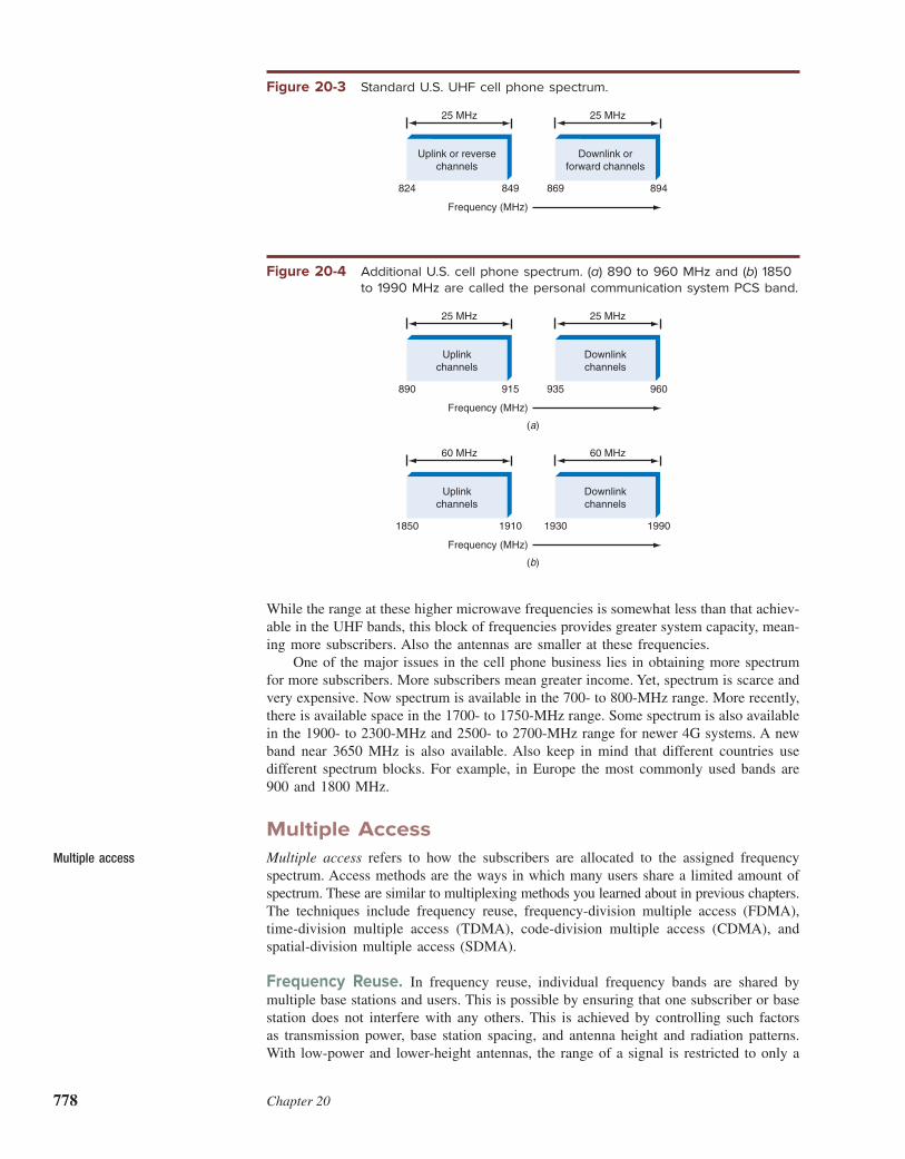
778 Chapter 20
While the range at these higher microwave frequencies is somewhat less than that achiev-able in the UHF bands, this block of frequencies provides greater system capacity, mean-ing more subscribers. Also the antennas are smaller at these frequencies. One of the major issues in the cell phone business lies in obtaining more spectrum for more subscribers. More subscribers mean greater income. Yet, spectrum is scarce and very expensive. Now spectrum is available in the 700- to 800-MHz range. More recently, there is available space in the 1700- to 1750-MHz range. Some spectrum is also available in the 1900- to 2300-MHz and 2500- to 2700-MHz range for newer 4G systems. A new band near 3650 MHz is also available. Also keep in mind that different countries use different spectrum blocks. For example, in Europe the most commonly used bands are 900 and 1800 MHz.
Multiple AccessMultiple access refers to how the subscribers are allocated to the assigned frequency spectrum. Access methods are the ways in which many users share a limited amount of spectrum. These are similar to multiplexing methods you learned about in previous chapters. The techniques include frequency reuse, frequency-division multiple access (FDMA), time-division multiple access (TDMA), code-division multiple access (CDMA), and spatial-division multiple access (SDMA).
Frequency Reuse. In frequency reuse, individual frequency bands are shared by multiple base stations and users. This is possible by ensuring that one subscriber or base station does not interfere with any others. This is achieved by controlling such factors as transmission power, base station spacing, and antenna height and radiation patterns. With low-power and lower-height antennas, the range of a signal is restricted to only a
Multiple access
Figure 20-3 Standard U.S. UHF cell phone spectrum.
25 MHz
Frequency (MHz)
824 849
Uplink or reversechannels
25 MHz
869 894
Downlink orforward channels
Figure 20-4 Additional U.S. cell phone spectrum. (a) 890 to 960 MHz and (b) 1850
to 1990 MHz are called the personal communication system PCS band.
25 MHz
Frequency (MHz)
890 915
Uplinkchannels
25 MHz
935 960
Downlinkchannels
60 MHz
Frequency (MHz)
1850 1910
Uplinkchannels
60 MHz
1930 1990
Downlinkchannels
(a)
(b)

Cell Phone Technologies 779
mile or so. Furthermore, most base stations use sectorized antennas with 1208 radiation patterns that transmit and receive over only a portion of the area they cover. See Fig. 20-5. In any given city, the same frequencies are used over and over simply by keeping cell site base stations isolated from one another.
Frequency-Division Multiple Access. FDMA systems are like frequency- division multiplexing in that they allow many users to share a block of spectrum by simply divid-ing it up into many smaller channels. See Fig. 20-6. Each channel of a band is given an assigned number or is designated by the center frequency of the channel. One subscriber is assigned to each channel. Typical channel widths are 30 kHz, 200 kHz, 1.25 MHz, and 5 MHz. There are usually two similar bands, one for uplink and the other for downlink.
Time-Division Multiple Access. TDMA relies on digital signals and operates on a single channel. Multiple users use different time slots. Because the audio signal is sampled at a rapid rate, the data words can be interleaved into different time slots, as Fig. 20-7 shows. Of the two common TDMA systems in use, one allows three users per frequency channel and the other allows eight users per channel.
Figure 20-5 Horizontal antenna radiation pattern of a common cell site showing
1208 sectors that permit frequency reuse.
Total cellsite coverage
Area coveredin each sector
Cell siteantenna
120°
Figure 20-6 Frequency-division multiple-access (FDMA) spectrum.
Frequency band
Channelcenter
frequencyChannel
bandwidthdepends on
technology used.
(30 kHz, 200 kHz, 1.25 MHz)

780 Chapter 20
Code-Division Multiple Access. CDMA is just another name for spread spectrum. A high percentage of cell phone systems use direct sequence spread spectrum (DSSS). Here the digital audio signals are encoded in a circuit called a vocoder to produce a 13-kbps serial digital compressed voice signal. It is then combined with a higher-frequency chipping signal. One system uses a 1.288-Mbps chipping signal to encode the audio, spreading the signal over a 1.25-MHz channel. See Fig. 20-8. With unique coding, up to 64 subscribers can share a 1.25-MHz channel. A similar technique is used with the
Figure 20-7 Time division multiple access (TDMA). Dif erent callers use dif erent
time slots on the same channel.
Serial voice datafor caller B
Caller A—slot 1
Caller B—slot 2
Caller C—slot 3
Caller A—slot 4
Caller B—slot 5
Caller C—slot 6
Repeat
Timeslot 1 2 3 4 5 6
Time t
XOR
Serial vocoded voice (13 kbps)Exclusive-ORgate performsthe spreading
Chippingsignal1.288 MHz
Pseudorandomcode generator
(PRCG)
Spread signalto modulator
Bandwidth ofvocoded voice
13-kHzband
1.25-MHz band
(a)
(b)
Figure 20-8 Code-division multiple access (CDMA). (a) Spreading the signal.
(b) Resulting bandwidth.

Cell Phone Technologies 781
wideband CDMA system of third-generation cellphones. A 3.84-Mbps chipping rate is used in a 5-MHz channel to accommodate multiple users.
Orthogonal Frequency Division Multiplexing Access (OFDMA). OFDMA is the access method used with OFDM. OFDM uses hundreds, even thousands, of sub-carriers in a wideband channel. This large number of subcarriers can be subdivided into smaller groups, and each group can be assigned to an individual user. In this way, many users can use the wideband channel assigned to the OFDM signal. Fig. 20-9 illustrates the principle. Groups of subcarriers are formed to create a sub-channel assigned to one user. In some systems, the subcarriers do not have to be con-tiguous, but instead might be spread around inside the total OFDM signal bandwidth.
Spatial-Division Multiple Access. This form of access is actually an extension of frequency reuse. It uses highly directional antennas to pinpoint users and reject others on the same frequency. In Fig. 20-10, very narrow antenna beams at the cell site base station are able to lock in on one subscriber but block another while both subscribers
2 3 41One Subcarrier
Subchannels
Frequency
Total OFDM Channel Bandwidth
One Subcarrier Subchannel
1
Subchannel
2Frequency
Total OFDM Channel Bandwidth
Figure 20-9 The Concept of OFDMA.
Figure 20-10 The concept of spatial-division multiple access (SDMA) using highly
directional antennas.
Antenna patterncan be repositionedover full 360°
Cell phoneuser
Antenna transmitsand/or receives onlyover this narrow range
Another cell phoneuser on the samefrequency is ignored

782 Chapter 20
are using the same frequency. Modern antenna technology using adaptive phased arrays is making this possible. Such antennas allow cell phone carriers to expand the number of subscribers by more aggressive frequency reuse because i ner discrimination can be
achieved with the antennas. SDMA is also widely used in wireless local-area networks
(WLANs) and other broadband wireless applications.
DuplexingDuplexing refers to the ways in which two-way radio or telephone conversations are
handled. Many two-way radio applications still use half duplex where one party talks at
a time. The communicating individuals take turns speaking and listening. Telephone
communications has always been full duplex, where both parties can simultaneously send
and receive. All cell phone systems are full duplex.
To achieve full duplex operation, however, special arrangements must be made. The
most common arrangement is called frequency-division duplexing (FDD). In FDD, sep-
arate frequency channels are assigned for the transmit and receive functions. The trans-
mit and receive channels are spaced so that they do not interfere with one another inside
the cell phone or base station circuits. The uplink and downlink channels in Figs. 20-3
and 20-4 are an example.
Another arrangement is time-division duplexing (TDD). This is less common but is
used in a few systems. The system assigns the transmit and receive data to different time
slots, both on the same frequency. For example, the transmitted and received data is
alternated in sequential time slots. While the transmitted and received signals do indeed
occur at different times, the speed of the signals is fast enough that a human feels as
though they are occurring at the same time. The primary benei t of TDD is that only one
channel is needed. With FDD two separated channels are required. A TDD signal uses
half the spectrum of FDD.
Still, FDD is far more widely used than TDD.
20-2 A Cellular Industry OverviewThe cellular telephone industry is one of the largest industries in the world. Also known
as the wireless or mobile business, it generates billions of dollars in revenue each year
for the telephone companies, the cell phone manufacturers, and other allied businesses.
And as you probably know, the cell phone has become the world’s most popular con-
sumer product. Over one billion new cells phones are sold each year. In developed
countries, most consumers already have a cell phone of some type. China is the largest
user of cell phones; the United States in second place in terms of total number of users.
The cell phone is so pervasive that it has greatly affected how we live and work and
how we do business. This section takes a brief look at how the cellular industry functions
and some of the trends and critical issues associated with it.
The Cellular CarriersCentral to the functioning of the mobile wireless business are the cellular carriers, also
known as the network operators. In the United States, there are four major carriers:
AT&T, Verizon, Sprint, and T-Mobile. There are also a number of smaller carriers, but
the four mentioned represent over 90 percent of the business. These are the organiza-
tions that build out the cellular network infrastructure and provide the mobile services.
They are also the ones who offer the cell phones to the consumer. Even though the
carriers do not design or build the cell phones themselves, they are very much a part
of the design process.
The other major players are the cell phone companies themselves. The leaders are
Samsung and Apple; other players include LG, HTC, Nokia/Microsoft, Google/Motorola,
Duplexing
Half duplex
Full duplex
frequency-division duplexing (FDD)
Time-division duplexing (TDD)

Cell Phone Technologies 783
and newer players such as Huawei and Lenovo. These companies design and build the cell phones to the specii cations provided by the carriers.
The reason the carriers have so much inl uence in the phones themselves relates to their frequency-spectrum holdings. Each carrier has access to its own specii c range of frequency bands, and phones must be made to match their holdings. This means that for the most part a cell phone purchased from AT&T will not work on the Verizon network and so on. Another factor is that some carriers use different second- and third-generation technologies that are not compatible from carrier to carrier. Other players in the industry include the software companies that provide the oper-ating systems for the cell phones. The leaders are Google with its Android operating system, Apple with its iOS software, and Microsoft. There are also many companies offering additional software in the form of applications (apps) that give the cell phone far more capability than was ever imagined at i rst. You can actually look at the cell phone as a general-purpose high-power microcomputer with a radio built in. Most of the software apps do not use the radio communications capability. The semiconductor com-panies are also major players. They develop and provide the chips to implement the cell phones and the base station equipment.
The Technology GenerationsThe cellular industry is driven not only by customer demand for service but also by the available technology. In this regard, the cellular industry is one of the fastest changing in existence. New products and services are offered as rapidly as they are conceived and developed. Changes in the technological standards also force rapid changes. The technol-ogy itself is divided into and dei ned by generations. The i rst-generation cell phones used analog technology with frequency modulation. This was rapidly abandoned as it was determined that carriers could not provide enough services to meet the demand. As a result, the i rst generation was quickly replaced with a newer, second-generation (2G) digital cell phone technology. Multiple 2G standards were developed worldwide, yet only two major technologies and standards have survived to this day. These include GSM and the original CDMA. Although 2G technology is still in use today around the world, it is slowly fading away and many carriers have stated their desire to end second-generation services in the near future. This allows them to repurpose their precious spectrum holding for greater sub-scriber capacity and higher data rates. A key factor was the development of data services, which happened during the second generation. Cell phones originally were designed primarily as voice telephones, but it was quickly discovered that it was possible to use them for data purposes. For 2G phones, data rates were slow, thereby limiting the functions to simple applications such as texting and e-mail. Once greater data capabilities were discovered, the demand for higher speeds and more exotic applications developed. This led to the creation of third-generation cell phones. Third-generation (3G) cell phones continued to use standard digital voice tech-niques but also developed high-speed data capability. New modulation and access meth-ods were created and standards were ratii ed. Third-generation phones rapidly became popular, and over a period of several years carriers adopted the new technology and built out their networks. New cell phones were developed to take advantage of the applications potential. During this time, several competing 3G technologies were created. These incompat-ible technologies were adopted by different carriers, making cell phones and the networks incompatible. This ultimately led to the desire for a complete industry standard, which in turn led to the development of fourth-generation phones and systems. The fourth generation (4G) has brought about the creation of a single standard or family of standards that all carriers could adopt. This 4G technology is known as Long Term Evolution (LTE), and it is slowly being adopted in one form or another by all U.S. and worldwide carriers. While most of the major carriers have already converted to the

784 Chapter 20
4G LTE technology, the process is still rolling out across the United States and the progress is widely varied worldwide. The 4G systems and phones have led to much higher data rates and amazing new cell phone capabilities, particularly that of being able to receive and generate video. Technology advances have given us not only the high-speed data capability necessary for video but also large, color touch screens, making the cell phone a more popular consumer product than ever. While most carriers are still implementing 4G LTE systems in the States and in other countries, work is already under way to dei ne the next, i fth generation. The main pur-
pose of 5G is to make the cellular and data services available over a wider range and to
provide even higher data speeds.
Trends and Critical IssuesThe basic trend in the cellular industry is continued growth and technological develop-
ment. In the developing countries, market saturation has already been achieved, meaning
that most individuals already have cell phones and services. This has the effect of reduc-
ing the growth rate, but it still provides an opportunity for consumers to upgrade to
improved phones and services. In addition, substantial growth is still available in other
parts of the world, especially undeveloped countries where telephone service is not typ-
ically available. In many parts of the world, cellular telephone service is the only tele-
phone service available.
Another major trend is the decline in the number of wired telephone customers.
Many consumers have already abandoned their basic wired telephones in favor of using
only cell phones. Today over 50 percent of consumers now use cellular telephones as
their primary communications service and that trend appears to continue.
Another trend is that carriers are continuing to build out their networks and improve
data rates in an effort to reach more consumers and capture more business. Keeping in
step with that, the cell phone manufacturers continue to provide even more sophisticated
and capable cell phones that consumers desire.
As for critical issues, the primary one is frequency spectrum availability. Only cer-
tain parts of the frequency spectrum (roughly 600 MHz to 4 GHz) are useful for cel-
lular service, and this frequency spectrum is already heavily occupied. The ability of a
carrier to continue to offer expanded service capacity as well as higher speeds is deter-
mined strictly by the amount of spectrum available. High capacity and high speed require
wider bandwidth. However, there is only a certain amount of spectrum available, and
most of it is already owned and occupied. Today carriers who want to expand their
operations must buy spectrum from others or purchase it through the regulatory agency,
the Federal Communications Commission (FCC), in their regular auctions. Spectrum
costs billions of dollars, and only the largest of carriers can afford it.
To solve this problem, the FCC has been attempting to free up spectrum from other
spectrum holders, such as the government, the military, and the TV broadcasters. The
TV broadcasters gave up spectrum during the changeover to digital TV in 2009. The
700- to 800-MHz band is now available and is already being used by some of the cel-
lular carriers. Forthcoming is another segment of spectrum in the 600- to 700-MHz range,
which will be auctioned off to the highest bidders. Eventually, higher frequencies are
going to have to be used to achieve improved service and data rates. The 5G standards
are already looking to the millimeter wave bands (28 to 70 GHz) as a potential solution
to the need for increased spectrum holdings.
Another issue is how long older technology should continue to be supported. With
today’s high-speed LTE 4G capability, most voice calls are still handled by the carriers’
2G and 3G switched-circuit networks. Soon these will be phased out in favor of internet
protocol (IP) voice services such as voice over LTE (VoLTE). This has yet to be fully
implemented by the carriers. And few cell phones support it. Yet it is the voice method
of the future. In the meantime, all cell phones, despite the fact they may be 4G LTE
capable, must continue to carry 2G and/or 3G capability to provide voice service.

Cell Phone Technologies 785
20-3 2G and 3G Digital Cell Phone SystemsThe original cellular technology AMPS used FM analog communications. However, today all new cell phones and systems use digital methods. These all-digital systems were developed primarily to expand the capacity of the cell phone systems already in place. The rapid growth of the number of wireless subscribers forced the carriers to seek new and more efi cient methods of increasing the number of users a system could han-
dle. The main problem was that the carriers were restricted by the Federal Communica-
tions Commission to specii c segments of the frequency spectrum. No additional space
was available for expansion. Digital techniques provide several ways to multiplex many
users into the same spectrum space.
The use of digital techniques brought several additional benei ts. Digital communi-
cation systems are inherently more robust than analog systems in that they are more
reliable in a noisy environment. Furthermore, digital circuits can be made smaller and
more power-efi cient, and therefore handsets can be more compact and can operate for
longer times on a single battery charge. In addition, digital cell phones greatly facilitate
the transmission of data as well as voice, so that data services such as e-mail and Inter-
net access are possible with a cell phone. Digital methods also offer high-speed data
capability making video, gaming and social media applications possible.
The i rst digital cell phones are referred to as second-generation (2G) phones. Today,
third- generation (3G) and fourth-generation (4G) cell phones and systems are in use. But
2G phones are still in use in the United States and around the world. The 2G phones will
eventually be phased out. This section covers the 2G systems still in use and describes
the various 3G systems that have mostly replaced 2G technology. 4G phone are discussed
in a separate section.
2G Cell Phone SystemsThree basic second-generation (2G) digital cell phone systems were developed and
deployed. Two use time-division multiplexing, and the third uses spread spectrum (SS)
or CDMA. The TDM systems are the Global System for Mobile Communications (GSM)
and the IS-136 standard for time-division multiple access. The SS system is code-division
multiple access. The IS-136 system was phased out early and replaced with GSM. Both
GSM and CDMA are still widely deployed throughout the world.
Vocoders. To use digital data transmission techniques i rst requires that the voice be
digitized. The circuit that does this is a vocoder, a special type of analog-to-digital (A/D)
converter and digital-to-analog (D/A) converter. With voice frequencies as high as
4 kHz, the minimum Nyquist sampling rate is two times the highest frequency, or 8 kHz.
This means that the A/D converter in a vocoder should sample the voice signal every
125 µs and generate a proportional binary word. Assuming that it is an 8-bit value, during
the 125-µs period, the 8 bits is transmitted serially. This translates to a serial data rate of
125y8 5 15.625 µs/bit, or 1y15.625 3 1026 5 64 kbps. This is how the T1 telephone
system described in Chap. 12 works.
This serial data signal, representing the voice, is now used to modulate the carrier
and the composite signal transmitted over the assigned channel. Recall that the bandwidth
required to transmit a digital signal depends primarily upon the data rate. The higher the
data rate, the wider the bandwidth required. As a rule of thumb, the bandwidth is roughly
equal to the data rate. For example, a 64-kbps signal would require about 64 kHz of
bandwidth. That represents 1 bit /Hz. Different modulation methods result in different
degrees of data rate per bandwidth. Some are more spectrally efi cient than others. A
1-bit/Hz rating is essentially wasteful of precious spectrum space. If the 30-kHz AMPS
channels are to be used to transmit 64-kbps voice, a more efi cient modulation scheme
is needed, or some other technique is required.
Digital cell phone system
2G cell phone system
Vocoder

786 Chapter 20
The main function of a vocoder is data compression. Data compression techniques are used to process the digitized voice signal in such a way as to reduce the number of bits needed to represent the voice reliably. This in turn allows the speed of data transmission to be reduced to a level compatible with that of the available channel bandwidth. In modern cell phones a variety of vocoding data compression schemes are used. An A/D converter is followed by a digital signal processing (DSP) chip that does the compression in accordance with some algorithm. The vocoder then generates a serial digital voice signal at a rate of 7.4 to 13 kbps. This permits three to eight voice signals to occupy the same channel by using TDM. At the receiver, the demodulated digital data is sent to the vocoder, where a DSP chip takes the serial bits and converts them back to binary words representing the voice. A D/A converter then recreates the voice. All 2G and 3G phones contain a vocoder.
GSM. The most widely used 2G digital system is GSM. GSM originally stood for “Group Special Mobile” but has become known as the “Global System for Mobile Communications.” It was developed in Europe under the auspices of the European Telecommunications Standardization Institute (ETSI) to replace the many incompatible analog systems used in different European countries. The GSM was designed to permit widespread roaming from country to country throughout Europe. GSM is implemented primarily in the 900-MHz band in Europe, but is also used in the 1800-MHz (1.8-GHz) range in Europe, where it is referred to as the digital cellular system (DCS), or DCS-1800. GSM is also widely implemented in the United States in both the 800- and 1900-MHz personal communication system band. GSM uses TDMA. The vocoder uses a compression scheme called regular pulse
excitation-linear prediction coding (RPE-LPC) or residual excited linear predictive
(RELP) coding that produces a 13-kbps voice bit stream. It allows eight telephone calls to be transmitted concurrently in a single 200-kHz-wide channel. The modulation method, known as Gaussian minimum shift keying (GMSK), is similar to frequency-shift keying (FSK) but has improved spectral properties that allow higher speeds to be transmitted in a narrower channel. A Gaussian response i lter shapes the serial digital bit stream before
modulation to narrow the signal bandwidth. The basic GSM data rate is 270 kbps in the
200-kHz channel, giving 270 kbps/200 kHz 51.35 bits/Hz. Considerable error detection
and correction coding is used to improve the reliability in the presence of noise, multipath
fading, interference, and Doppler shifts. The basic GSM TDMA frame is shown in
Fig. 20-11. Each frame is 4.615 ms long, and each voice slot is 0.577 ms long. GSM also uses a frequency-hopping scheme to minimize interchannel interference. The hop rate is 217 hops per second, or about 1200 bits per hop. FDD is used for full duplex operation. Two key additions to GSM are general packet radio service (GPRS) and enhanced data rate for GSM evolution (EDGE). These are packet-based data services designed to permit Internet access, e-mail, and other forms of digital data transmission. These tech-nologies are described later under the section 2.5G Cell Phone Systems.
IS-95 CDMA. This TIA cell phone standard is called code-division multiple access (CDMA). Also known as cdmaOne, it uses spread spectrum. This system was invented by Qualcomm, a company that makes the chip sets used in CDMA cell phones. The company
GSM (Global System for Mobile Communications)
Digital cellular system (DCS), or DCS-1800
Regular pulse excitation-linear prediction coding (RPE-LPC) or residual excited linear predictive (RELP) coding
Gaussian minimum shift keying (GMSK)
IS-95 CDMA
GOOD TO KNOWTo estimate the bandwidth neces-
sary to transmit a specifi ed data
rate, use the rule of thumb of a
one-to-one correspondence
between data rate and bandwidth,
for example, 1-Mbps data rate
and 1-MHz bandwidth.
0.577 ms
2 3 4 5
156 bitsper user
4.615 ms (1248 bits)
6 7 8
Timeslot 1
Figure 20-11 A GSM TDMA frame for eight time slots.

Cell Phone Technologies 787
also holds most of the patents in this i eld. CDMA uses direct sequence spread spectrum
(DSSS) with a 1.2288-MHz chipping rate that spreads the signal over a 1.25-MHz channel.
As many as 64 users can use this band simultaneously with little or no interference or
degradation of service, although in practice typically only 10 to 40 subscribers occupy a
channel at one time. This CDMA system uses FDD for duplexing.
As in other cell phone systems, CDMA takes the voice signal and digitizes it in a
vocoder. The output is a 13-kbps serial voice signal that is further processed before it is
used to modulate the carrier. The digitized voice is fed to an exclusive-OR (XOR) gate
where it is mixed with a 64-bit pseudorandom code occurring at the chip rate of
1.2288 Mbps. This signal is then used to modulate the carrier with QPSK. The carrier may
be in the regular 800- to 900-MHz band or in the PCS-1900 band. The resulting signal
occupies a huge bandwidth spread over a wide spectrum. It may also coexist with up to 64
other CDMA signals that use the same carrier but have different pseudorandom codes. These
special codes are known as Walsh codes and are chosen so that they are easily recognized
and recovered at the receiver by using the correlation technique described earlier.
A key part of a CDMA system is APC. All cell phones have APC, but for CDMA it
is especially important. For the receivers to recover a CDMA signal, all incoming signal
levels must be at the same power level. This ensures that the receiver does not confuse a
higher-power signal with a lower-power signal during the de correlation detection process.
The base stations increase the power level of weak distant signals and decrease the power
level of signals near the cell site.
Digital Cell Phone ArchitectureFig. 20-12 is a block diagram of a 2G cell phone. The RF section contains the trans-
mitter and receiver circuits including mixers, local oscillators or frequency synthesiz-
ers for channel selection, the receiver low-noise amplii er (LNA), and the transmitter
power amplii er (PA). The baseband section contains the vocoder with its A/D and
D/A converters plus a DSP chip that handles many processing functions typically
performed by analog circuits in older systems. For example, today most baseband and
intermediate-frequency i ltering is done digitally, as are modulation, demodulation,
and mixing.
An embedded controller handles all the digital control and signaling, handoffs, and
connection and identii cation operations that take place transparent to the subscriber. It
also takes care of running the display and keyboard and all user functions such as num-
ber storage, autodialing, and caller ID. Because of the complexity of the baseband and
control functions, this embedded controller is usually a very fast (more than 100-MHz)
32-bit microprocessor with considerable RAM, ROM, and l ash memory. A separate DSP chip handles the signal processing duties. In addition to adopting digital techniques in 2G and later phones, designers have worked hard to eliminate costly components such as i lters and to create circuitry that conserves power and thereby provides longer battery life. This has led to some interest-ing architectures, especially in the receiver section. Today, the dominant architectures are the direct-conversion and very low-IF designs.
Direct Conversion. The direct-conversion or zero-IF design sets the LO frequency to the incoming signal frequency so that the translation is made directly to the baseband signal. See Fig. 20-13. Because direct conversion works only with double-sideband (DSB) suppressed AM signals, changes have been made to accommodate FSK, BPSK, QPSK, and other forms of digital modulation. Specii cally, the incoming signal is applied to two mixers simultaneously. One mixer receives the LO signal directly (sine), and the other receives a signal shifted 90° (cosine). This results in down conversion to baseband as well as the generation of in-phase (I ) and quadrature (Q) signals that preserve the frequency and phase information in the signal necessary for demodulation. Direct conversion is popular because it eliminates the need for an expensive and physically large selective SAW IF i lter. It also eliminates the imaging problem so
Walsh codes
GOOD TO KNOWCellular phones equipped with a
digital signal processor (DSP) chip
can compress speech to fi t many
digital calls in the same amount
of radio spectrum previously
required for analog calls.

788 Chapter 20
Figure 20-12 Block diagram for a 2G digital cell phone.
Embedded controller
RAM
ROM
Flash
TX
RX
RF
LNA
Keyboard
Speaker Microphone
Antenna switch or duplexer
Vocoder
Mixer
MixerPower amplifier
Frequency synthesizer
Digitalsignal
processor
A/Dconverter
D/Aconverter
Baseband
LCDdisplay
Control
Figure 20-13 A direct-conversion receiver.
Q
I
SAWfilter
Frequency synthesizerLocal oscillator
Low-passfilter
Low-passfilter
LNADigitalsignal
processor
A/Dconverter
A/Dconverter
Baseband
0° (sine)90° (cosine)
common in superheterodyne designs, especially in the crowded multiband cellular spectrum. With direct conversion, baseband i ltering can be accomplished by using
simple low-pass RC i lters and/or DSP i lters. The I and Q signals are digitized, and a
DSP chip performs additional i ltering, demodulation, and voice decoding. Modern IC

Cell Phone Technologies 789
designs have essentially eliminated the LO leakage and dc offset problems ordinarily associated with direct-conversion designs.
Low IF. Another popular alternative is low-IF architecture. When an IF is used near the baseband frequencies, i ltering is simple and very effective. Using an IF near 100 kHz
permits simple RC i lters to be used, eliminating the larger and more expensive SAW
i lters. The low IF design is no longer widely used.
2.5G Cell Phone SystemsThe designation 2.5G refers to a generation of cell phones between the original
second-generation (2G) digital phones and the newer third-generation (3G) phones. The
2.5G phones bring data transmission capability to 2G phones in addition to normal voice
service. A 2.5G phone permits subscribers to exchange e-mails and text messages and access
the Internet by cell phone. Because of the small screen size and a small or very restricted
keyboard, data transmission capability is limited but available to those who need it.
Currently, three technologies are used in 2.5G systems: GPRS, EDGE, and
CDMA2000. Although GPRS and EDGE systems have been implemented, they are gen-
erally considered to be temporary solutions to the need for data transmission capability
in cell phones. True high-speed packet data capability is available with 3G phones. The
CDMA2000 technology is an extension and improvement of the IS-95A/B standard.
GPRS. One popular 2.5G technology is the general packet radio service (GPRS). This
system is designed to work with GSM phones. It uses one or more of the eight TDMA
time slots in a GSM phone system to transmit data rather than digitized voice. Depend-
ing on how many of the eight time slots are used, the data rate can vary from about
20 kbps up to a maximum of 160 kbps. A typical rate is about 40 kbps, which is more
than enough for e-mail and short message service (SMS) but poor for Internet access.
Each GSM frame has eight time slots for data. Refer to Fig. 20-11. The overall bit
rate is 270 kbps. In voice operation, each slot contains the compressed or vocoded voice
signal. In GPRS, other types of data can be transmitted. The data rate that can be achieved
is a function of the type of coding used (FEC) and the number of time slots allotted to the
data. The GPRS standard, which was created by the European Telecommunications Stan-
dards Institute (ETSI), is now maintained by the 3rd Generation Partnership Project (3GPP).
It dei nes four levels of data coding referred to a CS-1 through CS-4. The most robust
coding scheme CS-1 produces fewer errors, but the maximum data speed per slot is 8 kbps.
The least robust coding method is CS-4, but it produces a data rate to 20 kbps. To achieve
maximum data rate, you could use all eight slots for a rate of 8 3 20 kbps 5 160 kbps.
However, this is never done. Instead, GPRS dei nes 12 classes that give different levels of
data speed. The selection of the desired class is made by the cell phone carrier who sets
just how much of the network capacity is devoted to voice and to data.
Class 12 gives downlink and uplink data rates of 80 kbps maximum. The carrier
usually adjusts the class to match its own mix of voice and data users and often charges
the data user on a per-kbps basis. Keep in mind, too, that the GPRS method involves an
automatic rate adjustment algorithm that adjusts the class and data rate to the robustness
of the wireless channel. Over shorter distances with less noise and interference, the
system can achieve the maximum data rate. Over longer distances with added noise, the
system adjusts itself to a lower data rate to ensure accurate transmission of the data.
Virtually all modern GSM phones come with GPRS, but the user must sign up for
services (instant messaging, e-mail, etc.) related to this capability.
EDGE. A faster 2.5G technology is enhanced data rate for GSM evolution (EDGE). It
is based upon the GPRS system but uses 8-PSK modulation instead of GMSK to achieve
even higher data rates up to 384 kbps.
EDGE is sometimes referred to as enhanced GPRS (EGPRS). It is usually
implemented as a software upgrade to the base stations but also requires a linear power
2.5G cell phone system
GPRS (general packet radio service)
EDGE (enhanced data rate for GSM evolution)

790 Chapter 20
amplii er. Both hardware and software changes are needed in a GPRS handset. EDGE
uses the GPRS class concept whereby the data rate is a function of the encoding and
the number of time slots used. By using 3π/8-8PSK modulation, 3 bits is coded per
symbol change, thereby tripling the gross data rate. The theoretical maximum data rate
is 473.6 kbps with all eight slots used. A more typical implementation is the use of four
slots for a data rate of 236.8 kbps. Again, a data rate algorithm automatically backs off
on the rate as channel conditions degrade due to noise or increased distance. Typical
everyday rates are usually over 100 kbps but less than 200 kbps.
One of the key changes required when EDGE is implemented is the need for linear
power amplii ers both at the base station and in the handset. GMSK as used in GSM
and GPRS is a type of FM with a constant envelope (amplitude) carrier that changes in
frequency with the modulation. FM permits more efi cient class C, D, E, and F ampli-
i ers to be used. These amplii ers clip or distort the amplitude of a signal but with FM
that does not interfere with the modulation. When 3π/8-8PSK is used, the envelope does
change as the signal switches from one phase to another. Therefore, to retain the infor-
mation content, the amplitude of the signal must be preserved through amplii cation.
A class AB linear power amplii er must be used. Some base stations already use such amplii ers and so may simply adjust them to maximum linear operation rather than maximum efi ciency. In the handsets, efi cient class C or E/F power amplii ers in the transmitter must be replaced with a class AB linear amplii er. This is a signii cant change in a handset as the lower efi ciency produces greater heat and shortens the battery life.
3G Cell Phone SystemsThird-generation (3G) cell phones are true packet data phones. They feature enhanced digital voice and high-speed data transmission capability. Third-generation phones were originally described by the term International Mobile Telecommunication 2000, or IMT-2000. The 2000 refers to 2000 MHz, the approximate center of the frequency range dei ned for 3G (1800 to 2200 MHz). The goal of the International Telecom-munications Union (ITU) was to dei ne a worldwide standard for future cell phones to which all other systems could evolve, thereby providing full global roaming. An IMT-2000 phone can achieve a data rate up to 2.048 Mbps in a i xed position, 384 kbps in a slow-moving pedestrian environment, and 144 kbps in a fast mobile environment. With such high-speed capability, a 3G phone can do lots more than just transmit high-quality digital voice. Some potential 3G applications include fast e-mail and Internet access. With larger color screens and full keyboards, cell phones can act more as small computer terminals. High speed also permits the transmission of video. Subscribers can watch a movie on their 3G phones, although the small screen limits viewing. In most models, a built-in an image sensor and lens lets cell phones become picture phones and digital cameras.
UMTS 3GThe ITU did not specify a particular technology to implement 3G. However, it did rec-ommend one worldwide version known as wideband CDMA (WCDMA). This system is also known as the Universal Mobile Telecommunications Service (UMTS). While the standard is still based in the ITU, it is developed, maintained, and promoted by the Third Generation Partnership Project (3GPP).
WCDMA. WCDMA is a direct sequence spread spectrum technology. In the most popular coni guration, it is designed to use a 3.84-MHz chipping rate in 5-MHz-wide bands. Duplexing is FDD requiring the matching of 5-MHz channels. The modulation is QPSK. It can achieve a packet data rate up to 2 Mbps. A key problem in implementing 3G is the need for huge portions of spectrum. New spectrum is scarce and expensive. In Europe, paired bands in the 1900- to 2200-MHz
3G cell phone system
International Mobile Telecommunication 2000 (IMT-2000)
Universal Mobile Telecommunica-tions Service (UMTS)

Cell Phone Technologies 791
range are available. In the United States, the 806- to 890-MHz range can be used for 3G in some areas. Some spectrum in the 1710- to 1885-MHz range is also available to some carriers. Also, some segments of the 2500- to 2690-MHz band are available. The exact 3G spectrum varies widely depending on which part of the world you are in, making it extremely difi cult to design a cell phone that is fully operable worldwide.
TD-SCDMA. The UMTS 3G standard also dei nes a TDD version known as
TD-SCDMA for time-division synchronous code-division multiple access. It is designed
to use a 1.6-MHz-wide channel with a chipping rate of 1.28 MHz. Different time slots
in the time-multiplexed data stream are assigned to uplink and downlink activity. The
number of uplink and downlink channels may be dynamically assigned so that a carrier
can adjust the system to the trafi c load at any given time. The primary benei ts of
TD-SCDMA are that less spectrum is needed. Only a single 1.6-MHz channel is needed.
Furthermore, since duplexing is TDD, there is no need for paired spectrum as in WCDMA
or GSM or any other FDD system. The downside is that the system is more complex
because of the extreme need for accurate timing and synchronization required for proper
operation. So far, the only nation to adopt TD-SCDMA as a standard is China.
HSPA. High-speed packet access (HSPA) is an enhancement to WCDMA systems to
make them faster. There is a high-speed downlink packet access (HSDPA) and a high-speed
uplink access (HSUPA) version. They can be used separately or together. Together, they
are referred to as HSPA. When the 3G WCDMA standard was i rst adopted, it was assumed
that it would be put into use far faster than it has. During the past years, wireless technology
has changed, making the original specii cations somewhat behind the times. The maximum
2-Mbps data rate was assumed to be fast enough for any service. But today, the demand
for faster data speeds is growing, especially because of the growing demand for mobile
video service. Because of the need for faster systems, a new system compatible with
WCDMA has been developed. Known as high-speed packet access (HSPA), it provides a
packet data rate from the base station to the handset many times that of the 2-Mbps
maximum rate of WCDMA.
HSDPA uses an adaptive coding and modulation scheme with QPSK and 16-QAM.
Data is transmitted in 2-ms frames. There are 12 categories of HSDPA that dei ne different
coding and modulation schemes. The minimum is category 11,900 kbps using QPSK.
Category 6 gives 3.6 Mbps using 16-QAM. The maximum data rate is 14.4 Mbps using
16-QAM in category 10. The actual rate achieved is a function of the link quality. High noise
and long range give a lower rate. The rate adapts to the channel conditions automatically.
While most data needs will be served by a high-speed downlink capability, in some
applications a fast uplink may be needed. This is accommodated by a companion stan-
dard known as high-speed uplink packet access (HSUPA). A fast handset to base station
rate is more difi cult to implement so uplink rates are naturally slower. HSUPA provides
a maximum data rate of 5.76 Mbps. Again, the rate adapts to the channel conditions.
An enhanced version called HSPA+ is now also available from some carriers. It
permits the use of 64QAM allowing many systems to deliver downlink rates of 21, 28
or 42 Mbps. Although not common there are more advanced versions that use multiple
carriers and MIMO to deliver even higher speeds. For example two or four 5 MHz chan-
nels can be combined to double or quadruple data speeds to 84 or 168 Mbps. Adding
2 3 2 or 4 3 4 MIMO can deliver peak rates in the 336 to 672 Mbps. Today most HSPA systems are still in operation but have been replaced in usage by the newer faster LTE 4G systems.
CDMA2000This standard was developed by Qualcomm. It is an extension of the widely used IS-95 CDMA standard also known as cdmaOne. The earliest versions of this radio system were correctly designated as a 2.5G technology, but subsequent improved versions have clearly made it a 3G technology because of the high data rates it can achieve.
High-speed downlink packet access (HSDPA)
High-speed uplink packet access (HSUPA)

792 Chapter 20
The basic CDMA2000 data transmission method is generally called 13RTT (radio transmission technology). It uses the same 1.25-MHz-wide channels but also changes the modulation and coding formats to actually double the voice capacity over that in IS-95. The data capability is packet-based and permits a data rate of up to 144 kbps, which is comparable to EDGE. A version designated 33RTT uses three 1.25-MHz channels for a total bandwidth of 3.75 MHz. By using a higher chip rate, a maximum date rate roughly three times the 13RTT speed (432 kbps) is possible. The more recent version is called 13EV-DO or Evolution-Data Optimized. It has a higher data rate approaching 3.1 Mbps downlink and an uplink rate up to 1.8 Mbps. Another version known as 13EV-DV for Evolution-Data/Voice has a maximum packet rate of 3.07 Mbps. Uplink speed is the same as that of 13EV-DO. Many carriers still implement CDMA2000, but it is used by the older phones for voice and low-speed data like texting and e-mail. It has been superseded by the newer LTE 4G systems.
20-4 Long Term Evolution and 4G Cellular SystemsLong Term Evolution (LTE) is the wireless cellular technology that is being adopted around the world as the primary cell phone communications service. Multiple 2G and 3G cellular radio methods are heading toward phase-out as carriers build their new LTE networks. It will be years before this expansion is complete, and the older radio tech-nologies like GSM and CDMA will coexist with LTE for a while. In the meantime, the next phase of the LTE standards as put forth by the Third Generation Partnership Project (3GPP) is ready to be deployed. Called LTE-Advanced, it is a signii cant upgrade to the
LTE standard that will provide more speed and greater reliability. Even though LTE-A
is still being developed, it is already in service in some areas. This section is a review
of LTE basics, a look at the features and benei ts of LTE-A, and a glimpse of what 5G
systems may be like.
The Road to LTELTE is a standard developed by the Third Generation Partnership Project (3GPP). This
is the international organization that developed the widely used 3G standards UMTS
WCDMA/HSPA. LTE has been in development for years, and different phases of it have
been released sequentially over the years. The i nal LTE standard designated Release 8
was completed in 2010. Release 9 was an update to that. Release 10 dei nes LTE-
Advanced and is available now.
Over the years, multiple cell phone technologies have been developed. The i rst
generation was analog (FM) technology, which is no longer available. The second gen-
eration (2G) brought digital technology with its benei ts to the industry. Multiple incom-
patible 2G standards were developed. Only two, GSM and IS-95A CDMA, have survived.
The third-generation (3G) standards were created next. Again multiple standards
were developed. Notably the major ones were WCDMA by the 3GPP and CDMA2000
by Qualcomm. Both have survived and are still in use today. The 3G standards were
continually updated into what is known as 3.5G. WCDMA was upgraded to HSPA and
CDMA2000 was expanded with 13RTT EV-DO Releases A and B. Both are still widely
deployed. In fact, in many places around the world, carriers are still adding 3G or upgrad-
ing their 3G systems. In the United States, AT&T and T-Mobile use GSM/WCDMA/
HSPA, whereas Verizon and Sprint use CDMA2000/EV-DO. Sprint implemented a
Section 20-4 is largely derived from the original article “An Introduction to LTE-Advanced: The Real 4G” by Louis E. Frenzel, published by Electronic Design magazine (Penton Media Inc.) in January and February, 2013, www.electronicdesign.com.

Cell Phone Technologies 793
network based on WiMAX, a technology similar to LTE, but is phasing it out. All of these carriers are now offering LTE. LTE came into being as an upgrade to the 3G standards. Its major benei ts were
recognized by the cellular industry and were embraced by virtually all mobile carriers
as the next generation. All cellular operators are now on the path to implementing LTE.
While 3GPP still dei nes LTE as a 3.9G technology, all of the current LTE networks are
marketed at 4G. The real 4G as designated by 3GPP is LTE-Advanced.
Currently LTE is alive and functioning in many U.S. cellular companies and in oth-
ers worldwide. The networks are not fully built out, and most of the older 2G and 3G
systems are still functioning in parallel. Because LTE coverage is not universal, most
cell phones still incorporate 2G and 3G systems for voice in areas where LTE is not yet
fully deployed. LTE-A deployment is a future rollout.
Why LTE? LTE brings amazing new capabilities to the cellular business. First, it
expands the capacity of the carrier, meaning that more subscribers can be added for a
given spectrum assignment. Second, it provides the high data rates that are needed by
the growing new applications, mainly video downloads to smartphones and other Internet
access. And third, it makes cellular connectivity more reliable. All of these needs are
important to maintaining growth and proi tability in the wireless business.
LTE TechnicalitiesLTE is likely the most complex wireless system ever developed. It incorporates features
that could not have been economically implemented even a decade ago. Today, with
large-scale ICs, LTE can easily be accommodated not only in a base station but in a
battery-powered handset. The complexity is a function of the advanced wireless methods
used as well as the many options and features that can be implemented. This section
examines mainly the physical layer of LTE, including modulation, access, duplexing, and
the use of MIMO.
Frequency. LTE operates in some of the existing cellular bands but also newer bands.
Specii c bands have been designated for LTE. These are shown in Table 20-1. Different
carriers use different bands depending upon the country of operation and the nature of
their spectrum holdings. Most LTE phones use two of these bands, and they are not the
same from carrier to carrier. For instance, the iPhone 5 for Verizon uses different bands
than the iPhone 5 from AT&T. Most of the bands are set up for frequency-division
duplexing (FDD), which uses two separate bands for uplink and downlink. Note in
Table 20-1 that bands 33 through 44 are used for time-division duplexing (TDD), and therefore the same frequencies are used for both uplink and downlink.
Bandwidth. LTE is a broadband wireless technology that uses wide channels to achieve the high data rates and accommodate lots of users. The standard is set up to permit band-widths of 1.4, 3, 5, 10, 15, and 20 MHz. The carrier selects the bandwidth depending on spectrum holdings as well as the type of service to be offered. The 5- and 10-MHz widths are the most common. Some bandwidths cannot be used in different bands.
Modulation. LTE uses the popular orthogonal frequency-division multiplex (OFDM) modulation scheme. It provides the essential spectral efi ciency to achieve the high data rates but also permits multiple users to share a common channel. The OFDM technique divides a given channel into many narrower subcarriers. The spacing is such that the subcarriers are orthogonal—that is, they will not interfere with one another despite the lack of guard bands between them. This comes about by having the subcarrier spacing equal to the reciprocal of symbol time. All subcarriers have a complete number of sine wave cycles that upon demodulation will sum to zero. In LTE the channel spacing is 15 kHz. The symbol period therefore is 1/15 kHz 5 66.7 µs. The high-speed serial data to be transmitted is divided up into multiple slower streams, and each is used to modulate one of the subcarriers. For example, in a 5-MHz

794 Chapter 20
Table 20-1 LTE Bands
LTE Band Number Uplink (MHz) Downlink (MHz)
1 1920–1980 2110–2170
2 1850– 1910 1930–1990
3 1710–1785 1805–1880
4 1710–1755 2110–2155
5 824–849 869–894
6 830–840 875–885
7 2500–2570 2620–2690
8 880–915 925–960
9 1749.9–1784.9 1844.9–1879.9
10 1710–1770 2110–2170
11 1427.9–1452.9 1475.9–1500.9
12 698–716 728–746
13 777–787 746–756
14 788–798 758–768
15 1900–1920 2600–2620
16 2010–2025 2585–2600
17 704–716 734–746
18 815–830 860–875
19 830–845 875–890
20 832–862 791–821
21 1447.9–1462.9 1495.9–1510.9
22 3410–3500 3510–3600
23 2000–2020 2180–2200
24 1625.9–1660.9 1525–1559
(Continued)

Cell Phone Technologies 795
25 1850–1915 1930–1995
26 859–894 814–849
27 852–869 807–824
28 758–803 703–748
33 1900–1920 1900–1920
34 2010–2025 2010–2025
35 1850–1910 1850–1910
36 1930–1990 1930–1990
37 1910–1930 1910–1930
38 2570–2620 2570–2620
39 1880–1920 1880–1920
40 2300–2400 2300–2400
41 2496–2690 2496–2690
42 3400–3600 3400–3600
43 3600–3800 3600–3800
44 703–803 703–803
Note: These cellular bands are allocated specii cally for LTE. Different carriers in different countries use different bands
that are unique to their cell phones. The spacing between FDD channels in bands 1 through 28 varies considerably
depending upon carrier spectrum holdings. Bands 33 through 44 have the same uplink and downlink frequencies as these
are TDD bands.
channel, up to 333 subcarriers could be used but the actual number is less like 300.
A 20-MHz channel might use 1024 subcarriers. The modulation on each can be QPSK, 16QAM, or 64QAM, depending on the speed needs. Fig. 20-14 shows how OFDM uses both frequency and time to spread the data, providing not only high speeds but also greater signal reliability. For each subcarrier, the data is sent in sequential symbols where each symbol represents multiple bits (e.g., QPSK, 2 bits; 16QAM, 4 bits; and 64QAM, 6 bits.) The basic data rate through a 15-kHz subcarrier channel is 15 kb/s. With higher-level modulation, higher data rates are possible. Data to be transmitted is allocated to one or more resource blocks. A resource block (RB) is a segment of the OFDM spectrum that is 12 subcarriers wide for a total of 180 kHz. There are seven time segments per subcarrier for a duration of 0.5 ms. Data is then transmitted in packets or frames, and a standard frame contains twenty 0.5-ms time slots. A resource block is the minimum basic building block of a transmission, and most transmissions require many RBs.

796 Chapter 20
Keep in mind the fact that the only practical way to implement OFDM is to do it in software. The basic process is handled with the fast Fourier transform (FFT). The transmitter uses the inverse FFT, while the receiver uses the FFT. The algorithms are implemented in a digital signal processor (DSP), an FPGA, or an ASIC designed for the process. The usual techniques of scrambling and adding forward error correcting codes are implemented as well. The choice of OFDM for LTE is primarily due to its lesser sensitivity to multipath effects. At the higher microwave frequencies, transmitted signals can take multiple paths to the receiver. The direct path is the best and preferred, but signals may be rel ected by mul-tiple objects, creating new signals that reach the receiver somewhat later in time. Depending upon the number of rel ected signals, and their strengths, ranges, and other factors, the signals at the receiver may add in a destructive way, creating fading or signal dropout. The multipath effects occur when the signals reach the receiver all within the time for one symbol period. Remember, a symbol is a modulation state that is either an amplitude, a phase, or amplitude-phase combination that representing two or more bits. If the multipath effects are such that the signals arrive at the receiver spread over several symbol periods, the outcome is called intersymbol interference (ISI). The result is bit errors. This can be overcome with error detecting and correcting codes, but these codes add to the complexity of the system. An equalizer at the receiver that collects all the received signals and delays them such that they all add can also correct for this problem but only further complicates the process. Spreading the signals in the form of multiple subcarriers over a wide bandwidth lessens these effects. This is especially true if the symbol rate of each subcarrier is longer, as it is in OFDM. If the multipath effects occur in less than one symbol period, then no equalizer is needed. Another effect is frequency variation of the subcarriers at the receiver caused by time or frequency shifts, such as that produced by the Doppler effect in a moving vehicle. This shift in frequency results in the loss of orthogonality and subsequently in bit errors. This problem is mitigated in LTE by adding a cyclical prei x (CP) to each transmitted bit sequence. The CP is a portion of an OFDM symbol created during the DSP process that is copied and added back to the front of the symbol. This bit of redundancy allows the
Figure 20-14 Data is transmitted by dividing it into slower parallel paths that
modulate multiple subcarriers in the assigned channel. The data
is transmitted in segments of one symbol per segment over each
subcarrier.
Subcarrier
spacing
15 kHz
Frequency
One resource black (180 kHz)LTE channel
Seven OFDM symbols
(0.5 ms)
Time

Cell Phone Technologies 797
receiver to recover the symbol if the time dispersion is shorter than the cyclical prei x.
This allows OFDM to be implemented without the complex equalization that can also
correct for this problem.
While the downlink of LTE uses OFDM, the uplink uses a different modulation
scheme, known as single carrier-frequency division multiplexing (SC-FDMA). OFDM
signals have a high peak-to-average-power ratio (PAPR), requiring a linear power
amplii er with overall low efi ciency. This is a poor quality for a handset that is battery
operated. SC-FDMA has a lower PAPR and is better suited to portable implementation.
The SC-FDMA process is complex, and a detailed discussion of it is not included here.
MIMO. A key feature of LTE is the incorporation multiple input multiple output
(MIMO), a method of using two or more antennas and related receive and transmit cir-
cuitry to achieve higher speeds within a given channel. One common arrangement is
2 3 2 MIMO, where the i rst number indicates the number of transmit antennas and the second number is the number of receive antennas. Standard LTE can accommodate up to a 4 3 4 arrangement. The MIMO technique divides the serial data to be transmitted into separate data streams that are then transmitted simultaneously over the same channel. Because all signal path are different, with special processing they can be recognized and separated at the receiver. The result is an increase in the overall data rate by a factor related to the number of antennas. This technique also mitigates the multipath problem and adds to the signal reliability because of the diversity of reception. A special version of MIMO known as multi-user MIMO is being implemented in some cellular systems as well as in some Wi-Fi systems. It allows multiple users to share a common channel. MU-MIMO relies upon many antennas implementing spatial division multiple access (SDMA) as well as unique channel coding to keep the signals separate. Channel bandwidth is divided amongst the users as needed. The difi cultly in implementing MIMO arises because of the small size of the hand-set and its limited space for antennas. Already most smartphones contain i ve antennas, including those for all the different cellular bands plus Wi-Fi, Bluetooth, GPS, and per-haps NFC. It is not likely that most phones will contain more than two LTE MIMO antennas, and their inclusion depends on being able to space them far enough apart so that spatial diversity is preserved with sufi cient isolation between them. Of course, it is easier to use more base station antennas. A typical LTE arrangement appears to be 4 3 2 to provide optimal coverage with the space available.
Data Rate. The data rate actually used or achieved with LTE is dependent upon several features, as you have seen. It depends on channel bandwidth, modulation type, MIMO coni guration, and of course the quality of the wireless path. In the worst-case situation, data rate could be only a few Mbps, but under good conditions data rate can rise to over 300 Mbps. On average, most practical LTE downlink rates are in the 5- to 15-Mbps range. This is faster than some i xed Internet access services using cable or DSL.
Access. Access refers to using the same channel to accommodate more than one user. This is effectively a multiplexing method. Standard methods include frequency-division multiple access (FDMA), time-division multiple access (TDMA), and code-division mul-tiple access (CDMA). OFDMA makes use of some of the available subcarriers and time slots within those subcarriers for each user. The number of subcarriers and time slots used depends on multiple factors. In any case, it is usually possible to accommodate up to hundreds of users per channel bandwidth.
TD-LTEMost LTE will be of the FDD variety, at least in the United States, Europe, and parts of Asia. Paired-spectrum groups are required for the separate uplink and downlink transmissions. TD-LTE requires only a single spectrum segment. TD-LTE is being widely

798 Chapter 20
implemented in China and India because of the more limited spectrum availability. This conserves spectrum and provides for more users per MHz. The LTE standards include a dei nition for TD-LTE. It is expected that some U.S. carriers, including Sprint, will use
TD-LTE.
LTE AdvancedLTE-A builds on the LTE OFDM/MIMO architecture to further increase data rate. It is
dei ned in 3GPP Releases 10 and 11. There are i ve major features: carrier aggregation,
increased MIMO, coordinated multipoint transmission, Hetnet (small cells) support, and
relays. Small cells are covered in the next section.
Carrier aggregation refers to the use of two or more 20-MHz channels combined into
one to increase data speed. Up to i ve 20-MHz channels can be combined. These channels
can be contiguous or noncontiguous as dei ned by the carrier’s spectrum assignments. With
maximum MIMO assignments, 64QAM, and 100 MHz bandwidth, a peak downlink data
rate of 1 Gbps can be achieved.
LTE dei nes MIMO coni gurations up to 4 3 4. With LTE-A that is extended to 8 3 8 with support for two transmit antennas in the handset. Most LTE handsets use two receive antennas and one transmit antenna. These MIMO additions will provide future data-speed increases if adopted. HetNet support refers to support for small cells in a larger overall heterogeneous network. The HetNet is an amalgamation of standard macro cell base stations plus micro-cells, metrocells, picocells, femto cells, and even Wi-Fi hot spots. This network provides increased coverage in a given area to improve connection reliability and increased data rates. Small cells are covered in the next section. Coordinated multipoint transmission is also known as co-operative MIMO. It is a set of techniques using different forms of MIMO and beamforming to improve the per-formance at cell edges. It makes use of coordinated scheduling and transmitters and antennas that are not collocated to provide greater spatial diversity that can improve link reliability and data rate. Relays is the use of repeater stations to help coverage in selected areas, especially indoors where most calls are initiated. LTE-A dei nes another base station type called a relay station. It is not a complete base station but a type of small cell that will i t in the HetNet infrastructure and provide a way to boost data rates and improve the depend-ability of a wireless link. Some deployment of LTE-A occurred in late 2013 with increasing adoption in 2014 and beyond. LTE-A is forward and backward compatible with basic LTE, meaning that an LTE handset will work on an LTE-A network and an LTE-A handset will work on a standard LTE network.
LTE-A ChallengesLTE solves many problems in providing high-speed wireless service. There is no better method, at least for now. However, it does pose multiple serious design and deployment issues. The greatest problem to overcome is the necessity of having to use multiple bands that often are widely spaced from one another. As a result, this requires multiple antennas, multiple power amplii ers, multiple i lters, switching circuits, and sometimes complex impedance matching solutions in the base stations as well as the phones themselves. Each cellular operator specii es cellphones for their spectrum. In addition, the power amplii ers (PAs) must be very linear if error vector mag-nitude (EVM) is to be within specii cations for the various multilevel modulation methods used. Linear amplii ers are inefi cient, and because of this they are the biggest consumer of power in the phone except for the touch screen. The need to cover mul-tiple bands necessitates the use of multiple PAs. Battery life in an LTE phone is typically shorter as a result. The need to include MIMO also means additional anten-nas and PAs.

Cell Phone Technologies 799
Solutions to these problems lie in more-efi cient power amplii ers and fewer of them.
Also, wider-bandwidth antennas solve the multiband problem. Tunable antennas are also
being designed by several companies to cover multiple bands with a single structure.
Another challenge is testing. Testing LTE systems with MIMO is a particularly com-
plex process. Luckily a number of test equipment companies have created systems for this
purpose. One of the greatest challenges is testing the higher-level MIMO coni gurations.
LTE-A permits up to 8 3 8 MIMO.
Voice over LTELTE is a packet-based IP data network. Initially LTE did not include a voice service.
However, LTE voice is now being implemented. Today, if you are using an LTE smart-
phone, you may still be using the existing 2G or 3G network for what is called circuit-
switched voice service. Eventually voice over LTE (VoLTE) will be fully implemented
in the base stations and in the handsets. VoLTE is just VoIP over LTE, and it will oper-
ate simply as a data application on the IP network.
Although a VoLTE protocol has been dei ned, implementing it requires major engi-
neering decisions and network changes. Most of these concern maintaining voice con-
nections for older non-LTE phones for some extended period. Particularly tricky are the
changes that will allow LTE phone users to get voice service if they move out of an area
with no LTE. When VoLTE is available, a subscriber could initiate a call using the LTE
system but drive out of the LTE coverage area. Systems must be able to hand that call
off to a traditional voice network. The mechanism for this is network software called
circuit-switched fallback (CSFB). It is now available on most networks. Another issue is
getting VoLTE into the handsets. VoLTE requires a separate chip in the phone, and few
have such a capability today.
Implementing VoIP requires a vocoder, a circuit that is essentially an A-to-D converter
to digitize the voice signal and a D-to-A converter to convert the digital voice back into
analog voice for the user. A vocoder also incorporates voice compression, a technique that
effectively minimizes the number of bits used to represent voice. This allows voice to be
transmitted faster but at lower data rates so it does not occupy much bandwidth.
LTE uses what is called the Adaptive Multi-Rate (AMR) vocoder. This is also used in
GSM systems and other 3GPP standards. It has a variable bit rate capability from 1.8 kbps
to 12.2 kbps. Digitized voice is then assembled into AMR packets and then into IP pack-
ets, which are then scheduled into transmission sequence. A call is allocated some of the
OFDMA subcarriers and some of the time slots within the bit streams of each subcarrier.
Smartphone AnalysisThe most sophisticated cell phone available today is called a smart phone. It incorpo-
rates LTE and a wide range of other wireless technologies. Chances are that you
already own smartphone. Here is a brief analysis of what’s inside the typical modern
smart phone.
Refer to the block diagram of a typical smart phone as shown in Fig. 20-15. Most
cell phones today are no longer just two-way radios for making phone calls. Instead, at
the core of the smart phone is a dual processor or quad processor microcomputer that
implements all of the various functions. Today’s smart phone is in reality a general-
purpose microcomputer that just happens to have cell phone with other communications
capabilities built in. The available computing power available has enabled the develop-
ment of a wide range of software applications (apps). These apps give the smart phone
capability far beyond its original function.
Color Touch Screens. The prominent feature of every smart phone today is its large
color screen. These high-resolution displays are made with different technologies, such as
LCD or OLED. All of them today are touch screens, meaning that all controls such as but-
tons, keyboards, and other operational tools are operated by pressing or swiping the screen.

800 Chapter 20
Figure 20-15 Block diagram of a generic 4G LTE smart phone.
LTE
XCVR
Touch
screen
LCD/OLED
color
screen
Power
management
regulators
Battery
charger
Camera
circuits
Keyboard
Battery
Lens
CCD
XCVR-transceiver ROM
DRAM
Flash
Driver
MIMO
Stereo headphones
Microphone
Speakers
MIMO
UMTS
WCDMA
XCVR
Bluetooth
XCVR
GPS
RX
Wi-Fi
XCVR
NFC
XCVR
Dual or
quad p
rocessors
with inte
rfa
ce
s
Cameras. Most cell phones and most smart phones contain a digital camera. These cameras use a CCD or CMOS light sensor and a lens to capture a scene and store it in l ash memory. These cameras have resolutions from 5 to 40 megapixels, therefore rival-ing stand-alone cameras. Many of the cameras are accompanied by an LED l ash. While these cameras are primarily for still photos, most are capable of recording real-time video. Many smart phones also have a second, front-facing camera for making video phone calls and taking seli es.
Radio Modems. Virtually all smart phones today contain LTE 4G technology. The newer phones use a two-antenna MIMO arrangement. The phone also usually contains a 2G and/or 3G radio for voice calls as well as backward capability for calls in a region without LTE service.

Cell Phone Technologies 801
Bluetooth. Bluetooth is a short-range radio technology to be discussed in the next section. However, its primary function in most cell phones is to implement a wireless headset and microphone. The Bluetooth radio can also be used with iBeacon technol-ogy that allows cell phones to read nearby information tags and Bluetooth location devices. It could also possibly be used with cashless payment systems that replace credit cards. Bluetooth is also used as a connecting device for smart watches, a wear-able accessory to many smart phones. The smart watch provides call, text, or e-mail alerts, time, and other information without taking the smartphone out of your pocket or purse. See Fig. 20-16.
Wi-Fi. Wi-Fi is the wireless local area network (WLAN) technology widely used throughout the world to implement Internet connections. Virtually all smart phones con-tain a Wi-Fi transceiver, and many include two antennas for MIMO. The Wi-Fi capabil-ity permits smart phones to connect to any available access point or hot spot, including wireless routers that are part of many home broadband Internet connections today. Wi-Fi is covered in Chap. 21.
GPS. Another radio inside of most smart phones is a GPS receiver. This gives the smart phone navigation capability. The smart phone is usually accompanied by map-ping software that provides vivid visual displays of maps tied to the GPS navigation satellites.
NFC. NFC is near i eld communications, another short-range radio technology built in
to some smart phones. It is used in payment systems that eliminate cash and credit cards.
NFC is not in all cell phones.
Functional Features. In addition to being able to make a phone call to any other
phone anywhere in the world, all smart phones have Internet access. The operating system
software includes a browser to allows you to access the Internet just as you would from
a desktop PC or laptop. The only disadvantage is the small screen.
Figure 20-16 The Samsung Gear smart watch communicates with a smart phone
with Bluetooth wireless technology.

802 Chapter 20
Another common feature is e-mail. Since you can access the Internet, you can eas-ily access your regular e-mail account from any location. Texting is another common feature that is used more often than e-mail. Music playback is a part of all smart phones. Virtually all smart phones have the ability to store songs and music videos in compressed form for playback on built-in speakers or through headphones. One of the most popular features of modern smart phones is the ability to play videos. Thanks to digital compression technology, video presentation is very common. By way of an Internet connection, you can watch videos from multiple sources, such as Google, YouTube, Netl ix, Hulu, and other video sources for movies and other short subjects. Another application that is possible thanks to video a and high-resolution display is games. There are literally thousands of games available for smart phones today, and these are widely used. All of these features are possible because of the internal processing power. Most smart phones contain a processor that contains two cores, each core being a full 32-bit microcontroller. Some phones also have larger quad core processors, and many incorpo-rate 64-bit processing power as well as 32-bit processing power. These multiple proces-sors implement the DSP required of most phones today. All cell phones are software-dei ned radios, and virtually all of the modulation, demodulation, encoding, decoding, voice and video compression, and other functions are handled by the processors. The processors also run the operating system and any applications software that is added later. The processors are usually accompanied by standard DRAM and l ash memory. A variety of special serial and parallel interfaces are provided to connect to the display, cameras, and other peripherals.
Battery and Charger. A key part of every cell phone is the battery power supply and its power management hardware. The lithium-ion battery operates a whole array of multiple voltage regulators and DC-DC converters that supply all of the different operating voltages to the ICs, interfaces, and peripheral devices. The power manage-ment system also shuts down unneeded circuits, such as the display, when they are not in use. In addition, all phones include a battery charger. The battery charger operates from an external AC power source. Some newer phones include wireless battery charging. This system uses magnetic induction to connect the cell phone to its charger. Both the charger and the cell phone have built-in coils that serve as windings on a transformer. By putting the coils close together, transformer action transfers the AC power from the charger to the charging circuitry inside the cell phone by magnetic induction, so that no wire connection is needed.
What Is 5G?It will take a decade or more for LTE and especially LTE-A to dominate in cellular coverage. Furthermore, new LTE releases from 3GPP are yet to come. In addition, some provisions of current LTE releases have yet to be implemented. An example is self-organizing networks (SONs), a feature that makes networks easier to plan, coni gure, optimize, and manage. With a SON, all base stations would be self-coni guring, taking into account nearby base stations and using internal algorithms to heal, self-optimize, and adapt to new nearby stations and other conditions. The small-cell movement to be discussed in the next section is dei nitely LTE-based, and extensive deployment with SON is yet to come. In the meantime, research continues with what is the i fth generation (5G) of cel-lular wireless. It is possible that 5G will simply stay on the same path as 4G and LTE—that is, that 5G will use higher frequencies and wider bandwidths to achieve even higher

Cell Phone Technologies 803
data rates. With semiconductor technology still viable at ever smaller IC feature sizes, operation well into the hundreds of GHz is possible. Already, advanced millimeter wave (30- to 300-GHz) systems are functioning with advanced chip sets in short-range personal area networks (PANs) for home video transfer (60 GHz), automotive radar (77 GHz), and cellular/hot spot backhaul (80 GHz). Some think the 28-GHz and 38-GHz spectrum segments offer good opportunities for cellular. Because of the higher frequencies, range is shorter, meaning that there are more but smaller cell sites. However, by using higher-level MIMO, higher-gain antenna arrays and beamforming, coverage will be reliable and the available bandwidth will permit download data rates as high as 10 Gbps. In summary, 5G will most likely be many small cells operating in one or more millimeter wave bands using smart, steerable, high-gain antennas.
20-5 Base Stations and Small CellsBase stations, also called cell sites or macro cells, form the heart of the cellular network. They implement all radio connectivity and operational and control functions and connect to the carrier’s telephone network as well as the Internet by way of backhaul equipment. A key trend today is the incorporation of small cells to complement the existing base stations to improve coverage and data speeds.
Base StationsThe most complex and expensive part of any cellular telephone system is the network of base stations that carriers must have to make it all work. Over the years, carriers have added many more base stations to handle the constantly growing number of subscribers. In addition, each base station has expanded and become more complex because of the growing number and variety of radio standards it must handle. Base stations must con-tinue to support 2G technologies, 2.5G enhancements, and now 3G systems. Support for multiple standards has led to considerably more equipment. An effort has been made by base station manufacturers to consolidate the equipment by using software-dei ned radio
techniques and DSP. These methods permit the base station receivers to accommodate
existing multiple standards and to be able to work with new standards by reprogramming
rather than replacing equipment.
Base stations consist of multiple receivers and transmitters so that many calls can
be handled on many different channels simultaneously. The transmitters in the cell site
are much more powerful than those in the handsets. Power levels up to 40 W are typical.
These power levels are achieved with highly linear broadband class A or class AB power
amplii ers. Since LTE and CDMA systems require linear amplii cation, base stations are
using digital pre-distortion (DPD) and envelope tracking (ET) to improve efi ciency.
Superior linearity is critical, especially in CDMA and LTE systems that cover a broad
spectrum. Nonlinearities produce intermodulation and spurious signals that can make a
system inoperable.
The most visible feature of a base station, of course, is its antenna on a tower.
The antennas used by base stations must serve many transmitters and receivers by
means of isolators, combiners, and splitters. Base station antennas have become direc-
tional rather omnidirectional, as the cell patterns suggest. This “sectorization” of the
cell site has helped to increase subscriber capacity with minimal cost. Most base sta-
tions use a triangular antenna array that looks like the one shown in Fig. 20-17. On
Section 20-5 is largely derived from the original article “Understanding the Small Cell and Het Net Movement,” by Louis E. Frenzel, published by Electronic Design magazine (Penton Media Inc.) in September and October, 2013, www.electronicdesign.com.

804 Chapter 20
each side of the triangular frame is an array of three vertical antennas forming a broadside or collinear array that may also use rel ectors. Each of the three arrays produces a gain of about 8 dB and an antenna pattern with a beam width of 120°. This divides the cell coverage into three equal sectors. See Fig. 20-18. This directional capability provides excellent isolation of the three sectors, which in turn permits the same channel frequencies to be used in each of three 120° sectors. Some sites also use two supplementary antennas that provide spatial diversity, which greatly improves the reception of weak signals from the handset. Carriers are beginning to use more sophis-ticated “smart” beam-forming antennas with more elements, arrays, and sectors to further improve capacity. A key trend is packaging all the RF transmit and receive circuitry, including power amplii ers, into a small housing that is mounted at the antennas at the top of the tower. These are called remote radio heads (RRHs). They eliminate the long, expensive, and
Figure 20-17 Typical triangular cell site antenna.
Top view
Triangular
mounting frame
Antenna elementsAntenna elements
Top view
Triangular antenna
Sector 3
Sector 2
Beam width of each
sector is 120�
Sector 1
Figure 20-18 Horizontal radiation and reception pattern of a typical cell site
antenna.

Cell Phone Technologies 805
high-loss transmission lines, thereby greatly improving base station power efi ciency. The
base station equipment is connected to the RRH by way of a digital i ber interface called
the Common Public Radio Interface (CPRI).
Small Cells and HetNet RationaleA small cell is a miniature cellular basestation with limited power and range. Its function
is to complement the larger macro basestations now the most common form of cell site.
This permits greater subscriber capacity as well as higher data speeds for all concerned.
Small cells are a growing trend that is expected to have its greatest impact in the future.
Currently, cell phone trafi c is handled by a huge network of cell sites called macro
basestations (BS). With their high power, tall towers with multiple antenna arrays, long
range, and backup power sources, these macro BS cover most of the United States except
for some very rural and geographically challenged areas. There are nearly 300,000 such
basestations in the United States. It is getting increasingly more difi cult to i nd and
secure suitable locations for such BS. The solution is the small cell.
In addition, the success of the smartphone and the growing subscriber demand for
more and faster service are putting the pressure on cellular carriers to expand and
upgrade their BS deployments. The carriers’ response has been to upgrade their systems
with the 4G LTE technology that offers signii cantly faster download speeds demanded
by the major increase in video consumption. LTE is still being installed with full cov-
erage not expected for several more years. One clear solution is the LTE small cell.
While the adoption of LTE will boost capacity and speed, limits are being reached.
The OFDM of LTE along with advanced modulation methods and MIMO have pushed
the spectral efi ciency (bits/Hz/Hz) of the cellular system to the Shannon limit. LTE
Advanced will improve speeds by providing more bandwidth through carrier aggrega-
tion. The ultimate limit is the spectrum available to the carrier. Again small cells and
frequency reuse can provide an interim solution until more spectrum is freed up.
Another major issue is indoor performance of cell phones. It has been shown that
over 80 percent or all cell phone calls are carried out indoors, in homes, ofi ces, shopping
malls, hotels and other venues. Indoor performance is signii cantly poorer than outdoor
performance as the radio signals are seriously attenuated, distorted and redirected by
walls, ceilings, l oors, furniture and other obstacles. Indoor situations limit the range of the radio and furthermore greatly curtails data speeds. LTE is helpful in overcoming this problem, but the real solution is the small cell. As it turns out, public and private Wi-Fi hotspots and access points i t the basic dei nition of a small cell. They can connect to a user smartphone, tablet, or laptop and provide access to the video and other information and media demanded by the user. You don’t have to use the cellular network to download video or access other big data applications if a Wi-Fi hotspot is nearby. Most cellular small cells will include a Wi-Fi access point. Groups of physically small cells can be installed anywhere, indoors or out. They can sit on a desk or be mounted on a wall, roof, lamp post or light pole. The small cells i ll in the gaps in coverage and provide service where macrocell coverage is poor. In high density population, cities with tall buildings are examples. It is estimated there will be from 5 to 25 small cells per macro cell in most networks. Networks of small cells overlay, or as some say underlay, the macro network to provide an overall boost not only in data speeds but also subscriber capacity. The general customer performance is greatly improved with more reliable connections and signii cantly higher download speeds. Another piece of the small cell trend is distributed antenna systems (DAS). DAS uses i ber optic cable from a macro BS to an array of antennas spread over a wide area to extend the reach and improve connection reliability. It is used in large buildings, airports, convention centers, sports complexes, and other large public venues. The collection of macro BS, small cells, Wi-Fi hotspots, and DAS is now referred to as heterogeneous network or HetNet.

806 Chapter 20
All small cells with use the existing licensed spectrum assigned to the carrier’s networks. The limited spectrum is shared by the method of frequency reuse and spatial diversity. Frequency reuse refers to the use of the same band by multiple cell sites. Spatial diversity means that these sites are spaced from one another so that coverage areas do not overlap and power levels are controlled to eliminate or minimize interference to adjacent cells and those on the same frequency.
Small Cells Defi nedThere are several different sizes and versions of small cells. They vary in the number of users they can handle, their power and range. In virtually all cases, they all include the essential 3G technologies of the carrier, LTE and Wi-Fi. They have a power source and a backhaul connection to the cellular network. Table 20-2 shows the general names and capabilities of each major classii cation.
The smallest is the femto cell. A femtocell is a single box BS used by the consumer
or small ofi ces to improve local cellular service. Femtos have been around for years,
and millions have been installed by most of the larger carriers. Backhaul is by way of
the customer’s high-speed Internet connection via a cable TV or DSL telecom provider.
There are also enterprise femtos that handle more users and provide a signii cant boost
in indoor accessibility.
There are progressively larger small cells such as the picocell, microcell, and metro-
cell, each with increasing capacity, power and range. Virtually all handle legacy 3G, LTE
and include Wi-Fi. Many of the future small cells will also feature LTE-Advanced, the
faster version of this 4G technology. See Table 20-2 for details.
Inside the Small CellA small cell is still a cellular basestation but boiled down to only a few key chips and
circuits. Thanks to super fast multicore processors, most 3G and LTE baseband operations
are easily handled by a single IC. This baseband IC is then connected to the RF circuitry
making up the radio transceiver. A general block diagram is shown in Fig. 20-19.
Table 20-2 A Summary of the Main Categories of Licensed Small Cells with their Defi ning Characteristics
Femto Pico Micro/Metro Macro
Indoor/outdoor Indoor Indoor or outdoor Outdoor Outdoor
Number of users 4–16 32–100 200 200–1000+
Max output power 20–100 mW 250 mW 2–10 W 40–100 W
Max cell radius 10–50 m 200 m 2 km 10–40 km
Bandwidth 10 MHz 20 MHz 20, 40 MHz 60–75 MHz
Technology 3G/4G/Wi-Fi 3G/4G/Wi-Fi 3G/4G/Wi- Fi 3G/4G
MIMO 2 3 2 2 3 2 4 3 4 4 3 4
Backhaul DSL, cable, i ber Microwave, mm Fiber, microwave Fiber, microwave

Cell Phone Technologies 807
The RF transceiver called the analog front-end consists of the receiver (RX) and transmitter (TX). The receiver gets its signal from the antenna amplii es it in a low noise
amplii er (LNA) and sends the signal to I/Q mixers forming a demodulator that recovers
the signal. The signals are passed to analog-to-digital converters (ADCs) that create the
input to the digital front-end processor.
Between the RF front-end and the baseband processor is additional circuitry that
performs decimation, digital upconversion (DUC), and digital downconversion (DDC).
Other digital processing includes crest factor reduction (CFR), digital predistortion
(DPD) and envelope tracking (ET). DPD and ET are used for linearization of the RF
power amplii ers to improve efi ciency. All this circuitry may be in a separate ASIC or
FPGA or may be included in the baseband chip or front-end RF circuitry.
The baseband processor creates the digital I/Q signals for the transmitter. These go
to digital-to-analog converters (DACs) in the analog front-end that produce the analog
equivalent signals. These are sent to I/Q mixers that form a modulator. The modulator
output is then sent to one or more power amplii ers (PAs) and then to the antenna.
The baseband processor has both multiple standard CPUs and digital signal proces-
sors (DSP) and handles all the modulation and demodulation and other process involved
with the various cellular standards. The I/O to the backhaul is typically by Ethernet.
Power comes from a power over Ethernet (PoE) connection if available or by some
other source.
Fig. 20-20 shows an example of single chip analog front-end. This is the
MAX2580 by Maxim Integrated. It contains the I/Q modulator and demodulator as
well as their fractional-N frequency synthesizers for channel selection. The multiple
circuits support 2 3 2 MIMO. The synthesizers cover all LTE bands 1 to 41 and
provide for bandwidth selection from 1.4 MHz to 20 MHz. The ADCs and DACs are
included on chip. The digital interfaces to the baseband processor are the JESD207.
The receiver section contains the LNAs however additional external LNAs could be
added if necessary. The transmitter output amplii ers provide 0 dBm. If more power
is needed external power amplii ers can be added. Maxim makes a wide range of
other RF circuits including the MAX2550-MAX2553 3G femtocell transceivers for
CDMA systems.
The baseband functions in a base station or small cell is implemented by a single
chip containing multiple processors, memory, logic and interface circuits. An example
from Texas Instruments is the KeyStone line these processors contain a mix of ARM
A15 RISC processors as well as TIs C66x DSPs. One typical unit is the TCI6630K2L
Figure 20-19 This general block diagram of a small cell indicates that it is essen-
tially a multicore baseband digital processor connected to the analog
RF front-end made up of the transmitter and receiver. Backhaul is
usually via Ethernet.
Switching/
duplexing
Multicore
baseband
processor
Antenna
Power
LNA
AC
PoE
Backhaul
Analog
I/Q signals
Power
amplifier
Analog
front end
Ethernet
RX
TX
Digital
front end
(DDC, DUC, CFR,
DPD, ET, etc.)
Wi-Fi

808 Chapter 20
shown in Fig. 20-21. It contains two ARM cores and four C66x DSPs. It also contains multiple logic accelerators to speed up operations, minimize the number of cores and reduce power consumption. This chip also includes the digital front-end circuits like DUC/DDC/DPD/CFR. Multiple interfaces include the JESD240B, PCIe, SPI, USB, and a gigabit Ethernet switch. Finally, most small cells will generally contain Wi-Fi and GPS. Power will come from Power over Ethernet (PoE) plus a mix of DC-DC converters and regulators. Most power is consumed by the RF power amplii ers and the baseband processor SoC.
Figure 20-20 The Maxim Integrated MAX2580 RF transceiver features two full radios to implement 2 3 2 MIMO.
Clock
generation
PLL
ADC
ADC
RXINHB2
RXOUT
RXCLK
RXFRM
CS
DIN
CLK
DOUT
TXIN
TXCLK
TXFRM
REF Clock
TCXO
30.72 MHz
15.36 MHz
19.2 MHz
RXINLB2
RXINHB1
RXINLB1
TXOUTHB2
TXOUTLB2
TXOUTHB1
TXOUTLB1
IQ
RX channel 2
IQ
RX channel 1
IQ
TX channel 2
IQ
TX channel 1
12
2
2
12
2
2
12
12
12
12R
X d
ata
JE
SD
207
TX
data
JE
SD
20
7
SPIControl logic
AUX ADC
AUX DAC
TEMP
AFC DAC
DAC
DAC
RX synthesizer
TX synthesizer
MAX2580

Cell Phone Technologies 809
Timing and SynchronizationA key requirement of all LTE basestations, macro or small cell, is timing and synchro-nization of all the radios in the network. Timing and synchronization is essential to achieve the specii cations of the Third Generation Partnership Project (3GPP), the
organization establishing the LTE standards. The timing and synchronizations is imple-
mented by delivering a formatted clock signal to the radio circuits of the base station.
These signals are then used to create the phase and frequency components of the LTE
modulation. Timing and synchronization is also essential for proper handoff and back-
haul coordination.
Several timing and synchronization methods have been developed including syn-
chronous Ethernet (SyncE) or G.8262 by the ITU and the IEEE’s Precision Time
Protocol (PTP) 1588–2008. The latter seems to be the preferred method, but both are
used. The PTP can be delivered with a grandmaster clock in the form of a time stamp
over the packet network. An alternative is Network Time Protocol (NTP) that is
designed to synchronize clock to some time reference over a variable latency data
network.
The timing requirements for implementing LTE in the network are severe. The typ-
ical clock precision required is 16 parts per billion (ppb) in the transport network and
50 ppb in the air interface. For TDD and Advanced versions of LTE, the phase require-
ments are also critical. In addition, the method of backhaul will vary with different types
C66x DSP C66x DSPARM A15
1MB L21MB L2
per C66x Core
Multicore shared
memory controller
2MB L3
DDR3/3L 72b-1333
System
services
Power
manager
Debug
NAND USB3 SPI PCIe 1GbE
JESD2048
EMIF and IO High-speed serDes lanes
Security accelerationPac
Radio accelerationPac
Dig. radioFront endBit rate
28 nm
Packet accelerationPac
1G Ethernet switch
Air and IP
USIM
UART GPIO CPRI/OBSAII2C
System
monitor
EDMA
PktDMA
ARM A15 C66x DSP C66x DSP
011100100010001111
Tera
Net
Multicore Navigator
Figure 20-21 The Texas Instruments TCi6630K2L is a small-cell baseband processor with two ARM CPUs and four
C66x DSPs, plus accelerators, the digital front-end components, and multiple interfaces including a
gigabit Ethernet switch.

810 Chapter 20
of small cells. Many will use microwave, others will use i ber and in residential femtos
DSL or cable TV provide the backhaul. Different timing schemes are needed to optimize
the performance.
The LTE Advanced small cells to come also have strict timing and synchroniza-
tion requirements to implement the key features of enhanced inter-cell interference
coordination (eICIC) and coordinated multipoint transmission/reception (CoMP)
both a type of interference management technology required for self-organizing networks (SON).
Wi-Fi Ol oad
The concept of Wi-Fi ofl oad is simple. It is the formal use of available hotspots and access points to carry the high-speed data relieving the cellular network of that burden. Since all smartphones have Wi-Fi, it is possible to create a system that automatically selects Wi-Fi for a fast download if a hot spot is nearby. While a subscriber could voluntarily access the data with Wi-Fi, he or she may not be aware of a useable hotspot. By ofl oading the cellular system, that network can handle more users with high-speed data needs that cannot be addressed with Wi-Fi. Today, the users can automatically ofl oad the network themselves by actively seeking an available hotspot to avoid the cost of using the cellular network. Otherwise, an automatic carrier-driven approach can be implemented to make the ofl oad work seamlessly when a user access a high-volume download. While the ultimate solution is to roll out a small cell underlay to increase capacity and coverage, Wi-Fi offers an immediate solution to the demand for faster downloads. Since high-speed trafi c like video is growing faster than the carriers can implement a full small cell system, Wi-Fi offers a fast and inexpensive way to deal with the problem. To make this work, several things must happen. First, cellular operators will have to partner with existing Wi-Fi providers in their coverage areas. Alternately, the cellular operators will need to build out their own Wi-Fi networks. Many have already constructed their own Wi-Fi networks to ensure the desired coverage. Wi-Fi networks are signii cantly less expensive to install than cellular base stations, including small cells. And they are usually faster than most even 4G networks. These cellular operator Wi-Fi networks are referred to as carrier-grade networks Second, some mechanism is needed to initiate an automatic selection of Wi-Fi vs. cellular network when a subscriber attempts to access some source of video or other big data. A subscriber’s smartphone or tablet will seek out the available networks then select the best option mostly favoring Wi-Fi if it is available. It has been estimated that up to 50 percent of cellular data trafi c will eventually be ofl oaded to Wi-Fi giving carriers time to roll out more small cells, expand their LTE networks, or add new spectrum while minimizing capital expenditures (CAPEX). The mechanism for this is now available in the form of the Wi-Fi Alliance’s Hotspot 2.0 and the IEEE 802.11u standard. First, 802.11u is a relatively recent enhancement to the 802.11 WLAN standards. It enables Wi-Fi to work with other networks including cellular networks. The enhancement essentially automates the connection between a smartphone, tablet or laptop to different Wi-Fi networks. It replaces the process of discovering nearby hotspots, entering passwords, performing authentication, and con-necting. Next, Hotspot 2.0 is an addition to the basic standard that uses 802.11u to automate access point discovery, registration, and provisioning and connection. This not only enables roaming between hotspots but also provides a mechanism to link to cel-lular networks to perform automated handoff between the cellular network and available Wi-Fi hotspots. Virtually all 3G/4G small cells will also include carrier-grade Wi-Fi either in the same enclosure or in an adjacent box. Furthermore, the newer cell phone models will incorporate Hotspot 2.0/802.11u to make the ofl oad option function. And no doubt the cellular operators see the ofl oad strategy as a way to buy time until more wireless spec-trum is available or as funds are available to acquire it. Wi-Fi is covered in Chap. 21.

Cell Phone Technologies 811
BackhaulBackhaul is the name of the connection of a cell site to the core network. Older original base stations used T1 or T2 lines, but today most macro BS in the United States use i ber optic
cable. Some in harder to reach areas use a microwave link. Fiber is preferred, of course, as
it is fast and reliable. However, it is costly to install as it requires access to property, digging
in the ground, or permission to use power poles. Microwave is simply line of sight (LOS)
point and shoot wireless. It is not as fast but that limitation is gradually going away with the
new systems. With most microwave links, a data capacity up to 1 Gb/s is usually available.
Small cell backhaul will most likely be a mix of i ber and wireless. If i ber is avail-
able and affordable it will be used. Otherwise, a wireless link will be the backhaul of
choice.
Small cell backhaul will sometimes be tricky. With small cells on lamp posts, sides
of buildings and in other odd locations, i ber or even AC power may be hard to come
by. A wireless link may be the only choice. And even that could be a challenge in large
cities with tall buildings and other structures blocking most paths back to the core net-
work. Multiple hop links may be used in some instances.
The most popular wireless backhaul frequencies are 6, 11, 18, and 23 GHz. These
frequencies require a license to use, and equipment is generally expensive. However,
other potential bands are the 60 GHz band and 70/80 GHz E-band. The 80 GHz band
does also require a license, but the 60 GHz band does not. The 60 GHz band (57-64
GHz) is an industrial-scientii c-medical (ISM) band that is open to any service.
The millimeter wave bands above 30 GHz offer lots of bandwidth to support higher
data rates; their range is severely limited by the physics of their short wavelength. However,
with high gain directional antennas and higher power, ranges can extend to several kilome-
ters. Just recently the FCC modii ed the Part 15 rules and regulations to permit higher power
and antenna gains in the 60 GHz band to make it more useful for small cell backhaul.
Fig. 20-22 shows one kind of small cell backhaul unit. It mounts next to the small
cell enclosure.
Self-Organizing NetworksSelf-organizing networks (SON) are a software solution to managing a HetNet. While
the interaction between macrocells is usually managed manually, with multiple small
cells such a manual task is overwhelming. With SON, the HetNet will essentially manage
Figure 20-22 The Ceragon FibeAir IP-20C is typical of the small-cell backhaul units
available. This one packages the radio, interfaces, and dish antenna
into a single unit and is available in standard licensed band frequen-
cies from 6 to 42 GHz. Typical data rate is 1 Gbps in a single Ethernet
channel. It uses 2048 QAM.
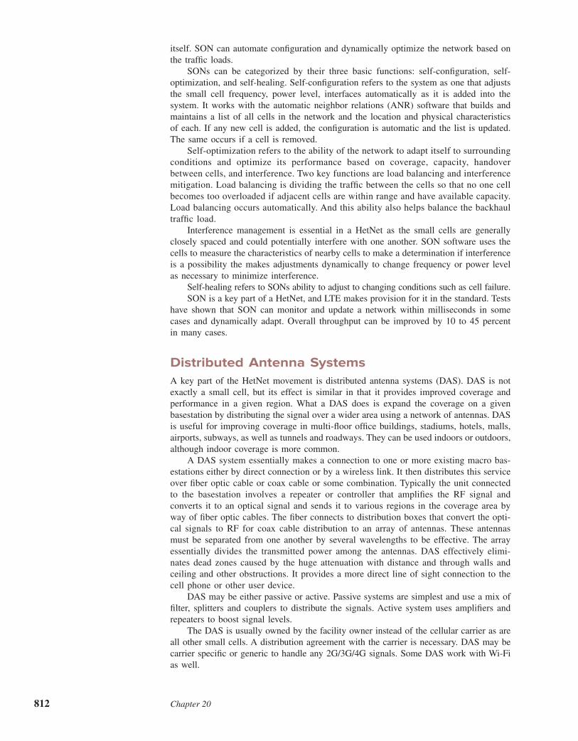
812 Chapter 20
itself. SON can automate coni guration and dynamically optimize the network based on
the trafi c loads.
SONs can be categorized by their three basic functions: self-coni guration, self-
optimization, and self-healing. Self-coni guration refers to the system as one that adjusts
the small cell frequency, power level, interfaces automatically as it is added into the
system. It works with the automatic neighbor relations (ANR) software that builds and
maintains a list of all cells in the network and the location and physical characteristics
of each. If any new cell is added, the coni guration is automatic and the list is updated.
The same occurs if a cell is removed.
Self-optimization refers to the ability of the network to adapt itself to surrounding
conditions and optimize its performance based on coverage, capacity, handover
between cells, and interference. Two key functions are load balancing and interference
mitigation. Load balancing is dividing the trafi c between the cells so that no one cell
becomes too overloaded if adjacent cells are within range and have available capacity.
Load balancing occurs automatically. And this ability also helps balance the backhaul
trafi c load.
Interference management is essential in a HetNet as the small cells are generally
closely spaced and could potentially interfere with one another. SON software uses the
cells to measure the characteristics of nearby cells to make a determination if interference
is a possibility the makes adjustments dynamically to change frequency or power level
as necessary to minimize interference.
Self-healing refers to SONs ability to adjust to changing conditions such as cell failure.
SON is a key part of a HetNet, and LTE makes provision for it in the standard. Tests
have shown that SON can monitor and update a network within milliseconds in some
cases and dynamically adapt. Overall throughput can be improved by 10 to 45 percent
in many cases.
Distributed Antenna SystemsA key part of the HetNet movement is distributed antenna systems (DAS). DAS is not
exactly a small cell, but its effect is similar in that it provides improved coverage and
performance in a given region. What a DAS does is expand the coverage on a given
basestation by distributing the signal over a wider area using a network of antennas. DAS
is useful for improving coverage in multi-l oor ofi ce buildings, stadiums, hotels, malls, airports, subways, as well as tunnels and roadways. They can be used indoors or outdoors, although indoor coverage is more common. A DAS system essentially makes a connection to one or more existing macro bas-estations either by direct connection or by a wireless link. It then distributes this service over i ber optic cable or coax cable or some combination. Typically the unit connected to the basestation involves a repeater or controller that amplii es the RF signal and converts it to an optical signal and sends it to various regions in the coverage area by way of i ber optic cables. The i ber connects to distribution boxes that convert the opti-cal signals to RF for coax cable distribution to an array of antennas. These antennas must be separated from one another by several wavelengths to be effective. The array essentially divides the transmitted power among the antennas. DAS effectively elimi-nates dead zones caused by the huge attenuation with distance and through walls and ceiling and other obstructions. It provides a more direct line of sight connection to the cell phone or other user device. DAS may be either passive or active. Passive systems are simplest and use a mix of i lter, splitters and couplers to distribute the signals. Active system uses amplii ers and repeaters to boost signal levels. The DAS is usually owned by the facility owner instead of the cellular carrier as are all other small cells. A distribution agreement with the carrier is necessary. DAS may be carrier specii c or generic to handle any 2G/3G/4G signals. Some DAS work with Wi-Fi as well.

Cell Phone Technologies 813
CHAPTER REVIEWOnline Activity
20-1 Investigate the SIM Card
Objective: To determine the presence and function of a SIM card in a cell phone.
Procedure: 1. Search on the term SIM as it relates to cell phones. 2. Answer the following questions.
Questions: 1. What does SIM stand for? 2. Where in the cell phone is the SIM card? 3. Do all cell phones have a SIM card? 4. What circuitry is on a SIM card? 5. Can SIM cards be used to reconi gure a cell phone from
one user to another?
20-2 Explore the Remote Radio Head Concept
Objective: To determine the benei ts and specii cations of a
remote radio head.
Procedure: 1. Search on the terms remote radio head, RRH, CPRI,
and similar terms.
2. Answer the following questions.
Questions: 1. What is an RRH?
2. What is inside an RRH?
3. Where is the RRH located?
4. How is DC power connected?
5. Dei ne CPRI.
6. What are the specii cations of CPRI?
20-3 Investigate the base station
Objective: Explore the Terminology of Cellular Base
Stations
Procedure: 1. Search on the terms base station, cell site, Node B,
eNode B, and RAN.
2. Answer the following questions.
Questions: 1. Dei ne Node B.
2. Dei ne eNode B.
3. Dei ne RAN.
4. Which of the above is associated with LTE?
Questions
1. What key communication technology is referred to
when the term wireless is used?
2. What is the current latest generation of cell phone tech-
nology?
3. Name the two main frequency bands used for cell
phones in the United States.
4. What primary characteristic determines cell site range
of coverage?
5. What segment of the frequency spectrum is used mostly
by the cellular industry? State approximate upper and
lower ranges.
6. Name i ve access methods used in cellular systems.
7. True or false? Cellular telephone radios operate full
duplex.
8. True or false? Cell site coverage areas are not all the
same size.
9. Name the four major U.S. cellular carriers.
10. True or false? There are more wire line telephone sub-
scribers than cellular subscribers.
11. What major challenge keeps carriers from expanding
their capacity and data speed?
12. What one application has forced cellular data rates to
increase?
13. What is the primary radio technology of 3G phones?
14. Which type of duplexing is the most widely used?
15. What circuit in the cellular telephone allows a transmit-
ter and receiver to share an antenna?
16. What is the benei t of TDD over FDD?
17. State the relationship between data rate and bandwidth
as it applies to the cellular system.
18. What technique allows multiple base stations to share a
common channel?
19. What is a vocoder?
20. List the two primary 2G digital cell phone systems used
worldwide. Which is the most widely used?
21. Name the two primary functions of a vocoder.
22. What unit of measure is used to determine the spectral
efi ciency of a modulation scheme?

814 Chapter 20
23. What is the bandwidth of a GSM channel? 24. How many users can share a channel in GSM? 25. True or false? GSM uses TDMA. 26. What modulation is used in GSM? 27. What type of multiuser access is available in IS-95
CDMA and WCDMA? 28. What is the bandwidth of a typical CDMA and
WCDMA channel? State the maximum number of sub-scribers that can use the channel.
29. What feature of CDMA is critical to its success in reception?
30. By what method is a CDMA channelized? 31. What two receiver architectures are common in most
modern 2G cell phones? State why they are preferred over the older superheterodyne architectures.
32. Why is the I/Q circuit arrangement used in cell phones? 33. List four functions typically performed by a DSP chip
in the baseband part of a cell phone. 34. At what point in most receivers are the A/D converters
placed? 35. Describe the basic antenna structure of a typical cell
site base station. 36. Describe the antenna radiation pattern and explain how
it permits sectorization. 37. How does the antenna permit frequency reuse? 38. What types of amplii ers are used in base stations?
What is their power level?
39. Why is power amplii er linearity so important?
40. Is CDMA2000 a 2G or 3G technology? Explain. Who
developed it?
41. What are the names of the fastest versions of
CDMA2000? What are their maximum data rates?
42. Name the technology that makes WCDMA faster.
What modulation methods are used?
43. True or false? A WCDMA 3G handset can communi-
cate with a CDMA2000 base station.
44. What is the maximum data rate of the most common
form of HSPA, and what modulation is used?
45. Name the U.S. carriers that use GSM/GPRS/EDGE
and WCDMA/HSPA.
46. Name the U.S. carriers that use CDMA2000.
47. What antenna technology permits increased subscriber
growth on existing base stations?
48. What is the name of the latest cell phone technology
that is marketed as 4G?
49. What modulation methods are used with 4G cell
phones?
50. Dei ne the term resource block and give its specii cations.
51. Does LTE use FDD or TDD?
52. Will an LTE phone from AT&T work on the Verizon
network? Explain.
53. What is the maximum LTE channel bandwidth? What
other bandwidths are popular?
54. What feature of LTE compensates for multipath and
Doppler shift problems?
55. What is the maximum MIMO coni guration for LTE?
for LTE-A?
56. What limits the MIMO coni guration in a smart phone?
What is the maximum practical?
57. What is the approximate maximum data rate of LTE?
What rate is more typical?
58. What access method is used with LTE? How does it
work?
59. How does LTE-Advanced implement data rates to
1 Gbps? 60. What is a remote radio head? What are its benei ts? 61. Do LTE phones have 3G or 2G technology? 62. List at least i ve different radios used in smart phones. 63. How are voice calls handled in the typical 3G or 4G
cell phone? 64. How are voice calls handled in LTE? 65. What is a HetNet? 66. Name four basic small-cell sizes and their specii cations. 67. What is a macrocell? 68. How do small cells improve the cellular network? 69. What techniques make small cells feasible? 70. What is backhaul? What are the most common types? 71. What is Wi-Fi ofl oad, and why is it benei cial? 72. What is an alternative to an array of small cells to
improve cellular coverage? 73. What are expected to be the three basic technical fea-
tures or specii cations of 5G cellular technology?
1. Compute the spectral efi ciency of modulation that gives a data rate of 2.4 Mbps in a bandwidth of 1.5 MHz. ◆
2. Without any special modulation methods, approxi-mately what bandwidth is needed to transmit a data rate of 1.2 Mbps?
3. How many GSM channels can exist in the spectrum of Fig. 20-4(b)?
4. How many LTE resource blocks i t into a 20-MHz channel?
5. What is the bandwidth of an LTE subcarrier? 6. What is the maximum number of users on a femtocell?
◆ Answers to Selected Problems follow Chap. 22.
Problems

815
chapter 21
Introduction
The most prevalent wireless technology is that associated with cell phones
as described in Chap. 20. However, there are many more wireless systems
and applications in common use today. These are primarily short-range
systems that have a range of a few inches up to several miles, depending
upon the application. This chapter describes the more widely used of
these popular systems. Each is generally defi ned by a specifi c industry
standard and is identifi ed with one or at least a few well-known applica-
tions. These popular technologies and their main applications are sum-
marized in the table below. Note that each technology is identifi ed by its
Wireless Technologies
Wireless Technology Primary Applications
Wi-Fi 802.11 Wireless Ethernet LAN
Bluetooth Short-range wireless primarily for audio
ZigBee 802.15.4 Home/industrial monitoring and control
Ultrawideband (UWB) High speed and short range for computer
peripherals and video connections
WiMAX 802.16 MAN broadband wireless
Radio-frequency ID (RFID) Wireless bar code for tracking and ID
Near-i eld communications (NFC) Ultrashort-range for smart cards and ID
Industrial scientii c medical (ISM) Mixed-use unlicensed short-range telemetry
and control
Infrared (IR) Optical wireless for control and data
White space radio Wireless telemetry and control and Internet
access?
The following sections describe each of these technologies in greater detail.

816 Chapter 21
Figure 21-1 Range versus data rate: common wireless technologies.
100 km
10 km
1 km
100 m
10 m
1 m
WCDMA
with
HSDPA
GSM/EDGE
EV-DO
ISM
RFID
NFC
ZigBee
802.15.14
WiMAX 802.16
LTE/LTE-A
Data rate
UWB
1 Gbit/s 10 Gbit/s100 Mbit/s10 Mbit/s1 Mbit/s100 kbps10 kbps
Bluetooth
802.15.3
Wi-Fi
802.11b/gWi-Fi
802.11n
Wi-Fi
802.11ac/ad
Infrared (IR)
trade name or standard designation. common name or an IEEE standard
number. In Fig. 21-1, the technologies are compared by both data rate and
range. As you can see, some of the technologies overlap in their coverage.
There is a wireless system that fi ts virtually every need.
Objectives
After completing this chapter, you will be able to:
■ Defi ne personal-area network (PAN) and wireless local area network
(WLAN).
■ Name two popular PAN technologies.
■ Identify the features, benefi ts, applications, and operation of the
wireless technologies Wi-Fi, Bluetooth, ZigBee, WiMAX, and
ultrawideband (UWB).
■ Explain the operation and applications of the wireless technologies
RFID, NFC, and IR.
■ Explain White Space radio.
■ Defi ne the Internet of Things (IoT) and machine-to-machine (M2M)
wireless.

Wireless Technologies 817
21-1 Wireless LANWireless LANs are more commonly referred to by their trade name Wi-Fi. The terms Wi-Fi, WLAN, and 802.11 are used interchangeability in this text. Local-area networks (LANs) within a company, government agency, hospital, or other organization typically use CAT5 or CAT6 unshielded twisted pair as the transport medium. However, more and more, wireless extensions to these LANs are becoming popular as are entirely wireless LANs. Low-cost wireless modems installed in personal computers and laptops make this possible. Three common coni gurations are shown in Fig. 21-2. Fig. 21-2(a)
shows a wireless access point (AP) is connected to an existing wired LAN, usually
through an Ethernet switch. This AP contains a transceiver that can cover a specii c
geographic area, usually inside a building. This area usually extends out to no more than
about 100 m, but generally the range is less due to the great signal attenuation of the
walls, ceilings, l oors, and other obstructions. PCs or laptops within that range and containing a radio modem can link up with the AP, which in turn connects the PC or laptop to the main LAN and any services generally available via that LAN such as e-mail and Internet access. Another popular coni guration is shown in Fig. 21-2(b). Here the AP is connected to the main LAN or more commonly to an Internet service provider (ISP) by way of a long-range interconnection such as a hardwired T1 or T3 line, i ber connection, or a microwave relay link such as WiMAX, as described later in this chapter. The AP is usu-ally installed in a restaurant, coffee shop, airport, hotel, convention center, or other public place. It is more commonly known as a “hot spot.” Some cities are also installing municipal hot spots. Anyone with a laptop equipped with a LAN modem interface can link up to the AP and access his or her e-mail or the Internet. There are hundreds of thousands of hot spots around the world. What makes the wireless LAN so appealing is that it offers l exibility, convenience, and lower costs. To add a node to an existing wired LAN, the main problem is the new wiring. If such wiring is not in place already, it is time-consuming and expensive to pull cables through walls and ceilings and to install connectors. Moving computers within a building because of ofi ce reconi guration is a huge problem and expense unless existing wiring can be reused. By using a wireless extension such problems essentially disappear. Any computer can be located at any new point quickly and easily at no additional cost. As long as the computer is within the range of the AP, the connection is automatic. Wireless is a great way to expand an existing network. Wireless LANs also serve our continuing need to be more mobile in our jobs and activities. The cell phone has given us freedom to maintain communications anywhere, at any time, and virtually in any place. The wireless LAN also gives us that same por-tability for our computers, mainly laptops, which have essentially become the de facto PC form factor. Within an organization, a user can take her or his laptop to the conference room for a meeting, to a colleague’s ofi ce, or to the cafeteria for lunch. And with all the available hot spots, we can use our laptops almost anywhere, especially while we are traveling. Another growing use of wireless LANs is in the implementation of home networks. See Fig. 21-2(c). As more and more families become users of multiple PCs, tablets, and smart phones, there is a need to interconnect each device to a broadband Internet connection such as a DSL or cable TV line. It allows each user to access e-mail or the Internet or to share a common peripheral such as a printer. Most home-owners do not want to wire their homes with CAT5/6 cable at great expense. Install-ing a wireless LAN is fast, easy, and very inexpensive these days. A special box called a residential gateway or wireless router connects to the cable TV or DSL and serves as the access point. This gateway or router uses a software approach called network address translation (NAT) to make it appear as if each networked PC has its own Internet address, when in reality only the one associated with the incoming broadband line is used.
Network address translation (NAT)

818 Chapter 21
Figure 21-2 Types of WLANs. (a) Access point extension to a wired LAN. (b) Public access point via an Internet
service provider (ISP), and (c) home router for Internet access.
Laptop
Laptops or tablets
Microwave
linkTo ISP
Wireless
AP
T1 Line
Ethernet
switch
PCWireless
AP
(a)
(b)
LAN CAT 5/6 cable
Laptops or tablets
Cable TV or DSL line to ISP
Wireless
router
(c)
Hardware of Wireless LANsThe hardware devices in a wireless LAN are the access point or the gateway/router and the radio modems in the PCs. The access point is just a box containing a transceiver that

Wireless Technologies 819
interfaces to an existing LAN by way of CAT5/6 wiring. It typically gets its dc operating power via the twisted-pair cabling, because the dc supply voltage is superimposed on the data. The IEEE 802.3af standard related to furnishing dc power over the network cable is referred to as Power over Ethernet (PoE). The AP is usually mounted high on a wall or ceiling to give good coverage to a specii c area. The antenna may be built into
the box or may be a separate array that gives directionality to the AP to ensure coverage
of a desired area and minimum interference to other nearby WLANs.
In a home network, the gateway or router is designed to attach to the DSL or cable
TV modem with CAT5/6 cable. It often attaches to one of the PCs in the home network
by cable. The other PCs link to the gateway/router wirelessly.
The radio modems for each PC take many forms. All are transceivers with an
accompanying antenna. The transceivers are usually a single chip in most of the newer
systems. In the older systems, the modem is contained on a plug-in card for the PC/PCI
bus. Today, it is more common to have the radio modem built into the PC motherboard.
For laptops and tablets, the modem is built in, so no special installation is needed.
Wireless LAN StandardsOver the years, a number of wireless LAN methods have been developed, tested, and
abandoned. One standard has emerged as the most l exible, affordable, and reliable. Known as the IEEE 802.11 standard, it is available in multiple forms for different needs. The table shows the different versions of the standard and some technical details.
Power over ethernet (PoE)
IEEE Standard Frequency,
GHz Access Max. Data Rate,
MbpsMax.
Range, m
802.11a 5 OFDM 54 50
802.11b 2.4 DSSS 11 100
802.11g 2.4 OFDM 54 100
802.11n 2.4/5 OFDM/MIMO 600 100
802.11ac 5 OFDM/MIMO 1.3 50–100
802.11ad 60 OFDM/beamforming 7 10
IEEE 802.11b. The earliest useful and most widely adopted version of the 802.11 standard is 802.11b. It operates in 11 channels in the 2.4-GHz unlicensed ISM band. This band extends from 2.4 to 2.4835 MHz for a total bandwidth of 83.5 MHz. The center frequencies of each channel are given below.
Channel Center Frequency, GHz
1 2.412
2 2.417
3 2.422
4 2.427
5 2.432
6 2.437
7 2.442
8 2.447
9 2.452
10 2.457
11 2.462
Note that the channels are spaced 5 MHz apart over the spectrum. However, each channel is 22 MHz wide so that the channels overlap. Any given AP uses one of these channels.
GOOD TO KNOWThe Institute of Electrical and
Electronic Engineers (IEEE) sets
the wireless standards for WLAN,
but the Wi-Fi Alliance supports,
promotes, tests, and certifi es the
interoperability of chips, modules,
access points, and other products.
The Alliance also develops
enhancements to the standards.
Wi-Fi is the offi cial trademark for
the 802.11 standard.

820 Chapter 21
The access method is direct sequence spread spectrum (DSSS) so that multiple signals may share the same band. Channel assignments are critical in facilities where multiple WLANs exist, so that interference is minimized. The 802.11b standard specii es a maximum data rate to 11 Mbps. This rate is achieved only under the most favorable path conditions such as minimum range and minimum noise. Increasing range or noise causes the rate to automatically drop off to 5.5, 2, or 1 Mbps. This helps ensure a reliable connection despite the lower speed. At the 1- and 2-Mbps rates, the serial data signal is XORed with an 11-bit code called the Barker code to produce the DSSS signal. This particular bit sequence has unique proper-ties that make it easy to receive and decode. The Barker sequence is 10110011000. Each serial data bit is XORed with this code. For modulation, 1 Mbps is achieved with DBPSK. For 2 Mbps, the modulation is DQPSK. To achieve its faster rates of 5.5 and 11 Mbps, a different form of coding called complementary code keying (CCK) is used. The serial data signal is then modii ed by using one of 64 eight-bit codes to represent 6 bits of the serial data signal. The bit coded bits are the chips. The modulation is differential quadrature phase-shift keying (DQPSK). Four chips per 6-bit sequence are used to achieve the 5.5-Mbps rate. The use of CCK greatly improves the performance of the signal under noise and multipath conditions because the unique codes have properties that make them easier to identify and decode under adverse conditions. As conditions degrade between the AP and the wireless node due to increased dis-tance, noise, or number of obstacles, the transceiver automatically readjusts to the chang-ing conditions by adjusting the data rate downward, i rst to 5.5 Mbps also using DQPSK/CCK, then to 2 Mbps using DQPSK alone, and then to 1 Mbps using DBPSK. The maximum allowed equivalent isotropic radiated power (EIRP) is 1 W. Most IC transceiv-ers produce an output of 100 mW. Gain antennas may be used as long as the output power plus the antenna gain is less than the 1-W EIRP allowed. A variety of power amplii er accessories and antennas are commercially available to customize each LAN. The overall range depends upon environmental conditions. Indoors the range is typ-ically less than 100 ft at 11 Mbps. It drops to 1 Mbps at about 300 ft. Outdoors with a clear line of sight and maximum EIRP, a range up to 8 km (about 12 mi) can be achieved.
IEEE 802.11a. The 802.11a standard was developed next. It uses the unlicensed 5-GHz band. There are three authorized segments: 5.15 to 5.25 GHz with 50-mW maximum power, 5.25 to 5.35 GHz with 250-mW maximum power, and 5.725 to 5.825 GHz at a maximum of 1 W of power. Each of these bands is divided into multiple nonoverlapping 20-MHz-wide channels. Each channel is designed to carry an OFDM signal made up of 52 subcarriers, 48 for data and the other 4 for error correction codes. Each of the subcar-riers is about 300 kHz wide. As with the 802.11b standard, the 802.11a version supports a wide range of data rates. The fastest is 54 Mbps. Other backoff rates usually include 48, 36, 24, 18, 12, 9, and 6 Mbps. Each uses a different modulation scheme. For 6 Mbps, BPSK is used. For 12 Mbps, QPSK is used. For the higher rates, QAM is used; 16-QAM gives 24 Mbps, while 64-QAM is used to achieve 54 Mbps. The standard provides for backoff data rates as the link conditions deteriorate due to increased range, noise, or multipath interference. The key advantage of the 802.11a standard is that the frequency band is much less used than the busy 2.4-GHz band, which contains microwave ovens, cordless phones, Bluetooth wireless, and a number of other services, all of which can cause interference at one time or another, thereby producing interference that can block communications or at least decrease the range and data rate. With fewer interfering signals in the 5-GHz band, there is less interference and greater reliability. The downside of this standard is its shorter range. As frequency of operation increases, the given transmission range typically decreases. Indoor operation greatly reduces range because 5-GHz signals are more easily absorbed and rel ected than 2.4-GHz signals. With 802.11a, the maximum range is about 50 m at the maximum data rate.
Complementary code keying (CCK)
Differential quadrature phase-shift keying (DQPSK)
Equivalent isotropic radiated power (EIRP)

Wireless Technologies 821
IEEE 802.11g. The 802.11g standard was an attempt to extend the data rate within the popular 2.4-GHz band. Using OFDM, this standard provides for a maximum data rate of 54 Mbps at 100 ft indoors. As with the 802.11a standard, there are lower backoff rates, as described earlier, as the communications path degrades. The 802.11g standard also accommodates the 802.11b standards and so is fully backward-compatible. An 802.11b transceiver can talk to an 802.11g AP but at the lower data rate. An 802.11g transceiver can also talk to an 802.11b AP but also at the lower data rate.
IEEE 802.11n. The 802.11n version was developed to further increase the data rate. It also uses both the 2.4-GHz and 5-GHz bands and OFDM. A primary feature of this standard is the use of multiple-input multiple-output (MIMO) antenna systems to improve reliability of the link. APs for 802.11n use two or more transmit antennas and three or more receive antennas. The wireless nodes use a similar arrangement. In each case, multiple transceivers are required for the AP and the node. This arrangement permits a data rate in the 100- to 600-Mbps range at a distance up to 100 m. MIMO systems greatly mitigate multipath problems and help extend the range and reliability of the wireless link. In all these standards, the carrier sense multiple access with collision avoidance (CSMA/CA) access method is used to minimize conl icts among those wireless nodes seeking access to the AP. Each transceiver listens before it transmits on a channel. If the channel is occupied, the transceiver waits a random period before attempting to transmit again. This process continues until the channel is free for transmission. 11n Wi-Fi dominates the wireless LAN space today, as it is commonly available in all smart phones, tablets, and laptops. And it is the wireless technology of all hot spots and access points, including the millions of home wireless routers. It is increasingly embedded in consumer electronic equipment. It is also backward-compatible with previ-ous standards, allowing 802.11a/g equipment to be used.
802.11ac. One of the newest versions of the standard is 802.11ac. 11ac uses the 5-GHz ISM band only, for minimum interference and maximum available bandwidth. Further-more, it continues the use of MIMO and OFDM. However, some key changes boost the theoretical data rate above 3 Gbps depending on modulation, channel bandwidth, and MIMO coni guration. The primary changes are 80- and 160-MHz-wide channels in addition to the usual 40-MHz channel. As the bandwidth increases, so do the number of OFDM subcarriers, to a maximum of 512 at 160-MHz bandwidth. OFDM also adds 256QAM, which further boosts data rate. Finally, it dei nes a greater number of MIMO versions with a maximum of an 838 coni guration. A multi-user version MU-MIMO is also dei ned. The standard also supports coexistence and compatibility with previous 11a and 11n devices. Transmit beamforming is also an option to extend range and ensure link reliability.
802.11ad. Another version of Wi-Fi is 802.11ad. 11ad uses the 60-GHz ISM band. It is backward-compatible with all previous versions, including 11a/b/g/n/ac, as the media access control (MAC) layers of the protocol are similar. The 11ad version is also known by its trade name WiGig. WiGig uses the unlicensed ISM 60-GHz band from 57 to 64 GHz. The technology divides this into four 2.16-GHz-wide bands. The primary modulation scheme is OFDM, which can support a data rate up to 7 Gbps, making it one of the fastest wireless tech-nologies available. The standard also dei nes a single-carrier mode that uses less power; this is a better i t for some portable handheld devices. The single-carrier mode can deliver a data rate up to 4.6 Gbps. Both speeds permit transmission of uncompressed video. The WiGig specii cation also provides security in the form of the Advanced Encryption Standard (AES). Because of the small antenna size at 60 GHz, gain antennas are normally used to boost signal power and range. The maximum typical range is 10 meters. WiGig products use on-chip phased array antennas that can provide beamforming. This adaptive beam-forming permits beam tracking between transmitter and receiver to ensure that obstacles

822 Chapter 21
can be avoided and speed maximized even under changing environmental conditions. The primary disadvantage of 11ad is its short range. Remember that the higher frequencies travel shorter distances, as the wireless physics dictates. This disadvantage is generally overcome by the high-gain beamforming antennas. The primary application of 11ad is the transport of video from one device to another over a short distance. One clever feature of the standard is the use of a protocol adaption layer (PAL). This is a software structure that talks to the MAC layer and allows simplii ed
wireless implementation of other fast standard interfaces like USB, HDMI, DisplayPort,
and PCIe.
Wi-Fi continues to be one of the most widely used wireless technologies in history.
Many of the new devices in the works are related to consumer media products, health/
i tness/medical, automotive, smart meters, and automation products.
Table 21-1 summarizes the most popular versions of Wi-Fi.
Related Wi-Fi StandardsThe IEEE 802.11 Working Groups keep a running agenda of development. Those groups
work on not only the next major standard versions but also many additions and improve-
ments to the basic standards. Some of the most signii cant past work does the following:
● 802.11e Provides Quality of Service (QoS) features that allow VoIP and other
critical services to be carried over Wi-Fi.
● 802.11i Provides full security for Wi-Fi in the form of WEP, WPA, and WPA2.
● 802.11s Brings automatic ad hoc mesh networking to Wi-Fi.
● 802.11u Provides a protocol between access points and clients that permits
inter-networking with support for authentication, authorization, and
accounting with network selection, encryption policy enforcement, and
resource management. Facilitates automatic connections and network
handoffs. Allows Wi-Fi to be used for cellular handoff in small cells.
● 802.11y Brings Wi-Fi to the 3650–3700 MHz band.
One of the most interesting versions of Wi-Fi is the 802.11p standard that is to be
deployed in V2x or vehicle-to-vehicle (V2V) and vehicle-to-infrastructure (V2I) systems.
These systems are part of the proposed Intelligent Telecommunications System (ITS) that
provides safety and trafi c information to vehicles using telematics. Called the Dedicated
Short Range Communications (DSRC) wireless system, this standard is similar to the
802.11a Wi-Fi standard.
The Dedicated Short-Range Communications (DSRC) system uses the IEEE 802.11p
standard and a protocol referred to as Wireless Access in Vehicular Environments
(WAVE). The DSRC is assigned a 75-MHz segment of spectrum from 5.85 to 5.925
GHz. There are seven 10-MHz channels designated by even numbers from 172 to 184.
These channels are half the size of a standard 20-MHz 802.11 channel to minimize
Table 21-1 Summary of the Most Current Active Wi-Fi Standards
IEEE std. Band Technology Modulation Channel BW
MIMO (antennas)
Range (meters)
Max. Speed
802.11n 2.4 & 5
GHz
OFDM Up to 64QAM 20, 40 MHz Up to 434 100 600 Mbps
802.11ac 5 GHz OFDM Up to 256QAM 40, 80,
160 MHzUp to 838 100 3 Gbps
802.11ad 60 GHz OFDM Up to 64QAM 2.16 GHz Beamforming 10 7 Gbps

Wireless Technologies 823
Doppler shift and multipath fading. A European version of the system is assigned 50 MHz of bandwidth for i ve channels. The purpose of this spectrum is to allow vehicle and roadside unit (RSU) infrastructure radios to form vehicular ad hoc networks (VANETs). These networks will be dynamic and provide short-lived intermittent connectivity to implement various safety applications for collision avoidance and road safety. Connections are automatic. The 802.11p standard radio is half duplex with a data rate in the 6- to 27-Mbps range and has an estimated maximum range of 300 meters (1 km). The WAVE protocol uses the standard PHY and MAC layers of the 802.11a standard but uses the IEEE 1609 standard family for the upper layers, including a MAC extension, an LLC layer, network and transport layers that include IPv6 with UDP and TCP, and an upper message application layer. Security is also provided by the 1609.2 standard. Several different types of short-message formats have been developed for different conditions. Then there are projects still being developed in the various task groups. An example is 802.11ah. This is a modii cation to existing standards that would allow operation in sub-1-GHz bands to extend the range and implement applications such as smart meters. Another interesting new standard in development is 11af for the TV white space opportunity to be covered later in this chapter.
The Wi-Fi AllianceWhat makes Wi-Fi so good is the support, promotion, and development of the Wi-Fi Alliance (WFA), a trade association of companies developing and using the standard. Its key function is testing and certifying all chips and products to ensure full compatibility and interoperability. The WFA also develops its own standards and some excellent enhancements to the standards. Some examples are Wi-Fi Direct, HotSpot 2.0 and Passpoint, and Miracast. Typically these are software enhancements that can be included in standard chipsets and products. Wi-Fi Direct is a modii cation of the basic standard to permit Wi-Fi-enabled devices to connect with one another without going through a traditional hot spot or router. This lets smart phones, laptops and tablets, cameras, printers, and other Wi-Fi-equipped devices to automatically develop one-to-one communications. Many chips and devices are now enabled with Wi-Fi Direct. HotSpot 2.0 is the WFA’s answer to linking Wi-Fi access points (APs) and eventually cellular networks. Passpoint is the certifying standard that provides an easier way to link up with a Wi-Fi network. It simplii es the i nding and enabling of access to hot spots and access points. The location and linkup of hot spots is smoother and automatic, and fully protected with WPA2 security. The enabler of HotSpot 2.0 is the 802.11u standard. It allows devices and networks to negotiate and connect automatically. The user does not have to do anything. HotSpot 2.0 and Passpoint select the best nearby AP and connect without user interaction. They permit Wi-Fi roaming and pave the way to automatic handoff for implementing cellular data ofl oad to Wi-Fi. Miracast is the WFA’s solution for displaying video between devices wirelessly without going through an access point. It lets Miracast-enabled devices transfer video directly, such as from a laptop to a big-screen TV, or from a smart phone to a TV, or from a laptop to a larger video monitor in a docking station. Other possible uses are sending a laptop screen to a projector or allowing a tablet to display TV from a cable set-top box. Miracast uses Wi-Fi Direct to make the connection.
Wi-Fi FutureEven though Wi-Fi appears to be everywhere now, soon it will be even more widespread. It is already available in many airliners so that passengers can connect to the Internet in l ight. It is used in printers and cameras. But that’s not all.

824 Chapter 21
Another Wi-Fi target is the machine-to-machine (M2M) i eld and the Internet of
Things (IoT). For example, Wi-Fi appears to be emerging as the wireless of choice in home
networks and even appliances. Both ZigBee and Z-Wave wireless devices are already in
the home, but they require some kind of gateway to make an Internet connection. Because
many homes already have a Wi-Fi network, it is a natural choice for home networks.
Whirlpool, LG, and others use Wi-Fi to collect usage data on their refrigerators, washers,
and other appliances. Some appliance makers offer a smart phone app that lets the owner
see energy consumption, usage, maintenance, and other data on each connected appliance.
Wireless Security. The 802.11 standard also includes provision for encryption to pro-
tect the privacy of wireless users. Because radio signals can literally be picked up by
anyone with an appropriate receiver, those concerned about privacy and security should
use the encryption feature built into the system. The basic security protocol is called Wired
Equivalent Privacy (WEP) and uses the RC4 encryption standard and authentication. WEP
may be turned off or on by the user. It does provide a basic level of security; however,
WEP has been cracked by hackers and is not totally secure from the most high-tech data
thieves. Two stronger encryption standards called Wi-Fi Protected Access (WPA) and WPA2
are also available in several forms to further boost the encryption process. The IEEE also
has a security standard called 802.11i that provides the ultimate in protection. It removes
all doubt about the safety of data transmission for even the toughest applications. Another
standard, 802.11x, provides a secure method of authentication for wireless transactions.
While the IEEE standards attempt to establish the technical specii cations of the trans-
ceivers and their interfaces, different implementations of the standards by different semi-
conductor manufacturers have created interoperability problems. What this means is that
even though each manufacturer has met the standard, some minor variation prevents the
transceiver from communicating with the transceiver of another manufacturer. Such interop-
erability problems greatly limited the adoption during the early stages of 802.11b WLANs.
It was so bad that manufacturers banded together to form the Wi-Fi Alliance. Wi-Fi is short
for wireless i delity, and it has been adopted as the trademark of 802.11 products. The Wi-Fi
Alliance set up testing and certii cation standards that all vendors had to meet to ensure
full interoperability of all products. Any Wi-Fi-certii ed AP or wireless node will talk to
any other Wi-Fi-certii ed products. The full interoperability brought about by the testing
and certii cation process has made this wireless standard popular and very widely used.
21-2 PANs and BluetoothA personal-area network (PAN) is a very small wireless network that is created infor-
mally or on an ad hoc basis. It typically involves only two or three nodes, but some
systems permit many nodes to be connected in a small area.
The most popular wireless PAN system is Bluetooth, a standard developed by the
cell phone company Ericsson for use as a cable replacement. The objective was to pro-
vide hands-free cell phone operation by eliminating the cable connecting a cell phone to
a headset. Today, this is one of the main applications of Bluetooth, but it also has other
cable replacement applications.
Bluetooth is a digital radio standard that uses frequency-hopping spread spectrum
(FHSS) in the unlicensed 2.4-GHz ISM band. It hops over 79 frequencies spaced 1 MHz
apart from 2.402 to 2.480 GHz. The hop rate is 1600 hops per second. The dwell time
on each frequency, therefore, is 1y1600 5 625 µs. During this time, digital data is
transmitted. The total data rate is 1 Mbps, but some of that is overhead (headers, error
detection and correction, etc.). The actual data rate is 723.2 kbps simplex or 433.9 kbps
Equivalent privacy (WEP)
Wi-Fi protected access (WPA)
Personal-area network (PAN)
Bluetooth
Sections 21-1 and 21-2 are mostly derived from the original article “Bluetooth and Wi-Fi Rule the Air-
waves” by Louis E. Frenzel published by Electronic Design magazine (Penton Media Inc.) in June and
July, 2013. www.electronicdesign.com

Wireless Technologies 825
duplex. The data, which may be voice or any other digitized information, is put into packets and transmitted sequentially in as many as i ve time slots. The serial data signal
is Gaussian-i ltered, and then FSK is used for modulation. The frequency shift between
binary 0 and 1 is 6160 kHz.
Three levels of transmission power have been dei ned, depending upon the appli-
cation. For short distances up to 10 m, class 3 power at 0 dBm (1 mW) is used. For
longer distances or more robust operation in an environment with obstacles and noise,
the higher-power class 2 can be used with 4 dBm or 2.5 mW. Maximum Bluetooth range
is about 100 m and is achieved with class 1 power of 20 dBm or 100 mW.
Bluetooth transceivers are available as single-chip transceivers that interface to the
device to be part of a PAN. These devices invariably contain some kind of embedded
controller that handles the application. If voice is used, a vocoder is needed.
Bluetooth is set up so that the wireless transceiver constantly sends out a search signal
and then listens for other nearby, similarly equipped Bluetooth devices. If another device
comes into range, the two Bluetooth devices automatically interconnect and exchange data.
These devices form what is called a piconet, the linking of one Bluetooth device that serves
as a master controller to up to seven other Bluetooth slave devices. Once the PAN has been established, the nodes can exchange information with one another. Bluetooth devices can also link to other piconets to establish larger scatternets. See Fig. 21-3. Another version 2.0 of Bluetooth is called Enhanced Data Rate (EDR). It has all the features described earlier but increases the overall data rate to 3 Mbps. The 3-Mbps rate includes all the headers and other overhead. The raw data rate is three times the 723 kbps rate mentioned earlier for a net rate of more than 2.1 Mbps. The new protocol still transmits at 1 Mbps using GFSK for accessing and recognizing inputs to establish a link and for the protocol headers. However, it uses a different modulation method to achieve the higher data rate in the data payload. A gross data rate of 2.1 Mbps is achieved by using a form of QPSK called n/4- differential QPSK. It uses 908 spaced phase shifts of 11358, 1458, 2458, and 21358. It transmits 2 bits per symbol with a symbol rate of 1 Mbps. To reach the 3-Mbps rate, an eight-phase differential phase-shift keying (8DPSK) modulation scheme is used. It transmits 3 bits per symbol. Otherwise all other charac-teristics of the Bluetooth standard are the same.
Piconet
Scatternet
Figure 21-3 Bluetooth piconet with scatternet link. Up to seven devices can be
actively connected.
Master Master
Slave 3
Slave 2
Slave 1
Slave 7
Slave
Slave 6
Slave 5
Slave 4
Bluetooth- enabled nodes
Up to 10-m wireless links
Scatternet link

826 Chapter 21
The most recent version of Bluetooth is 4.0. It incorporates all the previous features of Bluetooth but adds Bluetooth Low Energy (BLE), a low-power variation of the orig-inal Bluetooth standard. Bluetooth BLE is also called Bluetooth Smart. Smart uses a different set of technical and radio techniques to ensure very low power consumption. The data pro-tocol was changed to make transmissions low-duty cycle or a very short transmission burst between long periods. The low-duty cycle, in addition to extremely low-power sleep modes, allows a Bluetooth Smart product to operate for many years on a coin cell. Bluetooth Smart provides a group of APIs to permit fast and easy applications development. Bluetooth Low Energy still operates in the same ISM (industrial-scientii c-medical)
license-free 2.4- to 2.483-GHz frequency band as standard Bluetooth. However, it uses
a different frequency-hopping spread spectrum (FHSS) scheme. Standard Bluetooth hops
at a rate of 1600 hops per second over 79 channels 1-MHz wide. BLE FHSS uses
40 channels 2-MHz wide to ensure greater reliability over longer distances. Standard Bluetooth offers gross data rates of 1, 2, or 3 Mbps. BLE’s maximum rate is 1 Mbps with a net throughput of 260 Kbps. GFSK modulation is used. Other features of BLE are a power output of 0 dBm (1 mW) and a typical maximum range of 50 meters. Security is 128-bit AES. Link reliability is improved with the use of an adaptive frequency-hopping technique that avoids interference, a 24-bit CRC, and a 32-bit Message Integrity Check. The most common network coni gurations are P2P or star. Latency is only 6 ms. A key point is that BLE is not compatible with standard Bluetooth, and it is a separate radio on standard Bluetooth 4.0 chips. If such interoperability is desirable, it could be implemented with a dual-mode device. This is an integrated circuit that contains both a standard Bluetooth radio and a BLE radio, where each can operate separately but not at the same time. They can share an antenna. It is also available as a separate device for low-power-only applications. Just for clarii cation, here is the new Bluetooth terminology:
● Bluetooth Smart Ready – This refers to the dual-mode chips set of version 4.0. It handles any previous versions of classic Bluetooth in addition to BLE.
● Bluetooth Smart – This is BLE only. It will not connect any other version of Blue-tooth except for Smart Ready 4.0 or other BLE devices.
● Bluetooth – This is Classic Bluetooth that is compatible with previous versions and Smart Ready devices. Will not connect with Smart devices.
Apple, Google, Android, and Microsoft (Windows 8) provide software support for the Bluetooth standards. That expedites connectivity with devices such as smart phones, tablets, and laptops. An interesting Bluetooth application is Apple’s iBeacon wireless location service. It uses Bluetooth Low Energy (BLE) to implement beacons to send out a message that dei nes their location to nearby BLE smartphones. This new technology is bringing forth a whole new batch of uses. The beacon is a BLE tag, sticker, or self-contained battery-powered gadget that is placed in a location that will allow it to reach nearby Bluetooth devices like iPhones or Android phones. The iBeacon tag has a range of around 40 to 50 feet in an indoor environment but could reach up to 100 feet or so in an outdoor setting with a clear line-of-sight path. The beacon pulses out a signal that is then received and acknowledged. The beacon then sends out a desired message to the phone. The most mentioned application is ads for retail stores and restaurants. In a mall or other shopping area, you would automatically receive sales notices or menu selections once you are in range of the store and if you have the appropriate iBeacon app. Any geo-fencing application can be applied to iBeacon. Geo-fencing uses the BLE range to dei ne a virtual boundary. Once you are within that “fence,” you can take part in whatever applications are running.

Wireless Technologies 827
Many phones already have BLE installed. All iPhones from 4S to current models are iBeacon-ready. So are many Android models, such as Samsung Galaxy. It is estimated that most smartphones will have BLE in the coming years. All you need are the apps to use iBeacon. The main applications for Bluetooth are cordless headsets for cell phones and hands-free voice systems in cars and trucks. It is also the main connection between smartphones and the accessory smart watches. Bluetooth is also used in other wearables such as those for medical or i tness monitoring. Other uses include wireless human
interface devices (HIDs) such as keyboards, mice, and game controllers. Any wireless
connection over a short distance that is within the data rate capability of Bluetooth is
a potential application.
The Bluetooth standard is maintained by the Bluetooth Special Interest Group (SIG)
and supported by more than 2000 manufacturers. Bluetooth was also originally standard-
ized by the IEEE as 802.15.1, but the standard is maintained by the Bluetooth SIG.
21-3 ZigBee and Mesh Wireless NetworksZigBee is the commercial name for another PAN network technology based on the IEEE
802.15.4 wireless standard. Like Bluetooth, it is a short-range technology with networking
capability. It was designed primarily for commercial, industrial, and home monitoring
and control applications. The 802.15.4 standard dei nes the so-called air interface, which
is the physical layer (PHY or layer 1 of the OSI standard) and the media access control
(MAC or layer 2) of the system. The ZigBee Alliance, an organization of chip, software,
and equipment vendors of ZigBee products, specii es additional higher levels of layers
including networking and security.
ZigBee is designed to operate in the license-free spectrum available in the world.
This is dei ned by the FCC Part 15 in the United States. There are three basic bands and
versions.
Number of Max. Data Frequency Band Channels Modulation Rate, Kbps
868 MHz (Europe) 1 DSSS/BPSK 20
915 MHz 1 DSSS/BPSK 40
2.4 GHz 16 DSSS/O-QPSK 250
Even though the data rates are low, this is not usually an issue, because most appli-
cations are simply transmitting sensor data or making simple on/off operations. Transmis-
sion is by packets with a maximum size of 128 bytes, 104 of which is data. Both 16- and
64-bit addressing modes are available, although the maximum is considered to be up to
65,536 total nodes. The access method as with Wi-Fi is CSMA/CA. The most widely
used version is the one operating in the 2.4-GHz band.
As for range, it varies considerably with the application and the environment. Using
2.4 GHz, the typical maximum indoor range is about 30 m. That can extend to 400 m
outdoors with a clear line of sight. Maximum range is obtained at 868 or 900 MHz and
can be as much as 1000 m with a line-of-sight path.
ZigBee’s virtue is its versatile networking capability. The standard supports three
topologies: star, mesh, and cluster tree. The most commonly used are the star and mesh,
illustrated in Fig. 21-4. These network topologies are made up of three types of ZigBee
nodes: a ZigBee coordinator (ZC), a ZigBee router (ZR), and ZigBee end device (ZED).
The ZC initiates a network formation. There is only one ZC per network. The ZR serves
as monitor or control device that observes a sensor or initiates off/on operations on some

828 Chapter 21
end device. It also serves as a router as it can receive data from other nodes and retrans-mit it to other nodes. The ZED is simply an end monitor or control device that only receives data or transmits it. It does not repeat or route. The ZC and ZR nodes are called full-function devices (FFDs), and the ZED is known as a reduced-function device (RFD). The star coni guration in Fig. 21-4(a) is the most common, where a centrally located
ZR accepts data from or distributes control data to other ZRs or ZEDs. The central ZR
then communicates back to the ZC, which serves as the master controller for the system.
In the mesh topology, most of the nodes are ZRs, which can serve as monitor and
control points but also can repeat or route data to and from other nodes. The value of
the mesh topology is that it can greatly extend the range of the network. If a node lacks
the power or position to reach the desired node, it can transmit its data through adjacent
nodes that pass along the data until the desired location is reached. While the maximum
range between nodes may be only 30 m or less, the range is multiplied by passing data
from node to node over a much longer range and wider area.
An additional feature of the mesh topology is network reliability or robustness. If
one node is disabled, data can still be routed through other nodes over alternate paths.
With redundant paths back to the ZC, a ZigBee mesh ensures that data reaches its des-
tination regardless of unfavorable conditions. Many critical applications require this level
of reliability.
Full-function devices (FFDs)
Reduced-function device (RFD)
Figure 21-4 Most common ZigBee network topologies. (a) Star. (b) Mesh.
ZigBee coordinator (FFD)
ZigBee router (FFD)
ZigBee end device (RFD or FFD)
ZC
ZC
(a)
(b)

Wireless Technologies 829
As for applications, ZigBee can address a wide range of wireless needs. It was designed primarily for monitoring and control. Monitoring refers to looking at a wide range of physical conditions, especially temperature, humidity, pressure, the presence of light, speed, and position information. Sensors generate an analog signal representing the physical variable that is amplii ed and otherwise conditioned and then converted to digital
data that is transmitted back to the central monitoring location where decisions are made.
This characteristic makes ZigBee a superior short-range telemetry system in what is
being called wireless sensor networks.
Control refers to the sending of command signals to initiate some action. Typically
commands are used to turn things off and on. Some examples are lights, motors, sole-
noids, relays, and other devices that perform some type of function.
Some popular applications include monitoring and controlling lights; heating, ven-
tilating, and air conditioning (HVAC) systems in large buildings; and industrial monitor-
ing and control in factories, chemical plants, and manufacturing operations. Automatic
electric and gas meter reading is a major application. Other applications include medical
uses such as wireless patient monitoring, automotive sensor systems, military battlei eld
monitoring, and a whole host of consumer applications such as home monitoring and
control, remote control of other objects, and security. Because ZigBee is so low-cost and
battery-operated, it can be used in a wide range of situations, most of which probably
have not been discovered yet.
21-4 WiMAX and Wireless Metropolitan-Area NetworksMetropolitan-area networks (MANs) are primarily i ber-optic networks, most often
SONET rings, that connect enterprise LANs to WANs or the Internet backbone. Another
typical MAN is a local cable TV network. Now there is wireless contender for
metropolitan-area networking. Known as WiMAX, it is the wireless system dei ned by
the IEEE 802.16 standard. It was developed to provide a wireless alternative to consum-
ers for broadband Internet connections. These connections are now dominated by cable
TV and DSL, but with the new WiMAX standard, wireless Internet service providers
(WISPs) may soon be offering wireless broadband connections.
The primary standard is known as IEEE 802.16-2004 or 802.16d. Its primary appli-
cations will i t into two basic categories: point-to-point (P2P) or point-to-multipoint
(PMP). The P2P mode is for applications requiring the transfer of data between two
points. Common examples are cell site backhaul from a base station to the switching
ofi ce or Wi-Fi hot spot interconnections to the ISP. Both of these applications typically
rely on hardwired T1 or T3 connections, which are very expensive. A wireless backhaul
link is far less expensive, not to mention easier to install.
The PMP mode is a broadcast mode from a central base station to multiple sur-
rounding nodes. In this mode, WiMAX serves as a WISP for homes or businesses. In
both modes, the service is assumed to be i xed; i.e., none of the nodes are mobile.
WiMAX was designed to operate anywhere in the 2- to 6-GHz range wherever
appropriate spectrum is available. The spectrum may be licensed or unlicensed depend-
ing upon its location and the host country. The most common bands are 2.3, 2.5, and
5.8 GHz in the United States and 3.5 GHz in Europe, Asia, and Canada.
The maximum data rate is 75 Mbps, but that is usually divided up among a large
number of users. Speed is set by bandwidth, which can be anything from 1.75 to 20 MHz.
The WISP will allocate bandwidth and speed to users based on their needs and charge
accordingly. The maximum range of a single base station is about 30 mi, although in a
practical system one base station will usually only cover a range of 2 to 10 km (3.2 to
6 mi). Full duplex using time-division duplexing (TDD) or frequency-division duplexing
(FDD) is supported by the standard. One or the other is chosen based on the application
and the spectrum and service available.
Wireless Internet service providers (WISPs)
Point-to-point (P2P)
Point-to-multipoint (PMP)

830 Chapter 21
WiMAX uses a 256-carrier OFDM system with adaptive modulation. OFDM is a superior method that mitigates the line-of-sight (LOS) problems that occur in serving a large area. Rel ections from buildings and other structures cause multipath problems that can stop a transmission. Trees and houses can absorb the signal, making reception poor or nonexistent. Yet OFDM helps to lessen these problems. The modulation method of each OFDM channel is selected automatically depending upon the range, noise, and data rate. The standard supports BPSK, QPSK, 16-QAM, 64-QAM, and 256-QAM. BPSK would be selected for longer range and lower speeds; 64-QAM or 256-QAM would be selected for shorter ranges to give higher speeds. A mobile version of WiMAX is now available. The standard is IEEE 802.16e 2005. It is designed to permit nodes to be mobile while maintaining contact with a base station. An example is a WiMAX-enabled laptop on a commuter train or in a car or truck. The maximum range is about 3 mi, but that will depend upon the environment and terrain. Speeds up to about 75 mi/h can be accommodated. Data rates are adaptable to the envi-ronment and range but can hit a maximum of 15 Mbps under ideal conditions. IEEE 802.16e uses 2048-channel OFDM to achieve these characteristics. The access method is OFDMA (access) where the 2048 channel OFDM signal is divided among multiple users. With 64 channels assigned to each subscriber, one OFDMA bandwidth can accom-modate up to 32 users. Although WiMAX is a well-developed and proven wireless technology, it has been eclipsed by LTE. LTE is similar in most respects to WiMAX, especially TD-LTE, as both use TDD and OFDMA. Most cellular companies and Internet service providers have chosen LTE, leaving WiMAX with an unsure future.
21-5 Infrared Wireless Perhaps the most widespread wireless system uses infrared light for short- distance data communication. The most ubiquitous example is the wireless remote control on virtually all TV sets, DVD players, and on most audio CD stereo systems. This standard feature on most consumer electronic products is so common that it is taken for granted. Infrared has also been used for wireless PANs. Because light travels in straight lines, there must be a clear path from transmitter to receiver for the system to work. Furthermore, light does not penetrate walls, l oors, and ceilings, as wireless radio does, so IR LANs are not practical. Wireless PANs, however, are widely used to link nearby laptops, PCs, and PDAs such as Palm Pilots. This section explores the most popular IR wireless systems.
TV Remote Control Almost every TV set sold these days, regardless of size or cost, has a wireless remote control. Other consumer electronic products have remote controls including VCRs, cable TV converters, CD and DVD players, stereo audio systems, and some ordinary radios. Generic remote controls are available to hook up to any device that you wish to control remotely. All these devices work on the same basic principle. A small handheld battery- powered unit transmits a serial digital code via an IR beam to a receiver that decodes it and carries out the specii c action dei ned by the code. A TV remote control is one of the more sophisticated of these controls, for it requires many codes to perform volume control, channel selection, and other functions. Fig. 21-5 is a general block diagram of a remote control transmitter. In most modern units, all the circuitry, except perhaps for the IR LED driver transistors, is contained within a single IC. The purpose of the transmitter is to convert a keyboard entry to a serial binary code that is transmitted by IR to the receiver. The keyboard is a matrix of momentary-contact single-pole single-throw (SPST) pushbuttons. The arrangement shown is organized as eight rows and four columns. The row and column connections are made to a keyboard encoder circuit inside the IC.
Infrared (IR) wireless
TV remote control

Wireless Technologies 831
Pulses generated internally are applied to the column lines. When a key is depressed, the pulses from one of the column outputs are connected to one of the row inputs. The encoder circuit converts this input to a unique binary code representing a number for channel selection or some function such as volume control. Some encoders generate as few as 6 bits, and others generate up to 32-bit codes. Also 9- and 10-bit codes are very common. The serial output is generated by the shift register as data is shifted out. A standard nonreturn to zero (NRZ) serial code is generated. This is usually applied to a serial encoder to generate a standard biphase or Manchester code. Recall that the biphase code provides more reliable transmission and reception because there is a signal change for every 0-to-1 or 1-to-0 transition. The actual bit rate is usually in the 30- to 70-kbps range. The serial bit stream turns a higher-frequency pulse source off and on according to the code’s binary 1s and 0s. The transmitter IC contains a clock oscillator that runs at a frequency in the 445- to 510-kHz range. A typical unit runs at 455 kHz, using an exter-nal ceramic resonator to set the frequency. The serial data turns the 455-kHz pulses off and on. For example, a binary 1 generates a burst of 16 pulses of 455 kHz, as shown in Fig. 21-6. When a binary 0 occurs in the data train, no pulses are transmitted. The i gure shows a 6-bit code (011001) with a start pulse. The period T of the 455-kHz pulses is 2.2 µs. The pulse width is set for a duty cycle of about 25 percent, or T/4. If 16 pulses make up a binary 1 interval, that duration is 16 3 2.2, or 35.2, µs. This translates to a code bit rate of 1y35.2 3 1026, or 28.410 kHz. The 455-kHz pulses modulate the IR light source by turning it off and on. The IR source is usually one or more IR LEDs. These are driven by a Darlington transistor pair
Figure 21-5 IR TV remote control transmitter.
2
3
4
5
9
10
11
12
13
14
15
16
Ca
Cb
Cc
Cd
R1
R2
R3
R4
R5
R6
R7
R8
Keyboard encoder
Shiftregister
Keyboard
ma
trix
Biphaseencoder
Frequencydivider�16
Clockoscillator
IR LEDs
Start,stop,synclogic
Serialoutput
Code
Ceramicresonator455 kHz
3–9 V
IR transmitter IC

832 Chapter 21
external to the IC, as shown in Fig. 21-5. Two or more LEDs are used to ensure a suf-i cient level of IR radiation to the receiver in the TV set. The LED current is usually
very high, giving high IR output levels for reliable transmission to the receiver. Some
remote units use three LEDs for a wide-angle transmission signal so that a high-amplitude
signal will be received regardless of the direction in which the remote is pointed.
An IR receiver is shown in Fig. 21-7. The PIN IR photodiode is mounted on the
front of the TV set, where it picks up the IR signal from the transmitter. The received
signal is very small despite the fact that the distance between the transmitter and receiver
is only 6 to 15 ft on average. Two or more high-gain amplii ers boost the signal level.
Most circuits have some form of automatic gain control (AGC). The incoming pulses
are detected, shaped, and converted to the original serial data train. This serial data is
then read by the control microcomputer that is usually part of the TV receiver.
The microcontroller is a dedicated microcomputer built into every TV set. A master
control program is stored in a ROM. The microcomputer converts inputs from the remote
control and front panel controls to output signals that control the various functions in a
TV set, such as channel selection and volume control.
Figure 21-6 Pulse waveforms in the IR remote control transmitter.
Serial codeoutput fromManchester
encoder
Start bit1
Bit A0
Bit B1
Bit C1
Bit D0
Bit E0
Bit F1
1 4
T
16 T
Drive signalto LED driver
T
Figure 21-7 The IR receiver and control microprocessor.
AGC
ROMTuner
Detectorand
waveshaper
IR remote receiver
Amplifiers
Video andchroma
Frontpanel
controls
Audiocircuit
Charactergenerator
Controlprocessor
PINdiode

Wireless Technologies 833
The microcontroller inputs and decodes the incoming signal and then issues output control signals to all other circuits: the PLL frequency synthesizer that controls the TV tuner, the volume control circuits in the audio section, and in the more advanced receivers, chroma and video such as hue, saturation, brightness, and contrast. The microcontroller also generates, sometimes with the help of an external IC, the characters and simple graph-ics that can be displayed on the screen. Most microcontrollers also contain a built-in clock. IR controls are still widely used and will continue to be. However, they are gradually being replaced by a radio version based on ZigBee called RF4CE or radio frequency for consumer electronics. RF4CE remotes have a longer range and do not require line-of-sight orientation. In addition they add the ability of two-way communications with the controlled device. Some products will use both RF4CE and IR.
IR PANsBesides remote control, the primary application for IR data communication is in short- distance links between computers and other devices. For IR short distance typically means up to 1 m. Under some special conditions, the distance can be extended up to 9 m maximum. And there must be a clear line of sight between transmitter and receiver. Because many of the short-range radio options, such as Bluetooth and ZigBee, offer better range and other benei ts, IR is no longer widely used as a wireless technology. However, it may i nd application in specialized operations where the benei ts of IR are important factors. Fig. 21-8 shows a block diagram of an IR transceiver. It connects to interface cir-cuitry in the PC or other device. The interface is typically a small embedded controller inside the computer or device. The encoder puts the serial digital data from the PC into the proper format for transmission. A high-current bipolar transistor or MOSFET drives one or more IR LEDs. The receiver consists of the PIN diode that picks up the IR light from a nearby transmitter. The signal is amplii ed and shaped and then sent to the decoder, which recovers the original data. Fig. 21-9 shows the physical arrangement of the transceiver module. It contains the LED and PIN diodes plus the related circuitry. The LED and PIN diode are positioned next to each other, about 0.5 to 1 in apart. There is a popular system for IR data communication system developed by Hewlett-Packard in the early 1990s. It has since become an international standard that is maintained by the Infrared Data Association (IrDA). The complete interface and system are referred to as IrDA. The systems are designed for short range. A typical range is about 1 m. IrDA system
Figure 21-8 IR wireless LAN transceiver.
Amplifier
shaper
LED driverEncoder
Decoder
Interface
adapter
1 V
One or more IR LEDs
Pin diode
photodetector
IR modem
PC

834 Chapter 21
As for data speed, the original standard supported speeds up to 115.2 kbps. Most systems used speeds as low as 2.4 kbps, although 9600 bps was very common. Different versions support speeds of 576 kbps and 1.152 Mbps up to 4 Mbps, which is the most commonly used version of IrDA. Newer versions of the standard support rates of 16 Mbps, 96 Mbps, 512 Mbps, 1 Gbps, 5 Gbps, and 10 Gbps. IrDA is not as widely used as the RF technologies.
21-6 Radio-Frequency Identifi cationand Near-Field CommunicationsAnother growing wireless technique is radio-frequency identii cation (RFID). You can think of it as the wireless version of bar codes. This technology uses thin, inexpensive tags or labels containing passive radio circuits that can be queried by a remote wireless inter-rogation unit. The tags are attached to any item that is to be monitored, tracked, accessed, located, or otherwise identii ed. RFID tags are widely used in inventory control, container
and parcel shipping, capital equipment and other asset management, baggage handling,
and manufacturing and production line tracking. They are also widely used for automatic
toll collection and parking access for vehicles. Other applications for RFID tags are per-
sonnel security checking and access, animal tracking, and theft prevention. As the technol-
ogy has developed, prices have dropped and many new applications have been discovered.
The basic concept of RFID is illustrated in Fig. 21-10. The tag is a very thin labellike
device into which is embedded a simple passive single-chip radio transceiver and antenna.
Radio-frequency identifi cation (RFID)
Figure 21-9 IR transceiver module.
PIN diode
Signal out Signal in
Must be in line of sight
IRLED
IR transceivermodulePrinted-circuit
board
Figure 21-10 Basic concept and components of an RFID system.
Interrogatoror
readerunit
Rectifierand filter
Digitalcode inmemory
Directcurrent
Tag
Computer
RF signalactivatesthe tag
Antenna
Tag sendscoded signal
identifying itself
Modulator

Wireless Technologies 835
The chip also contains a memory that stores a digital ID code unique to the tagged item. For the item to be identii ed, it must pass by the interrogation or reader unit, or the reader
unit must physically go to a location near the item. Longer-range systems cover a com-
plete building or area. The reader unit sends out a radio signal that may travel from a
few inches up to no more than 100 ft or so. The radio signal is strong enough to activate
the tag. The tag rectii es and i lters the RF signal into direct current that operates the
transceiver. This activates a low-power transmitter that sends a signal back to the inter-
rogator unit along with its embedded ID code. The reader then checks its attached com-
puter, where it notes the presence of the item and may perform other processing tasks
associated with the application.
RFID systems operate over the full radio spectrum. Commercial systems have
been built to operate from 50 kHz to 2.4 GHz. The most popular ranges are 125
kHz, 13.56 MHz, 902 to 928 MHz, and 2.45 GHz. The 125-kHz and 13.56-MHz
units operate only over short distances up to several feet, whereas the 902- to 928-
MHz and 2.45-GHz units can operate up to about 100 ft. Most of the tags are passive;
i.e., they have no power source of their own. They rely upon the interrogator unit to
supply a large enough RF signal to rectify for dc power. However, some active tages
containing small l at batteries are available, and they can operate over a much larger range. Fig. 21-11 shows a block diagram of a typical 13.56-MHz RFID inter rogator unit. A 13.56-MHz crystal oscillator generates the basic RF signal, which is amplii ed and sent to the antenna. A microcontroller gates the oscillator on for a short time, and then the receiver waits for a response from the tag. The antenna picks up the weak tag signal. The receiver amplii es and demodulates it and then recovers the serial data code. The microcontroller communicates with the attached computer to do whatever processing is needed in the ID process. Some RFID tag coni gurations are shown in Fig. 21-12. They consist of a l at spiral inductor and a capacitor that make up a 13.56-MHz tuned circuit that serves as the antenna. The transceiver chip is contained in the black dot on the tag. A block
Figure 21-11 Block diagram of RFID interrogator (reader).
LNA
Computer
Transmitter
Receiver
Signal13.56MHz
XTAL
Interface
Microcontroller
Demodulator
Recovered data code
RF power amplifierOscillator Antenna
Interrogator (reader) unit

836 Chapter 21
diagram of the circuitry is given in Fig. 21-13. A typical tag is the model MCRF 355y360, a product of Microchip Technology Inc. The resonant circuit picks up the interrogator signal as if it were the induced signal in a transformer secondary rather than an actual received electromagnetic radio wave. When the voltage reaches about 4 Vp-p, the power circuits are activated. The RF is rectii ed in a voltage multiplier
circuit, i ltered, and regulated into the direct current that operates the remaining
circuits.
The unique ID code is stored in an electrically erasable programmable read-only
memory (EEPROM) in the tag chip. In this device, the code is 154 bits long. Fig. 21-14
shows the format of the packet sent to the reader. The 9-bit header initiates synchroniza-
tion at the reader receiver for clock recovery. The customer’s unique ID number is
encoded with 13 bytes. The checksum provides for error checking at the reader. The code
Figure 21-12 RFID tag confi gurations.
Figure 21-13 Block diagram of RFID tag.
Writecircuits
Rectifier,filter, andregulator
Direct currentto all
circuits
Resonantat
13.56 MHz
Serial datacode
MOSFET
Tag a
nte
nna
EEPROM
Clock
70 kHz

Wireless Technologies 837
is stored in the chip by the manufacturer with a contact transmitter that activates the chip and writes the code into memory. The tag chip contains the EEPROM write circuitry that stores the code. The ID code in EEPROM is read out serially in NRZ data format, which is then converted to a Manchester or biphase signal that is used to modulate the carrier sent back to the reader. See Fig. 21-15. The Manchester code is used so that the clock can be easily recovered from the data in the reader. The data rate is typically 70 kbps. With a bit time of 1y70 3 103 5 14.28 µs, it takes 154 3 14.28 µs 5 2200 µs, or 2.2 ms, to transmit the 154-bit code. The modulation used is a form of amplitude modulation called backscatter modula-
tion. The circuitry was shown in Fig. 21-13, and the process is shown in Fig. 21-16. The coil in the external tuned circuit/antenna is tapped. A MOSFET switching transistor is
Backscatter modulation
Figure 21-14 Format of coded packets transmitted to the reader by the tag. (Courtesy Microchip Technology)
98
104 17 16
154
0
bit headerbit customer numberbits (13 � 8) of user databits of zeros between each byte, header, and checksumbits of checksumbitsTotal:
0 Byte 13Customernumber
111111111
Header 13 bytes of user data 16-bit checksum
0 Byte 12 0 … Byte 2 0 Byte 1 Checksum0 0 Checksum 00
Figure 21-15 Data waveforms in the tag. The Manchester-coded signal operates the cloaking transistor. (Courtesy
Microchip Technology)
Signal Waveform Description
1 0 1 1 0 0 0 1 1 0 1 0Data
CLK
NRZ-L
(reference only)
Biphase-L
(Manchester)
Digital data
Internal clock signal
Nonreturn to zero level
1 is represented by logic high level
0 is represented by logic low level
Biphase level (split phase)
A level change occurs at middle of
every bit clock period
1 is represented by a high to low
level change at midclock
0 is represented by a low to high
level change at midclock

838 Chapter 21
connected to that tap inside the tag. The data to be transmitted is applied to this transistor. When the transistor is off, the carrier is passed to the tuned circuit and sent to the reader, which reads the signal as a binary 1. When the transistor is turned on, a portion of the coil is shorted, making the external tuned circuit resonant at a frequency of 3 to 6 MHz higher than its 13.56-MHz design frequency. This signal is out of the frequency range of the reader, so it receives a much lower-level signal that is interpreted as a binary 0. During the time the transistor is on, the signal is said to be cloaking. With the transistor off, the signal is uncloaked. The cloaking and uncloaking process produces amplitude shift keying (ASK) at the reader receiver. See Fig. 21-16. In some systems, the tag tuned circuit serves as the secondary winding of a trans-former where the reader antenna is the primary winding. The binary pulses to be trans-mitted modify the impedance of the tag antenna, and this, in turn, causes an amplitude shift in the reader. As the tag’s data is read out, the process loads and unloads the secondary winding tag antenna, causing a rel ected impedance back into the reader
antenna. A typical carrier may have a 100-V peak-to-peak amplitude that will shift by
several hundred millivolts as data is being transmitted by the tag. A peak detector recov-
ers the signal.
The most recent new RFID standard is called Gen 2 for second generation. It is a
standard developed by more than 60 companies worldwide. The standard is under the
auspices of EPCGlobal, the organization that also standardizes the Electronic Product
Code (EPC) to be used on all tagged items. The Gen 2 standard operates in the 900-
MHz region with different frequencies being used in different countries depending upon
the local regulations. The 868-MHz frequency is common in Europe while 915 MHz
is common in the United States. The standard uses ASK backscatter and supports a
96-bit EPC plus a 32-bit error correction code and a kill command that deactivates a
tag after it is read.
A key benei t of the new standard is that it is designed to read multiple tags faster.
Tag read rates as high as 1500 tags per second are possible, although in most situations
the read rate will be no more than 500 to 1000 tags per second, which is still much faster
than the 100 tag per second maximum imposed by the older standards. The Gen 2 tags
are also more robust and can operate reliably in an environment with multiple readers
transmitting and receiving simultaneously. The RFID i eld is still new but growing as
tag prices drop and as greater security measures are developed.
Near-Field CommunicationsOne of the newest forms of wireless is a version of RFID called near-i eld communica-
tions (NFC). It is an ultrashort-range wireless whose range is rarely more than a few
inches. It is a technology used in smart cards and cell phones to pay for purchases or
gain admittance to some facilities.
Figure 21-16 RF signal at the reader showing ASK by cloaking. (Courtesy Microchip Technology)
When tag is in uncloaking
When tag is in cloaking
t
V

Wireless Technologies 839
Near i eld means the near i eld of a radio wave. As discussed earlier, a radio wave is
made up of both electric and magnetic i elds. At a distance of about 10 wavelengths or more
at the operating frequency, the radio wave behaves just as Maxwell’s equations describe it.
The two i elds exchange energy and reinforce each other as it passes from transmitting
antenna to receiving antenna. This is the so-called far i eld. At a distance of less than 10
wavelengths from the transmitting antenna is the near i eld, where the individual electric and
magnetic i elds exist. The electric i eld is not useful, but the magnetic i eld is used for short-range communications. The way to imagine NFC is as the magnetic i eld between the wind-ings of a transformer. The coefi cient of coupling is very low because of a large distance between the primary winding (the transmitting antenna) and secondary winding (the receiv-ing antenna). The primary limitation of the near i eld is that the magnetic i eld strength drops off at a rate of about 1/d 6, where d is the distance. With only low power the range is very limited. The far i eld only drops off at a 1/d2 rate. NFC is standardized internationally. The technology is similar to that used in RFID. It is similar to and compatible with the technology used in smart cards, those credit cards with an internal chip that allow you to pay for something by just passing the card over a point-of-sale (POS) terminal reader. The standard specii es an operating frequency of 13.56 MHz, the international no-license band and one of the ISM band Part 15/18 frequencies in the United States. The transfer data rate is 106, 212, or 424 kbps. The speed depends upon the range, which is up to maximum of 20 cm or about 8 in. In most cases, the actual range will be only a few inches or no more than 10 cm. The standard also specii es an active and a passive mode of operation. In the active mode, both parties have powered transceivers. This means that each node has a battery or some other power supply. Either unit may initiate a transmission, which is half duplex with a “listen before transmit” protocol. One of the devices is the initiator, and the other device becomes the target. In the passive mode, the target is a passive device such as an RFID tag. The tag gets its operational power from the i eld transmitted by the initiator. It then transmits data back to the initiator by modulating the magnetic i eld, using backscatter AM. There are several intended applications for this ultrashort-range technology. The most frequent use is an automatic payment tool such as a smart card. But instead of using a smart card, the NFC transceiver is built into your cell phone. To buy something, you just tap your cell phone on the reader or pass it within an inch or so, and your credit card account is automatically billed. You could use it to buy theater tickets or even to pay for a plane, train, or hotel charge. Some modern smart phones have NFC built in, but payment with this technology is still not widespread, at the time this is written. The second most useful application is automatic gated entry. Passing your cell phone near the reader allows you entry into a building, parking lot, or other controlled area. NFC chips are also expected to be incorporated into the next-generation passports. Another proposed use is to set up and initiate other forms of wireless. Some short-range wireless modes such as Wi-Fi or Bluetooth require that the two parties desiring a peer-to-peer link i rst exchange information to set up the correct protocol. It is sometimes called pairing. Putting your cell phone, laptop, or other device next to the device to be connected to allows all this protocol setup to be exchanged automatically. After that the two devices then automatically begin talking in the new wireless mode faster and at a longer distance. NFC chips are small and inexpensive, so look for them to be more widely used as further applications are discovered.
21-7 Ultrawideband WirelessPerhaps the newest and most unusual form of wireless is known as ultrawideband (UWB)
wireless. There are two basic forms of UWB, the original version based on very narrow impulses and the newer kind based on OFDM. Both spread the signal over a very wide
Ultrawideband (UWB) wireless

840 Chapter 21
range of spectrum but at a very low signal level, so it does not interfere with other signals operating over those frequencies. Both methods are used, but the newer OFDM version appears to have captured the greatest number of manufacturing companies and the appli-cations. Both types of UWB are covered in this section. The original UWB discovered in the 1960s is known as impulse, baseband, or carrier-less wireless. This form of UWB transmits data in the form of very short pulses, typically less than 1 ns. From the Fourier theory discussed in Chap. 12, you know that a fundamen-tal frequency sine wave and many harmonics can represent any pulse train. A UWB signal using very short pulses with a low duty cycle occupies a very wide bandwidth. A UWB signal is dei ned as having a bandwidth at least 25 percent of the center frequency, or
1.5 GHz minimum. Another dei nition specii es UWB as occupying more than 500 MHz of spectrum. Fig. 21-17 shows a UWB signal spectrum compared to a standard 30-kHz cell phone channel and a 5-MHz wideband CDMA (spread spectrum) cell phone channel. The FCC permits UWB in the 3.1- to 10.6-GHz range. The only other services in this region are satellites, radars, broadband wireless, and wireless networks. UWB equip-ment spreads its signals over much of that range, but the power level is so low that there is essentially no interference to other services. UWB is like spread spectrum in that many users can share a single wide bandwidth simultaneously. A UWB signal starts as a very low duty cycle (,1 percent) rectangular pulse stream at some pulse repetition interval (PRI). The pulses are then Gaussian-i ltered and dif-ferentiated to produce the i nal pulses to be transmitted. The pulses are applied directly to the antenna (see Fig. 21-18). Known as monocycles, these pulses are not just one cycle
Figure 21-17 UWB signal bandwidth compared to conventional and spread spectrum signal bandwidth.
Noise level
(200 kHz)
Wideband CDMA (5 MHz)
UWB (several gigahertz)
(Not to scale) Frequency
GSM/GPRS/EDGE
Figure 21-18 Basic UWB waveform of repetitive monocycles.
Pulse width
Pulse repetition interval (PRI)
Time

Wireless Technologies 841
of a sine wave. They are shaped by a Gaussian i lter. The pulse width sets the center
frequency of the signal and the half-power bandwidth. The center frequency is approxi-
mately the reciprocal of the pulse width. For a pulse width of 500 ps, the center fre-
quency is 1y500 3 10212 5 2 GHz.
The serial data to be transmitted is then encoded with a unique pseudorandom code like
that used in CDMA. This method effectively “channelizes” the system so that multiple users
can share the spectrum but still be individually identii ed. The coded signal then modulates
the pulse train by either PPM or BPSK. Both methods are illustrated in Fig. 21-19. In PPM,
the position of the pulse may occur sooner or later in time than a pulse with no modulation.
A binary 0 may be represented by an earlier pulse, and a binary 1 as a later pulse, or vice
versa. The time shift is small compared to the pulse width. Because of the very small time
differences, the timing clock generating the pulses must be very precise and stable, with
minimal jitter, to ensure recovery.
In BPSK, the PRI is constant, and the data bits produce a normal pulse for a binary
0 and a phase-inverted pulse for a binary 1.
Multiband OFDM UWBThe newest form of UWB is called multiband OFDM or MB-OFDM UWB. The term
multiband is derived from the fact that many OFDM carriers make up the signal. This
form of UWB divides the lower end of the assigned spectrum into three 528-MHz-wide
channels, as shown in Fig. 21-20. These bands extend from 3.168 to 4.952 GHz. Note
the center frequencies of the three bands. Each band is designed to hold an OFDM data
signal. There are 128 carriers per band, and each carrier has a bandwidth of 4.125 MHz.
Of the bands 100 actually carry the data while 12 are used as pilot carriers to aid in
establishing communications with nearby nodes. The remaining carriers serve as guard
bands on either side to prevent interference between the three portions of spectrum.
Fig. 21-19 Types of UWB modulation. (a) Pulse position modulation (PPM). (b) Binary phase-shift keying (BPSK).
Earlierpulse
Unmodulated (normal)pulse position
Later pulse
(a)
Earlierpulse
Normal pulse
Later pulse
Normal pulsePhase
inversion
(b)

842 Chapter 21
The signal to be transmitted is divided up among the carriers, and each is modulated by BPSK or QPSK depending on the data speed selected. In Fig. 21-20 you will see a dashed line that designates the maximum allowed operating power specii ed by the FCC. It is a very low 241 dBm/MHz, which generally prevents any interference to other services. The system is designed to permit a wide range of data rates from about 53 to 480 Mbps. The most often mentioned speed is 110 Mbps at a range up to 10 m. A speed of up to 480 Mbps is possible but only at a range of 2 to 3 m. Implementation of an OFDM UWB transceiver is just like that of any OFDM device. DSP chips are used to create the transmit carriers with the inverse fast Fourier transform (IFFT), and a DSP chip in the receiver uses the FFT for recovery of the data. MB-OFDM UWB radios are usually a single-chip IC containing all functions. There is no UWB standard. Companies worked for years in an IEEE Task Group to create a single standard to be designated 802.15.3a. No consensus could be reached, so companies went their different ways. The largest group of companies banded together in the WiMedia Alliance to create a standard that most could agree upon. Today the MB-OFDM form of UWB is the defacto standard. The WiMedia Alliance maintains this standard.
Advantages and Disadvantages of UWBUWB offers many benei ts to radar, imaging, and communication applications:
1. Superior resolution in radar and imaging.
2. Immunity to multipath propagation effects.
3. License-free operation.
4. No interference to other signals using the same frequency band. UWB signals appear as random noise to conventional radios.
5. Power-efi cient, extremely low-power operation. Peak power levels are in the milliwatt region, and average power is in microwatts.
6. Simple circuitry, most of which can be integrated in standard CMOS.
7. Potentially low cost.
The primary disadvantage, which is also an advantage, is low power. It severely limits the range of operation. The range can be extended in military radar with higher power levels, but the power level in commercial and consumer applications is severely restricted by the FCC. Typical ranges are from a few inches up to no more than about 100 ft.
Figure 21-20 Operating spectrum for multiband OFDM UWB.
Po
we
r le
ve
l
528 MHz 528 MHz
Each band contains 128 OFDM carriers
− 41 dBm/MHzmaximum allowed power
3432 3960 4488
Frequency (MHz)

Wireless Technologies 843
Primary Application of UWBThe primary application of impulse UWB to date has been in military radar. The very short pulse widths of electromagnetic energy permit very i ne resolution of target distance and
detail. Short pulses also give UWB the ability to penetrate surfaces to see what is behind
them. For that reason, UWB is an excellent electronic imaging technique. It is especially
effective in seeing through leaves, trees, and foliage. UWB radars can even see underground
to detect mines, pipes, and so on. UWB radar is used by i re, emergency, and police person-
nel to see through walls and doors. Medical versions permit body imaging for diagnosis.
There are several target markets for UWB. First is computer peripherals. UWB,
when married to the popular PC and laptop USB (Universal Serial Bus) interface, per-
mits a wireless USB connection. USB is used almost exclusively today for connecting
devices to PCs and laptops such as printers, mice, external drives, and networking equip-
ment. By making the interface wireless, cables and the hassle of connecting them are
eliminated. This application for UWB never developed as most wireless PC peripherals
use either Wi-Fi (printers) or Bluetooth (keyboard, mouse).
UWB is also attractive for wirelessly connecting video equipment. Because of the
very high-speed nature of digital TV and video, a superhigh-speed wireless technology
is needed for transport. Using a UWB link gives even higher speed with very low power
consumption. The range is limited, but video links are usually short from TV set to cable
box or DVD player or to a camcorder or wireless speakers. The multiband OFDM form
of UWB is not widely used but is found in some wireless laptop docking stations for
video monitor connection.
21-8 Additional Wireless ApplicationsOf the wireless technologies described in this chapter, Bluetooth and Wi-Fi are the most
common. These will continue to dominate, but newer technologies will certainly be devel-
oped and new applications found. Three other technologies that deserve mention here are
TV white space (TVWS), the Internet of Things (IoT), and machine-to-machine (M2M).
TV White Space“White space” is the term used to refer to the unused TV channels that are present around
the United States. The idea is to use the vacant channels for short-range data transmis-
sion. The number and location of these unused channels vary widely from location to
location, so cognitive radio techniques are used to identify vacant channels that are least
likely to interfere with the TV channels. A national database of TV station locations and
open channels lets the cognitive radio identify and hop to an appropriate clear channel.
TVWS uses the TV channels in the 470- to 710-MHz range. These are UHF TV
channels 20–31. The channel bandwidth is 6 MHz. The basic modulation scheme is
BPSK, QPSK 16QAM, or 64QAM. The transmit power level is 20 dBm, and the antenna
gain is 0 dBi. These low frequencies offer exceptional range, far greater than other Wi-Fi
versions in the 2.4- and 5-GHz range. Ranges to several miles are possible. Data rates
vary depending on modulation type, range, and other factors. Current commercial prod-
ucts offer data rates to 20 Mbps.
The main applications for TVWS have yet to be established, but potential uses
include Wi-Fi backhaul, telemetry and remote monitoring and control, and wireless
broadband Internet access for rural areas.
Current equipment for white spaces initially uses proprietary wireless standards.
However, the 802.11af Wi-Fi standard targets the TV white spaces opportunity. The
802.11af standard dei nes the PHY and MAC layers for white space operation. You will
hear of 802.11af referred to as Super Wi-Fi or White-Fi. Another IEEE standard 802.22
has been developed for white spaces. Both 802.11af and 802.22 are based on OFDM.

844 Chapter 21
Machine-to-Machine (M2M) and Internet of Things (IoT) ApplicationsBoth M2M and IoT are movements that seek to connect devices to one another or con-nect devices to humans wirelessly. M2M has been in development for over two decades, beginning with various applications in telemetry, industrial automation, and systems like SCADA (supervisory control and data acquisition). M2M’s goal is to connect machines to one another and to facilitate automated communications between them. M2M-enabled devices can exchange information, make decisions, and implement operations without the help of a human. M2M is the automated remote monitoring and control of objects. Remote monitoring of pipelines and vending machines and the tracking of trucks and l eet vehicles are common uses today. Connectivity has largely been cellular, although other technologies like Wi-Fi are used. M2M forms the basis for IoT. IoT, or the Internet of Everything as some call it, is a broader vision for connecting machines to one another or machines to humans. M2M focuses predominantly on industrial, business, and commercial applications. IoT is more for consumer-related applications. The big idea is putting almost anything on the Internet so that it can communicate with remote computers, other devices, or even humans.
M2M. The uses of M2M include transportation, energy, industrial, sales and payment, security, and healthcare. For example, transportation includes trucking companies that monitor the location and status of tractors and trailers. Automotive l eet management is another. Both of these involve location, so all include embedded GPS receivers. Any large asset can be tracked this way. Most of these applications use cellular connections. Automotive uses are also emerging. Energy applications are based on the smart grid. M2M is increasingly used to mon-itor electricity-generating facilities, substations, and related equipment. It is extensively used in wind- and solar-generation plants. M2M has also come to some home neighbor-hoods for sending utility meter data back to the utility. Smart meters in homes transmit electric or gas usage to a nearby concentrator hub using ZigBee or some other wireless technology. The concentrator then connects back to the utility via the cellular network of some other wireless method. Industrial M2M is simply a variation of industrial automation communications. There are many forms of industrial networks, and a growing number are wireless. Telem-etry is the biggest category, used for the monitoring of oil and gas pipelines, tank farms, oil rigs, and other remote facilities by cellular or other connections. Sales and payment uses are everywhere. Point-of-sales terminals are all networked, many by wireless. Vending machines and kiosks are often monitored by cellular. Security is a major category. M2M is used for all manner of security monitoring. Much of it is video that is recorded and sometimes monitored by a human. Cellular is the usual choice, although other wireless links are often involved. Healthcare applications mostly involve remote patient monitoring. Automotive com-munications is one of the fastest-growing M2M categories. As for wireless technology, any can be used but most of it is done with cellular connections. Most applications require only low-speed data rates (<1Mbps), so 2G tech-nology is adequate. However, because many cellular carriers are planning to phase out 2G in the future, most M2M applications use 3G. LTE is also available. M2M services are offered by most cellular operators. Fig. 21-21 shows a complete cellular modem that can be embedded into almost any product. Some include a GPS receiver for tracking. Wi-Fi, ZigBee, and Bluetooth can also be used.
IoT. The Internet of Things is like M2M but with a broader scope of applications. It is more oriented to consumer and general commercial applications. IoT assumes that each “thing” has an IP address. It can be almost anything. IoT has been a good concept for years, but now it is in its very early stages of development and deployment. Like

Wireless Technologies 845
all new technologies it has started with proprietary products and systems but seems destined to develop where standards are available to move the concept forward to implementation. Fig. 21-22 shows a simplii ed diagram of an IoT application. The device to be
monitored or controlled contains an embedded wireless transceiver that talks to a gateway
Figure 21-21 The Sierra Wireless AirPrime SL808x embedded cellular module
of ers 3G HSDPA/GSM/GPRS/EDGE connectivity and quad-band
850/1900/1800/900-MHz coverage. The dimensions are 25 3 30 3
2.35 mm.
Figure 21-22 Any Internet of Things application includes the “thing,” a wireless
gateway to the Internet, the application server, and the application
interface.
Internet
Cloud-based
server
Device or “thing”
(thermostat)
Wi-Fi, Bluetooth,
ZigBee, etc.
74
Router or
gateway
Laptop Smartphone
Applications interface

846 Chapter 21
or router that has an Internet connection. For example, a home thermostat would com-municate by Wi-Fi with the home Wi-Fi router, which connects to the Internet via a cable TV or DSL link. That link connects with a remote cloud-based server that supplies the applications intelligence. It collects the data, analyzes it, stores it, makes decisions, and can initiate actions. This server connects by way of the Internet to the applications inter-face, where another machine like a PC analyzes and displays status and actions. A popular applications interface is a smart phone; these are quickly becoming our all-purpose remote controls. Most IoT applications are in the home. Any appliance, large or small, is a target. Some washers, dryers, refrigerators, and dishwashers already incorporate Wi-Fi to automatically report usage and problems to the manufacturer. Small appliances, like a crockpot or coffee maker, can also be controlled. They can be turned off and on, and their temperature can be controlled with an app from an iPhone. LED lighting control is another use. Some manufacturers make a generic device that lets do-it-yourselfers (DIYs) build solutions by adding Internet connectivity to any device controlled with a DC switch, such as robots, motors, sprinklers, and so on, via an iPhone app. Another very popular IoT device is the thermostat. A smart thermostat with IoT can replace most existing thermostats for improved monitoring and control of heat-ing and air conditioning for energy savings. It is linked by Wi-Fi to the home router, and a smart phone app lets you view settings, change settings, and view times of change. Note the theme here. A smart phone or a tablet is used as the monitor and con-trol device. These are ideal platforms for Internet connections. That means more machine-to-human communications, rather than machine-to-machine as with pure M2M. The number of possible home applications is huge. Besides appliances, IoT will include things like garage doors, door locks, security systems including remote video monitoring, and lighting. Whole-home automation is still a niche, but IoT should make it more popular. One other burgeoning area of IoT is health and i tness. Patient monitoring has become popular. In medical patients, specii c body functions are tracked with sensors like electrocardiogram patches, sleep sensors, blood glucose and blood pressure monitors, and thermometers, and these must be constantly monitored to ensure wellness. Patients can be quickly and easily provided with sensors and wireless connections that gather data for transmission later or even in real time. Wearables are another IoT category. This is a new classii cation consisting of gadgets like Google Glass, smart watches, and sensors embedded in clothing like vests and coats. These devices usually connect via Bluetooth to a smart phone or other platform for further processing and connectivity. Fitness is a related segment and dei nitely a hot topic. A variety of products transmit exercise data, such as heart rate or pedometer steps, from Bluetooth sensors to a smart phone for collection, storage, and analysis. The general acceptance of wearables has yet to be determined, but it will no doubt be part of the IoT mix. As for wireless platforms, any can be used. Wi-Fi is the most common, but cellular, ZigBee, and Bluetooth are also widely used. Many market research i rms and IoT companies are predicting 30 to 100 billion connected devices in the world by 2020.
Section 21-8 is partially derived from the original article “The Connected World Awaits” by Louis E. Frenzel published by Electronic Design magazine (Penton Media Inc.) in April, 2014. www.electronicdesign.com

Wireless Technologies 847
CHAPTER REVIEWOnline Activity
21-1 Wireless Alliances
Objective: Become familiar with the organizations that support specii c wireless standards.
Procedure: 1. Search on the terms Wi-Fi Alliance, Bluetooth SIG,
ZigBee Alliance, or related terms and locate the support
sites for these technologies.
2. Answer the questions below.
Questions: 1. How many members does each of the organizations
have?
2. For Bluetooth and ZigBee, list the different application
proi les or specii cations for each.
3. What frequency range is used by all three wireless
technologies?
4. How can radios of each technology work in an environ-
ment with all three signals present?
5. Is a license required to use any of the three technolo-
gies, or can anyone use them free?
6. What is the main responsibility of each organization?
Questions
1. What is the primary benei t of a wireless LAN?
2. Name the IEEE standard for WLANs.
3. What is the commercial nickname for this standard?
4. List the six main version of the IEEE WLAN standard,
and state the operating frequency range and maximum
data rate.
5. What is an access point? A hot spot?
6. What is the name of the unit that forms the base unit of
a home WLAN?
7. Name the three Wi-Fi frequency bands.
8. Name two major factors that permit higher data rates in
the 11n, 11ac, and 11ad standards.
9. Which Wi-Fi standard offers the fastest data rate? What
is its main application?
10. What is Wi-Fi ofl oad? What iEEE and Wi-Fi Alliance standards make it possible?
11. Dei ne Wi-Fi Direct. 12. Describe how interoperability is achieved with IEEE
standard WLAN equipment. 13. What is a PAN? 14. Name the two most popular PAN standards. 15. Describe the access mode and modulation type used in
the original version of Bluetooth. 16. Describe the access mode and modulation type used in
the newest version of Bluetooth. 17. How is Bluetooth Low Energy different from standard
Bluetooth? 18. What is the approximate maximum communications
range of class 1 and class 3 Bluetooth power categories? 19. What is a piconet? A scatternet? 20. List i ve popular applications for Bluetooth. Name the
most popular application.
21. What is the IEEE standard on which ZigBee is based? 22. State the main application for ZigBee. 23. List the operating frequency ranges of ZigBee and the
maximum data rates for each. 24. Which version of ZigBee is the most popular? 25. What are the access method and modulation used in
ZigBee? 26. Name the two primary network topologies used with
ZigBee. 27. Explain how a mesh network increases the transmis-
sion range and reliability. 28. List i ve popular applications for ZigBee. 29. What is the popular name for the IEEE 802.16d/e
standard? 30. Explain why IEEE 802.16 is a MAN technology. 31. What are the two main topologies of the 802.16
standard? 32. Name the general operating frequency range of 802.16. 33. What wireless technology has reduced the popularity
and adoption of 802.16? 34. Name the access and modulation methods used in
802.16. 35. List the maximum operating speeds and range of
802.16. 36. What is 802.16e? 37. State the major use for IR wireless. 38. Name the primary IR data standard. 39. What physical requirement is necessary for IR systems
to work? 40. What is RFID? 41. RFID is the electronic equivalent of what popular
coding and ID scheme?

848 Chapter 21
42. Where does the circuitry in a RFID tag get the dc volt-age to operate its circuits?
43. Name the three primary operating frequencies for RFID tags.
44. What is the approximate maximum operating range of a 13.56-MHz tag?
45. Name the type of modulation used in most passive tags. 46. List i ve potential applications of RFID.
47. What is the most recent version of RFID standards?
State the
a. Operating frequency range
b. Advantages and benei ts
48. Where is the Electronic Product Code stored in a tag?
49. What is NFC?
50. State the operating frequency and data rates of the NFC
standard.
51. What are the main two applications for NFC?
52. Describe the basic concept of UWB. Is a carrier used?
53. What is the name of the type of pulse transmitted by
UWB?
54. State the primary operating frequency range of UWB.
55. State the two types of modulation used with UWB.
56. List the major advantages of UWB over other wireless
methods.
57. What is the primary disadvantage of UWB?
58. Why is UWB no longer widely used?
59. Explain the access mode, modulation, and frequency
bands for the newest form of UWB.
60. What is the maximum data rate of this newest form of
UWB?
61. Name two popular applications of the newest form of
UWB.
62. Explain the concept of white space radio.
63. What is the frequency range of white space radio?
64. Explain how a white space radio i nds an unused
channel.
65. List three wireless technologies or standards used for
white space.
66. Give two main uses for white space radio.
67. What is M2M?
68. List i ve applications for M2M.
69. What wireless service sometimes accompanies an
M2M application?
70. What is the primary wireless technology used in M2M?
71. Dei ne IoT.
72. Where are the most promising IoT applications imple-
mented? Name i ve possible applications.
73. What devices are commonly used to monitor and
control IoT applications?
74. What wireless technologies are used in IoT applications?
1. Refer to Fig. 21-1.
a. What low-speed wireless technology gives the
greatest range?
b. What technology gives the maximum speed over
the greatest range?
2. The pulse width of a UWB monocycle is 60 ps. What is
the approximate center frequency? ◆
◆ Answers to Selected Problems follow Chap. 22.
Problems
1. Name three wireless technologies or applications not
covered in this chapter.
2. Think up three new wireless applications that would be
useful and potentially practical.
3. In selecting a LAN or PAN, what three critical factors
should be considered for each application?
4. What is the primary reason the range of an 802.11ad
radio is so limited? How is that disadvantage overcome?
Critical Thinking

849
22chapter
This book was written primarily to educate those of you seeking to
become specialists in communication electronics. If you are employed in
communication electronics, your work will involve some form of testing and
measurement. The work may be design, evaluation, installation, operation,
servicing, repair, and maintenance or testing to specifi cations or standards.
The purpose of this chapter is to introduce you to the wide range of
special testing equipment and measurement procedures used in commu-
nication electronics. The chapter concludes with a special section on trou-
bleshooting techniques and EMI reduction.
Because of the wide range of communication equipment available and
the many dif erences from manufacturer to manufacturer, it is dii cult to be
specifi c. Only general test and measurement procedures are given. Just
keep in mind that when you are performing real tests and measurements,
you must familiarize yourself with not only the test equipment used but also
the specifi c transmitter, receiver, or other communication device being
tested. Manuals for both the test instruments and the communication equip-
ment, as well as any standards references, should be available for reference.
Objectives
After completing this chapter, you will be able to:
■ List 10 common test instruments used in testing communication
equipment and describe the basic operation of each.
■ Explain the operation of a vector signal generator and vector signal analyzer.
■ Name common communication equipment tests carried out on transmit-
ters, receivers, and antennas, including frequency measurements, power
measurements, SWR measurements, sensitivity, and spectrum analyses.
■ Describe the basic troubleshooting procedures used for locating
problems in transmitters and receivers.
■ Defi ne electromagnetic interference (EMI), list its sources, and
describe the measures to control it.
Communication Testsand Measurements
850 Chapter 22
22-1 Communication Test EquipmentThis section gives a broad overview of the many different types of test instruments avail-able for use with communication equipment. It is assumed that you already know basic test and measurement techniques used with conventional low-frequency test equipment, such as multimeters, signal generators, and oscilloscopes. In your communication work, you will continue to use standard oscilloscopes and multimeters for measuring voltages, currents, and resistance. Coverage of these basic test instruments will not be repeated here. We will, however, draw upon your knowledge of the principles of those instruments as they apply to the test equipment discussed in this section.
Voltage MeasurementsThe most common measurement obtained for most electronic equipment is voltage. This is particularly true for dc and low-frequency ac applications. In RF applications, voltage measurements may be important under some conditions, but power measurements are far more common at higher frequencies, particularly microwave. In testing and troubleshoot-ing communication equipment, you will still use a dc voltmeter to check power supplies and other dc conditions. There are also occasions when measurement of RF, that is, ac, voltage must be made. There are two basic ways to make ac voltage measurements in electronic equipment. One is to use an ac voltmeter. Most conventional voltmeters can measure ac voltages from a few millivolts to several hundred volts. Typical bench or portable ac multimeters are restricted in their frequency range to a maximum of several thousand kilohertz. Higher-frequency ac voltmeters are available for measuring audio voltages up to several hundred thousand kilohertz. For higher frequencies, special RF voltmeters must be used. The second method is to use an oscilloscope as described below.
RF Voltmeters. An RF voltmeter is a special piece of test equipment designed to measure the voltage of high-frequency signals. Typical units are available for making measurements up to 10 MHz. Special units capable of measuring voltages from micro-volts to hundreds of volts at frequencies up to 1 to 2 GHz are also available. RF voltmeters are made to measure sine wave voltages, with the readout given in root
mean square (rms). Most RF voltmeters are of the analog variety with a moving pointer on a background scale. Measurement accuracy is within the 1 to 5 percent range depend-ing upon the specii c instrument. Accuracy is usually quoted as a percentage of the reading
or as a percentage of the full-scale value of the voltage range selected. RF voltmeters with
digital readout probes are also available with somewhat improved measurement accuracy.
RF Probes. One way to measure RF voltage is to use an RF probe with a standard dc
multimeter. RF probes are sometimes referred to as detector probes. An RF probe is basically
a rectii er (germanium or hot carrier) with a i lter capacitor that stores the peak value of the
sine wave RF voltage. The external dc voltmeter reads the capacitor voltage. The result is a
peak value that can easily be converted to root mean square by multiplying it by 0.707.
Most RF probes are good for RF voltage measurements to about 250 MHz. The
accuracy is about 5 percent, but that is usually very good for RF measurements.
Oscilloscopes. Two basic types of oscilloscopes are used in RF measurements: the
analog oscilloscope and the digital storage oscilloscope (DSO).
Analog oscilloscopes amplify the signal to be measured and display it on the face of a
CRT at a specii c sweep rate. They are available for displaying and measuring RF voltages
to about 500 MHz. As a rule, an analog oscilloscope should have a bandwidth of three to
i ve or more times the highest-frequency component (a carrier, a harmonic, or a sideband)
to be displayed.
Digital storage oscilloscopes, also known as digital, or sampling, oscilloscopes, are
growing in popularity and rapidly replacing analog oscilloscopes. DSOs use high-speed
RF voltmeter
Root mean square (rms)
RF probe (detector probe)
Analog oscilloscope
Digital storage oscilloscope (DSO; digital, or sampling, oscilloscope)

Communication Tests and Measurements 851
sampling or A/D techniques to convert the signal to be measured to a series of digital words that are stored in an internal memory. Sampling rates vary depending upon the oscilloscope but can range from approximately 20 million samples per second to more than 50 billion samples per second. Each measurement sample is usually converted to an 8- or 10-bit parallel binary number that is stored in an internal memory. Oscilloscopes with approximately 1 Gbyte of memory or more are available depending upon the product. Today, more than 50 percent of oscilloscope sales are of the digital sampling type. DSOs are very popular for high-frequency measurements because they provide the means to display signals with frequencies up to about 70 GHz. This means that complex mod-ulated microwave signals can be readily viewed, measured, and analyzed.
Power MetersAs indicated earlier, it is far more common to measure RF power than it is to measure RF voltage or current. This is particularly true in testing and adjusting transmitters that typically develop signii cant output power. One of the most commonly used RF test
instruments is the power meter.
Power meters come in a variety of sizes and coni gurations. One of the most popu-
lar is a small in-line power meter designed to be inserted into the coaxial cable between
a transmitter and an antenna. The meter is used to measure the transmitter output power
supply to the antenna. A short coaxial cable connects the transmitter output to the power
meter, and the output of the power meter is connected to the antenna or dummy load.
A more sophisticated power meter is the bench unit designed for laboratory or pro-
duction line testing. The output of the transmitter or other device whose power is to be
measured is connected by a short coaxial cable to the power meter input.
Power meters may have either an analog readout meter or a digital display. The dial
or display is calibrated in milliwatts, watts, or kilowatts. The dial can also be calibrated
in terms of dBm. This is the decibel power reference to 1 milliwatt (mW). In the smaller,
handheld type of power meter, an SWR measurement capability is usually included.
The operation of a power meter is generally based on converting signal power to
heat. Whenever current l ows through a resistance, power is dissipated in the form of heat. If the heat can be accurately measured, it can usually be converted to an electric signal that can be displayed on a meter.
Power meter
Example 22-1An RF voltmeter with a detector probe is used to measure the voltage across a 75-V resistive load. The frequency is 137.5 MHz. The measured voltage is 8 V. What power is dissipated in the load?
An RF power meter with a detector probe produces a peak reading of voltage VP :
VP 5 8 V
Vrms 5 0.707VP
5 0.707(8) 5 5.656 V
Power 5V
2
R5
(5.656)2
75
532
755 0.4265 W
5 426.5 mW
GOOD TO KNOWThe main disadvantage of equiva-
lent time sampling is the time
required to acquire enough sam-
ples to start the display.

852 Chapter 22
Power can also be measured indirectly. If the load impedance is known and resistive, you can measure the voltage across the load and then calculate the power with the formula P 5 V
2/R.
Power Measurement CircuitsRelatively simple circuits can be used to measure power in transmitters and RF power circuits. An example is the monomatch circuit shown in Fig. 22-1. It uses a 50-V trans-mission line made with a microstrip on a small printed-circuit board (PCB). The center conductor is the segment labeled 2 in the schematic. On each side of the center conduc-tor are narrower pickup loops labeled 1 and 3. An RF voltage proportional to the forward and reverse (rel ected) power is produced as the result of capacitive and inductive coupling with the center conductor. The voltage in segment 3 represents the forward power. It is rectii ed by diode D1 and i ltered by C1 into a proportional dc voltage. This voltage is applied through multiplier resistors R3 and R5 to a meter whose scale is cali-brated in watts of power. Note the 50-V resistors that terminate the pickup loops for impedance matching. The voltage induced in pickup loop 1 is proportional to the rel ected power. It is rectii ed by D2 and i ltered into a proportional direct current by C2. A switch is used to select the display of either the forward or the rel ected power. Resistor R5 is used to calibrate the meter circuit, using an accurate power meter as a standard. Another popular power measurement circuit is the directional coupler shown in Fig. 22-2. A short piece of 50-V coaxial cable serves as the single-turn primary winding on a transformer made with a toroid core and a secondary winding of many turns of i ne wire. When RF power is passed through the coaxial section, a stepped-up voltage
Figure 22-1 Monomatch power/SWR meter.
C2
C1
A
1
2
3
R2
50 �
R1
50 �
R5
D1
D2
R4
R3
Reflected
Powerinputfromtransmitter
Output tocoaxial cabletransmissionline andantenna
Copperstripson printedcircuit board
Forward
Meter

Communication Tests and Measurements 853
is induced into the secondary winding. Equal-value resistors R1 and R2 divide the voltage equally between two diode rectii er circuits made up of D1 and D2 and the related
components.
A voltage divider made up of C1, C2, C3, and L1 samples the voltage at the output
of the circuit. This voltage is applied to both diode rectii ers along with the voltages
from the transformer secondary. When these voltages are combined, the rectii ed outputs
are proportional to the forward and rel ected voltages on the line. Low-pass i lters R3-C6 and R4-C7 smooth the rectii ed signals into direct current. A meter arrangement like that in Fig. 22-1 is used to display either forward or rel ected power. Both circuits can be designed to handle power levels from a few milliwatts to many kilowatts. When low-level signals are used, the diodes must be of the germanium or hot carrier type with low bias threshold voltages (0.2 to 0.4 V) to provide sufi cient accuracy of measurement. With careful design and adjustment, these circuits can give an accuracy of 90 percent or better. Because the circuits are so small, they are often built into the transmitter or other circuit along with the meter and switch.
Figure 22-2 Directional coupler power measurement.
Inputfrom transmitter
Outputto antenna
C1
C2
R2R1
C3D1
C4
R3 R4
C6 C7
C5
L1D2
CT
Forwardpower
Reflectedpower
Toroid core
Direct current tometer circuit
Secondarywinding

854 Chapter 22
Dummy LoadsA dummy load is a resistor that is connected to the transmission line in place of the antenna to absorb the transmitter output power. When power is measured or other transmitter tests are done, it is usually desirable to disconnect the antenna so that the transmitter does not radiate and interfere with other stations on the same frequency. In addition, it is best that no radiation be released if the transmitter has a problem or does not meet frequency or emission standards. The dummy load meets this requirement. The dummy load may be connected directly to the transmitter coaxial output connector, or it may be connected to it by a short piece of coaxial cable. The load is a resistor whose value is equal to the output impedance of the transmit-ter and that has sufi cient power rating. For example, a CB transmitter has an output
impedance of 50 V and a power rating of about 4 W. The resistor dummy load must be
capable of dissipating that amount of power or more. For example, you could use three
150-V, 2-W resistors in parallel to give a load of 150/3, or 50, V and 3 3 2, or 6, W.
Standard composition carbon resistors can be used. The tolerance is not critical, and
resistors with 5 or 10 percent tolerance will work well.
For low-power transmitters such as CBs and amateur radios, an incandescent light
bulb makes a reasonably good load. A type 47 pilot light is widely used for transmitter
outputs of several watts. An ordinary lightbulb of 75 or 100 W, or higher, can also be
used for higher-power transmitters.
The best dummy load is a commercial unit designed for that purpose. These
units are usually designed for some upper power limit such as 200 W or 1 kW. The
higher-power units are made with a resistor immersed in oil to improve its heat dis-
sipation capability without burning up. A typical unit is a resistor installed in a 1-gal
can filled with insulating oil. A coaxial connector on top is used to attach the unit
to the transmitter. Other units are mounted in an aluminum housing with heat fins
to improve heat dissipation. The resistors are noncritical, but they must be noninduc-
tive. The resistor should be as close to pure resistance at the operating frequency as
possible.
Standing Wave Ratio Meters The SWR can be determined by calculation if the forward and rel ected power values are known. Some SWR meters use the monomatch or directional coupler circuits described above and then implement the SWR calculation given in Example 22-2 with op amps and analog multiplier ICs. But you can also determine SWR directly.
Dummy load
Standing wave ratio meters
Example 22-2If the forward power and rel ected power in a circuit are known, the SWR can be calculated. If the forward power is 380 W and the rel ected power is 40 W, what is the SWR?
SWR 51 1 1PR/PF
1 2 1PR/PF
51 1 140/380
1 2 140/380
51 1 0.324
1 2 0.3245
1.324
0.6755 1.96

Communication Tests and Measurements 855
Fig. 22-3(a) shows a bridge SWR meter. A bridge is formed of precision, noninduc-tive resistors and the antenna radiation resistance. In some SWR meters, resistors are replaced with a capacitive voltage divider. The meter is connected to measure the unbal-ance of the bridge. The transmitter is the ac power source. Fig. 22-3(b) shows the circuit rearranged so that the meter and one side of the bridge are grounded, thereby creating a better match to unbalanced coaxial transmission lines. Note the use of coaxial connectors for the transmitter input and the antenna and trans-mission line. The meter is a basic dc microammeter. Diode D1 rectii es the RF signal
into a proportional direct current. If the radiation resistance of the antenna is 50 V, the
bridge will be balanced and the meter reading will be zero. The meter is calibrated to
display an SWR of 1. If the antenna radiation resistance is not 50 V, the bridge will be
unbalanced and the meter will display a reading that is proportional to the degree of
unbalance. The meter is calibrated in SWR values.
Signal GeneratorsA signal generator is one of the most often needed pieces of equipment in communication
equipment servicing. As its name implies, a signal generator is a device that produces
an output signal of a specii c shape at a specii c frequency and, in communication
applications, usually with some form of modulation. The heart of all signal generators
is a variable-frequency oscillator that generates a signal that is usually a sine wave.
Audio-frequency sine waves are required for the testing of audio circuits in communication
equipment, and sine waves in the RF range from approximately 500 kHz to 30 GHz are
required to test all types of RF amplii ers, i lters, and other circuits. This section provides
a general overview of the most common types of signal generators used in communication
testing and servicing.
Signal generator
Figure 22-3 Bridge SWR meter.
A
R1
51R3
51
R2
51RL
(antennaload)
Bridge balance occurs when:
R1
R2
R3
RL
�
A
R1
51 D1
R3
51
R2
51
�
�
Antenna
Transmitterinput
(a )
(b)

856 Chapter 22
Function Generators. A function generator is a signal generator designed to generate sine waves, square waves, and triangular waves over a frequency range of approximately 0.001 Hz to about 3 MHz. By changing capacitor values and varying the charging cur-rent with a variable resistance, a wide range of frequencies can be developed. The sine, square, and triangular waves are also available simultaneously at individual output jacks. A function generator is one of the most l exible signal generators available. It cov-ers all the frequencies needed for audio testing and provides signals in the low-RF range. The precision of the frequency setting is accurate for most testing purposes. A frequency counter can be used for precise frequency measurement if needed. The output impedance of a function generator is typically 50 V. The output jacks are BNC connectors, which are used with 50- or 75-V coaxial cable. The output ampli-tude is continuously adjustable with a potentiometer. Some function generators include a switched resistive attenuator that allows the output voltage to be reduced to the millivolt and microvolt levels. Because of the very low cost and l exibility of a function generator, it is the most popu-lar bench instrument in use for general testing of radio amplii ers, i lters, and low-frequency RF circuits. The square wave output signals also make it useful in testing digital circuits.
RF Signal Generators. Two basic types of RF signal generators are in use. The i rst is a simple, inexpensive type that uses a variable-frequency oscillator to generate RF signals in the 100-kHz to 500-MHz range. The second type is frequency- synthesized. These simple RF signal generators contain an output level control that can be used to adjust the signal to the desired level, from a few volts down to several millivolts. Some units contain built-in resistive step attenuators to reduce the signal level even further. The more sophisticated generators have built-in level control or automatic gain control (AGC). This ensures that the output signal remains constant while it is tuned over a broad frequency range. Most low-cost signal generators allow the RF signal being generated to be amplitude-modulated. Normally, a built-in audio oscillator with a i xed frequency somewhere in the 400- to 1000-Hz range is included. A modulation level control is provided to adjust the modulation from 0 to 100 percent. Some RF generators have a built-in frequency modulator. Such low-cost signal generators are useful in testing and troubleshooting communica-tion receivers. They can provide an RF signal at the signal frequency for injection into the antenna terminals of the receiver. The generator can produce signals that can substitute for local oscillators or can be set to the intermediate frequencies for testing IF amplii ers. The output frequency is usually set by a large calibrated dial. The precision of calibration is only a few percent, but more precise settings can be obtained by monitor-ing the signal output on a frequency counter. When any type of generator based on LC or RC oscillators is being used, it is best to turn the generator on and let it warm up for several hours before it is used. When a generator is i rst turned on, its output frequency will drift because of changes in capac-itance, inductance, and resistance values. Once the circuit has warmed up to its operating temperature, these variations cease or drop to a negligible amount. Newer generators use frequency synthesis techniques. These generators include one or more mixer circuits that allow the generator to cover an extremely wide range of frequencies. The great value of a frequency-synthesized signal generator is its excellent frequency stability and precision of frequency setting. Most frequency-synthesized signal generators use a front panel keyboard. The desired frequency is entered with the keypad and displayed on a digital readout. As with other signal generators, the output level is fully variable. The output impedance is typi-cally 50 V, with both BNC- and N-type coaxial connectors being required. Frequency-synthesized generators are available for frequencies into the 20- to 70-GHz range. Such generators are extremely expensive, but they may be required if precision measurement and testing are necessary.
Sweep Generators. A sweep generator is a signal generator whose output frequency can be linearly varied over some specii c range. Sweep generators have oscillators
Function generator
RF signal generator
Frequency synthesis
Sweep generator
GOOD TO KNOWA function generator is one of the
most fl exible generators available.
It covers all the frequencies
needed for audio testing and
provides signals in the low-RF
range.

Communication Tests and Measurements 857
that can be frequency-modulated, where a linear sawtooth voltage is used as a modulating signal. The resulting output waveform is a constant-amplitude sine wave whose frequency increases from some lower limit to some upper limit (see Fig. 22-4). Sweep generators are normally used to provide a means of automatically varying the frequency over a narrow range to plot the frequency response of a i lter or amplii er or to show the bandpass response curve of the tuned circuits in equipment such as a receiver. The sweep generator is connected to the input of the circuit, and the upper and lower frequencies are determined by adjustments on the generator. The generator then automatically sweeps over the desired frequency range. At the same time, the output of the circuit being tested is monitored. The amplitude of the output will vary according to the frequency, depending on the type of circuit being tested. The output of the circuit is connected to an RF detector probe. The resulting signal is the envelope of the RF signal as determined by the output variation of the circuit being tested. The signal displayed on the oscilloscope is an amplitude plot of the frequency response curve. The horizontal axis represents the frequency being varied with time, and the output represents the amplitude of the circuit output at each of the frequencies. Fig. 22-5 shows the general test setup. The linear sweep from the sweep generator is used in place of the oscilloscope’s internal sweep so that the displayed response curve is perfectly synchronized with the generator.
The Keysight UXA signal analysis enables designers to understand what’s happening
inside their device and prove that it’s meeting or exceeding its performance goals.
Figure 22-4 Sweep generator output.
Linear sawtoothsweep signal
Generator output

858 Chapter 22
Most sweep generators also have marker capability; i.e., one or more reference oscillators are included to provide frequency markers at selected points so that the response curve can be actively interpreted. Marker increments may be 100 kHz or 1 MHz. They are added to (linearly mixed with) the output of the RF detector probe, and the composite signal is amplii ed and sent to the vertical input of the oscilloscope.
Sweep generators can save a considerable amount of time in testing and adjusting com-
plex tuned circuits in receivers and other equipment.
Most function generators have built-in sweep capability. If sweep capability is not
built in, often an input jack is provided so that an external sawtooth wave can be con-
nected to the generator for sweep purposes.
Arbitrary Waveform Generators. A newer type of signal generator is the arbitrary
waveform generator. It uses digital techniques to generate almost any waveform. An
arbitrary waveform generator stores binary values of a desired waveform in a memory.
These binary words are fed sequentially to a digital-to-analog converter that produces a
stepped approximation of the desired wave. Most arbitrary waveform generators come
with preprogrammed standard waves such as sine, rectangular, sawtooth, and triangular
waves, and amplitude modulation. These generators are set up so that you can program
a waveform. The arbitrary waveform generator provides a fast and easy way to generate
almost any signal shape. Because digital sampling techniques are used, the upper fre-
quency limit of the output is usually below 10 GHz.
Frequency CountersOne of the most widely used communication test instruments is the frequency counter.
It measures the frequency of transmitters, local and carrier oscillators, frequency synthe-
sizers, and any other signal-generating circuit or equipment. It is imperative that the
frequency counter operate on its assigned frequency to ensure compliance with rules and
regulations and to avoid interference with other services.
A frequency counter displays the frequency of a signal on a decimal readout. Coun-
ters are available as bench instruments or portable battery-powered units. A block dia-
gram of a frequency counter is shown in Fig. 22-6. Almost all digital counters are made
up of six basic components: input circuit, gate, decimal counter, display, control circuits,
and time base. In various combinations, these circuits permit the counter to make time
and frequency measurements.
Frequency Measurement. Frequency is a measure of the number of events or cycles
of a signal that occur in a given time. The usual unit of frequency measurement is hertz
(Hz), or cycles per second. The time base generates a very precise signal that is used to open, or enable, the main gate for an accurate period of time to allow the input pulses to pass through to the counter. The time base accuracy is the most critical specii cation of the counter. The counter accumulates the number of input cycles that occur during that 1-s interval. The display then shows the frequency in cycles per second, or hertz.
Marker capability
Arbitrary waveform generator
Frequency counter
Frequency
Figure 22-5 Testing frequency response with a sweep generator.
Sweepgenerator
RFdetectorprobe
Circuit undertest (amplifier,
filter, etc.)
Oscilloscope
FM signal
Horizontal input
Vertical input

Communication Tests and Measurements 859
The number of decade counters and display digits also determines the resolution of the frequency measurement. The greater the number of digits, the better the resolution will be. Most low-cost counters have at least i ve digits of display. This provides reason-
ably good resolution on most frequency measurements. For very high-frequency mea-
surements, resolution is more limited. However, good resolution can still be obtained
with a minimum number of digits by optimum selection of the time base frequency.
In most counters that have a selectable time base, the position of the display decimal
point is automatically adjusted as the time base signal is adjusted. In this way, the display
always shows the frequency in units of hertz, kilohertz, or megahertz. Some of the more
sophisticated counters have an automatic time base selection feature called autoranging.
Special autoranging circuitry in the counter automatically selects the best time base
frequency for maximum measurement resolution without overranging. Overranging is
the condition that occurs when the count capability of the counter is exceeded during
the count interval. The number of counters and display digits determines the count capa-
bility and thus the overrange point for a given time base.
Prescaling. All the techniques for measuring high frequencies involve a process that
converts the high frequency to a proportional lower frequency that can be measured with
conventional counting circuitry. This translation of the high frequency to the lower fre-
quency is called down conversion.
Prescaling is a down-conversion technique that involves the division of the input
frequency by a factor that puts the resulting signal into the normal frequency range of
the counter. It is important to realize that although prescaling permits the measurement
of higher frequencies, it is not without its disadvantages, one of which is loss of resolu-
tion. One digit of resolution is lost for each decade of prescaling incorporated.
The prescaling technique for extending the frequency-measuring capability of a
counter is widely used. It is simple to implement with modern, high-speed ICs. It is also
the most economical method of extending the counting range. Prescalers can be built
into the counter and switched in when necessary. Alternatively, external prescalers, which
are widely available for low-cost counters, can be used. Most prescalers operate in the
range of 200 MHz to 20 GHz. For frequencies beyond 20 GHz, more sophisticated
down-conversion techniques must be used.
Spectrum AnalyzersThe spectrum analyzer is one of the most useful and popular communication test instru-
ments. Its basic function is to display received signals in the frequency domain. Oscil-
loscopes are used to display signals in the time domain. The sweep circuits in the
Autoranging
Overranging
Down conversion
Prescaling
Spectrum analyzer
Figure 22-6 Block diagram of a frequency counter.
Inputcircuits
Controlcircuits
Timebase
BCD (decimal counters)
Display
GateInput signalto be
measured
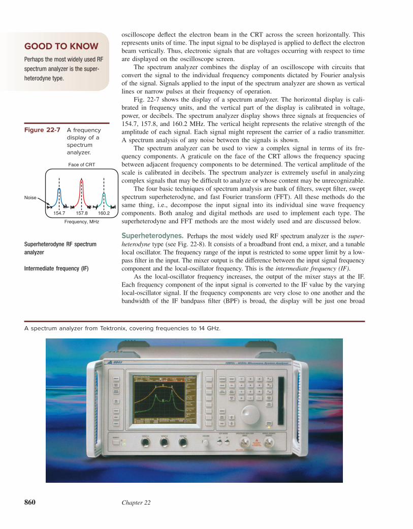
860 Chapter 22
oscilloscope del ect the electron beam in the CRT across the screen horizontally. This represents units of time. The input signal to be displayed is applied to del ect the electron beam vertically. Thus, electronic signals that are voltages occurring with respect to time are displayed on the oscilloscope screen. The spectrum analyzer combines the display of an oscilloscope with circuits that convert the signal to the individual frequency components dictated by Fourier analysis of the signal. Signals applied to the input of the spectrum analyzer are shown as vertical lines or narrow pulses at their frequency of operation. Fig. 22-7 shows the display of a spectrum analyzer. The horizontal display is cali-brated in frequency units, and the vertical part of the display is calibrated in voltage, power, or decibels. The spectrum analyzer display shows three signals at frequencies of 154.7, 157.8, and 160.2 MHz. The vertical height represents the relative strength of the amplitude of each signal. Each signal might represent the carrier of a radio transmitter. A spectrum analysis of any noise between the signals is shown. The spectrum analyzer can be used to view a complex signal in terms of its fre-quency components. A graticule on the face of the CRT allows the frequency spacing between adjacent frequency components to be determined. The vertical amplitude of the scale is calibrated in decibels. The spectrum analyzer is extremely useful in analyzing complex signals that may be difi cult to analyze or whose content may be unrecognizable. The four basic techniques of spectrum analysis are bank of i lters, swept i lter, swept spectrum superheterodyne, and fast Fourier transform (FFT). All these methods do the same thing, i.e., decompose the input signal into its individual sine wave frequency components. Both analog and digital methods are used to implement each type. The superheterodyne and FFT methods are the most widely used and are discussed below.
Superheterodynes. Perhaps the most widely used RF spectrum analyzer is the super-
heterodyne type (see Fig. 22-8). It consists of a broadband front end, a mixer, and a tunable local oscillator. The frequency range of the input is restricted to some upper limit by a low-pass i lter in the input. The mixer output is the difference between the input signal frequency component and the local-oscillator frequency. This is the intermediate frequency (IF). As the local-oscillator frequency increases, the output of the mixer stays at the IF. Each frequency component of the input signal is converted to the IF value by the varying local-oscillator signal. If the frequency components are very close to one another and the bandwidth of the IF bandpass i lter (BPF) is broad, the display will be just one broad
Superheterodyne RF spectrum analyzer
Intermediate frequency (IF)
A spectrum analyzer from Tektronix, covering frequencies to 14 GHz.
Figure 22-7 A frequency
dis play of a
spectrum
analyzer.
Noise
Face of CRT
154.7 157.8 160.2
Frequency, MHz
GOOD TO KNOWPerhaps the most widely used RF
spectrum analyzer is the super-
heterodyne type.

Communication Tests and Measurements 861
pulse. Narrowing the bandwidth of the IF BPF allows more closely spaced components to be detected. Most spectrum analyzers have several switchable selectivity ranges for the IF. Spectrum analyzers are available in many coni gurations with different specii ca tions,
and they are designed to display signals from approximately 100 kHz to approximately
70 GHz. Most RF and microwave spectrum analyzers are superheterodynes. Spectrum
analyzers are usually calibrated to provide relatively good measurement accuracy of the
signal. Most signals are displayed as power or decibel measurements, although some
analyzers provide for voltage level displays. The input is usually applied through a 50-V
coaxial cable and connector.
FFT Spectrum Analyzers. The fast Fourier transform (FFT) method of spectrum
analysis relies on the FFT mathematical analysis. FFT spectrum analyzers give a high-
resolution display and are generally superior to all other types of spectrum analyzers.
However, the upper frequency of the input signal is limited to frequencies in the tens of
megahertz range.
In addition to measuring the spectrum of a signal, spectrum analyzers are useful in
detecting harmonics and other spurious signals generated unintentionally. Spectrum analyz-
ers can be used to display the relative signal-to-noise ratio, and they are ideal for analyzing
modulation components and displaying the harmonic spectrum of a rectangular pulse train.
Despite their extremely high prices (usually $10,000 to $50,000), spectrum analyzers
are widely used. Many critical testing and measurement applications demand their use,
especially in developing new RF equipment and in making i nal tests and measurements
of manufactured units. Spectrum analyzers are also used in the i eld for testing cable TV
systems, cellular telephone systems, i ber-optic networks, and other complex communica-
tion systems.
Network AnalyzersA network analyzer is a test instrument designed to analyze linear circuits, especially
RF circuits. It is a combination instrument that contains a wide-range sweep sine wave
generator and a CRT output that displays not only frequency plots as does a spectrum
analyzer but also plots of phase shift versus frequency.
Network analyzers are used by engineers to determine the specii c performance
characteristics of a circuit they are designing, such as a i lter, an amplii er, or a mixer.
They are also useful in analyzing transmission lines and even individual components.
The network analyzer applies a swept-frequency sine wave and measures the circuit
output. The resulting measurement data is then used to produce an output display such
as an amplitude versus frequency plot, a phase shift versus frequency, or even a plot of
complex impedance values on a Smith chart display.
Network analyzers completely describe the performance or characterization of a
circuit. This type of information is useful not only to engineers creating the circuits but
Fast Fourier transform (FFT) spectrum analyzer
Network analyzer
Figure 22-8 Superheterodyne RF spectrum analyzer.
Low-pass
filter
LCD
BPFRF
detectorInput signal
Mixer IF amplifier
Tunable
local oscillator or VCO
Horizontal
sweep
Vertical
amplifier
Linear
sweep
generator
GOOD TO KNOWAlthough network analyzers are
expensive, they are invaluable for
determining the performance
characteristics of components or
circuits producing results in a
display.

862 Chapter 22
also to those in manufacturing who have to produce and test the circuit. Despite their very high cost, these instruments are widely used because of the valuable information they provide and the massive amount of design and test time they save.
Vector Signal Analyzers and GeneratorsAs wireless signals have become so complex and varied over the years, it has been necessary to create test instruments that can analyze and generate these signals. Vector signal analyzers and generators are those instruments. They can create or analyze OFDM, QPSK, QAM, FSK, WCDMA, and other signals that are common to widely used wire-less technologies like Wi-Fi, WiMAX, 3G WCDMA, HSPA, and LTE, as well as unique radar and satellite standards.
Vector Signal Generator. A vector signal generator (VSG) is a variation of an arbitrary waveform generator. A simplii ed example is shown in Fig. 22-9. The
complex signal, such as OFDM, is generated in the DSP circuitry, which produces
the in-phase (I) and quadrature (Q) components. The I and Q signals then go to DACs
that produce the equivalent analog signals. These are then sent to a quadrature mod-
ulator along with a i nal carrier signal from a local oscillator (LO) PLL. The modu-
lator output is usually amplii ed and applied to an attenuator that allows the signal
level to be set. In some instruments, the signal may be generated at a lower interme-
diate frequency (IF) and then mixed by an upconverter to the desired higher output
frequency.
Most VSGs are provided with preprogrammed signal formats for the most common
wireless standards, such as 802.11 or LTE. VSGs may also be user-programmed for
special formats or variations of existing standards. A commercial VSG is shown in
Fig. 22-10.
Vector Signal Analyzer. A vector signal analyzer (VSA) is an instrument designed
to capture and provide a way to disassemble a signal to see its detail. A VSA is similar
to a spectrum analyzer but with more output options. The VSA is useful in design to
ensure that new circuitry meets the desired standards. It is also useful in troubleshooting
to locate problems and standards variations. A VSA can usually display a frequency
spectrum, a modulation constellation diagram, a digital code, or even standard analog
time-domain signals like an oscilloscope.
Figure 22-9 Generic diagram of a vector signal generator.
DACQ
I
DSP
Quadrature
modulator
Output
I I
Q Q
Programming
Memory
Programming
LPF
PLL/LO
DAC LPF
90°
Communication Tests and Measurements 863
Figure 22-10 The National Instruments PXIe 5646R is a modularized vector signal
transceiver that contains a VSG and a VSA.
Figure 22-11 Block diagram of a vector signal analyzer.
Display
LO
Mixer
BPF
Time
data
store&
process
To
processorsLPF
FFT
Processors
Signal to be
analyzed
Processor
inputs
Spectrum
Constellation
Code
Demod
Decode
I
Q
90°
ADC
PLL
LO
Fig. 22-11 shows a generic block diagram of a VSA. The RF signal to be analyzed is fed to the an amplii er and/or an attenuator that sets the level. The signal is applied
to a mixer that downconverts the signal to an IF of a specii c bandwidth. A bandpass
i lter sets the bandwidth, and a low-pass i lter serves as an anti-aliasing i lter for the
analog-to-digital converter (ADC). The ADC produces a time-sampled version of the

864 Chapter 22
signal that will be used by the remainder of the VGA to do its analysis. The sampled data is stored and further groomed for additional processing. The digitized input signal then goes to a quadrature demodulator along with a local oscillator signal where the I and Q components of the signal are recovered. The I and Q signals are stored and corrected as needed, and then sent to one of several processors, depending upon the selected output. If a frequency spectrum output is desired, the signals go to a fast Fourier transform (FFT) processor, where the frequency components of the signal are determined and then displayed in traditional frequency spectrum format. Another option is demodulation that recovers the specii c data in the form of a constellation diagram display. This is especially useful for PSK and QAM signals. This type of output lets you measure the error vector magnitude (EVM) of the signal. For CDMA analysis, the processor can generate and display the unique coding asso-ciated with the signal. Alternately a standard time-domain output may be selected. Some VSAs can also accommodate MIMO signals. Fig. 22-12 shows some typical outputs. Fig. 22-13 shows a commercial VSA. Some manufacturers package the VSA and VGA modules together to form a vector signal transceiver. With most wireless equipment using OFDM and other advanced forms of signal technology today, the VSA and VSG have become the test instruments of choice for design, manufacturing test, and i eld troubleshooting.
Field Strength MetersOne of the least expensive pieces of RF test equipment is the i eld strength meter (FSM), a portable device used for detecting the presence of RF signals near an antenna. The FSM is a sensitive detector for RF energy being radiated by a transmitter into an antenna.
Field strength meter (FSM)
Figure 22-12 Commonly available VSA output options including a constellation
diagram for QAM, power vs. time plot, power vs. frequency plot, and
gain or phase fl atness plots. Courtesy National Instruments.

Communication Tests and Measurements 865
It provides a relative indication of the strength of the electromagnetic waves reaching the meter. The i eld strength meter is a vertical whip antenna, usually of the telescoping type,
connected to a simple diode detector. The diode detector is exactly like the circuit of a
simple crystal radio or a detector probe, as described earlier, but without any tuned cir-
cuits so that the unit will pick up signals on any frequency.
The i eld strength meter does not give an accurate measurement of signal strength.
In fact, its only purpose is to detect the presence of a nearby signal (within about 100 ft
or less). Its purpose is to determine whether a given transmitter and antenna system are
working. The closer the meter is moved to the transmitter and antenna, the higher the
signal level.
A useful function of the meter is the determination of the radiation pattern of an
antenna. The i eld strength meter is adjusted to give the maximum reading in the direc-
tion of the most radiation from the antenna. The meter is moved in a constant-radius
circle around the antenna for 360°. Every 5° or 10°, a i eld strength reading is taken
from the meter. The resulting set of readings can be plotted on polar graph paper to
reveal the horizontal radiation pattern of the antenna.
Other types of i eld strength meters are available. A simple meter may be built to
incorporate a resonant circuit to tune the input to a specii c transmitter frequency. This
makes the meter more sensitive. Some meters have a built-in amplii er to make the meter
even more sensitive and useful at greater distances from the antenna.
An absolute (rather than relative) i eld strength meter is available for accurate
measurements of signal strength. The strength of the radiated signal is usually measured
in microvolts per meter (µV/m). This is the amount of voltage the signal will induce
into an antenna that is 1 m long. An absolute i eld strength meter is calibrated in units
of microvolts per meter. Highly accurate signal measurements can be made.
Other Test InstrumentsThere are hundreds of types of communication test instruments, most of which are very
specialized. The ones described previously in this chapter, plus those listed in the above
table, are the most common, but there are many others including the many special test
instruments designed by equipment manufacturers for testing their production units or
servicing customers’ equipment.
Absolute fi eld strength meter
Figure 22-13 The National Instruments PXIe 5665 VSA has a frequency range to
3.6 or 14 GHz with bandwidth options of 25 or 50 MHz.

866 Chapter 22
22-2 Common Communication TestsHundreds, even thousands, of different tests are made on communication equipment. However, some common tests are widely used on all types of communication equipment. This section summarizes the most common tests and measurements made in the servic-ing of communication equipment. Most of the tests described here focus on standard radio communication equipment. Tests for transmitters, receivers, and antennas will be described, as will special microwave tests, i ber-optic cable tests, and tests on data communication equipment. Keep in mind
that the test procedures described are general. To make specii c tests, follow the test
setups recommended by the test equipment manufacturer. Always have the manuals for
the test equipment and the equipment being serviced on hand for reference.
Transmitter TestsFour main tests are made on most transmitters: tests of frequency, modulation, and power,
and tests for any undesired output signal component such as harmonics and parasitic
radiations. These tests and measurements are made for several reasons. First, any equip-
ment that radiates a radio signal is governed by Federal Communications Commission
(FCC) rules and regulations. For a transmitter to meet its intended purpose, the FCC
specii es frequency, power, and other measurements to which the equipment must com-
ply. Second, the tests are normally made when the equipment is i rst installed to be sure
that everything is working correctly. Third, such tests may be performed to troubleshoot
equipment. If the equipment is not working properly, these tests are some of the i rst
that should be made to help identify the trouble.
Frequency Measurement. Regardless of the method of carrier generation, the fre-
quency of the transmitter is important. The transmitter must operate on the assigned
frequency to comply with FCC regulations and to ensure that the signal can be picked
up by a receiver tuned to that frequency.
Instrument Purpose
Absorption wave Variable tuned circuit with an indicator that tells when the
meter tuned circuit is resonant to a signal coupled to the meter
by a transmitter; provides a rough indication of frequency.
Impedance meter An instrument, usually of the bridge type, that accurately
measures the impedance of a circuit, a component, or
even an antenna at RF frequencies.
Dip oscillator A tunable oscillator used to determine the approximate
resonant frequency of any deenergized LC–resonant
circuit. The oscillator inductor is coupled to the tuned
circuit inductor, and the oscillator is tuned until its
feedback is reduced as energy being taken by the tuned
circuit, which is indicated by a “dip,” or reduction, in
current on a built-in meter. The approximate frequency
is read from a calibrated dial.
Noise bridge Bridge circuit driven by a random noise voltage source
(usually a reverse-biased zener diode that generates
random “white” or pseudorandom “pink” noise) that has
an antenna or coaxial cable as one leg of the bridge;
used to make antenna characteristic impedance mea-
surements and measurements of coaxial cable velocity
factor and length.
Absorption wave meter
Impedance meter
Dip oscillator
Noise bridge
GOOD TO KNOWTo make specifi c tests, always
follow the test setups recom-
mended by the test equipment
manufacturer. Keep the manuals
for test equipment and for the
equipment being serviced on
hand for reference.

Communication Tests and Measurements 867
The output of a transmitter is measured directly to determine its frequency. The transmitted signal is independently picked up and its frequency measured on a frequency counter. Fig. 22-14 shows several methods of picking up the signal. Many frequency counters designed for communication work come with an antenna that picks up the signal directly from the transmitter [see Fig. 22-14(a)]. The transmitter is keyed up (turned on) while it is connected to its regular antenna, and the antenna on the counter picks up the signal and translates it to one that can be measured by the counter circuitry. No modulation should be applied, especially if FM is used. The transmitter output can be connected to a dummy load [see Fig. 22-14(b)]. This will ensure that no signal is radiated, but that there will be sufi cient signal pickup
to make a frequency measurement if the counter and its antenna are placed near the
transmitter.
Another method of connecting the counter to the transmitter is to use a small coil,
as shown in Fig. 22-14(c). A small pickup coil can be made of stiff copper wire.
Enamel copper wire, size AWG 12 or 14 wire, is formed into a loop of two to four
turns. The ends of the loop are connected to a coaxial cable with a BNC connector for
attachment to the frequency counter. The loop can be placed near the transmitter cir-
cuits. This method of pickup is used when the transmitter has been opened and its
circuits have been exposed. For most transmitters, the loop has been placed only in
the general vicinity of the circuitry. Normally the loop picks up radiation from one
of the inductors in the i nal stage of the transmitter. Maximum coupling is achieved when the axis of the turns of the loop is parallel to the axis of one of the inductors in the i nal output stage. Once the signal from the transmitter is coupled to the counter, the counter sensitivity is adjusted, and the counter is set to the desired range for displaying the frequency. The greater the number of digits the counter can display, the more accurate the measurement. Normally this test is made without modulation. If only the carrier is transmitted, any modulation effects can be ignored. Modulation must not be applied to an FM transmitter, because the carrier frequency will be varied by the modulation, resulting in an inaccurate frequency measurement.
Figure 22-14 Transmitter frequency measurement.
12345
Frequencycounter
(b)
Transmitter
12345
Coaxialcable
Antenna
Frequencycounter
(a )
Transmitter
12345Coaxialcable
Antenna
Frequencycounter
(c )
50-�dummy
load
Transmitter PCB
Coil
50 �
Coaxial cable
BNC connecterAxis
Transmitter inductor
Inductivecoupling
Antenna

868 Chapter 22
The quality of crystals today is excellent; thus, off-frequency operation is not com-mon. If the transmitter is not within specii cations, the crystal can be replaced. In some
critical pieces of equipment, the crystal may be in an oven. If the oven temperature
control circuits are not working correctly, the crystal may have drifted off frequency.
This calls for repair of the oven circuitry or replacement of the entire unit.
If the signal source is a frequency synthesizer, the precision of the reference crystal
can be checked. If it is within specii cations, perhaps an off-frequency operation is being
caused by a digital problem in the phase-locked loop (PLL). An incorrect frequency-
division ratio, faulty phase detector, or poorly tracking voltage-controlled oscillator
(VCO) may be the problem.
Modulation Tests. If AM is being used in the transmitter, you should measure the
percentage of modulation. It is best to keep the percentage of modulation as close to 100
as possible to ensure maximum output power and below 100 to prevent signal distortion
and harmonic radiation. In FM or PM transmitters, you should measure the frequency
deviation with modulation. The goal with FM is to keep the deviation within the specii c
range to prevent adjacent channel interference.
The best way to measure AM is to use an oscilloscope and display the AM signal
directly. To do this, you must have an oscilloscope whose vertical amplii er bandwidth
is sufi cient to cover the transmitter frequency. Fig. 22-15(a) shows the basic test setup.
Figure 22-15 AM measurement. (a) Test setup. (b) Typical waveforms.
AMtransmitter
Audiogenerator Microphone input
Coaxial cable
2–5 pF
Dummyload
(50 �)
Oscilloscope
(a )
(b)
Evenly spaced vertical linesindicate carrier sine wave
0% (no) modulation
100%modulation
B A % modulation � A � B
A � B� 100
Overmodulation (>100%) distortion

Communication Tests and Measurements 869
An audio signal generator is used to amplitude-modulate the transmitter. An audio signal of 400 to 1000 Hz is applied in place of the microphone signal. The transmitter is then keyed up, and the oscilloscope is attached to the output load. It is best to perform this test with a dummy load to prevent radiation of the signal. The oscilloscope is then adjusted to display the AM signal. The display will appear as shown in Fig. 22-15(b).
Power Measurements. Most transmitters have a tune-up procedure recommended by the manufacturer for adjusting each stage to produce maximum output power. In older transmitters, tuned circuits between stages have to be precisely adjusted in the correct sequence. In modern solid-state transmitters, there are fewer adjustments, but in most cases there are some adjustments in the driver and frequency multiplier stages as well as tuning adjustments for resonance at the operating frequency to the i nal amplii er.
There may be impedance-matching adjustments in the i nal amplii er to ensure full cou-
pling of the power to the antenna. The process is essentially that of adjusting the tuned
circuits to resonance. These measurements are generally made while monitoring the
output power of the transmitter.
The procedure for measuring the output power is to connect the transmitter output
to an RF power meter and the dummy load, as shown in Fig. 22-16. The transmitter is
keyed up without modulation, and adjustments are made on the transmitter circuit to tune
for maximum power output. With the test arrangement shown, the power meter will
display the output power reading.
Once the transmitter is properly tuned up, it can be connected to the antenna. The
power into the antenna will then be indicated. If the antenna is properly matched to the
transmission line, the amount of output power will be the same as that in the dummy
load. If not, SWR measurements should be made. Most modern power meters measure
both forward and rel ected power, so SWR measurements are easier to make. It may be necessary to adjust the antenna or a matching circuit to ensure maximum output power with minimum SWR.
Harmonics and Spurious Output Measurements. A common problem in transmitters is the radiation of undesirable harmonics or spurious signals. Ideally, the output of the transmitter should be a pure signal at the carrier frequency with only those sideband components produced by the modulating signal. However, most transmitters will generate some harmonics and spurious signals. Transmitters that use class C, class D, and class E amplii ers generate a high harmonic content. If the tuned circuits in the transmitter are properly designed, the Q’s will be high enough to reduce the harmonic content level sufi ciently. However, this is not always the case. Another problem is that other spurious signals can be generated by transmitters. In high-power transmitters particularly, parasitic oscillations can occur. These are caused by the excitation of small tuned circuits whose components are the stray inductances and capacitances in the circuits or the transistors of the tubes involved. Parasitic oscillations can reach high levels and cause radiation on undesired frequencies. For most transmitters, the FCC specii es maximum levels of harmonic and spurious radiation. Intermodulation distortion in mixers and nonlinear circuits also produces
Figure 22-16 Power measurement.
Transmitter
RFpowermeter
Coaxial cable
Dummyload

870 Chapter 22
unwanted signals. Normally these signals must be at least 30 or 40 dB down from the main carrier signal. The best way to measure harmonics and spurious signals is to use a spectrum analyzer. The transmitter output is modulated with an audio tone, and its output is monitored directly on the spectrum analyzer. It is usually best to feed the transmitter output into a dummy load for this measurement. The spectrum analyzer is then adjusted to display the normal carrier and sideband pattern. The search for high-level signals can begin for spurious outputs by tuning the spectrum analyzer above and below the operating frequency. The spectrum analyzer can be tuned to search for signals at the second, third, and higher harmonics of the carrier frequency. If signals are detected, they can be measured to ensure that they are sufi ciently low in power
to meet FCC regulations and/or the manufacturer’s specii cations. The spectrum
analyzer is then tuned over a broad range to ensure that no other spurious nonharmonic
signals are present.
It may be possible to reduce the harmonic and spurious output content by making
a minor transmitter tuning adjustment. If not, to meet specii cations, it is often necessary
to use i lters to eliminate unwanted harmonics or other signals.
Antenna and Transmission Line TestsIf the transmitter is working correctly and the antenna has been properly designed, about
the only test that needs to be made on the transmission line and antenna is for standing
waves. It will tell you whether any further adjustments are necessary. If the SWR is high,
you can usually tune the antenna to reduce it.
You may also run into a transmission line problem. It may be open or short-
circuited, which will show up on an SWR test as ini nite SWR. But there may be other
problems such as a cable that has been cut, short-circuited, or crushed between the
transmitter and receiver. These kinds of problems can be located with a time-domain
rel ectometer test.
SWR Tests. The test procedure for SWR is shown in Fig. 22-17. The SWR meter is connected between the transmission line and the antenna. Check with the manufacturer of the SWR meter to determine whether any specii c connection location is required or whether other conditions must be met. Some of the lower-cost SWR meters must be connected directly at the antenna or a specii c number of half wavelengths from the antenna back to the transmitter. Once the meter is properly connected, key up the transmitter without modulation. The transmitter should have been previously tuned and adjusted for maximum output power. The SWR can be read directly from the instrument’s meter. In some cases, the meter will give measurements for the relative amount of incident or forward and rel ected power or will read out in terms of the rel ection coefi cient, in which case you must calculate the SWR as described earlier. Other meters will read out directly in SWR. The maximum range is usually 3:1.
Figure 22-17 SWR measurement.
Transmitter
SWR meter
Coaxial cable
Coaxial cable
Antenna

Communication Tests and Measurements 871
The ideal SWR is 1 or 1:1, which means that all the power generated by the trans-mitter is absorbed by the antenna load. Nevertheless, in even the best systems, perfect matching is rarely achieved. Any mismatch will produce rel ected power and standing waves. If the SWR is less than 2:1, the amount of power that will be lost or rel ected will be minimal. The primary procedure for reducing the SWR is to make antenna adjustments, usu-ally in the form of modifying the element lengths to more closely tune the antenna to the frequency of operation. Using many antennas makes it possible to adjust their length over a narrow range to i ne-tune the SWR. Other antennas permit adjustment to provide a better match of the transmission line to the driven element of the antenna. These adjust-ments can be made one at a time, and the SWR monitored.
TDR Tests. Time-domain rel ectometry (TDR) is a pulse for cables and transmission lines of all types. It is widely used in i nding faults in cables used for digital data trans-mission, but it can be used for RF transmission lines. (Refer to the section Data Com-munication Tests later in this chapter for details.)
Receiver TestsThe primary tests for receivers involve sensitivity and noise level. The greater the sen-sitivity of the receiver, the higher its gain and the better job it does of receiving very small signals. As part of the sensitivity testing, the signal-to-noise (S/N) ratio is also usually mea-sured indirectly. The ability of a receiver to pick up weak signals is just as much a function of the receiver noise level as it is of overall receiver gain. The lower the noise level, the greater the ability of the receiver to detect weak signals. As part of an overall sensitivity check, some receiver manufacturers specify an audio power output level. Since receiver sensitivity measurements are usually made by measur-ing the speaker output voltage, power output can also be checked if desired. In this section, some of the common tests made on receivers are described. The information is generic, and the actual testing procedures often differ from one receiver manufacturer to another.
Equipment Required. To make sensitivity and noise measurements, the following equipment is necessary:
1. Dual-Trace Oscilloscope. The vertical frequency response is not too critical, for you will be viewing noise and audio frequency signals.
2. RF Signal Generator. This generator provides an RF signal at the receiver operating frequency. It should have an output attenuator so that signals as low as 1 µV or less can be set. This may indicate the need for an external attenuator if the generator does not have built-in attenuators or output level adjustments. The generator must also have modulation capability, either AM or FM, depending upon the type of receiver to be tested.
3. RF Voltmeter. The RF voltmeter is needed to measure the RF generator output voltage in some tests. Some higher-quality RF generators have an RF voltmeter built in to aid in setting the output attenuator and level controls.
4. Frequency Counter. A frequency counter capable of measuring the RF generator output frequency is needed.
5. Multimeter. A multimeter capable of measuring audio-frequency (AF) voltage levels is needed. Any analog or digital multimeter with ac measurement capability in the AF range can be used.
6. Dummy Loads. A dummy load is needed for the receiver antenna input for the noise test. This can be either a 50- or a 75-V resistor attached to the appropriate coaxial input connector. A dummy load is needed for the speaker. Because most noise and sensitivity tests are made with maximum receiver gain including audio
Time-domain refl ectometry
GOOD TO KNOWThe ability of a receiver to pick up
weak signals is just as much a
function of receiver noise level as
it is of overall receiver gain. The
lower the noise level, the greater
the ability of the receiver to detect
weak signals.

872 Chapter 22
gain, it is not practical or desirable to leave the speaker connected. Most communi-cation receivers have an audio output power capability of 2 to 10 W, which is suf-i ciently high to make the output signal level too high for comfort. A speaker dummy
load of 4, 8, or 16 V, depending upon the speaker impedance, is needed. Be sure
that the dummy load can withstand the maximum audio power output of the receiver.
Do not use wire-wound resistors for this application, for they have too much induc-
tance. Check the receiver’s specii cations for both the impedance and the maximum
power level specii cation.
Noise Tests. Noise consists of random signal variations picked up by the receiver or
caused by thermal agitation and other conditions inside the receiver circuitry. External
noise cannot be controlled or eliminated. However, noise contributed by the receiver can
be controlled. Every effort is made during the design to minimize internally generated
noise and thus to improve the ability of the receiver to pick up weak signals.
Most noise generated by the receiver occurs in the receiver’s front end, primarily
the RF amplii er and the mixer. Careful attention is given to the design of both these
circuits so that they contribute minimum noise.
Because noise is a totally random signal that is a composite of varying frequency
and varying amplitude signals, it is somewhat difi cult to measure. However, the following
procedure has become a common and popular method that is easy to implement.
Refer to the test setup shown in Fig. 22-18. The antenna is removed from the
receiver, and a dummy load of the correct impedance is used to replace it. A carbon
composition resistor of 50 or 75 V can be used. The idea is to prevent the receiver from
picking up any signals while maintaining the correct impedance.
At the output of the receiver, the speaker is replaced with a dummy load. Most
speakers have an output impedance of 4 or 8 V. Check the receiver’s specii cations, and
connect an appropriate value of resistor in place of the speaker. Be sure that the dummy
load resistors can withstand the output power.
Finally, connect the dual-trace oscilloscope across the dummy speaker load. The
same signal should be displayed on both channels of the oscilloscope. The displayed
signal will be an amplii ed version of the noise produced by the receiver and amplii ed
by all the stages between the antenna input and the speaker. Follow this step-by-step
procedure:
1. Turn on the receiver, and tune it to a channel where no signal will be received.
2. Set the receiver volume control to maximum. If the receiver has any type of RF or
IF gain control, it too should be set to its maximum setting.
3. Set the oscilloscope input for the lower trace (channel B) to ground. Most oscillo-
scopes have a switch that allows the input to be set for ac measurements, dc mea-
surements, or ground. Grounding the channel B input will prevent any signal from
being displayed. At this time, you will see a straight horizontal line for the lower
trace. Adjust that lower trace so that it lines up with one of the horizontal graticule
lines near the bottom of the oscilloscope screen. This will provide a voltage mea-
surement reference.
Noise
Figure 22-18 Noise test setup.
Receiver
Dummy loadfor antenna(50 or 75 �)
Antenna input jack
Speaker output terminals
Dummy loadfor speaker
(4, 8, 16, etc. �)
Channel AChannel B
GOOD TO KNOWTo determine the noise level when
the horizontal spacing on the
oscilloscope and the vertical
sensitivity are known, multiply
the horizontal spacing by the
sensitivity and divide by 2.

Communication Tests and Measurements 873
4. Set the channel B input and the channel A input to alternating current. Adjust the vertical sensitivities of channels A and B so that they are on the same range. Make the adjustments so that the signal is displayed something like that shown in Fig. 22-19(a). You should see exactly the same noise pattern on both channels.
5. Using the vertical position control on the upper or A channel, move the upper noise trace downward so that it begins to merge with the noise signal on channel B. The correct adjustment for the position of the channel A noise signal is such that the peaks of the upper and lower signals just barely merge. This will generally be indi-cated at the point where there is no blank space between upper and lower traces. The signal should look something like that shown in Fig. 22-19(b).
6. Now set both oscilloscope inputs to ground, thereby preventing the noise signal from being displayed. You will see two straight horizontal lines. The distance between the two lines is a measure of the noise voltage. The value indicated is two times the root mean square (rms) noise voltage [see Fig. 22-19(c)].
Assume that the adjustments described above were made and the separation between the two horizontal traces is 1.2 vertical divisions. If the vertical gains of both channels are set to the 10 mV per division range, the noise reading is 1.2 3 10 mV 512 mV. The rms noise voltage is one-half of this i gure, or 12 mV/2 5 6 mV.
Power Output Tests. Sometimes it is necessary to measure the receiver’s total power
output capability. This is a good general test of all the receiver circuits. If the receiver
can supply the manufacturer’s specii ed maximum output power into the speaker with a
given low RF signal level input, the receiver is operating correctly.
The test setup for the power output test is shown in Fig. 22-20. An RF signal gen-
erator for the correct frequency is used as the primary signal source. It must also be
possible to modulate this generator with either AM or FM depending upon the type of
receiver.
It is also desirable to connect a frequency counter to the signal generator output to
provide an accurate measure of the receiver input frequency. Most communication receiv-
ers operate on specii c frequency channels. For the test to be valid, the generator output
frequency must be set to the center of the receiver frequency channel. This will usually
be known from the receiver’s specii cations. The signal generator is tuned, and the fre-
quency is set by monitoring the digital readout on the frequency counter.
Be sure to replace the speaker with a resistive load of an impedance equal to that
of the speaker, such as 8 V. The dummy speaker load should also be able to carry the
Figure 22-19 Noise measurement procedure.
Channel A
Channel B
Display noiseacross speaker on
both channels
Channel A
Channel B
Channel A
Channel B
Merge waveformso that peaks just
merge with nospace showing
Remove signals,measure spacing
1.2 divisions at 10 mV per division �12 mV; noise voltage �
� 6 mV rms 12 mV
2
(a )
(b)
(c )

874 Chapter 22
maximum rated output power of the receiver. Finally, connect an ac voltmeter across the speaker dummy load. Turn on the receiver, and set the volume control to the maximum. If the receiver has a variable RF or IF gain control, you must set it to the maximum setting also. At this time, any other receiver features should be disabled. For example, in an FM receiver, the squelch should be turned off or disabled. In an AM receiver, if a noise limiter is used, it too should be turned off. To begin the test, follow this procedure:
1. Set the RF generator output level to 1 mV. If the RF signal generator has a built-in RF voltmeter, use it to make this setting. Otherwise, an external RF voltmeter may be needed, as shown in Fig. 22-20.
2. Set the signal generator for modulation of the appropriate type. If AM is used, set the percentage of modulation for 30. If FM is used, set the deviation for ;3 kHz. In most signal generators, the percentage of AM and the frequency deviation for FM are i xed. Refer to the signal generator specii cations to i nd out what these
values are.
3. With everything appropriately adjusted, measure the ac voltage across the speaker
dummy load. This will be an rms reading.
4. To determine the receiver power output, use the standard power formula P 5 V 2/R.
Assume that you measure an rms voltage of 4 V across an 8-V speaker. The power
output will be
P 5V
2
R5
42
85
16
85 2 W
An optional test is to observe the signal across the speaker load with an oscilloscope.
Most RF generators modulate the input signal with a sine wave of 400 Hz or 1 kHz. If
an oscilloscope is placed across the dummy speaker load, the sine wave will be seen.
This will indicate whether the receiver is distorting. The oscilloscope can also be used
in place of the audio voltmeter to make the voltage measurement across the dummy
speaker load. Remember that oscilloscope measurements are peak to peak. The peak-to-
peak value must be converted to root mean square to make the power output calculation.
20-dB Quieting Sensitivity Tests. In most cases, the sensitivity of a receiver is
expressed in terms of the minimum RF voltage at the antenna terminals that will produce
a specii c audio output power level. Most measurements factor in the effect of noise.
The method of sensitivity measurement is determined according to whether AM or FM
is used. Because most modern radio communication equipment uses frequency modulation,
Figure 22-20 Power output test.
V
Frequencycounter
8 �AC (audio)voltmeter
Speaker output terminalsAntennainput jack
RF voltmeter
Receiver
RF signalgenerator

Communication Tests and Measurements 875
measuring FM receiver sensitivity is illustrated. There are two basic methods, quieting and SINAD. The quieting method measures the amount of signal needed to reduce the output noise to 20 dB. As the signal level increases, the noise level decreases until the limiters in the IF section begin to start their clipping action. When this happens, the receiver output “quiets”; i.e., its output is silent and blanks out the noise. The SINAD test is a measure of the input signal voltage that will produce at least a 12-dB signal-to-noise ratio. The noise value includes any harmonics that are produced by the receiver circuits because of distortion. The test setup for receiver sensitivity measurements is shown in Fig. 22-21(a). It consists of an RF signal generator, an RF voltmeter, a frequency counter, the receiver to be tested, and a voltmeter to measure the output across the speaker dummy load. It is often necessary to provide an impedance-matching network between the gen-erator and the receiver antenna input terminals. Most RF generators have a 50-V output impedance. This may match the receiver input impedance exactly. However, some receiver input impedances may be different. For example, if a receiver has a 75-V input imped-ance, some form of impedance matching will be required. This is usually handled by a resistive attenuator known as an impedance-matching pad, which is a resistive T network that provides the correct match between the receiver input and the generator. A typical impedance- matching pad is shown in Fig. 22-21(b). It matches the 50-V generator output to the 50-V receiver antenna input. Because resistors are used, the impedance-matching circuit is also an attenuator. With the values given in Fig. 22-21(b), the signal attenuation is 10 dB. This must be factored into all signal generator measurements to obtain the cor-rect sensitivity i gure. Different values of resistors can be used to create a pad with the
correct impedance-matching qualities but with lower or higher values of attenuation.
Quieting method
SINAD test
Impedance-matching pad
Figure 22-21 (a) Quieting method of FM receiver sensitivity measurement. (b) T-type
impedance-matching attenuator.
Frequencycounter
Impedance- matchingattenuator
VReceiver 8 �
Speakeroutput terminals
Antennainput jack
Coaxial connections
RF signalgenerator
RF voltmeter
(a )
AC (audio)voltmeter
(b)
50 �
18 � 51 �
39 � 75 �
RFsignal
generator
10-dBimpedance-
matching pad Receiver
876 Chapter 22
Some manufacturers specify a special input network made up of resistors, inductors, and/or capacitors for this or other sensitivity tests. This network helps simulate the antenna accurately in equipment that uses special antennas. Follow this procedure to make the 20-dB quieting measurement:
1. Turn on the receiver, and set it to an unused channel.
2. Leave the signal generator off so that no signal is applied.
3. Set the receiver gain to maximum with any RF or IF gain control, if available.
4. Adjust the volume control of the receiver so that you read some convenient value of noise voltage on the meter connected across the speaker. One volt rms is a good value if you can achieve it; but if not, any other convenient value will do.
5. Turn on the signal generator, but set the output level to zero or some very low value. Adjust the generator frequency to the center of the receiver’s channel setting. Turn off the modulation so that the generator supplies carrier only.
6. Increase the signal generator output signal level a little at a time, and observe the volt-age across the speaker. The noise voltage level will decrease as the carrier signal gets strong enough to overpower the noise. Increase the signal level until the noise voltage drops to one-tenth of its previous value.
7. Measure the generator output voltage on the generator meter or the external RF voltmeter.
8. If an attenuator pad or other impedance-matching network was used, subtract the loss it introduces. The resulting value is the voltage level that produces 20 dB of quieting in the receiver.
Assume that you measured a generator output of 5 µV that produces the 20-dB noise decrease. This is applied across a 50-V load producing an input power of P2 5V
2/R 5 (5 3 1026)2/50 5 0.5 pW. This is attenuated further by the 10-dB matching pad to a level of one-tenth, or 0.05 pW, which translates to a voltage level across 50 V as
V 5 2PR 5 20.05 3 10212 3 50 5 1.58 3 1026 5 1.58 µV
This is the receiver sensitivity. It takes 1.58 µV of a signal to produce 20 dB of quieting in the receiver. For a good communication receiver, the 20-dB quieting value should be under 1 µV. A typical value is in the 0.2- to 0.5-µV range. The lower the value, the better the sensitivity.
Blocking and Third-Order Intercept Tests. As the spectrum has become more crowded and as modulation advances have permitted higher speed per hertz of bandwidth, the potential for adjacent channel interference has signii cantly increased. To ensure
minimum adjacent channel interference, receiver specii cations have become tighter. This
is especially true in cell phones. Whole suites of tests must be passed by the receiver in
order to meet the specii cations of a specii c cell phone standard such as GSM or CDMA.
An example is the receiver blocking test that makes measurements to ensure that
signals from an adjacent channel do not block or desensitize the channel being used.
A very strong signal near the receiving frequency has the effect of lowering the gain of the receiver. Any small signal being received will be decreased in amplitude or even blocked completely. Some specii cations call for the receiver to be able to receive a weak signal when the adjacent channel signal is 60 to 70 dB greater in level. The ability to meet this test depends upon the i ltering selectivity of the receiver. But perhaps the most difi cult test is the third-order intercept test, designated TOI or IP3. This test is a measure of the linearity of amplii ers, mixers, and other circuits. When two signals are applied to a circuit, any nonlinearity in the circuit causes a mixing or modulation effect. The larger the input signals, the more likely the amplii er will be driven into a nonlinear region where mixing will occur. Sum and difference signals will be produced. Some of the resulting so-called intermodulation products are problematic because they occur at a frequency near or inside the receiver bandpass and interfere with
Third-order intercept test (TOI or IP3)
GOOD TO KNOWThe third-order intercept test
determines whether a cell phone
will fi lter out large nearby signals
that can be mistakenly inter-
preted by the cell phone as its
receiving frequency.

Communication Tests and Measurements 877
the signal being received. Such signals, because they are so close to the desired signal, cannot be i ltered out. These intermodulation signals must be reduced as much as pos-
sible in the design of the receiver by selecting more linear components or giving greater
attention to biasing schemes and operating points.
Fig. 22-22 shows two signals f1 and f2 that appear at the input to an amplii er. The
nonlinear action of the amplii er generates a wide range of sums and differences, includ-
ing those with the second and third harmonics. Most of these undesired products will be
i ltered out by the receiver IF i lters. The third-order products cause the most problems,
because they will most likely fall within the receiver IF bandpass. The third-order products
are 2f1 6 f2 and 2f2 6 f1, where the terms 2f1 2 f2 and 2f2 2 f1 cause the most problems.
To measure the third-order problem, two equal power signals are applied to the
amplii er or other circuit to be tested. The frequency spacing is usually small and often
made equal to the normal channel spacing used. The power of the input signals is grad-
ually increased, and measurements are made on the amplii er output to determine the
levels of the test signals and the third-order products. As the power levels of the input
signals increase, the third-order signal power increases as the cube of the input power
change. On a logarithmic scale, the rate of increase of third-order products is three times
that of the original signals.
Refer to Fig. 22-23. If you plot the output signal amplitudes versus input signal
power increases, at some point the power levels reach their limit and l atten out. If you
Figure 22-22 Third-order intermodulation products.
Third-orderIntermodulation
products
Circuit inputs
2f1 � f2 f1 f2 2f2 � f1
Frequency
Figure 22-23 Third-order intercept plot of an RF amplifi er.
�40
�60
�50
�40
�30
�20
�10
0
10
20
30
�30 �20 �10 0 10 20
First-ordersignal power
Third-ordersignal power
Third-orderintercept point
15 dBm
Circuit input power (dBm)
Circuit o
utp
ut pow
er
(dB
m)
GOOD TO KNOWThe third-order products that
most often interfere with a signal
are 2f1 2 f2 and 2f2 2 f1.

878 Chapter 22
extend the linear portions of the two curves, they will meet at a theoretical point where the initially lower third-order signals equal the main input signals in amplitude. This is the third-order intercept point. The input power at that point is used as a measure of the intermodulation. In Fig. 22-23, the IP3 point is at 15 dBm. Typical IP3 values are between 0 and 35 dBm. The higher the IP3 value, the better the circuit linearity and the lower the intermodulation products.
Microwave TestsMicrowave tests are generally similar to those performed on standard transmitters and receivers. Transmitter measurements include output power, deviation, harmonics, and spurious signals as well as modulation. The techniques are similar but require the use of only those test instruments whose frequency response is in the desired microwave region. The same goes for receiver measurements and antenna transmission line tests. The pro-cedures are generally the same, but the equipment is different. For example, with power measurements, a directional coupler is normally used as the transmitter output to reduce the signal to a proper level for measurement with the power meter.
Data Communication TestsThe tests for wireless data communication equipment are essentially the same as those for standard RF communication as described above. The only difference is the type of modulation used to apply the binary signal to the carrier. FSK and its many variants, as well as PSK and spread spectrum, are the most widely used. Special FSK and PSK deviation and modulation meters are available to make these measurements. For data communication applications in which binary signals are baseband on coax-ial and twisted-pair cables, such as in LANs, more conventional testing methods may be used. For example, binary test patterns may be initiated in the transmitting equip-ment, and the signal viewed on the oscilloscope at the receiving end. Tests of signal attenuation and wave shape can then be made.
Eye Diagrams. A common method of analyzing the quality of binary data transmitted on a cable is to display what is known as the eye diagram on a common oscilloscope. The eye diagram, or pattern, is a display of the individual bits overlapped with one another. The resulting output looks like an open eye. The shape of the pattern and the degree that the eye is “open” can be used to determine many things about the quality of transmission. Eye diagrams are used for testing because it is difi cult to display long streams of random serial bits on an oscilloscope. The randomness of the data prevents good syn-chronization of the oscilloscope with the data, and thus the display jitters and changes continuously. Sending the same pattern of bits such as repeating the ASCII code for the letter U (alternating 1s and 0s) may help the synchronization process, but the display of one whole word on the screen usually does not provide sufi cient detail to determine the nature of the signal. The eye diagram solves these problems. Fig. 22-24(a) shows a serial pulse train of alternating binary 0s and 1s that is applied to a transmission line. The transmission line, either coaxial or twisted pair, is a low-pass i lter, and therefore it eliminates or at least greatly attenuates the higher- frequency components in the pulse train. It also delays the signal. The result is that the signal is rounded and distorted at the end of the cable and the input to the receiver [see Fig. 22-24(b)]. The longer the cable and/or the higher the bit rate, the greater the distortion. The pulses tend to blur into one another, causing what is called intersymbol interference (ISI). ISI makes the voltage levels for binary 1 and 0 closer together with 1 bit smearing or overlapping into the other. This makes the receiver’s job of clearly distinguishing a binary 1 from a binary 0 more difi cult. Furthermore, noise is usually picked up along the trans-mission path, making the received signal a poor representation of the original data signal.
Eye diagram
Intersymbol interference (ISI)
GOOD TO KNOWThe eye diagram is an excellent
way to get a nonprecise, quick,
qualitative check of a signal. The
eye pattern tells at a glance the
degree of bandwidth limitation,
signal distortion, jitter, and noise
margin.

Communication Tests and Measurements 879
Too much signal rounding or ISI introduces bit errors. Fig. 22-24(c) shows a severely distorted, noisy data signal. The eye pattern provides a way to view a serial data signal and to make a determi-nation about its quality. To display the eye diagram, you need an oscilloscope with a bandwidth at least i ve times the maximum bit rate. For example, if the bit rate is 10 Mbps,
the oscilloscope bandwidth should be at least 10 3 5 MHz, or 50 MHz. The higher the
better. The oscilloscope should have triggered sweep. Either a conventional analog or a
digital oscilloscope can be used.
Apply the baseband binary signal at the end of the cable and the receiver input
to the vertical input. Adjust the sweep rate of the oscilloscope so that a 1-bit interval
takes up the entire horizontal width of the screen. Use the variable sweep control to
i ne-tune the display and use the trigger controls to stabilize the display. The result is
an eye diagram.
Several different eye patterns are shown in Fig. 22-25. The multiple lines represent
the overlapping pulses occurring over time. Their amplitude and phase shift are
slightly shifted from sweep to sweep, thereby giving the kind of pattern shown. If the
signal has not been severely rounded, delayed, or distorted, it might appear as shown
in Fig. 22-25(a). The eye is “wide open” and has a trapezoidal shape. This is a com-
posite display of the rise and fall times of the pulses overlapping one another. The
steeper the sides, the less the distortion. The eye pattern in Fig. 22-25(a) indicates
wide bandwidth of the medium.
In Fig. 22-25(b), the pattern looks more like an open eye. The pulses are rounded,
indicating that the bandwidth is limited. In fact, the pulses approach the shape of a sine
wave. The pattern shown in Fig. 22-25(c) indicates more severe bandwidth limiting. This
reduces the amplitude of the rounded pulses, resulting in a pattern that appears to be an
eye that is closing. The more the eye closes, the narrower the bandwidth, the greater
the distortion, and the greater the intersymbol interference. The difference between the
binary 0 and 1 levels is less, and the chance is greater for the receiver to misinterpret
the level and create a bit error.
Note further in Fig. 22-25(c) that the amplitudes of some of the traces are differ-
ent from others. This is caused by noise varying the amplitude of the signal. The noise
can further confuse the receiver, thus producing bit errors. The amount of voltage
between the lowest of the upper patterns and the highest of the lower patterns as shown
is called the noise margin. The smaller this value, the greater the noise and the greater
the bit error rate. Noise margin is sometimes expressed as a percentage based upon the
ratio of the noise margin level a in Fig. 22-25(c) to the maximum peak-to-peak value
of the eye A.
The eye diagram is not a precise measurement method. But it is an excellent way
to get a quick qualitative check of the signal. The eye pattern tells at a glance the degree
of bandwidth limitation, signal distortion, jitter, and noise margin.
Noise margin
Figure 22-24 (a) Ideal signal before transmission. (b) Signal attenuated, distorted,
and delayed by medium (coaxial or twisted pair). (c) Severely attenu-
ated signal with noise.
0 1 0 1 0 1 0
Noise
Intersymbol interference (ISI)
(a )
(b)
(c )

880 Chapter 22
Pattern Generators. A pattern generator is a device that produces i xed binary bit patterns in serial
form to use as test signals in data communication sys-
tems. The pattern generator may generate a repeating
ASCII code or any desired stream of 1s and 0s. Pattern
generators are used to replace the actual source of data
such as the computer. Their output patterns can be
changed to standard codes or messages or may be
programmable to some desired sequence. A pattern
generator may be implemented in software at the
sending computer.
Bit Error Rate Tests. At the other end of the
link, the pattern generator sequence is detected and
compared to the known actual pattern or message
sent. Any errors in the comparison indicate errors.
The instrument that detects the pulse’s pattern and
compares it is called a bit error rate (BER) analyzer.
It compares on a bit-by-bit basis the transmitted and
received data to point out every bit error made. It
keeps track of the total number of bits sent and the
Figure 22-25 Eye diagrams. (a) Good bandwidth. (b) Limited bandwidth. (c) Severe
bandwidth limitation with noise.
Rise and falltimes of pulses
Eye
1-bit interval
(a )
(b)
(c )
A
a
Noise margin
Multiple amplitudesindicate noise
% noise margin � a
A� 100
An eye diagram on an oscilloscope that is optimized for optical
data communication testing.
Pattern generator
Bit error rate (BER) analyzer

Communication Tests and Measurements 881
number of errors that occur and then computes the BER by dividing the number of errors by the number of bits sent. The BER tester must of course know the exact pattern or message sent by the pattern generator.
Percent BER 5number of errors detected
numbers of bits sent3 100
TDR Tests with an Analyzer. Special data communication test instruments are also available. A popular instrument is the TDR tester, also known as a cable analyzer or LAN meter. This instrument, often handheld, is connected to coaxial or twisted-pair cable and is able to make tests and measurements, some of which are
1. Tests for open or short circuits and impedance anomalies on coaxial or twisted-pair cables.
2. Measurements of cable length, capacitance, and loop resistance.
3. Measurements of cable attenuation.
4. Tests for cable miswiring such as so-called split pairs.
A split pair is a wiring error often made when a cable contains multiple twisted-pair lines. One of the wires from one twisted pair is wrongly paired with one wire from another twisted pair. Many tests are based upon what is called time-domain rel ectometry (TDR). The TDR technique can be used on any cable or transmission line, such as antenna lines or LAN cables, to determine SWR, short and open circuits, and characteristic impedance mismatches between cable and load. It can even determine the distance to the short or open circuit or to any other glitch anywhere along the line. TDR testing is based upon the presence of standing waves on the line if impedances are not matched. The basic TDR process is to apply a rectangular pulse to the cable input and to monitor the signal at the input. The test setup is shown in Fig. 22-26. If the load imped-ance is matched, the pulse will be absorbed by the load and no rel ections will occur. However, if there is a short or open circuit or impedance mismatch, a pulse will be rel ected from the point of the mismatch.
Protocol Analyzers. The most sophisticated data communications test equipment is the protocol analyzer. Its purpose is to capture and analyze the data transmitted in a particular system. Most data communication systems transmit data in frames or packets that include preamble information such as sync bits or frames, start of header codes, addresses of source and destination, and a i nite block of data, followed by error detection codes. A protocol analyzer can capture these frames, analyze them, and tell you whether the system is operating properly. The analyzer will determine the specii c protocol being captured and then indicate whether the data transmitted is following the protocol or whether there are errors in transmission or in formatting the frame.
TDR tester (cable analyzer or LAN meter)
Split pair
time-domain refl ectometry (TDR)
Protocol analyzer
Figure 22-26 TDR test setup.
Load
T connector
Z0
ZL
Cable
Oscilloscope

882 Chapter 22
Protocol analyzers contain microcomputers programmed to recognize a wide range of data communication protocols such as Bisync, SDLC, HDLC, Ethernet, SONET, OTN, and other network protocols. These instruments normally cost tens of thousands of dol-lars and may, in fact, be primarily a computer containing the stored protocols and soft-ware that read and store and then compare and analyze the received data so that it can report any differences or errors. Most protocol analyzers have a video display.
Special Test Sets. As communications equipment, especially wireless, has become more complex, it has been necessary to develop special test systems for specii c proto-
cols. For example, special test sets have been developed for GSM, CDMA, and LTE cell
phones, Wi-Fi, and Bluetooth. These test sets combine multiple instruments into a com-
mon enclosure along with a computer for control. The instruments include signal gen-
erators (synthesizers) operating on the desired frequency bands along with the proper
modulation and protocol for a given standard. This part of the test set permits testing of
the receiver. Another section will include a calibrated receiver set up to receive any
transmitted signal. An internal computer is programmed to conduct a precise sequence
of tests and then to record and analyze the data. Test sets automate the testing procedure
and identify those units (cell phones, etc.) that pass or fail the tests. These automated
systems usually include internal spectrum analyzers for display of results.
Fiber-Optic Test Equipment and MeasurementsA variety of special instruments are available for testing and measuring i ber-optic sys-
tems. The most widely used i ber-optic instruments are the automatic splicer and the
optical time-domain rel ectometer (OTDR).
Automatic Splicers. Splicing i ber-optic cable is a common occurrence in installing
and maintaining i ber-optic systems. This operation can be accomplished with hand tools
especially made for cutting, polishing, and splicing the cable. However, as the cable
thickness has gotten i ner, hand splicing has become more difi cult than ever. It is very
difi cult to align the two cable ends perfectly before the splice is made.
To overcome this problem, a special splicer has been developed by several manu-
facturers. It provides a way to automatically align the cable ends and splice them. The
two cables to be spliced are stripped and cleaved by hand and then placed in the unit.
A special mechanism holds the two cable ends close together. Then an optical system
with a light source, lenses, and light sensors detects the physical alignment of the two
cables, and a servo feedback mechanism drives a motor so that the two cable ends are
perfectly centered on each other. An optical viewing screen is provided so that the oper-
ator can view the alignment from two directions at 90° to each other.
Once the alignment is perfect, the splicer is activated. The splicer is a pair of probes
centered over the junction of the two cable ends. Pressing the “splice” button causes the
probes to generate an electric arc hot enough to fuse the two glass cable ends together.
The automatic splicer is very expensive, but it must be used because it is not possible
for human beings to make good splices visually and by hand. Handmade splices have high
attenuation, whereas minimum attenuation is best achieved with the automatic splicer.
Optical Time-Domain Refl ectometer. Another essential instrument for i ber-optic
work is the optical TDR, or OTDR. It is an oscilloscopelike device with a LCD display
and a built-in microcomputer.
The OTDR works as a standard TDR in that it generates a pluse, in this case, a light
pulse, and sends it down a cable to be tested. If there is a break or defect, there is a
light rel ection, just as there is a rel ection on an electric transmission line. The rel ection is detected. Internal circuitry measures the time between the transmitted and rel ected pulses so that the location of the break or other fault can be calculated and displayed. The OTDR also detects splices, connectors, and other anomalies such as dents in the cable. The attenuation of each of these irregularities can be determined and displayed.
Automatic splicer
Optical-time-domain refl ectometer (OTDR)

Communication Tests and Measurements 883
Optical Signal Analyzer. A newer breed of versatile optical test instrument makes multiple measurements. In addition to providing the OTDR measurement, this unit is a sampling oscilloscope capable of displaying signals of more than 10 Gbps. It can also be used to show eye patterns, optical output power, and jitter. Jitter is a type of noise that shows up as a time variation of the leading and trailing edges of a binary signal. See Fig. 22-27. It appears as a kind of phase or frequency shift in which the time period for 1 bit is lengthened or shortened at a rapid rate. Jitter shows up on an oscilloscope as a blurring of the 0-to-1 and 1-to-0 transitions of a binary signal. It is not much of a problem at lower data rates, but as data rates go above 1 GHz, jitter becomes more prevalent. On i ber-optic data systems, jitter is a major problem. Further-
more, jitter is difi cult to measure. Most optical i ber communication networks such as
SONET have jitter specii cations that must be met. Therefore, some accurate method of
measurement is needed. Some of the newer optical signal analyzers have a jitter mea-
surement capability. Jitter is usually expressed as a percentage of the unit interval (UI).
The UI is the bit time of the data signal. For example, a jitter measurement may be
0.01 UI or 10 mUI.
22-3 Troubleshooting TechniquesSome of the main duties of a communication expert are to troubleshoot, service, and
maintain communication equipment. Most communication equipment is relatively reli-
able and requires little maintenance. However, equipment does fail. Most electronic
communication equipment fails because of on-the-job wear and tear. Of course, it is still
possible for equipment to fail as the result of component defects. The equipment might
fail eventually because of poor design, exceeding of product capabilities, or misapplica-
tion. In any case, you must locate such failures and repair them. This is where trouble-
shooting techniques are valuable. The goal is to i nd the trouble quickly, solve the
problem, and put the equipment back into use as economically as possible.
General Servicing AdviceOne of the main decisions you must make in dealing with any kind of electronic equip-
ment is to repair or not to repair. Because of the nature of electronic equipment today,
repairing it may not be the fastest and most economical approach.
Assume that you have a defective radio transceiver. One of your options is to send
the unit out for repair. Repair rates run anywhere from $50 per hour to over $100 per
hour depending upon the equipment, the manufacturer, and other factors. If the problem
is a difi cult one, it may take several hours to locate and repair it. Many communication
transceivers are inexpensive units that may cost less to buy new than to repair.
Optical signal analyzer
Jitter
unit interval (UI)
Figure 22-27 Jitter on a data signal.
0 0 1 0 1 1 0 1
Jitter
1 UI
GOOD TO KNOWJitter is noise that is a time varia-
tion at the beginning and end of a
binary signal.

884 Chapter 22
There are two types of repair approaches: (1) replace modules or (2) troubleshoot to the component level and replace individual components. Some electronic equipment is built in sections or modules. The module is, in most cases, a separate PCB containing a portion of the circuitry inside the unit. The typical arrangement might be for the receiver to be on one PCB, the transmitter on another, and the power supply on still another, with another unit such as a tuner or frequency synthesizer also separate. A fast and easy way to troubleshoot and repair a unit is to replace the entire defective module. If you are a manufacturer repairing your own units in volume for customers, or if your organization does many repairs of a similar nature on a particular brand or model of equipment, repair at the component level is the best approach.
Common ProblemsMany repairs can be made quickly and easily because they result from problems that occur on a regular basis. Some of the most common problems in communication equip-ment are power supply failures, cable and connector failures, and antenna troubles.
Power Supplies. All equipment is powered by some type of dc power supply. If the power supply doesn’t work, the equipment is completely inoperable. Therefore, one of the i rst things you should do is to check that the power supply is working.
If the unit is used in a i xed location and operates from standard ac power lines, the
i rst test should be to check for ac power and the availability of the correct dc power
supply voltages. Is the unit plugged in, and if so, does ac power actually get to the
outlet? If ac power is indeed available, check the power supply inside the unit next. These
power supplies convert ac power to one or more dc voltages to operate the equipment.
Open the equipment and, using the manufacturer’s service information, determine the
power supply voltages. Then use a multimeter to verify that they are at the correct levels.
Most power supplies these days are regulated, and therefore the voltages should be very
close to those specii ed, at least within 6 5 percent. Anything outside that range should
be suspect. Any voltages that are obviously quite different from the specii ed value indi-
cate a power supply problem.
Another common power supply problem is bad batteries. With continuous usage, bat-
teries quickly run down. If primary batteries are used, the batteries must be replaced with
new ones. If secondary or rechargeable batteries continue to fail even after short periods of
use after charging, it means that they, too, should be replaced. Most rechargeable batteries
can be charged and discharged only so many times before they are no longer effective.
Cables and Connectors. Perhaps the most common failure points in any electronic
system or equipment are the mechanical components. Connectors and cables are mechan-
ical and can be a weak link in electronic equipment. Once it has been coni rmed that
the power supplies are operating correctly in the equipment, the next step is to check
the cables and connectors. Start by verifying that the connectors are correctly attached.
Another common problem is for the cable attached to the connector to break internally.
Most of the time the cable does not break completely, but one or more wires in the cable
may be broken while others remain attached.
Occasionally connectors get dirty. Removing the connector and cleaning the connec-
tions often solve the problem. It may be necessary to replace the connectors to ensure a
reliable physical connection, however.
DocumentationBefore you begin any serious detailed troubleshooting and repair of communication
equipment, be sure that you have all the necessary documentation. This includes the
manufacturer’s user operation manual and any technical service manuals that you can
acquire. Nothing speeds up troubleshooting and repair faster than having all the technical
information before you begin. Manufacturers often regularly identify common problems
GOOD TO KNOWCables and connectors are
a weak link in electronic
equipment.

Communication Tests and Measurements 885
and suggest troubleshooting approaches. But perhaps most important, manufacturers provide specii cations as well as measurement data and procedures that are critical to the
operation of the equipment. By having this information, you will be able to make the
necessary tests, measurements, and adjustments to ensure that the equipment complies
with the specii cations.
Troubleshooting MethodsThere are two basic approaches to troubleshooting transmitters, receivers, and other
equipment: signal tracing and signal injection. Both methods work equally well and may
often be used together to isolate a difi cult problem.
Signal Tracing. A commonly used technique in troubleshooting communications
equipment is called signal tracing. The idea is to use an oscilloscope or other signal
detection device to follow a signal through the various stages of the equipment. As long
as the signal is present and of the correct amplitude, the circuits are good. The point at
which you lose the signal in the equipment or at which the signal no longer conforms
to specii cations is the location of the problem.
To perform signal tracing in a transmitter, you need some type of monitoring or
measuring instrument: an RF voltmeter or an oscilloscope, an RF detector probe on an
oscilloscope, a spectrum analyzer, and power meters and frequency counters.
Fig. 22-28 is a block diagram of a dual-conversion communications receiver. To
troubleshoot this receiver, you need an RF signal generator to supply a low-level input
to the antenna terminals. Modulate the input with an audio signal. Then using an oscil-
loscope, spectrum analyzer, or other instrument, follow the signal through the various
stages of the receiver. This procedure assumes that the power supplies are working and
all other circuits get the correct DC voltages.
As a i rst step, check the output of the local oscillator or frequency synthesizer to
verify that a signal is reaching the i rst mixer. If the input signal passes through the input
RF LNA, check the output of the mixer to be sure the correct IF is obtained. Then trace
the signal through any IF i lters or IF amplii er stages to the second mixer. Be sure the
local oscillator is providing a signal to the second mixer. Then test to see if the correct
second IF appears at the mixer output.
The demodulator may be a DSP in a modern receiver. Here all you can do is test for
a digital output and an output from any DAC. If audio stages are involved, test them next.
If you modulated the RF input signal with an audio signal, you may hear the output on
the speaker. Otherwise trace the audio signal through any audio and power amplii er stages.
If you encounter a problem, the trouble is probably a bad transistor or IC. Active
components such as transistors and ICs fail more often than passive components such as
resistors, capacitors, and inductors or transformers. You should verify bias voltages to
determine that they are correct; but if they are and the circuit still does not operate, usu-
ally there is an open or short-circuited transistor.
Signal tracing
Figure 22-28 A generic communication receiver.
L. O.
Audio PA
IF 2nd mixer1st mixer
LNA
Input signal
from RF
generator
(modulated) DSP
DemodBPF BPF
Local Osc.
PLL
Freq, Syn. DAC

886 Chapter 22
Other components may also fail. Capacitors fail more often than any other type of component except the semiconductor devices. Resistors are less likely to fail but can open or change in value. Inductors rarely fail. Delicate, sensitive components such as crystal, ceramic, and SAW i lters can also break. Once you isolate the problem to a
particular component, turn off the power, replace the suspected part, and repeat the tests.
Continue testing until the receiver works.
Signal Injection. Signal injection is somewhat similar to signal tracing. It is normally
used with receivers. The process is to use signal generators of the correct output fre-
quency to inject a signal into the various stages of the receiver and to check for the
appropriate output response, usually a correct signal in the speaker.
Signal injection is the opposite of signal tracing, for it starts at the speaker or other
output and works backward through the receiver from output to antenna. If the output is
audio, signal injection begins by testing the audio power output amplii er. You inject a
1-kHz sine wave from an audio oscillator or function generator into the input of the
amplii er. Follow the receiver documentation’s information with regard to how much
signal should be present at the outputs of each stage. If an audio signal is heard, the
speaker and power amplii er are OK. Then inject the audio signal into any other audio
amplii er stages back to the demodulator circuit output.
The next injection takes place at the input to the IF amplii er or the second mixer,
if the receiver has one. Set the RF signal generator to the IF with appropriate audio
modulation. You should hear the audio tone in the speaker. If you do not, check the
local-oscillator and IF stages. Do not overlook the demodulator. Keep in mind that you
may not actually be able to get to the inputs and outputs of some circuits because they
may be contained within an IC. If this is the case, you can restrict the injection to the
IC input while monitoring the output. If you get no output, replace the IC.
Next, inject a signal of any higher IF with modulation at the input to the i rst mixer.
You should hear the tone; but if you do not, inspect and test the i rst IF stages and local
oscillator. Finally, test the RF amplii er with a signal at the receive frequency.
Modern Troubleshooting. Although signal tracing and signal injection are valid
troubleshooting approaches, they are more difi cult than ever when applied to a modern
communications device. Examples are cell phones and wireless LAN transceivers or line
cards in a router. These devices use only one or more ICs to implement the entire signal
chain. It is not possible to access the internal circuits of the chips, making the procedures
described previously impossible, if not more difi cult. These techniques have limited use
in such highly integrated devices, although the principles are still valid.
Boundary Scan and the JTAG Standard. Modern networking and communica-
tions equipment is made up primarily of digital ICs. These are large-scale devices made
for surface mounting on a printed-circuit board (PCB). It is difi cult and sometimes not
possible to access the pins on an IC, making signal tracing or injection worthless in
troubleshooting. Realizing this, IC designers eventually i gured out a way not only to
test the chip after it is made and packaged, but also to test the equipment built with these
chips. This method is called boundary scan.
The purpose of boundary scan is to provide a way to observe test points inside the
chip that are not normally accessible and to observe signals at IC pins inaccessible
because of their surface mounting on a PCB. And it provides a way to apply test signals
to selected points in the circuit and then to monitor the results. Fig. 22-29 shows the
boundary scan circuitry that is built into many complex ICs. The logic circuitry to be
tested is in the center and referred to as core logic. Surrounding the core is a series of
boundary scan cells (BSCs). Each BSC is made up of a pair of l ip-l ops and some mul-tiplexers that can receive inputs and store them or output their contents when interrogated. The BSC l ip-l ops are also connected to form a large shift register, the boundary scan register. This register provides the basic storage unit for inputting and outputting data. The input and output are serial. Serial data can be input to the register via the TDI line.
Signal injection
GOOD TO KNOWTesting of communication prod-
ucts is done with special test sets
designed to match the specifi ca-
tions and features of the commu-
nication standard. Products tested
in this way include such items as
cell phones, wireless LAN trans-
ceivers, and fi ber-optic systems.

Communication Tests and Measurements 887
Data stored in the register can be read out serially by monitoring the TDO line. An external clock signal TCK and a test mode select (TMS) signal control the serial data speed through the test access port (TAP) controller. The function of the boundary scan circuitry is determined by a binary-coded instruction that is entered serially. To read the data in at the internally monitored points, the boundary scan circuits are fed a serial instruction called INTEST. This is stored in the instruction register and decoded. The internal circuits are then coni gured by the logic to read the data from the
core logic and store it in the BSCs. The data in the boundary scan register is then shifted
out and read serially. This serial data is generally sent to a computer where a program
uses it to determine if the results are correct.
Other instructions may also be entered to control the various functions. A SAMPLE/
PRELOAD instruction is used to set the core logic to some desired state before a test is
run. The CLAMP instruction can also be used to set the core logic levels to some pre-
determined pattern. The RUNBIST instruction causes a predetermined, built-in self-test
(BIST) to be executed.
The boundary scan circuitry and its operation have been standardized by the Insti-
tute of Electrical and Electronics Engineers (IEEE) and is designated as the Joint Test
Action Group (JTAG) 1149.1 standard. Most large complex ICs now contain a JTAG
interface and internal circuitry. It is used to test the chip. Then later it may be used by
Figure 22-29 The boundary scan circuitry is built into the IC.
Boundary scan register
BS
CB
SC
BS
CB
SC
BS
C
BS
CB
SC
BS
CB
SC
User dataregister
Instructionregister
Bypassresister
Tap
Inputpins
Outputpins
TDI
TMS
TCK
TDO
OE
MPX
Core logicunder test
MPX
Note: The boundary scan register is shifted TDI to TDO.

888 Chapter 22
the equipment manufacturer as a way to implement a larger test program for the equip-ment. Because a computer is programmed to use the JTAG interface, most testing and troubleshooting can be automated. An engineer or technician can actually sit in front of a computer, running the test software and exercise and test the equipment and monitor the results.
22-4 Electromagnetic Interference TestingA growing problem in electronic communication is electromagnetic interference (EMI). Also known in earlier years as radio-frequency interference (RFI) and TV interference
(TVI), now EMI is dei ned as any interference to a communication device by any other
electronic device. Since all electronic circuits and equipment emit some form of EMI,
they are potentially sources of interference with sensitive communication devices such
as cell phones, cordless phones, radio and TV sets, pagers, and wireless LANs. As the
number of computers has increased and as more and more cell phones and other wire-
less devices have come into use, the EMI problem has become a major one. The prob-
lem is so great that the FCC has created interference standards that must be met by all
electronic devices. Before any electronic equipment can be sold and used, it must be
tested and certii ed by the FCC to ensure that it does not emit radiation in excess of the
allowed amount. Such strict rules and regulations have made design and manufacturing
more difi cult and have increased the cost of electronic products. But the result has been
fewer interference problems between electronic products and a reduction in disruption
of their use.
Today, a large part of the work of a communication technician or engineer is EMI
testing and EMI minimization in products. This section briel y describes EMI, its sources, common techniques for reducing EMI, and EMI testing procedures.
Sources of Electromagnetic InterferenceAny radio transmitter is a source of EMI. Although transmitters are assigned to a specii c frequency or band, they can nevertheless cause interference because of the harmonics, intermodulation products, or spurious signals they produce. Receivers are also a source of EMI. A local oscillator or frequency synthesizer generates low-level signals that, if not minimized, can interfere with nearby equipment. Almost all other electronic devices can also generate EMI. Perhaps the worst offend-ers are computers. Computers contain millions of logic circuits that switch off and on at rates up to and in excess of 2 GHz. Because of the short pulses with fast rise and fall times that are generated, these circuits naturally generate a massive number of harmon-ics. The problem is so severe that computer manufacturers must comply with some of the FCC’s toughest EMI reduction rules. Computer manufacturers use every trick in the book to get the radiation level down to the FCC specii cations. Of course, any electronic equipment that uses an embedded microcontroller, which today is almost every electronic device, is a potential source of EMI. Another major source of EMI is switching power supplies. More than 80 percent of all power supplies in use today are of the switching variety, and this percentage is increas-ing. Power supplies that use switching regulators generate very high levels of pulse energy and radiate many high-amplitude harmonics. Inverters (dc-to-ac converters) in uninterruptible power supplies (UPS) and dc-to-dc converters also use switching methods and therefore produce harmonics and radiation. The 60-Hz power line is another source of interference. Electrical transient pulses caused by high-power motors and other equipment turning off or on can disrupt com-puter operation or create a type of noise for communication equipment. Just the large
Electromagnetic interference (EMI)
Radio-frequency interference (RFI)
TV interference (TVI)
GOOD TO KNOWThe local oscillator of a receiver
can be a source of electromag-
netic interference.

Communication Tests and Measurements 889
magnetic and electric i elds produced by the ubiquitious power lines can cause hum in
stereo amplii ers, noise in sensitive medical equipment, and interference in communica-
tion receivers.
Another form of EMI is electrostatic discharge (ESD). This is the dissipation of a
large static electric i eld. Lightning is the perfect example. The huge pulse of current
produced by lightning generates an enormous number of harmonics that show up as noise
in radio receivers. Anyplace where static buildup occurs can produce ESD, which not
only can destroy integrated circuits and transistors but also can generate pulses that
manifest themselves as noise in a receiver.
EMI is transmitted between electronic devices by several means. Interfering signals
may travel by way of electromagnetic radiation (radio) from one unit to another. EMI
may also be passed along by inductive or capacitive coupling when two units are close
to each other. Cross talk on adjacent cables is an example. And interfering signals may
be passed along from one piece of equipment to another by way of the ac power line
that both use as the main power source.
Reduction of Electromagnetic InterferenceThe three basic techniques for reducing the level of EMI are grounding, shielding, and
i ltering. All these methods are used in the design of new equipment as well as in reduc-
ing EMI in applications in which the equipment is already deployed. Here is a brief
summary of the techniques most often used.
Grounding. A poor electrical ground often causes EMI. As you know, a ground is
the common reference point for most, if not all, voltages in a circuit. This ground
shows up in many different physical forms. It may be a metal chassis or rack, the
metal frame of a building, or water pipes. The best ground is an earth ground formed
when a long copper rod is driven into the ground. Inside the equipment, the ground is
formed on the PCBs on which the components are mounted. The ground is usually a
wide copper strip or in some cases a broad copper ground plane formed on one side
of the PCB.
In the design of equipment, especially RF circuits, the ground is a key consideration.
Much care is taken in forming it, routing it, and connecting to it. Short, wide, and very
low-resistance connections are the best. In equipment that uses both analog (linear) and
digital circuits, separate grounding paths are usually formed for each type of circuit. This
helps minimize interference to the sensitive analog circuits by the noisier digital circuits.
The two ground systems are eventually connected, of course, but at only one point in
the equipment.
Circuit grounds in equipment are in place and cannot be changed. But it is possible
for the grounding connections of different pieces of equipment in a system to cause
some form of EMI. Many times, the EMI can be eliminated or greatly reduced by
simply experimenting with different ground arrangements. These are some useful
guidelines:
1. If a piece of equipment does not have a ground, add one. A connection to a large
common ground is preferred, especially one connected to earth ground.
2. Ground connections should always be kept as short as possible. Ground wires should
be no longer than λ/4 at the highest frequency of operation.
3. Ground cables should be large and have low resistance. Stranded copper wire of a
size greater than AWG 10 is preferred. The size should be greater if the ground
carries a large current. Copper braid as wide as practical also makes a good ground
connection.
4. If multiple pieces of equipment are involved and signals are passed from one unit
to another, ground loops may exist. A ground loop is formed when multiple circuits
or pieces of equipment are connected to a common ground but at different points.
See Fig. 22-30. Current l ow in the ground connection can produce a voltage drop
Electrostatic discharge (ESD)
Ground
Ground loop

890 Chapter 22
across a part of the ground. That voltage then shows up in series, with the very small signals at the inputs to other circuits or equipment causing interference. Ground loops are eliminated by connecting all circuits or equipment to a single point on the common ground. See Fig. 22-31.
5. EMI is often caused by the incorrect connection of coaxial cable shields. The shield braid may be broken or open at one of the connectors. In some applications, ground-ing only one end of the shield instead of at both ends of the cable reduces EMI. This is also true of any shielded wire. Experimentation with the cable shields and grounds can often reduce EMI.
6. Remember that all ac power connections have a ground associated with them. In two-wire ac connections, the neutral wire is grounded at the entry point of the alter-nating current. In three-wire systems, the third wire is also a ground used primarily for safety purposes. However, the lack of a third ground can also cause interference. Adding the third ground wire often solves EMI problems.
Shielding. Shielding is the process of surrounding EMI-emitting circuits or sensitive receiving circuits with a metal enclosure to prevent the radiation or pickup of signals. Often, just placing a metal plate between circuits or pieces of equipment to block radiation is sufi cient to reduce or eliminate EMI. The metal rel ects any radiated signals and can actually absorb some of the radiated energy.
Shielding
Figure 22-30 Grounds are not perfect short circuits, especially at high frequencies,
where skin ef ect makes the resistance higher and permits ground
loops to form.
Equipment Racks of circuits Equipment
Ground loopvoltage
Ground loopvoltage
Ground bus
Earth ground
Figure 22-31 Single-point grounds are best because they minimize the formation of
ground loops.
EquipmentEquipmentEquipment
Heavycopper wire,strap or braid
Single-point ground
Copper rod driveninto the earth
� �4

Communication Tests and Measurements 891
Almost all communication equipment is made with extensive use of shielding. Oscillators and frequency synthesizers are almost always packaged in a shielded can or enclosure. Individual transmitter or receiver stages are often shielded from one another with blocking plates or completely surrounding enclosures. Switching power supplies are always shielded in their own enclosure. Just remember that when shielding is used, ventilation holes are usually necessary to release any heat produced by the circuits being shielded. These holes must be as small as possible. If the holes have a diameter that is near λ/2 of the signals being used, the holes can act as slot antennas and radiate the signals more effectively. Good initial design prevents this problem. In some cases, RF signals leak from shielded enclosures where the various panels of metal come together. A continuous shield is the most effective, but most shielded boxes must have a removable panel or two to permit assembly and repair access. If the panels are not securely mated with a low-resistance contact, RF will leak out of the opening. Securely attaching panels with multiple screws and making sure that the metal is not dirty or oxidized will solve this problem. If not, special l exible metal seals have been designed to attach to enclosures and panels that must mate with one another. These seals will eliminate the leakage. Finally, radiation EMI can sometimes be reduced in a larger system by moving the equipment around. By placing the offending units farther apart, the problem can be elim-inated or at least minimized. Remember that the strength of a radiated signal varies as the square of the distance between the transmitting and receiving circuits. Even a short-distance move is all that may be needed to reduce the interference to an acceptable level.
Filtering. The third method of EMI reduction is i ltering. Filters allow desired signals to pass and undesired signals to be signii cantly reduced in level. Filters are not much help in curing radiation or signal coupling problems, but they are a very effective way to deal with conducted EMI, interference that is passed from one circuit or piece of equipment to another by actual physical conduction over a cable or other connection. Some types of i lters used in reducing EMI include
1. Bypass and decoupling circuits or components used on the dc power supply lines inside the equipment. Typical decoupling circuits are shown in Fig. 22-32. Instead of using a physical inductor (usually called a radio-frequency choke, or RFC) in series with the dc line, small cylindrical ferrite beads can be placed over a wire conductor to form a small inductance. These beads are widely used in high-frequency equipment. The bypass capacitors must have a very low impedance, even for RF signals; i.e., ceramic or mica capacitors must be used. Any plastic dielectric or electrolytic capacitors used for decoupling must be accompanied by a parallel ceramic or mica to make the i ltering effective at the higher frequencies.
Filtering
Radio-frequency choke (RFC)
Figure 22-32 Decoupling circuits are low-pass fi lters that keep high-frequency
signals out of the power supply.
RFCor ferritebeads
Decouplingor bypasscapacitor0.001 to 0.1 F
Decouplingor bypasscapacitor0.001 to 0.1 F
�DC �DC

892 Chapter 22
2. High- or low-pass i lters used at the inputs and outputs of the equipment. A common
example is the low-pass i lter that is placed at the output on most transmitters to
reduce harmonics in the output.
3. ac power line i lters. These are low-pass i lters placed at the ac input to the
equipment power supplies to remove any high-frequency components that may pass
into or out of equipment connected to a common power line. Fig. 22-33 shows a
common ac power line i lter that is now built into almost all types of electronic
equipment, especially computers and any equipment using sensitive high-gain
amplii ers (medical, stereo sound, industrial measuring equipment, communications
receivers, etc.).
4. Filters on cables. By wrapping several turns of a cable around a toroid core, as
shown in Fig. 22-34, interfering signals produced by inductive or capacitive cou-
pling can be reduced. Any common-mode signals induce voltages into the core,
where they are canceled out. This approach works on ac power cords or any
signal-carrying cable.
Measurement of Electromagnetic InterferenceThe rules and regulations pertaining to EMI are given in the Code of Federal Reg-
ulations, Title 47, Parts 15 and 18. Anyone working in the communication field
should have copies of the code, which can be obtained from the Government Printing
Figure 22-33 Alternating-current power line fi lter works both ways, removing high-
frequency signals on input and output.
Metal shieldPowerground
aclineplug orconnector
To equipment power supply
Figure 22-34 A toroid core cancels common-mode signals picked up by radiation
or through capacitive or inductive coupling.
ac power cord orcoaxial cable, etc.
Toroid ferritecord

Communication Tests and Measurements 893
Office. Essentially these guidelines state the maximum signal strength levels permit-ted for certain types of equipment. The accepted levels of radiation vary consider-ably depending upon the type of equipment, the environment in which it is used, and the frequency range. The FCC also distinguishes between intentional radiators such as wireless LANs and other wireless units and unintentional radiators such as computers. Radiation is measured with a i eld strength meter. It may be a simple device, as
described earlier in this chapter, or a sensitive broadband communication receiver with a
calibrated antenna. In either case, the measurement unit is microvolts per meter (µV/m).
This is the amount of received signal picked up by an antenna 1 m long at some speci-
i ed distance.
Consider the FCC regulations for a computer. Conducted EMI must not exceed over
the frequency range of 450 kHz to 30 MHz on the ac power line. Radiated emissions
may not exceed a specii c i eld strength level at a given distance for specii ed frequency
ranges. The measurement distance is either 3 or 10 ft. At 10 ft the received signal strength
may not exceed
100 µV/m between 30 and 88 MHz
150 µV/m between 88 and 216 MHz
200 µV/m between 216 and 960 MHz
500 µV/m above 960 MHz
Several manufacturers make complete EMI test systems that are sophisticated i eld
strength meters or special receivers with matched antennas that are used to “sniff
out’’ EMI. Some units have inductive or capacitive accessory probes that are designed
to pick up magnetic or electric i elds radiated from equipment. These probes are good
for i nding radiation leaks in shielded enclosures, connectors, or cables. The antennas
are directional so that they can be scanned around an area or a piece of equipment
to help pinpoint the radiation source and its frequency. Once the nature of the
radiation is determined, grounding, shielding, or i ltering steps can be taken to
eliminate it.
Keysight’s two-port PXI VNA modules in a test station enables powerful device
characterization without expanding system height or footprint.
GOOD TO KNOWRadiation is measured with a fi eld
strength meter in units of micro-
volts per meter (µV/m).

894 Chapter 22
CHAPTER REVIEWOnline Activity
22-1 Test Equipment Suppliers
Objective: Become familiar with the largest and most popu-lar communications test instrument manufacturers.
Procedure: 1. Search on the terms RF test equipment, microwave test
instruments, communications instruments, or similar terms. Explore the available applications notes, data sheets, tutorials, white papers and other references.
Questions: 1. List i ve prominent RF test instrument companies.
2. List at least two references that you would download
to learn more.
Questions
1. What is the most important specii cation of an ac volt-
meter for measuring radio-frequency voltages?
2. What is a digital oscilloscope? Name the major sections
of a DSO, and describe how they work.
3. What kind of resistors must be used in a dummy load?
4. Name two common types of SWR meters.
5. Name two common power-measuring circuits.
6. Show how the SWR can be determined from power
measurements.
7. What is the name of the versatile generator that gener-
ates sine, square, and triangular waves?
8. How is the output level of an RF generator controlled?
9. What is the typical output impedance of an RF generator?
10. What cautions should you take and what guidelines
should you follow when connecting measuring instru-
ments to the equipment being tested? Why should you
allow an RF generator to warm up before using it?
11. What is a sweep generator, and how does it work?
12. Name two applications for a sweep generator.
13. How is the output of the circuit being tested with a
sweep generator detected and displayed?
14. Name the six main sections of a frequency counter.
15. Explain how a vector signal generator works.
16. What is a network analyzer? How is it used?
17. What is displayed on the output of a spectrum ana-
lyzer? Explain.
18. State the function of a i eld strength meter. What is its
circuit?
19. Name the four most common transmitter tests.
20. What is a vector signal analyzer? Name two common
outputs.
21. What kind of test instrument is best for detecting the
presence of harmonics and spurious radiation from a
transmitter?
22. Generally, what level of SWR should not be exceeded
in normal operation?
23. What does SINAD mean?
24. What does the receiver blocking test determine?
25. What does the third-order intercept test in a receiver
measure?
26. What does an eye pattern show?
27. What does a “closing eye” usually indicate about the
medium or circuit being tested?
28. Explain how an excessively noisy binary bit stream
appears in an eye diagram.
29. What kind of instrument is used for bit error rate testing?
30. Describe the basic process of bit error rate testing.
31. What is a protocol analyzer? How does it display its
results?
32. What types of components are most likely to fail in
communication equipment?
33. What circuits should be tested i rst before any trouble-
shooting is initiated?
34. Besides the right test equipment, what should you have
on hand before you attempt to service or troubleshoot
any kind of communication equipment?
35. Name two ways in which an antenna may be defective.
36. Name the two basic types of troubleshooting methods
used with communication equipment. Which is more
likely to be used on receivers? Transmitters?
37. What test instruments are needed to carry out the two
troubleshooting methods given above?
38. Name four measurements often made in i ber-optic
systems.
39. In what type of equipment and in what frequency range
is jitter a problem?
40. What is jitter?
41. What is the common unit for jitter measurement?
42. Why are large-scale ICs difi cult to test by signal injec-
tion and tracing?
43. What is the name of the internal circuitry built into
many large-scale ICs for test purposes?
44. By what circuit is the test data entered or accessed?
45. How is data entered and monitored with built-in test
circuits?
46. What controls the function of the test circuits?

Communication Tests and Measurements 895
47. Name the standard of this test method. 48. Dei ne EMI.
49. Who mandates EMI control?
50. How can receivers be a source of EMI?
51. How can a power supply be an EMI source?
52. Explain the role of the 60-Hz ac power line in EMI.
53. Name three ways by which EMI is transmitted.
54. What is the most common source of EMI?
55. List the three techniques used to reduce EMI.
56. What is considered the ground on a PCB?
57. What is the best type of ground?
58. What is a ground loop? What causes it?
59. How are ground loop problems eliminated?
60. State the conductor requirements for a good ground.
61. How does shielding minimize EMI?
62. What can be done to prevent radiation leakage from a
shield?
63. What is the effect of power supply decoupling circuits
on EMI?
64. What can be used in place of an RFC in a decoupling
circuit?
65. Explain what ac power line i lters do.
66. What type of interference does a toroid core deal with
most effectively?
67. Where can rules and regulations for EMI be found?
68. Name two types of EMI radiation testing equipment.
69. What is the basic measuring unit for radiated EMI?
What does it mean?
70. What components in an EMI test system allow you to
pinpoint the source of radiation?
1. Explain the theory behind the operation of an arbitrary
waveform generator. What is its main limitation? ◆
2. Explain the operation of a superheterodyne spec-
trum analyzer. What determines the resolution of the
analyzer?
3. A noise test is performed on a receiver. Where is the
noise measured? The spacing between the two horizon-
tal lines on the oscillope screen is 2.3 divisions. The
vertical sensitivity calibration is 20 mV per division.
What is the noise level? (Use the procedure described
in the text.) ◆
4. In Fig. 22-28, the output of the second mixer is missing.
What components are most likely defective? ◆
5. A small radio transmitter puts out 5 W of forward
power but produces 1 W of rel ected power. What is the SWR?
◆ Answers to Selected Problems follow Chap. 22.
Problems
1. State two benei ts of DSOs over analog oscilloscopes. 2. How do you lower the SWR if it is too high? 3. A handheld cellular telephone worth approximately
$200, consumer retail price, was obtained free when the cellular service was i rst initiated. It does not work. A call to the dealer indicates that this model can be re-paired, but the labor rate is $100 per hour, and most repairs require a minimum of 2 h to i x. Parts charges are extra. Should you have the telephone i xed, or
should you buy a new one? Give your reasons for the decision you make.
4. Give three examples of how household appliances could produce EMI and the electronic equipment they may interfere with.
5. State the potential for CB radios, FM family radios, and amateur radio equipment to interfere with other house-hold electronic equipment.
6. Can the JTAG system test analog/RF circuits?
Critical Thinking

896
Answers to Selected Problems
CHAPTER 1
1-1. 7.5 MHz, 60 MHz, 3750 MHz, or 3.75 GHz
1-3. In radar and satellites
CHAPTER 2
2-1. 50,000 2-3. 30,357 2-5. 5.4, 0.4074 2-7. 14 dB 2-9. 37 dBm
CHAPTER 3
3-1. m 5 (Vmax 2 Vmin)/ (Vmax 1
Vmin) 3-3. 100 percent 3-5. 80 percent 3-7. 3896 kHz, 3904 kHz;
BW 5 8 kHz 3-9. 800 W
CHAPTER 4
4-1. 28.8 W, 14.4 W 4-3. 200 µV
CHAPTER 5
5-1. mf 5 12 kHz/2 kHz 5 6 5-5. 20.1 5-7. 8.57 5-9. 3750 V, 3600 or 3900 V (EIA)
CHAPTER 6
6-1. 1.29 MHz 6-3. 3141.4 Hz or 61570.7 Hz at
4000-Hz modulating frequency
6-5. f0 5 446.43 kHz, fL 5
71.43 kHz
CHAPTER 7
7-1. 7 MHz 7-3. 8 kHz 2 5 kHz 5 3 kHz 7-5. 92.06 dB
CHAPTER 8
8-1. 206.4 MHz 8-3. 25.005 MHz
8-5. 1627 8-7. 132 MHz, 50 kHz 8-11. 72 W
CHAPTER 9
9-1. 6 kHz 9-3. 18.06 and 17.94 MHz 9-5. 2.4 9-7. 46 MHz 9-9. 27, 162, 189, and 351 MHz
CHAPTER 10
10-1. 133 10-3. T1: Bit rate 1.544 MHz,
24 channels T3: Bit rate 44.736 MHz,
672 channels
CHAPTER 11
11-1. EBCDIC 11-3. 69.44 µS 11-5. 60 kbps 11-7. 139.475 Mbps 11-9. 8 3 1026
CHAPTER 12
12-1. 100 Mbps; t 5 1/100 3 106 5 0.01 3 1026 5 0.01 µS 5
10 nS.
CHAPTER 13
13-1. 0.857 m 13-3. 51 V 13-5. VF 5 0.6324 13-7. 4.02 ft 13-9. 1.325 nS
CHAPTER 14
14-1. 0.1 wavelength 5 20 V; 0.3wavelength 5 90 V(see Fig. 14-11)
14-3. 468/27 5 17.333 mHz, 520 kHz to 1.04 MHz
14-5. 75-V coaxial cable (50-ohm cable is also used)
14-7. 1.822 ft 14-9. 1.65 ft
CHAPTER 15
15-1. 1.06 µS 15-3. Binary: 110111101001101100
00100000010001 Hex: DE9B0811 15-5. 64 octets, 128 bits
CHAPTER 16
16-1. 36 percent, 0.36 percent 16-3. 0.632 in 16-5. 50 mW 16-7. 8.43 in 16-9. Gain 5 960,000 or 59.82 dB;
beamwidth 5 0.145°
CHAPTER 17
17-1. Zero degrees (equator), 90° (polar)
17-3. The TC&C system is used to i re small hydrazine thrusters
that move the satellite in one of
several directions.
17-5. Satellite position information
is transmitted as part of the
NAV-msg 1500-bit message
containing ephemeris and
timing information. The data
rate is 50 bps.
17-7. Differential GPS uses a
precisely placed earth station
that receives the L1 GPS
signals and computes the error
between them and its own
precisely known location. The
error is transmitted to special
DGPS receivers that can
decipher the error data and
correct the output. Accuracies
to within 3 to 6 ft are possible.
CHAPTER 18
18-2. BORSCHT functions are
battery power, overvoltage
protection, ringing,
supervision, coding,
hybrid, test.

Answers to Selected Problems 897
18-4. Links between exchanges are four line rather than two line; that is, the send and receive signals are separated before transmission between exchanges. These links may be twisted pair, i ber-optic
cable, or microwave radio and
may be analog or digital, in
either case with multiplexing.
18-7. The document to be transmitted
is divided into many i ne
horizontal lines as it is scanned a
line at a time by a transducer that
converts the dark and light
portions into an electrical signal
that is used to modulate a carrier.
CHAPTER 19
19-1. 300,000,000 m/s, 186,000 mi/s
19-3. See Fig. 19-8 and the related
text.
19-5. 12 percent
19-7. 9.6 km
19-9. 100 MHz, 200 MHz
CHAPTER 20
20-1. Spectral efi ciency is data
rate divided by bandwidth:
2.4 Mbps/1.5 Mhz 5
1.6 bits/Hz.
CHAPTER 21
21-2. 16.67 GHz
CHAPTER 22
22-1. An arbitrary waveform
generator uses digital techniques
to generate a wave of any shape
by storing binary samples in a
memory and outputting them
through a digital-to-analog
converter and i lter. Primary
limitation is that the maximum
frequency is about 1 GHz.
22-3. Noise is measured across a
dummy resistive load replacing
the speaker. 23 mV rms
22-4. The 2nd mixer or its local
oscillator.

2G cell phone system Second-generation digital cell phone system. The systems are GSM, TDMA, and CDMA.
2.5G cell phone system A generation of cell phone between the original second-generation (2G) digital phone and the newer third- generation (3G) phone. It brings data transmission capability to 2G phones.
3DES triple data encryption standard Using the DES encryption three times to improve security.
3G cell phone system Third-generation cell phones, which are true packet data phones with enhanced digital voice and high-speed data transmission capability.
3GPP third generation partnership project An organization dedicated to developing and improving cell phone technologies that are standardized through the ITU.
4G cell phone system Fourth generation of cell phones. Used to describe Long Term Evo-lution (LTE) advanced cell phone technolo-gies that feature OFDM and packet data rates up to 100 Mbps in a mobile environment.
5G cell phone system The next-generation system, based primarily on millimeter wave small cells that complement macro base stations to expand coverage and boost data rates to 1 Gbps.
8VSB 8-level vestigial sideband modulation. A multilevel modulation scheme used in U.S. digital TV to obtain high speed in a 6-MHz channel.
10Base-2 Ethernet LAN A type of Ethernet local-area network system implemented with thin coaxial cable.
10Base-T Ethernet LAN The twisted-pair version of Ethernet. The most widely used version.
10-gigabit Ethernet A version of Ethernet that permits data speeds up to 10 Gbps over i ber-optic cable.
100-gigabit Ethernet Versions of Ethernet
that provide 100-Gbps and higher data rates
over various i ber-optic cable combinations.
100Base-TX. See Fast Ethernet.
802.3 The IEEE Ethernet standard.
802.11 The IEEE Wi-Fi standard.
802.15 The IEEE standard for short-range
wireless, such as Bluetooth and ZigBee.
802.13 The IEEE standard for WiMAX.
802.22 The IEEE standard for a wireless
regional area network and white space.
1000Base-T Ethernet See Gigabit Ethernet.
10G/Base-T Ethernet A version of Ethernet
that supports 10-Gbps data rates over
twisted-pair copper cable.
1496/1596 circuit A typical IC balanced
modulator that can work at carrier frequen-
cies up to approximately 100 MHz and can
achieve a carrier suppression of 50 to 65 dB.
AAbsolute fi eld strength meter Device used
for accurate measurements of signal strength.
Usually measured in microvolts per meter.
Absorption In i ber-optic communication, the
way light energy is converted to heat in the
core material owing to the impurity of the
glass or plastic.
Absorption wave meter Variable tuned cir-
cuit with an indicator that tells when the
tuned circuit is resonant to a signal coupled
to the meter by a transmitter; provides a
rough indication of frequency.
Access method The protocol used for trans-
mitting and receiving information on a bus.
Access point (AP) A Wi-Fi LAN hot-spot
connection device.
Accumulator The combination of a register
and adder.
Acknowledge character (ACK) A character
that acknowledges that a transmission was
received.
Additive white Gaussian noise (AWGN) A
synthetic random noise based on a Gaussian
distribution of frequencies and amplitudes
used in bit error rate (BER) testing of digital
communications equipment.
Advanced encryption standard (AES) An
encryption method developed by the National
Institute of Standards and Technology (NIST)
to be more secure than the older DES stan-
dard because it uses 128, 192, or 256 bit keys.
Advanced mobile phone system (AMPS) The original cell phone system,
based on analog radio technologies.
Advanced television standards committee (ATSC) A standards body that sets the
specii cations for digital high-dei nition tele-
vision and other video systems.
A-law compander The type of companding
used in European telephone networks.
Aliasing A problem that occurs when the
sampling frequency is not high enough.
Aliasing causes a new signal near the
original to be created.
All-pass fi lter A i lter that passes all frequen-
cies equally well over its design range
but has a i xed or predictable phase shift
characteristic.
American Standard Code for Information Interchange (ASCII) The most widely
used data communication code. This is a
7-bit binary code.
Amplifi cation The boosting of signal voltage
and power.
Amplitude modulation Varying the amplitude
of a carrier signal to transmit information.
Amplitude shift keying (ASK) Amplitude
modulation by square waves or rectangular
binary pulses.
Analog multiplier A type of IC that performs
mathematical multiplication of two signals
and can be used as a balanced modulator. It
uses differential amplii ers operating in a
linear mode.
Analog oscilloscope Device that amplii es
the signal to be measured and displays it on
the face of a CRT at a specii c sweep rate.
Analog signal A smoothly and continuously
varying voltage or current.
Analog-to-digital conversion (A/D conver-sion) The process of sampling or measur-
ing an analog signal at regular intervals and
converting it into a binary value.
Angle modulation A collective term refer-
ring to FM and PM.
Angle of elevation The angle between the
line from the earth station’s antenna to the
satellite and the line between the same
antenna and the earth’s horizon.
Angle of incidence An angle A between the
incident ray and the normal at the rel ecting surface.
Angle of inclination The angle formed between the line that passes through the cen-ter of the earth and the north pole and the line that passes through the center of the earth and is also perpendicular to the orbital plane.
Angstrom (Å) A unit of measure for light wavelength, equal to 10210 m or 1024 μm.
Answering machine A feature on an elec-tronic telephone that answers a call after a preprogrammed number of rings and saves the voice message. More formally called voice mail.
Antenna An electromechanical device used to transmit or receive radio signals.
Antenna array Two or more antenna ele-ments combined to create an antenna with directivity and gain.
Glossary
898

Glossary 899
Bandpass fi lter A i lter that passes frequen-
cies over a narrow range between lower and
upper cutoff frequencies.
Band-reject, bandstop, or notch fi lter A
i lter that rejects or stops frequencies over a
narrow range but allows frequencies above
and below to pass.
Bandwidth The narrow frequency range over
which the signal amplitude in a circuit is
highest. The portion of the electromagnetic
spectrum occupied by a signal. The range of
frequencies a cable will carry. It determines
the maximum speed of the data pulses the
cable can handle.
Base station A cell site in a cellular tele-
phone system, the most visible feature of
which is its antenna on a tower.
Baseband LAN A local-area network in
which the data to be transmitted is placed
directly on the transmission medium, usually
a twisted pair cable, as binary voltage levels.
Basic rate interface (BRI) A type of ISDN
connection using one twisted pair. Two
bearer (B) voice channels and one data con-
trol (D) channel are multiplexed on the line.
Baud rate In digital communication systems,
the number of signaling elements or symbols
that occur in a given unit of time.
Baudot code Rarely used today, this binary
data code was used in early teletype machines.
Beam antenna An antenna that is highly
directional and has very high gain.
Beamwidth The measure of an antenna’s
directivity.
Beat frequency oscillator (BFO) An oscilla-
tor that is built into receivers designed to
receive SSB or CW signals.
Bessel fi lter A i lter that provides the desired
frequency response but has a constant time
delay in the passband.
Bessel function A mathematical process
used to solve the FM equation.
Bicone antenna A widely used omnidirec-
tional microwave antenna. Signals are fed
into the antenna through a waveguide or
coaxial cable ending in a l ared cone.Bidirectional antenna An antenna that
receives signals best in two directions.Bidirectional coupler A variation of the direc-
tional coupler in which two sections of line are used to sample the energy in both direc-tions, allowing determination of the SWR.
Binary check code, block-check character, or block-check sequence (BCC or BCS) The logical sum of the data bytes in a block used as a method of error detection.
Binary code A type of code consisting of patterns of 0s and 1s. Each pattern represents number a letter of the alphabet, or some special symbol such as punctuation or a mathematical operation.
Binary phase-shift keying (BPSK) or phase-shift keying (PSK) The process of modu-lating a carrier with binary data by changing the carrier phase 1808.
Biphase encoding See Manchester encoding.
Internet backbones. ATM systems break data into 53-byte packets and transmit them over i ber-optic networks at speeds up to 10 Gbps.
Atmospheric noise The electrical distur-bance that occurs naturally in the earth’s atmosphere. Also known as static.
Atomic clock An electronic oscillator that uses the oscillating energy of a gas to pro-vide a stable operating frequency.
Attenuation The reduction in signal ampli-tude over distance.
Audio The voice or sound portion of a com-munication system.
Authentication An electronic method of verifying who a person is for the secure exchange of information.
Automatic frequency control (AFC) A feedback control circuit that is used in high- frequency receivers and keeps the local oscillator on frequency.
Automatic gain control (AGC) A feature of receivers that ensures that the output signal remains constant over a broad range of input signal amplitudes.
Automatic splicer A device used to achieve highly accurate alignment and splicing of i ber-optic cable.
Automatic voice level adjustment The pro-cess of having a circuit sense and adjust the gain of an amplii er used to amplify voice signals in a radio or telephone system.
Autoranging A feature of frequency counters that selects the best time-base frequency for maximum measurement resolution without overranging.
Avalanche photodiode (APD) A widely used, sensitive, and fast photosensor. It is reverse-biased.
Azimuth The compass direction in which north is equal to 0°.
BBackbone LAN A central network with nodes
that are other LANs. This provides a convenient way to interconnect a variety of different LANs for organizationwide communication. Also the main communica-tions i ber links in the Internet.
Backhaul The communications link between a cellular base station and the network opera-tion by way of i ber-optic cable or micro-wave.
Backward wave oscillator (BWO) A type of TWT in which the wave travels from the anode end back toward the electron gun, where it is extracted.
Balanced modulator A circuit that generates a DSB signal, suppressing the carrier and leaving only the sum and difference frequen-cies at the output.
Balanced transmission line A transmission line with neither wire connected to ground. Instead, the signal on each wire is referenced to ground.
Balun A device used to convert transmission lines from balanced to unbalanced operation.
Antenna bandwidth The range of frequencies over which an antenna operates efi ciently; the difference between the upper and lower cutoff frequencies of the antenna, which acts as a resonant circuit or bandpass i lter.
Antenna directivity The ability of an antenna to send or receive signals over a narrow hori-zontal or vertical directional range.
Antenna Q The ratio of inductive reactance to resistance. Although it is difi cult to calculate the exact Q for an antenna, the higher the Q, the narrower the bandwidth. Lowering Q widens bandwidth.
Antenna radiation pattern The geometric shape of the signal strength around an antenna.
Antenna reciprocity The condition that exists when the characteristics and performance of an antenna are the same whether the antenna is radiating or intercepting a signal.
Antenna resonance The frequency at which an antenna has peak voltage or current.
Antenna subsystem An assemblage of devices used for both transmitting and receiving signals.
Antenna tuner A coni guration consisting of a variable inductor, one or more variable capacitors, or a combination of these components connected in various ways.
Antenna tuning A technique used to maxi-mize power output by impedance matching.
Anti-aliasing fi lter A low-pass i lter usually placed between the signal source and the A/D converter to ensure that no signal with a frequency greater than one-half the sample frequency is passed.
Antilog The number obtained when the base is raised to the logarithm that is the exponent.
Anti-transmit-receive (ATR) tube A type of spark gap tube. It effectively disconnects the transmitter from the circuit during the receive interval in a high-power radar system.
Apogee The highest point of a satellite above the earth.
Arbitrary waveform generator A signal generator that uses digital techniques to gen-erate almost any waveform.
Array waveguide grating (AWG) An array of optical waveguides of different lengths made with silica on a silicon chip that can be used for both multiplexing and demultiplexing.
Asynchronous data transmission A trans-mission method in which each data word is accompanied by start and stop bits that indi-cate the beginning and ending of the word.
Asychronous digital subscriber line (ADSL) The most widely used form of dig-ital subscriber line (DSL). It permits data rates up to 8 Mbps and upstream rates up to 640 kbps using the existing telephone lines.
Asynchronous protocol The simplest form of protocol for ASCII-coded data transmis-sion, using a start bit and a stop bit framing a single character, and with a parity bit between the character bit and the stop bit.
Asynchronous transfer mode (ATM) system A packet-switching system used in

900 Glossary
CATV converter Known as a cable TV box, this tuner can select the special cable TV channels and convert them to a frequency that any TV set can pick up.
Cauer fi lter A i lter producing more rapid
attenuation than a Chebyshev i lter. Though
Cauer i lters provide greater attenuation out
of the passband, they do so with an even
higher ripple.
Cavity resonator A waveguide-like device that
acts like a high-Q parallel resonant circuit.
CB synthesizer Often used in citizens band
radios, this is usually a PLL with one or
more mixers that generate the carrier with
the local oscillator frequencies for the
receiver.
CDMA See Code division multiple access.
Cells In the cellular radio system, the small
geographic service areas.
Cellular radio system Standard telephone
service provided by two-way radio at remote
locations.
Central oi ce (local exchange) A facility to
which each telephone is directly connected
by a twisted-pair cable.
Centrex An alternative to private branch
exchange (PBX) that uses special equipment
whereby most of the switching is carried out
the local exchange switching equipment over
special trunk lines.
Ceramic fi lter A i lter made with a manufac-
tured crystal-like compound with the same
piezoelectric qualities as quartz. Like a crys-
tal i lter, the ceramic i lter provides high
selectivity but is less expensive.
Channel The amount of bandwidth that a
signal occupies in the radio frequency
spectrum.
Channelization process The process of
dividing a range of frequencies into multiple
bands of frequencies called channels over
which transmissions will be made.
Characteristic (surge) impedance Imped-
ance that is a function of the inductance, resis-
tance, and capacitance in a transmission line.
Charged coupled device (CCD) Often used
in fax machines, this is a light-sensitive
semiconductor device that converts varying
light amplitudes into an electrical signal.
Chebyshev fi lter A i lter with extremely
good selectivity. The attenuation rate is much
higher than that of the Butterworth i lter. The
main problem with this i lter is ripple in the
passband.
Choke See Inductor.
Choke joint Two l anges connected to a waveguide at the center that is used to inter-connect two sections of waveguide.
Chromatic dispersion In a multimode step index cable, a type of dispersion that occurs when multiple wavelengths of light are used.
Circular polarization When electric and magnetic i elds rotate as they leave an antenna.
Circulator A three-port microwave device used for coupling energy in only one direc-tion around a closed loop.
Browser The software that makes it possible to navigate and explore the Web and to access and display information.
Bus topology A topology in which all of the nodes in a LAN are connected to a common cable.
Butterworth fi lter Filter with maximum l at-ness in re sponse in the passband and uniform attenuation with frequency.
CC band The microwave band from 4 to 8
GHz.Cable headend The main collection and dis-
tribution point for video signals and Internet access in a cable TV system.
Caller ID (calling line identifi cation service)
A feature on many electronic telephones. The calling number is displayed on an LCD readout when the phone is ringing, permit-ting the recipient of the call to identify the caller.
Capacitor A circuit component made up of two parallel conductors separated by an insu-lating medium. A capacitor is capable of storing energy in the form of a charge and an electric i eld.
Capture ef ect The effect caused by two or more FM signals occurring simultaneously on the same frequency. The stronger signal captures the channel, eliminating the weaker channel.
Capture range The range of frequencies over which a PLL will capture an input signal.
Carrier A high-frequency signal usually a sine wave whose characteristics are changed by having a baseband signal impressed upon it.
Carrier frequency The frequency generated by an unmodulated radio, radar, carrier com-munication, etc., or the average frequency of the emitted wave when modulated by a symmetrical signal.
Carrier generator An oscillator.Carrier recovery circuit A term applying to a
number of techniques that can be used in a receiver to generate a carrier signal that has the correct frequency and phase relationship to the original transmitting carrier.
Carrier sense multiple access with collision
detection (CSMA/CD) The access method used in Ethernet.
Carson’s rule A method of determining the bandwidth of an FM signal.
Cassegrain feed A method of feeding a parabolic antenna in which electromagnetic radiation from the horn strikes a small rel ector that rel ects the energy toward a large dish, which then radiates it in parallel beams.
Cathode-ray tube (CRT) A TV picture tube, or vacuum tube.
CATV (cable TV) A system of delivering a TV signal to home receivers by way of a coaxial and/or i ber-optic cable rather than by radio wave propagation.
Bipolar transistor mixer A special mixer that consists of a single transistor biased into the nonlinear range to produce analog multiplication.
Birdies Random “chirping” or “tweeting” sounds at the audio output of some receivers due to intermodulation products.
Bisync protocol An IBM protocol, widely used in computer communication. It usually begins with the transmission of two or more ASCII sync (SYN) characters.
Bit error rate (BER) The number of bit errors that occur for a given number of bits transmitted.
Bit error rate (BER) analyzer A device that compares the transmitted and received data on a bit-by-bit basis to point out every bit error made.
Block A group of data that represents hun-dreds or even thousands of 1-byte characters.
Bluetooth A wireless PAN system. One of its applications is to provide hands-free cell phone operation.
Bluetooth Low Energy A version of Blue-tooth designed for very-low-power battery-powered devices.
BNC connector Connector that is widely used with coaxial cables to attach test instru-ments to equipment being tested. Often used in LANs and some UHF radios.
BORSCHT Seven basic functions provided by the subscriber line interface circuit (SLIC): Battery, Overvoltage protection, Ringing, Supervision, Coding, Hybrid, and Test.
Bow-tie antenna A popular and effective variation of the dipole antenna, which uses two-dimensional cones or triangles.
Bridge Electronic equipment connected as a node on the network that performs bidirec-tional communication between two LANs.
Bridge circuit An electrical network consist-ing of four impedances connected to form a rectangle, with one pair of diagonally oppo-site corners connected to an input device and the other pair to an output device.
Broadband connection A fast Internet connection provided by a local telephone company or other organization. A broad-band connection can provide speeds up to 1 Gbps.
Broadband LAN A type of LAN in which the binary data to be transmitted is used to mod-ulate a carrier, which is then placed on the transmission medium.
Broadband transmission The process of changing a baseband signal using a modula-tor circuit.
Broadside array A stacked collinear antenna consisting of half-wave dipoles separated from one another by one-half wavelengths.
Brouter A combination of a bridge and a router that can switch, perform protocol conversion, and serve as a communication manager between two LANs.

Glossary 901
low- frequency tone transmitted along with audio to provide some communication privacy on a particular channel.
Continuous-wave (CW) radar A type of radar using a constant-amplitude continuous microwave sine wave. The echo is also a constant-amplitude microwave sine wave of the same frequency but of lower amplitude and shifted in phase.
Continuous-wave (CW) transmission A code transmission such as Morse code in which the signal is turned on and off to transmit a message.
Control segment The part of the GPS system consisting of the various ground stations that monitor the satellites and provide control and update information.
Converter See Mixer.Convolutional code A type of error-correcting
code where a string of bits is converted to a larger number of bits for the purpose of improving reliability of transmission in the presence of noise.
Copper digital data interface (CDDI) Stan-dard wire cable version of the FDDI system. It is less expensive than FDDI because twisted pair is used instead of i ber-optic cable.
Cordless telephone Full-duplex, two-way
radio system made up of two units, the por-
table unit or handset, and the base unit.
Core The glass i ber in a i ber-optic cable that
is usually surrounded by a protective plastic
cladding. Also the CPU in an integrated pro-
cessor.
Corner refl ector A type of high-frequency
antenna in which a rel ector is placed behind the dipole to improve gain and directivity.
Correlated noise Another name for inter-modulation distortion. Correlated noise is produced only when signals are present. It is manifested as the signals called birdies.
Cosmic noise Noise generated by stars out-side our solar system.
Counterpoise The entire ground-plane col-lection of radials.
Coupled circuit A circuit linked by way of a magnetic i eld through transformer action.
Critical angle The angle between the incident light ray and the normal to the glass i ber surface. This value depends upon the index of refraction of the glass.
Crossed-fi eld amplifi er (CFA) Similar to a TWT, this amplii er has a lower gain but is somewhat more efi cient.
CRT See Cathode-ray tube.Crystal diode See Point-contact diode.Crystal fi lter A i lter made from the same
type of quartz crystal normally used in crystal oscillators. It is used in communication receivers in which superior selectivity is required.
Crystal oscillator An oscillator in which the frequency of the AC output is determined by the mechanical properties of a piezoelectric crystal.
Cognitive radio An intelligent radio that can make decisions about when and how to make transmissions based on sensing and access-ing external inputs.
Coil See Inductor.Collector modulator A high-level AM mod-
ulator that takes a low-level signal and amplii es it to a high-power level.
Collinear antenna An antenna consisting of two or more half-wave dipoles mounted end to end.
Colpitts oscillator An oscillator in which the feedback is derived from a capacitive voltage divider.
Common mode rejection In a balanced transmission line, any external signal induced into the cable appears on both wires simultaneously but cancels at the receiver. This is called common mode rejection, and it signii cantly reduces noise.
Communication The process of exchanging information.
Communication satellite Type of satellite that makes long-distance communication pos-sible by serving as a relay station in the sky.
Commutating fi lter A variation of a switched capacitor i lter made of discrete resistors and capacitors with MOSFET switches driven by a counter and decoder.
Commutator A form of rotary switch used in multiplexers in early TDM/PAM telemetry systems.
Companding A process of signal compres-sion and expansion that is used to overcome problems of distortion and noise in the trans-mission of audio signals.
Compression A process that reduces the number of binary words needed to represent a given analog signal.
Computer branch exchange (CPX) See Pri-vate branch exchange.
Conductor A wire or cable that carries cur-rent from one place to another.
Cone of acceptance The area external to the end of a i ber-optic cable and dei ned by the critical angle. Any light beam outside the cone will not be internally rel ected and transmitted down the cable.
Constellation diagram A graphic or test instrument output showing points on a chart that represent the many combinations of amplitude and phase shift used in QAM.
Conical antenna A dipole antenna that uses two cone-shaped elements.
Connector A special mechanical assembly that allows i ber-optic cables to be joined to one another or used to connect a transmis-sion line to a piece of equipment or to another transmission line.
Constant-k fi lter A i lter that makes the prod-uct of the capacitive and inductive reactances a constant value k.
Continuous phase frequency-shift keying (CPFSK) A type of frequency modulation that eliminates phase discontinuities.
Continuous tone-control squelch system (CTCS) A system activated by a
Cladding A plastic sheath surrounding a i ber-optic cable with an index of refraction that keeps light waves in the core.
Class A amplifi er A linear amplii er. This is not an efi cient amplii er and thus makes a poor power amplii er.
Class AB amplifi er Similar to a Class B amplii er but biased with a small amount of conduction to eliminate crossover distortion.
Class B amplifi er An amplii er that is biased at cutoff so that no collector current l ows with zero input. This type of amplii er is used mainly as a push-pull amplii er.
Class C amplifi er This amplii er is very efi -cient because it conducts for even less than one-half of the sine-wave input cycle.
Class D amplifi er An efi cient switching amplii er that uses a pair of transistors to produce a square-wave current in a tuned circuit.
Class E amplifi er An efi cient switching amplii er in which only a single transistor is used, either bipolar or MOSFET.
Class F amplifi er A variation of the class E amplii er. It contains an additional resonant network in the collector or drain circuit.
Class S amplifi er This amplii er uses switch-ing techniques with a scheme of pulse-width modulation. It is found mainly in audio applications.
Cleaving The i rst step in cutting i ber-optic cable, so that it is perfectly square on the end.
Client-server confi guration The general LAN coni guration in which one of the com-puters in a network runs the LAN and deter-mines how the system operates.
Clock and data recovery circuit (CDR) A circuit used to generate clock pulses from a received signal.
Coarse wavelength division multiplexing (CWDM) A method of multiplexing data on i ber-optic cable. See also Dense wave-length division multiplexing.
Coaxial cable A widely used type of trans-mission line that consists of a solid center conductor surrounded by a dielectric mate-rial. In cable TV systems, it is usually 75-V RG-6/U cable.
Coaxial connector An electromechanical cable termination device designed to provide a convenient way to attach and disconnect equipment and cables and maintain the integrity and electrical properties of a cable.
Code division multiple access (CDMA) A digital cell phone system using direct sequence spread spectrum (DSSS). See also Direct- sequence SS; IS-95 CDMA; Time division multiple access.
Codec A single, large-scale IC chip that takes care of all A/D and D/A conversion and related functions.
Coding Also known as analog-to-digital (A/D) conversion.
Coding gain The gain in dB of a system resulting from the use of forward error cor-rection coding.

902 Glossary
series of digital words that are stored in internal memory.
Digital Subscriber Line (DSL) The process of transmitting digital data over analog tele-phone lines using OFDM/DMT.
Digital-to-analog (D/A) conversion The process of translating multiple binary num-bers back into the equivalent analog voltage.
Digital TV (DTV) See High-dei nition TV.
Diode A unidirectional semiconductor device
used for rectii cation, signal detection, and
mixing.
Diode detector A simple and widely used
amplitude demodulator.
Diode mixer A widely used mixer that uses a
diode.
Diode modulator A simple amplitude
modulator.
Diode ring or lattice modulator A popular
and widely used type of balanced modulator.
Dip oscillator A tunable oscillator used to
determine the approximate resonant fre-
quency of any de- energized LC-resonant
circuit.
Diplexer A type of i lter or circulator that
allows a single antenna to be shared by a
transmitter and receiver.
Dipole antenna An antenna consisting of two
pieces of wire, rod, or tubing that together
are one-half wavelength long at the operating
resonant frequency. Also called Hertz
antenna or doublet.
Direct attached storage (DAS) A method of
communications between a computer and
external storage like hard disks using a stan-
dard parallel interface over short distances.
Direct Broadcast Satellite (DBS) service A
TV signal distribution system that uses K
band signals to send cable-TV-like service to
homes equipped with 18-in.-diameter satel-
lite antennas.
Direct conversion (DC) or zero IF (ZIF) receiver A special version of the
superheterodyne that translates RF directly
to baseband.
Direct digital synthesis (DDS) A form of
frequency synthesis in which a sine-wave or
other waveform output is generated digitally
with software and a DAC.
Direct-sequence SS or code division multi-ple access (CDMA) A type of spread
spectrum in which the serial binary data is
mixed with a higher-frequency pseudoran-
dom binary code at a faster rate and then
used to phase-modulate a carrier.
Directional coupler A commonly used wave-
guide component that facilitates the mea-
surement of microwave power in a wave-
guide and the SWR.
Directivity The ability of an antenna to send
or receive signals over a narrow horizontal
and vertical directional range.
Director A kind of parasitic element in a Yagi
that is shorter than the half-wave dipole-
driven element and is mounted in front of the
element to increase gain and directivity.
Demodulator (detector) A circuit that
accepts modulated signals and recovers the
original modulating information.
Demultiplexer A device with a single input
and multiple outputs, one for each original
input signal.
Dense wavelength division multiplexing (DWDM) A light frequency multiplexing
method that uses 8, 16, 32, 64, or more data
channels on a single i ber.
Depletion region A thin area with no free
carriers, holes, or electrons around a PN
semiconductor junction that acts like a thin
insulator that prevents current l ow through the device.
Detector See Demodulator.Detector probe See RF probe.Deviation meter A device designed to mea-
sure the amount of carrier deviation of an FM/PM transmitter.
Deviation ratio The number of times per sec-ond the carrier frequency deviates above and below its center frequency.
Dial tone In a telephone set, the audio note indicating that the telephone is ready to use.
Dialing circuit A circuit that provides a way for entering the telephone number to be called. The system used is either a pulse or a tone system.
Dielectric The insulating portion of a capacitor.Dielectric (lens) antenna An antenna that
uses a special dielectric material to collimate or focus microwaves from a source into a narrow beam.
Dif erential amplifi er modulator An ampli-i er with high gain and good linearity that can be amplitude modulated 100 percent.
Dif erential phase-shift keying (DPSK)
A type of phase modulation that simplii es the demodulation process because the transmitted signal itself becomes the phase reference.
Dif raction The bending of waves around an object.
Digital cell phone system The system that has superseded the original analog AMPS system.
Digital private branch exchange (DPBX) A telephone switching system in which all switching is done by IC transistor switches that have replaced the mechanical relays in older PBXs and PABXs.
Digital satellite radio or digital audio radio
service (DARS) A satellite service that provides hundreds of channels of music, news, sports, and talk radio primarily to car radios.
Digital signal A signal that changes in steps or discrete increments. Most digital signals use binary or two-state codes.
Digital signal processing (DSP) The pro-cessing of analog signals by digital comput-ing methods.
Digital storage oscilloscope (DSO; digital or
sampling oscilloscope) A device that uses high-speed sampling or A/D techniques to convert the signal to be measured into a
Crystal radio receiver An early radio receiver that had weak reception because no active amplii cation was used.
Cutof frequency The frequency at which the output of a frequency-selective device, such as a i lter or amplii er, drops to 70.7 percent of its maximum output. Also known as the half-power or 3-dB down point.
Cyclical redundancy check (CRC) A math-ematical technique used in data transmission that catches 99.9 percent or more of trans-mission errors.
DD layer The layer of the ionosphere that is far-
thest from the sun. This layer is weakly ion-ized and exists only in daylight.
Daisy chain topology A variation of a ring topology that can be described as a ring that has been broken.
Data bus Multiple parallel lines that carry binary data.
Data communication A technique that can be used to transmit voice, video, and other analog signals in digital form.
Data compression techniques A digital data processing technique that looks for redundancy in the transmitted signal to speed up transmission.
Data conversion In digital communication, the conversion of data in analog form into digital form and vice versa.
Data encryption standard (DES) One of the i rst and still widely used encryption stan-dards created by the National Institute of Standards and Technology (NIST). It uses 56-bit keys that are no longer considered to provide the ultimate in security.
Data over cable service interface specifi ca-
tions (DOCSIS) A standard for cable tele-vision transmission developed and main-tained by CableLabs.
Data rate The speed of the binary pulses in a communication system in bits per second.
dBm A power level expressed in dB refer-enced to one milliwatt.
Decibel The unit of measure created as a way of expressing the hearing response of the human ear to various sound levels but now primarily used to express gain or loss in electronic circuits, cables or communication links.
Decimation in time (DIT) The processing that takes place with the fast Fourier transform.
Decimator A type of digital i lter.Decryption Deciphering an encrypted mes-
sage to recover the original data.Deemphasis A process used to return the fre-
quency response of a preemphasized signal to its normal level.
De-emphasis circuit A simple low-pass i lter with a time constant of 75 µs.
Defi nition The resolution of detail in a TV picture.
Delay line A circuit that delays a signal or sample by some constant time interval.

Glossary 903
Elevation See Angle of elevation.Encoding A process in which binary data is
transformed into a unique variation of the binary code, such as the Manchester code, prior to transmission.
Encryption The process of encoding data in such a way as to obscure its meaning and content so that it can be transmitted securely.
End ef ect A phenomenon caused by any sup-port insulators used at the ends of a wire antenna. It causes a capacitance to be added to the end of each wire.
End-fi re array An antenna that uses two half-wave dipoles spaced one-half wavelength apart and has a bidirectional radiation pattern.
End of transmission block character
(ETB) A character transmitted to signal the end of a data block.
End of transmission character (EOT) A character transmitted to signal the end of the data transmission.
Engineer In the i eld of electronics, a person
who holds a bachelor’s or an advanced
degree and specializes in design.
Enhanced 911 (E911) capability A feature
included with 2.5G and 3G phones that is
mandated by the U.S. government. This
feature makes it possible to locate any cell
phone position automatically.
Enhanced data for GSM evolution See
EDGE.
Envelope An imaginary line connecting the
positive peaks and negative peaks of the car-
rier wave form. The envelope gives the exact
shape of the modulating information signal.
Also, the outline of the peaks of individual
signals like harmonics in the frequency
spectrum.
Envelope delay The time needed for a point
on a waveform to pass through a i lter.
Envelope detector Another name for diode
detector.
Envelope tracking A technique of modulat-
ing the DC power source with the envelope
of the signal to be amplii ed as a way to
improve overall efi ciency.
Equatorial orbit A satellite orbit with an incli-
nation of 0°.
Erbium-doped fi ber amplifi er (EDFA) A
type of optical amplii er.
Error One or more incorrect bits in the trans-
mission of information that is often caused
by a very high noise level. It can be detected
by special circuitry.
Error signal The output of a phase detector
circuit.
Ethernet LAN Developed by Xerox Corpora-
tion, one of the oldest and one of the most
widely used LAN types. It uses bus topology
and baseband data-transmission methods.
Extended Binary Coded Decimal Inter-
change Code (EBCDIC) An 8-bit code
used mainly in IBM and IBM-compatible
computing systems and equipment. It allows
a maximum of 256 characters to be repre-
sented.
DP-QPSK Dual polarization, quadrature
phase-shift keying. An optical modulation
method used to achieve 100-Gbps or higher
data rates on i ber-optic cable.
Driven array A directional antenna that has
two or more driven elements.
Dual-conversion receiver A receiver in
which the i rst mixer converts the incoming
signal to a relatively high intermediate
frequency, for the purpose of eliminating
images, and the second mixer converts that
IF to a much lower frequency at which good
selectivity is easier to obtain.
Dual-conversion transponder A device
that translates the uplink signal to the
downlink frequency in two steps with two
mixers.
Dual-tone multifrequency (DTMF) sys-
tem The tone dialing system used in most
modern telephones.
Dummy load A resistor that is connected to
the transmission line in place of the antenna
to absorb transmitter output power.
Duplex communication Communication that
l ows in two directions.
EE-commerce Business done over the Internet.E layer The layer of the ionosphere next to the
D layer. This layer is weakly ionized and exists only in daylight.
EDGE (enhanced data for GSM evolution)
A faster 2.5G technology that used 8-PSKS modulation to achieve data rates up to 384 kbps.
Ef ective radiated power (ERP) The power radiated by an antenna with directivity and therefore gain.
Electric fi eld An invisible force i eld pro-duced by the presence of a potential differ-ence between two conductors.
Electromagnetic compatibility (EMC) The concept and goal of all signal generating equipment being able to operate in the pres-ence of one another without interfering with one another.
Electromagnetic fi eld A radio wave.Electromagnetic interference (EMI) Any
interference to a communication device by any other electrical or electronic device.
Electromagnetic spectrum The range of electromagnetic signals encompassing all frequencies.
Electromagnetic wave A signal such as a radio signal made up of both electric and magnetic i elds.
Electronic communication system A group of devices including a transmitter, a channel or medium, and a receiver.
Electro-optical modulator (EOM) A type of modulator used in i ber-optical systems that uses a voltage-controlled voltage-sensitive material to produce phase modulation of a laser light beam.
Electrostatic discharge The dissipation of a large electric i eld; lightning is an example.
Discrete Fourier transform (DFT) An algo-rithm that can be used in a DSP processor to analyze the frequency content of an input signal.
Discrete Multitone (DMT) The name for OFDM used in DSL.
Discriminator A circuit in a system that takes an FM signal and re-creates the original DC or AC signal produced by the transducer.
Dish antenna Special antenna using a para-bolic rel ector which selects the signal from the desired satellite and provides very high gain.
Dispersion Pulse stretching caused by the many different paths through a i ber-optic cable.
Distance measuring equipment
(DME) Equipment that permits accurate distance measurements between stations in aircraft navigation.
Distortion A condition that causes a signal’s shape to be changed by a circuit. The intro-duction of harmonics into a signal.
Distributed antenna system (DAS) A method of spreading cellular phone coverage over a wide area using a network of multiple antennas with coaxial and i ber-optic cables.
Distributed feedback laser (DFL) A laser made with a cavity that contains an inte-grated grating structure that acts like a selec-tive i lter.
Diversity system A way to minimize fading caused by multipath signals by using multi-ple transmitters, receivers, or antennas.
Doherty amplifi er A type of RF power amplii er that uses a linear class AB ampli-i er plus a class C amplii er to create a linear amplii er with greater efi ciency.
Doppler ef ect A frequency shift that occurs when there is motion between a transmitting station and a remote target.
Dotted decimal A way of simplifying an IP address by converting each byte or octet of the address into a decimal number and separating the decimal numbers with a dot or period.
Double-conversion down converter One of two types of down converter used in earth station receivers. It resolves the problems of image rejection and tuning or channel selec-tion difi culties.
Double-sideband suppressed carrier (DSSC
or DSB) signal A signal containing both upper and lower sidebands, with the carrier suppressed.
Doubler A frequency multiplier that multi-plies the frequency by 2.
Doublet See Dipole antenna.Doubly balanced mixer A balanced modulator.Down conversion The process used in radio
receivers in which high-frequency radio sig-nals are converted to a lower, intermediate frequency.
Downlink The transmission path from a base station to a cell phone or other device. The transmission from a satellite to a ground station.

904 Glossary
nonsinusoidal signals in terms of harmonics using calculus.
Frame The portion of a packet that contains the data to be communicated plus addressing and error detection codes.
Frame rate The number of frames transmitted in 1 second.
Frame relay A packet switching system used by the major telecommunications companies for data transfer.
Free-running frequency The normal operat-ing frequency of a VCO, as determined by internal frequency-determining components.
Frequency In electronics, the number of cycles of a repetitive wave that occur in a given period of time.
Frequency conversion The process of trans-lating a signal to a higher or lower frequency while retaining the originally transmitted information.
Frequency-correcting network, predis-torter, or 1/f fi lter A low-pass i lter that
causes the higher modulating frequencies to
be attenuated.
Frequency counter A test instrument that
measures signal frequency.
Frequency deviation (fd) The amount of
change in carrier frequency produced by the
modulating signal.
Frequency demodulator A circuit used to
recover the original modulating signal from
an FM transmission.
Frequency divider A circuit with an output
frequency that is some integer submultiple
of the input frequency.
Frequency division duplexing (FDD) A
method of implementing full duplex opera-
tion using two separate bands, one for trans-
mit and the other for receive.
Frequency division multiplexing (FDM) or frequency division multiple access (FDMA) A type of multiplexing in which
multiple signals share the bandwidth of a
common communication channel.
Frequency-domain display A plot of signal
amplitude versus frequency.
Frequency-hopping (FH) SS A type of spread
spectrum in which the frequency of the carrier
of the transmitter is changed according to a
predetermined sequence at a rate less than the
serial binary data modulating the carrier.
Frequency modulation Modulation in which
the instantaneous frequency of the modu-
lated waves differs from the carrier
frequency by an amount proportional to the
instantaneous value of the modulating wave.
Frequency modulator A circuit that varies
carrier frequency in accordance with the
modulating signal.
Frequency multiplier A circuit with an out-
put frequency that is some integer multiple of
the input frequency.
Frequency-multiplier diode A diode
designed primarily for frequency-multiplier
service. Varactor diodes and step-recovery
diodes are frequency- multiplier diodes.
digital and optical multi-plexing techniques
for high-speed data communication.
Fiber-optic connector A connector designed
to provide a fast and easy way to attach or
remove i ber-optic cables.
Fiber-optic interrepeater link (FOIRL) A
i ber-optic communication channel with
repeaters at each end that are designed to
interconnect two Ethernet networks.
Fibre Channel (FC) An optical i ber transmis-
sion standard with speeds to 40 Gbps used
primarily in storage area networks (SANs).
Fibre Distributed Data Interface (FDDI) A
LAN standard designed to connect up to 500
nodes (PCs, etc.) in a ring coni guration over
a distance of up to 60 miles.
Field In the generation of a video signal, one
complete scanning of a scene, which con-
tains 2621⁄2 lines.
Field strength meter (FSM) A portable
device used for detecting the presence of RF
signals near an antenna.
File transfer The transfer of i les, records, or
whole databases from one place to another.
Filter A frequency-selective circuit designed
to pass some frequencies and reject others.
Filtering The use of circuits to separate
frequencies.
Final power amplifi er The high-power
amplii er that drives to an antenna or other
load in an RF system.
Finite impulse response (FIR) fi lter (nonre-cursive fi lter) A popular DSP i lter whose
output is a function of the sum of products of
the current input samples.
Firewall A piece of software that monitors all
incoming data to a network for the purpose
of establishing whether the data meets the
standards or guidelines set by an organiza-
tion or individual for admission to the net-
work and computers.
Flash converter A fast analog-to-digital con-
verter that uses a large resistive voltage
divider and multiple analog comparators.
Flicker noise An electrical disturbance that
occurs in resistors and conductors and is the
result of minute random variations of resis-
tance in the semiconductor material.
FM/FM system A system that uses the FM of
the VCO subcarriers as well as the FM of the
i nal carrier in a telemetry system.
Folded dipole A variation of the half-wave
dipole consisting of two parallel conductors
connected at the ends with one side open at
the center.
Forward AGC A method of reducing gain by
increasing the collector current.
Forward error correction (FEC) The process
of detecting and correcting errors at the
receiver so that retransmission is not
necessary.
Forward (incident) power The power sent
down a transmission line toward the load.
Foster-Seeley discriminator One of the ear-
liest FM demodulators, no longer used.
Fourier theory The process for accurately
analyzing and expressing complex
External noise Random AC voltage that
comes from sources over which we have
little or no control — industrial, atmospheric,
or space.
Extraterrestrial noise An electrical distur-
bance that is solar or cosmic (from space).
Extremely high frequency (EHF) The fre-
quency range from 30 to 300 GHz.
Extremely low frequency (ELF) The fre-
quency range from 30 to 300 Hz.
Eye diagram A diagram or pattern that is a dis-
play of overlapping individual bits of binary
data displayed on a common oscilloscope.
FF layer The layer of the ionosphere closest to
the sun. It is highly ionized, has the greatest
effect on radio signals, and exists day and
night.
F-type connector An inexpensive coaxial
connector used in TVs, VCRs, and cable TV.
Facsimile An electronic system for transmit-
ting graphical information by wire or radio.
Facsimile standards Standards established
by the International Telecommunications
Union to ensure compatibility of fax
machines made by different manufacturers.
Fading A problem that occurs when radio
waves pass through objects on their way
from transmitter to receiver. The radio waves
are negatively affected by these objects.
Far fi eld The radio wave beyond about one
wavelength from the antenna.
Fast Ethernet A newer version of Ethernet,
currently the most widespread version of
Ethernet. It has a speed of 100 Mbps. Also
called 100Base-TX.
Fast Fourier transform (FFT) A special
version of the DFT algorithm developed to
speed up the calculation of signal spectrum
analysis.
Fast Fourier transform (FFT) spectrum analyzer A test instrument that gives a fre-
quency domain display similar to other types
of spectrum analyzers.
Femto cell A small cellular base station
designed for home or small ofi ces to improve
coverage and data rate. See Small cell.
Ferrite disk A ceramic, sometimes made of
yttrium-iron-garnet (YIG), used in circulators.
FET mixer A mixer that uses the square law
response of a i eld-effect transistor for
frequency conversion.
FET phase modulator A modulator with a
phase shifter made up of a capacitor and the
variable resistance of a i eld-effect transistor.
Fiber digital data interface (FDDI) A high-
speed i ber-optic cable network offering a
data transmission rate of 100 Mbps.
Fiber-optic cable A nonconducting cable
consisting of a glass or plastic center cable
surrounded by a plastic cladding encased in a
plastic outer sheath and used in optical com-
munication systems. It acts as a light “pipe.”
Fiber-optic communication system A com-
munication system that uses electronic

Glossary 905
Handof A switching at the mobile telephone switching ofi ce (MTSO). From a weaker
cell to a stronger cell, to provide optimum
transmission and reception.
Handset The portion of a telephone that con-
tains the speaker and microphone, which
serve as transmitter and receiver.
Handshaking The exchange of status infor-
mation between transmitter and receiver
in a digital system.
Harmonic A sine wave whose frequency is some
integer multiple of a fundamental sine wave.
Hartley’s law A law that states that the
greater the bandwidth of a channel, the
greater the amount of information that can
be transmitted in a given time.
Harvard architecture A type of microprocessor
in which there are two memories: a program or
instruction memory and a data memory. There
are two data paths between the memories.
Hash function or algorithm A simple
method of encryption that converts a plain-
text message into a compressed binary num-
ber representing that data.
Helical antenna A wire helix in which the
diameter of the helix is typically one-third
wavelength. Spacing between turns is about
one-quarter wavelength.
Hertz antenna See Dipole antenna.
Heterodyne processing A method of trans-
lating the incoming TV signal to a different
frequency.
Heterodyne processor A module used by
cable companies to translate receiver signals
to the desired channel.
Heterodyning The function performed by a
mixer circuit in frequency conversion.
Heterojunction bipolar transistor
(HBT) A transistor that makes
high-frequency amplii cation possible in
both discrete form and integrated circuits.
It is formed with two different types of
semiconductor materials.
High-defi nition TV (HDTV) or digital TV
(DTV) System that transmits i ne picture
detail and enhanced sound.
High electron mobility transistor (HEMT) A
variant of the MESFET that extends the fre-
quency range beyond 20 GHz by adding an
extra layer of semiconductor material.
High frequency (HF) The frequency range
from 30 to 300 MHz.
High-level AM A variation of voltage and
power in the i nal RF amplii er stage of a
transmitter.
High-level data link control (HDLC) protocol
A popular modulation technique used in
modems for increasing the number of bits
per baud.
High-pass fi lter A i lter that passes frequen-
cies above the cutoff but rejects frequencies
below it.
High-power amplifi er (HPA) An amplii er
used to increase signal level.
High Speed Downlink Packet Access
(HSDPA) An improved version of the 3G
WCDMA system using higher-level
anyone with an appropriate receiver to pin-
point his or her location on earth.
Global System for Mobile Communica-
tions See GSM.
GLONASS Russia’s global satellite navigation
system.
GNSS Global Navigation Satellite Systems
The generic term for the world’s satellite
navigation systems.
GPRS (general packet radio service) The
most popular 2.5G technology, designed to
work with GSM phones. It transmits data as
well as digitized voice.
GPS receiver A complex superheterodyne
microwave receiver designed to pick up GPS
signals, decode them, and compute the loca-
tion of the receiver.
Graded index cable A cable whose index of
refraction for the core varies smoothly and
continuously over the diameter of the core.
Grid A control element added between the
plate and the cathode of a vacuum tube to
control the current l ow.Ground The common reference point for most
voltages in a circuit.Ground control equipment (GCE) subsystem
Equipment at a satellite earth station, which is used for demodulating and demultiplexing the received signals.
Ground loop An unintentional circuit that occurs when multiple circuits or pieces of equipment are connected to a common ground at different points.
Ground plane A conducting surface or array of conductors over 1⁄4 λ long used as one element in a vertical antenna. The earth becomes known as the ground plane once a good elec-trical connection to earth has been made.
Ground-plane antenna. See Marconi verti-cal antenna.
Ground station Also known as an earth sta-tion, the terrestrial base of the satellite com-munication system.
Ground wave A wave that follows the curve of the earth and can therefore travel to dis-tances beyond the horizon.
GSM (Global System for Mobile Communi-
cations or Group Special Mobile) The most widely used 2G digital phone system.
Gunn diode A thin piece of N-type gallium arsenide (GaAs) or indium phosphide (InP) semiconductor that forms a resistor when voltage is applied to it. Also called transferred-electron device (TED). Uses its negative resistance characteristics to generate a microwave signal.
Gyrotron The only device available for power amplii cation and signal generation in the millimeter-wave range.
HHamming code A popular method of forward
error correction (FEC), a code that uses extra bits added to a transmitted word and processed to identify and correct bit errors.
Frequency reuse A technique used for effec-tively increasing the bandwidth and informa-tion-carrying capacity of a communications system. A means by which cells within a cellular telephone system can share the same frequency channel. See also Spatial multiplexing.
Frequency-shift keying (FSK) A type of modulation widely used in the transmission of binary data. Used primarily in low-speed modems, FSK uses two sine-wave frequen-cies that represent binary 0s and 1s.
Frequency spectrum The electromagnetic spectrum.
Frequency synthesizer A signal-generating circuit whose output can be changed in discrete increments by digital means.
Friis’s formula The formula used to calculate the range, wavelength, power, and antenna gains in a wireless system.
Front-to-back (F/B) ratio The ratio of the power radiated in the forward direction to the power radiated in the backward direction.
Full duplex Simultaneous two-way communications.
Function generator A signal generator that generates sine waves, square waves, and triangular waves over a frequency range of about 0.001 Hz to about 2 MHz.
GGaAsFET A junction i eld-effect transistor
made with gallium arsenide. See also Gal-lium arsenide.
Gain Amplii cation. The ratio of output to input of an amplii er, circuit or antenna.
Galileo The European Union’s global satellite navigation system.
Gallium arsenide (GaAs) semiconductor A compound semiconductor used in microwave transistors and LEDs made specii cally for i ber-optic applications. It emits light at 1.3 µm.
GaN Gallium nitride semiconductor, used to make FET power transistors.
GASFET Another name for MESFET.Gateway An internetwork device that acts as
an interface between two LANs or between a LAN and a larger computer system. This two-way translator allows different types of systems to communicate.
Gaussian fi ltered MSK (GMSK) A method of prei ltering MSK in which harmonic content and overall signal bandwidth are reduced.
General packet radio service See GPRS.Geocenter The center of the earth.Gigabit Ethernet The most recent version
of Ethernet, capable of achieving 1000 Mbps or 1 Gbps over Category 5 UTP or i ber-optic cable. Also called 1000Base-T Ethernet.
Gilbert transconductance cell The balanced mixer made with transisters and used in most IC mixers.
Global Positioning System (GPS) Satellite-based navigation system that can be used by

906 Glossary
Infi nite impulse response (IIR) fi lter (recur-sive fi lter) A recursive DSP i lter that uses
feedback. Each new output sample is calcu-
lated using both the current output and past
samples.
Information In electronic communication sys-
tems, the message or data.
Infrared communication A form of optical
communication that utilizes signals from 0.7
to 1000 µm.
Infrared LAN The least expensive form of
wireless LAN. It uses infrared transceivers.
Infrared (IR) wireless The use of infrared
light for short-distance data communication.
Infrared spectrum The region of the optical
spectrum just below visible light, from 0.7
to 1000 µm.
Injection laser diode (ILD) A PN-junction
diode usually made with GaAs. It produces a
low-level light over a broad frequency range
with a low-level forward-biased current.
Insertion loss The loss a i lter introduces to
the signals in the passband (usually in deci-
bels). Passive i lters introduce attenuation
because of resistive losses in the components
and the voltage divider effect.
Institute of Electrical and Electronics Engi-neers (IEEE) A professional society that
establishes and maintains a wide range of elec-
trical, electronic, and computing standards.
Instrumentation subsystem An extension
of a satellite telemetry system; a general
term for all the electronic equipment used to
deal with the information transmitted back to
the earth station.
Integrated circuit See entries under IC.
Integrated services digital network (ISDN) system A digital communication interface
designed to replace the local analog loop
used in the public switched network but
rarely used.
Intensity modulation A type of modulation
used when the information or intelligence
signal controls the brightness of a laser trans-
mitter. A form of amplitude modulation.
Interexchange carriers (IXCs) Long-distance
telephone service carriers.
Interlaced scanning The meshing of two
sequentially scanned i elds on a TV CRT.
Intermediate frequency (IF) The lower fre-
quency to which superheterodyne receivers
convert all incoming signals. The mixer out-
put of a superheterodyne receiver, it is the
difference between the input signal fre-
quency component and the local oscillator
frequency.
Intermediate-power amplifi er (IPA) An
amplii er in a chain of several amplii ers
used to boost the power level of a signal
before transmission. The amplii ers are usu-
ally referred to as low-power, intermediate-
power, and high-power amplii ers.
Intermodulation distortion Distortion
resulting from the generation of new
signals and harmonics arising from circuit
nonlinearities.
IC electronic telephone A telephone unit in
which all the circuits are fully integrated on
a single chip of silicon.
IF amplifi er An amplii er that uses tuned cir-
cuits with crystal, ceramic, or SAW i lters in
order to provide good selectivity. See also
Intermediate frequency.
Image An interfering RF signal that is spaced
from the desired incoming signal by a fre-
quency that is two times the intermediate
frequency above or below the incoming
frequency.
Image processing The processing of data by
algorithms that are used to improve the reso-
lution clarity, speed, or signal-to-noise ratio
of a transmitted picture.
Image reject mixer A special type of mixer
used in designs in which images cannot be
tolerated.
IMPATT diode A PN-junction diode that is
made of silicon, GaAs, or InP and operates
with a high reverse bias that causes it to ava-
lanche, or break down. It is available with
power ratings to about 25 W and to frequen-
cies as high as 30 GHz.
Impedance The total opposition of the com-
ponents produced by combining resistance,
inductance and/or capacitance in series or
parallel.
Impedance matching A procedure done to
ensure that maximum power transfer will
take place between a transmitter or receiver
and an antenna with transmission line.
Impedance-matching network A circuit
used to transfer maximum signal power from
one circuit to another.
Impedance-matching pad A resistive
T network that provides the correct match
between the receiver and input and the
generator.
Impedance meter An instrument (often
bridge type) that accurately measures the
impedance of a circuit, a component, or an
antenna at RF frequencies.
Impedance of space See Wave impedance.
Incident power See Forward power.
Incident ray Light ray from a light source.
The input wave from a generator to the end
of a i ber-optic transmission line.
Index of refraction A i gure obtained by
dividing the speed of a light wave in a vac-
uum by the speed of a light wave in a
medium that causes the wave to be bent. The
ratio of the speed of light in air to the speed
of light in the substance.
Indirect FM The FM produced by a phase
modulator.
Indium phosphide (InP) semiconductor A
compound semiconductor material made
with indium and phosphorus.
Inductor An electronic component made by
winding multiple turns of a wire on a form.
Also called a coil or choke.
Industrial noise Electrical disturbance cre-
ated by manufactured equipment such as
automotive ignition systems, electric motors,
and generators.
modulation like 16QAM to achieve higher
data speeds in cellular downlink.
High Speed Uplink Packet Access (HSUPA) An improved version of the 3G
WCDMA system using higher-level modula-
tion to achieve higher data speeds in cellular
uplink.
High Speed Packet Access (HSPA) An
improved version of the 3G WCDMA sys-
tem using higher-level modulation like
16QAM to achieve higher data speeds in
cellular uplink and downlink.
Horn antenna An antenna created by l aring the end of the waveguide. The more gradual the l air, the better the impedance match and the lower the loss.
Hot carrier diode Also known as a Schottky diode, this diode is made with N-type silicon on which is a thin metal layer.
Hot spot A public Wi-Fi access point.Hub A LAN accessory that functions like a
central connecting box. It is designed to receive the cable inputs from various PC nodes and connect them to the server.
Huygens’ principle The principle based on the assumption that all electromagnetic waves radiate as spherical wavefronts from a source. When the waves encounter an obsta-cle, they pass around it, above it, and on either side of it.
Hybrid circuit A popular form of MMIC that combines all amplii er ICs connected to microstrip circuits and discrete components of various types. Also, a special transformer used to convert signals from the four wires of a transmitter and receiver into a signal suitable for a single two-line pair to the local loop.
Hybrid fi ber cable (HFC) system A newer system of cable TV in which a i ber-optic cable and a coaxial cable rather than just a coaxial cable is used.
Hybrid ring A special form of microstrip with four taps or ports on the line spaced at one-quarter wavelength intervals, which can be used as inputs or outputs.
Hybrid T A waveguide-like device with com-bined series and shunt T sections that is used to permit simultaneous use of an antenna by both a transmitter and a receiver.
Hypertext On the Web, a method that allows different pages or sites to be linked.
Hypertext transfer protocol (http) The i rst part of a URL. It specii es the communica-tion protocol to be used.
II and Q The in-phase and quadrature signals
used in most digital modulation and demod-ulations circuits.
I color signal A TV color signal with the fol-lowing specii cations: 60 percent red, 28 per-cent green, and 232 percent blue.
IC balanced modulator A balanced modula-tor circuit using differential amplii ers.

Glossary 907
Light A type of electromagnetic radiation that occupies the part of the frequency spectrum lower in frequency than x-rays but higher in frequency than microwaves and includes infrared, visible, and ultraviolet light.
Light detector (photocell) A light-sensitive device that converts light pulses into an elec-trical signal.
Light-emitting diode (LED) A PN-junction semiconductor device that emits light when forward-biased.
Light receiver A type of receiver in which current through the photodiode, generated when light is sensed, produces a current that is amplii ed in an op amp.
Light transmitter A laser or LED and its
associated driving circuitry.
Limiter A circuit used to remove any ampli-
tude variations on the FM signal before the
signal is applied to the demodulator.
Linear amplifi er An amplii er that provides
an output that is an identical, enlarged rep-
lica of the input. An amplii er whose output
is a straight line function of its input.
Line-of-sight communication A communi-
cation signal that travels in a straight line
directly from the transmitting antenna to the
receiving antenna.
Loading coil A series inductor used to bring a
short antenna into resonance at the desired
frequency.
Local access and transport areas (LATAs) Designated geographical areas to which local
exchange carriers (LECs) provide telephone
services.
Local exchange See Central ofi ce.
Local exchange companies (or carriers; LECs) Companies to which local
exchanges that provide local telephone ser-
vice are connected.
Local loop (subscriber loop) A two-wire,
twisted-pair connection between a telephone
and the central ofi ce.
Local oscillator Either a conventional LC
tuned or crystal oscillator or a frequency
synthesizer used to produce a continuous
sine wave. Usually drives a mixer in a
receiver.
Lock range The range of frequencies over
which a PLL can track an input signal and
remain locked.
Log-periodic array An antenna in which the
lengths of the driven elements vary and are
related logarithmically. This type of antenna
also provides a very wide bandwidth as well
as gain and directivity.
Long-distance operation Service offered by
interexchange carriers that provide the inter-
connection for any inter-LATA connections.
Longitudinal redundancy check (LRC) The
process of logically adding, by exclusive
ORing, all the characters in a specii c block
of transmitted data used for error detection.
Long Term Evolution (LTE) A fourth-generation
(4G) cellular telephone system using
OFDM.
IS-95 CDMA A TIA cell phone standard, also
known as CDMA One, which uses spread
spectrum.
Isolator A type of circulator with one input
and one output.
Isotropic radiator A theoretical point source
of electromagnetic energy.
JJacket The protective insulation that sur-
rounds the core of a cable with its cladding.
JBOD Just a bunch of disks Term used to
describe a collection of hard disk drives used
externally for a computer or server to store
massive amounts of data.
Jitter A type of noise that shows up as a time
variation of the leading and trailing edges of
a binary signal.
KKey A secret binary number used in the
encryption process that must be known or
exchanged to decrypt the data.
Key system A small telephone system
designed to serve from 2 to 50 user tele-
phones within an organization.
LL network An inductor and a capacitor con-
nected in various L-shaped coni gurations
used for impedance matching.
Laser A single-frequency light source that
produces a very narrow beam of brilliant
light of a specii c wavelength.
Laser diode PN-junction diode usually made
with a GaAs compound that produces coher-
ent laser light. It is the most widely used
light source in i ber-optic systems.
Laser transmitter The circuitry associated
with the laser in a i ber-optic transceiver.
Latitude The angle between a line from a
given point on the surface of the earth to the
geocenter and the line between the geocenter
and the equator.
Lattice modulator See Diode ring.
Law of refl ection This law states that the angle
of incidence is equal to the angle of rel ection.LC fi lter A i lter made with inductors and
capacitors.LC oscillator A signal-generating circuit whose
frequency is set by an inductor-capacitor com-bination. Colpitts, Hartley, and Clapp circuits are examples of this type of oscillator.
LDMOS Laterally diffused metal oxide semi-conductor. A type of enhancement mode FET used for RF power amplii cation.
LED transmitter A type of transmitter employing a light-emitting diode that is used for short-distance, low-speed, digital i ber-optic systems.
Left-hand circular polarization (LHCP) The term that describes radiation that leaves an antenna with a counterclockwise rotation.
Intermodulation products The unintentional mixing of signals and harmonics to produce undesired interfering signals.
Internal noise Noise caused by heat in elec-tronic components in a receiver such as resistors, diodes, and transistors.
International Organization for Standardization An organization that has developed a frame-work, or hierarchy, known as the open sys-tems interconnection model, that dei nes how data can be communicated.
International Telecommunications Union (ITU) An agency of the United Nations whose duties include setting standards for various areas within the communication i eld. Formerly known as the CCITT, it establishes standards to ensure compatability of telecommunication equipment of different manufacturers.
Internet A worldwide connection of comput-ers by means of a complex network of many networks.
Internet backbone A collection of world-wide networks of high-speed i ber-optic cable that carry all Internet trafi c.
Internet Engineering Task Force (IETF) An organization that develops and standardizes technologies and protocols related to Internet data transfer.
Internet of Things (IoT) The idea of connect-ing any electric or electronic device to the Internet for the purpose of remote monitor-ing and/or control.
Internet service provider (ISP) A company set up especially to tap into the Internet.
Interoperability The ability of equipment from one manufacturer to work compatibly with that of another.
Intersymbol interference (ISI) Pulses that blur into one another cause this type of inter-ference. The longer the cable or the higher the bit rate, the greater the distortion.
Ionosphere The region of the upper atmo-sphere where ultraviolet radiation from the sun causes the atmosphere to become electri-cally charged, or ionize.
IP address Internet protocol address. A 32-bit binary number assigned to a specii c com-puter to identify its presence on the Internet to a router.
IPv4 (Internet Protocol version 4) The cur-rently most widely used IP protocol. Its des-tination address size, 32 bits, limits the num-ber of users.
IPv6 The latest Internet protocol that uses a 128-bit address.
IrDA system The most widely used IR data communication system.
Iridium system An advanced satellite cellular telephone system that uses a constellation of 66 satellites in six polar orbits with 11 satel-lites per orbit 420 miles above the earth.
iSCSI Internet Small Computer Systems Inter-face (SCSI). A version of the popular SCSI parallel data interface used to connect hard drives and tape drives to computers that uses Ethernet for connectivity.

908 Glossary
are connected by telephone lines or micro-wave radio relay links.
Modal dispersion In a multimode step index cable, an attenuation or stretching of a pulse at the end of the cable.
Modem A device that converts binary signals into analog signals capable of being trans-mitted over the telephone lines and demodu-lates them, re-creating the binary output.
Modulation The process by which a baseband voice, video, or digital signal is modii ed by
another, higher-frequency signal called the
carrier.
Modulation index The ratio of the frequency
deviation to the modulating frequency.
Modulator A circuit used to vary some
aspect of a radio carrier or light signal in
accordance with the modulating baseband
signal.
Monolithic microwave integrated circuit (MMIC) A circuit that incorporates two or
more stages of FET or bipolar transistors
made on a common chip to form a multi-
stage amplii er.
Morse code A series of dots and dashes that
represent letters of the alphabet, numbers,
and punctuation marks.
MOSFET See Metal-oxide-semiconductor
i eld-effect transistor.
Motion Picture Experts Group (MPEG) The
organization that establishes technical stan-
dards for movies and video.
µ-law compander The type of companding
used in telephone systems in the United
States and Japan.
Multicarrier modulation (MCM) See Orthog-
onal frequency division multiplexing.
Multicasting The ability of IP to move fast
audio and video data over the Internet from a
single source to multiple destinations.
Multimode graded index cable A type of
cable that has several modes, or paths, of
transmission through the cable but is orderly
and predictable.
Multimode step index cable A type of cable
used for short to medium distances at rela-
tively low pulse frequencies. It is a widely
used type of i ber-optic cable.
Multipath interference Fading that occurs
when a transmitted signal takes multiple
paths to the receiver because of rel ections. Also called Rayleigh fading.
Multiple data message format (MDMF) A message format used in caller ID.
Multiple input multiple output (MIMO) A wireless technique that makes use of multi-ple antennas at the transmitter and receiver to make use of multipath signals to improve communications range, speed, and reliability.
Multiplexer A device or circuit that time (or frequency) shares a single channel with mul-tiple signals.
Multiplexing A technique that allows more than one signal to be transmitted concur-rently over a single medium.
Metal-oxide-semiconductor fi eld-ef ect
transistor (MOSFET) A transistor often used in switching amplii er applications. It pro-vides extremely low power dissipation even with high current. The basic building block of most CMOS digital integrated circuits.
Metal-semiconductor fi eld-ef ect transistor
(MESFET) See GaAsFET.Metropolitan-area network (MAN) A net-
work that covers a city, town, or village. A cable TV system is an example of a MAN.
Micrometer (µm) or micron One-millionth of a meter. Light waves or small dimensions in integrated circuits are expressed in terms of this unit.
Microstrip A l at conductor separated from a conducting ground plane by an insulating dielectric used as a transmission line or tuned circuit. It is preferred for reactive circuits at microwave frequencies.
Microstrip tuned circuit A section of microstrip transmission line used as a resonant circuit.
Microwaves The frequencies from 1 GHz to 30 GHz.
Microwave antenna Any antenna used at frequencies above 1 GHz.
Microwave transistor A transistor that oper-ates like other transistors, whether it is a bipolar or an FET type. The differences between this and a lower-frequency transis-tor are geometry and packaging that is optimized for frequencies above 1 GHz.
Microwave transistor amplifi er The transis-tor amplii er used in the front end of a micro-wave receiver to provide initial amplii cation for the mixer. The typical gain range is 20 to 25 dB. Also a power transistor used in micro-wave transmitters.
Microwave tube A type of tube that includes the klystron, magnetron, and traveling-wave tube.
Millimeter wave An electromagnetic wave at a frequency above 30 GHz. The part of the frequency spectrum lower in frequency than x-rays but higher in frequency than micro-waves (about 30 to 300 GHz).
Minimum shift keying (MSK) An improved version of FSK or continuous phase fre-quency-shift keying in which the signals are fully synchronized with one another.
Minor lobe The portion of the directional response curve of an antenna that denotes the transmission of RF energy over a particu-lar range of angles different from the major direction of radiation of the antenna.
Mixer (converter) Any device or circuit whose output does not vary linearly with the input. A device that translates the signal up or down to another frequency.
MLT-3 encoding The encoding method used in Fast Ethernet.
Mobile identifi cation number (MIN) The telephone number assigned to a cellular unit.
Mobile telephone switching oi ce
(MTSO) The master control center to which the cells in a cellular phone system
Long Term Evolution-Advanced An updated and faster 4G wireless system capa-ble of mobile data rates to 1 Gbps.
Losses Attenuation or weakening of a signal in a circuit, coaxial, or i ber-optic cable.
Low-density parity-check (LDPC) code A form of error correction code for improving transmission reliability in a noisy channel.
Low frequency (LF) The frequency range from 30 to 300 kHz.
Low-level AM Amplitude modulation at a low power level that must be amplii ed by a lin-ear amplii er considerably before being transmitted.
Low-noise amplifi er (LNA) An RF amplii er that uses special low-noise transistors to provide initial amplii cation in a receiver.
Low-noise block (LNB) converter An assembly mounted at the feed point of a par-abolic rel ector containing an LNA, a mixer, and a local oscillator that down-converts a satellite signal to a lower IF.
Low-pass fi lter A circuit that introduces no attenuation at frequencies below the cutoff frequency but greatly attenuates all signals with frequencies above the cutoff.
MMach-Zehnder (MZ) modulator A type of
modulator used to produce amplitude modu-lation of a laser beam using a voltage-controlled material.
Machine-to-machine (M2M) Communica-tions between machines or devices without human intervention for remote asset track-ing, monitoring, and control.
Magnetic fi eld The invisible force i eld cre-ated by a magnet.
Magnetron A microwave vacuum tube that is a diode tube with built-in cavity resona-tors and an extremely powerful permanent magnet.
Manchester code A type of the binary line code that prevents the DC voltage level on a transmission cable from building up to an unacceptable level. A unipolar or bipolar coding system widely used in LANs. Also called biphase encoding.
Marconi (ground-plane) vertical
antenna A quarter-wavelength vertical radiator used to achieve vertical polarization and omnidirectional characteristics. See also Quarter- wavelength vertical antenna.
Matched line The ideal situation in which a transmission line terminates in a load that has a resistive impedance equal to the char-acteristic impedance of the line.
Matching stub See Q section.Media Accesses Controller (MAC) The cir-
cuitry making up Layer 2 of an OSI type protocol.
Medium frequency (MF) The frequency range from 300 to 3000 kHz.
MESFET A junction i eld-effect transistor made with gallium arsenide (GaAs). Also called GASFET.

Glossary 909
oscilloscope capable of displaying signals of more than 10 Gbps.
Optical spectrum A group of signals with frequencies higher than 300 GHz. The range of frequencies that consists of infrared, visi-ble, and ultraviolet light (range of 3 3 1011 to 3 3 1016 Hz).
Optical time domain refl ectometer (OTDR) A device that generates a light pulse and sends it down a i ber-optic cable to be tested.
If there is a defect in the line, light will be
rel ected. The time between the generated and rel ected pulses is measured.
Optical transport network (OTN) A net-working standard for supporting IP systems, Ethernet, SONET, and other synchronous and asynchronous networking protocols in high-speed (up to 100 Gbps) long-haul backbone networks.
Optics The aspect of physics concerned with the behavior of light.
Orbit The path taken by a satellite as it circles the earth.
Orthogonal frequency division multiplexing (OFDM) A modulation method by which data is transmitted by simultaneously modu-lating segments of the high-speed bit stream onto multiple carriers spaced throughout the channel bandwidth. Also called multicarrier modulation (MCM).
Oscillator diode A special semiconductor device (Gunn diode, TRAPPAT diode, etc.) that generates a microwave signal, usually a sine wave at the resonant frequency, when used with a tuned circuit element such as a waveguide, microstrip, microstrip, or stripline.
Overmodulation In amplitude modulation, the term describing the condition when the modulating voltage is greater than the carrier voltage.
Overranging In amplitude modulation, the condition that occurs when the count capa-bility of a counter is exceeded during the count interval.
Oversampling converter A type of converter that uses a clock or sampling frequency that is many times the minimum Nyquist rate required for other types of converters. The o¢ converter is an example of an oversam-pling converter.
Overtone Similar to a harmonic. An integer multiple of a fundamental oscillation frequency.
Overtone crystal A crystal that is cut in a special way so that it optimizes its oscillation at an overtone of the basic crystal frequency.
Overvoltage protection The protection afforded by circuits and components that protect the subscriber line interface circuits from electrical damage.
PPacket A unit of data made up of the frame of
data and additional bytes at the beginning and end that contain addresses and error cor-rection codes.
impedance measurements and measurements of coaxial cable velocity factor and length.
Noise factor The ratio of the S/N power at the input to the S/N power at the output.
Noise fi gure The noise factor as expressed in decibels.
Noise immunity Resistance to noise. Digital signals are more immune to noise than analog signals.
Noise margin The amount of voltage between the highest expected noise voltage and a threshold level above which triggering occurs.
Noise temperature Another way to express noise in an amplii er or receiver using the Kelvin scale.
Nonreturn to zero encoding (NRZ) A method of encoding in which the signal remains at the binary level assigned to it for the entire bit time.
Notch, band-reject, or bandstop fi lter A type of i lter that rejects or stops frequencies over a narrow range but allows frequencies above and below to pass.
Numerical aperture (NA) A number less than 1 that indicates the range of angles over which a particular cable will work.
Nyquist frequency The minimum sampling frequency at which the high-frequency infor-mation in an analog signal can be retained. It is equal to two times the highest signal frequency.
OOctet An 8-bit number, word or block of data.
Another name for byte.OFDMA Orthogonal frequency division multi-
plex access. Multiple-user access in OFDM by dividing the subcarriers into smaller groups assigned to individual users.
Omnidirectional antenna An antenna that transmits equally well in all horizontal direc-tions. It has a circular horizontal transmis-sion pattern.
One-shot multivibrator A pulse generator circuit that produces one output pulse whose duration has been set to some desired interval.
ON – OFF keying (OOK) A form of ampli-tude modulation where the carrier is turned off or on by a modulating binary signal.
Open systems interconnection (OSI) protocol A framework or hierarchy designed to establish general interoperability guidelines for developers of communication systems and protocols.
Optical communication system A commu-nication system that uses light to transmit information from one place to another.
Optical-electrical-optical (OEO) conversion See Regeneration.
Optical multimode (OM) A type of graded-index i ber-optical cable that is available in various specii cations for different cost, distance, and speed needs.
Optical signal analyzer An optical test instrument that provides the OTDR measurement and is also a sampling
Multistage integrated circuit amplifi er A type of small-signal microwave amplii er or monolithic microwave integrated circuit (MMIC).
Muting circuit See Squelch circuit.
NN connector Widely used in RF applications,
this type of connector is used on larger cables such as RG-8/U.
Nanometer (nm) One-billionth of a meter. Light waves are often expressed in terms of nanometers.
Narrow-band FM (NBFM) A special case of FM in which the modulation process produces only a single pair of signii cant sidebands like those produced by AM.
National Telecommunications and Information Administration (NTIA) A regulatory body of the U.S. government whose function is to regulate electromag-netic emissions for the government and military services.
Near fi eld The radio wave within about one wavelength of the radiating antenna.
Near fi eld communications (NFC) A short range wireless technology similar to RFID that uses the near magnetic i eld of a radio wave for data transfers at distances to 8 inches. Used for payment and access when used in a cell phone.
NE566 IC VCO An IC voltage-controlled oscillator.
NE602 IC mixer A popular circuit that uses bipolar transistors connected as Gilbert transconductance cells.
Network analyzer A test instrument designed to analyze linear circuits. It is a combination instrument that contains a wide-range sweep sine-wave generator and a CRT output that displays not only frequency plots like a spec-trum analyzer but also plots of phase shift versus frequency.
Network attached storage (NAS) A group of hard disks usually connected to a com-puter or server via standard Ethernet.
Network interface controller (NIC) A device that provides the I/O interface between each node on a network and the network wiring.
Noise In electronics, any signal that is a mix-ture of many frequencies at many ampli-tudes that gets added to a radio or informa-tion signal as it is transmitted from one place to another or as it is processed. Ran-dom signal variations picked up by a receiver or caused by thermal agitation and other conditions inside the receiver circuitry. Random, undesirable electronic energy that enters a communication system via the com-munication medium and interferes with the transmitted message.
Noise bridge A bridge circuit driven by a random noise voltage source that has an antenna or coaxial cable as one leg of the bridge. Used to make antenna characteristic

910 Glossary
Pilot carrier A low-level carrier signal. It is used to help in the recovery of DSB and SSB signals.
PIN diode A device used as a switch or vari-able resistor in a microwave circuit. This PN-junction diodes has an I layer between the P and N sections.
PIN diode modulator A modulator using a special type of silicon junction diode designed for use at frequencies above approximately 100 MHz.
Pixel A tiny dot of light, thousands of which make up a television or computer monitor screen. Each pixel can be any of hundreds of colors.
PL-259 connector A male connector that i ts
on the end of a coaxial cable and provides a
way to attach the shield braid and inner
conductor.
Plaintext The name given to any message or
data to be encrypted.
Plan-position indicator (PPI) A type of CRT
display that shows both the range and the
azimuth of a target on a radar set.
Plenum cable Coaxial or twisted-pair cable
run between l oors and across ceilings through special channels or chambers built into the structure.
PLL demodulator A circuit that recovers FM signals. It has an S/N ratio better than that of other FM detectors.
Point-contact diode A semiconductor diode made from a piece of P-type semiconductor material and a i ne tungsten wire that makes contact with the semiconductor material at a small point of contact. Used in radar receivers.
Point of presence (POP) oi ce A serving ofi ce used to provide interconnections to the IXCs.
Polar orbit A satellite orbit that passes over the north and south poles.
Polarization The orientation of the electric i eld in a radio wave with respect to the earth.
Pole A frequency at which there is a high impedance in the circuit.
Posigrade orbit An orbit that moves in the same direction as the earth’s rotation.
POTS Plain old telephone system. The tele-phone network. See PSTN.
Power (fl ux) budget An accounting of all attenuation and gain in a i ber-optic system.
Power combiner A component, circuit, or waveguide assembly that sums the power outputs of two or more circuits.
Power divider A component, circuit, or waveguide assembly that equally divides a common input amongst two or more outputs.
Power meter A commonly used RF test meter that mea sures the forward and rel ected power output of a circuit.
Power subsystem The basic power source of a satellite system. Most satellites use solar panels for its basic power source.
Preamble Multiple bytes of data in a packet protocol that help to establish clock synchronization.
Perigee Lowest point of a satellite orbit above the earth.
Permittivity The dielectric constant of the material between two conductors.
Personal-area network (PAN) A very small network created informally or on an ad hoc basis. Nowadays, all PANs are wireless.
Personal communication service (PCS)
The band of frequencies near 1900 MHz that is used for cellular telephones.
pHEMT Pseudomorphic high electron mobil-ity transistor. A type of depletion mode FET used as an RF power amplifer in the micro-wave bands.
Phase modulation (PM) The signal that results when the amount of phase shift of a constant-frequency carrier is varied in accor-dance with a modulating signal.
Phase modulator A circuit often used instead of direct FM because the carrier oscillator can be optimized for frequency accuracy and stability.
Phase noise Noise in the form of phase or frequency variations produced by jitter in an oscillator or other frequency source.
Phased array An antenna system made up of a large group of similar antennas on a com-mon plane to provide controllable gain and directivity.
Phased array radar A type of radar that pro-vides l exibility in scanning narrow sectors and tracking multiple targets by using a phased antenna array.
Phase-locked loop (PLL) A frequency- or phase- sensitive feedback control circuit used in frequency demodulation, frequency syn-thesizers, and various i ltering and signal-detection applications.
Phase-shift keying (PSK) A type of modula-tion in which the binary signal changes the phase shift of a sine-wave character depend-ing upon whether a binary 0 or a binary 1 is to be transmitted. Also called binary phase-shift keying (BPSK).
Phasor A line or arrow whose length is pro-portional to the peak value of the sine wave being represented and its angle indicating phase position.
Photocell See Light detector.Photodiode Silicon PN-junction diode that is
sensitive to light. It is the most widely used light sensor.
Phototransistor A light-sensitive transistor used for light detection.
PHY Abbreviation of the physical layer of a data communications system based on the OSI system.
Physical optics A term referring to the ways that light can be processed.
π network Network coni guration resembling the Greek letter π.
Piconet The linking of one Bluetooth device that serves as a master controller to up to seven other Bluetooth devices.
Piezoelectric ef ect Vibration that occurs when a crystal is excited by an AC signal across its plates.
PAM demultiplexer A circuit that recovers data multiplexed with PAM.
PAM/FM system An arrangement in which PAM signals frequency-modulate a carrier.
PAM/FM/PM system An arrangement in which PAM signals frequency-modulate a subcarrier that, in turn, phase modulates the carrier.
Parabolic antenna An antenna in which the energy radiated by the horn is pointed at a parabolic rel ector that focuses the energy into a narrow beam and rel ects it toward its destination. When receiving, the antenna focuses signals on the horn.
Parallel data transmission A type of data transfer in which all the bits of a code word are transferred simultaneously. This method of data transfer is not practical in long- distance communication systems.
Parallel resonant circuit A selective circuit formed when the inductor and capacitor are connected in parallel with the applied voltage.
Parallel-wire line A transmission line made up of two parallel conductors separated by a space of 1⁄2 in. to several inches.
Parasitic array A basic antenna connected to a transmission line plus one or more addi-tional conductors that are not connected to the transmission line. A Yagi antenna.
Parity A widely used system of error detec-tion. Each character transmitted contains 1 additional bit.
Passband The frequency range over which a i lter or amplii er passes signals. This is the range between cutoff frequencies or between the cutoff frequency and zero.
Passive intermodulation (PIM) distortion
The generation of undesirable signals due to mixing in nonlinear anomalies present in wireless transmission line, antenna, and con-nector interfaces.
Patch antenna An antenna made with microstrip on PCBs. It is a circular or rectan-gular area of copper separated from the ground plane by the thickness of the PCB’s insulating material.
Path attenuation Loss created by the dis-tance of free space between a transmitting and receiving antenna, usually expressed as a power ratio or in decibels.
Pattern generator A device that produces i xed binary bit patterns in serial form to use as test signals in data communication systems.
PCM demultiplexer A circuit that recovers data multiplexed using PCM.
Peak envelope power (PEP) The maximum power produced on voice amplitude peaks in single sideband communication.
Peer-to-peer confi guration A type of LAN that is smaller and less expensive than client-server LANs and provides a simple way to build a network within an ofi ce.
Percentage of modulation The ratio of the amplitude of the modulating signal to the amplitude of the carrier.

Glossary 911
RR-Y signal A color signal also called B-Y.
Combining three color signals causes Y to be subtracted from R or B signals.
Radar (radio detection and ranging) An electronic communication system based on the principle that high-frequency RF signals are rel ected by conductive targets.
Radial A quarter-wavelength wire laid hori-zontally on the ground or buried in the earth at the base of an antenna to create an artii -cial ground plane.
Radiation resistance The impedance of an antenna at its driving point.
Radio The general term applied to any form of wireless communication from one point to another.
Radio frequency identifi cation (RFID) A growing wireless technique similar to bar coding.
Radio horizon The distance at which direct wave signals can no longer be received. It is a function of the height of the transmitting and receiving antennas.
Radio wave An electromagnetic wave that can be rel ected, refracted, diffracted, and focused.
Rayleigh fading See Multipath interference.RC fi lter A i lter using combinations of resis-
tors and capacitors to achieve the desired frequency response.
RCA phonograph connector An inexpen-sive coaxial connector used primarily in audio equipment.
Reactance The opposition to AC l ow that is offered by coils and capacitors.
Receiver The speaker in a telephone handset. A collection of electronic components and circuits that accepts the transmitted message from a channel and converts it back to a form understandable by people. A device in which a modulated light wave is picked up by a photodetector. The signal is amplii ed and then demodulated to recover the original signal.
Redundancy The simplest way to ensure error-free transmission. Each character or message is sent multiple times until it is properly received.
Redundant array of independent disks (RAID) A collection of hard disk drives used to store data remotely from a computer or server.
Reed Solomon A widely used forward error correction technique that encodes and decodes both wired and wireless data streams to improve reliability of data transfer.
Reed-Solomon (RS) code A forward error correction code that adds extra parity bits to the block of data being transmitted. It permits multiple errors to be detected and corrected.
Reference regulator A zener diode that receives the DC supply voltage as an input and translates it into a precise reference voltage.
Refl ected power The power not absorbed by a load and bounced back to the transmitter.
Pulse-duration modulation See Pulse-width modulation.
Pulse modulation (PM) Modulation used to transmit analog data in the form of pulses whose amplitude, width, or time position is varied.
Pulse-position modulation (PPM) A proce-dure in which the pulses change position according to the amplitude of the analog signal.
Pulse spectrum The frequency distribution of the sinusoidal components of a pulse in relative amplitude and relative phase.
Pulse-width modulation (PWM) or pulse- duration modulation (PDM) A proce-dure in which the width or duration of the pulses varies according to the amplitude of the analog signal.
Pulsed radar A radar system in which signals are transmitted in short bursts or pulses.
Push-pull amplifi er An amplii er using two tubes or transistors biased for Class AB, B, or C, connected in such an arrangement that both the positive and the negative alterna-tions of the input are amplii ed.
QQ The quadrature signal is an I-Q modulator.Q color signal A TV color signal with the
following specii cations: 21 percent red, 252 percent green, 31 percent blue.
Q section (matching stub) A quarter wave-length of coaxial or balanced transmission line of a specii c impedance that is connected between a load and a source in order to match impedances.
Quadrative A 90° phase relationship.Quadrature amplitude modulation
(QAM) A modulation technique used in modems for increasing the number of bits per baud. It uses both amplitude and phase modulation of a carrier.
Quadrature detector An FM demodulator that produces a phase shift of 90° at the unmodulated carrier frequency. It is primar-ily used in TV audio demodulation.
Quadrature modulation A type of modula-tion-multiplexing that combines two carriers shifted by 90°, each modulated by a separate signal.
Quadrature (quaternary or quadra) phase PSK (QPSK) A system in which each pair of successive digital bits in the transmitted word is assigned a particular phase. It is used to increase the binary data rate while main-taining the bandwidth needed to transmit the signal.
Quantizing error Error associated with the analog-to-digital conversion process.
Quarter-wavelength vertical antenna An antenna whose main radiating element is a wire, tubing, or conductor that is one-quarter wave-length at the main operating frequency. Also called a Marconi or ground-plane antenna.
Quieting method A type of sensitivity measure-ment that determines the amount of RF input signal needed to reduce output noise to 20 dB.
Preemphasis A technique that helps to offset high-frequency noise interference in FM radio.
Prescaler A special frequency divider nor-mally used between the high-output frequency of a VCO and the programmable part of a divider in a PLL frequency synthesizer. Also a divider used ahead of a frequency counter.
Prescaling A frequency division technique that involves the division of the input frequency by a factor that puts the resulting signal into the normal frequency range of the counter.
Primary rate interface (PRI) An ISDN con-nection type made up of one twisted pair. This method uses 23 bearer (B) channels and one (D) channel multiplexed on the line.
Prime meridian Special meridian used as a reference point for measuring longitude.
Private automatic branch exchange (PABX) A telephone switching system that is extremely small, fast, and efi cient. Many PABXs are designed to carry digital signals and analog voice signals.
Private branch exchange (PBX) A tele-phone switching system, dedicated to a sin-gle customer, which provides telephone switching and links inside an organization and also connects to the standard public tele-phone network.
Private telephone system Telephone ser-vice provided to companies or large organi-zations with many employees and many telephones.
Product detector A balanced modulator used to recover SSB or DSB signals.
Progressive scanning Line-after-line scan-ning used in HDTV and computer monitor screens.
Protocol Rules and procedures used to ensure compatibility between the sender and receiver of serial digital data.
Protocol analyzer A test instrument used to capture and analyze the data transmitted in a data communication system.
PSTN Public switched telephone network. The telephone system. See POTS.
Public key encryption (PKE) A method of encryption that uses two keys, one public and the other private.
Pulse-amplitude modulation (PAM) Modu-lation that produces a series of constant-width pulses whose amplitudes vary with the analog signal. The pulses are usually narrow compared to the period of sampling.
Pulse-averaging discriminator A circuit that converts FM signals into constant-amplitude pulses and i lters them into the original signal.
Pulse-code modulation (PCM) A form of time division multiplexing (TDM) in which multiple channels of digitized voice signals are transmitted in serial form. Each channel is assigned a time slot in which to transmit one binary word of data.
Pulse dialing The type of dialing produced by a rotary dialing mechanism in older telephones.

912 Glossary
Satellite receiver A special subsystem designed to work with a TV set, consisting of a dish antenna, a low-noise amplii er and
down converter, an IF section with appropri-
ate demodulators for both video and sound,
and a method of interconnecting to a conven-
tional TV set.
Satellite TV The distribution of TV signals
via satellite.
SatNav receiver A communication receiver
designed to be used as part of a satellite nav-
igation system.
SAW fi lter A solid-state i lter used to obtain
bandpass selectivity in RF or IF amplii ers.
Scanning A technique that divides a rectan-
gular scene up into individual lines.
Scattering Light lost due to light waves enter-
ing at the wrong angle and being lost in the
cladding of a cable because of refraction.
Scatternet A linking of piconets.
Schmitt trigger circuit A level detector that
switches between specii c voltage levels.
Schottky diode A diode made with N-type
silicon with a thin metal layer. Also known
as a hot carrier diode.
Secure socket layer (SSL) A process involv-
ing encryption and authentication to provide
for secure transactions like credit card pur-
chases over the Internet.
Selective fading A phenomenon that occurs
when the carrier and sidebands arrive at a
receiver a slightly different times, causing a
phase shift that can make them cancel one
another instead of adding up to the original
AM signal.
Selectivity The ability of a communication
receiver to identify and select a desired sig-
nal from the thousands of others present in
the frequency spectrum and minimize all
others.
Semiconductor diode A unidirectional cur-
rent junction formed of P- and N-type semi-
conductor materials.
Semiconductor noise Noise created by elec-
tronic components such as diodes and
transistors.
Sensitivity The ability of a communication
receiver to pick up weak signals. This is
mainly a function of overall gain.
Serial data transfer Data transfer in which
each bit of a word is transmitted one after
another.
Serial-parallel conversion A technique for
converting between serial and parallel trans-
mission and vice versa. It is usually done by
shift registers.
Serializer/deserializer (SERDES) device A
circuit used for serial-to-parallel or parallel-
to-serial data conversion.
Series modulator An amplitude-modulating
scheme that eliminates the need for a large,
heavy, and expensive modulation transformer.
Series resonant circuit A circuit made up of
inductance, capacitance, and resistance used
in i lters.
Settling time The amount of time it takes
for the output voltage of a D/A converter
RF voltmeter A special piece of test equip-
ment optimized for measuring the voltage of
high-frequency signals.
RG-8/U coaxial cable One of two types of
coaxial cable used in Ethernet networks and
antenna transmission lines. It has a charac-
teristic impedance of 53 V, is about 0.4 in.
in diameter, and is referred to as thick cable.
RG-58/U coaxial cable A widely used thin
cable, this cable is used for antenna trans-
mission lines for CB radios and cellular
telephones as well as for LANs.
Right-hand circular polarization (RHCP) The term that describes radiation
that leaves an antenna with a clockwise
rotation.
Ring A terminal on a telephone at which
wires end.
Ring topology A LAN coni guration in which
one PC acts as a server and the computers
are linked together in a closed loop. Data is
usually transferred around the ring in only
one direction, passing through each node.
Ringer A bell or electronic oscillator con-
nected to a speaker that is used to indicate
the presence of an incoming call.
Ringing A 20 Hz signal provided by a local
telephone ofi ce that indicates when a spe-
cii c telephone is receiving a call.
Ripple Amplitude variation with frequency in
the passband, or the repetitive rise and fall of
the signal level in the passband of some
types of i lters.
Rise time The time it takes a pulse voltage to
rise from its 10 percent value to its 90 per-
cent value.
RJ-11 connector A modular plug containing
up to six terminals through which most tele-
phones attach to an outlet.
RJ-45 connector A large modular connector
used in terminating twisted pairs in Ethernet
LANs. It contains up to eight terminals.
Root-mean-square (rms) An average that
expresses current or voltage magnitude.
Router An intelligent device with decision-
making and switching capabilities, designed
to connect two networks.
Rubbering A term sometimes applied to the
whole process of i ne-tuning a crystal in an
oscillator.
SSample-and-hold (S/H) circuit (track/store
circuit) A circuit that accepts an analog
input signal and passes it through, unchanged,
during its sampling mode. In the hold mode,
the amplii er remembers or stores a particular
voltage level at the instant of sampling.
Sampling The process of “looking at” an ana-
log signal for a brief time. During this inter-
val, the amplitude of the analog signal is
allowed to be passed or stored.
Satellite A physical object that orbits, or
rotates, around some celestial body.
Satellite period (sidereal period) The time
it takes for a satellite to complete one orbit.
Refl ection When light rays strike a rel ective surface, the light waves are thrown back, or rel ected. The angle of rel ection is equal to the angle of incidence. Radio waves are re l ected by any conducting surface they encounter along a path.
Refl ection coei cient The ratio of the rel ected voltage wave Vr to the incident voltage wave Vl. It provides information on current and voltage along a transmission line.
Refl ector A parasitic element that is typically about 5 percent longer than the half-wave dipole-driven element. A parabolic dish used in microwave antennas.
Refraction The bending of a light ray that occurs when light rays pass from one medium to another. The bending of radio waves in the ionosphere.
Regeneration The process of converting a weak optical signal to its electrical equiva-lent, amplifying and reshaping it electroni-cally, and then retransmitting it on another laser. Also used to rejuvinate electrical sig-nals transmitted over long distances.
Regenerative repeater A circuit that picks up transmitted signals, amplii es them, and retransmits them sometimes on another frequency.
Remote bridge A special bridge used to con-nect two LANs that are separated by a long distance.
Repeater A circuit that takes a partially degraded signal, boosts its level, and shapes it up. Over long distances, several repeaters may be required. A satellite used to receive information from a transmitting station and then retransmit it to receiving stations.
Resolution The amount of detail produced by a TV signal. In D/A converters, the total number of increments the D/A converter produces over its output voltage range.
Resonant circuit A tuned circuit or i lter that has a maximum response, either voltage or current, at a particular (resonant) frequency. A circuit using a combination of inductance and capacitance or materials that exhibits resonance such as ceramic or quartz crystals.
Retrograde orbit The orbit that moves in the direction opposite to the earth’s rotation.
Return to zero (RZ) encoding A method of encoding in which the voltage level assigned to a binary 1 level returns to zero during the bit period.
Reverse AGC A method of reducing gain by decreasing the collector current.
RF amplifi er Also known as a preselector, or low-noise amplii er that provides some ini-tial gain and selectivity in a receiver.
RF probe (detector probe) A rectii er with a i lter capacitor that stores the peak value of the sine-wave RF voltage.
RF signal generator A signal generator used in testing. A variable-frequency oscillator or a frequency-synthesizer.

Glossary 913
Small-signal diode A diode used for signal detection and mixing. Two examples are the point-contact diode and the Schottky barrier, or hot-carrier, diode.
Small-signal microwave amplifi er An amplii er made of a single transistor or mul-
tiple transistors combined with a biasing cir-
cuit and any microstrip circuits or compo-
nents as required. Most of these amplii ers
are of the integrated circuit variety.
Smart phone The most advanced and sophis-
ticated cell phone handset to date, incorpo-
rating a large color touch screen, 4G LTE
technology, Wi-Fi, Bluetooth, GPS, and mul-
tiple processors.
Smith chart A graph that permits visual solu-
tions to transmission-line calculations.
Snap-of varactor See Step-recovery diode.
Snell’s law A formula that gives the relation-
ship between the angles and the indices of
refraction.
Software-defi ned radio A receiver, transmit-
ter, or transceiver in which most of the func-
tions are performed by programs or subrou-
tines in a DSP.
Solar panel A device that converts the light
energy of the sun into a voltage. It is the most
common source of power used in satellites.
SONET See Synchronous Optical Network.
Space segment The part of a satellite com-
munication or navigation station that is in
space.
Space wave A wave that travels in a straight
line directly from the transmitting antenna to
the receiving antenna. It is also known as
line-of-sight communication.
Spam Unwanted and unsolicited email
messages.
Spatial isolation A technique used to
increase the bandwidth and signal-carrying
capacity of a satellite.
Spatial multiplexing or diversity (frequency
reuse) The transmission of multiple wire-
less signals on a common frequency in such
a way that the signals do not interfere with
one another.
Spectrum analysis The process of examining
a signal to determine its frequency content.
Spectrum analyzer An oscilloscope-like test
instrument used to display received signals
in the frequency domain.
Speech processing The way the voice signal
used in communication is modii ed before
being applied to the modulator.
Speed of light Approximately 300,000,000
m/s, or about 186,000 mi/s, in free space.
Light waves travel in a straight line.
Splatter A type of harmonic sideband inter-
ference, so called because of the way it
sounds at the receiver.
Splicing Permanently attaching the end of one
i ber-optic cable to another. Also connecting
electrical conductors.
Split pair A wiring error often made when a
cable contains multiple twisted-pair lines.
Spread spectrum (SS) A modulation and
multiplexing technique that distributes
device to follow a signal through various
stages of the equipment.
Silica Another name for glass.
Simplex communication Communication
that l ows in one direction.SINAD (signal plus noise and distor-
tion) A way of expressing the quality of communication receivers. SINAD equals the composite signal plus the noise and distor-tion divided by noise and distortion contrib-uted by the receiver.
SINAD test A method of sensitivity measure-ment that determines the input signal voltage that will produce at least a 12-dB signal-to-noise ratio.
Single-conversion down converter A cir-cuit used to translate the frequency of a transmitted or received signal to a lower fre-quency. A mixer with an output that is at a lower frequency than its input.
Single-conversion transponder A device that uses a single mixer to translate the uplink signal to the downlink frequency.
Single data message format (SDMF) A message format used in caller ID.
Single-mode step index cable A cable used for long-distance transmission and maximum content. It eliminates modal dispersion by minimizing the paths through the core.
Single-sideband suppressed carrier (SSSC)
or single-sideband (SSB) modulation A form of AM in which the carrier is suppressed and one of the sidebands is eliminated.
Single-sideband transceiver A transceiver that utilizes single sideband signals. Like AM and CW transceivers, in this transceiver the transmitter and receiver can share many circuits.
Skin ef ect The tendency of electrons to l ow near and on the outer surface of a conductor at frequencies in the VHF, UHF, and micro-wave regions.
Skip distance The distance from the trans-mitting antenna to the point on earth where the i rst refracted signal strikes the earth and is rel ected.
Skirt selectivity The steepness of the sides of a tuned circuit response curve.
Sky wave A signal that is radiated by an antenna into the upper atmosphere, where it is bent back to earth because of refraction in the upper atmosphere.
Slope detector The simplest frequency demodulator. It makes use of a tuned circuit and a diode detector to convert frequency variations into voltage variations.
Slot antenna A radiator made by cutting a half- wavelength rectangular opening in a conducting sheet of metal or into a wave-guide. It is used on high-speed aircraft.
SMA connector A coaxial cable connector that is characterized by the hexagonal shape of the body of the male connector.
Small cell A miniature cellular base station with limited coverage range and subscriber capacity, used to i ll in coverage gaps and provide a boost in data speed and reliability.
or S/H circuit to stabilize to within a spe-cii c voltage range after a change in binary input.
Shadow fading Fading caused by objects coming between a transmitter and receiver, for example, when a large building comes between a vehicle containing a transceiver and a base station transceiver.
Shannon-Hartley theorem The relationship between channel capacity, bandwidth, and noise. This is expressed as C 5 B log2 (1 1 S/N).
Shape factor The ratio of the pass bandwidth to the stop bandwidth of a bandpass i lter. The smaller the ratio, the greater the selectiv-ity. The steepness of the skirts or the skirt selectivity of a receiver.
Shielding The process of surrounding EMI-emitting circuits or sensitive receiving cir-cuits with a metal enclosure to prevent the radiation of pickup of signals.
Shift register A sequential logic circuit made up of a number of l ip-l ops connected in cascade.
Shot noise Noise produced by the random movement of electrons or holes across a PN junction. Also, the most common type of semiconductor noise.
Sideband A new signal generated as part of the modulation process. Sidebands are at sum and difference frequencies directly above and directly below the carrier frequency.
Sidereal period See Satellite period.Sigma-delta (oD) converter A variation of
the delta converter, also known as a delta-sigma of charge balance converter. This circuit provides extreme precision, wide dynamic range, and low noise in analog-to-digital conversion.
Signal bandwidth The frequency range occupied by a signal.
Signal bias A bias method used in Class C amplii ers involving adjusting the time con-stant of R1 and C1 so that an average DC reverse-bias voltage is established. The applied voltage causes the transistor to con-duct, but only on the peaks.
Signal generator A device that produces an output signal of a specii c shape at a specii c frequency and, in communication, usually with some form of modulation.
Signal injection A common way to trouble-shoot receivers by using a signal generator of the correct output frequency to test stages of a receiver or transmitter for the correct out-put response.
Signal plus noise and distortion See
SINAD.Signal processing The manipulation of a sig-
nal by amplii cation, i ltering, modulation, or other mathematical operations.
Signal-to-noise ratio (S/N or SNR) A ratio indicating the relative strengths of a signal and noise in a communication system.
Signal tracing A common way to trouble-shoot equipment by using a signal detection

914 Glossary
Switched integrator The basic building block of a switched capacitor i lter (SCF).
Switching amplifi er A transistor that is used
as a switch and is either conducting or
nonconducting.
Symbol A unit of carrier signal modii ed by
amplitude, frequency, phase, or some combi-
nation of these to represent mulitple bits
of a data stream to be transmitted.
Sync pulse A pulse applied to one of the
input channels at a transmitter to synchro-
nize the multiplexed channels at the receiver.
Synchronizing circuit A circuit needed to
keep the sweep of a TV receiver in step with
the transmitted signal.
Synchronous data link control (SDLC) pro-tocol A l exible and widely used synchro-nous protocol, it is used in networks that are interconnections of multiple computers.
Synchronous data transmission The tech-nique of transmitting each data word one after another without start and stop bits, synchronized with a clock signal, usually in multiword blocks.
Synchronous detection A method in which an internal clock signal at the carrier fre-quency in a receiver switches the AM signal off and on, producing rectii cation similar to that in standard diode detectors.
Synchronous detector A circuit that uses an internal clock signal at the carrier frequency to switch the AM signal off and on.
Synchronous (geostationary or geosynchro-nous) satellite A satellite that appears to remain in a i xed position because it rotates in exact synchronism with the earth.
Synchronous Optical Network (SONET) An optical network developed to transmit digitized telephone calls and data over i ber- optic cable at high speed.
TT-1 system A PCM system developed by Bell
Telephone for transmitting telephone conver-sations by high-speed digital links. It multi-plexes 24 voice channels onto a single line using TDM techniques.
T-carrier system A digital telephone system used throughout the United States.
T junction See T section.T network A type of impedance-matching
network. The coni guration of circuit ele-ments resembles the letter T.
T section A device used to split or combine two or more sources of microwave power.
Tank circuit A parallel-resonant LC circuit.TCP/IP protocol A software protocol, at the
heart of the Internet, that ensures that data is properly partitioned, transmitted, received, and reassembled.
TDD Telecommunication device for the deaf.TDR tester (cable analyzer or LAN meter)
An instrument used to make tests and measurements of items such as opens or short circuits, cable attenuation, or cable miswiring.
carrier for each modulator is on a different frequency and is called a subcarrier.
Subcarrier oscillator (SCO) A modulated oscillator used in a telemetry system.
Submillimeter wave An electromagnetic wave at a frequency below 30 GHz.
Subsatellite point (SSP) The point on the earth that is directly below a satellite and through which the satellite’s location is specii ed.
Subscriber interface (subscriber line inter-face circuit, SLIC) A group of basic cir-cuits that power the telephone and provide all the basic functions such as ringing, dial tone, and dialing supervision.
Subscriber loop See Local loop.Subsidiary communication authorization
(SCA) signal A separate subcarrier of 67 kHz that is frequency-modulated by audio signals, usually music, and transmitted with an FM broadcast signal.
Successive approximations converter A type of A to D converter in which the bits driving a DAC are turned on one at a time from MSB to USB to estimate input voltage level.
Successive approximations register (SAR) A special register that causes each bit in a register driving a DAC to be turned on one at a time from MSB to LSB until the closest binary value is stored in the register.
Superheterodyne A receiver that converts signals to the intermediate frequency and for which a single set of amplii ers provides a i xed level of sensitivity and selectivity.
Superheterodyne RF spectrum analyzer A widely used type of RF spectrum analyzer.
Superhigh frequency (SHF) The frequency range from 3 to 30 GHz.
Supervision The group of functions in the subscriber line interface that monitor local loop conditions and provide services.
Surface acoustic wave (SAW) fi lter A spe-cial form of crystal i lter. It operates like a i xed tuned bandpass i lter designed to pro-vide the exact selectivity required by a given application.
Surge impedance See Characteristic impedance.
Surveillance satellite A satellite used for purposes such as military reconnaissance, map making, and weather forecasting.
Sweep generator A signal generator with an output frequency that can be linearly varied over some specii c range.
Switch A hublike device used to connect indi-vidual PC nodes to the network wiring.
Switch hook A double-pole mechanical switch that is usually actuated by a telephone handset.
Switched capacitor fi lter (SCF) An active IC i lter made of op amps, capacitors, and transistor switches. It can be designed to operate as a high-pass, low-pass, bandpass, or bandstop i lter.
a signal and its sidebands over a very wide bandwidth.
Spyware Software attached to your computer unknowingly that monitors your activity, computer usage, and collects data and reports it back to its initiator without your knowledge or permission.
Square-law function A current variation in proportion to the square of the input signals.
Squelch (muting) circuit A circuit used to keep the receiver audio turned off until an RF signal appears at the receiver input.
SSB See Single-sideband.Standards In communication systems, spec-
ii cations and guidelines that companies and individuals follow to ensure compati-bility between transmitting and receiving equipment.
Standing wave A composite of forward and rel ected voltage distributed along a trans-mission line, not matched to the load, which indicates that the power produced by the generator is not totally absorbed by the load.
Standing wave ratio (SWR) The ratio of maximum current to minimum current, or the ratio of maximum voltage to minimum voltage along a transmission line.
Standing wave ratio (SWR) meter A meter that measures forward and rel ected power and therefore can display SWR.
Star topology A network coni guration con-sisting of a central controller node and multi-ple individual stations connected to it.
Start and stop bits Binary levels that indi-cate the beginning and ending of a word in asynchronous data transmission.
Start frame delimiter (SFD) The portion of a packet protocol that announces the beginning of the packet.
Start of header (SOH) character The char-acter that begins a frame. It is an ASCII character which means that the transmission is beginning.
Start of text (STX) character An ASCII character indicating the start of text.
Static Electrical disturbances that occur natu-rally in the earth’s atmosphere. Also called atmospheric noise.
Step index cable A cable with a sharply dei ned step in the index of refraction where the i ber core and the cladding interface.
Step-recovery diode A PN-junction diode made with gallium arsenide or silicon.
Stop band The range of frequencies outside the passband, that is, the range of frequen-cies that are greatly attenuated by the i lter. Frequencies in this range are rejected.
Storage area network (SAN) A network of disk drives used to access massive amounts of data.
Straight-through processor A device that picks up TV signals from a local station and amplii es the signal before multiplexing it onto the main cable.
Subcarrier In an FDM system, each signal to be transmitted feeds a modulator circuit. The

Glossary 915
operate with a high reverse bias that causes it to avalanche, or break down.
Traveling-wave tube (TWT) A versatile microwave RF power amplii er. It can gener-
ate hundreds and even thousands of watts of
microwave power.
Tree topology A bus topology in which each
node has multiple interconnections to other
nodes through a star interconnection.
Trellis code modulation (TCM) A special
form of QAM that facilitates error detection
and correction.
Triode A type of vacuum tube with three
elements — the cathode, the grid, and the plate.
Tripler A frequency multiplier that multiplies
the frequency by 3.
Trunk cable The main output cable in a modern
cable TV system usually a i ber-optic cable.
Trunked repeater system A system in
which two or more repeaters are under the
control of a computer system that can trans-
fer a user from an assigned but busy repeater
to another, available repeater.
TTY Teletypewriter.
Tunable laser A laser used in i ber-optic sys-
tems whose frequency can be varied by
changing the DC bias on the device or
mechanically adjusting an external cavity.
Tuned circuit A circuit made up of inductors
and capacitors that resonate at specii c
frequencies.
Tuner An RF unit with LNA, mixer and local
oscillator used as the front-end in a receiver
to produce an IF output.
Tuning synthesizer A local oscillator set to
frequencies that will convert the RF signals
to the IF.
Turbo code A kind of forward error correc-
tion code using feedback to improve trans-
mission reliability in the presence of noise.
TV remote control A small handheld battery-
powered unit that transmits a serial digital
code via an IR beam to a receiver that
decodes it and carries out the specii c
action dei ned by the code.
TV signal Voice and video signals that occupy
a channel in the spectrum with a bandwidth
of 6 MHz.
TV spectrum allocation An allotted range.
For example, using VHF and UHF frequen-
cies, TV stations in the United States use the
frequency range between 54 and 806 MHz.
Sixty-eight 6-MHz TV channels are assigned
frequencies within this range.
TVRO (TV receive-only) system A satellite
receiver containing circuitry for controlling
the positioning of a satellite dish antenna.
Twisted pair Two insulated copper wires
twisted together loosely to form a transmis-
sion line.
Type-P display A kind of radar display using
a cathode-ray tube (CRT) that shows target
rel ections as vertical “blips” with respect to a horizontal time sweep across the face of the CRT.
It is widely used in i nding faults in cables used for digital data transmission.
Tip A terminal on a telephone at which wires end.
Tone dialing A dialing system used in most modern telephones that uses pairs of audio tones to create signals representing the num-bers to be dialed. See DMTF.
Top hat In a shortened antenna, an arrange-ment in which conductors are added at the top of the antenna.
Topology The physical paths used to connect the nodes on a network.
Toroid A doughnut-shaped core used in RF transformers, usually made of a special type of powdered iron.
Transceiver A communication equipment package in which both transmitter and receiver are in a single unit.
Transferred-electron device (TED) See
Gunn diode.Transimpedance amplifi er (TIA) The input
stage of a light receiver circuit during which the diode current is converted into an output voltage and amplii ed.
Transit system A satellite navigation system used by the U.S. Navy.
Transit time See Time delay.Transit-time noise Noise caused by the time
it takes for a current carrier such as a hole or electron to move from the input to the output.
Transmatch circuit A type of antenna tuner that uses a coil and three capacitors to tune the antenna for optional SWR.
Transmission line A cable that carries radio signals, telephone signals, computer data, TV signals, etc. The two requirements of any trans-mission line are that it introduce minimum attenuation and distortion of the signal, and not radiate any of the signal as radio energy.
Transmission line transformer A type of transformer widely used in power amplii ers for coupling between stages and impedance matching.
Transmit-receive (TR) tube A special vac-uum tube used as a fast high-power switch that permits both the receiver and a high-power transmitter to share a single antenna without damage to the receiver.
Transmit subsystem In a satellite, collection of electronic equipment that takes the signal to be transmitted, amplii es it, and sends it to the antenna.
Transmitter A collection of electronic com-ponents and circuits designed to convert an electrical signal into one that can be trans-mitted over a given medium.
Transponder The transmitter-receiver combi-nation in a satellite.
Transverse electric (TE) fi eld The electric i eld at a right angle to the direction of wave propagation.
Transverse magnetic (TM) fi eld The magnetic i eld transverse to the direction of propagation.
TRAPATT diode A PN-junction diode made of silicon, GaAs, or InP. It is designed to
Technician A person working in the electron-ics industry with some kind of postsecondary education in electronics — usually 2 years of formal, post – high school training usually involved with equipment service, mainte-nance, repair, installation, or operation.
Technologist In the i eld of electronics, a tech-nologist usually holds a bachelor’s degree in electronics technology from a technical college or university usually employed as an engineer.
Tee switching confi guration In a PIN diode, a combination of two series switches and a shunt switch.
Telemetry A communication system used for remote monitoring or measurement.
Telemetry, command, and control (TC&C) subsystem Equipment consisting of a receiver and the recorders and indicators that allow a ground station to monitor and control conditions in a satellite.
Telephone hierarchy The organization of the path in which a call travels from the person placing the call to the person receiving the call.
Telephone set An analog baseband receiver with a microphone and speaker, better known as a transmitter and receiver. It also uses a ringer and dialing mechanism.
Telephone system An analog system origi-nally designed for full-duplex communica-tion of voice signals. It now employs digital techniques.
Terahertz (THz) One trillion cycles per second.Termination A resistive load connected to a
transmission line or waveguide to prevent rel ections on the line.
Test signal A special tone placed on the local loop by the phone company to check the sta-tus and quality of lines.
Thermal agitation Random variation of elec-trons in an electronic component due to heat energy.
Thermal noise Noise resulting from the ran-dom motion of free electrons in a conductor caused by heat.
Thermistor A resistor whose resistance varies inversely with temperature.
Third-order intercept test (TOI or IP3) A measure of the linearity of amplii ers, mix-ers, and other circuits.
Time delay (transit time) The time it takes for a signal applied at one end of a transmis-sion line to appear at the other end of the line.
Time division multiple access (TDMA) A special form of time division multiplexing that provides multiple voice channels per satellite or telephone spectrum.
Time division multiplexing (TDM) A time-sharing or sampling technique that makes it possible for each signal to occupy the entire bandwidth of a channel. However, each signal is transmitted for only a brief period of time.
Time domain display A display of variations in voltage, current, or power with respect to time as on an oscilloscope screen.
Time domain refl ectometry (TDR) A test for all types of cables and transmission lines.

916 Glossary
WWaveguide A hollow metal conducting pipe
designed to carry and constrain the electro-magnetic waves of a microwave signal. It has a rectangular or circular cross section and is made of copper, aluminum, or brass.
Waveguide cutof frequency The frequency below which a waveguide will not transmit energy.
Wavelength The distance occupied by one cycle of a wave (usually expressed in meters).
Wavelength division multiplexing
(WDM) Frequency division multiplexing (FDM) used on i ber-optic cable. It permits
multiple channels of data to operate indepen-
dently on different light wavelengths in a
i ber-optic cable.
WCDMA- wideband CDMA A version of
CDMA that uses 5 MHz wide channels to
implement 3G cell phone systems. A stan-
dard based on the 3GPP.
White (Johnson) noise Noise containing all
frequencies randomly occurring at random
amplitudes.
White space Unused TV channels that can be
used for license-free data communications
services. Also called TV white space
(TVWS).
Wide-area network (WAN) One of three
basic types of electronic networks in com-
mon use. The long-distance telephone sys-
tems linked together are also this type of net-
work. The Internet backbone is a WAN.
Wide-wavelength division multiplexing
(WWDM) A variation of 10-gigabit Ether-
net in which data is divided into four chan-
nels and transmitted simultaneously over
four different wavelengths of infrared light
near 1310 nm. It is similar to frequency
division multiplexing.
Wi-Fi The trade name of the wireless local
area networking technology dei ned by the
IEEE 802.11 standard. It uses the 2.4 and
5.8 GHz bands to send high-speed data at a
range up to 100 meters. It is widely used to
access the Internet via hot spots with a lap-
top computer.
WiGig The trade name of a wireless LAN
technology using the IEEE 802.11ad stan-
dard in the 60-GHz band.
WiMAX World interoperability for Microwave
Access. The trade name for a broadband
wireless technology based on the IEEE
802.16 standard. Use for i xed broadband
access and for mobile access at high data
rates with cell sites up to 3 miles away.
Wireless LAN A network communicating
through radio and infrared techniques. In
this system, each PC must contain a wireless
modem or transceiver.
World Wide Web A special part of the Inter-
net where companies, organizations, govern-
ment, or individuals can post information for
others to access and use.
Vertical-cavity surface-emitting laser
(VCSEL) A laser used in i ber-optic
systems that is made on the surface of sili-
con wafer – like transistors and integrated
circuits.
Vertical radiation pattern The part of the
doughnut-shaped radiation pattern of an
antenna indicating its vertical response.
Very high bit rate digital subscriber line
(VDSL) A version of DSL that can achieve
bit rates of 50 to 100 Mbps over twisted-pair
telephone cable.
Very high frequency (VHF) The frequency
range from 30 to 300 MHz.
Very low frequency (VLF) The frequency
range from 15 to 20 kHz.
Vestigial sideband signal An AM signal
where a portion of one sideband is sup-
pressed. Used in TV.
Video intermediate frequency A standard
45.75-MHz frequency for TV pictures or
41.25 MHz for sound.
Video signal A voltage variation representing
variations in light intensity along a scan line.
Virtual private network (VPN) A technique
that uses software to establish a virtual net-
work over a LAN or the Internet for the pur-
pose of providing security only to autho-
rized users.
Virus An unwanted program that disrupts or
destroys the software and hardware of a
computer.
Visible light The frequency in the 400- to
700-nm range, or 0.4 to 0.7 µm, depending
upon the color of the light.
Visible spectrum A group of signals with
frequencies ranging from 0.4 to 0.7 µm.
Vocoder A circuit that digitizes voice signals.
See also Codec.
Voice frequency (VF) A group of signals
with frequencies ranging from 300 to 3000
Hz. This is the range of normal speech.
Voice over Internet Protocol
(VoIP) Transmitting digitized and com-
pressed voice signals over the Internet and
other IP networks.
Voice over LTE The same as VoIP but specii -
cally over LTE cellphone systems.
Voice mail See Answering machine.
Voltage-controlled oscillator (VCO) or
voltage-controlled crystal oscillator
(VXO) A circuit in which the varying
direct or alternating current changes the
frequency of an oscillator operating at the
carrier frequency. An oscillator often used
in applications in which voltage to fre-
quency conversion is required. Its fre-
quency is controlled by an external input
voltage.
Von Neumann architecture The stored-
program concept that is the basis of opera-
tion of all digital computers.
Von Neumann bottleneck Term describing
the fact that only one path exists between the
memory and the CPU. Therefore, only one
data or instruction word can be accessed at a
time. This greatly limits execution speed.
UUltrahigh frequency (UHF) The frequency
range from 300 to 3000 MHz.
Ultraviolet range The range of frequencies
above violet visible light, which has a wave-
length of 400 nm, or 0.4 µm.
Ultrawideband (UWB) radar Radar in the
form of pulsed radar that radiates a stream of
very short pulses several hundred picosec-
onds long. The resulting spectrum is very
broad.
Ultrawideband (UWB) wireless A type of
wireless that transmits data in the form of
very short pulses.
Unbalanced transmission line A transmis-
sion line in which one conductor is con-
nected to ground.
Undersampling Sampling or digitizing an
analog signal at a rate less than the minimum
Nyquist rate for the purpose of frequency
translation or sampling rate reduction benei ts.
Unidirectional antenna An antenna that
sends or receives signals in one direction only.
Uniform resource locator (URL) A special
address used to locate sites on the Web.
Up conversion The process in which the
original signal is generated at a lower
frequency and then converted to a higher
frequency for transmission.
Uplink The original signal transmitted from an
earth station to a satellite. Also the transmis-
sion of a signal from a cell phone or other
user device back to the base station or access
point.
User datagram protocol (UDP) A protocol
used with TCP/IP.
VVaractor A diode designed to optimize the
variable capacitance exhibited as reverse bias
is changed.
Varactor diode A voltage variable capacitor.
When a reverse bias is applied to the diode,
it acts like a capacitor.
Varactor modulator A modulator that uti-
lizes a varactor.
Variable frequency oscillator (VFO) An
oscillator used to provide continuous tuning
over a desired range.
Varistor A nonlinear resistance element
whose resistance changes depending upon
the amount of voltage applied across it.
Vector signal analyzer (VSA) A test instru-
ment that digitizes a signal and analyzes it
with software to determine modulation,
spectrum, bandwidth, and other characteris-
tics that are displayed on an LCD screen.
Vector signal generator (VSG) A test instru-
ment that uses software and direct digital
synthesis (DDS) to generate complex modu-
lated signals for wireless system testing.
Velocity factor The ratio of the velocity of
propagation of a signal in a transmission line
to its velocity in free space.

Glossary 917
Zero IF (ZIF) receiver See Direct conversion receiver.
ZigBee The trade name of a wireless technol-ogy that is based on the IEEE standard 802.15.4. It uses low speed data in the ISM UHF and low microwave bands to imple-ment monitor and control functions over short distances in home, commercial and industrial applications. It is based on the concept of mesh networks.
YYagi antenna A directional gain antenna
made up of a driven element and one or more parasitic elements.
ZZero A frequency at which there is zero
impedance in a circuit.
XxDSL modem A specii c digital subscriber
line (DSL) standard. The “x” is one of sev-
eral letters that dei ne the standard.
Xmodem protocol A protocol used
for asynchronous ASCII-coded data
transmission between computers via
modem. These transmissions begin
with a NAK character.

918
Credits
Text Credits
CHAPTER 1
Page 13: Grob/Schultz, Basic Electronics, 9th ed., Glencoe/McGraw-Hill, 2003, p. 4
CHAPTER 2
Page 39: From Tippens, Physics, 6th ed. by McGraw-Hill Education. Copyright © 2001 by McGraw-Hill Education. Reprinted by permission of McGraw-Hill Education.
CHAPTER 9
Figure 9.36: Popular Electronics, January 1991, Gernsback Publications, Inc.
CHAPTER 13
H.A. AFFEL et. al.
CHAPTER 19
Figure 19.31: Courtesy Vitesse Semiconductor Corp.Figure 19.38: Courtesy Vitesse Semiconductor Corp.
CHAPTER 21
Figures 21.14, 21.15, 21.16: Figures on pages 843 and 844 reprinted with permission of the copyright owner, Microchip Technology Incorporated. All rights reserved. No further reprints or reproductions may be made without Microchip Technology Inc’s prior written consent.
CHAPTER 1
Page 17: ©Onoky Photography/SuperStock RF; p. 25: ©Fuse/Getty Images RF.
CHAPTER 2
Page 41: ©AVX Corporation; p. 89: ©Tektronix. Used with Permission All Rights Reserved.
CHAPTER 8
Figure 8.7: Courtesy Fox Electronics.
CHAPTER 9
Figure 9.38 & 9.40: ©Louis Frenzel.
CHAPTER 12
12.1: ©Keysight Technologies, Inc.
CHAPTER 13
Page 491: ©David Joel/Image Bank/Getty Images.
CHAPTER 14
Page 522: ©Enrico Sacchetti/Science Source; p. 547: ©Peter Timmermans/The Image Bank/Getty Images.
CHAPTER 16
Page 594: ©Randy Wells/The Image Bank/Getty Images; p. 596 & 620: ©Keysight Technologies, Inc.
CHAPTER 17
Page 681: ©Comstock/PunchStock RF; p. 685: ©Oleksiy Maksymenko/Alamy; p. 692: Courtesy Department of Defense; p. 734: ©Steve Dunwell/Photolibrary/Getty Images.
CHAPTER 19
Page 744: ©Courtesy Gigahertz Optik, Inc.; 19.39: Courtesy NeoPhotonics Corporation; p. 760: ©Ingram Publishing/McGraw-Hill Education.
CHAPTER 20
20.16: ©iStock/360/Getty Images RF; 20.22: ©Ceragon Networks.
CHAPTER 21
Figure 21.12: ©uli nusko/Alamy; 21.21: ©Sierra Wireless.
CHAPTER 22
Page 857: ©Keysight Technologies, Inc.; p. 860: ©Tektronix Used with Permission. All Rights Reserved; 22.10-22.13: ©National Instruments; p. 880: ©Tektronix. Used with Permission. All Rights Reserved; p. 893: ©Keysight Technologies, Inc.
Photo Credits

919
Index
Absolute i eld strength meter, 865 Absolute scale, 317 Absorption, 744 Access. See also specii c access
LTE, 797 multiple, 778–782
Access method, 456 Access points (AP), 823 Accumulator, 254 Acknowledge (ACK) character, 427 Active i lters, 56, 68–70 Adaptive beam forming antenna, 641–642 Adaptive Multi-Rate (AMR) vocoder, 799 A/D (analog-to-digital) conversion/converters, 197,
198–200, 212–222 l ash converter, 215–216 pipelined converter, 217 sigma-delta converter, 220–222 specii cations, 217–220 successive-approximations, 213–215
Add-drop multiplexer (ADM), 437, 563 Additive white Gaussian noise (AWGN), 324 Advanced Encryption Standard (AES), 582 Advanced mobile phone system (AMPS), 776 Advanced Research Project Agency (ARPA), 567 Air-core transformers, 282 AKM. See Apogee kick motor (AKM) A-law compander, 226 Aliasing, 201–203 All-pass i lter, 56 Alternative mark inversion (AMI), 383 Aluminum gallium arsenide (AlGaAs), 271 Amateur radio, 22 Amazon, 557 AM broadcast signals, 543 American National Standards Institute (ANSI),
442, 562 American Standard Code for Information
Interchange (ASCII), 376 Amplii cation, 762 Amplii ers
class C, 259, 262–267 dei ned, 669 hybrid circuit, 603 linear, 259, 260–262 linear broadband power, 272–276 microwave, 602–605 MMIC, 603 power, 259–276, 603–605, 677, 678–679 small-signal, 602–605 switching, 259–260, 268–271 transistor, 602–603
Amplitude demodulators. See Demodulators Amplitude modulation (AM), 10, 92–114, 732, 733
applications, 169 FM vs., 167–169 frequency-domain display, 100–102 high-level, 125–129 low-level, 121–125 principles of, 118–121 pulse modulation in, 102–104 receiver, 336–337 sidebands, 18–19, 98–100, 108–112, 141–148 signal power, 19, 104–108, 111–112 single-sideband modulation, 108–112, 141–148 in time domain, 118–119 transmitters, 237–239
Amplitude-shift keying (ASK), 102 AMPS. See Advanced mobile phone system (AMPS) AMR. See Adaptive Multi-Rate (AMR) vocoder AM radio stations, 238 Analog multipliers, 140 Analog oscilloscopes, 850
Analog sampled data i lters. See Switched capacitor i lters (SCF)
Analog signals, 7, 8 Analog Terminal Adapter (ATA), 722–723 Analog-to-digital (A/D) conversion/converter, 197,
198–200, 212–222, 274, 297, 312, 641, 721 l ash converter, 215–216 pipelined converter, 217 sigma-delta converter, 220–222 specii cations, 217–220 successive-approximations, 213–215
Analyzers network, 861–862 optical signal, 883 protocol, 881–882 spectrum, 859–861 TDR tester, 881 vector signal, 862–864
Angle modulation, 150 Angle of elevation, 659, 662, 663 Angle of incidence, 729 Angle of inclination, 658–659 Angstrom (Å), 728 ANR. See Automatic neighbor relations (ANR)
software Answering machine, 704. See also Voice mail Antenna array, 528 Antenna gain, 519–520 Antenna matching, 535 Antenna Q, 515–516 Antenna radiation resistance, 509 Antenna resonance, 515 Antenna(s), 504–551
adaptive beam forming, 641–642 bandwidth of, 515–516 basic, 511–512 bicone, 634 dielectric/lens, 636, 640 directivity, 517–519 fundamentals, 505–512 helical, 633–634 horn, 626–629 intelligent/smart, 640–641 length, 523–525 LHCP, 667 low-frequency, 625–626 microwave, 596, 625–642 operation, 507–510 parabolic, 629–633 patch, 637–638 phased array, 638 printed-circuit, 638–640 radiation pattern, 517–519 radio wave propagation, 538–551 reciprocity, 511 slot, 634–636 subsystems, 674–675 tuners, 536–538 types, 513–538
Antenna tuning, 535 Antialiasing i lter, 203 Antilogs, 36–38 Antispam software, 585 Antispyware software, 585 Anti-transmit-receive (ATR) tube, 649 Antivirus, 585 APD. See Avalanche photodiode (APD) Apogee, 658 Apogee kick motor (AKM), 669 Applications subsystem, 673 Arbitrary waveform generator, 858 Arrayed waveguide grating (AWG), 764 Arrays, 528–530
driven, 530–533 parasitic, 528–530
ASCII (American Standard Code for Information Interchange), 8
ASK. See Amplitude-shift keying (ASK) Asymmetric, 412 Asymmetric encryption, 582 Asynchronous digital subscriber line (ADSL),
412–414, 559 Asynchronous protocols, 427 Asynchronous transfer mode (ATM), 561–562, 567 Asynchronous transmission, 380 ATA. See Analog Terminal Adapter (ATA) Atmospheric noise, 315 Atomic clocks, 687–688. See also Global
Positioning System (GPS) ATR. See Anti-transmit-receive (ATR) tube Attenuation, 5, 33–35, 61, 443, 744–745 Audio phase shift, 146–147 Audio signal, 4 Authentication, 583 Automatic gain control (AGC), 297, 329–332, 341 Automatic neighbor relations (ANR) software, 812 Automatic repeat request (ARQ), 418 Automatic splicers, 882 Automatic voice level adjustment, 700–701 Autoranging, 859 Autotransformers, 282–283 Avalanche photodiode (APD), 755 AWG. See Arrayed waveguide grating (AWG) Azimuth, 662
angle, 662
Backhaul, 811 Backward wave oscillator (BWO), 625 Balanced modulator, 109 Balanced transmission line, 464 Baluns, 281, 283–286, 464, 536 Bandpass i lter, 56, 65–67, 70 Band-pass i lter (BPF), 596 Band-reject i lters, 56, 60–61, 67–68 Bands, microwave, 589 Bandstop i lters. See Notch i lters Bandwidth (BW), 18–21, 205, 292, 735, 745
antenna, 515–516 channel, 18–19 dei ned, 18 LTE, 793 of radio channels, 162–163 ratio, 62 rise time and, 87–89 of series resonant circuit, 48
Barrel connector, 466–467 Baseband signals, 669 Baseband transmission, modulation in, 8–9 Base stations, 803–805. See also Cell phones Basic crystal oscillator (XO), 244 Battery, 709 Battery, smartphones, 802 Baudot code, 375 Baud rate, 378 Bayonet connectors, 747 Beam antenna, 529 Beam forming antenna, 641–642 Beam width, 519 Beat, 333 Beat frequency oscillator (BFO), 333–334 Bell Telephone Company, 776 Bessel function, 158–162 Bessel/Thomson i lter, 64–65 Biasing methods, 263–264 BiCMOS, 327

920 Index
Code-division multiplexing, 11 Coded OFDM (COFDM), 412 Coding, 709–710 Coding gains, 425 Cognitive radio, 313 Coherent light, 732, 749 Coils. See Inductors Collector modulator, 125–128 Collinear antennas, 530–531 Collision, 456 Color touch screens, smartphones, 799 Colpitts oscillator, 243, 303 Combiner, 670 Comb response, 77 Common-mode rejection, 464 Communication, dei ned, 3 Communication channels, 4–5 Communication link, 435 Communications Act of 1934, 20 Communication satellites, 545, 680–684
DBS, 681–683 satellite cell phones, 683–684
Communication subsystems, satellite, 669–671 baseband signals, 669 broadband system, 670 channelization process, 670–671 dual-conversion transponder, 669 multichannel coni gurations, 669–670 regenerative repeater, 669 single-conversion transponder, 669 transponder, 669
Communication systems, 3–5 components of, 4 ( See also specii c components)
Commutating i lters, 75–77 Commutation rate, 359 Commutator switches, 359–360 CoMP. See Coordinated multipoint transmission/
reception (CoMP) Companding, 224–227 Compass, 692 Complementary code keying (CCK), 820 Compression. See Data compression Compression circuits, 96 Computer branch exchanges (CPX), 713 Cone of acceptance, 737 Conical antenna, 516–517 Connection joints, 610 Connectors, 444, 466–469
i ber-optic cables, 746–747 problems with, 884
Constellation diagrams, 397, 400 Contention system, 456 Continuous-phase frequency-shift keying
(CPFSK), 393 Continuous tone-coded squelch system
(CTCSS), 332 Continuous-wave (CW)
radar, 647–648 receivers, 333–334 transmission, 8, 103, 237, 375
Control, 829 Control segment, GPS, 687 Control subsystems, satellite, 679–680 Conventional band. See C band Converters
ADC, 197, 198–200, 212–222 DAC, 197, 200–201, 206–212
Convolutional codes, 424–425 Coordinated multipoint transmission/reception
(CoMP), 810 Cordless telephone, 706–708
concepts, 706 features, capabilities, and limitations, 707–708 frequency bands, 706–707
Core, 738 Corner rel ector, 625, 626 Correlated noise, 321 Correlation process, 408 Cosmic noise, 315 Counterpoise, 521–522 CP. See Clock pulse (CP) CPX. See Computer branch exchanges (CPX) Critical angle, 731, 736–737 Crossed-i eld amplii er (CFA), 625 Cross section, radar, 644 Cross talk, 385, 443 CRT. See Cathode-ray tube (CRT) Cryogenics, 324 Crystal, 241–242
CB synthesizer, 339–341 CCD. See Charge-coupled devices (CCDs) CCITT, 719 CCK. See Complementary code keying (CCK) CDMA. See Code-division multiple access (CDMA) CDMA2000, 791–792 CDR. See Clock and data recovery (CDR) unit Cell phones
backhaul, 811 base stations, 803–805 DAS, 812 i fth-generation (5G), 802–803 fourth generation (4G), 783–784 LTE, 783–784, 792–803 satellite, 683–684 second-generation (2G), 783, 785–790 small cells, 805–808 SON, 811–812 third-generation (3G), 783, 790–792 timing and synchronization, 809–810 Wi-Fi ofl oad, 810
Cellular radio system, 776 concepts, 776–777 duplexing, 782 frequency allocation, 777–778 multiple access, 778–782
Cellular telephone industry, 782–784 carriers, 782–783 technology generations, 783–784 trends and critical issues, 784
Celsius scale, 317 Central ofi ce (local exchange), 710 Centrex, 713 Ceramic i lters, 70–74, 328 Certii cation, 26–27 Certii cation authority (CA), 584 CFA. See Crossed-i eld amplii er (CFA) Channel, 589 Channelization process, 670–671 Channels
bandwidth, 18–19 communication, 4–5
Characteristic impedance, transmission line, 469–470 Charge-coupled devices (CCDs), 716–717 Charger, smartphones, 802 Chebyshev/Tchebyschev i lter, 64 China, 692 Chip, 407 Chipping rate, 407 Chokes. See Inductors Chromatic dispersion, 741 Ciphertext, 582 Circular polarization, 510, 634 Circulators, 616–617 Citizens radio, 22 Cladding, 738 Class A amplii ers, 259
buffers, 260 Class AB linear amplii ers, 259 Class B amplii ers, 259
push-pull, 261–262 Class C amplii ers, 259, 262–267, 268 Class D amplii ers, 269–270 Class E amplii ers, 270–271 Class F amplii ers, 271 Class S amplii ers, 271 Cleaving, 747 Clock and data recovery (CDR) unit, 756 Clock multiplier unit (CMU), 756 Clock pulse (CP), 197 Clock recovery circuit, 363–364 Cloud computing, 560 CML. See Current mode logic (CML) CMU. See Clock multiplier unit (CMU) Coarse acquisition (C/A) code, 686–687 Coarse wavelength division multiplexing
(CWDM), 454 Coarse WDM (CWDM), 763 Coaxial cable, 463, 475
connector, 444, 466–469 in digital data transmission, 384–385 in Ethernet networks, 451 in local area network, 441–442 RG-8/U, 451 RG-58/U, 451
Codecs, 227–228 Code-division multiple access (CDMA), 268, 272,
349, 404, 409, 667, 780–781 IS-95, 786–787
Bicone antenna, 634 Bidirectional antenna, 526 Bidirectional coupler, 614 Bii lar windings, 536 Bin, 413 Binary data, 8–9
transmission, 10 Binary phase-shift keying (BPSK), 156, 394–395
carrier recovery circuit, 395–396 demodulator, 395 modulator, 394–395
Biphase encoding, 383 Bipolar i eld-effect transistors, 621 Bipolar NRZ, 382 Bipolar RZ, 383 Bipolar transistors, 238, 269 Birdies, 301, 321 Bisync protocol, 427–428 Bit error rate (BER), 294, 324, 325, 401, 417
tests, 880–881 Bit errors, 314 Bit rate distance product, 759 Bit splitter, 398 Block-check character (BCC), 421 Block-check sequence (BCS), 421 Blocking test, 876 Bluetooth, 824–827
smartphones, 801 Bluetooth Low Energy (BLE), 826–827 Bluetooth Special Interest Group (SIG), 827 BNC connectors, 444, 466–467 Bolt, Baranek & Newman (BBN), 557 Boltzmann’s constant, 325 BORSCHT functions, 710 Boundary, 729 Boundary scan, 886–888 Bow tie antenna, 516–517 BPF. See Band-pass i lter (BPF) BPSK. See Binary phase-shift keying (BPSK) Bridge circuit, 123 Bridges, 446 Bridge-T i lter, 68 Broadband connection, 559–560 Broadband modem techniques, 412–416 Broadband system, 670 Broadband transmission
modulation in, 9–11 Broadside array, 531, 532 Browser, 557 Buncher cavity, 622 Bus topology, 438–440 Butterworth i lter, 64 BWO. See Backward wave oscillator (BWO)
Cable Labs, 416 Cable modems, 414–416 Cables, 441–444
problems with, 884 Cable television, 21, 353–354, 559 C/A code. See Coarse acquisition (C/A) code Caller ID, 704–705 Calling line identii cation service. See Caller ID Cameras, smartphones, 800 Capacitive reactance, 41 Capacitors, 41–42 Capture effect, 167–168 Capture range, 188, 189 Careers, in electronic communication, 23–27 Carrier Ethernet, 459–460 Carrier generators, 241–259 Carrier(s), 9
current transmission, 5 dei ned, 92 deviation, 154–155 frequency, 173 phase shift, 144–146 recovery circuit, 133, 134
Carrier sense multiple access with collision detection (CSMA/CD), 456
Carrier-to-noise (C/N), 402 Carson’s rule, 162 Cascaded circuit, 33 Cascode amplii er, 327 Cassegrain feed, 632 Cathode-ray tube (CRT), 621 Cauer/elliptical i lter, 64 Cavity resonators, 615–616 C band, 665, 763

Index 921
Dipole antenna, 513 Dipole length, 514–515 Dipole polarization, 517 Direct Attached Storage (DAS), 577 Direct broadcast satellite (DBS), 681–683 Direct-conversion, 787–789 Direct conversion receivers, 310–312 Direct digital synthesis (DDS), 250–257
and PLL synthesizer, 257 Directional antenna, 518 Directional couplers, 613–614 Directivity, 526–527 Directly modulated laser (DML) diode, 757 Director, 528 Direct-sequence spread spectrum (DSSS), 407–409,
707, 780 DirecTV, 681 Direct waves, 543–545 Discrete Fourier transform (DFT), 231 Discrete multitone (DMT), 412, 413 Discriminators, 353
pulse-averaging, 184–185 Dispersion, 740–742, 744
chromatic, 741 DWDM, 741 EDC, 741–742 modal, 741 PMD, 741
Distortion, 95–96, 323 Distributed antenna systems (DAS), 812 Distributed capacitance. See Stray/distributed
capacitance Distributed feedback (DFB) laser, 750 DIT. See Decimation in time (DIT) Diversity system, 550–551 D layer, ionosphere, 542 DML. See Directly modulated laser (DML) diode DOCSIS 3.1, 416 Documentation, 884–885 Doherty amplii er, 275–276 Doppler effect, 647–648 Doppler shift, 548 DoT. See Department of Transportation (DoT) Dotted decimal, 569, 572 Doubler, 177 Double-sideband (DSB) signal, 141
demodulation, 147–148 Double-sideband suppressed carrier/signals
(DSB/DSSC), 108–109 disadvantages of, 110–111
Doublet, 513 Doubly balanced mixer, 299, 300 Down conversion, 297, 859 Downlink, 664 DPSK demodulator, 396–397 DQPSK. See Differential quadrature phase-shift
keying (DQPSK) Driven arrays, 530–533 Driven element, 528 Drooping radials, 523 DSB/DSSC. See Double-sideband suppressed
carrier/signals (DSB/DSSC) DSB signal. See Double-sideband (DSB) signal DSL, 722, 723 DSO. See Digital storage oscilloscopes DSP. See Digital signal processing (DSP) chip DSP processors, 229–230 DSSS. See Direct-sequence spread spectrum (DSSS) DTMF. See Dual-tone multifrequency (DTMF)
system DTV. See Digital television (DTV) Dual-conversion receivers, 309–310 Dual-conversion transponder, 669 Dual-gate MOSFET mixer, 300, 301 Dual IC transceiver, 343–344 Dual polarization—quadrature phase-shift keying
(DP-QPSK), 769–770 Dual-tone multifrequency (DTMF) system, 698,
701–702 DUC. See Digital upconversion (DUC) Dummy loads, 854 Duplex communication, 7 Duplexing, 371–372, 782 Duty cycle D, 78 DVR. See Digital video recorder (DVR) DWDM. S ee Dense wavelength-division
multiplexing (DWDM) Dwell time, 405 Dynamic range, 218, 297
Deviation ratio, 158 DFT. See Discrete Fourier transform (DFT) DGPS. See Differential GPS (DGPS) Diagonal distortion, 130 Dialing
circuits, telephone set, 697–698 dei ned, 701 pulse, 701 tone, 701
Dial tone, telephone set, 697 Dibit, 397 Dielectric/lens antenna, 636, 640 Differential amplii er modulator, 123–125 Differential GPS (DGPS), 691 Differential phase coding, 396 Differential phase-shift keying (DPSK), 396–397 Differential quadrature phase-shift keying
(DQPSK), 820 Difi e-Hellman key exchange, 582 Diffraction, 540 Digital audio radio service (DARS), 684 Digital carrier systems, 369 Digital cell phone architecture, 787–789 Digital certii cates, 583–584 Digital coded squelch (DCS), 333 Digital codes, 375–377
early, 375 modern, 375–377
Digital communication, 192–233 benei ts of, 193–194 data conversion, 197–222
A/D, 197, 198–200 D/A, 197, 200–201 oversampling, 203, 204 principles of, 197–203 undersampling, 204–206
digital signal processing in, 200, 228–233 disadvantages of, 194 error detection/correction in, 194 and noise immunity, 193–194 pulse modulation in, 102–104, 222–228
Digital data transmission, 374–430 broadband modem techniques, 412–416 digital codes, 375–377 error detection and correction, 416–426 modem concepts and methods, 389–403 principles of, 377–383 protocols, 426–430 transmission efi ciency, 383–389 wideband modulation, 403–412
Digital downconversion (DDC), 807 Digital Enhanced Cordless Telecommunications
(DECT), 708 Digital integrated circuits, 194 Digital predistortion (DPD) amplii cation, 273–274 Digital radio, 21 Digital satellite radio, 684 Digital signal processing (DSP), 194, 200, 273–274,
292, 312 applications, 230–231 chip, 718, 786 processors, 229–230
Digital signals, 7–8, 193–194 Digital signal synthesis (DSS), 245 Digital storage oscilloscopes, 850–851 Digital subscriber line (DSL), 412, 560 Digital subscriber line access multiplexers
(DSLAMs), 414 Digital television (DTV), 21 Digital-to-analog (D/A) conversion/converter, 197,
200–201, 206–212, 274, 297, 312, 721 components of, 207 specii cations, 210–212 string, 208–209 weighted current source, 209–210
Digital transmission, principles of, 377–383 asynchronous transmission, 380 encoding methods, 382–383 serial transmission, 377–380 synchronous transmission, 380–381
Digital transmitters, 240–241 Digital upconversion (DUC), 807 Digital video recorder (DVR), 682–683 Digital wrapper. See Optical Transport Network (OTN) Diode detectors, 129–131 Diode mixer, 299 Diode modulators, 121–123 Diode rings. See Lattice modulator Diplexer, 511, 616–617, 673. See also Circulators
Crystal diode. See Point-contact diodes Crystal i lters, 70–74, 328 Crystal oscillators, 176–177, 241–245
voltage-controlled, 177 Crystal ovens, 242 Crystal radio receiver, 131–132 Current mode logic (CML), 212 Curved sections, 611 Customer premises equipment (CPE), 369 Cutoff frequency, 56, 57, 474–475, 607. See also
Waveguides CWDM. See Coarse WDM (CWDM) CW transmission. See Continuous-wave (CW)
transmission Cycles per second (cps), 12 Cyclical redundancy check (CRC), 419–420, 457
DAC. See Digital-to-analog converter (DAC) D/A (digital-to-analog) conversion/converter, 197,
200–201, 206–212 components of, 207 specii cations, 210–212 string, 208–209 weighted current source, 209–210
Daisy chain topology, 440 DARS. See Digital audio radio service (DARS) DAS. See Distributed antenna systems (DAS) Data
conversion ( See Data conversion) dei ned, 193 digital transmission of, 193–194 parallel transfer, 195 serial transfer, 195–196
Data bus, 195 Data communication, 683 Data communication tests, 878–882
bit error rate tests, 880–881 eye diagram, 878–879 pattern generator, 880 protocol analyzer, 881–882 special test systems, 882 TDR tester, 881
Data compression digital signal processing, 230–231 facsimile, 718
Data conversion, 197–222 A/D, 197, 198–200 D/A, 197, 200–201, 206–212 oversampling, 203, 204 principles of, 197–203 undersampling, 204–206
Data Encryption Standard (DES), 582 Datagram, 567 Data over Cable Service Interface Specii cation
(DOCSIS), 416 Data rate, 758 Data rate, LTE, 797 dBc, 40 dBm, 39 DBS. See Direct broadcast satellite (DBS) Decade, 58 Decibels (dB), 35–40 Decimation in time (DIT), 232–233 Decimator, 222 Decryption, 581–582 DECT. See Digital Enhanced Cordless
Telecommunications (DECT) Deemphasis circuit, 167 Delay line, 273, 472 Demodulators, 297, 389
AM, 129–134 FM, 183–189 phase-locked loop, 189
Demultiplexer (DEMUX), 349, 361–365, 765 PCM, 368
Demultiplexing, 11. See also Receiver(s) Dense wavelength-division multiplexing (DWDM),
741, 763–764 Density-modulated beam
klystrons, 622 TWT, 625
Department of Transportation (DoT), 691 Depletion region, 173 Despread, 409 Destination address, 457 Detectors, 297
quadrature, 185–186 slope, 183–184

922 Index
connectors, 746–747 construction, 738–739 critical angle, 736–737 frequency range, 745 losses, 759–760 numerical aperture, 737 performance considerations, 758–759 power (l ux) budget, 759–762 principles, 736–737 size, 743 specii cations, 743–745 splicing, 747 test equipment and measurements, 882–883 types, 739–743
Fiber-optic connector, 444 Fiber to the home (FTTH), 765 Fibre Channel (FC), 577–578 Fibre Channel over Internet Protocol (FCIP), 579 Field-effect transistors (FETs), 119
GaN, 271 LDMOS, 271
Field programmable logic array (FPGA), 230 Field strength meter (FSM), 864–865 5G cell phones, 802–803 File transfer program (FTP), 557, 568 Filtering
digital signal processing, 230, 231–232 for EMI reduction, 891–892 in SSB signal generation, 141–143
Filters, 56–77 active, 56, 68–70 all-pass, 56 antialiasing, 203 bandpass, 56, 65–67 band-reject, 56, 60–61, 67–68 ceramic, 70–74 crystal, 70–74, 328 dei ned, 56 FIR, 231–232 Gaussian low-pass, 393 high-pass, 56, 59–60, 63–64, 69 IIR, 232 LC, 61–68 low-pass, 56–59, 63–64, 69, 241 mechanical, 65 nonrecursive, 231–232 passive, 56 RC, 56–61 surface acoustic wave, 73–74 switched capacitor, 74–77 terminology, 61–62
Final power amplii er, 238 Finite impulse response (FIR), 231–232, 741–742 FIR. See Finite impulse response (FIR) Firewalls, 584–585 First mile, 455, 766 Flash converter, 215–216 Flat group delay, 65 F layer, ionosphere, 542 Flicker noise, 319 Flux budget. See Power (l ux) budget Flywheel effect, 265 FM/FM system, 353 FM stereo broadcasting, 354–357 Focusing plates, 622 Folded dipole, 520–521 40/100-Gbps Ethernet, 767–771 Forward AGC, 329–330 Forward error correction (FEC), 412, 421, 681 Forward (incident) power, 480 Fourier analysis, 77–89
importance of, 84 time domain vs. frequency domain, 81–84
1496/1596 IC balanced modulator, 137–141 applications for, 139–140
FPGA. See Field programmable logic array (FPGA) Fractional N divider PLL, 250 Frame, 360, 370, 427 Frame check sequence (FCS), 561 Frame rate, 360 Frame Relay (FR), 561 Frame synchronization, 364–365 Free-running frequency, 187 Free space, 4, 728
light wave communication in, 732–733 Frequency, 12–13
carrier, 173 cutoff, 56, 57 free-running, 187
Erbium-doped i ber amplii er (EDFA), 762 Error correction, 420–421
block-check character, 421 convolutional codes, 424–425 Hamming code, 421–423 interleaving, 423–424 low-density parity check, 425–426 Reed Solomon (RS) code, 423
Error detection, 417 cyclical redundancy check, 419–420 encoding methods, 418 parity, 418–419 redundancy, 418
Errors, 211 detection/correction in digital communication, 194 quantizing, 199
Error signal, 186 ESD. See Electrostatic discharge (ESD) Ethernet, 416, 449–458, 562, 564
access method, 456 advanced, 458–459 carrier, 459–460 encoding, 449–450 40 Gbps and 100 Gbps, 458–459 Gigabit, 452–453 100Base-TX, 452 and OSI layers, 458 packet protocols, 456–457 speed, 451 10-Gbit, 453–454 topology, 449 transmission medium, 451–456
Ethernet in the i rst mile (EFM), 455, 766 Ethernet LAN, 383 Ethernet Passive Optical Network (EPON), 455 Ethernet switches, 447 European Telecommunications Standards Institute
(ETSI), 789 European Union (EU), 693 Even parity, 418 Extended Binary Coded Decimal Interchange Code
(EBCDIC), 377 External bias, 264 External noise, 315 Extraterrestrial noise, 315 Extremely high frequency (EHF), 16 Extremely low frequency (ELF), 15 Eye diagram, 878–879
Fabry-Perot (FP) laser, 749 Facsimile, 21, 683, 714–720
components, 714 data compression, 718 image processing, 716–717 machine operation, 719–720 modems, 718–719
Fading, 548 Fahrenheit scale, 317 Family radio service, 22 Far i eld, 509–510 Far infrared, 728 Fast Ethernet, 451, 452 Fast Fourier transform (FFT), 231, 232–233, 338
spectrum analyzer, 861 Fax. See Facsimile (fax) FCC. See Federal Communications Commission
(FCC) FC switch, 579 FDD. See Frequency-division duplexing (FDD) FDMA. See Frequency-division multiple access
(FDMA) FEC. See Forward error correction (FEC) Federal Aviation Administration (FAA), 691 Federal Communications Commission (FCC), 19,
20, 238, 286, 590 Feedforward amplii er, 272 Ferrite disk, 617 Ferrule, 746 FET mixer, 299–301 FFD. See Full-function devices (FFD) FFT. See Fast Fourier transform (FFT) FHSS. See Frequency-hopping spread spectrum
(FHSS) Fiber-optic cables, 443–444, 731, 733–735
applications, 735 attenuation, 744–745 bandwidth, 735, 745 benei ts, 735–736
eBay, 557 E-Commerce, 557 EDC. See Electronic dispersion compensation
(EDC) EDFA. See Erbium-doped i ber amplii er (EDFA) EDGE. See Enhanced data rate for GSM evolution
(EDGE) EDR. See Enhanced Data Rate (EDR) Effective number of bits (ENOB), 220 Effective radiated power (ERP), 519 Efi ciency, power amplii ers, 267–268 EFM. See Ethernet in the i rst mile (EFM) EHF. See Extremely high frequency (EHF) EIRP. See Equivalent isotropic radiated power
(EIRP) E layer, ionosphere, 542 Electrical conductors, 4 Electric i eld, 505–506 Electromagnetic i eld, 509 Electromagnetic focusing technique, 622 Electromagnetic interference (EMI)
i ltering, 891–892 grounding, 889–890 measurement, 892–893 reduction, 889–892 shielding, 890–891 sources, 888–889 testing, 888–893
Electromagnetic spectrum bandwidth, 18–21 dei ned, 12 frequency, 12–13 wavelength, 13–15
Electromagnetic waves, 12, 505 Electronic communication
applications of, 20–22 employers in, 24–26 jobs/careers in, 23–27 milestones of, 2 systems, 3–5 types of, 6–8
Electronic dispersion compensation (EDC), 741–742
Electronic Industries Alliance (EIA), 442 Electronic multiplexers, 360–361 Electronic telephones, 702–706. See also
Telephones caller ID, 704–705 line interface, 705–706 microprocessor control, 703 voice mail, 704
Electro-optical modulators (EOM), 752–753 Electrostatic discharge (ESD), 889 Electrostatic focusing technique, 622 Elevation, angle of, 659, 662, 663 ELF. See Extremely low frequency (ELF) Elliptical i lter. See Cauer/elliptical i lter Elliptic Curve Cryptosystem (ECC), 583 E-mail, 441, 557, 559, 560 Emitter-coupled logic (ECL) l ip-l ops, 249 Emitter-follower crystal oscillator, 243 Encoding methods, 382–383, 418
choice of, 383 nonreturn to zero, 382 return to zero, 383
Encryption, 581–582 End effect, 514 End-i re array, 531–532 End-of-transmission-block (ETB) character, 428 End-of-transmission (EOT) character, 427, 428 End user, 26 Engineers, 23 Enhanced Data Rate (EDR), 825 Enhanced data rate for GSM evolution (EDGE),
789–790 Enhanced GPS, 691 Enhanced inter-cell interference coordination
(eICIC), 810 ENOB. See Effective number of bits (ENOB) Enterprise IP phones, 723 Envelope, 86, 93 Envelope delay, 62 Envelope detector, 130 Envelope tracking (ET), 274–275 EOM. See Electro-optical modulators (EOM) Ephemeris, 686 Equatorial orbit, 659. See also Satellite orbits Equivalent isotropic radiated power (EIRP), 820 Equivalent noise temperature, 323

Index 923
High-power linear amplii ers, 260, 261 High-speed downlink packet access (HSDPA), 791 High-speed packet access (HSPA), 791 High-speed uplink packet access (HSUPA), 791 Home VoIP, 722–723 Horizontally polarized, 510 Horizontal redundancy check, 421 Horn antenna, 626–629
bandwidth, 629 beam width, 628–629 gain, 629
Host, 559 Host bus adapter (HBA), 579 Hot carrier diodes, 618. See also Small-signal
diodes as mixers, 296
HotSpot 2.0, 823 HPA. See High-power amplii er (HPA) HSDPA. See High-speed downlink packet access
(HSDPA) HSPA. See High-speed packet access (HSPA) HSUPA. See High-speed uplink packet access
(HSUPA) Hubs, 445–446 Human communication, 3 100-Gbps MSA modules, 771. See also 40/100-Gbps
Ethernet Huygens’ principle, 540 Hybrid circuit, 603
telephone set, 698 Hybrid i ber-coaxial (HFC) network, 414–415 Hybrid ring, 600. See also Microstrips Hybrid T, 612 Hypertext, 557 Hypertext markup language (HTML), 557 Hypertext transfer protocol (http), 559, 568
IC AM/FM/SW radio, 336–337 IC balanced modulators, 137–141 IC devices, 140 IC electronic telephone, 702–703. See also
Electronic telephones IC mixer, 301–303 ICs. See Integrated circuits (ICs) IC Wi-Fi transceivers, 341–343 IEEE 802.11a, 820 IEEE 802.11ac, 821 IEEE 802.11ad, 821–822 IEEE 802.11b, 819–820 IEEE 802.11g, 821 IEEE 802.11n, 821 IETF. See Internet Engineering Task Force (IETF) IF. See Intermediate frequency (IF) IF amplii ers, 296–297, 328–329 IF tuning, 675, 676 IIR i lter. See Ini nite impulse response (IIR) i lter ILD. See Injection laser diode (ILD) Image, 306
problem, solving of, 308–309 receivers, 306–313
Image processing, facsimile, 716–717 Image reject mixer, 303 IMPATT diodes, 620. See also Frequency-multiplier
diodes Impedance, 61 Impedance matching, 534–538 Impedance-matching networks, 276–286
balun, 281, 283–286 L networks, 277–279 π networks, 280–281 T networks, 280–281 transformer, 281–283 transmission line transformers, 283–286
Impedance-matching pad, 875 Impedance of space, 509 Incident ray, 729 Incident wave, 478 Inclination, angle of, 658–659 Index of refraction, 729–731. See also Refraction India, 693 Indirect FM, 156 Indium phosphide (InP) semiconductor, 748 Inductance, 42 Induction coil, 700 Inductive reactance, 42–43 Inductors, 42–44
types of, 43 Industrial noise, 315
Generating function, 420 GEO. See Geosynchronous earth orbit (GEO) Geocenter, 657, 661. See also Satellite orbits Geo-fencing, 826 Geosynchronous earth orbit (GEO), 660 Geosynchronous satellites, 662 Gigabit Ethernet (GE), 451, 452–453 Gigabit rate, 758 Gilbert cell, 301–303 Gilbert transconductance cell. See Gilbert cell Global Navigation Satellite System (GNSS),
685–693 GPS, 685–692 worldwide, 692–693
Global Positioning System (GPS), 673 applications, 691–692 atomic clocks, 687–688 control segment, 687 dei ned, 685 differential, 691 enhanced, 691 receivers, 688–691 smartphones, 801 space segment, 685–687 WASS, 691
GLONASS, 692 GMSK. See Gaussian minimum shift keying
(GMSK) GNSS. See Global Navigation Satellite System
(GNSS) GPRS. See General packet radio service (GPRS) GPS. See Global Positioning System (GPS) Graded index cable, 739 Ground control equipment (GCE) subsystem, 673,
676–677 Grounding, for EMI reduction, 889–890 Ground plane, 521–522 Ground-plane antenna, 521 Ground stations, satellite, 673–680 Ground waves, 541 Groups, 232 GSM (Global System for Mobile
Communications), 786 GSPS (giga/billions of samples per second), 198 Gunn diodes, 619–620. See also Frequency-
multiplier diodes Gyrotrons, 625. See also Microwave tubes
Half duplex, 782 communication, 7
Half-power points, 48 Hamming bits, 421 Hamming code, 421–423 Handset, telephone set, 698 Handshaking, 426 Harmonics, 78, 120, 244 Harmonics signal tests, 869–870 Hartley’s law, 383–384 Harvard architecture, 230 Hash functions, 583 HBT. See Heterojunction bipolar transistor (HBT) HDMI. See High-dei nition multimedia interface
(HDMI) cable Height, satellite orbits, 657–658 Helical antenna, 633–634 HEMT. See High electron mobility transistor
(HEMT) Henry (H), 42 Hertz, Heinrich, 3, 12, 13 Hertz antenna, 513 Heterodyning, 297 Heterojunction bipolar transistor (HBT), 602 HetNet, 805–806, 812 Hexadecimal values, 377 HF. See High frequency (HF) High cut i lters. See Low-pass i lter High-dei nition multimedia interface (HDMI)
cable, 682 High electron mobility transistor (HEMT), 271, 602 High frequency (HF), 16, 19–20 High-level AM, 125–129 High-level AM transmitters, 237–239 High-level data link control (HDLC) protocol, 428 High-loss i bers, 745 High-pass i lter, 69
LC i lters, 63–64 RC i lters, 56, 59–60
High-power amplii er (HPA), 670, 678–679
intermediate, 860 LTE, 793 measurement, 858–859, 866–868 microwave, 589 Nyquist, 198, 202 ranges of, 15–16
Frequency conversion, 297–306 Frequency-correcting network, 156 Frequency counters, 858–859 Frequency deviation, 151 Frequency divider, 245–246 Frequency-division duplexing (FDD), 371–372,
708, 782 Frequency-division multiple access (FDMA), 349,
667, 779 Frequency-division multiplexing (FDM), 11, 194,
349–357, 410–412. See also Multiplexing applications, 351–357 receiver-demultiplexers, 351 transmitter-multiplexers, 350–351
Frequency domain AM in, 119–121 time domain vs., 81–84
Frequency-domain display AM, 100–102 of DSB signal, 109
Frequency-hopping spread spectrum (FHSS), 404–407, 826
Frequency modulation (FM), 10, 150–169, 732–733 advantages of, 167–168 AM vs., 167–169 applications, 169 circuits, 168, 172–189
demodulators, 183–189 phase modulators, 180–183
crystal oscillator, 176–177 disadvantages of, 168 indirect, 156 low-level, 239–240 narrowband, 160 PM conversion to, 155–156 principles of, 151–153 receiver, 336–337 sidebands, 156–163 signal bandwidth, 162–163 suppression effects on noise, 163–167 transmitters, 239–240
Frequency modulators, 173–180 Frequency multiplier circuit, 177 Frequency-multiplier diodes, 618–619. See also
Semiconductor diodes Frequency multipliers, 246, 266–267 Frequency range, i ber-optic cables, 745 Frequency reuse, 349, 667, 778–779 Frequency-selective fading, 409 Frequency-shift keying (FSK), 10, 152, 390–393 Frequency synthesis, 856 Frequency synthesizers, 245, 246, 247, 304–306 Friis’ formula, 324 Front-to-back (F/B) ratio, 529 FSM. See Field strength meter (FSM) FTTH. See Fiber to the home (FTTH) F-type connector, 468 Full duplex, 698, 782
communication, 7 operation, 391
Full-function devices (FFD), 828 Full-scale current, 207 Full wave synchronous detector, 132, 133 Function generators, 856
Gain, 31–32, 69, 519, 527 and directivity of antenna, relationship between,
527–528 Galileo, 693 Gallium arsenide (GaAs) semiconductor, 748 Gallium nitride (GaN), 271 GaN HEMT, 271 GASFETs, 326 Gateways, 448, 683 Gateway servers, 448 Gaussian i ltered MSK (GMSK), 393 Gaussian FSK (GFSK), 707 Gaussian low-pass i lter, 393 Gaussian minimum shift keying (GMSK), 786 GCE. See Ground control equipment (GCE)
subsystem General packet radio service (GPRS), 786, 789–790

924 Index
repeaters, 445 routers, 447–448 switches, 446–447 wireless, 448–449
Local exchange. See Central ofi ce (local exchange) Local exchange companies (LECs), 710 Local loop (subscriber loop), 696, 698–702 Local oscillators, 296, 303–304 Lock range, 188 Logarithms, 35–40 Logical link control (LLC), 458 Log-periodic array, 533 Longitude, 661–662. See also Latitude Longitudinal redundancy check (LRC), 421 Long Term Evolution (LTE), 783–784, 792–803
access, 797 advanced, 798–799 bands, 794–795 bandwidth, 793 challenges, 798–799 data rate, 797 5G, 802–803 frequency, 793 MIMO, 797 modulation, 793–797 smartphone, 799–802 TD-LTE, 797–798 technicalities, 793–797 timing and synchronization, 809–810 voice over, 799
Long-term evolution (LTE) cellular technology, 272 Long-wavelength band, 763 Loop antenna, 639 Low-density parity check (LDPC), 425–426 Low earth-orbiting (LEO) satellites, 660 Low frequency (LF), 16 Low-frequency antenna, 625–626 Low group of frequencies, 701 Low IF receiver, 312 Low-level AM, 121–125
signals, amplifying, 125, 126 Low-level FM transmitters, 239–240 Low-loss i bers, 745 Low-noise amplii er (LNA), 296, 325–328, 337,
594, 596, 670 Low-pass i lter, 69
LC i lters, 63–64 RC i lters, 56–59
Low-pass i lter (LPF), 241, 253, 595 Low-voltage differential signaling (LVDS), 212 LPF. See Low-pass i lter (LPF) LSB. See Least signii cant bit (LSB) Lumped model, 469
Machine-to-machine (M2M), 844–846 Mach-Zehnder (MZ) modulator, 752–753 MAC processors. See Multiply and accumulate
(MAC) processors Magic T. See Hybrid T Magnetic i eld, 505 Magnetron, 623–624, 648. See also Microwave
tubes interaction chamber, 623 perpendicular to the page, 623 pulsed, 624
MAN. See Metropolitan-area network (MAN) Manchester code, 449–450 Manchester encoding, 383 Manufacturers, 24–25 Marconi antenna, 521–525 Mark, 380, 383, 390 Marker capability, 857–858 M-ary, 398 Matched lines, 479–480 Matching networks, 276. See also Impedance-
matching networks Matching stub, 535–536 Maxwell’s equations, 511 MDMF. See Multiple-data message format
(MDMF) Meander line antenna, 639–640 Mechanical i lters, 65 Media access control (MAC), 458 Media access control address, 447, 576
and IP address, 576–577 Medium earth-orbiting (MEO) satellites, 660 Medium frequency (MF), 16 Medium-loss i bers, 745
Johnson noise, 316 JTAG standard, 887–888 Just a Bunch of Disks (JBOD), 577
Kelvin scale, 317 Kevlar, 739 Klystrons, 621–623, 648. See also Microwave tubes
buncher cavity, 622 density-modulated beam, 622 electromagnetic focusing, 622 electrostatic focusing, 622 velocity modulation, 622
Knife-edge diffraction, 540
LAN. See Local-area network (LAN) LAN-to-LAN connections, 561 Laser, 733
DFB, 750 diodes, 749–750 Fabry-Perot (FP), 749 ILD, 749 transmitters, 751–752 tunable, 750 VCSEL, 750
Laser driver (LD), 757 Last mile, 455, 766 LATA. See Local access and transport areas (LATA) Latency, 722 Laterally diffused MOS (LDMOS) FET, 271 Latitude, 661–662. See also Longitude Lattice modulator, 134–137 Law of rel ection, 729 L band. See Long-wavelength band LC i lters, 61–65
high-pass, 63–64 low-pass, 63–64 types of, 64–65 ( See also specii c types)
LC oscillator, 303–304 LCR circuits. See RLC circuits LDMOS FETs. See Laterally diffused MOS
(LDMOS) FET Least signii cant bit (LSB), 196 LED. See Light-emitting diodes (LED) Left-hand circular polarization (LHCP), 510, 667 Lens antennas. See Dielectric/lens antenna LEO. See Low earth-orbiting (LEO) satellites LF. See Low frequency (LF) LHCP. See Left-hand circular polarization (LHCP) Licensing, 26–27 Light, 17, 727–728. See also Fiber-optic cables;
Optical communication detector (photocell), 734, 754–755 in free space, 732–733 modulator, 732–733, 752–754 rationale for, 732 receivers, 733, 755 rel ection, 728–729 refraction, 729–731 sources, 732, 748–750 speed of, 728 transceivers, 755–758 transmitters, 750–752 waves, 728
Light-emitting diodes (LED), 732, 748–749 transmitter, 750–751
Limiter, 328–329 Linear amplii ers, 259, 260–262, 268 Linear broadband power amplii ers, 272–276 Linear mixing process, in FDM system, 352 Line-of-sight communication, 543 Liquid-crystal display (LCD), 356 LNA. See Low-noise amplii er (LNA) L networks, 277–279 Loading coil, 524 Load-pulling circuit, 275 Local access and transport areas (LATA), 710–711 Local-area networks (LANs), 22, 193, 436, 464, 559
applications, 440–441 bridges, 446 cables, 441–444 connectors, 444 Ethernet, 449–458 gateways, 448 hardware, 441–449 hubs, 445–446 modems, 448 network interface controller, 444–445
Industrial-scientii c-medical (ISM) bands, 286 Ini nite impulse response (IIR) i lter, 232 Information, 3 Information theory, 383, 388 Infrared Data Association (IrDA), 833–834 Infrared region, 17 Infrared spectrum, 728 Infrared (IR) wireless, 830–834
PAN, 833–834 TV remote control, 830–833
Infrastructure as a service (IaaS), 560 Injection laser diode (ILD), 749 Insertion loss, 58, 61 Institute of Electrical and Electronics Engineers
(IEEE), 456 Instrumentation, 679–680 Instrumentation subsystem, 680 Integrated circuits (ICs), 719
AM/FM/SW/LW receiver, 336–337 devices, 140 digital, 194 1496/1596, 137–141 switched capacitor i lters, 74–77
Intelligent/smart antenna, 640–641 diversity, 640 MIMO, 640–641
Intensity modulation, 732 Interaction chamber, 623 Interexchange carriers (IXCs), 711 Interface, 729 Interleaving, 423–424 Intermediate frequency (IF), 204, 295, 296, 860 Intermediate-power amplii er (IPA), 678–679 Intermodulation distortion, 320–321 Intermodulation products, 120 Internal noise, 315–321
intermodulation distortion, 320–321 semiconductor noise, 318–320 thermal noise, 316–318
International Organization for Standardization, 429 International Telecommunications Union (ITU), 20,
113, 562, 719 International Telegraph and Telephone Consultative
Committee, 719 Internet, 22, 556–586
and addressing, 571–575 backbone, 436, 566 dei ned, 557 search, 558 security, 580–586 storage-area networks, 577–580 transmission systems, 561–577 working of, 558–560
Internet Assigned Numbers Authority (IANA), 569 Internet cloud, 571 Internet Control Message Protocol (ICMP), 581 Internet Engineering Task Force (IETF), 722 Internet Fibre Channel Protocol (iFCP), 579 Internet of Things (IoT), 21, 844–846 Internet Protocol (IP), 567, 569–570, 571 Internet SCSI (iSCSI), 578, 579–580 Internet service provider (ISP), 448, 559, 560 Internet telephony, 720–723. See also Voice over
Internet Protocol (VoIP) Enterprise IP phones, 723
Interoperability, 20, 428 Inverse fast Fourier transform (IFFT), 411 Inverted exclusive-NOR circuit (XNOR), 396 Inverted-F antenna, 639 Ionosphere, 542 IoT. See Internet of Things (IoT) IPA. See Intermediate-power amplii er (IPA) IPsec (Internet Protocol security), 585 IPv4 (Internet Protocol version 4), 569 IPv6 packet, 570 I/Q modulators/demodulators, 595–596, 807 IrDA. See Infrared Data Association (IrDA) Iridium system, 683 IRNSS, 693 Iron-core transformers, 282 IS-95 CDMA, 786–787 Isolators, 617 Isotropic radiator, 519 ITU. See International Telecommunications
Union (ITU)
Jamming signals, 409 Jitter, 883

Index 925
Multiplexing, 8, 11, 347–372 code-division, 11 dei ned, 194, 348 frequency-division, 11, 194, 349–357 modulation and, 8–11 principles, 348–349 pulse-code modulation, 365–371 time-division, 11, 194, 357–365 types of, 349 use of, 348 wavelength division, 11
Multiply and accumulate (MAC) processors, 230 Multisource agreements (MSA), 757 µ -law compander, 226 Music, 22 Muting circuit. See Squelch circuits
Nanometers, 728 Narrowband and spread spectrum signals,
comparison between, 408 Narrowband FM (NBFM), 160 NAT. See Network address translation (NAT) National Institute of Standards and Technology
(NIST), 582 National Telecommunications and Information
Administration (NTIA), 20 Navigation satellites, 21 Navstar. See Global Positioning System (GPS) NBFM. See Narrowband FM (NBFM) N connector, 444 Near-end cross talk (NEXT), 443 Near i eld, 509–510, 519 Near-i eld communications (NFC), 510, 838–839
smartphones, 801 Near infrared, 728 Negative temperature coefi cient (NPO) ceramic
capacitors, 304 NE566 IC VCO, 179–180 NE602 mixer, 301–303 Netscape, 557, 584 Network access points (NAPs), 566 Network address, 574 Network address translation (NAT), 817 Network analyzers, 861–862 Network Attached Storage (NAS), 577 Network interface card (NIC), 579 Network interface controller (NIC), 444–445 Network mask, 575–576 Network(s), 435. See also Local-area networks
(LANs) hierarchy, 437 topologies, 437–440 types of, 435–437
Network Time Protocol (NTP), 809 NFC. See Near-i eld communications (NFC) Node, 435 Noise, 3, 5, 314–325
atmospheric, 315 on binary signal, 193 in cascaded stages, 323–324 external, 315 extraterrestrial, 315 factor, 321, 325 impact of, on signal, 388 industrial, 315 internal, 315–321 low, 315 in microwave region, 323 and phase shift, 164–165 quantizing, 218–219 suppression effects of FM, 163–167 temperature, 322–323 white, 315
Noise-derived squelch circuits, 332 Noise i gure (NF), 321 Noise l oor, 293 Noise immunity, 167, 193–194 Noise ratio (NR), 321 Noise tests, 872–873 Nonrecursive i lter, 231–232 Nonreturn to zero (NRZ) encoding, 382, 386 Normal, 728 Normalized, Smith chart, 493 Notch i lters, 60–61 NPN power transistors, 602. See also Microwave
transistors NTIA. See National Telecommunications and
Information Administration (NTIA)
doubly balanced, 299, 300 FET, 299–301 IC, 301–303 image reject, 303
Mixing principles, 297–299 MLT-3 encoding, 452 M2M. See Machine-to-machine (M2M) Mobile telephone switching ofi ce (MTSO),
776–777 Modal dispersion, 741 Mode, i ber-optic cable, 739 Modems, 10, 389–390, 412, 448, 559
cable, 414–416 facsimile (fax), 718–719 modulation used in, 390–401 radio, 800 xDSL, 412–414
Modern troubleshooting, 886 Modular interface, 705 Modulation
amplitude, 10 in baseband transmission, 8–9 in broadband transmission, 9–11 for data communication, 390–401
differential phase-shift keying, 396–397 frequency-shift keying, 390–393 orthogonal frequency-division
multiplexing, 390 phase-shift keying, 393–396 quadrature amplitude modulation, 399–401 quadrature phase PSK, 397–399
dei ned, 8 LTE, 793–797 and multiplexing, 8–11 tests, 868–869
Modulation index, 95–98, 118, 157–158, 393 Modulators, 389
AM, 95, 121–129 balanced, 109, 134–141 diode, 121–123 EOM, 752–753 frequency, 173–180 lattice, 134–137 Mach-Zehnder, 752–753 optical communication, 732–733, 752–753 phase, 180–183 varactor, 175–176
Monochromatic light, 732, 749 Monolithic microwave integrated-circuit (MMIC)
amplii er, 603 Monotonicity, 211 Morse code, 8, 102–103, 237, 375 MOSFETs, 74–75, 212
switches, 209 Most signii cant bit (MSB), 196 Motion Picture Experts Group. See MPEG Moving target indication (MTI), 648 MPEG, 681 MSB. See Most signii cant bit (MSB) MSPS (millions of samples per second), 198 MTI. See Moving target indication (MTI) MTSO. See Mobile telephone switching ofi ce
(MTSO) Multiband OFDM UWB, 841–842 Multicarrier modulation (MCM), 410–412 Multicasting, 569 Multichannel coni gurations, communication
subsystems, 669–670 Multimode, 739 Multimode i ber (MMF), 443, 453 Multimode graded index cables, 742–743 Multimode step index cable, 739–740 Multipath interference, 548–550 Multiple access, 409, 778–782
CDMA, 780–781 dei ned, 778 FDMA, 779 frequency reuse, 778–779 OFDMA, 781 SDMA, 781–782 TDMA, 779, 780
Multiple coding levels, 387 Multiple-data message format (MDMF), 704 Multiple-hop transmission, 543 Multiple-input, multiple-output (MIMO), 343,
640–641, 797 Multiplexer, 348–349, 670
PCM, 365–368 Multiplexers (MUX), 765
MEO. See Medium earth-orbiting (MEO) satellites Meridians, 661 MESFETs, 326 Mesh topology, 440 Mesh wireless networks, 827–829 Message Digest 5 (MD5), 583 Message function, 420 Metal-oxide semiconductor i eld-effect transistors
(MOSFETs), 238, 269, 270 dual-gate, 300 as mixers, 296
Metro Ethernet Foundation (MEF), 460 Metro networks, 436 Metropolitan-area network (MAN), 22, 436, 829 MF. See Medium frequency (MF) Micro-electro-mechanical systems (MEMS)
technology, 245 Micrometers, 728 Micron, 728 Microprocessor control, electronic telephones, 703 Microsoft, 560 Microsoft Internet Explorer, 557, 584 Microstrips, 488–489, 596–601
hybrid ring, 600 impedance, 597–598 open and shorted lines, 597 transmission line used for reactive circuits, 597
Microwave(s), 16 bands, 589 benei ts, 589–591 cavity resonators, 615–616 circulators, 616–617 disadvantages, 591–592 frequencies, 589 isolators, 617 receivers, 593–596 tests, 878 transmission lines, 596 transmitters, 592–593 waveguides, 606–614
Microwave amplii ers hybrid circuit, 603 MMIC, 603 power, 603–605 small-signal, 602–605 transistor, 602–603
Microwave antennas, 596, 625–642 adaptive beam forming, 641–642 bicone, 634 dielectric/lens, 636 helical, 633–634 horn, 626–629 intelligent/smart, 640–641 low-frequency, 625–626 parabolic, 629–633 patch, 637–638 phased array, 638 printed-circuit, 638–640 slot, 634–636
Microwave integrated circuits (MICs), 489 Microwave semiconductor diodes, 617–621
frequency-multiplier diodes, 618–619 oscillator diodes, 619–620 PIN diodes, 620–621 small-signal diodes, 617–618
Microwave transistors, 601–602 HBT, 602 HEMT, 602 low-power small-signal, 601–602 NPN power, 602
Microwave tubes, 621–625 BWO, 625 CFA, 625 gyrotrons, 625 klystrons, 621–623 magnetron, 623–624 TWT, 624–625
Miller capacitance, 327 Millimeter wave, 16 Millimeter waves, 589. See also Microwave(s) MIMO. See Multiple-input, multiple-output (MIMO) Minimum discernible signal (MDS), 293 Minimum shift keying (MSK), 393 Minor lobe, 526 Mismatched (resonant) lines, 481 Mixer, 296, 618
concept of, 297 and converter circuits, 299–303 diode, 299

926 Index
Point-to-multipoint (PMP), 829 Point-to-point (P2P), 829 Polarization, 510 Polarization mode dispersion (PMD), 741 Polar orbit, 659. See also Satellite orbits Pole, 62 Polyvinyl chloride (PVC), 738 POP. See Point-of-presence (POP) Posigrade orbit, 657. See also Satellite orbits Position coordinates, satellite orbits, 660–662 Postamplii er (PA), 756 POTS. See Plain Old Telephone Service (POTS) Powdered iron toroids, 283 Power-added efi ciency (PAE), 268 Power amplii er (PA), 241, 259–276, 603–605
FET, 605 GaN, 605 HPA, 678–679 IPA, 678–679 transmit subsystem, 677, 678–679
Power (l ux) budget, 759–762 Power combiner, 612 Power divider, 612 Power line communications (PLC), 5 Power measurement circuits, 852–853 Power measurements, 869 Power meters, 851–852 Power over Ethernet (PoE), 455–456, 819 Power subsystems, satellite, 671, 679 Power supplies, 884 PPI. See Plan position indicator (PPI) displays PPM. See Pulse-position modulation (PPM) PRC. See Pseudorandom code (PRC) Preamble, 457 Precision of crystal, 242 Precision Time Protocol (PTP), 809 Predistorter, 156 Preemphasis, 165–167 Prescaler, 249 Prescaling, 859 Preselector, 296 PRF. See Pulse repetition frequency (PRF) Prime center, Smith chart, 492 Prime meridian, 661 Printed-circuit antenna, 638–640 Printed-circuit board (PCB), 488, 597 Private automatic branch exchanges (PABX), 713 Private branch exchange (PBX), 713–714 Private key encryption, 582 Private telephone system, 712–714
key systems, 712 PBX, 713–714
Processing gain, 408 Product detector, 147 Protocol analyzer, 881–882 Protocols, 426–430
asynchronous, 427 synchronous, 427–428
PRT. See Pulse repetition time (PRT) Pseudomorphic HEMT (pHEMT), 271 Pseudorandom code (PRC), 406–407, 686–687 Pseudorandom noise (PSN), 404 PSK. See Phase-shift keying (PSK) PSTN. See Public Switched Telephone Network
(PSTN) PTP. See Precision Time Protocol (PTP) Public key encryption (PKE), 582 Public switched telephone network (PSTN), 708 Pulling capacitor, 244 Pulse amplitude modulation (PAM), 201, 222, 223,
358, 378–379 Pulse-averaging discriminator, 184–185 Pulse-code modulation (PCM), 223–228,
365–371, 722 benei ts of, 369 codecs/vocoder, 227–228 companding, 224–227 demultiplexers, 368 multiplexers, 365–368 timing signals for, 224 traditional, 224
Pulse dialing, 701 Pulsed magnetron, 624 Pulsed radar, 646–647
block diagram of, 648–650 demodulator in, 649
Pulse modulation, 102–104, 222–228, 733 dei ned, 222 PAM, 222, 223
Packet protocols, Ethernet system, 456–457 Packet-switching transmission system, 567–570 Paging, 683 PAM. See Pulse amplitude modulation (PAM) PAM multiplexers, 358–361 Parabolic antenna, 629–633
beam width, 630–631 feed methods, 632–633 gain, 630–631
Parabolic rel ector, 629–630 Parallel data transfer, 195 Parallel resonant circuit, 52–55, 66 Parallel-T notch i lters, 60 Parallel-wire line, 463 Parasitic arrays, 528–530 Parasitic elements, 528 Parity, 418–419 Parity bit, 418 Passband, 61 Passive i lters, 56 Passive optical networks (PON), 764–767 Passwords, 583 Patch antenna, 637–638 Path attenuation, 547 Pattern generators, 880 PBX. See Private branch exchange (PBX) PCB. See Printed-circuit board (PCB) PCM. See Pulse-code modulation (PCM) PCM video systems, 365–366 Peak envelope power (PEP), 111 Peak-to-average power ratio (PAPR), 274 Percentage of modulation, 95, 96–98 Perigee, 658 Permittivity, 506 Personal-area network (PAN), 824–827
infrared (IR) wireless, 833–834 Personal-area networks (PANs), 436 Personal identii cation numbers (PIN), 583 Phase-amplitude-modulated (QAM), 413 Phase-C shift keying (PSK), 366 Phased array, 638
radar, 650 Phase-locked loop (PLL), 186–189, 245, 594, 756
demodulator, 189 synthesizers, 245–251, 304–306
Phase modulation (PM), 10, 153–156, 180–183 conversion to FM, 155–156
Phase noise, 247, 257–259 Phase reversal/phase inversion, 393 Phase shift, 153
audio, 146–147 carrier, 144–146 examples of, 394 noise and, 164–165 and SSB signal generation, 143–147
Phase-shift keying (PSK), 10, 156, 393–396 Photocell. See Light detector (photocell) Photodiode, 754 Phototransistor, 754 Physical optics, 728–731 Piconet, 825 Pierce crystal oscillator, 245 Piezoelectric effect, 241 Piezoelectricity, 71 Pilot carrier, 111 PIN diodes, 620–621, 754–755. See also
Semiconductor diodes Pinging, 581 Pink noise, 316, 319 Pipelined converter, 217 π networks, 280–281 Pixels, 717 Plain Old Telephone Service (POTS), 708, 722, 723 Plaintext, 582 Plan position indicator (PPI) displays, 649–650 Plastic-clad silica (PCS) cable, 738 Platform as a service (PaaS), 560 PLC. See Power line communications (PLC) PL-259 connector, 466 Plenum cable, 442, 443 PLL. See Phase-locked loop (PLL) PLL discriminator, 353 PM. See Phase modulation (PM) PMD. See Polarization mode dispersion (PMD) PoE. See Power over Ethernet (PoE) Point-contact diodes, 617, 618. See also
Small-signal diodes Point-of-presence (POP), 711 Point-of-sale (PoS) terminals, 680
NTP. See Network Time Protocol (NTP) N-type connector, 468, 469 Numerical aperture, 737 Numerically controlled oscillator (NCO), 287, 338 Nyquist frequency, 198, 202
Octave, 58 Octet, 453, 567 Odd parity, 418 OEO. See Optical-electrical-optical (OEO)
conversion OFDM. See Orthogonal frequency-division
multiplexing (OFDM) OLT. See Optical line terminal (OLT) Omnidirectional antenna, 521 1/f i lter, 156 One-quarter wavelength vertical antenna, 521–525 One-shot multivibrator, 361 One-way communication. See Simplex
communication ON/OFF keying (OOK), 103 ONT. See Optical networking terminal (ONT) ONU. See Optical networking unit (ONU) Open-circuit load, 478 Open lines, 480–481 Open navigation system, 685. See also Global
Positioning System (GPS) Open systems interconnection (OSI) model,
428–430, 429 Operating mode, electromagnetic i elds, 608 Operating with cryogenic conditions, 323 Optical channel wrapper. S ee Optical Transport
Network (OTN) Optical communication, 726–771
i ber-optic cables ( See Fiber-optic cables) 40/100-Gbps Ethernet, 767–771 light ( See Light) modulators, 732–733, 752–753 performance considerations, 758–759 physical optics, 728–731 PON, 764–767 principles, 727–731 transceivers, 755–758 WDM, 762–764
Optical-electrical-optical (OEO) conversion, 762 Optical Internetworking Foundation (OIF), 757 Optical line terminal (OLT), 765 Optical media, 4 Optical networking terminal (ONT), 766 Optical networking unit (ONU), 766 Optical signal analyzer, 883 Optical spectrum, 727, 728 Optical time-domain rel ectometer (OTDR), 882 Optical Transport Network (OTN), 562, 563–564 Optical transport technology, 769–771 Optics, 727 Orbital dynamics, 656 Orthogonal frequency-division multiplexing
(OFDM), 259, 268, 272, 410–412, 590, 781 Oscillator(s)
beat frequency, 333–334 crystal, 176–177 overtone, 244–245 subcarrier, 352 voltage-controlled, 177–180, 187–188, 352
Oscillator diodes, 619–620. See also Semiconductor diodes
Oscilloscope, 84, 850–851 OTDR. See Optical time-domain rel ectometer
(OTDR) Output amplii ers, 208 Oven-controlled crystal oscillator (OCXO), 244 Overhead, 380, 417 Overmodulation, 95–96 Overranging, 859 Oversampling converter, 220 Over the top (OTT) video, 558 Overtone, 244
crystal, 244 oscillators, 244–245
Overvoltage protection, 709
PA. See Power amplii er (PA) PABX. See Private automatic branch exchanges
(PABX) Packet, 456, 558, 567 Packet over SONET (PoS), 567

Index 927
RF tuning, 675–676 RF voltmeter, 850 RF waves. See Radio-frequency (RF) waves RHCP. Se e Right-hand circularly polarized (RHCP)
signals Right-hand circularly polarized (RHCP) signals,
667, 689 Right-hand circular polarization (RHCP), 510 Rijndael algorithm, 582 Ring, 699 Ringer, telephone, 697, 699 Ringing, 709 Ring topology, 438 Ripple, 61 RISC. See Reduced-instruction-set computing
(RISC) Rise time, and bandwidth, 87–89 Rivest Cipher #4 (RC4), 582 RJ-45 connector, 444 RJ-11 modular connector, 444, 705, 706 RLC circuits, 43, 45 Roll-off, 62 Root mean square (rms), 850 ROSA. See Receive optical subassembly (ROSA) Rotary-switch multiplexer, 359 Routers, 437, 447–448, 565–566 R-2R converter, 206 Rubbering, 244 Russia, 692
SA. See Selective availability (SA) SA612 IC mixer, 301–303 Sample-and-hold (S/H) circuit, 212–213 Sampling, 203
oversampling, 204 undersampling, 204–206
SAR. See Successive-approximations register (SAR)
Satellite orbits, 656–663 angle of elevation, 659, 662, 663 angle of inclination, 658–659 azimuth, 662 geocenter, 657, 661 geosynchronous orbits, 660 height, 657–658 posigrade, 657 position coordinates, 660–662 retrograde, 657 revolution period, 658 sidereal period, 658 speed, 658
Satellite phones, 22 Satellite subsystems, 667–673 SAW i lter, 328. See Surface acoustic wave (SAW)
i lter Scattering, 744 Scatternet, 825 SCF. See Switched capacitor i lters (SCF) Schmitt trigger circuit, 180 Schottky diodes, 618. See also Hot carrier diodes SDMA. See Spatial division multiplexing/spatial
division multiple access (SDMA) SDMF. See Single-data message format (SDMF) SDRs. See Software-dei ned radios (SDRs) Search engines, 558 Second-order response, 69 Secret key encryption (SKE), 582 Secure Hash Algorithm-1 (SHA-1), 583 Secure socket layer (SSL), 584 Security, Internet, 580–586
measures, 581–586 threats to, 580–581
Security threats, types of, 580–581 DoS attack, 581 spam, 581 spyware, 581 viruses, 580–581
Selective availability (SA), 687 Selective fading, 110, 134 Selectivity
receivers, 292–293 resonant circuit, 49
Self-bias method, 264 Self-coni guration, 812 Self-healing, 812 Self-optimization, 812 Self-organizing networks (SON), 811–812. See also
Cell phones
circuits in, 325–334 coni guration, 294–295 dei ned, 5 direct conversion, 310–312 dual-conversion, 309–310 frequency conversion, 297–306 GPS, 688–691 images, 306–313 intermediate frequency, 306–313 light, 733, 755 low IF, 312 microwave, 593–596 and noise, 314–325 selectivity, 292–293 sensitivity, 293–294, 325 superheterodyne, 295–297 telephone, 696, 700 transceivers ( See Transceivers) VHF, 334–336
Receiver tests, 871–878 blocking test, 876 20-dB quieting sensitivity tests, 874–876 equipment required, 871–872 noise tests, 872–873 power output tests, 873–874 third-order intercept test, 876–878
Receive subsystems, satellite, 675–677 circuits, 675–676 GCE, 676–677
Recursive codes, 424–425 Reduced-function device (RFD), 828 Reduced-instruction-set computing (RISC), 228 Redundancy, 418 Redundant arrays of independent disks (RAIDs),
437, 577 Reed Solomon (RS) code, 423 Reference signal, 186 Reference value, 39 Reference voltage regulator, 206–207 Rel ected power, 480 Rel ected wave, 478 Rel ection, 539, 728–729 Rel ection coefi cient, 482–483 Rel ections and standing waves, relationship
between, 477–479 Rel ector, 528 Refraction, 539–540, 729–731
critical angle, 731 index of, 729–731 total internal, 731
Regeneration, 762 Regenerative repeater, 669 RELP. See Residual excited linear predictive
(RELP) coding Remote bridges, 446 Remote control, 21 Remote keyless entry (RKE), 286 Repeater, 663–665. See also Transponder
regenerative, 669 Repeaters, 445, 544–545 Resellers, 25 Reserved host ID numbers, 575 Residual excited linear predictive (RELP) coding, 786 Residuals, 41, 591 Resistors, 44
network, 207 Resolution, 210, 217 Resonance/resonant circuits
parallel, 52–55, 66 series, 45–52, 66 tuned circuits and, 45–55
Resonant circuits, 481 and reactive components, 485–487
Resonant step-up voltage, 51 Retrograde orbit, 657 Return loss, 483 Return to zero (RZ) encoding, 383, 386 Reverse AGC, 329–330 Revolution period, satellite orbits, 658 RF amplii ers, 296, 325–328 RFC. See Radio-frequency choke (RFC) RFD. See Reduced-function device (RFD) RFI. See Radio-frequency interference (RFI) RFID. See Radio-frequency identii cation (RFID) RF power transistors, 271 RF probe (detector probe), 850 RF signal generators, 856 RFSPACE SDR-IQ communications receiver,
337–338
PCM, 223–228 PPM, 222, 223 PWM, 222, 223
Pulse-position modulation (PPM), 222, 223 Pulse repetition frequency (PRF), 646 Pulse repetition time (PRT), 646–647 Pulse spectrum, 84–86 Pulse-width modulation (PWM), 222, 223, 271 Push-pull amplii er, 261–262 PVC. See Polyvinyl chloride (PVC) PWM. See Pulse-width modulation (PWM)
QAM (quadrature amplitude modulation), 268, 272
QMC. See Quadrature modulator correction (QMC) Q of resonant circuit, 292 QPSK. See Quadrature phase-shift keying (QPSK) QPSK demodulator, 399 Q section, 535–536 QSFP, 758 Quadrature amplitude modulation (QAM), 378,
399–401 Quadrature detector, 185–186
waveforms in, 187 Quadrature modulator correction (QMC), 287 Quadrature phase-shift keying (QPSK), 356, 397 Quality factor Q, 44, 48–51 Quantizing error, 199 Quantizing noise, 218–219 Quieting method, 875 Quieting sensitivity tests, 874–876
Radar, 22, 643–651 applications, 650–651 block diagram of, 648–650 continuous-wave (CW), 647–648 cross section, 644 display, 649–650 equation, 645 phased array, 650 pulsed, 646–647 signal, 644 trigonometry, 645 type P display, 649–650 UWB, 650
Radials, 521–522 Radiation pattern, antenna, 521 Radiation resistance, 513–514, 523 Radio astronomy, 22 Radio broadcasting, 21 Radio Data System (RDS), 337, 356 Radio Determination Services (RDS), 683 Radio emissions, classii cation, 112–114 Radio-frequency choke (RFC), 175, 891 Radio-frequency identii cation (RFID), 510, 680,
834–838 Radio-frequency interference (RFI), 888 Radio-frequency (RF) waves, 9 Radio horizon, 543 Radio modems, 800 Radio(s), 4
bandwidth of channels, 162–163 software-dei ned, 231
Radio transmitters, 236–288 Radio wave propagation, 538–551
calculating received power, 546–547 problems, 548–551 through space, 540–545
Radio waves, 505, 538 electric i eld, 505–506 magnetic i eld, 505 optical characteristics, 538–540 propagation ( See Radio wave propagation)
Random-access memory (RAM), 565, 682 Rayleigh fading, 548 RCA phonograph connector, 468 RC i lters, 56–61
high-pass i lter, 59–60 low-pass i lter, 56–59 notch i lters, 60–61
RDS. See Radio Determination Services (RDS) Reactance, 41 Received power, calculation of, 546–547 Received signal strength indicators (RSSIs), 551 Receive-only (RO) VSAT, 680 Receive optical subassembly (ROSA), 756 Receivers, 291–344

928 Index
Splicing, i ber-optic cables, 747 Split pair, 881 Splitters, 764 Spread spectrum (SS), 349, 403–410
benei ts of, 409–410 direct-sequence, 407–409 frequency-hopping, 404–407
Spurious free dynamic range (SFDR), 218–219 Spurious signal tests, 869–870 Spyware, 581 Square-law function, 119 Square wave, 78, 79–80 Squelch circuits, 332–333 SSB (single-sideband) signals
receivers, 333–334 SSB/SSSC. See Single-sideband suppressed carrier
(SSB/SSSC) SSP. See Subsatellite point (SSP) Stages, 232 Standards, 20–21 Standing wave ratio (SWR), 482–485
meters, 854–855 tests, 870–871
Standing waves, 476–485 Start and stop bits, 380 Start frame delimiter (SFD), 457 Start-of-header (SOH) character, 427, 428 Start-of-text (STX) character, 428 Star topology, 438 Static. See Atmospheric noise ST connectors, 747 Step index cable, 739 Step-recovery diodes, 619 Stereo FM multiplex modulator, 354–355 Stop band, 61 Storage-area networks (SANs), 437, 577–580 Stray/distributed capacitance, 42 String DAC, 208–209 Stripline, 488, 489 Subcarrier oscillator (SCO), 352 Subcarriers, 16, 350 Submillimeter band, 589 Subnet mask, 576 Subnetting, 576 Subsatellite point (SSP), 661 Subscriber interface, 705 Subscriber loop. See Local loop (subscriber loop) Subsidiary communications authorization (SCA)
signal, 354, 356 Successive-approximations register (SAR), 213 Superheterodyne receivers, 295–297, 306–307 Superheterodyne RF spectrum analyzer, 860–861 Superheterodynes, 860–861 Superhigh frequency (SHF), 16 Supervision, 709 Surface acoustic wave (SAW) i lter, 73–74 Surface waves, 541 Surge impedance, 469–470 Surveillance, 22 Surveillance satellite, 684 Sweep generator, 857–858 Switched capacitor i lters (SCF), 74–77 Switched integrator, 74–75 Switches, 446–447
D/A converter, 208 Switch hook, telephone set, 697 Switching amplii ers, 259–260, 268–271 Symmetric clipping, 328 Synchronous data link control (SDLC) protocol, 428 Synchronous data transmission, 380–381 Synchronous detectors, 132–134 Synchronous Digital Hierarchy (SDH), 562, 564 Synchronous Optical Network (SONET), 562–564 Synchronous transport mode, 562 Synchronous transport signal (STS), 562 Sync pulse, 364–365 Synthesizers, frequency, 246, 247
Tank circuit, 52 Tank current, 52 T-carrier system, 369, 370 TC&C. See Telemetry, command, and control
(TC&C) subsystem TCP/IP protocol, 567–568, 570–571 TDD. See Time-division duplexing (TTD) TD-LTE, 797–798 TDMA. See Time-division multiple access (TDMA) TDR. See Time-domain rel ectometry (TDR)
demodulation, 147–148 disadvantages of, 110–111 i lter method, 141–143 phasing method, 143–147
SIP. See Session initiation protocol (SIP) Size, i ber-optic cables, 743 Skin effect, 44–45 Skip distance, 543 Skip zone, 543 Skirts, 293 Skirt selectivity, 293 Sky waves, 542–543 Slope detector, 183–184 Slot antenna, 634–636 SMA connectors, 466–468, 747 Small cells, 805–808. See also Cell phones
backhaul, 811 baseband functions, 807–808 baseband processor, 807 block diagram, 807 dei ned, 806 Wi-Fi access point, 805
Small Computer Storage Interface (SCSI), 577 Small-signal diodes, 617–618 Small-signal microwave amplii ers, 602–605
hybrid circuit, 603 MMIC, 603 power, 603–605 transistor, 602–603
Smartphones, 799–802. See also Cell phones battery, 802 Bluetooth, 801 cameras, 800 charger, 802 color touch screens, 799 functional features, 801–802 GPS, 801 NFC, 801 radio modems, 800 Wi-Fi, 801
SMF. See Single-mode i ber (SMF) Smith chart, 490–501
normalized form, 493 plotting and reading impedance values, 494–495 prime center, 492 reactance circles on, 493 resistance circles on, 492, 493 SWR circle on, 495–496 use of, examples on, 496–501 wavelength scales on, 495
Smuri ng, 581 Snap-off varactor. See Step-recovery diodes SNR. See Signal-to-noise (S / N) ratio (SNR) software as a service (SaaS), 560 Software-dei ned radio (SDR), 312–313
receivers, 337–338 transmitter, 287–288
Software-dei ned radios (SDRs), 231 Solar l ares, 5 SON. See Self-organizing networks (SON) Sonar, 22 Space, 390 Space segment, GPS, 685–687 Space waves, 543–545 Spam, 581 Spark gap tubes, 649 Spatial diversity, 550 Spatial division multiplexing/spatial division
multiple access (SDMA), 642, 781–782 Spatial multiplexing, 349 Spectral efi ciency, 392
and noise, 401–403 Spectral power density, 258 Spectrum
analyzers, 859–861 electromagnetic ( See Electromagnetic spectrum) infrared, 728 management, 20 optical, 17, 727, 728 pulse, 84–86 satellite use of, 665–667
Spectrum analysis, 231 Spectrum analyzer, 84, 89, 100 Speech processing, 238 Speed
of light, 728 satellite orbits, 658
SPI. See Serial peripheral interface (SPI) Splatter, 103
Semiconductor diodes frequency-multiplier diodes, 618–619 microwave, 617–621 oscillator diodes, 619–620 PIN diodes, 620–621 small-signal diodes, 617–618
Semiconductor noise, 318–320 Sensitivity, receivers, 293–294 SERDES devices. See Serializer/deserializer
(SERDES) devices Serial data rate, 377–380 Serial data transfer, 195–196 Serializer/deserializer (SERDES), 565
circuit, 756 devices, 197
Serial-parallel conversion, 196–197 Serial peripheral interface (SPI), 212 Serial transmission, 377–380 Series modulator, 128–129 Series resonant circuit, 45–52, 66
bandwidth of, 48 Servers, 437, 438 Service organizations, 25 Servicing advice, 883–884 Serving, 711 Session initiation protocol (SIP), 722 Settling time, 211 SFDR (spurious free dynamic range), 198 SFF, 758 SFP, 758 SFP + , 758 Shadow fading, 548 Shadow zone, 540 Shannon-Hartley theorem, 388 Shape factor, 62, 293 SHF. See Superhigh frequency (SHF) Shielded twisted-pair (STP) cables, 442 Shielding, 890–891 Shift register, 197 Short-circuit load, 478 Shorted lines, 480 Short-range wireless transmitter, 286–287 Shot noise, 318 Shunt T, 611–612. S ee also T sections/junctions Sideband clipping, 265 Sidebands, 206
AM, 18–19, 98–100, 108–112, 141–148 FM, 156–163
Sidereal period, 658 Side tone, 700 Sigma-delta ( Σ ∆ ) converter, 220–222 Signal averaging, 231 Signal bias, 264 Signal generators, 855–858
arbitrary waveform generator, 858 function generators, 856 RF signal generators, 856 sweep generator, 857–858
Signaling, telephone system, 712 Signaling element, 378 Signal injection, 886 Signal power, 19, 104–108, 111–112 Signal propagation, waveguides, 608–610 Signal regeneration, 193 Signal-to-noise (S / N) ratio (SNR), 5, 193, 198, 218,
293, 314, 325, 401, 402 Signal tracing, 885–886 Silica, 738 Silicon germanium (SiGe), 327 Silicon Labs si473x-D60 integrated circuit AM/FM/
SW/LW receiver, 336–337 Simple mail transfer protocol (SMTP), 568 Simplex communication, 6 SINAD, 220, 323, 325
test, 875 Sinc function, 86 Sine waves, 78–79
modulating signal, 153 Single-conversion transponder, 669 Single-data message format (SDMF), 704 Single mode, 739 Single-mode i ber (SMF), 443, 453, 741 Single-mode step index cables, 742 Single-pole, double-throw (SPDT) switch, 132 Single-sideband (SSB)
transceivers, 339, 340 transmitter, 240
Single-sideband suppressed carrier (SSB/SSSC), 108–112, 141–148

Index 929
Transverse magnetic (TM) i eld, 608 TRAPATT diodes, 620. See also Frequency-
multiplier diodes Traps, 68 Traveling-wave tube (TWT), 624–625, 670
collector, 624 density modulation, 625
Tree topology, 440 Trellis codes, 418, 424 Tripler, 177 Troubleshooting techniques, 883–888 Trunked repeater systems, 545 Trunks, 712 T sections/junctions, 611–612 T-1 system, 369–370 T-2 system, 370–371 T-3 system, 370–371 T-4 system, 370–371 TT&C. See Telemetry, tracking, and command
(TT&C) subsystem Tubes
BWO, 625 CFA, 625 CRT, 621 gyrotrons, 625 klystrons, 621–623 magnetron, 623–624 microwave, 621–625 TWT, 624–625 vacuum, 621
Tunable laser, 750 Tuned circuits
microstrips, 596–601 PCB, 597
Tuned circuit(s), 41–55 dei ned, 41 reactive components, 41–45 and resonance, 45–55
Tuned output circuit, 264–266 Tuned radio frequency (TRF) receiver, 295 Tunneling, 585 Turbo codes, 418, 425 TV interference (TVI), 888 TV remote control, 830–833 TV white space (TVWS), 843 20-dB quieting sensitivity tests, 874–876 Twin-T notch i lters, 60–61 Twisted-pair cable, 384–385, 442–443, 451–452,
463–464 Twisted-pair connectors, 444 2G cell phones, 783, 785–790
digital architecture, 787–789 GSM, 786 IS-95 CDMA, 786–787 low IF, 789 vocoder, 785–786
2.5G cell phones, 789–790 EDGE, 789–790 GPRS, 789
Two-way communication. See Duplex communication
Two-way radio, 22 TWT. See Traveling-wave tube (TWT) Type P display, 649–650
Ultrahigh frequency (UHF), 16, 19, 238–240, 268 connector, 466–467
Ultraviolet light (UV), 17 Ultraviolet range, 728 Ultrawideband (UWB)
advantages and disadvantages, 842 primary application of, 843 radar, 650 wireless, 839–843
UMTS 3G, 790–791 Unbalanced transmission line, 464 Uncorrelated noise, 321 Unidirectional antenna, 526 Uniform resource locator (URL), 559 Uninterruptible power supplies (UPS), 679 Unipolar NRZ, 382, 449–450 Unipolar RZ, 383 Unit interval (UI), 883 Unshielded twisted-pair (UTP), 385, 442 Up conversion, 297 Uplink, 664 UPS. See Uninterruptible power supplies (UPS) U.S. Coast Guard, 691
Top-level domain (TLD), 558 Topology, 437
bus, 438–440 logical versus physical, 440 mesh, 440 ring, 438 star, 438
Toroid transformer, 282–283 TOSA. See Transmit optical subassembly (TOSA) Total internal rel ection, 731 TR. See Transmit-receive (TR) tube Track/store circuit, 212–213 Trainer, 24 Transceivers, 338–344, 715
CB synthesizer, 339–341 dei ned, 5 IC Wi-Fi, 341–343 optical, 755–758 SSB, 339, 340 wireless, 343–344
Transferred-electron devices (TED), 619–620. See also Frequency-multiplier diodes
Transformer, 281–283 Transformer impedance matching, 282–283 Transimpedance amplii er (TIA), 755, 756 Transistor amplii ers, 602–603 Transistor modulator, 123 Transit time, 319 Transit-time noise, 319 Transmatch circuit, 537 Transmission, of digital data, 374–430
broadband modem techniques, 412–416 digital codes, 375–377 error detection and correction, 416–426 modem concepts and methods, 389–403 principles of, 377–383 protocols, 426–430 transmission efi ciency, 383–389 wideband modulation, 403–412
Transmission Control Protocol (TCP), 567, 568–569, 570–571
Transmission lines, 462–501 balanced versus unbalanced, 464 characteristic impedance, 469–470 as circuit elements, 485–490 connectors, 466–469 length of, calculation of, 471 magnetic and electric i elds in, 506–507 microwave, 596 primary requirements of, 463 Smith chart, 490–501 specii cations, 473–476 standing waves, 476–485 time delay, 472–473 transformers, 283–286 types of, 463–464 velocity factor in, 470–471 wavelength of cables, 464–466
Transmission media and bandwidth, 384–386 Transmit optical subassembly (TOSA), 756 Transmit-receive (TR) tube, 649 Transmitters, 4
basic requirements, 237 carrier generation, 241–259 circuits, 286–288, 677–679 dei ned, 237 efi ciency of, 168 fundamentals, 237–241 impedance-matching networks, 276–286 laser, 751–752 LED, 750–751 light, 750–752 microwave, 592–593 power amplii ers in, 259–276 radio, 236–288 telephone, 696, 700
Transmitter subsystems, satellite, 677–679 Transmitter tests, 866–870
frequency measurement, 866–868 harmonics and spurious signals, 869–870 modulation tests, 868–869 power measurements, 869
Transponder, 545, 664, 669 dual-conversion, 669 functions of, 664 single-conversion, 669 wide bandwidth, 664
Transport layer security (TLS), 584 Transverse electric (TE) i eld, 608
TDR tester, 881 TD-SCDMA, 791 Technical sales, 24 Technical writers, 24 Technicians, 23–24 TED. See Transferred-electron devices (TED) Tee coni guration, 620 Telecommunications Act of 1996, 20 Telecommunications Industry Association
(TIA), 442 Telecommunication systems, 695–723. See also
Optical communication cellular ( See Cell phones) facsimile (fax), 683, 714–720 telephone, 696–614 VoIP, 720–723
Telemetry, 21, 348, 351–353, 679. See also Multiplexing
Telemetry, command, and control (TC&C) subsystem, 671–672
Telemetry, tracking, and command (TT&C) subsystem, 668
Telephones, 696–708 cellular, 22 cordless, 22, 706–708 electronic, 702–706 Internet, 22, 720–723 local loop, 696, 698–702 satellite, 22
Telephone set, 696–698 dialing circuits, 697–698 dial tone, 697 DTMF, 698 functions, 697 handset, 698 hybrid circuit, 698 ringer, 697 switch hook, 697
Telephone system, 708–714 hierarchy, 710–712 and Internet connection, 559 private, 712–714 signaling, 712 subscriber interface, 708–710
Television (TV) broadcasting, 21 cable, 21 digital, 21
Temperature-compensated crystal oscillator (TCXO), 244
Temperature scales, and conversions, 317 10Base-2 Ethernet LAN, 451 Terminations, 612–613 Tesla, Nicola, 3 Thermal agitation, 316 Thermal noise, 316–318 Thermistor, 351 Thick cable, 451 Thicknet, 451 3G cell phones, 783, 790–792
CDMA2000, 791–792 UMTS, 790–791
Third Generation Partnership Project (3GPP), 809 Third harmonic crystals, 244 Third-order intercept test, 876–878 Thomson i lter. See Bessel/Thomson i lter 3GPP. See Third Generation Partnership Project
(3GPP) TIA. See Transimpedance amplii er (TIA) Time delay, 62 Time delay (transit time), 472–473 Time-division duplexing (TDD), 371–372, 708, 782 Time-division multiple access (TDMA), 349, 667,
683, 779–780 Time-division multiplexing (TDM), 11, 194, 349,
357–365. See also Multiplexing basic concept, 357–358 demultiplexer circuits, 361–365 PAM multiplexers, 358–361 transmission of digital data by, 358
Time domain AM in, 118–119 vs. frequency domain, 81–84
Time-domain display, 108 Time-domain rel ectometry (TDR), 871, 881 Tip, 699 T networks, 280–281 Tone dialing, 701 Top hat, 524

930 Index
smartphones, 801 standards, 819–823 WFA, 823
Wireless metropolitan-area networks (WMAN), 829–830
Wireless radio. See Radio(s) Wireless security, 586, 824 Wireless technologies, 815–846
Bluetooth, 824–827 infrared wireless, 830–834 IoT, 844–846 M2M, 844–846 NFC, 838–839 PAN, 824–827 RFID, 834–838 TVWS, 843 UWB, 839–843 WiMAX, 829–830 WLAN, 817–824 ZigBee, 827–829
Wireless transceiver, 343–344 Wireless UWB, 839–843 Wiring block, 705 WISP. See Wireless Internet service
providers (WISP) WMAN. See Wireless metropolitan-area networks
(WMAN) World Administrative Radio Conferences, 20 World Wide Web (WWW), 557, 571. See a lso
Internet Worms, 581 WWW addresses, 559
X2, 758 xDSL modems, 412–414 XENPAK, 758 XFP, 758 Xmodem protocol, 427 XOFF protocol, 426 XON protocol, 426 XOR phase detector, operation of, 248 XPAK, 758 XSBI, 757
Yagi antenna, 528 YIG. See Yttrium-iron-garnet (YIG) Yttrium-iron-garnet (YIG), 617
Zero-IF (ZIF) receiver, 310–312 Zero impedance, 62 ZigBee, 827–829 ZigBee coordinator (ZC), 827 ZigBee end device (ZED), 828 ZigBee router (ZR), 828–829
VSA. See Vector signal analyzers (VSA) VSAT. See Very small-aperture terminal (VSAT) VSG. See Vector signal generator (VSG) VXO. See Voltage-controlled crystal oscillator (VXO)
WAAS. See Wide-Area Augmentation System (WAAS)
Walsh codes, 787 WAN. See Wide-area network (WAN) Waterfall display, 338 Waveguides, 606–614
cutoff frequency, 607 hardware and accessories, 610–614 signal injection and extraction, 606 signal propagation, 608–610 size and frequency, 607
Wave impedance, 509 Wavelength, 13–15, 728
light, 17 very high frequency, 14
Wavelength-division multiplexing (WDM), 11, 459, 762–764
CWDM, 763 DWDM, 763–764
Wavelength of cables, 464–466 WCDMA, 790–791 WDM. See Wavelength-division multiplexing
(WDM) Web, 557 Weighted current source DAC, 209–210 WEP. See Wired Equivalent Privacy (WEP) WFA. See Wi-Fi Alliance (WFA) White noise, 315, 316 Wide-Area Augmentation System (WAAS), 691 Wide-area network (WAN), 22, 436 Wideband modulation, 403
orthogonal frequency division multiplexing, 410–412
spread spectrum, 403–410 Wide-wavelength division multiplexing
(WWDM), 454 Wi-Fi. See Wireless local-area networks (WLAN) Wi-Fi Alliance (WFA), 823 Wi-Fi Direct, 823 Wi-Fi ofl oad, 810 WiGig, 821 WiMAX, 412, 829–830 Wired Equivalent Privacy (WEP), 824 Wireless Ethernet, 454 Wireless i delity (Wi-Fi). See Wireless local-area
networks (WLAN) Wireless Internet service providers (WISP), 829 Wireless local-area network (WLAN), 341,
448–449, 723, 817–824 future, 823–824 hardware, 818–819
User Datagram Protocol (UDP), 571 UWB. See Ultrawideband (UWB)
Vacuum tubes, 238, 621. See also Microwave tubes Varactor diodes, 618–619 Varactor modulators
frequency, 175–176 Varactors, 173
opeation, 173–175 Variable-frequency oscillator (VFO), 240, 303–304 Variable-gain amplii er (VGA), 331, 341 Varistor, 699 VCOs. See Voltage-controlled oscillators (VCOs) Vector signal analyzers (VSA), 862–864 Vector signal generator (VSG), 862 Velocity factor (VF), 470–471
calculation of, 471 Velocity modulation, 622 Vertical cavity surface-emitting laser (VCSEL), 750 Vertically polarized, 510 Vertical radiation pattern, 521 Vertical redundancy check (VRC), 419 Very high frequency (VHF), 16, 19, 238–240, 268
wavelengths, 14 Very high-speed DSL (VDSL), 414 Very low frequency (VLF), 16 Very small-aperture terminal (VSAT), 680 VF. See Voice frequency (VF) VHF. See Very high frequency (VHF) VHF aircraft communication circuit, 334–336 Video or TV over the Internet (IPTV), 558 Virtual LAN, 585 Virtual private network (VPN), 585 Viruses, 580–581 Visible light, 728 Visible spectrum, 17. See also Light Viterbi code, 424 VLF. See Very low frequency (VLF) Vocoder, 227–228, 785–786. See also 2G cell phones Voice frequency (VF), 16 Voice mail, 704 Voice over Internet Protocol (VoIP), 455, 558,
720–723 fundamentals, 721–722 home, 722–723 latency, 722 link establishment, 722 signal l ow, 721–722
Voice over LTE, 799 Voice over the Internet protocol (VoIP) phones, 22 Voltage-controlled crystal oscillator (VXO), 177, 244 Voltage-controlled oscillators (VCOs), 177–180,
187–188, 352, 363–364 Voltage measurements, 850–851 Voltage variable capacitor (VVC), 244 Von Neumann bottleneck, 229