periodic steady state simulation using spectrerf
56
CALIFORNIA STATE UNIVERSITY, NORTHRIDGE PERIODIC STEADY STATE SIMULATION USING SPECTRERF A graduate project submitted in partial fulfillment of the requirements For the degree of Master of Science in Electrical Engineering. By Gateek Fating May 2017
-
Upload
khangminh22 -
Category
Documents
-
view
1 -
download
0
Transcript of periodic steady state simulation using spectrerf

CALIFORNIA STATE UNIVERSITY, NORTHRIDGE
PERIODIC STEADY STATE SIMULATION USING SPECTRERF
A graduate project submitted in partial fulfillment of the requirements
For the degree of Master of Science in Electrical Engineering.
By
Gateek Fating
May 2017

ii
The graduate project of Gateek Fating is approved
_________________________ __________________
Dr. Matthew Radmanesh Date
__________________________ ___________________
Dr. Ruting Jia Date
__________________________ __________________
Dr. Jack Ou, Chair Date
California State University, Northridge

iii
Acknowledgement
Success is the manifestation of diligence, perseverance and inspiration. For achieving any
goal, one needs a very good instructor and I got it in the form of Dr. Jack Ou. From the
very start of this project, Dr. Jack Ou guided me with his profuse knowledge and
experience. He constantly directed me towards the betterment of the project by negating
my difficulties and providing solutions to those problems. His endeavor foresight and
dynamism contributed in a big way in the completion of this project within stipulated time.
Being a person of forbearance I have always been an easy lender of ears which has helped
me to gain knowledge. During my graduate studies, I got an in-depth knowledge of various
facets of Masters’ project from my project committee members Dr. Matthew Radmanesh
and Dr. Ruting Jia. I am very grateful to both of them.
I also feel grateful to the department chair, Dr. Law who has always extracted best
performance from me. Finally, I wish to express my profound thanks to my parents who
have supported me in all ways to complete this work.

iv
Table of contents
Signature page ii
Acknowledgement iii
List of figures vi
List of tables vii
Abstract viii
Chapter1 Introduction 1
1.1 Introduction to SpectreRF simulator 1
1.1.1 History 1
1.1.2 Advantages over Traditional RF simulation 2
1.2 Working of SpectreRF simulator 2
Chapter 2 Background: Periodic Steady State Simulation Techniques 6
2.1 Overview 6
2.2 Differences between Shooting and Harmonic Balance engines 7
2.3 Applications of RF simulation engines 8
2.4 Different Spectre simulation techniques 8
2.4.1 Periodic Steady State analysis (PSS) 9
2.4.2 Periodic AC analysis (PAC) 11
2.4.3 Quasi Periodic Steady State analysis (PDisto or QPSS) 14
Chapter 3 Basics of RF Mixer theory 19
3.1 Outline 19
3.2 General mixer theory 19
3.3 Important metrics in mixer theory 21
3.4 Types of RF mixers 23
3.5 Gilbert cell mixer 24
3.5.1 Single balanced Gilbert cell mixer 25

v
Chapter 4 Simulation procedures for different analyses 27
4.1 Outline 27
4.2 Test Schematic of RF Mixer 27
4.3 Simulation using Periodic Steady State analysis 28
4.3.1 Overview 28
4.3.2 Goal for PSS analysis 28
4.3.3 Procedure for PSS analysis using SpectreRF simulator 29
4.3.4 Simulation results 32
4.4 Simulation using Periodic A.C analysis 33
4.4.1 Overview 33
4.4.2 Goal for PAC analysis 34
4.4.3 Procedure for PAC analysis using SpectreRF simulator 34
4.4.4 Simulation results 36
4.5 Simulation using Quasi-Periodic Steady State analysis 38
4.5.1 Overview 38
4.5.2 Goal for QPSS analysis 38
4.5.3 Comparison between QPSS and PSS swept PAC analysis 39
4.5.4 Procedure for QPSS analysis using SpectreRF simulator 39
4.5.5 Simulation results 42
Chapter 5 Conclusion 47
Bibliography 48

vi
List of figures
Figure 1-1: SpectreRF Tool flow 2
Figure 1-2: Different sweep parameters in the analyses 3
Figure 1-3: Netlist option in ADE window to execute the simulation 4
Figure 2-1: Different types of analyses in SpectreRF circuit simulator 9
Figure 2-2: IF voltage spectrum at different harmonics using PSS analysis 11
Figure 2-3: IF voltage spectrum at different sidebands using PAC analysis 14
Figure 2-4: Voltage spectrum at different harmonics using QPSS analysis 18
Figure 3-1: Types of mixers 23
Figure 3-2: Gilbert cell schematic 25
Figure 3-3: Operation of single-balanced active mixer 26
Figure 4-1: Test schematic of active down-conversion Gilbert mixer 28
Figure 4-2: PSS analysis form using Newton Shooting engine 30
Figure 4-3: ADE-L window indicating PSS analysis on test-circuit 31
Figure 4-4: Simulation window indicating error-free execution 31
Figure 4-5: Direct plot form for plotting the required metrics 32
Figure 4-6: IF output voltage comparison at different harmonics 33
Figure 4-7: PAC analysis form in ADE-L window 35
Figure 4-8: ADE-L window indicating PSS swept PAC analysis 35
Figure 4-9: Direct plot form for plotting the required metrics 36
Figure 4-10: Voltage convergence gain at different IF frequencies 37
Figure 4-11: QPSS analysis form-I in ADE-L window 40
Figure 4-12: ADE-L window for the QPSS analysis 41
Figure 4-13: QPSS analysis form –II in ADE-L window 42
Figure 4-14: Direct plot form for plotting required metrics through QPSS 43
Figure 4-15: Voltage convergence gain versus RF signal power 44
Figure 4-16: Direct plot form for plotting required metrics through QPSS 45
Figure 4-17: Computation of conversion gain from power spectrum at IF and RF 46

vii
List of tables
Table 2-1: Difference between Simulation Engines in SpectreRF 7
Table 2-2: Output voltage at different harmonics 10
Table 2-3: Output IF voltage at different sidebands 13
Table 2-4: IF output voltage at different harmonics 17

viii
ABSTRACT
PERIODIC STEADY STATE SIMULATION USING SPECTRERF
By
Gateek Fating
Master of Science in Electrical Engineering
This project reviews the three major analyses techniques in RF circuit simulation in
Cadence Virtuoso. The SpectreRF Circuit simulator is used to analyze the Periodic Steady
State (PSS), Periodic AC (PAC) and Quasi-Periodic Steady State analysis (QPSS alias
Periodic Distortion) in Cadence Virtuoso. A down-conversion Gilbert mixer test schematic
at 915 MHz LO frequency and 915.1 MHz RF frequency is used to analyze behavior of
important metrics like convergence gain of a mixer using the above-mentioned simulation
techniques. PSS simulation shows the voltage spectrum at different harmonics exhibited
by this mixer test bench. PAC analysis gives the information about the conversion gain
with respect to IF frequency. QPSS analysis is used to compute power conversion gain
from power at IF and RF frequencies. Also, it is verified from QPSS analysis that as LO
signal power increases, the voltage convergence gain decreases. Different characteristics
of an RF-mixer test bench were learnt, analyzed and simulated using SpectreRF simulator.
1
Chapter 1: Introduction
SpectreRF is a circuit simulator in Cadence Virtuoso that offers a high accuracy and fast
SPICE-level simulation for determining steady state solution of nonlinear radio frequency
(RF) circuit [1]. This project uses SpectreRF circuit simulator to compute steady-state
solutions to circuit simulation.
1.1 Introduction to SpectreRF Simulator
1.1.1 History
Various circuit simulators began to appear around 1970’s after tremendous rise in
integrated circuit market. The Advanced Statistical Analysis Program group (also
abbreviated as ASTAP) at IBM and Simulation Program with Integrated Circuit Emphasis
group (also abbreviated as SPICE) at UC, Berkeley were key contributors to the progress
in circuit simulators. The SPICE released in 1972 had capabilities to simulate the integrated
circuits. In late 1980’s, Spectre was released to compute microwave circuit simulations
with Harmonic Balance (HB) [4]. Cadence pioneered the use of “Krylov subspace”, which
improved the capacity by 100 times while consuming very little memory [4]. Due to this
added capability, Spectre simulator could simulate circuits with thousands of transistors
within the same stipulated time while consuming very little memory. During the early days,
Spectre was well-known for three reasons:
a. It was the only RF simulator designed to simulate complex bipolar CMOS RF circuits
whereas, other simulators were mainly used to simulate very small GaAs integrated
circuits [3].
b. Other simulators by HP (Microwave Non-linear simulator) used harmonic balance
(HB) method of simulation whereas SpectreRF was primarily built on the principle of
“Krylov subspace” shooting method.
c. After the inclusion of periodic analyses, (such as PSS, PAC, PXF, etc.) SpectreRF
circuit simulator attained an edge over its competitors in RF circuit simulation.

2
1.1.2 Advantages over Traditional RF Simulation
Here are the advantages of SpectreRF Simulator as compared to the traditional RF
simulators:
a. SpectreRF circuit simulator provides an accurate high-level analog/RF simulation
with high desired accuracy as compared to traditional RF simulators.
b. Unlike the complexities in traditional RF simulators, SpectreRF simulator uses post-
layout simulation of RLC elements to improve the performance of complex RF circuits
[2].
c. SpectreRF simulator has the ability to simulate an RF circuit and extract important
metrics using Shooting and HB simulation engines.
d. This simulator can improve the manufacturing and design of complex IC’s by
implementing Monte-Carlo statistical analyses.
1.2 Working of SpectreRF Simulator
The simulation of any design schematic in SpectreRF simulator comprises of five-steps as
shown in Figure 1-1 below:
Figure 1-1. SpectreRF tool flow.
a. Design – In this step, an error-free test bench is implemented using active and passive
elements. This also includes using the appropriate biasing voltages or using proper widths
or lengths for the transistors. This project discusses in detail a down-conversion mixer test
bench in Chapter 4.

3
b. Analog Design Environment (ADE) – It is the heart of the SpectreRF simulator. The
Analog Design Environment allows users to set-up appropriate model libraries and load
previously saved states for simulating an appropriate analysis on the test circuit. The ADE
family includes ADE-L, ADE-XL and ADE-GXL with the latter used in creating complex
simulation environment requiring high sensitivity and estimation [3].
Different design environments are provided by ADE for an efficient simulation of the test
schematic. This project uses the PSS, PAC and QPSS analyses from the ADE which are
demonstrated in Chapter 4. For performing these analyses, different sweep parameters and
accuracy parameters are used for efficient calculation of metrics from the test-schematic.
Sweep parameters
The sweep parameter in the analyses allows the user to sweep multiple variables,
temperatures, components model parameters. The user can set the sweep types as absolute
(or default) and relative to the harmonic frequency as shown in Figure 1-2 below. The
output characteristics of the analyses can be changed according to the requirements as
linear, logarithmic and automatic.
Figure 1-2. Different sweep parameters in the analyses.
In linear sweep parameter, the user can input the step-size for the simulation.
In logarithmic sweep parameter, the user can input the number of steps for the simulation.
Accuracy parameters
Various important metrics of an RF circuit can be accurately computed using the errpreset
parameter in the simulation. This parameter allows the user to adjust the output simulation
attribute according to the accuracy requirements.
4
For a fast simulation without moderate accuracy, errpreset must be set to liberal. For a
reasonable accuracy, the errpreset must be set to moderate. For high accuracy without any
concern for simulation time, the errpreset must be set to conservative.
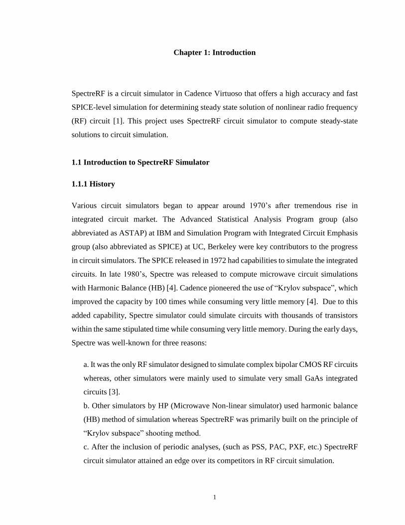
c. Netlist – It is responsible for execution of RF simulation by using various simulation
controls, design variables and analyses provided in ADE to save and plot the outputs. After
a successful simulation, total time taken and other relevant steps in the simulation are
explained extensively. The below Figure 1-3 shows the netlist option which is to be
selected after the design variables and proper analyses is chosen for plotting the outputs.
Figure 1-3. Netlist option in ADE window to execute the simulation.
d. SpectreRF engine – It is used to simulate the test circuit using appropriate analysis.
There are two SpectreRF simulation engines to perform any large signal analysis:
Shooting method is used to simulate the circuit based on time duration and is implemented
in periodic and quasi-periodic analyses. It is an adaptive and iterative control method that
is effective for sharp transitions in the input signal. This principle of convergence is used
in this algorithm. Convergence is a two-step process involving transient analysis and the
PSS analysis which will be discussed in more detail in Chapter 2.
Harmonic Balance (HB) method is used to simulate the circuit based on the frequency span
used for simulation. This simulation engine was primarily used in the traditional RF

5
simulators which considered circuit to be almost linear. As the complication in the circuits
increased by time; complex circuits like the mixers or switched capacitor-filter could not
be implemented using the traditional technique of harmonic analysis.
e. Analog artist plot results – It uses the calculator results, design variables and specific
analysis from Analog Design Environment (ADE) to plot the output results from the
simulation [1].
Different simulation engines are used for the analyses of any test schematic. These analyses
allow the user to extract the useful metrics of the test-circuit. The basics of these analyses
and the simulation engines used for efficient execution will be explained in detail in
Chapter 2.

6
Chapter 2 Background: Periodic Steady State Simulation Techniques
2.1 Overview
The SpectreRF circuit simulator uses simulation techniques to simultaneously add several
analyses to generate desired support for the efficient calculation of common analog and RF
communication circuits.
SpectreRF engines are the methods to simulate the RF analyses. These methods are used
based on linearity of the RF circuits. There are two simulation engines:
A. Newton Shooting method
Newton Shooting is a time-domain method based on the assumption of initial conditions.
It is an adaptive time-domain control method that is effective for circuits that have non-
linear or sharp transitions. Periodic Steady State (PSS) is primarily used in circuits where
the input signal varies with time [3]. The number of iterations depend on the linearity of
the circuit. The estimation of initial condition is an essential step in these simulations. The
following iterative, step-wise approach is to be followed for simulations with Newton-
Shooting implementation:
a. The first iteration is a transient analysis for one time-period known as 𝑡 = 𝑡𝑠𝑡𝑎𝑏. The
range of first iteration is from 𝑡 = 0 to 𝑡 = 𝑃𝑆𝑆𝑓𝑢𝑛𝑑. The 𝑡𝑠𝑡𝑎𝑏 parameter can be
adjusted properly by the user to a result in a periodic steady state.
b. The second iteration is PSS analysis and makes use of convergence. Here the values
are measured at the beginning and at the concluding part of one time-period [3]. The
range of this iteration is between 𝑡 = 𝑡𝑠𝑡𝑎𝑏 to 𝑡 = (𝑡𝑠𝑡𝑎𝑏 + 1/𝑃𝑆𝑆𝑓𝑢𝑛𝑑).
c. The third iteration compares the few data points at the end of the previous shooting
interval to adjust the slopes of the waveform at the beginning of the current interval.

7
B. Harmonic Balance method
The Harmonic Balance algorithm (HB) calculates the steady state solution using Fourier
series. It is purely frequency-domain technique.
Harmonic balance technique is first performed on small signal components of the
frequency and then on larger signal components which gives rise to new harmonics. It
performs small signal steady state calculations on the harmonics so that the shape of the
final transient signal is produced within an extremely small error tolerance. Harmonic
Balance method is also known as flexible balance method and is more robust for weakly
non-linear circuits.
2.2 Differences between Shooting and Harmonic Balance engines
For any RF circuit simulation, when the simulation parameters are set up properly, both
Newton Shooting method as well as harmonic balance method should give similar results.
Because both the simulation engines run on different domains i.e. time and frequency
respectively, the results are not seen to be identical [1]. After learning about both the
methods of RF simulation, the two simulation engines can be summarized as shown in
Table 2-1 below:
Newton Shooting method Harmonic Balance method
This is a time domain method for
simulation.
This is a frequency domain method for
simulation.
It is not favorable for lossy circuits; but
new methods are being modified for
improvements.
It is efficient for analyzing distributed
components like lossy transmission lines.
It gives accurate results for non-linear
circuits.
It is accurate if the circuit is linear with
sinusoid V, I.
It can handle abrupt transitions in signals
due to variable step-time for simulation.
It is not favorable for unsteady input
signals. (HB could also increase simulation
time).
Table 2-1. Difference between Simulation Engines in SpectreRF.
8
2.3 Applications of RF simulation engines
Shooting Newton method is mainly used for circuits where input signals have sharp
transitions (like in nonlinear circuits, frequency dividers), oscillators with dividers or
digital control components.
So to summarize, harmonic balance is mainly used for weakly nonlinear circuits/systems.
It is implemented in the RF frontend circuits like LNA's, IQ modulators, LC oscillators,
crystal oscillators and S-parameter models [2].
2.4. Different Spectre simulation techniques
SpectreRF circuit simulator employs different simulation techniques for deriving metrics
for any RF circuit. This section includes a brief description for each simulation techniques.
These techniques in SpectreRF simulator allows the users to sweep the input parameters,
specify different variables and use multiple analyses within the same simulation. The
flexibility of this simulator makes it reliable for the user to simulate the circuits.
There are four main types of analysis depending on the circuit topology as shown in Figure
2-1:
a. DC / Large signal analysis.
b. AC / Small signal analysis.
c. Transient signal analysis.
d. RF signal analysis.
In small signal model, the approximation of a transistor is made around its D.C operating
point [1]. The amplitude of the signal is small enough, so that the operation is over a very
small portion of nonlinear device (e.g. BJT or MOSFET) [1]. Such a small portion is thus
regarded as almost linear. When the amplitude of the signal is large, the behavior affects
the operating point and to employ such non-linear effects; it is important to use large-signal
model approximation. Large signal analysis enables us to find the DC operating point of
the circuit to remove non-linearity components from the characteristic of the device.
In small signal analysis, the question of how small the signal should be to be considered
for this approximation is challenging. To address this problem-statement; distortion at the

9
output due to minimal changes in the input signal is considered. In addition, circuit
topology and operating point also play an important role in decision making. Figure 2-1
shows a brief explanation of different types of analyses in SpectreRF circuit simulator:
Figure 2-1. Different types of analyses in SpectreRF circuit simulator.
2.4.1 Periodic Steady State analysis (PSS)
The Periodic Steady-State (PSS) analysis is a large-signal analysis that directly computes
the steady-state response of a circuit at a specified beat frequency [1]. The SpectreRF
simulation in this project uses Shooting method to simulate PSS analysis. This method
starts with estimation of the initial condition. The shooting method requires multiple
iterations for bringing the final state of the circuit to an almost linear function of the initial
state. As this method is iterative in nature, it takes multiple iterations to simulate the circuit
and remove the non-linearity. In this simulation, the user can sweep frequency and other
design variables.
The PSS analysis with shooting method calculates the steady-state waveforms using
transient analysis and PSS analysis. The first iteration is transient analysis which is run for

10
duration of 𝑡𝑠𝑡𝑎𝑏 with a simulation time of 𝑡 = 0 to 𝑡 = 𝑃𝑆𝑆𝑓𝑢𝑛𝑑. The second iteration is
PSS analysis which is run between to 𝑡 = 𝑡𝑠𝑡𝑎𝑏 to 𝑡 = (𝑡𝑠𝑡𝑎𝑏 + 1/𝑃𝑆𝑆𝑓𝑢𝑛𝑑). The steady
response of the circuit is determined at the beat frequency in PSS analysis.
The large signal PSS analysis with LO calculates the IF voltage at different harmonics.
These magnitudes are only offset by the LO frequency. In addition, the output mixing
products are generated at different harmonics (which are linear multiples of LO frequency)
as a result of PSS large signal analysis. The IF voltage at these harmonics are mentioned
below in Table 2-2:
Harmonics Frequency [Hz] IF Voltage [V/V]
0 0 6.18 µ
1 915 M 57.87 m
2 1.83 G 814.07 n
3 2.745 G 4.525 m
4 3.66 G 593.84 n
5 4.575 G 972.82 µ
Table 2-2. Output voltage at different harmonics.
In addition, the IF spectrum generated at different harmonics after simulating a frequency
translation circuit at beat frequency of 915 MHz is shown below. Higher IF voltage is
obtained at the LO frequency (915 MHz) as seen from the from the voltage spectrum shown
in Figure 2-2.

11
Figure 2-2. IF voltage spectrum at different harmonics using PSS analysis. The voltage
spectrum is generated only at integer multiples of LO frequency (915 MHz) as only large
signal PSS analysis is run for circuit simulation.
2.4.2. Periodic AC analysis (PAC)
“In periodic small-signal analyses, the small-signal analyses are applied to periodically
driven circuits that exhibit frequency conversion” [2]. The PAC analysis is run on top of
large signal analysis. It allows the user to sweep the frequency in a particular range.
The PAC analysis generates the output harmonics at linear multiples of the beat frequency.
The output mixing products of the input signal and the LO harmonics are generated. The
output mixing products are a result of large signal and small signal analysis. Down-
conversion and up-conversion translation effects are realized in frequency-translation
circuits. For example, in down-conversion mixers, different sidebands are denoted as ‘-1’
and’-2’ when the sideband is offset from the input frequency by ‘-1’ or ‘-2’. Also, ‘+1’ and

12
‘+2’ is denoted for sidebands generated in up-conversion mixers. The IF output voltage is
denoted in Table 2-3 at different sidebands generated due to frequency translation effect at
each harmonic of the LO frequency (915 MHz).
In SpectreRF simulation example shown below, the maxsideband parameter is set to 2.
The maxsideband generates the kmax sidebands ranging from –kmax to +kmax. So, total
sidebands generated after the SpectreRF simulation is given by Equation 2.1:
Total sidebands = 2 ∗ 𝑘𝑚𝑎𝑥 + 1 (2.1)
= 2 (2) + 1
= 5 sidebands ranging from -2 to +2.
Also, the output frequency at each sideband can be calculated as:
𝑓(𝑜𝑢𝑡) = 𝑓(𝑖𝑛) + 𝑘𝑖 ∗ 𝑃𝑆𝑆𝑓𝑢𝑛𝑑 , (2.2)
where 𝑓(𝑜𝑢𝑡) is the output signal frequency, 𝑓(𝑖𝑛) is the RF frequency also known as
input frequency and 𝑃𝑆𝑆𝑓𝑢𝑛𝑑 is the beat frequency or the LO frequency of the mixer.
Different values of output sidebands can be calculated using Equation 2.2. Also, as the
maxsideband parameter is set to 2, a total of 5 sidebands are generated in output spectrum
as seen in Figure 2-3. From equation 2-2, 𝑓(𝑖𝑛) is the RF frequency (915.1 MHz),
𝑃𝑆𝑆𝑓𝑢𝑛𝑑is the beat frequency of the circuit which evenly divides all the frequencies of the
circuit. The beat frequency of the test bench mixer is 915 MHz. Different values of ki are
updated from -2 to +2 to calculate different sidebands in the output spectrum as shown,
For index -2: 𝑓(𝑜𝑢𝑡) = 915.1 MHz + (-2)(915 MHz)
= 914.99 MHz (LO frequency of the circuit).
For index -1: 𝑓(𝑜𝑢𝑡) = 915.1 MHz + (-1)(915 MHz)
= 100 KHz (IF frequency of the circuit),
where ‘-1’ index calculated above represents the down converted sideband of the mixer.
This is the difference of the input frequency 𝑓(𝑖𝑛) and the fundamental frequency,
𝑃𝑆𝑆𝑓𝑢𝑛𝑑. Similarly, other sidebands of the output spectrum are calculated below,
For index 0: 𝑓(𝑜𝑢𝑡) = 915.1 MHz + (0)(915 MHz)
= 915.1 MHz (RF frequency of the circuit).

13
For index 1: 𝑓(𝑜𝑢𝑡) = 915.1 MHz + (1)(915 MHz)
= 1.83 GHz.
For index 2: 𝑓(𝑜𝑢𝑡) = 915.1 MHz + (2)(915 MHz)
= 2.745 GHz.
The sidebands represented by indices in the below table are generated due to down-
conversion translation effects at the sum and difference of 𝑓(𝑖𝑛) and 𝑃𝑆𝑆𝑓𝑢𝑛𝑑 frequencies
of the mixer circuit. The corresponding voltage values at these sidebands are shown in
Table 2-3:
Index Frequency [Hz] IF Voltage [V/V]
-2 914.99 M 1.19 µ
-1 100 K 76.95 m
0 915.1 M 1.07 µ
1 1.83 G 3.35 m
2 2.745 G 523.57 n
Table 2-3. Output IF voltage at different sidebands.
The output IF voltage spectrum generated due to the small signal PAC analysis is shown
in Figure 2-3 below. This figure shows the IF voltage spectrum at the above calculated
sidebands. From the figure 2-3 below, higher IF voltage magnitude of 76.94m is obtained
at the down-converted sideband of 100 KHz also represented by ‘-1’. Also, higher voltage
magnitude of 1.19µ is obtained at LO sideband represented by ‘-2’ as compared to the IF
magnitude of 1.06µ obtained at RF frequency. The other sidebands at 1.83 MHz and 2.75
MHz are a result of summation of 𝑓(𝑖𝑛)and 𝑃𝑆𝑆𝑓𝑢𝑛𝑑 frequencies.

14
Figure 2-3. IF Voltage spectrum at different sidebands using PAC analysis. Higher IF
voltage magnitude of 76.94m is obtained at the down-converted sideband.
From PSS and PAC analysis, the latter being a small signal analysis represents the
translation effects of the mixer in the IF voltage spectrum. PAC analysis allows the user to
learn the frequency response at different sidebands by representing the output mixing
products in the IF voltage spectrum. On the other hand, PSS being a large signal analysis
only allows the user to view the output voltage spectrum of harmonics at beat frequency.
So, the down-converted output products can be analyzed in the output spectrum with PAC
simulation as compared to PSS simulation.
2.4.3 Quasi-Periodic Steady State analysis (PDisto or QPSS)
PDisto or Quasi-Periodic Steady-State (QPSS) analysis is a large-signal analysis which
computes the solution for circuit with multiple moderate tones [2]. In this analysis, the user

15
can analyze the harmonic effects in the test bench. The moderate tones specified in the
QPSS analysis are responsible for generating large signal response at the input RF
frequency. QPSS analysis computes both the large signal analysis of the circuit and the
harmonics effects due to the moderate tones.
In QPSS analysis, shooting method is used to perform SpectreRF simulation. In SpectreRF
simulation, the mixing products are generated by both the large and moderate fundamentals
selected in the ADE-L form. The maxharms parameter denotes the array of sidebands
ranging from [k1,k2,...,kn], where k denotes the harmonics by large and moderate
signal. If ‘i’ is the sideband for moderate signal and ‘j’ denotes the sideband for large signal,
then the frequency translation effects generated due to moderate tones are centered at:
𝑓(𝑜𝑢𝑡) = 𝑖 ∗ (𝑓𝑙𝑎𝑟𝑔𝑒−𝑠𝑖𝑔𝑛𝑎𝑙) + 𝑗 ∗ (𝑓𝑚𝑜𝑑𝑒𝑟𝑎𝑡𝑒−𝑠𝑖𝑔𝑛𝑎𝑙) . (2.3)
The large tone of the mixer is considered as 915 MHz (LO frequency) with 3 harmonics
and moderate tone is considered as 915.1 MHz (input RF frequency) with 2 harmonics. LO
signal is considered as large as it is sinusoidal and is responsible for higher distortion
effects as compared to input RF signal which is dc. In QPSS analysis, the large signal
harmonics are represented from ‘-3’ to ’+3’, whereas the moderate signal harmonics are
represented from ‘-2’ to ‘+2’. The different translation effects in the frequency response of
the IF voltage spectrum is due to the moderate tone. As shown in Table 2-4, the actual
frequencies produced by the circuit can be calculated using Equation 2-3 as shown below.
For large signal harmonic ‘-3’ and moderate signal harmonic ‘-2’, 𝑓(𝑜𝑢𝑡)is given by:
𝑓(𝑜𝑢𝑡) = 𝑖 ∗ (𝑓𝑙𝑎𝑟𝑔𝑒−𝑠𝑖𝑔𝑛𝑎𝑙) + 𝑗 ∗ (𝑓𝑚𝑜𝑑𝑒𝑟𝑎𝑡𝑒−𝑠𝑖𝑔𝑛𝑎𝑙)
= (-3)(915 MHz) + (-2)(915.1 MHz)
= 4.575 GHz.
Similarly, all the different values in Table 2-4 are calculated and after running SpectreRF
simulation, the IF voltage spectrum is obtained at these frequencies. All these calculated
output frequencies in the Table 2-4 are a result of large and moderate harmonics specified
in the SpectreRF simulation. The IF voltage spectrum is calculated at the harmonics of
large signal (LO frequencies) and the mixing products due to the harmonics of the moderate
signal. So, from the Table 2-4, peak IF voltage at 100 KHz (with large tone ‘-1’ and

16
moderate tone ‘+1’) which is the down-converted output and all other harmonics are
cancelled out. Also, at LO frequency (915 MHz), IF voltage magnitude of 27.06 m is
obtained. And at RF frequency (915.1 MHz), IF voltage magnitude of 100.05 µ is obtained.
Higher IF output magnitude is obtained at LO frequency as compared to RF frequency. All
the harmonics generated due to the large and moderate tones in the mixer circuit are
tabulated in below Table 2-4:
Large Signal
harmonic
Moderate signal
harmonic
Frequency [Hz] IF Voltage [V/V]
-3 -2 4.575 G 892.37 µ
-3 -1 3.66 G 824.05 µ
-3 0 2.745 G 539.19 µ
-3 1 1.829 G 357.74 µ
-3 2 914.8 M 955 µ
-2 -2 3.66 G 442.63 µ
-2 -1 2.745 G 602.05 µ
-2 0 1.83 G 1.019 m
-2 1 914.9 M 1.373 m
-2 2 200 K 1.36 m
-1 -2 2.7452 G 11.016 m
-1 -1 1.8301 G 17.499 m
-1 0 915 M 27.06 m
-1 1 100 K 16.61 m
-1 2 915.2 M 10.57 m
0 -2 1.8302 G 141.5 µ
0 -1 915.1 M 100.05 µ
0 0 0 8.69 µ
0 1 915.1 M 100.05 µ
0 2 1.8302 G 141.5 µ
1 -2 915.2 M 10.57 m
1 -1 100 K 16.61 m

17
1 0 915 M 27.06 m
1 1 1.8301 G 17.5 m
1 2 2.7452 G 11.016 m
2 -2 200 K 1.36 m
2 -1 914.9 M 1.373 m
2 0 1.830 G 357.74 µ
2 1 2.7451 G 602.05 µ
2 2 3.6602 G 442.63 µ
3 -2 914.8 M 955 µ
3 -1 1.83 G 357.74 µ
3 0 2.7450 G 539.19 µ
3 1 3.66 G 824.05 µ
3 2 4.5752 G 892.37 µ
Table 2-4. IF output voltage at different harmonics.
QPSS analysis only calculates the actual frequencies produced by the circuit whereas PSS
analysis calculates harmonics of the beat frequency [8].
Both PSS followed by PAC analysis and QPSS analysis can simulate the circuit and
analyze the translation effects from the output harmonics. But from Figure 2-3 and Figure
2-4, one implicit observation is that the QPSS output spectrum has more output mixing
products as compared to PAC analysis. This certainly enables the user to read more data
from the QPSS output spectrum as compared to PAC output spectrum in Figure 2-3.
There are two main reasons for the advantage of QPSS analysis over PSS followed by PAC
analysis:
Firstly, QPSS analysis takes into consideration the frequency translation effects due to
large and moderate tones in the mixer circuit. On the contrary, PAC analysis does not
consider small signal harmonics for the frequency-translation effects in the output.
Secondly, QPSS analysis allows the user to analyze the translation effects due to aperiodic
sinusoids generated due to addition of large and moderate tones. Due to this, QPSS analysis
can determine the linearity of the circuit by computing the effects due to third order inter-
modulation products.

18
The output spectrum on simulation using PAC analysis (in Figure 2-3) models all the
harmonics generated from Equation 2-2. This means that with PSS followed by PAC
analysis, takes into consideration only effects due to small signal at 𝑓𝑢𝑛𝑑(𝑃𝑆𝑆)frequency.
But the output spectrum generated after simulation using QPSS analysis, (in Figure 2-4)
models all harmonics generated from Equation 2-3. So, the output spectrum involves
effects due to moderate tones and addition of aperiodic sinusoids which produces more
output mixing products as shown below:
Figure 2-4. Voltage spectrum at different harmonics using QPSS analysis.

19
Chapter 3: Basics of RF Mixer theory
3.1 Outline
RF mixer is an active or passive device that converts input signal from one frequency to
the other. It is accomplished by multiplying two input frequencies to obtain an output which
is either a sum or difference of the input frequencies. In this chapter, basics of RF mixer
theory, their types and working will be discussed.
3.2 General mixer theory
“A mixer is a 3-port active/passive device with two input ports and one output port” [6].
RF mixers are used in the transmitters and receivers of a basic communication block for
frequency translation (as shown in Figure 3-1 below) [5]. Depending on the topology of
the mixer (up-conversion or down-conversion), the LO, RF and IF ports are used as input
port or output port in a mixer design.
A down-conversion frequency mixer consists of RF and LO as two input frequencies. The
output is a down-converted intermediate frequency (IF), which is a either a sum or
difference of LO and RF frequency depending on the low side or high side conversion.
The frequency translation in a non-linear mixer device can be understood from Equation
3.1 and 3.2 below:
a(t) = A*cos ω1t (3.1)
b(t) = B*cost ω2t . (3.2)
where a(t) and b(t) are the input signals and ω1 and ω2 are the respective input
frequencies. The mixer output signal is accomplished by multiplying the two input signals
also given by:
a (t)* b (t) = A cos ω1t * B cos ω2t
= 1
2 *AB [cos (ω1 – ω2) + cos (ω1+ω2)] . (3.3)

20
The above Equation 3.3 is the output of the mixer which is given by the difference and sum
of both input frequencies. Depending on the application of RF mixer, it can be implemented
at the transmitter or receiver.
There are two main topologies that decide the mixer operation in any communication
system:
Up-conversion mixer: Considering LO as the input frequency, in this mixer topology the
output frequency is higher than the 2nd input signal frequency [7]. This generates the sum
and difference components as shown below in Equation 3.4 and Equation 3.5:
fRF = fLO + fIF , or (3.4)
fRF = fLO - fIF . (3.5)
From the expression, in up-conversion mixer, IF is the other input and RF is the output.
Down-conversion mixer: Considering LO as the input frequency, in this mixer topology
the output frequency is lower than the 2nd input signal frequency [7]. This generates the
sum and difference components as shown in Equation 3.6 and Equation 3.7:
fIF = fRF– fLO , or (3.6)
fIF = fLO - fRF . (3.7)
From the above expression, in down-conversion mixer, RF is the other input and output is
lower IF intermediate frequency.
A mixer can be implemented by using either passive devices (like diodes) or active devices
(mainly FETs). Depending on the elements used in the mixer design, they are broadly
classified into passive mixers and active mixers.
A passive mixer implemented using diodes usually has conversion loss instead of
conversion gain. An unbalanced passive mixer topology makes use of multiple diodes to
balance the circuit symmetry and thereby improve port-isolation. In passive mixer, due to
large conversion loss, LNA is used before the frequency-mixer to amplify the input signal.
On the other hand, an active mixer is made of transistors or FET’s. They have improved
port-isolation compared to passive mixer, higher noise and more power consumption.

21
Active mixers are configured to provide high conversion gain, so they are mostly used for
RFIC implementation. It is essential to choose an appropriate operating frequency for
different ports of the active frequency mixer. Failure to do so results in noise, non-linearity
and leakage effects.
3.3 Important metrics in mixer theory
a) Conversion gain
“Conversion gain or loss is the ratio of the IF output (voltage or power) to the RF input
signal (voltage or power) value”. Voltage conversion gain (VCG) and power conversion gain
(PCG) is also represented by Equation 3.6 and Equation 3.7 as shown below:
VCG = 𝑟.𝑚.𝑠 𝑣𝑜𝑙𝑡𝑎𝑔𝑒 𝑜𝑓 𝐼𝐹 𝑠𝑖𝑔𝑛𝑎𝑙
𝑟.𝑚.𝑠 𝑣𝑜𝑙𝑡𝑎𝑔𝑒 𝑜𝑓 𝑅𝐹 𝑠𝑖𝑔𝑛𝑎𝑙 (3.8)
or
PCG (dB) = Output IF power (dBm) – RF input power (dBm) . (3.9)
Conversion gain or loss is an important metric which determines the mixer performance
based on isolation and 1dB-compression point. Conversion gain helps to realize the quality
of mixer [7].
b) Noise Figure
“Noise figure (NF) is defined as the ratio of SNR at the IF port to the SNR of the RF port”
[6]. It is the measure of noise through different stages of the mixer as it gets converted to
IF output. It is In case of passive mixers, conversion loss is measured by insertion loss.
Image reject filters are used preceding the mixers in order to suppress the image noise.
During a mixer design, single sideband and double sideband noise figures are taken into
consideration.
Single sideband NF (SSB-NF)
The SSB-NF assumes noise inputs at the image frequencies. In this assumption, signal
input from only one sideband is considered. “SSB-NF is the ratio of SNR at desired IF
(output) to SNR at RF (input) measured in single side-band” [8]. The noise factor for SSB
is twice the DSB noise factor.

22
Double sideband NF (DSB-NF)
The DSB-NF assumes noise and signal inputs from both side-bands. “DSB-NF is the ratio
of SNR at IF (output) to the SNR at input measured in both signal and image sidebands”
[8]. DSB-NF is much easier to measure than SSB-NF. Also, conversion loss of DSB-NF is
usually 3dB less than the SSB-NF [8].
Comparison of power and conversion loss is represented by Equation 3.8 and 3.9 below:
Power: P(IF)DSB = 2 * P(IF) SSB (3.10)
Conversion loss: (CL)DSB = (CL)SSB – 3dB . (3.11)
c) Linearity
The linearity of a mixer is an important metric which determines its quality of operation.
“Linearity is the measure of input intercept point (IIP3) which is the input RF power at
which the unwanted intermodulation products and desired IF at the output are equal” [5].
In any receiver, the odd-order products are most harmful, as they have the highest
amplitude with lowest order. So, the third order intercept (TOI) plays an important role in
determining the linearity of a mixer [6].
d) Port isolation
Port isolation is the measure of power leakage in dB between different ports of the mixer.
It is represented by the difference in power at the input port and output port of the mixer.
Due to different active and passive elements in the mixer, it is susceptible to feedthrough
(or coupling) [7]. Feedthrough or coupling is the leakage amount of LO power into either
the IF or the RF ports.
Few properties of an RF mixer can be summarized as below:
a) Higher conversion gain results in lower noise figure at the mixer output.
b) Intercept point is the measure of linearity performance of the mixer.
c) There should be minimum interaction between IF, RF and LO ports. Port-isolation
is a crucial factor in mixer performance.
d) Noise figure can be improved by suppressing the image noise frequencies. Noise
figure impacts receiver sensitivity to a large extent.
e) The operating frequency range determines the final selection of the mixer type [6].

23
3.4 Types of RF mixers
RF mixers are categorized in three types depending on their construction as shown in
Figure 3-1.
Figure 3-1. Types of mixers.
1. Single-device mixer
This mixer is very favorable at higher frequencies like the RF/millimeter wave band. It is
constructed using one diode or transistor [6]. For the design of single device mixer, these
rules must be followed:
a) For maximum gain and better port-isolation, LO node should be short-circuited to
RF and IF frequencies. Also, RF node should be shorted to LO frequency to
suppress port isolation due to power leakage between LO and RF ports.
b) The IF port termination of the diode at image frequency results in better conversion
efficiency.
c) This mixer with FET’s is comparatively simple to the diode implementation as FET
is a 3-terminal device and provides RF-to-LO port isolation.
d) In short, all undesired frequencies are terminated at both input and output.
2. Single-balanced mixer
These mixers consist of two different single device mixers and each of them are either 90
degree or 180 degree out of phase. Port isolation between all three ports is ensured for an
improved mixer performance [6]. This mixer also rejects spurious intermodulation
products. The only disadvantage of this mixer design is its higher LO power requirements.

24
Single-balanced mixers use two diodes or transistors. To reduce the noise figure or increase
the conversion gain, these diodes or transistors need to be well matched.
3. Double-balanced mixer
These mixers exhibit higher linearity and isolation as compared to single device mixer and
single balanced mixer, but they have lower conversion gain. The two most widely used
double balanced mixer implementation topologies are star and ring. The advantage of
double balanced mixers to the prior two types are its improved ability of port-isolation,
suppression of spurious inter-modulation products and increased linearity [6]. These
mixers have lower conversion gain but have higher IIP3 and lower IM products due to
better port isolation [6].
3.5 Gilbert cell mixer
One of the most popular mixer designs in today’s industry is the Gilbert cell mixer or
multiplier named after Barrie Gilbert. This type of mixer design exploits the symmetrical
topology and removes undesired RF and LO signals from the IF by cancellation. Inputs
from LO port are provided to the two FET’s M2 and M3 to switch currents completely
between the two sides and M1 acts as a transconductance stage. Multiple topographies of
Gilbert cell multiplier are used in the schematic from single balanced to double balanced
and more complex designs for better port isolation.
As both LO and RF are well-balanced, it provides suppression of the unwanted LO and RF
signal components at the IF output [8]. In a Gilbert cell mixer, all the ports are inherently
isolated which suppresses the port-leakage. This mixer can maintain appropriate noise
figure and achieve high conversion gain, linearity and port-isolation.

25
Figure 3-2. Gilbert cell schematic.
3.5.1 Single balanced Gilbert cell mixer
In this mixer topology (shown in Figure 3-3), the FET M1 is fed with an RF signal. At this
transconductance stage, M1 converts the input RF voltage (VRF) to current. Next, the in-
phase and out-of-phase LO signal is fed to the FET’s M2 and M3 via local oscillator. The
current from transconductance stage is multiplied with the local oscillator input at this
current switching stage. This current is then converted into voltage via the load resistors
R1 & R2 and the output voltage can be calculated from the respective negative and positive
IF ports (VIF shown in the Figure 3-2). This operation is summarized below in Figure 3-3.

26
Figure 3-3. Operation of single-balanced active mixer [5].

27
Chapter 4: Simulation procedures for different analyses
4.1 Outline
This chapter explains different simulation procedures used to compute RF metrics of a
mixer using SpectreRF. A step-wise approach is implemented to explain various periodic
steady state simulations using SpectreRF. We use a single-balanced active Gilbert mixer
as a test bench to demonstrate PSS, PAC and QPSS analysis.
4.2 Test Schematic of RF Mixer
A three-port single-balanced mixer (shown in Figure 4-1) is used to perform different
simulations discussed later in this chapter. The mixer is commonly called as multiplier
based mixer or Gilbert mixer. The test bench mixer has an LO frequency of 915 MHz and
RF frequency of 915.1 MHz to compute important metrics like voltage conversion gain,
power conversion gain, etc.
The test bench shown in Figure 4-1 consists of an LO port (port 0), an RF port (port 1)
and a balun which provides differential inputs from LO port to M1 and M2 of single
balanced mixer to switch the currents completely between the two sides. Both the input
ports of the mixer are terminated with a 50 Ω resistor. M3 acts as a transconductance stage
whereas M1 and M2 act as current-switching stage where the gate voltage of the two NFETs
is same in magnitude but opposite in phase. The FET transistors used in the schematic are
standard 180nm cmhv7sf family from IBM’s CMOS 7sf technology.
The RF mixer schematic shown in Figure 4-1 below is generated using “Cirkuit” software.

28
Figure 4-1. Test schematic of active down-conversion Gilbert mixer.
4.3 Simulation using Periodic Steady State analysis
4.3.1 Overview
PSS is a small signal analysis, which is mainly concerned with the steady-state response of
a circuit at a definite beat frequency [1]. This analysis technique computes the operating
point of the circuit and the initial condition [2]. In this section, PSS simulation is performed
on the test bench using Shooting method.
4.3.2 Goal for PSS analysis
The goal of PSS analysis is to calculate the gain in output voltage of an active mixer
schematic at LO frequency. In this analysis, we compare the output IF voltage with respect
to the input RF voltage. In large signal analysis, the simulation time is not affected by the
number of harmonics specified in the ADE-L environment [2], but it is greatly affected in
case of moderate signal analysis.
29
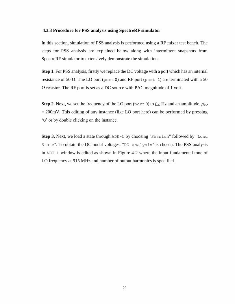
4.3.3 Procedure for PSS analysis using SpectreRF simulator
In this section, simulation of PSS analysis is performed using a RF mixer test bench. The
steps for PSS analysis are explained below along with intermittent snapshots from
SpectreRF simulator to extensively demonstrate the simulation.
Step 1. For PSS analysis, firstly we replace the DC voltage with a port which has an internal
resistance of 50 Ω. The LO port (port 0) and RF port (port 1) are terminated with a 50
Ω resistor. The RF port is set as a DC source with PAC magnitude of 1 volt.
Step 2. Next, we set the frequency of the LO port (port 0) to fLO Hz and an amplitude, pLO
= 200mV. This editing of any instance (like LO port here) can be performed by pressing
‘Q’ or by double clicking on the instance.
Step 3. Next, we load a state through ADE-L by choosing "Session" followed by "Load
State". To obtain the DC nodal voltages, "DC analysis" is chosen. The PSS analysis
in ADE-L window is edited as shown in Figure 4-2 where the input fundamental tone of
LO frequency at 915 MHz and number of output harmonics is specified.

30
Figure 4-2. PSS analysis form using Newton Shooting engine.
Step 4. The final ADE-L window is displayed in Figure 4-3 where DC and PSS analysis
are checked before simulating the test-circuit. From the ADE-L window, it is inferred that
the PSS is used as a simulation analysis and the signal at port 0 (LO port) is considered
as large signal. Moreover, seven harmonics are specified so that we can compare the
output and input harmonics in our final spectrum. The ADE-L window mainly consists of
three sections:
a) Design variables (inputs that need to be simulated).
b) Analyses (the analysis of interest).
c) Outputs.

31
Figure 4-3. ADE-L window indicating PSS analyses on test-circuit.
The DC analysis in the above form, computes the DC voltage at every node. Similarly,
transient analysis compares the transient behavior of signals at different nets.
Step 5. Next, the test circuit is simulated (either from the schematic window or the ADE-L
window) and the simulation is verified to be correct only when the simulation window (as
shown below in Figure 4-4) pops up indicating the exact duration taken to simulate and the
step-wise calculation of the PSS analysis on test-circuit. This indicates that the circuit is
simulated without errors and the results are ready to be analyzed.
Figure 4-4. Simulation window indicating error-free execution.

32
4.3.4 Simulation Results
The simulation results are obtained after choosing appropriate choices on direct plot form.
As we are interested in comparing the magnitude of input RF and corresponding output IF
voltage spectrum, we select the appropriate choices as shown in Figure 4-5 below. Next,
we choose the differential RF input and IF output nets on the schematic to obtain the
voltage comparison at different harmonics.
Figure 4-5. Direct plot form for plotting the required metrics.
The output of the PSS analysis shows a comparison of IF and RF voltage at different
harmonics (specified 7 harmonics for this analysis). From Figure 4-6, it is inferred that at
DC (0 Hz), we obtain an output IF voltage of 6.18 µV. Next, at LO frequency of the mixer
(915 MHz) which is also the first harmonic, we obtain an output IF voltage of 57.87 mV.

33
Different output voltages at different harmonics are seen in Figure 4-6. Higher output IF
voltage of 57.87 mV is obtained as compared to the input RF voltage of 1.2 nV at 915
MHz. This indicates higher output IF voltage (VIF) at LO frequency with respect to RF
voltage (VRF).
Figure 4-6. IF output voltage comparison at different harmonics. Higher output IF voltage
is seen at odd harmonics (1st, 3rd, 5th and so on) as compared to even harmonics.
4.4 Simulation using Periodic AC analysis
4.4.1 Overview
Periodic AC analysis (PAC) is a small-signal analysis that runs over a large signal analysis
[2]. PAC analysis evaluates the transfer function of circuits like mixers, low noise
amplifiers and similar circuits that execute frequency translation. Unlike AC analysis, in
PAC the transfer functions is calculated around a periodically varying DC operating point
[2]. So, a large analysis (like PSS or QPSS) is simulated before running PAC simulation.

34
4.4.2 Goal for PAC analysis
The goal of this analysis is to compute the conversion gain with respect to IF frequency.
This is achieved by sweeping the input sideband of LO frequency and obtain voltage
conversion gain. First, the transient analysis is performed to check if the mixer performs
proper function of mixing the RF and LO inputs. So, in this chapter, we simulate the PSS
analysis along with small-signal PAC analysis (i.e. we run PSS swept-PAC analysis to
obtain the conversion gain with respect to IF frequency). For the down-conversion mixer
shown in Figure 4-1, output IF frequency is given by fIF = |fRF – fLO|.
4.4.3 Procedure for PAC analysis using SpectreRF simulator
PAC analysis procedure for an active down- conversion single balanced mixer is described
below:
Step 1. From test-schematic shown in Figure 4-1, port 0 and port 1 are the LO port and
the RF port with sinusoidal source. A balun used in the circuit has 50Ω of single input
impedance and 100Ω of output impedance.
Small signal PAC analysis is run after large signal PSS analysis to compute the voltage
conversion gain with respect to IF frequency.
Step 2. Next, the test-schematic is saved and a new ADE-L window is launched. An
appropriate PSS and PAC analysis is chosen with design variables required for successful
simulation. The ADE-L window also allows the user to choose appropriate simulation
engine. Shooting method is used in this simulation for large signal PSS analysis.
Step 3. The same ADE-L environment state is used to perform PAC analysis as shown in
Figure 4-7 below after PSS analysis. Here we input the sweep range for LO frequency from
915 MHz to 1.165 GHz with three sidebands in order to simulate the PSS swept PAC
analysis. The area of interest to plot voltage conversion gain is confined from 915 MHz to
1.165 GHz. This range of frequency will give an idea of how the voltage conversion gain
varies over a 250 MHz IF frequency. Also, sweep-type is chosen as ‘linear’ with a step
size of 3MHz and maximum 3 side-bands.

35
Figure 4-7. PAC analysis form in ADE-L window.
Step 4. Next, the analyses form in the ADE-L window is updated (in this case PSS and
PAC analyses) according to the simulation requirement. So, the final ADE-L environment
window for PSS swept-PAC analysis looks as shown in Figure 4-8 below.
Figure 4-8. ADE-L window indicating PSS swept PAC analysis.

36
4.4.4 Simulation results
After successful execution of the PSS swept-PAC analysis, Results followed by
Direct Plot-Main Form is selected to plot the voltage converge gain of the RF mixer.
In the Direct Plot Form shown in Figure 4-9, the input sideband refers to the frequency
range which we are interested in. As the LO frequency of the mixer is 915MHz, the input
sideband is chosen from 915 MHz to 1.165 GHz also indicated as ‘0’. And the output
sideband refers to the actual sideband frequency where the voltage conversion gain to be
compared. Next, this frequency range of 250 MHz (1.165 GHz - 915MHz = 250 MHz),
will in-fact give an idea of voltage conversion gain variation with respect to IF frequency.
The output sideband is chosen as down-conversion (shown as ‘-1’) in the range of 0 to 250
MHz as shown in below Figure 4-9. Therefore, after choosing proper options on main form,
appropriate nets/ports/instances is selected on the schematic in order to obtain the
conversion gain variation with respect to IF frequency of the mixer test bench.
Figure 4-9. Direct plot form for plotting the required metrics.

37
From the PAC analysis shown in below Figure 4-10, maximum conversion gain (CG) of
22.22 dB is obtained at IF frequency of 3MHz. Also, we see that after peak conversion gain
at 3MHz, there is a steep conversion loss until 250 MHz and beyond.
This behavior of the voltage conversion gain as shown in below Figure 4-10 is because the
circuit at the IF output behaves as a low-pass filter. A passive R-C low pass filter (LPF) is
implemented near the IF port of the mixer where the output signal is taken across the
capacitor. In the below Figure 4-10, if the input sideband is increased beyond 1.165 GHz,
the conversion gain reduces and thereby replicates the gain versus frequency characteristics
of band pass filter. The conversion gain characteristics shown in Figure 4-10 below is
identical to gain-magnitude frequency response of a low pass filter.
Figure 4-10. Voltage conversion gain at different IF frequencies. The maximum conversion
gain is obtained at 3 MHz and the conversion gain characteristics are identical to the
frequency response of a low pass filter.

38
Different values of conversion gain at LO frequencies of 3MHz step-size are obtained from
the .vcsv file extracted from simulated cadence plot. This .vcsv file generated from
simulation consists of X and Y coordinates of those nodes. The different values from the
.vcsv file obtained from simulation output indicates different values of voltage
conversion gain at different LO signal frequencies when swept from 0 MHz to 250 MHz
with 3 MHz step size.
4.5 Simulation using Quasi-Periodic Steady State analysis
4.5.1 Overview
QPSS is a large-signal analysis, which is performed when dealing with multi-tonal input
signal. It uses both Shooting as well as Harmonic Balance engines for simulation according
to the requirement of desired output. In general, harmonic balance is preferred due to its
faster simulation-time and accuracy with less memory. QPSS with Newton Shooting is
helpful in situations where the overall system is very non-linear. QPSS (also known as
PDISTO analysis) can compute the intermodulation distortion effects very efficiently by
considering the large and moderate tones contributing to non-linearity.
4.5.2 Goal for QPSS analysis
The goal for QPSS analysis is to calculate the conversion gain vs RF signal power. In this
analysis, both LO and RF port are provided with sinusoidal source with respective fLO
(considered as large signal) and fRF (considered as moderate signal) frequencies. In this
section, we analyze the behavior of voltage conversion gain with respect to LO signal
power using QPSS analysis. If the effect of the RF tone is small, we could use a PSS
analysis instead.
This analysis consists of two stages, the first stage comprises of transient phase to initialize
the circuit and the second stage computes the quasi-periodic steady-state solution by
performing the Shooting method [2].
The transient phase consists of two intervals:
1. An initial transient analysis suppresses all moderate input signals.
2. At least two stabilizing transient analyses run with all signals activated.

39
This is also referred to as ‘tstab’ in PSS analysis that decides the total number of iterations
required for simulation. The Shooting stage employs MFT algorithm (also known as Mixed
Frequency Time) which can run on multiple fundamental frequencies. This Shooting stage
is the second stage after the transient analysis is completed. When the same system is dealt
with PSS followed by a PAC analysis; QPSS yields more information instead [1].
4.5.3 Comparison between QPSS and PSS swept PAC analysis
QPSS analysis is very similar to PSS swept-PAC analysis as it uses many parameters like
‘tstab’ and similar to the PSS analysis. However, QPSS analysis provides more information
about the harmonics of multiple input signals that are even aperiodic [2]. On the other hand,
using PSS swept with PAC can only compute the information of single small signal at the
fundamental frequency that is computed using PSS analysis [2]. In QPSS, signal level of
one of the tone should be large and the rest of the tones could be moderate. An implicit
comparison between both these analyses is explained in chapter 2.
4.5.4 Procedure for QPSS analysis using SpectreRF simulator
In this simulation, we use QPSS analysis for computing two results related to the
performance metric of RF mixer:
(I) Voltage conversion gain variation with respect to RF signal power (pRF).
(II) Power spectrum at IF and RF frequencies.
(I) Voltage conversion gain of RF mixer with respect to RF signal power (pRF)
In this simulation, we demonstrate how the voltage conversion gain reaches steep roll-off
when the RF signal power is increased gradually from -70dBm to 0dBm. The following
steps are used to simulate QPSS analysis:
Step 1. From the circuit in Figure 4-1; LO port (port 0) is selected and its properties are
set as a sinusoidal source with fLO and pLO as two design variables for the LO port.
Moreover, an internal resistance of 50 Ω is considered with a PAC magnitude of 1 volt.

40
Step 2. Next, the properties of the RF port (port 1) are edited by assigning design
variables for magnitude as pRF and frequency as fRF. Further, as QPSS is a large signal
analysis, it requires a large and moderate signal for its simulation.
Step 3. In the QPSS form in Figure 4-11 below, fLO is considered as large signal analysis
with 5 harmonics and fRF as moderate signal analysis with 3 harmonics. Also, to compute
conversion gain with respect to RF signal power, pRF is swept by providing an appropriate
sweep range. So this environment has to be created in ADE-L window and depending on
the required accuracy, the output plot can be set to conservative, moderate or liberal. Also,
pRF is swept between the sweep range of -70 dBm to 0 dBm to generate the output
conversion gain variation with respect to swept RF signal power.
Figure 4-11. QPSS analysis form-I in ADE-L window.
Step 4. So, finally the ADE-L window is shown in the Figure 4-12 below where we add
constant design variable values for pRF = -30 dBm, fLO = 915 MHz and fRF = 915.1 MHz.

41
Figure 4-12. ADE-L window for the QPSS analysis.
(II) Power spectrum at IF and RF frequencies using QPSS analysis.
In this simulation, QPSS analysis is used to calculate the conversion gain of the mixer from
IF and RF power. For the calculation of power conversion gain, power spectrum is plotted
using QPSS simulation at LO, RF and IF frequencies.
Step 1. The LO and RF port properties for this simulation are similar to step 1 and step 2
as discussed above. The only change in this procedure is to implement this simulation using
a different ADE-L environment window where we specify the sweep and accuracy
parameters according to the desired results.
Step 2. In the QPSS form as shown in Figure 4-13 below, we consider fLO as large signal
analysis with 5 harmonics and fRF as moderate signal analysis with 3 harmonics. But unlike
the previous analysis, we do not sweep any parameter here as we need to compute the
conversion gain from the power spectrum at RF and IF frequencies. The accuracy for the
output spectrum is set to conservative for better accuracy (the accuracy is set to
conservative when the circuit parameters are very sensitive).

42
Figure 4-13. QPSS analysis form-II in ADE-L window.
4.5.5 Simulation Results
(I) Voltage conversion gain of RF mixer with respect to RF signal power (pRF)
After an error-free simulation, the results for conversion gain variation with respect to RF
signal power can be plotted using direct plot form. Here as we vary the RF signal power,
we choose sweep option as variable shown below in Figure 4-14. To compute voltage
conversion gain, we choose the input harmonic as RF frequency = 915.1 MHz and output
harmonic as IF frequency = 100 KHz (difference of RF and LO frequencies). In the
Direct Plot Form ‘-1’ indicates that the output frequency is a down-converted

43
sideband or in other words it is indicated for down-conversion mixers and contrarily, ‘+1’
is indicated for up conversion translation effects. After selecting appropriate input and
output harmonics, we have to select the numerator positive, numerator negative followed
by denominator positive and denominator negative differential nets on the schematic.
Figure 4-14. Direct plot form for plotting required metrics through QPSS.
The aim in this simulation is to analyze the behavior of voltage conversion gain. So the
numerator net to be chosen on the schematic is IF net (+ve and -ve) and the denominator
net on the schematic should be RF net (+ve and -ve).
After successfully selecting appropriate nets on schematic, we obtain the following graph
as shown in Figure 4-15. From the plot, we observe the conversion gain variation with
respect to RF signal power. Furthermore, we note that as the RF signal power increases
past -21 dBm, there is a sharp roll-off in the conversion gain characteristics. This means

44
that we see a saturated gain response of the mixer when we vary the RF signal power from
-70 dBm to -28 dBm. In other words, the conversion gain of the RF mixer is 21.89 dB from
-70 dBm to -28 dBm and we see a steep conversion loss post -28 dBm. At 0 dBm, we note
the conversion gain to be -16.4dB. As our area of interest was to verify the conversion gain
response with respect to RF signal power, we have achieved it successfully. The Figure 4-
15 above is plotted in Matlab software, where conversion gain values at different instances
of RF signal power are extracted in .vcsv file obtained from the cadence output plot.
Figure 4-15. Voltage conversion gain versus RF signal power. The RF signal power is
swept to monitor the conversion gain characteristics of the RF mixer. We can infer here
that as the RF signal power increases, the voltage conversion gain decreases.
(II) Power spectrum at IF and RF frequencies
After an error-free execution of the schematic, in this simulation we find the power
spectrum at IF and RF frequencies to compute the conversion gain. The gist of this
simulation is to verify that the power conversion gain obtained in the previous simulations

45
is approximately equal to the difference of output power at IF and available input RF
power. It is also denoted as:
Power Conversion gain = 𝑂𝑢𝑡𝑝𝑢𝑡 𝑝𝑜𝑤𝑒𝑟 𝑎𝑡 𝐼𝐹
𝑅𝐹 𝑎𝑣𝑎𝑖𝑙𝑎𝑙𝑒 𝑖𝑛𝑝𝑢𝑡 𝑝𝑜𝑤𝑒𝑟 , (4.1)
where power conversion gain is calculated as the difference of power at IF and RF
terminals of the mixer.
So, it is important to compute the power spectrum at RF and IF frequencies. Next, we
choose the appropriate choices on QPSS direct plot form as shown in Figure 4-16 shown
below. After selecting the choices, we finally select the positive and negative differential
nets. Here, we select the numerator differential net as IF and denominator differential net
as RF representing the conversion gain.
Figure 4-16. Direct plot form for plotting required metrics through QPSS.
From the output plot obtained in Figure 4-17, the output power at IF frequency (100 KHz)
is -8.31 dBm and input available power at RF frequency (915.1 MHz) is -30 dBm. “And

46
the conversion gain of the mixer is the difference of IF output power and RF input power”.
The conversion gain is analytically computed to be 21.69 dB (-8.31dBm + 30dBm). So,
we verify that the conversion gain obtained through power spectrum is approximate to
conversion gain calculated in previous PAC and QPSS simulations for the down-
conversion Gilbert mixer.
Figure 4-17. Computation of conversion gain from power spectrum at IF and RF. Power at
IF frequency = -8.31 dBm and power at RF frequency = -30 dBm. So the conversion gain
is calculated to be 21.69 dB from the plot above by taking a difference of power at IF and
RF frequency.

47
Chapter 5: Conclusion
Different periodic steady state analyses (PSS, PAC and QPSS) are successfully performed
to simulate a RF mixer test bench and calculate its important metrics. Firstly, PSS analysis
is used to compare output IF voltage at different harmonics. Peak IF voltage of 57.87mV
is obtained at LO frequency by using the single balanced Gilbert mixer schematic.
Secondly, PAC analysis is used to measure the conversion gain of the mixer with respect
to IF frequency. Maximum conversion gain of 22.22 dB is achieved at 3 MHz IF frequency.
The PAC simulation results showed that the mixer yields a better conversion gain in the
sidebands of the fundamental LO frequency. From the conversion gain plot vs IF
frequency, it is realized that the circuit behaves as a low-pass filter at the IF port of the
mixer. Next, the mixer test bench is simulated using a large-signal QPSS analysis to
measure the voltage conversion gain and its behavior with increased RF signal power. As
the RF signal power increases, voltage conversion gain decreases. In other QPSS analysis,
it is verified that in case of down-conversion mixer, the power conversion gain at IF
frequency is the difference of power at RF and IF frequencies.
Overall, the RF mixer test-bench is simulated with different steady state analyses
techniques using SpectreRF simulator to evaluate its important metrics.

48
Bibliography
[1] "Virtuoso Spectre Circuit Simulator RF Analysis User Guide", Product version 6.2 June
2007.
[2] "Virtuoso Spectre Circuit Simulator and Accelerated Parallel Simulator RF Analysis
User Guide”, Product Version 14.1, October 2014.
[3] “Virtuoso SpectreRF Simulation Option User Guide”, Product version 6.1 December
2006.
[4] Ken Kundert “The Designer’s Guide to Spice and Spectre”, Kluwer Academic
Publishers, 1995.
[5] Behzad Razavi, “RF Microelectronics”, Pearson Ed., 2nd ed. New York: Hamilton
Printing, 2011, pp. 337-398.
[6] Iulian Rosu, “RF Mixers” [Online].
Available FTP: http://www.qsl.net/va3iul/RF%20Mixers/RF_Mixers.pdf
[7] Ferenc Marki and Christopher Marki, “Mixer Basics Primer - A Tutorial for RF and
Microwave Mixers”, 2010.
[8] “Spectre Circuit Simulator RF Analysis Theory”, Product version 16.1, December
2016.