Packaging Approach for Integrating 40/45-nm ELK Devices Into Wire Bond and Flip-Chip Packages
11
IEEE TRANSACTIONS ON COMPONENTS, PACKAGING AND MANUFACTURING TECHNOLOGY, VOL. 1, NO. 12, DECEMBER 2011 1923 Packaging Approach for Integrating 40/45-nm ELK Devices into Wire Bond and Flip-Chip Packages Tan Hua Hong, John Beleran, Koh Y. S. Drake, Ong P. L. Wilson, Gaurav Mehta, Gatbonton Librado, X. R. Zhang, and C. Surasit Abstract—There is a rapid transition in the semiconductor packaging industry of devices moving toward 40/45-nm extreme low k (ELK) from the development phase into mainstream semiconductor assembly manufacturing. The drive to achieve adoption without major changes to process and equipment infrastructure while meeting the superior yield necessary is high. The main goal of this paper is to share learning’s and provide solutions for integration and qualifications of 40/45-nm ELK devices into flip-chip (FC) and wire-bond (WB) package technology. The scope of this paper covers the fine-pitch ball grid array for the WB packages and FC chip-scale package for the FC Devices. The main challenge and focus point for WB 45/40-nm interconnects is on the first bond process. This paper will share some detailed analysis on the following. 1) Characterization for 45 nm ELK ultrafine-pitch. 2) Key factors for good Au ball bond integrity. 3) Recommendations for achieving the required levels of reliability for 45-nm Cu ELK. The challenge of FC Technology today has been changing at a faster rate and more and more adoption has been made from the conventional eutectic solder bumps or high lead solder bumps toward the lead free solder bump mainly due to the Green initiatives. This paper will share analysis on the following areas. 1) Thermo-mechanical simulation on key input factors and its correlation to actual evaluations. 2) Integration of Pb Free ELK bumps with 40-nm ELK technology are various critical processes. 3) Moldable underfill technology for Pb Free + ELK devices. In addition, critical process control is also required at the wafer level process of wafer thinning and dicing, including the need of Laser Grooving will also be covered. Index Terms—40 nm, extreme low k, flip chip, moldable underfill, white bump. I. I NTRODUCTION U LTRA LOW-K (ULK) and extreme low k (ELK) dielec- tric materials are mechanically weak because of their porous structure so as to decrease their dielectric value when compared to the standard or even the Low-k material. Addi- tionally, the adhesion strength between the ULK or ELK dielectric layer and the other layers in Si die are weak leading to them being easily cracked when subjected to thermal and mechanical stress. The main focus for assembly houses is to Manuscript received November 10, 2010; revised May 6, 2011; accepted May 11, 2011. Date of publication August 1, 2011; date of current version December 21, 2011. Recommended for publication by Associate Editor B. Dang upon evaluation of reviewers’ comments. The authors are with the United Test and Assembly Center Ltd., 554916, Singapore (e-mail: [email protected]; john_beleran@sg. utacgroup.com; [email protected]; [email protected]. com; [email protected]). Color versions of one or more of the figures in this paper are available online at http://ieeexplore.ieee.org. Digital Object Identifier 10.1109/TCPMT.2011.2158106 provide a feasible process and material set suitable to provide that extra margin necessary to make this switch successful without any major changes to existing processes. Therefore, a synergy is required not just between the Front-End/Back- End process and also the equipment and materials suppliers. Technical advances and integrating of 40/45 (ELK) materials into the manufacturing process has been a challenging effort. Microelectronic packages are heading toward device minia- turization requiring bond pad pitch reduction to ultrafine pitch (e.g. 40 μm) with very narrow bonding area. The integration of 40/45-nm ELK into this trend coupled with fragile dielectric structures add more assembly process challenges that require careful characterization and process optimization without cre- ating major process change from standard assembly process is needed. Ultrafine pitch devices utilizing fine wire diameter (Au) of 0.8 mil did not exhibit much issue with reference to ball bonded integrity even for different gold wire types of 2N, 3N, and 4N. However, for ultrafine pitch devices like 40-μm pad pitches coupled with 40/45-nm ELK technology perceived greater challenges at wire-bond (WB) process. For the flip-chip (FC) application, lead-free solder bumps are more brittle and less mechanical strain than high-lead solder or eutectic solder bumps. It is then easy for delamination or bump crack to occur when subjected to thermo-mechanical stresses. These stresses are generated mainly due to the mismatch between the coefficient of thermal expansion (CTE) of the bump, capillary underfill (CUF) or moldable underfill (MUF), and the substrate. The contradictory requirements for Pb Free bumps protection (high Tg/Modulus) and the ELK dielectric materials (low Tg/Modulus) are critical and must be resolved. A balance is required to achieve the desired reliabil- ity while meeting the necessary process and manufacturability needs. Although a lot of development has been done on CUF for 40/45-nm Low K, MUF technology is relatively new and is being driven to eventually replace CUF due to the cost benefits and manufacturing cycle time reductions. Last, newer trends like the reduction in bump height and diameter (pitch) create an additional challenge for the ELK structure leading to possible delamination and crack. II. TEST VEHICLE (TV) DETAILS This paper is comprised of two TVs for the WB 40/45-nm and one TV for FC chip-scale package (FCCSP) 40-nm device. The WB TV package structures are shown in Fig. 1 including material details used for this experiment outlined in Table I. The 40-nm FC package structure and TV details are shown in Fig. 2 and Table II, respectively. The main challenge of this 2156–3950/$26.00 © 2011 IEEE
-
Upload
independent -
Category
Documents
-
view
1 -
download
0
Transcript of Packaging Approach for Integrating 40/45-nm ELK Devices Into Wire Bond and Flip-Chip Packages
IEEE TRANSACTIONS ON COMPONENTS, PACKAGING AND MANUFACTURING TECHNOLOGY, VOL. 1, NO. 12, DECEMBER 2011 1923
Packaging Approach for Integrating 40/45-nm ELKDevices into Wire Bond and Flip-Chip Packages
Tan Hua Hong, John Beleran, Koh Y. S. Drake, Ong P. L. Wilson, Gaurav Mehta, Gatbonton Librado,X. R. Zhang, and C. Surasit
Abstract— There is a rapid transition in the semiconductorpackaging industry of devices moving toward 40/45-nm extremelow k (ELK) from the development phase into mainstreamsemiconductor assembly manufacturing. The drive to achieveadoption without major changes to process and equipmentinfrastructure while meeting the superior yield necessary ishigh. The main goal of this paper is to share learning’s andprovide solutions for integration and qualifications of 40/45-nmELK devices into flip-chip (FC) and wire-bond (WB) packagetechnology. The scope of this paper covers the fine-pitch ball gridarray for the WB packages and FC chip-scale package for the FCDevices. The main challenge and focus point for WB 45/40-nminterconnects is on the first bond process. This paper will sharesome detailed analysis on the following. 1) Characterization for45 nm ELK ultrafine-pitch. 2) Key factors for good Au ball bondintegrity. 3) Recommendations for achieving the required levels ofreliability for 45-nm Cu ELK. The challenge of FC Technologytoday has been changing at a faster rate and more and moreadoption has been made from the conventional eutectic solderbumps or high lead solder bumps toward the lead free solderbump mainly due to the Green initiatives. This paper will shareanalysis on the following areas. 1) Thermo-mechanical simulationon key input factors and its correlation to actual evaluations.2) Integration of Pb Free ELK bumps with 40-nm ELKtechnology are various critical processes. 3) Moldable underfilltechnology for Pb Free + ELK devices. In addition, criticalprocess control is also required at the wafer level process ofwafer thinning and dicing, including the need of Laser Groovingwill also be covered.
Index Terms— 40 nm, extreme low k, flip chip, moldableunderfill, white bump.
I. INTRODUCTION
ULTRA LOW-K (ULK) and extreme low k (ELK) dielec-tric materials are mechanically weak because of their
porous structure so as to decrease their dielectric value whencompared to the standard or even the Low-k material. Addi-tionally, the adhesion strength between the ULK or ELKdielectric layer and the other layers in Si die are weak leadingto them being easily cracked when subjected to thermal andmechanical stress. The main focus for assembly houses is to
Manuscript received November 10, 2010; revised May 6, 2011; acceptedMay 11, 2011. Date of publication August 1, 2011; date of current versionDecember 21, 2011. Recommended for publication by Associate Editor B.Dang upon evaluation of reviewers’ comments.
The authors are with the United Test and Assembly Center Ltd.,554916, Singapore (e-mail: [email protected]; [email protected]; [email protected]; [email protected]; [email protected]).
Color versions of one or more of the figures in this paper are availableonline at http://ieeexplore.ieee.org.
Digital Object Identifier 10.1109/TCPMT.2011.2158106
provide a feasible process and material set suitable to providethat extra margin necessary to make this switch successfulwithout any major changes to existing processes. Therefore,a synergy is required not just between the Front-End/Back-End process and also the equipment and materials suppliers.Technical advances and integrating of 40/45 (ELK) materialsinto the manufacturing process has been a challenging effort.Microelectronic packages are heading toward device minia-turization requiring bond pad pitch reduction to ultrafine pitch(e.g. 40 µm) with very narrow bonding area. The integrationof 40/45-nm ELK into this trend coupled with fragile dielectricstructures add more assembly process challenges that requirecareful characterization and process optimization without cre-ating major process change from standard assembly processis needed. Ultrafine pitch devices utilizing fine wire diameter(Au) of 0.8 mil did not exhibit much issue with reference toball bonded integrity even for different gold wire types of 2N,3N, and 4N. However, for ultrafine pitch devices like 40-µmpad pitches coupled with 40/45-nm ELK technology perceivedgreater challenges at wire-bond (WB) process.
For the flip-chip (FC) application, lead-free solder bumpsare more brittle and less mechanical strain than high-leadsolder or eutectic solder bumps. It is then easy for delaminationor bump crack to occur when subjected to thermo-mechanicalstresses. These stresses are generated mainly due to themismatch between the coefficient of thermal expansion (CTE)of the bump, capillary underfill (CUF) or moldable underfill(MUF), and the substrate. The contradictory requirements forPb Free bumps protection (high Tg/Modulus) and the ELKdielectric materials (low Tg/Modulus) are critical and must beresolved. A balance is required to achieve the desired reliabil-ity while meeting the necessary process and manufacturabilityneeds. Although a lot of development has been done on CUFfor 40/45-nm Low K, MUF technology is relatively new andis being driven to eventually replace CUF due to the costbenefits and manufacturing cycle time reductions. Last, newertrends like the reduction in bump height and diameter (pitch)create an additional challenge for the ELK structure leadingto possible delamination and crack.
II. TEST VEHICLE (TV) DETAILS
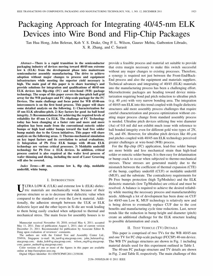
This paper is comprised of two TVs for the WB 40/45-nmand one TV for FC chip-scale package (FCCSP) 40-nm device.The WB TV package structures are shown in Fig. 1 includingmaterial details used for this experiment outlined in Table I.
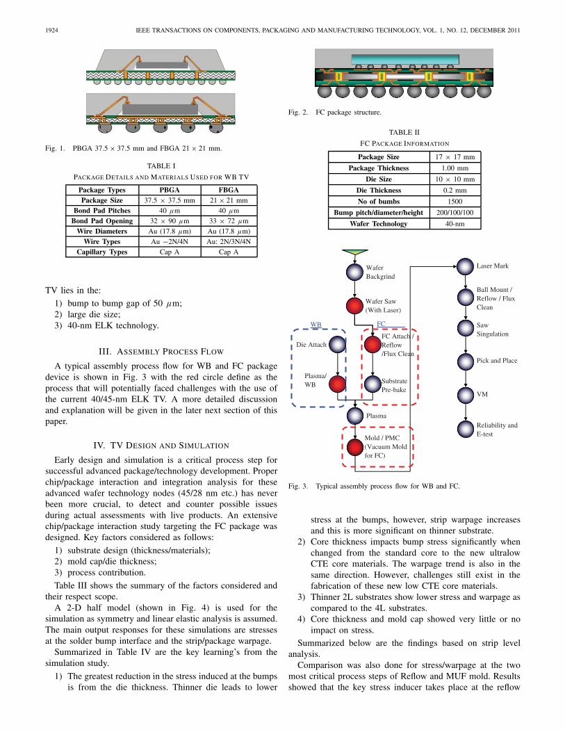
The 40-nm FC package structure and TV details are shownin Fig. 2 and Table II, respectively. The main challenge of this
2156–3950/$26.00 © 2011 IEEE
1924 IEEE TRANSACTIONS ON COMPONENTS, PACKAGING AND MANUFACTURING TECHNOLOGY, VOL. 1, NO. 12, DECEMBER 2011
Fig. 1. PBGA 37.5 × 37.5 mm and FBGA 21 × 21 mm.
TABLE I
PACKAGE DETAILS AND MATERIALS USED FOR WB TV
Package Types PBGA FBGAPackage Size 37.5 × 37.5 mm 21 × 21 mm
Bond Pad Pitches 40 µm 40 µm
Bond Pad Opening 32 × 90 µm 33 × 72 µm
Wire Diameters Au (17.8 µm) Au (17.8 µm)
Wire Types Au −2N/4N Au: 2N/3N/4N
Capillary Types Cap A Cap A
TV lies in the:
1) bump to bump gap of 50 µm;2) large die size;3) 40-nm ELK technology.
III. ASSEMBLY PROCESS FLOW
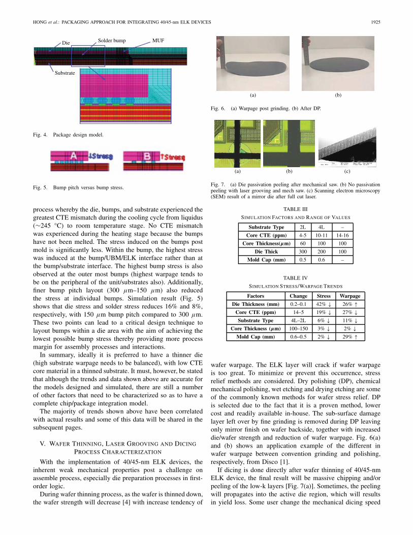
A typical assembly process flow for WB and FC packagedevice is shown in Fig. 3 with the red circle define as theprocess that will potentially faced challenges with the use ofthe current 40/45-nm ELK TV. A more detailed discussionand explanation will be given in the later next section of thispaper.
IV. TV DESIGN AND SIMULATION
Early design and simulation is a critical process step forsuccessful advanced package/technology development. Properchip/package interaction and integration analysis for theseadvanced wafer technology nodes (45/28 nm etc.) has neverbeen more crucial, to detect and counter possible issuesduring actual assessments with live products. An extensivechip/package interaction study targeting the FC package wasdesigned. Key factors considered as follows:
1) substrate design (thickness/materials);2) mold cap/die thickness;3) process contribution.
Table III shows the summary of the factors considered andtheir respect scope.
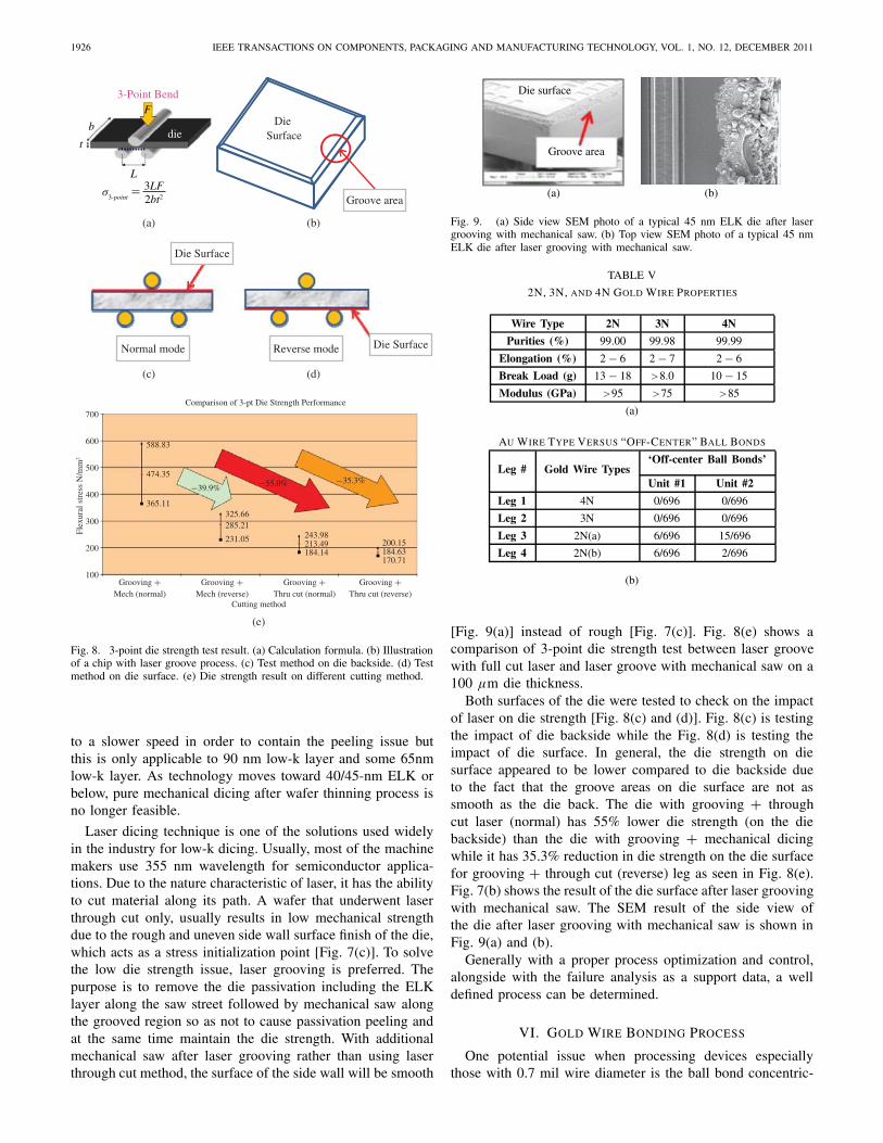
A 2-D half model (shown in Fig. 4) is used for thesimulation as symmetry and linear elastic analysis is assumed.The main output responses for these simulations are stressesat the solder bump interface and the strip/package warpage.
Summarized in Table IV are the key learning’s from thesimulation study.
1) The greatest reduction in the stress induced at the bumpsis from the die thickness. Thinner die leads to lower
Fig. 2. FC package structure.
TABLE II
FC PACKAGE INFORMATION
Package Size 17 × 17 mm
Package Thickness 1.00 mm
Die Size 10 × 10 mm
Die Thickness 0.2 mm
No of bumbs 1500
Bump pitch/diameter/height 200/100/100
Wafer Technology 40-nm
Wafer Backgrind
Wafer Saw(With Laser)
FC Attach /Reflow/Flux Clean
Plasma
Mold / PMC(Vacuum Moldfor FC)
Ball Mount / Reflow / Flux Clean
SawSingulation
SubstratePre-bake
Pick and Place
VM
Laser Mark
Reliability andE-test
WB FC
Die Attach
Plasma/WB
Fig. 3. Typical assembly process flow for WB and FC.
stress at the bumps, however, strip warpage increasesand this is more significant on thinner substrate.
2) Core thickness impacts bump stress significantly whenchanged from the standard core to the new ultralowCTE core materials. The warpage trend is also in thesame direction. However, challenges still exist in thefabrication of these new low CTE core materials.
3) Thinner 2L substrates show lower stress and warpage ascompared to the 4L substrates.
4) Core thickness and mold cap showed very little or noimpact on stress.
Summarized below are the findings based on strip levelanalysis.
Comparison was also done for stress/warpage at the twomost critical process steps of Reflow and MUF mold. Resultsshowed that the key stress inducer takes place at the reflow
HONG et al.: PACKAGING APPROACH FOR INTEGRATING 40/45-nm ELK DEVICES 1925
Die
Substrate
Solder bump MUF
Fig. 4. Package design model.
Fig. 5. Bump pitch versus bump stress.
process whereby the die, bumps, and substrate experienced thegreatest CTE mismatch during the cooling cycle from liquidus(∼245 °C) to room temperature stage. No CTE mismatchwas experienced during the heating stage because the bumpshave not been melted. The stress induced on the bumps postmold is significantly less. Within the bump, the highest stresswas induced at the bump/UBM/ELK interface rather than atthe bump/substrate interface. The highest bump stress is alsoobserved at the outer most bumps (highest warpage tends tobe on the peripheral of the unit/substrates also). Additionally,finer bump pitch layout (300 µm–150 µm) also reducedthe stress at individual bumps. Simulation result (Fig. 5)shows that die stress and solder stress reduces 16% and 8%,respectively, with 150 µm bump pitch compared to 300 µm.These two points can lead to a critical design technique tolayout bumps within a die area with the aim of achieving thelowest possible bump stress thereby providing more processmargin for assembly processes and interactions.
In summary, ideally it is preferred to have a thinner die(high substrate warpage needs to be balanced), with low CTEcore material in a thinned substrate. It must, however, be statedthat although the trends and data shown above are accurate forthe models designed and simulated, there are still a numberof other factors that need to be characterized so as to have acomplete chip/package integration model.
The majority of trends shown above have been correlatedwith actual results and some of this data will be shared in thesubsequent pages.
V. WAFER THINNING, LASER GROOVING AND DICING
PROCESS CHARACTERIZATION
With the implementation of 40/45-nm ELK devices, theinherent weak mechanical properties post a challenge onassemble process, especially die preparation processes in first-order logic.
During wafer thinning process, as the wafer is thinned down,the wafer strength will decrease [4] with increase tendency of
(a) (b)
Fig. 6. (a) Warpage post grinding. (b) After DP.
(a) (b) (c)
Fig. 7. (a) Die passivation peeling after mechanical saw. (b) No passivationpeeling with laser grooving and mech saw. (c) Scanning electron microscopy(SEM) result of a mirror die after full cut laser.
TABLE III
SIMULATION FACTORS AND RANGE OF VALUES
Substrate Type 2L 4L –
Core CTE (ppm) 4-5 10-11 14-16
Core Thickness(µm) 60 100 100
Die Thick 300 200 100
Mold Cap (mm) 0.5 0.6 –
TABLE IV
SIMULATION STRESS/WARPAGE TRENDS
Factors Change Stress Warpage
Die Thickness (mm) 0.2–0.1 42% ↓ 26% ↑Core CTE (ppm) 14–5 19% ↓ 27% ↓Substrate Type 4L–2L 6% ↓ 11% ↓
Core Thickness (µm) 100–150 3% ↓ 2% ↓Mold Cap (mm) 0.6–0.5 2% ↓ 29% ↑
wafer warpage. The ELK layer will crack if wafer warpageis too great. To minimize or prevent this occurrence, stressrelief methods are considered. Dry polishing (DP), chemicalmechanical polishing, wet etching and drying etching are someof the commonly known methods for wafer stress relief. DPis selected due to the fact that it is a proven method, lowercost and readily available in-house. The sub-surface damagelayer left over by fine grinding is removed during DP leavingonly mirror finish on wafer backside, together with increaseddie/wafer strength and reduction of wafer warpage. Fig. 6(a)and (b) shows an application example of the different inwafer warpage between convention grinding and polishing,respectively, from Disco [1].
If dicing is done directly after wafer thinning of 40/45-nmELK device, the final result will be massive chipping and/orpeeling of the low-k layers [Fig. 7(a)]. Sometimes, the peelingwill propagates into the active die region, which will resultsin yield loss. Some user change the mechanical dicing speed
1926 IEEE TRANSACTIONS ON COMPONENTS, PACKAGING AND MANUFACTURING TECHNOLOGY, VOL. 1, NO. 12, DECEMBER 2011
Die Surface
Groove area
(b)(a)
(d)(c)
Die Surface
Die SurfaceNormal mode Reverse mode
3-Point BendF
L
dieb
t
3LFσ
3-point 2bt2=
700
588.83
474.35
365.11
Grooving +Mech (normal)
Grooving +Mech (reverse)
Grooving +Thru cut (normal)
Cutting method
(e)
Grooving +Thru cut (reverse)
325.66
−39.9% −55.0% −35.3%
285.21
231.05 243.98213.49184.14
200.15184.63170.71
Comparison of 3-pt Die Strength Performance
600
500
400
Flex
ural
str
ess
N/m
m2
300
200
100
Fig. 8. 3-point die strength test result. (a) Calculation formula. (b) Illustrationof a chip with laser groove process. (c) Test method on die backside. (d) Testmethod on die surface. (e) Die strength result on different cutting method.
to a slower speed in order to contain the peeling issue butthis is only applicable to 90 nm low-k layer and some 65nmlow-k layer. As technology moves toward 40/45-nm ELK orbelow, pure mechanical dicing after wafer thinning process isno longer feasible.
Laser dicing technique is one of the solutions used widelyin the industry for low-k dicing. Usually, most of the machinemakers use 355 nm wavelength for semiconductor applica-tions. Due to the nature characteristic of laser, it has the abilityto cut material along its path. A wafer that underwent laserthrough cut only, usually results in low mechanical strengthdue to the rough and uneven side wall surface finish of the die,which acts as a stress initialization point [Fig. 7(c)]. To solvethe low die strength issue, laser grooving is preferred. Thepurpose is to remove the die passivation including the ELKlayer along the saw street followed by mechanical saw alongthe grooved region so as not to cause passivation peeling andat the same time maintain the die strength. With additionalmechanical saw after laser grooving rather than using laserthrough cut method, the surface of the side wall will be smooth
(a) (b)
Die surface
Groove area
Fig. 9. (a) Side view SEM photo of a typical 45 nm ELK die after lasergrooving with mechanical saw. (b) Top view SEM photo of a typical 45 nmELK die after laser grooving with mechanical saw.
TABLE V
2N, 3N, AND 4N GOLD WIRE PROPERTIES
Wire Type 2N 3N 4N
Purities (%) 99.00 99.98 99.99
Elongation (%) 2 − 6 2 − 7 2 − 6
Break Load (g) 13 − 18 >8.0 10 − 15
Modulus (GPa) >95 >75 >85
(a)
AU WIRE TYPE VERSUS “OFF-CENTER” BALL BONDS
Leg # Gold Wire Types‘Off-center Ball Bonds’
Unit #1 Unit #2
Leg 1 4N 0/696 0/696
Leg 2 3N 0/696 0/696
Leg 3 2N(a) 6/696 15/696
Leg 4 2N(b) 6/696 2/696
(b)
[Fig. 9(a)] instead of rough [Fig. 7(c)]. Fig. 8(e) shows acomparison of 3-point die strength test between laser groovewith full cut laser and laser groove with mechanical saw on a100 µm die thickness.
Both surfaces of the die were tested to check on the impactof laser on die strength [Fig. 8(c) and (d)]. Fig. 8(c) is testingthe impact of die backside while the Fig. 8(d) is testing theimpact of die surface. In general, the die strength on diesurface appeared to be lower compared to die backside dueto the fact that the groove areas on die surface are not assmooth as the die back. The die with grooving + throughcut laser (normal) has 55% lower die strength (on the diebackside) than the die with grooving + mechanical dicingwhile it has 35.3% reduction in die strength on the die surfacefor grooving + through cut (reverse) leg as seen in Fig. 8(e).Fig. 7(b) shows the result of the die surface after laser groovingwith mechanical saw. The SEM result of the side view ofthe die after laser grooving with mechanical saw is shown inFig. 9(a) and (b).
Generally with a proper process optimization and control,alongside with the failure analysis as a support data, a welldefined process can be determined.
VI. GOLD WIRE BONDING PROCESS
One potential issue when processing devices especiallythose with 0.7 mil wire diameter is the ball bond concentric-
HONG et al.: PACKAGING APPROACH FOR INTEGRATING 40/45-nm ELK DEVICES 1927
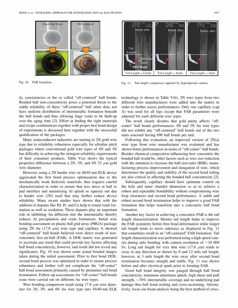
Good Ball Bond Off-centered
Fig. 10. FAB formation.
ity consistencies or the so called “off-centered” ball bonds.Bonded ball non-concentricity poses a potential threat to thestable reliability of these “off-centered” ball often does nothave uniform distribution of intermetallic formation beneaththe ball bonds and thus allowing large voids to be built-upover the aging time [2]. Effort in finding the right materialsand recipe combinations together with proper first bond designof experiments is discussed here together with the successfulqualification of the packages.
Many semiconductor industries are turning to 2N gold wiretype due to reliability robustness especially for ultrafine pitchpackages where conventional gold wire types of 4N and 3Nhas difficulty in achieving the stringent reliability requirementsof their consumer products. Table V(a) shows the typicalproperties difference between a 2N, 3N, and 4N 25 µm goldwire diameter.
However, using a 2N harder wire on 40/45-nm ELK deviceaggravated the first bond process optimization due to themechanically weak dielectric materials, thus requires carefulcharacterization in order to ensure that less stress at ball topad interface and minimizing Al splash or squeeze out dueto harder wire (2N) used that may further reduce devicereliability. Many recent studies have shown that with theaddition of dopants like Pd, Pt, and Cu help to retard voids for-mation as well as oxidation. These dopants play an importantrole in inhibiting Au diffusion into the intermetallic therebyreduces Al precipitation and voids formations. Initial wirebonding assessment on plastic ball grid array (PBGA) packageusing 2N Au (17.8 µm) wire type and capillary A showed“off-centered” ball bonds believed were direct result of non-concentric free-air-ball (FAB). A DOE matrix was generatedto ascertain any trend that could provide key factors affectingball bond concentricity, however, end result did not reveal anysignificance. Fig. 10 was shown some actual bonded imagestaken during the initial assessment. Prior to first bond DOE,second bond process was optimized in order to ensure processrobustness and further will not complicate the “off-center”ball bond assessment primarily caused by premature tail bondtermination. Follow-up assessments for “off-center” ball bondsissue were carried out on different Au wire types.
Wire bonding comparison result using 17.8 µm wire diam-eter for 2N, 3N, and 4N Au wire type into 45/40-nm ELK
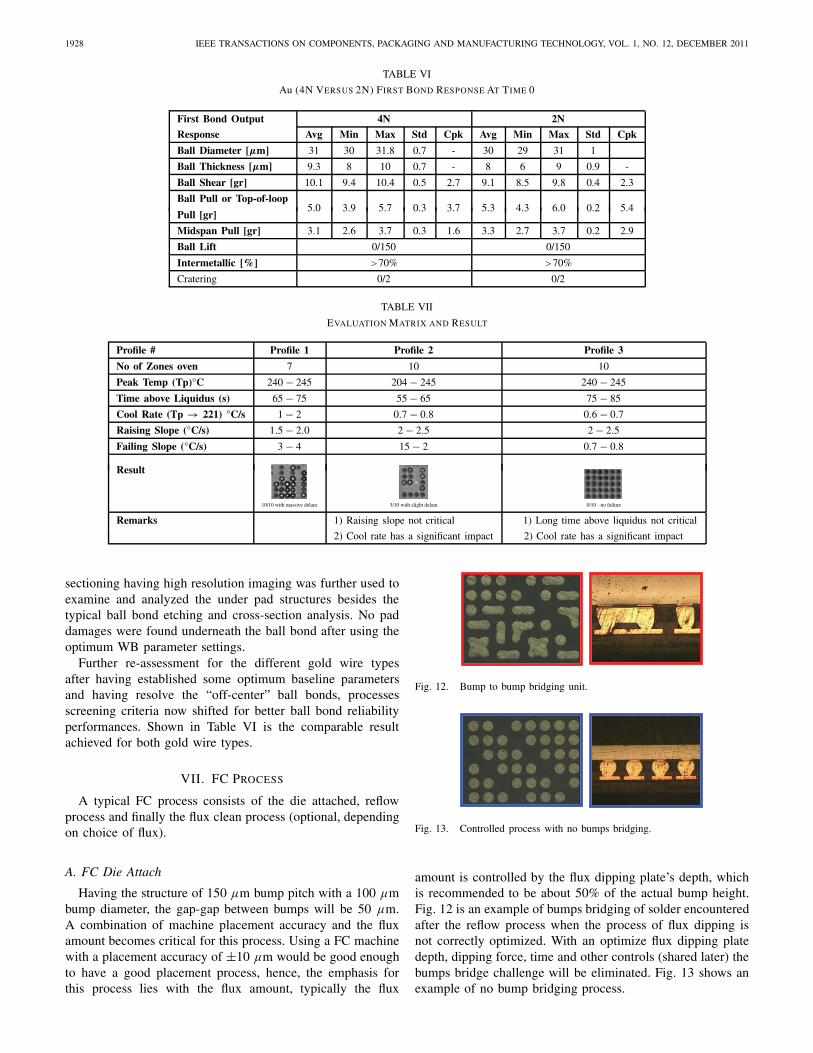
Tail Length � 3milsTail Length � 8milsTail Length �12mils
TailLength
EFO Wand
before after
EFO Wand
Electrical Spark
before after before after
Fig. 11. Tail length comparison captured by hyperspectral camera.
technology is shown in Table V(b). 2N wire types from twodifferent wire manufacturers were added into the matrix inorder to further assess performances. Only one capillary (capA) was used for all legs except that FAB parameters wereadjusted for each different wire types.
The result clearly dictates that gold purity affects “off-center” ball bonds performances. 4N and 3N Au wire typesdid not exhibit any “off-centered” ball bonds out of the twounits assessed having 696 ball bonds per unit.
Following this evaluation, an improved version of 2N(a)wire type from wire manufacturer was evaluated and hasshown better performances in terms of “off-center” ball bonds.Besides chemical composition influencing how concentric thebonded ball would be, other factors such as wire size reductionwith the intention to increase the ball-size-ratio (BSR), manu-facturing process improvement and elongation of wire, whichdetermines the quality and stability of the second bond tailingare also critical in affecting the bonded ball concentricity [2].
Subsequently, capillary should have optimum control onthe hole and inner chamfer dimension so as to achieve arobust and repeatable bondability without compromising wireloop clearances and second bond performance. A stable androbust second bond termination helps to improve a good FABformation that helps transform into a concentric ball bondformation.
Another key factor in achieving a concentric FAB is the taillength characterization. Shorter tail length helps to improvethe FAB symmetry before first bond deformation while longertail length tends to move sideways as displayed in Fig. 11that sometimes result to an “off-centered” FAB formation. Taillength characterization was performed using a high speed cam-era during auto bonding with camera resolution of ∼10 000f/s. Long tail length for very thin wire (17.8 µm) tends tosway in any direction as shown by 8 and 12 mils tail length,however, at 3 mils length the wire sway after second bondtermination becomes straight and stable. Fig. 11 was shownbefore and after electrical spark prior to forming FAB.
Good ball bond integrity was gauged through ball bondconcentricity, minimum aluminum splash, high shear and pullstrength, >70% intermetallic coverage and no underlying paddamage thru ball bond etching and cross-sectioning. Alterna-tively, focus ion beam analysis being the best method of cross-
1928 IEEE TRANSACTIONS ON COMPONENTS, PACKAGING AND MANUFACTURING TECHNOLOGY, VOL. 1, NO. 12, DECEMBER 2011
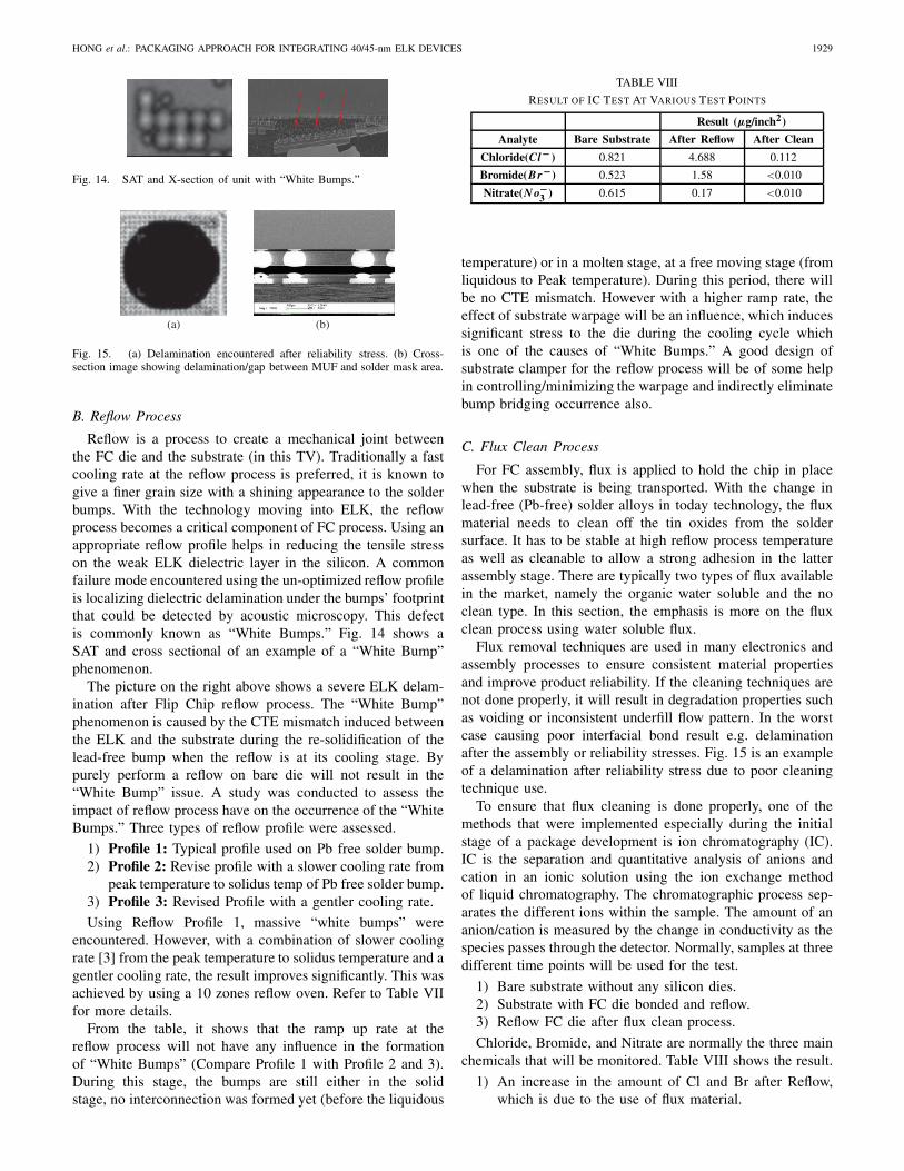
TABLE VI
Au (4N VERSUS 2N) FIRST BOND RESPONSE AT TIME 0
First Bond Output 4N 2N
Response Avg Min Max Std Cpk Avg Min Max Std Cpk
Ball Diameter [µm] 31 30 31.8 0.7 - 30 29 31 1
Ball Thickness [µm] 9.3 8 10 0.7 - 8 6 9 0.9 -
Ball Shear [gr] 10.1 9.4 10.4 0.5 2.7 9.1 8.5 9.8 0.4 2.3
Ball Pull or Top-of-loop5.0 3.9 5.7 0.3 3.7 5.3 4.3 6.0 0.2 5.4
Pull [gr]
Midspan Pull [gr] 3.1 2.6 3.7 0.3 1.6 3.3 2.7 3.7 0.2 2.9
Ball Lift 0/150 0/150
Intermetallic [%] >70% >70%
Cratering 0/2 0/2
TABLE VII
EVALUATION MATRIX AND RESULT
Profile # Profile 1 Profile 2 Profile 3
No of Zones oven 7 10 10
Peak Temp (Tp)°C 240 − 245 204 − 245 240 − 245
Time above Liquidus (s) 65 − 75 55 − 65 75 − 85
Cool Rate (Tp → 221) °C/s 1 − 2 0.7 − 0.8 0.6 − 0.7
Raising Slope (°C/s) 1.5 − 2.0 2 − 2.5 2 − 2.5
Failing Slope (°C/s) 3 − 4 15 − 2 0.7 − 0.8
Result
10/10 with massive delam 3/10 with slight delam 0/10 - no failure
Remarks 1) Raising slope not critical 1) Long time above liquidus not critical
2) Cool rate has a significant impact 2) Cool rate has a significant impact
sectioning having high resolution imaging was further used toexamine and analyzed the under pad structures besides thetypical ball bond etching and cross-section analysis. No paddamages were found underneath the ball bond after using theoptimum WB parameter settings.
Further re-assessment for the different gold wire typesafter having established some optimum baseline parametersand having resolve the “off-center” ball bonds, processesscreening criteria now shifted for better ball bond reliabilityperformances. Shown in Table VI is the comparable resultachieved for both gold wire types.
VII. FC PROCESS
A typical FC process consists of the die attached, reflowprocess and finally the flux clean process (optional, dependingon choice of flux).
A. FC Die Attach
Having the structure of 150 µm bump pitch with a 100 µmbump diameter, the gap-gap between bumps will be 50 µm.A combination of machine placement accuracy and the fluxamount becomes critical for this process. Using a FC machinewith a placement accuracy of ±10 µm would be good enoughto have a good placement process, hence, the emphasis forthis process lies with the flux amount, typically the flux
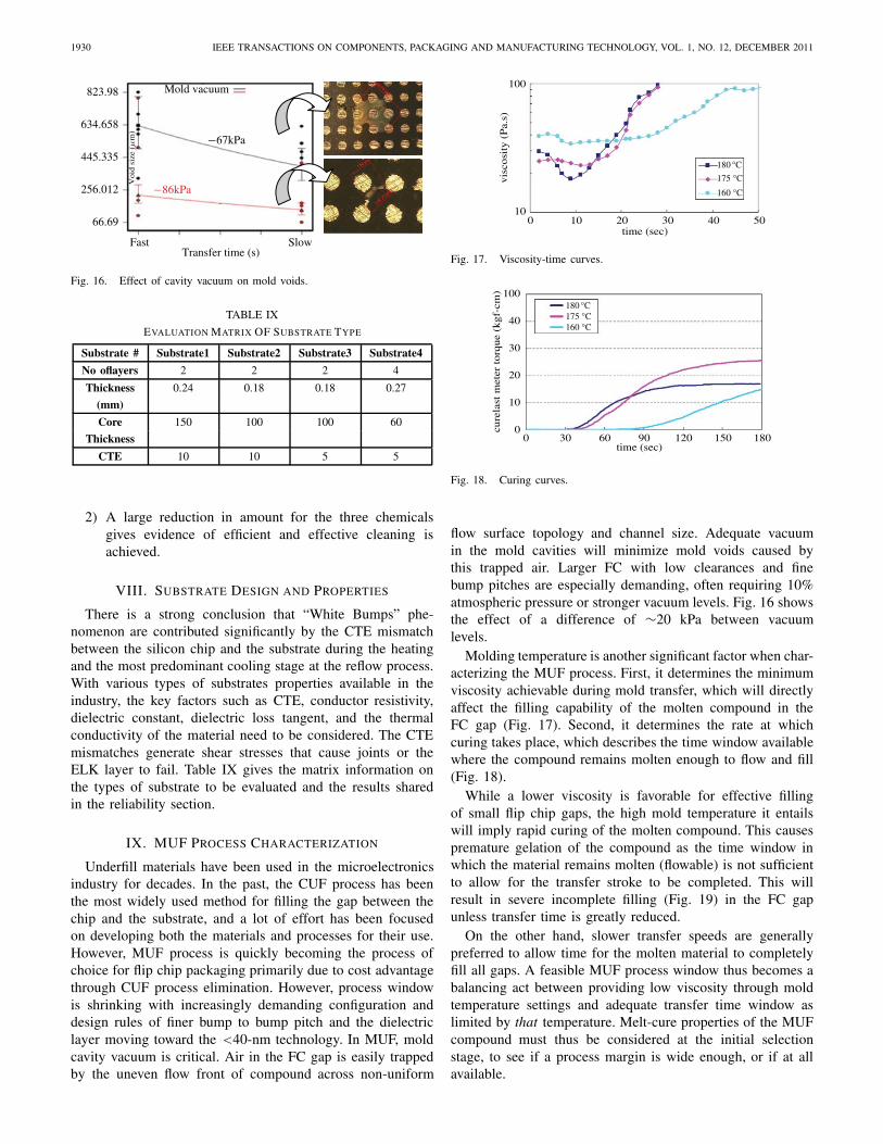
Fig. 12. Bump to bump bridging unit.
Fig. 13. Controlled process with no bumps bridging.
amount is controlled by the flux dipping plate’s depth, whichis recommended to be about 50% of the actual bump height.Fig. 12 is an example of bumps bridging of solder encounteredafter the reflow process when the process of flux dipping isnot correctly optimized. With an optimize flux dipping platedepth, dipping force, time and other controls (shared later) thebumps bridge challenge will be eliminated. Fig. 13 shows anexample of no bump bridging process.
HONG et al.: PACKAGING APPROACH FOR INTEGRATING 40/45-nm ELK DEVICES 1929
Fig. 14. SAT and X-section of unit with “White Bumps.”
(a) (b)
Fig. 15. (a) Delamination encountered after reliability stress. (b) Cross-section image showing delamination/gap between MUF and solder mask area.
B. Reflow Process
Reflow is a process to create a mechanical joint betweenthe FC die and the substrate (in this TV). Traditionally a fastcooling rate at the reflow process is preferred, it is known togive a finer grain size with a shining appearance to the solderbumps. With the technology moving into ELK, the reflowprocess becomes a critical component of FC process. Using anappropriate reflow profile helps in reducing the tensile stresson the weak ELK dielectric layer in the silicon. A commonfailure mode encountered using the un-optimized reflow profileis localizing dielectric delamination under the bumps’ footprintthat could be detected by acoustic microscopy. This defectis commonly known as “White Bumps.” Fig. 14 shows aSAT and cross sectional of an example of a “White Bump”phenomenon.
The picture on the right above shows a severe ELK delam-ination after Flip Chip reflow process. The “White Bump”phenomenon is caused by the CTE mismatch induced betweenthe ELK and the substrate during the re-solidification of thelead-free bump when the reflow is at its cooling stage. Bypurely perform a reflow on bare die will not result in the“White Bump” issue. A study was conducted to assess theimpact of reflow process have on the occurrence of the “WhiteBumps.” Three types of reflow profile were assessed.
1) Profile 1: Typical profile used on Pb free solder bump.2) Profile 2: Revise profile with a slower cooling rate from
peak temperature to solidus temp of Pb free solder bump.3) Profile 3: Revised Profile with a gentler cooling rate.
Using Reflow Profile 1, massive “white bumps” wereencountered. However, with a combination of slower coolingrate [3] from the peak temperature to solidus temperature and agentler cooling rate, the result improves significantly. This wasachieved by using a 10 zones reflow oven. Refer to Table VIIfor more details.
From the table, it shows that the ramp up rate at thereflow process will not have any influence in the formationof “White Bumps” (Compare Profile 1 with Profile 2 and 3).During this stage, the bumps are still either in the solidstage, no interconnection was formed yet (before the liquidous
TABLE VIII
RESULT OF IC TEST AT VARIOUS TEST POINTS
Result (µg/inch2)
Analyte Bare Substrate After Reflow After Clean
Chloride(Cl− ) 0.821 4.688 0.112
Bromide(Br−) 0.523 1.58 <0.010
Nitrate(N o−3 ) 0.615 0.17 <0.010
temperature) or in a molten stage, at a free moving stage (fromliquidous to Peak temperature). During this period, there willbe no CTE mismatch. However with a higher ramp rate, theeffect of substrate warpage will be an influence, which inducessignificant stress to the die during the cooling cycle whichis one of the causes of “White Bumps.” A good design ofsubstrate clamper for the reflow process will be of some helpin controlling/minimizing the warpage and indirectly eliminatebump bridging occurrence also.
C. Flux Clean Process
For FC assembly, flux is applied to hold the chip in placewhen the substrate is being transported. With the change inlead-free (Pb-free) solder alloys in today technology, the fluxmaterial needs to clean off the tin oxides from the soldersurface. It has to be stable at high reflow process temperatureas well as cleanable to allow a strong adhesion in the latterassembly stage. There are typically two types of flux availablein the market, namely the organic water soluble and the noclean type. In this section, the emphasis is more on the fluxclean process using water soluble flux.
Flux removal techniques are used in many electronics andassembly processes to ensure consistent material propertiesand improve product reliability. If the cleaning techniques arenot done properly, it will result in degradation properties suchas voiding or inconsistent underfill flow pattern. In the worstcase causing poor interfacial bond result e.g. delaminationafter the assembly or reliability stresses. Fig. 15 is an exampleof a delamination after reliability stress due to poor cleaningtechnique use.
To ensure that flux cleaning is done properly, one of themethods that were implemented especially during the initialstage of a package development is ion chromatography (IC).IC is the separation and quantitative analysis of anions andcation in an ionic solution using the ion exchange methodof liquid chromatography. The chromatographic process sep-arates the different ions within the sample. The amount of ananion/cation is measured by the change in conductivity as thespecies passes through the detector. Normally, samples at threedifferent time points will be used for the test.
1) Bare substrate without any silicon dies.2) Substrate with FC die bonded and reflow.3) Reflow FC die after flux clean process.
Chloride, Bromide, and Nitrate are normally the three mainchemicals that will be monitored. Table VIII shows the result.
1) An increase in the amount of Cl and Br after Reflow,which is due to the use of flux material.
1930 IEEE TRANSACTIONS ON COMPONENTS, PACKAGING AND MANUFACTURING TECHNOLOGY, VOL. 1, NO. 12, DECEMBER 2011
Mold vacuum
−67kPa
−86kPa
Fast
Voi
d si
ze (μ
m)
823.98
634.658
445.335
256.012
66.69
SlowTransfer time (s)
Fig. 16. Effect of cavity vacuum on mold voids.
TABLE IX
EVALUATION MATRIX OF SUBSTRATE TYPE
Substrate # Substrate1 Substrate2 Substrate3 Substrate4
No oflayers 2 2 2 4
Thickness 0.24 0.18 0.18 0.27
(mm)
Core 150 100 100 60
Thickness
CTE 10 10 5 5
2) A large reduction in amount for the three chemicalsgives evidence of efficient and effective cleaning isachieved.
VIII. SUBSTRATE DESIGN AND PROPERTIES
There is a strong conclusion that “White Bumps” phe-nomenon are contributed significantly by the CTE mismatchbetween the silicon chip and the substrate during the heatingand the most predominant cooling stage at the reflow process.With various types of substrates properties available in theindustry, the key factors such as CTE, conductor resistivity,dielectric constant, dielectric loss tangent, and the thermalconductivity of the material need to be considered. The CTEmismatches generate shear stresses that cause joints or theELK layer to fail. Table IX gives the matrix information onthe types of substrate to be evaluated and the results sharedin the reliability section.
IX. MUF PROCESS CHARACTERIZATION
Underfill materials have been used in the microelectronicsindustry for decades. In the past, the CUF process has beenthe most widely used method for filling the gap between thechip and the substrate, and a lot of effort has been focusedon developing both the materials and processes for their use.However, MUF process is quickly becoming the process ofchoice for flip chip packaging primarily due to cost advantagethrough CUF process elimination. However, process windowis shrinking with increasingly demanding configuration anddesign rules of finer bump to bump pitch and the dielectriclayer moving toward the <40-nm technology. In MUF, moldcavity vacuum is critical. Air in the FC gap is easily trappedby the uneven flow front of compound across non-uniform
100
10
time (sec)0 10 20 30 40 50
visc
osit
y (P
a.s)
180 °C
175 °C
160 °C
Fig. 17. Viscosity-time curves.
time (sec)
180 °C175 °C160 °C
100
00 30 60 90 120 150 180
10
20
30
40
cure
last
met
er t
orqu
e (k
gf-c
m)
Fig. 18. Curing curves.
flow surface topology and channel size. Adequate vacuumin the mold cavities will minimize mold voids caused bythis trapped air. Larger FC with low clearances and finebump pitches are especially demanding, often requiring 10%atmospheric pressure or stronger vacuum levels. Fig. 16 showsthe effect of a difference of ∼20 kPa between vacuumlevels.
Molding temperature is another significant factor when char-acterizing the MUF process. First, it determines the minimumviscosity achievable during mold transfer, which will directlyaffect the filling capability of the molten compound in theFC gap (Fig. 17). Second, it determines the rate at whichcuring takes place, which describes the time window availablewhere the compound remains molten enough to flow and fill(Fig. 18).
While a lower viscosity is favorable for effective fillingof small flip chip gaps, the high mold temperature it entailswill imply rapid curing of the molten compound. This causespremature gelation of the compound as the time window inwhich the material remains molten (flowable) is not sufficientto allow for the transfer stroke to be completed. This willresult in severe incomplete filling (Fig. 19) in the FC gapunless transfer time is greatly reduced.
On the other hand, slower transfer speeds are generallypreferred to allow time for the molten material to completelyfill all gaps. A feasible MUF process window thus becomes abalancing act between providing low viscosity through moldtemperature settings and adequate transfer time window aslimited by that temperature. Melt-cure properties of the MUFcompound must thus be considered at the initial selectionstage, to see if a process margin is wide enough, or if at allavailable.
HONG et al.: PACKAGING APPROACH FOR INTEGRATING 40/45-nm ELK DEVICES 1931
Fig. 19. Incomplete filling at high mold temperature.
(a) (b)
Fig. 20. (a) Low versus high. (b) Porosity material.
A. MUF Process/Material Limitations
Current trend for MUF material is the continuous decreasein filler size to cater for the ever-shrinking FC gap in arace for smaller, thinner packages. As a rule of thumb, thegap must be 2–3x the max filler size for successful filling.With the advent of ultrafine pitches and small bumps, materialproperties are becoming inadequate while material prices arebecoming prohibitive.
All MUF materials by major suppliers tested so far alsoexhibit a certain degree of intrinsic material porosity aftermolding. This is non-flow related and cannot be eliminatedor even reduced through process optimization.
Voids due to porosity (Fig. 20) are generally found to be50∼100 µm in size. This can pose a problem with fine pitchFC packages as they are large enough to short adjacent bumps(50 µm bump-to-bump, Fig. 21).
Parts exhibiting high-risk characteristics were subject to theextreme conditions designed to promote the intended failures.A relevant example would be electrical shorts due to FC bumpsmelting across mold voids. An extreme and unlikely levelof stress was deliberately induced, (e.g. 10x reflow), and nofailure (Fig. 22) was observed in all the units assessed.
There are, however, inherent risks of escapees for issuesof low defect rate. These risks are to be mitigated throughrigorous testing through.
1) Increased sample sizes.2) Increased stringency in testing conditions.3) Testing across entire process window.
X. FC PACKAGE PERFORMANCE
With the various process optimizations, the final outputresult of a package performance always lies in the packagewarpage or coplanarity and last the reliability performancewhen undergoes various reliability stresses.
Package warpage or coplanarity is critical because for everyassembled package, they would still need to undergo the boardlevel assembly. With the current TV, the maximum coplanarityrequired is targeted to be less than 100 µm to ensure a good
(a) (b)
Fig. 21. (a) Typical porosity. (b) Void shorting bumps.
Fig. 22. No bump short (post 10x reflow).
Die Thickness Comparison0.130.120.110.100.090.080.070.060.05
1 2
Leg
Each PairStudents 10.05
Fig. 23. Die thickness correlation.
Mold Compound Comparison0.13
0.09
0.08
0.07
0.06
0.05
0.041 2
Leg
Each PairStudents 10.05
Fig. 24. Mold compound correlation.
assembly. Below is the warpage result of the four selectedsubstrate types used in this evaluation.
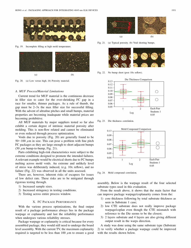
From the result above, it shows that the main factor thatcan improve package warpage/coplanarity comes from the:
1) core thickness following by total substrate thickness asseen in Substrate 1 case;
2) low CTE substrate does not really improve packagewarpage/coplan even though the CTE mismatch withreference to the Die seems to be the closest;
3) 2 layers substrate and 4 layers are also giving differentoutput result in the warps direction.
A study was done using the same substrate type (Substrate2) to verify whether a package warpage could be improvedwith the results shown below.
1932 IEEE TRANSACTIONS ON COMPONENTS, PACKAGING AND MANUFACTURING TECHNOLOGY, VOL. 1, NO. 12, DECEMBER 2011
TABLE X
UNIT WARPAGE
Substrate # Substrate 1 Substrate 2 Substrate 3 Substrate 4
Warpage Direction
27 μm 68 μm 95 μm 21 μm
Ave Coplan result taken Max: 81 118 185 92
from VM machine Ave: 63 82 146 67
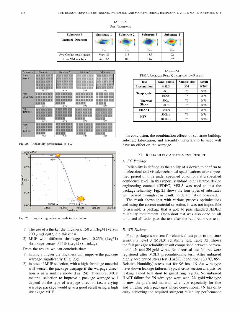
Substrate #AfterMSL3
AfteruHast 96 hrs
AfterTC1000x
AfterHTS1000 hrs
Substrate 1 Substrate 2 Substrate 3 Substrate 4
0/75 0/75 0/75 0/75
0/25 0/25 0/25 0/25
0/25 0/25 0/25 0/25
0/25 0/25 0/25 0/25
Fig. 25. Reliability performance of TV.
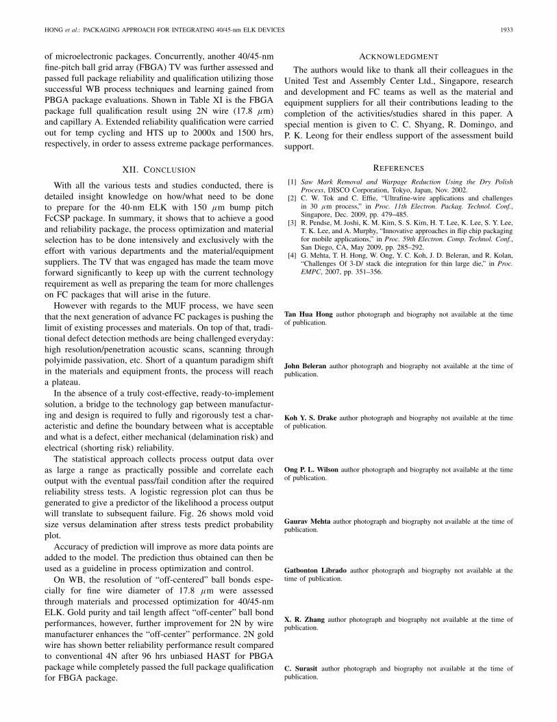
Logistic Plot1.00
0.75
0.50
Popc
orn?
0.25
0.000 50000 100000 150000
Vold area200000 250000
95%
5%78300 152685
N
Y
Fig. 26. Logistic regression as predictor for failure.
1) The use of a thicker die thickness, 150 µm(leg#1) versus200 µm(Leg#2) die thickness.
2) MUF with different shrinkage level, 0.25% (Leg#1)shrinkage versus 0.34% (Leg#2) shrinkage.
From the results we can conclude that:
1) having a thicker die thickness will improve the packagewarpage significantly (Fig. 23);
2) in case of MUF selection, with a high shrinkage materialwill worsen the package warpage if the warpage direc-tion is in a smiling mode (Fig. 24). Therefore, MUFmaterial selection to improve a package warpage willdepend on the type of warpage direction i.e., a cryingwarpage package would give a good result using a highshrinkage MUF.
TABLE XI
FBGA PACKAGE FULL QUALIFICATION RESULT
Test Read points Sample size Result
Precondition MSL3 304 0/304
Temp cycle500x 76 0/76
1000x 76 0/76
ThermalShock
300x 76 0/76
500x 76 0/76
µHAST 100hrs 76 0/76
HTS500hrs 76 0/76
1000hrs 76 0/76
In conclusion, the combination effects of substrate buildup,substrate fabrication, and assembly materials to be used willhave an effect on the warpage.
XI. RELIABILITY ASSESSMENT RESULT
A. FC Package
Reliability is defined as the ability of a device to confirm toits electrical and visual/mechanical specifications over a spec-ified period of time under specified conditions at a specifiedconfidence level. In this report, standard joint electron deviceengineering council (JEDEC) MSL3 was used to test thepackage reliability. Fig. 25 shows the four types of substrateswith passed through scan result, no delamination observed.
The result shows that with various process optimizationsand using the correct material selection, it was not impossibleto assemble a package that is able to pass standard JEDECreliability requirement. Open/short test was also done on allunits and all units pass the test after the required stress test.
B. WB Package
Final package were sent for electrical test prior to moisturesensitivity level 3 (MSL3) reliability test. Table XI, showsthe full package reliability result comparison between conven-tional 4N and 2N gold wires. No electrical test failures wereregistered after MSL3 preconditioning test. After unbiasedhighly accelerated stress test (HAST) (condition: 130 °C, 85%Relative Humidity) stress test for 96 hrs, 4N Au wire typehave shown leakage failures. Typical cross-section analysis forleakage failed ball short to guard ring rejects. No unbiasedHAST failure for 2N wire type were seen. 2N gold wire typeis now the preferred material wire type especially for fineand ultrafine pitch packages where conventional 4N has diffi-culty achieving the required stringent reliability performance
HONG et al.: PACKAGING APPROACH FOR INTEGRATING 40/45-nm ELK DEVICES 1933
of microelectronic packages. Concurrently, another 40/45-nmfine-pitch ball grid array (FBGA) TV was further assessed andpassed full package reliability and qualification utilizing thosesuccessful WB process techniques and learning gained fromPBGA package evaluations. Shown in Table XI is the FBGApackage full qualification result using 2N wire (17.8 µm)and capillary A. Extended reliability qualification were carriedout for temp cycling and HTS up to 2000x and 1500 hrs,respectively, in order to assess extreme package performances.
XII. CONCLUSION
With all the various tests and studies conducted, there isdetailed insight knowledge on how/what need to be doneto prepare for the 40-nm ELK with 150 µm bump pitchFcCSP package. In summary, it shows that to achieve a goodand reliability package, the process optimization and materialselection has to be done intensively and exclusively with theeffort with various departments and the material/equipmentsuppliers. The TV that was engaged has made the team moveforward significantly to keep up with the current technologyrequirement as well as preparing the team for more challengeson FC packages that will arise in the future.
However with regards to the MUF process, we have seenthat the next generation of advance FC packages is pushing thelimit of existing processes and materials. On top of that, tradi-tional defect detection methods are being challenged everyday:high resolution/penetration acoustic scans, scanning throughpolyimide passivation, etc. Short of a quantum paradigm shiftin the materials and equipment fronts, the process will reacha plateau.
In the absence of a truly cost-effective, ready-to-implementsolution, a bridge to the technology gap between manufactur-ing and design is required to fully and rigorously test a char-acteristic and define the boundary between what is acceptableand what is a defect, either mechanical (delamination risk) andelectrical (shorting risk) reliability.
The statistical approach collects process output data overas large a range as practically possible and correlate eachoutput with the eventual pass/fail condition after the requiredreliability stress tests. A logistic regression plot can thus begenerated to give a predictor of the likelihood a process outputwill translate to subsequent failure. Fig. 26 shows mold voidsize versus delamination after stress tests predict probabilityplot.
Accuracy of prediction will improve as more data points areadded to the model. The prediction thus obtained can then beused as a guideline in process optimization and control.
On WB, the resolution of “off-centered” ball bonds espe-cially for fine wire diameter of 17.8 µm were assessedthrough materials and processed optimization for 40/45-nmELK. Gold purity and tail length affect “off-center” ball bondperformances, however, further improvement for 2N by wiremanufacturer enhances the “off-center” performance. 2N goldwire has shown better reliability performance result comparedto conventional 4N after 96 hrs unbiased HAST for PBGApackage while completely passed the full package qualificationfor FBGA package.
ACKNOWLEDGMENT
The authors would like to thank all their colleagues in theUnited Test and Assembly Center Ltd., Singapore, researchand development and FC teams as well as the material andequipment suppliers for all their contributions leading to thecompletion of the activities/studies shared in this paper. Aspecial mention is given to C. C. Shyang, R. Domingo, andP. K. Leong for their endless support of the assessment buildsupport.
REFERENCES
[1] Saw Mark Removal and Warpage Reduction Using the Dry PolishProcess, DISCO Corporation, Tokyo, Japan, Nov. 2002.
[2] C. W. Tok and C. Effie, “Ultrafine-wire applications and challengesin 30 µm process,” in Proc. 11th Electron. Packag. Technol. Conf.,Singapore, Dec. 2009, pp. 479–485.
[3] R. Pendse, M. Joshi, K. M. Kim, S. S. Kim, H. T. Lee, K. Lee, S. Y. Lee,T. K. Lee, and A. Murphy, “Innovative approaches in flip chip packagingfor mobile applications,” in Proc. 59th Electron. Comp. Technol. Conf.,San Diego, CA, May 2009, pp. 285–292.
[4] G. Mehta, T. H. Hong, W. Ong, Y. C. Koh, J. D. Beleran, and R. Kolan,“Challenges Of 3-D/ stack die integration for thin large die,” in Proc.EMPC, 2007, pp. 351–356.
Tan Hua Hong author photograph and biography not available at the timeof publication.
John Beleran author photograph and biography not available at the time ofpublication.
Koh Y. S. Drake author photograph and biography not available at the timeof publication.
Ong P. L. Wilson author photograph and biography not available at the timeof publication.
Gaurav Mehta author photograph and biography not available at the time ofpublication.
Gatbonton Librado author photograph and biography not available at thetime of publication.
X. R. Zhang author photograph and biography not available at the time ofpublication.
C. Surasit author photograph and biography not available at the time ofpublication.