Route Choice Modelling Using Fuzzy logic and Adaptive Neuro-fuzzy
Upload
diponegoroCategory
view
0download
0
Neural and Fuzzy Logic Controlof Drives and Power Systems


Neural and Fuzzy LogicControl of Drives andPower Systems
M.N. Cirstea, A. Dinu, J.G. Khor,M. McCormick
Newnes
OXFORD AMSTERDAM BOSTON LONDON NEW YORK PARISSAN DIEGO SAN FRANCISCO SINGAPORE SYDNEY TOKYO

NewnesAn imprint of Elsevier ScienceLinacre House, Jordan Hill, Oxford OX2 8DP225 Wildwood Avenue, Woburn, MA 01801-2041
First published 2002
Copyright © 2002, M.N. Cirstea, A. Dinu, J.G. Khor, M. McCormick. All rights reservedThe right of M.N. Cirstea, A. Dinu, J.G. Khor and M. McCormick to be identified as theauthors of this work has been asserted in accordance with the Copyright,Designs and Patents Act 1988
No part of this publication may be reproduced in any material form (includingphotocopying or storing in any medium by electronic means and whetheror not transiently or incidentally to some other use of this publication) withoutthe written permission of the copyright holder except in accordance with theprovisions of the Copyright, Designs and Patents Act 1988 or under the terms ofa licence issued by the Copyright Licensing Agency Ltd, 90 Tottenham Court Road,London, England W1T 4LP. Applications for the copyright holder’s writtenpermission to reproduce any part of this publication should be addressedto the publisher
British Library Cataloguing in Publication DataA catalogue record for this book is available from the British Library
ISBN 0 7506 55585
For information on all Newnes publicationsvisit our website at www.newnespress.com
Typeset at Replika Press Pvt Ltd, Delhi 110 040, IndiaPrinted and bound in Great Britain

Preface......................................................
Control systems 1.......................................Control theory: historical review 1.............Introduction to control systems 2...............Control systems for a. c. drives 5..............
Modern control systems design usingCAD techniques........................................
Electronic design automation ( EDA).....Application specific integrated circuit (ASIC) basics 12...........................................Field programmable gate arrays (FPGAs) 14...................................................ASICs for power systems and drives 16.....
Electric motors and power systems.......Electric motors........................................Power systems 19.......................................Pulse width modulation 22..........................The space vector in electrical systems 26...Induction motor control 28...........................Synchronous generators control 51............
Elements of neural control......................Neurone types........................................Artificial neural networks architectures 59...Training algorithms 61.................................Control applications of ANNs 69.................Neural network implementation 71..............
Neural FPGA implementation..................Neural networks design andimplementation strategy.........................

Universal programs Ò FFANNhardware implementation 95.......................Hardware implementation complexityanalysis 98..................................................
Fuzzy logic fundamentals........................Historical review.....................................Fuzzy sets and fuzzy logic 114.....................Types of membership functions 116.............Linguistic variables 117.................................Fuzzy logic operators 117.............................Fuzzy control systems 118............................Fuzzy logic in power and controlapplications 121............................................
VHDL fundamentals.................................Introduction.............................................VHDL design units 126..................................Libraries, visibility and state system inVHDL 131......................................................Sequential statements 135............................Concurrent statements 141...........................Functions and procedures 146......................Advanced features in VHDL 151...................Summary 154................................................
Neural current and speed control ofinduction motors......................................
The induction motor equivalent circuit....The current control algorithm 161.................The new sensorless motor controlstrategy 183...................................................Induction motor controller VHDLdesign 199.....................................................FPGA controller experimental results 227.....

Fuzzy logic control of a synchronousgenerator set.............................................
System representation...........................VHDL modelling 248.....................................FPGA implementation 270............................System assembly and experimentaltests 285........................................................Conclusions 292............................................
Final notes................................................
References................................................
Appendices...............................................Appendix A - C++ code for ANNimplementation.......................................Appendix B - C++ Programs for PWMgeneration 333..............................................Appendix C - Subnetworks VHDLmodels 341....................................................Appendix D - VHDL model of sinewave ROM 355..............................................Appendix E - VHDL code forsimulation 357...............................................Appendix F - VHDL code for synthesis 374..Appendix G - PWM controllers 389...............
Index

Preface
The idea of writing this book arose from the need to investigate the main principles ofmodern power electronic control strategies, using fuzzy logic and neural networks, forresearch and teaching. Primarily, the book aims to be a quick learning guide forpostgraduate/undergraduate students or design engineers interested in learning thefundamentals of modern control of drives and power systems in conjunction with thepowerful design methodology based on VHDL.
At the same time, the book is structured to address the more complex needs ofprofessional designers, using VHDL for neural and fuzzy logic systems design, byincluding comprehensive design examples. This facilitates the understanding of hardwaredescription language applications and provides a practical approach to the developmentof advanced controllers for power electronics.
The first section of the book contains a brief review of control strategies for electricdrives/power systems and a summary description of neural networks, fuzzy logic, electronicdesign automation (EDA) techniques, ASICs/FPGAs and VHDL. The aspects coveredallow a basic understanding of the main principles of modern control. The secondsection contains two comprehensive case studies. The first deals with neural current andspeed control of induction motor drives, whereas the second presents the environmentallyfriendly fuzzy logic control of a diesel-driven stand-alone synchronous generator set.Both control strategies were implemented in Xilinx FPGAs and comprehensively testedby simulation and experimental measurements.
This book brings together the complex features of control strategies, EDA, neuralnetworks, fuzzy logic, electric machines and drives, power systems and VHDL andforms a basic guide for the understanding of the fundamental principles of modernpower electronic control systems design. To be expert in the design of advanced digitalcontrollers for drives and power systems, extra reading is strongly recommended andcomprehensive material is referenced in the bibliographical section. The book includesa number of recent research results from work carried out by the authors, who aremembers of the electronic control and drives research group at De Montfort University,Leicester, UK.
The facilities provided by the university and the support of NEWAGE AVK SEG,Stamford, UK, a major international manufacturer of electric generators, are gratefullyacknowledged.
Dr Marcian N. CirsteaDr Andrei Dinu
Dr Jeen G. KhorProf. Malcolm McCormick


1
Control systems
1.1 Control theory: historical review
The function of a control mechanism is to maintain certain essential properties of asystem at a desired value under perturbations. Historical control systems which aresimple but effective have been employed in water regulation and control of liquid levelin wine vessels for centuries. Some of these concepts are still used today, for examplethe float system in the water tank of the toilet flush. However, modern control systemsused in today’s industry are much more complex and owe their beginnings to thedevelopment of control theory. The earliest significant work in modern automatic controlcan be traced to James Watt’s design of the fly-ball governor (1788) for the speedcontrol of a steam engine. In 1868, Maxwell [170] presented the first mathematicalanalysis of feedback control. It was during this time that systematic studies into controlsystems and feedback dynamics began. One significant development was the well-known Routh’s stability criterion (1877) which won E.J. Routh the Adam’s Prize.
The early twentieth century saw the beginning of what is now known as classicalcontrol theory. Minorsky’s work (1922) on the determination of stability from thedifferential equation describing the system (characteristic equation) and Nyquist’sdevelopment (1932) of a graphical procedure for determining stability (frequency response)substantially contributed to the study of control theory. In 1934, Hazen [111] introducedthe term ‘servomechanism’ to describe position control systems in his attempt to developa generalised theory of servomechanisms. Two years later, the development of theproportional integral derivative (PID) controller was described by Callender et al.(1936). Control theory, like many branches of engineering, underwent significantdevelopment during World War II. Based on Nyquist’s work, H.W. Bode introduced amethod for feedback amplifier design, now known as the Bode plot (1945). By 1948, theroot locus method of design and stability analysis was developed by W.R. Evans [93].With the introduction of digital computers in the 1960s, the use of frequency responseand characteristic equations began to give way to ordinary differential equations (ODEs),which worked well with computers. This led to the birth of modern control theory.
While the term classical control theory is used to describe the design methods ofBode, Nyquist, Minorsky and similar workers, modern control theory relies on ODEdesign methods that are more suitable for computer aided engineering, for example thestate space approach. Both these branches of control theory rely on mathematicalrepresentation of the control plant from which to derive its performance. To address theissues of non-linearities and time-variant parameters in plant models, control strategies

2 Neural and Fuzzy Logic Control of Drives and Power Systems
that continuously adapt to the variations of plant characteristics have been introduced.Generally known as adaptive control systems, they include techniques such as self-tuning control, H-infinity control, model referencing adaptive control and sliding modecontrol, Studies also include the use of non-linear state observers that continuouslyestimate the parameters of the control plant [174]. They can be employed to tackle theissue of non-observability, that is the condition whereby not all of the required states areavailable for feedback. This may be the cheaper solution because it does not require asmany sensors, such as in variable speed drives [59], or because it is physically difficultor even impossible to obtain the feedback states such as in a nuclear reactor.
In many instances, the mathematical model of the plant is simply unknown or ill-defined, leading to greater complexities in the design of the control system. It has beenproposed that intelligent control systems give a better performance in such cases.Unlike conventional control techniques, intelligent controllers are based on artificialintelligence (AI) rather than on a plant model. They imitate the human decision-makingprocess and can often be implemented in complex systems with more success thanconventional control techniques. AI can be classified into expert systems, fuzzy logic,artificial neural networks and genetic algorithms. With the exception of expert systems,these techniques are based on soft-computing methods. The result is that they are capableof making approximations and ‘intelligent guesses’ where necessary, in order to comeout with a ‘good enough’ result under a given set of constraints. Intelligent controlsystems may employ one or more AI techniques in their design.
1.2 Introduction to control systems
A system is a group of physical components assembled to perform a specific function.A system may be electrical, mechanical, hydraulic, pneumatic, thermal, biomedical, ora combination of any of these systems. An ideal control system is one in which an outputis a direct function of input. However, in practice disturbances affect the output beingcontrolled and cause it to deviate from the desired value. A control system may bedefined in a variety of ways, but the most basic definition is:
A control system is a group of components assembled in such a way as to regulate anenergy input to achieve the desired output.
1.2.1 Classification
Control systems are classified based on the following characteristics:
(A) The type of operating techniques used in driving the output to a desired value:• Analogue control systems – analogue techniques are used to process the input
signal and control the output signal.• Digital control systems – digital techniques are employed to control the output.
Analogue, digital, or both analogue and digital techniques may be used tocontrol a desired physical quantity, which can be any physical variable (tempera-ture, pressure, electric voltage, mechanical position, etc.). At the beginning

Control systems 3
of the control era, most control systems were analogue employing analoguetechniques, but these systems were relatively bulky, complex and cumbersome,both to design and to maintain. However, with the development of digitaltechnology the design of control systems became easier as well as moreeconomical. Nowadays, digital control systems are used more and more due totheir accuracy, precision, high speed of response, wide range of applicationsand, why not, elegance. The main difference between an analogue control systemand a digital control system is that the first processes continuous signals whilethe second processes discrete signals, which are in fact periodically taken samplesof continuous signals.
(B) The use of feedback:• Closed-loop systems with either positive (regenerative) feedback or negative
(degenerative) feedback. If an output or part of an output is fed back so that itcan be compared with an input, the system is said to use feedback and thearrangement forms a closed loop. If the feedback signal aids an input signal –the feedback is positive; if the feedback signal opposes the input signal – thefeedback is negative.
• Open-loop systems – systems that don’t use a feedback. Advantages of open-loop control systems are that they are relatively simple, economical and easy tomaintain. On the other hand, closed-loop systems are more accurate, stable andless sensitive to outside disturbances, although they are relatively expensive,complex and not easy to maintain.
(C) The nature of system behaviour:• Linear systems – if the amplitude proportionality property (a) and the principle
of superposition (b) are satisfied. (a) If the system output is o(t) for a giveninput i(t), then for an input Ki (t) the output should be Ko(t); K is the proportionalityconstant. (b) According to the superposition principle if i1(t) and i2(t) are inputsand their corresponding outputs are o1(t) and o2(t), then the input i1(t) + i2(t)must produce the output o1(t) + o2(t). Example d.c. motor speed control system.
• Non-linear systems – these do not follow amplitude proportionality and thesuperposition principle.
(D) The application area:• Servomechanisms – control systems in which the output or the controlled variable
is a mechanical position or the rate of change of mechanical position (a motion).Example: d.c. motor speed control.
• Sequential control systems – systems in which a prescribed set of operations areperformed. Example: automatic washing machine.
• Numerical control systems – they act on ‘numerical information’ (controlledvariables as position, speed, direction – coded in the form of instructions)stored on a ‘control medium’ (simply a storage medium: punched cards, papertape, magnetic tape, CD-ROM). The control medium contains all the instructionsnecessary to accomplish a desired manufacturing operation (milling, welding,drilling). The major advantage of a numerical control system is the flexibilityof its control medium.
• Process control systems – the variables in a manufacturing process are controlled.Examples: temperature, pressure, conductivity. They can be either closed-loopor open-loop control systems.

4 Neural and Fuzzy Logic Control of Drives and Power Systems
(E) The method of generating the control pulses:• Single-channel control systems.• Multi-channel control systems.
(F) The synchronisation between the signals within the control system and inputvoltages:• Synchronous control systems.• Asynchronous control systems.
1.2.2 Characteristics of control systems
Although different systems are designed to perform different functions, all of them haveto meet some common requirements. The major characteristics of a typical controlsystem, which are often used as measures of performance to evaluate a system underconsideration, are the following:
1.2.2.1 Stability
A system is said to be stable if its output attains a certain value in a finite time after theinput is applied. When the output of a system remains constant and does not change asa function of time, the output is said to attain a steady-state value. On the contrary, anunstable system never attains a steady-state value. A practical system must be stable. Anunstable system may be made stable by using certain techniques, of which the mostcommon is the use of compensating networks. Often, an unstable system is made stablesimply by using negative feedback.
1.2.2.2 Accuracy
The accuracy indicates deviation of the actual output from its desired value and it is arelative measure of system performance. Generally, the accuracy of a control system isimproved by using control models such as integral or integral plus proportional.
1.2.2.3 Speed of response
The speed of response is a measure of how quickly an output attains a steady-state valueafter the input is applied. A practical system must have a finite response time.
1.2.2.4 Sensitivity
The sensitivity of a system is a measure of how sensitive the output is to changes in thevalues of physical components as well as environmental conditions. The dependence ofoutput on disturbances can be minimised by using certain compensating networks.
1.2.2.5 Representation
The most common methods used to represent control systems in order to improvecommunication between design engineers and users are block diagrams and signal flowgraphs. They help visualisation of the system under consideration at a glance. The blockdiagram of a system consists of blocks, directed line segments joining these blocks andthe summing junctions or error detectors that are used to add the signals algebraically.

Control systems 5
A signal flow graph is a diagram that indicates the manner in which the signal flows ina given system. It is a one-line diagram that uses directed segments.
This short overview on control systems and their general features aimed to familiarisethe reader with basic characteristics of control systems. The next section focuses onsome general aspects of control systems for electrical drives, especially for a.c. electricaldrives.
1.3 Control systems for a.c. drives
A specific definition of a process control system may be: ‘A control system is a combinationof amplifiers, transducers, and actuators, which collectively act on a process to maintainsome condition at a required value.’ The adjustable speed a.c. drive constitutes amultivariable control system and therefore, in principle, the general theories of multivariablecontrol system should be applicable. Here, the voltages and the frequency are the controlinputs and the outputs may be speed, position, torque, airgap flux, stator current or acombination of all of them. If the mathematical model of the system is consideredprecise and no extraneous disturbances are possible, then theoretically open loop controlof the drive system should be satisfactory. This means that the control functions can bedefined uniquely to give the specified performance of the drive system. The performanceof the drive can be optimised by generating critical control functions using modernoptimal control theories. Optimal control theory is extremely difficult to apply to a reallife industrial drive system because of the laborious computational requirement and theinaccuracies of the system model.
1.3.1 The objects of control systems in a.c. drives
Before the advent of power semiconductor devices, a.c. machines were commonlyaccepted as fixed speed machines due to their connection to a fixed voltage and frequencysupply. Similarly, d.c. motors were considered the workhorses in industry for variablespeed applications. Although control principles and converter equipment are simple, thed.c. machine is expensive when compared to the simple and rugged cage type inductionmotor. In addition, the principal problem of a d.c. machine is that commutators andbrushes make it unreliable, unsuitable to operate in dusty and explosive environmentsand it requires frequent maintenance. The a.c. machine is more rugged and reliable, aswell as less expensive and more efficient, especially the cage type induction motor;however, the cost of the converter and the control is considerably higher, which makesthe a.c. drive more expensive than the d.c. drive. In addition, the control of a.c. drivesis very complex and requires intricate signal processing to obtain a performance comparableto the d.c. drive. Present technology aims to provide substantial cost reductions andperformance improvements for a.c. drive systems to make them more universally used.Some of the expanding application areas are:
• Replacement of variable speed d.c. drives by appropriate a.c. drive systems.• Application of adjustable speed a.c. drives to constant speed process control, thereby
saving energy.

6 Neural and Fuzzy Logic Control of Drives and Power Systems
• Replacement of heat engines (which use petroleum-based energy), hydraulic andpneumatic controlled drive systems by electric a.c. drive systems (as in the electriccar).
An electrical a.c. machine is a complex electromagnetic and mechanical structure thatis designed for optimal conversion of electrical energy into mechanical energy, and viceversa. In a conventional multiphase machine, the time phase distribution of powersupply and space phase distribution of stator windings produce a rotating airgap fluxwave, and the speed of rotation correlates with the frequency of the power supply. Theairgap flux reacts with the rotor magnetomotive force (MMF) wave to develop theelectrical torque, the magnitude of which depends on the flux and MMF amplitudes andtheir phase displacement angle. The rotor MMF in a synchronous machine is created bya separate field winding that carries d.c. current, whereas in an induction motor it isproduced by the stator induction effect. The speed to frequency relationship is unique ina synchronous machine, but for induction motors, the rotor must ‘slip’ from synchronousspeed to induce rotor MMF, which results in the development of the torque.
In adjustable speed a.c. drive systems the static power converter constitutes an interfacebetween the primary power supply and the machine. The converter generally convertsand controls the 60 Hz, three-phase a.c. supply for the machine, which may be atvariable-voltage-constant-frequency, constant-voltage-variable-frequency or variable-voltage-variable-frequency. A converter consists of a matrix of power semiconductorswitching devices which may be thyristors, gate turn-off (GTO) devices, power transistors,or power MOS. This acts like a switch mode power amplifier between the controlsignals and the output, with inherently rich harmonics at the input and the output. Theoutput harmonics cause machine heating and torque pulsation problems and the inputharmonics cause line voltage distortion and electromagnetic interference (EMI) problems.Since generally no additional dynamics are involved in the converter circuit, the inputand output powers match at any instant, and the output waveform may be constructedfrom input waves and the characteristic switching functions.
A well-designed drive system should carefully consider the interaction between theconverter and the machine, and the various design trade-off considerations. As theconverter operation and its mode of control severely affect the machine performance,the machine parameters similarly affect the converter performance. The power switchingdevices of a converter are delicate and very sensitive to voltage and current transients.While a machine may have large overload current capability, the semiconductor deviceoverload capability is very limited because of the short transient thermal time constant.In addition, the commutation capability of a converter may soon reach the limitingcondition due to overcurrent. Therefore, the converter is normally designed to match thepeak power capability of the machine, which is an expensive proposition. Because of thepossibility of overvoltage and overcurrent failures, a converter normally requires well-designed control and protection schemes.
1.3.2 Basic principle of microcomputer control
Traditional control systems are normally implemented using analogue and digital hardware.In its relatively short existence, digital computer technology has touched, and had aprofound effect upon, many areas of life. Its enormous success is due largely to the

Control systems 7
flexibility and reliability that computer systems offer to potential users. This, coupledwith the ability to handle and manipulate vast amounts of data quickly, efficiently andrepeatedly, has made computers extremely useful in many varied applications. In controlsystems the digital computer acts as the controller and provides the enabling technologythat allows the design and implementation of the overall system, so that satisfactoryperformance is obtained.
Digital control systems differ from continuous systems in that the computer acts onlyat instants of time rather than continuously. This is because a computer can execute onlyone operation at a time, and so the overall algorithm proceeds in a sequential manner.Hence, taking measurements from the system and processing them to compute an activatingsignal, which is then applied to the system, is a standard procedure in a typical controlapplication. Having applied a control action, the computer collects the next set ofmeasurements and repeats the complete iteration in an endless loop. The maximumfrequency of control update is defined by the time taken to complete one cycle of theloop. This is obviously dependent upon the complexity of the control task and thecapabilities of the hardware.
At first glance this appears to be a poorly matched situation, where a digital computeris attempting to control a continuous system by applying impulsive signals to it everynow and then; from this viewpoint it seems unlikely that satisfactory results are possible.Fortunately, the setup is not as awkward as it first appears. If the cycle iteration speedof the computer and the dynamics of the system are taken into account, adequateperformance can be expected when the former is much faster than the latter. Indeed,digital controllers have been used to give results as good as, or better than, analoguecontrollers in numerous situations, with the added feature that the control strategies canbe varied by simply reprogramming the computer instead of having to change thehardware. In addition, analogue controllers are susceptible to ageing and drift, which inturn causes degradation in performance. These advantages have attracted many users toadopt digital technology in preference to conventional methods and made computercontrol applicable to many areas. Some of the current interest areas are: auto-pilots foraeroplanes/missiles, satellite altitude control, industrial and process control, robotics,navigational systems and radar and building energy management and control systems.
With advances in VLSI (very large scale integration) and denser packing capabilities,faster integrated circuits can be manufactured which result in quicker and more powerfulcomputers. Therefore, application to control areas which a few years ago were consideredto be impractical or impossible because of computer limitations, are now entering therealms of possibility.
Another recent advance in computer systems is in the area of parallel processing,where the computational task is shared out between several processors that cancommunicate with each other in an efficient manner. Individual processors can solvesub-problems, with the results brought together in some ordered way, to arrive at thesolution to the overall problem. Since many processors can be incorporated to executethe computations, it is possible to solve large and complex problems quickly and efficiently.
One of the problems in a computer control system is the interfacing between computersand continuous systems so that the analogue plant signals can first be read into thecomputer, and then digital control signals can be applied to the system. Analoguesignals must be converted into digital form for analysis in the computer, and the digitalsignals from the computer have to be converted back to analogue form for application

8 Neural and Fuzzy Logic Control of Drives and Power Systems
to the plant under control. This kind of converter can introduce significant conversiontime delays into digital computer control system applications. These, together withother sequential processing delays, mean that when continuous analogue signals are tobe converted into digital form, the conversions can only be performed at discrete instants,separated by finite intervals.
In computer control applications impulsive signals are inappropriate for controllinganalogue systems, since these require an input signal to be present all the time. Toovercome this difficulty, hold devices are inserted at the digital-to-analogue interfaces.The simplest device available is a zero-order-hold (ZOH), which holds the output constantat the value fed to it at the last sampling instant; hence a piecewise constant signal isgenerated. Higher order holds are also available, which use a number of previous samplinginstant values to generate the signal over the current sampling interval.
Mainly, in a digital control loop, the following procedure must take place:
• Measure system output and compare with the desired value to give an error.• Use the error, via a control law, to compute an actuating signal.• Apply this corrective input to the system.• Wait for the next sampling instant.• Repeat this algorithm.
The functions that can be incorporated in microcomputer software are summarised asfollows:
• Converter control, including firing pulse generation.• Feedback control.• Signal estimation for system control.• Drive mode sequencing.• Diagnostics.
The superiority of microcomputer control over conventional hardware-based controlcan be recognised as evident when dealing with complex drive control systems. Thesimplification of hardware saves control electronics cost and improves the system reliability.Digital control has inherently improved noise immunity, which is particularly importantin drive systems because of large power switching transients in the converters. Additionally,the software control algorithms can easily be altered or improved in the future withoutchanging the hardware. Another important feature is that the structure and parameters ofthe control system can be altered in real time, making the control adaptive to the plantcharacteristics. The complex computation and decision-taking capabilities of micro-computers enables the application of the modern optimal and adaptive control theoriesto optimise the drive system performance. In addition, powerful diagnoses can be writtenin the software. Microcomputer technology is moving at such a fast rate that the use ofefficient high level language with large hardware integration and VLSI implementationof the controller is easily possible.
Unlike dedicated hardware control, a microcomputer executes control in serial fashion,i.e. multitasking operations are performed in a time multiplexed method. As a result, aslow computation capability may pose serious problems in executing the fast controlloops. However, the problem can be solved by multi-microprocessor control, wherejudicious partitioning of tasks can significantly enhance the execution speed. The differentstages necessary in microcomputer control development of a drive system are:

Control systems 9
• Develop control strategy.• Make simplified system study and determine control parameters.• Translate into digital control algorithm.• Simulate drive system on hybrid/digital computer-iterate control.• Develop hardware and software.• Design and build breadboard test.
The foregoing outlines some basic aspects of microcomputer/microprocessor control.Presently, many digital control systems are microprocessor-based, primarily because ofthe availability of control integrated circuits (ICs), cheaper memories and tremendousadvancements in data handling capabilities. A big step forward in control is the use ofapplication specific integrated circuits (ASICs), which have successfully replacedmicroprocessors due to their ease of design using modern computer-aided design (CAD)/electronic design automation (EDA) techniques.

2.1 Electronic design automation (EDA)
Following the traditional design route, the engineer begins with the idea, then normallyproceeds to the paper circuit design stage. The design then continues through to theprototype stage, using any of the many traditional construction methods. The prototypedesign is then tested and verified against the specification. At this point if any conceptualfault is found, a redesign is carried out and the process is repeated.
The use and simulation of mathematical models for electrical systems design hasbeen employed for some considerable time, but the functional models derived must thenbe translated into hardware and it is at this stage that the technology-based design rulesand delays are taken into account. Electronic design automation (EDA) enables thistransition to take place with a higher degree of confidence than was previously possible.
EDA tools are well suited to providing low level, high speed hardware, to implementthe control functions in power electronic systems. Computer-aided design (CAD) softwareenables the design and evaluation of these complex digital circuits within the PC/workstation environment, without the requirement for physical hardware at this stage.For the successful development of the specialised microelectronics hardware needed, aknowledge of available technologies and EDA techniques for design, simulation, layout,PCB production and verification is required. The design cycle can be considerablyreduced by removing three parts of the design cycle before the design is verified, by atechnique known as the modelling and simulation method. This allows a product to beproduced for the market in a much shorter time than using traditional methods. Themethod is illustrated in the block diagram in Fig. 2.1.
The method allows the development of the design using the CAD system, wherebyverification is carried out by simulating the circuit design using software models. At thispoint any design faults should be identified and rectified without going through thecostly step of prototype construction for verification. The modelling and simulationmethod allows the design to be about 98 per cent certain of working correctly first time[186].
The work of multidisciplinary teams is facilitated by the large variety of softwareintegrated into the EDA environment which improves the efficiency of the design processby integrating the expertise of the specialists into an enabling environment. Furtherdevelopment of the methodology leads to a concurrent engineering approach to thedesign process. The basic concept of concurrent engineering is that all parts of thedesign, production, manufacture, marketing, financing and managing of a product are
2
Modern control systems designusing CAD techniques

Modern control systems design using CAD techniques 11
carried out in a computer and workstation environment. This allows access to a commondatabase where any modification to a product is updated to all members of the designand support team, but only key personnel are allowed to alter data [51].
The basic forces of change that affect product development are: technology, tools,tasks, talent and time. These forces are at work in disturbing or stabilising a specificcompany setting the product development environment. This environment includes people,concepts and technologies necessary to design a product, manufacture it and market it.According to Carter and Sullivan [52], change forces not only exist in parallel, but alsoare fully integrated vertically and horizontally in the product development environment.
With the increasingly competitive nature of the electronics industry, the developmenttime for new products is rapidly decreasing. Engineers are constantly expected to developnew products for the market within a short time. The introduction of electronic designautomation in the late 1970s and early 1980s has allowed the development time ofelectronic designs to be shortened considerably. EDA is a design methodology in whichdedicated tools, primarily software products, are used to assist in the development ofintegrated circuits, printed circuit boards (PCBs) and electronic systems. In the earlydays, EDA tools were nothing more than a set of incoherent design tools that aided aspecific stage in the development cycle, providing what are called ‘islands of automation’.Where the different tools need to share data, user-written data translators were sometimesused. EDA tools have since evolved into an integration of design tool-sets that conformto a standard data management protocol, thus eliminating the need for data translators.Some of the advantages of EDA include [40]:
• Enabling more thorough verification of design using simulation tools. This allows thedesign to be verified before being implemented into hardware, thus design faults canbe detected in the early stages of the design process.
• Exploring alternative designs using the synthesis and implementation tools. Thedesigner can create a few alternative designs before selecting the best design for theimplementation.
• Automating some of the design steps, thus allowing the designer to concentrate onmore important activities.
• Ease in design data management.• Enabling the designer to operate at higher levels of abstraction, i.e. ‘top-down’ design
method.
Fig. 2.1 Modern modelling and simulation design methodology versus traditional approach
IdeaSystemmodel
Verificationby
simulation
Circuitdesign Layout
Fabrication
Test
Manufacture
Traditional
Modern

12 Neural and Fuzzy Logic Control of Drives and Power Systems
Using hardware description languages such as VHDL and Verilog HDL, top-downdesign is realisable. The designs are first described at register transfer level (RTL) wherethe design functions are addressed, with no reference to the hardware required forimplementation. RTL descriptions can then be automatically translated into gate levelusing logic synthesis tools. This design methodology is similar to software programming,where the programme is written in a high level language before being converted intomachine language.
The popularity of EDA tools has increased rapidly with the widespread use of applicationspecific integrated circuits (ASICs) and field programmable gate arrays (FPGAs) in the1980s. In ASIC technology, the cost of correcting a design flaw late in the designprocess can be very high. The need for ‘right-first-time’ designs led to demands forreliable EDA tools. With increasing use of ASICs and FPGAs in power electroniccontrol systems, EDA techniques are increasingly being employed [60], [186], [187].This has led to the development of a new design approach that relies more on verificationby simulation, allowing new products to be developed and produced for the market ina shorter time.
2.2 Application specific integrated circuit(ASIC) basics
For many years the designers of electronic circuits and systems have been totally dependentupon the semiconductor manufacturers for the type of integrated circuit from whichtheir circuits and systems may be built. In areas where very large volumes are required,such as calculators, televisions, radios and washing machines, the semiconductormanufacturers have produced full custom designs. The high cost of this process hasprevented the exploitation of the size, speed, weight and reliability benefits of silicondesign for all but the mass production market or certain military products.
The introduction of computer-aided design (CAD) in the 1980s brought silicon designcosts within the bounds of possibility for an increased number of products. In mostcases, if the total production of a few thousand pieces is anticipated, then it is likely thata semi-custom integrated circuit will prove viable. The uniqueness of a design in siliconis also an important commercial consideration. It will take a competitor much longer tocopy the key features of a silicon chip than it would for him to produce a comparableprinted circuit board. Due to the availability of CAD systems, circuit and system designersnow have the ability to produce the design to be implemented in silicon and no longerhave to use SSI/MSI devices supplied by semiconductor manufacturers. A designer cannow consider what type of integration to use for the fabrication of his applicationspecific integrated circuit (ASIC) design.
Application specific integrated circuits (ASICs) is a generic term used to designate anyintegrated circuit designed and built specifically for a particular application. The ASICconcept has been introduced with the advances of VLSI technology which permits theuser to tailor his design during the development stages of an IC to suit his needs. Theadvancement of the large-scale integration process has resulted in two major ASICtechnologies, CMOS and BiCMOS, that have attained feature sizes of 0.18 µm andsmaller. With the CMOS process, it is possible to manufacture ASIC devices with

Modern control systems design using CAD techniques 13
10 000 000 gates or higher (one gate is generally defined as a single NAND gate). Onthe other hand, BiCMOS gate arrays (containing bipolar and CMOS devices) will offergreater operating speed at the expense of a more complex process and lower densities.The frequency of BiCMOS devices is relatively high (100 MHz), because of the drivecapacity of bipolar transistors. However, the density is lower. With 0.18 µm BiCMOStechnology, it is possible to obtain ICs having up to 5 000 000 gates.
Mixed-signal ASICs (containing both digital and analogue components on the samechip) are recently offered by several chip suppliers providing more possibilities forintegration of complex systems. These chip level systems can implement combinedanalogue/digital designs that formerly required board-level solutions. Analogue cellsinclude operational amplifiers, comparators, D/A and A/D converters, sample-and-hold,voltage references, and RC active filters. Logic cells include gates, counters, registers,microsequencer, PLA (programmable logic array), RAM and ROM. Interface cells include8- and 16-bit parallel I/O ports as well as synchronous serial ports and UARTs (universalasynchronous receiver–transmitters).
RISC and DSP cores are now offered as megacells by several chip suppliers permittingthe design of customised advanced processors using an ASIC design methodology.Building blocks such as DSP cores, RISC cores, memory and logic modules can beintegrated on a single chip by the user using advanced CAD (computer-aided design)tools. As an example, Texas Instruments Inc. offers DSP cores in the C1x, C2x, C3x andC5x families as ASIC core cells. Each core is a library cell including a schematicsymbol, a timing simulation model for the simulation engine, chip layout files, and a setof test patterns.
The design process of an ASIC consists of three main stages:
• Logic design and simulation.• Placement, routing layout.• Prototype production.
The end-user can enter the design process following the semi-standard, semi-customand full-custom paths, depending on the specific requirements of his application.
With semi-standard ASICs, cost is highly negotiable if predicted volume is sufficientand trustworthy, and the IC manufacturer might retain some rights to resell the chip orparts of its design to others.
In the semi-custom design path, the design engineer (end-user) establishes thespecifications, performs the logic design (schematic capture and design verification)and simulation using CAD tools usually provided by the ASIC supplier. A CAD netlist(a list of simulated network connections) and the performance specifications are thensubmitted. The chip supplier performs the placement, routing, connectivity check andmask layout merging precharacterised physical blocks into a mosaic with its own uniquecustomised metallisation and builds the prototype chip.
In the full-custom design path, in addition to the semi-custom design stages, the end-user also goes through a placement, routing and connectivity check of the design. Thechip supplier takes responsibility only for mask layout and prototype production. Thedesign of semi-custom ASICs can be performed using gate arrays or standard cellstechnologies. A gate array is a CMOS LSI chip consisting of p devices, n devices andtunnels in a repetitive, ordered structure on either a silicon or a sapphire substrate. Alldevice nodes (gates, drains and sources) are accessible. Gate arrays are available for

14 Neural and Fuzzy Logic Control of Drives and Power Systems
both single-layer and multilayer metallisation. To design an ASIC using a gate array, theend-user defines the connections of the individual devices to achieve the desired functions.At the fabrication stage, only metallisation layers are deposited on the silicon. Signalrouting over the gates makes the gates beneath unusable. In this approach, gate utilisationfactor is usually about 70–90 per cent. Macros such as RAM and ROM are very inefficientfor implementation. However, lower cost and quicker production times are expected forthis technology.
In the cell-based approach, no fixed positions for gates and routing channels arepredefined. The integrated circuit is designed using libraries of building blocks withspecific logic functions. The chip supplier generally provides extensive libraries ofwell-characterised and verified standard cells, supercells and megacells. To design theASIC, the end-user combines the library cells into the configuration that performs thefunctions required by his specific application. The fabrication process involves theetching of the required gates as well as the deposition metallisation of layers. Standard-cell technology offers a better utilisation factor for silicon. Dedicated macros for RAMand ROM ensure reduced gates count and minimum silicon area. A longer fabricationtime is expected since more steps are required.
The design of ASICs is performed usually in CAD systems. The stages are: schematiccapture, simulation, logic optimisation and synthesis, placement and routing, layoutversus schematic design rule check, and functions compiler. The design of a highperformance mixed-signal IC is inherently more difficult than the design of a logic IC.The variety of analogue and digital functions requires a cell-based approach. Thoroughsimulation and layout verification is necessary to ensure the functionality of the prototypeASIC. Redesign of large ASICs typically uses a high level design language (HDL =hardware description language) to help designers to document designs and to simulatelarge systems. The most common hardware description languages are Verilog and VHDL(the latter conforms to IEEE Standard 1076).
Programmable logic devices (PLDs) are uncommitted arrays of AND and OR logicgates that can be organised to perform dedicated functions by selectively making theinterconnections between the gates. Recent PLDs have additional elements (outputlogic macro cell, clock, security fuse, tri-state output buffers and programmable outputfeedback) that make them more adaptable for digital implementations. The most popularPLDs are PALs (programmable array logics), PLAs (programmable logic arrays) andEPROMs. Programming of PLDs can be done by blowing fuses (in PALs) or by EEPROMor SRAM technologies which provide reprogrammability. The main advantages of PLDscompared to FPGAs are the speed and ease of use without non-recurring engineeringcost. The size of PLDs is, on the other hand, smaller than that of FPGAs. Current PLDsoffer complexity equivalent to hundreds of thousands of gates and speed of the order ofhundreds of MHz.
2.3 Field programmable gate arrays (FPGAs)
Field programmable gate arrays (FPGAs) are a special class of ASICs which differ frommask-programmed gate arrays in that their programming is done by end-users at theirsite with no IC masking steps. An FPGA consists of an array of logic blocks that can beprogrammed and connected to achieve different designs. Current commercial FPGAs

Modern control systems design using CAD techniques 15
utilise logic blocks that are based on one of the following: transistor pairs, basic smallgates (two-input NANDs and exclusive-ORs), multiplexers, look-up tables, and widefan-in AND–OR structures. Reprogramming of FPGAs is via electrically programmableswitches that are implemented by one of three main technologies: static RAM (SRAM),antifuse and floating gate. Static RAM technology: the switch is a pass transistor that iscontrolled by the state of a static RAM bit. A SRAM-based FPGA is programmed bywriting data in the static RAM. Antifuse technology: an antifuse is a two-terminaldevice that irreversibly changes from a high resistance to a low resistance link whenelectrically programmed by a high voltage. Floating-gate technology: the switch is afloating-gate transistor that can be turned off by injecting a charge on the floating gate.The charge can be removed by exposing the floating gate to ultraviolet (UV) light(EPROM technology) or by using an electric voltage (EEPROM technology). The designprocess of an FPGA consists of three main stages:
• Logic design and simulation.• Placement, routing and connectivity check.• Programming.
The process is the same as that used for a semi-custom ASIC gate array, except for thelast stage, and uses mostly the same software tools. Current FPGAs offer complexityequivalent to a million gate conventional gate array and typical system clock speeds ofhundreds of MHz. The size is much smaller than mask-programmed gate arrays butlarge enough to implement relatively complex functions on a single chip. The mainadvantage of FPGAs over mask-programmed ASICs is the fast turnaround that cansignificantly reduce design risk because a design error can be quickly and inexpensivelycorrected by reprogramming the FPGA.
The Foundation Series is an EDA software by Xilinx Inc. for designing and implementingprogrammable hardware such as field programmable gate arrays (FPGAs) andprogrammable logic devices (PLDs). The main component of the software is the FoundationProject Manager, an application that manages the EDA tools in the software and maintainsa unified environment for the user. It comprises five groups: Design Entry, Simulation,Implementation, Verification and Programming. There are three Design Entries: HDLEditor, FSM (Finite State Machine) Editor and Schematic Editor. They allow the projectdesign to be described either as an HDL program, a state machine description or as aschematic design. The designs presented as examples in this book use all three methods.After the Design Entry stage, the design can be synthesised, a process that converts thedesign, whether it is an HDL program or a schematic, into a netlist format. The netlistscontain the structural description of the design and are used for functional simulation.At this stage, it is not yet specific to any technology.
In order to download the design into hardware, the target technology has to bespecified. The netlist is compiled into a format that is compatible to the targeted devicein a process that is called implementation. This is followed by accurate timing simulation.It is important to note that the targeted device has to be confirmed at the start of theimplementation procedure. In the applications presented in the second part of this book,the Xilinx XC4010XL-PC84 FPGA device was used. Further information on eachimplementation segment as well as on the Foundation Series in general can be found in[14], [80]. For the present discussion, it is sufficient to point out that the final productof this procedure is a bitstream file, which can be directly downloaded into the targeteddevice via the serial or parallel interfaces of a PC.

16 Neural and Fuzzy Logic Control of Drives and Power Systems
2.4 ASICs for power systems and drives
The development of a traditional microprocessor-based motion control system is acomplex task consisting of several stages usually completed by several engineers. Itinvolves the design of both hardware and software components and their integrationconsidering various factors such as system performance specifications, processor computingcapacities, hardware availability, software development and debugging tools, and systemcost. This development can follow the same guidelines as that adopted for any real-timecontrol system. However, the motion control designer has to pay particular attention tothe constraints imposed by the control configuration and strategy since the final designcan be greatly affected.
In motion control systems, ASIC technology permits the design engineer to tailor theprocessor and the peripheral devices to obtain the desired specifications for his application.Using ASIC methodology, a motion control engineer can design a control system on oneor several chips using building blocks such as DSP or RISC cores, memory, analogueand logic modules. Optimised integration level and performance can thus be achieved.The high integration level results in a reduced chips count that can lower significantlythe fabrication cost and improve the system reliability. A disadvantage of ASICs inmotion control systems is the lack of flexibility to modify or to adapt the design todifferent types of motor drives, once the chip is built. To change the design, even insmall detail, it is necessary to go back to the initial design stages. The high developmentand fabrication cost for an ASIC can thus only be justified in large volume production.In small-volume production and in prototyping stages, FPGAs offer a realistic alternativeto full gate arrays design to implement specific motion control functions of high complexityrequiring up to a million gates.
Chip manufacturers are now offering a number of standard ASICs that performcomplex functions in drive control systems such as coordinates conversion (abc/dqconversion), pulse width modulation, PID controllers, fuzzy controllers, neural networks,etc. Such devices can be used with advantage in motion control designs allowing reductionof processor computing load and increase of the sampling rate. In the following, someexamples of commercial ASICs designed for motion control are presented.
The Analogue Devices AD2SIO0/AD2S110 a.c. vector controller performs the Clarkand Park transformations, usually required for implementing field-oriented control ofa.c. motors. The Clark transform converts a three-phase parameter (abc coordinates)into an equivalent two-phase parameter (α-β coordinates). The Park transform rotatesthe resulting vector into another one, represented in a new rectangular set of coordinates,normally linked to the rotor (α-β to d-q coordinates).
The Hewlett-Packard HCTL-1000 is a general-purpose digital motion control ICwhich provides position and velocity control for d.c., d.c. brushless and stepper motors.The HCTL-1000 executes any one of four control algorithms selected by the user:position control, proportional velocity control, trapezoidal profile control for point-to-point moves and integral velocity control.
The Signetics HEF4752V a.c. motor control circuit is an ASIC designed for thecontrol of three-phase pulse width modulated (PWM) inverters in a.c. motor speedcontrol systems. A pure digital waveform generation is used for synthesising three 120°out of phase signals, the average voltage of which varies sinusoidally with time in thefrequency range 0 to 200 Hz.

Modern control systems design using CAD techniques 17
The American Neuralogix NLX230 fuzzy microcontroller is a fully configurablefuzzy logic engine containing a 1-of-8 input selector, 16 fuzzifiers, a minimum comparator,a maximum comparator and a rule memory. Up to 64 rules can be stored in the on-chip,24-bit-wide rule memory. The NLX230 can perform 30 million rules per second.
The Intel 80170X ETANN (Electrically Trainable Analogue Neural Network) simulatesthe data processing functions of 64 neurones, each of which is influenced by up to 128weighted synapse inputs. The chip has 64 analogue inputs and outputs. Its controlfunctions for setting and reading synapse weights are digital. The 80170X is capable of2 billion multiply–accumulate operations (connections) per second.
The few dedicated circuit examples given above, together with the general moderntrend towards ‘systems-on-a-chip’ integration in electronics, illustrate the need for furthercomplex ASIC/FPGA designs for drives and power systems.

3.1 Electric motors
Electric motors are major users of electricity in industrial plants and commercial premises.Motive power accounts for almost half of the total electrical energy used in the UK andnearly two-thirds of industrial electricity use. It is estimated that over ten million motors,with a total capacity of 70 GW, are installed in UK industry alone [11]. Although manymotor types are currently in use (synchronous motors, PM synchronous motors, d.c.motors, d.c.-brushless motors, switched reluctance motors, stepping motors), most ofthe industrial drives are powered by three-phase induction motors. The majority of themare rated up to 300 kW and can be classified as illustrated by Fig. 3.1.
3
Electric motors and powersystems
Fig. 3.1 Energy consumption by induction motors up to 300 kW in industry
The large industrial use of induction motors has been stimulated over the years bytheir low prices and reliability. The low price of buying such a motor can, however, bedeceptive. A modest-sized 11 kW induction motor costs as little as £300 to buy, but itcould accumulate running costs of over £30 000 in ten years. The electricity bill for amotor for just a month can be more than its purchase price [11]. Therefore, even smallefficiency improvements may produce impressive cost savings.
The most efficient and flexible solutions to the energy saving problem are based onvariable speed drives (VSDs). Using VSDs the motor speed can be readily adapted tothe requirements of particular applications. For instance, VSDs replace the old solutionof using adjustable nozzles in applications involving fans or pumps. An adjustable
15%8%
23%
14%
8%
32%
Fans
Pumps
Air compressors
Other compressors
Process andconveyors
Other

Electric motors and power systems 19
nozzle can ensure a variable flow of fluid, but at the cost of decreasing the motorefficiency. A VSD is capable of performing the same task while maintaining the motorefficiency at high levels. In addition to the huge potential for saving energy, the use ofinduction-motor-based VSDs has other important benefits including:
• improved process control and hence enhanced productivity;• soft starting, soft stopping and regenerative braking;• unity power factor;• wide range of speed, torque and power;• good dynamic response (comparable with d.c. drives).
Previously, d.c. motors were extensively used in complex speed and position controlapplications, such as industrial robots and numerically controlled machinery, becausetheir flux and torque can be easily controlled. However, d.c. motors have the disadvantageof using a commutator, which increases the motor size, the maintenance cost and reducesthe motor life. Advances in digital technology and power electronics have made theinduction motor control a cost-effective solution. Therefore, d.c. motors are currentlybeing replaced by induction motors in many industrial plants. A large proportion of theinduction-motor VSD cost is still due to the price of the sensors and digital controllersthat are needed. However, the prices of the digital electronic circuits have decreasedsharply during the last few years. This makes the sensor cost an important considerationin the total price of the VSD.
The speed and/or position sensors ensure high operation accuracy for the closed-loopsystems. In some practical situations, however, there are strong reasons to eliminate thespeed sensor due to both economical and technical reasons. For example, the pumpsused in oilrigs to pump out the oil have to work under the surface of the sea, sometimesat depths of 50 metres. Obtaining the speed measurement data up to the surface meansextra cables, which is extremely expensive, therefore reducing the number of sensorsand measurement cables provides a major cost reduction [13]. Recently, it has beenshown that speed can be calculated from the current and voltage across the a.c. motorthereby eliminating the need for speed sensors. There have been many alternative proposalsaddressing the problem of speed sensorless induction motor control. These methods aremathematically intensive as they imply the on-line calculation of the space-vector motormodel. Therefore, they are implemented using fast state-of-the-art digital circuits (ASICsand DSPs). An example of modern sensorless neural control of an induction motor ispresented in the second part of this book.
3.2 Power systems
The discovery of electromagnetism by Michael Faraday in 1831 led to the rapiddevelopment of electromagnet machines for converting mechanical energy into electricity.Within a few months of Faraday’s announcement, an Italian scientist, Signor Salvatordal Negro, invented an electric generator in which a permanent magnet was pushed andpulled to provide the necessary motion. The first of the rotating electromagnet generatorsas we know today was invented by Hypolite Pixii in Paris. It was made public at ameeting of Académie des Science in 1832. Later that year, Pixii added a commutator tohis machine to obtain direct current (d.c.) from the alternating current (a.c.) produced.

20 Neural and Fuzzy Logic Control of Drives and Power Systems
Early electric generators, or dynamos as they are known, produced d.c. electric currenton a small scale. They were used mainly for supplying electroplating baths and later forproviding power to arc lamps in lighthouses.
The invention of light bulbs and steam-engine-driven generators in America by ThomasA. Edison led to the commercial expansion of electric generation for lighting purposestowards the end of the nineteenth century. In the early days direct current was thepreference, but when long distance transmission become necessary alternating currentwas found to be more suitable. Power transmission at high voltages is more economicaland the voltage level of alternating current can be easily changed using transformers. Bythe second half of the twentieth century, alternating current became almost universal,leading to the widespread use of a.c. generators. Among the various types of a.c. generators,the polyphase synchronous generator is the largest single-unit electrical machine inproduction today, with power ratings of up to several hundred MVAs being common.They are widely used in large power stations as well as in industrial, marine,telecommunication and other standby or continuous power applications. Recent work insynchronous generators is mainly aimed at improving the efficiency of the machine,quality of the output power and the stability of the system. Synchronous generators areresponsible for the bulk of the electrical power generated in the world. They are mainlyused in power stations and are predominantly driven either by steam or hydraulic turbines.These generators are usually connected to an infinite bus where the terminal voltages areheld at a constant value irrespective of loading due to the capacity (‘momentum’) of allthe other generators also connected to it. Another common application of synchronousgenerators is their use in stand-alone or isolated power generation systems. The primemover in such applications is usually a diesel engine.
Although a massive proportion of synchronous generators are electromagnetic, theuse of permanent magnet synchronous machines as stand-alone generators has beenstudied for more than half a century. Permanent magnet synchronous generators (PMSGs)are more difficult to regulate and it is only with the recent developments in powerelectronics that they are seriously being considered for various applications [39], [191],[17]. One of the main advantages of the control system proposed in the examples sectionof this book is its ability to regulate stand-alone PMSGs as well as electromagnetgenerators. This functionality is duly demonstrated by the experiments presented, inwhich a PMSG is used. It has to be mentioned that synchronous machines are by nomeans the only type of electrical machine used for stand-alone power generation. Studieshave been conducted into the use of induction generators [76], [77], [78], [54], reluctancegenerators [18] and other types of machines that might prove to be more suitable incertain applications.
Since the invention of electrical machines in the nineteenth century, there has been aneed to convert electrical power for various applications such as electrical machinedrives, voltage regulation, welding, heating, etc. Initially, rotating machines werepredominantly used to control and convert electrical power. It was the introduction ofthe glass bulb mercury arc rectifier (1900) which led to the beginning of the powerelectronics era. Power electronics is the branch of engineering concerned with theapplication of electronics in the control and conversion of electrical power. Early powerelectronic devices such as thyratrons and ignitrons were crude and unreliable. Theintroduction of selenium rectifiers during World War II was particularly welcome due totheir reliability.

Electric motors and power systems 21
In 1948, the invention of the p-n junction transistor by Bardeen, Brattian and Shockleyfrom Bell Laboratories was seen as a revolutionary advancement in the field of electronics.This laid the foundation for the development of the p-n-p-n transistor switch by J.L.Moll et al. (1956), a device which later became known as the thyristor, or siliconcontrolled rectifier (SCR). By 1957, the first commercial thyristor was made availableby General Electric Company. This marked the beginning of the modern power electronicsera. This three-terminal device had a continuous current rating of 25 A and a blockingvoltage of up to 300 V. Since then, the thyristor has become one of the most populardevices in power electronics. Circuit design engineers have constantly worked on improvingthe operating performance of the thyristor, resulting in the creation of a range of differenttypes of thyristors optimised for different applications. They can generally be groupedinto six categories, namely [16]:
• Phase control thyristor.• Inverter thyristor.• Asymmetrical thyristor.• Reverse conducting thyristor (RCT).• Gate-assisted turn-off thyristor (GATT).• Light-triggered thyristor.
Another class of power electronic device subsequently developed were the controllablepower switches. Thyristors, while being able to be latched on by a control signal, canonly be turned off by the power circuit, which is a great drawback. However, controllableswitches can be turned on as well as turned off by the control signals. Although controllableswitches like the transistor have been around since 1948, designing them to possess highpower handling capabilities was not achieved until much later. Compared to thyristors,controllable power switches offer greater flexibility in power applications, including thepossibility of controlling d.c. circuits without complicated commutation circuitry. Thus,they are particularly attractive in inverter applications. Examples of devices in thiscategory are gate turn-off thyristors (GTOs), power transistors, power MOSFETs, integratedgate-commutated thyristors (IGCTs) and insulated gate bipolar transistors (IGBTs). TheGTO is a thyristor-like latching device but can be turned off by a negative gate current.Power transistors and power MOSFETs were developed from small-signal designs tolater versions which are capable of handling higher voltage applications in the order ofhundreds of volts. In the early 1980s, the IGBT was developed [26], which combines thelow on-state conduction losses of the bipolar junction transistor (BJT) and the highswitching frequency of the MOSFET. The IGBT has since gained widespread popularityin power electronic applications. Commercial IGBTs are currently available up to3.3 kV. These components can be used in a range of power applications. The developmentof such power devices is expected to grow as the use of new materials such asmonocrystalline silicon carbide (SiC) increases their voltage ratings and reduces thermalresistance [198], [196].
Generally, a power electronic system comprises two separate sets of circuits: thelogic level control circuitry and the high power circuits. Recent developments in electronicsmade it possible to combine these two components into a single integrated circuit, thepower integrated circuit (PIC). A PIC is defined by Thomas [217] as an integratedcircuit which combines the logic level control and/or protection circuitry with powerhandling capability of supplying 1 A and withstanding at least 100 V. With the current
22 Neural and Fuzzy Logic Control of Drives and Power Systems
trend towards integrated solutions, this technology is receiving a substantial amount ofattention. Integrated power electronic devices are seen as the solution for smaller andlower cost power electronic systems in the future.
3.3 Pulse width modulation
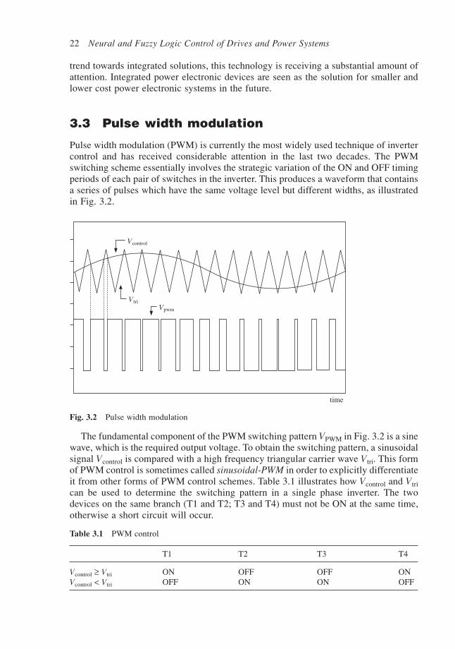
Pulse width modulation (PWM) is currently the most widely used technique of invertercontrol and has received considerable attention in the last two decades. The PWMswitching scheme essentially involves the strategic variation of the ON and OFF timingperiods of each pair of switches in the inverter. This produces a waveform that containsa series of pulses which have the same voltage level but different widths, as illustratedin Fig. 3.2.
Fig. 3.2 Pulse width modulation
Vcontrol
VtriVpwm
time
The fundamental component of the PWM switching pattern VPWM in Fig. 3.2 is a sinewave, which is the required output voltage. To obtain the switching pattern, a sinusoidalsignal Vcontrol is compared with a high frequency triangular carrier wave Vtri. This formof PWM control is sometimes called sinusoidal-PWM in order to explicitly differentiateit from other forms of PWM control schemes. Table 3.1 illustrates how Vcontrol and Vtrican be used to determine the switching pattern in a single phase inverter. The twodevices on the same branch (T1 and T2; T3 and T4) must not be ON at the same time,otherwise a short circuit will occur.
Table 3.1 PWM control
T1 T2 T3 T4
Vcontrol ≥ Vtri ON OFF OFF ONVcontrol < Vtri OFF ON ON OFF

Electric motors and power systems 23
In sinusoidal-PWM control schemes, there are two characteristic ratios which areimportant factors in the design of the controllers. The amplitude modulation ratio ma isdefined as the ratio of the peak amplitude of the control signal to the peak amplitude ofthe carrier signal,
mV
Va = control
tri
ˆ
ˆ
The frequency modulation ratio mf is defined as the ratio of the carrier frequency to theratio of the control signal frequency.
mf
ff = control
tri
The standard sinusoidal-PWM technique suffers from the major drawback that thea.c. term gain (Gac), which is the ratio of the amplitude of the output voltage to theamplitude of the PWM waveform, is limited to a maximum value of 0.866 (Gac ≤ 0.866).Several improved PWM techniques have been introduced to tackle this problem but theyeach have their own disadvantages. In general, improved techniques have higher a.c.gains but suffer from more harmonic distortions and require more complicated hardwarefor implementation. Further information of the improved techniques can be found in[44]. They include techniques such as sine + 3rd harmonic PWM, harmonic injectionand programmed harmonic elimination. Other PWM techniques include random PWMschemes and sliding mode control. Random PWM schemes [124], [106] are based onthe use of random number generation. They offer a more evenly spread harmonic spectrumand are found to have reduced radio interference, noise and vibration effects. Slidingmode control, on the other hand, is described by Jung and Tzou [137] to be especiallysuitable for closed-loop control of power converting systems under load variations.
However, improved PWM techniques require a more complex hardware implementation.For the present work, the standard PWM technique is found to be suitable for theapplication while being easier to implement in hardware when compared to the othertechniques.
There are various design solutions to implement a PWM controller. The followingsection describes a traditional circuit implementation method: a C++ program is used togenerate the switching pattern. A fairly straightforward method is to use an erasableprogrammable read only memory (EPROM) to store the PWM pattern. During theoperation, this information is sequentially retrieved and fed into a driver circuit board,which will switch the IGBTs accordingly. Figure 3.3 shows a schematic of the circuitdesign. It comprises a voltage controlled oscillator NE566 (IC1), a counter (IC2), anEPROM (IC3) and some AND gates (IC4) to act as output buffers.
The information for producing one cycle of the power waveform, i.e. one period ofthe sinusoidal reference signal, is broken down into 4096 slices and stored in the EPROMmemory locations. Each momory location corresponds to an address ranging from 0 to4095 and each bit of information in a memory location controls one power switch in theinverter. For a single phase inverter which has four power switches, 4096 × 4 bits (16 kb)of memory are required while a three-phase inverter with six switches requires 4096 ×6 bits (24 kb) of memory. IC2 is a CMOS4040 12-bit counter, designed to count from0 to 4095 in a repetitive cycle. This is used as the address input to retrieve information

24N
eural and Fuzzy L
ogic Control of D
rives and Power System
s
Fig. 3.3 Circuit diagram of the EPROM-based PWM generator
V+12 V
R210k
C2
0.001 uF
IC1RV115 k
R110k
56 8
VcRV+ TRi
SQ
43 10
6 VNE566
C1470pF
7 1
V––12 V
16IC2
CLK
Q0Q1Q2Q3Q4Q5Q6Q7Q8Q9
Q10Q11
0765324
131214151
109876543
252421232
2022271
14R35k
Vpp
2764
IC3A0A1A2A3A4A5A6A7A8A9A10A11A12
CEOEPGMVPP
D0D1D2D3D4D5D6D7
1112131516171819
IC412
12
12
12
3
3
3
3
4081C4B
4081C4C
4081C4D
4081
ERI
01020304
11
4040
28
8
MR

Electric motors and power systems 25
from the EPROM. To obtain an output frequency of 50 Hz, the counter (IC2) has tocomplete 50 cycles in one second. Therefore, the sampling frequency must be:
fs = 50 × 4096 = 204.8 kHz
The advantage of using a voltage controlled oscillator instead of a fixed frequencyoscillator is that a voltage signal can be used to control the oscillator frequency andhence the sampling frequency of the inverter.
This makes it possible to control the inverter frequency with a closed-loop controlcircuit. Due to immediate availability during the implementation stage, a 64 kb EPROMis used in the circuit although 16 kb (212 × 4) of information is sufficient for single-phase operation (24 kb for three phase). The period of the triangular carrier wave ischosen to contain ten sampling units. Each sampling unit corresponds to one clock cyclehence the actual sampling time will be the inverse of the clock frequency.
In the C program, a comparison between the reference power waveform and thecarrier waveform is made at every sampling point. The output is 1 if the reference powervalue is larger than the carrier value and 0 if vice versa. The necessary switching signalis generated from this comparison as shown in Fig. 3.4. However, as a result of introducingdiscrete sampling points, a certain amount of error is inevitable. The errors are labelledas ±εn in the diagram. The maximum value for each error is just under the length of onesampling unit which, in this case, is 10 per cent of the period of the switching signal(because one cycle of the switching signal consists of ten sampling units). The effectsof these errors can be reduced by increasing the number of sampling points in each cycleof the switching signal. This can be done either by maintaining the frequency modulationratio mf and increasing the total number of sampling points in the power cycle or bymaintaining the number of sampling points in one power cycle and reducing mf.
Fig. 3.4 PWM waveform generation
Carrier waveform
Power waveform
5 10 n
+ε1
– ε1
PWM switchingwaveform
5 10 n
1
The frequency of the triangular carrier waveform, also known as the switching frequencyis given by:
ftri = 1/(NTs) Hz
where Ts is the sampling period which is determined by the desired power frequency and

26 Neural and Fuzzy Logic Control of Drives and Power Systems
N is the number of sampling points in one cycle of the carrier signal. For a 50 Hz powerfrequency, the sampling frequency Ts is:
Ts = 150
14096
= 4.88 s⋅ µ
Therefore, the switching frequency is
f tri –6= 110 4.88 10
Hz = 20.48 kHz× ×
The frequency modulation factor is given by:
mff
TTf
s
s= =
(1/4096 )(1/10 )
= 409.6tri
1
where:ftri is the frequency of the triangular carrier waveform (switching frequency)f1 is the frequency of the fundamental harmonic (sinusoidal power frequency)
A three-phase PWM waveform generator was also constructed by simply changing thecontents of the EPROM with a new C program which is written to generate the three-phase switching data. In the program, the triangular carrier waveform is compared withthree different sinusoidal power waveforms, each phase shifted from one another by120°. The result of each comparison determines the switching signal of the IGBTs ineach branch of the inverter. Instead of four outputs, the three-phase PWM controller hassix outputs, as there are six IGBTs in a three-phase inverter. Therefore, two additionaldata outputs from the EPROM are used. The control circuit was successfully implementedand used in the experiments of the second case study presented in this book.
3.4 The space vector in electrical systems
The space vector concept originated in the study of Y-connected induction motors but itcan be extended to describe all three-phase electric systems regardless of their exactnature: electrical generators, electrical motors, transformers, etc. The basic principle isto transform the scalar electromagnetic quantities describing the system (currents, voltagesand magnetic fluxes) into two-dimensional vectors named space vectors. One spacevector replaces a set of three scalar quantities of the same type, thereby generating amore compact notation for the mathematical equations. Therefore, space vectors arelargely used to analyse the operation of three-phase electrical machines [159], [183],[227], [229].
If ‘A’ is an electromagnetic quantity then Aa, Ab and Ac are the three values correspondingto the three system phases. They are initially associated with two-dimensional vectorssituated on three directions 120° apart in a plane:
r rA Aa b, , and
rAc as illustrated in Fig.
3.5. Adding the three vectors together, a single two-dimensional vector is obtainedaccording to equation (3.1).
rA is the space vector associated with scalar quantities Aa,
Ab and Ac. The vector components on the real axis (axis ‘d’) and on the imaginary axis(axis ‘q’) are given in (3.2).
r r r rA A A Aa b c = + + (3.1)

Electric motors and power systems 27
A A A A A A A
A A A A A A
d a b c a b c
q a b c b c
= cos(0) + cos23
+ cos 43
= – 12
– 12
= sin(0) + sin23
+ sin 43
= 32
– 32
⋅ ⋅
⋅
⋅ ⋅
⋅
π π
π π (3.2)
In practical calculations, the space vectors are represented either by 2 × 1 matrices orby complex quantities. Using matrix notation, equation (3.2) becomes (3.3) while (3.4)describes the complex number approach to space vector calculation (3.1). Two-dimensionalvectors like the one in (3.1) are distinguished from the equivalent complex numbers bymeans of notation. Underlined symbols stand for complex values while vectors arerepresented by symbols placed under an arrow. Thus, A is a complex number while
rA
is a vector.
A
A
A
A
A
d
q
a
b
c
⋅
= 1 – 1
2– 1
2
0 32
– 32
(3.3)
A A A A
j
a b c = + +
= cos 23
+ sin 23
2ε ε
ε π π⋅ ⋅
⋅
(3.4)
The transformation of the set of three scalar variables into a space vector is equivalentto a transformation from a three-phase system into a two-phase system. The inversetransformation can be calculated based on the property that the algebraic sum of thethree scalar values is always null. This property is shared by all electromagnetic quantitiesrelated to individual phases (currents, voltages and magnetic fluxes) if the power supplygenerates symmetric voltages and the load is symmetric and Y-connected.
Aa + Ab + Ac = 0 (3.5)
Combining (3.5) with equation (3.2), the system (3.6) is generated from which (3.7) is
Fig. 3.5 The relation between phase quantities and the corresponding space vector
bImag
(q axis)
0
a Real(d axis)
c
rAc
rA
rAc
rAb
rAb
rAa

28 Neural and Fuzzy Logic Control of Drives and Power Systems
derived. The system (3.7) describes the inverse transformation of a space vector into thecorresponding set of three scalar phase quantities.
A A A A
A A A
A A A
d a b c
q b c
a b c
= – 12
– 12
= 32
– 32
+ + = 0
(3.6)
A A
A A A
A A A
a d
b d q
c d q
= 23
= – 13
+ 13
= – 13
– 13
⋅
⋅ ⋅
⋅ ⋅
(3.7)
3.5 Induction motor control
3.5.1 Space vector model of three-phase induction motor
The mathematical models of the electrical machines are classified as lumped-parametercircuit models and distributed-parameter models. The latter are more complex but moreaccurate than the former. The distributed-parameter models are used for very precisecalculations necessary for optimal machine design. They allow an exact calculation ofthe electromagnetic field and heat distribution inside the machine. The lumped-parametermodels can be obtained as a simplification of the distributed-parameter models. Theyare used for control system design where only global quantities like currents, torque andspeed are important. Their internal distribution inside the machine is not relevant whendesigning controllers to govern the evolution of speed, torque and power consumptionaccording to the particular application requirements.
Furthermore, the lumped-parameter circuit model is simpler and therefore moreconvenient to use in the study of electric drives. The space vector model of the inductionmotor is the lumped-parameter model with the largest use in the study and design ofelectrical drive applications. It is common to consider as a first approximation that therotor windings and the stator windings have a sinusoidal distribution inside the motorand no magnetic saturation is present [43], [159]. Therefore, the magnetomotive force(MMF) space harmonics and slot harmonics are neglected. Although saturation is nottaken into account, the model is considered to yield acceptable results for the study ofcommon electric drive applications [159], [227].
The induction motor space vector model is derived from the basic electrical equationsdescribing each of the stator windings and each of the rotor windings. The stator windingsequations are given in (3.8) where uas, ubs and ucs are the phase voltages, ias, ibs and icsare the phase currents, while Ψas, Ψbs and Ψcs are the phase magnetic fluxes.

Electric motors and power systems 29
u R it
u R it
u R it
as s asas
bs s bsbs
cs s cscs
= + d
d
= + d
d
= + d
d
Ψ
Ψ
Ψ
(3.8)
The associated space vectors (expressed as complex numbers) are obtained bymultiplying the second equation in (3.8) with ε and the third with ε2, after which all thethree equations are added together. The conversion of the three scalar equations into onespace vector equation is illustrated by (3.9) and (3.10).
u R it
u R it
u R it
as s asas
bs s bsbs
cs s cscs
= + d
d
= + d
d
= + d
d2 2 2
Ψ
ε ε εΨ
ε ε εΨ
⋅
⋅
(3.9)
u u u u
i i i i u R it
ss
as bs cs
ss
as bs cs
ss
as bs cs
ss
s ss s
s = + +
= + +
= + +
= + d
d
2
2
2
ε εε ε
Ψ Ψ ε Ψ ε Ψ
Ψ⋅ ⋅⋅ ⋅⋅ ⋅
⇒ (3.10)
Different reference frames (still or rotating) can be used to calculate the coordinatesof the electromagnetic space vectors [43]. Equations (3.10) are written in the statorreference frame.
bImθ Ims
ω
0
c
Reθ
a Res
Fig. 3.6 The fixed stator reference frame and the general mobile θ reference frame
θ
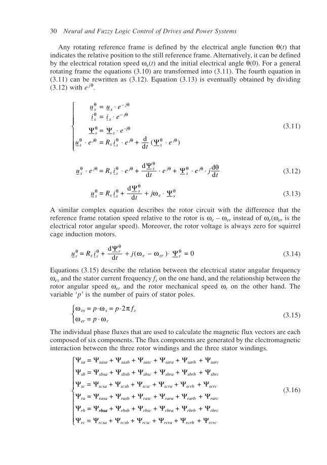
30 Neural and Fuzzy Logic Control of Drives and Power Systems
Any rotating reference frame is defined by the electrical angle function θ(t) thatindicates the relative position to the still reference frame. Alternatively, it can be definedby the electrical rotation speed ωe(t) and the initial electrical angle θ(0). For a generalrotating frame the equations (3.10) are transformed into (3.11). The fourth equation in(3.11) can be rewritten as (3.12). Equation (3.13) is eventually obtained by dividing(3.12) with e jθ.
u u e
i i e
e
u e R i et
e
s sj
s sj
s s–j
sj
s sj
sj
θ θ
θ θ
θ θ
θ θ θ θ θ θ
Ψ Ψ
Ψ
=
=
=
= + dd
( )
–
–
⋅⋅
⋅
⋅ ⋅ ⋅
(3.11)
u e R i et
e e jts
js s
j s js
jθ θ θ θθ
θ θ θΨΨ θ = +
dd
+ dd
⋅ ⋅ ⋅ ⋅ ⋅ (3.12)
u R it
js s ss
e sθ θ
θθΨ
ω Ψ= + d
d + ⋅ (3.13)
A similar complex equation describes the rotor circuit with the difference that thereference frame rotation speed relative to the rotor is ωe – ωer instead of ωe(ωer is theelectrical rotor angular speed). Moreover, the rotor voltage is always zero for squirrelcage induction motors.
u R it
jr s rr
e er rθ θ
θθΨ
ω ω Ψ= + d
d ( – ) = 0+ ⋅ (3.14)
Equations (3.15) describe the relation between the electrical stator angular frequencyωes and the stator current frequency fs on the one hand, and the relationship between therotor angular speed ωer and the rotor mechanical speed ωr on the other hand. Thevariable ‘p’ is the number of pairs of stator poles.
ω ω πω ω
es s s
er r
p p f
p
= = 2
=
⋅ ⋅⋅
(3.15)
The individual phase fluxes that are used to calculate the magnetic flux vectors are eachcomposed of six components. The flux components are generated by the electromagneticinteraction between the three rotor windings and the three stator windings.
Ψ Ψ Ψ Ψ Ψ Ψ Ψ
Ψ Ψ Ψ Ψ Ψ Ψ Ψ
Ψ Ψ Ψ Ψ Ψ Ψ Ψ
Ψ Ψ Ψ Ψ Ψ Ψ Ψ
Ψ Ψ
sa sasa sasb sasc sara sarb sarc
sb sbsa sbsb sbsc sbra sbrb sbrc
sc scsa scsb scsc scra scrb scrc
ra rasa rasb rasc rara rarb rarc
rb
= + + + + +
= + + + + +
= + + + + +
= + + + + +
= rbsarbsa rbsb rbsc rbra rbrb rbrc
rc rcsa rcsb rcsc rcra rcrb rcrc
+ + + + +
= + + + + +
Ψ Ψ Ψ Ψ Ψ
Ψ Ψ Ψ Ψ Ψ Ψ Ψ
(3.16)

Electric motors and power systems 31
In equation (3.16) each flux component is identified by four indices: the first twoindicate the winding where the magnetic flux is measured while the last two indicate thewinding that generates it. For instance, Ψsarb is the flux generated into stator winding ‘a’by rotor winding ‘b’. The flux components related to stator phase ‘a’ are described by(3.17). The names and the significance of the symbols are as follows:
• lmsr – the mutual inductance between stator and rotor. It is proportional to the fluxcreated by one rotor phase into one stator phase.
• mσs – the stator mutual leakage inductance between two stator phases. It is proportionalto the flux produced by one stator phase into another stator phase without influencingthe rotor. It therefore models the magnetic field lines that intersect two stator windingswithout intersecting the rotor.
• lms – the mutual inductance between stator phases. It is proportional to the fluxcreated by one stator phase into another stator phase through the rotor. It models themagnetic field lines that are created by one stator phase but intersects both the rotorand the other stator winding.
• lσs – the stator phase leakage inductance. It is proportional to the stator phase leakagemagnetic flux. The corresponding magnetic field lines do not intersect any windingother than the stator winding which produces them.
• α – the angle between the stator d-axis and the rotor d-axis.
Ψ
Ψπ
Ψπ
Ψ α
Ψ απ
σ
σ
σ
sasa s ms sa
sasb s ms sb
sasc s ms sc
sara msr ra
sarb msr
l l i
m l i
m l i
l i
l
= ( + )
= + cos 23
= + cos 43
= ( cos )
= cos + 23
⋅
⋅
⋅
⋅
⋅
⋅ ⋅
⋅
⋅
⋅
⋅
= cos + 43
i
l i
rb
sarc msr rcΨ απ
(3.17)
The magnetic coupling between different windings is influenced by their relative position.The coupling is maximal when the angle between the two windings is zero and it is nullat 90°. This geometric factor can be expressed by simple cosine functions due to theassumption that the magnetic field has a sinusoidal distribution. Adding the six componentsfrom (3.17) yields:
Ψ α ασ σsa s s ms sa msr ra msr rc rbl m l i l i l i i= – + 32
+ 32
cos + 32
sin ( – )
⋅ ⋅ ⋅ ⋅ ⋅
(3.18)
Equation (3.18) is obtained based on the property that the sum of the three phasecurrents is zero. Similar results are obtained for stator phases ‘b’ and ‘c’.

32 Neural and Fuzzy Logic Control of Drives and Power Systems
Ψ α α
Ψ α α
σ σ
σ σ
sb s s ms sb msr rb msr ra rc
sc s s ms sc msr rc msr rb
l m l i l i l i i
l m l i l i l i i
= – +32
+ 32
cos + 32
sin ( – )
= – +32
+ 32
cos + 32
sin ( –
⋅ ⋅ ⋅ ⋅ ⋅
⋅ ⋅ ⋅ ⋅ ⋅ rara)
(3.19)
Eventually the stator flux space vector is calculated multiplying equations (3.18) and(3.19) with l, ε and ε2 and adding them together. The flux has two components: onedepends on the stator currents and the other depends on the rotor currents.
Ψ Ψ Ψ
Ψ
Ψ α α ε ε ε ε
σ σ
ss
sss
srs
ss s s ms ss
sr msr r msr rb rc ra rc ra rb
l m l i
l i l i i i i i i
= +
= – + 32
= 32
cos + 32
sin (– + + – – + )2 2
⋅
⋅ ⋅
(3.20)
The expression describing the flux component Ψsr can be further transformed using themathematical properties (3.21). The results are presented in (3.22), (3.23) and (3.24).Equation (3.24) becomes (3.25) in a general reference frame given by angle θ.
ε εε εε ε
– = 3
– + = 3
– = 3
2
2
2
j
l j
l j
⋅⋅ ⋅⋅ ⋅
(3.21)
Ψ α α ε εsrs
msr r msr ra rb rcl i l j i i i = 32
cos + 32
sin 3 ( + + )2⋅ ⋅ ⋅ (3.22)
Ψ α α αsrs
msr rr
msr rr
msr rr j
msr rsl i j l i l i e l i = 3
2 cos + 3
2 sin = 3
2 = 3
2 ⋅ ⋅ ⋅ ⋅ ⋅ ⋅
(3.23)
Ψ σ σss
s s ms ss
msr rsl m l i l i = – +
32
+ 32
⋅
⋅ ⋅ ⋅ (3.24)
Ψθσ σ
θ θs s s ms s msr rl m l i l i = – +
32
+ 32
⋅
⋅ ⋅ ⋅ (3.25)
The rotor flux expression is similar to the stator flux expression but each stator inductanceis replaced by the corresponding rotor inductance. Thus, inducation motor equations,formulated for a reference frame defined by the angle θ(t) and the rotation speed ω(t),are:

Electric motors and power systems 33
u R it
j
u R it
j
l m l i l i
s s ss
e s
r r rr
e er r
s s s ms s msr r
r
θ θθ
θ
θ θθ
θ
θσ σ
θ θ
θ
Ψω Ψ
Ψω ω Ψ
Ψ
Ψ
= + d
d +
= + d
d + ( – )
= – + 32
+ 32
⋅
⋅ ⋅ ⋅
= – + 32
+ 32
l m l i l ir r mr r msr sσ σθ θ⋅
⋅ ⋅ ⋅
(3.26)
The magnetic flux expressions in (3.26) are complicated because seven differentinductances are involved. The mathematical technique of referring the rotor quantitiesto the stator is usually applied to the equations given in (3.26) in order to simplify theflux equations. The basic principle of referring the rotor quantities to the stator is tomultiply rotor quantities with constant values in such a manner that the power transferbetween stator and rotor is not altered. Thus, if the rotor current is multiplied by constantk then the rotor voltage and the rotor flux are multiplied by 1/k. On the other hand, therotor resistance and the rotor inductance are multiplied by 1/k2. The constant k thatgenerates the simplest transformation of system (3.26) is given by (3.27) while thecorresponding referred rotor quantities are (3.28). The equation linking all the referredquantities is (3.29).
kllmsr
ms = (3.27)
i k ill
i
uk
ull
u
kll
Rk
Rll
R
r rmsr
msr
r rms
msrr
r rms
msrr
r rms
msrr
′ ⋅ ⋅
′ ⋅ ⋅
′ ⋅ ⋅
′ ⋅ ⋅
θ θ θ
θ θ θ
θ θ θΨ Ψ Ψ
= =
= 1 =
= 1 =
= 1 = 2
2
2
(3.28)
′ ′′ ′u R it
jr r rr
e er rθ θ
θθΨ ω ω Ψ = +
dd
+ ( – ) (3.29)
The referred rotor flux can be expressed as a function of the stator current and thereferred rotor current vector (3.30).
Ψ Ψθ θσ σ
θ θ′
⋅ ′ ⋅r
ms
msrr
ms
msrr r mr r ms s
ll
ll
l m l i l i= = – + 32
+ 32
2
2 (3.30)
The inductances lms, lmr and lmsr are always related by equation (3.31). This relationshipallows the rewriting of equation (3.30) as (3.32) and (3.33).
lms · lmr = lmsr2 (3.31)

34 Neural and Fuzzy Logic Control of Drives and Power Systems
Ψ θσ σ
θ θ θ′ ⋅ ′ ⋅ ′ ⋅rms
msrr r r ms r ms s
ll
l m i l i l i= ( – ) + 32
+ 32
2
2 (3.32)
Ψ θσ
θ θ θ θ′ ′ ⋅ ′ ⋅ ′ ⋅ ′ ⋅r r m r m s r r m sL L i L i L i L i= ( + ) + = + (3.33)
The significance of the symbols in the previous equations is:
• ′Lll
l mrms
msrr rσ σ σ= ( – )
2
2 – the total referred rotor leakage inductance.
• L lm ms= 32 – the resulting stator–rotor mutual inductance.
• ′ ′L L Lr r m= + σ – the total referred rotor inductance.
Substituting the first equation (3.28) in (3.25), the stator flux can be written as:
Ψθσ σ
θ θs s s ms s ms rl m l i l i= – +
32
+ 32
⋅
⋅ ⋅ ⋅ ′ (3.34)
Ψθσ
θ θ θ θs r m r m s s s m sL L i L i L i L i= ( + ) + = + ⋅ ⋅ ⋅ ⋅ ′ (3.35)
The significance of the symbols is:
• Lσs = lσs – mσs – the total stator leakage inductance.• Ls = Lσs + Lm – the total stator inductance.
Thus, (3.36) is the compact format of the induction motor equations initially presentedin (3.26). This system of equations expresses the space vector model of the inductionmotor [159]. This model will be used in the neural induction motor control examplepresented in the second section of the book.
u R it
j
u R it
j
L i L i
L i L i
s s rs
s
r r rr
e er r
s s s m r
r r r m s
θ θθ
θ
θ θθ
θ
θ θ θ
θ θ θ
ΨωΨ
Ψω ω Ψ
Ψ
Ψ
= + d
d +
= + d
d + ( – ) = 0
= +
= +
′ ′ ′′
′
′
′ ′ ′
(3.36)
Note: Usually, to simplify the notation, the apostrophe symbols are not included in theequations. Yet, the rotor quantities are implicitly referred to the stator. No apostrophesymbol is used in the rest of this book but they are implied for all rotor equations orparameters.
3.5.2 Induction motor control strategies
During the first one hundred years after its invention, the induction motor was known asa constant speed electrical machine. The advent of electrical power converters in the

Electric motors and power systems 35
1960s made possible the use of the induction motor as a variable speed machine. Therecent development of the digital technology created the possibility of implementingcomplex control algorithms yielding high dynamic performance [229].
Correct control over the motor torque is a prerequisite of all the speed control strategies.The torque equation can be derived from power-based considerations and can be expressedas a function of the current and voltage space vectors. The total power consumed by themotor has three components: the power dissipated by the winding resistances PR, thepower stored in the internal magnetic fields Pµ and the mechanical power PM. The motortorque is proportional to the mechanical power and inversely proportional to the rotorspeed (3.37). The total motor power is the power consumed by all six stator and rotorwindings so it can be calculated as in equation (3.38). Elementary algebraic calculationsshow that the rotor power and the stator power can be calculated as indicated by (3.39).The calculations can be performed in any reference frame defined by the time functionθ(t). Now as:
P P P P
TP
pP
R M
M
r
M
er
= + +
= =
µ
⋅
ω ω(3.37)
therefore:
P = Ps + Pr = usaisa + usbisb + uscisc + uraira + urbisb + urcisc (3.38)
where:
P u i u i u i u i u i
P u i u i u i u i u i
s sa sa sb sb sc sc ss
ss
s s
r ra ra rb rb rc rc rr
rr
r r
= + + = 23
Re = 23
Re
= + + = 23
Re = 23
Re
* *
* *
⋅ ⋅
⋅ ⋅
θ θ
θ θ(3.39)
The equations (3.40) are obtained by substituting general equations (3.36) into (3.39).Thus, the three power components are calculated according to (3.41).
P R it
j i
P R it
j i
s s ss
e s s
r r rr
e er r r
= 23
Re + d
d +
= 23
Re + d
d + ( – )
θθ
θ θ
θθ
θ θ
Ψω Ψ
Ψω ω Ψ
⋅
⋅
⋅
⋅
*
*
(3.40)
P R i i R i i
Pt
it
i
P j i j i
R s s s r r r
ss
rr
M e s s e er r r
= 23
Re +
= 23
Re d
d +
dd
= 23
Re + ( – ) *
θ θ θ θ
θθ
θθ
θ θ θ θ
Ψ Ψ
ω Ψ ω ω Ψ
⋅ ⋅
⋅ ⋅
⋅ ⋅ ⋅ ⋅
µ
* *
* *
*
(3.41)

36 Neural and Fuzzy Logic Control of Drives and Power Systems
The imaginary number ‘j’ in the expression of the mechanical power component PM canbe eliminated using the general algebraic property (3.42).
Rej · z = – Imz (3.42)
The two components of the imaginary part in (3.42) can be rewritten as in (3.43), so thatthe mechanical power equation becomes (3.44).
Im = Im ( + ) = Im
Im ( – ) = ( – ) Im
ω Ψ ω ωω ω Ψ ω ω
θ θ θ θ θ θ θ
θ θ θ θe s s e s s m r s e m r s
e er r r e er m s r
i L i L i i L i i
i L i i
⋅ ⋅ ⋅ ⋅ ⋅ ⋅⋅ ⋅ ⋅ ⋅
* * *
* *(3.43)
P L i i i iM m e r s e er s r= – 23
[ Im + ( – ) Im ]ω ω ωθ θ θ θ⋅ ⋅ ⋅ ⋅* * (3.44)
Based on the mathematical property (3.45) equation (3.44) is further transformed into(3.46).
Im x · y* + Im y · x* = 0 (3.45)
P L i i p L i iM er m s r r m s r= 23
Im = 23
Im ω ωθ θ θ θ⋅ ⋅ ⋅ ⋅* * (3.46)
Therefore, the motor torque may be expressed by (3.47). It is seen that the motor torquedepends only on the rotor current vector and on the stator current vector.
T pL i im s r = 23
Im ⋅ ⋅θ θ* (3.47)
Alternatively, the torque can be expressed as equivalent functions of the stator magneticflux and/or the rotor magnetic flux as shown in (3.48), where δ is the angle between thestator flux and the rotor flux.
T p i
T p i
T pL
L L Lp
LL L L
r r
s s
m
s r ms r
m
s r ms r
= 23
Im (a)
= 23
Im (b)
= 23
–
Im = 23
–
| | | | sin (c)2 2
⋅ ⋅
⋅ ⋅
⋅ ⋅ ⋅ ⋅ ⋅ ⋅ ⋅
Ψ
Ψ
Ψ Ψ Ψ Ψ δ
θ θ
θ θ
θ θ θ θ
*
*
*
(3.48)
Relations (3.47) and (3.48) directly or indirectly underlie all induction motor controlstrategies. They can be classified as scalar control and vector control strategies (Fig.3.7). The scalar control operates utilising simplified equations derived from the generalspace vector model (3.36). This approach involves only the space vector amplitudes andtheir corresponding frequencies and the simplified equations are valid only in steady-state operation. Consequently, scalar control is simple but generates poor responseduring transient operation [227]. In contrast, vector control operates directly with thespace vector model of the motor and implements the equations given in (3.48). Therefore,it offers good results in both steady-state operation and transient operation. The groupof vector control algorithms includes the direct torque control (DTC) method and theclass of field-oriented control strategies. The theory of field-oriented control was developed
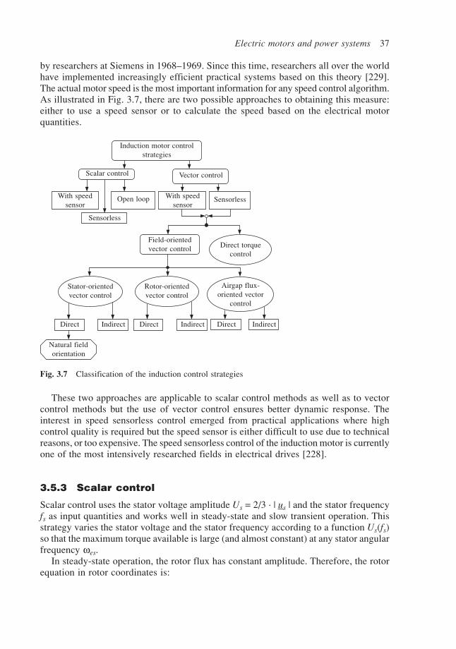
Electric motors and power systems 37
by researchers at Siemens in 1968–1969. Since this time, researchers all over the worldhave implemented increasingly efficient practical systems based on this theory [229].The actual motor speed is the most important information for any speed control algorithm.As illustrated in Fig. 3.7, there are two possible approaches to obtaining this measure:either to use a speed sensor or to calculate the speed based on the electrical motorquantities.
Fig. 3.7 Classification of the induction control strategies
Induction motor controlstrategies
Scalar control Vector control
With speedsensor
Open loop With speedsensor
Sensorless
Sensorless
Field-orientedvector control Direct torque
control
Stator-orientedvector control
Rotor-orientedvector control
Airgap flux-oriented vector
control
Direct Indirect Direct Indirect Direct Indirect
Natural fieldorientation
These two approaches are applicable to scalar control methods as well as to vectorcontrol methods but the use of vector control ensures better dynamic response. Theinterest in speed sensorless control emerged from practical applications where highcontrol quality is required but the speed sensor is either difficult to use due to technicalreasons, or too expensive. The speed sensorless control of the induction motor is currentlyone of the most intensively researched fields in electrical drives [228].
3.5.3 Scalar control
Scalar control uses the stator voltage amplitude Us = 2/3 · | us | and the stator frequencyfs as input quantities and works well in steady-state and slow transient operation. Thisstrategy varies the stator voltage and the stator frequency according to a function Us(fs)so that the maximum torque available is large (and almost constant) at any stator angularfrequency ωes.
In steady-state operation, the rotor flux has constant amplitude. Therefore, the rotorequation in rotor coordinates is:

38 Neural and Fuzzy Logic Control of Drives and Power Systems
R it
R i j R i j L i L ir rr r
r
r rr
es er rr
r rr
es er r rr
m sr+
dd
= + ( – ) = + ( – ) ( + ) = 0Ψ
ω ω Ψ ω ω ⋅
(3.49)
Under these conditions, the rotor current depends on the stator current space vector andon the slip angular frequency (the difference ωes – ωer) as indicated in (3.50).
ij L i
R j Lrr es er m s
r
r es er r=
– ( – ) + ( – )ω ω
ω ω (3.50)
The initial motor torque expression (3.47) can be modified by substituting (3.50) in(3.47) which yields equation (3.51). Therefore, the motor torque is proportional to thestator current module squared.
T pLj i iR j L
pL ij
R j Lmes er s
rsr
r es er rm2
sr es er
r es er r = 2
3 Im
( – ) + ( – )
= 23
| | Im ( – )
+ ( – )2
*2⋅
⋅
⋅
ω ωω ω
ω ωω ω
(3.51)
It is seen that the stator current depends on the stator voltage as indicated by (3.52),(3.53), (3.54), while the dependency between the torque and the stator voltage is obtainedby combining equations (3.51) and (3.54) to give relationship (3.55).
u R i j j R i jsr
s sr
er sr
es er sr
s sr
es sr = + + ( – ) = + ω Ψ ω ω Ψ ω Ψ (3.52)
u R i j L ij L iR j Ls
rs s
res s s
r es er m sr
r es er r = + –
( – ) + ( – )
2
ωω ω
ω ω⋅
(3.53)
| | = | |
+ + ( – )
+ ( – )
2i
u
R j LL
R j L
sr s
r
s es ses es er m
r es er r
ω ω ω ωω ω
(3.54)
T pLU
R j LL
R j L
j LR j Lm
s
s es ses es er m
r es er r
es er m
r es er r = 3
2
+ + ( – )
+ ( – )
Im ( – )+ ( – )
22
2 2
2
⋅ ⋅
ω ω ω ωω ω
ω ωω ω
(3.55)
Figure 3.8 presents the torque–speed characteristic calculated according to (3.55) fora three-phase induction motor with the parameters Rs = 0.371 Ω; Rr = 0.415 Ω; Lsσ =2.72 mH; Lrσ = 3.3 mH; Lm = 84.33 mH; p = 1; P = 11.1 kW. The motor is supplied bya three-phase 240 V/50 Hz supply. As the figure shows, the motor torque is zero atsynchronous speed and has its maximum at a relatively high angular speed ωM ascompared to the rated stator angular frequency (314 rad/s). The motor normally operatesat speeds between the synchronous angular speed and ωM. At high stator angular frequency,around the rated value, the stator resistance is negligible, thus, | |i s
r in (3.54) dependsonly on the slip angular frequency (ωslp = ωes – ωer) and on the voltage angular frequency

Electric motors and power systems 39
ratio (Us /ωs). If this ratio is kept constant then the stator current amplitude and themotor torque depend solely on the slip angular frequency. Therefore, the maximummotor torque TM is independent of the stator angular frequency ωes. At low frequencies,however, the stator resistance has an important influence on the stator current and leadsto a diminished maximum torque, with negative effects on the motor operation. Theeffect of the stator resistance on the motor torque can be counteracted by raising thestator voltage to compensate for the stator resistance. The function Us(ωs) that maintainsTM constant at all frequencies can be derived from (3.55). The solution is a non-linearexpression, difficult to implement into hardware. A linear approximation of this functionis usually adopted in practical situations. The linear approximation Us(ωs) is defined bytwo points corresponding to the zero stator frequency and to the rated stator frequency:
• At zero stator frequency, the stator voltage has to generate a current equal to thestator current at rated stator angular frequency (314 rad/s) and maximum torque.
• At the rated stator frequency, the voltage attains its rated value.
The stator voltage amplitude is therefore defined by (3.56) where ‘p’ is the numberof stator pole pairs. This approximate solution does not provide a perfectly constantTmax but restricts its variation within a narrow interval.
U R IU R I
pU fs s s T es
s s s Ts s= +
– 2 50
= + (max )MAX (max )
0ω π Φ⋅ ⋅ ⋅ (3.56)
Speeds over the rated value can be obtained by increasing the stator frequency overthe 50 Hz limit but in this case the voltage is maintained constant at its maximum valueUsMAX. As a result, the maximum available torque decreases (it is inversely proportionalto the frequency squared) and very high speeds cannot be obtained using this method.For instance, the maximum torque decreases by as much as 25 per cent from the ratedvalue if the stator frequency is 100 Hz. The open-loop scalar control implements thestrategy illustrated by (3.56). This offers an approximate control over the motor speedbut the effects of the load torque variations cannot be compensated for due to the lack
Fig. 3.8 Induction motor mechanical characteristic (P = 11.1 kW)
T (Nm)
70
60
50
40
30
20
10
0
TM
–50 0 50 100 150 200 250 300 350ωM ω (rad/s)

40 Neural and Fuzzy Logic Control of Drives and Power Systems
of any feedback information. A compensation of the average slip angular frequency canbe performed instead so that the rotor speed equals the reference speed for the mostfrequent load torque value.
The control scheme can be implemented with a controlled rectifier as presented inFig. 3.9, or with an uncontrolled rectifier. In the first case, the PWM inverter controlsonly the frequency of the output voltage, while the rectifier determines the outputvoltage amplitude. In the second case, the switching pattern inside the inverter is morecomplex and determines both the frequency and the amplitude of the output voltage.
Fig. 3.9 Open-loop scalar control scheme
The scalar control strategy with speed sensor can be implemented as in Fig. 3.10using a controlled rectifier and a PWM inverter. As in the previous section, the controlledrectifier can be replaced by an uncontrolled rectifier if the inverter controls both thefrequency and the amplitude of the output voltage. The voltage control loop modifiesthe d.c. voltage according to the required speed profile while the optimal slip frequencyis calculated as a function of the current absorbed by the motor: the slip increases withthe absorbed current. This type of slip-current correlation limits the current variations inthe d.c. link during the transient motor operation.
+
–
f rref U s
refSpeed
controller
Voltagecontroller
Controlledrectifier
PWMinverter
IM
fslp(I)fslp
fs
++ fr+
+
–
Fig. 3.10 Scalar control scheme with speed sensor
An increase of the resistive load increases the current absorbed by the motor anddecreases its speed. This lowers the d.c. link voltage. The speed controller responds byincreasing the reference voltage while the slip calculator increases the motor slip. Asdemonstrated by equation (3.55) the motor torque increases with the increase of thestator voltage and with the increase of the slip angular frequency. On the other hand, thestator current depends on the stator voltage in the manner indicated in (3.54). Therefore,
fsRectifier
PWMinverter
fsf r
ref
Expected slipfrequency
IM
+
U sref
+
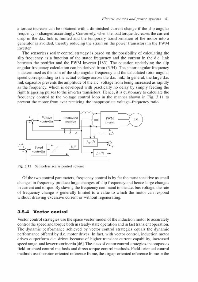
Electric motors and power systems 41
a torque increase can be obtained with a diminished current change if the slip angularfrequency is changed accordingly. Conversely, when the load torque decreases the currentdrop in the d.c. link is limited and the temporary transformation of the motor into agenerator is avoided, thereby reducing the strain on the power transistors in the PWMinverter.
The sensorless scalar control strategy is based on the possibility of calculating theslip frequency as a function of the stator frequency and the current in the d.c. linkbetween the rectifier and the PWM inverter [183]. The equation underlying the slipangular frequency calculation can be derived from (3.54). The stator angular frequencyis determined as the sum of the slip angular frequency and the calculated rotor angularspeed corresponding to the actual voltage across the d.c. link. In general, the large d.c.link capacitor prevents the amplitude of the a.c. voltage from being increased as rapidlyas the frequency, which is developed with practically no delay by simply feeding theright triggering pulses to the inverter transistors. Hence, it is customary to calculate thefrequency control to the voltage control loop in the manner shown in Fig. 3.11 toprevent the motor from ever receiving the inappropriate voltage–frequency ratio.
Fig. 3.11 Sensorless scalar control scheme
f rref
U sref
+
–
Voltagecontroller
Controlledrectifier
PWMinverter
IM
fs
++
fslp (I)
fr (U)
Speedcontroller
+–
Of the two control parameters, frequency control is by far the most sensitive as smallchanges in frequency produce large changes of slip frequency and hence large changesin current and torque. By slaving the frequency command to the d.c. bus voltage, the rateof frequency change is generally limited to a value to which the motor can respondwithout drawing excessive current or without regenerating.
3.5.4 Vector control
Vector control strategies use the space vector model of the induction motor to accuratelycontrol the speed and torque both in steady-state operation and in fast transient operation.The dynamic performance achieved by vector control strategies equals the dynamicperformance offered by d.c. motor drives. In fact, with vector control, induction motordrives outperform d.c. drives because of higher transient current capability, increasedspeed range, and lower rotor inertia [46]. The class of vector control strategies encompassesfield-oriented control methods and direct torque control methods. Field-oriented controlmethods use the rotor-oriented reference frame, the airgap-oriented reference frame or the

42 Neural and Fuzzy Logic Control of Drives and Power Systems
stator-oriented reference frame (see Fig. 3.7). In each case, the reference frame real axis(axis ‘d’) is oriented along the direction indicated by the corresponding magnetic flux.The rotor-oriented vector control simplifies the control system structure and generatesvery fast transient response. However, systems working with the stator flux vector or withthe airgap flux vector have been successfully implemented as well [79], [43].
3.5.5 Rotor flux orientation
In the rotor flux-oriented reference frame, the rotor flux vector has no imaginary part sothat the torque expression (3.48(a)) can be written as (3.57). The rotor flux and the rotorcurrent depend on one another in the manner indicated by the equations in (3.58).
T p i p ir r rd rq = 23
Re Im = – 23
⋅ ⋅ ⋅ ⋅Ψ Ψθ θ* (3.57)
ΨΨ
Ψ ω ω Ψ Ψ
Ψω ω Ψ ω ω Ψ
Ψ
Ψ Ψ
rd r rd m sd
rq r rq m sq
r rdrd
e er rq r rdrd
r rqrq
e er rd r rq e er rd
L i L i
L i L i
R it
R it
R it
R i
r
r r
= +
= + = 0
+ d
d – ( – ) = +
dd
= 0
+ d
d + ( – ) = + ( – ) == 0
(3.58)
Equations (3.59) and (3.60) can be derived from the previous system. They illustratethe influence of the stator current components over the rotor flux and on the rotorcurrent component on axis ‘q’ (irq). Thus, the modification speed of the rotor flux islimited by the rotor time constant Tr = Lr /Rr, while the rotor current component irq canbe changed rapidly as no time constant is involved in (3.60).
LR t
L ir
r
rdrd m sd
dd
+ = Ψ Ψ (3.59)
iLL
irqm
rsq= – ⋅ (3.60)
As demonstrated by (3.59) and (3.60), the two quantities influencing the torque canbe independently controlled by two uncoupled control loops. For high dynamicperformance, the torque is controlled by keeping the rotor flux Ψrd constant whilevarying the rotor current component irq. Keeping the rotor flux constant implies maintainingisd at a constant value while the rotor current component irq is controlled by the statorcurrent component isq.
The control strategy requires the rotor flux orientation to be determined in order tocalculate isd and isq. The direct vector control method estimates the magnetic flux vectoras a function of the stator voltage, the stator current and the rotor speed. There are threetypes of rotor flux estimators differing by the input data they use: the current–speedestimator (Is, ωer), the current–voltage estimator (Is, Us) and the current–voltage–speedestimator (Is, Us, ωer). The indirect vector control method is simpler as it calculates onlythe argument θ of the rotor flux as a function of isd and isq. The direct vector control is morerobust than the indirect vector control but its performance depends on the type of fluxestimator used.

Electric motors and power systems 43
The current–speed estimator is derived from the basic rotor equation and from therotor flux expression as shown in (3.61), (3.62) and (3.63). The rotor flux is the solutionof the integral equation (3.64). This estimator works well at low speeds but it is notprecise at high speeds because in this case the speed measuring errors have a biginfluence on the calculation results.
0 = + d
d –
= +
R it
j
L i L i
r rs r
s
er rs
rs
m ss
r rs
Ψω Ψ
Ψ
(3.61)
0 = –
+ d
d – R
L iL t
jrrs
s ss
r
rs
er rs⋅
Ψ Ψω Ψ (3.62)
dd
= – 1
+ + Ψ
ω Ψrs
rer r
s s
rss
t Tj
LT
i
⋅ (3.63)
Ψ ω Ψωr Is
t
rer r
s s
rss
Tj
LT
i t( , ) 0
= – 1
+ + d∫
⋅
(3.64)
The current–voltage flux estimator is derived from the stator equation and the stator fluxexpression (see (3.65), (3.66), (3.67)). Therefore, the equation defining the current–voltage flux estimator is (3.68). This method offers accurate results at high speeds butthe precision at low speeds is low.
u R it
L i L i L iLL
L i
ss
s ss s
s
ss
s ss
m rs
s ss m
rrs
m ss
= + d
d
= + = + ( – )
Ψ
Ψ Ψ
(3.65)
u R i Lit
LL t
Lits
ss s
ss
ss
m
r
rs
mss
= + dd
+ d
d –
dd
Ψ
(3.66)
dd
= ( – ) + –
dd
2Ψ rs
r
mss
s ss s r m
m
ss
tLL
u R iL L L
Lit
⋅ (3.67)
Ψ r I Us r
m
t
ss
s ss s r m
mssL
Lu R i t
L L LL
i( , ) 0
2
= ( – ) d + –
⋅ ⋅∫ (3.68)
The current–voltage–speed estimator (Is, Us, ωer) combines the previous two solutions:equation (3.64) and equation (3.68). It generates good rotor flux estimates both at lowspeeds and high speeds.
ΨΨ Ψ
ωω
r I Us r I
sr I Us
( , , )( , ) ( , )
= +
2(3.69)
The rotor flux is the original choice for field orientation because in this reference framethe equations corresponding to the two axes ((3.59) and (3.60)) are completely independent.

44 Neural and Fuzzy Logic Control of Drives and Power Systems
As a result, this control method generates the best dynamic performance. On the otherhand, the stator flux orientation has the advantage that the torque calculation uses thestator flux instead of the rotor flux as illustrated by (3.70) which is a consequence of(3.48(b)). The stator magnetic flux is much easier to calculate than the rotor magneticflux because it depends on stator quantities (currents, voltages and resistance) that canbe directly measured.
T p i p is s sd sq = 23
Im Re = 23
*⋅ ⋅ ⋅ ⋅θ θΨ Ψ (3.70)
Ψθ θ θs
t
s s su R i t = ( – ) d 0∫ (3.71)
A typical direct rotor field-oriented control scheme (see Fig. 3.12) contains two closedloops: one for isd (controlling the motor magnetic flux) and the other for isq (controllingthe motor torque). The rotor flux orientation exploits the advantage that the two quantitiescan be controlled independently: the value of one stator current component does nothave any influence over the value of the other current component. This property simplifiesthe control structure and generates good dynamic performance. One of the three fluxobservers previously described is used to determine the rotor magnetic flux. Thisinformation is used to calculate the reference frame transformations: from the statorreference frame to rotor reference frame, and from the rotor reference to stator referenceframe.
The flux generating current component (isd) is maintained constant for speeds under
Fig. 3.12 Direct rotor field-oriented control scheme
the rated value but is decreased for speeds above the rated value (in the so-called fieldweakening region). Regardless of the vector control strategy, it can be demonstrated thatmaintaining the magnetic flux constant at different stator frequencies implies that thestator voltage amplitude is approximately proportional to the stator frequency. As in thecase of scalar control, the stator voltage amplitude is given by an equation similar to(3.56). Therefore, for speeds larger than the rated value the magnetic flux value cannotbe kept constant because that would require high voltages that may damage the motor.
ωref
ωer
+–
+–
e– jθ 2 → 3
ua
ubuc
PWMinverter
IM
cos θ sin θΨrx
Ψry
Rotor fluxestimator
ia
ib
ωer
ωr
p
cos θ sin θ
e+jθ 2←3
+ –
isqref
23
p Lm⋅
usqr
usdr
usqs
usds
isdr
isqr
isds
isqs
isdref Ψ Ψ Ψ
θΨΨ
θΨΨ
= +
cos =
sin =
2 2rx ry
rx
ry

Electric motors and power systems 45
High speeds are obtained at the expense of the field weakening which decreases theefficiency of the motor.
The torque generating current component (isq) is calculated as a function of therequired motor torque and the motor field. The reference current isq
ref is proportional tothe torque-to-field ratio. The torque is calculated in turn as a function of the differencebetween the reference speed and the actual speed of the motor.
In the case of indirect rotor field orientation, the flux orientation is calculated byintegrating the stator angular frequency (3.72). The slip angular frequency is estimatedas shown by equation (3.75) which is derived from the basic equations governing therotor circuit (see (3.73) and (3.74)). In (3.75) it is implicit that the rotor flux amplitudeis constant due to very good current controllers providing very fast (ideally instantaneous)dynamic response. Parameter detuning leads to a loss of rotor field orientation and to adeterioration of the system dynamic response. The rotor time constant Tr especiallyshould be updated through an estimator [169].
θ ω ω ω( ) = ( + ) d = d 0
slp 0
t t tt
r
t
s∫ ∫ ⋅ (3.72)
0 = + d
d + ( – ) R i
tjr r
r rr
es er rrΨ
ω ω Ψ⋅ (3.73)
0 = + + d
d = + = +
0 = – + d
d
slp slp slp
slp
R it
R i R i
R it
r rq rdrq
r rq rd r rq r
r rd rqrd
ω ΨΨ
ω Ψ ω Ψ
ω Ψ Ψ
(3.74)
ω Ψ Ψslp = – = 1 R i L R
Li
Tii
r rq
r
m r
r rsq
r
sq
sd⋅ ≈ ⋅ (3.75)
Fig. 3.13 Indirect rotor field-oriented control scheme
ωref
ωer
+–
–e–jθ 2 → 3
ia
ib
ic
Currentcontroller
IM
ia
ib
ωr
p
θ
e+jθ 2←3
PWMinverter
ua
ubuc
––
Tr
Rotor timeconstantestimator
ωslp
θ
++
+ –+ –
–
–
isqref
23
p Lm⋅
isqr
usdr
isqs
isds
isdr
isqr
isds
isqs
isdref

46 Neural and Fuzzy Logic Control of Drives and Power Systems
3.5.6 Stator and airgap flux orientation
In the case of stator flux orientation, the flux equations take the form presented in(3.76). The magnetic flux vector and the stator current vector are the solutions of twocoupled equations: (3.77) and (3.78) derived from (3.76). Therefore, the magnetic fluxand the torque-generating current component cannot be controlled independently as inthe case of rotor orientation. Here any modification of the magnetic flux has effects onthe torque-generating current component. This slows the system transient responseunless special compensation blocks are added to the control scheme.
ΨΨ
Ψ ω Ψ Ψ
Ψω Ψ ω Ψ
Ψ
Ψ Ψ
sd s sd m rd
sq s sq m rq
s sdsd
e sq s sdsd
sd
s sqsq
e sd s sq e sd sq
L i L i
L i L i
R it
R it
u
R it
R i u
s
s s
= +
= + = 0
+ d
d – = +
dd
=
+ d
d + = + =
(3.76)
dd
= – Ψsd
sd s sdtu R i (3.77)
iu
Rsqsq e sd
s
s= – ω ΨΨ
(3.78)
The equations underlying the airgap flux orientation are identical to (3.77) and (3.78)but are expressed in a different reference frame. Both the stator and the airgap-orientedvector control strategy are similar to the rotor-oriented vector control in that the magneticflux vector is kept constant for speeds below the rated value, while the torque is variedby modifying the corresponding current component (isq in this case). Figure 3.14 presentsan example of stator field orientation. The control method is similar to the rotor fluxorientation but contains an additional flux controller. The flux controller is added todiminish the effects of the interaction between the magnetic flux vector and the torque-generating stator current component.
Fig. 3.14 Direct stator field-oriented control scheme
ωΨ θ Fluxmodel
–
+ –+
Ψ
ωref
ωer
isqref
isdrefSpeed
controller
Ψ
Ψref
+ –
+
–
Fluxcontroller
–+
+–
isd
isq
Rs Rs ia
ibe+jθ 2←3
isds
isqs
usqs
e–jθ 2→ 3 IM
ωr
p
PWMinverter
ua
ubuc
ωer
usq
usd usds

Electric motors and power systems 47
3.5.7 Direct torque control
In a PWM inverter-fed machine, the vector Ψr is more filtered than Ψs and therefore Ψrrotates more smoothly. The motion of Ψs, dictated by the stator voltage, is discontinuous,but the average velocity is the same with that of Ψr in steady state. The direct torquecontrol (DTC) method is based on relation (3.48(c)). Therefore, the torque is controlledby varying the angle δ between the two flux vectors. Any DTC implementation containsa flux control loop and a torque control loop. The reference torque value is calculatedby a speed controller, while the flux reference is determined as a function of the referencespeed ωref.
Fig. 3.15 Direct torque control with speed sensor
The machine voltages and currents are sensed to estimate the torque and the statorflux vector. The flux vector estimation gives information about the 60° sector where Ψsis located. The errors EΨ and ET generate digital signals through the respective hysteresis-band comparators. A three-dimensional look-up table then selects the most appropriatevoltage vector (ua, ub, uc) to satisfy the flux and torque demands.
DTC ensures fast transient response and generates simple implementations due to theabsence of the closed-loop current control, traditional PWM algorithm and the vectortransformations. It can be implemented with speed sensor as well as in sensorlessconfigurations. However, the drawbacks of DTC are the pulsating torque, pulsating fluxand the increased harmonic loss [46]. Recently a large number of papers have beenpublished concerned with improving DTC control [162], [122], [123], [132], [56], [24],[55].
3.5.8 Sensorless vector control schemes
The speed estimation methods for induction motors are based on the possibility of beingable to calculate the rotor speed as a function of stator currents and stator voltages.Therefore the physical speed sensor is replaced by a software or hardware implementedmodule that performs the necessary calculations. The relation between the voltage andcurrent is influenced by both the motor speed and the winding parameters. These parameters
Selectiontableωref
Speedcontroller
Ψ
+ – –+
Tua
ub
IM
ωr
PWMinverter
ua
ubuc
–+
Ψref EΨ
T ref ET
+1–1
+1–1 0
ia
ib
Flux andtorque
estimation
60° sectoridentification
Ψsd Ψsq
θ

48 Neural and Fuzzy Logic Control of Drives and Power Systems
are subject to alterations during the motor operation due to heating and magnetic saturation.Consequently, on-line parameter estimation procedures need to be implemented alongsidespeed estimation algorithms to ensure correct results under various operation conditions.
Complex mathematical methods have been developed to integrate the speed estimationwith the electrical parameter estimation process and to achieve high accuracy andindependence of the motor parameter variations. These methods combine the classicalfield orientation approach with extended Kalman filters [20], [164], Luenberger observers[153], [190], neural networks [38], [226] and fuzzy logic [231], [34]. A different approachmakes use of the effects of the rotor saliencies on the stator currents and voltages [216]or the parasitic effects that originate from the discrete winding structure of a cage rotor.In both these two cases, the stator currents contain harmonics that depend on the rotorspeed so that Fourier transforms are involved in the speed calculation. Most of thesemethods are more accurate at high speeds than at low speeds. As a result, the lowestspeed at which the system works correctly is an important performance indicator.
The Kalman filter (KF) was developed by R. Kalman and R. Bucy in the early 1960s[138], [139]. The standard KF [224] is a recursive state estimator for multiple-input/multiple-output systems with noisy measurement data and with process noise (stochasticplant model). It uses the inputs and the outputs of the plant together with a state–spacemodel of the system, to give optimal estimates of the system state. The space–statemodel is described by equation (3.79) where vector x is the state of the system andvector u contains the system inputs. The system output is given by (3.80). The matricesv and w, known as the spectral density matrices, model the noise processes. The noiseis supposed to be white and Gaussian.
x = Ax + Bu + Fv (3.79)
y = C · x + w (3.80)
The filter equation is given in (3.81), where K is the gain matrix of the filter. K iscalculated as a function of the matrices u and w that describe the statistical properties ofthe noise processes. Equation (3.81) has the general form of a linear state–space observer.Thus, the KF is an optimal observer because it calculates the vector x as a function ofvector u in such a manner that the adverse effect of the noise is minimised.
ˆ ˆ ˆx Ax Bu K y Cx = + + ( – ) (3.81)
In the standard linear form, the Kalman filter can only estimate the stator current d-q components, and the rotor current d-q components. To estimate the rotor speed and/or the rotor resistance (the critical electrical parameter for most of the control strategies),the time-varying variable is treated as a state variable. Consequently, a non-linear systemmodel is generated. To use a non-linear model with the standard Kalman filter, themodel must be linearised around the current operating point, giving a linear perturbationmodel. The result is the extended Kalman filter (EKF). A comparison of the performancesof KF and EKF is presented in [164]. The applications using KFs and EKFs are verypopular although they impose high computational demands on the digital equipmentinvolved [200].
The sensorless vector control of induction motors continues to be investigated bymany authors and several improvements have been proposed in recent years [160],[118], [140], [144], [192], [213], [230]. Many companies have launched their own

Electric motors and power systems 49
sensorless vector control products [27]. The most representative products are shown inTable 3.2.
Table 3.2 Representative a.c. sensorless vector control products
Company Product Ratings Vac input Speed Torque Min.kW reg. (±%) reg. (±%) speed at
100%cont.torque
ABB ACS 600 2.2–600 380–690 0.1–0.3 2 2 Hz
Allen–Bradley 1336 Impact/ 0.75–485 230–600 0.5 5 0.5 HzForcea.c. Drive
Baldor Electric 17H Encoderless 0.75–373 180–660 10% 3.5 100 rpmVector Control of slip
Cutler–Hammer AF93 1.5–15 340–528 0.5 N/A 50 rpm
Mitsubishi Electr. A200E 0.4–55 230–575 1.0 N/A <1 HzAmerica A024/A044 0.1–3.7 230–460 1–3 N/A 3 Hz
Siemens E & A Master Drive to 1500 208–690 0.1 <2.5 06SE70
Square D Altivar 66SV 0.75–220 208–460 1.0 N/A 0.5 Hz
Yaskawa electr. VS–616G5 0.4–800 200–600 0.1 3 0.5 HzAmerica
NFO Control AB NFO Sinus Switch 0.37–5.5 230–400 1 1 1
The natural field orientation (NFO) method, invented and patented by the Swedishcompany NFO Control AB, is one of the simplest and most efficient sensorless motorcontrol strategies so far. NFO Control AB implemented this method into hardwarealongside an improved PWM switching strategy and sell it under the name ‘NFO SinusSwitch’. NFO is derived from the stator field-oriented vector control and it can beimplemented for both speed sensor and sensorless systems but its advantages are fullyexploited in the sensorless configuration. The corresponding control circuit is asimplification of the control scheme in Fig. 3.14. The essence of NFO is that themagnitude of the stator flux is not calculated by integration as in the case of stator fluxorientation. The flux is set in open loop as a reference quantity that may be subject tochange for field weakening [135], [136]. Thus, both the flux controller and the divider,that are present in Fig. 3.14 inside the speed control loop, are eliminated.
NFO can be implemented in several forms beginning with the basic configurationwithout current controllers, shown in Fig. 3.16, applicable to small drives. In this case,the voltage component usq is determined by the speed controller while the voltagecomponent usd is calculated only as a function of the magnetising current ims so that thecorrect stator magnetic flux is generated. The stator magnetising current is defined by(3.82).
Ψs = Lsis + Lmir = Lmism (3.82)
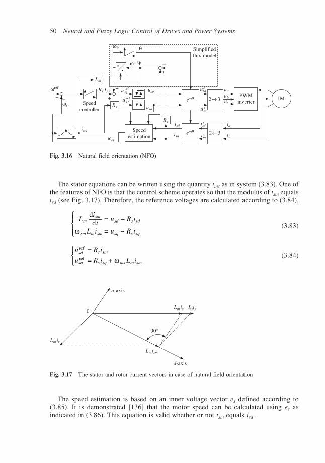
50 Neural and Fuzzy Logic Control of Drives and Power Systems
The stator equations can be written using the quantity ims as in system (3.83). One ofthe features of NFO is that the control scheme operates so that the modulus of ism equalsisd (see Fig. 3.17). Therefore, the reference voltages are calculated according to (3.84).
Lit
u R i
L i u R i
msm
sd s sd
sm m sm sq s sq
dd
= –
= – ω
(3.83)
u R i
u R i L isd s sm
sq s sq ms m sm
ref
ref
=
= + ω
(3.84)
ωΨ θ Simplifiedflux model
–
+
ωref
ωer Speedcontroller
ωer
+ –
Speedestimation
+
isd
isq
Rs ia
ibe+jθ 2←3
isds
isqs
usqs
e–jθ 2→ 3 IMPWM
inverter
ua
ubuc
ω · Ψ
ims
Rs
Lm
Rs·Isq+ usq
usd usds
usqref
usdref
Fig. 3.16 Natural field orientation (NFO)
Fig. 3.17 The stator and rotor current vectors in case of natural field orientation
Lm ir
0
q-axis
Lm is Lsis
90°
Lmism
d-axis
The speed estimation is based on an inner voltage vector es defined according to(3.85). It is demonstrated [136] that the motor speed can be calculated using es asindicated in (3.86). This equation is valid whether or not ism equals isd.

Electric motors and power systems 51
e u R R iit
LLLLL L L
L
s s s rs
rs
s
ss
m
rr
m
s r m
m
= – + 1 + 1 +
– dd
=
=
= – 2
2
σσ σ
σ
σ
σ
σ
σ
(3.85)
ω
σ σr
sq
ssm
ssd
e
pLi
i=
1 +
– ⋅ ⋅
(3.86)
At low speed, the magnitude of e is small. Therefore small errors in measuring themotor currents will lead to large relative errors in calculating the vector e (3.85) that willin turn reflect into large relative errors of the estimated rotor speed. Thus, the speedestimation precision is minimal at very small rotor speed. Most sensorless controlstrategies face the same problem, which is why the minimal speed that the system canefficiently control is one of the key parameters used in measuring the control systemperformance.
The space–vector concept has been described alongside the space–vector model ofthe three-phase induction motor. These concepts have been used to describe the maintechniques for the control of induction motor drives. In the next chapter, neural networktheory is briefly presented and neural control is considered with a view to assessing itsapplicability to produce efficient control systems for the envisaged induction motorapplications.
3.6 Synchronous generators control
Synchronous generators are responsible for the bulk of the electrical power generated inthe world today. They are mainly used in power stations and are predominantly driveneither by steam or hydraulic turbines. These generators are usually connected to aninfinite bus where the terminal voltages are held at a constant value by the ‘momentum’of all the other generators also connected to it. Another common application of synchronousgenerators is their use in stand-alone or isolated power generation systems. The primemover in such applications is usually a diesel engine.
The aim of the example presented in this section is to develop an improved controlsystem for diesel engine driven stand-alone synchronous generator sets. Its primaryobjective is to design and build a working prototype that incorporates a new controlstrategy and the latest engineering innovations. The subsidiary objectives include ensuringthat the prototype system:
• can be used effectively as a starting point for further studies into a new generation ofcontrollers for stand-alone synchronous generator sets;
• incorporates a certain amount of artificial intelligence such that it is flexible and notspecific to a particular type of engine-generator set;

52 Neural and Fuzzy Logic Control of Drives and Power Systems
• is designed using a systematic process which enables rapid prototyping of futureimprovements;
• takes advantage of modern digital electronic technology.
The following section discusses the control systems of synchronous generators, in anattempt to tie these developments to the design example presented in the second part ofthe book. Although a massive proportion of synchronous generators are electromagnetic,the use of permanent magnet synchronous machines as stand-alone generators has beenstudied for more than half a century. Permanent magnet synchronous generators (PMSGs)are more difficult to regulate and it is only with the recent developments in powerelectronics that they are seriously being considered for various applications [39], [191],[17]. One of the main advantages of the control system proposed in the examples sectionof this book is its ability to regulate stand-alone PMSGs as well as electromagnetgenerators. This functionality is duly demonstrated by the experiments presented inwhich a PMSG is used.
The study of synchronous generator control systems can roughly be divided into twoparts: voltage regulation and speed governing. Both control elements contribute to thestability of the machine in the presence of perturbations. A reliable control system setis essential for the safe operation of generators. There are various methods of controllinga synchronous generator and suitability will depend on the type of machine, its applicationand the operating conditions. For instance, the voltage regulation of an electromagnetsynchronous generator is usually achieved by controlling the field excitation currentwhereas permanent magnet generators do not have excitation systems and require atotally different strategy.
The voltage regulation system in an electromagnet synchronous generator is calledan automatic voltage regulator (AVR). It is a device that automatically adjusts the outputvoltage of the generator in order to maintain it at a relatively constant value. This isachieved by comparing the output voltage with a reference voltage and, from the difference(or error), it makes the necessary adjustments in the field current to bring the outputvoltage closer to the required value. Older AVRs used in the early days belong to a classof electromechanical devices. They are generally slow acting and possess zones ofinsensitivity known as dead bands. There is a wide variety of electromechanical AVRs,ranging from vibrating contact regulators to carbon pile regulators [235]. However, theyare now replaced with continuously acting electronic regulators that are much faster anddo not possess dead bands, hence the term ‘continuously acting’. Figure 3.18 shows ablock diagram of an electronic AVR system [6].
The generator set comprises two sections: the main section and an exciter. Eachsection consists of an armature winding and a field winding. Electrical power is derivedfrom the terminals of the main armature winding. The AVR maintains a closed-loopcontrol of the terminal voltage by taking in a ratio of the main armature voltage as theinput, comparing it to a preset reference value and producing a control signal to theexciter field based on the error. This induces the correct amount of current in the exciterarmature and the current is transferred into the main field winding via a set of rotatingdiodes. The complete system is an efficient and well-established method of regulatingthe terminal voltage in a stand-alone electromagnet synchronous generator set. Powersystem generators also employ AVRs in their control systems, but they form only a partof a comprehensive control and regulation system. Most AVRs utilise analogue electronicsto accomplish the control tasks. It is found to be cheap, simple and effective for the job.

Electric motors and power systems 53
However, like all electronic applications, there is a growing interest in applying digitalelectronic technology to AVRs. The major advantages of digital AVRs over their analoguecounterparts are the capability of realising sophisticated control functions and the easeof transmission and recording of information. The nature of digital systems allowscomplex algorithms to be executed either as a software-based system [164] or a hardware-based system [124]. Digital AVRs are capable of performing all the tasks of theiranalogue counterparts as well as a range of additional functions, including the following:
• They can have direct interaction with higher levels of controls. This allows them tobe interfaced with the main computer of the building, power plant or supervisorysystem, enabling interoperability.
• The control parameters are more accessible to modifications with built-in logic switchesand software tuning programs. Changes in the control parameters of analogue AVRscan be difficult and expensive to implement. Therefore the parameter values of analogueAVRs are usually fixed at the design and commission stage.
• Stabilisers can be configured to switch in and out the system without interrupting theservice, depending on the need.
• They can operate at optimal or suboptimal conditions over a wider range of operation.This is especially true with the introduction of adaptive and intelligent controllers.
In 1976, Malik, Hope and Huber worked on a software-based digital AVR [124] fora power system generator, whereby the control functions of the AVR were stored in anon-line station mini computer. The flexibility of a software-based system extended themathematical capabilities of the controller and allowed for one basic hardware design tobe used with different control strategies, thus drastically reducing the cost of redesigningthe controller to different specifications. The digital AVR used by Hirayama et al.(1993) [114] was capable of all the functions of an analogue AVR as well as possessingadditional features such as advanced fault status indication, self-diagnostic features,verification of generator dynamics and the recording of transients. A more comprehensivemonitor of the power systems was also possible by feeding the recorded transient data
Fig. 3.18 Block diagram of a synchronous generator and AVR
Power
Voltagesense
AVRSet reference
voltage
Output
Exciter field(stator)
Exciter armature(rotor)Rotating
diodes
Main armature(stator)
Mechanicalrotational
power input
Main field (rotor)
Electrical power output

54 Neural and Fuzzy Logic Control of Drives and Power Systems
into a personal computer (PC) via an RS232C link. Dedicated software in the PC willthen calculate the Bode diagram and indicate transient responses and rise times. Similarly,the digital excitation control systems (DECS) used in Godhwani and Basler’s (1996)[98], [99] study into design methodology of controllers offer all the advantages ofdigital control. In their work, the PID settings for a generator controller were programmedinto an electronically erasable programmable read only memory (EEPROM). Due to thefact that different systems require different PID settings for optimal performance,manufacturers of analogue controllers often have to provide multiple designs toaccommodate variations in stability networks. Godwhani and Basler proposed a designmethodology – direct design method of controller design – that allows the closed-looppoles to be placed at any desired location. The PID settings were then custom designedfor each individual system using this method and stored into the EEPROM. This createsa single design which is flexible for the operation of a wide range of generator sizes(ranging from 10 kW to 50 MW).
As result of the highly non-linear nature of synchronous machines, it can be quitedifficult to design a control system with high performance over different operatingpoints. This is becoming an increasingly important issue especially in power systems.To address the problem, Marino [167] proposed exact feedback linearisation, a techniquewhich received some recent attention [198]. There is also interest in adaptive AVRs[129], [95], [238] and power system controllers. There are currently several differentapproaches to adaptive control of synchronous generators in power system control suchas:
• linear optimal control theory [175];• self-tuning control theory [98], [185];• fuzzy logic [114];• adaptive neural network [145], [240], [150].
Although these works are mainly targeted for power systems applications, althoughsome of the ideas presented can be incorporated into other applications. Stand-alonesynchronous generators, systems with conventional AVRs and speed governors havealways been operated at a fixed speed. The speed is determined by the desired powerfrequency and the number of pole-pairs in the machine. Running the generator at anyother speed is not usually considered as a design option. One of the main problems insuch a scheme is the task of maintaining the desired power frequency, especially underheavy load. Since the frequency is directly proportional to the speed, any change inspeed would certainly disrupt the shape of the power waveform in that the frequencywould vary in relation to the speed. It is only with recent developments in power devicesand converter technology that variable-speed constant-frequency (VSCF) systems havebeen given serious attention. The matrix converter proposed in [232] initiated severalstudies into the a.c.–a.c. converter [241], [236], [215], but disparate issues such ascommutation problems and the complexity of switching schemes generate reservationsfor its use in the present work. A more common solution for a.c.–a.c. power frequencyconversion is to buffer the transition with a d.c. link, effectively producing an a.c.–d.c.–a.c. conversion scheme. In this book, a power electronic system implementing thisscheme is called a d.c. link converter. The main components of a d.c. link converterinclude some form of rectifier, energy storage component(s) such as a smoothing capacitorand an inverter. Some schemes also incorporate a boost converter in the d.c. link [41].

Electric motors and power systems 55
In the last decade, d.c. link converters have received considerable attention in the areaof VSCF wind energy systems. VSCF schemes are widely used in stand-alone windenergy conversion systems to solve the problem of frequency fluctuations which resultfrom changes in wind velocity and load. Figure 3.19 shows a simplified block diagramof a typical VSCF wind energy conversion system that incorporates a d.c. link converter.
Fig. 3.19 Simplified block diagram of a VSCF wind energy conversion system
Windturbine
Rectifier InverterPoweroutput
Control system
Although most of these schemes are designed for induction generators [188], [202],[172] there are also numerous projects which involve synchronous generators [42].Research in this area usually focuses around control systems for capturing maximumenergy from varying wind velocity. Others include work such as the study of interfacesystems to improve the quality of power from VSCF wind turbines connected to a utilitygrid [134], [206], [57]. Unfortunately, the application of VSCF schemes in other systemssuch as stand-alone generators is somewhat limited. In an engine driven system, forexample, the choice of speed can have great influence on the operational characteristicsand efficiency of the engine. With the correct setting, it is possible for the system to beoptimised for specific performances such as fuel consumption, exhaust emissions, vibrationsand generator ratings. In a domestic or recreational application, where the generatorsystem has to be placed close to the living space, reducing noise pollution may be animportant consideration when selecting the operational speed. An example of a stand-alone generator system controller based on fuzzy logic is presented in the second sectionof this book.

Neural control is a branch of the general field of intelligent control, which is based onthe concept of artificial intelligence (AI). AI can be defined as computer emulation ofthe human thinking process. The AI techniques are generally classified as expert systems(ES), fuzzy logic (FL) and artificial neural networks (ANN). The classical expert systemsare based on Boolean algebra and use precise calculations while fuzzy logic systemsinvolve calculations based on an approximate reasoning. Fuzzy logic is a superset ofconventional (Boolean) logic that has been extended to handle the concept of partialtruth–truth values between ‘completely true’ and ‘completely false’ [88]. It was introducedby Dr Lotfi Zadeh of UC/Berkeley in the 1960s as a means to model the uncertainty ofnatural language. The truth of a logical expression in fuzzy logic is a number in theinterval [0,1]. Fuzzy logic has emerged as a profitable tool for the control of complexindustrial processes and systems. It is used for processes that have no simple mathematicalmodel, for highly non-linear processes, or where the processing of linguistically formulatedknowledge is to be performed. Although it was invented in the United States, the rapidgrowth of this technology originated from Japan and has now again reached the USAand Europe. The controllers based on this mathematical approach are known as fuzzycontrollers.
The use of artificial neural networks (ANNs) is the most powerful approach in AI.ANNs are information processing structures which emulate the architecture and operationalmode of the biological nervous tissue. Any ANN is a system made up of several basicentities (named neurones) which are interconnected and operate in parallel transmittingsignals to one another in order to achieve a certain processing task [237]. One of themost outstanding features of ANNs is their capability to simulate the learning process.They are supplied with pairs of input and output signals from which general rules areautomatically derived so that the ANN will be (in certain conditions) capable of generatingthe correct output for a signal that was not previously used. The neural approach can becombined with the fuzzy logic generating neuro-fuzzy systems that combine the advantagesof the two control paradigms.
4.1 Neurone types
The operation of the artificial neurones is inspired by their natural counterparts. Eachartificial neurone has several inputs (corresponding to the synapses of the biologicalneurones) and one single output, the axon. Each input is characterised by a certain
4
Elements of neural control

Elements of neural control 57
weight indicating the influence of the corresponding signal over the neurone output. Theneurone calculates an equivalent total input signal as the weighted sum of the individualinput signals (4.1).
net = =1Σi
n
i iw x⋅ (4.1)
The resulting quantity is then compared with a constant value named the thresholdlevel and the output signal is calculated as a function of their difference (net – t). Thisfunction is named the transfer function or the activation function. The input weights, thethreshold level and the activation function are the parameters which completely describean artificial neurone. Depending on the type of the artificial neurone the activationfunction may have several forms. There are analogue neurones using continuous realactivation functions and discrete neurones whose activation functions are discontinuous.Bipolar neurones generate both positive and negative outputs while unipolar ones generateonly positive values. In the case of bipolar analogue neurones, the most popular activationfunction is given by (4.2). The output varies continuously between –1 and +1, dependingon the input signals that can have any real value (Fig. 4.1).
Fig. 4.1 Sigmoidal activation function of bipolar analogue neurones (λ = 1)
f(net)
+1
0 t net
–1
Parameter λ is a constant controlling the slope of the activation function’s graph.Some authors consider λ = 1 to simplify the calculations while others operate with themore general format presented in (4.2) but the fundamental results and properties of thecorresponding ANNs remain valid in both situations. The function in (4.2) is part of alarger transfer function class called ‘sigmoidal functions’. What they have in commonis the graph shape and the property to be derivable, which is essential in some applications.
fe t1 –(net – )(net) = 2
1 + – 1
λ ⋅(4.2)
An alternative activation function is presented in (4.3). It is part of the sigmoidalfunctions group and, as shown in (4.4), it has the same limit values as function f1.Unipolar analogue neurones are similar to bipolar ones with the difference that theoutput signals can only take values between 0 and +1 (Fig. 4.2). Their activation functionis described by (4.5).
f ee
t
t2
–(net – )
–(net – )(net) = 1 – 1 +
λλ
⋅⋅
(4.3)

58 Neural and Fuzzy Logic Control of Drives and Power Systems
lim (net) = +1
lim (net) = –1net + 2
net – 2
→ ∞
→ ∞
f
f(4.4)
fe t3 – (net – )(net) = 1
1 + λ ⋅ (4.5)
Not all continuous activation functions are sigmoidal. The stepwise-linear activationfunction presented in (4.6) is not derivable in two points: net = t – 1.0 and net = t + 1.0(Fig. 4.3).
f(net)+ 1
+ 0.5
0 t net
Fig. 4.2 Sigmoidal activation function for unipolar analogue neurones (λ = 1)
Fig. 4.3 Non-sigmoidal activation function
f(net)+ 1
net0t
–1
t – 1.0
t + 1.0
f
t
t t t
t 4 (net) =
–1 if net < – 1.0
net – if net [ – 1.0; + 1.0]
+1 if net > + 1.0
∈
(4.6)
Discrete neurones use threshold type activation functions. The bipolar discrete sort isassociated with the activation function described in (4.7) while the unipolar type usesthe activation function illustrated by (4.8). These two functions can be considered limitingcases (λ → ∞) of the sigmoidal transfer functions presented in (4.2) and (4.5).
ft
t5 (net) = 1 net
–1 net <
≥
(4.7)
ft
t6 (net) = 1 net
0 net <
≥
(4.8)

Elements of neural control 59
Over the last few years, more sophisticated types of neurones and activation functionshave been introduced in order to solve different sorts of practical problems. In particular,radial basis neurones have proved very useful for many control system and systemidentification applications. These neurones use so-called radial basis activation functions.Equation (4.9) presents the most often used form for such a function, where ‘x’ is the n-dimensional vector of input signals and ‘t’ a constant vector of the same dimensionwhile || · || is the Euclidean norm in the n-dimensional space.
f7(x) = exp(– || x – t ||2) (4.9)
Practically f7 shows how close vector ‘x’ is to vector ‘t’ in this n-dimensional space. Thecloser x is to t, the larger is f7(x); if x = t then f7(x) = 1. The classical Gaussian bell isobtained for the unidimensional case while the two-dimensional case is illustrated byFig. 4.4. Obviously, such a neurone type is very far from the biological model, but thisis irrelevant since it proves useful for certain technical applications.
Fig. 4.4 Radial basis activation function: two-dimensional case
f(x, y)1.0
0.8
0.6
0.4
0.2
0.0
0.91.2
x
0.30.6
0.91.2
y
4.2 Artificial neural networks architectures
Artificial neural networks differ by the type of neurones they are made of and by themanner of their interconnection. There are two major classes of neural networks: feed-forward ANNs and recurrent ANNs. Feed-forward artificial neural networks (FFANNs)are organised into cascaded layers of neurones. Each layer contains neurones receivinginput signals from the neurones in the previous layer and transmitting outputs to theneurones in the subsequent layer. The neurones within a layer do not communicate toone another. The first network layer is named the input layer, while the last one is namedthe output layer. All the other neurone layers are known as the hidden layers of theneural network.
FFANNs do not have any memory of the past inputs so that they are used for applicationswhere the output is only a function of the present inputs. Therefore, each input vectoris simply associated with an output vector. If step activation functions are used, several

60 Neural and Fuzzy Logic Control of Drives and Power Systems
analogue or discrete input vectors can be associated with a single discrete output vector.Such neural networks are used to solve classification problems. In a classification problem,the set of all possible input vectors is divided into several arbitrary subsets. Each subsetis a class. The problem consists of finding out to which class a given input vectorbelongs. The neural network associates each class with a binary vector and generates thecorresponding code for any input vector. Recurrent artificial neural networks includearchitectures where neurones in the same layer communicate (cellular neural networks)or architectures where some of the outputs of a FFANN are used as inputs (real-timerecurrent networks, Hopfield networks). These neural architectures can be describedeither by continuous time models or by discrete time models.
OutputsOutputlayer
Hiddenlayer
Hiddenlayer
Inputs
Fig. 4.5 Feed-forward neural network architecture
The concept of cellular neural network (CNN) was first introduced by Chua and Yang(1988). It is a special class of recurrent neural networks, which consist of cells connectedonly to the cells in their neighbourhood (Fig. 4.6). Thus, the main feature of CNNs is thefact that information is directly exchanged just between neighbouring cells.
Fig. 4.6 Cellular neural network
Due to this local interconnection property, CNNs have been considered particularlysuitable for VLSI implementations for high speed parallel signal processing. CNNs are

Elements of neural control 61
used in several application areas: image processing, artificial vision, associative memories,biological systems modelling, etc.
The real-time recurrent neural networks are the most adequate neural structures formodelling finite and infinite state machines. They explicitly implement the concept of‘internal state’ as a set of neurone outputs which are used as future inputs of the FFANNcontained inside the feedback architecture (Fig. 4.7).
Fig. 4.7 One-layer real-time recurrent neural network (discrete time model)
Outputs
Internalstate
z–1
z–1
z–1
z–1
Unit-delayoperators
Inputs
The discrete-time models contain delay units on the feedback connections, while thecontinuous-time models contain low-pass filters (usually first-order elements). Finitestate machines are modelled by discrete-time models involving neurones with stepactivation functions, while infinite state machines are modelled by continuous-timemodels containing neurones with sigmoidal activation functions.
Hopfield networks are a particular case of recurrent neural networks that contain onlyone layer of neurones and there is no feedback loop between any neurone and itself. Theconnections between any two different neurones are symmetrical in Hopfield networks,that is the corresponding weights are equal. Furthermore, each neurone is connected toan external input signal. Each state of a Hopfield network can be characterised by a so-called ‘energy function’. The evolution of the network’s state determines a decrease ofthe energy function towards a local minimum. Each local minimum is associated to astable state. In this respect, Hopfield networks can be configured in manners that allowsolutions to be found for particular optimisation problems. This feature has been usedfor associative memory applications, and the optimisation of the power dispatch in thepower systems [92].
4.3 Training algorithms
One of the most important features of neural networks is their ability to learn (to betrained) and improve their operation using a set of examples named training data set.

62 Neural and Fuzzy Logic Control of Drives and Power Systems
The training process is controlled by mathematical algorithms that fall in two mainclasses: constructive and non-constructive. The non-constructive training algorithmsadapt only the connection weights and the threshold levels. The constructive algorithmsmodify all the network features including its architecture (neurones and even layers areadded or eliminated as necessary). All the algorithms modify the neurone weights andthresholds based on calculations that analyse the network response to particular inputs.The modifications are performed in a manner that brings the network outputs closer tothe expected ones.
Depending on the nature of the training data set, there are two categories of algorithms:supervised and unsupervised [110]. The supervised algorithms use a training data setcomposed of input–output pairs. The unsupervised algorithms use only the input vectors.In the case of supervised algorithms, the training process is controlled by an externalentity (the ‘teacher’) that is able to establish whether the network outputs are adequateto the inputs and what is the size of the error. Then the network parameters are modifiedaccording to the particular correction method defining each training algorithm. In caseof unsupervised methods (the Hebbian rule, the ‘winner takes all’ algorithm, etc.), thereare no means to know what the expected outputs are. The network evolves as a result ofthe ‘experience’ gained from the previous input vectors. The weight values converge toa set of final values dictated by the input values used as training data set in conjunctionwith the particular training algorithm.
The unsupervised family of training algorithms is mainly used for signal and imageprocessing, where pattern classification, data clustering or compression algorithms areinvolved. The control engineering problems are better tackled by supervised trainingmethods, as the relationship between inputs and desired outputs is better defined andeasier to control.
4.3.1 The error back-propagation algorithm
The most popular supervised training algorithm is the one named ‘error back-propagation’,or simply ‘back-propagation’. It involves training a FFANN structure made up of sigmoidalactivation function neurones. The back-propagation algorithm is a gradient methodaiming to minimise the total operation error of the neural network. The total error is afunction defined by equation (4.10) where Oi
ref is the column vector of the referenceoutputs and Oi is the column vector of the actual network outputs corresponding to theinput pattern number ‘i’. The total error Err is the sum of the errors corresponding to allnp input patterns.
Err = ( – ) ( – ) = || – ||=1
ref ref=1
ref 2Σ Σi
n
i iT
i i i
n
i i
p p
O O O O O O⋅ (4.10)
For each training step, the vector of all neurone weights and threshold weights (W)is updated in such a way that the total error Err is decreased. The vector W can beassociated to a point in a NW-dimensional space (the parameter space), where NW is thetotal number of weights and thresholds in the neural network. The most efficient way toperform the update is to shift the point W along the curve indicated by the gradient ofthe total error (∇Err). This principle is illustrated by equation (4.11), where W(t) is theparameter vector during the current training cycle, W(t + 1) is the parameter vector for

Elements of neural control 63
the next training cycle and η is the learning-rate constant. Ideally, the algorithm stopswhen the total error is zero. In practice, it is stopped when the error is considerednegligible.
W(t + 1) = W(t) – η · ∇Err = W(t) – η · ∂∂
∂∂
∂∂
∂∂
Err Err Err . . . Err1 2 3w w w wN
T
w
(4.11)
For the practical calculation of the error gradient ∇Err, the components in the vectorW are usually rearranged as a three-dimensional matrix. The matrix has a number ofrectangular layers equal to the number of neurone layers in the neural network. Eachrectangular layer is a two-dimensional matrix containing one line for each neurone inthe corresponding layer of the neural network. Each line includes the input weights andits threshold level of a neurone. Therefore, the element wjkm in the three-dimensionalmatrix is the weight ‘m’ of the neurone ‘k’ situated in the layer ‘j’ inside the neuralnetwork. The threshold level corresponds to the last element in each line and is nottreated any differently to the input weights because it can be considered as an extraweight supplied with a constant input signal –1. In the case of a one-layer network, thecomponents of the error gradient are calculated according to (4.12) where the inputsignal xm is the corresponding input signal.
∂∂
∂∂
⋅ ⋅Err = || – || = – 2( – ) d
d(net – )
1 1 =1ref 2
=1ref
w wO O o o
ft
xkm km i
n
i i i
n
ik ikik k
m
p p
Σ Σ
(4.12)
As demonstrated in [243], bipolar sigmoidal activation functions given by (4.2) havethe property (4.13), so that the equation (4.12) can be transformed into (4.14).
dd(net – )
= 12
(1 – )2ft
f (4.13)
∂∂
⋅ ⋅Err = – ( – ) (1 – ) 1 =1
ref1 1
2
wo f f x
km i
n
ik i k i k m
p
Σ (4.14)
If the network has more than one layer then the input signal xm is generated by theneurone ‘m’ in the layer two so that xm has to be replaced with f2m. Equations (4.16) and(4.17) illustrate the calculations for the neurones in layers two and three.
∂∂
⋅ ⋅Err = – ( – ) (1 – ) 1 =1
ref1 1
22w
o f f fkm i
n
ik i k i k m
p
Σ (4.15)
∂∂
⋅ ⋅ ⋅ ⋅Err = – ( – ) (1 – ) (1 – ) 2 =1
ref1 1
21 2
23w
o f f w f fkm i
n
x ix i x i x xk i k i m
p
Σ Σ (4.16)
∂∂
⋅ ⋅ ⋅ ⋅ ⋅ ⋅Err = – ( – ) (1– ) (1– ) (1– )3 =1
ref1 1
21 2
22 3
24w
o f f w f w f fkm i
n
x ix i x i x y xy i y yk i k m
p
Σ Σ Σ
(4.17)
The previous calculations can be generalised for any number of layers [155], [243].

64 Neural and Fuzzy Logic Control of Drives and Power Systems
Each component of the gradient is determined following the iterative process (4.18).Similar results are obtained for all types of sigmoidal activation functions These equationsjustify the name of the training algorithm: the output errors of the FFANN affect thecalculations referring to any weight because their influence propagates back to theinputs from one layer to the next in accordance with (4.18).
Err = ( – )
= (1 – )
= (1 – )
. . .
= (1
= 1
ref1 1
1 12
1 y 2
2 22
2 y 3
( – 1)
∂∂
⋅
⋅ ⋅
⋅ ⋅
wo f
f w
f w
jk mi
n
x ix i x i x
i x i x y x i y
i x i x y x i y
i k x
p
Σ Σ
ΣΣ
δ
δ δ
δ δ
δ –– )
= 0
(1 – ) =
( – 1)2
( – 1) y
( – 1)2
f w
x m
f f x m
i k x y k x ik y
ikxi k x km
⋅ ⋅
≠⋅
Σ δ
δ
(4.18)
The back-propagation algorithm faces the well-known problem of any non-linearoptimising algorithm using the gradient method: it can become stuck in a local minimumof the objective function (the function ‘Err’ in this case). Therefore, the back-propagationalgorithm is not guaranteed to generate a satisfactory solution for all input–outputassociation problems and FFANN architectures. The training result depends on severalfactors [243]:
• Network architecture (number of layers, number of neurones in each layer).• Initial parameter values W(0).• The details of the input–output mapping.• Selected training data set (pairs of inputs and corresponding desired outputs).• The learning-rate constant η.
Back-propagation is not a constructive algorithm; the network architecture has to bechosen in advance. Unfortunately, there is no clearly defined set of rules to be followedin order to decide which is the most appropriate architecture for a problem. Choosingthe architecture is a result of a trial and error process supported by previous experience.However, it has been mathematically demonstrated that any input–output mapping canbe learned by a FFANN with only one hidden layer, provided that the number ofneurones in the hidden layer is large enough for the problem to be solved [173]. Thismeans that if a neural network proves incapable of learning how to perform a certaintask, the one possible solution is to increase the number of neurones in the hidden layeror layers.
A different solution is to restart the algorithm with another set of initial parametersW(0). This solution is based on the assumption that the previous failure was generatedby stopping at a local minimum. The trajectory of vector W in the parameter space isdependent on its starting point W(0), therefore, the situation may be avoided by changingthe initial weights and thresholds.
Another important aspect is choosing an adequate training data set, so that if thenumber of different input values is finite, the training data set covers all the possibilities.Nevertheless, if this number is infinite (e.g. when the inputs are analogue signals), or if

Elements of neural control 65
the number is too large, then only a selection of input combinations will be used to trainthe neural network. The quality of the training process is influenced by the way thetraining data set is generated. If the training data set adequately covers all the aspects ofthe input–output mapping, then the network will be able to generate correct answers forinputs that were not used during the training period. This property is called ‘generalisation’and is made possible by the fact that any FFANN actually performs an interpolation inan n-dimensional space (where ‘n’ is the length of the input vectors) [121]. The interpolationis carried out based on the information provided by the input vectors used during thetraining period. If the input–output mapping is continuous and smooth, then the networkwill easily generalise and yield correct answers as a result of a training performed withonly few input vectors. If the input–output mapping is rugged and complicated, then alarge number of input vectors is required for an adequate training process. The trainingprocess may require hundreds, thousands or even millions of steps of the type describedby (4.11). The actual number depends on the nature of the input–output mapping and onthe learning-rate constant η. A large value for η accelerates the training process but alsoincreases the chance that the vector W oscillates around the final solution without everreaching it. A small η increases the chances to obtain the desired solution but alsoincreases the necessary number of training cycles.
4.3.2 Algorithms derived from the back-propagation method
A series of new algorithms have been derived in the last two decades from the classicalback-propagation method. They bring improvements to the training process by acceleratingthe convergence and improving the chances of finding a good solution for particularapplication types. The improvements proposed can be summarised as:
• The learning-rate constant η is varied after each training cycle. It starts with a largevalue that is progressively diminished during the training process. Therefore, thetraining process is fast at the beginning but the final oscillations are avoided becauseη decreases during the training process.
• Every adjustable network parameter has its own learning-rate constant ηi. The back-propagation algorithm may be slow, because the use of a unique learning-rate parametermay not suit all the complicated error variations in the NW-dimensional parameterspace. Thus, a learning-rate value that is appropriate for the adjustment of one weightis not necessarily appropriate for the adjustment of another. Thus, the learning algorithmis described by equation (4.19).
W t W tw w w wN
N
T
WW
( + 1) = ( ) – Err Err Err . . . Err1
12
23
3η η η η∂
∂∂∂
∂∂
∂∂
(4.19)
• If one learning-rate is associated with each network parameter, then all the learning-rates are allowed to vary from one training cycle to the next. The variance may becalculated according to the first ballet point. More sophisticated methods may calculatethe learning-rate constants based on the error function partial derivatives. Therefore,ηi is large if the influence of wi over the error is small and ηi is small otherwise(4.20).

66 Neural and Fuzzy Logic Control of Drives and Power Systems
ηi
iwK
K = 1
Err + where > 0
∂∂
(4.20)
• If the sign of the error derivative ∂Err/∂wi oscillates for several consecutive iterations,the corresponding learning-rate parameter ηi is decreased.
• The convergence of the training is accelerated by supplementing the current weightadjustment with a fraction of the previous weight adjustment, as shown in equation(4.21). This algorithm is named the momentum method [243] and the second termindicating the fraction of the most recent weight adjustment is called the momentumterm. The momentum term α is a user-selected constant with values between 0.1 and0.8.
W(t + 1) = W(t) – η · ∇Err + α[W(t) – W(t – 1)] (4.21)
Real-time recurrent neural networks need to be trained in such a manner that theylearn a certain temporal correlation between inputs and outputs. A promising trainingmethod applicable to such situations and named the dynamic back-propagation training[112] has been derived from the classical one. The main feature of the new method isthat input vectors are not applied randomly, but in rigorously defined series. The expectedoutputs depend both on the current input and on past inputs, while the error calculationis performed globally for the entire temporal series of input vectors.
4.3.3 Training algorithms for neurones with stepactivation functions
If the activation functions of the neurones in FFANN are not sigmoidal, the back-propagation algorithm cannot be used because the error function cannot be derived.However, two other recursive methods presented in (4.22) and (4.23) are applicable tothe FFANNs with only one layer. These are recursive methods like the back-propagationalgorithm, but in this case, the training process always has a finite number of cycles,provided that the desired input–output relation can be learned by a one layer network.
w w x o fjkt
jkt
i
n
k ij ij
p+1
=1
ref = + ( – )η ⋅ ⋅Σ (4.22)
w w x ojkt
jkt
i
n
k ij ij
p+1
=1
ref = + ( – net )η ⋅ ⋅Σ (4.23)
Finding the correct weights for a multilayer FFANN with step activation functions isa complicated problem. The two previous methods cannot be generalised for suchnetworks and either constructive methods or genetic algorithms need to be usedinstead.
There are many other training algorithms than the ones presented here. However, thealgorithms presented are used in the vast majority of control applications. The otheralgorithms known in the literature are used for mainly other types of applications likesignal processing, associative memories, neurologic studies, etc.

Elements of neural control 67
4.3.4 The Voronoi diagram algorithm
The Voronoi diagram is a constructive algorithm applicable to FFANNs composed ofneurones with a step activation function [47]. As previously mentioned, any FFANNcontaining step activation function neurones solves a classification problem. The Voronoidiagram is a graphical representation of the classification problem to be implemented bythe FFANN. Let us consider the m-dimensional space of the input data and a set ofpoints in this space, corresponding to a given set of input vectors. The Voronoi diagram(also known as Thiessen polygons or Dirichelet tessallation) is a partitioning of the m-dimensional space into convex regions called Voronoi cells, each of which defines theregion of influence of one given point in its interior. Any Voronoi cell can be defined asthe intersection of a finite number of half-spaces and is therefore delimited by a finitenumber of hyperplanes.
Each hyperplane can be modelled by one neurone with a step activation function suchas (4.7) or (4.8). In the unipolar situation, the neurone generates the output signal ‘1’ forthe inputs corresponding to points on a given side of the hyperplane, while ‘0’ isgenerated for all the other inputs. As illustrated by (4.24), there is a one-to-onecorrespondence between the algebraic parameters defining the hyperplane and the neuroneparameters. The same applies to bipolar neurones, but the output ‘0’ is replaced by ‘–1’.
Σ
Σ
j
m
j j
j
m
j j
w x t t f
w x t t f
=1
=1
– 0 net – 0 (net) = 1
– 0 net – 0 (net) = 0
⋅
≥ ⇔ ≥ ⇔
⋅
< ⇔ < ⇔
(4.24)
A Voronoi cell is defined by its borders. Consequently, a point in the input data spacebelongs to a certain Voronoi cell only if all the corresponding neurones simultaneouslygenerate the required outputs. Thus, the set of convex cells in a Voronoi diagram can bemodelled by a FFANN with two layers. The input layer contains the neurones modellingthe hyperplanes and the second layer contains one neurone for each convex cell. All theneurones defining the borders of a particular cell feed the corresponding neurone in thesecond layer. The classes defined by a classification operation are not necessarily convex.Therefore, one class may be the union of several Voronoi cells. As a result, a third layeris necessary in the corresponding neural network. The third layer contains one neuronefor each class of input vectors. Each neurone is connected only to those neuronesin the second layer implementing Voronoi cells that are part of the given inputvector class.
Figure 4.8 illustrates a Voronoi diagram example built for a neural network with twoinputs and one output. Thus, the diagram is two-dimensional and the hyperplanes arestraight lines. The shaded areas cover the Voronoi cells that belong to the class ‘1’, theother cells are part of class ‘0’. There are four Voronoi cells in Fig. 4.8: ra, rb, rc, rd thatbelong to class ‘1’, and they are bounded by nine lines modelled by neurones n1 throughn9. Therefore, the first neurone layer contains nine neurones, the second contains fourneurones (one neurone for each of the Voronoi cells) whereas the third layer contains asingle 4-input neurone (Fig. 4.9). The outputs of the neurone in the third layer are‘1’ when X1 and X2 correspond to a point in one of the shaded areas and ‘0’ for all theother cases.

68 Neural and Fuzzy Logic Control of Drives and Power Systems
Very efficient computer algorithms have been developed for the construction of Voronoidiagrams in high dimensional space [89]. They are able to solve this class of problem inlinear time and this performance provides tremendous impetus for further research onthis topic.
Fig. 4.8 The Voronoi diagram for a 2D example
Network output
ra rb rc rd
X1 X2
n1 n7 n8 n6 n2 n5 n4 n9
Fig. 4.9 The neural architecture based on the Voronoi diagram in Fig. 4.8
n1
n4
n2
n5
X1
ra
n6
rb
rd
n7
n8
n9
n3
rc
X2
n3

Elements of neural control 69
4.4 Control applications of ANNs
In recent years, neural solutions have been suggested for many industrial systems usingeither feed-forward or recurrent neural networks. Most of the published papers describecontrol system applications built around a feed-forward neural network included insidea traditional feedback control system. The ANN is usually made up of sigmoidal activationfunction neurones and back propagation is normally used to train the network either on-line or off-line. Some applications use neurones with a radial base activation function.The ANN may play different roles: plant identification [105], [212], non-linear controller[131], [225], and fault signalling [127], [126]. The neural plant identification techniquecan be applied to induction motor sensorless speed estimation, for example in [38]where the plant parameter to be identified is the rotor speed.
Typical neural networks used for identification purposes are multilayer feed-forwardstructures containing neurones with sigmoidal activation function. There are twoconfigurations for plant identification: the forward configuration and the inverseconfiguration [243]. In case of forward configuration, the neural network receives thesame input vector x as the plant, and the plant output provides the reference output Oref
during the training (Fig. 4.10(a)). During the identification, the norm of the error vector||Oref – O|| is minimised using the back-propagation algorithm. As illustrated in Fig.4.10(b), the inverse plant identification employs the plant output y as the network input,while the neural network generates an approximation of the input vector of the plant.The norm of the error vector to be minimised through learning is therefore ||x – O||.
Fig. 4.10 Neural network configuration for plant identification: (a) forward plant identification;(b) inverse plant identification
x
Plant
Neuralnetwork
(a) (b)
O–
+ Oref – O
y = Oref
x – O +
x
–O
y = Oref
Plant
Neuralnetwork
Feed-forward neural networks generate instantaneous response, thus they can modelthe steady-state operation of the plant but are not directly capable of modelling itsdynamic behaviour. To account for the plant dynamics, the FFANN has to be suppliedwith a series of past inputs of the plant. Such an approach requires that the neuralnetwork is interfaced with a shift register that stores the time series of input vectors (seeFig. 4.11). The shift register is updated at each operation step. An update consists ofstoring the most recent input vector and discarding the oldest input vector.
An alternative solution is to use recurrent neural networks. This solution is purelyneuronal in that it does not require a shift register. However, most of the control systemshave used the first solution so far, because the dynamic back-propagation algorithmrequires more computation resources than its static counterpart.
Both identification configurations have advantages and disadvantages. Forward plant

70 Neural and Fuzzy Logic Control of Drives and Power Systems
identification is always feasible, but it does not immediately allow for the constructionof the plant control. In contrast, plant inverse identification facilitates simple plantcontrol. However, the identification itself is not always feasible because in some casesmore than one vector x corresponds to a certain vector y (or series of such vectors).
Figure 4.12 presents a basic control system using a neurocontroller. There are twoalternatives: either the neural network is trained only off-line in an inverse identificationconfiguration, as presented in Fig. 4.10(b), or it is initially trained off-line but thetraining continues on-line in the control system. For training purposes, the back-propagationalgorithm is the most appropriate. Shift registers are used, both during the off-lineidentification process and inside the control system, to enable the modelling of thedynamic plant behaviour. The neurocontroller input consists of the most recent plantoutputs plus the output reference for the current time. Therefore, at each operationstep, it generates a control vector O that causes the plant to produce the expectedoutput yref.
Fig. 4.11 Neural network interfacing for modelling the plant dynamics
O
Feed-forward neuralnetwork
x(t) x(t – 1) x(t – 2) x(t – 3) x(t – n)
Shift register
Shi
ft r
egis
ter
yrefy – yref–
+
yOPlantNeural
network
Fig. 4.12 Basic control system configuration using a feed-forward neurocontroller
The fault signalling applications are part of the larger class of classificationapplications. The task of the neural network is to analyse the input data and to generateinformation about the operation of the plant: normal operation, or abnormal operation.In the second case, it may give further details about the abnormality: short circuit,surpassing voltage or speed limits, etc. The neural network is of the feed-forward typeand is trained off-line using experimental data that reflects all possible operation modesof the plant.

Elements of neural control 71
4.5 Neural network implementation
Hardware implemented neural networks are essentially arrays of interconnected processingunits that operate concurrently. Each unit has a simple internal structure that, in somecases, includes a small amount of local memory. The most important design issuesconcerning any neural network hardware implementation are the degree of parallelism,the information processing performance, the flexibility and the silicon area. There areseveral categories of neural network hardware implementation [161]:
• Analogue implementation.• Digital implementation.• Hybrid implementation.• Optical implementation.
4.5.1 Analogue hardware implementation
Analogue neural networks can exploit physical properties of silicon devices to performnetwork operations obtaining very high processing speed. However, analogue designcan be very difficult because of the need to compensate for parameter variations withtemperature, manufacturing conditions, etc. One approach is to implement neuronesusing common operational amplifiers and resistors [243]. The operational amplifierimplements the activation function, while the resistors determine the weight values (Fig.4.13). The amplifier output voltage Vout depends on the input voltages V+ and V– that, inturn, depend both on the input voltages and on the resistors’ values. Ohm’s laws are usedto perform all the necessary calculations.
V1
Vn
Vn+1
Vm
Negativeweights
Positiveweights
+
–
Vss
VddVout
Linearregion
Saturatedregion
Vss
0
Vdd
Vout
Saturatedregion
V+ – V–
Fig. 4.13 Neurone implementation using operational amplifiers and resistors
The implementation style using resistors ensures very good linearity but it is notflexible because the weight values are set during the manufacturing process and theycannot be altered afterwards. Creating a changeable analogue synapse involves thecomplication of analogue weight storage. The simplest approach is to replace the fixedvalue resistors by MOS transistors that can operate as voltage adjustable switches. Eachtransistor is controlled by a voltage Vgs produced by the charge stored on a capacitor,
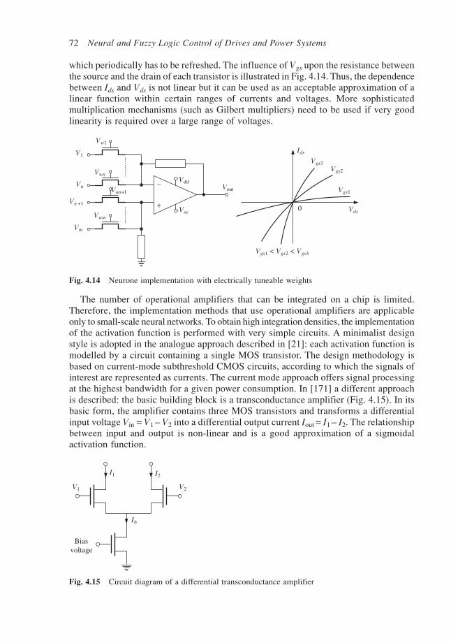
72 Neural and Fuzzy Logic Control of Drives and Power Systems
which periodically has to be refreshed. The influence of Vgs upon the resistance betweenthe source and the drain of each transistor is illustrated in Fig. 4.14. Thus, the dependencebetween Ids and Vds is not linear but it can be used as an acceptable approximation of alinear function within certain ranges of currents and voltages. More sophisticatedmultiplication mechanisms (such as Gilbert multipliers) need to be used if very goodlinearity is required over a large range of voltages.
Vw1
Vdd
V1
Vn
Vn +1
Vm
Vwm
Vwn+1
Vwn
Vss
Vout
Ids
Vgs3Vgs2
Vgs1
Vds
Vgs1 < Vgs2 < Vgs3
_
+ 0
Fig. 4.14 Neurone implementation with electrically tuneable weights
The number of operational amplifiers that can be integrated on a chip is limited.Therefore, the implementation methods that use operational amplifiers are applicableonly to small-scale neural networks. To obtain high integration densities, the implementationof the activation function is performed with very simple circuits. A minimalist designstyle is adopted in the analogue approach described in [21]: each activation function ismodelled by a circuit containing a single MOS transistor. The design methodology isbased on current-mode subthreshold CMOS circuits, according to which the signals ofinterest are represented as currents. The current mode approach offers signal processingat the highest bandwidth for a given power consumption. In [171] a different approachis described: the basic building block is a transconductance amplifier (Fig. 4.15). In itsbasic form, the amplifier contains three MOS transistors and transforms a differentialinput voltage Vin = V1 – V2 into a differential output current Iout = I1 – I2. The relationshipbetween input and output is non-linear and is a good approximation of a sigmoidalactivation function.
Fig. 4.15 Circuit diagram of a differential transconductance amplifier
V1
I1 I2
Ib
Biasvoltage
V2

Elements of neural control 73
The first analogue commercial chip was the Intel 80170NW ETANN (electricallytrainable analogue neural network) [12]. It contains 64 neurones and 10 280 weights.The non-volatile weights are stored as charge on floating transistor gates and a Gilbertmultiplier provides 4-quadrant multiplication. A flexible design, including internal feedbackand division of the weights into 64 × 80 banks, allows multiple configurations includingthree layers of 64 neurones/layer, and two layers with 128 inputs and 64 neurones/layer.No on-chip training was provided, so the connection with a PC is necessary. The PCperforms the training process and then transmits the resulting weight values to theneural chip.
New implementation technologies and possible applications of analogue neural chipscontinue to be investigated and several successes have been reported in the literature[176], [156], [163], [109], [168].
4.5.2 Digital hardware implementation
The digital neural network category encompasses many subcategories including slicearchitectures, single instruction multiple data (SIMD) approach, systolic array devices,radial basis function (RBF) architectures, ASIC and FPGA implementations. For designers,digital technology has the advantage of mature fabrication techniques and digital chipsare easily embedded into most applications. However, digital calculations are usuallyslower than in analogue systems, especially when performing the multiplications betweenweights and input signals. Moreover, analogue inputs must first be converted into digitalformat. The most common performance rating used to compare digital neuralimplementations is the connection-per-seconds (CPS), which is defined as the rate ofmultiplication and accumulate operations during normal operation.
Slice architectures for neural networks provide basic building blocks to constructnetworks of arbitrary size and precision. For example, the NeuroLogix NLX-420 NeuralProcessor Slice has 16 processing elements and a speed of 300 MCPS. A common 16-bit input bus is multiplied by different weights in each parallel processing element. Theweights are initially read from outside the chip. The 16-bit weights and inputs can beselected by the user as 16 1-bit values, four 4-bit values, two 8-bit values or one 16-bitvalue. The 16 neuronal inputs are processed by a user-defined piecewise continuousactivation function to produce a 16-bit output. Internal feedback allows the implementationof multilayer networks and multiple chips can be interconnected to build large networks.
A far more elaborate approach is to place many small processors on a chip. Twoarchitectures dominate such designs: single instruction with multiple data (SIMD) andsystolic arrays. For SIMD design, each processor executes the same instruction inparallel, but on different data. In systolic arrays, the basic processors are connected ina matrix architecture. Each processor does one calculation step before passing its resulton to the next processor in a pipelined manner. A systolic array system can be built withSiemens MA-16. The MA-16 provides fast matrix operations using 4 × 4 processormatrices with a 16-bit interconnecting bus. The overall performance is 400 MCPS. Themultiplier and accumulator outputs have 48-bit precision. Weights are stored on-chipand neurone activation functions are generated off-chip via look-up tables. Multiplechips can be cascaded.
The networks with RBF neurones provide fast learning and straightforwardimplementation. The comparison of input vectors to stored training vectors can be done

74 Neural and Fuzzy Logic Control of Drives and Power Systems
quickly if non-Euclidean distances (such as the Manhattan norm shown in (4.25)) arecalculated with no multiplication. One of the commercially available products is theNestor NI1000 chip. The Nestor NI1000, developed jointly by Intel and Nestor, contains1024 stored vectors of 256 5-bit elements. The chip has two on-chip learning algorithms,but it is relatively slow: 40 kCPS.
|| – || = | – |ManhattanX Y x yi i iΣ (4.25)
Digital ASIC and FPGA solutions require that the ANN is fully designed and trainedfor a particular application before its actual hardware implementation. The operation ofthe ANN is usually described in terms of Boolean functions or in terms of logic operationsand threshold gates (TGs). The threshold gate is a more general concept than a logicgate. Any logic gate can be considered a particular case of a TG but TGs can performmore complex information processing tasks than logic gates. They have inputs withdifferent integer weights that make them very suitable for neurone hardwareimplementation. Unfortunately, the technology limits the weights to small integer values:0, ±1, ±2, ±3. The direct use of TGs to implement neurones generates compact hardwarestructures, but this approach can only be used for a limited number of ASIC technologies.It cannot be used for FPGA implementation because they are not available inside thecomplex logic blocks (CLBs) of FPGA chips. However, the indirect use of TGs ispossible because a TG can be emulated by a digital structure composed of no more thana few AND, OR and NOT interconnected logic gates.
Designing an ANN for a specific application involves the use of either trainingalgorithms or constructive algorithms. Constructive algorithms are the preferable approachin many situations because they are able to determine both the network architecture andthe neurone weights and are guaranteed to converge in finite time. A large number ofconstructive algorithms, reviewed in [36], have been developed in the last decade. Theyare divided into three categories: geometric ([47], [193]), network-based [205] andalgebraic [120]. Several VLSI friendly algorithms have been created in order to bringcloser the design stage and the implementation stage. These algorithms consider somespecific aspects of VLSI implementation technology: the precision of the input weightsand the neurone fan-in. These factors lead to important limitations that need to be takeninto account when designing a neural network. One of the first VLSI friendly algorithmsused the concept of an ‘adaptive tree network’ [22]. Further research in this direction hasbeen extended by using a combination of AND gates and OR gates, alongside thresholdgates (TGs) [25].
4.5.3 Hybrid implementation techniques
Hybrid design attempts to combine the advantages of analogue and digital techniques.The use of analogue implementation is attractive for reasons of compactness, speed andthe absence of quantisation effects. The advantage of digital signals is their robustness.These signals are not affected by disturbances and the calculations performed in digitalformat always yield precise results.
The pulse modulation technique is one of the most promising principles that can beused to develop efficient hybrid architectures. Using pulse modulation, the internalsignals of the neural network are modelled as pulse streams whose parameters are varied

Elements of neural control 75
in accordance with the neurone states. Depending on the parameter that is varied, thereare three theoretical alternatives: the pulse amplitude modulation, the pulse widthmodulation and the pulse frequency modulation [110].
In case of pulse amplitude modulation, the amplitude of the pulses is modulated intime in a manner that reflects the variation of the corresponding neurone signal. Thistechnique is not satisfactory in neural networks because the information is transmittedas analogue voltage levels, which makes it susceptible to processing errors due to circuitparameter variations.
The pulse width modulation method alters the pulses’ duration according to theamplitude of the neural signal. The pulse width modulated signal is robust since theinformation is coded as a set of time intervals and no analogue voltage is used. However,if several signals in the neural network have almost similar values, then a large numberof pulse edges occur almost simultaneously. The existence of this synchronism representsa drawback in VLSI networks since many synapses tend to draw current from theinternal supply lines simultaneously. It follows that the internal supply lines have to beoversized to accommodate the high instantaneous currents that may be produced by theuse of pulse width modulation.
Pulse frequency modulation maintains both the amplitude and the width of the pulsesconstant but modifies the frequency of the pulses. This modulation scheme generatesrobust signals as well. Moreover, different signals modelling the equal analogue quantitiesare usually phase-shifted, which leads to avoiding the synchronism of the pulse edges.Thus, the power requirement is averaged over time as a result of using pulse frequencymodulation. Hybrid neural networks combining pulse frequency modulation and neuronesimplemented in analogue technology have been successfully designed and implemented[178], [58].
Another reason for producing hybrid neural network implementations is the need tointerface the neural architectures with existing digital equipment. In such a situation, theexternal inputs and outputs are digital, to facilitate the integration into the digital systems,while internally some or all of the processing is done in analogue technology. TheAT&T ANNA chip, for example, is externally digital and all the internal signals are indigital format, but it uses capacitor charge to store the neurone weights [195]. Thecharge is periodically refreshed by a specialised internal mechanism. The chip structureincludes multiplying digital-to-analogue converters (MDACs), electronic devices capableof multiplying a digital value with an analogue signal. The MDACs are used to performthe multiplications between the weights and the input signals of each neurone. Conversely,the Bellcore CLNN-32 chip uses digital 5-bit weights, but the neurone inputs andoutputs are analogue signals [19]. As in the case of the ANNA chip, the multiplicationsbetween weights and signals involve the use of MDACs. The overall performance of theBellcore chip is 100 MCPS. Thus, the MDACs allow the neural network designer freelyto combine analogue and digital technologies in an optimal fashion for a given applicationproblem.
4.5.4 Software versus hardware implementations
Software implementation uses a classical von Neuman machine (a general-purposemicroprocessor or a DSP). This approach can be used to implement any kind of neuralnetwork structures and any training algorithm. However, neural networks simulated on

76 Neural and Fuzzy Logic Control of Drives and Power Systems
von Neuman machines run in a series fashion which does not allow them to be used inreal-time applications. The operation speed of the neural network is inversely proportionalto the number of neurones. Consequently, very large neural networks can only be efficientlysoftware implemented if special hardware resources are also available: either largegeneral-purpose parallel machines or cheaper alternatives such as specialised coprocessors,or accelerator cards for personal computers.
The hardware approach overcomes the speed limitations of software implementedneural networks. True parallel operation mode is achieved in this case, making thecalculation speed independent of the network complexity. The actual speed of hardwareimplementation solutions depends on the technology. The highest speed is achievedusing optical implementations while the lowest speed is obtained with the electronicdigital architectures. Several optical neural processors have been reported in the literature[94], [90]; however, optical technology has not yet attained maturity. The approach isstill too expensive, too imprecise and too rigid, so electronic implementations are preferredin most cases.
The training process is faster in the case of specialised chips when compared tosoftware implementations but only relatively simple training strategies are currentlyimplemented into hardware. Thus, a limited number of training algorithms can be performedon-line. If the practical application does not require on-line training, the training processcan be performed off-line in a software system, and then the resulting weights can bedownloaded into the neural chip. Alternatively, the obtained weights can be used toproduce an ASIC or FPGA implementation. FPGA implementations are preferable asthey allow fast prototyping and furthermore, some FPGA chips are able to change theirstructure on-line. This feature supports the design of a large range of new on-linetraining algorithms for digital implemented neural networks.

This chapter describes a new strategy for implementing neural networks into digitalhardware using logic gates and determines the resulting implementation complexity toprove its superiority when compared to results previously presented in the literature.The strategy is illustrated by a complete implementation example: the neural networkcontrolling the current through the stator windings of the induction motor. Experimentalresults are presented to demonstrate the validity of the adopted design and implementationprinciples.
5.1 Neural networks design andimplementation strategy
The FFANN design and implementation manner adopted in this book is adapted toapplications that require high operation speed, accurate control over the network outputs,low cost digital hardware and fast prototyping. FPGA chips are ideal for fast prototypingbut the low cost versions still have a limited number of available logic gates. Therefore,the amount of required hardware resources needs to be minimised by optimising thenumber of neurones and by a compact implementation of each neurone. The classicalFFANN design method using neurones with sigmoidal activation function and the back-propagation training algorithm is not appropriate in this context because the resultingnumber of neurones is large and the sigmoidal activation function requires a considerableamount of hardware resources for implementation. Therefore, neural networks designedusing the constructive Voronoi algorithm and consisting of neurones with step activationfunctions were used instead. The constructive algorithm ensures the minimisation of theneurone number, while the step activation function simplifies the implementation size ofeach neurone.
5.1.1 General implementation principles
The hardware resources offered by FPGA chips are limited to logic gates and flip-flops.The implementation strategy developed in this book uses exclusively logic gates totransform any FFANN into a digital hardware structure. The strategy exploits theequivalence between the operation of logic gates and the operation of particular types ofneurones. N-input AND gates and n-input OR gates are assimilated to n-input unipolar
5
Neural FPGA implementation
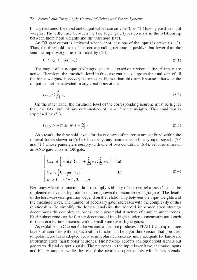
78 Neural and Fuzzy Logic Control of Drives and Power Systems
binary neurones (the input and output values can only be ‘0’ or ‘1’) having positive inputweights. The difference between the two logic gate types consists in the relationshipbetween their input weights and the threshold level.
An OR gate output is activated whenever at least one of the inputs is active (is ‘1’).Thus, the threshold level of the corresponding neurone is positive, but lower than thesmallest input weight, as illustrated by (5.1).
0 < min ORt wi
i≤ (5.1)
The output of an n-input AND logic gate is activated only when all the ‘n’ inputs areactive. Therefore, the threshold level in this case can be as large as the total sum of allthe input weights. However, it cannot be higher than this sum because otherwise theoutput cannot be activated in any conditions at all.
t wi
n
iAND =1 ≤ Σ (5.2)
On the other hand, the threshold level of the corresponding neurone must be higherthan the total sum of any combination of ‘n – 1’ input weights. This condition isexpressed by (5.3):
t w wi i
n
iAND =1 > – min + Σ (5.3)
As a result, the threshold levels for the two sorts of neurones are confined within theinterval limits shown in (5.4). Conversely, any neurone with binary input signals (‘0’and ‘1’) whose parameters comply with one of two conditions (5.4), behaves either asan AND gate or as an OR gate.
– min + ; (a)
0; min (b)
> 0 = 1, 2, . . .,
AND =1 =1
OR
t w w w
t w
w i n
i i i
n
i i
n
i
i i
i
∈
∈
∀
Σ Σ
(5.4)
Neurones whose parameters do not comply with any of the two relations (5.4) can beimplemented as a configuration containing several interconnected logic gates. The detailsof the hardware configuration depend on the relationship between the input weights andthe threshold level. The number of necessary gates increases with the complexity of thisrelationship. To simplify the logical analysis, the adopted implementation strategydecomposes the complex neurones into a pyramidal structure of simpler subneurones.Each subneurone can be further decomposed into higher-order subneurones until eachof them can be implemented with a small number of logic gates.
As explained in Chapter 4, the Voronoi algorithm produces a FFANN with up to threelayers of neurones with step activation functions. The algorithm version that producesunipolar neurones is adopted because unipolar neurones are more adequate for hardwareimplementation than bipolar neurones. The network accepts analogue input signals butgenerates digital output signals. The neurones in the input layer have analogue inputsand binary outputs, while the rest of the neurones operate only with binary signals.
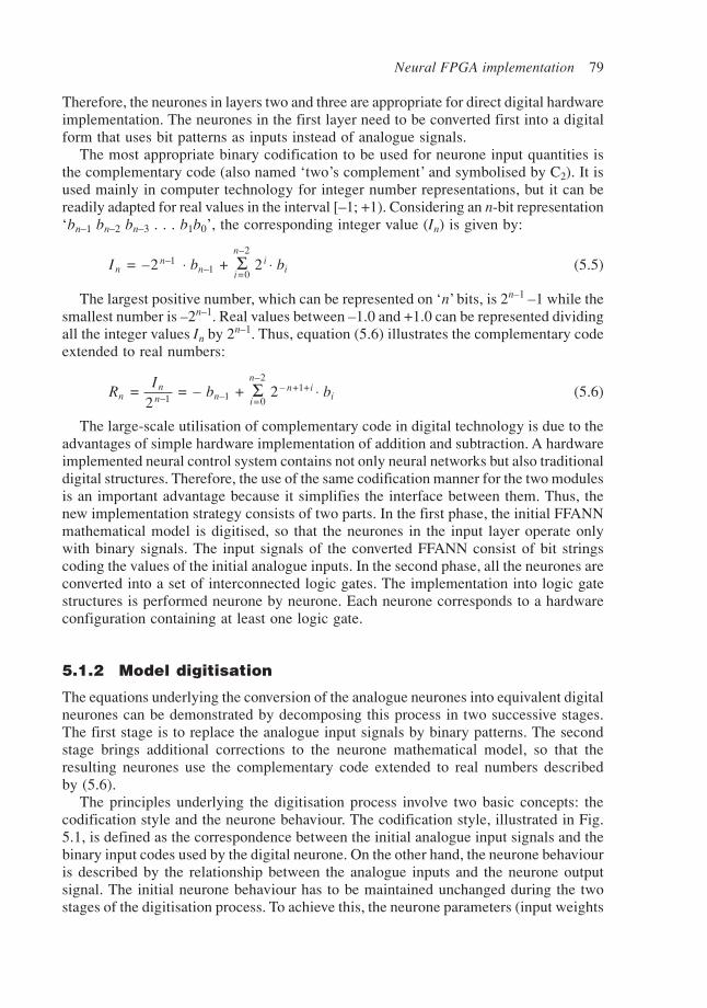
Neural FPGA implementation 79
Therefore, the neurones in layers two and three are appropriate for direct digital hardwareimplementation. The neurones in the first layer need to be converted first into a digitalform that uses bit patterns as inputs instead of analogue signals.
The most appropriate binary codification to be used for neurone input quantities isthe complementary code (also named ‘two’s complement’ and symbolised by C2). It isused mainly in computer technology for integer number representations, but it can bereadily adapted for real values in the interval [–1; +1). Considering an n-bit representation‘bn–1 bn–2 bn–3 . . . b1b0’, the corresponding integer value (In) is given by:
I b bnn
n i
ni
i = –2 + 2 –1–1 =0
–2
⋅ ⋅Σ (5.5)
The largest positive number, which can be represented on ‘n’ bits, is 2n–1 –1 while thesmallest number is –2n–1. Real values between –1.0 and +1.0 can be represented dividingall the integer values In by 2n–1. Thus, equation (5.6) illustrates the complementary codeextended to real numbers:
RI
b bnn
n n i
nn i
i = 2
= – + 2 –1 –1 =0
–2– +1+Σ ⋅ (5.6)
The large-scale utilisation of complementary code in digital technology is due to theadvantages of simple hardware implementation of addition and subtraction. A hardwareimplemented neural control system contains not only neural networks but also traditionaldigital structures. Therefore, the use of the same codification manner for the two modulesis an important advantage because it simplifies the interface between them. Thus, thenew implementation strategy consists of two parts. In the first phase, the initial FFANNmathematical model is digitised, so that the neurones in the input layer operate onlywith binary signals. The input signals of the converted FFANN consist of bit stringscoding the values of the initial analogue inputs. In the second phase, all the neurones areconverted into a set of interconnected logic gates. The implementation into logic gatestructures is performed neurone by neurone. Each neurone corresponds to a hardwareconfiguration containing at least one logic gate.
5.1.2 Model digitisation
The equations underlying the conversion of the analogue neurones into equivalent digitalneurones can be demonstrated by decomposing this process in two successive stages.The first stage is to replace the analogue input signals by binary patterns. The secondstage brings additional corrections to the neurone mathematical model, so that theresulting neurones use the complementary code extended to real numbers describedby (5.6).
The principles underlying the digitisation process involve two basic concepts: thecodification style and the neurone behaviour. The codification style, illustrated in Fig.5.1, is defined as the correspondence between the initial analogue input signals and thebinary input codes used by the digital neurone. On the other hand, the neurone behaviouris described by the relationship between the analogue inputs and the neurone outputsignal. The initial neurone behaviour has to be maintained unchanged during the twostages of the digitisation process. To achieve this, the neurone parameters (input weights

80 Neural and Fuzzy Logic Control of Drives and Power Systems
and the threshold levels) need to be modified at each conversion stage, in a manner thatcounteracts the effects of replacing the analogue input signals with binary patterns.
The minimal condition to attain this aim is to perform the changes such that the signof the activation function argument is kept constant. This principle is expressed byequation
sign – = sign(net – ) = constant=1Σi
m
i iw x t t⋅
(5.7)
However, for reasons of mathematical simplicity, a more restrictive condition is usedinstead, namely the argument ‘net – t’ of the activation function is itself kept constantrather than only the sign of it:
Σi
m
i iw x t t=1
– = net – = constant⋅ (5.8)
5.1.2.1 Conversion stage one
The first step, illustrated in Fig. 5.2, transforms the analogue neurones generated bymeans of the Voronoi algorithm into digital neurones. The newly obtained neuronesreceive binary patterns on their inputs instead of analogue signals. The task is achieved
Fig. 5.1 Basic concepts related to the neurone digitisation process
Codification style
Analoguesignals
Input code
Neuroneparameters
Neurone behaviour
Neuroneoutput
Fig. 5.2 The neurone model before and after stage one of the conversion
wi2
wi1xi1
xi2
neti – ti
x i10(1)
x i11(1)
x i 2(1)
0
x i 2(1)
1
x i 2(1)
2
wi 2(1)
2
wi 2(1)
1
wi 2(1)
0
wi10(1)
wi11(1)
wi12(1)
net – (1) (1)i it
Oi(1)
x i12(1)
Oi

Neural FPGA implementation 81
by keeping the threshold level unchanged while splitting each input defined by its initialweight wij into nb subinputs, whose weights wijp (p = 0, 1, . . . nb – 1) are calculated as:
w w p n
w w
t t
ijp
p
n ij b
ij n ij
i i
b
b
(1)+1
( –1)(1)
(1)
= 22
< – 1
= –
=
⋅ ∀
(5.9)
The superscript ‘(1)’ in equations (5.9) shows that the corresponding quantities havebeen calculated during the first conversion stage. Likewise, the superscript ‘(2)’ identifiesthe quantities calculated during the second conversion stage.
The result of the previous calculations is that the initial ‘m’ inputs are turned into ‘m’input clusters, each cluster containing ‘nb’ subinputs. The symbol ‘wij’ stands for theweight number ‘j’ of the neurone ‘i’ in the network, while ‘ ’(1)wijp represents the weightof subinput ‘p’ in cluster ‘j’ pertaining to neurone ‘i’. The index p = 0 corresponds to theleast significant binary figure, while p = nb – 1 corresponds to the most significant one.
According to the previous considerations, only those neurone parameter changes thatmaintain argument ‘neti – ti’ of the activation function constant are allowed. The argumentcorresponding to the neurone after the first conversion stage is calculated as
net – = – = – + 22
–(1) (1)
=1 =0
–1(1) (1) (1)
=1
(1)
=0
–2 +1(1) (1)
i i j
m
p
n
ijp jp i j
m
ij jp p
n
ij
p
n jp it w x t w x w x tb b
bΣ Σ Σ Σ⋅ ⋅ ⋅ ⋅
(5.10)
where x jp(1) (p = 0, 1, 2, . . . nb – 1) are the bits of the binary code received by each new
neurone input.Equation (5.10) can be transformed into
net – = – + 2 – (1) (1)
=1 ( –1)(1)
=0
–2– + + 1 (1) (1)
i i j
m
ij j n p
nn p
jp it w x x tb
bbΣ Σ⋅ ⋅
(5.11)
The expression between parentheses corresponds to the extended complementarycode definition given in equation (5.6). Therefore, (5.11) is further transformed into
net – = – = – = net – (1) (1)
=1
(1)
=1i i j
m
ij j i j
m
ij j i i it w x t w x t tΣ Σ⋅ ⋅ (5.12)
where xj is an analogue input value of the initial neurone. This proves that the conditionexpressed by (5.7) is fulfilled. Thus, during conversion stage one the codification stylebased on the complementary code has been introduced and the required modificationsof the neurone parameters have been performed so that the neurone behaviour has beenmaintained unchanged.
5.1.2.2 Conversion stage two
The conversion of the neural network into logic gate architecture is based on the relations

82 Neural and Fuzzy Logic Control of Drives and Power Systems
(5.4) and on the possibility to transform any neurone into an equivalent structure containinginterconnected elements that comply with (5.4). Such transformations are possible onlyif all the neurone weights are positive. The stage one neurones may have both positiveand negative weights. The second conversion stage aims to replace these neurones withequivalent ones having only positive weights. The simplest way to eliminate negativeinput weights is to use only the module of their values. Consequently, the relationshipbetween stage one neurone weights and their stage two counterparts is expressed by
w wijp ijp(2) (1) = | | (5.13)
Adopting this method means that supplementary parameter alterations are required inorder to counteract the neurone behaviour alteration which is caused by changing thesign of some input weights. As the weight values have already been changed accordingto (5.13), the neurone behaviour can be corrected by changing the threshold level and/or the codification style.
It can be demonstrated that no change of the threshold level can counteract the effectof the input weight alterations. Thus, the change of the threshold level needs to becarried out in such a manner that equation
net – = | | – = – = net – (2) (2)
=1 =0
–1(1) (2) (2)
=1 =0
–1(1) (1) (1) (1) (1)
i i j
m
p
n
ijp ijp i j
m
p
n
ijp ijp i i it w x t w x t tb b
Σ Σ Σ Σ⋅ ⋅
(5.14)
is fulfilled for any input bits xijp. However, if the input signals to the stage two neuronesare the same as the inputs to stage one neurones ( = )(2) (1)x xijp ijp , then there is no constantvalue ti
(2) that allows (5.14) to be valid for any combination of input signals. To provethis, the value of ti
(2) can be calculated as
t t w w xi i j
m
p
n
ijp ijp ijp
b(2) (1)
=1 =0
–1(1) (1) (1) = + (| | – ) Σ Σ ⋅ (5.15)
which is derived from equation (5.14). The value calculated according to (5.15) isdependent on the input bits xijp
(1) and therefore is not a constant as the threshold levelshould be.
Equation (5.15) demonstrates that no acceptable solution exists when the codificationstyle of stage one neurone is identical to the codification style of stage two neurone.Therefore, the codification style needs to be altered as well. A simple solution to thisproblem can be found if the input bits corresponding to negative input weights at stageone neurones are reversed at stage two neurones. The modification can be readilyimplemented into hardware with NOT logic gates as shown in Fig. 5.3.
The relationship between the input bits of stage two neurones and stage one neuronesis expressed by function
xx w
x wijpijp ijp
ijp ijp
(2)(1) (1)
(1) (1) = if > 0
1 – if < 0
(5.16)
The two situations in (5.16) can be compressed into equation
xw
w xijpijp
ijp ijp(2)
(1)(1) (1) =
1 – sign ( )
2 + sign ( ) ⋅ (5.17)

Neural FPGA implementation 83
where the ‘sign’ function is defined by
sign ( ) =
+1 > 0
0 = 0
–1 < 0
x
x
x
x
(5.18)
Using (5.13) and (5.17), the argument of the transfer function for stage two neuronescan be calculated as
net – = | | – sign( ) | |
2+sign( ) | | –(2) (2)
=1 =0
–1 (1) (1) (1)(1) (1) (1) (2)
i i j
m
p
nijp ijp ijp
ijp ijp ijp itw w w
w w x tb
Σ Σ⋅
⋅ ⋅
(5.19)and
net – = + | | –
2–(2) (2)
=1 =0
–1(1) (1)
=1 =0
–1 (1) (1)(2)
i i j
m
p
n
ijp ijp j
m
p
nijp ijp
it w xw w
tb b
Σ Σ Σ Σ⋅
(5.20)
Given the requirement of equality between the two activation function arguments, thethreshold level can be calculated based on equation
Σ Σ Σ Σ Σ Σj
m
p
n
ijp ijp j
m
p
nijp ijp
i j
m
p
n
ijp ijp i
b b b
w xw w
t w x t=1 =0
–1(1) (1)
=1 =0
–1 (1) (1)(2)
=1 =0
–1(1) (1) (1) +
| | –
2– = – ⋅
⋅ (5.21)
Therefore, the result is
t tw w
i i j
m
p
nijp ijpb
(2) (1)
=1 =0
–1 (1) (1)
= + | | –
2Σ Σ (5.22)
The threshold level ti(2) is constant in equation (5.22) because it depends exclusively on
constant quantities. The parameters of stage one neurones depend on the initial parametersas described by (5.9). Consequently, (5.22) can be successively transformed as:
t tw w w w
i i j
mij ij
j
m
p
n
p
n ij
p
n ijb b b(2)
=1 =1 =0
–2
+1 +1
= + | | +
2 +
22
| | – 22
2Σ Σ Σ
⋅ ⋅(5.23)
Fig. 5.3 The neurone ‘i’ before and after stage two of the conversion
x i10(1)
x i11(1)
x i 2(1)
0
x i 2(1)
1
wi10(1) < 0
wi11(1) < 0
wi 2(1) > 00
wi 2(1) > 01
net – (4) (4)i it
Oi(4)
x i10(2)
xi11(2)
xi 2(2)
0
xi 2(2)
1
wi10(2)
wi11(2)
wi 20(2)
wi 21(2)
net – (5) (5)i it
Oi(5)
84 Neural and Fuzzy Logic Control of Drives and Power Systems
t tw w
w wi i j
mij ij
j
m
p
n p
n ij ij
b
b
(2)
=1 =1 =0
–2
= + | | +
2 + 2
2 (| | – )Σ Σ Σ ⋅ (5.24)
t tw w
w w wi i j
mij ij
j
m
p
n p
n ij ij j
m
ij
b
b
(2)
=1 =1 =0
–2
=1 = +
| | – 2
+ 22
(| | – ) + Σ Σ Σ Σ⋅ (5.25)
t t w w wi i j
m
p
n p
n ij j
m
p
n p
n ij j
m
ij
b
b
b
b
(2)
=1 =0
–1
=1 =0
–1
=1 = + 2
2 | | – 2
2 + Σ Σ Σ Σ Σ⋅ ⋅ (5.26)
t t w w wi i
n
n j
m
ij
n
n j
m
ij j
m
ijb
b
b
b
(2)
=1 =1 =1 = + 2 – 1
2 | | – 2 – 1
2 + ⋅ ⋅Σ Σ Σ (5.27)
t t w wi in
j
m
ijn
j
m
ijb b(2) –
=1–
=1 = + (1 – 2 ) | | + 2 ⋅ ⋅Σ Σ (5.28)
Thus, the parameters of the final digital neurones can be calculated as a function ofthe initial analogue neurone parameters by combining (5.28) with (5.13) and (5.9), theresult being
= 2
2 | | = 0, 1, 2, . . . – 1
= + (1 – 2 ) | | + 2
(2)+1
(2) –=1
–=1
w w p n
t t w w
ijp
p
n ij b
i in
j
m
ijn
j
m
ij
b
b b
⋅
⋅ ⋅
Σ Σ
(5.29)
As shown in Fig. 5.4, the final implementation solution uses a codification style thatinvolves two binary codes. The first one is the complementary code. This code istransformed by a set of NOT gates into the second code, which is directly used by theneurone obtained after the second conversion stage. This neurone model has only positiveinput weights so that it can be transformed into a digital structure containing exclusivelyAND logic gates and OR logic gates.
Fig. 5.4 Neurone conversion solution
Codification style Implemented with NOT gates
Analoguesignals
Input code (1)(complementary
code)
Input code(2) Neurone
output
Neuroneparameters
Neurone behaviour
5.1.3 Digital model implementation using logic gates
The FFANN implementation into a hardware structure is performed separately for eachneurone. The implementation method requires that at first the array of input weightswijp
(2) is sorted in descending order. The sorted array contains a total number of A = m ×

Neural FPGA implementation 85
nb elements ( , , . . . )1 2 3w w w ws s sAs , where ‘m’ is the number of analogue input signals
and nb is the number of bits used for each input code. The sorted weights correspond tothe input signals x x xs s
As
1 2, , . . . . An iterative conversion procedure is used to analyse theinput weights and to generate the corresponding netlist description of the logic gateimplementation. As mentioned in section 5.1.1, the iterative procedure decomposes theinitial neurone into a pyramidal structure of interconnected subneurones. The structurecomprises a top subneurone, a layer of first-order subneurones, a layer of second-ordersubneurones, etc. The subneurones have all the properties of normal neurones but theyhave fewer inputs than the initial neurone. Some subneurones are implementable byvery simple logic gate configurations. The rest are further decomposed into second-order and third-order subneurones until all of them are implemented.
5.1.3.1 Preliminary considerations
A series of interrelated basic concepts needs to be defined before describing the iterativehardware implementation process: terminal weight group, group threshold level,dominant weight, cumulated weight, critical weight, non-critical weight, significantweight, insignificant weight.
A terminal weight group (or simply a terminal group) is a set of weights comprisingthe last N consecutive elements in the sorted array. Therefore any terminal weightgroup can be uniquely identified by the symbol Gt(F) where ‘F’ is the index of its firstelement. There are a number of A overlapping terminal weight groups in the sortedarray: Gt(1), Gt(2), Gt(3), . . . , Gt(A). Terminal weight group Gt(1) encompasses all theweights in the array. The weights of each first-order subneurone generated by theiterative implementation algorithm are the weights of a terminal group. However, noterminal group generates a first-order subneurone in the final implementation. Thus,the number of first-order subneurones in the pyramidal logic gate structure is situatedin the interval [0; A].
The group threshold level Tt is a quantity calculated by the conversion algorithm foreach terminal group of weights that is to be converted into a subneurone. The groupthreshold level equals the threshold level of the subneurone to be generated. The sameterminal group can be analysed by the implementation algorithm more than once indifferent contexts. Each time it can be associated with a different threshold level.
If a weight value is larger than the group threshold level, then it is named a dominantweight of the corresponding terminal group. Any dominant weight is related to a dominantinput that, if active, is able to activate the neurone output signal (force it to ‘1’), evenif all the other input signals are inactive (‘0’). The dominant weights in a subneurone arealways the first in the corresponding terminal group, because the initial array of weightswas sorted in descending order. Consequently, the number D of dominant inputs can bedetermined using condition (5.30), and if the largest weight in a terminal group is notdominant, no weight is dominant in that terminal group.
w T i D
w T i DF is
t
F is
t
+
+
0 <
≥ ∀ ≤< ∀ ≥
(5.30)
The cumulated weight of a terminal group Gt(F) is defined as the sum of all itscomponent weights. The cumulated weight equals the ‘net’ value of the neurone whenall its inputs are active (‘1’) in the same time. This is the maximum ‘net’ value of the

86 Neural and Fuzzy Logic Control of Drives and Power Systems
corresponding subneurone. If the cumulated weight is smaller than the group thresholdlevel, then the subneurone output is always inactive, regardless of the input signals.
W F w w xt i F
A
is
i F
A
is
is( ) = = max
= =Σ Σ ⋅
(5.31)
The output of a subneurone can be activated either by dominant inputs or, if nodominant input is active, by combinations of several non-dominant inputs. Some ofthese non-dominant inputs are included in all the combinations capable of activating theoutput. They are named critical inputs and they correspond to critical weights. Activatingthese inputs does not necessarily ensure that the subneurone output is active. They onlybring the ‘net’ value of the subneurone close to the group threshold, so that the outputcan be activated in conjunction with less important input signals (the importance of aninput signal is proportional to its corresponding weight). As the initial array is sorted indescending order, the critical weights always follow the dominant weights in any terminalgroup.
Thus, the critical weights can be determined by subtracting all the dominant weightsfrom the cumulated weight. The result has to be larger than the group threshold. Eachof the remaining weights is then subtracted from the previous result, obtaining a seriesof increasing values. Those values that are smaller than the group threshold level correspondto critical weights. This method is summarised in (5.32) where D is the number ofdominant weights and C is the number of critical weights in the given terminal group.
W F w T
W F w w T j C
W F w w T j C
t i
D
F is
t
t F D js
i
D
F is
t
t F D js
i
D
F is
t
( ) – >
( ) – – < 0 <
( ) – –
= 0
–1
+
+ + = 0
–1
+
+ + = 0
–1
+
Σ
Σ
Σ
∀ ≤
≥ ∀ ≥
(5.32)
Thus, if all dominant inputs are ‘0’ and at least one of the critical weights is ‘0’ at thesame time, then the neurone output cannot be active. On the other hand, the subneuroneoutput can be active when all the dominant inputs are inactive, but all the critical inputsare active.
In some cases, the critical inputs are sufficient to activate the neurone output. In othercases, the critical inputs can activate the output only in conjunction with certaincombinations of less important inputs, because the sum of the critical weights is lowerthan the threshold level. These less important inputs, involved in activating the subneuroneoutput, are named non-critical inputs and they correspond to non-critical weights. Asopposed to critical inputs, none of the non-critical inputs is essential for the subneuroneactivation. If a non-critical input is inactive, its task can be performed by groups of othernon-critical inputs, so that the ‘net’ value is maintained above the threshold level and thesubneurone is kept active. However, if all non-critical inputs are deactivated at the sametime, the subneurone output is deactivated as well. A subneurone with D dominantweights and C critical weights has non-critical weights as well, if and only if theconditions (5.33) are fulfilled. These conditions signify that the neurone output can beactivated by non-dominant inputs but the task cannot be performed by critical inputs

Neural FPGA implementation 87
alone.
<
= +
= 0
–1
+ +
Σ
Σ
i D
A
F is
t
i
C
F D is
t
w T
w T
≥
(5.33)
The three previous input categories (dominant, critical and non-critical) are unequallyimportant for the subneurone operation, but all influence the output signal. These typesof inputs have significant weights. Insignificant inputs do not influence the subneuroneoutput at all. The insignificant inputs have insignificant weights, which are very smalland do not affect the relation between the subneurone ‘net’ value and the group thresholdlevel, regardless of the corresponding input signals. Consequently, these inputs are notimplemented into hardware.
The effect of sorting the initial array of input weights is that the weights of the sametype are grouped together. Furthermore, the groups are arranged in a standard sequence:dominant, critical, non-critical and insignificant, as illustrated by Fig. 5.5 on the particularcase of a neurone with 12 arbitrarily chosen input weights.
Fig. 5.5 The neurone weight types and their relative position in the sorted array of weights
One or several weight types can be absent from the sequence. For instance, a neuronecomplying with condition (5.4(a)) is implementable with an AND logic gate and hasonly critical weights, because if one of the AND inputs is ‘0’ (inactive) the logic outputis ‘0’ as well. Similarly, the neurones complying with condition (5.4(b)) are implementablewith OR logic gates and have only dominant input weights.
13
1211
32.5
2 1.51 0.5 0.1 0.05
1.2
Threshold level = 10.0
Dominantweights
Criticalweights
Non-criticalweights
Insignificantweights
Significant weights
W s1 W s
2 W s3 W s
4 W s5 W s
8W s6 W s
7 W s9 W s
10 W s11 W s
12

88 Neural and Fuzzy Logic Control of Drives and Power Systems
5.1.3.2 The implementation process – detailed description
In this section, the hardware implementation of the digital neurones is described indetail, using the concepts and the formulas from the previous section. The implementationprocess is divided into three procedures (Fig. 5.6):
• The first one carries out a preliminary neurone check. It analyses the sign of itsthreshold level ‘t’. If the sign is negative or zero, the neurone output is always activeregardless of the input signals and the neurone implementation is a simple connectionbetween Vcc (+5 V) and its output.
• If the threshold level is positive, the array of weights is sorted in descending orderand then the second procedure is called. This is a recursive implementation procedurethat repeatedly calls itself and builds the required pyramidal structure, gate by gate.
• Eventually the third procedure is called which, according to the principles discussedin section 5.1.2 (at conversion stage two), attaches inverter gates to those inputs in thesorted array that correspond to negative weight values at conversion stage one
( < 0)(1)w wxs
ijp⇔ .
Fig. 5.6 The hardware implementation process
The recursive implementation procedure (B) has two input parameters that arerecalculated for each call of the procedure. The two parameters are the current terminalgroup defined by its starting index F, and the associated threshold level of the terminalgroup Tt. The parameters at the first call are F = 1 and Tt = t. Thus, the process starts byanalysing the terminal group Gt(F) = Gt(1), which comprises all the weights in the arrayin conjunction with the neurone threshold level ‘t’. The operation of the recursiveimplementation can be described in ten steps.
Step 1 The number D of dominant inputs and the number C of critical inputs arecalculated by means of (5.30) and (5.32). Condition (5.33) is used to determine whetherthe subneurone has non-critical inputs. Table 5.1 presents all the possible situations andthe next algorithm step to be performed in each case.
Step 2 The neurone has no significant input and therefore its output is always inactive.The hardware implementation reduces to a simple connection between the neuroneoutput and the circuit ground. End of the procedure (B).
Step 3 The subneurone has only dominant inputs and it is implemented as a D-input ORgate. End of the procedure (B).
Start
(A)
(B)
Recursive implementationprocedure(AND and OR gates insertion)
NOT gatesinsertion (C)
Stop
Sorting theweights
yest > 0
out < = Vcc
Stop
no
Preliminaryneuronecheck

Neural FPGA implementation 89
Step 4 The subneurone has only critical inputs and it is implemented as a D-input ANDgate. End of the procedure (B).
Step 5 The subneurone can be activated either by one of the dominant inputs or by allthe critical inputs together. Therefore, the current subneurone can be decomposed intoa simpler subneurone plus one higher-order subneurone. The first has D + 1 dominantinputs and is connected to the D dominant inputs of the initial subneurone, while inputD + 1 is fed by the second subneurone. The output of the second subneurone is activatedonly when the initial subneurone is activated due to the critical input signals. Therefore,it is implemented as a C-input AND logic gate. End of the procedure (B).
Table 5.1 Subneurone implementation cases
Dominant inputs Critical inputs Non-critical inputs Next algorithm step
D = 0 C = 0 N = 0 step 2D > 0 C = 0 N = 0 step 3D = 0 C > 0 N = 0 step 4D > 0 C > 0 N = 0 step 5D = 0 C = 0 N > 0 step 7D > 0 C = 0 N > 0 step 8D = 0 C > 0 N > 0 step 6D > 0 C > 0 N > 0 step 9
Fig. 5.7 Subneurone implementation at step 5
Step 6 The subneurone has critical and non-critical inputs. Therefore, the subneuroneoutput is active if all the critical inputs are active simultaneously with certain combinationsof non-critical inputs. The subneurone can be decomposed into a higher-order subneuronesupplying a simple subneurone implementable as an AND gate with C + 1 inputs. Thefirst C gate inputs are connected to the current subneurone critical inputs, while the lastinput is connected to the output of the higher-order subneurone which analyses theremaining input combinations.
Subneurone output
F F + D – 1
F + D F + D + C – 1
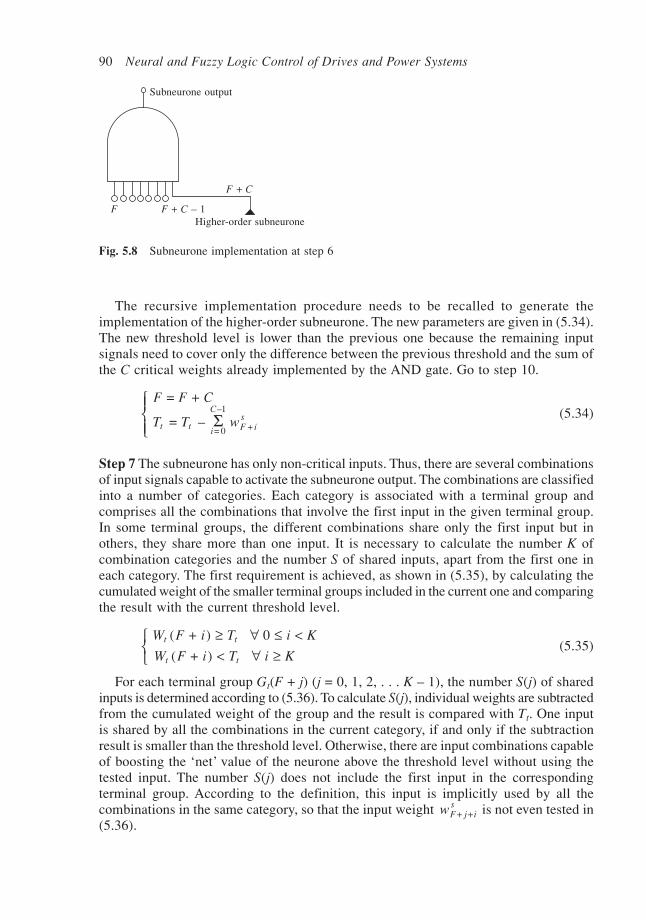
90 Neural and Fuzzy Logic Control of Drives and Power Systems
The recursive implementation procedure needs to be recalled to generate theimplementation of the higher-order subneurone. The new parameters are given in (5.34).The new threshold level is lower than the previous one because the remaining inputsignals need to cover only the difference between the previous threshold and the sum ofthe C critical weights already implemented by the AND gate. Go to step 10.
= +
= – = 0
–1
+
F F C
T T wt t i
C
F isΣ
(5.34)
Step 7 The subneurone has only non-critical inputs. Thus, there are several combinationsof input signals capable to activate the subneurone output. The combinations are classifiedinto a number of categories. Each category is associated with a terminal group andcomprises all the combinations that involve the first input in the given terminal group.In some terminal groups, the different combinations share only the first input but inothers, they share more than one input. It is necessary to calculate the number K ofcombination categories and the number S of shared inputs, apart from the first one ineach category. The first requirement is achieved, as shown in (5.35), by calculating thecumulated weight of the smaller terminal groups included in the current one and comparingthe result with the current threshold level.
( + ) 0 <
( + ) <
W F i T i K
W F i T i Kt t
t t
≥ ∀ ≤∀ ≥
(5.35)
For each terminal group Gt(F + j) (j = 0, 1, 2, . . . K – 1), the number S(j) of sharedinputs is determined according to (5.36). To calculate S(j), individual weights are subtractedfrom the cumulated weight of the group and the result is compared with Tt. One inputis shared by all the combinations in the current category, if and only if the subtractionresult is smaller than the threshold level. Otherwise, there are input combinations capableof boosting the ‘net’ value of the neurone above the threshold level without using thetested input. The number S(j) does not include the first input in the correspondingterminal group. According to the definition, this input is implicitly used by all thecombinations in the same category, so that the input weight wF j i
s+ + is not even tested in
(5.36).
Fig. 5.8 Subneurone implementation at step 6
F F + C – 1
Subneurone output
Higher-order subneurone
F + C

Neural FPGA implementation 91
( + ) – < 0 < ( ) [if ( ) > 0]
( + ) – ( ) + + +1
+ + +1
W F j w T i S j S j
W F j w T i S j
t F j is
t
t F j is
t
∀ ≤≥ ∀ ≥
(5.36)
Therefore, the current subneurone is implemented as an OR gate with K inputs asillustrated in Fig. 5.9. The OR gate inputs are fed by AND gates with S( j) + 2 inputs (j= 0, 1, 2, . . . K – 1) that model the K different combination categories. The first S(j) +1 inputs of each AND gate are connected to all the shared inputs of the combinations inthe respective category (including this time the first input in the corresponding terminalgroup). Input S( j) + 2 is connected to the output of a higher-order subneurone thatanalyses the contribution of the remaining inputs to the total net value. Go to step 10.The recursive implementation procedure is recalled K times for each high-order subneurone.The parameters for each call are calculated according to (5.37). The principles thatunderlie these calculations are similar to those applying to the parameters in (5.34). Goto step 10.
Subneurone output
F F + S(0)
Higher-ordersubneurone 1
F + 1 F + S(1) + 1
Higher-ordersubneurone 2
F + K – 1
F + K – 1 + S(K – 1)
Higher-ordersubneurone K
Fig. 5.9 Subneurone implementation at step 7
= + ( ) + 1
= – = 0
( )
+ +
F F S j
T T w
j
tj t i
S j
F j isΣ
(5.37)
Step 8 The neurone has dominant inputs and non-critical inputs. The combinations ofnon-critical inputs able to activate the neurone output fall into a number of K categories.Number K is determined using method (5.38), which is similar to (5.35) but takes intoaccount the existence of the D dominant inputs. Thus, the index of the first non-criticalinput is, in this case, F + D instead of F, so that the initial index F + i in (5.35) has tobe replaced with F + D + i.
( + + ) 0 <
( + + ) <
W F D i T i K
W F D i T i Kt t
t t
≥ ∀ ≤∀ ≥
(5.38)

92 Neural and Fuzzy Logic Control of Drives and Power Systems
Similarly, the number S( j) of shared inputs in each category of input combinations iscalculated according to method (5.39), which is derived from (5.36) by replacing each‘F’ with ‘F + D’ to take into account the existence of the dominant inputs.
( + + ) – < 0 < ( ) [if ( ) > 0]
( + + ) – ( ) + + +1
+ + +1
W F D j w T i S j S j
W F D j w T i S j
t F D+ j is
t
t F D+ j is
t
∀ ≤≥ ∀ ≥
(5.39)
As shown in Fig. 5.10, the neurone is implemented by an OR gate with D + K inputsinterconnected with K AND gates. The first D inputs of the OR gate are connected to thesubneurone dominant inputs, while the rest of the inputs are supplied by the AND gates.
As in the previous cases, the recursive procedure is recalled K times to implement theK higher-order subneurones in Fig. 5.10. The parameters for each call are given in(5.40). Go to step 10.
= + + ( ) + 1
= – = 0
( )
+ + +
F F D S j
T T w
j
tj t i
S j
F D j isΣ
(5.40)
Fig. 5.10 Subneurone implementation at step 8
Step 9 The neurone contains all three types of significant inputs: dominant, critical andnon-critical. It is implemented by a D + 1-input OR logic gate cascaded with a C + 1-input AND gate and a higher-order subneurone as shown in Fig. 5.11. The higher-ordersubneurone analyses the combinations of non-critical inputs and activates the currentsubneurone output when a valid combination is received on the inputs simultaneouslywith all the critical inputs being active. To generate the higher-order subneuroneimplementation, the recursive procedure is called with the parameters calculated in(5.41). Go to step 10.
Subneurone output
F F + D – 1
Higher-ordersubneurone 2
Higher-ordersubneurone K
Higher-ordersubneurone 1
F + D F + D + S(0) F + D + 1 F + D + S(1) + 1 F + D + K – 1 F + D + S(K – 1) + K– 1

Neural FPGA implementation 93
= + +
= – = 0
–1
+ +
F F D C
T T wt t i
C
F D isΣ
(5.41)
Step 10 The execution of the implementation process returns to the point where thepresent procedure call has been performed. This point can be inside this procedure atsteps 6, 7, 8 or 9, or it can be at the stage where the recursive process itself was initiated.In the first case, according to computer programming principles, the old parameters Fand Tt are restored and the execution resumes at the stage where this call was initiated.In the second case, the execution of the present procedure stops.
5.1.3.3 Neurone implementation example
For a better understanding of the implementation algorithm, a complete example ispresented in Fig. 5.13. The neurone has A = 12 input weights and positive thresholdlevel ‘t’. The weights are sorted in descending order and the recursive implementationprocedure is initiated with parameters F = 1 and Tt = t = 10, as shown in Fig. 5.12. Thenumber of dominant and critical inputs is calculated at step 1 of the recursiveimplementation procedure. The result is D = 3, C = 0. The three dominant inputscorrespond to the dominant weights w w ws s s
1 2 3, , in Fig. 5.13. Condition (5.33) is usedto demonstrate that the neurone has non-critical inputs as well. Thus, according to Table5.1, the next step to be performed is step 8. The number K of non-critical input combinationsis calculated using relations (5.38). The result is K = 3. The first two groups containweight combinations sharing only one input each, while in the third group, four inputsare shared. Therefore, the output of the neurone implementation is generated by the 6-input OR gate g1 connected to the three dominant inputs and to three AND gates (g2,g3, g4). Gates g2 and g3 have two inputs while g4 has five inputs.
As illustrated in Fig. 5.12, the iterative procedure recalls itself three times to generatethe subneurones corresponding to the three previously mentioned groups of weights.First, the procedure is recalled with parameters F = 5 and T t wt
s = – = 1.94 to generate
Fig. 5.11 Subneurone structure at the step 9
Subneurone output
F + D – 1F
F + D F + D + C – 1
Higher-order subneurone

94 Neural and Fuzzy Logic Control of Drives and Power Systems
Call 1F = 1; Tt = 10
Call 4F = 6; Tt = 3.9
Call 8F = 10; Tt = 0.8
Call 7F = 9; Tt = 1.9
Call 6F = 8; Tt = 1.4
Call 2F = 5; Tt = 1.9
Call 3F = 10; Tt = 0.1
Call 5F = 7; Tt = 1
Fig. 5.12 The recursive implementation process for the neurone in Fig. 5.13
Fig. 5.13 Digital mathematical model to gate structure conversion example
the implementation of the subneurone connected to gate g2. This subneurone has fourdominant inputs (related to the weights w w w ws s s s
5 6 7 8, , , ), one critical input (correspondingto w ws
9 3(2) = ) and two non-critical inputs (corresponding to w s
10 and w s11 ). Step 9 is
carried out and gates g5 and g6 are inserted into the hardware structure. The remainingthree inputs belong to a higher-order subneurone that requires the iterative procedure tobe called for the third time.
The procedure parameters are redefined as F = 10 and Tt = t – 1.9 – w s9 = 0.1 during
call number three. As a result, the corresponding subneurone contains two dominantinputs plus one insignificant input (corresponding to w s
12 ) and it is implemented by the2-input OR gate g7. At this stage, calls number 2 and 3 of the iterative procedure arefinished. The control is handed over to call number 1 which initiates the call number 4with the parameters F = 6, Tt = t – w s
5 = 3.9 in order to generate the implementation of
1211.5
11Threshold level = 10
8.1
6.1
2.92.5
21.8 1 0.5 0.05
w 9(1) < 0
w 4(2) w 7
(2) w1(2) w6
(2) w 9(2) w 2
(2) w5(2) w8
(2) w3(2) w10
(2) w11(2) w12
(2)
w s1 w s
2 w s3 w s
4 w s5 w s
6 w s7 w s
8 w s9 w s
10 w s11 w s
12
The sorted array of input weightsat conversion stage two
Output
g1
4 7 1
6
g2 g3 g4
2583
2 5 8
g5 g8 g16
10 11 5 8 310
g6 g9 g10 g11
8 3 10 11
10 11
g7 g12 g13 g15
10 11
93 2 5 8 3
g14
9

Neural FPGA implementation 95
the subneurone connected to the AND gate g3. The new subneurone has only non-critical weights falling in K = 3 categories and it is implemented by logic gates g8, g9,g10 and g11. This subneurone is connected to three third-order subneurones, which areanalysed during procedure calls 5, 6 and 7, and their implementations contain the gatesg12 to g15.
The end of procedure call 7 brings procedure call 4 to an end as well. The control ispassed back to procedure call 1, which initiates the call number 8 with parameters F =10 and Tt = t – w w w ws s s s
6 7 8 9 – – – = 0.8, and implements the subneurone connectedto the AND gate g4. This second-order subneurone has two dominant inputs (correspondingto w s
10 and w s11 ) and one insignificant input (related to w s
12 ), so that it is implementedby the 2-input OR gate g16. The end of procedure call number 8 is followed by the endof procedure call number 1, which stops the entire recursive process. At this point thethird procedure is called (procedure C in Fig. 5.6), and inverter gates are connected tothe inputs related to the weight w9. After this stage is finished, the neurone hardwareimplementation is complete. It is seen that the weight w12 is insignificant due to its smallvalue and therefore the corresponding input was not necessary in any combination ofinputs. Thus, the neurone implementation consists of eight subneurones and requires atotal of 18 logic gates arranged on six layers.
This example illustrates the complicated calculations necessary to transform even asimple neurone model into a system of interconnected logic gates. ANNs containingseveral neurones require an amount of calculations that can be efficiently performedonly by specialised software instruments. Such instruments have been developed andthey are presented in the next section.
5.2 Universal programs – FFANN hardwareimplementation
The solution adopted in this book is universally applicable. It implies a three stageautomatic analysis of the FFANN mathematical model and the generation of a VHDLmodel describing the corresponding hardware structure. The task is carried out by a setof three interconnected C++ programs, given in Appendix A and illustrated in Fig. 5.14,which communicate by means of simple ASCII files.
Matrix description ofthe neural network OPTIM.CPP
Optimised netlistdescriptionCONV_NET.CPP
Netlist description
VHDL_TR.CPP
VHDL model of thedigital hardwareimplementation
Fig. 5.14 The data flow between mathematical description and the VHDL model of an FFANN

96 Neural and Fuzzy Logic Control of Drives and Power Systems
The first program, CONV_NET, transforms the input mathematical model into apreliminary netlist description of the hardware implementation. The mathematical modelconsists of a set of matrices containing the parameters of the neurones in the neuralnetwork. Each matrix refers to one neural layer and each row in a matrix contains theparameters of a single neurone. The first elements of a row are the neurone weightswhile the last one is the threshold level. The transformation starts with the modeldigitisation, performed according to equations (5.29), and then applies the algorithmillustrated by Fig. 5.6. The program allows the user to set the number of bits used by theanalogue inputs, and the maximal number of inputs per logic gate. If a larger number ofinputs are required at a certain stage of the conversion, a pyramidal interconnection ofsimpler gates will be used to replace the required gate (Fig. 5.15).
Fig. 5.15 Examples of fan-in reduction using interconnections of simpler logic gates
The second program, OPTIM, minimises the netlist description by eliminating theredundant components. The netlist optimisation requires that three memory tablescontaining the circuit nodes and gates are built. Each table contains data about a specifictype of logic gate (NOT, AND, OR). The tables are thoroughly explored to find groupsof redundant gates (gates of the same type connected to the same input nodes). Eachgroup is replaced with a single logic gate whose output signal is distributed to all thecircuit nodes previously connected to the outputs of the eliminated gates. For instance,the gates g7, g15 and g16 in Fig. 5.13 are redundant and can be replaced by a single 2-input OR gate. The elimination of any gate changes the circuit configuration. Gates thatwere initially connected to different nodes can be connected to the same nodes after theelimination of a number of redundant gates. This creates the opportunity for furtherelimination of redundant gates. Therefore, after the equivalent gates are removed, thetables are updated and the process is restarted as shown in Fig. 5.16. The optimisationprocess stops only when no additional modification can be made in any of the threetables.
The third program, VHDL_TR, transforms the optimised netlist description into aVHDL model of the hardware implemented neural network. The obtained VHDL filecan be synthesised using any commercially available software package specialised inFPGA design. The file contains a single VHDL entity (the network) whose correspondingarchitecture comprises a number of internal signals and a list of assignment statements.Each statement models one or several identical logic gates by associating a logicalexpression with an internal signal or with an output signal.
1 2 3 4 5
1 2 3 4 5
1 2 3 4 5 6
1 2 3 4 5 6

Neural FPGA implementation 97
For exemplification, the VHDL model of the neurone in Fig. 5.13 is presented below.The model has been generated using the three universal C++ programs. It is importantto note that the index of the components inside the input port ‘d_in’ vary between 0 and11 instead of 1 to 12 as it was in Fig. 5.13.
—— Code Fragment 5.1LIBRARY ieee;USE ieee.std_logic_1164.all;
ENTITY network1 ISPORT(d_in : IN std_logic_vector(11 DOWNTO 0); ——the 12 input signals
d_out: OUT std_logic_vector(0 DOWNTO 0));— —the single outputEND network1;ARCHITECTURE arch_network1 OF network1 IS
SIGNAL n1,n2,n3,n4,n5,n7,n8,n9,n10,n11,n12,n13,n16: std_logic;
BEGINn16<= NOT d_in(8); —— the NOT gaten1<= d_in(5) AND n4; —— gate g2n2<=n16 AND n7; —— gate g3n8<=d_in(1) AND n11; —— gate g9n9 <=d_in(4) AND n12; —— gate g10n5<=d_in(2) AND n15; —— gate g6n13 <=d_in(9) AND d_in(10); —— gate g14n7<=n8 AND n9 AND n10; —— gate g8
Fig. 5.16 The general flowchart underlying the optimisation program
START
Check table with NOT gates
Eliminate redundant gates and update NOT-table
Check table with OR gates
Eliminate redundant gates and update OR-table
Check table with AND gates
Eliminate redundant gates and update AND-table
yesany update?
no
Write results into output file
STOP

98 Neural and Fuzzy Logic Control of Drives and Power Systems
n10 <=d_in(7) AND d_in(2) AND n15; —— gate g11n3<=d_in(1) AND d_in(4) AND d_in(7) AND d_in(2) AND n15;n15<=d_in(9) OR d_in(10); —— gates g7, g15, g16n12 <=d_in(7) OR d_in(2) OR n13; —— gate g13n11 <=d_in(4) OR d_in(7) OR d_in(2) OR d_in(9); —— gate g12n4<=n16 OR d_in(1) OR d_in(4) OR d_in(7) OR n5; —— gate g5d_out(0)<=d_in(3) OR d_in(6) OR d_in(0) OR n1 OR n2 OR n3;END arch_network1;
CONFIGURATION conf_network1 OF network1 ISFOR arch_network1END FOR;
END conf_network1;
The optimisation performed by OPTIM has three important effects on the previousVHDL model:
• A single expression models the group of the redundant gates g7, g15 and g16. Theother logic gates are modelled by individual logic expressions.
• The internal signals n6, n14 and n15 are absent in the list at the beginning of thenetwork architecture. They have been removed alongside with the gates g7, g15 andg16.
• The three types of logic operators (NOT, AND, OR) occur in three distinct sectionsof the network architecture description. Inside each section, the logic expressions aresorted in ascending order according to the number of logic operators involved. Thisfeature is just a side effect of the optimisation algorithm but it simplifies the inspectionof the obtained VHDL model (for instance, counting the total number of gates of acertain type or with a certain fan-in).
5.3 Hardware implementationcomplexity analysis
There are two important cost functions characterising the ANN hardware implementations:the input–output delay and the required chip area. For most applications, the delay timeis satisfactory but the chip area is critical because the hardware resources are alwayslimited. The input–output delay is approximately proportional to the implementationdepth, which is defined as the number of layers of elementary circuit units: TGs or logicgates. Several approximate methods have been proposed to determine the required chiparea of an ANN, depending on the envisaged implementation technology. They implythe calculation of the number of neurones, the number of implementation units (logicgates or threshold gates, depending on the technology) [36], the total input number ofall implementation units [108], the sum of all input weights and thresholds [36], etc. Inthe case of FPGA implementations, the total number of gates is the most suitable meansto determine the implementation complexity.
It is difficult to calculate in advance the number of logic gates required by a pyramidallogic structure with n inputs, like the one in Fig. 5.13, because the result depends on thefan-in of each individual logic gate. The calculations are simple only if it is possible to

Neural FPGA implementation 99
achieve the implementation with logic gates having the same fan-in ∆. In this case, theimplementation complexity is given by equation (5.42), where x is the ceiling function(the smallest integer greater than or equal to x).
N nLG = – 1
– 1∆ ∆ (5.42)
Usually the implementation algorithms require logic gates with different fan-ins, so that(5.42) is applicable only to a limited number of practical situations. However, any ∆-input AND gate or ∆-input OR gate can be replaced by a number of ∆ gates of the sametype, but having only two inputs. If the fan-in is restricted to ∆ = 2, then equation (5.42)is simplified as (5.43).
NLG2 = n – 1 (5.43)
Any logic circuit can be built using exclusively 2-input logic gates. Therefore, thenumber of equivalent 2-input gates in the neural network implementation is a universalmeasure of its hardware complexity and offers a means to compare different implementationalgorithms. As opposed to the rest of the logic gates, the NOT gates always have ∆ = 1.However, they are not taken into account when estimating the implementation complexitybecause the NOT logic operator can be integrated into 2-input logic gates as shown inFig. 5.17. Note that the total number of inputs ‘n’ in (5.42) and (5.43) is larger than thenumber of the neurone binary inputs (A = na × nb) because some input signals drivemore than one gate in the pyramidal structure.
Fig. 5.17 The integration of NOT operator in complex logic gates: NOT-AND and NOT-OR
5.3.1 Results previously reported in the literature
An efficient neural network implementation strategy is one that minimises the numberof equivalent 2-input gates in the corresponding digital circuit. Only a few complexityminimising algorithms have been developed so far for digital hardware implementations.The most relevant two of them are proposed in [214] and [37] and lead to the same orderof implementation complexity but generate different circuit depths. The results presentedin [37] are converted here in numbers of 2-input gates and then a comparison is performedbetween these results and the hardware complexity generated by the new implementationstrategy proposed in this book.
In [37] the neural network is treated as a set of k Boolean functions Fn ,m , i (i = 1, 2,. . . . k), with n inputs and a cumulated total of m groups of ‘1’ in the truth table. In theone-dimensional case a group of ‘1’ is a set of successive n-bit input strings, whosecorresponding function outputs are all ‘1’. The approach can be extended from one

100 Neural and Fuzzy Logic Control of Drives and Power Systems
dimension to several dimensions, as shown in Fig. 5.18. The number of truth tabledimensions equals the number n a of inputs of the analogue neurone modelled.
Fig. 5.18 Groups of ‘1’ in one-dimensional and two-dimensional truth tables
One-dimensional group of ‘1’
Outputvalues0 0 1 1 1 0 0 0
000 001 010 011 100 101 110 111The binary code of the input signal
11 0 0 0 0
10 0 0 1 1
01 0 0 1 1
00 0 0 1 1
00 01 10 11
Two-dimensionalgroup of ‘1’
The binarycode ofinput Y
The binary code of input X
The groups of ‘1’ are generated with a constructive method so that they optimallycover those points in the d-dimensional input data space that have to activate the outputsof the corresponding network. Therefore, the constructive method used in [37] is aparticular case of the Voronoi algorithm, where all the Voronoi cells are hypercubesbounded by hyperplanes parallel to the axes of the input data space. Three implementationalternatives are compared:
(i) Direct function implementation in disjunctive normal form (DNF) (initially proposed[33]).
(ii) A more sophisticated strategy which involves the use of n-bit comparators alongsideAND gates and OR gates. The comparators model the na-dimensional hyperplanesparallel to na – 1 axes of the input data space. Each of them performs comparisonsbetween one of the na analogue input signals and a constant. The second layer ismade up of 2na-input AND gates. Each AND gate implements a hypercube-shapedVoronoi cell corresponding to a group of ‘1’. The third layer is made up of ORgates combining the information provided by different AND gates.
(iii) A synthesis of the previous two methods that replaces some of the comparatorswith DNF terms of the Boolean function. This method analyses the size of thegroups of ‘1’. The small cells are more efficiently implemented in DNF format,while large groups are better implemented by comparators. Thus, some of thecomparators are replaced by a number of AND gates and NOT gates.
Any n-bit comparator between a variable quantity and a constant value can be implementedwith up to ‘n – 1’ 2-input gates [35]. A neural network with na analogue inputs codedon nb bits each requires up to na
nb (2 – 1)⋅ comparators, which is equivalent ton na b
nb ( – 1) (2 – 1)⋅ ⋅ 2-input logic gates. The redundancy across different comparatorscan be reduced by optimisation algorithms. The optimisation is limited by the numberof comparators. The comparators’ outputs are independent signals and therefore aregenerated by separated logic gates. Thus, if there are na
nb (2 – 1)⋅ comparators then

Neural FPGA implementation 101
the complexity of the circuit cannot be decreased below nanb (2 – 1)⋅ 2-input logic
gates.The set of Boolean functions Fn ,m,i (i = 1, 2, . . . k) contains a total of m groups of
‘1’ in the truth tables. Consequently, the implementation complexity of the secondneurone layer in the corresponding ANN is up to (2 · na – 1) · m equivalent 2-input logicgates. On the other hand, the hardware complexity of the third layer is up to m k Ck – + 2 .This result is a generalisation of the particular cases illustrated in Fig. 5.19. Thus, if theneural network has only one output (k = 1) then the third layer is implemented as apyramid of OR logic gates with the complexity of m – 1 equivalent 2-input gates. If theneural network has two outputs then the situation is more complex. Thus, the outputs aregenerated by two different pyramids that can share some of the ‘m’ inputs (Fig. 5.19(c))or they can be completely separate (Fig. 5.19(b)). When the two pyramids share part ofthe ‘m’ inputs the resulting implementation contains three subpyramids and two extraOR gates generating the actual output signals. As a result, the hardware complexity islarger than in Fig. 5.19(b).
Fig. 5.19 Analysis of the third layer complexity (typical situations)
Complexity: m – 1
k = 1 (a)
k = 2
Complexity: m – 2
k = 2 (b)
(c)
Complexity: m – 1
(d)
Complexity: m – 1
k = 3
Complexity: m
(e)
k = 3
When the number of neural network outputs is larger than two, several situations arepossible depending on the number of shared clusters of input signals between differentOR-gate pyramids. Two possibilities are illustrated in Fig. 5.19(d) and Fig. 5.19(e) forthe situation when k = 3. Generally, the hardware complexity corresponding to the third

102 Neural and Fuzzy Logic Control of Drives and Power Systems
neural network layer increases with the number of shared clusters of inputs. The maximalnumber of input clusters is Ck
2 , therefore, a number of k Ck + 2 subpyramids are containedin the corresponding hardware implementation. Furthermore, each output is generatedby a pyramidal OR-gate structure with k inputs and a complexity of k – 1 2-input logicgates. Therefore the total complexity of the third layer can be calculated as
m – k – Ck2 + k · (k – 1) = m – k + Ck
2 (5.44)
Thus, the upper limit of the implementation complexity for method (ii) in [37] is:
N n n m m kk k
an
ab
LG2(ii) = (2 – 1) + (2 – 1) + – ( – 1)
2⋅ ⋅ ⋅ + (5.45)
It is demonstrated in [37] that the hybrid method (iii) generates implementations withup to four times less complexity. The complexity level given in (5.45) is thereby reducedto:
Nn n m k k ka
na
b
LG2(iii) = (2 – 1)
4 +
2
+ ( – 1)
8 –
4⋅ ⋅
(5.46)
The complexity of the second layer can be calculated as a function of the number Nneurof neurones in the first layer of the ANN generating the Boolean functions Fn ,m , i (i = 1,2, . . . k). Two different situations are illustrated in Fig. 5.20(a) and (b). In Fig. 5.20(a),the decomposition of the central region of the diagram into Voronoi cells is demonstratedand the implementation of one cell is illustrated. In Fig. 5.20(b), the neural networkcontains only one neurone and therefore each Voronoi cell is defined by two comparators
Neurone (1)Neurone (2)
Neurone (3)
2 nb
2 nb
na inputs
(b)2 na inputs
(a)
Fig. 5.20 The estimation of the second layer complexity in a two-dimensional case

Neural FPGA implementation 103
supplying a single 2-input AND gate. This result can be generalised for an na-dimensionalinput data space as follows: each neurone modelling an oblique hyperplane in the inputdata space is part of a number of up to 2 ( – 1)n nb a⋅ groups of ‘1’. The correspondingVoronoi cell requires up to 2 · na comparison results but only na of them are linked toa particular neural hyperplane. If required, the other na signals are related to a differentneurone. Therefore the maximal number of inputs of the AND-gate structure implementingthe second layer is Nneur · na · 2 ( – 1)n nb a⋅ .
In these conditions, equation (5.46) becomes (5.47). The result in (5.47) is an upperlimit because it is possible that more than one neurone includes a certain group of ‘1’.
Nn N n k k ka
na
n n nb a b b
LG2 obliqueneur
–
= (2 – 1)
4 +
2 – 12
+ ( – 1)
8 –
4⋅ ⋅ ⋅
(5.47)
The most general parameter used to compare the general properties of theimplementation algorithms is the order of complexity of the generated hardware structure.The order of complexity is a concept initially used in software engineering and computersciences, but it has been extended for assessing the size of neural hardware implementations[35], [36], [37]. The order of complexity associated with an implementation algorithmis an expression that shows how the implementation complexity varies with the increaseof the network parameters (number of neurones, number of interconnections, etc.). Theincrease can be linear, polynomial, exponential, factorial, etc. The order of complexityis obtained considering that all network parameters involved in the exact hardwarecomplexity equation have very large values. In such a situation, one of the terms has amuch larger value than the others, so that the overall complexity can be approximatedby this term alone. The order of complexity is defined as the expression of the mostsignificant term in the hardware complexity equation, after all the constant factors havebeen eliminated. The elimination of constant factors is justified by the fact that they donot affect the relation between two different orders of complexity.
For instance, an exponential order of complexity always implies larger implementationsthan a linear order of complexity. Provided that the size of the network (Nneur) is sufficientlylarge, (5.48) is fulfilled and the exponential expression generates larger values than anylinear expression, regardless of the constants K1 and K2 involved. The same considerationsapply to any pair of complexity orders.
K K NN
KK
NNN
1 2 neurneur
2
1neur 2 > 2 > (if is sufficiently large)neur
neur⋅ ⋅ ⇔ (5.48)
For implementations where both na and nb are large numbers, the second term in(5.47) is the largest and the approximation in (5.49) is valid. Thus, the implementationsize undergoes an exponential increase with na and nb which makes the implementationof sizeable neural networks very difficult.
NN n
O N nan n n
an n n
a b ba b b
LG2 obliqueneur
–
neur–
22
( 2 )≈ ⋅ ⋅ ⇔ ⋅ ⋅ (5.49)
5.3.2 The analysis of the new implementation method
The logic structure generated by the implementation algorithm adopted in this book,initially presented in section 5.1.3.2, is analysed now from a geometrical point of view,

104 Neural and Fuzzy Logic Control of Drives and Power Systems
in order to determine the corresponding hardware complexity. The analysis is firstperformed for neurones with two analogue inputs (X and Y), and then the results aregeneralised for any number of analogue inputs. The hardware complexity is initiallyassessed without taking into account any hardware optimisation. Then the improvementsbrought about by the optimisation algorithm presented in section 5.2 are considered aswell, and the hardware complexity after optimisation is discussed.
5.3.2.1 Implementation without optimisation
If the neurone has only two analogue inputs then the input data space is two-dimensionaland the hyperplanes are reduced to simple lines. The input data space is divided in fourquadrants depending on the values of the most significant bits in X and Y input binarycodes. The half-space where the neurone output is active covers a number of one, two,three or four of these quadrants. The quadrants can be either partially covered or totallycovered. Each quadrant is in its turn divided into four other subquadrants defined by thesecond significant bit in each input code. The division process can be carried out for nbtimes because each input code contains nb bits. Each division in four subquadrantscorresponds to a subneurone inside the complete hardware implementation. The subneuronemodels the boundary between the active region and the inactive region inside thesubquadrant. If the symmetrical situations are ignored, there are only eight types ofrelative positions between the hyperplane and the four quadrants. They are analysed inFig. 5.21 alongside the corresponding subneurone implementations. The presented resultsapply to the subneurones of orders larger than one but smaller than nb. The analysis ofthe first-order subneurones generates results similar to the findings shown in Fig. 5.21,but the bits ‘0’ and ‘1’ in the truth tables are reversed. This situation is caused by the useof two’s complement codification where the most significant bit of positive numbers is‘0’, while for negative numbers it is ‘1’. Therefore, all subneurones of order i < nb in thepyramidal structure are fed with the signals of zero, one, two or three higher-ordersubneurones. The subneurones of order nb are not fed by other subneurones becausethere are no more bits available in the input codes to generate such subneurones. In thiscase, as shown in Fig. 5.22, the higher-order subquadrants are either completely includedor completely excluded from the active region of the current subquadrant. Suchsubquadrants are named elementary subquadrants because they cannot be further dividedinto higher-order subquadrants.
If the area bounded by the hyperplane is more than half the surface of a higher-ordersubquadrant then it is completely included in the active region. Otherwise, it is completelyexcluded. There are five types of nb-order subneurones defined by the number ofsubquadrants that are included in the active region (Fig. 5.22). Two of them have thehardware complexity NLG2 = 1 (H and J), while the other three have the complexity NLG2= 0 (G, I, K), because they do not require any logic gate for their implementation.
In a data space with more than two dimensions, there are more subneurone types thanin Fig. 5.21. As Fig. 5.21 demonstrates, the number of subneurones equals every timethe number of subquadrants are crossed by the hyperplane. Therefore, the highest hardwarecomplexity is obtained when the number of subquadrants crossed by the hyperplane ismaximal. A hyperplane in a na-dimensional space can cross up to 2 – 1na quadrants.Therefore, this is the maximum number of higher-order subneurones that can feed thecurrent subneurone. In such a situation, the pyramidal logic gate structure can be consideredas a binary tree with na + 1 layers of nodes and 2 na leaves: one leaf for each subquadrant

Neural FPGA implementation 105
Fig. 5.21 The division of a (i – 1)-order quadrant in i-order quadrants and the corresponding subneuroneimplementations (1 < i < nb)
1
xi
yi
Output
0 1
0
yi
1
(A)
xi
active zone
Sub-quadrant
Higher-ordersubneurone (1)
(B)
0 1xi
2
11
yi
0
Higher-ordersubneurone (1)
yi
Higher-ordersubneurone (2)
xi
Output
Output
Higher-ordersubneurone (3)
yixi
Higher-ordersubneurone (2)
Higher-ordersubneurone (1)
1
0
yi
0 1xi
yi
(C)
2
13
Output
Higher-ordersubneurone (3)
Higher-ordersubneurone (2)
Higher-ordersubneurone (1)
yiyi
xi0 1xi
(D)
0
yi
1
13
2
Output
1
yi
0
0 1xi
(E)
xi
yi
Higher-ordersubneurone (2)
Higher-ordersubneurone (1)
1
2
Output
(F)
0 xi1
yi
1
0
yi
xi
Higher-ordersubneurone (1)
1
Output
xi
yi
yi
Higher-ordersubneurone (1)
Higher-ordersubneurone (2)10 xi
1
yi
0
(G)
2
1
Output
xi
10xi
(H)
0
yi
1

106 Neural and Fuzzy Logic Control of Drives and Power Systems
inside the current quadrant. Some of the leaves use the signals generated by subneuronesto produce the correct neurone output signals while others directly use the input signalsof the original neurone. Figure 5.23 illustrates a three-dimensional subneurone (na = 3)that generates a maximal hardware implementation because the hyperplane crosses allsubquadrants except (xi, yi, zi) = (1, 1, 1). In this subquadrant, the subneurone output is‘1’. The maximal number of nodes in the binary tree, except the neurone output, is:
Fig. 5.22 Types of nb-order subneurones
Fig. 5.23 A three-dimensional subneurone implementation and the corresponding binary tree
Output
Vcc
10 xi
(K)
0
yi
1
Output
xi yi
1xi0
1
yi
0
(J)
(H)
0 1xi
0
yi
1
xi yi
Output
1
yi
0
(I)
0 1xi
xi
OutputOutput1
yi
0
0 1xi
Elementary sub-quadrant
(G)
Output
Out
Tree root
Tree nodes xi = 0
yi = 0
zi = 0
yi = 1
zi = 1zi = 0zi = 1zi = 0zi = 1zi = 0zi = 1
yi = 1 yi = 0
xi = 1
Leaves
zi = 0zi = 0zi = 0zi = 0zi = 1
zi(1) (2) (4)
(3) (5) (6)
zizi
yi zi
yi(7)
xi
yi = 0yi = 1
zi = 1 zi = 1
zi = 1
yi = 1 yi = 0
xi = 0xi = 1

Neural FPGA implementation 107
Σi
ni n
aa
=1+1 2 = 2 – 2 (5.50)
As illustrated in Fig. 5.23, each node of the binary tree generates one input in the logicgate structure if the related input bit (xi, yi, zi) is ‘1’ on that node. Otherwise, no inputis necessary. Only half of the nodes correspond to input bits ‘1’. Thus, the total numberof inputs in the logic gate structure is the sum between the number of subneurones andthe number of nodes divided by two (5.51).
N nan
n naa
ainputs
+1( ) = 2 – 1 + 2 – 2
2 = 2 – 2 +1 (5.51)
The maximal hardware complexity of one subneurone can be calculated as a function ofna, according to (5.52).
NGT2–max(na) = Ninputs(na) – 1 = 2 – 3 +1na (5.52)
The total pyramidal structure of logic gates corresponding to one neurone has acomplicated structure due to the variable number of higher-order subneurones feedingeach lower-order subneurone. However, it is possible to determine the total number ofsubneurones of any order without analysing the detailed interconnections between themand the subneurones of other orders. The number of subneurones equals the number ofsubquadrants of corresponding size that are crossed by the hyperplane in the input dataspace. In a two-dimensional case, the subquadrants are square-shaped and there are2i–1 subquadrants on each side of the square input data space. The maximal number ofcrossed subquadrants is 2 · 2i–1 – 1. In an na-dimensional data space the subquadrants arecubes (na = 3) or hypercubes (na > 3) and the previous result can be generalised to:
N i i n i n i na a asubn
( –1) ( –1) ( –1) ( –1) +1 ( –1) ( –1)+1( ) = 2 [2 ] – 1 = 2 – 1 < 2⋅ ⋅ ⋅ (5.53)
The generalisation is based on the fact that the hyperplane can be projected on a basewith na – 1 dimensions upon which lie a number of maximum 2( –1) ( –1)i na⋅ quadrants.Each of these quadrants is the bottom of an na-dimensional prism containing at mosttwo subquadrants that are crossed by the hyperplane. Figure 5.24 illustrates the two-dimensional and the three-dimensional situations. Therefore, the total number ofsubneurones is given by equation (5.54).
Ni
nn i
n n
n
ba
a b
atotal–subn =1( –1) ( –1)
( –1)
–1 = 2 2 – 1 < 2 2 – 12 – 1
Σ ⋅ ⋅⋅⋅
(5.54)
Based on the previous results, an absolute upper limit of the total implementationcomplexity of all the analogue neurones can be calculated as in (5.55). This calculationdoes not take into account the fact that order-nb subneurones have a smaller hardwarecomplexity.
N N N N Nn n n
nna b b
aa
GT2–total neur total–subn GT2–max neur
–
–1+1 = < 2 2 – 1
2 – 1(2 –3)⋅ ⋅ ⋅
⋅
(5.55)
The expression (5.55) can be replaced with the higher maximal limit that has asimpler expression, as in (5.56).

108 Neural and Fuzzy Logic Control of Drives and Power Systems
N N Nn n n
nn n n na b b
aa a b b
GT2–total neur
–
–2+1 4
neur– < 2 2 – 1
2(2 –3) < 2 (2 – 1)⋅
⋅ ⋅ ⋅
(5.56)
The order of complexity generated by the adopted implementation method is given by(5.58).
O N n n na b b( 2 )neur–⋅ (5.57)
This result is superior to the one presented in (5.49) which corresponds to the methodpresented in [37] because the order of complexity (5.57) is smaller than the order ofcomplexity (5.49). Therefore, the implementation of large neural networks designedwith Voronoi diagrams is most efficient using the implementation strategy presented insection 5.1.3 even if no hardware optimisation is carried out.
5.3.2.2 Optimised implementations
The optimisation process presented in section 5.2 decreases even further the level of theinitial hardware complexity. Very efficient optimisations are possible because, despitethe large number of high-order subneurones, the number of different subneurone typesis relatively small. This means that many of the subneurones are redundant. Given thecorrespondence between the hyperplanes in the input data space and neurones hardwareimplementation, the number of different subneurones of a certain order is estimatedusing geometrical considerations. An order-i subneurone, in a two-dimensional dataspace, corresponds to a hyperplane (a straight line) in a quadrant with the side length2 – +1n ib elementary subquadrants. The slope of the two-dimensional hyperplane (thestraight line) is the same in all the subquadrants, regardless of their order. Thus, thesubquadrants differ only by the intersection points between the hyperplane and thecorresponding subquadrant sides (Fig. 5.25). For a certain order ‘i’, there are a number
Y
X
(A)
Y
(B)
X
Z
Fig. 5.24 The intersection between the hyperplane and the subquadrants of second order (i = 2) in thetwo-dimensional case (A), and three-dimensional case (B)

Neural FPGA implementation 109
of Nc = 2 × 2 – +1n ib classes of two-dimensional subquadrants, depending on theseintersection points. Similarly, in an na-dimensional data space the number of classes isNc = na · 2 – +1n ib .
The subquadrants in the same class can differ by the exact shape of the boundarybetween the active region and the inactive region. The shape of this boundary dependson the slope and position of the hyperplane and it contains a precisely determinedsequence of steps as in the example presented in Fig. 5.25. The maximal number ofdifferent step patterns for a given class of subquadrants can be calculated using algebraicand geometrical considerations. First, this upper limit is determined in a two-dimensionalinput data space and then the result is generalised for an n-dimensional situation.
Fig. 5.25 Example of order-i subquadrant
Elementary subquadrants
Intersectionpoint
Elementarysubquadrants
2 – +1n ib
2 – +1n ib
The step pattern in each subquadrant of order ‘i’ depends on the exact position of thestraight line in the subquadrant. An elementary subquadrant is included in the activeregion of the two-dimensional input data space if more than half of its surface is situatedon the active side of the hyperplane defining the neurone. In a two-dimensional case, thehyperplane is reduced to a straight line. The inclusion or the exclusion of each elementaryquadrant can be determined by analysing the position of its centre. If the centre lies onthe active side of the hyperplane then it has to be included in the active region of theinput data space. Otherwise, it is excluded from the active region of the input data space.All the step patterns included in one of the Nc classes contain a common elementaryquadrant on one side of the current subquadrant. This elementary subquadrant is determinedby the intersection point between the hyperplane and the side of the subquadrant, asshown in Fig. 5.26.
The exact position of the intersection point can vary by as much as 1/2nb+1 for oneclass of patterns, and it determines which other elementary subquadrants are included inthe active region. This corresponds to two extreme hyperplane positions (a) and (b),presented in Fig. 5.26. When the hyperplane is in position (a) then only the elementarysubquadrants marked by number ‘1’ in Fig. 5.26 are included in the active region. If thehyperplane position changes continuously from position (a) to position (b) then newelementary quadrants are included in the active region in the order determined by the

110 Neural and Fuzzy Logic Control of Drives and Power Systems
distance between the corresponding centres and the initial hyperplane (a). This order isindicated for the example in Fig. 5.26 by the numbers 2 through 7. The inclusion of eachelementary quadrant generates a new pattern included in the current class. In the end,when the position (b) is attained, a maximal number of 2 – 1– +1n ib new elementarysubquadrants have been added. This means that in a two-dimensional input data spacethe maximum number of patterns in a class is Np(i) = 2 – +1n ib .
In a three-dimensional situation, the hyperplane is immersed in a three-dimensionaldata space as initially presented in Fig. 5.24(B). The elementary subquadrants are in thiscase cubes grouped together into prisms with square bases included in the (X, Y) plane.Depending on its slope, the projection of the hyperplane can cover the entire (X, Y)square included in the current subquadrant or only part of it. If the entire (X, Y) squareis covered then the two extreme positions of the boundary plane enclose a number of upto ( 2 – +1n ib )2 – 1 centres of elementary quadrants and therefore the maximal number ofpatterns inside one class is N ip
n ib( ) = 22 ( – + 1)⋅ . In an na-dimensional space, this can begeneralised as N ip
n n ia b( ) = 2( – 1) ( – + 1)⋅ . Therefore, the maximal number of differentsubquadrants, and implicitly the maximal number of subneurone types of the order ‘i’,is given by (5.58).
Nsub–q(i) = Nc(i) · Np(i) = na · 2 ( – +1)n n ia b⋅ (5.58)
The number of subneurones per layer is an increasing exponential as shown byequation (5.53), while the number of possible subneurone implementations is a decreasingexponential as demonstrated by (5.58). After the optimisation, the number of subneuronesof each order is the minimum between the number of possible subneurones and theactual number of subneurones, as shown in (5.59). Therefore, due to the exponentialvariation of the two functions, the remaining neurones after the optimisation are veryfew as compared to the initial number of neurones. This situation is illustrated by theexample in Fig. 5.27.
Fig. 5.26 The step patterns included in one class of order ‘i’ subquadrants
Hyperplaneposition (a)
Hyperplaneposition (b)
Elementarysubquadrantdefining theclass ofpatterns
elementary subquadrants
1/2 +1nb
1/2 +1nb
1/2 +1nb
2 – +1n ib
1/2 +1nb
1 1 1 1 1 1 1 1
2 1 1 1 1 1 1 1
6 3 1 1 1 1 1
7 1 1 1
58 1
4

Neural FPGA implementation 111
N i N i N i nn ia
n n ia a bsubn–opt subn sub–q
( –1)( –1)+1 ( – +1)( ) = min ( ); ( ) = min2 ; 2⋅
(5.59)
N i N i N i n i n n i na a b asubn–opt subn sub–q
( –1)( –1)+1 ( – +1)+log( ) = min ( ); ( )= min2 ; 2 2
(5.60)
The intersection point between the two graphs illustrated by Fig. 5.27 is placed at thelocation corresponding to equal exponents in (5.60). This is given by the solution of theequation (5.61).
(na – 1) · (i – 1) + 1 = na(nb – i + 1) + log2 na (5.61)
To compare the present algorithm with the algorithm presented in [37], the limit situation,with na and nb having very large values, is analysed in (5.62).
lim = lim + 2 + log – 2
2 – 1 =
2; ;
2
n n n n
a b a a
a
b
a b a bi
n n n nn
n→∞ →∞
⋅
(5.62)
Therefore, the number of optimised subneurones can be calculated as in equations(5.63), (5.64) and (5.65).
N ni
nn i–
i n
n
an n i
ba
b
ba b
subn–opt =1
/2( – 1) ( 1)
= /2+1( – +1)< 2 2 + 2Σ Σ⋅ ⋅⋅ (5.63)
N nn
n
n a
nn
n
ab
a
ab
asubn–opt
( –1) 2
–1
2
+1
= 2 2 – 12 – 1
+ 2 – 12 – 1
– 1⋅ ⋅
⋅ ⋅
(5.64)
N n nn
nn
an
n
aa
ba a
b
subn–opt( – 1)
2 – + 2
2 2 + 2 – ≈ ⋅⋅(5.65)
The resulting total complexity is given by (5.66).
Fig. 5.27 Graphical representation of the optimisation process (na = 2, nb = 10)
Number ofunoptimisedsubneurones
Number ofpossiblesubneurones
1 2 3 4 5 6 7 8 9 10
Subneurone order
600
500
400
300
200
100
0

112 Neural and Fuzzy Logic Control of Drives and Power Systems
N N N N nnn n n
an
nn
aa b b
ab
aLG2–total neur subn–opt
+ 1neur
2–
2 + 3
2 + +1
= (2 – 3) 2 + 2⋅ ⋅ ≈ ⋅ ⋅
(5.66)
Therefore, the resulting order of complexity is (5.67).
O N na
n nna b
aneur
2 +
2⋅ ⋅
(5.67)
This result does not take into account the cross-neurone optimisations, which can bringfurther hardware reduction. Still, it shows that the increase of the network implementationwith parameters na and nb is much slower in the case of the new implementation method,as compared with the standard method presented in [37]. The result in (5.67) is slightlylarger than the square root of the initial result (5.49). This implies a substantial gain interms of hardware complexity reduction for large neural networks.
The method in [37] considers a particular case of Voronoi algorithm where all thehyperplanes are parallel to the axes in the input data space, in which case the generatedorder of complexity is reasonable. If a general Voronoi approach using oblique hyperplanesis necessary then method [37] generates much larger implementations than the onepresented in this chapter. In conclusion, the present implementation method is the mostadequate for ANN network implementation designed using Voronoi diagrams with obliquehyperplanes.
Over the past few years, the use of fuzzy set theory, or fuzzy logic, in control systemshas been gaining widespread popularity, especially in Japan. From as early as the mid-1970s, Japanese scientists have been instrumental in transforming the theory of fuzzylogic into a technological realisation. Today, fuzzy logic-based control systems, orsimply fuzzy logic controllers (FLCs), can be found in a growing number of products,from washing machines to speedboats, from air condition units to hand-held autofocuscameras. In the present book, fuzzy logic is exemplified in the speed governing systemof a synchronous generator set.
The success of fuzzy logic controllers is mainly due to their ability to cope withknowledge represented in a linguistic form instead of representation in the conventionalmathematical framework. Control engineers have traditionally relied on mathematicalmodels for their designs. However, the more complex a system, the less effective themathematical model. This is the fundamental concept that provided the motivation forfuzzy logic and is formulated by Lofti Zadeh, the founder of fuzzy set theory, as thePrinciple of Incompatibility.
Zadeh stated that [240]:As the complexity of a system increases, our ability to make precise and yet significantstatements about its behaviour diminishes until a threshold is reached beyond whichprecision and significance (or relevance) become almost mutually exclusivecharacteristics.
Real-world problems can be extremely complex and complex systems are inherentlyfuzzy. The main advantage of fuzzy logic controllers is their ability to incorporateexperience, intuition and heuristics into the system instead of relying on mathematicalmodels. This makes them more effective in applications where existing models are ill-defined and not reliable enough.
6.1 Historical review
The term ‘fuzzy’ in fuzzy logic was first coined in 1965 by Professor Lofti Zadeh, thenChair of UC Berkeley’s Electrical Engineering Department. He used the term to describemultivalued sets in the seminal paper, ‘Fuzzy Sets’ [239]. The work in his paper isderived from multivalued logic, a concept which emerged in the 1920s to deal with
6
Fuzzy logic fundamentals

114 Neural and Fuzzy Logic Control of Drives and Power Systems
Heisenberg’s Uncertainty Principle in quantum mechanics. Multivalued logic was furtherdeveloped by distinguished logicians such as Jan Lukasiewicz, Bertrand Russell andMax Black. At the time, multivalence was usually described by the term ‘vagueness’.When Zadeh developed his theory, he introduced the term ‘fuzzy’.
Zadeh applied Lukasiewicz’s multivalued logic to set theory and created what hecalled fuzzy sets – sets whose elements belong to it in different degrees. According to thefuzzy principle, ‘everything is a matter of degree’. While conventional logic is bivalence(TRUE or FALSE, 1 or 0), fuzzy logic is multivalence (from 0 to 1). It is a shift fromconventional mathematics and number crunching to philosophy and language. At thebeginning, fuzzy logic remained very much a theoretical concept with little practicalapplications. The work Zadeh was involved in consisted mainly of the computer simulationof mathematical ideas. In the 1970s, Professor Edrahim Mamdani of Queen Mary College,London, built the first fuzzy system, a steam engine controller, and later the first fuzzytraffic lights. This led to the extensive development of fuzzy control applications andproducts seen today.
6.2 Fuzzy sets and fuzzy logic
Classical set theory was founded by the German mathematician Georg Cantor (1845–1918). In the theory, a universe of discourse, U, is defined as a collection of objects allhaving the same characteristics. A classical set is then a collection of a number of thoseelements. The member elements of a classical set belong to the set 100 per cent. Otherelements in the universe of discourse, which are non-member elements of the set, arenot related to the set at all. A definitive boundary can be drawn for the set, as depictedin Fig. 6.1.
c
a
U
b
c
a
U
b
(a) (b)
Fig. 6.1 (a) Classical/crisp set boundary; (b) fuzzy set boundary
A classical set can be denoted by A = x ∈ U | P(x) where the elements of A havethe property P, and U is the universe of discourse. The characteristic function µA(x):U→ 0, 1 is defined as ‘0’ if x is not an element of A and ‘1’ if x is an element of A. Here,U contains only two elements, ‘1’ and ‘0’. Therefore, an element x, in the universe ofdiscourse is either a member of set A or not a member of set A. There is ambiguity aboutmembership. For example, consider the set ADULT, which contains elements classifiedby the variable AGE. It can be said that an element with AGE = ‘5’ would not be amember of the set whereas an element with AGE = ‘45’ would be. The question whicharises is, where can a sharp and discrete line be drawn in order to separate members

Fuzzy logic fundamentals 115
from non-members? At AGE = ‘18’? By doing so, it means that elements with AGE =‘17.9’ are not members of the set ADULT but those with AGE = ‘18.1’ are. This systemis obviously not realistic to model the definition of an adult human. Simple problemssuch as this one embody the notion behind Zadeh’s Principle of Incompatibility.
In fuzzy set theory, the concept of characteristic function is extended into a moregeneralised form, known as membership function: µA(x):U → [0, 1]. While a characteristicfunction exists in a two-element set of 0, 1, a membership function can take up anyvalue between the unit interval [0, 1] (note that curly brackets are used to representdiscrete membership while square brackets are used to represent continuous membership).The set which is defined by this extended membership function is called a fuzzy set. Incontrast, a classical set which is defined by the two-element characteristic function, asdescribed earlier, is called a crisp set. Fuzzy set theory essentially extends the conceptof sets to encompass vagueness. Membership to a set is no longer a matter of ‘true’ or‘false’, ‘1’ or ‘0’, but a matter of degree. The degree of membership becomes important.The boundary of a fuzzy set is shown in Fig. 6.1(b). While point a is a member of thefuzzy set and point c is not a member, the membership of point b is ambiguous as it fallson the boundary. The concept of membership function is used to define the extent towhich a point on the boundary belongs to the set. A fuzzy set F can be defined by the setof tuples F = (µF(x), x) | x ∈ U. Zadeh proposed a notation for describing fuzzy setswhereby ‘+’ denotes enumeration and ‘/’ denotes a tuple. Therefore, the fuzzy set Fbecomes:
F x x UU
F = ( )/ for a continuous universe ∫ µ
or F x x Ux U F = ( )/ for a discrete universe Σ∈
µ
Returning to the earlier example, an element with AGE = ‘18.1’ may now be assignedwith the membership degree to the set ADULT of, say, 1.0. An element of AGE = ‘17.9’may then have a membership degree of 0.8 instead of 0. Such gradual change in thedegree of membership provides a better representation of the real world. However, theexact shape of the membership function is very subjective and depends on the designerand the context of the application. While set operations such as complement, union andintersection are straightforward definitions in classical set theory, their interpretation ismore complicated in fuzzy set theory due to the graded attribute of membership functions.Zadeh [239] proposed the following fuzzy set operation definitions as an extension tothe classical operations:
• Complement ∀ ∈ ′x X x xA A : ( ) = 1 – ( )µ µ• Union ∀x ∈ X:µA∪B(x) = max[µA(x), µB(y)]• Intersection ∀x ∈ X:µA∩B(x) = min[µA(x), µB(y)]
These definitions form the foundations of the basics of fuzzy logic thoery. The relationshipbetween an element in the universe of discourse and a fuzzy set is defined by itsmembership function. The exact nature of the relation depends on the shape or the typeof membership function used.

116 Neural and Fuzzy Logic Control of Drives and Power Systems
6.3 Types of membership functions
Figure 6.2 shows various types of membership functions which are commonly used infuzzy set theory. The choice of shape depends on the individual application. In fuzzy
µ(x)
α β x α
(a) (b)β γ
α β γ
(d)
α β(c)
(e) (f)α β α β γ λ
Fig. 6.2 Types of membership functions: (a) Γ-function; (b) S-function; (c) L-function; (d) Λ-function;(e) Gaussian function; (f) Π-function
control applications, Gaussian or bell-shaped functions and S-functions are not normallyused. Functions such as Γ-function, L-function and Λ-function are far more common.
The definitions of the membership functions chosen to be exemplified in this book are:
Γ-function, Γ:U → [0, 1]
Γ( ; , ) =
0
( – )/( – )
1
<
>
x x
x
x
x
α β α β αα
α ββ
≤ ≤
L-function, L:U → [0, 1]
L x x
x
x
x
( ; , ) =
1
( – )/( – )
0
<
>
α β β α βα
α ββ
≤ ≤

Fuzzy logic fundamentals 117
Λ-function, Λ:U → [0, 1]
Λ ( ; , , ) =
0
( – )/( – )
( – )/( – )
0
<
>
xx
x
x
x
x
x
α β γα β αγ β γ
αα ββ γ
γ
≤ ≤≤ ≤
6.4 Linguistic variables
The concept of a linguistic variable, a term which is later used to describe the inputs andoutputs of the FLC, is the foundation of fuzzy logic control systems. A conventionalvariable is numerical and precise. It is not capable of supporting the vagueness in fuzzyset theory. By definition, a linguistic variable is made up of words, sentences or artificiallanguage which are less precise than numbers. It provides the means of approximatecharacterisation of complex or ill-defined phenomena. For example, ‘AGE’ is a linguisticvariable whose values may be the fuzzy sets ‘YOUNG’ and ‘OLD’. A more commonexample in fuzzy control would be the linguistic variable ‘ERROR’, which may havelinguistic values such as ‘POSITIVE’, ‘ZERO’ and ‘NEGATIVE’. In this book, thefollowing conventions are used to define linguistic variables. If Xi is a linguistic variabledefined over the universe of discourse U where x ∈ U then
LXik (for k = 1, . . . n) are the linguistic values Xi can take
n is the number of linguistic values Xi haveµLXi,k(x) is the LXi
k membership function for the value xLXi is the set containing LX LX LX LX Lxi
ki i i i
n, where = , . . . .1 2
In the example above:
X1 is ‘ERROR’n = 3 is the number of linguistic values in X1
LX11 is ‘POSITIVE’
LX12 is ‘ZERO’
LX13 is ‘NEGATIVE’
and, for x = –1, 0, 1:
µLX1,1(–1) = 0; µLX1,1(0) = 0; µLX1,1(1) = 1µLX1,2(–1) = 0; µLX1,2(0) = 1; µLX1,2(1) = 0µLX1,3(–1) = 1; µLX1,3(0) = 0; µLX1,3(1) = 0
6.5 Fuzzy logic operators
Logical connectives are also defined for fuzzy logic operations. They are closely relatedto Zadeh’s definitions of fuzzy set operations. The following are four fuzzy operationswhich are significant for the second example presented in this book. R denotes therelation between the fuzzy sets A and B.

118 Neural and Fuzzy Logic Control of Drives and Power Systems
Negation
µ µA Ax x( ) = 1 – ( )
Disjunction
R: A OR B µR(x) = max[µA(x), µB(x)]
Conjunction
R: A AND B µR(x) = min[µA(x), µB(x)]
Implication
R: (x = A) → (y = B) IF x is A THEN y is B
Fuzzy implication is an important connective in fuzzy control systems because thecontrol strategies are embodied by sets of IF-THEN rules. There are various differenttechniques in which fuzzy implication may be defined. These relationships are mostlyderived from multivalued logic theory. The following are some of the common techniquesof fuzzy implication found in literature.
Zadeh’s classical implication:
µR(x, y) = maxmin[µA(x), µB(y)], 1 – µA(x)
Mamdani’s implication:
µR(x, y) = min[µA(x), µB(y)]
Note that Mamdani’s implication is equivalent to Zadeh’s classical implication whenµA(x) ≥ 0.5 and µB(y) ≥ 0.5.
Godel’s implication:
µµ
µ µR
B
A Bx y
y
x y( , ) =
1
( )
( ) ( )
otherwise
≤
Lukasiewicz’ implication:
µR(x, y) = min1, [1 – µA(x) + µB(y)]
The differences in using the various implication techniques are described in [207]. It isfairly obvious by looking at the mathematical functions of the different implicationtechniques that Mamdani’s technique is the most suitable for hardware implementation.It is also the most popular technique in control applications and is the technique used inthe design example presented in the second part.
6.6 Fuzzy control systems
Figure 6.3 shows the block diagram of a typical fuzzy logic controller (FLC) and thesystem plant as described in [194]. There are five principal elements to a fuzzy logiccontroller:
• Fuzzification module (fuzzifier).• Knowledge base.

Fuzzy logic fundamentals 119
• Rule base.• Inference engine.• Defuzzification module (defuzzifier).
Automatic changes in the design parameters of any of the five elements creates anadaptive fuzzy controller. Fuzzy control systems with fixed parameters are non-adaptive.Other non-fuzzy elements which are also part of the control system include the sensors,the analogue–digital converters, the digital–analogue converters and the normalisationcircuits. There are usually two types of normalisation circuits: one maps the physicalvalues of the control inputs onto a normalised universe of discourse and the other mapsthe normalised value of the control output variables back onto its physical domain.
6.6.1 Fuzzifier
The fuzzification module converts the crisp values of the control inputs into fuzzyvalues, so that they are compatible with the fuzzy set representation in the rule base. Thechoice of fuzzification strategy is dependent on the inference engine, i.e. whether it iscomposition based or individual-rule-firing based [88].
6.6.2 Knowledge base
The knowledge base consists of a database of the plant. It provides all the necessarydefinitions for the fuzzification process such as membership functions, fuzzy setrepresentation of the input–output variables and the mapping functions between thephysical and fuzzy domain.
6.6.3 Rule base
The rule base is essentially the control strategy of the system. It is usually obtained fromexpert knowledge or heuristics and expressed as a set of IF-THEN rules. The rules arebased on the fuzzy inference concept and the antecedents and consequents are associatedwith linguistic variables. For example:
Knowledgebase Rule base
Input Scaling factorsnormalisation
Fuzzification InferenceDefuzzificationdenormalisation
Plant Output
Output-scalingfactors
normalisationSensors
Fig. 6.3 Block diagram of a typical fuzzy logic controller

120 Neural and Fuzzy Logic Control of Drives and Power Systems
Error (e) and output (u) are linguistic variables while Positive Big (PB) and NegativeBig (NB) are the linguistic values. The rules are interpreted using a fuzzy implicationtechnique. In fuzzy control theory, this is normally Mamdani’s implication technique.
6.6.4 Defuzzifier
The diagram in Fig. 6.4 shows the membership functions related to a typical fuzzycontroller’s output variable defined over its universe of discourse. The FLC will processthe input data and map the output to one or more of these linguistic values (LU1 to LU5).Depending on the conditions, the membership functions of the linguistic values may beclipped. Figure 6.5 shows an output condition with two significant (clipped above zero)output linguistic values. The union of the membership functions forms the fuzzy outputvalue of the controller.
rule antecedent rule consequent
IF error (e) is Positive Big (PB) THEN output (u) is Negative Big (NB)
Fig. 6.4 Membership function of the output linguistic values
Membershipfunction
LU1 LU2 LU3 LU4 LU5
Output domain, y
Membershipfunction
D2
D1
E1 E2
Possibility
Output domain, y
Fig. 6.5 Possibility distribution of an output condition
This is represented by the shaded area in Fig. 6.5 and is expressed by the fuzzy setequation:
S S y y i ki
k
i S i Si = , ( ) = max [ ( )] = 1, 2, . . . =1∪ µ µ
where:S is the union of all the output linguistic valuesSi is an output linguistic value with clipped membership functionk is the total number of output linguistic values defined in the universe of discourse.

Fuzzy logic fundamentals 121
In most cases, the fuzzy output value S has very little practical use as most applicationsrequire non-fuzzy (crisp) control actions. Therefore, it is necessary to produce a crispvalue to represent the possibility distribution of the output. The mathematical procedureof converting fuzzy values into crisp values is known as ‘defuzzification’. A number ofdefuzzification methods have been suggested. The different methods produce similarbut not always the same results for a given input condition. The choice of defuzzificationmethods usually depends on the application and the available processing power.
The defuzzification method used in the example presented in the second part is theweighted average method. This method requires relatively little processing power and isideal for FPGA implementation where ‘area space’ is a major consideration. However,it is only valid for symmetrical membership functions. Each membership function isassigned with a weighting, which is the output point where the membership value ismaximum. Based on the diagram in Fig. 6.5, the defuzzification process can be expressedby:
f yy y
y( ) =
( ) ( )
ΣΣµ
µ⋅
and using the weighted average method becomes:
f yE D
Dmn m m
mn m( ) =
=1
=1
ΣΣ
⋅
where:f(y) is the crisp output valueEm is the crisp weighting for the linguistic value LUm
Dm is the membership value of y with relation to the linguistic value LUm.
The crisp defuzzifier output is used as it is or via an interfacing block, to control the plant.
6.7 Fuzzy logic in power andcontrol applications
Over the past two decades, there has been a tremendous growth in the use of fuzzy logiccontrollers in power systems as well as power electronic applications. A recent series oftutorials in the IEE Power Engineering Journal [208], [209] which focused entirely onthe applications of fuzzy logic in power systems is evidence of its growing significancein the field. Current applications in power systems include power system stability control,power system stability assessment, line fault detection and process optimisation forgeneration, transmission and distribution. Fuzzy logic is also used in motion control[45], [210], control of wind turbines [203], motor efficiency optimisation [211] andwaveform estimation [202]. The advantages of using fuzzy logic in such applicationsinclude the following:
• Fuzzy logic controllers are not dependent on accurate mathematical models. This isparticularly useful in power system applications where large systems are difficult tomodel. It is also relevant to smaller applications with significant non-linearities in thesystem.

122 Neural and Fuzzy Logic Control of Drives and Power Systems
• Fuzzy logic controllers are based on heuristics and therefore able to incorporatehuman intuition and experience.
There are numerous ways to build and implement a fuzzy logic system. It can either bebased on a fuzzy logic development shell or built using software programming languagessuch as C++ or even Java. In the example presented in this book a different approach ismade. The fuzzy system is developed using a hardware description language, VHDL.

7.1 Introduction
Today electronic systems are so complex that traditional design methods are not able tokeep pace with the increased demands of higher levels of integration coupled with afaster time-to-market cycle. As most of the large electronic systems typically involveyears of research and development time prior to their actual production and with theexponential increase in complexity of integrated circuit design, it became clear that astandard design language that referenced a much higher level of design abstraction wasrequired in order to facilitate the design process.
Therefore, modern design methodologies use a top-down approach in order to shortenthe design cycle and to manage such an increased complexity. A key point of thisapproach is a Hardware Description Language (HDL) capable of offering support at alllevels of description (behavioural, structural, physical). The standard represents a stand-alone specification that is not necessarily dependent on any specific tool developer orsystem subcontractor [15]. The verification of textual description correctness requires atest-bench that will ideally be able to exercise the modelled device under test at all levelsof description.
The development of the VHDL (Very High Speed Integrated Circuit HardwareDescription Language) began with a mandate set by the US Department of Defense(DoD) in the early 1980s as part of the Very High Speed Integrated Circuit (VHSIC)Program. This resulted in the adoption and release of the VHDL’s IEEE Standard approvedby the IEEE Standards Board in September 1993.
This chapter is a quick guide [61] to the main aspects of VHDL. The definition of thelanguage is detailed in [10] and in-depth discussions can be found in all major VHDLtext books [180], [189], [204], [15]. Many VHDL worked examples can be found in[61].
7.1.1 Top-down design methodology
The challenge for the developers of VHDL was to produce a hardware descriptionlanguage flexible enough to simulate conceptual designs but versatile enough to allowdetailed timing simulation. The result is that VHDL is so robust that it can support awide spectrum of modelling styles. For example, VHDL can represent a detailed descriptionof the implementation aspects, or the most abstract ideas.
7
VHDL fundamentals

124 Neural and Fuzzy Logic Control of Drives and Power Systems
By supporting a wide array of modelling styles the language allows the designer toquickly develop and simulate ideas without being preocupied with the details ofimplementation. Simultaneously, as the design evolves to completion, the language isable to support a complex digital system. Top-down design is the term given to thedesign flow (Fig. 7.1) which begins with modelling an idea at an abstract level, and thenproceeding through the iterative steps necessary to further refine this process into adetailed digital system.
Design specification
VHDLbehavioural model
Simulation
VHDL-RTL
Simulation
Synthesis
Simulation
Implementation
Timing analysis
Device programming
Graphical VHDLtool
Graphical VHDLtool
Specificationlevel
Behaviourallevel
RT level
Netlist level
Fig. 7.1 Top-down design flow
By producing a model at a very high level of abstraction, a test environment can bedeveloped early in the design cycle. The development of a test environment allowsverification that the concept is functionally correct within its intended scope. As thedesign evolves to each new level of detail, the test environment is used to test forultimate compliance with the original specification.
VHDL’s flexibility and choice of modelling styles enable a natural progression fromidea to implementation and the top-down design process encourages the designer todevelop and simulate ideas at their conception. A primary benefit of VHDL for thedesigner is the ability to quickly create, simulate and verify an abstract model. Bysimulating early in the process, design concepts can be tested long before investment ismade in the implementation phase. A major feature of VHDL is its inherent ability to

VHDL fundamentals 125
handle all levels of abstraction. This means that the designer requires the use of only asingle language, as well as a single simulator for all phases of design.
7.1.2 Terminology
• Behavioural model – a simulation model that does not contain any implementationdetails and is described in abstract terms.
• Structural model – a netlist representation of a device consisting of instantiatedcomponents and their interconnections.
• Register Transfer Level (RTL) model or dataflow model – a model typicallydescribed with basic procedural constructs and functional operators and which maybe targeted for automatic synthesis tools.
• Mixed-level modelling – a mixture of behavioural and structural modelling constructs.• Sequential – describes procedural activity similar to most general-purpose programming
languages, implying that ordering of statements is important to the meaning of theprogram and therefore statements are executed in the order in which they occur.
• Concurrent – describes statements operating in parallel with each other and initiatedby signal value changes.
• Driver – signals within VHDL are controlled by drivers, through which the newsignal values are propagated.
• Event – is a change in a signal value as a result of a new value being applied to thatsignal.
• Transaction – is said to have occurred on a signal whenever a value is assigned to thesignal; the new value may or may not cause the signal value to change.
• Sensitivity list – a list of signals that activate the execution of concurrent elementswhen an event occurs on any one of them.
• LRM – the IEEE Standard 1076 Language Reference Manual.• A modified Bachus–Naur Format (BNF) description for the VHDL statements
discussed will be used in this book.• Square brackets ‘[]’ – items contained within the square brackets are optional items
for that VHDL statement.• Squiggly brackets ‘’ – items contained within the squiggly brackets indicate items
that can be included within the VHDL statement zero, one, or multiple times.
7.1.3 Behavioural and structural design
VHDL behavioural descriptions can be categorised as descriptions in which there is noreference to submodules within a specific VHDL architecture. This does not precludethe use of subprograms within VHDL descriptions but precludes the use of other VHDLcomponents. Behavioural descriptions are generally procedural descriptions definingthe design functionality. For the simple reason that one cannot necessarily relate thisfunctional description to physical digital devices, this type of VHDL is classed asbehavioural. The beauty of behavioural descriptions is that a designer can quicklymodel a digital system without being concerned with considering the details of thephysical implementation.
Structural VHDL descriptions are categorised by the instantiation and interconnection

126 Neural and Fuzzy Logic Control of Drives and Power Systems
of VHDL components. Structural VHDL descriptions can be viewed as VHDL netlists.Purely structural architectures are rare in practice because they do not exploit the abstractioncapacity of VHDL language and the synthesis tool ability to deal with abstractions andefficiently generate hardware structures corresponding to complex mathematical models.
VHDL encourages a design partitioning approach, with detailed block developmentand structure implementation accomplished gradually.
VHDL supports behavioural as well as structural modelling. With behavioural modelling,few if any implementation details are revealed. The advantage to behavioural modellingis that one can quickly describe the functionality of a device or design using abstractconcepts, such as signals of data types like integer. Structural modelling with componentinstantiation allows the designer to describe how the device will perform the function.
A designer should not assume that they must choose between a structural or behaviouralmodelling style since that assumption would place severe restrictions on the language.VHDL provides constructs that support a mix of both high level behavioural and structuralmodelling in all phases of design and throughout the entire top-down design process,allowing the designer to make a gradual transition from a behavioural model to astructural model. A behavioural (therefore abstract) VHDL description means a reducednumber of program lines and shorter development time. Conversely, more structuraldescriptions may generate a lower number of hardware primitives because the performanceof present synthesis tools is limited and they are not always capable of finding theoptimal solution to certain applications. However, detailed knowledge of both the synthesistool and the architecture of the target integrated circuit are required in order to write anoptimal structural description of a complex entity. An inefficient structural descriptionmay often take more of the chip area than the solution automatically generated by thesynthesis tool and based on a behavioural architecture. Therefore it is advisable forinexperienced engineers to keep the abstraction at a high level and rely on the synthesistool capabilities.
7.2 VHDL design units
There are five design units in VHDL: entity, architecture, configuration, package andpackage body. Design units within a library (libraries are defined in the next section) areclassified as either primary or secondary design units. Secondary design units aredependent upon the information contained within the primary design units. Therefore,secondary design units may only be analysed after the analysis of the primary unit. Theprimary design units within a design library are:
• the entity design unit which has as its secondary design unit the architecture (withina library an entity may have multiple architectures);
• the package design unit which has a package body as its secondary design unit (apackage may have at most one package body within a design library);
• the configuration which has no secondary design units dependent upon it.
All primary design units (entity, package, and configuration) within a design librarymust have unique names, known as identifiers. They must be legal VHDL identifiers,which means that they must begin with an alphabetic character (a–z), all characters mustbe alphanumeric (a–z, 0–9) or underscores (_), and the identifier must not be a reserved

VHDL fundamentals 127
word. Words like ENTITY, ARCHITECTURE, CONFIGURATION, PACKAGE, etc.,are reserved by the language, and cannot be used outside the scope for which they wereintended. Identifiers are not case sensitive and have no limitation to the number ofcharacters used. Some examples of illegal identifiers for design units are:
and – reserved word,or – reserved word,_xor_gate – cannot begin with an underscore,5_entity – cannot begin with a numeric character,this_is_pound£ – ‘£’ is an illegal character in identifier.
The names of secondary design units must be unique for each primary design unit. Forinstance, for an entity called and2 there can be multiple architectures for that entity aslong as they have unique names. There can be two different entities that have the samearchitecture name. It is legal to have an entity called and4 which has an architecturecalled behave that exists in the same library as an entity called or3 with an architecturecalled behave:
LIBRARY lib_1ENTITY “and6”
ARCHITECTURE “behave”ARCHITECTURE “stru”
ENTITY “or3”ARCHITECTURE “behave”
7.2.1 Entity
The entity design unit is the interface between the outside world and the design. Theconnection points (PORTs) to the design, the direction and type of information thatflows through these connection points are specified in this unit. For example, a 2-inputAND gate entity might look like:
ENTITY and2 ISPORT (in1,in2: IN bit;
output: OUT bit);END [ENTITY] [and2];--comments in VHDLare written behind two dashes --
This design unit describes a device named and2. This device has three connectionpoints, two inputs and one output. The type of information that flows through theseconnection points is a data type called bit that can take on the value ‘0’ or ‘1’. Theentity’s name within an END statement is optional. Additional information can beplaced to specify other parameters of the device such as speed or width. These are calledgenerics. The example can be extended to include some delay parameters on the devicethat describe the propagation delay used in the behavioural description:
ENTITY and2 ISGENERIC(tplh: time := 3 ns;
tphl: time := 5 ns);PORT (in1,in2: IN bit;

128 Neural and Fuzzy Logic Control of Drives and Power Systems
output: OUT bit);END and2;
Two generics (tplh and tphl) of type time have been placed. The default value of thegenerics (3 ns and 5 ns) are reprogrammable on an instance by instance basis. Genericsare a very powerful and important feature of the language. The syntax of the entitystatement requires the keywords ENTITY and IS to surround the user defined entity_name.Between this header and the keyword END is the entity’s declarative region where aGENERIC statement and a PORT statement can be placed. An example of a morecomplicated entity, containing buses on the input and output ports, is:
ENTITY complex_with_buses ISGENERIC (width: integer := 8;
tplh, tphl: time := 5 ns);PORT(input: IN bit_vector (width-1 DOWNTO 0);
output: OUT bit_vector(0 TO width-1);clk: IN bit);
END complex_with_buses;
7.2.2 Architecture
The architecture defines the behaviour of an entity from a simulation point of view. Itdepends upon the information declared within an entity and has access to that information(ports and generics) within its body. An example of an architecture for the 2-input ANDgate might look like:
ARCHITECTURE behave OF and2 ISBEGIN
output <= in1 and in2;END behave;
Between the architecture’s header and the BEGIN statement is the architecture’s declarativeregion. In this region additional items can be declared which are available to the architecture.Possible declarations within an architecture include types, signals, subprograms andcomponents. In the above example, the declarative region is empty. Between the BEGINstatement and the END statement is the architecture’s statement region. Any concurrentstatement may be placed within the architecture’s statement region. In the exampleabove, a signal assignment statement is being used as an illustration of a concurrentstatement. This assignment statement uses the signal assignment operator “<=” to assignthe logical AND of ports in1 and in2 to the port output.
Another example of an architecture can be a structural description of a 3-input ANDgate. This example contains a COMPONENT and SIGNAL declaration; it uses thesignal internal and the ports of the and3 entity (input1, input2, input3, output) to connectto the ports of the two instantiated components.
ARCHITECTURE struct OF and3 ISCOMPONENT and2
PORT(in1,in2: IN bit;out1: OUT bit);

VHDL fundamentals 129
END COMPONENT;SIGNAL internal: bit;
BEGINu1:and2 PORT MAP(in1 => input1, in2 => input2, out1 => internal);u2:and2 PORT MAP(in1 => input3, in2 => internal, out1 => output);
END;
7.2.3 Configuration
A configuration design unit is used to bind an architecture to an entity, so it defineswhich functionality (architecture) a particular entity will have. As there can be multipledifferent architectures for a particular entity, there can also be multiple differentconfigurations for that entity. An example of a configuration written for the followingentity and architecture might look like:
ENTITY and2 ISGENERIC(delay: time := 3 ns);PORT(in1, in2: IN bit; output: OUT bit);
END and2;ARCHITECTURE behav OF and2 ISBEGIN
output <= in1 and in2 AFTER delay;END behav;CONFIGURATION config1 OF and2 IS
FOR behavEND FOR;
END config1;
An example of a configuration called conf which binds an entity called top_level to anarchitecture called struct is shown below. Inside the architecture structure are twoinstantiated components, U1 and U2, both of which are bound by individual FORconstructs which specify configurations for each of the subordinate components.
CONFIGURATION conf OF top_level ISFOR struct
FOR u1:nand_gate USE CONFIGURATION WORK.config1;END FOR;FOR u2:or_gate USE CONFIGURATION WORK.config2;END FOR;
END FOR;END conf;
A configuration can become a detailed parts list for a design by reaching down throughthe hierarchy and binding an entity/architecture pair for every instantiated component inthe design. A configuration that would bind the structural architecture to its and_orentity and bind entity/architectures to the instantiated components might look like:
LIBRARY design_1;CONFIGURATION con_1 of and_or IS

130 Neural and Fuzzy Logic Control of Drives and Power Systems
FOR structureFOR u1: and2 USE ENTITY WORK.and2(behave);END FOR;FOR u2: or2 USE CONFIGURATION design_1.or2_con;END FOR;END FOR;
END con_1;
Each of the FOR statements above is a configuration specification. There are two basictypes of configuration specifications and both are being used above. The first type usesan ENTITY configuration specification that indicates an instantiated component whoselabel is u1 and whose component declaration is and2. An entity and2 is bound to thiscomponent, found in the library whose symbolic name is WORK, and the architecturecalled behave is used for that and2 entity. The second type of configuration specificationuses the CONFIGURATION keyword, and indicates an instantiated component whoselabel is u2 and whose component declaration is or2. A configuration called or2_con thatcan be found in the library with symbolic name design_1 is to be bound to this component.
Configuration specifications are not limited to configurations but can be placed directlyinto the architecture:
LIBRARY design_1;ARCHITECTURE struct OF and_or IS
COMPONENT and2PORT(and1,and2 : IN bit;
and_out: OUT bit);END COMPONENT;--Configuration SpecificationFOR u1: and2 USE ENTITY WORK.and2(behave);COMPONENT or2
PORT(or1,or2: IN bit;or_out: OUT bit);
END COMPONENT;--Configuration SpecificationFOR u2: or2 USE CONFIGURATION design_1.or2_con;SIGNAL intern_1: bit;
BEGINu1: and2 PORT MAP(in1, in2, intern_1);u2: or2 PORT MAP(in3, intern_1, out_1);
END structure;
In this last example the configuration specifications are shown within the declarativeregion of the architecture. This will produce the same results as shown in the firstexample. It seems simpler but in order to change this configuration specification thearchitecture has to be edited and recompiled, while in the first example only theconfiguration had to be edited and recompiled. So, by placing configuration specificationswithin a configuration, many configurations with different configuration specificationscan be defined for the same entity/architecture pair. This allows the configuration of adesign without editing it.

VHDL fundamentals 131
7.2.4 Package
Useful data type declarations and subprogram definitions are often placed into a packageso that they can be accessed by a large number of entities, architectures or other packages.This allows a uniform coding style and produces easy to read and understandable codethat, consequently, is easier to maintain and debug. Many useful VHDL constructs canbe placed inside a package, such as: subprograms, types and/or subtypes, constants,signals (global), files, aliases, components, attributes. A simple example of a package is:
PACKAGE my_pack ISTYPE data_type is (‘X’,‘0’,‘1’,‘Z’);FUNCTION data_to_bit (input: data_type) RETURN bit;
END my_pack;
7.2.5 Package body
The package body design unit contains the functionality of subprograms or the value ofconstants declared within a package. Consequently, the package body is dependent onthe package declaration. Designers can use a package body to ‘hide’ the functionality ofsubprograms or the value of a constant from their user. An example of a package bodywritten for the package my_pack might look like:
PACKAGE my_pack ISCONSTANT temp1: real;PROCEDURE do_nothing (input:IN bit);
END my_pack;PACKAGE BODY my_pack IS
CONSTANT temp1: real := 32.0;PROCEDURE do_nothing(input:IN bit) ISBEGIN
RETURN;END do_nothing;
END my_pack;
7.3 Libraries, visibility and state system in VHDL
A design file is a VHDL text file that can be edited by the designer and will be the inputto a VHDL analyser. The only requirement placed on a VHDL design file is that a designunit be completely contained within one file. It is therefore legal to create files thatcontain 1, 2, 3, ..., 100+ design units within them.
7.3.1 Libraries
The concept of a design library is fundamental to the understanding of design unitrelationships, since a design unit resides within a design library. It is placed there by theVHDL analyse process. Therefore, a design unit within a design library is alwayssyntactically correct. A VHDL design library is associated with a symbolic name that

132 Neural and Fuzzy Logic Control of Drives and Power Systems
can be used by VHDL design units to access information contained within a library.This information may include the contents of packages, entities, architectures orconfigurations. Normally, a design library is implemented as a directory structure in thefile system. Once a library (directory) has been established and associated with a symbolicname, design units may be placed into that library. This is accomplished through analysing(compiling) VHDL code. The symbolic name associated with a library can be thoughtof as an absolute address to that library structure.
There are two symbolic library names that are always available to designers. The firstis a library designated by the identifier STD. The second is a library designated by theidentifier WORK. The STD library is very special as it contains two packages that arebasic and fundamental to any VHDL design. The first package is called STANDARDand is specified by the IEEE 1076 LRM. It contains the basic VHDL types such asinteger, real, or Boolean. The second package is called TEXTIO and is also detailed bythe IEEE 1076 standard. The TEXTIO package contains useful subprograms that enablethe user to perform ASCII file manipulation.
When VHDL source files are analysed, the results are placed into the library associatedwith the symbolic name WORK. The WORK library may point to different libraries aseach design library becomes the target of an analyse process. At any point in time, thedesign library to which one is compiling can be referenced in two ways: with its absoluteaddress (the library’s symbolic name) or with the relative address WORK.
7.3.2 Visibility
Visibility in VHDL refers to those declared constructs that are available to the currentdesign unit. Formally, any information visible to an entity is visible within all thearchitectures for that entity. Also, any information visible to a package is visible to itspackage body. It is as though a secondary design unit adopts any information availableto its parent, the associated primary design unit. To make information contained withina package available to another design unit, an entity, an architecture, or another packagethat package must be made ‘visible’ to that design unit. To do this, the LIBRARY andthe USE statements must be used. A library can be referenced by the identifier, itssymbolic name. The name of the library must be made visible. This is done by using theLIBRARY statement.Example:
LIBRARY IEEE;ENTITY test ISEND test;
This would make the symbolic name IEEE available for reference within the entitycalled test as well as any architecture written for this entity. VHDL implicitly providestwo library statements before every design unit making the library STD and the libraryWORK available for all; they do not have to be stated explicitly. These are:
LIBRARY STD;LIBRARY WORK;
In order to make a particular package within a library visible to a design unit, thispackage must be specified with a USE statement. The USE statement takes as arguments

VHDL fundamentals 133
a symbolic name of a library followed by a period ‘.’, the package name followed by aperiod ‘.’, and a reference to a member element (type, constant, signal, function, procedure)in the package. The statement is ended with a semicolon ‘;’. A package calledstd_logic_1164 is considered as an example, which is contained in the library whosesymbolic name is ieee and this package contains a function called ‘and’. If this functionis to be made visible to an entity called ‘test’ to be analysed into the ‘ieee’ library, then:
LIBRARY ieee;USE ieee.std_logic_1164.and;ENTITY test ISEND test;
If the designer wants to make all declarations within a package visible to a design unit,then ‘ALL’ is used:
LIBRARY ieee;USE ieee.std_logic_1164.ALL;ENTITY test ISEND test;
This code sequence makes everything in the package std_logic_1164 located in thelibrary ieee visible to the entity test and all of its architectures. The library that iscurrently the target of the analysis can be referenced by the symbolic name WORK.VHDL implicitly gives all design units access to the library WORK. If the workinglibrary happened to be pointing to the same directory as the ieee library, then the aboveexample could be written as:
USE WORK.std_logic_1164.ALLENTITY test ISEND test;
A USE statement is implicitly provided to make the STANDARD package available toall design units:
USE STD.STANDARD.ALL;
7.3.3 State system
Traditional simulators have a fixed palette of primitives and also have a fixed state/strength system, applicable to discrete digital system simulations. Therefore, like thelimitations of fixed primitives, the designer has to be immediately concerned withimplementation aspects when conceiving new ideas. Traditional simulators enforced thelimitations of a fixed palette of primitives and a fixed state system by integrating aschematic capture system. This forced the engineer to think in terms of gates, flip-flops,multiplexers and registers instead of allowing concentration on the functionality of thedesign. With VHDL, the user defines the simulator’s state system. One can duplicate atraditional simulator’s fixed state system or define highly abstract states. For example:
TYPE week_day IS (Monday, Tuesday, Wednesday, Thursday, Friday, Saturday);
Within the context of VHDL, a TYPE is a set of values. This set of values encompasses

134 Neural and Fuzzy Logic Control of Drives and Power Systems
all possible values held by a signal, variable, or constant of an assigned TYPE. Collectively,signals, variables and constants are called objects. When an object is declared, the set ofvalues (type) that the object can hold is established. The simulator will not allow a valueto be assigned to an object that is not within the set of the declared type. For example:
SIGNAL clock : std_ulogic;VARIABLE crayon : colour := black;CONSTANT clear : std_ulogic := ‘1’;
In each case an object is declared and associated with a type. In the case of the variable,an initial value is declared. With the constant declaration, the constant value is specified.Types are usually declared within a package. This allows the type to be available to alldesign units which refer to that package. A typical type definition within a packagemight look like:
PACKAGE std_logic_1164 ISTYPE std_ulogic IS (‘U’,‘0’,‘1’,‘Z’,‘X’,‘W’,‘L’,‘H’,‘-’);
END std_logic_1164;LIBRARY ieee;USE ieee.std_logic_1164.ALL;ENTITY mux IS
GENERIC(tplh: time := 3 ns);PORT(in1,in2,sel: IN std_ulogic; output: OUT std_ulogic);
END mux;
Type std_ulogic is declared within the package std_logic_1164. Any design unit thatreferences this package will be able to use std_ulogic. This is shown with the entity muxabove. By making visible the package std_logic_1164, any object can be declared usingthe type std_ulogic. Types can also be defined within any declarative region of a designunit. For example, declaring the same type, std_ulogic, within an entity would look like:
ENTITY mux ISTYPE std_ulogic IS (‘U’,‘0’,‘1’,‘Z’,‘X’,‘W’,‘L’,‘H’,‘-’);GENERIC(tplh: time := 3 ns);PORT(in1,in2,sel: IN std_ulogic; output: OUT std_ulogic);
END mux;
In both the prior examples, the entity mux is identical in definition. The only differenceis that the type std_ulogic, in the first example, is globally available while the typestd_ulogic defined in the second example is only available within the entity mux andany associated architecture. Objects are said to be in one of three possible classes:signals, variables, or constants. Ports fall into the signals class while generics fall intothe constants class.
7.3.4 VHDL simulation
A VHDL simulation is an event-driven simulation, which detects and reacts to changeson specific channels. In VHDL these channels are signals and the subsequent reactionto these changes is described by the concurrent VHDL statements that are sensitive tothese signals. In a VHDL simulation cycle, signals are updated and events detected.

VHDL fundamentals 135
VHDL statements sensitive to these events are queued and then executed. These statementscan also cause additional events without simulation time advancing. Therefore, a VHDLsimulation cycle executes all statements on the present queue, updates all signals, detectsnew events and builds new execution lists. Since it is possible to have repeated executionsof a VHDL simulation cycle without advancing time, a mechanism is needed for describingthe forward motion of a VHDL simulation without regard to time. All signal assignmentsoccur at least one delta in the future. This is called delta ordered simulation. Example:
ARCHITECTURE behave OF rom ISSIGNAL addr: integer;
BEGINPROCESS (address)VARIABLE memory: mem_type;BEGIN
addr <= vect_to_int(address);data <= memory(addr);
END PROCESSEND behave;
In the example above a simple ROM is being modelled. The intent is to read in an 8-bitbinary address (address), convert the address from binary to integer (addr), and drive theoutput signal (data) with the appropriate value selected by indexing memory(memory(addr)). The algorithm will not work since it depends on the signal addr toupdate its value immediately so that the memory can be indexed with the new value.Since addr will not update until the next delta point, the memory will be indexed withthe wrong value. A correct implementation would be to declare addr as a variable.Variable values are assigned immediately. For example:
ARCHITECTURE behave OF rom ISBEGIN
PROCESS (address)VARIABLE memory: mem_type;VARIABLE addr: integer;BEGIN
addr := vect_to_int(address);data <= memory(addr);
END PROCESSEND behave;
7.4 Sequential statements
The process statement is the basic building block for behavioural modelling. A processstatement is a concurrent shell in which sequential statements can be executed. Allstatements within a process are executed sequentially, when the process becomes active.The process as a concurrent statement is presented in 7.5.1.
The process statement can contain one and only one sensitivity list. A process witha sensitivity list can only be triggered by an event on a signal in this list. Once triggered,the process will execute all statements contained within the sequential statement section,

136 Neural and Fuzzy Logic Control of Drives and Power Systems
and then suspend until another event is detected on one of those signals. If multiplesignals are included in the sensitivity list, any one of those signals can trigger theprocess. Therefore, the use of a sensitivity list in a process is fairly limited. The WAITsequential statement provides the user with more options than the process sensitivitylist.
7.4.1 Wait
The first advantage to a WAIT statement is that it can be placed anywhere within theprocess body. With the process sensitivity list the process effectively suspends at the endof the process. With the WAIT statement, suspension occurs wherever a WAIT statementis encountered. The second advantage is that there is no limitation to the number ofWAIT statements within a process. The third is that WAIT statements are more flexible.WAIT statements cannot be used in conjunction with a process sensitivity list. Theprocess sensitivity list is equivalent to:
WAIT on signal1, signal2, ...
placed as the last sequential statement in a process. This WAIT statement simply meansthat if any of the listed signals has an event resume the process. There are four variationsof WAIT statements and combinations of them. They are:
WAIT ON signal_list;WAIT UNTIL condition;WAIT FOR time;WAIT;
Examples:
WAIT ON clock, clear, preset, d;
This statement will suspend a process and will resume if an event occurs on signalsclock, clear, preset, or d.
WAIT UNTIL (clock = ‘1’);
This statement will suspend a process and will resume when an event occurs on clockand the Boolean expression clock = ‘1’ is true. All conditions following UNTIL mustfirst have an event and the Boolean expression must be true.
WAIT FOR 10 ns;
Wait for simulation time to advance 10 ns, then resume the process. An effective way tomodel ‘time-out’.
WAIT;
Suspend forever. There are number of instances where processes have been developedjust to execute once.
WAIT ON clock UNTIL (clear = ‘0’) FOR 10 ns;
This WAIT statement is an amalgamation of three types of WAIT statements. If aprocess does not have a sensitivity list and does not have a WAIT statement contained

VHDL fundamentals 137
within it, the process will loop forever. During the initialisation phase of simulation allconcurrent statements are executed once. The process statement is executed until itsuspends during initialisation. If the process statement does not have a sensitivity list orat least one WAIT statement it will never suspend. Most VHDL compilers will check toensure that a sensitivity list or WAIT statements are included in every process.
7.4.2 If-then-else
If-then-else is a basic mechanism for building decision structures. The VHDL syntax is:
IF condition THENsequence_of_statements
[ELSIF condition THENsequence_of_statements ]
[ELSEsequence_of_statements ]
END IF;
A minimum if-then-else statement is:
IF condition THENsequence_of_statements
END IF;
The execution of the if-then-else statement involves the sequential evaluation of the IFclause followed by any ELSIF clauses. The first clause to evaluate true will result in theassociated sequence_of_statements to be executed. Once these sequence_of_statementshave been executed, execution will end. If an ELSE clause is included and the IF and allELSIF clauses have evaluated false, the ELSE will always evaluate true and execute.Note that the use of ELSIF is correct and that END IF is two words.
Examples:
IF (clock = ‘1’) THENq <= d AFTER 10 ns;
END IF;This example is a simple representation of a D flip-flop having input and output, d andq respectively. If clock is a ‘1’ then assign to the signal q the current value on signal dafter 10 nanoseconds from the current simulation time. The next example shows thedescription of a clocked 4 to 1 mux:
PROCESS (clk)VARIABLE temp : bit;BEGINIF clk = ‘1’ THEN
IF sel = “00” THENtemp := inputs(0);
ELSIF sel = “01” THENtemp := inputs(1);
ELSIF sel = “10” THENtemp := inputs(2);

138 Neural and Fuzzy Logic Control of Drives and Power Systems
ELSEtemp := inputs(3);
END IF;output <= temp AFTER 5 ns;
END IF;END PROCESS;
Notes:
• The syntax for the variable assignment operator ‘:=’ is different from the signalassignment operator ‘<=.’
• Variables are assigned immediately, as opposed to signals, which are assigned at thenext delta, if no delay is specified. Changes in values of variables do not causesimulation events.
• Variables are local to the process; their values are retained from one execution of aprocess to the next. Variables are used for local storage and signals are used as avehicle to pass information among concurrent statements.
7.4.3 Case
The case statement can be thought of as a switch. An expression is evaluated and asequence_of_statements associated with the matching choice is executed. If the expressionevaluates to a choice, then the associated statements will be executed. Exit will occurwhen all statements associated with the first matching choice are executed. Syntax:
CASE expression ISWHEN choice => sequence_of_statements[WHEN choice => sequence_of_statements]END CASE;
Example:
CASE vect ISWHEN “00” => int := 0;WHEN “01” => int := 1;WHEN “10” => int := 2;WHEN “11” => int := 3;
END CASE;
In this example vect is a two element bit_vector. By evaluating vect the matchingWHEN choice will cause the variable int to be assigned the matching integer value. Theclocked 4 to 1 mux example modelled before by using if-then-else statements can berewritten using nested case statements.
PROCESS (clk)VARIABLE temp : bit;
BEGINCASE clk ISWHEN ‘1’ => CASE sel IS
WHEN “00” => temp := inputs(0);

VHDL fundamentals 139
WHEN “01” => temp := inputs(1);WHEN “10” => temp := inputs(2);WHEN “11” => temp := inputs(3);END CASE;
output <= temp AFTER 5 ns;WHEN OTHERS => NULL;END CASE;
END PROCESS;
7.4.4 Loop
Loop statements provide a mechanism to repeatedly execute a sequence of statements.The syntax is:
[label: ] [iteration_scheme] LOOPsequence_of_statements
END LOOP [label];
Iteration_schemes can be:
WHILE conditionFOR loop_iteration_range
An iteration_scheme can be one of two types, WHILE or FOR. If the WHILE constructis used, the condition is evaluated and, if true, the sequence_of_statements within theloop statement will be executed. If the FOR construct is used, the sequence_of_statementswithin the loop will be repeatedly executed for the range specified.
Two statements can be used within the loop statement that will allow either thetermination of a loop iteration or the complete termination of the loop statement. Thesestatements are the NEXT and EXIT statements.
Examples:
FOR i IN 0 TO 3 LOOPIF (bus(i) = ‘1’) THEN
value := value + 2**i;END IF;
END LOOP;
This loop statement will examine each individual bit of the bit_vector bus. If the individualbit is a ‘1’ then value will be increased by the exponential 2**i. After the fourth pass,the loop range will be exceeded and the loop will terminate. A feature of VHDL, unlikeother programming languages, is that the range variable i was not declared. Any rangevariables used within the FOR construct do not have to be declared. The same rangeidentifier can be used repeatedly from one loop statement to the next.
FOR i IN 3 DOWNTO 0 LOOPIF (bus(i) = ‘1’) THEN
value := value + 2**i;END IF;
END LOOP;

140 Neural and Fuzzy Logic Control of Drives and Power Systems
The above example shows that the range can be ascending or descending just by usingthe keywords TO or DOWNTO.
FUNCTION vect_to_int (bus: bit_vector(0 to 3))RETURN INTEGER ISVARIABLE value: integer := 0;VARIABLE i: integer := 0;BEGIN
WHILE (i < 4) LOOPIF (bus(i) = ‘1’) THEN
value := value + 2**i;END IF;END LOOP;
RETURN value;END vector_to_integer;
This is the same example using different constructs. For the WHILE construct (unlikethe FOR construct) the range identifier i must be declared.
7.4.5 Assert
The ASSERT statement is a mechanism that allows direct reporting to a VHDL simulator’sstandard output, usually displayed in the simulation window or console; some simulatorsallow the output to be redirected to a file. The ASSERT statement evaluates a Booleanexpression and, if false, will report a string to the standard output. ASSERT messagesare useful for reporting simulation progress, setup and hold violations, out of boundsaddresses, overflow and underflow, etc. The syntax is:
ASSERT condition[REPORT string][SEVERITY level]
The ASSERT condition is a Boolean expression. If the condition evaluates to false theassert statement will execute. According to the LRM, the error message reported by aVHDL simulator must contain a minimum of:
• ASSERT message identification.• The SEVERITY level – defaults to ERROR if not specified.• The REPORT string.• The name of the design unit containing the assert statement.
The optional REPORT line allows for a user-defined message to be included with themessage. This is unique in that no string formatting functions are required.
The SEVERITY level is a type defined in the package STD. The severity level cantake on one of four values:
TYPE SEVERITY_LEVEL IS (NOTE, WARNING, ERROR, FAILURE);
Examples:
PROCESS (clk)

VHDL fundamentals 141
BEGINIF clk = ‘X’ THEN
ASSERT false REPORT “Clock is unknown”SEVERITY error;
END IF;END PROCESS;
In this example the assert statement will always execute if encountered. The Booleancondition is declared false. The if statement, clk = ‘X’, determines whether the assertstatement should be executed.
PROCESS (clk)BEGIN
ASSERT (address < 1024)REPORT “Address out of range!” SEVERITY warning;
END PROCESS;
In this example, if address is less than 1024 the assert message will evaluate to true andnot execute. When address is 1024 or greater the assert statement will execute.
ASSERT false REPORT “All Done With Stimulus Application!”SEVERITY note;
This assert always evaluates false and will report to the simulator that the application ofstimulus is complete.
7.5 Concurrent statements
7.5.1 Process
The process statement is a concurent statement and constitutes the basic building blockfor behavioural modelling. A process contains sequential statements which are executedsequentially when the process becomes active. The syntax for a process statement is:
[label] : PROCESS [(sensitivity_list)]process_declarative_part
BEGINprocess_statement_part
END PROCESS [label];
The optional label allows for a user-defined name for the process. If the label is includedwith the END PROCESS clause, it must match the PROCESS label. A process statementmay contain an optional sensitivity list. A sensitivity list contains signals that trigger theprocess statement. The process statement begins execution when any of the sensitivitylist’s signals contain an event. Once activated via a sensitivity list event, the processstatement executes statements in a sequential manner. Upon reaching the end of theprocess, execution suspends until the next sensitivity list signal event. Without a sensitivitylist a process will suspend only when a WAIT sequential statement is encountered.Example: a process sensitive to the signal clock. When an event occurs on clock theprocess will execute. Within the statement part of the process it is a signal assignment

142 Neural and Fuzzy Logic Control of Drives and Power Systems
statement which inverts the value of clock 50 ns in the future. This will schedule anevent on clock. This process toggles clock every 50 ns.
PROCESS (clock)BEGIN
clock <= not(clock) AFTER 50 ns;END PROCESS;
7.5.2 Signal assignment
This is used quite frequently. The syntax for a signal assignment statement is:
target <= delay_options straight_transforms orconditional_transforms orselected_transforms;
There are two delay_options, INERTIAL and TRANSPORT. Delay_options are anadvanced topic and will not be discussed. If a delay_option is not specified the defaultis inertial. Signal assignments are self-contained VHDL processes. Depending on whichtransforms are used, straight transforms, conditional_transforms or selected_transforms,a concurrent signal assignment can replicate simple VHDL processes or VHDL processeswith if-then-else statements or case statements, respectively.
ARCHITECTURE arch1 OF and2 ISBEGIN
output <= in1 and in2;END arch1;
This architecture can be rewritten using a process statement that duplicates the functionalityof the architecture above. Rewriting the signal assignment statement as a process statementprovides insight into the operation of a concurrent signal assignment statement. Allconcurrent statements have signals to which they are sensitive. This sensitivity list ofsignals is what activates a concurrent statement. With the concurrent signal assignmentstatement, all signals to the right of the signal assignment operator, <=, comprise thesensitivity list of that statement. In this example, if an event occurs on signals in1 or in2that statement will be executed.
ARCHITECTURE arch2 OF and2 ISBEGIN
PROCESS (in1, in2)BEGIN
output <= in1 and in2;END PROCESS;
END arch2;
An example of a 2-input AND gate with a delay of 10 nanoseconds is:
ARCHITECTURE and2 OF and2 ISBEGINoutput <= in1 and in2 AFTER 10 ns;
END and2;

VHDL fundamentals 143
In conditional transforms the keywords WHEN and ELSE indicate conditional transforms.This example replicates a VHDL process statement with if-then-else constructs. Allsignals to the right of the signal assignment operator are sensitive to events, and as suchwill activate this signal assignment statement.
…………BEGIN
output <= in1 AFTER tplh WHEN sel = ‘0’ and rising(in1) ELSEin1 AFTER tphl WHEN sel = ‘0’ and falling(in1) ELSEin2 AFTER tplh WHEN sel = ‘1’ and rising(in2) ELSEin2 AFTER tphl WHEN sel = ‘1’ and falling(in2) ELSE‘0’ AFTER tphl;
END rtl;
The example below shows a 2 to 1 mux using selected_transforms within a concurrentsignal assignment statement. Since the input and sel signals appear to the right of thesignal assignment statement they make up the sensitivity list. If an event occurs on anyof those signals, one of the four drivers will be selected. Selection is based on whichWHEN condition matches the value on the sel signal.
.................BEGIN
WITH sel SELECToutput <= input(0) AFTER 5 ns WHEN “00”,
input(1) AFTER 5 ns WHEN “01”,input(2) AFTER 5 ns WHEN “10”,input(3) AFTER 5 ns WHEN “11”;
END simple;
The example below uses the sequential case statement within a process statement:
ENTITY mux ISPORT (input: IN bit_vector(0 to 3);
sel: IN bit_vector(0 to 1);output: OUT bit);
END mux;ARCHITECTURE simple OF mux ISBEGIN
PROCESS (input,sel)BEGINCASE sel IS
WHEN “00” => output <= input(0) AFTER 5 ns;WHEN “01” => output <= input(1) AFTER 5 ns;WHEN “10” => output <= input(2) AFTER 5 ns;WHEN “11” => output <= input(3) AFTER 5 ns;
END CASE;END PROCESS;
END simple;

144 Neural and Fuzzy Logic Control of Drives and Power Systems
7.5.3 Component instantiation
The component instantiation statement is the vehicle used to provide structural designmechanisms to VHDL. It is with this construct that hierarchical designs may be developed.The component instantiation statement allows the placement of an instance of a VHDLentity, the connection of signals to the ports of the entity and, if necessary, the modificationof generic values declared within the entity of the instantiated component. The syntaxis:
label: component_name[GENERIC MAP (association_list)][PORT MAP (association_list)];
The label and component_name are the only required elements of the componentinstantiation statement. The GENERIC MAP is optional if there are no generics declaredwithin the entity declaration of the instantiated component or there is no need to overridethe generics declared. The PORT MAP is optional if the component has no ports or ifthe designer does not have the intention to hook it up.
Before a component can be instantiated it must be declared. The declaration can beeither in an architecture’s declarative region or within a package. The package is referencedthrough the LIBRARY and the USE clauses. The component declaration clause onlyspecifies an entity and not an entity/architecture pair. The intended architecture for thedeclared components is specified through configuration specifications which bind anarchitecture to an entity. The PORT MAP constructs wire up the devices and the GENERICMAP constructs allow the overriding of the default generic values declared within theentity statements of the subcomponents. By default, the mapping of signals to the actualports of the component is a positional relationship. The first signal listed in a port mapconstruct will map to the first port defined in the component declaration.
With the remapping construct ‘=>’ the designer can force the connection of signalsto specific ports, despite the order in which they were declared. Each instantiated componentexecutes concurrently with all other concurrent statements. If an event occurs on anyports of mode in or inout, the associated entity/architecture pair will execute.
7.5.4 Generate
A generate statement provides a mechanism for iterative or conditional elaboration of aportion of a description. Some schematic capture systems provide a mechanism thatallows a designer to instantiate a single component and then attach a property that willcause the replication of the component a specific number of times. This expansion ishandled by the schematic compiler. This provides a higher level of abstraction whendesigning at the gate level. The expansion of such a construct is iterative elaboration.
A conditional generate statement will be compiled regardless of the condition. Duringthe elaboration phase of simulation, if the condition is false the behaviour within thegenerate statement will be discarded. The syntax is:
label: generation_scheme GENERATEconcurrent_statementsEND GENERATE [label];

VHDL fundamentals 145
generation_scheme ::=FOR generate_specificationIF condition
A label is required for a generate statement and is optional when used with the ENDGENERATE construct. If the optional label is used with the END GENERATE constructit must match the generate label. There are two generation_schemes available for thegenerate, which are the FOR generation scheme and the IF generation scheme. Dependingon which generation scheme is chosen, the resulting behaviour will be either iterative orconditional elaboration. The FOR scheme will cause an iterative elaboration schemeand the IF scheme will cause a conditional elaboration scheme. Only the iterativeelaboration scheme will be discussed. Example:
ENTITY reg16 ISPORT (input : IN bit_vector (0 to 15);
clock : IN bit;output : OUT bit_vector (0 to 15));
END reg16;ARCHITECTURE struct OF reg16 IS
COMPONENT dffPORT (d, clk : IN bit; q : OUT bit);
END COMPONENT;BEGIN
G1: FOR i IN 0 TO 15 GENERATEG1: dff PORT MAP (input(i),clock,output(i));
END GENERATE G1;END struct;
This example shows the VHDL equivalent of the description given using schematiccapture to imply a 16-bit register without instantiating all 16 flip-flops. By using thegenerate statement and a FOR generation scheme the dff device can be easily replicated.As in the sequential loop statement, the counter i does not have to be declared and willincrement by 1 for each loop through the generate statement. When 16 loops have beencompleted, generation stops.
7.5.5 Assert
The assert statement can be used both as a sequential statement and a concurrent statement.Instead of including the assert statement within a process as used in section 7.4, it willbe stand-alone. Its functionality is identical but the signals within the assert conditionconstructs become the sensitivity list for the concurrent assert statement. Whenever anevent occurs on one of those signals, the assert statement will become active and execute.Once active, the assert statement will only report to the simulator if the Boolean expressionevaluates to false.
Example:
ASSERT (address < 5) REPORT “Address out of range!”SEVERITY warning;

146 Neural and Fuzzy Logic Control of Drives and Power Systems
7.6 Functions and procedures
7.6.1 Functions
A function can be thought of as a user-defined expression and, similar to an expression,returns a single value. A function can be called from anywhere within a VHDL statementthat an expression can be placed. A function can have a parameter list, the same as aprocedure but unlike a procedure, each parameter in the function’s parameter list has amode of input IN. The class of the parameter can be explicitly declared but, if absent,will default to CONSTANT. This means that a function can only read the value on anyof its parameters and cannot make assignments to any of these parameters. A functioncannot have an assignment to signals or variables that it up-level references and thus hasno side-effects.
Functions have two parts, the declaration and the body. Function declarations areonly allowed within a package. Functions declared within a package are available foruse by any design unit that makes reference to it via the LIBRARY and USE statements.The simplified syntax for a function declaration is:
FUNCTION function_name [( parameter_list )] RETURN type_mark;
The keywords FUNCTION and RETURN signify the declaration of a function. Thefunction_name is a user-chosen identifier for the function. Formal parameters of functionscan be objects of class constant or signal and can only be of mode IN. If the object classof a formal parameter is not explicitly specified, the class will default to CONSTANT.The parameter_list is optional. Although the passing of parameters to a function isoptional the returning of one value is mandatory. This is required since a function callis used as an expression and not as a VHDL statement. The function declaration includesthe type of the returned value. Function examples:
PACKAGE utilities ISFUNCTION v_to_int ( vect : bit_vector(0 TO 3))
RETURN integer;FUNCTION rising (SIGNAL sig : bit) RETURN boolean;FUNCTION falling(SIGNAL sig : bit) RETURN boolean;
END utilities;
The first function declared is a vector to integer conversion. A 4-element bit_vector ispassed in and an integer value is returned. The class of the formal vector parameter isnot specified and therefore becomes CONSTANT and the mode is unspecified andtherefore defaults to IN. The mode of parameters in function parameter lists is rarelyexplicitly specified as the only acceptable mode is IN. The functions rising and fallingwill decide if a rising or falling edge occurred on the signal passed in. Edge detectionroutines commonly use information stored by the simulator in the attributes of a signal.To access this information the parameter must be declared to have a class of SIGNAL.
7.6.2 Function body
The body of a function contains the procedural instructions which encompass the behaviourof a function. The function declaration defines the calling interface of the function.

VHDL fundamentals 147
Since functions are used as expressions in VHDL, a function body defines an evaluationor conversion the function will carry out. The simplified syntax is:
FUNCTION function_name [( parameter_list )] RETURN type_mark IS[declarative_items ; ]
BEGIN[sequential_statements ; ]
END [function_name ];
The keywords FUNCTION, RETURN and IS represent the beginning delimiter of afunction body and the keyword END marks the ending delimiter. The function_nameused with the END construct is optional and, if used, must match the function_nameused with the FUNCTION construct. The parameter_list requirements are identical tothose discussed with the function declaration. A function body can exist without acorresponding function declaration.
Matching function declarations and function bodies are required if the function bodyis defined within a package and the function must be visible to design units that referenceit via the library and use statements. If a function will only be used by other functionsor procedures within the same package, the declaration can be omitted. The functionbody can be thought of as a function declaration and function body all wrapped into one.This capability is needed since functions can be defined within declarative regions ofentity and architecture design units or within the declarative regions of a process, generate,block, function or procedure VHDL statements.
The function body has a declarative region that begins immediately after the keywordIS and ends right before the keyword BEGIN. Inside this region declarative_items canbe declared. Declarative_items include: types, variables, constants, procedures, functions,and so forth. The keyword BEGIN delimits the beginning of the sequential statementsthat define the action the function will execute. A function call is only executed as aresult of encountering its call within a calling expression. A function initialises anyinternal variables declared in the declarative region to their initial value and beginssequential execution of statements located after the BEGIN statement until it hits aRETURN statement. The RETURN statement must be accompanied by an expressionthat evaluates to the type declared in the function’s RETURN type_mark. It is a run-timeerror if the end of a function is encountered prior to hitting an explicit RETURNstatement.
Examples:
PACKAGE BODY utilities ISFUNCTION vector_to_integer ( vect : bit_vector(0 to 3))
RETURN integer ISVARIABLE result: integer := 0;VARIABLE weight: integer := 1;BEGINFor i IN 0 TO 3 LOOP
IF vect(i) = ‘1’ THENresult := result+weight;
END IF;weight := weight * 2;

148 Neural and Fuzzy Logic Control of Drives and Power Systems
END LOOP;RETURN result;END vector_to_integer;FUNCTION rising(SIGNAL sig : bit) RETURN boolean ISBEGINIF sig = ‘0’ THEN
RETURN false;ELSE
RETURN true;END IF;END rising;FUNCTION falling(SIGNAL sig : bit) RETURN boolean ISBEGIN
IF sig = ‘0’ THENRETURN true;
ELSERETURN false;
END IF;END falling;
END utilities;
7.6.3 Procedures
A procedure is a group of sequential VHDL statements that typically represent a singlelogical action. Therefore, a procedure call is a single stand-alone VHDL statement.Typical situations for a procedure could include:
request_bus(request_level,timeout);initialise_memory(memory_id,data_file);refresh_screen;
Modular design with subprograms results in clean and easily maintainable code. Ifthere is a problem with the protocol or the functionality of one of the procedures, it isfar easier to fix that anomaly within the affected procedure than to go to each of theinstances where that procedure is used and make the changes. Modular coding alsoallows a designer to concentrate on the functionality of the model rather than theimplementation.
A VHDL procedure can be called as a sequential statement or as a concurrent statement.If it is being called sequentially, the procedure begins execution when the call is encountered.As a concurrent statement, the signals in the procedure’s parameter list (of mode IN orINOUT) comprise the sensitivity list for the procedure. That is, whenever a signal in aconcurrent procedure call’s parameter list has an event, the procedure begins execution.
Independent of whether the procedure is activated via sequential or concurrent activity,all statements within a procedure are executed sequentially from the top to the bottom;therefore, all statements within a procedure’s body must be sequential. There is no limitto the number of input or output parameters that can be passed to or from a procedure.A function returns one value only and because of this property, a procedure is often amore appropriate choice of implementation than a function. For instance, when
VHDL fundamentals 149
implementing a vector addition operation, it is often necessary to produce the carryoutput and overflow status along with the sum. Since three items must be returned, theappropriate choice for this implementation is a procedure.
Procedures can have side-effects. These are modifications of objects declared outsidethe procedure that were not passed through the procedure’s argument list. This capability,commonly referred to as up-level referencing, is extremely powerful; however, thesetypes of procedures can make the operation of a design difficult to understand.
Technically, a procedure has two parts: the declaration and the body. A proceduredeclaration is only allowed within a package. Procedures declared within a package areavailable for use by any design unit that refers to it via the LIBRARY and USE statements.The syntax for a procedure declaration within a package is:
PROCEDURE procedure_name [( parameter_list )];
The keyword PROCEDURE signifies the declaration of a procedure. The procedure_nameis a user-chosen name for the procedure and the parameter_list is the argument list ofobjects that can be passed to or from the procedure. Formal parameters of procedureshave an associated class and their class can be constant, variable, or signal. Formalparameters of procedures are also associated with a direction or mode; this mode can bein, out, or inout. Although an explicit definition for the class and mode of a parameteris optional, an implicit declaration for these exists. If neither the parameter’s mode northe class is explicitly defined, the resulting parameter will be treated as mode IN withclass CONSTANT. If, however, the mode is explicitly specified but no class is given,then the parameter will be treated as having the VARIABLE class. For a procedure, theparameter_list is optional.
A procedure’s name, the number of arguments passed, the object class and mode ofthe arguments all make up the signature of a procedure call. It is, therefore, possible tohave a single procedure name that has many different signatures. The mode of theparameter determines what the procedure may do with the parameter. If the mode on aparameter is IN, then the procedure may only read the value on the parameter. If themode on the parameter is OUT, then the procedure may only assign to this parameter.If the parameter has a mode of INOUT, then the procedure may read the value of theparameter and also make an assignment to the parameter.
The result of a variable assignment statement occurs immediately and the result isavailable to the next sequential statement. Whereas, in a signal assignment statement, alleffects of that signal assignment statement occur in the future, and the result is notavailable to the next sequential statement. Therefore, a procedure must know whether itis dealing with variables or signals. Signals carry more information about themselvesthan simply their current value, this attribute information including the event status ofthe signal, the last value of the signal, and more. If a parameter has been given theexplicit class of SIGNAL, then the procedure also has access to this important attributeinformation for the parameter. Procedure examples:
PACKAGE utilities ISPROCEDURE add_element( element:IN real;
VARIABLE filter_data: INOUT filter_data_type);PROCEDURE zero_out(input:INOUT filter_data_type);PROCEDURE still_busy;
END utilities;

150 Neural and Fuzzy Logic Control of Drives and Power Systems
The example shows procedure declarations within a PACKAGE. In the ‘utilities’ packagethree procedures are being declared. The first procedure declares add_element as havingtwo parameters in its parameter_list, element and filter_data. The first parameter has noexplicit class but is of mode IN. This parameter will default to a class of CONSTANT.The second parameter has an explicit class of VARIABLE and has an explicit mode ofINOUT. Within the add_element procedure, no assignment to the parameter calledelement is allowed (mode IN) but both assignment and reading of the parameter calledfilter_data (mode INOUT) are permissible. The second procedure declared is calledzero_out and has a single argument in its parameter list. Since the class is not explicitlyspecified and the mode is INOUT, the class of the parameter defaults to variable. Withinthis procedure, therefore, this parameter can be read and can also be assigned a newvalue by using the variable assignment operator (:=). The last procedure declarationshown is called still_busy and does not have a parameter list. Therefore, no argumentsare passed in or returned. This can still perform a valuable function by utilising WAITstatements to delay simulation or by using up-level referencing to gather information ormake assignments to signals that have not been explicitly passed through the parameterlist.
7.6.4 Procedure body
The procedure body contains the procedural instructions that encompass the behaviourof a procedure. In contrast, the procedure declaration defines the calling interface of theprocedure and identifies whether or not the procedure is available for global use. Theprocedure body uses the procedure’s declaration for its interface and defines the actionthe procedure will carry out. The syntax for the procedure body is:
PROCEDURE procedure_name [( parameter_list )] IS [declarative_items; ]BEGIN
[sequential_statements; ]END [ procedure_name ];
The keywords PROCEDURE and IS represent the beginning delimiter of a procedurebody and the keyword END marks the ending delimiter. The procedure_name used withthe END construct is optional and, if used, must match the procedure_name used withthe procedure construct. The parameter_list requirements are identical to those discussedwith the procedure declaration.
The procedure body can be thought of as a procedure declaration and procedure bodyall wrapped into one. This is needed since procedures can be defined within declarativeregions of entity and architecture design units or within the declarative regions of aprocess, generate, block, function or procedure VHDL statements. This provides theability to localise procedures. The procedure body has a declarative region that beginsimmediately after the keyword IS and ends right before the keyword BEGIN. Inside thisregion declarative_items can be declared. Declarative_items include: types, variables,constants, procedures, functions, and so forth. The keyword BEGIN delimits the beginningof the sequential statements that define the action a procedure will execute. The keywordEND delimits the end of a procedure body with the optional procedure_name. If theprocedure’s label is used in conjunction with the END statement, it must match theprocedure_name declared at the beginning of the procedure body.

VHDL fundamentals 151
Once activated, a procedure initialises any internal variables declared in the declarativeregion to their initial value and begins sequential execution of statements. It continuesexecution until it hits a WAIT statement, a RETURN statement, or the end of theprocedure (implicit RETURN). Upon hitting a RETURN statement, the calling programresumes execution with any parameters passed out of the procedure updated with theirnew values.
Examples
PROCEDURE add_element(element:IN real;VARIABLE filter_data: INOUT filter_data_type) IS
BEGINFOR i IN filter_data’high DOWNTO filter_data’low+1 LOOP
filter_data(i) := filter_data(i-1);END LOOP;filter_data(filter_data’low) := element;
END add_element;PROCEDURE zero_out(input:INOUT filter_data_type) isBEGIN
FOR i IN input’range LOOPinput(i) := 0.0;
END LOOP;END zero_out;
7.7 Advanced features in VHDL
7.7.1 Attributes
There are two types of attributes: predefined attributes and user-defined attributes. Theuser-defined attribute is an advanced feature that allows the user to expand the languagebeyond what is available. It would be useful to maintain information about a signal otherthan its present value. Such information could include: the prior value of the signal, thetime elapsed since the signal value changed or last event, the time elapsed since thesignal value was driven or last transaction, if the signal is an array, what is the length ofthe array, etc.
ENTITY reg ISGENERIC (tsu:time := 3 ns);PORT( d: IN bit_vector(3 DOWNTO 0);
clk: IN bit;q: OUT bit_vector(3 DOWNTO 0));
BEGINPROCESS (clk)BEGIN
IF clock = ‘1’ THENASSERT (d’LAST_EVENT > tsu)
REPORT “Setup Violation on the d Input!”SEVERITY error;
152 Neural and Fuzzy Logic Control of Drives and Power Systems
END IF;END PROCESS;
END reg;
The expression which the assert statement evaluates has the ‘LAST_EVENT attributeon the d input port and this is a signal attribute. Port d is a signal and ‘LAST_EVENTis one of the predefined attributes for a signal. The time since the last event occurred onthe signal d is stored within the attribute d’LAST_EVENT. There are predefined attributesfor signals, types and blocks. Attribute information is also maintained for objects declaredas arrays allowing the determination of array length, dimension, indexing of an array.Predefined attributes include:
• ‘EVENT Boolean value that is true when signal that it is attached to has hadan event in the current delta.
• ‘LEFT Value that indicates the leftmost bound of an array index.• ‘RIGHT Value that indicates the rightmost bound of an array index.• ‘HIGH Value that indicates the highest value of an array index.• ‘LOW Value that indicates the lowest value of an array index.• ‘RANGE The range of values that an array index can take on.• ‘LAST_VALUE The value that the signal this is attached to was prior to its current
value.
7.7.2 Overloading
Overloading refers to using the same identifier to mean different things based on thecontext in which it is used. Overloading is a powerful concept which applies to threedifferent areas: subprogram overloading, enumerated value overloading, operatoroverloading. With respect to subprogram overloading an example is given of an overloadedsubprogram (function) called rotate_left which can be used to work on different inputparameter types:
PACKAGE util ISTYPE mvl3 IS (‘X’,‘0’,‘1’);TYPE mvl4 IS (‘X’,‘0’,‘1’,‘Z’);TYPE mvl3_vector IS ARRAY(natural RANGE <>) OF mvl3;TYPE mvl4_vector IS ARRAY(natural RANGE <>) OF mvl4;FUNCTION rotate_left(input:mvl3_vector) RETURN mvl3_vector;FUNCTION rotate_left(input:mvl4_vector) RETURN mvl4_vector;
END util;
Two overloaded functions are being declared. The functions are overloaded because theidentifiers for the functions are the same but the signature of the functions is different.A subprogram’s signature includes the subprogram name, the number of subprogramparameters, the types of each subprogram’s parameters, the class of each subprogram’sparameters and, in the case of functions, the subprogram return type. If any of these aredifferent between two subprograms of the same name, they are said to be overloaded. Inthe example above there are two subprograms (functions) being declared that have thesame name, the same number of parameters and each subprogram parameter has thesame class. However, the type of the parameters and the type being returned by the

VHDL fundamentals 153
subprogram are different. These two functions are overloaded. VHDL allows the end-user to overload the common operators for various data types. Other operators that maybe overloaded include “+”, “–”, “*”, “/”, etc.
7.7.3 Passive processes
A passive PROCESS is any PROCESS which does not affect the simulation behaviourof any signal, therefore no signal assignments can occur. All PROCESSes communicatewith the outside world by manipulating signal values. A passive PROCESS can be usedto monitor simulation activity and report on erroneous behaviour through textual messages.A passive PROCESS can appear either within an architecture or within an entity’s body.The only type of PROCESS that may appear within an entity’s body is a passive PROCESS.Typically, timing checks are implemented as passive PROCESSes within the entity’sbody section. An example is given below showing how a single passive PROCESS isactivated by an event on the clk port. If this is a rising edge, the PROCESS checks tomake sure that the d input has been stable for at least tsu time units. If it is violated, amessage will be reported:
ENTITY reg ISGENERIC (tsu:time := 3 ns);PORT(d: IN bit_vector(3 DOWNTO 0);
clk: IN bit;q: OUT bit_vector(3 DOWNTO 0));
BEGINPROCESS (clk)BEGIN
IF clock = ‘1’ THENASSERT (d’LAST_EVENT > tsu)
REPORT “Setup Violation on the d Input!”SEVERITY error;
END IF;END PROCESS;
END reg;
7.7.4 TEXTIO
Within the STD library TEXTIO contains file input/output routines. These allow theuser to read and write ASCII files within a VHDL model. In order to access a text filefrom VHDL, the user must create a symbolic name, known as a file designator for thefile, using the FILE statement. An example shows how a file designator called demo_fileis being created. The type of the file is text and the file is read only (mode is IN). Theonly other mode of a file designator is OUT (write only). A line variable is an accesstype with each element being of type character. To read a line from a file into a linevariable the readline routine from TEXTIO is engaged. The PROCESS reads a line outof the demo_file every time there is an event on the clk signal, it then places the line readfrom that file into a variable (l_var) that is of elastic array type called a line type:

154 Neural and Fuzzy Logic Control of Drives and Power Systems
USE STD.textio.ALL;ARCHITECTURE behave OF t_bench ISFILE demo_file: text IS IN “/home/stim_file.txt”;BEGIN
PROCESS(clk)VARIABLE l_var:line;BEGIN
readline(demo_file,l_var);END PROCESS;
END behave;
7.8 Summary
• VHDL supports behavioural as well as structural modelling. With behavioural modelling,few if any implementation details are revealed. The advantage to behavioural modellingis that the functionality of a device or design can easily be described using abstractconcepts. Structural modelling with component instantiation allows the designer todescribe how the device will perform the function.
• VHDL provides constructs that support a mix of both high level behavioural andstructural modelling in all phases of design and throughout the entire top-downdesign process.
• Five different design units were discussed that comprise the fundamental buildingblocks in VHDL. The entity, the architecture and the configuration constitute thephysical aspects of a design. The entity describes the interface information for adevice. The architecture describes the behaviour for a device. There could be manydifferent architectures for a given entity. The configuration design unit describes thebinding of an architecture to an entity.
• The packages are a repository for common elements that may be used by manydifferent designs. These common elements quite often include subprograms,components, constants and other objects that may need to be generally available. Thepackage body design unit contains the functionality of subprograms or the value ofconstants declared within a package.
• The library is the physical repository in which design units (that have been successfullyanalysed by the VHDL analyser) are stored. There are two statements that makedesign units visible to other design units: LIBRARY and USE. The LIBRARY statementactivates a library for potential use by a design unit. Depending on the syntax used,the USE statement engages other elements. Three statements are always implied, ormade available to VHDL design units. These are:
LIBRARY std;LIBRARY work;
USE std.standard.ALL;
• VHDL provides multi-level design simulations, which can range from most abstractto details of a switch level simulation. A VHDL simulator is a concurrent eventsimulator. When an event is detected the VHDL statements that are sensitive to thatevent are queued for execution. This cycle is repeated. Signals are only updated at the

VHDL fundamentals 155
beginning of a simulation cycle and are not updated immediately after execution.Delta ordering is a vehicle in which forward motion in a VHDL simulation can beexpressed without advancing simulation time. Time in a VHDL simulation is representedby two axes, delta ordering and simulation time. Simulation time will never advanceuntil all deltas scheduled for the present simulation time have been executed.
• Since VHDL is a concurrent programming language, all sequential statements arecontained within a concurrent shell called a PROCESS. The most common used fiveconcurrent statements were discussed: Process, Assert, Component Instantiation,Generate, Signal Assignment. Concurrent statements are miniature forms of describinga VHDL PROCESS. Each concurrent statement has a sensitivity list and each concurrentstatement will execute asynchronously when an event occurs in its respective sensitivitylist. Most concurrent statements could be modelled as PROCESSes and, as such,provide a mechanism for partitioning a large design.
• Through a combination of TEXTIO techniques, portable VHDL test-benches can bedeveloped. It can be seen how a component could be stimulated by informationcontained within a file, the results of that component’s behaviour can be comparedagainst an expected results file and any errata could be reported to a file.


Case Studies


This chapter presents the mathematical principles and algorithms underlying a newsensorless control strategy for three-phase cage induction motors. The control methodcomprises two elements: the stator current control strategy and the sensorless speedcontrol strategy. Both of them are based on an equivalent three-phase R–L–e circuitwhose parameters are derived from the space vector model of the induction motor. Aninduction motor speed estimation strategy is presented. A new sensorless speed controlmethod is formulated and tested by simulation. The VHDL design and FPGAimplementation of the new controller are presented, including simulation and experimentalresults.
8.1 The induction motor equivalent circuit
The proposed motor control strategy uses the classical sensorless drive system structurewith the motor supplied by a VSI-PWM inverter, which is controlled by a digital circuitbased only on the stator current feedback information. As mentioned in Chapter 3, thepredictive current control method uses an equivalent R–L–e circuit for the load modelledby the equation
u t Ri t Li t
te t( ) = ( ) +
d ( )d
+ ( ) (8.1)
The R–L–e equivalent circuit parameters for an induction motor can be derived from itsgeneral space vector model
= + d
d
= + d
d – ( – ) = 0
= +
= +
u R it
u R it
j
L i L i
L i L i
s s ss
r r rr
e er r
s s s m r
r r r m s
θ θθ
θ θθ
θ
θ θ θ
θ θ θ
ω ω
Ψ
ΨΨ
Ψ
Ψ
(8.2)
particularised for the stator reference frame. Thus, the parameters defining the referenceframe are θ = 0 and ω = ωes = 0, which yields the equation system
8
Neural current and speed controlof induction motors

160 Neural and Fuzzy Logic Control of Drives and Power Systems
= + d
d
= + d
d – = 0
= +
= +
u R it
u R it
j
L i L i
L i L i
ss
s ss s
s
rs
r rs r
s
er rs
ss
s ss
m rs
rs
r rs
m ss
Ψ
ΨΨ
ΨΨ
ω
(8.3)
The two fluxes can be eliminated from the equations giving:
= +
dd
+ dd
0 = + dd
+ dd
– ( + )
u R i Lit
Lit
R i Lit
Lit
j L i L i
ss
s ss
sss
mrs
r rs
mss
rrs
er m ss
r rsω
(8.4)
Therefore the derivative of the rotor current vector is
dd
= 1 – – dd
+ ( + )it L
R i Lit
j L i L irs
rr r
sm
ss
er r rs
m ssω
(8.5)
Substituting this in (8.4) gives
u R i L LLL
it
LL
R i j L i L iss
s ss
s mm
r
ss
m
rr r
ser r r
sm s
s = + – dd
+ [– + ( + )]
ω (8.6)
Identifying this result with the fundamental equation (8.1), the parameters of the equivalentcircuit are determined as follows:
= –
=
= [– + ( + )] = (– + )
=
=
2
LL L L
LR R
eLL
R i j L i L iLL
R i j
u u
i i
s r m
r
s
m
rr r
ser r r
sm s
s m
rr r
ser r
s
s
s
ω ω Ψ
(8.7)
Consequently, the voltage space vector u is the voltage supplying the motor, the currenti is the stator current, while the internal voltage e is a quantity bearing information onthe motor operation parameters (speed and rotor current). Table 8.1 presents the electricalparameters of five different three-phase cage induction motors. It reflects the influenceof the motor power on other parameter values. Thus, the stator and the rotor resistancesare larger at lower powers and smaller at higher powers. In a well-designed motor, theleakage inductances are always small compared to the mutual inductance and the totalleakage inductance Lσs + Lσr does not generally exceed 10 per cent of the mutualinductance Lm.
Under these conditions, the expression of the equivalent inductance L can be transformedas shown in (8.8) and it can be approximated by the sum of the two leakage inductances.The result is the approximate equivalent circuit illustrated in Fig. 8.1.

Neural current and speed control of induction motors 161
LL L L L L
L LL L L L L
L LL L
s m r m m
m r
s r m s r
m rs r =
( + ) ( + ) – +
= + ( + )
+ +
2σ σ
σ
σ σ σ σ
σσ σ
⋅≈ (8.8)
Thus, despite the large number of turns in the motor windings, the equivalent inductanceL is relatively small due to the tight magnetic coupling between stator and rotor. However,the precise circuit contains a slightly larger equivalent inductance that can be calculatedaccording to (8.7).
The parameters of the 11.1 kW motor presented on column (b) in Table 8.1 are usedin the example to illustrate all the control principles formulated in this chapter. Usingthe same parameters for all simulations and calculations facilitates meaningful comparisonsbetween alternative control strategies.
8.2 The current control algorithm
8.2.1 The switching strategy
The predictive current control strategy proposed in this section [81] involves the conceptof non-inductive voltage, which is defined as the sum of the resistive voltage componentRi and the internal voltage component e. This quantity, denoted by Vni, excludes theinductive voltage component Ldi/dt from the total voltage, hence the name of non-inductive voltage. This can be calculated using one of the two expressions:
V Ri e u Litni = + = –
dd
(8.9)
The second formulation is more profitable as it does not use the value of the internalvoltage e, which is difficult to calculate. The digital implementation of the control
Table 8.1 Electrical parameters of three-phase induction motors
Quantity (a) (b) (c) (d) (e)
Rs 0.0114 Ω 0.371 Ω 0.79 Ω 2.89 Ω 5.9 ΩRr 0.011 Ω 0.415 Ω 0.76 Ω 2.39 Ω 4.62 ΩLsσ 0.32 mH 2.72 mH 1.57 mH 11 mH 22 mHLrσ 0.36 mH 3.3 mH 1.59 mH 6 mH 24 mHLm 11.68 mH 84.33 mH 65 mH 214 mH 809 mHp (pole pairs) 2 1 2 1 1P 110 kW 11.1 kW 5 kW 3 kW 2 kW
Fig. 8.1 The approximate R–L–e equivalent circuit of a three-phase induction motor
Rs
Rs
Rs
Lσs + Lσr
Lσs + Lσr
Lσs + Lσr
ea
eb
ec

162 Neural and Fuzzy Logic Control of Drives and Power Systems
algorithm requires that all the quantities are sampled at equal time intervals. If thesampling process is taken into account then equation (8.1) becomes (8.10), where Ts isthe sampling period and k is the index of the samples:
u kT Ri kT LT
i k T i k T e k T k Ts ss
s s s s( ) = ( ) + [ ( ) – (( – 1) )] + ( ) + Err( , ) (8.10)
The function Err(k, Ts) represents the calculation error generated by replacing the derivativein (8.1) with the approximation calculated based on the difference between two consecutivecurrent values. The calculation error decreases with increasing frequency of the PWMand is negligible at the frequencies commonly used in induction motor drive systems(2 kHz to 20 kHz). Under these conditions, equation (8.10) can be written as:
u kT Ri kT LT
i kT i k T e kTs ss
s s s( ) ( ) + [ ( ) – (( – 1) )] + ( )≅ (8.11)
The notation can be simplified by replacing the time argument ‘kTs’ with the sampleindex k, thereby transforming equation (8.11) into the equivalent form
u k Ri k LT
i k i k e ks
( ) ( ) + [ ( ) – ( – 1)] + ( )≅ (8.12)
Based on (8.9) and (8.12), the non-inductive voltage can be approximated as
V k u k LT
i k i knis
( ) ( ) – [ ( ) – ( – 1)]≅ (8.13)
The inverter output voltage is constant between two consecutive switching transientsand if the PWM period is sufficiently short, the internal voltage e can be consideredconstant as well (u(t) = U), e(t) = E). This assumption substantially simplifies thecurrent calculations. Thus, the relationship (8.1) becomes
U Ri t Li t
tE = ( ) +
d ( )d
+ (8.14)
and has the solution
i tU E
Ri
U ER
eRtL( ) =
– + (0) –
–
–
⋅ (8.15)
The real and the imaginary part of the current space vector are
( ) = Re ( ) = Re
– + Re (0) –
–
( ) = Im ( ) = Im –
+ Im (0) – –
–
–
x t i tU E
Ri
U ER
e
y t i tU E
Ri
U ER
e
RtL
RtL
⋅
⋅
(8.16)
Combining the two equations (8.16), the result is
y tU E
R
iU E
R
iU E
R
x t iU E
R( ) = Im
– +
Im (0) – –
Re (0) – –
( ) – Re (0) – –
⋅
(8.17)

Neural current and speed control of induction motors 163
which can be reduced to
y ti
U ER
iU E
R
x t i a x t b( ) = Im (0) –
–
Re (0) – –
( ) + Im (0) = ( ) +
⋅ ⋅ (8.18)
The constants ‘a’ and ‘b’ in (8.18) are defined by
=
Im (0) – –
Re (0) – –
= Im (0)
ai
U ER
iU E
R
b i
(8.19)
Equation (8.18) is that of a straight line. This entails that the vertex of the current spacevector i shifts with a variable speed along a straight trajectory. Due to the linear relationshipbetween vectors Vni and i, the trajectory of Vni is straight as well. Furthermore, accordingto (8.20), the vertices of the two space vectors shift along parallel trajectories whosedirection is indicated by the argument ε calculated according to (8.21).
V t R i t E V R ini ni( ) = ( ) + d = d⋅ ⇒ ⋅ (8.20)
ε = arg(d ) = arg(d = arg( (+ ) – (0)) = arg( (+ ) – (0))V i i i V Vni ni ni∞ ∞ (8.21)
The value V ni(+∞) is the non-inductive voltage after an infinitely long time and can becalculated as:
V Ri t E RU E
Ri
U ER
e E Uni t t
RtL(+ )= lim( ( ) + ) = lim
– + (0) –
– + =
–∞ ⋅
⋅
→∞ →∞
(8.22)
As a result, the angle ε is
ε = arg( – (0))U V ni (8.23)
Thus, as illustrated in Fig. 8.2, the trajectory of vector Vni is a straight line oriented onthe direction that links the point corresponding to the inverter output voltage with theinitial value of the non-inductive voltage Vni(0). These considerations can be used todetermine the direction of the current trajectory in the complex plane without using thevalue of the internal voltage e. The control voltages to the transistors in the PWMinverter need to be generated in such a way that the inverter output voltage maintains therequired currents across the load. The required current modification during one samplingperiod is a complex quantity defined by the argument ‘argi ref (k + 1) – i(k)’ and themodule |i ref(k + 1) – i(k)|. These two parameters are often impossible to achievesimultaneously because only seven inverter output voltages are available, which meansthat only seven different current shifts can be performed at a given moment. Therefore,there are two alternative switching strategies:
• Minimising the module of the current error | iref(k + 1) – i(k + 1)|.

164 Neural and Fuzzy Logic Control of Drives and Power Systems
• Minimising the angle between the direction of the required current trajectory and thedirection of the actual current trajectory |argiref(k + 1) – i(k) – argi(k + 1) – i(k)|.
The first alternative generates optimal control results but requires that equation (8.14) issolved for all seven possible output voltages and the results are compared. The mostimportant disadvantage of this method is that the internal voltage E needs to be determinedfirst. The calculation can be performed according to the equation
E k V k Ri k u k LT
i k i k Ri knis
( ) = ( ) – ( ) ( ) – [ ( ) – ( – 1)] – ( )≅ (8.24)
but this involves the value of the stator resistance R that needs to be determined on-linedue to temperature variation during the motor operation. Therefore, this method necessitatescomplicated calculations that make it impractical. The inverter switching strategy adoptedin this example uses the second alternative. This approach yields good control resultswithout requiring the value of the stator resistance, because it involves Vni instead of Ein the calculations. Thus, the directions εj (j = 1, 2, 3, . . . 7) of the possible currenttrajectories are first determined according to equation (8.23). Then the output voltage ujthat minimises the expression | – arg ( + 1) – ( )|refε j i k i k is generated during the nextsampling period. This current control strategy is illustrated by the example in Fig. 8.3.The current error vector ∆iref = iref(k + 1) – i(k) indicates a direction in the complex planewhich is not identical to any of the directions that can be achieved using the availablevoltages. However, the voltage coded as (0, 1, 0) is capable of producing a currentchange in a direction that is much closer to the reference one than the other six possibilities(including the zero output voltage). As a result, this voltage is generated during the nextsampling period Ts. A consequence of the fast voltage switching is that the non-inductivevoltage vector Vni never reaches the final value Vni(+∞) = u during any of the samplingperiods and therefore Vni is always inside the hexagon in Fig. 8.3.
The switching strategy can include the null voltage generated by the inverter, therebyincreasing the control flexibility, or it can exclude it improving the current response
(0, 1, 0)Im
(1, 1, 0)
V1(0)
ε (1, 0, 0)
Re0
(0, 1, 1) (1, 1, 1)
(0, 0, 0)
(0, 0, 1)V1(+00) = u
(1, 0, 0)
Fig. 8.2 The trajectory of the vertex of Vni space vector

Neural current and speed control of induction motors 165
speed. Including the null output voltage in the switching strategy improves the currentharmonic content [81], but presents the disadvantage that the current response is slow ifthe motor current is small. The current change rate |di/dt | when u = 0 is governed byequation
dd
= – 1 | + |it L
Ri e (8.25)
that is derived from (8.1). As demonstrated by (8.7), the internal voltage e is proportionalto the motor currents, and therefore the module of vector e is approximately proportionalwith the module of the equivalent current vector (the stator current). In this case, thecurrent change rate can be considered proportional to the module of the current vector,which means that the system response is infinitely slow when the motor currents tend tozero.
dd
– | | | | (0) –it
K i i i e K t≅ ⇒ ≅ ⋅ (8.26)
If the inverter generated voltage is not zero then the current change rate is given by
dd
– 1 | + – | = – 1 | – |it L
Ri e uL
V uni= (8.27)
This ensures high response speed because the vector Vni lies always inside the voltagehexagon and therefore |Vni – u| is always much larger than zero. As a result, the controlmethod excluding the zero output voltage has to be adopted when the value of |Vni | isbelow a critical limit |Vni |crt. The zero voltage can be involved in the switching strategywhen |Vni | is above this limit. The value of the critical limit is chosen based on therequired current response and the parameters in the equivalent circuit. Consequently, thecontrol method that always excludes the zero voltage can be considered a particular case
Output voltage
(0, 1, 0)
Im
(1, 1, 0)
V n i(k)R[iref (k +1) –i(k)]
0
(0, 1, 1)
(0, 0, 1) (1, 0, 1)
(1, 0, 0)
Re
Fig. 8.3 The graphic representation of the PWM current control principle

166 Neural and Fuzzy Logic Control of Drives and Power Systems
of the general control strategy. This particular case is defined by | Vni |crt = +∞ so that| Vni | < | Vni |crt in all situations.
Therefore, the adopted current control strategy in this basic form is flexible as itallows adjusting the relationship between the response speed and the harmonic content.A small | Vni |crt ensures a better harmonic content while a large | Vni |crt generates fastertransient response. The new current control strategy generates voltage pulses defined bywidths that are integer multiples of the sampling period Ts. The motor currents aresampled before each switching process. Every time, the last two sets of current samplesare used in the calculations for the next voltage. Therefore, the output voltage canchange only at definite moments in time given by
tk = kTs + δt k = 0, 1, 2, 3, . . . (8.28)
where δt is the time required for the calculation process to be fulfilled (Fig. 8.4).
Fig. 8.4 The PWM voltage signal generated by the basic version of the new control algorithm
uδ t
0 Ts 2Ts 3Ts 4Ts 5Ts 6Ts 7Ts 8Ts t
The classical PWM signals are generated by comparing a sine wave (the modulator)with a triangular wave (the carrier). The widths of the generated voltage pulses varycontinuously between zero and the period of the triangular carrier Tc. The frequency ofthe voltage pulses fPWM equals the carrier frequency fc. An alternative method is thespace vector PWM. It changes the inverter voltage between the seven possible values insuch a manner that the average voltage over several switching periods equals the referencevoltage space vector. In both cases, the PWM frequency has to be vigorously controlledbecause it influences the quality of the generated voltage signal, but it is also approximatelyproportional to the losses in the inverter. Thus, it has to be limited to an acceptable valueby adopting an appropriate carrier frequency. The PWM frequency used in commondrive systems varies between 2 kHz and 20 kHz.
The PWM frequency generated by the new control method is not constant but isinfluenced by the motor operation conditions and it varies inside the interval [0; 1/(2Ts)]. The maximal number of switching processes per second is restricted by equation(8.28). This number needs to be large so that a voltage change can be generated atapproximately the moment it is required. This consideration leads to the necessity of ashort sampling period. Nonetheless, a short Ts is equivalent to an increased upper limitof the PWM frequency. Therefore, an additional restriction needs to be imposed on thecurrent control algorithm in order to limit the frequency of the PWM voltage whilemaintaining a short sampling period. A given PWM frequency fPWM can be imposed ifonly two switching processes are allowed during a time interval of TPWM = 1/fPWM. If thevoltage has already been switched twice during a certain time period, then the switchingprocess is inhibited until a new period begins. Thus, Ts and TPWM are now independentquantities and Ts can be set at much smaller values than TPWM. Typically, TPWM is 10 to

Neural current and speed control of induction motors 167
40 times longer than Ts. As the PWM frequency can be as high as 20 kHz, it means thatthe sampling frequency can be up to 800 kHz, which requires fast A/D converters. Thisis the enhanced version of the current control algorithm. It is more flexible than thebasic algorithm version because it allows a supplemental adjustment of the inverterlosses beside control over the current harmonics.
8.2.2 The adopted neural architecture
The output voltages generated by a PWM inverter can be associated with a 3-bit code.The neural network has the task of generating the correct bit code related to each PWMrectangular voltage pulse. According to the current control strategy adopted, the neuralnetwork output signals depend on two factors: the vertex position of the non-inductivespace vector Vni(k) in the complex plane, and the direction indicated by error vector[i ref(k + 1) – i(k)] = R∆i ref. For each position in the complex plane and for eachdirection, one specific set of control signals is generated to the inverter.
The actual current i(k), the reference current i ref (k + 1) and the non-inductive voltageVni(k) are complex quantities treated as pairs of real values. This implies the constructionof a four-dimensional Voronoi diagram: two dimensions correspond to current errorvector, while the other two are the components of vector Vni(k). To simplify the designprocess, the network has been decomposed into functional modules. Each module wasthen designed separately by means of two-dimensional Voronoi diagrams. The novelarchitecture is defined by three interconnected subnetworks (Fig. 8.5). The first neuralcomponent determines the position of the non-inductive voltage space vector Vni(k) inthe complex plane, while the second determines the direction of the current error vector∆i ref. The third subnetwork merges the two results and generates a 3-bit code associatedwith one of the output voltages of the PWM inverter.
Control signals generation(two layers)
Layer 4Layer 3
Layer 2
Layer 1
Angle calculation(one layer)
Position calculation(two layers)
iref(k + 1) – i(k) V ni(k)
Fig. 8.5 The architecture of the neural network
The first two subnetworks are designed by means of Voronoi diagrams. Two bi-dimensional Voronoi diagrams were used, each being the projection of a four-dimensionaldiagram on perpendicular planes. Each combination of four real inputs corresponds totwo input-data points in two different diagrams. They are the projections of the uniqueinput-data point in the four-dimensional input-data space.
The adopted implementation solution is: the angle subnetwork determines the argumentof the error vector ∆iref with a precision of ±α°, while the position subnetwork dividesthe complex plane into ‘m’ polygonal cells and determines the cell which includes the

168 Neural and Fuzzy Logic Control of Drives and Power Systems
vertex of Vni(k). The generation of the control signals to be supplied to the PWM inverterconsiders that the vertex of Vni(k) is located in the centre of the corresponding cell, andthe calculation is performed accordingly.
8.2.2.1 The angle subnetwork
This subnetwork uses a number of ‘n’ neurones placed within a single layer to divide thecomplex plane into ‘2n’ sectors (Fig. 8.6). The calculation error ‘∆ε’ is related to thenumber of neurones ‘n’ according to equation (8.29):
∆ε = 3602
°⋅ n
(8.29)
Fig. 8.6 The division of the complex plane into sectors (angular Voronoi cells)
Im
Re
1
2
34
56
789101112
1314
15
16
17
18
The neurone output is ‘1’ if the vertex of the current error vector is located in theactive region defined by the neurone in the complex plane, and it is ‘0’ otherwise.Consequently, a different result is generated for each of the n sectors. The obtainedbinary code has an important property: any group of consecutive sectors shares severalidentical bits on certain positions in the corresponding codes, as shown in Table 8.2.
The number of shared bits decreases when the width of the group increases. Thus, ifthe sectors are defined by n neurones then the codes corresponding to a group of mconsecutive sectors share n – m + 1 identical bits. The positions of the shared bitsdepend on the position of the sector group inside the 360° interval. These properties areexploited by the control signal subnetwork described in section 8.2.2.3, and by theimplementation of the on-line inductance estimator.
8.2.2.2 The position subnetwork
The position subnetwork divides the complex plane into polygonal cells. There is a largerange of possible solutions for performing this division. According to the adopted currentcontrol principles, the argument of the difference vector Vni – uPWM, where uPWM is one

Neural current and speed control of induction motors 169
of the inverter output voltages, equals to the argument of the corresponding currentvariation across the load. To ensure good operation accuracy, the arguments correspondingto the same voltage uPWM but to different vectors Vni inside the same Voronoi cell,should have almost equal values. Using geometrical considerations, three conclusionscan be drawn:
• Increasing the number of cells increases the operational accuracy of the neural network.• The point in the complex plane corresponding to an inverter output voltage uPWM
cannot be included in any Voronoi cell. If such a point were included in a cell thenargVni – uPWM varies between 0° and 360° for different vectors Vni in the same cell.Therefore, these points need to be part of the cell boundaries.
• As a consequence of the previous point, the vectors Vni situated close to a voltagevector uPWM should be separated into a large number of cells, the criterion of separationbeing the value of argVni – uPWM. This means that the complex plane division intocells should have a radial structure around each point corresponding to an inverteroutput voltage. Around such a point, the Voronoi diagram has to be similar toFig. 8.6.
The adopted solution simultaneously takes into account the previous three points andthe need to minimise the number of neurones. Therefore, the division into cells shownin Fig. 8.7 has been chosen. It has the advantage that one neurone can be involved in theradial configuration of two or three different inverter voltages thereby optimising theratio between the current control quality and the hardware implementation complexity.
The position subnetwork contains two layers. The first layer models the boundariesof the triangular Voronoi cells. The second layer contains a number of neurones equalto the number of Voronoi cells. Each neurone is activated if the input-data point issituated inside the associated cell. The output data generated by this subnetwork istherefore a string of NV bits that contains a single bit ‘1’ and NV – 1 bits ‘0’, where NVis the total number of Voronoi cells. The neurones in the second layer can be implementedas a combination of NOT gates and 3-input AND gates that are driven by the neuronesin the first layer.
Table 8.2 The codes generated by an angle subnetwork with n = 6 neurones
Angle interval Code
[–15°; 15°) 0 0 0 0 0 0[15°; 45°) 1 0 0 0 0 0[45°; 75°) 1 1 0 0 0 0[75°; 105°) 1 1 1 0 0 0[105°; 135°) 1 1 1 1 0 0
[135°; 165°) 1 1 1 1 1 0[165°; 195°) 1 1 1 1 1 1[195°; 225°) 0 1 1 1 1 1[225°; 255°) 0 0 1 1 1 1[255°; 285°) 0 0 0 1 1 1
[285°; 315°) 0 0 0 0 1 1[315°; 345°) 0 0 0 0 0 1

170 Neural and Fuzzy Logic Control of Drives and Power Systems
8.2.2.3 The control signal subnetwork
The control signal subnetwork has the task of generating the 3-bit output code relatedto the inverter voltage, using the information generated by the other two subnetworks.For each triangular Voronoi cell, the argument of the current error vector can havevalues between 0° and 360°. The interval [0°; 360°] corresponding to each cell isdivided into sectors related to different inverter output voltages. The division into sectorsis carried out considering that the vector Vni is always situated in the centre of thecorresponding triangular Voronoi cell. There are two alternative control strategies: thezero output voltage generated by the inverter is either included or excluded from thecalculations. Therefore, the 360° interval is divided into either six or seven intervals,depending whether the zero voltage is used or not. The zero voltage is never used by theVoronoi cells in the immediate neighbourhood of the complex plane origin because inthis case |Vni | is small, and using the zero voltage would cause a very slow currentresponse (Fig. 8.8).
The architecture of the control subnetwork contains two layers. The first layer includessix or seven neurones, one for each triangular Voronoi cell, depending on the adoptedcurrent control version and on the position of the cell with respect to the origin of thecomplex plane. Each neurone identifies a sector in the complex plane that is associatedwith a range of error vectors arguments arg∆iref. This argument information is codedby the angle subnetwork (Table 8.3, see page 222). Therefore, all the angle values insidea certain sector correspond to binary codes that share a given set of identical bits oncertain consecutive positions inside these codes. As a result, the neurones in the firstlayer are implemented as AND connected to a certain number of NOT gates dependingon the numbers of bits ‘0’ and ‘1’ to be tested. An additional input of the AND gate isconnected to the output of one neurone in the position subnetwork. The output of this
Im
(0, 1, 0) (1, 1, 0)
(0, 1, 1)0
(1, 0, 0)
Re
(1, 0, 1)(0, 0, 1)
Fig. 8.7 The partition of the interest area into Voronoi cells

Neural current and speed control of induction motors 171
neurone is activated when the vector Vni is situated in the correct triangular Voronoi cell.The second layer consists of three neurones generating the three general output bits ofthe neural network. These neurones multiplex the information supplied by the first layerneurones, and they are implemented as OR logic gates.
8.2.3 The automated design process
A set of three programs has been developed in order to generate an adequate matrixdescription for the three neural subnetworks. These programs (see Appendix B) are usedin conjunction with other three universal programs – CONV_NET, OPTIM and VHDL_TR– to obtain a complete automation of the neural network design and implementation.The conversion process is monitored by a master program (PWM_GEN) that controlsthe user interface and calls all the six specialised programs in the correct order. Thelogical connections between these programs are illustrated by Fig. 8.9. The masterprogram allows the user to control the main parameters of the neural networks to begenerated:
• The number of triangular Voronoi cells.• The number ‘n’ of sectors used to divide the 360° interval.• The number of bits used to code the analogue inputs of the angle subnetwork.• The number of bits used to code the analogue inputs of the position subnetwork.• The maximum number of inputs allowed for one gate.• Whether six or seven PWM output voltages are used.
Note: If the number of triangular Voronoi cells is only six, the present current controlmethod becomes similar to the control algorithm presented in [179] where the complexplane is divided into six regions. The control algorithm in [179] uses very limitedinformation on vector e because only the region in the complex plane that includes thevertex of e can be calculated. The information on Vni used by the present control
Im
(0, 1, 0) (1, 1, 0)
(0, 1, 1)
0
(1, 0, 0)Re
(1, 0, 1)(0, 0, 1)
Voronoi cellwhich excludes
the use of thezero voltage
Voronoi cellwhich allows
the use of thezero voltage
Fig. 8.8 The triangular cell classification based on position with respect to the origin

172 Neural and Fuzzy Logic Control of Drives and Power Systems
algorithm is more accurate because the inductance L is estimated on-line in the mannerdescribed in 8.2.4.
Alternative architectures defined by different numerical parameters have been testedby means of computer simulation. The solution generating an optimal performance–complexity ratio has been adopted. The implementation solution uses nb = 5 input bitsto code each analogue input for both the angle subnetwork and the position subnetwork.The 360° interval is divided into 36 sectors while the complex plane is divided into 54triangular Voronoi cells. The zero voltage is not used (the parameter | Vni |crt was consideredinfinite).
The initial netlist description of the angle subnetwork contained 660 logic gatesarranged on 11 gate layers. The netlist was eventually optimised to 378 gates (representing57.27 per cent of the initial gate count). The initial and the final number of gates for theposition subnetwork are 567 and 242, which means compression to 42.68 per cent. Thissubnetwork has been implemented by a logic gate structure with 14 layers, while thecontrol signal subnetwork has been optimised from 3026 to 709 gates resulting in acompression ratio of approx. 1:4. The corresponding hardware implementation containsonly six layers of logic gates. Therefore, the total number of logic gates in the optimisedneural implementation is 1329 logic gates. The overall circuit depth is 14 + 6 = 20 layersof logic gates. The VHDL descriptions of the angle subnetwork and of the positionsubnetwork are presented in Appendix C.
8.2.4 The on-line inductance estimation
For correct current control, the value of inductance L needs to be either measured or
ANGLES.CPP REGIONS.CPP
CTRL. CPP
CONV_NET.CPP
OPTIM.CPP
VHDL_TR.CPP
File name:wa.asc
File names:wrl. asc & wr2.asc
File name:points.asc
File names:wc1.asc &
wc2.asc
File name:context dependent
File name:context dependent
File name:context dependent
Fig. 8.9 The neural PWM generator design programs and their interconnections

Neural current and speed control of induction motors 173
estimated. An original on-line estimation method has been integrated into the switchingalgorithm to transform it into a universal control strategy that does not require anyprevious information about the motor parameters.
The on-line estimation starts with an initial inductance L(0). The inductance estimationL(0) is then incrementally updated and progressively more accurate estimationsˆ ˆ ˆL L L(1), (2), (3) are calculated until the correct value is found. The algorithm convergence
is guaranteed for any initial inductance value, but for reasons of simplicity, it is consideredthat L(0) = 0 . Each incremental correction is performed in parallel with one currentcontrol step (one output voltage being determined). The effect of using an estimatedinductance instead of the exact value is that the non-inductive voltage Vni cannot becalculated exactly, but an estimated value V ni is determined instead. Equation (8.13)can be therefore rewritten as
ˆˆ ˆ
V k u kLT
i k i k u k LT
i knis s
( ) = ( ) – [ ( ) – ( – 1)] = ( ) – ( )⋅ ∆ (8.30)
The estimated inductance is given by the relation L = L + ∆L where L is the realinductance and ∆L is the estimation error. As a result, equation (8.30) becomes
V k u kL L
Ti k V k
LT
i knis
nis
( ) = ( ) – +
( ) = ( ) – ( )∆ ∆ ∆ ∆⋅ ⋅ (8.31)
During the next sampling period the current varies according to equation
u(k + 1 ) ≅ Ri(k + 1) + e(k + 1) + LTs
∆i(k + 1) (8.32)
Adding and subtracting Vni(k) = Ri(k) + e(k) gives
u(k + 1) ≅ Vni(k) – Ri(k) – e(k) + Ri(k + 1) + e(k + 1) + LTs
∆i(k + 1) (8.33)
With the notation ∆e(k + 1) = e(k + 1) – e(k), (8.33) can be written as
u(k + 1) ≅ Vni(k) + R∆i(k + 1) + ∆e(k + 1) + LTs
∆i(k + 1) (8.34)
and as
u(k + 1) – Vni(k) ≅ RLTs
+
· ∆i(k + 1) + ∆e(k + 1) (8.35)
Substituting (8.31) in (8.35) gives:
u k V k LT
i k RLT
i k e knis s
( + 1) – ( ) – ( ) + ( + 1) + ( + 1)ˆ ∆ ∆ ∆ ∆⋅ ≅
⋅ (8.36)
or
V k RLT
i k LT
i k e ks s
∆ ∆ ∆ ∆ ∆( + 1) + ( + 1) + ( ) + ( + 1)≅
⋅ ⋅ (8.37)
where
ˆ ˆV k u k V kni∆ ( + 1) = ( + 1) – ( ) (8.38)

174 Neural and Fuzzy Logic Control of Drives and Power Systems
The internal voltage e is shown to be a function of the motor currents, which has a rateof change limited by the motor inductance. Therefore, the change of the internal voltagee is similarly limited and |∆e(k + 1)| decreases with the increase of the sampling frequencyfs = 1/Ts. As a result, in many practical applications |∆e(k + 1)| is much smaller than themodule of the other two terms in equation (8.37).If conditions
| ( + 1) | << + | + 1) |
| ( + 1) | << | ( ) |
∆ ∆
∆ ∆ ∆
e k RLT
i k
e kL i k
T
s
s
⋅
⋅
((8.39)
are fulfilled then equation (8.37) can be simplified as
V k RLT
i k LT
i ks s
∆ ∆ ∆ ∆( + 1) + ( + 1) + ( )≅
⋅ ⋅ (8.40)
The on-line induction estimation is based on the approximate equation (8.40) and ongeometrical properties of the set of three space vectors involved in it. Thus, if theestimation error ∆L is positive then the space vector V k∆( + 1) is situated between∆i(k + 1) and ∆i(k) as illustrated by Fig. 8.10(a). On the other hand, if ∆L is negativethen ∆i(k + 1) lies between ∆i(k) and V k∆ ( + 1) . In case ∆L = 0, the direction ofV k∆ ( + 1) will be the same as the direction of ∆i(k + 1).
Fig. 8.10 Inductance estimation principle
0
(a) (b)
0
∆ i(k)
The estimated inductance L = L + ∆L needs to be corrected by decreasing it wheneverthe situation in Fig. 8.10(a) occurs, and by increasing it in the situation illustrated byFig. 8.10(b). The algorithm is concisely expressed as
ˆ ˆ ˆ
ˆ ˆ ˆL k L k L i k V k i k
L k L k L V k i k i k
( + 1) = ( )+ if ( + 1) is between ( + 1) and ( )
( + 1) = ( )+ if ( + 1) is between ( ) and ( + 1)
δ ∆ ∆δ ∆ ∆
∆
∆
(8.41)
where the increment step δL is a small positive quantity.The presented algorithm operates correctly only if |∆e(k + 1)| is negligible. The
validity conditions (8.39) for induction estimation are a prerequisite for obtaining accurate
∆i k( )
V k∆ ( + 1)
∆∆
LT
i ks
( )⋅
V k∆ ( )
RLT
i ks
+ ( + 1)
⋅ ∆
∆∆
LT
i ks
( )⋅
RLT
i ks
+ ( + 1)
⋅ ∆

Neural current and speed control of induction motors 175
estimation values. The larger the value of |∆e(k + 1) | the larger the estimation errors.Other factors that influence the induction estimation process are the quantisation errorof the A/D converters and the value of the step δL.
Due to the quantisation error, the vectors V k∆ ( + 1) and ∆i(k + 1) are not always inthe same direction even if the inductance estimation is correct. This causes small fluctuationsof the estimated value after the approximate inductance has already been calculated.The amplitude of the fluctuations is proportional to the increment step size δL andtherefore it has to be small to ensure good estimation precision.
8.2.5 Conditions for accurate current control
As previously demonstrated, the PWM current controller operates correctly if the samplingfrequency is high. Two conditions need to be fulfilled:
• The sampling frequency has to be sufficiently high to ensure that the approximateexpression (8.13) of the non-inductive voltage Vni is valid.
• The sampling frequency needs to be high enough to ensure that the variations of theinternal voltage |∆e(k + 1) | fulfil the conditions (8.39) for accurate inductance estimation.
The limitations imposed by these conditions in the particular case where the inverterload is an induction motor are investigated and presented in [81]. The calculationsincorporate a series of approximations that do not diminish the generality of the conclusions.The values of the motor parameters in Table 8.1 are used as a guide to determining thevalidity of the approximations. The sampling frequency fs must comply [81] with thecondition
fTs
s= 1 >> = 2 100 = 628 Hzmaxω π ⋅ (8.42)
It can be demonstrated [81] that the first condition for accurate induction estimationbecomes
dd
< ( + ) dd
<< + dd
1 >> max maxet
R Lit
R LT
it Ts
ss
ss
ss
sω ω⋅
⋅ ⇔ (8.43)
which is equivalent to condition (8.42).
The second condition for accurate induction estimation is [81]:
RL
k u LL T
it
LL T
k usss
s
ss
sss+ (1 + ) | | <<
min
dd
=
(1– ) | |max PWM PWMω ∆ ∆
⋅ ⋅ ⋅ ⋅ ⋅
(8.44)
The sampling frequency fs which fulfils this condition is given by
fT
kk
R LLs
s
s= 1 >> 1 + 1 –
+ PWM
PWM
max⋅ ω∆ (8.45)
The accepted inductance estimation error ∆L is an important factor that influences theminimal sampling frequency. Very accurate inductance estimations imply small ∆L that,
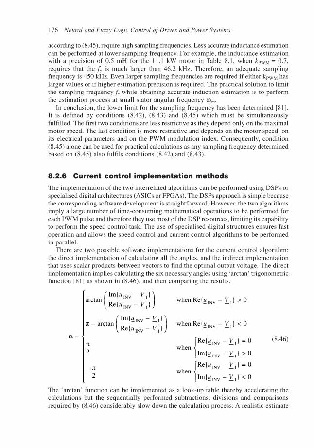
176 Neural and Fuzzy Logic Control of Drives and Power Systems
according to (8.45), require high sampling frequencies. Less accurate inductance estimationcan be performed at lower sampling frequency. For example, the inductance estimationwith a precision of 0.5 mH for the 11.1 kW motor in Table 8.1, when kPWM = 0.7,requires that the fs is much larger than 46.2 kHz. Therefore, an adequate samplingfrequency is 450 kHz. Even larger sampling frequencies are required if either kPWM haslarger values or if higher estimation precision is required. The practical solution to limitthe sampling frequency fs while obtaining accurate induction estimation is to performthe estimation process at small stator angular frequency ωes.
In conclusion, the lower limit for the sampling frequency has been determined [81].It is defined by conditions (8.42), (8.43) and (8.45) which must be simultaneouslyfulfilled. The first two conditions are less restrictive as they depend only on the maximalmotor speed. The last condition is more restrictive and depends on the motor speed, onits electrical parameters and on the PWM modulation index. Consequently, condition(8.45) alone can be used for practical calculations as any sampling frequency determinedbased on (8.45) also fulfils conditions (8.42) and (8.43).
8.2.6 Current control implementation methods
The implementation of the two interrelated algorithms can be performed using DSPs orspecialised digital architectures (ASICs or FPGAs). The DSPs approach is simple becausethe corresponding software development is straightforward. However, the two algorithmsimply a large number of time-consuming mathematical operations to be performed foreach PWM pulse and therefore they use most of the DSP resources, limiting its capabilityto perform the speed control task. The use of specialised digital structures ensures fastoperation and allows the speed control and current control algorithms to be performedin parallel.
There are two possible software implementations for the current control algorithm:the direct implementation of calculating all the angles, and the indirect implementationthat uses scalar products between vectors to find the optimal output voltage. The directimplementation implies calculating the six necessary angles using ‘arctan’ trigonometricfunction [81] as shown in (8.46), and then comparing the results.
α
π
π
π
=
arctan Im –
Re – when Re – > 0
– arctan Im –
Re – when Re – < 0
2when
Re – = 0
Im – > 0
– 2
when Re –
INV 1
INV 1INV 1
INV 1
INV 1INV 1
INV 1
INV 1
INV 1
u V
u Vu V
u V
u Vu V
u V
u V
u V
== 0
Im – < 0INV 1u V
(8.46)
The ‘arctan’ function can be implemented as a look-up table thereby accelerating thecalculations but the sequentially performed subtractions, divisions and comparisonsrequired by (8.46) considerably slow down the calculation process. A realistic estimate

Neural current and speed control of induction motors 177
of the computational effort can be obtained considering that the first two possibilities in(8.46) are equally probable while the last two are unlikely to be fulfilled due to the exactequalities which are involved. In this case between 12 and 18 subtractions (dependinghow many times case (a) and case (b) occur in (8.46)) are requested. Additionally, afurther six divisions and between 6 + 6 = 12 and 9 + 6 = 15 comparisons have to beperformed for each sampling period.
There are DSPs containing on-chip RAM and on-chip maskable ROM (for instance,TMS320C5x) [9]. Consequently, both the control program and the look-up table canreside either on-chip or off-chip in an external EPROM. On-chip configuration isadvantageous because it is compact, reliable and simplifies the PCB design. Unfortunately,the on-chip ROM memory space is limited. A total of 8.210 memory words are availablefor TMS320C51 and twice as much for TMS320C53 [9]. If the complete motor controlprogram is large then space for a look-up table might not be available. In these circumstancesthe table would have to be placed in an external EPROM.
For a simple and compact hardware implementation, alternative algorithms must beused to eliminate the need for the external EPROM memory chip. As a result, thetrigonometric function calculations must be avoided because any specialised routine forcalculating such functions is a huge time consumer. The indirect implementation avoidstrigonometric functions by utilising scalar products, which are performed between eachof the six vectors and the reference vector. By definition the scalar product between twon-dimensional vectors a and b is given by
a b a b = | | | | cos ⋅ ⋅ ⋅ ϕ (8.47)
The smaller the angle ϕ between the two vectors, the larger the result. Thus, the correctoutput voltage is chosen by maximising the corresponding scalar product [81]. Thecalculations are relevant only if the six vectors have the same module. To fulfil thiscondition, the six vectors need to be normalised. Consequently the six scalar productspj (where j = 1, 2, . . ., 6) have to be calculated.
The combined software implementation of the current control and inductance estimationalgorithms requires a very large number of mathematical operations to be performed. Inthe case where the direct current control implementation is employed, then up to 12 +24 = 36 algebraic calculations and 15 + 2 = 17 comparisons are requested for eachalgorithm step. The use of the indirect current control implementation in order to eliminatethe need for look-up tables requires up to 12 + 54 = 66 algebraic operations and 5 + 2= 7 comparisons for each algorithm step. In a typical situation where the PWM frequencyof 20 kHz and TPWM = 10·Ts, the algorithm requires that 200 000 calculation steps areperformed each second. This amounts to a total of 7 200 000 algebraic operations plus3 400 000 comparisons per second in the case of the direct implementation. The indirectimplementation requires a computational effort of 13 200 000 algebraic operations and1 400 000 comparisons per second.
A DSP program created to perform all these operations contains supplementaryinstructions: reading operands from memory, writing results to memory, program controlinstructions (jumps), and so on. An optimistic estimate is that the calculation and comparisoninstruction number is approximately equal to the number of all other instructions in theprogram. This means that a speed of at least 30 000 000 instructions per second (30MIPS) is required for on-line operation. The DSPs commonly used in drive systemapplications belong to the TMS320C3x and TMS320C5x series and are fast and inexpensive

178 Neural and Fuzzy Logic Control of Drives and Power Systems
processors. For example, the 16-bit, fixed-point DSPs TMS320C5x generation performsup to 50 MIPS while some of the TMS320C3x perform 30 MIPS but have a separate60 MFLOPS floating point arithmetic unit, which increases the total computation powertremendously. The latest DSP devices offer much larger calculation speeds (TMS320C6xgeneration offers 1600 MIPS) but their price is still too high for inexpensive drivecontrol applications. Thus, the computation effort required by the adopted current controlstrategy can be handled by an inexpensive DSP. However, the algorithm consumes asignificant part of its total resources (up to 33 per cent if a DSP from the TMS320C3xgeneration is used and up to 60 per cent if a TMS320C5x is used). Therefore, a complexinduction motor control strategy including the presented current control method can bedifficult to implement using a single common inexpensive DSP. The resistance estimationalgorithms plus the flux and speed control procedures involve a large number of calculationsand the total requirements can easily surpass the calculation power of such a chip.
Multiprocessor DSP-based control systems are therefore not a practical solution, andhardware implementation using ASIC or FPGA technologies proves to be an adequatealternative strategy for a fast and efficient control system capable of providing highperformance. The high speed is achieved by adapting the hardware architecture to thealgorithm specific data flow requirements. In addition, pipelining and parallel processingcan be used on a large scale to exploit all the opportunities offered by the specificcalculation algorithms. The more parallelisms that can be found in one algorithm thefaster the operation of its hardware implementation can be. Calculation parallelism isbest exploited by hardware implemented neural networks containing tens or hundreds ofelementary processing units cooperating to solve a particular problem. The neural approachis flexible as the neurone number can be increased or decreased and the calculationprecision varied accordingly. The neural network size and architecture is determinedbased on the necessary calculation precision and the available hardware resources. Themotor controller structure developed in this research work uses FPGA implementedneural networks alongside pipelined digital structures to carry out the computationallyintensive task of controlling the stator current. This solution is fast, inexpensive andeliminates the timing problems related to the sequential operation of a DSP processor.Using this approach, the complexity of the control tasks performed is not significantlylimited by the hardware operation speed. The only important limitation is given by theavailable amount of hardware resources.
8.2.7 Current control simulationThe system simulation approach combines the modelling flexibility of the VHDL softwaretools with the graphical capabilities of MATLAB. Thus, the simulation results havebeen generated in a numerical format using Workview Office 7.31 produced by Viewlogic,and then imported in MATLAB to generate the corresponding graphs.
A VHDL model of a three-phase induction motor has been created using themathematical space vector model of the motor. A separate simplified model of the PWMinverter has been developed considering all power transistors as ideal switches. The twomodules were combined with an abstract VHDL description of the adopted controlstrategy to generate a model of the entire drive system. This has been used to analyse thecurrent control principles presented in section 8.2. The system operation has been simulatedwith different parameter values and the simulation results validated the current controlprinciples previously presented.

Neural current and speed control of induction motors 179
In the VHDL Code Fragment 8.1, the motor model is an entity having two input ports(the stator voltage and load torque) and two output ports (the stator currents and therotor angular frequency). All data regarding the motor operation during the simulationis stored in an output ASCII file (motor.txt). The file contains numerical data in matrixformat, which is compatible with MATLAB. Each line in the matrix contains the set ofquantities that characterise the motor operation at a certain moment in time: currents,voltages, speed and torque.
—— Code Fragment 8.1LIBRARY math;USE math.complex_basic.all;USE math.mathtyx.all;USE std.textio.all;
ENTITY motor ISPORT(us: IN COMPLEX;Tload: IN REAL;ist: OUT COMPLEX;omegar: OUT REAL);
END motor;
ARCHITECTURE arch_motor OF motor ISCONSTANT Rs: REAL :=0.371;CONSTANT Rr: REAL :=0.415;CONSTANT Ls: REAL :=0.08705;CONSTANT Lr: REAL :=0.08763;CONSTANT Lm: REAL :=0.08433;CONSTANT Jr: REAL :=0.1;CONSTANT p: REAL :=2.0;CONSTANT deltat: TIME :=50 ns;CONSTANT dt: REAL := 5.0e-8;SIGNAL next_step: INTEGER :=1;FILE outf : TEXT IS OUT “c:\andrei\motor.txt”;
BEGINPROCESS(next_step)VARIABLE my_line: LINE;VARIABLE ist1,ist2,ir1,ir2,Fist1,Fist2,Fir1,Fir2,z:COMPLEX :=(0.0,0.0);VARIABLE T,omegar1,omegar2: REAL :=0.0;CONSTANT d_space: STRING :=” “;BEGINIF next_step=1 THENWRITE(my_line,us.re);WRITE (my_line,d_space);WRITE(my_line,us.im);WRITE (my_line,d_space);WRITE(my_line,ist1.re);WRITE (my_line,d_space);WRITE(my_line,ist1.im);WRITE (my_line,d_space);WRITE(my_line,ir1.re);
180 Neural and Fuzzy Logic Control of Drives and Power Systems
WRITE (my_line,d_space);WRITE(my_line,ir1.im);WRITE (my_line,d_space);WRITE(my_line,T);WRITE (my_line,d_space);WRITE(my_line,omegar1);WRITELINE(outf,my_line);END IF;ist1:=ist2;ir1:=ir2;Fist1:=Fist2;Fir1:=Fir2;omegar1:=omegar2;Fist2:=Fist1+(us-Rs*ist1)*dt;Fir2:=Fir1+(j*omegar1*Fir1-Rr*ir1)*dt;ist2:=(Lr*Fist2-Lm*Fir2)/(Lr*Ls-Lm*Lm);ir2:=(Ls*Fir2-Lm*Fist2)/(Lr*Ls-Lm*Lm);z:=ist1*conj(ir1);T:=3.0/4.0*p*Lm*(z.im);omegar2:=omegar1+(T-Tload)/Jr;IF next_step<1000 THENnext_step<=next_step+1 AFTER deltat;ELSEnext_step<=1 AFTER deltat;END IF;ist<=ist1;omegar<=omegar1;END PROCESS;
END arch_motor;
CONFIGURATION conf_motor OF motor ISFOR arch_motorEND FOR;
END conf_motor;
The PWM inverter is modelled as a simple VHDL process. The sensitivity list of theprocess contains the 6-bit vector ‘abcdef’ containing the control signals to the six powertransistors. The first three bits uniquely define the inverter output voltage. They are usedas the selection criterion in the CASE statement that generates the corresponding voltagespace vector ‘us’.
—— Code Fragment 8.2process(abcdef(5 downto 3))
constant U0: REAL :=begincase abcdef(5 downto 3) iswhen “100”=> us<=U0*(1.0,0.0);when “110”=> us<=U0*(0.5,0.866);when “010”=> us<=U0*(-0.5,0.866);when “011”=> us<=U0*(-1.0,0.0);when “001”=> us<=U0*(-0.5,-0.866);when “101”=> us<=U0*(0.5,-0.866);

Neural current and speed control of induction motors 181
when others=> us<=(0.0,0.0);end case;end process;
The motor parameters used for the simulations presented in Figs. 8.11, 8.12 and 8.13 aregiven in column (b) of Table 8.1. Thus, according to equation (8.8) the inductance in theequivalent circuit is L = 5.9 mH. The parameters defining the operation of the currentcontroller are as follows:
• The module of the reference stator current space vector: 10 A.• The reference frequency: 50 Hz.• The inductance updating step δL: 0.05 mH.• The PWM frequency: 20 kHz.• The sampling frequency: 450 kHz.• | Vni |crt = ∞.
In Fig. 8.11 it is shown that the correct inductance value is obtained in a short timeinterval (about 200 ms). The initial induction estimation error is very large causing verylarge errors in the calculation of the non-inductive voltage vector Vni. The increasingaccuracy of the inductance estimate is reflected in the decreasing ripples of estimatedVni shown in Fig. 8.12.
L (mH)
6
5
4
3
2
1
00 50 100 150 200 250 300 t (ms)
Fig. 8.11 Inductance estimation values
Figure 8.13 presents the trajectory in the complex plane of the actual current spacevector across the stator winding. It demonstrates that the current ripples are maintainedat low levels.
Similar simulations have been performed for a current control algorithm version thatalways uses all the seven output voltages (| Vni |crt = 0). Similar results are obtained butthe inductance estimation process is much slower (about ten times slower). Moreover,the variations of the inductance estimation value in steady-state operation are twice the

182 Neural and Fuzzy Logic Control of Drives and Power Systems
amplitude of the result of Fig. 8.11. However, the current ripple amplitude decreased toapproximately 70 per cent compared to Fig. 8.13 after the inductance estimation processwas finished. Thus, although using the zero voltage decreases the current ripples, it also
250
200
150
100
50
0
–50
–100
–150
–200
–250
ReV ni(V)
0 50 100 150 200 250 300 t (ms)
Fig. 8.12 The non-inductive voltage estimation
Fig. 8.13 The load current space vector
Imi (A)
15
10
5
0
–5
–10
–15
Re i (A)
–15 –10 –5 0 5 10 15

Neural current and speed control of induction motors 183
increases the inductance estimation errors, thereby affecting the accuracy of the informationon motor operation. Consequently, this control method version decreases the precisionof any sensorless speed control strategy based on the equivalent R–L–e circuit.
8.3 The new sensorless motor control strategy
The common sensorless induction motor control strategies are derived from the sensor-based field-oriented control methods that have been extended to include speed estimationalgorithms. All field orientation methods require several transformations of theelectromagnetic quantities from the stator reference frame into the flux reference frame,and back from the flux reference frame into stator reference frame. Thus, a generalstator quantity ‘A’ is transformed from fixed stator coordinates into mobile flux coordinates,using equation (8.48). The inverse transformation is carried out according to (8.49)where θ(t) indicates the angle of the flux vector (the rotor flux, the stator flux or theairgap flux) and is a function of time. The complete control algorithms require severalother mathematical calculations to be carried out: integrations, divisions, multiplicationsand square roots.
A
A
t t
t t
A
Ad
q
ds
qs
θ
θ
θ θθ θ
⋅
= cos ( ) sin ( )
– sin ( ) cos ( ) (8.48)
A
A
t t
t t
A
Ads
qs
d
q
⋅
=
cos ( ) –sin ( )
sin ( ) cos ( )
θ θθ θ
θ
θ (8.49)
The sensorless speed control strategies are usually software implemented using DSPsor microcontrollers, because the hardware implementation is difficult to achieve due tothe large number of different mathematical operations to be implemented. Attemptshave been made to combine the software and the hardware approaches [98]. This strategyrequires the implementation of a custom mathematical processor alongside specialisedcontrol modules, RAM memory and ROM memory (to store the control programs). Thespecialised modules implement routine tasks such as the PWM signal generation or theA/D converter control, while the mathematical processor carries out all the complexmathematical calculations and updates the operation parameters for the specialisedmodules. Such an approach combines the flexibility of software implementation and thespeed of the hardware implementation. It requires large integrated circuits and complexdesign procedures including simulation tools capable of checking the operation of themixed software–hardware control block. An inexpensive, simple and compact hardwareimplementation requires the calculation overhead to be minimised so that the softwarecomponent of the control algorithm can be eliminated. Therefore, simpler speed estimationmethods and control strategies need to be devised.
The calculation complexity can be much reduced if quantities that are invariant atreference frame transformations are used so that matrix equations like (8.48) and (8.49)can be eliminated. The two types of quantities having such a property are the spacevector modules and the phase shifts between the space vectors. A control algorithm thatoperates with these quantities is more suitable to using polar coordinates than theclassical rectangular coordinates. Consequently, new speed estimation algorithms and
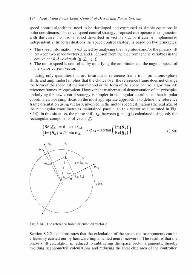
184 Neural and Fuzzy Logic Control of Drives and Power Systems
speed control algorithms need to be developed and expressed as simple equations inpolar coordinates. The novel speed control strategy proposed can operate in conjunctionwith the current control method described in section 8.2, or it can be implementedindependently. In both situations the speed control strategy is based on two principles:
• The speed information is extracted by analysing the magnitude and/or the phase shiftbetween two space vectors A and B, chosen from the electromagnetic variables in theequivalent R–L–e circuit (u, Vni, e, i).
• The motor speed is controlled by modifying the amplitude and the angular speed ofthe stator current vector.
Using only quantities that are invariant at reference frame transformations (phaseshifts and amplitudes) implies that the choice over the reference frame does not changethe form of the speed estimation method or the form of the speed control algorithm. Allreference frames are equivalent. However, the mathematical demonstration of the principlesunderlying the new control strategy is simpler in rectangular coordinates than in polarcoordinates. For simplification the most appropriate approach is to define the referenceframe orientation using vector A involved in the motor speed estimation (the real axis ofthe rectangular coordinates is maintained parallel to this vector as illustrated in Fig.8.14). In this situation, the phase shift αBA between B and A is calculated using only therectangular components of vector B:
Re = cos
Im = sin = arctan
Im Re
B B
B B
BB
BA
BABA
θ
θ
θ
θ
αα
α⋅⋅
⇒
(8.50)
Fig. 8.14 The reference frame oriented on vector A
b
Imθ Ims
B
ImBθ
αBA
0
θReBθ
A = ReAθ
Reθ
a Res
c
Section 8.2.2.1 demonstrates that the calculation of the space vector arguments can beefficiently carried out by hardware implemented neural networks. The result is that thephase shift calculation is reduced to subtracting the space vector arguments, therebyavoiding trigonometric calculations and reducing the total chip area of the controller.

Neural current and speed control of induction motors 185
Therefore, equations like (8.50) are used only for theoretical analysis but do not have tobe implemented directly into hardware.
8.3.1 Speed estimation algorithms
Several estimation methods can be developed depending on the vectors A and B that arechosen from the quantities available in the R–L–e circuit (u, Vni, e, i). The methods havedifferent degrees of accuracy and imply different calculation complexity levels. Themost straightforward solution is operating with the voltage u and the current i becausethey are directly measurable quantities. The non-inductive voltage Vni is a good optionif the speed estimation is performed by a controller that uses the current control strategypresented in section 8.2. The vector Vni is calculated for the current control algorithmbut the information can also be transferred to the speed estimator thereby decreasing thecomputation effort. The use of the internal voltage e requires the largest number ofcalculations because its value needs to be derived from the space vectors u or Vni.
The class of estimation methods defined by A = is is analysed in a stator current-oriented reference frame. Due to the stator current orientation, the imaginary part of thestator current vector is zero and the reference frame rotates with the angular speed ωes,which corresponds to the synchronism speed in steady-state operation. Throughout thissection, the superscript ‘syn’ is attached to space vectors expressed in the synchronousstator current-oriented reference frame. The conditions defining the chosen referenceframe are mathematically described by
θ ω =
= es
s s
t
i I
⋅
(8.51)
where Is designates a real quantity. The induction motor space vector model in a statorcurrent-oriented reference frame is expressed as
u R It
j
u R it
j
L I L i
L i L I
s s ss
es s
r r rr
es er r
s s s m r
s r r m s
synsyn
syn
syn synsyn
syn
syn syn
syn syn
= + d
d +
= + d
d + ( – )
= +
= +
Ψω Ψ
Ψω ω Ψ
ΨΨ
⋅
(8.52)
If the last two equations in (8.52) are substituted in the first two, the result is
u R I Li
tL
It
j L I L i
R i Li
tL
It
j L I L i
s s s mr
ss
es s s m r
r r rr
ms
m s r r
synsyn
syn
synsyn
slpsyn
= + d
d +
dd
+ ( + )
0 = + d
d +
dd
+ ( + )
ω
ω
(8.53)
The quantity ‘ωslp’ in (8.53) is the ‘slip angular frequency’ and represents the differencebetween the stator and the rotor electrical angular frequencies.
ωslp = ωes – ωer (8.54)

186 Neural and Fuzzy Logic Control of Drives and Power Systems
The slip angular frequency is related to the motor slip ‘s’ as follows
ωslp = s · ωes (8.55)
The calculation of ωslp is a prerequisite for the rotor speed estimation. The relationbetween ωslp and the rotor speed is described by
ωω ω
ωω
res
sp p=
– = –
slp slp(8.56)
Therefore, the speed estimation methods can be reduced to methods of estimating theslip angular frequency. Due to their mathematical simplicity and hardware implementationadvantages, the estimators based on the phase-shift information are adopted in this workas the optimal solution to the speed calculation problem [81]. To achieve the motorspeed estimation, the information contained in the value of the angle α between thestator current vector i and one of the other vectors: e, us or Vni is processed. Thecalculations [81] yield the following results:
tan = tan (arg ) = ( + ) +
( – ) ( + ) + –1 –1 syn
2slp2 2
slp2
2 2slp2 2 2 2α
ω ω ωω ω ωui r
s r r r es m r r
r s m r r es m r es
uR L R L L L R
L L L R L L R⋅ ⋅(8.57)
tan = Re
Im = +
( + –1
syn
synslp
2slp2 2
2 2αω ω
ωV ini
ni
r
r
r s r r
es m rni
V
V
LR
L R R L
L R (8.58)
tan = Re Im
= –1syn
synslpα
ωei
r
r
e
e
LR (8.59)
Relation (8.57) is very complicated and non-linear. It is not suitable to hardwareimplemented estimation of the slip angular speed. The result in (8.58) is simpler than(8.57), it contains one term that is proportional with ωslp and another term proportionalwith the slip angular frequency squared. If the stator angular frequency is high (ωes ≅314 rad/s), and the slip is small (it normally is during typical motor operation) then thelast term in (8.58) can be neglected and an almost linear relationship between ωslp andtan–1 ( )αV ini is obtained:
Re
Im tan
syn
synslp
slp–1V
V
LR
RL
ni
ni
r
r
r
rV ini≈ ⇒ ≈ ⋅
ωω α (8.60)
Figure 8.15 presents the numerical calculation results obtained for the 11.1 kW motorat a stator angular frequency ωs = 314 rad/s. It can be seen that the Re(Vni)/Im(Vni)characteristics are almost straight lines. Unfortunately, their curvature increases withthe decrease of speed so that the relationship (8.60) is not valid for speeds much belowthe rated speed.
The approximate relationship (8.60) is appropriate for hardware implementation togetherwith the current control strategy previously presented in section 8.2, because it providesthe value of Vni. This version of the slip estimator is based on the equation
ω αslp–1 –1= tan ( ) = tan [arg( ) – arg ( )] V i
r
rnis
ss r
rni
RL
V iRL
⋅ ⋅ (8.61)
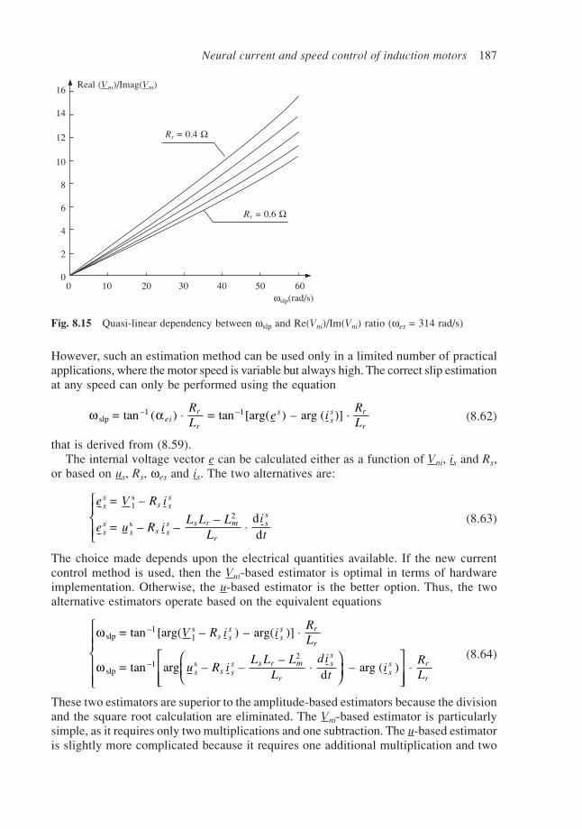
Neural current and speed control of induction motors 187
However, such an estimation method can be used only in a limited number of practicalapplications, where the motor speed is variable but always high. The correct slip estimationat any speed can only be performed using the equation
ω αslp–1 –1= tan ( ) = tan [arg( ) – arg ( )] ei
r
r
sss r
r
RL
e iRL
⋅ ⋅ (8.62)
that is derived from (8.59).The internal voltage vector e can be calculated either as a function of Vni, is and Rs,
or based on us, Rs, ωes and is. The two alternatives are:
e V R i
e u R iL L L
Lit
ss
s ss
ss
s s ss s r m
r
ss
= –
= – – –
dd
1s
s2
⋅
(8.63)
The choice made depends upon the electrical quantities available. If the new currentcontrol method is used, then the Vni-based estimator is optimal in terms of hardwareimplementation. Otherwise, the u-based estimator is the better option. Thus, the twoalternative estimators operate based on the equivalent equations
ω
ω
slp–1
1s
slp–1 s
2
= tan [arg( – ) – arg( )]
= tan arg – – –
d
– arg ( )
V R i iRL
u R iL L L
Ldi
ti
RL
s ss
ss r
r
s s ss s r m
r
ss
ss r
r
⋅
⋅
⋅
(8.64)
These two estimators are superior to the amplitude-based estimators because the divisionand the square root calculation are eliminated. The Vni-based estimator is particularlysimple, as it requires only two multiplications and one subtraction. The u-based estimatoris slightly more complicated because it requires one additional multiplication and two
Fig. 8.15 Quasi-linear dependency between ωslp and Re(Vni)/Im(Vni) ratio (ωes = 314 rad/s)
Real (Vni)/Imag(Vni)
Rr = 0.4 Ω
Rr = 0.6 Ω
ωslp(rad/s)
16
14
12
10
8
6
4
2
00 10 20 30 40 50 60

188 Neural and Fuzzy Logic Control of Drives and Power Systems
additional subtractions (the current derivative being approximated by the difference ofthe last two current samples). The vector argument calculations in the stator referenceframe can be performed by a hardware implemented neural network. Alternatively, thefunction tan–1 can be easily implemented as a small look-up table because it is a periodicaland symmetrical function and only its values between 0° and 90° need to be stored.Such a small table is implementable into the same chip as the rest of the speed controller.
8.3.2 The novel speed control algorithm
In accordance with the general principles exposed at the beginning of section 8.3, anovel speed control algorithm is proposed which can be expressed as a set of simplemathematical equations written in polar coordinates. The proposed speed control strategyincorporates the slip estimator based on the phase-shift between the vectors e and is. Thenew method simultaneously carries out two interrelated tasks:
• Controlling the rotor speed ωr so that it follows the reference speed ωref.• Maintaining the slip angular frequency at a constant value: ωslp = Ωslp.
The two tasks are performed by controlling the angular frequency and the amplitude ofthe stator current. Thus, the speed controller contains two control loops. The slip controlloop determines the stator current amplitude Is in such a manner that ωslp is maintainedas close as possible to the reference value Ωslp, while the speed control loop calculatesthe stator angular frequency ωes.
8.3.2.1 The slip control loop
The slip control loop implements a non-linear control strategy to keep ωslp constant bymodifying the stator current amplitude Is. The stator current controls the rotor currentand the interaction of the two generates the motor torque, which in turn affects the slipangular frequency. The induction motor torque is given by the general equation
T L i im s r = 23
Im *⋅ ⋅ (8.65)
If the expression of the rotor current for steady-state operation [81] is substituted in(8.65) then the steady-state motor torque is obtained as a function of current amplitudeand slip angular frequency:
T I Lj L I
R j Ls mm s
r r( , ) = Im
– slpslp
2
slpω
ωω⋅
(8.66)
This expression can be further simplified as follows:
T I Lj L I R j L
R Ls mm s r r
r r
( , ) = Im ( + )
+ slpslp
2slp
2slp2 2ω
ω ωω
⋅
(8.67)
T IL I R
R Lsm s r
r r
( , ) = + slp
slp2 2
2slp2 2ω
ωω (8.68)
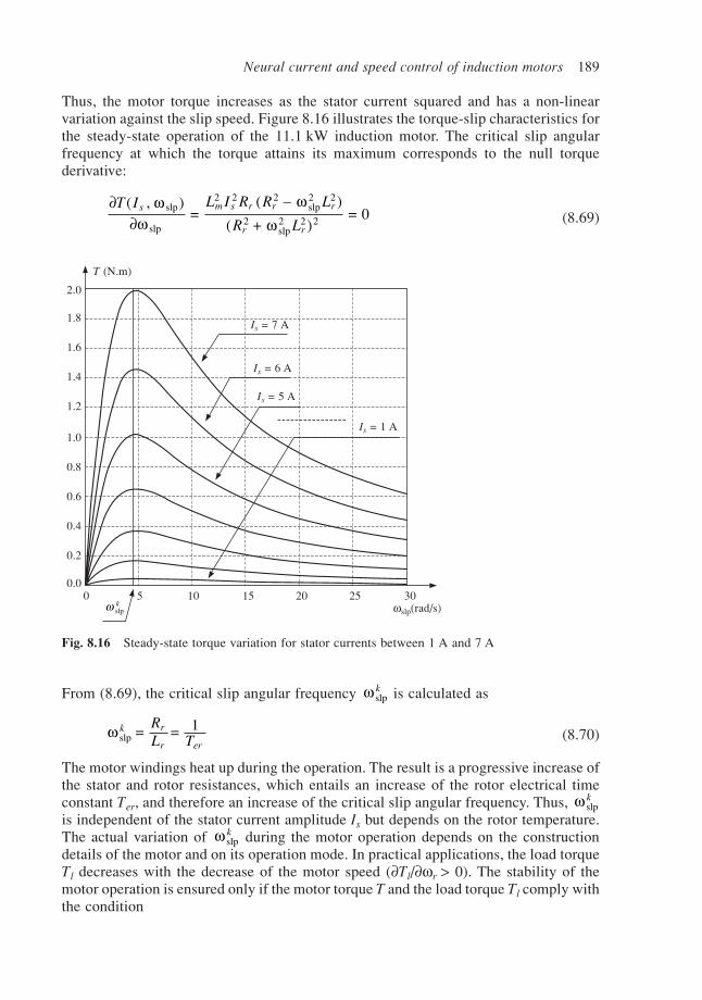
Neural current and speed control of induction motors 189
Thus, the motor torque increases as the stator current squared and has a non-linearvariation against the slip speed. Figure 8.16 illustrates the torque-slip characteristics forthe steady-state operation of the 11.1 kW induction motor. The critical slip angularfrequency at which the torque attains its maximum corresponds to the null torquederivative:
∂∂
T I L I R R L
R Ls m s r r r
r r
( , ) =
( – )
( + ) = 0
slp
slp
2 2 2slp2 2
2slp2 2 2
ωω
ωω (8.69)
Fig. 8.16 Steady-state torque variation for stator currents between 1 A and 7 A
T (N.m)
2.0
1.8
1.6
1.4
1.2
1.0
0.8
0.6
0.4
0.2
0.00 5 10 15 20 25 30
ωslp(rad/s)
Is = 7 A
Is = 6 A
Is = 5 A
Is = 1 A
From (8.69), the critical slip angular frequency ω slpk is calculated as
ω slp = = 1k r
r er
RL T (8.70)
The motor windings heat up during the operation. The result is a progressive increase ofthe stator and rotor resistances, which entails an increase of the rotor electrical timeconstant Ter, and therefore an increase of the critical slip angular frequency. Thus, ω slp
k
is independent of the stator current amplitude Is but depends on the rotor temperature.The actual variation of ω slp
k during the motor operation depends on the constructiondetails of the motor and on its operation mode. In practical applications, the load torqueTl decreases with the decrease of the motor speed (∂Tl/∂ωr > 0). The stability of themotor operation is ensured only if the motor torque T and the load torque Tl comply withthe condition
ω slpk

190 Neural and Fuzzy Logic Control of Drives and Power Systems
sign = – sign sign = – sign slp slp
∂∂
∂∂
⇔ ∂∂
∂∂
T T T T
r
l
r
l
ω ω ω ω (8.71)
As a result, the motor speed is stable only if the slip angular frequency is in the interval[0; ω slp
k ). Therefore, the reference slip angular frequency Ωslp has to be set to a valuesituated inside this interval. According to Fig. 8.16, the motor slip can be varied atconstant load torque by controlling the stator current amplitude. The slip control loopneeds to increase the stator current amplitude Is when the slip angular frequency ωslp islarger than the reference Ωslp, and to decrease it when the slip angular frequency issmaller than Ωslp. The process requires information on the actual motor slip. To calculatethis information, the control loop incorporates the slip estimation principles based onthe phase shift between esyn and isyn. Thus, maintaining a constant slip angular frequencyduring the steady-state operation is equivalent to maintaining a constant angle betweenesyn and isyn.
The locus of esyn is a set of circles tangential to the real axis of the rectangularsynchronous reference frame [81]. The stator current amplitude Is is proportional to thecircle radius so that for a given stator current amplitude the locus is made up of the twocircles illustrated in Fig. 8.17. As demonstrated by (8.72), the quadrant where theinternal voltage esyn is situated depends on the sign of the stator angular frequency ωesand on the sign of the slip angular frequency ωslp:
sign Re = sign sign
sign Im = sign
synslp
syn
e
ees
es
ω ωω
⋅
(8.72)
Fig. 8.17 Internal load voltage locus in the complex plane
II Imesyn
I
III IV
ωes > 0ωslp < 0
ωes > 0ωslp > 0
0 Is Re
ωes < 0ωslp > 0
ωes < 0ωslp < 0
In most practical applications, the load torque opposes the motor shaft rotation. In thissituation, the absolute value of the rotor speed is smaller than the absolute value of themagnetic field speed. Therefore ωes and ωslp have the same sign and esyn is situatedeither in quadrant I or in quadrant IV of Fig. 8.17.
| ωes | > | ωer | ⇒ sign (ωslp) = sign (ωes) (8.73)
There are applications where the torque may not be opposed to the shaft rotation, for

Neural current and speed control of induction motors 191
example cranes and elevators. When an elevator is moving down, its weight creates atorque that tends to accelerate the shaft rotation. As a result, the rotor moves faster thanthe motor magnetic field, and the slip angular frequency sign is the opposite of the statorangular frequency sign. In this situation, the vector esyn is situated in either quadrant IIor quadrant III.
| ωes | < | ωer | ⇒ sign (ωslp) = – sign (ωes) (8.74)
In conclusion, the sign of the reference slip angular frequency Ωslp depends on the statorangular frequency sign and on the nature of the load. It is positive for motor operationin quadrants I and III and negative otherwise. The motor operation in the four quadrantscorresponds to four different internal voltage vectors for steady-state operation: esyn(Ωslp1),esyn(Ωslp2), esyn(Ωslp3), esyn(Ωslp4) where | Ωslp1 | = | Ωslp2 | = | Ωslp3 | = | Ωslp4 |. The valuesof the four reference slip values Ωslp have to be smaller in absolute value than themodule of the critical slip angular frequency | |slpω k . If equation (8.70) is substituted in(8.59), the result is:
tan = –1 slp
slp
αωωei k
(8.75)
Consequently, the internal voltage vectors corresponding to the motor operation atcritical slip are placed at 45o with regard to the reference frame axes. At slip valuessmaller in absolute values than | |slpω k tan–1αei decreases and if ωslp is null then tan–1 αeiis null as well. As shown in Fig. 8.18, the vectors esyn(Ωslp1), esyn(Ωslp2), esyn(Ωslp3),esyn(Ωslp4) need to be situated in the sectors limited by the imaginary axis of the synchronousreference system and by the vectors esyn(ωslp1), e
syn(ωslp2), esyn(ωslp3), esyn(ωslp4). Theslip control principle is formulated as follows:
• When the internal voltage vector esyn lies in one of the shaded areas in Fig. 8.18, thecontroller decreases the stator current amplitude in order to increase the absolutevalue of the slip angular frequency | ωslp |.
Fig. 8.18 Characteristic points on esyn locus and corresponding slip angular frequencies
esyn(Ωslp2)
esyn(0) Imesyn(Ωslp1)
II I
Re
esyn(Ωslp3) esyn(Ωslp4)
esyn(0)III IV
e ksynslp2( )ω e ksyn
slp1( )ω
i ssyn
e ksynslp4( )ωe ksyn
slp3( )ω

192 Neural and Fuzzy Logic Control of Drives and Power Systems
• When the internal voltage vector lies outside the shaded sectors the speed controllerneeds to decrease the stator current amplitude in order to increase the | ωslp |.
Due to the symmetry in Fig. 8.18 the calculations referring to four quadrants can bereduced to equivalent calculations in only one quadrant. This transformation is carriedout by replacing the real and imaginary parts of vector esyn by absolute values. Theresult (Fig. 8.19) is an equivalent vector E eqv
syn given by
E e j e E jeqvsyn syn syn
eqvsyn
eqvref
eqvref= |Re | + | Im | = | | [cos ( ) + sin ( )]⋅ ⋅ ⋅ α α (8.76)
Fig. 8.19 The reduction of the four quadrants to one
| Im |
βeqv
αeqv
0 i s |Re|
The rules governing the control of the stator current amplitude can therefore be expressedas the differential equation
dd
= ( , )
= arg ( ) – arg ) = arctan – arg ( )
eqv
eqv eqvsyn
slp eqvsyn
slpslp
slpeqvsyn
slp
It
F I
E E E
sI s
k
β
β ωω
ωΩ Ω
(
(8.77)
where the angle βeqv is the difference between the reference argument α eqvref =
arg ( )eqvsyn
slpE Ω and the argument αeqv of the actual equivalent vector E eqvsyn .
There are several alternative expressions for the function FI but all of them have tolimit the current amplitude within an interval of acceptable values [Ismin; Ismax]. Themaximum limit is imposed by safety considerations as the motor and the power electronicscircuitry has to be protected against overheating. The minimal stator current is imposedso that the internal voltage amplitude | esyn | does not decrease under the limit where itsargument cannot be calculated. Several versions of function FI are analysed in [81] andthe corresponding motor control performance is assessed.
dd
< 0Its
E eqvsyn
slp( )Ω
E eqvsyn
dd
> 0Its
α eqvref

Neural current and speed control of induction motors 193
8.3.2.2 The speed control loop
If the slip angular frequency ωslp is maintained constant then the steady-state relationshipbetween the rotor mechanical speed and the stator electrical angular frequency is linear:
ωes = Ωslp + ωer = Ωslp + p · ωr (8.78)
However, the slip angular frequency ωslp cannot be kept constant at the reference valueΩslp in transient operation. During transient operation all the quantities describing themotor operation undergo complicated changes that are difficult to control due to thenon-linearities. Furthermore, transient operation causes the slip estimation errors, therebyincreasing the difficulty of the control task. The speed control loop must simultaneouslycompensate the errors of the motor slip estimation and control the rotor speed. Thecontrol strategy can be expressed by the general differential equations
ω ω ω ω ωω ω ω βω
es r er r r
eses es s
p
tF I
ref refslp
ref refslp
ref
refeqv
= sign ( + = sign + d
d = ( , , , )
⋅ Ω ⋅ Ω ⋅
(8.79)
where the function ‘sign’ is defined by
sign ( ) =
+ 1 when > 0
0 when = 0
– 1 when < 0
x
x
x
x
(8.80)
Any speed control strategy can be defined by the two functions Fω and FI involved inequations (8.77) and (8.79). The simplest control version is defined by the functions
F IK I I I
I I I
F I K
I sI s s s
s s s
es es s es es
( , ) = when ( ; )
0 when ( ;
( , , , ) = sign ( – )
eqveqv –min –max
–min –max
refeqv
ref
ββ
ω ω β ω ωω ω
⋅ ∈∉
⋅
(8.81)
where KI and Kω are proportionality constants. In this case, the derivative of the currentamplitude is proportional to the angular error βeqv, while the derivative of the angularfrequency depends on the sign of the stator frequency error. Therefore, the motor controlis linear and uses two P controllers operating in an independent manner, as the twofunctions FI and Fω are calculated based on different parameters. This type of control isappropriate when the application requirements do not include fast transient response.
Using this control strategy, the motor behaves similarly to a synchronous machinewith a start-up cage rotor:
• It is able to generate a constant speed for a certain range of load torque values.• The rotor speed follows the variations of the stator frequency if this variation is slow.• If the variations of the stator frequency are too fast, they take the rotor out of synchronism
and the speed response becomes relatively slow.
The simulation results in [81] prove that the transient slip estimation errors do notaffect the stability of the drive system operation. The errors cause oscillations of theangles αeqv and βeqv but the stator current amplitude is given by

194 Neural and Fuzzy Logic Control of Drives and Power Systems
Is(t) = KI · ∫ βeqv(t) · dt (8.82)
so that the effect of these oscillations is filtered out by integration. However, controlstrategies of increased complexity are required to obtain a fast response of the systemto step changes of ωref. Very fast induction motor transient responses are typicallyobtained using the rotor field-oriented control strategy. The new speed control strategycan be improved by finding two functions FI and Fω that emulate the behaviour of arotor field-oriented controller. Thus, the field generating current component isd needs tobe maintained constant while modifying the torque generating current component accordingto the speed error. This requires the calculation of the position θψ(t) of the rotor fluxvector ψ
r and the equations (8.83) to be solved.
i I t t t t t
i I t t t t t f
sd s
t
es
sd s
t
es r
= ( ) cos ( ) d – ( ) = const.
= ( ) sin ( ) d – ( ) = ( – )
0
0
ref
⋅ ⋅ ⋅
⋅ ⋅ ⋅
∫∫
ω θ
ω θ ω ω
ψ
ψ
(8.83)
The rotor flux vector is not calculated by the new speed control strategy in order tominimise the calculation amount. On the other hand, solving the equation system (8.83)would increase the hardware implementation complexity to an unacceptable level. However,this strategy can approximate the position of ψ
r using the position of esyn for large andmedium power motors. If the speed is larger than a few revolutions per second, then esyn
is approximately perpendicular on the rotor flux vector ψr because the rotor resistance
can be neglected as compared to motor reactance. Under these conditions, esyn can beused to determine the position of vector ψ
r in the complex plane.Figure 8.20 indicates the typical positions of the vectors e, i and Ψr in the synchronous
reference frame. Modifying the motor speed requires a modification of the motor torque.The field orientation solution is to alter the stator current component isq while keeping
Fig. 8.20 Relative position of vectors e, i and Ψr in the synchronous reference frame
Im
esyn
γ
αisq
ir
0
isd
Is Re
γ
Ψ rsyn

Neural current and speed control of induction motors 195
isd constant. According to the new control method, the task is achieved by simultaneouslychanging the stator angular frequency ωes and the stator current amplitude Is. The twostator current components are:
i I
i Isd s
sq s
= cos
= sin
⋅⋅
γγ (8.84)
where the angle γ is indicated in Fig 8.20, while the derivatives of the two componentsare
dd
= dd
cos – sin dd
= 0
dd
= dd
sin + cos dd
it
It
It
it
It
It
sd ss
sq ss
γ γ γ
γ γ γ
⋅
⋅
(8.85)
The derivative disd /dt is ideally null during the motor speed change and therefore thevariation of the stator current amplitude Is depends on γ according to
dd
= tg dd
It
It
ss ⋅ ⋅γ γ
(8.86)
which is derived from the first equation (8.85). Substituting (8.86) into the secondequation (8.85), the result is
dd
= dd
tg
tg sin + cos It
it
s qs ⋅ ⋅γ
γ γ γ (8.87)
which demonstrates that the stator current component isq increases with the increase ofIs. At the same time, any variation of Is has to comply with the condition (8.86).Consequently, any increase of the stator current amplitude Is has to be simultaneouswith an increase of the angle γ = π/2 – argesyn. The variation of Is generates an initialincrease of argesyn followed by a decrease [81]. This variation is reflected in theopposite alteration of the slip estimation results and of the angle γ (unwanted result). Tomaintain the relationship between Is and γ in accordance with (8.86), the stator angularfrequency ωes must be simultaneously altered with Is so that the effects of ωes variationscompensate the unwanted effects over angle γ. It was proven in [81] that increasing theslip angular frequency ωslp = ωes – ωer leads to oscillations starting with an initialdecrease of argesyn. This can cancel out the unwanted increase caused by the modificationof Is. The subsequent oscillations of angle γ resulting from the modification of Is needto be cancelled out by suitable variations of ωes. The exact analytical non-linear solutionto this problem is difficult to find. However, simplified solutions, equivalent to quasi-field-oriented control methods, can be investigated based on a few principles derivedfrom the previous considerations and from the rules governing the slip estimation process.The principles are:
• The value of argesyn needs to be maintained at values close to 90° (Ωslp has to besmall) to maintain the slip estimation errors at acceptable levels.
• The rotor speed changes are always initiated by the speed control loop according toequations (8.78) and (8.79). The stator current variations compensate for the unwantedoscillations of angle γ, which can be calculated as a function of βeqv and α eqv
ref .

196 Neural and Fuzzy Logic Control of Drives and Power Systems
• The angle γ must be allowed to increase during the speed changes simultaneouslywith the increase of Is. This is equivalent with a simultaneous increase of βeqv and Is,which can be easily achieved if ∂FI/∂βeqv > 0.
• If the angles γ and βeqv become too large, the speed of variation of the stator frequencyhas to be limited in order to reduce the motor slip and the error slip estimations.However, provided the motor slip has small values, the stator frequency can beallowed to undergo fast speed changes.
One of the simplest solutions that complies with the principles outlined is
F IK I I I
I I I
F IK K
I sI s s s
s s s
es es ses
es
( , ) = if ( ; )
0 if ( ; )
( , , , ) = sign ( – ) ( – ) if <
sign ( –
eqveqv –min –max
–min –max
refeqv
refes 1 eqv 2 eqv max
ref
ββ
ω ω βω ω β β βω ωω
ω ω
⋅ ∈∉
⋅ ⋅
eses K K) ( – ) if 1 max 2 eqv max⋅ ⋅ ≥
ω ωβ β β
(8.88)
where Fω is a piecewise linear function (Fig. 8.21) defined by the constants KI, Kω1, Kω2,β whose optimal values depend on the motor parameters. The functions (8.88) represent
Fig. 8.21 The variation of Fω with β when ω esref > ωes
the basic version of the new sensorless speed control algorithm proposed in this book.This control solution has been tested by simulations on the 11.1 kW motor using differentvalues for the constants in (8.88). The MATLAB simulation results demonstratesubstantially improved dynamic response, as exemplified in Fig. 8.22. In the same time,the method is capable of maintaining the rotor speed constant despite load torquevariations (Fig. 8.23). The system response speed is approximately proportional to Kω1but increasing Kω1 over a certain limit actually deteriorates the system response. Thisphenomenon is illustrated in Fig. 8.24, which can be compared with Fig. 8.22.
As shown by these simulation results, the stator angular frequency undergoes non-linear variation caused by the non-linear mathematical model (8.88) of the controlstrategy. Again, the motor behaves in a similar manner to a synchronous motor: the rotorspeed follows the stator frequency changes only if the speed of these changes is belowa critical limit depending on the rotor inertia and on the load torque.
ωslp < Ωslp
Fω
ωslp = 0
Kω1
ωslp > Ωslp
ωslp = Ωslp
Kω1 – βmax · Kω2
Area of limitedstator frequency
variation
0 βmax βeqv90 – eqvref° α α eqv
ref

Neural current and speed control of induction motors 197
The speed control strategy can be further refined by using different values for theconstant KI depending on the stator current amplitude Is. A single value KI cannot beoptimal for all the motor currents in the range (Is-min; Is-max) because, as demonstrated byequation (8.68), the motor torque is proportional to Is squared, and the same derivative
Speed (rad/s)350
300
250
200
150
100
50
0
Reference speed
Rotor speed
Stator angularfrequency
Time (s)0 0.5 1 1.5 2 2.5 3 3.5 4
Fig. 8.22 Quasi-field oriented control method results (Kω1 = 1000 s–1)
Speed (rad/s)350
300
250
200
150
100
50
0
Time (s)0 0.5 1 1.5 2 2.5 3
Time (s)0 0.5 1 1.5 2 2.5 3
Torque (N.m)7
6
5
4
3
2
1
0
Fig. 8.23 The motor speed variation during a step increase of the load torque (Kω1 = 1000 s–1)

198 Neural and Fuzzy Logic Control of Drives and Power Systems
dIs /dt produces different torque variations at different stator current amplitudes. Theeffect is a slow dynamic response of the motor when the current is close to Is-min and avery fast one when the current is close to Is-max. Thus, to optimise the motor response,an improved function FI needs to be found, which ensures the same dynamic parametersboth at small stator currents and at large stator currents. This requires that the motorderivative does not depend on the stator current amplitude. The time derivative of thetorque is:
dd
= ( , )
dd
= 2
+
dd
slp slp2
2slp2 2
Tt
T I
I
It
L I R
R L
It
s
s
s m s r
r r
s∂∂
⋅ ⋅α ω
ω(8.89)
Consequently, the torque derivative dT/dt is independent of the current amplitude Is ifdIs/dt is inversely proportional to Is. To include this improvement, the quasi-field-orientedcontrol strategy initially formulated in (8.88) can be transformed into
dd
= ( , ) = / if ( ; )
0 if ( ; )
dd
= ( , , , )=sign ( – ) ( – ) if
eqveqv – min – max
– min – max
refeqv
refes 1 eqv 2
It
F IK I I I I
I I I
tF I
K K
sI s
I s s s s
s s s
eses es s
es
ββ
ωω ω β
ω ω β βω
ω ω
⋅ ∈∉
⋅ ⋅ eqveqv max
ref1 max 2 eqv max
refslp
refslp
ref
<
sign ( – ) ( – ) if
= + = + p .
βω ω β β β
ω ω ω
ω ωes es
es er r
K K⋅ ⋅ ≥
Ω Ω
(8.90)
In case the limited hardware resources available do not allow the implementation of asupplementary division block (it consumes a significant amount of chip area), the division
Speed (rad/s)350
300
250
200
150
100
50
0
Time (s)0 0.5 1 1.5 2 2.5 3 3.5 4 4.5 5
Reference speed
Stator angularfrequency
Rotor speed
Fig. 8.24 Quasi-field-oriented control method results (Kω1 = 3000 s–1)

Neural current and speed control of induction motors 199
by Is can be replaced by a stepwise approximation. Therefore, the unique constant KI isreplaced by a stepwise approximation that uses a set of different constants KI1, KI2, KI3,. . . depending on the value of Is. In this case, the parameters of the electrical drivedynamic response depend on the quality of the approximation, which in turn depends onthe amount of available hardware resources. The functions (8.90) represent the enhancedversion of the new sensorless speed control algorithm proposed in this book.
8.3.3 The complete control scheme
The complete sensorless induction motor control scheme includes a speed controllerthat operates according to (8.90), a current controller that implements the new methoddescribed in section 8.2, and a conversion block that interfaces the two controllers (Fig.8.25), which transforms the quantities ω es sIref ref and into the reference current is for thecurrent controller.
Fig. 8.25 The block diagram of the sensorless control scheme
ωref
Ωslp
Speed controller
Conversionblock
Currentcontroller
ia ib
PWMinverter
A/D conversion
Inductionmotor
Non-linearsystem
is
ωr
T1
The current control principles formulated represent a generalisation of the methodpresented in [179) that leads to superior control performance. The new method requiresa big computational effort that can only be performed with the aid of hardware implementedneural networks. The combined effect of the speed controller non-linearity and the slipestimation errors during the transients are very difficult to analyse mathematically butthe overall system behaviour can be studied using computer simulations. MATLABsimulations prove that the drive system operates without significant speed oscillations,without stationary errors and with good dynamic performance.
8.4 Induction motor controller VHDL design
The design and hardware implementation of the motor controller is carried out usingtwo main software resources: Workview Office 7.31 and Xilinx Foundation 1.4. Both ofthem are sophisticated tools for the design, simulation and testing of FPGA implementedcircuits. Workview Office is a general software package produced by Viewlogic [2], [3]and it can be used in conjunction with FPGAs manufactured by a large variety of
ω sref I s
ref

200 Neural and Fuzzy Logic Control of Drives and Power Systems
producers. It includes a flexible VHDL simulator that supports all the features describedby the IEEE 1076-1993 standard definition of the language [10]. On the other hand,Xilinx Foundation is a software package specialised in developing applications usingthe FPGA families manufactured by Xilinx [5], [8], [14]. It is capable of optimising thehardware implementation according to speed and chip area requirements of particularapplications, being more versatile than Workview Office from this point of view. However,Xilinx Foundation supports only a subset of the standard VHDL language, namely thosestatements and functions that can be synthesised and directly implemented into hardware.Furthermore, this software lacks a VHDL simulator. It performs simulations using thenetlist files obtained after the synthesis stage, which limits its capabilities and slowsdown the design and test cycle. Consequently, the VHDL design and simulation havebeen performed using Workview Office while the implementation and timing verificationhave been carried out using Xilinx Foundation. The combined use of the two softwarepackages improved the overall efficiency of the simulation, troubleshooting and synthesisstages in the design cycle. The VHDL description of the complete motor controllerincludes the current control strategy and the sensorless speed control algorithm. Themodel has been developed using a hierarchical approach and contains four tiers thatconsist of several specialised logic blocks (Fig. 8.26).
DCinput
voltage–
+
PWM inverter
A/Dconversion
iaib
ic
R
R
R
L
L
L
ea
eb
ec
Internalload
voltageStart conv.
Data ready
Tier2
PWM inverterinterface
NeuralPWM
generator
angle
LNeuralinductanceestimator
Speed control Slipestimator
Tier3Control
unitControl
unit
Multiplepurpose
multiplier
Algebraiccalculations
Interfaceblock
Tier1 Tier0sp
eed
Referencespeed
calculator
Controlunit
Look-uptable
Motorcontroller
clkref. speed
I
Fig. 8.26 The functional blocks of the FPGA motor controller
The VHDL code related to these blocks utilises generic parameters to define the sizeof the registers, adders, subtracters, buses and other elements involved. This allows

Neural current and speed control of induction motors 201
rescaling of the controller hardware structure according to the calculation precisionimposed by the available types of FPGA circuits. The present version of the motorcontroller has been implemented into a Xilinx XC4010XL FPGA included on an XS40test board, which contains a 12 MHz clock circuit. The control units included in thestructure of tiers 0, 1 and 2 synchronise the operation of all the other logic blocks andcontrol the information transfer between different tiers. They have been designed asclock-synchronised finite state machines (FSMs) using the specialised State Editorprogram included in the Xilinx Foundation package. Using this program, a FSM isgraphically described as a state diagram, which can be automatically converted into aVHDL model. The other blocks in each tier have been directly described in VHDL usingthe register-transfer logic (RTL) manner. Therefore, they consist of registers interleavedwith combinational logic structures: adders, subtracters, comparators, etc.
Each of the four tiers performs specific tasks:
• Tier0 generates a space vector of constant amplitude and variable angular speed. Theangular speed corresponds to the stator current frequency. The vector is defined by itsreal and imaginary parts in the stator reference frame. Therefore, tier0 is a sine wavegenerator. It produces two variable frequency sine waves shifted with 90°.
• Tier1 carries out the algebraic calculations required by the control algorithm andcontrols the operation of the A/D converters that provide information on the motorcurrents. It determines the reference current space vector by multiplying the unitspace vector generated by tier1 with the amplitude of the reference stator current. Italso calculates the vectors Vni and V∆ involved in the current control algorithm and inthe on-line inductance estimation process.
• Tier2 contains the neural network that generates the PWM switching pattern basedon space vectors is and Vni. The angle calculation subnetwork, which is part of thecomplex neural network, is involved in the on-line inductance estimation algorithm.It also calculates the motor slip angle αeqv that is used by tier3.
• Tier3 generates the reference stator angular frequency and the reference stator currentamplitude using the external reference rotor speed and the motor slip angle as inputinformation.
8.4.1 The reference speed calculator and sine wavegenerator (Tier 0)
Tier0 is described by a VHDL entity with three input ports (clock, reset and speed_rate)and three output ports: cosx, cosy and start_tier1 as shown in the Code Fragment8.3. The first two outputs are the projections on axes OX and OY (Fig. 8.27) of the unitvector rotating around the origin of the two-dimensional plane with the angular speedindicated by the input port speed_rate. The output port start_tier1 informs tier1when the calculations performed by tier0 have been completed and the data on theoutput ports cosx and cosy is ready.
—— Code Fragment 8.3entity tier0 is
port (clk: in STD_LOGIC;reset: in STD_LOGIC;

202 Neural and Fuzzy Logic Control of Drives and Power Systems
speed_rate: in STD_LOGIC_VECTOR(16 downto 0);cosx: out STD_LOGIC_VECTOR (8 downto 0);cosy: out STD_LOGIC_VECTOR (8 downto 0);start_tier1: out STD_LOGIC);
end tier0;
The architecture of tier0 contains three components: a data processing unit (data_tier0),a control unit (ctrl_tier0) and a look-up table (sin_rom). The look-up table storesinformation about the waveform of the two sine waves that need to be generated.Traditionally, the look-up table contains the samples of the sine wave to be generatedand the data processing unit reads the table in sequence and at the required speed. Toreduce the memory size, only the information referring to a quarter of a sine waveperiod is stored in the memory. However, such a look-up table is still too large to beefficiently implemented in the same FPGA with the rest of the controller. To minimisethe memory implementation size, the differential modulation technique has been used.This was made possible by the fact that the angle θ in Fig. 8.27 has a predictablevariation in time due to its relation to the stator current angular frequency: dθ/dt = ωes.It increases or decreases depending on the sign of ωes, but is not subject to suddenvariations. Therefore, the values of cosx and cosy can be determined by adding orsubtracting small increments to the values calculated during the previous calculationcycle. The increments take up fewer bits than the corresponding sine wave samplesbecause they are small quantities. These small increments can be stored in a compactlook-up table that requires much less hardware resources than the classical look-uptable.
Fig. 8.27 The real and imaginary components of the unit vector
cos y
cos x
+1.0Im
–1.0 0
θ
+1.0
Re
–1.0
The VHDL code describing the look-up table has been automatically generated bythe specialised C++ program Sin_Rom.CPP presented in Appendix D. The program hastwo parameters defining the amplitude of the sine wave (ampl) and the number ofentries in the look-up table (n_steps). Therefore, several versions of the look-up tablecan be generated by altering these two parameters. The optimal version depends on the

Neural current and speed control of induction motors 203
required precision and on the available hardware resources. Different alternatives havebeen tested by simulation and physical implementation, and the solution given by ampl= 127 and n_steps = 64 has eventually been adopted. These two parameters define asine wave with 265 samples per period and values between –127 and +127. The differencebetween two samples varies between 0 and 7, so 3 bits are sufficient for each memorylocation. In conclusion, the differential modulation technique reduces the size of thelook-up table to 33 per cent because the initial 9-bit samples can be replaced by 3-bitsample differences. The VHDL model automatically generated by the C++ program isan entity with one input port (the address bus) and one output port (the data bus). Theassociated architecture contains a single process that produces the data corresponding tothe address using the constant array of 64 std_logic_vector elements shown in CodeFragment 8.4
—— Code Fragment 8.4LIBRARY IEEE;USE IEEE.std_logic_1164.ALL;USE IEEE.std_logic_unsigned.ALL;ENTITY sin_rom IS
PORT(A: IN std_logic_vector(5 DOWNTO 0);DO: OUT std_logic_vector(2 DOWNTO 0));
END sin_rom;
ARCHITECTURE sin_rom_arch OF sin_rom ISTYPE mem_data IS ARRAY (0 TO 63) OF std_logic_vector(2 downto 0);constant VD: mem_data :=( (‘0’,‘0’,‘0’),(‘0’,‘0’,‘0’),(‘0’,‘0’,‘1’),(‘0’,‘0’,‘0’),
—— .................(‘1’,‘1’,‘1’),(‘1’,‘1’,‘0’),(‘1’,‘1’,‘0’),(‘1’,‘1’,‘0’),(‘1’,‘1’,‘0’),(‘1’,‘1’,‘1’),(‘1’,‘1’,‘0’));
BEGINPROCESS(A)beginDO<=VD(conv_integer(A));END PROCESS;
END sin_rom_arch;
The data processing unit inside the sine wave generator has a cyclical operation. Duringeach cycle, it reads the look-up table in sequence and adds or subtracts the memoryvalues to the current outputs in order to generate the required sine waves. The operationcycles are initiated by a clock divider modelled by the VHDL process start_generatorinside the architecture of data_tier0. The corresponding VHDL code is:

204 Neural and Fuzzy Logic Control of Drives and Power Systems
—— Code Fragment 8.5start_generator: process(reset,clk)
variable counter_val: integer range 0 to 511;beginif reset=‘1’ thencounter_val:=2;start<=‘0’;elsif clk=‘1’ and clk’event thenif counter_val=0 thencounter_val:=UpperCount_tierf;start<=‘1’;elsecounter_val:=counter_val-1;start<=‘0’;end if;end if;end process;
end data_tierf_arch;
The clock division ratio specified by the constant UpperCount_tierf has been setto 79. Given the 12 MHz frequency of the clock signal, a number of 150 000 operationcycles are initiated every second. A complete sine wave period contains 256 samples, soeach sample is repeatedly generated for a number of times that depends on the requiredsine wave frequency. To achieve this, a new value read from the ROM memory is addedto the previous result only when the memory address changes. Thus, the speed ofchanging the memory address is proportional to the required frequency. The multiplicationwith the corresponding proportionality constant is performed by tier1, which transmitsthe result to tier0 on the input port speed_rate.
The value of speed_rate is added to the signal adr_cosy and the result is storedin the register next_adr_cosy. Based on the information stored in adr_cosy andnext_adr_cosy, the correct memory address is generated, after which the value ofcosy is updated. At the end of each operation cycle, next_adr_cosy is copied toadr_cosy so that a new value for next_adr_cosy can be calculated at the beginningof the next cycle. The addition is performed using the ‘+’ operator defined instd_logic_signed package from IEEE library. The operators in this package have theadvantage that the sign bit of the shorter operand is always extended on the emptypositions as shown in Fig. 8.28. This simplifies the design process for complementarycode adders and subtracters. They can be directly modelled by the corresponding algebraicequations.
Two signals generated by the control unit, add_speed_rate and inc_adr, indicatethe moments when the two address values adr_cosy and next_adr_cosy are updated.They correspond to independent VHDL processes because the updating operations arecarried out at separate moments in time:
—— Code Fragment 8.6process(reset,add_speed_rate)
beginif reset=‘1’ thennext_adr_cosy<=(others=>‘0’);

Neural current and speed control of induction motors 205
speed_sign<=‘0’;elsif add_speed_rate=‘1’ and add_speed_rate’event thennext_adr_cosy<=adr_cosy+speed_rate;speed_sign<=speed_rate(16);end if;end process;
process(inc_adr,reset) ——It is the last process to be performedbeginif reset=‘1’ thenadr_cosy<=(others=>‘0’);elsif inc_adr=‘1’ and inc_adr’event thenadr_cosy<=next_adr_cosy;end if;end process;
The signals adr_cosy and next_adr_cosy are 24-bit vectors whose most significant8 bits correspond to the sample index relative to the beginning of the sine wave period(a number between 0 and 255). During each operation cycle, next_adr_cosy is comparedto adr_cosy. If the most significant 8 bits in the two vectors are different, it means thatthe current sample index has changed after next_adr_cosy has been modified byadding speed_rate. Consequently, a new value is to be read from the memory and ithas to be either added to or subtracted from cosy, depending on the slope of the sinewave around the current sample. Otherwise no operation is performed.
The look-up table has only 64 entries corresponding to a quarter of the complete sinewave period. As a result, the address required by the look-up table is made up of only6 bits and varies between 0 and 63. The address needs to be calculated according to acertain algorithm, which locates the correct look-up table entry depending on the currentsample index (between 0 and 255) and the sine wave frequency sign. The details of theaddress calculation algorithm are first presented for positive speeds and then it is extendedto both positive and negative speeds. As the sample index increases from 0 to 255, thememory address varies according to Fig. 8.29. Thus, when the sample index is inside theinterval [0; 63] (the first sine wave quarter), the bits 16 to 21 of adr_cosy are used asmemory address:
mem_adr = adr_cosy(21 downto 16) (8.91)
For sample indices in the interval [64; 127] (the second sine wave quarter), the memory
Fig. 8.28 NEXT_ADR_COSY calculation
23 22 21 2019 18 17 16 1514 1312 1110 9 8 7 6 5 4 3 2 1 0
16 15 14 13 12 11 10 9 8 7 6 5 4 3 2 1 0
sign bit
+ ADR_COSY
SPEED_RATE
=
NEXT_ADR_C O SY23 22 2120 19 18 17 16 15 14 13 12 11 10 9 8 7 6 5 4 3 2 1 0

206 Neural and Fuzzy Logic Control of Drives and Power Systems
values need to be extracted in the reversed order. The address is in this case calculatedusing the formula:
mem_adr = 127 – adr_cosy (22 downto 16) (8.92)
The same addressing sequence is used for the second sine wave half because the twohalves differ only by the most significant bit of adr_cosy, which is ‘0’ during the firsthalf and ‘1’ during the second half. The bits 16 to 22 of adr_cosy undergo the samesequence of changes during the two sine wave halves (Fig. 8.30) and therefore the samecalculations can be used to generate the entire waveform. Thus, formula (8.91) is appliedfor the third sine wave quarter, while formula (8.92) is used for the fourth quarter.
Fig. 8.29 The correspondence between the sine wave sample index and the memory address
Memory address
70
60
50
40
30
20
10
00 50 100 150 200 250
Sample index
23 22 2120 19 18 17 16 15 14 13 12 11 10 9 8 7 6 5 4 3 2 1 0
Sample index relative to thebeginning of the current sine
wave half: [0; 127]
Sample index inthe first quarterof the sine wave
[0; 63]
Absolutesample index
[0; 255]
Fig. 8.30 The bits of signal adr_cosy
The most significant bit of adr_cosy (the bit 23) is used to decide whether the newmemory value has to be added to or subtracted from the current cosy value. These

Neural current and speed control of induction motors 207
values are added during the first half and subtracted during the second as shown in Fig.8.31.
Fig. 8.31 Sine wave generation algorithm (positive speeds)
1
0.8
0.6
0.4
0.2
0
–0.2
–0.4
–0.6
–0.8
–10 50 100 150 200 250
Addr. increasemem. values
are added
Addr. decreasemem. values
are added
Addr. increasemem. values
are subtracted
Addr. decreasemem. values
are subtracted
Sampleindex
The values fromthe look-up tableare added to theprevious result
The values from thelook-up table are
subtracted from theprevious result
The algorithm can be now extended for both positive and negative speeds. To do so,it must be noted that each location in the look-up table stores the difference between thenext sine wave sample and the current sine wave sample for positive sine waveslope and positive speed:
TABLE [mem_adr] = | NextSample – CurrentSample | (8.93)
At negative speeds the sequence of samples is reversed so that the previous sample iscalculated instead of the next sample:
TABLE [mem_adr–1] = | CurrentSample – PreviousSample | (8.94)
The vector next_adr_cosy is larger than adr_cosy at positive speed becausespeed_rate is a positive value. When the speed is negative, speed_rate is negativeas well, and next_adr_cosy becomes smaller than adr_cosy. Thus, adr_cosy isused to generate mem_adr when the speed is positive, while next_adr_cosy is usedto calculate mem_adr-1 when the speed is negative.
The memory address used to update cosx is derived from signals adr_cosx andnext_adr_cosx which are 8-bit long vectors. Their values are related to the values ofadr_cosy and next_adr_cosy because the two sine waves are 90° shifted, which istranslated into a sample index difference of 64. Consequently, adr_cosx is obtainedadding 64 to the most significant 8 bits of adr_cosy, which can be reduced to adding‘01’ to the bits 22 and 23 of adr_cosy (Fig. 8.32). The vector next_adr_cosx is usedonly to generate the memory addresses at negative speeds because the transitions betweentwo sine wave samples are already determined by the difference between adr_cosyand next_adr_cosy. Consequently, next_adr_cosx is calculated according to thesimple equation

208 Neural and Fuzzy Logic Control of Drives and Power Systems
next_adr_cosx = adr_cosx – 1 (8.95)
The sine wave generator calculates the address in two stages implemented as twoVHDL processes. First, an internal memory address (int_mem_adr) is calculatedbased on the 7 bits which give the relative sample index to the beginning of the currentsine wave half (Fig. 8.30). The internal memory address is compared to 63 during thesecond stage, and in case it surpasses this limit then equation (8.92) is used to calculatethe equivalent address, which is confined between 0 and 63. When this upper limit is notsurpassed, no calculation is performed. The final result mem_adr consists of the leastsignificant 6 bits of the vector x generated at stage two.
Due to the large number of operation cycles performed every second compared to thenumber of sine wave samples, there are numerous cycles when the memory is notaddressed because tier0 outputs do not need to be updated. During the cycles when thememory needs to be addressed, the operation is carried out twice: first time to updatecosy and second time to update cosx. The signal controlling which of the two memoryaddresses is to be calculated at a certain moment (adr_mux) is generated by the controlunit. This signal is ‘0’ when the address corresponding to cosy is calculated, and it is ‘1’otherwise. Therefore, the calculation of int_mem_adr in the first VHDL process dependsboth on adr_mux and on the speed sign stored by the signal speed_sign as shown inthe following code fragment.
—— Code Fragment 8.7process(adr_cosy,adr_cosx,next_adr_cosy,next_adr_cosx,
adr_mux,speed_sign)beginif speed_sign=‘0’ and adr_mux=‘0’ thenint_mem_adr<=adr_cosy(22 downto 16);elsif speed_sign=‘0’ and adr_mux=‘1’ thenint_mem_adr<=adr_cosx(6 downto 0);elsif speed_sign=‘1’ and adr_mux=‘0’ thenint_mem_adr<=next_adr_cosy(22 downto 16);elseint_mem_adr<=next_adr_cosx(6 downto 0);end if;end process;
process(int_mem_adr)variable x: std_logic_vector(6 downto 0);
23 22 21 20 19 18 17 16 15 14 13 12 11 10 9 8 7 6 5 4 3 2 1 0+
ADR_COSY
0 1
7 6 5 4 3 2 1 0 ADR_COSX
=
Fig. 8.32 ADR_COSX calculation

Neural current and speed control of induction motors 209
beginx:=int_mem_adr;if x(6)=‘1’ thenx:=“0111111”-(‘0’ & x(5 downto 0));end if;mem_adr<=x(5 downto 0);end process;
adr_cosx<=(adr_cosy(23 downto 22)+“01”) & adr_cosy(21 downto 16);next_adr_cosx<=adr_cosx-“01”;
Signals cosy and cosx are updated inside two VHDL processes, which are activatedby the signals add_cosy and add_cosx generated by the control unit. These processesdecide whether to add or subtract the value read from the look-up table based on thespeed sign and the most significant bit of adr_cosy and adr_cosx, respectively. Thismost significant bit indicates if the current sample is situated in the first or in the secondhalf of the sine wave period. This information is correlated with the sign of the sinewave slope. If the slope is positive the new value has to be added to the output signal,otherwise it has to be subtracted. The reset signal is part of the sensitivity list of the twoprocesses so it initialises the outputs at the beginning of the circuit operation. The twooutputs cosx and cosy are also periodically reinitialised to the correct values wheneveradr_cosy is zero (Code Fragment 8.8). This mechanism improves the system robustnessby avoiding the accumulation of errors caused by possible electromagnetic interferencegenerated by the power transistors in the PWM inverter.
—— Code Fragment 8.8process(adr_cosy)
—This reset ensures that errors are periodically eliminatedbeginif adr_cosy(23 downto 16)=“00000000” thenperiodical_reset<=‘1’;elseperiodical_reset<=‘0’;end if;end process;
process(add_cosy,reset,adr_cosy,periodical_reset)beginif (reset=‘1’) or (periodical_reset=‘1’) thenint_cosy<=(8=>‘1’,0=>‘1’,others=>‘0’);elsif add_cosy=‘1’ and add_cosy’event thenif (adr_cosy(23) xor speed_sign)=‘0’ thenint_cosy<=int_cosy+(‘0’ & data);elseint_cosy<=int_cosy-(‘0’ & data);end if;end if;end process;
——The value of ‘cosx’ is reset whenever the memory address is 0 and——mux_adr=0. When mux_adr=1 it means cosx will be increased.——Therefore it mustn’t be reset any longer.

210 Neural and Fuzzy Logic Control of Drives and Power Systems
process(add_cosx,reset,adr_cosy,adr_mux,periodical_reset)beginif reset=‘1’ or (periodical_reset=‘1’ and adr_mux=‘0’) thenint_cosx<=(others=>‘0’);elsif add_cosx=‘1’ and add_cosx’event thenif (adr_cosx(7) xor speed_sign)=‘0’ thenint_cosx<=int_cosx+(‘0’ & data);elseint_cosx<=int_cosx-(‘0’ & data);end if;end if;end process;cosy<=int_cosy;cosx<=int_cosx;
As previously mentioned, the control unit has been designed as a finite state machineusing the State Editor included in the Xilinx Foundation software package. Thus, theoperation of ctrl_tier0 was initially described by a state diagram, which has subsequentlybeen converted into a VHDL model. The elements of a typical diagram are states,transitions, transition conditions, actions, the reset signal, the clock signal, input portsand output ports.
• The transitions between states are triggered by the clock signal. The state machinecan be defined as either active on the rising clock edge or active on the falling clockedge.
• A condition assigned to a transition inhibits the state change until the condition isfulfilled. All conditions need to comply with the VHDL syntax because they areincluded as they were written in the automatically generated VHDL model of theFSM.
• The actions performed by the state machine are changes of the output ports. There arethree different types of actions entry actions, state actions and exit actions. Thechanges occur at different moments in time: at the transition from the previous stateto the current state (entry action), during the current state (state action) or at thetransition between current state and next state (exit actions).
• The reset signal is a special input port that brings the state machine in its originalstate. It can be defined as synchronous or asynchronous. The synchronous resetbrings the FSM in the initial state only when the correct clock edge occurs, while theeffect of an asynchronous reset signal is instantaneous.
• There are two types of output ports: registered and combinational. The registeredoutputs are modelled as registers and therefore the effect of any action is valid untilthe next action modifies the port. The combinational outputs have no memory. Theeffect of any action lasts as long as the FSM is in the state linked to the respectiveaction, after which the output returns value specified for the original state (the stateforced by the reset signal).
The model of ctrl_tier0 has been defined as a state machine with six states that isactive on the falling clock edge and uses an asynchronous reset signal. The control unithas five output ports: adr_mux, add_cosx, add_cosy, add_speed_rate and inc_adr.The port adr_mux is registered while the others are combinational (Fig. 8.33). Eachoperation cycle of ctrl_tier0 begins when the start signal is activated by the process in

Neural current and speed control of induction motors 211
Code Fragment 8.5 contained in the data processing unit. The first action carried outduring the control unit operation cycle is to trigger the calculation of next_adr_cosyby adding speed_rate to its previous value. The vectors adr_cosy and next_adr_cosyare compared by the data processing unit and the signal equal is set accordingly. Thisrequires the inclusion of a comparator in the structure of the data processing unit. Thecorresponding VHDL model is described by Code Fragment 8.9.
—— Code Fragment 8.9process(adr_cosy,next_adr_cosy)
beginif adr_cosy(22 downto 16) /= next_adr_cosy(22 downto 16) thenequal<=‘0’;elseequal<=‘1’;end if;end process;
If the most significant 8 bits of next_adr_cosy and adr_cosy are different, then thevalues of cosx and cosy need to be updated. During states S1, S2 and S3 the variableadr_mux is set to ‘0’ so that cosy can be updated when add_cosy is activated.During states S4, S5 and S6 adr_mux is set to ‘1’ to calculate the memory addresscorresponding to cosx. The output vector cosx is updated during the state S5. Duringstate S6, the signal inc_adr is activated and, as shown by Code Fragment 8.6, thevector adr_cosy is updated. If the vectors adr_cosy and next_adr_cosy are equalthen the operation cycle comprises only the final action linked to the state S6. Consequently,there are short operation cycles and long operation cycles depending on the value of thesignal equal generated by the data processing unit. These two cycle types are illustratedby the simulation results in Fig. 8.34.
The complete model of the sine wave generator has been simulated using Workview
Fig. 8.33 The state diagram of ctrl_tier0
//diagram ACTIONS
ctrl_tier0
equal
startresetclk
inc_adr
add_speed_rate
adr_mux
add_cosxadd_cosy
Entry actionadr_mux<=‘0’;Sreg0
reset=‘1’ start=‘1’ equal=‘0’
add_speed_rate<=‘1’; State action add_cosy<=‘1’
equal=‘1’add_cosx<=‘1’;
adr_mux<=‘1’;
inc_adr<=‘1’;
add_speed_rate<=‘0’;add_cosy<=‘0’;add_cosx<=‘0’;inc_adr<=‘0’;
S1 S2 S3
S6 S5 S4
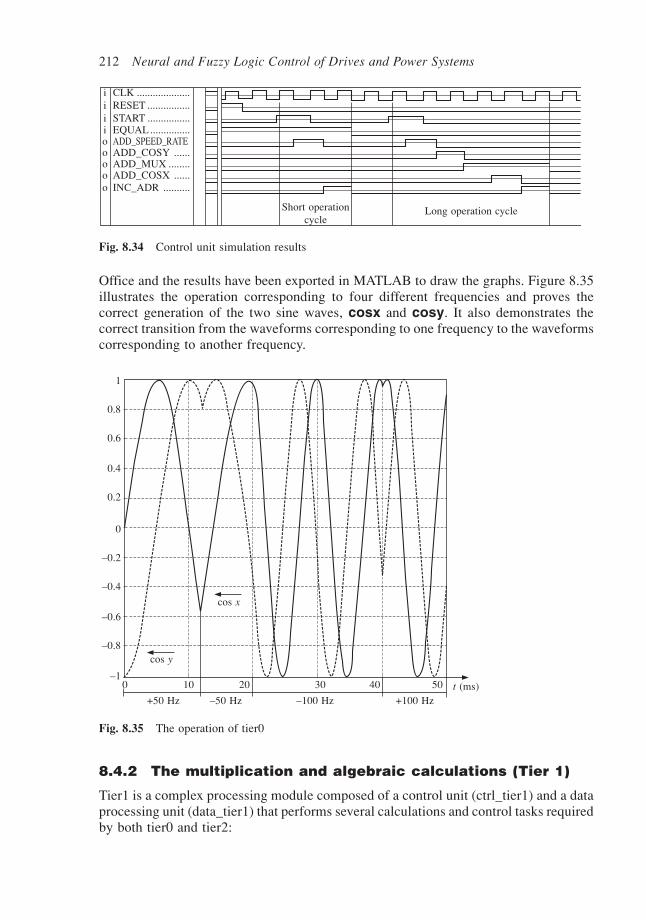
212 Neural and Fuzzy Logic Control of Drives and Power Systems
Office and the results have been exported in MATLAB to draw the graphs. Figure 8.35illustrates the operation corresponding to four different frequencies and proves thecorrect generation of the two sine waves, cosx and cosy. It also demonstrates thecorrect transition from the waveforms corresponding to one frequency to the waveformscorresponding to another frequency.
Fig. 8.34 Control unit simulation results
i CLK ....................i RESET ................i START ................i EQUAL ...............o ADD_SPEED_RATEo ADD_COSY ......o ADD_MUX ........o ADD_COSX ......o INC_ADR ..........
Short operationcycle
Long operation cycle
Fig. 8.35 The operation of tier0
1
0.8
0.6
0.4
0.2
0
–0.2
–0.4
–0.6
–0.8
–1
cos x
cos y
0 10 20 30 40 50
+50 Hz –50 Hz –100 Hz +100 Hzt (ms)
8.4.2 The multiplication and algebraic calculations (Tier 1)
Tier1 is a complex processing module composed of a control unit (ctrl_tier1) and a dataprocessing unit (data_tier1) that performs several calculations and control tasks requiredby both tier0 and tier2:

Neural current and speed control of induction motors 213
• Controls the operation of the two A/D converters connected to Hall sensors thatmeasure the stator currents of the motor.
• Uses the digital output from the A/D converters to calculate the stator current spacevector.
• Determines the derivative of the current space vector and uses this information tocalculate the non-inductive space vector Vni .
• Calculates the space vector V∆ = u(k) – Vni(k – 1), which is used by tier2 to estimatethe inductance in the equivalent R–L–e circuit.
• Calculates the vector speed_rate used by tier0.• Calculates the rectangular coordinates of the reference stator current by multiplying
the unit vector produced by tier0 with the amplitude calculated by tier3.• Performs adjustments of the numerical values supplied to the neural network located
in tier2, so that the network operation speed is maximised.
To achieve all these tasks, tier1 needs to perform several multiplications. There arenumerous multiplier hardware architectures reported in the literature [233], [234], [151],[91]. They differ in hardware complexity and operating speed. The fastest multipliersuse combinational architectures but unfortunately they have very large hardware complexity.Sequential architectures are more compact but at the same time they are slower. Tooptimise both the speed of the motor controller and its complexity, a single fast multiplieris used by tier1 to perform all the multiplications. Therefore, all the signals involved inmultiplications have been multiplexed to the inputs of this multiplier.
The VHDL multiplier model developed implements the 2 Nsl – radix multiplicationalgorithm which is flexible as it allows good control over the trade-off between speedand circuit complexity. The multiplication is carried out in several stages using groupsof Nsl bits at a time, where the number Nsl is the multiplier’s step length. If Nsl is 1 theclassical Booth architecture is obtained. This generates a very compact but slow multiplier.If the value of Nsl is larger than 1 then faster multipliers are obtained but they occupymore space on the chip. The fastest architecture is obtained when Nsl equals the lengthof the second operand. In this case, the corresponding hardware multiplier has a purelycombinational structure, which makes it space inefficient but very fast.
The VHDL multiplier model uses three generic parameters that define the length ofthe two operands and the step length, as shown in Code Fragment 8.10. These parametersallow the adaptation of the multiplier to any application requirements referring to speed,operand size and hardware complexity.
—— Code Fragment 8.10entity smultiplier is
generic(n,m,step_length: integer);port (a: in STD_LOGIC_VECTOR (n-1 downto 0);
—— Can be only positiveb: in STD_LOGIC_VECTOR (m-1 downto 0);
—— Can be both positive and negativeprod: out STD_LOGIC_VECTOR (n+m-1 downto 0);clk,start: in STD_LOGIC;ready: out STD_LOGIC);
end smultiplier;

214 Neural and Fuzzy Logic Control of Drives and Power Systems
The fact that all the multiplications required by the motor control algorithm involve asigned operand and an unsigned operand has been exploited to optimise the structure ofthe controller. Thus, a specialised multiplier has been created, which has an unsignedinput bus (b) and a signed one (a). The multiplication process is composed of a seriesof simple operation cycles. Each cycle consists in multiplying the operand a with theleast significant Nsl bits of b and adding the result into a shift register. Both the resultand the operand b are then shifted with Nsl positions to the right. The architecturecomprises two shift registers, a control unit and a reduced size combinational multiplierwith input buses of width equal to the size of a and Nsl, as illustrated in Fig. 8.36. Themultiplication process is triggered by the start input signal. When this signal is active(is ‘1’) both the control unit and the multiplication result register are reset. When startreturns to ‘0’, the control unit initiates the multiplier operation by activating the signalfirst_step which causes the operand b to be loaded into the corresponding shift register.After b has been loaded, the series of calculation cycles commences. During each cycle,the load_step signal is activated first and then shift_step is activated. After the shift,the most significant Nsl bits of the two registers in Fig. 8.36 are padded with zeroes.
Fig. 8.36 Flexible multiplier structure
Multiplication result (int_prod)
Reset Load Shift AB
Shift
Load
Step length
Shift_stepFirst_step Load_step
Control unit
Start Clk
Adder
Reduced size combinationalmultiplier
The number of necessary calculation cycles is given by the VHDL constant nstepsthat depends on the length of b (parameter m) and on the step length Nsl, according toequation
nsteps = ceiling (m/Nsl) (8.96)
where the function ‘ceiling’ generates the smallest integer that is larger than its argument.Signal count is loaded with value nsteps when the input signal start is activated, andit is decreased at each calculation cycle simultaneously with adding the partial multiplicationresult to the result register. If count is larger than 1 then the two registers are shiftedand a new cycle is initiated, otherwise the calculations are stopped and the ready signalis activated.
The VHDL model of the control unit, shown in Code Fragment 8.11, operates with

Neural current and speed control of induction motors 215
five different states (s0, s1, s2, s3, s4), each of them activating one of the control signalspreviously discussed.
—— Code Fragment 8.11type state is (s0,s1,s2,s3,s4);
signal s: state;constant nsteps: integer := (m+step_length-1)/step_length;process(clk,start)
beginif start=‘1’ thens<=s0;count<=nsteps;elsif clk=‘1’ and clk’event thencase s iswhen s0 => s<=s1;when s1 => s<=s2;when s2 => if count>1 thens<=s3;count<=count-1;elses<=s4;end if;when s3 => s<=s2;when s4 => null;when others => null;end case;end if;end process;first_step <= ‘1’ when s=s1 else ‘0’;load_step <= ‘1’ when s=s2 else ‘0’;shift_step <= ‘1’ when s=s3 else ‘0’;ready_int <= ‘1’ when s=s4 else ‘0’;ready<=ready_int;
This algorithm is applicable only to positive values. Therefore, if the operand b ispositive then the multiplication result is the value stored in the result register after thecalculation sequence has finished. Otherwise, this result has to be transformed into avalid two’s complement codification of the negative multiplication result. Thistransformation is based on the next considerations:
• If b is a negative number then ‘2m – b’ which is its two’s complement is a positivenumber.
• If b is replaced by ‘2m – b’ in the multiplication process, the result is ‘(2m – b) ⋅ a’that has the same module as the correct result but it has the opposite sign.
• The correct multiplication result is obtained by reversing the sign of the previousexpression. Therefore, the calculation formula is: a ⋅ b–2m ⋅ a.
The VHDL implementation of this principle is described by the process in Code Fragment8.12, where the information is transferred from the internal register int_prod to theoutput port prod in two manners, depending on the most significant bit of b. If b(m –1) = ‘0’ then the operand b is positive and the internal information is copied to the outputport, while if b(m – 1) = ‘1’ then the previous calculation formula is used.

216 Neural and Fuzzy Logic Control of Drives and Power Systems
—— Code Fragment 8.12process(a,b,int_prod)
beginif b(m-1)=‘0’ thenprod<=int_prod(n+m-1 downto 0);elseprod<=int_prod(n+m-1 downto 0) - (a & zeroes(m));end if;end process;
Figure 8.37 presents the pipelined architecture of data_tier1 that includes the multiplierpreviously discussed. The first operation performed is the calculation of the rectangularcomponents ix and iy of the stator current space vector. The calculation is carried outusing a modified form of the classical conversion equations. Thus, the two componentsare replaced by equivalent values that are rescaled to limit their maximal values and tolimit the number of bits necessary to be allocated for each of them. The rescalingtechnique allows a good control over the number of bits used by each internal signal, buton the other hand decreases the calculation precision of data_tier1. Furthermore, therescaling factors need to be taken into account by the subsequent calculations thatinvolve the equivalent quantities. The simulation and the synthesis results showed thatrescaling with 0.5 offers the best trade-off between precision and hardware complexity.Therefore, the calculations are performed according to:
i i ii
i
i i i ii
ii
ii
x a xx
a
y b a yy
ba
ba
= 32
= 2
= 34
= 32
(2 + ) = 2
= 32
+ 2
= 0.866 + 2
eqv
eqv
⋅ ⇒ ⋅
⋅ ⇒ ⋅
⋅
(8.97)
The multiplication with 0.866 required in (8.97) is performed by the multiplier integratedin data_tier1. Once the two rectangular components have been determined, the currenterror vector ∆iref(k) = iref(k + 1) – i(k) and the current variation ∆i(k) = i(k) – i(k – 1) arecalculated by simple subtracters. The components of ∆i(k) are multiplied with the estimatedinductance L and subtracted from the corresponding voltage components to determinethe vector Vni, which is used by both the neural network generating the PWM signal andby data_tier1 to calculate the vector V∆. The adapter blocks included in Fig. 8.37 enhance theoperational precision of the angle subnetwork inside the neural network contained by tier2.
The angle subnetwork calculates the argument of a space vector based on its rectangularcoordinates. The number of input bits of the angle subnetwork is smaller than the totalnumber of bits of the two coordinates. Therefore, it uses only the most significant n bitsof these coordinates. If the two values are small numbers, the most significant bits areall ‘0’ or all ‘1’ (depending on the sign of the numbers) and an incorrect result is generated.
The adapter simultaneously shifts the two coordinate values to the left until theirleftmost n positions contain significant bits. Shifting a binary number to the left isequivalent to a multiplication by a power of two. As the two coordinates are simultaneouslymultiplied with the same power of two, the adapter amplifies the module of the vectorbut leaves the vector argument unchanged.

Neural current and speed control of induction motors 217
The VHDL model of the adapter has two main input ports inbusa and inbusb (theinitial two coordinates) and two main outputs outbusa and outbusb, as shown inCode Fragment 8.13. The generic parameter ‘n’ defines the width of the input and theoutput buses. It has to be set in accordance with the width of the VHDL signals to whichit is connected. All the signals in this tier have correlated widths that are primarilydetermined by a generic parameter ‘ni’ which determines the width of the buses ia andib presented in Fig. 8.37.
—— Code Fragment 8.13entity adapter is
generic(n: integer);port (inbusa: in STD_LOGIC_VECTOR (n-1 downto 0);inbusb: in STD_LOGIC_VECTOR (n-1 downto 0);outbusa: out STD_LOGIC_VECTOR (n-1 downto 0);outbusb: out STD_LOGIC_VECTOR (n-1 downto 0);clk: in STD_LOGIC;ld: in STD_LOGIC;ready: out STD_LOGIC);
end adapter;
The additional input ld triggers the shifting process while ready signals the momentwhen the process is finished. Each step of the process is synchronised by the clocksignal clk. The method to determine the end of the process is to test the most significanttwo bits in each of the two partial results. If any of the two pairs contains different bitsthen the process must stop to avoid an overflow that would change the sign of at leastone of the coordinates.
The process must also be stopped if all the bits are zero in the same time. Thishappens when both input coordinates are simultaneously zero, which would cause aninfinite shifting process. The architecture of the adapter contains two VHDL processes:the first shifts the two input values in a synchronised manner, while the second verifiesthe existence of non-zero bits and communicates the result through the internal signalnot_all_zero:
—— Code Fragment 8.14architecture adapter_arch of adapter is
signal int_busa,int_busb: STD_LOGIC_VECTOR(n-1 downto 0);signal not_all_zero: std_logic;
beginprocess(ld,clk,inbusa,inbusb)beginif clk=‘1’ and clk’event thenif ld=‘1’ thenint_busa<=inbusa;int_busb<=inbusb;ready<=‘0’;elsif (int_busa(n-1)=int_busa(n-2)) and(int_busb(n-1)=int_busb(n-2))and (not_all_zero=‘1’) then

218 Neural and Fuzzy Logic Control of Drives and Power Systems
int_busa<=int_busa(n-1) & int_busa(n-3 downto 0) & ‘0’;int_busb<=int_busb(n-1) & int_busb(n-3 downto 0) & ‘0’;else
Fig. 8.37 The structure of data_tier1
ia/4
/8 / 2
ib
ixiy
+ +add
+ +add
Reset
ld_i
rstload
reg rstloadreg
rstload
reg rstreg load
ld_i
ld_i
reset
rstloadreg
ld_i
rx
+ –sub
+ –sub
– +subad
r_a
Mux
Mux adr_b
Multiplier
ready_disadapter
rst load
ld_d
i
ld_e
rri
adapterrstload
outbusa outbusb outbusa outbusb
ready_erris
∆irefdi
abc
uyux
ready_m
start_mabc
+ –sub
– +sub
+ –sub
– +sub
ld_V
lx
ld_V
ly
reg load reg loadready_V2s adapter
load
ld_V2
outbusa outbusb
ld_V
r
reg load
R·ix
+ –sub
Vni-x Vni-y
reg load
speed_rate
ld_s
peed
_rat
e
ready_es
outbusa outbusb
ld_e
e
adapterload
– +sub
rstreg load ↑I
d_ir
y
V∆
I yrefix
ref

Neural current and speed control of induction motors 219
ready<=‘1’;end if;end if;end process;
process(int_busa,int_busb)variable x: std_logic;beginx:=‘0’;for i in 0 to n-1 loopx:=x or int_busa(i);x:=x or int_busb(i);end loop;not_all_zero<=x;end process;outbusa<=int_busa;outbusb<=int_busb;
end adapter_arch;
Figure 8.38 presents the state diagram that describes the operating sequence of tier1,which is controlled by ctrl_tier1 modelled as a pair of correlated state machines. Thefirst dictates the sequence of mathematical operations performed by tier1 while theother controls the interface with the A/D converters. The A/D circuits TLC1550 producedby Texas Instruments [1] have been used, as they offer the advantage of integrating thesample-and-hold circuit, an internal clock oscillator and the digital converter itself inthe same chip. Moreover, this type of chip can be easily interfaced with other digitalcircuits due to the 3-state parallel port, and it can be addressed as an external memorydevice. Thus, it has an RD input pin that triggers the conversion and an active low EOCoutput pin that signals the end of the conversion. The interface state machine activatesRD in state S28 and then waits for the conversion to finish. After each conversion, itloads the information in the specialised registers, as shown in Fig. 8.38 correlated withFig. 8.37.
The operation of the first state machine in Fig. 8.38 is described by a linear sequenceof states which controls the multiplier, the associated multiplexers and loads each partialresult in the specially allocated register. The activity of the two state machines is correlatedby means of the internal signal RdNow that is used to indicate the moments when theanalogue to digital conversion is finished. Each operation cycle of ctrl_tier1 is triggeredby the start_tier1 signal, which has a frequency of 150 kHz and it is generated byctrl_tier0. As a result, the A/D converters are activated with the same frequency andtherefore the sampling frequency of the motor controller is 150 kHz as well.
8.4.3 The PWM generation and on-line inductanceestimation (Tier 2)
The data processing unit of tier2 named data_tier2 (Fig. 8.39) contains the PWM signalgenerator, which includes the new neural network architecture presented at the beginningof this example, the on-line inductance estimator and the motor slip calculator. All thesethree digital structures use information provided by the angle subnetwork. Thus, theinductance estimation is performed by comparing the arguments of vectors ∆i(k), ∆i(k– 1), V∆(k), the motor slip is calculated as the difference between arge and argis,

220 Neural and Fuzzy Logic Control of Drives and Power Systems
while the PWM generation requires the calculation of arg∆iref. This implementationsolution reduces the hardware complexity of the motor controller because the sameneural structure is used for three different purposes.
The structure of data_tier2, shown in Fig. 8.39, includes three registers that areconnected to the angle subnetwork and store the output codes associated with the vectors∆i(k), ∆i(k – 1), V∆(k) calculated by tier1. They provide this information to an analysis
ctrl_tier1
//diagram ACTIONS
ld_V1y
ready_m
EOC1
startreset
clk
EOC2ld_speed_ratemux_adrb[2:0]
mux_adra[1:0]
ld_iry
ld_irx
start_m
ld_errild_V2
ld_e
ld_di
ld_i
ld_sinxy
RD
start_tier2
RdNow
ld_Vr
ld_V1x
Sreg0mux_adra<=“10”;
mux_adrb<=“100”;ld_V2<=‘1’;
mux_adra<=“10”;mux_adrb<=“000”;
start_m<=‘1’;
reset=‘1’ start=‘1’
start_m<=‘1’;mux_adra<=“10”;
mux_adrb<=“001”;ld_speed_rate<=‘1’;
ready m=‘1’
ready m=‘1’
ld_Vr<=‘1’;mux_adrb<=“010”; start_m<=‘1’;
ready m=‘1’
ready m=‘1’
ready m=‘1’
ready m=‘1’
ld_irx<=‘0’;ld_iry<=‘0’;start_m<=‘0’;ld_di<=‘0’;ld_erri<=‘0’;ld_e<=‘0’;ld_V2<=‘0’;ld_V1x<=‘0’;ld_V1y<=‘0’;ld_Vr<=‘0’;ld_sinxy<=‘0’;ld_speed_rate<=‘0’;start_tier2<=‘0’;
start_m<=‘1’; mux_adrb<=“011”; ld_irx<=‘1’;
ld_iry<=‘1’;
ld_di<=‘1’;ld_erri<=‘1’;ld_sinxy<=‘1’; start_m<=‘1’;
mux_adra<=“10”;mux_adrb<=“100”;
ld_e<=‘1’,start_tier2<=‘1’;
ld_V1y<=‘1’; start_m<=‘1’;mux_adrb<=“101”;
ld_V1x<=‘1’;
RdNow<=‘1’;ld_i <=‘1’;RD<=‘0’;RD<=‘1’;RdNow<=‘0’;
(EOC1 or EOC2)=‘0’
start=‘1’
ld_i1<=‘0’;ld_i2<=‘0’;
Sreg1
reset=‘1’
S1 S2 S3 S4
S8 S7 S6 S5
S9 S10 S11 S12
S17
S18
S27 S37
S19
S16 S15 S14 S13
S22
S23
S30S31S29S28
S26 S25 S24
S20 S21
Fig. 8.38 The state diagram of ctrl_tier1
RdNow = ‘1’;

Neural current and speed control of induction motors 221
module that controls the inductance updating block, which increments or decrementsthe value of the inductance, depending on the relative position between the three vectors.The induction estimation result is loaded into a register whose ‘load’ input is validatedby comparing the reference rotor frequency with the upper limit of 10 Hz. It was shownin an earlier section that the induction estimation errors increase with increasing statorfrequency. It is also demonstrated that stator frequency increases linearly with the rotorsteady-state angular speed. Thus, the inductance estimation errors can be maintainedlow if the estimation process is performed only at low rotor reference speed. The‘frequency check’ block in Fig. 8.39 compares the reference speed with the upper limitand validates the estimate signal generated by ctrl_tier2 only if the reference speed issituated below this limit. Otherwise, the estimated inductance L is unchanged.
Fig. 8.39 The RTL description of data_tier2
a b c d e f
αeqv equivalent slip angle
Reduction to thefirst quadrant
α slip anglesub
– +PWM inverter interface
ref.speed
Frequencycheck
estimate
a b c
ld_a
bc
clk
Validationblock
ld_r
eg
reg
ld ld_s
lip_
angl
e
reg
ld
ld_e
s
reg
ld
reset Inductance updating
reset block load
+ –
Analysis moduleConversion to two’s
complement
Control subnetwork
Position calculationsubnetwork
Angle calculationsubnetwork
Vnix Vniy
Vni
outmux
e i V∆ ∆iref ∆i
ld_dis reg
ld
reg
ld
reg
ld
ld_d
is
ld_V
2s
According to the induction estimation algorithm discussed in Chapter 4, the analysismodule has to determine which vector (∆i(k), ∆i(k – 1) or V∆(k)) is situated between theother two. As demonstrated earlier, the angle subnetwork divides the 360° interval intoa number of equal sectors. All the output codes associated with space vectors thatbelong to a given group of consecutive sectors correspond to binary codes that share acertain number of identical bits. One space vector is situated between the other two ifit is included in the group of sectors delimited by the two vectors. Therefore, the relativeposition of the space vectors can be determined by analysing the codes associated withthe angle subnetwork.
L
reset
adr_net

222 Neural and Fuzzy Logic Control of Drives and Power Systems
The method is illustrated by an example in Table 8.3 that involves three vectors v2,v4, v6 situated in the sectors 2, 4 and 6. It can be calculated that v4 lies between v2 andv6 because the code associated with v4 shares the bits b5 and b0 with the codes correspondingto v2 and v6. On the other hand, the vectors v2 and v4 share the bits b5, b2, b1, b0.Therefore, v6 is not situated between v2 and v4 because the code of v6 does not share thebits b2 and b1 with the other two codes.
Table 8.3 The output codes of an angle subnetwork with n = 6 neurones
Sector index Angle interval Codeb5 b4 b3 b2 b1 b0
1 [–15°; 15°) 0 0 0 0 0 0
2 [15°; 45°) 1 0 0 0 0 0
3 [45°; 75°) 1 1 0 0 0 0
4 [75°; 105°) 1 1 1 0 0 0
5 [105°; 135°) 1 1 1 1 0 0
6 [135°; 165°) 1 1 1 1 1 0
7 [165°; 195°) 1 1 1 1 1 18 [195°; 225°) 0 1 1 1 1 19 [225°; 255°) 0 0 1 1 1 1
10 [255°; 285°) 0 0 0 1 1 111 [285°; 315°) 0 0 0 0 1 112 [315°; 345°) 0 0 0 0 0 1
The PWM inverter interface transforms the 3 bits ‘abc’ defining the desired inverteroutput voltage into a vector with six control signals ‘abcdef’ that are transmitted to thepower transistors. The edges of the signals controlling the transistors in the same inverterleg (a–d, b–e, and c–f) do not simultaneously occur so that short-circuits are avoided.
Thus, a transistor is turned on at 2.5 µs after its counterpart in the inverter leg hasbeen turned off. This is achieved by using the hardware structure in Fig. 8.40 where thecontrol signals are generated by AND gates whose outputs depend both on the currentbits and on the previous bits generated by the neural network.
The previous bits are stored into a 6-bit register that is loaded at 2.5 µs after theneural network new output has been transmitted to the interface block. If one of the bitswas previously ‘1’ while the current value is ‘0’, then the corresponding AND gateoutput changes from ‘1’ to ‘0’ immediately. If the previous value was ‘0’ and the currentvalue is ‘1’ the AND gate output transition cannot occur immediately because the gateinputs are different for a period of 2.5 µs. The 2.5 µs delay is generated by a down-counter that is reset by the same signal ld_reg which loads the ‘abc’ register (Fig. 8.39).
The signal ld_reg is generated by the validation block, which is a modulo 9 counter.Therefore, the frequency of ld_reg is ten times smaller than the frequency of ld_abc.The signal ld_abc is activated once during each operation cycle of the motor controller.The operation cycles are initiated by tier0 with a frequency of 150 kHz, which entailsthat the signal ld_reg has a frequency of 15 kHz. Therefore, in this configuration thefrequency of the PWM signal generated by the motor controller is 15 kHz.
The control unit of tier2 (Fig. 8.41) synchronises the operation of the multiplexerconnected to the angle subnetwork in Fig. 8.39 with the activity of the registers and the

Neural current and speed control of induction motors 223
operation of the inductance updating block. The operation cycle of the control unit isdescribed by Fig. 8.41 and it consists of the following steps:
1. The stator current vector is supplied to the angle subnetwork and after the calculationsthe 3-bit vector abc is loaded in the corresponding register.
2. The shifted components of vector e are analysed and the corresponding value isstored in the specialised register by activating signal ld_es.
3. The angle of the current space vector is is determined and the quantity proportionalwith the slip angular frequency is determined.
4. The code corresponding to the argument of the vector V∆ is calculated and stored ina register.
5. The argument of ∆i(k) is calculated and it replaces the value of ∆i(k – 1) which istransferred into a second register (Fig. 8.39).
6. Once the angle codes associated with the three vectors ∆i(k), ∆i(k – 1), V∆(k) areknown, their relative position is analysed by the corresponding combinational moduleand then the estimated value of L is updated. It can be increased, decreased or leftunchanged.
Each operation cycle starts when the necessary input information, calculated by tier1, isavailable on the input ports of tier2. The appropriate moment to start the operation oftier2 is indicated by the signal start_tier2 generated by tier1. On the other hand,ctrl_tier2 waits for the four adapters included inside tier1 to finish their shifting tasks.As shown in Fig. 8.41, the signals ready_erris, ready_es, ready_V2s and ready_disgenerated by the adapters in Fig. 8.37 are used to test the validity of the input before itis processed by the angle subnetwork.
a b c d e f
clk
resetRegister
Counterclk reset
resetclk
ld_reg
A B C
Fig. 8.40 The PWM inverter interface

224 Neural and Fuzzy Logic Control of Drives and Power Systems
8.4.4 The implementation of the speed controlstrategy (Tier 3)
Tier3 calculates the stator frequency and the stator current amplitude using the slipangle and the rotor reference speed. The calculations are performed according to thecontrol principles discussed. The simplified function FI using a single proportionalityconstant KI has been used to minimise the hardware structure of this tier. To simplify theVHDL model even further, the multiplication with KI has been modelled as a set ofshifts and additions as follows:
—— Code Fragment 8.15process(beta) —— Multiplication by 0.101B=0.625
variable x: std_logic_vector(7 downto 0);begin
x:=beta & “0000”;x:=beta+beta(3) & beta(3) & beta & “00”;
Ki_times_beta<=x;end process;
The approach is advantageous when KI contains a large number of ‘0’ bits but a smallnumber of ‘1’ bits. The current increments calculated using FI are accumulated in aspecialised register. The accumulation process can be inhibited if Is decreases under the
//diagram ACTIONS
ctrl_tier2ready_V2s
ready_dis
resetclk
ready_erris
ready_es
start_tier2
ld_dis
ld_V2s
ld_esld_slip_angle
estimate
adr_nn[2:0]
ld_abc
Sreg0 adr_nn<=“000”;
ld_es<=‘0’;ld_V2s<=‘0’;ld_abc<=‘0’;estimate<=‘0’;ld_dis<=‘0’;ld_slip_angle<=‘0’;
reset=‘1’S1 S2 S3 S4
ld_abc<=‘1’;adr_nn<=“001”;
ld_es<=‘1’;
(start tier2 and ready erris=‘1’ready es=‘1’
ready_V2s=‘1’
ld_V2s<=‘1’;adr_nn<=“011”; ld_slip_angle<=‘1’;
S5S6S7S8
ready_dis=‘1’
adr_nn<=“100”;ld_dis<=‘1’;
adr_nn<=“010”;
estimate<=‘1’;
S9 S10 S11
Fig. 8.41 The state diagram of ctrl_tier2

Neural current and speed control of induction motors 225
limit Is-min or increases over Is-max, thereby maintaining the current amplitude within theacceptable range of values (Fig. 8.42). The speed derivative function Fω has been
Fig. 8.42 The structure of tier3
Stator frequency
mux
add+ +
add+ –
Ωslpupdate
reset
Frequencyregister
Current amplituderegisterclk reset
Update
Limit check
Add+ + add
+ +add
+ –
sub+ –
sub– +
sign
bit
sign
bit
mux
Speed derivative
Actual rotor speedReferencce
rotorspeed
Equivalentslip angle
Referenceangle
Starter currentamplitude
implemented as a look-up table. The angle neural network divides the 360° interval into36 sectors, which means that only nine sectors are allocated to each quadrant. Therefore,the look-up table is small and can be modelled by a case VHDL statement:
—— Code Fragment 8.16process(alpha)begin
case alpha iswhen “0000”=> F_omega<=”00011”;when “0001”=> F_omega<=”00011”;when “0010”=> F_omega<=”00011”;when “0011”=> F_omega<=”00100”;when “0100”=> F_omega<=”00110”;when “0101”=> F_omega<=”01000”;when “0110”=> F_omega<=”01010”;when “0111”=> F_omega<=”01100”;when “1000”=> F_omega<=”01110”;when others=> F_omega<=”01111”end case;
end process;
The approach has the advantage that non-linear versions of Fω can be implemented with

226 Neural and Fuzzy Logic Control of Drives and Power Systems
the same hardware resources as the piecewise linear versions. The values generated byFω are always positive and are added or subtracted depending on the difference betweenthe reference speed and the calculated speed of the rotor. Furthermore, the constantquantity Ωslp needs to be added to or subtracted from the previously obtained resultdepending on the sign of the reference speed. All these situations are analysed by thesimple interconnection of adders, subtracters and multiplexers shown in Fig. 8.42.
The operation of tier3 does not require a control unit. All the results are updated whenthe input signal update is activated by tier2. This input signal is connected to the signalestimate generated by ctrl_tier2. The signal estimate is activated at the end of theoperation cycle of tier2 after the motor slip angle has been calculated. Therefore, itindicates an appropriate moment for tier3 to perform its calculations as the slip angleαeqv is one of the two input data used by this tier.
8.4.5 The complete motor controller simulations
A VHDL test-bench can be developed by combining the model of the complete controllerwith the VHDL model of the three-phase induction motor presented earlier. Severalsimulations have been performed using a Workview Office software package with differentvalues of the generic parameters involved in the controller description, in order to testits correct operation. The simulations demonstrate the controller capability to generatecorrect PWM signals (Fig. 8.43), to accurately control the stator current and to determinethe motor equivalent inductance.
/abcdef(5)
/abcdef(4)
/abcdef(3)
/abcdef(2)
/abcdef(1)
/abcdef(0)
16 m 16.5 mTime (seconds)
Fig. 8.43 Motor controller simulation results
The precision of the neural network generating the PWM signal is restricted by thelimited number of Voronoi cells. However, given an adequately high number of cells,the operation imprecision is sufficiently low to have a negligible effect on the overalloperation of the drive system. The on-line induction estimation process is affected bythe limited precision of the angle subnetwork involved (±5° error), and as result, thefinal estimated inductance is smaller than the correct value. Figure 8.44 presents acomparison between the simulation results performed in ideal conditions (perfectlyaccurate angle calculations), and the simulation results obtained with the controller

Neural current and speed control of induction motors 227
8.5 FPGA controller experimental results
This section presents experimental results relating to the performance of a completethree-phase induction motor drive system controlled by the new neural FPGA controller.
8.5.1 The drive system
Practical tests have been performed using the FH2 MkIV test-bench produced byTecQuipment [4]. The test-bench offers the facility to mount up to two electrical machines,d.c. and a.c. on the same shaft (Fig. 8.45) and includes speed and torque sensors fortesting the motor operation.
model that performs angle calculations using the hardware implemented angle subnetwork.The inductance estimation inaccuracy causes errors in the calculation of vectors Vni ande but this does not affect their average value over several operation cycles of the controller.Thus, the effect of the inductance estimation error over the motor speed control isminimal due to the high inertia of the rotor that filters out the ripples of the controlsignals, originated by the induction estimation errors. The accuracy of the inductanceestimation can be increased by increasing the number of neurones included in the anglesubnetwork. However, the simulations performed proved that adapting this approachbrings only a minimal improvement to the global behaviour of the drive system whichis not justified due to the increase of the total hardware complexity of the motor controller.The computer simulations demonstrated the adequate operation of the motor controllerincluding the neural network, and a satisfactory capability to control the operation of athree-phase induction motor. After the successful implementation of the motor controllerinto a Xilinx XC4010XL FPGA, it has been tested in conjunction with a small three-phase induction motor (less than 0.5 kW).
L (mH)
Results obtained in ideal conditions
Results obtained with the hardwareimplemented neural network
0 50 100 150 200 250 300 t (ms)
6
5
4
3
2
1
0
Fig. 8.44 Comparison of inductance estimation simulation results

228 Neural and Fuzzy Logic Control of Drives and Power Systems
The laboratory test-bench configuration available includes the FH90 four-pole three-phase cage induction motor and the FH50 d.c. motor (not used in the experiments). Thestator windings are reconfigurable, both ∆-connection and Y-connection being possible.Nevertheless, TecQuipment recommends that the ∆-connection is used. The rated linevoltage is 220 V in this configuration, while the line currents have values of up to 1 A,depending on the load torque. The practical experiments proved that the speed controlprinciples discussed in section 8.3.2 are valid for both Y-connection and ∆-connection.This experimental conclusion is supported by the theoretical possibility of transformingany ∆-connected load supplied by a sinusoidal voltage system into an equivalent Y-connected load. The high frequency harmonics contained by the PWM voltage arefiltered by the motor inductances and therefore the corresponding current harmonics arenegligible. As a result, only the fundamental harmonics of the voltage and current needto be taken into account and the Y-connected equivalent R–L–e circuit is applicable to∆-connected motors as well.
The experimental setup that includes the FH2 MkIV test-bench and the FH90 inductionmotor is presented as a block diagram in Fig. 8.46. The motor is supplied by a PWMinverter bridge SKM40GD132D produced by Semikron [7] which contains 1200 VIGBT transistors. The bridge is supplied with d.c. voltage by a diode rectifier via a low-pass filter. The input voltage of the rectifier can be adjusted using an autotransformer,which allows the smooth control of the d.c.-link voltage. The IGBT transistors in theinverter are controlled by the XC4010XL FPGA controller on the XS40 test board. ThisFPGA is a low voltage device that associates the voltage level of 3.3 V with logic ‘1’ [8].
The voltage level of the control signals is adapted in two stages to the electricalcharacteristics of the power transistors. First, the CMOS interface in Fig. 8.46 amplifies
Fig. 8.45 The FH2 MkIV test-bench

Neural current and speed control of induction motors 229
the output signals of the FPGA to 5 V and supplies them to the transistor driver board.At the same time, the CMOS interface protects the control circuits against the damagingeffects of any failure that may occur in the power circuits. In the second stage, the driverboard amplifies the control signals to 15 V, which is the control voltage level, recommendedby the IGBT manufacturer.
Two of the motor currents are measured using Hall effect transducers that generate avoltage proportional to the measured current, which are then amplified using simpleoperational amplifiers and transmitted to the TLC1550 10-bit A/D converters producedby Texas Instruments [1]. The binary codes produced by the A/D converters are transmittedto the FPGA controller. As mentioned in Chapter 6, the VHDL controller model containsa series of generic parameters defining the size of several internal modules. Many ofthese parameters are correlated and depend on the width ‘ni’ of the two current inputbuses ‘ia’ and ‘ib’. To implement the entire motor controller in a single XC4010XLFPGA, the generic parameter ‘ni’ was limited to eight. Thus, only the eight most significantbits are used by the FPGA controller in this configuration. The reference speed of themotor is set in two’s complement code using a set of eight switches. Consequently, therotor electrical angular frequency ωer can be set at values between –128 and +127 Hz,corresponding to mechanical speeds between –3840 rev/s and +3810 rev/s. The CMOSinterface and the operational amplifiers have been implemented on a single interfaceboard, illustrated in Fig. 8.47 together with the XS40 board.
The parameters of the speed control algorithm implemented by tier3 (see Chapter 6)have been determined based on practical experiments with the motor. The equivalentparameters of the FH90 motor were initially determined. The stator resistance wasdirectly measured, the result being 95 Ω, which is a large value for a three-phaseinduction motor. The equivalent inductance L has been approximated by measuring thevoltages across the motor and currents at 50 Hz stator frequency, with the rotor locked(zero speed). In these conditions, the internal voltage e has a small value and the totalimpedance of the motor is mainly due to the resistance R and the equivalent inductance.
Fig. 8.46 The schematic of the experimental setup
240 V
Auto-transformer
Insulationtransformer 6 mH
470 µFPWM
inverter(SKM40GD132D)
IM3~
Torquegenerator
Speedmeasurement
240 V180 V
Insulationtransformer
Auto-transformer
Driver board forpower transistors
Signalamplification
A/ Dconversion
CMOSinterface
FPGA
XS40 board
Switches

230 Neural and Fuzzy Logic Control of Drives and Power Systems
The measurements and the calculations showed that L is approximately 220 mH. Thecritical slip angular frequency was determined while keeping the stator current constant.This was achieved by connecting the rotor windings to variable resistors as shown inFig. 8.48. The obtained result was ω slp = 95k rad/s corresponding to a speed of1050 rev/s (the rated speed is 1500 rev/s). The equivalent slip angle α eqv
ref has beenarbitrarily set at 65° (according to the considerations in Chapter 4, it can have any valuebetween 45° and 90°). The equation
tan ( ) = –1eqvref slp
slp
ααΩ
k (8.98)
Fig. 8.47 The XS40 board and the interface board
Speedgauge
Torquegauge
IM~3
A
ua
ub
uc
Manual currentcontrol
Fig. 8.48 The measurement of the critical slip at constant current
demonstrated in Chapter 4, yields the value Ωslp = 44.3 rad/s, corresponding to a slipfrequency of 7 Hz. The other parameters that define the speed control algorithm (Kω1,Kω2, βmax, KI) were determined by tuning in practical experiments.

Neural current and speed control of induction motors 231
In conclusion, the main characteristics of the adopted VHDL motor controller are:
• The sampling frequency (tier1) fs = 150 kHz.• The PWM frequency (tier2) fPWM = 15 kHz.• The maximal rotor speed allowing inductance estimation 600 rev/min (10 Hz).• The width of the input buses ia and ib (tier1) ni = 8.• The step length of the multiplier Nsl = 4.• The stator resistance (defined by a constant in the model of tier1): Rs = 95 Ω.• The equivalent slip angle αeqv = 65°.• The reference slip angular frequency Ωslp = 44.3 rad/s.• The parameters defining the speed control dynamics: Kω1 = 650 s–1, Kω2 = 200 s–1,
βmax = 0.7 rad, KI = 1 A/s.• The switching delay between the two transistors in the same inverter leg: 2.5 µs.• The input clock frequency fclk = 12 MHz.• The number of samples used to generate the reference sine wave (tier0): 256.• The number of bits for each entry of the look-up table (tier0): 3.• The number of bits used for the reference motor speed: 8.• The number of inverter output voltages used: 6 out of 7 (the null voltage is not used).• The number of triangular Voronoi cells of the position neural subnetwork: 54.• The number of sectors of the angle subnetwork: 36.• The number of bits used to code the input signals of the position subnetwork: 5.• The number of bits used to code the input signals of the angle subnetwork: 5.
In this configuration, the implementation of the controller took up 98 per cent of thehardware resources available on the XC4010XL FPGA. The values of all the parameterscan be easily modified by altering a series of constants and generic parameters in theVHDL code describing the model of the motor controller. Consequently, given theappropriate FPGA, the controller can be adapted in terms of hardware complexity andoperation accuracy to the requirements of a large range of particular applications.
Two sets of experiments were carried out. The first set verified the PWM voltagegeneration and the current control accuracy, while the second set referred to the speedcontrol performance of the drive system.
8.5.2 Current and voltage control tests
A special version of the controller VHDL model was created for the first set of experiments.This version lacks tier3 so the frequency of the stator current is identical to the frequencyspecified by means of the eight switches and the stator current amplitude is constant.This approach simplifies the testing procedure because it checks the operation of tiers0, 1 and 2 without the feedback signals calculated by tier3 and therefore any operationalerror can be easily located.
Figure 8.49 presents four of the PWM control signals generated by the FPGA motorcontroller. They were monitored using a four-channel Hewlett Packard digital oscilloscope.The waveforms demonstrate the correlation between two of the signals that control thetransistor on the same inverter leg (ctrl(5) and ctrl(2)). Thus, the two signals havecomplementary values: when one of them is ‘0’ the other is ‘1’. The 2.5 µs delaygenerated by the interface block contained in tier2 is not visible in Fig. 8.49 due tothe inappropriate time scale (50 µs/div), but it can be observed in Fig. 8.50 where the

232 Neural and Fuzzy Logic Control of Drives and Power Systems
time scale is 15 µs/div. The overall PWM voltage across the motor can be seen in Fig.8.51.
Fig. 8.49 Four of the FPGA output signals controlling the transistors in the PWM inverter
abcdef(5)
abcdef(4)
abcdef(3)
abcdef(2)
Fig. 8.50 Switching delays produced by tier2 to avoid the short-circuits in the PWM inverter
abcdef(3)
abcdef(0)
Fig. 8.51 The PWM voltage generated by the inverter for a reference stator frequency of 50 Hz

Neural current and speed control of induction motors 233
Figure 8.52 illustrates one of the motor currents corresponding to the operation modegenerated by the voltages in Fig. 8.51. The voltage signal in Fig. 8.52 is acquired fromone of the Hall transducers and its amplitude of 200 mV corresponds to current amplitudeof 0.4 A. Figure 8.53 presents the d.c.-link voltage in the same operation conditions anddemonstrates that the gamma filter composed of the 6 mH inductor and 470 µF capacitorillustrated in Fig. 8.46 is capable of maintaining the d.c. voltage level within acceptablelimits.
Fig. 8.52 One of the stator currents (the stator is Y-connected) measured using a Hall transducer
8.5.3 Speed control tests
The second set of experiments, demonstrating speed control, were carried out using theentire VHDL model of the controller, as presented in the previous chapter. The testswere performed with the stator ∆-connected, but similar results are obtained when the
200 V
Fig. 8.53 The voltage ripple on the d.c. link

234 Neural and Fuzzy Logic Control of Drives and Power Systems
stator winding is Y-connected. The drive system has been tested both in steady-state andin transient operation.
Figure 8.54 compares the steady-state operation of the induction motor with or withoutthe new FPGA controller connected. The reference speed of the controller is 1500rev/s (the rated speed of the FH90 motor). The graphs demonstrate that the controller iscapable of maintaining the rotor speed almost constant despite large variations of theload torque. The improvement brought aboard by the new controller is seen in theimproved speed–torque characteristic. The improvement can be quantified as the speedincrease produced by the controller for each value of the load torque.
Fig. 8.54 The static mechanical characteristic of the motor with and without digital controller
T (Nm)
Natural torque characteristic
Controlled torque characteristic
Speed controlimprovement at
0.5 N.m
n (rev/min)400 600 800 1000 1200 1400 1600
0.9
0.8
0.7
0.6
0.5
0.4
0.3
0.2
0.1
0
Figure 8.55 presents the motor transient response to a fast variation of the torque. Aperfect step variation of the load torque could not be achieved due to the limitations ofthe test-bench. However, Fig. 8.55 shows the capability of the FPGA controller tomaintain the speed almost constant while the load torque undergoes significant variationsrelative to the motor rated power. Thus, the increase of the torque causes a slight slowdown of the rotor and this leads to an increase of the motor slip above the imposedvalue. Therefore, the slip compensation mechanism included in the controller increasesthe motor current and boosts the active torque reducing the slip frequency to the initialvalue. The transient process takes approximately 0.8 s.
Figure 8.56 illustrates the motor start-up when the load torque is null. The transientresponse lasts for approximately 0.65 s, after which the motor speed is constant at1500 rev/min.
The load torque during the transient operation illustrated in Figs. 8.57 and 8.58 isproportional to the rotor speed and therefore motor acceleration is more difficult and thetransient response slower. The result in Fig. 8.58 can be compared with the motorstarting characteristic when no speed control system is used (Fig. 8.57). Clearly, theFPGA speed controller improves the dynamic response of the drive system.

Neural current and speed control of induction motors 235
0.8 s
1500 rot/min
Speed
Torque
0.45 Nm
Fig. 8.55 The drive system response to a step change of the load torque
0.65 sec
Speed
1500 rot/min
Torque
0 Nm
Fig. 8.56 The motor start without external load torque
1.2 sec
1500 rot/min
Speed
Torque
0.45 Nm
Fig. 8.57 The natural motor start under load without the FPGA controller

236 Neural and Fuzzy Logic Control of Drives and Power Systems
The improvement is limited by two factors:
• The motor parameters.• The available hardware resources.
The parameters of the motor FH90 are not suitable for sensorless control with highresponse speed because the stator resistance is large (95 Ω) and therefore the resistivevoltage component is large. Furthermore, the motor power is small (approximately0.5 kW) so the amplitude of the internal voltage e is smaller than the resistive voltagecomponent. As a result, the calculated equivalent slip angle αeqv is inaccurate andaffected by large fluctuations during motor operation. These fluctuations tend to causesystem instability, which can be counteracted only by increasing the time constants ofthe system, equivalent to limiting its overall dynamic performance. Nonetheless, thelimitations imposed by the motor parameters are not particular to the new controlmethod developed, they affect most of the sensorless speed control algorithms.
Fig. 8.58 The motor start under load when controlled by the FPGA device
0.75 sec
1500 rot/min
Speed
Torque
0.45 Nm

9.1 System representation
Before commencing an in-depth discussion about the control system, it is appropriate todiscuss the plant, i.e. the elements to be controlled. In this chapter mathematical modelsof some of the control plant elements are described. The plant comprises a powerelectronic system, a permanent magnet synchronous generator and a diesel engine. Twocontrol units are presented in this example, a fuzzy logic controller (FLC) for the engineand a PWM controller for the output inverter. The analysis of the system is divided intotwo parts as shown in Fig. 9.1. Ensuing sections in this chapter discuss the control plantelements relating to the fuzzy logic controller, namely the rectifier, the generator and thediesel engine. The analysis of the inverter and the PWM controller is presented as aseparate section.
9
Fuzzy logic control of asynchronous generator set
Dieselengine
Permanentmagnet
synchronousgenerator
Rectifier
Fuzzy logiccontroller
Inverter
PWMcontroller
Poweroutput
Fig. 9.1 Block diagram of complete system
9.1.1 Rectifier circuit
A circuit diagram of a three-phase uncontrolled (diode) rectifier attached to a Y-connectedsinusoidal voltage source is shown in Fig. 9.2. This circuit is used to convert the a.c.output of the generator terminals into d.c. power. The phases are marked a, b and c. Thebranches of the rectifier bridge are connected to the generator terminals, therefore theline to line voltage vl–l of the rectifier is equal to the generator terminal voltage vt.
9.1.1.1 Voltage analysis
Figure 9.3 shows the waveforms of various voltages taken from the circuit in Fig. 9.2.Waveforms va–n, vb–n and vc–n are the line–neutral voltages of each phase. vdc is the

238 Neural and Fuzzy Logic Control of Drives and Power Systems
instantaneous rectifier output voltage while Vt is the r.m.s. value of the line–line voltage,vt. The mean output voltage Vdc can be obtained by integrating vdc over a period of π /3radians as follows:
V V t t Vt tdc–
6
6 = 1
3
2 cos d = 3 2
πω ω ππ
π
⋅∫
Fig. 9.2 Three-phase uncontrolled rectifier
n
a
b
c
vt
it,a
it,b
it,c
vdc
id,c
Load
Fig. 9.3 Voltage waveforms of rectifier circuit
vac
vdcVdc
va–n vb–n vc–n
ω t
√ 2 Vt
ω t2ππ
6π3
56π 7
6π 3
2π 1
61π
9.1.1.2 Current analysis
The current waveforms of the rectifier circuit are shown in Fig. 9.4. The line currentwaveform it,a is not sinusoidal, therefore the r.m.s. value cannot be obtained simply witha division by √2. From the definition of root mean square, the r.m.s. of it,a is given by
r.m.s. : = + + . . . + 1
222
32 2
Ii i i i
ntn

Fuzzy logic control of a synchronous generator set 239
Taking samples at every π/6 interval,
II I
I It t = [4 ( ) ] + [4 (– ) ] + [4 0 ]
12; = 2
3 dc
2dc
2 2
dc× × × ⋅
9.1.2 Synchronous generator
9.1.2.1 Voltage analysis
The operation of the synchronous generator is based on Faraday’s law of electromagneticinduction which states that: The total electromagnetic force (e.m.f.) generated in aclosed circuit is equal to the negative time rate of change of the flux linkages linking thecircuit.
This law was derived from Faraday’s observation that an e.m.f. is induced in aconductor or circuit placed in a magnetic field when there is a change of flux linkageslinking the circuit. The flux changes can be the result of a relative motion between thecircuit and the flux or the effect of a varying magnetic flux. Faraday’s law can berepresented by the following equation:
e tt
( ) = – dd
λ
where e(t) is the generated e.m.f. and λ is the flux linkage. In a synchronous machine,the magnetic flux is provided either by a permanent magnet or an electromagnet, placedinside a set of windings as shown in Fig. 9.5. The flux linkages linking the winding arevaried by physically rotating the magnet. The rotor can be a permanent magnet, or anelectromagnet with a field winding. Electromagnet generators are easier to control andtherefore more common. The stator houses the armature windings.
The armature windings are the windings in which the e.m.f. is induced. Figure 9.5shows a three-phase synchronous machine, with armature windings marked aa′, bb′,and cc′. If the angular velocity of the rotating field in radians per second is ω, then:
ϕ = ωt (9.1)
Considering only phase a, if the rotor moves by an angle ϕ, the flux linking aa′ is givenby,
Fig. 9.4 Current waveform of rectifier circuit
ωt
2π
ω t
Idc
Idc
idc
it,a
π6
π3
56π 7
6π 3
2π 1
61π

240 Neural and Fuzzy Logic Control of Drives and Power Systems
λ = Nφ cos ϕ (9.2)
where N is the number of turns in aa′ and φ is the airgap flux. Therefore, the e.m.f.induced per phase is given by
et t
Nta = –
dd
= –dd
dd
= ( sin ) dd
λ λϕ
ϕ φ ϕ ϕ⋅ ⋅ ⋅ ⋅ (9.3)
Substituting ϕ for ωt and dϕ/dt for 2πf yields
ea = 2πf N φ sin ωt (9.4)
In practice, the constructions of the machine, such as the pitch and distribution of thecoils, assert influence on the waveshape of the induced e.m.f. A reduction factor knownas the winding factor KW has to be applied to account for this. Therefore, the inducede.m.f. per phase becomes
ea = 2π fNφKw sin ωt (9.5)
which can also be written as
e E fta i = sin 2ˆ π (9.6)
where Ei is the peak value of the induced e.m.f. and f is its frequency.Using phase a as reference and because phases a, b and c are displaced by 120°, the
voltages for each field are therefore given by
e E f ta i = sin 2ˆ π (9.7)
e E f tb i = sin (2 – 120 )ˆ π ° (9.8)
e E f tc i = sin (2 + 120 )ˆ π ° (9.9)
In machines with more than a pair of poles, the generated electrical frequency f is givenby
f = p . nmech (9.10)
ϕ
a
b′
c
a′
b
c′Magnet
Armaturewindings
ω
Fig. 9.5 Three-phase synchronous machine

Fuzzy logic control of a synchronous generator set 241
where nmech is the mechanical synchronous speed (revolutions per second) and p is thenumber of machine pole-pairs.
9.1.3 Equivalent circuit model
Dynamic models of the synchronous machine can be derived from the generalisedtheory of electrical machines and are widely used in the design of classical controlsystems. The design of the controllers is derived from the plant model. However, becausethe control system presented in this example is not developed from a model of the plant,the accuracy of the model does not directly influence the performance of the design.Instead, the model is used to study the response of the design and to verify its functionalitythrough simulations. Although a dynamic model would provide a more comprehensiveanalysis, the steady-state model is sufficient for the task.
An equivalent circuit model of a synchronous generator can be derived to study thevoltage and current characteristics of the machine. The flow of current in the fieldwinding If induces a flux φi in the airgap which links with the armature winding.Similarly, the flow of current in the armature winding also produces a flux, φa. Thearmature flux φa comprises two components, the armature reaction flux φar, and theleakage flux φal. The larger component, φar, is established in the airgap and links withthe field winding, while φal does not exist in the airgap and links only with the armaturewinding. Therefore, the resultant flux in the airgap φag is made up of φi and φar.
φag = φi + φar (9.11)
φag induces a voltage in the stator winding, Eag which lags φag by 90°. According to thesuperposition theorem, Eag comprises two components, induced by the correspondingflux component. Hence,
Eag = Ei + Ear (9.12)
Ei is the induced e.m.f. also known as the internal generated voltage of the machine. Adiagram of the vectors concerned is shown in Fig. 9.6(a). It shows the armature reactionvoltage Ear, lagging φar and Ia by 90°. In other words, –Ear leads Ia by 90°. A voltageleading a current by 90° can be represented as the voltage drop across a reactance.Hence –Ear can be represented as the voltage drop across a reactance, say Xar, where Xaris known as the magnetising reactance. Therefore, by substituting (–Ear) with (Ia jXar),(9.12) can be rewritten as
Ei = Ia jXar + Eag (9.13)
Figure 9.1(b) shows an equivalent circuit of the model described by (9.13). To includethe terminal voltage per phase Vφ (instead of just the airgap voltage, Eag), the leakagereactance Xal and the effective armature winding resistance Ra have to be taken intoaccount. The effective resistance of Ra is approximately 1.6 times its d.c. resistance asa result of skin effect and operating temperature effects. Figure 9.6(c) shows the completeequivalent circuit of a synchronous machine.
Xar and Xal can be lumped together as a single reactance denoted by Xs, which is knownas the synchronous reactance.
Xs = Xar + Xal (9.14)

242 Neural and Fuzzy Logic Control of Drives and Power Systems
The synchronous impedance is given by
Zs = Ra + jXs (9.15)
The steady-state mathematical model of the synchronous machine can therefore bedescribed by the equation
Ei = Ia(Ra + jXs) + Vφ (9.16)
The equivalent circuit model is a steady-state model and does not provide any informationabout the dynamics of the machine. Transient response to load changes, faults and otherdisturbances cannot be properly analysed using this model. Dynamic models of thesynchronous machine can be derived from the generalised theory of electrical machinesand are widely used in the design of classical control systems. The design of the controllersis derived from the plant model.
9.1.4 The generator–rectifier model
From (9.5) and (9.10), the peak value of the internal generated voltage is found to be
E N K pni w = 2 mechπ φ (9.17)
Because the generated voltage is sinusoidal, its r.m.s. value is given by
E N K pni w = 2 mechπ φ (9.18)
For an electromagnet generator the flux in the machine is controlled by its field current.The relationship between the flux and the field current can be observed by performingan open circuit test on the machine and plotting the results on an ‘Ei vs. If’ graph whichis sometimes called the open circuit characteristic (OCC) plot. Details of the test can befound in any text book on electrical machines. Figure 9.7 shows a typical OCC plot ofa synchronous generator. The curve is observed to be linear until some saturation startsto occur at high field current. This is due to iron saturation in the synchronous generator.
Fig. 9.6 Equivalent circuit model of a synchronous generator
Ia
φ ar
–Ear Ear
(a)
IaXar
Ei
(b)
Eag Ei Eag
Xar XalIa
Xs
Ra
Vφ
(c)

Fuzzy logic control of a synchronous generator set 243
From (9.18) and the OCC plot, it can be assumed that flux φ is directly proportional tothe field current If in the linear region. Therefore, φ ∝ If
φ = G ⋅ If (9.19)
where G is the proportionality constant.From (9.16), (9.18) and (9.19), the synchronous generator can be described by the
steady-state model,
Ei = K ⋅ G ⋅ If ⋅ nmech (9.20)
Vφ = Ei – Ia ( jXs + Ra) (9.21)
where K N K pw = 2 .πEquation (9.20) gives the phase voltage of the generator output. The generator’s terminalvoltage may or may not be the same as its phase voltage, depending on the configurationof its windings. The three phases of a synchronous generator can either be connected ina star (Y) configuration or delta (∆) configuration as shown by Fig. 9.8.
For a Y-connected generator,
V V I It t a = 3 and = φ (9.22)
Fig. 9.7 A typical open circuit plot for a synchronous generator
Ei
If
Linear region
Fig. 9.8 Configuration of generator windings: (a) star-connection; (b) delta connection
Ra
j Xs
Ei3
Vφ
Ra
j Xs
Ei1
IaIt
Vt
Ei2
j Xs
Ra
VφRa
j Xs
Ei3
Ia
Ei1
j Xs
Ra
It
Vt
Ra j Xs Ei2
(a) (b)

244 Neural and Fuzzy Logic Control of Drives and Power Systems
For a ∆-connected generator,
V V I It t a = and = 3φ (9.23)
where:Vt is the generator’s terminal voltageIt is the generator’s terminal currentVφ is the generator’s phase voltageIa is the armature current or the generator’s phase current.
Figure 9.9 shows a block diagram of the synchronous generator model based on theequivalent circuit model. Vt is the complex r.m.s. voltage of the generator terminal. For
nmech
If Gφ
KEi Vφ Vt
+–
Ra
jXs ++
IaIt
Y:1or
∆:1/ 3
Y: 3or
∆:1
Fig. 9.9 Block diagram based on equivalent circuit model
the present application, this model has to be further developed to include a three-phaserectifier and also to consider the torque characteristics as well as the power factor. Aphasor diagram of the generator voltages and currents is shown in Fig. 9.10. The anglebetween the phase voltage Vφ and the internal generated voltage Ei is known as thepower angle δ. For generator operation (as opposed to motor operation), the powerangle is always positive, as shown in Fig. 9.10. The diagram also shows a lagging powerfactor condition whereby the current Ia lags Vφ by an angle θ. The power factor is givenby cos θ.
Ei
δ
θIa
Vφ IaRa
jIaXs
Fig. 9.10 Phasor diagram of a synchronous generator
Using Vφ as reference, the equivalent circuit model can be expressed as
Vφ ∠0° = Ea ∠δ – Ia ∠θ (Ra + jXs)

Fuzzy logic control of a synchronous generator set 245
Vφ = Ei cos δ – IaRa cos θ + IaXs sin θ + j Ei sin δ – IaXs cos θ – IaRa sin θ
Because Vφ is the reference, its imaginary component is zero, therefore,
Vφ = Ei cos δ – IaRa cos θ + IaXs sin θ (9.24)
and Ei sin δ – IaXs cos θ – IaRa sin θ = 0
δ θ θ = sin ( cos + sin –1 IE
X Ra
is a
(9.25)
For a three-phase synchronous generator, power is given by Preal = 3VφIa cos θ.Power is the product of torque and speed, hence the induced torque is
τ ω θφind
mech =
3 cos
V Ia
or
τπ
θφind
mech =
6 cos
V In
a(9.26)
where ωmech is the mechanical speed in radians per second and nmech is the mechanicalspeed in revolutions per second.
Figure 9.11 shows the model that is developed to represent the synchronous generatorand rectifier. The inputs of this model are the rotational speed nmech, field current If,power factor angle θ and the current at the d.c. link Idc, used as a measure of theelectrical load. The outputs are the d.c. link voltage Vdc and the induced torque τindwhich loads the engine. To account for the generator winding configuration (Y or ∆),conversions between the phase values and terminal values of voltage and current arebased on (9.22) and (9.23). The generator phase voltage is obtained from (9.24) and(9.25) while the induced torque is from (9.26).
9.1.5 The diesel engine
The second model to be developed is one for the diesel engine. The operation of dieselengines involves a large number of complex processes, with many delays, lags and non-linearities. It is therefore difficult to develop a comprehensive mathematical model tostudy and analyse the diesel engine. Even manufacturers of control systems and speedgovernors for diesel engines are known to focus on empirical methods rather thantheoretical modelling for analysis. In this book, a model of a diesel engine is requiredto provide a complete representation of the control plant. The aim of this exercise is todevelop a ‘good enough’ model for the functional verification of the control system.Since detailed studies are not necessary at this stage, an approach which favours reducedcomplexity and incorporates a certain degree of approximation is preferred. For thepurpose of speed control studies, the diesel engine can be represented as a combustionsystem and inertia as shown by the block diagram in Fig. 9.12. The combustion systemproduces an engine torque τE as a function of the fuel rack position y. The engine torqueis used to oppose the load torque τL and the difference ∆τ is converted into acceleration/deceleration ∆nmech in the lumped inertia (engine inertia + load ineria).

246 Neural and Fuzzy Logic Control of Drives and Power Systems
When the speed of the engine changes, it moves along the engine’s torque curve asshown in Fig. 9.13. Each engine’s torque curve is specific to a fuelling rate q. For agiven speed, the developed engine torque τE can be increased by increasing q. Anequilibrium point is reached when the engine’s torque curve intersects the load’s torquecurve.
If the engine torque is written as
τE = f(nmech, q) (9.27)
and the equilibrium point for a given operating condition is when
n n q qmech mech = ; = ˜ ˜
then, expanding (9.27) into a Taylor series about the equilibrium point yields
Fig. 9.11 Model of generator–rectifier system
nmech
If
Idc
θ
KGE1
E1
IaIt
Rectifier
Y:1∆:1/√3
θIa δ Ei
Vφ = Ei cos δ + Ia(Xs sin θ – Ra cos θ)
VφθIanmech
τind
Vφ
Vt
Y:√3∆:1
Vdc
Rectifier
yFuel rack position(governor control)
Enginecombustion
system
Enginetorque, τE
+–
∆τ
Loadtorque, τL
Engine andload
inertia, J
∆nmech
Fig. 9.12 Diesel engine and load representation
θ
δ θ θ = sin ( cos + sin )–1 IE
X Ra
is a
23
τ θφ
indmech
= 6
cos πv I
na
v vdc =
3 2π t

Fuzzy logic control of a synchronous generator set 247
τ E f n qf
nn n
fq
q q = ( , ) + ( – ) + ( – )mechmech
mech mech˜ ˜ ˜ ˜∂
∂∂∂
+ 12!
( – ) + ( – )( – )+ ( – ) +. . .2
mech2 mech mech
22
mechmech mech
2
22∂
∂∂
∂ ∂∂∂
fn
n nf
n qn n q q
fq
q q˜ ˜ ˜ ˜
If the operating condition is within the vicinity of the equilibrium point, it can beassumed that the higher order terms are negligible, therefore,
τ E f n qf
nn n
fq
q q – ( , ) = ( – ) + ( – )mechmech
mech mech˜ ˜ ˜ ˜∂
∂
∂∂
τ τE Ef
nn n
fq
q q – = ( – ) + ( – )mech
mech mech˜ ˜ ˜∂
∂
∂∂
(9.28)
Using ‘δ’ to denote small changes about the equilibrium point, this can be written as
δτ τ δ τ δEE
q
E
nn
nq
q = + mech
mech
mech
∂∂
∂∂
(9.29)
At this juncture, a bold step is taken to further simplify the situation by extending theuse of the equation above over the entire range of analysis. It is acknowledged that(9.29) is a linearised approximation which is only valid within the proximity of theoperational point from which the equation is derived. However, this linear model isassumed to be capable of providing at least a qualitative ‘feel’ of the engine’s torque–speed characteristics, even if the quantitative results are only rough approximations. Ithas to be pointed out that these models are not developed to be used as a starting pointfor the design of the control system. The controllers presented are model-free designs,therefore there is no danger of the limitations of the models being translated into thecontrol system. Writing
∂∂
∂∂
τ τ δ δE
q
E
nn
Aq
q B ymech
= and = mech
where δy is the change in fuel rack position y, (9.29) can be written as
δτE = A · δ nmech + B ⋅ δy
Fig. 9.13 Torque–speed characteristics
Torqueτ
T2
T1
N1
Increaseload
L1
L2
q2
q1
Increasefuelling rate
Speed, nmech
Engine torque curve τE
Load torque curve τL

248 Neural and Fuzzy Logic Control of Drives and Power Systems
By extending the linear properties over the entire range of analysis, it can be assumedthat A and B are constants. Therefore, from the superposition principle, the engine’storque curve can be represented by the linear equation:
τE = A · nmech + B · y (9.30)
The net accelerating torque is given by the difference between the engine’s torque andthe load torque:
∆τ = τE – τL
Since ∆ τ ω =
dd
Jtm
where J is the combined moment of inertia of the engine and generator and ωm is themechanical speed in radians per second. It can be shown that the discrete equivalent canbe written as
C n n zT J
( – ) = mech mech
–1⋅ ∆τ
∆ ∆τn
JDmech = (9.31)
where:C is a constantT is the sampling periodD = (T/C)nmech is the mechanical speed in revolutions per second.
A block diagram of a discrete engine model based on (9.30) and (9.31) is shown in Fig.9.14.
τLLoad characteristic
∆τ–
+
τE
++
By
A
Inertia
D
JE + JL
∆nmech nmech
+ +
z–1
Fig. 9.14 Linearised discrete model of the diesel engine
9.2 VHDL modelling
Although VHDL is a hardware description language and is used primarily for circuitdesign, it has the basic properties of any software programming language. It is therefore

Fuzzy logic control of a synchronous generator set 249
capable of implementing mathematical models. Two VHDL components are designed torepresent the models of the generator–rectifier and the diesel engine developed in thischapter. The complete source codes of the models can be found in Appendix E. Sincethe models are initially designed for the purpose of computer simulations and not forhardware implementation, it is possible to declare the signals and variables as the typeREAL. This gives the design a greater freedom in numerical analysis. It is also possibleto incorporate complex mathematical functions such as trigonometry in the design.
The VHDL design of the generator and rectifier model is configured with the entityname Generect. It is designed as a synchronous circuit with five input signals (includingCLK). Three output signals provide simulated information on the generator’s phasevoltage Vph and induced torque TG as well as the d.c. voltage at the rectifier’s outputVdc. As already touched upon earlier in this chapter, the voltages at the generator’sterminals are largely determined by the nature of its winding configuration. Two constants,YD–CURR and VD–VOLT, which have values defined in the declaration section of thedesign architecture sets the configuration of the model. In this, they are defined withvalues that set the model as a Y-connected generator.
The VHDL model for the diesel engine is configured with the entity name Engine.The input signals of the model are load torque TL, control signal to the fuel actuator Y,the clock signal CLK and the sampling period PRD while the engine’s torque TE andspeed NE make up the output signals. It implements the mathematical equations of theengine and, like Genrect, the section of the code that does this is self-explanatory. Aslight addition to the model, to prevent the calculated output values from ‘running away’in the event of simulation errors, is that the output signals are designed to operate withina fixed boundary of values. The maximum and minimum limits of these values are setwithin the code.
Figure 9.15 (a) and (b) show the block diagram of Genrect and Engine respectively.The two components have their respective input and output ports and can be connected
Fig. 9.15 Block diagram of VHDL models: (a) Genrect; (b) Engine
(a)
(b)
IN
IN
IN
IN
IN
IN
IN
IN
VHDL design
CLK Vdc
Ifield TG
Idc Vph
theta
OUT
OUT
OUT
OUT
OUT
VHDL design
CLK TE
TL NE
Y
PRD
Engine
Genrect

250 Neural and Fuzzy Logic Control of Drives and Power Systems
directly to the VHDL designs of the control system for simulation purposes. The use ofthe plant models in conjunction with the control system in a functional simulation willbe discussed later. The PWM inverter is presented in the following chapter. It includessome functional and performance simulations as well as a description of the invertercontrol system design.
9.2.1 PWM inverter design and analysis
While the previous chapter discussed the mathematical representation of the dieselengine, synchronous generator and rectifier, this chapter presents an analysis of thecontrol plant, namely the power inverter system shown as shaded blocks in Fig. 9.16. Acommon application of power inverters is in a.c.–d.c.–a.c. systems, such as variablespeed control of a.c. motors, uninterruptible power supplies and variable speed windenergy conversion systems. In this example, the inverter is used to convert the d.c.voltage at the d.c. link into a constant 50 Hz sinusoidal output voltage.
Fig. 9.16 Block diagram of the complete system
Diesel engine
Permanentmagnet
synchronousgenerator
Fuzzy logiccontroller
Rectifier Inverter
PWMcontroller
Poweroutput
The diagrams in Fig. 9.17 show the configurations of single-phase and three-phaseswitch-mode inverters. They are made up of a number of power switches (four for singlephase and six for three phase) arranged in a bridge configuration. At present, IGBTs arethe most widely used type of power switches for inverter applications due to theircontrollability and relatively high voltage ratings. Various control strategies can be usedto control the power switches such that a sinusoidal waveform can be obtained at theoutput. However, the raw output voltage usually contains other high frequency harmonic
Fig. 9.17 Switch-mode inverter: (a) single phase; (b) three phase
Vdc
T1
T2
T3
T4
Vdc
T1
T2
T3
T4
T5
T6
(b)(a)

Fuzzy logic control of a synchronous generator set 251
components, which have to be eliminated before the desired voltage waveform can berecovered. This is normally achieved using a low-pass filter. The amount of harmonicdistortion at the output depends largely on the type of switching pattern. Examples ofcommonly used switching patterns are square wave, quasi square wave and pulse widthmodulation (PWM). The switching strategy used is pulse width modulation, a techniquethat produces waveforms, which tend to contain less of the low order harmonics thanother switching arrangements.
9.2.2 Fuzzy synchronous generator control
There are a number of reasons for using fuzzy logic in this application, the primaryadvantage being the flexibility offered by fuzzy logic. The backbone of any FLC isembodied in a set of fuzzy rules, with two implications:
• The fact that the control strategy is represented by a set of rules and not an elaboratedset of equations. This allows the designer to change the basic characteristics of thecontroller with minimal fuss, simply by redefining the rules. The structure of othercomponents in the FLC remains intact and hence the effort to redesign the hardwareconfiguration is significantly reduced. This is a great advantage in research applicationswhere some further studies into alternative control strategies are expected.
• The fuzzy aspect of the rules, which is dealing with the imprecise definition of thesystem. This allows vagueness in the design of the control system to be tolerated toa certain degree and eliminates the need for a well-defined mathematical model ofthe plant. The control plant in this project is not a trivial system to model withsignificant accuracy, since it comprises a number of different non-linear componentssuch as the diesel engine and synchronous generator. Models with reduced complexitycan be employed for analysing the functional characteristics of the FLC.
The following sections describe the work involved in developing the desired controllerfor the generator set based on the concepts introduced at the beginning of this chapter.
9.2.2.1 Control block
Figure 9.18 shows a block diagram of the FLC and a stand-alone generator set. Thecomponents of the FLC are represented by the shaded blocks. There are two inputs tothe FLC. Its final functionality is determined by the choice of inputs and the definitionof the fuzzy rule base. This allows the system to be studied under different controlstrategies and specifications using the same hardware. Only three sections have to bemodified: the two interfacing blocks and the rule base. In this experiment, the d.c.voltage at the output of the rectifier is used as an input to the FLC. The plan is to testthe system with a basic control strategy: maintaining the d.c. voltage within a smallrange, over varying load currents. The control output u is used to control the rate of flowof the fuel to the diesel engine.
The tasks involved in designing a typical FLC can be loosely summarised as follows:
• Decide on an overall strategy based on the design criteria.• Identify an implementation technology.• Identify the I/O variables (knowledge base).• Define the membership functions for the variables (knowledge base).

252 Neural and Fuzzy Logic Control of Drives and Power Systems
Fig. 9.18 Block diagram of fuzzy logic controller and control plant
• Formulate a fuzzy rule base.• Choose a method of inference.• Choose a defuzzification technique.
This design procedure forms a general guide and may well vary from one design toanother, depending on the individual aims and requirements.
9.2.2.2 Overall strategy
The design has to be able to accommodate different control strategies and yet not be tooinherently complex for hardware implementation. Two input variables (x1 and x2) areused. This is enough to give the system a certain amount of possible capabilities. Toomany inputs add complications to the design as the number of fuzzy rules expandsexponentially with the number of input variables. There are methods to handle largeamounts of input variables but these are not discussed in this book. A generic structureof the FLC is first designed and the specific functionality which is determined by theknowledge base and the formulation of the rule base is designed at a later stage.
9.2.2.3 Implementation technology
The most common method of implementing fuzzy controllers at the moment is withmicroprocessors. In this project, a different implementation technology has been chosen.One of the objectives of this book is to investigate the implementation of FLCs intoFPGAs. This is a major consideration, as the design would ultimately have to be able tofit into the chosen FPGA(s). The required ‘area space’ or gate count becomes a significantdesign criteria.
9.2.2.4 Membership functions
The present design utilises three types of functions – Γ-function, L-function and Λ-function – all of which have already been presented. These functions have been provento produce good results for control applications and can be easily implemented intohardware. The universe of discourse of the input variables is partitioned into five fuzzy
yx1
x2
Actuator
u
Interface
Defuzzifier
Engine Generator Rectifier Inverter
a.c.output
Interface
FuzzifierFuzzy
inferencemachine
Fuzzy rule base

Fuzzy logic control of a synchronous generator set 253
sets or linguistic values (B1 to B5), while the output variable can take any of the sevenlinguistic values (D1 to D7). Graphical representations of the membership functions areshown in Figs. 9.19 and 9.20.
Membershipfunction
Bi1 Bi
2 Bi3 Bi
4 Bi5
a 1i b1
i c 2i c 3
i c 4i
a 2i b 2
i b 3i b 4
i b 5i
a 3i a 4
i a 5i
xi
Fig. 9.19 Membership function of input variables
Membershipfunction D1 D2 D3 D4 D5 D6 D7 D8 D9
E1 E2 E 3 E 4 E5 E 6 E7 E 8 E 9y
Fig. 9.20 Membership function of output variable
The following equations define the membership functions for the linguistic valuesassociated with the input variables.
B
x a
x b
a ba x b j
x b
ij
i ij
i ij
ij
ij i
ji i
j
i ij
=
1 <
( – )
( – ) for = 1
0 >
≤ ≤
(9.32)
B
x a
x a
b aa x b j
x b
ij
i ij
i ij
ij
ij i
ji i
j
i ij
=
0 <
( – )
( – ) for = 5
1 >
≤ ≤
(9.33)

254 Neural and Fuzzy Logic Control of Drives and Power Systems
B
x a
x a
b aa x b
x c
b cb x c
x c
jij
i ij
i ij
ij
ij i
ji i
j
i ij
ij
ij i
ji i
j
i ij
=
0 <
( – )
( – )
( – )
( – ) <
0 >
for = 2, 3, 4
≤ ≤
≤
(9.34)
where i = 1, 2 and j = 1, . . . , 5.The crisp values of the input variables are mapped onto the fuzzy plane using the
equations above. It gives each input variable a membership function relating to thefuzzy sets, B Bi i
1 5 to . It has to be pointed out that in these equations, Bij is used to
denote the membership function. The reader should be aware that in this book, thesymbol Bi
j is used for both, the linguistic value as well as the membership function.Strictly speaking, the linguistic value should be denoted using Bi
j , while the membershipfunction using µBi, j(xi).
In this example, ‘µ’ and ‘(xi)’ are dropped from the denotation of membership function,thus,
µ Bi j i ijx B, ( ) = = 0.5
is used to indicate that xi belongs to the linguistic value Bij by a membership function
of the value 0.5.The universe of discourse of the output variable is divided into seven linguistic
values. The membership functions of the output values are intentionally made to besymmetrical, as this will simplify the defuzzification computation. E1 to E7 are the meanof each function and act as the weightings to the weighted average method ofdefuzzification.
9.2.2.5 Fuzzy rule base
Each input variable can take any of the five linguistic values, therefore 25 (= 5 × 5) rulesare formulated. The rules have the typical fuzzy rule structure, using linguistic variablesin both the antecedent and consequent, and are expressed in IF-THEN manner. Theymap the input states onto 25 output conditions (C1 to C25). The fuzzy rules have thegeneral form,
R x A x A y Ck k k k: IF is AND is , THEN is 1 1 2 2 (9.35)
where:Rk (k = 1, 2, …, 25) is the kth rule of the fuzzy systemx1, x2 are the input linguistic variablesy is the output linguistic variableAi
k (i = 1, 2; k = 1, 2, …, 25) is the kth fuzzy set defined in the ith input spaceand Ai
k can take any linguistic value associated with xi,Ck is the output condition inferred by the kth rule.
If the denotation is such that the linguistic variables:
xi for i = 1, 2

Fuzzy logic control of a synchronous generator set 255
have the following linguistic values:
B i jij for = 1, 2; = 1 to 5
then the rule base can be represented by a fuzzy associative memory (FAM) table (Table9.1).
Table 9.1 Fuzzy associative memory table
x2 B21 B2
2 B23 B2
4 B25
x1
B11 C1 C2 C3 C4 C5
B12 C6 C7 C8 C9 C10
B13 C11 C12 C13 C14 C15
B14 C16 C17 C18 C19 C20
B15 C21 C22 C23 C24 C25
9.2.2.6 Inference engine
The FLC design in this project incorporates Mamdani’s implication method of inference,which is one of the most popular methods in fuzzy control applications. In essence,Mamdani’s implication for the fuzzy rule of (9.35) is given by
µ µ µCk
y x x kk k( ) = max [min[ ( ), ( )]] = 1, 2, . . . , 25A 1 A 2
1 2(9.36)
The implication has a simple min–max structure which makes it easy to incorporate intohardware. The block diagram in Fig. 9.21 provides an overview of the controller’sinternal structure. Two input variables are fuzzified, producing the corresponding linguisticvalues and membership functions ( ).Bi
j The first phase of Mamdani’s implication involvesmin-operation since the antecedent pairs in the rule structure are connected by a logical‘AND’. All the rules are then aggregated using a max-operation.
9.2.2.7 Defuzzification technique
Different defuzzification techniques have different levels of complexities. There havebeen several studies into the methodology to guide the selection of defuzzificationtechniques based on the criteria of the design [207]. The dominant criteria in this designlies in the implementation stage. In order to implement the system into an FPGA, itwould be advantageous for the defuzzification technique to be fairly straightforward andnot to involve a large number of complex calculations. The weighted average method isviewed to be an appropriate technique for systems involving hardware implementation.Due to the fact that the output membership functions are symmetrical in nature, themean of the fuzzy sets can be used as weightings for the defuzzification process. Thistechnique requires several multiply-by-a-constant operations and only one division process.The fact that the multipliers have constant values further reduces the complexity of thehardware structure.

256 Neural and Fuzzy Logic Control of Drives and Power Systems
Fuzzification
Inference Defuzzification
Input 1
Input 2
B11
B12
B13
B14
B15
B21
B22
B23
B24
B25
MINfuzzy rules
MAXoutput
fuzzy sets
Ck 25
D1
D2
D3
D4
D5
D6
D7
D8
D9
E2
E3
E4
E5
E6
E7
E8
E9
9/
/
∑
∑
a
b
u
E1
ab
9.2.3 Rule base design
It has been mentioned that the rule base moulds the functionality of an FLC. The rulesare most likely to be formulated based on some level of human understanding of theplant, and although a fuzzy logic control system supports heuristics, the process ofconstructing the rules is still the subject of considerable studies. The most basic way ofconstructing the rule base is by trial and error, but this usually involves heavy computationand has a low efficiency. Numerous other techniques have been suggested, some ofwhich involve automatic generation of the rule base using computational methods suchas genetic algorithms [141], [116] and evolutionary programming [128]. The design ofFLCs can also be based on conventional control structures such as PID and sliding modecontrol. Description and examples of such structures in fuzzy control can be found in[177], [157]. The design of the FLC in the present work is based on PI controllersbecause it is highly suitable for the governing (of the d.c. voltage) system required. Therule base is constructed from the control law of a PI system.
9.2.3.1 PI control
The proportional–integral (PI) controller is a well-known system in control engineering.It is, in essence, a lag compensator characterised by the transfer function
G s KT s
( ) = 1 + 1 ⋅
(9.37)
Fig. 9.21 Block diagram of the operations in a fuzzy logic controller

Fuzzy logic control of a synchronous generator set 257
where:G(s) is the gainK is the control parameterT is the time constant.
The control law is given by the equation
u K e KT
e tp I
t
PI0
= + 1 d⋅ ⋅ ⋅∫ (9.38)
where:u is the control signale is the error, given by e = (input value) – (reference value).
Differentiating (9.38) gives
dd
= dd
+ ut
Ket
K eP I⋅ ⋅ (9.39)
In discrete-time systems, (9.39) can be written as
u(kT) – u(kT – T ) = KP · e(kT ) – e(kT – T ) + KI · e(kT )
∆u = KP · ∆e + KI · e (9.40)
where:∆u is the change in u over one sampling period∆e is the change in e over one sampling period.
The characteristic of a PI controller can be represented by the phase plane diagramshown in Fig. 9.22. A diagonal line where ∆u = 0 divides the area where ∆u is positiveand ∆u is negative.
∆e
∆u < 0
∆u > 0e
∆u = 0
Fig. 9.22 Characteristic of PI controller
9.2.3.2 PI-like fuzzy control
At this stage, the control law in (9.40) is not in fuzzy terms. In order to design a fuzzycontroller based on the PI control structure, the following definitions are made:
Let E be the linguistic variable for the error e∆E be the linguistic variable for the change of error ∆eU be the linguistic variable for the control output u.

258 Neural and Fuzzy Logic Control of Drives and Power Systems
Based on the conventions in Section 6.1.4, the following sets are defined:
LE = Negative Big, Negative, Zero, Positive, Positive Big
L E∆ = Negative Big, Negative, Zero, Positive, Positive Big
LU = Negative Big, Negative, Negative Small, Zero, Positive Small, Positive, PositiveBig
The corresponding PI control law in IF-THEN rules has the form:
R E A E A U Ck k k k : IF is and is , THEN is 1 2∆ (9.41)
where:Ak
1 can take any linguistic value in the set LEAk
2 can take any linguistic value in the set L E∆Ck can take any linguistic value in the set LU .
To implement this design into the FLC, let:
• x1 = E• x2 = ∆E• , , , , 1 2 3 4 5B B B B Bi i i i i = Negative Big, Negative, Zero, Positive, Positive Big
for i =1, 2• D1, D2, D3, D4, D5, D6, D7 = Negative Big, Negative, Negative Small, Zero,
Positive Small, Positive, Positive Big.
Table 9.2 shows the FAM table of the design.
Table 9.2 FAM table for FLC design
∆E NB N Z P PBE
NB R1 R2 R3 R4 R5 NVB Negative Very Bigu = PVB u = PB u = P u = PS u = Z NB Negative Big
N R6 R7 R8 R9 R10 N Negativeu = PB u = P u = PS u = Z u = NS NS Negative Small
Z R11 R12 R13 R14 R15 Z Zerou = P u = PS u = Z u = NS u = N PS Positive Small
P R16 R17 R18 R19 R20 P Positiveu = PS u = Z u = NS u = N u = NB PB Positive Big
PB R21 R22 R23 R24 R25 PVB Positive Very Bigu = Z u = NS u = N u = NB u = NVB
9.2.3.3 Interfacing blocks
Figure 9.23 shows a block diagram demonstrating the implementation of the FLC in astand-alone generator system. The control plant in the diagram represents the engine,generator and rectifier system. The notation ‘z–1’ is used to mark a delay in the signal byone sampling period (the subject of Z-transform can be found in [184]).
In this application, the input interface converts the d.c. voltage at the output of theplant into error and change of error which are used as the two inputs to the FLC.

Fuzzy logic control of a synchronous generator set 259
Another interface converts the output into the required value for the plant. The characteristicsof the interfacing blocks can be described by the following equations:
Input interface:
e = VREF – Vdc
x1 = e
x2 = x1 – x1⋅ z –1
Output interface:
∆u = y
u = ∆u + u ⋅ z –1
Once the design issues of the FLC have been resolved, the next step is to consider theimplementation scheme. In this project, the design is achieved using VHDL.
9.2.4 VHDL description
The FLC is designed and modelled in an EDA environment using VHDL. The controlleris broken down into ‘components’, with each component performing a specific functionsuch as fuzzification, inference, etc. This means that the design of each component canbe modified or simply combined with one another to form a complete system. Twolevels of design descriptions are presented in this example. A behavioural level descriptionis used to test the functional validity of the design. At this level, the design is relativelygeneric and not restricted by any particular technological constraints. Once the functionalityof the design is verified, it is subsequently modified for implementation into the chosentechnology. This involves two main tasks: converting the code into structural level andoptimising the design. The amount of optimisation required will depend on the targettechnology. In a general sense, the smaller the targeted device the greater the amount ofeffort required. The target device in this case is the Xilinx XC4010XL FPGA, which hasan equivalent logic gate count of 10 000. This is comparatively small as FPGAs withmillions of gates are nowadays available on the market.
The FLC is divided into five VHDL components. Figure 9.24 shows a diagram of the
Fig. 9.23 Block diagram of the control system
VREF+
–
e
∆e+
–
Z –1
x1
FLC y
x2
Rule base
++
∆u u
Z –1
PlantVdc

260 Neural and Fuzzy Logic Control of Drives and Power Systems
FLC architecture. Each component is depicted with its VHDL code file ‘<filename>.vhd’.The functionality of components Interface1, Interface2 and part of the componentInfer will determine the characteristics of the FLC. Input and output variables aredesigned with a resolution of 8 bits.
Fig. 9.24 Components of the fuzzy logic controller
The ports and signals can be declared either as type integer or std_logic_vector.An example of the two ways of declaration mentioned here are:
port(x1 :in integer;x2 :in integer;y :out integer);
and
port(x1 :in std_logic_vector(7 downto 0);x2 :in std_logic_vector(7 downto 0);y :out std_logic_vector(7 downto 0));
The choice of type will depend on whether it is easier to write the VHDL code usinginteger or std_logic_vector. At synthesis level there is little difference betweenthe two types. However, when developing the design for hardware implementation, therange of the integer must be specified during declaration. In this example both typesare used, depending on the conditions. Conversion functions exist in VHDL to convertbetween the types [10]. They are:
conv_integer( ); and conv_std_logic_vector( );
9.2.4.1 Interfacing components
The interfacing circuits are vital parts of the FLC. They form the link between the coreof the FLC and the control plant and, together with the rule base, shape the characteristicsof the complete control system. The FLC is used as a PI-like controller in the stand-alone generator system, using the d.c. voltage as an input.
Components Interface1 and Interface2 are used to implement the input and output
Input(s)
ClockCLK
x1 x2
Interface 1
Fuzzify Infer Defuzz
Interface 2Output
Fuzzy logic controller
B B11
15to
B B21
25to
D1 to D7
y

Fuzzy logic control of a synchronous generator set 261
interfacing functions. Part of the code in the VHDL file Interface1.vhd is shown below(the complete contents of the VHDL files can be found in Appendix E):
process(CLK)…
begin…PAST_VAR := NOW_VAR; NOW_VAR := error;
…DIFF := NOW_VAR - PAST_VAR;—— Normalised input values:x1 <= NOW_VAR ;x2 <= DIFF * GAIN ;…end process;
In the final version of the design, Interface2 is embedded within the code forDefuzz. The following code section implements the output interface function:
——Output interface…U_var := Uz + Y ;Uz := U_var ;…U <= U_var ;…
9.2.4.2 Fuzzify
The function of the component Fuzzify is to convert the crisp input variables into fuzzyvalues. The membership functions of the input variables are defined in the ‘constant-declaration’ part of Fuzzify as shown below:
architecture Fuzzify_arc of Fuzzify isconstant a1:integer := -60;constant b1:integer := -30;constant a2:integer := -10;constant b2:integer := -30;constant c2:integer := 0;…
The membership values of the input variables to the linguistic values are then assignedbased on these constant values. Thus, the membership functions can be slightly modifiedby redefining the constants. However, the shape of the membership functions wouldremain more or less the same, i.e. L–, Γ- and Λ-functions as shown in Fig. 9.25.
9.2.4.3 Fuzzy inference
The component Infer performs Mamdani’s min–max inference to obtain the resultingfuzzy output, as a consequence of the rule base. A model, as shown in Fig. 9.26, is

262 Neural and Fuzzy Logic Control of Drives and Power Systems
developed to represent the inference engine in such a way that it can be easily adoptedinto the hardware description. The left-hand side of the diagram shows the implicationof 25 output conditions by the fuzzy rule antecedent using min-operators. Each outputcondition models the consequence of a single rule. Therefore, the rule
R1 : IF x1 is B x B U C11
2 21 1 and is , THEN is
becomes
C B B111
21 = min[ , ].
The max-operator is used to take into account the combined effect of all the rules. The25 output conditions are aggregated into seven linguistic values (D1 to D7) based on theconditions set by the rules. This operation is depicted by the right-hand side blocks inFig. 9.26.
Fig. 9.25 Membership function of input variables
µB1
i B2i B3
i B 4i B5
i
a1 b1 c2 c3 c4a2 b2 b3 b4 b5
a3 a4 a5
x
Fig. 9.26 Model of the inference engine
x1
x2
B11
B12
B15
B11
B12
B15
min
min
min
min
min
C1
C2
C3
C4
C25
C1
C2
C25
C1
C2
C25
C1
C2
C25
maxD7
maxD2
maxD1

Fuzzy logic control of a synchronous generator set 263
For the purpose of illustration, switches are used to model the association of theoutput conditions to the linguistic values. A switch is set ‘ON’ if an output condition isassociated with the linguistic value for the block of max-operation in question. Thismeans that the collective effect of the rule base can be modelled by defining the statusof the switches. For example, in the design of the FVG (refer to FAM table in Table 9.2),the membership function of the linguistic value D1 is the aggregate of conditions C20,C24 and C25. This is modelled by ‘connecting’ the three output conditions to the max-operation of D1 and ‘disconnecting’ the other conditions, as illustrated by the block inFig. 9.27. The operation is described by the function:
D1 = max[C20, C24, C25].
Fig. 9.27 Model of the process of aggregating the fuzzy rules
C20
C24
C25 maxD1
o/c
C (others)
Using the same principle, the entire set of fuzzy rules of the FVG is implemented intothe VHDL component Infer simply by defining the association between the outputconditions and the linguistic values (D1 to D7). The following functions are used toincorporate the rule base of the FVG into the FLC.
D1 = max[C20, C24, C25]D2 = max[C15, C15, C23]D3 = max[C10, C14, C18, C22]D4 = max[C5, C9, C13, C17, C21]D5 = max[C4, C8, C12, C16]D6 = max[C3, C7, C11]D7 = max[C1, C2, C6]
9.2.4.4 Defuzzifier
The function of the component Defuzz is to convert the fuzzy output value of thecontrol system into the corresponding crisp value. This is achieved using the weightedaverage defuzzification method. This defuzzification operation requires several multipliersand a divider. Behavioural modelling in VHDL supports multiplication and division butthese operations are complicated to realise in the synthesis and implementation stages.However, in this chapter only the functional simulation is discussed. Therefore, themultiplication operator ‘*’ and the division operator ‘/’ are used. At subsequent stages,modifications are required, as most synthesis tools do not support the division operator‘/’. In addition, using a lower level of design description has the advantage of requiringfewer gates than the ‘*’ operator. Using the multiplication and division operators resultsin the defuzzification code being fairly straightforward, as shown below:
DEFUZZ_PROCESS:process(CLK)variable Dividend, Divisor : integer;

264 Neural and Fuzzy Logic Control of Drives and Power Systems
beginif CLK’event and CLK=‘1’ then
Dividend := (E1*D1)+(E2*D2)+ (E3*D3)+(E4*D4)+(E5*D5)+(E6*D6)+(E7*D7)+(E8*D8)+(E9*D9);
Divisor := (D1+D2+D3+D4+D5+D6+D7+D8+D9);if Divisor = 0 then
— *** Avoid division by zero ***Y := 0;
elseY := (Dividend/Divisor);…
end if;end if;
end process;
The dividend is obtained from the sum of the product of the linguistic values and theirrespective weightings while the divisor is simply the sum of all the linguistic values.A section of the design, marked ‘***Avoid division by zero***’, is dedicated tochecking if the value of the divisor is zero and taking the appropriate measures to avoida ‘division by zero’ error.
Once all the components of the FLC are successfully designed, a top hierarchyVHDL component, Control, is created to bind them together in the manner shown inFig. 9.24 such as to form the complete controller. Within Control, the interfacingcomponents, Fuzzify, Infer and Defuzz are instantiated and connected to one another.Control also features two clocking signals for synchronising its internal components.By combining the completed design of Control with the plant models, the performancecan be analysed using computer simulations.
9.2.5 Simulations
A series of computer simulations is conducted on the FLC to analyse its performancebefore proceeding to hardware implementation. For this task, a VHDL test component,Sim, is created to simulate the control environment. By using the models developedalready, Engine and Genrect, it is possible to simulate the relationship between theFLC and the control plant within the VHDL platform in order to study the controller.Figure 9.28 shows a simplified block diagram of the structural composition of Sim.
The shaded blocks represent components that have been previously described and areinstantiated inside the structure of Sim. The white blocks are sections of code whichperform the data type conversions between the signals of the plant models and those ofthe controller. A listing of the VHDL code for Sim is found in Appendix E – 11.5.9.
The method adopted for running the simulation is by using a VHDL test-bench. Atest-bench is a VHDL design written specifically to provide a test environment for thedesign under study. A model of the test-bench is shown in Fig. 9.29. It is made up of twomain parts, the stimulus and the observer. The former generates the necessary inputsignals to the design while the observer reads and records the output signals resultingfrom the stimulus signals.
A test-bench TB_Sim is subsequently created for Sim. The code for TB_Simcan be found in Appendix E – 11.5.10. The following VHDL codes are two importantsections in TB_Sim:

Fuzzy logic control of a synchronous generator set 265
VHDL code (TB_Sim):—— Stimulus
CLK1 <= not CLK1 after 10 ns;CLK2 <= not CLK2 after 1 ns;Period <= 3.0;Theta <= 0.0;Ifield <= 2.5;Vref <= 1000;Idc <= 2.0, 6.0 after 4000 ns;
—— Observer—— Write results into fileprocess (CLK1)
file outfile : text is out“C:\My Designs\Simulation\src\Results\Result1a.txt”;variable out_line : line;
beginwrite(out_line, Vdc);
Fig. 9.28 Block diagram of Sim
Fig. 9.29 Model of a VHDL test-bench
thetaIfield
Idc
periodCLK2
UE
Delay
U
TL_SIG
Vref
CLK1
Engine nGenrect
Vph
Vdc
TE
Vdc_SIG
realto
integer
torque_SIG
ControlInteger
toreal
Test-bench
Stimulus Observer
Modelunder teste.g. Sim

266 Neural and Fuzzy Logic Control of Drives and Power Systems
writeline(outfile, out_line);end process;
The first section, marked Stimulus, is responsible for assigning the appropriate values tothe components in the test environment. In the given example, the load current (measuredat the d.c. link) Idc is changed from 2.0 A to 6.0 A when t = 4000 ns. The other sectionof code (with the marking Observer) records the response of the system and writes theinformation into a text file. This is achieved using the write and writeline statementsthat are found in the std.textio library package. In this chapter, graphical representationsof the system responses designed using MS Excel are shown instead of the raw numericaldata. The voltage values shown in the graphs are normalised to the reference voltage.
9.2.5.1 Simulation 1
In this simulation, the effects of the weightings E1–7 for the defuzzification process inthe component Defuzz are investigated. The values of the weightings in SimulationNo.1a are:
E1 = –8; E2 = –6; E3 = –4; E4 = –2; E5 = 0; E6 = 2; E7 = 4; E8 = 6; E9 = 8
Using the stimulus signals described by the VHDL code below, the d.c. voltage responseof the system is simulated.
VHDL code (TB_Sim):—— Stimulus
CLK1 <= not CLK1 after 10 ns;CLK2 <= not CLK2 after 1 ns;Period <= 3.0;Theta <= 0.0;Ifield <= 2.5;Vref <= 1000;Idc <= 10.0;
The reference voltage is set to 1000 as this is a convenient value with which to analysethe performance of the controller. In the graphs shown, Figs 9.30 to 9.37, the values of
Fig. 9.30 Voltage response in simulation No. 1a
d.c.
vol
tage
1.20
1.00
0.80
0.60
0.40
0.20
0.000 10 20 30 40 50
time (sec)

Fuzzy logic control of a synchronous generator set 267
the d.c. voltage in the graphs are normalised to the reference voltage (i.e. d.c. voltage =Vds/Vref).
It is clearly visible from Fig. 9.30 that the system is unstable. The d.c. voltageoscillates continuously with a magnitude of up to 9 per cent of the reference value. Thisis partly caused by overcompensation, which results from the large weighting values inthe defuzzification process. In Simulation No. 1b, the weighting values are reduced to:
E1 = –4; E2 = –3; E3 = –2; E4 = –1; E5 = 0; E6 = 1; E7 = 2; E8 = 3; E9 = 4
The voltage response, plotted in the graph in Fig. 9.31, shows that the system has beenstabilised by reducing the weightings in the defuzzification process. However, there isa steady-state error of almost 7.5 per cent. In order to improve the performance in thisrespect, it is necessary to examine the shapes of the input membership functions in thecomponent Fuzzify and its effect on the control performance.
Fig. 9.31 Voltage response in Simulation No.1b
d.c.
vol
tage
1.20
1.00
0.80
0.60
0.40
0.20
0.000 10 20 30 40 50
Time (sec)
The conditions set in the fuzzification process in Simulations No. 1a and No. 1b areas follows:
VHDL Code (Fuzzify):Simulation Nos.1a and b
constant a1 :INTEGER := -80;constant b1 :INTEGER := -40;constant a2 :INTEGER := -80;constant b2 :INTEGER := -40;constant c2 :INTEGER := 0;constant a3 :INTEGER := -40;constant b3 :INTEGER := 0;constant c3 :INTEGER := 40;constant a4 :INTEGER := 0;constant b4 :INTEGER := 40;constant c4 :INTEGER := 80;constant a5 :INTEGER := 40;constant b5 :INTEGER := 80;
Plotted on a graph, these conditions present a membership function diagram similar tothe one shown in Fig. 9.32. The shapes of the membership functions of the threelinguistic values in the middle are identical, with each of them spanning 80 units over

268 Neural and Fuzzy Logic Control of Drives and Power Systems
the x-axis. By making the linguistic value at the centre (Zero) more focused around thevalue zero, it is possible to reduce the magnitude of the steady-state error. The FLCdesign is constructed such that this task can be achieved simply by changing somevalues of the 13 constants (a1-4, b1-5, c2-5) inside Fuzzify.
Fig. 9.32 Input variables membership functions in Simulations No. 1a and No. 1b
(Mem
bers
hip
func
. ×
100) 120
100
80
60
40
20
0
–100 –9
0–8
0–7
0–6
0–5
0–4
0–3
0–2
0–1
0 0 10 20 30 40 50 60 70 80 90 100
X
9.2.5.2 Simulation 2
If the membership function in Fig. 9.32 is made too narrow, the system loses its stability.This is demonstrated by Simulation No. 2a, in which the membership function of theinput variables is changed to that of Fig. 9.33 whereby the linguistic value Zero rangesbetween (–5) and (+5). The voltage response is plotted in the graph in Fig. 9.34. Thesystem response is oscillatory albeit with a smaller magnitude (2.5 per cent) than that ofSimulation No. 1a.
(Mem
bers
hip
func
. ×
100) 120
100
80
60
40
20
0
–100 –9
0–8
0–7
0–6
0–5
0–
40 –30
–20
–10 0 10 20 30 40 50 60 70 80 90 100
X
Fig. 9.33 Input variables membership functions in Simulation No. 2a
In Simulation No. 2b, the membership function of the input variables is modified toresemble the diagram in Fig. 9.35. The result, shown by the graph in Fig. 9.36 clearlyproves that, when the correct balance is achieved in the choice of membership function,the FLC performance is considerably improved. The steady-state error in this case isless than 1.6 per cent.

Fuzzy logic control of a synchronous generator set 269
9.2.5.3 Simulation 3
Once the parameters in Fuzzify and Defuzz are properly tuned, the system can besimulated under varying load conditions. In Simulation No. 3a, the d.c. load current ischanged from 2 A to 6 A. Figure 9.37 shows the voltage response whereby the changeoccurs when t = 20 seconds. There is a transient dip in the voltage of less than 14 percent when the load current increases suddenly, but the FLC is shown to be capable ofrestoring the voltage to its original value in less than 5 seconds.
This section has presented an extensive example of the VHDL design of a fuzzy logiccontroller. A series of simulations was presented and the results provided the necessarysystem validation to proceed to hardware implementation with confidence.
Fig. 9.34 Voltage response in Simulation No. 2a.
d.c.
vol
tage
1.20
1.00
0.80
0.60
0.40
0.20
0.000 10 20 30 40 50
Time (sec)
Fig. 9.36 Voltage response in Simulation No. 2b
Fig. 9.35 Input variables membership functions in Simulation No. 2b
(Mem
bers
hip
func
. ×
100) 120
100
80
60
40
20
0
–100 –9
0
–80
–70
–60
–50
–40 –3
0
–20
–10 0 10 20 30 40 50 60 70 80 90 100
x
d.c.
vol
tage
1.20
1.00
0.80
0.60
0.40
0.20
0.000 10 20 30 40 50
Time (sec)

270 Neural and Fuzzy Logic Control of Drives and Power Systems
9.3 FPGA implementation
In order to transform a behavioural level VHDL design such as the one presented in theprevious section into a hardware design, a number of considerations have to be madeand the design must be optimised before implementation. The synthesis and implementationprocesses are discussed. Synthesis is the act of converting the VHDL code into a netlist.A netlist is a standard method of describing the design at a level of abstraction that issuitable for hardware implementation, either at an architectural level which consists oflogic blocks or at a logic level which is made up of logic primitives. Implementation isthe process of converting the netlist into a format that can be downloaded into the targettechnology. This procedure is very technology-specific since different devices requiredifferent formats. The target technology for this design is the XC4010XL-PC84, amember of the Xilinx XC4000XL Series of FPGAs [8]. These devices are fullyreconfigurable and can be reprogrammed an unlimited number of times. The XilinxXC4010 has a maximum logic gate count of 10 000. The relevance of this point willbecome clear later in the section when it is shown that the original FLC design discussedso far is too large to fit into a Xilinx XC4010.
The design of the FLC presented so far in this example did not take into account thesynthesis and implementation considerations and the limitations of the target technology.Xilinx XC4010XL FPGA has a total of 400 CLBs and an equivalent gate count of 10 000.
Using the EDA tool, Xilinx Foundation Series [14], a VHDL design can be synthesisedthen implemented for a particular device. Figure 9.38 shows a simplified block diagramof the process. In the synthesis stage, the VHDL code is converted into a netlist, which
d.c.
vol
tage
1.20
1.00
0.80
0.60
0.40
0.20
0.000 10 20 30 40 50
Time (sec)
Fig. 9.37 Voltage response in Simulation No. 3a
Hardware
DownloadingsoftwareBitstream
Hardwarespecifications
ImplementationtoolsNetlist
SynthesistoolsVHDL
code
Fig. 9.38 Simplified block diagram of the hardware design process
Fuzzy logic control of a synchronous generator set 271
is a format that contains the structural hardware description of the design. A function isconsidered NOT to be ‘synthesisable’ if the synthesis tool cannot readily convert it intohardware description. Functions such as mathematical division and trigonometric operationsare not synthesisable using currently available synthesis tools. Implementation in thiscontext is the process of converting the netlist into a bitstream file. The information inthe bitstream is used to configure the functionality of the target FPGA. During theimplementation stage, the target technology and other hardware design specificationssuch as pin allocation have to be confirmed. For troubleshooting and analysis purposes,Xilinx Foundation also generates a status report at each stage of the process.
Before a VHDL design can be synthesised, all the VHDL functions which are not‘synthesisable’ have to be eliminated and replaced with functions that can be translatedinto hardware.
9.3.1 The divider
The FLC’s defuzzification process requires a division operation. In the behaviouraldesign, the division is achieved with the following VHDL statements (refer to AppendixE – 11.5.6):
process(CLK)variable Dividend, Divisor : integer;
begin…Y <= (Dividend/Divisor);…
end process;
This process is not suitable for synthesis for two reasons:
• The variables Dividend and Divisor are declared as open-ended integers, with nomeaning in hardware design. Integer variables and signals should be given a well-defined range such as
process(CLK)variable Dividend :integer range 0 to 512;
begin
This way of declaration informs the synthesis tool about the maximum number of bitsrequired by the variables. By not explicitly defining a range, the synthesis tool willassign a default number of bits to model the variable. This usually results in a waste ofresources. Alternatively, they can be declared as std_logic_vector type, which has amore relevant form in hardware terms. The declaration is written as:
process(CLK)variable Dividend :std_logic_vector(8 downto 0);
begin
• The division operator ‘/’ is not supported by present synthesis tools, including XilinxFoundation. To implement this calculation in hardware, it is necessary to design adigital divider at structural level.

272 Neural and Fuzzy Logic Control of Drives and Power Systems
9.3.2 Analysis of binary integer division
Before entering a discussion on binary division, it is appropriate to define some of theterms which are used. The dividend (divA) is defined as the number to be divided whilethe divisor (divB) is the number by which the dividend is divided. The division processcan then be expressed by the following equation:
divAdivB
= + divB
Y R
where Y is the quotient and R is the remainder whereby R < divB.In binary notation, the numbers can be written as
div A = 2(n–1) · a(n–1) + 2(n–2) · a(n–2) . . . + 21 · a1 + 2° · a0
div B = 2(m–1) · b(m–1) + 2(m–2) · b(m–2) . . . + 21 · b1 + 2° · b0
Y = 2(n–1) · y(n–1) + 2(n–2) · y(n–2) . . . + 21 · y1 + 2° · y0
Using the pencil-and-paper method, a binary division process is performed in a numberof steps. In each step, a partial dividend PD is divided by the divisor such that if j isthe index for the steps, then,
yPD R
jj j
= –
divB
and
PD( j –1) = 2Rj + a( j–1)
where:j = (n – 1), (n – 2) …, 0Rj is the partial remainder and Rj < div B.
For example, dividing the binary number ‘1101’ by ‘11’:
)11 11010100
using the pencil-and-paper method,
when j = 3, PD = 1 ⇒ y3 = 0, R3 = 1,when j = 2, PD = 11 ⇒ y2 = 1, R2 = 0,when j = 1, PD = 0 ⇒ y1 = 0, R1 = 0,when j = 0, PD = 01 ⇒ y0 = 0, R0 = 1.
R0 is also the true remainder R.Therefore, the result of the division can be written as:
110111
= 0100 + 111
2
22
2
2
or, in decimal notation,
133
= 4 + 13

Fuzzy logic control of a synchronous generator set 273
9.3.3 Binary integer division algorithm
There are several different algorithms, which can perform binary integer division. Somealgorithms have parallel operations and require only one clock cycle to carry out thecalculation while others operate in a sequential manner and may require more clockcycles, such as the one presented later in this chapter. As a general rule, the algorithmswith parallel operations are larger in area size than the sequential ones when they areimplemented into hardware. The division algorithm used in this example is derived fromthe pencil-and-paper method of binary division. Let
divA be an n-bit register which holds the unsigned dividend,divB be an m-bit register which holds the unsigned divisor,Bp be a signed (m + 1)-bit register which holds the positive value of B,Bn be a signed (m + 1)-bit register which holds the negative value of B,A be an n-bit register which holds the partial dividend PD,As be a flip-flop appended to the left end of A to store the sign bit, andZsZ be the temporary register used to store.
Using the symbol ‘←’ to denote ‘is assigned as’, the division algorithm used in thisbook can be written as follows:
• Block 1:Initialisation:
clear A;Bp ← positive value of divB;Bn ← negative value of divB (two’s complement);
• Block 2:For j = (n – 1):
shift left (A)(divA);ZjZ ← (AsA + Bn);qj ← not(Zj);
• Block 3For j = (n – 2), (n – 3) …, 1, 0
shift left AP;if q( j–1) = ‘0’ then:ZsZ ← (As A + Bp);else if q( j–1) = ‘1’ then:ZsZ ← (As A + Bn);end if;
qj ← not(Zs);AsA ← ZsZ.
A VHDL code is written to implement this algorithm for a 14-bit dividend and a 9-bitdivisor. The code defines the dividend as divA, the divisor as divB and the quotient isdefined as Y. It is assumed that the effects of the Remainder on the control performanceis small, therefore the Remainder can be truncated altogether. Since the algorithm issequential, the entire operation is carried out in a VHDL process. A circuit is alsoincluded to avoid a division-by-zero error by clearing Y (assign all bits to zero) whendivB equals zero. Using two’s complement conversion to obtain the negative value of

274 Neural and Fuzzy Logic Control of Drives and Power Systems
divB, the ‘Initialisation’ procedure in Block 1 is performed by the following section ofcode:
—— Initialisation—— Clear A
A(13 downto 0) :=”0000000000000000”;—— Assign divB(+ve) and divB(-ve)
Bp:=”00000”&divB;Bn:=not(Bp)+”000000000000001”;
It can be observed that the variables are treated as binary-valued bits and bytes insteadof whole numbers. This is a realistic view of digital circuits and highlights an importantdifference between hardware description and software programming. The next sequenceof commands converts the dividend divA into an unsigned value. This is essentialbecause the algorithm is not designed to cope with negative values of the dividend.From the defuzzification process, it is known that the divisor divB is always a positivenumber. Therefore, it follows that the sign status (whether positive or negative) of thequotient Y is always the same as the sign status of divA. The functions in Blocks 2 and3 are implemented by introducing the status bits Load and Ready. ‘Load = 1’ relatesto the condition whereby a new set of dividend and divisor values are loaded into thedivider circuit, i.e. when j = (n –1), while ‘Ready = 1’ is the condition whereby thedivision calculation for the recent set of values has been completed, that is when j = 0.The VHDL code also includes the description of the output interface circuit of thecontroller, which implements the following function:
u ← u ⋅ z –1 + y
where:y is the crisp output from the defuzzifieru is the actual control signal.
The section of code that describes this circuit is written as follows:
…if SIGN=‘1’ then…- - Negative
U-var := U_Past - Y;…else- - Positive
U_var := U_Past + Y;…end if;…
In any hardware code that involves continuous increment or decrement of numericalvalues, there is a danger of overflow. Therefore, the upper and lower limit of the outputis set at ‘11111111’ and ‘00000000’, respectively. This prevents the 8-bit output registerfrom overflowing into a 9-bit value (e.g. 11111111 + 1 = [1]00000000).

Fuzzy logic control of a synchronous generator set 275
The VHDL code is subsequently configured as a component and a netlist is created.Figure 9.39 shows the symbol of the component Divider as viewed in the XilinxFoundation Schematic Editor.
Fig. 9.39 Symbol of the component ‘Divider’ with I/O buffers and pads
IPAD
IPAD
IPAD
IPAD8
IPAD4
IPAD
IPAD
IPAD8
IPAD
Divider
U1
XNF netlist
CLK READY
RST U[7:0]
LOAD
divA [13:0]
divB [8:0]
9.3.4 Design optimisation
Even after the behavioural design of the FLC is converted into a format that is fullysupported for synthesis, there are still other issues to consider, particularly regardingimplementation. This section looks at the question of area optimisation. Figure 9.40shows an extract from the implementation status report of the FLC design targeted at theXilinx XC4010 FPGA.
Fig. 9.40 Synthesis report for top hierarchy entity: Control.vhd
>> Control_b.vhd (Behavioural)
Design summary———————
Number of errors: 2Number of warnings: 3Number of CLBs: 600 out of 400 150%
CLB Flip Flops:CLB Latches:4 input LUTs:3 input LUTs:
Number of bonded IOBs: 60 out of 63 95%IOB Flops: 0IOB Latches: 0
Number of BUFGLSs: 1 out of 8 12%Number of RPM macros: 30
Total equivalent gate count for design: 6341Additional JTAG gate count for IOBs: 2880
Not enough CLBsto support design
Maximum gatecount in 10 000

276 Neural and Fuzzy Logic Control of Drives and Power Systems
The following points can be noted:
• The FLC design requires more CLBs than is readily available in a XilinxXC4010.
• The total equivalent gate count for the design is below the maximum stated in theData Book.
• The number of bonded IOBs in the device is sufficient for the design.
From these observations, it can be seen that although the design is too large for theXilinx XC4010 in terms of CLBs, it has a total equivalent gate count that is within itslimits. This suggests that the design is not fully utilising the logic gates in each CLB.The design can be easily implemented into one of the bigger devices in the Xilinx 4000family, but in order to implement it into the XC4010XL, a certain number of modificationshave to be made. These modifications optimise the design such that it is functionallyidentical to the original design but requires a smaller area. However, in reducing the areaspace, there is a trade-off between other properties. In this case, one of the concerns isthat by optimising the design, the fuzzy rule base also becomes more deeply integratedinto its structure, thereby losing some of the features which make the controller genericand flexible.
The quality of a design can be measured by two main variables, area and performance.The area of a design simply refers to the sum of the area space of the circuit components.The measure of performance is more complex as it involves analysis of the structure andbehaviour of the circuit. There are a number of variables that relate to circuit performancesuch as propagation delay, cycle-time, latency and throughput but they are not discussedin great detail here. Briefly, propagation delay is the delay through the critical path ofa circuit (for combinational logic circuit), cycle-time is the fastest clock period that canbe applied to the circuit (for synchronous sequential circuit), latency is the number ofclock cycles required to execute the operation and throughput refers to the rate at whichdata is consumed and produced by the circuit. Optimisation is the act of minimising thearea and maximising the performance. Usually, there has to be a trade-off between thetwo. In most cases, design optimisation is subject to constraints such as:
• minimise the area under performance constraints• maximise the performance under area constraints.
The task in this design falls under the first category, which is to minimise the area.
9.3.4.1 Structural multiplication
It has already been shown how multiplication in VHDL programs can be carried outusing the operator ‘*’. A simple multiplication by an arbitrary number, say five, can beperformed with the following statement:
A<= B*5;
Another method of implementing this operation is to explicitly describe the step-by-stepprocedure of the binary multiplication. Returning to the recent example, the pencil-and-paper method of the binary multiplication when B = 9 is written as follows:

Fuzzy logic control of a synchronous generator set 277
1001 ← B× 101 ← 5
————————1001 ← B0000 ← 01001 ← B, shift left by 2 bits
———————101101 ← A
This can be described in VHDL as: A<= B + shl(B,“s10”);where shl( B, “10” ) is the command statement to shift the contents of B to the leftby 2 bits.
The multiplication process effectively becomes a combination of an addition and ashift-left operation. Using this method to describe all the multiply-by-a-constant procedures,the area size of the design can be reduced significantly.
9.3.4.2 Fuzzifier optimisation
In the fuzzification process of the FLC design that was previously presented, the twoinputs, x1 and x2, are processed using two separate fuzzification blocks. Since both ofthe inputs are fuzzified in exactly the same manner, it is possible to create just onefuzzification block to be shared between the two input variables. This reduces the areabut it is at the expense of the performance, particularly latency.
While previously the entire process can be completed in just one clock cycle, thisapproach requires at least two clock cycles. To achieve this, there is also the need formemory elements to store the result of the first computation while the second set of datais being computed. At the end of the second computation, both sets of results arereleased simultaneously. In order to reduce the area size further, another method ofoptimisation is devised.
The fuzzification block has five outputs, one for each fuzzy value defined in theinputs’ universe of discourse. However, the fuzzification process entails that, for anysingle crisp value of the input xi, only two adjacent fuzzy values are significant (withnon-zero membership values). By ignoring the insignificant fuzzy values, the number ofoutput signals can also be reduced from five to two. The possible combinations ofsignificant fuzzy values for an arbitrary input are:
B B B B B B B Bi i i i i i i i1 2 2 3 3 4 4 5 and ; and ; and ; and
It is found that using just three variables, ADRi, Bi_A and Bi_B, all the combinationscan be sufficiently represented for any value of xi as shown by the following statements:
ADRi = “00” : Bi_A = Bi1 , Bi_B = Bi
2
ADRi = “01” : Bi_A = Bi2 , Bi_B = Bi
3
ADRi = “10” : Bi_A = Bi3 , Bi_B = Bi
4
ADRi = “11” : Bi_A = Bi4 , Bi_B = Bi
5
Figure 9.41 illustrates how these conditions correspond with the universe of discourse.The complete VHDL code of the fuzzifier can be found in Appendix F. An outline of
the code’s functional structure is described by the flowchart shown in Fig. 9.42.Management of the input and output signals is mainly controlled by a status bit, R_sig.When R_sig is ‘1’, the input x1 is fuzzified but the output values remain unchanged.

278 Neural and Fuzzy Logic Control of Drives and Power Systems
When R_sig is ‘0’, the input x2 is fuzzified and the new values of all the outputs areassigned. The variables temp, temp_A and temp_B represent the temporary registersused to store the fuzzy values of x1 while the fuzzy values of x2 are being computed.The operation takes two clock cycles to complete and all the fuzzy values are simultaneouslyreleased.
9.3.4.3 ‘Mini’ FAM tables
The FAM table of the FLC design discussed in an earlier section is shown again in Table9.3. It was mentioned that the inference of the fuzzy rules is achieved using Mamdani’sinference technique and the VHDL code presented uses an inference engine whichtriggers all 25 rules during every calculation. This section describes an algorithm whichis developed to reduce the amount of computation required by focusing only on therelevant rules and ignoring those which are irrelevant to the conditions in question.From the previous section, it is known that for every set of inputs, only four fuzzy values(two for each input) are significant. This means that only four fuzzy rules are relevantat any one time.
An easier way of explaining the technique is to imagine the entire FAM table to becovered from view. Access to the content of the FAM table is only allowed through asmall window and only four adjoining rules can be viewed through this window at atime. Therefore, instead of having to access 25 rules, the inference engine only has toaccess four rules during every computation. The window can move around the FAMtable and its position is identified by an index j defined as:
ADR1 = ”00” & ADR2 = ”00” → j = 0ADR1 = ”00” & ADR2 = ”01” → j = 1ADR1 = ”00” & ADR2 = ”10” → j = 2ADR1 = ”00” & ADR2 = ”11” → j = 3ADR1 = ”01” & ADR2 = ”00” → j = 4ADR1 = ”01” & ADR2 = ”01” → j = 5ADR1 = ”11” & ADR2 = ”11” → j = 15
There are 16 ‘window positions’ altogether and the first six are shown in Fig. 9.43. Theshaded blocks are the rules which are considered relevant for the input conditionscorresponding to the index j. To distinguish the ‘windowed’ view of the FAM table fromthe original table, the first is referred to as the ‘Mini’ fuzzy associative memory (FAM)table.
Membershipfunction
Bi1 Bi
2 Bi3 Bi
4 Bi5
ADRi “00” ADRi “01” ADRi “10” ADRi “11”
xi
Fig. 9.41 Definition of input fuzzy values

Fuzzy logic control of a synchronous generator set 279
STARTProcess (CLK,RST)
RST = 1YES
NO
CLK’event&CLK = 1
YES
NO
Clear all outputsignals;
R_sig <=‘1’;
YESR_sig = 1
x := x1 x := x2
Fuzzification Blockinput :x
outputs: ADR, B_A, B_B
NOYESR_sig = 1
temp <=ADR;temp_A <=B_A;temp_B <=B_B;READY <=‘0’;R_sig <=‘0’;
ADR1 <=temp;B1_A <=temp_A;B1_B <=temp_B;ADR2 <=ADR;B2_A <=B_A;B_B <=B_B;READY <=‘1’;R_sig <=‘1’;
END Process
Fig. 9.42 Flowchart of the fuzzifier
When the window technique is applied to the FAM table in Table 9.3, it is observed thata number of the mini-FAM tables are identical (e.g. j = 1 and j = 4). Out of the 16 mini-FAM tables, there are only seven unique tables as shown in Fig. 9.44.
If WIN is the index for the new set of tables, then the tables can be arranged using thefollowing:

280 Neural and Fuzzy Logic Control of Drives and Power Systems
IF j=0 THEN WIN=“0000”IF j=1 OR j=4 THEN WIN=”0001”IF j=2 OR j=5 OR j=8 THEN WIN=”0010”…F j=11 OR j=14 THEN WIN=”0101”IF j=15 THEN WIN=”0110”
This algorithm requires a considerable number of IF-THEN operations and is not necessarilyan efficient way to implement the design into hardware. By observing the pattern in theoriginal FAM table, it can be shown that the mini-FAM tables are identical when thesum of ADR1 and ADR2 is the same. Therefore, instead of using numerous IF-THENoperations, the arrangement of the mini-FAM tables is achieved using a single addition
Table 9.3 FAM table of the FLC design
∆ E NB N Z P PBE
NB R1 R2 R3 R4 R5
u = PVB u = PB u = P u = PS u = Z NVB Negative Very BigN R6 R7 R8 R9 R10 NB Negative Big
u = PB u = P u = PS u = Z u = NS N NegativeZ R11 R12 R13 R14 R15 NS Negative Small
u = P u = PS u = Z u = NS u = N Z ZeroP R16 R17 R18 R19 R20 PS Positive Small
u = PS u = Z u = NS u = N u = NB P PositivePB R21 R22 R23 R24 R25 PB Positive Big
u = Z u = NS u = N u = NB u =NVB PVB Positive Very Big
C1 C2
C3 C4
C1 C2
C3 C4
C1 C2
C3 C4
C1 C2
C3 C4 C1 C2
C3 C4
C1 C2
C3 C4
j = 0 j = 1 j = 2
j = 3 j = 4 j = 5
Fig. 9.43 ‘Mini’ FAM tables

Fuzzy logic control of a synchronous generator set 281
operation as shown by the following statement in the VHDL code (see Appendix F –11.6.4):
WIN <= (“00”&ADR1) + ADR2;
where ADR1 and ADR2 are signals from the component Fuzzify. The function ofthe statement (“00”&ADR1) is to expand the value of ADR1 from 2 bits to 4 bitssuch that it is compatible with the 4-bit signal WIN. The variables inside the mini-FAMtable are subsequently processed in the section of the code that is marked ‘Mini-FuzzyInference Engine’. In the original code, the inference engine contains 25 MIN-operations.The modified code consists of only four MIN-operations, which is a notable reduction.
9.3.4.4 Defuzzification algorithm
The original algorithm for the MAX-operation and defuzzification process contains twoimportant computations: the aggregation of 25 rule-consequents into nine output (fuzzy)values, and the multiplication of each output value by a constant weighting.
By incorporating the modifications discussed in the previous sections, only foursignificant rule-consequents are considered. Therefore, the number of rule-consequentsto be aggregated is reduced but the allocation of correct weightings for the significantoutput values becomes slightly more complicated. From the tables in Fig. 9.44 it isobvious that regardless of the WIN value, the consequents C2 and C3 always point to thesame fuzzy value (e.g. when WIN = “0000”: C1→PVB, C2→PB, C3→PB, C4→P).This implies that only C2 and C3 have to be aggregated, hence:
DA = C1DB = max[ C2, C3]DC = C4
where DA, DB and DC represent the membership function of the output fuzzy values.The actual fuzzy values referred to by DA, DB and DC are determined by the value
of WIN. If Ei is the weighting while VA, VB and VC are the weighted values, then
WIN = “0000” : VA = DA* EPVB, VB = DB* EPB, VC = DC* EP ;WIN = “0001” : VA = DA* EPB, VB = DB* EP, VC = DC* EPS ;
PVB PB
PB P
PB P
P PS
P PS
PS Z
PS Z
Z NS
Z NS
NS N
NS N
N NB
N NB
NB NVB
WIN “0000” WIN “0001” WIN “0010” WIN “0011”
WIN “0100” WIN “0101” WIN “0110”
Fig. 9.44 Mini-FAM tables for the FLC design
282 Neural and Fuzzy Logic Control of Drives and Power Systems
WIN = “0010” : VA = DA* EP, VB = DB* EPS, VC = DC* EZ ;WIN = “0011” : VA = DA* EPS, VB = DB* EZ, VC = DC* ENS ;WIN = “0100” : VA = DA* EZ, VB = DB* ENS, VC = DC* EN ;WIN = “0101” : VA = DA* ENS, VB = DB* EN, VC = DC* ENB ;WIN = “0110” : VA = DA* EN, VB = DB* ENB, VC = DC* ENVB ;
Although the functions above can be implemented with seven IF-THEN statements it ispreferable to adopt a less space consuming method. Figure 9.45 shows a flowchart ofthe modified Defuzz design. The complete VHDL code can be found in Appendix F. Inthis design, instead of seven IF-THEN operations, only three are required to accomplishthe main task (not counting the reset and clocking circuits). The command statements inBlock 0 implement the reset conditions whereby all the outputs (except READY) andinternal variables are cleared. The condition LOAD=’1’ and READY=’1’ indicates thatthe component is ready to initialise the defuzzification process and proceeds to executethe commands in Block 1 and Block 2. Block 1 performs the aggregation of C2 andC3 using a MAX-operator:
Block 1:DA = C1DB = max[ C2, C3]DC = C4
In Block 2, it is assumed that WIN = “0000”, and the fuzzy values are then multipliedby the appropriate weightings for PVB, PB and P. If the weightings are defined as:
EPVB = 40; EPB = 30; EP = 20; EPS = 10; EZ = 0;ENS = –10; EN = –20; ENB = –30; ENVB = – 40;
then Block 2 can be written as:
Block 2:VA = DA * 40VB = DB * 30VC = DC * 20
The subsequent commands check to see if WIN is in fact “0000”. If the case is true (i.e.COUNT = WIN), then the computation is complete and the output signals divA, divBand READY are assigned with the appropriate values. Otherwise, the computation isincomplete (READY = ’0’) and Block 3 is executed in the next clock cycle.
The strategy of this algorithm relies on the fact that the values of VA, VB and VCdecrease steadily as WIN increases. In other words,
IFWIN = “0000”: VA0 = DA*40, VB0 = DB*30, VC0 = DC*20
THEN,WIN = “0001”: VA1 = VA0 – (DA*10), VB1 = VB0 – (DB*10), VC1 = VC0 – (DC*10)WIN = “0010”: VA2 = VA1 – (DA*10), VB2 = VB1– (DB*10), VC2 = VC1 – (DC*10)WIN = “0011”: VA3 = VA2– (DA*10), VB3 = VB2– (DB*10), VC3 = VC2 – (DC*10)….
By taking advantage of the recurring pattern, Block 3 can be described with just fourlogical statements:

Fuzzy logic control of a synchronous generator set 283
Block 3:COUNT = COUNT + 1VA = VA – (DA*10)
STARTProcess (CLK, RST)
YESRST = 1
NO
CLK’ event&CLK = 1
NO
YES
YES
NO
LOAD = 1&READY = 1
BLOCK 0
BLOCK 1
BLOCK 2
NOREADY = 0
YES
BLOCK 3
NOYESCOUNT = WIN
divA<=VA+VB+VC;divB<=DA+DB+DC;
READY <=’1’;READY <=’0’;
END PROCESS
Fig. 9.45 Flowchart of the code for defuzzification

284 Neural and Fuzzy Logic Control of Drives and Power Systems
VB = VB – (DB*10)VC = VC – (DC*10)
Once the optimised structural-level design is successfully completed, it is implementedusing Xilinx Foundation HDL Editor.
9.3.5 Implementation
Each element of the FLC is designed and carefully optimised for synthesis. Five VHDLcomponents DERIV, FUZZIFY, INFER, DEFUZZ and DIVIDER make up the coreof the fuzzy controller. The nature of the components’ connection and the functionalityof the processes are described by an upper hierarchy VHDL code Control.vhd.These components are wired to each other to form the complete control system. Inaddition to the components, two synchronous processes Process1 and Process2are used to synchronise various signals. The code is subsequently synthesised to generatea netlist of the upper hierarchy component Control.
In creating a single top hierarchy component, it is easier to proceed into theimplementation stage using the Xilinx Foundation Schematic Editor whereby the designcan be developed in a graphical form. The ‘Create Macro symbol from netlist’function allows the component Control to be converted into a Macro symbol that canexist in the Schematic Editor. Then, using Xilinx Foundation Implementation tools, thedesign can be compiled into a bitstream file.
Xilinx XC4010 FPGA is available in several packages and the one used for thisdesign is the PC-84 package which has 84 I/O pins in total. During the generation of thebitstream, the inputs and outputs of the design are mapped to the physical I/O pins of theFPGA. The allocation of pin numbers can either be automatically performed by theimplementation tools or explicitly specified by the user. In this design, all the pins arespecified by manually assigning the appropriate pin numbers to the IPADs and OPADsin the Schematic Editor. This enables the designer to have full control over the functionof the physical pins in the FPGA.
The allocation of pin numbers to the I/O pads is shown by the schematic diagram (asseen in the Xilinx Foundation Schematic Editor) of the design in Fig. 9.46. The numbers(preceded by the letter ‘p’) in the I/O pads are the allocated pin numbers. It can be seenfrom the diagram that the clock input of the design is allocated to pin 35, and as it is themain clock signal, a global buffer IBUFG is used instead of the normal input buffer.
Once the hardware specifications have been confirmed, the netlist is compiled into abitstream file using the Implementation procedure in Xilinx Foundation Project Manager.The implementation report shows that the modifications were effective in utilising thelogic blocks in the FPGA in a more efficient manner and confirms that the bitstream fileis successfully generated without errors and is ready for downloading.
The circuit board used to house the target FPGA during downloading is the XS40Board, a Xilinx FPGA evaluation board from X Engineering Software Systems (XESS)Corp. Figure 9.47 shows a picture of the XS40. The XS40 Board connects to the parallelport of a personal computer (PC) via a cable with DB-25 connectors. Having set up theboard appropriately, the bitstream file can then be downloaded into the FPGA using theXSTOOLS software. The downloading of the FLC design in FPGA represents a majormilestone in the hardware realisation of the control system. The next section showssome experimental test results of the complete system using the FPGA controller.

Fuzzy logic control of a synchronous generator set 285
p29p35p10
p28p38p39p40p44p45p46p47
p48p49p50p62p68p77p80p81
IBUFBUFGIBUF
SWP
SWPCLK
IBUF v6IBUF v5IBUF v4IBUF v3IBUF v2IBUF v1IBUF v0IBUF
REF(70:)
IBUF REF7IBUF REF6IBUF REF5IBUF REF4IBUF REF3IBUF REF2IBUF REF1IBUF REF0
Control
U2
p82
p18p19p20p23p24p25p26p27
Fig. 9.46 Xilinx foundation schematic editor design
RST
Ready OBUF
OBUFOBUFOBUFOBUFOBUFOBUFOBUFOBUF
u7u6u5u4u3u2u1u0
v7
U(7:0)
CLK1 ReadyCLK2 u[7:0]RSTVDC [7:0]VREF [7:0]
9.4 System assembly and experimental tests
A block diagram of the complete test system is shown in Fig. 9.48.The system can be subdivided into three main sections:
• an electromechanical system which comprises the generator, the diesel engine andthe electromagnetic actuator
Fig. 9.47 Picture of XS40 Board (reproduced with permission of XESS Corporation, USA)

286 Neural and Fuzzy Logic Control of Drives and Power Systems
• a power electronic system consisting of the diode bridge rectifier, d.c. link and IGBTinverter
• an electronic control system.
The electronic control system can be further divided into two components, namelythe PWM controller and a control loop consisting of the sensing and interfacing circuitsas well as the FPGA (fuzzy) controller.
9.4.1 The fuzzy logic controller (FLC)
The integration of the FLC in the system is illustrated by Fig. 9.49 whereas the mainVHDL components of the FLC are shown in Fig. 9.50.
Fig. 9.48 Block diagram of engine–generator set and controller
Permanentmagnet
synchronousgenerator
Dieselengine
Fuel controlactuator
Actuatorinterface circuit
D/Aconverter
FPGAcontroller
A/Dconverter
Clock
PWMcontroller
Vdc
Bridgerectifier
IGBTinverter
C Load
Voltagesensor
IGBT drivercircuit
Valve engine generator rectifier inverter
a.c.output
Fuzzy logic controller
DefuzzifierFuzzy
inferencemachine
Fuzzifier
Fuzzy rule base
x2
d
dt
x1
Fig. 9.49 Block diagram of fuzzy variable speed governor and generator system

Fuzzy logic control of a synchronous generator set 287
9.4.2 The PWM controller
The PWM control circuit used for testing the system does not form a specific objectivefor presentation as part of this example because it uses a PWM controller commerciallyavailable and not a controller specifically designed for this application. However, thiswill be briefly presented in this section.
The PWM IGBT inverter is controlled using SA828, a three-phase PWM waveformgenerator from GEC Plessey. The SA828 has six TTL level PWM outputs that controlthe six switches in a three-phase inverter via a driver circuit.
9.4.2.1 Functional description
The PWM fundamental waveform (a standard sinusoidal reference waveform) is storedin an on-chip ROM, storing only the shape of the power waveform and not the actualswitching pattern. Calculation of the switching pattern is performed on the chip. Theadvantage of this approach is the ability to change PWM parameters such as the modulationratios during the generation of the switching pattern. Using the maximum clock frequencyof 12.5 MHz, the triangular carrier frequency can be selected up to 24 kHz. The SA828is designed to operate in conjunction with an external microprocessor. Values of twogroups of registers have to be programmed into the device in order to set the parametersfor the desired output waveform. The SA828 is controlled by loading data into two 24-bit registers, the initialisation register and the control register, via a microprocessorinterface. The initialisation register contains all the information on the parameters,which are constant. The parameters set in the initialisation register are:
• Carrier frequency.• Power frequency range.• Pulse delay time.• Pulse deletion time.• Counter reset.
The data in the initialisation register is loaded only once, during power up, and does notchange in the course of the operation. Data in the control register, however, can be
Fig. 9.50 VHDL entity diagram of FVSG
System model
Fuzzy variable speed governor
u_crispDefuzz.vhd
CLK
/
/
/
25
(C1–C25)Rules.vhd
(B – B )11
15
5
5
(B – B )21
25
Fuzzify.vhd x1
x2 ddt
288 Neural and Fuzzy Logic Control of Drives and Power Systems
modified during the operation of the chip, allowing real-time control of the PWMwaveform. The parameters set in the control register are:
• Power frequency.• Overmodulation.• Forward/Reverse.• Output inhibit.• Power waveform amplitude.
The choices for the PWM parameters are based on the desired output waveform as wellas the overall system requirements. The following calculations are used to determine thenecessary data for the initialisation and control registers. The clock frequency used is12 MHz.
9.4.2.2 Initialisation register
The initialisation register controls five PWM parameters. They are:
The carrier frequency fcarr is set at 11.7 kHzThis is the frequency of the triangular waveform that is compared to the referencewaveform to obtain the PWM switching pattern.
ff
ncarrclk =
512 ×
⇒ ××
× × =
512 = 12 10
512 11.7 10 = 2clk
carr
6
3nf
fwhere fcarr = carrier frequency and fclk = clock frequency.
The reference frequency range frange is set for 61 HzThis parameter sets the maximum reference frequency of the waveform. In variablespeed motor applications, this feature prevents the machine from being operated outsideits design parameters.
ff m
rangecarr =
384
×
⇒× ×
× =
384 = 61 384
11.7 10 = 2
range
carr3m
ff
The pulse delay time tdelay is set at 5.83 µµµµµsThe pulse delay time is the blanking time between two complementary switchingwaveforms. Setting a large delay time increases low harmonic distortion to the outputwaveform. At the same time, the delay has to be large enough to prevent a ‘shoot-through’ between two complementary power switches. The pulse delay time is determinedby a 6-bit word, PDY.
tpdy
fdelaycarr
= 512×
⇒ pdy = tdelay × fcarr × 512 = 5.83 × 10–6 × 11.7 × 103 × 512 = 35
where pdy is the value of the PDY word.

Fuzzy logic control of a synchronous generator set 289
The pulse deletion time tpd is set at 10 µµµµµsTheoretically, the pulses in a PWM waveform can be infinitesimally narrow. However,in practice, a narrow pulse may cause problems to the power switches due to storageeffects. The pulse deletion time sets a minimum pulse width time. Pulses with widthsnarrower than the minimum time are eliminated altogether. From the data sheet:
tpdt
fpdcarr
= 512×
⇒ pdt = tpdt × fcarr × 512 = 10 × 10–6 × 11.7 × 103 × 512 = 60
PDT is the 7-bit word which determines the pulse deletion time and pdt is the value ofPDT. From the data sheet, when pdt = 60, PDT =1001110.
Counter reset (active low)This facility allows the internal reference frequency counter to be set to zero. When thecounter reset is active LOW, the internal reference frequency phase counter is set to 0°for the red phase. The counter reset is released when HIGH. For this application thecounter is set HIGH all the time.
9.4.2.3 Control register
The control register provides on-line control over four parameters. They are:
Reference frequency (power frequency)The reference frequency is the frequency of the inverter’s output voltage. The presentapplication does not require variable frequency output. The reference frequency is set ata constant value of 50 Hz by the 8-bit word PFS in the control register. The decimalvalue of the word is denoted by pfs.
ff p f s
powerrange
=
4096×
p fsf
f =
4096 = 50 4096
61 = 3357
power
range
× ×
From the data sheet, when pfs = 3357, PFS = 00011011.
OvermodulationOvermodulation is not required, therefore the overmodulation switch OM is set to 0.
Reference waveform amplitude (power waveform amplitude)The reference waveform amplitude is set in percentage of the maximum value. For thisapplication, the reference waveform amplitude is required to be maintained constanteven if disturbances cause the d.c. line voltage to change. This means that on-linecontrol of the reference waveform amplitude setting is required to maintain a constantoutput. However, for initial testing purposes, the amplitude setting of this open-loopcontrol circuitry is set at 80 per cent. Hence the amplitude in percentage is:

290 Neural and Fuzzy Logic Control of Drives and Power Systems
A Apower =
255 100%×
⇒× × =
255100
= 80 255100
= 204power
AA
where A is the decimal value of the 7-bit word AMP which determines the referencewaveform amplitude. From the data sheet, when A = 204, AMP =1001100.
InhibitOutput inhibit is set to ‘0’ during the first control sequence and set to ‘1’ during subsequentcontrol sequences.
From the preceding set of calculations, a table containing the register data can beobtained as shown in Table 9.4. The first column shows the register while the lastcolumn shows the hexadecimal value of the register. The present design employs the useof a PIC16x00 series microcontroller to control the SA828. The microcontroller isprogrammed to feed the necessary signals into the PWM SA828. A listing of the programcode is included in Appendix G. This control circuit was successfully implemented andused in the practical experiments.
Table 9.4 Values for initialisation and control registers
InitialisationCR PDT6 PDT5 PDT4 PDT3 PDT2 PDT1 PDT0
R0 1 1 0 0 1 1 1 0 CEFRS2 FRS1 FRS0 X X CFS2 CFS1 CFS0
R1 0 0 1 1 1 0 0 1 39X X PDY5 PDY4 PDY3 PDY2 PDY1 PDY0
R2 1 1 1 0 0 0 0 1 E1
Control 1PFS7 PFS6 PFS5 PFS4 PFS3 PFS2 PFS1 PFS0
R0 0 0 0 1 1 0 1 1 1BF/R OM INH X PFS11 PFS10 PFS9 PFS8
R1 0 0 0 1 1 1 0 1 1DAMP7 AMP6 AMP5 AMP4 AMP3 AMP2 AMP1 AMP0
R2 1 1 0 0 1 1 0 0 CC
Control 2PFS7 PFS6 PFS5 PFS4 PFS3 PFS2 PFS1 PFS0
R0 0 0 0 1 1 0 1 1 1BF/R OM INH X PFS11 PFS10 PFS9 PFS8
R1 0 0 1 1 1 1 0 1 3DAMP7 AMP6 AMP5 AMP4 AMP3 AMP2 AMP1 AMP0
R2 1 1 0 0 1 1 0 0 CC
9.4.3 Experimental results
The system was initially tested under a ‘step change in rectifier load’ condition. Theobjective of this test was to check if the control system is capable of maintaining the d.c.voltage at a desired level under a step change in loading condition. The output of the

Fuzzy logic control of a synchronous generator set 291
generator is connected to a rectifier, which is loaded with a set of resistive banks. Theload is changed from 119 Ω to 37.5 Ω and the voltage response is monitored. The clockfrequency of the controller in this test is 1.2 kHz. For the purpose of comparison, aninitial test is carried out without the control system, whereby the actuator is set at a fixedposition. The result shown in Fig. 9.51 confirms that the generator system is not intrinsically
d.c.
vol
tage
(vo
lt)
350
300
250
200
150
100
50
00 5 10 15 20 25 30 35 40 45
Time (sec)
Fig. 9.51 Voltage response to d.c. load step variation without controller
stable under changing load; when the load changes, it can be observed that the operationalspeed drops steadily until the engine finally stalls. Figure 9.52 shows the voltage responsewhen the controller is connected to the system. The desired d.c. voltage is set at 250 V.The graph shows that the controller is successful in stabilising the generator system.Although there is a voltage drop of about 14 per cent when the load changes, this effectis soon counteracted by the controller and the voltage level recovers to a steady value.
d.c.
vol
tage
(vo
lt)
350
300
250
200
150
100
50
00 5 10 15 20 25 30 35 40 45
Time (sec)
Fig. 9.52 Voltage response to d.c. load step variation with control system
Another test was that of a step variation of inverter load. The inverter was loaded witha star connected resistive load at time t = 10 s. Figure 9.53 shows the response of the d.c.link voltage when the controller is connected. The results show that the control systemmanages to maintain the d.c. voltage level constant despite load changes. The clockingfrequency value used for test is 1.2 kHz. The load current measured on the d.c. link is5 A. It was observed that the output frequency of the inverter is maintained at 50 Hzduring the entire operation, while there are variations in the generator speed, dependingon the load and the actions taken by the controller. These speed variations do not affectthe output frequency.
From the experimental results presented it can be concluded that the controller issuccessful at governing the d.c. voltage level over different loading conditions. The
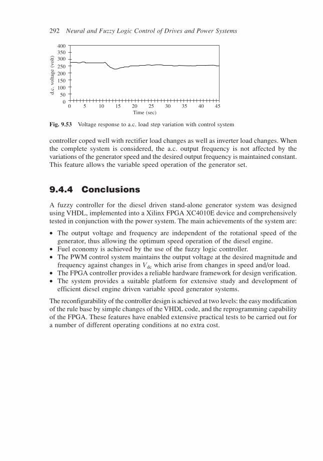
292 Neural and Fuzzy Logic Control of Drives and Power Systems
controller coped well with rectifier load changes as well as inverter load changes. Whenthe complete system is considered, the a.c. output frequency is not affected by thevariations of the generator speed and the desired output frequency is maintained constant.This feature allows the variable speed operation of the generator set.
9.4.4 Conclusions
A fuzzy controller for the diesel driven stand-alone generator system was designedusing VHDL, implemented into a Xilinx FPGA XC4010E device and comprehensivelytested in conjunction with the power system. The main achievements of the system are:
• The output voltage and frequency are independent of the rotational speed of thegenerator, thus allowing the optimum speed operation of the diesel engine.
• Fuel economy is achieved by the use of the fuzzy logic controller.• The PWM control system maintains the output voltage at the desired magnitude and
frequency against changes in Vdc which arise from changes in speed and/or load.• The FPGA controller provides a reliable hardware framework for design verification.• The system provides a suitable platform for extensive study and development of
efficient diesel engine driven variable speed generator systems.
The reconfigurability of the controller design is achieved at two levels: the easy modificationof the rule base by simple changes of the VHDL code, and the reprogramming capabilityof the FPGA. These features have enabled extensive practical tests to be carried out fora number of different operating conditions at no extra cost.
Fig. 9.53 Voltage response to a.c. load step variation with control system
d.c.
vol
tage
(vo
lt)
400350300
25020015010050
00 5 10 15 20 25 30 35 40 45
Time (sec)

Final notes
The VHDL approach to the holistic modelling, simulation, design and controllerimplementation of complex power systems including digital controllers enables a uniqueworking environment, a short development time, multiple choices for the implementationtarget technology and universal compatibility of the design with respect to a range ofexisting modern CAD tools.
Specific digital electronic modules, implementing fast and effective neural andfuzzy logic control elements, can be included in complex control systems as intellectualproperty (IP) blocks and reused in accordance with modern principles of designreuse.
Due to these advantages, the authors estimate that such methodologies, based onhardware description languages, will be used on a larger scale in the future for digitallycontrolled power systems modelling, design and analysis.

[1] Analogue and Mixed Signal Catalogue, Texas Instruments, copyright 1999.[2] Designing with Powerview/WorkviewPLUS, Viewlogic Systems, Inc., 293 Boston Post Road
West, Marlboro, Massachusetts 01752-4615, copyright 1993.[3] Digital Analysis with Powerview/WorkviewPLUS, Viewlogic Systems, Inc., 293 Boston Post
Road West, Marlboro, Massachusetts 01752-4615, copyright 1993.[4] FH2/3 MkIV Electrical Machines Teaching System, TecQuipment, Bonsall Street, Long Eaton,
Nottingham, NG10 2AN, UK, 1997.[5] Foundation Series Quick Start Guide 1.4, Xilinx, Inc., 1997.[6] Technical Reference Manual, Newage Intern. Ltd, Section 4131, Jan. 1990, p.1.[7] Semikron Innovation + Service, Semikron International, Sigmundstr. 200, D-90431, Nuremberg,
Germany, copyright 1998.[8] The Programmable Logic Data Book, Xilinx, Inc., 2100 Logic Drive, San José, California
95124, USA, copyright 1999.[9] TMS320C5x – User’s Guide, Texas Instruments, Inc., 1992.
[10] IEEE Standard VHDL Language Reference Manual, IEEE standard 1076-1993.[11] Energy Savings with Electric Motors and Drives, guide provided by Energy Efficiency Enquiries
Bureau, Crown copyright 1998.[12] Intel 80170NX ETANN Data Sheets, Feb. 1991.[13] Sensorless Control with Kalman Filter on TMS320 Fixed-Point DSP, Literature Number:
BPRA057, Texas Instruments Europe, July 1997 (www.ti.com).[14] Foundation Series Quick Start Guide 1.4, Xilinx, Inc., 1991–1997.[15] VHDL SelfStart_Kit, Topdown Design Solutions, 1995.[16] Adler, M.S. et al.: ‘The Evolution of Power Device Technology’, IEEE Trans. Electron Devices,
vol. 31, no. 11, Nov. 1984, pp. 1570–1591.[17] Akmese, R., Chalmers, B.J.: ‘Permanent Magnet Alternators with Constant Output Voltage’,
Proc. Universities Power Eng. Conf. UPEC’97, vol. 1, 10–12 Sept. 1997, pp. 34–36.[18] Alolah, A.I.: ‘Steady State Operating Limits of Three Phase Self-excited Reluctance Generator’,
IEE Proc. C, vol. 139, no. 3, May 1992, pp. 261–268.[19] Alspector, J., Allen, R.B., Jayakumar, A., Zeppenfeld, T., Meir, R.: ‘Relaxation Networks for
Large Supervised Learning Problems’, in Advances in Neural Information Processing Systems3 (Lippmann, R.P., Moody, J.E., Touretzky, D.S., eds), Morgan Kaufmann, San Mateo, CA,1991, pp. 1015–1021.
[20] Al-Tayie, J.K., Acarnley, P.P. ‘Estimation of Speed, Stator Temperature and Rotor Temperaturein Cage Induction Motor Drive using the Extended Kalman Filter Algorithm’, IEE Proceedingson Electric Power Applications, vol. 144, no. 5, Sept. 1997, pp. 301–309.
[21] Andreou, A.G., Boahen, K.A., Pouliqueen, P.O., Jenkins, R.E., Strohbehn, K. ‘Current-modeSubthreshold MOS Circuits for Analogue VLSI Neural Systems’, IEEE Transactions on NeuralNetworks, vol. 2, 1991, pp. 205–213.
10
References

References 295
[22] Armstrong, W.W., Gecsei, J.: ‘Adaption Algorithms for Binary Tree Networks’, IEEE Transactionson System, Man, Cybernetics, no. 9, 1979, pp. 276–285.
[23] Atkinson, D.J., Hopfensperger, B., Lakin, R.A.: ‘Field Oriented Control of a Doubly-fedInduction Machine using Coupled Microcontrollers’, EPE’99 Lausanne (CD).
[24] Aubebart, F., Girerd, C., Chapuis, Y.A., Poure, P., Braun, F.: ‘ASIC Implementation of DirectTorque Control for Induction Machines: Functional Validation by Power and Control Simulation’,PCIM’98, Power Converter and Intelligent Motion Conference, Nuremberg, 25–28 May 1998,pp. 251–260.
[25] Ayestaran, H.E., Prager, R.W.: ‘The Logical Gates Growing Network’, Technical Report CUED/F-INFENG/TR 137, Engineering Dept., Cambridge University, 1993.
[26] Baliga, B.J. et al.: ‘The Insulated Gate Transistor (IGT) – A New Power Switching Device’,IEEE/IAS Ann. Meet. Conf. Rec., 1983, pp. 794–803.
[27] Bartos, F.J.: ‘Sensorless Vector Drives Strive for Recognition’, Control Engineering, Sept.1996.
[28] Bashagha, A.E., Ibrahim, M.K.: ‘A New Digit-serial Divider Architecture’, International Journalon Electronics, vol. 75, no. 1, pp. 133–140.
[29] Bashagha, A.E., Ibrahim, M.K.: ‘A New High Radix Non-restoring Divider Architecture’,International Journal on Electronics, vol. 79, no. 4, 1995, pp. 455–470.
[30] Bashagha, A.E., Ibrahim, M.K.: ‘Design of a Square-root Architecture: Digit Serial Approach’,International Journal on Electronics, vol. 76, no. 1, 1994, pp. 15–25.
[31] Bashagha, A.E., Ibrahim, M.K.: ‘Digit-serial Squaring Architecture’, Journal of Circuits,Systems and Computers, vol. 4, no. 1, 1994, pp. 99–108.
[32] Bashagha, A.E., Ibrahim, M.K.: ‘Nonrestoring Radix-2k Square Rooting Algorithm’, Journalof Circuits, Systems and Computers, vol. 6, no. 3, 1996, pp. 267–285.
[33] Baum, E.B.: ‘On the Capabilities of Multilayer Perceptrons’, J. Compl., no. 4, 1988, pp. 193–215.
[34] Beierke, S., Konigbauer, R., Krause, B., Altrock, C.V.: ‘Fuzzy Logic Enhanced Control of ACMotor Using DSP’, Embedded Systems Conference California, 1995, pp. 101–106.
[35] Beiu, V.: ‘Entropy, Constructive Neural Learning and VLSI Efficiency’, in Proceedings ofNEUROTOP’97: Neural Priorities on Data Transmission and EDA, Brasov Romania, 22–30May 1997, pp. 38–74.
[36] Beiu, V.: VLSI Complexity of Discrete Neural Networks, Gordon and Breach & HarwoodAcademics Publishing, 1998.
[37] Beiu, V., Taylor, J.G.: ‘Optimal Mapping of Neural Networks onto FPGAs’, ‘Natural to ArtificialNeural Computation’, Lecture Notes in CS930, Springer-Verlag, Berlin, June 1995.
[38] Ben-Brahim, L.: ‘Motor Speed Identification Via Neural Networks’, IEEE Industry ApplicationsMagazine, vol. 1, no. 1, Jan./Feb. 1995, pp. 28–32.
[39] Binns, K.J., Kurdali, A.: ‘Permanent Magnet A.C. Generator’, Proc. IEE, vol. 126, no. 7, July1979, pp. 690–696.
[40] Blayliss, J.: ‘Electronic Design Automation Report,’ Cambridge Market Intelligence, 1994.[41] Bleijs, J.A.M., Wong, K.J.: ‘Control of a Variable Speed Wind Turbine with a Synchronous
Generator and Boost Rectifier,’ Proc. 37th Universities Power Eng. Conf. UPEC’97, 10–12Sept. 1997, pp. 722–725.
[42] Bleijs, J.A.M.: ‘Improvement in Performance of a Passive Pitch Wind Turbine with VariableSpeed Operation’, Proc. of 5th Eur. Wind Energy Assoc. Conf. EWEC, Thessaloniki, Greece,vol. 1, Oct. 1994, pp. 588–592.
[43] Boldea, I., Nasar, S.A.: ‘Vector Control of A.C. Drives’, CRC Press, Boca Raton, 1992.[44] Boost, M.A., Ziogas, P.D.: ‘State-of-the-art Carrier PWM. Techniques: A Critical Evaluation’,
IEEE Trans. Ind. Applicat., vol. 24, no. 24, March/April 1988, pp. 271–280.[45] Bose, B.K.: ‘Expert System, Fuzzy Logic and Neural Network Applications in Power Electronics
and Motion Control’, Proc. IEEE, vol. 82, Aug. 1994, pp.1303–1323.[46] Bose, K.B.: ‘High Performance Control of Induction Motor Drives’, IEEE Industrial Electronics
Society Newsletter, Sept. 1999, pp. 7–11.

296 Neural and Fuzzy Logic Control of Drives and Power Systems
[47] Bose, N.K., Garga, A.K.: ‘Neural Network Design Using Voronoi Diagrams’, IEEE Transactionson Neural Networks, vol. 4, no. 5, Sept. 1993, pp. 778–787.
[48] Bowes, S.R., Mount, M.J.: ‘Microprocessor Control of PWM Inverters’, IEEE Trans. Ind.Applicat., vol. 128, no. 6, 1981, pp. 293–305.
[49] Brod, D.M., Novotny, D.W.: ‘Current Control of VSI-PWM Inverters’, IEEE-IAS Conf. Rec.,1984, pp. 418–425.
[50] Butcher, J.C.: The Numerical Analysis of Ordinary Differential Equations – Runge–Kutta andGeneral Linear Methods, John Wiley & Sons, 1987.
[51] Carter, D.E., Stilwell-Baker, B.: Concurrent Engineering: The Product Development Environmentfor the 1990s, Mentor Graphics, 1991.
[52] Carter, D.E., Sullivan, T.N.: Concurrent Engineering: Best Practices for Global Success,Mentor Graphics, 1994.
[53] Cecati, C., Rotondale, N.: ‘Torque and Speed Regulation of Induction Motors Using thePassivity Theory Approach’, IEEE Transactions on Industrial Applications, vol. 46, no.1, Feb.1999, pp. 119–127.
[54] Chan, T.F.: ‘Self-excited Induction Generators Driven by Regulated and Unregulated Turbines’,IEEE Trans. on Energy Conversion, vol. 11, no. 3, Sept. 1996, pp. 338–343.
[55] Chapuis, Y.A., Poure, P., Braun, F.: ‘Torque Dynamic Correction of Direct Torque Control forInduction Machine Using a DSP’, PCIM’98, Power Converter and Intelligent Motion Conference,Nuremberg, 25–28 May 1998, pp. 241–250.
[56] Chapuis, Y.A., Roye, D.: ‘Optimization of Square Wave Transition for Direct Torque Controlof Induction Machine’, Proceedings of the Intelligent Motion Conference, Nuremberg, 10–12June 1997.
[57] Chen, Z., Spooner, E.: ‘Grid Interface Options for Variable Speed Permanent Magnet Generators’,IEE Proc. Electr. Power Appl., vol. 145, no. 4, July 1998, pp. 273–282.
[58] Churcher, D., Baxter, D.J., Hamilton, A., Murray, A.F., Reekie, H.M.: ‘Generic Analog NeuralComputation – The EPSILON chip’, in Advances in Neural Information Processing Systems,(Hanson, S.J., Cowan, D.J., Giles, C.L. eds.), Morgan Kaufmann 1993, San Mateo, CA: pp.773–780.
[59] Cilia, J., Asher, G.M., Bradley, K.J.: ‘Sensorless Position Detection for Vector ControlledInduction Motor Drives Using an Asymmetric Outer-section Cage’, IEEE Trans. on IAS, vol.33, no. 5, Sept./Oct. 1997, pp. 1162–1169.
[60] Cirstea, M.N.: ‘An investigation into ASIC Control of a 6-pulse Cycloconverter Quad-windingInduction Motor’, PhD Thesis, Nottingham Trent University, 1996.
[61] Cirstea, M.N., Dinu, A., Nicula, D.: A Practical Guide to VHDL Design, Editura Tehnica,Bucharest, Romania, 2001, ISBN: 973–31-1539–8.
[62] Cirstea, M.N., Patterson, E.B., Morley, D., Koczara, W., Przybylski, J.: ‘Electronic DesignAutomation Techniques Transferred to Central/Eastern Europe’, ‘Advances in Design andManufacturing’ – Concerted Efforts for Europe – European Commission DG iii, 1995, vol. 6,Ch. 43, pp. 85–92.
[63] Cirstea, M.N., Patterson, E.B., Holmes, P.G., Morley, D.: ‘A New Technique to Model andSimulate Divided Winding Induction Motors’, Proc. of IEE Int. Conf. on Computation inElectromagnetics (CEM’96), Bath, UK, April 1996, pp. 194–199.
[64] Cirstea, M.N., Patterson, E.B., Morley, D., Holmes, P.G.: ‘A Complete ASIC ControlledElectric Drive System’, Proc. of the International Symposium on Circuits and Systems (ISCAS’96– IEEE sponsored), Atlanta, Georgia, USA, May 1996, vol. 1, pp. 561–564.
[65] Cirstea, M.N., Giamusi, M., McCormick, M.: ‘A Modern ASIC Controller for a 6-pulseRectifier’, Proceedings of the ASIC’97 IEEE Conference, Portland, Oregon, USA, 7–10 Sept.,1997, pp. 335–338.
[66] Cirstea, M.N.: ‘ASIC Control System for Electric Drives’, Proc. of IEE/IEEE InternationalSymposium of Integrated Circuits – (ISIC’97), Singapore, 11–12 Sept. 1997, pp. 621–624.
[67] Cirstea, M.N., McCormick, M.: ‘Intelligent ASIC Control of Power Electronics’, Proc. of the

References 297
International Conference on Power Conversion and Intelligent Motion (PCIM’98), Nuremberg,Germany, 26–28 May 1998, pp. 95–99.
[68] Cirstea, M.N., McCormick, M.: ‘Control Systems for Power Electronics’, Proc. of the IEEInternational Conf. on Simulation (SIMULATION’98), York, UK, Oct. 1998, pp.182–186.
[69] Cirstea, M.N., Khor, J.G., McCormick M., Haydock, L.: ‘VHDL Design of an IntelligentFuzzy Logic Controller for Synchronous Generator Sets Implemented in FPGA’, Proc. of theInternational HDL Conference, Santa Clara, California, USA, April 1999, pp. 43–47.
[70] Cirstea, M.N., Khor, J.G., Hu, Y., McCormick, M., Haydock, L.: ‘Intelligent Fuzzy LogicController for Power Generation Systems’, Proc. of the 9th International Conference onElectrical Machines and Drives, Canterbury, UK, Sept. 1999, pp. 321–324.
[71] Cirstea, M.N., Aounis, A., Dinu, A., McCormick, M.: ‘A VHDL Approach to Induction MotorModelling’, Proc. of IEE CONTROL ’00, Cambridge, UK, Sept. 2000, CDROM.
[72] Cirstea, M.N., Dinu, A., McCormick, M., Nicula, D.: ‘A VHDL Success Story: Electric DriveSystem using Neural Controller’, Proc. of the IEEE VIUF/BMAS Fall Conference, Orlando,Florida, Oct. 2000, pp. 118–122.
[73] Cirstea, M.N., Dinu, A., McCormick, M.: ‘A New Neural Networks Approach to InductionMotor Speed Control’, Proc. of the IEEE Power Electronics Specialists Conference (PESC),Vancouver, Canada, 18–22 June 2001, CD-ROM.
[74] Cirstea, M.N., Khor, J.G., McCormick, M.: ‘FPGA Fuzzy Logic Controller for Variable SpeedGenerators’, Proc. of IEEE International Conference on Control Applications (CCA), MexicoCity, 4–7 Sept. 2001, CDROM.
[75] Comnac, V., Cirstea, M.N., Giamusi, M., Cernat, R.M.: ‘Torque and Speed Control of Inverter-fed Interior Permanent Magnet Synchronous Motor Using Sliding Mode’, Proc. of Int. EuropeanConf. on Power Electronics & Applications (EPE), Lausanne, Switzerland, 1999, CDROM.
[76] Conradi, P.: Reuse in Electronic Design: from Information Modelling to Intellectual Properties,John Wiley & Son Ltd, 1999.
[77] Cybenko, G.: ‘Approximations by Superposition of a Sigmoidal Function’, Mathematics ofControl, Signal and Systems, vol. 2, 1989, pp. 303–314.
[78] De Mello, F.P., Hannet, L.N.: ‘Large Scale Induction Generators for Power Systems’, IEEETrans. on Power Apparatus & Systems, PAS 100, 1981, pp. 2610–2618.
[79] DeDoncker, R., Novotny, D.W.: ‘The Universal Field Oriented Controller’, IEEE-IAS Trans.,vol. 30, no. 1, Jan./Feb. 1994, pp. 92–100.
[80] Den Bout, D.V.: The Practical Xilinx Designer Lab Book, Prentice Hall, 1998.[81] Dinu, A.: ‘FPGA Neural Controller for Three Phase Sensorless Induction Motor Drive Systems’,
PhD Thesis, De Montfort University, 2000.[82] Dinu, A., Cirstea, M.N., McCormick, M., Ometto, A., Rotondale, N.: ‘An Adaptive Control
Strategy for Electric Drives’, Proc. of the International Conference on Power Conversion andIntelligent Motion (PCIM’98), Nuremberg, Germany, 26–28 May 1998, pp. 101–107.
[83] Dinu, A., Cirstea, M.N., McCormick, M.: ‘Virtual Prototyping of a Digital Neural CurrentController’, Proc. of the IEEE International Workshop on Rapid Systems Prototyping, Leuven,Belgium, 2–5 June 1998, pp. 176–181.
[84] Dinu, A., Cirstea, M.N., McCormick, M., Ometto, A., Rotondale, N.: ‘Load IndependentCurrent Control Strategy for PWM Inverters’, Proc. of the IEE CONTROL’98, Swansea, UK,1–4 Sept. 1998, vol. 2, pp.1118–1122.
[85] Dinu, A., Cirstea, M.N., McCormick, M., Ometto, A., Rotondale, N.: ‘Neural ASIC Controllerfor PWM Power Systems’, Proc. of the 11th IEEE International ASIC Conference, Rochester,USA, 13–16 Sept. 1998, pp. 29–33.
[86] Dinu, A., Cirstea, M.N., McCormick, M., Haydock, L., Al-Khayat, N.: ‘Neural Current Controllerfor Induction Motor Applications’, Proc. of Int. Conf. on Optimization of Electric & ElectronicEquipment (OPTIM-IEE, IEEE), Brasov, Romania, May 2000, pp. 665–670. Award: 3rd ABBprize!
[87] Dinu, A., Cirstea, M.N., McCormick, M., Ometto, A., Rotondale, N.: ‘Sensorless Induction

298 Neural and Fuzzy Logic Control of Drives and Power Systems
Motor Control Strategy Optimised for FPGA Hardware Implementation’, Journal of ElectricalEngineering, vol.1, no. 1, 2001, pp. 26–31, ISSN 1582–4594.
[88] Driankov, D., Hellendoorn, H., Reinfrank, M.: An Introduction to Fuzzy Control, Springer-Verlag, Berlin Heidelberg, 1993.
[89] Dwyer, R.A.: ‘High-dimensional Voronoi Diagrams in Linear Expected Time’, Discr. Comput.Geom., vol. 6, 1991, pp. 343–367.
[90] Eichmann, G., Caulfield, H.J.: ‘Optical Learning (Inference) Machine’, Applied Optics, no.24, 1985, pp. 378.
[91] Eldridge, S.E., Walter, C.D.: ‘Hardware Implementation of Montgomery’s Modular MultiplicationAlgorithm’, IEEE Transactions on Computers, vol. 42, 1993, pp. 693-699.
[92] EL-Sharkawi, M., Neibur, D. (eds): ‘Artificial Neural Networks Applied to Power Systems’,IEEE Power Engineering Society tutorial course, IEEE catalogue number 96 TP 112–0, 1996.
[93] Evans, W.R.: Graphical Analysis of Control Systems, Trans. AIEE, 1948.[94] Farhat, N.H., Psaltis, D., Prata, A., Paek, E.: ‘Optical Implementation of the Hopfield Model’,
Applied Optics, no. 24, 1985, p. 339.[95] Farsi, M., Zachariah, K.J., Finch, J.W.: ‘Implementation of a Self-tuning AVR’, IEE Proc. –
Control Theory Appl., vol. 144, no. 1, Jan. 1997, pp. 32–39.[96] Fodor, D., Vas, J., Katona, Z.: ‘Fuzzy Logic Based Vector Control of AC Motor Using Embedded
DSP Controller Board’, Proc. of PCIM’98 – Intelligent Motion, pp. 235–240.[97] Foussier, P., Calmon, F., Carrabina, J., Fathallah, M., Grennerat, V., Jorda, X., Gontrand, C.,
Retif, M.J., Chante, J.-P.: ‘Practical Example of Algorithm Integration for Electrical Drives’,EPE’99 Lausanne (CDRom).
[98] Ghosh, A., Ledwich, G., Malik, O.P., Hope, G.S.: ‘Power Systems Stabilisers Based on AdaptiveControl Techniques’, IEE Trans. on Power Apparatus and Systems, vol. PAS-103, no. 8, 1984,pp. 1983–1989.
[99] Godhwani, A., Basler, M.J.: ‘A Digital Excitation Control System for Use on Brushless ExcitedSynchronous Generators’, IEEE Trans. on Energy Conversion, vol. 11, no. 3, Sept. 1996. pp.616–619.
[100] Goslin, G.R.: ‘Using Xilinx FPGAs to Design Custom Digital Signal Processing Devices’,Proceedings of the 1995 DSP Technical Program, pp. 595–604.
[101] Goslin, G., Newgard, B.: ‘16-Tap, 8-bit FIR Filter Application Guide’, Xilinx Inc., Nov., 1994.[102] Gottlieb, I.M.: ‘Power Supplies, Switching Regulators, Inverters and Converters’, 1st edition,
Blue Ridge Summit, PA, 1984.[103] Gottlieb, I.M.: Practical Power-control Techniques, 1st edition, Indianapolis, IN, USA: H.W.
Sams, 1987.[104] Gottlieb, I.M.: Regulated Power Supplies, 4th edition, Blue Ridge Summit, PA, 1992.[105] Grzesiak, L., Beliczynski, B.: ‘Simple Neural Cascade Architecture for Estimating of Stator
and Rotor Flux’, EPE’99 Lausanne (CDRom).[106] Habetler, T.G., Divan, D.M.: ‘Acoustic Noise Reduction in Sinusoidal PWM Drives Using a
Randomly Modulated Carrier’, IEEE Trans. on Power Electronics, vol. 6, July 1991, pp. 356–363.
[107] Habetler, T.G.: ‘A Space Vector-based Regulator for AC/DC/AC Converters’, IEEE Trans. onPower Electronics, vol 8, no. 1, 1993, pp. 30–36.
[108] Hammerstrom, D.: ‘The Connectivity Analysis of Simple Association – or – How ManyConnections Do You Need’, Proceedings NIPS’87 (Denver, USA), Amer. Inst. Phys., 1987,pp. 338–347.
[109] Harrer, H., Nossek, J.A., Stelzl, R.: ‘An Analog Implementation of Discrete-time CellularNeural Networks’, IEEE Transactions on Neural Networks, vol. 3, no. 3, May 1992, pp. 466–476.
[110] Haykin, S.: Neural Networks – a Comprehensive Foundation, Macmillan College PublishingCompany Inc., 1994.
[111] Hazen, H.L.: Theory of Servomechanism, J. Franklin Inst., 1934.

References 299
[112] Heht-Nielsen, R.: Neurocomputing. Reading, Addison-Wesley Publishing Co., 1990.[113] Hilloowala, R.M., Sharaf, A.M.: ‘A Rule-based Fuzzy Logic Controller for a PWM Inverter in
a Stand Alone Wind Energy Conversion Scheme’, IEEE Trans. on Industry Appl., vol. 32, no.1, 1996, pp. 57–65.
[114] Hirayama, T.: ‘Robustness of Fuzzy Logic Power System Stabilisers Applied to MultimachinePower System’, IEEE Trans. Energy Conversion, vol. 9, no. 3, 1994, pp. 451–459.
[115] Hirayama, K. et al.: ‘Digital A.V.R. Application to Power Plants’, IEEE Trans. on EnergyConversion, vol. 8, no. 4, Dec. 1993.
[116] Hmaifar, A., McCormick, E.: ‘Simultaneous Design of Membership Functions and Rule Setsfor Fuzzy Controllers Using Genetic Algorithms’, IEEE Trans. Fuzzy Syst., vol. 3, no. 2, May1995, pp. 129–139.
[117] Holtz, J.: ‘Pulsewidth Modulation – A Survey’, IEEE Trans. Ind. Electron., vol. 39, no. 5,1992, pp. 410–420.
[118] Holtz, J.: ‘Speed Estimation and Sensorless Control of AC Drives’, Proceedings of IECON’93,IEEE-Industrial Electronics Society, 1993, pp. 649–654.
[119] Holtz, J., Stadtfeld, S.: ‘A Predictive Controller for the Stator Current Vector of AC MachinesFed from Switched Voltage Source’, JIEE IPEC-Tokyo Conf., 1983, pp. 1665–1675.
[120] Hopcroft, J.E., Mattson, R.L.: ‘Synthesis of Minimal Threshold Logic Networks’, IEEE Trans.on Electr. Comp., EC-6, 1965, pp. 552–560.
[121] Hornik, K., Stinchcombe, M., White, H.: ‘Multilayer Feedforward Networks are UniversalApproximators’, Neural Networks, no. 2, 1989, pp. 359–366.
[122] Hu, W.Y., Zhong, L., Rahman, M.F., Lim, K.W.: ‘A Fuzzy Observer for Stator Resistance forApplication in Direct Torque Control of Induction Motor Drives’, Proc. of the Second InternationalConference on Power Electronics and Drives (PEDS’97), 26–29 May, 1997 Singapore, vol. 1,pp. 91–96.
[123] Hu, Y.W., Rahman, M.F. et al. ‘Direct Torque Control of Induction Motor Using Fuzzy Logic’,Canadian Conference on Electrical and Computer Engineering, St John’s, Newfoundland,Canada, 25–28 May 1997, vol. 2, pp. 767–772.
[124] Huber, D.W., Runtz, K.J., Malik, O.P., Hope, G.S.: ‘Analytical and Experimental Studies of aDigital A.V.R.’, IEEE 8th PICA Conf. Proc., 1973, pp 195–203.
[125] Hui, S.Y.R., Oppermann, I., Sathiakumar, S.: ‘Microprocessor-based Random PWM Schemesfor D.C.–A.C. Power Conversion’, IEEE Trans. on Power Electronics, vol. 12, no. 2, March1997, pp. 253–260.
[126] Hwang, B., Saif, M., Jamshidi, M.: ‘A Neural Network Based Fault Detection and Identification(FDI) for a Pressurized Water Reactor’, Proceedings of the 12th IFAC World Congress onAutomatic Control, Sydney, Australia, 1993.
[127] Hwang, B.C., Saif, M., Jamshidi, M.: ‘Fault Detection and Diagnosis of a Nuclear Power PlantUsing Artificial Neural Networks’, Journal of Intelligent and Fuzzy Systems, vol. 3, no. 3,1995, pp. 197–213.
[128] Hwang, H.S.: ‘Automatic Design of Fuzzy Rule Base for Modelling and Control UsingEvolutionary Programming’, IEE Proc. Contr. Theory Appl., vol. 146, no. 1, Jan. 1999, pp. 9–16.
[129] Ibrahim, A.S., Hogg, B.W., Sharaf, M.M.: ‘Self-tuning Automatic Voltage Regulators for aSynchronous Generator’, IEE Proc. Pt. D, vol. 136, no. 5, Sept. 1989, pp. 252–260.
[130] Ibrahim, M.K., Bashagha, A.E.: ‘Area-Time Efficient Two’s Complement Square Rooting’,International Journal on Electronics, vol. 86, no. 2, 1999, pp. 127–140.
[131] Irwin, G.W., Warwick, K., Hunt, K.J.: ‘Neural Network Applications in Control’, Institution ofElectrical Engineers, London, 1995.
[132] Javurek, J: ‘Possibilities of Improving the Method of Direct Control of Asynchronous MachineTorque’, Automatizace Journal (Czech Republic), no. 12, 1997, pp. 789–794.
[133] Jeong, S.G., Myung-Ho, W.: ‘DSP Based Active Power Filter with Predictive Current Control’,IEEE Trans. on Industrial Electronics, vol. 44, No. 3, June 1997.

300 Neural and Fuzzy Logic Control of Drives and Power Systems
[134] Jones, R., Smith, G.A.: ‘High Quality Mains Power Form Variable Speed Wind Turbines’, Int.Conf. on Renewable Energy – Clean Power, 2001, IEE Conf. Publ. No. 385, 17–19 Nov. 1993,pp. 202–206.
[135] Jönsson, R.: ‘Natural Field Orientation (NFO) Provides Sensorless Control of AC InductionServo Motors’, PCIM Magazine, June 1995, pp. 10–17.
[136] Jönsson, R., Leonhard, W.: ‘Control of an Induction Motor without a Mechanical Sensor,based on the Principle of “Natural Field Orientation” (NFO)’, International Power ElectronicsConference IPEC, Yokohama, 1995, pp. 101–106.
[137] Jung, S.L., Tzou, Y.Y.: ‘Discrete Sliding Mode Control of a PWM Inverter for SinusoidalOutput Waveform Synthesis with Optimal Sliding Curve’, IEEE Trans. on Power Electronics,vol. 11, no. 4, July 1996, pp. 567–577.
[138] Kalman, R.E.: ‘A New Approach to Linear Filtering and Prediction Problems’, Trans. ASME(J. Basic Engineering), vol. 82D, no. 1, March 1960, pp. 35–45.
[139] Kalman, R.E., Bucy, R.S.: ‘New Results in Linear Filtering and Prediction Theory’, Trans.ASME (J. Basic Engineering), vol. 83D, no. 1, March 1961, pp. 95–108.
[140] Kanmachi, T., Takahashi, I: ‘Sensor-less Speed Control of an Induction Motor’, IEEE IndustryApplications Magazine, vol. 1, no. 1, Jan./Feb. 1995, pp. 22–27.
[141] Karr, C.L., Gentry, E.J.: ‘Fuzzy Control of pH Using Genetic Algorithm’, IEEE Trans. FuzzySyst., vol. 1, no. 1, Jan. 1993, pp. 46–53.
[142] Kawamura, A., Hoft, R.G.: ‘Instantaneous Feedback Controlled PWM Inverters with AdaptiveHysteresis’, IEEE Trans. Ind. Appl., vol. IA-20, 1984, pp. 769–775.
[143] Kazmierkowski, M.P., Dzieniakowski, M.A.: ‘Review of Current Regulation Techniques forThree-phase PWM Inverters’, IEEE IECON Conf. Rec., 1994, pp. 567–575.
[144] Kelemen, A., Panã, T.: ‘Simultaneous Speed and Rotor Resistance Estimation for SensorlessVector-controlled Induction Motor Drives’, Proceedings of the Twenty-Seventh InternationalIntelligent Motion Conference, 20–22 June, Nuremberg, Germany, 1995, pp. 523–530.
[145] Kennedy, D.C., Quintana, V.H.: ‘Neural Network Regulators for Synchronous Machines’,Proc. of ESAP, 1993, pp. 531–535.
[146] Khor, J.: ‘An Intelligent Controller for Synchronous Generators’, PhD Thesis, De MontfortUniversity, 1999.
[147] Khor, J.G., Cirstea, M.N., McCormick M., Low, W.F.: ‘PWM Control Techniques for VariableSpeed Generator Set’, Proc. of Int. Conf. on Optimization of Electric and Electronic Equipment(OPTIM’98-IEE, IEEE), vol. II, Brasov, Romania, May 1998, pp. 379–382.
[148] Khor, J.G., Cirstea, M.N., McCormick M.: ‘Control of Stand Alone Synchronous Generatorsat Optimum Speed’, Proc. of the 33rd IEEE Intersociety Energy Conversion EngineeringConference (IECEC’98), Colorado Springs, USA, 2–6 Aug. 1998, CD-ROM.
[149] Knapp, S.K., Xilinx Corporate Applications Manager: Using Programmable Logic to AccelerateDSP Functions, Xilinx Inc., Dec. 1996.
[150] Kobayashi, T., Yokoyama, A.: ‘An Adaptive Neuro-control System of Synchronous Generatorfor Power System Stabilisation’, IEEE Trans. on Energy Conversion, vol. 11, no. 3, Sept.1996, pp. 621–630.
[151] Koc, C.K., Johnson S.: ‘Multiplication of Signed-digit Numbers’, Electronics Letters, May1994, pp. 840–841.
[152] Kolar, J.K., Ertl, H., Zach, F.C.: ‘Analysis of On- and Off-line Optimised Predictive CurrentControllers for PWM Converter Systems’, IEEE Trans. on Power Electronics, vol. 6, July1991, pp. 451–462.
[153] Krzeminski, Z.: ‘An Observer System for Induction Motor without Speed Sensor’, Proceedingsof the Twenty-Seventh International Intelligent Motion Conference, 20–22 June 1995, Nuremberg,Germany, pp. 143–153.
[154] Krzeminski, Z., Guzinski, J.: ‘DSP Based Sensorless Control System of the Induction Motor’,Proc. of PCIM’98 – Intelligent Motion, pp. 137–146.
[155] Kung, S.Y.: ‘Digital Neural Networks’, Prentice Hall, 1993.

References 301
[156] Lanser, J.A., Lehmann, T.: ‘An Analog CMOS Chip Set for Neural Networks with ArbitraryTopologies’, IEEE Trans. on Neural Networks, vol. 4, no 3, May 1993, pp. 441–444.
[157] Lee, J.: ‘On Methods for Improving Performance of PI-Type Fuzzy Logic Controllers’, IEEETrans. Fuzzy Systems, vol. 1, no. 4, Nov. 1993, pp. 298–302.
[158] Le-Huy, H., Dessiant, L.A.: ‘An Adaptive Current Control Scheme for PWM SynchronousMotor Drives: Analysis and Simulation’, IEEE Trans. on Power Electronics, vol. 4, Oct. 1989,pp. 486–495.
[159] Leonhard, W.: Control of Electrical Drives, 2nd edition, Springer, Berlin, 1996.[160] Lin, F.-J., Shyu, K.-K., Wai, R.-J.: ‘DSP-based Minmax Speed Sensorless Induction Motor
Drive with Sliding Mode Model-following Speed Controller’, IEE Proceedings – ElectricPower Applications, Nov. 1999, vol. 146, Issue 6, p. 471.
[161] Lindsey, C.S., Lindblad, Th.: ‘Review of Hardware Neural Networks: A User’s Perspective’,Proceedings of the 3rd Workshop on Neural Networks: From Biology to High Energy Physics,Isola d’Elba, Italy, 26–30 Sept. 1994.
[162] Lüdtke, I., Jayne, M.G.: ‘A New Direct Torque Control Strategy’, IEE Colloquium on Advancesin Control Systems for Electric Drives, 24 May 1995, London, UK, Digest No. 1995, pp. 114–120.
[163] Macq, D., Verleysen, M., Jespers, P., Legat, J.D.: ‘Analog Implementation of a Kohonen Mapwith On-Chip Learning’, IEEE Transactions on Neural Networks, vol. 4, no. 3, May 1993, pp.456–461.
[164] Malik, O.P., Hope, G.S., Huber, D.W.: ‘Design and Test Results of a Software Based DigitalA.V.R’, IEEE Trans. on Power Appliances and Systems, vol. PAS-92, no. 2, March/April 1976,pp. 634–642.
[165] Manes, C., Parasiliti, F., Tursini, M.: ‘Comparative Study of Rotor Flux Estimation in InductionMotors with a Nonlinear Observer and the Extended Kalman Filter’, Proceedings of the 20thInternational Conference on Industrial Electronics Control and Instrumentation IECON, Bologna,vol. 3, 1994, p. 2149.
[166] Manes, C., Parasiliti, F., Tursini, M.: ‘DSP Based Fied-oriented Control of Induction Motorwith a Non-Linear State Observer’, 27th Annual IEEE Power Electronics Specialists Conference,vol. 2, 1996, p. 1254.
[167] Marino, R.: ‘An Example of Non-linear Regulator’, IEEE Trans. Automatic Contr., vol. 29, no.3, 1984, pp. 276–279.
[168] Massengill, L.W., Mundie, D.B.: ‘An Analog Neural Hardware Implementation Using Charge-injection Multipliers and Neuron-specific Gain Control’, IEEE Transactions on Neural Networks,vol. 3, no. 3, May 1992, pp. 354–362.
[169] Matsuo, T., Lipo, T.A.: ‘A Rotor Parameter Identification Scheme for Vector Controlled InductionMotor Drives’, Rec. IEEE-IAS Annual Meeting, pp. 538–545.
[170] Maxwell, J.C.: ‘On Governors’, Proc. Roy. Soc. (London), 1868.[171] Mead, C.A., Ismail, M.: ‘Analogue VLSI Implementation of Neural Systems’, MA: Kluwer,
Boston, 1989.[172] Miller, A., Muljadi, E., Zinger, D.S.: ‘A Variable Speed Wind Turbine Power Control’, IEEE
Trans. on Energy Conversion, vol. 12, no. 2, 1997, pp. 181–186.[173] Mirchandini, G., Cao, W.: ‘On Hidden Nodes in Neural Nets’, IEEE Transactions on Circuits
and Systems, no. 36, May 1989, pp. 661–664.[174] Misawa, E.A., Hedrick, J.K.: ‘Non-linear Observers – a State of the Art Survey’, ASME J.
Dyn. Syst. Meas. Contr., vol. 111, 1989, pp. 344–352.[175] Morioka, Y. et al.: ‘Application of Multivariable Optimal Controller to Real Power Systems’,
IEEE Trans. on Power Systems, vol. 9, no. 4, 1994, pp. 1949–1955.[176] Mortara, A., Vittoz, E.A.: ‘A Communication Architecture Tailored for Analog VLSI Artificial
Neural Networks: Intrinsic Performance and Limitations’, IEEE Transactions on Neural Networks,vol. 5, no. 3, May 1994, pp. 459–466.
[177] Mudi, R.K., Pal, N.R.: ‘A Robust Self-tuning Scheme for PI- and PD-type Fuzzy Controllers’,IEEE Trans. Fuzzy Systems, vol. 7, no. 1, Feb. 1999, pp. 2–16.

302 Neural and Fuzzy Logic Control of Drives and Power Systems
[178] Murray, A.F., Del Corso, D., Tarassenko, L.: ‘Pulse-stream VLSI Neural Networks MixingAnalog and Digital Techniques’, IEEE Transactions on Neural Networks, vol. 2, no. 2, March1991, pp. 193–204.
[179] Nabae, S., Ogasawara, M., Akagi, H.: ‘A New Control Scheme for Current Controlled PWMInverters’, IEEE Trans. Ind. Appl., vol. IA–22, no. 4, July/Aug. 1986, pp. 697–701.
[180] Navabi, Z.: ‘VHDL – Analysis and Modeling of Digital Systems’, Electrical and ComputerEngineering Series, McGraw-Hill International Editors, 1993.
[181] New, B.: ‘A Distributed Arithmetic Approach to Designing Scaleable DSP Chips’, EDN, 17August 1995, pp. 107–114.
[182] Nicula, D., Cirstea, M.N.: ‘Successful CAD Tools Application to FPGA/ASIC Design’,International Journal of Engineering Education, vol. 15, no. 1, 1999, pp. 72–76.
[183] Novotny, D.W., Lipo, T.A.: ‘Vector Control and Dynamics of AC Drive’, Oxford SciencePublications, Clarendon Press, Oxford, 1996.
[184] Ogata, K.: ‘Discrete-time Control System’, Prentice-Hall, 1995.[185] Pahalawaththa, N.C., Hope, G.S., Malik, O.P.: ‘Multivariable Self Tuning Power System Stabiliser
Simulation and Implementation Studies’, IEEE Trans. on Energy Conversion, vol. 6, no. 2,1991, pp. 310–319.
[186] Patterson, E.B.: ‘Electronic Design Automation for Power Electronic Drives’, PhD Thesis,Nottingham Trent University, 1993.
[187] Patterson, E.B., Holmes, P.G., Morley, D.: ‘Electronic Design Automation (EDA) Techniquesfor the Design of Power Electronic Control Systems’, IEE Proc. – G, vol. 139, no. 2, April1992, pp. 191–198.
[188] Pena, R.S., Asher, G.M., Clare, J.C.: ‘A Doubly-fed Induction Generator Using Back-to-BackPWM Converters Supplying an Isolated Load from a Variable Speed Wind Turbine’, IEE Proc.– B, vol. 143, no. 5, Sept. 1996, pp. 380–387.
[189] Perry, D.L.: VHDL, 2nd edition, McGraw-Hill Series on Computer Engineering, McGraw-HillInc., 1994.
[190] Profumo, F., Griva, G., Tenconi, A., Abrate, M., Ferraris, L.: ‘Stability Analysis of LuenbergerObservers for Speed Sensorless High Performance Spindle Drives’, EPE’99, Lausanne (CD-Rom).
[191] Rahman, M.A., Osheiba, A.M., Radwan, T.S.: ‘Modelling and Controller Design of an IsolatedDiesel Engine Permanent Magnet Synchronous Generator’, IEEE Trans. on Energy Conversion,vol. 11, no. 2, June 1996, pp. 324–329.
[192] Rajashekara, K., Kawamura, A., Matsuse, K.: ‘Sensorless Control of AC Drives’, IEEE Press,1996.
[193] Ramacher, U., Wesseling, M.: ‘A Geometrical Approach to Neural Network Design’, ProceedingsIJCNN’89 (Washington USA), IEEE Press, vol. 2, January 1989, pp. 147–153.
[194] Ross, R.J.: ‘Fuzzy Logic with Engineering Applications’, McGraw-Hill, 1995.[195] Säkinger, E., Boser, B.E., Jackel, L.D.: ‘A Neurocomputer Board Based on the ANNA Neural
Network Chip’, in ‘Advances in Neural Information Processing Systems’, (Moody, J.E., Hanson,S.J., Lippmann, R.P., eds.), Morgan Kaufmann 1992, San Mateo, CA, pp.773–780.
[196] Sankara Narayanan, E.M., De Souza, M.M., Qin, Z.: ‘Devices and Technologies for HighVoltage Integrated Circuits’, Proc. Int. Conf. on Semiconductor Materials and Technologies,New Delhi, India,16–21 Dec. 1996.
[197] Satieo, S., Torrey, D.A.: ‘Fuzzy Logic Control of a Space–Vector PWM Current Regulator forThree-phase Power Converters’, IEEE Transactions on Power Electronics, vol. 13, no. 3,1998, pp. 419–426.
[198] Savaresi, S.M.: ‘Exact Feedback Linearisation of a Fifth Order Model of Synchronous Generators’,IEE Proc. Contr. Theory Appl., vol. 146, no. 1, Jan. 1999, pp. 53–57.
[199] Scharf, A.: ‘Twenty Years of Innovation’, PCIM Magazine, issue 6, 1999, pp. 10–12.[200] Schwartz, M., Shaw, L: ‘Signal Processing – Discrete Spectral Analysis, Detection and
Estimation’, McGraw-Hill Book Company, 1975.

References 303
[201] Seepold, R., Kunzmann, A. (eds): ‘Reuse Techniques for Vlsi Design’, Kluwer AcademicPublishers, 1999.
[202] Simoes, M.G., Bose, B.K.: ‘Application of Fuzzy Logic in the Estimation of Power ElectronicWaveforms’, IEEE/IAS Annual Meet. Conf. Rec., 1993, pp. 853–861.
[203] Simoes, M.G. et al.: ‘Fuzzy Logic Based Intelligent Control of a Variable Speed Cage MachineWind Generation System’, IEEE Trans. Power Electronics, vol. 12, no. 1, Jan. 1997, pp. 87–94.
[204] Sjoholm, S., Lindh, L.: VHDL for Designers, Prentice-Hall, 1997.[205] Smieja, F.J.: ‘Neural Network Constructive Algorithm: Trading Generalisation for Learning
Efficiency?’, Circuits, Systems, Signal Processing, vol. 12, no. 2, 1993, pp. 331–374.[206] Smith, G.A., Stephens, R.G., Marshall, P., Kansara, M.: ‘A Sinewave Interface for Variable
Speed Wind Turbines’, 5th European Conf. on Power Electronics & Applications, IEE Conf.Publ. No. 377, 13–16 Sept. 1993, pp. 97–102.
[207] Smith, F.S., Shen, Q.: ‘Selecting Inference and Defuzzification Techniques for Fuzzy LogicControl’, Proc. of UKACC Intern. Conference on Control, 1–4 Sept. 1998, pp. 54–59.
[208] Song, Y., Johns, A.T.: ‘Applications of Fuzzy Logic in Power Systems, Part 1’, IEE PowerEngineering Journal, Oct. 1997.
[209] Song, Y., Johns, A.T.: ‘Applications of Fuzzy Logic in Power Systems, Part 2’, IEE PowerEngineering Journal, Aug. 1998, pp. 185–190.
[210] Sousa, G.C.D., Bose, B.K.: ‘A Fuzzy Set Theory Based Control of a Phase-Controlled Converterdc Machine Drive’, IEEE Trans. Ind. Appl., vol. 30, 1994, pp. 34–44.
[211] Sousa, G.C.D. et al.: ‘Fuzzy Logic Based On-line Efficiency Optimisation Control of anIndirect Vector Controlled Induction Motor Drive’, Proc. IEEE/IECON Conf., 1993, pp. 1168–1174.
[212] Summer, M., Campbell, J., Curtis, M.: ‘A Stator Resistance Estimator for Sensorless VectorControlled Drives using Artificial Neural Networks’, EPE’99, Lausanne (CD Rom).
[213] Tajima, H., Hori, Y.: ‘Speed Sensorless Field Orientation Control of the Induction Machine’,IEEE Trans. Ind. Appl., vol. 29, 1993, pp. 175–180.
[214] Tan, S., Vandewalle, J.: ‘Efficient Algorithm for the Design of Multilayer Feed-forward NeuralNetworks’, Proc. IJCNN’92 (Baltimore, USA), IEEE Press, vol. 2, 1992, pp. 190–195.
[215] Tenti, P., Malesani, L., Rossetto, L.: ‘Optimum Control of N-input K-output Matrix Converters’,IEEE Trans. Power Electron., vol. 7, no. 4, 1992, pp. 707–713.
[216] Teske, N., Asher, G.M., Bradley, K.J., Summer, M.: ‘Sensorless Position Control of InductionMachines using Rotor Saliencies under Load Conditions’, EPE’99, Lausanne (CD Rom).
[217] Thomas, M.J.: ‘Designing Intelligent Muscle into Industrial Motion Control’, IEEE Trans.Ind. Electron., vol. 37, no. 5, 1990, pp. 329–341.
[218] Trynadlowski, A.M., Legowski, S.: ‘Minimum-loss Vector PWM Strategy for Three-phaseInverters’, IEEE Trans. Power Electron., vol. 9, no. 1, 1994, pp. 26–34.
[219] Tzou, Y.-Y., Tsai, M.-F., Lin, Y.F., Wu, H.: ‘Dual-DSP Fully Digital Control of an InductionMotor’, IEEE ISIE Conf. Rec., Warsaw, Poland, 17–20 June 1996, pp. 673–678.
[220] Tzou, Y.-Y., Hsu, H.-J.: ‘FPGA Realization of Space–Vector PWM Control IC for Three-phasePWM Inverters’, IEEE Transactions on Power Electronics, vol. 12, no. 6, Nov. 1997, pp. 953–963.
[221] Tzou, Y.-Y., Yeh, S.-T., Wu, H.: ‘DSP-based Rotor Time Constant Identification and Slip GainAuto-tuning for Indirect Vector-controlled Induction Drives’, IECON Proc., vol. II, Taiwan,1996, p. 1228.
[222] Vadivel, S., Bhuvaneswari, G., Rao, G.S.: ‘A Unified Approach to Real Time Implementationof DSP Based PWM Waveforms’, IEEE Trans. Power Electron., vol. 6, no. 4, 1991, pp. 565–575.
[223] Van der Broeck, H.W., Skudelny, H.C., Stanke, G.V.: ‘Analysis and Realisation of a PulsewidthModulator Based on Voltage Space vectors’, IEEE Transactions on Industry Applications, vol.24, no. 1, Jan./Feb. 1988, pp. 142–150.

304 Neural and Fuzzy Logic Control of Drives and Power Systems
[224] Vanlandingham, H.F.: ‘Introduction to Digital Control Systems’, MacMillan Press, NewYork,1992.
[225] Vas, P., Li J., Stronach, A.F.: ‘Artificial Neural Network-based Control of ElectromechanicalSystems’, Proceedings of 4th European Conference on Control IEE, Coventry, 1994.
[226] Vas, P.: ‘Artificial-intelligence-based Electrical Machines and Drives. Application of Fuzzy,Neural, Fuzzy-neural and Genetic Algorithms’, Monographs in Electrical and ElectronicEngineering, Oxford University Press, 1999.
[227] Vas, P.: ‘Electrical Machines and Drives, A Space-Vector Theory Approach’, Monographs inElectrical and Electronic Engineering, Oxford University Press, 1992.
[228] Vas, P.: ‘Sensorless Vector and Direct Torque Control’, Monographs in Electrical and ElectronicEngineering, Oxford University Press, 1998.
[229] Vas, P.: ‘Vector Control of AC Machines’, Monographs in Electrical and Electronic Engineering,Oxford University Press, 1990.
[230] Vas, P., Stronach, A.F., Neuroth, M.: ‘DSP-based Speed-sensorless High-performance TorqueControlled Induction Motor Drives’, Proc. of PCIM’98 Intelligent Motion, pp. 225–234.
[231] Vas, P., Stronach, A.F., Neuroth, M., Du, T.: ‘A Fuzzy Controlled Speed-Sensorless InductionMotor Drive with Flux Estimators’, IEE EMD, Durham, 1995, pp. 315–319.
[232] Venturini, M.G.B., Alesina, A.: ‘A New Sine Wave in, Sine Wave out, Conversion TechniqueEliminates Reactive Elements’, Proc. Powercon 7, 1980, pp. E3.1–E3.15.
[233] Walter, C.D.: ‘Fast Modular Multiplication using 2-Power Radix’, International Journal ofComputer Mathematics, no. 3, 1991, pp. 21–28.
[234] Walter, C.D.: ‘Systolic Modular Multiplication’, IEEE Transactions on Computers, vol. 42,1993, pp. 376–378.
[235] Weedy, B.M.: Electric Power Systems, 3rd Edition, John Wiley & Sons, 1995.[236] Wheeler, P.W., Grant, D.A.: ‘A Low Loss Matrix Converter for A.C. Variable Speed Drives’,
Proc. EPE’93, UK, vol. 5, 1993, pp. 27–32.[237] White, D.A., Sofge, D.A.: Handbook of Intelligent Control: Neural, Fuzzy, and Adaptive
Approaches, Multiscience Press, Inc., 1992.[238] Wu, Q.H., Hogg, B.H.: ‘Robust Self-tuning Regulator for a Synchronous Generator’, IEE
Proc. – D, vol. 135, no. 6, Nov. 1988, pp. 463–473.[239] Zadeh, L.A.: ‘Fuzzy Sets’, Information and Control, vol. 8, 1965, pp. 338–353.[240] Zadeh, L.A.: ‘Outline of a New Approach to the Analysis of Complex Systems and Decision
Processes’, IEEE Trans. Syst., Man & Cybern., vol. 3, 1973, pp. 28–44.[241] Zhang, L., Watthanasarn, C., Shepherd, W.: ‘Analysis and Comparison of Control Techniques
for A.C.–A.C. Matrix Converters’, IEE Proc. Electr. Power Appl., vol. 145, no. 4, July 1998,pp. 284–294.
[242] Zhang, Y., Malik, O.P., Chen G.P.: ‘Artificial Neural Network Power System Stabilisers inMultimachine Power System Environment’, IEEE Trans. on Energy Conversion, vol. 10, no.1, 1995, pp. 147–153.
[243] Zurada, J.M.: Introduction to Artificial Neural Systems, West Publishing Company, 1992.

The electronic format of the program codes (ASCII text) is downloadable from thepublisher’s website at: http://www.bh.com/newnes
11.1 Appendix A – C++ code for ANNimplementation
11.1.1 CONV_NET.CPP
#include <iostream.h>#include <fstream.h>#include <string.h>#include <stdlib.h>#include <memmanag.h>#define MaximumDepth 100#define LengthInputTab 2000#define AND 1#define ANY 0ofstream output_file;int *out_layer, *index, *node, *inverter, *used;// Index specifies the initial position of the weights in the matrix// row before they were rearranged according to their descending// values.Node is a vector which stores the node numbers corresponding// to the weights. The node number is not generally speaking corelated// with the input numbers because there are inversor gates and because// some neurones are located in other layers than the first.double *w; //The weights vector for one neuroneint no_w; //The number of weights per neuroneint current_node,output_node,no_gates=0,max_depth,depth=0;int no_max_inputs;void add_gate(int ind_init, double threshold, char and_gate);void arrange(void)
int i,i_max,i_aux,j;double max,max_aux;for(i=0;i<no_w;i++)
max=w[i];
11
Appendices

306 Neural and Fuzzy Logic Control of Drives and Power Systems
i_max=i;for(j=i+1;j<no_w;j++)
if (max<w[jl)
max=w[j];i_max=j;
if(i_max != i)
max_aux=w[i_max];w[i_max]=w[i];w[i]=max_aux;i_aux=index[i_max];index[i_max]=index[i];index[i]=i_aux;
int add_inverter(int i)
no_gates++;++current_node;output_file<<“.NOT ”;output_file<<node[index[i]]<<“ “<<current_node<<“\n”;if(!output_file.good())
cout<<“\n\aError on file writing”;exit(1);
return current_node;
double* measure_matrix(int& no_neu,int& no_values, istream& input_file)
double temp;char buffer[2];no_neu=no_values=0;while(input_file.read(buffer,1),!input_file.eof())
if(buffer[0]==‘\n’)no_neu++;
input_file.clear();input_file.seekg(0,ios::beg);do
input_file>>temp;if(!input_file.eof())
no_values++;while(!input_file.eof());if(no_neu==0)
no_neu++;

Appendices 307
if((no_values/no_neu)*no_neu == no_values)no_values=no_values/no_neu;
elseif((no_values/(no_neu+1)) == no_values)
no_values=no_values/(no_neu+1);no_neu++;
else
cout<<“\n\aError in input file!”;exit(1);
input_file.clear();input_file.seekg(0,ios::beg);w=alloc_double(no_values);return w;
void read_line_matrix(istream& input_file)
int i;for(i=0;i<no_w+1;i++)
input_file>>w[i];if(!input_file.good())
cout<<“\n\aError when reading the input file”;exit(1);
int convert_neuron(void)
int i;double threshold;
inverter=alloc_int(no_w); //Shows if the corresponding weight was// negative thereby requiring an inversor gate
used=alloc_int(no_w); //Shows if the node has been already used// in the past so that the inverter has already been put
index=alloc_int(no_w+1);
for(i=0;i<no_w;i++)
index[i]=i;inverter[i]=0;used[i]=0;
for(i=0;i<no_w;i++)
if(w[i]<0)
w[i]=-w[i];inverter[index[i]]=1;
w[no_w]-=w[i];

308 Neural and Fuzzy Logic Control of Drives and Power Systems
w[i]=2*w[i];threshold=-w[no_w];if(threshold<=0)
output_node=-1; //Output value is constantly 1cout<<“\n\aWarning: The output of a neurone is constantly 1”;
else
arrange();add_gate(0,threshold,ANY);
delete index;delete used;delete inverter;return output_node;
int port_number(int i)
int rez;if (inverter[index[i]]==0)
rez=node[index[i]];if(depth>max_depth)
max_depth=depth;else
if(depth+1>max_depth)max_depth=depth+1;
if (used[index[i]])rez=used[index[i]];
else
used[index[i]]=add_inverter(i);rez=used[index[i]];
return rez;
int det_num_internal_gate_layers(int no_inp)
int no_inp_top,no_layers=1;if(no_inp<=no_max_inputs)
return 1;elsewhile(no_inp>no_max_inputs)
no_inp_top=no_inp/no_max_inputs;if(no_inp>no_inp_top*no_max_inputs)
no_inp_top++;

Appendices 309
no_inp=no_inp_top;no_layers++;
return no_layers;
int cursor=0;int input[LengthInputTab];void write_gate(char *name,int no_inputs, int local_cursor)
int i,no_inp_top_gate,no_last_inputs;if(no_inputs<=no_max_inputs)
output_file<<name<<no_inputs;for(i=0;i<no_inputs;i++)
output_file<<“ “<<input[local_cursor+i];current_node++;output_file<<“ ”<<current_node<<“\n”;output_node=current_node;no_gates++;if(!output_file.good())
cout<<“\n\aError on file writing”;exit(1);
else
no_inp_top_gate=no_inputs/no_max_inputs;if(no_inputs>no_inp_top_gate*no_max_inputs)
no_inp_top_gate++;if(cursor+no_inputs+no_inp_top_gate>=LengthInputTab)
cout<<“\n\aError: Input table is full”;exit(1);
for(i=0;i<no_inp_top_gate-1;i++)
local_cursor=cursor+i*no_max_inputs;write_gate(name,no_max_inputs,local_cursor);input[cursor+no_inputs+i]=output_node;
local_cursor=cursor+(no_inp_top_gate-1)*no_max_inputs;no_last_inputs=no_inputs-(no_inp_top_gate_1)*no_max_inputs;if(no_last_inputs>1) //It is possible to have only one remaining
input
write_gate(name,no_last_inputs,local_cursor);input[cursor+no_inputs+no_inp_top_gate-1]=output_node;
else
input[cursor+no_inputs+no_inp_top_gate-1]=input[cursor+no_inputs-1];

310 Neural and Fuzzy Logic Control of Drives and Power Systems
for(i=0;i<no_inp_top_gate;i++)input[cursor+i]=input[cursor+no_inputs+i];
write_gate(name,no_inp_top_gate,cursor);
double sum;int j;void add_gate(int ind_init, double threshold, char and_gate)
int i,no_inputs,no_big_weights,ind_for_AND;//These are local variables because they need to be preserved during
the//recursive calls of the functionif(threshold<=0)
cout<<“\n\aError: The output of a subneurone is constantly 1”;exit(1);
if(!and_gate)
sum=0;no_inputs=0;no_big_weights=0;ind_for_AND=ind_init;for(i=ind_init; i<no_w;i++)
if(w[i]>=threshold)
no_inputs++;no_big_weights++;ind_for_AND=i+1;
for(i=ind_for_AND;i<no_w;i++)
sum=0;for(j=i;j<no_w;j++)sum+=w[j]; //The sum will be the result of several cumulated
if(sum>=threshold) //inputs anyway because these are not big weights.no_inputs++;
if((no_inputs>1) && (!and_gate))
depth=depth+det_num_internal_gate_layers(no_inputs);//‘-1’ because there is one gate anyway
if(depth>MaximumDepth)
cout<<“\n\aError: Too many recursive calls!”;exit(1);
for(i=0;i<no_inputs;i++)
if(i>=no_big_weights)

Appendices 311
cursor+=no_inputs;if(cursor>=LengthInputTab)
cout<<“\n\aError: Input table is full. Enlarge the input table”;exit(1);
add_gate(ind_init+i,threshold,AND);cursor-=no_inputs; //necessarily be an AND gateinput[cursor+i]=output_node;
else
input[cursor+i]=port_number(ind_init+i);write_gate(“.OR”,no_inputs,cursor); //the gate is writtendepth=depth-det_num_internal_gate_layers(no_inputs);
else if((no_inputs==1) && (no_big_weights==1) && (!and_gate))
output_node=port_number(ind_init); //It is just a straightforward//input-output connection
else if(((no_inputs==1) && (no_big_weights==0)) || and_gate)//An AND gate will be used
no_inputs=1; //When is just a simple AND gate, it corresponds to a//single combination of inputs. Variable ‘no_inputs’ is
//used for economy of space in the stack. The first input//is compulsory to be used which is why no_inputs=1.
sum=0;for(i=ind_init;i<no_w;i++)
sum+=w[i];for(i=ind_init+1;i<no_w;i++)
if(sum-w[i]<threshold)no_inputs++;
elsebreak;sum=0;for(i=ind_init;i<ind_init+no_inputs;i++)
sum+=w[i];if(threshold-sum>0)
no_inputs++; //A further subneurone is requiredif(no_inputs<2)
cout<<“\n\aError in algorithm! An AND gate has less than 2inputs!”;
exit(1);depth+=det_num_internal_gate_layers(no_inputs);
//‘–1’ because there is one gate anywayif(depth>MaximumDepth)
cout<<“\n\aError: Too many recursive calls!”; exit(1);
for(i=0;i<no_inputs;i++)

312 Neural and Fuzzy Logic Control of Drives and Power Systems
if((i<no_inputs-1) || (threshold-sum<=0))
input[cursor+i]=port_number(i+ind_init);if((i==no_inputs-1) && (threshold-sum>0))
cursor+=no_inputs; //The supplementary subneurone is addedif(cursor>=LengthInputTab)
cout<<“\n\aError: Input table is full. Enlarge the input table”;exit(1);
add_gate(ind_init+no_inputs-1,threshold-sum,ANY);cursor-=no_inputs;input[cursor+i]=output_node;
write_gate(“.AND”,no_inputs,cursor);depth-=det_num_internal_gate_layers(no_inputs);
else if(no_inputs==0)
output_node=0; //Output value is constantly 0cout<<“\n\aWarning: The output of a neurone is constantly 0”;
else
cout<<“\n\aError in conversion algorithm”;exit(1);
void main(int no_par, char** par)
ifstream input_file;int no_neu=0, no_values_per_line, previous_no_neu,gate_layers=0;int i,no_file;if(no_par<4)
cout<<“\nToo few parameters”;exit(1);
no_max_inputs=atoi(par[no_par-1]);output_file.open(par[no_par-2],ios::out);if(!output_file.good())
cout<<“\n\aError: The output file cannot be opened!”;exit(1);
cout<<“\n----- Start conversion -----”;for(no_file=1;no_file<no_par-2;no_file++)
input_file.open(par[no_file],ios::in);if(!input_file.good())

Appendices 313
cout<<“\n\aError: The input file cannot be opened!”;exit(1);
cout<<“\nProcessing file ”<<no_file;previous_no_neu=no_neu;w=measure_matrix(no_neu,no_values_per_line, input_file);no_w=no_values_per_line-1;if((no_file>1)&&(previous_no_neu != no_values_per_line-1))
cout<<“\n\aError: Wrong number of neurones in layer”<<no_file;exit(1);
out_layer=alloc_int(no_neu);if(no_file==1)
node=alloc_int(no_w);for(i=0;i<no_w;i++)
node[i]=i+1;output_file<<“.INPUT “<<node[i]<<“\n”;if(!output_file.good())
cout<<“\n\aError on file writing”;exit(1);
current_node=no_w;
max_depth=0;for(i=0;i<no_neu;i++)
read_line_matrix(input_file);out_layer[i]=convert_neuron();
gate_layers+=max_depth;if(no_file==no_par-3) //It was the last input file so the output
//ports must be writtenfor(i=0;i<no_neu;i++)
output_file<<“.OUTPUT “<<out_layer[i]<<“\n”;if(!output_file.good())
cout<<“\n\aError on file writing”;exit(1);
delete node;if(no_file<no_par-3)
//File no ‘no_par-2’ is the output file so this is //not the last input file
node=alloc_int(no_neu);

314 Neural and Fuzzy Logic Control of Drives and Power Systems
for(i=0;i<no_neu;i++)
node[i]=out_layer[i]; //The outputs of the previous layer are//the inputs for the next one
if(node[i]<=0)
cout<<“\n\aWarning: The output of the hidden neuron “<<(i+1);cout<<“ in layer “<<no_file<<“ is constant!”;
input_file.close();delete w;delete out_layer;
input_file.close();cout<<“\nThe output file contains “<<no_gates<<“ logic gates on “;cout<<gate_layers<<“ gate layers\n”;
11.1.2 OPTIM.CPP
#include <iostream.h>#include <fstream.h>#include <stdlib.h>#include <string.h>#include <memmanag.h>#define NOT 3#define AND 1#define OR 4#define INPUT 2#define OUTPUT 5#define NO_WORDS 5#define CANCELLED -2//‘0’ is already defined in CONV_NET!.CPP as ‘ground’ and ‘-1’ as ‘Vcc’.
char* words[5]=“.AND”,“.INPUT”,“.NOT”,”.OR”,“.OUTPUT”;int length[5]=4,6,4,3,7;struct gate_string
char name[8];int no_gates;int cursor;int* gate_nodes;
;gate_string *and_s, *or_s;int *input_s, *output_s, *not_s;int max_input=0,max_output=0,max_and=0,max_or=0,max_not=0;int cursor_input=0,cursor_output=0,cursor_not=0;int no_init_gates,no_fin_gates;gate_string* alloc_gate_string(int no_gate_strings)

Appendices 315
gate_string *pointer;if(no_gate_strings>0)
if(!(pointer=new gate_string[no_gate_strings]))
cout<<alloc_err;exit(1);
return pointer;
else
return NULL;void init_structures(void)
int i;for(i=0;i<max_and-1;i++)
and_s[i].no_gates=0;and_s[i].cursor=0;and_s[i].name[0]=0;
for(i=0;i<max_or-1;i++)
or_s[i].no_gates=0;or_s[i].cursor=0;or_s[i].name[0]=0;
int check_word(char* buffer)
int i,j,found;for(i=0;i<NO_WORDS;i++)
found=1;for(j=0;j<length[i];j++)
if(buffer[j] != words[i][j])
found=0;break;
if(found==1)
return i+1;return 0;
int det_inputs(char *buffer)
int i=0;while(((buffer[i]>=‘A’) && (buffer[i]<=‘Z’)) || (buffer[i]==‘.’))
i++;return atoi(buffer+i);

316 Neural and Fuzzy Logic Control of Drives and Power Systems
void first_scan(ifstream& in_file)
char buffer[10];int i, node,ind_word,no_inputs;cout<<“First scan\n”;while(!in_file.eof())
in_file>>buffer;ind_word=check_word(buffer);switch (ind_word)
case INPUT: in_file>>node;max_input++;break;
case OUTPUT:in_file>>node;max_output++;break;
case AND: no_inputs=det_inputs(buffer);if(no_inputs>max_and)
max_and=no_inputs;for(i=0;i<=no_inputs;i++)
in_file>>node;break;
case OR: no_inputs=det_inputs(buffer);if(no_inputs>max_or)max_or=no_inputs;
for(i=0;i<=no_inputs;i++)in_file>>node;
break;case NOT: in_file>>node;
in_file>>node;max_not++;break;
default: if(buffer[0]==0)break;
else
cout<<“\n\aSyntax error in input file”;exit(1);
and_s=alloc_gate_string(max_and-1);or_s=alloc_gate_string(max_or-1);input_s=alloc_int(max_input);output_s=alloc_int(max_output);not_s=alloc_int(2*max_not);init_structures();no_init_gates=max_not;
void second_scan(ifstream& in_file)

Appendices 317
char buffer[10];int i, node,ind_word,no_inputs;cout<<“Second scan\n”;in_file.seekg(0,ios::beg);in_file.clear();while(!in_file.eof())
in_file>>buffer;ind_word=check_word(buffer);switch (ind_word)
case INPUT: in_file>>node;input_s[cursor_input]=node;cursor_input++;break;
case OUTPUT:in_file>>node;output_s[cursor_output]=node;cursor_output++;break;
case AND: no_inputs=det_inputs(buffer);and_s[no_inputs-2].no_gates++;strcpy(and_s[no_inputs-2].name,buffer);for(i=0;i<=no_inputs;i++)in_file>>node;break;
case OR: no_inputs=det_inputs(buffer);or_s[no_inputs-2].no_gates++;strcpy(or_s[no_inputs-2].name,buffer);for(i=0;i<=no_inputs;i++)
in_file>>node;break;
case NOT: in_file>>node;not_s[cursor_not++]=node;in_file>>node;not_s[cursor_not++]=node;break;
default: if(buffer[0]==0)break;
else
cout<<“\n\aSyntax error in input file”;exit(1);
for(i=0;i<max_and-1;i++)
and_s[i].gate_nodes=alloc_int((and_s[i].no_gates)*(i+3));no_init_gates+=and_s[i].no_gates;
for(i=0;i<max_or-1;i++)

318 Neural and Fuzzy Logic Control of Drives and Power Systems
or_s[i].gate_nodes=alloc_int((or_s[i].no_gates)*(i+3));no_init_gates+=or_s[i].no_gates;
void third_scan(ifstream& in_file)
char buffer[10];int i,node,ind_word,no_inputs,curs;cout<<“Third scan\n”;in_file.seekg(0,ios::beg);in_file.clear();while(!in_file.eof())
in_file>>buffer;ind_word=check_word(buffer);switch (ind_word)
case AND: no_inputs=det_inputs(buffer);curs=and_s[no_inputs-2].cursor;for(i=0;i<=no_inputs;i++)in_file>>and_s[no_inputs-2].gate_nodes[curs+i];and_s[no_inputs-2].cursor+=(no_inputs+1);break;
case OR: no_inputs=det_inputs(buffer);curs=or_s[no_inputs-2].cursor;for(i=0;i<=no_inputs;i++)in_file>>or_s[no_inputs-2].gate_nodes[curs+i];or_s[no_inputs-2].cursor+=(no_inputs+1);break;
case NOT: in_file>>node; //If it is an inverter gate there arecase INPUT: //two nodes to be read. If it is justcase OUTPUT: in_file>>node; //a port, there is only one node to
break; //be read;default: if(buffer[0]==0)
break;else
cout<<“\n\aSyntax error in input file”;exit(1);
void write_file(ofstream& out_file)
int i,j,k;for(i=0;i<max_input;i++)
out_file<<“.INPUT ”<<input_s[i]<<“\n”;for(i=0;i<max_not;i++)
if(not_s[2*i] != CANCELLED)out_file<<“.NOT ”<<not_s[2*i]<<“ ”<<not_s[2*i+1]<<“\n”;

Appendices 319
for(i=0;i<max_and-1;i++)if(and_s[i].name[0])
for(j=0;j<and_s[i].no_gates;j++)if(and_s[i].gate_nodes[j*(i+3)]!=CANCELLED)
out_file<<and_s[i].name;for(k=0;k<i+3;k++)
out_file<<“ ”<<and_s[i].gate_nodes[j*(i+3)+k];out_file<<“\n”;
for(i=0;i<max_or-1;i++)
if(or_s[i].name[0])for(j=0;j<or_s[i].no_gates;j++)
if(or_s[i].gate_nodes[j*(i+3)]!=CANCELLED)
out_file<<or_s[i].name;for(k=0;k<i+3;k++)
out_file<<“ ”<<or_s[i].gate_nodes[j*(i+3)+k];out_file<<“\n”;
for(i=0;i<max_output;i++)
out_file<<“.OUTPUT ”<<output_s[i]<<“\n”;void arrange_inputs(int *begin, int length)
int i,j,i_min,min,aux;for(i=0;i<length-2;i++) //The last is the output node and the //second-last doesn’t need to be
exchangedmin=begin[i]; //with itselfi_min=i;for(j=i+1;j<length-1;j++) //The last is the output node which is
notif(begin[j]<min) //to be modified
min=begin[j];i_min=j;
if(i != i_min)
aux=begin[i];begin[i]=begin[i_min];begin[i_min]=aux;
void arrange_all_inputs(void)
int i,j;for(i=0;i<max_and-1;i++)
for(j=0;j<and_s[i].no_gates;j++)arrange_inputs(and_s[i].gate_nodes+j*(i+3),i+3);

320 Neural and Fuzzy Logic Control of Drives and Power Systems
for(i=0;i<max_or-1;i++)for(j=0;j<or_s[i].no_gates;j++)
arrange_inputs(or_s[i].gate_nodes+j*(i+3),i+3);int check_inputs(int *begin1, int *begin2, int length)
int i, rez=1;if((*begin1 == CANCELLED) || (*begin2 == CANCELLED))
return 0;else
for(i=0;i<length-1;i++)if(begin1[i] != begin2[i])
rez=0;break;
return rez;
void replace_all(int dest, int source)
int i,j;for(i=0;i<max_not;i++)
if(not_s[2*i]==dest)not_s[2*i]=source;
for(i=0;i<max_and-1;i++)for(j=0;j<(and_s[i].no_gates)*(i+3);j++)
if(and_s[i].gate_nodes[j]==dest)and_s[i].gate_nodes[j]=source;for(i=0;i<max_or-1;i++)
for(j=0;j<(or_s[i].no_gates)*(i+3);j++)if(or_s[i].gate_nodes[j]==dest)
or_s[i].gate_nodes[j]=source;for(i=0;i<max_output;i++)
if(output_s[i]==dest)output_s[i]=source;
void optimise_structure(void)
int i,j,k,replacement;do
replacement=0;arrange_all_inputs();for(i=0;i<max_not-1;i++)
for(j=i+1;j<max_not;j++)if((not_s[2*i]==not_s[2*j]) && (not_s[2*i] != CANCELLED))
not_s[2*j]=CANCELLED;replace_all(not_s[2*j+1],not_s[2*i+1]);replacement=1;

Appendices 321
no_fin_gates––;
for(i=0;i<max_and-1;i++)for(j=0;j<and_s[i].no_gates-1;j++)
for(k=j+1;k<and_s[i].no_gates;k++)if(check_inputs(and_s[i].gate_nodes+j*(i+3),
and_s[i].gate_nodes+k*(i+3),i+3))
and_s[i].gate_nodes[k*(i+3)]=CANCELLED;replace_all(and_s[i].gate_nodes[k*(i+3)+i+2],
and_s[i].gate_nodes[j*(i+3)+i+2]);replacement=1;no_fin_gates––;
for(i=0;i<max_or-1;i++)
for(j=0;j<or_s[i].no_gates-1;j++)for(k=j+1;k<or_s[i].no_gates;k++)
if(check_inputs(or_s[i].gate_nodes+j*(i+3),or_s[i].gate_nodes+k*(i+3),i+3))
or_s[i].gate_nodes[k*(i+3)]=CANCELLED;replace_all(or_s[i].gate_nodes[k*(i+3)+i+2],
or_s[i].gate_nodes[j*(i+3)+i+2]);replacement=1;no_fin_gates––;
while(replacement);
void dealloc_everything(void)
int i;for(i=0;i<max_and-1;i++)
delete and_s[i].gate_nodes;for(i=0;i<max_or-1;i++)
delete or_s[i].gate_nodes;delete and_s;delete or_s;delete not_s;delete input_s;delete output_s;
void main(int no_par, char** par)
ifstream in_file;ofstream out_file;if(no_par<3)
cout<<“\nToo few parameters”;exit(1);
in_file.open(par[1],ios::in);

322 Neural and Fuzzy Logic Control of Drives and Power Systems
if(!in_file.good())
cout<<“\n\aError: The input file cannot be opened!”;exit(1);
cout<<“\n---------- Start optimisation ----------\n”;first_scan(in_file);second_scan(in_file);third_scan(in_file);cout<<no_init_gates<<“ gates in the input file\n”;no_fin_gates=no_init_gates;optimise_structure();out_file.open(par[2],ios::out);if(!out_file.good())
cout<<“\n\aError: The output file cannot be opened!”;exit(1);
write_file(out_file);dealloc_everything();in_file.close();out_file.close();cout<<no_fin_gates<<“ gates in the output file\n”;if(no_fin_gates<no_init_gates)
cout<<“The structure has been compressed at ”;cout<<((100.0*no_fin_gates)/no_init_gates)<<“% from the initial
size\n”;else
cout<<“The structure could not be compressed\n”;
11.1.3 VHDL_TR.CPP
#include <iostream.h>#include <fstream.h>#include <stdlib.h>#include <string.h>#include <ctype.h>#include <memmanag.h>#define NO_WORDS 5#define BUFFER_SIZE 30#define NO_INPUTS_MAX 25#define NO_PORTS 300#define NO_MAX_FILES 5#define _and 1#define _or 2#define _inv 3#define _input 4#define _output 5

Appendices 323
#define INPUT_TYPE 1#define NODE_TYPE 2#define OUTPUT_TYPE 3
typedef char standard_list[2][NO_INPUTS_MAX];char *dict[NO_WORDS]=“AND”,“OR”,“NOT”,“INPUT”,“OUTPUT”;char buffer[BUFFER_SIZE];char* node_list;int input_list[NO_PORTS],output_list[NO_PORTS];int max_node_number,internal_nodes,input_cursor,output_cursor;int gate_count[NO_MAX_FILES];int no_first_net;ofstream output_file;void init_list_gate_count(void)
int i;for(i=0;i<NO_MAX_FILES;i++)
gate_count[i]=0;int search_word(char* name, int length)
int i,answer=0;char* temp=alloc_char(length+1);for(i=0;i<length;i++)
temp[i]=name[i];temp[length]=0;for(i=0;i<NO_WORDS;i++)
if(!strcmp(dict[i],temp))
answer=i+1;break;
delete temp;return answer;
int word_limit(char* buffer, int& w_beg, int& w_end)
int i;w_beg=w_end=-1;for(i=0;i<BUFFER_SIZE && buffer[i]!=0;i++)
if(buffer[i]>=‘A’ && buffer[i]<=‘Z’ && w_beg==-1)w_beg=i;
if(buffer[i]<‘A’ || buffer[i]>‘Z’ && w_beg!=-1)w_end=i-1;
if(w_beg!=-1 && w_end!=-1)return 1;
if(buffer[i]==0 && w_beg>-1)
w_end=i-1;return 1;

324 Neural and Fuzzy Logic Control of Drives and Power Systems
return 0;void count_ports_and_nodes(int no_file, char** par)
ifstream input_file;int w_beg,w_end,index;int input_number=0,output_number=0,current_node_number;input_cursor=0;output_cursor=0;input_number=0;output_number=0;cout<<“\n Processing file ”<<no_file;input_file.open(par[no_file],ios::in);if(!input_file.good())
cout<<“\n\aError: The input file cannot be opened”;exit(1);
input_file>>buffer;while(!input_file.eof() || buffer[0])
if(word_limit(buffer,w_beg,w_end))if(index=search_word(&buffer[w_beg],w_end-w_beg+1))
if(index==_input)input_number=1;
if(index==_output)output_number=1;else
cout<<“\n\aError: Syntax error in input file”;exit(1);
else
current_node_number=atoi(buffer);if(max_node_number<current_node_number)
max_node_number=current_node_number;if(input_number==1)
input_list[input_cursor++]=current_node_number;input_number=0;
if(output_number==1)
output_list[output_cursor++]=current_node_number;output_number=0;
input_file>>buffer;

Appendices 325
input_file.close();if(input_cursor>=NO_PORTS)
cout<<“\n\aError: Too many input ports”;exit(1);
if(output_cursor>=NO_PORTS)
cout<<“\n\aError: Too many output ports”;exit(1);
int find_node_in_vector(int* vector, int node_num, int total_num)
int i;for(i=0; i<NO_PORTS;i++)
if(vector[i]==node_num)return total_num-i-1;
cout<<“\n\aSerious internal error in the algorithm”;exit(1);return 0;
void write_network_entity(int no_file)
output_file<<“LIBRARY ieee;\nUSE ieee.std_logic_1164.all;\n\n”;output_file<<“ENTITY network”<<(no_file+no_first_net-1)<<“ IS\n”;output_file<<“ PORT(d_in : IN std_logic_vector(“<<(input_cursor-1);output_file<<“ DOWNTO 0);\n d_out: OUT std_logic_vector(“;output_file<<(output_cursor-1)<<“ DOWNTO 0));\nEND network”;output_file<<(no_file+no_first_net-1)<<“;\n\n”;
void write_logic_exp(ifstream& input_file,int no_file)
#define NO_GATE_INP 30char gate_name[5];int i,no_inputs,w_beg,w_end,index;int gate_nodes[NO_GATE_INP];input_file>>buffer;while(!input_file.eof())
if(word_limit(buffer,w_beg,w_end))
index=search_word(&buffer[w_beg],w_end-w_beg+1);if(index<=3)
for(i=0;*(dict[index-1]+i)!=0;i++)gate_name[i]=(*(dict[index-1]+i));
gate_name[i]=0;gate_count[no_file-1]++;if(index<3)

326 Neural and Fuzzy Logic Control of Drives and Power Systems
no_inputs=atoi(&buffer[w_end+1]);else
no_inputs=1;if(no_inputs>NO_GATE_INP)
cout<<“\n\aError: One of the gates has too many inputs”;exit(1);
for(i=0;i<no_inputs+1;i++)
input_file>>gate_nodes[i];if(node_list[gate_nodes[no_inputs]-1]==NODE_TYPE)
output_file<<“ n”<<gate_nodes[no_inputs];else
output_file<<“ d_out(“<<find_node_in_vector(output_list,gate_nodes[no_inputs],output_cursor);
output_file<<“)”;output_file<<“<=”;if (no_inputs>1)
if(node_list[gate_nodes[0]-1]==NODE_TYPE)output_file<<“ n”<<gate_nodes[0];
else
output_file<<“ d_in(“<<find_node_in_vector(input_list, gate_nodes[0],input_cursor);output_file<<“)”;
for(i=1;i<no_inputs;i++)
output_file<<“ “<<gate_name;if(node_list[gate_nodes[i]-1]==NODE_TYPE)
output_file<<“ n”<<gate_nodes[i];else
output_file<<“ d_in(”<<find_node_in_vector(input_list,
gate_nodes[i],input_cursor);output_file<<“)”;
output_file<<“;\n”;
else
output_file<<“ ”<<gate_name;if(node_list[gate_nodes[0]-1]==NODE_TYPE)
output_file<<“ n”<<gate_nodes[0];else
output_file<<“ d_in(”<<find_node_in_vector(input_list,

Appendices 327
gate_nodes[0],input_cursor);output_file<<“)”;
output_file<<“;\n”;
input_file>>buffer;
void write_network_architecture(char* file_name,int no_file)
ifstream input_file;int i,it_is_input,it_is_output,w_beg,w_end,index,current_node_number;int no_signals;node_list=alloc_char(max_node_number+1); //+1 is for safetyfor(i=0;i<max_node_number;i++)
node_list[i]=0;cout<<“\n Reprocessing file ”<<no_file;output_file<< “ARCHITECTURE arch_network”<<(no_file+no_first_net-1);output_file<<“ OF network”<<(no_file+no_first_net-1)<<“ IS\n”;input_file.open(file_name,ios::in);if(!input_file.good())
cout<<“\n\aError: The input file cannot be opened”;exit(1);
input_file>>buffer;while(!input_file.eof()|| buffer[0])
if(word_limit(buffer,w_beg,w_end))
index=search_word(&buffer[w_beg],w_end-w_beg+1);if(index==_input)
it_is_input=1;else
it_is_input=0;if(index==_output)
it_is_output=1;else
it_is_output=0;elsecurrent_node_number=atoi(buffer);if(it_is_input)
node_list[current_node_number-1]=INPUT_TYPE;else if(it_is_output)
node_list[current_node_number-1]=OUTPUT_TYPE;else if(node_list[current_node_number-1]!=INPUT_TYPE &&
node_list[current_node_number-1]!=OUTPUT_TYPE)

328 Neural and Fuzzy Logic Control of Drives and Power Systems
node_list[current_node_number-1]=NODE_TYPE;internal_nodes=1;
input_file>>buffer;
no_signals=1;if (internal_nodes)
output_file<<“ SIGNAL n”;for(i=0;i<max_node_number;i++)
if(node_list[i]==NODE_TYPE)
output_file<<(i+1);break;
for(i++;i<max_node_number;i++)
if(node_list[i]==NODE_TYPE)no_signals++;
if(no_signals%10==0)output_file<<“,\n n”;
elseoutput_file<<“,n”;
output_file<<(i+1);
output_file<<“: std_logic;\n”;
output_file<<“BEGIN\n”;input_file.seekg(0,ios::beg);input_file.clear();write_logic_exp(input_file, no_file);output_file<<“END arch_network”<<(no_file+no_first_net-1)<<“;\n\n”;input_file.close();delete node_list;
void write_network_configuration(int no_file)
output_file<<“CONFIGURATION conf_network” <<(no_file+no_first_net-1);
output_file<<“ OF network”;output_file<<(no_file+no_first_net-1)<<“ IS\n FOR arch_network”;output_file<<(no_file+no_first_net-1);output_file<<“\nEND FOR;\nEND conf_network” <<(no_file+no_first_net-
1);output_file<<“;\n\n”;
void write_networks(int no_file, char** par)
write_network_entity(no_file);

Appendices 329
write_network_architecture(par[no_file],no_file);write_network_configuration(no_file);
void main(int no_par, char** par)
ifstream input_file;int i,j,total_gate_count=0;init_list_gate_count();if(no_par<4)
cout<<“\n\aError: Too few parameters!”;exit(1);
if(no_par>NO_MAX_FILES+3) //3 is for prog.name+out file+ no. first
net.
cout<<“\n\aError: Too many files!”;exit(1);
no_first_net=atoi(par[no_par-1]);output_file.open(par[no_par-2],ios::out);if(!output_file.good())
cout<<“\n\aError: Output file cannot be opened!”;exit(1);
for(i=1;i<no_par-2;i++)
for(j=0;j<NO_PORTS;j++)
input_list[j]=0;output_list[j]=0;
max_node_number=0;internal_nodes=0;count_ports_and_nodes(i, par);write_networks(i,par);cout<<“\nArchitecture no. “<<i<<“ contains “<<gate_count[i-1]<<“
gates”;total_gate_count+=gate_count[i-1];
cout<<“\nTotal gate count: ”<<total_gate_count;output_file.close();
11.1.4 MEMMANAG.H
//This is a header file used by the three universal programs#if !defined( __STDLIB_H )#include <stdlib.h>#endif

330 Neural and Fuzzy Logic Control of Drives and Power Systems
char* alloc_err=“\n\aError: Insufficient RAM memory for dinamicallocation!”;
float* alloc_float(int mem_length)
float *pointer;if(mem_length>0)
if(!(pointer=new float[mem_length]))
cout<<alloc_err;exit(1);
return pointer;
else
return NULL;double* alloc_double(int mem_length)
double *pointer;if(mem_length>0)
if(!(pointer=new double[mem_length]))
cout<<alloc_err;exit(1);
return pointer;
else
return NULL;int* alloc_int(int mem_length)
int *pointer;if(mem_length>0)
if(!(pointer=new int[mem_length]))
cout<<alloc_err;exit(1);
return pointer;
else
return NULL;char* alloc_char(int mem_length)
char *pointer;if(mem_length>0)

Appendices 331
if(!(pointer=new char[mem_length]))
cout<<alloc_err;exit(1);
return pointer;
else
return NULL;
11.1.5 MATRIX.H
//This is a header file used by the three universal programs#include <iostream.h>#include <process.h>char* alloc_error=“\n\aError: Not enough memory for dinamic allocation!”;class vector
private:int length;double* no;
public:vector(void);vector(int);~vector(void);double& operator[](int);void resize(int);
;class matrix
private:int rows,columns;vector* val;
public:matrix(int,int);~matrix();vector& operator[](int);int no_rows(void);int no_columns(void);
;vector::vector(void)
length=0;no=NULL;
vector::vector(int nlength)
length=nlength;if(length>0)

332 Neural and Fuzzy Logic Control of Drives and Power Systems
if(!(no=new double[length]))
cout<<alloc_error;exit(1);
else
no=NULL;vector::~vector(void)
if(no!=NULL)delete no;
double& vector::operator[](int index)
if(index<0 || index>=length)
cout<<“\n\aError: Index value is outside limits”;exit(1);
return no[index];
void vector::resize(int nlength)
if (no!=NULL)delete no;
length=nlength;if(length>0)
if(!(no=new double[length]))
cout<<alloc_error;exit(1);
else
no=NULL;matrix::matrix(int length1, int length2)
int i;if(length1<=0 || length2<=0)
cout<<“\n\aError: The matrix dimensions must be positive!”;exit(1);
rows=length1;columns=length2;if(!(val=new vector[rows]))
cout<<alloc_error;

Appendices 333
exit(1);for(i=0;i<rows;i++)
val[i].resize(columns);matrix::~matrix(void)
delete [] val;vector& matrix::operator[](int index)
if(index<0 || index>=rows)
cout<<“\n\aError: Index value is outside limits”;exit(1);
return val[index];
int matrix::no_rows(void)
return rows;int matrix::no_columns(void)
return columns;
11.2 Appendix B – C++ Programs for PWMgeneration
11.2.1 ANGLES.CPP
#include <iostream.h>#include <fstream.h>#include <math.h>#include <stdlib.h>
int main(int no_par, char** par)
int no_bits, no_sectors;int no_lines,i,j,k;double val[2],val_dig,step,threshold;ofstream f;if(no_par<4)
cout<<“\nError: Too few pparameters!”;exit(1);
no_bits=atoi(par[1]);no_sectors=atoi(par[2]);no_lines=no_sectors/2;

334 Neural and Fuzzy Logic Control of Drives and Power Systems
step=M_PI/no_lines;f.open(par[3],ios::out);if(!f.good())
cout<<“\n\aError: The output file cannot be opened!”;exit(1);
f.precision(12);f.setf(ios::fixed);for(i=1;i<=no_lines;i++)
if(i*step-step/2!=M_PI_2)
val[0]=-tan(i*step-step/2);if(val[0]<0)
val[1]=1;else
val[0]=-val[0];val[1]=-1;
else
val[0]=-1;val[1]=0;
for(j=0;j<2;j++)
for(k=no_bits-1;k>=0;k––)
val_dig=val[j]*pow(2,k)/(pow(2,no_bits)-1);if(k==no_bits-1)
val_dig=-val_dig; //In order to have C2 codification for inputsf<<val_dig<<“ ”;
threshold=(val[0]+val[1])/(pow(2,no_bits)-1);f<<(-threshold)<<endl;
f.close();return 0;
11.2.2 REGIONS.CPP
#include <iostream.h>#include <fstream.h>#include <process.h>#include <matrix.h>#include <math.h>#include <stdlib.h>
void write_matrix(matrix& mat,char* file_name)

Appendices 335
int i,j;ofstream f(file_name,ios::out);f.precision(12);if(!f.good())
cout<<“\n\aError:Output file could not be open in regions.exe”;cout<<“\nFile name:”<<file_name;exit(1);
for(i=0;i<mat.no_rows();i++)
for(j=0;j<mat.no_columns()-1;j++)f<<mat[i][j]<<“ ”;
f<<mat[i][mat.no_columns()-1]<<“\n”;f.close();
int main(int no_par, char** par)
int no_bits, no_int_stripes,no_ext_stripes,no_boundaries;int i,j,k,ind,outer_limit,matrix_lines,third_vertex_j,line,no_regions;double vertical_step;if(no_par<6)
cout<<“\n\aError:Too few parameters”;exit(1);
no_bits=atoi(par[1]);no_int_stripes=atoi(par[2]);no_ext_stripes=atoi(par[3]);outer_limit=(no_ext_stripes+no_int_stripes)/2-1;matrix_lines=3*(2*outer_limit+1);
matrix w1(matrix_lines,3);for(j=0,i=-outer_limit;i<=outer_limit;i++,j++)
w1[j][0]=0;w1[j][1]=1;w1[j][2]=-vertical_step*i-1.0/(pow(2,no_bits)-1);
for(i=-outer_limit;i<=outer_limit;i++,j++)
w1[j][0]=-sqrt(3); //positive slopes y=-w1*x-w3w1[j][1]=1;w1[j][2]=-2*vertical_step*i-(1-sqrt(3))/(pow(2,no_bits)-1);
for(i=-outer_limit;i<=outer_limit;i++,j++)
w1[j][0]=sqrt(3); //negative slopes y=-w1*x-w3w1[j][1]=1;w1[j][2]=-2*vertical_step*i-(1+sqrt(3))/(pow(2,no_bits)-1);

336 Neural and Fuzzy Logic Control of Drives and Power Systems
matrix w_dig(matrix_lines,2*no_bits+1);for(i=0;i<matrix_lines;i++)
for(j=0;j<no_bits;j++)
w_dig[i][j]=w1[i][0]*pow(2,(no_bits-j-1))/(pow(2,no_bits)-1);w_dig[i][no_bits+j]=w1[i][1]*pow(2,(no_bits-j-1))/(pow(2,no_bits)-1);if(j==0) //Condition necessary in order to obtain //C2 representation for the input values
w_dig[i][j]=-w_dig[i][j];w_dig[i][no_bits+j]=-w_dig[i][no_bits+j];
w_dig[i][2*no_bits]=w1[i][2];
write_matrix(w_dig,par[4]);
ofstream f2(par[5],ios::out);if(!f2.good())
cout<<“\n\aError:Output file could not be opened by regions.exe”;cout<<“\nFile name:”<<par[5];exit(1);
no_regions=6*(no_int_stripes+no_ext_stripes)*
(no_int_stripes+no_ext_stripes)/4;matrix points(no_regions,2);line=0;for(i=-outer_limit-1;i<=outer_limit;i++) //i & j are vertex
coordinatesfor(j=-outer_limit-1;j<=outer_limit+1;j++)
if(j-i<=outer_limit+1 && j-i>=-outer_limit)//j-i=index of positive slope boundaryfor(k=-1;k<=1;k+=2)
third_vertex_j=j+k;if(third_vertex_j>=-outer_limit-1 && third_vertex_j<=outer_limit+1)
no_boundaries=0;if(k>0)
for(ind=-outer_limit;ind<=outer_limit;ind++)if(j==ind) //horizontal boundaryf2<<“1 ”;no_boundaries++;elsef2<<“0 ”;
for(ind=-outer_limit;ind<=outer_limit;ind++)

Appendices 337
if(j-i==ind) //positive slope boundaryf2<<“-1 ”;no_boundaries++;elsef2<<“0 ”;
for(ind=-outer_limit;ind<=outer_limit;ind++)if(i+1==ind) //negative slope boundaryf2<<“-1 ”;no_boundaries++;elsef2<<“0 ”;
elsefor(ind=-outer_limit;ind<=outer_limit;ind++)
if(j==ind) //horizontal boundaryf2<<“-1 ”;no_boundaries++;elsef2<<“0 ”;
for(ind=-outer_limit;ind<=outer_limit;ind++)if(j-(i+1)==ind) //positive slope boundaryf2<<“1 ”;no_boundaries++;elsef2<<“0 ”;
for(ind=-outer_limit;ind<=outer_limit;ind++)if(i==ind) //negative slope boundaryf2<<“1 ”;no_boundaries++;elsef2<<“0 ”;
f2<<(-no_boundaries+0.5)<<“\n”;points[line][0]=2.0/no_int_stripes*(i-j/2.0+0.5);points[line][1]=2.0/no_int_stripes*(j+k/3.0)*sqrt(3)/2;line++;
f2.close();write_matrix(points,par[6]);return 0;

338 Neural and Fuzzy Logic Control of Drives and Power Systems
11.2.3 CTRL.CPP
#include <iostream.h>#include <fstream.h>#include <string.h>#include <stdlib.h>#include <math.h>#include <memmanag.h>int no_regions,no_angles;double xh[7]=1,0.5,-0.5,-1,-0.5,0.5,0.0,yh[7]=0,sqrt(3)/2, sqrt(3)/
2,0,-sqrt(3)/2,-sqrt(3)/2,0.0;
char* there_is_neu;double* read_matrix(double *w,ifstream& in_file)
int i;char buffer[40];no_regions=0;in_file>>buffer;while(buffer[0])
no_regions++;in_file>>buffer;
no_regions/=2;in_file.seekg(0,ios::beg);in_file.clear();w=alloc_double(2*no_regions);for(i=0;i<2*no_regions;i++)
in_file>>w[i];return w;
double minimal_difference(double ang1, double ang2)
double dif;dif=fabs(ang2-ang1);while(dif>M_PI)
dif=fabs(2*M_PI-dif);return dif;
int right_direction(double x, double y, int k, int index)
int i,i_min;double step=2*M_PI/no_angles;double ang[7],min;for(i=0;i<7;i++)
ang[i]=atan2(yh[i]-y,xh[i]-x);ang[i]=minimal_difference(ang[i],k*step);
min=ang[0];i_min=0;for(i=1;i<7;i++)

Appendices 339
if(ang[i]<=min) //The condition <= instead of < helps including //the zero inverter voltage in the considered
setmin=ang[i]; //of possibilities. Zero voltage is the last in
thei_min=i; //lists xh and yh.
if (i_min==index)
return 1;else
return 0;void write_first_layer(double *w, ofstream& out_file)
int i,j,k,l,num,not_null;double step=2*M_PI/no_angles;int *neu_o=alloc_int(no_angles/2);int *neu_i=alloc_int(no_angles/2);for(i=0;i<7;i++)
for(j=0;j<no_regions;j++)
num=0;for(k=0;k<no_angles/2;k++)
neu_o[k]=0;for(k=0;k<no_angles;k++) //Checking each possible direction
if(right_direction(w[2*j], w[2*j+1],k,i))
for(l=0;l<no_angles/2;l++) //To determine the corresponding//result from angle calculation network
if((k*step>=l*step+step/2) && (k*step<l*step+step/2+M_PI))neu_i[l]=1;
elseneu_i[l]=-1;
for(l=0;l<no_angles/2;l++)neu_o[l]+=neu_i[l];
num++;
not_null=0; //This variable counts the input weights which are notnull
for(k=0;k<no_angles/2;k++)if(neu_o[k]==num && num>0)
neu_o[k]=1;not_null++;
else if(neu_o[k]==-num && num>0)
neu_o[k]=-1;not_null++;
else
neu_o[k]=0;

340 Neural and Fuzzy Logic Control of Drives and Power Systems
if(not_null)
for(k=0;k<no_regions;k++)if(j==k)
out_file<<“1 ”;else
out_file<<“0 ”;for(k=0;k<no_angles/2;k++)
out_file<<neu_o[k]<<“ ”;out_file<<(-not_null-0.5)<<“\n”;there_is_neu[i*no_regions+j]=1;
else
there_is_neu[i*no_regions+j]=0;
delete neu_o;delete neu_i;
void write_second_layer(ofstream& out_file)
int i,j,k,ones,no_inputs;int corelation[3][3]=5,0,1,1,2,3,3,4,5;for(i=0;i<3;i++)
no_inputs=0;for(j=0;j<7*no_regions;j++)
ones=0;for(k=0;k<3;k++)
if(corelation[i][k] == j/no_regions || j/no_regions == 6)
ones=1;break;
if(there_is_neu[j])
if(ones)
out_file<<“1 ”;no_inputs++;
else
out_file<<“0 ”;
if(no_inputs)out_file<<(no_inputs-0.5)<<“\n”;
void main(int no_par, char** par)
double* w;

Appendices 341
ifstream in_file;ofstream out_file;if(no_par<5)
cout<<“\n\aToo few parameters”;exit(1);
no_angles=atoi(par[4]);if(no_angles%2==1)
cout<<“\a\nError:The number of angles cannot be odd”;exit(1);
in_file.open(par[1],ios::in);
if (!in_file.good())
cout<<“\n\aError: The input file could not be opened”;exit(1);
w=read_matrix(w,in_file);there_is_neu=alloc_char(7*no_regions);in_file.close();out_file.open(par[2],ios::out);if (!out_file.good())
cout<<“\n\aError: The output file could not be opened”;exit(1);
write_first_layer(w, out_file);out_file.close();out_file.open(par[3],ios::out);if (!out_file.good())
cout<<“\n\aError: The output file could not be opened”;exit(1);
write_second_layer(out_file);out_file.close();delete w;delete there_is_neu;
11.3 Appendix C – Subnetworks VHDL models
11.3.1 The angle subnetwork
LIBRARY ieee;USE ieee.std_logic_1164.all;ENTITY network2 IS
PORT(d_in : IN std_logic_vector(9 DOWNTO 0);d_out: OUT std_logic_vector(17 DOWNTO 0));

342 Neural and Fuzzy Logic Control of Drives and Power Systems
END network2;ARCHITECTURE arch_network2 OF network2 IS
SIGNAL n11,n12,n13,n14,n15,n16,n17,n18,n19,n20,n21,n22,n29,n30,n31,n32,n33,n34,n35,n36,n37,n38,n39,n40,n41,n43,n44,n46,n47,n48,n49,n57,n58,n59,n60,n62,n63,n64,n65,n69,n70,n76,n77,n78,n79,n80,n81,n82,n83,n84,n85,n89,n90,n91,n92,n93,n100,n101,n103,n104,n105,n106,n110,n111,n112,n113,n114,n115,n116,n117,n118,n120,n121,n122,n123,n124,n125,n127,n128,n129,n130,n131,n132,n133,n135,n137,n138,n139,n140,n147,n148,n150,n151,n152,n157,n158,n159,n160,n173,n174,n175,n176,n205,n206,n215,n216,n217,n218,n219,n222,n223,n225,n226,n230,n231,n232,n233,n235,n236,n238,n239,n240,n241,n242,n243,n244,n245,n246,n250,n251,n252,n253,n260,n261,n263,n264,n265,n266,n267,n270,n271,n272,n273,n274,n275,n276,n277,n278,n280,n281,n282,n283,n287,n288,n290,n291,n292,n293,n294,n302,n305,n306,n310,n311,n312,n313,n314,n315,n316,n317,n318,n319,n320,n321,n322,n330,n331,n332,n333,n334,n335,n336,n337,n343,n344,n345,n346,n347,n348,n349,n350,n351,n352,n353,n361,n362,n365,n366,n367,n368,n369,n370,n372,n373,n375,n376,n377,n378,n379,n380,n381,n382,n383,n384,n385,n395,n396,n397,n398,n399,n400,n401,n405,n406,n407,n408,n409,n410,n411,n412,n413,n414,n415,n419,n420,n421,n422,n423,n424,n426,n427,n437,n438,n439,n440,n441,n443,n444,n446,n447,n448,n450,n452,n453,n454,n455,n456,n457,n459,n460,n461,n462,n466,n467,n468,n469,n472,n473,n474,n475,n476,n477,n478,n479,n490,n491,n496,n497,n505,n506,n507,n508,n509,n529,n530,n542,n544,n545,n548,n551,n552,n553,n554,n555,n556,n557,n558,n559,n561,n562,n563,n564,n565,n566,n570,n571,n572,n573,n576,n577,n579,n580,n581,n582,n593,n595,n596,n597,n598,n602,n603,n604,n605,n606,n607,n608,n610,n611,n612,n616,n617,n618,n619,n620,n621,n622,n623,n624,n632,n633,n637,n638,n639,n640,n641,n643,n644,n646,n647,n648,n649,n650,n651,n652,n653,n661,n662,n667,n668,n669: std_logic;
BEGINn11<= NOT d_in(4);n12<= NOT d_in(8);n13<= NOT d_in(7);n18<= NOT d_in(6);n19<= NOT d_in(5);n343<= NOT d_in(3);n344<= NOT d_in(2);n347<= NOT d_in(1);n348<= NOT d_in(0);n15<= d_in(0) AND n14;n17<= n11 AND n16;n20<= n18 AND n19;

Appendices 343
n30<= d_in(2) AND n29;n31<= d_in(0) AND n13;n33<= n12 AND n32;n36<= n11 AND n35;n38<= n13 AND n37;n41<= n12 AND n40;n44<= n13 AND n43;n47<= d_in(1) AND n46;n58<= d_in(1) AND n57;n60<= d_in(0) AND n59;n63<= n13 AND n62;n65<= d_in(2) AND n64;n70<= d_in(1) AND n69;n77<= n12 AND n76;n79<= n11 AND n78;n80<= d_in(0) AND n18;n82<= d_in(1) AND n81;n85<= d_in(2) AND n84;n91<= n12 AND n90;n101<= d_in(1) AND n100;n104<= d_in(3) AND n103;n106<= d_in(2) AND n105;n111<= n13 AND n110;n114<= n12 AND n113;n118<= n11 AND n117;n120<= n18 AND n115;n121<= d_in(0) AND n19;n123<= n12 AND n122;n125<= n13 AND n124;n128<= d_in(1) AND n127;n130<= d_in(2) AND n129;n133<= d_in(3) AND n132;n135<= d_in(1) AND n37;n140<= d_in(9) AND n139;n148<= n18 AND n147;n150<= d_in(1) AND n115;n152<= n13 AND n151;n158<= d_in(2) AND n157;n160<= n12 AND n159;n174<= d_in(3) AND n173;n176<= d_in(9) AND n175;n206<= n11 AND n205;n215<= d_in(1) AND n19;n217<= n12 AND n216;n219<= n13 AND n218;n223<= d_in(2) AND n222;n226<= d_in(3) AND n225;n233<= d_in(9) AND n232;n236<= d_in(3) AND n235;n238<= d_in(2) AND n124;n240<= n18 AND n239;n243<= n13 AND n242;
344 Neural and Fuzzy Logic Control of Drives and Power Systems
n246<= n12 AND n245;n253<= n11 AND n252;n261<= n18 AND n260;n263<= d_in(2) AND n239;n265<= n13 AND n264;n267<= n18 AND n266;n271<= d_in(3) AND n270;n273<= d_in(9) AND n272;n274<= d_in(1) AND d_in(0);n276<= n18 AND n275;n278<= n19 AND n277;n281<= d_in(2) AND n280;n283<= n13 AND n282;n288<= n18 AND n287;n292<= d_in(3) AND n291;n302<= d_in(2) AND n147;n306<= d_in(3) AND n305;n311<= n18 AND n310;n313<= d_in(9) AND n312;n315<= d_in(3) AND n314;n317<= n18 AND n316;n319<= n13 AND n318;n330<= d_in(2) AND n277;n332<= d_in(9) AND n331;n334<= n19 AND n333;n335<= d_in(3) AND d_in(2);n346<= d_in(9) AND n345;n349<= n347 AND n348;n351<= n343 AND n350;n362<= n343 AND n361;n366<= n19 AND n365;n368<= n18 AND n367;n370<= d_in(9) AND n369;n373<= n343 AND n372;n376<= n18 AND n375;n379<= n13 AND n378;n382<= d_in(4) AND n381;n385<= n12 AND n384;n396<= n344 AND n395;n399<= n13 AND n398;n401<= n18 AND n400;n406<= n343 AND n405;n409<= d_in(9) AND n408;n411<= n18 AND n410;n413<= n344 AND n412;n415<= n13 AND n414;n420<= n344 AND n419;n422<= n343 AND n421;n424<= d_in(4) AND n423;n427<= n12 AND n426;n438<= n347 AND n437;n439<= n19 AND n348;

Appendices 345
n441<= n12 AND n440;n444<= n344 AND n443;n448<= n343 AND n447;n450<= n18 AND n412;n455<= d_in(9) AND n454;n457<= n343 AND n456;n459<= n18 AND n395;n460<= n19 AND n347;n462<= n13 AND n461;n469<= n12 AND n468;n473<= n344 AND n472;n478<= d_in(4) AND n477;n491<= n13 AND n490;n497<= n12 AND n496;n506<= n343 AND n505;n509<= d_in(9) AND n508;n530<= d_in(4) AND n529;n542<= n18 AND n437;n545<= n343 AND n544;n548<= n13 AND n443;n552<= n12 AND n551;n554<= n347 AND n553;n559<= d_in(4) AND n558;n561<= n12 AND n456;n563<= n347 AND n562;n564<= n18 AND n348;n566<= n344 AND n565;n573<= n343 AND n572;n577<= n13 AND n576;n582<= d_in(9) AND n581;n593<= n13 AND n562;n596<= n344 AND n595;n598<= n347 AND n597;n603<= n12 AND n602;n606<= d_in(4) AND n605;n608<= n347 AND n607;n610<= n13 AND n553;n612<= n344 AND n611;n617<= n13 AND n616;n619<= n12 AND n618;n621<= d_in(9) AND n620;n624<= n343 AND n623;n633<= n12 AND n632;n637<= n59 AND n348;n639<= n347 AND n638;n641<= d_in(4) AND n640;n644<= n12 AND n643;n647<= n347 AND n646;n650<= n344 AND n649;n662<= d_in(4) AND n661;n667<= n12 AND n21;n34<= d_in(1) AND d_in(0) AND n13;

346 Neural and Fuzzy Logic Control of Drives and Power Systems
n39<= d_in(0) AND n18 AND n19;n83<= d_in(0) AND n13 AND n18;n93<= d_in(9) AND d_in(3) AND n92;n241<= d_in(1) AND d_in(0) AND n19;n290<= d_in(2) AND n19 AND n277;n294<= n11 AND n12 AND n293;n322<= n11 AND n12 AND n321;n397<= n19 AND n347 AND n348;n446<= n18 AND n347 AND n437;n453<= n13 AND n344 AND n452;n467<= n18 AND n344 AND n466;n476<= n13 AND n343 AND n475;n555<= n18 AND n19 AND n348;n557<= n13 AND n344 AND n556;n571<= n13 AND n347 AND n570;n580<= n12 AND n344 AND n579;n653<= d_in(9) AND n343 AND n652;n49<= d_in(9) AND d_in(3) AND d_in(2) AND n48;n89<= d_in(0) AND n13 AND n18 AND n19;n112<= d_in(1) AND d_in(0) AND n18 AND n19;n138<= d_in(2) AND n12 AND n13 AND n137;n231<= d_in(2) AND n13 AND n18 AND n230;n244<= d_in(2) AND d_in(1) AND n18 AND n19;n251<= d_in(3) AND d_in(2) AND n13 AND n250;n377<= n19 AND n344 AND n347 AND n348;n474<= n18 AND n19 AND n347 AND n348;n648<= n13 AND n18 AND n19 AND n348;n116<= d_in(2) AND d_in(1) AND n13 AND n18 AND n115;n131<= d_in(1) AND d_in(0) AND n13 AND n18 AND n19;n337<= n11 AND n12 AND n13 AND n18 AND n336;n353<= d_in(4) AND n12 AND n13 AND n18 AND n352;n380<= n18 AND n19 AND n343 AND n344 AND n347;n407<= n18 AND n19 AND n344 AND n347 AND n348;n604<= n13 AND n18 AND n19 AND n347 AND n348;n651<= n12 AND n13 AND n18 AND n347 AND n348;n669<= d_in(9) AND n343 AND n344 AND n347 AND n668;n320<= d_in(3) AND d_in(2) AND d_in(1) AND d_in(0) AND n18 AND n19;n507<= n13 AND n18 AND n19 AND n344 AND n347 AND n348;n22<= d_in(9) AND d_in(3) AND d_in(2) AND d_in(1) AND d_in(0) AND n12
AND n21;n383<= n13 AND n18 AND n19 AND n343 AND n344 AND n347 AND n348;n622<= n12 AND n13 AND n18 AND n19 AND n344 AND n347 AND n348;n479<= n12 AND n13 AND n18 AND n19 AND n343 AND n344 AND n347 AND n348;n14<= n12 OR n13;n21<= n13 OR n20;d_out(17)<= n17 OR n22;n32<= d_in(1) OR n31;n37<= d_in(0) OR n18;n43<= d_in(0) OR n20;n46<= n39 OR n44;n48<= n41 OR n47;d_out(16)<= n36 OR n49;

Appendices 347
n59<= n18 OR n19;n62<= n20 OR n60;n76<= n63 OR n70;n81<= n13 OR n80;n90<= n82 OR n89;n92<= n85 OR n91;d_out(15)<= n79 OR n93;n110<= n80 OR n101;n115<= d_in(0) OR n19;n127<= n18 OR n121;n129<= n125 OR n128;n137<= n39 OR n135;n139<= n133 OR n138;d_out(14)<= n118 OR n140;n157<= n148 OR n150;n173<= n152 OR n158;n205<= n160 OR n174;d_out(13)<= n176 OR n206;n222<= n18 OR n150;n230<= n121 OR n150;n239<= d_in(1) OR n19;n250<= n148 OR n241;n252<= n246 OR n251;d_out(12)<= n233 OR n253;n270<= n263 OR n267;n277<= d_in(1) OR d_in(0);n280<= n274 OR n278;n291<= n288 OR n290;n293<= n283 OR n292;d_out(11)<= n273 OR n294;n310<= n215 OR n302;n316<= d_in(2) OR n19;n318<= n315 OR n317;n321<= n319 OR n320;d_out(10)<= n313 OR n322;n336<= n334 OR n335;d_out(9)<= n332 OR n337;n350<= n344 OR n349;n352<= n19 OR n351;d_out(8)<= n346 OR n353;n365<= n347 OR n348;n367<= n344 OR n366;n381<= n379 OR n380;n384<= n382 OR n383;d_out(7)<= n370 OR n385;n412<= n19 OR n347;n419<= n19 OR n349;n421<= n411 OR n420;n423<= n415 OR n422;n426<= n383 OR n424;d_out(6)<= n409 OR n427;n437<= n19 OR n348;

348 Neural and Fuzzy Logic Control of Drives and Power Systems
n452<= n397 OR n450;n466<= n438 OR n439;n472<= n18 OR n438;n475<= n473 OR n474;n477<= n469 OR n476;n553<= n18 OR n348;n556<= n554 OR n555;n570<= n439 OR n542;n576<= n347 OR n542;n579<= n474 OR n577;n581<= n573 OR n580;d_out(3)<= n559 OR n582;n616<= n20 OR n348;n618<= n608 OR n617;n620<= n612 OR n619;n623<= n621 OR n622;d_out(2)<= n606 OR n624;n638<= n13 OR n637;n652<= n650 OR n651;d_out(1)<= n641 OR n653;n668<= n348 OR n667;d_out(0)<= n662 OR n669;n40<= d_in(1) OR n38 OR n39;n57<= d_in(0) OR n13 OR n20;n64<= n12 OR n58 OR n63;n69<= n13 OR n20 OR n60;n84<= n12 OR n82 OR n83;n100<= d_in(0) OR n18 OR n19;n113<= n106 OR n111 OR n112;n132<= n123 OR n130 OR n131;n147<= d_in(1) OR d_in(0) OR n19;n151<= d_in(2) OR n148 OR n150;n159<= d_in(3) OR n152 OR n158;n175<= n11 OR n160 OR n174;n225<= n112 OR n219 OR n223;n242<= n238 OR n240 OR n241;n245<= n236 OR n243 OR n244;n264<= d_in(3) OR n261 OR n263;n266<= d_in(2) OR d_in(1) OR n19;n275<= d_in(2) OR n19 OR n274;n282<= d_in(3) OR n276 OR n281;n287<= d_in(2) OR n274 OR n278;n305<= n18 OR n278 OR n302;n314<= d_in(2) OR n18 OR n19;n361<= n18 OR n19 OR n344;n375<= n19 OR n344 OR n349;n378<= n373 OR n376 OR n377;n395<= n19 OR n347 OR n348;n405<= n396 OR n397 OR n401;n410<= n19 OR n344 OR n347;n414<= n343 OR n411 OR n413;n443<= n18 OR n347 OR n439;

Appendices 349
n447<= n13 OR n444 OR n446;n461<= n344 OR n459 OR n460;n468<= n457 OR n462 OR n467;d_out(5)<= n455 OR n478 OR n479;n505<= n444 OR n474 OR n491;n529<= n497 OR n506 OR n507;d_out(4)<= n479 OR n509 OR n530;n551<= n344 OR n446 OR n548;n562<= n18 OR n19 OR n348;n565<= n13 OR n563 OR n564;n572<= n561 OR n566 OR n571;n602<= n555 OR n593 OR n598;n607<= n13 OR n18 OR n348;n611<= n12 OR n608 OR n610;n632<= n13 OR n347 OR n348;n646<= n13 OR n20 OR n348;n649<= n644 OR n647 OR n648;n78<= d_in(9) OR d_in(3) OR n65 OR n77;n105<= d_in(1) OR d_in(0) OR n13 OR n18;n117<= d_in(9) OR n104 OR n114 OR n116;n124<= d_in(1) OR d_in(0) OR n18 OR n19;n232<= n11 OR n217 OR n226 OR n231;n260<= d_in(2) OR d_in(1) OR d_in(0) OR n19;n272<= n11 OR n12 OR n265 OR n271;n333<= d_in(3) OR d_in(2) OR d_in(1) OR d_in(0);n372<= n18 OR n19 OR n344 OR n349;n398<= n18 OR n343 OR n396 OR n397;n400<= n19 OR n344 OR n347 OR n348;n454<= d_in(4) OR n441 OR n448 OR n453;n490<= n18 OR n344 OR n347 OR n439;n496<= n343 OR n444 OR n474 OR n491;n508<= d_in(4) OR n497 OR n506 OR n507;n558<= d_in(9) OR n545 OR n552 OR n557;n595<= n12 OR n347 OR n555 OR n593;n597<= n13 OR n18 OR n19 OR n348;n643<= n13 OR n20 OR n347 OR n348;n16<= d_in(9) OR d_in(3) OR d_in(2) OR d_in(1) OR n15;n35<= d_in(9) OR d_in(3) OR n30 OR n33 OR n34;n103<= d_in(2) OR n12 OR n13 OR n39 OR n101;n122<= d_in(2) OR d_in(1) OR n13 OR n120 OR n121;n216<= d_in(3) OR d_in(2) OR n13 OR n148 OR n215;n218<= d_in(2) OR d_in(1) OR d_in(0) OR n18 OR n19;n235<= d_in(2) OR d_in(1) OR n13 OR n18 OR n121;n312<= n11 OR n12 OR n13 OR n306 OR n311;n369<= d_in(4) OR n12 OR n13 OR n362 OR n368;n408<= d_in(4) OR n12 OR n399 OR n406 OR n407;n605<= d_in(9) OR n343 OR n596 OR n603 OR n604;n640<= d_in(9) OR n343 OR n344 OR n633 OR n639;n29<= d_in(1) OR d_in(0) OR n12 OR n13 OR n18 OR n19;n440<= n13 OR n18 OR n343 OR n344 OR n438 OR n439;n456<= n13 OR n18 OR n19 OR n344 OR n347 OR n348;n544<= n12 OR n13 OR n344 OR n347 OR n439 OR n542;

350 Neural and Fuzzy Logic Control of Drives and Power Systems
n331<= d_in(3) OR n11 OR n12 OR n13 OR n18 OR n19 OR n330;n345<= d_in(4) OR n12 OR n13 OR n18 OR n19 OR n343 OR n344;n661<= d_in(9) OR n12 OR n13 OR n343 OR n344 OR n347 OR n348;
END arch_network2;CONFIGURATION conf_network2 OF network2 IS
FOR arch_network2END FOR;
END conf_network2;
11.3.2 The position subnetwork
LIBRARY ieee;USE ieee.std_logic_1164.all;ENTITY network1 IS
PORT(d_in : IN std_logic_vector(9 DOWNTO 0); d_out: OUT std_logic_vector(53 DOWNTO 0));
END network1;ARCHITECTURE arch_network1 OF network1 IS
SIGNAL n11,n12,n13,n14,n16,n17,n18,n21,n22,n24,n25,n26,n28,n29,n30,n31,n32,n33,n34,n35,n36,n37,n38,n39,n40,n41,n42,n43,n44,n45,n46,n47,n48,n49,n50,n51,n52,n53,n54,n55,n57,n58,n59,n60,n61,n62,n63,n64,n65,n66,n67,n68,n74,n75,n80,n81,n86,n87,n93,n94,n95,n96,n97,n98,n99,n100,n108,n109,n110,n116,n117,n133,n134,n149,n150,n151,n152,n153,n154,n163,n164,n165,n166,n173,n174,n183,n184,n185,n197,n198,n199,n217,n218,n220,n221,n239,n240,n241,n242,n243,n245,n246,n247,n248,n249,n250,n251,n253,n254,n258,n259,n260,n261,n264,n265,n266,n267,n268,n269,n270,n271,n272,n273,n274,n275,n276,n277,n278,n279,n280,n281,n282,n283,n284,n285,n288,n289,n293,n294,n296,n297,n298,n304,n305,n314,n315,n316,n317,n324,n325,n326,n329,n330,n334,n335,n348,n349,n367,n368,n369,n372,n373,n379,n380,n390,n391,n399,n400,n401,n411,n412,n450,n451,n452,n453,n455,n457,n460,n462,n465,n469,n470,n487,n491,n492,n514,n521,n547: std_logic;
BEGINn11<= NOT d_in(4);n28<= NOT d_in(8);n29<= NOT d_in(7);n30<= NOT d_in(6);n31<= NOT d_in(5);n243<= NOT d_in(9);n452<= NOT n154;n453<= NOT n285;n455<= NOT n14;n457<= NOT n199;n460<= NOT n18;n462<= NOT n242;n465<= NOT n11;

Appendices 351
n469<= NOT n110;n470<= NOT n326;n487<= NOT n22;n491<= NOT n68;n492<= NOT n369;n514<= NOT n26;n521<= NOT n412;n547<= NOT n451;n13<= d_in(3) AND n12;n22<= n11 AND n21;n26<= n11 AND n25;n34<= d_in(9) AND n33;n36<= d_in(2) AND n35;n38<= n30 AND n37;n41<= d_in(3) AND n40;n43<= d_in(2) AND n42;n45<= n30 AND n44;n47<= n29 AND n46;n50<= n11 AND n49;n52<= d_in(1) AND n51;n53<= d_in(0) AND n31;n55<= d_in(2) AND n54;n59<= d_in(3) AND n58;n60<= d_in(1) AND n31;n62<= d_in(2) AND n61;n65<= n29 AND n64;n67<= n28 AND n66;n75<= n29 AND n74;n81<= d_in(9) AND n80;n87<= n28 AND n86;n94<= n29 AND n93;n97<= d_in(3) AND n96;n100<= n11 AND n99;n117<= n28 AND n116;n134<= d_in(9) AND n133;n150<= n28 AND n149;n153<= n11 AND n152;n164<= n30 AND n163;n166<= n11 AND n165;n174<= n28 AND n173;n185<= d_in(9) AND n184;n218<= n29 AND n217;n221<= n11 AND n220;n240<= d_in(9) AND n239;n246<= d_in(1) AND n245;n247<= d_in(5) AND d_in(0);n249<= n243 AND n248;n251<= d_in(8) AND n250;n254<= d_in(2) AND n253;n259<= d_in(6) AND n258;n261<= d_in(3) AND n260;n265<= d_in(2) AND n264;

352 Neural and Fuzzy Logic Control of Drives and Power Systems
n268<= d_in(7) AND n267;n270<= n11 AND n269;n272<= d_in(7) AND n271;n274<= d_in(6) AND n273;n277<= d_in(2) AND n276;n280<= d_in(3) AND n279;n284<= d_in(8) AND n283;n289<= d_in(3) AND n288;n294<= d_in(7) AND n293;n298<= n243 AND n297;n305<= d_in(8) AND n304;n317<= n11 AND n316;n330<= n11 AND n329;n335<= d_in(8) AND n334;n349<= n243 AND n348;n373<= d_in(7) AND n372;n380<= n11 AND n379;n391<= d_in(8) AND n390;n401<= n243 AND n400;n451<= n243 AND n450;d_out(53)<= n452 AND n453;d_out(52)<= n154 AND n455;d_out(50)<= n199 AND n460;d_out(48)<= n242 AND n465;d_out(47)<= n11 AND n453;d_out(46)<= n469 AND n470;d_out(38)<= n22 AND n470;d_out(37)<= n491 AND n492;d_out(27)<= n26 AND n492;d_out(26)<= n369 AND n455;d_out(16)<= n242 AND n369;d_out(15)<= n412 AND n460;d_out(7)<= n199 AND n412;d_out(6)<= n451 AND n465;d_out(5)<= n11 AND n491;d_out(3)<= n22 AND n469;d_out(1)<= n26 AND n452;d_out(0)<= n154 AND n451;n17<= d_in(3) AND d_in(2) AND n16;n24<= d_in(2) AND d_in(1) AND d_in(0);n39<= d_in(1) AND d_in(0) AND n31;n57<= d_in(1) AND n30 AND n51;n183<= d_in(3) AND n29 AND n108;n198<= n11 AND n28 AND n197;n266<= d_in(6) AND d_in(5) AND d_in(1);n275<= d_in(5) AND d_in(1) AND d_in(0);n296<= d_in(6) AND d_in(2) AND n281;n315<= d_in(7) AND d_in(3) AND n314;n368<= d_in(8) AND n11 AND n367;n399<= d_in(7) AND d_in(3) AND n324;d_out(51)<= n14 AND n453 AND n457;d_out(49)<= n18 AND n453 AND n462;

Appendices 353
d_out(45)<= n110 AND n285 AND n455;d_out(44)<= n14 AND n452 AND n470;d_out(43)<= n154 AND n285 AND n460;d_out(42)<= n18 AND n457 AND n470;d_out(41)<= n199 AND n285 AND n465;d_out(40)<= n11 AND n462 AND n470;d_out(39)<= n242 AND n285 AND n487;d_out(36)<= n68 AND n326 AND n455;d_out(35)<= n14 AND n469 AND n492;d_out(34)<= n110 AND n326 AND n460;d_out(33)<= n18 AND n452 AND n492;d_out(32)<= n154 AND n326 AND n465;d_out(31)<= n11 AND n457 AND n492;d_out(30)<= n199 AND n326 AND n487;d_out(29)<= n22 AND n462 AND n492;d_out(28)<= n242 AND n326 AND n514;d_out(25)<= n14 AND n491 AND n521;d_out(24)<= n68 AND n369 AND n460;d_out(23)<= n18 AND n469 AND n521;d_out(22)<= n110 AND n369 AND n465;d_out(21)<= n11 AND n452 AND n521;d_out(20)<= n154 AND n369 AND n487;d_out(19)<= n22 AND n457 AND n521;d_out(18)<= n199 AND n369 AND n514;d_out(17)<= n26 AND n462 AND n521;d_out(14)<= n18 AND n491 AND n547;d_out(13)<= n68 AND n412 AND n465;d_out(12)<= n11 AND n469 AND n547;d_out(11)<= n110 AND n412 AND n487;d_out(10)<= n22 AND n452 AND n547;d_out(9)<= n154 AND n412 AND n514;d_out(8)<= n26 AND n457 AND n547;d_out(4)<= n68 AND n451 AND n487;d_out(2)<= n110 AND n451 AND n514;n63<= d_in(1) AND d_in(0) AND n30 AND n31;n95<= d_in(2) AND d_in(1) AND n30 AND n31;n109<= d_in(3) AND n28 AND n29 AND n108;n278<= d_in(6) AND d_in(5) AND d_in(1) AND d_in(0);n282<= d_in(7) AND d_in(6) AND d_in(2) AND n281;n325<= d_in(8) AND d_in(7) AND d_in(3) AND n324;n48<= d_in(2) AND d_in(1) AND d_in(0) AND n30 AND n31;n411<= d_in(8) AND d_in(7) AND d_in(3) AND n11 AND n314;n98<= d_in(2) AND d_in(1) AND d_in(0) AND n29 AND n30 AND n31;n151<= d_in(3) AND d_in(2) AND d_in(1) AND n29 AND n30 AND n31;n241<= d_in(3) AND d_in(2) AND d_in(1) AND n11 AND n28 AND n29 AND n30
AND n31;n12<= d_in(2) OR d_in(1);n14<= n11 OR n13;n16<= d_in(1) OR d_in(0);n18<= n11 OR n17;n21<= d_in(3) OR d_in(2);n25<= d_in(3) OR n24;

354 Neural and Fuzzy Logic Control of Drives and Power Systems
n33<= d_in(0) OR n32;n44<= d_in(1) OR n31;n46<= n43 OR n45;n51<= d_in(0) OR n31;n61<= n30 OR n60;n64<= n62 OR n63;n66<= n59 OR n65;n96<= n94 OR n95;n108<= n55 OR n57;n152<= n150 OR n151;n154<= n134 OR n153;n163<= d_in(1) OR n53;n197<= n97 OR n98;n199<= n185 OR n198;n217<= n43 OR n164;n239<= n67 OR n221;n242<= n240 OR n241;n245<= d_in(5) OR d_in(0);n258<= n246 OR n247;n264<= d_in(6) OR n246;n267<= n265 OR n266;n276<= n274 OR n275;n281<= d_in(5) OR d_in(1);n283<= n280 OR n282;n314<= n254 OR n259;n316<= n305 OR n315;n324<= n277 OR n278;n367<= n261 OR n268;n369<= n349 OR n368;n412<= n401 OR n411;n450<= n270 OR n284;n37<= d_in(1) OR d_in(0) OR n31;n42<= d_in(1) OR n30 OR n31;n54<= n30 OR n52 OR n53;n58<= n29 OR n55 OR n57;n68<= n34 OR n50 OR n67;n93<= n36 OR n38 OR n39;n99<= n87 OR n97 OR n98;n110<= n81 OR n100 OR n109;n149<= n41 OR n47 OR n48;n184<= n166 OR n174 OR n183;n253<= d_in(6) OR d_in(1) OR n247;n260<= d_in(7) OR n254 OR n259;n269<= n251 OR n261 OR n268;n273<= d_in(5) OR d_in(1) OR d_in(0);n279<= n272 OR n277 OR n278;n285<= n249 OR n270 OR n284;n326<= n298 OR n317 OR n325;n390<= n289 OR n294 OR n296;n400<= n380 OR n391 OR n399;n35<= d_in(1) OR d_in(0) OR n30 OR n31;n40<= n29 OR n36 OR n38 OR n39;

Appendices 355
n49<= n28 OR n41 OR n47 OR n48;n86<= d_in(3) OR n29 OR n43 OR n45;n133<= n11 OR n59 OR n65 OR n117;n173<= d_in(3) OR n62 OR n63 OR n75;n220<= n28 OR n41 OR n48 OR n218;n271<= d_in(6) OR d_in(5) OR d_in(2) OR d_in(1);n293<= d_in(6) OR d_in(2) OR n246 OR n247;n304<= d_in(7) OR d_in(3) OR n265 OR n266;n348<= n280 OR n282 OR n330 OR n335;n74<= d_in(2) OR d_in(1) OR d_in(0) OR n30 OR n31;n165<= d_in(3) OR n28 OR n29 OR n43 OR n164;n288<= d_in(7) OR d_in(6) OR d_in(5) OR d_in(2) OR d_in(1);n297<= d_in(8) OR n11 OR n289 OR n294 OR n296;n372<= d_in(6) OR d_in(5) OR d_in(2) OR d_in(1) OR d_in(0);n379<= d_in(8) OR d_in(3) OR n265 OR n266 OR n373;n80<= d_in(3) OR n11 OR n28 OR n62 OR n63 OR n75;n334<= d_in(7) OR d_in(6) OR d_in(3) OR d_in(2) OR n246 OR n247;n116<= d_in(3) OR d_in(2) OR d_in(1) OR d_in(0) OR n29 OR n30 OR n31;n250<= d_in(7) OR d_in(6) OR d_in(5) OR d_in(3) OR d_in(2) OR d_in(1)
OR d_in(0);n32<= d_in(3) OR d_in(2) OR d_in(1) OR n11 OR n28 OR n29 OR n30 OR n31;n248<= d_in(8) OR d_in(7) OR d_in(6) OR d_in(3) OR d_in(2) OR n11 OR
n246 OR n247;n329<= d_in(8) OR d_in(7) OR d_in(6) OR d_in(5) OR d_in(3) OR d_in(2)
OR d_in(1) OR d_in(0);END arch_network1;CONFIGURATION conf_network1 OF network1 IS
FOR arch_network1END FOR;
END conf_network1;
11.4 Appendix D – VHDL model of sine wave ROM
11.4.1 SIN_ROM.CPP
/* This program generates the VHDL model of the internal look-up tableused by tier1.*/#include <iostream.h>#include <fstream.h>#include <math.h>#include <process.h>#include <string.h>#include <conio.h>#define AMPL 255#define N_STEPS 64#define FileName “c:\\andrei\\sin_rom.vhd”const int upper_index=((int)floor(log(N_STEPS-1)/log(2)));void write_header(ofstream& f)
f<<“LIBRARY IEEE;”<<endl;

356 Neural and Fuzzy Logic Control of Drives and Power Systems
f<<“USE IEEE.std_logic_1164.ALL;”<<endl;f<<“USE IEEE.std_logic_unsigned.ALL;”<<endl<<endl;f<<“ENTITY sin_rom IS”<<endl;f<<“ PORT(“<<endl;f<<“ A: IN std_logic_vector(“<<upper_index;f<<“ DOWNTO 0);”<<endl;f<<“ DO: OUT std_logic_vector(2 DOWNTO 0));”<<endl;f<<“END sin_rom;”<<endl<<endl;f<<“ARCHITECTURE sin_rom_arch OF sin_rom IS”<<endl;f<<“ TYPE mem_data IS ARRAY (0 TO “<<(pow(2,upper_index+1)-1);f<<“) OF std_logic_vector(2 downto 0);”<<endl;f<<“ constant VD: mem_data :=”<<endl<<“ (“;
void write_end(ofstream& f)
f<<“BEGIN”<<endl;f<<“ PROCESS(A)”<<endl;f<<“ begin”<<endl;f<<“ DO<=VD(conv_integer(A));”<<endl;f<<“ END PROCESS;”<<endl;f<<“END sin_rom_arch;”;
void main(void)
clrscr();ofstream f;int sample;double step=M_PI/2.0/N_STEPS;int sum=-AMPL,max=0;f.open(FileName,ios::out);if(f.fail())
cout<<“Error:The file could not be opened”<<endl;exit(1);
write_header(f);for(int i=0;i<N_STEPS;i++)
sample=floor(AMPL*sin(-M_PI_2+(i+1)*step)-sum+0.5);if(max<sample)
max=sample;sum+=sample;cout<<sample<<endl;switch(sample)
case 0: f<<“ (‘0’,‘0’,‘0’)”;if (i<N_STEPS-1)
f<<“,”<<endl;break;
case 1: f<<“ (‘0’,‘0’,‘1’)”;if (i<N_STEPS-1)
f<<“,”<<endl;

Appendices 357
break;case 2: f<<“ (‘0’,‘1’,‘0’)”;
if (i<N_STEPS-1)f<<“,”<<endl;
break;case 3: f<<“ (‘0’,‘1’,‘1’)”;
if (i<N_STEPS-1)f<<“,”<<endl;
break;case 4: f<<“ (‘1’,‘0’,‘0’)”;
if (i<N_STEPS-1)f<<“,”<<endl;
break;case 5: f<<“ (‘1’,‘0’,‘1’)”;
if (i<N_STEPS-1)f<<“,”<<endl;
break;case 6: f<<“ (‘1’,‘1’,‘0’)”;
if (i<N_STEPS-1)f<<“,”<<endl;
break;default: f<<“ (‘1’,‘1’,‘1’)”;
if (i<N_STEPS-1)f<<“,”<<endl;
f<<“);”<<endl;write_end(f);f.close();
11.5 Appendix E – VHDL code for simulation
Plant models for simulation
11.5.1 Generator and rectifier model
—— File: Genrect.vhd—— Model of Synchronous Generator-Rectifier system.—— Steady state model of generator-rectifier system—— is derived from the equivalent circuit model of synchronous generators.library ieee;use ieee.std_logic_1164.all;use ieee.math_real.all;entity Genrect is
port (—— inputs
n : in REAL;Ifield : in REAL;Idc : in REAL;theta : in REAL;

358 Neural and Fuzzy Logic Control of Drives and Power Systems
CLK : in STD_LOGIC;—— outputs
Vph : out REAL;Vdc : out REAL;torque : out REAL);
end Genrect;architecture Genrect_arc of Genrect isconstant PI :REAL:=3.1416;constant KG_CONST :REAL:=4.7997;constant R_CONST :REAL:=0.0015;constant X_CONST :REAL:=1.0000;constant RECT1_CONST :REAL:=0.8165;constant RECT2_CONST :REAL:=1.3500;—— Star Configurationconstant YD_CURR :REAL:=1.0000;constant YD_VOLT :REAL:=1.7320;begin—— REM: Architecture is Synchronous and SequentialGENREC_PROCESS:process(CLK)
variable Ei_VAR : REAL;variable Iph_VAR, Vph_VAR : REAL;variable torque_VAR : REAL;variable delta_VAR : REAL;
beginif (CLK‘event and CLK=’1’) then
—— Avoid division by zero when n=0.0if (n=0.0) then
—— Assign output signals—— No speed -> No voltageVph <= 0.0;Vdc <= 0.0;torque<=50.0;
elseEi_VAR := KG_CONST * n * Ifield;Iph_VAR := RECT1_CONST * YD_CURR * Idc;delta_VAR := arcsin( (Iph_VAR/Ei_VAR) * (X_CONST*cos(theta) +
R_CONST*sin(theta)) );Vph_VAR := Ei_VAR*cos(delta_VAR) + Iph_VAR*(X_CONST*sin(theta) -
R_CONST*cos(theta) );—— Assign output signals
Vph <= Vph_VAR;Vdc <= YD_VOLT * RECT2_CONST * Vph_VAR;torque<=(6.0*PI*Vph_VAR*Iph_VAR*cos(theta))/n;
end if;end if;end process;end Genrect_arc;configuration Genrect_conf1 of Genrect is
for Genrect_arcend for;
end Genrect_conf1;

Appendices 359
11.5.2 Diesel engine model
—— File: Engine.vhd—— Diesel Engine Model Based on linearised torque-speed characteristics.library ieee;use ieee.MATH_REAL.all;use ieee.std_logic_1164.all;entity Engine is
port ( —— inputs TL : in REAL; Q : in REAL; Period : in REAL; CLK : in STD_LOGIC; —— output Te : out REAL; Nout : out REAL);
end Engine;architecture Engine_arc of Engine is
signal Nz_SIG : REAL:=0.0;constant A_CONST :REAL:= 0.9;constant B_CONST :REAL:= 50.53;—— Total inertiaconstant J_CONST :REAL:= 10.0;
begin—— REM Architecture is Synchronous and SequentialENGINE_PROCESS:
process(CLK)variable Te_VAR :REAL:=0.0;variable N_VAR :REAL:=0.0;variable TL_VAR :REAL:=0.0;
beginif (CLK’event and CLK=‘1’) thenTL_VAR := TL;Te_VAR := (B_CONST*Q)-(A_CONST*Nz_SIG);N_VAR := (((Te_VAR-TL_VAR)/J_CONST)*Period)+Nz_SIG;
—— Assign output/signal with MAX/MIN limitif (N_VAR > -5000.0 or N_VAR < 5000.0) then
Nz_SIG <= N_VAR;Nout <= N_VAR;
elsif (N_VAR < -5000.0) thenNz_SIG <= -5000.0;Nout <= -5000.0;
elsif (N_VAR > 5000.0) thenNz_SIG <= 5000.0;Nout <= 5000.0;
end if;if (Te_VAR > -5000.0 or Te_VAR < 5000.0) then
Te <= Te_VAR;elsif (Te_VAR < -5000.0) then
Te <= -5000.0;elsif (Te_VAR > 5000.0) then
Te <= 5000.0;

360 Neural and Fuzzy Logic Control of Drives and Power Systems
end if;end if;
end process;end Engine_arc;configuration Engine_conf1 of Engine is
for Engine_arcend for;
end Engine_conf1;
Fuzzy logic controller
11.5.3 Input interface
—— File: Interface1.vhd—— Part of Fuzzy Logic Controller—— Simulation Versionlibrary ieee;use ieee.std_logic_1164.all;entity Interface1 is
port (CLK :in STD_LOGIC;Vdc :in INTEGER;Vref :in INTEGER;x1 :out INTEGER;x2 :out INTEGER);
end Interface1;architecture Interface1_arc of Interface1 isbegin
LATCH_PROCESS:process(CLK)variable NOW_VAR:INTEGER:=0;variable PAST_VAR:INTEGER:=0;variable error:INTEGER:=0;variable DIFF :INTEGER:=0;beginif CLK’event and CLK=‘1’ then—— errorerror:= (Vdc-Vref)/3;—— x1 -> (x1, x2)PAST_VAR:=NOW_VAR;NOW_VAR:=error;—— Output Assignmentif (NOW_VAR<=(-127)) then
x1<=(-127);elsif (NOW_VAR>=128) then
x1<=128;else
x1<=NOW_VAR;end if;DIFF:= NOW_VAR-PAST_VAR;if (DIFF>=30) then

Appendices 361
x2<=100;elsif (DIFF<=-30) then
x2<=-100;else
x2<=DIFF*3;end if;
x2<=0;end if;end process;
end Interface1_arc;configuration Interface1_conf1 of Interface1 is
for Interface1_arcend for;
end Interface1_conf1;
11.5.4 Fuzzifier
—— File: Fuzzify.vhd—— Fuzzifier—— Part of Fuzzy Logic Controller—— Simulation Versionlibrary ieee;use ieee.std_logic_1164.all;use ieee.numeric_std.all;entity Fuzzify is
port (—— inputsx1: in INTEGER range -127 to 128;x2: in INTEGER range -127 to 128;—— fuzzy sets for x1B1_1: out INTEGER range 0 to 128;B1_2: out INTEGER range 0 to 128;B1_3: out INTEGER range 0 to 128;B1_4: out INTEGER range 0 to 128;B1_5: out INTEGER range 0 to 128;—— fuzzy sets for x2B2_1: out INTEGER range 0 to 128;B2_2: out INTEGER range 0 to 128;B2_3: out INTEGER range 0 to 128;B2_4: out INTEGER range 0 to 128;B2_5: out INTEGER range 0 to 128);
end Fuzzify;architecture Fuzzify_arc of Fuzzify is
constant a1:INTEGER:=-60;constant b1:INTEGER:=-10;constant a2:INTEGER:=-60;constant b2:INTEGER:=-10;constant c2:INTEGER:=0;constant a3:INTEGER:=-10;constant b3:INTEGER:=0;constant c3:INTEGER:=10;
362 Neural and Fuzzy Logic Control of Drives and Power Systems
constant a4:INTEGER:=0;constant b4:INTEGER:=10;constant c4:INTEGER:=60;constant a5:INTEGER:=10;constant b5:INTEGER:=60;
begin—— Concurrent Architechture
——| Fuzzify input x1 |———— 1. Very SmallB1_1 <= 100 when x1<=a1 else(100*(x1-b1))/(a1-b1)when(x1>a1 and x1<=b1)else
0;—— 2. SmallB1_2 <= (100*(x1-a2))/(b2-a2) when (x1>=a2 and x1<=b2) else
(100*(x1-c2))/(b2-c2) when (x1>b2 and x1<=c2) else 0;—— 3. OptimumB1_3 <= (100*(x1-a3))/(b3-a3) when (x1>=a3 and x1<=b3) else
(100*(x1-c3))/(b3-c3) when (x1>b3 and x1<=c3) else 0;—— 4. BigB1_4 <= (100*(x1-a4))/(b4-a4) when (x1>=a4 and x1<=b4) else
(100*(x1-c4))/(b4-c4) when (x1>b4 and x1<=c4) else 0;—— 5. Very BigB1_5 <= 0 when x1<=a5 else
(100*(x1-b5))/(a5-b5) when (x1>a5 and x1<b5) else 100;——| Fuzzify input x2 |———— 1. Very SmallB2_1 <= 100 when x2<=a1 else
(100*(x2-b1))/(a1-b1) when (x2>a1 and x2<=b1) else 0;—— 2. SmallB2_2 <= (100*(x2-a2))/(b2-a2) when (x2>=a2 and x2<=b2) else
(100*(x2-c2))/(b2-c2) when (x2>b2 and x2<=c2) else 0;—— 3. OptimumB2_3 <= (100*(x2-a3))/(b3-a3) when (x2>=a3 and x2<=b3) else
(100*(x2-c3))/(b3-c3) when (x2>b3 and x2<=c3) else 0;—— 4. BigB2_4 <= (100*(x2-a4))/(b4-a4) when (x2>=a4 and x2<=b4) else
(100*(x2-c4))/(b4-c4) when (x2>b4 and x2<=c4) else 0;—— 5. Very Big
B2_5 <= 0 when x2<=a5 else(100*(x2-b5))/(a5-b5) when (x2>a5 and x2<b5) else 100;
end Fuzzify_arc;configuration Fuzzify_conf1 of Fuzzify is
for Fuzzify_arcend for;
end Fuzzify_conf1;
11.5.5 Rule base and inference engine
—— File: Infer.vhd—— Rule base and Inference Engine—— Part of Fuzzy Logic Controller—— Simulation Version

Appendices 363
library ieee;use ieee.std_logic_1164.all;entity Infer is
port (CLK: in STD_LOGIC;
—— InputsB1_1: in INTEGER range 0 to 128;B1_2: in INTEGER range 0 to 128;B1_3: in INTEGER range 0 to 128;B1_4: in INTEGER range 0 to 128;B1_5: in INTEGER range 0 to 128;B2_1: in INTEGER range 0 to 128;B2_2: in INTEGER range 0 to 128;B2_3: in INTEGER range 0 to 128;B2_4: in INTEGER range 0 to 128;B2_5: in INTEGER range 0 to 128;
—— OutputsD1: out INTEGER range 0 to 128;D2: out INTEGER range 0 to 128;D3: out INTEGER range 0 to 128;D4: out INTEGER range 0 to 128;D5: out INTEGER range 0 to 128;D6: out INTEGER range 0 to 128;D7: out INTEGER range 0 to 128;D8: out INTEGER range 0 to 128;D9: out INTEGER range 0 to 128);
end Infer;architecture Infer_arc of Infer isbeginSequential:process(CLK)
variable c1,c2,c3,c4,c5: INTEGER range 0 to 128;variable c6,c7,c8,c9,c10: INTEGER range 0 to 128;variable c11,c12,c13,c14,c15: INTEGER range 0 to 128;variable c16,c17,c18,c19,c20: INTEGER range 0 to 128;variable c21,c22,c23,c24,c25: INTEGER range 0 to 128;
begin—— Fuzzy Inference Engine —— Ci = min(U1_x,U2_y)if B1_1 < B2_1 then c1:=B1_1;else c1:=B2_1;end if;
if B1_1 < B2_2 then c2:=B1_1;else c2:=B2_2;end if;
if B1_1 < B2_3 then c3:=B1_1;else c3:=B2_3;end if;
if B1_1 < B2_4 then c4:=B1_1;else c4:=B2_4;end if;
if B1_1 < B2_5 then c5:=B1_1;else c5:=B2_5;

364 Neural and Fuzzy Logic Control of Drives and Power Systems
end if;if B1_2 < B2_1 then c6:=B1_2;
else c6:=B2_1;end if;
if B1_2 < B2_2 then c7:=B1_2;else c7:=B2_2;end if;
if B1_2 < B2_3 then c8:=B1_2;else c8:=B2_3;end if;
if B1_2 < B2_4 then c9:=B1_2;else c9:=B2_4;end if;
if B1_2 < B2_5 then c10:=B1_2;else c10:=B2_5;end if;
if B1_3 < B2_1 then c11:=B1_3;else c11:=B2_1;end if;
if B1_3 < B2_2 then c12:=B1_3;else c12:=B2_2;end if;
if B1_3 < B2_3 then c13:=B1_3;else c13:=B2_3;end if;
if B1_3 < B2_4 then c14:=B1_3;else c14:=B2_4;end if;
if B1_3 < B2_5 then c15:=B1_3;else c15:=B2_5;end if;
if B1_4 < B2_1 then c16:=B1_4;else c16:=B2_1;end if;
if B1_4 < B2_2 then c17:=B1_4;else c17:=B2_2;end if;
if B1_4 < B2_3 then c18:=B1_4;else c18:=B2_3;end if;
if B1_4 < B2_4 then c19:=B1_4;else c19:=B2_4;end if;if B1_4 < B2_5 then c20:=B1_4;else c20:=B2_5;end if;if B1_5 < B2_1 then c21:=B1_5;else c21:=B2_1;end if;if B1_5 < B2_2 then c22:=B1_5;else c22:=B2_2;end if;

Appendices 365
if B1_5 < B2_3 then c23:=B1_5;else c23:=B2_3;end if;if B1_5 < B2_4 then c24:=B1_5;else c24:=B2_4;end if;if B1_5 < B2_5 then c25:=B1_5;else c25:=B2_5;end if;
—— 25 Fuzzy Rules -> 9 Fuzzy Sets (Get MAX) ———— Negative Very BigD1 <= c25;—— Negative Bigif ( c20=0 and c24=0 ) then
D2<= 0;elsif (c20>=c24) then
D2<=c20;else
D2<=c24;end if;—— Negativeif (c15=0 and c19=0 and c23=0) then D3<=0;elsif (c15>=c19 and c15>=c23) then D3<=c15;elsif (c19>=c15 and c19>=c23) then D3<=c19;elseD3<=c23;end if;—— Negative Smallif (c10=0 and c14=0 and c18=0 and c22=0) then D4<=0;elsif (c10>=c14 and c10>=c18 and c10>=c22)then D4<=c10;elsif (c14>=c10 and c14>=c18 and c14>=c22)then D4<=c14;elsif (c18>=c10 and c18>=c14 and c18>=c22) then D4<=c18;else D4<=c22;end if;—— Zeroif (c5 =0 and c9 =0 and c13=0 and c17=0 and c21=0)then D5<=0;elsif (c5>=c9 and c5>=c13 and c5>=c17 and c5>=c21)then D5<=c5;elsif (c9>=c5 and c9>=c13 and c9>=c17 and c9>=c21)then D5<=c9;elsif (c13>=c5 and c13>=c9 and c13>=c17 and c13>=c21)then D5<=c13;elsif (c17>=c5 and c17>=c9 and c17>=c13 and c17>=c21)then D5<=c17;else D5<=c21;end if;—— Positive Smallif (c4 =0 and c8 =0 and c12=0 and c16=0) then D6<=0;elsif (c4 >=c8 and c4 >=c12 and c4 >=c16) then D6<=c4;elsif (c8 >=c4 and c8 >=c12 and c8 >=c16) then D6<=c8;elsif (c12>=c4 and c12>=c8 and c12>=c16) then D6<=c12;else D6<=c16;end if;
—— Positiveif (c3 =0 and c7 =0 and c11=0) then D7<=0;elsif (c3 >=c7 and c3 >=c11) then D7<=c3;

366 Neural and Fuzzy Logic Control of Drives and Power Systems
elsif (c7 >=c3 and c7 >=c11) then D7<=c7;else D7<=c11;end if;
—— Positive Bigif (c2=0 and c6=0) then D8<=0;elsif (c2>=c6) then D8<=c2;else D8<=c6;end if;
—— Positive Very BigD9 <= c1;
end process;end Infer_arc;configuration Infer_conf1 of Infer is
for Infer_arcend for;
end Infer_conf1;
11.5.6 Defuzzifier and output interface
—— File: Defuzz.vhd—— Defuzzifier and Output Interface—— Part of Fuzzy Logic Controller—— Simulation Versionlibrary ieee;use ieee.std_logic_1164.all;entity Defuzz is
port (CLK: in STD_LOGIC;
D1: in INTEGER range 0 to 128;D2: in INTEGER range 0 to 128;D3: in INTEGER range 0 to 128;D4: in INTEGER range 0 to 128;D5: in INTEGER range 0 to 128;D6: in INTEGER range 0 to 128;D7: in INTEGER range 0 to 128;D8: in INTEGER range 0 to 128;D9: in INTEGER range 0 to 128;
—— Crisp control signalU: out INTEGER);
end Defuzz;architecture Defuzz_arc of Defuzz is
constant E1: INTEGER:=-4;constant E2: INTEGER:=-3;constant E3: INTEGER:=-2;constant E4: INTEGER:=-1;constant E5: INTEGER:=0;constant E6: INTEGER:=1;constant E7: INTEGER:=2;constant E8: INTEGER:=3;constant E9: INTEGER:=4;
begin

Appendices 367
—— Defuzz Engine : Weighted average methodDEFUZZ_PROCESS:process(CLK)
variable Dividend :INTEGER:=0;variable Divisor :INTEGER:=1;variable Y :INTEGER;variable Uz :INTEGER:=20;variable U_var :INTEGER;
beginif CLK’event and CLK=‘1’ thenDividend:=(E1*D1)+(E2*D2)+(E3*D3)+(E4*D4)+(E5*D5)+(E6*D6)
+(E7*D7)+(E8*D8)+(E9*D9);Divisor:=(D1+D2+D3+D4+D5+D6+D7+D8+D9);
—— To avoid division by zeroif Divisor=0 then
Y:=0;else
—— Definition of crisp outputY := (Dividend/Divisor);
end if;Ys<=Y;—— Output interface
U_var :=Uz+Y;Uz :=U_var;
if (U_VAR<=(-254)) thenU<=(-254);
elsif (U_VAR>=255) thenU<=255;
elseU<=U_var;
end if;end if;end process;end Defuzz_arc;configuration Defuzz_conf1 of Defuzz is
for Defuzz_arcend for;
end Defuzz_conf1;
11.5.7 Top hierarchy of FLC
—— File: Controller.vhd—— Binds all the components together—— Simulation Versionlibrary ieee;use ieee.std_logic_1164.all;entity Controller is
port (CLK :in STD_LOGIC;Vdc :in INTEGER;Vref :in INTEGER;

368 Neural and Fuzzy Logic Control of Drives and Power Systems
U :out INTEGER);end Controller;architecture Controller_arc of Controller iscomponent Interface1
port (CLK :in STD_LOGIC;Vdc :in INTEGER;Vref :in INTEGER;x1 :out INTEGER;x2 :out INTEGER);
end component Interface1;component Fuzzify
port (—— inputsx1: in INTEGER range -127 to 128;x2: in INTEGER range -127 to 128;—— fuzzy sets for x1B1_1: out INTEGER range 0 to 128;B1_2: out INTEGER range 0 to 128;B1_3: out INTEGER range 0 to 128;B1_4: out INTEGER range 0 to 128;B1_5: out INTEGER range 0 to 128;—— fuzzy sets for x2B2_1: out INTEGER range 0 to 128;B2_2: out INTEGER range 0 to 128;B2_3: out INTEGER range 0 to 128;B2_4: out INTEGER range 0 to 128;B2_5: out INTEGER range 0 to 128);
end component Fuzzify;component Infer
port (CLK: in STD_LOGIC;—— Inputs
B1_1: in INTEGER range 0 to 128;B1_2: in INTEGER range 0 to 128;B1_3: in INTEGER range 0 to 128;B1_4: in INTEGER range 0 to 128;B1_5: in INTEGER range 0 to 128;B2_1: in INTEGER range 0 to 128;B2_2: in INTEGER range 0 to 128;B2_3: in INTEGER range 0 to 128;B2_4: in INTEGER range 0 to 128;B2_5: in INTEGER range 0 to 128;
—— OutputsD1: out INTEGER range -127 to 128;D2: out INTEGER range -127 to 128;D3: out INTEGER range -127 to 128;D4: out INTEGER range -127 to 128;D5: out INTEGER range -127 to 128;D6: out INTEGER range -127 to 128;D7: out INTEGER range -127 to 128;D8: out INTEGER range -127 to 128;

Appendices 369
D9: out INTEGER range -127 to 128);
end component Infer;component Defuzz
port (CLK: in STD_LOGIC;D1: in INTEGER range -127 to 128;D2: in INTEGER range -127 to 128;D3: in INTEGER range -127 to 128;D4: in INTEGER range -127 to 128;D5: in INTEGER range -127 to 128;D6: in INTEGER range -127 to 128;D7: in INTEGER range -127 to 128;D8: in INTEGER range -127 to 128;D9: in INTEGER range -127 to 128;
—— Crisp control signalU: out INTEGER);
end component Defuzz;signal x1_SIG, x2_SIG : INTEGER;signal SB1_1,SB1_2,SB1_3,SB1_4,SB1_5 : INTEGER range 0 to 128;signal SB2_1,SB2_2,SB2_3,SB2_4,SB2_5 : INTEGER range 0 to 128;signal D1_SIG,D2_SIG,D3_SIG : INTEGER range -127 to 128;signal D4_SIG,D5_SIG,D6_SIG : INTEGER range -127 to 128;signal D7_SIG,D8_SIG,D9_SIG : INTEGER range -127 to 128;
beginInterface1_U: Interface1 port map(CLK=>CLK, Vdc=>Vdc, Vref=>Vref,
x1=>x1_SIG, x2=>x2_SIG);Fuzzify_U: Fuzzify port map(x1=>x1_SIG, x2=>x2_SIG,
B1_1=>SB1_1,B1_2=>SB1_2, B1_3=>SB1_3, B1_4=>SB1_4,B1_5=>SB1_5,B2_1=>SB2_1, B2_2=>SB2_2, B2_3=>SB2_3, B2_4=>SB2_4,B2_5=>SB2_5);
Infer_U: Infer port map(CLK=>CLK, B1_1=>SB1_1, B1_2=>SB1_2, B1_3=>SB1_3,B1_4=>SB1_4, B1_5=>SB1_5, B2_1=>SB2_1, B2_2=>SB2_2, B2_3=>SB2_3,B2_4=>SB2_4, B2_5=>SB2_5,—— Outputs D1=>D1_SIG,D2=>D2_SIG,D3=>D3_SIG, D4=>D4_SIG, D5=>D5_SIG,D6=>D6_SIG, D7=>D7_SIG,D8=>D8_SIG,D9=>D9_SIG);
Defuzz_U:Defuzz port map(—— InputsCLK=>CLK, D1=>D1_SIG, D2=>D2_SIG, D3=>D3_SIG, D4=>D4_SIG, D5=>D5_SIG,D6=>D6_SIG, D7=>D7_SIG,D8=>D8_SIG,D9=>D9_SIG,—— OutputU=>u);
end Controller_arc;configuration Controller_conf1 of Controller is
for Controller_arcfor Interface1_U: Interface1 use configuration work.Interface1_conf1;end for;for Fuzzify_U:Fuzzify use configuration work.Fuzzify_conf1;end for;for Infer_U:Infer use configuration work.Infer_conf1;end for;for Defuzz_U:Defuzz use configuration work.Defuzz_conf1;

370 Neural and Fuzzy Logic Control of Drives and Power Systems
end for;end for;
end Controller_conf1;
Test-benches and simulations
11.5.8 Delay
—— File: Delay.vhd—— Part of Simulation componentlibrary ieee;use ieee.std_logic_1164.all;entity delay is
port (Tin: in REAL;Uin: in REAL;MUX: in STD_LOGIC;
Uout: out REAL:=2.0;Tout: out REAL:=10.0);
end delay;architecture delay_arc of delay is
beginTout <= Tin when MUX=‘1’;Uout <= Uin when MUX=‘1’;
end delay_arc;configuration delay_conf1 of delay is
for delay_arcend for;
end delay_conf1;
11.5.9 Simulator
—— File: Sim.vhd—— Simulation component—— This test unit comprises:—— FLC, Engine, Genrect and a delay componentlibrary ieee;use ieee.math_real.all;use ieee.std_logic_1164.all;entity Sim isport (
—— inputsCLK1 : in STD_LOGIC;CLK2 : in STD_LOGIC;Period : in REAL;Idc : in REAL;theta : in REAL;Ifield : in REAL;Vref : in INTEGER;
—— outputs

Appendices 371
TE : out REAL;Vph : out REAL;Vdc : out REAL);
end Sim;architecture Sim_arc of Sim is
component Controllerport( CLK :in std_logic;
Vdc :in INTEGER;Vref:in INTEGER;U :out INTEGER);
end component;component Engineport(
TL : in REAL;U : in REAL;CLK : in STD_LOGIC;Period : in REAL;TE : out REAL;N : out REAL);
end component;component Genrectport(
N : in REAL;Ifield : in REAL;Idc : in REAL;theta : in REAL;CLK : in STD_LOGIC;Vph : out REAL;Vdc : out REAL;TG : out REAL);
end component;component delayport(
Tin : in REAL;Uin : in REAL;MUX : in STD_LOGIC;Uout : out REAL;Tout : out REAL);
end component;—— Controller input flow
signal Vdc_SIG :REAL;signal Vdc_rSIG :REAL;signal Vdc_iSIG :INTEGER;
—— Controller output flowsignal U_iSIG :INTEGER;signal U_rSIG, Uo_SIG :REAL;
—— Torque & Speed signalssignal TL_SIG :REAL :=50.0;signal TG_SIG :REAL;signal N_SIG :REAL;
—— Delay elementsignal MUX :STD_LOGIC:=‘0’;

372 Neural and Fuzzy Logic Control of Drives and Power Systems
signal UE_SIG :REAL :=2.0;beginController_U: Controller
port map(—— InputsCLK=>CLK1, Vdc =>Vdc_iSIG, Vref=>Vref,—— OutputsU=>U_iSIG);
Engine_U: Engine port map(TL=>TL_SIG,U=>UE_SIG,CLK=>CLK2,Period =>Period,TE=>TE,N=>N_SIG);Genrect_U: Genrectport map(N=>N_SIG, Ifield=>Ifield,Idc=>Idc, theta=>theta, CLK=>CLK2,Vph=>Vph,Vdc=>Vdc_SIG,TG=>TG_SIG);delay_U: delayport map(Tin=>TG_SIG,Uin=>Uo_SIG,MUX=>MUX,Uout=>UE_SIG,Tout
=>TL_SIG);—— Torque in/out delay to overcome problem—— caused by propagation of unknown values during the starting transient.
MUX <=’1' after 30ns;—— error: NormaliseVdc_rSIG <= Vdc_SIG * 1.0;—— error: Real-Integer ConversionVdc_iSIG <= 2000 when (Vdc_rSIG>2000.0) else0 when (Vdc_rSIG<0.0) elseINTEGER(Vdc_rSIG);—— U: Integer-Real ConversionU_rSIG <= REAL(U_iSIG);—— UnNormalise U (from -127/128 to 12.7/12.8)OutputU:process(CLK1)variable COUNT_VAR : STD_LOGIC := ‘0’;variable U_VAR :REAL;beginif (CLK1’event and CLK1=‘1’) thenif (COUNT_VAR=‘1’) then
U_VAR := (U_rSIG/10.0);if (U_VAR>25.5) then
Uo_SIG <= 25.5;elsif (U_VAR<-25.4) then
Uo_SIG <= -25.4;elseUo_SIG <= U_VAR;
end if;else—— Initial condition
COUNT_VAR:=‘1’;Uo_SIG <= 2.0;
end if;end if;end process;
—— Assign output VdcVdc <= Vdc_SIG;

Appendices 373
end Sim_arc;configuration Sim_conf1 of Sim is
for Sim_arcfor Controller_U: Controller use configuration work.Controller_conf1;end for;for Engine_U: Engine use configuration work.Engine_conf1;end for;for Genrect_U: Genrect use configuration work.Genrect_conf1;end for;for delay_U: delay use configuration work.delay_conf1;end for;
end for;end Sim_conf1;
11.5.10 Test-bench for ‘Sim’
—— File: TB_Sim.vhd—— Testbench for Sim—— Provides the appropriate stimuli and observes the simulated signals—— Writes the observed values into a text filelibrary ieee;use ieee.math_real.all;use ieee.std_logic_1164.all;use std.textio.all;entity TB_Sim isend TB_Sim;architecture TB_Sim_arc of TB_Sim is
—— Component declaration of the tested unitcomponent Simport(——InputsCLK1 :in std_logic;CLK2 :in std_logic;Period in REAL;Idc :in REAL;theta :in REAL;Ifield :in REAL;Vref :in INTEGER;——OutputsTE :out REAL;Vph :out REAL;Vdc :out REAL );end component;—— Stimulus signals - signals mapped to the input and inout ports of
tested entitysignal CLK1 : std_logic:=‘1’;signal CLK2 : std_logic:=‘1’;signal Period : REAL;signal Idc : REAL;signal theta : REAL;signal Ifield : REAL;

374 Neural and Fuzzy Logic Control of Drives and Power Systems
signal Vref : INTEGER;—— Observed signals - signals mapped to the output ports of tested
entitysignal TE : REAL;signal Vph : REAL;signal Vdc : REAL;—— Signals for simulation purposes
begin—— Unit Under Test port mapUUT : Sim
port map(——InputsCLK1 => CLK1,CLK2 => CLK2, Period => Period, Idc => Idc, theta => theta,Ifield => Ifield, Vref => Vref,——OutputsTE => TE, Vph => Vph, Vdc => Vdc );
—— ***Stimulus***——CLK1 <= not CLK1 after 10ns;CLK2 <= not CLK2 after 1ns;—— Period:Period <= 3.0;theta <= 0.0;Ifield <= 2.5;Vref <= 1000;Idc <= 25.0,1.0 after 4100ns;
——Write results into fileprocess (CLK1)
file outfile : text is out“C:\My Designs\Simulation\src\Results\Further25.txt”;variable out_line : line;
beginwrite(out_line, Vdc);
——write(out_line, “ ”); write(out_line, Idc);writeline(outfile, out_line);
end process;end TB_Sim_arc;configuration TB_Sim_conf1 of TB_Sim is
for TB_Sim_arcfor UUT : Simuse entity work.Sim(Sim_ARC);end for;end for;
end TB_Sim_conf1;
11.6 Appendix F – VHDL code for synthesis
Fuzzy logic controller
11.6.1 Input interface
—— File: Deriv.vhd

Appendices 375
library ieee;use ieee.std_logic_1164.all;use ieee.std_logic_signed.all;use ieee.std_logic_arith.all;entity Deriv is
port (CLK : in STD_LOGIC;RST : in STD_LOGIC;Vdc : in std_logic_vector(7 downto 0);Vref : in std_logic_vector(7 downto 0);x1: out std_logic_vector(8 downto 0);x2: out std_logic_vector(8 downto 0));
end Deriv;architecture Deriv_arc of Deriv isbeginLATCH_PROCESS:process(CLK,RST)
variable x: std_logic_vector(8 downto 0);variable NOW_VAR: std_logic_vector(8 downto 0);variable PAST_VAR: std_logic_vector(8 downto 0);variable DIFF: std_logic_vector(8 downto 0);variable Vdc_var: std_logic_vector(8 downto 0);variable Vref_var: std_logic_vector(8 downto 0);variable x_temp: std_logic_vector(8 downto 0);variable error: std_logic_vector(8 downto 0);
begin ——processif RST=‘1’ then
NOW_VAR :=“000000000”;PAST_VAR :=“000000000”;DIFF:= “000000000”;x1<= “000000000”;x2<= “000000000”;
elsif CLK’event and CLK=‘1’ then——Convert from unsigned to signedVdc_var(8):=‘0’;Vdc_var(7 downto 0):=Vdc;Vref_var(8):=‘0’;Vref_var(7 downto 0):=Vref;——Get Errorerror:=Vdc_var-Vref_var;——x is error*(Gain=3)x:=error+shl(error,“1”);——Overflow checkif (error(8) XOR x(8))=‘1’ thenif error(8)=‘1’ then
x:=“110011100”;else
x:=“001100100”;end if;end if;——Block: x -> x1, x2———— Effect immediately

376 Neural and Fuzzy Logic Control of Drives and Power Systems
PAST_VAR:=NOW_VAR;NOW_VAR:=x;DIFF:= NOW_VAR-PAST_VAR;— —x1 is NOW_VARx1<=NOW_VAR;——x2——x2<=“000000000”;
end if; —— Clock,Resetend process;end Deriv_arc;—— Configurationconfiguration Deriv_conf1 of Deriv is
for Deriv_arcend for;
end Deriv_conf1;
11.6.2 Fuzzifier
—— File: Fuzzify2.vhdlibrary ieee;use ieee.std_logic_1164.all;use ieee.std_logic_signed.all;use ieee.std_logic_arith.all;entity Fuzzify2 is
port (—— inputsCLK : in STD_LOGIC;RST : in STD_LOGIC;x1 : in std_logic_vector(8 downto 0);x2 : in std_logic_vector(8 downto 0);—— addressADR1 : out std_logic_vector(1 downto 0);ADR2 : out std_logic_vector(1 downto 0);—— fuzzy sets for x1 (data)B1_A : out std_logic_vector(8 downto 0);B1_B : out std_logic_vector(8 downto 0);—— fuzzy sets for x2 (data)B2_A : out std_logic_vector(8 downto 0);B2_B : out std_logic_vector(8 downto 0);
READY : out std_logic);end Fuzzify2;architecture Fuzzify2_arc of Fuzzify2 is
signal temp : std_logic_vector(1 downto 0);signal temp_A : std_logic_vector(8 downto 0);signal temp_B : std_logic_vector(8 downto 0);signal R_sig : std_logic;
begin—— Sequential Architecture (Synchronous)process(CLK,RST)constant AA_const:std_logic_vector(8 downto 0): =conv_std_logic_vector
(-60,9);

Appendices 377
constant BB_const:std_logic_vector(8 downto 0): =conv_std_logic_vector(-10,9);
constant CC_const:std_logic_vector(8 downto 0):=“000000000”;constant DD_const:std_logic_vector(8 downto 0): =conv_std_logic_
vector(10,9);constant EE_const:std_logic_vector(8 downto 0): =conv_std_logic_
vector(60,9);constant hundred: std_logic_vector(8 downto 0):=“001100100”;constant zero: std_logic_vector(8 downto 0):=“000000000”;
variable dumbs: std_logic_vector(8 downto 0);variable x: std_logic_vector(8 downto 0);variable ADR: std_logic_vector(1 downto 0);variable B_A: std_logic_vector(8 downto 0);variable B_B: std_logic_vector(8 downto 0);
beginif RST=‘1’ then
ADR1<=“00”;ADR2<=“00”;—— fuzzy sets for x1 (data)B1_A<= zero;B1_B<= zero;—— fuzzy sets for x2 (data)B2_A<= zero;B2_B<= zero;
R_sig<=‘1’;READY<=‘0’;
elsif CLK’event and CLK=‘1’ then——MUXif R_sig=‘1’ then
x:=x1;else
x:=x2;end if; ——select bit——| Fuzzify input x (Sequential) |——
if x<=AA_const then——Zone 0aADR:=“00”;——Very Small(B_1)B_A:=hundred;——Small(B_2)B_B:=zero;
elsif (x>AA_const and x<=BB_const) then——Zone 0bADR:=“00”;——Very Small(B_1)=2(-x-10)dumbs:=not(x-“01”)-“01010”;B_A :=shl(dumbs,“1”);——Small(B_2)=100-2(-x-10)B_B:=hundred-B_A;
elsif (x>BB_const and x<=CC_const) then——Zone1ADR:=”01";

378 Neural and Fuzzy Logic Control of Drives and Power Systems
——Small(B_2)=x*(-10)=pos_x*10dumbs:=not(x-“01”);B_A:=shl(dumbs,“1”)+shl(dumbs,“11”);——Optimum(B_3)B_B:=hundred-B_A;
elsif (x>CC_const and x<=DD_const) then——Zone2ADR:=”10";——Optimum(B_3)dumbs:=shl(x,“1”)+shl(x,“11”);B_A:=hundred-dumbs;——Big(B_4)B_B:=dumbs;
elsif (x>DD_const and x<=EE_const) then——Zone3aADR:=“11”;——Big(B_4)=100-2(x-10)dumbs:=x-“01010”;——Very Big(B_5)B_B:=shl(dumbs,“1”);B_A:=hundred-B_B;
else ——(x>EE_const)——Zone3bADR:=“11”;——Big(B_4)B_A:=zero;——Very Big(B_5)B_B:=hundred;
end if; —— fuzzy sets for x——Storing of process results
if R_sig=‘1’ thentemp<=ADR;temp_A<=B_A;temp_B<=B_B;
READY<=‘0’;R_sig<=‘0’;
elsif R_sig=‘0’ thenADR1<=temp;B1_A<=temp_A;B1_B<=temp_B;ADR2<=ADR;B2_A<=B_A;B2_B<=B_B;READY<=‘1’;R_sig<=‘1’;
end if; ——R_sigend if; ——CLK,RESETend process; —— mainend Fuzzify2_arc;—— Configurationconfiguration Fuzzify2_conf1 of Fuzzify2 is
for Fuzzify2_arc

Appendices 379
end for;end Fuzzify2_conf1;
11.6.3 Inference engine
—— File: Infer.vhdlibrary ieee;use ieee.std_logic_1164.all;use ieee.std_logic_signed.all;use ieee.std_logic_arith.all;entity Infer is
port (—— Standard InputCLK : in std_logic;LOAD: in std_logic;RST : in std_logic;—— InputsADR1: in std_logic_vector(1 downto 0);B1_Ad: in std_logic_vector(8 downto 0);B1_Bd: in std_logic_vector(8 downto 0);
ADR2: in std_logic_vector(1 downto 0);B2_Ad: in std_logic_vector(8 downto 0);B2_Bd: in std_logic_vector(8 downto 0);—— Outputswin: out std_logic_vector(3 downto 0);c1: out std_logic_vector(8 downto 0);c2: out std_logic_vector(8 downto 0);c3: out std_logic_vector(8 downto 0);c4: out std_logic_vector(8 downto 0));
end Infer;architecture Infer_arc of Infer isbeginMAIN_PROCESS:process(CLK,RST)begin ——processif RST=‘1’ then
win<=“0000”;c1<=“000000000”;c2<=“000000000”;c3<=“000000000”;c4<=“000000000”;
elsif CLK’event and CLK=‘1’ thenif LOAD=‘1’ then
——| Fuzzy Inference Engine | Ci=min(B1_a,B2_b)|——win<=(“00”& ADR1)+ADR2;——| Mini Fuzzy Inference Engine |————:B—>C (min operation)—— c1:=min(B1_Ad,B2_Ad)
if (B1_Ad<B2_Ad) thenc1<=B1_Ad;
else

380 Neural and Fuzzy Logic Control of Drives and Power Systems
c1<=B2_Ad;end if;
—— c2:=min(B1_Bd,B2_Ad)if (B1_Bd<B2_Ad) then
c2<=B1_Bd;else
c2<=B2_Ad;end if;
—— c3:=min(B1_Ad,B2_Bd)if (B1_Ad<B2_Bd) then
c3<=B1_Ad;else
c3<=B2_Bd;end if;
– – c4:=min(B1_Bd,B2_Bd)if (B1_Bd<B2_Bd) then
c4<=B1_Bd;else
c4<=B2_Bd;end if;end if; ——LOAD
end if; ——RST,CLKend process;end Infer_arc;—— Configurationconfiguration Infer_conf1 of Infer is
for Infer_arcend for;
end Infer_conf1;
11.6.4 Defuzzifier
—— File: Defuzz.vhdlibrary ieee;use ieee.std_logic_1164.all;use ieee.std_logic_signed.all;use ieee.std_logic_arith.all;entity Defuzz is
port (—— Standard InputCLK: in std_logic;RST: in std_logic;LOAD: in std_logic;WIN: in std_logic_vector(3 downto 0);c1: in std_logic_vector(8 downto 0);c2: in std_logic_vector(8 downto 0);c3: in std_logic_vector(8 downto 0);c4: in std_logic_vector(8 downto 0);
—— OutputsREADY: out std_logic;divA: out std_logic_vector(13 downto 0);

Appendices 381
divB: out std_logic_vector(8 downto 0));end Defuzz;architecture Defuzz_arc of Defuzz is
signal READY_sig: std_logic;beginMAIN_PROCESS:process(CLK,RST)
variable COUNT: std_logic_vector(3 downto 0);variable DA: std_logic_vector(8 downto 0);variable DB: std_logic_vector(8 downto 0);variable DC: std_logic_vector(8 downto 0);variable VA1: std_logic_vector(13 downto 0);variable VB1: std_logic_vector(13 downto 0);variable VC1: std_logic_vector(13 downto 0);variable VA: std_logic_vector(13 downto 0);variable VB: std_logic_vector(13 downto 0);variable VC: std_logic_vector(13 downto 0);variable SA: std_logic_vector(13 downto 0);variable SB: std_logic_vector(13 downto 0);variable SC: std_logic_vector(13 downto 0);
begin ——processif RST=‘1’ then
divA<=“00000000000000”;divB<=“000000001”;READY<=‘1’;READY_sig<=‘1’;COUNT:=“0000”;DA:=“000000000”;DB:=“000000000”;DC:=“000000000”;VA:=“00000000000000”;VB:=“00000000000000”;VC:=“00000000000000”;
elsif CLK’event and CLK=‘1’ thenif LOAD=‘1’ and (READY_sig=‘1’ or (COUNT>WIN)) thenCOUNT:=“0000”;——Sample——DA:=c1DA:=c1;—— DB:=max(c2,c3)if c2>c3 then DB:=c2;else DB:=c3;end if;——DC:=c3DC:=c4;——Defuzz: Multiplication——VA:=DA*POS_40;
VA1:=”00000"&DA;——SA:=shl(VA1,“1”)+shl(VA1,“11”); ——VA1*10
SA:=VA1;VA:=shl(SA,[10”); ——SAv*4
——VB:=DB*POS_30;

382 Neural and Fuzzy Logic Control of Drives and Power Systems
VB1:=“00000”&DB;——SB:=shl(VB1,“1”)+shl(VB1,“11”); ——VB1*10
SB:=VB1;VB:=shl(SB,“1”)+SB; ——SAc*3
—— VC:=DC*POS_20;VC1:=“00000”&DC;
—— SC:=shl(VC1,“1”)+shl(VC1,“11”); ——VC1*10SC:=VC1;VC:=shl(SC,“1”); ——SCv*2
elsif READY_sig=‘0’ thenCOUNT:=COUNT+1;VA:=VA-SA;VB:=VB-SB;VC:=VC-SC;
else—— LOAD=0, READY_sig=1—— Do nothingend if;——READY,LOADif COUNT=WIN then
——Inputs to the dividerdivA<=VA+VB+VC;divB<=DA+DB+DC;READY_sig<=‘1’;READY<=‘1’;
elseREADY_sig<=‘0’;READY<=‘0’;
end if; ——WIN=COUNTend if; ——RST,CLKend process;end Defuzz_arc;—— Configurationconfiguration Defuzz_conf1 of Defuzz is
for Defuzz_arcend for;
end Defuzz_conf1;
11.6.5 Divider
—— File: Divide.vhd—— Remarks:—— Part of Fuzzy Logic Controller—— Implementation Version—— Includes output interface—— Output of divider is Y—— Output of interface is U—— Overflow limit includedlibrary ieee;use ieee.std_logic_1164.all;use ieee.std_logic_unsigned.all;

Appendices 383
use ieee.std_logic_arith.all;entity Divider is
port (—— Standard Input
CLK: in std_logic;RST: in std_logic;LOAD: in std_logic;—— Inputs
divA: in std_logic_vector(13 downto 0);divB: in std_logic_vector(8 downto 0);
—— OutputsREADY: out std_logic;U: out std_logic_vector(7 downto 0));
end Divider;architecture Divider_arc of Divider is
signal READY_sig: std_logic;beginMAIN_PROCESS:process(CLK,RST)
——Variables for dividervariable SIGN: std_logic;variable divBp: std_logic_vector(13 downto 0);variable divBn: std_logic_vector(13 downto 0);variable A: std_logic_vector(13 downto 0);variable divA_var: std_logic_vector(12 downto 0);variable Y1_var: std_logic_vector(12 downto 0);variable Y: std_logic_vector(7 downto 0);variable U_past: std_logic_vector(7 downto 0);variable U_var: std_logic_vector(7 downto 0);variable COUNT: integer range -1 to 11;
beginif RST=‘1’ then
U<=“01111111”;U_past:=“01111111”;READY_sig<=‘1’;READY<=‘0’;COUNT:=11;
elsif CLK’event and CLK=’1' then——Loading new input values and perform first division sequence——Condition: Load=1 & Ready=1if LOAD=‘1’ and READY_sig=‘1’ then——Division by zero checkif divB=“00000000” then
——Avoid division by zero: assign Y=0Y1_var:=“0000000000000”;READY<=‘1’;READY_sig<=‘1’;
else ——divB——Assign D(+ve) and D(-ve)divBp:=“00000”&divB;divBn:=not(divBp)+“00000000000001”;——Convert SIGNED into UNSIGNED

384 Neural and Fuzzy Logic Control of Drives and Power Systems
SIGN:=divA(13);if SIGN=‘1’ then
divA_var:=not(divA(12 downto 0))+“01”;else
divA_var:=divA(12 downto 0);end if; ——SIGN type conversion——First division sequence after loadingA(13 downto 1):=“0000000000000”;A(0):=divA_var(12);divA_var:=shl(divA_var,“1”);A:=A+divBn;Y1_var(12):=not(A(13));COUNT:=11; ——END First division sequence
end if; ——divB——Subsequent Division sequence.——Condition: Load=[don’t care] & Ready=0elsif (READY_sig=‘0’ and COUNT>0) then——————————————————————————————————————————————————————————————— DIVIDER ———— divA: in std_logic_vector(13 downto 0); ———— divB: in std_logic_vector(7 downto 0); ———— Y: out std_logic_vector(7 downto 0); ———— U: out std_logic_vector(7 downto 0); ——
COUNT:=COUNT-1;A:=shl(A,“1”);A(0):=divA_var(12);divA_var:=shl(divA_var,“1”);if Y1_var(COUNT+1)=‘0’ then
A:=A+divBp;else
A:=A+divBn;end if;Y1_var(COUNT):=not(A(13));
——LOAD=0, READY=1——No operationend if; ——LOAD, READYif COUNT=0 then
——Ready to spit out the answer——Converts back into SIGNED value (2’s complement)——Assume that Y2_var’s value does not exceed 8bits(signed)
Y:=Y1_var(7 downto 0);if SIGN=‘1’ then
—— Y2_var:=not((‘0’&Y1_var)-“01”);—— Y<=Y2_var(7 downto 0);——Negative
U_var:=U_Past-Y;——Set lower limit “00000000”
if U_var>U_past thenU_past:=“00000000”;U<=“00000000”;
elseU_past:=U_var;

Appendices 385
U<=U_var;end if;
else——Positive
U_var:=U_Past+Y;——Set upper limit “11111111”
if U_var<U_past thenU_past:=“11111111”;U<=“11111111”;
elseU_past:=U_var;U<=U_var;
end if;end if; ——SIGNREADY<=‘1’;READY_sig<=‘1’;
else ——COUNT——Not ready: condition: COUNT != 0READY<=‘0’;READY_sig<=‘0’;
end if; ——COUNTend if; ——CLK,RSTend process;end Divider_arc;—— Configurationconfiguration Divider_conf1 of Divider is
for Divider_arcend for;
end Divider_conf1;
11.6.6 Top hierarchy component of FLC
—— File: Control.vhd—— Remarks: Fuzzy Logic Controller (Top hierarchy component)—— Contains Deriv, Fuzzify2, Infer, Defuzz, Divider—— Modified to fit 9bitslibrary ieee;use ieee.std_logic_1164.all;use ieee.std_logic_signed.all;use ieee.std_logic_arith.all;entity Control is
port (—— inputs
CLK1: in std_logic;CLK2: in std_logic;RST: in std_logic;Vdc: in std_logic_vector(7 downto 0);Vref: in std_logic_vector(7 downto 0);——Test Probes——x1: out std_logic_vector(8 downto 0);——x2: out std_logic_vector(8 downto 0);

386 Neural and Fuzzy Logic Control of Drives and Power Systems
—— OutputsU: out std_logic_vector(7 downto 0);READY: out std_logic);
end Control;architecture Control_arc of Control iscomponent Deriv
port(CLK: in STD_LOGIC;RST: in STD_LOGIC;Vdc: in std_logic_vector(7 downto 0);Vref: in std_logic_vector(7 downto 0);
x1: out std_logic_vector(8 downto 0);x2: out std_logic_vector(8 downto 0));
end component;component Fuzzify2
port(—— inputsCLK: in STD_LOGIC;RST: in STD_LOGIC;x1: in std_logic_vector(8 downto 0);x2: in std_logic_vector(8 downto 0);—— addressADR1: out std_logic_vector(1 downto 0);ADR2: out std_logic_vector(1 downto 0);—— fuzzy sets for x1 (data)B1_A: out std_logic_vector(8 downto 0);B1_B: out std_logic_vector(8 downto 0);—— fuzzy sets for x2 (data)B2_A: out std_logic_vector(8 downto 0);B2_B: out std_logic_vector(8 downto 0);READY: out std_logic);
end component;component Infer
port(—— Standard InputCLK: in std_logic;LOAD: in std_logic;RST: in std_logic;—— Inputs
ADR1: in std_logic_vector(1 downto 0);B1_Ad: in std_logic_vector(8 downto 0);B1_Bd: in std_logic_vector(8 downto 0);ADR2: in std_logic_vector(1 downto 0);B2_Ad: in std_logic_vector(8 downto 0);B2_Bd: in std_logic_vector(8 downto 0);—— Outputswin: out std_logic_vector(3 downto 0);c1: out std_logic_vector(8 downto 0);c2: out std_logic_vector(8 downto 0);c3: out std_logic_vector(8 downto 0);c4: out std_logic_vector(8 downto 0));
end component;

Appendices 387
component Defuzzport (—— Standard InputCLK: in std_logic;RST: in std_logic;LOAD: in std_logic;WIN: in std_logic_vector(3 downto 0);c1: in std_logic_vector(8 downto 0);c2: in std_logic_vector(8 downto 0);c3: in std_logic_vector(8 downto 0);c4: in std_logic_vector(8 downto 0);—— OutputsREADY: out std_logic;divA: out std_logic_vector(13 downto 0);divB: out std_logic_vector(8 downto 0));
end component;component Divider
port (—— Standard InputCLK: in std_logic;RST: in std_logic;LOAD: in std_logic;—— Inputs
divA: in std_logic_vector(13 downto 0);divB: in std_logic_vector(8 downto 0);
—— OutputsREADY: out std_logic;U: out std_logic_vector(7 downto 0));
end component;——Signal Declarationsignal SIG2_4, SIG4_5: std_logic;signal x1_sig, x2_sig: std_logic_vector(8 downto 0);signal adr1_sig, adr2_sig: std_logic_vector(1 downto 0);signal B1a_sig, B1b_sig, B2a_sig, B2b_sig: std_logic_vector(8 downto 0);signal c1_sig, c2_sig, c3_sig, c4_sig: std_logic_vector(8 downto 0);signal win: std_logic_vector(3 downto 0);signal DA_sig: std_logic_vector(13 downto 0);signal DB_sig: std_logic_vector(8 downto 0);signal READY2, READY4: std_logic;beginDeriv_U: Deriv
port map(——inCLK=>CLK1,
RST=>RST,Vdc=>Vdc,Vref=>Vref,——outx1=>x1_sig,x2=>x2_sig);
Fuzzify2_U: Fuzzify2port map(

388 Neural and Fuzzy Logic Control of Drives and Power Systems
——inCLK=>CLK2,
RST=>RST,x1=>x1_sig,x2=>x2_sig,——outADR1=>adr1_sig,ADR2=>adr2_sig,B1_A=>B1a_sig,B1_B=>B1b_sig,B2_A=>B2a_sig,B2_B=>B2b_sig,READY=>READY2);
Infer_U: Inferport map(——in
CLK=>CLK2,LOAD=>READY2,RST=>RST,ADR1=>adr1_sig,
B1_Ad=>B1a_sig,B1_Bd=>B1b_sig,ADR2=>adr2_sig,B2_Ad=>B2a_sig,B2_Bd=>B2b_sig,—— Outputswin=>win,c1=>c1_sig,
c2=>c2_sig,c3=>c3_sig,c4=>c4_sig);
Defuzz_U: Defuzzport map(—— Standard InputCLK=>CLK2,RST=>RST,LOAD=>SIG2_4,WIN=>win,c1=>c1_sig,c2=>c2_sig,c3=>c3_sig,c4=>c4_sig,READY=>READY4,divA=>DA_sig,divB=>DB_sig);
Divider_U: Dividerport map(CLK=>CLK2,RST=>RST,LOAD=>SIG4_5,divA=>DA_sig,divB=>DB_sig,READY=>READY,
Appendices 389
U=>U);——Infer-Defuzzprocess(CLK2,RST)beginif RST=‘1’ then
SIG2_4<=‘0’;elsif CLK2’event and CLK2=‘1’ then
if READY2=‘1’ thenSIG2_4<=‘1’;
elseSIG2_4<=‘0’;
end if;end if;end process;——Defuzz-Dividerprocess(CLK2,RST)beginif RST=‘1’ then
SIG4_5<=‘0’;elsif CLK2’event and CLK2=‘1’ then
if READY4=‘1’ thenSIG4_5<=‘1’;
elseSIG4_5<=‘0’;
end if;end if;end process;——Probe——x1<=x1_sig;——x2<=x2_sig;end Control_arc;——configuration Control_conf1 of Control is——for Control_arc—— for Deriv_U: Deriv use configuration work.Deriv_conf1;—— end for;—— for Fuzzify2_U: Fuzzify2 use configuration work.Fuzzify2_conf1;—— end for;—— for Infer_U: Infer use configuration work.Infer_conf1;—— end for;—— for Defuzz_U: Defuzz use configuration work.Defuzz_conf1;—— end for;—— for Divider_U: Divider use configuration work.Divider_conf1;—— end for;—— end for;—— end Control_conf1;
11.7 Appendix G – PWM controllers
11.7.1 C++ program for PWM waveform generation
// This program generates the PWM waveforms based on the desiredparameters.

390 Neural and Fuzzy Logic Control of Drives and Power Systems
#include <iostream.h>#include <fstream.h>#include <string.h>#include <math.h>#include <stdio.h>// Function prototypeint Sign(float);int main(void)
fstream out_file;//define stream objectchar filename[30] ;char T;int Choice;float n,NT,M,N;//initialise valuesN=4096; //EPROM memory spaces, Sinewave periodint A[4096],B[4096],C[4096],NA[4096],Out[4096];float Tri[4096];cout <<“\n Pulse Width Modulation Pattern Generation Program”;// Request for parameterscout <<“\n”;cout <<“\n1. Three Phase.”;cout <<“\n2. Single Phase, bipolar voltage switching.”;cout <<“\n3. Single Phase, half controlled switching.”;cout <<“\n\nEnter selection (1-3): ”;cin >>Choice;cout <<“\nEnter triwave period, NT (N=4096) : ”;cin >>NT;cout <<“Enter amplitude modulation factor : ”;cin >>M;//Triangular wave generationTri[0]=0;for(n=1;n<N;n++)
Tri[n]=Tri[n-1]+(Sign(sin(2*M_PI*(n/NT)+M_PI)-
sin(2*M_PI*((n-1)/NT)+M_PI))*(4.0/NT));
//Comparator - Phase A onlyfor(n=0;n<N;n++)
// Phase Aif((M*sin(2*M_PI*(n/N))) >= Tri[n])A[n]=2;NA[n]=1;
elseA[n]=1;NA[n]=2;

Appendices 391
// Defining Phases B & C - shift by 120deg (1365)for (n=0;n<N;n++)
// Phase Bif((M*sin((2*M_PI*(n/N))+2.094395)) >= Tri[n])B[n]=2;elseB[n]=1;
// Phase Cif((M*sin((2*M_PI*(n/N))-2.094395)) >= Tri[n])C[n]=2;elseC[n]=1;
// Assigning values for Out[n]switch(Choice)
case 1:for (n=0;n<N;n++)Out[n]= A[n]+(B[n]*4)+(C[n]*16);break;case 2:for (n=0;n<N;n++)Out[n]= A[n]+(NA[n]*4);break;case 3:for (n=0;n<N;n++)if (n<(N/2))Out[n]=A[n]+(2*4);elseOut[n]=A[n]+(1*4);
/***** Filing Operation *****/cout <<“\nEnter name of input file : ”;gets(filename);

392 Neural and Fuzzy Logic Control of Drives and Power Systems
cout <<“\nInclude test parameters (y/n) ? ”;cin >>T;out_file.open(filename, ios::out);// Filing Errorif(! out_file)
cout << “\nUnable to open file ”;return 1;
cout << “\nWriting data into file : “ << filename;// Writing into fileif(T==‘y’|| T==‘Y’)
out_file <<“<Testing Parameters>\n”;switch(Choice)case 1:out_file <<“Three Phase\n”;break;case 2:out_file <<“Single Phase (full)\n”;break;case 3:out_file <<“Single Phase (half)\n”;break;
out_file <<“N=” <<N <<“ ; NT=” <<NT <<“ ; Ma=”<<M <<“\n\n”;
for(n=0;n<N;n++)out_file << hex << Out[n] <<“ ”;
out_file.close();cout <<“\n\nOk.”;return 0;
/***** End of Main() *****///FUNCTION : Sign//PURPOSE : To return the sign of the float a.int Sign(float a)
if(a<0)
return -1;
elsereturn 1;

Appendices 393
11.7.2 PIC assembly code to control SA828
;This program initialises the SA828 pulse width modulation chipLIST C=80, P=16C84, F=INHX8M
include “c:\pic\p16cxx.inc”list
;************************ EQUATES **************************;********************PIN/BIT DEFINITIONS***********************
__FUSES _CP_OFF&_PWRTE_OFF&_WDT_OFF&_XT_OSC; __CONFIG 11H
#DEFINE ALE 0 ;PORT A#DEFINE WRTE 1 ;PORT A#DEFINE RST 2 ;PORT A#DEFINE LIGHT 3 ;PORT A CONFIDENCE LIGHT#DEFINE SWTCH 4 ;PORT A INPUT;PORTB IS ALL ADDRESS LINES AND DATA LINESADDRSS EQU 11HDAT EQU 12HCOUNTER EQU 13HCOUNTER2 EQU 14HORG 000HRESET GOTO START;***********************MAIN PROGRAM**************************START CLRF STATUS ;Initialise port b as outputs
MOVLW 0X00MOVWF PORTBMOVLW 0X00TRIS PORTB; port a arranged as all outputsCLRF PORTAMOVLW 0X10TRIS PORTABCF EEADR,7 ;Clear EE top addresses to minimise
powerBCF EEADR,6
;SORT OUT ALL THE INTERRUPTSBCF INTCON,GIE ;GLOBAL INTERRUPT
DISABLEBCF INTCON,EEIE ;NO EEPROM INTERRUPTBCF INTCON,T0IE ;NO TIMER INTERRUPTBSF INTCON,INTE ;PORT B PIN 6 INTERRUPT
ENABLEDBCF INTCON,RBIE ;CHANGE ON PORT B
INTERRUPT BISABLEDBSF STATUS,RP0BCF 0X1,INTEDG ;INTERRUPT ON FALLING
EDGE;FOR PORT B PIN 6INTERRUPT
BCF STATUS,RP0;****FIRST MAKE SURE DEVICE IS RESET**************

394 Neural and Fuzzy Logic Control of Drives and Power Systems
BCF PORTA,RSTMAIN
;*******SENDS D2 TO ADDRESS 0MOVLW 0MOVWF ADDRSSMOVLW 0XD2MOVWF DATCALL SENDIT
;*******SENDS 0 TO ADDRESS 1MOVLW 1MOVWF ADDRSSMOVLW 0X00MOVWF DATCALL SENDIT
;*******SENDS 7F TO ADDRESS 2MOVLW 2MOVWF ADDRSSMOVLW 0X7FMOVWF DATCALL SENDIT
;*******SENDS FF TO ADDRESS 4MOVLW 4MOVWF ADDRSSMOVLW 0XFFMOVWF DATCALL SENDIT
;*******SENDS CD TO ADDRESS 0MOVLW 0MOVWF ADDRSSMOVLW 0XCDMOVWF DATCALL SENDIT
;*******SENDS 0C TO ADDRESS 1MOVLW 1MOVWF ADDRSSMOVLW 0X0CMOVWF DATCALL SENDIT
;*******SENDS CC TO ADDRESS 2MOVLW 2MOVWF ADDRSSMOVLW 0XCCMOVWF DATCALL SENDIT
;*******SENDS FF TO ADDRESS 3MOVLW 3MOVWF ADDRSSMOVLW 0XFFMOVWF DATCALL SENDIT
;Enable PWM OutputBSF PORTA,RST

Appendices 395
;*******SENDS CD TO ADDRESS 0MOVLW 0MOVWF ADDRSSMOVLW 0XCDMOVWF DATCALL SENDIT
;*******SENDS 2C TO ADDRESS 1MOVLW 1MOVWF ADDRSSMOVLW 0X2CMOVWF DATCALL SENDIT
;*******SENDS CC TO ADDRESS 2MOVLW 2MOVWF ADDRSSMOVLW 0XCCMOVWF DATCALL SENDIT
;*******SENDS FF TO ADDRESS 3MOVLW 3MOVWF ADDRSSMOVLW 0XFFMOVWF DATCALL SENDIT
WAIT1 MOVLW 0XFFMOVWF COUNTERMOVWF COUNTER2
WAIT2 NOPNOPDECFSZ COUNTER,FGOTO WAIT2DECFSZ COUNTER2,FGOTO WAIT2BSF PORTA,LIGHTMOVLW 0XFFMOVWF COUNTERMOVWF COUNTER2
WAIT3 NOPNOPDECFSZ COUNTER,FGOTO WAIT3DECFSZ COUNTER2,FGOTO WAIT3BCF PORTA,LIGHTGOTO WAIT2GOTO MAIN
;THIS SUBROUTINE IS USED TO DRIVE ALE AND WRTE HIGH AND LOW;AS PER THE INTEL TIMING SPECIFICATIONSSENDIT
BSF PORTA,ALE ;take ale highMOVF ADDRSS,W ;send the address

396 Neural and Fuzzy Logic Control of Drives and Power Systems
MOVWF PORTBBCF PORTA,ALE ;take ale lowBCF PORTA,WRTE ;take write lowMOVF DAT,WMOVWF PORTB ;send the dataBSF PORTA,WRTE ;take write highRETURN
END

accuracy 4, 19, 48, 169, 181, 183, 185, 227,231, 241, 251
activation function 57, 58, 62, 69, 71–73, 80,81, 83
sigmoidal 69, 72, 77step 67, 77stepwise-linear 58
AI 2, 56algorithms 2, 8, 16, 35–36, 48, 53, 61–62, 65–
68, 74–76, 99, 100, 103, 159, 176–178,183–185, 236, 256, 273
analogue electronics 52ANN see neural networks 56, 59, 69, 74, 98architecture 56, 61, 62, 64, 73, 74, 81, 96–98,
125–130, 132, 134–135, 142–145, 147,150, 153, 167, 170, 178–179, 202–203,213–215, 217, 219, 249, 260–261, 327,342, 350, 356, 358–361, 363, 366, 368,370–371, 373, 375–376, 379, 381, 383,386
artificial intelligence 2, 51, 56ASIC 12–17, 73–76, 178Automatic Voltage Regulator (AVR) 52
back propagation 69BiCMOS 12, 13
CAD 10, 12–14, 293CMOS 12–13, 228–229Concurrent engineering 10control 1–10, 16–17, 19–24, 26, 28, 34–37, 39–
42, 44, 47, 49–53, 59, 66, 69–70, 94–95,113, 118 119, 121, 159, 161, 163–167,264–265
adaptive 2, 8, 54digital 2, 3, 7–9, 54direct torque 36, 41, 47intelligent 56neural 19, 51, 56predictive 161sensorless vector 47–49sliding mode 2, 23
systems 5, 10, 12, 16, 51, 52, 54, 55, 69,113, 118, 119, 178, 241–242, 245,293
vector 36, 37, 41–42, 44, 46, 49converter 5, 6, 8, 54, 55, 183, 219co-ordinates 16, 217
polar 184, 188rectangular 16
critical inputs 86, 88, 89, 92, 93
defuzzification 119, 252, 254–255, 263, 266,267, 271, 274, 281–282
design 1–4, 6–7, 9–16, 23, 28, 51–54, 71–74,77, 96, 119, 123–127, 129–134, 140,144, 146–151, 154–155, 159, 167, 171,177, 183, 199, 200, 204, 241, 242, 247,249, 250–252, 255–260, 263–64, 268–271, 275–278, 280, 282, 284, 288, 290,292–293
circuit 10, 21, 248full-custom 13
drives 2, 5, 16–20, 37, 41, 49, 51electric 6, 28
DSP 13, 16, 176–178DTC 47
EDA 9–12, 15, 259, 270EEPROM 14–15, 54, 393EKF 48electric drives 28
variable speed 2, 18electric motors 18engine 1, 13, 20, 51, 55, 114, 237, 245, 246,
248–251, 258, 264, 285, 291, 292, 359–360, 367, 370, 373
EPROM 23, 25, 26, 177experimental results 77, 159, 227, 290, 291extended Kalman filter 48
Feed-forward artificial neural networks 59FFANN 60–62, 64–67, 69, 77–79, 84, 95
Index
398 Index
flux 5, 6, 30–34, 36–37, 42–47, 49, 178, 183,194, 239–243
FPGA 14, 15, 17, 73–74, 76–77, 96, 98, 121,178, 199–202, 227–229, 231, 234, 252,255, 259, 270, 271, 275, 284, 286, 292
frequency 1, 5–7, 13, 16, 21–23, 25–26, 30, 37–41, 44–45, 54–55, 75, 162, 166, 167,174–177, 179, 181, 186, 188, 189–191,193, 195, 196, 201, 202, 204, 205, 212,219, 221–224, 228–231, 234, 287–289,291, 292
frequency control 41fuzzification 118, 119, 259, 267, 277fuzzy control 114, 116, 118, 120, 255–257fuzzy logic 2, 17, 48, 54, 55, 56, 113, 114, 115,
117, 118, 121, 122, 237, 251, 256, 269,286, 292, 293, 360–362, 366, 374, 382,385
fuzzy sets 114, 115, 117, 252–255, 361, 365,368, 376–378, 386
generators 19, 20, 26, 51–52, 54–55, 239, 357GTO 6, 21
Hardware Description Language 14, 122, 123,248, 357
HDL 15harmonics 6, 28, 48, 167, 228, 251
IC 12–14, 16identification 59, 69–70, 140IGBT 21, 228, 229, 287IGCT 21implementation 7, 8, 11–12, 14–15, 23, 25, 47,
71–79, 83–85, 88, 90–96, 98–104, 107,108, 112, 121, 123–126, 133, 135, 148–149, 154, 159, 161, 167–168, 171–172,176–177, 183, 200, 202, 203, 215, 220,224, 227, 231, 258, 259, 263, 270, 271,275, 281, 293, 305, 382
hardware 23, 71, 73, 74, 76, 78, 79, 85, 88,98, 96, 102, 104, 106, 118, 169, 172,177, 178, 183, 186–187, 194, 199–200,249, 252, 255, 260, 264, 269–270
induction motors 6, 18, 19, 26, 30, 47, 48, 159,160
industry 1, 5, 11, 18inference engine 119, 255, 262, 278, 281, 362–
363, 379
input weight 78, 82, 90intelligent control 2inverter 21–23, 25–26, 40–41, 47, 54, 88, 95,
159, 162–164, 166–170, 175, 178, 180,209, 222, 228, 231, 237, 250, 286, 287,291–292, 305, 307, 308, 318, 339
Kalman filter 48KF 48
linguistic variable 117, 254, 257
machine 3, 6, 12, 15, 19, 20, 28, 35, 47, 52, 54,75, 210, 219, 240–242, 288
a.c 5, 6d.c 5, 6electric 6electrical 20, 34
magnetic coupling 31, 161MATLAB 178–179, 196, 199, 212membership function 115, 117, 120–121, 254,
263, 267, 268, 281microcontroller 17, 290microprocessor 8, 9, 16, 75, 287modulation ratio 23, 25
Natural Field Orientation 49neural networks 16, 48, 56, 59–61, 66, 69, 71–
73, 75–77, 79, 108, 112, 171, 178, 184,199
neurone 56–57, 59, 61–62, 67, 73–75, 78, 79,81–88, 91–93, 99, 100, 102–104, 106–107, 109, 168–171, 178, 305, 308, 312,314
neurone optimisation 96–98, 104, 108, 110,112
NFO 49–50non-critical inputs 86, 88–94
PAL 14permanent magnet machine 237, 239, 250PI 256–257, 260PIC 21, 393PID 1, 16, 54, 256PLA 13power system 52–54, 121, 292power electronics 19–21, 52, 192

Index 399
principles 5, 74, 77, 79, 88, 91, 93, 159, 161,168, 178, 184, 188, 190, 195, 196, 199,224, 228, 293
PWM 16, 22–23, 26, 40–41, 47, 159, 162–163,166–167, 171, 175–178, 180–181, 183,201, 209, 216, 219, 220, 222, 226, 228,231–232, 237, 250–251, 286–290, 292,333, 389, 394
rectifier 20, 21, 40, 41, 44, 228, 237–238, 245,249–251, 258, 286, 290–292, 357
reference frame 29–30, 32, 35, 41–44, 159,183–185, 188, 190–191, 194, 201, 242,244, 249
representation 1, 4, 67, 79, 113, 115, 119, 137,237, 245, 250, 336
response 1, 3–4, 19, 36, 37, 42, 45–47, 62, 69,164–166, 170, 193–194, 196, 198–199,234, 236, 241, 242, 266–269, 291
RTL 12, 125, 201rule base 119, 251–252, 254–256, 260–261,
263, 292, 362
sensitivity 4, 125, 135–137, 141–143, 145, 148,155, 180, 209
silicon 12, 13, 14, 21, 71simulation results 178, 193, 196, 211, 226space vector 26–29, 32, 34, 36, 38, 41, 159–
160, 162–163, 166–167, 174, 178, 180–181, 183–185
speed estimation 47, 48, 50, 51, 69, 159, 183–186SRAM 14–15
stability 1, 4, 20, 52, 54, 121, 189, 193, 268standard-cell 14state diagram 201, 210, 219synchronous machine 6, 193, 239, 241–242
test results 284three phase control 16thyristor 21torque 5, 6, 19, 28, 35–42, 44–47, 179, 188–
191, 193–194, 196–198, 227, 228, 234,244–246, 248, 249, 358, 371–372
training algorithm 62, 64, 75, 77transfer function 57, 83, 256transistor 15, 21, 71–73, 222, 229, 231
VHDL 12, 14, 95–98, 122–123, 126, 131–135,137, 139–140, 142–148, 150, 153–154,159, 172, 178–180, 200–204, 208–211,213–215, 217, 224–226, 229, 231, 233,248–250, 259–261, 263–267, 269–271,273–278, 281, 284, 292–293, 341, 355,357, 374
VLSI 7, 8, 12, 60, 74, 75Voronoi diagram 67, 167, 169VSI 159
Xilinx Foundation (software) 200, 201, 210,270–271, 275, 284
Zadeh, Lofti 56, 113
Copyright © 2022 FDOKUMEN