Negative differential resistance in nanoclay films offers pressure sensing characteristics
6
Negative differential resistance in nanoclay films offers pressure sensing characteristics Nisha Pawar, H. B. Bohidar, Aakanksha Sharma, and Subhasis Ghosh Citation: Appl. Phys. Lett. 102, 103109 (2013); doi: 10.1063/1.4795524 View online: http://dx.doi.org/10.1063/1.4795524 View Table of Contents: http://apl.aip.org/resource/1/APPLAB/v102/i10 Published by the American Institute of Physics. Related Articles Conductivity and frequency dependent specific absorption rate J. Appl. Phys. 113, 074902 (2013) Effects of hydrodynamic interaction on the equivalent conductivity minimum of electrolyte solutions in solvents of low dielectric constant J. Chem. Phys. 138, 024503 (2013) Effect of pressure on the ionic conductivity of Li+ and Cl− ions in water J. Chem. Phys. 137, 144506 (2012) Eigen-like hydrated protons traveling with a local distortion through the water nanotube in new molecular porous crystals {[MIII(H2bim)3](TMA)·20H2O}n (M = Co, Rh, Ru) J. Chem. Phys. 137, 144503 (2012) Transport properties of room-temperature ionic liquids from classical molecular dynamics J. Chem. Phys. 137, 044508 (2012) Additional information on Appl. Phys. Lett. Journal Homepage: http://apl.aip.org/ Journal Information: http://apl.aip.org/about/about_the_journal Top downloads: http://apl.aip.org/features/most_downloaded Information for Authors: http://apl.aip.org/authors
-
Upload
uni-bayreuth -
Category
Documents
-
view
1 -
download
0
Transcript of Negative differential resistance in nanoclay films offers pressure sensing characteristics

Negative differential resistance in nanoclay films offers pressure sensingcharacteristicsNisha Pawar, H. B. Bohidar, Aakanksha Sharma, and Subhasis Ghosh Citation: Appl. Phys. Lett. 102, 103109 (2013); doi: 10.1063/1.4795524 View online: http://dx.doi.org/10.1063/1.4795524 View Table of Contents: http://apl.aip.org/resource/1/APPLAB/v102/i10 Published by the American Institute of Physics. Related ArticlesConductivity and frequency dependent specific absorption rate J. Appl. Phys. 113, 074902 (2013) Effects of hydrodynamic interaction on the equivalent conductivity minimum of electrolyte solutions in solvents oflow dielectric constant J. Chem. Phys. 138, 024503 (2013) Effect of pressure on the ionic conductivity of Li+ and Cl− ions in water J. Chem. Phys. 137, 144506 (2012) Eigen-like hydrated protons traveling with a local distortion through the water nanotube in new molecular porouscrystals {[MIII(H2bim)3](TMA)·20H2O}n (M = Co, Rh, Ru) J. Chem. Phys. 137, 144503 (2012) Transport properties of room-temperature ionic liquids from classical molecular dynamics J. Chem. Phys. 137, 044508 (2012) Additional information on Appl. Phys. Lett.Journal Homepage: http://apl.aip.org/ Journal Information: http://apl.aip.org/about/about_the_journal Top downloads: http://apl.aip.org/features/most_downloaded Information for Authors: http://apl.aip.org/authors
Negative differential resistance in nanoclay films offers pressure sensingcharacteristics
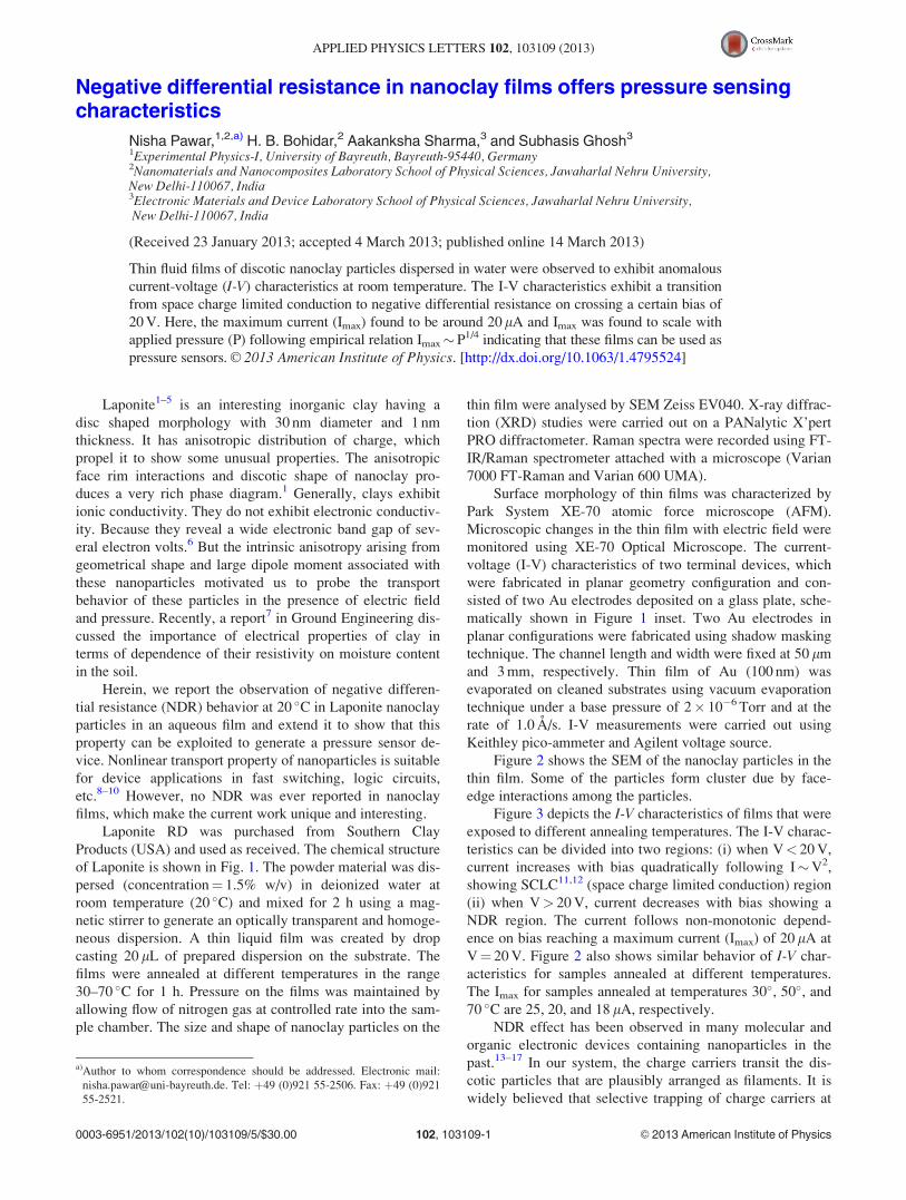
Nisha Pawar,1,2,a) H. B. Bohidar,2 Aakanksha Sharma,3 and Subhasis Ghosh3
1Experimental Physics-I, University of Bayreuth, Bayreuth-95440, Germany2Nanomaterials and Nanocomposites Laboratory School of Physical Sciences, Jawaharlal Nehru University,New Delhi-110067, India3Electronic Materials and Device Laboratory School of Physical Sciences, Jawaharlal Nehru University,New Delhi-110067, India
(Received 23 January 2013; accepted 4 March 2013; published online 14 March 2013)
Thin fluid films of discotic nanoclay particles dispersed in water were observed to exhibit anomalous
current-voltage (I-V) characteristics at room temperature. The I-V characteristics exhibit a transition
from space charge limited conduction to negative differential resistance on crossing a certain bias of
20 V. Here, the maximum current (Imax) found to be around 20 lA and Imax was found to scale with
applied pressure (P) following empirical relation Imax� P1/4 indicating that these films can be used as
pressure sensors. VC 2013 American Institute of Physics. [http://dx.doi.org/10.1063/1.4795524]
Laponite1–5 is an interesting inorganic clay having a
disc shaped morphology with 30 nm diameter and 1 nm
thickness. It has anisotropic distribution of charge, which
propel it to show some unusual properties. The anisotropic
face rim interactions and discotic shape of nanoclay pro-
duces a very rich phase diagram.1 Generally, clays exhibit
ionic conductivity. They do not exhibit electronic conductiv-
ity. Because they reveal a wide electronic band gap of sev-
eral electron volts.6 But the intrinsic anisotropy arising from
geometrical shape and large dipole moment associated with
these nanoparticles motivated us to probe the transport
behavior of these particles in the presence of electric field
and pressure. Recently, a report7 in Ground Engineering dis-
cussed the importance of electrical properties of clay in
terms of dependence of their resistivity on moisture content
in the soil.
Herein, we report the observation of negative differen-
tial resistance (NDR) behavior at 20 �C in Laponite nanoclay
particles in an aqueous film and extend it to show that this
property can be exploited to generate a pressure sensor de-
vice. Nonlinear transport property of nanoparticles is suitable
for device applications in fast switching, logic circuits,
etc.8–10 However, no NDR was ever reported in nanoclay
films, which make the current work unique and interesting.
Laponite RD was purchased from Southern Clay
Products (USA) and used as received. The chemical structure
of Laponite is shown in Fig. 1. The powder material was dis-
persed (concentration¼ 1.5% w/v) in deionized water at
room temperature (20 �C) and mixed for 2 h using a mag-
netic stirrer to generate an optically transparent and homoge-
neous dispersion. A thin liquid film was created by drop
casting 20 lL of prepared dispersion on the substrate. The
films were annealed at different temperatures in the range
30–70 �C for 1 h. Pressure on the films was maintained by
allowing flow of nitrogen gas at controlled rate into the sam-
ple chamber. The size and shape of nanoclay particles on the
thin film were analysed by SEM Zeiss EV040. X-ray diffrac-
tion (XRD) studies were carried out on a PANalytic X’pert
PRO diffractometer. Raman spectra were recorded using FT-
IR/Raman spectrometer attached with a microscope (Varian
7000 FT-Raman and Varian 600 UMA).
Surface morphology of thin films was characterized by
Park System XE-70 atomic force microscope (AFM).
Microscopic changes in the thin film with electric field were
monitored using XE-70 Optical Microscope. The current-
voltage (I-V) characteristics of two terminal devices, which
were fabricated in planar geometry configuration and con-
sisted of two Au electrodes deposited on a glass plate, sche-
matically shown in Figure 1 inset. Two Au electrodes in
planar configurations were fabricated using shadow masking
technique. The channel length and width were fixed at 50 lm
and 3 mm, respectively. Thin film of Au (100 nm) was
evaporated on cleaned substrates using vacuum evaporation
technique under a base pressure of 2� 10�6 Torr and at the
rate of 1.0 A/s. I-V measurements were carried out using
Keithley pico-ammeter and Agilent voltage source.
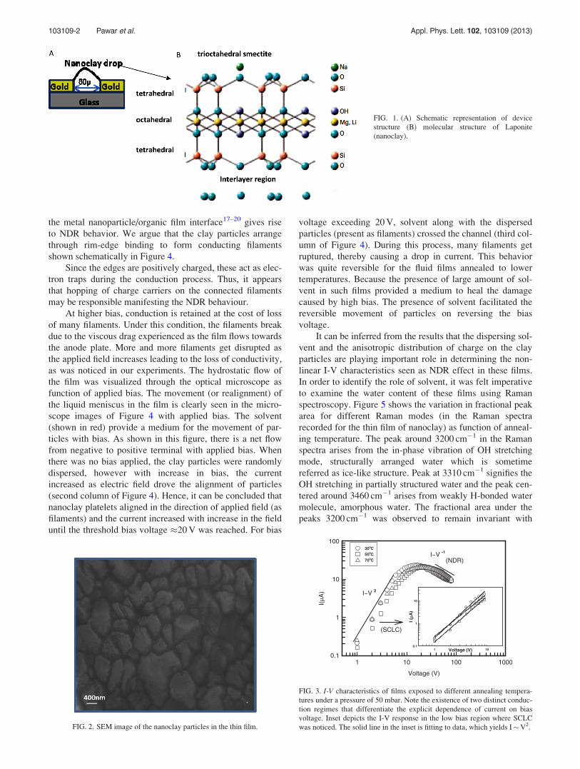
Figure 2 shows the SEM of the nanoclay particles in the
thin film. Some of the particles form cluster due by face-
edge interactions among the particles.
Figure 3 depicts the I-V characteristics of films that were
exposed to different annealing temperatures. The I-V charac-
teristics can be divided into two regions: (i) when V< 20 V,
current increases with bias quadratically following I�V2,
showing SCLC11,12 (space charge limited conduction) region
(ii) when V> 20 V, current decreases with bias showing a
NDR region. The current follows non-monotonic depend-
ence on bias reaching a maximum current (Imax) of 20 lA at
V¼ 20 V. Figure 2 also shows similar behavior of I-V char-
acteristics for samples annealed at different temperatures.
The Imax for samples annealed at temperatures 30�, 50�, and
70 �C are 25, 20, and 18 lA, respectively.
NDR effect has been observed in many molecular and
organic electronic devices containing nanoparticles in the
past.13–17 In our system, the charge carriers transit the dis-
cotic particles that are plausibly arranged as filaments. It is
widely believed that selective trapping of charge carriers at
a)Author to whom correspondence should be addressed. Electronic mail:
[email protected]. Tel: þ49 (0)921 55-2506. Fax: þ49 (0)921
55-2521.
0003-6951/2013/102(10)/103109/5/$30.00 VC 2013 American Institute of Physics102, 103109-1
APPLIED PHYSICS LETTERS 102, 103109 (2013)
the metal nanoparticle/organic film interface17–20 gives rise
to NDR behavior. We argue that the clay particles arrange
through rim-edge binding to form conducting filaments
shown schematically in Figure 4.
Since the edges are positively charged, these act as elec-
tron traps during the conduction process. Thus, it appears
that hopping of charge carriers on the connected filaments
may be responsible manifesting the NDR behaviour.
At higher bias, conduction is retained at the cost of loss
of many filaments. Under this condition, the filaments break
due to the viscous drag experienced as the film flows towards
the anode plate. More and more filaments get disrupted as
the applied field increases leading to the loss of conductivity,
as was noticed in our experiments. The hydrostatic flow of
the film was visualized through the optical microscope as
function of applied bias. The movement (or realignment) of
the liquid meniscus in the film is clearly seen in the micro-
scope images of Figure 4 with applied bias. The solvent
(shown in red) provide a medium for the movement of par-
ticles with bias. As shown in this figure, there is a net flow
from negative to positive terminal with applied bias. When
there was no bias applied, the clay particles were randomly
dispersed, however with increase in bias, the current
increased as electric field drove the alignment of particles
(second column of Figure 4). Hence, it can be concluded that
nanoclay platelets aligned in the direction of applied field (as
filaments) and the current increased with increase in the field
until the threshold bias voltage �20 V was reached. For bias
voltage exceeding 20 V, solvent along with the dispersed
particles (present as filaments) crossed the channel (third col-
umn of Figure 4). During this process, many filaments get
ruptured, thereby causing a drop in current. This behavior
was quite reversible for the fluid films annealed to lower
temperatures. Because the presence of large amount of sol-
vent in such films provided a medium to heal the damage
caused by high bias. The presence of solvent facilitated the
reversible movement of particles on reversing the bias
voltage.
It can be inferred from the results that the dispersing sol-
vent and the anisotropic distribution of charge on the clay
particles are playing important role in determining the non-
linear I-V characteristics seen as NDR effect in these films.
In order to identify the role of solvent, it was felt imperative
to examine the water content of these films using Raman
spectroscopy. Figure 5 shows the variation in fractional peak
area for different Raman modes (in the Raman spectra
recorded for the thin film of nanoclay) as function of anneal-
ing temperature. The peak around 3200 cm�1 in the Raman
spectra arises from the in-phase vibration of OH stretching
mode, structurally arranged water which is sometime
referred as ice-like structure. Peak at 3310 cm�1 signifies the
OH stretching in partially structured water and the peak cen-
tered around 3460 cm�1 arises from weakly H-bonded water
molecule, amorphous water. The fractional area under the
peaks 3200 cm�1 was observed to remain invariant with
FIG. 1. (A) Schematic representation of device
structure (B) molecular structure of Laponite
(nanoclay).
FIG. 2. SEM image of the nanoclay particles in the thin film.
FIG. 3. I-V characteristics of films exposed to different annealing tempera-
tures under a pressure of 50 mbar. Note the existence of two distinct conduc-
tion regimes that differentiate the explicit dependence of current on bias
voltage. Inset depicts the I-V response in the low bias region where SCLC
was noticed. The solid line in the inset is fitting to data, which yields I�V2.
103109-2 Pawar et al. Appl. Phys. Lett. 102, 103109 (2013)

change in temperature while the same for 3310 cm�1 and
3460 cm�1 band decreased with increase in annealing tem-
perature (Figure 5). This indicates significant loss of solvent
(water) from these films. Realize that particle hydration is
provided by mostly partially structured water. Thus, loss of
hydartion would manifest in the breaking of filaments pres-
ent across the channel resulting in drop in current.
This also explains the reduction in the observed maxi-
mum current Imax with annealing temperature due to the
lesser amount of solvent required for healing against ruptur-
ing the filaments caused by applied bias. This infers that the
annealing temperature controls the amount of solvent in the
film, which plays an important role in the movement of par-
ticles across the channel attributing NDR feature to the film.
These films were subjected to XRD analysis in order to
probe their micro-crystalline characteristics. A representative
set of data is shown in Figure 6 for a film annealed at 30 �C.
XRD and AFM topographic images of the thin films have
been measured in-situ under electric field. Figure 6 clearly
shows how the peak intensity of XRD and film roughness
calculated from AFM topographic images vary under electric
field. For fields below 20 V, the XRD peak intensity
remained invariant under applied bias but a sharp decrease
was noticed when the voltage crosses 20 V (in NDR region).
Thus, the film characteristic is found to alter significantly as
FIG. 4. Comparison of optical (middle row) and morphological (bottom row) changes of a nanoclay film (annealed at 30 �C) in different bias regimes (i) no bias
(column 1), (ii) SCLC (column 2), and (iii) NDR (column 3). Here, "þ" and "�" sign show respective electrode positions. Top row shows the schematic represen-
tation of particle arrangement in three regimes. Middle row shows the microscope images of the film of nanoclay particles. Yellow line shows the channel (50 lm
and 3 mm) with þ and � as the electrode on the sides shown, red color shows the movement of the particles in the film as a function of bias applied. Last row
shows the AFM snapshots on the channel of the film. The first column shows the random alignment of the particle and their cluster in the absence of any bias volt-
age, second column shows the alignment of the particle forming a filament across the channel, and third column shows that filament got broken after the applica-
tion of higher bias voltage (or the liquid film shown by red color migrates to the anode plate). Upper row is the middle row rotated by 90 �C.
FIG. 5. Variation in peak area for three Raman bands at 3200 cm�1,
3300 cm�1 and 3460 cm�1 as a function of annealing temperature.
103109-3 Pawar et al. Appl. Phys. Lett. 102, 103109 (2013)

function of applied bias, a property that was exploited subse-
quently. The change in XRD peak intensity and surface
roughness clearly indicate the change in the alignment of
clay particles embedded in the film with bias. Interestingly,
the average roughness of the film was observed to decrease
with the applied field and passing through minima at �20 V.
The correlation between film roughness and XRD inten-
sity clearly indicates the reduction in alignment of clay par-
ticles resulting a drop in current and the appearance of NDR.
Presumably, in the NDR region, movement of solvent medi-
ated clay particles creates various trap states, which provide
hindrance to the flow of current. However, the morphologi-
cal changes in the samples were not visible at any instance.
The unique field dependent characteristic shown in
Figure 5 was effectively used to propose the design of a
potential pressure sensor. Figure 7 shows the I-V characteris-
tics of a film exposed to different pressure. The current pro-
files shown in Figures 3 and 7 are similar except Imax
increases with pressure. This implies, as discussed before,
that the particle arrangement inside the film is sensitive to
applied pressure. The maximum current is plotted as function
of applied pressure in the inset of Figure 7, which depicts
excellent pressure sensitivity. At low pressure, the particles
have random orientation, which results in the flow of less
current due to misalignment of particles. Arrangement of
particles, presumably as filaments was found to be facilitated
at higher pressure. The maximum current, Imax, determined
from Figure 7 was fitted to the applied pressure, P, which fol-
lowed a power-law scaling relation given by Imax� P1/4. The
observed behavior was completely reversible with a resetting
time �20 s. Thus, the observation of SCLC to NDR cross-
over in Laponite films revealed a unique and interesting elec-
trical property that was not known hitherto. This particular
attribute has potential to be developed in to a nano material
based device.
In conclusion, we show that nanoclay films exhibit
unique bias dependent conduction behaviour not known
hitherto. Conduction through films is governed by SCLC for
low bias, whereas above a threshold bias, the film shows
NDR revealing a non-monotonic dependence on electric field.
The dependence of Imax over annealing temperature infers the
alignment of particles mediated by solvent. It was conjectured
with the help of AFM and XRD studies that linear organiza-
tion of the anisotropic clay platelets in the form of filaments
provides the conduction path. The rupturing of filaments at
higher electric filed is responsible for NDR. The exact nature
of charge carriers remained elusive and undetermined in our
studies that are a subject of future work. These films depicted
considerable pressure sensitivity, a feature that will enable
these materials to be developed as pressure sensors.
We are thankful to Advanced Research Instrumentation
Facility of the University for Raman, SEM, and XRD facil-
ity. N.P. acknowledges support from Council of Scientific
and Industrial Research, Government of India for fellowship.
1A. Mourchid and P. Levitz, Phys. Rev. E 57, R4887–R4890 (1998).2M. Kroon, G. Wegdam, H. Gerard, and R. Sprik, Phys. Rev. E 54,
6541–6550 (1996).3F. Pignon, J. M. Piau, and A. Magnin, Phys. Rev. Lett. 76, 4857–4860
(1996).4R. Bandyopadhyay, D. Liang, H. Yardimci, D. A. Sessoms, M. A.
Borthwick, S. G. J. Mochrie, J. L. Harden, and R. L. Leheny, Phys. Rev.
Lett. 93, 228302 (2004).5P. Mongondry, J. F. Tassin, and T. Nicolai, J. Colloid Interface Sci. 283,
397–405 (2005).6E. Izci, Key Eng. Material. 264–268, 1357–1360 (2004).7Report Ground Engineering, Monitoring Electrical Appliance, September
12–14, 2010, available at www.bgs.ac.uk/downloads/start.cfm?id=1872.8H. Mizuta and T. Tanoue, The Physics and Applications of ResonantTunneling Diodes (Cambridge University Press, Cambridge, 1995).
9T. P. E. Broekaert, B. Brar, J. P. A. van der Wagt, C. Seabaugh, T. S.
Moise, F. J. Morris, E. A. Beam, and G. A. Frazier, IEEE J. Solid State
Circuits 33, 1342–1349 (1998).10S.-Y. Chung, N. Jin, P. R. Berger, R. Yu, P. E. Thompson, R. Lake, S. L.
Rommel, and S. K. Kurinec, Appl. Phys. Lett. 84, 2688–2691 (2004).11M. A. Lampert, Phys. Rev. 103, 1648–1656 (1956).
FIG. 6. Variation of XRD peak intensity (at 2h¼ 6.1�), sample roughness
and current in the film as function of applied voltage. Note that 20 V is a
characteristic bias for this device.
FIG. 7. I-V characteristics for a clay film at different pressure and annealed
at constant temperature 70 �C. Imax is plotted as function of pressure in the
inset. Solid line depicts a power law fit as Imax�P1/4.
103109-4 Pawar et al. Appl. Phys. Lett. 102, 103109 (2013)

12N. F. Mott and R. W. Gurney, Electronic Processes in Ionic Crystals(Oxford University Press, New York, 1940), Vol. 172.
13A. A. Grinberg, S. Luryi, M. R. Pinto, and N. L. Schryer, IEEE Trans.
Electron Devices 36, 1162–1170 (1989).14T. W. Hickmott, J. Appl. Phys. 33, 2669–2682 (1962).15R. D. Gould and C. A. Hogarth, Phys. Status Solids 23, 531–535 (1974).16W. Tang, H. Shi, G. Xu, B. S. Ong, Z. D. Popovic, J. Deng, J. Zhao, and
G. Rao, Adv. Mater (Weinheim, Ger.) 17, 2307–2311 (2005).
17R. J. Tseng, J. Ouyang, C.-W. Chu, J. Huang, and Y. Yang, Appl. Phys.
Lett. 88, 123506 (2006).18J. Chen, L. Xu, J. Lin, Y. Geng, L. Wang, and D. Ma, Appl. Phys. Lett. 89,
083514 (2006).19J. Li, D. N. Zheng, X. S. Rao, C. H. Sow, L. Chen, and C. K. Ong,
Europhys. Lett. 65, 823–829 (2004).20Q. Hu, S. M. Jung, H. H. Lee, Y.-S. Kim, Y. J. Choi, D.-H. Kang, K.-B.
Kim, and T.-S. Yoon, J. Phys. D: Appl. Phys. 44, 085403 (2011).
103109-5 Pawar et al. Appl. Phys. Lett. 102, 103109 (2013)