Nanostructural and electronic properties of polytypes in InN nanocolumns
10
Nanostructural and electronic properties of polytypes in InN nanocolumns J. Kioseoglou, T. Koukoula, Ph. Komninou, A. Georgakilas, M. Androulidaki, and Th. Kehagias Citation: Journal of Applied Physics 114, 074312 (2013); doi: 10.1063/1.4818517 View online: http://dx.doi.org/10.1063/1.4818517 View Table of Contents: http://scitation.aip.org/content/aip/journal/jap/114/7?ver=pdfcov Published by the AIP Publishing [This article is copyrighted as indicated in the article. Reuse of AIP content is subject to the terms at: http://scitation.aip.org/termsconditions. Downloaded to ] IP: 155.207.10.238 On: Sun, 08 Dec 2013 17:22:51
Transcript of Nanostructural and electronic properties of polytypes in InN nanocolumns

Nanostructural and electronic properties of polytypes in InN nanocolumnsJ. Kioseoglou, T. Koukoula, Ph. Komninou, A. Georgakilas, M. Androulidaki, and Th. Kehagias Citation: Journal of Applied Physics 114, 074312 (2013); doi: 10.1063/1.4818517 View online: http://dx.doi.org/10.1063/1.4818517 View Table of Contents: http://scitation.aip.org/content/aip/journal/jap/114/7?ver=pdfcov Published by the AIP Publishing
[This article is copyrighted as indicated in the article. Reuse of AIP content is subject to the terms at: http://scitation.aip.org/termsconditions. Downloaded to ] IP:
155.207.10.238 On: Sun, 08 Dec 2013 17:22:51

Nanostructural and electronic properties of polytypes in InN nanocolumns
J. Kioseoglou,1 T. Koukoula,1 Ph. Komninou,1 A. Georgakilas,2 M. Androulidaki,2
and Th. Kehagias1,a)
1Physics Department, Aristotle University of Thessaloniki, GR-54124 Thessaloniki, Greece2Microelectronics Research Group, IESL, FORTH, P.O. Box 1385, GR-71110 Heraklion,Crete and Department of Physics, University of Crete, P.O. Box 2208, GR-71003 Heraklion, Crete, Greece
(Received 18 June 2013; accepted 31 July 2013; published online 21 August 2013)
Transmission electron microscopy techniques and density functional theory calculations were
employed to investigate the nanostructural and electronic properties of InN polytypes observed in
InN nanocolumns, grown on Si(111) by molecular beam epitaxy. Moir�e fringes and alternating
hexagonal and cubic lattice stacking sequences along the c-axis, observed among the wurtzite
layers, implied the presence of different structures embedded in the basic 2H structure of the
nanocolumns. Quantitative electron diffraction analysis and high-resolution image simulations
verified the coexistence of the wurtzite structure with the 4H, 6H, and the 3C zinc-blende structural
polytypes. Total energies calculations established the 2H wurtzite structure as the most stable
polytype. The band gap of all polytypes was found direct with the energies and the band gaps of
the 4H (Eg¼ 0.64 eV) and 6H (Eg¼ 0.60 eV) structures calculated between the corresponding
values of the 2H (Eg¼ 0.75 eV) and 3C (Eg¼ 0.49 eV) basic structures. Theoretical and
experimental analysis showed that at the initial stages of growth InN nanocolumns were under
tensile strain along both the basal plane and growth direction. Structural polytypes were then
introduced in the form of embedded inclusions to accommodate the excess tensile strain along the
growth direction, allowing the entire process of polymorphism to be the dominant strain relaxation
mechanism of InN nanocolumns. Moreover, the lattice and energetic properties and band gap
values of InN polytypes showed a linear dependence on hexagonality, while the presence of
polytypes led to a characteristic broadening of the photoluminescence emission peak toward lower
emission energies. VC 2013 AIP Publishing LLC. [http://dx.doi.org/10.1063/1.4818517]
I. INTRODUCTION
One-dimensional III-nitride nanostructures, such as nano-
columns (NCs), have shown high potential not only for the
fabrication of nanodevices but also for the overgrowth of
stress-free films, given that the small lateral dimension of NCs
allows InN heteroepitaxial growth free of threading defects.
The ability to grow high quality InN-based nanostructures
will maximize the high prospectives of InN and its ternary
(InGaN and InAlN) and quaternary (InAlGaN) alloys, which
constitute a unique semiconductor material system covering
from near infrared to the ultraviolet region of the electromag-
netic spectrum, with significant applications in LEDs, LDs,
solar cells, and chemical sensors.1 Understanding of the nano-
scale structural properties of these structures is important for
the optimization of their growth process and control over their
electronic and optical properties.
The main structural defects observed in this type of
nanostructures are stacking faults (SFs),2 which are closely
related to polytypism. Currently, polytypism in semiconduc-
tor groups IV-IV and III–V has attracted much attention
from the scientific community and therefore, becomes a mat-
ter of intense research activity. In particular, SiC exhibits
pronounced polytypism with more than a hundred different
crystalline modifications, namely, polytypes.3–5 The struc-
tural and electronic properties of semiconducting materials
containing multiple polytypes seem to arise as a combination
of the corresponding properties of the basic structures, i.e.,
the cubic/zinc-blende (3C) and the hexagonal/wurtzite (2H)
polytypes of these materials. Polytype inclusions are easier
to form in nanowires, since the small nanowire diameter
allows interlayers of different stacking sequences to form
from sidewall to sidewall and thus, there is no need of
bounding partial dislocations, resulting in more stable struc-
tures.2,6 Current reports in III–V nanowires showed that by
controlling polytypism, new potentials of crystal phase engi-
neering in “heterocrystalline homostructures” are opening.7
However, it was not until recently that polytypism in
III-Nitrides was observed, due to growth on SiC sub-
strates.8,9 In particular, the growth of high quality nonpolar
4H-polytype AlN and AlN/AlGaN multiple-quantum-well
structures on (1�100) or (11�20) 4H-SiC substrates, with low
threading dislocation and SF densities, has been reported
along with theoretical studies.10,11 In addition, polytype
domains in InGaN thick layers and 4H-InN in Mg doped InN
layer were experimentally observed by transmission electron
microscopy (TEM).12,13 Therefore, polytypism in InN but
also in combination with Ga- and Al-based nitrides can bring
about new prospects for band gap tuning and lead to new
complex structures with tailored electronic and optical prop-
erties. Consequently, theoretical understanding and experi-
mental control over quantum size growth of nitride
polytypes will play an important role in semiconductors
technology.a)E-mail: [email protected]
0021-8979/2013/114(7)/074312/9/$30.00 VC 2013 AIP Publishing LLC114, 074312-1
JOURNAL OF APPLIED PHYSICS 114, 074312 (2013)
[This article is copyrighted as indicated in the article. Reuse of AIP content is subject to the terms at: http://scitation.aip.org/termsconditions. Downloaded to ] IP:
155.207.10.238 On: Sun, 08 Dec 2013 17:22:51

To explore this possibility, a thorough experimental
and theoretical analysis was carried out to enlighten poly-
typism in InN NCs. TEM-based techniques and density
functional theory (DFT) calculations were employed to
investigate the structural and the electronic properties of
InN polytypes. The study was originally triggered by the
experimental identification of structural polytypes in InN
NCs grown on Si(111) by plasma assisted molecular beam
epitaxy (PAMBE). High-resolution TEM (HRTEM) obser-
vations, image simulations as well as quantitative analysis
of the selected area electron diffraction (SAED) patterns,
based on DFT calculations, revealed the presence of various
polymorphisms along with the ground state wurtzite (2H)structure. Photoluminescence (PL) experiments combined
with band structure DFT calculations were utilized to ana-
lyze the band gap characteristics of the InN structural poly-
types and their influence on the emission spectrum of
wurtzite InN.
II. EXPERIMENTAL AND THEORETICAL METHODS
The InN NCs were grown by PAMBE on boron-doped
p-type Si(111) substrates under intense nitrogen rich condi-
tions. Initially, an ex-situ chemical cleaning method was
applied on the substrate’s surface, followed by in-situ ther-
mal cleaning, which resulted in 7� 7 surface reconstruction
observed by reflection high energy electron diffraction
(RHEED). InN NCs were grown, without prior nitridation of
the Si surface, at Tsub¼ 500 �C for 1 h using a III/N flux ratio
of 0.16 with the In-flux set at 120 nm/h. Details of the growth
process of similar nanostructures have been given
elsewhere.14,15
Specimens for TEM and HRTEM observations were
prepared in cross-sectional geometry (XTEM) by mechanical
grinding, followed by low-voltage Arþ high-precision ion-
milling (Gatan PIPS) to achieve electron transparency. The
TEM and HRTEM experiments were performed using a
200 kV Jeol 2011 microscope with a point resolution of
0.194 nm and Cs¼ 0.5 mm.
DFT calculations under the ABINIT code,16 and the
local density approximation (LDA) were used to resolve
the energies of the polytypes with respect to the wurtzite
structure and the band gap of each different structures
implementing modified pseudopotentials, which accurately
reproduce the band gap of InN (MPP-LDA approach).17 In
particular, the plane waves were expanded up to a cutoff
energy of 140 Ry and 8� 8� 12 for 2H, 8� 8� 8 for 3C,
8� 8� 6 for 4H, and 8� 8� 4 for 6H. Monkhorst-Pack
k-point meshes were used for the 1� 1� 1 unit cell.
Simulated HRTEM images as well as simulated SAED pat-
terns of the complex crystal structures were calculated
using the EMS software.18
The 20 K PL spectrum reported in this work was
obtained using a He–Cd continuous-wave laser at 325 nm
(35 mW) and a monochromator with 600 grooves/mm gra-
ting blazed at 2 lm. The measurements were taken with a
special liquid nitrogen (LN2) cooled InGaAs PIN photodiode
detector with a maximum responsivity at 1.92 lm and a
lock-in amplifier.
III. MORPHOLOGY AND NANOSTRUCTURE OF InNNCs
The overall morphology of the InN NCs is shown in the
XTEM micrograph of Fig. 1(a), viewed along the [11�20]InN//
[1�10]Si zone axis (z.a.). The NCs areal density was �8� 108
cm�2, while their average height was estimated at 330
6 20 nm. Their diameter ranged from 50 nm to 250 nm with
the majority of them in the middle and the high end of the
range. However, the diameter of InN NCs remains rather
constant along the growth axis and thus, a negligible tapering
effect was accounted. Moreover, faceted tip morphology of
the NCs was observed. While their sidewalls are the
m-planes, their tips are formed by 6-fold crystal facets
inclined by �23�–26� relative to the basal plane, and there-
fore, they were characterized as the {10�14} planes. As seen
in the HRTEM image of Fig. 1(b), the high N-flux resulted
in unintentional nitridation of the Si surface and formation of
a thin amorphous layer at the InN/Si interface, which is usu-
ally observed in III/N heteroepitaxy on Si and is character-
ized as SixNy.2 Furthermore, in the NC of Fig. 1(b), besides
the (0001) basal planes of the wurtzite structure, numerous
areas exhibiting Moir�e patterns are evident. This clearly
implies the presence of overlapping crystals tilted or twisted
by a few degrees, even from the early stages of growth.
Different lattice stacking sequences were identified
along the growth direction (Fig. 2(a)). In the HRTEM image
of Fig. 2(a), regions of an integer multiplicity of the 2Hstacking mediated by atomic layers of cubic stacking, as
FIG. 1. (a) XTEM micrograph near the [11�20]InN//[1�10]Si z.a., showing the
faceted tip morphology of InN NCs. (b) HRTEM image of a NC along the
[11�20]InN//[1�10]Si z.a., illustrating the growth of NCs on a SixNy amorphous
layer formed at the InN/Si interface by unintentional nitridation of the Si
surface. Moir�e fringes suggest the superposition of slightly tilted/twisted
crystal lattices in the NC.
074312-2 Kioseoglou et al. J. Appl. Phys. 114, 074312 (2013)
[This article is copyrighted as indicated in the article. Reuse of AIP content is subject to the terms at: http://scitation.aip.org/termsconditions. Downloaded to ] IP:
155.207.10.238 On: Sun, 08 Dec 2013 17:22:51

well as regions exclusively of cubic stacking embedded in
the dominant wurtzite lattice are observed. This obviously
suggests the occurrence of InN structural polytypes in the
NCs. The 4H, 6H, and 3C polytypes could be identified from
several HRTEM images of numerous NCs. These polytypes
appear in the form of inclusions within the basic wurtzite
structure. In Fig. 2(b), Fast-Fourier Transform (FFT) diffrac-
tograms of the marked areas depicted in the HRTEM image
of Fig. 2(a) are shown, revealing the presence of additional
frequencies and thus, verifying the occurrence of structural
polytypes of the 2H structure in conjunction with the [11�20]
oriented 2H and the [1�10] oriented 3C basic structures,
respectively. When polytype inclusions are not localized in
the vicinity of the free lateral sidewalls, they are usually
delimited by partial dislocations resembling to the SF forma-
tion. This issue will be addressed later.
At the interfacial area, i.e., at the early stages of InN
growth, a permutation between narrow (<50 nm in diameter)
and wider NCs was observed. While in narrow NCs phase
transitions from the 2H structure to other InN polytypes were
observed to occur very close to the Si surface (Figs. 1(b) and
2(c)), in wider NCs the wurtzite structure is dominant, and
polytypes were seen to form at later stages of growth,
namely, after several monolayers of 2H InN growth
(Fig. 2(d)). This could be explained in terms of lattice con-
stant differences in smaller and large radius initial InN
nuclei, forming presumably narrow and wider NCs, respec-
tively. For a given surface tension, the Laplace pressure is
inversely proportional to the nuclei radius, thus small nuclei
should exhibit high values of Laplace pressure, in the range
of several GPa,19 which may trigger polymorphic transitions
from the initial stages of NC growth. For larger radii
(>100 nm), Laplace pressure inside InN nuclei drops rapidly,
hence the basic 2H structure is prevailing. Moreover, the ani-
sotropy of surface energy was established as an even stron-
ger driving force for the formation of NCs,19 which leads to
an effective pressure and, consequently, induces a deviation
on the lattice constants in small nuclei.
The unintentional nitridation of the Si surface resulted
in a non-uniform amorphous SixNy layer exhibiting thick-
ness fluctuations (1.5–3.5 nm) and thus, a noticeable rough-
ness (Figs. 2(c) and 2(d)). However, as shown in the
HRTEM images of Figs. 2(c) and 2(d) by black arrows,
crystalline Si islands apparently remained intact at the Si
surface, although it was subjected to the unintentional nitri-
dation at the early stages of InN growth. Indeed the Si sur-
face seems to be rapidly covered by InN nuclei that evolve
into InN NCs and complete amorphization at the InN/Si
interface is prevented. Si islands were observed in almost
every NC/substrate interface and can potentially act as seeds
promoting epitaxial growth of InN-on-Si. Nevertheless,
since the area covered by Si islands is restrained, InN
growth is practically accomplished on the amorphous SixNy
material and thus, the epitaxial strain imposed by the lattice
mismatch should be considered minimal. As a consequence
of the interfacial amorphous layer thickness fluctuations,
deviations from the exact epitaxial relationship between the
two lattices were observed (Fig. 2(d)), i.e., the [0001]
growth axis of the NCs is not parallel to the normal of the
substrate’s surface.
FIG. 2. (a) HRTEM image taken along
the [11�20]InN z.a., showing regions of
successive atomic layers with different
stacking sequences (2H, 4H, 6H, and
3C) along the growth axis. (b)
Corresponding FFT diffractograms of
the four marked domains revealing the
presence of additional spatial frequen-
cies in the [11�20] oriented 2H InN
belonging to the 4H and 6H polytypes
(white arrows), as well as the [1�10]
oriented 3C polytype. (c) HRTEM
image along the [11�20]InN//[1�10]Si
z.a., depicting the InN/Si interface of a
narrow NC. Crystalline Si islands resi-
dues of the unintentional nitridation of
the Si surface are observed (black
arrows). (d) Corresponding HRTEM
image from a wider NC, where the
roughness of the SixNy layer led to
misalignment of the growth axis of the
NC relative to the Si surface normal.
074312-3 Kioseoglou et al. J. Appl. Phys. 114, 074312 (2013)
[This article is copyrighted as indicated in the article. Reuse of AIP content is subject to the terms at: http://scitation.aip.org/termsconditions. Downloaded to ] IP:
155.207.10.238 On: Sun, 08 Dec 2013 17:22:51

IV. CRYSTALLOGRAPHY AND ATOMISTIC MODELINGOF InN STRUCTURAL POLYTYPES
InN commonly adopts the wurtzite structure (2H, space
group (S.G.)P63mc), which comprises four atoms per unit
cell and can be visualized as two interpenetrating hexagonal
substructures; one of In and one of N atoms displaced by the
distance u along the c-axis. The primitive basis vectors of
the unit cell are a1¼ (12;�
ffiffi3p
2; 0)a, a2¼ (1
2;ffiffi3p
2; 0)a, and
a3¼ (0,0,c/a)a in Cartesian coordinates, while the positions
of the atoms, in units of a1, a2, and a3, are (13; 2
3; 0) and
(23; 1
3; 1
2) for atoms of the one species, and (1
3; 2
3; u) and
(23; 1
3; uþ 1
2) for atoms of the other species. In the ideal wurt-
zite structure u¼ 3/8 and c=a ¼ffiffiffiffiffiffiffiffi8=3
p, otherwise in order to
describe small deviations from the ideal u displacement
between the sublattices of the two species, a dimensionless
internal structural parameter e1 should be introduced (then
u ¼ 3=8þ e1).20 The relation between e1 and the strain-free
c=a ratio for the 2H structure can be deduced from the con-
servation law of the bond length as e1 ¼ 18
83
ca
� ��2 � 1� �
.20
The stacking sequence along [0001] is ���ABABAB���, while
each layer parallel to the basal plane is composed of two sub-
layers of distinct atomic species. Now, we define as hexago-
nal layer h each layer which is adjacent to two identical
layers, such as B in ���ABABAB���. This leads to 2H wurtzite
being symbolized as ���hhhhhh���. In Table I, the correspond-
ing crystallographic definitions and symbols for the 3C, 4H,and 6H crystal structures are given.
Based on the above crystallographic analysis, atomistic
models of all relevant polytypes were constructed as shown
in Fig. 3.
V. QUANTITATIVE ELECTRON DIFFRACTIONANALYSIS
The variety of structures resulting from the observed dif-
ferent stacking sequences that match the structural polytypes
of InN were studied by quantitative SAED analysis in con-
junction with DFT calculations. Consequently, SAED pat-
terns taken exactly on the [11�20]InN z.a. were digitized at
4000 dpi using a Nikon SUPER COOLSCAN 9000 and the
spacing of the wurtzite reflections along the [0001] direction
were then measured using line profiles and peak finding tech-
niques.21 In order to identify the exact position of each
reflection, the “center of mass” of each spot corresponding to
a reflection was calculated, where the term “mass” stands for
the intensity of each pixel. In addition, simulated SAED pat-
terns, based on DFT calculations, were calculated, and the
positions of the experimental reflections were compared with
the simulated ones. Figure 4(a) is a SAED pattern of a wider
TABLE I. Crystallographic data of the 3C, 4H, and 6H InN structural polytypes; i.e., space group, primitive basic vectors of the unit cell, atomic positions of
the two species in units of primitive vectors, and the dimensionless internal structural parameters (e1, e2, e3, d1, d2) describing deviations from the ideal crystal
structures. The stacking sequences along [0001] direction and the structure symbols are also depicted.
3C, S.G. F�43m 4H, S.G. P63mc 6H, S.G. P63mc
Primitive vectors a1 ¼ (12; 1
2; 0)a a1 ¼ (1
2;ffiffi3p
2; 0)a a1 ¼ (1
2;ffiffi3p
2; 0)a
a2 ¼ (12; 0; 1
2)a a2 ¼ (1
2;ffiffi3p
2; 0)a a2 ¼ (1
2;ffiffi3p
2; 0)a
a3 ¼ (0; 12; 1
2)a a3 ¼ (0,0,c/a)a a3 ¼ (0,0,c/a)a
Atomic positions in units of a1, a2, a3 1st species 2nd species 1st species 2nd species 1st species 2nd species
(0; 0; 0) (0; 0; 18þe1)
(0; 0; 0) ð13; 2
3; 7
16þ e2Þ (0; 0; 1
2) (0; 0; 5
8þe1)
ð0; 0; 12Þ (0; 0; 3
16þ e1) (1
3þd2;
23þd1;
16þd1) (1
3; 2
3; 7
24þe2)
ð0; 0; 0Þ (14; 1
4; 1
4) (1
3; 2
3; 1
4þ d1) (0; 0; 11
16þ e1) (1
3þd2;
23þd1;
56þd2) (1
3; 2
3; 23
24þe3)
(23; 1
3; 3
4þ d1) (2
3; 1
3; 15
16þ e2) (2
3þd1;
13þd2;
13þd2) (2
3; 1
3; 11
24þe3)
(23þd1;
13þd2;
23þd1) (2
3; 1
3; 19
24þe2)
Stacking sequence along [0001] …ABCABC… …ABCBABCBA… …ABCACBABCACBA…
Structure symbols ���cccccc��� ���hchchc��� ���hcchcchcc���
FIG. 3. Atomistic models of the polytypes identified in the InN NCs. The
various lattice stacking sequences are given on the structural models, while
the atomic stacking is denoted by a green line. The clat is the lattice constant
of each individual structure, in terms of a hexagonal lattice, while c is the
equivalent distance in each polytype corresponding to the d-spacing of the
(0001) planes of the 2H structure. Large/blue and small/red spheres corre-
spond to the In and N atomic species of the InN structure, respectively.
074312-4 Kioseoglou et al. J. Appl. Phys. 114, 074312 (2013)
[This article is copyrighted as indicated in the article. Reuse of AIP content is subject to the terms at: http://scitation.aip.org/termsconditions. Downloaded to ] IP:
155.207.10.238 On: Sun, 08 Dec 2013 17:22:51

NC, oriented along the [11�20] z.a., showing reflections from
the dominant 2H-InN structure along with satellite spots.
Most of the satellite spots belong to hexagonal-like struc-
tures aligned along the [11�20] z.a. of wurtzite. The assess-
ment of numerous SAED patterns taken from various NCs
by the preceding quantitative analysis, in combination with
simulated SAED patterns, resulted in crystallographic identi-
fication of the satellite reflections belonging to InN polytypes
and the d-spacing of their basal planes were determined. The
structural polytypes were characterized as 4H, 6H, and 3Cand their corresponding reflections are denoted in Fig. 4(a).
In addition, HRTEM image simulations based on the
calculated polytypes were used in order to validate the
results of the SAED analysis. In Fig. 4(b), the marked areas
of the HRTEM image of Fig. 2(a), as well as the simulated
HRTEM images of the various identified polytypes are illus-
trated. The unambiguous matching between them verified
the presence of multiple structural polytype inclusions in
wurtzite InN.
In Table II, the results of the quantitative analysis on the
experimental SAED patterns are depicted. Besides the clat
lattice constant values, the c values, which are the distances
in each polytype equivalent to the d0001-spacing of the 2Hstructure, are also given. These values were calculated for
each sC or sH structure (s¼ 3,4,6 for 3C, 4H, and 6H,
respectively) by the following formulas: clat ¼ sacubic=ffiffiffi3p
,
c ¼ 2acubic=ffiffiffi3p
, and ahex ¼ acubic=ffiffiffi2p
for the cubic structure,
and c ¼ clat=ðs=2Þ for the wurtzite structures. For the calcu-
lations, we have postulated that NCs as integral entities are
strain-free, due to their free lateral and top surfaces and
hence, the clat constant of the 2H structure was taken from
Ref. 22 (clat¼ 5.702 A). In Table II, the calculated by DFT
relaxed lattice constants (alat, clat), as well as the correspond-
ing c values and the c/a ratio of all structures, are depicted.
For the various polytypes, the values of the c spacing are
directly comparable. A notable conformity of the experimen-
tal values and the results of theoretical calculations is
observed.
Furthermore, in Table III, the calculated by DFT internal
structural parameters describing the relaxation of the atomic
positions within the unit cells of the hexagonal 2H, 4H, and
6H structures, namely, the deviations from the ideal configu-
rations, are given. Taking into account, the c=a ratios given
in Table II, the conservation law of the bond length resulted
in e1 ¼ 42:7� 10�4, for the 2H structure, which is close to
the corresponding calculated value given in Table III. This
finding is opposed to the disagreement between the bond
length conservation and the DFT calculated values found in
FIG. 4. (a) Experimental SAED pattern taken from a wider NC showing the
wurtzite InN reflections (black indexes) coexist with numerous satellite
spots of the 4H (blue indexes), 6H (white indexes), and 3C (red indexes)
InN structural polytypes. (b) HRTEM image simulations (thick-
ness¼ 10.7 nm defocus¼�63 nm, second maximum of contrast, white spots
correspond to atomic columns) of 2H, 4H, 6H, and 3C structures and the
corresponding experimental images (marked areas of Fig. 2(a)).
TABLE II. The clat lattice constants and the c values of the various InN structural polytypes as measured experimentally by quantitative SAED analysis. The
calculated by DFT strain-free alat, clat lattice constants, c values and c/a ratio are also presented.
Experimental values by SAED analysis Calculated values by DFT
Polytype clat (A) (60:007) c (A) (60:007) alat (A) clat (A) c (A) c/a
2H 5.702 5.702 3.5600 5.7167 5.7167 1.6058
4H 11.468 5.734 3.5501 11.5090 5.7545 1.6210
6H 17.251 5.750 3.5473 17.2962 5.7654 1.6253
3C 8.704
acubic¼ 5.025
ahex¼ 3.553
5.803 acubic¼ 5.0393
ahex¼ 3.563
8.7282 5.8188 1.6330
TABLE III. The dimensionless internal structural parameters calculated by
DFT describing the deviations of the atomic positions (relaxed atomic posi-
tions) from the ideal 2H, 4H, and 6H structures.
Polytype e1 � 10�4 e2 � 10�4 e3 � 10�4 d1 � 10�4 d2 � 10�4
2H 36
4H 7.2 4.9 �4.0
6H 1.6 1.4 4.7 �5.0 �1.8
074312-5 Kioseoglou et al. J. Appl. Phys. 114, 074312 (2013)
[This article is copyrighted as indicated in the article. Reuse of AIP content is subject to the terms at: http://scitation.aip.org/termsconditions. Downloaded to ] IP:
155.207.10.238 On: Sun, 08 Dec 2013 17:22:51
group III–V polytypes.23 To the best of our knowledge, there
are no previous theoretical results for the internal structural
parameters for InN polytypes.
In addition, the strain state of the NCs at the interface
with Si was investigated. Quantitative analysis was imple-
mented on a series of SAED patterns taken on the interfacial
InN/Si area. Using the d-spacing of the (111) Si planes
as reference (3.134 A), the (10�10) as well as the (0002)
d-spacing of InN was measured and both lattice constants of
InN were found expanded with respect to the strain-free val-
ues of InN.22 In particular, the a lattice constant was found
larger by 1.6%, while the c by 1.8%, respectively. Following
elasticity theory, this leads to the conclusion that InN NCs
were grown on SixNy exhibiting tensile strain, probably due
to the particular bonding environment between the InN and
the amorphous layer, as well as due to the growth conditions.
We will come back to this later.
VI. ELECTRONIC PROPERTIES OF InN POLYTYPES
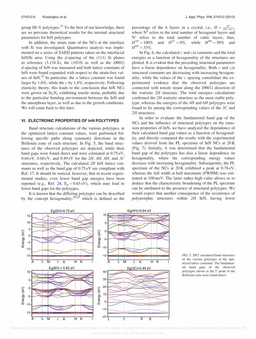
Band structure calculations of the various polytypes, at
the optimized lattice constant values, were performed fol-
lowing specific paths along symmetry directions in the
Brillouin zone of each structure. In Fig. 5, the band struc-
tures of the observed polytypes are depicted, while their
band gaps were found direct and were estimated at 0.75 eV,
0.64 eV, 0.60 eV, and 0.49 eV for the 2H, 4H, 6H, and 3Cstructures, respectively. The calculated 2H InN lattice con-
stants as well as the band gap of 0.75 eV are compliant with
Ref. 17. It should be noticed, however, that in recent experi-
mental studies, even lower band gap energies have been
reported (e.g., Ref. 24, Eg¼ 0.65 eV), which may lead to
lower band gaps for the polytypes.
It is known that the differing potytypes can be described
by the concept hexagonality,20,25 which is defined as the
percentage of the h layers in a crystal, i.e., H ¼ Nh
ðNhþNcÞ,where Nh refers to the total number of hexagonal layers and
Nc refers to the total number of cubic layers, thus,
H2H¼ 100% and H3C¼ 0%, while H4H¼ 50% and
H6H¼ 33%.
In Fig. 6, the calculated c and c/a constants and the total
energies as a function of hexagonality of the structures are
plotted. It is evident that the preceding structural parameters
have a linear dependence on hexagonality. Both c and c/astructural constants are decreasing with increasing hexagon-
ality, while the values of the c spacing consolidate the ex-
perimental evidence that the observed polytypes are
connected with tensile strain along the [0001] direction of
the wurtzite 2H structure. The total energies calculations
confirmed the 2H wurtzite structure as the most stable poly-
type, whereas the energies of the 4H and 6H polytypes were
found to lie among the corresponding values of the 3C and
2H structures.
In order to evaluate the fundamental band gap of the
NCs and the influence of structural polytypes on the emis-
sion properties of InN, we have analyzed the dependence of
their calculated band gap values as a function of hexagonal-
ity, and directly compared the results with the experimental
values derived from the PL spectrum of InN NCs at 20 K
(Fig. 7). Initially, it was determined that the fundamental
band gap of the polytypes has also a linear dependence on
hexagonality, where the corresponding energy values
decrease with increasing hexagonality. Subsequently, the PL
spectrum of the NCs at 20 K exhibited a peak at 0.78 eV,
whereas the full width at half maximum (FWHM) was esti-
mated at 100 meV. The latter rather high value allows us to
deduce that the characteristic broadening of the PL spectrum
can be attributed to the presence of structural polytypes. We
would expect that another consequence of the occurrence of
polymorphic structures within 2H InN, having lower
FIG. 5. DFT calculated band structures
of the various polytypes at the opti-
mized lattice constants. The fundamen-
tal band gaps of the observed
polytypes shown at the C point of the
Brillouin zone were found direct.
074312-6 Kioseoglou et al. J. Appl. Phys. 114, 074312 (2013)
[This article is copyrighted as indicated in the article. Reuse of AIP content is subject to the terms at: http://scitation.aip.org/termsconditions. Downloaded to ] IP:
155.207.10.238 On: Sun, 08 Dec 2013 17:22:51

fundamental band gap than wurtzite, would be the red-shift
of the overall PL peak at energies well below that of the 2H.
Here, in contrast, the 0.78 eV value of the PL peak was even
higher than the fundamental band gap of pure InN. The free
carrier concentration at 20 K in InN films grown in the same
system was n � 1.0� 1019 cm�3,26 indicating a degenerate
semiconductor behavior of InN NCs. It is well established
that due to the Burstein-Moss effect, at high free carrier con-
centrations, the absorption edge and the luminescence peak
are blue-shifted in relation to the fundamental band gap of
InN by a value equal to the Fermi energy.27 The Fermi
energy is calculated for an effective mass of m� ¼ 0:1 m0 by
the equation: EF¼ 3:58 m0
m�
� �nn0
� �2=3 meV,28 where m0 is the
rest mass and n0¼ 1.0� 1018 cm�3 is the electron equilib-
rium carrier concentration. Consequently, taking into
account the Burstein-Moss effect the band gap of NCs
should be, in our case, shifted toward lower energy by
166 meV relative to the experimental 20 K PL peak. This
results in an estimation of Eg¼ 0.61 eV of the fundamental
band gap of the InN NCs at 20 K, significantly lower than
the band gap of wurtzite InN at 300 K
(0.65–0.75 eV),1,17,24,27 which should be attributed to the
presence of the 4H, 6H, and 3C inclusions in the NCs.
Consequently, it is concluded that the introduction of struc-
tural polytypes could explain the lower emission energies
(after correction for the Burstein-Moss shift) from the InN
NCs, while the lowest band gap that could be reached is that
of the cubic InN. It should be noticed that confinement and
recombination of carriers is expected to occur in the low
band gap polytype inclusions in the wurtzite structure.
VII. DISCUSSION
As depicted in Table II and shown in Fig. 6(a), the ex-
perimental values of the c lattice constants of 3C, 4H, and
6H polytypes were expanded with respect to the strain-free
2H structure, in compliance with DFT calculations. In partic-
ular, the 3C polytype was strained by 1.77% with respect to
the 2H structure, while the 6H and the 4H, by 0.84% and
0.56%, respectively. Furthermore, the DFT calculated values
of the corresponding relaxed structures predicted an expan-
sion of 1.79%, 0.85%, and 0.66% for the 3C, 6H, and 4H,
respectively. This means that the observed polytype inclu-
sions in the InN NCs are nearly strain-free. Hence, the way
that multiple polytype structures with slightly different lat-
tice parameters interrelate in a NC becomes of high interest.
Figure 8(a) is a structural model of a 4H domain embedded
in the wurtzite matrix. Both structures are modeled in their
DFT relaxed lattice constants (c4H > c2H, a2H > a4H, Table
I), and they are initially aligned (bottom surface). The unrec-
onstructed boundaries between the overlapped structural
models are along the dashed lines and they comprise partial
dislocations. However, it is clear that those boundaries could
be formed also along inclined planes. The larger c4H lattice
constant with respect with the c2H can lead to corrugated lat-
tice fringes of the (0002) planes between the adjacent
FIG. 6. The structural parameters of the polytypes as a function of the hexa-
gonality of the polytypes are depicted. (a) The DFT calculated c lattice con-
stant (black squares) and the corresponding experimental values (green dots)
present a linear dependence on hexagonality. (b) and (c) The c/a ratio and
the total energies calculated by DFT, respectively, follow the same rule.
FIG. 7. The DFT calculated band gap of the various InN polytypes as a
function of hexagonality along with the PL spectrum of the InN NPs at 20 K.
The experimental luminescence peak of NCs is 0.78 eV, while their funda-
mental band gap, due to the Burstein-Moss effect, was estimated at 0.61 eV.
074312-7 Kioseoglou et al. J. Appl. Phys. 114, 074312 (2013)
[This article is copyrighted as indicated in the article. Reuse of AIP content is subject to the terms at: http://scitation.aip.org/termsconditions. Downloaded to ] IP:
155.207.10.238 On: Sun, 08 Dec 2013 17:22:51

domains, as shown in the top surface of the structural model.
The model is directly comparable to HRTEM experimental
observations. A HRTEM image of the InN NCs is shown in
Fig. 8(b), where multiple polytype inclusions are denoted
with their corresponding stacking sequence. In the center
part, the 2H matrix is depicted, while from both sides 4H as
well as 6H polytypes are identified. The boundaries along
inclined planes between the different structures consist of
partial dislocations (denoted by arrows), whereas the corru-
gated form of the (0002) lattice fringes is also evidenced.
Our finding that the relaxed InN polytypes exhibited
larger c values with respect to the wurtzite structure, along
with the fact that the observed polytypes were introduced in
the form of embedded inclusions delimited by partial disloca-
tions, may lead to the formation mechanism of structural pol-
ytypes in InN NCs. Experimental evidence has shown that at
the onset of growth, the InN NCs grew under tensile strain
along both the basal plane and the growth direction. This sug-
gests the existence of volume elastic strain at the initial stages
of growth, under the following constraint: formation of the
initial stable nuclei of wurtzite InN on the amorphous SixNy
should be governed solely by surface stress, which is highly
probable since the epitaxial strain between InN and the Si
substrate is feeble. A similar case was also evidenced by
Consonni et al.,19 where the nucleation mechanism of self-
induced GaN nanowires grown on amorphous interlayer was
investigated. Soon after, structural polytypes are introduced
in order to accommodate the excess tensile strain along the
growth direction. In addition, the in-plane component of par-
tial dislocations that bound the polytype inclusions relief par-
tially the strain along the basal plane, while the rest is
relieved at the free lateral surfaces of the NCs. In other
words, partial dislocations act as misfit dislocations between
the tensile strained wurtzite InN and its relaxed structural
polytypes. This means that the introduction of polytypes in
the form of embedded inclusions inside 2H InN, is the key
mechanism for the relaxation of NCs.
In order to validate the preceding assumption, we have
constructed the ezz-exx strain diagram of InN polytypes.
Following the biaxial formulation in wurtzite structure, the
strain components are defined by the expressions: exx ¼ a0�aa ,
ezz ¼ c0�cc and ezz ¼ �2 C13
C33exx, where a, c are the strain-free
bulk lattice constants, a0 and c0 the corresponding strained
values and Cij are the elastic constants of InN. In addition,
the volume per In-N pair is defined by the equilibrium a and
c lattice constants from Veq ¼ffiffi3p
4a2c.20 Consequently, in a
ezz-exx strain diagram, we can determine the elastic structural
transitions following the biaxial formulation, as well as the
constant volume transition, where both the a0 and c0 lattice
constants can vary without affecting the equilibrium volume
Veq. In Fig. 9, the corresponding strain diagram of the 2HInN structure is presented, where both the biaxial and vol-
ume elastic transitions are illustrated. In addition, the isovo-
lume expansion and contraction lines with respect to the
equilibrium volume are also marked.
From the diagram of Fig. 9, we deduce that the 4H and
6H polytypes follow an isovolume expansion of �0.12%
with respect to the 2H structure. Moreover, the volume of
the 3C structure is also found expanded by �2%. It is clear
that InN polytypes are not related with biaxial strain.
Therefore, InN polytypes should be scarcely observed in
FIG. 9. The ezz-exx strain diagram of InN polytypes. The ezz and exx strains
are given with respect to the 2H wurtzite structure. The calculated structural
transitions of the polytypes are denoted. The red (solid) line depicts biaxial
strain, while the dashed lines denote various isovolume elastic strains, using
the 2H structure as reference.
FIG. 8. (a) Structural model of a 4H domain in a wurtzite (2H) matrix.
Vertical dashed lines illustrate the unreconstructed boundaries between the
two structures comprising partial dislocations. Both structures are initially
aligned, at the bottom surface, and along the [0001] growth direction the
hexagonal (h) and cubic (c) layers are denoted, following the crystallo-
graphic notation given in the text. Large [blue (2H) or green (4H)] and small
[red (2H) or yellow (4H)] spheres symbolize In and N atoms, respectively.
(b) Experimental HRTEM image, taken along the [11�20]InN z.a., where
structural polytype inclusions with their corresponding stacking sequence
are denoted. The corrugated form of the overlapping basal planes between
polytypes is evident. The location of partial dislocations, marked by arrows,
indicate that boundaries between polytypes are along inclined planes.
074312-8 Kioseoglou et al. J. Appl. Phys. 114, 074312 (2013)
[This article is copyrighted as indicated in the article. Reuse of AIP content is subject to the terms at: http://scitation.aip.org/termsconditions. Downloaded to ] IP:
155.207.10.238 On: Sun, 08 Dec 2013 17:22:51

epitaxially grown films, where the dominant strain state is
the biaxial one. In contrast, the present study establishes that
InN structural polytypes are clearly associated with volume
elastic strain, which seems to be the driving force of struc-
tural polytypes introduction in InN NCs.
VIII. CONCLUSIONS
In summary, HRTEM and SAED analysis of InN NCs
revealed multiple inclusions with different lattice stacking
sequences within the ground state 2H wurtzite structure of
InN, generating satellite reflections in the SAED patterns.
HRTEM imaging and SAED simulations based on DFT cal-
culations identified these inclusions as the 4H, 6H, as well as
the 3C structural InN polytypes, embedded in the wurtzite
matrix of NCs in the form of inclusions delimited by partial
dislocations. Total energy calculations establish the 2Hstructure as the most stable polytype, while the band gap of
the 4H and 6H, and 3C polytypes was estimated at 0.64 eV,
0.60 eV, and 0.49 eV, respectively, compared to the
Eg¼ 0.75 eV of the 2H structure. We demonstrated that the
structural and electronic properties of InN polytypes have a
linear dependence on hexagonality. Based on quantitative
SAED patterns analysis in conjunction with DFT calcula-
tions and the corresponding strain analysis, we deduce that
introduction of the observed structural polytypes is linked
with volume elastic strain and constitutes the main relaxation
mechanism of the NCs. Finally, the presence of 3C, 4H, and
6H polytypes, led to red-shift of the estimated fundamental
band gap (Eg¼ 0.61 eV) of the InN NCs, suggesting that
manipulation of polytypism in III-Nitrides may initiate chal-
lenging opportunities on band gap tuning of functional nano-
structures. Therefore, handling the growth conditions of
structural polytypes in III-Nitrides in a manner that the rela-
tive ratio among them can be regulated, will allow a precise
control of the emission energy and subsequently, novel char-
acteristics for optoelectronic devices.
ACKNOWLEDGMENTS
This research has been co-financed by the European
Union (European Social Fund–ESF) and Greek national
funds through the Operational Program “Education and
Lifelong Learning” of the National Strategic Reference
Framework (NSRF)-Research Funding Program: THALES.
1H. Morkoc, “GaN-based optical and electronic devices,” in Handbook ofNitride Semiconductors and Devices, (Wiley-VCH, Berlin, 2008), Vol. 3.
2L. Geelhaar, C. Cheze, B. Jenichen, O. Brandt, C. Pf€uller, S. M€unch, R.
Rothemund, S. Reitzenstein, A. Forchel, T. Kehagias, P. Komninou, G. P.
Dimitrakopulos, T. Karakostas, L. Lari, P. R. Chalker, M. H. Gass, and H.
Riechert, IEEE J. Sel. Top. Quantum Electron. 17, 878 (2011).3C. Cheng, R. J. Needs, and V. Heine, J. Phys. C 21(6), 1049 (1988).4W. R. L. Lambrecht, S. Limpijumnong, S. N. Rashkeev, and B. Segall,
Phys. Status Solidi B 202(1), 5 (1997).5A. Fissel, Phys. Rep. 379, 149 (2003).6R. Gurwitz, A. Tavor, L. Karpeles, I. Shalish, W. Yi, G. Seryogin, and V.
Narayanamurti, Appl. Phys. Lett. 100, 191602 (2012).7P. Caroff, K. A. Dick, J. Johansson, M. E. Messing, K. Deppert, and L.
Samuelson, Nat. Nanotechnol. 4, 50 (2009).8M. Horita, J. Suda, and T. Kimoto, Appl. Phys. Lett. 89, 112117 (2006).9M. Horita, T. Kimoto, and J. Suda, Appl. Phys. Lett. 93, 082106 (2008).
10Y. C. Cheng, H. T. Chen, X. X. Li, X. L. Wu, J. Zhu, S. H. Li, and P. K.
Chu, J. Appl. Phys. 105, 083511 (2009).11Y. C. Cheng, X. L. Wu, S. H. Li, and P. K. Chu, Appl. Phys. Lett. 95,
121902 (2009).12Z. Liliental-Weber, K. M. Yu, M. Hawkridge, S. Bedair, A. E. Berman, A.
Emara, J. Domagala, and J. Bak-Misiuk, Phys. Status Solidi C 6, S433
(2009).13Z. Liliental-Weber, M. E. Hawkridge, X. Wang, and A. Yoshikawa, Phys.
Status Solidi C 7, 2025 (2010).14A. O. Ajagunna, A. Adikimenakis, E. Iliopoulos, K. Tsagaraki, M.
Androulidaki, and A. Georgakilas, J. Cryst. Growth 311, 2058 (2009).15A. P. Vajpeyi, A. O. Ajagunna, K. Tsagaraki, M. Androulidaki, and A.
Georgakilas, Nanotechnology 20, 325605 (2009).16X. Gonze, B. Amadon, P.-M. Anglade, J.-M. Beuken, F. Bottin, P.
Boulanger, F. Bruneval, D. Caliste, R. Caracas, M. Cote, T. Deutsch, L.
Genovese, P. Ghosez, M. Giantomassi, S. Goedecker, D. R. Hamann, P.
Hermet, F. Jollet, G. Jomard, S. Leroux, M. Mancini, S. Mazevet, M. J. T.
Oliveira, G. Onida, Y. Pouillon, T. Rangel, G.-M. Rignanese, D. Sangalli,
R. Shaltaf, M. Torrent, M. J. Verstraete, G. Zerah, and J. W. Zwanziger,
Comput. Phys. Commun. 180, 2582 (2009).17D. Segev, A. Janotti, and C. G. Van de Walle, Phys. Rev. B 75, 035201
(2007).18P. A. Stadelmann, Ultramicroscopy 21, 131 (1987).19V. Consonni, M. Hanke, M. Knelangen, L. Geelhaar, A. Trampert, and H.
Riechert, Phys. Rev. B 83, 035310 (2011).20P. K€ackell, B. Wenzien, and F. Bechstedt, Phys. Rev. B 50, 17037 (1994).21J. Kioseoglou, G. P. Dimitrakopulos, P. Komninou, T. Kehagias, and T.
Karakostas, Phys. Status Solidi A 203, 2156 (2006).22T. Kehagias, A. Delimitis, P. Komninou, E. Iliopoulos, E. Dimakis, A.
Georgakilas, and G. Nouet, Appl. Phys. Lett. 86, 151905 (2005).23C. Panse, D. Kriegner, and F. Bechstedt, Phys. Rev. B 84, 075217
(2011).24A. Georgakilas, in Proceedings of the International Semiconductor
Conference CAS 2008 (IEEE, 2008), pp. 43–52.25C. Raffy, J. Furthm€uller, and F. Bechstedt, Phys. Rev. B 66(7), 075201
(2002).26C. C. Katsidis, A. O. Ajagunna, and A. Georgakilas, J. Appl. Phys. 113,
073502 (2013).27V. Y. Davydov, A. A. Klochikhin, V. V. Emtsev, S. V. Ivanov, V. V.
Vekshin, F. Bechstedt, J. Furthm€uller, H. Harima, A. V. Mudryi, A.
Hashimoto, A. Yamamoto, J. Aderhold, J. Graul, and E. E. Haller, Phys.
Status Solidi B 230, R4 (2002).28V. Y. Davydov, A. A. Klochikhin, V. V. Emtsev, D. A. Kurdyukov, S. V.
Ivanov, V. V. Vekshin, F. Bechstedt, J. Furthm€uller, J. Aderhold, J. Graul,
A. V. Mudryi, H. Harima, A. Hashimoto, A. Yamamoto, and E. E. Haller,
Phys. Status Solidi B 234, 787 (2002).
074312-9 Kioseoglou et al. J. Appl. Phys. 114, 074312 (2013)
[This article is copyrighted as indicated in the article. Reuse of AIP content is subject to the terms at: http://scitation.aip.org/termsconditions. Downloaded to ] IP:
155.207.10.238 On: Sun, 08 Dec 2013 17:22:51