
Molecular Packing of High-Mobility Diketo Pyrrolo-Pyrrole Polymer Semiconductors with Branched Alkyl...
12
Published: August 04, 2011 r2011 American Chemical Society 15073 dx.doi.org/10.1021/ja204515s | J. Am. Chem. Soc. 2011, 133, 15073–15084 ARTICLE pubs.acs.org/JACS Molecular Packing of High-Mobility Diketo Pyrrolo-Pyrrole Polymer Semiconductors with Branched Alkyl Side Chains Xinran Zhang, † Lee J. Richter, ‡ Dean M. DeLongchamp,* ,† R. Joseph Kline, † Matthew R. Hammond, † Iain McCulloch,* ,|| Martin Heeney, || Raja S. Ashraf, || Jeremy N. Smith, ^ Thomas D. Anthopoulos, ^ Bob Schroeder, # Yves H. Geerts, # Daniel A. Fischer, § and Michael F. Toney 3 † Polymers Division, ‡ Surface and Microanalysis Science Division, and § Ceramics Division, National Institute of Standards and Technology, Gaithersburg, Maryland 20899, United States ) Department of Chemistry and Centre for Plastic Electronics, and ^ Department of Physics and Centre for Plastic Electronics, Imperial College London, South Kensington, SW7 2AZ, United Kingdom # Universit e Libre de Bruxelles (ULB), Facult e des Sciences, Laboratoire Chimie des Polym eres, CP 206/1, Boulevard du Triomphe, 1050 Brussels, Belgium 3 Stanford Synchrotron Radiation Lightsource, Menlo Park, California 94025, United States b S Supporting Information ’ INTRODUCTION The past decade has witnessed a rapid expansion in the number of solution-processable polymer semiconductors that can exhibit field-effect mobilities (μ) exceeding 0.1 cm 2 V 1 s 1 and compete with the performance of amorphous silicon. 123 This progress has made polymer semiconductors a promising candidate semiconducting layer for low-cost flexible thin film transistors (TFTs) to enable large-area electronics applications such as display backplanes 24 and radio frequency identification (RFID) tags. 25 Significant effort has been invested in deriving structure property relationships for high-mobility polymer semiconduc- tors. Polymers within the largest family of polymer semiconduc- tors, the polythiophene derivatives, typically exhibit a lamellar packing motif with π-stacked conjugated backbones separated by lamellae of insulating alkyl side chains. 14 Early studies of poly(3-hexylthiophene) (P3HT) 1 proposed that it is essential that the π-stacking direction lie in the substrate plane, making the common ring plane of the backbone “edge-on” upon the substrate. This molecular packing behavior orients what are thought to be the two fast transport directions (along the back- bone and ππ stacking) within the substrate plane for conven- tional TFT geometries. Both poly(3,3 0 -dialkyl-quaterthiophene) (PQT) 2 and poly(2,5-bis(3-alkylthiophen-2-yl)thieno[3,2-b]- thiophene) (PBTTT) 3 exhibit a similar structure. In the case of PBTTT, 26 a low linear side chain attachment density led to forma- tion of a highly ordered structure that permitted side chain interdigitation and alkane crystallization between adjacent back- bone layers. The PBTTT synthetic design of low attachment density and linear side chains, however, sacrificed room-temperature solubility. PBTTT therefore required elevated temperatures 3 or uncommon solvents 27 for solution processing. Recent reports have shown that high-mobility polymer semi- conductors (μ ≈ 0.2 cm 2 V 1 s 1 or even higher) are feasible with a face-on alignment of the backbone ring planes with an out- of-plane ππ stacking direction, 11,12,19 despite the placement of insulating alkyl chains in the plane of 2D charge transport. Received: May 25, 2011 ABSTRACT: We describe a series of highly soluble diketo pyrrolo-pyrrole (DPP)-bithiophene copolymers exhibiting field effect hole mobilities up to 0.74 cm 2 V 1 s 1 , with a common synthetic motif of bulky 2-octyldodecyl side groups on the conjugated backbone. Spectroscopy, diffraction, and microscopy measurements reveal a transition in molecular packing behavior from a preferen- tially edge-on orientation of the conjugated plane to a preferentially face-on orientation as the attachment density of the side chains increases. Thermal annealing generally reduces both the face-on population and the misoriented edge-on domains. The highest hole mobilities of this series were obtained from edge-on molecular packing and in-plane liquid-crystalline texture, but films with a bimodal orientation distribution and no discernible in-plane texture exhibited surprisingly comparable mobilities. The high hole mobility may therefore arise from the molecular packing feature common to the entire polymer series: back- bones that are strictly oriented parallel to the substrate plane and coplanar with other backbones in the same layer.
Transcript of Molecular Packing of High-Mobility Diketo Pyrrolo-Pyrrole Polymer Semiconductors with Branched Alkyl...
Published: August 04, 2011
r 2011 American Chemical Society 15073 dx.doi.org/10.1021/ja204515s | J. Am. Chem. Soc. 2011, 133, 15073–15084
ARTICLE
pubs.acs.org/JACS
Molecular Packing of High-Mobility Diketo Pyrrolo-Pyrrole PolymerSemiconductors with Branched Alkyl Side ChainsXinran Zhang,† Lee J. Richter,‡ Dean M. DeLongchamp,*,† R. Joseph Kline,† Matthew R. Hammond,†
Iain McCulloch,*,|| Martin Heeney,|| Raja S. Ashraf,|| Jeremy N. Smith,^ Thomas D. Anthopoulos,^
Bob Schroeder,# Yves H. Geerts,# Daniel A. Fischer,§ and Michael F. Toney3
†Polymers Division, ‡Surface and Microanalysis Science Division, and §Ceramics Division, National Institute of Standards andTechnology, Gaithersburg, Maryland 20899, United States
)Department of Chemistry and Centre for Plastic Electronics, and ^Department of Physics and Centre for Plastic Electronics, ImperialCollege London, South Kensington, SW7 2AZ, United Kingdom#Universit�e Libre de Bruxelles (ULB), Facult�e des Sciences, Laboratoire Chimie des Polym�eres, CP 206/1, Boulevard du Triomphe,1050 Brussels, Belgium3Stanford Synchrotron Radiation Lightsource, Menlo Park, California 94025, United States
bS Supporting Information
’ INTRODUCTION
The past decade has witnessed a rapid expansion in thenumber of solution-processable polymer semiconductors thatcan exhibit field-effect mobilities (μ) exceeding 0.1 cm2 V�1 s�1
and compete with the performance of amorphous silicon.1�23
This progress has made polymer semiconductors a promisingcandidate semiconducting layer for low-cost flexible thin filmtransistors (TFTs) to enable large-area electronics applicationssuch as display backplanes24 and radio frequency identification(RFID) tags.25
Significant effort has been invested in deriving structure�property relationships for high-mobility polymer semiconduc-tors. Polymers within the largest family of polymer semiconduc-tors, the polythiophene derivatives, typically exhibit a lamellarpackingmotif withπ-stacked conjugated backbones separated bylamellae of insulating alkyl side chains.1�4 Early studies ofpoly(3-hexylthiophene) (P3HT)1 proposed that it is essentialthat the π-stacking direction lie in the substrate plane, makingthe common ring plane of the backbone “edge-on” upon thesubstrate. This molecular packing behavior orients what are
thought to be the two fast transport directions (along the back-bone and π�π stacking) within the substrate plane for conven-tional TFT geometries. Both poly(3,30-dialkyl-quaterthiophene)(PQT)2 and poly(2,5-bis(3-alkylthiophen-2-yl)thieno[3,2-b]-thiophene) (PBTTT)3 exhibit a similar structure. In the case ofPBTTT,26 a low linear side chain attachment density led to forma-tion of a highly ordered structure that permitted side chaininterdigitation and alkane crystallization between adjacent back-bone layers. The PBTTT synthetic design of low attachmentdensity and linear side chains, however, sacrificed room-temperaturesolubility. PBTTT therefore required elevated temperatures3 oruncommon solvents27 for solution processing.
Recent reports have shown that high-mobility polymer semi-conductors (μ ≈ 0.2 cm2 V�1 s�1 or even higher) are feasiblewith a face-on alignment of the backbone ring planes with an out-of-plane π�π stacking direction,11,12,19 despite the placementof insulating alkyl chains in the plane of 2D charge transport.
Received: May 25, 2011
ABSTRACT: We describe a series of highly soluble diketo pyrrolo-pyrrole(DPP)-bithiophene copolymers exhibiting field effect hole mobilities up to0.74 cm2 V�1 s�1, with a common synthetic motif of bulky 2-octyldodecyl sidegroups on the conjugated backbone. Spectroscopy, diffraction, and microscopymeasurements reveal a transition in molecular packing behavior from a preferen-tially edge-on orientation of the conjugated plane to a preferentially face-onorientation as the attachment density of the side chains increases. Thermalannealing generally reduces both the face-on population and the misorientededge-on domains. The highest hole mobilities of this series were obtained fromedge-on molecular packing and in-plane liquid-crystalline texture, but films with abimodal orientation distribution and no discernible in-plane texture exhibitedsurprisingly comparable mobilities. The high hole mobility may therefore arisefrom the molecular packing feature common to the entire polymer series: back-bones that are strictly oriented parallel to the substrate plane and coplanar with other backbones in the same layer.
15074 dx.doi.org/10.1021/ja204515s |J. Am. Chem. Soc. 2011, 133, 15073–15084
Journal of the American Chemical Society ARTICLE
Two striking examples of this molecular packing behavior were anaphthlenedicarboximide�bithiophene copolymer (P(NDI2OD-T2)) reported by Yan et al. (μ ≈ 0.45�0.85 cm2 V�1 s�1)11,12
and an indacenodithiophene�benzothiadiazole copolymer(IDT-BT) reported by Zhang et al. (μ ≈ 1 cm2 V�1 s�1).19 Itis also worth noting that, unlike the case of PBTTT, the highcharge mobilites of P(NDI2OD-T2) and IDT-BT were accom-panied by excellent room-temperature solubility in commonorganic solvents, due to the incorporation of long branched alkylside chains that were previously thought to be detrimental tocharge transport.10,16,17 These solubilizing groups make thepolymers more compatible with large-area roll-to-roll productionprocesses.28�30 Two questions naturally arise from this discus-sion: (1) Beyond the edge-on/face-on orientation of conjugatedbackbone, is there a more essential structural characteristicresponsible for high mobilities in polymer semiconductors?(2) In the presence of disordered, bulky side chains, how do theconjugated backbones pack to enable effective charge transport?
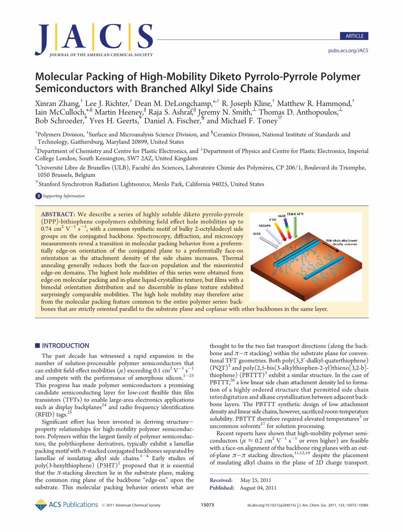
In this Article, we characterize the thin film molecular packingbehavior of three thiophene-based donor�acceptor copolymerscontaining electron-deficient diketo pyrrolo-pyrrole (DPP) unitswith pendant 2-octyldodecyl groups. The repeat units of these
polymers consist of two moieties: (1) a common DPP-bithiophenemoiety and (2) a variable moiety that can be thienothiophene(TT), bithiophene (2T), or monothiophene (T). The corre-sponding polymers are hereafter referred to as DPPT-TT,DPPT-2T, and DPPT-T, respectively, and are depicted inScheme 1. These polymers are highly soluble in common organicsolvents such as chloroform and chlorobenzene at room tem-perature, yet they can exhibit high field-effect mobilities compar-able to those of the best-performing polymer semiconductorswith linear side chains. Several aspects of molecular packingbehavior, such as the orientation of conjugated backbones, theside chain arrangement, and the in-plane texture, provide newinsights into structure�property relationships for high-mobilitypolymer semiconductors with branched side chains.
’RESULTS
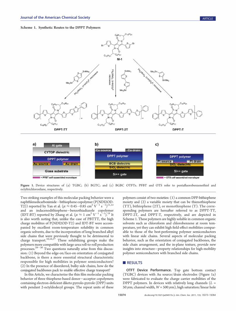
OTFT Device Performance. Top gate bottom contact(TGBC) devices with Au source/drain electrodes (Figure 1a)were fabricated to evaluate the charge carrier mobilities of theDPPT polymers. In devices with relatively long channels (L =50 μm; channel width,W = 500 μm), high saturation/linear hole
Scheme 1. Synthetic Routes to the DPPT Polymers
Figure 1. Device structures of (a) TGBC; (b) BGTC; and (c) BGBC OTFTs. PFBT and OTS refer to pentafluorobenzenethiol andoctyltrichlorosilane, respectively.
15075 dx.doi.org/10.1021/ja204515s |J. Am. Chem. Soc. 2011, 133, 15073–15084
Journal of the American Chemical Society ARTICLE
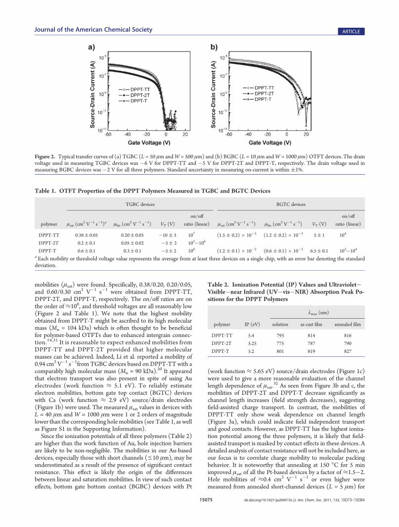
mobilities (μsat) were found. Specifically, 0.38/0.20, 0.20/0.05,and 0.60/0.30 cm2 V�1 s�1 were obtained from DPPT-TT,DPPT-2T, and DPPT-T, respectively. The on/off ratios are onthe order of ≈106, and threshold voltages are all reasonably low(Figure 2 and Table 1). We note that the highest mobilityobtained from DPPT-T might be ascribed to its high molecularmass (Mn = 104 kDa) which is often thought to be beneficialfor polymer-based OTFTs due to enhanced intergrain connec-tion.14,31 It is reasonable to expect enhanced mobilities fromDPPT-TT and DPPT-2T provided that higher molecularmasses can be achieved. Indeed, Li et al. reported a mobility of0.94 cm2 V�1 s�1from TGBC devices based on DPPT-TT with acomparably high molecular mass (Mn = 90 kDa).20 It appearedthat electron transport was also present in spite of using Auelectrodes (work function ≈ 5.1 eV). To reliably estimateelectron mobilities, bottom gate top contact (BGTC) deviceswith Ca (work function ≈ 2.9 eV) source/drain electrodes(Figure 1b) were used. The measured μsat values in devices withL = 40 μm and W = 1000 μm were 1 or 2 orders of magnitudelower than the corresponding holemobilities (see Table 1, as wellas Figure S1 in the Supporting Information).Since the ionization potentials of all three polymers (Table 2)
are higher than the work function of Au, hole injection barriersare likely to be non-negligible. The mobilities in our Au-baseddevices, especially those with short channels (e10 μm), may beunderestimated as a result of the presence of significant contactresistance. This effect is likely the origin of the differencesbetween linear and saturation mobilities. In view of such contacteffects, bottom gate bottom contact (BGBC) devices with Pt
(work function ≈ 5.65 eV) source/drain electrodes (Figure 1c)were used to give a more reasonable evaluation of the channellength dependence of μsat.
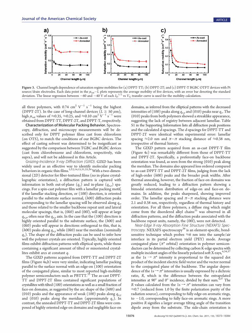
32 As seen from Figure 3b and c, themobilities of DPPT-2T and DPPT-T decrease significantly aschannel length increases (field strength decreases), suggestingfield-assisted charge transport. In contrast, the mobilities ofDPPT-TT only show weak dependence on channel length(Figure 3a), which could indicate field independent transportand good contacts. However, as DPPT-TT has the highest ioniza-tion potential among the three polymers, it is likely that field-assisted transport is masked by contact effects in these devices. Adetailed analysis of contact resistance will not be included here, asour focus is to correlate charge mobility to molecular packingbehavior. It is noteworthy that annealing at 150 �C for 5 minimproved μsat of all the Pt-based devices by a factor of ≈1.5�2.Hole mobilities of ≈0.4 cm2 V�1 s�1 or even higher weremeasured from annealed short-channel devices (L = 5 μm) for
Figure 2. Typical transfer curves of (a) TGBC (L = 50 μm andW = 500 μm) and (b) BGBC (L = 10 μm andW = 1000 μm)OTFT devices. The drainvoltage used in measuring TGBC devices was �6 V for DPPT-TT and �5 V for DPPT-2T and DPPT-T, respectively. The drain voltage used inmeasuring BGBC devices was �2 V for all three polymers. Standard uncertainty in measuring on-current is within (1%.
Table 1. OTFT Properties of the DPPT Polymers Measured in TGBC and BGTC Devices
TGBC devices BGTC devices
polymer μsat (cm2 V�1 s�1)a μlin (cm
2 V�1 s�1) VT (V)
on/off
ratio (linear) μsat (cm2 V�1 s�1) μlin (cm
2 V�1 s�1) VT (V)
on/off
ratio (linear)
DPPT-TT 0.38( 0.05 0.20( 0.05 �10 ( 3 107 (1.5 ( 0.2) � 10�3 (1.2 ( 0.2) � 10�3 5( 1 104
DPPT-2T 0.2( 0.1 0.05( 0.02 �5( 2 105�106
DPPT-T 0.6( 0.1 0.3( 0.1 �5( 2 106 (1.2 ( 0.1) � 10�2 (0.6 ( 0.1) � 10�2 6.5( 0.1 103�104
a Each mobility or threshold voltage value represents the average from at least three devices on a single chip, with an error bar denoting the standarddeviation.
Table 2. Ionization Potential (IP) Values and Ultraviolet�Visible�near Infrared (UV�vis�NIR) Absorption Peak Po-sitions for the DPPT Polymers
λmax (nm)
polymer IP (eV) solution as-cast film annealed film
DPPT-TT 5.4 793 814 816
DPPT-2T 5.25 775 787 790
DPPT-T 5.2 801 819 827
15076 dx.doi.org/10.1021/ja204515s |J. Am. Chem. Soc. 2011, 133, 15073–15084
Journal of the American Chemical Society ARTICLE
all three polymers, with 0.74 cm2 V�1 s�1 being the highest(DPPT-2T). In the case of long-channel devices (L g 50 μm),high μsat values of ≈0.35, ≈0.25, and ≈0.10 cm2 V�1 s�1 wereobtained fromDPPT-TT, DPPT-2T, and DPPT-T, respectively.Characterization ofMolecular Packing Behavior. Spectros-
copy, diffraction, and microscopy measurements will be de-scribed only for DPPT polymer films cast from chloroform(on OTS), to match the conditions of our BGBC devices. Theeffect of casting solvent was determined to be insignificant assuggested by the comparison between TGBC and BGBC devices(cast from chlorobenzene and chloroform, respectively, videsupra), and will not be addressed in this Article.Grazing-Incidence X-ray Diffraction (GIXD). GIXD has been
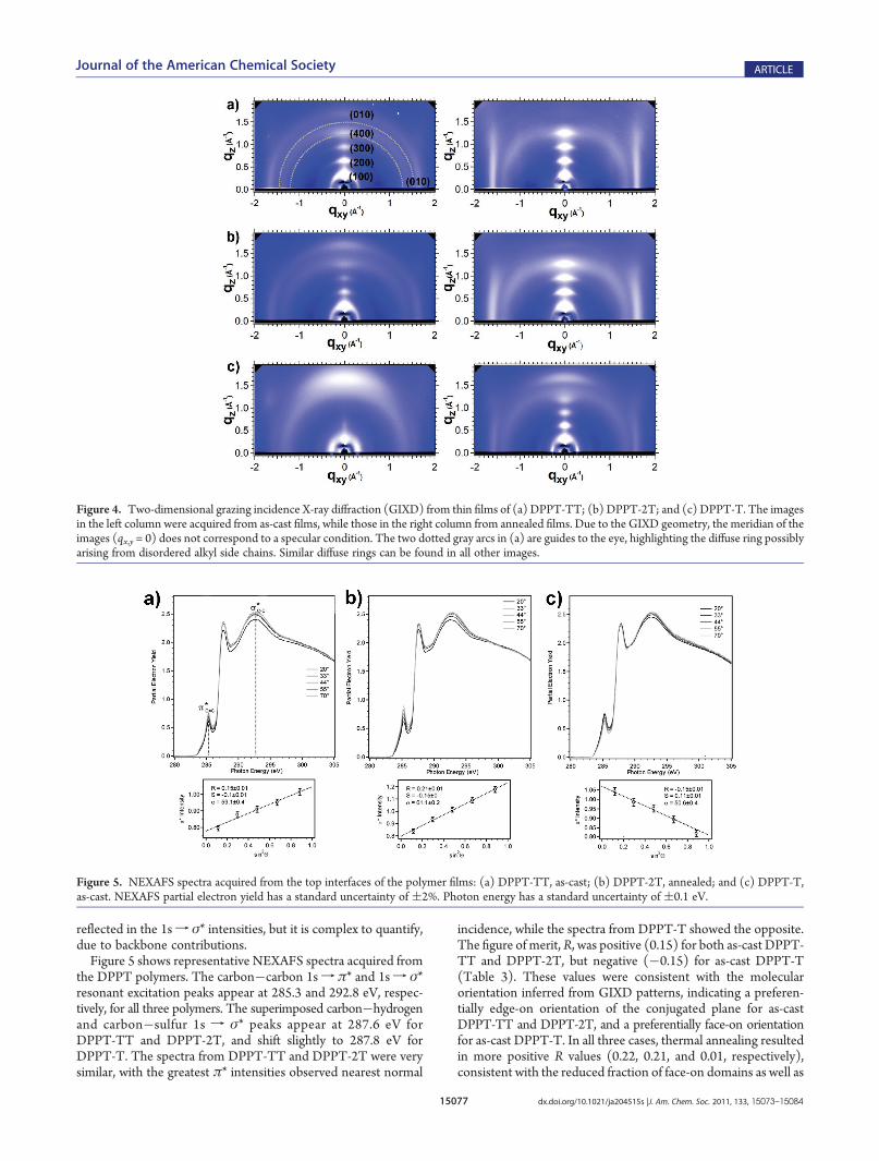
widely used as an effective way to identify molecular packingbehaviors in organic thin films.5,12,14,15,31,33,34 With a two-dimen-sional (2D) detector for fiber-textured films (no in-plane crystal-lographic orientation), a diffraction pattern is captured withinformation in both out-of-plane (qz) and in-plane (qx,y) spa-cings. For a spin-cast polymer film with a lamellar packing motif,if the lamellar stacking direction, or (100) direction, is orientedparallel to the substrate surface normal, (h00) diffraction peakscorresponding to the lamellar spacing will be observed along qz,and those related to the smaller backbone repeat unit and lateralmolecular spacings, that is, (0k0) and (00l), will appear at largeqx,y, often near the qx,y axis. In the case that the (100) direction ishighly oriented parallel to the substrate surface, the (h00) and(0k0) peaks will appear in directions orthogonal to this, that is,(h00) peaks along qx,y while (0k0) near the meridian (nominallyqz). The shape of the diffraction peaks can be used to infer howwell the polymer crystals are oriented. Typically, highly orientedfilms exhibit diffraction patterns with elliptical spots, while thosecontaining a significant amount of tilted or misoriented crystal-lites exhibit arcs at constant q.The GIXD patterns acquired from DPPT-TT and DPPT-2T
films (Figure 4a,b) were very similar, indicating lamellar packingparallel to the surface normal with an edge-on (100) orientationof the conjugated plane, similar to most reported high-mobilitypolymer semiconductors such as PBTTT.33 The as-cast DPPT-TT and DPPT-2T films contained significant populations ofcrystallites with tilted (100) orientations as well as a small fraction offace-on domains, as suggested by the arc shape of the (h00) and(010) peaks and the appearance of weak (100) peaks along qx,yand (010) peaks along the meridian (approximately qz). Incontrast, the annealed DPPT-TT and DPPT-2T films were com-posed of highly oriented edge-on domains and negligible face-on
domains, as inferred from the elliptical patterns with the decreasedintensities of (100) peaks along qx,y and (010) peaks near qz. The(010) peaks from both polymers showed a streaklike appearance,suggesting the lack of registry between adjacent lamellae. TableS1 in the Supporting Information lists all diffraction peak positionsand the calculated d-spacings. The d-spacings for DPPT-TT andDPPT-2T were identical within experimental error: lamellarspacing ≈2.0 nm and π�π stacking distance of ≈0.38 nm,irrespective of thermal history.The GIXD pattern acquired from an as-cast DPPT-T film
(Figure 4c) was remarkably different from those of DPPT-TTand DPPT-2T. Specifically, a preferentially face-on backboneorientation was found, as seen from the strong (010) peak alongthe meridian. The domains also appeared less ordered comparedto as-cast DPPT-TT and DPPT-2T films, judging from the lackof high-order (h00) peaks and the broader peak widths. Afterthermal annealing, however, the fraction of face-on domains wasgreatly reduced, leading to a diffraction pattern showing abimodal orientation distribution of edge-on and face-on do-mains. In addition, the peaks sharpened, showing improvedorder. The lamellar spacing and π�π stacking distance were2.1 and 0.38 nm, respectively, regardless of thermal history andorientation. For all three polymers, a diffuse ring which mightcome from the disordered alkyl chains35 was observed in alldiffraction patterns, and the diffraction peaks associated with thebackbone repeat units, namely, the (00l), were not detected.Near-Edge X-ray Absorption Fine Structure (NEXAFS) Spec-
troscopy. NEXAFS spectroscopy36 is an element-specific, bond-sensitive technique which probes ≈6 nm into the sample/airinterface in its partial electron yield (PEY) mode. Averageconjugated plane (π* orbital) orientation in polymer semicon-ductors can be determined by collecting carbonK-edge spectra withmultiple incident angles of the linearly polarized soft X-rays,4,34,37
as the 1s f π* intensity is proportional to the squared dotproduct of the incident electric field vector and the vector normalto the conjugated plane of the backbone. The angular depen-dence of the 1sf π* intensities is usually expressed by a dichroicratio, R, which is the difference between the extrapolatedintensities at 90� and 0� incidence, divided by their sum.4,37 TheR values calculated from the 1s f π* intensities can vary from≈0.7 (reduced from 1.0 by the finite polarization purity of theradiation source), corresponding to fully edge-on aromatic rings,to �1.0, corresponding to fully face-on aromatic rings. A morepositive R signifies a larger average tilting angle of the transitiondipole away from the substrate. The side-chain orientation is
Figure 3. Channel length dependence of saturation regimemobilities for (a) DPPT-TT; (b)DPPT-2T; and (c) DPPT-T BGBCOTFT devices with Ptsource/drain electrodes. Each data point in the μsat�L plots represents the average mobility of five devices, with an error bar denoting the standarddeviation. The linear regression between �60 and �40 V of each ID
1/2 vs VG transfer curve is used for the mobility calculation.
15077 dx.doi.org/10.1021/ja204515s |J. Am. Chem. Soc. 2011, 133, 15073–15084
Journal of the American Chemical Society ARTICLE
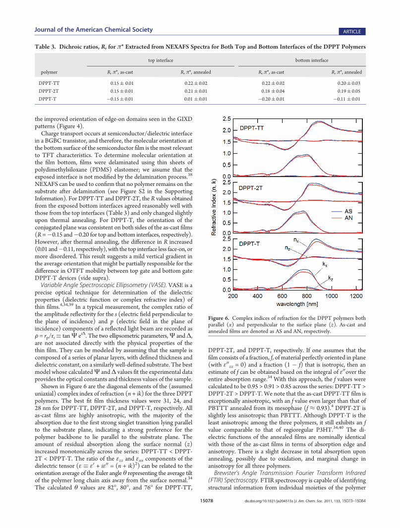
reflected in the 1sf σ* intensities, but it is complex to quantify,due to backbone contributions.Figure 5 shows representative NEXAFS spectra acquired from
the DPPT polymers. The carbon�carbon 1sf π* and 1sf σ*resonant excitation peaks appear at 285.3 and 292.8 eV, respec-tively, for all three polymers. The superimposed carbon�hydrogenand carbon�sulfur 1s f σ* peaks appear at 287.6 eV forDPPT-TT and DPPT-2T, and shift slightly to 287.8 eV forDPPT-T. The spectra from DPPT-TT and DPPT-2T were verysimilar, with the greatest π* intensities observed nearest normal
incidence, while the spectra from DPPT-T showed the opposite.The figure of merit, R, was positive (0.15) for both as-cast DPPT-TT and DPPT-2T, but negative (�0.15) for as-cast DPPT-T(Table 3). These values were consistent with the molecularorientation inferred from GIXD patterns, indicating a preferen-tially edge-on orientation of the conjugated plane for as-castDPPT-TT and DPPT-2T, and a preferentially face-on orientationfor as-cast DPPT-T. In all three cases, thermal annealing resultedin more positive R values (0.22, 0.21, and 0.01, respectively),consistent with the reduced fraction of face-on domains as well as
Figure 4. Two-dimensional grazing incidence X-ray diffraction (GIXD) from thin films of (a) DPPT-TT; (b) DPPT-2T; and (c) DPPT-T. The imagesin the left column were acquired from as-cast films, while those in the right column from annealed films. Due to the GIXD geometry, the meridian of theimages (qx,y = 0) does not correspond to a specular condition. The two dotted gray arcs in (a) are guides to the eye, highlighting the diffuse ring possiblyarising from disordered alkyl side chains. Similar diffuse rings can be found in all other images.
Figure 5. NEXAFS spectra acquired from the top interfaces of the polymer films: (a) DPPT-TT, as-cast; (b) DPPT-2T, annealed; and (c) DPPT-T,as-cast. NEXAFS partial electron yield has a standard uncertainty of (2%. Photon energy has a standard uncertainty of (0.1 eV.
15078 dx.doi.org/10.1021/ja204515s |J. Am. Chem. Soc. 2011, 133, 15073–15084
Journal of the American Chemical Society ARTICLE
the improved orientation of edge-on domains seen in the GIXDpatterns (Figure 4).Charge transport occurs at semiconductor/dielectric interface
in a BGBC transistor, and therefore, the molecular orientation atthe bottom surface of the semiconductor film is the most relevantto TFT characteristics. To determine molecular orientation atthe film bottom, films were delaminated using thin sheets ofpolydimethylsiloxane (PDMS) elastomer; we assume that theexposed interface is not modified by the delamination process.38
NEXAFS can be used to confirm that no polymer remains on thesubstrate after delamination (see Figure S2 in the SupportingInformation). For DPPT-TT and DPPT-2T, the R values obtainedfrom the exposed bottom interfaces agreed reasonably well withthose from the top interfaces (Table 3) and only changed slightlyupon thermal annealing. For DPPT-T, the orientation of theconjugated plane was consistent on both sides of the as-cast films(R =�0.15 and�0.20 for top and bottom interfaces, respectively).However, after thermal annealing, the difference in R increased(0.01 and�0.11, respectively), with the top interface less face-on, ormore disordered. This result suggests a mild vertical gradient inthe average orientation that might be partially responsible for thedifference in OTFT mobility between top gate and bottom gateDPPT-T devices (vide supra).Variable Angle Spectroscopic Ellipsometry (VASE). VASE is a
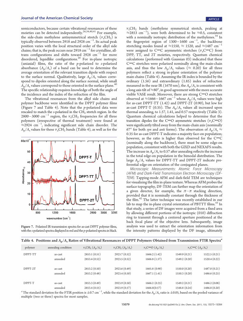
precise optical technique for determination of the dielectricproperties (dielectric function or complex refractive index) ofthin films.4,34,39 In a typical measurement, the complex ratio ofthe amplitude reflectivity for the s (electric field perpendicular tothe plane of incidence) and p (electric field in the plane ofincidence) components of a reflected light beam are recorded asF = rp/rs� tanΨ eiΔ. The two ellipsometric parameters,Ψ andΔ,are not associated directly with the physical properties of thethin film. They can be modeled by assuming that the sample iscomposed of a series of planar layers, with defined thickness anddielectric constant, on a similarly well-defined substrate. The bestmodel whose calculatedΨ andΔ values fit the experimental dataprovides the optical constants and thickness values of the sample.Shown in Figure 6 are the diagonal elements of the (assumed
uniaxial) complex index of refraction (n + ik) for the three DPPTpolymers. The best fit film thickness values were 31, 24, and28 nm for DPPT-TT, DPPT-2T, and DPPT-T, respectively. Allas-cast films are highly anisotropic, with the majority of theabsorption due to the first strong singlet transition lying parallelto the substrate plane, indicating a strong preference for thepolymer backbone to lie parallel to the substrate plane. Theamount of residual absorption along the surface normal (z)increased monotonically across the series: DPPT-TT < DPPT-2T < DPPT-T. The ratio of the εzz and εxx components of thedielectric tensor (ε � ε0 + iε00 = (n + ik)2) can be related to theorientation average of the Euler angle θ representing the average tiltof the polymer long chain axis away from the surface normal.34
The calculated θ values are 82�, 80�, and 76� for DPPT-TT,
DPPT-2T, and DPPT-T, respectively. If one assumes that thefilm consists of a fraction, f, of material perfectly oriented in plane(with ε00zz = 0) and a fraction (1 � f) that is isotropic, then anestimate of f can be obtained based on the integral of ε00over theentire absorption range.34 With this approach, the f values werecalculated to be 0.95 > 0.91 > 0.85 across the series: DPPT-TT >DPPT-2T > DPPT-T. We note that the as-cast DPPT-TT film isexceptionally anisotropic, with an f value even larger than that ofPBTTT annealed from its mesophase (f ≈ 0.93).4 DPPT-2T isslightly less anisotropic than PBTTT. Although DPPT-T is theleast anisotropic among the three polymers, it still exhibits an fvalue comparable to that of regioregular P3HT.34,40 The di-electric functions of the annealed films are nominally identicalwith those of the as-cast films in terms of absorption edge andanisotropy. There is a slight decrease in total absorption uponannealing, possibly due to oxidation, and marginal change inanisotropy for all three polymers.Brewster’s Angle Transmission Fourier Transform Infrared
(FTIR) Spectroscopy. FTIR spectroscopy is capable of identifyingstructural information from individual moieties of the polymer
Table 3. Dichroic ratios, R, for π* Extracted from NEXAFS Spectra for Both Top and Bottom Interfaces of the DPPT Polymers
top interface bottom interface
polymer R, π*, as-cast R, π*, annealed R, π*, as-cast R, π*, annealed
DPPT-TT 0.15( 0.01 0.22( 0.02 0.22( 0.02 0.20( 0.03
DPPT-2T 0.15( 0.01 0.21( 0.01 0.18 ( 0.04 0.19( 0.05
DPPT-T �0.15( 0.01 0.01 ( 0.01 �0.20( 0.01 �0.11 ( 0.01
Figure 6. Complex indices of refraction for the DPPT polymers bothparallel (x) and perpendicular to the surface plane (z). As-cast andannealed films are denoted as AS and AN, respectively.
15079 dx.doi.org/10.1021/ja204515s |J. Am. Chem. Soc. 2011, 133, 15073–15084
Journal of the American Chemical Society ARTICLE
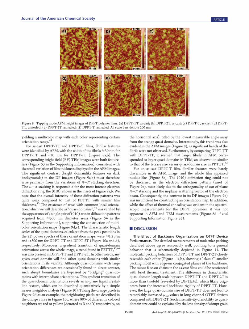
semiconductors, because certain vibrational resonances of thesemoieties can be detected independently.26,34,40,41 For example,the side-chain methylene antisymmetrical stretch (νaCH2) istypically observed between 2918 and 2928 cm�1. Its actual peakposition varies with the local structural order of the alkyl sidechains; that is, the peak occurs near 2918 cm�1 for crystalline, all-trans configurations and shifts toward 2928 cm�1 for moredisordered, liquidlike configurations.26 For in-plane isotropic(uniaxial) films, the ratio of the p-polarized to s-polarizedabsorbance (Ap/As) of a band can be used to determine theaverage orientation of the relevant transition dipole with respectto the surface normal. Qualitatively, large Ap/As values corre-spond to dipoles oriented along the surface normal, while smallAp/As values correspond to those oriented in the surface plane.
40
The specific relationship requires knowledge of both the angle ofthe incidence and the index of the refraction of the film.The vibrational resonances from the alkyl side chains and
polymer backbone were identified in the DPPT polymer films(Figure 7 and Table 4). Note that the p-polarized data wererescaled to match the s-polarized in the CH2 stretch region. In the2800�3000 cm�1 region, the νaCH2 frequencies for all threepolymers (irrespective of thermal treatment) were found at≈2924 cm�1, indicating significant side chain disorder. TheAp/As values for these νaCH2 bands (Table 4), as well as for the
νsCH2 bands (methylene symmetrical stretch, peaking at≈2853 cm�1), were both determined to be ≈0.5, consistentwith a nominally isotropic distribution of the methylenes.34 Inthe fingerprint region of 1300�1600 cm�1, the backbonestretching modes found at ≈1550, ≈ 1520, and ≈1487 cm�1
were assigned to CdC asymmetric stretches (νaCdC) fromDPP, TT, and 2T moieties, respectively. Quantum chemicalcalculations (performed with Gaussian 03) indicated that theseCdC stretches were polarized nominally along the main-chainaxis, and thus the low Ap/As values (≈ 0.20) for all threepolymers reflect a strong in-plane orientation of the polymermain chains (Table 4). Assuming the IR index is bounded by theordinary (1.56) and extraordinary (1.85) index of refractionmeasured in the near IR (1670 nm), the Ap/As is consistent witha long axis tilt of≈80�, in good agreement with themore accuratevisible VASE result. Moreover, there are strong CdO stretchesobserved at ≈1666�1667 cm�1 whose Ap/As values were highfor as-cast DPPT-TT (1.42) and DPPT-2T (0.90), but low foras-cast DPPT-T (0.35). The Ap/As values all increased uponthermal annealing, to 1.57, 1.41, and 0.57 respectively (Table 3).Quantum chemical calculations helped to determine that thetransition dipoles for the CdO asymmetric stretches (νaCdO)were significantly tilted away from themain-chain axis (nominally67� for both syn and anti forms). The observation of Ap/As ≈0.35 for as-cast DPPT-T indicates a majority face-on population;however, as the ratio is higher than observed for the CdC(nominally along the backbone), there must be some edge-onpopulation, consistent with both the GIXD andNEXAFS results.The increase in Ap/As to 0.57 after annealing reflects the increasein the total edge-on population in the bimodal distribution. Thelarge Ap/As values for DPPT-TT and DPPT-2T indicate pre-ferential edge-on orientation of the conjugated planes.Microscopic Measurements: Atomic Force Microscopy
(AFM) and Dark-Field Transmission Electron Microscopy (DF-TEM). Tapping-mode AFM and dark-field TEM are techniquesfor visualizing the film in-plane texture. Whereas AFMprobes thesurface topography, DF-TEM can further map the orientation ofa given director, for example, the π�π stacking direction,provided that it is nominally constant through the thickness ofthe film.42 The latter technique was recently established in ourlab to map the in-plane crystal orientation of PBTTT films.43 Inthat study, a series of DF images were acquired from a fixed areaby allowing different portions of the isotropic (010) diffractionring to transmit through a centered aperture positioned at theback focal plane of the objective lens. Subsequently, imageanalysis was used to extract the orientation information fromthe intensity patterns displayed by the DF image, ultimately
Figure 7. Polarized IR transmission spectra for as-cast DPPT polymer films,with the s-polarized spectradisplayed in red and thep-polarized spectra inblack.
Table 4. Positions and Ap/As Ratios of Vibrational Resonances of DPPT Polymers Obtained from Transmission FTIR Spectraa
polymer annealing condition νsCH2 (Ap/As) νaCH2 (Ap/As) νaCdO (Ap/As) νaCdC (Ap/As)
DPPT-TT as-cast 2853.1 (0.51) 2923.7 (0.52) 1666.2 (1.42) 1549.9 (0.21) 1522.5 (0.21)
annealed 2853.4 (0.52) 2923.5 (0.52) 1666.8 (1.57) 1549.2 (0.20) 1520.4 (0.22)
DPPT-2T as-cast 2853.2 (0.50) 2923.6 (0.49) 1665.8 (0.90) 1550.0 (0.20) 1487.0 (0.21)
annealed 2853.2 (0.48) 2923.4 (0.50) 1667.1 (1.41) 1550.3 (0.20) 1486.6 (0.25)
DPPT-T as-cast 2853.3 (0.49) 2923.9 (0.50) 1666.2 (0.35) 1549.2 (0.21) 1486.2 (0.08)
annealed 2853.4 (0.55) 2923.9 (0.57) 1666.8(0.57) 1548.8 (0.24) 1486.8 (0.20)aThe standard deviation for the FTIR position is(0.7 cm�1, while the standard deviation for the Ap/As ratio is(0.05, based on the pooled variance ofmultiple (two or three) spectra for most samples.
15080 dx.doi.org/10.1021/ja204515s |J. Am. Chem. Soc. 2011, 133, 15073–15084
Journal of the American Chemical Society ARTICLE
yielding a multicolor map with each color representing certainorientation range.43
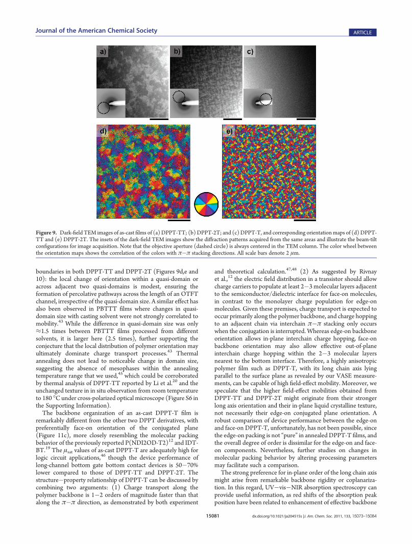
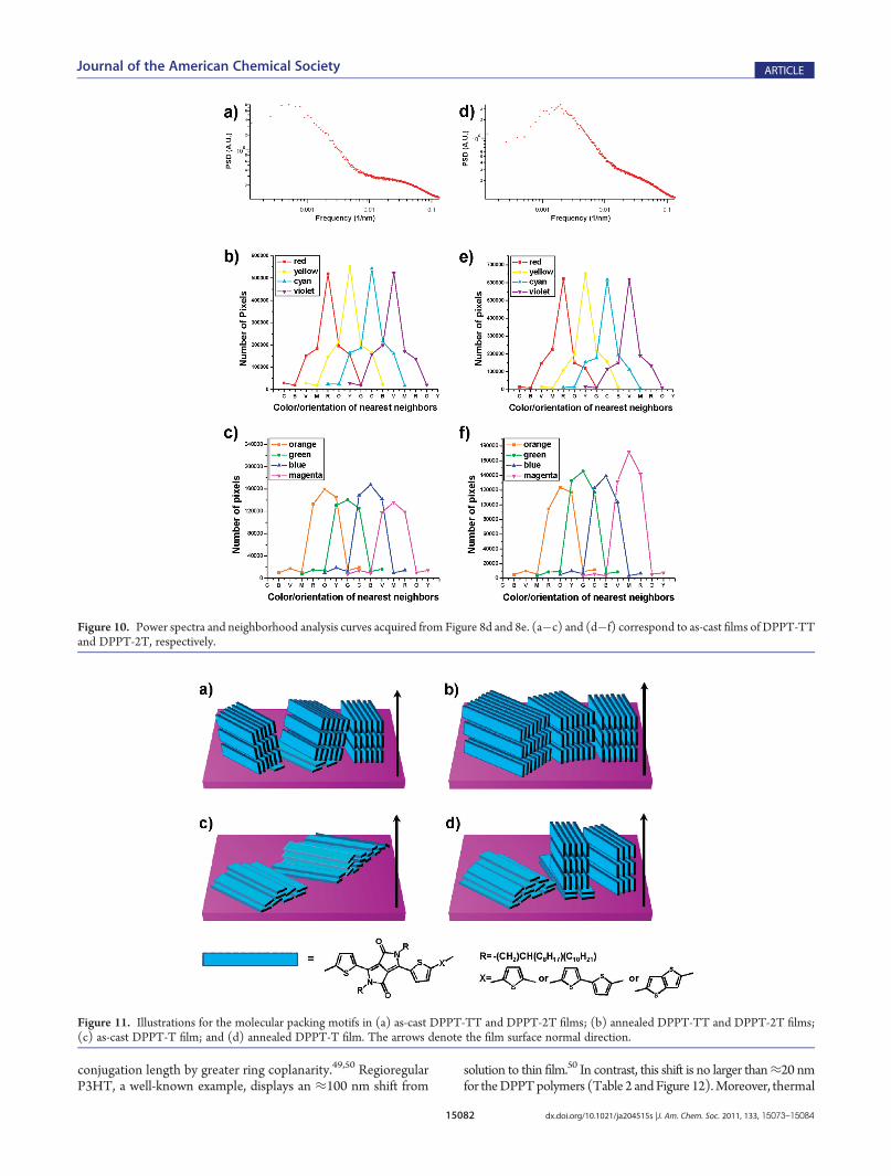
For as-cast DPPT-TT and DPPT-2T films, fibrillar featureswere identified by AFM, with the width of the fibrils≈30 nm forDPPT-TT and <20 nm for DPPT-2T (Figure 8a,b). Thecorresponding bright-field (BF) TEM images were both feature-less (Figure S3 in the Supporting Information), consistent withthe small variation of film thickness displayed in the AFM images.The significant contrast (bright domainlike features on darkbackgrounds) in the DF images (Figure 9a,b) must thereforearise primarily from the variations of π�π stacking direction.The π�π stacking is responsible for the most intense electrondiffraction ring, the (010), shown in the insets of Figure 9a,b. Wenote that the overall intensity of these diffraction patterns wasquite weak compared to that of PBTTT with similar filmthickness.43 The existence of areas with common local orienta-tion, which we will describe as “quasi-domains”,44 was verified bythe appearance of a single pair of (010) arcs in diffraction patternsacquired from ≈300 nm diameter areas (Figure S4 in theSupporting Information), supporting the construction of multi-color orientation maps (Figure 9d,e). The characteristic lengthscales of the quasi-domains, calculated from the peak positions inthe 2D power spectra of these orientation maps, were ≈1.2 μmand ≈500 nm for DPPT-TT and DPPT-2T (Figure 10a and d),respectively. Moreover, a gradient transition of quasi-domainorientations across the whole image, a trend found in PBTTT,43,44
was also present inDPPT-TT andDPPT-2T. In other words, anygiven quasi-domain will find other quasi-domains with similarorientations in its vicinity. Although quasi-domains with largeorientation differences are occasionally found in direct contact,such abrupt boundaries are bypassed by “bridging” quasi-do-mains with intermediate orientations. This gradient transition ofthe quasi-domain orientations reveals an in-plane liquid crystal-line texture, which can be described quantitatively by a simplenearest neighbor analysis (Figure 10). Taking the orange pixels inFigure 9d as an example, the neighboring pixels are described inthe orange curve in Figure 10c, where 80% of differently coloredneighbors are red or yellow (denoted as R and Y, respectively, on
the horizontal axis), titled by the lowest measurable angle awayfrom the orange quasi-domains. Interestingly, this trend was alsoevident in the AFM images (Figure 8), as significant bends of thefibrils were not observed. Furthermore, by comparing DPPT-TTwith DPPT-2T, it seemed that larger fibrils in AFM corre-sponded to larger quasi-domains in TEM, an observation similarto that of the terrace size versus quasi-domain size in PBTTT.43
For an as-cast DPPT-T film, fibrillar features were barelydiscernible in its AFM image, and the whole film appearednodule-like (Figure 8c). The (010) diffraction ring could notbe discerned in the electron diffraction pattern (inset ofFigure 9c), most likely due to the orthogonality of out-of-planeπ�π stacking and the in-plane scattering vector of the electronbeam. Consequently, the contrast in its DF images (Figure 9c)was insufficient for constructing an orientation map. In addition,while the effect of thermal annealing was evident in the spectro-scopic measurements for the DPPT polymers, it was notapparent in AFM and TEM measurements (Figure 8d�f andSupporting Information Figure S5).
’DISCUSSION
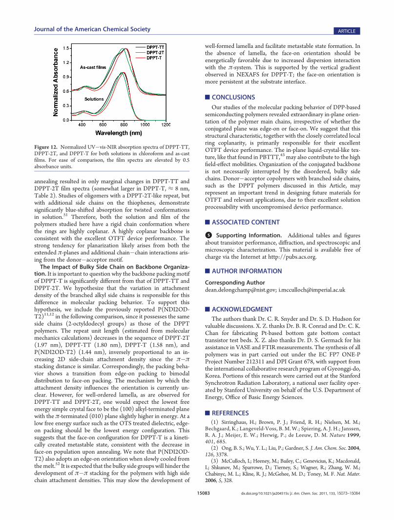
The Effect of Backbone Organization on OTFT DevicePerformance. The detailed measurements of molecular packingdescribed above agree reasonably well, pointing to a generalbehavior that is schematically depicted in Figure 11. Themolecular packing behaviors of DPPT-TT and DPPT-2T closelyresemble each other (Figure 11a,b), showing a “classic” lamellarpacking motif with edge-on conjugated planes of the backbone.The minor face-on chains in the as-cast films could be reorientedwith brief thermal treatment. The difference in characteristicquasi-domain length scale between DPPT-TT and DPPT-2T ismore than twofold (revealed by DF-TEM), which likely origi-nates from the increased backbone rigidity of DPPT-TT. How-ever, the large quasi-domain size of DPPT-TT does not lead toremarkably increased μsat values in long-channel OTFT devicescompared with DPPT-2T. Such insensitivity of mobility to quasi-domain size could be explained by the low density of abrupt grain
Figure 8. Tapping mode AFM height images of DPPT polymer films. (a) DPPT-TT, as-cast; (b) DPPT-2T, as-cast; (c) DPPT-T, as-cast; (d) DPPT-TT, annealed; (e) DPPT-2T, annealed; (f) DPPT-T, annealed. All scale bars denote 200 nm.
15081 dx.doi.org/10.1021/ja204515s |J. Am. Chem. Soc. 2011, 133, 15073–15084
Journal of the American Chemical Society ARTICLE
boundaries in both DPPT-TT and DPPT-2T (Figures 9d,e and10): the local change of orientation within a quasi-domain oracross adjacent two quasi-domains is modest, ensuring theformation of percolative pathways across the length of an OTFTchannel, irrespective of the quasi-domain size. A similar effect hasalso been observed in PBTTT films where changes in quasi-domain size with casting solvent were not strongly correlated tomobility.43 While the difference in quasi-domain size was only≈1.5 times between PBTTT films processed from differentsolvents, it is larger here (2.5 times), further supporting theconjecture that the local distribution of polymer orientation mayultimately dominate charge transport processes.43 Thermalannealing does not lead to noticeable change in domain size,suggesting the absence of mesophases within the annealingtemperature range that we used,45 which could be corroboratedby thermal analysis of DPPT-TT reported by Li et al.20 and theunchanged texture in in situ observation from room temperatureto 180 �C under cross-polarized optical microscope (Figure S6 inthe Supporting Information).The backbone organization of an as-cast DPPT-T film is
remarkably different from the other two DPPT derivatives, withpreferentially face-on orientation of the conjugated plane(Figure 11c), more closely resembling the molecular packingbehavior of the previously reported P(NDI2OD-T2)12 and IDT-BT.19 The μsat values of as-cast DPPT-T are adequately high forlogic circuit applications,46 though the device performance oflong-channel bottom gate bottom contact devices is 50�70%lower compared to those of DPPT-TT and DPPT-2T. Thestructure�property relationship of DPPT-T can be discussed bycombining two arguments: (1) Charge transport along thepolymer backbone is 1�2 orders of magnitude faster than thatalong the π�π direction, as demonstrated by both experiment
and theoretical calculation.47,48 (2) As suggested by Rivnayet al.,12 the electric field distribution in a transistor should allowcharge carriers to populate at least 2�3 molecular layers adjacentto the semiconductor/dielectric interface for face-on molecules,in contrast to the monolayer charge population for edge-onmolecules. Given these premises, charge transport is expected tooccur primarily along the polymer backbone, and charge hoppingto an adjacent chain via interchain π�π stacking only occurswhen the conjugation is interrupted. Whereas edge-on backboneorientation allows in-plane interchain charge hopping, face-onbackbone orientation may also allow effective out-of-planeinterchain charge hopping within the 2�3 molecular layersnearest to the bottom interface. Therefore, a highly anisotropicpolymer film such as DPPT-T, with its long chain axis lyingparallel to the surface plane as revealed by our VASE measure-ments, can be capable of high field-effect mobility. Moreover, wespeculate that the higher field-effect mobilities obtained fromDPPT-TT and DPPT-2T might originate from their strongerlong axis orientation and their in-plane liquid crystalline texture,not necessarily their edge-on conjugated plane orientation. Arobust comparison of device performance between the edge-onand face-on DPPT-T, unfortunately, has not been possible, sincethe edge-on packing is not “pure” in annealed DPPT-T films, andthe overall degree of order is dissimilar for the edge-on and face-on components. Nevertheless, further studies on changes inmolecular packing behavior by altering processing parametersmay facilitate such a comparison.The strong preference for in-plane order of the long chain axis
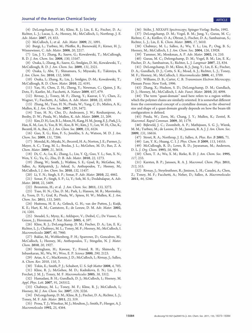
might arise from remarkable backbone rigidity or coplanariza-tion. In this regard, UV�vis�NIR absorption spectroscopy canprovide useful information, as red shifts of the absorption peakposition have been related to enhancement of effective backbone
Figure 9. Dark-field TEM images of as-cast films of (a) DPPT-TT; (b) DPPT-2T; and (c) DPPT-T, and corresponding orientationmaps of (d) DPPT-TT and (e) DPPT-2T. The insets of the dark-field TEM images show the diffraction patterns acquired from the same areas and illustrate the beam-tiltconfigurations for image acquisition. Note that the objective aperture (dashed circle) is always centered in the TEM column. The color wheel betweenthe orientation maps shows the correlation of the colors with π�π stacking directions. All scale bars denote 2 μm.
15082 dx.doi.org/10.1021/ja204515s |J. Am. Chem. Soc. 2011, 133, 15073–15084
Journal of the American Chemical Society ARTICLE
conjugation length by greater ring coplanarity.49,50 RegioregularP3HT, a well-known example, displays an ≈100 nm shift from
solution to thin film.50 In contrast, this shift is no larger than≈20 nmfor theDPPTpolymers (Table 2 andFigure 12).Moreover, thermal
Figure 10. Power spectra and neighborhood analysis curves acquired from Figure 8d and 8e. (a�c) and (d�f) correspond to as-cast films of DPPT-TTand DPPT-2T, respectively.
Figure 11. Illustrations for the molecular packing motifs in (a) as-cast DPPT-TT and DPPT-2T films; (b) annealed DPPT-TT and DPPT-2T films;(c) as-cast DPPT-T film; and (d) annealed DPPT-T film. The arrows denote the film surface normal direction.
15083 dx.doi.org/10.1021/ja204515s |J. Am. Chem. Soc. 2011, 133, 15073–15084
Journal of the American Chemical Society ARTICLE
annealing resulted in only marginal changes in DPPT-TT andDPPT-2T film spectra (somewhat larger in DPPT-T, ≈ 8 nm,Table 2). Studies of oligomers with a DPPT-2T-like repeat, butwith additional side chains on the thiophenes, demonstratesignificantly blue-shifted absorption for twisted conformationsin solution.51 Therefore, both the solution and film of thepolymers studied here have a rigid chain conformation wherethe rings are highly coplanar. A highly coplanar backbone isconsistent with the excellent OTFT device performance. Thestrong tendency for planarization likely arises from both theextended π-planes and additional chain�chain interactions aris-ing from the donor�acceptor motif.The Impact of Bulky Side Chain on Backbone Organiza-
tion. It is important to question why the backbone packing motifof DPPT-T is significantly different from that of DPPT-TT andDPPT-2T. We hypothesize that the variation in attachmentdensity of the branched alkyl side chains is responsible for thisdifference in molecular packing behavior. To support thishypothesis, we include the previously reported P(NDI2OD-T2)11,12 in the following comparison, since it possesses the sameside chains (2-octyldodecyl groups) as those of the DPPTpolymers. The repeat unit length (estimated from molecularmechanics calculations) decreases in the sequence of DPPT-2T(1.97 nm), DPPT-TT (1.80 nm), DPPT-T (1.58 nm), andP(NDI2OD-T2) (1.44 nm), inversely proportional to an in-creasing 2D side-chain attachment density since the π�πstacking distance is similar. Correspondingly, the packing beha-vior shows a transition from edge-on packing to bimodaldistribution to face-on packing. The mechanism by which theattachment density influences the orientation is currently un-clear. However, for well-ordered lamella, as are observed forDPPT-TT and DPPT-2T, one would expect the lowest freeenergy simple crystal face to be the (100) alkyl-terminated planewith the π-terminated (010) plane slightly higher in energy. At alow free energy surface such as the OTS treated dielectric, edge-on packing should be the lowest energy configuration. Thissuggests that the face-on configuration for DPPT-T is a kineti-cally created metastable state, consistent with the decrease inface-on population upon annealing. We note that P(NDI2OD-T2) also adopts an edge-on orientation when slowly cooled fromthemelt.52 It is expected that the bulky side groups will hinder thedevelopment of π�π stacking for the polymers with high sidechain attachment densities. This may slow the development of
well-formed lamella and facilitate metastable state formation. Inthe absence of lamella, the face-on orientation should beenergetically favorable due to increased dispersion interactionwith the π-system. This is supported by the vertical gradientobserved in NEXAFS for DPPT-T; the face-on orientation ismore persistent at the substrate interface.
’CONCLUSIONS
Our studies of the molecular packing behavior of DPP-basedsemiconducting polymers revealed extraordinary in-plane orien-tation of the polymer main chains, irrespective of whether theconjugated plane was edge-on or face-on. We suggest that thisstructural characteristic, together with the closely correlated localring coplanarity, is primarily responsible for their excellentOTFT device performance. The in-plane liquid-crystal-like tex-ture, like that found in PBTTT,43 may also contribute to the highfield-effect mobilities. Organization of the conjugated backboneis not necessarily interrupted by the disordered, bulky sidechains. Donor�acceptor copolymers with branched side chains,such as the DPPT polymers discussed in this Article, mayrepresent an important trend in designing future materials forOTFT and relevant applications, due to their excellent solutionprocessability with uncompromised device performance.
’ASSOCIATED CONTENT
bS Supporting Information. Additional tables and figuresabout transistor performance, diffraction, and spectroscopic andmicroscopic characterization. This material is available free ofcharge via the Internet at http://pubs.acs.org.
’AUTHOR INFORMATION
Corresponding [email protected]; [email protected]
’ACKNOWLEDGMENT
The authors thank Dr. C. R. Snyder and Dr. S. D. Hudson forvaluable discussions. X. Z. thanks Dr. B. R. Conrad and Dr. C. K.Chan for fabricating Pt-based bottom gate bottom contacttransistor test beds. X. Z. also thanks Dr. D. S. Germack for hisassistance in VASE and FTIRmeasurements. The synthesis of allpolymers was in part carried out under the EC FP7 ONE-PProject Number 212311 and DPI Grant 678, with support fromthe international collaborative research program of Gyeonggi-do,Korea. Portions of this research were carried out at the StanfordSynchrotron Radiation Laboratory, a national user facility oper-ated by Stanford University on behalf of the U.S. Department ofEnergy, Office of Basic Energy Sciences.
’REFERENCES
(1) Sirringhaus, H.; Brown, P. J.; Friend, R. H.; Nielsen, M. M.;Bechgaard, K.; Langeveld-Voss, B. M. W.; Spiering, A. J. H.; Janssen,R. A. J.; Meijer, E. W.; Herwig, P.; de Leeuw, D. M. Nature 1999,401, 685.
(2) Ong, B. S.; Wu, Y. L.; Liu, P.; Gardner, S. J. Am. Chem. Soc. 2004,126, 3378.
(3) McCulloch, I.; Heeney, M.; Bailey, C.; Genevicius, K.; Macdonald,I.; Shkunov, M.; Sparrowe, D.; Tierney, S.; Wagner, R.; Zhang, W. M.;Chabinyc, M. L.; Kline, R. J.; McGehee, M. D.; Toney, M. F. Nat. Mater.2006, 5, 328.
Figure 12. Normalized UV�vis-NIR absorption spectra of DPPT-TT,DPPT-2T, and DPPT-T for both solutions in chloroform and as-castfilms. For ease of comparison, the film spectra are elevated by 0.5absorbance units.
15084 dx.doi.org/10.1021/ja204515s |J. Am. Chem. Soc. 2011, 133, 15073–15084
Journal of the American Chemical Society ARTICLE
(4) DeLongchamp, D. M.; Kline, R. J.; Lin, E. K.; Fischer, D. A.;Richter, L. J.; Lucas, L. A.; Heeney, M.; McCulloch, I.; Northrup, J. E.Adv. Mater. 2007, 19, 833.(5) McCulloch, I.; et al. Adv. Mater. 2009, 21, 1091.(6) Burgi, L.; Turbiez, M.; Pfeiffer, R.; Bienewald, F.; Kirner, H. J.;
Winnewisser, C. Adv. Mater. 2008, 20, 2217.(7) Liu, J. Y.; Zhang, R.; Sauve, G.; Kowalewski, T.; McCullough,
R. D. J. Am. Chem. Soc. 2008, 130, 13167.(8) Osaka, I.; Zhang, R.; Sauve, G.; Smilgies, D. M.; Kowalewski, T.;
McCullough, R. D. J. Am. Chem. Soc. 2009, 131, 2521.(9) Osaka, I.; Abe, T.; Shinamura, S.; Miyazaki, E.; Takimiya, K.
J. Am. Chem. Soc. 2010, 132, 5000.(10) Osaka, I.; Zhang, R.; Liu, J.; Smilgies, D.-M.; Kowalewski, T.;
McCullough, R. D. Chem. Mater. 2010, 22, 4191.(11) Yan, H.; Chen, Z. H.; Zheng, Y.; Newman, C.; Quinn, J. R.;
Dotz, F.; Kastler, M.; Facchetti, A. Nature 2009, 457, 679.(12) Rivnay, J.; Toney, M. F.; Zheng, Y.; Kauvar, I. V.; Chen, Z.;
Wagner, V.; Facchetti, A.; Salleo, A. Adv. Mater. 2010, 22, 4359.(13) Zhang, M.; Tsao, H. N.; Pisula, W.; Yang, C. D.; Mishra, A. K.;
Mullen, K. J. Am. Chem. Soc. 2007, 129, 3472.(14) Tsao, H. N.; Cho, D.; Andreasen, J. W.; Rouhanipour, A.;
Breiby, D. W.; Pisula, W.; Mullen, K. Adv. Mater. 2009, 21, 209.(15) Kim,D.H.; Lee, B. L.;Moon,H.;Kang,H.M.; Jeong, E. J.; Park, J. I.;
Han, K. M.; Lee, S.; Yoo, B. W.; Koo, B. W.; Kim, J. Y.; Lee, W. H.; Cho, K.;Becerril, H. A.; Bao, Z. J. Am. Chem. Soc. 2009, 131, 6124.(16) Guo, X. G.; Kim, F. S.; Jenekhe, S. A.; Watson, M. D. J. Am.
Chem. Soc. 2009, 131, 7206.(17) Mondal, R.;Miyaki, N.; Becerril, H. A.; Norton, J. E.; Parmer, J.;
Mayer, A. C.; Tang, M. L.; Bredas, J. L.; McGehee, M. D.; Bao, Z. A.Chem. Mater. 2009, 21, 3618.(18) Di, C. A.; Lu, K.; Zhang, L.; Liu, Y. Q.; Guo, Y. L.; Sun, X. N.;
Wen, Y. G.; Yu, G.; Zhu, D. B. Adv. Mater. 2010, 22, 1273.(19) Zhang, W.; Smith, J.; Watkins, S. E.; Gysel, R.; McGehee, M.;
Salleo, A.; Kirkpatrick, J.; Ashraf, S.; Anthopoulos, T.; Heeney, M.;McCulloch, I. J. Am. Chem. Soc. 2010, 132, 11437.(20) Li, Y. N.; Singh, S. P.; Sonar, P. Adv. Mater. 2010, 22, 4862.(21) Sonar, P.; Singh, S. P.; Li, Y.; Soh, M. S.; Dodabalapur, A. Adv.
Mater. 2010, 22, 5409.(22) Bronstein, H.; et al. J. Am. Chem. Soc. 2011, 133, 3272.(23) Tsao, H. N.; Cho, D. M.; Park, I.; Hansen, M. R.; Mavrinskiy,
A.; Yoon, D. Y.; Graf, R.; Pisula, W.; Spiess, H. W.; Mullen, K. J. Am.Chem. Soc. 2011, 133, 2605.(24) Huitema, H. E. A.; Gelinck, G. H.; van der Putten, J.; Kuijk,
K. E.; Hart, K. M.; Cantatore, E.; de Leeuw, D. M. Adv. Mater. 2002,14, 1201.(25) Steudel, S.; Myny, K.; Arkhipov, V.; Deibel, C.; De Vusser, S.;
Genoe, J.; Heremans, P. Nat. Mater. 2005, 4, 597.(26) Kline, R. J.; DeLongchamp, D. M.; Fischer, D. A.; Lin, E. K.;
Richter, L. J.; Chabinyc, M. L.; Toney, M. F.; Heeney, M.; McCulloch, I.Macromolecules 2007, 40, 7960.(27) Baklar, M.; Wobkenberg, P. H.; Sparrowe, D.; Goncalves, M.;
McCulloch, I.; Heeney, M.; Anthopoulos, T.; Stingelin, N. J. Mater.Chem. 2010, 20, 1927.(28) Sirringhaus, H.; Kawase, T.; Friend, R. H.; Shimoda, T.;
Inbasekaran, M.; Wu, W.; Woo, E. P. Science 2000, 290, 2123.(29) Arias, A. C.; MacKenzie, J. D.; McCulloch, I.; Rivnay, J.; Salleo,
A. Chem. Rev. 2010, 110, 3.(30) Tekin, E.; Smith, P. J.; Schubert, U. S. Soft Matter 2008, 4, 703.(31) Kline, R. J.; McGehee, M. D.; Kadnikova, E. N.; Liu, J. S.;
Frechet, J. M. J.; Toney, M. F. Macromolecules 2005, 38, 3312.(32) Hamadani, B. H.; Gundlach, D. J.; McCulloch, I.; Heeney, M.
Appl. Phys. Lett. 2007, 91, 243512.(33) Chabinyc, M. L.; Toney, M. F.; Kline, R. J.; McCulloch, I.;
Heeney, M. J. Am. Chem. Soc. 2007, 129, 3226.(34) DeLongchamp, D. M.; Kline, R. J.; Fischer, D. A.; Richter, L. J.;
Toney, M. F. Adv. Mater. 2011, 23, 319.(35) Prosa, T. J.; Winokur, M. J.; Moulton, J.; Smith, P.; Heeger, A. J.
Macromolecules 1992, 25, 4364.
(36) St€ohr, J. NEXAFS Spectroscopy; Spinger-Verlag: Berlin, 1992.(37) DeLongchamp, D. M.; Vogel, B. M.; Jung, Y.; Gurau, M. C.;
Richter, C. A.; Kirillov, O. A.; Obrzut, J.; Fischer, D. A.; Sambasivan, S.;Richter, L. J.; Lin, E. K. Chem. Mater. 2005, 17, 5610.
(38) Chabinyc, M. L.; Salleo, A.; Wu, Y. L.; Liu, P.; Ong, B. S.;Heeney, M.; McCulloch, I. J. Am. Chem. Soc. 2004, 126, 13928.
(39) Tammer, M.; Monkman, A. P. Adv. Mater. 2002, 14, 210.(40) Gurau, M. C.; Delongchamp, D. M.; Vogel, B. M.; Lin, E. K.;
Fischer, D. A.; Sambasivan, S.; Richter, L. J. Langmuir 2007, 23, 834.(41) DeLongchamp, D. M.; Kline, R. J.; Jung, Y.; Lin, E. K.; Fischer,
D. A.; Gundlach, D. J.; Cotts, S. K.; Moad, A. J.; Richter, L. J.; Toney,M. F.; Heeney, M.; McCulloch, I. Macromolecules 2008, 41, 5709.
(42) Williams, D. B.; Carter, C. B. Transmisson Electron Microscopy;Plenum Press: New York, 1996.
(43) Zhang, X.; Hudson, S. D.; DeLongchamp, D. M.; Gundlach,D. J.; Heeney, M.; McCulloch, I. Adv. Funct. Mater. 2010, 20, 4098.
(44) The term “quasi-domain” used here refers to a region withinwhich the polymer chains are similarly oriented. It is somewhat differentfrom the conventional concept of a crystalline domain, as the observedsize and shape of a quasi-domain greatly depends on how the beam-tiltconfiguration is defined.
(45) Pisula, W.; Zorn, M.; Chang, J. Y.; Mullen, K.; Zentel, R.Macromol. Rapid Commun. 2009, 30, 1179.
(46) Bijleveld, J. C.; Zoombelt, A. P.; Mathijssen, S. G. J.; Wienk,M. M.; Turbiez, M.; de Leeuw, D. M.; Janssen, R. A. J. J. Am. Chem. Soc.2009, 131, 16616.
(47) Street, R. A.; Northrup, J. E.; Salleo, A. Phys. Rev. B 2005, 71.(48) Lan, Y. K.; Huang, C. I. J. Phys. Chem. B 2009, 113, 14555.(49) McCullough, R. D.; Lowe, R. D.; Jayaraman, M.; Anderson,
D. L. J. Org. Chem. 1993, 58, 904.(50) Chen, T. A.; Wu, X. M.; Rieke, R. D. J. Am. Chem. Soc. 1995,
117, 233.(51) Karsten, B. P.; Janssen, R. A. J. Macromol. Chem. Phys. 2011,
212, 515.(52) Rivnay, J.; Steyrleuthner, R.; Jimison, L. H.; Casadei, A.; Chen,
Z.; Toney, M. F.; Facchetti, A.; Neher, D.; Salleo, A. Macromolecules2011, 44, 5246.


![Synthesis, molecular structure and spectral analysis of ethyl 4-[(3,5-dinitrobenzoyl)-hydrazonomethyl]-3,5-dimethyl-1H-pyrrole-2-carboxylate: a combined experimental and quantum chemical](https://static.fdokumen.com/doc/165x107/631c33fe665120b3330bbdad/synthesis-molecular-structure-and-spectral-analysis-of-ethyl-4-35-dinitrobenzoyl-hydrazonomethyl-35-dimethyl-1h-pyrrole-2-carboxylate.jpg)


![Inhibition of NF-kB/DNA Interactions and HIV-1 LTR Directed Transcription by Hybrid Molecules Containing Pyrrolo [2,1-c] [1,4] Benzodiazepine (PBD) and Oligopyrrole Carriers](https://static.fdokumen.com/doc/165x107/63251a17c9c7f5721c01e818/inhibition-of-nf-kbdna-interactions-and-hiv-1-ltr-directed-transcription-by-hybrid.jpg)

![Synthesis and Hole-Transporting Properties of Highly Fluorescent N -Aryl Dithieno[3,2- b :2′,3′- d ]pyrrole-Based Oligomers](https://static.fdokumen.com/doc/165x107/63367429e8daaa60da0fe860/synthesis-and-hole-transporting-properties-of-highly-fluorescent-n-aryl-dithieno32-.jpg)
![Synthesis of Pyrrolo[1,3]-Diazepines and Potential Poxvirus ...](https://static.fdokumen.com/doc/165x107/63286568051fac18490eb53f/synthesis-of-pyrrolo13-diazepines-and-potential-poxvirus-.jpg)


![Synthesis and QSAR study of novel cytotoxic spiro[3H-indole-3,2′(1′H)-pyrrolo[3,4-c]pyrrole]-2,3′,5′(1H,2′aH,4′H)-triones](https://static.fdokumen.com/doc/165x107/633673d102a8c1a4ec02326c/synthesis-and-qsar-study-of-novel-cytotoxic-spiro3h-indole-321h-pyrrolo34-cpyrrole-2351h2ah4h-triones.jpg)

![Bisindenoisoquinoline bis-1,3-{(5,6-dihydro-5,11-diketo-11H-indeno[1,2-c]isoquinoline)-6-propylamino}propane bis(trifluoroacetate) (NSC 727357), a DNA intercalator and topoisomerase](https://static.fdokumen.com/doc/165x107/63195970e9c87e0c0910145e/bisindenoisoquinoline-bis-13-56-dihydro-511-diketo-11h-indeno12-cisoquinoline-6-propylaminopropane.jpg)
![Amberlite–IRA402 (OH) ion exchange resin mediated synthesis of indolizines, pyrrolo [1,2-a] quinolines and isoquinolines: Antibacterial and antifungal evaluation of the products](https://static.fdokumen.com/doc/165x107/631b31c4a906b217b9065971/amberliteira402-oh-ion-exchange-resin-mediated-synthesis-of-indolizines-pyrrolo-1674799713.jpg)

