MINI PROJECT REPORT On DIGITAL STOP WATCH
62
DIGITAL STOP WATCH MINI PROJECT REPORT On DIGITAL STOP WATCH Dissertation submitted in the partial fulfillment of the academic requirements For the award of the Degree of Bachelor of Technology In ELECTRONICS & COMMUNICATION ENGINEERING G. Swetha (12B65A0411) Under the guidance of I.Sudhakar Prof. ECE Dept. Department of Electronics and Communication Engineering NALLA MALLA REDDY ENGINEERING COLLEGE (Approved by AICTE, Affiliated to JNTU, Hyderabad) 1
-
Upload
independent -
Category
Documents
-
view
0 -
download
0
Transcript of MINI PROJECT REPORT On DIGITAL STOP WATCH
DIGITAL STOP WATCH
MINI PROJECT REPORT
On
DIGITAL STOP WATCH
Dissertation submitted in the partial fulfillment ofthe academic requirements
For the award of the Degree of
Bachelor of TechnologyIn
ELECTRONICS & COMMUNICATION ENGINEERING
G. Swetha (12B65A0411)
Under the guidance of
I.Sudhakar
Prof. ECE Dept.
Department of Electronics and Communication Engineering
NALLA MALLA REDDY ENGINEERING COLLEGE(Approved by AICTE, Affiliated to JNTU, Hyderabad)
1
DIGITAL STOP WATCH
Divya Nagar, Kachvanisingaram Post, Ghatkesar (M), R.R. Dist.-500088
2012-2015
NALLA MALLA REDDY ENGINEERING
COLLEGE
(Approved by AICTE, Affiliated to JNTU,Hyderabad)
Divya Nagar, Kachvanisingaram Post, Ghatkesar (M), R.R.
Dist.-500088
2012-2015
CERTIFICATE
This is to certify that the mini project entitled
“DIGITAL STOP WATCH” is being submitted by the following student
in partial fulfilment of the academic requirements for the degree
of Bachelor of Technology in Electronics and Communication
Engineering, Nalla Malla Reddy Engineering College, JNTU,
Hyderabad during the academic year 2012-15.
G. Swetha (12B65A0411)
2

DIGITAL STOP WATCH
Mr.RAMCHANDRA External Examiner Mr.I.SudhakarHead of the Department, Guide
Department of ECE. Prof. ECE Department.
ACKNOWLEDGEMENT
The completion of the mini project gives me
immense happiness and satisfaction by providing me with an
opportunity to express my gratitude to everyone who has played an
important role in supporting me in my venture, and i would also
take a step ahead to thanks everybody else who inspired my
actions and work.
On an outset i would take an opportunity to
express my gratefulness to Dr. N. Divya, Principal,
Nalla Malla Reddy Engineering College, Divyanagar, for always
3

DIGITAL STOP WATCH
being the fountainhead of all encouragement and fostering me with
the required amenities.
I would also like to express our sincere thanks
to Prof. Ramchandra, Head of the Department of Electronics and
Communications Engineering, who has always been a constant source
of inspiration and enlightenment.
My project could not have achieved its successful
completion without the esteem supervision and guidance of
I.Sudhakar, Professor of ECE Department, who was always there to
provide me with his immense knowledge and experience.
I would also like to express my indebtedness to my
guide of Mini Project Mr.I.Sudhakar Professor of ECE
Department who guided me throughout my project and helped me in
all possible ways and provided me with his valuable suggestions.
Lastly, i would like to express my gratefulness to
my parents and friends for having shown their trust and faith in
me and boosting my morals constantly.
4
DIGITAL STOP WATCH
ABSTRACTStopwatches find use as time keeping device in many fields,
namely sports. Stopwatches may be analog or digital. Its function
is to find out how long it takes in an activity .Digital
stopwatches are much more common the analog version owing to
their higher accuracy and ease of use. Here we have tried to
realize a digital stopwatch of reasonable accuracy and
reliability.
This particular stopwatch can count up to 9 minutes
and 59.9 seconds .It is accurate up to one tenth of a second. The
circuit is relatively simple and easy to realize .The heart of
the circuit is an a stable mv followed by counter and decoder
stages. The circuit us explained extensively in the following
pages.The circuit operates on 5-v dc supply. It uses a seven
segment LED display of common anode type to show time
5
DIGITAL STOP WATCH
Contents
INTRODUCTION______________________________________6
CHAPTER 1
1.1 Block diagram_______________________________________10
1.2 Block diagram explanation_____________________________10
CHAPTER 2
2.1 Circuit diagram______________________________________12
2.2 Hardware Components
2.2.1 Power Supply _____________________________________12
2.2.2 Transfomer_______________________________________ 13
2.2.3 Rectifier__________________________________________14
2.2.4 Voltage regulator___________________________________14
2.2.5 7-Segment Display__________________________________15
2.2.6 BC547 ___________________________________________21
2.2.7 Microcontroller ____________________________________25
6
DIGITAL STOP WATCH
CHAPTER 3
3.1 Software Description_________________________________32
CHAPTER 4
4.1 Source Code________________________________________37
CHAPTER 5
5.1 Application_________________________________________45
CONCLUSION________________________________________45
REFERENCES ________________________________________45
INTRODUCTION
DIGITAL STOPWATCH DESCRIPTION
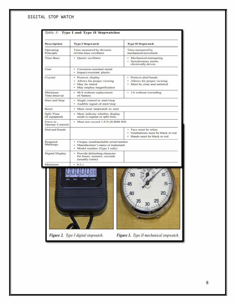
STOPWATCHES:- Stopwatches can be classified into two categories,
Type I and Type II. In general, stopwatches are classified as
Type I if they have a digital design employing quartz oscillators
and electronic circuitry to measure time intervals (Figure 2).
Type II stopwatches have an
analog design and use mechanical mechanisms to measure time
intervals (Figure 3). Key
elements of Type I and Type II stopwatches are summarized in
Table.
7
DIGITAL STOP WATCH
8
DIGITAL STOP WATCH
ASIC THEORY OF OPERATION Every stopwatch is composed of four
elements: a power source, a time base, a counter, and an
indicator or display. The design and construction of each
component depends upon the type of stopwatch. Digital (Type I)
Stopwatches — The power source of a type I stopwatch is usually a
silver cell or alkaline battery, which powers the oscillator,
counting and display circuitry. The time base is usually a quartz
crystal oscillator, with a nominal frequency of 32 768 Hz (215
Hz). Figure 4 shows the inside of a typical device, with the
printed circuit board, quartz crystal oscillator, and battery
visible. The counter circuit consists of digital dividers that
count the time base oscillations for the period that is initiated
9
DIGITAL STOP WATCH
by the start/stop buttons. The display typically has seven or
eight digits.
TIMERS
Timers, unlike stopwatches, count down from a
preset time period instead of counting up from zero. They can be
small, battery-operated devices that are used to signal when a
certain time period has elapsed, or they can be larger devices
that plug into a wall outlet and control other items (Figure 6).
A parking meter is an example of a countdown timer. Inserting a
coin starts the internal timer counting down from an initial
preset point. When the time has elapsed, the “EXPIRED” flag is
raised. One type of timer used extensively in industry is the
process control timer. As their name implies, these devices
measure or control the duration of a specific process. For
example, when a product is made, it may need to be heat treated
for a specific length of time. In an automated manufacturing
system, the process control timer determines the amount of time
that the item is heated. In some applications, such as integrated
circuit manufacturing, the timing process can be critical for
proper operation.
Process control timers are also used in many
different types of laboratory environments. Calibration
laboratories use timers to calibrate units such as radiation
detectors, where they regulate the amount of time the detector is
exposed to the radiation source. Any uncertainty in the time of
10
DIGITAL STOP WATCH
exposure directly influences the uncertainty of the detector
calibration. Timers are also used in the medical field. For
example, medical laboratories use process control timers when
specimen cultures are grown. Hospitals use timers to regulate the
amount of medication given to patients intravenously.
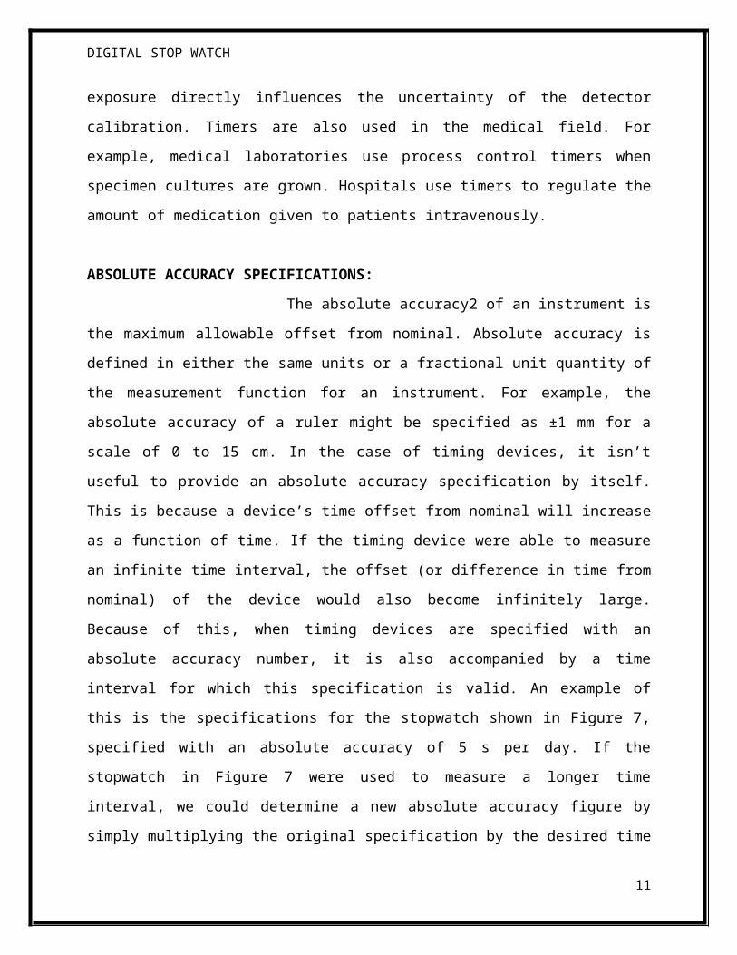
ABSOLUTE ACCURACY SPECIFICATIONS:
The absolute accuracy2 of an instrument is
the maximum allowable offset from nominal. Absolute accuracy is
defined in either the same units or a fractional unit quantity of
the measurement function for an instrument. For example, the
absolute accuracy of a ruler might be specified as ±1 mm for a
scale of 0 to 15 cm. In the case of timing devices, it isn’t
useful to provide an absolute accuracy specification by itself.
This is because a device’s time offset from nominal will increase
as a function of time. If the timing device were able to measure
an infinite time interval, the offset (or difference in time from
nominal) of the device would also become infinitely large.
Because of this, when timing devices are specified with an
absolute accuracy number, it is also accompanied by a time
interval for which this specification is valid. An example of
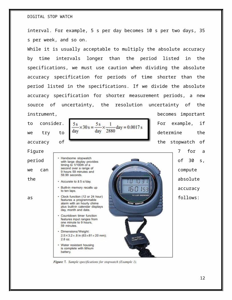
this is the specifications for the stopwatch shown in Figure 7,
specified with an absolute accuracy of 5 s per day. If the
stopwatch in Figure 7 were used to measure a longer time
interval, we could determine a new absolute accuracy figure by
simply multiplying the original specification by the desired time
11
DIGITAL STOP WATCH
interval. For example, 5 s per day becomes 10 s per two days, 35
s per week, and so on.
While it is usually acceptable to multiply the absolute accuracy
by time intervals longer than the period listed in the
specifications, we must use caution when dividing the absolute
accuracy specification for periods of time shorter than the
period listed in the specifications. If we divide the absolute
accuracy specification for shorter measurement periods, a new
source of uncertainty, the resolution uncertainty of the
instrument, becomes important
to consider. For example, if
we try to determine the
accuracy of the stopwatch of
Figure 7 for a
period of 30 s,
we can compute
the absolute
accuracy
as follows:
12
DIGITAL STOP WATCH
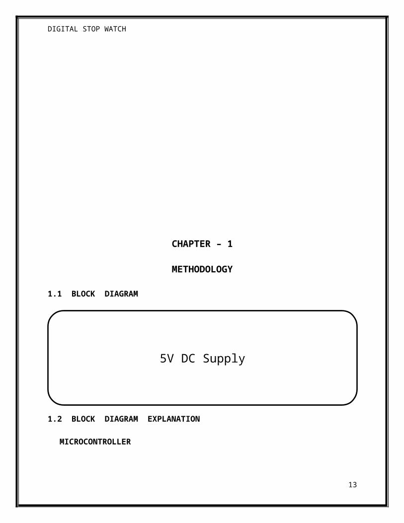
CHAPTER – 1
METHODOLOGY
1.1 BLOCK DIAGRAM
1.2 BLOCK DIAGRAM EXPLANATION
MICROCONTROLLER
13
5V DC Supply
DIGITAL STOP WATCH
Microcontroller provides a great advantage that a program is
stored in ROM that has an important role in managing the system's
operations and functions. Since the program written into ROM is fixed
that is, it cannot be altered or changed; as a result the operation of
the system remains constant (unchanged) regardless of the instructions
given to it. Hence, a microcontroller can be thought of a device
containing on-chip program memory.
VOLTAGE SOURCE (VDD=5V)
A voltage source is a two terminal device which can maintain
a fixed voltage. An ideal voltage source can maintain the fixed
voltage independent of the load resistance or the output current.
However, a real-world voltage source cannot supply unlimited
current. A voltage source is the dual of a current source. Real-
world sources of electrical energy, such as batteries,
generators, and power systems, can be modeled for analysis
purposes as a combination of an ideal voltage source and
additional combinations of impedance elements.
SWITCHES
Some switches are connected to this microcontroller for
controlling its working. These switches are for play, pause and for
selection of modes that have to be followed by the microcontroller.
14
DIGITAL STOP WATCH
switches are used to control the display drivers of the 7segment
display.
7-SEGMENT DISPLAY:
A seven-segment display or seven-segment indicator,
is a form of electronic display
device for displaying decimal numerals that is an alternative to
the more complex dot matrix
displays. Seven-segment displays are widely used in digital
clocks, electronic meters, and
other electronic devices for displaying numerical information.
15
DIGITAL STOP WATCH
CHAPTER-2
2.1 CIRCUIT DIAGRAM
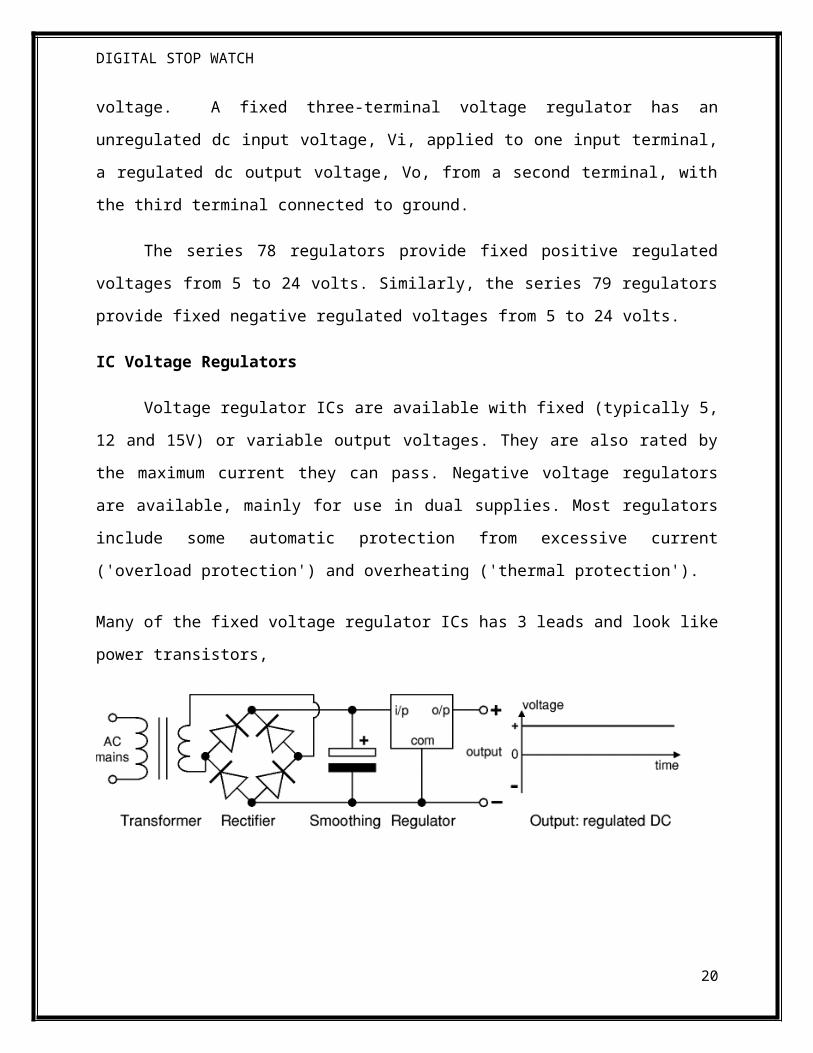
2.2 HARDWARE DESCRIPTION2.2.1 Power supply
As the microcontroller operating voltage is +5V DC.
Through this power supply circuit we have to create a +5V DC
16
DIGITAL STOP WATCH
which is given to the micro controller. The below components
are used to create the power supply
Fig 3.1.1: Block Diagram of Power Supply
Description:
230V AC supply is given to the step down transformer of 12A
type. It may be a 230V to 9V or 12V step down transformer. The
output of the step down transformer is given to bridge rectifier.
The bridge rectifier is formed with 1N4007 diodes. The bridge
rectifier converts the AC Voltage into DC Voltage. But the output
DC Voltage contains some AC component (ripples). So we use a
capacitors-2200uF/25V, 0.1uF/D and resistor of 10K as a filter
for removing ripples. That output DC Voltage is given to the
positive voltage regulator LM7805 (i.e., 78 represents the
positive series and 5 represent the output voltage it can
provide). So the output of the regulator will be the regulated
+5V DC. To indicate the condition of the circuit we place a LED
at the end of the circuit.
17
Regulator 7805
FilterBridgerectifi
Step downtransforme
230VAC
DIGITAL STOP WATCH
Fig 3.1.1: Schematic of Power Supply
2.2.2 Transformer
Transformer is a device used to increment or decrement the
input voltage given as per the requirement. The transformers are
classified into two types depending upon their functionality.
They are Step up transformer and Step down transformer.
In our project, we made use of step down transformer for
stepping down the house hold ac power supply i.e. the 230-240V
power supply to 12 V.
2.2.3 Rectifier
The output of the transformer is AC and should be rectified
to a constant DC .For this, it is necessary to feed the output of
the transformer to a rectifier. The rectifier is employed to
convert the alternating ac to a constant dc.
18

DIGITAL STOP WATCH
The rectification is done by using one or more diodes
connected in series or parallel. If only one diode is used then
only first half cycle is rectified and it is termed as half wave
rectification and the rectifier used is termed as Half-wave
rectifier.
If two diodes are employed in parallel then both positive
and negative half cycles are rectified and this is full wave
rectification and the rectifier is termed as Full-wave rectifier.
If the diodes are arranged in the form of bridge then it is
termed as Bridge rectifier .It acts as a full wave rectifier. In
our project we have employed a bridge Rectifier.
Fig 3.1.2.1: bridge
rectifier circuit
2.2.4 Voltage Regulator
Voltage regulators comprise a class of widely used ICs.
Regulator IC units contain the circuitry for reference source,
comparator amplifier, control device, and overload protection all
in a single IC. IC units provide regulation of either a fixed
positive voltage, a fixed negative voltage, or an adjustably set
19
DIGITAL STOP WATCH
voltage. A fixed three-terminal voltage regulator has an
unregulated dc input voltage, Vi, applied to one input terminal,
a regulated dc output voltage, Vo, from a second terminal, with
the third terminal connected to ground.
The series 78 regulators provide fixed positive regulated
voltages from 5 to 24 volts. Similarly, the series 79 regulators
provide fixed negative regulated voltages from 5 to 24 volts.
IC Voltage Regulators
Voltage regulator ICs are available with fixed (typically 5,
12 and 15V) or variable output voltages. They are also rated by
the maximum current they can pass. Negative voltage regulators
are available, mainly for use in dual supplies. Most regulators
include some automatic protection from excessive current
('overload protection') and overheating ('thermal protection').
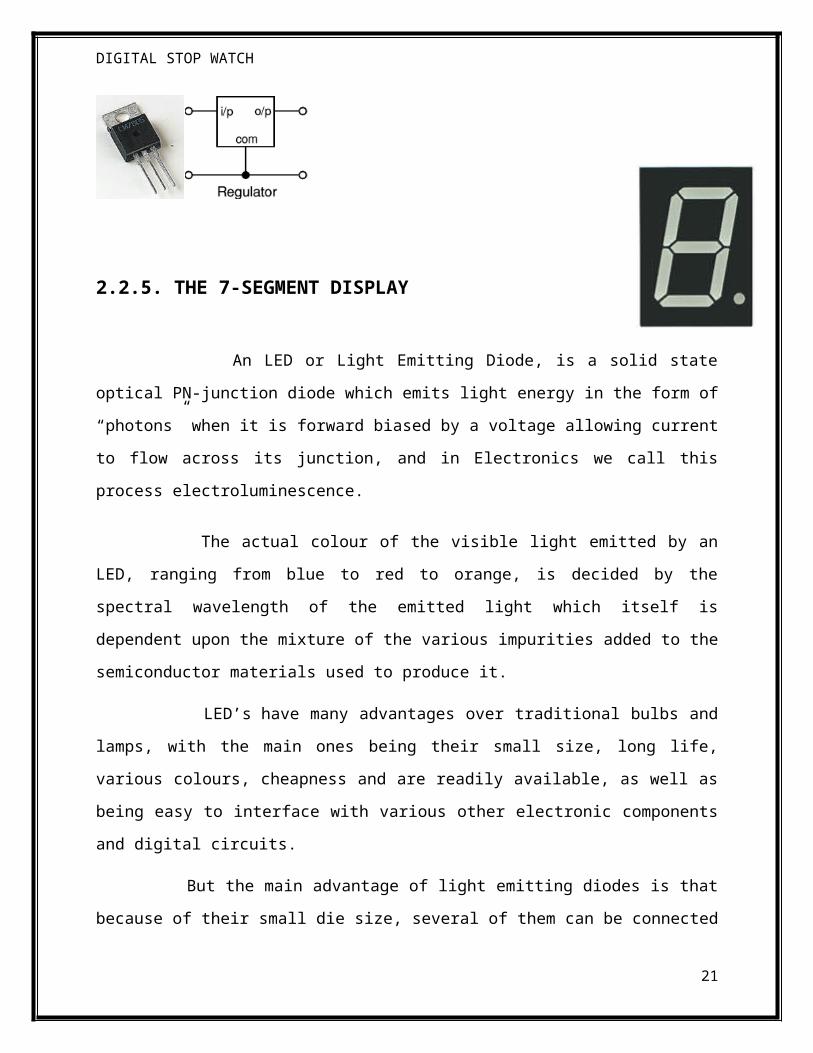
Many of the fixed voltage regulator ICs has 3 leads and look like
power transistors,
20
DIGITAL STOP WATCH
2.2.5. THE 7-SEGMENT DISPLAY
An LED or Light Emitting Diode, is a solid state
optical PN-junction diode which emits light energy in the form of
“photons” when it is forward biased by a voltage allowing current
to flow across its junction, and in Electronics we call this
process electroluminescence.
The actual colour of the visible light emitted by an
LED, ranging from blue to red to orange, is decided by the
spectral wavelength of the emitted light which itself is
dependent upon the mixture of the various impurities added to the
semiconductor materials used to produce it.
LED’s have many advantages over traditional bulbs and
lamps, with the main ones being their small size, long life,
various colours, cheapness and are readily available, as well as
being easy to interface with various other electronic components
and digital circuits.
But the main advantage of light emitting diodes is that
because of their small die size, several of them can be connected
21
DIGITAL STOP WATCH
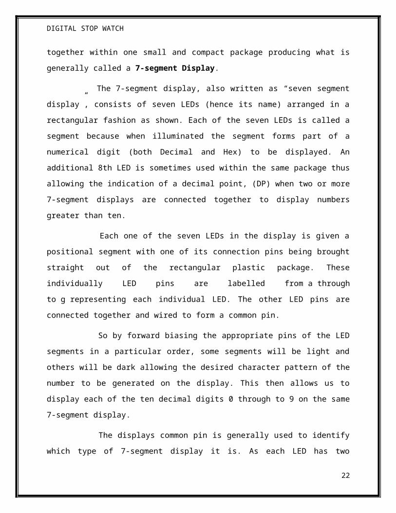
together within one small and compact package producing what is
generally called a 7-segment Display.
The 7-segment display, also written as “seven segment
display”, consists of seven LEDs (hence its name) arranged in a
rectangular fashion as shown. Each of the seven LEDs is called a
segment because when illuminated the segment forms part of a
numerical digit (both Decimal and Hex) to be displayed. An
additional 8th LED is sometimes used within the same package thus
allowing the indication of a decimal point, (DP) when two or more
7-segment displays are connected together to display numbers
greater than ten.
Each one of the seven LEDs in the display is given a
positional segment with one of its connection pins being brought
straight out of the rectangular plastic package. These
individually LED pins are labelled from a through
to g representing each individual LED. The other LED pins are
connected together and wired to form a common pin.
So by forward biasing the appropriate pins of the LED
segments in a particular order, some segments will be light and
others will be dark allowing the desired character pattern of the
number to be generated on the display. This then allows us to
display each of the ten decimal digits 0 through to 9 on the same
7-segment display.
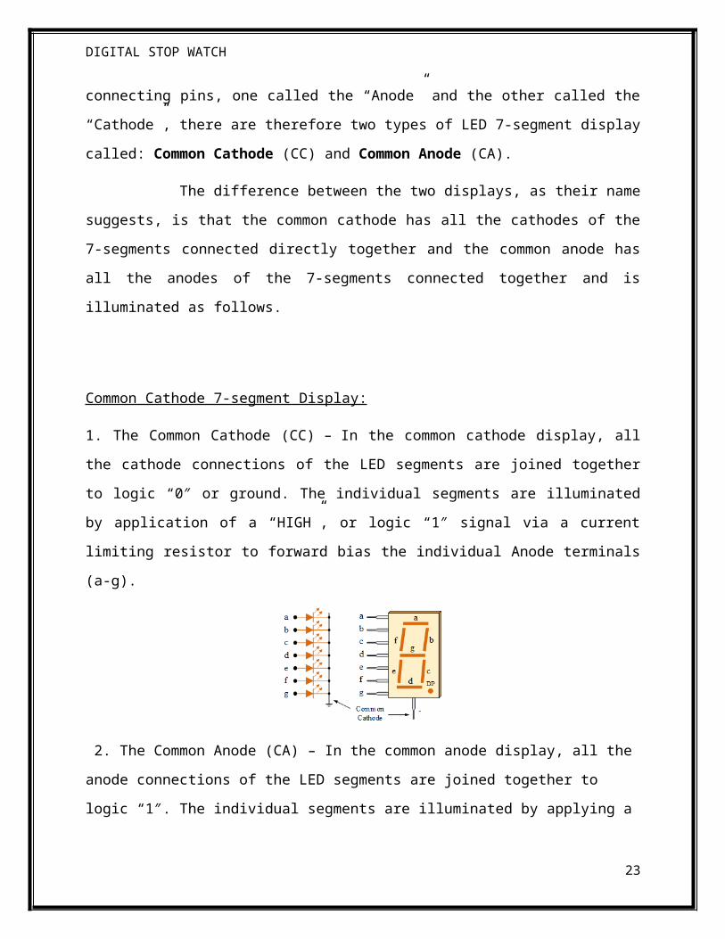
The displays common pin is generally used to identify
which type of 7-segment display it is. As each LED has two
22
DIGITAL STOP WATCH
connecting pins, one called the “Anode” and the other called the
“Cathode”, there are therefore two types of LED 7-segment display
called: Common Cathode (CC) and Common Anode (CA).
The difference between the two displays, as their name
suggests, is that the common cathode has all the cathodes of the
7-segments connected directly together and the common anode has
all the anodes of the 7-segments connected together and is
illuminated as follows.
Common Cathode 7-segment Display:
1. The Common Cathode (CC) – In the common cathode display, all
the cathode connections of the LED segments are joined together
to logic “0″ or ground. The individual segments are illuminated
by application of a “HIGH”, or logic “1″ signal via a current
limiting resistor to forward bias the individual Anode terminals
(a-g).
2. The Common Anode (CA) – In the common anode display, all the
anode connections of the LED segments are joined together to
logic “1″. The individual segments are illuminated by applying a
23
DIGITAL STOP WATCH
ground, logic “0″ or “LOW” signal via a suitable current limiting
resistor to the Cathode of the particular segment (a-g).
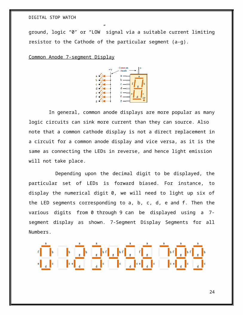
Common Anode 7-segment Display
In general, common anode displays are more popular as many
logic circuits can sink more current than they can source. Also
note that a common cathode display is not a direct replacement in
a circuit for a common anode display and vice versa, as it is the
same as connecting the LEDs in reverse, and hence light emission
will not take place.
Depending upon the decimal digit to be displayed, the
particular set of LEDs is forward biased. For instance, to
display the numerical digit 0, we will need to light up six of
the LED segments corresponding to a, b, c, d, e and f. Then the
various digits from 0 through 9 can be displayed using a 7-
segment display as shown. 7-Segment Display Segments for all
Numbers.
24
DIGITAL STOP WATCH
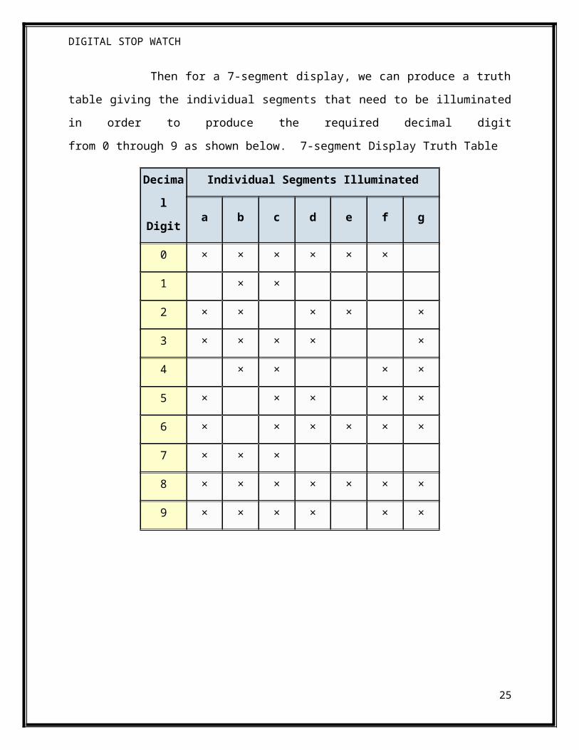
Then for a 7-segment display, we can produce a truth
table giving the individual segments that need to be illuminated
in order to produce the required decimal digit
from 0 through 9 as shown below. 7-segment Display Truth Table
Decima
l
Digit
Individual Segments Illuminated
a b c d e f g
0 × × × × × ×
1 × ×
2 × × × × ×
3 × × × × ×
4 × × × ×
5 × × × × ×
6 × × × × × ×
7 × × ×
8 × × × × × × ×
9 × × × × × ×
25
DIGITAL STOP WATCH
Driving a 7-segment Display
Although a 7-segment display can be thought of as a
single display, it is still seven individual LEDs within a single
package and as such these LEDs need protection from overcurrent.
LEDs produce light only when it is forward biased with the amount
of light emitted being proportional to the forward current.
This means then that an LEDs light intensity increases
in an approximately linear manner with an increasing current. So
this forward current must be controlled and limited to a safe
value by an external resistor to prevent damage to the LED
segments.
The forward voltage drop across a red LED segment is
very low at about 2-to-2.2 volts, (blue and white LEDs can be as
high as 3.6 volts) so to illuminate correctly, the LED segments
should be connected to a voltage source in excess of this forward
voltage value with a series resistance used to limit the forward
current to a desirable value.
Typically for a standard red coloured 7-segment
display, each LED segment can draw about 15 mA to illuminated
correctly, so on a 5 volt digital logic circuit, the value of the
current limiting resistor would be about 200Ω (5v – 2v)/15mA, or
220Ω to the nearest higher preferred value.
26
DIGITAL STOP WATCH
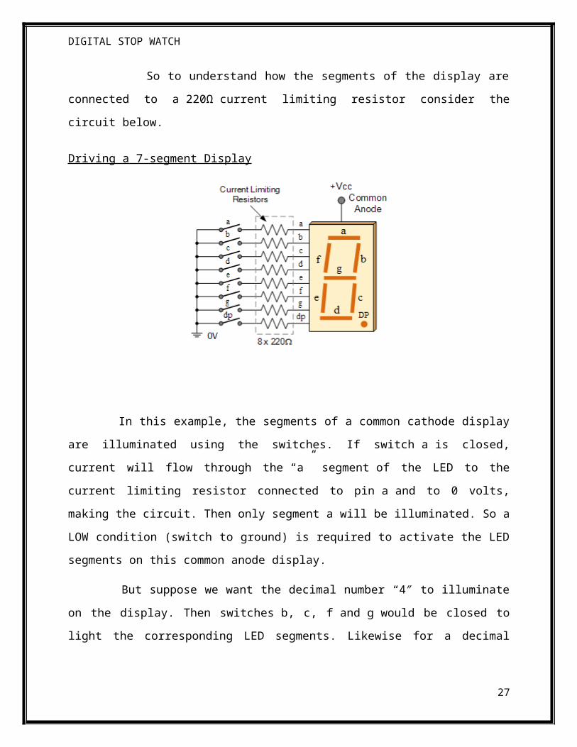
So to understand how the segments of the display are
connected to a 220Ω current limiting resistor consider the
circuit below.
Driving a 7-segment Display
In this example, the segments of a common cathode display
are illuminated using the switches. If switch a is closed,
current will flow through the “a” segment of the LED to the
current limiting resistor connected to pin a and to 0 volts,
making the circuit. Then only segment a will be illuminated. So a
LOW condition (switch to ground) is required to activate the LED
segments on this common anode display.
But suppose we want the decimal number “4″ to illuminate
on the display. Then switches b, c, f and g would be closed to
light the corresponding LED segments. Likewise for a decimal
27

DIGITAL STOP WATCH
number “7″, switches a, b, c would be closed. But illuminating 7-
segment displays using individual switches is not very practical.
For checking the display you require a simple tool that is your
multi-meter. Steps follow while testing seven segment displays -
1. Hold the display in your hand and identify the pin 1.This can
be done as shown in figure below.
2. Now take multi-meter (Assumption followed red lead for
positive and black lead for negative). Set the multi-meter in
continuity range.
3. Check for sound test (touch both the leads together sound will
produce). Sometimes it may possible, battery of your multi-meter
become weak and we will be not being able to get the display.
4. Put the Black lead of multi-meter on pin 3 or 8 both are
common pin as they are internally connected.
5. Now put Red lead of multi-meter on any other pin may be 1, 5.
6. If any of the segment glows then your display is common
cathode.
28

DIGITAL STOP WATCH
7. If none of the segment glows than interchange the leads of
multi-meter.
8. Connect the Red lead of multi-meter on pin 3 or pin 8 as both
are common pin and internally connected to each other.
9. Now put the black lead of the multi-meter on other remaining
pin. If any of the segment glow than your display is common
anode, as in common anode positive pin is common and rest are
supplied with negative supply.
10. Check all segments of both common cathode and anode to ensure
your display is working properly.
11. If none of the segment glows means your 7 segment is faulty.
I hope this will save your time and energy for identification
and let you know how to test seven segment display.
2.2.6 BC547
The BC547 transistor is an NPN Epitaxial Silicon Transistor.
The BC547 transistor is a general-purpose transistor in small
plastic packages. It is used in general-purpose switching and
amplification BC847/BC547 series 45 V, 100 Ma NPN general-purpose
transistors.
29

DIGITAL STOP WATCH
Fig 3.3.1: BC 547
TRANSISTOR PINOUTS
The BC547 transistor is an NPN bipolar transistor, in which
the letters “N” and “P” refer to the majority charge carriers
inside the different regions of the transistor.
The Transistor as a Switch
When used as an AC signal amplifier, the transistors Base
biasing voltage is applied in such a way that it always operates
within its "active" region, that is the linear part of the output
characteristics curves are used. However, both the NPN & PNP type
bipolar transistors can be made to operate as "ON/OFF" type solid
state switches by biasing the transistors base differently to
that of a signal amplifier.
Solid state switches are one of the main applications for
the use of transistors, and transistor switches can be used for
controlling high power devices such as motors, solenoids or
lamps, but they can also used in digital electronics and logic
gate circuits.
30
DIGITAL STOP WATCH
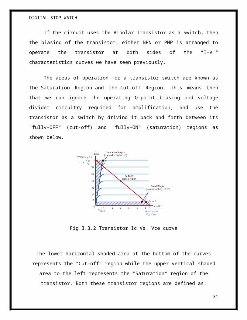
If the circuit uses the Bipolar Transistor as a Switch, then
the biasing of the transistor, either NPN or PNP is arranged to
operate the transistor at both sides of the “I-V "
characteristics curves we have seen previously.
The areas of operation for a transistor switch are known as
the Saturation Region and the Cut-off Region. This means then
that we can ignore the operating Q-point biasing and voltage
divider circuitry required for amplification, and use the
transistor as a switch by driving it back and forth between its
"fully-OFF" (cut-off) and "fully-ON" (saturation) regions as
shown below.
Fig 3.3.2 Transistor Ic Vs. Vce curve
The lower horizontal shaded area at the bottom of the curves
represents the "Cut-off" region while the upper vertical shaded
area to the left represents the "Saturation" region of the
transistor. Both these transistor regions are defined as:
31
DIGITAL STOP WATCH
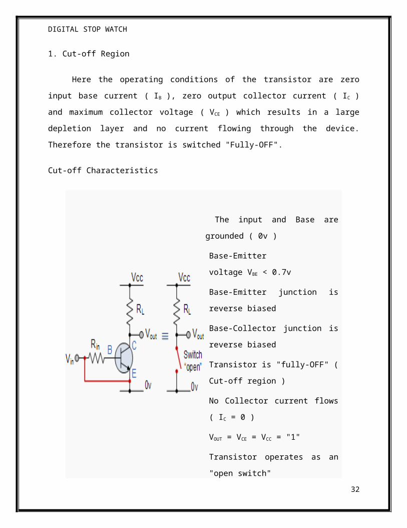
1. Cut-off Region
Here the operating conditions of the transistor are zero
input base current ( IB ), zero output collector current ( IC )
and maximum collector voltage ( VCE ) which results in a large
depletion layer and no current flowing through the device.
Therefore the transistor is switched "Fully-OFF".
Cut-off Characteristics
The input and Base are
grounded ( 0v )
Base-Emitter
voltage VBE < 0.7v
Base-Emitter junction is
reverse biased
Base-Collector junction is
reverse biased
Transistor is "fully-OFF" (
Cut-off region )
No Collector current flows
( IC = 0 )
VOUT = VCE = VCC = "1"
Transistor operates as an
"open switch"32
DIGITAL STOP WATCH
Then we can define the "cut-off region" or "OFF mode" when
using a bipolar transistor as a switch as being, both junctions
reverse biased, VB < 0.7v and IC = 0. For a PNP transistor, the
Emitter potential must be negative with respect to the Base.
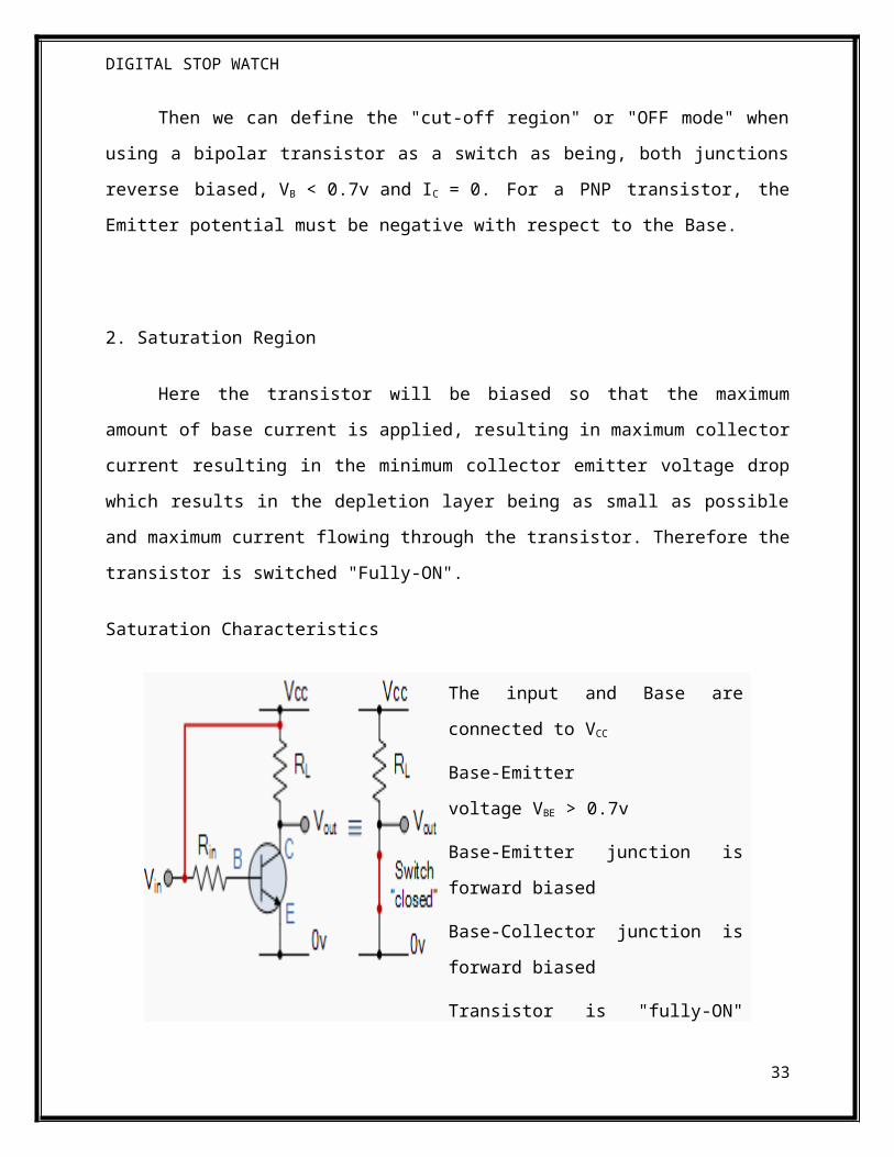
2. Saturation Region
Here the transistor will be biased so that the maximum
amount of base current is applied, resulting in maximum collector
current resulting in the minimum collector emitter voltage drop
which results in the depletion layer being as small as possible
and maximum current flowing through the transistor. Therefore the
transistor is switched "Fully-ON".
Saturation Characteristics
The input and Base are
connected to VCC
Base-Emitter
voltage VBE > 0.7v
Base-Emitter junction is
forward biased
Base-Collector junction is
forward biased
Transistor is "fully-ON"
33
DIGITAL STOP WATCH
( saturation region )
Max Collector current flows
( IC = Vcc/RL )
VCE = 0 ( ideal saturation )
VOUT = VCE = "0"
Transistor operates as a
"closed switch"
Then we can define the "saturation region" or "ON mode" when
using a bipolar transistor as a switch as being, both junctions
forward biased, VB > 0.7v and IC = Maximum. For a PNP transistor,
the Emitter potential must be positive with respect to the Base.
Then the transistor operates as a "single-pole single-throw"
(SPST) solid state switch. With a zero signal applied to the Base
of the transistor it turns "OFF" acting like an open switch and
zero collector current flows. With a positive signal applied to
the Base of the transistor it turns "ON" acting like a closed
switch and maximum circuit current flows through the device.
In our circuit we use a transistor as a switch for every
single 7 segment display in order to control the display, the
frequency of switching the display on/off is so rapid that the
human eye doesn’t identify the on/off period.
The transistor’s base is connected to the microcontroller to
control the switching of display continuously. The clock cycle of
34

DIGITAL STOP WATCH
on/off of the display from the microcontroller is sent through
base.
2.2.7 Microcontroller (AT89S52)
Features
• Compatible with MCS-51Products
• 8K Bytes of In-System Programmable (ISP) Flash Memory
• 4.0V to 5.5V Operating Range
• Fully Static Operation: 0 Hz to 33 MHz
• 256Bytes Internal RAM
• 32 Programmable I/O Lines
• 3 16-bit Timer/Counters
• Full Duplex UART Serial Channel
DESCRIPTION OF MICROCONTROLLER AT 89S52:
The AT89S52 is a low-power, high-performance CMOS 8-bit
micro controller with 8Kbytes of in-system programmable Flash
memory. The device is manufactured
Using Atmel’s high-density non-volatile
memory technology and is compatible with the industry-standard
80C51 micro controller. The on-chip Flash allows the program
memory to be reprogrammed in-system or by a conventional non-
35
DIGITAL STOP WATCH
volatile memory programmer. By combining a versatile 8-bit CPU
with in-system programmable flash one monolithic chip; the Atmel
AT89S52 is a powerful micro controller, which provides a highly
flexible and cost- effective solution to many embedded control
applications.
The AT89S52 provides the following standard features: 8K bytes
of Flash, 256 bytes of RAM, 32 I/O lines, Watchdog timer, two
data pointers, three 16-bit timer/counters, full duplex serial
port, on-chip oscillator, and clock circuitry. In addition,
the AT89S52 is designed with static logic for perationdown to
zero frequency and supports two software selectable power
saving modes. The Idle Mode stops the CPU while allowing the
RAM timer/counters, serial port, and interrupt system to
continue functioning. The Power-down mode saves the RAM
contents but freezes the oscillator, disabling all other chip
functions until the next interrupt or hardware reset.
36
DIGITAL STOP WATCH
Fig 3.4.1 Architecture of 89S52
37
DIGITAL STOP WATCH
Fig. 3.4.2 Pin diagram of 89S52
Pin Description of microcontroller AT89S52
VCC: Supply voltage.
GND: Ground.
Port 0
Port 0 is an 8-bit open drain bidirectional I/O port. As an
output port, each pin can sink eight TTL inputs. When 1s are
written to port 0 pins, the pins can be used as high-impedance
inputs. Port 0 can also be configured to be the multiplexed low-
38
DIGITAL STOP WATCH
order address/data bus during accesses to external program and
data memory. In this mode, P0 has internal pull-ups. Port 0 also
receives the code bytes during Flash programming and outputs the
code bytes during program verification. External pull-ups are
required during program verification.
Port 1
Port 1 is an 8-bit bidirectional I/O port with internal
pull-ups. The Port 1 output buffers can sink/source four TTL
inputs. When 1s are written to Port 1 pins, they are pulled high
by the internal pull-ups and can be used as inputs. As inputs,
Port 1 pins that are externally being pulled low will source
current (IIL) because of the internal pull-ups. In addition,
P1.0 and P1.1 can be configured to be the timer/counter 2
external count input (P1.0/T2) and the timer/counter 2 trigger
input (P1.1/T2EX), respectively, as shown in the following table.
Table 3.4.1: The Alternate Functions of
Port 1 Pins
Port 1 also receives the low-order address bytes during Flash
programming and verification.
39
DIGITAL STOP WATCH
Port 2
Port 2 is an 8-bit bidirectional I/O port with internal
pull-ups. The Port 2 output buffers can sink/source four TTL
inputs. When 1s are written to Port 2 pins, they are pulled high
by the internal pull-ups and can be used as inputs. As inputs,
Port 2 pins that are externally being pulled low will source
current (IIL) because of the internal pull-ups.Port 2 emits the
high-order address byte during fetches from external program
memory and during accesses to external data memory that use 16-
bit addresses (MOVX @ DPTR). In this application, Port 2 uses
strong internal pull-ups when emitting 1s. During accesses to
external data memory that use 8-bit addresses (MOVX @ RI), Port 2
emits the contents of the P2 Special Function Register.
Port 2 also receives the high-order address bits and some
control signals during Flash programming and verification.
Port 3
Port 3 is an 8-bit bidirectional I/O port with internal
pull-ups. The Port 3 output buffers can sink/source four TTL
inputs. When 1s are written to Port 3 pins, they are pulled high
by the internal pull-ups and can be used as inputs. As inputs,
Port 3 pins that are externally being pulled low will source
current (IIL) because of the pull-ups.
40
DIGITAL STOP WATCH
Port 3 receives some control signals for Flash programming and
verification.
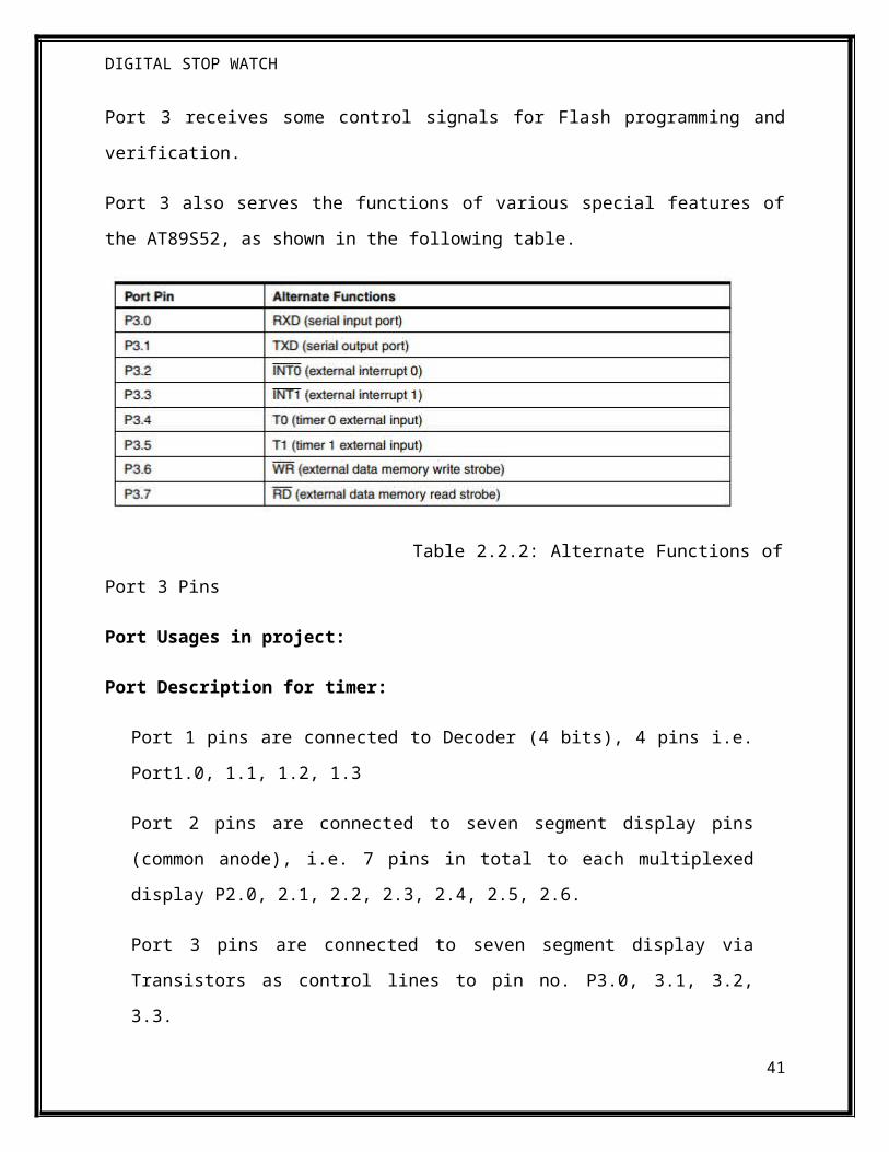
Port 3 also serves the functions of various special features of
the AT89S52, as shown in the following table.
Table 2.2.2: Alternate Functions of
Port 3 Pins
Port Usages in project:
Port Description for timer:
Port 1 pins are connected to Decoder (4 bits), 4 pins i.e.
Port1.0, 1.1, 1.2, 1.3
Port 2 pins are connected to seven segment display pins
(common anode), i.e. 7 pins in total to each multiplexed
display P2.0, 2.1, 2.2, 2.3, 2.4, 2.5, 2.6.
Port 3 pins are connected to seven segment display via
Transistors as control lines to pin no. P3.0, 3.1, 3.2,
3.3.
41
DIGITAL STOP WATCH
Port Description for Score:
Port 1 pins are connected to Decoder (4 bits), 4 pins i.e.
Port1.0, 1.1, 1.2, 1.3
Port 2 pins are connected to seven segment display pins
(common anode), i.e. 7 pins in total to each multiplexed
display P2.0, 2.1, 2.2, 2.3, 2.4, 2.5, 2.6.
Port 3 pins are connected to seven segment display via
Transistors as control lines to pin no. P3.0, 3.1, 3.2,
3.3.
Port Description for team name display:
Port 1 pins are connected to switch’s 4 switch’s each for
each display, 4 pins i.e. Port1.0, 1.1, 1.2, 1.3
Port 2 pins are connected to seven segment display pins
(common anode), i.e. 7 pins in total to each multiplexed
display P2.0, 2.1, 2.2, 2.3, 2.4, 2.5, 2.6.
Port 3 pins are connected to seven segment display via
Transistors as control lines to pin no. P3.0, 3.1, 3.2,
3.3.
RST: Reset input. A high on this pin for two machine cycles
while the oscillator is running resets the device. Each module
in the score board has been provided with its own reset button.
42
DIGITAL STOP WATCH
ALE/PROG:
Address Latch Enable (ALE) is an output pulse for latching
the low byte of the address during accesses to external memory.
This pin is also the program pulse input (PROG) during Flash
programming. In normal operation, ALE is emitted at a constant
rate of1/6 the oscillator frequency and may be used for external
timing or clocking purposes. Note, however, that one ALE pulse is
skipped during each access to external data Memory. If desired,
ALE operation can be disabled by setting bit 0 of SFR location
8EH. with the bit set, ALE is active only
during a MOVX or MOVC instruction. Otherwise, the pin is
weakly pulled high. Setting the ALE-disable bit has no effect
if the micro controller is in external execution mode.
PSEN:
Program Store Enable (PSEN) is the read strobe to
external program memory. When the AT89S52 is executing code
from external program memory, PSEN is activated twice each
machine cycle, except that two PSEN activations are skipped
during each access to external data memory.
EA/VPP:
External Access Enable. EA must be strapped to GND in
order to enable the device to fetch code from external program
memory locations starting at 0000H up to FFFFH. Note, however,
that if lock bit 1 is programmed, EA will be internally
43
DIGITAL STOP WATCH
latched on reset. A should be strapped to VCC for internal
program executions. This pin also receives the 12-
voltProgramming enables voltage (VPP) during Flash
programming.
3.4.1 OSCILLATOR
XTAL1 and XTAL2 are the input and output, respectively, of
an inverting amplifier that can be configured for use as an on-
chip oscillator. Either a quartz crystal or ceramic resonator may
be used. To drive the device from an external clock source, XTAL2
should be left unconnected while XTAL1 is driven, as shown in
Figure 2.2.3. There are no requirements on the duty cycle of the
external clock signal, since the input to the internal clocking
circuitry is through a divide-by-two flip-flop, but minimum and
maximum voltage high and low time specifications must be
observed.
XTAL1:
Input to the inverting oscillator amplifier and input to
the internal clock operating circuit.
XTAL2 :
Output from the inverting oscillator amplifier.
We have used a 11.0592Mhz crystal oscillator.
44

DIGITAL STOP WATCH
3. Software Description
3.1 µvision2
µVision2 is an IDE (Integrated Development
Environment) that helps us write, compile, and debug embedded
programs. It encapsulates the following components:
A project manager.
A make facility.
Tool configuration.
Editor.
A powerful debugger.
3.1.1 Creating application in µvision2:
1. Select Project - New Project.
2. Select a directory and enter the name of the project file.
3. Select Project - Select Device and select an 8051, 251, or
C16x/ST10 device from the Device Database™.
4. Create source files to add to the project.
5. Select Project - Targets, Groups, and Files. Add/Files,
select Source Group1, and add the source files to the
project.
6. Select Project - Options and set the tool options. when we
select the target device from the Device Database all
special options are set automatically. We need to configure
45

DIGITAL STOP WATCH
only the memory map of our target hardware. Default memory
model settings are optimal for most applications.
7. Select Project - Rebuild all target files or Build target.
3.1.2 Debugging an application in µvision2:
To debug an application created using µVision2, we must:
1. Select Debug - Start/Stop Debug Session.
2. Use the Step toolbar buttons to single-step through your
program. We may enter G, main in the Output Window to
execute to the main C function.
3. Open the Serial Window using the Serial #1 button on the
toolbar
We can Debug program using standard options like Step, Go, Break,
and so on.
3.1.3 Creating a Project:
µVision2 is a standard Windows application and
started by clicking on the program icon. To create a new project
file select from the µVision2 menu
Project – New Project…. This opens a standard Windows dialog that
asks us for the new project file name. a separate folder should
be used for each project. we can simply use the icon Create New
Folder in this dialog to get a new empty folder. Then select this
folder and enter the file name for the new project, i.e.
Project1.
46

DIGITAL STOP WATCH
µVision2 creates a new project file with
the name PROJECT1.UV2 which contains a default target and file
group name. We can see these names in the Project Window – Files.
Now use from the menu Project – Select
Device for Target and select a CPU for the project. The Select
Device dialog box shows the µVision2 device database. Just select
the micro controller we use. For example, we are using the
Philips 80C51RD+ CPU. This selection sets necessary tool options
for the 80C51RD+ device and simplifies in this way the tool
Configuration
3.1.4 Building projects and creating a hex files:
Typical, the tool settings under Options – Target are all we
need to start a new application. we may translate all source
files and line the application with a click on the Build Target
toolbar icon. When we build an application with syntax errors,
µVision2 will display errors and warning messages in the Output
Window – Build page. A double click on a message line opens the
source file on the correct location in a µVision2 editor window.
Once we have successfully generated our application we can start
debugging
After we have tested your application, it is required to
create an Intel HEX file to download the software into an EPROM
programmer or simulator. µVision2 creates HEX files with each
build process when Create HEX files under Options for Target –
Output is enabled. We may start our PROM programming utility
47
DIGITAL STOP WATCH
after the make process when we specify the program under the
option Run User Program #1.
3.1.5 CPU Simulation:
µVision2 simulates up to 16 Mbytes of memory from which
areas can be mapped for read, write, or code execution access.
The µVision2 simulator traps and reports illegal memory
accesses. In addition to memory mapping, the simulator also
provides support for the integrated peripherals of the various
8051 derivatives. The on-chip peripherals of the CPU you have
selected are configured from the Device
3.1.6 Database selection:
We may select and display the on-chip peripheral components
using the Debug menu. We can also change the aspects of each
peripheral using the controls in the dialog boxes.
3.1.7 Start debugging:
We start the debug mode of µVision2 with the Debug –
Start/Stop Debug Session command. Depending on the Options for
Target – Debug Configuration, µVision2 will load the application
program and run the startup code. µVision2 saves the editor
screen layout and restores the screen layout of the last debug
session. If the program execution stops, µVision2 opens an editor
window with the source text or shows CPU instructions in the
disassembly window. The next executable statement is marked with
48
DIGITAL STOP WATCH
a yellow arrow. During debugging, most editor features are still
available.
For example, we can use the find command or correct program
errors. Program source text of the application is shown in the
same windows. The project structure or tool parameters cannot be
modified. All build commands are disabled.
3.1.8 Disassembly window:
The Disassembly window shows the target program as mixed
source and assembly program or just assembly code. A trace
history of previously executed instructions may be displayed with
Debug – View Trace Records. To enable the trace history, set
Debug – Enable/Disable Trace Recording.
If we select the Disassembly Window as the active window,
all program step commands work on CPU instruction level rather
than program source lines. we can select a text line and set or
modify code breakpoints using toolbar buttons or the context menu
commands.
we may use the dialog Debug – Inline Assembly to modify the
CPU instructions. That allows us to correct mistakes or to make
temporary changes to the target program you are debugging.
49

DIGITAL STOP WATCH
3.2 KEIL
Keil compiler is a software used where the machine language
code is written and compiled. After compilation, the machine
source code is converted into hex code which is to be dumped into
the microcontroller for further processing. Keil compiler also
supports C language code.
Flow chart
50
µVision menu Project
Select New project
Create a Project
Select a
In target, create thesource group
Create a new source
Save the file with the
Give the relevantparameters to the target
IfErro
DIGITAL STOP WATCH
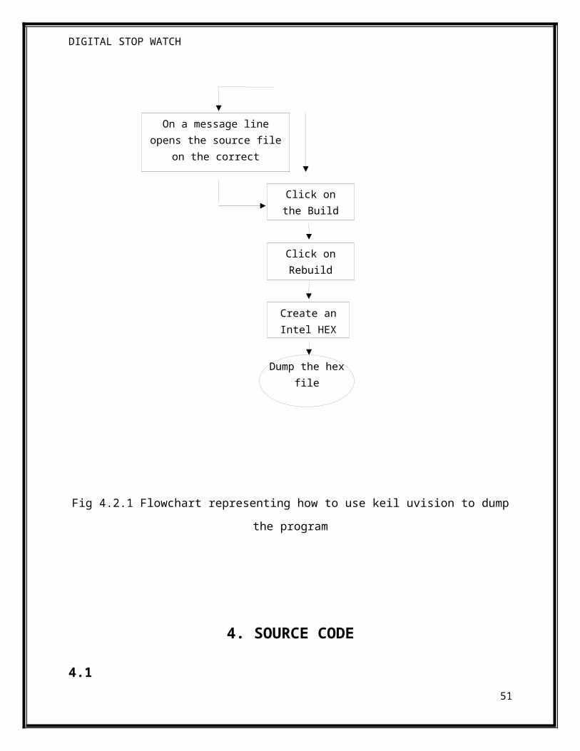
Fig 4.2.1 Flowchart representing how to use keil uvision to dump
the program
4. SOURCE CODE
4.1 51
On a message lineopens the source file
on the correctlocation in a µVision
Click onthe Build
Click onRebuild
Create anIntel HEX
Dump the hexfile
DIGITAL STOP WATCH
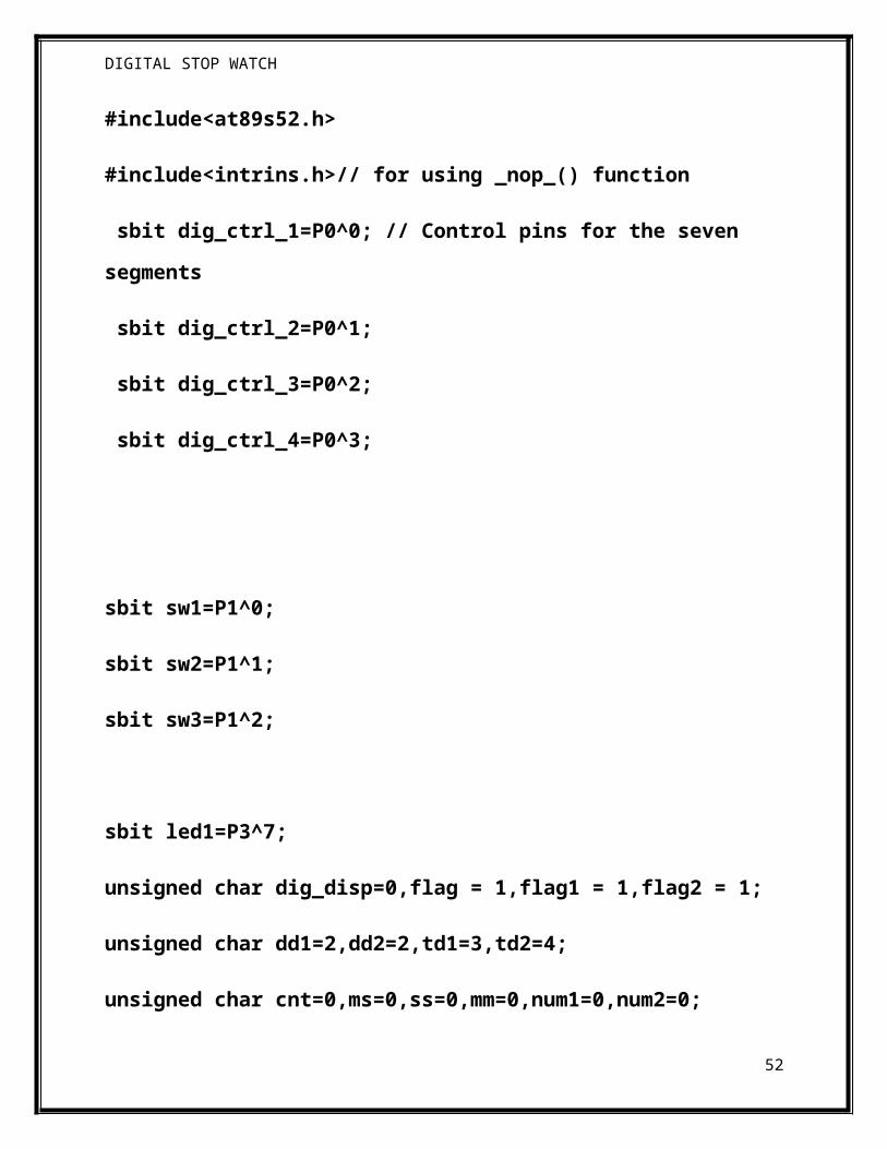
#include<at89s52.h>
#include<intrins.h>// for using _nop_() function
sbit dig_ctrl_1=P0^0; // Control pins for the seven
segments
sbit dig_ctrl_2=P0^1;
sbit dig_ctrl_3=P0^2;
sbit dig_ctrl_4=P0^3;
sbit sw1=P1^0;
sbit sw2=P1^1;
sbit sw3=P1^2;
sbit led1=P3^7;
unsigned char dig_disp=0,flag = 1,flag1 = 1,flag2 = 1;
unsigned char dd1=2,dd2=2,td1=3,td2=4;
unsigned char cnt=0,ms=0,ss=0,mm=0,num1=0,num2=0;
52
DIGITAL STOP WATCH
char
digi_val[10]={0x40,0xF9,0x24,0x30,0x19,0x12,0x02,0xF8,0
x00,0x10};
void msdelay(unsigned int itime)
{
unsigned int i,j ;
for(i=0;i<itime;i++) ;
for(j=0;j<1;j++);
}
void display() interrupt 1 // Function to
display the four digit number using multiplexing on
seven segment. It uses Timer 0 interrupt to display the
four digits one by one after a time delay of 2.5 milli
second
{
TL0=0x36;
53
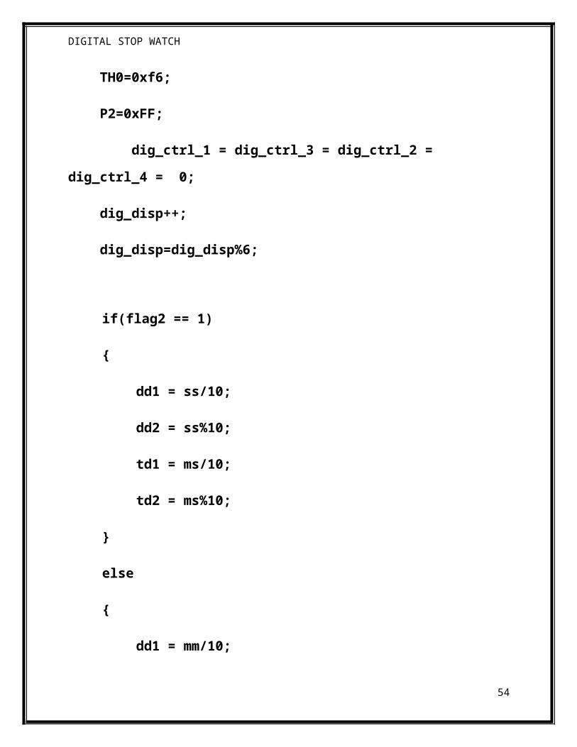
DIGITAL STOP WATCH
TH0=0xf6;
P2=0xFF;
dig_ctrl_1 = dig_ctrl_3 = dig_ctrl_2 =
dig_ctrl_4 = 0;
dig_disp++;
dig_disp=dig_disp%6;
if(flag2 == 1)
{
dd1 = ss/10;
dd2 = ss%10;
td1 = ms/10;
td2 = ms%10;
}
else
{
dd1 = mm/10;
54
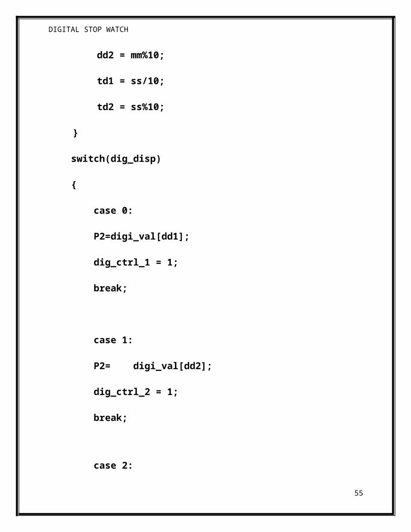
DIGITAL STOP WATCH
dd2 = mm%10;
td1 = ss/10;
td2 = ss%10;
}
switch(dig_disp)
{
case 0:
P2=digi_val[dd1];
dig_ctrl_1 = 1;
break;
case 1:
P2= digi_val[dd2];
dig_ctrl_2 = 1;
break;
case 2:
55
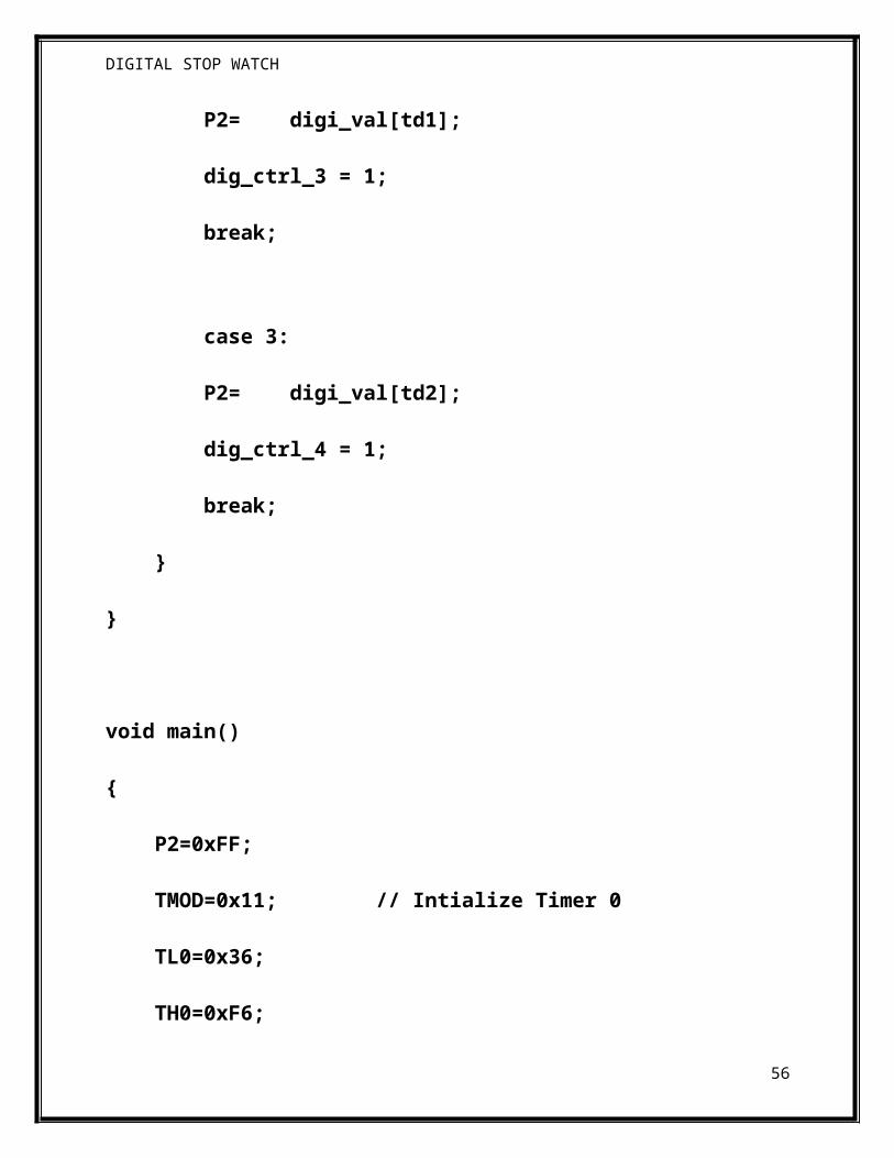
DIGITAL STOP WATCH
P2= digi_val[td1];
dig_ctrl_3 = 1;
break;
case 3:
P2= digi_val[td2];
dig_ctrl_4 = 1;
break;
}
}
void main()
{
P2=0xFF;
TMOD=0x11; // Intialize Timer 0
TL0=0x36;
TH0=0xF6;
56
DIGITAL STOP WATCH
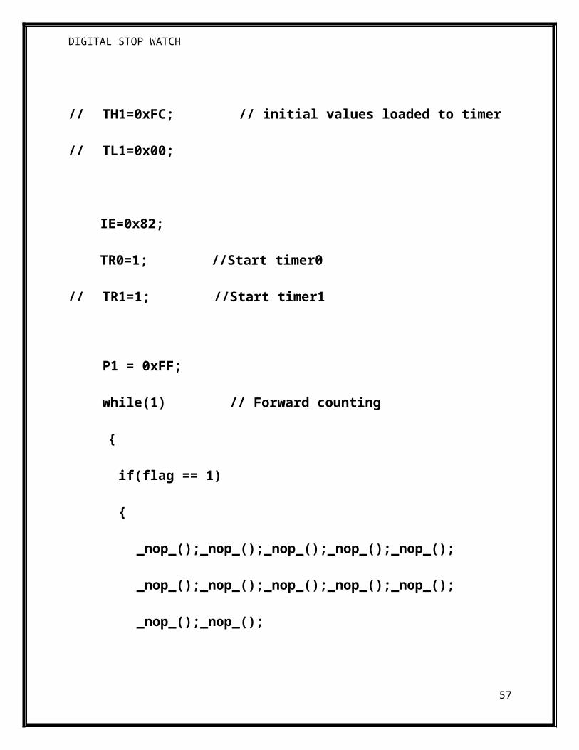
// TH1=0xFC; // initial values loaded to timer
// TL1=0x00;
IE=0x82;
TR0=1; //Start timer0
// TR1=1; //Start timer1
P1 = 0xFF;
while(1) // Forward counting
{
if(flag == 1)
{
_nop_();_nop_();_nop_();_nop_();_nop_();
_nop_();_nop_();_nop_();_nop_();_nop_();
_nop_();_nop_();
57
DIGITAL STOP WATCH
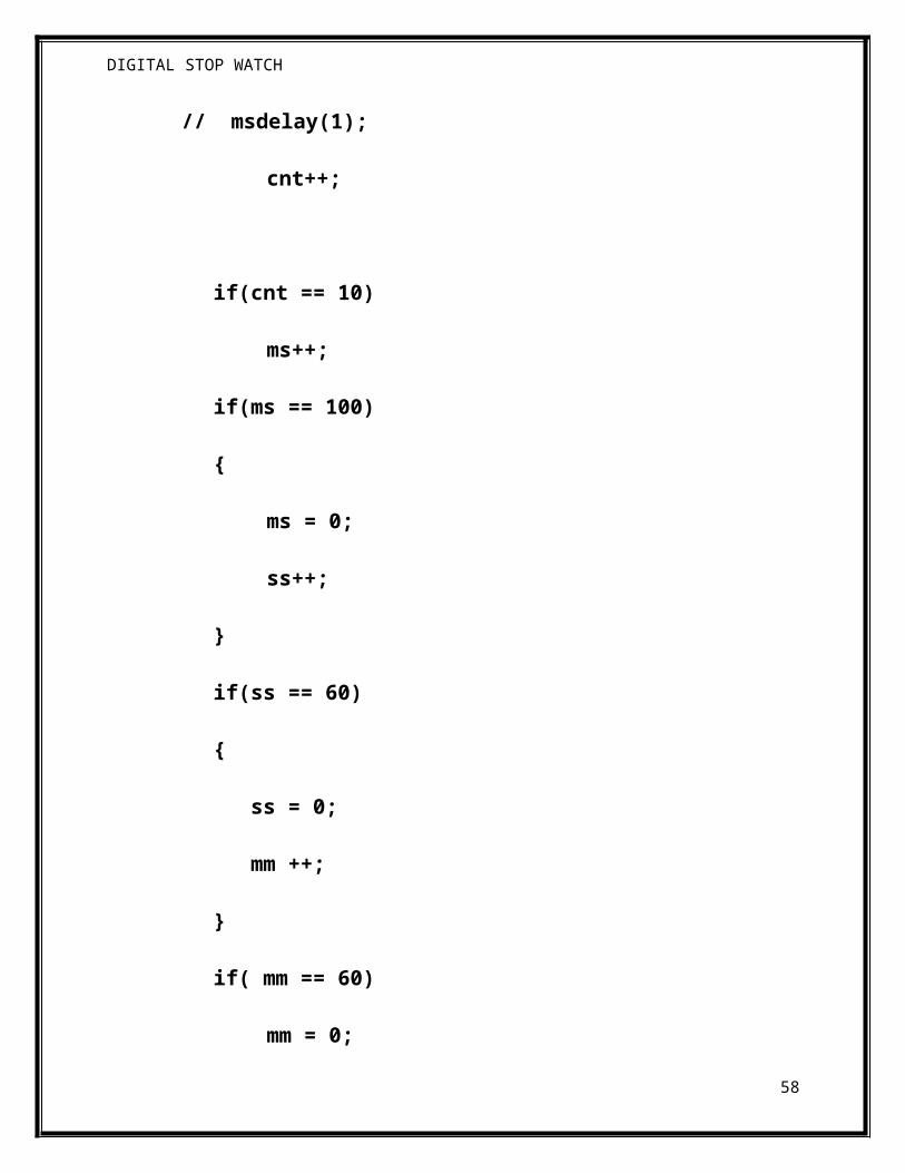
// msdelay(1);
cnt++;
if(cnt == 10)
ms++;
if(ms == 100)
{
ms = 0;
ss++;
}
if(ss == 60)
{
ss = 0;
mm ++;
}
if( mm == 60)
mm = 0;
58
DIGITAL STOP WATCH
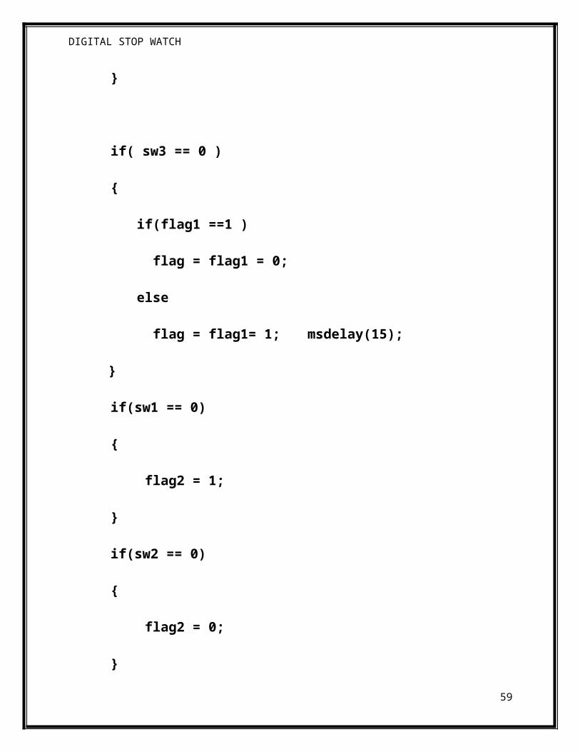
}
if( sw3 == 0 )
{
if(flag1 ==1 )
flag = flag1 = 0;
else
flag = flag1= 1; msdelay(15);
}
if(sw1 == 0)
{
flag2 = 1;
}
if(sw2 == 0)
{
flag2 = 0;
}
59

DIGITAL STOP WATCH
}
}
60
DIGITAL STOP WATCH
CHAPTER 5
5.1 APPLICATIONS.
Laboratory experiments
Sporting events
Competitions
CONCLUSIONAfter completion of this digital stop watch project i have
learnt some knowledge in designing the circuit and understood the
coding process. The circuit has been implemented on bread board
and soldiered on general purpose PCB. This circuit can operate in
two modes with play and pause switches.
REFERENCES
1.) Kenneth .J. Ayala, The 8051 Microcontroller and its
applications, prentice hall, new Edition, 2006. –
“about the microcontroller functioning”
61
DIGITAL STOP WATCH
2.) www.circuitstoday.com – “basics of Seven segment
display , transistor”
3.) www.8051projects.info – “ about at 89S52
microcontroller”
4.) Datasheet’s 434Mhz RF module Rx. Tx. - Cytron
Technologies Sdn. Bhd.
7 segment display –LTS 542/543 LITE ON
ELECTRONICS, INC.
62