LECTURE NOTES COMPILED BY DR. A.O. AKINWUNMI
29
1 | Page LECTURE NOTES COMPILED BY DR. A.O. AKINWUNMI
-
Upload
khangminh22 -
Category
Documents
-
view
3 -
download
0
Transcript of LECTURE NOTES COMPILED BY DR. A.O. AKINWUNMI

1 | P a g e
LECTURE NOTES
COMPILED BY DR. A.O. AKINWUNMI

2 | P a g e
MODULE 1: UNIT 3
LOGIC GATES
UNIT OBJECTIVES
This unit is aimed at:
(i) introducing students to digital logic system.
(ii) fostering understanding of students through exposure to the applications of digital logic system.
LEARNING OUTCOMES
At the end of the unit, students should be able to identify the characteristics and operations of the
different logic gates and how they can be applied in solving real world problems.
3.1 Introduction to Logic Gate
Logic gates are basic electronic circuits that can be used to implement the common elementary logic
expressions, also known as Boolean expressions. The logic gate is the main building block for
combinational circuit. There are three basic logic gates, namely the OR gate, the AND gate and the
NOT gate. Other logic gates that are derived from these basic gates are the NAND gate, the NOR
gate, the EXCLUSIVE OR gate and the EXCLUSIVE-NOR gate.
3.2 Positive and Negative Logic
In most digital logic gates and digital logic systems “Positive logic”, are used in which a logic level
“0” or “LOW” is represented by a zero voltage, 0v or ground and a logic level “1” or “HIGH” is
represented by a higher voltage such as +5 volts, with the switching from one voltage level to the
other, from either a logic level “0” to a “1” or a “1” to a “0” being made as quickly as possible to
prevent any faulty operation of the logic circuit.
A complementary “Negative Logic” system also exist in which the values and the rules of a logic “0”
and a logic “1” are reversed but in this tutorial section about digital logic gates we shall only refer to
the positive logic convention as it is the most commonly used.
The binary variables, as we know, can have either of the two states, i.e. the logic ‘0’ state or the logic
‘1’ state. These logic states in digital systems such as computers, for instance, are represented by two
different voltage levels or two different current levels. If the more positive of the two voltage or
current levels represents a logic ‘1’ and the less positive of the two levels represents a logic ‘0’, then
the logic system is referred to as a positive logic system. If the more positive of the two voltage or
current levels represents a logic ‘0’ and the less positive of the two levels represents a logic ‘1’, then
the logic system is referred to as a negative logic system.

3 | P a g e
3.3 Truth Table
A truth table lists all possible combinations of input binary variables and the corresponding outputs
of a logic system. The logic system output can be found from the logic expression, often referred to
as the Boolean expression, that relates the output with the inputs of that very logic system. When the
number of input binary variables is only one, then there are only two possible inputs, i.e. ‘0’ and ‘1’.
If the number of inputs is two, there can be four possible input combinations, i.e. 00, 01, 10 and 11.
Similarly, for three input binary variables, the number of possible input combinations becomes eight,
i.e. 000, 001, 010, 011, 100, 101, 110 and 111. This statement can be generalized to say that, if a
logic circuit has n binary inputs, its truth table will have 2n possible input combinations, or in other
words 2n rows. A typical illustration of a logic system with two inputs and corresponding truth table
is shown in figure 3.1a and 3.1b
Figure 3.1 a: Logic system Figure 3.1 b: Truth table for logic system
3.4 Logic Gates
The logic gate is the most basic building block of any digital system, including computers. Each one
of the basic logic gates is a piece of hardware or an electronic circuit that can be used to implement
some basic logic expression. While laws of Boolean algebra could be used to do manipulation with
binary variables and simplify logic expressions, these are actually implemented in a digital system
with the help of electronic circuits called logic gates. The three basic logic gates are the OR gate, the
AND gate and the NOT gate.
A logic gate is an electronic device that makes logical decisions based on the different combinations
of digital signals present on its inputs. Logic gates may have more than one input, (A, B, C, etc.) but
generally only have one digital output, (Q). Individual logic gates can be connected together to form
combinational or sequential circuits, or larger logic gate functions. A large number of electronic
circuits (in computers, control units, and so on) are made up of logic gates that process signals which
represent true or false.
Logic gates are electronic circuits that can be used to implement the most elementary logic
expressions, also known as Boolean expressions. The logic gate is the most basic building block of
combinational logic. There are three basic logic gates, namely the OR gate, the AND gate and the
NOT gate. Other logic gates that are derived from these basic gates are the NAND gate, the NOR
gate, the EXCLUSIVEOR gate and the EXCLUSIVE-NOR gate.
Logic gates can be combined together to produce more complex logic circuits (networks). The
output from a logic circuit (network) is verified by producing a truth table. Truth tables are used to
show logic gate functions.

4 | P a g e
3.4.1 OR Gate
An OR gate performs an ORing operation on two or more than two logic variables. The OR operation
on two independent logic variables A and B is written as Y = A+B and reads as Y equals A OR B
and not as A plus B. An OR gate is a logic circuit with two or more inputs and one output. The output
of an OR gate is LOW only when all of its inputs are LOW. For all other possible input combinations,
the output is HIGH. This statement when interpreted for a positive logic system means the following.
The output of an OR gate is a logic ‘0’ only when all of its inputs are at logic ‘0’. For all other possible
input combinations, the output is a logic ‘1’. Figure 3.2 shows the circuit symbol and the truth table
of a two-input OR gate. The operation of a two-input OR gate is explained by the logic expression
Y=A+B
Figure 3.2: Two input OR Gate
The logic or Boolean expression given for a digital logic OR gate is that for Logical Addition which
is denoted by a plus sign, ( + ) giving us the Boolean expression of: A+B = Y.
Thus a logic OR gate can be correctly described as an “Inclusive OR gate” because the output is true
when both of its inputs are true (HIGH). Then we can define the operation of a 2-input logic OR gate
as being:
“If either A or B is true, then Q is true”
2-input Transistor OR Gate
A simple 2-input inclusive OR gate can be constructed using RTL Resistor-transistor switches
connected together as shown below in figure 3.3 with the inputs connected directly to the transistor
bases. Either transistor must be saturated “ON” for an output at Q.
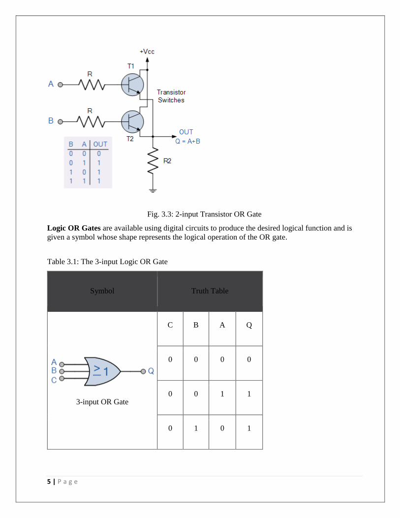
5 | P a g e
Fig. 3.3: 2-input Transistor OR Gate
Logic OR Gates are available using digital circuits to produce the desired logical function and is
given a symbol whose shape represents the logical operation of the OR gate.
Table 3.1: The 3-input Logic OR Gate
Symbol Truth Table
3-input OR Gate
C B A Q
0 0 0 0
0 0 1 1
0 1 0 1

6 | P a g e
0 1 1 1
1 0 0 1
1 0 1 1
1 1 0 1
1 1 1 1
Boolean Expression Q = A+B+C Read as A OR B OR C gives Q
Like the AND gate, the OR function can have any number of individual inputs. However,
commercial available OR gates are available in 2, 3, or 4 inputs types. Additional inputs will
require gates to be cascaded together for example.
Multi-input OR Gate
Fig. 3.4: 6-input “OR” function
The Boolean Expression for this 6-input OR gate will therefore be:
Q = (A+B)+(C+D)+(E+F) In other words: A or B or C or D or E or F gives Q

7 | P a g e
If the number of inputs required is an odd number of inputs any “unused” inputs can be held LOW
by connecting them directly to ground using suitable “Pull-down” resistors.
Commonly available digital logic OR gate IC’s includes:
TTL Logic OR Gates: 74LS32 Quad 2-input
CMOS Logic OR Gates: CD4071 Quad 2-input, CD4075 Triple 3-input, CD4072 Dual 4-input
7432 Quad 2-input Logic OR Gate see figure 3.5
Figure 3.5: 7432 Quad 2-input Logic OR Gate
3.4.2 AND Gate
An AND gate is a logic circuit having two or more inputs and one output. The output of an AND gate
is HIGH only when all of its inputs are in the HIGH state. In all other cases, the output is LOW.
When interpreted for a positive logic system, this means that the output of the AND gate is a logic
‘1’ only when all of its inputs are in logic ‘1’ state. In all other cases, the output is logic ‘0’. The logic
symbol and truth table of a two-input AND gate are shown in Figures 3.6(a) and (b) respectively.
Figure 3.6: 2-input AND gate logic symbol and truth table
The AND operation on two independent logic variables A and B is written as Y = A.B and reads as
Y equals A AND B and not as A multiplied by B. Here, A and B are input logic variables and Y is
the output. An AND gate performs an ANDing operation:
The logic or Boolean expression given for a digital logic AND gate is that for Logical
Multiplication which is denoted by a single dot or full stop symbol, ( . ) giving us the Boolean
expression of: A.B = Q.
Then we can define the operation of a 2-input logic AND gate as being:
8 | P a g e
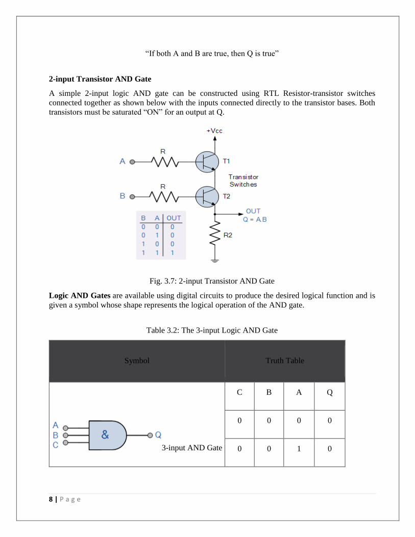
“If both A and B are true, then Q is true”
2-input Transistor AND Gate
A simple 2-input logic AND gate can be constructed using RTL Resistor-transistor switches
connected together as shown below with the inputs connected directly to the transistor bases. Both
transistors must be saturated “ON” for an output at Q.
Fig. 3.7: 2-input Transistor AND Gate
Logic AND Gates are available using digital circuits to produce the desired logical function and is
given a symbol whose shape represents the logical operation of the AND gate.
Table 3.2: The 3-input Logic AND Gate
Symbol Truth Table
3-input AND Gate
C B A Q
0 0 0 0
0 0 1 0

9 | P a g e
0 1 0 0
0 1 1 0
1 0 0 0
1 0 1 0
1 1 0 0
1 1 1 1
Boolean Expression Q = A.B.C Read as A AND B AND C gives Q
Because the Boolean expression for the logic AND function is defined as (.), which is a binary
operation, AND gates can be cascaded together to form any number of individual inputs. However,
commercial available AND gate IC’s are only available in standard 2, 3, or 4-input packages. If
additional inputs are required, then standard AND gates will need to be cascaded together to obtain
the required input value, for example see figure 1.8.
Multi-input AND Gate
Fig. 3.8: 6-input “AND” function

10 | P a g e
The Boolean Expression for this 6-input AND gate will therefore be:
Q = (A.B).(C.D).(E.F)
In other words;
A and B and C and D and E and F gives Q
If the number of inputs required is an odd number of inputs any “unused” inputs can be held HIGH
by connecting them directly to the power supply using suitable “Pull-up” resistors.
Commonly available digital logic AND gate IC’s include:
TTL Logic AND Gates: 74LS08 Quad 2-input see figure 3.9, 74LS11 Triple 3-input, 74LS21 Dual
4-input
CMOS Logic AND Gates: CD4081 Quad 2-input, CD4073 Triple 3-input, CD4082 Dual 4-input
Figure 3.9: 7408 Quad 2-input AND Gate
3.4.3 NOT Gate
A NOT gate is a one-input, one-output logic circuit whose output is always the complement of the
input. That is, a LOW input produces a HIGH output, and vice versa. When using a positive logic
system, a logic ‘0’ at the input produces a logic ‘1’ at the output, and vice versa. It is also known as
a ‘complementing circuit’ or an ‘inverting circuit’. Figure 3.10 a and b show the circuit symbol
and the truth table.
The NOT operation on a logic variable X is
denoted as X or X’. That is, if X is the input to a
NOT circuit, then its output Y is given by Y =
X or X’ and reads as Y equals NOT X. Thus, if
Fig.3.10: NOT gate logic symbol and truth table X = 0,Y = 1 and if X = 1,Y = 0.

11 | P a g e
The Logic NOT Gate is the most basic of all the logical gates and is often referred to as an
Inverting Buffer or simply an Inverter
It is a single input device which has an output level that is normally at logic level “1” and goes
“LOW” to a logic level “0” when its single input is at logic level “1”, in other words it “inverts”
(complements) its input signal. The output from a NOT gate only returns “HIGH” again when its
input is at logic level “0” giving us the Boolean expression of: A = Q.
Then we can define the operation of a single input digital logic NOT gate as being:
“If A is NOT true, then Q is true”
Transistor NOT Gate
A simple 1-input logic NOT gate can be constructed using a RTL Resistor-transistor switches as
shown below with the input connected directly to the transistor base see figure 3.11. The transistor
must be saturated “ON” for an inverted output “OFF” at Q.
Figure 3.11: Transistor NOT Gate
Logic NOT Gates are available using digital circuits to produce the desired logical function. The
standard NOT gate is given a symbol whose shape is of a triangle pointing to the right with a circle
at its end. This circle is known as an “inversion bubble” and is used
in NOT, NAND and NOR symbols at their output to represent the logical operation of
the NOT function. This bubble denotes a signal inversion (complementation) of the signal and can
be present on either or both the output and/or the input terminals.

12 | P a g e
Table 3.3: The Logic NOT Gate Truth Table
Symbol Truth Table
Inverter or NOT Gate
A Q
0 1
1 0
Boolean Expression Q = not A or A Read as inverse of A gives Q
Logic NOT gates provide the complement of their input signal and are so called because when their
input signal is “HIGH” their output state will NOT be “HIGH”. Likewise, when their input signal is
“LOW” their output state will NOT be “LOW”. As they are single input devices, logic NOT gates
are not normally classed as “decision” making devices or even as a gate, such as
the AND or OR gates which have two or more logic inputs. Commercial available NOT gates IC’s
are available in either 4 or 6 individual gates within a single IC package e.g. TTL 7404 Hex
Inverter see figure 3.12.
Figure 3.12: TTL 7404 Hex Inverter
The “bubble” (o) present at the end of the NOT gate symbol above denotes a signal inversion
(complementation) of the output signal. But this bubble can also be present at the gates input to
indicate an active-LOW input. This inversion of the input signal is not restricted to the NOT gate
only but can be used on any digital circuit or gate as shown with the operation of inversion being
exactly the same whether on the input or output terminal. The easiest way is to think of the bubble
as simply an inverter.

13 | P a g e
Signal Inversion using Active-low input Bubble
Figure 3.13: Bubble Notation for Input Inversion
3.4.4 EXCLUSIVE-OR Gate
The EXCLUSIVE-OR gate, commonly written as EX-OR gate, is a two-input, one-output gate.
Figures 3.14 (a) and (b) respectively show the logic symbol and truth table of a two-input EX-OR
gate. As can be seen from the truth table, the output of an EX-OR gate is a logic ‘1’ when the inputs
are unlike and a logic ‘0’ when the inputs are like. Although EX-OR gates are available in integrated
circuit form only as two-input gates, unlike other gates which are available in multiple inputs also,
multiple-input EX-OR logic functions can be implemented using more than one two-input gates. The
truth table of a multiple-input EX-OR function can be expressed as follows. The output of a multiple-
input EX-OR logic function is a logic ‘1’ when the number of 1s in the input sequence is odd and a
logic ‘0’ when the number of 1s in the input sequence is even, including zero. That is, an all 0s input
sequence also produces a logic ‘0’ at the output. Figure 3.14 (c) shows the truth table of a four-input
EX-OR function. The output of a two-input EX-OR gate is expressed by Y=(AB) = A B + A B
Figure 3.14 (a) 2 input exclusive-OR Gate symbol Figure 3.14(b) 2 input exclusive-OR Gate truth
table

14 | P a g e
Figure 3.14 (c) the truth table of a four-input EXCLUSIVE-OR gate
3.4.5 NAND Gate
NAND stands for NOT AND. An AND gate followed by a NOT circuit makes it a NAND gate
[Figure 3.15(a)]. Figure 3.15 (b) shows the circuit symbol of a two-input NAND gate. The truth table
of a NAND gate is obtained from the truth table of an AND gate by complementing the output entries
[Figure 3.15 (c)]. The output of a NAND gate is a logic ‘0’ when all its inputs are a logic ‘1’. For all
other input combinations, the output is a logic ‘1’. NAND gate operation is logically expressed as
Y= BA.
Figure 3.15 (a) Two-input NAND implementation using an AND gate and a NOT circuit, (b) the
circuit symbol of a two-input NAND gate and (c) the truth table of a two-input NAND gate.

15 | P a g e
In general, the Boolean expression for a NAND gate with more than two inputs can be written as Y=
............ EDCBA
NAND gates are available in the form of IC such as TTL 7400 Quad 2 Input NAND see figure 3.16
Figure 3.16: TTL 7400 Quad 2 Input NAND
3.4.6 NOR Gate
NOR stands for NOT OR. An OR gate followed by a NOT circuit makes it a NOR gate [Figure
3.17(a)]. The truth table of a NOR gate is obtained from the truth table of an OR gate by
complementing the output entries. The output of a NOR gate is a logic ‘1’ when all its inputs are
logic ‘0’. For all other input combinations, the output is a logic ‘0’. The output of a two-input NOR
gate is logically expressed as Y= BA
(a) (b)
(c)
Figure 3.17(a) Two-input NOR implementation using an OR gate and a NOT circuit, (b) the circuit
symbol of a two-input NOR gate and (c) the truth table of a two-input NOR gate.

16 | P a g e
In general, the Boolean expression for a NOR gate with more than two inputs can be written as Y=
.... EDCBA
NOR gates are available in the form of IC such as TTL 7402 Quad 2 Input NOR gates see figure
3.18
Figure 3.18: TTL 7402 Quad 2 Input NOR gates
3.4.7 EXCLUSIVE-NOR Gate
EXCLUSIVE-NOR (commonly written as EX-NOR) means NOT of EX-OR, i.e. the logic gate that
we get by complementing the output of an EX-OR gate. Figure 3.19 shows its circuit symbol along
with its truth table.
The truth table of an EX-NOR gate is obtained from the truth table of an EX-OR gate by
complementing the output entries. Logically, Y= B) (A = (A.B + A . B )
Figure 3.19 (a) Circuit symbol of a two-input EXCLUSIVE-NOR gate and (b) the truth table of a
two-input EXCLUSIVE-NOR gate.
The output of a two-input EX-NOR gate is a logic ‘1’ when the inputs are like and a logic ‘0’ when
they are unlike. In general, the output of a multiple-input EX-NOR logic function is a logic ‘0’ when
the number of 1s in the input sequence is odd and a logic ‘1’ when the number of 1s in the input

17 | P a g e
sequence is even including zero. That is, an all 0s input sequence also produces a logic ‘1’ at the
output.
3.4.8 INHIBIT Gate
There are many situations in digital circuit design where the passage of a logic signal needs to be
either enabled or inhibited depending upon certain other control inputs. INHIBIT here means that the
gate produces a certain fixed logic level at the output irrespective of changes in the input logic level.
As an illustration, if one of the inputs of a four-input NOR gate is permanently tied to logic ‘1’ level,
then the output will always be at logic ‘0’ level irrespective of the logic status of other inputs. This
gate will behave as a NOR gate only when this control input is at logic ‘0’ level. This is an example
of the INHIBIT function. The INHIBIT function is available in integrated circuit form for an AND
gate, which is basically an AND gate with one of its inputs negated by an inverter. The negated input
acts to inhibit the gate. In other words, the gate will behave like an AND gate only when the negated
input is driven to a logic ‘0’. Refer to the INHIBIT gate of Figure 3.20(a). If the waveform of Figure
3.20 (b) is applied to the INHIBIT input, draw the waveform at the output.
Figure 3.20a Figure 3.20b
Solution
Since all other inputs of the gate have been permanently tied to logic ‘1’ level, a logic ‘0’ at the
INHIBIT input would produce a logic ‘1’ at the output and a logic ‘1’ at the INHIBIT input would
produce a logic ‘0’ at the output. The output waveform is therefore the inversion of the input
waveform and is shown in Figure 3.20c.

18 | P a g e
Figure 3.20c
3.4.9 Universal Gates
OR, AND and NOT gates are the three basic logic gates as they together can be used to construct
the logic circuit for any given Boolean expression. NOR and NAND gates have the property that
they individually can be used to hardware-implement a logic circuit corresponding to any given
Boolean expression. That is, it is possible to use either only NAND gates or only NOR gates to
implement any Boolean expression. This is so because a combination of NAND gates or a
combination of NOR gates can be used to perform functions of any of the basic logic gates. It is for
this reason that NAND and NOR gates are universal gates.
3.4.10 NAND and NOR Gate Equivalents
An Inverter or logic NOT gate can also be made using standard NAND and NOR gates by
connecting together ALL their inputs to a common input signal for example.
A very simple inverter can also be made using just a single stage transistor switching circuit as
shown.

19 | P a g e
When the transistors base input at “A” is high, the transistor conducts and collector current flows
producing a voltage drop across the resistor Rthereby connecting the output point at “Q” to ground
thus resulting in a zero voltage output at “Q”.
Likewise, when the transistors base input at “A” is low (0v), the transistor now switches “OFF” and
no collector current flows through the resistor resulting in an output voltage at “Q” high at a value
near to +Vcc.
Then, with an input voltage at “A” HIGH, the output at “Q” will be LOW and an input voltage at
“A” LOW the resulting output voltage at “Q” is HIGH producing the complement or inversion of
the input signal.
3.4.11 Gates with Open Collector/Drain Outputs
These are gates where we need to connect an external resistor, called the pull-up resistor, between
the output and the DC power supply to make the logic gate perform the intended logic function.
Depending on the logic family used to construct the logic gate, they are referred to as gates with open
collector output (in the case of the TTL logic family) or open drain output (in the case of the MOS
logic family).
The advantage of using open collector/open drain gates lies in their capability of providing an
ANDing operation when outputs of several gates are tied together through a common pull-up resistor,
without having to use an AND gate for the purpose. This connection is also referred to as WIRE-
AND connection. Figure 3.21(a) shows such a connection for open collector NAND gates. The output
in this case would be Y= AB .CD . EF
Figure 3.21 (a) WIRE-AND connection with open collector/drain devices for NAND Gates

20 | P a g e
Figure 3.21 (b) WIRE-AND connection with open collector/drain devices for NOT Gates.
Figure 3.21(b) shows a similar arrangement for NOT gates. The disadvantage is that they are
relatively slower and noisier. Open collector/drain devices are therefore not recommended for
applications where speed is an important consideration.
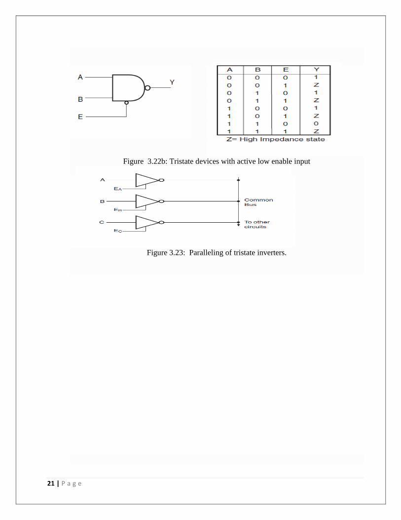
3.4.12 Tristate Logic Gates
Tristate logic gates have three possible output states, i.e. the logic ‘1’ state, the logic ‘0’ state and a
high-impedance state. The high-impedance state is controlled by an external ENABLE input. The
ENABLE input decides whether the gate is active or in the high-impedance state. When active, it can
be ‘0’ or ‘1’ depending upon input conditions. One of the main advantages of these gates is that their
inputs and outputs can be connected in parallel to a common bus line. Figure 3.22(a) shows the circuit
symbol of a tristate NAND gate with active HIGH ENABLE input, along with its truth table. The
one shown in Figure 3.22 (b) has active LOW ENABLE input. When tristate devices are paralleled,
only one of them is enabled at a time. Figure 3.23 shows paralleling of tristate inverters having active
HIGH ENABLE inputs.
Figure 3.22a: Tristate devices with active high enable input
21 | P a g e
Figure 3.22b: Tristate devices with active low enable input
Figure 3.23: Paralleling of tristate inverters.

22 | P a g e
Exercises
1. Consider the figure below and what would the output pulse train look like?
The output pulse train would be:
a= 0, b=1, c=0, d=1, e=0, f=0, g=0, and h=0
2. Sketch the output waveform for the pulsed operation of the gate below
3. How would you hardware-implement a four-input OR gate using two-input OR gates only?
Solution
Figure 1.13(a) shows one possible arrangement of two-input OR gates that simulates a four-input
OR gate. A, B, C and D are logic inputs and Y 3 is the output. Figure 1.13 (b) shows another
possible arrangement. In the case of Fig. 1.13 (a), the output of OR gate 1 is Y1 = (A+B). The
second OR gate produces the output Y 2 = (Y1+C) = (A+B+C). Similarly, the output of OR gate 3
is Y3 = (Y2+D)= (A+B+C+D). In the case of Fig. 1.13(b), the output of OR gate 1 is Y 1 = (A+B).
The second OR gate produces the output Y2 =(C +D). Output Y3 of the third OR gate is given by
(Y1+Y2) = (A+B+C +D).
A
B
X.............................................................................
A
B X

23 | P a g e
4. Draw the output waveform for the OR gate and the given pulsed input waveforms of Fi
5. How can you implement a NOT circuit using a two-input EX-OR gate?
With reference to the truth table of a two-input EX-OR gate, it is clear from the truth table that, if
one of the inputs of the gate is permanently tied to logic ‘1’ level, then the other input and output
perform the function of a NOT circuit. Figure 4.14(b) shows the implementation
Figure 4.14 Implementation of a NOT circuit using an EX-OR gate.
6. Study the following logic system carefully and then complete the truth table that follows:

24 | P a g e
7. Look at the following logic symbols labelled A–E.
a) Which is the correct symbol for an AND gate. ……………
b) Which is the correct symbol for a NOT gate. ……………
c) Which is the correct symbol for a NOR gate. ……………
d) Which is the correct symbol for a NAND gate. ……………
e) Which is the correct symbol for an OR gate. ……………
8. The pinout diagram for a logic IC is shown below.

25 | P a g e
a) How many logic gates are contained in this IC?
b) How many inputs does each gate have?
c) Give the number of the pin connected to the output of gate G?
d) Which two pins should be connected to the power supply?
e) What is the name given to the type of logic gate contained in this IC?
9. The following truth table represents a particular logic function. Use the information in the table
to draw a corresponding logic gate system that will produce this function.
We first have to identify all the combinations of the inputs that cause the output to be logic 1. In
this case it occurs in two rows of the truth table.
We then label these outputs as explained above in the ‘Quick Rule’.
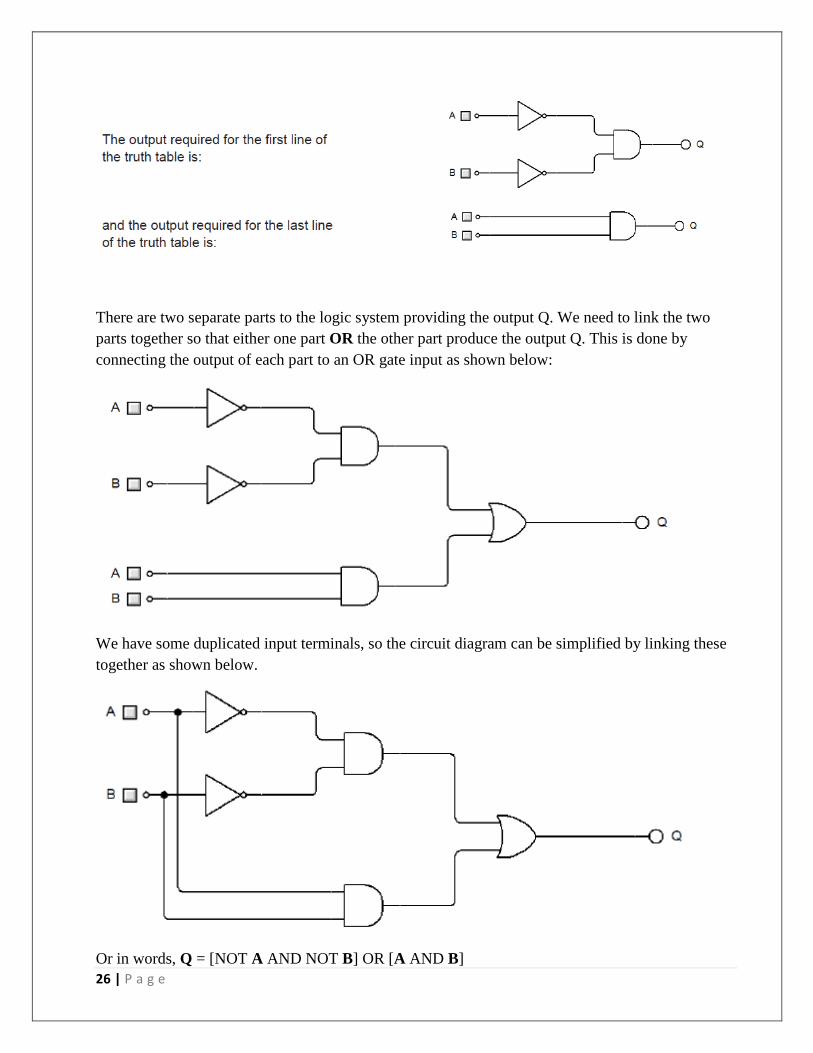
26 | P a g e
There are two separate parts to the logic system providing the output Q. We need to link the two
parts together so that either one part OR the other part produce the output Q. This is done by
connecting the output of each part to an OR gate input as shown below:
We have some duplicated input terminals, so the circuit diagram can be simplified by linking these
together as shown below.
Or in words, Q = [NOT A AND NOT B] OR [A AND B]

27 | P a g e
10. The Boolean equations labelled A–G, below are to be used to answer the following questions.
A) Q = A.B
B) Q = A+B
C) Q = A + B
D) Q = A
E) Q = A.B
F) Q = A.B
G) Q = A + B
i. Which equation is correct for an AND gate?
ii. Which equation is correct for a NOT gate?
iii. Which equation is correct for a NOR gate?
iv. Which equation is correct for a NAND gate?
v. Which equation is correct for an OR gate?
vi. Which equation produces the same logic output as G?
vii. Which equation produces the same logic output as B?
11. A logic system has two input sensors A and B and two outputs. Output 1 is high when sensor A
is high and sensor B is high. Output 2 is high either when sensor A is low and sensor B is high, or
when sensor A is high and sensor B is high.
a) Complete the truth table to satisfy these conditions.
b) Draw the circuit diagram for the logic system.
Solution a) Output 1 is high only when A = 1 and B = 1. Identify this cell in the output 1 column of the truth
table and place a ‘1’ in it. Place zeros in the three other cells in the output 1 column.
Output 2 is high when A = 0 and B = 1, or when A = 1 and B = 1. Identify these two cells in the
output 2 column of the truth table. Place a ‘1’ in these two cells and zeros in the other two.
You should have obtained the following truth table.
Examine the output 1 pattern. You should realise that it is the same pattern as for an AND gate.
Examine the output 2 pattern. You should realise that it is the same as input B.
The circuit diagram can then be drawn.

28 | P a g e
12. Before take-off, the pilot and co-pilot of an aircraft carry out preflight safety checks. When all
checks have been completed they each move a switch from the up to the down position.
• When both switches are up, a red indicator on the instrument panel is on.
• This changes to yellow when at least one of them operates their switch.
• When both have operated their switches, a green indicator comes on.
• The engines can only be started when the green indicator is on.
Assume that the switches provide logic level 0 in the up position and logic level 1 in their down
position. The LED indicators operate on logic level 1.
a) Check the completed truth table for the system.
b) Now we need the logic system that can produce these outputs. Take each one in turn.
For the RED output – there is a standard gate that can produce this output – a NOR gate.
For the YELLOW output – there are actually two ways of generating the YELLOW output.

29 | P a g e
First is a standard gate that can produce the output – an OR gate using inputs A and B.
Alternatively the output Y is the opposite of the RED output. So we could achieve the same
by just inverting the RED output
For GREEN output – again a standard gate can produce this output – an AND gate.
The complete system therefore is: