lcd controller kits LG - Spectrah
32
Professional for LCD panel Complete LCD display kits https://www.spectrah.com/product/lcd%20controller%20board%20selection%20guide.pdf See our product category https://www.spectrah.com/product/index.php Datasheet Product Specification Color TFT-LCD Module
-
Upload
khangminh22 -
Category
Documents
-
view
0 -
download
0
Transcript of lcd controller kits LG - Spectrah

Professional for LCD panel
Complete LCD display kits https://www.spectrah.com/product/lcd%20controller%20board%20selection%20guide.pdf
See our product category https://www.spectrah.com/product/index.php
Datasheet
Product Specification
Color TFT-LCD Module
Product Specification
1 / 27
LC470WU1Liquid Crystal Display
Ver. 1.0 Sep. 21. 2005
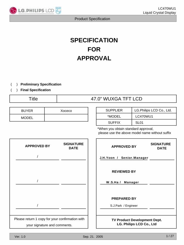
SPECIFICATIONFOR
APPROVAL
))
((
Final SpecificationPreliminary Specification●
47.0” WUXGA TFT LCDTitle
MODEL
XocecoBUYER
*When you obtain standard approval,please use the above model name without suffix
LC470WU1*MODEL
SL01SUFFIX
LG.Philips LCD Co., Ltd.SUPPLIER
TV Product Development Dept.LG. Philips LCD Co., Ltd
S.J.Park / Engineer
PREPARED BY
REVIEWED BY
SIGNATUREDATEAPPROVED BY
Please return 1 copy for your confirmation with
your signature and comments.
/
/
/
SIGNATURE DATEAPPROVED BY
J.H.Yoon / Senior.Manager
W.S.Ha / Manager
Product Specification
2 / 27
LC470WU1Liquid Crystal Display
Ver. 1.0 Sep. 21. 2005
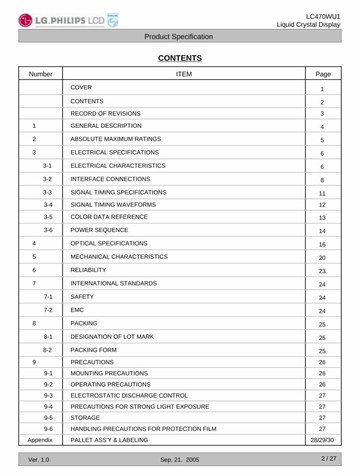
CONTENTS
27HANDLING PRECAUTIONS FOR PROTECTION FILM9-6
28/29/30PALLET ASS’Y & LABELINGAppendix
26PRECAUTIONS9
26MOUNTING PRECAUTIONS9-1
26OPERATING PRECAUTIONS9-2
27ELECTROSTATIC DISCHARGE CONTROL9-3
27PRECAUTIONS FOR STRONG LIGHT EXPOSURE9-4
27STORAGE9-5
13
8INTERFACE CONNECTIONS3-2
COLOR DATA REFERENCE3-5
25DESIGNATION OF LOT MARK8-1
25PACKING FORM8-2
25PACKING8
24EMC7-2
1COVER
2CONTENTS
3RECORD OF REVISIONS
4GENERAL DESCRIPTION1
5ABSOLUTE MAXIMUM RATINGS2
6ELECTRICAL SPECIFICATIONS3
6ELECTRICAL CHARACTERISTICS3-1
11SIGNAL TIMING SPECIFICATIONS3-3
12SIGNAL TIMING WAVEFORMS3-4
14POWER SEQUENCE3-6
16OPTICAL SPECIFICATIONS4
20MECHANICAL CHARACTERISTICS5
23RELIABILITY6
24INTERNATIONAL STANDARDS7
24SAFETY7-1
PageITEMNumber

Product Specification
3 / 27
LC470WU1Liquid Crystal Display
Ver. 1.0 Sep. 21. 2005
RECORD OF REVISIONS
Change of Timing Chart & International Standards11,24July 22. 20050.6
Fill in the Power Consumptions & Rush Current6,7Mar. 16. 20050.1
Change of the Pin Map (Pin No. 26,27,42,43,47)8Mar. 16. 20050.1
Addition of Packing Spec.(Appendix)28,29,30July 28. 20050.7
Fill in the Color coordinates & Gray spec.5,7,17,18Sep. 21. 20051.0
Change of the Luminance & Contrast Ratio4,16May. 03. 20050.2
Preliminary Specification(First Draft) -Feb.17, 20050.0
Change of the Luminance & Timing Chart4,14,15,16June. 01. 20050.3
Addition of the Timing Table(PAL)12Aug. 31. 20050.9
Fill in the Power Consumptions, Change of Burst On Duty Ratio4,6,7Aug. 25. 20050.8
Addition of Interface Timing Value(Min.)11June. 23. 20050.5
Addition of panel Gap & Tolerance21,22June. 13. 20050.4
DescriptionPageRevision DateRevision No.

Product Specification
4 / 27
LC470WU1Liquid Crystal Display
Ver. 1.0 Sep. 21. 2005
1. General DescriptionThe LC470WU1 is a Color Active Matrix Liquid Crystal Display with an integral Cold Cathode FluorescentLamp(CCFL) backlight system. The matrix employs a-Si Thin Film Transistor as the active element.It is a transmissive display type which is operating in the normally black mode. It has a 46.96 inch diagonally measured active display area with WUXGA resolution (1080 vertical by 1920 horizontal pixel array).Each pixel is divided into Red, Green and Blue sub-pixels or dots which are arrayed in vertical stripes.Gray scale or the luminance of the sub-pixel color is determined with a 8-bit gray scale signal for each dot.Therefore, it can present a palette of more than 16.7M(true) colors. It has been designed to apply the 8-bit 2-port LVDS interface.It is intended to support LCD TV, PCTV where high brightness, super wide viewing angle, high color gamut,high color depth and fast response time are important.
CN1(51pin)
LVDS2Port
Source Driver Circuit
TFT - LCD Panel(1920 × RGB × 1080 pixels)
G1
S1 S1920
G1080
Back light Assembly (24CCFL)
Mini-LVDS(RGB)
Timing Controller(LVDS Rx integrated)
Gate D
river Circuit
12Pin X 4CN2Pin X 1CN
+24.0VGND
EEPROM
Power Circuit Block
SDASCL+12.0V
SDRAM
MEMCTRL RGB
VBR for AI
AI_Enable
VBR_OUT
Status
General Features
Viewing angle free ( R/L 178 (Typ.), U/D 178 (Typ.))Viewing Angle (CR>10)
8-bit, 16.7 M colorsColor Depth
1920 horiz. by 1080 vert. Pixels, RGB stripe arrangementPixel Format
550 cd/m2 (Center 1point ,Typ.)Luminance, White
Total 231W (Typ.) (Logic=8.4W, Inverter=223 W [IBL= 5.8] ) Power Consumption
20.0K g (Typ.) Weight
Transmissive mode, Normally blackDisplay Mode
Hard coating(3H), Anti-glare treatment of the front polarizerSurface Treatment
0.5415 mm x 0.5415 mmPixel Pitch
1096.0(H) x 640.0 (V) x 48.1 mm(D) (Typ.)Outline Dimension
46.96 inch (1192.87mm) diagonalActive Screen Size

Product Specification
5 / 27
LC470WU1Liquid Crystal Display
Ver. 1.0 Sep. 21. 2005
2. Absolute Maximum RatingsThe following items are maximum values which, if exceeded, may cause faulty operation or damage to theLCD module.
Table 1. ABSOLUTE MAXIMUM RATINGS
Note : 1. Temperature and relative humidity range are shown in the figure below. Wet bulb temperature should be 39 °C Max. and no condensation of water.
VDC+5.00VBrBrightness Control Voltage
Note 1
°C+400TOPOperating Temperature
VDC+27.021.6VBLBacklight inverter
LCM
Unit
%RH9010HOPOperating Ambient Humidity
%RH9010HSTStorage Humidity
°C+50-20TSTStorage Temperature
VDC+5.25-0.3VON/OFFON/OFF Control Voltage
VDC+14.0-0.3VLCDPower InputVoltage
MaxMinParameter Remark
ValueSymbol
at 25 ± 2 °C
90%
10 20 30 40 50 60 70 800-20
010
20
30
40
50
Dry Bulb Temperature [°C]
Wet BulbTemperature [°C]
Storage
Operation
Hum
idity
[(%
)RH
]
10%
40%
60%
60

Product Specification
6 / 27
LC470WU1Liquid Crystal Display
Ver. 1.0 Sep. 21. 2005
3. Electrical Specifications3-1. Electrical Characteristics
It requires two power inputs. One is employed to power for the LCD circuit. The other Is used for the CCFL backlight and inverter circuit.
Table 2. ELECTRICAL CHARACTERISTICS
1mA800700-
1Watt9.68.4-PLCDPower Consumption
3A5--IRUSHRush current
VDC12.612.011.4VLCDPower Input Voltage
2mA1100980-ILCDPower Input Current
Circuit :
Parameter SymbolMaxTypMin
NoteUnitValue
Note : 1. The specified current and power consumption are under the VLCD=12.0V, 25 ± 2°C, fV=60Hz condition whereas mosaic pattern(8 x 6) is displayed and fV is the frame frequency.
2. The current is specified at the maximum current pattern.3. The duration of rush current is about 2ms and rising time of power input is 1ms (min.).
White : 255GrayBlack : 0Gray
Mosaic Pattern(8 x 6)

Product Specification
7 / 27
LC470WU1Liquid Crystal Display
Ver. 1.0 Sep. 21. 2005
Table 2. ELECTRICAL CHARACTERISTICS (Continue)
A13.212IBLTurn onoperating
Vp-p0.2-0.2Power Supply Input Voltage Ripple
Lamp :
Life Time
Inverter :
3Hrs50,000
W240223-PBLPower Consumption
2VDC3.30VBRBrightness AdjustInput Voltage for Control System
Signals
1
VDC25.224.022.8VBLPower Input Voltage
A10.09.3-IBLPower Input Current
On/OffOff
On VDC5.03.0V on
VDC0.50.0-0.3V off
Parameter SymbolMaxTypMin
NoteUnitValue
Notes :1. Electrical characteristics are determined after the unit has been ‘ON’ and stable for approximately 120
minutes at 25±2°CThe specified current and power consumption are under the typical supply Input voltage, it is total powerconsumption.The ripple voltage of the power supply input voltage is under 0.2 Vp-p.LPL recommend Input Voltage is 24.0V ± 5%.
2. Brightness Control.This VBR Voltage control brightness.
3. The life is determined as the time at which luminance of the lamp is 50% compared to that of initial value at the typical lamp current on condition of continuous operating at 25 ± 2°C.Specified value is when lamp is aligned horizontally.
Minimum Brightness.(Burst On Duty 40%)0V
Maximum Brightness (100%)3.3V
FunctionVBR Voltage

Product Specification
8 / 27
LC470WU1Liquid Crystal Display
Ver. 1.0 Sep. 21. 2005
3-2. Interface ConnectionsThis LCD module employs two kinds of interface connection, a 51-pin connector is used for the module electronics and four 12-pin connectors are used for the integral backlight system.
3-2-1. LCD Module
- LCD Connector(CN1): FI-R51S-HF(manufactured by JAE)- Mating Connector : FI-RE51HL(manufactured by JAE)
Table 3. MODULE CONNECTOR(CN1) PIN CONFIGURATION
-5150494847464544434241403938373635
34333231
30
29
28
27
No
-
Power Supply +12.0VPower Supply +12.0VPower Supply +12.0VPower Supply +12.0VNo connectionGroundGroundGroundNo connection or GroundNo connection or GroundNo connectionNo connectionSECOND CHANNEL 3+
SECOND CHANNEL 3-
GroundSECOND CLOCK CHANNEL C+
SECOND CLOCK CHANNEL C-
GroundSECOND CHANNEL 2+
SECOND CHANNEL 2-
SECOND CHANNEL 1+
SECOND CHANNEL 1-
SECOND CHANNEL 0+
SECOND CHANNEL 0-
No connection or Ground
Description
-VLCD
VLCD
VLCD
VLCDNC
GNDGNDGND
Reserved (NC)Reserved (NC)Reserved (NC)Reserved (NC)
RE3P
RE3N
GND
RECLKP
RECLKN
GND
RE2P
RE2N
RE1P
RE1N
RE0P
RE0N
Reserved (NC)
Symbol
No connectionReserved (NC)25
No connectionReserved (NC)24FIRST CHANNEL 3+RO3P23FIRST CHANNEL 3-RO3N22GroundGND21
FIRST CHANNEL 1+RO1P15FIRST CHANNEL 1-RO1N14FIRST CHANNEL 0+RO0P13FIRST CHANNEL 0-RO0N12GroundGND11
Serial Data for AI & ODMSDA2
Serial Clock for AI & ODMSCL3Serial Data for P-VcomVSDA4
Serial Clock for P-VcomVSCL5Data Write ProtectionWP6Logic ‘L’ Level : LG(NS) FormatLVDS Select7External VBR InputVBR_EXT8VBR OutputVBR_OUT9Logic ‘L’ Level : DisableAI Enable10
FIRST CHANNEL 2-RO2N16
FIRST CHANNEL 2+RO2N17GroundGND18
FIRST CLOCK CHANNEL C-ROCLKN19
FIRST CLOCK CHANNEL C+ROCLKP20
No connection or GroundReserved (NC)26
DescriptionSymbolNo
GND Ground1
Note : 1. All GND(ground) pins should be connected together to the LCD module’s metal frame. 2. All VLCD (power input) pins should be connected together.3. All Input levels of LVDS signals are based on the IEA 664 Standard.4. Specific pins(pin No. #1~#10) are used for internal data process of the LCD module.
If not used, these pins are no connection.

Product Specification
9 / 27
LC470WU1Liquid Crystal Display
Ver. 1.0 Sep. 21. 2005
Table 4. Required signal assignment for Flat Link (NS:DS90C387) Transmitter
Positive LVDS differential data output3
1
2
3
4
5
6
7
8
9
10
11
12
13
14
15
16
17
18
19
20
21
22
23
24
25
26
27
28
D5
D6
D7
GND
D8
D9
D10
VCC
D11
D12
D13
GND
D14
D15
D16
VCC
D17
D18
D19
GND
D20
D21
D22
D23
VCC
D24
D25
VCC
TTL Input(R7)
Ground pin for TTL
Power Supply for TTL Input
Ground pin for TTL
Power Supply for TTL Input
Ground pin for TTL Input
Power Supply for TTL Input
Power Supply for TTL Input
TTL Input(R5)
TTL Input(G0)
TTL Input(G1)
TTL Input(G2)
TTL Input(G6)
TTL Input(G7)
TTL Input(G3)
TTL Input(G4)
TTL Input(G5)
TTL Input(B0)
TTL Input(B6)
TTL Input(B7)
TTL Input(B1)
TTL Input(B2)
TTL Input(B3)
TTL Input(B4)
TTL Input(B5)
TTL Input(HSYNC)
TTL Input(VSYNC)
TTL Input(RSVD)
29
30
31
32
33
34
35
36
37
38
39
40
41
42
43
44
45
46
47
48
49
50
51
52
53
54
55
56
D26
TxCLKIN
PWR DWN
PLL GND
PLL VCC
PLL GND
LVDS GND
TxOUT3+
TxOUT3-
TxCLKOUT+
TxCLKOUT-
TxOUT2+
TxOUT2-
LVDS GND
LVDS VCC
TxOUT1+
TxOUT1-
LVDS GND
D27
D0
D1
GND
D2
D3
D4
GND
TxOUT0+
TxOUT0-
Ground pin for TTL
Ground pin for PLL
Ground pin for PLL
Ground pin for LVDS
Ground pin for LVDS
Ground pin for TTL
Ground pin for TTL
Power Supply for PLL
Power Supply for LVDS
TTL Input(DE)
TTL Input(R6)
TTL Input(R0)
TTL Input(R1)
TTL Input(R2)
TTL Input(R3)
TTL Input(R4)
Negative LVDS differential data output3
Positive LVDS differential clock output
Negative LVDS differential clock output
Positive LVDS differential data output2
Negative LVDS differential data output2
Positive LVDS differential data output1
Negative LVDS differential data output1
Positive LVDS differential data output0
Negative LVDS differential data output0
TTL Level clock Input
Power Down Input
Pin Name Require SignalPin Pin Name Require SignalPin
Notes : 1. Refer to LVDS Transmitter Data Sheet for detail descriptions.2. 7 means MSB and 0 means LSB at R,G,B pixel data

Product Specification
10 / 27
LC470WU1Liquid Crystal Display
Ver. 1.0 Sep. 21. 2005
3-2-2. Backlight Inverter Input Connector-Inverter Connector : S12B-PH-SM3(manufactured by JST) or Equivalent-Mating Connector : PHR-12 or EquivalentStatus Connector-Inverter Connector : 20022WR-02A00(manufactured by Yeon Ho co., Korea)-Mating Connector : 20022HR-02S00(manufactured by Yeon Ho co., Korea)
Table 5. INVERTER CONNECTOR PIN CONFIGULATION
Note : 1. GND should be connected to the LCD module’s metal frame.
2. Minimum Brightness : VBR = 0.0VMaximum Brightness : VBR = 3.3V
3. VON : 3.0 ~ 5.0VVOFF : -0.3 ~ 0.5V
PCB 1 2 3 1211 TopBottom
Component sideInput connector
11 2
Status connector
GNDPOWER GNDGND1
Option Pin(Lamp Open Status Detection)
3Don’t careOn/Off0V ~ 5.0VOn/Off12
StatusUpper 3.0V(Normal), Under 0.7V(Abnormal)
Status2
Don’t care
GND
GND
GND
GND
GND
VBL
VBL
VBL
VBL
VBL
Slave
VBR
GND
GND
GND
GND
GND
VBL
VBL
VBL
VBL
VBL
Master
2
POWER GNDGND7
POWER GNDGND8 1
0V ~ 3.3V VBR11
POWER GNDGND10
POWER GNDGND9
POWER GNDGND6
Power Supply +24.0VVBL5
Power Supply +24.0VVBL4
Power Supply +24.0VVBL3
Power Supply +24.0VVBL2
Power Supply +24.0VVBL1
NoteDescriptionSymbolPin No

Product Specification
11 / 27
LC470WU1Liquid Crystal Display
Ver. 1.0 Sep. 21. 2005
3-3. Signal Timing Specifications
Table 6 shows the signal timing required at the input of the LVDS transmitter. All of the interface signal timing should be satisfied with the following specification for normal operation.
Table 6. TIMING TABLE for NTSC (DE Only Mode)
Horizontal
Vertical Lines694511tVBBlank
Lines-1080-tVVDisplayPeriod
Lines114911251091tVPTotal
Total
Blank
DisplayPeriod
tHP
tHB
tHV
Symbol
2200/2tclk128011001060
tclk320140100
tclk-960-
NoteUnitMaxTypMinITEM
Frequency
Vertical
Horizontal
DCLK
fVfH
fCLK
Symbol
Hz636057
KHz68.967.565.5
148.5/2MHz7774.2570
NoteUnitMaxTypMinITEM
Note : The Input of HSYNC & VSYNC signal does not have an effect on normal operation(DE Only Mode).
The performance of the electro-optical characteristics may be influenced by variance of the vertical refresh rate.

Product Specification
12 / 27
LC470WU1Liquid Crystal Display
Ver. 1.0 Sep. 21. 2005
Table 7 shows the signal timing required at the input of the LVDS transmitter. All of the interface signal timing should be satisfied with the following specification for normal operation.
Table 7. TIMING TABLE for PAL (DE Only Mode)
Horizontal
Vertical Lines654525tVBBlank
Lines-1080-tVVDisplayPeriod
Lines114511251105tVPTotal
Total
Blank
DisplayPeriod
tHP
tHB
tHV
Symbol
2200/2tclk120011001060
tclk240140100
tclk-960-
NoteUnitMaxTypMinITEM
Frequency
Vertical
Horizontal
DCLK
fVfH
fCLK
Symbol
Hz535047
KHz57.2556.2555.25
123.75/2MHz67.561.8859.63
NoteUnitMaxTypMinITEM
Note : The Input of HSYNC & VSYNC signal does not have an effect on normal operation(DE Only Mode).
The performance of the electro-optical characteristics may be influenced by variance of the vertical refresh rate.

Product Specification
13 / 27
LC470WU1Liquid Crystal Display
Ver. 1.0 Sep. 21. 2005
3-4. Signal Timing Waveforms
0.7VDD
0.3VDDDE, Data
Valid data
Pixel 0,0 Pixel 2,0
tCLK 0.5 VDDDCLK
Pixel 1,0 Pixel 3,0
Invalid data Invalid data
Invalid data Invalid data
DE(Data Enable)
Valid data
tVP
tWV
tVBP tVV tVFPVSync
DE(Data Enable)
tHP
tHBP tHV tHFP
tWH
* tHB = tHFP + tWH +tHBP* tVB = tVFP + tWV +tVBP
First data
Second data
* Reference : Sync. Relation
HSync
DE(Data Enable)
Product Specification
14 / 27
LC470WU1Liquid Crystal Display
Ver. 1.0 Sep. 21. 2005
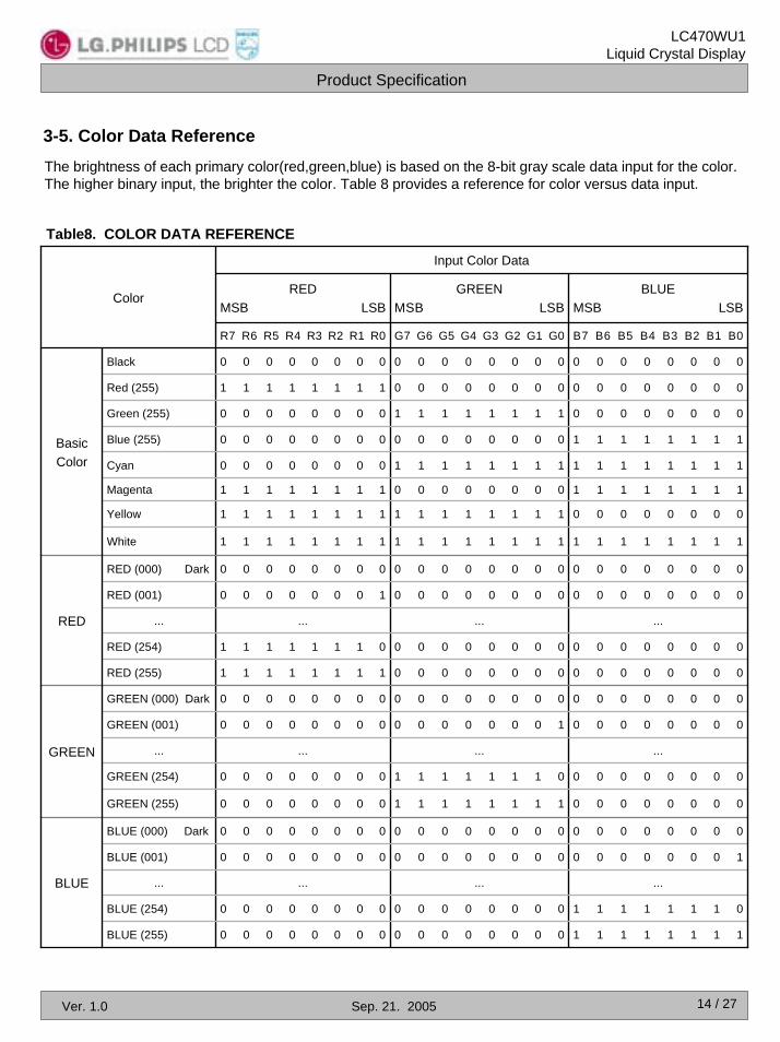
3-5. Color Data ReferenceThe brightness of each primary color(red,green,blue) is based on the 8-bit gray scale data input for the color.The higher binary input, the brighter the color. Table 8 provides a reference for color versus data input.
Table8. COLOR DATA REFERENCE
0 0 0 0 0 0 0 0 0 00 0 0 0 0 0 00 GREEN (00 0 0 0 0 0 00) Dark
GREEN
0 0 0 0 0 0 0 0 0 00 0 0 0 0 0 0 1 0 0 0 0 0 0GREEN (001)
............
0 0 0 1 1 0 0 0 0 01 1 1 0 0 1 1 0 0 0 0 0 0 0GREEN (254)
0 0 0 1 1 0 0 0 0 01 1 1 0 0 1 1 1 0 0 0 0 0 0GREEN (255)
0 0 0 0 0 0 0 0 0 00 0 0 0 0 0 00 RED (000) Dark 0 0 0 0 0 0
RED
0 0 0 0 0 0 0 0 0 00 0 0 0 0 0 0 0 0 0 0 0 0 1RED (001)
............
0 0 0 0 0 0 0 0 0 00 0 0 1 1 0 0 0 1 1 1 1 1 0RED (254)
0 0 0 0 0 0 0 0 0 00 0 0 1 1 0 0 0 1 1 1 1 1 1RED (255)
0 0 0 0 0 0 0 0 0 10 0 0 0 0 0 0 0 0 0 0 0 0 0BLUE (001)
............
1 1 1 0 0 1 1 1 1 00 0 0 0 0 0 0 0 0 0 0 0 0 0BLUE (254)
1 1 1 0 0 1 1 1 1 10 0 0 0 0 0 0 0 0 0 0 0 0 0BLUE (255)
BLUE (000) Dark 0
White
Yellow
Magenta
Cyan
Blue (255)
Green (255)
Red (255)
Black 0 0 0 0 0 0 0 0 0 00 0 0 0 0 0 0 0 0 0 0 0 0 0
BasicColor
0 0 0 0 0 0 0 0 0 00 0 0 1 1 0 0 0 1 1 1 1 1 1
0 0 0 1 1 0 0 0 0 01 1 1 0 0 1 1 1 0 0 0 0 0 0
1 1 1 0 0 1 1 1 1 10 0 0 0 0 0 0 0 0 0 0 0 0 0
1 1 1 1 1 1 1 1 1 11 1 1 0 0 1 1 1 0 0 0 0 0 0
1 1 1 0 0 1 1 1 1 10 0 0 1 1 0 0 0 1 1 1 1 1 1
0 0 0 1 1 0 0 0 0 01 1 1 1 1 1 1 1 1 1 1 1 1 1
1 1 1 1 1 1 1 1 1 11 1 1 1 1 1 1 1 1 1 1 1 1 1
BLUEMSB SB LSB
GREENMMSB LSB
RED LSB
B77 G6 G5 G4 G3 G2 G1 G0 B6 B5 B4 B3 B2 B1 B0GR7 R6 R5 R4 R3 R2 R1 R0
0 0 0 0 0 0 0 0 0 00 0 0 0 0 0 0 0 0 0 0 0 0
BLUE
Color
Input Color Data

Product Specification
15 / 27
LC470WU1Liquid Crystal Display
Ver. 1.0 Sep. 21. 2005
3-6. Power Sequence3-6-1. LCD Driving circuit
Interface Signal (Tx)
Power for Lamp
Power Supply For LCDVLCD
10%0V
90% 90%
10%
T1 T2 T5 T6 T7
T3 T4
Valid Data
Lamp ON
T8 T9Option Signal (AI_Enable)
Table 9. POWER SEQUENCE
ms300--T6
s--1.0T7
ms0 < T9 < T5T9
ms0 < T8 < T2T8
ms50-0.5T2
ms
ms--200T3
--200T4
ms50-0.5T5
ms20-0.5T1
MaxTypMinUnit
ValueParameter
Note : 1. Please avoid floating state of interface signal at invalid period.2. When the interface signal is invalid, be sure to pull down the power supply VLCD to 0V.3. Flicker would come out when power on-off(T7=under 2s) is tested over several ten-times.4. The case when the T2/T5 exceed maximum specification, it operates protection
pattern(Black pattern) till valid signal inputted. There is no reliability problem.5. The T3/T4 is recommended value, the case when failed to meet a minimum specification,
abnormal display would be shown. There is no reliability problem.

Product Specification
16 / 27
LC470WU1Liquid Crystal Display
Ver. 1.0 Sep. 21. 2005
3-6-2. On/Off for Inverter
VBL(Min) x 0.8ms10--T4
After Inverter’s connected
Remark
ms--500T2
ms--0T3
ms-20T1
MaxTypMinUnit
ValueParameter
Table 10. POWER SEQUENCE FOR INVERTER
Enable(On/Off)
VBR
Power For Inverter
VBL 10%0V
90%
T1 T2
24V (typ.)
T3
3-6-3. Deep condition for Inverter
0V
VBL
T4
VBL (Min) x 0.8

Product Specification
17 / 27
LC470WU1Liquid Crystal Display
Ver. 1.0 Sep. 21. 2005
4. Optical SpecificationOptical characteristics are determined after the unit has been ‘ON’ and stable for approximately 2 Hrs in a dark environment at 25±2°C. The specified optical values are measured at an approximate 50cm distance from the LCD surface on condition that viewing angle of Φ and θ equal to 0 °.FIG. 1 shows additional information concerning the measurement equipment and method.
LCD ModuleOptical Stage(x,y) Pritchard 880 orequivalent
50cmFIG. 1 Optical Characteristic Measurement Equipment and Method
Table 11. OPTICAL CHARACTERISTICS Ta= 25±2°C, VLCD=12.0V, fV=60Hz, Dclk=148.5MHz VBR=3.3V
With AI
CR with AI -1600TBD
Without AI
-800TBDCR
6Gray Scale
5P
y axis, down (φ=270°)y axis, up (φ=90°)x axis, left (φ=180°)x axis, right(φ=0°)
-8985θd-8985θu-8985θl
5degree
-8985θr
Viewing Angle (CR>10)
WHITE
BLUE
GREEN
RED
0.611Gy0.279Gx
0.062By0.146Bx
0.278Wy0.272Wx
ms
0.340Ry
Typ +0.03
0.638
Typ-0.03
Rx
Color Coordinates [CIE1931]
4168TrR , TrDResponse Time(Gray-to-Gray)
31.3δ WHITELuminance Variation2cd/m2550TBDLWHSurface Luminance, white
1
NoteUnit
Contrast Ratio
MaxTypMinValue
SymbolParameter
Product Specification
18 / 27
LC470WU1Liquid Crystal Display
Ver. 1.0 Sep. 21. 2005
Note :1. Contrast Ratio(CR) is defined mathematically as :
Surface Luminance with all white pixelsContrast Ratio =
Surface Luminance with all black pixelsMeasure Position : Center 1-point.
2. Surface Luminance(LWH) is the luminance value measured at an approximate 50cm distance from
the center 1-point of LCD surface as all pixels displaying white. See FIG. 2 for more information.
3. The variation of surface luminance , δ WHITE is defined as :
δ WHITE(5P) = Maximum(Lon1,Lon2, Lon3, Lon4, Lon5) / Minimum(Lon1,Lon2, Lon3, Lon4, Lon5)
Where Lon1 to Lon5 are the luminance with all pixels displaying white at 5 locations . For more information, see the FIG. 2.
4. Response time is defined as the required time for the transition from G(N) to G(M) (Rise Time, TrR) and from G(M) to G(N) (Decay Time, TrD). For additional information see the FIG. 3. (N<M)
5. Viewing angle is the angle at which the contrast ratio is greater than 10. The angles aredetermined for the horizontal or x axis and the vertical or y axis with respect to the z axis whichis normal to the LCD module surface. For more information, see the FIG. 4.
6. See Table 12 for gray scale specification
Table 12. GRAY SCALE SPECIFICATION
10087.375.3264.4254.2644.136.4828.8622.517.1912.217.954.672.360.960.330.16
Luminance [%] (Typ.)
10085.072.460.250.440.832.625.519.514.210.36.2
3.561.8
0.640.130.06
Luminance [%] (Typ.) with AI
L239L255
L159L175L191L207
L111L127L143
L223
L47L63L79L95
L31L15L0
Gray Level

Product Specification
19 / 27
LC470WU1Liquid Crystal Display
Ver. 1.0 Sep. 21. 2005
Measuring point for surface luminance & measuring point for luminance variation.
H
A
V
B
①
③②
⑤④A : H / 4 mmB : V / 4 mmH : 1039.68 mmV : 584.82 mm@ H,V : Active Area
FIG. 2 5 Points for Luminance Measure
Response time is defined as the following figure and shall be measured by switching the input signal for “Gray(N)” and “Gray(M)”.
Gray(M)Gray(N)
TrR TrD10090
10
0
Optical Response
N,M = 0(Black)~255(White), N<MGray(N)
FIG. 3 Response Time

Product Specification
20 / 27
LC470WU1Liquid Crystal Display
Ver. 1.0 Sep. 21. 2005
Dimension of viewing angle range
Normal Y E
φ
θ
φ = 0 °, Right
φ = 180 °, Left
φ = 270 °, Down
φ = 90 °, Up
FIG. 4 Viewing Angle

Product Specification
21 / 27
LC470WU1Liquid Crystal Display
Ver. 1.0 Sep. 21. 2005
5. Mechanical Characteristics
Table 13 provides general mechanical characteristics.
Table 13. MECHANICAL CHARACTERISTICS
ValueItem
584.82 mmVertical
Hard coating(3H)Anti-glare treatment of the front polarizerSurface Treatment
20.0 Kg (Typ.)Weight
593.0 mmVertical
640.0 mmVertical
48.1 mmDepth
1039.68 mmHorizontalActive Display Area
1047.8 mmHorizontalBezel Area
1096.0 mmHorizontal
Outline Dimension
Note : Please refer to page21 and 22 for mechanic drawings in terms of tolerance.

Product Specification
22 / 27
LC470WU1Liquid Crystal Display
Ver. 1.0 Sep. 21. 2005
<FRONT VIEW>

Product Specification
23 / 27
LC470WU1Liquid Crystal Display
Ver. 1.0 Sep. 21. 2005
<REAR VIEW>

Product Specification
24 / 27
LC470WU1Liquid Crystal Display
Ver. 1.0 Sep. 21. 2005
6. Reliability
Table 14. ENVIRONMENT TEST CONDITION
Ta= 40 °C, 90%RHHumidity condition Operation7
0 - 14,000 feet(4267.2m)0 - 40,000 feet(12192m)
Altitude operatingstorage / shipment8
Shock level :50G(X,Y axis) , 35G(Z axis)Waveform : half sine wave, 11msDirection : ±X, ±Y, ±Z
One time each direction
Shock test(non-operating)6
Wave form : randomVibration level : 1.0G RMSBandwidth : 10-300HzDuration : 30 min for X,Y,Z axis
One time each direction
Vibration test(non-operating)5
Ta= 0°C 240hLow temperature operation test4
Ta= 40°C 50%RH 240hHigh temperature operation test3
Ta= -20°C 240hLow temperature storage test2
Ta= 50°C 240hHigh temperature storage test1
ConditionTest ItemNo.

Product Specification
25 / 27
LC470WU1Liquid Crystal Display
Ver. 1.0 Sep. 21. 2005
7. International Standards
7-1. Safety
a) UL 60950-1:2003, First Edition, Underwriters Laboratories, Inc.,Standard for Safety of Information Technology Equipment.b) CAN/CSA C22.2, No. 60950-1-03 1st Ed. April 1, 2003, Canadian Standards Association,Standard for Safety of Information Technology Equipment.c) EN 60950-1:2001, First Edition, European Committee for Electrotechnical Standardization(CENELEC)European Standard for Safety of Information Technology Equipment.
7-2. EMC
a) ANSI C63.4 “Methods of Measurement of Radio-Noise Emissions from Low-Voltage Electrical and Electrical Equipment in the Range of 9kHZ to 40GHz. “American National Standards Institute(ANSI),1992b) C.I.S.P.R. “Limits and Methods of Measurement of Radio Interface Characteristics of InformationTechnology Equipment.“ International Special Committee on Radio Interference.c) EN 55022 “Limits and Methods of Measurement of Radio Interface Characteristics of InformationTechnology Equipment.“ European Committee for Electrotechnical Standardization.(CENELEC), 1998( Including A1: 2000 )

Product Specification
26 / 27
LC470WU1Liquid Crystal Display
Ver. 1.0 Sep. 21. 2005
8. Packing8-1. Designation of Lot Mark
a) Lot Mark
A B C D E F G H I J K L M
A,B,C : SIZE(INCH) D : YEAR E : MONTH F : FACTORY CODEG : ASSEMBLY CODE H, I, J, K, L, M : SERIAL NO.
Note1. YEAR
Mark
Year
0
2010
6
2006
7
2007
8
2008
9
2009
4
2004
5
2005
321
200320022001
2. MONTH
B
Nov
Mark
Month
A
Oct
6
Jun
7
Jul
8
Aug
9
Sep
4
Apr
5
May
C321
DecMarFebJan
3. FACTORY CODE
C
LPL Nanjing
D
HEESUNG
Mark
Factory Code
K
LPL Gumi
4. SERIAL NO.
Mark 100001~199999, 200001~299999, 300001~399999, …., A00001~A99999, ….., Z00001~Z99999
b) Location of Lot Mark
Serial No. is printed on the label. The label is attached to the backside of the LCD module.This is subject to change without prior notice.
8-2. Packing Forma) Package quantity in one pallet : 10 pcs
b) Pallet Size : 1220mm X 1140mm X 860mm

Product Specification
27 / 27
LC470WU1Liquid Crystal Display
Ver. 1.0 Sep. 21. 2005
9. Precautions
Please pay attention to the followings when you use this TFT LCD module.
9-1. Mounting Precautions(1) You must mount a module using holes arranged in four corners or four sides.(2) You should consider the mounting structure so that uneven force (ex. Twisted stress) is not applied to the
module. And the case on which a module is mounted should have sufficient strength so that external force is not transmitted directly to the module.
(3) Please attach the surface transparent protective plate to the surface in order to protect the polarizer.Transparent protective plate should have sufficient strength in order to the resist external force.
(4) You should adopt radiation structure to satisfy the temperature specification.(5) Acetic acid type and chlorine type materials for the cover case are not desirable because the former
generates corrosive gas of attacking the polarizer at high temperature and the latter causes circuit break by electro-chemical reaction.
(6) Do not touch, push or rub the exposed polarizers with glass, tweezers or anything harder than HBpencil lead. And please do not rub with dust clothes with chemical treatment.Do not touch the surface of polarizer for bare hand or greasy cloth.(Some cosmetics are detrimentalto the polarizer.)
(7) When the surface becomes dusty, please wipe gently with absorbent cotton or other soft materials like chamois soaks with petroleum benzine. Normal-hexane is recommended for cleaning the adhesives used to attach front / rear polarizers. Do not use acetone, toluene and alcohol because they cause chemical damage to the polarizer.
(8) Wipe off saliva or water drops as soon as possible. Their long time contact with polarizer causes deformations and color fading.
(9) Do not open the case because inside circuits do not have sufficient strength.
9-2. Operating Precautions
(1) The spike noise causes the mis-operation of circuits. It should be lower than following voltage : V=±200mV(Over and under shoot voltage)
(2) Response time depends on the temperature.(In lower temperature, it becomes longer.)(3) Brightness depends on the temperature. (In lower temperature, it becomes lower.)
And in lower temperature, response time(required time that brightness is stable after turned on) becomeslonger.
(4) Be careful for condensation at sudden temperature change. Condensation makes damage to polarizer or electrical contacted parts. And after fading condensation, smear or spot will occur.
(5) When fixed patterns are displayed for a long time, remnant image is likely to occur.(6) Module has high frequency circuits. Sufficient suppression to the electromagnetic interference shall be
done by system manufacturers. Grounding and shielding methods may be important to minimized theinterference.
(7) Please do not give any mechanical and/or acoustical impact to LCM. Otherwise, LCM can’t be operated its full characteristics perfectly.
(8) A screw which is fastened up the steels should be a machine screw. (if not, it causes metallic foreign material and deal LCM a fatal blow)
(9) Please do not set LCD on its edge.

Product Specification
28 / 27
LC470WU1Liquid Crystal Display
Ver. 1.0 Sep. 21. 2005
9-3. Electrostatic Discharge ControlSince a module is composed of electronic circuits, it is not strong to electrostatic discharge. Make certain that treatment persons are connected to ground through wrist band etc. And don’t touch interface pin directly.
9-4. Precautions for Strong Light ExposureStrong light exposure causes degradation of polarizer and color filter.
9-5. StorageWhen storing modules as spares for a long time, the following precautions are necessary.
(1) Store them in a dark place. Do not expose the module to sunlight or fluorescent light. Keep the temperature between 5°C and 35°C at normal humidity.
(2) The polarizer surface should not come in contact with any other object.It is recommended that they be stored in the container in which they were shipped.
9-6. Handling Precautions for Protection Film(1) The protection film is attached to the bezel with a small masking tape.
When the protection film is peeled off, static electricity is generated between the film and polarizer.This should be peeled off slowly and carefully by people who are electrically grounded and with well ion-blown equipment or in such a condition, etc.
(2) When the module with protection film attached is stored for a long time, sometimes there remains a very small amount of glue still on the bezel after the protection film is peeled off.
(3) You can remove the glue easily. When the glue remains on the bezel surface or its vestige is recognized, please wipe them off with absorbent cotton waste or other soft material like chamois soaked with normal-hexane.

Product Specification
29 / 27
LC470WU1Liquid Crystal Display
Ver. 1.0 Sep. 21. 2005
# APPENDIX-Ⅰ■LC470WU1-SL01 Pallet Ass’y
ANGLE COVER8
ANGLE PACKING7
6
PAPER 1220X1140X138MMPALLET4
MASKING 20MM X 50MTAPE3
47INCHBAG2
LCD Module1
MATERIALDESCRIPTIONNO.
PACKING
PAPER
PAPER
EPS
PACKING EPS5
BAND,CLIP9 STEEL
LABEL11 YUPO PAPER 80G 100X100
BAND10 PP
A- 1 / 3
Product Specification
30 / 27
LC470WU1Liquid Crystal Display
Ver. 1.0 Sep. 21. 2005
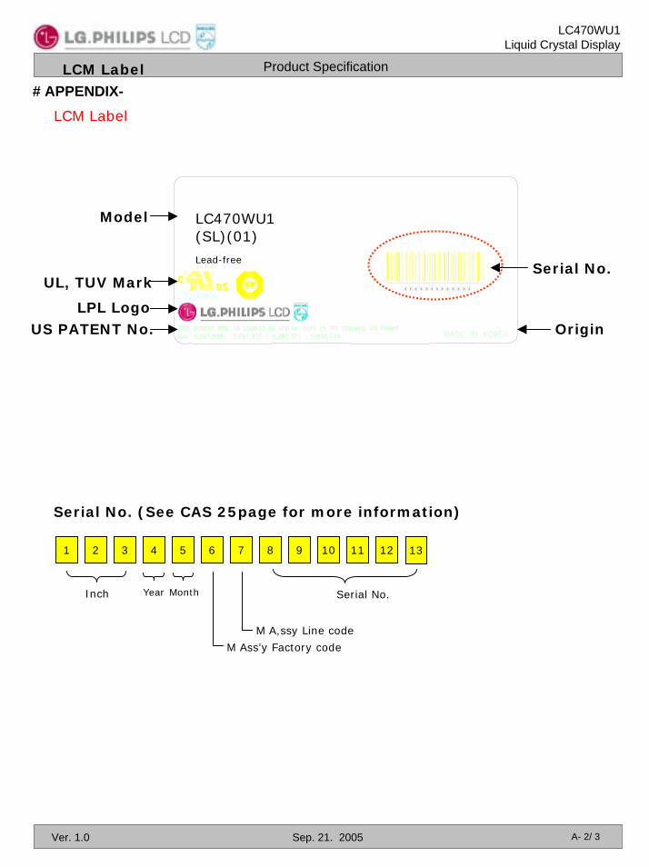
■ LCM Label# APPENDIX-Ⅱ■ LCM Label
Model
UL, TUV Mark
LPL LogoUS PATENT No.
LC470WU1(SL)(01)Lead-free
Serial No.
Origin
8
■ Serial No. (See CAS 25page for more information)
1 2 3 4 5 6 7 9 10 11 12
Inch
M Ass’y Factory code
M A,ssy Line code
Serial No.
13
MonthYear
A- 2/ 3

Product Specification
31 / 27
LC470WU1Liquid Crystal Display
Ver. 1.0 Sep. 21. 2005
# APPENDIX- Ⅲ
■ Pallet Label
10
LC470WU1
SL01
A- 3 / 3